growth and characterization of in-plane solid-liquid-solid
TRANSCRIPT

HAL Id: tel-02422227https://tel.archives-ouvertes.fr/tel-02422227
Submitted on 21 Dec 2019
HAL is a multi-disciplinary open accessarchive for the deposit and dissemination of sci-entific research documents, whether they are pub-lished or not. The documents may come fromteaching and research institutions in France orabroad, or from public or private research centers.
L’archive ouverte pluridisciplinaire HAL, estdestinée au dépôt et à la diffusion de documentsscientifiques de niveau recherche, publiés ou non,émanant des établissements d’enseignement et derecherche français ou étrangers, des laboratoirespublics ou privés.
Growth and characterization of in-planesolid-liquid-solid GeSn and SiSn nanowires
Edy Edward Azrak
To cite this version:Edy Edward Azrak. Growth and characterization of in-plane solid-liquid-solid GeSn and SiSnnanowires. Materials. Normandie Université, 2018. English. �NNT : 2018NORMR135�. �tel-02422227�

THÈSE
Pour obtenir le diplôme de doctorat
Spécialité Physique – Science des Matériaux
Préparée au sein de l’Université de Rouen Normandie
Growth and Characterization of In-Plane Solid-Liquid-Solid
GeSn and SiSn Nanowires
Présentée et soutenue par
Edy Edward Azrak
Thèse dirigée par Philippe PAREIGE, laboratoire Groupe de Physique des Matériaux.
Thèse soutenue publiquement le 20 Décembre 2018
devant le jury composé de
Mme. Caroline BONAFOS Directrice de Recherche – CEMES/
Université de Toulouse 3 - Toulouse Rapporteur
M. Christophe DELERUE Directeur de Recherche – IEMN/ Université
de Lille 1 - Lille Examinateur
M. Moustafa EL-KURDI Maitre de Conférences HDR – C2N/
Université Paris Saclay - Orsay Rapporteur
M. Pere Roca i CABARROCAS Directeur de Recherche – LPICM/ Ecole
polytechnique – Palaiseau Examinateur
M. Sébastien DUGUAY Maitre de conférences – GPM/ Université
de Rouen Normandie Encadrant
M. Philippe PAREIGE Professeur – GPM/ Université de Rouen
Normandie Directeur de thèse


ABSTRACT
Germanium-Tin alloy is a unique class semiconductor gaining a strong attention because
of its significant electrical and optical properties. Sn incorporation in Ge allows straightforward
band-gap engineering enabling to enhance the electron and hole mobilities, and for a sufficient Sn
amount an indirect-to-direct band-gap transition occurs. Its versatility rises due the possible
monolithic integration on Si-platforms making it an ideal material in domains of optoelectronics,
and high speed electronic devices.
This thesis has focused on the fabrication and characterization of crystalline Ge1-xSnx
nanowires with high Sn concentrations. New strategies were designed to fabricate many types of
GeSn nanowires. The results have been explained as function of the existing kinetic models. A
new growth mechanism was reported (i.e. Solid-Solid-Solid mechanism – SSS), it consists of
growing in-plane GeSn nanowires using Sn catalysts below the melting point of Sn. Four mass
transport models were proposed for the SSS growth mechanism. Various characterizations (e.g.
TEM and APT) were done to investigate the physical and chemical properties of the obtained
nanowires.
Keywords: Germanium-Tin (GeSn), semiconductor, band-gap, nanowires, catalyst,
growth, solid-liquid-solid, solid-solid-solid, characterizations.

RÉSUMÉ
L’alliage germanium-étain est un semiconducteur qui suscite une grande attention en
raison de ses propriétés électriques et optiques. L’incorporation de Sn dans le germanium permet
d’ajuster la largeur de bande interdite (gap) et d’améliorer la mobilité des électrons et des trous,
et pour une quantité suffisante d’étain, le matériau passe d’un gap indirect à direct. Cet alliage est
versatile parce qu’il peut être intégré d’une façon monolithique sur le Si, c’est ce qui en fait un
matériau idéal dans les domaines de l'optoélectronique à base de silicium.
Cette thèse est sur la fabrication et la caractérisation de nanofils cristallins Ge1-xSnx à
haute concentration en Sn. Des nouvelles stratégies ont été employées pour fabriquer de
nombreux types de nanofils GeSn. Les résultats ont été expliqués en fonction des modèles
cinétiques existants. Un nouveau mécanisme de croissance y est décrit: le mécanisme solide-
solide-solide – SSS. Il consiste à faire croître des nanofils de GeSn dans le plan du substrat à
l’aide de catalyseurs d’étain à une température inférieure au point de fusion de Sn. Quatre
modèles de transport de masse sont proposés pour le mécanisme de croissance du SSS. Diverses
caractérisations (par exemple TEM et APT) ont été effectuées pour étudier les propriétés
physiques, et chimiques des nanofils.
Mot-Clés: Germanium-Étain (GeSn), semiconducteur, bande interdite, nanofils,
catalyseur, croissance, solide-liquide-solide, solide-solide-solide, caractérisation.

ACKNOWLEDGEMENT
The thesis was carried out in the laboratory Material Physics Group (GPM) UMR CNRS
6634 – University of Rouen Normandy and INSA Rouen Normandy. A part of this work was
done in collaboration with Laboratory of Physics of Interfaces and Thin Films (LPICM) in École
Polytechnique Palaiseau.
First I would like to thank my director Pr. Philippe Pareige and my supervisor Dr.
Sébastien Duguay for their support, help, and discussions during my PhD. I am thankful to my
thesis director for giving me the opportunity to work on this topic, as well as my supervisor for
his indispensable guidance over the last several years. I appreciate their encouragement and
knowledge which were crucial and vital to achieve the objectives of this thesis. I also enjoyed
their humorous spirits, and care over the past several years.
I had a great fortune to be hosted by Pr. Pere Roca i Cabarrocas in LPICM. His invaluable
guidance, high expertise and great enthusiasm were essential ingredients in the success of this
PhD. I am very grateful of this fruitful collaboration.
I extend my gratitude to Dr. Wanghua Chen who was at that time in LPICM. By working
closely together, I have learned a lot about catalyst preparations, thin-film depositions, and
nanowires growth. I appreciate his dynamism and motivation despite many drawbacks in our
work.
I would like to thank the jury who accepted to evaluate this PhD: Mr. Christophe Delerue,
Research Director at IEMN from University of Lille who made me honored by accepting to be
the president of the jury; Mrs. Caroline Bonafos, Research Director at CEMES from University
of Toulouse and Mr. Moustafa El-Kurdi, Lecturer-Researcher at C2N from University of Paris-
Saclay, who made me grateful by accepting to be the rapporteurs of my thesis, and Mr. Pere Roca
i Cabarrocas, Research Director at LPICM from École Polytehnique Palaiseau, who made me
very honored by accepting to be the examiner in this jury.

I thank all the GPM and LPICM people and especially my close colleagues who made this
PhD an enjoyable venture.
I sent my warmest thanks to Dr. Chantal Karam for her precious contributions,
unwavering support, encouragement, and patience. Without any doubt, her heart-blessings were
invaluable to reach this milestone in my life.
Lastly, I am humbled to dedicate this PhD thesis to my parents, who devoted a big effort
to teach me. I am very thankful for their advices, guidance, and reassurance which were very
important for me.

CONTENTS
INTRODUCTION........................................................................................................................... 1
REFERENCE...................................................................................................................................4
I TOWARDS NANOWIRES...............................................................................................6
I.1 SEMICONDUCTOR NANOWIRES AND THEIR APPLICATIONS..................................6
I.2 NANOWIRES FABRICATION.............................................................................................7
I.2.1 TOP-DOWN APPROACH.............................................................................................7
I.2.2 BOTTOM-UP APPROACH...........................................................................................8
I.2.2.1 VAPOR-LIQUID-SOLID........................................................................................9
I.2.2.2 VAPOR-SOLID-SOLID........................................................................................12
I.2.2.3 VAPOR-SOLID.....................................................................................................13
I.2.2.4 SOLID-LIQUID-SOLID........................................................................................14
I.3 PRINCIPLES OF SLS: SATURATION, NUCLEATION AND DRIVING FORCE..........15
I.4 GERMANIUM – TIN ALLOY.............................................................................................20
I.4.1 THIN-FILM CONFIGURATION.................................................................................23
I.4.2 NANOWIRE CONFIGURATION...............................................................................24
I.4.3 CATALYST ATOM INCROPORATION....................................................................25
I.4.3.1 FOR VERTICAL SILICON NWS.........................................................................27
I.4.3.2 FOR IN-PLANE SILICON NWS..........................................................................31
I.5 SUMMARY..........................................................................................................................34
I.6 REFERENCES......................................................................................................................34

II FABRICATION & CHARACTERIZATION TECHNIQUES.............................42
II.1 CATALYST PREPARATION.............................................................................................42
II.1.1 MAGNETRON SPUTTERING...................................................................................42
II.1.2 THERMAL EVAPORATION.....................................................................................44
II.2 NANOWIRES ELABORATION: PLASMA ENHANCED CHEMICAL VAPOR
DEPOSITION.......................................................................................................................45
II.3 CHARACTERIZATION TECHNIQUES...........................................................................49
II.3.1 DUAL BEAM ELECTRON – ION MICROSCOPE..................................................49
II.3.1.1 SCANNING ELECTRON MICROSCOPE.........................................................50
II.3.1.2 FOCUSED ION BEAM........................................................................................51
II.3.1.2.1 SAMPLE PREPARATION FOR TEM AND APT..........................................54
II.3.2 RAMAN SPECTROSCOPY.......................................................................................56
II.3.3 TRANSMISSION ELECTRON MICROSCOPE........................................................58
II.3.3.1 HIGH RESOLUTION – TEM..............................................................................61
II.3.3.2 SCANNING – TEM.............................................................................................61
II.3.3.3 ENERGY DISPERSIVE X-RAY SPECTROSCOPY..........................................62
II.3.5 ATOME PROBE TOMOGRAPHY............................................................................63
II.3.5.1 3D VOLUME CONSTRUCTION.......................................................................66
II.4 SUMMARY.........................................................................................................................68
II.5 REFERENCE.......................................................................................................................68
III IN-PLANE SOLID-LIQUID-SOLID (IPSLS) GERMANUIM
NANOWIRES....................................................................................................................72
III.1 GROWTH USING INDIUM-TIN NANOPARTICLES....................................................72

III.1.1 GERMANIUM NANOCRYSTALS..........................................................................73
III.1.2 EUTECTIC CATALYST……...................................................................................81
III.1.3 GERMANIUM NANOWIRES..................................................................................86
III.2 SUMMARY.................................................................................................................89
III.3 REFERENCES............................................................................................................89
IV IPSLS GERMANUIM-TIN AND SILICON-TIN NANOWIRES..................93
IV.1. IN-PLANE SOLID-LIQUID-SOLID SILICON-TIN NANOWIRES..................................93
IV.2 GROWTH USING TIN PRECURSORS CATALYSTS....................................................95
IV.2.1 EVAPORATED TIN NANOPARTICLES................................................................95
IV.2.2 TIN DIOXIDE COLLOIDS.......................................................................................98
IV.2.2.1 GERMANUIM-TIN NANOWIRES...................................................................99
IV.2.2.1.1 RAMAN SPECTRA...................................................................................101
IV. 2.2.1.2 TEM-EDX MEASUREMENTS................................................................102
IV. 2.2.1.3 HIGH TIN-INCORPORATION EXPLANATION...................................106
IV. 2.2.1.3.1 COMPLEMANTARITY OF GE AND SN.........................................107
IV. 2.2.1.3.2 STEP-FLOW KINETIC MODEL.......................................................109
IV. 2.2.1.3.3 CONTINUOUS GROWTH MODEL.................................................112
IV. 2.2.1.3.4 DIMER-BASED MODEL..................................................................113
IV. 2.2.1.4 EFFECT OF TIN-INCORPORATION ON NANOWIRES..........................115
IV. 2.2.1.5 EFFECT OF ANNEALING...........................................................................120
IV. 2.2.1.6 THE LAST STAGE OF GROWTH...............................................................122
IV.3 ATOMIC 3D IMAGING AND CHEMICAL COMPOSITION.....................................127

IV.4 SUMMARY.....................................................................................................................132
IV.5 REFERENCE...................................................................................................................133
V NEW BOTTOM UP APPROACH: SOLID-SOLID-SOLID (SSS)
MECHANISM..................................................................................................................137
V.1 IN-PLANE SSS SN-CATALYZED GERMANIUM-TIN NANONWIRES....................138
V.1.1 IPSSS THERMAL ACTIVATION WINDOW..........................................................139
V.1.2 COMAPRISON SSS AND SLS NANOWIRES........................................................141
V.1.3 STRUCTURE AND COMPOSITION OF IPSSS GESN NANOWIRES................143
V.1.4 GROWTH RATE ESTIMATION..............................................................................147
V.1.5 IPSSS GROWTH MECHANISM..............................................................................151
V.2 OUT-OF-PLANE GERMANIUM-TIN NANOWIRES...................................................156
V.2.1 COMPOSITION OF GESN NANOWIRES.............................................................161
V.2.2 PROPOSED MECHANISM OF GROWTH..............................................................163
V.3 SUMMARY.......................................................................................................................164
V.4 REFERENCE....................................................................................................................165
CONCLUSION & PERSPECTIVES.......................................................................................... 167

1
INTRODUCTION
It has been half a century that silicon is used as platforms in optoelectronics, and as
main components in microelectronics, because it can be excellently passivated by SiO2 [1],
and it is largely abundant on earth [2]. Great efforts have been done to decrease the size of
active Si components to integrate more of them on a single chip, and make use of their
enhanced properties at nanoscales. As a consequence, the performance is further upgraded
because of the miniaturization. However, nowadays the limit of Moore’s law is approached
[3]; micro- and optoelectronics are limited by the intrinsic properties of Si and by its
insufficient light emission. Even though, the miniaturization can pursued beyond Moore’s law
by different designs and architectures of samples and materials (i.e. More Moore [4]), it will
be limited by quantum mechanical effects [5]. For this reason, the idea of integrating other
elements such as Ge or GeSn in Si-based technologies to boost their performance and increase
their light emissions rises.
One of the main topics in material science today is the Ge1-xSnx (germanium-tin) alloy [6].
It has attracted a great deal of interest due to its promising properties. Incorporating Sn into Ge
allows a band-structure engineering, which can expand the capabilities of the existing Si-based
technologies, and open new routes towards the next generation of semiconductor devices [7]. By
achieving sufficient Sn incorporation in Ge an indirect-to-direct bandgap transition occurs, which
leads to a considerable advancement in the domain of optoelectronics, especially when integrated
on Si platforms. GeSn with a direct band gap can be used as an active component in the near
infrared region in photoemission [8], photodetection [9], or even in photovoltaics [10, 11].
Furthermore, GeSn can also upgrade the domain of nanoelectronics. Indeed, its enhanced electron
and hole mobilities [12] enable the production of high speed transistors and high speed logic
gates [13, 14]. Moreover, the possibility of monolithic integration is what may amplify the use of
Ge1-xSnx on Si-platforms [15]. Nonetheless, there are many fundamental challenges to fabricate
such an alloy: 1) the low solubility of Sn in Ge, 2) high phase separation tendency, and 3) the size
difference between Ge and Sn [16]. Though, many research teams have accomplished high
incorporations of Sn, the highest concentration to date is 17 at.% at the expenses of a degraded
crystal quality [17]. Conversely, other researchers have fabricated a relatively better crystalline
quality thin-films of GeSn, but the concentration of Sn did not exceed ~ 13 at.% [8]. In addition,
there have been many studies published on Ge1-xSnx nanowires (NWs), since their high surface-

2
to-volume ratio can bring physical and chemical properties which are not accessible in their bulk
counterparts. For example, Au-catalyzed Ge NWs obtained by vapor-liquid-solid (VLS)
mechanism did not attain more than ~ 10 at.% Sn [18], meanwhile the use solution-liquid-solid
mechanism produced NWs with ~ 12 at.% Sn but lacking a good crystalline structure[19].
Another alloy studied but not as common as the latter one (i.e. GeSn) is Si1-xSnx [20].
The reason for the lower number of studies conducted on this alloy is the huge concentrations
of Sn needed to achieve a direct bandgap; it is much higher than the ones needed for Ge.
Indeed, the tight-binding based calculations within the virtual crystal approximation predict a
transition at 60 at.% Sn [21], whereas the density functional theory predicts at ~ 25 at.% Sn
[22]. Incorporating such concentrations of Sn is staggeringly limited as predicted by the Si-Sn
phase diagram (~ 0.01 at.% Sn [23]) at the growth temperature used in this thesis. Therefore,
relevant optical and electrical properties for SiSn have not been characterized so far.
In this thesis, we try to overcome the drawbacks presented above, and to achieve a
high incorporation of Sn while attempting to maintain a good crystalline quality. To fabricate
these nanowires, two catalyst precursors are used: SnO2 and Sn. The fact that Sn is used as a
catalyst adds more challenges to the growth of nanowires, specifically Ge NWs. Sn is known
to be an unstable catalyst [24] due to its low surface tension [25], especially when it is in
contact with a-Ge:H [26], a high surface energy material. In addition, Sn NPs have a higher
wettability on a-Ge:H and a higher solubility in the corresponding layer [27] as compared to a-
Si:H[28]. All these problems should be solved to accomplish the main objective of this study.
SiSn NWs fabricated by Dr. Zhaoguo Xue (at LPICM – École Polytechnique) are
characterized in this thesis.
In chapter 1, reasonable explanations will be presented to justify the use of nanowires
as the layout structure of GeSn and SiSn alloys. A brief literature survey showing the state of
the art growth strategies, including the top-down and the bottom-up approaches is presented.
Our main focus is on the Solid-Liquid-Solid (SLS) mechanism, and the physics behind it will
be carefully described. The GeSn alloy is, then introduced, along its important properties, and
the challenges that could be faced during the fabrication are tackled. Two configurations of
Ge1-xSnx alloy were discussed, namely: thin-films and nanowires. The part of nanowires is
more extended since it is the nanostructure used in this study. Moreover, the concentration of

3
catalyst atoms in VLS grown NWs are compared to SLS ones to highlight the importance of
the SLS mechanism.
In chapter 2, the first part will describe the synthesis reactors along with the parameters
of the fabrication of the catalysts and NWs. Afterwards, the characterization tools used to
investigate the obtained NWs are introduced, and their functionalities are physically
explained.
In chapter 3, the growth of Ge NWs using indium as a catalyst will be studied. Since it
is a well-explored catalyst, the indium is implemented for the first trials of Ge NWs growth.
The size of the catalyst droplets is shown to play an essential role in determining structure of
Ge.
In chapter 4, the in-plane GeSn NWs growth is done using Sn catalyst by solid-liquid-
solid mechanism. Although, many challenges exist, the essential factor leading to a successful
growth of these NWs is presented. Specimens of different samples are characterized at atomic
scales using mainly the transmission electron microscope and the atom probe tomography.
In chapter 5, an unexpected growth mechanism will be presented and compared with
the SLS mechanism. Indeed, in-plane Ge1-xSnx NWs can be grown below the melting
temperature of Sn NPs. Other interesting experiments about the fabrication of out-of-plane
Ge1-xSnx nanowires by modifying the growth protocol, and quantification results will be
discussed.

4
REFERENCES
1. Jana, T., Mukhopadhyay Sumita, Ray Swati, Low temperature silicon oxide and nitride for
surface passivation of silicon solar cells. Solar energy materials and solar cells, 2002. 71(2): p.
197-211.
2. McIntosh, K.R., Cudzinovic, Michael J, Smith, David D, Mulligan, William P, Swanson, Richard
M. The choice of silicon wafer for the production of low-cost rear-contact solar cells. in
Photovoltaic Energy Conversion, 2003. Proceedings of 3rd World Conference on. 2003. IEEE.
3. Kish, L.B., End of Moore's law: thermal (noise) death of integration in micro and nano
electronics. Physics Letters A, 2002. 305(3-4): p. 144-149.
4. Waldrop, M.M., More than moore. Nature, 2016. 530(7589): p. 144-148.
5. Powell, J.R., The quantum limit to Moore's law. Proceedings of the IEEE, 2008. 96(8): p. 1247-
1248.
6. Zaima, S., Nakatsuka, Osamu, Taoka, Noriyuki, Kurosawa, Masashi, Takeuchi, Wakana,
Sakashita, Mitsuo, Growth and applications of GeSn-related group-IV semiconductor materials.
Science and Technology of Advanced Materials, 2015. 16(4): p. 043502.
7. Attiaoui, A., Moutanabbir, Oussama, Optical and Electronic Propreties of GeSn and GeSiSn
Heterostructures and Nanowires. ECS Transactions, 2014. 64(6): p. 869-879.
8. Homewood Kevin, P., Lourenço Manon A., The rise of the GeSn laser. Nature Photonics, 2015. 9:
p. 78.
9. Assefa, S., Xia, Fengnian, Vlasov, Yurii A, Reinventing germanium avalanche photodetector for
nanophotonic on-chip optical interconnects. Nature, 2010. 464(7285): p. 80.
10. Bedell, S.W., Sadana, Devendra K, Shahrjerdi, Davood, Spalling methods to form multi-junction
photovoltaic structure. 2015, Google Patents.
11. Xie, J., Growth and activation of group IV semiconductors for application in infrared detectors
and photovoltaics. 2010.
12. Sau, J.D., Cohen Marvin L., Possibility of increased mobility in Ge-Sn alloy system. Physical
Review B, 2007. 75(4): p. 045208.
13. Yang, Y., Lu Low, Kain, Wang, Wei, Guo, Pengfei, Wang, Lanxiang, Han, Genquan, Yeo, Yee-
Chia, Germanium-tin n-channel tunneling field-effect transistor: Device physics and simulation
study. Journal of Applied Physics, 2013. 113(19): p. 194507.
14. Gong, X., Han, Genquan, Bai, Fan, Su, Shaojian, Guo, Pengfei, Yang, Yue, Cheng, Ran, Zhang,
Dongliang, Zhang, Guangze, Xue, Chunlai, Germanium–Tin (GeSn) p-Channel MOSFETs
Fabricated on (100) and (111) Surface Orientations With Sub-400ͦ C Si2H6 Passivation. IEEE
Electron Device Letters, 2013. 34(3): p. 339-341.
15. Soref, R.A., Friedman, Lionel, Direct-gap germanium-tin multiple-quantum-well electro-optical
devices on silicon or germanium substrates. 1996, Google Patents.
16. Gupta, S., Chen, Robert, Huang, Yi-Chiau, Kim, Yihwan, Sanchez, Errol, Harris, James S,
Saraswat, Krishna C, Highly Selective Dry Etching of Germanium over Germanium–Tin (Ge1–x
Sn x): A Novel Route for Ge1–x Sn x Nanostructure Fabrication. Nano letters, 2013. 13(8): p.
3783-3790.
17. Kormoš, L., Kratzer M., Kostecki K., Oehme M., Šikola T., Kasper E., Schulze J., Teichert C.,
Surface analysis of epitaxially grown GeSn alloys with Sn contents between 15% and 18%.
Surface and Interface Analysis, 2017. 49(4): p. 297-302.
18. Biswas, S., Doherty Jessica, Saladukha Dzianis, Ramasse Quentin, Majumdar Dipanwita,
Upmanyu Moneesh, Singha Achintya, Ochalski Tomasz, Morris Michael A., Holmes Justin D.,
Non-equilibrium induction of tin in germanium: towards direct bandgap Ge1−xSnx nanowires.
Nature Communications, 2016. 7: p. 11405.

5
19. Barth, S., Seifner, Michael S., Bernardi, Johannes, Microwave-assisted solution-liquid-solid
growth of Ge1-xSnx nanowires with high tin content. Chemical Communications, 2015. 51(61): p.
12282-12285.
20. Masashi, K., Motohiro, Kato, Takashi, Yamaha, Noriyuki, Taoka, Osamu, Nakatsuka, Shigeaki,
Zaima, Near-infrared light absorption by polycrystalline SiSn alloys grown on insulating layers.
Applied Physics Letters, 2015. 106(17): p. 171908.
21. Pairot, M., Zoran, Ikonić, Paul, Harrison, Band structure calculations of Si–Ge–Sn alloys:
achieving direct band gap materials. Semiconductor Science and Technology, 2007. 22(7): p.
742.
22. Tolle, J., A. V. G. Chizmeshya, Y.-Y. Fang, J. Kouvetakis, V. R. D’Costa, C.-W. Hu, J.
Menéndez, I. S. T. Tsong, Low temperature chemical vapor deposition of Si-based compounds via
SiH3SiH2SiH3: Metastable SiSn∕GeSn∕Si(100) heteroepitaxial structures. Applied Physics Letters,
2006. 89(23): p. 231924.
23. Olesinski, R.W., Abbaschian, G. J., The Si−Sn (Silicon−Tin) system. Bulletin of Alloy Phase
Diagrams, 1984. 5(3): p. 273-276.
24. Misra, S., et al., Wetting Layer: The Key Player in Plasma-Assisted Silicon Nanowire Growth
Mediated by Tin. The Journal of Physical Chemistry C, 2013. 117(34): p. 17786-17790.
25. Nebol'sin, V.A. and A.A. Shchetinin, Role of Surface Energy in the Vapor–Liquid–Solid Growth
of Silicon. Inorganic Materials, 2003. 39(9): p. 899-903.
26. Chambouleyron, I., et al., Mössbauer study of hydrogenated amorphous germanium‐tin thin‐film
alloys. Journal of Applied Physics, 1989. 66(5): p. 2083-2090.
27. I. Chambouleyron, F.C.M., Use of hydrogenation in the study of the properties of amorphous
germanium tin alloys. Journal of Applied Physics, 1989. 65(4): p. 1591-1597.
28. Kulikov, G.S. and K.K. Khodzhaev, Diffusion doping of undoped hydrogenated amorphous
silicon with tin. Semiconductors, 1998. 32(2): p. 123-123.

6
I TOWARDS NANOWIRES
On the threshold of the 21th century, immense technological advances have been
achieved in a wide variety of activities, such as electronics, optoelectronics, and photonics.
Nowadays, these early innovations are considered to have many drawbacks such as: 1- high
amount of material required for their fabrication, 2- high power consumption while
performing, and 3- low efficiency. In 1959, Professor Richard Feynman has introduced for the
first time the notion of nanotechnology. His lecture entitled “There is Plenty of Room at the
Bottom” was about the technology and engineering at the atomic scale (10-9 m). The
“nanoscale” is typically billionths of a meter, the difference between 1 nanometer and 1 meter
is same as the difference between the diameter of the earth (12 756 200 m) and the diameter of
a marble (0.012 m). Materials and functional systems built at this scale have unique
capabilities due to the preponderance of surface and interface energies. However, for the
benefits of the nanotechnology to be realized, scientists need to “see” atoms and learn how to
manipulate them. In 1981, two professors; Bining and Rohrer from IBM laboratory, invented
the scanning tunneling microscope which created an essential impact on the development of
nanotechnology. Since then, nano-scale manipulations, characterizations and applications have
sharply risen. By fabricating devices on the scale of a few atoms, their properties exhibit
distinctive physical and chemical behavior due to quantum mechanical effects. The
nanotechnology allows us to manufacture lighter, stronger, and more efficient devices that can
outperform the conventional ones. Nanodevices require less amount of material to be built and
less energy to perform. Different forms of miniaturized-structures can be built: 1) 0-dimension
i.e. quantum dots, 2) 1-dimension i.e. nanowires, nanotubes, and nanobelts, 3) 2-dimension i.e.
thin films, and quantum wells.
I.1 SEMICONDUCTOR NANOWIRES AND THEIR APPLICATIONS
Among other dimensions, 1-dimensional nanostructures; namely nanowires (NWs),
have gained lots of attention due to their high surface-to-volume ratio, their susceptibility to be
guided (using patterned substrate for instance), and their possible integration in electronics
(e.g. NW-based FET [1] and FinFET [2] where FET denotes “Field Effect Transistor”),

7
photonics (e.g. ZnO nanolaser [3]), mechanics (e.g. flexible-NWs [4]), electro-mechanics (e.g.
NW-based resonators [5]), thermal applications (e.g. thermoelectric Si NWs [6]), biological
applications (e.g. nanosensor for biological species [7]), and energy conversion applications
(e.g. dye-sensitized solar-cells [8]). Three categories of NWs are available nowadays: 1)
semiconductor NWs e.g. Si, Ge, GaAs, InP, 2) metallic NWs e.g. Ag, Cu, Pt, 3) insulating
NWs e.g. SiO2.
I.2 NANOWIRES FABRICATION
What is more revolutionary is the fabrication of these nanostructures for incorporation
into micro- and macroscale systems. Tremendous amount of research efforts have been
devoted to understand how to control precisely the dimensions, crystal structures, and
compositions of such complex nanosystems. To enable their integration into useful devices,
two different paths are pursued: 1) Top-down (TD) and 2) Bottom-up (BU) approaches.
I.2.1 TOP-DOWN APPROACH
From macro to nano-scale, the TD approach using lithography techniques allows to
downsize bulky systems into dimensions below 100 nm, as shown in Figure.I.1. For instance,
the focused ion beam lithography can reach a lateral precision of 30 nm [9]. Meanwhile, with
the current optical lithography techniques, short-wavelengths such as X-ray allow to reach a
sharp patterning of < 15 nm [10]. Among these lithography techniques, the most precise one is
the electron beam that can reach lower than 10 nm resolution [11]. Despite that TD approaches
allow to achieve small features; it becomes increasingly difficult to apply them at nanometer
dimensions. In order for nanomaterials to display phenomena associated with quantized-
effects, it is necessary to change the strategy of fabrication.
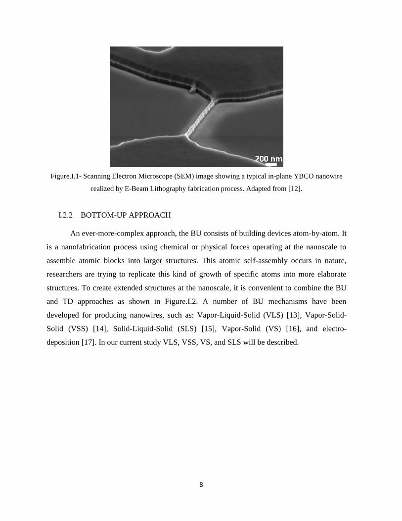
8
Figure.I.1- Scanning Electron Microscope (SEM) image showing a typical in-plane YBCO nanowire
realized by E-Beam Lithography fabrication process. Adapted from [12].
I.2.2 BOTTOM-UP APPROACH
An ever-more-complex approach, the BU consists of building devices atom-by-atom. It
is a nanofabrication process using chemical or physical forces operating at the nanoscale to
assemble atomic blocks into larger structures. This atomic self-assembly occurs in nature,
researchers are trying to replicate this kind of growth of specific atoms into more elaborate
structures. To create extended structures at the nanoscale, it is convenient to combine the BU
and TD approaches as shown in Figure.I.2. A number of BU mechanisms have been
developed for producing nanowires, such as: Vapor-Liquid-Solid (VLS) [13], Vapor-Solid-
Solid (VSS) [14], Solid-Liquid-Solid (SLS) [15], Vapor-Solid (VS) [16], and electro-
deposition [17]. In our current study VLS, VSS, VS, and SLS will be described.

9
Figure.I.2- SEM image of GaAs nanowires arrays grown via VLS mechanism using Au nanodots that
are defined by electron beam lithography. It is a combination of BU and TD approaches. (Courtesy of
C2N – center for nanosciences and nanotechnology)
I.2.2.1 VAPOR-LIQUID-SOLID (VLS)
The VLS mechanism was discovered in 1964 by Wagner and Ellis in Bell Telephone
laboratory for Silicon whiskers (nanowires) growth [18]. This new concept of crystal growth
has been widely used owing to its simplicity and versatility when applied in many
semiconductor systems. The key issue related to the growth of nanowires is how to induce a 1-
Dimensional crystal growth, as shown in Fig.I.3, in a controlled manner.

10
Figure.I.3- TEM and SEM micrographs showing VLS-grown NWs. a) SEM image of straight as-grown
VLS GaAs NWs catalyzed by Au NPs realized by Metal-Organic Vapor-Phase Epitaxy (MOVPE)
[19]. b) High-Resolution Transmission Electron Microscope (HR-TEM) image of a VLS-InAs NW
catalyzed by Au NP in a Molecular-Beam-Epitaxy (MBE) reactor [20].
First, metallic droplets are deposited onto a given substrate in vacuum. Second, atomic
vapors of semiconducting (SC) materials are introduced in the reactor while the system is
heated at a given temperature. The role of metal droplets is to form a liquid solution for a
vapor-phase absorption of the SC material (i.e. Si, Ge). The metal catalyst will form liquid
alloy droplets (metal – SC alloy) by adsorbing SC vapor components [21]. In the case of Si
NWs, when the temperature is above the eutectic point of Au-Si alloy which is 363℃
(Fig.I.4.a), SiH4 molecules dissociate at the surface of the catalyst, and H2 molecules are
evacuated while Si atoms enter the liquid, as shown in Fig.I.4.b. When the actual
concentration of the SC material is higher than its equilibrium concentration in the metal
droplet, the alloy will be supersaturated. After an incubation time (time for crystalline-seed
formation), a precipitation of a crystalline-Si (c-Si) seed occurs on the triple-phase boundary
(TPB) line (vapor – solid - liquid circular line) which is located at the bottom edge of the
catalyst. Subsequently, Si atoms prefer to diffuse towards the newly-formed c-Si seed because
less energy will be involved (balance of chemical potentials) with the crystal growth as
compared with a secondary nucleation event. Atomically, the NWs are grown layer-by-layer
in a step-flow mode [22, 23]. The SC nanowire diameter is determined by the size of the
catalyst [24]. The 1D crystal growth will continue as long as vapor components are supplied,
and the catalyst is not consumed.

11
Figure.I.4- Au-catalyzed SiNWs via VLS mechanism. a) Au – Si phase diagram, the eutectic point is
363±0.3℃ with a Si composition of 18.6 at.%. b) schematic illustration showing the VLS mechanism.
First, Au droplets are deposited on the surface of a Si substrate. Second, the temperature of the
substrate is raised sufficiently. Third, Silane (SiH4) gas is introduced. Silane will dissociate at the
surface of the molten catalyst. Since the solubility of Hydrogen is low enough inside the liquid Au,
only Si atoms will penetrate the catalyst surface and proceed for diffusion. An Au-Si alloy is formed.

12
When the supersaturation of Si in Au is reached, precipitation of c-Si will occur at the catalyst /
substrate interface. The crystalline nanowires will grow while pushing the catalyst perpendicularly
further from the substrate.
I.2.2.2 VAPOR-SOLID-SOLID (VSS)
While the VLS mechanism has become routinely used for fabricating self-assembled
nanowires, attention in the past two decades has been paid on the use of alternative solid
catalysts [25, 26]. The VSS follows the same process as VLS, except that the temperature used
for the growth is below the eutectic point of the metal – SC alloy. The limitations of VLS are:
1) the liquid catalyst can be incorporated into the nanowire affecting its properties in an
unwanted way [27], 2) the formation of abrupt heterostructures along the nanowire i.e.
Si/Ge/Si is fundamentally hard because of the high solubility of Ge and Si in the liquid
catalyst i.e. Au [28]. This phenomenon is called “Reservoir Effect”. It creates a composition
gradient along the nanowire [29], and 3) Kinking and tapering of NWs are more likely to
occur in VLS growth, thus, affecting their shape and size [30]. Advantageously, for VSS
mode, catalyst atoms are more bonded while at solid-state, thus, eliminating their
incorporation into the NW. In addition, the growth species have lower solubility in the solid
droplet which helps to create compositionally abrupt and structurally perfect heterointerfaces
[31], see Fig.I.5. In this case, the catalyst is solid which makes the incubation time shorter than
in the case of VLS. A tiny excess amount of SC material can raise enough the chemical
potential to nucleate a c-seed, consistent with the low solubility inside the catalyst [32]. Atoms
that grow the NW can follow many paths to supply the growing interface: 1- diffusion inside
the solid catalyst, 2- diffusion on the surface of the catalyst, and 3- diffusion on the sidewalls
of the NW [14]. The VSS mode grows NWs using the step-flow which has the same kinetics
as the VLS mode [33].

13
Figure.I.5- High-resolution TEM image of a Si-Ge heterojunction nanowire. a) Si NW (length 500 nm,
diameter 18 nm) was grown rapidly using VLS at 510°C then cooled and grown for several minutes in the
VSS mode at 360°C, followed by growth of a Ge segment at 360°C. b) HAADF-STEM image of a wire
(diameter 17 nm) grown under the same conditions. The inset shows the intensity profile across the
interface, averaged over a 5-nm strip along the midpoint of the wire. The width of the interface is 1.3 nm.
Adapted from [32].
I.2.2.3 VAPOR-SOLID (VS)
The VS method is another approach to promote the growth of NWs while avoiding the
contamination from catalyst incorporation. In the absence of the catalyst (as shown in Fig.I.6),
NWs can nucleate and grow by a direct vapor-deposition on the substrate. The spontaneous
catalyst-free NWs growth can be driven by screw dislocations [34], planar defects (twin
boundary or stacking fault) [35, 36], anisotropic surface energy of various facets [37]. The VS-
grown NWs are mainly metals and oxide-metals such as: WO3 [38], ZnO [39], MgO [40], Fe2O3
[41], Sn [42].

14
Figure.I.6- HRTEM micrograph showing the growth of a catalyst-free Tungsten-Oxide nanowire in a
Vapor-Solid style from a W-filament [43].
I.2.2.4 SOLID-LIQUID-SOLID (SLS)
From an application point of view, the integration of vertical (out-of-plane) NWs
grown by VLS into 2D planar devices is an essential difficulty. A formidable challenge is to
manipulate and assemble vertical NWs into a 2D layout for large-scale integrations of NW-
based devices. The In-Plane Solid-Liquid-Solid (IPSLS) mechanism, discovered by
Cabarrocas and Yu [44], is a BU approach that could represent an ultimate solution for the
fabrication of NW-based planar devices. It provides new opportunities to design and exploit
novel in-plane NW-based applications. IPSLS can be perceived as a nano-liquid-phase-
epitaxy [45] process or a nanoscaled metal induced crystallization [46]. The SLS is a three-
step process: 1) the formation of metal nanoparticles (NPs) such as: In, Sn on an Indium-Tin-
Oxide substrate for example (Fig.I.7.a). 2) An amorphous layer of SC material (i.e. Si, Ge) is
deposited on top (Fig.I.7.b). 3) The temperature of the substrate is raised sufficiently to
activate the lateral growth of NWs while maintaining the system in a reactive-gas-free
environment (see Fig.I.7.c.d).

15
Figure.I.7- The SLS mechanism. a) In nanoparticles are formed by chemical reduction of ITO using a
H2 plasma. b) an amorphous Si layer is deposited on top of the system. c) the temperature of the
substrate is raised sufficiently to activate the growth of IPSLS Si NWs. d) SEM image showing an
IPSLS-SiNW catalyzed by an In droplet [47].
I.3 PRINCIPLES OF SLS: SATURATION, NUCLEATION AND DRIVING FORCE
To control the size, morphology, structure, and growth path of NWs, it is crucial to
understand this nanoscale crystallization process. After the formation of catalyst NPs, a thin
film of, for example, hydrogenated amorphous Silicon (a-Si:H) is deposited on top. The
temperature is raised to melt the NPs which by themselves start to dissolve and absorb Si
atoms from the solid-state precursor (a-Si:H). The concentration of Si in the catalyst NPs starts
to increase, forming a catalyst – Si alloy NP similarly to the VLS process, leading to a
supersaturation state. Thermodynamically, increasing the concentration corresponds to an
increase in the chemical potential of the absorbed species in the catalyst. Therefore, a
heterogeneous nucleation will occur when accommodating more Si is no longer energetically
favorable. The newly-formed crystal embryo must remain stable long enough for the growth to
occur. For simplification, we assimilate the crystal nucleus to a droplet shape with a given
radius. The stability of this nucleus-embryo is related to its critical radius 𝑟∗ [48]:
𝑟∗ =2𝛾
∆𝐺 (1)

16
Where 𝛾 the interfacial free energy of the nucleus in the ambient phase, ∆𝐺 is the Gibbs
energy difference between Si atoms in the catalyst and Si atoms in the crystal. ∆𝐺∗ is the
energy used to atomically assemble the nucleus. After exceeding the critical size, the tendency
of nuclei to grow will persist (see Fig.I.8).
Figure.I.8- Schematic illustration showing the energetic stability of a crystal nucleus as a function of its
size. In the unstable side (𝑟 < 𝑟∗), the nucleus risks decaying if its size remains less than the critical
value 𝑟∗ for a certain period of time. When 𝑟 = 𝑟∗, the energy barrier reaches its peak ∆𝐺∗. Beyond
this value (𝑟 > 𝑟∗), the growth of the nucleus reduces the Gibbs energy of the system.
Thermodynamically, the growth of this nucleus is allowed.
The most favorable site for the nucleation for both VLS [49] and SLS [47] mechanisms
is at the TPB line, for instance in Fig.I.9, Si crystal-seeds are formed at the region where once
was the TPB line during the initial stage of the growth.

17
Figure.I.9- SEM image of the starting point of a nanowire (depicted by a light-green dashed
line), it is the initial location of the catalyst. Si-nuclei are formed at the original TPB line during the
early stage of nucleation [47].
Many nuclei can form at the bottom edge of the catalyst, but the biggest one having
the lowest surface-to-volume ratio (thus, lowest Gibbs energy) is the most favorable sink for
the incoming Si atoms [47]. Therefore, the biggest crystal seed grows faster than the other
ones which might decay (or dissolve). Nuclei growth process can follow three types of atomic
assembly [50-52]: 3-dimensional island growth (Volmer-Weber), layer-by-layer growth
(Frank-van-der Merwe), and 3D islands on top of one or few epitaxial layers (Stranski-
Krastanov). For the case of catalyst-assisted nanowires, in-situ observations have shown that
the growth is done in a layer-by-layer fashion [53].
The initial dynamic process of the IPSLS growth is established as soon as an
absorption (catalyst/a-Si:H) and deposition (c-Si/catalyst) edges appear. The Gibbs energy
difference between the a-Si:H (𝐸𝑎) and c-Si (𝐸𝑐) is ∆𝐸𝑎𝑐 = 𝐸𝑎 − 𝐸𝑐 ~ 0.12 − 0.15 𝑒𝑉 [54,
55]. The concentration of the dissolved Si at the absorption interface is higher than at the
deposition interface. The mass transport of the dissolved Si atoms is driven by the
concentration gradient across the catalyst. The absorption interface region has a higher
concentration of Si atoms, which create a diffusive mass flux (JSi) towards lower concentration
regions inside the catalyst (near the c-Si/catalyst interface), as depicted in Fig.I.10.a. As a
consequence, the absorbed-Si atoms are transported to the rear-side of the NP to grow the
nanowire. The dragging of the catalyst to dissolve more a-Si:H is derived from the chemical
potential difference between the front absorption edge and the back deposition edge ∆Eac.
Considering that the dissolution of silicon atoms from the amorphous precursor layer is a
quick step, then the absorption flux rate (Jin) into the catalyst NP is then determined by the
diffusion transport flux (JSi) [47]:
𝐽𝑖𝑛 = 𝐽𝑆𝑖 =𝐷𝑠
𝐿𝑐(𝐶𝑒𝑞
𝑎 − 𝐶𝑆𝑖) (2)
Where 𝐿𝑐 the diameter of the catalyst NP, 𝐷𝑠 the diffusion coefficient of Si atoms in the
catalyst, 𝐶𝑒𝑞𝑎 = 𝐶𝑒𝑞
𝑐 . 𝑒∆𝐸𝑎𝑐/𝑘𝑇 is the equilibrium concentration of dissolved Si atoms at the

18
absorption interface (catalyst/a-Si:H), 𝐶𝑒𝑞𝑐 is the equilibrium concentration of Si atoms near the
crystalline interface, and 𝐶𝑆𝑖 is the Si concentration at the c-Si/catalyst interface. The
concentration difference across the In catalyst is ∆𝐶𝑆𝑖. To obtain a growth rate of 102 nm/s,
∆𝐶𝑆𝑖 𝐶𝑒𝑞𝑐⁄ should be less than 2% (at growth temperatures between 400℃ - 500℃). For this
reason, 𝐶𝑆𝑖 can be considered to be very close to 𝐶𝑒𝑞𝑎 .
The dissolved Si atoms build the NWs by forming two-dimensional nucleation centers,
and then new monolayers are completed by a lateral growth of these nucleation centers. This
process is repeated layer-by-layer to grow the entire NW. The atomic formation process of
SiNW is described by theoretical frameworks [56, 57]. The deposition flux rate (Jout) can be
described by the nucleation rate theory in VLS [57]:
𝐽𝑜𝑢𝑡~ 𝐺𝑛𝑐−1/2
. 𝑒−𝐺𝑛𝑐/𝑘𝑇 (3)
Where 𝐺𝑛𝑐 is the nucleation barrier for the formation of 2D nucleation centers on the SiNW
end, 𝑇 is the temperature, and 𝑘 is the Boltzmann constant.
Figure.I.10- Schematic illustration for the absorption, diffusion, and deposition steps involved in the
growth of lateral SiNW via IPSLS mechanism [44, 47]. a) Ea, Ec, and Ei denote the Gibbs energy of Si
atoms in the amorphous, crystalline (considered as a reference), and dissolved in In catalyst drop,
respectively; CSi is the dissolved Si atom concentration in the catalyst drop; Jin, Jout, and JSi are the
absorption, deposition, and mass transport diffusion flux rates of Si atoms. The catalyst, having a
diameter of Lc, is rolling (as depicted by the circular arrow inside the catalyst) towards the a-Si:H with

19
a thickness of Ha. b) Illustration of the imbalanced TPB line due to the continuous absorption of Si
atoms (depicted by a red arrow) from the a-Si:H precursor. 𝛾𝐼𝑛−𝑆𝑖, 𝛾𝐼𝑛−𝑣𝑎𝑐, and 𝛾𝑆𝑖−𝑣𝑎𝑐 are the surface
tensions of Indium catalyst/a-Si:H, Indium catalyst/ vacuum, and a-Si:H/vacuum
respectively. 𝑓𝑑𝑟𝑎𝑔𝑔𝑖𝑛𝑔 is the dragging force driving the catalyst.
The dynamics of the SLS mechanism is a direct effect of the Gibbs energy difference
between the two edges of the catalyst. Moments before the appearance of a dragging force, the
tensions between In/vacuum (𝛾𝐼𝑛−𝑣𝑎𝑐,), In/a-Si:H (𝛾𝐼𝑛−𝑆𝑖
), and a-Si:H/vacuum (𝛾𝑆𝑖−𝑣𝑎𝑐
) are
balanced in the horizontal direction (by projecting each component to an horizontal-axis):
𝛾𝐼𝑛−𝑆𝑖 = 𝛾𝑆𝑖−𝑣𝑎𝑐 − 𝛾𝐼𝑛−𝑣𝑎𝑐 × 𝑐𝑜𝑠𝜃 (4)
The catalyst/a-Si:H interface tension (𝛾𝐼𝑛−𝑆𝑖
) is weakened by the dissolution and absorption of
Si atoms. Consequently, the balance between the tensions is broken (as shown in
Fig.I.10.b): 𝛾𝐼𝑛−𝑆𝑖 < 𝛾𝑆𝑖−𝑣𝑎𝑐 − 𝛾𝐼𝑛−𝑣𝑎𝑐 × 𝑐𝑜𝑠𝜃. The system seeks to re-establish the balance
again by dragging forward the TPB line (in other terms the catalyst is dragged) and forms a
new In/a-Si:H interface. Knowing that the absorption is continuous, the tensions balance will
be broken again and repeatedly; thus; the dragging force will be repeatedly exerted on the TPB
line. Since the catalyst is subjected to a friction at its bottom contact compared to its top, a
rolling forward movement might be a possibility (as shown in Fig.I.10.a by a circular dashed
arrow).
It is worth mentioning that this kind of in-plane nanowires is not only achieved using
SLS mechanism. Indeed, by using different catalytic metals, such as Pb (lead), it is possible to
grow in-plane VLS NWs [58]. The Pb NPs get supplied by Si atoms from a SiH4 (Silane)
plasma. At the same time and during the growth, a hydrogenated amorphous Silicon (a-Si:H)
layer is deposited around and on top of the catalyst. These in-plane VLS SiNWs catalyzed by
Pb NPs have no depletion (trench) of a-Si:H layer (Fig.I.11.b) compared to SLS SiNWs
catalyzed by Indium (In) NPs (Fig.I.11.a). In other terms, it means that the catalyst did not
consume (apparently) Si from the a-Si:H layer but from the SiH4 plasma. This observation
does not exclude the possibility that the a-Si:H is weakly thinned and used for the growth.
This kind of growth might be a combination of VLS and SLS.

20
Figure.I.11- SEM micrographs of in-plane SiNWs catalyzed by a) In NP in SLS mode, and b) Pb NP in
VLS mode [58].
The description of the IPSLS mechanism was done for SiNWs. The theory is well-elaborated
and explained specially for SiNWs catalyzed by Indium droplets. However, this work was not
extended for Ge or GeSnNWs. This will be the subject of this thesis, and it will be elaborated
more in the following sections.
I.4 GERMANIUM – TIN ALLOY
It has been a few decades that Si nanoelectronics have been developed. However, the
performance of Si ultra-large-scale integrated circuits (ICs) has only improved by increasing
the number of elementary components (i.e. transistors, diodes) in the devices by shrinking
their size. As we approach the limit of Moore’s law, with further decreasing of the
components size (< 10 nm) [59], quantum tunneling and other related quantum effects will be
inevitable. From this point, the necessity to develop novel materials with an increased
performance rises. The crystalline Si properties such as the low carrier mobility and the
indirect band-gap [60] limit further improvements in Si-based electronics and optoelectronics.
As a viable alternative to Si, the group IV compound Germanium-Tin (Ge1-xSnx) is a
unique class of semiconductor offering adjustable electrical and optical properties as a
function of Sn concentration. The GeSn is a metastable alloy since the solubility of Sn in Ge is
less than 1 at.% at the temperatures used for fabrication (Fig.I.12.a). The incorporation of Sn
affects the electronic band structure of the system. For instance, in the Ge1-xSnx alloy, the
direct Γ-valley decreases faster than the indirect valley (L) in the conduction band (at k = 0)
with the increase of Sn incorporation. The energy difference between Γ and L valleys in c-Ge
is ∆𝐸 = 0.14 eV, as schematically shown Fig.I.12.b. When the Γ-valley is lower than L-valley

21
the material becomes a direct gap [61], see for instance Fig.I.12.c. By using the non-local
empirical pseudopotential method [62], it has been reported that the required Sn concentration
to transform Ge into a direct gap semiconductor is above 6 %, although some contradiction
regarding this value exist [63-65]. However, to achieve experimentally such concentration,
several fundamental obstacles have to be solved: i) the solubility of Sn in Ge is only 1% at
temperatures below 500℃ [66] , ii) there is a strong Sn segregation behavior [67] and iii) the
larger size of Sn compared to Ge [68] which can degrade the Ge lattice.

22
Figure.I.12. Ge and Ge1-xSnx energy band diagrams a) the Ge-Sn phase diagram (adapted from ref
[69]) b) At the Brillouin zone of intrinsic Ge, the lowest conduction state is located in L-valley, whereas
the highest valence state is in Г-valley (at k = 0). An offset of 0.14 eV splits the Г and L-valleys. In bulk-
Ge, the indirect bandgap energy is Eg = 0.66 eV (at room temperature). c) The electronic band structure
changes upon incorporation of Sn. Adding Sn, to the diamond cubic phase c-Ge nanowire, lowers the Г-
valley faster than L-valley. It is expected that a Sn content above 6% in the Ge will cause the indirect-to-
direct gap transition.
This alloy presents many convenient properties such as: 1) high carrier mobility compared
to Si and Ge individually [70-72], and can be further improved by increasing the Sn content, 2)
tunable bandgap [73], 3) direct bandgap transition for a sufficiently high Sn content
[74], 4) low thermal budget required to grow a GeSn alloy, due to its low eutectic point
(231.1℃) [70], and 5) strain engineering as a stressor for strained Ge [75]. The Ge1-xSnx is very
suitable as a channel material for high speed and low power consumption transistors (see
Figure.I.13.), such as: Thin-Film Transistors (TFTs), Metal-Oxide-Semiconductor Field-Effect-
Transistors (MOSFETs), Tunnel-FETs, FinFET [76], and Multi-Quantum-Well (MQW) LEDs
[77].
Figure.I.13- GeSn-based FinFET [76]. a) SEM tilted-view of the transistor. b) cross-section TEM
image along BB’ (the yellow dashed-line) showing the GeSn FinFET with fin width 𝑊𝑓𝑖𝑛 = 30 𝑛𝑚. c)
HRTEM image showing the crystallinity of the GeSn-fin on SiO2 with a smooth sidewall.
Moreover, this alloy has significantly increased the interest of the research and industrial
communities due to its potential high performance in photonic and optoelectronic applications.

23
To tailor the GeSn properties, it is necessary to control the Sn concentration in the alloy. Two
main bandgap engineering approaches have been developed to transform Ge into a direct
bandgap semiconductor: tensile strain [78] and Sn alloying [79]. In this thesis, Sn alloying will
be further developed. Two main configurations of GeSn alloys exist: i) thin-film, and ii)
nanowires.
I.4.1 THIN-FILM CONFIGURATION
Extensive efforts have been done to break the barrier of the Sn equilibrium
concentration without degrading the crystalline quality of GeSn alloys. The precipitation is a
serious problem to achieve an effective Sn content in a homogeneous high-quality Ge1-xSnx
layer. During the GeSn crystal growth and post-growth processes (such as thermal-
processing), precipitation of Sn can occur. In addition, the oxidation of the GeSn alloy is
shown to enhance the segregation of Sn near the surface of the structure [80]. Surface
roughness has been witnessed for Ge1-xSnx epitaxy layers grown in a chemical vapor
deposition (CVD) reactor [81], knowing that the temperature used for the CVD growth was
between 300℃ and 350℃. Respectively, Sn precipitates are often observed at high growth
temperatures (such as 400℃) that are used for Ge epitaxy. Numerous studies have proven that
the substrate temperature is the key to obtain high quality GeSn layers. To avoid Sn
precipitation, low-temperature growth (< 231.1℃) should be used. Recently, a successful
metastable GeSn thin film has been grown with relatively high Sn content (~ 18% at. Sn)
using molecular beam epitaxy (MBE) at 140°C but failed in suppressing the phase separation
tendency [82], as shown in Fig.I.14. Meanwhile other groups have succeeded to maintain good
crystal structure in thin films with lower Sn concentrations (~ 12% at. Sn) [83].

24
Figure.I.14. SEM and EDX results of a 200-nm thick GeSn layer with approximately 18 at.% Sn
concentration. a) SEM top-view with the corresponding Energy Dispersive X-ray Spectroscopy (EDX)
b) Ge, and c) Sn [82].
The abovementioned methods provide a good control of Sn incorporation, and allow
creating thin-film heterostructures with sharp interfaces. Nonetheless, the elaboration of 2D
films leads to a large number of misfit dislocations in the GeSn structure due to a large lattice
mismatch between GeSn and the underlying Si substrate (> 4.2 %) [84]. To avoid such defects,
other solutions have been developed, for example: GeSn film on insulator [85, 86], and growth
of GeSn NWs using bottom-up approaches [87, 88].
I.4.2 NANOWIRE CONFIGURATION
To keep on track with miniaturization of Si-based nanoelectronics and photonics, the
nanowire configuration has also been investigated. This one-dimensional (1D) nanoform has an
advantageous high surface-to-volume ratio which allows a better strain-relaxation as compared
to bulk and thin film approaches [89]. On one hand, the top-down techniques used for
fabricating a good quality; single crystalline, straight, and uniform diameter Ge1-xSnx nanowires
with no Sn clustering are rather limited due to under-developed surface and etch chemistries.
On the other hand, bottom-up paradigms allow associating kinetic effects during the dynamic
process of Ge1-xSnx NWs growth, which can influence the incorporation of Sn in the system.
Among the most popular growth techniques [90-92] (vapor-liquid-solid that is shown in
Fig.I.15.a, vapor-solid-solid, and electrodeposition), the most effective for impurity
incorporation is the growth under non-equilibrium conditions [93]. For instance, Au-catalyzed

25
Ge NWs grown by VLS mechanism reach ~3 - 4 at.% Sn [94] with plenty of structural defects
(see Fig.I.15.c), and could reach ~ 10 at.% Sn [95]. Microwave-assisted solution-liquid-solid
process allowed to reach ~ 12 at.% of Sn, but the NWs lack a good quality structure [96].
Figure.I.15. SEM and TEM micrographs of Ge-core/GeSn-shell NWs [94]. a) low magnification SEM
and magnified inset of core-shell Ge/Ge1-xSnx NWs grown on Ge (111). b) low magnification TEM
showing Sn-enriched coherent defect region in GeSn. c) Ge1-xSnx shell structural defects, taken from
[112̅] zone-axis HRTEM micrograph with Fast-Fourier Transform (FFT) inset.
I.4.3 CATALYST ATOM INCROPORATION
The immediate result of the direct contact between the liquid catalyst and the NW’s
growing interface is the impurity (catalyst atoms) incorporation. Formerly, it was thought that
the impurity incorporation phenomenon is a deteriorating factor since it is unintentional [97]
and sometimes nonuniform [98] leading to detrimental physical and chemical properties. For
example, Au catalyst, which is the most commonly used material, is very deleterious to the
electronic properties of c-Si [99]. It is also known that Au atoms act as recombination centers

26
for photogenerated-carriers within SiNWs, which decrease the photovoltaic efficiency [100].
Structurally, a correlation was found between Au incorporation and the growth orientation of
SiNWs [101], see Fig.I.16. Au atoms are trapped by the same types of defects more than
others, depending on the interplay between surface energies. For these reasons, instead of Au,
other types of catalysts have been used such as Al [102].
Figure.I.16. HRTEM and STEM micrographs showing the incorporation of Au in structural defects in
SiNWs [27, 103]. a) radial cross-section view in HRTEM of a <110> oriented SiNW with Au-decorated
grain boundary, and b) STEM view. c) STEM unprocessed image axial-view of Au atoms line in a
SiNW, and d) HRTEM filtered image of the same SiNW tilted 15° about its growth axis.
An intriguing question was raised about the nature of Au incorporation [104]: what is
the possible mechanism of incorporation if Au atoms can be trapped even without defects in c-
SiNWs? The suggested answer was that the growth has been done under non-equilibrium
conditions which lead to a kinetic impurity trapping. From this point-of-view, broad studies on
this framework have been started. The essential idea was to achieve a precise control of
impurities incorporation (dopants, i.e. P, B; or catalyst atoms, i.e. In, Sn) during the growth of

27
NWs, which will enable a novel and efficient route to functional NWs in direct technological
implications. Incorporation of a suitable amount of dopant or catalyst atoms into NWs can
render desirable modifications in their physical (or chemical) properties. The availability of
many types of catalysts gives flexibility in fabricating NWs with different enhanced-
properties. For instance, p-type doping can be achieved if the Ga catalyst gets injected into
group-IV NWs [105], whereas n-type doping is achieved by using Bi catalyst [106].
I.4.3.1 FOR VERTICAL SILICON NWS
The VLS enables an in-situ impurity doping through the metal catalyst [107], and
allows the formation of complex axial and radial heterostructures [108, 109]. Also, catalyst
atoms were found to be homogeneously distributed throughout the NW’s body rather than
trapped by defects, see for instance Fig.I.17. For this reason, incorporation studies were
initiated for VLS-grown NWs in 2008, namely for Au-catalyzed SiNWs [27]. An interesting
finding was the incorporation of Au throughout a defect-free NW structure, so the defect-
related trapping is ruled out. Here other explanations started to be developed to understand the
presence of catalyst atoms in the bulk of the NW structure. One of them is that the solidus, in
the Au-Si phase diagram, might shift towards higher Au concentration in the NW because of
the supersaturated Au-Si liquid catalyst which makes the growth a non-equilibrium process.
At this nanoscale-operation, the bulk equilibrium phase diagram cannot predict the
composition neither for the catalyst nor for the NW during the non-equilibrium growth and
after it. Same analogy was applied to GeNWs where a kinetic-dependent behavior was
predicted to be responsible for the excessive impurity injection from the catalyst tip [95, 110].
The possibility of catalyst atoms incorporation through the NW sidewalls due to homoepitaxy
by Vapor-Solid growth was also investigated, and proven to be negligible [95].

28
Figure.I.17. Three-dimensional APT atom-by-atom map (each point is an atom represented in the real
3-Dimensional space) showing the incorporation of Al atoms homogeneously in a SiNW grown at
410℃. The nickel serves as a protection layer from ion etching operations. Only a limited number of
atoms is displayed for clarity reason (2.5×10⁴ atoms of each element). Inset, a cross-sectional TEM
image of an identical Si nanowire (scale bar, 40 nm), adapted from [93].
The main model used to describe the nanowires growth is based on the step flow
kinetics [49, 93, 95]. In this regime, the growth is attributed to the progressive addition of
atomic monolayers at the solid side of the NW/catalyst interface. The interface advances by
the lateral flow of atomic steps (Fig. I.18). Consequently, the interface velocity, vint
(perpendicular to the interface) is proportional to the step velocity vstep and inversely
proportional to the incubation time (which is the time for supersaturation and nucleation).
Catalyst atoms adsorbed at the interface have a limited time 𝜏𝑒 (escape time) to diffuse back to
the liquid catalyst. If the adsorbed atoms do not escape to the liquid before 𝜏e expires, they will
be permanently incorporated at the growing solid surface.

29
Figure.I.18. A simple schematic illustration of step growth (Supplementary information of ref. [93]).
Left schema: the impurity (red atom) at the step edge can jump between the two sides of the interface
during 𝜏𝑒 = 𝑎 𝑣𝑠𝑡𝑒𝑝⁄ (“a” is the width of one atomic row, vstep is the step velocity) which is the time
needed for an atomic row completion. Right schema: the impurity becomes trapped in the layer after
the growth of the next row of atoms, that means when 𝜏𝑒 expires.
The partition coefficient, k, is commonly used to quantify the shift of solubility
boundaries of the incorporated solute atoms (at the solid interface). It represents the
composition ratio of the solute (catalyst atoms which are considered as impurity atoms) in the
solid (NW), 𝐶𝑖𝑚𝑝𝑢𝑟𝑖𝑡𝑦𝑠𝑜𝑙𝑖𝑑 , and in the melt at the NW/catalyst interface,𝐶𝑖𝑚𝑝𝑢𝑟𝑖𝑡𝑦
𝑙𝑖𝑞𝑢𝑖𝑑:
𝑘 = 𝐶𝑖𝑚𝑝𝑢𝑟𝑖𝑡𝑦𝑠𝑜𝑙𝑖𝑑 𝐶𝑖𝑚𝑝𝑢𝑟𝑖𝑡𝑦
𝑙𝑖𝑞𝑢𝑖𝑑⁄
This model (step-flow) treats the case in which an atomically smooth, sharp interface advances
by the periodic lateral passage of monolayer steps (as shown in Fig.I.18). The passage of a
step results in the incorporation of any solute atoms into the layer. Solute diffuses back into
the liquid during the period before the passage of the next step, at which point any remaining
solute is assumed to be permanently trapped into the solid. The predicted velocity-dependence
of k for this mechanism is [111]:
𝑘(𝑣) = 𝑘𝑒 + (1 − 𝑘𝑒)exp (−𝑣𝐷/𝑣𝑖𝑛𝑡)
Where ke is the equilibrium composition of the solute in the solid, 𝑣𝐷 = 𝐷 𝑎⁄ is the
diffusive velocity with D the interdiffusion coefficient across the interface and “a” is the width
of one atomic row. k undergoes a strong deviation towards higher values from the classical

30
solubility limit upon a growth rate of few m/s (as shown in Fig.I.19) [111]. The rapid
progression of the NW/catalyst interface traps the solute atoms escaping from the solid side of
this interface, which diffuse slower than the moving interface; this phenomenon is known as
the “solute trapping” [112].
Figure.I.19. Interface velocity dependence of the partition coefficient for Bismuth in Si (001)
[111]. Various models predict the increase of the partition coefficient among the increase of the growth
interface velocity. The data points (Aziz et al.) are from ref. [113].
A more advanced and recent study (Moutanabbir et al. 2013 [93]) went deep into the
atomistic procedure of Al-catalyzed SiNWs grown by VLS mechanism. A colossal
incorporation of Al atoms into VLS-grown SiNWs has been achieved by Moutanabbir et al.,
with a concentration two orders of magnitude higher than their equilibrium solubility [93].
They wrote that the above-elucidated model describes the incorporation for bulk systems, and
thereby cannot be used for NWs. The reason behind is the delay of formation of two
successive Si-bilayers. There is an incubation time needed for nucleation which accounts for
slowing down the interface velocity, and therefore minimizing the trapping-effect. Assuming
that the step-growth is aperiodic, they have established an expression taking into consideration
the step velocity and the bilayer formation time 𝜏𝐵𝐿. Despite inserting the NWs growth-
characteristic parameters, they could not totally explain the reasons behind this incorporation.

31
However, they believed that there are two main parameters influencing the catalyst injection:
i) the Gibbs free energy of the liquid at an equilibrium composition, and ii) the characteristic
supersaturation. The incorporation of catalyst atoms is still an open debate, but it is clearly
related to growth kinetics.
I.4.3.2 FOR IN-PLANE SILICON NWS
Discussions have also been done on the incorporation of catalyst atoms into NWs
grown by the SLS mechanism [114]. In this study Chen et al. have made a comparison
between the VLS and SLS growth modes using two different catalysts: In and Sn. Even
though these are two distinctive mechanisms, it is interesting to validate that the incorporation
process is kinetically-based. This idea can be tested by the SLS mechanism where growth
rates are much higher (up to 100 nm.s-1 [44]) than in the VLS (1 - 10 nm.s-1 [115]). Therefore,
one would expect a higher incorporation in SLS compared to VLS. The main reason behind
these huge growth rates relies in the direct contact between the catalyst and the amorphous
feeding layer (a-Si:H in this case). The growth rate effect was proved by Atom Probe
Tomography (APT, for details see chap II), as shown in Fig.I.20. As predicted, the SLS
mechanism does lead to a higher concentration of catalyst atoms into NWs compared to VLS,
for both used catalysts In and Sn.

32
Figure.I.20. Dependence of impurity concentration on SiNW growth rate. The experimental data
show an increase in impurity (In and Sn) concentration upon the increase of SiNWs growth rate. The
fitting curve is derived from the dimer-insertion model developed by Chen et al. [114]. The three-
dimensional APT reconstructions show the catalyst atoms distribution in SiNWs grown by VLS on the
left, SLS on the right. In and Sn atoms are represented by blue and pink colors, respectively. Scale bar
in the reconstruction volume, 20 nm.
Chen et al. have found, experimentally, that impurities are first incorporated in a
homogeneous way into the NW and then redistributed (segregated) to nearby defects. With the
introduction of impurity dimers (Si-Sn) or (Si-In) into a NW during the nucleation process, a
distortion in the NW’s crystalline structure is created due to the atomic radius of the impurities
(bigger than Si [116]). This distortion (stress-field) can be relaxed by the segregation of the
incorporated In and Sn towards structural defects, as shown in Fig.I.21.

33
Figure.I.21. STEM images of SiNW synthesized via SLS mechanism. (a)-(b) High-magnified view of a
SiNW with a twin plane decorated by In or Sn (or both) atoms. The SiNW growth direction is <211>.
Correlation of (c) STEM and (d) APT results showing that the segregation at the twin plane is due to In
atoms. Only 20 at.% of Si atoms are represented for clarity.
Based on this finding, they have introduced the notion of dimer-atom-insertion kinetic
model to explain the high incorporation rate. The growth of SiNWs is due to a successive
addition of bilayers of Si dimers (Si-Si) and impurity dimers (Si-In and Si-Sn). A dimer is an
assembly of two atoms that can be identical (homodimer) or different (heterodimer). The
impurity concentration Ci in SiNWs can be deduced from the ratio between incorporation rate
of impurity dimers and Si dimers:
𝐶𝑖 =𝑣𝑆𝑖−𝑖
(𝑣𝑆𝑖−𝑆𝑖 + 𝑣𝑆𝑖−𝑖)
Where 𝑣𝑆𝑖−𝑖 and 𝑣𝑆𝑖−𝑆𝑖 are the incorporation rates of impurity dimers and Si dimers,
respectively. The incorporation rate of Si dimers depends mainly on the Gibbs energy
difference (∆𝐸 = 𝐸𝑙 − 𝐸𝑆𝑖−𝑆𝑖) between the dissolved state of Si atoms in droplet (𝐸𝑙 =
𝑘𝑇𝑙𝑛[𝐶𝑆𝑖
𝐶𝑒𝑞]) and the Si-Si dimer nucleation energy (𝐸𝑆𝑖−𝑆𝑖). The same analogy can be applied
for the incorporation rate of impurity dimers; ∆𝐸′ = 𝐸𝑙 − 𝐸𝑆𝑖−𝑖. This model seemed to be
consistent with experimental results, as indicated by the fitting curve in Fig.I.20.

34
I.5 SUMMARY
Extensive efforts have been paid to improve the performance of Si-based technologies,
but this material lacks adequate physical properties for further enhancement. As a result, the new
quest for researchers was finding a new material with better properties than Si, and can be
integrated on Si. One of the most recent developed materials was the Ge1-xSnx alloy, which is an
interesting material for microelectronics and optoelectronics. The carrier mobility is improved by
the increment of Sn concentration in Ge, and an indirect-to-direct transition of the energy band-
gap occurs for a sufficient amount of Sn (between 6 at.% and 11 at.%). The nanowire
configuration allows decreasing more the devices size, keeping on the track of miniaturization.
With the ability of controlling their properties, and guiding them to assemble a certain circuitry
design, the IPSLS NWs are now the center of interest of many research laboratories. Broad and
comprehensible studies have been conducted on IPSLS SiNWs, is it possible to do the same for
GeSn NWs? In the next chapter (II), the machines used to grow and characterize Ge and GeSn
NWs will be elaborated.
I.6 REFERENCES
1. J. Appenzeller, J.K., M. T. Bjork, H. Riel, H. Schmid, W. Riess, Toward Nanowire Electronics.
IEEE Transactions on Electron Devices, 2008. 55(11): p. 2827-2845.
2. Fu-Liang, Y.D.-H., Lee Hou-Yu, Chen Chang-Yun, Chang Sheng-Da, Liu Cheng-Chuan, Huang
Tang-Xuan, Chung Hung-Wei, Chen Chien-Chao, Huang Yi-Hsuan, Liu Chung-Cheng, Wu Chi-
Chun, Chen Shih-Chang, Chen Ying-Tsung, Chen Ying-Ho, Chen Chih-Jian, Chen Bor. 5nm-gate
nanowire FinFET. in Digest of Technical Papers. Symposium on VLSI Technology. 2004.
3. Pauzauskie, P.J.Y., Peidong, Nanowire photonics. Materials Today, 2006. 9(10): p. 36-45.
4. Zhaoguo Xue, M.X., Xing Li, Jimmy Wang, Xiaofan Jiang, Xianlong Wei, Linwei Yu, Qing
Chen, Junzhuan Wang, Jun Xu, Yi Shi, Kunji Chen, Pere Roca i Cabarrocas, In‐Plane Self‐Turning and Twin Dynamics Renders Large Stretchability to Mono‐Like Zigzag Silicon Nanowire
Springs. Advanced Functional Materials, 2016. 26(29): p. 5352-5359.
5. Li Mingwei, B.R.B., Morrow Thomas J., Sioss James A., Lew Kok-Keong, Redwing Joan M.,
Keating Christine D., Mayer Theresa S., Bottom-up assembly of large-area nanowire resonator
arrays. Nature Nanotechnology, 2008. 3: p. 88.
6. Hochbaum Allon I., C.R., Delgado Raul Diaz, Liang Wenjie, Garnett Erik C., Najarian Mark,
Majumdar Arun,Yang Peidong, Enhanced thermoelectric performance of rough silicon
nanowires. Nature, 2008. 451: p. 163.
7. Cui Yi, W.Q., Park Hongkun, Lieber Charles M., Nanowire Nanosensors for Highly Sensitive and
Selective Detection of Biological and Chemical Species. Science, 2001. 293(5533): p. 1289-1292.
8. Karam Chantal, G.C., Habchi Roland, Abboud Nadine, Khoury Antonio, Tingry Sophie, Miele
Philippe, Utke Ivo, Bechelany Mikhael, Urchin-inspired ZnO-TiO 2 core-shell as building blocks
for dye sensitized solar cells. Vol. 126. 2017.
9. Schröder Tim, T.M.E., Walsh Michael, Li Luozhou, Zheng Jiabao, Schukraft Marco, Sipahigil
Alp, Evans Ruffin E., Sukachev Denis D., Nguyen Christian T., Pacheco Jose L., Camacho Ryan

35
M., Bielejec Edward S., Lukin Mikhail D., Englund Dirk, Scalable focused ion beam creation of
nearly lifetime-limited single quantum emitters in diamond nanostructures. Nature
Communications, 2017. 8: p. 15376.
10. Maldonado Juan R., P., Martin, X-ray lithography: Some history, current status and future
prospects. Microelectronic Engineering, 2016. 161: p. 87-93.
11. Okazaki, S., High resolution optical lithography or high throughput electron beam lithography:
The technical struggle from the micro to the nano-fabrication evolution. Microelectronic
Engineering, 2015. 133: p. 23-35.
12. Tafuri, F., Massarotti Davide, Galletti Luca, Stornaiuolo, Daniela Montemurro, Domenico
Longobardi, Luigi Lucignano, Procolo Rotoli, Giacomo Pepe, Giovanni Piero Tagliacozzo, Arturo
Lombardi, Floriana, Recent Achievements on the Physics of High-T C Superconductor Josephson
Junctions: Background, Perspectives and Inspiration. Journal of Superconductivity and Novel
Magnetism, 2013. 26(1): p. 21-41.
13. Givargizov, E.I., FUNDAMENTAL ASPECTS OF VLS GROWTH A2 - CULLEN, G.W, in Vapour
Growth and Epitaxy, E. Kaldis, R.L. Parker, and C.J.M. Rooymans, Editors. 1975, Elsevier. p. 20-
30.
14. Kolasinski, K.W., Catalytic growth of nanowires: Vapor–liquid–solid, vapor–solid–solid,
solution–liquid–solid and solid–liquid–solid growth. Current Opinion in Solid State and Materials
Science, 2006. 10(3): p. 182-191.
15. Yu Linwei, A.P.-J., Picardi, Gennaro, Roca i Cabarrocas, Pere, An In-Plane Solid-Liquid-Solid
Growth Mode for Self-Avoiding Lateral Silicon Nanowires. Physical Review Letters, 2009.
102(12): p. 125501.
16. Ambrosini, S., M. Fanetti, V. Grillo, A. Franciosi, S. Rubini, Vapor-liquid-solid and vapor-solid
growth of self-catalyzed GaAs nanowires. AIP Advances, 2011. 1(4): p. 042142.
17. Makhlouf, H., Karam Chantal, Lamouchi Amina, Tingry Sophie, Miele Philippe, Habchi Roland,
Chtourou Radhouane, Bechelany Mikhael, Analysis of ultraviolet photo-response of ZnO
nanostructures prepared by electrodeposition and atomic layer deposition. Applied Surface
Science, 2018. 444: p. 253-259.
18. R. S. Wagner, W.C.E., VAPOR‐LIQUID‐SOLID MECHANISM OF SINGLE CRYSTAL
GROWTH. Applied Physics Letters, 1964. 4(5): p. 89-90.
19. Brönstrup, G., C. Leiterer, N. Jahr, C. Gutsche, A. Lysov, I. Regolin, W. Prost, F. J. Tegude, W.
Fritzsche, S. Christiansen, A precise optical determination of nanoscale diameters of
semiconductor nanowires. Nanotechnology, 2011. 22(38): p. 385201.
20. Zhang, Z., Lu Z., Chen P., Xu H., Guo Y., Liao Z., Shi S., Lu W., Zou J., Size-dependent
structural quality of InAs Nanowires Grown by Molecular Beam Epitaxy
21. Westwater, J., Gosain D. P., Tomiya S. , Usui S. , Ruda H. , Growth of silicon nanowires via
gold/silane vapor–liquid–solid reaction. Journal of Vacuum Science & Technology B:
Microelectronics and Nanometer Structures Processing, Measurement, and Phenomena, 1997.
15(3): p. 554-557.
22. Hofmann, S. and W.C.T. Sharma Renu, Cervantes-Sodi Felipe, Ducati Caterina, Kasama Takeshi,
Dunin-Borkowski Rafal E., Drucker Jeff, Bennett Peter, Robertson John, Ledge-flow-controlled
catalyst interface dynamics during Si nanowire growth. Nature Materials, 2008. 7: p. 372.
23. Wu, Y., Yang Peidong, Direct Observation of Vapor−Liquid−Solid Nanowire Growth. Journal of
the American Chemical Society, 2001. 123(13): p. 3165-3166.
24. Yi Cui, L.J.L., Mark S. Gudiksen, Jianfang Wang, Charles M. Lieber, Diameter-controlled
synthesis of single-crystal silicon nanowires. Applied Physics Letters, 2001. 78(15): p. 2214-
2216.
25. Kibum, K., Dong An Kim, Hyun‐Seung Lee, Cheol‐Joo Kim, Jee‐Eun Yang, Moon‐Ho Jo, Low‐Temperature Deterministic Growth of Ge Nanowires Using Cu Solid Catalysts. Advanced
Materials, 2008. 20(24): p. 4684-4690.

36
26. Shruti, V.T., Ann F. Marshall, Paul C. McIntyre, Kinetics of germanium nanowire growth by the
vapor-solid-solid mechanism with a Ni-based catalyst. APL Materials, 2013. 1(6): p. 061101.
27. Allen, J.E., Hemesath, Eric R., Perea Daniel E., Lensch-Falk Jessica L., Li Z. Y., Yin Feng, Gass
Mhairi H., Wang Peng, Bleloch Andrew L., Palmer Richard E., Lauhon Lincoln J., High-
resolution detection of Au catalyst atoms in Si nanowires. Nature Nanotechnology, 2008. 3: p.
168.
28. Clark Trevor E., N.P., Lew Kok-Keong, Pan Ling, Redwing Joan M., Dickey Elizabeth C.,
Diameter Dependent Growth Rate and Interfacial Abruptness in Vapor–Liquid–Solid Si/Si1−xGex
Heterostructure Nanowires. Nano Letters, 2008. 8(4): p. 1246-1252.
29. Li, N., Tan Teh Y., Gösele U., Transition region width of nanowire hetero- and pn-junctions
grown using vapor–liquid–solid processes. Applied Physics A, 2008. 90(4): p. 591-596.
30. Hannon, J.B., Kodambaka S., Ross F. M., Tromp R. M., The influence of the surface migration of
gold on the growth of silicon nanowires. Nature, 2006. 440: p. 69.
31. Samuelson, L., Thelander C., Björk M. T., Borgström M., Deppert K., Dick K. A., Hansen A. E.,
Mårtensson T., Panev N., Persson A. I., Seifert W., Sköld N., Larsson M. W., Wallenberg L. R.,
Semiconductor nanowires for 0D and 1D physics and applications. Physica E: Low-dimensional
Systems and Nanostructures, 2004. 25(2): p. 313-318.
32. Wen, C.-Y., Reuter M. C., Bruley J., Tersoff J., Kodambaka S., Stach E. A., Ross F. M.,
Formation of Compositionally Abrupt Axial Heterojunctions in Silicon-Germanium Nanowires.
Science, 2009. 326(5957): p. 1247-1250.
33. Wang, Y., Schmidt Volker, Senz Stephan, Gösele Ulrich, Epitaxial growth of silicon nanowires
using an aluminium catalyst. Nature Nanotechnology, 2006. 1: p. 186.
34. Bierman, M.J., Lau Y. K. Albert, Kvit Alexander V., Schmitt Andrew L., Jin Song, Dislocation-
Driven Nanowire Growth and Eshelby Twist. Science, 2008. 320(5879): p. 1060-1063.
35. Meng, F., Estruga Marc, Forticaux Audrey, Morin Stephen A., Wu Qiang, Hu Zheng, Jin Song,
Formation of Stacking Faults and the Screw Dislocation-Driven Growth: A Case Study of
Aluminum Nitride Nanowires. ACS Nano, 2013. 7(12): p. 11369-11378.
36. Smith, A.M., Kast Matthew G., Nail Benjamin A., Aloni Shaul, Boettcher Shannon W., A planar-
defect-driven growth mechanism of oxygen deficient tungsten oxide nanowires. Journal of
Materials Chemistry A, 2014. 2(17): p. 6121-6129.
37. Matt, L., Joshua Goldberger, Peidong Yang, SEMICONDUCTOR NANOWIRES AND
NANOTUBES. Annual Review of Materials Research, 2004. 34(1): p. 83-122.
38. Tokunaga, T. and T.K. Kawamoto Tadashi, Nakamura Naohiro, Hayashi Yasuhiko, Sasaki
Katsuhiro, Kuroda Kotaro, Yamamoto Takahisa, Growth and structure analysis of tungsten oxide
nanorods using environmental TEM. Nanoscale Research Letters, 2012. 7(1): p. 85.
39. Lu, Z., Heng Xin, Chakraborty Anirban, Luo Cheng, Growth of Ultra-Long ZnO Microtubes
Using a Modified Vapor-Solid Setup. Micromachines, 2014. 5(4): p. 1069.
40. Yin, Y., Zhang G., Xia Y., Synthesis and Characterization of MgO Nanowires Through a Vapor‐Phase Precursor Method. Advanced Functional Materials, 2002. 12(4): p. 293-298.
41. Chueh, Y.L., Lai M.‐W., Liang J.‐Q., Chou L.‐J., Wang Z. L., Systematic Study of the Growth of
Aligned Arrays of α‐Fe2O3 and Fe3O4 Nanowires by a Vapor–Solid Process. Advanced
Functional Materials, 2006. 16(17): p. 2243-2251.
42. Hsu, Y.-J., Lu Shih-Yuan, Vapor−Solid Growth of Sn Nanowires: Growth Mechanism and
Superconductivity. The Journal of Physical Chemistry B, 2005. 109(10): p. 4398-4403.
43. Chen, C.L., H. Mori, In situ TEM observation of the growth and decomposition of monoclinic W
18 O 49 nanowires. Nanotechnology, 2009. 20(28): p. 285604.
44. Yu, L., Alet Pierre-Jean, Picardi Gennaro, Roca i Cabarrocas Pere, An In-Plane Solid-Liquid-Solid
Growth Mode for Self-Avoiding Lateral Silicon Nanowires. Physical Review Letters, 2009.
102(12): p. 125501.

37
45. Umit Cosckun, A., Yaman Yener, Faruk Arinc, Simulation of dissolution of silicon in an indium
solution by spectral methods. Modelling and Simulation in Materials Science and Engineering,
2002. 10(5): p. 539.
46. Pereira, L., Barquinha P., Fortunato E., Martins R., Influence of metal induced crystallization
parameters on the performance of polycrystalline silicon thin film transistors. Thin Solid Films,
2005. 487(1): p. 102-106.
47. Yu, L., i Cabarrocas Pere Roca, Growth mechanism and dynamics of in-plane solid-liquid-solid
silicon nanowires. Physical Review B, 2010. 81(8): p. 085323.
48. Porter, D.A., Easterling K.E., Phase Transformations in Metals and Alloys, Third Edition
(Revised Reprint). 1992: Taylor & Francis.
49. Wacaser Brent, A., Dick Kimberly A., Johansson Jonas, Borgström Magnus T., Deppert Knut,
Samuelson Lars, Preferential Interface Nucleation: An Expansion of the VLS Growth Mechanism
for Nanowires. Advanced Materials, 2009. 21(2): p. 153-165.
50. Evans, M.M.R., Glueckstein, J. C., Nogami, J., Epitaxial growth of manganese on silicon:
Volmer-Weber growth on the Si(111) surface. Physical Review B, 1996. 53(7): p. 4000-4004.
51. Jiang, X., K. Schiffmann, A. Westphal, C.‐P. Klages, Atomic‐force‐microscopic study of
heteroepitaxial diamond nucleation on (100) silicon. Applied Physics Letters, 1993. 63(9): p.
1203-1205.
52. Osten, H.J., Klatt, J., Lippert, G., Dietrich, B., Bugiel, E., Surfactant-controlled solid phase
epitaxy of germanium on silicon. Physical Review Letters, 1992. 69(3): p. 450-453.
53. Oh, S.H. and K.Y. Chisholm Matthew F., Kaplan Wayne D., Luo Weidong, Rühle Manfred,
Scheu Christina, Oscillatory Mass Transport in Vapor-Liquid-Solid Growth of Sapphire
Nanowires. Science, 2010. 330(6003): p. 489-493.
54. Štich, I., Car R., Parrinello M., Amorphous silicon studied by ab initio molecular dynamics:
Preparation, structure, and properties. Physical Review B, 1991. 44(20): p. 11092-11104.
55. Roorda, S., Doorn S., Sinke W. C., Scholte P. M. L. O., van Loenen E., Calorimetric evidence for
structural relaxation in amorphous silicon. Physical Review Letters, 1989. 62(16): p. 1880-1883.
56. Dubrovskii, V.G., Sibirev N. V., Cirlin G. E., Harmand J. C., Ustinov V. M., Theoretical analysis
of the vapor-liquid-solid mechanism of nanowire growth during molecular beam epitaxy. Physical
Review E, 2006. 73(2): p. 021603.
57. Dubrovskii, V.G., Sibirev Nickolai V., Growth rate of a crystal facet of arbitrary size and growth
kinetics of vertical nanowires. Physical Review E, 2004. 70(3): p. 031604.
58. Kočka, J., Müller Martin, Stuchlík Jiří, Stuchlíková Ha, Červenka Jiří, Fejfar Antonín, Role of a‐Si:H in lateral growth of crystalline silicon nanowires using Pb and In catalysts. physica status
solidi (a), 2016. 213(7): p. 1821-1825.
59. Waldrop, M.M., The chips are down for Moore’s law. Nature, 2016. 530(7589): p. 144-147.
60. Jacobsen, R.S., et al., Strained silicon as a new electro-optic material. Nature, 2006. 441(7090):
p. 199-202.
61. Zhang, P., et al., Computational design of direct-bandgap semiconductors that lattice-match
silicon. Nature, 2001. 409(6816): p. 69-71.
62. Gupta, S., et al., Achieving direct band gap in germanium through integration of Sn alloying and
external strain. Journal of Applied Physics, 2013. 113(7): p. 073707.
63. Moontragoon, P., R. A. Soref, Z. Ikonic, The direct and indirect bandgaps of unstrained
SixGe1−x−ySny and their photonic device applications. Journal of Applied Physics, 2012. 112(7):
p. 073106.
64. Pairot, M., Zoran Ikonić, Paul Harrison, Band structure calculations of Si–Ge–Sn alloys:
achieving direct band gap materials. Semiconductor Science and Technology, 2007. 22(7): p.
742.
65. Gupta, S., Blanka Magyari-Köpe, Yoshio Nishi, Krishna C. Saraswat, Achieving direct band gap
in germanium through integration of Sn alloying and external strain. Journal of Applied Physics,
2013. 113(7): p. 073707.

38
66. Trumbore, F.A., Solid Solubilities and Electrical Properties of Tin in Germanium Single Crystals.
Journal of the Electromchemical Society, 1956. 103(11): p. 3.
67. Li, H., et al., Characteristics of Sn segregation in Ge/GeSn heterostructures. Applied Physics
Letters, 2014. 105(15): p. 151906.
68. Gencarelli, F., Vincent, B., Demeulemeester, J., Vantomme, A., Moussa, A., Franquet, A., Kumar,
Arul, Bender, Hugo, Meersschaut, J., Vandervorst, Wilfried, Loo, R.,Caymax, Matty, Temst, K.,
Heyns, M., Crystalline Properties and Strain Relaxation Mechanism of CVD Grown GeSn. Vol.
50. 2013. 875-883.
69. Olesinski, R., Abbaschian GJ, The Ge− Sn (Germanium− Tin) system. Bulletin of Alloy Phase
Diagrams, 1984. 5(3): p. 265-271.
70. Noriyuki, U., Tatsuro Maeda, Ruben R. Lieten, Shingo Okajima, Yuji Ohishi, Ryohei Takase,
Manabu Ishimaru, Jean-Pierre Locquet, Carrier and heat transport properties of polycrystalline
GeSn films on SiO2. Applied Physics Letters, 2015. 107(23): p. 232105.
71. Sau, J.D., Cohen Marvin L., Possibility of increased mobility in Ge-Sn alloy system. Physical
Review B, 2007. 75(4): p. 045208.
72. Ruben, R.L., Tatsuro Maeda, Wipakorn Jevasuwan, Hiroyuki Hattori, Noriyuki Uchida, Shu
Miura, Masatoshi Tanaka, Jean-Pierre Locquet, Tensile-Strained GeSn Metal–Oxide–
Semiconductor Field-Effect Transistor Devices on Si(111) Using Solid Phase Epitaxy. Applied
Physics Express, 2013. 6(10): p. 101301.
73. Cong, H., Yang Fan, Xue Chunlai, Yu Kai, Zhou Lin, Wang Nan, Cheng Buwen, Wang Qiming,
Multilayer Graphene–GeSn Quantum Well Heterostructure SWIR Light Source. Small, 2018.
14(17): p. 1704414.
74. Homewood Kevin, P., Lourenço Manon A., The rise of the GeSn laser. Nature Photonics, 2015. 9:
p. 78.
75. Zaima, S. and T.N. Nakatsuka Osamu, Kurosawa Masashi, Takeuchi Wakana, Sakashita Mitsuo,
Growth and applications of GeSn-related group-IV semiconductor materials. Science and
Technology of Advanced Materials, 2015. 16(4): p. 043502.
76. Wang, W., Lei Dian, Huang Yi-Chiau, Lee Kwang Hong, Loke Wan-Khai, Dong Yuan, Xu
Shengqiang, Tan Chuan Seng, Wang Hong, Yoon Soon-Fatt, Gong Xiao, Yeo Yee-Chia, High-
performance GeSn photodetector and fin field-effect transistor (FinFET) on an advanced GeSn-
on-insulator platform. Optics Express, 2018. 26(8): p. 10305-10314.
77. Stange, D. and v.d.D.N. Wirths S., Mussler G., Stoica T., Ikonic Z., Hartmann J. M., Mantl S.,
Grützmacher D., Buca D., Optical Transitions in Direct-Bandgap Ge1–xSnx Alloys. ACS
Photonics, 2015. 2(11): p. 1539-1545.
78. Yasuhiko, I., Kazumi Wada, Douglas D. Cannon, Jifeng Liu, Hsin-Chiao Luan, Lionel C.
Kimerling, Strain-induced band gap shrinkage in Ge grown on Si substrate. Applied Physics
Letters, 2003. 82(13): p. 2044-2046.
79. Mathews J., R.T.B., J. Tolle, C. Xu, R. Roucka, J. Kouvetakis, J. Menéndez, Direct-gap
photoluminescence with tunable emission wavelength in Ge1−ySny alloys on silicon. Applied
Physics Letters, 2010. 97(22): p. 221912.
80. Kimihiko Kato, T.A., Noriyuki Taoka, Mitsuo Sakashita, Wakana Takeuchi, Osamu Nakatsuka,
Shigeaki Zaima, Robustness of Sn precipitation during thermal oxidation of Ge 1− x Sn x on
Ge(001). Japanese Journal of Applied Physics, 2014. 53(8S1): p. 08LD04.
81. Gencarellia, F., B. Vincenta, J. Demeulemeesterc, A. Vantommec, A. Moussaa, A. Franqueta, A.
Kumara, H. Bendera, J. Meersschauta, W. Vandervorsta, R. Looa, M. Caymaxa, K. Temstc, M.
Heynsa Crystalline Properties and Strain Relaxation Mechanism of CVD Grown GeSn. ECS J.
Solid State Sci. Technol., 2013. 2(4): p. 134-137.
82. Kormoš, L., Kratzer M., Kostecki K., Oehme M., Šikola T., Kasper E., Schulze J., Teichert C.,
Surface analysis of epitaxially grown GeSn alloys with Sn contents between 15% and 18%.
Surface and Interface Analysis, 2017. 49(4): p. 297-302.

39
83. WirthsS, et al., Lasing in direct-bandgap GeSn alloy grown on Si. Nat Photon, 2015. 9(2): p. 88-
92.
84. Mączko, H.S., Kudrawiec R., Gladysiewicz M., Material gain engineering in GeSn/Ge quantum
wells integrated with an Si platform. Scientific Reports, 2016. 6: p. 34082.
85. Dian, L., Kwang Hong Lee, Shuyu Bao, Wei Wang, Bing Wang, Xiao Gong, Chuan Seng Tan,
Yee-Chia Yeo, GeSn-on-insulator substrate formed by direct wafer bonding. Applied Physics
Letters, 2016. 109(2): p. 022106.
86. Toko, K., N. Oya, N. Saitoh, N. Yoshizawa, T. Suemasu, 70 °C synthesis of high-Sn content
(25%) GeSn on insulator by Sn-induced crystallization of amorphous Ge. Applied Physics Letters,
2015. 106(8): p. 082109.
87. Zhu, Z., Y. Song, Y. Han, Y. Li, Z. Zhang, L. Zhang, S. Wang. GeSn/Ge dual-nanowire
heterostructure. in 2017 IEEE Photonics Society Summer Topical Meeting Series (SUM). 2017.
88. Assali, S. and L.A. Dijkstra A., Koelling S., Verheijen M. A., Gagliano L., von den Driesch N.,
Buca D., Koenraad P. M., Haverkort J. E. M., Bakkers E. P. A. M., Growth and Optical
Properties of Direct Band Gap Ge/Ge0.87Sn0.13 Core/Shell Nanowire Arrays. Nano Letters,
2017. 17(3): p. 1538-1544.
89. Xiang, H.J., Wei, Su-Huai, Da Silva, Juarez L. F., Li, Jingbo, Strain relaxation and band-gap
tunability in ternary InxGa1-xN nanowires. Physical Review B, 2008. 78(19): p. 193301.
90. Karam, C., et al., Urchin-inspired ZnO-TiO 2 core-shell as building blocks for dye sensitized solar
cells. Vol. 126. 2017.
91. Greytak, A.B., et al., Growth and transport properties of complementary germanium nanowire
field-effect transistors. Applied Physics Letters, 2004. 84(21): p. 4176-4178.
92. Kodambaka, S., et al., Germanium Nanowire Growth Below the Eutectic Temperature. Science,
2007. 316(5825): p. 729-732.
93. Moutanabbir, O., Isheim Dieter, Blumtritt Horst, Senz Stephan, Pippel Eckhard, Seidman David
N., Colossal injection of catalyst atoms into silicon nanowires. Nature, 2013. 496(7443): p. 78-82.
94. Meng, A.C., Fenrich Colleen S., Braun Michael R., McVittie James P., Marshall Ann F., Harris
James S., McIntyre Paul C., Core-Shell Germanium/Germanium–Tin Nanowires Exhibiting
Room-Temperature Direct- and Indirect-Gap Photoluminescence. Nano Letters, 2016. 16(12): p.
7521-7529.
95. Biswas, S., Doherty Jessica, Saladukha Dzianis, Ramasse Quentin, Majumdar Dipanwita,
Upmanyu Moneesh, Singha Achintya, Ochalski Tomasz, Morris Michael A., Holmes Justin D.,
Non-equilibrium induction of tin in germanium: towards direct bandgap Ge1−xSnx nanowires.
2016. 7: p. 11405.
96. Barth, S., M.S. Seifner, and J. Bernardi, Microwave-assisted solution-liquid-solid growth of Ge1-
xSnx nanowires with high tin content. Chemical Communications, 2015. 51(61): p. 12282-12285.
97. Bullis, W.M., Properties of gold in silicon. Solid-State Electronics, 1966. 9(2): p. 143-168.
98. Thompson, K., Flaitz Philip L., Ronsheim Paul, Larson David J., Kelly Thomas F., Imaging of
Arsenic Cottrell Atmospheres Around Silicon Defects by Three-Dimensional Atom Probe
Tomography. Science, 2007. 317(5843): p. 1370-1374.
99. Sprokel, G.J., Fairfield J. M., Diffusion of Gold into Silicon Crystals. Journal of The
Electrochemical Society, 1965. 112(2): p. 200-203.
100. Gunawan, O., Guha Supratik, Characteristics of vapor–liquid–solid grown silicon nanowire solar
cells. Solar Energy Materials and Solar Cells, 2009. 93(8): p. 1388-1393.
101. Bar-Sadan, M., Barthel Juri, Shtrikman Hadas, Houben Lothar, Direct Imaging of Single Au
Atoms Within GaAs Nanowires. Nano Letters, 2012. 12(5): p. 2352-2356.
102. Ke, Y., Weng Xiaojun, Redwing Joan M., Eichfeld Chad M., Swisher Thomas R., Mohney
Suzanne E., Habib Youssef M., Fabrication and Electrical Properties of Si Nanowires
Synthesized by Al Catalyzed Vapor−Liquid−Solid Growth. Nano Letters, 2009. 9(12): p. 4494-
4499.

40
103. Hemesath, E.R., Schreiber Daniel K., Gulsoy Emine B., Kisielowski Christian F., Petford-Long
Amanda K., Voorhees Peter W., Lauhon Lincoln J., Catalyst Incorporation at Defects during
Nanowire Growth. Nano Letters, 2012. 12(1): p. 167-171.
104. Allen Jonathan, E., Hemesath Eric R., Perea Daniel E., Lensch-Falk Jessica L., Li Z. Y., Yin
Feng, Gass Mhairi H., Wang Peng, Bleloch Andrew L., Palmer Richard E., Lauhon Lincoln J.,
High-resolution detection of Au catalyst atoms in Si nanowires. Nature Nanotechnology, 2008. 3:
p. 168.
105. Givargizov, E.I., Sheftal N. N., Morphology of silicon whiskers grown by the VLS-technique.
Journal of Crystal Growth, 1971. 9: p. 326-329.
106. Kumar, R.R., Rao K. Narasimha, Phani A. R., Bismuth catalyzed growth of silicon nanowires by
electron beam evaporation. Materials Letters, 2012. 82: p. 163-166.
107. Cui, Y., Lieber, Charles M., Functional Nanoscale Electronic Devices Assembled Using Silicon
Nanowire Building Blocks. Science, 2001. 291(5505): p. 851-853.
108. Gudiksen, M.S., Lauhon Lincoln J., Wang Jianfang, Smith David C., Lieber Charles M., Growth
of nanowire superlattice structures for nanoscale photonics and electronics. Nature, 2002. 415: p.
617.
109. Lauhon, L.J., Gudiksen Mark S., Wang Deli, Lieber Charles M., Epitaxial core–shell and core–
multishell nanowire heterostructures. Nature, 2002. 420: p. 57.
110. Kodambaka, S., Tersoff J., Reuter M. C., Ross F. M., Germanium Nanowire Growth Below the
Eutectic Temperature. Science, 2007. 316(5825): p. 729-732.
111. Reitano, R., Patrick M. Smith, Michael J. Aziz, Solute trapping of group III, IV, and V elements in
silicon by an aperiodic stepwise growth mechanism. Journal of Applied Physics, 1994. 76(3): p.
1518-1529.
112. Aziz, M.J., White C. W., Solute Trapping in Silicon by Lateral Motion of {111} Ledges. Physical
Review Letters, 1986. 57(21): p. 2675-2678.
113. Aziz, M.J., Tsao J. Y., Thompson M. O., Peercy P. S., White C. W., Solute Trapping:
Comparison of Theory with Experiment. Physical Review Letters, 1986. 56(23): p. 2489-2492.
114. Chen, W., Yu Linwei, Misra Soumyadeep, Fan Zheng, Pareige Philippe, Patriarche Gilles,
Bouchoule Sophie, Cabarrocas Pere Roca i, Incorporation and redistribution of impurities into
silicon nanowires during metal-particle-assisted growth. Nature Communications, 2014. 5: p.
4134.
115. Linwei, Y., Pierre-Jean Alet, Gennaro Picardi, Isabelle Maurin, Pere Roca i Cabarrocas, Synthesis,
morphology and compositional evolution of silicon nanowires directly grown on SnO 2 substrates.
Nanotechnology, 2008. 19(48): p. 485605.
116. Jones, S.W., Diffusion in Silicon (ICKnowledge LCC, 2006).

41

42
II FABRICATION & CHARACTERIZATION TECHNIQUES
In this chapter, the elaboration and characterization techniques used in this PhD thesis
will be presented. First, the catalyst preparation is detailed, two physical vapor deposition
(PVD) methods are used: i) magnetron sputtering, and ii) thermal evaporation. Second, the
NWs growth reactor will be presented. It is a reactor where the bottom-up assembly is done,
namely, the plasma-enhanced chemical vapor deposition reactor (PECVD). Third, basic
principles of SEM, FIB (focused ion beam), TEM (and STEM), and APT characterization will
be presented. Moreover, the FIB preparation methods (coarse milling, fine milling, lift-out,
welding and cleaning) for TEM and APT will be discussed.
II.1 CATALYST PREPARATION
The first step for the growth of NWs is the catalyst deposition. The catalyst plays an
essential role in the production of nanowires. Many catalyst-related parameters (such as: size,
composition and density) can strongly affect the shape, morphology, size and composition of
the NWs. Therefore, it is important to control these parameters to tune the growth of NWs.
The first type of catalyst used is Indium since its fabrication is well optimized for NWs
growth. In order to fabricate the catalyst, an ITO (Sn-doped In2O3) thin-film is deposited using
the magnetron sputtering machine, then, it is transformed by chemical reduction to In NPs in
the PECVD reactor. Since our work consists of fabricating GeSn NWs using Sn catalysts, the
second type of catalyst is Sn. These NPs are fabricated using the thermal evaporation of a Sn
powder.
II.1.1 MAGNETRON SPUTTERING
Magnetron sputtering is a physical type of deposition technique (PVD), where a
plasma reactor is involved Fig.II.1. In our system an inert gas, Argon, is utilized as a sputter
particle. A glow discharge plasma is ignited and confined within a close distance to the target
material, ITO (Sn-doped In2O3) in our case, which is to be deposited [1]. The surface of the
target material is eroded (bombarded) by highly energetic ions (Ar+ in our case) created by the
plasma. The ejected atoms, coming from the targeted specimen, travel through the vacuum
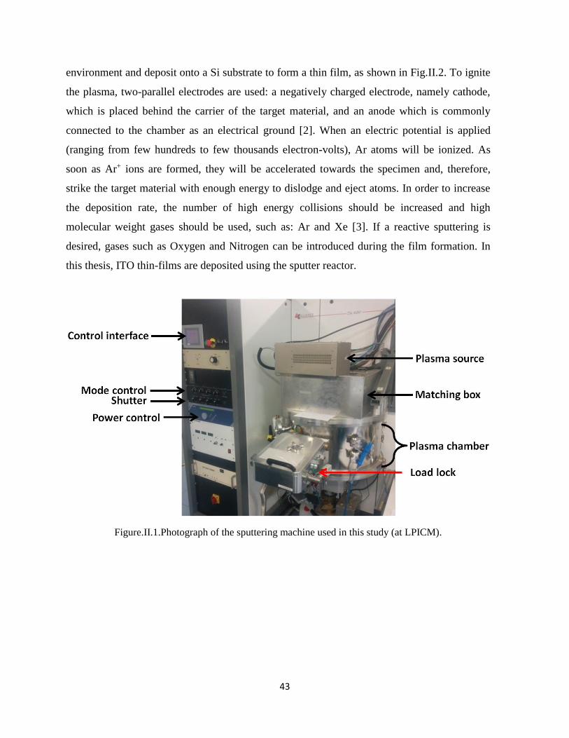
43
environment and deposit onto a Si substrate to form a thin film, as shown in Fig.II.2. To ignite
the plasma, two-parallel electrodes are used: a negatively charged electrode, namely cathode,
which is placed behind the carrier of the target material, and an anode which is commonly
connected to the chamber as an electrical ground [2]. When an electric potential is applied
(ranging from few hundreds to few thousands electron-volts), Ar atoms will be ionized. As
soon as Ar+ ions are formed, they will be accelerated towards the specimen and, therefore,
strike the target material with enough energy to dislodge and eject atoms. In order to increase
the deposition rate, the number of high energy collisions should be increased and high
molecular weight gases should be used, such as: Ar and Xe [3]. If a reactive sputtering is
desired, gases such as Oxygen and Nitrogen can be introduced during the film formation. In
this thesis, ITO thin-films are deposited using the sputter reactor.
Figure.II.1.Photograph of the sputtering machine used in this study (at LPICM).

44
Figure.II.2.Schematic illustration of a magnetron sputtering coater.
II.1.2 THERMAL EVAPORATION
Another common, yet, simple method of PVD is thermal evaporation in which the “Joule-
effect” is used. Maintained in high-vacuum, a crucible (i.e. Tungsten, Molybdenum) contains the
source material to be deposited in a form of powder or pellets. The evaporation starts when the
temperature is significantly increased (i.e. > 800℃ for Sn). When source atoms have enough
energy, they will eventually leave the surface of the source and travel through the vacuum
environment to reach the substrate which is positioned above the crucible (see Fig.II.3).
Figure.II.3. a) Schematic illustration of a thermal evaporator, QCM denotes: quartz crystal monitor which

45
is a tool used to control the rate and thickness of the deposited material (the deposition control in (b) is
possible with the aid of a QCM). The source material is located in resistive crucible that is heated enough
to evaporate source atoms [4]. b) a photograph of the thermal evaporator used in this study (at LPICM).
The deposition rate can be controlled by the intensity of the flowing current through the
resistive crucible, increasing the current will results in increasing the temperature and therefore
the deposition rate. The pressure is held low to decrease contamination, and to maintain a long
mean free path for the evaporated atoms to reach the substrate. In this thesis, the thermal
evaporator (shown in Fig.II.3.b) is used for the deposition of pure Sn catalyst NPs, since a target
specimen of Sn is not provided for the deposition in the magnetron coater (shown in the previous
section).
II.2 NANOWIRES ELABORATION: PLASMA ENHANCED CHEMICAL VAPOR
DEPOSITION (PECVD)
PECVD is one of the most used technologies for the fabrication of thin films and
nanowires. Not only used in research laboratories, the PECVD has been scaled up for
industrial applications [5]. The PECVD reactor, used in this study [6], satisfies the
requirements for production of high-performance thin film- and nanowire-based devices. For
instance, one can control precisely the process parameters such as: gas flow rates, gas
pressure, RF (radio-frequency) power, and the temperatures of the reactor wall, the substrate
holder, and electrodes. It is a versatile reactor where surface treatments, deposition, and
etching using different types of plasma in a one pump-down process are possible. The
numerous reactive gases, such as: Silane (SiH4), Germane (GeH4), Methane (CH4), Phosphine
(PH3), Diborane (B2H6), Tetrafluorosilane (SiF4), Dihydrogen (H2), and Ammonia (NH3), give
a huge flexibility in the fabrication process. Unlike the conventional CVD using only thermal
energy to dissociate molecules, this technique is plasma-assisted where energetic electrons
collide with gas molecules and ionize them (Fig.II.4). Therefore, the processes can be operated
at low temperatures (down to room temperature). In this system, two electrodes are placed in
parallel to create a capacitive configuration; the substrate is connected to the ground electrode
while the other electrode is powered by a DC or a RF (in our case), or a Very-High Frequency
(VHF) source. The dissociation of the reactive gases in this kind of systems is achieved

46
through their excitation in a 13.56 MHz capacitively couple RF discharge where the power is
provided by an RF generator. Electrons acquire enough energy, by the electric field created
between the two parallel plate electrodes, to dissociate the molecules in the reactor (Fig.II.4).
Numerous reactive species can be created in the plasma depending on the energy of the
electrons, thus, electric field. Let us take the dissociation of Germane (GeH4) for instance, for
different electron impact energies i.e. 8.2 eV, 8.7 eV, 8.9 eV, and 9.4 eV; different radicals are
produced correspondingly: GeH3−, GeH2
−, GeH−, and Ge respectively [7].
Figure.II.4. a) Schematic illustration of a capacitively coupled RF glow discharge reactor. The
plasma provides the reactive species which their interaction with the substrate depends on their charge
due to the presence of a space charge region (dark region between the plasma and the substrate). The
species contributing to deposition are shown at the space charge region. SiHx are the main radicals for
the deposition. They diffuse through the dark region to reach the substrate (this diffusion depends on
their mean free path, hence, the pressure in the plasma chamber). Photons and metastable species
interact with the growing films, but fewer studies have been conducted to know their impact on films
properties. Electrons and negative ions are mostly confined in the plasma due to its higher potential

47
compared to the substrate. On the contrary, positive ions will be accelerated towards the substrate as
soon as they arrive to the space charge region. Clusters and nanocrystals formed in the plasma may or
may not diffuse towards the substrate depending on their charge [8].
As shown in Fig.II.4, a wide variety of species are present in the plasma: Si radicals (SiH3,
SiH2, SiH, and Si), electrons, positive ions, photons and metastable species, negative ions,
clusters, and nanocrystals [9]. These species will react on the substrate in different amounts
depending on the process conditions.
The dark region plays an important role in filtering the diffusing charged particles
depending on their charges. One can observe that this region surrounds the bulk plasma and it
is called plasma “sheath”, see for instance Fig.II.5.a. In fact, since electrons are much lighter
than ions, they can escape from the plasma much faster as there is no confining potential
barrier. The electrons will accumulate on the chamber walls, thus, building up a negative field
repelling all incoming negatively-charged particles (mainly electrons), as shown in Fig.II.5.b.
This dark region with a low electron density results in the decrease of electron-molecule
collisions and therefore a decrease of gas excitation leading to this dark-region.
Figure.II.5. Plasma sheath region, a) photography showing the dark region between the bulk plasma
and the powered electrode [10]. b) schematic illustration showing the lack of electrons near the
electrode, due to a repelling field created by their accumulation on the surface. Since the collision
between electrons and molecules is reduced, no light is emitted in the sheath.
When radicals reach the substrate, mainly they will get physisorbed and diffuse along
the growing layer. These radicals experience a variety of reactions: i) they can desorb back to
the sheath depending on their sticking coefficient, ii) recombine with another radical to form
new ones (e.g. GeH3 + GeH3 = Ge2H6), iii) recombine to a hydrogen atom from the surface of

48
the substrate (e.g. GeH3 + H = GeH4), leaving a dangling bond on the surface which might
form a chemical bond with another radical (e.g. GeH3), iv) radicals can get chemically bonded
with dangling bonds at the surface of substrate (Si dangling bond in the case of a Si substrate)
which leads to the deposition.
In this thesis, two PECVD reactors were used: PLASFIL and ARCAM. Each has its
own advantages; on one hand, PLASFIL can be heated to a temperature of 650 ℃ for the
substrate holder and 450℃ for the RF electrode. It is a monochamber reactor where the
substrate holder is located below the RF electrode. The typical conditions for chemical
reduction of SnO2 are: temperature of the substrate is 250℃, pressure is set to 0.6 Torr,
hydrogen flow is 100 sccm (standard cubic centimeter), the optimal plasma power is 30 W,
and the duration depends on whether the SnO2 is a native oxide layer or a NP (for the case of
NP; t = 10 min, and for the latter case t = 2 min). Moreover the deposition conditions used in
this thesis are: i) substrate’s temperature is between 120℃ and 350℃, pressure stabilized at
0.3 Torr, Germane, hydrogen flows are 50 sccm and 40 sccm respectively, plasma power
should be 2 W, and the duration depends on the desired thickness (10 min deposition
corresponds to ~15 nm). The annealing step, where the growth is activated, is normally done
under flow of 100 sccm hydrogen at temperatures between 230℃ and 350℃.
Figure.II.6. PLASFIL reactor a) photography, b) schematic illustration of the reactor’s design
On the other hand, ARCAM reactor has three independent plasma boxes (15 cm in
diameter) grouped in a big single vessel. This multiplasma-monochamber reactor allows the

49
fabrication of various kinds of samples in a one pump-down. For example, three samples can
be produced successively: intrinsic, n-type, and p-type NWs (or thin-films) each grown in a
separate plasma chamber, which helps enormously to reduce the processing time and therefore
the fabrication cost. However, the temperature cannot exceed 350℃. Here it is noteworthy that
the same fabrication conditions are used as in PLASFIL, except that the temperature should
not exceed the 300℃.
Figure.II.7. Photography of ARCAM reactor, the inset shows the three-plasma chambers located inside
the reactor’s main vessel.
II.3 CHARACTERIZATION TECHNIQUES
The process of fabrication may not be as difficult as the characterization one.
Investigations of chemical and physical properties of nanowires (nanoscale) require
appropriate and sophisticated techniques. In the following parts, we will describe the
characterization techniques used in this thesis: Scanning Electron Microscope (SEM), Focused
Ion Beam (FIB), Raman spectroscopy, Transmission Electron Microscope (TEM), and Atom
Probe Tomography (APT).
II.3.1 DUAL BEAM ELECTRON – ION MICROSCOPE
The fastest way for feedback concerning all aspects of the NWs growth, is provided by
the SEM observations [11]. In this study, a Zeiss NVision 40 FIB-SEM composed of ionic and
electronic columns (which are shown in Fig.II.8), has been employed for feedback, and
nanoscale preparations for TEM and APT analyses. NVision 40 combines a high resolution

50
SEM with the precision milling and nanofabrication abilities of a high resolution FIB. All
characterization and processing can be controlled using a computer interface with a dedicated
software (SmartSEM).
II.3.1.1 SCANNING ELECTRON MICROSCOPE
SEM is a highly versatile electron beam instrument that can provide images over 100
times more magnified than commercial optical microscopes, and permits the observation and
characterization of heterogeneous organic and inorganic materials on a nanometer scale [12].
The electron column consists of an electron gun which is in our case a Schottky field emission
Gemini column that operates between 100 V to 30 kV. The resolving capabilities of the
featured SEM are 1.1 nm at 20 kV and 2.5 nm at 1 kV. The electron path is controlled by two
or more electromagnetic lenses located inside the column. A high vacuum is achieved, i.e. in
our case 10-10 mbar in the gun column and between 10-6 – 10-7 mbar in the system (analysis
chamber where the specimen is located). These ultra-low pressures are mandatory in order to:
i) minimize the electron-particle collisions which make the electrons deviate from their initial
trajectory, and ii) avoid contamination.
The scanned image is formed point-by-point. Usually two pairs of electromagnetic
deflection coils, dubbed “scanning coils”, are used to sweep the beam across the specimen. In
fact, the scanning coils cause the beam to move and to scan a series of discrete locations along
a line, then along another line below the first. This process is repeated until an electronic
rectangular image of the specimen is generated [13]. Upon electron-specimen interactions,
many types of signals can be generated, such as: Secondary Electrons (SE), BackScattered
Electrons (BSE), Auger Electrons (AE), X-ray, visible light (cathodoluminescence), and
electron-hole pairs, as shown in Fig.II.9.a. The BSE and SE are the most used signals to
construct images. For instance, the SE signal provides a detailed inspection of the topography
of the sample’s surface, Fig.II.9.b. Meanwhile, BSE provide beneficial information on the
material composition, crystallography and magnetic field, Fig.II.9.c.

51
Figure.II.9. Different signals obtained upon electrons collision in SEM. a) Schematic illustration of
different types of signals produced consequent to the electron-specimen interactions. b) electronic
image constructed using SE in SEM at an accelerating voltage of 20 kV of a particle made of Pb and
Ba. The SE image shows the detailed topological features of the particle, however it shows no contrast
difference related to the atomic number Z. c) image of the same particle constructed using BSE, the
contrast difference is Z-related and helps differentiate the location of different elements in the particle.
The whiter elements are Pb (SEM image courtesy of LKA Bayern, Karl Lüftl)
II.3.1.2 FOCUSED ION BEAM
Similar to SEM, the FIB consists of a vacuum column, electromagnetic coils, and a
Liquid-Metal Ion Source (LMIS, typically a reservoir of liquid Ga) responsible for creating a
finely focused ion beam. In our study, the ion gun (inclined 54° with respect to the SEM

52
column) featured in the FIB is SIINT Zeta Ga+ ion which can be operated between 1 kV and
30 kV with ion currents between 0.1 pA and 45 nA. The resolution of the ion beam is 4 nm at
1 pA, which is lower than SEM because ions cannot be as finely-focused as electrons.
The FIB has capabilities that are not available in any other milling technique, such as:
an accurate target – area selection which enables the selectivity of a ROI, and milling both
sides of a chunk (parallel milling) [14]. These capabilities are very important for high quality
TEM and Atom-probe specimen fabrications. Despite these advantages, the ion milling causes
extensive damages to the ROI, such as structural defects (amorphization), and ion implantation
[15]. These artifacts are related to the ion-beam incident angle and accelerating voltage. In
fact, Ga ions that are accelerated by 30 kV helps to coarsely mill the chunk, for this reason it is
considered to be a time efficient process. However, at this accelerating voltage lots of damages
are created by the incident ions. It was shown that by reducing the accelerating voltage, less
damage is produced, i.e. 5kV produces less damage to the surface (and sub-surface) than 30
kV, as shown in Fig.II.10.

53
Figure.II.10. HR-TEM images for Si lamellas [110] prepared using three accelerating voltage: 30 kV, 5
kV, and 2 kV. The sidewall amorphization size induced by a) 30 kV, the amorphous thickness is ~ 20
nm, b) 5kV, the thickness is ~ 2 nm, c) 2kV, the thickness range between 0.5 and 1.5 nm. d) the
polishing damage induced by a 30 kV accelerating voltage, e) 5 kV, and f) 2 kV. (Image adapted from
ref [16]).
Moreover, it was shown that increasing the incident angle while using 50kV will
increase the damages and implantation. To avoid these drawbacks, the incident angle should
be lowered while coarse milling. Nevertheless, it was shown that even at 1° incident angle the
sample will get damaged [17]. It is impossible to avoid the damages completely during a
coarse mill, but a cleaning process can repair the damaged surface. The optimal accelerating
voltage for a cleaning procedure is 2 kV [16] (Fig.II.10.f). At this voltage, Ga ions will not be
able to penetrate the surface, but only have the energy to clean the defected surface. This type
of cleaning requires increasing the incident angle (typically, ± 4°) knowing that at low kV
exposing the surface to the beam will not induce further damaging.
The NVision 40 is equipped with a Gas Injection System (GIS). The gas supply consists of
(CH3)3CH3C5H9Pt precursor reservoir that is heated up to 40℃ resulting in a gas flux of 1018
molecules/cm2s. The gas is introduced into the chamber using a nozzle of 0.5 mm diameter. The
open-end of the nozzle is brought into close proximity to the substrate surface. The SE is mainly
produced by the collisions of the incident ions or electrons with the substrate surface [18]. The
SE possesses low energy < 50 eV which corresponds to the precursor molecules bonding energy.
Therefore, SE is responsible for cracking the gas molecules as well as the formation of bonds
between the created species and the substrate surface atoms. Ion and electron beams can be used
to deposit material at a specific region [19]. The CVD can be achieved in two ways: i) Ion Beam-
Induced Deposition (IBID) [20], and ii) Electron Beam Induced Deposition (EBID) [21, 22].
However, the ion beam is much more efficient (faster) for the deposition than the electron beam,
because the ion beam creates an important number of secondary electrons upon the collision with
the sample compared to an electron beam. The usual conditions for IBID are: 30 kV accelerating
voltage, 40 pA (for 4 μm × 4 μm surface area), dwell time of 0.4 μs, and a pixel fill factor of
55%. Note that increasing the deposition surface area requires increasing the ion current for a
more efficient deposition. For the EBID the typical conditions are: 5 kV accelerating voltage,

54
slow scan speed, and a current of few nA (high current mode – 60 μm aperture). Chemical
analysis has shown that IBID – Pt contains a large amount of carbon incorporated into it from the
broken down precursor gas 30–50 at.%, meanwhile EBID – Pt contains up to 70 at.% [23].
II.3.1.2.1 SAMPLE PREPARATION FOR TEM AND APT
The dual-beam is equipped with a micro-manipulator (Kleindiek, Nanotechnik,
Germany) which is used for lift-outs during this study. As a first step, in the lift out process, Pt
is deposited in SEM via EBID on the Region-Of-Interest (ROI), as shown in Fig.II.11.a,b.
This preliminary coating serves as a protection from the ion beam imaging; the thickness
should be between 100 to 150 nm. The ion imaging is done at an ion current of 40 pA and an
accelerating voltage of 30 kV. The second layer of Pt, with a thickness ranging from 300 to
400 nm deposited via IBID, serves as a protection from coarse milling operations. High ion
currents (1.5 nA to 3 nA) are then controlled to be focused perpendicularly towards the
surrounding of the ROI, in a sputtering process called milling process, Fig.II.11.c. Therefore,
the newly-formed chunk is only attached to the substrate from one side that is underneath the
ROI, see Fig.II.11.c. At this point, the Kleindiek micromanipulator is introduced, and then its
tip is welded on the chunk using IBID of Pt, Fig.II.11.d. Then, a milling step is necessary to
detach the chunk from the main specimen and lift it out using the micromanipulator,
Fig.II.11.e. Now the following preparation procedure depends on the type of the fine-
characterization that will be done after FIB-SEM operations (TEM or APT).
In the case of TEM, the chunk welded on the tip of the micromanipulator is also
welded on the TEM copper lamella using Pt IBID, and the contact point between the
micromanipulator and the chunk is milled using Ga+ to achieve their detachment, Fig.II.11.f.
For TEM observations, the chunk is thinned to thicknesses less than 100 nm using low ion
currents (40 pA to 80 pA), Fig.II.11.g. As a final step, a cleaning process (at a low
accelerating voltage: 2 kV) is necessary to remove most of the ion-damaged regions from the
ROI cross-section, thus, leaving the crystalline structured material ready for TEM analysis,
Fig.II.11.h, i.

55
Figure.II.11. SEM images of TEM-lamella preparation using FIB. a) SEM image showing
the ROI (NWs), b) deposition of Pt protective layer using EBID, c) coarse milling around the chunk
leaving only the downside part attached to the substrate, d) The GIS nozzle and the micromanipulator
are inserted nearby the chunk. Pt is used to weld the micromanipulator with the chunk, e) SEM image
of the lifted-out chunk, after the welding, ions are controlled to mill the downside part of the chunk in
order to detach it from the main sample. Insert: simultaneous FIB view, f) the chunk is welded on the
copper TEM-lamella and then detached from the micromanipulator, g) coarse milling process in order
to reduce the chunk size for proper TEM observations, h) top-view of the chunk after fine milling, i)
side-view of the chunk after cleaning at 2 kV accelerating voltage and 30 pA ion current.
In the case of APT, the chunk is welded on a W-tip by Pt welding. Afterwards, an
annular milling is achieved using the FIB. In fact, the mask shown in Fig.II.12.a is to protect
the ROI while milling the other parts. The accelerating voltage used in this process is 30 kV
and the ion current is between 40 pA to 80 pA. The latter process is repeated while decreasing

56
the mask size. As a final step, a cleaning process is required to remove the FIB-damaged
region using an accelerating voltage of 2 kV with 30 pA as an ion current. Fig.II.12.b is an
SEM image showing a p-i-n junction SiNW milled and cleaned using FIB and ready for APT
analysis.
Figure.II.12. APT tip preparation a) schematic illustration showing the preparation process of an APT
tip, first the chunk is welded using Pt on a W tip support, then it is coarsely milled by 30 kV
accelerated-Ga+ ions, while a mask is protecting the ROI. When the apex radius is less than 50 nm, a
cleaning process is required to remove the damages induced by the FIB. In this process, the Ga ions
accelerating voltage is reduced to 2 kV. b) SEM image showing a p-i-n junction SiNW milled, cleaned,
and ready for APT analysis.
II.3.2 RAMAN SPECTROSCOPY
Raman spectroscopy is a non-invasive, practical, and quick tool for composition
identifications and quantifications [24, 25]. When light is scattered from a molecule or crystal,
most photons are elastically scattered with the same energy (wavelength) as the incident
photons. However, only a small fraction of light (roughly 1 part in 10 million) is scattered at
frequencies different from the incident photons. The Raman effect, which is the process of
inelastic scattering, is too weak to be seen by the naked eye; for this reason a highly sensitive
spectrometer is used. The shift in wavelength of the inelastically scattered radiation provides
chemical and structural information. Raman shifted photons can be of either lower (Stokes

57
scattering) [26] or higher (anti-Stokes scattering) energy [27], depending upon the vibrational
state of the molecule under study, whereas the Raleigh scattering is when the photons have
equal amount of energy as the incident ones (Fig.II.13). It was demonstrated that the Raman
spectroscopy can be used to quantify the composition of a given material, and the strain-state
in a certain structure by tracking the pic shift (Stokes, or anti-Stokes) [28, 29].
Figure.II.13. Schematic identifying light scattering after laser exposure on a sample [30].
Raman scattering experiments show that the frequency of the Ge peak (corresponding
to the bulk wGe = 301 cm-1) decreases with the increasing Sn concentration in the alloy, as
shown in Fig.II.14.

58
Figure.II.14. Raman spectra from a bulk Ge substrate and fully strained Ge1-xSnx layers grown
on Ge (001). Films compositions x and thicknesses from bottom to top are: x = 0.03, t = 62 nm; x =
0.075, t = 40 nm; and x = 0.13, t = 31 nm.
The shift is linearly related to x in Ge1-xSnx and is given by ∆wGeSn = - k. x, where k is
the prefactor depending on the strain state of the structure and x is the atomic fraction of Sn. In
fact, accommodating Sn in Ge will create a compressive strain (due the Sn-induced bond
stretching) causing a shift in the frequency. In this thesis, the micro-Raman used is Horiba
LabSpec 5 (at LPICM), equipped with Helium-Neon (HeNe) laser with an excitation
wavelength of λlaser = 633 nm and CCD detector.
II.3.3 TRANSMISSION ELECTRON MICROSCOPE (TEM)
As highlighted previously, the nanometer resolutions attained in a SEM are highly
compatible with the actual developments of the nanotechnology [31]. Since the nanoscience is

59
an nanometer-scale material engineering (ranging from 1 nm to 100 nm), a more advanced
microscopy is required for atomic characterization. An in-depth analysis of individual nano-
objects requires the use of the Transmission Electron Microscopy (TEM). The main advantage
of TEM relies on the volumetric information acquired, as in this case the electrons with
superior energies as against the SEM transverse the specimen. For instance, the typical
electron energies used in a SEM range from 1 to 30kV, whilst the accelerated voltage in a
commercial TEM ranges from 60 to 300kV, but less or higher for specific configurations. The
principles of a TEM rely on the wave-particle duality, which was first theorized by Louis de
Broglie [32] in 1925. This theory stands at the bases of the relationship between the energy of
an electron and its characteristic wavelength:
𝜆 =ℎ
[2𝑚0𝑒𝑉(1 +𝑒𝑉
2𝑚0𝑐2)]1 2⁄
Where h is Plank’s constant, m0 and e are the mass and charge of an electron respectively, V is
the accelerating voltage (eV is the energy of an electron), and c the speed of light in vacuum.
This equation stipulates that an electron accelerated by acceleration voltages of 200 kV or 300 kV
have a wavelength of 3 or 2 pm respectively. Therefore, increasing the electron velocity will
eventually decrease its wavelength; and thereby the resolution of an electron micrograph will
increase. In 1932, the idea of an electron microscope first came to the mind of Ernst Ruska who,
afterwards, received the prestigious Nobel prize (1986) [33]. Only 4-years after his breakthrough,
commercial TEMs started to be built. In TEM, the electron beam kinetic energy can range from
100 keV to 400 keV, and recently an ultra-high voltage TEM was built that can reach a superior
value of 1.25 MeV for enhanced resolutions [34, 35]. Very fast, this TEM showed its limitations
in terms of materials to investigate, since the high acceleration voltages induce important changes
in the materials structure, e.g. the beam-induced damages.
The schematic representation of a TEM setup is displayed in Figure II.15, with the highlight on
the main constitutive segments, which were progressively improved in time in an effort to
achieve the ultimate resolutions. From a technological point of view, huge advances were
achieved with the development of the correctors for the aberrations encountered in the
condenser and objective lenses. Such correctors installed on commercial TEMs allow to rich
point to point resolutions down to 70 pm in TEM parallel mode. In the same time, the

60
development of new cameras and detectors allows one to gather different types of signals and to
build up more and more complex approaches. As function of the information researched and the
material investigated, several modes can be developed in a TEM. Only the working modes
employed during the current investigations are further described.
Figure.II.15. Schematic image representing the TEM basic setup.

61
II.3.3.1 HIGH RESOLUTION – TEM
In a TEM, an incident coherent parallel beam can be used to achieve high resolution
enabling to visualize even atomic columns, e.g. High Resolution TEM. Different types of
contrasts can be generated in TEM, for example diffraction contrast and mass-thickness contrast
[36]. Upon electron-specimen interactions, the waves of the electrons that have interacted with
the sample will undergo a phase shift as compared to electrons that have not interacted with the
sample. This phase shift is the main component of the contrast when high resolution images are
acquired, and this is the reason why the HRTEM imaging is named phase contrast imaging.
In the case of crystalline materials, their orientation in the zone axis as against the
electrons beam is obligatory for HRTEM imaging. It can be achieved by specimen tilting in the
microscope to the desired zone axis under diffraction mode. The diffraction mode is usually
employed by selecting an area of interest from the sample to explore the material’s crystal
orientation and/or crystal structure within the very specific area [37]. The electronic diffraction is
mainly described by Bragg’s law [38].
II.3.3.2 SCANNING – TEM (STEM)
In STEM mode, a small energetic probe (highly-focused electron beam) scans the sample
and with a well-defined speed [39]. The directly transmitted beam (elastically scattered and part
of the diffracted electrons) is registered by a circular detector i.e. Bright-Field STEM imaging
mode, whereas the electrons scattered at large angles are acquired by annular detectors under
Dark Field STEM mode, as shown in Fig.II.16.a [40]. The transmitted beam can be detected on
the BF detector, Fig.II.16.b. Electrons that are deviated over small angles with respect to the
transmitted beam can be detected on the annular DF (ADF) detector (angles between 10 and 40
mrad). Electrons impinging on the ADF detector can be diffracted electrons; therefore the image
is sensitive to diffraction contrast [41]. Whilst, electrons deviated at higher angles can be detected
on the HAADF detector (angles > 40 mrad), Fig.II.16.c. The electrons collected by the HAADF
detector are incoherently scattered [42], and the contrast in HAADF STEM depends on the
atomic number Z, hence I ∝ Z2. Meaning that heavy elements (i.e. Sn) can be easily distinguished
by a higher intensity area from lighter ones (i.e. Ge), which appears darker.

62
Fig.II.16. a) The STEM principle and the associated detectors located beneath the specimen; high-angle-
annular dark-field (HAADF) annular dark-field (ADF), and bright-field (BF). The X-ray detector is
located above the specimen surface. b) aberration-corrected STEM BF mode image of a PtCo NP, and c)
HAADF mode of the same particle
Apart from the imaging contrast, the STEM methodology can be employed to probe the exact
location of specific chemical events and/or to build up maps of the constitutive elements or of the
chemical imprint (hybridization states for example) within the sample. To this end, additional
spectroscopy devices are associated to the imaging mode, as described in the next section.
Similar with the TEM mode, the spatial resolution in the STEM mode can be improved by the
addition of corrections for the spherical and/or chromatic aberrations. Such, sub nanometer
resolutions are commonly attained in Cs probe corrected microscopes under STEM mode.
II.3.3.3 ENERGY DISPERSIVE X-RAY SPECTROSCOPY
The abovementioned TEM modes are mainly used for structural and crystallographic
investigations, but chemical analysis can be performed as well by using the Energy Dispersive
X-rays Spectroscopy (EDS) or Electron Energy Loss Spectroscopy (EELS). The principle
behind the electron spectroscopy techniques within the TEM are schematized in Fig II.17.
Such, an electron located in a core-state of an atom can be ejected by the energetic incident
electron to an unfilled state or vacuum. Afterwards, a shell-electron fills the empty core-state

63
resulting in a characteristic X-ray emission captured by the EDX detector, whereas the
incident electrons which lost part of their energy will be collimated and detected on the EELS
spectrometer. Each element in the periodic table has its own characteristic energy signature
under EDS or EELS, which are further employed for the materials characterization.
Figure.II.17. Schema of the fundamental emission processes of the characteristic x-rays, and the energy
loss electrons, which are acquired afterwards by a dedicated EDX and EELS detectors.
In this study, the TEM experiments were carried out on a Cs probe corrected JEOL
ARM200 TEM and a double corrected TEM, both analytical TEMs operated at 200kV. The
double corrected TEM is equipped with a 100mm Centurio EDX detector and a Quantum GIF
for the energy electron loss spectroscopy EELS. This configuration allows to attain spatial point
resolutions down to 78 pm under TEM. A probe of 0.1 nm was used to scan the specimen in
STEM mode. A camera length of 8 cm and high speed scanning protocol (5µsec/px) was
employed for the STEM-HAADF images. 256x256px chemical maps were recorded for every
element of interest by continuous scanning with exposures times of 20µseconds/px and for
mean recording durations of 45 minutes. Cross-correlations algorithms were applied every 30
seconds along the experiment to avoid the maps misalignments due to specimen spatial drifts.
II.3.5 ATOM PROBE TOMOGRAPHY
The atom probe tomography (APT) is one of the most advanced forms of microscopy
for atomic-scale characterizations. It is a high-resolution tri-dimensional analytical
microscope. It is worth noting that APT is derived from the field ion microscope (FIM), and

64
both were invented by Prof. Erwin Müller [43-45] and, more widely, is part of the field
emission microscope family. The principle of APT relies on the atom evaporation and further
ionization from a sample surface using a high electric field. In order to achieve such high field,
a needle-like sample, with an apex radius less than 50 nm, which preparation by FIB, usually
used for semiconductors, is subjected to a high positive voltage (typically between 2 to 15kV).
The sharpness of the tip allows the electric field to be very intense at the apex (few tens of
V/nm). The electric field F is given by:
𝐹 =𝑉
𝑘𝑅
Where V is the standing voltage, R the curvature radius of the tip, and k is a geometrical factor
taking into account the shape of the tip. By assuming k = 1, for a standing voltage of 2 kV and
a tip radius of 50 nm, then the electric field on the apex of the tip is F = 40 V/nm. The sample
is then evaporated atoms by atoms, atomic layer by atomic layer. The evaporation atom by
atom is controlled by applying a voltage inferior to its evaporation field and then applying
short electric pulses (for metals or alloys) or laser pulses (semiconductors) [Ref. Baptiste
Gault, Atom Probe Microscopy]. The mass-to-charge ratio is, then, calculated using the ToF
and the value of the applied voltage on the tip. Assuming that the evaporated atoms leaving
the tip have no initial velocity, they acquire their speed from the electrostatic field in the
chamber. In other words, the acquired kinetic energy (Ec) by an evaporated atom is equal to
the potential energy (Ep) of the electrostatic field. Consequently, the energy conservation is
written as Ec = ½ mv2 = n e- V = Ep, where m and v are respectively the mass and speed of the
atom, ne- is the charge of the ion (n is the charge state 1+, 2+…), and V is the applied voltage.
The maximum speed is attained by the ions just before they hit the detector, then, v = L/ToF
(L is the distance between the tip and the detector). As a result, the mass-to-charge ratio can be
calculated by:
𝑚
𝑛= 2𝑒𝑉[
𝑇𝑜𝐹
𝐿]2
The identification of the detected atoms is done by determining their mass-to-charge ratios
which is derived from a direct measurement of ToF, L, and V for each single atom. It is worth
noting that the APT experiment is carried out in an analysis chamber with an ultra-high

65
vacuum (10-10 mbar) to avoid gases ionization at the tip surface. The tip is also cooled down to
temperatures usually between 10 K and 80 K. This cryogenic temperature is important to
reduce the thermal agitation at the surface of the tip and reduce the diffusion of atoms from the
specimen across its surface.
In this study, Laser-Assisted Wide Angle Tomographic Atom Probe (LAWATAP,
CAMECA shown in Fig.II.18) and Flexible-TAP (FlexTAP, CAMECA) are used for the
analysis of semiconducting NWs. The FlexTAP enables the user to change distance between
the sample and the detector, while this distance is fixed in LAWATAP. In these APTs,
femtosecond lasers are implemented for an extremely short laser-pulse (400 fs) which is
necessary to obtain a highly-resolved mass spectrum. In this work, a wavelength of λ = 515
nm (green), and a temperature of 80 K were chosen for the analysis of nanowires.
Figure.II.18. Photograph showing the LAWATAP used in this study.

66
II.3.5.1 3D VOLUME RECONSTRUCTION
The used ion detector is not only time-resolved (measures ToFs), but also sensitive to
impact positions of ions (recording the X,Y coordinates of each ion) [46]. In modern APTs,
the ion detector is enhanced by micro-channel plates (MCPs) to convert the impact of a single
ion into a cascade of up to millions of electrons [47].
In the case of LAWATAP and FlexTAP, an advanced delay-line detector (aDLD) capable of
resolving multi-ion hits simultaneously is placed behind the MCPs [48]. The aDLD consists of
parallel conductive lines closely-assembled to form a conductive plate, Fig.II.19. Two
conductive plates are used to determine the X,Y coordinates of the impact, knowing that each
one of the conductive plates gives information about only one dimension (either X, or Y). The
electron cloud formed by the MCPs upon the ion impact travels in the vicinity of the analysis
chamber to reach the aDLD. The electronic system of the APT digitize the position of the
atoms laterally (in X,Y dimensions).
Figure.II.19. schematic illustration showing the concept of a delay-line detector [49]. Two ions hit
the MCP which result in two electron clouds that travel towards the X,Y plates. Then the system
measure the propagation time in X and Y plates in order to calculate the impact coordinates.
Two electrical signals are created when the electron cloud hits the two-plates of the aDLD.
Afterwards, these signals travel through the conductive lines to reach the collectors of the X,Y

67
plates. The propagation time to reach both ends of each plate can be measured which enables
the determination of the lateral impact coordinates (XD,YD) on the detector:
𝑋𝐷 = 𝐿𝑥
𝑇𝑥2 − 𝑇𝑥1
2𝑇𝑃𝑥
Where Lx is the length of the detector line, Tx1 and Tx2 are the times needed to reach both ends
of the conductive line (for X-dimension), and Tpx is the total propagation time for a signal
travelling between both ends (along the entire line). Same analogy can be done for YD.
Using the coordination and sequence of arrival dataset recorded by the APT electronic
system, all detected atoms can be traced back to their initial position on the tip. The
reconstruction is then made atom by atom. Many models have been proposed in the past years
concerning the 3-dimensional reconstruction [50-52]. Under the hypothesis that the
reconstruction is performed by a point projection model, the general expression to determine
the original atomic position on the surface of the tip is given by [53]:
𝑥 =𝑋𝐷 𝜉 𝑉
𝐿 𝑘 𝐹
Where x is the real x-dimension of the atom on the tip, XD is the ion-MCP impact coordinate,
𝜉 is the compression factor that takes into account the modification of the field lines due the
constant change in the shape of the tip, and L is the flight length. The same analogy is used for
y-dimension. From this simple expression which was established initially, a more complex and
advanced algorithm was developed by Bas et al. [52] taking into consideration several
parameters influencing the reconstruction such as: the tip curvature, and the tilt angle between
the tip axis and the detector. In order to get a 3D reconstruction, a z position (depth
coordinate) is calculated for each atom using the APT analysis data and several assumptions.
[52] The reconstruction and data treatment (mass spectrum, composition, cluster, etc..;
analyses) is made in the home-made GPM 3D software. It is worth noting that the
reconstruction protocol works quite well for homogeneous materials. However, as far as
several phases or layers are presents in the APT analysis, some limitations related to the
trajectory aberrations of ions, known as local magnification effects, will distort the
reconstruction, limit the spatial resolution and its capacity to investigate to probe the local
composition [53, 54].

68
II.4 SUMMARY
In this chapter, a description of fabrication and characterization machines used in this
thesis is given. Two catalyst elaboration techniques were used: magnetron sputtering coater, and
thermal evaporator. Each was used to elaborate a different type of catalysts; the first is used to
deposit a thin-film of ITO that will be transformed to InNPs using the PECVD reactor (as it will
be discussed in Chapter III), the second is for evaporating Sn to form the NPs. The PECVD
reactor is used for surface treatments, depositions, and growth of NWs.
Moreover, different characterization techniques are used for speculations and investigations of
the obtained NWs. The FIB/SEM dual beam was used to fabricate specimens that are specially
designed for TEM (lamella) and APT (tip). Furthermore, the SEM is used for feedback on the
shape and size of the NWs, as well as the growth success rate after the fabrication process. The
TEM allows having a deep insight on the NWs atomic structure, and the EDX allows the
quantification of the components constituting the NWs. The APT is considered the ultra-fine
characterization tool, with abilities to reconstruct in 3D real-space the atom-by-atom evaporated
NWs. The mass-spectrometry, equipped in the atom probe, gives the ability of identifying the
detected evaporated atoms with single atom precision. In the next chapter, the synthesis and
characterization of the Ge and GeSn NWs catalyzed by In and Sn NPs will be detailed.
II.5 REFERENCES
1. Vossen, J., Kern, W., "Thin film processes II" Academic Press (1991): 179. London.
2. Vossen, J., Kern, W., "Thin film processes II". Academic Press (1991): 184. London.
3. Kelly, P.J., Arnell, R. D., Magnetron sputtering: a review of recent developments and
applications. Vacuum, 2000. 56(3): p. 159-172.
4. http://slideplayer.com/slide/7404434/.
5. Treutler, C.P., Industrial use of plasma-deposited coatings for components of automotive fuel
injection systems. Surface and Coatings Technology, 2005. 200(5-6): p. 1969-1975.
6. Cabarrocas, P., J. B. Chévrier, J. Huc, A. Lloret, J. Y. Parey, J. P. M. Schmitt, A fully automated
hot‐wall multiplasma‐monochamber reactor for thin film deposition. Journal of Vacuum Science
& Technology A, 1991. 9(4): p. 2331-2341.
7. Hoshino, M., Matejčík Š, Nunes Y., Ferreira da Silva F., Limão-Vieira P., Tanaka H., Negative
ion formation through dissociative electron attachment to GeH4: Comparative studies with CH4
and SiH4. International Journal of Mass Spectrometry, 2011. 306(1): p. 51-56.
8. P Roca i Cabarrocas , K.K.-H., Cariou Romain, Labrune Martin, Johnson EV, Moreno M, Rios A
Torres, Abolmasov Sergey, Kasouit Samir, Low temperature plasma synthesis of nanocrystals
and their application to the growth of crystalline silicon and germanium thin films. MRS Online
Proceedings Library Archive, 2012. 1426: p. 319-329.

69
9. Wilfried van Sark , L.K., Francesco Roca, Physics and technology of amorphous-crystalline
heterostructure silicon solar cells. 2012: Springer.
10. Kroesen, G.M.W., Beckers J., Trienekens D., Schrader A., van Heerebeek J., de Kluijver R. ,
Particle charge and electrical field studied in the pre-sheath of an RF discharge.
11. Adams, F., Barbante Carlo, Chapter 7 - Electron-Based Imaging Techniques, in Comprehensive
Analytical Chemistry, F. Adams and C. Barbante, Editors. 2015, Elsevier. p. 269-313.
12. Scanning Electron Microscopy, in Materials Science and Technology.
13. Unakar, N.J., Tsui J. Y., Harding C. V., Scanning Electron Microscopy. Ophthalmic Research,
1981. 13(1): p. 20-35.
14. Mayer Joachim, G.L.A., Kamino Takeo, Michael Joseph, TEM Sample Preparation and FIB-
Induced Damage. MRS Bulletin, 2011. 32(5): p. 400-407.
15. Thompson K., G.B., Larson D., Leer B. van, Hong L., Minimization of Ga Induced FIB Damage
Using Low Energy Clean-up. Microscopy and Microanalysis, 2006. 12(S02): p. 1736-1737.
16. Giannuzzi L. A., G.R., Ringnalda J., 2 keV Ga+ FIB Milling for Reducing Amorphous Damage in
Silicon. Microscopy and Microanalysis, 2005. 11(S02): p. 828-829.
17. McCaffrey J. P., P.M.W., Madsen L. D., Surface damage formation during ion-beam thinning of
samples for transmission electron microscopy. Ultramicroscopy, 2001. 87(3): p. 97-104.
18. Park YK, N.T., Takai M, Lehrer C, Frey L, Ryssel H, Comparison of beam-induced deposition
using ion microprobe. Nuclear Instruments and Methods in Physics Research Section B: Beam
Interactions with Materials and Atoms, 1999. 148(1-4): p. 25-31.
19. Saxey, D.W., Cairney J. M., McGrouther D., Honma T., Ringer S. P., Atom probe specimen
fabrication methods using a dual FIB/SEM. Ultramicroscopy, 2007. 107(9): p. 756-760.
20. Sadki, E.S., S. Ooi, and K. Hirata, Focused-ion-beam-induced deposition of superconducting
nanowires. Applied Physics Letters, 2004. 85(25): p. 6206-6208.
21. van Kouwen, L., Botman Aurelien, Hagen Cornelis W., Focused Electron-Beam-Induced
Deposition of 3 nm Dots in a Scanning Electron Microscope. Nano Letters, 2009. 9(5): p. 2149-
2152.
22. Donev, E.U., Hastings J. Todd, Electron-Beam-Induced Deposition of Platinum from a Liquid
Precursor. Nano Letters, 2009. 9(7): p. 2715-2718.
23. Puretz J, S.L., Focused ion beam deposition of Pt containing films. Journal of Vacuum Science &
Technology B: Microelectronics and Nanometer Structures Processing, Measurement, and
Phenomena, 1992. 10(6): p. 2695-2698.
24. Ferrari, A.C., Basko Denis M., Raman spectroscopy as a versatile tool for studying the properties
of graphene. Nature Nanotechnology, 2013. 8: p. 235.
25. Dresselhaus, M.S., Dresselhaus G., Saito R., Jorio A., Raman spectroscopy of carbon nanotubes.
Physics Reports, 2005. 409(2): p. 47-99.
26. Kneipp Katrin, K.H., Itzkan Irving, Dasari Ramachandra R., Feld Michael S., Ultrasensitive
Chemical Analysis by Raman Spectroscopy. Chemical Reviews, 1999. 99(10): p. 2957-2976.
27. Zumbusch, A., Holtom Gary R., Xie X. Sunney, Three-Dimensional Vibrational Imaging by
Coherent Anti-Stokes Raman Scattering. Physical Review Letters, 1999. 82(20): p. 4142-4145.
28. Rojas-López, M., H. Navarro-Contreras, P. Desjardins, O. Gurdal, N. Taylor, J. R. A. Carlsson, J.
E. Greene, Raman scattering from fully strained Ge1−xSnx (x⩽0.22) alloys grown on
Ge(001)2×1 by low-temperature molecular beam epitaxy. Journal of Applied Physics, 1998.
84(4): p. 2219-2223.
29. Hai, L., Robert Chen, Yijie Huo, Theodore I. Kamins, James S. Harris, Raman study of strained
Ge1−xSnx alloys. Applied Physics Letters, 2011. 98(26): p. 261917.
30. Butler Holly J., A.L., Bird Benjamin, Cinque Gianfelice, Curtis Kelly, Dorney Jennifer, Esmonde-
White Karen, Fullwood Nigel J., Gardner Benjamin, Martin-Hirsch Pierre L., Walsh Michael J.,
McAinsh Martin R., Stone Nicholas, Martin Francis L., Using Raman spectroscopy to
characterize biological materials. Nature Protocols, 2016. 11: p. 664.
31. Joy, D.C., Limits of SEM Resolution. Microscopy Today, 2018. 4(5): p. 10-11.

70
32. de Broglie, L., L'Oeuvre d'Einstein et la Dualit\'e des Ondes et des Corpuscules. Reviews of
Modern Physics, 1949. 21(3): p. 345-347.
33. Ernst, R., Electron microscope. 1941, Google Patents.
34. Zhang, X.W., Boyen H. G., Deyneka N., Ziemann P., Banhart F., Schreck M., Epitaxy of cubic
boron nitride on (001)-oriented diamond. Nature Materials, 2003. 2: p. 312.
35. Hyung Seok, K., , Suh Ju Hyung, Park Chan Gyung, Lee Sang Jun, Noh Sam Kyu, Song Jin
Dong, Park Yong Ju, Choi Won Jun, Lee Jung Il, Structure and thermal stability of InAs/GaAs
quantum dots grown by atomic layer epitaxy and molecular beam epitaxy. Journal of Crystal
Growth, 2005. 285(1): p. 137-145.
36. Petroff, P.M., Transmission electron microscopy of interfaces in III–V compound semiconductors.
Journal of Vacuum Science and Technology, 1977. 14(4): p. 973-978.
37. L., R., Electron diffraction methods in TEM, STEM and SEM. Scanning, 1979. 2(1): p. 3-19.
38. Bragg, W.L., Darbyshire J. A., The structure of thin films of certain metallic oxides. Transactions
of the Faraday Society, 1932. 28(0): p. 522-529.
39. Okunishi, E., Ishikawa Isamu, Sawada Hidetaka, Hosokawa Fumio, Hori Madoka, Kondo
Yukihito, Visualization of light elements at ultrahigh resolution by STEM annular bright field
microscopy. Microscopy and Microanalysis, 2009. 15(S2): p. 164.
40. Friedrich, H., McCartney M. R., Buseck P. R., Comparison of intensity distributions in
tomograms from BF TEM, ADF STEM, HAADF STEM, and calculated tilt series.
Ultramicroscopy, 2005. 106(1): p. 18-27.
41. Nellist, P., Pennycook SJ, The principles and interpretation of annular dark-field Z-contrast
imaging, in Advances in imaging and electron physics. 2000, Elsevier. p. 147-203.
42. McBride, J.R., Kippeny Tadd C., Pennycook Stephen J., Rosenthal Sandra J., Aberration-
Corrected Z-Contrast Scanning Transmission Electron Microscopy of CdSe Nanocrystals. Nano
Letters, 2004. 4(7): p. 1279-1283.
43. Müller, E.W., Bahadur Kanwar, Field Ionization of Gases at a Metal Surface and the Resolution
of the Field Ion Microscope. Physical Review, 1956. 102(3): p. 624-631.
44. Müller, E.W., Resolution of the Atomic Structure of a Metal Surface by the Field Ion Microscope.
Journal of Applied Physics, 1956. 27(5): p. 474-476.
45. Erwin, W.M., John A. Panitz, S. Brooks McLane, The Atom‐Probe Field Ion Microscope. Review
of Scientific Instruments, 1968. 39(1): p. 83-86.
46. A. Cerezo, T.J. Godfrey, G.D.W. Smith, Rev. Sci. Instrum. 59, 862–866 (1988).
47. Blavette, D., Deconihout B., Bostel A., Sarrau J. M., Bouet M., Menand A., The tomographic
atom probe: A quantitative three‐dimensional nanoanalytical instrument on an atomic scale.
Review of Scientific Instruments, 1993. 64(10): p. 2911-2919.
48. G. Da Costa, H.W., S. Duguay, A. Bostel, D. Blavette, B. Deconihout, Advance in multi-hit
detection and quantization in atom probe tomography. Review of Scientific Instruments, 2012.
83(12): p. 123709.
49. Gault, B., Michael P, Cairney Julie M, Ringer Simon P, Atom probe microscopy. Vol. 160. 2012:
Springer Science & Business Media.
50. D. Blavette, A. Bostel, J.M. Sarrau and J. Gallot, Proc. 29th IFES (1982) p. 497.
51. Blavette, D., Sarrau JM, Bostel A, Gallot J, Direction et distance d'analyse a la sonde atomique.
Revue De Physique Appliquee, 1982. 17(7): p. 435-440.
52. Bas, P., Bostel A., Deconihout B., Blavette D., A general protocol for the reconstruction of 3D
atom probe data. Applied Surface Science, 1995. 87-88: p. 298-304.
53. Gault, B., De Geuser Frederic, Stephenson Leigh T, Moody Michael P, Muddle Barrington C,
Ringer Simon P, Estimation of the reconstruction parameters for atom probe tomography.
Microscopy and Microanalysis, 2008. 14(4): p. 296-305.
54. Melkonyan Davit, F.C., Arnoldi Laurent, Demeulemeester Jelle, Kumar Arul, Bogdanowicz
Janusz, Vurpillot Francois, Vandervorst Wilfried, Atom probe tomography analysis of SiGe fins
embedded in SiO2: Facts and artefacts. Ultramicroscopy, 2017. 179: p. 100-107.

71

72
III IN-PLANE SOLID-LIQUID-SOLID GERMANIUM NANOWIRES
Germanium is a good candidate to integrate in Si-based technologies in order to develop
new applications ranging from integrated circuit interconnects to new generations of electronics
[1, 2]. Fabricating Ge in a 1-dimensional nanowire configuration allows the downsizing of Ge-
based electronic nanocomponents. Therefore, growing in-plane GeNWs for convenient 2D planar
integrations is a crucial and important aspect to achieve for further development in the domain of
electronics. However, the growth of these building blocks (GeNWs) is not well explored as for
SiNWs. It has been demonstrated that lateral SiNWs can be grown using wide variety of catalyst,
and implemented into many technologies. One of the most used mechanisms of growth for
SiNWs is the SLS mechanism. It is an important mode of fabrication since it allows obtaining
SiNWs that are in-plane. These SiNWs have been implemented in a wide variety of functional
technologies, such as: SiNW-based FET [3, 4], sensors [5], and solar-cells [6]. In this chapter, we
will investigate the possibility of growing Indium-catalyzed GeNWs using the SLS mechanism. It
is important to understand the influence of certain growth parameters on the GeNWs, which
allows to fully control and master the GeNWs growth. Moreover, SEM, FIB, and TEM were used
as characterization techniques to provide structural and compositional information, which enables
comprehending the effect of growth parameters.
III.1 GROWTH USING INDIUM-TIN NANOPARTICLES
The first step in the growth procedure is the formation catalyst NPs, namely, InSn NPs. A
Si (111) was used as a substrate for the deposition of an ITO thin film. The PVD of ITO was
done in the magnetron sputtering reactor where an ITO target was sputtered by a 200 W Ar+
plasma for 10 min at 180℃ under 6 × 10⁻³ mbar, Fig.III.1.a.c. The thickness of the deposited ITO
thin film is ~ 400 nm. It is noteworthy, that it is also possible to deposit ITO films at room
temperature [7]. Then the Si substrate containing the ITO film is introduced in the PECVD
reactor. A Hydrogen plasma is ignited in the chamber under the conditions: 5 W, 0.38 Torr, H2
flow 100 sccm “standard cubic centimeter”, 1 min and T = 400℃ (which is above the melting
point of In 156.6℃). The surface of the ITO film is chemically reduced by hydrogen atoms and
transformed into a Sn-doped In layer. This superficial metal layer de-wets and agglomerates to

73
form catalyst NPs [8]. As shown in Fig.III.1.d, the ITO surface has been roughened compared to
the untreated ITO which means that the H2 plasma has reduced the surface creating reactively the
InSn NPs. It has been shown that the diameter of InSn NPs is proportional to the temperature
(i.e. InSn diameter increases with the increasing temperature) [9]. The EDX measurement shows
that under these fabrication conditions, the NPs are made of 90 % In and 10 % Sn, hence, we
consider referring to these In-rich droplets as In NPs [10].
Figure.III.1.Schematic representation of the In NPs formation process: a) the thin film of ITO deposited
using the RF sputter reactor, is exposed to a hydrogen plasma at 400℃. b) after the chemical reduction of
ITO, In NPs are formed. c) SEM image top-view of as-deposited ITO film. d) SEM image tilted view
(50°) showing the In NP formation after the H2 plasma treatment.
III.1.1 GERMANIUM CRYSTALS
Before initiating the Ge NW growth, an amorphous Ge layer should be deposited on top
of the catalyst NPs. The thickness of the amorphous layer is a very important factor for NW
growth. The objective is to supersaturate the NPs in order to precipitate crystalline Ge seeds and

74
for this reason the thickness of the a-Ge:H must be adapted to the size of the catalyst. In the case
of Si, its solubility in In is lower than 0.01 at.% at 300℃ and less than 0.1 at.% at 600℃,
therefore, In NPs are easily saturated by Si at the annealing temperature used. Meanwhile, in the
case of Ge, its solubility in In is ~ 1 at.% at 300℃, and more than 10 at.% at 600℃ [11]. In other
words, Ge is 100 times more soluble in In NPs than Si at the temperatures used in this study. As a
result, the a-Ge:H layer should be thicker than the a-Si:H layer to achieve the supersaturation in
the In NPs. As a preliminary measurement of the a-Ge:H thickness, a spectroscopic ellipsometry
is used. Fig.III.2.a shows the real and the imaginary parts of the pseudo-dielectric function of an
a-Ge:H film deposited on a corning glass under the conditions indicated in table in FigIII.2.b. The
modelling (based on Tauc-Lorentz model [12]) of the spectra indicates that the film thickness is ~
14 nm. The deposition rate of a-Ge:H is 2 × 10⁻² nm/s for the conditions shown in Fig.III.2.b.
Figure.III.2. Deposition rate measurement of a-Ge:H. a) measurements and the fitting results of a-Ge:H
deposited on a corning glass by a phase-modulated ellipsometry from 1.5 to 4.5 eV with incident angle of
70°. b) the deposition conditions used to obtain a deposition rate of 2 × 10⁻² nm/s.
Our first attempt to grow GeNWs using In NPs as a catalyst was not successful, as shown
in Fig.III.3.a. From the SEM observations, it can be inferred that there is no sign of Ge seed
formation. In fact, the a-Ge:H deposition is done in 5 min, that means the estimated thickness is ~
7 nm. The amount of Ge is not enough to supersaturate the catalyst droplets, specially that the
annealing process is done at ~ 440℃ which means that the solubility of Ge in In is between 3
at.% and 5 at.% [11]. Purposely to investigate if the deposited Ge quantity is sufficient for
supersaturation, we calculated the amount of Ge consumed in this case, and estimated its atomic
percentage in the In droplet. The concentration of Ge is estimated to be ~ 0.05 at.% which is far
lower than the amount needed for supersaturation. In a second trial shown in Fig.III.3.b, the

75
thickness of a-Ge:H is increased to ~ 28 nm. In this case, Ge seeds nucleate on the bottom edges
of In droplets, which means that the supersaturation is reached. Normally the catalyst should
travel a longer distance to produce a c-NW, but in this case the distance travelled is short with
respect to the catalyst size, for this reason we call these structures Ge nanocrystals (GeNCs).
Here, it is important to cite few potential applications for the Ge crystals; for example: detectors
for Gamma ray spectroscopy because of the low band-gap energy (0.7 eV) of Ge resulting in the
creation of a large number of electron-hole pairs (which means an enhanced sensitivity) [13, 14].
Moreover, In-doped Ge crystals (p-type) have a great potential in the field of nanoelectronics [15-
17]. The fact that the Ge NWs in Fig.III.3.b are short might be related to the annealing
temperature. It has been demonstrated that amorphous Ge starts to crystallize at temperatures
above 350℃ [18, 19]. The amorphous-to-crystalline transition affects the system in a way that
stops the growth earlier. Indeed, the driving force for NW growth is the difference in Gibbs
energy between the a-Ge and c-Ge. The thermodynamic force derived from the Gibbs energy
difference between the front absorption edge and the back deposition edge of the catalyst is
insignificant if the growth temperature is above 350℃, because all the bottom edges of the
catalyst are in contact with a crystalline Ge structure.
To solve this problem, the same conditions have been used for the growth, except that the
annealing temperature was reduced from 440℃ to 220℃ to prevent the a-Ge:H crystallization.
Even though the catalysts shown in Fig.III.3 (b) and (c) are fabricated using the same parameters,
there is a large size distribution in both samples. Therefore, here, we show two different sizes to
compare the growth trials using different catalyst sizes. Attempts have shown that even if the
temperature is reduced below the crystallization temperature of a-Ge:H, only Ge seeds are
formed with no further growth (no NWs), Fig.III.3.c. By comparing Fig.III.3. (b) and (c), smaller
catalysts (diameter = 1 μm ± 100 nm) can grow larger Ge-seed (with respect to their diameter)
compared to catalysts from (b) (diameter = 2 μm ± 300 nm). It should be noted that in section
III.1.3, long Ge NWs are produced with the same conditions but with different catalyst size.

76
Figure.III.3. SEM observations of In-catalyzed GeNWs growth trials. a) no GeNWs observed due to
inactive In NPs. The deposited a-Ge:H thickness on top of the system is estimated to be ~ 7 nm.
b) Same conditions as in (a) but with a thicker a-Ge:H layer ~ 28 nm. Ge crystals have been formed on the
bottom edges of In NPs. c) Bigger Ge crystals are formed with respect to the size of the catalysts, which is
clear by comparing (b) and (c).
The TEM is used to investigate their structure, and composition, as well as the interface
SiOx/GeNCs (SiOx denotes “native silicon oxide”). The crystalline nature of GeNCs is proven by
TEM micrographs shown in Fig.III.4. The interface Ge/Si is separated by a native silicon oxide
with a thickness ranging between 2 nm to 3 nm. The SiOx is considered to have a rougher surface
compared to the crystalline Si substrate which affect the GeNCs crystallinity inducing structural
defects, see Fig.III.4.b,c,d in the Ge region. The depicted white dashed-line in Fig.III.4.c is a Ge
grain at the interface with a different orientation than its surrounding. The STEM-HAADF

77
micrograph of the same grain (Fig.III.4.d) shows no contrast difference related to Z (atomic
number) meaning that it is indeed a Ge grain.
Figure.III.4. Structural analysis of the interface GeNC/Si. a) SEM tilted view (54°) during FIB milling, b)
TEM micrograph shows a part of the GeNC/Si interface, c) HR-TEM micrograph showing a highly
magnified part of the interface. The dashed white line depicts a Ge grain with a different orientation than
its surroundings, and d) HAADF STEM micrograph of the same grain, the dark region is the Si substrate
and the bright region is the GeNC. No contrast difference between the grain and the surrounding NC,
which means that they are both Ge.

78
The linear concentration profiles, obtained by EDX measurements, prove that In exists at the
interface. The quantifications, done in Fig.III.5, indicates a maximum value of 4 at.% ± 1 at.% of
In. As a possible explanation, In atoms get bonded on the SiOx because of the existing dangling
bonds on the oxide surface. Here it is worth mentioning that despite approximately 2 nm SiOx
exist according to the TEM micrographs in Fig.III.4, the EDX concentration profile in Fig,III.5.b
only shows ~ 30 at.% oxygen at the interface, which is due to the EDX resolution.
Figure.III.5. Compositional analysis of the GeNC/Si interface, a) TEM image of the investigated area
along the 160 nm line, b) atomic concentration profile of Ge/Si along the interface. Oxygen (up to 30
at.%) exist on the interface due to SiOx. In is present with an atomic percentage of up to 4%. Note that the
complement to 100% is due to presence of the Cu grid nearby the analyzed area, plus the Ga and Pt atoms
that are incorporated at the surface of the sample during the ion beam preparation process.
Not only Ge grains can exist at the Si/GeNC interface, HAADF-STEM shows a bright contrast
indicating the presence of heavier elements (Fig.III.6.a). The EDX cartography, in Fig.III.6.b,
shows the existence of In and Sn elements at the interface. The EDX quantifications of the InSn-
rich region show that the compositions are: 68 at.% Ge; 19 at.% O; 11 at.% In; and 1 at.% Sn.
Two hypotheses may explain the presence of such region: i) the sputtered ITO layer may not be
completely converted to InSn droplets during the H2 plasma reduction, thus, leaving a residual
untreated region behind, and ii) The location of the scanned area is close to the GeNC/catalyst
interface. By looking at Fig.III.6.b, the oxygen atoms seem to be more located at the native oxide
region, but not preferentially located in the metal-rich region. As a consequence, the possibility
(i) of an untreated residual ITO layer is ruled out leading the analysis to the second possibility.

79
Figure.III.6. InSn exists at the interface between Ge and Si. a) STEM-HAADF shows a Z-contrast difference
at the interface, a 2D EDX cartography is also shown on the same micrograph revealing the existence of
InSn, b) explicit EDX cartography shows O, In, and Sn distribution in this region.
In general, no heteroepitaxy is found between the GeNC and the Si substrate. As an
exception, on one local part along the scanned interface we did find a region without native
oxide, where the GeNC is in direct contact with the c-Si underlying substrate as shown in
Fig.III.7.a (white circle). The crystalline Si surface seems to influence the Ge structure by
inducing a certain crystalline orientation in the GeNC. In this particular Ge region, fewer defects
are observed compared to when it is in contact with the SiOx. To prove the better crystallinity, a
selected area electron diffraction pattern (SAEDP) was done for the GeNC nearby the
“heteroepitaxy” region, Fig.III.7.b. The zone axis in the SAEDP is evaluated to be [2̅33]. This
kind of epitaxial growth phenomenon was demonstrated for in-plane SiNWs on Si (100) wafers
where the crystallographic orientations of the Si (100) help aligning (or guiding) the SiNWs.
Moreover, the crystalline structure of the Si substrate was reflected epitaxially along the entire
SiNWs [20]. Indeed, the in-plane nanostructures are heavily influenced by the underlying
substrate. Therefore, one of the possibilities to improve the crystalline structure of the NC (and
NWs) is to make a direct contact with a crystal surface.

80
Figure.III.7. Region of heteroepitaxy between GeNC/Si. a) HR-TEM micrograph shows the depicted
region of heteroepitaxy. The crystallinity of Ge is highly improved upon this crystal contact, b) SAEDP of
the GeNC nearby the heteroepitaxy region; the zone axis is [2̅33].
1 0 1 / n m
SA Ge
5 nm
10 1/nm
a)
b)
Ge
Si
Crystallinity influence

81
III.1.2 EUTECTIC CATALYST
During the FIB operations, eutectic structures were observed in catalyst NPs such as these
in Fig.III.8.a. Many catalysts have shown to be nanostructured on the inside (see inset of
Fig.III.8.a, which is a magnified image of the catalyst cross-section). The difference in contrast is
firmly related to Z, this means two kinds of lamellas (or rods) are built inside the catalyst
(possibly Ge and In). However, the interesting point is that the Ge-In binary phase diagram
(Fig.III.8.b) shows an eutectic point at 99.9927 at.% for In, hence, 0.0073 at.% for Ge at a
temperature 156 ℃, which is not enough for the Ge to build such structures.

82
Figure.III.8. Eutectic structure in In catalyst, a) SEM micrographs showing nanostructured In
catalyst. The brighter lamellas (or rods) have a width of 17 nm ± 2 nm and the darker have 15 nm ± 2 nm.
It is noteworthy that these milling operations are done using the FIB ZEISS XB 540.
b) Ge-In phase diagram
b)
a)

83
To investigate the composition, TEM-EDX measurements are needed. Unfortunately, the
FIB seemed to affect the eutectic structure of the catalysts during the preparation of TEM
lamellas, as shown in Fig.III.9. Small In NPs form around the bigger In droplets when milling
using FIB in nearby regions, as depicted by the black arrows in Fig.III.9a. Up to 12 catalysts have
been milled using FIB, all of them showing eutectic structures during the first part of milling.
Then, these structures are completely lost during the advancement of the preparation which
means that no nanostructuring is observed by SEM at the end. In Fig.III.9.b, it can be noticed that
the catalyst under the ion-operation have a shape of a molten liquid, even though it is protected
by a Pt layer. Possibly the FIB is raising locally the temperature, and the In has a relatively low
melting temperature of In (156.6℃) could lead to this behavior.
Figure.III.9. SEM micrographs showing that FIB is affecting the catalyst. a) A general view around the
milling region, where the black arrows indicate the affected catalysts. Small NPs start to appear around In
droplets, b) a magnified image of zone 1 shows that the catalyst appear as a “melt” with NPs around,
despite that the catalyst is protected by a Pt layer. c) A magnified image of zone 2 shows an unprotected

84
catalyst by Pt, NPs start to grow in the surrounding upon FIB milling in nearby region. The milling
process was done in FIB NVISION 40.
Despite this deteriorating effect, a TEM lamella was made for fine structural and
compositional investigations. No eutectic structure was observed in the catalyst using TEM due
to FIB processing, Fig.III.10.a,b. Moreover, it was found that the high energy electron beam
induces a recrystallization in the catalyst, Fig.III.10.c. The recrystallized region of In increases in
size for an increased exposure under the 200 keV beam, Fig.III.10.d. The quantification
measurements using EDX showed that the In NP is made of almost 100 at.% In. Meanwhile,
Fig.III.10.(e) and (f) show that Ge grains exist on the surface of the catalyst. These grains are
located between the Pt layer and the catalyst surface, and their sizes vary between 10 nm and 40
nm. How did the Ge grains form on the surface of the catalyst? To answer this question we need
to analyze the growth procedures of the GeNCs. In the beginning of the process, In NPs are in
their liquid state dissolving Ge atoms from the amorphous layer. After the formation of Ge
crystal seeds at the bottom edges of the catalyst, the dissolved Ge atoms will diffuse towards the
most favorable c-Ge seed. When the temperature is decreased, the thermodynamic process starts
to slow down. The Ge atoms remaining inside the catalyst will be either deposited on a c-Ge
seed, or diffuse outside the catalyst to reach the surface (because the solubility of Ge in In
decreases with the decreasing temperature), or they will stay inside the catalyst (forming the
eutectic structure). Yet, another explanation can be proposed for the formation of these grains. It
is shown that FIB affects the structure of the catalyst by heating it locally; maybe the eutectic
structure inside the catalyst which is possibly made of Ge/In lamellas (or rods) disappears due to
the diffusion of Ge atoms towards the outer surface of the catalyst and forming these Ge grains.
Since experimentally it is hard to investigate due the previously mentioned limiting factors, a
calculation based on SEM observation is made. It is important to know if the Ge quantity inside
the catalyst is enough to build these lamellas (inside the In) or grains (on the In surface). In
Fig.III.11, the region around the catalyst (depicted by a white line) corresponds to the consumed
a-Ge:H layer. By measuring the surface, and knowing the thickness of a-Ge:H layer, the number
of Ge atoms that are consumed by the In NP having a diameter D = 1.3 μm can be estimated.
Using the same analogy, the number of Ge atoms needed to build the GeNC can be estimated by
measuring its volume (knowing that GeNCs are stable under the FIB). The same calculation is

85
done for 12 catalysts of the same sample. By comparing these two values, we find that there is an
excess of 30 at.% to 40 at.% of Ge inside the catalyst which is more than enough to build the
GeNC and Ge lamellas.
Figure.III.10. In NP TEM investigations, a) STEM-HAADF micrograph of an In catalyst protected
by a Pt layer, no eutectic structure is found. b) HRTEM micrograph of zone HR1 in (a), showing a grain
boundary and white dots around it. c) HRTEM micrograph showing a recrystallization process of In due to
the high energy electron beam. d) HR of the same region showing the increase in size of the defect created

86
by the beam with the increase of exposure time. e) 2D EDX cartography showing grains of Ge on the
surface of the catalyst. f) an explicit elemental view and their distribution of the same region shown in (e).
The Ge grains are penetrated by Ga ions due during the IBID process. The Oxygen is coming from the
native oxide formed by In upon the contact with atmosphere.
Figure.III.11. A SEM micrograph of GeNC grown by In NP. The depicted region is the consumed a-Ge:H,
and D is the catalyst diameter.
III.1.3 GERMANIUM NANOWIRES
The inability to grow long GeNWs seemed to be related to the catalyst size, as can be
inferred from Fig.III.12. Bigger catalyst sizes (diameter ~ 1 μm), like the one shown in
Fig.III.12.a, travel a short distance compared to InNPs that have catalyzed the NWs in
Fig.III.12.b. Moreover, the small catalysts seem to be totally consumed by the NWs; therefore the
direct measurement of their diameters cannot be performed. Nonetheless, the trench size indicates
approximatively the diameter of the catalyst which is in this case (Fig.III.12.b) close to 60 nm.

87
Figure.III.12. SEM images tilted (54°) showing the effect of In NP size on the growth of GeNWs. a)
GeNC grown by a 1 μm diameter In droplet. b) Magnified image of the depicted trench region in (a)
showing the growth NWs with a diameter DNW ~ 26 nm. The trench is 60 nm wide, which is indicates
approximatively the In NP diameter.
The size effect has already been explained by the discoverers of the SLS mechanism
Linwei Yu and Pere Roca i Cabarrocas [21]. The absorption flux rate Jin is considered to be
dependent on the Ge diffusion flux inside the catalyst, Fig.III.13.a (see section I.3 in Chap.I).
This diffusion is imposed by the Ge concentration gradient (inside the catalyst) between the front
absorption edge and the back deposition edge. A Ge mass transport inside the catalyst is created
due to this gradient. Moreover, the deposition flux rate Jout is considered to be dependent on the
nucleation barrier of Ge onto the NW, Fig.III.13.a (see section I.3 in Chap.I). Linwei Yu et al.
(ref. [21]) have fitted these flux rates as a function of Si concentration in In NPs, Fig.III.13.b. As
a function of Si concentration inside the InNP, the red line represents the deposition flux rate and
the blue lines represent the absorption flux rates for different catalyst sizes (LCi with i = 1,2,3).
The Lc denotes the length of the catalyst. It is noteworthy to mention that the catalyst shape is
fluctuating during the growth, therefore the catalyst diameter is not constant, and may be
elliptical in some cases. A closer look on Fig.III.13.b shows that when the catalyst size decreases
from LC1 to LC3 the absorption and deposition flux rates increase, which means that catalysts
having small LCs travel faster on the surface of the substrate. The dissolution of the amorphous
layer is faster as well as the deposition process for small sized catalysts.

88
Figure.III.13. Theoretical explanation of the catalyst size effect on the growth of GeNWs. a) Schematic
illustration showing the absorption (Jin) and deposition (Jout) edges on the bottom part of the catalyst. b)
Depicts the variation in the balanced condition in the catalyst drops with different sizes of LC1 > LC2 > LC3
[21].
Interestingly, the samples having large In droplets (700 nm to 1.5 μm) also have smaller
ones (i.e. 60 nm to 200 nm) due to the large size distribution during the formation of InNPs by H2
plasma. Fig.III.14 shows that long GeNWs are successfully grown with lengths up to 15 μm.
Fig.III.14. SEM images showing In-catalyzed GeNWs guided by surface patterns. a) the
length of these NWs can reach up to 15 μm. The sample features surface defects that guides the NWs
growth. The inset shows the trench size ~ 220 nm (scale bar 200 nm). b) A magnified image of zone 1
which corresponds to the end region of the NW’s growth. Small NWs are produced (indexed by white

89
arrows) due to the splitting of the In NP into smaller ones. c) A magnified image of zone 2 showing the
initial Ge crystal seed precipitated at the beginning of the growth process.
The important point is that the long GeNWs are obtained under the same growth conditions of
GeNCs (in other words both NCs and NWs were obtained on the same sample). The only
difference is the catalyst size. These NWs seem to be guided by patterns (which are basically
substrate defects) featured on the surface. This implies that GeNWs catalyzed by In NPs can be
intentionally guided by a patterned substrate (using lithography for instance).
III.2 SUMMARY
In this chapter, the study covered the fabrication of In-catalyzed Ge NCs and NWs. The
objective was to fabricate GeNWs using the catalyst and mechanism as used for SiNWs. In
droplets were implemented for this SLS growth. It was shown that the a-Ge:H layer should have
enough thickness to supersaturate the catalyst, and then to precipitate the crystalline Ge. Using
these Indium droplets, GeNCs were obtained. Their crystallinity is shown to be affected
tremendously by the substrate structure. Therefore for improving the crystalline quality of
GeNCs, they should grow directly on a crystalline interface. After the FIB cross-sectional
milling, the SEM shows that In droplets are nanostructured. Most probably, a eutectic structure
was formed by alternation of Ge and In phases inside the droplet. However, it was not possible t
achieve TEM or APT characterizations due to ion-induced damages during the preparation
process in FIB.
Moreover, it was shown that in-plane SLS GeNWs can be fabricated using In NPs. In
fact, decreasing the size of the catalyst can increase the length of NWs. This can be explained by
the increased deposition rate for small sized NPs (i.e. ≤ 200 nm) compared to bigger sizes.
Therefore long In-catalyzed IPSLS GeNWs were produced, and were intrinsically guided by the
defects on the surface of the substrate. It means that GeNWs can be equally guided using simple
surface features (such as step-edges, or substrate crystallinity influence) just like SiNWs.
III.3 REFERENCES
1. Yu, B., Sun, XH, Calebotta, GA, Dholakia, GR, Meyyappan, M, One-dimensional germanium
nanowires for future electronics. Journal of Cluster Science, 2006. 17(4): p. 579-597.
90
2. Higashi, H., Kasahara, K, Kudo, K, Okamoto, H, Moto, K, Park, J-H, Yamada, S, Kanashima, T,
Miyao, M, Tsunoda, I, A pseudo-single-crystalline germanium film for flexible electronics.
Applied Physics Letters, 2015. 106(4): p. 041902.
3. Cui, Y., Zhong, Zhaohui, Wang, Deli, Wang, Wayne U, Lieber, Charles M, High performance
silicon nanowire field effect transistors. Nano letters, 2003. 3(2): p. 149-152.
4. Yu, L., Chen, Wanghua, O’Donnell, Benedict, Patriarche, Gilles, Bouchoule, Sophie, Pareige,
Philippe, Rogel, Regis, Claire Salaun, Anne, Pichon, Laurent, Roca i Cabarrocas, Pere, Growth-
in-place deployment of in-plane silicon nanowires. Applied Physics Letters, 2011. 99(20): p.
203104.
5. Rurali, R., Colloquium: Structural, electronic, and transport properties of silicon nanowires.
Reviews of Modern Physics, 2010. 82(1): p. 427.
6. Yu, L., Misra, Soumyadeep, Wang, Junzhuan, Qian, Shengyi, Foldyna, Martin, Xu, Jun, Shi, Yi,
Johnson, Erik, Cabarrocas, Pere Roca, Understanding light harvesting in radial junction
amorphous silicon thin film solar cells. Scientific reports, 2014. 4: p. 4357.
7. Mikio, M., Hiroaki Kakinuma, Masaaki Sakamoto, Hideo Sawai, Plasma Etching of ITO Thin
Films Using a CH 4 /H 2 Gas Mixture. Japanese Journal of Applied Physics, 1990. 29(10A): p.
L1932.
8. Alet, P.-J., Yu Linwei, Patriarche Gilles, Palacin Serge, Roca i Cabarrocas Pere, In situ generation
of indium catalysts to grow crystalline silicon nanowires at low temperature on ITO. Journal of
Materials Chemistry, 2008. 18(43): p. 5187-5189.
9. Linwei, Y., Benedict O’Donnell, Martin Foldyna, Pere Roca i Cabarrocas, Radial junction
amorphous silicon solar cells on PECVD-grown silicon nanowires. Nanotechnology, 2012.
23(19): p. 194011.
10. Fan, Z., Maurice Jean-Luc, Chen Wanghua, Guilet Stéphane, Cambril Edmond, Lafosse Xavier,
Couraud Laurent, Merghem Kamel, Yu Linwei, Bouchoule Sophie, Roca i Cabarrocas Pere, On
the Mechanism of In Nanoparticle Formation by Exposing ITO Thin Films to Hydrogen Plasmas.
Langmuir, 2017. 33(43): p. 12114-12119.
11. Keck, P.H., Broder Jacob, The Solubility of Silicon and Germanium in Gallium and Indium.
Physical Review, 1953. 90(4): p. 521-522.
12. Kildemo, M., Ossikovski R, Stchakovsky M, Measurement of the absorption edge of thick
transparent substrates using the incoherent reflection model and spectroscopic UV–visible–near
IR ellipsometry. Thin Solid Films, 1998. 313: p. 108-113.
13. Scovell, P., Meehan E, Araújo HM, Dobson J, Ghag C, Kraus H, Kudryavtsev VA, Majewski P,
Paling SM, Preece RM, Low-background gamma spectroscopy at the boulby underground
laboratory. Astroparticle Physics, 2018. 97: p. 160-173.
14. Simpson, J., The euroball spectrometer. Zeitschrift für Physik A Hadrons and Nuclei, 1997.
358(2): p. 139-143.
15. Chroneos, A., H. Bracht, R. W. Grimes, B. P. Uberuaga, Vacancy-mediated dopant diffusion
activation enthalpies for germanium. Applied Physics Letters, 2008. 92(17): p. 172103.
16. Kube, R., H. Bracht, A. Chroneos, M. Posselt, B. Schmidt, Intrinsic and extrinsic diffusion of
indium in germanium. Journal of Applied Physics, 2009. 106(6): p. 063534.
17. Feng, R., F. Kremer, D. J. Sprouster, S. Mirzaei, S. Decoster, C. J. Glover, S. A. Medling, J. L.
Hansen, A. Nylandsted-Larsen, S. P. Russo, M. C. Ridgway, Electrical and structural properties
of In-implanted Si1−xGex alloys. Journal of Applied Physics, 2016. 119(2): p. 025709.
18. P. Germain, K.Z., S. Squelard, J. C. Bourgoin, A. Gheorghiu, Crystallization in amorphous
germanium. Journal of Applied Physics, 1979. 50(11): p. 6986-6994.
19. Fumiya, O., Yoshio, Ogawa, Yoshibumi, Fujiki, Effect of Deposited Metals on the Crystallization
Temperature of Amorphous Germanium Film. Japanese Journal of Applied Physics, 1969. 8(8): p.
1056.
20. Yu, L., Xu Mingkun, Xu Jie, Xue Zhaoguo, Fan Zheng, Picardi Gennaro, Fortuna Franck, Wang
Junzhuan, Xu Jun, Shi Yi, Chen Kunji, Roca i Cabarrocas Pere, In-Plane Epitaxial Growth of

91
Silicon Nanowires and Junction Formation on Si(100) Substrates. Nano Letters, 2014. 14(11): p.
6469-6474.
21. Yu, L., i Cabarrocas Pere Roca, Growth mechanism and dynamics of in-plane solid-liquid-solid
silicon nanowires. Physical Review B, 2010. 81(8): p. 085323.

92

93
IV IN-PLANE SOLID-LIQUID-SOLID GERMANIUM-TIN NANOWIRES
The objective of this thesis is the fabrication of a GeSn alloy in a NW configuration.
GeSn alloy has already started grabbing the attention of many researchers, due its huge potential
properties. It can be used many functional applications such as: Laser emission in mid-infrared
region [1], Li-ion batteries [2], photodiodes [3], FinFET [4], and MOSFET [5]. The SLS
mechanism is very interesting since it can lead to a faster growth rates compared to the classical
VLS. Therefore, it can be used as a strategy to increase the incorporation of catalyst atoms in Ge
NWs as it was demonstrated for SiNWs [6]. Here, the SLS method is implemented to grow GeSn
NWs.
In the first part of this chapter, the growth of Sn-catalyzed IPSLS SiNWs (fabricated by
Dr. Xue Zhaoguo at LPICM) will be discussed.
In the second part, the same mechanism used for SiSn NWs (i.e. SLS) will be used for the
GeSn NWs. Growth attempts were done using two Sn-based precursors are used: i) pure Sn NPs,
and ii) SnO2 NPs. Compositional and structural characterizations are done for GeSn NWs.
In the third part, Sn concentrations are also measured for SiNWs to compare with the
results of GeSn NWs. The quantifications are done using the APT.
IV.1 IN-PLANE SOLID-LIQUID-SOLID SILICON-TIN NANOWIRES
Si nanowires (SiNWs) are one important type among a wide variety of nanomaterials.
What is boosting the interest in these NWs is the ability to engineer their properties and shapes
for different kinds of applications. For instance, the growth path of IPSLS SiNWs can be
controlled by guiding the catalysts using step-edges (or by the influence of the Si substrate
crystallinity) to design functional networks or circuits [7, 8]. Moreover, SiNWs can be doped and
prepared for nanoelectronic [9] or photovoltaic [10] applications. However, alloying Si with Sn is
fundamentally a hard task to achieve. The phase diagram of Si-Sn shows that Sn cannot be
incorporated in Si at the growth temperatures used in our processes (300℃ to 400℃), the
solubility of Sn in Si is ~ 0.01 at.% at these temperatures [11]. Nevertheless, it is crucial to
achieve such an alloy regarding to the major improvement in its properties, which are very useful
in the domain of nanoelectronics [12] and has a great potential for photovoltaics [13].

94
These SiNWs have been fabricated using the IPSLS mechanism, which is the same one
used for the growth of GeSn NWs. The growth includes five steps to synthesize these NWs: i)
deposition of Sn NPs via thermal evaporation, ii) creation of Sn strips using standard lithography
(Fig.V.1.a), iii) Sn native oxide removal by H2 plasma reduction iv) deposition of an a-Si:H layer
on top of these strips, and v) annealing the sample at temperatures above the eutectic point of Sn
(Fig.V.1.b-e). The fabrication of these samples was done by Mr. Zhaoguo Xue at LPICM – École
Polytechnique Palaiseau.

95
Fig.IV.1 SEM images of IPSLS SiNWs. a) Sn strips as etched by lithography, b) magnified image of (a)
showing the growth of Sn-catalyzed SiNWs along the strips, c) SiNW of ~ 23 μm long grown at 400℃
during, d) the end region of the growth, and e) the starting region of the SiNW growth.
The length of IPSLS SiNWs obtained using Sn catalyst can reach ~ 23 μm, as the one
shown in Fig.IV.1.c. This is due to the low solubility of Sn in Si. For the fabrication of SiNWs,
pure metallic Sn was used, and there is no complete wetting behavior of Sn NP at the region
where the SiNW ends, see Fig. IV.1.d. Therefore, the Sn NPs seem to be stable during the growth
process of SiNWs. Since the objective is to fabricate GeSn NWs, growth attempts using the same
mechanism and methodology will be made in the next section.
IV.2 GROWTH USING TIN PRECURSOR CATALYSTS
The main objective of this study is to create crystalline GeSn NWs. The incorporation of
Sn into Ge (forming a diamond cubic phase αGeSn) improves the mobility of charge carriers and
changes the bandgap from indirect to direct for a sufficient amount of Sn. The controllable
incorporation of Sn in Ge allows straightforward band-gap engineering, providing an efficient
route towards a full GeSn integration in a novel range of Si-based optoelectronics and
nanoelectronics. However, exploiting GeSn potentials requires a non-equilibrium growth
mechanism. In this work, we present the catalytic growth of in-plane GeSn nanowires using two
Sn-based catalysts: 1) metallic Sn nanoparticles (NPs), and 2) SnO2 colloids. The in-plane solid-
liquid-solid (IPSLS) method is used for the growth of GexSn1-x NWs, by employing a thin film of
hydrogenated amorphous Ge (a-Ge:H) as the source of Ge atoms.
IV.2.1 EVAPORATED TIN NANOPARTICLES
The first set of growth experiments is carried out using pure Sn NPs as catalysts. High
purity Sn powder is evaporated and deposited onto the surface of a Si substrate with an average
diameter of 16 nm, Fig.IV.2.a,d. Afterwards, the sample is introduced in a PECVD reactor. A
H2 plasma is ignited at a substrate temperature of 400℃ in order to remove the native oxide

96
from the Sn droplets. To deposit the a-Ge:H layer, the temperature is decreased to 120℃ and the
substrate with Sn NPs on top is exposed to a Germane and Hydrogen plasma with a flow of 50
sccm and 20 sccm respectively and a RF power of 2 W during 10 min, Fig.IV.2.b. Under these
conditions, an a-Ge:H layer ~ 14 nm thick is deposited on top of the catalyst NPs. Finally, the
temperature is raised above the eutectic point of Sn (231℃, for instance 270℃) to activate the
NW growth.
Growth attempts using this strategy have been unsuccessful as shown in Fig.IV.2.c,e;
possibly due to the high density of Sn NPs (1.9×10¹¹/cm2), Fig.IV.2.d. Sn NPs should be distant
from each other, since the growth of NWs requires a space where NPs can travel to achieve the
growth.
Fig.IV.2. Growth trials using evaporated Sn. a) Thermal evaporation of a Sn thin film onto a crystalline Si
substrate. Sn NPs (~16 nm) are formed after annealing at 400°C in a hydrogen plasma. b) Deposition of
the hydrogenated amorphous Ge layer (~14 nm) on the Si substrate containing the
Sn NPs. c) Sn wetting behavior upon annealing at 300°C. d) SEM image of as-deposited Sn NPs by
evaporation, the density is estimated to be ~ 1.9×10¹¹/cm2. e) SEM image showing the result of the
annealing process of Sn NPs topped with an a-Ge:H layer. The inset shows a magnified image.

97
In order to make room for the NPs to do their trip, Sn strips are used. The Sn strips are also
evaporated and deposited onto a Si substrate. The average diameter of the NPs is 200 nm. The
space between Sn strips is obtained using standard lithography. (The Sn strips are prepared by
Zhaoguo Xue in the school of electronics science and engineering – Nanjing University – China).
Even though the Sn strips have enough regions with only a-Ge:H on top of the Si substrate, no
growth occurs as shown in Fig.IV.3.
Fig.IV.3. Growth trials using Sn strips. a) SEM image top-view showing the unsuccessful growth attempt.
b) Magnified tilted view (54°) showing the Sn wetting and no NWs are formed.
After careful analysis, it can be concluded that the strong wetting of Sn on a-Ge:H
surface is the main factor preventing the growth of GeSn NWs, Fig.IV.3.b. Indeed, Sn is known
to be an unstable catalyst [14] due to its low surface tension [15] especially when it is in contact
with a-Ge:H [16], a high surface energy material. In addition, Sn NPs have a higher wettability
on a-Ge:H and a higher solubility in the corresponding layer [17] as compared to a-Si:H [18]. For
this reason, the growth of in-plane GeSn NWs using Sn is certainly more challenging than the
growth of Si NWs.

98
IV.2.2 TIN DIOXIDE COLLOIDS
A second set of growth experiments was designed using SnO2 NPs as a catalyst precursor.
The reason for using this type of Sn is to prevent the wetting. For instance, simple surface
features, such as step-edges, help pinning and directing the catalysts, thereby guiding the growth
of NWs [19]. The liquid catalyst is energetically more stable when located on a step-edge rather
than on a flat substrate. This pinning effect may be used in our case to prevent the Sn from
wetting when in contact with a-Ge:H above the melting point. The objective is to partially
reduce the SnO2 to pure Sn, leaving a SnO2 NP that pins the liquid Sn (reduces the wetting
behavior), and therefore favoring the growth of NWs.
To prepare the NPs, 8 grams of commercial SnO2 powder are added to 25 ml of
Diethylene glycol (DEG). The mixture is grinded in a milling machine to reduce the size of SnO2
particles and disperse them. By centrifugation, the supernatant which is mostly DEG is separated
from heavy SnO2 particles. After pouring out the DEG from the main solution, a 0.01 mol/L of
Tetramethylamonium Hydroxide (TMAOH) is used as a solvent to prevent precipitation. Then,
the TMAOH/SnO2 mixture undergoes another round of centrifugation to separate the smaller
particles from the bigger aggregated particles. Ultra-sonic treatment is applied to better disperse
the NPs in the colloidal solution (Fig.IV.4.a). Further aging of the SnO2 colloidal solution leads
to SnO2 aggregates (dubbed SnO2 clusters), as shown in Fig.IV.4.b.
The Si substrate, onto which the corresponding SnO2 colloids will be deposited, should be
cleaned and prepared. The substrate is soaked for 1 hour in TFD (a surface cleaning detergent).
To further clean the organic residue off the substrate’s surface, two methods are employed: 1-
Piranha solution (based on sulfuric acid H2SO4 and hydrogen peroxide H2O2), 2- UV-Ozone
treatment. To render the surface hydrophilic and provide a cationic character for the surface that
allows attracting negatively charged species (the SnO2 NPs are surface charged by the TMAOH)
a PDDA Poly(diallyldimethylammonium chloride) layer is deposited. As a last step, the Si
substrate is covered by a few drops of the colloidal SnO2 NPs for 5 min. Afterwards, the sample
is rinsed with distilled water and blown dried. The SnO2 colloids was prepared by Shiwen Gao
(internship student from LPICM) in “Laboratoire de Physique de la Matière condensée” (PMC)
in École Polytechnique – Palaiseau.

99
Fig.IV.4. SEM images of colloidal SnO2 NPs deposited on a substrate that is cleaned by TFD and UV-
ozone. a) Centrifuged at 1000 g (g is the unit of the effective gravitational force) and diluted 5 times. b)
After aging the solution (a) for 2 weeks.
For further surface treatments and growth processing the sample is loaded in the PECVD
reactor. The oxide catalyst is partially reduced to pure Sn using H2 plasma for 10 min at 250℃
and a power density of 22 mW/cm2. For the a-Ge:H deposition and annealing procedure we used
the same parameters as in the case of Sn evaporation (section III.2.1).
IV.2.2.1 GERMANIUM-TIN NANOWIRES
The SnO2 NPs are partially reduced to pure Sn using H2 plasma. In order for the Sn NPs
to form and coalesce, the substrate temperature should be above the melting point of Sn
(231.1°C) namely 250°C during the H2 plasma reduction (Fig.IV.5.a). To deposit the a-Ge:H
layer, the temperature is set to 120°C and a 2 W plasma is ignited for 10 min under a flow of 50
sccm Germane (the gas composition is 1 at.% of GeH4 in H2) and 40 sccm of H2 (Fig.IV.5.b).
The GeSn NW growth takes place during annealing at temperatures ranging between 250°C to
300°C under 100 sccm of H2 flow (Fig.IV.5.c). The SnO2 NP standstill in its initial site during
the growth because it remains solid due to its high melting point (> 1600°C) as shown by the
SEM images of Fig.IV.5.d. Indeed, the pinning effect created by SnO2 NPs seems to play an
essential role in the growth of GeSn NWs.

100
Fig.IV.5. GeSn NWs growth process. a) Schematic illustration showing the reduction step of SnO2
NP partially into pure Sn using a H2 plasma at 250℃. b) A 15 nm a-Ge:H layer is deposited on top of the
system at 120℃. c) Growth of GeSn NWs at 270℃, the thermodynamic force drags the Sn NPs to
catalyze the growth. d) SEM top view of a GeSn NW grown by the SLS mechanism. The SnO2 NP
remains at the initial position. The trench is an empty region or extremely thinned a-Ge:H, which it is
produced by movement of the catalyst. The end of the growth is characterized by a wetting behavior of
the catalyst.
At the initial stage of growth, the Ge concentration in the Sn NP starts to increase and the
SnO2 NP plays the role of a ledge that prevents liquid Sn from wetting until supersaturation of
Ge in the Sn NP is attained. Energetically favorable sites for crystalline nanowire nucleation are
located at the Sn – SnO2 interface. Many crystal seeds can form, but the one having the lowest
surface-to-volume ratio, thus, the lowest Gibbs energy, will preferentially attract the dissolved
Ge atoms. Once a catalyst-seed interface is built, an absorption and deposition edge will appear.
Amorphous Ge has a higher Gibbs energy than its crystalline form; this energy difference,
between the back side (catalyst-crystalline interface) and the front side (catalyst-amorphous
interface) of Sn NPs, creates a thermodynamic driving force that drags the catalysts toward the
amorphous layer as shown in Fig.IV.5.c. Sn NPs dissolve the a-Ge:H at their front absorption

101
side while digging a trench in the corresponding layer. As a consequence, the total system
energy is reduced upon the transformation of a-Ge:H into a c-Ge NW.
IV.2.2.1.1 RAMAN SPECTRA
As a first approach to characterize the composition of GeSn NWs, Horiba LabSpec 5
micro-Raman spectroscopy was used. A Helium-Neon (HeNe) laser with a wavelength of
λ = 633 nm is used for the excitation; the signal is detected using CCD detector. Fig.IV.6 shows
the micro-Raman spectra measured on an a-Ge:H layer and on a region containing GeSn NWs.
Bulk Ge has a strong Ge-Ge longitudinal optical (LO) phonon peak at 𝑤𝐺𝑒 = 301 ± 0.5 𝑐𝑚−1
[20], which progressively shifts to lower frequencies with an increasing Sn concentration. The
wavenumber shift can be described by the linear equation: ∆𝑤𝐺𝑒𝑆𝑛 = −𝑘. 𝑥 𝑐𝑚−1 where x is
Sn atomic fraction and k is a prefactor depending on the strain state of the nanowires [21].
Accordingly, for strained and relaxed nanowires, the prefactors are respectively 𝑘𝑠 = 30.3
and 𝑘𝑟 = 76.8. In Fig.IV.6, the Ge-Ge longitudinal optical (LO) phonon peak is located
at 293 𝑐𝑚−1 due to the spectral feature of the compressive strain and the substitution-Sn-
induced bond stretching in GeSn NWs. Using the linear shift equation, the Sn atomic percentage
in GeSn NWs is estimated to be ~ 10 % for a completely relaxed structure and ~ 26% for a
strained structure.

102
Fig.IV.6. Micro-Raman spectra (λ = 633 nm excitation) of a sample containing GeSn NWs (blue)
and a region containing only a-Ge:H (red).
IV.2.2.1.2 TEM-EDX MEASUREMENTS
In Scanning TEM (STEM) mode, and by using High Angular Annular Dark Field
(HAADF), the intensity scales with the atomic number of the constitutive elements. This allows
complementary analysis with Energy Dispersive X-ray spectroscopy (EDX) to map the
chemical composition. The complete STEM-HAADF and STEM-EDS investigation of a GeSn
NW cross-section prepared by FIB is displayed in Fig.IV.7. According to the linear
concentration profile of the 55 nm diameter NW shown in Fig.IV.7.b, the Ge and Sn have a
spatial distribution complementarity. The Ge varies from 20 at.% which marks the edge of the
NW to reach 70 at.% inside, whereas, in Fig.IV.7.d, the EDX cartography shows that Ge and Sn
are homogeneously distributed at the nanometer scale without visible precipitations. Since a 1.5
nm spatial resolution has been employed for the STEM-EDS mapping experiments, the
presence of atomically ordered GeSn alloy cannot be ascertained. For a more accurate
quantification, a well-defined rectangular area was selected for an EDX count, the average Sn
composition is 22 ± 3 at.% Sn. These measurements have been repeated for other GeSn NWs
produced under the same growth conditions, therefore leading to an average concentration of
21.3 at.% Sn.
By correlating the STEM-EDS analysis and the micro-Raman of the Sn concentration, we
can infer that GeSn NW is strained (the prefactor is k = 36.4) due to the accommodation of ~ 22
% of Sn atoms in the Ge lattice.
The high resolution HAADF micrograph (Fig.IV.7.c) identifies the crystalline nature of the
NW. To identify the orientation of the NW cross-section, the interatomic distance is measured,
datomic = 0.2 nm, using the HR micrograph (Fig.IV.7.c). The miller indices (h,k,l) are deduced
using the cubic crystal system:
𝑑𝑎𝑡𝑜𝑚𝑖𝑐 =𝑎
√ℎ2 + 𝑘2 + 𝑙2

103
Where “a” is the lattice constant. In fact, it is not accurate to use the lattice constant of Ge (aGe)
or Sn (aSn) since it is an alloy. Both elements in this structure (78 at.% Ge and 22 at.% Sn) affect
the lattice constant, for this reason Vegard’s law is used to obtain a more accurate value:
𝑎𝐺𝑒𝑆𝑛 = 0.78 × 𝑎𝐺𝑒 + 0.22 × 𝑎𝑆𝑛
Knowing that aGe = 0.56579 nm and aSn = 0.64892 nm (diamond structure of Sn), therefore aGeSn
= 0.58407 nm, and √ℎ2 + 𝑘2 + 𝑙2 = 2.92. In the case of diamond structure, the summation 𝑁 =
ℎ2 + 𝑘2 + 𝑙2 is restricted to 2,8,11,16,19. In this particular case, N = 8. Thereby, the most
probable orientation is [220] according to the diffraction database [22].
Another axial cross-section is prepared using the GeSn NW shown by Fig.IV.8.a.b. The
NW is crystalline but with structural defects, as shown in the GeSn region of Fig.IV.8.c. These
structural defects might be due to two possible reasons, 1) the accommodation of a high
concentration of Sn in Ge and 2) the FIB damage during the TEM lamella preparation. On the
one hand, Sn and Ge have different atom sizes which results in a poor crystalline structure. On
the other hand, during FIB operation; atoms are displaced (i.e. point defects) upon Ga+
collisions which make the structure lose its long-range ordering (for sufficient point defects) in
localized regions of GeSn. To get rid of these FIB-related structural defects, a cleaning process
is conducted. The cleaning process consists of accelerating the Ga+ at 2 kV to gently dismantle
the defected regions leaving, thus, a less damaged surface [23]. Here, it is noteworthy that the
accelerating voltage used for FIB coarse milling is 30 kV. As a consequence, most of the
defects seen in Fig.IV.8.c are related to the accommodation of Sn in Ge.
The TEM lamella shows that the NW has 21 at.% Sn and 79 at.% Ge. The elements are
quite homogeneously distributed inside the NW, Fig.IV.8.d. In this case, these NWs have been
grown at 300℃, unlike the latter case (270℃).

104
Fig.IV.7 High-resolution two-dimensional Energy Dispersive X-ray (EDX) map and structure of a
Sn catalyzed Ge nanowire. a) HAADF micrograph showing a radial cross-section of a GeSn NW grown
on a Si substrate at 270°C, and protected by a Pt layer. b) The composition profile along the black arrow
zone (along the diameter of the nanowire) indicates the atomic percentage of Ge and Sn (the complement
to 100% is due to presence of Si, Ga, O, and Pt atoms incorporated at the surface of the sample during
the ion beam preparation process. c) A high-resolution image, depicted as HR Zone (white square),
shows a defect free crystalline material. d) A cross-sectional HRTEM – EDX, 30 min count, displays the
elemental spatial distributions of Ge in red, Sn in green, Si in blue, and Pt in yellow.

105
Fig.IV.8 Axial cross-section of an in-plane SLS GeSn NW grown on a Si substrate at 300℃. a) SEM
image showing a GeSn NW, the indexed region is the axial TEM lamella analyzed in TEM. b) bright-field
micrograph superposed with EDX measurements. The Ge-Sn presents the nanowire, Pt is the protective
layer, O is present due to native oxide and Si is the substrate. c) HRTEM micrograph showing the
interface region between the GeSn NW and the Si substrate. d) 2D cartography showing the homogeneous
distribution of Ge and Sn along the nanowire. The inset shows the concentration of Sn in Ge > 21 at.%
(The quantification has been done in the white rectangle inside the NW shown by the bright-field image
(b)).

106
Since the growth is a thermally activated process, increasing the temperature will
eventually increase the growth rate of NWs. As demonstrated by Chen et al.[6], the catalyst
incorporation in the NWs depends on the growth rate. In our case, increasing the temperature
from 270℃ to 300℃ should increase the growth rate and therefore the incorporation of Sn.
However, the TEM results show that there is no meaningful variation in terms of Sn
concentration in both samples annealed at 270℃ and 300℃. Two possibilities are presented,
either the incorporation of Sn is not related to the temperature but to another parameter, or it is
indeed related to the temperature. Here, it is important to discuss the IPSLS growth process
technically. After the deposition of a-Ge:H at 120℃, the temperature should be raised above the
melting point of Sn ( 231.1℃ which is also the Ge-Sn eutectic point), namely 300℃, to activate
the growth. While raising the temperature to reach the desired value, the NWs start to grow as
soon as the supersaturation is reached in the liquid catalyst. When reaching the nominal
temperature of 300℃, many GeSn NWs have already grown and some of them have grown
around 270℃. This means that the exact temperature at which a NW is grown is difficult to be
deduced.
As a perspective, a hint can be used to extract the NW’s growth temperature. The hint is
related to the size of the catalyst. It will be demonstrated in section – III. 2.2.1.3.2, that by
increasing the temperature; bigger catalyst will be activated. For example, a catalyst of 250 nm
diameter cannot be activated using a temperature below 300℃. In brief, increasing the growth
temperature will increase the size of the activated catalysts. A relationship between the
temperature and the catalyst size should be established to deduce the growth temperature.
IV.2.2.1.3 HIGH TIN-INCORPORATION EXPLANATION
In order to explain the high incorporation of Sn in GeSn NWs, one imperatively needs to
address the problem of the atomic motion within the system at the NW/catalyst interface.
Understanding the kinetic behavior of the newly obtained material with enhanced solubility is
essential for tailoring the NW properties..

107
IV.2.2.1.3.1 COMPLEMANTARITY OF GE AND SN
In the concentration profile of the IPSLS GeSn NW obtained by STEM-EDX shown in
Fig.IV.7.b, a complementary distribution of Ge and Sn is witnessed. This observation raises the
possibility that there are not enough Ge atoms in the Sn NP to build an atomic layer, which
implies that Sn atoms are completing the deficiencies. To clarify if there is a shortage from the
Ge part, a comparison is made between the Ge amount needed to build an atomic monolayer and
the amount of Ge in the liquid Sn catalyst. Therefore, if the concentration of Ge is not enough in
the liquid catalyst, then Sn atoms might be completing the layer.
As a first step to approach the calculation, we consider that the NW’s radial cross-section has a
squared surface; with WNW is the size of a square side, and the diameter of the catalyst, DNP, is
estimated by the trench size (Fig.IV.9.a). In Fig.IV.9.b, one atomic layer is considered to have a
thickness of aGeSn.
Fig.IV.9 Cross-section schematic illustrations showing the model proposed for the complementarity
calculations. a) A radial cross-section view considering that the NW’s surface is a square with a width of
WNW and DNP is the diameter of the Sn NP. b) top view of the NW considering that an atomic monolayer
width is aGeSn. c) SEM top-view image of the GeSn NW used to estimate the Ge amounts.
The atomic radiuses of Ge and Sn are rGe = 125 pm and rSn = 142 pm. The WNW is made up by
the summation of Ge and Sn atoms, therefore:

108
WNW = N×[0.21 × (2.rSn) + 0.79 × (2.rGe)]
N is the total number of atoms making up the atomic line having a length of WNW. As shown in
Fig.IV.9.c, the NW has an average width of 57 nm and the average DNP = 150 nm is deduced
from the trench size. These parameters lead to N = 221 atoms. Since the NW’s radial cross-
section is considered to be a square, therefore N2 = (221)2 = 48841 atoms is the number of Ge and
Sn constituting an atomic layer at the crystalline interface of the NW. This monolayer is formed
by 79 at.% Ge, therefore, the number of Ge atoms in this monolayer is NGe = 0.79 × N = 38584
atom. However, since our objective is to determine if the Ge atoms present in liquid Sn are
enough to build an entire Ge layer at the NW’s surface, the number of Ge atoms in that
monolayer is considered to be equal to N2.
The number of Ge atoms in the liquid catalyst is estimated using the Ge-Sn phase diagram. To do
so, the number of Sn atoms in the catalyst should be estimated first. The volume of the Sn NP is
considered to be a half-sphere:
VNP =2π
3 (
DNP
2)
3
= 8.8 × 10⁻²² m3
The Sn density is given by ρSn(T) = 7.375 − 6.765 × 10⁻⁴ × T(K) [24]. The growth
temperature is 270℃ which makes ρSn = 7.015 g/cm3. The mass of Sn catalyst is mSn = 6.18 ×
10-15 g and knowing the molar mass of Sn (118.71 g/mol), the molar quantity is n = 5.2 × 10⁻¹⁷
mol. Therefore the number of Sn atoms constituting the NP is NSn ~ 31×106 atoms. The phase
diagram of Ge-Sn indicates that 0.5 at.% of these atoms are Ge (at 270℃ and under equilibrium
conditions), therefore the number of Ge atoms in the liquid catalyst is NGe/SnNP = 1.5×10⁶ atoms.
As a result, there are enough Ge atoms in the Sn NP to build ~ 30 crystalline layers of Ge at the
NW’s crystalline interface. This means another atomistic mechanism is underlying the high
incorporation of Sn. Other models based on the kinetic theory will be considered (in sections
III.2.2.1.3.(2), (3), and (4)) to overcome the limitation of the latter one.

109
IV.2.2.1.3.2 STEP-FLOW KINETIC MODEL
The step flow kinetics is the commonly used model to described the growth of nanowires
with a non-equilibrium catalyst atom incorporation (see Chapter I - section I.4.3.1 for more
details) [25, 26]. From a mechanistic perspective, the out-of-equilibrium Sn incorporation in our
case is most probably caused by a kinetics-related factor, controlled by the growth rate. The
previous findings reported by Chen et al. [1] show that high growth rates lead to high Sn and In
incorporation into SiNWs grown by the IPSLS method (which is faster than the VLS method).
This is the result of the direct contact of Sn NPs with the a-Ge:H feeding layer, this contact
creates a powerful force dragging the catalyst, and thus leads to higher growth rates compared
with VLS.
Amazingly, in our case, for a partition coefficient k = 0.21 (see Chapter I - section I.4.3.1
for more details) the growth rate is of few tens of nm/s, which is much lower than the capability
of kinetic trapping as predicted by the existing model [27]. The kinetic model states that the
catalyst/NW interface velocities should be of the order of a few m/s to obtain such high partition
coefficient. Biswas et al. [26] suggested that the time required for Sn atoms to escape from the
solid interface towards the liquid catalyst corresponds to the time needed to complete a step,
rather than completing an interface layer as suggested by the main step-flow model. In other
words, the Vstep is responsible for solute trapping and should be considered in the calculation of
“k” instead of Vint. However, at the atomic level, the process consists of embedding Sn atoms at
the step-edges (at the solid part of the NW/catalyst interface) right after the construction of the
next row of atoms. Therefore, the velocity of atomic line formation Val should be accounted for
this non-classical incorporation of Sn rather than the step velocity Vstep (Fig.IV.10).

110
Fig.IV.10. Schematic illustration showing the stepwise growth regime at the NW/catalyst interface,
where Vint, Vstep, Val, 𝜏e are the interface velocity, step velocity, atomic line velocity (that is the velocity
of atomic line formation) and the escape time of adsorbed atoms, respectively. The blue atoms are frozen
at the nanowire’s solid surface; the green atoms are the newly adsorbed atoms on the solid interface.
Atoms at the step-edges can jump back to the liquid (as indicated by the red atom) as long as the newly
adsorbed atoms did not form a row.
To calculate the partition coefficient “k”, the velocities should be calculated. Typically,
these velocities are deduced from the growth rate (GR). As mentioned in section III.2.2.1.2; each
time the temperature increases by 1℃ to reach the desired value (i.e. 300℃), a group of catalysts
having a certain size are activated. As a consequence, the GR is difficult to determine since the
temperature at which the NWs start to grow is not known. Therefore, dividing the length of a NW
by the annealing duration (which should be the growth duration) will probably give an incorrect
GR value. After this reasoning, the best approach is to consider an interval of GRs. To determine
a feasible range within our framework, we consider that the growth is done between 1 min and 3
min (see Chapter IV section – IV.1.4 for a detailed explanation about the growth duration) and
the average IPSLS GeSn NWs length is 1 μm based on SEM observations. Therefore, the
estimated GR interval is [5 nm/s – 16 nm/s].
One crystalline layer has the thickness of aGeSn = 0.58407 nm which is the estimated
lattice constant of the alloy. The number of layers, NL, built per second is equal to the GR divided
by aGeSn:

111
In the case of GR = 5 nm/s 8.5 layers / s
In the case of GR = 16 nm/s 27 layers / s
The time required for one atomic layer, τ1L, to be built is equal to 1/NL for both cases (5 nm/s and
16 nm/s):
τ1L5 nm/s
= 0.117 s
τ1L16 nm/s
= 0.037 s
By considering a typical NW’s width, WNW = 57 nm, the step velocity at which the step flows
Vstep across the NW’s width is equal to WNW/ τ1L:
Vstep10 nm/s
= WNW / 0.117 = 487 nm /s
Vstep30 nm/s
= WNW / 0.037 = 1540 nm /s
The fundamental component of the flowing step is the velocity of atomic line formation Val. The
time required to build one atomic line, tal, at the step-edge is:
tal5 nm/s
= (aGeSn × τ1L5 nm/s
) / WNW = (0.58407 × 0.117) / 57 = 1.19 ms
tal16 nm/s
= (aGeSn × τ1L16 nm/s
) / WNW = (0.58407 × 0.037) / 57 = 0.37 ms
Therefore the velocity of an atomic line formation Val (to complete a line of 57 nm during tal) is:
Val5 nm/s
= WNW / tal5 nm/s
= 48 μm / s
Val16 nm/s
= WNW / tal16 nm/s
= 150 μm / s
The velocity of atomic line formation Val (see Fig.IV.10, in our case Val is between 48
μm/s and 150 μm/s) should be accounted for this non-classical incorporation of Sn rather than the
step velocity Vstep = [0.48 μm/s – 1.5 μm/s]. The solute atoms (Sn for instance) would have a
shorter escape time if the trapping process depended on the atomic line formation 𝜏e = [1.2 ms –
0.38 ms] instead of [0.117 s – 0.037 s] in the case of the step completion.
The main formula of “k” for a step-wise growth regime is given in Chap I section I.4.3.1.
The Ke can be neglected since it is less than 0.01 (because the equilibrium solubility of Sn in Ge
is < 1 at.%). Therefore, a more simplified formula is obtained:

112
k (v) ~ exp (- vD / Vint)
Vint is the interface velocity, and vD is the diffusive velocity given by :
vD = D / λ
where D is the diffusion coefficient of the solute atom (i.e. Sn) in the liquid (Sn catalyst) at the
interface (NW/catalyst) and λ is the atomic jump height. We consider that λ is equal to aGeSn =
0.584 nm. The interdiffusion coefficient at 300℃ is D = 0.29 × 10⁻⁸ m2/s according to ref.[28].
This implies that the diffusive speed at 300℃ is vD = 4.8 m/s. As a result, Sn atoms have
plenty of time to leave the growing layer before being trapped. Therefore, despite considering
the atomic line formation Val for the calculations using the velocity dependent partition
coefficient, the step flow model predicts an insignificant Sn incorporation in the NWs.
IV.2.2.1.3.3 CONTINUOUS GROWTH MODEL
The CGM is another conventional kinetic model that might accounts for the incorporation
of Sn beyond the equilibrium limit [29]. This model operates in the case of a high driving force
(conversely to step-flow kinetics) where the solid part of the interface (NW/catalyst) will advance
continuously [30]. This model treats the case where the interface is atomically rough. At steady-
state, the growth occurs by direct impingement of atoms on high energy sites of the interface
[31]. However, the detailed atomistic description of the solute incorporation process is not
provided. The partition coefficient for CGM given by this model is:
𝑘(𝑣) = 𝑣𝑖𝑛𝑡 𝑣𝐷⁄ + 𝑘𝑒
𝑣𝑖𝑛𝑡 𝑣𝐷⁄ + 1
By inserting Vint (that is the growth rate) into the equation, the values of k are very small. In fact,
the solute atoms (Sn) have a diffusive velocity; vD ~ 5 m/s which is fast enough compared to Vint
to be trapped at the interface. The Val cannot be used in this model since it is a direct
impingement mechanism. Even if the maximum Val is used in the equation the partition
coefficient is ~ 10-5. Therefore, these models only fit the rapid cooling process where growth
rates are few m/s, which are necessary to trap the diffusive solute atoms.

113
IV.2.2.1.3.4 DIMER-INSERTION MODEL
For the case of Sn incorporation into Si NWs using the IPSLS growth mechanism, Chen
et al. proposed a model based on the insertion of dimers [1] where the nucleation of Si is realized
via Si pairs or dimers (Si-Si) and the incorporation of Sn atoms is realized via Si-Sn dimers. At
low growth temperature (e.g. < 400 °C), the dimers are likely to be stable without breaking into
two atoms. By analogy, the same dimer-based nucleation mechanism can be proposed for our
GeSn NWs. Once Ge-based dimers are formed, other adatoms or dimers can join and constitute
the nuclei of a growing terrace. Such kind of nucleation around the Ge-based dimers occurs on
the whole growing interface with multi sites. As a consequence, growing terraces can coalesce
with each other and then form a complete layer. Based on the dimer nucleation with multi sites, a
very high interface velocity (NW growth rate) is expected. Two types of dimers can be found in
our NW growth system including Ge-Ge and Ge-Sn. With the increase of NW growth rate
(higher supersaturation), more Ge adatoms in the Ge/Sn alloy droplet are available allowing more
Ge-Sn dimers to be formed. Therefore, the concentration CSn will increase with the increase of
NW growth rate:
𝐶𝑆𝑛 =𝜈𝐺𝑒−𝑆𝑛
𝜈𝐺𝑒−𝐺𝑒 + 𝜈𝐺𝑒−𝑆𝑛 (1)
Where 𝜈𝐺𝑒−𝐺𝑒 and 𝜈𝐺𝑒−𝑆𝑛 are the incorporation rates of Ge-Ge and Ge-Sn dimers respectively,
which are obtained by analogy to 𝜈𝑆𝑖−𝑆𝑖 and 𝜈𝑆𝑖−𝑆𝑛 [1]. The 𝜈𝐺𝑒−𝐺𝑒 is given by:
𝜈𝐺𝑒−𝐺𝑒 ≈ 𝜈0[𝐶𝐺𝑒
2𝑒∆𝐸 𝑘𝑇⁄ + (1 −
𝐶𝐺𝑒
2)𝑒−∆𝐸 𝑘𝑇⁄ ] (2)
Where CGe is the concentration of Ge in the Sn NP, 𝜈0 is the vibrational frequency, k is
Boltzmann’s constant, T is the growth temperature, ∆𝐸 is the Gibbs energy difference between
the dissolved Ge atoms in droplet and the Ge-Ge dimer nucleation energy (which is considered to
be zero), and Ceq is the equilibrium concentration of Ge in Sn which is ~ 0.5 at.% at 270℃.
The 𝜈𝐺𝑒−𝑆𝑛 is given by:
𝜈𝐺𝑒−𝑆𝑛 ≈ 𝜈0[𝐶𝐺𝑒𝑒∆𝐸′ 𝑘𝑇⁄ + (1 − 𝐶𝐺𝑒)𝑒∆𝐸′ 𝑘𝑇⁄ ] (3)

114
Where ∆𝐸′ is the Gibbs energy difference between the dissolved state of Ge in the Sn NP,
and the Ge-Sn dimer nucleation energy which is reasonably considered to be zero. After inserting
equations (2) and (3) into (1) and rearranging, the dimer-insertion formula can be written as:
𝐶𝑆𝑛 =(𝛼𝜂𝐶𝑒𝑞)
2+𝐶𝑒𝑞exp (√𝑉 𝑏⁄ )(exp(2√𝑉 𝑏⁄ )−(𝛼𝜂𝐶𝑒𝑞)
2)
2𝛼𝜂𝐶𝑒𝑞(1+𝛼𝜂𝐶𝑒𝑞)+𝐶𝑒𝑞exp (√𝑉 𝑏⁄ )(exp(2√𝑉 𝑏⁄ )(2+𝛼𝜂𝐶𝑒𝑞)−𝛼𝜂𝐶𝑒𝑞−2(𝛼𝜂𝐶𝑒𝑞)2
) (4)
Where 𝛼 is the insertion coefficient and is considered as a fitting parameter, in our case 𝛼𝑆𝑛 =
1.3, which corresponds to the growth of GeSn NWs using Sn catalyst (the insertion coefficient of
impurity atoms used in literature for Si NWs catalyzed by In and Sn: 𝛼𝑆𝑛 = 27 and 𝛼𝐼𝑛 = 2.95
are given for comparison), 𝜂 = exp (∆𝐺 𝑘𝑇⁄ ) where ∆𝐺 is the Sn segregation energy barrier.
Actually, the segregation starts between 320℃ and 350℃, therefore the thermal energy is equal to
78 ± 2 meV, thus, 𝜂 = 4.48 ± 0.34, thereby the main curve giving the Sn concentration
prediction versus the growth rate (GR) will have a certain error margin, 𝐶𝑒𝑞 = 0.5 𝑎𝑡. % 𝑆𝑛 is the
equilibrium solubility of Sn in Ge at the growth temperature 270℃, V is the GR, and “b” is the
maximum growth rate measured using Sn catalyst for SiNWs and it is equal to 50 nm/s. The
dimer-insertion model developed for Sn incorporation in GeSn NWs function of the growth rate
is represented by the black line in Fig.IV.11. Since there is an uncertainty of segregation
temperature (2 meV), the curve has a certain error margin that is represented by two red curves.

115
Fig.IV.11. Dependence of Sn concentration on GeSn NWs growth rate (black curve) based on the dimer
insertion model. The Sn atomic percentage values (red region) correspond to the GR interval [5 nm/s – 16
nm/s] (blue region) estimated for the growth of IPSLS GeSn NWs at 270℃. The yellow point on the curve
shows that for a 22 at.% Sn incorporation the GR should be equal to 7 nm/s. The error caused by the
uncertainty of the temperature at which the segregation starts is represented by the two red curves.
The GR corresponding to 22 ± 0.5 at.% Sn is 7 nm/s according to the curve which relies in the
previously determined interval of GRs [5 nm/s and 16 nm/s] for IPSLS GeSn NWs grown at
270℃. As a conclusion, among the kinetic models used in the literature for describing the high
incorporation of solute atoms (such as Sn) in a crystalline host (such as a Ge NW), the DIM is the
best to predict the Sn concentration for a given growth rate. By insertion of Ge-Sn and Sn-Sn
dimers into the NW crystalline interface, high Sn incorporation is achieved.
IV.2.2.1.4 EFFECT OF TIN-INCORPORATION ON NANOWIRES LENGTH
The length of a nanowire (LNW) is strongly correlated with the solubility of catalyst
atoms in its structure, such that Sn-catalyzed Silicon NWs are tens of micrometers long [32] due
to the low solubility of Sn in solid Si (< 0.01% at. Sn) at temperatures between 400℃ and 500℃

116
[33]. In the case of Ge, the relatively short NWs provide an indirect evidence for an important
incorporation of Sn into the GeSn NWs. The assumption that LNW is correlated with the catalyst
size is correct as long as the limiting factor for the growth is the availability of the catalyst. By
inserting into the model the catalyst diameter (DNP = 300 ± 10 nm) at the starting region, we
find that ~ 22 at.% Sn should be incorporated to obtain the observed NW length (~ 886 nm).
For the IPSLS nanowires, the catalyst is in their liquid state during growth. The shape of
the liquid NP is hard to determine, as it is changing constantly during growth [34]. However, the
volume of the droplet can be approximated by a 1/4 sphere (Fig.IV.12.a):
𝑉𝑆𝑛 𝑁𝑃 = 𝑉1
4𝑠𝑝ℎ𝑒𝑟𝑖𝑐𝑎𝑙
(5)
In this measurement the initial diameter of the catalyst is assumed to be 𝐷𝑁𝑃 = 305 ± 10 𝑛𝑚 and
the length of the nanowire is 𝐿𝑁𝑊−𝑒𝑥𝑝 = 886 ± 89𝑛𝑚. Due to the wetting, the exact length of
the NW is hard to determine. For this reason, the error (± 89 nm), which is the end of the NW is
considered to extend from the beginning of the wetting region till its end as shown in Fig.IV.12.b.
Fig.IV.12 a) Schematic illustration showing the supposed catalyst shape during growth. b) SEM image of
an IPSLS GeSn NW used as an example in this calculation. DNP denotes the diameter of the Sn NP (305 ±
10 nm) which is assumed to be equal to the trench size, LNW is length of the NW shown by the green
dashed line that starts at the edge of the SnO2 NP and ends at the green point. The error is considered to be
89 nm, therefore LNW-exp = 886 ± 89 nm.
Let NLayer be the number of atomic layers making up the nanowire. We assume that the NW is
monocrystalline. Sn atoms from the catalyst are incorporated in each monolayer in a certain

117
percentage (i.e. 21 at.% Sn). Therefore, dividing the number of Sn atoms of the catalyst (𝑁𝑆𝑛𝑁𝑃) by
the number of consumed Sn in each layer (𝑁𝑆𝑛𝑙𝑎𝑦𝑒𝑟
) will give the total number of layers forming
the NW 𝑁𝑙𝑎𝑦𝑒𝑟:
𝑁𝑙𝑎𝑦𝑒𝑟 =𝑁𝑆𝑛
𝑁𝑃
𝑁𝑆𝑛𝑙𝑎𝑦𝑒𝑟 (6)
By measuring the trench, we can calculate the total number of Sn atoms in the NP:
𝑁𝑆𝑛𝑁𝑃 =
1
4
4𝜋
3(
𝐷𝑁𝑃
2)
3
.𝑁𝐴
𝑀𝑆𝑛. 𝐷 (7)
Where DNP is diameter of the catalyst, 𝑁𝐴is the Avogadro number and 𝑀𝑆𝑛 is the Sn Molar mass
(118.71 g/mol), and D is the density of Sn. The measured diameter of the hemisphere (molten Sn
drop) is ~ 305 𝑛𝑚, which corresponds to 137 × 106 Sn atoms.
The diameter of the NW is continuously decreasing during growth. The linear decrease in
size can be written as a mathematical equation. If at the beginning of the nanowire 𝐷0 = 128 𝑛𝑚
and at the end 𝐷𝑒𝑛𝑑 = 83 𝑛𝑚, therefore we have a decrease of ∆𝐷 = 45 𝑛𝑚. The length of this
nanowire is 𝐿𝑁𝑊−𝑒𝑥𝑝 = 886 𝑛𝑚. If we divide ∆𝐷 by the total length of the nanowire we obtain
the shrinking rate:
∆𝐷=45 𝑛𝑚
𝐿𝑁𝑊−𝑒𝑥𝑝=886 𝑛𝑚= 0.05 (8)
Thus, every 1 nm traveled by the Sn NP the diameter of the NW shrinks by 0.05 nm. Statistically,
the average shrinking rate of GeSn NWs from the same sample is:
∆𝐷𝑎𝑣𝑒𝑟𝑎𝑔𝑒
𝐿𝑁𝑊 𝑎𝑣𝑒𝑟𝑎𝑔𝑒= 0.047 (9)
The mathematical expression describing the fact that the diameter of the NW is a decreasing
function of the growth distance by a certain shrinking rate is:
𝐷𝑖𝑎𝑚𝑒𝑡𝑒𝑟 𝑜𝑓 𝑛𝑎𝑛𝑜𝑤𝑖𝑟𝑒 = −0.047 × 𝑔𝑟𝑜𝑤𝑡ℎ 𝑑𝑖𝑠𝑡𝑎𝑛𝑐𝑒 + 𝑖𝑛𝑖𝑡𝑖𝑎𝑙 𝑑𝑖𝑎𝑚𝑒𝑡𝑒𝑟
𝐷𝑁𝑊 = −0.047 × 𝑑 + 𝐷0 (10)
Quarter-sphere volume Amount of matter

118
The diameter of the nanowire is a function of the distance travelled by the catalyst (or function of
the growth distance). The shrinking rate is negative which describes the decrease of the
nanowire’s diameter.
Even though the Sn percentage is constant along the entire NW, the number of consumed Sn
atoms in each monolayer is a function of the growth distance. In fact, not all the layers are
incorporating the same amount of Sn atoms. The first layer incorporates the most, and thereafter
the number starts to decrease in a constant rate in the following layers due to the decreasing 𝐷𝑁𝑊.
The cross-sectional surface of the NW is considered to be a disk. The expression that gives the
number of consumed Sn atoms as a function of the growth distance is:
𝑁𝑠𝑛 = [𝜋(−0,028.𝑑+𝐷0)2
𝑆𝑐𝑢𝑏𝑒] × 8 × 𝑆𝑛 𝑎𝑡. 𝑓𝑟𝑎𝑐𝑡𝑖𝑜𝑛 (11)
Where Scube is the surface of one diamond cube, which is equal to (aGeSn)2, the term
π(−0.028 × d + D0)2 is the surface of one atomic layer constituting the NW interface which is
considered as a surface of a disk (π × 𝐷𝑁𝑊2 ), “d” is the growth distance, which maximum value is
equal to the nanowire’s length and the minimum is equal to one atomic layer (aGeSn), and “D0” is
the initial diameter of the nanowire.
When 𝜋(𝐷𝑁𝑊)2 is divided by 𝑆𝑐𝑢𝑏𝑒; one would obtain the number of cubes constituting
the layer for a certain “d”. For each value of “d”, a certain number of cubes are calculated. Note
that Microsoft excel was used to do the loop calculations. By multiplying the number of cubes by
8, one would obtain the number of atoms in the layer. The multiplication by the atomic fraction
(i.e. 0,21) gives the number of Sn atoms incorporated in that layer. Therefore, the main formula
is:
𝑁𝑙𝑎𝑦𝑒𝑟𝑠 =𝑁𝑆𝑛
𝑐𝑎𝑡𝑎𝑙𝑦𝑠𝑡
𝑁𝑆𝑛𝑁𝑊 𝑙𝑎𝑦𝑒𝑟𝑠 =
1
4
4𝜋
3(
𝐷𝑁𝑃2
)3
.𝐷𝑒𝑛𝑠𝑖𝑡𝑦×𝑁𝐴
𝑀𝑆𝑛
[𝜋×(−0,047.𝑑+𝐷0)2
𝑆𝑐𝑢𝑏𝑒]×𝑁𝑎𝑡. 𝑝𝑒𝑟 𝑑𝑖𝑎𝑚𝑜𝑛𝑑 𝑐𝑢𝑏𝑒 ×𝑆𝑛 𝑎𝑡.𝑓𝑟𝑎𝑐𝑡𝑖𝑜𝑛
(12)
By multiplying aGeSn × Nlayers the NW’s length can be obtained. To compute equation (12), the
GeSn NW shown in Fig.IV.12.b is taken as an example. In fact, the trench is the trace of the
catalyst, in this case, we assume that the diameter of the catalyst is equal to the trench size: DNP =
305 nm, and LNW-exp = 886 nm. The dependence of DNP on LNW for different Sn incorporation
fractions is shown in Fig.IV.13. To resume, two variables are present in this formula (eq.12): DNP

119
and Sn atomic fraction. Therefore, to obtain the atomic percentage of Sn inside the NW, DNP is
inserted into eq.(12), and the Sn atomic fraction should be fitted so that the theoretical length of
the NW, LNW, matches the experimental length of the NW (i.e. LNW-exp = 886 nm). Therefore, the
Sn at.% corresponding to the measured LNW-exp is 22 at.%, as shown by the “black curve” in
Fig.IV.13.
Furthermore, if the incorporation of Sn increases the LNW decreases and vice-versa as
shown in Fig.IV.13.
Fig.IV.13. The developed model showing the variation of DNP as a function of LNW-theoretical for different
incorporation percentages of Sn. The initial DNP is 305 nm and it starts to decrease as function of LNW. A
higher incorporation percentage results in steeper decrease in DNP. The theoretical length LNW-theoretical is
extracted at DNP = 0 nm). Under the condition of 22 at.% Sn incorporation, LNW-theoretical is equal to 883 nm
(black curve) which is the closest to the experimental value of LNW (886 ± 89 nm).
Fig.IV.14 shows the difference of LNW with and without considering the shrinking rate in the
calculation. The formula without the shrinking rate (the modified part is highlighted in red) is:
𝑁𝑙𝑎𝑦𝑒𝑟𝑠 =
𝜋
3(
𝐷𝑁𝑃2
)3
.𝐷𝑒𝑛𝑠𝑖𝑡𝑦×𝑁𝐴
𝑀𝑆𝑛
[𝜋×(𝐷0)2
𝑆𝑐𝑢𝑏𝑒]×8×𝑆𝑛 𝑎𝑡.𝑓𝑟𝑎𝑐𝑡𝑖𝑜𝑛
(13)
An error of 220 nm is committed on LNW if the decrease in the size of catalyst (hence the
diameter of the NW) is not considered.

120
Fig.IV.14. The dependence of DNP on LNW with and without considering the shrinking rate in modelling.
The red curve shows the LNW (that is 664 nm) without considering the shrinking rate of the catalyst
diameter, meanwhile it is considered for the black curve. An error of more than 200 nm is committed in
LNW if the shrinking rate is not considered.
More accurate results can be obtained by considering a more realistic shape of the catalyst, and
taking account the Sn NPs pinned on the trench sides. Furthermore, the statistics used to average
the shrinking rate can be more elaborated to approach the real values. This model can be
extended for other types of NWs with high incorporation of catalyst atoms (e.g. SiNWs catalyzed
by Sn).
IV.2.2.1.5 EFFECT OF ANNEALING
The technology steps to process GeSn NWs into electronic or optoelectronic devices
will involve annealing steps (for instance for contact optimization). It is therefore important to
determine a thermal window in which GeSn NWs are stable. Under thermal constraints, Ge-Sn
systems are known to phase-separate. Annealing such a system might induce changes on its
microstructural and physical properties. In the case of an epitaxially grown GeSn thin-film,

121
strain relaxation starts by the formation of misfit dislocations at temperatures between 450℃ -
540℃, whilst higher temperatures lead to a steeper segregation and precipitation [35].
Fig.IV.15. Thermal stability of GeSn NWs. a) SEM image showing a Ge0.78Sn0.22 NW grown at
270℃. b) SEM image showing NWs of the same sample shown in (a) but annealed at 350℃ during 3
hours. c) STEM – bright field micrograph shows a Z-contrast, where Sn atoms (heavier than Ge) are
darker than Ge atoms. Note that this NW is protected by a Pt layer during FIB preparation. d) The
STEM-EDX map displays the spatial distribution of Ge in red, Sn in green, and Si in blue, explaining the
inhomogeneous radial contrast. Thus the EDX presents a sharp evidence of a phase-separation into two
phases: a Ge-rich region (< 1 at.% Sn) and a Sn-rich region (with at.% Ge smaller than the detectable
threshold).
Upon the annealing step, the NWs appear rougher compared to the un-annealed ones, as
shown be the SEM images in Fig.IV.15.a,b. For deeper structural and composition insights,
TEM analyses are used. The phase separation starts at 350℃, which is lower than the separation

122
temperature previously reported by Li et al (for ~ 8 at.% Sn ). As shown in Fig.IV.15.c, two
distinct regions (Ge and Sn) are obtained inside the nanowire. According to EDX measurements
(Fig.IV.15.d), we identify a nearly pure Sn region (the Ge content here is below the detectable
amount of 0.1 at.%), whereas Ge-rich regions contain a traceable amount of Sn (< 1 at.%). The
bottom Ge region in Fig.IV.15.d does not appear well in the EDX map due to the superposition
of Ge and Sn maps. As a conclusion, increasing the growth temperature leads to a Ge-Sn phase
separation, such that the thermal window for a stable GeSn processing into devices is < 350℃.
IV.2.2.1.6 THE LAST STAGE OF GROWTH
As can be seen in Fig.IV.15.(a) and (b), a full wetting occurs at the end of the IPSLS -
GeSn NWs growth. It was reported that 𝐸𝐺𝑒−𝑆𝑛 < 𝐸𝑆𝑛−𝑆𝑛, with 𝐸𝑎−𝑏 bonding energy between
atom a and atom b, thus, increasing the Ge composition in Sn NP alters the surface tension and
the contact angle [36]. Therefore, possibly, the increment of Ge composition in the Sn catalyst
might be the leading cause of the catalyst wetting at the end of the growth. Since the bonding
energy of Ge-Sn is weaker than Sn-Sn and Ge-Ge as reported by Naidich et al. [36], the surface
tension will be weaker upon the increment of the Ge concentration in the catalyst (number of Ge-
Sn bonds is bigger than Sn-Sn or Ge-Ge bonds). This implies a decrease in the contact angle.
During growth, the only parameter changing is the diameter of the catalyst DNP (hence
DNW) due to the incorporation of Sn. When the catalyst gets small enough, surface effects start to
act. The classical thermodynamics will no longer predict the solubility of Ge in Sn. The phase-
diagram shows that the solubility of Ge in Sn is ~ 0.5 at.% at 270℃ (that is the growth
temperature) as shown in Fig.IV.16.

123
Fig.IV.16. Sn-rich region of Ge-Sn binary phase diagram, for a temperature of 270℃ Ge solubility in Sn
NP is ~ 0.5 % at. Ge [37].
The Gibbs – Thomson effect shifts the solubility limit of Ge in Sn. As the particle gets smaller,
Ge will be more soluble in Sn NPs. Thus a shift from the standard classical system having
solubility limit of 𝑋∞, towards a nano-thermodynamic system with a new solubility 𝑋 (eq.1):
𝑋 = 𝑋∞𝑒𝑥 𝑝 (2𝛾𝑣𝑚 𝑅𝑃⁄
𝑅𝑇) (1)
Where X is the new solubility limit, X∞ is the solubility limit for a sufficiently big Sn NP (0.5
at.% Ge at 270℃), γ is the Sn surface tension (0.5 J/m2 at 270℃), vm is the molar volume of Sn
(1.62 × 10⁻⁵ m3/mol), RP is the particle radius (m), R is the gas constant (8.314 J/K.mol), and T
the temperature (543 K). In equation (1), the radius of the particle, 𝑅𝑃, is considered to be a
radius of a sphere. However, in our case the liquid Sn NP shape is hard to determine. An
adjustment of 𝑅𝑃 is crucial to approach to the real volume. We propose the new volume to be ¼
spherical cap + ½ cone (smaller than a spherical volume) as shown in Fig.IV.17.

124
Fig.IV.17. Schema representing a second possible model to calculate the volume of Sn NP
A new radius, 𝑟𝑝, should be calculated (and inserted in eq.1). The Sn NP volume is considered to
be:
𝑉𝑆𝑛 𝑁𝑃 = 𝑉14
𝑐𝑎𝑝+ 𝑉1
2 𝑐𝑜𝑛𝑒
(2)
With:
𝑉14⁄ 𝑐𝑎𝑝 =
𝜋
12ℎ2(3𝑅𝑃 − ℎ) (3)
𝑉12⁄ 𝑐𝑜𝑛𝑒 =
𝜋
3𝑅𝑝
2. 𝐻𝑐𝑜𝑛𝑒 (4)
Where Hcone is the height of the cone, Hcap is the height of the spherical cap, and RP is the
measured radius. We assimilate the approximate volume of the Sn NP (VSnNP) to a full-sphere
volume with a new radius 𝑟𝑝 instead of RP (the measured one), because the Gibbs-Thomson
formula does only account for spherical radiuses:
𝜋
12ℎ2(3𝑅𝑃 − ℎ) +
𝜋
3𝑅𝑝
2. 𝐻𝑐𝑜𝑛𝑒 =4𝜋
3𝑟𝑝
3 (5)
After rearranging equation (5):

125
𝑟𝑝 = √1
8[𝑅𝑝
2. 𝐻𝑐𝑜𝑛𝑒 + ℎ𝑐𝑎𝑝2 (3𝑅𝑝 − ℎ𝑐𝑎𝑝)]
3
(6)
Where Hcone and hcap are measured using SEM, and they are equal to 49 nm and 60 nm
respectively. These geometrical parameters can be modified according to SEM images in regions
prior to the wetting (last stage of growth). Equation (6) is the new value of Sn NP radius, 𝑟𝑝,
assimilated to a sphere. To compute the variation of Ge solubility in the Sn NP (XGe/Sn) as a
function of 𝑟𝑝, equation (6) is inserted into eq.(1). The plot is shown in Fig.IV.18.
Fig.IV.18. The red curve represents the variation of the solubility of Ge in Sn NP (XGe/Sn) as a function of
the approximated radius rP. The blue line depicts the same solubility but for largely enough Sn NPs.
The Ge solubility in Sn starts to increase smoothly at nearly RP = 140 nm and steeply rises at RP
~ 50 nm. Therefore, according to Naidich et al. [36], Ge atoms start to bond with Sn atom inside
the catalyst leading to a decrease in the surface tension of the Sn NP and possibly leading to the
wetting at the end of the growth. Fig.IV.19 shows SEM images of the SLS GeSn NWs, the
objective is to determine the trench size before wetting occurrence. Interestingly, whatever the

126
catalyst size, the trench sizes before the wetting are almost the same (see Fig.IV.19) and averaged
to be 160 nm. It is noteworthy that the measured trench size corresponds to 2RP (not the real
diameter of the catalyst). As previously mentioned, the diameter of the catalyst cannot be
measured directly. We approximated the real radius to be: rp which is a function of RP. For
instance, the trench size is equal to 2RP = 160 nm RP = 80 nm, the approximated radius is rp =
35 nm which corresponds to the exponential increase of XGe/Sn in the curve of Fig.IV.18.
Fig.IV.19. SEM images of IPSLS GeSn NWs. The diameter of the catalyst before the wetting is averaged
to be ~ 160 nm.
The difficulty is defining the shape of the catalyst before the wetting. As a perspective, an in-situ
TEM or SEM measurements could help to reveal the shape of the catalyst, which can be used to
improve the modelling of GeSn growth and termination.
After these investigations and analyses, Sn incorporation must also be achieved in the SiNWs
shown in the first part of this chapter. For this reason, APT characterizations are done to quantify
the Sn concentrations inside the SiNWs.

127
IV.3 ATOMIC 3D IMAGING AND CHEMICAL COMPOSITION
As it was shown in previous sections, Sn can be incorporated in large amounts inside
IPSLS GeSn NWs due to the dimer incorporation. Therefore, we suspect that this kind of kinetic
trapping occurs during the growth of Sn-catalyzed SiNWs, only if the growth rate is sufficient.
For an atomic-scale investigation, high precision quantifications, and qualitative 3D mappings,
the atom probe tomography is used for investigating the Sn-catalyzed IPSLS SiNWs. The
objective is to compare SiNWs with different growth rates, to examine the concentration of Sn
atoms in the NWs, and determine their spatial distribution. In Fig.IV.20, a SiNW is mounted on a
W tip via an ex-situ micromanipulation process. In fact, a very sharp W-tip (needle-like) is
attached to a micromanipulator system. Then, this tip is approached towards the SiNWs located
on the substrate under an optical microscope. The micromanipulator system allows smooth and
subtle movements (i.e. x,y,z). When the W-tip gets close to a SiNW, the electro-static force
attaches the two together. Finally, the NW is lifted out, then inserted in FIB/SEM and welded by
a Pt layer. It is noteworthy that SiNWs are much easier to lift-out since they are longer than GeSn
NWs and not as adhered as GeSn NWs on the surface of the substrate. Afterwards the tip is
inserted into the APT, and analyzed.
Fig.IV.20. SEM images of a SiNW mounted on a tungsten tip, and welded with Pt. The inset is a
magnified view of the NW, approximately 70 nm are evaporated during the APT analysis.

128
Conditions for the APT analyses were chosen to be: 1) for the laser: an Ultra-Violet wavelength
(λ = 343 nm), and a power of 2.22 mW corresponding to a laser energy of 22 nJ/ pulse, and 2) the
temperature of the analysis was set to 80K. Those conditions are chosen first to avoid a high
electric field, thus preventing preferential evaporation of atoms, and second to avoid a high laser
power, thus preventing overheating the tip during analysis.
Two samples of Sn-catalyzed SiNWs have been analyzed using APT, one grown at 300℃
and the other one at 400℃. In Fig.IV.21 the mass spectrum (MS) for SiNWs annealed at 400℃ is
shown, as an example, since MS for both cases are similar.
Fig.IV.21. Mass spectrum obtained using the time-of-flight measurements in APT.
The most abundant element is Si, which has three isotope peaks (for both single and double
charged ions), whereas Sn has ten isotopes that are clearly visible in the MS of Fig.IV.21. Most

129
of the detected Sn and Si atoms are doubly ionized. In fact, the state of ionization is firmly related
to the electric field at the apex of the tip and to other APT parameters such as the laser power for
a given detection rate. By using the charge to state ratio (CSR - number of Si2+ atoms over
number of Si+ atoms) for both samples, Kingham curves [38] indicate that the electric field
exerted on the tips is between 18 V/nm and 18.5 V/nm, for both Si and Sn elements. Note that
both experiments presented here were done at the same CSR and hence same field of
evaporation.
Quantifications were done for both samples and the overall concentration of Si and Sn
throughout the analyzed NWs were given using the atomic percentage in Table.III.1. It is worth
noting that the quantification in laser-assisted APT might be an issue, especially for binary
compounds like GaAs or ZnO [39]. However, the quantification for Si is usually good, especially
using detection systems with enhanced multi-hit detection capabilities [40].
Table.III.1 – Quantifications of Sn and Si in SiNWs for 300℃ and 400℃ growth
temperatures.
Substrate Temperature 300℃ 400℃
Tin 9.14 ± 0.04 at.% 10.01 ± 0.08 at.%
Silicon 90.86 ± 0.04 at.% 89.99 ± 0.08 at.%
Amazingly, highly out-of-equilibrium Sn concentrations were incorporated in those
IPSLS SiNWs. Varying from ~ 9.1 at.% Sn to ~ 10 at.% Sn for 300℃ and 400℃ respectively,
these NWs are rather SiSn alloy NWs. These concentrations are far beyond the predictions of the
Si-Sn phase diagram. It is roughly 3 orders of magnitude the solubility of Sn in Si at the
temperatures used for the growth. Using our previous analogy about the kinetic-based
incorporation, large injection of Sn-based dimers (Si-Sn or Sn-Sn) into the Si crystalline matrix
(i.e. NW) is suggested. The temperature is an essential parameter that influences the dynamics of
the growth, namely the growth rate (GR) of the NWs. Therefore one would expect higher GR for
higher temperatures. In the case of 300℃, the growth rate is ~ 2 nm/s, meanwhile it is ~ 6 nm/s in
the case of 400℃. This difference between the GRs has resulted in a subtle change in Sn
concentrations inside the SiSn NWs.

130
The 3D reconstructions associated to the analyses of both samples are presented in
Fig.IV.22 a and b. Each point (red for Si and blue for Sn) represents an atom. Reconstructions are
made with the home-made 3D GPM Software developed by G. Da Costa using a cone-angle
protocol. As it can be seen in Fig.IV.22, one reconstruction is conical (a) while the other is
cylindrical (b). For the latter, the SiSn NW was only welded to the tip by a Pt layer deposited via
IBID (please refer to section II.3.1.2.1) with no further milling or cleaning. As a consequence,
evaporation is made at constant voltage, what results in a 0-degree cone angle in the
reconstruction protocol and the observed cylindrical shape. The other sample (in Fig.IV.22.a) was
welded to a tungsten tip by Pt via IBID, but then milled annularly and cleaned using FIB to
reduce its diameter, hence, inducing a conical shape. This conical shape in turns induces a
voltage change during APT experiment to keep a constant detection rate. This voltage change
results in a magnification change and then to a varying radius during the tip reconstruction. This
was taken into account by choosing a 10 degree cone angle in the reconstruction protocol.
The 3D reconstructions show that Si atoms are homogeneously distributed in both
samples, as shown by the associated elemental reconstructions in Fig.IV.22.

131
Fig.IV.22. 3D reconstructions of APT analyses of SiSn NWs grown at a) 300℃, and b) 400℃. The blue
points are Sn atoms, and the red points are Si atoms. For clarity, in (a) only 80 at.% Sn and 5 at.% Si were
represented in the holograms, and in (b) only 10 at.% Si was represented.
Concerning the Sn spatial distribution, most of the atoms are homogeneously distributed with
small enrichments spread in the NWs. In the case of 300℃, the concentration as given by 3D

132
selected regions (i.e. cubes of 3×3×3 nm3) inside these enrichments can go up to 28 at.% ± 5
at.%, whereas in the case of 400℃, Fig.IV.22 (b), Sn can reach up to 17 at.% ± 2 at.%. These
enrichments vary in size from 4 nm to 8 nm in both samples. To correlate these observations to
the crystalline structure of SiSn NWs, TEM analysis is essentially required.
IV.4 SUMMARY
In the first part, the growth of SiSn NWs using Sn as catalyst is discussed. Sn NPs seem to
be more stable during the growth of these NWs compared to GeSn NWs. No complete wetting
behavior was encountered using Sn catalyst for SiSn NWs. Moreover, the solubility of Sn in Si is
lower than in Ge, which leads to longer SiSn NWs compared to GeSn NWs.
In the second part, we studied the fabrication of GeSn NWs. In a first approach, pure
metallic Sn was deposited using thermal evaporation. However, the resulting pure Sn NPs lead to
an unsuccessful growth of NWs. Two reasons for this failure were presented: 1) the very high
density of Sn NPs on the surface which is ~ 2×10¹¹ NP/cm2, 2) the strong wetting behavior
caused by the contact of Sn with a-Ge:H layer. To understand the reason, a sample with Sn strips
(with low density Sn NPs) is used to make room for the catalyst to travel on the substrate. Despite
this strategy, Sn NPs still wet upon the contact with a-Ge:H layer. A second type of catalyst
precursor was proposed: SnO2 colloids. This time the SnO2 NPs were partially reduced to pure
Sn. The objective was to limit the wetting behavior of Sn by the pinning effect created using
SnO2 NPs. This design was successful and crystalline GeSn NWs were obtained with an
amazing 22 at.% Sn incorporated homogeneously inside the NWs. Three kinetic models were
presented to explain the high concentration of Sn in the GeSn NWs: step-wise flow, continuous
growth, and dimer-based insertion. The first two models were not able to predict the high Sn
percentage as function of the GR. The dimer-insertion model was developed for Sn catalyzed
GeSn NWs. Based on this model, we predicted that for 22 at.% Sn concentration the GR should
be 7 nm/s which is consistent with the estimated growth rate interval of IPSLS GeSn NWs grown
at 270℃.
In the third part, atomic scale mappings and quantifications were done on IPSLS SiSn
NWs. Interestingly; the quantifications have shown that SiSn NWs have far from equilibrium Sn
concentrations varying from ~ 9 at.% to 10 at.% for 300℃ and 400℃ respectively. Unfortunately,

133
the same APT analysis for GeSn NWs were not possible due to their short length (< 1.5μm), and
their well adherence on the surface of the substrate.
IV.5 REFERENCES
1. Homewood Kevin, P., Lourenço Manon A., The rise of the GeSn laser. Nature Photonics, 2015. 9:
p. 78.
2. Cho, Y.J., Kim, Chang Hyun, Im, Hyung Soon, Myung, Yoon, Kim, Han Sung, Back, Seung
Hyuk, Lim, Young Rok, Jung, Chan Su, Jang, Dong Myung, Park, Jeunghee, Germanium–tin
alloy nanocrystals for high-performance lithium ion batteries. Physical Chemistry Chemical
Physics, 2013. 15(28): p. 11691-11695.
3. Dong, Y., Wang, Wei, Xu, Xin, Gong, Xiao, Lei, Dian, Zhou, Qian, Xu, Zhe, Loke, Wan Khai,
Yoon, Soon-Fatt, Liang, Gengchiau, Germanium-tin on Si avalanche photodiode: device design
and technology demonstration. IEEE Transactions on Electron Devices, 2015. 62(1): p. 128-135.
4. Lei, D., Lee, Kwang Hong, Huang, Yi-Chiau, Bao, Shuyu, Wang, Wei, Masudy-Panah, Saeid,
Yadav, Sachin, Kumar, Annie, Dong, Yuan, Kang, Yuye. Enhanced Germanium-Tin P-Channel
FinFET Performance using Post-Metal Anneal. in 2018 IEEE 2nd Electron Devices Technology
and Manufacturing Conference (EDTM). 2018. IEEE.
5. Han, G., Su, Shaojian, Zhan, Chunlei, Zhou, Qian, Yang, Yue, Wang, Lanxiang, Guo, Pengfei,
Wei, Wang, Wong, Choun Pei, Shen, Ze Xiang. High-mobility germanium-tin (GeSn) p-channel
MOSFETs featuring metallic source/drain and sub-370 C process modules. in Electron Devices
Meeting (IEDM), 2011 IEEE International. 2011. IEEE.
6. Chen, W., Yu Linwei, Misra Soumyadeep, Fan Zheng, Pareige Philippe, Patriarche Gilles,
Bouchoule Sophie, Cabarrocas Pere Roca i, Incorporation and redistribution of impurities into
silicon nanowires during metal-particle-assisted growth. Nature Communications, 2014. 5: p.
4134.
7. Linwei Yu, M.O., Oumkelthoum Moustapha, Franck Fortuna, Pere Roca i Cabarrocas, Guided
growth of in-plane silicon nanowires. Applied Physics Letters, 2009. 95(11): p. 113106.
8. Linwei Yu, W.C., Benedict O’Donnell, Gilles Patriarche, Sophie Bouchoule, Philippe Pareige,
Regis Rogel, Anne Claire Salaun, Laurent Pichon, Pere Roca i Cabarrocas, Growth-in-place
deployment of in-plane silicon nanowires. Applied Physics Letters, 2011. 99(20): p. 203104.
9. Cui, Y., Zhong; Zhaohui, Wang; Deli, Wang; Wayne U.; Lieber, Charles M., High Performance
Silicon Nanowire Field Effect Transistors. Nano Letters, 2003. 3(2): p. 149-152.
10. Linwei, Y.B., O’Donnell; Martin, Foldyna; Pere Roca i, Cabarrocas, Radial junction amorphous
silicon solar cells on PECVD-grown silicon nanowires. Nanotechnology, 2012. 23(19): p.
194011.
11. Olesinski, R.A., GJ, The Si− Sn (Silicon− Tin) system. Bulletin of Alloy Phase Diagrams, 1984.
5(3): p. 273-276.
12. Rasmus, V.S.J.T., G. Pedersen; Arne, N. Larsen, Quasiparticle electronic and optical properties
of the Si–Sn system. Journal of Physics: Condensed Matter, 2011. 23(34): p. 345501.
13. Lozac'h, M.Š., Vladimir; Askari, Sadegh; Mariotti, Davide; Ohashi, Noboru; Koganezawa,
Tomoyuki; Miyadera, Tetsuhiko; Matsubara, Koji, Semiconducting silicon-tin alloy nanocrystals
with direct bandgap behavior for photovoltaic devices. Materials Today Energy, 2018. 7: p. 87-
97.
14. Misra, S., et al., Wetting Layer: The Key Player in Plasma-Assisted Silicon Nanowire Growth
Mediated by Tin. The Journal of Physical Chemistry C, 2013. 117(34): p. 17786-17790.
15. Nebol'sin, V.A. and A.A. Shchetinin, Role of Surface Energy in the Vapor–Liquid–Solid Growth
of Silicon. Inorganic Materials, 2003. 39(9): p. 899-903.

134
16. Chambouleyron, I., et al., Mössbauer study of hydrogenated amorphous germanium‐tin thin‐film
alloys. Journal of Applied Physics, 1989. 66(5): p. 2083-2090.
17. I. Chambouleyron, F.C.M., Use of hydrogenation in the study of the properties of amorphous
germanium tin alloys. Journal of Applied Physics, 1989. 65(4): p. 1591-1597.
18. Kulikov, G.S. and K.K. Khodzhaev, Diffusion doping of undoped hydrogenated amorphous
silicon with tin. Semiconductors, 1998. 32(2): p. 123-123.
19. Yu, L., et al., Guided growth of in-plane silicon nanowires. Applied Physics Letters, 2009.
95(11): p. 113106.
20. Dash, J.K., et al., Metal-enhanced Ge1-xSnx alloy film growth on glass substrates using a biaxial
CaF2 buffer layer. CrystEngComm, 2014. 16(37): p. 8794-8804.
21. Rojas-López, M., et al., Raman scattering from fully strained Ge1−xSnx (x⩽0.22) alloys grown
on Ge(001)2×1 by low-temperature molecular beam epitaxy. Journal of Applied Physics, 1998.
84(4): p. 2219-2223.
22. Downs Robert, T., Hall-Wallace Michelle, The American Mineralogist crystal structure database.
American Mineralogist, 2003. 88(1): p. 247-250.
23. Thompson, K., Gorman B, Larson D, van Leer Brandon, Hong Liang, Minimization of Ga induced
FIB damage using low energy clean-up. Microscopy and Microanalysis, 2006. 12(S02): p. 1736.
24. Alchagirov, B.B., Chochaeva A. M., Temperature dependence of the density of liquid tin. High
Temperature, 2000. 38(1): p. 44-48.
25. Moutanabbir, O., et al., Colossal injection of catalyst atoms into silicon nanowires. Nature, 2013.
496(7443): p. 78-82.
26. Biswas, S., et al., Non-equilibrium induction of tin in germanium: towards direct bandgap
Ge1−xSnx nanowires. 2016. 7: p. 11405.
27. Reitano, R., P.M. Smith, and M.J. Aziz, Solute trapping of group III, IV, and V elements in silicon
by an aperiodic stepwise growth mechanism. Journal of Applied Physics, 1994. 76(3): p. 1518-
1529.
28. Bruson, A., Gerl, M, Diffusion coefficient of Sn 113, Sb 124, Ag 110 m, and Au 195 in liquid Sn.
Physical Review B, 1980. 21(12): p. 5447.
29. Aziz, M.J., Tsao J. Y., Thompson M. O., Peercy P. S., White C. W., Solute Trapping:
Comparison of Theory with Experiment. Physical Review Letters, 1986. 56(23): p. 2489-2492.
30. Aziz, M.J., Model for solute redistribution during rapid solidification. Journal of Applied Physics,
1982. 53(2): p. 1158-1168.
31. Goldman, L.M., Aziz M. J., Aperiodic stepwise growth model for the velocity and orientation
dependence of solute trapping. Journal of Materials Research, 2011. 2(4): p. 524-527.
32. Xue, Z., et al., In‐Plane Self‐Turning and Twin Dynamics Renders Large Stretchability to Mono‐Like Zigzag Silicon Nanowire Springs. Advanced Functional Materials, 2016. 26(29): p. 5352-
5359.
33. Olesinski, R.W., Abbaschian, G. J., The Si−Sn (Silicon−Tin) system. Bulletin of Alloy Phase
Diagrams, 1984. 5(3): p. 273-276.
34. Yu, L., Alet Pierre-Jean, Picardi Gennaro, Roca i Cabarrocas Pere, An In-Plane Solid-Liquid-Solid
Growth Mode for Self-Avoiding Lateral Silicon Nanowires. Physical Review Letters, 2009.
102(12): p. 125501.
35. Li, H., et al., Strain relaxation and Sn segregation in GeSn epilayers under thermal treatment.
Applied Physics Letters, 2013. 102(25): p. 251907.
36. Naidich, Y.V. and V.M. Perevertailo, Surface and contact properties in the system composed of
germanium and a tin-germanium melt. Soviet Powder Metallurgy and Metal Ceramics, 1971.
10(2): p. 142-147.
37. Olesinski, R., Abbaschian GJ, The Ge− Sn (Germanium− Tin) system. Bulletin of Alloy Phase
Diagrams, 1984. 5(3): p. 265-271.
38. Gault, B., Michael P, Cairney Julie M, Ringer Simon P, Atom probe microscopy. Vol. 160. 2012:
Springer Science & Business Media.

135
39. Nooshin, A., Rodrigue Lardé, Etienne Talbot, Philippe Pareige, Lorenzo Rigutti, Lorenzo
Mancini, Jonathan Houard, Celia Castro, Vincent Sallet, Emir Zehani, Said Hassani, Corine
Sartel, Ahmed Ziani, Xavier Portier, Quantitative analysis of doped/undoped ZnO nanomaterials
using laser assisted atom probe tomography: Influence of the analysis parameters. Journal of
Applied Physics, 2015. 118(21): p. 215703.
40. G. Da Costa, H.W., S. Duguay, A. Bostel, D. Blavette, B. Deconihout, Advance in multi-hit
detection and quantization in atom probe tomography. Review of Scientific Instruments, 2012.
83(12): p. 123709.

136

137
V NEW BOTTOM UP APPROACH: SOLID-SOLID-SOLID (SSS)
MECHANISM
Metal catalysts are traditionally often used in their liquid phase during the catalytic
growth of NWs, so that NWs can grow by the classical VLS [1] or SLS [2] mechanisms, in
which the material is deposited onto the growing terrace of the NW via a liquid NP. In fact, the
metal NP (e.g. In, Sn, Au, Fe, and Ti) forms an alloy with the semiconductor material (e.g. Si) at
temperatures defined by their corresponding phase diagrams (i.e. Au-Si, Fe-Si, and Ti-Si). The
eutectic temperature is in general lower than the melting point of pure metal catalyst (such as Au,
Fe, or Ti-catalyzed SiNWs). It was thought that the temperature should be increased above the
eutectic temperature of a given metal-semiconductor NP to activate the growth. Interestingly, the
growth of vertical NWs has been achieved below the eutectic point for many systems; such as:
Au-catalyzed Ge NWs, InAs and GaAs NWs, and Ti-catalyzed SiNWs [3-7]. These growth
processes follow the VSS (vapor-solid-solid) mechanism which resembles the VLS but has
relatively smaller growth rates, and produces out-of-plane NWs. However, there are no reports
on the growth of in-plane NWs below a eutectic point. So the question is: is it possible to grow
in-plane NWs using a solid catalyst? Can a solid catalyst move while it is buried (coated) under
an a-Ge:H layer?
Amazingly, experimental proofs of the GeSn NWs growth below the eutectic point are
presented. Hence, in this chapter, the growth of Sn-catalyzed GeSn NWs at temperatures below
the melting point of Sn is studied. The thermal activation window for GeSn NWs is determined.
Moreover, the differences between NWs produced at different temperatures are highlighted;
which enables to distinguish two types of NW growth: the classical IPSLS [2] and the new
IPSSS. Many possible explanations will be proposed about the driving force and the energy
interplay underlying the IPSSS growth mode. At the end of this chapter, we will show that by
changing the growth process steps, out-of-plane GeSn NWs can also be synthesized, and the
possible mechanisms for the out-of-plane GeSn NWs growth are discussed.

138
V.1 SN-CATALYZED IN-PLANE SSS (IPSSS) GERMANIUM-TIN NANOWIRES
A gas precursor decomposes on the surface of a catalyst to form a metal-semiconductor
alloy, and the eutectic temperature (TE) of this alloy is lower than the melting temperature (TM) of
the metal catalyst itself. Considering Ti-catalyzed SiNWs for instance, Ti has TM = 1668℃,
meanwhile the newly formed TiSi2 NP alloy has TE = 1300℃. According to the Ti-Si phase
diagram [8], Si is soluble in the Ti droplet. Hence, it can form the TiSi2 alloy and, thereby, melt
at temperatures below TM. As mentioned in the introduction of this chapter, this is the case of
many metal-semiconductor systems [3-7]. However, Sn-catalyzed GeNWs are a different case.
The Ge-Sn phase diagram [9] shows that TM = TE = 231.9℃, and that the Ge solubility in Sn at
temperatures below TM is close to 0.1 at.%. This means, that it is very unlikely that Ge forms an
alloy with the Sn droplet. Therefore, in principle, the temperature should be equal to TM =
231.9℃ or higher to activate the growth. The latter analogy is following the Ge-Sn phase diagram
predictions. Nonetheless, we cannot ascertain theoretically the failure of the growth of in-plane
NWs at temperatures below the eutectic point without an experimental attempt, because vertical
VSS-NWs have been successfully produced by solid-phase catalysts. To reveal the plausibility of
the SSS mechanism, growth trials are done in an attempt to grow in-plane GeNWs at
temperatures below TE = TM. The IPSSS growth mode resembles the IPSLS mechanism, except
that it leads to NW growth at temperatures below the melting point of Sn, as shown in Fig.V.1.

139
Figure.V.1- Growth of GeSn nanowires using SnO2 as a precursor for the production of Sn catalyst. a)
Partial reduction of SnO2 NPs under hydrogen plasma. b) Deposition of a hydrogenated amorphous Ge
layer (~17 nm) on the partially reduced SnO2 NPs. c) Growth of Zig-Zag GeSn NWs at 180 °C. d) Growth
of NWs following a random trajectory at 270 °C.
Briefly, the fabrication process consists of: i) deposition of SnO2 colloidal NPs on a Si substrate,
ii) partial reduction of SnO2 to metallic Sn using a H2 plasma (Fig.V.1.a), iii) deposition of an
amorphous germanium layer (Fig.V.1.b), iv) annealing below the eutectic temperature of Sn to
activate the SSS growth (Fig.V.1.c), or above for the SLS mode (Fig.V.1.d).
V.1.1 IPSSS THERMAL ACTIVATION WINDOW
Surprisingly, the NWs growth can be promoted at temperatures below the melting point
of Sn (TM = TE = 231.9℃). The temperature below which no IPSSS-GeSn NWs could be grown
is determined experimentally to be 140℃, whereas at higher temperatures 160℃ to 230℃, the
IPSSS growth mechanism is activated. Increasing the temperature above the eutectic point of
GeSn will result in the growth of IPSLS GeSn NWs. Further temperature increase (above 300℃)
may lead to phase separation between Ge and Sn. The thermal activation window for each
mechanism is shown in Table.V.1. In the case of in-plane NW growth, the catalyst should be in
the liquid state, so it can be supersaturated by Si or Ge to promote the growth of in-plane NWs [2,
10, 11]. However, in the IPSSS growth mode, the catalyst is most probably in its solid state since
the temperature can be as low as 160℃; i.e., 70℃ below the melting point. Reducing the size of a
NP will increase the surface-to-volume ratio (i.e. the surface energy increases), which in turn
modifies the properties of the NP, in particular its melting temperature [12]. To investigate the
possibility that the catalysts are in their liquid state even below the melting point of the bulk
material, the general expression of the variation of the transition temperature with the size of the
structure is used [13]:
𝑇 = 𝑇𝑚,∞ (1 −𝑏
𝐷𝐶) (1)
Where Tm,∞ is the bulk melting temperature, b is a coefficient depending on the material, and DC
is the diameter of the nanoparticle. Note that eq.(1) is only used for spherical particles.
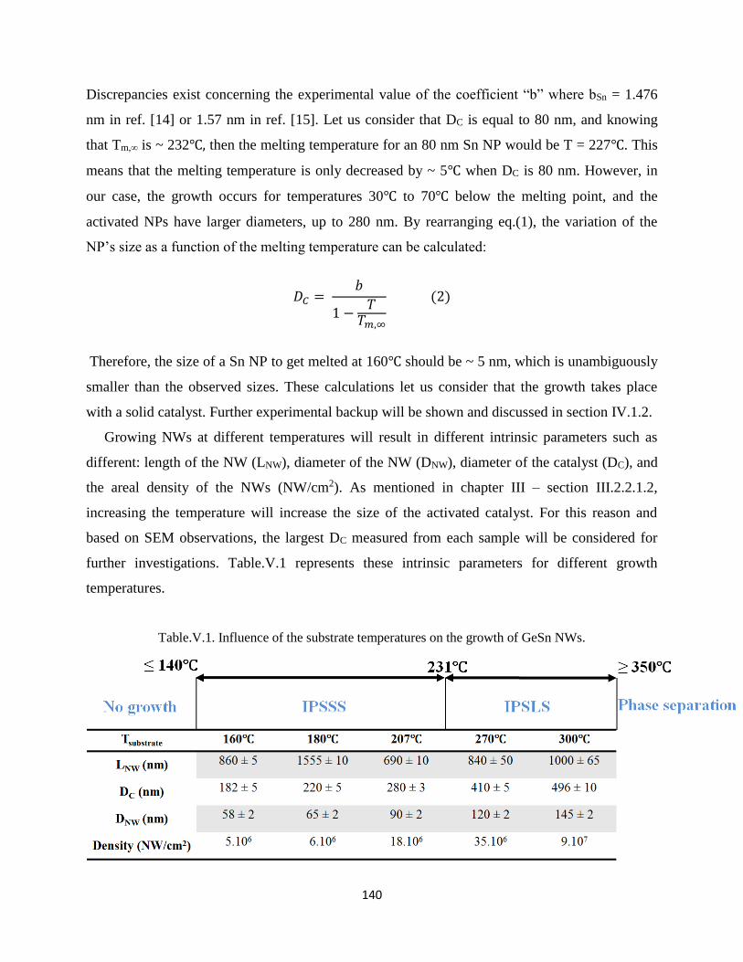
140
Discrepancies exist concerning the experimental value of the coefficient “b” where bSn = 1.476
nm in ref. [14] or 1.57 nm in ref. [15]. Let us consider that DC is equal to 80 nm, and knowing
that Tm,∞ is ~ 232℃, then the melting temperature for an 80 nm Sn NP would be T = 227℃. This
means that the melting temperature is only decreased by ~ 5℃ when DC is 80 nm. However, in
our case, the growth occurs for temperatures 30℃ to 70℃ below the melting point, and the
activated NPs have larger diameters, up to 280 nm. By rearranging eq.(1), the variation of the
NP’s size as a function of the melting temperature can be calculated:
𝐷𝐶 = 𝑏
1 −𝑇
𝑇𝑚,∞
(2)
Therefore, the size of a Sn NP to get melted at 160℃ should be ~ 5 nm, which is unambiguously
smaller than the observed sizes. These calculations let us consider that the growth takes place
with a solid catalyst. Further experimental backup will be shown and discussed in section IV.1.2.
Growing NWs at different temperatures will result in different intrinsic parameters such as
different: length of the NW (LNW), diameter of the NW (DNW), diameter of the catalyst (DC), and
the areal density of the NWs (NW/cm2). As mentioned in chapter III – section III.2.2.1.2,
increasing the temperature will increase the size of the activated catalyst. For this reason and
based on SEM observations, the largest DC measured from each sample will be considered for
further investigations. Table.V.1 represents these intrinsic parameters for different growth
temperatures.
Table.V.1. Influence of the substrate temperatures on the growth of GeSn NWs.

141
It is noteworthy that the error bars correspond to the uncertainty in the measurements
using SEM observations done on each nanowire. Indeed, increasing the temperature will increase
the activated catalyst size (DC), i.e. from ~ 182 nm (at 160℃) to ~ 500 nm (at 300℃). The
diameter of the nanowires, DNW, is proportional to DC, therefore upon the increase of the
substrate temperature, the DNW increase as well. LNW is much harder to interpret, since it depends
on the incorporation rate of Sn in the NWs (see Chap IV – section IV.2.2.1.5), and on DC. If the
incorporation rate of Sn is considered to be the same in all the samples (i.e. independent of the
substrate temperature), larger catalysts do not necessarily mean longer NWs, because DNW might
also be large enough to produce NWs having the same lengths. The density of NWs increases
with the increasing of the substrate temperature. This is the result of activating more catalysts of
larger sizes alongside the smaller ones.
V.1.2 COMPARSION BETWEEN SSS- AND SLS-GROWN NANOWIRES
Many differences between the NWs produced via SSS and SLS approaches exist, for
example: trajectories, morphologies, trenches, a-Ge:H consumption, structure and growth
endings. These differences are highlighted in Fig.V.2.

142
Figure.V.2- Main differences between SSS and SLS grown GeSn NWs. a) SEM image of an IPSSS
GeSn NW grown at 180℃; the green arrow indexes the starting path of the catalyst. The inset is a tilted
view showing that the NW has grown around the SnO2 NP (scale bar 200 nm). b) SEM image of an
IPSLS GeSn NW grown at 270℃, the inset is a tilted view showing the SnO2 NP at the beginning which
was not surrounded by the NW (scale bar 200 nm). c,d) SEM images tilted 60°, showing the entire

143
IPSSS and IPSLS grown NWs respectively. Cross-sectional TEM (bright-field) view with low
magnification of GeSn NWs grown at e) 180℃ f) 270℃.
In Fig.V.2, the SEM images show the two types of NWs. The SSS-NW has a regular zig-
zag shape with a smooth surface, whereas in the case of SLS mode, the NW trajectory is
irregular and its surface is rougher compared to the previous one. In the case of SSS mode, the
solid Sn NP turns around the SnO2 NP while growing the GeSn NW (Fig.V.2.a), until it
detaches from the SnO2 NP (the reason for this turning and detachment from the SnO2 NP will
be explained in section IV.1.5). However for the SLS growth, the catalyst simply moves away
from the SnO2 NP as soon as the NW starts to grow (Fig.V.2.b.d). Tiny Sn nanoparticles (25 nm
± 5 nm) are pinned along the a-Ge:H trench in the SLS case (Fig.V.2.b), most probably due to
the wetting of liquid Sn during the NW growth. Conversely, no such pinning effect is observed
in the case of SSS (Fig.V.2.a,c), since the catalyst is most probably solid. At the last stage of the
SLS growth, the catalysis is ended with a strong Sn-wetting (the case of liquid Sn), whereas, in
the case of SSS growth this wetting does not exist, see for instance Fig.V.2.(c) and (d). Cross-
sectional TEM images are shown in Fig.V.2.(e) and (f) for 180℃ and 270℃ samples,
respectively. In the case of IPSSS, the thickness of the a-Ge:H film decreases near the GeSn
NW growth region (more details in section V.1.4), whereas, a-Ge:H was completely consumed
in IPSLS. These analyses were based on SEM and TEM observations; however for a more
fundamental comprehension a chemical analysis is required.
V.1.3 STRUCTURE AND COMPOSITION OF IPSSS GESN NANOWIRES
The STEM-HAADF and STEM-EDS investigation of GeSn NW cross-sections prepared
by FIB for samples grown at 180°C and 270°C are displayed in Fig.V.3. In Fig.V.3.a, the
HAADF shows the faceted topology of the NW grown at 180°C (see the green indexed
interface between Pt and NW) with the inset indicating its crystalline nature. The EDS mapping
in Fig.V.3.b shows that the outer layers of the shell are made of pure c-Ge having a thickness of
~ 13.5 nm, and the core part of the NW made of GeSn has a diameter of ~ 23 nm. Therefore, the
structure is unambiguously a core-shell, with a GeSn core and Ge-rich shell. The Sn
concentration starts to increase from the outer part (Ge-rich region) to the core, eventually to

144
reach its highest value (~ 35 at.%) at nearly the core part of the NW (as shown in Fig.V.3.c).
Core-shell structures were observed on all the IPSSS GeSn NWs grown at temperatures below
the eutectic one. For comparison, the NWs grown at higher temperature (270°C) are also shown
(cross-sectional TEM in Fig.V.3.d), and their distribution of Sn according to the EDX in
Fig.V.3.e-h is homogeneous. However, this homogeneity cannot be ascertained on an atomic
scale, due to resolution limitations of the EDX (~ 1.5 nm), see chapter IV – section IV.2.2.1.2
for more details.
Figure.V.3- HRTEM and EDX mapping of GeSn NWs grown at 180 and 270°C. a) HAADF micrograph
showing a radial cross-section of a GeSn NW grown on a Si substrate at 180°C. b) The corresponding
EDX mapping of IPSSS GeSn NW showing a core-shell structure. c) Composition profile along the
vertical white dashed line in (b). d) Cross-section TEM image of GeSn NWs grown at 270°C. e) The
corresponding EDX mapping of the IPSLS GeSn NW in (d), showing a homogeneous distribution; Ge and
Sn elemental spatial distributions are shown in (f) and (g) respectively. (h) Composition profile along the
black arrow indicating the atomic percentage of Ge and Sn (the complement to 100% is due to presence of

145
Si, Ga, O, and Pt atoms incorporated at the surface of the sample during the ion beam preparation
process). The EDX error is approximately ± 3 at.%.
Based on the previous observations a comparison is made between the SLS and SSS as
shown in table.V.2.
Table.V.2. IPSSS and IPSLS GeSn NWs comparison
SSS
SLS
Starting point
Sn NPs turn around the
SnO2 NPs while growing
the nanowires
Sn NPs move away from
SnO2 NPs while growing
the nanowire
Trajectory Zig-Zag Random
Morphology Smooth Rough
Trench edge No pinned Sn NPs Sn NPs are pinned
Ending point No wetting Wetting
a-Ge:H layer Partially consumed Largely consumed
Element distribution Sn-rich Core/Ge-rich shell Homogeneous GeSn
Structure Polycrystalline Polycrystalline
As previously described, many experimental observations support the hypothesis that the catalyst
is solid during the growth, such as: no pinned NPs on the trench, no wetting at the end of the
growth, and smooth morphology of the NWs. In fact, the morphology variations of SLS NWs are
induced by the catalyst deformation during the growth [2]. However, if the catalyst is solid, these
deformations will most probably not happen, thus, leading to a smoother NWs surface in IPSSS
mode compared to IPSLS-NWs.
Mechanism Description
SE
M
TE
M-E
DX

146
Another unique feature of the IPSSS growth mode is that some of the examined GeSn
NWs are porous (specifically two IPSSS-NWs grown at 160℃ and 180℃ out of 18 examined),
see Fig.V.4.
Figure.V.4- Cross-section STEM – HAADF and EDX mapping of different regions of a porous IPSSS
GeSn NW grown at 180℃. The indexed (white rectangle) region in site 4 is shown in Bright-field view for
more clarity.

147
The porosity is not related to the growth temperature, this has been proven by the observation of
many IPSSS-NWs cross-sections analyzed in TEM from samples grown at different
temperatures. The growth mechanism of the IPSSS might be responsible of this porosity which is
believed to be formed during the growth. The voids are located in the core region (Sn-rich region)
of the GeSn NW, as shown by the EDX maps of Fig.V.4. On the image 4 in Fig.V.4, the white
rectangle contains two pores that are shown in the bright field micrograph. These two pores seem
to be empty separate bubbles inside the NW, with no connection between them. Yet, a clear proof
on the existence of a tubular void along the entire NW is not available (it would require a
statistical study, i.e. hundreds of cross-sections are necessary).
V.1.4 GROWTH RATE ESTIMATION
The growth rate (GR) is obtained by dividing the length of a nanowire by the duration of
its growth. In our case, the high incorporation of Sn results in a rapid consumption of the catalyst
into the NW, therefore, no Sn NPs can be observed after the growth. Therefore, as it was
mentioned in Chap.IV – section 2.2.1.3.2, because the real growth time is not known, a lower
value of GR could be obtained. In order to determine a value of GR close to the real one, the
growth should be stopped before the full incorporation of the catalyst in the NW. The growth
steps are: 1) reduction of SnO2 NPs, 2) deposition of a-Ge:H layer, and 3) annealing to activate
the growth. Thus, many growth trials are needed to determine at which step the NWs are growing
and for how long the growth lasts. Table.V.3 resumes a number of trials serving the investigation.
The first three trials include an annealing process (at 270℃) to activate the growth. However, the
catalysts were completely consumed even after decreasing the annealing time from 90 min to 10
min. The 4th trial proves that annealing is unnecessary because the growth is achieved during the
deposition of a-Ge:H at 180 ℃ for 10 min, which means that the RF plasma is still ignited during
the growth. This could be a reason why the Sn NPs pinned on the edges of the trench in the SLS
case do not exist in the SSS case; the plasma may etch them leaving a smoother trench (compare
for instance Fig.V.2.(a) and (b)). Another possibility is that the plasma modifies the surface
energy of a-Ge:H (i.e. decreases it) and therefore reduces the wetting behavior. This has been
observed in the case of VLS growth of SiNWs catalyzed by Au [16].

148
Table.V.3 – Different growth trials by decreasing the annealing and deposition times.
Figure.V.5- Top-view SEM image of IPSSS GeSn NWs grown during the deposition of a-Ge:H for a) 2
min, b) 1 min.
Decreasing the deposition time to 2 min leads to the growth of discontinuous GeSn NWs
(Fig.V.5.a). In this case, the quantity of the a-Ge:H was not enough to build a continuous NW,

149
but smaller catalysts build continuous ones (see inset Fig.V.5). This raises questions on the
growth mechanism, especially if the catalyst is considered in its solid state. A discussion will be
made in the next section about the possibility of supersaturating a solid catalyst by Ge, and the
possible growth mechanisms of the IPSSS GeSn NWs.
Further decrease in the deposition time results in almost no growth of NWs. In fact, for
the one minute deposition sample (at 180℃), only very tiny nanowires are activated, as the one
shown in the inset Fig.V.5.b, which means that the a-Ge:H thickness is an important factor for
starting the growth. There are two conditions to start the growth: i) if the small catalysts (e.g.
with an average trench size at the starting position of ~ 25 nm) are liquid, then the amorphous
thickness is enough to supersaturate them and precipitate c-Ge seeds which will create a Gibbs
energy difference, thus, a driving force, and ii) if the catalysts are solid, than the Ge atoms will
diffuse on their surface and form c-Ge seeds on one side of the catalyst, thereby, an energy
difference and a driving force. In the latter case, Ge atoms will have to diffuse a short distance to
reach a bottom edge region or the SnO2/Sn interface; due to the small catalyst size, the c-Ge seed
needed to create the driving force will have a smaller size as well. Despite the decrease of the
deposition time down to 1 min, the activated (small) catalyst has been totally consumed which
complicates even more the determination of the GR.
The TEM images (for instance Fig.V.2.e) show that the trench region, in the SSS mode,
contains an a-Ge:H layer surrounding the IPSSS NWs. Normally these layers are totally
consumed (or extremely thinned) by the liquid catalyst. The fact that the NWs are growing during
the plasma deposition step means that the a-Ge:H layer is continuously deposited during or after
the growth of the NWs. Based on this hypothesis, the growth rate of the NWs can be calculated
using the thickness of the a-Ge:H deposited after the formation of the core part. Let us assume
that W is the initial thickness of the a-Ge:H deposited when the catalyst just grew the NW at the
moment t = t0 (as shown in Fig.V.6.a) and Wend is the thickness of the a-Ge:H layer at the end of
the deposition step, in other terms, it is the total thickness of the a-Ge:H layer at the end of the
deposition (as shown in Fig.V.6.b).

150
Figure.V.6- Determination of the growth rate a) GeSn NW cross-section schema showing the
thickness (W) of the a-Ge:H at the moment when this region of the nanowire is grown, b) same as
previous schema, except that a-Ge:H deposition has continued after the NWs growth, therefore more
thickness of a-Ge:H is added. Wend denotes the total thickness of the a-Ge:H at the end of the
deposition process, and Wpost: the width of the a-Ge:H layer added after the growth of the nanowire to
a certain length. c) SEM top-view of the NW used for the growth rate calculation. The TEM lamella
obtained using FIB is indexed by the rectangle, the length of the nanowire starting from the initial
position till the lamella is ~ 655 nm.
Thus, it can be written that Wend = W + Wpost, where Wpost is the thickness of the a-Ge:H
deposited after the growth of the NW, and till the end of the deposition process (at t = t0 + t’).
Therefore to calculate the growth rate, it is necessary to calculate W (the initial thickness at the
moment when the NW grew which is the one shown in Fig.V.6.a); W = Wend - Wpost. The
measurements using the TEM micrograph (Fig.V.2.e) gives: Wend ~ 17 nm and Wpost ~ 15 nm;
and therefore W = 2 nm. Under the deposition conditions used in the PECVD reactor (PLASFIL),
every 6 min of GeH4 plasma corresponds to ~ 17 nm thickness of a-Ge:H (i.e. growth rate of a-
Ge:H is ~ 0.047 nm/s), then the W = 2 nm corresponds to ~ 42 s. The SEM top-view image
corresponding to the NW cross-section of Fig.V.2.e, is shown in Fig.V.6.c. It indicates the region
which was prepared by the FIB (the indexed rectangle in Fig.V.6.c), hence, the length of the NW
grown during 42 s (= t0) is ~ 655 nm therefore the growth rate of the NW is GR ~ 16nm/s. By
referring to the DIM (dimer-insertion model) in chapter III – section 2.2.1.3.4, the GR of 16 nm/s

151
corresponds to an incorporation of 35 at.% Sn into the NW, which is consistent with the
experimental results.
The NW growth takes place during the deposition of a-Ge:H by PECVD, as it is shown in
table.V.3. This means that the core region of the NW (Sn-rich) is fabricated by the catalyst, then,
the Ge covers the core of the NW, resulting in a core-shell structure (schematically shown in
Fig.V.6.b). Interestingly, the post deposition of a-Ge:H (after the formation of the core part of the
GeSn NW) indicated in Fig.V.6.b is, under the used conditions, heteroepitaxially grown. As it
was shown previously by the TEM in Fig.V.3.a, the Ge shell has a crystalline structure and it is
faceted. The shell growth is a standard vapor-solid deposition at 180℃, however in the case of
the core region, which is the NW catalyzed by Sn is more complicated. In the following part,
various possibilities for the IPSSS growth mechanism will be discussed.
V.1.5 IPSSS GROWTH MECHANISM
There are two aspects to consider when trying to explain the SSS growth mechanism:
first, the essential mechanism of Ge mass transport to form the NWs, and second, the detachment
of Sn NPs from the SnO2 NP at the beginning of the growth.
The mass transport mechanism of Ge to reach the NW is important to understand for an
advanced growth control. Many hypotheses can be proposed to explain the growth mechanism.
i) As a first possibility, the Ge transport could be achieved by diffusion inside the solid
catalyst [17], as shown in Fig.V.7.a. To assess this possibility, the duration of Ge diffusion should
be calculated. Because, no data is available on the diffusion of Ge in Sn, we will consider the
interdiffusion coefficient of Ge/Sn [18]. The diffusion coefficient of Ge in Sn is:
𝐷 = 𝐷0. 𝑒− 𝐸𝐴𝑘𝑇 𝑐𝑚2. 𝑠−1
With D0 being the pre-exponential factor that equals to 2.9×10⁻⁷ cm2.s-1, the activation energy EA
that equals to 1.21 eV, k is the Boltzmann constant, and T is the temperature in Kelvin. The
diffusion coefficients corresponding to 210℃, 180℃, and 160℃ are 6.8×10⁻²⁰, 1×10-20, and
2.3×10⁻²¹ cm2.s-1 respectively. Here, we consider that the diffusion process occurs in one direction
(according to the white arrow in Fig.V.7.a), which means that L = √2𝐷𝑡. Supposing that the

152
diameter of the catalyst has a typical value of 115 nm which is the distance to be travelled by Ge
atoms (L) to reach the NW, therefore the time needed to travel from the front side of the catalyst
to the rear side (that is the NW/catalyst interface) for 210℃, 180℃, and 160℃ are 16 × 106 hours,
112 × 106 hours, and 47 × 107 hours respectively. Knowing that the growth is done in less than 5
min during the deposition phase, the calculations do not support the diffusion through the solid
catalysts as being the dominant growth mechanism. The distance L can be lower than the
diameter of the catalyst since the growth is proven to be done during the deposition stage. In
other words, Ge atoms can be deposited on the surface of the catalyst then diffuse inside the
catalyst towards the NW using a shorter distance than the latter case. However, even if the
distance is divided by two, Ge atoms still need ~ 4 × 10⁶ hours to reach the NW at 210℃.
ii) Grain boundaries (GBs) can exist in catalysts having diameters around 100 nm, which
can be considered as ultra-fine grained nanoparticles [19]. Since no TEM experiment is done to
prove the GBs existence, and no data is available on the diffusion of Ge through them, this
possibility remains a hypothesis. The activation energy for GB diffusion is, in general, lower than
that of solid diffusion [20]. As a result, a faster mass transport can occur compared to the
standard diffusion through the catalyst structure (Fig.V.7.b). In general, the melting process starts
at GBs and defects in the crystalline structure, at temperatures that are around 80% of the melting
point of the system [21]. In our case, the temperatures used for the growth vary between 70% and
90% of the melting temperature of bulk Sn (~ 232℃), therefore, the GBs can be premelted which
can further enhance the diffusion of Ge atoms through them.
iii) The third possibility is the diffusion on the surface of the catalyst, as shown in
Fig.V.7.c. Since the mass transport via volume diffusion requires an extremely long time to be
achieved, perhaps the surface diffusion is a more favorable mechanism of mass transport. In the
vapor-solid-solid mechanism, the diffusion occurs on the surface of the catalyst [22]. Briefly, the
VSS uses a gas precursor that decomposes on the surface of the catalyst, and the feeding atoms
migrate on the surface towards the triple-phase boundary (NW/catalyst/atmosphere) which is
considered the main gate for the insertion of atoms. By analogy, we suggest that the same
mechanism can occur for the SSS growth process. However, the sources of Ge atoms for the
NWs growth are: the plasma, and the amorphous layer. The plasma decomposes the gas
precursor, thus, providing Ge atoms to the Sn NPs, while the a-Ge:H layer is a very dense source
of Ge atoms compared to the gas precursor. Therefore, a higher growth rate is expected for the

153
SSS compared to VSS. Moreover, the incubation time is considered to be lower for a solid
catalyst compared to a liquid catalyst, which increases more the growth rate of the NWs.
iv) The last possibility is the diffusion through a premelted surface, as shown in Fig.V.7.d.
As mentioned previously, the growth temperature varies between 160℃ and 210℃, and the
liquid-solid phase transition occurs progressively but not spontaneously via the boundaries
interface, surface, and structural defects of the catalyst [21]. The incoming Ge atoms (from the
plasma and a-Ge:H thin-film) can diffuse inside the premelted surface of the catalyst towards the
Ge NW. This diffusion process can be simply dictated by Fick’s law. This possibility can also
explain the discontinuous NWs obtained at low temperatures (< 231℃). In fact, the Ge should
supersaturate the molten surface of the catalyst in order to precipitate a crystalline NW. However,
for the two minutes deposition case, the Ge atoms were insufficient to keep the molten surface
supersaturated, which therefore created a discontinuous NW.
Figure.V.7- Proposed IPSSS mass transport mechanisms a) volume diffusion of Ge through the catalyst b)
diffusion via the grain boundaries, c) diffusion on the surface of the catalyst, and d) diffusion inside the
molten surface of the catalyst.
Since the GeSn NW growth takes place during the plasma deposition step, an experiment
was done to investigate if it is possible to do the IPSSS growth without the plasma Fig.V.9.c. It is

154
important to reveal whether IPSSS NWs are grown using GeHx radicals coming from the plasma
or from the amorphous layer or from both sources. Therefore, approximately 8 nm of a-Ge:H
were deposited on top of the catalysts, and the deposition temperature was chosen to be 110℃, to
avoid the growth during this step. Then, the plasma was turned off, and the temperature was
raised to 180℃ for 1 hour to activate the growth in vacuum environment. The resulting
nanostructures are shown in Fig.V.8. It is not straightforward to call these nanostructures as
NWs. So the result is that the catalyst cannot rely only the a-Ge:H layer to achieve the growth.
However, if the catalyst relies only on the radicals (GeHx) that are coming from the plasma
during the deposition step, then we shall see no “trench” after the growth (see Chap I section I.3 –
Fig.I.11). After careful analysis of these data, we conclude two main points: 1) the catalyst uses
both sources of Ge (GeHx radicals, and a-Ge:H) for the growth, 2) since the Gibbs energy of
plasma-produced radicals is relatively higher than that of the a-Ge:H, then a greater driving force
is created compared to using only a-Ge:H as Ge source. For these reasons, the growth of IPSSS
GeSn NWs is successful in the presence of plasma radicals.
Fig.V.8 SEM images of a validation test of SSS mechanism. a) An aggregate of Sn catalyst
topped with an a-Ge:H layer and activated at 180℃ for 55 min b) a magnified image of (a).
In the IPSSS mode, the Sn NP turns around the SnO2 NP during the initial stages of the
growth. It is energetically more favorable for the solid Sn NP to stay in contact with the SnO2
NP, as shown in Fig.V.2.a and in Fig.V.9.a. This pinning effect remains until it reaches the NW
already grown at the starting position. In fact, alongside the pinning effect, the catalyst is
advancing circularly around the SnO2 NP, and the driving force is created by the Gibb energy

155
difference between the amorphous and crystalline Ge on its both sides (Fig.V.9.c). As soon as the
SnNP reaches the already grown NW, after almost completing a circular turn, it gets detached
from the SnO2 NP.
Figure.V.9- The detachment of the Sn NP from the SnO2 NP. a) Initial stages of the turning process of Sn
driven by the pinning effect of SnO2 NPs, b) the detachment of the Sn NP due to the existence of the NW
on its front and rear side. The green, red, and orange lines are respectively the catalyst/a-Ge:H,
catalyst/NW, and NW/catalyst interfaces; and c) the driving force between the orange and the green lines
is derived from the Gibbs energy difference of a-Ge:H and the c-GeNW.
In Fig.V.9.b, there are two interfaces: catalyst/a-Ge:H (green) and catalyst/NW (orange, and red).
When the catalyst meets the NW grown earlier, the circular advancement of the catalyst will stop
due to the existence of a crystalline Ge on both sides of the catalyst (orange and red interfaces in
Fig.V.9.b). As a result, there is no Gibbs energy difference between these two interfaces, thus, no

156
driving force. However, the catalyst is still in contact with a-Ge:H, as indicated by the green
interface in Fig.V.9.b, where the thermodynamic force drags the catalyst away from the SnO2 NP.
As a conclusion, four possible mechanisms of Ge transport to the NW were considered: i) bulk
diffusion, ii) grain boundary diffusion, iii) surface diffusion, and iv) diffusion through the
premelted surface of the catalyst. We concluded that the last two possibilities are the most
probable, because the diffusion process is easier on the surface of the catalyst or through its
premelted surface compared to the other two cases. The IPSSS GeSn NWs are synthesized during
the deposition, where the plasma helps achieving the growth. Moreover, it was shown that the
detachment of Sn NP from the SnO2 NP is a consequence of the Gibbs free energy. In the
following section, we will present growth experiments that are designed to improve the
crystalline quality of the GeSn NWs.
V.2 OUT-OF-PLANE GERMANIUM-TIN NANOWIRES
In all the previous experiments, the NWs were grown on native silicon oxide layers (SiOx)
topping the c-Si substrate. In fact, crystalline Si wafers were used for the growth, but since they
are exposed to the atmosphere, a typical ~ 2 nm SiOx layer is formed. To improve the
crystallinity of the in-plane NWs, the idea was to remove the native SiOx and grow the NWs
directly on a c-Si surface. To remove the SiOx from the surface of the c-Si substrate a HF dip
was used. The experimental procedure is shown in Fig.V.10.

157
Figure.V.10- Schematic illustration showing the growth process where the native oxide on the c-Si wafer
was removed via HF dip. The crystalline surface of the substrate was protected from oxidation using a 7
nm a-Ge:H and 1 nm of a-Si:H. SnO2 NPs were deposited and partially reduced to Sn using a hydrogen
plasma. Then a SiF4 plasma was ignited for 10 min to remove the silicon native oxide. The temperature
was raised from 140℃ to 250℃ in 38 min (under hydrogen flow), and then the sample was left to cool-
down to 180℃. The sample was kept in the PECVD reactor for 14 hours at 180℃ (under high-vacuum).
Directly after dipping the substrate in HF for 30 seconds, the substrate was rinsed with
deionized water and dried with Nitrogen gas. Afterwards, the substrate is introduced in the
PECVD reactor where a-Ge:H and a-Si:H layers of 7 nm and 1 nm respectively were deposited to
protect the c-Si surface from oxidation. Then, the SnO2 colloids were deposited on top of the
amorphous layers, and partially reduced using a H2 plasma (30 W) at 250℃ for 10 min. Finally,

158
the native oxide layer formed on top of the a-Si:H was treated by SiF4 plasma (10 W) at 140℃
for 10 min. To activate the SLS growth, the temperature was raised from 140℃ to 250℃ in 38
min, and the sample was left for 14 hours under vacuum at 180℃.
We expected that Sn NPs would dissolve the amorphous layers beneath, get
supersaturated, and precipitate NWs on the crystalline surface of the Si substrate. However,
unexpectedly, out-of-plane NWs have been grown, as can be seen in Fig.V.11. The Sn NPs have
catalyzed NWs that have different lengths and diameters. For instance, the length can vary from
500 nm to 1 μm, whereas the diameter (∅top and ∅bottom represents the top and the bottom
diameters respectively) can vary for the same NW, which might be due to the consumption of Sn
catalyst (see Fig.V.11). The surface of the sample is roughened by the SiF4 or H2 plasma
treatment, as shown in Fig.V.11.a. Moreover, the regions around the grown NWs seem to be
thinner (Fig.V.11.a,b), and the regions that are more close to the growth are possibly wetted by
the liquid Sn (Fig.V.11.c,d,e).

159
Figure.V.11- SEM images showing the out-of-plane NWs. a) Low magnification showing the
NWs and the topology of the surface of the substrate near and away from the growth regions. b) Top view

160
of a NWs region where there is no visible wetting. c) Top view of NWs region where the Sn wetting is
visible. (d) and (e) tilted view of two NWs regions.
In order to further analyze the process, a region of NWs was selected for TEM
characterizations, see Fig.V.12. Using FIB/SEM, a cross-sectional TEM lamella was obtained
containing the indexed NWs (NW1, and NW2) in Fig.V.12.a. The axial cross-sections
(Fig.V.12.b,c) show that each NW has two NPs, one located on its top and the other one on its
bottom. Most probably the NP sitting on the top of the NW is Sn, whereas the bottom one is most
probably SnO2. The diffraction pattern obtained using TEM shows the crystalline nature of NW2
(inset of Fig.V.12.c). In the next section, an EDX measurement is used to reveal the spatial
distributions and the composition of these NWs.

161
Figure.V.12- Out-of-plane nanowire micrographs. a) SEM image showing a heart-shaped catalyst pad
with vertical NWs on top. NW1, and NW2 were analyzed using TEM and EDX. b) An axial cross-
section of NW1. Two catalysts can be observed in this micrograph, the top one was partially destroyed
during FIB operation. c) Axial cross-section of NW2. This image shows the catalyst on top of the NW as
well as a catalyst on its bottom. The inset is an electronic diffraction pattern proving the crystallinity of
this NW.
V.2.1 COMPOSITION OF GE-SN NANOWIRES
For further composition investigations, STEM-EDX measurements were performed. The
EDX cartography done on NW2, is shown in Fig.V.13.a, and the cartography of its composition
(Fig.V.13.b) proves that it is a GeNW with a Sn NP on its top. To quantify the NW composition,
a region depicted “spectre” is chosen. The quantification results are shown in the table of
Fig.V.13.c, ~ 5 at.% Sn is incorporated inside such kind of NWs which is higher than the
equilibrium solubility (< 0.5 at.% of Sn in Ge).
Figure.V.13- EDX measurements on the upper part of NW3. a) A NW micrograph showing the 2D EDX
cartography at the top NW/catalyst interface. b) EDX measurement on the interface, showing the 2D
spatial distribution of the elements (atomic percentage). c) A quantification of the NW composition
showing the atomic concentration in the NW’s body (far from the catalyst).

162
It is also important to determine the nature of the remaining part of the catalyst precursor on the
bottom part of the NW in order to understand the growth mechanism. It is expected to be SnO2
since it is standing still on the bottom side of the NW (Fig.V.14.a,b), and the EDX
quantification confirmed our expectation. Therefore, when raising the temperature only the
molten part of the catalyst (Sn) will catalyze the growth while the SnO2 NP will remain
inactive.
Figure.V.14- EDX measurements on the bottom part of NW2 a) A NW micrograph showing the 2D EDX
cartography at the bottom NW/catalyst interface. b) EDX elemental mapping, showing the 2D spatial
distribution of elements (atomic percentage).
The SEM, TEM, and EDX analysis are important to reveal the nature, and structure
quality of the obtained NWs. They are equally important to help the determination of the growth
mechanism. Four hypotheses are proposed and discussed in the following section based on the
characterization results.

163
V.2.2 PROPOSED GROWTH MECHANISM
Three samples were successfully fabricated containing out-of-plane NWs, each having the
same process conditions, except that the amorphous Ge thickness was increased from 3 nm to 5
nm. This means that this kind of NWs is reproducible. Four scenarios are proposed to explain this
growth:
1- Ge atoms are transported by the plasma from the reactor inner walls (which are coated by
a-Ge:H) and from the a-Ge:H layer on the substrate. This mass transport can be done
during the H2 or SiF4 plasma. In the case of H2 plasma, the catalysts are in their liquid state
(the temperature during this process is 250℃) leading to the standard VLS mechanism.
2- Ge atoms might be provided during the SiF4 plasma treatment. Note that the SiF4 plasma
duration is 10 min with a flow of 30 sccm at 140℃, therefore the growth should proceed
via VSS mechanism (solid catalyst).
3- Ge atoms can be provided during the annealing step; when the temperature is raised from
140℃ to 250℃ during 38 min. Since there is no plasma during this step, then there is no
Ge transport via H2 or SiF4 plasma. Therefore, the only way the Ge can reach the liquid
catalyst is by surface diffusion.
4- As the previous analysis, but this time during the last step, which is the annealing at 180℃
during 14 hours. These atoms may nucleate under the bottom part of the solid catalyst to
grow a NW, or between the SnO2 and the Sn NPs. The superficial diffusion process is only
allowed when the native oxide of the amorphous layer is treated by SiF4 plasma, because
the SiOx plays the role of a barrier preventing the diffusion of Ge atoms. Note that these
samples have been kept in the reactor for 14 hours at 180℃ after raising the temperature to
250℃ during 38 min. An approximate calculation to estimate the surface diffusion length
is made using 1.63 eV [23] as an activation energy for surface diffusion of Ge, and 5.102
cm2/s as a pre-exponential factor [24]. During 14 hours, Ge atoms can diffuse
approximately ~ 42 nm on the surface of the substrate. This diffusion length is enough for
the Ge to migrate towards the catalyst, nucleate and grow a NW.
Since it is proved using EDX that these are GeSn NWs, the second possibility is dismissed. The
GeH4 gas was not used after the deposition of SnO2 and the subsequent treatments (but only

164
before the SnO2 colloidal deposition). To restrain the number of possibilities, two experiments
were designed to reveal the step at which the vertical nanowires are grown.
In the first experiment, the same fabrication procedure is repeated with the same conditions
except that we stopped after the H2 plasma treatment step which is done at 250℃ for 10 min. No
further SiF4 plasma treatment or annealing in this case. Then, the sample is taken out for SEM
inspection. The growth was unsuccessful; no NWs are produced at this step. It means the H2
plasma did not etch the a-Ge:H layer (that have a superficial native oxide) to transport Ge atoms
to the liquid catalyst.
In the second experiment, the same procedure as the previous one is repeated, but this time the
SiF4 plasma treatment is added alongside the H2 plasma. The duration of the treatment is 10 mins,
and the temperature used is 140℃, which means that the catalyst NPs stay in their solid state. The
growth is unsuccessful, no NWs are produced. Same analogy as the previous condition, the SiF4
plasma did not etch the amorphous layer to provide Ge atoms for the catalysts, despite removing
the native oxide of the amorphous layer. Leaving the last two mechanisms as the most probable,
unfortunately it was not possible to perform further experiments. This leaves the underlying
mechanisms of these NWs as perspective for future studies.
V.3 SUMMARY
As a conclusion, a new mechanism was proposed for the growth of GeSn NWs using Sn
NPs at substrate temperatures below the melting point of Sn. It was shown that Sn NPs are small
in size but not enough to shift their melting point towards lower temperature. Therefore, Sn NPs
are expected to be in their solid state during the growth of NWs. An activation window is defined
for the growth of GeSn NWs, with a lower limit at 160℃, which is 70℃ below the eutectic
temperature. The IPSSS NWs have different morphologies than IPSLS NWs. Moreover, at the
region where the NW ends, wetting is not observed for the IPSSS mechanism, which is
considered as additional evidence that the catalysts are solid. The IPSSS NWs are shown to have
a core-shell structure (Sn-rich core and Ge-rich shell) compared to a homogeneous (at a
nanoscale) distribution for the IPSLS GeSn NWs. The Sn concentration in the IPSSS GeSn NWs
can reach up to 35 at.% at the core part, while in the shell it is nearly pure Ge. Four mechanisms

165
were suggested for the IPSSS GeSn NWs growth: bulk diffusion, grain boundary diffusion,
surface diffusion, and premelted surface diffusion. We concluded that the last two possibilities
are the most probable.
Unexpectedly, out-of-plane GeSn NWs were obtained using a modified growth process,
where an amorphous Ge layer is deposited at the first place, then, SnO2 colloids and their
subsequent plasma treatments. The EDX quantifications have shown that the Sn concentration
can be ~ 5 at.% in the NWs. Various growth mechanisms are proposed for this kind of vertical
NWs. After many experiments, their reproducibility is proven. Many trials are done with
different conditions proving that the growth is neither a VLS nor a VSS mechanism. The most
probable mechanisms for the growth are SLS or SSS out-of-plane. As perspective work, its
suggested to repeat the same growth process of the out-of-plane including the 14 hours annealing
at 180℃, in order to verify that the growth is done in the last step.
V.4 REFERENCES
1. Dubrovskii, V., Sibirev NV, Cirlin GE, Harmand JC, Ustinov VM, Theoretical analysis of the
vapor-liquid-solid mechanism of nanowire growth during molecular beam epitaxy. Physical
Review E, 2006. 73(2): p. 021603.
2. Yu, L., i Cabarrocas Pere Roca, Growth mechanism and dynamics of in-plane solid-liquid-solid
silicon nanowires. Physical Review B, 2010. 81(8): p. 085323.
3. Kodambaka, S., Tersoff J, Reuter MC, Ross FM, Germanium nanowire growth below the eutectic
temperature. Science, 2007. 316(5825): p. 729-732.
4. Hiruma, K., Yazawa M, Katsuyama T, Ogawa K, Haraguchi K, Koguchi M, Kakibayashi H,
Growth and optical properties of nanometer‐scale GaAs and InAs whiskers. Journal of Applied
Physics, 1995. 77(2): p. 447-462.
5. Kamins, T., Stanley Williams R, Basile DP, Hesjedal T, Harris JS, Ti-catalyzed Si nanowires by
chemical vapor deposition: Microscopy and growth mechanisms. Journal of Applied Physics,
2001. 89(2): p. 1008-1016.
6. Ohlsson, B., Björk MT, Persson AI, Thelander Claes, Wallenberg LR, Magnusson MH, Deppert
Knut, Samuelson Lars, Growth and characterization of GaAs and InAs nano-whiskers and
InAs/GaAs heterostructures. Physica E: Low-dimensional Systems and Nanostructures, 2002.
13(2-4): p. 1126-1130.
7. Persson, A.I., Larsson Magnus W, Stenström Stig, Ohlsson B Jonas, Samuelson Lars, Wallenberg
L Reine, Solid-phase diffusion mechanism for GaAs nanowire growth. Nature materials, 2004.
3(10): p. 677.
8. Bandyopadhyay, D., The Ti-Si-C system (titanium-silicon-carbon). Journal of phase equilibria and
diffusion, 2004. 25(5): p. 415-420.
9. Olesinski, R., Abbaschian GJ, The Ge− Sn (Germanium− Tin) system. Bulletin of Alloy Phase
Diagrams, 1984. 5(3): p. 265-271.
166
10. Yu, L., Alet Pierre-Jean, Picardi Gennaro, Roca i Cabarrocas Pere, An In-Plane Solid-Liquid-Solid
Growth Mode for Self-Avoiding Lateral Silicon Nanowires. Physical Review Letters, 2009.
102(12): p. 125501.
11. Linwei Yu, M.O., Oumkelthoum Moustapha, Franck Fortuna, Pere Roca i Cabarrocas, Guided
growth of in-plane silicon nanowires. Applied Physics Letters, 2009. 95(11): p. 113106.
12. Liu Minglu, W., Robert Y., Size-Dependent Melting Behavior of Colloidal In, Sn, and Bi
Nanocrystals. Scientific Reports, 2015. 5: p. 16353.
13. Wautelet, M., Effects of size, shape and environment on the phase diagrams of small structures.
Nanotechnology, 1992. 3(1): p. 42.
14. Allen G. L., B.R.A., Gile W. W., Jesser W. A., Small particle melting of pure metals. Thin Solid
Films, 1986. 144(2): p. 297-308.
15. Wautelet, M., Estimation of the variation of the melting temperature with the size of small
particles, on the basis of a surface-phonon instability model. Journal of Physics D: Applied
Physics, 1991. 24(3): p. 343.
16. Chen, W., Pareige Philippe, Castro Celia, Xu Tao, Grandidier Bruno, Stiévenard Didier, Roca i
Cabarrocas Pere, Atomic characterization of Au clusters in vapor-liquid-solid grown silicon
nanowires. Journal of Applied Physics, 2015. 118(10): p. 104301.
17. Wen, C.-Y., Reuter MC, Tersoff J, Stach EA, Ross FM, Structure, growth kinetics, and ledge flow
during vapor− solid− solid growth of copper-catalyzed silicon nanowires. Nano letters, 2009.
10(2): p. 514-519.
18. Wei Wang, Y.D., Qian Zhou, Eng Soon Tok, Yee-Chia Yeo, Germanium–tin interdiffusion in
strained Ge/GeSn multiple-quantum-well structure. Journal of Physics D: Applied Physics, 2016.
49(22): p. 225102.
19. Sauvage, X., Wilde Gerhard, Divinski SV, Horita Zenji, Valiev RZ, Grain boundaries in ultrafine
grained materials processed by severe plastic deformation and related phenomena. Materials
Science and Engineering: A, 2012. 540: p. 1-12.
20. Mishin, Y., Herzig Chr, Grain boundary diffusion: recent progress and future research. Materials
Science and Engineering: A, 1999. 260(1-2): p. 55-71.
21. Alsayed Ahmed M, I.M.F., Zhang Jian, Collings Peter J, Yodh Arjun G, Premelting at defects
within bulk colloidal crystals. Science, 2005. 309(5738): p. 1207-1210.
22. Kolasinski, K.W., Catalytic growth of nanowires: vapor–liquid–solid, vapor–solid–solid,
solution–liquid–solid and solid–liquid–solid growth. Current Opinion in Solid State and Materials
Science, 2006. 10(3-4): p. 182-191.
23. Fukatsu, S., et al., Self‐limitation in the surface segregation of Ge atoms during Si molecular
beam epitaxial growth. Applied Physics Letters, 1991. 59(17): p. 2103-2105.
24. Allen, C.E., R. Ditchfield, and E.G. Seebauer, Surface diffusion of Ge on Si(111): Experiment and
simulation. Physical Review B, 1997. 55(19): p. 13304-13313.

167
CONCLUSION & PERSPECTIVES
This thesis is a pioneering work on GeSn nanowires, backed up by atomic scale
characterization techniques such as APT and TEM. The objective is to fabricate crystalline GeSn
NWs with a high Sn incorporation, while maintaining the crystallinity and avoiding phase
separation of Sn and Ge. Among several growth mechanisms, the bottom-up in-plane SLS was
chosen for the growth of GeSn NWs, since it helps achieving high growth rates, which are
necessary for a non-equilibrium kinetically driven incorporation of Sn.
Chap I presented a literature review about the state-of-the-art methods of growing
nanowires. The main focus was on the bottom up approaches VLS and SLS. Since the SLS
allows achieving higher growth rates, and SLS nanowires can be controlled and guided to
assemble a certain circuitry design, therefore, the SLS mechanism was chosen to fabricate the
GeSn NWs. The Ge1-xSnx alloy is an interesting material for electronics and optoelectronics due
its better properties compared to Si. The carrier mobility is improved by the increment of Sn
concentration in Ge, and an indirect-to-direct transition of the energy band-gap occurs for a
sufficient amount of Sn (between 6 at.% and 11 at.%).
Chap II described the fabrication and characterization machines used in this thesis. In the
first part, the fabrication techniques were discussed. For the fabrication of catalysts, magnetron
sputtering coater, and thermal evaporator were used. The PECVD reactor was used for surface
treatments, depositions, and growth of NWs. In the second part, different characterization
techniques were used for investigations of the obtained NWs. The FIB/SEM dual beam was used
to fabricate specially-designed specimens for TEM and APT characterizations. The TEM allowed
having a deep insight on the NWs atomic structure, and the EDX allowed the quantification of
the components constituting the NWs. APT is an ultra-fine characterization tool, with abilities to
reconstruct in 3D real-space the atom-by-atom evaporated NWs. The mass-spectrometry,
equipped in the atom probe, gives the ability of identifying the detected evaporated atoms with
single atom precision.
In Chap III, In-catalyzed Ge NCs and NWs were studied. Indium catalysts are obtained
using the reduction of an ITO thin film which was deposited by magnetron sputtering. The
feeding layer (a-Ge:H) is then deposited on top of the whole system at a temperature below the

168
eutectic point of Ge-In (< 156 ℃). The temperature was raised above the latter temperature to
activate the growth. The analysis showed that the size of the catalyst influences the length of the
NWs. Large catalysts drops (700 nm to 1.5 μm in diameter) can grow shorter NWs compared to
smaller catalysts (60 nm to 200 nm), which were able to grow Ge NWs up to 15 μm long under
the same conditions. As a perspective, further characterization are needed for the GeNWs
produced by the In NPs (i.e. 60 nm – 200 nm) in APT, in order to see if the In is incorporated in
the NWs. The incorporation of In in Ge NWs might produce p-type NWs, which might be useful
in nanoelectronics.
In the first part of Chap IV, the growth of IPSLS SiSn NWs is described. Two
temperatures were used for the growth 300℃ and 400℃. In the second part of this chapter, the
fabrication of GeSn NWs was studied. The evaporated metallic Sn lead to unsuccessful GeSn
NWs growth attempts. The reason for this failure is the strong wetting behavior caused by the
contact of Sn with a-Ge:H layer. Another catalyst precursor was used: the SnO2 NPs. These NPs
were partially reduced to pure Sn in PECVD. The objective was to limit the wetting behavior of
Sn by the pinning effect created by SnO2 NPs. This strategy was successful and crystalline GeSn
NWs were grown with an amazing 22 at.% Sn incorporated homogeneously inside the NWs.
Four kinetic models were presented to explain the high concentration of Sn in the GeSn NWs:
Ge-Sn complementarity, step-wise flow, continuous growth, and dimer-based insertion. The first
three models were not able to account for the high Sn percentage, even by using the atomic line
formation velocity, which is more than 9000 times higher than the interface velocity. The dimer-
insertion model was developed for Sn catalyzed GeSn NWs. Based on this model, we predicted
that in order to obtain 22 at.% Sn concentration, the growth rate should be 7 nm/s which is
consistent with the estimated growth rate interval of IPSLS GeSn NWs grown at 270℃. In the
third part, atomic scale mappings and quantifications were done on IPSLS SiSn NWs. These
quantifications show that these NWs have far from equilibrium Sn concentrations varying from ~
9 at.% to 10 at.% for 300℃ and 400℃ respectively. Although, Sn seemed homogeneously
distributed throughout the NWs Sn enrichments existed at both temperatures. As perspective,
the density of GeSn NWs should be increased by optimizing the density of the catalyst NPs, and
should be passivated. This will allows investigating the indirect-to-direct bandgap transition by
micro-photoluminescence.

169
In the last chapter, we have presented a new in-plane Solid-Solid-Solid mechanism for the
growth of GeSn NWs using Sn NPs at substrate temperatures below the melting point of Sn. It
was shown that the size of Sn NPs is not small enough to melt at the growth temperatures. An
activation window is defined for the growth of GeSn NWs, with a lower limit at 160℃ (i.e. 70℃
below melting point). The IPSSS NWs have different morphologies than IPSLS NWs. Moreover,
at the region where the NW ends, wetting is not observed for the IPSSS mechanism, which is
considered as additional evidence that the catalysts are solid. The IPSSS NWs are shown to have
a core-shell structure (Sn-rich core and Ge-rich shell) compared to a homogeneous (at a
nanoscale) distribution for the IPSLS GeSn NWs. The Sn concentration in the IPSSS GeSn NWs
can reach up to 35 at.% at the core part, while in the shell it is nearly pure Ge. Four mechanisms
were suggested for the IPSSS GeSn NWs growth: bulk diffusion, grain boundary diffusion,
surface diffusion, and premelted surface diffusion. We concluded that the last two possibilities
are the most probable. Finally, unexpected out-of-plane GeSn NWs were obtained using a
modified growth process. The amorphous Ge layer is deposited at the first place, then, SnO2
colloids were deposited thereafter, and then comes the subsequent plasma treatments. The EDX
quantifications have shown that the Sn concentration can be ~ 5 at.% in the NWs. Various growth
mechanisms are proposed for this kind of vertical NWs. Many trials were done with different
conditions proving that the growth is neither a VLS nor a VSS mechanism. The most probable
mechanisms for the growth are SLS or SSS out-of-plane. As perspectives, first, IPSSS
mechanism should be utilized to grow other types of NWs, such as IPSSS SiNWs catalyzed by
Sn, which can result in a sufficient concentration of Sn transforming the bandgap of Si into a
direct one. Second, an in-situ TEM can provide an invaluable insight on the catalyst state (i.e.
solid or liquid) during an IPSSS growth, and on the mass transport mechanism of these IPSSS
NWs. Third, the dimer-insertion model for GeSn NWs should be validated by investigating more
NWs cross-section in TEM.