grokking the mcs-48 system - github pages · the mcs-48 microcontroller family i have access to....
TRANSCRIPT

Grokking the MCS-48 System
Version 3.4, August 2018

Preface
This document came into existence as the effort to collect and maintain the information aboutthe MCS-48 microcontroller family I have access to.The collected paperwork consists of several copied sheets from Intel databooks that age overtime, slowly fading away. In addition, the resources in electronic form for this microcontrollerfamily were never complete nor exhaustive. As nowadays, not everyone is lucky enough tohave access to these old, big databooks, this document intends to transport all theknowledge necessary to work with these grandfathers.Please note that this document does not claim correctness of the contained information. Norshould you ever use it as the only reference for building critical applications.
Five separate sources contributed to this document:
• Two different versions of the "MCS-48TM Microcomputer User's Manual"The chapter "The Expanded MCS-48TM System" was found in a 1978's copy of the User'sManual while the chapter "The Single Component MCS®-48 System" was probably part of alater revision of the User's Manual.
• Das 8039, 8048, 8748 BrevierH. Weidner, BraunschweigThe first part of this booklet is a translation of "The Single Component MCS®-48 System"into the German language while the second part gives a very detailed description of thefamily's instruction set.
• HMOS Single-Component 8-Bit MicrocomputerIntel Corporation, August 1982, Order Number 210677-001A 9-page datasheet with an excellent instruction set table.
• Some scanned pages with details about the 8243, apparently from an old Intel databook.
• A set of copied pages containing the 8245 product specification. The second page of the character set is missing.
The following are trademarks of Intel Corporation and its affiliates and may be used only to identify Intel products: BXP, CREDIT, i, ICE, ICS, im, insite, Intel, INTEL, Intelevision, Intellec,iSBC, iSBX, Library Manager, MCS, MAIN MULTIMODULE, Megachassis, Micromap, MULTIBUS, Plug-A-Bubble, PROMPT, Promware, RMX, UPI, µScope, System 2000,Micromainframe, and the combination of MCS, ICE, iSBC, iRMX or iCS and a numerical suffix.

October 2006
Arnim Läugermailto: arnim.laeuger <at> gmx.net

HMOS Single-Component 8-Bit Microcomputer• High Performance HMOS • Reduced Power Consumption• Interval Timer/Event Counter • Compatible with 8080/8085 Peripherals• Two Single Level Interrupts • Easily Expandable Memory and I/O• Single 5-Volt Supply • Up to 1.36 μss Instruction Cycle• Over 96 Instructions; 90% Single Byte All Instructions 1 or 2 Cycles
The Intel MCS®-48 family are totally self-sufficient, 8-bit parallel computers fabricated on single silicon chips usingIntel's advanced N-channel silicon gate HMOS process.
The family contains 27 I/O lines, an 8-bit timer/counter and on-board oscillator/clock circuits. For systems thatrequire extra capability, the family can be expanded using MCS®-80/MCS®-85 peripherals.
To minimize development problems and provide maximum flexibility, a logically and functionally pin-compatibleversion of the ROM devices with UV-erasable user-programmable EPROM program memory is available withminor differences.
These microcomputers are designed to be efficient controllers as well as arithmetic processors. They haveextensive bit handling capability as well as facilities for both binary and BCD arithmetic. Efficient use of programmemory results from an instruction set consisting mostly of single byte instructions and no instructions over 2bytes in length.
Device Internal Memory RAM Standby8050AH 4K x 8 ROM 256 x 8 RAM yes8049H 2K x 8 ROM 128 x 8 RAM yes8048H 1K x 8 ROM 64 x 8 RAM yes8040AHL none 256 x 8 RAM yes8039HL none 128 x 8 RAM yes8035HL none 64 x 8 RAM yes8749H 2K x 8 EPROM 128 x 8 RAM yes8748H 1K x 8 EPROM 64 x 8 RAM yes
Figure 1.Block Diagram
Figure 2.Logic Symbol
Figure 3.Pin Configuration

THE SINGLE COMPONENT MCS®-48 SYSTEM
1.0 INTRODUCTIONSections 2 through 5 describe in detail the functionalcharacteristics of the 8748H and 8749H EPROM,8048AH/8049AH/8050AH ROM and 8035AHL/8039AHL/8040AHL CPU single component micro-computers. Unless otherwise noted, details within thesesections apply to all versions. This chapter is limited tothose functions useful in single-chip implementations ofthe MCS®-48. The Chapter on the Expanded MCS®-48System discusses functions which allow expansion ofprogram memory, data memory, and input output capa-bility.
2.0 ARCHITECTUREThe following sections break the MCS-48 Family intofunctional blocks and describe each in detail. The follow-ing description will use the 8048AH as the representativeproduct for the family. See Figure 4.
2.1 Arithmetic SectionThe arithmetic section of the processor contains the basicdata manipulation functions of the 8048AH and can bedivided into the following blocks:
• Arithmetic Logic Unit (ALU)
• Accumulator
• Carry Flag
• Instruction Decoder
In a typical operation data stored in the accumulator iscombined in the ALU with data from another source on theinternal bus (such as a register or I/O port) and the resultis stored in the accumulator or another register.
The following is more detailed description of the functionof each block.
INSTRUCTION DECODERThe operation code (op code) portion of each programinstruction is stored in the Instruction Decoder and is con-verted to outputs which control the function of each of theblocks of the Arithmetic Section. These lines control thesource of data and the destination register as well as thefunction performed in the ALU.
ARITHMETIC LOGIC UNITThe ALU accepts 8-bit data words from one or twosources and generates an 8-bit result under control of theInstruction Decoder. The ALU can perform the followingfunctions:
• Add With or Without Carry• AND, OR, Exclusive OR• Increment/Decrement• Bit Complement• Rotate Left, Right• Swap Nibbles• BCD Decimal Adjust
If the operation performed by the ALU results in a valuerepresented by more than 8 bits (overflow of most sig-nificant bit), the Carry Flag is set in the Program StatusWord.
ACCUMULATORThe accumulator is the single most important data registerin the processor, being one of the sources of input to theALU and often the destination of the result of operationsperformed by the ALU. Data to and from I/O ports andmemory also normally passes through the accumulator.
2.2 Program MemoryResident program memory consists of 1024, 2048 or 4096words eight bit wide which are addressed by the programcounter. In the 8748H and the 8749H this memory is userprogrammable and erasable EPROM; in the 8048AH/8049AH/8050AH the memory is ROM which is maskprogrammable at the factory. The 8035AHL/8039AHL/8040AHL has no internal program memory and is usedwith external memory devices. Program code is com-pletely interchangeable among the various versions. Toaccess the upper 2K of program memory in the 8050AHand other MCS-48 devices, a select memory bank and aJUMP or CALL instruction must be executed to cross the2K boundary.
There are three locations in Program Memory of specialimportance as shown in Figure 5.
LOCATION 0Activating the Reset line of the processor causes the firstinstruction to be fetched from location 0.
LOCATION 3Activating the Interrupt input line of the processor (ifinterrupt is enabled) causes a jump to subroutine at lo-cation 3.
LOCATION 7A timer/counter interrupt resulting from timer counteroverflow (if enabled) causes a jump to subroutine at loca-tion 7.
Therefore, the first instruction to be executed after ini-tialization is stored in location 0, the first word of anexternal interrupt service subroutine is stored in location 3and the first word of a timer/counter service routines isstored in location 7. Program memory can be used to
5

SINGLE COMPONENT MCS®-48 SYSTEM
6
Figure 4: 8748H/8048H/8749AH/8050AH Block Diagram

SINGLE COMPONENT MCS®-48 SYSTEM
store constants as well as program instructions. Instruc-tions such as MOVP and MOVP3 allow easy access todata "lookup" tables.
2.3 Data MemoryResident data memory is organized as 64, 128 or 256 by8-bits wide in the 8048AH, 8049AH and 8058AH. Alllocations are indirectly addressable through either of twoRAM Pointer Registers which reside at address 0 and 1 ofthe register array. In addition, as shown in Figure 6, thefirst 8 locations (0-7) of th array are designated as workingregisters and are directly addressable by severalinstructions. Since these registers are more easily ad-dressed, they are usually used to store frequentlyaccessed intermediate results. The DJNZ instructionmakes very efficient use of the working registers asprogram loop counters by allowing the programmer todecrement and test the register in a single instruction.
By executing a Register Bank Switch instruction (SEL RB),RAM locations 24-31 are designated as the working
registers in place of locations 0-7 and are then directlyaddressable. This second bank of working registers maybe used as an extension of the first bank or reserved foruse during interrupt service subroutines allowing the re-gisters of Bank 0 used in the main program to be instantly"saved" by a Bank Switch. Note that if this second bank isnot used, locations 24-31 are still addressable as generalpurpose RAM. Since the two RAM pointer Registers R0and R1 are a part of the working register array, bankswitch effectively creates two more pointer registers (R0/and R1/) which can be used with R0 and R1 to easilyaccess up to four separate working areas in RAM at onetime. RAM locations 8-23 also serve a dual role in thatthey contain the program counter stack as explained inSection 2.6. These locations are addressed by the StackPointer during subroutine calls as well as by RAM PointerRegisters R0 and R1. If the level of subroutine nesting isless than 8, all stack registers are not required and can beused as general purpose RAM locations. Each level ofsubroutine nesting not used provides the user with twoadditional RAM locations.
7
Figure 6. Data Memory Map
Figure 5. Program Memory Map

SINGLE COMPONENT MCS®-48 SYSTEM
8
Figure 7. "Quasi-bidirectional" Port Structure
SINGLE COMPONENT MCS®-48 SYSTEM
2.4 Input/OutputThe 8048AH has 27 lines which can be used for input oroutput functions. These lines are grouped as 3 ports of 8lines each which serve as either inputs, outputs or bidi-rectional ports and 3 "test" inputs which can alter programsequences when tested by conditional jump instructions.
PORTS 1 AND 2Ports 1 and 2 are each 8 bits wide and have identicalcharacteristics. Data written to these ports is staticallylatched and remains unchanged until rewritten. As inputports these lines are non-latching, i. e., inputs must bepresent until read by an input instruction. Inputs are fullyTTL compatible and outputs will drive one standard TTLload.
The lines of ports 1 and 2 are called quasi-bidirectionalbecause of a special output circuit structure which allowseach line to serve as an input and output or both eventhough outputs are statically latched. Figure 7 shows thecircuit configuration in detail. Each line is continuouslypulled to VCC through a resistive device of relatively highimpedance.
This pullup is sufficient to provide the source current for aTTL high level yet can be pulled low by a standard TTLgate thus allowing the same pin to be used for both inputand output. To provide fast switching times in a "0" to "1"transition a relatively low impedance device is switched inmomentarily (≈ 1/5 of a machine cycle) whenever a "1" iswritten to the line. When a "0" is written to the line, a lowimpedance device overcomes the light pullup andprovides TTL current sinking capability. Since thepulldown transistor is a low impedance device a "1" mustfirst be written to any line which is to be used as an input.Reset initializes all lines to the high impedance "1" state.
It is important to note that the ORL and the ANL are read/write operations. When executed, the μC "reads" the port,modifies the data according to the instruction, then"writes" the data back to the port. The "writing" (essentiallyan OUTL instruction) enables the low impedance pull-upmomentarily again even if the data was unchanged from a"1". This specifically applies to configurations that haveinputs and outputs mixed together on the same port. Seealso section 8 in the Expanded MCS-48 System chapter.
BUSBus is also an 8-bit port which is a true bidirectional portwith associated input and output strobes. If the bidirec-tional feature is not needed, Bus can serve as either astatically latched output port or non-latching input port.Input and output lines on this port cannot be mixedhowever.
As a static port, data is written and latched using theOUTL instruction and inputted using the INS instruction.The INS and OUTL instructions generate pulses on thecorresponding RD' and WR' output strobe lines; however,in the static port mode they are generally not used. As abidirectional port the MOVX instructions are used to readand write the port. A write to the port generates a pulse onthe WR' output line and output data is valid at the trailingedge of WR'. A read of the port generates a pulse on theRD' output line and input data must be valid at the trailingedge of RD'. When not being written or read, the BUSlines are in a high impedance state. See also sections 7and 8 in the Expanded MCS-48 System chapter.
2.5 Test and INT InputsThree pins serve as inputs and are testable with the con-ditional jump instructions. These are T0, T1, and INT'.These pins allow inputs to cause program brancheswithout the necessity to load an input port into the accu-mulator. The T0, T1, and INT' pins have other possiblefunctions as well. See the pin description in Section 3.
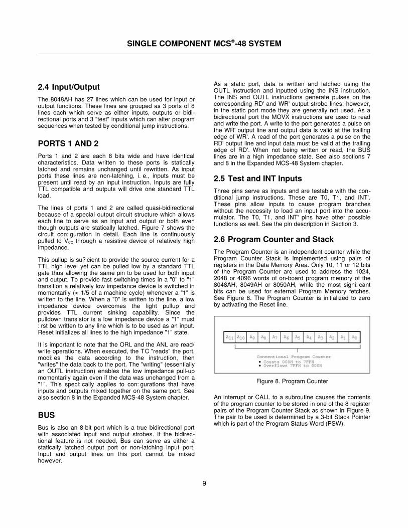
2.6 Program Counter and StackThe Program Counter is an independent counter while theProgram Counter Stack is implemented using pairs ofregisters in the Data Memory Area. Only 10, 11 or 12 bitsof the Program Counter are used to address the 1024,2048 or 4096 words of on-board program memory of the8048AH, 8049AH or 8050AH, while the most significantbits can be used for external Program Memory fetches.See Figure 8. The Program Counter is initialized to zeroby activating the Reset line.
An interrupt or CALL to a subroutine causes the contentsof the program counter to be stored in one of the 8 registerpairs of the Program Counter Stack as shown in Figure 9.The pair to be used is determined by a 3-bit Stack Pointerwhich is part of the Program Status Word (PSW).
9
Figure 8. Program Counter

SINGLE COMPONENT MCS®-48 SYSTEM
Data RAM locations 8-23 are available as stack registersand are used to store the Program Counter and 4 bits ofPSW as shown in Figure 9. The Stack Pointer wheninitialized to 000 points to RAM location 8 and 9. The firstsubroutine jump or interrupt results in the program countercontents being transferred to locations 8 and 9 of the RAMarray. The stack pointer is then incremented by one topoint to locations 10 and 11 in anticipation of anotherCALL. Nesting of subroutines within subroutines cancontinue up to 8 times without overflowing the stack. Ifoverflow does occur, the deepest address stored (loca-tions 8 and 9) will be overwritten and lost since the stackpointer overflows from 111 to 000. It also underflows from000 to 111.
The end of a subroutine, which is signaled by a returninstruction (RET or RETR), causes the Stack Pointer to bedecremented and the contents of the resulting register pairto be transferred to the Program Counter.
2.7 Program Status WordAn 8-bit status word which can be loaded to and from theaccumulator exists called the Program Status Word
(PSW). Figure 10 shows the information available in theword. The Program Status Word is actually a collection offlip-flops throughout the machine which can be read orwritten as a whole. The ability to write the PSW allows foreasy restoration of machine status after a power downsequence.
The upper four bits of PSW are stored in the ProgramCounter Stack with every call to subroutine or interruptvector and are optionally restored upon return with theRETR instruction. The RET return instruction does notupdate PSW.
The PSW bit definitions are as follows:
Bits 0-2: Stack Pointer bits (S0, S1, S2)
Bit 3: Not used ("1" level when read)
Bit 4: Working Register Bank Switch Bit (BS)0 = Bank 01 = Bank 1
Bit 5: Flag 0 bit (F0) user controlled flag which canbe complemented or cleared and tested withthe conditional jump instruction JF0.
Bit 6: Auxiliary Carry (AC) carry bit generated by anADD instruction and used by the decimaladjust instruction DA A.
Bit 7: Carry (CY) carry flag which indicates that theprevious operation has resulted in overflow ofthe accumulator.
2.8 Conditional Branch LogicThe conditional branch logic within the processor enablesseveral conditions internal and external to the processor tobe tested by the user program. By using the conditionaljump instruction the conditions that are listed in 1 canaffect a change in the sequence of the program execution.
10
Figure 10. Program Status Word (PSW)
Figure 9. Program Counter Stack

SINGLE COMPONENT MCS®-48 SYSTEM
11
Figure 11. Interrupt Logic

SINGLE COMPONENT MCS®-48 SYSTEM
Table 1
Device TestableJump Condition
(Jump On)not all
Accumulator All zeros zerosAccumulator Bit --- 1Carry Flag 0 1User Flags (F0, F1) --- 1Timer Overflow Flag --- 1Test Inputs (T0, T1) 0 1Interrupt Input (INT) 0 ---
2.9 InterruptAn interrupt sequence is initiated by applying a low "0"level input to the INT' pin. Interrupt is level triggered andactive low to allow "WIRE ORing" of several interruptsources at the input pin. Figure 11 shows the interruptlogic of the 8048AH. The interrupt line is sampled everyinstruction cycle and when detected causes a "call tosubroutine" at location 3 in program memory as soon asall cycles of the current instruction are complete. On 2-cycle instructions the interrupt line is sampled on the 2ndcycle only. INT' must be held low for at least 3 machinecycles to ensure proper interrupt operations. As in anyCALL to subroutine, the Program Counter and ProgramStatus word is saved in the stack. For a description of thisoperation see the previous section, Program Counter andStack. Program Memory location 3 usually contains anunconditional jump to an interrupt service subroutineelsewhere in program memory. The end of an interrupt
service subroutine is signaled by the execution of a Returnand Restore Status instruction RETR. The interruptsystem is single level in that once an interrupt is detectedall further interrupt requests are ignored until execution ofan RETR reenables the interrupt input logic. This occursat the beginning of the second cycle of the RETRinstruction. This sequence holds true also for an internalinterrupt generated by timer overflow. If an internaltimer/counter generated interrupt and an external sourcewill be recognized at the same time, the external sourcewill be recognized. See the following Timer/Countersection for a description of timer interrupt. If needed, asecond external interrupt can be created by enabling thetimer/counter interrupt, loading FFH in the Counter (oneless than terminal count) and enabling the event countermode. A "1" to "0" transition on the T1 input will thencause an interrupt vector to location 7.
INTERRUPT TIMINGThe interrupt input may be enabled or disabled underProgram Control using the EN I and DIS I instructions.Interrupts are disabled by Reset and remain so untilenabled by the user's program. An interrupt request mustbe removed before the RETR instruction is executed uponreturn from the service subroutine otherwise the processorwill re-enter the service routine immediately. Manyperipheral devices prevent this situation by resetting theirinterrupt request line whenever the processor accesses(Reads or Writes) the peripheral's data buffer register. Ifthe interrupt device does not require access by theprocessor, one output line of the 8048AH may be des-ignated as an "interrupt acknowledge" which is activatedby the service subroutine to reset the interrupt request.The INT' pin may also be tested using the conditional jump
12
Figure 12. Timer/Event Counter

SINGLE COMPONENT MCS®-48 SYSTEM
instruction JNI. This instruction may be used to detect thepresence of a pending interrupt before interrupts areenabled. If interrupt is left disabled, INT' may be used asanother test input like T0 and T1.
2.10 Timer/CounterThe 8048AH contains a counter to aid the user in countingexternal events and generating accurate time delays with-out placing a burden on the processor for these functions.In both modes the counter operation is the same, the onlydifference being the source of the input to the counter.The timer/event counter is show in Figure 12.
COUNTERThe 8-bit binary counter is presettable and readable withthe MOV instructions which transfer the contents of theaccumulator to the counter and vice versa. The countercontent may be affected by Reset and should be initializedby software. The counter is stopped by a Reset or STOPTCNT instruction and remains stopped until started as atimer by a STRT T instruction or as an event counter by aSTRT CNT instruction. Once started, the counter willincrement to this maximum count (FF) and overflow tozero continuing its count until stopped by a STOP TCNTinstruction or Reset.
The increment from maximum count to zero (overflow)results in the setting of an overflow flag flip-flop and in thegeneration of an interrupt request. The state of theoverflow flag is testable with the conditional jump instruc-tion JTF. The flag is reset by executing a JTF or by Reset.The interrupt request is stored in a latch and then ORedwith the external interrupt input INT. The timer interruptmay be enabled or disabled independently of external in-terrupt by the EN TCNTI and DIS TCNTI instructions. Ifenabled, the counter overflow will cause a subroutine callto location 7 where the timer or counter service routinemay be stored.
If timer and external interrupts occur simultaneously, theexternal interrupt will be recognized and the Call will be tolocation 3. Since the timer interrupt is latched it will remainpending until the external device is serviced andimmediately be recognized upon return from the serviceroutine. The pending timer interrupt is reset by the Call tolocation 7 or may be removed by executing a DIS TCNTIinstruction.
AS AN EVENT COUNTERExecution of a START CNT instruction connects the T1input pin to the counter input and enables the counter. TheT1 input is sampled at the beginning of state 3 or in laterMCS-48 devices in state time 4. Subsequent high to lowtransitions on T1 will cause the counter to increment. T1
13
Table 2. Baud Rate Generation
Frequency(MHz)
TCY T0 Prr(1/5 TCY) Timer Prescaler(32 TCY)
46811
3.75 µs2.50 µs1.88 µs1.36 µs
750 ns500 ns375 ns275 ns
120 µs80 µs
60.2 µs43.5 µs
BaudRate
4 MHzTimer Counts +
Instr. Cycles
6 MHzTimer Counts +
Instr. Cycles
8 MHzTimer Counts +
Instr. Cycles
11 MHzTimer Counts +
Instr. Cycles110 75 + 24 Cycles
.01% Error113 + 20 Cycles
.01% Error151 + 3 Cycles
.01% Error208 + 28 Cycles
.01% Error300 27 + 24 Cycles
.1% Error41 + 21 Cycles
.03% Error55 + 13 Cycles
.01% Error76 + 18 Cycles
.04% Error1200 6 + 30 Cycles
.1% Error10 + 13 Cycles
.1% Error12 + 27 Cycles
.06% Error19 + 4 Cycles
.12% Error1800 4 + 20 Cycles
.1% Error6 + 30 Cycles
.1% Error9 + 7 Cycles.17% Error
12 + 24 Cycles.12% Error
2400 3 + 15 Cycles.1% Error
5 + 6 Cycles.4% Error
6 + 24 Cycles.29% Error
9 + 18 Cycles.12% Error
4800 1 + 23 Cycles1.0% Error
2 + 19 Cycles.4% Error
3 + 14 Cycles.74% Error
4 + 25 Cycles.12% Error

SINGLE COMPONENT MCS®-48 SYSTEM
must be held low for at least 1 machine cycle to ensure itwon't be missed. The maximum rate at which the countermay be incremented is once per three instruction cycles(every 5.7 µsec when using an 8 MHz crystal) --- there isno minimum frequency. T1 input must remain high for atleast 1/5 machine cycle after each transition.
AS A TIMER
14
Figure 13. MCS-48 Timing Generation and Cycle Timing

SINGLE COMPONENT MCS®-48 SYSTEM
15
Figure 14. 8048AH/8049AH Instruction Timing Diagram

SINGLE COMPONENT MCS®-48 SYSTEM
Execution of a START T instruction connects an internalclock to the counter input and enables the counter. Theinternal clock is derived by passing the basic machinecycle clock through a ÷ 32 prescaler. The prescaler isreset during the START T instruction. The resulting clockincrements the counter every 32 machine cycles. Variousdelays from 1 to 256 counts can be obtained by presettingthe counter and detecting overflow. Times longer than 256counts may be achieved by accumulating multipleoverflows in a register under software control. For timeresolution less than 1 count an external clock can beapplied to the T1 input and the counter operated in theevent counter mode. ALE divided by 3 or more can serveas this external clock. Very small delays or "fine tuning" oflarger delays can be easily accomplished by softwaredelay loops.
Often a serial link is desirable in an MCS-48 family mem-ber. 2 lists the timer counts and cycles needed for aspecific baud rate given a crystal frequency.
2.11 Clock and Timing CircuitsTiming generation for the 8048AH is completely self con-tained with the exception of a frequency reference whichcan be XTAL, ceramic resonator or external clock source.The Clock and Timing circuitry can be divided into thefollowing functional blocks.
OSCILLATORThe on-board oscillator is a high gain parallel resonantcircuit with a frequency range of 1 to 11 MHz. The X1external pin is the input to the amplifier stage while X2 isthe output. A crystal or ceramic resonator connected
between X1 and X2 provides the feedback and phase shiftrequired for oscillation. If an accurate frequency referenceis not required, ceramic resonator may be used in place ofthe crystal.
For accurate clocking, a crystal should be used. An ex-ternally generated clock may also be applied to X1—X2 asthe frequency source. See the data sheet for moreinformation.
16
Figure 15.

SINGLE COMPONENT MCS®-48 SYSTEM
STATE COUNTERThe output of the oscillator is divided by 3 in the StateCounter to create a clock which defines the state times ofthe machine (CLK). CLK can be made available on theexternal pin T0 by executing an ENT0 CLK instruction.The output of CLK on T0 is disabled by Reset of theprocessor.
CYCLE COUNTERCLK is then divided by 5 in the Cycle Counter to provide aclock which defines a machine cycle consisting of 5machine states as shown in Figure 13. Figure 14 showsthe different internal operations as divided into themachine states. This clock is called Address Latch Enable(ALE) because of its function in MCS-48 systems withexternal memory. It is provided continuously on the ALEoutput pin.
2.12 ResetThe reset input provides a means for initialization for theprocessor. This Schmitt-trigger input has an internal pullupdevice which in combination with an external 1 µFcapacitor provides an internal reset pulse of sufficientlength to guarantee all circuitry is reset, as shown inFigure 15. If the reset pulse is generated externally, theRESET pin must be held low for at least 10 millisecondsafter the power supply is within tolerance. Only 5 machinecycles (6.8 µs @ 11 MHz) are required if power is alreadyon and the oscillator has stabilized. ALE and PSEN (if EA= 1) are active while in Reset.
Reset performs the following functions:
1) Sets program counter to zero.
2) Sets stack pointer to zero.
3) Selects register bank 0.
4) Selects memory bank 0.
5) Sets BUS to high impedance state (except when EA = 5 V).
6) Sets Ports 1 and 2 to input mode.
7) Disables interrupts (timer and external).
8) Stops timer.
9) Clears timer flag.
10) Clears F0 and F1.
11) Disables clock output from T0.
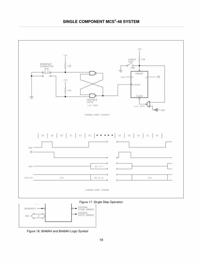
2.13 Single-StepThis feature, as pictured in Figure 17, provides the userwith a debug capability in that the processor can bestepped through the program one instruction at a time.While stopped, the address of the next instruction to befetched is available concurrently on BUS and the lowerhalf of Port 2. The user can therefore follow the programthrough each of the instruction steps. A timing diagram,showing the interaction between output ALE and inputSS', is shown. The BUS buffer contents are lost duringsingle step; however, a latch may be added to reestablishthe lost I/O capability if needed. Data is valid at theleading edge of ALE.
TIMINGThe 8048AH operates in a single-step mode as follows:
1) The processor is requested to stop by applying a lowlevel on SS'.
2) The processor responds by stopping during the ad-dress fetch portion of the next instruction. If a doublecycle instruction is in progress when the single stepcommand is received, both cycles will be completedbefore stopping.
3) The processor acknowledges it has entered thestopped state by raising ALE high. In this state (whichcan be maintained indefinitely) the address of the nextinstruction to be fetched is present on BUS and thelower half of port 2.
4) SS' is then raised high to bring the processor out of thestopped mode allowing it to fetch the next instruction.The exit from stop is indicated by the processor briningALE low.
5) To stop the processor at the next instruction, SS' mustbe brought low again soon after ALE goes low. If SS' isleft high the processor remains in a "Run" mode.
A diagram for implementing the single-step function of the8748Ah is show in Figure 17. D-type flip-flop with presetand clear is used to generate SS'. In the run mode SS' isheld high by keeping the flip-flop preset (preset hasprecedence over the clear input). To enter single step,preset is removed allowing ALE to bring SS' low via theclear input. ALE should be buffered since the clear input ofan SN7474 is the equivalent of 3 TTL loads. Theprocessor is now in the stopped state. The next instructionis initiated by clocking a "1" into the flip-flop. This "1" willnot appear on SS' unless ALE is high removing clear fromthe flip-flop. In response to SS' going high the processorbegins an instruction fetch which brings ALE low resettingSS' through the clear input and causing the processor toagain enter the stopped state.
17

SINGLE COMPONENT MCS®-48 SYSTEM
2.14 Power Down Mode(8048AH, 8049AH, 8050AH,8039AHL, 8035AHL, 8040AHL)
Extra circuitry has been added to the 8048AH/8049AH/8050AH ROM version to allow power to be removed fromall but the data RAM array for low power standby oper-ation. In the power down mode the contents of data RAMcan be maintained while drawing typically 10% to 15% ofnormal operating power requirements.
VCC serves as the 5V supply pin for the bulk of circuitrywhile the VDD pin supplies only the RAM array. In normaloperation both pins are at 5V while in standby, VCC is atground and VDD is maintained at its standard value. Ap-plying Reset to the processor through the RESET' pininhibits any access to the RAM by the processor andguarantees the RAM cannot be inadvertently altered aspower is removed from VCC.
A typical power down sequence (Figure 16) occurs asfollows:
1) Imminent power supply failure is detected by user de-fined circuitry. Signal must be early enough to allow8048AH to save all necessary data before VCC fallsbelow normal operating limits.
2) Power fail signal is used to interrupt processor andvector it to a power fail service routine.
3) Power fail routine saves all important data and machinestatus in the internal data RAM array. Routine may alsoinitiate transfer of backup supply to the VDD pin andindicate to external circuitry that power fail routine iscomplete.
4) Reset is applied to guarantee data will not be altered asthe power supply falls out of limits. Reset must be heldlow until VCC is at ground level.
Recovery from the Power Down mode can occur as anyother power-on sequence with an external capacitor onthe Reset input providing the necessary delay. See theprevious section on Reset.
18
Figure 16. Power Down Sequence
SINGLE COMPONENT MCS®-48 SYSTEM
19
Figure 18. 8048AH and 8049AH Logic Symbol
Figure 17. Single Step Operation

SINGLE COMPONENT MCS®-48 SYSTEM
2.15 External Access ModeNormally, the first 1K (8048AH), 2K (8049AH) or 4K(8050AH) words of program memory are automaticallyfetched from internal ROM or EPROM. The EA input pinhowever allows the user to efficiently disable internalprogram memory by forcing all program memory fetchesto reference external memory. The following chapter ex-plains how access to external program memory isaccomplished.
The External Access mode is very useful in system testand debug because it allows the user to disable hisinternal applications program and substitute an externalprogram of his choice --- a diagnostic routine for instance.In addition, the data sheet shows how internal programmemory can be read externally, independent of theprocessor. A "1" level on EA initiates the external accessmode. For proper operation, Reset should be appliedwhile the EA input is changed.
2.16 Sync ModeThe 8048AH, 8049AH, 8050AH has incorporated a newSYNC mode. The Sync mode is provided to ease thedesign of multiple controller circuits by allowing the de-signer to force the device into known phase and statetime. The SYNC mode may also be utilized by automatictest equipment (ATE) for quick, easy and efficient synchro-nizing between the tester and the DUT (device under test).
SYNC mode is enabled when SS' pin is raised to highvoltage level of +12 volts. To begin synchronization, T0 israised to 5 volts at least four clock cycles after SS'. T0must be high for at least four X1 clock cycles to fully resetthe prescaler and time state generators. T0 may then bebrought down with the rising edge of X1. Two clock cycleslater, with the rising edge of X1, the device enters intoTime State 1, Phase 1. SS' is then brought down to 5 volts4 clocks later after T0. RESET' is allowed to go high 5 tCY(75 clocks) later for normal execution of code. See Figure19.
20

SINGLE COMPONENT MCS®-48 SYSTEM
3.0 PIN DESCRIPTIONThe MCS-48 processors are packaged in 40 pin Dual In-Line Packages (DIP's). 3 is a summary of the functions ofeach pin. Figure 18 is the logic symbol for the 8048AHproduct family. Where it exists, the second paragraphdescribes each pin's function in an expanded MCS-48system. Unless otherwise specified, each input is TTLcompatible and each output will drive one standard TTLload.
21
Figure 19. Sync Mode Timing

SINGLE COMPONENT MCS®-48 SYSTEM
22
Table 3. Pin Description
DesignationPin
Number* FunctionVSS 20 Circuit GND potentialVDD 26 Programming power supply; 21V during program for the 8748H/8749H; +5V during
operation for both ROM and EPROM. Low power standby pin in 8048AH and8049AH/8050AH ROM versions.
VCC 40 Main power supply; +5V during operation and during 8748H and 8749H programming.PROG 25 Program pulse; +18V input pin during 8748H/8749H programming. Output strobe for 8243
I/O expander.P10-P17(Port 1)
27-34 8-bit quasi-bidirectional port. (Internal Pullup ≈ 50 kΩ)
P20-27(Port 2)
21-2435-38
8-bit quasi-bidirectional port. (Internal Pullup ≈ 50 kΩ)
P20-23 contain the four high order program counter bits during an external program mem-ory fetch and serve as a 4-bit O/O expander bus for 8243.
D0-D7(BUS)
12-19 True bidirectional port which can be written or read synchronously using the RD', WR'strobes. The port can also be statically latched.
Contains the 8 low order program counter bits during an external program memory fetch,and receives the addressed instruction under the control of PSEN'. Also contains theaddress and data during an external RAM data store instruction, under control of ALE, RD'and WR'.
T0 1 Input pin testable using the conditional transfer instructions JT0 and JNT0. T0 can be des-ignated as a clock output using ENT0 CLK instruction. T0 is also used during programmingand sync mode.
T1 39 Input pin testable using the JT1 and JNT1 instructions. Can be designated the eventcounter input using the STRT CNT instruction. (See Section 2.10).
INT' 6 Interrupt input. Initiates an interrupt if interrupt is enabled. Interrupt is disabled after a reset.(Active low)
Interrupt must remain low for at least 3 machine cycles to ensure proper operation.RD' 8 Output strobe activated during a BUS read. Can be used to enable data onto the BUS from
external device. (Active low)RESET' 4 Input which is used to initialize the processor. Also used during EPROM programming and
verification. (Active low) (Internal pullup ≈ 50 kΩ)WR' 10 Output strobe during a BUS write. (Active low) Used as a write strobe to external data
memory.ALE 11 Address Latch Enable. This signal occurs once during each cycle and is useful as a clock
output.
The negative edge of ALE strobes address into external data and program memory.PSEN' 9 Program Store Enable. This output occurs only during a fetch to external program memory.
(Active low)SS' 5 Single step input can be used in conjunction with ALE to "single step" the processor
through each instruction. (Active low) (Internal Pullup ≈ 300 kΩ) +12V for sync modes (SeeSection 2.16).

SINGLE COMPONENT MCS®-48 SYSTEM
4.0 PROGRAMMING, VERIFYING, AND ERASING EPROMThe internal Program Memory of the 8748H and the8749H may be erased and reprogrammed by the user asexplained in the following sections. See also the 8748Hand 8749H data sheets.
4.1 Programming/VerificationIn brief, the programming process consists of: applying theprogram mode, applying an address, latching the address,applying data, and applying a programming pulse. Thisprogramming algorithm applies to both the 8748H and8749H. Each word is programmed completely before
moving on to the next and is followed by a verificationstep. The following is a list of the pins used for program-ming and a description of their functions:
Pin Function
XTAL1 Clock Input (3 to 4.0 MHz)Reset Initialization and Address LatchingTest 0 Selection of Program (0 V) or Verify
(5 V) ModeEA Activation of Program/Verify ModesBUS Address and Data Input. Data Output
During VerifyP20-1 Address Input for 8748HP20-2 Address Input for 8749HVDD Programming Power SupplyPROG Program Pulse InputP10-P11 Tied to ground (8749H only)
4.1.1 8748H and 8749H ERASURECHARACTERISTICSThe erasure characteristics of the 8748H and 8749H aresuch that erasure begins to occur when exposed to lightwith wavelengths shorter than approximately 4000 Angs-troms (Å). It should be noted that the sunlight and certaintypes of fluorescent lamps have wavelengths in the 3000-4000 Å range. Data show that constant exposure to roomlevel fluorescent lighting could erase the typical 8748Hand 8749H in approximately 3 years while it would takeapproximately 1 week to cause erasure when exposed todirect sunlight. If the 8748H or 8749H is to be exposed tothese types of lighting conditions for extended periods oftime, opaque labels should be placed over the 8748H
window to prevent unintentional erasure.
When erased, bits of the 8748H and 8749H ProgramMemory are in the logic "0" state.
23
Table 4. D.C. Specification for Programming 8748H/8749H
Symbol Parameter Min Max Unit Test ConditionsVDDH VDD Program Voltage High Level 20.5 21.5 VVDDL VDD Voltage Low Level 4.75 5.25 VVPH PROG Program Voltage High Level 17.5 18.5 VVPL PROG Voltage Low Level 4.0 VCC VVEAH EA Program or Verify Voltage High Level 17.5 18.5 VIDD VDD High Voltage Supply Current 20.0 mAIPROG PROG High Voltage Supply Current 1.0 mAIEA EA High Voltage Supply Current 1.0 mA
TA = 25 °C; VCC = 5 V ±5%; VDD = 21 V ±5%
Table 3. Pin Description (Continued)
DesignationPin
Number* FunctionEA
7
External Access input which forces all program memory fetches to reference externalmemory. Useful for emulation and debug and essential for testing and program verification.(Active high) +12V for 8048AH/8049AH/8050AH program verification and +18V for8748H/8749H program verification (Internal Pullup ≈ 10 MΩ on 8048AH/8049AH/8035AHL/8039AHL/8050AH/8040AHL)
XTAL1 2 One side of crystal input for internal oscillator. Also input for external source.XTAL2 3 Other side of crystal/external source input.
*Unless otherwise stated, inputs do not have internal pullup resistors. 8048AH, 8748H, 8049AH, 8050AH, 8040AHL

SINGLE COMPONENT MCS®-48 SYSTEM
The recommended erasure procedure for the 8748H and8749H is exposure to shortwave ultraviolet light which hasa wavelength of 2537 Angstroms (Å). The integrated dose(i. e., UV intensity × exposure time) for erasure should bea minimum of 15 Wsec/cm2 power rating. The 8748H and8749H should be placed within one inch from the lamptubes during erasure. Some lamps have a filter in theirtubes and this filter should be removed before erasure.
24

SINGLE COMPONENT MCS®-48 SYSTEM
25
Figure 20. Program/Verify Sequence for 8749H/8748H

SINGLE COMPONENT MCS®-48 SYSTEM
26
Table 5. A.C. Specification for Programming 8748H/8749H
Symbol Parameter Min Max Unit Test ConditionstAW Address Setup Time to RESET' ↑ 4tCY
tWA Address Hold Time to RESET' ↑ 4tCY
tDW Data in Setup Time to PROG ↑ 4tCY
tWD Data in Hold Time after PROG ↓ 4tCY
tPH RESET' Hold Time to Verify 4tCY
tVDDW VDD Hold Time before PROG ↑ 0 1.0 mstVDDH VDD Hold Time after PROG ↓ 0 1.0 mstPW Program Pulse Width 50 60 mstTW TEST 0 Setup Time for Program Mode 4tCY
tWT TEST 0 Hold Time after Program Mode 4tCY
tDO TEST 0 to data Out Delay 4tCY
tWW RESET' Pulse Width to Latch Address 4tCY
tr, tf VDD and PROG Rise and Fall Times 0.5 100 µstCY CPU Operation Cycle Time 3.75 5 µstRE RESET' Setup Time before EA ↑ 4tCY
TA = 25 °C; VCC = 5 V ±5%; VDD = 21 V ±5%
NOTE:If TEST 0 is high, tDO can be triggered by RESET' ↑.
SINGLE COMPONENT MCS®-48 SYSTEM
27
Instruction Code Flags
Mnemonic Function Description D7 D6 D5 D4 D3 D2 D1 D0 Cycles Bytes C AC F0 F1
Data Moves
MOV A, = data (A) ← data Move immediate the specified data intothe Accumulator.
0d7
0d6
1d5
0d4
0d3
0d2
1d1
1d0
2 2
MOV A, Rr (A) ← (Rr); r = 0 – 7 Move the contents of the designatedregister into the Accumulator.
1 1 1 1 1 r r r 1 1
MOV A, @ Rr (A) ← ((Rr)); r = 0 – 1 Move indirect the contents of datamemory location into the Accumulator.
1 1 1 1 0 0 0 r 1 1
MOV A, PSW (A) ← (PSW) Move contents of the Program StatusWord into the Accumulator.
1 1 0 0 0 1 1 1 1 1
MOV Rr, = data (Rr) ← data; r = 0 – 7 Move immediate the specified data intothe designated register.
1d7
0d6
1d5
1d4
1d3
rd2
rd1
rd0
2 2
MOV Rr, A (Rr) ← (A); r = 0 – 7 Move Accumulator contents into thedesignated register.
1 0 1 0 1 r r r 1 1
MOV @ Rr, A ((Rr)) ← (A); r = 0 – 1 Move indirect Accumulator contentsinto data memory location.
1 0 1 0 0 0 0 r 1 1
MOV @ Rr, = data ((Rr)) ← data; r = 0 – 1 Move immediate the specified data intodata memory.
1d7
0d6
1d5
1d4
0d3
0d2
0d1
rd0
2 2
MOV PSW, A (PSW) ← (A) Move contents of Accumulator into theProgram Status Word.
1 1 0 1 0 1 1 1 1 1
MOVP A, @ A (PC 0 – 7) ← (A)(A) ← ((PC))
Move data in the current page into theAccumulator.
1 0 1 0 0 0 1 1 2 1
MOVP3 A, @ A (PC 0 – 7) ← (A)(PC 8 – 10) ← 011(A) ← ((PC))
Move Program data in Page 3 into theAccumulator.
1 1 1 0 0 0 1 1 2 1
MOVX A, @ Rr (A) ← ((Rr)); r = 0 – 1 Move indirect the contents of externaldata memory into the Accumulator.
1 0 0 0 0 0 0 r 2 1
MOVX @ Rr, A ((Rr)) ← (A); r = 0 – 1 Move indirect the contents of theAccumulator into external data memory.
1 0 0 1 0 0 0 r 2 1
XCH A, Rr (A) (Rr); r = 0 – 7⇄ (Rr); r = 0 – 7 Exchange the Accumulator anddesignated register's contents.
0 0 1 0 1 r r r 1 1
XCH A, @ Rr (A) ((Rr)); r = 0 – 1⇄ (Rr); r = 0 – 7 Exchange indirect contents of Accumu-lator and location in data memory.
0 0 1 0 0 0 0 r 1 1
XCHD A, @ Rr (A 0 – 3) ((Rr)(0 – 3))⇄ (Rr); r = 0 – 7
r = 0 – 1Exchange indirect 4-bit contents ofAccumulator and data memory.
0 0 1 1 0 0 0 r 1 1
Flags
CPL C (C) ← NOT (C) Complement content of carry bit. 1 0 1 0 0 1 1 1 1 1 •
CPL F0 (F0) ← NOT (F0) Complement content of Flag F0. 1 0 0 1 0 1 0 1 1 1 •
CPL F1 (F1) ← NOT (F1) Complement content of Flag F1. 1 0 1 1 0 1 0 1 1 1 •
CLR C (C) ← 0 Clear content of carry bit to 0. 1 0 0 1 0 1 1 1 1 1 •
CLR F0 (F0) ← 0 Clear content of Flag 0 to 0. 1 0 0 0 0 1 0 1 1 1 •
CLR F1 (F1) ← 0 Clear content of Flag 1 to 0. 1 0 1 0 0 1 0 1 1 1 •
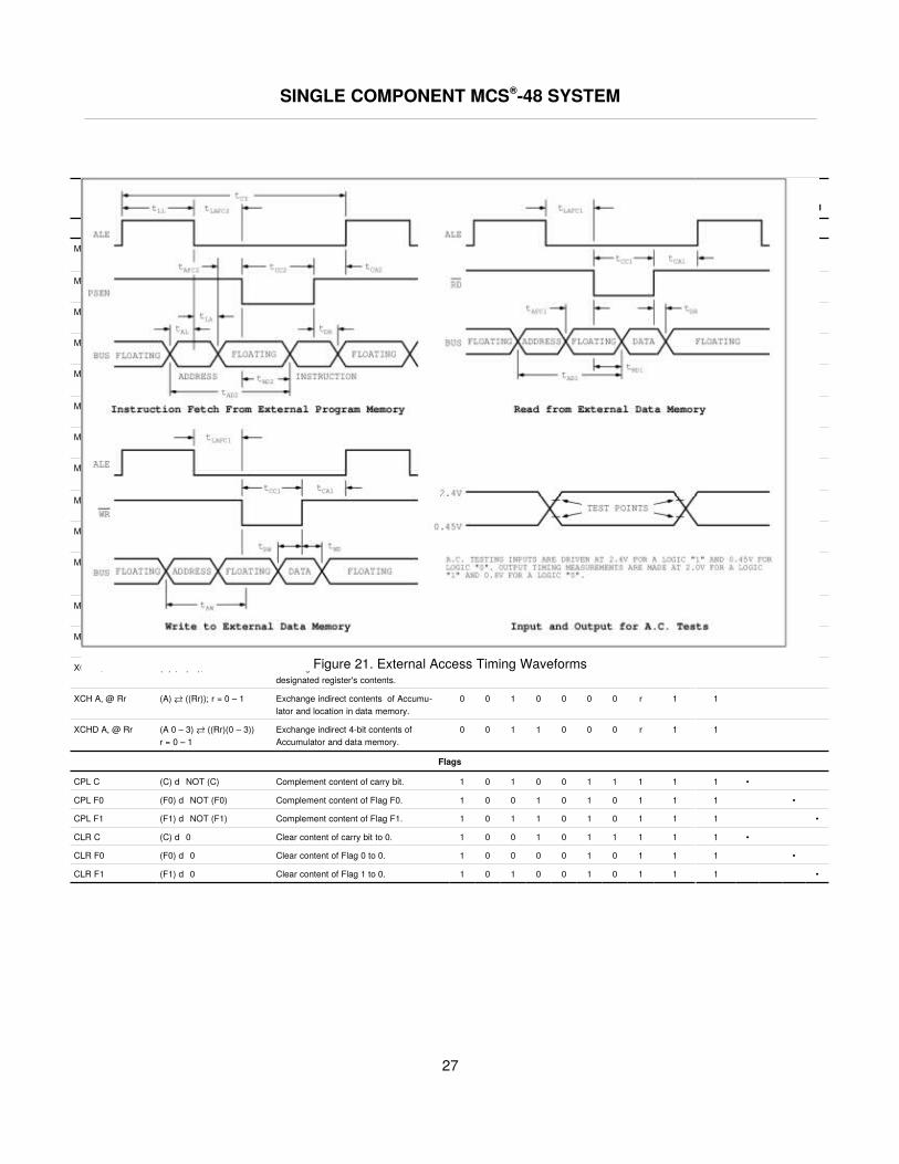
Figure 21. External Access Timing Waveforms

SINGLE COMPONENT MCS®-48 SYSTEM
28
Figure 22. Port 1 / Port 2 Timing Waveforms

SINGLE COMPONENT MCS®-48 SYSTEM
29
A.C. CHARACTERISTICS (TA = 0 °C to 70 °C; VCC = VDD = 5 V ± 10%; VSS = 0 V)
Symbol Parameterf (tCY)
(Note 4)
11 MHz
Min Max UnitConditions
(Note 1)
tCY Cycle Time 15/F(XTAL) 1.36 15.0 us (Note 3)
tLL ALE Pulse Width 7/30 tCY - 170 150 ns
tAL Addr Setup to ALE 2/15 tCY - 110 70 ns (Note 2)
tLA Addr Hold from ALE 1/15 tCY - 40 50 ns
tCC1 Control Pulse Width (RD', WR') 1/2 tCY - 200 480 ns
tCC2 Control Pulse Width (PSEN') 2/5 tCY - 200 350 ns
tDW Data Setup before WR' 13/30 tCY - 200 390 ns
tWD Data Hold after WR' 1/15 tCY - 50 40 ns
tDR Data Hold (RD', PSEN') 1/10 tCY - 30 0 110 ns
tRD1 RD' to Data In 11/30 tCY - 170 330 ns
tRD2 PSEN' to Data In 4/15 tCY - 170 190 ns
tAW Addr Setup to WR' 1/3 tCY - 150 300 ns
tAD1 Addr Setup to Data (RD') 7/10 tCY - 220 730 ns
tAD2 Addr Setup to Data (PSEN') 1/2 tCY - 220 460 ns
tAFC1 Addr Float to RD', WR' 2/15 tCY - 40 140 ns (Note 2)
tAFC2 Addr Float to PSEN' 1/30 tCY - 40 10 ns (Note 2)
tLAFC1 ALE to Control (RD', WR') 1/5 tCY - 75 200 ns
tLAFC2 ALE to Control (PSEN') 1/10 tCY - 75 60 ns
tCA1 Control to ALE (RD', WR', PROG') 1/15 tCY - 40 50 ns
tCA2 Control to ALE (PSEN') 4/15 tCY - 40 320 ns
tCP Port Control Setup to PROG' 2/15 tCY - 80 100 ns
tPC Port Control Hold to PROG' 4/15 tCY - 200 160 ns
tPR PROG' to P2 Input Valid 17/30 tCY - 120 650 ns
tPF Input Data Hold from PROG' 1/10 tCY 0 140 ns
tDP Output Data Setup 2/5 tCY - 150 400 ns
tPD Output Data Hold 1/10 tCY - 50 90 ns
tPP PROG' Pulse Width 7/10 tCY - 250 700 ns
tPL Port 2 I/O Setup to ALE 4/15 tCY - 200 160 ns
tLP Port 2 I/O Hold to ALE 1/30 tCY - 30 15 ns
tPV Port Output from ALE 3/10 tCY + 100 510 ns
t0PRR T0 Rep Rate 3/15 tCY 270 ns
Notes:
1. Control output CL = 80 pFBUS Outputs CL = 150 pF
2. BUS High ImpedanceLoad 20 pF
3. f(tCY) assumes 50% duty cycleon X1 and X2.

SINGLE COMPONENT MCS®-48 SYSTEM
30

SINGLE COMPONENT MCS®-48 SYSTEM
31
Instruction Code Flags
Mnemonic Function Description D7 D6 D5 D4 D3 D2 D1 D0 Cycles Bytes C AC F0 F1
Input/Output
ANL BUS, = data (BUS) ← (BUS) AND data Logical and immediate specified datawith contents on BUS.
1d7
0d6
0d5
1d4
1d3
0d2
0d1
0d0
2 2
ANL Pp, = data (Pp) ← (Pp) AND datap = 1 – 2
Logical and immediate specified datawith designated port (1 – 2).
1d7
0d6
0d5
1d4
1d3
0d2
pd1
pd0
2 2
ANLD Pp, A (Pp) ← (Pp) AND (A 0 – 3)p = 4 – 7
Logical and contents of Accumulator withdesignated port (4 – 7).
1 0 0 1 1 1 p p 2 1
IN A, Pp (A) ← (Pp); p = 1 – 2 Input data from designated port (1 – 2)into Accumulator.
0 0 0 0 1 0 p p 2 1
INS A, BUS (A) ← (BUS) Input strobed BUS data into Accumulator. 0 0 0 0 1 0 0 0 2 1
MOVD A ,Pp (A 0 – 3) ← (Pp); p = 4 – 7(A 4 – 7) ← 0
Move contents of designated port (4 – 7)into Accumulator.
0 0 0 0 1 1 p p 2 1
MOVD Pp, A (Pp) ← A (0 – 3); p = 4 – 7 Move contents of Accumulator todesignated port (4 – 7).
0 0 1 1 1 1 p p 2 1
ORL BUS, = data (BUS) ← (BUS) OR data Logical or immediate specified data withcontents of BUS.
1d7
0d6
0d5
0d4
1d3
0d2
0d1
0d0
2 2
ORLD Pp, A (Pp) ← (Pp) OR (A 0 – 3)p = 4 – 7
Logical or contents of Accumulator withdesignated port (4 – 7).
1 0 0 0 1 1 p p 1 1
ORL Pp, = data (Pp) ← (Pp) OR datap = 1 – 2
Logical or immediate specified data withdesignated port (1 – 2).
1d7
0d6
0d5
0d4
1d3
0d2
pd1
pd0
2 2
OUTL BUS, A ⑤ (BUS) ← A Output contents of Accumulator ontoBUS.
0 0 0 0 0 0 1 0 2 1
OUTL Pp, A (Pp) ← (A); p = 1 – 2 Output contents of Accumulator todesignated port (1 – 2).
0 0 1 1 1 0 p p2
1
Registers
DEC Rr (Rr) ← (Rr) – 1; r = 0 – 7 Decrement by 1 contents of designatedregister.
1 1 0 0 1 r r r 1 1
INC Rr (Rr) ← (Rr) + 1; r = 0 – 7 Increment by 1 contents of designatedregister.
0 0 0 1 1 r r r 1 1
INC @ Rr ((Rr)) ← ((Rr)) + 1; r = 0 – 1 Increment indirect by 1 the contents ofdata memory location.
0 0 0 1 0 0 0 r 1 1
Subroutine
CALL addr ((SP)) ← (PC), (PSW 4 – 7)(SP) ← (SP) + 1(PC 8 – 10) ← addr 8 – 10(PC 0 – 7) ← addr 0 – 7(PC 11) ← DBF
Call designated Subroutine. a10a7
a9a6
a8a5
1a4
0a3
1a2
0a1
0a0
2 2
RET (SP) ← (SP) – 1(PC) ← ((SP))
Return from Subroutine withoutrestoring Program Status Word.
1 0 0 0 0 0 1 1 2 1
RETR (SP) ← (SP) – 1(PC) ← ((SP))(PSW 4 – 7) ← ((SP))
Return from Subroutine restoringProgram Status Word.
1 0 0 1 0 0 1 1 2 1
Timer/Counter
EN TCNTI Enable internal interrupt Flag forTimer/Counter output.
0 0 1 0 0 1 0 1 1 1
DIS TCNTI Disable internal interrupt Flag forTimer Counter output.
0 0 1 1 0 1 0 1 1 1
MOV A, T (A) ← (T) Move contents of Timer/Counter intoAccumulator.
0 1 0 0 0 0 1 0 1 1
MOV T, A (T) ← (A) Move contents of Accumulator intoTimer/Counter.
0 1 1 0 0 0 1 0 1 1
STOP TCNT Stop Count for Event Counter. 0 1 1 0 0 1 0 1 1 1

SINGLE COMPONENT MCS®-48 SYSTEM
32
Instruction Code Flags
Mnemonic Function Description D7 D6 D5 D4 D3 D2 D1 D0 Cycles Bytes C AC F0 F1
Miscellaneous
NOP No Operation performed. 0 0 0 0 0 0 0 0 1 1
Accumulator
ADD A, = data (A) ← (A) + data Add immediate the specified Data to theAccumulator.
0d7
0d6
0d5
0d4
0d3
0d2
1d1
1d0
2 2 • •
ADD A, Rr (A) ← (A) + (Rr)r = 0 – 7
Add contents of designated register tothe Accumulator.
0 1 1 0 1 r r r 1 1 • •
ADD A, @ Rr (A) ← (A) + ((Rr))r = 0 – 1
Add indirect the contents of the datamemory location to the Accumulator.
0 1 1 0 0 0 0 r 1 1 • •
ADDC A, = data (A) ← (A) + (C) + data Add immediate with carry the specifieddata to the Accumulator.
0d7
0d6
0d5
1d4
0d3
0d2
1d1
1d0
2 2 • •
ADDC A, Rr (A) ← (A) + (C) + (Rr)r = 0 – 7
Add with carry the contents of thedesignated register to the Accumulator.
0 1 1 1 1 r r r 1 1 • •
ADDC A, @ Rr (A) ← (A) + (C) + ((Rr))r = 0 – 1
Add indirect with carry the contents ofdata memory location to the Accumulator.
0 1 1 1 0 0 0 r 1 1 • •
ANL A, = data (A) ← (A) AND data Logical and specified immediate datawith Accumulator.
0d7
1d6
0d5
1d4
0d3
0d2
1d1
1d0
2 2
ANL A, Rr (A) ← (A) AND (Rr)r = 0 – 7
Logical and contents of designatedregister with Accumulator.
0 1 0 1 1 r r r 1 1
ANL A, @ Rr (A) ← (A) AND ((Rr))r = 0 – 1
Logical and indirect the contents of datamemory with Accumulator.
0 1 0 1 0 0 0 r 1 1
CPL A (A) ← NOT (A) Complement the contents of theAccumulator.
0 0 1 1 0 1 1 1 1 1
CLR A (A) ← 0 CLEAR the contents of the Accumulator. 0 0 1 0 0 1 1 1 1 1
DA A DECIMAL ADJUST the contents of theAccumulator.
0 1 0 1 0 1 1 1 1 1 •
DEC A (A) ← (A) – 1 Decrement by 1 the Accumulator'scontents.
0 0 0 0 0 1 1 1 1 1
INC A (A) ← (A) + 1 Increment by 1 the Accumulator'scontents.
0 0 0 1 0 1 1 1 1 1
ORL A, = data (A) ← (A) OR data Logical or specified immediate datawith Accumulator.
0d7
1d6
0d5
0d4
0d3
0d2
1d1
1d0
2 2
ORL A, Rr (A) ← (A) OR (Rr)r = 0 – 7
Logical or contents of designatedregister with Accumulator.
0 1 0 0 1 r r r 1 1
ORL A, @ Rr (A) ← (A) OR ((Rr))r = 0 – 1
Logical or indirect the contents of datamemory with Accumulator.
0 1 0 0 0 0 0 r 1 1
RL A (AN + 1) ← (AN); N = 0 – 6(A0) ← (A7)
Rotate Accumulator left by 1-bit withoutcarry.
1 1 1 0 0 1 1 1 1 1
RLC A (AN + 1) ← (AN); N = 0 – 6(A0) ← (C)(C) ← (A7)
Rotate Accumulator left by 1-bit throughcarry.
1 1 1 1 0 1 1 1 1 1 •
RR A (AN) ← (AN + 1); N = 0 – 6(A7) ← (A0)
Rotate Accumulator right by 1-bit withoutcarry.
0 1 1 1 0 1 1 1 1 1
RRC A (AN ) ← (AN + 1); N = 0 – 6(A7) ← (C)(C) ← (A0)
Rotate Accumulator right by 1-bit throughcarry.
0 1 1 0 0 1 1 1 1 1 •
SWAP A (A4 – 7) (A0 – 3)⇄ (Rr); r = 0 – 7 Swap the 2 4-bit nibbles in theAccumulator.
0 1 0 0 0 1 1 1 1 1
XRL A, = data (A) ← (A) XOR data Logical xor specified immediate datawith Accumulator.
1d7
1d6
0d5
1d4
0d3
0d2
1d1
1d0
2 2
XRL A, Rr (A) ← (A) XOR (Rr)r = 0 – 7
Logical xor contents of designatedregister with Accumulator.
1 1 0 1 1 r r r 1 1

SINGLE COMPONENT MCS®-48 SYSTEM
33
Instruction Code Flags
Mnemonic Function Description D7 D6 D5 D4 D3 D2 D1 D0 Cycles Bytes C AC F0 F1
Branch
DJNZ Rr, addr (Rr) ← (Rr) – 1; r = 0 – 7if (Rr) ≠ 0:(PcC0 – 7) ← addr
Decrement the specified register andtest contents.
1a7
1a6
1a5
0a4
1a3
ra2
ra1
ra0
2 2
JBb addr (PC 0 – 7) ← addr if Bb = 1(PC) ← (PC) + 2 if Bb = 0
Jump to specified address if Accumulatorbit is set.
b2a7
b1a6
b0a5
1a4
0a3
0a2
1a1
0a0
2 2
JC addr (PC 0 – 7) ← addr if C = 1(PC) ← (PC) + 2 if C = 0
Jump to specified address if carry flagis set.
1a7
1a6
1a5
1a4
0a3
1a2
1a1
0a0
2 2
JF0 addr (PC 0 – 7) ← addr if F0 = 1(PC) ← (PC) + 2 if F0 = 0
Jump to specified address if Flag F0is set.
1a7
0a6
1a5
1a4
0a3
1a2
1a1
0a0
2 2
JF1 addr (PC 0 – 7) ← addr if F01= 1(PC) ← (PC) + 2 if F1 = 0
Jump to specified address if Flag F1is set.
0a7
1a6
1a5
1a4
0a3
1a2
1a1
0a0
2 2
JMP addr (PC 8 – 10) ← addr 8 – 10(PC 0 -7) ← add 0 – 7(PC 11) ← DBF
Direct Jump to specified address withinthe 2K address block.
a10a7
a9a6
a8a5
0a4
0a3
1a2
0a1
0a0
2 2
JMPP @ A (PC 0 – 7) ← ((A)) Jump indirect to specified address withinaddress page.
1 0 1 1 0 0 1 1 2 1
JNC addr (PC 0 – 7) ← addr if C = 0(PC) ← (PC) if C = 1
Jump to specified address if carry flagis low.
1a7
1a6
1a5
0a4
0a3
1a2
1a1
0a0
2 2
JNI addr (PC 0 – 7) ← addr if I = 0(PC) ← (PC) if I = 1
Jump to specified address if interruptis low.
1a7
0a6
0a5
0a4
0a3
1a2
1a1
0a0
2 2
JNT0 addr (PC 0 – 7) ← addr if T0 = 0(PC) ← (PC) if T0 = 1
Jump to specified address if Test 0 is low. 0a7
0a6
1a5
0a4
0a3
1a2
1a1
0a0
2 2
JNT1 addr (PC 0 – 7) ← addr if T1 = 0(PC) ← (PC) if T1 = 1
Jump to specified address if Test 1 is low. 0a7
1a6
0a5
0a4
0a3
1a2
1a1
0a0
2 2
JNZ addr (PC 0 – 7) ← addr if A ≠ 0(PC) ← (PC) if A = 0
Jump to specified address if Accumulatoris non-zero.
1a7
0a6
0a5
1a4
0a3
1a2
1a1
0a0
2 2
JTF addr (PC 0 – 7) ← addr if TF = 1(PC) ← (PC) if TF = 0
Jump to specified address if Timer Flag isset to 1.
0a7
0a6
0a5
1a4
0a3
1a2
1a1
0a0
2 2
JT0 addr (PC 0 – 7) ← addr if T0 = 1(PC) ← (PC) if T0 = 0
Jump to specified address if Test 0 is a 1. 0a7
0a6
1a5
1a4
0a3
1a2
1a1
0a0
2 2
JT1 addr (PC 0 – 7) ← addr if T1 = 1(PC) ← (PC) if T1 = 0
Jump to specified address if Test 1 is a 1. 0a7
1a6
0a5
1a4
0a3
1a2
1a1
0a0
2 2
JZ addr (PC 0 – 7) ← addr if A = 0(PC) ← (PC) if A ≠ 0
Jump to specified address if Accumulatoris 0.
1a7
1a6
0a5
0a4
0a3
1a2
1a1
0a0
2 2
Control
EN I Enable the external Interrupt input. 0 0 0 0 0 1 0 1 1 1
DIS I Disable the external Interrupt input. 0 0 0 1 0 1 0 1 1 1
ENT0 CLK Enable the Clock Output pin T0. 0 1 1 1 0 1 0 1 1 1
SEL MB0 (DBF) ← 0 Select Bank 0 (locations 0 – 2047) ofProgram Memory.
1 1 1 0 0 1 0 1 1 1
SEL MB1 (DBF) ← 1 Select Bank 1 (locations 2048 – 4095) ofProgram Memory.
1 1 1 1 0 1 0 1 1 1
SEL RB0 (BS) ← 0 Select Bank 0 (locations 0 – 7) ofData Memory.
1 1 0 0 0 1 0 1 1 1
SEL RB1 (BS) ← 1 Select Bank 1 (locations 24 – 31) ofData Memory.
1 1 0 1 0 1 0 1 1 1
tion Code Designators r and p form the binary representation of the Registers and Ports involved.② The dot under the appropriate flag bit indicates that its content is subject to change by the instruction it appears in.③ References to the address and data are specified in bytes 2 and or 1 of the instruction.④ Numerical Subscritions appearing in the FUNCTION column reference the specific bits affected.⑤ When the Bus is written to with an OUTL instruction, the Bus remains an Output Port until either device is reset or a MOVX instruction is executed.

SINGLE COMPONENT MCS®-48 SYSTEM
5.0 INSTRUCTION SETThe MCS-48 instruction set is extensive for a machine ofits size and has been tailored to be straightforward andvery efficient in its use of program memory. All instructionsare either one or two bytes in length and over 70% areonly one byte long. Also, all instructions execute in eitherone or two cycles (2.5 µsec or 5.0 µsec when using a6 MHz XTAL) and over 50% of all instructions execute in asingle cycle. Double cycle instructions include allimmediate instructions and all I/O instructions.
The MCS-48 microcomputers have been designed toefficiently handle arithmetic operations in both binary andBCD as well as to efficiently handle the single bitoperations required in control applications. Specialinstructions have also been included to simplify loopcounters, table lookup routines, and N-way branchroutines.
Data TransfersThe 8-bit accumulator is the central point for all datatransfers within the 8048. Data can be transferredbetween the 8 registers of each working register bank andthe accumulator directly, i.e. The source or destinationregister is specified by the instruction. The remaininglocations of the internal RAM array are referred to as DataMemory and are addressed indirectly via an addressstored in either R0 or R1 of the active working registerbank. R0 and R1 are also used to indirectly addressexternal data memory when it is present. Transfers to andfrom internal RAM require one cycle while transfers toexternal RAM require two. Constants stored in ProgramMemory can be loaded directly to the accumulator and tothe 8 working registers. Data can also be transferreddirectly between the on-board timer/counter or theaccumulator and the Program Status Word (PSW). Writingto the PSW alters machine status accordingly andprovides a means of restoring status after an interrupt orof altering the stack pointer if necessary.
Accumulator OperationsImmediate data, data memory or the working registers canbe added with or without carry to the accumulator. Thesesources can also be ANDed, ORed or Exclusive ORed tothe accumulator. Data may be moved to or from theaccumulator and working registers or data memory. Thetwo values can also be exchanged in a single operation.
In addition, the lower 4 bits of the accumulator can beexchanged with the lower 4 bits of any of the internal RAMlocations. This instruction, along with an instruction whichswaps the upper and lower 4-bit halves of the accu-mulator, provides easy handling of 4-bit quantities,including BCD numbers. To facilitate BCD arithmetic, a
Decimal Adjust instruction is included. This instruction isused to correct the result of the binary addition of two two-digit BCD numbers. Performing a decimal adjust on theresult in the accumulator produces the required BCDresult.
Finally, the accumulator can be: incremented, decre-mented, cleared or complemented and can be rotated leftor right 1 bit at a time with or without carry.
Although there is no subtract instruction in the 8048, thisoperation can be easily implemented with three single-byte single-cycle instructions.
A value may be subtracted from the accumulator with theresult in the accumulator by:
Complement Accumulator CPL AAdd register to Accumulator ADD A, RrComplement Accumulator CPL A
Register OperationsThe working registers can be accessed via the accu-mulator as explained above or can be loaded immediatewith constraints from program memory. In addition, theycan be incremented or decremented or used as loopcounters using the decrement and skip, if not zeroinstruction, as explained under branch instructions.
All Data Memory including working registers can beaccessed with indirect instructions via R0 and R1 and canbe incremented.
FlagsThere are four user accessible flags in the 8048: Carry,Auxiliary Carry, F0, and F1. Carry indicates overflow of theaccumulator and Auxiliary Carry is used to indicateoverflow between BCD digits and is used during decimaladjust operation. Both Carry and Auxiliary Carry areaccessible as part of the Program Status word and arestored on the stack during subroutines. F0 and F1 areundedicated general purpose flags to be used as theprogrammer desires. Both flags can be cleared or comple-mented and tested by conditional jump instructions. F0 isalso accessible via the Program Status word and is storedon the stack with the carry flags.
Branch InstructionsThe unconditional jump instruction is two bytes and allowsjumps anywhere in the first 2K words of program memory.Jumps to the second 2K of memory (4K words are directlyaddressable) are made by first executing a select memorybank instruction then executing the jump instruction. The2K boundary can only be crossed via a jump or subroutine
34

SINGLE COMPONENT MCS®-48 SYSTEM
call instruction, i.e. The bank switch does not occur until ajump is executed. Once a memory bank has beenselected all subsequent jumps will be to the selected bankuntil another select memory bank instruction is executed.A subroutine in the opposite bank can be accessed by aselect memory bank instruction followed by a callinstruction. Upon completion of the subroutine executionwill automatically return to the original bank; however,unless the original bank is reselected, the next jumpinstruction encountered will again transfer execution to theopposite bank.
Conditional jumps can test the following inputs andmachine status:
T0 Input pinT1 Input pinINT' Input pinAccumulator ZeroAny bit of AccumulatorCarry FlagF0 FlagF1 Flag
Conditional jumps allow a branch to any address withinthe current page (256 words) of execution. The conditionstested are the instantaneous values at the time theconditional jump is executed. For instance, the jump onaccumulator zero instruction tests the accumulator itselfnot an intermediate zero flag.
The decrement register and skip if not zero instructioncombines a decrement and a branch instruction to createan instruction very useful in implementing a loop counter.This instruction can designate any one of the 8 workingregisters as a counter and can effect a branch to anyaddress within the current page of execution.
A single byte indirect jump instruction allows the programto be vectored to any one of several locations based onthe contents of the accumulator. The contents of theaccumulator points to a location in program memory whichcontains the jump address. The 8-bit jump address refersto the current page of execution. This instruction could beuseful, for instance, to vector to any one of severalroutines based on an ASCII character which has beenloaded in the accumulator. In this way ASCII key inputscan be used to initiate various routines.
SubroutinesSubroutines are entered by executing a call instruction.Calls can be made like unconditional jumps to anyaddress in a 2K word bank and jumps across the 2Kboundary are executed in the same manner. Two separatereturn instructions determine whether or not status (upper4 bits of PSW) is restored upon return from the subroutine.
The return and restore status instruction also signals theend of an interrupt service routine if one has been inprogress.
Timer InstructionsThe 8-bit on board timer/counter can be loaded or read viathe accumulator while the counter is stopped or whilecounting. The counter can be started as a timer with aninternal clock source or as an event counter or timer withan external clock applied to the T1 input pin. Theinstruction executed determines which clock source isused. A single instruction stops the counter whether it isoperating with an internal or an external clock source. Inaddition, two instructions allow the timer interrupt to beenabled or disabled.
Control InstructionsTwo instructions allow the external interrupt source to beenabled or disabled. Interrupts are initially disabled andare automatically disabled while an interrupt serviceroutine is in progress and re-enabled afterwards.
There are four memory bank select instructions, two todesignate the active working register bank and two tocontrol program memory banks. The operation of thememory bank switch is explained in section 6.1.2. Theworking register bank switch instructions allow theprogrammer to immediately substitute a second 8 registerworking register bank for the one in use. This effectivelyprovides 16 working registers or it can be used as ameans of quickly saving the contents of the registers inresponse to an interrupt. The user has the option to switchor not to switch banks on interrupt. However, if the banksare switched, the original bank will be automaticallyrestored upon execution of a return and restore statusinstruction at the end of the interrupt service routine.
A special instruction enables an internal clock, which isthe XTAL frequency divided by three, to be output on pinT0. This clock can be used as a general purpose clock inthe user system. This instruction should be used only toinitialize the system since the clock output can be disabledonly by application of system reset.
Input/Output InstructionsPorts 1 and 2 are 8-bit static I/O ports which can beloaded to and from the accumulator. Outputs are staticallylatched but inputs are not latched and must be read whileinputs are present. In addition, immediate data fromprogram memory can be ANDed or ORed directly to Port 1and Port 2 with the result remaining on the port. Thisallows “masks” stored in program memory to selectivelyset or reset individual bits of the I/O ports. Ports 1 and 2
35

SINGLE COMPONENT MCS®-48 SYSTEM
are configured to allow input an a given pin by first writinga “1” out to th pin.
An 8-bit port called BUS can also be accessed via theaccumulator and can have statically latched outputs aswell. It too can have immediate data ANDed or OReddirectly to its outputs, however, unlike Ports 1 and 2, alleight lines of BUS must be treated as either input oroutput at any one time. In addition to being a static port,BUS can be used as a true synchronous bi-directional portusing the Move External instructions used to accessexternal data memory. When these instructions areexecuted a corresponding READ or WRITE pulse isgenerated and data is valid only at this time. When data isnot being transferred BUS is in a high impedance state.
The basic three on board I/O ports can be expanded via a4-bit expander bus using half of Port 2. I/O expanderdevices on this bus consist of four 4-bit ports which areaddressed as ports 4 through 7. These ports have theirown AND and OR instructions like the on board ports aswell as move instructions to transfer data in and out. Theexpander AND and OR instructions, however, combine thecontents of accumulator with the selected port rather thanimmediate data as is done with the on board ports.
I/O devices can also be added externally using the BUSport as the expansion bus. In this case the I/O portsbecome “memory mapped”, i.e. They are addressed in thesame way as external data memory and exist in theexternal data memory address space addressed bypointer register R0 or R1.
5.1 Instruction Set DescriptionThe following pages describe the MCS-48 instruction setin detail. The instruction set is first summarized withinstructions grouped functionally. This summary page isfollowed by a detailed description listed alphabetically bymnemonic opcode.
The alphabetic listing includes the following information:
MnemonicMachine CodeVerbal DescriptionSymbolic Description
The machine code is represented with the most significantbit (7) to the left and two byte instructions are representedwith the first byte on the left.
ADD A, Rr Add Register Contents to Accumulator
(A) ← (A) + (Rr) r = 0 – 7
The contents of register Rr is added to the Accumulator. The Carry flagis modified according to the result of the operation.
0 1 1 0 1 r r r
ADD A, @ Rr Add Data Memory Contents to Accumulator
(A) ← (A) + ((Rr)) r = 0 – 1
The contents of the Data Memory location addressed by bits 0 – 5(0 – 6 for 8039/8049) of register Rr is added to the Accumulator. TheCarry flag is modified according to the result of the operation.
0 1 1 0 0 0 0 r
ADD A, data Add Immediate Data to Accumulator
(A) ← (A) + data 2 cycles
The contents byte that follows the opcode is added to the Accumulator.The Carry flag is modified according to the result of the operation.
0 0 0 0 0 0 1 1
d7 d6 d5 d4 d3 d2 d1 d0
ADDC A, Rr Add Carry and Register Contents to Accumulator
(A) ← (A) + (C) + (Rr) r = 0 – 7
The Carry flag is added to the Accumulator and then cleared.Afterwards, the contents of register Rr is added to the Accumulator. TheCarry flag is modified according to the result of the operation.
0 1 1 1 1 r r r
ADDC A, @ Rr Add Carry and Data Memory Contents to Accumulator
(A) ← (A) + (C) + ((Rr)) r = 0 – 1
The Carry flag is added to the Accumulator and then cleared.Afterwards, the contents of the Data Memory location addressed by bits0 – 5 (0 – 6 for 8039/8049) of register Rr is added to the Accumulator.The Carry flag is modified according to the result of the operation.
0 1 1 1 0 0 0 r
ADDC A, data Add Carry and Immediate Data to Accumulator
(A) ← (A) + (C) + data 2 cycles
The Carry flag is added to the Accumulator and then cleared.Afterwards, the contents byte that follows the opcode is added to theAccumulator. The Carry flag is modified according to the result of theoperation.
0 0 0 1 0 0 1 1
d7 d6 d5 d4 d3 d2 d1 d0
ANL A, Rr Logical AND Accumulator with Register Mask
(A) ← (A) ∧ (Rr) r = 0 – 7
The contents of the Accumulator is logically (bitwise) anded with thecontents of register Rr.
0 1 0 1 1 r r r
36

SINGLE COMPONENT MCS®-48 SYSTEM
ANL A, @ Rr Logical AND Accumulator with Memory Mask
(A) ← (A) ((Rr))∧ r = 0 – 1
The contents of the Accumulator is logically (bitwise) anded with thecontents of the Data Memory location addressed by bits 0 – 5 (0 – 6 for8039/8049) of register Rr.
0 1 0 1 0 0 0 r
ANL A, data Logical AND Accumulator with Immediate Mask
(A) ← (A) data∧ 2 cycles
The contents of the Accumulator is logically (bitwise) anded with thecontents of the byte that follows the opcode.
0 1 0 1 0 0 1 1
d7 d6 d5 d4 d3 d2 d1 d0
ANL BUS, data Logical AND BUS with Immediate Mask
(BUS) ← (BUS) data∧ 2 cycles
BUS is read and its contents is logically (bitwise) anded with thecontents of the byte that follows the opcode. This instruction requiresthe instruction OUTL BUS, A to be executed in advance.
Note: This instruction is not available for the 8021/8022. It must not beused with the 8035/8039 as BUS is used for external Program Memoryaccess.
1 0 0 1 1 0 0 0
d7 d6 d5 d4 d3 d2 d1 d0
ANL Pp, data Logical AND Port 1 – 2 with Immediate Mask
(Pp) ← (Pp) data∧ p = 1 – 2 2 cycles
Port p is read and its contents is logically (bitwise) anded with thecontents of the byte that follows the opcode.
Note: This instruction is not available for the 8021/8022.
1 0 0 1 1 0 p p
d7 d6 d5 d4 d3 d2 d1 d0
ANLD Pp, A Logical AND Port 4 – 7 with Accumulator Mask
(Pp) ← (Pp) A(0 – 3)∧ p = 4 – 7 2 cycles
Port p is read and its bits 0 – 3 are logically (bitwise) anded with bits0 - 3 of the Accumulator.
1 0 0 1 1 1 p p p 1 – 0 Port
0011
0101
4567
CALL addr Subroutine Call
((SP)) ← (PC), (PSW 4 – 7)(SP) ← (SP) + 1(PC 8 – 10) ← addr 8 – 10(PC 0 – 7) ← addr 0 – 7(PC 11) ← DBF
2 cycles
The Program Counter and bits 4 to 7 of the PSW are stored on theProgram Stack. The Program Stack Counter (PSW 0 – 2) is updated.Program execution continues at the Program Memory locationaddressed by addr. Bit 11 of the Program Counter is initialized with DBF(determined by last SEL MBx instruction).
A CALL instruction cannot begin at Program Memory locations 2046-2047 or 4094-4095.
The program execution resumes with the next instruction after theCALL.
a10 a9 a8 1 0 1 0 0
a7 a6 a5 a4 a3 a2 a1 a0
CLR A Clear Accumulator
(A) ← 0
The contents of the Accumulator is cleared to 0.
0 0 1 0 0 1 1 1
CLR C Clear Carry Bit
(C) ← 0
The Carry bit is cleared to 0.
The Carry bit can set by ADD, ADDC, RL C, CPL C, RRC an DAA.
1 0 0 1 0 1 1 1
CLR F0 Clear Flag 0
(F0) ← 0
Flag 0 is cleared to 0.
Note: This instruction is not available for the 8021/8022.
1 0 0 0 0 1 0 1
CLR F1 Clear Flag 1
(F1) ← 0
Flag 1 is cleared to 0.
Note: This instruction is not available for the 8021/8022.
1 0 1 0 0 1 0 1
CPL A Complement Accumulator
(A) ← ¬ (A)
The contents of the Accumulator is inverted (one's complement).
0 0 1 1 0 1 1 1
37

SINGLE COMPONENT MCS®-48 SYSTEM
CPL C Complement Carry Bit
(C) ← ¬ (C)
The contents of the Carry bit is inverted.
1 0 1 0 0 1 1 1
CPL F0 Complement Flag 0
(F0) ← ¬ (F0)
The contents of the Flag 0 is inverted.
Note: This instruction is not available for the 8021/8022.
1 0 0 1 0 1 0 1
CPL F1 Complement Flag 1
(F1) ← ¬ (F1)
The contents of the Flag 1 is inverted.
Note: This instruction is not available for the 8021/8022.
1 0 1 1 0 1 0 1
DA A Decimal Adjust Accumulator
The 8-bit value in the Accumulator is modified resulting in twoBCD-encoded values.
1) If the value of bits 0 – 3 is greater than 9 or AC is set then 6 isadded to the contents of the Accumulator.
2) If the value of bits 4 – 7 is now greater than 9 or C is set then 6 isadded to the most significant nibble.
Example: The Accumulator contains 10011011.
C0
0
1
AC0
0
0
71
100
0
010
0
110
41
000
3100
0
010
0
110
0
0101
1
Add 6 to bits 0 – 7
Add 6 to bits 4 – 7Overflow to Carry
0 1 0 1 0 1 1 1
DEC A Decrement Accumulator
(A) ← (A) – 1
The contents of the Accumulator is decremented by 1.
0 0 0 0 0 1 1 1
DEC Rr Decrement Register
(Rr) ← (Rr) – 1 r = 0 – 1
The contents of register Rr is decremented by 1.
Note: This instruction is not available for the 8021/8022.
1 1 0 0 1 r r r
DIS I Disable External Interrupt
Disable external interrupt requests.
Note: This instruction is not available for the 8021.
0 0 0 1 0 1 0 1
DIS TCNTI Disable Timer/Counter Interrupt
Disable Timer/Counter interrupt request. A pending interrupt request iscleared. Overflow of the counter does not trigger an interrupt, althoughthe counter continues its operation and sets the T flag eventually.
Note: This instruction is not available for the 8021.
0 0 1 1 0 1 0 1
DJNZ Rr, addr Decrement Register and Test
(Rr) ← (Rr) – 1(PC 0 – 7) ← addr; if Rr ≠ 0(PC) ← (PC) + 2; if Rr = 0
r = 0 – 7 2 cycles
The contents of register Rr is decremented by 1 and tested for zero. Ifall bits are 0 then program execution is continued with the nextinstruction. If not all bits are 0 then a jump to the given address is done.
The address must be an 8-bit value, i. e. the jump will be within thecurrent page (256 bytes). If the DJNZ instruction is at location 255 of apage then the jump destination will be located in the following page.
1 1 1 0 1 r r r
a7 a6 a5 a4 a3 a2 a1 a0
EN I Enable External Interrupt
Enable external interrupt request.
Note: This instruction is not available for the 8021.
0 0 0 0 0 1 0 1
EN TCNTI Enable Timer/Counter Interrupt
Enable Timer/Counter interrupts request.
Note: This instruction is not available for the 8021.
0 0 1 0 0 1 0 1
ENT0 CLK Enable Clock Output
Enables the clock output at T0 pin. A reset deactivates this function.
Note: This instruction is not available for the 8021/8022.
0 1 1 1 0 1 0 1
IN A, Pp Input Port or Data to Accumulator
(A) ← (Pp) p = 1 – 2 2 cycles
Port p is read and its contents is stored in the Accumulator.
For the 8021 the instruction IN A, P2 triggers storing of P 20 – 23 to theAccumulator bits 0 – 3 (bits 4 – 7 are cleared to 0).
0 0 0 0 1 0 p p
INC A Increment Accumulator
(A) ← (A) + 1
The contents of the Accumulator is incremented by 1.
0 0 0 1 0 1 1 1
38

SINGLE COMPONENT MCS®-48 SYSTEM
INC Rr Increment register
(Rr) ← (Rr) + 1 r = 0 – 7
The contents of register Rr is incremented by 1.
0 0 0 1 1 r r r
INC @ Rr Increment Data Memory Location
((Rr)) ← ((Rr)) + 1 r = 0 – 1
the contents of the Data Memory location addressed by bits 0 – 5 (0 – 6for 8039/8049) of register Rr is incremented by 1.
0 0 0 1 0 0 0 r
IN A, P0 Input of Port 0 Data to Accumulator
Equivalent to INS A, BUS but not RD' strobe is generated.Note: This instruction is only available for the 8021/8022.
INS A, BUS Strobed Input of BUS Data to Accumulator
(A) ← (BUS) 2 cycles
BUS is read with a low-strobe on RD' and it contents is transferred tothe Accumulator.
Note: This instruction must not be used with the 8035/8039 as BUS isused for external Program Memory access.
0 0 0 0 1 0 0 0
JBb addr Jump if Accumulator Bit is Set
(PC 0 – 7) ← addr; if Bb = 1(PC) ← (PC) + 2; if Bb = 0
b = 0 – 7 2 cycles
If Accumulator bit b is set then a jump is executed to the ProgramMemory location addressed by the byte that follows the opcode. If it isnot set then program execution continues with the next instruction.
Note: This instruction is not available for the 8021/8022.
b2 b1 b0 1 0 0 1 0
a7 a6 a5 a4 a3 a2 a1 a0
JC addr Jump if Carry is Set
(PC 0 – 7) ← addr; if C = 1(PC) ← (PC) + 2; if C = 0
2 cycles
If Carry is set then a jump is executed to the Program Memory locationaddressed by the byte that follows the opcode. If it is not set thenprogram execution continues with the next instruction.
1 1 1 1 0 1 1 0
a7 a6 a5 a4 a3 a2 a1 a0
JF0 addr Jump if Flag 0 is Set
(PC 0 – 7) ← addr; if F0 = 1(PC) ← (PC) + 2; if F0 = 0
2 cycles
If Flag 0 is set then a jump is executed to the Program Memory locationaddressed by the byte that follows the opcode. If it is not set thenprogram execution continues with the next instruction.
Note: This instruction is not available for the 8021/8022.
1 0 1 1 0 1 1 0
a7 a6 a5 a4 a3 a2 a1 a0
JF1 addr Jump if Flag 1 is Set
(PC 0 – 7) ← addr; if F1 = 1(PC) ← (PC) + 2; if F1 = 0
2 cycles
If Flag 1 is set then a jump is executed to the Program Memory locationaddressed by the byte that follows the opcode. If it is not set thenprogram execution continues with the next instruction.
Note: This instruction is not available for the 8021/8022.
0 1 1 1 0 1 1 0
a7 a6 a5 a4 a3 a2 a1 a0
JMP addr Direct Jump
(PC 8 – 10) ← addr 8 – 10(PC 0 – 7) ← addr 0 – 7(PC 11) ← DBF
2 cycles
Program execution continues at the Program Memory locationaddressed by addr. Bit 11 of the Program Counter is initialized with DBF(determined by last SEL MBx instruction).
a10 a9 a8 0 0 1 0 0
a7 a6 a5 a4 a3 a2 a1 a0
JMPP @ A Indirect Jump Within Page
(PC 0 – 7) ← ((A)) 2 cycles
The contents of the Program Memory location addressed by theAccumulator is used as the new page offset of the Program Counter.
1 0 1 1 0 0 1 1
JNC addr Jump if Carry is Not Set
(PC 0 – 7) ← addr; if C = 0(PC) ← (PC) + 2; if C = 1
2 cycles
If Carry is not set then a jump is executed to the Program Memorylocation addressed by the byte that follows the opcode. If it is set thenprogram execution continues with the next instruction.
1 1 1 0 0 1 1 0
a7 a6 a5 a4 a3 a2 a1 a0
39

SINGLE COMPONENT MCS®-48 SYSTEM
JNI addr Jump if Interrupt Input is Low
(PC 0 – 7) ← addr; if I = 0(PC) ← (PC) + 2; if I = 1
2 cycles
If the external interrupt input pin is low then a jump is executed to theProgram Memory location addressed by the byte that follows theopcode. If it is high then program execution continues with the nextinstruction.
Note: This instruction is not available for the 8021/8022.
1 0 0 0 0 1 1 0
a7 a6 a5 a4 a3 a2 a1 a0
JNT0 addr Jump if Test 0 is Low
(PC 0 – 7) ← addr; if T0 = 0(PC) ← (PC) + 2; if T0 = 1
2 cycles
If Test 0 is low then a jump is executed to the Program Memory locationaddressed by the byte that follows the opcode. If it is high then programexecution continues with the next instruction.
Note: This instruction is not available for the 8021/8022.
0 0 1 0 0 1 1 0
a7 a6 a5 a4 a3 a2 a1 a0
JNT1 addr Jump if Test 1 is Low
(PC 0 – 7) ← addr; if T1 = 0(PC) ← (PC) + 2; if T1 = 1
2 cycles
If Test 1 is low then a jump is executed to the Program Memory locationaddressed by the byte that follows the opcode. If it is high then programexecution continues with the next instruction.
0 1 0 0 0 1 1 0
a7 a6 a5 a4 a3 a2 a1 a0
JNZ addr Jump if Accumulator is Not Zero
(PC 0 – 7) ← addr; if Accu ≠ 0(PC) ← (PC) + 2; if Accu = 0
2 cycles
If the Accumulator contents is not all zero then a jump is executed to theProgram Memory location addressed by the byte that follows theopcode. If it is all zero then program execution continues with the nextinstruction.
1 0 0 1 0 1 1 0
a7 a6 a5 a4 a3 a2 a1 a0
JTF addr Jump if Timer/Counter Flag is Set
(PC 0 – 7) ← addr; if T = 1(PC) ← (PC) + 2; if T = 0
2 cycles
If the Timer/Counter flag is set then a jump is executed to the ProgramMemory location addressed by the byte that follows the opcode. If it isnot set then program execution continues with the next instruction.
This instruction clears the Timer/Counter flag after it has been read.
0 0 0 1 0 1 1 0
a7 a6 a5 a4 a3 a2 a1 a0
JT0 addr Jump if Test 0 is High
(PC 0 – 7) ← addr; if T0 = 1(PC) ← (PC) + 2; if T0 = 0
2 cycles
If Test 0 is high then a jump is executed to the Program Memorylocation addressed by the byte that follows the opcode. If it is low thenprogram execution continues with the next instruction.
Note: This instruction is not available for the 8021/8022.
0 0 1 1 0 1 1 0
a7 a6 a5 a4 a3 a2 a1 a0
JT1 addr Jump if Test 1 is High
(PC 0 – 7) ← addr; if T1 = 1(PC) ← (PC) + 2; if T1 = 0
2 cycles
If Test 1 is high then a jump is executed to the Program Memorylocation addressed by the byte that follows the opcode. If it is low thenprogram execution continues with the next instruction.
0 1 0 1 0 1 1 0
a7 a6 a5 a4 a3 a2 a1 a0
JZ addr Jump if Accumulator is Zero
(PC 0 – 7) ← addr; if Accu = 0(PC) ← (PC) + 2; if Accu ≠ 0
2 cycles
If the Accumulator contents is all zero then a jump is executed to theProgram Memory location addressed by the byte that follows theopcode. If it is not all zero then program execution continues with thenext instruction.
1 1 0 0 0 1 1 0
a7 a6 a5 a4 a3 a2 a1 a0
MOV A, data Move Immediate Data to Accumulator
(A) ← data 2 cycles
The Accumulator is loaded with the contents of the Program Memorylocation that follows the opcode .
0 0 1 0 0 0 1 1
d7 d6 d5 d4 d3 d2 d1 d0
MOV A, PSW Move PSW Contents to Accumulator
(A) ← (PSW)
The contents of the PSW is copied into the Accumulator.
Note: This instruction is not available for the 8021/8022.
1 1 0 0 0 1 1 1
MOV A, Rr Move Register Contents to Accumulator
(A) ← (Rr) r = 0 – 7
The contents of register Rr is copied into the Accumulator.
1 1 1 1 1 r r r
40

SINGLE COMPONENT MCS®-48 SYSTEM
MOV A, @ Rr Move Data Memory Contents to Accumulator
(A) ← ((Rr)) r = 0 – 1
The contents of the Data Memory location addressed by bits 0 – 5(0 – 6 for the 8039/8049) is copied into the Accumulator.
1 1 1 1 0 0 0 r
MOV A, T Move Timer/Counter Contents to Accumulator
(A) ← (T)
The contents of the Timer/Counter register is copied into theAccumulator.
0 1 0 0 0 0 1 0
MOV PSW, A Move Accumulator Contents to PSW
(PSW) ← (A)
The contents of the Accumulator is copied into the PSW (all bits).
Note: This instruction is not available for the 8021/8022.
1 1 0 1 0 1 1 1
MOV Rr, A Move Accumulator Contents to Register
(Rr) ← (A) r = 0 – 7
The contents of the Accumulator is copied into register Rr.
1 0 1 0 1 r r r
MOV Rr, data Move Immediate Data into Register
(Rr) ← data r = 0 – 7 2 cycles
The contents of the Program Memory location that follows the opcode iscopied into register Rr.
1 0 1 1 1 r r r
d7 d6 d5 d4 d3 d2 d1 d0
MOV @ Rr, A Move Accumulator Contents to Data Memory
((Rr)) ← (A) r = 0 – 1
The contents of the Accumulator is copied into the Data Memorylocation addressed by bits 0 – 5 (0 – 6 for the 8039/8049).
1 0 1 0 0 0 0 r
MOV @ Rr, data Move Immediate Data to Data Memory
((Rr)) ← data r = 0 – 1 2 cycles
The byte that follows the opcode is copied into the Data Memorylocation addressed by bits 0 – 5 (0 – 6 for 8039/8049) of register Rr.
1 0 1 1 0 0 0 r
d7 d6 d5 d4 d3 d2 d1 d0
MOV T, A Move Accumulator Contents to Timer/Counter
(T) ← (A)
The contents of the Accumulator is copied into the Timer/Counterregister.
0 1 1 0 0 0 1 0
MOVD A, Pp Move Port 4 – 7 Data to Accumulator
(A 0 – 3) ← (Pp)(A 4 – 7) ← 0
p = 4 – 7 2 cycles
Port p is read and its bits 0 – 3 are copied into the Accumulator. Bits4 – 7 of the Accumulator are cleared to 0.
See the ANLD Pp, A instruction for coding of the p field.
0 0 0 0 1 1 p p
MOVD Pp, A Move Accumulator Data to Port 4 – 7
(Pp) ← (A 0 – 3) p = 4 – 7 2 cycles
Bits 0 – 3 of the Accumulator are copied to port p.
See the ANLD Pp, A instruction for coding of the p field.
0 0 1 1 1 1 p p
MOVP A, @ A Move Current Page Data to Accumulator
(PC 0 – 7) ← (A)(A) ← ((PC))
2 cycles
The contents of the Program Memory location addressed by theAccumulator is copied into the Accumulator. Only bits 0 – 7 of theProgram Counter are affected. Therefore, the instruction is restricted tothe current page. The Program Counter is restored after the operation.
Note: If the instruction is located at address 255 of the current pagethen the next page is addressed with the Accumulator as offset.
1 0 1 0 0 0 1 1
MOVP3 A, @ A Move Page 3 Data to Accumulator
(PC 0 – 7) ← (A)(PC 8 – 11) ← 0011(A) ← ((PC))
2 cycles
The contents of the Program Memory location addressed by theAccumulator in page 3 is copied into the Accumulator. The ProgramCounter is restored after the operation.
1 1 1 0 0 0 1 1
MOVX A, @ Rr Move External Data Memory Contents to Accumulator
(A) ← ((Rr)) r = 0 – 1 2 cycles
The contents of the external Data Memory location addressed byregister Rr is copied into the Accumulator.
Note: This instruction is not available for the 8021/8022.
1 0 0 0 0 0 0 r
41

SINGLE COMPONENT MCS®-48 SYSTEM
MOVX @ Rr, A Move Accumulator Contents to External Data Memory
((Rr)) ← (A) r = 0 – 1 2 cycles
The contents of the Accumulator is copied to the external Data Memorylocation addressed by register Rr.
Note: This instruction is not available for the 8021/8022.
1 0 0 1 0 0 0 r
NOP No Operation
No operation is executed. Program execution continues with the nextinstruction.
0 0 0 0 0 0 0 0
ORL A, Rr Logical OR Accumulator With Register Mask
(A) ← (A) (Rr)∨ (Rr) r = 0 – 7
The contents of the Accumulator is logically (bitwise) ored with thecontents of register Rr.
0 1 0 0 1 r r r
ORL A, @ Rr Logical OR Accumulator With Memory Mask
(A) ← (A) ((Rr))∨ (Rr) r = 0 – 1
The contents of the Accumulator is logically (bitwise) ored with thecontents of the Data Memory location addressed by bits 0 – 5 (0 – 6 forthe 8039/8049).
0 1 0 0 0 0 0 r
ORL A, data Logical OR Accumulator With Immediate Mask
(A) ← (A) data∨ (Rr) 2 cycles
The contents of the Accumulator is logically (bitwise) ored with thecontents of the Program Memory location following the opcode.
0 1 0 0 0 0 1 1
d7 d6 d5 d4 d3 d2 d1 d0
ORL BUS, data Logical OR BUS with Immediate Mask
(BUS) ← (BUS) data∨ (Rr) 2 cycles
BUS is read and its contents is logically (bitwise) ored with the contentsof the byte that follows the opcode. This instruction requires theinstruction OUTL BUS, A to be executed in advance.
Note: This instruction is not available for the 8021/8022. It must not beused with the 8035/8039 as BUS is used for external Program Memoryaccess.
1 0 0 0 1 0 0 0
d7 d6 d5 d4 d3 d2 d1 d0
ORL Pp, data Logical OR Port 1 – 2 With Immediate Mask
(Pp) ← (Pp) data∨ (Rr) p = 1 – 2 2 cycles
Port p is read and its contents is logically (bitwise) ored with thecontents of the byte that follows the opcode.
Note: This instruction is not available for the 8021/8022.
1 0 0 0 1 0 p p
d7 d6 d5 d4 d3 d2 d1 d0
ORLD Pp, A Logical OR Port 4 – 7 With Accumulator Mask
(Pp) ← (Pp) A(0 – 3)∨ (Rr) p = 4 – 7 2 cycles
Port p is read and its bits 0 – 3 are logically (bitwise) ored with bits 0 - 3of the Accumulator.
See the ANLD Pp, A instruction for coding of the p field.
Note: This instruction is not available for the 8021/8022.
1 0 0 0 1 1 p p
OUTL P0, A Output Accumulator Data to Port 0
Note: This instruction is only available for the 8021/8022.
1 0 0 1 0 0 0 0
OUTL BUS, A Output Accumulator Data to BUS
(BUS) ← (A) 2 cycles
The contents of the Accumulator is put on the BUS with a low-strobe onWR'. The BUS lines maintain their contents until the next OUTL BUS, Ainstruction. All other instructions related to BUS (except INS A, BUS)destroy the BUS state. This also includes the MOVX instructions.Note: This instruction is not available for the 8021/8022.
0 0 0 0 0 0 1 0
OUTL Pp, A Output Accumulator Data to Port 1 – 2
(Pp) ← (A) p = 1 – 2 2 cycles
The contents of the Accumulator is put on port p. The port lines maintaintheir contents until they are modified by another instruction related toport Pp.
0 0 1 1 1 0 p p
RAD Move Conversion Result Register to Accumulator
2 cycles
The contents of the A/D result register is copied into the Accumulator.
Note: This instruction is only available for the 8022.
1 0 0 0 0 0 0 0
RET Return Without PSW Restore
(SP) ← (SP) – 1(PC) ← ((SP))
2 cycles
The Program Stack Counter is decremented by 1. Using this newaddress, the Program Counter is restored from the Program Stack.
Bits 4 – 7 of the PSW are not restored.
1 0 0 0 0 0 1 1
42

SINGLE COMPONENT MCS®-48 SYSTEM
RETI Return from Interrupt
(SP) ← (SP) – 1(PC) ← ((SP)) + 1
2 cycles
The Program Stack Counter is decremented by 1. Using this newaddress, the Program Counter is restored from the Program Stack.
The interrupt logic enables a new interrupt request.
Note: This instruction is only available for the 8022.
1 0 0 1 0 0 1 1
RETR Return With PSW Restore
(SP) ← (SP) – 1(PC) ← ((SP))(PSW 4 – 7) ← ((SP))
2 cycles
The Program Stack Counter is decremented by 1. Using this newaddress, the Program Counter is restored from the Program Stack. Inaddition, bits 4 – 7 of the PSW are restored from the Program Stack.
This instruction should only be used to return from an interrupt servicesubroutine. Moreover, it should not be used for call/returns within theinterrupt service routine as it clears the interrupt flag and thus enables anew interrupt request to be processed by the system (interrupt nesting).
Note: This instruction is not available for the 8021/8022.
1 0 0 1 0 0 1 1
RL A Rotate Left Without Carry
(A n+1) ← (A n); n = 0 – 6(A 0) ← (A 7)
The contents of the Accumulator is rotated left by one bit position.
1 1 1 0 0 1 1 1
RLC A Rotate Left With Carry
(A n+1) ← (A n); n = 0 – 6(A 0) ← (C)(C) ← (A 7)
The contents of the Accumulator is rotated left through Carry by one bitposition.
1 1 1 1 0 1 1 1
RR A Rotate Right Without Carry
(A n) ← (A n+1); n = 0 – 6(A 7) ← (A 0)
The contents of the Accumulator is rotated right by one bit position.
0 1 1 1 0 1 1 1
RRC A Rotate Right With Carry
(A n) ← (A n+1); n = 0 – 6(A 7) ← (C)(C) ← (A 0)
The contents of the Accumulator is rotated right through Carry by onebit position.
0 1 1 0 0 1 1 1
SEL AN0 Select Analog Input 0
Input 0 of the A/D converter is selected and a new conversion is started.A running conversion is aborted and restarted.
Note: This instruction is only available for the 8022.
1 0 0 1 0 1 0 1
SEL AN1 Select Analog Input 1
Input 1 of the A/D converter is selected and a new conversion is started.A running conversion is aborted and restarted.
Note: This instruction is only available for the 8022.
1 0 0 0 0 1 0 1
SEL MB0 Select Memory Bank 0
(DBF) ← 0
MBF is set to 0, selecting bank 0 of the Program Memory. The followingJMP and CALL instructions will target the locations 0 – 2047 of theProgram Memory.
Note: This instruction is not available for the 8021/8022.
1 1 1 0 0 1 0 1
SEL MB1 Select Memory Bank 1
(DBF) ← 1
MBF is set to 1, selecting bank 1 of the Program Memory. The followingJMP and CALL instructions will target the locations 2048 – 4095 of theProgram Memory.
Note: This instruction is not available for the 8021/8022.
1 1 1 1 0 1 0 1
SEL RB0 Select Register Bank 0
(BS) ← 0
Bit 4 of PSW is set to 0. Registers 0 – 7 are mapped to Data Memorylocations 0 – 7. This is the recommended setting for normal programexecution.
Note: This instruction is not available for the 8021/8022.
1 1 0 0 0 1 0 1
SEL RB1 Select Register Bank 1
(BS) ← 1
Bit 4 of PSW is set to 1. Register s0 – 7 are mapped to Data Memorylocations 24 – 31.
This is the recommended setting for interrupt service subroutines asData Memory locations 0 – 7 are not modified. The RETR instruction atthe end of the interrupt subroutine will restore BS (bit 4 of PSW).
Note: This instruction is not available for the 8021/8022.
1 1 0 1 0 1 0 1
STOP TCNT Stop Timer/Counter
The Timer/Counter is stopped.
0 1 1 0 0 1 0 1
43

SINGLE COMPONENT MCS®-48 SYSTEM
STRT CNT Start Event Counter
T1 is declared as input for the Event Counter. Every high-to-lowtransition at T1 increments the counter register by 1.
0 1 0 0 0 1 0 1
STRT T Start Timer
The internal clock is declared as input for the Timer Counter. After 32machine cycles, the counter register is incremented by 1. Thisinstruction resets the prescaler to 0 by does not change the counterregister.
0 1 0 1 0 1 0 1
SWAP A Swap Nibbles Within Accumulator
(A 4 – 7) ⇄ (Rr); r = 0 – 7 (A 0 – 3)
Bits 0 – 3 and 4 – 7 of the Accumulator are swapped.
0 1 0 0 0 1 1 1
XCH A, Rr Exchange Accumulator and Register Contents
(A) (Rr)⇄ (Rr); r = 0 – 7 r = 0 – 7
The contents of the Accumulator is exchanged with the contents ofregister Rr.
0 0 1 0 1 r r r
XCH A, @ Rr Exchange Accumulator and Data Memory Contents
(A) ((Rr))⇄ (Rr); r = 0 – 7 r = 0 – 1
The contents of the Accumulator is exchanged with the contents of theData Memory location addressed by bits 0 – 5 (0 – 6 for the 8039/8049).
0 0 1 0 0 0 0 r
XCHD A, @ Rr Exchange Accumulator and Data Memory 4-Bit Data
(A 0 – 3) ⇄ (Rr); r = 0 – 7 ((Rr)) r = 0 – 1
The bits 0 – 3 of the Accumulator are exchanged with bits 0 – 3 of theData Memory location addressed by bits 0 – 5 (0 – 6 for the 8039/8049).
0 0 1 1 0 0 0 r
XRL A, Rr Logical XOR Accumulator With Register Mask
(A) ← (A) (Rr)⊕ (Rr) r = 0 – 7
The contents of the Accumulator is logically (bitwise) xored with thecontents of register Rr.
1 1 0 1 1 r r r
XRL A, @ Rr Logical XOR Accumulator With Memory Mask
(A) ← (A) ((Rr))⊕ (Rr) r = 0 – 1
The contents of the Accumulator is logically (bitwise) xored with thecontents of the Data Memory location addressed by bits 0 – 5 (0 – 6 forthe 8039/8049).
1 1 0 1 0 0 0 r
XRL A, data Logical XOR Accumulator With Immediate Mask
(A) ← (A) data⊕ (Rr) 2 cycles
The contents of the Accumulator is logically (bitwise) xored with thecontents of the Program Memory location following the opcode.
1 1 0 1 0 0 1 1
d7 d6 d5 d4 d3 d2 d1 d0
44

THE EXPANDED MCS-48TM SYSTEM
6.0 SummaryIf the capabilities resident on the single-chip 8048/8049,8748 or 8045/8039 are not sufficient for your systemrequirements, special on-board circuitry allows theaddition of a wide variety external memory, I/O or specialperipherals you may require. The processor can bedirectly and simply expanded in the following areas:
• Program Memory to 4K words
• Data Memory to 320 words (384 words with 8049)
• I/O by unlimited amount
• Special Functions using 8080/8085 peripherals
By using bank switching techniques maximum capability isessentially unlimited. Bank switching is discussed later inthe chapter. Expansion is accomplished in two ways:
1. Expander I/O --- A special I/O Expander circuit the8243 provides for the addition of four 4-bit Input/Outputports with the sacrifice of only the lower half (4 bits) ofport 2 for inter-device communication. Multiple 8243smay be added to this 4-bit bus by generating therequired “chip select” lines.
2. Standard 8085 Bus --- One port of the 8048 is like the 8bit bidirectional data bus of the 8085 microcomputersystem allowing interface to the numerous standardmemories and peripherals of the MCS-80/85 micro-computer family.
MCS-48 systems can be configured using either both ofthese expansion features to optimize system capabilitiesto the application. Both expander devices and standardmemories and peripherals can be added virtually anynumber and combination required.
6.1 Expansion of Program MemoryProgram Memory is expanded beyond the resident 1K or2K words by using the 8058 BUS feature of the MCS-48.All program memory fetches from addresses less than1024 (2048) occur internally with no external signals beinggenerated (except ALE which is always present). Ataddress 1024 the 8048 automatically initiates externalprogram memory fetches.
6.1.1 Instruction Fetch Cycle (External)For all instruction fetches from addresses of 1024 (2048)or greater the following will occur:
1. The contents of the 12 bit program counter will beoutput on BUS and the lower half of port 2.
2. Address Latch Enable (ALE) will indicate the time atwhich address is valid. The trailing edge of ALE is usedto latch the address externally.
3. Program Store Enable (PSEN') indicates that anexternal instruction fetch is in progress and serves toenable the external memory device.
4. BUS reverts to input (floating) mode and the processoraccepts its 8 bit contents as an instruction word.
All instruction fetches including internal addresses can beforced to be external by activating the EA pin of the8048/8049. The 8035/8039 processors without programmemory always operate in the external program memorymode (EA = 5 V).
6.1.2 Extended Program Memory Addressing (Beyond 2K)For programs of 2K words or less, the 8048/8049 addres-ses program memory in the conventional manner.Addresses beyond 2047 can be reached by executing aprogram memory bank switch instruction (SEL MB0, SELMB1) followed by a branch instruction (JMP or CALL). Thebank switch feature extends the range of branchinstructions beyond their normal 2K range and at thesame time prevents the user from inadvertently crossingthe 2K boundary.
Program Memory Bank SwitchThe switching of 2K program memory banks isaccomplished by directly setting or resetting the mostsignificant bit of the program counter (bit 11). Bit 11 is notaltered by normal incrementing of the program counter butis loaded with the contents of a special flip-flop each timea JMP or CALL instruction is executed. This special flip-flop is set by executing an SEL MB1 and reset bySEL MB0. Therefore, the SEL MB instruction may beexecuted at any time prior to the actual bank switch whichoccurs during the next branch instruction encountered.Since all twelve bits of the program counter includingbit (11) are stored in the stack when a CALL is executed,the user may jump to subroutines across the 2K boundaryand the proper bank will be restored upon return.However, the bank switch flip-flop will not be altered onreturn.
Interrupt RoutinesInterrupts always vector the program counter to location 3or 7 in the first 2K bank and bit 11 of the program counteris held at “0” during the interrupt service routine. The endof the service routine is signaled by the execution of anRETR instruction. Interrupt service routines shouldtherefore be contained entirely in the lower 2K words ofprogram memory. The execution of a SEL MB0 orSEL MB1 instruction within an interrupt routine is notrecommended since it will not alter PC11 while in theroutine, but will change the internal flip-flop.
45

EXPANDED MCS-48TM SYSTEM
6.1.3 Restoring I/O Port InformationAlthough the lower half of Port 2 is used to output the fourmost significant bits of address during an externalprogram memory fetch, the I/O information is still outputduring certain portions of each machine cycle. I/Oinformation is always present on Port 2 lower at the risingedge of ALE and can be sampled or latched at this time.
6.2 Expansion of Data MemoryData Memory is expanded beyond the resident 64 wordsby using the 8085 type bus feature of the MCS-48.
6.2.1 Read/Write CyclesAll address and data is transferred over the 8 lines ofBUS. A read or write cycle occurs as follows:
1. The contents of register R0 or R1 is outputted on BUS.
2. Address Latch Enable (ALE) indicates address is valid.The trailing edge of ALE is used to latch the addressexternally.
3. A read (RD') or write (WR') pulse on the correspondingoutput pins of the 8048 indicates the type of datamemory access in progress. Output data is valid at thetrailing edge of WR' and input data must be valid at thetrailing edge of RD'.
4. Data (8-bits) is transferred in or out over BUS.
6.2.2 Addressing External Data MemoryExternal Data Memory is accessed with its own two-cyclemove instructions MOVX A, @R and MOVX @R, A whichtransfer 8 bits of data between the accumulator and theexternal memory location addressed by the contents ofone of the RAM Pointer Registers R0 or R1. This allows256 locations to be addressed in addition to the residentlocations. Additional pages may be added by “bankswitching” with extra output lines of the 8048.
6.3 Expansion of Input/OutputThere are four possible modes of I/O expansion with the8048: one using a special low cost expander, the 8243;another using standard MCS-80/85 I/O devices; and athird using the combination memory/I/O expander devicesthe 8155, 8355 and 8755. It is also possible to expandusing standard TTL devices.
6.3.1 I/O Expander DeviceThe most efficient means of I/O expansion for smallsystems is the 8243 I/O Expander Device which requires
only 4 port lines (lower half of Port 2) for communicationwith the 8048. The 8243 contains four 4-bit I/O ports whichserve as extension of the on chip I/O and are addressedas ports #4 – 7. The following operations may beperformed on these ports:
1. Transfer Accumulator to Port.2. Transfer Port to Accumulator.3. AND Accumulator to Port.4. OR Accumulator to Port.A 4-bit transfer from a port to the lower half of the Accu-mulator sets the most significant four bits to zero. Allcommunication between the 8048 and the 8243 occursover Port 2 lower (P20 – P23) with timing provided by anoutput pulse on the PROG pin of the processor. Eachtransfer consists of two 4-bit nibbles:
The first containing the “op code” and port address andthe second containing the actual 4 bits of data.
Nibble 1 Nibble 23 2 1 0 3 2 1 0I I A A d d d d
InstructionCode
PortAddress
II AA00 Read 00 -- Port #401 Write 01 -- Port #510 OR 10 -- Port #511 AND 11 -- Port #6
A high to low transition of the PROG line indicates thataddress is present while a low to high transition indicatesthe presence of data. Additional 8243s may be added tothe four bit bus and chip selected using additional outputlines from the 8048/8748.
I/O Port CharacteristicsEach of the four 4-bit ports of the 8243 can serve as eitherinput or output and can provide high drive capability inboth the high and low state.
6.3.2 I/O Expansion with Standard PeripheralsStandard MCS-80/85 type I/O devices may be added tothe MCS-48 using the same bus and timing used for Data
46

EXPANDED MCS-48TM SYSTEM
Memory expansion. I/O devices reside on the DataMemory bus and in the data memory address space andare accessed with the same MOVX instructions. See theprevious section on data memory expansion for adescription of timing. The following are a few of theStandard MCS-80 devices which are very useful in MCS-48 systems.
8214 Priority Interrupt Encoder8251 Serial Communications Interface8255 General Purpose Programmable I/O8279 Keyboard/Display Interface8253 Interval Timer
6.3.3 Combination Memory and I/O ExpandersAs mentioned in the sections on program and datamemory expansion the 8355/8755 and 8155 expandersalso contain I/O capability.
8355/8755: These two parts are ROM and EPROMequivalents and therefore contain the same I/O structure.I/O consists of two 8-bit ports which normally reside in theexternal data memory address space and are accessedwith MOVX instructions. Associated with each port is an 8-bit Data Direction Register which defines each bit in theport as either an input or an output. The data directionregisters are directly addressable thereby allowing theuser to define under software control each individual bit ofthe ports as either input or output. All outputs are staticallylatched and double buffered. Inputs are not latched.
8155/8156: I/O on the 8155/8156 is configured as two 8-bit programmable I/O ports and one 6-bit programmableport. These three registers and a Control/Status registerare accessible as external data memory with the MOVXinstructions. The contents of the control register deter-mines the mode of the three ports. The ports can beprogrammed as input or output with or without associatedhandshake communication lines. In the handshake mode,lines of the six-bit port become input and output strobesfor the two 8-bit ports. See the data sheet below fordetails. Also included in the 8155 is a 14-bitprogrammable timer. The clock input to the timer and thetimer overflow output are available on external pins. Thetimer can be programmed to stop on terminal count or tocontinuously reload itself. A square wave or pulse outputon terminal count can also be specified.
6.4 Memory Bank SwitchingCertain systems may require more than the 4K words ofprogram memory which are directly addressable by theprogram counter or more than the 256 data memory and
I/O locations directly addressable by the pointer registersR0 and R1. These systems can be achieved using “bankswitching” techniques. Bank switching is merely the sel-ection of various blocks or “banks” of memory usingdedicated output port lines from the processor. In the caseof the 8048 program memory is selected in blocks of 4Kwords at a time while data memory and I/O are enabled256 words at a time.
The most important consideration in implementing two ormore banks is the software required to cross the bankboundaries. Each crossing of the boundary requires thatthe processor first write a control bit to an output portbefore accessing memory or I/O in the new bank. Ifprogram memory is being switched, programs should beorganized to keep boundary crossing to a minimum.Jumping to subroutines across the boundary should beavoided when possible since the programmer must keeptrack of which bank to return to after completion of thesubroutine. If these subroutines are to be nested andaccessed from either bank, a software “stack” should beimplemented to save the bank switch bit just as if wereanother bit of the program counter.
From a hardware standpoint bank switching is verystraight-forward and involves only the connection of an I/Oline or lines as bank enable signals. These enables areANDed with normal memory and I/O chip select signals toactivate the proper bank.
6.5 Control Signal SummaryThe following table summarizes the instructions whichactivate the various control outputs of the MCS-48 pro-cessor.
CONTROLSIGNAL WHEN ACTIVE
RD' DURING MOVX A, @R OR INS BUSWR' DURING MOVX @R, A OR OUTL BUSALE EVERY MACHINE CYCLE
PSEN' DURING FETCH OF EXTERNAL PROGRAM MEMORY (INSTRUCTION ORIMMEDIATE DATA)
PROG DURING MOVD A, P ANLD P, AMOVD P, A ORLD P, A
During all other instructions these outputs are driven to theinactive state.
47
EXPANDED MCS-48TM SYSTEM
6.6 Port Characteristics
BUS Port OperationsThe BUS port can operate in three different modes: as alatched I/O port, as a bi-directional bus port, or as a pro-gram memory address output when external memory isused. The BUS port lines are either active high, active lowor high impedance (floating). The latched mode (INS,OUTL) is intended for use in the single chip configurationwhere BUS is not being used as an expander port. OUTLand MOVX instructions can be mixed if necessary.However, a previously latched output will be destroyed byexecuting a MOVX instruction and BUS will be left in thehigh impedance state. OUTL should never be used in asystem with external program memory, since latching BUScan cause the next instruction, if external, to be fetchedimproperly.
Port 2 OperationsThe lower half of Port 2 can be used in three differentways: as a quasi, bi-directional static port, as an 8243expander port and to address external program memory.In all cases outputs are driven low by an active device anddriven high momentarily by an active device and held highby a 50 KΩ resistor to +5 V.
The port may contain latched I/O data prior to its use inanother mode without affecting operation of either. If lowerPort 2 (P20-3) is used to output address for an externalprogram memory fetch the I/O information previouslylatched will be automatically removed temporarily whileaddress is present then restored when the fetch iscomplete. However, if lower Port 2 is used to communi-cate with an 8243, previously latched I/O information willbe removed and not restored. After an input from the 8243P(20-3) will be left in the input mode (floating). After anoutput to the 8243 P(20-3) will contain the value written,ANDed or ORed to the 8243 port.
48

8243MCS-48® INPUT/OUTPUT EXPANDER
• Low Cost • 24-Pin DIP• Simple Interface to MCS-48®
Microcomputers• Single 5V Supply• High Output Drive
• Four 4-Bit I/O Ports• AND and OR Directly to Ports
• Direct Extension of Resident 8048 I/O Ports
The Intel® 8243 is an input/output expander designed specifically to provide a low cost means of I/O expansionfor the MCS-48 family of single chip microcomputers. Fabricated in 5 volts NMOS, the 8243 combines low cost,single supply voltage and high drive capability.
The 8243 consists of four 4-bit bidirectional static I/O ports and one 4-bit port which serves as an interface to theMCS-48 microcomputers. The 4-bit interface requires that only 4 I/O lines of the 8048 be used for I/O expansion,and also allows multiple 8243's to be added to the same bus.
The I/O ports of the 8243 serve as a direct extension of the resident I/O facilities of the MCS-48 microcomputersand are accessed by their own MOV, ANL and ORL instructions.
Figure 23. 8243 Block Diagram
Figure 24. 8243 PinConfiguration

8243 INPUT/OUTPUT EXPANDER
Table 6. Pin Description
Symbol Pin No. FunctionPROG 7 CLOCK INPUT. A high to low
transition on PROG signifies that address and control are availableon P20 – P23, and a low to high transition signifies that data is available on P20 – P23.
CS' 6 CHIP SELECT INPUT. A high onCS inhibits any change of output or internal status.
P20 – P23 11 – 8 Four (4) bit bi-directional port contains the address and control bits on a high to low transition of PROG. During a low to high transition, contains the data for aselected output port if a write operation, or the data from a selected port before the low to high transition if a read operation.
GND 12 0 volt supply.P40 – P43P50 – P53P60 – P63P70 – P73
2 – 51,23 – 2120 – 1713 – 16
Four (4) bit bi-directional I/O ports. May be programmed to be input (during read), low impedance latched output (after write), or a tristate (after read). Data on pins P20 – P23 may be directly written, ANDed or ORed with previous data.
VCC 24 +5 volt supply.
FUNCTIONAL DESCRIPTION
General OperationThe 8243 contains four 4-bit I/O ports which serve as anextension of the on-chip I/O and are addressed as ports4 – 7. The following operations may be performed onthese ports:
• Transfer Accumulator to Port• Transfer Port to Accumulator• AND Accumulator to Port• OR Accumulator to Port
All communication between the 8048 and the 8243 occursover Port 2 (P20 – P23) with timing provided by an outputpulse on the PROG pin of the processor. Each transferconsists of two 4-bit nibbles.The first containing the “op code” and port address andthe second containing the actual 4-bits of data. A high tolow transition of the PROG line indicates that address is
present while a low to high transition indicates thepresence of data. Additional 8243's may be added to the4-bit bus and chip selected using additional output linesfrom the 8048/8748/8035.
Power On Initialization
Initial application of power to the device forces input/output ports 4, 5, 6, and 7 to the tri-state and port 2 to theinput mode. The PROG pin may be either high or lowwhen power is applied. The first high to low transition ofPROG causes device to exit power on mode. The poweron sequence is initiated if VCC drops below 1V.
Address InstructionP21 P20 Code P23 P22 Code
0 0 Port 4 0 0 Read0 1 Port 5 0 1 Write1 0 Port 6 1 0 ORLD1 1 Port 7 1 1 ANLD
Write Modes
The device has three write modes. MOVD Pi, A directlywrites new data into the selected port and old data is lost.ORLD Pi, A takes new data, OR's it with the old data andthen writes it to the port. ANLD Pi, A takes new data,AND's it with the old data and then writes it to the port.Operation code and port address are latched from theinput port 2 on the high to low transition of the PROG pin.On the low to high transition of PROG, data on port 2 istransferred to the logic block of the specified output port.
After the logic manipulation is performed, the data islatched and output. The old data remains latched until newvalid outputs are entered.
Read Mode
The device has one read mode. The operation code andport address are latched from the input port 2 on the highto low transition of the PROG pin. As soon as the readoperation and port address are decoded, the appropriateoutputs are tri-stated and the input buffers switched on.The read operation is terminated by a low to hightransition of the PROG pin. The port (4, 5, 6 or 7) that wasselected is switched to the tri-state mode while port 2 isreturned to the input mode.
Normally, a port will be in an output (write mode) or input(read mode). If modes are changed during operation, thefirst read following a write should be ignored; all followingreads are valid. This is to allow the external driver on theport to settle after the first read instruction removes thelow impedance drive from the 8243 output. A read of anyport will leave that port in a high impedance state.
50

8243 INPUT/OUTPUT EXPANDER
ASOLUTE MAXIMUM RATINGS*
Ambient Temperature Under Bias ................ 0 °C to 70 °CStorage Temperature ............................ -65 °C to +150 °CVoltage on Any Pin
With Respect to Ground .......................... -0.5 V to +7 VPower Dissipation ....................................................... 1 W
* Notice: Stresses above those listed under “AbsoluteMaximum Ratings” may cause permanent damage to thedevice. This is a stress rating only and functional opera-tion of the device at these or any other conditions abovethose indicated in the operational sections of thisspecification is not implied. Exposure to absolutemaximum rating conditions for extended periods affectdevice reliability.
51
D.C. CHARACTERISTICS TA = 0 °C to 70 °C, VCC = 5 V ±10%
Symbol Parameter Min Typ Max Units Test ConditionsVIL Input Low Voltage -0.5 0,8 VVIH Input High Voltage 0,2 VCC + 0.5 VVOL1 Output Low Voltage Ports 4 – 7 0,45 V IOL = 4.5 mA*VOL2 Output Low Voltage Port 7 1 V IOL = 20 mAVOH1 Output High Voltage Ports 4 – 7 2,4 V IOH = 240 µAIL1 Input Leakage Ports 4 – 7 -10 20 µA VIN = VCC to 0 VIL2 Input Leakage Port 2, CS, PROG -10 10 µAVOL3 Output Low Voltage Port 2 0,45 V IOL = 0.6 mAICC VCC Supply Current 10 20 mAVOL2 Output Voltage Port 2 2,4 V IOH = 100 µAIOL Sum of all IOL from 16 Outputs 72 mA 4.5 mA Each Pin
* See following graph for additional sink current capability.
A.C. CHARACTERISTICS TA = 0 °C to 70 °C, VCC = 5 V ±10%
Symbol Parameter Min Max Units Test ConditionstA Code Valid Before PROG 100 ns 80 pF LoadtB Code Valid After PROG 60 ns 20 pF LoadtC Data Valid Before PROG 200 ns 80 pF LoadtD Data Valid After PROG 20 ns 20 pF LoadtH Floating After PROG 0 150 ns 20 pF LoadtK PROG Negative Pulse Width 700 nstCS CS Valid Before / After PROG 50 nstPO Ports 4 – 7 Valid After PROG 700 ns 100 pF LoadtLP1 Ports 4 – 7 Valid Before / After PROG 100 nstACC Port 2 Valid After PROG 650 ns 80 pF Load

8243 INPUT/OUTPUT EXPANDER
WAVEFORMS
52

8243 INPUT/OUTPUT EXPANDER
Sink CapabilityThe 8243 can sink 5 mA @ 0.45 V on each of its 16 I/Olines simultaneously. If, however, all lines are not sinkingsimultaneously or all lines are not fully loaded, the drivecapability of any individual line increases as is shown bythe accompanying curve.
For example, if only 5 of the 16 lines are to sink current atone time, the curve shows that each of those 5 lines iscapable of sinking 9 mA @ 0.45 V (if any lines are to sink9 mA the total IOL must not exceed 45 mA or five 9 mAloads).
Example: How many pins can drive 5 TTL loads (1.6 mA)assuming remaining pins are unloaded?IOL = 5 x 1.6 mA = 8 mA∈IOL = 60 mA from curve# pins = 60 mA ÷ 8 mA/pin = 7.5 = 7In this case, 7 lines can sink can sink 8 mA for a total of56 mA. This leaves 4 mA sink current capability which canbe divided in any way among the remaining 8 i/O lines ofthe 8243.
Example: This example shows how the use of the 20 mAsink capability of Port 7 affects the sinking capability of theother I/O lines.An 8243 will drive the following loads simultaneously.2 loads – 20 mA @ 1 V (port 7 only)8 loads – 4 mA @ 0.45 V6 loads – 3.2 mA @ 0.45 Vis this within the specified limits?
I∈ OL = (2 x 20) + (8 x 4) + (6 x 3.2) = 91.2 mA. From thecurve: for IOL = 4 mA, I∈ OL ≈ 93 mA. Since 91.2 mA <93 mA the loads are within the specified limits.
Although the 20 mA @ 1 V loads are used in calculatingI∈ OL, it is the largest current required @ 0.45 V which
determines the maximum allowable I∈ OL.
NOTE:A 10 kΩ to 50 kΩ pullup resistor to +5 V should be addedto 8243 outputs when driving to 5 V CMOS directly.
53
Figure 25.

8243 INPUT/OUTPUT EXPANDER
54
Figure 28. Using Multiple 8243's
Figure 27. Output Expander Timing
Figure 26. Expander Interface

PRODUCT: 8245 REV: 0 DATE: 1/20/78
The 8245 is a general purpose graphics display device that operates in conjunction with raster scan type displays. Its primary purpose is to provide a means for generating and moving objects on a TV screen for use in the customer game market. However, its generality and flexibility makes it suitable for use also in teaching machines, animation displays, simulation trainers, and etc.
This device is a peripheral that communicates over the data and address bus of the 8048/8748. Although other microprocessors may be used with it, these particular devices provide the greatest capability for the low system cost.
FEATURES
. Single 5V supply
. 28 pin CerDip or plastic DIP package.
. 8048/8748/8085 Compatible.
. Partial color TV sync generator, CCIR standards.
. Provides shapes that are mask programmable in internal ROM.
. Accommodate up to 32 object locations on the display simultaneously.
. Devices may be multiplexed to provide greater than 32 object locations on the display.. All movement of objects displayed is under software control in the microprocessor.. Display objects that collide return status and location information to the micro- processor.. Provides Red, Green, Blue, Luminance, and Sound outputs.
* Note: Signals that are asserted when the variable is low voltage are designated by a , eg. CS is active low.
SYMBOL I/O
D0-D7 I/O Data/Address lines to/from 8048/8749.
CS I Chip Select enables writing to or reading from the addressed Functional block within the device.
ALE I Address Latch Enable allows the contents of the multiplexed address/ data bus to be interpreted as an address.
WR I Write Strobe causes the bus data to be written into the previously selected memory element.
RD I Read Strobe allows status and counter information to be read from the device.
IRQ I Interrupt request to the microprocessor, set Low for request and cleared when the status register is read.
HSYNC O Horizontal sync.
VBL I/O Vertical blanking identifies the period during which the display is blank while the CRT beam is in vertical retrace.
HBL O Horizontal blanking identifies the period during which the display is blank while the CRT beam is in horizontal retrace.
M/S I Master/Slave designates a device to be either a master or a slave unit. A master, so designated, feeds VBL and HBL to itself from its internal sync generator and also sends VBL and HBL out to the slave device if one exists. A slave, so designated receives VBL and HBL for its internal synchronization.

2
CLK I The clock input operates at a fixed frequency of 3.54 MHz. The duty cycle shall be 50% with 5% deviation.
R O The Red output is a chroma signal representing objects that are to be displayed in a read color.
G O The Green output is a chroma signal representing objects that are to be displayed in a green color.
B O The Blue output is a chroma signal representing objects that are to be displayed in a read color.
L O The Luminance output represents the ORed result of active patterns in the minor system, the major system, and the grid (if set grid bright is active)
BG O The Burst Gate defines the duration of the 4.43 MHz color reference signal required for generation of the composite color signal in external analog circuitry.
SND O The Sound output provides an audio driving signal to the external sound modulator.
STB I The position strobe input.
CX I Chip Expander. If there are 2 8245's in a system, LUM #2 is connected to CX #1 and LUM #1 is connected to CX #2. This allows status or overlaps between objects on different chips to be read by the CPU.
VCC I +5V supply.
VSS I Gnd.
8245 PINOUT

3
SUMMARY
The 8085 timings are more restrictive than the 8048 timings. Although the initialgame product will match an 8245 with an 8048, it is desirable to design the 8245 towork with both the 8048 and the 8085. This will allow upwards compatibility withthe more powerful CPU and very probably will extend the product life of the 8245.The following timings should allow the 8245 to work in either system.
READ CYCLE:
WRITE CYCLE:
References: “Standard Peripheral Timing for 8085 Bus”, April 20, 1976; 8048/8748/8035<cropped> datasheet, September 1976

4
SYMBOL DESCRIPTION MIN MAX UNITS
tAL ......... Address valid before T.E. of ALE ... 50 NSEC
tLA ......... Address hold time after ALE ... 100 NSEC
tLL ......... ALE width ... 100 NSEC
tAC ......... Address valid to L.E. of control ... 150 NSEC
tLC ......... T.E. of ALE to L.E. of control ... 100 NSEC
tAD ......... Address valid to valid data out ... 400 NSEC
tRD ......... Data out delay from RD ... 150 NSEC
tRDF ......... Data bus float after RD ... 10 75 NSEC
tCC ......... Width of control ... 250 NSEC
tDW ......... Data in valid to T.E. of WR ... 150 NSEC
tWD ......... Data valid after T.E. of WR ... 0 NSEC
tCL ......... T.E. of control to L.E. of ALE ... 20 NSEC
tRV ......... T.E. of control to L.E. of next ... 300 NSEC control
tCA ......... Address hold after control ... 0 NSEC
NOTE: The 8245 will ignore the information on the data lines except for the cycles when RD or WR are active.
8245 ELECTRICAL SPECIFICATION
D.C. CHARACTERISTICS
TA = 0ºC to 70ºC; VCC = +5V ±5%; VSS = 0V
SYMBOL PARAMETER MIN. TYP. MAX. UNIT CONDITIONS
VIL* Input low voltage VSS-0.5 0.8 VVIH* Input high voltage 2.0 VCC VVOL Output low voltage 0.45 V IOL = 1.6mAVOH Output high voltage 2.4 V IOH = -200µAIIL Input leakage ± 20 µA (VSS + 0.45) ≤ VIN ≤ VCCICC VCC current drain 200 mAA.C. CHARACTERISTICS
TA = 0ºC to 70ºC; VCC = +5V ±5%; VSS = 0V
Timing measurements are made at the following reference voltages unless otherwisenoted:
Input “1” = 2.0V, “0” = 0.8V Output “1” = 2.0V, “0” = 0.8V
Output loading consists of one TTL load and 50pF total external capacitance exceptthe system bus which is loaded by one TTL load and 100pF.
* Except CLK input which has VIL = 0.5 MAX VIH = 4.0 MIN and rise/fall timeRise and fall times will be 200 NSEC or less. Rise and fall times will be measuredfrom 0.8V to 2.0V. RGB outputs occur within 25 nsec, of each other, luminance outputwill occur 0 to 150 nsec, after RGB.

5
FUNCTIONAL SPECIFICATION
The 8245 is organized as a group of subfunction blocks that communicate viaan internal bus with the I/O port. Most of the subfunctions are individuallyaddressable for the transfer of information with the controlling microprocessor.These blocks may be categorized functionally as follows:
1. Major display system
2. Minor display system
3. Grid display system
4. Sound system
5. Status and control circuits
6. Sync generator
The use of both major and minor display systems provides hardware parallelismto circumvent the problem of concurrent objects. In general, the single majorsystem is used to display fixed objects, while the plurality of minor systemssimilarly handles moving objects. In exceptional cases nonstrategic moving objectsmay be placed in the major system but this should be avoided where accommodation isprovided by the minor systems. All objects in the major system are composed of8 X 7 bit arrays,* while all objects in the minor system are composed of 8 X 8 bitarrays. Larger objects are produced by concatenation of the basic arrays. Allmajor system objects start on even lines.
The grid display system places a segment programmable grid in the backgroundof the display. Any grid segment may be either inserted or deleted programmaticallyto produce a variety of arrays such as checkerboards, racetracks, mazes, and etc.An additional feature allows vertical segments to be expanded horizontally and thusprovide illuminated square and rectangular areas.
The sound system contains both a random noise generator as well as a programmedsound section. The resulting signals may be combined digitally to produce specialeffects such as gun shot sounds.
The status and control circuits provide a message transfer mechanism between the8245 and the microprocessor. Control messages sent from the microprocessor areutilized within the control circuits. These messages determine the types of statusmessages to be returned and also define certain key conditions associated with thedisplayed objects. The status messages returned to the microprocessor from the 8245provide information relative to the display that is used by the microprocessor forinput to the program.
* An 8 X 7 array is composed of 8 horizontal dots and (7 X 2) horizontal lines.

6
The sync generator provides both sync and blanking signals for use internallyon the chip as well as an output for use by the accompanying TV modulator circuitry.A color burst gate is also provided as an output for use by the modulator. The mannerin which the sync generator output signals are utilized is determined by the programming of the M/S input pin. A high level or ‘1’ input designates the Master mode andcauses the sync generator outputs to drive both internal circuitry abd to provideoutputs on the appropriate pins (HBL, VBL, CSY and BG). Conversely, a low level or‘0’ input designates the Slave mode and allows the HBL and VBL pins to be used asinputs which are then driven by another 8244 designated as a Master. In this latercase, both CSY and BG are derived from the Master 8244 along with HBL and VBL foruse by the external circuitry. A non interlaced sweep format is used, primarily,to eliminate the objectionable effect known as “color crawl”. The resulting sweeprates are close to Americal NTSC standards so that there will be no difficulty insynchronization. For operation on European standards, the 8244 will be operated inthe Slave mode and appropriate signals will be supplied to it from external synccircuitry.
MAJOR DISPLAY SYSTEM
The purpose of the major display system is to position and select both specificfixed objects and also non-colliding moving objects of a non-strategic nature. Thissystem can position a total of 28 objects in the static positioning mode1 and agreater number in the dynamic positioning mode2. The positioning of each individualobject requires 15 bits of addressing information. All addressing is physicallyrelative to the upper left hand corner of the display field. The first 7 bitsspecify the vertical position which can be on one of 121 even scanning lines in afield. The remaining 8 bits specify one of 183 positions horizontally across thescreen. All objects in the major system are fixed in size.
The major system is partitioned into a pair of groups, where each group isoptimized for different types of displays. This expedient allows a considerablereduction in chip size without adversely affecting total function. Primarily, thefirst group provides for alphanumberic or grouped object display by allowing eachCAM location to point to a character group of up to four arbitrarily selectableobjects. These objects have a fixed spacing at 16 clock intervals which allowsmatching of object placement with the grid format. Thus, a single CAM locationmay place up to four objects centered within the grid areas. For the purpose oftextual presentation, associated pairs of CAM locations may locate alphanumericsin an interspersed fashion so as to provide adjacent characters. Alternatively,any object spacing may be achieved either by programming appropriate blanks ordifferent starting locations.
1 The static positioning mode loads all object data during vertical blanking interval.
2 The dynamic positioning mode loads any or all object data during horizontal blanking interval.
7
The first group uses four CAM locations to provide starting points for multipleobjects. Each group CAM location contains an additional 2-bit counter and therebyis able to point to four LSS* locations. Thus, the first group controls the place-ment and selection of 16 objects. If the fourth pattern is truncated all fourobjects will be truncated to the height of the fourth.
The second group within the major system provides for the placement of gameobstacles that are either fixed in location or may be movable within certainrestrictions. As movable objects, they should not be utilized as strategic elementssuch as balls, bullets, race cars, etc. However, they do provide slow movingobstacles such as covered wagons or other vehicles. In addition, these objects,when moving, should be prevented from overlapping any other objects in the majorsystem as no means for identification by the microprocessor is available. Thisnonoverlapping function is achieved by proper programming. Within this group thereis a one to one correspondence between a CAM location and a single displayed object.Since there are 12 CAM locations in the second group, there are also 12 objectsthat may be placed.
The portion of the total CAM array that constitutes the major system pointsto a total of 28 storage locations in the LSS. The information stored in the LSSrepresents the location address of the associated pattern in the pattern ROM.Rather than store the starting address of the desired pattern in the LSS, a two'scomplement displacement is stored. This expedient allows a simple hardwaremechanism for sequencing through the consecutive addresses of ROM patterns asthey are encountered. The displacement represents the difference between thestarting address of the object pattern in ROM and the scanning line number inthe raster display. This may be simply stated as follows:
N = Object Number
A single 9 bit adder is sufficient for accommodating all address sequencingfor the major system. The LSS must be able to store 9 bit displacements. Thesequence of events that takes place for the placement of an object pattern isas follows: As a match occurs between the contents of the beam location counterand the address stored in any particular CAM cell, a pointer enables an outputfrom the particular associated line number, obtained from the line counter,and results in the address of the desired row of the object pattern in ROM.If the full 8 X 7 pattern is desired, then the first match of the CAM causesthe above described procedure to produce the starting address of the objectpattern in ROM. As horizontal matches occur on successive scan lines, aconsequential incrementation of the ROM address occurs. An end of patternaddress is detected on every eighth address and terminates the presentation ofeach particular object. There is no restriction as to whether a full 8 X 7 orany portion of the pattern in the vertical dimension may be presented as a displayedobject. This flexibility allows the programmer to use fractions of object patternsif it is desired to do so.
*LSS = Linear Select Store
LSSN = ROM object Address−[VertiCamDataN
2 ]

8
In addition to the 9 bit displacement in each location in the LSS, there isprovision for the storage of 3 color bits. These bits designate the primarycolors red, green, and blue. By the activation of more than one color bitsimultaneously, various hues are also produced.
The following table presents a summary of the specifications for the majorsystem:
1 4 7 8 4 16 64 9 3 8 dots wide 14 lines high 2 12 7 8 1 12 64 9 3 8 dots wide 14 lines high
* There are 64 objects total, any of which can be selected by either Group.
MINOR DISPLAY SYSTEM
As a first order objective all strategic objects are selected and displayed by theminor display system. In some games it may be useful to put fixed objects in theminor system and there is no restriction that prevents this. There are four repli-cated blocks within the minor system. Each block is autonomous in function andprovides for the placement of a single object. Each of these objects may collidewith each other or with objects in the major system. In either event, the minorobject is readily identifiable by the microprocessor so that immediate responsiveaction may be taken.
Minor system objects are locatable by a portion of the overall CAM array, just as inthe major system. However, the similarity of the two systems ends in the signalpath beyond the CAM array. Each of the four CAM locations in the minor system isdedicated and points to a singular block of object pattern bits located in RAMstorage. In contrast, the CAM locations in the major system can point to any ofthe 64 objects stored in the pattern ROM. In addition, the mechanism for sequencingthrough the rows of the pattern RAM's is different than that used in the major system.In place of a singular adder as used in the major system, each minor system containsits individual three bit counter. This counter is updated at the beginning of eachhorizontal scan line. The decoding of the counter points to the proper location inthe pattern RAM. Thus, each dot row in an object is presented as the RAM locationsare sequenced. The RAM locations are loadable from the internal bus by a Writeoperation of the microprocessor. The RAM has the capacity to store eight bytesfor each object thereby allowing an 8 X 8 object presentation. Associated witheach minor system is an Attribute Register whose contents are arranged as follows:
Group
No. of
Simul Objects
Group
No. of
Selectable
Objects *
Disp.
Bits in
LSS
Attribute
Bits in
LSS
No. of
Simul Objects
CAM loc.
No. of
Bits in
Hor. CAM
No. of
Bits in
Vert. CAM
No. of
CAM
Loc.
Object
Size

9
7 6 5 4 3 2 1 0
X X B G R D S X9
The Bits in this register are defined as follows:
Bit 0 – X9 is the ninth Bit in the horizontal address of the beam location. Thisbit allows the beam location to be resolved to 140ns increments.
Bit 1 – The S or smoothing Bit allows a displacement of either the odd or evencount horizontal sweep lines in order to provide an improved appearance of objectsthat visually rotate on the screen.
Bit 2 – The D or duration Bit determines whether an object will be presented innormal size or if its x and y dimensions will be increased by a factor of two.
Bit 3 – The R Bit specifies whether the object contains a red component of colordisplay.
Bit 4 – The G Bit specifies whether the object contains a green component of colordisplay.
Bit 5 – The B Bit specifies whether the object contains a blue component of colordisplay.
Bits 6 and 7 – These bits are unspecified and exert no control.
The definition of the delay of dot rows within an object depends on Bits 0, 1,and 2 as shown in the following table:
Bit 2 Bit 1 Bit 0 Even Line Odd Line D S X9 Delay (ns) Delay (ns)
0 0 0 0 0 0 0 1 140 140 0 1 0 140 0 0 1 1 0 140 1 0 0 0 0 1 0 1 280 280 1 1 0 280 0 1 1 1 0 280
10
GRID DISPLAY SYSTEM
The grid display consists of an array of nine enclosed areas horizontally andeight areas vertically. Each line segment between the nodes of the array isindividually controllable so that it may be presented or be inhibited.
A full array, consisting of all segments present, is created by combining ninecomplete horizontal display bars with ten complete vertical display bars. Eachhorizontal bar consists of nine concatenated bar segments, while a vertical barconsists of eight concatenated bar segments. Each horizontal bar on the TVscreen is composed of three consecutive horizontal scan lines, while adjacentbars are spaced by 21 horizontal scan lines. A vertical bar is made up of acolumn of dot groups. Each dot group is programmable to consist of either twoor sixteen clock intervals (3.54Mhz) in width*. A conventional grid utilizestwo clock intervals while large area clock arrays, such as checkerboards,utilize sixteen clock intervals. The spacing between adjacent vertical barsis fourteen clock intervals. Thus, wide vertical bar segments that are adjacent,appear to be continuous displayed areas. The grid is centered vertically on theTV screen by allowing the first or top horizontal bar to start on the 24thhorizontal scan line relative to the end of vertical blanking (VBL). Similarly,horizontal centering is accomplished by allowing the first or left-most verticalbar to start on the 10th clock cycle from the end of horizontal blanking (HBL).
A programmable feature allows the grid to be augmented by the addition of adot matrix. In this case the dots appear at a physical placement on the TVscreen, where otherwise the intersection of the horizontal and vertical barswould appear. The dots are composed of three horizontal scan line segmentsthat have a width equivalent to two clock cycles. Since, a full array of dotsis always presented, no segment programming requirement exists for dot arrays,although segments and dots can simultaneously be displayed.
An additional programmable feature allows the grid display, or any of itspreviously described subsets, to be either presented or inhibited on theTV screen.
The upper left hand corner of the grid has program coordinates (Y,X) = (13H,0BH).The observed position on the screen will be (Y,X) = (18H,18H).
* Horizontal displacement on the TV screen is directly proportional to time.

11
SOUND SYSTEM
The sound system generates a duty cycle modulated square wave from which an audiosignal is extracted by means of an external low pass filter. The control of theduty cycle is effected by information that is transferred from the microprocessorto the 8245. This information consists of triple byte groups that determine theaudio frequency and an accompanying 4 bits that determine volume.
The triple byte groups are loaded into three-eight bit shift registers locatedon the 8245. Each byte in the group is loaded sequentially into its respectiveregister during a load interval. All three bytes are loaded in between conse-cutive shift clock pulses. The concatenation of the three registers resultsin a 24 bit string that is shifted out by this shift clock. The resultingserial pattern of ones and zeroes contains a fundamental band of frequencycomponents that lie in the audio range. This particular signal is further“chopped” by a higher frequency that is a multiple of the shift clock. Byduty cycle modulation of this “chopping” signal, the amplitude of the audiocomponent is varied. There are four control bits that are used to control theaudio level. These bits are loaded into a four bit down counter that is shiftedby the high frequency shift clock. The resulting output is ANDED with the outputfrom the three concatenated shift registers to produce the composite audio output.In addition to the four volume control bits, three other control bits are usedto augment the overall operation of the sound system. A noise enable bit enablesa feedback path in the output eight bit shift register, in the 25 bit shift pathto produce the noise component. Simultaneously, the noise is added to the audiocomponent that is progressing down the shift register.
The shift frequency for the register may be varied between two values by anothercontrol bit. This expedient allows low audio frequencies to be produced withfewer refresh cycles from the microprocessor than for high frequencies thus, re-ducing the load on the processor.
For the reproduction of certain audio tones that are subharmonically related tothe shift clock, the need for microprocessor refresh is totally eliminated byrecirculation of the 24 bit shift path.
The format of the sound control word is described below:
7 6 5 4 3 2 1 0
EN X S N V3 V2 V1 V0
Bits 0 – 3 – Volume Bits, collectively as a 4 bit word, these bits define theoutput audio level.
Bit – 4 – Noise Enable; controls noise generation and mixing with the audiosignal. Bit 4 = 1, noise on; Bit = 0, noise off.

12
SOUND SYSTEM
Bit 5 – Shift Frequency; determines frequency of shift clock.Bit 5 = 1, f = 3933Hz. Bit 5 = 0, f = 983Hz.
Bit 7 – Enable sound; 0 = No sound, 1 = sound.
For those modes of operation requiring sound refresh data from the microprocessor,an interrupt is generated each time that the 24 sound bits have been shifted throughthe three eight bit shift registers. A 5 bit counter set to module 24 counts shiftclocks and determines when the interrupt should occur.
The sound shift registers, volume counter and sound control word register are allindividually addressed by the microprocessor for the purpose of loading data. Theaddress of these elements is shown under the topic of “Address Structure”.
3933Hz =H4
=15,734
4; 983Hz =
H16
=15,73416

13
CONTROL AND STATUS
The control over various operational parameters on the chip is effected by thebits in the control word that is written into the control register by themicroprocessor. The bits in the control word are defined as follows:
Bit 0 – Enable Horizontal Interrupt, generates an interrupt 20 µs in advance ofthe occurrence of horizontal blanking. This advance notice to the microprocessorallows a sufficient interval for the reading of the status information so thatappropriate control can be exerted during the horizontal blanking interval.
Bit 1* - Forced Position Strobe, allows the freezing of the beam location infor-mation in the X-Y position registers so that the microprocessor can locate thebeam at any time. Bit 1 = 1 strobes beam location to X-Y registers. Bit 1 = 0disables strobe internal, but external strobe through position strobe Pin canstill take place.
Bit 2 – Enable Sound Interrupt, allows an interrupt to be generated whenever thesound register needs new data. Bit 2 = 1 enables sound interrupt, Bit 2 = 0disables sound interrupt.
Bit 3 – Enable Grid, allows two luminance levels of the grid. If the bit is a 0,the luminance signal is inhibited during grid information intervals. If the Bitis a 1, the luminance signal is active during grid information intervals.
Bit 4 – Enable External Overlap Interrupt, allows an interrupt upon detection ofan overlap, when more than one 8245 exists in a system.
Bit 5 – Enable Display, allows objects to be displayed. Bit 5 = 1 enables display;Bit 5 = 0 disables objects. The purpose of this bit is to allow the µP to writenew data to the 8245 when the display is part way through a display field. Itis the responsibility of the software to disable the display only when there areno active patterns being displayed.
Bit 6 – Dot Enable, allows the presentation of a dot array in addition to thegrid array. The dots appear at the intersection of the horizontal and verticallines in the grid format. Bit 6 = 1 enables dots; bit 6 = 0 enables normal grid.
Bit 7 – Grid Segment Width, allows the selection of narrow or wide verticalsegments in the grid. Bit 7 = 1 enables wide segments; bit 7 = 0 enables narrowgrid.
The color of the grid and background is determined by the data stored in theColor Latch. Also by setting the Enable Grid bit to '0' the grid can be turnedoff and the grid RAM can be used for other data storage. The bits in the ColorLatch are defined as follows:
*The “or” of STB and Force Position Strobe will cause X-Y reg to follow the BLC. A falling edge on the OR output will freeze the BLC. The reg will remain frozen until after the x-register is read. This strobe will not cause false data to be loaded into latch (synchronized on 0 edge, when BLC is not changing).

14
Bit 0 – Grid Color Blue Bit 4 – Background Color GreenBit 1 – Grid Color Green Bit 5 – Background Color RedBit 2 – Grid Color Red Bit 6 – Set Grid BrightBit 3 – Background Color Blue
CONTROL AND STATUS
The Enable Overlap register allows for selectable masking of overlaps. When abit in the Enable Overlap register is a '0' the overlap of that object withany other object will not set the bits for the other objects in the OverlapStatus register. The bit pattern is as follows:
Bit 0 – Minor System 0 Bit 4 – Vertical GridBit 1 – Minor System 1 Bit 5 – Horizontal Grid and dotsBit 2 – Minor System 2 Bit 6 – External ChipBit 3 – Minor System 3 Bit 7 – Major System
The Overlap Status register stores the coincidences as they occur on the screen.Whenever two or more objects are simultaneously displayed the bits for bothobjects are set unless the Enable Overlap register has those bits masked. TheExternal Chip overlap corresponds to the Signal on the 'CX' Pin. The bit patternis the same as that of the Enable Overlap Register above. This register is resetwhen read.
The Control Status Word is used to determine the chip status and interrupt sources.The bit pattern is as follows:
Bit 0 – Horizontal Status – Starts 20 µs before Horizontal blank starts. Ends 5 µsbefore Horizontal blank ends.
Bit 1 – Position Strobe Status – Status of X-Y Register strobe '1' = Follow BeamLocation Ctr, '0' = latched. (See note on page 14)
Bit 2 – Sound Needs Service – Sound register empty
Bit 3 – Vertical Status = Vertical Blanking
Bit 4 – N/C
Bit 5 – N/C
Bit 6 – External Chip Overlap Interrupt – Set when an overlap occurs with signalon 'CX' Pin.
Bit 7 – Major System Overlap – Set when the chip attempts to load major systemshift register if shift register already has one. The status register bits 2, 6and the interrupt flip flop are cleared by reading the status reg. The overlapstatus register is cleared when read.

15
SYNC GENERATOR
The sync generator operates as a non-addressable autonomous circuit block withinthe 8245. As such, it provides a source for synchronizing signals both forinternal use by the 8245 circuitry and for transmission to external circuitry.Externally the signal becomes processed with the color, luminance, and soundsignals and ultimately results in synchronization of the associated TV receiver.
The manner in which the signals are utilized is determined by the mode in whichthe 8245 operates in a particular configuration. In a small system, utilizinga single 8245, it is operated in the Master Mode. The signals from the sync generatordrive both the display circuitry on the 8245 and also exit the chip, via appropriatepins, to drive the external circuitry. The external logic and the 8245 sync logictogether generate sync signals compatible with CCI standards.
In larger system configurations, where the need for more than one 8245 exists,a single 8245 is designated the Master, as previously described. In addition,one or more 8244's are used as Slave Mode devices by connecting their M/S pinsto Vss. The sync generator on a Slave Mode device is free to run but the outputis not utilized outside the chip.
In Master Mode operation the sync generator signals used internally by the 8245are horizontal blanking (HBL) and vertical blanking (VBL). Correspondingly,these two signals provide outputs along with horizontal sync (HSYNC) and colorburst gate (BG). In Slave Mode operation the 8244 received only HBL and VBLfrom a Master Mode 8245.
The sync generator in conjunction with external logic provides non-interlacedsynchronizing signals. It operates from a frequency of 3.54 Mhz. This clockingsignal is divided by a factor of 227.0 in order to obtain the horizontal linefrequency of 15,625 Hz.
In conjunction with external circuitry the horizontal line frequency is dividedby a factor of 313 or 312 to produce the vertical sync frequency of 49.92 Hz.In the following timing diagrams, those signals shown under Horizontal Timing arereproduced at the 15,625 Hz rate, while the signals shown under Vertical Timingare reproduced at the 49.92 Hz or 50.08 Hz rate. Horizontal Blanking Burst Gate,and Horizontal Sync are generated during all portions of the vertical timingsequence. Vertical Interrupts are not generated within the 8245, although thevertical status bit is set during Vertical Blanking.

16
SYNC GENERATOR
ADDRESS STRUCTURE
The subfunction blocks within the 8244 may be individually addressed for thewriting and in some cases, the reading of data. The addressing structure ofthese blocks is shown below:
CAM AND LINEAR SELECT STORE
ADDRESS SUBFUNCTION
Bit: 7 6 5 4 3 2 1 0
0 Object 0 0 LINE CAM (Y CAM) 0 Number 0 1 DOT CAM (X CAM) 0 1 0 LSS BITS 0-7 0 1 1 LSS BITS 8-11
Note: For the Minor System LSS Bits 0-7 are attribute bits stored in the Attribute register.

17
ADDRESS STRUCTURE
MINOR SYSTEM PATTERN RAM
ADDRESS SUBFUNCTION
Bit: 7 6 5 4 3 2 1 0 PATTERN RAM
1 0 0| | |
OBJECT PATTERN NUMBER RAM LINE NUMBER
MISCELLANEOUS REGISTERS
ADDRESS SUBFUNCTION
Bit: 7 6 5 4 3 2 1 0
1 0 1 X 0 0 0 0 CONTROL 0 0 0 1 CONTROL STATUS 0 0 1 0 OVERLAP STATUS AND OVERLAP ENABLE 0 0 1 1 COLOR LATCH 0 1 0 0 Y REGISTER 0 1 0 1 X REGISTER 0 1 1 0 NA 0 1 1 1 SOUND 0 1 0 0 0 SOUND 1 1 0 0 1 SOUND 2 1 0 1 0 SOUND STATUS
GRID
ADDRESS SUBFUNCTION Bit: 7 6 5 4 3 2 1 0
1 1 0 0 HORIZONTAL SEGMENTS 0 to 7, 1 1 0 1 column HORIZONTAL SEGMENTS 8 1 1 1 0 number VERTICAL SEGMENTS
READ AND WRITE CAPABILITY:
READ/WRITE: ALL CAM ALL LINEAR STORE EXCEPT MINOR SYSTEM GRID RAM MINOR SYSTEM PATTERN RAM CONTROL REG. SOUND STATUS REG.
18
ADDRESS STRUCTURE
READ ONLY: X-REG Y-REG OVERLAP STATUS REG CONTROL STATUS REG
WRITE ONLY: MINOR SYSTEM LINEAR STORE (ATTRIBUTE REG) COLOR LATCH ENABLE OVERLAP SOUND REGS 0, 1, 2

19
ADDRESS STRUCTURE
The addressable function block structure may be shown by means of an overviewaddress map as follows:

20
ADDRESS STRUCTURE
A more detailed breakdown of the addressable function block is shown asfollows:

21
ADDRESS STRUCTURE
The addressing of the individual memory sections within the Minor and Majorsystems is shown as follows:
MINOR SYSTEMS
ADDRESSING
SYSTEM NO. Y CAM X CAM LSS
0 00H 01H 02H
1 04 05 06
2 08 09 0A
3 0C 0D 0E
WORD FORMATS
Bits 7 6 5 4 3 2 1 0
Y CAM MSB LSBX CAM MSB 2ndLSBLSS x x B G R D S X9
PATTERN RAM Address
SYSTEM NO. ADDRESS
0 80H Line 1 81 Line 2 87 Line 8 1 88 Line 1 Line 2 8F Line 8 2 90 Line 1 Line 2 97 Line 8 3 98 Line 1 Line 2 9F Line 8
RAM WORD FORMAT
Bits 7 6 5 4 3 2 1 0 last out 1st out

22
MAJOR SYSTEMS
ADDRESSING LSS #1 LSS#2 LSS #3 LSS #4 SYSTEM NO. Y CAM X CAM A B
0 10 11 12,13
1 14 15 16,17
2 18 19 1A,1B
3 1C 1D 1E,1F
4 20 21 22,23
5 24 25 26,27
6 28 29 2A,2B
7 2C 2D 2E,2F
8 30 31 32,33
9 34 35 36,37
10 38 39 3A,3B
11 3C 3D 3E,3F
12 40+44+ 41+45+ 42.43 46,47 4A,4B 4E,4F 48+4C 49+4D
13 50+54+ 51+55+ 52,53 56,57 5A,5B 5E,5F 58+5C 59+5D
14 60+64+ 61+65+ 62,63 66,67 6A,6B 6E,6F 68+6C 69+6D
15 70+74+ 71+75+ 72,73 76,77 7A,7B 7E.7F 78+7C 79+7D
WORD FORMATS
Bits 7 6 5 4 3 2 1 0
Y CAM MSB LSB
X CAM MSB LSB
LSS (0-7) 2ndMSB LSB
LSS (8-11) B G R MSB
GROUP
MAJOR

23
ADDRESS STRUCTURE
The addressing of the Grid elements is shown relative to the overall grid display as
follows:

24

25

26

27
- missing -