graduate s n xxiv cycle - units.it
TRANSCRIPT
UNIVERSITÀ DEGLI STUDI DI TRIESTE GRADUATE SCHOOL OF NANOTECNOLOGY
XXIV CYCLE – 2009 - 2011
Doctoral thesis on:
ADVANCED MEMS RESONATOR FOR MASS
DETECTION AND MICROMECHANICAL TRANSISTOR
By:
SEID-HOSSEIN PAKDAST
Under the supervision of:
Dr. MARCO LAZZARINO

II
UNIVERSITÀ DEGLI STUDI DI TRIESTE Sede Amministrativa del Dottorato di Ricerca
Consiglio Nazionale delle Ricerche - Istituto Officina dei Materiali - Laboratorio TASC
Posto di dottorato attivato grazie al contributo del Dip.to di Fisica su fondi Consorzio per la
Fisica provenienti da Consorzio Area di Ricerca Trieste (finalizzata al Progetto
"Nanotecnologie per l'Energia: sviluppo di celle fotovoltaiche basate su nanostrutture.")
XXIV CICLO DEL DOTTORATO DI RICERCA IN NANOTECNOLOGIE
GRADUATE SCHOOL OF NANOTECNOLOGY
XXIV CICLO DEL DOTTORATO DI RICERCA IN NANOTECNOLOGIE
“ADVANCED MEMS RESONATOR FOR MASS
DETECTION AND MICROMECHANICAL TRANSISTOR” Settore scientifico-disciplinare: FIS01 FISICA SPERIMENTALE
ANNO ACCADEMICO 2010/2011

III

IV
Institutions
Università degli Studi di Trieste
Piazzale Europa, 1
34127 Trieste, Italy
www.units.it
Graduate School of Nanotechnology
c/o Dipartimento di Fisica - Università di Trieste
Via A.Valerio, 2
34127 Trieste, Italy
www.nanotech.units.it
The experimental work of this dissertation has been carried on starting from January 2009 at
Laboratorio TASC, one of the consociated of the new Istituto Officina dei Materiali (IOM) which is in
turn one of the institutes of the italian National Research Council (Consiglio Nazionale delle Ricerche,
CNR).
CNR - Istituto Officina dei Materiali
Laboratorio TASC
Area Science Park - Basovizza
Edificio MM
S.S. 14, km 163.5
34149 Trieste, Italy
www.tasc.infm.it
Printed on 02/03/2012 19:03

V
Table of Contents
Institutions ....................................................................................................................... IV
Table of Contents ............................................................................................................. V
Preface and Acknowledgements ....................................................................................VII
List of abbreviations ......................................................................................................... X
Abstract ........................................................................................................................... XI
1 Introduction to Micro-electro-mechanical- systems ...................................................... 1 1.1 Motivation ........................................................................................................................................ 1 1.2 Cantilever-based MEMS sensors ...................................................................................................... 4 1.3 Mechanical Coupled Cantilevers ...................................................................................................... 6 1.4 Transduction methods....................................................................................................................... 9 1.5 Cantilevers as mass sensors ............................................................................................................ 16 1.6 Thesis overview .............................................................................................................................. 20
2 Theory of Microcantilevers .......................................................................................... 23 2.1 Introduction .................................................................................................................................... 23 2.2 Static Mode ..................................................................................................................................... 23 2.3 Dynamic mode ................................................................................................................................ 24 2.4 Q-factor .......................................................................................................................................... 26 2.5 Mechanics of Cantilever Systems ................................................................................................... 30 2.6 Triple Coupled Cantilevers (TCC) ................................................................................................. 31
3 Simulation of Triple Coupled Cantilever (TCC) Systems ........................................... 37 3.1 Introduction .................................................................................................................................... 37 3.2 Eigenfrequency Modes of TCC by using FEM Simulation ............................................................ 39 3.3 Optimization of the overhang (width and length) ........................................................................... 41 3.4 Added mass vs. Amplitude ratio ..................................................................................................... 47
4 Design and Fabrication Process of TCC ...................................................................... 53 4.1 Introduction .................................................................................................................................... 53 4.2 Design of TCC with Silicon nitride (SiN) ...................................................................................... 56 4.3 Fabrication process flow of SiN ..................................................................................................... 57 4.4 Fabrication Process of TCC device: ............................................................................................... 60 4.5 Second design with silicon nitride (SiN) ........................................................................................ 61 4.6 Fabrication Process Flow of TCC device ....................................................................................... 63 4.7 Fabrication with Silicon on Insulator (SOI): .................................................................................. 66 4.8 Fabrication process of SOI ............................................................................................................. 66
5 Experimental Results ................................................................................................... 71 5.1 Introduction .................................................................................................................................... 71 5.2 Experimental setup ......................................................................................................................... 72 5.3 Optimization of Experimental Setup .............................................................................................. 75 5.4 Actuation methods (Piezoelectric and Optical actuation) ............................................................... 75 5.5 Measurement of SOI TCC .............................................................................................................. 77 5.6 SiN TCC as Mass Sensor ................................................................................................................ 79 5.7 Focused Ion Beam with SiN TCC .................................................................................................. 84 5.8 A proposal for a Micromechanical Transistor (µMT) .................................................................... 88 5.9 Field Effect Transistor (FET) ......................................................................................................... 92 5.10 Cell Growth on Cantilever ............................................................................................................ 97
6 Conclusions .................................................................................................................. 99
Appendix A – Details of simulation of TCC ................................................................ XV
Appendix B – Width of overhang vs. Resonance frequency .................................... XXVI
Appendix C – Process sequences of TCC in SOI, SiN ............................................ XXVII
Appendix D –Detailed drawings of the vacuum chamber ......................................... XXX
Appendix E –Growth of Cells .................................................................................. XXXII
List of References .................................................................................................. XXXIII

VI
This page intentionally left blank

VII
Preface and Acknowledgements
This thesis has been written as a part of fulfillment of the requirements for obtaining the Ph.D.
degree at the University of Trieste (UniTS), in Nanotechnology during the period from the 1st
of January 2009 to the 1st of March 2012. The Ph.D. project has been carried out at CNR-IOM
Laboratorio TASC in BioMEMS group in Laboratory for Interdisciplinary Lithography
Technology (LILIT) under supervision of Dr. Marco Lazzarino.
The path to a PhD degree has been exciting and winding one. The route was not always well
illuminated and at times it became very bumpy. Nonetheless, there have been many people
who provided guidance and support along the way. I am grateful for their time, friendship,
and words of wisdom.
First of all I would like to express my sincerest gratitude, love to my parents and family
members for their continuous motivation and support.
I wish to record my deep sense of gratitude to my research supervisor Dr. Marco Lazzarino
for his benevolent guidance, support and encouragement to carry out this project and his
valuable suggestions in preparing this thesis without which I could not have completed my
work.
My sincere thanks to all the staff members, lab assistants, secretary (Roberta Ferranti, Paola
Mistron and Rossella Fanucchi, etc.) of TASC for their assistance in all respects.
I would like to thank Stefano Bigaran and Vanja Cvelbar etc for their help with the internet
and software programs and Federico Salvador, Andrea Martin, Massimiliano De Marco and
Alessandro Pertot of electronic and metal workshops for their help to fix the experimental
set-up.
I would like to thank to the present and former members of the LILIT and BioMEMS groups
which have provided an open, friendly, helpful and inspiring atmosphere which made these
past three years a great experience. I would also like to acknowledge Mauro Prasciolu to
perform Focused Ion Beam (FIB) on one of the TCC devices.
For the part of friendships, I would like to acknowledge Valeria Toffoli, Damino Casses,
Mauro Melli, Elisa MiglioriniI, Daniele Borin, Luca Piantanida and Laura Andolfi.

VIII
Secondly, I thank Mattia, Valeria, Daniele for being fantastic office mates during the Ph.D.
time and for very interesting discussions we have had in the office.
Thanks for all the useful discussions about science, politics and etc. during the coffee and tea
breaks with Muhammad Arshad, Manvendra Kumar, Vikas Baranwal, Mattia Fanetti,
Sunil Bhardwaj, Sajid Hussain, P.S.Srinivas Babu, Raffaqat Hussain and Lucero Alvarez
Mino etc.
I would like to thank the Iranian friends (Majid M. Khorasani, Sara Mohammadi, Saeed
Hariri, Ahmad Fakhari, Mohammad Bahrami, Masoud Nahali and Haghani, Fatemeh
Kashani, Sina Tafazoli and etc.) and Italian friends (Nanotech@trieste) for their fun, help and
support throughout the three years of my stay in Trieste.
I also had enjoyable time with all the Centro Universita Sportivo (CUS) members of the table
tennis team, especially thanks to our coach Bruno Bianchi, for his encouragement, tolerance
and always positive mind set.
I thank to Prof. Maurizio Fermeglia for being a fantastic program coordinator and leader for
Ph.D. School in Nanotechnology of University of Trieste.

IX
This page intentionally left blank

X
List of abbreviations
AC -------------------------------------------------------------------------------- Alternating Current
AFM ---------------------------------------------------------------------- Atomic Force Microscope
Au--------------------------------------------------------------------------------------------------- Gold
CTE ------------------------------------------------------------ Coefficient of Thermal Expansion
CW --------------------------------------------------------------------------------- Continuous Wave
DC -------------------------------------------------------------------------------------- Direct Current
FEA ------------------------------------------------------------------------- Finite Element Analyse
FEM ------------------------------------------------------------------------- Finite Element Method
FIB --------------------------------------------------------------------------------- Focused Ion Beam
HARM ------------------------------------------------------- High Aspect Ratio Micromachining
HNA -------------------------------------------------------------------------- HF/Nitric/Acetic Acid
IC ----------------------------------------------------------------------------------- Integrated Circuit
KOH --------------------------------------------------------------------------- Potassium Hydroxide
LPCVD ---------------------------------------------- Low Pressure Chemical Vapor Deposition
MEMS ------------------------------------------------------- Micro-Electro-Mechanical Systems
MOEMS ---------------------------------------------- Micro-Opto-Electro-Mechanical Systems
MOSFET -------------------------------- Metal-Oxide-Semiconductor Field-Effect-Transistor
NEMS --------------------------------------------------------- Nano-Electro-Mechanical Systems
OD ------------------------------------------------------------------------------------ Optical Density
pg -------------------------------------------------------------------------------- Picogram (1x10-12
g)
PR------------------------------------------------------------------------------------------- Photoresist
PSA ------------------------------------------------------------------------ Prostate Specific Antigen
PZT ------------------------------------------------------------------------- Lead Zirconate Titanatet
QCM ----------------------------------------------------------------- Quartz Crystal Mass Balance
4QP -------------------------------------------------------------------------- 4-Quadrant Photodiode
RF------------------------------------------------------------------------------------ Radio Frequency
RIE ------------------------------------------------------------------------------ Reactive Ion Etching
Si -------------------------------------------------------------------------------------------------- Silicon
SEM ---------------------------------------------------------------- Scanning Electron Microscope
SiN ------------------------------------------------------------------------------------- Silicon nitride
SOI ------------------------------------------------------------------------------ Silicon-on-Insulator
µMT ---------------------------------------------------------------------- MicroMehanical Transitor
UHV ----------------------------------------------------------------------------- Ultra High Vacuum
UV ------------------------------------------------------------------------------------------ Ultraviolet

XI
Abstract
Cantilever sensors have been the subject of growing attention in the last decades and their use
as mass detectors proved with attogram sensitivity. The rush towards the detection of mass of
few molecules pushed the development of more sensitive devices, which have been pursued
mainly through downscaling of the cantilever-based devices. In the field of mass sensing, the
performance of microcantilever sensors could be increased by using an array of mechanically
coupled micro cantilevers of identical size.
In this thesis, we propose three mechanically coupled identical cantilevers, having three
localized frequency modes with well-defined symmetry. We measure the oscillation
amplitudes of all three cantilevers. We use finite element analysis to investigate the coupling
effect on the performance of the system, in particular its mass response. We fabricated
prototype micron-sized devices, showing that the mass sensitivity of a triple coupled
cantilever (TCC) system is comparable to that of a single resonator. Coupled cantilevers offer
several advantages over single cantilevers, including less stringent vacuum requirements for
operation, mass localization, insensitivity to surface stress and to distributed a-specific
adsorption. We measure the known masses of silica beads of 1µm and 4µm in diameter using
TCC. As it is difficult to obtain one single bead at the free end of the cantilevers, we choose to
use the Focused Ion Beam. By sequential removing mass from one cantilever in precise
sequence, we proved that TCC is also unaffected from a-specific adsorption as is, on the
contrary, the case of single resonator.
Finally, we proposed shown the use of TCC can be as micromechanical transistor device. We
implemented an actuation strategy based on dielectric gradient force which enabled a separate
actuation and control of oscillation amplitude, thus realizing a gating effect suitable to be
applied for logic operation.

XII
This page intentionally left blank
1 INTRODUCTION TO MICRO-ELECTRO-
MECHANICAL- SYSTEMS
1.1 Motivation
This chapter gives an overview of the MEMS cantilever sensors. First, a brief description of
MEMS topics including main applications is presented. Next section introduces the mass
sensors based on resonant beams including the state-of-the-art of ultra-sensitive sensors.
Finally the outline of chapters is described.
The transistor was invented in 1947 gave rise to the beginning of Integrated Circuit (IC)
technology which is the machining of complex electronic circuits on a small piece of a
semiconductor [1]. This technology would be a revolution so big efforts have been made in
almost 20 years in order to shrink the dimensions of transistor and thereby increase the quality
of the microstructures on a chip.
Since the fifties, physicists, chemists and engineers joined up, because of the necessity of
broad interdisciplinary competences, and many materials, processes and tools have been
invented and deeply studied. Nowadays, it is possible to manufacture 1 million of transistors
per mm2, because of the development of manufacturing processes. This allowed to shrink
computers which had dimensions of a room in devices which can be kept in one hand. Indeed,
“shrink” is the keyword of IC industry because smaller means cheaper and faster because less
material, power consumption and space are required.
In thirty years, the minimum printed line widths (i.e., transistor gate lengths) has reduced
from 10 microns (1971) to 32 nanometers (2010) and the International Technology Roadmap
for Semiconductors (ITRS) estimates that the 11 nanometer will be reached in 2022 [2]. It
will be the ultimate step of the miniaturization of silicon devices: smaller than this will be
forbidden by quantum mechanics laws.

2 H. Pakdast
However, all the know-how, accumulated in decades, was not confined only in the electronic
industry but several and different applications have been proposed. In the 1970s, the concept
of micro-electro-mechanical systems (MEMS) was introduced and now this technology is
widespread in many devices: from ink-jet and bubble-jet printer heads [3], digital projectors
[4,5,6], accelerometers [7,8], and has been successfully commercialized in the market [9].
MEMS is the integration of mechanical and electronic elements on a common substrate
through the utilization of microfabrication technology. The mechanical part, which can
generally move, has two main functions: sensing and actuating. For example, MEMS are used
as sensors in accelerometers, gyroscopes, pressure or flow sensors and, as actuator, they are
employed as micromotors, mirror mounts, micro pumps and AFM cantilevers [10] All the
examples reported above are MEMS devices that have succeeded in being competitive in the
market. There are some emerging MEMS based products that might be better than the existing
technology in the future, such as the Millipede ™ project [11] that aims to offer better
cost/data storage ratio than existing options such as flash memory.
The reasons of their success are basically three:
1. They are cheap. Due to the “batch processing” many devices are made in same time
reducing the price of a single component.
2. They are extremely sensitive. In fact, as rule of thumbs, in many applications, the
smaller the sensor, the less is affected by external perturbation. Moreover as actuator,
precision down to nanometer scale is achievable.
3. They are small. It is possible to integrate many sensors and many function on the same
device, which in turn can be embedded practically in every environment.
Besides these commercial available applications which we use every day, MEMS has
attracted the interest of some researchers in field of fundamental research.
Due to a constant efforts to shrink the device and to improve the measurement techniques, it
has been demonstrated force and mass sensitivity of the order of zeptonewtons and zeptogram
(zepto = 10-21
). In general, these devices are called nano-electro-mechanical-systems (NEMS)
to stress the difference with the micro device, but, usually just one of three dimensions (i.e.
thickness) is less than 100 nanometers, in figure 1.1 some of the most important results are
shown.
However, this kind of measurements, requires extremely demanding condition, like
milliKelvin temperature and ultra high vacuum, so with the present technology, they are

1 Introduction 3
confined in few high level laboratories and can hardly be applied for any commercial
applications. But if we accept the compromise of reducing the sensitivity in favor of
increasing the feasibility we can still use the MEMS approach for developing tools and
application for different fields of science, including Biology and Medicine.
Figure 1.1: NEMS devices
(a) A torsional resonator used to study Casimir forces [12]
(b) An ultrasensitive magnetic force detector that has been used to detect a single electron
spin [13]
(c) A 116-MHz resonator coupled to a single-electron transistor [14].
(d) Suspended mesoscopic device used for measuring the quantum of thermal
conductance [15].
(e) Zeptogram-Scale Nanomechanical Mass sensor [16].
(f) Nanomechanical resonator coupled to qubits [17].

4 H. Pakdast
1.2 Cantilever-based MEMS sensors
The use of cantilevers in microtechnology became popular with the invention of the Atomic
Force Microscope (AFM) in 1986 [10,18] and nowadays they are very important tools within
the research area of micro- and nanofabrication. A cantilever is a beam that is clamped at one
end and free-standing at the other figure 1.2. The length L and the width W define the
cantilever plane and typically the thickness t is at least an order magnitude lower than the
other dimensions. In the AFM, a sharp tip is added at the free-standing extremity and the
surface of the sample is scanned while measuring the deflection of the cantilever, which is
caused by the interaction of the tip with the sample. In controlled conditions, with extremely
sharp tips and proper samples, the tip-sample interaction is dominated by the attractive and
repulsive forces at atomic level, hence the name of atomic force microscopy figure 1.3. The
low spring constant of the cantilever allows a high out-of-plane deflection of the cantilever
upon small changes of the topography.
Figure 1.2: Schematic of a cantilever Figure 1.3: Principle of the AFM [19]
In the 1990s, a large variety of sensor technologies based on microcantilevers were applied as
mass sensors [20,21,22,23,24], such as biological, physical, chemical, medical diagnostics
and environmental monitoring. One of the advantages of micromechanical biosensors is that
microcantilevers are produced using a microfabrication process, which allows parallel
production of microcantilevers at low cost, and with a very low structure error. This has
motivated the development of biosensors based on arrays of microcantilevers [25,26,27]. It
has been demonstrated that microcantilevers can be used for the identification and detection
of bio/chemical molecules [28], evaluation of hydrogen storage capacity [29] and monitoring
of air pollution [30]. One particular kind of application of biosensor-based cantilever is the
1 Introduction 5
highly sensitive and label-free mass detection by measuring resonant frequency shifts before
and after the load of biological mass [31,32,33]. Resonating cantilevers can be used for mass
detection because added mass results in a change of the resonance frequency of the beam
[34,35].
The basic principle is the measurement of the resonance frequency shift is due to the mass
adsorption to the cantilever, effecting a change in cantilever mass, assuming that the spring
constant is remained constant, and then a change in cantilever mass and a shift in the
resonance frequency occur. This mass sensing has been widely used as a detection scheme for
small masses, e.g. DNA, virus and cells [36,37,38,39]. Another sensor principle is based on
changes of surface stress resulting in static bending of the cantilever [40,41,42]. These
measurement methods will be discussed in detail in the following section. For all cantilever-
based sensors, optical read-out is most commonly used for the measurement of the cantilever
deflection figure 1.3 [43,44,34,40,41,42,45]. A laser beam is focused onto the apex (free end)
of the cantilever and the reflection is monitored using a position sensitive photodiode (PSD).
Alternatively, the use of piezoresistive [46,47], piezoelectric [48,49], capacitive [50,51,52] or
MOSFET-based [53] read-out methods has been demonstrated. The selection of the read-out
method depends on the specific application. For example, compared to optical read-out, the
integration of piezoresistors has the advantage that the signal is not influenced by the optical
properties of the surrounding medium. On the other hand, fabrication of the cantilever devices
for piezoresistive read-out is more time-consuming.
In the last decay the microcantilevers have been used to sense DNA, proteins, antigen-
antibody reactions, gases etc. [54,55,56,57,58]
Cantilever sensors can be applied in three different areas: surface stress, change in
temperature and change in mass, where the different areas will be explained below:
Surface stress: The surface of the cantilever is coated with a detection layer. When the
target molecules bind to the detection layer they will induce a surface stress, typically
originated from the increase in volume of the bound molecules, thus causing the
cantilever to bend, see figure 1.4A.
Change in temperature: When there is an exothermic or endothermic reaction, it will
change the temperature of the cantilever. In the case where the cantilever is made of
several materials with different Coefficient of Thermal Expansion (CTE), it will bend
due to the bimorph effect, see figure 1.4B.

6 H. Pakdast
Change in mass: The resonance frequency of the cantilever is depending on the mass
of the cantilever. When a mass is added, the resonance frequency will be changed, see
figure 1.4C.
Figure 1.4: Three different detection principles using a cantilever. (A) Illustrates change in surface stress due to
chemical adsorption. (B) Change in temperature due to different chemical solvent on the free end of the
cantilever. (C) Mass change can be measured due to change in resonance frequency. [59]
Cantilever-based sensors are applied in many various fields. The collective behavior of
coupled MEMS arrays can also efficiently enhance the performance of resonator-based
devices, such as RF-filters [60], mass sensor [61,62], magnetometers [63], etc.
In this Ph.D. thesis, we will show a novel and alternative design of a mass sensor. With this
design we are independent of the surface stress as it is the case in the resonance shift method
for a single cantilever system. The detection mechanism is called mode localization of
vibration amplitudes of array of cantilevers [64,65]. The main challenge in this Ph.D. project
lies on the fabrication processes.
1.3 Mechanical Coupled Cantilevers
The coupled cantilever systems approach exhibits sensitivity comparable with the well
established frequency shift method, when used in high vacuum and with high quality factor
cantilevers, and offers several additional advantages. Our device is less affected by the surface
stress induced by mass adsorption along the cantilever; the quadratic dependence on the
adsorbing site position allows a more precise determination of the mass location; using the
oscillator phase response it is possible to identify the cantilever onto which adsorption takes
place.
Resonating microstructures and resonant cantilevers in particular have been proposed as very
1 Introduction 7
sensitive tools for mass detection with sensitivity down to single molecule level [66]. In spite
of the impressive effort which have been devoted so far to the investigation of resonant
microstructures in many different fields, very little has been proposed in the direction of a
higher degree of complexity; A. Qazi et al. demonstrated a driver-follower geometry for
molecular detection [67]; M. Spletzer et al. proposed the use of coupled cantilevers for mode
localization derived mass detection [68]; E. Gil-Santos et al. focused on the influence of
actuation strategy on the mode localization observing that inertial actuation excite
preferentially one cantilever and distorts the system response, while using thermal excitation
it is possible to obtain a more realistic behavior at the price of a lower signal to noise ratio
[69]. Finally H. Okamoto and coworkers proposed a GaAs based coupled clamped beams [70]
in which the asymmetries of the device are compensated by inducing locally a thermal stress
with a laser, thus obtaining a perfectly symmetric device.
The detectors based on two weakly coupled cantilevers, shown in figure 1.5, have two major
limitations. Upon mass adsorption on one cantilever the initial symmetry is broken and the
modes are localized: in particular the cantilever where the mass is adsorbed will oscillate
mainly at the higher frequency while the reference cantilever will have higher oscillation
amplitude on the low frequency mode. However, both cantilevers have finite amplitude in
both modes; moreover unless the frequency is tuned by stressing one cantilever as already
done for clamped beams [70], the relative amplitude in the two modes is not controllable.
Upon mass adsorption the amplitude variation is relatively small and depends on the initial
amplitude.

8 H. Pakdast
Figure 1.5: Coupled microcantilever devices.
(a) Array of two cantilevers are fabricated by Focused Ion Beam, offering possibility for
mass sensor applications [71].
(b) A pair of electrostatically and mechanically coupled microcantilevers [72].
(c) The two nearly identical coupled microcantilevers are proposing an ultrasensitive
mass sensing by using mode localization in the vibrations [68].
(d) Coupled nanomechanical systems and their entangled eigenstates offer unique
opportunities for the detection of ultrasmall masses [69].
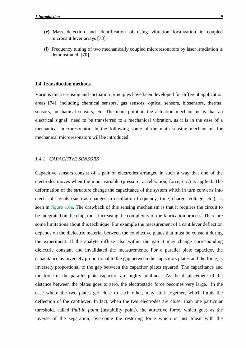
1 Introduction 9
(e) Mass detection and identification of using vibration localization in coupled
microcantilever arrays [73].
(f) Frequency tuning of two mechanically coupled microresonators by laser irradiation is
demonstrated. [70].
1.4 Transduction methods
Various micro-sensing and -actuation principles have been developed for different application
areas [74], including chemical sensors, gas sensors, optical sensors, biosensors, thermal
sensors, mechanical sensors, etc. The main point in the actuation mechanisms is that an
electrical signal need to be transferred to a mechanical vibration, as it is in the case of a
mechanical microresonator. In the following some of the main sensing mechanisms for
mechanical microresonators will be introduced.
1.4.1 CAPACITIVE SENSORS
Capacitive sensors consist of a pair of electrodes arranged in such a way that one of the
electrodes moves when the input variable (pressure, acceleration, force, etc.) is applied. The
deformation of the structure change the capacitance of the system which in turn converts into
electrical signals (such as changes in oscillation frequency, time, charge, voltage, etc.), as
seen in figure 1.6a. The drawback of this sensing mechanism is that it requires the circuit to
be integrated on the chip, thus, increasing the complexity of the fabrication process. There are
some limitations about this technique. For example the measurement of a cantilever deflection
depends on the dielectric material between the conductive plates that must be constant during
the experiment. If the analyte diffuse also within the gap it may change corresponding
dielectric constant and invalidated the measurements. For a parallel plate capacitor, the
capacitance, is inversely proportional to the gap between the capacitors plates and the force, is
inversely proportional to the gap between the capacitor plates squared. The capacitance and
the force of the parallel plate capacitor are highly nonlinear. As the displacement of the
distance between the plates goes to zero, the electrostatic force becomes very large. In the
case where the two plates get close to each other, may stick together, which limits the
deflection of the cantilever. In fact, when the two electrodes are closer than one particular
threshold, called Pull-in point (instability point), the attractive force, which goes as the
inverse of the separation, overcome the restoring force which is just linear with the

10 H. Pakdast
displacement, and the two arm collapse on each other. The scaling down of the electrodes or
cantilever will decrease the sensitivity as well, due to the fact that the capacitance of a
capacitor is proportional to its surface area. At this level the parasitic effects become more
than the actual detection signals. A capacitive sensor is fabricated based on cantilever-fingers
by Scott Miller et al, as shown in figure 1.6b.
Figure 1.6: Capacitive detection sensor based on cantilever. a) A schematic of capacitive detection and
electrostatic excitation [75]. b) An example on capacitive sensor on cantilever-fingers [76]
There are fix electrodes and movable electrodes. The cantilevers are movable electrodes, as
shown in figure 1.6b. The vibration of the movable electrodes is coming from the asymmetric
field which creates moving away from the substrate (fix electrodes). This system is very
sensitive to small changes in the distance and can be measured as well. The pull-in depends in
a capacitive system on the geometric quantities (i.e., not a function of spring constant, area,
etc.). The pull-in phenomena make constraint on the design of capacitive sensors and
actuators.
1.4.2 PIEZOELECTRIC SENSORS
Simply stated, piezoelectric materials produce a voltage in response to an applied force,
usually a uniaxial compressive force. Similarly, a change in dimensions can be induced by the
application of a voltage to a piezoelectric material. In this way they are very similar to electro-
strictive materials.
These materials are usually ceramics with a perovskite structure , see figure 1.7. The
a b

1 Introduction 11
perovskite structure exists in two crystallographic forms. Below the Curie temperature they
have a tetragonal structure and above the Curie temperature they transform into a cubic
structure. In the tetragonal state, each unit cell has an electric dipole, i.e. there is a small
charge differential between each end of the unit cell.
Figure 1.7: Shows the (a) tetragonal perovskite structure below the Curie temperature and the (b) cubic structure
above the Curie temperature [77].
A mechanical deformation (such as a compressive force) can decrease the separation between
the cations and anions which produces an internal field or voltage.
In MEMS applications, thin films of piezoelectric materials are deposited on the device,
usually by evaporation or sputtering, and are used as movement sensors and actuators. . By
applying an AC signal, the material will expand and compress at in time in request to the
applied DC and AC signal. When the mechanical modulation reaches the resonance
frequency of the resonator it is possible to induce large oscillations, orders of magnitude
larger than the actual displacements produced by the piezoelectric actuator, figure 1.8. The
QCM (Quartz crystal mass balance) is one example of commercial device using a
piezoelectric material, quartz, to put the detector into resonance frequency. A QCM device
works by sending an electrical signal through a gold-plated quartz crystal, figure 1.8b, which
causes a vibration at some resonant frequency

12 H. Pakdast
Figure 1.8: a) A schematic of piezoelectric actuation on a cantilever. Reproduced from [75] b) The QCM is a
piezoelectric mass-sensing device.
The PZT material as actuating mechanism has several advantages over other actuating
mechanisms. Since this sensor generates its own voltage, it does not require any further steps
in microfabrication processes. Therefore, the application of piezoelectric actuation has been
used in many biosensor applications. Furthermore, the piezoelectric effect depends only
linearly with the size, therefore also the smallest NEMS can be actuated with this approach. In
alternative, external piezo slab can be used to oscillate the whole MEMS chip as is used done
in AFM instruments operating in dynamic modes. Unfortunately in this way all the
eigenfrequencies of the whole chip are excited: a piezoelectric base excitation applied to the
ensemble of the cantilevers cannot efficiently excite many of the entangled coupled
eigenstates thus limiting the sensitivity of such arrays [69].
1.4.3 PIEZORESISTIVE SENSORS
A typical structure for a piezoresistive microsensor is shown in figure 1.9a. The resistor can
be produced by a selective doping by implantation or diffusion of the moving part in silicon
or by depositing a conductive layer with a significant piezoresistivity. To maximize the effect,
the resistor is usually located in the region where the displacement is larger e.g. in cantilevers
close to the fix end. The deflection of the cantilever induces a change of the resistor strain,
hence resulting in the resistance changing due to the piezoresistive effect in silicon. To
enhance the sensitivity, four piezoresistors could be made and connected into a Wheatstone
bridge configuration [78], thus obtaining a differential reading and minimizing the noise.
a b

1 Introduction 13
These kinds of built-in detection can make the fabrication process more complex, but can be
efficient for a fast response time.
The performance of piezoresistive microsensors varies with temperature and pressure. The
sensitivities of the sensors decrease as the temperature increases, while any residual stress
generated during the fabrication will also influence the sensitivities of the sensors. The
piezoresistive method is mostly used in static mode, because there cantilevers are thin and
softer and the forces generated by the adsorbed molecules result in large bendings. [79],
thereby it is easy to measure the quantitative of molecules by calculating the resistance
changes.
In some cases, the piezo resistance has been used also in dynamic mode, as in the experiment
illustrated in figure 1.9b. Here a very thin (10nm) layer of gold is deposited ontop of
insulating silicon nitride cantilevers that operate at very high frequency. Because of the
reduced thickness of the film, the change in the grain boundaries induced by the strain
produces a detectable effect in the resistance of the film itself.
Figure 1.9: a) A schematic of piezoelectric actuation on a cantilever. Reproduced from [75] b) The resistance
strain vs. frequency spectrum. There are four different lengths of cantilevers. The detection of resonant
frequency is done by piezoresistors. [20]
1.4.4 Optical actuation
The vibration modes can be excited by focusing a frequency-pulsed laser beam near the fix
end of the microcantilever. The laser induces a time-periodic temperature change around the
spot region, which gives a cantilever vibration via the periodic stress in the material.
Usually, the photothermal excitation of the cantilevers was achieved by a red laser diode
beam. It is a non-contact and local excitation of micromechanical resonator. The spot size can

14 H. Pakdast
be around 2-10 µm. One of the advantages of using photothermal actuation is that it can select
which spatial mode of a microcantilever can be excited.
Optical actuation has been demonstrated to work also a liquid environment [80]. The optical
actuation does not need any electrical connections on the device nor a specific fabrication
procedure and the most common approach of using a microcantilever with multilayer of
different thermal expansion coefficients will affect a deflection of the microcantilever when it
is heated by the absorption of the incoming laser beam, see figure 1.10.
Figure 1.10: An optical actuation technique. Reproduced from [75]
The photothermal excitation technique has been used by Datskos et al. [81] to illustrate that
the microcantilevers can be actuated by optically actuation, shown in figure 1.11.
Figure 1.11: a) The picture is a SEM image of different lengths and resonance frequencies. These
microcantilevers are made of gold-coated Silicon. b) An experimental result illustrates a frequency shift of the
smallest cantilever at the resonance frequency (f0=2.25 MHz) before and after adsorption of 11-
mercaptoundecanoic acid in air surrounding. [81]

1 Introduction 15
One example is illustrated in figure 1.11. This experiment is done with the gold-coated
Silicon microcantilever that has a resonance frequency at 2.25 MHz, see figure. 1.11a. It is
illustrated in figure 1.11b the measurements of before and after evaporation of the 11-
mercaptoundecanoic acid absorbed. The measurement is done in an air ambient, which means
that the damping has a big affect on the vibration of the cantilever.
1.4.5 Dielectric gradient force
A recently published paper by P. Quirin et al. [82] in Nature has illustrated that it is possible
to actuate any kind of dielectric materials in an inhomogeneous electric field. The basic
principle is that the electrodes, usually coated with gold, are connected to a DC (direct
current) and an RF (radio frequency) sources. The DC is applied to the electrodes and
indirectly polarize the resonator which should b made of a dielectric material, such as Silicon
nitride. The force that is created by the static voltage, VDC, can be modulated by applying RF.
This configuration can be able to excite the dielectric material, which in the case of the cited
paper was a double clamped beam, as shown in figure 1.12.
Figure 1.12: a) A depicted image of suspended double clamped beam of silicon nitride. The electrodes (yellow)
are connected to DC and RF. b) The suspended double clamped beam is actuated by dielectric force. [82]
There are both advantages and disadvantages for all the different actuation and detection
methods. The choice of the optimal approach depends highly on the environment and on the
specific application of the resonator with respect to the fabrication process. Furthermore, the
actuation and detection configurations are not limited, can be combined and interchanged
16 H. Pakdast
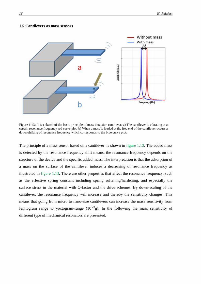
1.5 Cantilevers as mass sensors
Figure 1.13: It is a sketch of the basic principle of mass detection cantilever. a) The cantilever is vibrating at a
certain resonance frequency red curve plot. b) When a mass is loaded at the free end of the cantilever occurs a
down-shifting of resonance frequency which corresponds to the blue curve plot.
The principle of a mass sensor based on a cantilever is shown in figure 1.13. The added mass
is detected by the resonance frequency shift means, the resonance frequency depends on the
structure of the device and the specific added mass. The interpretation is that the adsorption of
a mass on the surface of the cantilever induces a decreasing of resonance frequency as
illustrated in figure 1.13. There are other properties that affect the resonance frequency, such
as the effective spring constant including spring softening/hardening, and especially the
surface stress in the material with Q-factor and the drive schemes. By down-scaling of the
cantilever, the resonance frequency will increase and thereby the sensitivity changes. This
means that going from micro to nano-size cantilevers can increase the mass sensitivity from
femtogram range to yoctogram-range (10-24
g). In the following the mass sensitivity of
different type of mechanical resonators are presented.

1 Introduction 17
a) The mass responsitivity is increased by doping the cantilever. Thereby increases Q-
factor. The resonance frequency of the cantilever is fres,0V=1.6 MHz for zero voltage,

18 H. Pakdast
gives a mass responsitivity of the cantilever 0.3 fg/Hz. The length, thickness and
thickness are l=40µm, w=2.3µm and t=5µm, respectively [83].
b) The SiC beam is double clamped. The resonator is in an ultra-high vacuum (UHV)
environment. The adsorbed mass is Au atoms that are generated by a thermal
evaporation source and travel towards the beam resonator. The mass of the Au atoms
are modulated by a shutter which could be registered by QCM. The NEMS resonator
is excited by RF bridge configuration and has a resonance frequency 32.8 MHz with a
mass sensitivity 2.53ag [84].
c) The circular disk with four arms are used to measure the mass of a prostate specific
antigen (PSA). The dimensions of the resonator is 6µm in diameter and the support
arms are 1µm wide. The mass sensitivity (equation 2.10 to 2.12) increases by having
thinner and lower density resonators. The large surface area is 54µm2 will increase the
probability of capturing analytes at extremely low concentrations, which may improve
sensitivity. The resonator was able to detect and measure the weight PSA to 55 zg. It
was mechanically excited by using PZT. The resonance frequency is 2.2 MHz and Q-
factor 6000 [85].
d) A microchannel with walls 2-3µm thick inside the cantilever. Under each cantilever
there is an electrostatic drive electrode and the cantilever vibration is detected by
optical laser. The microfluid cantilever can be measured in air with water inside. The
resonance frequencies are not significantly changed. The advantage of the device is
that it can measure the mass of objects that are not attached to the surface. The device
can measure with 300 ag precision. If the sizes of the microfluidic cantilever decreases
the precision of the mass will increase. [86]
e) An oscillator has dimensions l=4µm, w=500nm and t= 160nm made of siliconnitride.
Au dot is deposited on the paddle (1µmx1µm). This cantilever has a mass sensitivity
0.39 ag. The Au dot is used to measure the mass of thiolate self-assembled monolayers
(SAM), and demonstrate single dsDNA molecule sensitivity [61].
f) The NEMS resonator is a double clamped beam. The dimensions of the beam is l=
2.3µm, w=150nm and t=70nm and 100nm. The resonance frequencies are 133MHz
and 190MHz, respectively. The beam is actuated by RF-signal. The NEMS device is
cryogenically cooled down and in a ultrahigh vacuum. The adsorbed masses are Xe
and N2 molecules that are flux controlled by a mechanically shutter and a gas nozzle.
The device with 190 MHz is measured to 100 zg. The device with 133 MHz is
measuring to 200 zg [16].

1 Introduction 19
Some resonators were based on nanowires and nanotubes that have yoctogram-range (10-24
g)
in mass sensitivity.
g) The double-walled nanotube is placed in a vacuum chamber, where the Au atoms can be
evaporated during the oscillation. The initial resonance frequency is 328.5 MHz. The mass
responsivity is 0.104 MHz/zg (1zg=1x10-24
kg). The evaporation is controlled by a
mechanical shutter. The first time of opening of the shutter is measured to 51 Au atoms [87].
h) A cantilever nanowires are grown by CVD. The Si nanowires are actuated by peizoelectric
element and detected by an optical laser. The resonance frequency of this nanowire is
2MHz. The dimensions of the nanowire is diameter=40nm and length = 5µm. This gives a
mass sensitivity 10 zg [88].
Generally, the drawbacks of decreasing the dimensions of the cantilever will effect reduction
in the sample volume, detectable mass density, limiting effective mass [89] and providing a
high resonance frequency and Q-factor, but practically becomes difficult to fabricate as well
as detection of the vibration movements.
Detectors based on two weakly coupled cantilevers have two major limitations. (1) Upon
mass adsorption on one cantilever the initial symmetry is broken and the modes become
localized: in particular the cantilever under-going mass adsorption will have a greater
contribution to the high frequency mode while the reference cantilever will have a higher
oscillation amplitude on the low frequency mode; however, both cantilevers retain a nonzero
amplitude in their least significant mode and the mass adsorption event cannot be easily
recognized. (2) Unless the frequency is tuned, e.g., by stressing one cantilever as already
demonstrated for clamped beams [70.], the relative amplitude in the two modes is not
controllable. Upon mass adsorption the amplitude variation is relatively small and depends on
the initial amplitude.
In summary, we demonstrated reviewed the principal MEMS sensors, in particular cantilever
based MEMS sensors and actuation strategies have been presented. The advantages of
coupled cantilevers compared to single cantilevers have been elaborated. In this thesis, by
considering several advantages and disadvantages, we have used triple coupled cantilever
(TCC) sensor with optical and force gradient actuation strategies has been used for the mass
detection. A detailed design and introduction about TCC is demonstrated in chapter 2.

20 H. Pakdast
1.6 Thesis overview
The aim of this project is to design and fabricate triple coupled cantilevers (TCC).
Investigations of two actuation strategies are done. The one is with piezoelectric (pzt) and the
second one is the optical (laser). Finally, a totally new actuation strategy has been
implemented on the SiN Electrodes TCC design.
We will show through this thesis that TCC device is used for two applications. The first
application is for mass detection and the second is for micromechanical transistor. The main
focus has been on solving design and technological problems in fabrication process.
Three designs of TCC are:
Fabrication of TCC in silicon-on-insulator (SOI TCC), and actuation methods were
with piezoelectric (pzt) and optical (frequency puls-modulated laser) strategies. The
read-out was done with a normal CW green laser.
A new strategy of fabrication of TCC in silicon nitride (SiN TCC), the actuation
strategy was made by optical laser.
Further improvement of TCC design (SiN Electrodes TCC) was made to integrate the
electrodes with the cantilevers. The new actuation (dielectric interaction) mechanism
was possible to apply TCC device.
1.6.1 Outline of chapters
In chapter two the main points of microcantilever theory are analytically described for
simple resonator structures, such as static and dynamic modes. The main damping factors
(surrounding loss, structural damping and internal dissipation in a structure) in a
microcantilever are explained and described. The mechanics of a microcantilever system
is described. Theoretical explanations of choosing triple coupled cantilever configurations
are given.
In chapter three finite element analysis is presented. In this chapter the eigenfrequency
modes of TCC is simulated by using finite element method (FEM). This method gives us
the advantage to optimize the design (width and length) of the overhang of the TCC

1 Introduction 21
device. Several simulations were made such as the dependence of the displacement
amplitude ratio of the cantilevers with respect to the added masses. The dependence of the
dimensions of the overhang with respect to the frequency and displacement amplitudes.
In chapter four I will describe the fabrication process flow and the designs of TCC
devices (SOI TCC, SiN TCC and SiN Electrodes TCC) in detail.
In chapter five I will explains both the experimental measurements of TCC devices and
the experimental setup. The setup is custom built for frequency response measurement.
The experimental results of SOI TCC, SiN TCC and SiN Electrodes TCC are shown in this
chapter. There is a section with an optimization of the experimental setup with respect to
the actuation methods (piezoelectric and optical) and the rotation of the photodetector.
The SiN TCC is measured with two different sizes of silica beads for mass detection. The
FIB process is also used for a better control of removing materials. The results of TCC
devices are evaluated and discussed. Moreover, the chapter contains considerations and
proposal of a micromechanical transistor. In the last section I will present the
measurement done using another type of cantilever which has a paddle (200x200µm2) that
is suspended to a cantilever. These cantilever plus the paddle was used to grow cells on
top of the paddle and to measure their dried mass.
In chapter six conclusions are drawn.


2 THEORY OF MICROCANTILEVERS
2.1 Introduction
Microcantilever sensors rely on their motion to indicate sensing, where the motion could be
static deflection or dynamic oscillation in one or several resonance modes. Microcantilever
can be modeled as a cantilever beam having thickness, width and length and fixed at one of its
ends. This chapter describes the theory for the mechanical response of microcantilevers in
bending, lateral and torsional modes and array coupled cantilevers when used as sensors.
2.2 Static Mode
Static deflection occurs due to differential surface stress. A beam which experience a different
surface stress on two opposite sides, bends itself and the deflection δ is proportional to the
differential stress Δσ according to the Stoney’s equation:
( )
(
)
(2.1)
Where ν is Poisson's ratio, E is Young's
modulus, L is the beam length and t is the
cantilever thickness. This model is valid also
for microcantilever and by means of selective
functionalization of one side of the cantilever
it possible to transduce molecular adsorption
to mechanical bending. The selective
functionalization it is usually obtained by

24 H. Pakdast
exploiting gold-thiol interaction. Probe molecules are functionalized with a thiol group and
one side of the cantilever is coated with gold. Thiolated molecules covalently bind with the
gold substrate. [21] Subsequently the target molecules bind to the probes. Each step induces a
bending. Arrays of cantilevers allow to perform differential measurements to recognize
different molecules.
2.3 Dynamic mode
Mechanical system responds to an external oscillating force with different amplitudes as a
function of the frequency. The spectral distribution is characterized by peaks which are
known as resonant frequencies which correspond to oscillating modes. Small driving force at
the resonance can induce large oscillation. The load on the end of cantilever induces a
deflection which is linearly proportional to the force applied [90]. Therefore, it is natural to
introduce a lump element model to describe the dynamics of a cantilever. A dynamic
mechanical system in the scope of this chapter will be dealing with an oscillatory mechanical
microcantilever and is explained by a simplified model. This model contains a spring-mass-
damper elements, as depicted in figure 2.1, which can be described by a second-order
differential equation (2.2). On the left hand side of the equation (2.2) there are three different
forces and on the right hand side there is an external force f(ωextt). This equation (2.2) is a
well-known one in the classical mechanics: the second Newton’s law.
The different forces are the inertial force M =FI, this term is a product of mass and
acceleration, which is the kinetic energy of the system. The second term on the left hand side
is the damping force C =FD, which is a product of velocity and damping coefficient. The
energy dissipates in the system due to the different damping mechanisms that will be treated
later. There are many different models of the damping coefficients, but this is the commonly
used one and it is easier to calculate the equation (2.2) in the analytical calculation. The third
term on the left hand side is the restoring force kx=Fk, where k stands for the stiffness in the
material, e.g. silicon, silicon-nitride etc. and x for the displacement from the equilibrium point
which in cantilevers corresponds to cantilever deflection. The elastic deformation of the
resonator during the mechanical vibrations gives a potential energy. This is another well-
known law from the classical mechanics, which is called Hook’s law. While the resonator
oscillates there will automatically be a balance between the potential and kinetic energy. The
required energy to oscillate the resonator comes from the external applied force, f(ωextt). All
the terms are written in the following equation (2.2) [91].

2 Theory of Microcantilevers 25
Figure 2.1: It is a schematic drawing of an oscillating resonator. The m is representing the resonator
(microcantilever) which is connected to a spring, k, and dashpot, c. The resonator is moving in x-direction which
is indicated by x. The external force is applied from the left (black arrow). This model is called Lumped-
Element-Model.
( ) (2.2)
Where meff is the effective mass of the cantilever, k the spring constant, c is the damping, the
f(ωextt) is the external force and angular frequency ωext angular frequency. The equation can be
written into
The equation (2.2) is normalized with respect to the effective mass meff. Then the eqn. (2.2) is
expressed in following equation (2.3)
( )
(2.3)
( )
(2.4)
Where ω0 is the system’s eigenfrequency and β is a damping factor of the
system.
√
(2.5)
The stationary solution for equation (2.4) is
( ) (2.6)
After large t the transient is finished. This equation shows, A0 the maximum oscillation
amplitude of a mechanical resonator (cantilever) can be reached when the frequency of the
external force, ωext, is matching with the natural frequency, ω0, of the mechanical resonator
(cantilever). This phenomenon is known as a resonance frequency, as illustrated in figure 2.2.
The resonance frequency changes from different materials and dimensions of the mechanical
resonators. In the energy distribution point of view the kinetic and potential energy is equally
contributing at amplitude of the resonance frequency.

26 H. Pakdast
√(
)
(2.7)
The phase of the oscillation amplitude is defined as
(2.8)
Now, there are two variables that are called natural frequency ωo, and damping ratio, β,
[92,93]. The quality factor, Q, is defined as.
(2.9)
Further analyses show that the resonance frequency peak is dependent on the damping factor
which is included in the equation (2.7). In an ideal system or in a simulation program can the
damping parameter be described as zero (β=0). But in a real system there will always be a
damping, which causes that the vibration of the cantilever or mechanical resonator decreases
over a time.
2.4 Q-factor
The Q-factor or “quality” factor of the resonator is one of the most important factors in a
mechanical resonator, because it is related on how sensitive the mechanical resonators are in
the different environmental conditions. The definition of the Q-factor is the total energy
stored, Etot, in the resonator structure divided by the sum of the energy lost, E, from the
resonating element per cycle [75]. The Q-factor can be measured by looking at the amplitude
vs. frequency spectrum of the resonator as seen in figure 2.2.
As the Q-factor changes its value, meaning that different dissipation mechanisms and
intensities are involved, the oscillation amplitude and shape of a given resonance frequency is
modified as a consequence, in figure 2.2 the Q-factor value is changed from 1 to 1000, from
the orange curve to the red

2 Theory of Microcantilevers 27
Figure 2.2: Oscillation amplitude vs. frequency spectrum. The Q-factor values are changed from 1 to 1000. The
shape of the resonant frequency peaks are getting narrower.
The importance of the Q-factor can be observed in figure 2.2, since a high value of Q-factor
gives a sharp resonant peak, which is needed to accurately measure a resonant frequency
change (one-single-cantilever system). The Q-factor can be calculated in several ways. One of
the methods is to find a resonant frequency, fres, and divide this value by the bandwidth at the
3dB-amplitude point, f3dB.The most common way is to take the width of the resonance
frequency peak at full width half maximum (FWHM), as a direct measure of the damping of
the system. Q is then the resonance frequency divided by the FWHM. The various definition
of the Q-factor is given in equation (2.10):
(2.10)
In a real cantilever system the main Q-factor contributions are described in the following.
Other factors can further contribute but they will not be treated because of very less influence
on the cantilever system during the vibration. The main influential Q-factors are the
following:
1) Viscous and acoustic damping, Qa,
2) Qs, damping due to internal material parameters
3) Damping at the mechanical constraint, Qi, such as crystal structure,
lattice defects, etc.
The total Q-factor can be related to these individual Q-factors as 1/Q = 1/Qa + 1/Qs + 1/Qi
+….

28 H. Pakdast
2.4.1 The energy lost to a surrounding fluid (1/Qa):
The energy loss to the surrounding is the most important of the all the loss mechanisms.
These losses appear between the resonator and the surrounding gas. The losses depend on the
nature of the gas, surrounding gas pressure, size and shape of the resonator, the direction of
the resonator’s vibrations, and the surface of the resonator. In the case of vacuum these losses
can be made negligible therefore for high sensitivity applications the micromechanical
resonators are operated in the vacuum. Other damping mechanisms associated with
surrounding fluids are acoustic waves and squeezed film damping.
2.4.2 The energy coupled through the resonator’s supports to a surrounding solid (1/Qs):
The structural damping is related to the resonator constraint to the substrate. The vibration
energy of the resonator can be dissipated from the resonator through its supports to the
surrounding structure. If the supports are carefully designed this dissipation mechanism can
be significantly reduced. For instance, it possible to find the natural nodes in the vibrational
movement of a resonator (non-vibrational-points), as illustrated in figure 2.3, where the
supports can be placed to bond the resonator to the support.
Figure 2.3: A tuning fork where the bottom of the base is fixed.

2 Theory of Microcantilevers 29
The figure 2.3 shows that a careful design can really minimize the energy dissipation in the
supports. As it is illustrated in figure 2.3, the mechanical supports can be very important for a
mechanical resonator in order to minimize the energy dissipation, thereby increase the Q-
factor for the given mechanical resonator, in this case is a tuning fork.
2.4.3 The energy dissipated internally within the resonator’s material (1/Qi):
The last energy dissipation contributes come from the material of the resonator structure that
can play role in the value of the Q-factor. The presence of impurities in the crystal can give
lower Q-factor. It has been reported [75] that low-level impurity single-crystalline silicon
have resonator Q-factors of approximately 106 in vacuum, while highly boron doped single-
crystalline silicon resonators typically have a Q-factor of approximately 104. The conclusion
is that the just impurities (boron-doped) could reduce the value of the Q-factor with factor 100
The main energy losses that could be considered in a micromechanical resonator system,
combine together to the total quality factor, as in equation (2.11):
(2.11)
This equation expresses that the lowest Q-factor determines the total Q-factor. The most
influential affect on the Q-factor is the viscous and acoustic damping, Qa [94].
If the damping is negligible, the peak position of the lowest mode corresponds to the natural
frequency and is given by:
√
√
(2.12)
Where ρ is the density, E is Young’s modulus, t is thickness and L is the length of the
cantilever. If the damping is not negligible the peak it is not at the natural frequency but is
reduced by the factor √
(For Q-factor of 10 the reduction is 0.12%, for Q-factor of
1000 is 0.12 ppm). The adsorption of molecules changes the shape of the resonance curves
and thereby effects a shift in the resonance frequency. As first approximation, the mass of the
resonator increases by the quantity Δm which corresponds to the mass of adsorbed molecules.
According to equation 2.12 the resonance changes to the value:
30 H. Pakdast
√
(2.13)
assuming the elastic constant does not change. If the added mass is much smaller than the
mass of the resonator it is possible to obtain a linear relation between the shift in frequency
and the variation of mass:
(2.14)
2.5 Mechanics of Cantilever Systems
We described the motion of a particular cantilever in detail with the motion equation (2.2) and
with the corresponding damping parameter. The resonance frequency of a microcantilever
depends on the geometry and material properties. In general, there are three fundamental
resonance frequencies. The first is the bending in the vertical direction, the second is the
lateral and the last is the torsional vibrations. These fundamental resonance frequencies
characterize the dynamic motions of a given microcantilever. These resonance frequencies are
called natural vibrations.
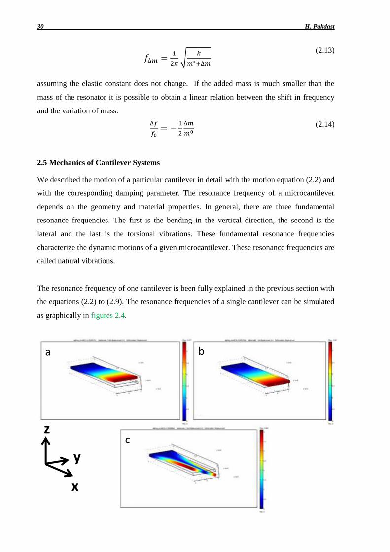
The resonance frequency of one cantilever is been fully explained in the previous section with
the equations (2.2) to (2.9). The resonance frequencies of a single cantilever can be simulated
as graphically in figures 2.4.
a b
c
z
x
y

2 Theory of Microcantilevers 31
Figure 2.4: The resonance frequency modes of a microcantilever. The dimensions are 100x20x2µm3. The colors
scale is proportional to displacement from the rest position going from zero (blue) to maximum (red). The
highest oscillation is at the free end. a) The first mode where the movement is in vertical (z) direction, b) the
second mode is only moving in lateral (x and y) directions and c) the last eigenmode has a torsional (twisting)
motion.
All the resonance frequencies that are shown in figure 2.4, can be calculated analytically, but
when the structure of the mechanical resonator becomes complex, then it is difficult to
calculate the eigenfrequencies analytically. Therefore, it is more convenient and less time-
consuming to apply the Finite Element Method (FEM), which we have applied in order to
find the fundamental of the vibrational modes. The FEM-software is used to solve the
resonance frequencies of more complex structures of microcantilevers that are mechanically
coupled together.
2.6 Triple Coupled Cantilevers (TCC)
The two coupled cantilevers by M. Spletzer et al. [68] have shown that it is more sensitive
than the frequency shift method. A schematic lumped element model of two identical
cantilevers are shown in figure 2.5a.
Figure 2.5: a) Schematic lump-element model of two identical coupled cantilevers. b) A SEM image of the
coupled cantilevers with gold-foil on one of the corners. C) The measurement before and after the mass is added.
Each cantilever is represented by a mass and spring K1, M1 or K2, M2 respectively. If the
added mass is zero ΔM=0, the spring constants of each cantilever is K=K1=K2. The common

32 H. Pakdast
coupling is the overhang which has a spring constant Kc. The ΔM represents the added mass to
the one of the cantilever as shown in figure 2.5a,b. If we are considering the first case where
K1=K2=K , M1=M2=M and ΔM=0. Then the cantilevers have the same spring constants as
well as masses and the oscillation amplitudes are shown in figure 2.5c that the lower
frequency corresponds to a symmetric and in phase eigenmode, where in higher frequency
corresponds to an antisymmetric and antiphase oscillation eigenmode. The point here is that
none of these modes are localized because the amplitudes of the displacements of each mass
(cantilever) are very close (in an ideal system the energy is equally partitioned between the
two modes, thus high frequency amplitude should be smaller by a factor (fs/fa)0.5
). The second
case is when the added mass is different from zero, ΔM≠0, the spring constants and masses
are different K1≠K2, M1≠M2, respectively. The added mass is breaking the symmetry of the
system and results in plot in figure 2.5c. The dotted lines show the added mass localizes the
eigenmodes, and it is clearly shown that the displacement amplitudes for either cantilever 1 or
2 in the corresponding eigenmodes oscillates more than the other.
Two important parameters can be expressed in term of the ratio κ=Kc/K. The shift of resonant
frequency of the modes is given by Δf/fo = ±2κ and the minimum mass detectable Δm/m is
proportional to Kc /(1+2K). It is clear that the mass sensitivity is maximized when the
coupling goes to zero and the first and second mode are closer than f0/Q = FWHM, or, in
other words, are experimentally indistinguishable. In their paper, Gil-Santos and coworkers
concluded that the two coupled cantilever system is never more sensitive than the single
cantilever counterpart. Therefore we have purposed three independent identical cantilevers
oscillate at the same frequency, see figure 2.6a. The spring elements are illustrating on the
cantilevers. The oscillation is three-fold degenerate. By adding a coupling element, see figure
2.6b, the degeneracy is split and three distinct modes, with different symmetry are generated,
as illustrated in figure 2.6.

2 Theory of Microcantilevers 33
Figure 2.6: The a) picture is showing the cantilevers are not coupled and the cantilevers have the same resonance
frequencies. In the b) picture the resonance frequencies are changed because of the coupling elements.
The three uncoupled cantilevers, figure 2.6a, are simulated in Comsol Multiphysics to
illustrate that the three uncoupled cantilevers have the same oscillation amplitudes, as
illustrated graphically in figure 2.6.
Figure 2.7: Three independent microcantilevers, where each of them is vibrating independently of each other.
The maximum oscillation amplitudes are the same for all of cantilevers. These cantilevers are not coupled at all,
therefore the resonance frequencies for identical independent cantilevers are the same.
The cantilevers are coupled as illustrated with coupling elements (springs) depicted in figure
2.6b, and thereby the dynamic behavior of each cantilever becomes dependent on each others.
The resonance frequency as shown in figure 2.7, each cantilevers have their own resonance
frequencies. With the coupling system the identical cantilevers have dependent resonance
frequencies as illustrated in figure 2.8
a b
c
z
x
y

34 H. Pakdast
Figure 2.8: The three microcantilevers are connected at the common base, which is called overhang. With
simulation program the correspondent frequency modes are simulated. In this case there are three fundamental
resonance frequencies. The red color is indicating the maximum oscillation amplitude and the blue color is
indicating the zero movement. a) the first mode which all the cantilevers are oscillating in the same phase and
direction as called symmetric mode. b) the second mode shows that the lateral cantilevers are moving in
antiphase and the central cantilever is not moving, also called antisymmetric mode. c) the third mode shows that
the central cantilever is moving in antiphase to the lateral cantilevers. The lateral cantilevers are moving in the
same direction and phase.
When the three identical microcantilevers are coupled as shown in figures 2.8, the mechanical
behavior will be significantly changed from that of a single cantilever. The coupling gives
three unique modes with distinct symmetry and increasing resonance frequency. The first
mode is characterized by all the microcantilevers oscillating at the same amplitude and phase.
The second mode shows that the central one is not moving and the lateral cantilevers are
moving in antiphase. The third mode is showing that the central one is moving more than the
lateral cantilevers. The lateral cantilevers are in the same phase than the central one.
In a conventional single cantilever system the detection of a mass is done by actuating the
microcantilever and thereby detecting the oscillation by optical detection. The cantilever is
measured before and after added mass. The frequency shift is calculated in order to find the
a b
c z
x
y

2 Theory of Microcantilevers 35
added mass.
Our proposal is an alternative way to detect masses without minimizing the dimensions of
microcantilevers further or applying expensive equipments such as ultra high vacuum. The
best performances and advantages of using a triple-coupled microcantilever systems are
obtained when the microcantilevers are in the 2nd
mode (or anti-symmetric mode), which is
shown in figure. 2.8b. One of crucial step is the microfabrication process in order to fabricate
perfect identical and symmetrical microcantilevers. In the simulation and experimental
chapters will be explained in more detail.

3 SIMULATION OF TRIPLE COUPLED CANTILEVER
(TCC) SYSTEMS
3.1 Introduction
The development of Finite Element Methods (FEM) spread the feasibility to design and
develop various products in various fields, especially in MEMS field. Number of designs
have been made in the area of BioMEMS, MOEMS, NEMS and is been continuing. Several
FEM simulation tools including ANSYS, Coventor, COMSOL Multiphysics etc., are
commercially available with several packages such as thermal, electromagnetic,
microfluidics, structural mechanics environments. Mostly, in structural mechanics
simulations, FEM helps excellently to understand the mechanical properties of the design
with visualizations, and also in reducing the cost and materials.
Finite element analysis (FEA) is used for simulating a range of engineering applications, such
as a mechanical structure. The structure is simulated and broken down into small elements, a
process called meshing. The idea is to simulate geometries similar to the cantilever devices
we have fabricated using microfabrication. The first step is to construct the structure of
interest and mesh it by a suitable mesh size. An example of a cantilever structure and its mesh
in COMSOL is shown in figure 3.1. The overall computational time depends on the size of
the mesh.

38 H. Pakdast
Figure 3.1: The model shows a mesh of TCC
COMSOL Multiphysics allows the users a detailed visualization of bends and twists of
structures with the accuracy which is required for most of the applications. COMSOL allows
entire designs to be constructed, refine and optimize whenever it is needed before going to
fabricate the devices. In this project, COMSOL tool with structural mechanics package was
used to design the TCC device. Also, various studies have performed such as dynamic
behavior of TCC to find out the minimum and maximum range of the length and width of the
overhang, vibrations in cantilever, symmetry break in the second mode, and finally relation
between added mass on the lateral cantilever with respect to the central cantilever.
In this project, the TCC device has been modeled as shown in figure 3.2, simulations have
been performed on the TCC before and after the added mass and investigated the dynamic
behavior of the device, observed that placing additional mass on one of the lateral cantilever
starts triggering the central cantilever. As shown clearly in figure 3.2, the overhang is
mechanically connected with the three cantilevers.
The purpose of the simulation was threefold. We aimed at find:
1) The fundamental resonant frequencies of TCC.
2) The dependence of resonant frequency and of the coupling on the dimension of the
overhang.

3 Simulation of Triple Coupled Cantilever (TCC) Systems 39
3) The relation between the added mass and oscillations of cantilevers especially, in the
second mode for the central cantilever.
Figure 3.2: A SEM image of TCC. The overhang is framed in red rectangular shape and the overhang is attached
to one side to the substrate.
3.2 Eigenfrequency Modes of TCC by using FEM Simulation
Figure 3.3: The three fundamental resonance frequencies are simulated by Comsol Multiphysics. Different colors
are indicating the vibration of TCC. The blue color represents non-displacement and the red stands for the
highest displacement of TCC. (a) Cantilevers are vibrating in the same direction and phase. This mode is called
symmetric mode. (b) The lateral cantilevers are vibrating in antiphase. The central cantilever is in non-vibrating
mode. This mode is called antisymmetric mode. (c) The lateral cantilevers are vibrating in the same directions
and phases compared to the central cantilever. This mode is called third mode. (d) The oscillation amplitude vs.
normalized width of each cantilever. The plots are taken from the displacement measured on the front-face of

40 H. Pakdast
each cantilever. All the modes are collected in one line plot, in order to have a better overview of all three
modes. The first, second and third modes are black, red and grey colors, respectively.
We first observed that three cantilevers generates three different eigenmodes as clearly
illustrated in figures 3.3, with corresponding shapes in figure 3.3a,b,c. The plots show the
displacement from the equilibrium position in false colors from dark blue to red. The
maximum displacement is localized at the free ends of the cantilevers. In the first mode all the
three cantilevers are in phase as illustrated in figure 3.3a, but, the central cantilever has a
lower oscillation amplitude in the first mode compared to the lateral (outer) cantilevers, as
plotted in figure 3.3a,d in black color This lower oscillation amplitude of the central
cantilever in the first eigenfrequency mode is related to the finite size of the overhang that do
not extend laterally beyond the cantilevers. If the size of the overhang (125 microns) is bigger
than the cantilevers, as illustrated in figure 3.4, then the difference in the displacement
amplitudes in all the three cantilevers are the same in the first mode.
Figure 3.4: width of the cantilever are drawn with respect to the displacement amplitude.
This will be discussed in detail in the section of optimization of the overhang. In the second
mode in figure 3.3b, the displacement of the central cantilever is on average equal to zero.
The third mode or the last fundamental mode of device, as shown in figure 3.3c the lateral
cantilevers are in the same phase and the central cantilever is in opposite phase to the lateral
cantilevers. Also for this mode, the extension of the overhang induce a more ideal ratio of the
oscillation amplitude and the central one has nearly twice the amplitude of the lateral ones.
The plot in figure 3.3d report on the x-axis the y coordinate of the simulated structure and in
the y-axis the displacement along z from the equilibrium position measured at the extreme

3 Simulation of Triple Coupled Cantilever (TCC) Systems 41
end of the cantilevers. The displacement is plotted only in correspondence of the cantilevers
while no data are plotted for the gaps. These simulation results clearly show how the three
coupled cantilevers of TCC device dynamically behaves. The main information we obtained
is the existence of a not negligible tilt around the cantilever x-axis, especially in the second
eigenmode. Here the central cantilever does not oscillate vertically but rotate along the central
axis with the same frequency. The presence of this rotation will require particular attention in
the measurement in laser deflection configuration, as we will see in the following. It is
important to notice here that these movements are not related to torsional eigenmodes which
have much higher resonance frequencies. These results are independent from the cantilever
length since they provide qualitative information which is valid for any cantilever/overhang
length.
3.3 Optimization of the overhang (width and length)
Overhang is nothing but a mechanical coupling of cantilevers. Overhang plays an important
role in the operation of the TCC device. The dimension of overhang decides the oscillation
amplitudes of each and every cantilever, as well as the amount of the frequency mode
splitting as shown in figure 3.7. In the simulation, the external edge of the overhang shown in
pink color in the figure 3.5 is fixed. There is only one boundary condition that is set to be
zero, which means that all the other edges or boundaries are free to move, as in the real
device. The three fundamental modes are obtained as represented in figure 3.3a,b and c. The
width and length of overhang are defined and optimized and are plotted in figure 3.6 and 3.7,
respectively.
The sequence of process steps performed using Comsol Multiphysics can be seen in the
appendix A. It is investigated from the results shown in figure 3.7 primarily, the maximum
and minimum width and lengths of overhang below certain stage effects the resonant
frequency, next, the behavior of device seems constant as the length of the cantilevers vary
from 50 to 100 microns. Results of TCC device having length of the cantilever 100 microns is
shown here in figure 3.7 and lengths 50 microns and 75 microns respectively are presented in
appendix B.
Simulation is the foundation for fabrication of device. Based on simulation knowledge, an
approach is made to fabricate the device. In fabrication, it is to be observed the overhang is
suspended to a membrane.

42 H. Pakdast
Figure 3.5: A typical drawing of a TCC device with the overhang. The pink color is showing the fixed edge. This
means the edge is fixed to a suspended membrane. This can be done by setting the boundary condition be zero.
Figure 3.6: Definition of the width and length of the overhang is represented.

3 Simulation of Triple Coupled Cantilever (TCC) Systems 43
Figure 3.7: The eigenfrequency dependence on the width and the length of overhang are plotted a and b,
respectively. The width is normalized to the width of TCC W0 =100microns.The length is normalized to the
length (100microns) of the cantilevers. The resonance frequencies are normalized. a) The resonance frequencies
increase slowly while the overhang width outside the external cantilevers. When the extension is comparable
with W0 no further is observed in all three modes. Plot b) is showing the region 0.10 to 0.20 where the overhang
length is optimal in order to achieve a coupling effect on all cantilevers. The region from 0.2 to 0.35 on plot b
shows that the coupling is giving three distinct modes as illustrated in a frame. The small simulation images are
showing the respective length and width of the overhang for all the modes that are plotted.
The width of the overhang in figure 3.7a, is varying from 100µm, which corresponds to
overhang not exceeding the lateral limit of the left and right cantilevers to 200µm which
corresponds to 50microns lateral extension of the overhang on both sides and is normalized.
The symmetry of the structure is maintained. The resonance frequency of three modes is a
function of normalized width of the overhang.
It is observed that in the initial point of the curve the resonance frequency depends on the
width, means, is increased with the increase of the width of the overhang, as the extra
overhang increases the rigidity of the systems. On the other hand, the extra mass added to the

44 H. Pakdast
system plays a minor role since it is placed in a region which is not subject to large
oscillation. Interestingly, when the width of the overhang reaches a value 1.5W0 in all the
three modes the curve starts to stabilize and/or saturate with respect to the resonance
frequency. So, beyond the value 1.5W0 in all the three modes, it is confirmed the resonance
frequency does not change significantly with increase in width. This information has been
used for an optimized design and fabrication of device, has an optimal width with stable
resonance frequency and the highest vibration amplitude. The next plot b), shows the effect of
the length of the overhang. The length of the overhang and the resonance frequency are
plotted in normalized units. There is a clear threshold for the onset of the cantilever coupling.
For overhang length shorter than one tenth of the cantilever length the three modes are still
degenerate in frequency and each one corresponds to the independent oscillation of one of the
three cantilevers. At longer overhang the degeneracy is splitted and the three modes with
different symmetry are observed. At increasing overhang length the resonance frequency for
each mode decreases, which is the joined consequence of the system mass and system overall
length increase, without a significant increase of longitudinal rigidity, as well as the frequency
splitting between the three modes, which derives from an increase of the coupling constant..
With this information, it is possible to design and fabricate the optimized TCC device that has
the highest sensitivity. The design and fabrication chapters, discuss how these values are used
to design a TCC that is fully optimized in both width and length of the overhang. In
particular, we choose to use the shorter possible overhang in order to reduce the system mass
and thus increase the sensitivity and to keep the three frequencies as close as possible, so that
they can be measured in a single frequency scan. The behavior oscillation amplitude with
respect to the length of the overhang is also simulated.
Figure 3.8 shows the ratio between the amplitude of a lateral cantilever in the first mode
versus that of the central cantilever in the second mode.

3 Simulation of Triple Coupled Cantilever (TCC) Systems 45
Figure 3.8: Oscillation amplitude versus overhang length in micro range. The different curves show the different
added masses. The pictures around the curves are the simulations of the resonance frequency of first, second and
third modes. The black continues line is without the mass has the smallest amplitude compared to the other
added masses (1pg, 10pg and 100pg).
As discussed earlier, an approach is made to prove the TCC device can be used as a mass
sensor. Simulations have been performed to investigate the performance of the TCC device.
Different masses of 1pg, 10pg and 100pg are added to one of the lateral cantilevers. The
results are shown in the figure 3.8. Different curves with different colors/sketches illustrate
different masses added to one of the lateral cantilever. The curve with black color is a case of

46 H. Pakdast
TCC device, in which the lateral cantilever without mass. As it is observed, when the length
of the overhang is below 10µm, the vibration amplitude is became zero in all the cases,
includes even cantilever without mass. The inset simulation images in figure 3.8e, f and g,
shows that TCC is behaving as a single, non-coupled individual cantilever system in all the
three modes. The highest vibration amplitude ratio occur around 10-15µm in length of
overhang. It is observed as the mass increases the oscillation amplitude increases. The inset
simulation images in figure 3.8b, c, and d, are showing that the coupling effect is working on
TCC. Then slowly the vibration amplitudes decrease and after 20µm, there is no affect on the
vibration amplitudes observed as the length of the overhang increases in all the cases. The
lowest peak value is when there is no mass. The highest peak value is due to heaviest mass
i.e. 100 pg. It means increase in mass gives increase in oscillation amplitude in the lateral
cantilever which is having no mass. An experiment is also performed with maximum applied
length of overhang, which may be around 100 microns. The simulation images in figure 3.8h,
i and j, shows the behavior of TCC when the overhang length is 100 microns. It gives the
information about the limitation of the overhang length in all the cases so as to predict the
device performance. From the figure 3.8 it emerged that the maximum variation of the
amplitude ratio upon mass addition is in the region where the length of the overhang is around
0.2-0.4. For shorter length the modes are not completely formed, and the amplitude slightly
depend on mass. For longer length the overhang contributes substantially to the cantilever
motion and sensitivity decreases. The selected range of the length of overhang gives the
necessary coupling effect to obtain the usual distinct modes with the highest vibration
amplitudes.
It is also been performed some studies on the width of the overhang as shown in figure 3.9.
Figure 3.9: The oscillation amplitude ratio versus width of overhang in microns. The red dots are the simulation

3 Simulation of Triple Coupled Cantilever (TCC) Systems 47
points. The minimum value of the width of the overhang can only be 100µm.
It is observed from the plot in figure 3.9 that increasing the width of the overhang can
increase the vibration amplitude less than a factor 7. The threshold value of the width of the
overhang is 145µm: below this value the amplitude ratio decreases. Above this value the
amplitude ratio does not change. This clearly conveys that the mass sensitivity can be
improved 7 times. On the other hand, it is very important to note that the TCC device is very
sensitive to any perturbation to the symmetry of the system, therefore it is very important to
have reproducible fabrication process. The larger the microfabricated area, the more defect
due to impurities, dust and errors. For these reasons we choose to sacrifice a factor 7 in
sensitivity and to keep the overhang width at its minimum to reduce the probability of defect
generation.
3.4 Added mass vs. Amplitude ratio
The difference in oscillation amplitudes of the central cantilever before and after that a mass
is added will give the exact value of the added mass, this method is called for mode
localization for the central cantilever. It is also possible to calculate the added mass by using
the conventional method, in which shift in the frequency can be observed due to the
application of added mass. One of the main advantages of TCC is that the added mass can be
calculated in any kind of environment without losing resolution; this is described in the
experimental results chapter. In this way it is possible to study the relation between the added
mass on one of the lateral cantilever with the ratio amplitudes. The ratio amplitude is intended
as the ratio of amplitude of the non-mass-lateral cantilever to the central cantilever. It is
observed, as the added mass increases, the oscillation amplitude of the central cantilever
increases, as illustrated in figure 3.10. The method used to realize the simulation is by adding
an artificial mass in the form of a box with known fixed size. Instead of increasing the
dimensions of the box, in this experiment, the mass density of the box is increased, thus
avoiding differences in the mesh at different added mass. Indeed the FEM results in the TCC
simulation are very sensitive to mesh. If the mesh is not sufficiently precise, it alone can break
the symmetry in the structure, and thereby the central cantilever result as vibrating even
without any additional added mass.

48 H. Pakdast
Figure 3.10: (a) This image is a simulation model of the TCC and the arrow is indicating the position of the
additional mass. The central cantilever is moving but for the low range of added masses is not visible in this
image. The added mass is 0.8 fg. (b) In this simulation image the added mass is 80 pg. The central cantilever is
visible in this image. This is a snapshot of one particular mass density is added, just to show that the central
cantilever is oscillating due the breaking symmetry. (c) The graph is a plot of the front-side-face of the three
cantilevers. The lines are representing oscillation amplitudes. The additional mass is on the right side as drawn
and shown in (a,b). As the added masses are increasing the oscillation amplitude of the central cantilever should
also be increased, as the color is getting close to the blue. The black color is showing the zero mass condition
and it is obvious that the structure is changed from added mass and after added mass.

3 Simulation of Triple Coupled Cantilever (TCC) Systems 49
A series of six simulations have been performed, added different masses: 0.8fg, 8.0fg, 80fg,
0.8pg, 8pg, 80pg to the cantilever shown in figure 3.10a. This particular TCC design in figure
3.10a has been used to demonstrate the sensitivity of mode localization in three coupled
cantilevers configuration. The grey arrow in figure 3.10a, b is indicating the position of the
additional mass on the lateral cantilever. It is observed that the amplitude of the central
cantilever has been increased by the application of mass 0.8fg and 80.0pg respectively on the
lateral cantilever as shown in the figure 3.10a and b. It is clearly observed that there is
vibration of the central cantilever when the mass is zero.
The position of added mass (box) is approximately close to the free end as at this particular
position the cantilevers have the highest oscillation amplitude. An attempt is made, all three
cantilevers are drawn from the front-face-side for the second mode in all six different added
masses are plotted in one plot as illustrated in figure 3.10c. In this way, the vibration
amplitude of the central cantilever can be observed as added mass is increasing. An
interesting observation is that vibration amplitude of the added-mass-lateral-cantilever
decrease with mass addition, while that of the not-added-mass-lateral-cantilever increases as
a result of center of mass balancing during oscillation. Also, as shown in figure 3.10d, a tilt in
the central cantilever is observed before and after deposition of the mass on the lateral
cantilever. Hence, it is concluded that the second mode of TCC design can be used as mass
detection sensor.
As shown in figure 3.10, that adding mass on the lateral cantilever will disturb the symmetry
of TCC, and the consequence is that the central cantilever starts to vibrate. The figure 3.10 has
also shown that adding more masses increases the vibration amplitude of the central
cantilever. The vibration amplitude of the non-mass lateral cantilever is in percentage less
increased compared to the central cantilever. The mass of box on 2x2x2µm3, with the same
material as used for TCC, but the density is changed. By changing the density of the box,
changes the mass of the box, and thereby the amplitude of the central cantilever increases, as
illustrated in figure 3.11.
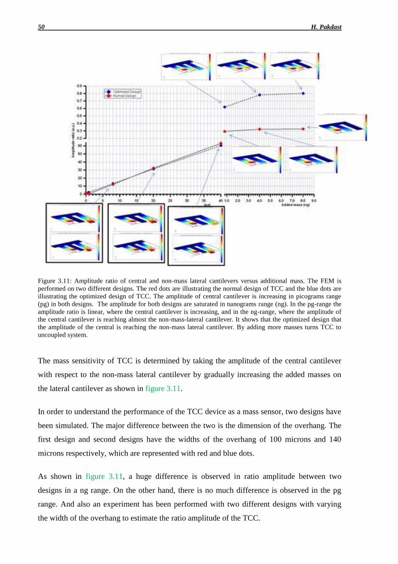
50 H. Pakdast
Figure 3.11: Amplitude ratio of central and non-mass lateral cantilevers versus additional mass. The FEM is
performed on two different designs. The red dots are illustrating the normal design of TCC and the blue dots are
illustrating the optimized design of TCC. The amplitude of central cantilever is increasing in picograms range
(pg) in both designs. The amplitude for both designs are saturated in nanograms range (ng). In the pg-range the
amplitude ratio is linear, where the central cantilever is increasing, and in the ng-range, where the amplitude of
the central cantilever is reaching almost the non-mass-lateral cantilever. It shows that the optimized design that
the amplitude of the central is reaching the non-mass lateral cantilever. By adding more masses turns TCC to
uncoupled system.
The mass sensitivity of TCC is determined by taking the amplitude of the central cantilever
with respect to the non-mass lateral cantilever by gradually increasing the added masses on
the lateral cantilever as shown in figure 3.11.
In order to understand the performance of the TCC device as a mass sensor, two designs have
been simulated. The major difference between the two is the dimension of the overhang. The
first design and second designs have the widths of the overhang of 100 microns and 140
microns respectively, which are represented with red and blue dots.
As shown in figure 3.11, a huge difference is observed in ratio amplitude between two
designs in a ng range. On the other hand, there is no much difference is observed in the pg
range. And also an experiment has been performed with two different designs with varying
the width of the overhang to estimate the ratio amplitude of the TCC.

3 Simulation of Triple Coupled Cantilever (TCC) Systems 51
From this it can be concluded that there is no significant improvements observed in ratio
amplitude between two designs in pg range. In the ng range, the ratio amplitude is not only
depending on the added mass but also on the width of the overhang. So, it can be finalized
that the TCC device no longer will work as mass sensor in a ng range and also no coupling
effect can be maintained between the cantilevers as shown in the inset simulation images in
figure 3.11 and figure 3.12. It should be noted, masses in fg range can be measured
comfortably using the proposed design, shown the figure 3.12.
Figure 3.12: Mass response expressed as the ratio of the amplitude in the second mode and the first mode
measured on the central cantilever versus the added mass express as a fraction of the cantilever mass. Dotted
line: overhang length 0.2; solid line: overhang length 0.4. The three oscillation mode sketched in the inset refer
to a situation in which the added mass is larger than 1% of the cantilever mass. In the lower frequency mode
only the loaded cantilever oscillate (left inset). At higher frequency the two unloaded cantilevers oscillate as two
coupled oscillator with quasi-symmetric (central inset) and quasi-antisymmetric (right inset) character.
It must be noted that in the real world it is demanding to fabricate the proposed TCC device as
there is always a movement of central cantilever due to the uncontrolled parameters
influences during the process of fabrication. However, in this project, at most care has been
taken to fabricate TCC device that can measure up to pg range, more details about the
fabrication process flow is discussed in the forthcoming chapters.
In conclusion, the detection of few molecules pushed the development of more and more
sensitive devices, which have been pursued mainly through downscaling of the devices. In
this thesis, the mass detection has shown that vibration localization in coupled

52 H. Pakdast
microcantilevers could represent an alternative strategy as a mass detection sensor.

4 DESIGN AND FABRICATION PROCESS OF TCC
4.1 Introduction
Microfabrication is at the basis of the Micro Electro Mechanical Systems (MEMS)
technology and is constituted by all the techniques which permit to fabricate structures with
dimensions from sub-millimiters to sub-microns. Microfabrication takes place in a particular
environment called “clean room” where particle, temperature and humidity are controlled. In
fact, if dust particles, which have dimension comparable with microstructure, land on a micro
fabricated device, they will ruin it. Moreover, in order to obtain robust and repeatable
processes, temperature and humidity must have always the same value with very low
fluctuations. The most studied and used material for fabrication is single crystalline silicon.
Another common substrate in MEMS technology is silicon on insulator (SOI). It consists in a
thick wafer of silicon covered by a thin thermal silicon oxide and of a thin crystalline layer of
silicon which may have several different crystallographic orientation in the device layer
while the thicker handle layer can be maintained on the most common <100> substrate. It
widely used in MEMS because by removing the insulator layer (called in this contest
sacrificial layer) it possible to make suspended structure. There are three fundamental
processes: lithography, etching and film deposition.
The fabrication approach used in MEMS devices can be classified into three general types;
bulk micromachining [95], surface micromachining [96] and high-aspect-ratio
micromachining (HARM) [97]. MEMS fabrication is similar to the fabrication of integrated
circuits, involves the addition or subtraction of two dimensional layers on/from a substrate
(usually silicon) based on photolithography and chemical etching. As a result, the 3
dimensional aspects of MEMS devices can be due to patterning and interaction of many 2D
layers. If required, additional layers may also be added using a variety of thin-film and
bonding techniques as well as by etching through sacrificial layers. On the other hand, the

54 H. Pakdast
complexity of the device may increase by the addition of independent structural layers.
4.1.1 Photolithography [98]:
A thin layer of an organic polymer, which is very sensitive to UV (ultraviolet) radiation, is
deposited on Silicon nitride or Silicon; this is called a photoresist (PR) and can be either
negative or positive: in positive PR polymer chains are broken by UV radiation, and become
soluble in specific solvents, named developer so that the exposed region can be removed. In
negative photoresist the polymers are cross-linked upon UV exposure and become insoluble
while the unexposed areas can be removed. A photolithographic mask made up of a quartz
(glass plate) which is a transparent in the UV spectral region, coated with a chromium pattern
(opaque), is placed in contact with the photoresist coated surface. The wafer is exposed to the
ultraviolet radiation transferring the pattern from the mask to the PR which is then developed.
On developing, the rinsing solution removes either the exposed areas or the unexposed areas
of PR leaving a pattern of bare and PR-coated Silicon nitride or Silicon on the surface of the
wafer. The resultant PR pattern is either the positive or negative image of the original pattern
of the photomask. The details of photolithographic process of TCC device is explained in the
forthcoming topics.
4.1.2 Bulk Micromachining Technique [95]:
Bulk micromachining involves the removal of part of the substrate. It is a process that uses
dry etching or a wet etching method.
Dry etching depends on vapour phase or plasma-based methods of etching using suitable
reactive gases usually at high temperatures. The most common form for MEMS is Reactive
Ion Etching (RIE) which utilizes additional energy in the form of Radio Frequency (RF)
power to drive the chemical reaction. Energetic ions are accelerated towards the sample to be
etched within a plasma phase supplying the additional energy needed for the reaction; as a
result the etching can occur at much lower temperatures (typically 150⁰C - 250⁰C, sometimes
room temperature) than those usually needed (above 1000⁰C). RIE is not limited by the
crystal planes in the silicon, and as a result, deep trenches and pits, or arbitrary shapes with
vertical walls can be etched [99].

4 Design and Fabrication Process of TCC 55
4.1.3 Wet Etching [100]:
Wet etching involves the removal of material through the immersion of a material (typically a
silicon or silicon nitride wafer) in a solution of a chemical etchant. These etchants can be
isotropic or anisotropic.
Isotropic etchants etch the material at the same rate in all directions, and consequently remove
material under the etch masks at the same rate as they etch through the material; this is known
as undercut. The most common form of isotropic silicon etch is HNA. A mixture of
hydrouoric acid (HF), nitric acid (HNO3), and acetic acid (CH3COOH), and lead to rounded
shape isotropic features in single crystalline silicon. HNA (hydrofluoric, nitric, acetic) is an
extremely aggressive acidic mixture which will vigorously attack silicon. It is an isotropic wet
etchant which etches silicon at a rate of approximately 1-3 microns per minute.
Anisotropic etchants etch faster in some crystallographic direction than in the others.
Potassium hydroxide (KOH) is the most common anisotropic etchant as it is relatively safe to
use. Structures formed in the substrate are dependent on the crystal orientation of the substrate
or wafer. Mostly such anisotropic etchants progress rapidly in the crystal direction
perpendicular to the <110> plane and less rapidly in the direction perpendicular to the <100>
plane. The direction perpendicular to the <111> plane etches very slowly [101].
4.1.4 Surface Micromachining [101]:
Surface micromachining involves the addition of material to the substrate in the form of
layers of thin films. These layers can either by structural layers or act as spacers, later to be
removed, they are known as sacrificial layers. Hence the process usually involves films of two
different materials: a structural material out of which the free standing structure is made
(generally polycrystalline silicon or polysilicon, silicon nitride and aluminum) and a
sacrificial material, deposited wherever either an open area or a free standing mechanical
structure is required.
4.1.5 Substrates [100]:
The most common substrate material for micromachining is silicon. The reasons to have
silicon are
Silicon is abundant and inexpensive material

56 H. Pakdast
Other crystalline semiconductors including germanium (Ge) and gallium arsenide
(GaAs) are used as substrate materials due to similar inherent features, but silicon is
distinguished from other semiconductors in that it can be readily oxidized to form a
chemically inert and electrically insulating surface layer of SiO2 on exposure to steam
at high temperatures.
The homogeneous crystal structure of silicon gives it the electrical properties needed
in microelectronic circuits, but in this form silicon also has desirable mechanical
properties.
Silicon forms the same type of crystal structure as diamond, and although the
interatomic bonds are much weaker, it is harder than most metals. In addition, it is
surprisingly resistant to mechanical stress, having a higher elastic limit than steel in
both tension and compression. Single crystal silicon also remains strong under
repeated cycles of tension and compression.
The crystalline orientation of silicon is important in the fabrication of MEMS devices
because some of the etchants used attack the crystal at different rates in different
directions.
Silicon is dominant as a substrate for MEMS but research and development is ongoing
with other non-semiconductor substrate materials including metals, glasses, quartz,
crystalline insulators, ceramics and polymers [102].
4.2 Design of TCC with Silicon nitride (SiN)
We used L-Edit software tool in this project, to draw the design of MEMS TCC device. These
designs are used to prepare the photolithographic mask. The process of photolithography is
explained in detail in the previous sections. Cantilevers and overhangs have been designed
using this software tool and can be observed in figure 4.1. The fabrication process is
explained in the next section.

4 Design and Fabrication Process of TCC 57
Figure 4.1: The cantilevers are mechanically coupled with an overhang. The lengths of the cantilevers are
varying for each step as written on top of the designs. As the lengths of the cantilevers are increasing the
resonance frequency is decreasing. The back-side mask is used for KOH opening widows. The black square is
used for spin coating of PR. The spin coater needs to hold the sample by vacuum, this can destroy the
membranes, and therefore the black square can prevent the breaking of the membranes during the rotation of
spin coater.
4.3 Fabrication process flow of SiN
We fabricated cantilevers (details in appendix C) starting from a bulk silicon wafers with a 2
micron-thick low-stress silicon nitride on both sides grown by LPCVD. The cantilevers are
thus made of silicon nitride.

58 H. Pakdast
Figure 4.2: Different steps of the fabrication process of TCC devices in silicon nitride are sketched.
1st step: The Si wafer is a commercial product available in the market. The thickness of the
silicon is 500µm. We used a wafer with 2 microns silicon nitride on both sides. The wafer is
cut in small pieces at 2x2cm2 so as to fit in vacuum chamber.
2nd
step: The fabrication process is done from the bottom of the sample. The photoresist is
deposited on the sample and photolithographic process is done with the back-side mask
design as shown in figure 4.1. The areas of PR which is not exposed to UV light will not be
developed. The areas of the PR which is exposed to UV light are removed.
3rd
step: In this step, we etched silicon nitride using Reactive Ion Etching (RIE). The sample
after photolithography process is place in RIE chamber. The sample and the chamber acts as a
two parallel plate capacitor. Different materials have different etch rates. Two different gases
CF4 and O2 with proper composition have been introduced in the chamber. 28.5 sccm of CF4
and 1.5 sccm of O2 are selected from the panel of RIE. An RF signal of 250V and 100W of
power is also applied. The gases inside the chamber are ionized and react with the surface of
the sample. 2 microns of silicon nitride has been etched in 30 minutes of process time. There
are two ways to find out that the etching is finished. The first way is to see any changes in
color from violet to green and silicon will remain as a combination of white and grey when
we tilt the sample. During the titling of the sample the color of the silicon nitride changes and
silicon will not change at all.

4 Design and Fabrication Process of TCC 59
The second way which is the safest way is to measure the height of the sample with a
profilometer. A profile meter is a tool that measures the height of the sample. If the etching
went successful the height of the silicon nitride and the silicon should be Δh =2 µm as
illustrated in figure 4.3.
Figure 4.3: The first layer is the silicon nitride and the second is the silicon. With a cantilever plus a tip the level
of silicon nitride and silicon is measured. The profiles of the heights of the two materials are sketched. The
profile meter is used to measure the height of different materials.
The unetched part of silicon nitride is used as a protection mask for silicon substrate in the
next step of fabrication process.
4th
step: We etching through the silicon substrate by using KOH solution. The sample is
immersed in solution of KOH having a concentration of 7.5M with a temperature of 70⁰C
kept approximately 7-8 hours time. The etch is observed along the crystal plane <111> can be
seen in the above figure 4.2. The etch shape is a pyramid, and the angle is 54.7⁰ [100].
5th
and 6th
steps: In these steps, we performed the fabrication processes on top of the sample.
The PR layer is deposited on the top of the silicon nitride membrane. This is the critical and
crucial step of fabrication of the TCC devices, as shown in step 6 of figure 4.2. The figure 4.4
shows that the TCC device has to be aligned with the edge of the suspended silicon nitride
membrane. Due to this step the overhang of TCC has been angled as shown in figure 4.4.
Δh
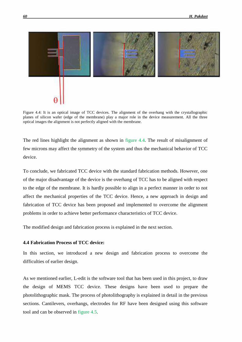
60 H. Pakdast
Figure 4.4: It is an optical image of TCC devices. The alignment of the overhang with the crystallographic
planes of silicon wafer (edge of the membrane) play a major role in the device measurement. All the three
optical images the alignment is not perfectly aligned with the membrane.
The red lines highlight the alignment as shown in figure 4.4. The result of misalignment of
few microns may affect the symmetry of the system and thus the mechanical behavior of TCC
device.
To conclude, we fabricated TCC device with the standard fabrication methods. However, one
of the major disadvantage of the device is the overhang of TCC has to be aligned with respect
to the edge of the membrane. It is hardly possible to align in a perfect manner in order to not
affect the mechanical properties of the TCC device. Hence, a new approach in design and
fabrication of TCC device has been proposed and implemented to overcome the alignment
problems in order to achieve better performance characteristics of TCC device.
The modified design and fabrication process is explained in the next section.
4.4 Fabrication Process of TCC device:
In this section, we introduced a new design and fabrication process to overcome the
difficulties of earlier design.
As we mentioned earlier, L-edit is the software tool that has been used in this project, to draw
the design of MEMS TCC device. These designs have been used to prepare the
photolithographic mask. The process of photolithography is explained in detail in the previous
sections. Cantilevers, overhangs, electrodes for RF have been designed using this software
tool and can be observed in figure 4.5.
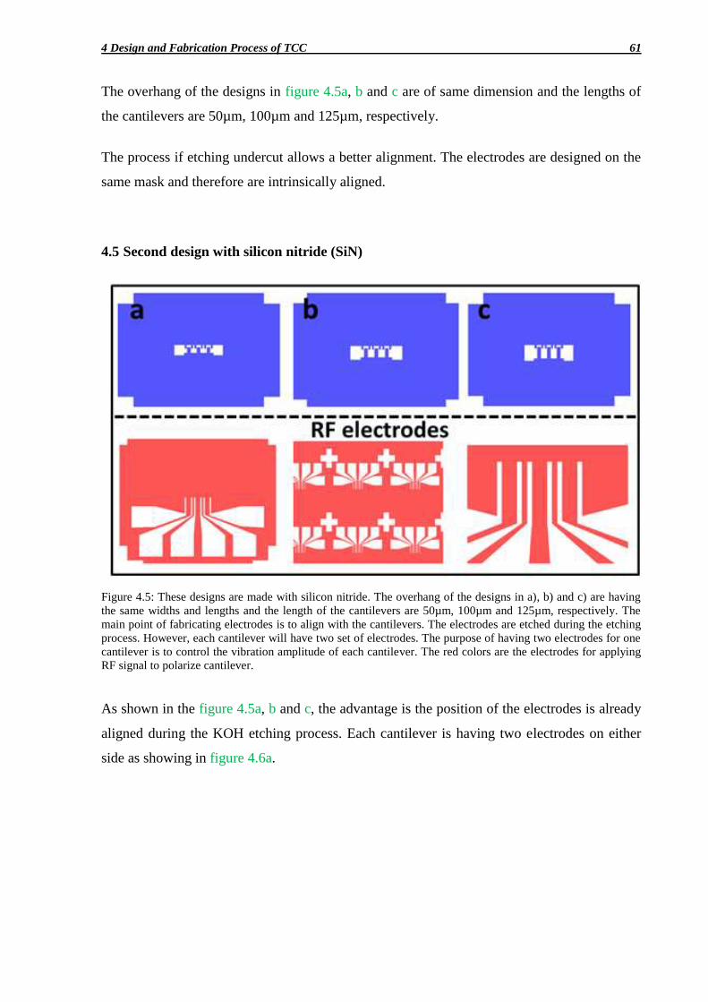
4 Design and Fabrication Process of TCC 61
The overhang of the designs in figure 4.5a, b and c are of same dimension and the lengths of
the cantilevers are 50µm, 100µm and 125µm, respectively.
The process if etching undercut allows a better alignment. The electrodes are designed on the
same mask and therefore are intrinsically aligned.
4.5 Second design with silicon nitride (SiN)
Figure 4.5: These designs are made with silicon nitride. The overhang of the designs in a), b) and c) are having
the same widths and lengths and the length of the cantilevers are 50µm, 100µm and 125µm, respectively. The
main point of fabricating electrodes is to align with the cantilevers. The electrodes are etched during the etching
process. However, each cantilever will have two set of electrodes. The purpose of having two electrodes for one
cantilever is to control the vibration amplitude of each cantilever. The red colors are the electrodes for applying
RF signal to polarize cantilever.
As shown in the figure 4.5a, b and c, the advantage is the position of the electrodes is already
aligned during the KOH etching process. Each cantilever is having two electrodes on either
side as showing in figure 4.6a.

62 H. Pakdast
Figure 4.6: The dimensions of the electrodes and cantilevers of TCC in silicon nitride. a) The cantilever is 50µm
in length, 75µm and 100 µm, respectively. The height of the overhang is constant in all the three designs. b) This
process needs two alignment marks. The first alignment is the square that is coming with making the TCC. c)
The alignment is to align the white cross with the square, as shown with the green circle when all the sides are
equally spaced, then the electrodes are aligned very well with the TCC cantilevers.

4 Design and Fabrication Process of TCC 63
4.6 Fabrication Process Flow of TCC device
Figure 4.7: The second approach of TCC fabricated in silicon nitride. The main steps are taken in this flow. The
whole processes are performed on the top of the TCC sample. The top views are to show the top of the surface of
the sample. The black lines illustrating the place the three steps are sketched.
1st step: In the first step, we transfer the designs of patterns, onto the surface of a substrate
using photolithographic process. Initially, the sample is coated with PR using spinner. A mask
as shown in figure 4.7 has been used for photolithographic process. The purpose of PR layer
is to protect the some part of the silicon nitride against RIE etching. The most critical action
in this step and in general for this process is a careful alignment along the <111>
crystallographic direction. Indeed wafer have always a “flat” indicating the crystallographic
direction. Since both mask edges and wafer flats are macroscopic, alignment is rather easy

64 H. Pakdast
and can be made with a significative precision.
2nd
step: In the second step, we etched the silicon nitride using Reactive Ion Etching (RIE).
The sample is place in RIE chamber after photolithographic process. The sample and the
chamber acts as a two parallel plate capacitor. Different materials have different etch rates.
Two different gases CF4 and O2 with proper composition is given in the chamber. 28.5sccm
of CF4 and 1.5sccm of O2 are selected from the panel of RIE. An RF signal of 250V and
100W of power is also applied. The gases inside the chamber are ionized and reacted with the
surface of the sample. It has been observed that 2 microns of silicon nitride has been etched in
30 minutes of process time.
3rd
step: In the third step, we etch the silicon substrate by using KOH wet etch process. The
sample is immersed in solution of KOH having a concentration of 7.5M with a temperature of
70⁰C kept approximately 4 hours time. The etch is observed along the crystal plane <111>. It
is to be observed that the overhang, cantilevers and electrodes are etched out at the same time.
The positions of the electrodes are self-aligned as discussed earlier.
After that we fabricated the electrodes. After the process of KOH etch, the sample is spin
coated using spinner with the two different materials. The first one is the Lift-Off Resist
(LOR 3B) and the second one is the PR (S1828). The LOR is used to make lift-off Au. The
corresponding mask is shown in figure 4.5 RF electrodes. More attention has been taken to
align the RF electrodes with the sample.
Finally, we deposited Gold (Au) on the top of the sample (or electrodes). Evaporation is a
common method of thin film deposition. The gold material is evaporated in a vacuum. The
vacuum allows vapor particles to travel directly to the sample, where they condense back to a
solid state. The final step is to make Lift-Off in a developer solution for 4-5 hours depending
on the thickness of the LOR thickness and baking time, 2µm and 180⁰C, respectively. The
etching along <111> crystal plane gives the cantilevers and location of the electrodes as
shown in figure 4.8.

4 Design and Fabrication Process of TCC 65
Figure 4.8: The final step of the fabrication process of TCC SiN device. The overhang, three cantilevers and the
place of the electrodes are very well aligned. The E-beam evaporation of Au layers is deposited and the Lift-off
is also done. The etching profile of KOH is clearly shown that the etching is along the <111> crystal plan.
The alignment of the RF-electrodes with the TCC mask as illustrated in figure 4.6c is done as
shown in figure 4.9.
Figure 4.9: The final prototype of TCC with the electrodes. a) The SEM image is taken from the top of the
sample. The RF-electrodes are aligned with the cantilevers. The two corners of the KOH-etched hole are metal
pieces. This is due to the Lift-off process. b) The optical image is showing a TCC device which the RF-
electrodes are very well aligned with the cantilevers.
In conclusion, we introduced and fabricated a new design of MEMS TCC with SiN material
using standard fabrication techniques. A perfect alignment between the cantilevers, overhang
Cantilevers Overhang
Electrodes KOH etching profile

66 H. Pakdast
and the electrodes has been achieved and is in good agreement with layout as shown in the
figure 4.9. This device has overcome all the difficulties such as alignment between the
overhang of TCC and membrane as shown in the figure 4.9.
We also attempt to fabricate the same design of TCC with Silicon On Insulator (SOI) material
to estimate the mechanical properties and the performance characteristics of the device. The
design and fabrication process of SOI TCC are explained in the next section and results are
quoted in the forthcoming sections.
4.7 Fabrication with Silicon on Insulator (SOI):
The same designs as shown in the figure 4.1 for overhang 25µm has been used in this section
and fabricated accordingly.
Figure 4.10: These designs of TCC are fabricated in SOI. The lengths of the cantilever start with 50µm increases
by 25µm as the line A is indicating. The separation of the cantilevers is 20µm between each other. The length of
100µm is fabricated as framed with a red line.
4.8 Fabrication process of SOI
As discussed, fabrication of TCC cantilevers consists of variety of different processes. In the
proposed case, TCC devices are fabricated from a commercial wafer of Si/SiO2/Si substrate
(SOI). The silicon oxide (SiO2) is etched to release the cantilevers in the final step, as shown
in figure 4.11.

4 Design and Fabrication Process of TCC 67
Figure 4.11: Fabrication process of SOI TCC device. There are three small squares that are defining the color
labels in the different process steps.
1st step: The SOI wafer is commercially available in the market and is used in this process.
2nd
and 3th
steps: We deposit 2 microns of PR on top of Si substrate using spinner. After
covering the sample with PR, defined the structures of TCC designs by using optical
lithography process. As illustrated in the previous sections, a photolithographic mask (black
squares), as illustrated in step 3 in figure 4.11, is used in an optical lithography process. The
designs of the mask of the cantilevers are illustrated in figure 4.10.
4th
step: The PR is developed in developer solution.
5th
step: In this step, silicon is etched using Reactive Ion Etching (RIE). The sample after
photolithography process is place in RIE chamber. Two different gases CF4 and O2 with
proper composition have been given in the chamber. 28.5sccm of CF4 and 1.5 sccm of O2
have been selected from the panel of RIE. An RF signal of 210V and 100W of power is also
applied. The gases inside the chamber are ionized and reacted with the surface of the sample.
It has been etched in 30 minutes of process time.

68 H. Pakdast
The last step or 6th
step: This process releases the cantilevers from the substrate. The
releasing process is done by using a HF-based buffered oxide etchant (BOE), as shown in step
6 in figure 4.11. BOE removes 100nm per min and the sample was in the solution for two
hours to remove more than 4 microns of SiO2 from the bottom of the cantilever. The
cantilevers are suspended to an overhang or to a base. The image in step 6 in figure 4.11 is
showing that the etching process profile of the overhang and base. The silicon oxide under the
cantilevers is also etched since the etching of silicon oxide is isotropic. At this point if the
sample is dried in room atmosphere, there is a problem with sticking. The cantilevers stick to
the Si base because the formation of small droplets of water between cantilevers and
substrates which pull down the cantilever due to water surface tension. In order to protect our
cantilevers from sticking problem we use a super critical phase drying. In this way it can be
protected cantilevers from drying. The space of the cantilevers and the substrate is less than 2
microns, as shown in figure 4.12.
Figure 4.12: These cantilevers are made in silicon. The red circles are illustrating the sticking area in the
cantilevers. The sticking happens only at the free ends of the cantilevers. a) and b) All the cantilevers are
suspended to a base. The cantilevers are sticking to the silicon oxide. c) The cantilevers are suspended to an
overhang. The sticking of the cantilevers is due to the distance between the cantilevers and the substrate. After
rinsing the cantilevers in the water, the sticking appears.
We observe the stick area at the free end of the cantilevers as shown in red circles of figure
4.12. This is due to the oxide etching. This may destroy the measurement because; the
cantilevers will not be able to vibrate.
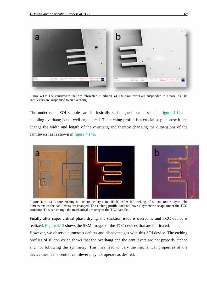
4 Design and Fabrication Process of TCC 69
Figure 4.13: The cantilevers that are fabricated in silicon. a) The cantilevers are suspended to a base. b) The
cantilevers are suspended to an overhang.
The undercut in SOI samples are intrinsically self-aligned, but as seen in figure 4.14 the
coupling overhang is not well engineered. The etching profile is a crucial step because it can
change the width and length of the overhang and thereby changing the dimensions of the
cantilevers, as is shown in figure 4.14b.
Figure 4.14: a) Before etching silicon oxide layer in HF. b) After HF etching of silicon oxide layer. The
dimensions of the cantilevers are changed. The etching profile does not have a symmetric shape under the TCC
structure. This can change the mechanical property of the TCC sample.
Finally after super critical phase drying, the sticktion issue is overcome and TCC device is
realized. Figure 4.13 shows the SEM images of the TCC devices that are fabricated.
However, we observe numerous defects and disadvantages with this SOI device. The etching
profiles of silicon oxide shows that the overhang and the cantilevers are not properly etched
and not following the symmetry. This may lead to vary the mechanical properties of the
device means the central cantilever may not operate as desired.


5 EXPERIMENTAL RESULTS
5.1 Introduction
In this chapter, frequency response measurements are described. As discussed in the previous
chapters, we fabricated three different designs with different fabrication processes. The three
designs are
TCC with SOI (SOI TCC) shown in figure 5.5c
TCC without electrodes (SiN TCC) shown in figure 5.7 , 5.8d and 5.9d
TCC with electrodes (SiN Electrodes TCC) shown in figure 5.12
The merits and demerit of each design have been discussed in the previous chapters.
We performed frequency and phase analysis with respect to the oscillation amplitudes on all
three cantilevers of all the above said three designs, initially on SOI TCC later with SiN TCC
and finally on SiN Electrodes TCC. The three kind of TCC devices are actuated with different
actuation strategies. Namely 1. Piezoelectric, which is most convenient, easy to operate [103]
2. Optical which is the most accurate in systems with many different resonances [81,104] and
3. Dielectric gradient force actuation (also called RF actuation), which the newly introduced
strategy and can easily integrable with electronics, [82] SOI TCC is actuated with both
piezoelectric and optical actuation method; SiN TCC is actuated with optical actuation; SiN
Electrodes TCC is actuated with both laser and dielectric gradient force actuation. An attempt
is made to investigate the most suitable actuation strategy for the TCC, the results are
presented in this chapter. Also, we investigated to make use the SiN TCC as a mass sensor and
a new approach is introduced to measure the mass as mode localization. SiN TCC is used in
this project to measure the mass of silica beads. The diameters of beads are 1 and 4 microns.

72 H. Pakdast
However, the deposition of the beads are not in easy to control therefore it was impossible to
locate the beads only at the very end of the cantilevers. On the contrary many beads were
observed at the overhang of the TCC device or along the length of the cantilevers as seen in
figure 5.7, figure 5.8d and 5.9d. This issue has overcome by using Focused Ion Beam (FIB)
technique which can be used to precisely position or remove a given mass with nanometric
resolution at the cost, however, of time consuming and very expensive process.
We also performed experiments to use the SiN Electrode TCC as Micromechanical Transistor
(µMT). We were motivated by an interesting article from the Roukes group in which an
interest in the article [105] RF MEMS devices for digital and analog applications were
proposed. We applied dielectric actuation strategy to the TCC in order to make use the SiN
Electrode TCC as mechanical transistor. By the simultaneous application of static voltage
(DC Voltage) and RF signal to the central cantilever and static voltage (DC Voltage) to the
one of the lateral cantilevers, results other lateral cantilever to vibrate. The vibration
amplitude can be controlled by the DC voltage. The behavior of this TCC device resembles
the function of a Field Effect Transistor (FET), where the gate voltage controls the current
flow in the channel. More explanation is given in the forthcoming sections. Experiments have
been performed on SiN Electrode TCC and the results are presented in this thesis.
Finally, an attempt to measure the mass of a cell and correlate it to bio-relevant informations,
such as genetic alterations is made on a single cantilever having paddle area of 200x200 µm2.
The resonance of the cantilever frequency was around 100-130 kHz and cells were grown
directly on the paddle. The idea was to measure the resonance frequency before and after the
growth of cell, in order to find out the quantitative weight of the fixe cells per cantilever. The
results are presented in this chapter.
5.2 Experimental setup
We measured the frequency response of TCC devices (SiN TCC, SiN Electrodes TCC and SOI
TCC) using a custom built experimental setup, as shown in figure 5.1. With this setup three
different actuation strategies can be implemented, such as piezoelectric, optical and dielectric
gradient force (RF), as explained in the introduction chapter. The setup consists of three main
sections. The first section is the actuation, the second section is the detection and the third
section is the readout electronics. The SOI TCC and SiN TCC devices utilize the two different
actuation schemes presented in experimental results chapter, on the other hand, SiN

5 Experimental Results 73
Electrodes TCC utilize the dielectric gradient force actuation scheme, because this actuation
scheme needs integrated electrodes. For the detection of the vibration amplitudes of the
cantilevers a detection system made with a light source (CW green laser), a photodetector
(4QP), beam splitters, focusing lens was assembled. The readout system was based on a
function generator, a Lock-in amplifier and a computer system for data acquisition with a
Labview-based acquisition software, as sketched in a diagram in figure 5.1.
Figure 5.1: This is a diagram of the experimental setup. The main sections are the actuation, detection and data
accumulation. The detection laser (green) is used to detect the vibration amplitude of every single cantilever. The
frequency pulsed laser (red) is to actuate TCC devices. On the inset SEM image is shown the positions of the
spots of the red and green lasers. The red laser spot is placed at the overhang. The green laser spot is placed at
the free end of the cantilever. The function generator is used to modulate the pulse of the red laser. One reference
signal from the function generator is connected to the Lock-in amplifier. The Lock-in amplifier will extract the
signal from 4QP and together with the reference signal generate a resonance frequency. The sample is mounted
in a vacuum chamber that can be moved in xy directions.
The TCC devices were mounted in a custom designed chamber with a base vacuum of 1x10⁻⁶
mbar. This chamber is designed in a way to be connected to a pump system, the RF-signals
connector, and equipped with suitable sample holder. The details of the drawing of the
chamber are in appendix D. The sample holder is on top of the chamber, as shown in figure
5.1 inset SEM image; the sample holder is covered by a transparent plastic, because the red

74 H. Pakdast
and green lasers have to be aligned, as shown in figure 5.1 inset SEM image.
The oscillations of the cantilevers were excited by a frequency-modulated red laser [106]
which is connected to a function generator. The laser actuation excites selectively those
resonance frequencies that are matching the naturally resonance frequencies of the TCC, as
presented in this chapter, figure 5.4.
The vibration amplitudes of the cantilevers were detected by an optical readout system as
shown in figure 5.2a. The system consists of a green laser and a four quadrant photodiode
(4QP) arranged in the optical lever configuration. The latter technique has been used to detect
cantilever oscillation amplitudes below 1 nm and therefore is particularly suitable to detect
small variation in low amplitude oscillators, as in our case [107]. The green laser beam
deflects via two beam-splitters (50%/50% cube beam splitter or prism) one focused onto the
TCC device using an optical microscope, as shown in figure 5.2b. A manual micropositioning
XY stage is used to move the whole chip with respect to the optical path in order to detect the
frequency response of each cantilever. The drive laser signal is removed from the optical lever
path using a band pass filter with optical density (OD) 6. A second manual micropositioning
XYZ stage is used to move the 4QP to maximize the signal and the rotation of 4QP that can
contribute to increase the signal as well as shown in figure 5.2c.

5 Experimental Results 75
Figure 5.2: Experimental setup images. a) and b) show front and side images of setup of a frequency-pulsed-
laser. c) A close view of the photodetector, focus lens, filter and the sample. d) A ceramic dual-in-line package is
used to mount the sample with electrical connections to be used for RF dielectric actuation purpose.
5.3 Optimization of Experimental Setup
Moving to SiN cantilever it was possible to obtain more symmetric structures with a very
small residual movement of the central cantilever in the second mode. However, it was
impossible to obtain zero movement. From FEM simulation, especially in the second mode
(antisymmetric mode), a torsional bending was observed with and without added masses on
the cantilever in figure 3.10. This is due to the bending of the whole structure which is
proportional to the vibration amplitude of the external cantilevers. This torsional mode is
present also in the case of a perfectly symmetrical structure. Our interest is to detect the
vertical motion of the cantilever and to decouple this information from the always present
torsional amplitude. The torsional bending can be reduced by rotating the photodetector. In
this way, the torsional bending is decoupled from the vertical vibrations. The frequency
response is measured before and after the rotation of the photodetector, in figure 5.3.
Figure 5.3: The oscillation amplitude versus resonance frequency. The red, black and grey lines are standing for
central, upper and down cantilevers, respectively. (a) The angle of the photodetector is not optimized. (b) The
angle of the photodetector is optimized.
The above measurements have been performed on the SiN TCC device.
5.4 Actuation methods (Piezoelectric and Optical actuation)
In this section, we suggested suitable actuation strategy in order to increase the sensitivity of
a b

76 H. Pakdast
the TCC device. Sensitivity of the device can be improved in several ways such as better
fabrication process, optimization of the experimental setup and selection of actuation strategy.
However, mainly, the actuation method is the key factor in determining the sensitivity.
Among several actuation strategies, piezoelectric and optical are the best suitable actuation
mechanisms [69]. Frequency response measurements is performed on SiN TCC by
considering two actuation strategies, the first actuation is to use the piezoelectric material to
give a mechanical motion to the sample. The piezoelectric material transforms into the
mechanical motion by applying RF signal to the material. The alternative actuation method is
the frequency modulated pulsed laser technique to excite the cantilevers of SiN TCC device.
The respective plots are shown in figure 5.4 below.
Figure 5.4: The vibration amplitude vs. frequency. The red line stands for optically actuation and the grey line
stands for piezoelectric actuation.
The piezoelectric actuation excites the desired resonance frequencies as expected. However,
there are some drawbacks for its use. Unwanted spurious frequencies involved in the
frequency spectrum is the one the main disadvantage of this actuation as shown in grey color
in figure 5.4. A macroscopic piezoelectric slab is placed in mechanical contact with the chip.
If we had piezo cantilevers, contacted individually, we will not have the same problems.
The piezoelectric actuation excites preferentially the first fundamental mode more than the
second and third. The reason is that in the first mode all the cantilever oscillate in phase and
therefore they can be excited all together at the same time by mechanical vibration. In second
and third mode, on the contrary, one or more cantilevers are in antiphase with respect to the

5 Experimental Results 77
other(s): therefore, when the whole chip is excited, part if the energy is transferred to the
wrong cantilever, and thus lost. The photothermal actuation on the contrary, can be focused
on one particular cantilever so that the maximum energy is transferred for each mode.
Moreover, an objective lens is used to focus the position of the excitation laser so that the
oscillation intensity can be maximized. As a consequence, as optical actuation excites equally
all the modes and the relative intensity respects the amount of energy stored in each mode
[108].
The laser beam excites the cantilevers while it focuses by using the objective lens at the
overhang of SiN TCC. The reason is the modulation of the spring constant is varied by the
laser beam by locally heating the spot area (and its temperature gradient), as a result the
material will thermally expand, which induces the compressive stress pushing the structure
into bending of cantilever [109]. The advantage of applying the optical actuation is it does not
require the oscillator to be conducting and no need of additional coils or electrodes located in
proximity to the oscillator. It can be easily integrated into existing, widely used optical
detection techniques.
5.5 Measurement of SOI TCC
In this design, we fabricated the cantilevers in silicon material. The details of fabrication
process are described in design and fabrication process chapter. The fabricated device of TCC
of silicon-on-Insulator (SOI) is shown in figure 5.5c.

78 H. Pakdast
Figure 5.5: The oscillation amplitude versus frequency. a) The measurements are done with the SOI-substrate.
Frequency response vs. normalized amplitude of TCC. The red and black colors are indicating the vibration
modes of the central and lateral (outer or external) cantilevers, respectively. The central and lateral cantilever is
symmetric in the first mode. b) Frequency response vs. phase of first and second modes. c) SEM image of SOI
TCC.
We measured the resonance frequencies of SOI TCC. The measurements are performed on the
central and one of outer cantilevers, as illustrated in figure 5.5a. The first and second
eigenmodes are 304 kHz and 318 kHz, respectively. The first mode shows that the central and
outer cantilevers are symmetric, as there is no frequency shift is observed. The central and
outer cantilevers are in same phase as plotted in figure 5.5b. The second mode in figure 5.5a,
illustrate the vibration amplitudes of the central and outer cantilevers. The red and black lines
are indicating the vibration amplitudes of the central and outer cantilevers, respectively. The
vibration amplitudes of the central cantilevers is only a factor 10 less compared to the
vibration amplitude of lateral cantilever, and show a finite oscillation amplitude which was
not expected from simulations. We attributed this effect to the defects generated in the
fabrication process such as improper wet etching as shown in figure 5.5c. It has shown in
chapter of Design and Fabrication Process that the etching of HF may create asymmetry in
the structure in a way that the dimensions of the outer cantilevers are different with the central
cantilever. The phase of the central cantilever in the second mode behave as expected, with
the two cantilevers which oscillate in phase (neglecting a factor 2) below the resonance
frequency, and oscillate in antiphase above the resonance frequency, which indicated that the

5 Experimental Results 79
central cantilever oscillate in phase with the non- measured lateral one, which in turn means
that the measured one is the heavier of the two is also different as illustrated in figure 5.5b.
5.6 SiN TCC as Mass Sensor
In the previous SOI TCC design the vibration amplitudes of the lateral cantilevers have factor
10 higher than the central cantilever. But, there is a necessity to improve this factor to have a
better sensitive device. Hence, we proposed and developed another with SiN material (SiN
TCC). In this SiN TCC design, a better fabrication process than SOI TCC has been carried out
and is presented in the Design and Fabrication Process Chapter 4. We observed from the
simulation results, addition of more masses to the SiN TCC results increase in the vibration
amplitude of central cantilever.
Figure 5.6: Beads on other device with 100 mircons. All the beads are deposited around the overhang, and few
beds are on the cantilevers.
In addition, a linear relationship is observed between non-mass lateral cantilever and the
central cantilever in the pg range. Investigations have been done to measure the mass of silica
beads of sizes 1 micron and 4 microns using the device. Experimental studies are performed
to observe the relation between added masses and the vibrational mode localization of SiN

80 H. Pakdast
TCC with other and better SiN TCC devices, as shown in figure 5.8d.
We have measured SiN TCC with three beads as shown in figure 5.7a and more beads shown
in figure 5.7c.
Figure 5.7: a) and b) are the same devices with different view . There are two beads on the right lateral cantilever
and one on the left lateral cantilever. Similarly, c) and d) are the same device with different view. e) frequency
response of the three modes before and after beads addition for the structure shown in panel a) and b)
The mass response measurement of device figure 5.7a is shown in panel e: Here it is
qualitatively clear that the system is still rather symmetric, since the single bead at the edge of
the left cantilever is compensated by the two beads in the middle of the right cantilever. The

5 Experimental Results 81
measurements confirm our assumptions: indeed all the resonance frequencies are lower
shifted upon mass addition, as expected, but the amplitude of the second mode for the central
cantilever does not change significantly, since the symmetry is quite preserved.
Figure 5.8d. shows clearly the mode localization of SiN TCC device.
Figure 5.8: Frequency response vs. vibration amplitude. a) This plot is performed before beads are added to the
TCC. The black stands for up cantilever, the red stands for the central cantilever and the grey is for down
cantilever. The three modes are measured for all the cantilevers. b) This plot is after beads are added. c) In this
plot before and after beads are added are plotted together. From the resonance frequency shift the added mass
can be calculated. d) A SEM image of TCC with the beads. e) Phase spectrum of the second mode after bead
adsorption. The gray curves refer to the lateral cantilever with beads, the black curves refer to the lateral
cantilever without beads, the red curves refer to the central cantilever.

82 H. Pakdast
In order to test the devices performances, silica microbeads with diameter of 4µm and 0.95
µm and weight of 73 pg and 0.98 pg respectively are used. Silica microbeads were dispersed
on the sample starting from a high dilute water-based suspension. Unfortunately this method
does not allow a precise location of the beads and only few devices resulted with a suitable
bead localization, as shown figure 5.6 for smaller beads and 5.8d. In figure 5.8d we display a
scanning electron microscopy (SEM) image showing one microbead at the extreme end of a
lateral cantilever, and several beads on the base of the cantilever and on the overhang. Figure
5.8c shows the frequency response of the first mode for the central and lateral cantilever
before (right) and after (left) mass addition. The recorded frequency shift corresponds to a
mass increase of about 16 pg; considering the 5 beads located along the cantilever, each
contributing a fraction (x/L), where x is the distance from the cantilever base and L the
cantilever length [110], this gives a bead mass of 9 pg, strongly underestimated. A FEM
analysis was performed to test and verify the x/L dependence of the frequency shift also for
TCC systems. Figure 5.8a and b shows the oscillation amplitudes relative to the second mode
recorded on the unloaded, loaded, and central cantilever (black, gray and red curve,
respectively) before and after the deposition of the silica bead. The amplitude ratio ρA
increases from about 10−3
to 0.08 thus providing a mass ratio of 1×10⁻²
that corresponds to an
added effective mass of 62 pg. We performed FEM analysis to investigate the dependence of
ρA on particle location along the lateral cantilever in a TCC system. The simulation showed
that ρA is proportional to (x/L)2. By weighing accordingly the contribution of each particle we
obtained 61 pg per bead, closer to the real value. The frequency shift based mass
determination error can be explained considering the stiffening of the cantilever elastic
constant induced by the bead interaction at the cantilever bases which shifts the resonance
frequency to higher values [111]. From this experiment we conclude that the mass
measurement using TCC systems is less affected by surface stress induced by mass location.
We also notice, that, in agreement to what should be expected from the general behavior of
mode localization [73], the loaded cantilever amplitude is reduced with respect to that of the
unloaded one. In figure 5.8e we report the phase behavior for the three cantilevers at the
second mode. Before crossing the second resonance the three cantilevers follow the excitation
with the same phase delay (180⁰). At resonance, the two external cantilevers vibrate in
antiphase, and the central one, follows the motion of the unloaded one. Far above the
resonance the three cantilevers are again all 180⁰ out-of-phases relative to the excitation, but
the loaded one has performed one extra cycle. The phase matching between mode resonances
for each cantilever is responsible for the asymmetric shape of the resonances [112]. By

5 Experimental Results 83
monitoring the phase response of the TCC system, the location of the adsorbed mass can be
therefore identified, regardless of the value of the added mass.
Figure 5.9: Frequency response measurement of another design of SIN TCC. This design has twice longer
cantilevers than the previous. a) All the three eigenmodes are shown in the same plot. The resonance frequency
measurements are performed before and after adding beads. The dotted lines are indicating no beads are added
and the continuous lines after beads are added. The black and grey colors are for outer cantilevers and the red
color is for central cantilever. b) The mode localization of the vibration of the central cantilever before and after
beads is added to the TCC. The black line is indicating the vibration without beads and the red line is showing
that the eigenmode is increased (more localized) due to deposition of beads. From the shift in the vibration
amplitude modes as illustrated the added mass can be found. c) A SEM image of SIN TCC with deposition of
beads on the overhang as well as on the outer-left-cantilever. d) A close SEM image of one bead on one of the
outer-left-cantilever.
To further investigate the experimental sensitivity limits of the TCC system and to explore the
possibility of minimizing the adsorption induced stiffening effect, in figure 5.9c,d SEM
picture shows TCC device in which two small silica bead have been located on one lateral
cantilever (the inset shows a detail of the two beads). The frequency response before and after
the bead addition is displayed in figure 5.9a,b where first and second mode response are
displayed. figure 5.9a shows the 200Hz frequency shift following the mass increase, measured
on the first vibration mode of the system. Considering that the particles are located 10

84 H. Pakdast
microns away from the cantilever extremity, the measured mass is 1.5 pg. On the other hand,
the relative amplitude increase in the second mode measured on the central cantilever and
shown in figure 5.9b is 0.0013 thus providing a mass ratio of 1.6×10⁻⁴
that, considering the
quadratic dependence on position along the cantilever, corresponds to an added mass of 1.6
pg. Here, because of the negligible size of the beads, the stress induced upon absorption is
negligible and the two methods are consistent with each other.
In conclusion, we demonstrated the application of the measurement of amplitude variation for
the determination of the absorbed mass in a TCC system. This approach exhibits sensitivity
comparable with the well established frequency shift method, when used in high vacuum and
with high quality factor cantilevers, and offers several additional advantages. Our technique is
less affected by the surface stress induced by mass adsorption along the cantilever; the
quadratic dependence on the adsorbing site position allows a more precise determination of
the mass location; using the oscillator phase response it is possible to identify the cantilever
onto which adsorption takes place. Further potential advantages are the insensitivity to the
adsorption of a nonspecific, uniformly distributed, mass (resulting, for instance, from
environmental contamination) that does not alter the symmetry of the system and therefore
only induces a frequency shift with no amplitude redistribution, and the weak dependence on
the quality factor of the oscillator, therefore on the operation environment of the device.
5.7 Focused Ion Beam with SiN TCC
We used FIB to make some cubic structures on the free end of the cantilever of silicon nitride
TCC, as SEM image is shown in figure 5.10. Each cubic structure has an area of (3μm)2 and
the thickness of the cubic structure is the same of the silicon nitride cantilever (2μm). The
dimension of the cubic structure is measured after FIB is performed. Each cubic structure has
a weight of 54 pg.
The FIB process is an extremely versatile technique which is used in research environment to
remove or deposit material on microstructures with nanometric spatial control. The
continuous down scaling of material science demands a corresponding focus on methods for
both investigation and manipulation of materials at that level. FIB is a very versatile technique
that has found use in different areas within especially semiconductor and materials research.
The principle of FIB is not very different from Scanning Electron Microscopy (SEM) and the
typical setups look in many ways similar. Ions are extracted from a Liquid Metal Ion Source

5 Experimental Results 85
(LMIS), which often is gallium that are kept liquid in the source and extracted from a tungsten
tip by a large potential, that also ionizes and accelerates the ions to typical energies of 5-100
keV down through the column. Electrostatic lenses condenses and focuses the ions while an
extraction voltage and plate apertures pick out a desired beam current by blanking the path of
outer ions. Secondary lenses are used to scan the ion beam across the surface. The reason for
using electrostatic lenses is because the normally used magnetic lenses in electron
microscopes need to be very large to condense the much heavier ions. [113] When ions strike
the surface of the sample different scattering processes can occur. Ions are much bigger and
heavier than electrons and hence they deliver their much higher energy density at a much
shorter distance than electrons. The ions impinge on the surface and interact with substrate
atoms in scattering processes. The ion-matter scattering can either have an elastic character
with nuclei or inelastic with electron. If the ions deliver enough energy to overcome the
binding energy of the surface atoms, these are physically sputtered away and either ventilated
out or redeposited in other areas. The sputtering of atom by the ion beam is referred to as FIB
milling. If the ions do not transfer the required amount of energy to sputter away atoms, they
instead enter the sample. Thus contaminating the original material [114,115].
Figure 5.10: The first cubic structure is made with FIB on one of the lateral cantilever. The dimension of the
cubic structure is measured after FIB is done. The volume of the cubic structure is 3x3x2μm. The TCC sample is
titled forward in order to perform the measurement of the thickness of the cubic structure.
The SiN TCC sample is measured after each FIB steps. The results are shown in figure 5.11.
We normalized all the plots with respect to the first modes as shown in figure 5.11. The lateral
cantilevers have black (outer up which means right cantilever) and grey (outer down which
means left cantilever) colors, respectively and the red color is for the central cantilever. The
ratio amplitude is between the amplitudes of the lateral cantilevers and the amplitude of the
central cantilever in the third mode, as illustrated in figure 5.11. The idea behind the FIB
experiment was to remove 60pg each time to test the TCC as a mass detection sensor. In this

86 H. Pakdast
way, the amount and the position of the removed material can be controlled with a
considerable advantage as compared to deposition of the silica beads in the previous section
where it resulted impossible to avoid the deposition of beads are around the overhang.
Moreover the aim of this experiment was to demonstrated that TTC system is sensitive to the
differential mass i.e. to the mass selectively adsorbed (or desorbed as in our case) from one
specific cantilever being on the contrary insensitive to unspecific adsorption.
The first cubic structure with FIB is performed as seen in figure 5.10, and the mass of the
cubic structure can be calculated by calculating the volume of the cubic structure and the
density, for Silicon nitride it is 3100 kg/m3 according to the Comsol Multiphysics.
As seen in figure 5.11, numbers of cubic structures are increasing from 1 to 3 and resultant
graphs are shown beside each design in figure 5.11b to d. We observed from the plots the
vibration amplitude of the central cantilever in the third mode increases with increase in the
number of cubic structures due to the imbalance in the structure. We also tried to bring back
to the balancing condition (one cubic structure case) by adding two cubic structures each on
two other cantilevers as shown in figure 5.11e. The steps and specifications are shown in table
1.

5 Experimental Results 87
Figure 5.11: Normalized amplitude of vibration of the cantilevers with respect to the frequency. There are five
plots of five different FIB steps. The red color is for the central cantilever, the black and grey colors are
indicating outer up (left) and down (right), respectively. A) In this plot the cantilevers are not drilled for any
cubic structures. The second mode for the amplitude of the central cantilever is around 1x10⁻²
. B) The first cubic
structure is made on one of the lateral cantilever and the amplitude of the central cantilever is increased to 8x10⁻¹
as indication of symmetry break in the structure. C) The second cubic structure is close to the first one. D) The
third cubic structure is made and the vibration amplitudes of outer cantilevers are not equally leveled in vibration
amplitudes. E) The last FIB step fourth cubic structures are done and the second mode has an unstable behavior
as compared to before.
All the cantilevers are measured for all the distinct modes (first, second and third), as seen in
figure 5.11. The second and third modes are normalized with respect to the vibration
amplitudes of first mode. The first plot in figure 5.11A, is measured before FIB process. The
second and third modes are showing a general TCC behavior.
The readout and actuation is performed by using the frequency pulsed lasers. The detection
laser is located close to the free end of the cantilever hence, the laser beam can be partially
diffracted by the cubic structure so that the overall intensity in one mode could result

88 H. Pakdast
diminished. A second possible explanation come from the well known fact that FIB operation
damage the substrate through the implantation of Ga+ ions which create defects which in turn
affect the resonance quality factor. Therefore the frequency measurement for the last step of
the FIB process did not show proper results, especially in the second mode for all the
cantilevers. Therefore, although the qualitative behavior is consistent with the initial
assumption we were not able to produce a quantitative agreement with second mode
simulation, as illustrated in figure 5.11D and E. In particular amplitude ratio did not follow a
linear relationship with the remode mass and did not recover completely after removing mass
from the other cantilevers. The third modes are having more reliable results and therefore we
display a table with all the ratio amplitudes for both down (right) and up (left) cantilevers with
respect to the central cantilever, see the table 1. The data do not show a linear trend though in
general the ratio increases with the increase of the asymmetry of the structure. The more
relevant result is that, when the structure recovers, at least partially, the symmetry the ratio
decreases again, showing that it depends on the localization of the mass rather than on the
overall added/removed mass.
FIB Steps Cubic structures
(60pg each)
Ratio (Up/Central) Ratio (Down/Central)
No FIB processing - 0.56 0.56
1 1 (same cantilever) 0.54 0.48
2 1 (same cantilever) 0.82 0.85
3 1 (same cantilever) 0.91 0.34
4 4 (central and the
other outer cantilever)
0.60 0.60
Table 1: The zero step in FIB step means that the TCC device was measured before the FIB process. The other
steps of FIB show that for each step one cubic structure was added to the one of the cantilever. 4 cubic structures
were added at the last step of FIB process. Two cubic structures are added to the central and to the one of the
outer cantilever. Calculation of the ratio amplitudes of the upper and down cantilevers are written with respect to
the central cantilever.
5.8 A proposal for a Micromechanical Transistor (µMT)
One particular field in MEMS that has a growing interest in the electronic and communication
markets [116] is RF-MEMS with various RF applications such as switches, resonators, and
filters etc. Operation of MEMS analog devices are based on the mechanical motion of a
resonator. The mechanical motion of the moving parts (cantilevers) is typically controlled by
a radio frequency signal force. Different attempts of MEMS switches and circuits can be
found in the literature [117,118,119].
The use of coupled cantilevers [120,70,105] for mechanical based logic elements have been

5 Experimental Results 89
already proposed in the past times. The MEMS devices are good candidates as alternative to
the traditional electronic components on the design of multiple RF devices [105,120] i.e.
mixers, on/off-switches, oscillators etc. These devices will improve the performance of an
electronic system, such as reducing costs, power consumption etc. [121,122] The
conventional electronic components of silicon such as FETs and PIN diodes have the
disadvantages [123] of high power consumption, low reliability, and high manufacturing cost.
The RF MEMS devices are offering miniaturization, integrating and better performance.
However, these semiconductor switches have poor isolation at high frequency operation.
The aim of this section is to mimic the Field Effect Transistors (FET) device in totally based
on mechanical coupled cantilevers transistor.
In traditional FET device, an electrical field gates the flow of electrical current through a
semiconductor. Instead of using an electrical signal, the new logic devices create the
switching field by mechanically deforming a cantilever. The coupled cantilevers are deformed
due to the electrostatic voltage (VDC), which lower the oscillation amplitudes of another
lateral cantilever. When we apply a RF-signal to across two Au-metal electrodes as shown in
figure 5.12, we create a field, which is sufficient to excite the SiN TCC Electrodes device into
a vibration. By applying a static voltage (VDC) on another cantilever, the cantilever motion
will be damped due to the cantilever attraction to the maximum point of the electric field. This
can work as damping factor for the whole system, in other words, the DC bias will serve as a
gating voltage. This type of device would allow mechanical action to be interfaced with
electronics, and could be the basis for a new form of logic device that uses the mechanical
resonator instead of field effect transistor. The mechanical alternative to the electronic FET
could be extremely advantageous in all those particular conditions where electronics fails,
such as at extremely low temperatures, where electrons are frozen inside the semiconductor,
or in harsh environment, where surface chemistry determine the response of superficial
electron channels, or in presence of damaging radiation that can affect the conductive
properties in semiconductor-based transistors.
The SiN TCC Electrodes are actuated by the dielectric gradient force. In the following section
the actuation will be implemented and applied on the SiN TCC Electrodes.
5.8.1 Dielectric gradient force actuation
The new drive scheme is integrated with the cantilevers. It is a local actuation for arbitrary
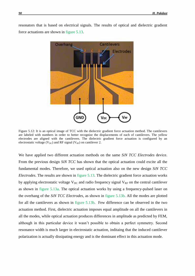
90 H. Pakdast
resonators that is based on electrical signals. The results of optical and dielectric gradient
force actuations are shown in figure 5.13.
Figure 5.12: It is an optical image of TCC with the dielectric gradient force actuation method. The cantilevers
are labeled with numbers in order to better recognize the displacements of each of cantilevers. The yellow
electrodes are aligned with the cantilevers. The dielectric gradient force actuation is configured by an
electrostatic voltage (VDC) and RF signal (VRF) on cantilever 2.
We have applied two different actuation methods on the same SiN TCC Electrodes device.
From the previous design SiN TCC has shown that the optical actuation could excite all the
fundamental modes. Therefore, we used optical actuation also on the new design SiN TCC
Electrodes. The results are shown in figure 5.13. The dielectric gradient force actuation works
by applying electrostatic voltage VDC and radio frequency signal VRF on the central cantilever
as shown in figure 5.13a. The optical actuation works by using a frequency-pulsed laser on
the overhang of the SiN TCC Electrodes, as shown in figure 5.13b. All the modes are plotted
for all the cantilevers as shown in figure 5.13b. Few difference can be observed in the two
actuation method. First, dielectric actuation imposes equal amplitude on all the cantilevers in
all the modes, while optical actuation produces differences in amplitude as predicted by FEM,
although in this particular device it wasn’t possible to obtain a perfect symmetry. Second
resonance width is much larger in electrostatic actuation, inditaing that the induced cantilever
polarization is actually dissipating energy and is the dominant effect in this actuation mode.

5 Experimental Results 91
Figure 5.13: Plot of frequency response vs. displacement amplitude. The black and grey is representing the
lateral cantilevers, respectively. The red stands for central cantilever. Two different actuation techniques are
used. a) the dielectric gradient force actuation method is used and all the modes are shown as it is the case of the
optical actuation. b) the frequency-pulsed laser is used on the new design SiN TCC Electrodes. The modes are
comparable with the dielectric gradient force technique.
We have shown that a dielectric cantilever can oscillate when a static voltage applies with a
modulation signal, then the cantilever attracts towards the maximum field strength because of
the inhomogeneous electric field, as shown in figure 5.13a. The inhomogeneous field in the
cantilever is created by two Au-electrodes, as shown in figure 5.12 for the central cantilever.
A static voltage VDC applied to the electrodes induces a strong dipolar moment in the
cantilever that in turn experiences an attractive force directed towards the electrodes.
Modulating VDC with an RF-signal VRF gives rise to an oscillating force component that
drives the cantilever perpendicularly to the sample plane.
We apply a static voltage on one of the oscillating lateral cantilevers. The static voltage is also

92 H. Pakdast
a spatially non-uniform field; thereby the cantilever will try to remain in the maximum field
region and a restoring force against the motion will be developed, decreasing the oscillation
amplitude. The field force works like a damping force for the applied lateral cantilevers,
because of the polarization dissipation mentioned before. Thanks to the fact that the TCC
system is made of three strongly entangled cantilevers which are, on the other hand, spatially
separated, it is possible to create on the same oscillator a damping field separated from the
oscillating field. In spite of the fact that the two are applied to two distinct cantilevers, they
affect the same oscillating system exactly in the same way two distinct voltages, VSD and VG,
affect the current in the channel of a FET. It is worth to stress here that, if a DC voltage is
applied on the same cantilever on which the RF voltage is applied, the oscillation amplitude is
increased by a factor 1 + VDC/VRF .
With these two properties:
Applying VDC and VRF on central cantilever
Applying Vdamping on one of the lateral cantilevers
These two properties together to conceive a sort of micromechanical transistor
Before the micromechanical transistor introduces, the FET device is explained, because the
micromechanical transistor has many similarities with FET device.
5.9 Field Effect Transistor (FET)
In this section the concept of FET device will be presented. We can make an analogy between
the FET device and the micromechanical transistor. In the figure 5.14, the FET device will be
introduced in a simple schematic diagram.
Figure 5.14: A schematic of diagram of Field Effect Transistor (FET) in cross section. a) The S stands for
source, D is drain current and the G is representing gate voltage. The current is flowing from the source to the

5 Experimental Results 93
drain, IDS. The gate voltage, VG, is controlling the current between the source and drain channel as shown with
the blue color. b) The I-V characteristic of FET is shown. In the initial stage of the VDS and ID is linear. When the
VDS, is reaching the threshold value starts the ID to saturate. The level of the ID is decided by the gate voltage.
[124]
The I-V characteristic behavior of FET device can be divided in three regions. The first region
or called cut off, the current is zero (ID=0) and the FET device is acting as an insulator, when
the VDS is smaller than the pinched off voltage (Vt). In the second region, the FET device is
acting like a linear resistor because the value of the drain-source voltage (VDS) is > pinched
voltage (Vt) as shown in figure 5.14b. The third region, or called the saturation region, where
the FET device is controlled by the gate voltage (VG), means that the current is not increasing
further as the drain-source voltage is increasing. We can see that for a given value of gate
voltage (VG), the current is constant. If the voltage gate, VG1 negatively increases, the
conduction channel will narrow and the current flow between the source and the drain will be
reduced, as it is shown in figure 5.14b. The first gate voltage VG1 is usually zero; therefore the
ID has the highest current flow. When the gate voltage VG4 is reached a sufficient enough
negative value the channel will stop flow of the current between the source and drain channel,
also called cut off [124], as is shown in figure 5.14b.
The main three operations of FET are:
1) Cut-off regime where no channel exists (Vt>VG) and ID = 0 for any VDS
2) Linear resistor regime (VG > Vt).
3) Saturation regime in which the channel is pinched means (VG>Vt) and ID is
not increased as VDS increases.
The final goal of the project is the development of a full micromechanical transistor using SiN
Electrodes TCC. In a transistor a high power signal is controlled by a low power signal, thus
obtaining amplification. In a FET device, at VDS (the input voltage) constant, the output
current IDS is controlled by the Gate Voltage, VG. Since IG is negligible, the FET acts as an
amplifier. In our device an oscillating bias VRF applied to one cantilever 2 is used to put the
three cantilevers in oscillation, as seen in figure 5.12. A second cantilever is exposed to a DC
bias that damps the cantilever motion, which is detected on the third cantilever. So, the
oscillation amplitude of the SiN Electrodes TCC is controlled by the DC signal, which, having
no RF components is a low power signal, while both excitation and oscillation are RF signal
and thus high power signal. Therefore we obtain an amplification effect. Proof of principle
investigations were performed and suggest that the device proposed is working as expected.

94 H. Pakdast
In the following the analogy of FET and µmechanical transistor are listed.
The saturation region in a FET device is related to the no current increases further as drain-
source voltage increases. The saturation region for micromechanical transistor is illustrated
by figure 5.15.
Figure 5.15: Oscillation amplitude vs. frequency for a given resonator. a) The black line is taken at the peak-
value of the lowest oscillation amplitude. The points are plotted in the right side. b) Oscillation amplitude vs.
actuation voltage (VRF). It is clear that the actuation voltage is linear to certain value, and then the oscillation
amplitude starts to reach a plateau [125].
The magnitude response curves at various driving amplitudes are shown in figure 5.15a. At
large amplitudes, the frequency response becomes nonlinear due to second order mechanical
properties such as stretching of the resonator. The deflection of the resonator shows that with
modest excitation voltages, motion beyond the onset of nonlinearity [126] is obtained. At
larger excitations the oscillation amplitude is increased and the resonator is stretched, and, as
in guitar strings under tension, the resonance frequency is shifted to higher values. As the
frequency is swept from low to high, it reaches a point that is no longer stable and so it
rapidly switches to the next stable state at lower amplitude.
The overall effect is that exciting the mechanical resonator at fixed frequency above a certain
amplitude the oscillation amplitude is not going to increase as actuation voltage (VRF)
increases, as shown in figure 5.15b.
FET
VDS
VG
IDS
µMT
Actuation amplitude VRF
Damping voltage VDC
Oscillation amplitude
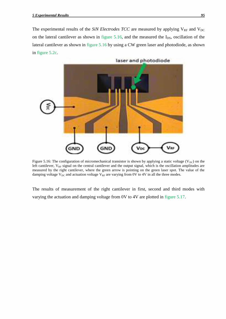
5 Experimental Results 95
The experimental results of the SiN Electrodes TCC are measured by applying VRF and VDC
on the lateral cantilever as shown in figure 5.16, and the measured the IDS, oscillation of the
lateral cantilever as shown in figure 5.16 by using a CW green laser and photodiode, as shown
in figure 5.2c.
Figure 5.16: The configuration of micromechanical transistor is shown by applying a static voltage (VDC) on the
left cantilever, VRF signal on the central cantilever and the output signal, which is the oscillation amplitudes are
measured by the right cantilever, where the green arrow is pointing on the green laser spot. The value of the
damping voltage VDC and actuation voltage VRF are varying from 0V to 4V in all the three modes.
The results of measurement of the right cantilever in first, second and third modes with
varying the actuation and damping voltage from 0V to 4V are plotted in figure 5.17.

96 H. Pakdast
Figure 5.17: Oscillation amplitude vs. actuation voltage. The actuation and damping voltage is from 0V to 4V,
respectively. The oscillation amplitude of the right cantilever is decreasing in the five damping voltage values.
The results of micromechanical transistor has shown that it has the tendency of the FET
device in the linear resistor regime. The results do not show the saturation regime; which is
more easily obtained in microbridges, which are clamped at the two ends and therefore
experience larger non linear effect. On the other hand the TCC approach can be applied also
to suspended microbridges, therefore more investigation in the direction are envisaged.
However, our work with coupled cantilever transistor device provides a first implementation
of a new approach to analog operations that performs mechanical-electrical actions in one
structural unit using a single material. This new family of transistors-like micromechanical
devices could provide new processing and memory capabilities in very small and portable
devices.

5 Experimental Results 97
5.10 Cell Growth on Cantilever
We performed an preliminary experiment on GT1 cells which are used as a neuronal cell
hypothalamic cell line. The GT1 cells are grown on the cantilevers according to the protocol
explained by Didonna A. et al [127]. Those cells are grown on the cantilever, as shown in
figure 5.18a, 5.19a. The cells grow well on the cantilevers and the images in figure 5.18b,
5.19b show that the cells were grown on the cantilever and close to the edge of the paddle.
Using the standard protocol for fluorescence to recognize the nuclei to define number of cells
are shown in figure 5.18b and 5.19b.
With the technique of resonance frequency shift method the weight of the cells can be
defined. The cells are dried and fixed so it is possible to perform the measurement in low
vacuum. The cantilevers were measured before the treatment with the cells. Afterwards the
cantilevers were prepared to be measured with the dried cells. In this way the weight of the
cells can be found and compared with the nuclei on the images performed.
The image in figure 5.18b, shows that there three cells on the base of the cantilever. This can
change the mechanical property of the cantilever’s resonance frequency
Figure 5.18: The frequency is normalized with the without cell resonance frequency. The y-axis is the
normalized vibration amplitude of the cantilever. The opposite y-axis is the phase profile. a) The cantilever after
the fabrication process. The dimensions of the cantilever are 200x200x2µm3. b) The fluorescence image of the
cells on the cantilever to count the number of the cells that are grown after the treatment of the cell growth. c)
The frequency response is performed before and after. The black color is before cells on top of the cantilever.
The red color is after the cell treatment. The dotted lines are the phase of the cantilever.

98 H. Pakdast
In principle the resonance frequency of a mechanical resonator should decrease as the mass of
the cantilever increases. In this case the resonance frequency is increasing due to cells grown
on the base results the stiffening of the cantilever elastic constant, as shown in figure 5.19b.
The next example is shown that the cells are not grown on the base.
Figure 5.19: The frequency is normalized. The y-axis is the normalized vibration amplitude of the cantilever.
The opposite y-axis is the phase profile. a) The cantilever after the fabrication process. The dimensions of the
cantilever are 200x200x2µm3. b) The fluorescence image of the cells on the cantilever to count the number of
the cells that are grown after the treatment of the cell growth. c) The frequency response is performed before and
after. The black color is before cells on top of the cantilever. The red color is after the cell treatment. The dotted
lines are the phase of the cantilever.
In this experiment the cells are not grown on the base, figure 5.19b. We observed the
resonance frequency is decreasing after the cells are added. This measurements allowed us to
evaluate the cellular mass in 0.5pg on average per cell. A further AFM analysis – not
performed – would allow the estimation of the cell density. Other cantilever measurements
are reported in the appendix E. The main improvement is to cover the base for cells, which
can affect the cell growth and the cantilever will not perform as normal mechanical resonator.

6 CONCLUSIONS
Three identical microcantilevers are coupled and the mechanical behavior is changed from a
single cantilever. The coupling gave three unique modes with distinct symmetry and
resonance frequency. The first mode is characterized by all the microcantilevers oscillating at
the same amplitude and phase. The second mode shows that the central cantilever has no
movement and the lateral cantilevers have a movement but in antiphase. In the third mode, the
central one is moving more than the lateral cantilevers. The lateral cantilevers are in the same
phase than the central one. The value of the length of overhang gives the necessary coupling
effect to obtain the usual distinct modes with the highest vibration amplitudes.
A Finite Element analysis of the mechanical behavior have been performed and the results
have been employed to design the best structure. Moreover, the sensitivity of the devices have
been determined.
Triple coupled cantilever (TCC) systems were fabricated on Silicon on Insulator wafer and on
Si3N4 suspended membrane using KOH-etch back-release technique.
We observe numerous defects and disadvantages with this SOI device. The etching profiles of
silicon oxide shows that the overhang and the cantilevers are not properly etched and not
following the symmetry. This may lead to vary the mechanical properties of the device means
the central cantilever may not operate as desired. Therefore, we made the TCC device with
SiN. Hence, we conclude that the performance of TCC device with SiN is a better device
compared to device with SOI to use as mass sensor. The experimental results obtained are
also supportive to the this argument and were presented .
Measurements show that the amplitude of oscillation of the central cantilever in the second
mode is negligible and an amplitude ratio better that 100 is obtained. Using these devices,

100 H. Pakdast
preliminary results indicated that a mass down to 1pg can be detected.
Focused ion beam lithography is used to make cubic structures in order to remove materials in
a controlled manner in order to demonstrate the intrinsic sensitivity of our device to mass
localization and the relative insensitivity to a-specific adsorbed mass. .
An electrostatic actuation of the TCC devices has been implemented using a self-aligned
configuration. This original configuration has been used to implement a micromechanical
analogous of an electronic transistor. In this approach, which takes advantage of the
mechanical entanglement of the three spatial separated cantilevers that form a TCC, one
cantilever is excited with an RF bias while a second one is damped by a DC bias and the
oscillation amplitude is monitored on the third one. The results of micromechanical transistor
were limited to the linear regime, but a not negligible gating effect was demonstrated..
Our work with coupled cantilever transistor device provided a first implementation of a new
approach to analog operations that performs mechanical-electrical actions in one structural
unit using a single material. This new family of transistors-like micromechanical devices
could provide new processing and memory capabilities in extreme environmental conditions,
such as at very low temperature or in presence of high energy radiation.
Finally, the results of the grow of GT1 cells on the paddle has shown that the cells are grown
on the cantilever and therefore gives a stiffer cantilever and thereby changing the resonance
frequency to higher resonance frequency. We need to make the cells grow on the paddle and
not on the cantilevers, so more investigations are needed. However we showed that it is
possible to count and detect the mass of single cells.

XV
Appendix A – Details of simulation of TCC
This appendix describes the details of simulations of TCC by Comsol
COMSOL Model Report
1. Table of Contents
Title - COMSOL Model Report
Table of Contents
Model Properties
Geometry
Geom1
Geom2
Materials/Coefficients Library
Solver Settings
Postprocessing
Variables
2. Model Properties
Property Value
Model name
Author
Company
Department
Reference
URL
Saved date Nov 15, 2011 7:12:37 PM
Creation date Nov 12, 2011 12:03:16 PM
COMSOL version COMSOL 3.5.0.603
File name: D:\Phd project\PhD Thesis\Simulation\frequency_vs_width_overhang\cantilever
length 50\TCC_50_overhang_100.mph
Application modes and modules used in this model:
Geom1 (3D)
o Solid, Stress-Strain (MEMS Module)

XVI
Geom2 (2D)
3. Geometry
Number of geometries: 2
3.1. Geom1
3.1.1. Point mode
3.1.2. Edge mode

XVII
3.1.3. Boundary mode
3.1.4. Subdomain mode

XVIII
3.2. Geom2
4. Geom1
Space dimensions: 3D
Independent variables: x, y, z
4.1. Mesh
4.1.1. Mesh Statistics
Number of degrees of freedom 131535
Number of mesh points 6916
Number of elements 24498
Tetrahedral 24498
Prism 0

XIX
Hexahedral 0
Number of boundary elements 11152
Triangular 11152
Quadrilateral 0
Number of edge elements 626
Number of vertex elements 28
Minimum element quality 0.278
Element volume ratio 0.074
4.2. Application Mode: Solid, Stress-Strain (smsld)
Application mode type: Solid, Stress-Strain (MEMS Module)
Application mode name: smsld
4.2.1. Scalar Variables
Name Variable Value Unit Description
jomega jomega_smsld -
lambda
rad/s Complex angular frequency
t_old_ini t_old_ini_smsld -1 s Initial condition previous time step (contact with
dynamic friction)
refpntx refpntx_smsld 0 m Reference point moment computation x coord.
refpnty refpnty_smsld 0 m Reference point moment computation y coord.
refpntz refpntz_smsld 0 m Reference point moment computation z coord.
4.2.2. Application Mode Properties
Property Value
Default element type Lagrange - Quadratic

XX
Analysis type Eigenfrequency
Large deformation Off
Specify eigenvalues using Eigenfrequency
Create frame Off
Deform frame Frame (ref)
Frame Frame (ref)
Weak constraints Off
Constraint type Ideal
4.2.3. Variables
Dependent variables: u, v, w, p
Shape functions: shlag(2,'u'), shlag(2,'v'), shlag(2,'w')
Interior boundaries not active
4.2.4. Boundary Settings
Boundary 2-5, 7-11, 13-17, 19-25 1
constrcond Free Fixed
4.2.5. Subdomain Settings
Subdomain 1-4
Young's modulus (E) Pa 250e9[Pa] (Si3N4)
Density (rho) kg/m3 3100[kg/m^3] (Si3N4)
Thermal expansion coeff. (alpha) 1/K 2.3e-6[1/K] (Si3N4)
Poisson's ratio (nu) 1 0.23 (Si3N4)
5. Geom2
Space dimensions: 2D
Independent variables: x, y, z
6. Materials/Coefficients Library
6.1. Si3N4
Parameter Value
Heat capacity at constant pressure (C) 700[J/(kg*K)]
Young's modulus (E) 250e9[Pa]
Thermal expansion coeff. (alpha) 2.3e-6[1/K]
Relative permittivity (epsilonr) 9.7
Thermal conductivity (k) 20[W/(m*K)]
Poisson's ratio (nu) 0.23
Density (rho) 3100[kg/m^3]
Electric conductivity (sigma) 0[S/m]

XXI
7. Solver Settings
Solve using a script: off
Analysis type Eigenfrequency
Auto select solver On
Solver Eigenfrequency
Solution form Automatic
Symmetric auto
Adaptive mesh refinement Off
Optimization/Sensitivity Off
Plot while solving Off
7.1. Direct (SPOOLES)
Solver type: Linear system solver
Parameter Value
Pivot threshold 0.1
Preordering algorithm Nested dissection
7.2. Eigenfrequency
Parameter Value
Desired number of eigenvalues 3
Search for eigenvalues around 0
Eigenvalue tolerance 0.0
Maximum number of eigenvalue iterations 300
Dimension of Krylov space 0
7.3. Advanced
Parameter Value
Constraint handling method Elimination
Null-space function Automatic
Automatic assembly block size On
Assembly block size 1000
Use Hermitian transpose of constraint matrix and in symmetry detection Off
Use complex functions with real input Off
Stop if error due to undefined operation On
Store solution on file Off
Type of scaling Automatic
Manual scaling
Row equilibration Off
Manual control of reassembly Off

XXII
Load constant On
Constraint constant On
Mass constant On
Damping (mass) constant On
Jacobian constant On
Constraint Jacobian constant On
8. Postprocessing
8.1. Eigenfrequency
614462.7741527525
648275.854840554
773177.0359670842
9. Variables
9.1. Point
Name Description Unit Expression
Fxg_smsld Point load in global x dir. N 0
Fyg_smsld Point load in global y dir. N 0
Fzg_smsld Point load in global z dir. N 0
disp_smsld Total displacement m sqrt(real(u)^2+real(v)^2+real(w)^2)
9.2. Edge
Name Description Unit Expression
Fxg_smsld Edge load in global x-dir. N/m 0
Fyg_smsld Edge load in global y-dir. N/m 0
Fzg_smsld Edge load in global z-dir. N/m 0
disp_smsld Total displacement m sqrt(real(u)^2+real(v)^2+real(w)^2)
9.3. Boundary
Name Description Unit Expression
Fxg_smsld Face load in global x- N/m^2 0

XXIII
dir.
Fyg_smsld Face load in global y-
dir.
N/m^2 0
Fzg_smsld Face load in global z-
dir.
N/m^2 0
disp_smsld Total displacement m sqrt(real(u)^2+real(v)^2+real(w)^2)
Tax_smsld Surface traction
(force/area) in x dir.
Pa sx_smsld * nx_smsld+sxy_smsld *
ny_smsld+sxz_smsld * nz_smsld
Tay_smsld Surface traction
(force/area) in y dir.
Pa sxy_smsld * nx_smsld+sy_smsld *
ny_smsld+syz_smsld * nz_smsld
Taz_smsld Surface traction
(force/area) in z dir.
Pa sxz_smsld * nx_smsld+syz_smsld *
ny_smsld+sz_smsld * nz_smsld
9.4. Subdomain
Name Description Unit Expression
Fxg_smsld Body load in
global x-dir.
N/m^3 0
Fyg_smsld Body load in
global y-dir.
N/m^3 0
Fzg_smsld Body load in
global z-dir.
N/m^3 0
disp_smsld Total
displacement
m sqrt(real(u)^2+real(v)^2+real(w)^2)
sx_smsld sx normal
stress global
sys.
Pa 4 * G_smsld * ex_smsld/3-2 * G_smsld *
ey_smsld/3-2 * G_smsld * ez_smsld/3-p
sy_smsld sy normal
stress global
sys.
Pa 4 * G_smsld * ey_smsld/3-2 * G_smsld *
ex_smsld/3-2 * G_smsld * ez_smsld/3-p
sz_smsld sz normal
stress global
sys.
Pa 4 * G_smsld * ez_smsld/3-2 * G_smsld *
ex_smsld/3-2 * G_smsld * ey_smsld/3-p
sxy_smsld sxy shear
stress global
sys.
Pa 2 * G_smsld * exy_smsld
syz_smsld syz shear
stress global
sys.
Pa 2 * G_smsld * eyz_smsld
sxz_smsld sxz shear
stress global
sys.
Pa 2 * G_smsld * exz_smsld
ex_smsld ex normal
strain global
sys.
1 ux
ey_smsld ey normal 1 vy

XXIV
strain global
sys.
ez_smsld ez normal
strain global
sys.
1 wz
exy_smsld exy shear
strain global
sys.
1 0.5 * (uy+vx)
eyz_smsld eyz shear
strain global
sys.
1 0.5 * (vz+wy)
exz_smsld exz shear
strain global
sys.
1 0.5 * (uz+wx)
sx_t_smsld Time der. of
normal stress
global sys.
(sx)
Pa/s E_smsld * ((1-nu_smsld) * ex_t_smsld+nu_smsld *
ey_t_smsld+nu_smsld * ez_t_smsld)/((1+nu_smsld)
* (1-2 * nu_smsld))
sxy_t_smsld Time der. of
shear stress
global sys.
(sxy)
Pa/s E_smsld * exy_t_smsld/(1+nu_smsld)
sy_t_smsld Time der. of
normal stress
global sys.
(sy)
Pa/s E_smsld * (nu_smsld * ex_t_smsld+(1-nu_smsld) *
ey_t_smsld+nu_smsld * ez_t_smsld)/((1+nu_smsld)
* (1-2 * nu_smsld))
syz_t_smsld Time der. of
shear stress
global sys.
(syz)
Pa/s E_smsld * eyz_t_smsld/(1+nu_smsld)
sz_t_smsld Time der. of
normal stress
global sys.
(sz)
Pa/s E_smsld * (nu_smsld * ex_t_smsld+nu_smsld *
ey_t_smsld+(1-nu_smsld) *
ez_t_smsld)/((1+nu_smsld) * (1-2 * nu_smsld))
sxz_t_smsld Time der. of
shear stress
global sys.
(sxz)
Pa/s E_smsld * exz_t_smsld/(1+nu_smsld)
ex_t_smsld ex_t normal
velocity strain
global sys.
1/s ux * jomega_smsld
exy_t_smsld exy_t shear
velocity strain
global sys.
1/s 0.5 * jomega_smsld * (uy+vx)
ey_t_smsld ey_t normal
velocity strain
global sys.
1/s vy * jomega_smsld

XXV
eyz_t_smsld eyz_t shear
velocity strain
global sys.
1/s 0.5 * jomega_smsld * (vz+wy)
ez_t_smsld ez_t normal
velocity strain
global sys.
1/s wz * jomega_smsld
exz_t_smsld exz_t shear
velocity strain
global sys.
1/s 0.5 * jomega_smsld * (uz+wx)
p Pressure Pa -K_smsld * evol_smsld
cp_smsld Pressure
wave velocity
m/s sqrt((K_smsld+4 * G_smsld/3)/rho_smsld)
cs_smsld Shear wave
velocity
m/s sqrt(G_smsld/rho_smsld)
mises_smsld von Mises
stress
Pa sqrt(sx_smsld^2+sy_smsld^2+sz_smsld^2-sx_smsld
* sy_smsld-sy_smsld * sz_smsld-sx_smsld *
sz_smsld+3 * sxy_smsld^2+3 * syz_smsld^2+3 *
sxz_smsld^2)
Ws_smsld Strain energy
density
J/m^3 0.5 * (sx_smsld * ex_smsld+sy_smsld *
ey_smsld+sz_smsld * ez_smsld+2 * sxy_smsld *
exy_smsld+2 * syz_smsld * eyz_smsld+2 *
sxz_smsld * exz_smsld)
evol_smsld Volumetric
strain
1 ex_smsld+ey_smsld+ez_smsld
Ent_smsld Entropy per
unit volume
J/(m^3*K) mat1_alpha * (sx_smsld-j * (imag(E_smsld * (1-
nu_smsld)/((1+nu_smsld) * (1-2 * nu_smsld))) *
ex_smsld+imag(E_smsld * nu_smsld/((1+nu_smsld)
* (1-2 * nu_smsld))) * ey_smsld+imag(E_smsld *
nu_smsld/((1+nu_smsld) * (1-2 * nu_smsld))) *
ez_smsld+imag(0) * exy_smsld+imag(0) *
eyz_smsld+imag(0) * exz_smsld)+sy_smsld-j *
(imag(E_smsld * nu_smsld/((1+nu_smsld) * (1-2 *
nu_smsld))) * ex_smsld+imag(E_smsld * (1-
nu_smsld)/((1+nu_smsld) * (1-2 * nu_smsld))) *
ey_smsld+imag(E_smsld * nu_smsld/((1+nu_smsld)
* (1-2 * nu_smsld))) * ez_smsld+imag(0) *
exy_smsld+imag(0) * eyz_smsld+imag(0) *
exz_smsld)+sz_smsld-j * (imag(E_smsld *
nu_smsld/((1+nu_smsld) * (1-2 * nu_smsld))) *
ex_smsld+imag(E_smsld * nu_smsld/((1+nu_smsld)
* (1-2 * nu_smsld))) * ey_smsld+imag(E_smsld *
(1-nu_smsld)/((1+nu_smsld) * (1-2 * nu_smsld))) *
ez_smsld+imag(0) * exy_smsld+imag(0) *
eyz_smsld+imag(0) * exz_smsld))
tresca_smsld Tresca stress Pa max(max(abs(s1_smsld-s2_smsld),abs(s2_smsld-
s3_smsld)),abs(s1_smsld-s3_smsld))

XXVI
Appendix B – Width of overhang vs. Resonance frequency
Cantilever length 50 microns
Cantilever length 75 microns

XXVII
Appendix C – Process sequences of TCC in SOI, SiN
Process flow for TCC
Process flow of SOI TCC
Process Step Process Name Recipe / Parameters Comments
1 SOI Wafer Cut in 1x1cm2 squares
Clean with ethanol
2 Spin Coating PR=S1828
time=50sec, 3000rpm
and acc.=2sec
thickness= 2µm
3 Baking Temperature=110⁰ C
and time= 2min.
To increase the
adhesion
4 Photolithography Exposure time=25 sec The sample and the
mask is in contact
5 Developer MF319, 1 min. Check under
microscope
6 Silicon Etching, RIE CF4=28.5 sccm
O2 = 1.5 sccm
Vbias=210 V
Power = 100W
Pressure inside the
chamber = 2.6x10⁻¹
Time=25 min.
Check the Vbias
during the process
and regulate it with
the pressure knob
attached to the
chamber. Check the
height of the etching
height of Silicon with
the profilometer.
7 Wet Etching of
silicon oxide, BOE
time=1.5 hours Avoid drying of the
sample, otherwise the
cantilevers will stick
to the substrate.
8 Super Critical Point
Drying
This method is used
to remove liquid in a
controlled manner.
Process flow of SiN TCC
Process Step Process Name Recipe / Parameters Comments
1 Silicon nitride on
both sides wafer
Cut in 1x1cm2 squares
Clean with ethanol
2 Spin Coating PR=S1828
time=50sec, 3000rpm
and acc.=10sec
Spin coating on both
sides.
thickness= 4µm
3 Baking Temperature=100⁰ C
and time= 2min.
4 Photolithography Exposure time=30 sec Bottom of the
sample, making

XXVIII
membrane
5 Developer MF319, 1 min. Check under
microscope
6 RIE-etching - Silicon
nitride
CF4=28.5 sccm
O2 = 1.5 sccm
Vbias=250 V
Power = 100W
Pressure inside the
chamber = 2.3x10⁻¹
Time=25 min.
.
7 Cleaning Acetone to clean PR Avoid drying of the
sample, otherwise
the cantilevers will
stick to the substrate.
8 KOH wet-etching of
silicon temperature = 70⁰C,
solid KOH = 42g,
water=0.150L,
concentration = 5M
The etching rate is
around 50µm/hour.
We wait for almost
10 hours.
9 Rinsing 1) Hot water
2) Cold water
10 Spin Coating PR=S1828 Same recipe as
before
11 Photolithography Exposure =30sec This time cantilevers
are made on top of
the sample.
Alignment with the
membrane is
required
12 Developer MF319
13 RIE-Etching of
silicon nitride
Same as before Making TCC out of
silicon nitride
14 Cleaning oxygen
plasma
O2=30 sccm,
Power = 50W,
Vbias=121V,
Pressure inside the
chamber=1.21x10⁻¹
,
time=10min.
If PR is still
remained, we can use
hot acetone.
Process flow of SiN Electrodes TCC
Process Step Process Name Recipe / Parameters Comments
1 Silicon nitride on
both sides wafer
Cut in 1x1cm2 squares
Clean with ethanol
2 Spin Coating PR=S1828
time=50sec, 3000rpm
and acc.=10sec
Spin coating on both
sides.
thickness= 4µm
3 Baking Temperature=100⁰ C
and time= 2min.
4 Photolithography Exposure time=30 sec The membrane is
done on bottom of

XXIX
the sample.
5 Developer MF319, 1 min. Check under
microscope
6 RIE-etching - Silicon
nitride
CF4=28.5 sccm
O2 = 1.5 sccm
Vbias=250 V
Power = 100W
Pressure inside the
chamber = 2x10⁻¹
Time=25 min.
7 Cleaning Acetone to clean PR Avoid drying of the
sample, otherwise
the cantilevers will
stick to the substrate.
8 KOH wet-etching of
silicon temperature = 70⁰C,
solid KOH = 42g,
water=0.150L,
concentration = 5M
The etching rate is
around 50µm/hour.
We wait for almost
10 hours.
9 Rinsing 1) Hot water
2) Cold water
10 Spin Coating First LOR =4000rpm,
acc=50 sec.
Second PR
(S1828)=3000rpm,
acc=50sec.
LOR is used for lift-
off-resist.
Wait 3 min. with
spinning to cover the
KOH-holes.
11 Baking LOR heating 180⁰C
for 1 min.
PR 120⁰C for 1 min.
11 Photolithography Exposure =30sec Using mask of the
electrodes
12 Developer MF319 for 50 sec.
13 E-beam evaporator Ti=10nm
Au=40nm
Deposition of gold
on the electrodes
14 Lift-Off process MF319 By carefully shaking
the glass within the
sample, the resist and
LOR will be
dissolved.

XXX
Appendix D –Detailed drawings of the vacuum chamber

XXXI

XXXII
Appendix E –Growth of Cells

XXXIII
List of References
1. B. Lojek, History of Semiconductor Engineering, 1° ed. Springer, 2006.
2. www.itrs.net 03.02.2012
3. T. Mimura and S. Sakai. “Micro-Piezoelectric Head Technology of Color Inkjet
Printer”, DPP 2001: Eye on the Future, 230-234, 2001.
4. L. J. Hornbeck, “Digital light processing for high-brightness, high-resolution
applications,” Proceedings of the SPIE - The International Society for Optical
Engineering , 3013: 27–40, 1997.
5. P.F. Van Kessel, L.J. Hornbeck, R.E. Meier, M.R. Douglass, “A MEMS-based
projection display”, Proceedings of the IEEE, 86(8): 1687-1704.
6. L. J. Hornbeck, “Digital light processing update-status and future applications”,
Proceedings of SPIE - The International Society for Optical Engineering, 3634: 158-
170, 1999.
7. N. Barbour and G. Schmidt, “Inertial sensor technology trends” Proceedings of the
IEEE ,1 (Sensors J.): 332–9, 2001.
8. C. Acar and A. M. Shkel, “Experimental evaluation and comparative analysis of
commercial variable-capacitance MEMS accelerometers”, J. Micromech. Microeng.
(13): 634-645, 2003.
9. V. Kaajakari, Practical MEMS: Design of microsystems, accelerometers, gyroscopes,
RF MEMS, optical MEMS, and microfluidic systems, Small Gear Publishing, 2009.
10. G. Binnig, C. F. Quate, C. Gerber, 'Atomic Force Microscope', Physical Review
Letters, 56 (1986) 930.
11. P. Vettiger, M. Despont, U. Drechsler, U. Du¨ rig, W. Ha. berle, M. I. Lutwyche, H. E.
Rothuizen, R. Stutz, R. Widmer, G. K. Binnig, “The “Millipede”— More than one
thousand tips for future AFM data storage”, IBM J. Res. Develop. 44(3): 323-340,
2000.
12. R. S. Decca, D. López, E. Fischbach, e D. E. Krause, “Measurement of the Casimir
Force between Dissimilar Metals,” Physical Review Letters, vol. 91, n°. 5, pag.
050402, Lug. 2003.
13. D. Rugar, R. Budakian, H. J. Mamin, e B. W. Chui, “Single spin detection by
magnetic resonance force microscopy,” Nature, vol. 430, n°. 6997, pagg. 329-332,
Lug. 2004.
14. R. G. Knobel e A. N. Cleland, “Nanometre-scale displacement sensing using a single
electron transistor,” Nature, vol. 424, n°. 6946, pagg. 291-293, Lug. 2003.
15. K. Schwab, E. A. Henriksen, J. M. Worlock, e M. L. Roukes, “Measurement of the
quantum of thermal conductance,” Nature, vol. 404, n°. 6781, pagg. 974-977, Apr.
2000.
16. Y. T. Yang, C. Callegari, X. L. Feng, K. L. Ekinci, e M. L. Roukes, “Zeptogram-Scale
Nanomechanical Mass Sensing,” Nano Letters, vol. 6, n°. 4, pagg. 583-586, Apr.
2006.
XXXIV
17. M. D. LaHaye, J. Suh, P. M. Echternach, K. C. Schwab, e M. L. Roukes,
“Nanomechanical measurements of a superconducting qubit,” Nature, vol. 459, n°.
7249, pagg. 960-964, Giu. 2009.
18. G. Binnig, H. Rohrer, Ch. Gerber, and E. Weibel. Surface studies by scanning
tunneling microscopy. Physical Review Letters, 49:57,61, 1982.
19. http://sahussain.wordpress.com/2007/11/03/can-we-see-the-atomic-dimension,
03.02.2012.
20. Mo Li, H. X. Tang and M. L. Roukes, Ultra-sensitive NEMS-based cantilevers for
sensing, scanned probe and very high-frequency applications, nature nanotechnology,
Vol. 2, 2007
21. Philip S. Waggoner and Harold G. Craighead, Micro- and nanomechanical sensors for
environmental, chemical, and biological detection, Lab Chip, 2007, 7, 1238–1255
22. Braun, T.; Ghatkesar, M. K.; Backmann, N.; Grange, W.; Boulanger, P.; Letellier, L.;
Lang, H. P.; Bietsch, A.; Gerber, C.; Hegner, M. Nat. Nanotechnol. 2009, 4, 179–185.
23. Dorrestijn, M.; Bietsch, A.; Ac¸ikalin, T.; Raman, A.; Hegner, M.; Meyer, E.; Gerber,
Ch. Phys. ReV. Lett. 2007, 98, 026102.
24. Varshney, M.; Waggoner, P. S.; Tan, C. P.; Aubin, K.; Montagna, R. A.; Craighead,
H. G. Anal. Chem. 2008, 80 (6), 2141–2148.
25. G. Wu, H. Ji, K. Hansen, T. Thundat, R. Datar, R. Cote, M.F. Hagan, A.K.
Chakraborty, A. Majumdar, Origin of nanomechanical cantilever motion generated
from biomolecular interactions, Proc. Natl. Acad. Sci. U.S.A. 980 (2001) 1560–1564.
26. M. Alvarez, L.G. Carrascosa, M. Moreno, A. Calle, A. Zaballos, L.M. Lechuga, C.
Martinez-A, J. Tamayo, Nanomechanics of the formation of DNA self-assembled
monolayers and hybridization on microcantilevers, Langmuir, (2000).
27. D.J. Lockhart, E.A. Winzeler, Genomics, gene expression and DNA arrays, Nature
405 (2000) 827.
28. Ilic, B.; Czaplewski, D.; Neuzil, P.; Campagnolo, C.; Batt, C. Appl. Phys. Lett. 2000,
77, 450.
29. Ono, T.; Li, X.; Miyashita, H.; Esashi, M. ReV. Sci. Instrum. 2003,74, 1240.
30. Thundat, T.; Wachter, E. A.; Sharp, S. L.; Warmack, R. J. Appl. Phys. Lett. 1995, 66,
1695.
31. N. V. Lavrik, M. J. Stepaniak, and P. G. Datskos, Rev. Sci. Instrum. 75, 2229,(2004).
32. B. Ilic, Y. Yang, K. Aubin, R. Reichenbach, S. Krylov, and H. G. Craighead, Nano
Lett. 5, 925 (2005).
33. K. L. Ekinci and M. L. Roukes, Rev. Sci. Instrum. 76, 061101 (2005).
34. T. Thundat, R. J. Warmack, G. Y. Chen, D. P. Allison, 'Thermal and ambient-induced
deflections of scanning force microscope cantilevers', Applied Physics Letters, 64
(1994) 2894.
35. T. Thundat, G. Y. Chen, R. J. Warmack, D. P. Allison, E. A. Wachter, 'Vapor
Detection Using Resonating Microcantilevers', Analytical Chemistry, 67 (1995) 519.
36. Gupta A, Akin D and Bashir R 2003 Single virus particle mass detection using
microresonators with nanoscale thickness Appl. Phys. Lett. 84 1976.
37. Gupta A and Akin D 2004 Detection of bacterial cells and antibodies using surface
micromachined thin silicon cantilever resonators J. Vac. Sci. Technol. B 22 2785–91.

XXXV
38. Vidic A, Then D and Ziegler C H 2003 A new cantilever system for gas and liquid
sensing Ultramicroscopy 97 407–16.
39. Hagleitner C, Hierlemann A, Lange D, Kummer A, Kerness N, Brand O and Baltes H
2001 Smart single-chip gas sensor microsystem Nature 414 293–6.
40. G. Y. Chen, T. Thundat, E. A. Wachter, R. J. Warmack, “Adsorption-induced surface
stress and its effects on resonance frequency of microcantilevers”, Journal of Applied
Physics, 77 (1995) 3618.
41. H. J. Butt, “A sensitive method to measure changes in the surface stress of solids”,
Journal of Colloid and Interface Science, 180 (1996) 251.
42. S. J. O'Shea, M. E. Welland, T. A. Brunt, A. R. Ramadan, T. Rayment, “Atomic force
microscopy stress sensors for studies in liquids”, Journal of Vacuum Science &
Technology B: Microelectronics and Nanometer Structures, 14 (1996) 1383.
43. J. K. Gimzewski, C. Gerber, E. Meyer, R. R. Schlittler, “Observation of a chemical
reaction using a micromechanical sensor”, Chemical Physics Letters, 217 (1994) 589.
44. J. R. Barnes, R. J. Stephenson, M. E. Welland, C. Gerber, J. K. Gimzewski,
“Photothermal Spectroscopy with Femtojoule Sensitivity Using a Micromechanical
Device”, Nature, 372 (1994) 79.
45. H. P. Lang, R. Berger, F. Battiston, J. P. Ramseyer, E. Meyer, C. Andreoli, J. Brugger,
P. Vettiger, M. Despont, T. Mezzacasa, L. Scandella, H. J. Güntherodt, C. Gerber, J.
K. Gimzewski, “ chemical sensor based on a micromechanical cantilever array for
the identification of gases and vapors”, Applied Physics A: Materials Science &
Processing, 66 (1998) S61.
46. M. Tortonese, R. C. Barrett, C. F. Quate, ”Atomic resolution with an atomic force
microscope using piezoresistive detection”, Applied Physics Letters, 62 (1993) 834.
47. J. Thaysen, A. Boisen, O. Hansen, S. Bouwstra, 'Atomic force microscopy probe with
piezoresistive read-out and a highly symmetrical Wheatstone bridge arrangement',
Sensors and Actuators A: Physical, 83 (2000) 47.
48. T. Itoh, T. Suga, 'Piezoelectric force sensor for scanning force microscopy', Sensors
and Actuators A: Physical, 43 (1994) 305.
49. P. F. Indermuhle, G. Schurmann, G. A. Racine, N. F. de Rooij, 'Fabrication and
characterization of cantilevers with integrated sharp tips and piezoelectric elements for
actuation and detection for parallel AFM applications', Sensors and Actuators A:
Physical, 60 (1997) 186.
50. C. L. Britton, R. L. Jones, P. I. Oden, Z. Hu, R. J. Warmack, S. F. Smith, W. L. Bryan,
J. M. Rochelle, 'Multiple-input microcantilever sensors', Ultramicroscopy, 82 (2000)
17.
51. D. R. Baselt, B. Fruhberger, E. Klaassen, S. Cemalovic, C. L. Britton, S. V. Patel, T.
E. Mlsna, D. McCorkle, B. Warmack, 'Design and performance of a microcantilever-
based hydrogen sensor', Sensors and Actuators B: Chemical, 88 (2003) 120.
52. N. Blanc, J. Brugger, N. F. de Rooij, U. Durig, 'Scanning force microscopy in the
dynamic mode using microfabricated capacitive sensors', journal of Vacuum Science
& Technology B: Microelectronics and Nanometer Structures, 14 (1996) 901.
53. G. Shekhawat, S.-H. Tark, V. P. Dravid, 'MOSFET-Embedded Microcantilevers for
Measuring Deflection in Biomolecular Sensors', Science, 311 (2006) 1592.

XXXVI
54. J. Fritz, M.K. Baller, H.P. Lang, H. Rothuizen, P. Vettiger, E. Meyer, H.-J.
Guntherodt, Ch. Gerber, and J.K. Gimzewski. Science, 288(5464):316, 2000.
55. G.-H. Wu, R.H. Data, K.M. Hansen, T. Thundat, R.J. Cote, and A. Ma-jumdar.
Bioassay of prostate-speci¯c antigen (psa) using microcantilevers. Nature
Biotechnolgy, 19:856860, 2001.
56. J. H. Lee, T. S. Kimb, and Ki. H. Yoon. E®ect of mass and stress on resonant
frequency shift of functionalized pb(zr0:52ti0:48)o3 thin ¯lm microcantilever for the
detection of c-reactive protein. Applied Physics Letters, 48(16):3187{3189, 2004.
57. A. Hierlemann, D. Lange, C. Hagleitner, N. Kerness, A. Koll, O. Brand, and H.
Baltes. Application-speci¯c sensor systems based on cmos chemical microsensors.
Sensors and Actuators B, 70(1-3):2{11, 2000.
58. E. Forsen, G. Abadal, S. Ghatnekar-Nilsson, J. Teva, J. Verd, R. Sandberg, W.
Svendsen, F. Perez-Murano, J. Esteve, E. Figueras, F. Campabadal, L. Montelius, N.
Barniol, and A. Boisen. Ultrasensitive mass sensor fully integrated with
complementary metal-oxide-semiconductor circuitry. Applied Physics Letters,
87(4):043507, 2005.
59. E. Fors´en. Nano-cantilevers fully integrated with cmos for ultrasensitive mass
detection. PhD thesis, DTU Nanotech, Technical University of Denmark (DTU),
2005.
60. M. U. Demirci, M. A. Abdelmoneum, and C. T.-C. Nguyen, Digest of Technical
Papers, The 12th International Conference on Solid-State Sensors and Actuators
(Transducers’03), Boston, MA, 8–12 June 2003 (un- published), pp. 955–958.
61. Ilic, B. et al. Attogram detection using nanoelectromechanical oscillators. J. Appl.
Phys. 95, 3694–3703 (2004)
62. K. L. Ekcini, X. M. H. Huang, and M. L. Roukes, Appl. Phys. Lett. 84, 4469 (2004).
63. D. K.Wickenden, J. L. Champion, R. Osiander, R. B. Givens, J. L. Lamb, J. A.
Miragliotta, D. A. Oursler, and T. J. Kistenmacher, Acta Astronaut. 52, 421 (2003).
64. Q. Chen, L. Huang, and Y.-C. Lai, “Chaos-induced intrinsic localized modes in
coupled microcantilever arrays,” Applied Physics Letters, vol. 92, no. 24, p. 241914,
2008.
65. M. Sato, B. E. Hubbard, L. Q. English, A. J. Sievers, B. Ilic, D. A. Czaplewski, and H.
G. Craighead, Chaos 13, 702, 2003.
66. B. Ilic and H. G. Craighead, Enumeration of DNA Molecules Bound a
Nanomechanical Oscillator, Nano Letters, Vol. 5 No. 5 (2005) 925-929
67. A. Qazi et al., Asymmetrical twin cantilevers for single molecule detection, Appl.
Phys. Lett., 90 173118 (2007).
68. M. Spletzer et al., Ultrasensitive mass sensing using mode localization in coupled
Microcantilevers, Appl. Phys. Lett., 88, 254102 (2006).
69. Eduardo Gil-Santos, Daniel Ramos, Anirban Jana, Montserrat Calleja, Arvind Raman,
and Javier Tamayo, Mass Sensing Based on Deterministic and Stochastic Responses
of Elastically Coupled Nanocantilevers,NANO LETTERS 2009 Vol. 9, No. 12 4122-
4127.
70. Hajime Okamoto,Takehito Kamada,Koji Onomitsu,Imran Mahboob and Hiroshi
Yamaguchi,Optical Tuning of Coupled Micromechanical Resonators, Applied Physics
Express 2 (2009) 062202.

XXXVII
71. S. Ghatnekar-Nilsson, J. Graham, R. Hull, and L. Montelius, “Multi-frequency
response from a designed array of micromechanical cantilevers fabricated using a
focused ion beam,” Nanotechnology, vol. 17, no. 20, pp. 5233-5237, Oct. 2006.
72. Mariateresa Napoli, Wenhua Zhang, Student Member, IEEE, Student Member,
ASME, Kimberly Turner, Member, IEEE, Member, ASME, and Bassam Bamieh,
Senior Member, IEEE, Characterization of Electrostatically Coupled Microcantilevers,
JOURNAL OF MICROELECTROMECHANICAL SYSTEMS, VOL. 14, NO. 2,
APRIL 2005.
73. M. Spletzer, A. Raman, H. Sumali, and J. P. Sullivan, “Highly sensitive mass
detection and identification using vibration localization in coupled microcantilever
arrays,” Applied Physics Letters, vol. 92, no. 11, p. 114102, 2008.
74. P. Rai-Choudhury (Ed.), Handbook of Microlithography, Micromachining and
Microfabrication, Vol. 2, Micromachining and Microfabrication, SPIE Optical
Engineering Press, Bellingham, WA, USA (1997).
75. Goeran Stemme. Resonant silicon sensors. Journal of Micromechanics and
Microengineering, 1(2):113{125, 1991.
76. Scott A. Miller, Kimberly L. Turner ,Noel C. MacDonald, Microelectromechanical
scanning probe instruments for array architectures, American Institute of Physics,
1997, 4155-4162.
77. http://www.gitam.edu/eresource/Engg_Phys/semester_2/dielec/BaTiO3.htm,
25.02.2012.
78. P.A. Rasmussen, J. Thaysen, S. Bouwstra and A.Boisen, Modular design of AFM
probe with sputtered silicon tip, Sensors and Actuators A 92 (2001) 96-101.
79. R. Mukhopadhyay, V. V. Sumbayev, M. Lorentzen, J. Kjems, P. a Andreasen, and F.
Besenbacher, “Cantilever sensor for nanomechanical detection of specific protein
conformations.,” Nano letters, vol. 5, no. 12, pp. 2385-8, Dec. 2005.
80. D. Ramos, J. Mertens, M. Calleja, and J. Tamayo, Phototermal self-excitation of
nanomechanical resonators in liquids APPLIED PHYSICS LETTERS 92,
173108,2008.
81. Nickolay V. Lavrik and Panos G. Datskos, Femtogram mass detection using
photothermally actuated nanomechanical resonators APL. Vol. 82, No. 16, 2003.
82. Quirin P. Unterreithmeier, Eva M. Weig and Jo¨rg P. Kotthaus, Universal transduction
scheme for nanomechanical systems based on dielectric forces Nature, Vol. 458, 2009.
83. Teva J, Abadal G, Torres F, Verd J, Pérez-Murano F, Barniol N (2005) A femtogram
resolution mass sensor platform, based on SOI electrostatically driven resonant
cantilever. Part I: electromechanical model and parameter extraction. Ultramicroscopy
106:800–807.
84. J. L. Ekinci, X.M.H. Huang, M.L. Roukes, Appl. Phys. Lett. 84 (2004) 4469-4471
85. Waggoner, P. S., Varshney, M. & Craighead, H. G. Detection of prostate specific
antigen with nanomechanical resonators. Lab on a Chip 9, 3095–3099 (2009).
86. Burg, T. P. et al. Weighing of biomolecules, single cells and single nanoparticles in
fluid. Nature 446, 1066–1069 (2007).
87. Jensen, K., Kim, K. & Zettl, A. An atomic-resolution nanomechanical mass sensor.
Nature Nanotech. 3, 533–537 (2008).

XXXVIII
88. Belov, M. et al. Mechanical resonance of clamped silicon nanowires measured by
optical interferometry. J. Appl. Phys. 103, 074304 (2008).
89. Fadel L, Lochon F, Dufour I and Francais O, Chemical sensing: millimeter size
resonant microcantilever performance , J. Micromech. Microeng. 14, S23–S30, 2004.
90. Simon Dandavino, Development of Resonator Based Atomic Oxygen Sensor System
for Spacecraft Applications, M.Sc. Thesis, Department of Micro and Nanotechnology
Techenical University of Denmark, 2007, chapter 4.
91. Karen M. Goeders, Jonathan S. Colton, and Lawrence A. Bottomley,
Microcantilevers: Sensing Chemical Interactions via Mechanical Motion, Chem. Rev.
2008, 108, 522-542.
92. W.T. Thomson, Theory of Vibration with Applications, Prentice Hall, Inc.,
Englewood, Cliffs, NJ, 1981.
93. F.S. Tse, I.E. Morse, R.T. Hinkle, Mechanical Vibrations, Theory and Applications,
Allyn and Bacon, Inc., Boston, 1978.
94. R.A. Buser and N.F. De Rooij, Resonant silicon structures, Sensors and Actuators, 17
145-154 (1989).
95. Evgeni Gusev, Eric Garfunkel and Arthur Dideikin, Advanced Materials and
Technologies for Micro/Nano-Devices, Sensors and Actuators, Springer, 2009.
96. Michael J. Heller and Anderas Guttman, Integrated Microfabricated Biodevices, 2002.
97. Guckel, H.,High aspect ratio micromachining via deep X-ray lithography, Proc. IEEE,
86 (1998), 1586
98. Gary Wiederrecht, Handbook of Nanofabrication, Elsevier, 2010.
99. Kovacs, G.T.A., Micromachined Transducers Sourcebook, McGraw-Hill, New York,
NY, 1998.
100. Sami Franssila, Introduction to Microfabrication, Wiley, 2004.
101. Madou, M., Fundamentals of Microfabrication, CRC Press, Inc., Boca Raton,
FL, 1997
102. Petersen, K.E., Silicon as a Mechanical Material, Proceedings of the IEEE,
May 1982, Vol. 70, No. 5, pp.420-457
103. F. Filhol, E. Defa, C. Divoux, C. Zinck, and M. Delaye, “Resonant micro-
mirror excited by a thin-film piezoelectric actuator for fast optical beam scanning,”
Sensors and Actuators A: Physical, vol. 123-124, pp. 483-489, Sep. 2005.
104. P. Castellini, “Measurement of vibrational modal parameters using laser pulse
excitation techniques,” Measurement, vol. 35, no. 2, pp. 163-179, Mar. 2004.
105. S. C. Masmanidis, R. B. Karabalin, I. De Vlaminck, G. Borghs, M. R.
Freeman, and M. L. Roukes, “Multifunctional nanomechanical systems via tunably
coupled piezoelectric actuation.,” Science (New York, N.Y.), vol. 317, no. 5839, pp.
780-3, Aug. 2007.
106. B. Ilic, S. Krylov, K. Aubin, R. Reichenbach, H.G. Craighead, Optical
excitation of nanoelectromechanical oscillators, Appl. Phys. Lett. 86 (2005) 193114
107. S. Alexander, et al., An atomic-resolution atomic-force microscope
implemented using an optical lever, J. Appl. Phys. 65 (1989) 164
108. D. Ramos et al., “Arrays of dual nanomechanical resonators for selective
biological detection,” Analytical chemistry, vol. 81, no. 6, pp. 2274-9, Mar. 2009.

XXXIX
109. L. Sekaric, M. Zalalutdinov, S. W. Turner, A. T. Zehnder, J. M. Parpia, and H.
G. Craighead, APPLIED PHYSICS LETTERS, VOLUME 80, NUMBER 19, 2002.
110. B. Ilic, D. Czaplewski, M. Zalalutdinov, H.G. Craighead, P. Neuzil, C.
Campagnolo, C. Batt, J. Vac. Sci. Technol. B 19 (2001) 2825.
111. J. Tamayo, D. Ramos, J. Mertens, M. Calleja, Effect of the adsorbate stiffness
on the resonance response of microcantilever sensors, Appl. Phys. Lett. 89 (2006)
224104.
112. Y.S. Joe, A.M. Satanin, C.S. Kim, Classical analogy of Fano resonances, Phys.
Scr. 74 (2006) 259.
113. N. Yao, ed., Focused Ion Beam Systems - Basics and Applications.
Cambridgeuniversity Press, 2007.
114. A. Tseng, Recent developments in micromilling using focused ion beam
technology,JOURNAL OF MICROMECHANICS AND MICROENGINEERING,
vol. 14, pp. R15_R34, Apr. 2004.
115. http://en.wikipedia.org/wiki/Focused_ion_beam, 28.02.2012
116. Héctor J. De Los Santos, RF MEMS Circuit Design for Wireless
communications, Artech House, 2002.
117. G.M. Rebeiz and J.B. Muldavin, RF MEMS Switches and Switch Circuits,
IEEE Microwave Magazin, 2001.
118. L.P.B. Katehi, J.F. Harvey, and E. Brown, MEMS and Si Micromachined
Circuits for High-Frequency Applications, IEEE Transactions On Mircowave Theory
and Techniques, Vol. 50, no. 3, 2002.
119. B. Schauwecker, K. M. Strohm, W. Simon, J. Mehner, and J.-F. Luy, Toggle
Switch – A new type of high bandwidth RF MEMS Switch, IEEE MTT-S, 2002.
120. I. Mahboob, E. Flurin, K. Nishiguchi, A. Fujiwara & H. Yamaguchi,
Interconnect-free parallel logic circuits in a single mechanical resonator, Nature
communications, 2:198,2011.
121. C.T. Nguyen et al., Vibrating RF MEMS for low power wireless
communications, Proc. Int. MEMS Workshop (MEMS'01), July 2001.
122. C.T. Nguyen, et al., Frequency-Selective MEMS for miniaturized low-power
communication devices, IEEE Trans. Mircowave theory and techniques, Vol. 47, n. 8,
1999.
123. Jae Y. Park, Jong U. Bu, and Joong W. Lee, RF MEMS Devices for Wireless
Applications, JOURNAL OF SEMICONDUCTOR TECHNOLOGY AND SCIENCE,
VOL.1, NO. 1, 2001.
124. ECE60L Lecture Notes, Spring 2002.
125. Results made by Mauro Melli.
126. A. H. Nayfeh and D. T. Mook, Nonlinear Oscillations,Wiley, New York, 1979.
127. Alessandro Didonna, Giuseppe Legname, Aberrant ERK 1/2 complex
activation and localization in scrapie-infected GT1-1 cells, Molecular
Neurodegeneration, 2010, 5:29