gr740 data sheet and user’s manual - gaisler.com · pad / pll controller ahb status timer units 1...
TRANSCRIPT

GR740Quad Core LEON4 SPARC V8 Processor
2018 Preliminary Data Sheet and User’s Manual
The most important thing we build is trust
9PCSD
P
8/
Features• Fault-tolerant quad-processor SPARC V8 integer unit
with 7-stage pipeline, 8 register windows, 4x4 KiB instruction and 4x4 KiB data caches.
• Double-precision IEEE-754 floating point units • 2 MiB Level-2 cache• 64-bit PC100 SDRAM memory interface with Reed-
Solomon EDAC*• 8/16-bit PROM/IO interface with EDAC*• SpaceWire router with eight SpaceWire links• 2x 10/100/1000 Mbit Ethernet interfaces*• PCI Initiator/Target interface*• MIL-STD-1553B interface*• 2x CAN 2.0 controller interface*• 2x UART, SPI, Timers and watchdog, 16+22 GPIO*• CPU and I/O memory management units• SpaceWire Time Distribution Protocol controller and
support for time synchronisation• JTAG, Ethernet* and SpaceWire* debug links
* Interfaces have shared pins
GR740-UM-DS, Jul 2018, Version 2.0
FPU
MMUCaches
X
LEON4
FPU
MMUCaches
PCIDMA
BootstrapGP register
TDPcontrolle
Timer unit 0watchdog
GPIO port0 - 1
UARTTemperature
sensor
Clock gatingunit
Pad / PLLcontroller
AHBStatus
Timer units1 - 4
PCIMaster
L2Cache
SDRAMCTRL w.
EDAC
MemoryScrubber
PROM& IO
CTRL w.EDAC
AHB/APBBridges
AHB/AHBBridge
IRQ(A)MP LEON4STAT.UNIT
32-bit APB
S S S
M
S
MMM
SSS
S MXMX Proce
128-
Memory bus
128-bit AHB
S M
SSSSS
S
S
Slave IO bus
32-bit AHB
S
S
S
S
S
S
Statistics
SS
6-bit100RAM
ROMIO
16-bit
DescriptionThe GR740 device is a radiation-hard system-on-chip featuring a quad-core fault-tolerant LEON4 SPARC V8 processor, eight port SpaceWire router, PCI initiator/target interface, MIL-STD-1553B interface, CAN 2.0 interfaces and 10/100/1000 Mbit Ethernet interfaces.
s
Specification• System frequency: 250 MHz• Main memory interface: PC100 SDRAM• SpaceWire router with SpaceWire links: 300
Mbit/s• 33 MHz PCI 2.3 initiator/target
interface• Ethernet 10/100/1000 Mbit MACs• CCGA625 / LGA625 package
LEON4
FPU
EthernetMIL-STD1553B
CANController
SpW routerPCI
Target
r
SPIcontroller
AHB BridgeIOMMU
AHBStatus
AHB/AHBBridge
DSU4AHB/APB
BridgeSpW RMAP
DCL
AHBTRACEJTAGDCL
Debug bus
SM
MSS
32-bit APB
MS
M
S
X
M M MM
S S SS SS
MSM
S
S
X
MM
S
MXMXsor bus
bit AHB
X
S
32-bit AHB
Master IO bus
32-bit AHB
MMUCaches
ApplicationsThe GR740 device is targeted at high-performance general purpose processing. The architecture is suitable for both symmetric and asymmetric multiprocessing. Shared resources can be monitored to support mixed-criticality applications.
www.cobham.com/gaisler

GR740
Table of contents1 Introduction.............................................................................................................................. 81.1 Scope ....................................................................................................................................................... 8
1.2 Preliminary data sheet limitations ........................................................................................................... 8
1.3 Updates and feedback.............................................................................................................................. 8
1.4 Software support...................................................................................................................................... 8
1.5 Development board ................................................................................................................................. 8
1.6 Performance, power consumption and radiation tolerance ..................................................................... 8
1.7 Reference documents .............................................................................................................................. 9
1.8 Document revision history .................................................................................................................... 10
1.9 Acronyms .............................................................................................................................................. 11
1.10 Definitions ............................................................................................................................................. 12
1.11 Register descriptions ............................................................................................................................. 13
2 Architecture............................................................................................................................ 142.1 Overview ............................................................................................................................................... 14
2.2 Cores...................................................................................................................................................... 16
2.3 Memory map ......................................................................................................................................... 17
2.4 Interrupts ............................................................................................................................................... 20
2.5 Plug & play and bus index information................................................................................................. 20
3 Signals.................................................................................................................................... 253.1 Bootstrap signals ................................................................................................................................... 25
3.2 Configuration for flight ......................................................................................................................... 26
3.3 Pin multiplexing .................................................................................................................................... 26
3.4 Complete signal list ............................................................................................................................... 30
3.5 Pin driver configuration......................................................................................................................... 33
4 Clocking and reset.................................................................................................................. 344.1 Clock inputs........................................................................................................................................... 34
4.2 Clock loop for SDRAM ........................................................................................................................ 34
4.3 Reset scheme ......................................................................................................................................... 35
4.4 Clock multiplexing for main system clock, SDRAM and SpaceWire .................................................. 36
4.5 PLL control and configuration .............................................................................................................. 37
4.6 PLL watchdog ....................................................................................................................................... 38
4.7 PCI clock ............................................................................................................................................... 38
4.8 MIL-STD-1553B clock ......................................................................................................................... 38
4.9 Clock gating unit ................................................................................................................................... 39
4.10 Debug AHB bus clocking...................................................................................................................... 39
5 Technical notes....................................................................................................................... 405.1 GRLIB AMBA plug&play scanning ..................................................................................................... 40
5.2 Processor register file initialisation and data scrubbing........................................................................ 40
5.3 PROM-less systems and SpaceWire RMAP ......................................................................................... 40
5.4 System integrity and debug communication links ................................................................................ 41
5.5 Separation and ASMP configurations ................................................................................................... 41
5.6 Clock gating .......................................................................................................................................... 42
5.7 Software portability............................................................................................................................... 43
5.8 Level-2 cache ........................................................................................................................................ 43
5.9 Time synchronisation ............................................................................................................................ 44
5.10 Bridges, posted-writes and ERROR response propagation................................................................... 45
GR740-UM-DS, Jul 2018, Version 2.0 2 www.cobham.com/gaisler

GR740
6 LEON4 - Fault-tolerant High-performance SPARC V8 32-bit Processor ............................. 466.1 Overview ............................................................................................................................................... 46
6.2 LEON4 integer unit ............................................................................................................................... 48
6.3 Cache system......................................................................................................................................... 54
6.4 Memory management unit..................................................................................................................... 57
6.5 Floating-point unit ................................................................................................................................. 58
6.6 Co-processor interface........................................................................................................................... 59
6.7 AMBA interface .................................................................................................................................... 59
6.8 Multi-processor system support ............................................................................................................ 62
6.9 ASI assignments .................................................................................................................................... 63
6.10 Configuration registers .......................................................................................................................... 68
6.11 Software considerations ........................................................................................................................ 77
7 Floating-point Control Unit ................................................................................................... 797.1 Floating-Point register file..................................................................................................................... 79
7.2 Floating-Point State Register (FSR)...................................................................................................... 79
7.3 Floating-Point Exceptions and Floating-Point Deferred-Queue ........................................................... 79
8 High-performance IEEE-754 Floating-point Unit ................................................................. 818.1 Overview ............................................................................................................................................... 81
8.2 Functional description ........................................................................................................................... 81
9 Level 2 Cache controller ........................................................................................................ 859.1 Overview ............................................................................................................................................... 85
9.2 Operation ............................................................................................................................................... 85
9.3 Operation ............................................................................................................................................... 88
9.4 Registers ................................................................................................................................................ 91
10 SDRAM Memory Controller with Reed-Solomon EDAC .................................................... 9910.1 Overview ............................................................................................................................................... 99
10.2 Operation ............................................................................................................................................... 99
10.3 Limitations............................................................................................................................................. 99
10.4 SDRAM back-end operation ............................................................................................................... 100
10.5 Fault-tolerant operation ....................................................................................................................... 103
10.6 Registers .............................................................................................................................................. 106
11 Memory Scrubber and AHB Status Register ....................................................................... 11111.1 Overview ............................................................................................................................................. 111
11.2 Operation ............................................................................................................................................. 111
11.3 Registers .............................................................................................................................................. 114
12 IOMMU - Bridge connecting Master I/O AHB bus ............................................................ 12012.1 Overview ............................................................................................................................................. 120
12.2 Bridge operation .................................................................................................................................. 120
12.3 General access protection and address translation .............................................................................. 123
12.4 Access Protection Vector..................................................................................................................... 124
12.5 IO Memory Management Unit (IOMMU) functionality..................................................................... 126
12.6 Fault-tolerance..................................................................................................................................... 129
12.7 Statistics............................................................................................................................................... 130
12.8 ASMP support ..................................................................................................................................... 130
12.9 Registers .............................................................................................................................................. 131
13 SpaceWire router.................................................................................................................. 14113.1 Overview ............................................................................................................................................. 141
GR740-UM-DS, Jul 2018, Version 2.0 3 www.cobham.com/gaisler
GR740
13.2 Operation ............................................................................................................................................. 14113.3 SpaceWire ports................................................................................................................................... 151
13.4 AMBA ports ........................................................................................................................................ 153
13.5 Configuration port ............................................................................................................................... 176
14 Gigabit Ethernet Media Access Controller (MAC) ............................................................. 20314.1 Overview ............................................................................................................................................. 203
14.2 Operation ............................................................................................................................................. 203
14.3 Tx DMA interface ............................................................................................................................... 204
14.4 Rx DMA interface ............................................................................................................................... 206
14.5 MDIO Interface ................................................................................................................................... 209
14.6 Ethernet Debug Communication Link (EDCL) .................................................................................. 209
14.7 Media Independent Interfaces ............................................................................................................. 211
14.8 Registers .............................................................................................................................................. 212
15 32-bit PCI/AHB bridge ........................................................................................................ 21715.1 Overview ............................................................................................................................................. 217
15.2 Configuration....................................................................................................................................... 217
15.3 Operation ............................................................................................................................................. 223
15.4 PCI Initiator interface.......................................................................................................................... 226
15.5 PCI Target interface............................................................................................................................. 227
15.6 DMA Controller .................................................................................................................................. 228
15.7 PCI trace buffer ................................................................................................................................... 230
15.8 Interrupts ............................................................................................................................................. 231
15.9 Reset .................................................................................................................................................... 232
15.10 Registers .............................................................................................................................................. 232
16 MIL-STD-1553B / AS15531 Interface ................................................................................ 24016.1 Overview ............................................................................................................................................. 240
16.2 Electrical interface............................................................................................................................... 240
16.3 Operation ............................................................................................................................................. 241
16.4 Bus Controller Operation .................................................................................................................... 242
16.5 Remote Terminal Operation ................................................................................................................ 247
16.6 Bus Monitor Operation........................................................................................................................ 251
16.7 Clocking and reset ............................................................................................................................... 251
16.8 Registers .............................................................................................................................................. 252
17 CAN 2.0 Controllers with DMA.......................................................................................... 26217.1 Overview ............................................................................................................................................. 262
17.2 Interface............................................................................................................................................... 263
17.3 Protocol ............................................................................................................................................... 263
17.4 Status and monitoring.......................................................................................................................... 263
17.5 Transmission........................................................................................................................................ 263
17.6 Reception............................................................................................................................................. 266
17.7 Global reset and enable ....................................................................................................................... 269
17.8 Interrupt ............................................................................................................................................... 269
17.9 Registers .............................................................................................................................................. 270
17.10 Memory mapping ................................................................................................................................ 280
18 Bridge connecting Slave I/O AHB bus to Processor AHB bus............................................ 28118.1 Overview ............................................................................................................................................. 281
18.2 Operation ............................................................................................................................................. 281
18.3 Registers .............................................................................................................................................. 284
GR740-UM-DS, Jul 2018, Version 2.0 4 www.cobham.com/gaisler

GR740
19 Fault-tolerant 8/16-bit PROM/IO Memory Interface .......................................................... 28519.1 Overview ............................................................................................................................................. 285
19.2 PROM access ...................................................................................................................................... 285
19.3 Memory mapped IO ............................................................................................................................ 287
19.4 8-bit and 16-bit PROM access............................................................................................................. 288
19.5 8- and 16-bit I/O access....................................................................................................................... 289
19.6 Burst cycles ......................................................................................................................................... 289
19.7 Memory EDAC ................................................................................................................................... 290
19.8 Bus Ready signalling........................................................................................................................... 290
19.9 Registers .............................................................................................................................................. 292
20 General Purpose Timer Units............................................................................................... 29620.1 Overview ............................................................................................................................................. 296
20.2 Operation ............................................................................................................................................. 296
20.3 Registers .............................................................................................................................................. 297
21 Multiprocessor Interrupt Controller with extended ASMP support ..................................... 30021.1 Overview ............................................................................................................................................. 300
21.2 Operation ............................................................................................................................................. 300
21.3 Registers .............................................................................................................................................. 305
22 General Purpose I/O Ports ................................................................................................... 31422.1 Overview ............................................................................................................................................. 314
22.2 Operation ............................................................................................................................................. 314
22.3 Registers .............................................................................................................................................. 315
23 UART Serial Interfaces ........................................................................................................ 32023.1 Overview ............................................................................................................................................. 320
23.2 Operation ............................................................................................................................................. 320
23.3 Baud-rate generation ........................................................................................................................... 321
23.4 Loop back mode .................................................................................................................................. 322
23.5 FIFO debug mode................................................................................................................................ 322
23.6 Interrupt generation ............................................................................................................................. 322
23.7 Registers .............................................................................................................................................. 323
24 SPI Controller supporting master and slave operation ........................................................ 32524.1 Overview ............................................................................................................................................. 325
24.2 Operation ............................................................................................................................................. 325
24.3 Registers .............................................................................................................................................. 328
25 Clock gating unit.................................................................................................................. 33525.1 Overview ............................................................................................................................................. 335
25.2 Operation ............................................................................................................................................. 335
25.3 Registers .............................................................................................................................................. 336
26 LEON4 Statistics Unit (Performance Counters).................................................................. 33926.1 Overview ............................................................................................................................................. 339
26.2 Multiple APB interfaces ...................................................................................................................... 341
26.3 Registers .............................................................................................................................................. 342
27 AHB Status Registers .......................................................................................................... 34627.1 Overview ............................................................................................................................................. 346
27.2 Operation ............................................................................................................................................. 346
27.3 Registers .............................................................................................................................................. 347
GR740-UM-DS, Jul 2018, Version 2.0 5 www.cobham.com/gaisler

GR740
28 Register for bootstrap signals............................................................................................... 34828.1 Overview ............................................................................................................................................. 348
28.2 Operation ............................................................................................................................................. 348
28.3 Registers .............................................................................................................................................. 348
29 Temperature sensor controller.............................................................................................. 35029.1 Overview ............................................................................................................................................. 350
29.2 Operation ............................................................................................................................................. 350
29.3 Registers .............................................................................................................................................. 351
30 Register Bank For I/O and PLL configuration registers ...................................................... 35330.1 Overview ............................................................................................................................................. 353
30.2 Operation ............................................................................................................................................. 353
30.3 Registers .............................................................................................................................................. 355
31 SpaceWire - Time Distribution Protocol Controller ............................................................ 36031.1 Overview ............................................................................................................................................. 360
31.2 Protocol ............................................................................................................................................... 360
31.3 Functionality........................................................................................................................................ 360
31.4 Registers .............................................................................................................................................. 367
32 Bridge connecting Debug AHB bus to Processor AHB bus ................................................ 38032.1 Overview ............................................................................................................................................. 380
32.2 Operation ............................................................................................................................................. 380
32.3 Registers .............................................................................................................................................. 383
33 LEON4 Hardware Debug Support Unit............................................................................... 38433.1 Overview ............................................................................................................................................. 384
33.2 Operation ............................................................................................................................................. 384
33.3 AHB Trace Buffer ............................................................................................................................... 385
33.4 Instruction trace buffer ........................................................................................................................ 387
33.5 DSU memory map............................................................................................................................... 388
33.6 DSU registers ...................................................................................................................................... 390
34 JTAG Debug Link with AHB Master Interface ................................................................... 40034.1 Overview ............................................................................................................................................. 400
34.2 Operation ............................................................................................................................................. 400
34.3 Registers .............................................................................................................................................. 401
35 SpaceWire Debug Link ........................................................................................................ 40235.1 Overview ............................................................................................................................................. 402
35.2 Operation ............................................................................................................................................. 402
35.3 Link interface ...................................................................................................................................... 403
35.4 Time-Code distribution ....................................................................................................................... 405
35.5 Receiver DMA channels...................................................................................................................... 405
35.6 Transmitter DMA channels ................................................................................................................. 410
35.7 RMAP.................................................................................................................................................. 413
35.8 AMBA interface .................................................................................................................................. 417
35.9 Registers .............................................................................................................................................. 418
36 AHB Trace buffer tracing Master I/O AHB bus .................................................................. 42436.1 Overview ............................................................................................................................................. 424
36.2 Operation ............................................................................................................................................. 424
36.3 Registers .............................................................................................................................................. 426
GR740-UM-DS, Jul 2018, Version 2.0 6 www.cobham.com/gaisler

GR740
37 AMBA AHB controller with plug&play support................................................................. 43037.1 Overview ............................................................................................................................................. 430
37.2 Operation ............................................................................................................................................. 430
38 AMBA AHB/APB bridge with plug&play support ............................................................. 43238.1 Overview ............................................................................................................................................. 432
38.2 Operation ............................................................................................................................................. 432
39 Electrical description ........................................................................................................... 43339.1 Absolute maximum ratings ................................................................................................................. 433
39.2 Recommended DC operating conditions............................................................................................. 433
39.3 Input and output signal DC characteristics.......................................................................................... 434
39.4 Power supplies..................................................................................................................................... 434
39.5 AC characteristics................................................................................................................................ 436
40 Mechanical description ........................................................................................................ 45540.1 Component and package ..................................................................................................................... 455
40.2 Package placement diagram ................................................................................................................ 456
40.3 Pin assignment..................................................................................................................................... 457
40.4 Package drawing.................................................................................................................................. 472
41 Temperature and thermal resistance..................................................................................... 476
42 Ordering information ........................................................................................................... 477
43 Errata.................................................................................................................................... 47843.1 Overview ............................................................................................................................................. 478
43.2 Errata descriptions.............................................................................................................................. 478
GR740-UM-DS, Jul 2018, Version 2.0 7 www.cobham.com/gaisler

GR740
1 Introduction1.1 Scope
This document is the preliminary data sheet for the GR740 device. The GR740 was developed in an activity funded by the European Space Agency.
This version of the document describes silicon revision 1 of the GR740 device. Users of earlier proto-type silicon should refer to the latest 1.x version of the data sheet, available from www.gaisler.com/GR740.
1.2 Preliminary data sheet limitations
Note that this document is a preliminary data sheet:
• Advanced data sheet - Product in development
• Preliminary data sheet - Shipping prototype
• Data sheet - Shipping space-grade product
1.3 Updates and feedback
Updates are available at http://www.gaisler.com/gr740
Feedback can be sent to Cobham Gaisler AB support: [email protected]
For commercial questions please contact [email protected]
1.4 Software support
The GR740 design is supported by standard toolchains provided by Cobham Gaisler. Toolchains can be downloaded from http://www.gaisler.com.
1.5 Development board
A development board with the GR740 device is available. Please see http://www.gaisler.com/gr-cpci-gr740.
1.6 Performance, power consumption and radiation tolerance
A technical note on GR740 validation and benchmarking is available at http://www.gaisler.com/gr740.
GR740-UM-DS, Jul 2018, Version 2.0 8 www.cobham.com/gaisler

GR740
1.7 Reference documents[AMBA] AMBA Specification, Rev 2.0, ARM Limited
[CCSDS] Time Code Formats, CCSDS 301.0-B-4, Blue Book, Issue 4, Novem-ber 2010, http://www.CCSDS.org
[FTMBCH] FTMCTRL: BCH EDAC with multiple 8-bit wide PROM and SRAM banks, GRLIB-AN-0003, http://www.gaisler.com/notes
[RMAP] Space engineering: SpaceWire - Remote memory access protocol, ECSS-E-ST-50-52C, February 2010
[GR-AN-0004] Handling of External Memory EDAC Errors in LEON/GRLIB Sys-tems, GRLIB-AN-0004, http://www.gaisler.com/notes
[SPARC] The SPARC Architecture Manual, Version 8, SPARC International Inc.
[SPW] Space engineering: SpaceWire - Links, nodes, routers and networks, ECSS-E-ST-50-12C, July 2008
[SPWBT] Booting a LEON system over SpaceWire RMAP, GRLIB-AN-0002, http://www.gaisler.com/notes
[SPWCUC] High Accuracy Time Synchronization over SpaceWire Networks, SPWCUC-REP-0003, Version 1.1, September 2012
[SPWD] SpaceWire-D - Deterministic Control and Data Delivery over Space-Wire Networks, Draft B, April 2010, ESA Contract Number 220774-07-NL/LvH
[SPWID] Space engineering: SpaceWire Protocol Identification, ECSS-E-ST-50-51C, 5 February 2010
[SPWINT] Yuriy Sheynin, Distributed Interrupts in SpaceWire Interconnections, International SpaceWire Conference, Nara, November 2008 (out-dated)
[SPWPNP] Space Engineering: SpaceWire Plug-and-Play protocol, ECSS-E-ST-50-54C, Draft, March 2013
[V8E] SPARC-V8 Supplement, SPARC-V8 Embedded (V8E) Architecture Specification, SPARC-V8E, Version 1.0, SPARC International Inc.
GR740-UM-DS, Jul 2018, Version 2.0 9 www.cobham.com/gaisler

GR740
1.8 Document revision historyChange record information is provided in table 1.
Table 1. Change record
Version Date Note
2.0 July 2018 Clear 1.x revision history.Add statement in section 1.1 that silicon revision 0 users should refer to version 1.x of the DS.Remove silicon revision 0 specifics from sections 2.3, 2.4, 3.1, 5.9.2, 6.2.16, 6.10.8, 9.4.12, 9.4.13, 10.6.1, 10.6.2, 13.5.3, 15.6.1, 15.6.3, 21.2.10, 21.3, 22.3.10, 27.2.4, 27.3, 28.3, 29, 31.3.3, 31.3.9, 31.3.11, 31.3.12, 31.4, 39.3, 40.4, 41, 42, and 43.Updated package drawings in section 40.4. In section 40.4.2 (CLGA) A, D1 and E1 have new values and F, E2 and e have limits defined. In section 40.4.3 (CCGA) A, A3, b, D1 and E1 have new values and D2, E2 and e have now limits defined.
GR740-UM-DS, Jul 2018, Version 2.0 10 www.cobham.com/gaisler
GR740
1.9 AcronymsTable 2. Acronyms
Acronym Comment
AHB Advanced High-performance bus, part of [AMBA]
AMBA Advanced Microcontroller Bus Architecture
AMP See ASMP
APB Advanced Peripheral Bus, part of [AMBA]
ASMP Asymmetric Multi-Processing (in the context of this document: different OS instances run-ning on own processor cores)
BCH Bose-Hocquenghem-Chaudhuri, class of error-correcting codes
CAN Controller Area Network, bus standard
CPU Central Processing Unit, used to refer to one LEON4 processor core.
DCL Debug Communication Link. Provides a bridge between an external interface and on-chip AHB bus.
DDR Double Data Rate
DMA Direct Memory Access
DSU Debug Support Unit
EDAC Error Detection and Correction
EDCL Ethernet Debug Communication Link
FIFO First-In-First-Out, refers to buffer type
FPU Floating Point Unit
Gb Gigabit, 109 bits
GB Gigabyte, 109 bytes
GiB Gibibyte, gigabinary byte, 230 bytes, unit defined in IEEE 1541-200
I/O Input/Output
IP, IPv4 Internet Protocol (version 4)
ISR Interrupt Service Routine
JTAG Joint Test Action Group (developer of IEEE Standard 1149.1-1990)
kB Kilobyte, 103 bytes
KiB Kibibyte, 210 bytes, unit defined in IEEE 1541-2002
L2 Level-2, used in L2 cache abbreviation
MAC Media Access Controller
Mb, Mbit Megabit, 106 bits
MB, Mbyte Megabyte, 106 bytes
MiB Mebibyte, 220 bytes, unit defined in IEEE 1541-2002
OS Operating System
PCI Peripheral Component Interconnect
PROM Programmable Read Only Memory. In this document used to signify boot-PROM.
RAM Random Access Memory
RMAP Remote Memory Access Protocol
SEE Single Event Effects
SEL/SEU/SET Single Event Latchup/Upset/Transient
GR740-UM-DS, Jul 2018, Version 2.0 11 www.cobham.com/gaisler

GR740
1.10 Definitions
This section and the following subsections define the typographic and naming conventions used throughout this document.
1.10.1 Bit numbering
The following conventions are used for bit numbering:
• The most significant bit (MSb) of a data type has the leftmost position
• The least significant bit of a data type has the rightmost position
• Unless otherwise indicated, the MSb of a data type has the highest bit number and the LSb the lowest bit number
1.10.2 Radix
The following conventions is used for writing numbers:
• Binary numbers are indicated by the prefix "0b", e.g. 0b1010.
• Hexadecimal numbers are indicated by the prefix "0x", e.g. 0xF00F
• Unless a radix is explicitly declared, the number should be considered a decimal.
1.10.3 Data types
Byte (BYTE) 8 bits of data
Halfword (HWORD) 16 bits of data
Word (WORD) 32 bits of data
Double word (DWORD) 64 bits of data
Quad word (4WORD) 128-bits of data
SMP Symmetric Multi-Processing
SPARC Scalable Processor ARChitecture
TCP Transmission Control Protocol
UART Universal Asynchronous Receiver/Transmitter
UDP User Datagram Protocol
Table 2. Acronyms
Acronym Comment
GR740-UM-DS, Jul 2018, Version 2.0 12 www.cobham.com/gaisler

GR740
1.11 Register descriptionsAn example register, showing the register layout used throughout this document, can be seen in table 3. The values used for the reset value fields are described in table 4, and the values used for the field type fields are described in table 5. Fields that are named RESERVED, RES, or R are read-only fields. These fields can be written with zero or with the value read from the same register field.
Table 3. <Address> - <Register acronym> - <Register name>31 24 23 16 15 8 7 0
EF3 EF2 EF1 EF0
<Reset value for EF3> <Reset value for EF2> <Reset value for EF1> <Reset value for EF0>
<Field type for EF3> <Field type for EF2> <Field type for EF1> <Field type for EF0>
31: 24 Example field 3 (EF3) - <Field description>
23: 16 Example field 2 (EF2) - <Field description>
15: 8 Example field 1 (EF1) - <Field description>
7: 0 Example field 0 (EF0) - <Field description>
Table 4. Reset value definitions
Value Description
0 Reset value 0.
1 Reset value 1. Used for single-bit fields.
0xNN Hexadecimal representation of reset value. Used for multi-bit fields.
0bNN Binary representation of reset value. Used for multi-bit fields.
NR Field not reset
* Special reset condition, described in textual description of the field. Used for example when reset value is taken from a pin.
- Don’t care / Not applicable
Table 5. Field type definitions
Value Description
r Read-only. Writes have no effect.
w Write-only. Used for a writable field in a register where the field’s read-value has no meaning.
rw Readable and writable.
rw* Readable and writable. Special condition for write, described in textual description of field.
wc Write-clear. Readable, and cleared when written with a 1
cas Readable, and writable through compare-and-swap. Only applies to SpaceWire Plug-and-Play regis-ters.
GR740-UM-DS, Jul 2018, Version 2.0 13 www.cobham.com/gaisler

GR740
2 Architecture2.1 Overview
The system is built around five AMBA AHB buses; one 128-bit Processor AHB bus, one 128-bit Memory AHB bus, two 32-bit I/O AHB buses and one 32-bit Debug AHB bus. The Processor AHB bus houses four LEON4FT processor cores connected to a shared L2 cache. The Memory AHB bus is located between the L2 cache and the main external memory interface (SDRAM) and attaches a mem-ory scrubber.
The two separate I/O AHB buses connect peripherals. Slave interfaces of the PCI master/target and PROM/IO memory controller are placed on one bus (Slave I/O AHB bus). All master/DMA interfaces are placed on the other bus (Master I/O AHB bus). The Master I/O AHB bus connects to the Processor AHB bus via an AHB/AHB bridge that provides access restriction and address translation (IOMMU) functionality. The IOMMU also has an AHB master interface connected to the Memory AHB bus. The AHB master interface to use when propagating traffic from a peripheral on the Master I/O AHB bus is dynamically configurable.
Peripheral unit register interfaces such as timers, interrupt controllers, UARTs, general purpose I/O port, SPI controller, MIL-STD-1553B interface, Ethernet MACs, CAN controllers, and SpaceWire router AMBA interfaces are connected via two AHB/APB bridges that are attached to the Processor AHB bus.
The fifth bus, a dedicated 32-bit Debug AHB bus, connects a debug support unit (DSU), one AHB trace buffer monitoring the Master I/O AHB bus and several debug communication links. The Debug AHB bus allows for non-intrusive debugging through the DSU and direct access to the complete sys-tem, as the Debug AHB bus is not placed behind an AHB bridge with access restriction functionality.
The chapters in this document have been grouped after the bus topology. The first chapters describe components connected to the Processor AHB bus, followed by the Memory AHB bus, Master I/O AHB bus and finally Slave I/O AHB bus, APB buses and Debug AHB bus.
GR740-UM-DS, Jul 2018, Version 2.0 14 www.cobham.com/gaisler

GR740
The GR740 has the following on-chip functions:• 4x LEON4 SPARC V8 processor cores with MMU and GRFPU floating-point unit
• Level-2 cache, 4-ways, BCH protection, supports locking of 1-4 ways
• Debug Support Unit (DSU) with instruction (512 lines) and AHB trace (256 lines) buffers
• Ethernet, JTAG and SpaceWire debug communication links
• 96-bit PC100 SDRAM memory controller with Reed-Solomon EDAC
• Hardware memory scrubber
• 8/16-bit PROM/IO controller with BCH EDAC
• I/O Memory Management Unit (IOMMU) with support for eight groups of DMA units
• 8-port SpaceWire router/switch with four on-chip AMBA ports with RMAP
• SpaceWire TDP controller
• 2x 10/100/1000 Mbit Ethernet MAC
• 32-bit 33 MHz PCI master/target interface with DMA engine
• MIL-STD-1553B interface controller
• 2x CAN 2.0B controllers
• 2x UART
• SPI master/slave controller
• Interrupt controller with extended support for asymmetric multiprocessing
• 1x Timer unit with five timers, time latch/set functionality and watchdog functionality
• 4x Timer unit with four timers and time latch/set functionality
• Separate AHB and PCI trace buffers
• Temperature sensor
• Clock gating unit
• LEON4 statistics unit (performance counters)
• Pad and PLL control unit
• AHB status registers
GR740-UM-DS, Jul 2018, Version 2.0 15 www.cobham.com/gaisler

GR740
2.2 CoresThe design is based on the following IP cores from the GRLIB IP Library:
The information in the last two columns is available via plug’n’play information in the system and is used by software to detect units and to initialize software drivers.
Table 6. Used IP cores
Core FunctionDocumented in section Vendor Device
AHB2AHB Uni-directional AHB/AHB bridge 32, 18 0x01 0x020
AHBJTAG JTAG/AHB Debug interface 34 0x01 0x01C
AHBSTAT AHB Status Register 27 0x01 0x052
AHBTRACE AHB trace buffer 36 0x01 0x017
APBCTRL AHB/APB bridge 38 0x01 0x006
IRQ(A)MP Multiprocessor interrupt controller 21 0x01 0x00D
APBUART 8-bit UART with FIFO 23 0x01 0x00C
DSU4 LEON4 Debug Support Unit 33 0x01 0x049
MMCTRL Memory controller 10 0x01 0x05D
GPTIMER Modular timer unit with watchdog 20 0x01 0x011
GR1553B MIL-STD-1553B / AS15531 interface 16 0x01 0x04D
GRCAN CAN 2.0 controller with DMA 17 0x01 0x03D
GRCLKGATE Clock gating unit 25 0x01 0x02C
GRETH_GBIT 10/100/1000 Ethernet MAC with DCL 14 0x01 0x01D
GRGPIO General Purpose I/O Port 22 0x01 0x01A
GRGPRBANK General Purpose Register Bank 30 0x01 0x08F
GRGPREG General Purpose Register 28 0x01 0x087
GRIOMMU AHB/AHB bridge with protection (IOMMU) 12 0x01 0x04F
GRPCI2 Fast 32-bit PCI bridge 15 0x01 0x07C
GRSPW2 SpaceWire codec with RMAP 35 0x01 0x029
GRSPWROUTER SpaceWire router switch 13 0x01 0x08B
GRSPWTDP SpaceWire - Time Distribution Protocol 31 0x01 0x097
FTMCTRL 8/16/32-bit memory controller with EDAC 19 0x01 0x054
L2CACHE Level 2 cache 9 0x01 0x04B
L4STAT LEON4 statistical unit 26 0x01 0x047
LEON4 LEON4 SPARC V8 32-bit processor 6 0x01 0x048
MEMSCRUB Memory scrubber 11 0x01 0x057
SPICTRL SPI controller 24 0x01 0x02D
GR740THSENS GR740 Temperature sensor controller 29 0x01 0x099
GR740-UM-DS, Jul 2018, Version 2.0 16 www.cobham.com/gaisler

GR740
2.3 Memory mapThe memory map of the internal AHB and APB buses as seen from the processor cores can be seen below. Software does not need to be aware that a bridge is positioned between the processor and a peripheral since the address mapping between buses is one-to-one.
Table 7. AMBA memory map, as seen from processors
Component Address range Area Bus
L2CACHE 0x00000000 - 0x7FFFFFFF L2 cache memory area. Covers SDRAM memory area.
Processor
GRPCI2 0x80000000 - 0xBFFFFFFF PCI memory area Slave I/O
FTMCTRL 0xC0000000 - 0xCFFFFFFF
0xD0000000 - 0xDFFFFFFF
PROM area
Memory mapped I/O area
Slave I/O
0xE0000000 - 0xEFFFFFFF Unused. This memory range is occu-pied on the Debug AHB bus and is not visible from the processors. A separate table below shows the map-ping.
Processor
L2CACHE 0xF0000000 - 0xF03FFFFF L2 cache configuration registers Processor
0xF0400000 - 0xFF7FFFFF Unused Processor
GRPCI2 0xFF800000 - 0xFF83FFFF PCI I/O area Slave I/O
GRIOMMU 0xFF840000 - 0xFF847FFF IOMMU configuration registers Slave I/O
0xFF848000 - 0xFF87FFFF Unused Slave I/O
GRSPWROUTER 0xFF880000 - 0xFF881FFF SpaceWire router configuration port Slave I/O
0xFF882000 - 0xFF8FEFFF Unused Slave I/O
0xFF8FF000 - 0xFF8FFFFF Slave I/O bus plug&play area Slave I/O
APBBRIDGE0 0xFF900000 - 0xFF9FFFFF APB bridge 0 Processor
A
P
B
B
R
I
D
G
E
0
APBUART0 0xFF900000 - 0xFF9000FF UART 0 registers Processor
APBUART1 0xFF901000 - 0xFF9010FF UART 1 registers Processor
GRGPIO0 0xFF902000 - 0xFF9020FF General purpose I/O port registers Processor
FTMCTRL 0xFF903000 - 0xFF9030FF PROM/IO controller registers Processor
IRQ(A)MP 0xFF904000 - 0xFF907FFF Interrupt controller registers Processor
GPTIMER0 0xFF908000 - 0xFF9080FF Timer unit 0 registers Processor
GPTIMER1 0xFF909000 - 0xFF9090FF Timer unit 1 registers Processor
GPTIMER2 0xFF90A000 - 0xFF90A0FF Timer unit 2 registers Processor
GPTIMER3 0xFF90B000 - 0xFF90B0FF Timer unit 3 registers Processor
GPTIMER4 0xFF90C000 - 0xFF90C0FF Timer unit 4 registers Processor
GRSPWROUTER 0xFF90D000 - 0xFF90DFFF SpaceWire router AMBA interface 0 Processor
GRSPWROUTER 0xFF90E000 - 0xFF90EFFF SpaceWire router AMBA interface 1 Processor
GRSPWROUTER 0xFF90F000 - 0xFF90FFFF SpaceWire router AMBA interface 2 Processor
GRSPWROUTER 0xFF910000 - 0xFF910FFF SpaceWire router AMBA interface 3 Processor
GRETH_GBIT0 0xFF940000 - 0xFF9400FF Gigabit Ethernet MAC 0 registers Processor
GRETH_GBIT1 0xFF980000 - 0xFF9800FF Gigabit Ethernet MAC 1 registers Processor
APBBRIDGE0 0xFF990000 - 0xFF9FFEFF Unused Processor
APBBRIDGE0 0xFF9FF000 - 0xFF9FFFFF APB bus 0 plug&play area Processor
APBBRIDGE1 0xFFA00000 - 0xFFAFFFFF APB bridge 1 Processor
GR740-UM-DS, Jul 2018, Version 2.0 17 www.cobham.com/gaisler

GR740
When connecting to the system via one of the debug communication links (JTAG, Ethernet, USB, orSpaceWire) connected to the Debug AHB bus, several debug support peripherals will be visible. Table 8 below lists the address map of these peripherals. Note that peripherals in the address range 0xE0000000 - 0xEFFFFFFF are not accessible from the processors or from any peripherals on the Master I/O AHB bus. Accesses to this range from any peripheral not located on the Debug AHB bus will result in an AMBA ERROR response (see also the AMBA ERROR propagation description in section 5.10.). Apart from the area 0xE0000000 - 0xEFFFFFFF, the AMBA memory space seen via the debug communication links is identical to the address space seen from other master in the system.
Accesses to unused AMBA AHB address space will result in an AMBA ERROR response, this applies to the memory areas that are marked as "Unused" in the table above. Accesses to unused areas located on one of the AHB/APB bridges will not have any effect, note that these unoccupied address ranges are not marked as "Unused" in the table above. No AMBA ERROR response will be given for memory allocated to one of the APB bridges. See also the AMBA ERROR propagation description in section 5.10.
A
P
B
B
R
I
D
G
E
1
GRPCI2 0xFFA00000 - 0xFFA000FF PCI controller registers Processor
GRCAN0 0xFFA01000 - 0xFFA013FF CAN 2.0 controller 0 Processor
GRCAN1 0xFFA02000 - 0xFFA023FF CAN 2.0 controller 1 Processor
SPICTRL 0xFFA03000 - 0xFFA030FF SPI controller Processor
GRCLKGATE 0xFFA04000 - 0xFFA040FF Clock gating unit Processor
GR1553B 0xFFA05000 - 0xFFA050FF MIL-STD-1553B controller Processor
AHBSTAT0 0xFFA06000 - 0xFFA060FF AHB status register monitoring Pro-cessor AHB bus
Processor
AHBSTAT1 0xFFA07000 - 0xFFA070FF AHB status register monitoring Slave I/O AHB bus
Processor
GRGPIO1 0xFFA08000 - 0xFFA080FF General purpose I/O register for mul-tiplexed pins.
Processor
GRGPREG 0xFFA09000 - 0xFFA090FF Register for bootstrap signals Processor
GR740THSENS 0xFFA0A000 - 0xFFA0A0FF Temperature sensor Processor
GRGPRBANK 0xFFA0B000 - 0xFFA0B0FF General purpose register bank Processor
GRSPWTDP 0xFFA0C000 - 0xFFA0C1FF CCSDS TDP controller Processor
L4STAT 0xFFA0D000 - 0xFFA0D1FF LEON4 Statistics Unit Processor
APBBRIDGE1 0xFFA0D200 - 0xFFAFFEFF Unused Processor
APBBRIDGE1 0xFFAFF000 - 0xFFAFFFFF APB bus 1 plug&play area Processor
0xFFB00000 - 0xFFDFFFFF Unused Processor
MMCTRL 0xFFE00000 - 0xFFE000FF SDRAM controller registers Memory
0xFFE00100 - 0xFFE00FFF Unused Memory
MEMSCRUB 0xFFE01000 - 0xFFE010FF Memory scrubber registers Memory
0xFFE01100 - 0xFFEFEFFF Unused Memory
0xFFEFF000 - 0xFFEFFFFF Memory bus plug&play area Memory
0xFFF00000 - 0xFFFFEFFF Unused Processor
0xFFFFF000 - 0xFFFFFFFF Processor bus plug&play area Processor
Table 7. AMBA memory map, as seen from processors
Component Address range Area Bus
GR740-UM-DS, Jul 2018, Version 2.0 18 www.cobham.com/gaisler

GR740
Table 8. AMBA address range 0xE0000000 - 0xEFFFFFFF on Debug AHB bus
Peripheral Address range Comment
DSU4 0xE0000000 - 0xE07FFFFF
0xE1000000 - 0xE17FFFFF
0xE2000000 - 0xE27FFFFF
0xE3000000 - 0xE37FFFFF
Debug Support Unit area for processor 0
Debug Support Unit area for processor 1
Debug Support Unit area for processor 2
Debug Support Unit area for processor 3
APBBRIDGED 0xE4000400 - 0xE40FFFFF APB bridge on Debug AHB bus
A
P
B
D
GRSPW2 0xE4000000 - 0xE40000FF SpaceWire RMAP target with AMBA interface
L4STAT 0xE4000200 - 0xE40003FF LEON4 Statistics unit, secondary port
APBBRIDGED 0xE4000200 - 0xE403FFFF Unused
GRPCI2 0xE4040000 - 0xE407FFFF GRPCI2 secondary PCI trace buffer interface
APBBRIDGED 0xE4080000 - 0xE40FFEFF Unused
APBBRIDGED 0xE40FFF00 - 0xE40FFFFF Debug APB bus plug&play area
0xE4100000 - 0xEEFFFFFF Unused
AHBTRACE 0xEFF00000 - 0xEFF1FFFF AHB trace buffer, tracing master I/O AHB bus
0xEFF20000 - 0xEFFFEFFF Unused
0xEFFFF000 - 0xEFFFFFFF Debug AHB bus plug&play area
GR740-UM-DS, Jul 2018, Version 2.0 19 www.cobham.com/gaisler

GR740
2.4 InterruptsThe table below indicates the interrupt assignments. Note that the table below describes interrupt bus lines, these can be remapped in the interrupt controller.
2.5 Plug & play and bus index information
The format of GRLIB AMBA Plug&play information is given in sections 37 and 38. The address ranges of the plug&play configuration areas are given in the preceding section and is also replicated for each unit in the tables below. The plug&play areas are used by software to detect the system-on-
Table 9. Interrupt assignments
Interrupt Peripheral Comment
1 GPTIMER0 GPTIMER unit 0, timer 1
2 GPTIMER0 GPTIMER unit 0, timer 2
3 GPTIMER0 GPTIMER unit 0, timer 3
4 GPTIMER0 GPTIMER unit 0, timer 4
5 GPTIMER0 GPTIMER unit 0, timer 5
6 GPTIMER1 Shared interrupt for all timers on GPTIMER unit 1
7 GPTIMER2 Shared interrupt for all timers on GPTIMER unit 2
8 GPTIMER3 Shared interrupt for all timers on GPTIMER unit 3
9 GPTIMER4 Shared interrupt for all timers on GPTIMER unit 4
10 IRQ(A)MP Extended interrupt line.
11 GRPCI/PCIDMA PCI master/target and PCI DMA
12 Unassigned Suitable for use by software for inter-processor and inter-process synchronization.13 Unassigned
14 Unassigned
15 Unassigned Note: Not maskable by processor
16 GRGPIO0 /1 / CAN The GPIO port has configuration registers that deter-mine the mapping between general purpose I/O lines and the four interrupt lines allocated to the GPIO port.
Interrupt lines 16 -18 are shared between the GPIO port and CAN controllers.
Interrupt line 19 is shared between the GPIO port and the SPI controller.
17 GRGPIO0 /1 / CAN
18 GRGPIO0 /1 / CAN
19 GRGPIO0/1/ SPICTRL
20 SPWROUTER AMBA I/F 0 SpaceWire router AMBA interface 0
21 SPWROUTER AMBA I/F 1 SpaceWire router AMBA interface 1
22 SPWROUTER AMBA I/F 2 SpaceWire router AMBA interface 2
23 SPWROUTER AMBA I/F 3 SpaceWire router AMBA interface 3
24 GRETH_GBIT0 Gigabit Ethernet MAC 0
25 GRETH_GBIT1 Gigabit Ethernet MAC 1
26 GR1553B MIL-STD-1553B interface controller
27 AHBSTAT/ST65THSENS Shared by all AHB Status registers in design and by temperature sensor.
28 MEMSCRUB/L2CACHE Memory scrubber and L2 cache
29 APBUART0 UART 0
30 APBUART1 UART 1
31 GRIOMMU / GRSPWTDP / SPWROUTER
IOMMU register interface interrupt.
CCSDS TDP controller interrupt
SpaceWire router AMBA configuration port interrupt
GR740-UM-DS, Jul 2018, Version 2.0 20 www.cobham.com/gaisler

GR740
chip architecture. The values in the tables below are fixed. The tables also include the bus indexes for all masters and slaves on the system’s AHB and APB buses.The plug & play memory map and bus indexes for AMBA AHB masters on the Processor AHB bus are shown in table 10.
The plug & play memory map and bus indexes for AMBA AHB slaves on the Processor AHB bus are shown in table 11.
The plug & play memory map and bus indexes for AMBA AHB masters on the Memory AHB bus are shown in table 12.
The plug & play memory map and bus indexes for AMBA AHB slaves on the Processor AHB bus are shown in table 13.
Table 10. Plug & play information for masters on Processor AHB bus
Master Index Function Address range
LEON4 0 LEON4 SPARC V8 Processor 0xFFFFF000 - 0xFFFFF01F
LEON4 1 LEON4 SPARC V8 Processor 0xFFFFF020 - 0xFFFFF03F
LEON4 2 LEON4 SPARC V8 Processor 0xFFFFF040 - 0xFFFFF05F
LEON4 3 LEON4 SPARC V8 Processor 0xFFFFF060 - 0xFFFFF07F
GRIOMMU 4 AHB/AHB bridge with protection functionality 0xFFFFF080 - 0xFFFFF09F
AHB2AHB 5 Uni-directional AHB/AHB bridge connecting Debug AHB bus to Processor AHB bus
0xFFFFF0B0 - 0xFFFFF0BF
Table 11. Plug & play information for slaves on Processor AHB bus
Slave Index Function Address range
L2CACHE 0 Level 2 cache 0xFFFFF800 - 0xFFFFF81F
AHB2AHB 1 Uni-directional AHB/AHB bridge connecting Proces-sor AHB bus to Slave I/O bus
0xFFFFF820 - 0xFFFFF83F
APBCTRL 2 AHB/APB bridge 0 0xFFFFF840 - 0xFFFFF85F
APBCTRL 3 AHB/APB bridge 1 0xFFFFF860 - 0xFFFFF87F
Table 12. Plug & play information for masters on Memory AHB bus
Master Index Function Address range
L2CACHE 0 Level 2 cache 0xFFEFF000 - 0xFFEFF01F
MEMSCRUB 1 Memory scrubber 0xFFEFF020 - 0xFFEFF03F
GRIOMMU 2 IOMMU secondary AHB master interface 0xFFEFF040 - 0xFFEFF05F
Table 13. Plug & play information for slaves on Memory AHB bus
Slave Index Function Address range
MMCTRL 0 SDRAM controller 0xFFEFF800 - 0xFFEFF81F
MEMSCRUB 1 Memory scrubber 0xFFEFF820 - 0xFFEFF83F
GR740-UM-DS, Jul 2018, Version 2.0 21 www.cobham.com/gaisler

GR740
The plug & play memory map and bus indexes for AMBA AHB masters on the Debug AHB bus are shown in table 14.The plug & play memory map and bus indexes for AMBA AHB slaves on the Processor AHB bus are shown in table 15.
The plug & play memory map and bus indexes for AMBA AHB masters on the Slave I/O AHB bus are shown in table 16.
The plug & play memory map and bus indexes for AMBA AHB slaves on the Slave I/O AHB bus are shown in table 17.
Table 14. Plug & play information for masters on Debug AHB bus
Master Index Function Address range
AHBJTAG 0 JTAG Debug Communication Link 0xEFFFF000 - 0xEFFFF01F
GRSPW2 1 SpaceWire codes with AMBA interface and RMAP target
0xEFFFF020 - 0xEFFFF03F
GRETH_GBIT EDCL 0
2 10/100/1000 Mbit Ethernet Debug Communication Link
0xEFFFF040 - 0xEFFFF05F
GRETH_GBIT EDCL 1
3 10/100/1000 Mbit Ethernet Debug Communication Link
0xEFFFF060 - 0xEFFFF07F
Table 15. Plug & play information for slaves on Debug AHB bus
Slave Index Function Address range
DSU4 0 LEON4 Debug Support Unit 0xEFFFF800 - 0xEFFFF81F
AHB2AHB 1 Uni-directional AHB/AHB bridge connecting Debug AHB bus to Processor AHB bus
0xEFFFF820 - 0xEFFFF83F
APBCTRL 2 AHB/APB bridge 0xEFFFF840 - 0xEFFFF85F
AHBTRACE 3 AHB trace buffer 0xEFFFF860 - 0xEFFFF87F
Table 16. Plug & play information for masters on Slave I/O AHB bus
Master Index Function Address range
AHB2AHB 0 Uni-directional AHB/AHB bridge connecting Proces-sor AHB bus to Slave I/O bus
0xFF8FF000 - 0xFF8FF01F
Table 17. Plug & play information for slaves on Slave I/O AHB bus
Slave Index Function Address range
FTMCTRL 0 PROM/IO controller 0xFF8FF800 - 0xFF8FF81F
GRPCI2 1 PCI master interface 0xFF8FF820 - 0xFF8FF83F
GRIOMMU 2 IOMMU register interface 0xFF8FF840 - 0xFF8FF85F
GRSPWROUTER 3 SpaceWire router AMBA configuration interface 0xFF8FF860 - 0xFF8FF87F
GR740-UM-DS, Jul 2018, Version 2.0 22 www.cobham.com/gaisler

GR740
The bus indexes for AMBA AHB masters on the Master I/O AHB bus are shown in table 18. The Master I/O AHB bus does not have an AMBA plug&play area.The bus index for the AMBA AHB slave on the Master I/O AHB bus is shown in table 19.
The plug & play memory map and bus indexes for AMBA APB slaves connected via the AHB/APB bridges on the Slave I/O AHB bus are shown in tables 20 and 21.
Table 18. Bus index information for masters on Master I/O AHB bus
Master Index Function Address range
GRPCI2 0 PCI target Not applicable
GRPCI2 1 PCI DMA Not applicable
GRETH_GBIT 0 2 10/100/1000 Ethernet MAC 0 Not applicable
GRETH_GBIT 1 3 10/100/1000 Ethernet MAC 1 Not applicable
SPWROUTER 4 SpaceWire router AMBA interface 0 Not applicable
SPWROUTER 5 SpaceWire router AMBA interface 1 Not applicable
SPWROUTER 6 SpaceWire router AMBA interface 2 Not applicable
SPWROUTER 7 SpaceWire router AMBA interface 3 Not applicable
GR1553B 8 MIL-STD-1553B interface Not applicable
GRCAN 9 CAN 2.0 controller Not applicable
Table 19. Bus index information for slaves on Master I/O AHB bus
Slave Index Function Address range
GRIOMMU 0 IOMMU slave interface Not applicable
Table 20. Plug & play information for APB slaves connected via the first APB bridge on Slave I/O AHB bus
Slave Index Function Address range
APBUART 0 UART 0 0xFF9FF000 - 0xFF9FF007
APBUART 1 UART 1 0xFF9FF008 - 0xFF9FF00F
GRGPIO 2 General Purpose I/O Port 0xFF9FF010 - 0xFF9FF017
FTMCTRL 3 PROM/IO memory controller 0xFF9FF018 - 0xFF9FF01F
IRQ(A)MP 4 Multiprocessor interrupt controller with AMP extension 0xFF9FF020 - 0xFF9FF027
GPTIMER 5 General Purpose Timer Unit 0 0xFF9FF028 - 0xFF9FF02F
GPTIMER 6 General Purpose Timer Unit 1 0xFF9FF030 - 0xFF9FF037
GPTIMER 7 General Purpose Timer Unit 2 0xFF9FF038 - 0xFF9FF03F
GPTIMER 8 General Purpose Timer Unit 3 0xFF9FF040 - 0xFF9FF047
GPTIMER 9 General Purpose Timer Unit 4 0xFF9FF048 - 0xFF9FF04F
GRSPWROUTER 10 SpaceWire router AMBA interface 0 0xFF9FF050 - 0xFF9FF057
GRSPWROUTER 11 SpaceWire router AMBA interface 1 0xFF9FF058 - 0xFF9FF05F
GRSPWROUTER 12 SpaceWire router AMBA interface 2 0xFF9FF060 - 0xFF9FF067
GRSPWROUTER 13 SpaceWire router AMBA interface 3 0xFF9FF068 - 0xFF9FF06F
GRETH_GBIT 14 10/100/1000 Mbit Ethernet MAC 0xFF9FF070 - 0xFF9FF077
GRETH_GBIT 15 10/100/1000 Mbit Ethernet MAC 0xFF9FF078 - 0xFF9FF07F
GR740-UM-DS, Jul 2018, Version 2.0 23 www.cobham.com/gaisler

GR740
The plug & play memory map and bus indexes for AMBA APB slaves connected via the AHB/APB bridge on the Debug AHB bus are shown in table 22.
Table 21. Plug & play information for APB slaves connected via the second APB bridge on Slave I/O AHB bus
Slave Index Function Address range
GRPCI2 0 PCI configuration register interface 0xFFAFF000 - 0xFFAFF007
GRCAN 1 CAN 2.0 controller 0xFFAFF008 - 0xFFAFF00F
GRCAN 2 CAN 2.0 controller 0xFFAFF010 - 0xFFAFF017
SPICTRL 3 SPI controller 0xFFAFF018 - 0xFFAFF01F
GRCLKGATE 4 Clock gating unit register interface 0xFFAFF020 - 0xFFAFF027
GR1553B 5 MIL-STD-1553B interface 0xFFAFF028 - 0xFFAFF02F
AHBSTAT 6 AHB Status register interface 0xFFAFF030 - 0xFFAFF037
AHBSTAT 7 AHB Status register interface 0xFFAFF038 - 0xFFAFF03F
GRGPIO 8 General purpose I/O port 0xFFAFF040 - 0xFFAFF047
GRGPREG 9 General purpose register for bootstrap control 0xFFAFF048 - 0xFFAFF04F
ST65THSENS 10 Temperature sensor 0xFFAFF050 - 0xFFAFF057
GRGPRBANK 11 General purpose register bank 0xFFAFF058 - 0xFFAFF05F
GRSPWTDP 12 SpaceWire - Time Distribution Protocol 0xFFAFF060 - 0xFFAFF067
L4STAT 13 LEON4 Statistics Unit register interface 0xFFAFF068 - 0xFFAFF06F
Table 22. Plug & play information for APB slaves connected via APB bridge on Debug AHB bus
Slave Index Function Address range
GRSPW2 0 SpaceWire codec AMBA interface with RMAP target 0xE40FF000 - 0xE40FF007
L4STAT 1 LEON4 Statistics Unit 0xE40FF008 - 0xE40FF00F
GRPCI2 2 GRPCI2 trace buffer secondary interface 0xE40FF010 - 0xE40FF017
GR740-UM-DS, Jul 2018, Version 2.0 24 www.cobham.com/gaisler

GR740
3 Signals3.1 Bootstrap signals
The power-up and initialisation state is affected by several external signals as shown in table 23. The bootstrap signals taken via GPIO are saved when the on-chip system reset is released. This occurs after deassertion of the SYS_RESETN input and lock of all active PLLs (see also reset description in section 4). This means that if a peripheral, such as the Ethernet controller, is clock gated off and then reset and enabled at a later time, the bootstrap signal value will be taken from the saved value present in a general purpose register described in section 28. See also section 4.9 for further information on the conditions for clock gating per peripheral.
Table 23. Bootstrap signals
Bootstrap signal Description
DSU_EN Enables the Debug Support Unit (DSU) and other members connected to the Debug AHB bus. If DSU_EN is HIGH the DSU and the Debug AHB bus will be clocked. If DSU_EN is LOW the DSU and all members on the Debug AHB bus will be clock gated off.
A special case exists for the Ethernet controllers. These controller have master interfaces con-nected to the Debug AHB bus and debug traffic can optionally be routed to this bus. If DSU_EN is LOW then the Ethernet Debug Communications Link (EDCL) functionality will be disabled and the Ethernet controllers will be clock gated off after reset. If DSU_EN is HIGH then the Ethernet controller clocks will be enabled. With DSU_EN HIGH, the EDCL functionality will be further configured by GPIO[7:0] as described further down in this table.
BREAK Puts all processors in debug mode when asserted while DSU_EN is HIGH. When DSU_EN is LOW, BREAK is assigned to the timer enable bit of the watchdog timer and also controls if the first processor starts executing after reset.
PCIMODE_ENABLE Enables PCI mode. If the bootstrap signal MEM_IFWIDTH is HIGH then PCIMODE_EN-ABLE selects if the top-half of the SDRAM interface should be used for the PCI controller (HIGH) or Ethernet port 1 (LOW).
MEM_IFWIDTH Selects the width of SDRAM interface. If this signal is LOW then the external memory interface uses 64 data bits with up to 32 check bits. If this signal is HIGH then the external memory inter-face uses 32 data bits with up to 16 check bits and the top half of the SDRAM interface is used for PCI or Ethernet port 1, as determined by the PCIMODE_ENABLE bootstrap signal.
MEM_CLKSEL The value of this signal determines the clock source for the SDRAM memory. If this signal is low then the memory clock and the system clock has the same source, otherwise the source for the memory clock is the MEM_EXTCLOCK clock input.
GPIO[5:0] Sets the least significant address nibble of the IP and MAC address for Ethernet Debug Commu-nication Link (EDCL) 0 and 1. GPIO [1:0] is also connected to the SpaceWire TDP controller:
For the Ethernet controllers:GPIO[1:0] sets the least significant bits of the nibble for EDCL 0 and EDCL1GPIO[3:2] sets the top nibble bits for EDCL 0 and GPIO[5:4] set the top nibble bits for EDCL1.
It is possible to disable the EDCLs at reset with bootstrap signals. As mentioned, when DSU_EN is LOW then the EDCLs will be disabled. EDCL 0 is also disabled if GPIO[3:0] is set to 0b1111 when Ethernet controller 0 leaves reset. EDCL 1 is disabled when GPIO[7:4] is set to 0b1111 when Ethernet controller 1 leaves reset. Note that this means that the disable condition for EDCL 1 makes use of the bootstrap signals GPIO[7:6] that are used to configure SpaceWire router dis-tributed interrupts.
The connections to the SpaceWire TDP controller are as follows:GPIO[0] is connected to the set elapsed time input, see section 31.3.11.GPIO[1] is connected to the increment elapsed time input, see section 31.3.3.
GPIO[7:6] Selects SpaceWire router Distributed Interrupt configuration
"00" - Interrupts with acknowledgment mode (32 interrupts with acknowledgments);
"01" - Extended interrupt mode (64 interrupts, no acknowledgments);
"10" - Distributed interrupts disabled, all Dist. Interrupt codes treated as Time-Codes;
"11" - Dist. interrupt disabled, Control code treated as Time-Code if CTRL flags are zero.
GR740-UM-DS, Jul 2018, Version 2.0 25 www.cobham.com/gaisler

GR740
3.2 Configuration for flight
To achieve the intended radiation tolerance in flight, certain bootstrap signals must be held at a fixed configuration:
• DSU_EN must be held low (disabling debug interfaces)
• JTAG_TRST must be held low (disabling the JTAG TAP)
3.3 Pin multiplexing
The device shares pin between the following groups of interfaces:
• Part of the PROM/IO interface shares pins with UART 0, UART 1, CAN 0, CAN 1, SpaceWire debug and MIL-STD-1553B. The pins can also be controlled as general-purpose I/O.
• The top half of the SDRAM interface shares pins with PCI and Ethernet port 1.
The sections below describes multiplexing for the affected interfaces. Section 30 describes the periph-eral through which software controls the multiplexing.
3.3.1 PROM/IO interface multiplexing
The selection between the PROM/IO interface and the other low-speed interfaces on the same pins is done at boot time via the bootstrap signal GPIO[15]. When GPIO[15] is LOW during reset, then the full PROM/IO interface will be available. When GPIO[15] is HIGH after reset, the alternative func-tion is routed to the shared pins.
The multiplexing has been designed so that even if starting with all the multiplexed pins set to their alternative (peripheral) mode, enough dedicated PROM/IO pins are still available to access an 8-bit, 64 KiB boot PROM for bootstrapping the system. Note that it is the top part of the data bus (PRO-MIO_DATA[15:8]) that is used for the PROM in 8-bit mode.
After reset, the setting can be reconfigured on a pin by pin basis by software using a register interface (see the General Purpose Register Bank section). The register interface can also reconfigure the multi-plexed I/O:s to function as general-purpose I/Os.
If only a subset of the alternative functions are desired and a larger PROM or IO interface is desired, then GPIO[15] should be kept LOW during reset and software can then during boot assign a subset of the signals to alternative functions. In this case, the effect of address lines tied to peripherals on the
GPIO[9:8] Selects if Ethernet Debug Communication Link 0 (GPIO[8]) and Link 1(GPIO[9]) traffic should be routed over the Debug AHB bus (HIGH) or the Master I/O AHB bus (LOW).
GPIO[10] Selects the PROM width. 0: 8-bit PROM, 1: 16-bit PROM
GPIO[11] Controls the clock gate settings for the SpaceWire router.
GPIO[13:12] Sets the two least significant bits of the SpaceWire router’s instance ID.
GPIO[14] Controls reset value of PROM/IO controller’s PROM EDAC enable (PE) bit. When this input is ’1’ at reset, EDAC checking of the PROM area will be enabled.
GPIO[15] Selects if the PROM/IO interface should be enabled after reset. If this signal is LOW then the PROM/IO interface is enabled. Otherwise the PROM/IO interface pins are routed to their alter-native functions.
PLL_BYPASS[2:0] Bypass PLL and use clock input directly. 2: SpW clock, 1: SDRAM clock, 0: System clock PLL bypass.
PLL_IGNLOCK The PLL outputs of the device are gated until the PLL lock outputs have been asserted. Setting this signal HIGH disables this clock gating for all PLLs, and also removes the lock signals from the reset generation.
Table 23. Bootstrap signals
Bootstrap signal Description
GR740-UM-DS, Jul 2018, Version 2.0 26 www.cobham.com/gaisler

GR740
board toggling during the first PROM accesses before they have been re-configured to their correct function will need to be considered at the system design level.A few inputs belonging to the SpaceWire debug and UART CTS signals are shared with GPIO bus pins without any explicit multiplexing, these inputs are simply connected to both functions at the same time. Note that the UART CTS signals are ignored by default and will therefore not affect UART operation unless flow control is enabled in the UART’s control register.
Table 24. Multiplexed PROM/IO interface pins with alternative functions and control register bit position
Pin name*
Primary function Alternative function GPIO2 function
Register bank FTMEN / ALTEN bit position**
Signal Dir Signal Dir Signal Dir
PROMIO_ADDR[27] (as pin name) O UART0_TXD O GPIO2[21] IO 21
PROMIO_ADDR[26] (as pin name) O UART1_TXD O GPIO2[20] IO 20
PROMIO_ADDR[25] (as pin name) O GR1553_BUSATXP O GPIO2[19] IO 19
PROMIO_ADDR[24] (as pin name) O GR1553_BUSATXN O GPIO2[18] IO 18
PROMIO_ADDR[23] (as pin name) O GR1553_BUSARXEN O GPIO2[17] IO 17
PROMIO_ADDR[22] (as pin name) O GR1553_BUSBTXP O GPIO2[16] IO 16
PROMIO_ADDR[21] (as pin name) O GR1553_BUSBTXN O GPIO2[15] IO 15
PROMIO_ADDR[20] (as pin name) O GR1553_BUSBRXEN O GPIO2[14] IO 14
PROMIO_ADDR[19] (as pin name) O SPWD_TXD O GPIO2[13] IO 13
PROMIO_ADDR[18] (as pin name) O SPWD_TXS O GPIO2[12] IO 12
PROMIO_ADDR[17] (as pin name) O UART0_RTS O GPIO2[11] IO 11
PROMIO_ADDR[16] (as pin name) O UART1_RTS O GPIO2[10] IO 10
PROMIO_DATA[7] (as pin name) IO UART0_RXD I GPIO2[9] IO 9
PROMIO_DATA[6] (as pin name) IO UART1_RXD I GPIO2[8] IO 8
PROMIO_DATA[5] (as pin name) IO CAN_RX0 I GPIO2[7] IO 7
PROMIO_DATA[4] (as pin name) IO CAN_RX1 I GPIO2[6] IO 6
PROMIO_DATA[3] (as pin name) IO GR1553_BUSARXP I GPIO2[5] IO 5
PROMIO_DATA[2] (as pin name) IO GR1553_BUSARXN I GPIO2[4] IO 4
PROMIO_DATA[1] (as pin name) IO GR1553_BUSBRXP I GPIO2[3] IO 3
PROMIO_DATA[0] (as pin name) IO GR1553_BUSBRXN I GPIO2[2] IO 2
PROMIO_CEN[1] (as pin name) O CAN_TX0 O GPIO2[1] IO 1
IO_SN (as pin name) O CAN_TX1 O GPIO2[0] IO 0
* See section 40.3 for pin assignments
** See section 30
GR740-UM-DS, Jul 2018, Version 2.0 27 www.cobham.com/gaisler

GR740
3.3.2 SDRAM interface multiplexing
The top half of the SDRAM interface shares pins with PCI and Ethernet port 1. The selection between full SDRAM, PCI and Ethernet is made with the bootstrap signals MEM_IFWIDTH and PCI-MODE_ENABLE. This configuration is static and should be kept constant during the runtime of the device (a change will require a full reset of the device). Some of the data mask (DQM) bits are used as clock inputs in the alternative modes, and their direction will therefore depend on con-figuration.
Table 25. Shared GPIO interface pins with slow interfaces
Pin name* Primary function Second function
Signal Dir Signal Dir
GPIO[7] (as pin name) IO SPWD_RXD I
GPIO[6] (as pin name) IO SPWD_RXS I
GPIO[5] (as pin name) IO UART0_CTSN I
GPIO[4] (as pin name) IO UART1_CTSN I
* See section 40.3 for pin assignments
Table 26. Selection between SDRAM, PCI and Ethernet 1
MEM_IFWIDTH PCIMODE_ENABLE SDRAM interface Ethernet port 1 PCI
0 0 64 data bits, 32 check bits Unavailable Unavailable
1
1 0 32 data bits, 16 check bits Available Unavailable
1 Unavailable Available
Table 27. Multiplexed SDRAM interface pins with PCI or Ethernet interfaces
Pin name* SDRAM function(MEM_IFWIDTH=LOW)
ETHERNET1 function(MEM_IFWIDTH=HIGH, PCIMODE_ENABLE=LOW)
PCI function (MEM_IFWIDTH=HIGH, PCIMODE_ENABLE=HIGH)
Signal Dir Signal Dir Signal Dir
MEM_DQ[95] (as pin name) IO ETH1_TXD[7] O PCI_AD[31] IO
MEM_DQ[94] (as pin name) IO ETH1_TXD[6] O PCI_AD[30] IO
MEM_DQ[93] (as pin name) IO ETH1_TXD[5] O PCI_AD[29] IO
MEM_DQ[92] (as pin name) IO ETH1_TXD[4] O PCI_AD[28] IO
MEM_DQ[91] (as pin name) IO ETH1_TXD[3] O PCI_AD[27] IO
MEM_DQ[90] (as pin name) IO ETH1_TXD[2] O PCI_AD[26] IO
MEM_DQ[89] (as pin name) IO ETH1_TXD[1] O PCI_AD[25] IO
MEM_DQ[88] (as pin name) IO ETH1_TXD[0] O PCI_AD[24] IO
MEM_DQ[87] (as pin name) IO ETH1_TXEN O PCI_AD[23] IO
MEM_DQ[86] (as pin name) IO ETH1_TXER O PCI_AD[22] IO
MEM_DQ[85] (as pin name) IO (none) I PCI_AD[21] IO
MEM_DQ[84] (as pin name) IO (none) I PCI_AD[20] IO
MEM_DQ[83] (as pin name) IO (none) I PCI_AD[19] IO
MEM_DQ[82] (as pin name) IO (none) I PCI_AD[18] IO
GR740-UM-DS, Jul 2018, Version 2.0 28 www.cobham.com/gaisler

GR740
MEM_DQ[81] (as pin name) IO (none) I PCI_AD[17] IO
MEM_DQ[80] (as pin name) IO (none) I PCI_AD[16] IO
MEM_DQ[63] (as pin name) IO ETH1_RXD[7] I PCI_AD[15] IO
MEM_DQ[62] (as pin name) IO ETH1_RXD[6] I PCI_AD[14] IO
MEM_DQ[61] (as pin name) IO ETH1_RXD[5] I PCI_AD[13] IO
MEM_DQ[60] (as pin name) IO ETH1_RXD[4] I PCI_AD[12] IO
MEM_DQ[59] (as pin name) IO ETH1_RXD[3] I PCI_AD[11] IO
MEM_DQ[58] (as pin name) IO ETH1_RXD[2] I PCI_AD[10] IO
MEM_DQ[57] (as pin name) IO ETH1_RXD[1] I PCI_AD[9] IO
MEM_DQ[56] (as pin name) IO ETH1_RXD[0] I PCI_AD[8] IO
MEM_DQ[55] (as pin name) IO ETH1_RXDV I PCI_AD[7] IO
MEM_DQ[54] (as pin name) IO ETH1_RXER I PCI_AD[6] IO
MEM_DQ[53] (as pin name) IO ETH1_COL I PCI_AD[5] IO
MEM_DQ[52] (as pin name) IO ETH1_CRS PCI_AD[4] IO
MEM_DQ[51] (as pin name) IO ETH1_MDINT PCI_AD[3] IO
MEM_DQ[50] (as pin name) IO (none) I PCI_AD[2] IO
MEM_DQ[49] (as pin name) IO (none) I PCI_AD[1] IO
MEM_DQ[48] (as pin name) IO (none) I PCI_AD[0] IO
MEM_DQ[47] (as pin name) IO (none) I PCI_CBE[3] IO
MEM_DQ[46] (as pin name) IO (none) I PCI_CBE[2] IO
MEM_DQ[45] (as pin name) IO (none) I PCI_CBE[1] IO
MEM_DQ[44] (as pin name) IO (none) I PCI_CBE[0] IO
MEM_DQ[43] (as pin name) IO (none) I PCI_FRAME IO
MEM_DQ[42] (as pin name) IO (none) I PCI_REQ O
MEM_DQ[41] (as pin name) IO (none) I PCI_GNT I
MEM_DQ[40] (as pin name) IO (none) I PCI_IRDY IO
MEM_DQ[39] (as pin name) IO (none) I PCI_TRDY IO
MEM_DQ[38] (as pin name) IO (none) I PCI_PAR IO
MEM_DQ[37] (as pin name) IO (none) I PCI_PERR IO
MEM_DQ[36] (as pin name) IO (none) I PCI_SERR IO
MEM_DQ[35] (as pin name) IO (none) I PCI_DEVSEL IO
MEM_DQ[34] (as pin name) IO (none) I PCI_STOP IO
MEM_DQ[33] (as pin name) IO (none) I PCI_INTA IO
MEM_DQ[32] (as pin name) IO (none) I PCI_INTB I
MEM_DQM[11] (as pin name) O ETH1_GTXCLK I PCI_M66EN I
MEM_DQM[10] (as pin name) O ETH1_TXCLK I PCI_HOSTN I
MEM_DQM[7] (as pin name) O ETH1_RXCLK I PCI_IDSEL I
MEM_DQM[6] (as pin name) O (none) I PCI_CLK I
MEM_DQM[5] (as pin name) O (none) I PCI_INTC I
MEM_DQM[4] (as pin name) O (none) I PCI_INTD I
* See section 40.3 for pin assignments
Table 27. Multiplexed SDRAM interface pins with PCI or Ethernet interfaces
Pin name* SDRAM function(MEM_IFWIDTH=LOW)
ETHERNET1 function(MEM_IFWIDTH=HIGH, PCIMODE_ENABLE=LOW)
PCI function (MEM_IFWIDTH=HIGH, PCIMODE_ENABLE=HIGH)
Signal Dir Signal Dir Signal Dir
GR740-UM-DS, Jul 2018, Version 2.0 29 www.cobham.com/gaisler

GR740
3.4 Complete signal listThe listing below shows all interface signals, sorted by interface. Some of these signals are located on shared pins as indicated in the table, therefore some physical pins will map to more than one entry in this table, with the pin name taken from the primary function of that pin. Section 3.3 and the device pin assignments in section 40.3 detail the pin sharing.
Table 28. All external signals, before pin sharing
Name Usage Pin sharing Direction Polarity
SYS_RESETN System reset No In Low
SYS_EXTLOCK External clocks locked (for reset genera-tion), tie high if unused
No In High
SYS_CLK System clock No In -
MEM_EXTCLOCK Alternate clock source for SDRAM inter-face
No In -
SPW_CLK SpaceWire clock No In Low
PROC_ERRORN Processor 0 error mode indicator No Out-Tri Low
BREAK Debug Support Unit and watchdog/proces-sor break signal. See description of boot-strap signals.
No In High
DSU_EN Debug Support Unit enable signal No In High
DSU_ACTIVE Debug Support Unit active signal No Out High
PCIMODE_ENABLE Enables PCI mode. See description of boot-strap signals
No In High
MEM_CLKSEL Memory interface external clock select sig-nal
No In -
MEM_IFWIDTH Memory interface width select signal No In -
MEM_CLK_OUT SDRAM clock output No Out -
MEM_CLK_OUT_DIFF_P SDRAM clock output (differential) No Out -
MEM_CLK_OUT_DIFF_N SDRAM clock output (differential) No Out -
MEM_CLK_IN SDRAM clock input No In -
MEM_WEN SDRAM write enable No Out Low
MEM_SN[1:0] SDRAM chip select No Out Low
MEM_RASN SDRAM row address strobe No Out Low
MEM_DQM[11:0] SDRAM data mask See 3.3.2 Out Low
MEM_DQ[95:0] SDRAM data and checkbit bus See 3.3.2 BiDir -
MEM_CKE[1:0] SDRAM interface clock enable No Out High
MEM_CASN SDRAM column address strobe No Out Low
MEM_BA[1:0] SDRAM bank address No Out -
MEM_ADDR[14:0] SDRAM address and chip select 3,2 No Out -
JTAG_TCK JTAG Clock No In -
JTAG_TMS JTAG Mode select No In -
JTAG_TDI JTAG Data in No In -
JTAG_TDO JTAG Data out No Out -
JTAG_TRST JTAG Reset No In -
ETH0_TXER Ethernet port 0, Transmit error No Out High
ETH0_TXD[7:0] Ethernet port 0, Transmitter output data No Out -
ETH0_TXEN Ethernet port 0, Transmitter enable No Out High
ETH0_GTXCLK Ethernet port 0, Gigabit clock No In -
GR740-UM-DS, Jul 2018, Version 2.0 30 www.cobham.com/gaisler

GR740
ETH0_TXCLK Ethernet port 0, Transmitter clock No In -
ETH0_RXER Ethernet port 0, Receive error No In High
ETH0_RXD[7:0] Ethernet port 0, Receiver data No In -
ETH0_RXDV Ethernet port 0, Receive data valid No In High
ETH0_RXCLK Ethernet port 0, receiver clock No In -
ETH0_MDIO Ethernet port 0 and 1, Management Inter-face Data Input/Output
No BiDir -
ETH0_MDC Ethernet port 0 and 1, Management Inter-face Data Clock
No Out -
ETH0_COL Ethernet port 0, Collision detected No In High
ETH0_CRS Ethernet port 0, Carrier sense No In High
ETH0_MDINT Ethernet port 0, Management Interface Interrupt
No In Low
ETH1_TXER Ethernet port 1, Transmit error See 3.3.2 Out High
ETH1_TXD[7:0] Ethernet port 1, Transmitter output data See 3.3.2 Out -
ETH1_TXEN Ethernet port 1, Transmitter enable See 3.3.2 Out High
ETH1_GTXCLK Ethernet port 1, Gigabit clock See 3.3.2 In -
ETH1_TXCLK Ethernet port 1, Transmitter clock See 3.3.2 In -
ETH1_RXER Ethernet port 1, Receive error See 3.3.2 In High
ETH1_RXD[7:0] Ethernet port 1, Receiver data See 3.3.2 In -
ETH1_RXDV Ethernet port 1, Receive data valid See 3.3.2 In High
ETH1_RXCLK Ethernet port 1, receiver clock See 3.3.2 In -
ETH1_COL Ethernet port 1, Collision detected See 3.3.2 In High
ETH1_CRS Ethernet port 1, Carrier sense See 3.3.2 In High
ETH1_MDINT Ethernet port 1, Management Interface Interrupt
See 3.3.2 In Low
SPWD_TXD SpaceWire Debug Communication Link transmit data
See 3.3.1 Out -
SPWD_TXS SpaceWire Debug Communication Link transmit strobe
See 3.3.1 Out -
SPWD_RXD SpaceWire Debug Communication Link receive data
See 3.3.1 In -
SPWD_RXS SpaceWire Debug Communication Link receive strobe
See 3.3.1 In -
SPW_TXD_P[7:0] SpaceWire router ports 1 - 8, transmit data, positive
No Out -
SPW_TXD_N[7:0] SpaceWire router ports 1 - 8, transmit data, negative
No Out -
SPW_TXS_P[7:0] SpaceWire router ports 1 - 8, transmit strobe, positive
No Out -
SPW_TXS_N[7:0] SpaceWire router ports 1 - 8, transmit strobe, negative
No Out -
SPW_RXD_P[7:0] SpaceWire router ports 1 - 8, receive data, positive
No In -
SPW_RXD_N[7:0] SpaceWire router ports 1 - 8, receive data, negative
No In -
SPW_RXS_P[7:0] SpaceWire router ports 1 - 8, receive strobe, positive
No In -
Table 28. All external signals, before pin sharing
Name Usage Pin sharing Direction Polarity
GR740-UM-DS, Jul 2018, Version 2.0 31 www.cobham.com/gaisler

GR740
SPW_RXS_N[7:0] SpaceWire router ports 1 - 8, receive strobe, negative
No In -
PCI_CLK PCI clock See 3.3.2 In -
PCI_GNT PCI grant See 3.3.2 In Low
PCI_IDSEL PCI Device select during configuration See 3.3.2 In High
PCI_HOSTN PCI System host. Low = Device will act as PCI host
See 3.3.2 In Low
PCI_AD[31:0] PCI Address and Data bus See 3.3.2 BiDir High
PCI_CBE[3:0] PCI Bus command and byte enable See 3.3.2 BiDir Low
PCI_FRAME PCI Cycle frame See 3.3.2 BiDir Low
PCI_IRDY PCI Initiator ready See 3.3.2 BiDir Low
PCI_TRDY PCI Target ready See 3.3.2 BiDir Low
PCI_DEVSEL PCI Device select See 3.3.2 BiDir Low
PCI_STOP PCI Stop See 3.3.2 BiDir Low
PCI_PERR PCI Parity error See 3.3.2 BiDir Low
PCI_SERR PCI System error See 3.3.2 BiDir Low
PCI_PAR PCI Parity signal See 3.3.2 BiDir High
PCI_INTA PCI Interrupt A See 3.3.2 BiDir Low
PCI_INTB PCI Interrupt B See 3.3.2 In Low
PCI_INTC PCI Interrupt C See 3.3.2 In Low
PCI_INTD PCI Interrupt D See 3.3.2 In Low
PCI_REQ PCI Request signal See 3.3.2 Out Low
PCI_M66EN PCI 66 MHz enable signal See 3.3.2 In High
PROM_CEN[1:0] PROM chip select See 3.3.1 Out Low
PROMIO_ADDR[27:0] PROM/IO address See 3.3.1 Out -
PROMIO_OEN PROM/IO Output Enable No Out Low
PROMIO_WEN PROM/IO Write Enable No Out Low
PROMIO_BRDYN PROM/IO Bus ready No In Low
PROMIO_READ PROM/IO Bus reading (for buffer control) No Out High
PROMIO_DATA[15:0] PROM/IO data See 3.3.1 BiDir -
IO_SN PROM/IO chip select See 3.3.1 Out Low
WDOGN Watchdog output No Out-Tri Low
GPIO[15:0] General Purpose I/O See 3.3.1 and 3.1
Bidir -
GPIO2[21:0] Second GPIO See 3.3.1
UART0_TXD UART 0, transmit data See 3.3.1 Out -
UART0_RXD UART 0, receive data See 3.3.1 In -
UART0_RTSN UART 0, request to sent See 3.3.1 Out Low
UART0_CTSN UART 0, clear to send See 3.3.1 In Low
UART1_TXD UART 1, transmit data See 3.3.1 Out -
UART1_RXD UART 1, receive data See 3.3.1 In -
UART1_RTSN UART 1, request to sent See 3.3.1 Out Low
UART1_CTSN UART 1, clear to send See 3.3.1 In Low
GR1553_BUSARXEN MIL-STD-1553 Bus A receiver enable See 3.3.1 Out High
Table 28. All external signals, before pin sharing
Name Usage Pin sharing Direction Polarity
GR740-UM-DS, Jul 2018, Version 2.0 32 www.cobham.com/gaisler

GR740
3.5 Pin driver configuration
The drive strength of the single-ended outputs in the device are software programmable through the general-purpose register bank (see section 30).
LVDS drivers that are not used in the application can be turned off to save power. This is controlled via the register bank interface. Note that there is no automatic turning off of the LVDS drivers of dis-abled or inactive SpaceWire links in this device, so this must be managed by the application software. Applications not using the SpaceWire router at all are recommended to disable all Spacewire LVDS drivers during boot.
GR1553_BUSARXP MIL-STD-1553 Bus A receiver positive input
See 3.3.1 In High
GR1553_BUSARXN MIL-STD-1553 Bus A receiver negative input
See 3.3.1 In High
GR1553_BUSATXIN MIL-STD-1553 Bus A transmitter inhibit No Out High
GR1553_BUSATXP MIL-STD-1553 Bus A transmitter positive output
See 3.3.1 Out High
GR1553_BUSATXN MIL-STD-1553 Bus A transmitter negative output
See 3.3.1 In High
GR1553_BUSBRXEN MIL-STD-1553 Bus B receiver enable See 3.3.1 Out High
GR1553_BUSBRXP MIL-STD-1553 Bus B receiver positive input
See 3.3.1 In High
GR1553_BUSBRXN MIL-STD-1553 Bus B receiver negative input
See 3.3.1 In High
GR1553_BUSBTXIN MIL-STD-1553 Bus B transmitter inhibit No Out High
GR1553_BUSBTXP MIL-STD-1553 Bus B transmitter positive output
See 3.3.1 Out High
GR1553_BUSBTXN MIL-STD-1553 Bus B transmitter negative output
See 3.3.1 Out High
GR1553_CLK MIL-STD-1553 interface clock No In -
SPI_MISO SPI controller, master input, slave output No BiDir -
SPI_MOSI SPI controller, master output, slave input No BiDir -
SPI_SCK SPI controller, clock No BiDir -
SPI_SEL SPI controller, SPI select No In Low
SPI_SLVSEL[1:0] SPI controller, slave select No Out Low
CAN_RXD[1:0] CAN controller, receive data (shares pin with PROM/IO interface)
See 3.3.1 In -
CAN_TXD[1:0] CAN controller, transmit data (shares pin with PROM/IO interface)
See 3.3.1 Out -
TESTEN Test enable signal.
This signal puts the device in test mode. Connect to ground.
No In High
PLL_BYPASS[2:0] Bypass PLL. See description of bootstrap signals.
No In High
PLL_IGNLOCK Ignore PLL lock. See description of boot-strap signals.
No In High
PLL_LOCKED[5:0] PLL coarse/fine lock. See description in clocking section
No Out High
Table 28. All external signals, before pin sharing
Name Usage Pin sharing Direction Polarity
GR740-UM-DS, Jul 2018, Version 2.0 33 www.cobham.com/gaisler

GR740
4 Clocking and reset4.1 Clock inputs
The table below specifies the clock inputs to the device.
The design makes use of clock multipliers to create the system clock, memory interface clock, and the SpaceWire transmitter clock.
4.2 Clock loop for SDRAM
Due to the drive strength limitations, the device may not be suitable to feed the clock directly to SDRAMs at higher speeds. The device therefore implements a clock looping scheme for the SDRAM clock, where the generated SDRAM clock goes out on either the single-ended MEM_CLK_OUT or the differential MEM_CLK_OUT_DIFF output, should then on the PCB be split and fed both to the SDRAM and back to the device’s MEM_CLK_IN input. In the device, the MEM_CLK_IN input clocks both the SDRAM interfacing registers as well as the SDRAM controller. See figure 1.
Both the differential and single-ended clock outputs are on by default after reset, software can during boot disable the output that is unused in order to avoid unnecessary switching activity.
While what is described above is the intended usage, technically there is no requirement that the clock fed to the MEM_CLK_IN input is related in frequency or phase to the clock going out the loop or any other clock in the system. Other ways of generating the SDRAM clocks such as external PLL:s are also possible.
Note: The external feedback loop is always required, no matter which clock source that is selected. The memory controller SDRAM domain is never clocked internally, only through MEM_CLK_IN.
Table 29. Clock inputs
Clock input Description Recommended frequency
SYS_CLK System clock input. A clock based on this clock input via PLL (unless PLL is bypassed) is used to clock the processors, on-chip buses and on-chip peripherals.
50 MHz
MEM_EXTCLK Alternative memory interface clock. Clock that either directly, or through a PLL, provides an alternative clock for the SDRAM mem-ory interface. See description in table 23, section 3.1.
50 MHz
SPW_CLK SpaceWire clock. Clock that either directly, or through a PLL (rec-ommended operating mode), provides a clock for the SpaceWire interfaces. See also sections 13.3.1.2 and 13.3.2.
50 MHz
JTAG_TCK JTAG clock 10 MHz
ETH0_GTXCLK Ethernet Gigabit MAC 0 clock 125 MHz
ETH0_TXCLK Ethernet MAC 0 transmit clock 25 MHz
ETH0_RXCLK Ethernet MAC 0 receive clock 25 MHz (MII)125 MHz (GMII)
ETH1_GTXCLK Ethernet Gigabit MAC 1 clock 125 MHz
ETH1_TXCLK Ethernet MAC 1 transmit clock 25 MHz
ETH1_RXCLK Ethernet MAC 1 receive clock 25 MHz (MII)125 MHz (GMII)
PCI_CLK PCI interface clock 33 MHz
GR1553_CLK MIL-STD-1553B interface clock 20 MHz
GR740-UM-DS, Jul 2018, Version 2.0 34 www.cobham.com/gaisler

GR740
4.3 Reset schemeThe device has an on-chip reset generator that creates a reset signal that is fed to the rest of the system. This is asynchronously asserted when the external SYS_RESETN input is asserted and synchronously deasserted a few cycles after the SYS_RESETN input has been deasserted.
The reset generation also considers the locking status of the PLLs, and will not deassert reset until the PLL:s have achieved lock. In the event PLL lock is lost, the system will again go into reset. Only the lock signals of PLLs that are used (not in bypass, or deselected by MEM_CLKSEL) are considered. If external PLLs are also used on the board, a separate input SYS_EXTLOCK is available to allow also including the lock status of these PLLs in the reset generation.
Where this default behavior is unwanted, the PLL_IGNLOCK bootstrap signal, when tied HIGH, will cause the lock statuses of the internal PLLs to be ignored (treated as always in lock) in the reset gener-ation. The SYS_EXTLOCK signal is never ignored. Since all the lock signals are available on pack-age pins, custom lock handling can be implemented on board level.
The bootstrap signal sampling, the general purpose register bank, and the PLL reconfiguration mod-ule have separate reset generation that is only reset when the master resetn signal is asserted and will not be affected by PLL lock status.
The JTAG_TRST input asynchronously resets the JTAG TAP in the device. This can be asserted at any time while the device is running without affecting device function provided that a JTAG debug access into the system is not currently in progress. The JTAG_TRST input must be asserted on power-up to ensure that the TAP instruction register can not power-up set to a test command. If JTAG is unused, JTAG_TRST should be tied low on the board.
Other peripherals, such as Ethernet, SpaceWire and PCI are all reset via internal signals generated from the SYS_RESETN input and PLL lock signals, as described above. To ensure proper reset of all the clock domains in the device, care must be taken to ensure that all external clocks for interfaces that will be used are active and toggling before the interface is enabled and ungated in the clock gating unit.
GR740-UM-DS, Jul 2018, Version 2.0 35 www.cobham.com/gaisler

GR740
4.4 Clock multiplexing for main system clock, SDRAM and SpaceWireThe diagram below shows how the clocks are multiplexed in the design.
Figure 1. GR740 clock multiplexing
SYSPLLSYS_CLK
PLL_LOCKED[1:0]
MEMPLLMEM_EXTCLKClock to SDRAM controller
&DSU_EN Debug bus and debug unit clocks
Clock GatingUnit
Gated CPU, FPUand peripheral clocks
control registers
cpu idle
System clock
SPWPLLSPW_CLK
to SPW codec
GR1553_CLK
ETH0*CLK
JTAG_TCK
to 1553 codec
to GRETH0
to TAP and scan chain
1
0
MEM_CLKSEL
MEM_CLK_IN
1
0
1
0
1
0
PLL_BYPASS[0]
PLL_BYPASS[1]
PLL_BYPASS[2]
MEM_CLK_OUTMEM_CLK_OUT_DIFF
1
0
MEM_DQM[6] &
&
&
&
MEM_DQM[10]
MEM_DQM[7]
MEM_IFWIDTH and PCIMODE_ENABLE
MEM_IFWIDTH and (not PCIMODE_ENABLE)
to PCI core
to GRETH1
to GRETH1
to GRETH1
1
0
Pos clk
Neg clk
MEM_DQM[11]
PLL_LOCKED[3:2]
PLL_LOCKED[5:4]
Clock to SDRAM devices
external clock split/loop
GR740-UM-DS, Jul 2018, Version 2.0 36 www.cobham.com/gaisler

GR740
4.5 PLL control and configurationEach PLL is put in power down mode whenever either:
• The master reset signal SYS_RESETN is asserted
• The PLL reconfiguration is commanded to reprogram the PLLs
• The PLL is set to be bypassed using the PLL_BYPASS bootstrap signal
The rest of the PLL configuration is controlled by the PLL reconfiguration unit. When SYS_RESETN is asserted this will be reset asynchronously to the default configuration. The reconfiguration unit can then be reprogrammed to other PLL configurations via the general purpose register bank interface (see section 30.2.4).
The configuration values tabulated below are the only supported configurations, other configurations are invalid and may lead to malfunction. Note also that when overclocking the device by exceeding the maximum clock frequencies given in the datasheet, correct functionality is not guaranteed and power consumption may exceed typical values.
Table 30. Supported SYSPLL configurations
SYSPLL Config word
SYS_CLKInput range
System clockMemory clock if MEM_CLKSEL=LOW
Comment
000010101 40-85 MHz (50 MHz nom)
5 x SYS_CLK (250 MHz nom)
SYS_CLK / 2 Default configuration
000001100 33.3-70 MHz 6 x SYS_CLK 1 x SYS_CLK
000001010 25-53 MHz 8 x SYS_CLK 2 x SYS_CLK
Table 31. Supported MEMPLL configurations
MEMPLL Config word
MEM_EXTCLOCK Input range
Memory clock if MEM_CLKSEL=HIGH
Comment
000001010 25-53 MHz 2 x MEM_EXTCLK Default configuration
Table 32. Supported SPWPLL configurations
SPWPLL Config word
SPW_CLKInput range
SpaceWire clock Comment
000010000 25-53 MHz 8 x SPW_CLK Default configuration
000001100 33.3-70 MHz 6 x SPW_CLK
GR740-UM-DS, Jul 2018, Version 2.0 37 www.cobham.com/gaisler

GR740
4.6 PLL watchdogAn additional watchdog is included in the system to detect if the main system clock stops running due to PLL malfunction or other unforeseen issue. The PLL watchdog is combined with the regular watchdog (GPTIMER0 timer 5) status and output on the WDOGN open-drain output. The watchdog has no other effect on the system so if no watchdog functionality is wanted then the WDOGN output can be ignored.
The PLL watchdog is clocked by the SYS_CLK input clock, and will trigger after 100 million SYS_-CLK cycles (2.0 seconds at the nominal 50 MHz input frequency) unless it is restarted. It is restarted whenever the GPTIMER0 TCTRL5 register is written (regardless of value written). Since this register is written as part of the normal system watchdog handling, the PLL watchdog will not need any addi-tional handling by software. The timeout value is fixed and can not be reprogrammed, and the current status of the PLL watchdog is not accessible from software.
4.7 PCI clock
The PCI clock is taken from the MEM_DQM[6] signal when the SDRAM is in half-width and PCI mode is enabled.
The input signal PCI_M66EN should reflect the frequency of the input PCI clock. PCI_M66EN is used to set a status bit in the PCI controller (see documentation of PCI controller Status and Com-mand register in table 250) and does not have any other effect on operation of the device. PCI_M66EN should be HIGH if the PCI clock is a 66 MHz clock and LOW if the PCI clock fre-quency is 33 MHz.
Note that the AC characteristics (input/output timing) of the PCI interface signals may prevent the device from being used in a 66 MHz PCI system.
4.8 MIL-STD-1553B clock
The 20 MHz clock for the MIL-STD-1553B codec is taken from the dedicated pin GR1553_CLK.
GR740-UM-DS, Jul 2018, Version 2.0 38 www.cobham.com/gaisler

GR740
4.9 Clock gating unitThe design has a clock gating unit through which individual units can have their AHB clocks enabled/disabled and resets driven. The peripherals connected to the clock gating unit are listed in the table below.
The LEON4 processor cores will automatically be clock gated when the processor enters power-down or halt state. A processor’s floating-point unit (GRFPU) will be clock gated when the corresponding processor has disabled FPU operations by setting the %psr.ef bit to zero, or when the processor has entered power-down/halt mode. After reset, processors 1 to 3 will be in power-down mode. Processor 0 will start executing if the BREAK bootstrap signal is LOW. If the BREAK bootstrap signal is HIGH then processor 0 will also enter power-down mode. If the device has debug mode enabled via the DSU_EN signal (=HIGH) then the processors will enter debug mode instead of power-down mode.
For more information see chapter about the clock gating unit, section 25.
4.10 Debug AHB bus clocking
All members of the Debug AHB bus will be gated off when the DSU_EN signal is low.
Table 33. Devices with gatable clock
Device State after system reset
Ethernet MAC 0 The Ethernet MACs are gated off after reset unless the Debug Sup-port Unit is enabled via the DSU_EN signal.
Ethernet MAC 1 is also disabled whenever mem_ifwidth is LOW or PCI mode is enabled (PCIMODE_ENABLE = HIGH)
Ethernet MAC 1
SpaceWire router The SpaceWire router is disabled after reset unless general purpose I/O line 11 (GPIO[11]) signals a prom-less system
PCI Target/Initiator and PCI DMA unit Enabled after reset if PCIMODE_ENABLE=HIGH. Otherwise disabled.
MIL-STD-1553B interface controller Disabled after reset
CAN 2.0 controller Disabled after reset
LEON4 Statistics unit Disabled after reset
UART 0 Enabled after reset
UART 1 Enabled after reset
SPI controller Disabled after reset
PROM/IO memory controller Enabled after reset
GR740-UM-DS, Jul 2018, Version 2.0 39 www.cobham.com/gaisler

GR740
5 Technical notes5.1 GRLIB AMBA plug&play scanning
The bus structure in this design requires some special consideration with regard to plug&play scan-ning. The default behavior of GRLIB AMBA plug&play scanning routines is to start scanning at address 0xFFFFF000. If any AHB/AHB bridges, APB bridges or L2 cache controllers are detected during the scan, the general scanning routine traverses the bridge and reads the plug&play informa-tion from the bus behind the bridge. In this design, the default 0xFFFFF000 address gives plug&play information for the Processor AHB bus. This plug&play area contains information which allows soft-ware to detect all devices on the Processor, Slave I/O, Master I/O and Memory AHB buses.
The plug&play information on the Processor bus does not contain any references to the plug&play information on the Debug AHB bus, nor can the peripherals on the Debug AHB bus be accessed from the Processor AHB bus as the buses are connected using a uni-directional bridge. In order to detect the peripherals on the Debug AHB bus, the debug monitor used must be informed about the memory map of the bus, or be instructed to start plug&play scanning at address 0xEFFFF000 from where all the other plug&play areas in the system can be found.
Depending on the debug monitor used, the monitor may detect that it connects to a GR740 design and start scanning on the Debug AHB bus (this applies to GRMON2 from Cobham Gaisler). Otherwise the address 0xEFFFF000 should be specified to the monitor. In the case where the monitor detects that it is connected to a GR740 design, it may be necessary to force the monitor to start scanning at the default address 0xFFFFF000 when connecting with a debug monitor through the Master I/O bus, from which the Debug AHB bus cannot be accessed (this is not required for GRMON2).
5.2 Processor register file initialisation and data scrubbing
Please refer to section 6.11.
5.3 PROM-less systems and SpaceWire RMAP
The system has support for PROM less operation where system software is uploaded by an external entity. In order to allow system software to be uploaded via RMAP the bootstrap signal GPIO[11] should be low in order to not clock gate off the SpaceWire router after system reset. The IOMMU will be in pass-through after reset allowing an external entity to upload software, change the processor reset start address, and wake the processors up via the multiprocessor interrupt controller’s register interface. In order to prevent the processor from starting execution, the external BREAK signal should be asserted (and the DSU needs to be disabled, see bootstrap signal descriptions in section 3.1). This will also prevent the timer unit’s watchdog timer from being started. Note that the PLL watchdog described in section 4.6 will still be active and external units must either pet this watchdog or have the WDOGN signal disconnected from reset circuitry to prevent reset of the device.
If the system has a boot PROM available it is recommended to have the SpaceWire router gated off after reset by setting the bootstrap signal GPIO[11] high during system reset. If router functionality needs to be immediately available, the designer should consider disabling RMAP or enable IOMMU protection early in the software boot process so that external entities cannot interfere with system operation. It takes 20 microseconds for the SpaceWire links to enter run state. Before that, incoming RMAP traffic cannot enter the system. This leaves time (4000 cycles at 200 MHz system frequency) for the processors to disable RMAP via a register write, or to set up rudimentary IOMMU protection.
Additional information and example software is available in [SPWBT].
GR740-UM-DS, Jul 2018, Version 2.0 40 www.cobham.com/gaisler
GR740
5.4 System integrity and debug communication linksThe debug communication links have unrestricted access to all parts of the system. When the Debug AHB bus is clock gated off via the external dsu_en signal, all debug communication links will be dis-abled. However, the Ethernet Debug Communication Links (EDCLs) can still be enabled via the Ethernet controllers’ register interfaces. Since the Debug AHB bus is gated off, the only path for EDCL traffic into the system is through the IOMMU. Since EDCL traffic flows through the same AHB master interface as normal Ethernet traffic the IOMMU may not provide adequate protection. To ensure that EDCL traffic cannot be harmful, even if accidentally enabled, it is recommended to tie GPIO[9:8] HIGH during system reset in order to force EDCL traffic onto the gated Debug AHB bus.
5.5 Separation and ASMP configurations
The system supports running different OS instances on each of the processor cores. The use of ASMP configurations is eased by:
• The multiprocessor interrupt controller that contains four internal interrupt controllers. This means that each OS (up to four) can have direct access to its own interrupt controller. It is also possible to run two SMP operating systems simultaneously.
• The availability of several general purpose timer units allows each OS to have a dedicated timer unit.
• All peripheral registers are mapped on 4 KiB address boundaries. This allows using the system’s memory management units to provide separation between operating systems.
• The I/O memory management unit (IOMMU) can prevent DMA capable peripheral controllersbelonging to one OS from overwriting memory areas belonging to another OS.
• The L2 cache supports replacement policies based on AHB master bus index. This means that the L2 cache can be configured so that one processor cannot evict data allocated by accesses from another processor.
The system does not provide full separation between operating systems. The main memory interface and AMBA buses are shared. Since space separation is provided by processor memory management units, it is possible for one operating system to disable the memory management unit and access mem-ory areas assigned to another operating system.
There are also other shared resources that require all software instances that can access them to behave properly:
• The Ethernet MDIO bus is shared. Both Ethernet controllers can access the same MDIO bus and it is possible to use one Ethernet controller's interface to reconfigure a transceiver connected to the other Ethernet controller. It is also possible to generate MDIO interrupts that will, if unmasked, assert a processor interrupt.
• The General Purpose IO port provides functionality that allows use by multiple processors using logical-AND/OR/XOR registers to change the registers. All processors that use these registers can access the full register interface of the GPIO port and can interfere with each other.
Overview of the start-up process of a separated ASMP system:
• On power up, processor 0 starts executing.
• Processor 0 boot code sets up memory controller and other critical shared resources.
• Processor 0 sets up the IOMMU access protection vectors so that each peripheral DMA can only access memory address space belonging to its chosen partition, and sets up the IRQ routing so that peripheral IRQs will go to internal interrupt controller belonging to that partition.
• Processor 0 now starts all the other cores by writing to the interrupt controller.
• Each processor now runs supervisor code that sets up it's MMU page tables so that it can not access peripherals and memory belonging to other partitions, and also so that it can only access
GR740-UM-DS, Jul 2018, Version 2.0 41 www.cobham.com/gaisler

GR740
it's own timer and interrupt controller, and also so the processor can not write to the page tables themselves.• Code in each partition can now run separated.
Note that the supervisor code running on the processors have to be trusted/audited to not manipulate the MMU setup in an illegal way (through stores to MMU configuration ASI 0x19) after it has been setup.
The level-2 cache can be either shared between the partitions, or it can be partitioned to reduce timing interference. This may be done by using the level-2 caches single master per way option. Another more flexible option is using the MMU address translation inside each partition to map the virtual address space to physical address ranges that can never end up in the same level-2 sets (only physical addresses with the same address bits 18:5 can end up in the same L2 set, and the MMU translation allows translation of bits 31:12).
5.6 Clock gating
Some peripherals are clock gated after reset (see section 4.9). Software drivers for LEON systems generally assume that the peripheral clocks are enabled and the clock gating unit should be configured by the bootloader or debug tool. The GRMON debugger has support for enabling all clocks when con-necting to the device and clocks for specific peripherals can also be enabled via the command line interface. Please see the GRMON user manual and operating system documentation for more infor-mation.
GR740-UM-DS, Jul 2018, Version 2.0 42 www.cobham.com/gaisler

GR740
5.7 Software portability5.7.1 Instruction set architecture
The LEON4 processor used in this design implements the SPARC V8 instruction set architecture. This means that any compiler that produces valid SPARC V8 executables can be used. Full instruction set compatibility is kept with LEON2FT and LEON3FT applications. The LEON4 processor imple-ments the SPARC V9 compare and swap (CAS) instruction. This instruction is not available on LEON2FT and is optional for LEON3FT implementations. Programs that utilize this instruction may therefore not be backward compatible with legacy systems. See also information about the memory map in section 5.7.4 below.
5.7.2 Peripherals
All peripherals in the design are IP cores from Cobham Gaisler’s GRLIB IP library. Standard GRLIB software drivers can be used.
For software driver development, this document describes the capabilities offered by the GR740 sys-tem. In order to write a generic driver for a GRLIB IP core, that can be used on all systems based on GRLIB, please also refer to the generic IP core documentation. Note, however, that the generic docu-mentation may describe functionality not present in this implementation and that this datasheet super-sedes any IP core documentation.
5.7.3 Plug and play
Standard GRLIB AMBA plug&play layout is used (see sections 37 and 38). The same software rou-tines used for typical LEON/GRLIB systems can be used.
5.7.4 Memory map
Many LEON2FT and LEON3FT systems use a memory map with ROM mapped at 0x0 and RAM mapped at 0x40000000. This design has RAM mapped at 0x0 and ROM mapped at 0xC0000000. This does in general not affect applications running on an operating system but it has implications for software running on bare-metal. Please refer to operating system documentation to see if and how special consideration can be taken for systems with RAM at 0x0 and ROM at 0xC0000000.
Differences in memory map may also mean that prebuilt system software images may not be portable between systems, and need to be rebuilt, even if software makes use of plug’n’play to discover peripheral register addresses.
5.8 Level-2 cache
The Level-2 (L2) cache controller is disabled after system reset. From a performance perspective it is recommended that the L2 cache is enabled as early in the boot process as possible. The L2 cache con-tents must be invalidated when the cache is enabled, see section 9 for details.
GR740-UM-DS, Jul 2018, Version 2.0 43 www.cobham.com/gaisler

GR740
5.9 Time synchronisation5.9.1 Overview
The system includes hardware functionality for time synchronization where the system can be config-ured to save the current time value on certain events. The system also supports toggling GPIO lines on timer ticks and when the current time value is latched. The event triggering the time latch and GPIO toggle responses is fully handled in hardware without requiring involvement from software, except for the need for initial configuration of the peripherals. This section provides an overview of the avail-able resources, please refer to the documentation of the peripherals for further details.
The following events can trigger time latching:
• Assertion of any of the interrupt lines, includes CAN controller RX and TX events and also events signaled via GPIO inputs since the GPIO ports can be configured to generate interrupts.
• SpaceWire Time-Code reception (signaled via router tick outputs 0 - 3, via SpaceWire router AMBA port interrupts and via TDP controller)
• MIL-STD-1553B reception of synchronize mode command (when operating as RT).
The following events can trigger a synchronization message or action:
• GPIO lines can be toggled on GPTIMER 0 timer ticks and all events that trigger time latching
• The TDP controller can initiate transmission of SpaceWire Time-Codes
• MIL-STD-1553B message transmission can be triggered by the timer 3 tick on GPTIMER 0 (when operating as BC)
5.9.2 Available timers
The following timers are available in the system:
• Processor up-counter - The up-counters accessible via internal registers %ASR22 and %ASR23, in the processors provide a 56-bit value (see section 6.10.4). All four processors share the same counter. The low part of this counter is also used for interrupt timestamping, the system’s trace buffers, and performance counter timestamping.
• General purpose timer units - Five general purpose timers units (GPTIMER0 - 4) provides 21 32-bit timers. GPTIMER0 has five timers where the last timer is used as the system watchdog and GPTIMER1-4 each has four 32-bit timers. All timers units are capable of latching or setting the time based on events on the interrupt bus or on separate inputs (called external events).
• The TDP controller provides basic time keeping functions such as Elapsed Time counter accord-ing to the CCSDS Unsegmented Code specification. It provides support for setting and sampling the Elapsed Time counter. The Elapsed Time counter can be incremented either using an internal frequency synthesizer or by using the external ET increment signal (mapped to GPIO[1]). The TDP controller also implements the Time Distribution Protocol (TDP). The aim of TDP is to dis-tribute and synchronize time across a SpaceWire network. The TDP controller also provides external datation services, there are four external datation services implemented which can latch the elapsed time counter when a specified event occurs. All external datation services share the same event inputs. The event on which time stamp must occur is configurable individually (using mask registers) for all the external datation services
GR740-UM-DS, Jul 2018, Version 2.0 44 www.cobham.com/gaisler

GR740
5.9.3 Generation of synchronization messages and eventsThe systems first general purpose I/O port supports toggling external signals GPIO(15:0) based on on-chip events. The PULSE register controlling this functionality is described in section 22.3.11. The table below gives an overview of the connections:
Note that the connection of the GPTIMER latch disable events and TDP controller datation pulses allow the system to be configured so that any interrupt in the device can invert the value of the corre-sponding GPIO lines. In this case the TDP controller and timer unit act as filters since they have mask registers to select which interrupts, or other event sources, that should cause time to be latched.
5.10 Bridges, posted-writes and ERROR response propagation
The GR740 system consists of several AHB buses connected via bridges. The bridges in the system make use of posted writes. Write operations on the slave side of a bridge will complete and then the write operation on the master side of the bridge will be started. In case the write operation then receives an AMBA ERROR response, this will not be propagated back to the first master since that write operation has already completed. This means that peripherals capable of DMA and the proces-sors may perform write accesses to unmapped areas, memory with uncorrectable errors and write-pro-tected regions without seeing the AMBA ERROR response, which would otherwise cause a processor to trap or a peripheral to stop processing and assert an interrupt. Instead, write errors need to be moni-tored using the system’s status registers.
Please note that status register monitoring is an important part of handling EDAC errors in external memory. See [GR-AN-0004] for further information.
Table 34. Events that can invert GPIO output
GPIO lines number Event
0 GPTIMER 0 tick 0
1 GPTIMER 0 tick 1
2 GPTIMER 0 tick 2
3 GPTIMER 0 tick 3
4 GPTIMER 0 tick 4
5 TDP controller CTICK
A pulse is generated when SpaceWire Time-Code is transmitted when TDP controller is acting as initiator.
A pulse is also generated when a diagnostic SpaceWire Time-Code is generated when TDP controller is acting as target.
6 TDP controller JTICK
The incoming SpaceWire Time-Code provides an output pulse when the TDP controller is acting as target, this output is used to visualize the jitter in incoming SpaceWire Time-Codes.
7 TDP controller datation pulse 0
8 TDP controller datation pulse 1
9 TDP controller datation pulse 2
10 TDP controller datation pulse 3
11 GPTIMER 0 latch disable
12 GPTIMER 1 latch disable
13 GPTIMER 2 latch disable
14 GPTIMER 3 latch disable
15 GPTIMER 4 latch disable
GR740-UM-DS, Jul 2018, Version 2.0 45 www.cobham.com/gaisler

GR740
6 LEON4 - Fault-tolerant High-performance SPARC V8 32-bit Processor6.1 Overview
LEON4 is a 32-bit processor core conforming to the IEEE-1754 (SPARC V8) architecture [SPARC] with a subset of the V8E extensions [V8E]. It is designed for embedded applications, combining high performance with low complexity and low power consumption.
The LEON4 core has the following main features: 7-stage pipeline with Harvard architecture, sepa-rate instruction and data caches, hardware multiplier and divider, on-chip debug support and multi-processor extensions.
The LEON4 processors in this device have fault-tolerance against SEU errors. The fault-tolerance is focused on the protection of on-chip RAM blocks, which are used to implement IU/FPU register files and the L1 cache memory.
6.1.1 Integer unit
The LEON4 integer unit is implemented according to the SPARC V8 manual [SPARC], including hardware multiply and divide instructions. The number of register windows is eight. The pipeline consists of 7 stages with a separate instruction and data cache interface.
6.1.2 Cache sub-system
LEON4 has a cache system consisting of a separate instruction and data cache. Both caches have four ways, four KiB/way, and 32 bytes per line. The instruction cache maintains one valid bit per cache line and uses streaming during line-refill to minimize refill latency. The data cache has one valid bit per cache line, uses write-through policy and implements a double-word write-buffer. Bus-snooping on the AHB bus maintains cache coherency for the data cache.
6.1.3 Floating-point unit and co-processor
The LEON4 integer unit provides interfaces for the high-performance GRFPU floating-point unit.´The floating-point processor executes in parallel with the integer unit, and does not block the operation unless a data or resource dependency exists. The floating-point controller and floating-point unit are further describes in sections 7 and 8.
Integer pipeline
I-Cache D-Cache
4-Port Register File
AMBA AHB Master (128-bit)
AHB I/F
7-Stage
Interrupt controllerHW MUL/DIV
IEEE-754 FPU Trace Buffer
Debug port
Interrupt port
Debug support unit
Figure 2. LEON4 processor core block diagram
SRMMU DTLBITLB
GR740-UM-DS, Jul 2018, Version 2.0 46 www.cobham.com/gaisler

GR740
6.1.4 Memory management unitEach processor core contains a SPARC V8 Reference Memory Management Unit (SRMMU). The SRMMU implements the full SPARC V8 MMU specification, and provides mapping between multi-ple 32-bit virtual address spaces and physical memory. A three-level hardware table-walk is imple-mented, and the MMU has 16 instruction and 16 data fully associative TLB entries.
6.1.5 On-chip debug support
The LEON4 pipeline includes functionality to allow non-intrusive debugging on target hardware. To aid software debugging, up to four watchpoint registers can be enabled. Each register can cause a breakpoint trap on an arbitrary instruction or data address range. When the (optional) debug support unit is attached, the watchpoints can be used to enter debug mode. Through a debug support interface, full access to all processor registers and caches is provided. The debug interfaces also allows single stepping, instruction tracing and hardware breakpoint/watchpoint control. An internal trace buffer can monitor and store executed instructions, which can later be read out via the debug interface.
6.1.6 Interrupt interface
LEON4 supports the SPARC V8 interrupt model with a total of 15 asynchronous interrupts. The inter-rupt interface provides functionality to both generate and acknowledge interrupts.
6.1.7 AMBA interface
The cache system implements an AMBA AHB master to load and store data to/from the caches. The interface is compliant with the AMBA-2.0 standard. During line refill, incremental burst are gener-ated to optimise the data transfer. The AMBA interface makes use of the full width of the 128-bit bus on cache line fills. The processor also has a snoop AHB slave input port which is used to monitor the accesses made by other masters on the processor AHB bus.
6.1.8 Power-down mode
The LEON4 processor core implements a power-down mode, which halts the pipeline and caches until the next interrupt. The processor supports clock gating during the power down period by provid-ing a clock-enable signal to the system’s clock gating unit. A small part of the processor is always clocked, to check for wake-up conditions and maintain cache coherency.
6.1.9 Multi-processor support
LEON4 is designed to be used in multi-processor systems. Each processor has a unique index to allow processor enumeration. The write-through caches and snooping mechanism guarantees memory coherency in shared-memory systems.
GR740-UM-DS, Jul 2018, Version 2.0 47 www.cobham.com/gaisler

GR740
6.2 LEON4 integer unit6.2.1 Overview
The LEON4 integer unit implements the integer part of the SPARC V8 instruction set. The implemen-tation is focused on high performance and low complexity. The LEON4 integer unit has the following main features:
• 7-stage instruction pipeline
• Separate instruction and data cache interface
• Support for eight register windows
• Hardware multiplier and Radix-2 divider (non-restoring)
• Static branch prediction
• Single-vector trapping for reduced code size
Figure 3. LEON4 integer unit datapath diagram
alu/shift mul/divy
64-bit 4-port register file
D-cachedcache read data64
op2rs1
Ywres
result m_y
Decode
Execute
Memory
Write-back
rs2rs1
rd
tbr, wim, psr
32 dcache address
e pc
30
+1
d_pc
jmpa
f_pc
Add
call/branch address
tbr‘0’
e_pc
m_pc
w_pc
d_inst
e_inst
m_inst
w_inst
Fetch
I-cacheaddressdata
Register Access
x_yxres
Exception
x_pcx_inst
r_pcr_inst
y, tbr, wim, psr
r_imm
rs3
stdata64 dcache write data
GR740-UM-DS, Jul 2018, Version 2.0 48 www.cobham.com/gaisler

GR740
6.2.2 Instruction pipelineThe LEON4 integer unit uses a single instruction issue pipeline with 7 stages:
1. FE (Instruction Fetch): If the instruction cache is enabled, the instruction is fetched from the instruction cache. Otherwise, the fetch is forwarded to the memory controller. The instruction is valid at the end of this stage and is latched inside the IU.
2. DE (Decode): The instruction is decoded and the CALL/Branch target addresses are generated.3. RA (Register access): Operands are read from the register file or from internal data bypasses.4. EX (Execute): ALU, logical, and shift operations are performed. For memory operations (e.g., LD) and for JMPL/
RETT, the address is generated.5. ME (Memory): Data cache is accessed. Store data read out in the execution stage is written to the data cache at this
time.6. XC (Exception) Traps and interrupts are resolved. For cache reads, the data is aligned.7. WR (Write): The result of ALU and cache operations are written back to the register file.
Table 35 lists the cycles per instruction (assuming cache hit and no icc or load interlock):
* Multiplication cycle count is 1 clock (1 clock issue rate, 2 clock data latency), for the 32x32 multiplie
Additional conditions that can extend an instructions duration in the pipeline are listed in the table and text below.
Branch interlock: When a conditional branch or trap is performed 1-2 cycles after an instruction which modifies the condition codes, 1-2 cycles of delay is added to allow the condition to be com-puted. If static branch prediction is enabled, this extra delay is incurred only if the branch is not taken.
Load delay: When using data shortly after the load instruction, the second instruction will be delayed to satisfy the pipeline’s load delay.
Mul latency: For pipelined multiplier implementations there is 1 cycle extra data latency, accessing the result immediately after a MUL will then add one cycle pipeline delay.
Hold cycles: During cache miss processing or when blocking on the store buffer, the pipeline will be held still until the data is ready, effectively extending the execution time of the instruction causing the miss by the corresponding number of cycles. Note that since the whole pipeline is held still, hold cycles will not mask load delay or interlock delays. For instance on a load cache miss followed by a data-dependent instruction, both hold cycles and load delay will be incurred.
FPU: The floating-point unit or coprocessor may need to hold the pipeline or extend a specific instruction.
Table 35. Instruction timing
Instruction Cycles (MMU disabled)
JMPL, RETT 3
SMUL/UMUL 1*
SDIV/UDIV 35
Taken Trap 5
Atomic load/store 5
All other instructions 1
GR740-UM-DS, Jul 2018, Version 2.0 49 www.cobham.com/gaisler

GR740
Certain specific events that cause these types of locks and their timing are listed in table 36 below.6.2.3 SPARC Implementor’s ID
Cobham Gaisler is assigned number 15 (0xF) as SPARC implementor’s identification. This value is hard-coded into bits 31:28 in the %psr register. The version number for LEON4 is 3 (same as for LEON3 to provide software compatibility), which is hard-coded in to bits 27:24 of the %psr.
6.2.4 Divide instructions
Full support for SPARC V8 divide instructions is provided (SDIV, UDIV, SDIVCC & UDIVCC). The divide instructions perform a 64-by-32 bit divide and produce a 32-bit result. Rounding and overflow detection is performed as defined in the SPARC V8 manual.
6.2.5 Multiply instructions
The LEON processor supports the SPARC integer multiply instructions UMUL, SMUL UMULCC and SMULCC. These instructions perform a 32x32-bit integer multiply, producing a 64-bit result. SMUL and SMULCC performs signed multiply while UMUL and UMULCC performs unsigned multiply. UMULCC and SMULCC also set the condition codes to reflect the result. The multiply instructions are performed using a 32x32 pipelined hardware multiplier.
6.2.6 Multiply and accumulate instructions
This implementation does not support multiply-and-accumulate (UMAC; SMAC) instructions.
6.2.7 Compare and Swap instruction (CASA)
LEON4 implements the SPARC V9 Compare and Swap Alternative (CASA) instruction. The CASA operates as described in the SPARC V9 manual. The instruction is privileged, except when setting ASI = 0xA (user data).
Table 36. Event timing
Event Cycles
Instruction cache miss processing, MMU disabled 3 + mem latency
Instruction cache miss processing, MMU enabled 5 + mem latency
Data cache miss processing, MMU disabled (read), L2 hit 3 + mem latency
Data cache miss processing, MMU disabled (write), write-buffer empty 0
Data cache miss processing, MMU enabled (read) 5 + mem latency
Data cache miss processing, MMU enabled (write), write-buffer empty 0
MMU page table walk 10 + 3 * mem latency
Branch prediction miss, branch follows ICC setting 2
Branch prediction miss, one instruction between branch and ICC setting 1
Pipeline restart due to register file or cache error correction 7
GR740-UM-DS, Jul 2018, Version 2.0 50 www.cobham.com/gaisler
GR740
6.2.8 Branch predictionStatic branch prediction can be optionally be enabled, and reduces the penalty for branches preceded by an instruction that modifies the integer condition codes. The predictor uses a branch-always strat-egy, and starts fetching instruction from the branch address. On a prediction hit, 1 or 2 clock cycles are saved, and there is no extra penalty incurred for misprediction as long as the branch target can be fetched from cache.
6.2.9 Register file data protection
The integer and FPU register files are protected against soft errors. Data errors will then be transpar-ently corrected without impact at application level. Correction is done for the read data value. The error remains in the register file and will be corrected on the next write to the register file position.
6.2.10 Hardware breakpoints
The integer unit can supports four hardware breakpoints. Each breakpoint consists of a pair of ancil-lary state registers (see section 6.10.5). Any binary aligned address range can be watched for instruc-tion or data access, and on a breakpoint hit, trap 0x0B is generated.
6.2.11 Instruction trace buffer
The instruction trace buffer consists of a circular buffer that stores executed instructions. This is enabled and accessed only through the processor’s debug port via the Debug Support Unit. When enabled, the following information is stored in real time, without affecting performance:
• Instruction address and opcode
• Instruction result
• Load/store data and address
• Trap information
• 30-bit time tag
The operation and control of the trace buffer is further described in section 33.4. Note that each pro-cessor has its own trace buffer allowing simultaneous tracing of all instruction streams.
The time tag value in the trace buffer has the same time source as the up-counter described in section 6.10.4.
6.2.12 Processor configuration register
The ancillary state register 17 (%asr17) provides information on implementation-specific characteris-tics for the processor. This can be used to enhance the performance of software. See section 6.10.5 for layout.
6.2.13 Exceptions
LEON4 adheres to the general SPARC trap model. The table below shows the implemented traps and their individual priority. When PSR (processor status register) bit ET=0, an exception trap causes the processor to halt execution and enter error mode. When processor 0 enters error mode, the external PROC_ERRORN signal will be asserted.
GR740-UM-DS, Jul 2018, Version 2.0 51 www.cobham.com/gaisler

GR740
The prioritization follows the SPARC V8 standard.
The fp_exception trap is deferred. The data_store_error is delivered as a deferred exception but is non-resumable and therefore classed as interrupting in above table.
For data_store_error, see also the AMBA ERROR propagation description in section 5.10.
6.2.14 Single vector trapping (SVT)
Single-vector trapping (SVT) is an SPARC V8e [V8E] option to reduce code size for embedded appli-cations. When enabled, any taken trap will always jump to the reset trap handler (%tbr.tba + 0). The trap type will be indicated in %tbr.tt, and must be decoded by the shared trap handler. SVT is enabled by setting bit 13 in %asr17.
Table 37. Trap allocation and priority
Trap TT Pri Description Class
reset 0x00 1 Power-on reset Interrupting
data_store_error 0x2b 2 write buffer error during data store Interrupting
instruction_access_exception 0x01 3 Error or MMU page fault during instruction fetch Precise
privileged_instruction 0x03 4 Execution of privileged instruction in user mode Precise
illegal_instruction 0x02 5 UNIMP or other un-implemented instruction Precise
fp_disabled 0x04 6 FP instruction while FPU disabled Precise
cp_disabled 0x24 6 CP instruction while Co-processor disabled Precise
watchpoint_detected 0x0B 7 Hardware breakpoint match Precise
window_overflow 0x05 8 SAVE into invalid window Precise
window_underflow 0x06 8 RESTORE into invalid window Precise
mem_address_not_aligned 0x07 10 Memory access to un-aligned address Precise
fp_exception 0x08 11 FPU exception Deferred
cp_exception 0x28 11 Co-processor exception Deferred
data_access_exception 0x09 13 Access error during data load, MMU page fault Precise
tag_overflow 0x0A 14 Tagged arithmetic overflow Precise
division_by_zero 0x2A 15 Divide by zero Precise
trap_instruction 0x80 - 0xFF 16 Software trap instruction (TA) Precise
interrupt_level_15 0x1F 17 Asynchronous interrupt 15 Interrupting
interrupt_level_14 0x1E 18 Asynchronous interrupt 14 Interrupting
interrupt_level_13 0x1D 19 Asynchronous interrupt 13 Interrupting
interrupt_level_12 0x1C 20 Asynchronous interrupt 12 Interrupting
interrupt_level_11 0x1B 21 Asynchronous interrupt 11 Interrupting
interrupt_level_10 0x1A 22 Asynchronous interrupt 10 Interrupting
interrupt_level_9 0x19 23 Asynchronous interrupt 9 Interrupting
interrupt_level_8 0x18 24 Asynchronous interrupt 8 Interrupting
interrupt_level_7 0x17 25 Asynchronous interrupt 7 Interrupting
interrupt_level_6 0x16 26 Asynchronous interrupt 6 Interrupting
interrupt_level_5 0x15 27 Asynchronous interrupt 5 Interrupting
interrupt_level_4 0x14 28 Asynchronous interrupt 4 Interrupting
interrupt_level_3 0x13 29 Asynchronous interrupt 3 Interrupting
interrupt_level_2 0x12 30 Asynchronous interrupt 2 Interrupting
interrupt_level_1 0x11 31 Asynchronous interrupt 1 Interrupting
GR740-UM-DS, Jul 2018, Version 2.0 52 www.cobham.com/gaisler

GR740
6.2.15 Address space identifiers (ASI)In addition to the address, a SPARC processor also generates an 8-bit address space identifier (ASI), providing up to 256 separate, 32-bit address spaces. During normal operation, the LEON4 processor accesses instructions and data using ASI 0x8 - 0xB as defined in the SPARC standard. Using the LDA/STA instructions, alternative address spaces can be accessed. The different available ASIs are described in section 6.9.
6.2.16 Partial WRPSR
Partial write %PSR (WRPSR) is a SPARC V8e option that allows WRPSR instructions to only affect the %PSR.ET field. If the WRPSR instruction’s rd field is non-zero, then the WRPSR write will only update ET.
6.2.17 Power-down
The processor has a power-down feature to minimize power consumption during idle periods. The power-down mode is entered by performing a WRASR instruction to %asr19:
wr %g0, %asr19
During power-down, the pipeline is halted until the next interrupt occurs. Signals inside the processor pipeline and caches are then static, reducing power consumption from dynamic switching. The default setting of the clock-gating unit is to also disable the processor and FPU clock when the processor enters this idle mode
Note: %asr19 must always be written with the data value zero to ensure compatiblity with future extensions.
Note: This instruction must be performed in supervisor mode with interrupts enabled.
When resuming from power-down, the pipeline will be re-filled from the point of power-down and the first instruction following the WRASR instruction will be executed prior to taking the interrupt trap. Up to six instructions after the WRASR instruction will be fetched (possibly with cache miss if they are not in cache) prior to fetching the trap handler.
6.2.18 Processor reset operation
The following table indicates the reset values of the registers which are affected by system reset. See also reset values specified for other registers, such as the cache control register in sections 6.9 and 6.10. All other registers maintain their value or are undefined.
By default, the execution will start from address 0xC0000000. This can be overridden by setting the reset start address register on the interrupt controller.
6.2.19 Multi-processor systems
The LEON4 processor supports symmetric multi-processing (SMP) and asymmetric multi-processing (ASMP) configurations. The ID of the processor on which the code is executing can be read out by reading the index field of the LEON4 configuration register.
Table 38. Processor reset values
Register Reset value
Trap Base Register Trap Base Address field reset to 0xC0000000
PC (program counter) 0xC0000000
nPC (next program counter) 0xC0000004
PSR (processor status register) ET=0, S=1
GR740-UM-DS, Jul 2018, Version 2.0 53 www.cobham.com/gaisler

GR740
After system reset, only the first processor will start (note that this depends on the value of the exter-nal signal BREAK. If BREAK is high after system reset. The first processor will either be halted or go into debug mode, depending on the value of external signal DSU_EN. All other processors will remain halted in power-down mode.After the system has been initialized, the remaining processors can be started by writing to the MP status register, located in the multi-processor interrupt controller. The halted processors start execuing from the reset address. Note that if the reset start address is changed (via the interrupt controller) then the processors must be started via the interrupt controller’s Processor boot register.
6.3 Cache system
6.3.1 Overview
The LEON4 processor pipeline implements a Harvard architecture with separate instruction and data buses, connected to two separate cache controllers. As long as the execution does not cause a cache miss, the cache controllers can serve one beat of an instruction fetch and one data load/store per cycle, keeping the pipeline running at full speed.
On cache miss, the cache controller will assert a hold signal freezing the IU pipeline, and after deliv-ering the data the hold signal is again lifted so execution continues. For accessing the bus, the cache controllers share the same AHB connection to the on-chip bus. Certain parts of the MMU (table walk logic) are also shared between the two caches.
Another important component included in the data cache is the write buffer, allowing stores to pro-ceed in parallel to executing instructions.
Cachability (memory areas that are cachable) for both caches is described in section 6.7.2.
6.3.2 Cache operation
Each cache controller has two main memory blocks, the tag memory and the data memory. At each address in the tag memory, a number of cache entries, ways, are stored for a certain set of possible memory addresses. The data memory stores the data for the corresponding ways.
For each way, the tag memory contains the following information:
• Valid bits saying if the entry contains valid data or is free. Both caches have a single valid bit for each cache line.
• The tag, all bits of the cached memory address that are not implied by the set
• If MMU is enabled, the context ID of the cache entry
• Check bits for detecting errors
When a read from cache is performed, the tags and data for all cache ways of the corresponding set are read out in parallel, the tags and valid bits are compared to the desired address and the matching way is selected. In the hit case, this is all done in the same cycle to support the full execution rate of the processor.
In the miss case, the cache will at first deliver incorrect data. However on the following cycle, a hold signal will be asserted to prevent the processor from proceeding with that data. After the miss has been processed, the correct data is injected into the pipeline using a memory data strobe (mds) signal, and afterwards the hold signal can be released. If the missed address is cacheable, then the data read in from the cache miss will be stored into the cache, possibly replacing one of the existing ways.
In the instruction streaming case, the processor pipeline is stepped one step for every received instruc-tion. If the processor needs extra pipeline cycles to stretch a multi-cycle instruction or due to an inter-lock condition (see section 6.2), or if the processor jumps/branches away, then the instruction cache will hold the pipe, fetch the remainder of the cache line, and the pipeline will then proceed normally.
GR740-UM-DS, Jul 2018, Version 2.0 54 www.cobham.com/gaisler
GR740
6.3.3 Address mappingThe addresses seen by the CPU are divided into tag, index and offset bits. The index is used to select the set in the cache, therefore only a limited number of cache lines with the same index part can be stored at one time in the cache. The tag is stored in the cache and compared upon read.
6.3.4 Data cache policy
The data cache employs a write-through policy, meaning that every store made on the CPU will prop-agate, via the write buffer, to the bus and there are no “dirty” lines in the cache that has not yet been written out apart from what is in the buffer. The store will also update the cache if the address is pres-ent, however a new line will not be allocated in that case.
Table 39. LEON4 Data caching behavior
Operation In cache Cacheable Bus action Cache action Load data
Data load No No Read No change Bus
No Yes Read Line allocated/replaced Bus
Yes - None No change Cache
Data load with forced cache miss (ASI 1)
No No Read No change Bus
No Yes Read Line allocated/replaced Bus
Yes - Read Data updated Bus
Data load with MMU bypass (ASI 0x1C)
- - Read (phys addr)
No change Bus
Data store No No Write (via buffer)
No change (N/A)
No Yes Write (via buffer)
No change (N/A)
Yes - Write (via buffer)
Data updated (N/A)
Data store with MMU bypass (ASI 0x1C)
- - Write (via buffer, phys addr)
Data updated. A store with ASI 0x1C is handled as a regular store instruction with the same address and data. This may lead to unexpected data cache updates, in particular when the MMU is enabled and used for address translation.
It is recommended that applications avoid using stores with ASI 0x1C and reimplement such code using ordinary store instructions instead.
Alternatively, a data cache flush can be used to get a consistent cache state after STA ASI=0x1C instructions have been performed.
(N/A)
Figure 4. Cache address mapping
045111231
Tag
4 KiB way, 32 bytes/line
OffsetIndex
GR740-UM-DS, Jul 2018, Version 2.0 55 www.cobham.com/gaisler

GR740
6.3.5 Write bufferThe data cache contains a write buffer able to hold a single 8,16,32, or 64-bit write. For half-word or byte stores, the stored data replicated into proper byte alignment for writing to a word-addressed device. The write is processed in the background so the system can keep executing while the write is being processed. However, any following instruction that requires bus access will block until the write buffer has been emptied. Loads served from cache will however not block, due to the cache policy used there can not be a mismatch between cache data and store buffer (the effect of this behavior on SMP systems is discussed in section 6.7).
Since the processor executes in parallel with the write buffer, a write error will not cause an exception to the store instruction. Depending on memory and cache activity, the write cycle may not occur until several clock cycles after the store instructions has completed. If a write error occurs, the currently executing instruction will take trap 0x2b. This trap can be disabled using the DWT configuration (see section 6.10.3). See also the AMBA ERROR propagation description in section 5.10.
Note: a 0x2b trap handler should flush the data cache, since a write hit would update the cache while the memory would keep the old value due the write error
6.3.6 Operating with MMU
When MMU is enabled, the virtual addresses seen by the running code no longer correspond directly to the physical addresses on the AHB bus. The cache uses tags based on the virtual addresses, as this avoids having to do any additional work to translate the address in the most timing-critical hit case. However, any time a bus access needs to be made, a translation request has to be sent to the MMU to convert the virtual address to a physical address. For the write buffer, this work is included in the background processing of the store. The translation request to the MMU may result in memory accesses from the MMU to perform table walk, depending on the state of the MMU.
The MMU context ID is included in the cache tags in order to allow switching between multiple MMU contexts mapping the same virtual address to different physical addresses. Note that the cache does not detect aliases to the same physical address so in that case the same physical address may be cached in multiple ways (also see snooping below).
Note: The processor requires cachable areas to support wide (128-bit) bus accesses. The MMU must not be used to mark uncacheable areas (such as AMBA plug&play and PCI memory space) as cache-able since this will violate the requirements in section 6.7.3.
6.3.7 Snooping
The data cache supports AHB bus snooping. The AHB bus the processor is connected to, is monitored for writes from other masters to an address which is in the cache. If a write is done to a cached address, that cache line is marked invalid and the processor will be forced to fetch the (new) data from memory the next time it is read.
For using snooping together with the MMU, an extra tag memory storing physical tags is used to allow comparing with the physical address on the AHB bus.
The processor can snoop on itself and invalidate any other cache lines aliased to the same physical address in case there are multiple virtual mappings to the same physical address that is being written. However, note that this does not happen until the write occurs on the bus so the other virtual aliases will return the old data in the meantime.
6.3.8 Enabling and disabling cache
Both I and D caches are disabled after reset. They are enabled by writing to the cache control register (see 6.10.6). Before enabling the caches after a reset they must be flushed to ensure that all tags are marked invalid.
GR740-UM-DS, Jul 2018, Version 2.0 56 www.cobham.com/gaisler

GR740
6.3.9 Cache freezeEach cache can be in one of three modes: disabled, enabled and frozen. If disabled, no cache operation is performed and load and store requests are passed directly to the memory controller. If enabled, the cache operates as described above. In the frozen state, the cache is accessed and kept in sync with the main memory as if it was enabled, but no new lines are allocated on read misses.
If the DF or IF bit is set, the corresponding cache will be frozen when an asynchronous interrupt is taken. This can be beneficial in real-time system to allow a more accurate calculation of worst-case execution time for a code segment. The execution of the interrupt handler will not evict any cache lines and when control is returned to the interrupted task, the cache state is identical to what it was before the interrupt. If a cache has been frozen by an interrupt, it can only be enabled again by enabling it in the CCR. This is typically done at the end of the interrupt handler before control is returned to the interrupted task.
6.3.10 Flushing
Both instruction and data cache are flushed either by executing the FLUSH instruction, setting the FI/FD bits in the cache control register, or by writing to certain ASI address spaces.
Cache flushing takes one clock cycle per cache set, during which the IU will not be halted, but during which the caches are disabled. When the flush operation is completed, the cache will resume the state (disabled, enabled or frozen) indicated in the cache control register. Diagnostic access to the cache is not possible during a flush operation and will cause a data exception (trap=0x09) if attempted.
Note that while the SPARC V8 specifies only that the instructions pointed to by the FLUSH argument will be flushed, the LEON4 will additionally flush the entire I and D cache (which is permitted by the standard as the additional flushing only affects performance and not operation). While the LEON4 currently ignores the address argument, it is recommended for future compatibility to only use the basic flush %g0 form if you want the full flush behavior.
6.3.11 Locking
Cache line locking is not supported by LEON4.
6.3.12 Diagnostic access
The cache tag and data contents can be directly accessed for diagnostics and for locking purposes via various ASI:s, see section 6.9.5.
6.3.13 Local scratch pad RAM
Local scratch pad RAM is not supported by LEON4.
6.3.14 Fault tolerance support
The cache memories (tags and data) are protected against soft errors using byte-parity codes. On a detected parity error, the corresponding cache (I or D) will be flushed and the data will be refetched from external memory. This is done transparently to software execution.
6.4 Memory management unit
6.4.1 Overview
The memory-management unit is compatible with the SPARC V8 reference MMU (SRMMU) archi-tecture described in the SPARC V8 manual, appendix H.
The MMU provides address translation of both instructions and data via page tables stored in mem-ory.When needed, the MMU will automatically access the page tables to calculate the correct physical
GR740-UM-DS, Jul 2018, Version 2.0 57 www.cobham.com/gaisler

GR740
address. The latest translations are stored in a special cache called the translation lookaside buffer (TLB), also referred to as Page Descriptor Cache (PDC) in the SRMMU specification. The MMU also provides access control, making it possible to “sandbox” unpriviledged code from accessing the rest of the system.6.4.2 MMU/Cache operation
When the MMU is disabled, the MMU is bypassed and the caches operate with physical address map-ping. When the MMU is enabled, the caches tags store the virtual address and also include an 8-bit context field. Both the tag address and context field must match to generate a cache hit. If cache snooping is used, physical tags must be enabled for it to work when address translation is used, see section 6.3.7.
Because the cache is virtually tagged, no extra clock cycles are needed in case of a cache load or instruction cache hit. In case of miss or write buffer processing, a translation is required which might add extra latency to the processing time, depending on if there is a TLB miss. TLB lookup is done at the same time as tag lookup and therefore add no extra clock cycles.
If there is a TLB miss the page table must be traversed, resulting in up to four AMBA read accesses and one possible writeback operation. See the SRMMU specification for the exact format of the page table.
An MMU page fault will generate trap 0x09 for the D-cache and trap 0x01 for the I cache, and update the MMU status registers according to table 40 and the SRMMU specification. In case of multiple errors, they fault type values are prioritized as the SRMMU specification requires. The cache and memory will not be modified on an MMU page fault.
6.4.3 Translation look-aside buffer (TLB)
The MMU has separate TLBs for instructions and data. The number of TLB entries (for each imple-mented TLB) is 16. The organisation of the TLB and number of entries is not visible to the software and does thus not require any modification to the operating system. The TLB can be flushed using an STA instruction to ASI 0x18, see section 6.9.6.
6.5 Floating-point unit
The high-performance GRFPU operates on single- and double-precision operands, and implements all SPARC V8 FPU operations including square root and division. The FPU is interfaced to the LEON4 pipeline using a LEON4-specific FPU controller (GRFPC) that allows FPU instructions to be exe-cuted simultaneously with integer instructions. Only in case of a data or resource dependency is the integer pipeline held. The GRFPU is fully pipelined and allows the start of one instruction each clock
Table 40. LEON4 MMU Fault Status Register, fault type values
Fault type SPARC V8 ref Priority Condition
6 Internal error 1 Never issued by LEON SRMMU
4 Translation error 2 AHB error response while performing table walk. Transla-tions errors as defined in SPARC V8 manual. A translation error caused by an AMBA ERROR response will over-write all other errors. Other translation errors do no over-write existing translation errors when FAV = 1.
1 Invalid address error 3 Page table entry for address was marked invalid
3 Privilege violation error
4 Access denied based on page table and su status (see SRMMU spec for how privilege and protection error are prioritized)2 Protection error 5
0 None - No error (inside trap this means the trap occurred when fetching the actual data)
GR740-UM-DS, Jul 2018, Version 2.0 58 www.cobham.com/gaisler

GR740
cycle, with the exception is FDIV and FSQRT which can only be executed one at a time. The FDIV and FSQRT are however executed in a separate divide unit and do not block the FPU from performing all other operations in parallel.All instructions except FDIV and FSQRT has a latency of three cycles, but to improve timing, the LEON4 FPU controller inserts an extra pipeline stage in the result forwarding path. This results in a latency of four clock cycles at instruction level. The table below shows the GRFPU instruction timing when used together with GRFPC:
The GRFPC controller implements the SPARC deferred trap model, and the FPU trap queue (FQ) can contain up to 7 queued instructions when an FPU exception is taken. The version field in %fsr has the value of 2 to signal that the processor is implemented with the GRFPU.
The GRFPU does not handle denormalized numbers as inputs and will in that case cause an fp_excep-tion with the FPU trap type set to unfinised_FPOP (tt=2). There is a non-standard mode in the FPU that will instead replace the denormalized inputs with zero and thus never create this condition.
6.6 Co-processor interface
The coprocessor interface is unused and disabled in this device.
6.7 AMBA interface
6.7.1 Overview
The LEON4 processor has one AHB master interface. The types of AMBA accesses supported and performed by the processor depend on the accessed memory area’s cachability, if the corresponding cache is enabled, and if the accessed memory area has been marked as being on the wide bus.
Cacheable instructions are fetched with a burst of two 128-bit accesses.
The HPROT signals of the AHB bus are driven to indicate if the accesses is instruction or data, and if it is a user or supervisor access.
In case of atomic accesses, a locked access will be made on the AMBA bus to guarantee atomicity as seen from other masters on the bus.
Table 41. GRFPU instruction timing with GRFPC
Instruction Throughput Latency
FADDS, FADDD, FSUBS, FSUBD,FMULS, FMULD, FSMULD, FITOS, FITOD, FSTOI, FDTOI, FSTOD, FDTOS, FCMPS, FCMPD, FCMPES. FCMPED 1 4
FDIVS 14 16
FDIVD 15 17
FSQRTS 22 24
FSQRTD 23 25
Table 42. HPROT values
Type of access User/Super HPROT
Instruction User 1100
Instruction Super 1110
Data User 1101
Data Super 1111
MMU Any 1101
GR740-UM-DS, Jul 2018, Version 2.0 59 www.cobham.com/gaisler

GR740
6.7.2 CachabilityThe processor treats the memory areas 0x00000000 - 0x7FFFFFFF and 0xC0000000 - 0xCFFFFFFF as cacheable. The test of the physical address space is treated as uncached.
GR740-UM-DS, Jul 2018, Version 2.0 60 www.cobham.com/gaisler

GR740
6.7.3 AMBA access sizeCacheable data is fetched in a burst 128-bit accesses Data access to uncacheable areas may only be done with 8-, 16- and 32-bit accesses, i.e. the LDD and STD instructions may not be used. If an area is marked as cacheable then the data cache will automatically try to use 128-bit accesses. This means that if 128-bit accesses are unwanted and a memory area is mapped as cacheable then software should only perform data accesses with cache bypass (ASI 0x1C) and no 64-bit loads (LDD) when accessing the slave. One example of how to use forced cache miss for loads is given by the following function:
static inline int load(int addr){ int tmp; asm volatile(" lda [%1]0x1c, %0 " : "=r"(tmp) : "r"(addr) ); return tmp;}
In the GR740 device, this may primarily be of interest when accessing the PROM area (base address at 0xC0000000) and possibly also for using the processor to test word and sub-word accesses to the Level-2 cache and memory controller (memory area 0x00000000 - 0x7FFFFFFF).
The processor only supports using wide accesses to memory areas that are marked as cached. This means that LDD shall not be used for peripheral register areas.
Store instructions result in a AMBA access with size corresponding to the executed instruction, 64-bit store instructions (STD) are always translated to 64-bit accesses (never converted into two 32-bit stores as is done for LEON3). The table below indicates the access types used for instruction and data accesses depending on cachability and cache configuration.
Processor
operation Area not cacheable1
Area is cacheable1
Cache enabled2 Cache disabled
Instruction fetch
Burst of 32-bit read accesses Burst of 128-bit accesses
Data load <= 32-bit
Read access with size specified by load instruction
Burst of 128-bit accesses
Single accesses can be per-formed via ASI 0x1C.
Read access with size speci-fied by load instruction
Data load 64-bit (LDD)
Illegal3
Single 64-bit access will be performedBurst of 128-bit accesses Single 64-bit read access
Data store <= 32-bit
Store access with size specified by store instruction.
Data store 64-bit (STD)
Illegal (64-bit store to 32-bit area)64-bit store access will be performed.
64-bit store access
1 Cached memory regions are 0x00000000 - 0x7FFFFFFF and 0xC0000000 - 0xCFFFFFFF.2 Bus accesses for reads will only be made on L1 cache miss or on load with forced cache miss.3 Data accesses to uncached areas may only be done with 8-, 16- and 32-bit accesses.
GR740-UM-DS, Jul 2018, Version 2.0 61 www.cobham.com/gaisler

GR740
6.7.4 Error handlingAn AHB ERROR response received while fetching instructions will normally case an instruction access exception (tt=0x1). However if this occurs during streaming on an address that is not needed, the I cache controller will just not set the corresponding valid bit in the cache tag. If the IU later fetches an instruction from the failed address, a cache miss will occur, triggering a new access to the failed address.
An AHB ERROR response while fetching data into the data cache will normally trigger a data_ac-cess_exception trap (tt=0x9). If the error was for a part of the cache line other than what was currently being requested by the pipeline, a trap is not generated and the valid bit for that line is not set.
An ERROR response during an MMU table walk will lead the MMU to set the fault type to Internal error (1) and generate an instruction or data access exception, depending on which type of access that caused the table walk.
For store operations, see also the AMBA ERROR propagation description in section 5.10.
6.8 Multi-processor system support
This section gives an overview of issues when using the LEON4 in multi-processor configuration.
6.8.1 Start-up
Only the first processor will start after reset, assuming that the BREAK bootstrap signal is low, and all other processors will remain halted in power-down mode. After the system has been initialized, the remaining processors can be started by writing to the ‘multiprocessor status register’, located in the multiprocessor interrupt controller. The halted processors start executing from the reset address (see section 6.2.18).
An application in a multiprocessor system can determine which processor it is executing on by check-ing the processor index field in the LEON4 configuration register (%asr17). As all processors typi-cally have the same reset start address value, boot software must check the processor index and perform processor specific setup (e.g. initialization of stack pointer) based on the value of the proces-sor index.
It is only possible for a processor to wake other processors up via the ‘multiprocessor status register’. Once a processor is running it cannot be reset via the interrupt controller. If software detects that one processor is unresponsive and needs to restart the processor then the full system should be reset, for example by triggering the system’s watchdog. In order for software to monitor that all processors in a system are up and running it is recommended to implement a heartbeat mechanism in software.
6.8.2 Shared memory model
Each processor core has it’s own separate AHB master interface and the AHB controller will arbitrate between them to share access to the on-chip bus.
If caches are not used, the processors will form a sequentially consistent (SC) system, where every processor will execute it’s loads, stores and atomics to memory in program order on the AHB bus and the different processors operations will be interleaved in some order through the AHB arbitration. The shared memory controller AHB slave is assumed to not reorder accesses so a read always returns the latest written value to that location on the bus.
When using caches with snooping (and with physical tags if using the MMU), the shared memory will act according to the slightly weaker SPARC Total Store Order (TSO) model. The TSO model is close to SC, except that loads may be reordered before stores coming from the same CPU. The stores and atomics are conceptually placed in a FIFO (see the diagrams in the SPARC standard) and the loads are allowed to bypass the FIFO if they are not to the same address as the stores. Loaded data from other addresses may therefore be either older or newer, with respect to the global memory order, than the stores that have been performed by the same CPU.
GR740-UM-DS, Jul 2018, Version 2.0 62 www.cobham.com/gaisler

GR740
In the LEON4 case this happens because cache hits are served without blocking even when there is data in the write buffer. The loaded data will always return the stored data in case of reading the same address, because if it is cached, the store updates the cache before being put in the write buffer, and if it was not in cache then the load will result in a miss which waits for the write buffer to complete. Loaded data from a different address can be older than the store if it is served by cache before the write has completed, or newer if it results in a cache miss or if there is a long enough delay for the store to propagate to memory before reading.See relevant literature on shared memory systems for more information. These details are mainly of concern for complex applications using lock-free data structures such as the Linux kernel, the recom-mendation for applications is to instead avoid concurrent access to shared structures by using mutexes/semaphores based on atomic instructions, or to use message passing schemes with one-direc-tional circular buffers.
6.8.3 Memory-mapped hardware
Hardware resource (peripheral registers) are memory mapped on uncacheable address spaces. They will be accessible from all the CPU:s in a sequentially consistent manner. Since software drivers usu-ally expect to be “alone” accessing the peripheral and the peripheral’s register interfaces are not designed for concurrent use by multiple masters, using a bare-C application designed for single-pro-cessor usage on multiple cores at the same time will generally not work. This can be solved by parti-tioning the applications so that each peripheral is only accessed by one of the CPU:s. This partitioning also need to be done between the interrupts so the peripheral’s interrupts will be received by the cor-rect processor.
6.9 ASI assignments
6.9.1 Summary
The table shows the ASI usage for LEON.
Table 43. ASI usage
ASI Usage
0x01 Forced cache miss.
0x02 System control registers (cache control register)
0x08, 0x09, 0x0A, 0x0B Normal cached access (replace if cacheable)
0x0C Instruction cache tags
0x0D Instruction cache data
0x0E Data cache tags
0x0F Data cache data
0x10 Flush instruction cache and data cache
0x11 Flush data cache
0x13 MMU only: Flush instruction and data cache
0x14 MMU only: MMU diagnostic D context cache access (deprecated, do not use in new SWapplications)
0x15 MMU only: MMU diagnostic I cache context access (deprecated, do not use in new SW applications)
0x18 MMU only: Flush TLB and I/D cache
0x19 MMU only: MMU registers
0x1C MMU only: MMU and cache bypass
0x1D MMU only: MMU diagnostic access (deprecated, do not use in new SW applications)
0x1E MMU only: MMU snoop tags diagnostic access
GR740-UM-DS, Jul 2018, Version 2.0 63 www.cobham.com/gaisler

GR740
The processor implements SPARC V8E nonprivileged ASI access, accesses to ASI 0x80 - 0xFF do not require supervisor privileges. No registers are mapped at ASI 0x80 - 0xFF and the instructions used to access these areas can be used as trace points for software tracing. Trace filtering (see section 33.4) allows filtering of these instructions.6.9.2 ASI 0x1, Forced cache miss
ASI 1 is used for systems without cache coherency, to load data that may have changed in the back-ground, for example by DMA units. It can also be used for other reasons, for example diagnostic pur-poses, to force a AHB load from memory regardless of cache state.
The address mapping of this ASI is matched with the regular address space, and if MMU is enabled then the address will be translated normally. Stores to this ASI will perform the same way as ordinary data stores.
For situations where you want to guarantee that the cache is not modified by the access, the MMU and cache bypass ASI, 0x1C, can be used instead and only for load operations (see section 6.3.4).
GR740-UM-DS, Jul 2018, Version 2.0 64 www.cobham.com/gaisler

GR740
6.9.3 ASI 0x2, System control registersASI 2 contains a few control registers that have not been assigned as ancillary state registers. These should only be read and written using 32-bit LDA/STA instructions.
All cache registers are accessed through load/store operations to the alternate address space (LDA/STA), using ASI = 2. The table below shows the register addresses:
6.9.4 ASI 0x8-0xB, Data/Instruction
These ASIs are assigned by the SPARC standard for normal data and instruction fetches.
Accessing the instruction ASIs explicitly via LDA/STA instructions is not supported in the LEON4 implementation. Using LDA/STA with the user/supervisor data ASI will behave as the affect the HPROT signal emitted by the processor according to section 6.7.1, but MMU access control will still be done according to the super-user state of the %psr register.
6.9.5 ASI 0xC-0xF, ICache tags/data, DCache tags/data
ASI 0xC-0xF provide diagnostic access to the instruction cache memories. These ASIs should only be accessed by 32-bit LDA/STA instructions. These ASIs can not be used while a cache flush is in prog-ress.
The same address bits used normally as index are used to index the cache also in the diagnostic access. For a multi-way cache, the lowest bits above the index part, the lowest bits that would nor-mally be used as tag, are used to select which way to read/write. The remaining address bits are don’t cares, leading the address map to wrap around.
The tag parity and context bits can also be read out through these ASIs by setting the PS bit in the cache configuration register. When this bit is set, the parity data is read instead of the ordinary data. When writing the tag bits, the context bits will always be written with the current context in the MMU control register. The parity to be written is calculated based on the supply write-value and the context ID in the MMU control register. The parity bits can be modified via the TB field in the cache control register.
Table 44. ASI 2 (system registers) address map
Address Register
0x00 Cache control register
0x04 Reserved
0x08 Instruction cache configuration register
0x0C Data cache configuration register
GR740-UM-DS, Jul 2018, Version 2.0 65 www.cobham.com/gaisler

GR740
Field Definitions:
• Address Tag (ATAG) - Contains the tag address of the cache line.
• Valid (V) - When set, the cache line contains valid data. The LEON4 caches only have one valid bit per cache line which is replicated for the whole 8-bit diagnostic field to keep software back-ward compatibility.
• CTXID - Context ID, used when MMU is enabled
• TPAR - Byte-wise parity of tag bits, context ID parity is XOR:ed into bit 3.
• DPAR - Byte-wise parity of data bits
6.9.6 ASI 0x10, 0x11, 0x13, 0x18 - Flush
For historical reasons there are multiple ASIs that flush the cache in different ways.
Writing to ASI 0x10 will flush the entire instruction cache and data cache.
Writing to ASI 0x11 will flush the data cache only.
Writing to ASI 0x13 will flush the instruction cache and data cache.
Writing to ASI 0x18, will flush both the MMU TLB, the I-cache, and the D-cache. This will block execution for a few cycles while the TLB is flushed and then continue asynchronously with the cache flushes continuing in the background.
Figure 5. ASI 0xC-0xF address mapping and data layout
045111231
(don’t care) Offset Index
13
Way
14
045111231
(don’t care) (don’t care)Index 13
Way
14
Data diagnostic ASIs (ASI 0xD,F):
Tag diagnostic ASIs (ASI 0xC,E):
Addr:
079:811:101231
VALIDATAG 00 -Data:
031
Addr:
Data: Cached data word
031531
TPARCTXIDParity:
1623
ReservedReserved
4
0331
DPARParity: Reserved
4
GR740-UM-DS, Jul 2018, Version 2.0 66 www.cobham.com/gaisler
GR740
6.9.7 ASI 0x19 - MMU registersThis ASI provides access to the MMU:s control and status registers. The following MMU registers are implemented:
6.9.8 ASI 0x1C - MMU and cache bypass
Performing an access via ASI 0x1C will act as if MMU and cache were disabled. The address will not be translated and the cache will not be used or updated by the access for load operations. Store opera-tions may update the cache (see section 6.3.4).
6.9.9 ASI 0x1E - MMU snoop tags diagnostic access
If the MMU has been configured to use separate snoop tags, they can be accessed via ASI 0x1E. This is primarily useful for RAM testing, and should not be performed during normal operation. This ASI is addressed the same way as the regular diagnostic ASI:s 0xC, 0xE, and the read/written data has the layout as shown below:
[31:10] Address tag. The physical address tag of the cache line.[1]: Parity. The odd parity over the data tag.[0]: Invalid. When set, the cache line is not valid and will cause a cache miss if accessed by the processor. Only present
if fast snooping is enabled.
Table 45. MMU registers (ASI = 0x19)
Address Register
0x000 MMU control register
0x100 Context pointer register
0x200 Context register
0x300 Fault status register
0x400 Fault address register
Figure 6. Snoop cache tag layout
011 2 11231
ATAG PAR IV“0000”
GR740-UM-DS, Jul 2018, Version 2.0 67 www.cobham.com/gaisler

GR740
6.10 Configuration registers6.10.1 PSR, WIM, TBR registers
The %psr, %wim, %tbr registers are implemented as required by the SPARC V8 standard.
Table 46. %psr- Processor state register31 28 27 24 23 20 19 14 13 12 11 8 7 6 5 4 0
IMPL VER ICC RESERVED EC EF PIL S PS ET CWP
0b1111 0b0011 0 0b000000 0 0 0x0 1 1 0 0b00000
r r r r r rw rw rw rw rw rw
31: 28 Implementation ID (IMPL), read-only hardwired to “1111” (15)
27: 24 Implementation version (VER), read-only hardwired to “0011” (3) for LEON3/LEON4.
23: 20 Integer condition codes (ICC), see sparcv8 for details
19: 14 Reserved
13 Enable coprocessor (EC) - read-only
12 Enable floating-point (EF)
11 8 Processor interrupt level (PIL) - controls the lowest IRQ number that can generate a trap
7 Supervisor (S)
6 Previous supervisor (PS), see SPARC V8 manual for details
5: Enable traps (ET)
4: 0 Current window pointer (CWP)
Table 47. %wim - Window Invalid Mask31 8 7 0
RESERVED WIM
0 NR
r rw
31: 8 RESERVED
7: 0 Window Invalid Mask (WIM)
Table 48. %tbr - Trap Base Register31 12 11 4 3 0
TBA TT R
Taken from interrupt controller. Default is 0xC0000 0 0
rw r r
31: 12 Trap base address (TBA) - Top 20 bits used for trap table address
11: 4 Trap type (TT) - Last taken trap type.
3: 0 RESERVED
GR740-UM-DS, Jul 2018, Version 2.0 68 www.cobham.com/gaisler

GR740
6.10.2 ASR16, LEON4FT register file protection registerThe ancillary state register 16 (%asr16) provides information on errors detected in the processor’s register files.
Table 49. %asr16 - LEON4FT register file protection register31 4 3 2 1 0
RESERVED FPCE IUCE
0 0 0
r rw rw
31: 4 RESERVED
3: 2 FP register file correctable error (FPCE) - Flag set when a correctable error has been detected in the FP register file. Bit 1 flags uneven registers and bit 0 flags even registers.
1: 0 IU register file correctable error (IUCE) - Flag set when a correctable error has been detected in the IU register file. Bit 1 flags uneven registers and bit 0 flags even registers.
GR740-UM-DS, Jul 2018, Version 2.0 69 www.cobham.com/gaisler
GR740
6.10.3 ASR17, LEON4 configuration registerThe ancillary state register 17 (%asr17) provides information on how the LEON4 implementation has been configured. This can be used to enhance the performance of software, or to support enumeration in multi-processor systems. There are also a few bits that are writable to configure certain aspects of the processor.
Table 50. %asr17 - LEON4 configuration register31 28 27 26 25 24 23 18 17 16 15 14 13 12 11 10 8 7 6 5 4 0
INDEX D
B
P
R1 D
B
P
M
R2 RESERVED CS CF DW SV LD FPU M V8 NWP NWIN
0 - 3 0 0 1 0 0 0b00 0 0 0 0b01 0 1 0b100 0x7
r rw rw rw rw r r rw rw r r r r r r
31: 28 Processor index (INDEX) - Each LEON core gets a unique index to support enumeration. The pro-cessors are numbered 0 - 3.
27 Disable Branch Prediction (DBP) - Disables branch prediction when set to ‘1’.
26 Reserved field (R1) - This field must always be written with ’0’.
25 Disable Branch Prediction on instruction cache misses (DBPM) - When set to ‘1’ this avoids instruc-tion cache fetches (and possible MMU table walk) for predicted instructions that may be annullated.
24 Reserved field (R2) - This field must always be written with ’0’.
23: 18 Reserved for future implementations
17 Clock switching (CS) - This field is 0 to signify that this implementation does not support clock switching.
16: 15 CPU clock frequency (CF) - This field is 0 to signify that the CPU runs at the same frequency as the AMBA bus.
14 Disable write error trap (DWT) - When set, a write error trap (tt = 0x2b) will be ignored. Set to zero after reset.
13 Single-vector trapping (SVT) enable - If set, will enable single-vector trapping.
12 Load delay (LD) - 0 to signify that a 1-cycle load delay i s used.
11: 10 FPU option (FPU) - "01” = GRFPU.
9 Multiply and accumulate (M) - 0 to signify that (MAC) instructions are unsupported.
8 SPARC V8 (V8) - Set to 1, to signify that the SPARC V8 multiply and divide instructions are avail-able.
7: 5 Number of implemented watchpoints (NWP) - Value is 4.
4: 0 Number of register windows (NWIN) - Number of implemented registers windows corresponds to NWIN+1. Field has value 7.
GR740-UM-DS, Jul 2018, Version 2.0 70 www.cobham.com/gaisler

GR740
6.10.4 ASR22-23 - Up-counterThe ancillary state registers 22 and 23 (%ASR22-23) contain a internal up-counter that can be read by software without causing any access on the on-chip bus. The number of available bits in the counter is 56 and corresponds to the DSU time tag counter. %ASR23 contains the least significant part of the counter value and %ASR22 contains the most significant part.
The time tag value accessible in these registers is the same time tag value used for the system’s trace buffers and for all processors. The time tag counter will increment when any of the trace buffers is enabled, or when the time tag counter is forced to be enabled via the DSU register interface, or when any processor has its %ASR22 Disable Up-counter (DUCNT) field set to zero. It is possible to control if the time tag counter should increment when the processors enter debug mode, this is configured via DSU AHB trace buffer control register’s TE and DF fields, see section 33.6.7.
The up-counter value will increment even if all processors have entered power-down mode.
Table 51. %asr22 - LEON4 Up-counter MSbs31 30 24 23 0
D
U
C
N
T
RESERVED UPCNT(55:32)
1 0 *
rw r
31 Disable Up-counter (DUCNT) - Disable upcounter. When set to ‘1’ the up-counter may be disabled. The value for the up-counter in each processor is taken from a shared timer. The shared counter is stopped when all processors have DUCNT set to one and the time tag counter in the DSU is disabled. When cleared, the counter will increment each processor clock cycle. Default (reset) value is ‘1’.
30: 24 RESERVED
23: 0 Counter value (UPCNT(62:32)) - Most significant bits of internal up-counter. Counter is reset to 0 at reset but may start counting due to conditions described for the DUCNT field.
Table 52. %asr23 - LEON4 Up-counter LSbs31 0
UPCNT(31:0)
*
r
31: 0 Counter value (UPCNT(31:0)) - Least significant bits of internal up-counter. Counter is reset to 0 at reset but may start counting due to conditions described for the DUCNT field in %asr22.
GR740-UM-DS, Jul 2018, Version 2.0 71 www.cobham.com/gaisler
GR740
6.10.5 ASR24-31, Hardware watchpoint/breakpoint registersEach breakpoint consists of a pair of ancillary state registers (%asr24/25, %asr26/27, %asr28/29 and %asr30/31) registers; one with the break address and one with a mask:
Note: Setting IF=DL=DS=0 disables the breakpoint
When there is a hardware watchpoint match and DL or DS is set then trap 0x0B will be generated. Hardware watchpoints can be used with or without the LEON4 debug support unit (DSU) enabled.
Table 53. %asr24, %asr26, %asr28, %asr30 - Watchpoint address register(s)31 2 1 0
WADDR[31:2] R IF
NR 0 0
rw r rw
31: 2 Watchpoint address (WADDR) - Address to compare against
1 RESERVED
0 Break on instruction fetch (IF) - Break on instruction fetch from the specified address/mask combi-nation
Table 54. %asr25, %asr27, %asr29, %asr31 - Watchpoint mask register(s)31 2 1 0
WMASKR[31:2] DL DS
NR 0 0
rw rw rw
31: 2 Watchpoint mask (WMASK) - Bit mask controlling which bits to check (1) or ignore (0) for match
1 Break on data load (DL) - Break on data load from the specified address/mask combination
0 Break on data store (DS) - Break on data store to the specified address/mask comination
GR740-UM-DS, Jul 2018, Version 2.0 72 www.cobham.com/gaisler

GR740
6.10.6 Cache control registerThe cache control register located at ASI 0x2, offset 0, contains control and status registers for the I and D cache.
Table 55. ASI 0x2, 0x00 - CCR - Cache control register31 30 29 28 27 26 25 24 23 22 21 20 19 18 17 16 15 14 13 12 11 10 9 8 7 6 5 4 3 2 1 0
R S
T
E
R PS TB DS FD FI FT R ST R IP DP ITE IDE DTE DDE DF IF DCS ICS
0 NR 0 0 0x0 0 0 0 0b01 0 1 0 0 0 0 0 0 0 0 0 0 0
r rw r rw rw rw rw rw r r r r r r rw rw rw rw rw rw rw rw
31 Reserved
30 Snoop Tag Flag (STE) - Set when parity error is detected in the data physical (snoop) tags.
29 Reserved
28 Parity Select (PS) - if set diagnostic read will return 4 check bits in the lsb bits, otherwise tag or data word is returned.
27: 24 Test Bits (TB) - if set, check bits will be xored with test bits TB during diagnostic write.
23 Data cache snoop enable (DS) - if set, will enable data cache snooping.
22 Flush data cache (FD). If set, will flush the instruction cache. Always reads as zero.
21 Flush Instruction cache (FI). If set, will flush the instruction cache. Always reads as zero.
20: 19 FT scheme (FT) - “01” = 4-bit checking implemented
18 Reserved for future implementations
17 Separate snoop tags (ST). Has value 1.
16 Reserved
15 Instruction cache flush pending (IP). This bit is set when an instruction cache flush operation is in progress
14 Data cache flush pending (DP). This bit is set when an data cache flush operation is in progress.
13: 12 Instruction Tag Errors (ITE) - Number of detected parity errors in the instruction tag cache.
11: 10 Instruction Data Errors (IDE) - Number of detected parity errors in the instruction data cache.
9: 8 Data Tag Errors (DTE) - Number of detected parity errors in the data tag cache.
7:6 Data Data Errors (DDE) - Number of detected parity errors in the data data cache.
5 Data Cache Freeze on Interrupt (DF) - If set, the data cache will automatically be frozen when an asynchronous interrupt is taken.
4 Instruction Cache Freeze on Interrupt (IF) - If set, the instruction cache will automatically be frozen when an asynchronous interrupt is taken.
3:2 Data Cache state (DCS) - Indicates the current data cache state according to the following: X0= dis-abled, 01 = frozen, 11 = enabled.
1:0 Instruction Cache state (ICS) - Indicates the current data cache state according to the following: X0= disabled, 01 = frozen, 11 = enabled.
GR740-UM-DS, Jul 2018, Version 2.0 73 www.cobham.com/gaisler

GR740
6.10.7 I-cache and D-cache configuration registersThe configuration of the two caches if defined in two registers: the instruction and data configuration registers. These registers are read-only, except for the REPL field that can be written, and indicate the size and configuration of the caches. They are located under ASI 2 at offset 8 and 12.
Table 56. ASI 0x2, 0x08 and 0x09C - CCFG - Cache configration registers31 30 29 28 27 26 25 24 23 22 21 20 19 18 17 16 15 14 13 12 11 10 9 8 7 6 5 4 3 2 1 0
CL R REPL SN WAYS WSIZE LR LSIZE RESERVED M RESERVED
0 0 1* 0b011 0x2 0 0b011 0x000 1 0b000
r r rw r r r r r r r r
31 Cache locking (CL) - Set if cache locking is implemented (always zeo).
30 RESERVED
29: 28 Cache replacement policy (REPL) - 00 - no replacement policy (direct-mapped cache), 01 - least recently used (LRU), 10 - least recently replaced (LRR), 11 - random.
This field is writable, default (reset) value is "01" = LRU.
27 Cache snooping (SN) - Value 1 to signify that snooping is supported for D-cache. Set to 0 for I-cache..
26: 24 Cache associativity (WAYS) - "011" - 4-way associative.
23: 20 Way size (WSIZE) - Indicates the size (KiB) of each cache way. This field has value 2. Size =
2SIZE=4 KiB way size.
19 Local ram (LR) - 0 in this implementation to signify that local RAMis not implemented.
18: 16 Line size (LSIZE) - Indicated the size (words) of each cache line. Set to 3. Line size = 2LSIZE= 8 words = 32 bytes.
15: 4 RESERVED
3 MMU present (M) - This bit is set to ‘1’ to signify that an MMU is present.
2: 0 RESERVED
GR740-UM-DS, Jul 2018, Version 2.0 74 www.cobham.com/gaisler

GR740
6.10.8 MMU control registerThe MMU control register is located in ASI 0x19 offset 0.
Table 57. ASI 0x19, 0x00- MMUCTRL - MMU control register31 30 29 28 27 26 25 24 23 22 21 20 19 18 17 16 15 14 13 12 11 10 9 8 7 6 5 4 3 2 1 0
IMPL VER ITLB DTLB R TD ST RESERVED P
S
O
RESERVED NF E
0x0 0x0 0b100 0b100 0 NR 1 0 0 0 0 0
r r r r r rw r r rw r rw rw
31: 28 MMU Implementation ID (IMPL) - Hardcoded to “0000”
27: 24 MMU Version ID (VER) - Hardcoded to “0000”.
23: 21 Number of ITLB entries (ITLB) - The number of ITLB entries is calculated as 2ITLB = 24 = 16.
20: 18 Number of DTLB entries (DTLB) - The number of DTLB entries is calculated as 2DTLB = 24 = 16.
17: 16 RESERVED
15 TLB disable (TD) - When set to 1, the TLB will be disabled and each data access will generate an MMU page table walk.
14 Separate TLB (ST) - This bit is set to 1 to signify that separate instruction and data TLBs are imple-mented
13: 8 RESERVED
7 Partial Store Ordering (PSO) - This field is writable but does not have an effect on processor opera-tion.
6: 2 RESERVED
1 No Fault (NF) - When NF= 0, any fault detected by the MMU causes FSR and FAR to be updated and causes a fault to be generated to the processor. When NF= 1, a fault on an access to ASI 9 is han-dled as when NF= 0; a fault on an access to any other ASI causes FSR and FAR to be updated but no fault is generated to the processor.
0 Enable MMU (E) - 0 = MMU disabled, 1 = MMU enabled.
GR740-UM-DS, Jul 2018, Version 2.0 75 www.cobham.com/gaisler

GR740
6.10.9 MMU context pointer and context registersThe MMU context pointer register is located in ASI 0x19 offset 0x100 and the MMU context register is located in ASI 0x19 offset 0x200. They together determine the location of the root page table descriptor for the current context. Their definition follow the SRMMU specification in the SPARC V8 manual with layouts shown below.
In the LEON4, the context bits are OR:ed with the lower MMU context pointer bits when calculating the address, so one can use less context bits to reduce the size/alignment requirements for the context table.
Table 58. ASI 0x19, offset 0x100 - MMUCTXP - MMU context pointer register31 2 1 0
CONTEXT TABLE POINTER R
NR 0
rw rr
31: 2 Context Table Pointer (CONTEXT TABLE POINTER) - Context table pointer, physical address bits 35:6 (note address is shifted 4 bits)
1: 0 Reserved
Table 59. ASI 0x19, offset 0x200 - MMUCTX - MMU context register31 8 7 0
RESERVED CONTEXT
0 0x00
r rw
31: 8 RESERVED
7: 0 Current contect ID (CONTEXT)
GR740-UM-DS, Jul 2018, Version 2.0 76 www.cobham.com/gaisler

GR740
6.10.10 MMU fault status registerThe MMU fault status register is located in ASI 0x19 offset 0x300, and the definition is based on the SRMMU specification in the SPARC V8 manual. The SPARC V8 specifies that the fault status regis-ter should be cleared on read, on the LEON4 only the FAV bit is cleared on read. The FAV bit is always set on error in the LEON4 implementation, so it can be used as a valid bit for the other fields.
6.10.11 MMU fault address register
The MMU fault address register is located in ASI 0x19 offset 0x400, and the definition follows the SRMMU specification in the SPARC V8 manual..
6.11 Software considerations
6.11.1 Register file initialization on power up
It is recommended that the boot code for the processor writes all registers in the IU and FPU register files before launching the main application. This allows software to be portable to both FT and non-FT versions of the LEON3 and LEON4 processors.
6.11.2 Start-up
After reset, the caches are disabled and the cache control register (CCR) is 0. Before the caches may be enabled, a flush operation must be performed to initialized (clear) the tags and valid bits. A suitable assembly sequence could be:
flushset 0x81000f, %g1sta %g1, [%g0] 2
Table 60. ASI 0x19, offset 0x300 - FSR - MMU Fault Status Register31 18 17 10 9 8 7 5 4 2 1 0
RESERVED EBE L AT FT F
A
V
OW
0 0 0 0 0 0 0
r r r r r r r
31: 18 RESERVED
17: 10 External bus error (EBE) - Never set on the LEON4
9: 8 Level (L) - Level of page table entry causing the fault
7: 5 Access type (AT) - See V8 standard
4: 2 Fault type (FT) - See table 40.
1 Fault address valid (FAV) - Cleared on read, always written to 1 on fault
0 Overwrite (W) - Multiple faults of the same priority encountered
Table 61. ASI 0x19, offset 0x400 - FAR - MMU Fault Address Register31 12 11 0
RESERVED
NR 0
r r
31: 12 Fault Address (FAULT ADDRESS) - Top bits of virtual address causing translation fault
11: 0 RESERVED
GR740-UM-DS, Jul 2018, Version 2.0 77 www.cobham.com/gaisler

GR740
6.11.3 Data scrubbingThere is generally no need to perform data scrubbing on either IU/FPU register files or the cache memory. During normal operation, the active part of the IU/FPU register files will be flushed to mem-ory on each task switch. This will cause all registers to be checked and corrected if necessary. Since most real-time operating systems performs several task switches per second, the data in the register files will be frequently refreshed.
The similar situation arises for the cache memory. In most applications, the cache memory is signifi-cantly smaller than the full application image, and the cache contents is gradually replaced as part of normal operation. For very small programs, the only risk of error build-up is if a part of the applica-tion is resident in the cache but not executed for a long period of time. In such cases, executing a cache flush instruction periodically (e.g. once per minute) is sufficient to refresh the cache contents.
6.11.4 Other considerations
Please see the application note Handling of External Memory EDAC Errors in LEON/GRLIB systems[GR-AN-0004].
GR740-UM-DS, Jul 2018, Version 2.0 78 www.cobham.com/gaisler

GR740
7 Floating-point Control UnitThe GRFPU Control Unit (GRFPC) is used to attach the GRFPU to the LEON integer unit (IU). GRFPC performs scheduling, decoding and dispatching of the FP operations to the GRFPU as well as managing the floating-point register file, the floating-point state register (FSR) and the floating-point deferred-trap queue (FQ). Floating-point operations are executed in parallel with other integer instruc-tions, the LEON integer pipeline is only stalled in case of operand or resource conflicts.
Each of the four LEON4 processor cores in the system integrates a GRFPU control unit that connects to one GRFPU unit per processor. Each processor has its own dedicated FPU.
7.1 Floating-Point register file
The GRFPU floating-point register file contains 32 32-bit floating-point registers (%f0-%f31). The register file is accessed by floating-point load and store instructions (LDF, LDDF, STD, STDF) and floating-point operate instructions (FPop).
7.2 Floating-Point State Register (FSR)
The GRFPC manages the floating-point state register (FSR) containing FPU mode and status infor-mation. All fields of the FSR register as defined in SPARC V8 specification are implemented and managed by the GRFPU conforming to the SPARC V8 specification and the IEEE-754 standard. Implementation-specific parts of the FSR managing are the NS (non-standard) bit and ftt field.
If the NS (non-standard) bit of the FSR register is set, all floating-point operations will be performed in non-standard mode as described in section 8.2.6. When the NS bit is cleared all operations are per-formed in standard IEEE-compliant mode.
Following floating-point trap types never occur and are therefore never set in the ftt field:- unimplemented_FPop: all FPop operations are implemented
- hardware_error: non-resumable hardware error- invalid_fp_register: no check that double-precision register is 0 mod 2 is performed
GRFPU implements the qne bit of the FSR register which reads 0 if the floating-point deferred-queue (FQ) is empty and 1 otherwise.
The FSR is accessed using LDFSR and STFSR instructions.
7.3 Floating-Point Exceptions and Floating-Point Deferred-Queue
GRFPU implements the SPARC deferred trap model for floating-point exceptions (fp_exception). A floating-point exception is caused by a floating-point instruction performing an operation resulting in one of following conditions:
• an operation raises IEEE floating-point exception (ftt = IEEE_754_exception) e.g. executing invalid operation such as 0/0 while the NVM bit of the TEM field id set (invalid exception enabled).
• an operation on denormalized floating-point numbers (in standard IEEE-mode) raises unfin-ished_FPop floating-point exception
• sequence error: abnormal error condition in the FPU due to the erroneous use of the floating-point instructions in the supervisor software.
The trap is deferred to one of the floating-point instructions (FPop, FP load/store, FP branch) follow-ing the trap-inducing instruction (note that this may not be next floating-point instruction in the pro-gram order due to exception-detecting mechanism and out-of-order instruction execution in the GRFPC). When the trap is taken the floating-point deferred-queue (FQ) contains the trap-inducing instruction and up to seven FPop instructions that were dispatched in the GRFPC but did not com-plete.
GR740-UM-DS, Jul 2018, Version 2.0 79 www.cobham.com/gaisler

GR740
After the trap is taken the qne bit of the FSR is set and remains set until the FQ is emptied. The STDFQ instruction reads a double-word from the floating-point deferred queue, the first word is the address of the instruction and the second word is the instruction code. All instructions in the FQ are FPop type instructions. The first access to the FQ gives a double-word with the trap-inducing instruc-tion, following double-words contain pending floating-point instructions. Supervisor software should emulate FPops from the FQ in the same order as they were read from the FQ.Note that instructions in the FQ may not appear in the same order as the program order since GRFPU executes floating-point instructions out-of-order. A floating-point trap is never deferred past an instruction specifying source registers, destination registers or condition codes that could be modified by the trap-inducing instruction. Execution or emulation of instructions in the FQ by the supervisor software gives therefore the same FPU state as if the instructions were executed in the program order.
GR740-UM-DS, Jul 2018, Version 2.0 80 www.cobham.com/gaisler

GR740
8 High-performance IEEE-754 Floating-point Unit8.1 Overview
GRFPU is a high-performance FPU implementing floating-point operations as defined in the IEEE Standard for Binary Floating-Point Arithmetic (IEEE-754) and the SPARC V8 standard (IEEE-1754). Supported formats are single and double precision floating-point numbers. The advanced design com-bines two execution units, a fully pipelined unit for execution of the most common FP operations and a non-blocking unit for execution of divide and square-root operations.
The logical view of the GRFPU is shown in figure 7.
Figure 7. GRFPU Logical View
8.2 Functional description
8.2.1 Floating-point number formats
GRFPU handles floating-point numbers in single or double precision format as defined in the IEEE-754 standard with exception for denormalized numbers. See section 8.2.5 for more information on denormalized numbers.
8.2.2 FP operations
GRFPU supports four types of floating-point operations: arithmetic, compare, convert and move. The operations implement all FP instructions specified by SPARC V8 instruction set, and most of the operations defined in IEEE-754. All operations are summarized in table 62.
operand1
opid
opcode
operand2
start
9
6
64
64
round
flushid
2
6
flush
result
resid
allow
except
ready
3
6
64
6
cc 2
nonstd
Pipelined execution unit
Iteration unit
GRFPUclk
reset
GR740-UM-DS, Jul 2018, Version 2.0 81 www.cobham.com/gaisler

GR740
Arithmetic operations include addition, subtraction, multiplication, division and square-root. Each arithmetic operation can be performed in single or double precision formats. Arithmetic operations have one clock cycle throughput and a latency of four clock cycles, except for divide and square-root operations, which have a throughput of 16 - 25 clock cycles and latency of 16 - 25 clock cycles (see
Table 62. : GRFPU operations
Operation OpCode[8:0] Op1 Op2 Result Exceptions Description
Arithmetic operations
FADDSFADDD
001000001
001000010
SPDP
SP DP
SPDP
UNF, NV, OF, UF, NX
Addition
FSUBSFSUBD
001000101
001000110
SPDP
SPDP
SPDP
UNF, NV, OF, UF, NX
Subtraction
FMULSFMULDFSMULD
001001001
001001010
001101001
SPDPSP
SPDPSP
SPDPDP
UNF, NV, OF, UF, NX
UNF, NV, OF, UF, NXUNF, NV, OF, UF
Multiplication, FSMULD gives exact double-precision product of two single-precision operands.
FDIVSFDIVD
001001101
001001110
SPDP
SPDP
SPDP
UNF, NV, OF, UF, NX, DZ
Division
FSQRTSFSQRTD
000101001
000101010
--
SPDP
SPDP
UNF, NV, NX
Square-root
Conversion operations
FITOSFITOD
011000100
011001000
- INT SPDP
NX-
Integer to floating-point conversion
FSTOIFDTOI
011010001
011010010
- SPDP
INT UNF, NV, NX
Floating-point to integer conversion. The result is rounded in round-to-zero mode.
FSTOI_RNDFDTOI_RND
111010001
111010010
- SPDP
INT UNF, NV, NX
Floating-point to integer conversion. Rounding according to RND input.
FSTODFDTOS
011001001
011000110
- SPDP
DPSP
UNF, NVUNF, NV, OF, UF, NX
Conversion between floating-point formats
Comparison operations
FCMPSFCMPD
001010001
001010010
SPDP
SPDP
CC NV Floating-point compare. Invalid exception is generated if either oper-and is a signaling NaN.
FCMPESFCMPED
001010101
001010110
SPDP
SPDP
CC NV Floating point compare. Invalid exception is generated if either oper-and is a NaN (quiet or signaling).
Negate, Absolute value and Move
FABSS 000001001 - SP SP - Absolute value.
FNEGS 000000101 - SP SP - Negate.
FMOVS 000000001 SP SP - Move. Copies operand to result out-put.
SP - single precision floating-point number
DP - double precision floating-point number
CC - condition codes INT - 32 bit integer
UNF, NV, OF, UF, NX - floating-point exceptions, see section 8.2.3
GR740-UM-DS, Jul 2018, Version 2.0 82 www.cobham.com/gaisler

GR740
table 63). Add, sub and multiply can be started on every clock cycle, providing high throughput for these common operations. Divide and square-root operations have lower throughput and higher latency due to complexity of the algorithms, but are executed in parallel with all other FP operations in a non-blocking iteration unit. Out-of-order execution of operations with different latencies is easily handled through the GRFPU interface by assigning an id to every operation which appears with the result on the output once the operation is completed.Conversion operations execute in a pipelined execution unit and have throughput of one clock cycle and latency of four clock cycles. Conversion operations provide conversion between different float-ing-point numbers and between floating-point numbers and integers.
Comparison functions offering two different types of quiet Not-a-Numbers (QNaNs) handling are provided. Move, negate and absolute value are also provided. These operations do not ever generate unfinished exception (unfinished exception is never signaled since compare, negate, absolute value and move handle denormalized numbers).
8.2.3 Exceptions
GRFPU detects all exceptions defined by the IEEE-754 standard. This includes detection of Invalid Operation (NV), Overflow (OF), Underflow (UF), Division-by-Zero (DZ) and Inexact (NX) excep-tion conditions. Generation of special results such as NaNs and infinity is also implemented. Over-flow (OF) and underflow (UF) are detected before rounding. If an operation underflows the result is flushed to zero (GRFPU does not support denormalized numbers or gradual underflow). A special Unfinished exception (UNF) is signaled when one of the operands is a denormalized number which is not handled by the arithmetic and conversion operations.
8.2.4 Rounding
All four rounding modes defined in the IEEE-754 standard are supported: round-to-nearest, round-to-+inf, round-to--inf and round-to-zero.
8.2.5 Denormalized numbers
Denormalized numbers are not handled by the GRFPU arithmetic and conversion operations. A sys-tem (microprocessor) with the GRFPU could emulate rare cases of operations on denormals in soft-ware using non-FPU operations. A special Unfinished exception (UNF) is used to signal an arithmetic or conversion operation on the denormalized numbers. Compare, move, negate and absolute value operations can handle denormalized numbers and do not raise the unfinished exception. GRFPU does not generate any denormalized numbers during arithmetic and conversion operations on normalized numbers. If the infinitely precise result of an operation is a tiny number (smaller than minimum value representable in normal format) the result is flushed to zero (with underflow and inexact flags set).
Table 63. : Throughput and latency
Operation Throughput Latency
FADDS, FADDD, FSUBS, FSUBD, FMULS, FMULD, FSMULD 1 4
FITOS, FITOD, FSTOI, FSTOI_RND, FDTOI, FDTOI_RND, FSTOD, FDTOS
1 4
FCMPS, FCMPD, FCMPES, FCMPED 1 4
FDIVS 16 16
FDIVD 16.5 (15/18)* 16.5 (15/18)*
FSQRTS 24 24
FSQRTD 24.5 (23/26)* 24.5 (23/26)*
* Throughput and latency are data dependant with two possible cases with equal statistical possibility.
GR740-UM-DS, Jul 2018, Version 2.0 83 www.cobham.com/gaisler

GR740
8.2.6 Non-standard ModeGRFPU can operate in a non-standard mode where all denormalized operands to arithmetic and con-version operations are treated as (correctly signed) zeroes. Calculations are performed on zero oper-ands instead of the denormalized numbers obeying all rules of the floating-point arithmetics including rounding of the results and detecting exceptions.
8.2.7 NaNs
GRFPU supports handling of Not-a-Numbers (NaNs) as defined in the IEEE-754 standard. Opera-tions on signaling NaNs (SNaNs) and invalid operations (e.g. inf/inf) generate the Invalid exception and deliver QNaN_GEN as result. Operations on Quiet NaNs (QNaNs), except for FCMPES and FCMPED, do not raise any exceptions and propagate QNaNs through the FP operations by delivering NaN-results according to table 64. QNaN_GEN is 0x7fffe00000000000 for double precision results and 0x7fff0000 for single precision results.
Table 64. : Operations on NaNs
Operand 2
Operand 1
FP QNaN2 SNaN2
none FP QNaN2 QNaN_GEN
FP FP QNaN2 QNaN_GEN
QNaN1 QNaN1 QNaN2 QNaN_GEN
SNaN1 QNaN_GEN QNaN_GEN QNaN_GEN
GR740-UM-DS, Jul 2018, Version 2.0 84 www.cobham.com/gaisler
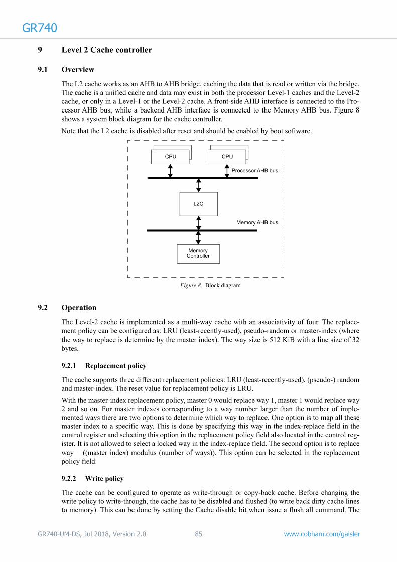
GR740
9 Level 2 Cache controller9.1 Overview
The L2 cache works as an AHB to AHB bridge, caching the data that is read or written via the bridge.The cache is a unified cache and data may exist in both the processor Level-1 caches and the Level-2 cache, or only in a Level-1 or the Level-2 cache. A front-side AHB interface is connected to the Pro-cessor AHB bus, while a backend AHB interface is connected to the Memory AHB bus. Figure 8 shows a system block diagram for the cache controller.
Note that the L2 cache is disabled after reset and should be enabled by boot software.
9.2 Operation
The Level-2 cache is implemented as a multi-way cache with an associativity of four. The replace-ment policy can be configured as: LRU (least-recently-used), pseudo-random or master-index (where the way to replace is determine by the master index). The way size is 512 KiB with a line size of 32 bytes.
9.2.1 Replacement policy
The cache supports three different replacement policies: LRU (least-recently-used), (pseudo-) random and master-index. The reset value for replacement policy is LRU.
With the master-index replacement policy, master 0 would replace way 1, master 1 would replace way 2 and so on. For master indexes corresponding to a way number larger than the number of imple-mented ways there are two options to determine which way to replace. One option is to map all these master index to a specific way. This is done by specifying this way in the index-replace field in the control register and selecting this option in the replacement policy field also located in the control reg-ister. It is not allowed to select a locked way in the index-replace field. The second option is to replace way = ((master index) modulus (number of ways)). This option can be selected in the replacement policy field.
9.2.2 Write policy
The cache can be configured to operate as write-through or copy-back cache. Before changing the write policy to write-through, the cache has to be disabled and flushed (to write back dirty cache lines to memory). This can be done by setting the Cache disable bit when issue a flush all command. The
Figure 8. Block diagram
CPU
Memory
L2C
CPU
Controller
Memory AHB bus
Processor AHB bus
GR740-UM-DS, Jul 2018, Version 2.0 85 www.cobham.com/gaisler

GR740
write policy is controlled via the cache control register. More fine-grained control can also be obtained by enabling the MTRR registers (see text below).9.2.3 Memory type range registers
The memory type range registers (MTRR) are used to control the cache operation with respect to the address. Each MTRR can define an area in memory to be uncached, write-through or write-protected. Each MTRR register consist of a 14-bit address field, a 14-bit mask and two 2-bit control fields. The address field is compared to the 14 most significant bits of the cache address, masked by the mask field. If the unmasked bits are equal to the address, an MTRR hit is declared. The cache operation is then performed according to the control fields (see register descriptions). If no hit is declared or if the MTRR is disabled, cache operation takes place according to the cache control register. The number of implemented MTRRs is sixteen. When changing the value of any MTRR register, the cache must be disabled and flushed (this can be done by setting the Cache disable bit when issuing a flush all com-mand).
Note that the write-protection provided via the MTRR registers is enforced even if the cache is dis-abled.
9.2.4 Cachability
The cache considers the address range 0x00000000 - 0x7FFFFFFF to be cachable. The cache can also be configured to use the HPROT signal to override the default cachable area. An access can only be redefined as non-cachable by the HPROT signal. See table 65 for information on how HPROT can change the access cachability within a cachable address area. The AMBA AHB signal HPROT[3] defines the access cacheable when active high and the AMBA AHB signal HPROT[2] defines the access as bufferable when active high.
* When the HPROT-Read-Hit-Bypass bit is set in the cache control register this will generate a Mem-ory access.
9.2.5 Cache tag entry
Table 66 shows the different fields of the cache tag entry for a cache with a way size of 512 KiB.
Table 65. Access cachability using HPROT.
HPROT: non-cachable, non-bufferable non-cachable, bufferable cacheable
Read hit Cache access* Cache access Cache access
Read miss Memory access Memory access Cache allocation and Memory access
Write hit Cache and Memory access Cache access Cache access
Write miss Memory access Memory access Cache allocation
Table 66. L2C Cache tag entry31 19 18 10 9 8 7 6 5 4 0
TAG 000000 Valid Dirty RES LRU
31 : 19 Address Tag (TAG) - Contains the address of the data held in the cache line.
9 : 8 Valid bits. When set, the corresponding sub-block of the cache line contains valid data. Valid bit 0 corresponds to the lower 16 bytes sub-block (with offset 1) in the cache line and valid bit 1 corre-sponds to the upper 16 bytes sub-block (with offset 0) in the cache line.
7 : 6 Dirty bits When set, this sub-block contains modified data.
5 RESERVED
4 : 0 LRU bits
GR740-UM-DS, Jul 2018, Version 2.0 86 www.cobham.com/gaisler

GR740
9.2.6 AHB address mappingThe AHB slave interface occupies three AHB address ranges. The first AHB memory bar is used for memory/cache data access and is mapped at 0x00000000 - 0x7FFFFFFF. The second AHB memory bar is used for access to configuration registers and the diagnostic interface and is mapped at 0xF0800000 - 0xF08FFFFF. The last AHB memory bar is used to map the IO area of the backend AHB bus (to access the plug&play information on that bus) and maps the Memory AHB bus area 0xFFE00000 - 0xFFEFFFFF.
9.2.7 Memory protection and Error handling
The L2 cache provides Error Detection And Correction (EDAC) protection for the data and tag mem-ory. One error can be corrected and two errors can be detected with the use of a (39, 32, 7) BCH code. The EDAC functionality can dynamically be enabled or disabled. Before being enabled the cache should be flushed. The dirty and valid bits fore each cache line is implemented with TMR. When EDAC error or backend AHB error or write-protection hit in a MTRR register is detected, the error status register is updated to store the error type. The address which caused the error is also saved in the error address register. The error types is prioritised in the way that a uncorrected EDAC error will overwrite any other previously stored error in the error status register. In all other cases, the error sta-tus register has to be cleared before a new error can be stored. Each error type (correctable-, uncor-rectable EDAC error, write-protection hit, backend AHB error) has a pending register bit. When set and this error is unmasked, a interrupt is generated. When an uncorrectable error is detected in the read data, the cache will respond with an AHB error. AHB error responses can also be enabled for access that match a stored error in the error status register. Error detection is done per cache line. The cache also provides a correctable error counter accessible via the error status register. After power-up the error status register needs to be cleared before any valid data can be read out.
Table 67. Cache action on detected EDAC error
Access/Error type Cache-line not dirty Cache-line dirty
Read, Correctable Tag error
Tag is corrected before read is handled, Error sta-tus is updated with a correctable error.
Tag is corrected before read is handled, Error status is updated with a correctable error.
Read, Uncorrectable Tag error
Cache-line invalidated before read is handled, Error status is updated with a correctable error.
Cache-line invalidated before read is handled, Error status is updated with a uncorrectable error. Cache data is lost.
Write, Correctable Tag error
Tag is corrected before write is handed, Error sta-tus is updated with a correctable error.
Tag is corrected before write is handled, Error status is updated with a correctable error.
Write, Uncorrect-able Tag error
Cache-line invalidated before write is handled, Error status is updated with a correctable error.
Cache-line invalidated before write is handled, Error status is updated with a uncorrectable error. Cache data is lost.
Read, Correctable Data error
Cache-data is corrected and updated, Error status is updated with a correctable error. AHB access is not affected.
Cache-data is corrected and updated, Error sta-tus is updated with a correctable error. AHB access is not affected.
Read, Uncorrectable Data error
Cache-line is invalidated, Error status is updated with a correctable error. AHB access is termi-nated with retry.
Cache-line is invalidated, Error status is updated with a uncorrectable error. AHB access is terminated with error.
Write (<32-bit), Cor-rectable Data error
Cache-data is corrected and updated, Error status is updated with a correctable error. AHB access is not affected.
Cache-data is corrected and updated, Error sta-tus is updated with a correctable error. AHB access is not affected.
Write (<32-bit), Uncorrectable Data error
Cache-line is re-fetched from memory, Error sta-tus is updated with a correctable error. AHB access is not affected.
Cache-line is invalidated, Error status is updated with a uncorrectable error. AHB access write data and cache data is lost.
GR740-UM-DS, Jul 2018, Version 2.0 87 www.cobham.com/gaisler

GR740
9.2.8 ScrubberThe cache is implemented with an internal memory scrubber to prevent build-up of errors in the cache memories. The scrubber is controlled via two registers in the cache configuration interface. To scrub one specific cache line the index and way of the line is set in the scrub control register. The scrub operation is started by setting the the pending bit to 1. The scrubber can also be configured to contin-uously loop through and scrub each cache line by setting the enabled bit to 1. In this mode, the delay between the scrub operation on each cache line is determine by the scrub delay register (in clock cycles).
9.2.9 Locked way
One or more ways can be configured to be locked (not replaced). The number of ways that should be locked is configured by the locked-way field in the control register. The way to be locked is starting with the uppermost way (for a 4-way associative cache way 4 is the first locked way, way 3 the sec-ond, and so on). After a way is locked, the cache-way has to be flushed with the “way flush” function to update the tag to match the desired locked address. During this “way flush” operation, the data can also be fetched from memory.
9.3 Operation
9.3.1 Read
A cachable read access to the cache results in a tag lookup to determine if the requested data is located in the cache memory. For a hit (requested data is in the cache) the data is read from the cache and no read access is issued to the memory. If the requested data is not in the cache (cache miss), the cache controller issues a read access to the memory controller to fetch the cache line containing the requested data. The replacement policy determines which cache line in a multi-way configuration that should be replaced and its tag is updated. If the replaced cache line is modified (dirty) this data is stored in a write buffer and after the requested data is fetched from memory the replaced cache line is written to memory.
For a non-cachable read access to the cache, the cache controller can issue a single read access or a burst read access to fetch the data from memory. The access type is determine by how the cache is configured regarding hprot support and bypass line fetch in the access control register. The data is stored in a read buffer and the state of the cache is not modified in any way.
The cache will insert wait-states until the read access is determined to be a cache hit or miss. For a cache hit the data is then delivered. For a miss the cache can insert wait-states during the memory fetch or issue a AMBA SPLIT (depending on how the cache is configured).
9.3.2 Write
A cachable write access to the cache results in a tag lookup to determine if the cache line is present in the cache. For a hit the cache line is updated. No access is issued to the memory for a copy-back con-figuration. When the cache is configured as a write-through cache, each write access is also issued towards memory. For a miss, the replacement policy determines which cache line in a multi-way con-figuration that should be replaced and updates its tag. If the replaced cache line is dirty, it is stored in a write buffer to be written back to the memory. The new cache line is updated with the data from the write access and for a non-128-bit access the rest of the cache line is fetched from memory. Last the replaced cache line is written to memory (when copy-back policy is used and the replaced cache line was marked dirty). When the cache is configured as a write-through cache, no cache lines are marked as dirty and no cache line needs to be written back to memory. Instead the write access is issued towards the memory as well. A new cache line is allocated on a miss for a cacheable write access independent of write policy (copy-back or write-through).
GR740-UM-DS, Jul 2018, Version 2.0 88 www.cobham.com/gaisler

GR740
For a non-cachable write access to the cache, the data is stored in a write buffer and the cache control-ler issue single write accesses to write the data to memory. The state of the cache is unmodified during this access.The cache can accept a non sub-word write hit access every clock cycle. When the cache is unable to accept a new write access the cache inserts wait-states or issue a AMBA SPLIT response depending on how the cache is configured.
9.3.3 Cache flushing
The cache can be flushed by accessing a cache flush register. There are three flush modes: invalidate (reset valid bits), write back (write back dirty cache lines to memory, but no invalidation of the cache content) and flush (write back dirty cache lines to memory and invalidate the cache line). The flush command can be applied to the entire cache, one way or to only one cache line. The cache line to be flushed can be addresses in two ways: direct address (specify way and line address) and memory address (specify which memory address that should be flushed in the cache. The controller will make a cache lookup for the specified address and on a hit, flush that cache line). When the entire cache is flushed the Memory Address field should be set to zero. To invalidate a cache line takes 5 clock cycles. If the cache line needs to be written back to memory one additional clock cycle is needed plus the memory write latency. When the whole cache is flushed the invalidation of the first cache line takes 5 clock cycles, after this one line can be invalidated each clock cycle. When a cache line needs to be written back to memory this memory access will be stored in an access buffer. If the buffer is full, the invalidation of the next cache line will stall until a slot in the buffer has opened up. If the cache also should be disabled after the flush is complete, it is recommended to set the cache disable bit together with the flush command in the Fush set/index register instead of writing ‘0’ to the cache enable bit in the cache control register.
Note that after a processor (or any other AHB master) has initiated a flush the processor is not blocked by the flush unless it writes or requests data from the Level-2 cache. The cache blocks all accesses (responds with AMBA SPLIT or wait-states depending on cache configuration) until the flush is com-plete.
9.3.4 Disabling Cache
To be able to safely disable the cache when it is being accessed, the cache need to be disabled and flushed at the same time. This is accomplished by setting the cache disable bit when issue the flush command.
9.3.5 Diagnostic cache access
The diagnostic interface can be used for RAM block testing and direct access to the cache tag, cache data content and EDAC check bits. The read-check-bits field in the error status/control register selects if data content or the EDAC check bits should be read out. On writes, the EDAC check bits can be selected from the data-check-bit or tag-check-bit register. These register can also be XOR:ed with the correct check bits on a write. See the error status/control register for how this is done.
9.3.6 Error injection
Error injection can be performed for data and tag lines either by modifying the value or the checkbits. The checkbits can be modified by defining a mask that will be XOR:ed with the generated checkbits or by defining the full checkbits to be written via the tag-check-bit register or data-check-bit-registers. The value can be modified by performing a diagnostic access while keeping the existing checkbits.
EDAC checkbits can be modified on a regular cache access by setting the xor-check-bit field in the error status/control register the data EDAC check bits will be XOR:ed with the data-check-bit register on the next write, or the tag EDAC check bits will be XOR:ed with the tag-check-bit register on the next tag replacement. The tag check bit manipulation is only done if the tag-check-bit register is not zero. The xor-check-bit is reset on the next tag replacement or data write. Errors can also be injected
GR740-UM-DS, Jul 2018, Version 2.0 89 www.cobham.com/gaisler

GR740
by writing an address together with the inject bit to the “Error injection” register. This will XOR the check-bits for the specified address with the data-check-bit register. If the specified address in not cached, the cache contents will be unchanged.9.3.7 AHB slave interface
The cache can accept 8-bit (byte), 16-bit (half word), 32-bit (word), 64-bit, and 128-bit single accesses and also 32-bit, 64-bit, and 128-bit burst accesses. For an access during a flush operation, the cache will respond with an AHB SPLIT response or with wait-states. For an uncorrectable error or a backend AHB error on a read access, the cache will respond with an AMBA ERROR response. For a correctable data error which require a cache line to be re-fetched from memory the cache will respond with a AMBA RETRY response.
9.3.8 AHB master interface
The master interface is the cache’s connection to the memory controller. During cache line fetch, the controller can issue either a 32-bit, 64-bit or 128-bit burst access. For a non cachable access and in write-through mode the cache can also issue a 8-bit (byte), 16-bit (half word), 32-bit (word), 64-bit, or 128-bit single write access.
9.3.9 Cache status
The cache controller has a status register that provides information on the cache configuration (multi-way configuration and set size). The cache also provides access, hit and error correction counters via the LEON4 statistics unit (see section 26).
GR740-UM-DS, Jul 2018, Version 2.0 90 www.cobham.com/gaisler

GR740
9.4 RegistersThe cache is configured via registers mapped into the AHB memory address space.
Table 68. L2C: AHB registers
AHB address offset Register
0x00 Control register
0x04 Status register
0x08 Flush (Memory address)
0x0C Flush (set, index)
0x10 - 0x1C Reserved
0x20 Error status/control
0x24 Error address
0x28 TAG-check-bit
0x2C Data-check-bit
0x30 Scrub Control/Status
0x34 Scrub Delay
0x38 Error injection
0x3C Access control
0x50 Error handling / injection configuration
0x80 - 0xFC MTRR registers
0x80000 - 0x8FFFC Diagnostic interface (Tag)0x80000: Tag 1, way-10x80004: Tag 1, way-20x80008: Tag 1, way-30x8000C: Tag 1, way-40x80010: Tag check-bits way-0,1,2,3 (Read only) bit[31] = RESERVED bit[30:24] = check-bits for way-1. bit[23] = RESERVED bit[22:16] = check-bits for way-2. bit[15] = RESERVED bit[14:8] = check-bits for way-3. bit[7] = RESERVED bit[6:0] = check-bits for way-4.0x80020: Tag 2, way-10x80024: ...
0x200000 - 0x3FFFFC Diagnostic interface (Data)0x200000 - 0x27FFFC: Data or check-bits way-10x280000 - 0x2FFFFF: Data or check-bits way-20x300000 - 0x27FFFC: Data or check-bits way-30x380000 - 0x3FFFFF: Data or check-bits way-4
When check-bits are read out:
Only 32-words at offset 0x0, 0x10, 0x20,... are valid check-bits.bit[31:28] = RESERVEDbit[27:21] = check-bits for data word at offset 0x0.bit[20:14] = check-bits for data word at offset 0x4.bit[13:7] = check-bits for data word at offset 0x8.bit[6:0] = check-bits for data word at offset 0xc.
GR740-UM-DS, Jul 2018, Version 2.0 91 www.cobham.com/gaisler

GR740
9.4.1Table 69. 0x00 - L2CC - L2C Control register
Control register
9.4.2 Status register
Table 70. 0x04 - L2CS - L2C Status register
31 29 28 27 19 18 16 15 12 11 8 7 6 5 4 3 2 1 0
EN EDAC
REPL RESERVED BBS INDEX-WAY LOCK RES HPRHB
HPB
UC HC WP HP
0 0 0 0 0b100 0 0 0 0 0 0 0 0 0
rw rw rw r rw rw rw r rw rw rw rw rw rw
31 Cache enable (EN) - When set, the cache controller is enabled. When disabled, the cache is bypassed.
30 EDAC enable (EDAC)
29: 28 Replacement policy (REPL) - 00: LRU01: (pseudo-) random10: Master-index using index-replace field11: Master-index using the modulus function
27: 19 RESERVED
18: 16 Backend bus size configuration (BBS) -“100”: Configure backend bus size to 128-bit.“011”: Configure backend bus size to 64-bit.“010”: Configure backend bus size to 32-bit.“000”: No configuration update is done.Other values: not supported.
15: 12 Master-index replacement (INDEX-WAY) - Way to replace when Master-index replacement policy and master index is larger than number of ways in the cache.
11: 8 Locked ways (LOCK) - Number of locked ways.
7: 6 RESERVED
5 HPROT read hit bypass (HPRHB) - When set, a non-cacheable and non-bufferable read access will bypass the cache on a cache hit and return data from memory. Only used with HPROT support.
4 HPROT bufferable (HPB) - When HPROT is used to determine cachability and this bit is set, all accesses is marked bufferable.
3 Bus usage status mode (UC) - 0 = wrapping mode, 1 = shifting mode.
2 Hit rate status mode (HC) - 0 = wrapping mode, 1 = shifting mode.
1 Write policy (WP) - When set, the cache controller uses the write-through write policy. When not set, the write policy is copy-back.
0 HPROT enable (HP) - When set, use HPROT to determine cachability.
31 25 24 23 22 21 16 15 13 12 2 1 0
RESERVED LS AT MP MTRR BBUS-W WAY-SIZE WAY
0 0 0 1 16 1 * 3
r r r r r r r r
31: 25 RESERVED
24 Cache line size (LS) - 1 = 64 bytes, 0 = 32 bytes.
23 Access time (AT) - Access timing not simulated.
22 Memory protection (MP) - implemented
21: 16 Memory Type Range Registers (MTRR) - Number of MTRR registers implemented (16)
15: 13 Backend bus width (BBUS-W) Set to 1 = 128-bit.
12: 2 Cache way size (WAY-SIZE) - Size in kBytes
1: 0 Multi-Way configuration (WAY)Set to “11“: 4-way
GR740-UM-DS, Jul 2018, Version 2.0 92 www.cobham.com/gaisler

GR740
9.4.3Table 71. 0x08 - L2CFMA - L2C Flush (Memory address) register
Flush memory address register
9.4.4
Table 72. 0x0C - L2CFSI - L2C Flush (Set, Index) register
Flush set/index register
31 5 4 3 2 0
Memory Address (ADDR) R DI FMODE
NR 0 0 0
rw r w rw
31: 5 Memory Address (ADDR) - (For flush all cache lines, this field should be set to zero)
4 RESERVED
3 Cache disable (DI) - Setting this bit to ‘1’ is equal to setting the Cache enable bit to ‘0’ in the Cache Control register
2: 0 Flush mode (FMODE) -“001“: Invalidate one line, “010”: Write-back one line, “011“: Invalidate & Write-back one line.“101“: Invalidate all lines, “110”: Write-back all lines, “111“: Invalidate & Write-back all lines.Only dirty cache lines are written back to memory.
31 16 10 9 8 7 6 5 4 3 2 1 0
INDEX / TAG FL VB DB R WAY DI WF FMODE
NR 0 0 0 0 0 0 0 0
rw rw rw rw r rw w rw rw
31: 16 Cache line index (INDEX) - used when a specific cache line is flushed
31: 10 (TAG) - used when “way flush” is issued. If a specific cache line is flushed, bit should be set to zero. When a way flush is issued, the bits in this field will be written to the TAGs for the selected cache way.
9 Fetch Line (FL) - If set to ‘1’ data is fetched form memory when a “way flush” is issued. If a specific cache line is flushed, this bit should be set to zero
8 Valid bit (VB) - used when “way flush” is issued. If a specific cache line is flushed, this bit should be set to zero.
7 Dirty bit (DB) - used when “way flush” is issued. If a specific cache line is flushed, this bit should be set to zero
6 RESERVED
5: 4 Cache way (WAY) -
3 Cache disable (DI) - Setting this bit to ‘1’ is equal to setting the Cache enable bit to ‘0’ in the Cache Control register.
2 Way-flush (WF) - When set one way is flushed, If a specific cache line should be flushed, this bit should be set to zero
1: 0 Flush mode (FMODE) -
line flush:“01“: Invalidate one line“10”: Write-back one line (if line is dirty)“11“: Invalidate & Write-back one line (if line is dirty).
way flush:“01“: Update Valid/Dirty bits according to register bit[8:7] and TAG according to register bits[31:10]“10”: Write-back dirty lines to memory“11“: Update Valid/Dirty bits according to register bits [8:7] and TAG according to register bits[31:10], and Write-back dirty lines to memory.
GR740-UM-DS, Jul 2018, Version 2.0 93 www.cobham.com/gaisler

GR740
9.4.5Table 73. 0x20 - L2CERR - L2CError status/control register
Error status/control register
31 28 27 26 24 23 22 21 20 19 18 16 15 12 11 8 7 6 5 4 3 2 1 0
AHBmasterindex
SCRUB
TYPE TAG/DATA
COR/UCOR
MULTI
VALID
DISERESP
Correctableerror
counter
IRQpending
IRQmask
Select CB
Select TCB
XCB
RCB
COMP
RST
NR NR NR NR NR NR NR 0 NR NR 0 0 0 0 0 0 0
r r r r r r r rw r r rw rw rw rw rw rw w
31: 28 AHB master that generated the access
27 Scrub error (SCRUB) - Indicates that the error was trigged by the scrubber.
26: 24 Access/Error Type: (TYPE) -000: cache read, 001: cache write, 010: memory fetch, 011: memory write,100: Write-protection hit, 101: backend read AHB error, 110: backend write AHB error
23 Tag or data Error - 0 tag error, 1: data error
22 Correctable or uncorrectable error - 0: correctable error, 1: uncorrectable error
21 Multiple error (MULTI) - set when multiple errors has been detected.
20 Error status valid (VALID) - register contains valid error status.
19 Disable error responses for uncorrectable EDAC error (DISERESP).
18: 16 Correctable error counter
15: 12 Interrupt pendingbit3: Backend AHB error bit2: Write-protection hitbit1: Uncorrectable EDAC error bit0: Correctable EDAC error
11: 8 Interrupt mask (if set this interrupt is unmasked)bit3: Backend AHB error bit2: Write-protection hitbit1: Uncorrectable EDAC error bit0: Correctable EDAC error
7: 6 Selects (CB) - data-check-bits for diagnostic data write:00: use generated check-bits01: use check-bits in the data-check-bit register10: XOR check-bits with the data-check-bit register11: use generated check-bits
Note: If this field is set to "01" or "10" then check-bits are overridden for all accesses. To get con-trolled error injection, the internal scrubber should be disabled and no accesses should be made to the Level-2 cache.
5: 4 Selects (TCB) - tag-check-bits for diagnostic tag write:00: use generated check-bits01: use check-bits in the tag-check-bit register10: XOR check-bits with the tag-check-bit register11: use generated check-bits
Note: If this field is set to "01" or "10" then check-bits are overridden for all accesses. To get con-trolled error injection, the internal scrubber should be disabled and no accesses should be made to the Level-2 cache.
3 Xor check-bits (XOR) - If set, the check-bits for the next data write or tag replace will be XOR:ed withe the check-bit register. Default value is 0.
2 Read check-bits (RCB) - If set, a diagnostic read to the cache data area will return the check-bits related to that data.When this bit is set, check bits for the data at offset 0x0 - 0xc can be read at offset 0x0, the check bits for data at offset 0x10 - 0x1c can be read at offset 0x10, ...
1 Compare error status (COMP) - If set, a read access matching a uncorrectable error stored in the error status register will generate a AHB error response. Default value is 0.
0 Resets (RST) - clear the status register to be able to store a new error. After power up the status reg-ister needs to be cleared before any valid data can be read out.
GR740-UM-DS, Jul 2018, Version 2.0 94 www.cobham.com/gaisler

GR740
9.4.6Table 74. 0x24 - L2CERRA - L2C Error address register
Error address register
9.4.7
Table 75. 0x28 - L2CTCB - L2C TAG-Check-Bits register
TAG check bits register
9.4.8
Table 76. 0x2C - L2CCB - L2C Data-Check-Bits register
Data check bits register
9.4.9
Table 77. 0x30 - L2CSCRUB - L2C Scrub control/status register
Scrub control/status register
31 0
Error Address (EADDR)
NR
r
31: 0 Error Address (EADDR)
31 7 6 0
RESERVED TCB
0 0
r rw
31: 7 RESERVED
6: 0 TAG Check-bits (TCB) - Check-bits which can be selected by the “Select check-bit“ field in the error status/control register for TAG updates
31 28 27 0
RESERVED CB
0 0
r rw
31: 28 RESERVED
27: 0 Data Check-bits (CB) - Check-bits which can be selected by the “Select check-bit“ field in the error status/control register for TAG updates
31 16 15 4 3 2 1 0
INDEX RESERVED WAY PEN
EN
0 0 0 0 0
rw r rw rw rw
31: 16 Scrub Index (INDEX) - Index for the next line scrub operation
15: 4 RESERVED
3: 2 Scrub Way (WAY) - Way for the next line scrub operation
1 Scrub Pending (PEN) - Indicates when a line scrub operation is pending. When the scrubber is dis-abled, writing ‘1’ to this bit scrubs one line.
0 Scrub Enable (EN) - Enables / disables the automatic scrub functionality.
GR740-UM-DS, Jul 2018, Version 2.0 95 www.cobham.com/gaisler

GR740
9.4.10Table 78. 0x34 - L2CSDEL - L2C Scrub delay register
Scrub delay register
9.4.11
Table 79. 0x38 - L2CEINJ - L2C Error injection register
Error injection register
31 16 15 0
RESERVED DEL
0 0
r rw
31: 16 RESERVED
15: 0 Scrub Delay (DEL) - Delay the scrubber waits before issue the next line scrub operation
31 2 1 0
ADDR R INJ
0 0 0
rw r rw
31: 2 Error Inject address (ADDR)
1: RESERVED
0 Inject error (INJ) - Set to ‘1’ to inject a error at “address”.
GR740-UM-DS, Jul 2018, Version 2.0 96 www.cobham.com/gaisler
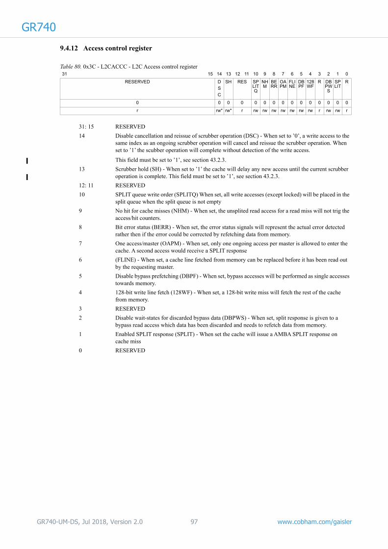
GR740
9.4.12Table 80. 0x3C - L2CACCC - L2C Access control register
Access control register
31 15 14 13 12 11 10 9 8 7 6 5 4 3 2 1 0
RESERVED D
S
C
SH RES SPLITQ
NHM
BERR
OAPM
FLINE
DBPF
128WF
R DBPWS
SPLIT
R
0 0 0 0 0 0 0 0 0 0 0 0 0 0 0
r rw* rw* r rw rw rw rw rw rw rw r rw rw r
31: 15 RESERVED
14 Disable cancellation and reissue of scrubber operation (DSC) - When set to ’0’, a write access to the same index as an ongoing scrubber operation will cancel and reissue the scrubber operation. When set to ’1’ the scubber operation will complete without detection of the write access.
This field must be set to ’1’, see section 43.2.3.
13 Scrubber hold (SH) - When set to ’1’ the cache will delay any new access until the current scrubber operation is complete. This field must be set to ’1’, see section 43.2.3.
12: 11 RESERVED
10 SPLIT queue write order (SPLITQ) When set, all write accesses (except locked) will be placed in the split queue when the split queue is not empty
9 No hit for cache misses (NHM) - When set, the unsplited read access for a read miss will not trig the access/hit counters.
8 Bit error status (BERR) - When set, the error status signals will represent the actual error detected rather then if the error could be corrected by refetching data from memory.
7 One access/master (OAPM) - When set, only one ongoing access per master is allowed to enter the cache. A second access would receive a SPLIT response
6 (FLINE) - When set, a cache line fetched from memory can be replaced before it has been read out by the requesting master.
5 Disable bypass prefetching (DBPF) - When set, bypass accesses will be performed as single accesses towards memory.
4 128-bit write line fetch (128WF) - When set, a 128-bit write miss will fetch the rest of the cache from memory.
3 RESERVED
2 Disable wait-states for discarded bypass data (DBPWS) - When set, split response is given to a bypass read access which data has been discarded and needs to refetch data from memory.
1 Enabled SPLIT response (SPLIT) - When set the cache will issue a AMBA SPLIT response on cache miss
0 RESERVED
GR740-UM-DS, Jul 2018, Version 2.0 97 www.cobham.com/gaisler

GR740
9.4.13 Error Handling / Injection configurationTable 81. 0x4C - L2CEINJCFG - L2C injection configuration register
9.4.14
Table 82. 0x80-FC - L2CMTRR - L2C Memory type range register
Memory type range registers
31 11 10 9 8 7 0
RESERVED EDI
TER
IMD
RES
0 0 0 0 0
r rw rw rw r
31: 11 RESERVED
10 (EDI) - Enable invalidation off cache line with un-correctable data error.When set to 1 and a un-correctable data error is detected, the cache line will be invalidated (remov-ing the error form the cache).
9 (TER) - Disable error response on un-correctable TAG error detection.When set to 0 the access detecting a un-correctable TAG error would generate a AMBA error response. When set to 1 this access would not generate an error response.
8 (IMD) - Disable index match only after un-correctable TAG error.When set to 1 the TAG and INDEX are matched against the error address register after a detected un-correctable TAG error. When set to 0 only the INDEX are matched against the error address register.
7: 0 RESERVED
31 18 17 16 15 2 1 0
ADDR ACC MASK WP AC
0 0 0 0 0
rw rw rw rw rw
31: 18 Address field (ADDR) - to be compared to the cache address [31:18]
17: 16 Access field (ACC) - 00: uncached, 01: write-through
15: 2 Address mask (MASK) - Only bits set to 1 will be used during address comparison
1 Write-protection (WP) - 0: disabled, 1: enabled
0 Access control field (AC) -. 0: disabled, 1: enabled
GR740-UM-DS, Jul 2018, Version 2.0 98 www.cobham.com/gaisler

GR740
10 SDRAM Memory Controller with Reed-Solomon EDAC10.1 Overview
The SDRAM memory controller is a 64+32-bit memory controller which is divided into a front-end and a back-end part.
10.2 Operation
10.2.1 Memory data width
The controller supports a full-width and a half-width mode, selected via the MEM_IFWIDTH input signal. In full-width mode, the memory bus has 64 data bits, and 0,16 or 32 check bits depending on EDAC configuration. In half-width mode, the memory bus has 32 data bits, plus 0,8 or 16 check bits.
10.2.2 Memory access
When an AHB access is done to the controller, the corresponding request is sent to the memory back-end which performs the access. For read bursts, the controller streams the read data so each burst item is delivered to the bus as soon as it arrives and wait states are added as needed between each part of the burst.
The controller has a write buffer holding one write access in EDAC configuration, and two write accesses in non-EDAC configuration. Each write access can be up to the configured burst length in size. The controller will mask the write latency by storing the data into the write buffer and releasing the AHB bus immediately. The latency will be seen however if a read access is done before the writes have completed or an additional write access is made when all buffers are used.
Writes of 32 bits or less will result in a read-modify-write cycle to update the checkbits (this is done even if EDAC has been disabled in the control register). In this case, the memory controller generates wait states on the AHB bus until the read part of the cycle has completed.
10.3 Limitations
The AHB front-end with EDAC is optimized for 64/128-bit masters and does not handle 32-bit bursts efficiently, each access will result in a RMW cycle in the write case, and a read cycle in the read case.In this device, this case only happens when the Level-2 cache is disabled or set to write-through mode.
Figure 9. Memory controller connected to AMBA bus and SDRAM
AHB Front-endwith EDAC
Read/Writedata buffers
SDR back-end
AHB slave I/Fto SDRAM
mem_ifwidth
mem_ifwidth
GR740-UM-DS, Jul 2018, Version 2.0 99 www.cobham.com/gaisler

GR740
10.4 SDRAM back-end operation10.4.1 General
Synchronous dynamic RAM (SDRAM) access is supported to 1-4 external banks of PC100 compati-ble devices. Each external bank has a separate chip select signal mapped to pins according to table 85.The controller supports devices with 8 - 12 column-address bits, up to 13 row-address bits, and 4 internal banks. The size of each of the external banks can be programmed in binary steps between 4 Mbyte and 512 Mbyte in half-width mode, and between 8 Mbyte and 1 Gbyte in full-width mode. The operation of the SDRAM controller is controlled through the configuration register SDCFG (see sec-tion 10.6).
10.4.2 Initialization
When the SDRAM controller is enabled, it automatically performs the SDRAM initialization sequence of PRECHARGE, 8x AUTO-REFRESH and LOAD-MODE-REG on both banks simultane-ously. The controller programs the SDRAM to use page burst on read accesses and single location access on write accesses.
10.4.3 Read and write cycles
A read cycle is started by performing an ACTIVATE command to the desired bank and row, followed by a READ command with data read after the programmed CAS delay. The read cycle is terminated with a PRE-CHARGE command, no banks are left open between two accesses.
Write cycles are performed similarly to read cycles, with the difference that WRITE commands are issued after activation.
10.4.4 Configurable SDRAM timing parameters
To provide optimum access cycles for different SDRAM devices (and at different frequencies), three SDRAM parameters can be programmed through the memory configuration register (SDCFG):TCAS, TRP and TRFCD. The value of these fields affect the SDRAM timing as described in table 83.
If the TCAS, TRP and TRFC are programmed such that the PC100 specifications are fulfilled, the remaining SDRAM timing parameters will also be met. The table below shows typical settings for 100 MHz operation and the resulting SDRAM timing (in ns). Note that in addition to these settings, the setup and hold timings must be satisfied to use the memory at a specific frequency.
Table 83. SDRAM programmable minimum timing parameters
SDRAM timing parameter Minimum timing (clocks)
CAS latency, RAS/CAS delay (tCAS, tRCD) TCAS + 2
Precharge to activate (tRP) TRP + 2
Auto-refresh command period (tRFC) TRFC + 3
Activate to precharge (tRAS) TRFC + 1
Activate to Activate (tRC) TRP + TRFC + 4
Table 84. SDRAM example programming
SDRAM settings tCAS tRC tRP tRFC tRAS
100 MHz, CL=2; TRP=0, TCAS=0, TRFC=4 20 80 20 70 50
100 MHz, CL=3; TRP=0, TCAS=1, TRFC=4 30 80 20 70 50
GR740-UM-DS, Jul 2018, Version 2.0 100 www.cobham.com/gaisler

GR740
10.4.5 RefreshThe SDRAM controller contains a refresh function that periodically issues an AUTO-REFRESH command to both SDRAM banks. The period between the commands (in clock periods) is pro-grammed in the refresh counter reload field in the SDCFG register. Depending on SDRAM type, the required period is typically 7.8 or 15.6 s (corresponding to 780 or 1560 clocks at 100 MHz). The generated refresh period is calculated as (reload value+1)/(memory clock period). The refresh func-tion is enabled by setting bit 31 in the SDCFG register.
10.4.6 2T signaling mode
An alternative mode is supported in the controller where all address and control signals except for the chip select is set for an extra cycle with chip select deasserted before the command is issued. This improves the board timing analysis for these signals since an extra cycle of setup time is achieved. The price of this is one extra SDRAM cycle of latency for the ACTIVATE command, resulting in one cycle extra read latency, and also one extra cycle for the REFRESH. Also due to internal design rea-sons, one extra cycle before PRECHARGE after a read burst (but not after writing) is also inserted, however this does not affect latency as it is done in parallel with the transfer of read data to the AHB domain.
The 2T signaling mode is activated by setting the EN2T bit in the SDRAM configuration register 2 SDCFG2) register.
In order for the 2T signaling mode to work, the mode register needs to be programmed for length-2 read and length-2 write bursts. Therefore, after changing the EN2T setting, the LOAD-MODE-REG-ISTER command must be reissued by writing to the SDRAM command configuration register field before proceeding with additional accesses.
10.4.7 Double chip select mode
As the 2T signaling mode improves analog setup time for all control signals except chip select, an additional setting exists to group the four chip select outputs into two chip selects, where each chip select signal is driven identically on two outputs in parallel. On the board, the two copies can each then be routed to half of the SDRAM devices and thereby reduce the capacitive load on each output.
10.4.8 SDRAM commands
The controller can issue four SDRAM commands by writing to the SDRAM command field in the SDRAM Configuration register: PRE-CHARGE, AUTO-REFRESH and LOAD-MODE-REG (LMR). The command field will be cleared after a command has been executed. Note that when changing the value of the CAS delay or enabling/disabling 2T signaling, a LOAD-MODE-REGIS-TER command should be generated at the same time to update the mode register. The mode register is programmed as shown in table 86.
Table 85. Mapping of chip selects to I/Os
Pin Function DCS=0 Function DCS=1
mem_sn(0) CS(0) CS(0)
mem_sn(1) CS(1) CS(0)
mem_addr(13) CS(2) CS(1)
mem_addr(14) CS(3) CS(1)
Table 86. SDRAM controller mode register programming
Mode register bit 12 .. 10 9 8 7 6 5 4 3 2 1 0
(reserved) WB Op Mode CAS Latency BT Burst length
Controller setting 0 EN2T 0 0 0 1 CL 0 0 0 EN2T
GR740-UM-DS, Jul 2018, Version 2.0 101 www.cobham.com/gaisler

GR740
10.4.9 Address bus connectionThe SDRAM address bus should be connected to mem_addr[12:0], the bank address to mem_ba[1:0], and the data bus to mem_dq[63:0] or mem_dq[31:0] if a 32-bit SDRAM data bus is used. Checkbits should be tied to mem_dq[95:64] in full-width mode and mem_dq[79:64] in half-width mode.
10.4.10 Command sequences
Below illustrates the sequences of commands issued by the SDRAM controller for read and write bursts at the minimum delay settings. CS and DQM in the table refers to the CS and DQM belonging to the selected address and size, unused banks and byte lanes are kept at 1 throughout the access.
Note: * Dummy read while waiting for end of data, data not used
Table 87. Length-4 read access command sequence
Cycle 2T signaling disabled 2T signaling enabled
CSn CMD DQM BA Addr CSn CMD DQM BA Addr
- 1 (NOP) (1) - - 1 (NOP) 1 - -
0 0 RAS (1) Bank Row 1 (RAS) 1 (Bank) (Row)
1 0 NOP 1 (Bank) (Row) 0 RAS 1 Bank Row
2 0 READ 0 Bank Col 1 (READ) 1 (Bank) (Col)
3 0 READ 0 Bank Col+1 0 READ 0 Bank Col
4 0 READ 0 Bank Col+2 1 (READ) 0 (Bank) (Col+2)
5 0 READ 0 Bank Col+3 0 READ 0 Bank Col+2
6 0 READ* 0 Bank Col+4 1 (READ) 0 (Bank) (Col+4)
7 0 READ* 0 Bank Col+5 0 READ* 0 Bank Col+4
8 0 READ* 0 Bank Col+6 1 (READ) 0 (Bank) Col+6
9 0 PCH 1 Bank (Col+6) 0 READ* 0 Bank Col+6
10 1 (NOP) 1 (Bank) (Col+6) 1 (PCH) 1 (Bank) (Col+8)
11 1 (NOP) 1 (Bank) (Col+6) 0 PCH 1 Bank (Col+8)
12 ... 1 (NOP) 1 (Bank) (Col+6) 1 NOP 1 (Bank) (Col+8)
Table 88. Length-4 write access command sequence
Cycle 2T signaling disabled 2T signaling enabled
CSn CMD DQM BA Addr CSn CMD DQM BA Addr
- 1 (NOP) 1 - - 1 (NOP) 1 - -
0 0 RAS 1 Bank Row 1 (RAS) 1 Bank (Row)
1 0 NOP 1 (Bank) (Row) 0 RAS 1 Bank Row
2 0 WRITE 0 Bank Col 1 (WRITE) 1 Bank (Col)
3 0 WRITE 0 Bank Col+1 0 WRITE 0 Bank Col
4 0 WRITE 0 Bank Col+2 1 (WRITE) 0 Bank (Col+2)
5 0 WRITE 0 Bank Col+3 0 WRITE 0 Bank Col+2
6 0 WRITE 1 Bank Col+4 1 (WRITE) 0 Bank (Col+4)
7 0 PCH 1 Bank Col+5 1 (PCH) 1 Bank (Col+4)
8 1 NOP 1 (Bank) Col+6 0 PCH 1 Bank Col+6
9 1 NOP 1 (Bank) (Col+6) 1 NOP 1 Bank Col+6
GR740-UM-DS, Jul 2018, Version 2.0 102 www.cobham.com/gaisler

GR740
10.5 Fault-tolerant operation10.5.1 Overview
For FT operation, the external memory interface data bus is widened and the extra bits are used to store 16 or 32 checkbits corresponding to each 64 bit data word. The variant to be used can be config-ured at run-time depending on the connected data width and the desired level of fault tolerance.
When writing, the controller generates the check bits and stores them along with the data. When read-ing, the controller will transparently correct any correctable bit errors and provide the corrected data on the AHB bus. However, the corrected bits are not written back to the memory so external scrub-bing is necessary to avoid uncorrectable errors accumulating over time.
An extra corrected error output signal is asserted when a correctable read error occurs, at the same cycle as the corrected data is delivered. This signal is connected to the memory scrubber. In case of uncorrectable error, this is signaled by giving an AHB ERROR response. See also the AMBA ERROR propagation description in section 5.10.
10.5.2 Error-correction properties
The memory controller uses an interleaved error correcting code which works on nibble (4-bit) units of data. The codec can be used in two interleaving modes, mode A and mode B.
In mode A, the basic code has 16 data bits, 8 check bits and can correct one nibble error. This code is interleaved by 4 using the pattern in table 89 to create a code with 64 data bits and 32 check bits.
This code can tolerate one nibble error in each of the A,B,C,D groups shown below. This means that we can correct 100% of single errors in two adjacent nibbles, or in any 8/16-bit wide data bus lane, that would correspond to a physical memory device. The code can also correct 18/23=78% of all pos-sible random two-nibble errors.
This interleaving pattern was designed to also provide good protection in case of reduced (32/16-bit) bus width with the same data-checkbit relation, so software will see the exact same checkbits on diag-nostic reads.
In mode B, the basic code has 32 data bits, 8 check bits and can correct one nibble error. This code is then interleaved by a factor of two to create a code with 64 data bits and 16 check bits.
Table 89. Mode Ax4 interleaving pattern (64-bit data width)63:60 59:56 55:52 51:48 47:44 43:40 39:36 35:32 31:28 27:24 23:20 19:16 15:12 11:8 7:4 3:0
C D A B A B C D B A D C D C B A
127:120 119:112 111:104 103:96 95:88 87:80 79:72 71:64
Ccb Dcb Acb Bcb Ccb Dcb Acb Bcb
Table 90. Mode Bx2 interleaving pattern (64-bit data width)63:60 59:56 55:52 51:48 47:44 43:40 39:36 35:32 31:28 27:24 23:20 19:16 15:12 11:8 7:4 3:0
A B A B A B A B B A B A B A B A
95:88 87:80 79:72 71:64
Acb Bcb Acb Bcb
Table 91. Mode Ax4 interleaving pattern (32-bit data width)95:80 79:76 75:72 71:68 67:64 63:32 31:28 27:24 23:20 19:16 15:12 11:8 7:4 3:0
- Ccb Dcb Acb Bcb - C D A B A B C D
- Bcb Acb Dcb Ccb - B A D C D C B A
Table 92. Mode Bx2 interleaving pattern (32-bit data width)95:80 79:76 75:72 71:68 67:64 63:32 31:28 27:24 23:20 19:16 15:12 11:8 7:4 3:0
- - - Acb Bcb - A B A B A B A B
- - - Bcb Acb - B A B A B A B A
GR740-UM-DS, Jul 2018, Version 2.0 103 www.cobham.com/gaisler

GR740
10.5.3 Data transfers
There is no extra time penalty in the case data is corrected compared to the error-free case.
Only writes of 64 bit width or higher will translate directly into write cycles to the external memory. Other types of write accesses will generate a read-modify-write (RMW) cycle in order to correctly update the check-bits. In the special case where an uncorrectable error is detected while performing the RMW cycle, the write is aborted and the incorrect checkbits are left unchanged so they will be detected upon the next read.
10.5.4 Configuration
Checkbits are always generated when writing even if EDEN is disabled. Which type of code, A or B, that is used can be controlled by the CODE field in the MUXCFG register. If the code is changed during operation, you will need to re-initialize the memory to regenerate the check-bits with the new code. One way to do this is to clear EDEN and then read and rewrite the memory contents.
Code checking on read is disabled on reset and is enabled by setting the EDEN bit in the MUXCFGregister. Before enabling this, the code to be used should be set in the CODE field and the memory contents should be (re-)initialized.
10.5.5 Diagnostic checkbit access
The checkbits and data can be accessed directly for testing and fault injection. This is done by writing the address of into the FTDA register. The check-bits and data can then be read and written via the FTDC and FTDD registers. Note that for checkbits the FTDA address is 64-bit aligned, while for data it is 32-bit aligned.
When the FTDC or FTDD registers are accessed, the corresponding access to the address configured in the FTDA register will be performed to the SDRAM and the read data is returned as if it was the contents of the register. The access will block with wait states until the access has completed, and unlike regular accesses so also writes will always block.
After the diagnostic data register has been read, the FT control register bits 31:19 can be read out to see if there were any correctable or uncorrectable errors detected, and where the correctable errors were located. There is one bit per byte lane describing where any correctable errors occurred. Note that the location mask is not valid if there were uncorrectable errors.
10.5.6 Code boundary
The code boundary feature allows you to gradually switch the memory from one interleaving mode to the other and regenerate the checkbits without stopping normal operation. This can be used when recovering from memory faults, as explained further below.
If the boundary address enable (BAEN) control bit is set, the controller will look at the address of each access, and use the interleaving mode selected in the CODE field for memory accesses above or equal to the boundary address, and the opposite code for memory accesses below to the boundary address.
If the boundary address update (BAUPD) control bit is also set, the controller will shift the boundary upwards whenever the the address directly above the boundary is written to. Since the written data is now below the boundary, it will be written using the opposite code. The write can be done with any size supported by the controller.
10.5.7 Data multiplexing
When code B is used instead of code A, the upper half of the checkbits become unused. The controller supports switching in this part of the data bus to replace another faulty part of the bus. To do this, one
GR740-UM-DS, Jul 2018, Version 2.0 104 www.cobham.com/gaisler

GR740
sets the DATAMUX field to a value between 1-4 to replace a quarter of the data bus, or to 5 to replace the active checkbit half. When writing, the selected part will also be written into the top bits, and when reading the top bits will be copied over into the selected part.10.5.8 Memory fault recovery
The above features are designed to make the system capable to deal with a permanent fault in an external memory chip.
A basic sequence of events is as follows:
1. The system is running correctly with EDAC enabled and the larger code A is used.
2. A memory chip gets a fault making the SDRAM deliver incorrect data on one byte lane. The memory controller keeps delivering error-free data but reports a correctable error on every read access.
3. A logging device (the memory scrubber) registers the high frequency of correctable errors and signals an interrupt.
4. The CPU performs a probe using the FT diagnostic registers to confirm that the error is perma-nent and on which physical lane the error is.
5. After determining that a permanent fault has occurred, the CPU reconfigures the memory con-troller as follows (all configuration register fields changed with a single register write):
The data multiplexing control field is set so the top checkbit half replaces the failed part of the data bus.
The code boundary register is set to the lowest memory address.
The boundary address enable and boundary address update enable bits are set.
The mask correctable error bit is set
6. The memory data and checkbits are now regenerated using locked read-write cycles to use the smaller code and replace the broken data with the upper half of the checkbit bus. This can be done in hardware using the memory scrubber.
7. After the whole memory has been regenerated, the CPU disables the code boundary, changes the code selection field to code B, and unsets the mask correctable error bit.
After this sequence, the system is now again fully operational, but running with the smaller code and replacement chip and can again recover from any single-nibble error. Note that during this sequence, it is possible for the system to operate and other masters can both read and write to memory while the regeneration is ongoing.
Table 93. DATAMUX configurations
mem_ifwidth DATAMUX Top bits swapped in Replaced "faulty" slice
- 0 No swapping
0 1 mem_dq(95:80) mem_dq(15:0)
2 mem_dq(31:16)
3 mem_dq(47:32)
4 mem_dq(63:48)
5 mem_dq(79:64)
1 1 mem_dq(79:72) mem_dq(7:0)
2 mem_dq(15:8)
3 mem_dq(23:16)
4 mem_dq(31:24)
5 mem_dq(71:64)
GR740-UM-DS, Jul 2018, Version 2.0 105 www.cobham.com/gaisler

GR740
10.6 RegistersThe controller has a register area accessible via the AHB slave interface. The registers should be accessed with 32-bit reads and writes. The registers are tabulated below.
Table 94. MMCTRL Registers
Offset Register
0x00 SDRAM configuration register 1(SDCFG1)
0x04 SDRAM configuration register 2 (SDCFG2)
0x08 - 0x1C Reserved
0x20 Mux Configuration Register (MUXCFG)
0x24 Mux Diagnostic Address register (FTDA)
0x28 FT Diagnostic Checkbit register (FTDC)
0x2C FT Diagnostic Data register (FTDD)
0x30 FT Code Boundary Register (FTBND)
0x34 - 0xFF Reserved
GR740-UM-DS, Jul 2018, Version 2.0 106 www.cobham.com/gaisler

GR740
10.6.1 SDRAM configuration register 1Table 95. 0x00 - SDCFG1 - SDRAM configuration register 131 30 29 27 26 25 23 22 21 20 18 17 16 15 14 0
RF tRP tRFC tC BANKSZ COLSZ COMMAND R MS 64 RFLOAD
0 1 0b111 1 0b000 10 0 0 0 * NR
rw rw rw rw rw rw rw r r r rw
31 SDRAM refresh (RF) - If set, the SDRAM refresh will be enabled.
30 SDRAM tRP timing (tRP) - tRP will be equal to 2 or 3 system clocks (0/1). When mobile SDRAM support is enabled, this bit also represent the MSB in the tRFC timing.
29: 27 SDRAM tRFC timing (tRFC) - tRFC will be equal to 3 + field-value system clocks. When mobile SDRAM support is enabled, this field is extended with the bit 30.
26 SDRAM CAS delay (tC) - Selects 2 or 3 cycle CAS delay (0/1). When changed, a LOAD-COM-MAND-REGISTER command must be issued at the same time. Also sets RAS/CAS delay (tRCD).
25: 23 SDRAM banks size (BANKSZ) - Defines the decoded memory size for each SDRAM chip select, excluding check bits:
In half-width mode: "000" = 4 Mbyte, "001" = 8 Mbyte, "010" = 16 Mbyte .... "111" = 512 Mbyte.
In full-width mode: "000" = 8 Mbyte, "001"= 16 Mbyte, "010" = 32 Mbyte .... "111" = 1024 Mbyte.
22: 21 SDRAM column size (COLSZ) - “00”=256, “01”=512, “10”=1024, “11”=4096 when bit[25:23]= “111”, 2048 otherwise.
20: 18 SDRAM command (COMMAND) - Writing a non-zero value will generate an SDRAM command: “010”=PRECHARGE, “100”=AUTO-REFRESH, “110”=LOAD-COMMAND-REGISTER. The field is reset after command has been executed.
17 RESERVED
16 Mobile SDRAM support (MS) - Disabled
15 64-bit data bus (64) - Reads ‘1’ if memory controller is configured for 64-bit data bus, otherwise ‘0’. Read-only. Affected by value of MEM_IFWIDTH bootstrap signal.
14: 0 Refresh counted reload value (RFLOAD) - The period between each AUTO-REFRESH command - Calculated as follows: tREFRESH = ((reload value) + 1) / SYSCLK
GR740-UM-DS, Jul 2018, Version 2.0 107 www.cobham.com/gaisler

GR740
10.6.2 SDRAM configuration register 2Table 96. 0x04 - SDCFG2 - SDRAM configuration register 231 30 29 24 16 15 14 13 12 0
R CE RESERVED E
N
2
T
D
C
S
BPARK
RESERVED
0 1 0 0 0 0 0
r rw r rw rw rw* r
31 RESERVED
30 Clock enable (CE) - This value is driven on the CKE inputs of the SDRAM. Should be set to ‘1’ for correct operation.
29: 16 RESERVED
15 Enable 2T signaling (EN2T)
14 Double chip select mode (DCS)
13 Bus parking enable (BPARK) - When this field is set to ’1’ the controller will start to drive the SDRAM DQ bus eight cycles after the controller has entered idle mode. The value driven is the last value read from the SDRAM bus. Bus parking is used to guarantee defined levels on the data bus that would otherwise be left floating and avoids the need of external pull-ups on the data bus.
12: 0 RESERVED
GR740-UM-DS, Jul 2018, Version 2.0 108 www.cobham.com/gaisler

GR740
10.6.3 Mux configuration registerTable 97. 0x20 - MUXCFG - Mux configuration register
10.6.4 FT diagnostic address register
Table 98. 0x24 - FTDA - FT diagnostic address register
31 20 19 18 16 15 12 11 8 7 5 4 3 2 1 0
ERRLOC D
D
E
R
R
DWIDTH BEID RESERVED DATAMUX C
E
M
B
A
U
P
D
B
A
E
N
C
O
D
E
E
D
E
N
0x000 0 * 0b0001 0 0 0 0 0 0 0
r r r r r rw rw rw rw rw rw
31: 20 Diag data read error location (ERRLOC) - Bit field describing location of corrected errors for last diagnostic data read. One bit per byte lane in 64+32-bit configuration.
19 Set high if last diagnostic data read contained an uncorrectable error (read-only)
18: 16 Data width (DWIDTH) - 010=32+16, 011=64+32 bits
15: 12 Back-end identifier (BEID) - “0001” - SDRAM
11: 8 RESERVED
7: 5 Data mux control (DATAMUX) - setting this nonzero switchess in the upper checkbit half with another data lane.
For 64-bit interface
000 = no switching
001 = Data bits 15:0, 010 = Data bits 31:16, 011: Data bits 47:32, 100: Data bits 63:48,
101 = Checkbits 79:64, 110,111 = Undefined
4 Correctable error masking (CEM) - If set to 1, the correctable error signal is masked out.
3 Enable automatic boundary shifting on write (BAUPD)
2 Enable the code boundary (BAEN)
1 Code selection (CODE) - 0=Code A (64+32/32+16/16+8), 1=Code B (64+16/32+8) (FT only)
0 EDAC Enable (EDEN) - Set to 1 to enable EDAC
31 2 1 0
FTDA RES
0 0
rw r
31: 2 Address to memory location for checkbit read/write (FTDA) - 64/32-bit aligned for checkbits/data
1: 0 RESERVED
GR740-UM-DS, Jul 2018, Version 2.0 109 www.cobham.com/gaisler

GR740
10.6.5 FT diagnostic checkbits registerTable 99. 0x28 - FTDC - FT diagnostic checkbits register
10.6.6 FT diagnostic data register
Table 100.0x2C - FTDD - FT diagnostic data register
10.6.7 FT boundary address register
Table 101.0x30 - FTBND - FT boundary address register
31 24 23 16 15 8 7 0
CBD CBC CBB CBA
* * * *
rw rw rw rw
31: 24 Checkbits for part D of 64-bit data word (CBD) - (undefined for code B)
23: 16 Checkbits for part C of 64-bit data word (CBC) - (undefined for code B)
15: 8 Checkbits for part B of 64-bit data word (CBB)
7: 0 Checkbits for part A of 64-it data word. (CBA)
Note that this is a "virtual" register backed by memory, an access to it will result in a corresponding access to the memory location configured in the FTDA register.
31 0
DATA
*
r
31: 0 Uncorrected data (DATA) - For 32-bit address set in FTDA register
Note that this is a "virtual" register backed by memory, an access to it will result in a corresponding access to the memory location configured in the FTDA register.
31 3 2 0
FTBND(31:3) RESERVED
0 0
rw 0
31: 3 Code boundary address (FTBND) - 64-bit aligned. Field contains address bits 31:3. Bits 2:0 are always zero.
2: 0 RESERVED
GR740-UM-DS, Jul 2018, Version 2.0 110 www.cobham.com/gaisler

GR740
11 Memory Scrubber and AHB Status Register11.1 Overview
The memory scrubber monitors the Memory AHB bus for accesses triggering an AMBA ERROR response, and for correctable errors signaled from fault tolerant memory controllers on the same bus. The memory scrubber can be programmed to scrub a memory area by reading through the memory and writing back the contents using a locked read-write cycle whenever a correctable error is detected. It can also be programmed to initialize a memory area to known values.
The memory scrubber register interface is largely backward compatible with the AHB status register.
Note that the scrubber is located on the bus between the Level-2 cache and the external memory con-troller. If the Level-2 cache is enabled and the scrubber is used to modify external memory then the Level-2 cache needs to be invalidated to ensure consistency with external memory contents.
11.2 Operation
11.2.1 Errors
All AMBA AHB bus transactions are monitored and current HADDR, HWRITE, HMASTER and HSIZE values are stored internally. When an error response (HRESP = “01”) is detected, an internal counter is increased. When the counter exceeds a user-selected threshold, the status and address regis-ter contents are frozen and the New Error (NE) bit is set to one. At the same time an interrupt is gen-erated, as described hereunder.
The default threshold is zero and enabled on reset so the first error on the bus will generate an inter-rupt.
The fault-tolerant memory controllers signal an un-correctable error as an AMBA error response, so that it can be detected by the processor as described above.
11.2.2 Correctable errors
Not only AMBA ERROR responses on the AHB bus can be detected. The memory controllers on the Memory AHB bus have a correctable error signal that is asserted each time a correctable error is detected. When such an error is detected, the effect will be the same as for an AHB error response. The only difference is that the Correctable Error (CE) bit in the status register is set to one when a cor-rectable error is detected. Correctable and uncorrectable errors use separate counters and threshold values.
Scrubber DMA
Registers
AHB Error monitorMemory with EDAC
ce
AMBA AHB
Figure 10. Memory scrubber block diagram
GR740-UM-DS, Jul 2018, Version 2.0 111 www.cobham.com/gaisler

GR740
When the CE bit is set, the interrupt routine can acquire the address containing the correctable error from the failing address register and correct it. When it is finished it resets the CE bit and the monitor-ing becomes active again. Interrupt handling is described in detail hereunder.11.2.3 Scrubbing
The memory scrubber can be commanded to scrub a certain memory area, by writing a start and end address to the scrubber’s start/end registers, followed by writing “00” to the scrub mode field and ‘1’ to the scrub enable bit in the scrubber control register.
After starting, the memory scrubber will proceed to read the memory region in bursts. The burst size is fixed to eight 32-bit words. When a correctable error is detected, the scrubber performs a locked read-write cycle to correct the error, and then resumes the scrub operation.
If a correctable error detected is in the middle of a burst, the following read in the burst is completed before the read-write cycle begins. The memory scrubber can handle the special case where that access also had a correctable error within the same locked scrub cycle.
If an uncorrectable error is detected, that location is left untouched.
Note that the status register functionality is running in parallel with the scrubber, so correctable and uncorrectable errors will be logged as usual. To prevent double logging, the memory scrubber masks out the (expected) correctable error arising during the locked correction cycle.
To allow normal access to the bus, the memory scrubber sleeps for a number of cycles between each burst. The number of cycles can be adjusted in the config register.
If the ID bit is set in the config register, the memory scrubber will interrupt when the complete scrub is done.
11.2.4 Scrubber error counters
The memory scrubber keeps track of the number of correctable errors detected during the current scrub run and the number of errors detected during processing of the current “count block”. The size of the count block is a fixed power of two equal or larger than the burst length (set to eight 32-bit words).
The memory scrubber can be set up to interrupt when the counters exceed given thresholds. When this happens, the NE bit, plus one of the SEC/SBC bits, is set in the status register.
11.2.5 External start
If the ES bit is set in the config register, the scrub enable bit is set automatically when the start input signal goes high. This can be used to set up periodic scrubbing. The start input signal is connected to the tick output of timer four on the system’s first general purpose timer unit (GPTIMER 0). The tick output will be high for one clock cycle when the fourth timer underflows.
11.2.6 Memory regeneration
The regeneration mode performs the same basic function as the scrub mode, but is optimised for the case where many (or all) locations have correctable errors.
In this mode, the whole memory area selected is scrubbed using locked read/write bursts.
If an uncorrectable error is encountered during the read burst, that burst block is processed once again using the regular scrub routine, and the regeneration mode resumes on the following block. This avoids overwriting uncorrectable error locations.
11.2.7 Initialization
The scrubber can be used to write a pre-defined pattern to a block of memory. This is often necessary on EDAC memory before it can be used.
GR740-UM-DS, Jul 2018, Version 2.0 112 www.cobham.com/gaisler

GR740
Before running the initialization, the pattern to be written to memory should be written into the scrub-ber initialization data register. The pattern has the same size as the burst length, so the corresponding number of writes to the initialization data register must be made.11.2.8 Interrupts
After an interrupt is generated, either the NE bit or the DONE bit in the status register is set, to indi-cate which type of event caused the interrupt.
The normal procedure is that an interrupt routine handles the error with the aid of the information in the status registers. When it is finished it resets the NE bit in the AHB status register or the DONE bit in the scrubber status register, and the monitoring becomes active again. Error interrupts can be gener-ated for both AMBA ERROR responses and correctable errors as described above.
11.2.9 Mode switching
Switching between scrubbing and regeneration modes can be done on the fly during a scrub by modi-fying the MODE field in the configuration register. The mode change will take effect on the following scrub burst.
If the address range needs to be changed, then the memory scrubber should be stopped before updat-ing the registers. This is done by clearing the SCEN bit, and waiting for the ACTIVE bit in the status register to go low. An exception is when making the range larger (i.e. increasing the end address or decreasing the start address), as this can be done on the fly.
11.2.10 Dual range support
The scrubber can work over two non-overlapping memory ranges. This feature is enabled by writing the start/end addresses of the second range into the scrubber’s second range start/end registers and set-ting the SERA bit in the configuration register. The two address ranges should not overlap.
GR740-UM-DS, Jul 2018, Version 2.0 113 www.cobham.com/gaisler

GR740
11.3 RegistersThe memory scrubber is programmed through registers mapped into an I/O region in the AHB address space. Only 32-bit accesses are supported
.
Table 102.Memory scrubber registers
AHB address offset Registers
0x00 AHB Status register
0x04 AHB Failing address register
0x08 AHB Error configuration register
0x0C Reserved
0x10 Status register
0x14 Configuration register
0x18 Range low address register
0x1C Range high address register
0x20 Position register
0x24 Error threshold register
0x28 Initialization data register
0x2C Second range start address register
0x30 Second range end address register
GR740-UM-DS, Jul 2018, Version 2.0 114 www.cobham.com/gaisler

GR740
11.3.1 AHB status registerTable 103.0x00 - AHBS - AHB Status register
11.3.2 AHB failing address register
Table 104.0x04 - AHBFAR - AHB Failing Address Register
31 22 21 14 13 12 11 10 9 8 7 6 3 2 0
CECNT UECNT DONE RES SEC SBC CE NE HWRITE HMASTER HSIZE
0 0 0 0 0 0 0 0 NR NR NR
rw rw r r rw rw rw rw r r r
31: 22 Global correctable error count (CECNT) - Global correctable error count
21: 14 Global uncorrectable error count (UECNT) - Global uncorrectable error count
13 Task Completed (DONE): Task completed.
This is a read-only copy of the DONE bit in the status register.
12 RESERVED
11 Scrubber error counter threshold exceeded (SEC) - Scrubber error counter threshold exceeded. Asserted together with NE.
10 Scrubber block error counter threshold exceeded (SBC) - Scrubber block error counter threshold exceeded. Asserted together with NE.
9 Correctable Error (CE) - Correctable Error. Set if the detected error was caused by a correctable error and zero otherwise.
8 New Error (NE) - Deasserted at start-up and after reset. Asserted when an error is detected. Reset by writing a zero to it.
7 AMBA write signal (HWRITE) - The HWRITE signal of the AHB transaction that caused the error.
6: 3 AMBA master signal (HMASTER) - The HMASTER signal of the AHB transaction that caused the error.
2: 0 AMBA size signal (HSIZE) - The HSIZE signal of the AHB transaction that caused the error
31 0
AHB FAILING ADDRESS
NR
r
31: 0 AHB failing address (AHB FAILING ADDRESS) - The HADDR signal of the AHB transaction that caused the error.
GR740-UM-DS, Jul 2018, Version 2.0 115 www.cobham.com/gaisler

GR740
11.3.3 AHB error configuration registerTable 105.0x08 - AHBERC - AHB Error configuration register
11.3.4 Status register
Table 106.0x10 - STAT - Status register
31 22 21 14 13 2 1 0
CECNTT UECNTT RESERVED C
E
C
T
E
U
E
C
T
E
0 0 0 0 0
rw rw rw rw
31: 22 Interrupt threshold value for global correctable error count (CECNTT) - Interrupt threshold value for global correctable error count
21: 14 Interrupt threshold value for global uncorrectable error count (UECNTT) - Interrupt threshold value for global uncorrectable error count
13: 2 RESERVED
1 Correctable error count threshold enable (CECTE) - Correctable error count threshold enable
0 Uncorrectable error count threshold enable (UECTE) - Uncorrectable error count threshold enable
31 22 21 14 13 12 5 4 2 1 0
RUNCOUNT BLKCOUNT D
O
N
E
RESERVED BURSTLEN A
C
T
I
V
E
0 0 0 0 0x1 0
r r wc r r r
31: 22 Run error count (RUNCOUNT) - Number of correctable errors in current scrub run
21: 14 Block error count (BLKCOUNT) - Number of correctable errors in current block
13 Task completed (DONE) - Task completed.
Needs to be cleared (by writing zero) before a new task completed interrupt can occur.
12: 5 RESERVED
4: 1 Burst length (BURSTLEN) - 2-log of AHB bus cycles; “0001”=2
0 Current state (ACTIVE) - 0=Idle, 1=Running
GR740-UM-DS, Jul 2018, Version 2.0 116 www.cobham.com/gaisler

GR740
11.3.5 Configuration registerTable 107.0x14 - CONFIG - Configuration register
11.3.6
Table 108.0x18 - RANGEL - Range low address register
Range low address register
11.3.7
Table 109.0x1C - RANGEH - Range high address register
Range high address register
31 16 15 8 7 6 5 4 3 2 1 0
RESERVED DELAY I
R
Q
D
R S
E
R
A
L
O
O
P
MODE ES S
C
E
N
0 0 0 0 0 0 0 0 0
r rw rw r rw rw rw rw rw
31: 16 RESERVED
15: 8 Delay time between processed blocks (DELAY) - Defines delay in cycles
7 Interrupt when DONE (IRQD) - Interrupt when task has completed
6 RESERVED
5 Second memory range enable (SERA) - Enables second memory range
4 Loop mode (LOOP) - Restart scrubber when run finishes
3: 2 Operation Mode (MODE) - 00=Scrub, 01=Regenerate, 10=Initialize, 11=Undefined
1 External start enable (ES) - If set to ’1’ then external start is enabled.
0 Scrubber enable (SCEN) - Enables scrubber
31 5 4 0
RLADDR
0 0b00000
rw r
31: 0 Scrubber range low address (RLADDR) - The lowest address in the range to be scrubbed
The address bits below the burst size alignment are constant ‘0’
31 5 4 0
RHADDR
0 0b11111
rw r
31: 0 Scrubber range high address (RHADDR) - The highest address in the range to be scrubbed
The address bits below the burst size alignment are constant ‘1’
GR740-UM-DS, Jul 2018, Version 2.0 117 www.cobham.com/gaisler

GR740
11.3.8 Position registerTable 110.0x20 - POS - Position register
11.3.9
Table 111.0x24 - ETHRES - Error threshold register
Error threshold register
11.3.10
Table 112.0x28 - INIT - Initialisation data register
Initialisation data register
31 5 4 0
POSITION
0 0b00000
rw r
31: 0 Scrubber position (POSITION) - The current position of the scrubber while active, otherwise zero.
The address bits below the burst size alignment are constant ‘0’
31 22 21 14 13 2 1 0
RECT BECT RESERVED R
E
C
T
E
B
E
C
T
E
0 0 0 0 0
rw rw r rw rw
31: 22 Interrupt threshold value for current scrub run correctable error count (RECT)
21: 14 Interrupt threshold value for current scrub block correctable error count (BECT)
13: 2 RESERVED
1 Scrub run correctable error count threshold enable (RECTE)
0 Scrub block correctable error count threshold enable (BECTE)
31 22 21 14 13 2 1 0
DATA
-
w
31: 0 Initialisation data (DATA) - Part of data pattern to be written in initialisation mode. A write opera-tion assigns the first part of the buffer and moves the rest of the words in the buffer one step.
GR740-UM-DS, Jul 2018, Version 2.0 118 www.cobham.com/gaisler

GR740
11.3.11 Second range low address registerTable 113.0x2C - RANGEL2 - Second range low address register
11.3.12
Table 114.0x30 - RANGEH2 - Second range high address register
Second range high address register
31 5 4 0
RLADDR
0 0b00000
rw r
31: 0 Scrubber range low address (RLADDR) - The lowest address in the range to be scrubbed (if CONFIG.SERA = 1)
The address bits below the burst size alignment are constant ‘0’
31 5 4 0
RHADDR
0 0b11111
rw r
31: 0 Scrubber range high address (RHADDR) - The highest address in the range to be scrubbed (if CONFIG.SERA = 1)
The address bits below the burst size alignment are constant ‘1’
GR740-UM-DS, Jul 2018, Version 2.0 119 www.cobham.com/gaisler

GR740
12 IOMMU - Bridge connecting Master I/O AHB bus12.1 Overview
The IOMMU is a bridge that connects the Master I/O AHB bus to the Processor AHB bus and to the Memory AHB bus. AHB transfer forwarding is performed in one direction, where AHB transfers to the slave interface are forwarded to one of the master interfaces. The bridge can be configured to pro-vide access protection and address translation for AMBA accesses traversing over the core. Access protection can be provided using a bit vector to restrict access to memory. Access protection and address translation can also be provided using page tables in main memory, providing full IOMMU functionality. Both protection strategies allow devices to be placed into eight groups that share data structures located in main memory. The protection and address translation functionality provides pro-tection for memory assigned to processes and operating systems from unwanted accesses by units capable of direct memory access.
Applications of the core include system partitioning, clock domain partitioning, system expansion and secure software partitioning.
Features offered by the core include:
• Single and burst AHB transfer forwarding
• Access protection and address translation that can provide full IOMMU functionality
• Devices can be placed into groups where a group shares page tables / access restriction vectors
• Hardware table-walk
• Efficient bus utilization through data prefetching and posted writes
• Read and write combining, improves bus utilization and allows connecting cores with differing AMBA access size restrictions.
12.2 Bridge operation
12.2.1 General
The first sub sections below describe the general AHB bridge function. The functionality providing access restriction and address translation is described starting with section 12.3. In the description of AHB accesses below the core propagates accesses from the Master I/O AHB bus to one of its master interfaces (Processor AHB bus or Memory AHB bus).
The core occupies the full 4 GiB AMBA address space on the Master I/O AHB bus and is capable of handling single and burst transfers generated by the AHB masters on the Master I/O bus.
For AHB write transfers write data is always buffered in an internal FIFO implementing posted writes. For AHB read transfers the core uses GRLIB’s AMBA Plug&Play information to determine whether the read data will be prefetched and buffered in an internal FIFO. If the target address for an AHB read burst transfer is a prefetchable location the read data will be prefetched and buffered.
The core will insert wait states when handling an access. The core will still issue RETRY when the core is busy emptying it’s write buffer on the master side.
12.2.2 Multi-bus bridge
The bridge has two AHB master interfaces connected to separate AHB buses. The bus select fields in the bridge’s Master configuration registers allows the user to select which AHB master interface that should be used for accesses initiated by a specific master on the Master I/O AHB bus. This selection can be overridden by a field in the IOPTE when IOMMU protection is enabled. Otherwise the Master configuration register for a master selects which bus accesses from the master will be propagated to. The bus selection is valid even if the IOMUU is disabled via the control register’s EN bit.
GR740-UM-DS, Jul 2018, Version 2.0 120 www.cobham.com/gaisler
GR740
The control register field LB selects which AHB master interfaces that should be used when the core fetches IOPTEs or APV bit vector data from memory (protection data structures described under sec-tions 12.4 and 12.5).12.2.3 AHB read transfers
When a read transfer is registered on the slave interface connected to the Master I/O AHB bus, the core will insert wait states. The master interface then requests the bus and starts the read transfer on the master side. Single transfers on the slave side are normally translated to single transfers with the same AHB address and control signals on the master side.
If the transfer is a burst transfer to a prefetchable location, the master interface will prefetch data in the internal read FIFO. If the burst on the slave side was an incremental burst of unspecified length (INCR), the length of the burst is unknown. In this case the master interface performs an incremental burst up to a 32-byte address boundary. When the burst transfer is completed on the master side, the core will return data with zero wait states.
If the burst is to a non-prefetchable area, the burst transfer on the master side is performed using sequence of NONSEQ, BUSY and SEQ transfers. The first access in the burst on the master side is of NONSEQ type. Since the master interface can not decide whether the burst will continue on the slave side or not, the system bus is held by performing BUSY transfers. On the slave side, the master that initiated the transfer is allowed in bus arbitration. The first access in the transfer is completed by returning read data. The next access in the transfer on the slave side is extended by asserting HREADY low. On the master side the next access is started by performing a SEQ transfer (and then holding the bus using BUSY transfers). This sequence is repeated until the transfer is ended on the slave side.
In case of an ERROR response on the master side the ERROR response will be given for the same access (address) on the slave side. SPLIT and RETRY responses on the master side are re-attempted until an OKAY or ERROR response is received.
12.2.4 AHB write transfers
The core implements posted writes. During the AHB write transfer on the slave side the data is buff-ered in the internal write FIFO and the transfer is completed on the slave side by always giving an OKAY response. The master interface requests the bus and performs the write transfer when the mas-ter bus is granted. If the burst transfer crosses the 32-byte write burst address boundary, a RETRYresponse is given. When the core has written the contents of the FIFO out on the master side, the core will allow the master on the slave side to perform the remaining accesses of the write burst transfer.
12.2.5 Read and write combining
Read and write combining allows the core to assemble or split AMBA accesses on the core’s slave interface into one or several accesses on the master interface. The effects of read and write combining is shown in the table below.
Table 115.Read and write combining
Access on slave interface Resulting access(es) on master interface
BYTE or HALF-WORD single read access to any area
Single access of same size
BYTE or HALF-WORD read burst to prefetchable area
Incremental read burst of same access size as on slave interface, the length is the same as the number of 32-bit words in the read buffer, but will not cross the read burst boundary.
BYTE or HALF-WORD read burst to non-prefetchable area
Incremental read burst of same access size as on slave interface, the length is the same as the length of the incoming burst. The master interface will insert BUSY cycles between the sequential accesses.
GR740-UM-DS, Jul 2018, Version 2.0 121 www.cobham.com/gaisler

GR740
Read and write combining is disabled for accesses to the area 0xF0000000 - 0xFFFFFFFF to prevent accesses wider than 32 bits to register areas.
12.2.6 Core latency
This section deals with latencies in the core’s bridge function. Access protection mechanisms may add additional delays, please refer to the description of access protection for a description of additional delays when access protection and/or address translation is enabled.
Table 116 further down shows core behaviour for a single read access.
While the transitions shown in table 116 are simplified they give an accurate view of the core delay. If the master interface needs to wait for a bus grant or if the read operation receives wait states, these cycles must be added to the cycle count in the tables.
Table 117 below lists the delays incurred for single operations that traverse the bridge while the bridge is in its idle state. The second column shows the number of cycles it takes the master side to perform the requested access, this column assumes that the master slave gets access to the bus immediately and that each access is completed with zero wait states. The table only includes the delay incurred by traversing the core. For instance, when the access initiating master reads the core’s prefetch buffer, each additional read will consume one clock cycle. However, this delay would also have been present if the master accessed any other slave.
Write accesses are accepted with zero wait states if the bridge is idle, this means that performing a write to the idle core does not incur any extra latency. However, the core must complete the write operation on the master side before it can handle a new access on the slave side. If the core has not
BYTE or HALF-WORD single write
Single access of same size
BYTE or HALF-WORD write burst Incremental write burst of same size and length, the maximum length is the number of 32-bit words in the write FIFO.
Single read access to any area Single access of same size
Read burst to prefetchable area Burst of 128-bit accesses up to 32-byte address boundary.
Read burst to non-prefetchable area Incremental read burst of same access size as on slave interface, the length is the same as the length of the incoming burst. The master interface will insert BUSY cycles between the sequential accesses.
Single write Single write access of same size
Write burst Burst write of maximum possible size. The core will use the maximum size (up to 128-bit) that it can use to empty the write buffer.
Table 116.Example of single read
Clock cycle Core slave side activity Core master side activity
0 Discovers access and transitions from idle state Idle
1 Slave side waits for master side, wait states are inserted on the AMBA bus.
Discovers slave side transition. Master interface output signals are assigned.
2 Bus access is granted, perform address phase.
3 Register read data and transition to data ready state.
4 Discovers that read data is ready, assign HREADY output register and data output regis-ter.
Idle
5 HREADY is driven on AMBA bus. Core has returned to idle state
Table 115.Read and write combining
Access on slave interface Resulting access(es) on master interface
GR740-UM-DS, Jul 2018, Version 2.0 122 www.cobham.com/gaisler

GR740
transitioned into its idle state, pending the completion of an earlier access, the delay suffered by an access be longer than what is shown in the tables in this section. Accesses may also suffer increased delays during collisions when the core has been instantiated to form a bi-directional bridge. Locked accesses that abort on-going read operations will also mean additional delays.Note that since the core has support for read and/or write combining, the number of cycles required for the master will change depending on the access size and length of the incoming burst access.
12.3 General access protection and address translation
12.3.1 Overview
The core provides two types of access protection. The first option is to use a bit vector to implement access restriction on a memory page basis. The second option is to use a page-table to provide access restriction and address translation. Regardless of the protection strategy, the core provides means to assign masters on the Master I/O AHB bus in groups where each group can be associated with a data structure (access restriction vector or page table) in memory. The core supports a dynamically config-urable page size from 4 to 512 KiB.
When a master on the Master I/O AHB bus initiates an access to be propagated, the bridge will first look at the incoming master’s group assignment setting to determine to which group the master belongs. When the group is known, the bridge can propagate or inhibit the access based on the group’s attributes, or determine the address of the in-memory data structures to use for access checks (and possibly address translation). The in-memory data structure may be cached by the bridge, otherwise the information will be fetched from main memory.
Once the bridge has the necessary information to process the incoming access, the access will be either allowed to propagate through the core or, in case the access is to a restricted memory location, be inhibited. If the access is inhibited, the bridge will issue an AMBA ERROR response to the master if the incoming access is a read access. The bridge implements posted writes, therefore write opera-tions will not receive an AMBA ERROR response. An interrupt can, optionally, be asserted when an access is inhibited. The AHB failing access register can be configured to log the first or most recent access that was inhibited.
It is possible for masters to access the bridge’s register interface through the bridge. In this case the bridge will perform an access to itself over the Processor and Slave I/O AHB buses.
Table 117.Access latencies
Access Master acc. cycles Slave cycles Delay incurred by performing access over core
Single read 3 1 4 * clkmst
Burst read with prefetch 2 + (burst length)x 2 2 * clkslv + (2 + burst length)* clkmst
Single writexx (2) 0 0
Burst writexx (2 + (burst length)) 0 0
x A prefetch operation ends at the address boundary defined by the prefetch buffer’s sizexx The core implements posted writes, the number of cycles taken by the master side can only affect the next access.
GR740-UM-DS, Jul 2018, Version 2.0 123 www.cobham.com/gaisler
GR740
12.3.2 Delays incurred from access protectionThe time required for the core’s master interface to start an access may be delayed by access protec-tion checks. Table 118 below shows the added delays, please refer to section 12.2.6 for a description of delays from the core’s bridge operation.
12.4 Access Protection Vector
The Access Protection Vector (APV) consists of a continuous bit vector where each bit determines the access rights to a memory page. The bit vector provides access restriction on the full 4 GiB AMBA address space. The required size of the bit vector depends on the page size used by the core, see table below:
Each group can have a bit vector with a base address specified by a field in the group’s Group Control Register. When a master performs an access to the core, the master’s group number is used to select one of the available bit vectors. The AMBA access size used to fetch the vector is fixed to quad-word (128-bits) and can be read out from the core’s Capability register 1. When the AMBA access size to use is 128-bits and the page size is 4 KiB, bits 31:19 of the incoming address (HADDR) are used to index a word in the bit vector, and bits HADDR[18:12] are used to select one of the 128 bits in the fetched data. For each increase in page size one bit less of the physical address is used.
The lowest page is protected by the most significant bit in the bit vector. This means that page 0 is protected by the most significant bit in byte 0 read from the bit vector’s base address (using big endian addressing). When performing WORD accesses, the lowest page is protected by bit 31 in the accessed word (using the bit numbering convention used throughout this document). When performing 4WORD (128-bit) accesses, the lowest page is protected by bit 127 in the accessed word. This allows the same bit vector layout regardless of access size used by the IOMMU to fetch bit vector data.
Table 118.Access protection check latencies
Protection mode Delay in clock cycles on master side
Disabled 0
Write-protection only and read access 0
Master assigned to group in pass-through or inactive group 1
Access Protection Vector, cache hit 1
Access Protection Vector cache miss, cache disabled Minimumx 4 clock cycles
IOMMU Protection, cache hit 1
IOMMU Protection, TLB miss, TLB disabled Minimumx 4 clock cycles
x The core may suffer additional AMBA bus delays when accessing the vector in memory. 4 cycles is the minimum time required and assumes that the core is instantly granted access to the bus and that data is delivered with zero wait states.
Table 119.Bit vector size vs. page size
Page size Bit vector size
4 KiB 128 KiB
8 KiB 64 KiB
16 KiB 32 KiB
32 KiB 16 KiB
64 KiB 8 KiB
128 KiB 4 KiB
256 KiB 2 KiB
512 KiB 1 KiB
GR740-UM-DS, Jul 2018, Version 2.0 124 www.cobham.com/gaisler

GR740
If the bit at the selected position is ‘0’, the access to the page is allowed and the core will propagate the access. If the selected bit is ‘1’, and the access is an read access, an AMBA ERROR response is given to the master initiating the access. If the selected bit is ‘1’, and the access is a write access, the write is inhibited (not propagated through the bridge).12.4.1 Access Protection Vector cache
The core has internal memory that can cache the Access Protection Vector. The cache has 32 lines where each line is 16 bytes. These parameters can be read via Capability registers 0 and 1. The RAMs in the APV cache are shared with the IOMMU TLB.
The cache is implemented as a direct-mapped cache built up of one data RAM and one tag RAM. The number of locations in each RAM is the number of lines in the cache. The width of the data RAM (cache line size) is the same as the size of the AMBA accesses used to fetch the APV from main mem-ory. The address used to select a position in the RAMs, called the set address, has log2(number of lines in the cache) = 5 bits.
The core will only cache bit vector data for accesses to the memory area 0x00000000 - 0x7FFFFFFF (SDRAM memory area). Capability register 1 contains an address and a mask that describes this area. Bit vector data for the specified memory range will be cached by the core. Bit vector data for accesses made outside the memory range will not be placed in the cache, and will instead be fetched for mem-ory on each access.
The number of address bits taken from the physical address required to uniquely address one position in the bit vector depends on the cache line size and the page size. The number of required bits is shown in table 120 below.
As the cache is not large enough to hold a copy of each position in the bit vector, part of the physical address and group will be placed in the cache tag RAM instead. The arrangement will be:
Since the physical address is used as the set address, accesses from a master assigned to one group may evict cached bit vector data belonging to another group. This may not be wanted in systems where interference between groups of masters should be minimized. In order to minimize inter-group interference, the core can use the group ID in the set address, this functionality is called group-set-addressing:
Table 120.Cache line size vs. physical address bits
Cache line size in bits
Bits of physical address needed to identify one position depending on page size
4 KiB 8 KiB 16 KiB 32 KiB 64 KiB 128 KiB 256 KiB 512 KiB
128 12 11 10 9 8 7 6 5
Table 121. Set address/ TAG arrangementSet address:
31 4 0
Not present Low bits of physical address
Contents of Tag RAM:
10 8 7 1 0
Not present Group ID High bits of physical address V
0 Valid (V) - Signals that addressed position in cache contains valid data
GR740-UM-DS, Jul 2018, Version 2.0 125 www.cobham.com/gaisler
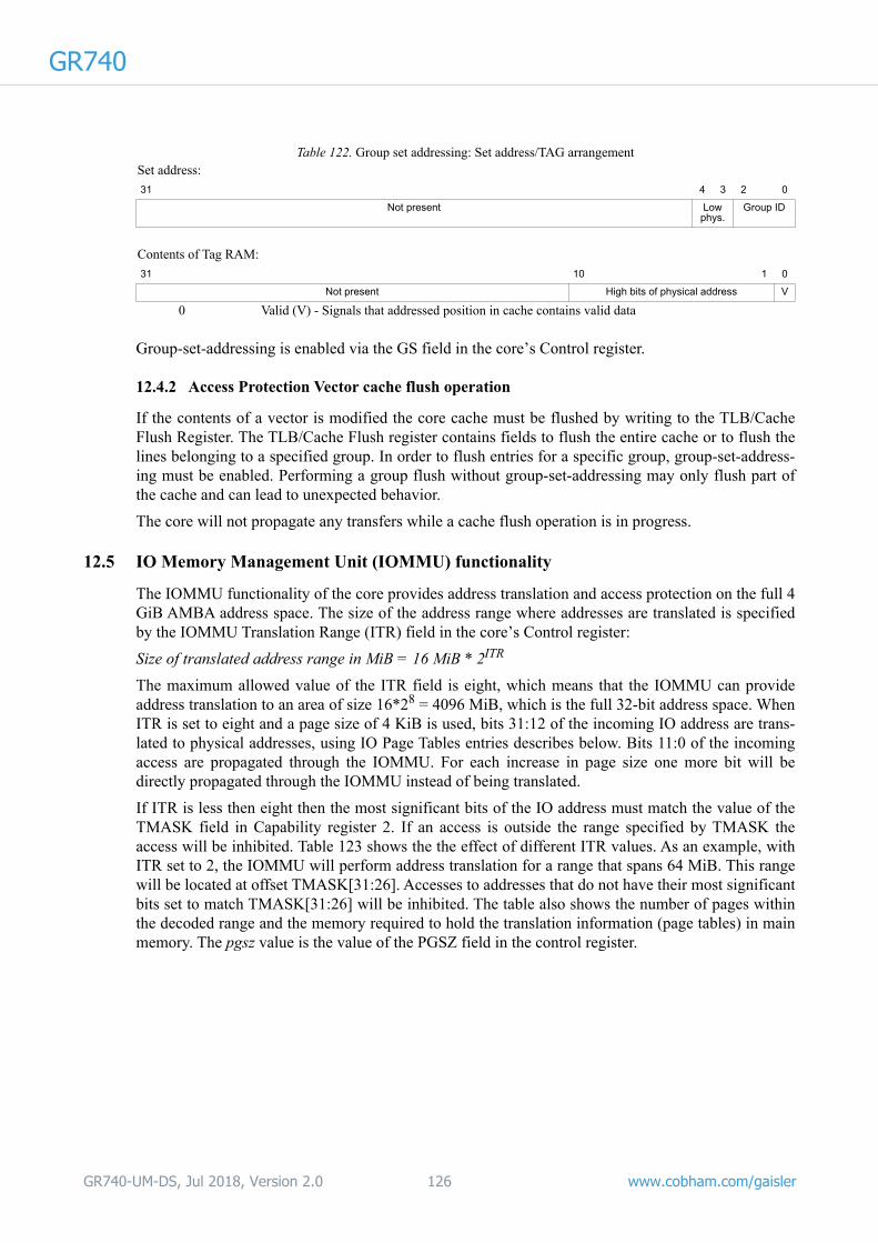
GR740
Group-set-addressing is enabled via the GS field in the core’s Control register.
12.4.2 Access Protection Vector cache flush operation
If the contents of a vector is modified the core cache must be flushed by writing to the TLB/Cache Flush Register. The TLB/Cache Flush register contains fields to flush the entire cache or to flush the lines belonging to a specified group. In order to flush entries for a specific group, group-set-address-ing must be enabled. Performing a group flush without group-set-addressing may only flush part of the cache and can lead to unexpected behavior.
The core will not propagate any transfers while a cache flush operation is in progress.
12.5 IO Memory Management Unit (IOMMU) functionality
The IOMMU functionality of the core provides address translation and access protection on the full 4 GiB AMBA address space. The size of the address range where addresses are translated is specified by the IOMMU Translation Range (ITR) field in the core’s Control register:
Size of translated address range in MiB = 16 MiB * 2ITR
The maximum allowed value of the ITR field is eight, which means that the IOMMU can provide address translation to an area of size 16*28 = 4096 MiB, which is the full 32-bit address space. When ITR is set to eight and a page size of 4 KiB is used, bits 31:12 of the incoming IO address are trans-lated to physical addresses, using IO Page Tables entries describes below. Bits 11:0 of the incoming access are propagated through the IOMMU. For each increase in page size one more bit will be directly propagated through the IOMMU instead of being translated.
If ITR is less then eight then the most significant bits of the IO address must match the value of the TMASK field in Capability register 2. If an access is outside the range specified by TMASK the access will be inhibited. Table 123 shows the the effect of different ITR values. As an example, with ITR set to 2, the IOMMU will perform address translation for a range that spans 64 MiB. This range will be located at offset TMASK[31:26]. Accesses to addresses that do not have their most significant bits set to match TMASK[31:26] will be inhibited. The table also shows the number of pages within the decoded range and the memory required to hold the translation information (page tables) in main memory. The pgsz value is the value of the PGSZ field in the control register.
Table 122. Group set addressing: Set address/TAG arrangementSet address:
31 4 3 2 0
Not present Low phys.
Group ID
Contents of Tag RAM:
31 10 1 0
Not present High bits of physical address V
0 Valid (V) - Signals that addressed position in cache contains valid data
GR740-UM-DS, Jul 2018, Version 2.0 126 www.cobham.com/gaisler

GR740
12.5.1 IO Page Table Entry
Address translation is performed by looking up translation information in a one-level table present in main memory. Part of the incoming address is used to index the table that consists of IO Page Table Entries. The format of an IO Page Table Entry (IOPTE) is shown in table 124 below.
When the core has IOMMU protection enabled all, incoming accesses from masters belonging to an active group, which is not in pass-through mode, will be matched against TMASK. If an access is out-side the range specified by ITR/TMASK, the access will be inhibited and may receive an AMBA ERROR response (not applicable when the access is a posted write).
If the incoming access is within the range specified by ITR/TMASK, the core will use the incoming IO address to index the page table containing the address translation information for the master/IO
Table 123.Effects of IOMMU Translation Range setting
ITR Size of translated range TMASK bits used Number of pages Size of page tables
0 16 MiB TMASK[31:24] 4096 / 2pgsz 16 / 2pgsz KiB
1 32 MiB TMASK[31:25] 8192 / 2pgsz 32 / 2pgsz KiB
2 64 MiB TMASK[31:26] 16384 / 2pgsz 64 / 2pgszKiB
3 128 MiB TMASK[31:27] 32768 / 2pgsz 128 / 2pgsz KiB
4 256 MiB TMASK[31:28] 655536 / 2pgsz 256 / 2pgsz KiB
5 512 MiB TMASK[31:29] 131072 / 2pgsz 512 / 2pgsz KiB
6 1024 MiB TMASK[31:30] 262144 / 2pgsz 1 / 2pgsz MiB
7 2048 MiB TMASK[31] 524288 / 2pgsz 2 / 2pgsz MiB
8 4096 MiB TMASK not used 1048576 / 2pgsz 4 / 2pgsz MiB
Table 124. IOMMU Page Table Entry (IOPTE)31 8 7 6 5 4 3 2 1 0
PPAGE C R BO BS W V R
31:8 Physical Page (PPAGE) - Bits 27:8 of this field corresponds to physical address bits 31:12 of the page. With a 4 KiB page size, PPAGE[27:8] is concatenated with the incoming IO address bits [11:0] to form the translated address. For each increase in page size one bit less of PPAGE is used and one bit more of the incoming IO address is used: this means that with a 16 KiB page size , PPAGE[27:10] will be concatenated with the incoming IO address bits [13:0] to form the translated address.
Bits 31:27 of this field are currently discarded by the IOMMU and are present in the data structure for forward compatibility with systems using 36-bit AMBA address space.
7 Cacheable (C) - This field is currently not used by the IOMMU
6:5 RESERVED
4 Bus select Override (BO) - If this field is set to ‘1’ then the bus selection is made via the IOPTE.BS field instead of the per master selection in the Master Configuration register.
3 Bus Select (BS) - Overrides master configuration register BS field when BO field in this IOPTE is set.
BS = ‘0’ routes traffic over the Processor AHB bus. BS = ‘1’ routes traffic to the Memory AHB bus.
2 Writeable (W) - If this field is ‘1’ write access is allowed to the page. If this field is ‘0’, only read accesses are allowed.
1 Valid (V) - If this field is ‘1’ the PTE is valid. If this field is ‘0’, accesses to the page covered by this PTE will be inhibited.
0 RESERVED
GR740-UM-DS, Jul 2018, Version 2.0 127 www.cobham.com/gaisler

GR740
address. The Translation Lookaside Buffer (TLB) that may hold a cached copy of the translation information. Otherwise the translation information will be fetched from main memory. The base address of the page table to use is given by the Group Configuration register to which the master per-forming the access is assigned. Please see the register description of the Group Configuration register for constraints on the page table base address. The core will use bits X:Y to index the table, where X depends on the value of the ITR field in the core’s Control register, and Y depends on the page size (Y = 12 + PGSZ field in Control register).When the core has fetched the translation information (IOPTE) for the accesses page it will check the IOPTE’s Valid (V) and Writeable (W) fields. If the IOPTE is invalid, the access will be inhibited. If the Writeable (W) field is unset and the access is a write access, the access will be inhibited. Other-wise the core will, for a page size of 4 KiB, use the IOPTE field PPAGE, bits 27:8, and bits 11:0 of the incoming IO address to form the physical address to use when the access is propagated by the core (physical address: PPAGE[27:8] & IOADDR[11:0]).
If the valid (V) bit of the IOPTE is ‘0’ the core may or may not store the IOPTE in the TLB. This is controlled via the SIV field in the core’s Control register.
12.5.2 Prefetch operations and IOMMU protection
During normal bridge operation, and with Access Protection Vector protection, the core determines if data for an access can be prefetched by looking at the IO address and the System bus plug and play information. This operation cannot be done without introducing additional delays when the core is using IOMMU protection. The incoming IO address must first be translated before it can be deter-mined if the access is to a memory area that can be prefetched. In order to minimize delays the core makes the assumption that any incoming burst access is to a prefetchable area. The result is that when using IOMMU protection all burst accesses will result in the core performing a prefetch operation.
12.5.3 Translation Lookaside Buffer operation
The TLB is implemented as a direct-mapped cache with 32 entries, where each entry is 16 bytes, built up of one data RAM and one tag RAM. The number of locations in each RAM is the number of entries in the TLB. The width of the data RAM (entry size) is the same as the size of the AMBA accesses used to fetch page table entries from main memory.
The address used to select a position in the RAMs, called the set address, has log2(number of entries in the TLB) = 5 bits. The number of address bits taken from the physical address required to uniquely address one position in the TLB depends on the page size. The number of required bits for each allowed page size is shown in table 120 below, the values in the third to tenth column is the number of address bits that must be used to accommodate the largest translatable range (maximum value of ITR field in the core’s Control register). Note that an entry size larger than 32 bits results in an TLB that holds multiple IOPTEs per entry.
Table 125.TLB entry size, page size
Entry size in bits
Entry size in IOPTEs
Bits of physical address needed to identify one position depending on page size
4 KiB 8 KiB 16 KiB 32 KiB 64 KiB 128 KiB 256 KiB 512 KiB
128 4 18 17 16 15 14 13 12 11
GR740-UM-DS, Jul 2018, Version 2.0 128 www.cobham.com/gaisler

GR740
As the TLB is not large enough to hold a copy of each position in the page table, part of the physical address and group will be placed in the tag RAM, the arrangement will be:Since the physical address is used as the set address, accesses from a master assigned to one group may evict cached IOPTE’s belonging to another group. This may not be wanted in systems where interference between groups of masters should be minimized. In order to minimize inter-group inter-ference, the core has support for using as much of the group ID as possible in the set address, this functionality is called group-set-addressing:
Group-set-addressing is enabled via the GS field in the core’s Control register.
12.5.4 TLB flush operation
If the contents of a page table is modified the TLB must be flushed by writing to the TLB/Cache Flush Register. The TLB/Cache Flush register contains fields to flush the entire TLB or to flush the entries belonging to a specified group. In order to flush entries for a specific group, group-set-addressing must be enabled. Performing a group flush without group-set-addressing may only flush part of the TLB and can lead to unexpected behavior.
When working in IOMMU mode, the core can be configured to not store a IOPTE in the TLB if the IOPTE’s valid (V) bit is cleared. This behavior is controller via the SIV field in the core’s Control reg-ister.
The core will not propagate any transfers while a flush operation is in progress.
12.6 Fault-tolerance
The Access Protection Vector cache and IOMMU TLB are implemented use byte-parity to protect entries in the cache/TLB. If an error is detected it will be processed as a cache/TLB miss and the data will be re-read from main memory. A detected error will also be reported via the core’s status register and the core also signals errors via its statistic output.
Errors can be injected in the Access Protection Vector cache and IOMMU TLB via the Data and Tag RAM Error Injection registers.
Table 126. Set address/TAG arrengementSet address:
31 4 0
Not present Low bits of physical address
Contents of Tag RAM:
31 16 14 13 1 0
Not present Group ID High bits of physical address V
0 Valid (V) - Signals that addressed position in cache contains valid data
Table 127. Group set address: Set address bits < (group ID bits) + (Physical address bits)Set address:
31 4 2 0
Not present Low phys
Group ID
Contents of Tag RAM:
31 16 16 1 0
Not present High bits of physical address V
0 Valid (V) - Signals that addressed position in cache contains valid data
GR740-UM-DS, Jul 2018, Version 2.0 129 www.cobham.com/gaisler

GR740
12.7 StatisticsThe bridge has outputs connected to the LEON4 Statistics Unit. The core has the following statistics outputs:
See section 26 for more information.
12.8 ASMP support
In some systems there may be a need to have separated instances of software each controlling a group of masters. In this case, sharing of the IOMMU register interface may not be wanted as it would allow software to modify the protection settings for a group of masters that belongs to another software instance. To prevent this, the core’s register interface is mirrored on different 4 KiB pages. Different write protection settings can be set for each mirrored block of registers. This allows use of a memory management unit to control that software running can write to one, and only one, subset of registers.
Four ASMP register blocks are available. Each ASMP register block mirrors the standard register set described in section 12.9 with the addition that some registers may be write protected. Table 129 con-tains a column that shows if a register is writable when accessed from an ASMP register block. The core’s Control register, Master configuration register(s), Diagnostic cache registers, the ASMP access control register(s) can never be written via ASMP register block. These registers are only available in the first register set starting at the core register set base address. ASMP register block n is mapped at an offset n*0x1000 from the core’s register base address.
Software should first set up the IOMMU and assign the masters into groups. Then the ASMP control registers should be configured to constrain which registers that can be written from each ASMP block. After this initialization is done, other parts of the software environment can be brought up.
As an example, consider the case where OS A will control masters 0, 1 and 4 while OS B will control masters 2 and 3. In this case it may be appropriate to map masters 0, 1 and 4 to group 0 and master 2 and 3 to group 1. The ASMP access control registers can then be configured to only allow accesses to the Group control register for group 0 from ASMP register block 1 and likewise only allow accesses to the Group control register for group 1 from ASMP register block 2.
OS A will then map in ASMP register block 1 (registers within page located at core base offset + 0x1000) and OS B will then map in ASMP register block 2 (registers within page located at core base offset + 0x2000). This way OS a will be able to change the base address and the properties of group 0, containing its masters, without being able to change the protection mechanisms of group 1 belonging to OS B. Note that since an OS is able to flush the TLB/cache it is able to impact the I/O performance of masters assigned to other OS instances. Also note that care must be taken when clearing status bits and setting the mask register that controls interrupt generation.
Table 128.IOMMU Statistics
Output Description
hit High for one cycle during TLB/cache hit.
miss High for one cycle during TLB/cache miss
pass High for one cycle during passthrough access
accok High for one cycle during access allowed
accerr High for one cycle during access denied
walk High while core is busy performing a table walk or accessing the access protection vector
lookup High while core is performing cache lookup/table walk
perr High for one cycle when core detects a parity error in the APV cache
GR740-UM-DS, Jul 2018, Version 2.0 130 www.cobham.com/gaisler

GR740
12.9 RegistersThe core is programmed through registers mapped into AHB I/O address space. All accesses to regis-ter address space must be made with word (32-bit) accesses.
Table 129.GRIOMMU registers
AHB address offset Register Writable in ASMP block
0x00 Capability register 0 No
0x04 Capability register 1 No
0x08 Capability register 2 No
0x0C Reserved -
0x10 Control register No
0x14 TLB/cache flush register Yes, protected*
0x18 Status register Yes, protected*
0x1C Interrupt mask register Yes, protected*
0x20 AHB Failing Access register No
0x24 - 0x3C Reserved, must not be accessed -
0x40 - 0x7C Master configuration registers. Master n configuration register is located at offset 0x40 + n*0x4.
No
0x80-0xBC Group control registers. Group n’s control register is located at offset 0x80 + n*0x4.
Yes, protected*
0xC0 Diagnostic cache access register No
0xC4 - 0xE0 Diagnostic cache access data registers 0 - 7 No
0xE4 Diagnostic cache access tag register No
0xE8 Data RAM error injection register No
0xEC Tag RAM error injection register No
0xF0 - 0xFF Reserved, must not be accessed No
0x100 - 0x10C ASMP access control registers.The control register for ASMP block n is located at offset 0x100+n*0x4.
No
* Register is duplicated in ASMP register block at offset 0x1000 + register offset. The number of ASMP register blocks is four. ASMP register block n starts at offset n*0x1000. Register is only writable if allowed by the corresponding ASMP access control register field.
GR740-UM-DS, Jul 2018, Version 2.0 131 www.cobham.com/gaisler

GR740
12.9.1 Capability register 0Table 130.0x00 - CAP0 - Capability register 031 30 29 28 27 24 23 20 19 18 17 16 15 14 13 12 11 9 8 7 4 3 0
A AC CA CP RESERVED NARB CS FT ST I IT IA IP RESERVED MB GRPS MSTS
1 1 1 0 0 0x4 1 0b01 1 1 1 1 0 0 1 7 9
r r r r r r r r r r r r r r r r r
31 Access Protection Vector (A) - Read-only ‘1’, the core has support for Access Protection Vector
30 Access Protection Vector Cache (AC) - Read-only ‘1’, the core has a internal cache for Access Pro-tection vector lookups.
29 Access Protection Vector Cache Addressing (CA): Read only ‘1’: Core supports using group ID as part of cache set address
28 Access Protection Vector Cache Pipeline (CP) - Read-only ‘0’, core does not have a pipeline stage added on the APV cache’s address.
27:24 RESERVED
23:20 ASMP Register Blocks (NARB) - Read-only 4. This field contains the number of ASMP register blocks that the core implements. The core has 4 ASMP register blocks with the first block starting at offset 0x1000 and the last block starting at offset 4*0x1000.
19 Configurable Page Size (CS) - Read-only ‘1’, the core supports several page sizes and the size is set via the Control register field PGSZ.
18:17 Fault Tolerance (FT) - Read-only “01” - APV cache and/or IOMMU TLB is protected by parity
16 Statistics (ST) - Read-only ‘1’, the core collects statistics
15 IOMMU functionality enable (I) - Read-only ‘1’, the core has support for IOMMU functionality.
14 IOMMU TLB (IT) - Read-only ‘1’, the core has an IOMMU Translation Lookaside Buffer (TLB)
13 IOMMU Addressing (IA): Read-only ‘1’: Core supports using group ID as part of TLB set address
12 IOMMU TLB Address Pipeline (IP) - Read-only ‘0’, the core does not have a pipeline stage added on the TLB’s address.
11:9 RESERVED
8 Multi-bus (MB) - Read-only ‘1’, the core is connected to two system buses (bus 0 is Processor AHB and bus 1 is Memory AHB).
7:4 Number of groups (GRPS) - Number of groups that the core has been implemented to support - 1. Value of GRPS is 7, the core supports eight groups.
3:0 Numbers of masters (MSTS) - Number of masters that the core has been implemented to support - 1. Value of MSTS is 9, the core supports ten masters.
GR740-UM-DS, Jul 2018, Version 2.0 132 www.cobham.com/gaisler

GR740
12.9.2 Capability register 1Table 131.0x04 - CAP1 - Capability register 1
12.9.3 Capability register 2
Table 132.0x08 - CAP2 - Capability register 2
31 20 19 16 15 8 7 5 4 0
CADDR CMASK CTAGBITS CISIZE CLINES
0 1 11 2 5
r r r r r
31:20 Access Protection Vector Cacheable Address (CADDR) - Read-only 0
19:16 Access Protection Vector Cacheable Mask (CMASK) - Read-only 1. Number of ‘1’s in the Access Protection Vector Cachable mask. The CMASK field together with the CADDR field specify a memory area protected by a part of the bit vector that can be cached by the core. The CMASK value corresponds to the number of most significant bits of the CADDR field that are matched against the incoming AMBA address when determining if the protection bits for the memory area should be cached. As CMASK is 1 and CADDR is 0x000, the core will cache protection information for the address range 0x00000000 - 0x7FFFFFFF.
15:8 Access Protection Vector Cache Tag bits (CTAGBITS) - Read-only 11. The width in bits of the Access Protection Vector cache’s tags.
7:5 Access Protection Vector Access size (CSIZE) - Read-only 2. 128-bit (16 byte). This field indicates the AMBA access size used when accessing the Access Protection Vector in main memory. This is also the cache line size for the APV cache.
4:0 Access Protection Vector Cache Lines (CLINES) - Read-only 5. Number of lines in the Access Pro-
tection Vector cache. The number of lines in the cache is 2CLINES.= 32.
31 24 23 20 19 18 17 16 15 8 7 5 4 0
TMASK RESERVED MTYPE TTYPE TTAGBITS ISIZE TLBENT
0xFF 0 0 0 0xF 0b100 0x5
r r r r r r r
31:24 Translation Mask (TMASK) - Read-only 0xFF. The incoming IO address bits IOADDR[31:24] must match this field, depending on the setting of the ITR field in the core’s Control register, for an address translation operation to be performed.
23:20 RESERVED
19:18 IOMMU Type (MTYPE) - Read-only 0, shows IOMMU implementation type.
17:16 TLB Type (TTYPE) - Read-only 0, shows implementation type of Translation Lookaside Buffer.
15:8 TLB Tag bits (TTAGBITS) - Read-only 16. The width in bits of the TLB tag.
7:5 IOMMU Access size (ISIZE) - Read only 0b100, 128-bit (16 byte). This field indicates the AMBA access size used when accessing page tables in main memory. This is also the line size for the TLB.
4:0 TLB entries (TLBENT) - Read-only 5. Number of entries in the TLB. The number of entries is 2TL-
BENT = 32.
GR740-UM-DS, Jul 2018, Version 2.0 133 www.cobham.com/gaisler

GR740
12.9.4 Control registerTable 133.0x10 - CTRL - Control register31 21 20 18 17 16 15 12 11 10 9 8 7 6 5 4 3 2 1 0
RESERVED PGSZ LB SP ITR DP SIV HPROT AU WP DM GS CE PM EN
0 0 0 0 0 0 0 0 0 0 0 0 0 0 0
r rw rw rw rw rw rw rw rw rw rw rw rw rw rw
31:21 RESERVED
20:18 Page Size (PGSZ) - The value in this field determines the page size mapped by page table entries and bit vector positions. Valid values are: 000: 4 KiB, 001: 8 KiB, 010: 16 KiB, 011: 32 KiB, 100: 64 KiB, 101: 128 KiB, 110: 256 KiB, 111: 512 KiB
17 Lookup bus (LB) - The value of this bit controls AHB master interface to use for fetching bit vector and/or page table entries from memory. If this field is ‘0’, the first master interface will be used for vector/table lookups. If this field is ‘1’, the second master interface will be used for lookups.
16 SPLIT support (SP) - This implementation of the bridge does not support use of AMBA SPLIT responses. This bit is read-only with a value of ‘0’.
15:12 IOMMU Translation Range (ITR) - This field defines the size of the address range translated by the
core’s IOMMU functionality. The size of the decoded address range is 16 MiB * 2ITR and the decoded memory area is located on an address with the most significant bits specified by the TMASK field in Capability register 2, unless ITR = 8 in which case the whole address space is cov-ered by the translated range.
11 Disable Prefetch (DP) - When this bit is ‘1’ the core will not perform any prefetch operations. During normal operation prefetch of data improves performance and should be enabled (the value of this bit should be ‘0’). Prefetching may need to be disabled in scenarios where IOMMU protection is enabled, which leads to a prefetch operation on every incoming burst access.
10 Save Invalid IOPTE (SIV) - If this field is ‘1’ the core will save IOPTEs that have their valid (V) bit set to ‘0’. If this field is ‘0’ the core will not buffer an IOPTE with valid (V) set to ‘0’ and perform an page table lookup every time the page covered by the IOPTE is accessed. If the value of this field is changed, a TLB flush must be made to remove any existing IOPTEs from the core’s internal buffer. Also if this field is set to ‘0’, any diagnostic accesses to the TLB should not set the IOPTE valid bit to ‘0’ unless the Tag valid bit is also set to ‘0’.
9:8 HPROT encoding (HPROT) - The value of this field will be assigned to the AMBA AHB HPROT signal bits 3:2 when the core is fetching protection data from main memory. HPROT(3) signals if the access is cacheable and HPROT(2) signals if the access is bufferable.
7 Always Update (AU) - If this bit is set to ‘0’ the AHB failing access register will only be updated if the Access Denied (AD) bit in the Status register is ‘0’ when the access is denied. Otherwise the AHB failing access register will be updated each time an access is denied, regardless of the Access Denied (AD) bit’s value.
6 Write Protection only (WP) - If this bit is set to ‘1’ the core will only used the Access Protection Vec-tor to protect against write accesses. Read accesses will be propagated over the core without any access restriction checks. This will improve the latency for read operations.
This field has no effect when the core is using IOMMU protection (PM field = “01”).
5 Diagnostic Mode (DM) - If this bit is set to ‘1’ the core’s internal buffers can be accessed via the Diagnostic interface (see Diagnostic cache access register) when the DE field of the Status register has been set by the core. Set this bit to ‘0’ to leave Diagnostic mode. While in this mode the core will not forward any incoming AMBA accesses.
4 Group-Set-addressing (GS) - When this bit is set to ‘1’, the core will use the group number as part of the Access Protection Vector cache set address.
3 Cache/TLB Enable (CE) - When this bit is set to ‘1’, the core’s internal cache/TLB is enabled.
2:1 Protection Mode (PM) - This value selects the protection mode to use. “00” selects Group Mode and/or Access Protection Vector mode. “01” selects IOMMU mode.
0 Enable (EN) - Core enable. If this bit is set to 1 the core is enabled. If this bit is set to 0 the core is disabled and in pass-through mode. After writing this bit software should read back the value. The change has not taken effect before the value of this bit has changed. The bit transition may be blocked if the core is in diagnostic access mode or otherwise occupied.
GR740-UM-DS, Jul 2018, Version 2.0 134 www.cobham.com/gaisler

GR740
12.9.5 TLB/cache flush registerTable 134.0x14 - FLUSH - TLB/cache flush register31 8 7 4 3 2 1 0
RESERVED FGRP RES GF F
0 0 0 0 0
r rw r rw rw
31:1 RESERVED
7:4 Flush Group (FGRP) - This field specifies the group to be used for a Group Flush, see GF field below.
3:2 RESERVED
1 Group Flush (GF) - When this bit is written to ‘1’ the cache entries for the group selected by the FGRP field will be flushed. More precisely the core will use the FGRP field as (part of the) set address when performing the flush. This flush option is only available if the core has support for group set addressing (CA field of Capability register 1 is non-zero). This flush option must only be used if the GS bit in the Control register is set to ‘1’, otherwise old data may still be marked as valid in the Access Protection Vector cache or IOMMU TLB. This bit will be reset to ‘0’ when a flush operation has completed. A flush operation also affects the FL and FC fields in the Status register.
0 Flush (F) - When this bit is written to ‘1’ the core’s internal cache will be flushed. This bit will be reset to ‘0’ when a flush operation has completed. A flush operation also affects the FL and FC fields in the Status register.
GR740-UM-DS, Jul 2018, Version 2.0 135 www.cobham.com/gaisler

GR740
12.9.6 Status registerTable 135.0x18 - STATUS - Status register
12.9.7 Interrupt mask register
Table 136.0x1c - IMASK - Interrupt mask register
31 6 5 4 3 2 1 0
RESERVED PE DE FC FL AD TE
0 0 0 0 0 0 0
r wc wc wc wc wc wc
31:6 RESERVED
5 Parity Error (PE) - The core sets this bit to ‘1’ when it detects a parity error in the tag or data RAM of the APV cache. This field is cleared by writing ‘1’ to this position, writes of ‘0’ have no effect.
4 Diagnostic Mode Enabled (DE) - If this bit is set to ‘1’ the core is in Diagnostic Mode where the core’s internal buffers can be accessed via the Diagnostic access registers. While in this mode the core will not forward any incoming AMBA accesses.
3 Flush Completed (FC) - The core sets this bit to ‘1’ when a flush operation completes. This field is cleared by writing ‘1’ to this position, writes of ‘0’ have no effect.
2 Flush started (FL) - The core sets this bit to ‘1’ when a Flush operation has started. This field is cleared by writing ‘1’ to this position, writes of ‘0’ have no effect.
1 Access Denied (AD) - The core denied an AMBA access. This field is cleared by writing ‘1’ to this position, writes of ‘0’ have no effect.
0 Translation Error (TE) - The core received an AMBA ERROR response while accessing the bit vec-tor or page tables in memory. This also leads to the incoming AMBA access being inhibited. Depending on the status of the Control register’s AU field and this register’s AD field this may also lead to an update of the AHB Failing Access register.
31 6 5 4 3 2 1 0
RESERVED PEI R FCI FLI ADI TEI
0 0 0 0 0 0 0
r rw rw rw rw rw rw
31:6 RESERVED
5 Parity Error Interrupt (PEI) - If this bit is set to ‘1’ an interrupt will be generated when the PE bit in the Status register transitions from ‘0’ to ‘1’.
4 RESERVED
3 Flush Completed Interrupt (FCI) - If this bit is set to ‘1’ an interrupt will be generated when the FC bit in the Status register transitions from ‘0’ to ‘1’.
2 Flush Started Interrupt (FLI) - If this bit is set to ‘1’ an interrupt will be generated when the FL bit in the Status register transitions from ‘0’ to ‘1’..
1 Access Denied Interrupt (ADI) - If this bit is set to ‘1’ an interrupt will be generated when the AD bit in the Status register transitions from ‘0’ to ‘1’.
0 Translation Error Interrupt (TEI) - If this bit is set to ‘1’ an interrupt will be generated when the TE bit in the Status register transitions from ‘0’ to ‘1’.
GR740-UM-DS, Jul 2018, Version 2.0 136 www.cobham.com/gaisler

GR740
12.9.8 AHB failing access registerTable 137.0x20 - AHBFAS - AHB failing access register
12.9.9 Master configuration registers
Table 138.0x40 - 0x64 - MSTCFG0-9 - Master configuration register 0 - 9
31 5 4 3 2 1 0
FADDR[31:5] FW FMASTER
0 0 0
r r r
31:5 Failing Address (FADDR[31:5]) - Bits 31:5 of IO address in access that was inhibited by the core. This field is updated depending on the value of the Control register AU field and the Status register AD field.
4 Failing Write (FW) - If this bit is set to ‘1’ the failed access was a write access, otherwise the failed access was a read access. This field is updated depending on the value of the Control register AU field and the Status register AD field.
3:0 Failing Master (FMASTER) - Index of the master that initiated the failed access. This field is updated depending on the value of the Control register AU field and the Status register AD field.
31 24 23 12 11 5 4 3 0
VENDOR DEVICE RESERVED BS GROUP
* * 0 0 0
r r r rw rw
31: 24 Vendor ID (VENDOR) - GRLIB Plug’n’play Vendor ID of master
23: 12 Device ID (DEVICE) - GRLIB Plug’n’play Device ID of master
11: 5 RESERVED
4 Bus select for master (BS) - Master n’s bus select register is located at register address offset 0x40 + n*0x4. This field specifies the bus to use for accesses initiated by AHB master n. A ‘0’ in this field routes master accesses to the Processor AHB bus. A ‘1’ in this field routes master accesses to the Memory AHB bus. Note that the value in this field affects bus selection even if the IOMMU is dis-abled.
3:0 Group assignment for master - Master n’s group assignment field is located at register address offset 0x40 + n*0x4. This field specifies the group to which a master is assigned.
GR740-UM-DS, Jul 2018, Version 2.0 137 www.cobham.com/gaisler

GR740
12.9.10 Group control registersTable 139.0x80 - 0x9C - GRPCTRL - Group control register 0 - 7
12.9.11 Diagnostic cache access register
Table 140.0xC0 - DIAGCTRL - Diagnostic cache access register
31 4 3 2 1 0
BASE[31:4] R P AG
0 0 0 0
rw r rw rw
31: 4 Base address (BASE) - Group n’s control register is located at offset 0x80 + n*0x4. This field con-tains the base address of the data structure for the group. The data structure must start on a 16-byte address boundary.
3: 2 RESERVED
1 Pass-through (P) - If this bit is set to ‘1’ and the group is active (see bit 0 below) the core will pass-through all accesses made by master in this group and not use the address specified by BASE to per-form look-ups in main memory. Note that this also means that the access will pass through untrans-lated when the core is using IOMMU protection (even if the access is outside the translated range defined by TMASK in Capability register 2).
If this bit is set to ‘0’, the core will use the contents in its cache, or in main memory, to perform checks and possibly address translation on incoming accesses.
0 Active Group (AG) - Indicates if the group is active. If this bit is set to ‘0’, all accesses made by mas-ters assigned to this group will be blocked.
If this bit is set to ‘1’, the core will check the P field of this register and possibly also the in-memory data structure before allowing or blocking the access.
31 30 29 22 21 20 19 18 0
DA RW RESERVED DP TP R SETADDR
0 0 0 0 0 0 NR
rw* rw* r rw* rw* r rw*
31 Diagnostic Access (DA) - When this bit is set to ‘1’ the core will perform a diagnostic operation to the cache address specified by the SETADDR field. When the operation has finished this bit will be reset to ‘0’.
30 Read/Write (RW) - If this bit is ‘1’ and the A field is set to ‘1’ the core will perform a read operation to the cache. The result will be available in the Diagnostic cache access tag and data register(s). If this bit is set to ‘0’ and the A field is set to ‘1’, the core will write the contents of the Diagnostic cache access tag and data registers to the internal cache.
29:22 RESERVED
21 Data Parity error (DP) - This bit is set to ‘1’ if a parity error has been detected in the word read from the cache’s data RAM. This bit can be set even if no diagnostic cache access has been made and it can also be set after a cache write operation. This bit is read-only.
20 Tag Parity error (TP) - This bit is set to ‘1’ if a parity error has been detected in the word read from the cache’s tag RAM. This bit can be set even if no diagnostic cache access has been made and it can also be set after a cache write operation. This bit is read-only.
19 RESERVED
18:0 Cache Set Address (SETADDR) - Set address to use for diagnostic cache access. When a read oper-ation has been performed, this field should not be changed until all wanted data has been read from the Diagnostic cache access data and tag registers. Changing this field invalidates the contents of the data and tag registers.
* This register can only be accessed if STATUS.DE bit in is set to 1
GR740-UM-DS, Jul 2018, Version 2.0 138 www.cobham.com/gaisler

GR740
12.9.12 Diagnostic cache access data registersTable 141.0xC4 - 0xE0 - DIAGD - Diagnostic cache access data register 0 - 7
12.9.13 Diagnostic cache access tag register
Table 142.0xE4 - DIAGT - Diagnostic cache access tag register
12.9.14 Data RAM error injection register
Table 143.0xE8 - DERRI - Data RAM error injection register
12.9.15 Tag RAM error injection register
Table 144.0xEC - TERRI - Tag RAM error injection register
31 0
CDATAn
NR
rw*
31:0 Cache data word n (CDATAn) - The core has 8 Diagnostic cache access data registers. Diagnostic cache access data register n holds data bits [31+32*n:32*n] in the cache line.
When using APV protection then the fetched vector is reversed before it is written in the cache. This means that bit 127 of the fetched vector is located in bit 0 of Diagnostic data access register 0.
* This register can only be accessed if the the STATUS.DE bit is set to 1
31 0
TAG V
NR
rw*
31:1 Cache tag (TAG) - The size of the tag depends on cache size. The contents of the tag depends on cache size and addressing settings.
0 Valid (V) - Valid bit of tag
* This register can only be accessed if the the STATUS.DE bit is set to 1
31 0
DPERRINJ
0
rw
31:0 Data RAM Parity Error Injection (DPERRINJ) - Bit DPERRINJ[n] in this register is XOR:ed with the parity bit for data bits [7+8*n:8*n] in the data RAM.
31 0
TPERRINJ
0
rw
31:0 Tag RAM Parity Error Injection (TPERRINJ) - Bit TPERRINJ[n] in this register is XOR:ed with the parity bit for tag bits [7+8*n:8*n] in the tag RAM.
GR740-UM-DS, Jul 2018, Version 2.0 139 www.cobham.com/gaisler

GR740
12.9.16 ASMP access control registersTable 145.0x100 - 0x10C - ASMPCTRL - ASMP access control registers 0 - 331 19 18 17 16 15 0
RESERVED FC SC MC GRPACCSZCTRL
0 0 0 0 0
r rw rw rw rw
31: 19 RESERVED
18 Flush register access control (FC) - If this bit is set to ‘1’ in the ASMP control register at offset 0x100 + n*0x4 then the TLB/cache flush register in ASMP register block n is writable. Otherwise writes to the TLB/cache flush register in ASMP register block n will be inhibited.
17 Status register access control (SC) - If this bit is set to ‘1’ in the ASMP control register at offset 0x100 + n*0x4 then the Status register in ASMP register block n is writable. Otherwise writes to the Status register in ASMP register block n will be inhibited.
16 Mask register access control (MC) - If this bit is set to ‘1’ in the ASMP control register at offset 0x100 + n*0x4 then the Master register in ASMP register block n is writable. Otherwise writes to the Mask register in ASMP register block n will be inhibited.
15:0 Group control register access control (GRPACCSZCTRL) - ASMP register block n’s group access control field is located at register address offset 0x100 + n*0x4. This field specifies which of the Group control registers that are writable from an ASMP register block. If GRPACCSZCTRL[i] in the ASMP access control register at offset 0x100 + n*0x4 is set to ‘1’ then Group control register i is writable from ASMP register block n.
GR740-UM-DS, Jul 2018, Version 2.0 140 www.cobham.com/gaisler

GR740
13 SpaceWire router13.1 Overview
The SpaceWire router implements a SpaceWire routing switch as defined in [SPW]. It provides an Remote Memory Access Protocol (RMAP) target according to [RMAP] for configuration at port 0 used for accessing internal configuration and status registers. In addition to this there are two different port types: SpaceWire ports and AMBA ports. The router implements a total of eight SpaceWire ports and four AMBA ports.
Among the features supported by the router are: group adaptive routing, packet distribution, system time-distribution, distributed interrupts, port timers to recover from deadlock situations, SpaceWire-D [SPWD] packet truncation based time-slot violations, and SpaceWire Plug-and-Play [SPWPNP].
Note: LVDS drivers that are not used in the application can be turned off to save power. This is con-trolled via the register bank interface. Note that there is no automatic turning off of the LVDS drivers of disabled or inactive SpaceWire links in this device, so this must be managed by the application software. See section 3.5 for further information.
13.2 Operation
The router ports are interconnected using a non-blocking switch matrix which can connect any input port to any output port. Access to each output port is arbitrated using a round-robin arbitration scheme. A single routing-table is used for the whole router. Access to the table is also arbitrated using a round-robin scheme.
The ports consist of configuration port 0 and two different types of external ports: SpaceWire links and AMBA interfaces. All ports have the same interface to the switch matrix and behave in the same manner. The difference in behavior is on the external side of the port. The SpaceWire ports provide standard SpaceWire link interfaces using on-chip LVDS. The AMBA ports transfer characters from and to an AHB bus using DMA. The different port types are described in further detail in sections 13.3, 13.4 and 13.5.
Figure 11. Block diagram
GR740-UM-DS, Jul 2018, Version 2.0 141 www.cobham.com/gaisler

GR740
13.2.1 Port numberingThe router’s ports are numbered as follows: configuration port has port number 0, the SpaceWire ports have port numbers 1-8, and the AMBA ports have port numbers 9-12.
13.2.2 Routing table
A single routing table is provided. The access to the routing table is arbitrated using a round-robin arbiter with each port being of equal priority. The operation is pipelined and one lookup can be done each cycle. This way, the maximum latency is equal to the number of ports in the router minus one. The impact on throughput should be negligible provided that packets do not arrive at the same time. The probability for this is higher when the traffic only consists of very small packets sent continu-ously (the average size being about the same as the number of ports). This should be a very uncom-mon case. Latency is still bounded and probably negligible in comparison to other latencies in most systems.
The routing table is configured with either RMAP or AMBA AHB accesses to the configuration port. Configuration of the routing table does not introduce any extra latency for packets since the configu-ration accesses have lower priority than packet traffic. The routing table is split into two parts, one which controls the port mapping for the address (RTR.RTPMAP registers) and one which controls properties for the address such as priority and header deletion (RTR.RTACTRL registers).
13.2.3 Port mapping
Each physical and logical address can be mapped to one or several output port(s). This is done by pro-gramming the corresponding RTR.RTPMAP register. The RTR.RTPMAP registers also control whether or not group adaptive routing or packet distribution shall be used for incoming packets with a specific address. The RTR.RTPMAP registers are not initialized after reset / power-up. For physical addresses this has the effect that the incoming packet is routed to the port that matches the address in the packet without any group adaptive routing or packet distribution. For logical addresses an unini-tialized RTR.RTPMAP register (or if the RTR.RTPMAP.PE field has been written with all zeros) has the effect that the incoming packet is spilled. See table 175 in section 13.5.3 for more details.
13.2.4 Address control
For each physical and logical address it is possible to configure the priority and to enable the spill-if-not-ready feature (explained in section 13.2.10). For each logical address it is further possible to enable/ disable the address and to enable / disable header deletion. Physical addresses are always enabled and have always header deletion enabled, as specified by ECSS-E-ST-50-12C [SPW]. An address is configured by programming the corresponding RTR.RTACTRL register. Logical addresses are disabled after reset / power-up. An incoming packet with a disabled logical address is spilled. See table 176 in section 13.5.3 for details.
13.2.5 Output port arbitration
Each output port is arbitrated individually based on the address of the incoming packet, using two pri-ority levels, with round-robin at each level. Each physical address and logical address can be config-ured in the routing table (RTR.RTACTRL register) to have either high or low priority. Priority assignments can have a significant impact on packet delays because packets can be large and the speed of the data consumer and link itself may not be known. This should therefore be considered when assigning priorities.
13.2.6 Group adaptive routing
Group adaptive routing can be used to map specific addresses to a group of output ports. Incoming packets with such addresses are automatically routed to the first port in the group that is not busy. It
GR740-UM-DS, Jul 2018, Version 2.0 142 www.cobham.com/gaisler
GR740
can be enabled for both physical and logical addresses and is configured by programming the corre-sponding RTR.RTPMAP register.When a packet arrives and group adaptive routing is enabled for the packet's address, the router looks up the group of ports selected by the corresponding RTR.RTPMAP register and transmits the packet on the port with the lowest index that is currently ready. Ready in this context means that the port's link interface is in run-state and currently not sending any other packet. If none of the selected output ports is ready, the incoming packet will either be spilled or transmitted on the first port that becomes ready. The action taken depends on the setting of the input port’s data character timer (see section 13.2.15), the spill-if-not-ready feature for the address (see section 13.2.10), and the link-start-on-request feature for the output ports (see section 13.2.13). See table 175 in section 13.5.3 for details on how to enable and configure group adaptive routing.
13.2.7 Packet distribution
Packet distribution can be used to implement multicast and broadcast addresses and can be enabled for both physical and logical addresses. Packet distribution is enabled and configured by program-ming the corresponding RTR.RTPMAP register.
When a packet arrives and packet distribution is enabled for the packet’s address, the router looks up the group of ports selected by the corresponding RTR.RTPMAP register. If all of the selected ports are ready, the packet is transmitted on all the ports. Ready in this context means that the port’s link inter-face is in run-state and currently not sending any other packet. If one or more of the selected ports are not ready, the incoming packet will either be spilled or transmitted once all ports are ready. The action taken depends on the setting of the input port’s data character timer (section 13.2.15), the spill-if-not-ready feature for the address (section 13.2.10), and the link-start-on-request feature for the output ports (section 13.2.13). See table 175 in section 13.5.3 for details on how to enable and configure packet distribution.
13.2.8 Port disable
A port can be disabled for data traffic by setting the corresponding RTR.PCTRL.DI bit. Incoming packets on a disabled port are silently spilled and packets are never routed to disabled ports. A dis-abled port will therefore not be included in any group used for group adaptive routing or packet distri-bution, even if the corresponding bit in that address’ RTR.RTPMAP.PE field is set.
The RTR.PCTRL.DI bit only affects the routing of data and is therefore not affecting the transmission and reception of time-codes and distributed interrupt codes.
13.2.9 Static routing
The router supports a feature called static routing, which can be enabled for each port individually. When enabled, all incoming packets on the port are routed based on the physical address specified in the port’s RTR.PCTRL2.SC field and the setting of the corresponding RTR.PCTRL2.SC bit rather than on the addresses of the packets. Header deletion is not used for incoming packets if static routing is enabled, which means that the first byte of the packets is always sent to the output port as well. Static routing to port 0 is not allowed and generates an invalid address error if attempted.
The STATICROUTEEN pin works as a global enable / disable for the static routing feature during reset. The feature is enabled if the pin is high during reset and disabled if the pin is low during reset. The RTR.RTRCFG.SR bit shows if the static routing feature is globally enabled or disabled.
Note that it is not possible to access the configuration port of the router from a port that has static rout-ing enabled.
13.2.10 Spill-if-not-ready
The spill-if-not-ready feature can be enabled individually for each physical and logical address by configuring the corresponding RTR.RTACTRL.SR bit. When enabled, an incoming packet is spilled
GR740-UM-DS, Jul 2018, Version 2.0 143 www.cobham.com/gaisler
GR740
if the selected output port’s link interface is not in run-state. If group adaptive routing is enabled for the address of the incoming packet then the packet is only spilled if none of the ports in the group is in run-state. If packet distribution is enabled for the address of the incoming packet then the packet is spilled unless the link interfaces for all selected output ports are in run-state. The spill-if-not-ready feature has priority over the incoming port’s data character timer (section 13.2.15) and the output port’s link-start-on-request feature (section 13.2.13). This means that if the spill-if-not-ready feature is enabled, the packet is spilled before the timer starts and the link-start-on-request feature will never be activated.13.2.11 Self addressing
Self addressing occurs when the selected output port for a packet is the same port as the input port. Whether or not this is allowed is controlled by the RTR.RTRCFG.SA bit. If self addressing is not allowed, the incoming packet is spilled and an invalid address error occurs.
When group adaptive routing is used and self addressing is not allowed, the input port is still allowed to be in the group of ports configured for the packet. The packet is not spilled until the router actually selects the input port as output port. If the router selects one of the other ports in the group, the packet is not spilled.
When packet distribution is used and self addressing is not allowed, the input port is not allowed to be in the group of ports configured for the packet since the packet should be sent to all ports in the group.
13.2.12 Invalid address error
An invalid address error occurs under the conditions listed below.
• When an incoming packet’s address corresponds to a non-existing port (physical addresses 13-31).
• When an incoming packet’s address is a logical address that is not enabled (RTR.RTACTRL.EN = 0).
• When an incoming packet’s address is a logical address for which the corresponding RTR.RTP-MAP register is not initialized or for which the corresponding RTR.RTPMAP.PE field is set to all zeros.
• When only one output port is selected for an incoming packet and this port is disabled (RTR.PCTRL.DI = 1).
• When self addressing occurs and the router is configured to not allow self addressing (RTR.RTRCFG.SA = 0).
• When a packet is routed with the static routing feature and the physical address programmed in RTR.PCTRL2.SD is 0 (static routing to port 0 is not allowed).
For all the invalid address cases above, the incoming packet is spilled and the RTR.PSTS.IA bit corre-sponding to the input port will be set to 1.
13.2.13 Link-start-on-request
The link-start-on-request feature makes it possible to automatically start a SpaceWire port’s link inter-face when a packet is routed to the port (i.e. the port is selected as output port). Each port can have the feature individually enabled by setting the corresponding RTR.PCTRL.LR bit to 1.
If a packet arrives and the link interface of the selected output port is not in run-state and the port has the link-start-on-request feature enabled, the router will try to start the link interface under the follow-ing conditions:
1. The link interface is not already trying to start (RTR.PCTRL.LS = 0).
2. The link is not disabled (RTR.PCTRL.LD = 0).
GR740-UM-DS, Jul 2018, Version 2.0 144 www.cobham.com/gaisler

GR740
3. The spill-if-not-ready feature is not enabled for the packet being routed.The link will continue to be started until either the RTR.PCTRL.LD bit is set to 1 or until the link is disabled through the auto-disconnect feature, as described in section 13.2.14.
The link-start-on-request feature is only available for the SpaceWire ports since the configuration port and the AMBA ports do not have a link interface FSM and are therefore always considered to be in run-state.
13.2.14 Auto-disconnect
The auto-disconnect feature allows to automatically disable the link interface of a SpaceWire port if the port has been inactive for a long enough period of time. Each port can have the feature individu-ally enabled by setting its corresponding RTR.PCTRL.AD bit to 1. The amount of time for which the port needs to be inactive is defined by the settings of the global prescaler register (RTR.PRES-CALER) and the port’s individual timer register (RTR.PTIMER). This time period is the same as the timeout period used by the port’s data character timer when recovering from deadlock situations (see section 13.2.15). If the auto-disconnect feature is enabled, a SpaceWire port will automatically disable its link interface under the following conditions:
1. The link interface entered run-state because it was started by the link-start-on-request feature described in section 13.2.15.
2. The packet that caused the link interface to start has finished (either sent or spilled).
3. Nothing has been transmitted or received on the port for the duration of the time period specified by the RTR.PRESCALER register and the corresponding RTR.PTIMER register.
4. The port’s corresponding RTR.PCTRL.LS bit has not been set to 1.
The auto-disconnect feature is only available for the SpaceWire ports since the configuration port and the AMBA ports do not have a link interface FSM and are therefore always considered to be in run-state.
13.2.15 Port data character timers
Each port has an individual data character timer, which can be used to timeout an ongoing data trans-fer in order to recover from a deadlock situation. There are two different timeouts defined: overrun timeout and underrun timeout. An overrun timeout occurs when the input port has data available but the output port(s) can not accept data fast enough. An underrun timeout occurs when the output port(s) can accept more data but the input port can not provide data fast enough.
The timeout period for a specific port is set in its RTR.PTIMER register and the timer is enabled through the corresponding RTR.PCTRL.TR bit. Timeouts due to overrun and underrun conditions can also be individually enabled / disabled through the corresponding RTR.PCTRL2.OR and RTR.PCTRL2.UR bits.
It is always the input port’s data character timer that is used for timing data transfers. When the timer is enabled, it decrements on every tick as defined by the global prescaler (RTR.PRESCALER regis-ter). The timer is always restarted when a data character is transmitted from the input port to the out-put port(s). If the timer expires, the ongoing packet is spilled and an EEP is written to the transmit FIFO of the output port(s).
The timeout period depends on the system clock frequency and is calculated as follows:
<timeout period> = (<clock period> x (RTR.PRESCALER+1)) x RTR.PTIMER
Sub-sections 13.2.15.1 through 13.2.15.4 clarifies the behaviour of the timers for different scenarios that can occur when a packet arrives.
Please see section 43.2.1 for an erratum related to overrun protection.
GR740-UM-DS, Jul 2018, Version 2.0 145 www.cobham.com/gaisler

GR740
13.2.15.1Timer disabledThe incoming packet will wait indefinitely for the output port(s) to be ready if the data character timer for an input port is disabled, unless the spill-if-not-ready feature is enabled for the packet’s address (see section 13.2.10).
13.2.15.2Timer enabled, but output port(s) not in run state
If the spill-if-not-ready feature (see section 13.2.10) is enabled, incoming packets are directly spilled in case the output port(s) are not in run state. If the feature is disabled, however, the incoming packet might be still spilled if the data character timer of the input port (together with the overrun timeout RTR.PCTRL2.OR) is enabled and the timer elapses before the output port(s) enter run-state. In case of group adaptive routing it is sufficient for one output port to enter run-state whereas in case of packet distribution all output ports must enter run-state. Note that this even applies if the link-start-on-request feature is enabled for an output port but the chosen timeout period is shorter than the time required to automatically start the link interface.
13.2.15.3Timer enabled, output port(s) in run-state but busy with other transmission
The input port’s data character timer will not start and the incoming packet will wait indefinitely until the output port either becomes free or leaves run-state. If group adaptive routing is enabled for the address of the incoming packet, the timer will not start if at least one output port of the group is in run-state. If packet distribution is used, the timer will not start if all output ports of the group are in run-state.
13.2.15.4Timer functionality when accessing the configuration port
The timer functionality is basically the same for the configuration port as for the other ports. When a command is received, the configuration port is the output port of the data transfer and when a reply is sent, the configuration port is the input port of the data transfer. The differences between the configu-ration port and the other ports are:
• The configuration port can always accept data fast enough, which means that an overrun timeout can never occur while a command is received.
• The configuration port can always send data fast enough, which means that an underrun timeout can never occur while a reply is sent.
13.2.16 Packet length truncation
Packet length truncation monitors the length of an incoming packet and increments a counter for each received data character. If the counter reaches a value larger than the input port’s RTR.MAXPLEN register and truncation is enabled for the input port (RTR.PCTRL.PL = 1), the rest of the packet is spilled and an EEP is written to the FIFO of the output port(s). Each port has its own RTR.MAX-PLEN register and counter in order to allow different maximum lengths for different ports.
Packet length truncation can also be enabled for port 0. In this case, it is the length of the RMAP / SpaceWire Plug-and-Play reply packet that is monitored.
13.2.17 System time-distribution
The router supports system time distribution through time-codes, as defined in [SPW]. It comprises a global time-counter register (RTR.TC) from which the latest received time-code can be read. Both the SpaceWire ports and the AMBA ports support time-code transmission and reception. All incoming time-codes update the RTR.TC register. If the incoming time-code has a time value which equals the old RTR.TC value plus one (modulo 64), the time-code is forwarded to all the other ports. The time-code is not sent out on the port on which it arrived. More details about the sending and receiving of time-codes through the AMBA ports are given in section 13.4.3.
GR740-UM-DS, Jul 2018, Version 2.0 146 www.cobham.com/gaisler

GR740
Time-codes can globally be enabled / disabled through the RTR.TC register, as well as individually enabled / disabled per port through corresponding RTR.PCTRL.TE bits. If time-codes are disabled for a port, all incoming time-codes on this port are discarded and no time-codes are forwarded to this port.The router can be configured to either filter out all incoming time-codes that do not have the two con-trol flags (bit 7:6) set to “00” or to discard the control flags and allow them to have any value. This configuration is done through the RTR.RTRCFG.TF bit. The control flags of the last received time-code can also be read from the RTR.TC register. Note that if interrupt distribution is globally enabled (RTR.RTRCFG.IE = 1), only control flags “00” are considered as time-codes, no matter of the value of the RTR.RTRCFG.TF bit.
13.2.18 SpaceWire distributed interrupt support
The router supports SpaceWire distributed interrupts. It can be configured to operate in two modes, interrupt with acknowledgment mode and extended interrupt mode. In the interrupt with acknowledg-ment mode, 32 interrupt numbers are supported, whereas the extended interrupt mode supports 64 interrupt numbers. The operation mode is configured through the RTR.RTRCFG.EE bit.
A distributed interrupt code is a control code that has the control flags (bits 7:6) always set to “10”.
• Interrupt with acknowledgment mode: A distributed interrupt code that has bit 5 set to 0 is called an interrupt code, and bits 4:0 specify an interrupt number between 0 and 31. When operating in the interrupt with acknowledgment mode, a distributed interrupt code with bit 5 set to 1 is called an interrupt acknowledgment code, which is used to acknowledge the interrupt with the interrupt number specified by bits 4:0.
• Extended interrupt mode: When operating in the extended interrupt mode, a distributed interrupt code with bit 5 set to 1 is called an extended interrupt code, and bits 4:0 specify an interrupt num-ber between 32 and 63. If bit 5 is set to 0, bits 4:0 specify an interrupt number between 0 and 31.
The interrupt codes and extended interrupt codes are generated by the source of the interrupt event, while the interrupt acknowledgment code is sent by the interrupt handler for the corresponding inter-rupt number.
The router has two 32-bit ISR register (RTR.ISR0 and RTR.ISR1) where each bit corresponds to one interrupt number. A bit in the ISR registers is set to 1 when an interrupt code or extended interrupt code with the corresponding interrupt number is received. A bit in the ISR registers is set to 0 when an interrupt acknowledgment code with the corresponding interrupt number is received. Therefore, the ISR registers reflect the status of all interrupt numbers. Each interrupt number has also its own timer which is used to clear the ISR register bit if an interrupt acknowledgment code is not received before the timer expires (for example if operating in the extended interrupt mode), as well as an optional timer which is used to control how fast a bit in the RTR.ISR register is allowed to toggle. See section 13.2.18.2 for more details on the ISR timers. Note that although it is possible to clear the bits in the ISR registers, these registers should normally only be used for diagnostics and FDIR.
The reset value of the distributed interrupt support is controlled via GPIO pins [7:6], see section 3.1.
13.2.18.1Receiving and transmitting distributed interrupt codes
When a distributed interrupt code is received on a port or the auxiliary time-code / distributed inter-rupt code interface, the following requirements must be fulfilled in order for the code to be distrib-uted:
1. Interrupt distribution is globally enabled (RTR.RTRCFG.IE = 1) and enabled for the port that received the code (corresponding RTR.PCTRL.IC = 1).
2. If the received code is an interrupt code, the RTR.PCTRL2.IR bit for the port must be set to 1. If the received code is an interrupt acknowledgment code or extended interrupt code, the RTR.PCTRL2.AR bit for the port must be set to 1.
GR740-UM-DS, Jul 2018, Version 2.0 147 www.cobham.com/gaisler

GR740
3. If the code is an interrupt code or extended interrupt code, the interrupt number’s corresponding bit in RTR.ISR0 or RTR.ISR1 must be 0. If the code is an interrupt acknowledgment code, the corre-sponding bit in RTR.ISR0 must be 1.4. No previous distributed interrupt code with the same interrupt number is waiting to be distributed.
5. The ISR change timers (see section 13.2.18.2) are either globally disabled (RTR.RTRCFG.IC = 0) or the interrupt number’s corresponding ISR change timer has expired.
The received code is discarded if one of the requirements above is not fulfilled. If all of the require-ments above are fulfilled, however, the received code is placed in a queue. The queue is then serviced in one of the four following ways, depending on the settings of the RTR.RTRCFG.IS and RTR.RTRCFG.IP bits:
1. All interrupt codes have priority over all interrupt acknowledgment codes / extended interrupt codes (RTR.RTRCFG.IP = 0) and the interrupt numbers are serviced through a round-robin scheme (RTR.RTRCFG.IS = 0). This is the default service scheme after reset / power-up.
2. All interrupt codes have priority over all interrupt acknowledgment codes / extended interrupt codes (RTR.RTRCFG.IP = 0) and the interrupt numbers are serviced with priority to lower interrupt numbers (RTR.RTRCFG.IS = 1).
3. All interrupt acknowledgment codes / extended interrupt codes have priority over all interrupt codes (RTR.RTRCFG.IP = 1) and the interrupt numbers are serviced through a round-robin scheme (RTR.RTRCFG.IS = 0).
4. All interrupt acknowledgment codes / extended interrupt codes have priority over all interrupt codes (RTR.RTRCFG.IP = 1) and the interrupt numbers are serviced with priority to lower interrupt numbers (RTR.RTRCFG.IS = 1).
When a distributed interrupt code has been selected from the queue, it is forwarded to all ports (except the port it was received on) that has interrupt distribution enabled (RTR.PCTRL.IC = 1) and that has transmission of interrupt codes or interrupt acknowledgment codes / extended interrupt codes enabled (RTR.PCTRL2.IT and RTR.PCTRL2.AT respectively).
13.2.18.2Interrupt distribution timers
Each interrupt number has two corresponding timers called the ISR timer and ISR change timer:
The ISR timer is started and reloaded with the value from the RTR.ISRTIMER register each time a received interrupt code / extended interrupt code sets the corresponding RTR.ISR0 / RTR.ISR1 bit to 1. If an interrupt acknowledgment code is received, the corresponding ISR timer is stopped. If the ISR timer expires before an interrupt acknowledgment code is received, the corresponding bit in the RTR.ISR0 or RTR.ISR1 register is cleared. The use of ISR timers is always enabled. In the interrupt with acknowledgment mode, the purpose of the timers is to recover from situations where an interrupt acknowledgment code is lost. In the extended interrupt mode, the purpose of the ISR timers is to limit the rate of interrupt code forwarding. It is important to configure the reload value for the ISR timer correctly. In the interrupt with acknowledgment mode, the reload value must not be less than the worst propagation delay for the interrupt code, plus the maximum delay in the interrupt handler, plus the worst propagation delay for the interrupt acknowledgment code. In the extended interrupt mode, the reload value must not be less than the worst propagation delay for the interrupt code / extended interrupt code.
The ISR change timers are timers that can optionally be used to control the minimum delay between two consecutive changes to the same RTR.ISR0 / RTR.ISR1 bit. The purpose of the timers is the pro-tection against unexpected codes that could occur, for example, due to a network malfunction or a babbling idiot. If the use of ISR change timers is enabled (RTR.RTRCFG.IC = 1), the ISR change timer for an RTR.ISR0 / RTR.ISR1 bit is started and reloaded with the value from the RTR.ISRC-TIMER register every time a received distributed interrupt code makes the RTR.ISR0 / RTR.ISR1 bit change its value. Until the timer has expired, the corresponding RTR.ISR0 / RTR.ISR1 bit is not
GR740-UM-DS, Jul 2018, Version 2.0 148 www.cobham.com/gaisler

GR740
allowed to change value and any received distributed interrupt code with that interrupt number is dis-carded. In the extended interrupt mode, the ISR change timers are not used and should be disabled.13.2.18.3Interrupt code generation
In addition to distributing interrupt codes received on the ports, the router can also generate an inter-rupt code / extended interrupt code when an internal error event occurs. In addition to the errors described in 13.2.20 the router can also be configured to send an interrupt code when a SpaceWire port’s link interface enters run-state.
Everything in sections 13.2.18.1 and 13.2.18.2 also applies when the distributed interrupt code is gen-erated by the router. The only difference is that a distributed interrupt code generated by the router will not be discarded if it is not allowed to be distributed. Instead, the distributed interrupt code will be distributed as soon as it is allowed to do so. The only time a distributed interrupt code generated by the router is not distributed is if the bits in RTR.PIP are cleared by software before the interrupt code is allowed to be sent.
The interrupt code generation is controlled through the RTR.ICODEGEN, RTR.IMASK, RTR.IPMASK, and RTR.PIP registers and in addition to the enable / disable bit (RTR.ICODE-GEN.EN), the following features are available:
• Each port has a corresponding bit in the RTR.IPMASK register in order to control whether or not an error on that specific port should generate an interrupt.
• The different error types have there own mask bit in the RTR.IMASK register in order to control whether or not that specific error should generate an interrupt.
• The interrupt number to use for a generated interrupt code is programmable through the RTR.ICODEGEN.IN field.
• The generated interrupt code can be configured to be either level type or edge type. Level type means that a new interrupt code will be sent as long as any bit in the RTR.PIP register is set. Edge type means that a new interrupt code will only be sent when a new error event occurs, i.e. when an RTR.PIP bit toggles from 0 to 1. The type is selected by the RTR.ICODEGEN.IT bit.
• A timer can be enabled through the RTR.ICODEGEN.TE bit. This timer controls the minimum time between a received interrupt acknowledgment code and the distribution of a newly gener-ated interrupt code. The timer is started and reloaded with the value from the RTR.AITIMER register when an interrupt acknowledgment code is received, if the router was the source of the corresponding interrupt code. Until the timer has expired, a newly generated interrupt code will not be distributed. The reload value must not be less than the worst propagation delay for the interrupt acknowledgment code.
• The router can be configured through RTR.ICODEGEN.AH and RTR.ICODEGEN.UA to auto-matically clear the RTR.PIP bits, which were set when the distributed interrupt code was gener-ated, once an interrupt acknowledgment code is received or once the ISR timer has expired.
13.2.19 Auxiliary time-code / distributed interrupt code interface
The router provides an auxiliary time-code / distributed interrupt code interface that is connected internally to the SpaceWire TDP controller.
The rules that determine whether a distributed interrupt code shall be forwarded to the ports are the same as for distributed interrupt codes received on any other port. However, for time-codes the value on the auxiliary interface is always forwarded and the router's internal time-count value is updated. Note that time-codes / distributed interrupt codes received through the auxiliary interface are not transmitted back to the auxiliary interface.
Just as the router ports, the auxiliary interface has enable / disable bits for time-codes (RTR.RTRCFG.AT) and interrupt codes (RTR.RTRCFG.AI), which must be set to 1 in order to trans-mit / receive codes.
GR740-UM-DS, Jul 2018, Version 2.0 149 www.cobham.com/gaisler

GR740
See section 31 for more information regarding the SpaceWire Time Distribution Protocol.13.2.20 Error detection and reporting
The router can detect and report the following errors:
• SpaceWire link errors: parity error, disconnect error, escape error, credit error (see [SPW] for definition of these errors).
• Packet spill due to: timeout (see section 13.2.14), packet length truncation (see section 13.2.16), time code / distributed interrupt code truncation (see section 13.2.21.1), and spill-if-not-ready feature (see section 13.2.10)
• Invalid address error (see section 13.2.12)
• Memory errors in the memory used for the routing table, RMAP command buffers, and port transmit and receive FIFO (see section 13.2.22)
• RMAP errors (see section 13.5.1)
• SpaceWire Plug-and-Play errors (see section 13.5.4)
Each error type has corresponding status bits in the RTR.PSTS register (RTR.PSTSCFG for the con-figuration port). Common for all the status bits is that they are set when the error is detected and that they stay set until they are cleared manually.
The router can also be configured to distribute an interrupt code when an error is detected. See section 13.2.18 for more details.
13.2.21 SpaceWire-D support
13.2.21.1Time-code and distributed interrupt code truncation
The router supports truncation of packets when it receives valid time-codes or distributed interrupt codes. A time-code is considered valid when the value equals the internal time count plus one (mod-ulo 64). A distributed interrupt code is considered valid if the corresponding ISR bit is flipped due to the reception of the code. The feature can be enabled individually for each port by setting the corre-sponding RTR.PCTRL.TS bit to 1. A filter allowing only certain time-codes and distributed interrupt codes to spill packets, can also be configured individually for each port (see RTR.PCTRL2 register).
If a packet transfer is ongoing when a valid time-code or distributed interrupt code is received and the code matches the filter in RTR.PCTRL2, the rest of the packet is spilled and an EEP is written to the FIFO of the output port(s).
Time-code and distributed interrupt code truncation can also be enabled for port 0. In that case, it is the RMAP / SpaceWire Plug-and-Play reply packet that is spilled.
13.2.22 On-chip memories
When an uncorrectable error is detected in the memories used for the routing table and the port map-ping while a packet is being routed, the packet will be discarded.
Uncorrectable errors in the ports’ FIFO memories are not handled since they only affect the contents of the routed packet and not the operation of the router itself. These types of errors can be detected by the user e.g. by adding CRC checksums to SpaceWire packets. Therefore, the RTR.PSTS.ME bit for the ports is mainly useful to gather statistics about data errors and cannot be used for error recovery.
In contrast, if the RTR.PSTSCFG.ME bits of the routing table or the port setup registers indicate a memory error, a scrubbing operation can be started. There is also an option of having automatic scrub-bing (see section 13.2.22.1).
For the FIFOs within the AMBA ports there is an option to spill the ongoing packet when an error occurs. This is controlled by the RTR.AMBACTRL.ME bit.
GR740-UM-DS, Jul 2018, Version 2.0 150 www.cobham.com/gaisler

GR740
13.2.22.1AutoscrubWith autoscrubbing enabled, the routing table and port setup registers are periodically read and rewrit-ten. This is done to prevent a buildup of SEUs, which can cause an uncorrectable error in the memo-ries. It runs in the background and has no timing impact on SpaceWire traffic but can delay configuration accesses by two cycles.
The scrubber starts at address 0 and simultaneously writes one location in the port setup memory and the routing table memory. It then waits for a timeout period before writing the next word. Eventually, the last location is reached and the process starts over from address 0.
The period between each word refresh is approximately 226 system clock cycles (system clock used for AMBA system). The scrubber uses a free time slot, in which data traffic does not perform a table lookup to read and write the memories that causes a small nondeterminism in the period.
13.3 SpaceWire ports
Each SpaceWire port comprises a SpaceWire codec that implements an encoder-decoder compliant to ECSS-E-ST-50-12C [SPW]. The interface to the router’s switch matrix consists of a transmit FIFO, receive FIFO, and control and status signals, see Figure 12. The transmit and receive FIFOs can both store up to 64 N-chars. All the configuration parameters and status information for the ports are acces-sible through the router’s configuration port, either through RMAP or AMBA AHB (see section 13.5.3).
13.3.1 Link-interface FSM
The link-interface FSM controls the link interface (a more detailed description is found in [SPW]). The low-level protocol handling (the signal and character level) is handled by the transmitter and receiver while the FSM handles the exchange level.
The link-interface FSM is controlled through the control signals provided in the RTR.PCTRL regis-ters. The link can be disabled through the RTR.PCTRL.LD bit, which depending on the current state, either prevents the link-interface from reaching the started-state or forces it to the error-reset state. When the link is not disabled, the link interface FSM is allowed to enter the started-state when either the RTR.PCTRL.LS bit is set, or the link-start-on-request feature is trying to start the port, or when a NULL character has been received and the RTR.PCTRL.AS bit is set.
The current state of the link-interface determines which type of characters are allowed to be transmit-ted. When the link-interface is in the connecting- or run-state, it is allowed to send FCTs. FCTs are sent automatically by the link-interface when possible. This is done based on the maximum value of 56 outstanding credits and the currently free space in the receive FIFO. FCTs are sent out as long as
Figure 12. Block diagram
TRANSMITTER
TXCLK
LINK INTERFACE
TRANSMITTERD(1:0)
S(1:0)
FSM
RECEIVER0
FIFO
RECEIVER FIFO
D0
S0
PHY
D
DV
CONTROL SIGNALS
STATUS SIGNALS
GR740-UM-DS, Jul 2018, Version 2.0 151 www.cobham.com/gaisler

GR740
the value of the outstanding credit counter is less than or equal to 48 and as long as there are at least 8 more empty FIFO entries available.N-Chars are sent in the run-state when they are available from the transmit FIFO and credits are avail-able. NULLs are sent when no other character transmission is requested or when the FSM is in a state where no other transmission is allowed.
The credit counter (incoming credits) is automatically increased when FCTs are received and decreased when N-Chars are transmitted. The credit counter for a SpaceWire port can be read from the corresponding RTR.CREDCNT register.
13.3.1.1 Transmitter
The state of the FSM, the credit counters, a possible request to send a time-code / distributed interrupt code, and requests from the transmit FIFO are used to decide which character is transmitted next. The type of character and the character itself (for N-Chars and time-codes / distributed interrupt codes) are presented to the low-level transmitter, which runs on the internal SpaceWire clock. For information on how to change the transmission rate see Section 13.3.2.
The state of the FSM, credit counters, requests from the time-interface and requests from the transmit-ter FIFO are used to decide the next character to be transmitted. The type of character and the charac-ter itself (for N-Chars and Time-codes) to be transmitted are presented to the low-level transmitter which is located in a separate clock-domain.
13.3.1.2 Receiver
The receiver detects connections from other nodes and receives characters as a bit stream recovered from the data and strobe signals by the PHY module, which presents it as a data and data-valid signal.
The receiver is activated as soon as the link-interface leaves the error reset state. Then, after a NULL is received it can start receiving any other characters. It detects parity, escape and credit errors, which causes the link interface to enter the error-reset state.
Received L-Chars are handled automatically by the link-interface, whereas all N-Chars are stored in the receive FIFO.
The max receive rate is 1.3 times the frequency of the internal SpaceWire clock and the device has been tested for a receive bit rate of maximum 300 Mbit/s. The system clock must be higher or equal to the receive bit rate divided by eight. For example, if the receive bit rate is 100 Mbit/s then the system clock must be at least 12.5 MHz.
13.3.2 Setting link-rate
The initialization divisor register (RTR.IDIV) determines the link-rate during initialization (all states up to and including the connecting-state) for all SpaceWire ports. The register is also used to calculate the link interface FSM timeouts for all SpaceWire ports (6.4 us and 12.8 us, as defined in the Space-Wire standard [SPW]). The RTR.IDIV register should always be set so that a 10 Mbit/s link-rate is achieved during initialization. Then, the timeout values are also calculated correctly.
To achieve a 10 Mbit/s link-rate, the RTR.IDIV register should be set as follows:
RTR.IDIV = (<frequency in MHz of internal SpaceWire clock> / 10) - 1
The link-rate in run-state can be controlled individually per SpaceWire port with the run-state divisor located in each port’s control register (RTR.PCTRL.RD field). The link-rate in run-state is calculated as follows:
<link-rate in Mbits/s> = <frequency in MHz of internal SpaceWire clock> / (RTR.PCTRL.RD+1)
The value in RTR.PCTRL.RD only affects the link-rate in run-state and does not affect the 6.4 us or 12.8 us timeouts values.
GR740-UM-DS, Jul 2018, Version 2.0 152 www.cobham.com/gaisler

GR740
13.4 AMBA portsThe AMBA ports are Cobham Gaisler’s GRSPW2 controller with the SpaceWire codec removed. Thus, the same drivers that are provided for the GRSPW2 can also be used for an AMBA port of the router. Only one additional driver is needed, which handles the setup of the registers within the con-figuration port.
13.4.1 Overview
The router’s AMBA ports are configured by register accesses through an APB interface. Data is trans-ferred through one to four DMA channels using an AHB master interface.
13.4.2 Operation
The main sub-blocks of the router AHB interfaces are the DMA engines, the RMAP target and the AMBA interface. A block diagram of the internal structure can be found in Figure 13.
The AMBA interface is divided into the AHB master interface and the APB interface. The DMA engines have FIFO interfaces to the router switch matrix. These FIFOs are used to transfer N-Chars between the AMBA bus and the other ports in the router.
The RMAP target handles incoming packets, which are determined to be RMAP commands instead of the receiver DMA engine. The RMAP command is decoded and if it is valid the operation is per-formed on the AHB bus. If a reply was requested, it is automatically transmitted back to the source by the RMAP transmitter.
The AMBA ports are controlled by writing to a set of user registers through the APB interface and a set of signals. The different sub-modules are discussed in further detail in later sections.
13.4.2.1 Protocol support
The AMBA port only accepts packets with a valid destination address in the first received byte. Pack-ets with address mismatch will be silently discarded (except in promiscuous mode which is covered in section 13.4.4.10).
The second byte is sometimes interpreted as a protocol ID as described hereafter. The RMAP protocol (ID=0x1) is the only protocol handled separately in hardware while other packets are stored to a DMA channel. If the RMAP target is enabled, all RMAP commands will be processed, executed and answered automatically in hardware. Otherwise, RMAP commands are stored to a DMA channel in the same way as other packets. RMAP replies are always stored to a DMA channel. More information on the RMAP protocol support is found in section 13.4.6 (note that this RMAP target is different from
Figure 13. Block diagram of the Router DMA port
TRANSMITTERFSM
SEND
RMAP
FSM
TRANSMITTERDMA ENGINE
RECEIVER DMA ENGINE
TRANSMITTER
RMAP RECEIVER
N-CHAR FIFO
RECEIVER AHB FIFO
RECEIVER DATAPARALLELIZATION
AHB
MASTER INTERFACE
REGISTERSAPB
INTERFACE
FROM ROUTERSWITCH MATRIX
TO ROUTERSWITCH MATRIX
GR740-UM-DS, Jul 2018, Version 2.0 153 www.cobham.com/gaisler

GR740
the one in the configuration port). When the RMAP target is disabled, there is no need to include a protocol ID in the packets and the data can start immediately after the address.All packets arriving with the extended protocol ID (0x00) are stored to a DMA channel. This means that the hardware RMAP target will not work if the incoming RMAP packets use the extended proto-col ID. Note also that packets with the reserved extended protocol identifier (ID = 0x000000) are not ignored by the AMBA port. It is up to the software to ignore them.
When transmitting packets, the address and protocol-ID fields must be included in the buffers from where data is fetched. They are not automatically added by the AMBA port DMA engine.
Figure 14 shows the packet types accepted by the port. The port also allows reception and transmis-sion with extended protocol identifiers but without support for RMAP CRC calculations and the RMAP target.
13.4.3 Time-Code / distributed interrupt interface
13.4.3.1 Sending and receiving Time-Codes
To transmit a Time-Code through the register interface of an AMBA port, the RTR.AMBACTRL.TI bit should be written to 1. When the bit is written, the AMBA port’s current time value (RTR.AMBATC.TIMECNT field) is incremented and a Time-Code consisting of the new time value together with the current control flags (RTR.AMBATC.TCTRL field) is sent. The RTR.AMBAC-TRL.TI bit will stay high until the Time-Code has been transmitted. Note that whether or not a Time-Code is forwarded to any other port after it has been sent by an AMBA port depends on the settings explained in 13.2.17.
A Time-Code that is received by an AMBA port will be stored in the port’s RTR.AMBATC register. There is also a possibility to generate AMBA interrupts and tick-out pulses that are routed to the GPTIMER units for time latching (see section 5.9). This is controlled through the RTR.AMBACTRL and RTR.AMBATC registers. See section 13.4.8 for details about these registers.
13.4.3.2 Sending and receiving distributed interrupts
To transmit a distributed interrupt code through the register interface of an AMBA port, the RTR.AMBAINTCTRL.II bit in should be written to 1. When the bit is written, the value of the RTR.AMBAINTCTRL.TXINT field determine which distributed interrupt code that will be sent. Note that whether or not a distributed interrupt code is forwarded to any other port after it has been sent by an AMBA port depends on the settings of the router and the state of that specific interrupt in the network. See 13.2.18 for details.
A distributed interrupt can also be configured to be generated automatically by the AMBA port upon certain events. This is controlled through the RTR.AMBAINTCTRL and RTR.AMBADMACTRL registers. See section 13.4.8 for details about these registers and features.
Distributed interrupt codes that are received by an AMBA port can be programmed to generate AMBA interrupts as well as tick out-pulses that are routed to the GPTIMER units for time latching (see section 5.9). See section 13.4.8 for details about these features.
Figure 14. The SpaceWire packet types supported by the port.
Addr ProtID Dn-2..D3D2D1D0 Dn-1 EOP
Addr D0 Dm-2..D4D3D2D1 Dm-1 EOP
GR740-UM-DS, Jul 2018, Version 2.0 154 www.cobham.com/gaisler

GR740
13.4.4 Receiver DMA channelsThe receiver DMA engine handles reception of data from the SpaceWire network to different DMA channels.
13.4.4.1 Address comparison and channel selection
Packets are received to different channels based on the address and whether a channel is enabled or not. When the receiver N-Char FIFO contains one or more characters, N-Chars are read by the receiver DMA engine. The first character is interpreted as the logical address and is compared with the addresses of each channel starting from 0. The packet will be stored to the first channel with an matching address. The complete packet including address and protocol ID but excluding EOP/EEP is stored to the memory address pointed to by the descriptors (explained later in this section) of the channel.
Each SpaceWire address register has a corresponding mask register. Only bits at an index containing a zero in the corresponding mask register are compared. This way a DMA channel can accept a range of addresses. There is a default address register which is used for address checking in all implemented DMA channels that do not have separate addressing enabled and for RMAP commands in the RMAP target. With separate addressing enabled the DMA channels’ own address/mask register pair is used instead.
If an RMAP command is received, it is only handled by the target if the default address register (including mask) matches the received address. Otherwise, the packet will be stored to a DMA chan-nel if one or more of them has a matching address. If the address does neither match the default address nor one of the DMA channels’ separate registers, the packet is still handled by the RMAP tar-get if enabled since it has to return the invalid address error code. The packet is only discarded (up to and including the next EOP/EEP) if an address cannot be matched and the RMAP target is disabled.
Packets other than RMAP commands that neither match the default address register nor the DMA channels’ address register will be discarded. Figure 15 shows a flowchart of the packet reception.
At least 2 non EOP/EEP N-Chars needs to be received for a packet to be stored to the DMA channel unless the promiscuous mode is enabled in which case 1 N-Char is enough. If it is an RMAP packet with hardware RMAP enabled, 3 N-Chars are needed since the command byte determines where the packet is processed. Packets smaller than these sizes are discarded.
13.4.4.2 Basic functionality of a channel
Reception is based on descriptors located in a consecutive area in memory that hold pointers to buf-fers where packets should be stored. When a packet arrives at the port, the destined channel is first determined as described in the previous section. A descriptor is then read from the descriptor area of the channel and the packet is stored to the memory area the descriptor is pointing to. Lastly, status information is stored to the same descriptor and the descriptor pointer is incremented by one. The fol-lowing sections describe the DMA channel reception in more detail.
13.4.4.3 Setting up the port for reception
A few registers need to be initialized before reception to a channel can take place. The DMA channel has a maximum length register, which sets the maximum packet size in bytes that can be received to this channel. Larger packets are truncated and the excessive part is spilled. If this happens, an indica-tion will be given in the status field of the descriptor. The minimum value for the receiver maximum length field is 4 and the value can only be incremented in steps of four bytes up to the maximum value of 33554428. If the maximum length is set to zero the receiver will not function correctly.
Either the default address register or the channel specific address register (the corresponding mask register must also be set) needs to be set to hold the address used by the channel. A control bit in the DMA channel control register determines whether the channel should use default address and mask registers for address comparison or the channel’s own registers. Using the default register, the same
GR740-UM-DS, Jul 2018, Version 2.0 155 www.cobham.com/gaisler

GR740
address range is accepted for all channels with default addressing, whereas the separate address pro-vides the channel its own range. If all channels use the default registers they will accept the same address range and the enabled channel with the lowest number will receive the packet.
Start Reception
Receive2 bytes
rmap enabled
defaddr*!defmask =rxaddr*!defmask
Yes
Receive1 byte
RMAP commandNo
Yes
No
Set DMA channel number to 0
Process RMAPcommand
Separate addressing
No
Yes
dma(n).addr*
rxaddr*!dma(n).mask
Channel enabled
Increment channel number
andpid =1 and
defaddr*!defmask =rxaddr*!defmask
!dma(n).mask=
Last DMA channel
No
Yes
Store packet toDMA channel
No
No
Yes
RMAP enabled
Discard packet
Yes
Yes
No
Figure 15. Flow chart of packet reception (promiscuous mode disabled).
No
GR740-UM-DS, Jul 2018, Version 2.0 156 www.cobham.com/gaisler

GR740
Finally, the descriptor table and control register must be initialized. This is described in the two fol-lowing sections.13.4.4.4 Setting up the descriptor table address
The port reads descriptors from an area in memory, to which the receiver descriptor table address reg-ister is pointing. The register consists of a base address and a descriptor selector. The base address points to the beginning of the area and must start on a 1024 bytes aligned address. It is also limited to be 1024 bytes in size which means the maximum number of descriptors is 128 since the descriptor size is 8 bytes.
The descriptor selector points to individual descriptors and is increased by 1 when a descriptor has been used. When the selector reaches the upper limit of the area, it wraps to the beginning automati-cally. It can also be set to wrap at a specific descriptor before the upper limit by setting the wrap bit in the descriptor. The idea is that the selector should be initialized to 0 (start of the descriptor area) but it can also be written with another 8 bytes aligned value to start somewhere in the middle of the area. It will still wrap to the beginning of the area.
To use a new descriptor table, the receiver enable bit in the corresponding AMBA port DMA control/status register has to be cleared first. Once the RX active bit in the same register is cleared, it is safe to update the descriptor table register. After updating and enabling the descriptors, the receiver enable bit can be set again.
13.4.4.5 Enabling descriptors
As mentioned earlier, one or more descriptors must be enabled before reception can take place. Each descriptor has a size of 8 bytes and its layout can be found in the tables below. The descriptors should be written to the memory area the receiver descriptor table address register is pointing to. Newly added descriptors must always be placed after the previous one written to the area. Otherwise, they will not be noticed.
A descriptor is enabled by setting the address pointer to a location where data can be stored and then setting the enable bit. The WR bit can be set to cause the selector to be set to zero when reception has finished to this descriptor. IE should be set if an interrupt is wanted when the reception has finished. The DMA control register interrupt enable bit must also be set for an interrupt to be generated.
Table 146. RXDMA receive descriptor word 0 (address offset 0x0)31 30 29 28 27 26 25 24 0
TR DC HC EP IE WR EN PACKETLENGTH
31 Truncated (TR) - Packet was truncated due to maximum length violation.
30 Data CRC (DC) - 1 if a CRC error was detected for the data and 0 otherwise.
29 Header CRC (HC) - 1 if a CRC error was detected for the header and 0 otherwise.
28 EEP termination (EP) - This packet ended with an Error End of Packet character.
27 Interrupt enable (IE) - If set, an interrupt will be generated when a packet has been received if the receive interrupt enable bit in the DMA channel control register is set.
26 Wrap (WR) - If set, the next descriptor used by the GRSPW will be the first one in the descriptor table (at the base address). Otherwise the descriptor pointer will be increased with 0x8 to use the descriptor at the next higher memory location. The descriptor table is limited to 1 KiB in size and the pointer will be automatically wrap back to the base address when it reaches the 1 KiB boundary.
25 Enable (EN) - Set to one to activate this descriptor. This means that the descriptor contains valid con-trol values and the memory area pointed to by the packet address field can be used to store a packet.
24: 0 Packet length (PACKETLENGTH) - The number of bytes received to this buffer. Only valid after EN has been set to 0 by the GRSPW.
GR740-UM-DS, Jul 2018, Version 2.0 157 www.cobham.com/gaisler

GR740
13.4.4.6 Setting up the DMA control register
The final step to receive packets is to set the control register as follows: The receiver must first be enabled by setting the rxen bit in the DMA control register (see section 13.4.8). The rxdescav bit in the DMA control register is then set to indicate that there are new active descriptors. This must always be done after the descriptors have been enabled or the port might not notice the new descriptors. More descriptors can be activated when reception has already started by enabling the descriptors and writ-ing the rxdescav bit. When these bits are set, reception will start immediately when data is arriving.
13.4.4.7 The effect to the control bits during reception
When the receiver is disabled, all packets going to the DMA-channel are discarded if the address of the packet does not fall into the range of another DMA channel. If the receiver is enabled and the address falls into the accepted address range, the next state is entered where the rxdescav bit is checked. This bit indicates whether there are active descriptors available or not and should be set by the external application using the DMA channel each time descriptors are enabled as mentioned above. If the rxdescav bit is ‘0’ and the nospill bit is ‘0’ the packets will be discarded. If nospill is ’1’ the AMBA port waits until rxdescav is set and the characters are kept in the N-Char FIFO during this time. If the FIFO becomes full, back-pressure is applied to the SpaceWire link by ceasing the trans-mission of FCTs.
When rxdescav is set, the next descriptor is read and - if enabled - the packet is received to the buffer. If the read descriptor is not enabled, however, rxdescav is set to ‘0’ and the packet is spilled depend-ing on the value of nospill.
The receiver can be disabled at any time, which will stop packets from being received to this channel. If a packet is currently received when the receiver is disabled, the reception will continue until it is finished. The rxdescav bit can also be cleared at any time. It will not affect any ongoing receptions but no more descriptors will be read until it is set again. Rxdescav is also cleared by the port when it reads a disabled descriptor.
13.4.4.8 Status bits
When the reception of a packet is finished, the enable bit in the current descriptor is set to zero. When enable is zero, the status bits are also valid and the number of received bytes is indicated in the length field. The DMA control register contains a status bit, which is set each time a packet has been received. The port can also be set up to generate an interrupt for this event.
The RMAP CRC calculation is always active for all received packets and the full payload of the packet without the EOP/EEP is covered. The packet is always assumed to be an RMAP packet and the length of the header is determined by checking byte 3 that should be the command field. The calcu-lated CRC value is then checked when the header has been received (according to the calculated num-ber of bytes) and if it is non-zero the HC bit is set indicating a header CRC error.
The CRC value is not reset after the header has been received, instead the calculation continues until the complete packet has been received. Then, if the CRC value is non-zero, the DC bit is set to indi-cate a data CRC error. This means that the port can indicate a data CRC error even if the data field was correct but the header CRC was incorrect. Thus, a CRC data error is only determinate when the HC bit is zero.
Table 147. RXDMA receive descriptor word 1 (address offset 0x4)31 0
PACKETADDRESS
31: 0 Packet address (PACKETADDRESS) - The address pointing at the buffer which will be used to store the received packet.
GR740-UM-DS, Jul 2018, Version 2.0 158 www.cobham.com/gaisler

GR740
If the received packet is not an RMAP packet, the header CRC error indication bit cannot be used. However, it is still possible to use the DC bit if the complete packet is covered by an appended CRC checksum, which is calculated according to the RMAP standard [RMAP]. For all other packets, both the HC and DC bits should be ignored.13.4.4.9 Error handling
If an AHB error occurs during reception, the current packet is spilled up to and including the next EEP/EOP and then the currently active channel is disabled and the receiver enters the idle state. A bit in the channels control/status register can be configured to be set to indicate this condition.
See also the AMBA ERROR propagation description in section 5.10.
13.4.4.10Promiscuous mode
The port supports a promiscuous mode where all received data (excluding EOPs/EEPs) is stored to the first enabled DMA channel regardless of the node address and possible early EOPs/EEPs. The AMBA port DMA RX maximum length register is still checked and packets exceeding this size are truncated.
RMAP commands are still handled by the RMAP hardware target when promiscuous mode is enabled, if the RMAP enable bit in the AMBA port DMA control/status register is set. If the RMAP enable bit is cleared, RMAP commands are stored to a DMA channel instead.
13.4.5 Transmitter DMA channels
The transmitter DMA engine handles the transmission of data from the DMA channels to the Space-Wire network. Each receive channel has a corresponding transmit channel which means that there can be up to 4 transmit channels. However, it is only necessary to use a separate transmit channel for each receive channel if there are also separate entities controlling the transmissions. The use of a single channel with multiple controlling entities would cause them to corrupt each other’s transmissions. A single channel is more efficient and should be used when possible.
Multiple transmit channels with pending transmissions are arbitrated in a round-robin fashion.
13.4.5.1 Basic functionality of a channel
A transmit DMA channel reads data from the AHB bus and stores it in the transmitter FIFO for trans-mission on the SpaceWire network. Transmission is based on the same type of descriptors as for the receiver and the descriptor table has the same alignment and size restrictions. When there are new descriptors enabled, the port reads them and transfers the amount of data indicated.
13.4.5.2 Setting up transmission
Four steps are needed to set up the port for transmission. First, the link interface must be enabled and started by writing the appropriate value to the ctrl register. Then, the address to the descriptor table needs to be written to the transmitter descriptor table address register and one or more descriptors must also be enabled in the table. Finally, the txen bit in the DMA control register is written with a one, which triggers the transmission. These steps are covered in more detail in the next sections.
13.4.5.3 Enabling descriptors
The descriptor table address register works in the same way as the one of the receiver, see section 13.4.4. Although the maximum size is 1024 bytes as for the receiver, it can only store 64 descriptors because the size of each descriptor is now 16 bytes instead of 8 bytes.
To transmit packets, one or more descriptors have to be initialized in memory, which is done in the following way: The number of bytes to be transmitted and a pointer to the data has to be set. There are two different length and address fields in the transmit descriptors because there are separate pointers
GR740-UM-DS, Jul 2018, Version 2.0 159 www.cobham.com/gaisler

GR740
for header and data. If a length field is zero, the corresponding part of a packet is skipped and if both are zero no packet is sent. The maximum header length is 255 bytes and the maximum data length is 16 MiB - 1. When the pointer and length fields have been set, the enable bit should be set to enable the descriptor. This must always be done last. The other control bits must also be set before enabling the descriptor.The transmit descriptors are 16 bytes in size so the maximum number in a single table is 64. The dif-ferent fields of the descriptor together with the memory offsets are shown in the tables below.
The HC bit should be set if RMAP CRC should be calculated and inserted for the header field and correspondingly the DC bit should be set for the data field. The header CRC will be calculated from the data fetched from the header pointer and the data CRC is generated from data fetched from the data pointer. The CRCs are appended after the corresponding fields. The non-CRC bytes field is set to the number of bytes in the beginning of the header field that should not be included in the CRC calcu-lation.
The CRCs are sent even if the corresponding length is zero, but when both lengths are zero no packet is sent, not even an EOP.
13.4.5.4 Starting transmissions
When the descriptors have been initialized, the transmit enable bit in the DMA control register has to be set to enable transmission. New descriptors can be activated in the table on the fly (while transmis-sion is active). Each time a set of descriptors is added, the transmit enable bit in the corresponding AMBA port DMA control/status register should be set. This has to be done because each time the port encounters a disabled descriptor this register bit is set to 0.
Table 148. TXDMA transmit descriptor word 0 (address offset 0x0)31 18 17 16 15 14 13 12 11 8 7 0
RESERVED DC HC RE IE WR EN NONCRCLEN HEADERLEN
31: 18 RESERVED
17 Append data CRC (DC) - Append CRC calculated according to the RMAP specification after the data sent from the data pointer. The CRC covers all the bytes from this pointer. A null CRC will be sent if the length of the data field is zero.
16 Append header CRC (HC) - Append CRC calculated according to the RMAP specification after the data sent from the header pointer. The CRC covers all bytes from this pointer except a number of bytes in the beginning specified by the non-crc bytes field. The CRC will not be sent if the header length field is zero.
15 RESERVED
14 Interrupt enable (IE) - If set, an interrupt will be generated when the packet has been transmitted and the transmitter interrupt enable bit in the DMA control register is set.
13 Wrap (WR) - If set, the descriptor pointer will wrap and the next descriptor read will be the first one in the table (at the base address). Otherwise the pointer is increased with 0x10 to use the descriptor at the next higher memory location.
12 Enable (EN) - Enable transmitter descriptor. When all control fields (address, length, wrap and crc) are set, this bit should be set. While the bit is set the descriptor should not be touched since this might corrupt the transmission. The GRSPW clears this bit when the transmission has finished.
11: 8 Non-CRC bytes (NONCRCLEN)- Sets the number of bytes in the beginning of the header which should not be included in the CRC calculation. This is necessary when using path addressing since one or more bytes in the beginning of the packet might be discarded before the packet reaches its destination.
7: 0 Header length (HEADERLEN) - Header Length in bytes. If set to zero, the header is skipped.
GR740-UM-DS, Jul 2018, Version 2.0 160 www.cobham.com/gaisler

GR740
13.4.5.5 The transmission process
When the transmit enable bit int the AMBA port DMA control/status register is set, the port starts reading descriptors immediately. The number of bytes indicated are read and transmitted. Once a transmission is finished, status information is written to the first field of the descriptor and a packet sent bit is set in the DMA control register. If an interrupt was requested, it will also be generated. Then, a new descriptor is read and - if enabled - a new transmission starts, otherwise the transmit enable bit is cleared and the transmitter channel stays idle until it is enabled again.
13.4.5.6 The descriptor table address register
The internal pointer, which is used to keep the current position in the descriptor table can be read and written through the APB interface. This pointer is set to zero during reset and is incremented each time a descriptor is used. It wraps automatically when the 1024 bytes limit for the descriptor table is reached or it can be set to wrap earlier by setting a bit in the current descriptor.
The descriptor table register can be updated with a new table anytime when no transmission is active. No transmission is active if the transmit enable bit is zero and the complete table has been sent or if the table is aborted (explained below). If the table is aborted one has to wait until the transmit enable bit is zero before updating the table pointer.
13.4.5.7 Error handling
13.4.5.7.1 Abort Tx
The DMA control register contains a bit called Abort TX, which if set causes the current transmission to be aborted, that is, the packet is truncated and an EEP is inserted. This is only useful if the packet
Table 149. TXDMA transmit descriptor word 1 (address offset 0x4)31 0
HEADERADDRESS
31: 0 Header address (HEADERADDRESS) - Address from where the packet header is fetched. Does not need to be word aligned.
Table 150. TXDMA transmit descriptor word 2 (address offset 0x8)31 24 23 0
RESERVED DATALEN
31: 24 RESERVED
23: 0 Data length (DATALEN) - Length of data part of packet. If set to zero, no data will be sent. If both data- and header-lengths are set to zero no packet will be sent.
Table 151. TXDMA transmit descriptor word 3(address offset 0xC)31 0
DATAADDRESS
31: 0 Data address (DATAADDRESS) - Address from where data is read. Does not need to be word aligned.
GR740-UM-DS, Jul 2018, Version 2.0 161 www.cobham.com/gaisler
GR740
needs to be aborted because of congestion on the SpaceWire network. If the congestion is on the AHB bus this will not help (This should not be a problem since AHB slaves should have a maximum of 16 waitstates). The aborted packet will have its LE bit set in the descriptor. The transmit enable register bit is also cleared and no new transmissions are done until the transmitter is enabled again.13.4.5.7.2 AHB error
When an AHB error is encountered during transmission, the currently active DMA channel is dis-abled and the transmitter goes to the idle mode. A bit in the control/status register of the DMA chan-nel is set to indicate this error condition and, if enabled, an interrupt will also be generated. Further error handling depends on what state the transmitter DMA engine was in when the AHB error occurred. If the descriptor was read, the packet transmission had not started yet and therefore no more actions are required. See also the AMBA ERROR propagation description in section 5.10.
If the AHB error occurs during packet transmission, the packet is truncated and an EEP is inserted. Lastly, if it occurs while status information is written to the descriptor, the descriptor is not closed cor-rectly and is thus staying enabled and not indicating any errors although the packet transmission has been successful.
The client using the channel has to correct the AHB error condition and enable the channel again. No more AHB transfers are done again from the same unit (receiver or transmitter) which was active during the AHB error until the error state is cleared and the unit is enabled again.
13.4.6 RMAP target
The Remote Memory Access Protocol (RMAP) is used to implement access to resources on the AHB bus via the SpaceWire Links, e.g. for reading and writing to memory, registers and FIFOs. This sec-tion describes the target implementation.
13.4.6.1 Fundamentals of the protocol
RMAP is a protocol, which is designed to provide remote access via a SpaceWire network to memory mapped resources on a SpaceWire node. It provides three operations: write, read and read-modify-write. These operations are posted operations which means that a source does not wait for an acknowledge or reply. It also implies that any number of operations can be outstanding at any time and that no timeout mechanism is implemented in the protocol. Timeouts must be implemented in the user application which sends the commands. Data payloads of up to 16 MiB - 1 is supported in the protocol. A destination can be requested to send replies and to verify data before executing an opera-tion. A complete description of the protocol is found in the RMAP standard [RMAP].
13.4.6.2 Implementation
The port includes a target for RMAP commands, which processes all incoming packets with protocol ID = 0x01, type field (bit 7 and 6 of the 3rd byte in the packet) equal to 01b and an address falling in the range set by the default address and mask register. When such a packet is detected, it is not stored to the DMA channel but is instead passed to the RMAP receiver.
The target implements all three commands defined in [RMAP], with some restrictions. Support is only provided for 32-bit big-endian systems. This means that the first byte received is the msb in a word. The target will not receive RMAP packets using the extended protocol ID which are always dumped to the DMA channel.
The RMAP receiver processes commands. If they are correct and accepted, the operation is performed on the AHB bus and a reply is generated. If an acknowledge is requested, the RMAP transmitter auto-matically sends the reply. RMAP transmissions have priority over DMA channel transmissions.
There is a user accessible destination key register, which is compared to the destination key field in incoming packets. If there is a mismatch and a reply has been requested, the error code in the reply is set to 3. Replies are sent if and only if the ack field is set to ‘1’.
GR740-UM-DS, Jul 2018, Version 2.0 162 www.cobham.com/gaisler

GR740
When a failure occurs during a bus access, the error code is set to 1 (General Error). There is a prede-termined order in which error-codes are set in the case of multiple errors. It is shown in table 152.Read accesses are performed on the fly, that is, they are not stored in a temporary buffer before trans-mission. This means that the error code 1 will never be seen in a read reply since the header has already been sent when the data is read. If an AHB error occurs, the packet is truncated and termi-nated with an EEP.
Errors up to and including Invalid Data CRC (number 8) are checked before verified commands. The other errors do not prevent verified operations from being performed.
Support for the different commands is described in the following subsections. All defined commands, which are received with an unsupported option set are not executed and a possible reply is sent with error code 10.
13.4.6.3 Write commands
The write commands are divided into two subcategories: verified writes and non-verified writes. Ver-ified writes have a length restriction of 4 bytes and the address must be aligned to the size. Thus, 1 byte writes can be done to any address, 2 bytes writes must be halfword aligned, 3 bytes writes are not allowed and 4 bytes writes must be word aligned. Since there will always be only one AHB operation performed for each RMAP verified write command, the incrementing address bit can be set to any value.
Non-verified writes have no restrictions when the incrementing bit is set to 1. If it is set to 0, the num-ber of bytes must be a multiple of 4 and the address word aligned. There is no guarantee how many words are written when early EOP/EEP is detected for non-verified writes.
13.4.6.4 Read commands
Read commands are performed on the fly when the reply is sent. Thus, if an AHB error occurs the packet is truncated and terminated with an EEP. There are no restrictions for incrementing reads but non-incrementing reads have the same alignment restrictions as non-verified writes. Note that the “Authorization failure” error code will be sent in the reply if a violation was detected even if the length field was zero. Also note that no data is sent in the reply if an error was detected, i.e. if the sta-tus field is non-zero.
Table 152.The order of error detection in case of multiple errors. The error detected first has number 1.
Detection Order Error Code Error
1 12 Invalid destination logical address
2 2 Unused RMAP packet type or command code
3 3 Invalid destination key
4 9 Verify buffer overrun
5 11 RMW data length error
6 10 Authorization failure
7* 1 General Error (AHB errors during non-verified writes)
8 5/7 Early EOP / EEP (if early)
9 4 Invalid Data CRC
10 1 General Error (AHB errors during verified writes or RMW)
11 7 EEP
12 6 Too Much Data
*The AHB error is not guaranteed to be detected before Early EOP/EEP or Invalid Data CRC. For very long accesses the AHB error detection might be delayed causing the other two errors to appear first.
GR740-UM-DS, Jul 2018, Version 2.0 163 www.cobham.com/gaisler

GR740
13.4.6.5 RMW commandsAll read-modify-write sizes are supported except of 6 which would cause 3 B being read and written on the bus. The RMW bus accesses have the same restrictions as the verified writes. As in the verified write case, the incrementing bit can be set to any value since only one AHB bus operation is per-formed for each RMW command. Too large cargo can only be detected after bus accesses and the detection of this error condition can therefore not prevent the operation from being performed. No data is sent in a reply if an error is detected, i.e. if the status field is non-zero.
13.4.6.6 Control
The RMAP target mostly runs in the background without any external intervention but there are a few control possibilities.
There is an enable bit in the control register of the port which can be used to completely disable the RMAP target. When it is set to ‘0’, no RMAP packets are handled in hardware but are instead stored to the DMA channel.
There is a chance that RMAP commands are not executed in the order of their arrival. This can hap-pen if a read command arrives before one or more write commands. Since the target stores replies in a buffer with more than one entry, several commands can be processed before a reply is sent out. Data for read replies is read when the reply is transmitted and thus write commands that arrived after the read command might have be already processed by then if a congestion on the transmit side prevented the RMAP target from sending out the reply immediately. To avoid this situation, the RMAP buffer disable bit can be set to force the target to only use one buffer.
The last control option for the target is the possibility to set the destination key, which is found in a separate register.
Table 153.AMBA port hardware RMAP handling of different packet type and command fields.
Bit 7 Bit 6 Bit 5 Bit 4 Bit 3 Bit 2 Command Action
ReservedCommand / Response
Write /Read
Verify data before write
Acknow-ledge
Increment Address
0 0 - - - - Response Stored to DMA-channel.
0 1 0 0 0 0 Not used Does nothing. No reply is sent.
0 1 0 0 0 1 Not used Does nothing. No reply is sent.
0 1 0 0 1 0 Read single address
Executed normally. Address has to be word aligned and data size a multiple of four. Reply is sent. If alignment restrictions are vio-lated error code is set to 10.
0 1 0 0 1 1 Read incre-menting address.
Executed normally. No restric-tions. Reply is sent.
0 1 0 1 0 0 Not used Does nothing. No reply is sent.
0 1 0 1 0 1 Not used Does nothing. No reply is sent.
0 1 0 1 1 0 Not used Does nothing. Reply is sent with error code 2.
GR740-UM-DS, Jul 2018, Version 2.0 164 www.cobham.com/gaisler
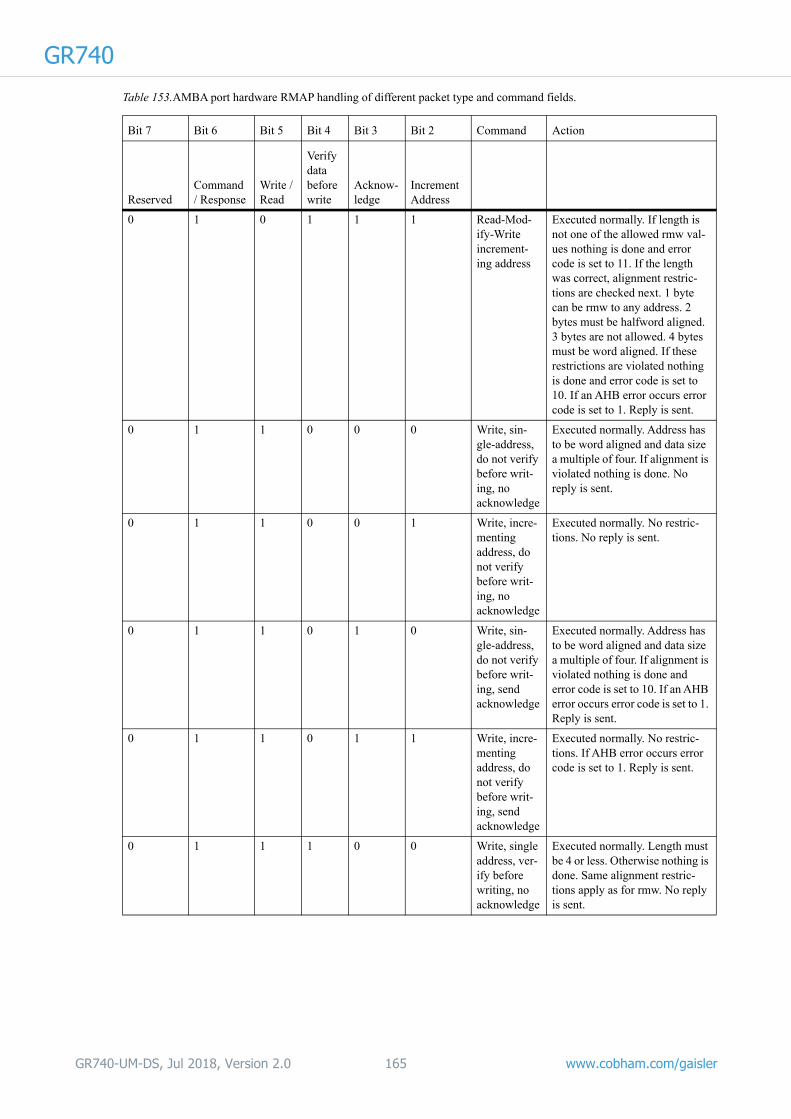
GR740
0 1 0 1 1 1 Read-Mod-ify-Write increment-ing address
Executed normally. If length is not one of the allowed rmw val-ues nothing is done and error code is set to 11. If the length was correct, alignment restric-tions are checked next. 1 byte can be rmw to any address. 2 bytes must be halfword aligned. 3 bytes are not allowed. 4 bytes must be word aligned. If these restrictions are violated nothing is done and error code is set to 10. If an AHB error occurs error code is set to 1. Reply is sent.
0 1 1 0 0 0 Write, sin-gle-address, do not verify before writ-ing, no acknowledge
Executed normally. Address has to be word aligned and data size a multiple of four. If alignment is violated nothing is done. No reply is sent.
0 1 1 0 0 1 Write, incre-menting address, do not verify before writ-ing, no acknowledge
Executed normally. No restric-tions. No reply is sent.
0 1 1 0 1 0 Write, sin-gle-address, do not verify before writ-ing, send acknowledge
Executed normally. Address has to be word aligned and data size a multiple of four. If alignment is violated nothing is done and error code is set to 10. If an AHB error occurs error code is set to 1. Reply is sent.
0 1 1 0 1 1 Write, incre-menting address, do not verify before writ-ing, send acknowledge
Executed normally. No restric-tions. If AHB error occurs error code is set to 1. Reply is sent.
0 1 1 1 0 0 Write, single address, ver-ify before writing, no acknowledge
Executed normally. Length must be 4 or less. Otherwise nothing is done. Same alignment restric-tions apply as for rmw. No reply is sent.
Table 153.AMBA port hardware RMAP handling of different packet type and command fields.
Bit 7 Bit 6 Bit 5 Bit 4 Bit 3 Bit 2 Command Action
ReservedCommand / Response
Write /Read
Verify data before write
Acknow-ledge
Increment Address
GR740-UM-DS, Jul 2018, Version 2.0 165 www.cobham.com/gaisler

GR740
13.4.7 AMBA interface
The AMBA interface consists of an APB interface, an AHB master interface and DMA FIFOs. The APB interface provides access to the user registers, which are described in section 13.4.8. The DMA engines have 32-bit wide FIFOs to the AHB master interface, which are used when reading and writ-ing to the bus.
The transmitter DMA engine reads data from the bus in bursts, which are half the FIFO size in length. A burst is always started when the FIFO is half-empty or if it can hold the last data for the packet. The burst containing the last data might have a shorter length if the packet is not an even number of bursts in size.
The receiver DMA works in the same way except that it checks if the FIFO is half-full and then per-forms a burst write to the bus which is half the FIFO size in length. Byte accesses are used for non-word-aligned buffers and/or packet lengths that are not a multiple of four bytes. There can be there-fore 1 to 3 single byte writes when writing the beginning and the end of a received packet.
13.4.7.1 APB slave interface
As mentioned above, the APB interface provides access to the user registers, which are 32-bits wide. Accesses to this interface are required to be aligned word accesses. The result is undefined if this restriction is violated.
0 1 1 1 0 1 Write, incre-menting address, ver-ify before writing, no acknowledge
Executed normally. Length must be 4 or less. Otherwise nothing is done. Same alignment restric-tions apply as for rmw. If they are violated nothing is done. No reply is sent.
0 1 1 1 1 0 Write, single address, ver-ify before writing, send acknowledge
Executed normally. Length must be 4 or less. Otherwise nothing is done and error code is set to 9. Same alignment restrictions apply as for rmw. If they are vio-lated nothing is done and error code is set to 10. If an AHB error occurs error code is set to 1. Reply is sent.
0 1 1 1 1 1 Write, incre-menting address, ver-ify before writing, send acknowledge
Executed normally. Length must be 4 or less. Otherwise nothing is done and error code is set to 9. Same alignment restrictions apply as for rmw. If they are vio-lated nothing is done and error code is set to 10. If an AHB error occurs error code is set to 1. Reply is sent.
1 0 - - - - Unused Stored to DMA-channel.
1 1 - - - - Unused Stored to DMA-channel.
Table 153.AMBA port hardware RMAP handling of different packet type and command fields.
Bit 7 Bit 6 Bit 5 Bit 4 Bit 3 Bit 2 Command Action
ReservedCommand / Response
Write /Read
Verify data before write
Acknow-ledge
Increment Address
GR740-UM-DS, Jul 2018, Version 2.0 166 www.cobham.com/gaisler

GR740
13.4.7.2 AHB master interfaceThe port contains a single master interface, which is used by both the transmitter and receiver DMA engines. The arbitration algorithm between the channels is done so that if the current owner requests the interface again it will always acquire it. This will not lead to starvation problems since the DMA engines always deassert their requests between accesses.
The burst length is half the AHB FIFO size except for the last transfer of a packet, which might be smaller. Shorter accesses are also done during descriptor reads and status writes.
The AHB master also supports non-incrementing accesses where the address is constant for several consecutive accesses. HTRANS is always NONSEQ in this case while for incrementing accesses it is set to SEQ after the first access. This feature is included to support non-incrementing reads and writes for RMAP.
If the port does not need the bus after a burst has finished, there is one wasted cycle (HTRANS = IDLE).
BUSY transfer types are never requested and the port provides full support for ERROR, RETRY and SPLIT responses.
13.4.8 Registers
The port is programmed through registers mapped into APB address space. The addresses in the table below are offsets from the base address of each AMBA port. The actual AMBA AHB address used to access a specific port can be determined by adding the offset to the corresponding base address of the port, as specified in table 7 in section 2.3. An identical set of registers described in this section exists for each AMBA port. The used register layout is explained in section 1.11.
GR740-UM-DS, Jul 2018, Version 2.0 167 www.cobham.com/gaisler

GR740
.Table 154.AMBA port registers
APB address offset** Register name Acronym
0x00 AMBA port Control RTR.AMBACTRL
0x40 AMBA port Status RTR.AMBASTS
0x08 AMBA port Default address RTR.AMBADEFADDR
0x0C RESERVED
0x10 AMBA port Destination key RTR.AMBADKEY
0x14 AMBA port Time-code RTR.AMBATC
0x18 RESERVED
0x20, 0x40, 0x60, 0x80 AMBA port DMA control/status, channels 1 - 4 * RTR.AMBADMACTRL
0x24, 0x44, 0x64, 0x84 AMBA port DMA RX maximum length, channels 1 - 4 * RTR.AMBADMAMAXLEN
0x28, 0x48, 0x68, 0x88 AMBA port DMA transmit descriptor table address, chan-nels 1 - 4 *
RTR.AMBADMATXDESC
0x2C, 0x4C, 0x6C, 0x8C AMBA port DMA receive descriptor table address, channels 1 - 4 *
RTR.AMBADMARXDESC
0x30, 0x50, 0x70, 0x90 AMBA port DMA address, channels 1 - 4 * RTR.AMBADMAADDR
0x34, 0x54, 0x74, 0x94 RESERVED
0x38, 0x58, 0x78, 0x98 RESERVED
0x3C, 0x5C, 0x7C, 0x9C RESERVED
0xA0 AMBA port Distributed interrupt control RTR.AMBAINTCTRL
0xA4 AMBA port Interrupt receive RTR.AMBAINTRX
0xA8 AMBA port Interrupt acknowledgement / extended interrupt receive
RTR.AMBAACKRX
0xAC AMBA port Interrupt timeout, interrupt 0-31 RTR.AMBAINTTO0
0xB0 AMBA port Interrupt timeout, interrupt 32-63 RTR.AMBAINTTO1
0xB4 AMBA port Interrupt mask, interrupt 0-31 RTR.AMBAINTMSK0
0xB8 AMBA port Interrupt mask, interrupt 32-63 RTR.AMBAINTMSK1
0xBC - 0xFF RESERVED
0x100 - 0xFFF See note ** below
* One identical register per DMA channel. Register is only described once
** Each AMBA port is allocated a 4 KiB memory area in the GR740 memory map. The router registers are aliased within this memory range which means that an access to offset 0x104 or 0x204 .. 0xF04 all access the same register. To ensure software should only access
GR740-UM-DS, Jul 2018, Version 2.0 168 www.cobham.com/gaisler

GR740
Table 155. 0x00 - RTR.AMBACTRL - AMBA port Control31 30 29 28 27 26 25 24 23 22 21 20 19 18 17 16 15 14 13 12 11 10 9 8 7 6 5 4 3 2 1 0
RA RX RC NCH RES DI ME RESERVED RD RE RESERVED TQ R RS PM TI IE RESERVED
1 1 1 0x3 0x0 1 0 0x00 0 1 0x00 0 0 0 0 0 0 0x0
r r r r r r rw r rw rw r rw r rw rw rw rw r
31 RMAP available (RA) - Constant value of 1, indicating that the RMAP target is implemented.
30 RX unaligned access (RX) - Constant value of 1, indicating that unaligned writes are available for the receiver.
29 RMAP CRC available (RC) - Constant value of 1, indicating that RMAP CRC is enabled.
28: 27 Number of DMA channels (NCH) - The number of available DMA channels minus one. Constant value of 0x3.
26: 25 RESERVED
24 Distributed interrupt support (DI) - Constant value of 1, indicating that distributed interrupts are supported.
23 Memory error truncation enable (ME) - If set to 1, a packet being transmitted will be truncated with an EEP if an error occur while reading from the AMBA port’s TX FIFO.
22: 18 RESERVED
17 RMAP buffer disable (RD) - If set only one RMAP buffer is used. This ensures that all RMAP commands will be executed consecutively.
16 RMAP Enable (RE) - Enable RMAP target.
15: 9 RESERVED
8 Tick-out IRQ (TQ) - Generate interrupt when a valid time-code is received if the time-code also matches the time-code filter specified by the RTR.AMBATIME.TCMSK and RTR.AMBATIME.TCVAL fields.
7 Time-code tick-out enable (TO) - If set to 1, the internal tickout signal is set when a valid time-code is received. if the time-code also matches the time-code filter specified by the RTR.AMBATIME.TCMSK and RTR.AMBA-TIME.TCVAL fields. The internal tickout signal is connected to the timer units as described in section 5.9 and in the LATCHCFG register description in section 20.3.
6 Reset (RS) - Make complete reset of the SpaceWire node. Self clearing.
5 Promiscuous Mode (PM) - Enable Promiscuous mode.
4 Tick In (TI) - The host can generate a tick by writing a one to this field. This will increment the timer counter and the new value is transmitted after the current character is transferred. A tick can also be generated by assert-ing the tick_in signal.
3 Interrupt Enable (IE) - If set, an interrupt is generated when bit 8 is set and its corresponding event occurs.
2: 0 RESERVED
GR740-UM-DS, Jul 2018, Version 2.0 169 www.cobham.com/gaisler

GR740
Table 156. 0x04 - RTR.AMBASTS - AMBA port Status31 30 28 27 26 25 24 23 13 12 11 9 8 7 0
R NIRQ NRXD NTXD RESERVED ME RESERVED EE IA RESERVED TO
0 0x6 0 0 0x000 0 0x0 0 0 0x00 0
r r r r r wc r wc wc r wc
31 RESERVED
30: 28 Number of interrupts (NIRQ) - Shows the number of support distributed interrupt, according to the formula
2NIRQ. Constant value of 0x6 = 64 supported interrupts.
27: 26 Number of receive descriptors (NRXD) - Shows the size of the DMA receive descriptor table. Constant value of 0, indicating 128 descriptors.
25: 24 Number of transmit descriptors (NTXD) - Shows the size of the DMA transmit descriptor table. Constant value of 0, indicating 64 descriptors.
23: 13 RESERVED
12 Memory error packet truncation (ME) - This bit is set to one when a transmitted packet is truncated with an EEP due to a memory error in the AMBA ports’ TX FIFO.
11: 9 RESERVED
8 Early EOP/EEP (EE) - Set to one when a packet is received with an EOP after the first byte for a non-RMAP packet and after the second byte for an RMAP packet.
7 Invalid Address (IA) - Set to one when a packet is received with an invalid destination address field, i.e it does not match the nodeaddr register.
6: 1 RESERVED
0 Tick Out (TO) - A new time count value was received and is stored in the time counter field.
Table 157. 0x08 - RTR.AMBADEFADDR - AMBA port Default address31 16 15 8 7 0
RESERVED DEFMASK DEFADDR
0x0000 0x00 0xFE
r rw rw
31: 8 RESERVED
15: 8 Default mask (DEFMASK) - Default mask used for node identification on the SpaceWire network. This field is used for masking the address before comparison. Both the received address and the DEFADDR field are anded with the inverse of DEFMASK before the address check.
7: 0 Default address (DEFADDR) - Default address used for node identification on the SpaceWire network. Reset value: 254.
Table 158. 0x10 - RTR.AMBADKEY - AMBA port Destination key31 8 7 0
RESERVED DESTKEY
NA 0x00
r rw
31: 8 RESERVED
7: 0 Destination key (DESTKEY) - RMAP destination key.
GR740-UM-DS, Jul 2018, Version 2.0 170 www.cobham.com/gaisler
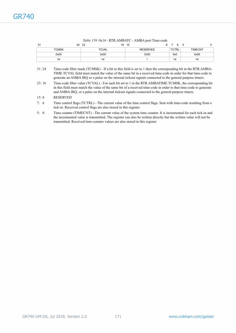
GR740
Table 159. 0x14 - RTR.AMBATC - AMBA port Time-code31 24 23 16 15 8 7 6 5 0
TCMSK TCVAL RESERVED TCTRL TIMECNT
0x00 0x00 0x00 0x0 0x00
rw rw r rw rw
31: 24 Time-code filter mask (TCMSK) - If a bit in this field is set to 1 then the corresponding bit in the RTR.AMBA-TIME.TCVAL field must match the value of the same bit in a received time-code in order for that time-code to generate an AMBA IRQ or a pulse on the internal tickout signals connected to the general purpose timers.
23: 16 Time-code filter value (TCVAL) - For each bit set to 1 in the RTR.AMBATIME.TCMSK, the corresponding bit in this field must match the value of the same bit of a received time-code in order to that time-code to generate and AMBA IRQ, or a pulse on the internal tickout signals connected to the general purpose timers.
15: 8 RESERVED
7: 6 Time control flags (TCTRL) - The current value of the time control flags. Sent with time-code resulting from a tick-in. Received control flags are also stored in this register.
5: 0 Time counter (TIMECNT) - The current value of the system time counter. It is incremented for each tick-in and the incremented value is transmitted. The register can also be written directly but the written value will not be transmitted. Received time-counter values are also stored in this register
GR740-UM-DS, Jul 2018, Version 2.0 171 www.cobham.com/gaisler

GR740
Table 160. 0x20,0x40,0x60,0x80 - RTR.AMBADMACTRL - AMBA port DMA control/status31 30 29 28 27 26 25 24 23 22 21 20 19 18 17 16 15 14 13 12 11 10 9 8 7 6 5 4 3 2 1 0
INTNUM RES EP TR IE IT RP TP RES SP SA EN NS RD RX AT RA TA PR PS AI RI TI RE TE
0x00 0x0 0 0 0 0 0 0 0x0 0 0 0 0 0 0 0 0 0 0 0 NR NR NR 0 0
rw r wc wc rw rw wc wc r rw rw rw rw rw r rw wc wc wc wc rw rw rw rw rw
31: 26 Interrupt number (INTNUM) - The interrupt number used for this DMA channel when sending a distributed interrupt code that was generated due to any of the events maskable by the RTR.AMBADMACTRL.IE and RTR.AMBADMACTRL.IT bits. The value in this field should be in the range 0 to 31.
25: 24 RESERVED
23 EEP termination (EP) - Set to 1 when a received packet for the corresponding DMA channel ended with an Error End of Packet (EEP) character.
22 Truncated (TR) - Set to 1 when a received packet for the corresponding DMA channel is truncated due to a maximum length violation.
21 Interrupt transmit enable on EEP (IE) - When set to 1, the distributed interrupt code specified in the RTR.AMBADMACTRL.INTNUM field is generated when a received packet on this DMA channel ended with an Error End of Packet (EEP) character.
20 Interrupt-code transmit enable on truncation (IT) - When set to 1, the distributed interrupt code specified in the RTR.AMBADMACTRL.INTNUM field is generated when a received packet on this DMA channel is truncated due to a maximum length violation.
19 Receive packet IRQ (RP) - This bit is set to 1 when an AMBA interrupt was generated due to the fact that a packet was received for the corresponding DMA channel.
18 Transmit packet IRQ (TP) - This bit is set to 1 when an AMBA interrupt was generated due to the fact that a packet was transmitted for the corresponding DMA channel.
17: 16 RESERVED
15 Strip pid (SP) - Remove the pid byte (second byte) of each packet. The address byte (first byte) will also be removed when this bit is set independent of the SA bit.
14 Strip addr (SA) - Remove the addr byte (first byte) of each packet.
13 Enable addr (EN) - Enable separate node address for this channel.
12 No spill (NS) - If cleared, packets will be discarded when a packet is arriving and there are no active descrip-tors. If set, the GRSPW will wait for a descriptor to be activated.
11 Rx descriptors available (RD) - Set to one, to indicate to the GRSPW that there are enabled descriptors in the descriptor table. Cleared by the GRSPW when it encounters a disabled descriptor:
10 RX active (RX) - Is set to ‘1’ if a reception to the DMA channel is currently active otherwise it is ‘0’.
9 Abort TX (AT) - Set to one to abort the currently transmitting packet and disable transmissions. If no trans-mission is active the only effect is to disable transmissions. Self clearing.
8 RX AHB error (RA) - An error response was detected on the AHB bus while this receive DMA channel was accessing the bus. The AHB error interrupt (AI) field must be set to ’1’ for the RA field to be set.
7 TX AHB error (TA) - An error response was detected on the AHB bus while this transmit DMA channel was accessing the bus.
6 Packet received (PR) - This bit is set each time a packet has been received. never cleared by the SW-node.
5 Packet sent (PS) - This bit is set each time a packet has been sent. Never cleared by the SW-node.
4 AHB error interrupt (AI) - If set, an interrupt will be generated each time an AHB error occurs when this DMA channel is accessing the bus.
3 Receive interrupt (RI) - If set, an interrupt will be generated each time a packet has been received. This hap-pens both if the packet is terminated by an EEP or EOP.
2 Transmit interrupt (TI) - If set, an interrupt will be generated each time a packet is transmitted. The interrupt is generated regardless of whether the transmission was successful or not.
1 Receiver enable (RE) - Set to one when packets are allowed to be received to this channel.
0 Transmitter enable (TE) - Write a one to this bit each time new descriptors are activated in the table. Writing a one will cause the SW-node to read a new descriptor and try to transmit the packet it points to. This bit is automatically cleared when the SW-node encounters a descriptor which is disabled.
GR740-UM-DS, Jul 2018, Version 2.0 172 www.cobham.com/gaisler

GR740
Table 161. 0x24,0x44,0x64,0x84 - RTR.AMBADMAMAXLEN - AMBA port DMA RX maximum length31 25 24 2 1 0
RESERVED RXMAXLEN RES
0x00 N/R 0x0
r rw r
31: 25 RESERVED
24: 2 RX maximum length (RXMAXLEN) - Receiver packet maximum length in 32-bit words.
1: 0 RESERVED
Table 162. 0x28,0x48,0x68,0x88 - RTR.AMBADMATXDESC - AMBA port DMA transmit descriptor table address31 10 9 4 3 0
DESCBASEADDR DESCSEL RESERVED
N/R 0x00 0x0
rw rw r
31: 10 Descriptor table base address (DESCBASEADDR) - Sets the base address of the descriptor table.
9: 4 Descriptor selector (DESCSEL) - Offset into the descriptor table. Shows which descriptor is currently used by the GRSPW. For each new descriptor read, the selector will increase with 16 and eventually wrap to zero again.
3: 0 RESERVED
Table 163. 0x2C,0x4C,0x6C,0x8C - RTR.AMBADMARXDESC - AMBA port DMA receive descriptor table address31 10 9 3 2 0
DESCBASEADDR DESCSEL RESERVED
N/R 0x00 0x0
rw rw r
31: 10 Descriptor table base address (DESCBASEADDR) - Sets the base address of the descriptor table. Not reset.
9: 3 Descriptor selector (DESCSEL) - Offset into the descriptor table. Shows which descriptor is currently used by the GRSPW. For each new descriptor read, the selector will increase with 8 and eventually wrap to zero again. Reset value: 0.
2: 0 RESERVED
Table 164. 0x30,0x50,0x70,0x90 - RTR.AMBADMAADDR - AMBA port DMA address31 16 15 8 7 0
RESERVED MASK ADDR
0x0000 N/R N/R
r rw rw
31: 8 RESERVED
15: 8 Mask (MASK) - Mask used for node identification on the SpaceWire network. This field is used for masking the address before comparison. Both the received address and the ADDR field are anded with the inverse of MASK before the address check.
7: 0 Address (ADDR) - Address used for node identification on the SpaceWire network for the corresponding dma channel when the EN bit in the DMA control register is set.
GR740-UM-DS, Jul 2018, Version 2.0 173 www.cobham.com/gaisler

GR740
Table 165. 0xA0 - RTR.AMBAINTCTRL - AMBA port Distributed interrupt control31 26 25 24 23 22 21 20 19 18 17 16 15 14 13 12 8 7 6 5 0
INTNUM R EE IA RES TQ AQ IQ RES AA AT IT RESERVED ID II TXINT
0x00 0 0 0 0x0 0 0 0 0x0 0 1 1 0x00 0 0 0x00
rw r rw rw r rw rw rw r rw rw rw r wc rw* rw
31: 26 Interrupt number (INTNUM) - The interrupt-number used when sending an interrupt code that was gener-ated due to any of the events maskable by the RTR.AMBAINCTRL.ER and RTR.AMBAINTCTRL.IA bits. Note that when RTR.RTRCFG.EE = 0 (interrupt with acknowledgement mode), this field must no be set to a value greater than 31.
25 RESERVED
24 Interrupt transmit on early EOP/EEP (EE) - If set to 1, a distributed interrupt code with the interrupt number specified in the RTR.AMBAINTCTRL.INTNUM field is sent each time an event occurs such that the STS.EE bit is set to 1 (even if the bit was already set when the event occurred).
23 Interrupt transmit on invalid address (IA) - If set to 1, a distributed interrupt code with the interrupt number specified in the RTR.AMBAINTCTRL.INTNUM field is sent each time an event occurs such that the STS.IA bit is set to 1 (even if the bit was already set when the event occurred).
22: 21 RESERVED
20 Interrupt timeout IRQ enable (TQ) - When set to 1, an AMBA interrupt is generated when a bit in the RTR.AMBAINTTO0 or RTR.AMBAINTTO1 registers is set. Note that the RTR.AMBACTRL.IE bit also must be set for this bit to have any effect.
19 Interrupt acknowledgment / extended interrupt receive IRQ enable (AQ) - When set to 1, an AMBA inter-rupt is generated when an interrupt acknowledgment code or extended interrupt code is received such that a bit in the RTR.AMBAACKRX register is set to 1 (even if the bit was already set when the code was received).
18 Interrupt-code receive IRQ enable (IQ) - When set to 1, an AMBA interrupt is generated when an interrupt code is received such that a bit in the RTR.AMBAINTRX register is set to 1 (even if the bit was already set when the code was received).
17: 16 RESERVED
15 Handle all interrupt acknowledgment codes (AA) - Is set to 0, only those received interrupt acknowledgment codes that match an interrupt code sent by software are handled. If set to 1, all received interrupt acknowl-edgment codes are handled.
14 Interrupt acknowledgment / extended interrupt tickout enable (AT) - When set to 1, the internal tickout sig-nal from this AMBA port is set when an interrupt acknowledgment code or extended interrupt code is received such that a bit in the RTR.AMBAACKRX register is set to 1 (even if the bit was already set when the code was received). The internal tickout signal is connected to the timer units as described in section 5.9 and in the LATCHCFG register description in section 20.3.
13 Interrupt tickout enable (IT) - When set to 1, the internal tickout signal from this AMBA port is set when an interrupt code is received such that a bit in the RTR.AMBAINTRX register is set to 1 (even if the bit was already set when the code was received). The internal tickout signal is connected to the timer units as described in section 5.9 and in the LATCHCFG register description in section 20.3.
12: 8 RESERVED
7 Interrupt discarded (ID) - This bit is set to 1 when a distributed interrupt code that software tried to send by writing the RTR.AMBAINTCTRL.II bit was discarded by the routers switch matrix. There is a maximum of ten clock cycle delay between the RTR.AMBAINTCTRL.II bit being written and this bit being set.
6 Interrupt-code tick-in (II) - When this field is written to 1 the distributed interrupt code specified by the RTR.AMBAINTCTRL.TXINT field will be sent out from the AMBA port to the routers switch matrix. This bit is automatically cleared and always reads ‘0’. Writing a ‘0’ has no effect.
5: 0 Transmit distributed interrupt code (TXINT) - The distributed interrupt code that will be sent when the reg-ister RTR.AMBAINTCTRL.II is written with 1.
GR740-UM-DS, Jul 2018, Version 2.0 174 www.cobham.com/gaisler

GR740
Table 166. 0xA4 - RTR.AMBAINTRX - AMBA port Interrupt receive31 0
RXIRQ
0x00000000
wc
31: 0 Received interrupt code (RXIRQ) - Each bit corresponds to the interrupt number with the same number as the bit index. A position is set to 1 when an interrupt code is received for which the corresponding bit in the RTR.AMBAINTMSK0 register is set to 1.
Table 167. 0xA8 - RTR.AMBAACKRX - AMBA port Interrupt acknowledgment / extended interrupt receive31 0
RXACK
0x00000000
wc
31: 0 Received interrupt acknowledgment code / extended interrupt code (RXACK) - When operating in extended interrupt mode (RTR.RTRCFG.EE = 1) then each bit corresponds to the interrupt number with the same number as the bit index plus 32, i.e bit 0 corresponds to interrupt number 32, bit 1 to interrupt number 33 etc. This bit gets set to 1 when an extended interrupt code is received for which the corresponding bit in the RTR.AMBAINTMSK1 register is set to 1.
When operating in interrupt with acknowledgment mode (RTR.RTRCFG.EE = 0) then each bit corresponds to the interrupt number with the same number as the bit index. This bit gets set to 1 an interrupt acknowledg-ment code is received for which the corresponding bit in the RTR.AMBAINTMSK0 register is set, and either if RTR.AMBAINTCTRL.AA is set to 1 or for which the matching interrupt code was sent by soft-ware.
Table 168. 0xAC - RTR.AMBAINTTO0 - AMBA port Interrupt timeout, interrupt 0-3131 0
INTTO
0x00000000
wc
31: 0 Interrupt code timeout (INTTO) - Each bit corresponds to the interrupt number with the same number as the bit index. This bit is set to 1 when an interrupt code that was sent by software doesn’t receive an interrupt acknowledgment code for the duration of a timeout period (specified in the RTR.ISRTIMER register), and if the corresponding bit in the RTR.AMBAINTMSK0 register is set.
Table 169. 0xAC - RTR.AMBAINTTO1 - AMBA port Interrupt timeout, interrupt 32-6331 0
INTTO
0x00000000
wc
31: 0 Extended interrupt code timeout (INTTO) - Each bit corresponds to the interrupt number with the same number as the bit index plus 32, i.e bit 0 corresponds to interrupt number 32, bit 1 to interrupt number 33 etc.. This bit is set to 1 when an extended interrupt code that was sent by software time out, i.e after the dura-tion of a timeout period (specified in the RTR.ISRTIMER register), and if the corresponding bit in the RTR.AMBAINTMSK1 register is set.
GR740-UM-DS, Jul 2018, Version 2.0 175 www.cobham.com/gaisler

GR740
13.5 Configuration port
The configuration port has port number 0. It consists of an RMAP target, AMBA AHB slave inter-face, SpaceWire Plug-and-Play interface, and a set of configuration and status registers.
13.5.1 RMAP target
13.5.1.1 Overview
The configuration port’s RMAP target implements the RMAP protocol, as defined in the RMAP stan-dard [RMAP]. Verified writes and reads of 4 B, and read-modify-writes of 4 B (8 B if the mask field is included in the count) are supported. Replies from the configuration port are always sent to the port they arrived on, regardless of the values of the RMAP command’s Initiator Logical Address field, and Reply Address field. The address space of the configuration port is specified in section 13.5.3.
Additional requirements on the RMAP commands imposed by the configuration port’s RMAP target are:
• The Target Logical Address field must be 0xFE.
• The Address fields must contain a 4 B aligned address.
• The Extended Address field must be 0x00.
• Key field must be 0x00.
• For write and read commands the Data Length fields must contain a value of either 0 or 4.
• For read-modify-write commands the Data Length fields must contain a value of either 0 or 8.
• For write commands the Verify Data Before Write bit in the Instruction field must be set to 1.
How the RMAP target handles commands that does not meet the above requirement is detailed in sec-tions 13.5.1.2 and 13.5.1.4.
Table 170. 0xB0 - RTR.AMBAINTMSK0 - AMBA port Interrupt mask, interrupt 0-3131 0
MASK
0x00000000
rw
31: 0 Interrupt mask (MASK) - Each bit corresponds to the interrupt number with the same value as the bit index. If a bit is set to 0, all received interrupt codes and interrupt acknowledgment codes with the interrupt identi-fier corresponding to that bit is ignored. If a bit is set to 1, then the matching distributed interrupt code is handled.
Table 171. 0xB0 - RTR.AMBAINTMSK1 - AMBA port Interrupt mask, interrupt 32-6331 0
MASK
0x00000000
rw
31: 0 Interrupt mask (MASK) - Each bit corresponds to the interrupt number with the same value as the bit index. plus 32, i.e bit 0 corresponds to interrupt number 32, bit 1 to interrupt number 33 etc. If a bit is set to 0, all received extended interrupt codes with the interrupt identifier corresponding to that bit is ignored. If a bit is set to 1, then the matching distributed interrupt code is handled.
GR740-UM-DS, Jul 2018, Version 2.0 176 www.cobham.com/gaisler

GR740
13.5.1.2 RMAP command supportTable 172 lists all possible RMAP commands and shows how the configuration port’s RMAP target handles them. An RMAP command will always have bits 7:6 of the command’s Instruction field set to “01”, and those bits are therefore left out of the table. Bits 1:0 of the command’s Instruction field determines the length of the command’s Reply Address Field, and does not affect the action taken, so they have been left out of the table as well. The action taken assumes that no errors were detected in the RMAP packet. For handling of RMAP packet error, see section 13.5.1.4
Table 172.RMAP command decoding and handling.
Bit 5 Bit 4 Bit 3 Bit 2
Write / Read
Verify Data Before Write Reply
Incre-ment Addr Function Action taken
0 0 0 0 Invalid No operation performed. Error code 0x02 is saved in the RTR.PCTRLCFG.EC field. No reply is sent.
0 0 0 1 Invalid No operation performed. Error code 0x02 is saved in the RTR.PCTRLCFG.EC field. No reply is sent.
0 0 1 0 Read single address
Read operation performed, if the requirements in section 13.5.1.1 are met.
0 0 1 1 Read increment-ing address
Read operation performed, if the requirements in section 13.5.1.1 are met.
0 1 0 0 Invalid No operation performed. Error code 0x02 is saved in the RTR.PCTRLCFG.EC field. No reply is sent.
0 1 0 1 Invalid No operation performed. Error code 0x02 is saved in the RTR.PCTRLCFG.EC field. No reply is sent.
0 1 1 0 Invalid No operation performed. Reply is sent with error code 0x02. Error code is also saved in the RTR.PCTRLCFG.EC field.
0 1 1 1 Read-modify-write increment-ing address
Read-modify-write operation performed if the requirements in section 13.5.1.1 are met.
1 0 0 0 Write, single address, don’t verify before writing, no reply
No operation performed. Error code 0x0A is saved in the RTR.PCTRLCFG.EC field. No reply sent.
1 0 0 1 Write, incre-menting address, don’t verify before writing, no reply
No operation performed. Error code 0x0A is saved in the RTR.PCTRLCFG.EC field. No reply sent.
1 0 1 0 Write, single address, don’t verify before write, send reply
No operation performed. Reply is sent with error code 0x0A. Error code is also saved in the RTR.PCTRLCFG.EC field.
1 0 1 1 Write, incre-menting address, don’t verify before write, send reply
No operation performed. Reply is sent with error code 0x0A. Error code is also saved in the RTR.PCTRLCFG.EC field.
1 1 0 0 Write, single address, verify before writing, no reply
Write operation performed if the requirements in section 13.5.1.1 are met.
GR740-UM-DS, Jul 2018, Version 2.0 177 www.cobham.com/gaisler

GR740
13.5.1.3 Access control
After reset / power-up the configuration port’s address space can be accessed from all the ports. Con-figuration port accesses can be individually disabled per port by clearing the corresponding RTR.PCTRL.CE bit. Write commands, and read-modify-write commands to the configuration area can be globally disabled by writing a 0 to the RTR.CFGWE.WE bit. When a correct RMAP command is received but not allowed due to one or more of the access control features being enabled, a reply with Status field set to 0x0A (Authorization failure) is sent (if requested), and the RTR.PSTSCFG.EC field is updated to reflect the error. If a reply is not requested, the RTR.PSTSCFG.EC field is still set. In both cases, the operation is not performed.
13.5.1.4 RMAP Error handling
Table 173 shows the order in which errors in an RMAP command are detected. As soon as an error is detected, the command is discarded. If a reply should be sent, to a command that included an error, the reply is sent as soon as possible after the error is detected. This means that the reply might be sent out before the complete incoming RMAP command has been received. Note that since the complete RMAP command is buffered before it is executed, a command that contains an error is never exe-cuted.
1 1 0 1 Write, incre-menting address, verify before writing, no reply
Write operation performed if the requirements in section 13.5.1.1 are met.
1 1 1 0 Write, single address, verify before writing, send reply
Write operation performed if the requirements in section 13.5.1.1 are met.
1 1 1 1 Write, incre-menting address, verify before writing, send reply
Write operation performed if the requirements in section 13.5.1.1 are met.
Table 173.RMAP target error detection order
Detection Order Error type
RMAP error code Action taken
1 Wrong Protocol Identifier N/A The RTR.PSTSCFG.PT bit is set in order to indicate that the error occurred. No reply is sent.
2 EOP / EEP before com-pleted header
N/A The RTR.PSTSCFG.EO / RTR.PSTSCFG.EE bit is set in order to indi-cate that the error occurred. No reply is sent.
3 Header CRC error N/A The RTR.PSTSCFG.HC bit is set in order to indicate that the error occurred. No reply is sent.
4 Unused RMAP packet type
N/A If the packet type (bit 7:6 of the packet’s Instruction field) is “10” or “11” then the bit RTR.PSTSCFG.PT is set. For the value “00” (indicat-ing a reply), no bit in RTR.PSTSCFG is set, since the RMAP standard [RMAP] does not specify that such an event should be recorded.
Table 172.RMAP command decoding and handling.
Bit 5 Bit 4 Bit 3 Bit 2
Write / Read
Verify Data Before Write Reply
Incre-ment Addr Function Action taken
GR740-UM-DS, Jul 2018, Version 2.0 178 www.cobham.com/gaisler

GR740
Most of the errors listed in table 173 are errors that only occur in one specific way, and they are also explained in the RMAP standard [RMAP]. Authorization failure (error code 0x0A) is however an exception. All the cases that lead to an authorization failure are listed below:
• A read command’s Data Length field exceed 128 B.
• A command’s (read, write, or read-modify-write) Address field does not contain a 4 B aligned address.
• The access control features described in section 13.5.1.3 prevented the port from accessing the RMAP target.
• The Address field of a command (read, write, or read-modify-write) contains an address that is outside of the configuration port’s memory space.
• The Length field of a command (read, write, or read-modify write) is 0 nor 4.
• A non-verified write command was received.
13.5.2 AMBA AHB slave interface
The configuration port provides an AMBA AHB slave interface, which makes the whole configura-tion port’s address space accessible from the AHB bus.
The routing table is shared between the ports, RMAP target and AHB slave, so accesses from the AHB slave might be stalled because of accesses from the other sources. The priority order when accessing the routing table, starting from the highest, is: router ports, AHB slave, RMAP target. Note that since the AHB slave has higher priority than the RMAP target, it is possible to read and write to
5 EEP immediately after header
N/A The RTR.PSTSCFG.EE bit is set in order to indicate that the error occurred. No reply is sent.
6 Unused RMAP command code
0x02 RMAP error code is saved in the RTR.PCTRLCFG.EC field. Reply is sent if the Reply bit in the command’s Instruction field was set to 1.
7 Invalid Target Logical Address
0x0C RMAP error code is saved in the RTR.PCTRLCFG.EC field. Reply is sent if the Reply bit in the command’s Instruction field was set to 1.
8 Invalid Key 0x03 RMAP error code is saved in the RTR.PCTRLCFG.EC field. Reply is sent if the Reply bit in the command’s Instruction field was set to 1.
9 Verify buffer overrun 0x09 RMAP error code is saved in the RTR.PCTRLCFG.EC field. Reply is sent if the Reply bit in the command’s Instruction field was set to 1.
10 RMW data length error 0x0B RMAP error code is saved in the RTR.PCTRLCFG.EC field. Reply is sent if the Reply bit in the command’s Instruction field was set to 1.
11 RMAP command not implemented or not authorized.
0x0A RMAP error code is saved in the RTR.PCTRLCFG.EC field. Reply is sent if the Reply bit in the command’s Instruction field was set to 1.
12 Early EOP / early EEP (not immediately after header)
0x05 / 0x07
RMAP error code is saved in the RTR.PCTRLCFG.EC field. Reply is sent if the Reply bit in the command’s Instruction field was set to 1.
13 Invalid Data CRC 0x04 RMAP error code is saved in the RTR.PCTRLCFG.EC field. Reply is sent if the Reply bit in the command’s Instruction field was set to 1.
14 EEP 0x07 RMAP error code is saved in the RTR.PCTRLCFG.EC field. Reply is sent if the Reply bit in the command’s Instruction field was set to 1.
15 Too much data 0x06 RMAP error code is saved in the RTR.PCTRLCFG.EC field. Reply is sent if the Reply bit in the command’s Instruction field was set to 1.
Table 173.RMAP target error detection order
Detection Order Error type
RMAP error code Action taken
GR740-UM-DS, Jul 2018, Version 2.0 179 www.cobham.com/gaisler

GR740
the configuration port’s registers in the middle of an RMAP write command. This needs to be consid-ered in order to avoid a mismatch between the expected written value and actual written value.None of the access control mechanisms mentioned in section 13.5.1.3 have any effect on the AHB slave interface.
13.5.3 Registers
The configuration port’s registers listed in this section can be accessed either through the RMAP tar-get, or the AMBA AHB slave interface. The address specified in table 174 is the RMAP address. When accessed through the AHB slave interface, the address in the table should be added to the router’s base address specified in table 7, section 2.3. Registers that exist in several identical copies, corresponding to different addresses or ports, for example the RTR.RTPMAP registers, are only described once. The register layout used is explained in section 1.11.
Table 174.GRSPWROUTER registers
RMAP address Register name Acronym
0x00000000 RESERVED *
0x00000004 - 0x00000030
Routing table port mapping, physical addresses 1-12 RTR.RTPMAP
0x00000034 - 0x0000007C
RESERVED *
0x00000080 - 0x000003FC
Routing table port mapping, logical addresses 32-255 RTR.RTPMAP
0x00000400 RESERVED *
0x00000404 - 0x00000430
Routing table address control, physical addresses 1-12 RTR.RTACTRL
0x00000450 - 0x0000047C
RESERVED *
0x00000480 - 0x000007FC
Routing table address control, logical addresses 32-255 RTR.RTACTRL
0x00000800 Port control, port 0 (configuration port) RTR.PCTRLCFG
0x00000804 - 0x00000830
Port control, port 1-12 (SpaceWire ports and AMBA ports) RTR.PCTRL
0x00000850 - 0x0000087C
RESERVED
0x00000880 Port status, port 0 (configuration port) RTR.PSTSCFG
0x00000884 - 0x000008B0
Port status, ports 1-12 (SpaceWire ports and AMBA ports) RTR.PSTS
0x000008D0 - 0x000008FC
RESERVED
0x00000900 - 0x00000930
Port timer reload, ports 0-12 RTR.PTIMER
0x00000950 - 0x0000097C
RESERVED
0x00000980 Port control 2, ports 0 (configuration port) RTR.PCTRL2CFG
0x00000984 - 0x00000930
Port control 2, ports 1-12 (SpaceWire ports and AMBA ports) RTR.PCTRL2
0x000009D0 - 0x000009FC
RESERVED
0x00000A00 Router configuration / status RTR.RTRCFG
0x00000A04 Time-code RTR.TC
0x00000A08 Version / instance ID RTR.VER
GR740-UM-DS, Jul 2018, Version 2.0 180 www.cobham.com/gaisler

GR740
0x00000A0C Initialization divisor RTR.IDIV
0x00000A10 Configuration write enable RTR.CFGWE
0x00000A14 Timer prescaler reload RTR.PRESCALER
0x00000A18 Interrupt mask RTR.IMASK
0x00000A1C Interrupt port mask RTR.IPMASK
0x00000A20 Port interrupt pending RTR.PIP
0x00000A24 Interrupt code generation RTR.ICODEGEN
0x00000A28 Interrupt code distribution ISR, interrupt 0-31 RTR.ISR0
0x00000A2C Interrupt code distribution ISR, interrupt 32-63 RTR.ISR1
0x00000A30 Interrupt code distribution ISR timer reload RTR.ISRTIMER
0x00000A34 Interrupt code distribution ACK-to-INT timer reload RTR.AITIMER
0x00000A38 Interrupt code distribution ISR change timer reload RTR.ISRCTIMER
0x00000A3C RESERVED
0x00000A40 SpaceWire link running status RTR.LRUNSTS
0x00000A44 Capability RTR.CAP
0x00000A48 - 0x00000A4C
RESERVED
0x00000A50 SpaceWire Plug-and-Play - Device Vendor and Product ID RTR.PNPVEND
0x00000A54 SpaceWire Plug-and-Play - Unit Vendor and Product ID RTR.PNPUVEND
0x00000A58 SpaceWire Plug-and-Play - Unit Serial Number RTR.PNPUSN
0x00000A5C - 0x00000DFC
RESERVED
0x00000E00 - 0x00000E30
Maximum packet length, ports 0-12 RTR.MAXPLEN
0x00000E50 - 0x00000E7C
RESERVED
0x00000E84 - 0x00000E20
Credit counter, ports 1-8 RTR.CREDCNT
0x00000E24 - 0x00000FFC
RESERVED
0x00001000 RESERVED**
0x00001004 - 0x00001030
Routing table, combined port mapping and address control, addresses 1-12 RTR.RTCOMB
0x00001050 - 0x0000107C
RESERVED**
0x00001080 - 0x000013FC
Routing table, combined port mapping and address control, addresses 32-255 RTR.RTCOMB
* Physical address 0 (configuration port), and physical addresses 13-31 (non existing ports) does not have an RTR.RTP-MAP or RTR.RTACTRL register, and are therefore RESERVED.
** Physical address 0 (configuration port), and physical addresses 13-31 (non existing ports) does not have an RTR.RTCOMB register, and are therefore RESERVED.
Table 175. 0x00000004-0x00000030, 0x00000080-0x000003FC - RTR.RTPMAP - Routing table port mapping, addresses 1-12 and 32-255
31 13 12 1 0
RESERVED PE PD
0x00000 N/R N/R
r rw rw
Table 174.GRSPWROUTER registers
RMAP address Register name Acronym
GR740-UM-DS, Jul 2018, Version 2.0 181 www.cobham.com/gaisler
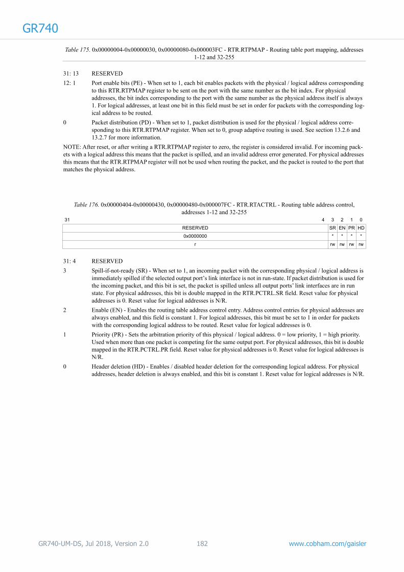
GR740
31: 13 RESERVED
12: 1 Port enable bits (PE) - When set to 1, each bit enables packets with the physical / logical address corresponding to this RTR.RTPMAP register to be sent on the port with the same number as the bit index. For physical addresses, the bit index corresponding to the port with the same number as the physical address itself is always 1. For logical addresses, at least one bit in this field must be set in order for packets with the corresponding log-ical address to be routed.
0 Packet distribution (PD) - When set to 1, packet distribution is used for the physical / logical address corre-sponding to this RTR.RTPMAP register. When set to 0, group adaptive routing is used. See section 13.2.6 and 13.2.7 for more information.
NOTE: After reset, or after writing a RTR.RTPMAP register to zero, the register is considered invalid. For incoming pack-ets with a logical address this means that the packet is spilled, and an invalid address error generated. For physical addresses this means that the RTR.RTPMAP register will not be used when routing the packet, and the packet is routed to the port that matches the physical address.
Table 176. 0x00000404-0x00000430, 0x00000480-0x000007FC - RTR.RTACTRL - Routing table address control, addresses 1-12 and 32-255
31 4 3 2 1 0
RESERVED SR EN PR HD
0x0000000 * * * *
r rw rw rw rw
31: 4 RESERVED
3 Spill-if-not-ready (SR) - When set to 1, an incoming packet with the corresponding physical / logical address is immediately spilled if the selected output port’s link interface is not in run-state. If packet distribution is used for the incoming packet, and this bit is set, the packet is spilled unless all output ports’ link interfaces are in run state. For physical addresses, this bit is double mapped in the RTR.PCTRL.SR field. Reset value for physical addresses is 0. Reset value for logical addresses is N/R.
2 Enable (EN) - Enables the routing table address control entry. Address control entries for physical addresses are always enabled, and this field is constant 1. For logical addresses, this bit must be set to 1 in order for packets with the corresponding logical address to be routed. Reset value for logical addresses is 0.
1 Priority (PR) - Sets the arbitration priority of this physical / logical address. 0 = low priority, 1 = high priority. Used when more than one packet is competing for the same output port. For physical addresses, this bit is double mapped in the RTR.PCTRL.PR field. Reset value for physical addresses is 0. Reset value for logical addresses is N/R.
0 Header deletion (HD) - Enables / disabled header deletion for the corresponding logical address. For physical addresses, header deletion is always enabled, and this bit is constant 1. Reset value for logical addresses is N/R.
Table 175. 0x00000004-0x00000030, 0x00000080-0x000003FC - RTR.RTPMAP - Routing table port mapping, addresses 1-12 and 32-255
GR740-UM-DS, Jul 2018, Version 2.0 182 www.cobham.com/gaisler

GR740
Table 177. 0x00000800 - RTR.PCTRLCFG - Port control, port 0 (configuration port)31 18 17 16 15 10 9 8 0
RESERVED PL TS RESERVED TR RESERVED
0x0000 0 0 0x00 1 0x000
r rw rw r rw r
31: 18 RESERVED
17 Packet length truncation (PL) - When set to 1, an RMAP / SpaceWire Plug-and-Play reply is spilled, and an EEP written to the transmit FIFO of the output port, if the total length of the reply packet exceeds the maximum length specified in the RTR.MAXPLEN register for port 0. See section 13.2.16 for more information on packet length truncation.
16 Time-code / distributed interrupt code truncation (TS) - When set to 1, an ongoing RMAP / SpaceWire Plug-and-Play reply is spilled, and an EEP written to the transmit FIFO of the output port, if a valid time-code or dis-tributed interrupt code is received, and if the time-code / distribute interrupt code matches the codes selected by the RTR.PCTRL2CFG.SV and RTR.PCTRL2CFG.SM fields. See section 13.2.21 for more information on time-code / distributed interrupt code spill.
15: 10 RESERVED
9 Timer enable (TR) - Enable data character timer for port 0. See section 13.2.15 for details.
8: 0 RESERVED
Table 178. 0x00000804-0x00000830 - RTR.PCTRL - Port control, ports 1-12 (SpaceWire ports and AMBA ports)31 24 23 22 21 20 19 18 17 16 15 14 11 10 9 8 7 6 5 4 3 2 1 0
RD RES ST SR AD LR PL TS IC ET RESERVED DI TR PR TF RS TE R CE AS LS LD
0x27 0x0 0 0 0 0 0 0 * 0 0x0 0 1 0 0 0 1 0 1 1 0 0
rw r rw rw rw rw rw rw rw rw r rw rw rw rw rw rw r rw rw rw rw
31: 24 Run-state clock divisor (RD) - Clock divisor value used for the corresponding port’s link interface when in run-state. Field is only available for the SpaceWire ports.
23: 22 RESERVED
21 Static routing enable (ST) - When set to 1, incoming packets on this port are routed based on the physical address specified in the corresponding RTR.PCTRL2.SD field, and the setting of the corresponding RTR.PCTRL2.SC bit, instead of the packet’s first byte. Header deletion is not used when static routing is enabled, which means that the first byte of the packet is always sent as well. This bit can only be set to 1 if the RTR.RTRCFG.SR bit is set to 1. Note that when this bit is set to 1 it is not possible to access the configuration port from this port.
20 Spill-if-not-ready (SR) - This bit is double mapping of the RTR.RTACTRL.SR bit. See table 176.
19 Auto-disconnect (AD) - When set to 1, the auto-disconnect feature described in section 13.2.14 is enabled. This bit is only available for the SpaceWire ports.
18 Link-start-on-request (LR) - When set to 1, the link-start-on-request feature described in section 13.2.13 is enabled. This bit is only available for the SpaceWire ports.
17 Packet length truncation (PL) - When set to 1, packets for which this port is the input port will be spilled, and an EEP written to the transmit FIFO of the output port(s) if the packets exceed the maximum length specified in the corresponding RTR.MAXPLEN register. See section 13.2.16 for more information on packet length truncation.
16 Time-code / distributed interrupt code truncation (TS) - When set to 1, ongoing packets for which this port is the input port will be spilled, and an EEP written to the transmit FIFO of the output port(s), if a valid time-code / distributed interrupt code is received, and if the time-code / distributed interrupt code also matches the codes selected by the RTR.PCTRL2.SV and RTR.PCTRL2.SM fields. See section 13.2.21 for more information on time-code / distributed interrupt code spill.
15 Distributed interrupt codes enable (IC) - When set to 0, all incoming distributed interrupt codes on this port are discarded, and no distributed interrupt codes are sent out on the port. When set to 1, the four bits RTR.PCTRL2.IR, RTR.PCTRL2.IT, RTR.PCTRL2.AR, RTR.PCTRL2.AT are used to enable / disable distrib-uted interrupt code transmit and receive. Note that the global distributed interrupt code enable bit, RTRTCFG.IE, also must be set to 1 for distributed interrupt codes to be sent / received. See section 13.2.18 for a description of distributed interrupt code distribution. Reset value depends on bootstrap signals, as described in section 3.1.
GR740-UM-DS, Jul 2018, Version 2.0 183 www.cobham.com/gaisler

GR740
14 Enable external time (ET) - When a time-code is received on the port and this bit is set to 0, the router discards the received time-code value and instead increments its internal time-counter value (RTR.TC.TC), and forwards a time-code with the new value to the other ports. If this bit is set to 1 when the time-code is received, the time-code is processed according to the rules described in section 13.2.17. This bit is only available for the AMBA ports.
13: 11 RESERVED
10 Disable port (DI) - When set to 1, data transfers to and from this port are disabled. See section 13.2.8 for details.
9 Packet timer enable (TR) - Enable the data character timer for incoming packets. See section 13.2.15 for details.
8 Priority (PR) - This bit is double mapping of the RTR.RTACTRL.SR bit. See table 176.
7 Transmit FIFO reset (TF) - Resets the transmit FIFO on this port. This means that the FIFO is emptied (counters and pointers set to 0), and an EEP is written to the FIFO to ensure that any incomplete packet is detected by the receiver. If a packet transmission is active (another port is using this port as output port) when this bit is set, the remainder of that packet will be spilled before the EEP is inserted. This bit is self-clearing, and should not be written with 0 while it is 1, since that could abort the ongoing transmit FIFO reset.
6 Receive FIFO spill (RS) - Spills the receive FIFO for this port, meaning that the packet currently being received is spilled. The output port(s) used for the packet will have an EEP written to the transmit FIFO to indicate that the packet was ended prematurely. If no packet is received, setting this bit has no effect. This bit is self-clearing, and should not be written with 0 while it is 1, since that could abort the ongoing receive FIFO spill.
5 Time-code enable (TE) - Enables time-codes to be received and transmitted on this port. When set to 1, received time-codes are processed according to the rules described in section 13.2.17. If this bit is set to 0, all received time-codes on this port are ignored.
4 RESERVED
3 Configuration port access enable (CE) - Enable accesses to the configuration port from this port. If set to 0, incoming packets with physical address 0 will be spilled.
2 Autostart (AS) - Enable the link interface FSM’s autostart feature, as defined in [SPW]. This bit is only available for the SpaceWire ports.
1 Link start (LS) - Start the link interface FSM. This bit is only available for the SpaceWire ports.
0 Link disabled (LD) - Disable the link interface FSM. This bit is only available for the SpaceWire ports.
Table 178. 0x00000804-0x00000830 - RTR.PCTRL - Port control, ports 1-12 (SpaceWire ports and AMBA ports)
GR740-UM-DS, Jul 2018, Version 2.0 184 www.cobham.com/gaisler

GR740
Table 179. 0x00000880 - RTR.PSTSCFG - Port status, port 0 (configuration port)31 30 29 28 27 26 25 24 23 20 19 18 17 12 11 7 6 5 4 3 0
EO EE PL TT PT HC PI CE EC R TS ME RESERVED IP RES CP PC
0 0 0 0 0 0 0 0 0x0 0 0 0 0x00 0x0 0x0 0x0
wc wc wc wc wc wc wc rw* r r wc wc r r r rw* r
31 Early EOP (EO) - Set to 1 when an RMAP / SpaceWire Plug-and-Play command with an early EOP was received by the configuration port. See section 13.5.1.4 for error detection order.
30 Early EEP (EE) - Set to one when an RMAP / SpaceWire Plug-and-Play command with an early EEP was received by the configuration port. See section 13.5.1.4 for error detection order.
29 Packet length truncation (PL) - Set to 1 when an RMAP / SpaceWire Plug-and-Play reply packet has been spilled due to a maximum length violation. See section 13.2.16 for details.
28 Time code / distributed interrupt code tick truncation (TT) - Set to one when an RMAP / SpaceWire Plug-and-Play reply packet has been spilled due to a time code / distributed interrupt code. See section 13.2.21 for details.
27 Packet type error (PT) - Set to one if an RMAP / SpaceWire Plug-and-Play packet with correct header CRC, but with the packet type bits set to the reserved values “10” or “11”, was received by the configuration port. See sec-tion 13.5.1.4 for error detection order.
26 Header CRC Error (HC) - Set to one if a Header CRC error is detected in an RMAP / SpaceWire Plug-and-Play command received by the configuration port. See section 13.5.1.4 for error detection order.
25 Protocol ID Error (PI) - Set to one if a packet received by the configuration port had the wrong protocol ID. Sup-ported protocol ID:s are 0x01 (RMAP), and 0x03 (SpaceWire Plug-and-Play). See section 13.5.1.4 for error detection order.
24 Clear error code (CE) - Write with a 1 to clear the RTR.PCTRLCFG.EC field. This bit is self clearing and always reads 0. Writing 0 has no effect.
23: 20 Error code (EC) - Shows the four least significant bits of the latest non-zero RMAP status code. If zero, no error has occurred.
19 RESERVED
18 Timeout spill (TS) - Set to one when an RMAP reply was spilled due to a packet timeout. See section 13.2.15 for details.
17 Memory error (ME) - Set to one when a memory error occur while accessing the on-chip memory used as buffer for RMAP connands handled by the configuration port.
16: 12 RESERVED
11: 7 Input port (IP) - The number of the last port from which a packet was routed to the configuration port. This field is updated even if an operation is not performed, for example due to an incorrect RMAP packet.
6: 5 RESERVED
4 Clear SpaceWire Plug-and-Play error code (CP) - Write with a 1 to clear the RTR.PCTRLCFG.PC field. This bit is self clearing and always reads 0. Writing 0 has no effect.
3: 0 SpaceWire Plug-and-Play Error code (PC) - Shows the four least significant bits of the latest non-zero Space-Wire Plug-and-Play status code. If zero, no error has occurred.
GR740-UM-DS, Jul 2018, Version 2.0 185 www.cobham.com/gaisler

GR740
Table 180. 0x00000884-0x000008B0 - RTR.PSTS - Port status, ports 1-12 (SpaceWire ports and AMBA ports)31 30 29 28 27 26 25 23 22 21 20 19 18 17 16 15 14 12 11 7 6 5 4 3 2 1 0
PT PL TT RS SR RESERVED LR SP AC R TS ME TF RE LS IP PR PB IA CE ER DE PE
* 0 0 0 0 0x0 0 0 0 0 0 0 0 1 000 00000 0 0 0 0 0 0 0
r wc wc wc wc r r r r r wc wc r r r r r r wc wc wc wc wc
31: 30 Port type (PT) - The type of this port. Constant value of “00” for the SpaceWire ports, and constant value of “01” for the AMBA ports.
29 Packet length truncation (PL) - Set to 1 when a packet for which this port was the input port has been spilled due to the packet length truncation feature. See section 13.2.16 for details.
28 Time-code / distributed interrupt code truncation (TT) - Set to 1 when a packet for which this port was the input port has been spilled due to the time-code / distributed interrupt code truncation feature. See section 13.2.21 for details.
27 RMAP / SpaceWire Plug-and-Play spill (RS) - Set to 1 when an RMAP / SpaceWire Plug-and-Play command received on this port was spilled by the configuration port.
26 Spill-if-not-ready spill (SR) - Set to 1 when a packet received on this port was spilled due to the spill-if-not-ready feature. See section 13.2.10.
25: 23 RESERVED
22 Link-start-on-request status (LR) - Set to 1 when this port either was started, or currently is trying to start, due to the link-start-on-request feature, described in section 13.2.13. This bit is only available for the SpaceWire ports.
21 Spill status (SP) - This bit is 1 when a packet that is incoming on this port currently is being spilled. Otherwise, this bit is 0.
20 Active status (AC) - Set to 1 when a packet arrives at this port and the port has been given access to the routing table. Cleared when the packet has been transmitted or spilled.
19 RESERVED
18 Timeout spill (TS) - Set to 1 when a packet for which this port was the input port was spilled due to a packet tim-eout. See section 13.2.15 for details.
17 Memory error (ME) - Set to one when a memory error occur while accessing the on-chip memory in the ports.
16 Transmit FIFO full (TF) - Set to 1 when the transmit FIFO on this port is full.
15 Receive FIFO empty (RE) - Set to 1 when the receive FIFO on this port is empty. This bit is only available for the SpaceWire ports.
14: 12 Link state (LS) - Current link state. 000 = Error reset. 001 = Error wait, 010 = Ready, 011 = Started, 100 = Con-necting, 101 = Run state. This field is only available for the SpaceWire ports.
11: 7 Input port (IP) - This field shows the number of the input port for either the currently ongoing packet transfer on this port (if RTR.PSTS.PB = 1), or for the last packet transfer on this port (if RTR.PSTS.PB = 0).
6 Port receive busy (PR) - Set to 1 when this port is the input port of an ongoing packet transfer.
5 Port transmit busy (PB) - Set to 1 when this port is the output port of an ongoing packet transfer.
4 Invalid address (IA) - Set to 1 when an invalid address error occurred on this port. See section 13.2.12 for details.
3 Credit error (CE) - Set to 1 when a credit error has occurred. This bit is only available for the SpaceWire ports.
2 Escape error (ER) - Set to 1 when an escape error has occurred. This bit is only available for the SpaceWire ports.
1 Disconnect error (DE) - Set to 1 when a disconnect error has occurred. This bit is only available for the Space-Wire ports.
0 Parity error (PE) - Set to 1 when a parity error has occurred on. This bit is only available for the SpaceWire ports.
GR740-UM-DS, Jul 2018, Version 2.0 186 www.cobham.com/gaisler

GR740
Table 181. 0x00000900-0x00000930 - RTR.PTIMER - Port timer reload, ports 0-1231 16 15 0
RESERVED RL
0x0000 0xFFFF
r rw*
31: 16 RESERVED
15: 0 Timer reload (RL) - Port timer reload value, counted in prescaler ticks. This value is used to reload the corre-sponding port timer used for packet transfer timeouts, and auto-disconnect. The minimum value of this field is 1. Trying to write 0 will result in 1 being written.
Table 182. 0x00000980 - RTR.PCTRL2CFG - Port control 2, port 0 (configuration port)31 24 23 16 15 14 13 12 11 10 9 8 6 5 1 0
SM SV OR RESERVED
0xC0 0x00 1 0x0000
rw rw rw r
31: 24 Time-code / distributed interrupt code truncation mask (SM) - Defines which bits of a time-code / distributed interrupt code that must match the value specified in RTR.PCTRL2CFG.SV in order for an RMAP / SpaceWire Plug-and-Play reply packet to be spilled. If a bit in this field is set to 1, the corresponding bit in RTR.PCTRL2.SV must match the time-code / distributed interrupt code. If a bit in this field is set to 0, the corre-sponding bit in RTR.PCTRL2.SV does not have to match the time-code / distributed interrupt code.
23: 16 Time-code / distributed interrupt code truncation value (SV) - Defines the value to use together with the RTR.PCTRL2CFG.SM field when checking if a received time-code / distributed interrupt code should spill an ongoing RMAP / SpaceWire Plug-and-Play reply.
15 Overrun timeout enable (OR) - Enables spilling due to overrun timeouts for RMAP / SpaceWire Plug-and-Play replies. See section 13.2.15 for details.
14: 0 RESERVED
GR740-UM-DS, Jul 2018, Version 2.0 187 www.cobham.com/gaisler

GR740
Table 183. 0x00000984-0x00000930 - RTR.PCTRL2 - Port control 2, ports 1-12 (SpaceWire ports and AMBA ports)31 24 23 16 15 14 13 12 11 10 9 8 6 5 1 0
SM SV OR UR R AT AR IT IR RESERVED SD SC
0xC0 0x00 1 1 0 1 1 1 1 0x0 0x00 0
rw rw rw rw r rw rw rw rw r rw rw
31: 24 Time-code / distribute interrupt code truncation mask (SM) - Defines which bits of a time-code / distributed interrupt code that must match the value specified in RTR.PCTRL2.SV in order for a packet, for which this port is the input port, to be spilled. If a bit in this field is set to 1, the corresponding bit in RTR.PCTRL2.SV must match the time-code / distribute interrupt code. If a bit in this field is set to 0, the corresponding bit in RTR.PCTRL2.SV does not have to match the time-code / distributed interrupt code.
23: 16 Time-code / distribute interrupt code truncation value (SV) - Defines the value to use together with the RTR.PCTRL2.SM field when checking if a time-code / distributed interrupt code should spill a packet for which this port is the input port.
15 Overrun timeout enable (OR) - Enables spilling due to overrun timeouts for packets for which this port is the input port. See section 13.2.15 for details.
14 Underrun timeout enable (UR) - Enables spilling due to unerrun timeouts for packets for which this port is the input port. See section 13.2.15 for details.
13 RESERVED
12 Interrupt acknowledgement code transmit enable (AT) - Enables the transmission of interrupt acknowledgement codes on this port. If set to 0, no interrupt acknowledgement codes will be forwarded to this port.
11 Interrupt acknowledgement code receive enable (AR) - Enabled the reception of interrupt acknowledgement codes on this port. If set to 0, all received interrupt acknowledgement codes on this port will be silently dis-carded.
10 Interrupt code transmit enable (IT) - Enables the transmission of interrupt codes on this port. If set to 0, no inter-rupt codes will be forwarded to this port.
9 Interrupt code receive enable (IR) - Enabled the reception of interrupt codes on this port. If set to 0, all received interrupt codes on this port will be silently discarded.
8: 6 RESERVED
5: 1 Static route destination (SD) - When RTR.PCTRL.ST is set to 1, incoming packets on this port will be routed based on the value of this field, and the setting of RTR.PCTRL2.SC, instead of the packet’s first byte.
0 Static route configuration (SC) - When this bit is set to 1, the RTR.RTPMAP register corresponding to the phys-ical address specified by the RTR.PCTRL2.SD field will be used when routing packets, if RTR.PCTRL.ST is set to 1.
Table 184. 0x00000A00 - RTR.RTRCFG - Router configuration / status31 27 26 22 21 17 16 15 14 13 12 11 10 9 8 7 6 5 4 3 2 1 0
SP AP RESERVED SR PE IC IS IP AI AT IE RE EE R SA TF ME TA PP
0x08 0x04 0x00 1 1 0 0 0 * 1 * 0 * 0 0 * 0 1 1
r r r r r rw rw rw rw rw rw rw rw r rw rw wc r r
31: 27 SpaceWire ports (SP) - Set to the number of SpaceWire ports in the router. Constant value of 0x08.
26: 22 AMBA ports (AP) - Set to the number of AMBA ports in the router. Constant value of 0x04
21: 16 RESERVED
15 Static routing enable (SR) - This read-only bit specifies that the router’s static routing feature is always globally enabled. See section 13.2.9 for details.
14 SpaceWire Plug-and-Play enable (PE) - This read-only bit specifies that the router’s SpaceWire Plug-and-Play features are always globally enabled. See section 13.5.4 for details.
13 ISR change timer enable (IC) - If set to 1, the router will wait for the time period specified by the RTR.IRC-TIMER register after an ISR bit change value, before it allows an incoming interrupt code / interrupt acknowl-edgement code to change the value of the same ISR bit. If set to 0, the ISR change timers are not used, and an ISR bit is allowed to change value again as soon as the previous interrupt code / interrupt acknowledgement code has been distributed.
GR740-UM-DS, Jul 2018, Version 2.0 188 www.cobham.com/gaisler

GR740
12 Distributed interrupt code selection routine (IS) - If set to 0, the router uses round-robin on the interrupt numbers when deciding which distribute interrupt code to distribute next. If set to 1, the router gives priority to lower interrupt numbers when deciding which interrupt code or interrupt acknowledgement code / extended interrupt code to distribute.
11 Distributed interrupt code priority (IP) - When set to 0, all interrupt codes have priority over all interrupt acknowledgement codes / extended interrupt codes, and will be distributed first. When set to 1, all interrupt acknowledgement codes / extended interrupt codes have priority over all interrupt codes.
10 Auxiliary distributed interrupt code enable (AI) - If set to 1, distributed interrupt codes can be sent and received on the auxiliary time code / distributed interrupt code interface. If set to 0, all distributed interrupt codes received on the auxiliary interface are silently discarded, and no distributed interrupt code codes will be trans-mitted on the interface. Reset value depends on bootstrap signals, as described in section 3.1.
9 Auxiliary time-code enable (AT) - If set to 1, time-codes can be sent and received on the auxiliary time code / distributed interrupt code interface. If set to 0, all time-codes received on the auxiliary interface are silently dis-carded, and no time-codes will be transmitted on the interface.
8 Distributed interrupt code enable (IE) - Global enable / disable for the distributed interrupt codes. If set to 0, all received distributed interrupt codes will either be silently discarded (if RTRCFG.TF = 1), or handled as time-codes (if RTRCFG.TF = 0). When set to 1, whether or not distributed interrupt codes are received or transmitted on a port depends on the setting of the register bits RTR.PCTRL.IC, RTR.PCTRL2.IR, RTR.PCTRL2.IT, RTR.PCTRL2.AR, and RTR.PCTRL2.AT. Reset value depends on bootstrap signals, as described in section 3.1.
7 Reset (RE) - Resets the complete router when written with a 1. When this bit is written through RMAP, an RMAP reply will not be sent, even if the reply bit in the RMAP commands Instruction field is set to 1. This bit is self-clearing.
6 Enable extended interrupts (EE) - If set to 0, all distributed interrupt codes with bit 5 set to 1 are handled as interrupt acknowledgement codes. If set to 1, all distributed interrupt codes with bit 5 set to 1 are handled as extended interrupt codes, i.e with interrupt identifiers 32-63.
5 RESERVED
4 Self addressing enable (SA) - If set to 1, ports are allowed to send packets to themselves. If set to 0, packets with the same input port as output port are spilled, and an invalid address error is asserted for that port.
3 Time-code control flag mode (TF) - When set to 0, all received time code / distributed interrupt codes are han-dled as time-codes, no matter the value of the control flags (bits 7:6 of the code). When set to 1, the time-code control flags must have value “00” to be considered valid time-codes. Note that the RTRCFG.IE bit has priority over this bit, which means that if RTRCFG.IE is 1, then setting this bit to 0 has no impact. Reset value depends on bootstrap signals, as described in section 3.1.
2 Memory error (ME) - Set to 1 when a memory error occur while accessing the on-chip memory used for the routing table.
1 Timers available (TA) - Constant value 1. Indicates that the router has support for timers, as described in section 13.2.15.
0 SpaceWire Plug and Play available (PP) - Constant value 1. Indicates that the router supports SpaceWire Plug and Play, as described in section 13.5.4.
Table 185. 0x00000A04 - RTR.TC - Time-code31 10 9 8 7 6 5 0
RESERVED RE EN CF TC
0x000000 0 1 0x0 0x00
r rw* rw r r
31: 10 RESERVED
9 Reset time-code (RE) - When this field is written to 1, the RTR.TC.CF and RTR.TC.TC fields are reset. This bit is self-clearing, and always reads 0. Writing 0 has no effect.
8 Enable time-codes (EN) - When set to 1, received time-codes are handled by the router according to the rules described in 13.2.17. When set to 0, all received time-codes are silently discarded.
7: 6 Time-control flags (CF) - The current value of the router’s time-code control flags (bits 7:6 of the latest valid time-code received).
5: 0 Time-counter (TC) - Current value of the router’s time counter.
Table 184. 0x00000A00 - RTR.RTRCFG - Router configuration / status
GR740-UM-DS, Jul 2018, Version 2.0 189 www.cobham.com/gaisler

GR740
Table 186. 0x00000A08 - RTR.VER - Version / instance ID31 24 23 16 15 8 7 2 1 0
MA MI PA ID
0x01 0x02 0x00 0x04 *
r r r rw rw
31: 24 Major version (MA) - Holds the major version number of the router. Constant value 0x01.
23: 16 Minor version (MI) - Holds the minor version number of the router. Constant value 0x02.
15: 8 Patch (PA) - Holds the patch number of the router. Constant value 0x00.
7: 0 Instance ID (ID) - Holds the instance ID number of the router. Reset value for bits 1:0 depends on bootstrap sig-nals, as described in section 3.1.
Table 187. 0x00000A0C - RTR.IDIV - Initialization divisor31 8 7 0
RESERVED ID
0x000000 0x27
r rw
31: 8 RESERVED
7: 0 Initialization clock divisor (ID) - Clock divisor value used by all the SpaceWire links to generate the 10 Mbit/s rate during initialization.
Table 188. 0x00000A10 - RTR.CFGWE - Configuration port write enable31 1 0
RESERVED WE
0x00000000 1
r rw
31: 1 RESERVED
0 Configuration port write enable (WE) - When set to 1, write accesses to the configuration port area are allowed. When set to 0, write accesses are only allowed to this register. RMAP write and RMAP read-modify-write com-mands will be replied to with the Status field set to 0x0A (authorization failure), if a reply was requested. The value of this bit has no effect for SpaceWire Plug-and-Play commands.
Table 189. 0x00000A14 - RTR.PRESCALER - Timer prescaler reload31 16 15 0
RESERVED RL
0x0000 0xFFFF
r rw*
31: 16 RESERVED
15: 0 Timer prescaler reload (RL) - Global prescaler reload value used for generating a common tick for the data char-acter timers, auto-disconnect timers, and interrupt code distribution timers. The prescaler runs on the system clock, and a tick is generated every RTR.PRESCALER.RL+1 CLK cycle. The minimum value of this field is 250. Trying to write a value less than that will result in 250 being written.
GR740-UM-DS, Jul 2018, Version 2.0 190 www.cobham.com/gaisler

GR740
Table 190. 0x00000A18 - RTR.IMASK - Interrupt mask31 11 10 9 8 7 6 5 4 3 2 1 0
RESERVED PE SR RS TT PL TS AC RE IA LE ME
0x00000 0 0 0 0 0 0 0 0 0 0 0
r rw rw rw rw rw rw rw rw rw rw rw
31: 11 RESERVED
10 SpaceWire Plug-and-Play error (PE) - Generate an interrupt when a SpaceWire Plug and Play error has been detected in the configuration port. The different errors are described in 13.5.4.
9 Spill-if-not-ready (SR) - Generate an interrupt when a packet has been spilled because of the spill-if-not-ready feature described in section 13.2.10.
8 Run-state entry (RS) - Generate an interrupt when a SpaceWire link enters run-state.
7 Time code / distributed interrupt code tick truncation (TT) - Generate an interrupt when a packet has been spilled because of the time code / distributed interrupt code truncation feature described in section 13.2.21.1.
6 Packet length truncation (PL) - Generate an interrupt when a packet has been spilled due to the packet length truncation feature described in section 13.2.16.
5 Timeout spill (TS) - Generate an interrupt when a packet has been spilled due to the timeout mechanism.
4 Auxiliary configuration port error (AC) - Generate an interrupt when either a header CRC error, protocol ID error, packet type error, early EOP, or early EEP has been detected in the configuration port.
3 RMAP error (RE) - Generate an interrupt when an error has been detected in the configuration port for an RMAP command such that the PSTS.EC field is set to a non-zero value.
2 Invalid address (IA)- Generate an interrupt when an invalid address error has occurred on a port. See RTR.PSTS:IA bit and section 13.2.12 for a definition of invalid address.
1 Link error (LE) - Generate an interrupt when a link error has been detected on a SpaceWire port.
0 Memory error (ME) - Generate an interrupt when a memory error occur in any of the router’s on-chip memories.
Table 191. 0x00000A1C - RTR.IPMASK - Interrupt port mask31 13 12 0
RESERVED IE
0x000 0x0000
r rw
31: 20 RESERVED
19: 0 Port interrupt enable (IE) - Set a bit to 1 to enable interrupts to be generated for an error detected in the port with the same number as the bit index. An interrupt is optionally signalled through a distributed interrupt code.
Table 192. 0x00000A20 - RTR.PIP - Port interrupt pending31 13 12 0
RESERVED IP
0x000 0x0000
r wc
31: 20 RESERVED
19: 0 Interrupt pending (IP) - When a bit is set to 1, the port with the same number as the bit index was the source of an interrupt. A bit in this field will only be set to 1 for a generated interrupt if the port’s corresponding bit in RTR.IPMASK is set, as well as the error types corresponding bit in RTR.IMASK, are set.
GR740-UM-DS, Jul 2018, Version 2.0 191 www.cobham.com/gaisler
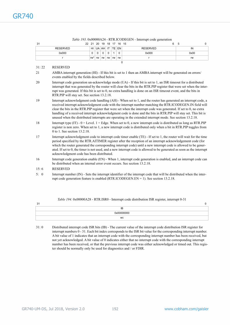
GR740
Table 193. 0x00000A24 - RTR.ICODEGEN - Interrupt code generation31 22 21 20 19 18 17 16 15 6 5 0
RESERVED HI UA AH IT TE EN RESERVED IN
0x000 0 0 0 0 1 0 0x000 0x00
r rw* rw rw rw rw rw r rw
0
31: 22 RESERVED
21 AMBA interrupt generation (HI) - If this bit is set to 1 then an AMBA interrupt will be generated on errors/events enabled by the fields described below.
20 Interrupt code generation un-acknowledge mode (UA) - If this bit is set to 1, an ISR timeout for a distributed interrupt that was generated by the router will clear the bits in the RTR.PIP register that were set when the inter-rupt was generated. If this bit is set to 0, no extra handling is done on an ISR timeout event, and the bits in RTR.PIP will stay set. See section 13.2.18.
19 Interrupt acknowledgment code handling (AH) - When set to 1, and the router has generated an interrupt code, a received interrupt acknowledgment code with the interrupt number matching the RTR.ICODEGEN.IN field will clear the bits in the RTR.PIP register that were set when the interrupt code was generated. If set to 0, no extra handling of a received interrupt acknowledgment code is done and the bits in RTR.PIP will stay set. This bit is unused when the distributed interrupts are operating in the extended interrupt mode. See section 13.2.18.
18 Interrupt type (IT) - 0 = Level. 1 = Edge. When set to 0, a new interrupt code is distributed as long as RTR.PIP register is non zero. When set to 1, a new interrupt code is distributed only when a bit in RTR.PIP toggles from 0 to 1. See section 13.2.18.
17 Interrupt acknowledgment code to interrupt code timer enable (TE) - If set to 1, the router will wait for the time period specified by the RTR.AITIMER register after the reception of an interrupt acknowledgement code (for which the router generated the corresponding interrupt code) until a new interrupt code is allowed to be gener-ated. If set to 0, the timer is not used, and a new interrupt code is allowed to be generated as soon as the interrupt acknowledgment code has been distributed.
16 Interrupt code generation enable (EN) - When 1, interrupt code generation is enabled, and an interrupt code can be distributed when an internal error event occurs. See section 13.2.18.
15: 6 RESERVED
5: 0 Interrupt number (IN) - Sets the interrupt identifier of the interrupt code that will be distributed when the inter-rupt code generation feature is enabled (RTR.ICODEGEN.EN = 1). See section 13.2.18.
Table 194. 0x00000A28 - RTR.ISR0 - Interrupt code distribution ISR register, interrupt 0-3131 0
IB
0x00000000
wc
31: 0 Distributed interrupt code ISR bits (IB) - The current value of the interrupt code distribution ISR register for interrupt numbers 0 - 31. Each bit index corresponds to the ISR bit value for the corresponding interrupt number. A bit value of 1 indicates that an interrupt code with the corresponding interrupt number has been received, but not yet acknowledged. A bit value of 0 indicates either that no interrupt code with the corresponding interrupt number has been received, or that the previous interrupt code was either acknowledged or timed out. This regis-ter should be normally only be used for diagnostics and / or FDIR.
GR740-UM-DS, Jul 2018, Version 2.0 192 www.cobham.com/gaisler

GR740
Table 195. 0x00000A2C - RTR.ISR1 - Interrupt code distribution ISR register, interrupt 32-6331 0
IB
0x00000000
wc
31: 0 Distributed interrupt code ISR bits (IB) - The current value of the interrupt code distribution ISR register for interrupt numbers 32 - 63. Each bit index corresponds to the ISR bit value for the corresponding interrupt num-ber, minus 32, i.e bit 0 corresponds to interrupt number 32, bit 1 to interrupt number 33 etc. A bit value of 1 indi-cates that an interrupt code with the corresponding interrupt number has been received, but not yet acknowledged. A bit value of 0 indicates either that no interrupt code with the corresponding interrupt number has been received, or that the previous extended interrupt code timed out. This register should be normally only be used for diagnostics and / or FDIR.
Table 196. 0x00000A30 - RTR.ISRTIMER - Interrupt code distribution ISR timer reload31 16 15 0
RESERVED RL
0x0000 0xFFFF
r rw
31: 16 RESERVED
15: 0 Interrupt code distribution ISR timer reload (RL) - Interrupt code distribution ISR timer reload value, counted in prescaler ticks. Each ISR bit has its own timer, which is started and reloaded with the value of this field when an interrupt code with the corresponding interrupt number is received (or generated by the router). See section 13.2.18 for details on interrupt code distribution.
Table 197. 0x00000A34 - RTR.AITIMER - Interrupt code distribution ACK-to-INT timer reload31 16 15 0
RESERVED RL
0x0000 0x0000
r rw
31: 16 RESERVED
15: 0 Interrupt acknowledgement code to interrupt code timer reload (RL) - Interrupt code distribution interrupt acknowledgement code to interrupt code timer reload value, counted in prescaler ticks. When an interrupt acknowledgement code is receive - for which the router generated the corresponding interrupt code - the inter-rupt acknowledgement code to interrupt code timer is started and reloaded with the value of this field. See sec-tion 13.2.18 for details on interrupt code distribution.
Table 198. 0x00000A38 - RTR.ISRCTIMER - Interrupt code distribution ISR change timer reload31 5 4 0
RESERVED RL
0x0000000 0x00
r rw
31: 5 RESERVED
4: 0 Interrupt code distribution ISR change timer reload (RL) - Interrupt code distribution ISR change timer reload value, counted in prescaler ticks. Each time an ISR bit change value, the corresponding ISR change timer is started and reloaded with the value of this field. See section 13.2.18 for details on interrupt code distribution.
GR740-UM-DS, Jul 2018, Version 2.0 193 www.cobham.com/gaisler

GR740
Table 199. 0x00000A40 - RTR.LRUNSTAT - Link running status31 9 8 1 0
RESERVED LR R
0x000000 0x00 0
r r r
31: 19 RESERVED
18: 1 Link running status (LR)- Each bit is set to 1 when the link interface for the SpaceWire port with the same num-ber as the bit index is in run-state. If the link interface is not in run-state, the bit is set to 0.
0 RESERVED
Table 200. 0x00000A44 - RTR.CAP - Capability31 26 25 24 23 22 20 19 18 16 15 14 13 12 11 10 9 5 4 0
RESERVED AF R PF R RM R AS AX DP ID SD PC CC
0x00 0x3 0 0x3 0 0x0 0 0 1 0 1 1 0x00 0x00
r r r r r r r r r r r r r r
31: 26 RESERVED
25: 24 AMBA port word FIFO size (AF) - Shows the number of entries in the AMBA port’s 32-bit FIFOs. The number
of entries is determined by the value of this field, according to the formula: Entries = 2(RTR.CAP.PF+2). Constant value of 0x3 = 32 entries.
23 RESERVED
22: 20 Port N-char FIFO size (PF) - Shows the number of entries in the port’s N-char FIFOs. The number of entries is
determined by the value of this field, according to the formula: Entries = 2(RTR.CAP.PF+4). Constant value of 0x3 = 128 entries.
19 RESERVED
18: 16 RMAP maximum data length (RM) - This field specifies the maximum data length in an RMAP read / write command that the configuration port can handle. The length can be determined according to the formula: Length
= 2(RTR.CAP.RM+2). Constant value of 0x0 = 4 bytes.
15 RESERVED
14 Synchronous / asynchronous auxiliary interface (AS) - Constant value of 0, indicating that the auxiliary time-code / distributed interrupt code interface is synchronous to the system clock.
13 Auxiliary time-code / distributed interrupt code support (AX) - Specifies that the router has support for the aux-iliary time-code / distributed interrupt code feature described in 13.2.19. Constant value of 1.
12 SpaceWire dual port (DP) - Constant value of 0, indicating that SpaceWire ports are not implemented with dual ports.
11 Distributed interrupt support (ID) - Specifies that the router has support for the interrupt code distribution scheme, described in 13.2.18. Constant value of 1.
10 SpaceWire-D support (SD) - Specifies that the router has support for the SpaceWire-D, described in section 13.2.21. Constant value of 1.
9: 5 Port packet counter bits (PC) - Specifies the number of bits in the port’s incoming / outgoing packet counters. Constant value of 0x00 = no packet counters.
4: 0 Port character counter bits (CC) - Specifies the number of bits in the port’s incoming / outgoing character count-ers. Constant value of 0x00 = no character counters.
GR740-UM-DS, Jul 2018, Version 2.0 194 www.cobham.com/gaisler

GR740
Table 201. 0x00000A50 - RTR.PNPVEND - SpaceWire Plug-and-Play - Device Vendor and Product ID31 16 15 0
VI PI
0x0003 0x0718
r r
31: 16 SpaceWire Plug-and-Play Vendor ID (VI) - Double mapping of the VEND bits from the SpaceWire Plug-and-Play Device Vendor and Product ID field. See table 210.
25: 0 SpaceWire Plug-and-Play Product ID (PI) - Double mapping of the PROD bits from the SpaceWire Plug-and-Play Device Vendor and Product ID field. See table 210.
Table 202. 0x00000A54 - RTR.PNPUVEND - SpaceWire Plug-and-Play - Unit Vendor and Product ID31 16 15 0
VI PI
0x0000 0x0000
rw rw
31: 16 SpaceWire Plug-and-Play Unit vendor ID (VI) - Double mapping of the VEND bits from the SpaceWire Plug-and-Play Unit Vendor and Product ID field (see table 219).
25: 0 SpaceWire Plug-and-Play Unit product ID (PI) - Double mapping of the PROD bits from the SpaceWire Plug-and-Play Unit Vendor and Product ID field (see table 219).
Table 203. 0x00000A58 - RTR.PNPUSN - SpaceWire Plug-and-Play - Unit Serial Number31 2 1 0
SN
0x00000000 *
rw
31: 0 SpaceWire Plug-and-Play Unit serial number (SN) - Double mapping of the SpaceWire Plug-and-Play Unit Serial Number field (see table 220). Reset value for bits 1:0 depends on bootstrap signals, as described in section 3.1.
Table 204. 0x00000E00-0x00000E30 - RTR.MAXPLEN - Maximum packet length, ports 0-1231 25 24 0
RESERVED ML
0x00 0x000000
r rw
31: 25 RESERVED
24: 0 Maximum packet length (ML) - Maximum length of packets for which the corresponding port is the input port. This field is only used when the RTR.PCTRL.PL bit (RTR.PCTRLCFG.PL for port 0) is set to 1. See section 13.2.16 for details.
GR740-UM-DS, Jul 2018, Version 2.0 195 www.cobham.com/gaisler

GR740
Table 205. 0x00000E84-0x00000EA0 - RTR.CREDCNT - Credit counter, ports 1-831 12 11 6 5 0
RESERVED OC IC
0x00000 0 0
r r r
31: 12 RESERVED
11: 6 Out credit counter (OC) - Number of outgoing credits. For each credit, the other end of the link is allowed to send one N-Char.
5: 0 In credit counter (IC) - Number of incoming credits. For each credit, the port is allowed to transmit one N-Char.
NOTE: This register is only available for SpaceWire ports.
Table 206. 0x00001004-0x000013FC - RTR.RTCOMB - Routing table, combined port mapping and address control, addresses 1-255
31 30 29 28 27 20 19 1 0
SR EN PR HD RESERVED PE PD
N/R 0 N/R N/R 0x00 N/R N/R
rw rw rw rw r rw rw
31 Spill-if-not-ready (SR) - This bit is a double mapping of the RTR.RTACTRL.SR bit. See table 176.
30 Enable (EN) - This bit is a double mapping of the RTR.RTACTRL.EN bit. See table 176.
29 Priority (PR) - This bit is a double mapping of the RTR.RTACTRL.PR bit. See table 176.
28 Header deletion (HD) - This bit is a double mapping of the RTR.RTACTRL.HD bit. See table 176.
27: 20 RESERVED
19: 1 Port enable bits (PE) - This field is a double mapping of the RTR.RTPMAP.PE field. See table 175.
NOTE: This register is not available via on-chip AHB slave interface. Only available through RMAP.
0 Packet distribution (PD) - This field is a double mapping of the RTR.RTPMAP.PD field. See table 175.
NOTE: See note for RTR.RTPMAP (table 175).
GR740-UM-DS, Jul 2018, Version 2.0 196 www.cobham.com/gaisler

GR740
13.5.4 SpaceWire Plug-and-Play interfaceThe configuration port supports parts of the SpaceWire Plug-and-Play protocol [SPWPNP]. The sup-ported fields are listed in table 209, and explained in more detail in tables 210 through 224.
The SpaceWire Plug-and-Play protocol uses standard RMAP commands and replies with the same requirements as presented in section 13.5.1, but with the following differences:
• Protocol Identifier field of a command shall be set to 0x03.
• A command’s address fields shall contain a word address. The SpaceWire Plug-and-Play addresses are encoded as shown in table 207.
• The increment bit in the command’s instruction field shall be set to 1, otherwise a reply with Sta-tus field set to 0x0A (authorization failure) is sent.
• RMAP Read-modify-write command is replaced by a compare-and-swap operation. The com-mand’s data fields shall contain the new data to be written, while the mask fields shall contain the value that the current data must match in order for the new data to be written. If there is a mis-match, a reply with Status field set to 0x0A (authorization failure) is sent.
• The reply packet’s Status field can contain the additional status codes described in table 208.
Note that it is not possible to access the SpaceWire Plug-and-Play fields through the AHB slave inter-face, except for the fields that are double mapped into the configuration port’s address space (see sec-tion 13.5.3).
An access (read, write, or compare-and-swap) made either to a field outside the Device Information service, or to a field in an undefined field set within the Device Information service, will generate a reply with the Status field set to 0xF1. An access (read, write, or compare-and-swap) to an undefined or unsupported field in one of the defined field sets, within the Device Information service, is not
Table 207. SpaceWire Plug-and-Play address encoding31 24 23 19 18 14 13 0
Application Index Protocol Index FieldSet ID Field ID
Table 208. SpaceWire Plug-and-Play status codes
Value Description
0xF0 Unauthorized access - A write, or compare-and-swap command arrived either when the router was not configured (Device ID field = 0), or the command did not match the owner information saved in the Link Information field and Owner Address fields.
0xF1 Reserved field set - A read, write, or compare-and-swap command’s address field points to a non existing field set.
0xF2 Read-only field - A write, or compare-and-swap command’s address points to a read-only field.
0xF3 Compare-and-swap-only-field - A write command’s address points to a compare-and-swap-only field.
GR740-UM-DS, Jul 2018, Version 2.0 197 www.cobham.com/gaisler

GR740
treated as an error, and the Status field of the reply will be 0x00. Possible write-data for such an access is discarded, and possible read-data returned is always 0.Table 209.SpaceWire Plug-and-Play support
SpW PnP Address Register name Acronym Service - Field set - Field
0x00000000 SpaceWire Plug-and-Play - Device Vendor and Product ID
RTR.PNPVEND Device Information - Device Identification - Device Vendor and Product ID
0x00000001 SpaceWire Plug-and-Play - Version RTR.PNPVER Device Information - Device Identification - Version
0x00000002 SpaceWire Plug-and-Play - Device Status RTR.PNPDEVSTS Device Information - Device Identification - Device Status
0x00000003 SpaceWire Plug-and-Play - Active Links RTR.PNPACTLNK Device Information - Device Identification - Active Links
0x00000004 SpaceWire Plug-and-Play - Link Information RTR.PNPLNKINFO Device Information - Device Identification - Link Information
0x00000005 SpaceWire Plug-and-Play - Owner Address 0 RTR.PNPOA0 Device Information - Device Identification - Owner Address 0
0x00000006 SpaceWire Plug-and-Play - Owner Address 1 RTR.PNPOA1 Device Information - Device Identification - Owner Address 1
0x00000007 SpaceWire Plug-and-Play - Owner Address 2 RTR.PNPOA2 Device Information - Device Identification - Owner Address 2
0x00000008 SpaceWire Plug-and-Play - Device ID RTR.PNPDEVID Device Information - Device Identification - Device ID
0x00000009 SpaceWire Plug-and-Play - Unit Vendor and Product ID
RTR.PNPUVEND Device Information - Device Identification - Unit Vendor and Product ID
0x0000000A SpaceWire Plug-and-Play - Unit Serial Num-ber
RTR.PNPUSN Device Information - Device Identification - Unit Serial Num-ber
0x00004000 SpaceWire Plug-and-Play - Vendor String Length
RTR.PNPVSTRL Device Information - Vendor / Product String - Vendor String Length
0x00006000 SpaceWire Plug-and-Play - Product String Length
RTR.PNPPSTRL Device Information - Vendor / Product String - Product String Length
0x00008000 SpaceWire Plug-and-Play - Protocol Count RTR.PNPPCNT Device Information - Protocol Support - Protocol Count
0x0000C000 SpaceWire Plug-and-Play - Application Count
RTR.PNPACNT Device Information - Application Support- Application Count
Table 210. 0x00000000 - RTR.PNPVEND - SpaceWire Plug-and-Play - Device Vendor and Product ID31 16 15 0
VEND PROD
0x0003 0x0740
r r
31: 16 Vendor ID (VEND) - SpaceWire vendor ID assigned to Cobham Gaisler. Constant value of 0x0003.
15: 0 Product ID (PROD) - Product ID assigned to GR740. Constant value of 0x0740
GR740-UM-DS, Jul 2018, Version 2.0 198 www.cobham.com/gaisler

GR740
Table 211. 0x00000001 - RTR.PNPVER - SpaceWire Plug-and-Play - Version31 24 23 16 15 8 7 0
MAJOR MINOR PATCH RESERVED
0x01 0x02 0x00 0x00
r r r r
31: 24 Major version number (MAJOR) - Constant value of 0x01.
23: 16 Minor version number (MINOR) - Constant value of 0x02
15: 8 Patch / Build number (PATCH) - Constant value of 0x00.
7: 0 RESERVED
Table 212. 0x00000002 - RTR.PNPDEVSTS - SpaceWire Plug-and-Play - Device Status31 8 7 0
RESERVED STATUS
0x000000 0x00
r r
31: 8 RESERVED
7: 0 Device status (STATUS) - Constant value of 0x00.
Table 213. 0x00000003 - RTR.PNPACTLNK - SpaceWire Plug-and-Play - Active Links31 9 8 1 0
RESERVED ACTIVE R
0x000 0x00 0
r r r
31: 13 RESERVED
12: 1 Link active (ACTIVE) - If set to 1, the port with the same number as the bit index is running. If set to 0, the port is not running. For the SpaceWire ports (ports 1-8), the corresponding bit will be set to 1 if the link interface is in run-state and the port is not disabled through the Port Control register (RTR.PCTRL.DI = 0). For the AMBA ports, the bit is set to 1 if RTR.PCTRL.DI = 0.
0 RESERVED
GR740-UM-DS, Jul 2018, Version 2.0 199 www.cobham.com/gaisler

GR740
Table 214. 0x00000004 - RTR.PNPLNKINFO -SpaceWire Plug-and-Play - Link Information31 24 23 22 21 20 16 15 13 12 8 7 6 5 4 0
OLA OAL R OL RES RL T U R LC
0x00 0x0 0 0x0 0x0 0x0 1 0 0 0xC
r r r r r r r r r r
31: 24 Owner logical address (OLA) - Shows the value of the Initiator Logical Address field from the last successful compare-and-swap command that set the Device ID field.
23: 22 Owner address length (OAL) - Shows how many of the three Owner Address fields that contain valid data.
21 RESERVED
20: 16 Owner link (OL) - Shows the number of the port which was used for the last successful operation to set the value of the Device ID field.
15: 13 RESERVED
12: 8 Return link (RL) - Shows the number of the port through which the reply to the current read command will be transmitted.
7 Device type (T) - Constant value of 1, indicating that this device is a router.
6 Unit information (U) - Indicates if the unit identification information (Unit Vendor and Product ID field, and Unit Serial Number field) are valid. 0 = invalid, 1 = valid. This bit will be 0 after reset / power-up. Once the Unit Vendor and Product ID field has been written with a non-zero value, this bit will be set to 1.
5 RESERVED
4: 0 Link count (LC) - Shows the number of router ports. Constant value of 0xC.
Table 215. 0x00000005 - RTR.PNPOA0 - SpaceWire Plug-and-Play - Owner Address 031 0
RA
0x00000000
r
31: 0 Reply address (RA) - Shows byte 0-3 of the Reply Address from the last successful compare-and-swap com-mand that set to the Device ID field. If there was no Reply Address, then this field is zero.
Table 216. 0x00000006 - RTR.PNPOA1 - SpaceWire Plug-and-Play - Owner Address 131 0
RA
0x00000000
r
31: 0 Reply address (RA) - Shows byte 4-7 of the Reply Address from the last successful compare-and-swap com-mand that set to the Device ID field. If the Reply Address was four bytes or less, then this field is zero.
Table 217. 0x00000007 - RTR.PNPOA2 - SpaceWire Plug-and-Play - Owner Address 231 0
RA
0x00000000
r
31: 0 Reply address (RA) - Shows byte 8-11 of the Reply Address from the last successful compare-and-swap com-mand that set to the Device ID field. If the Reply Address was eight bytes or less, then this field is zero.
GR740-UM-DS, Jul 2018, Version 2.0 200 www.cobham.com/gaisler
GR740
Table 218. 0x00000008 - RTR.PNPDEVID - SpaceWire Plug-and-Play - Device ID31 0
DID
0x00000000
cas
31: 0 Device ID (DID) - Shows the device identifier. After reset / power-up, or when this field is written to zero, the router is not considered to have an owner. The same applies to the case when the port indicated by the OL bits in the Link Information field is either disconnected, or disabled by setting the RTR.PCTRL.DI bit to 1. This field is only writable through a compare-and-swap operation.
Table 219. 0x00000009 - RTR.PNPUVEND - SpaceWire Plug-and-Play - Unit Vendor and Product ID31 16 15 0
VEND PROD
0x0000 0x0000
r r
31: 16 Unit vendor ID (VEND) - Shows the unit vendor identifier. This field is read-only through the SpaceWire Plug-and-Play protocol, however it is writable through RMAP and AHB (see section 13.5.3). When this field, or the PROD field, is written with a non-zero value, the U bit in the Link Information field is set to 1.
15: 0 Unit product ID (VEND) - Shows the unit product identifier. This field is read-only through the SpaceWire Plug-and-Play protocol, however it is writable through RMAP and AHB (see section 13.5.3). When this field, or the VEND field, is written with a non-zero value, the U bit in the Link Information field is set to 1.
Table 220. 0x0000000A - RTR.PNPUSN - SpaceWire Plug-and-Play - Unit Serial Number31 0
USN
0x00000000
r
31: 0 Unit serial number (USN) - Shows the unit serial number. This field is read-only through the SpaceWire Plug-and-Play protocol, however it is writable through RMAP and AHB (see section 13.5.3).
Table 221. 0x00004000 - RTR.PNPVSTRL - SpaceWire Plug-and-Play - Vendor String Length31 15 14 0
RESERVED LEN
0x00000 0x0000
r r
31: 15 RESERVED
14: 0 Vendor string length (LEN) - Constant value of 0, indicating that no vendor string is present.
GR740-UM-DS, Jul 2018, Version 2.0 201 www.cobham.com/gaisler
GR740
Table 222. 0x00006000 - RTR.PNPPSTRL - SpaceWire Plug-and-Play - Product String Length31 15 14 0
RESERVED LEN
0x00000 0x0000
r r
31: 15 RESERVED
14: 0 Product string length (LEN) - Constant value of 0, indicating that no product string is present.
Table 223. 0x00008000 - RTR.PNPPCNT - SpaceWire Plug-and-Play - Protocol Count31 5 4 0
RESERVED PC
0x0000000 0x00
r r
31: 5 RESERVED
4: 0 Protocol count (PC) - Constant value of 0, indicating that no protocols can be managed by using SpaceWire Plug-and-Play.
Table 224. 0x0000C000 - RTR.PNPACNT - SpaceWire Plug-and-Play - Application Count31 8 7 0
RESERVED AC
0x000000 0x00
r r
31: 8 RESERVED
7: 0 Application count (AC) - Constant value of 0, indicating that no applications can be managed by using Space-Wire Plug-and-Play.
GR740-UM-DS, Jul 2018, Version 2.0 202 www.cobham.com/gaisler
GR740
14 Gigabit Ethernet Media Access Controller (MAC)14.1 Overview
Cobham Gaisler’s Gigabit Ethernet Media Access Controller (GRETH_GBIT) provides an interface between an AMBA-AHB bus and an Ethernet network. It supports 10/100/1000 Mbit speed in both full- and half-duplex. The AMBA interface consists of an APB interface for configuration and control and an AHB master interface which handles the dataflow. The dataflow is handled through DMA channels. There is one DMA engine for the transmitter and one for the receiver. Both share the same AHB master interface.
The ethernet interface supports the MII and GMII interfaces which should be connected to an external PHY. The GRETH also provides access to the MII Management interface which is used to configure the PHY. Hardware support for the Ethernet Debug Communication Link (EDCL) protocol is also provided. This is an UDP/IP based protocol used for remote debugging.
Some of the supported features for the DMA channels are Scatter Gather I/O and TCP/UDP over IPv4 checksum offloading for both receiver and transmitter.
The system contains two GRETH_GBIT cores. The AHB master interfaces are connected to the Mas-ter I/O AHB bus. The cores also gave dedicated EDCL interfaces connected to the Debug AHB bus. The selection of which master interface to use for EDCL traffic is made via bootstrap signals.
14.2 Operation
14.2.1 System overview
The GRETH_GBIT consists of 3 functional units: The DMA channels, MDIO interface and the optional Ethernet Debug Communication Link (EDCL).
The main functionality consists of the DMA channels which are used for transferring data between an AHB bus and an Ethernet network. There is one transmitter DMA channel and one Receiver DMA channel. The operation of the DMA channels is controlled through registers accessible through the APB interface.
Figure 16. Block diagram of the internal structure of the GRETH_GBIT
AHBAPB
Ethernet MAC
Registers MDIOETH*_MDIO
ETH*_MDC
AHB MasterInterface
Transmitter
Receiver
Transmitter
Receiver
DMA Engine
DMA Engine
RAM
RAM
ETH*_TXENETH*_TXERETH*_TXD[7:0]ETH*_TXCLKETH*_CRSETH*_COL
ETH*_RXDVETH*_RXERETH*_RXD[7:0]ETH*_RXCLK
EDCL Transmitter
EDCL Receiver
ETH*_GTXCLK
GR740-UM-DS, Jul 2018, Version 2.0 203 www.cobham.com/gaisler

GR740
The MDIO interface is used for accessing configuration and status registers in one or more PHYs con-nected to the MAC. The operation of this interface is also controlled through the APB interface.The EDCL provides read and write access to an AHB bus through Ethernet. It uses the UDP, IP and ARP protocols together with a custom application layer protocol to accomplish this. The EDCL con-tains no user accessible registers and always runs in parallel with the DMA channels.
The Media Independent Interface (MII) and Gigabit Media Independent Interface (GMII) are used for communicating with the PHY. More information can be found in section 14.7.
The EDCL and the DMA channels share the Ethernet receiver and transmitter. More information on these functional units is provided in sections 14.3 - 14.6.
14.2.2 Protocol support
The GRETH_GBIT is implemented according to IEEE standard 802.3-2002. There is no support for the optional control sublayer. This means that packets with type 0x8808 (the only currently defined ctrl packets) are discarded.
14.2.3 Dedicated EDCL AHB master interface
The core has an additional master interface connected to the Debug AHB bus that can be used for the EDCL. This master interface is enabled with the external signals GPIO[8] and GPIO[9]. These signals are only sampled at reset and changes have no effect until the next reset. Note that the core can be reset via the clock gating unit and that this will lead to the value of GPIO[9:8] being sampled. See sec-tion 3.1 for further information on bootstrap signals.
14.3 Tx DMA interface
The transmitter DMA interface is used for transmitting data on an Ethernet network. The transmission is done using descriptors located in memory.
14.3.1 Setting up a descriptor.
A single descriptor is shown in table 225 and 226. The number of bytes to be sent should be set in the length field and the address field should point to the data. There are no alignment restrictions on the address field. If the interrupt enable (IE) bit is set, an interrupt will be generated when the packet has been sent (this requires that the transmitter interrupt bit in the control register is also set). The inter-rupt will be generated regardless of whether the packet was transmitted successfully or not.
Table 225. Address offset 0x0 - GRETH_GBIT transmit descriptor word 031 21 20 19 18 17 16 15 14 13 12 11 10 0
RESERVED UC TC IC MO LC AL UE IE WR EN LENGTH
31: 21 RESERVED
20 UDP checksum (UC) - Calculate and insert the UDP checksum for this packet. The checksum is only inserted if an UDP packet is detected.
19 TCP checksum (TC) - Calculate and insert the TCP checksum for this packet. The checksum is only inserted if an TCP packet is detected.
18 IP checksum (IC) - Calculate and insert the IP header checksum for this packet. The checksum is only inserted if an IP packet is detected.
17 More (MO) - More descriptors should be fetched for this packet (Scatter Gather I/O).
16 Late collision (LC) - A late collision occurred during the transmission (1000 Mbit mode only).
15 Attempt limit error (AL) - The packet was not transmitted because the maximum number of attempts was reached.
14 Underrun error (UE) - The packet was incorrectly transmitted due to a FIFO underrun error.
GR740-UM-DS, Jul 2018, Version 2.0 204 www.cobham.com/gaisler

GR740
To enable a descriptor the enable (EN) bit should be set and after this is done, the descriptor should not be touched until the enable bit has been cleared by the GRETH_GBIT. The rest of the fields in the descriptor are explained later in this section.
14.3.2 Starting transmissions
Enabling a descriptor is not enough to start a transmission. A pointer to the memory area holding the descriptors must first be set in the GRETH_GBIT. This is done in the transmitter descriptor pointer register. The address must be aligned to a 1 kB boundary. Bits 31 to 10 hold the base address of descriptor area while bits 9 to 3 form a pointer to an individual descriptor. The first descriptor should be located at the base address and when it has been used by the GRETH_GBIT the pointer field is incremented by 8 to point at the next descriptor. The pointer will automatically wrap back to zero when the next 1 kB boundary has been reached (the descriptor at address offset 0x3F8 has been used). The WR bit in the descriptors can be set to make the pointer wrap back to zero before the 1 kB bound-ary.
The pointer field has also been made writable for maximum flexibility but care should be taken when writing to the descriptor pointer register. It should never be touched when a transmission is active.
The final step to activate the transmission is to set the transmit enable bit in the control register. This tells the GRETH_GBIT that there are more active descriptors in the descriptor table. This bit should always be set when new descriptors are enabled, even if transmissions are already active. The descrip-tors must always be enabled before the transmit enable bit is set.
14.3.3 Descriptor handling after transmission
When a transmission of a packet has finished, status is written to the first word in the corresponding descriptor. The Underrun Error bit is set if the transmitter RAM was not able to provide data at a suf-ficient rate. This indicates a synchronization problem most probably caused by a low clock rate on the AHB clock. The whole packet is buffered in the transmitter RAM before transmission so underruns cannot be caused by bus congestion. The Attempt Limit Error bit is set if more collisions occurred than allowed. When running in 1000 Mbit mode the Late Collision bit indicates that a collision occurred after the slottime boundary was passed.
The packet was successfully transmitted only if these three bits are zero. The other bits in the first descriptor word are set to zero after transmission while the second word is left untouched.
The enable bit should be used as the indicator when a descriptor can be used again, which is when it has been cleared by the GRETH_GBIT. There are three bits in the GRETH_GBIT status register that
13 Interrupt enable (IE) - Enable Interrupts. An interrupt will be generated when the packet from this descriptor has been sent provided that the transmitter interrupt enable bit in the control register is set. The interrupt is generated regardless if the packet was transmitted successfully or if it terminated with an error.
12 Wrap (WR) - Set to one to make the descriptor pointer wrap to zero after this descriptor has been used. If this bit is not set the pointer will increment by 8. The pointer automatically wraps to zero when the 1 kB boundary of the descriptor table is reached.
11 Enable (EN) - Set to one to enable the descriptor. Should always be set last of all the descriptor fields.
10: 0 LENGTH - The number of bytes to be transmitted.
Table 226. Address offset 0x4 - GRETH_GBIT transmit descriptor word 131 0
ADDRESS
31: 0 Address (ADDRESS) - Pointer to the buffer area from where the packet data will be loaded.
Table 225. Address offset 0x0 - GRETH_GBIT transmit descriptor word 0
GR740-UM-DS, Jul 2018, Version 2.0 205 www.cobham.com/gaisler

GR740
hold transmission status. The Transmit Error (TE) bit is set each time an transmission ended with an error (when at least one of the three status bits in the transmit descriptor has been set). The Transmit Successful (TI) is set each time a transmission ended successfully.The Transmit AHB Error (TA) bit is set when an AHB error was encountered either when reading a descriptor, reading packet data or writing status to the descriptor. Any active transmissions are aborted and the transmitter is disabled. The transmitter can be activated again by setting the transmit enable register. See also the AMBA ERROR propagation description in section 5.10.
14.3.4 Setting up the data for transmission
The data to be transmitted should be placed beginning at the address pointed by the descriptor address field. The GRETH_GBIT does not add the Ethernet address and type fields so they must also be stored in the data buffer. The 4 B Ethernet CRC is automatically appended at the end of each packet. Each descriptor will be sent as a single Ethernet packet. If the size field in a descriptor is greater than 1514 B, the packet will not be sent.
14.3.5 Scatter Gather I/O
A packet can be generated from data fetched from several descriptors. This is called Scatter Gather I/O. The More (MO) bit should be set to 1 to indicate that more descriptors should be used to generate the current packet. When data from the current descriptor has been read to the RAM the next descrip-tor is fetched and the new data is appended to the previous data. This continues until a descriptor with the MO bit set to 0 is encountered. The packet will then be transmitted.
Status is written immediately when data has been read to RAM for descriptors with MO set to 1. The status bits are always set to 0 since no transmission has occurred. The status bits will be written to the last descriptor for the packet (which had MO set to 0) when the transmission has finished.
No interrupts are generated for descriptors with MO set to 1 so the IE bit is don’t care in this case.
The checksum offload control bits (explained in section 14.3.6) must be set to the same values for all descriptors used for a single packet.
14.3.6 Checksum offloading
Support is provided for checksum calculations in hardware for TCP and UDP over IPv4. The check-sum calculations are enabled in each descriptor and applies only to that packet (when the MO bit is set all descriptors used for a single packet must have the checksum control bits set in the same way).
The IP Checksum bit (IC) enables IP header checksum calculations. If an IPv4 packet is detected when transmitting the packet associated with the descriptor the header checksum is calculated and inserted. If TCP Checksum (TC) is set the TCP checksum is calculated and inserted if an TCP/IPv4 packet is detected. Finally, if the UDP Checksum bit is set the UDP checksum is calculated and inserted if a UDP/IPv4 packet is detected. In the case of fragmented IP packets, checksums for TCP and UDP are only inserted for the first fragment (which contains the TCP or UDP header).
14.4 Rx DMA interface
The receiver DMA interface is used for receiving data from an Ethernet network. The reception is done using descriptors located in memory.
14.4.1 Setting up descriptors
A single descriptor is shown in table 227 and 228. The address field points at the location where the received data should be stored. There are no restrictions on alignment. The GRETH_GBIT will never store more than 1518 B to the buffer (the tagged maximum frame size excluding CRC). The CRC field (4 B) is never stored to memory so it is not included in this number. If the interrupt enable (IE) bit is set, an interrupt will be generated when a packet has been received to this buffer (this requires
GR740-UM-DS, Jul 2018, Version 2.0 206 www.cobham.com/gaisler

GR740
that the receiver interrupt bit in the control register is also set). The interrupt will be generated regard-less of whether the packet was received successfully or not.The enable bit is set to indicate that the descriptor is valid which means it can be used by the to store a packet. After it is set the descriptor should not be touched until the EN bit has been cleared by the GRETH_GBIT.
The rest of the fields in the descriptor are explained later in this section.
14.4.2 Starting reception
Enabling a descriptor is not enough to start reception. A pointer to the memory area holding the descriptors must first be set in the GRETH_GBIT. This is done in the receiver descriptor pointer reg-ister. The address must be aligned to a 1 kB boundary. Bits 31 to 10 hold the base address of descrip-tor area while bits 9 to 3 form a pointer to an individual descriptor. The first descriptor should be located at the base address and when it has been used by the GRETH_GBIT the pointer field is incre-mented by 8 to point at the next descriptor. The pointer will automatically wrap back to zero when the
Table 227. Address offset 0x0 - GRETH_GBIT receive descriptor word 031 27 26 25 24 23 22 21 20 19 18 17 16 15 14 13 12 11 10 0
RESERVED MC IF TR TD UR UD IR ID LE OE CE FT AE IE WR EN LENGTH
31: 27 RESERVED
26 Multicast address (MC) - The destination address of the packet was a multicast address (not broad-cast).
25 IP fragment (IF) - Fragmented IP packet detected.
24 TCP error (TR) - TCP checksum error detected.
23 TCP detected (TD) - TCP packet detected.
22 UDP error (UR) - UDP checksum error detected.
21 UDP detected (UD) - UDP packet detected.
20 IP error (IR) - IP checksum error detected.
19 IP detected (ID) - IP packet detected.
18 Length error (LE) - The length/type field of the packet did not match the actual number of received bytes.
17 Overrun error (OE) - The frame was incorrectly received due to a FIFO overrun.
16 CRC error (CE) - A CRC error was detected in this frame.
15 Frame too long (FT) - A frame larger than the maximum size was received. The excessive part was truncated.
14 Alignment error (AE) - An odd number of nibbles were received.
13 Interrupt Enable (IE) - Enable Interrupts. An interrupt will be generated when a packet has been received to this descriptor provided that the receiver interrupt enable bit in the control register is set. The interrupt is generated regardless if the packet was received successfully or if it terminated with an error.
12 Wrap (WR) - Set to one to make the descriptor pointer wrap to zero after this descriptor has been used. If this bit is not set the pointer will increment by 8. The pointer automatically wraps to zero when the 1 kB boundary of the descriptor table is reached.
11 Enable (EN) - Set to one to enable the descriptor. Should always be set last of all the descriptor fields.
10: 0 LENGTH - The number of bytes received to this descriptor.
Table 228. Address offset 0x4 - GRETH_GBIT receive descriptor word 131 0
ADDRESS
31: 0 Address (ADDRESS) - Pointer to the buffer area from where the packet data will be loaded.
GR740-UM-DS, Jul 2018, Version 2.0 207 www.cobham.com/gaisler

GR740
next 1 kB boundary has been reached (the descriptor at address offset 0x3F8 has been used). The WR bit in the descriptors can be set to make the pointer wrap back to zero before the 1 kB boundary.The pointer field has also been made writable for maximum flexibility but care should be taken when writing to the descriptor pointer register. It should never be touched when reception is active.
The final step to activate reception is to set the receiver enable bit in the control register. This will make the GRETH_GBIT read the first descriptor and wait for an incoming packet.
14.4.3 Descriptor handling after reception
The GRETH indicates a completed reception by clearing the descriptor enable bit. The other control bits (WR, IE) are also cleared. The number of received bytes is shown in the length field. The parts of the Ethernet frame stored are the destination address, source address, type and data fields. Bits 24-14 in the first descriptor word are status bits indicating different receive errors. Bits 18 - 14 are zero after a reception without link layer errors. The status bits are described in table 227 (except the checksum offload bits which are also described in section 14.4.6).
Packets arriving that are smaller than the minimum Ethernet size of 64 B are not considered as a reception and are discarded. The current receive descriptor will be left untouched an used for the first packet arriving with an accepted size. The TS bit in the status register is set each time this event occurs.
If a packet is received with an address not accepted by the MAC, the IA status register bit will be set.
Packets larger than maximum size cause the FT bit in the receive descriptor to be set. The length field is not guaranteed to hold the correct value of received bytes. The counting stops after the word con-taining the last byte up to the maximum size limit has been written to memory.
The address word of the descriptor is never touched by the GRETH.
14.4.4 Reception with AHB errors
If an AHB error occurs during a descriptor read or data store, the Receiver AHB Error (RA) bit in the status register will be set and the receiver is disabled. The current reception is aborted. The receiver can be enabled again by setting the Receive Enable bit in the control register. See also the AMBA ERROR propagation description in section 5.10.
14.4.5 Accepted MAC addresses
In the default configuration the core receives packets with either the unicast address set in the MAC address register or the broadcast address. Multicast support can also be enabled and in that case a hash function is used to filter received multicast packets. A 64-bit register, which is accessible through the APB interface, determines which addresses should be received. Each address is mapped to one of the 64 bits using the hash function and if the bit is set to one the packet will be received. The address is mapped to the table by taking the 6 least significant bits of the 32-bit Ethernet CRC calculated over the destination address of the MAC frame. A bit in the receive descriptor is set if a packet with a mul-ticast address has been received to it.
14.4.6 Checksum offload
Support is provided for checksum calculations in hardware for TCP/UDP over IPv4. The checksum logic is always active and detects IPv4 packets with TCP or UDP payloads. If IPv4 is detected the ID bit is set, UD is set if an UDP payload is detected in the IP packet and TD is set if a TCP payload is detected in the IP packet (TD and UD are never set if an IPv4 packet is not detected). When one or more of these packet types is detected its corresponding checksum is calculated and if an error is detected the checksum error bit for that packet type is set. The error bits are never set if the corre-sponding packet type is not detected. The core does not support checksum calculations for TCP and
GR740-UM-DS, Jul 2018, Version 2.0 208 www.cobham.com/gaisler

GR740
UDP when the IP packet has been fragmented. This condition is indicated by the IF bit in the receiver descriptor and when set neither the TCP nor the UDP checksum error indications are valid.14.5 MDIO Interface
The MDIO interface provides access to PHY configuration and status registers through a two-wire interface which is included in the MII interface. The GRETH_GBIT provides full support for the MDIO interface.
The MDIO interface can be used to access from 1 to 32 PHY containing 1 to 32 16-bit registers. A read transfer i set up by writing the PHY and register addresses to the MDIO Control register and set-ting the read bit. This caused the Busy bit to be set and the operation is finished when the Busy bit is cleared. If the operation was successful the Linkfail bit is zero and the data field contains the read data. An unsuccessful operation is indicated by the Linkfail bit being set. The data field is undefined in this case.
A write operation is started by writing the 16-bit data, PHY address and register address to the MDIO Control register and setting the write bit. The operation is finished when the busy bit is cleared and it was successful if the Linkfail bit is zero.
14.5.1 PHY interrupts
The core also supports status change interrupts from the PHY. A level sensitive, active low, interrupt signal can be connected on the eth{0,1}_mdint input. The PHY status change bit in the status register is set each time an event is detected on this signal. If the PHY status interrupt enable bit is set at the time of the event the core will also generate an interrupt on the AHB bus.
14.6 Ethernet Debug Communication Link (EDCL)
The EDCL provides access to an on-chip AHB bus through Ethernet. It uses the UDP, IP and ARP protocols together with a custom application layer protocol. The application layer protocol uses an ARQ algorithm to provide reliable AHB instruction transfers. Through this link, a read or write trans-fer can be generated to any address on the AHB bus.
14.6.1 Operation
The EDCL receives packets in parallel with the MAC receive DMA channel. It uses a separate MAC address which is used for distinguishing EDCL packets from packets destined to the MAC DMA channel. The EDCL also has an IP address. Since ARP packets use the Ethernet broadcast address, the IP-address must be used in this case to distinguish between EDCL ARP packets and those that should go to the DMA-channel. Packets that are determined to be EDCL packets are not processed by the receive DMA channel.
When the packets are checked to be correct, the AHB operation is performed. The operation is per-formed with the same AHB master interface that the DMA-engines use. The replies are automatically sent by the EDCL transmitter when the operation is finished. It shares the Ethernet transmitter with the transmitter DMA-engine but has higher priority.
14.6.2 EDCL protocols
The EDCL accepts Ethernet frames containing IP or ARP data. ARP is handled according to the pro-tocol specification with no exceptions.
GR740-UM-DS, Jul 2018, Version 2.0 209 www.cobham.com/gaisler

GR740
IP packets carry the actual AHB commands. The EDCL expects an Ethernet frame containing IP, UDP and the EDCL specific application layer parts. Table 229 shows the IP packet required by the EDCL. The contents of the different protocol headers can be found in TCP/IP literature.The following is required for successful communication with the EDCL: A correct destination MAC address, an Ethernet type field containing 0x0806 (ARP) or 0x0800 (IP). The IP-address is then com-pared for a match. The IP-header checksum and identification fields are not checked. There are a few restrictions on the IP-header fields. The version must be four and the header size must be 5 B (no options). The protocol field must always be 0x11 indicating a UDP packet. The length and checksum are the only IP fields changed for the reply.
The EDCL only provides one service at the moment and it is therefore not required to check the UDP port number. The reply will have the original source port number in both the source and destination fields. UDP checksum are not used and the checksum field is set to zero in the replies.
The UDP data field contains the EDCL application protocol fields. Table 230 shows the application protocol fields (data field excluded) in packets received by the EDCL. The 16-bit offset is used to align the rest of the application layer data to word boundaries in memory and can thus be set to any value. The R/W field determines whether a read (0) or a write(1) should be performed. The length
field contains the number of bytes to be read or written. If R/W is one the data field shown in Table 229 contains the data to be written. If R/W is zero the data field is empty in the received packets. Table 231 shows the application layer fields of the replies from the EDCL. The length field is always zero for replies to write requests. For read requests it contains the number of bytes of data contained in the data field.
The EDCL implements a Go-Back-N algorithm providing reliable transfers. The 14-bit sequence number in received packets are checked against an internal counter for a match. If they do not match, no operation is performed and the ACK/NAK field is set to 1 in the reply frame. The reply frame con-tains the internal counter value in the sequence number field. If the sequence number matches, the operation is performed, the internal counter is incremented, the internal counter value is stored in the sequence number field and the ACK/NAK field is set to 0 in the reply. The length field is always set to 0 for ACK/NAK=1 frames. The unused field is not checked and is copied to the reply. It can thus be set to hold for example some extra id bits if needed.
14.6.3 EDCL IP and Ethernet address settings
The default value of the EDCL IP and MAC addresses are shown in the table below. The addresses can be changed by software:
Table 229.The IP packet expected by the EDCL.
Ethernet
Header
IP
Header
UDP
Header
2 B
Offset
4 B
Control word
4 B
Address
Data 0 - 242
4B Words
Ethernet
CRC
Table 230.The EDCL application layer fields in received frames.
16-bit Offset 14-bit Sequence number 1-bit R/W 10-bit Length 7-bit Unused
Table 231.The EDCL application layer fields in transmitted frames.
16-bit Offset 14-bit sequence number 1-bit ACK/NAK 10-bit Length 7-bit Unused
Table 232.EDCL addresses
Core MAC address IP address
GRETH_GBIT 0 00:50:C2:75:A3:30 to 3F 192.168.0.16 to 31
GRETH_GBIT 1 00:50:C2:75:A3:40 to 4F 192.168.0.32 to 47
GR740-UM-DS, Jul 2018, Version 2.0 210 www.cobham.com/gaisler

GR740
In order to allow several EDCL enabled GRETH controllers on the same sub-net without the need for configuring the cores, the four least significant bits of the IP and MAC addresses are set via general purpose I/O lines at reset. See the description of bootstrap signals in section 3.1. Note that the four least significant bits of the IP and MAC addresses also will be reset if the Ethernet controllers are reset via the clock gating unit.
14.6.4 EDCL buffer size
The EDCL has a dedicated internal 2 KiB buffer memory which stores the received packets during processing. Table 233 shows how many concurrent packets the EDCL can handle, the maximum size of each packet including headers and the maximum size of the data payload. Sending more packets before receiving a reply than specified for the selected buffer size will lead to dropped packets. The behavior is unspecified if sending packets exceeding the maximum allowed size.
14.7 Media Independent Interfaces
There are several interfaces defined between the MAC sublayer and the Physical layer. The GRETH_GBIT supports the Media Independent Interface (MII) and the Gigabit Media Independent Interface (GMII).
The GMII is used in 1000 Mbit mode and the MII in 10 and 100 Mbit. These interfaces are defined separately in the 802.3-2002 standard but in practice they share most of the signals. The GMII has 9 additional signals compared to the MII. Four data signals are added to the receiver and transmitter data interfaces respectively and a new transmit clock for the gigabit mode is also introduced.
Table 233.EDCL buffer size limitations
Total buffer size (KiB) Number of packet buffers Packet buffer size (B) Maximum data payload (B)
2 4 512 456
Table 234.Signals in GMII and MII.
MII and GMII GMII Only
txd[3:0] txd[7:4]
tx_en rxd[7:4]
tx_er gtx_clk
rx_col
rx_crs
rxd[3:0]
rx_clk
rx_er
rx_dv
GR740-UM-DS, Jul 2018, Version 2.0 211 www.cobham.com/gaisler
GR740
14.8 RegistersThe core is programmed through registers mapped into APB address space.
Table 235.GRETH_GBIT registers
APB address offset Register
0x0 Control register
0x4 Status/Interrupt-source register
0x8 MAC Address MSB
0xC MAC Address LSB
0x10 MDIO Control/Status
0x14 Transmit descriptor pointer
0x18 Receiver descriptor pointer
0x1C EDCL IP
0x20 Hash table msb
0x24 Hash table lsb
0x28 EDCL MAC address MSB
0x2C EDCL MAC address LSB
0x30 - 0xFF RESERVED
GR740-UM-DS, Jul 2018, Version 2.0 212 www.cobham.com/gaisler

GR740
Table 236. 0x0 - GRETH_GBIT control register31 30 28 27 26 25 24 15 14 13 12 11 10 9 8 7 6 5 4 3 2 1 0
EA BS GA MA MC RESERVED ED RD DD ME PI BM GB SP RS PM FD RI TI RE TE
1 0b010 1 1 1 * 0 0 0 0 0 0 0 0 0 0 0 0 0 0
r r r r r rw rw rw rw rw rw rw rw wc rw rw rw rw rw rw
31 EDCL available (EA) - Set to one if the EDCL is available.
30: 28 EDCL buffer size (BS) - Shows the amount of memory used for EDCL buffers. 1 = 2 KiB
27 Gigabit MAC available (GA) - This bit always reads as a 1 and indicates that the MAC has 1000 Mbit capability.
26 MDIO interrupts enabled (MA) - Set to one when the core supports MDIO interrupts..
25 Multicast available (MC) - Set to one when the core supports multicast address reception.
24: 15 RESERVED
14 EDCL Disable (ED) - Set to one to disablethe EDCL and zero to enable it. Reset value taken from the external DSU_EN signal. If DSU_EN is high then this bit will be low, and the EDCL will be enabled after reset. Otherwise the EDCL will be disabled after reset.
13 RAM debug enable (RD) - RAM debug access is not available in this design. This bit is always zero. Writes have no effect.
12 Disable duplex detection (DD) - Disable the EDCL speed/duplex detection FSM. If the FSM cannot complete the detection the MDIO interface will be locked in busy mode. If software needs to access the MDIO the FSM can be disabled here and as soon as the MDIO busy bit is 0 the interface is avail-able. Note that the FSM cannot be re-enabled again.
11 Multicast enable (ME) - Enable reception of multicast addresses.
10 PHY status change interrupt enable (PI) - Enables interrupts for detected PHY status changes.
9 Burstmode (BM) - When set to 1, transmissions use burstmode in 1000 Mbit Half-duplex mode (GB=1, FD = 0). When 0 in this speed mode normal transmissions are always used with extension inserted. Operation is undefined when set to 1 in other speed modes.
8 Gigabit (GB) - 1 sets the current speed mode to 1000 Mbit and when set to 0, the speed mode is selected with bit 7 (SP).
7 Speed (SP) - Sets the current speed mode. 0 = 10 Mbit, 1 = 100 Mbit. Must not be set to 1 at the same time as bit 8 (GB).
6 Reset (RS) - A one written to this bit resets the GRETH_GBIT core. Self clearing. No other accesses should be done .to the slave interface other than polling this bit until it is cleared.
5 Promiscuous mode (PM) - If set, the GRETH_GBIT operates in promiscuous mode which means it will receive all packets regardless of the destination address.
4 Full duplex (FD) - If set, the GRETH_GBIT operates in full-duplex mode otherwise it operates in half-duplex.
3 Receiver interrupt (RI) - Enable Receiver Interrupts. An interrupt will be generated each time a packet is received when this bit is set. The interrupt is generated regardless if the packet was received successfully or if it terminated with an error.
2 Transmitter interrupt (TI) - Enable Transmitter Interrupts. An interrupt will be generated each time a packet is transmitted when this bit is set. The interrupt is generated regardless if the packet was transmitted successfully or if it terminated with an error.
1 Receive enable (RE) - Should be written with a one each time new descriptors are enabled. As long as this bit is one the GRETH_GBIT will read new descriptors and as soon as it encounters a disabled descriptor it will stop until RE is set again. This bit should be written with a one after the new descriptors have been enabled.
0 Transmit enable (TE) - Should be written with a one each time new descriptors are enabled. As long as this bit is one the GRETH_GBIT will read new descriptors and as soon as it encounters a disabled descriptor it will stop until TE is set again. This bit should be written with a one after the new descriptors have been enabled.
GR740-UM-DS, Jul 2018, Version 2.0 213 www.cobham.com/gaisler

GR740
Table 237. 0x4 - GRETH_GBIT status register.31 9 8 7 6 5 4 3 2 1 0
RESERVED PS IA TS TA RA TI RI TE RE
0 0 0 NR NR NR NR NR NR
wc wc wc wc wc wc wc wc wc
31: 9 RESERVED
8 PHY status changes (PS) - Set each time a PHY status change is detected.
7 Invalid address (IA) - A packet with an address not accepted by the MAC was received. Cleared when written with a one.
6 Too small (TS) - A packet smaller than the minimum size was received. Cleared when written with a one.
5 Transmitter AHB error (TA) - An AHB error was encountered in transmitter DMA engine. Cleared when written with a one. Not Reset.
4 Receiver AHB error (RA) - An AHB error was encountered in receiver DMA engine. Cleared when written with a one. Not Reset.
3 Transmit successful (TI) - A packet was transmitted without errors. Cleared when written with a one. Not Reset.
2 Receive successful (RI) - A packet was received without errors. Cleared when written with a one. Not Reset.
1 Transmitter error (TE) - A packet was transmitted which terminated with an error. Cleared when written with a one. Not Reset.
0 Receiver error (RE) - A packet has been received which terminated with an error. Cleared when writ-ten with a one. Not Reset.
Table 238. 0x8 - GRETH_GBIT MAC address MSB.31 16 15 0
RESERVED Bit 47 downto 32 of the MAC Address
NR
rw
31: 16 RESERVED
15: 0 The two most significant bytes of the MAC Address. Not Reset.
Table 239. 0xC - GRETH_GBIT MAC address LSB.31 0
Bit 31 downto 0 of the MAC Address
NR
rw
31: 0 The 4 least significant bytes of the MAC Address. Not Reset.
GR740-UM-DS, Jul 2018, Version 2.0 214 www.cobham.com/gaisler
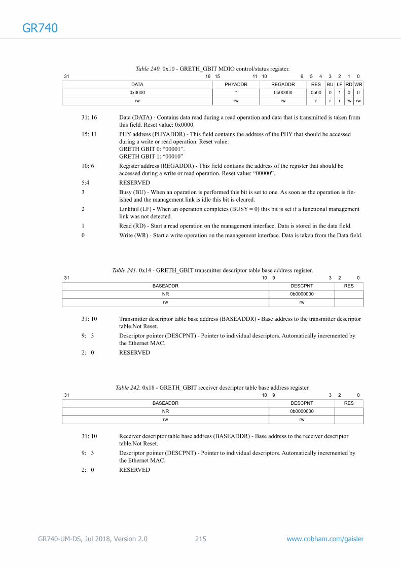
GR740
Table 240. 0x10 - GRETH_GBIT MDIO control/status register.31 16 15 11 10 6 5 4 3 2 1 0
DATA PHYADDR REGADDR RES BU LF RD WR
0x0000 * 0b00000 0b00 0 1 0 0
rw rw rw r r r rw rw
31: 16 Data (DATA) - Contains data read during a read operation and data that is transmitted is taken from this field. Reset value: 0x0000.
15: 11 PHY address (PHYADDR) - This field contains the address of the PHY that should be accessed during a write or read operation. Reset value: GRETH GBIT 0: “00001”.GRETH GBIT 1: “00010”
10: 6 Register address (REGADDR) - This field contains the address of the register that should be accessed during a write or read operation. Reset value: “00000”.
5:4 RESERVED
3 Busy (BU) - When an operation is performed this bit is set to one. As soon as the operation is fin-ished and the management link is idle this bit is cleared.
2 Linkfail (LF) - When an operation completes (BUSY = 0) this bit is set if a functional management link was not detected.
1 Read (RD) - Start a read operation on the management interface. Data is stored in the data field.
0 Write (WR) - Start a write operation on the management interface. Data is taken from the Data field.
Table 241. 0x14 - GRETH_GBIT transmitter descriptor table base address register.31 10 9 3 2 0
BASEADDR DESCPNT RES
NR 0b0000000
rw rw
31: 10 Transmitter descriptor table base address (BASEADDR) - Base address to the transmitter descriptor table.Not Reset.
9: 3 Descriptor pointer (DESCPNT) - Pointer to individual descriptors. Automatically incremented by the Ethernet MAC.
2: 0 RESERVED
Table 242. 0x18 - GRETH_GBIT receiver descriptor table base address register.31 10 9 3 2 0
BASEADDR DESCPNT RES
NR 0b0000000
rw rw
31: 10 Receiver descriptor table base address (BASEADDR) - Base address to the receiver descriptor table.Not Reset.
9: 3 Descriptor pointer (DESCPNT) - Pointer to individual descriptors. Automatically incremented by the Ethernet MAC.
2: 0 RESERVED
GR740-UM-DS, Jul 2018, Version 2.0 215 www.cobham.com/gaisler

GR740
Table 243. 0x1C - GRETH_GBIT EDCL IP register31 0
EDCL IP ADDRESS
*
rw
31: 0 EDCL IP address. Reset value: GRETH GBIT 0: 0xC0A80010 (192.168.0.16).GRETH GBIT 1: 0xC0A80020 (192.168.0.32)The four lowest bits of the EDCL IP address might be taken from GPIO inputs, see section 3.1.
Table 244. 0x20 - GRETH_GBIT Hash table msb register31 0
Hash table (64:32)
NR
rw
31: 0 Hash table msb. Bits 64 downto 32 of the hash table.
Table 245. 0x24 - GRETH_GBIT Hash table lsb register31 0
Hash table (64:32)
NR
rw
31: 0 Hash table lsb. Bits 31downto 0 of the hash table.
Table 246. 0x28 - GRETH_GBIT EDCL MAC address MSB.31 16 15 0
RESERVED Bit 47 downto 32 of the EDCL MAC Address
0x50C2
rw
31: 16 RESERVED
15: 0 The 2 most significant bytes of the EDCL MAC Address.
Table 247. 0x2C - GRETH_GBIT EDCL MAC address LSB.31 0
Bit 31 downto 0 of the EDCL MAC Address
*
rw
31: 0 The 4 least significant bytes of the EDCL MAC Address. Reset value: GRETH GBIT 0: 0x0075A330.GRETH GBIT 1: 0x0075A340The four lowest bits of the EDCL IP address might be taken from GPIO inputs, see section 3.1.
GR740-UM-DS, Jul 2018, Version 2.0 216 www.cobham.com/gaisler
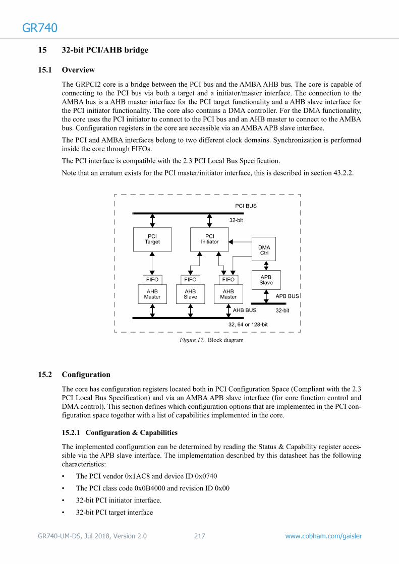
GR740
15 32-bit PCI/AHB bridge15.1 Overview
The GRPCI2 core is a bridge between the PCI bus and the AMBA AHB bus. The core is capable of connecting to the PCI bus via both a target and a initiator/master interface. The connection to the AMBA bus is a AHB master interface for the PCI target functionality and a AHB slave interface for the PCI initiator functionality. The core also contains a DMA controller. For the DMA functionality, the core uses the PCI initiator to connect to the PCI bus and an AHB master to connect to the AMBA bus. Configuration registers in the core are accessible via an AMBA APB slave interface.
The PCI and AMBA interfaces belong to two different clock domains. Synchronization is performed inside the core through FIFOs.
The PCI interface is compatible with the 2.3 PCI Local Bus Specification.
Note that an erratum exists for the PCI master/initiator interface, this is described in section 43.2.2.
15.2 Configuration
The core has configuration registers located both in PCI Configuration Space (Compliant with the 2.3 PCI Local Bus Specification) and via an AMBA APB slave interface (for core function control and DMA control). This section defines which configuration options that are implemented in the PCI con-figuration space together with a list of capabilities implemented in the core.
15.2.1 Configuration & Capabilities
The implemented configuration can be determined by reading the Status & Capability register acces-sible via the APB slave interface. The implementation described by this datasheet has the following characteristics:
• The PCI vendor 0x1AC8 and device ID 0x0740
• The PCI class code 0x0B4000 and revision ID 0x00
• 32-bit PCI initiator interface.
• 32-bit PCI target interface
Figure 17. Block diagram
PCI
AHB BUS
PCI BUS
32-bit
32, 64 or 128-bit
PCI
AHBMaster
AHBSlave
AHBMaster
FIFO FIFO FIFO
Target InitiatorDMACtrl
APB BUS
32-bit
APBSlave
GR740-UM-DS, Jul 2018, Version 2.0 217 www.cobham.com/gaisler

GR740
• DMA controller• Two FIFOs with a depth of eight words each
• Two 128 MiB PCI BARs marked as prefetchable. One 8 MiB PCI BAR marked as non-prefetch-able. The sizes given here are default sizes. The BAR sizes are configurable (down to a minimum size of 8 MiB) and the BARs can also be disabled.
• Device interrupt generation
• PCI interrupt sampling and forwarding
15.2.2 PCI Configuration Space
The core implements the following registers in the PCI Configuration Space Header. For more detailed information regarding each field in these registers please refer to the PCI Local Bus Specifi-cation.
Table 248.GRPCI2: Implemented registers in the PCI Configuration Space Header
PCI address offset Register
0x00 Device ID, Vendor ID
0x04 Status, Command
0x08 Class Code, Revision ID
0x0C BIST, Header Type, Latency Timer, Cache Line Size
0x10 - 0x24 Base Address Registers
0x34 Capabilities Pointer
0x3C Max_Lat, Min_Gnt, Interrupt Pin, Interrupt Line
Table 249.0x00 - Device ID and Vendor ID register31 16 16 15 0
Device ID Vendor ID
0x0061 0x1AC8
r r
31: 16 Device ID, 0x0740
15: 0 Vendor ID, 0x1AC8
GR740-UM-DS, Jul 2018, Version 2.0 218 www.cobham.com/gaisler
GR740
Table 250.0x04 - Status and Command register31 30 29 28 27 26 25 24 23 22 21 20 19 18 11 10 9 8 7 6 5 4 3 2 1 0
DPE
SSE
RMA
RTA
STA
DEVSEL
timing
MDPE
FBBC
RES
66MHz
CL IS RESERVED ID NotImp
SE NotImp
PER
NotImp
MWI
NotImp
BM MS NotImp
0 0 0 0 0 0b01 0 0 0 * 1 0 0 0 0 0 0 0 0 0 0 0 0 0
wc wc wc wc wc r r r r r r r r rw r rw r rw r rw r rw rw r
31 Detected Parity Error (DPE)
30 Signaled System Error (SSE)
29 Received Master Abort (RMA)
28 Received Target Abort (RTA)
27 Signaled Target Abort (STA)
26: 25 DEVSEL timing - Returns “01“ indicating medium
24 Master Data Parity Error (MDPE)
23 Fast Back-to-Back Capable (FBBC) - Returns zero.
22 RESERVED
21 66 MHz Capable (66MHZ)
NOTE: In this implementation this bit has been defined as the status of the PCI_M66EN signal rather than the capability of the core. For a 33 MHz design, this signal should be connected to ground and this status bit will have the correct value of ‘0’. For a 66 MHz design, this signal is pulled-up by the backplane and this status bit will have the correct value of ‘1’. For a 66 MHz capa-ble design inserted in a 33 MHz system, this bit will then indicate a 33 MHz capable device.
20 Capabilities List (CL) - Returns one
19 Interrupt Status (IS)
18: 11 RESERVED
10 Interrupt Disable (DI)
9 NOT IMPLEMENTED, Returns zero.
8 SERR# Enable (SE)
7 NOT IMPLEMENTED, Returns zero.
6 Parity Error Response (PER)
5 NOT IMPLEMENTED, Returns zero.
4 Memory Write and Invalidate Enable (MWI)
3 NOT IMPLEMENTED, Returns zero.
2 Bus Master (BM)
1 Memory Space (MS)
0 NOT IMPLEMENTED, Returns zero.
GR740-UM-DS, Jul 2018, Version 2.0 219 www.cobham.com/gaisler

GR740
Table 251.0x08 - Class Code and Revision ID register31 8 7 0
Class Code Revision ID
0x0B4000 0x00
r r
31: 8 Class Code, 0x0B4000
7: 0 Revision ID, 0x00
Table 252.0x0C - BIST, Header Type, Latency Timer, and Cache Line Size register31 24 23 16 15 8 7 0
BIST Header Type Latency Timer Cache Line Size
0 0 0 0
r r rw rw
31: 24 BIST - NOT IMPLEMENTED, Returns zeros
23: 16 Header Type - Returns 00
15: 8 Latency Timer - All bits are writable
7: 0 Cache Line Size - NOT IMPLEMENTED, Returns zero
Table 253.0x10-0x24 - Base Address Registers31 4 3 2 1 0
Base Address PF Type MS
0 * 0 0
rw r r r
31: 4 Base Address - The size of the BAR is determine by how many of the bits (starting from bit 31) are implemented. Bits not implemented returns zero.
The first two BARs are 128 MiB in size by default. The third BAR is 8 MiB by default. The 8 MiB BAR is suitable for mapping registers.
3 Prefetchable (PF) - zero indicating non-prefetchable. The two first BARs have the prefetchable bit set. The third BAR is not prefetchable and is suitable for mapping system registers.
2: 1 Type - Returns zero.
0 Memory Space Indicator (MS) - Returns zero
GR740-UM-DS, Jul 2018, Version 2.0 220 www.cobham.com/gaisler

GR740
Table 254.0x34 - Capabilities Pointer Register31 8 7 0
RESERVED Capabilities Pointer
0 0x40
r r
31: 8 RESERVED
7: 0 Capabilities Pointer - Indicates the first item in the list of capabilities of the Extended PCI Configu-ration Space. Value: 0x40
Table 255.0x3C - Max_Lat, Min_Gnt, Interrupt Pin and Interrupt Line register31 24 23 16 15 8 7 0
Max_Lat Min_Gnt Interrupt Pin Interrupt Line
0 0 INTA 0
r r r rw
31: 24 (Max_Lat) - NOT IMPLEMENTED, Returns zero
23: 16 (Min_Gnt) - NOT IMPLEMENTED, Returns zero
15: 8 Interrupt Pin - Indicates INTA
7: 0 Interrupt Line
GR740-UM-DS, Jul 2018, Version 2.0 221 www.cobham.com/gaisler

GR740
15.2.3 Extended PCI Configuration SpaceThis section describes the first item in the list of capabilities implemented in the Extended PCI Con-figuration Space. This capability is core specific and contains the PCI to AMBA address mapping and the option to change endianess of the PCI bus.
Table 256.GRPCI2: Internal capabilities of the Extended PCI Configuration Space
PCI address offset (with the Capabilities pointer as base) Register
0x00 Length, Next Pointer, ID
0x04 - 0x18 PCI BAR to AHB address mapping
0x1C Extended PCI Configuration Space to AHB address mapping
0x20 AHB IO base address and PCI bus config (endianess switch)
0x24 - 0x38 PCI BAR size and prefetch
0x3C AHB master prefetch burst limit
Table 257.0x00 - Length, Next pointer and ID31 24 23 16 15 8 7 0
RESERVED Length Next Pointer Capability ID
0 0x40 0x00 0x09
r r r r
31: 24 RESERVED
23: 16 Length - Returns 0x40.
15: 8 Next Pointer - Pointer to the next item in the list of capabilites. Set to 0x00
7: 0 Capability ID - Returns 0x09 indicating Vendor Specific.
Table 258.0x04-0x18 - PCI BAR to AHB address mapping register31 0
PCI BAR to AHB address mapping
0
rw
31: 0 PCI BAR to AHB address mapping - 32-bit mapping register for each PCI BAR. Translate an access to a PCI BAR to a AHB base address. The size of the BAR determine how many bits (starting form bit 31) are implemented. Bits non implemented returns zero
Table 259.0x1C - Extended PCI Configuration Space to AHB address mapping register31 8 7 0
Extended PCI Configuration Space to AHB address mapping RESERVED
0 0
rw r
31: 8 Extended PCI Configuration Space to AHB address mapping - Translates an access to the Extended PCI Con-figuration Space (excluding the address range for the internal register located in this configuration space) to a AHB address.
7: 0 RESERVED
GR740-UM-DS, Jul 2018, Version 2.0 222 www.cobham.com/gaisler

GR740
15.3 Operation
15.3.1 Access support
The core supports both single and burst accesses on the AMBA AHB bus and on the PCI bus. For more information on which PCI commands that are supported, see the PCI target section and for burst limitations see the Burst section.
15.3.2 FIFOs
The core has separate FIFOs for each data path: PCI target read, PCI target write, PCI master read, PCI master write, DMA AHB-to-PCI, and DMA PCI-to-AHB.
Table 260.0x20 - AHB IO base address and PCI bus config (endianess register)31 20 19 2 1 0
AHB IO base address RESERVED DISEN
ENDIAN
* 0 0 0
r r rw rw
31: 20 Base address of the AHB IO area
19: 2 RESERVED
1 Target access discard time out enable (DISEN) - When set to ‘1’, the target will discard a pending access if no retry of the access is detected during 2**15 PCI clock cycles.
0 PCI bus endianess switch (ENDIAN) - 1: defines the PCI bus to be little-endian, 0: defines the PCI bus to be big-endian
Table 261.0x24-0x38 - PCI BAR size and prefetch register31 4 3 2 0
PCI BAR size mask PF RES
* * 0
rw rw r
31: 4 PCI BAR size mask - A size mask register for each PCI BAR. When bit[n] is set to ‘1’ bit[n] in the PCI BAR register is implemented and can return a non-zero value. All bits from the lowest bit set to ‘1’ up to bit 31 need to be set to ‘1’. When bit 31 is ‘0’, this PCI BAR is disabled.
3 Prefetch bit (PF) - Prefetch bit in PCI BAR register
2: 0 RESERVED
Table 262.0x3C - AHB master burst limit31 16 15 0
RESERVED Burst length
0 0xFFFF
r rw
31: 16 RESERVED
15: 0 Burst length - Maximum number of beats - 1 in the burst. (Maximum value is 0xFFFF => 0x10000 beats => 64 KiB address)
GR740-UM-DS, Jul 2018, Version 2.0 223 www.cobham.com/gaisler

GR740
15.3.3 Byte enables and byte twisting (endianess)The core has the capability of converting endianess between the two busses. This means that all byte lanes can be swapped by the core as shown in figure below.
Table 263 defines the supported AHB address/size and PCI byte enable combinations.
As the AHB bus in the design is as big-endian, the core is able to define the PCI bus as little-endian (as defined by the PCI Local Bus Specification) with endianess conversion or define the PCI bus as big-endian without endianess conversion.
The endianess of the PCI bus is configured via the core specific Extended PCI Configuration Space.
15.3.4 PCI configuration cycles
Accesses to PCI Configuration Space are not altered by the endianess settings. The PCI Configuration Space is always defined as little-endian (as specified in the PCI Local Bus Specification). This means
Table 263.AHB address/size <=> PCI byte enable combinations.
AHB HSIZE AHB ADDRESS[1:0] Little-endian CBE[3:0] Big-endian CBE[3:0]
00 (8-bit) 00 1110 0111
00 (8-bit) 01 1101 1011
00 (8-bit) 10 1011 1101
00 (8-bit) 11 0111 1110
01 (16-bit) 00 1100 0011
01 (16-bit) 10 0011 1100
10 (32-bit) 00 0000 0000
Figure 18. GRPCI2 byte twisting
PCI bus
AHB bus 31-24 23-16 15-8 7-0
31-24 23-16 15-8 7-0
GRPCI2
Address 3
Address 3
Address 0
Address 0
GR740-UM-DS, Jul 2018, Version 2.0 224 www.cobham.com/gaisler

GR740
that the PCI target does not change the byte order even if the endianess conversion is enabled and the PCI master always converts PCI Configuration Space accesses to little-endian.Data stored in a register in the PCI Configuration Space as 0x12345678 (bit[31:0]) is transferred to the AHB bus as 0x78563412 (bit[31:0]). This means that non-8-bit accesses to the PCI Configuration Space must be converted in software to get the correct byte order.
15.3.5 Memory and I/O accesses
Memory and I/O accesses are always affected by the endianess conversion setting. The core should define the PCI bus as little-endian in the following scenarios: When the core is the PCI host and little-endian peripherals issues DMA transfers to host memory. When the core is a peripheral device and issues DMA transfers to a little-endian PCI host.
15.3.6 Bursts
PCI bus: The PCI target terminates a burst when no FIFO is available (the AMBA AHB master is not able to fill or empty the FIFO fast enough) or for reads when the burst reached the length specified by the “AHB master prefetch burst limit” register. This register defines a boundary which a burst can not cross i.e. when set to 0x400 beats (address boundary at 4 KiB) the core only prefetches data up to this boundary and then terminates the burst with a disconnect.
The PCI master stops the burst when the latency timer times out (see the PCI Local Bus Specification for information on the latency timer) or for reads when the burst reaches the limit defined by “PCI master prefetch burst limit” register (if AHB master performing the access is unmasked). If the master is masked in this register, the limit is set to 1 KiB. The PCI master does not prefetch data across this address boundary.
AHB bus: As long as a FIFOs are available for writes and data in a FIFO is available for read, the AHB slave does not limit the burst length. The burst length for the AHB master is limited by the FIFO depth (8 words). The AHB master only bursts up to the FIFO boundary. Only linear-incremental burst mode is supported.
DMA: DMA accesses are not affected by the “AHB master prefetch burst limit“ register or the “PCI master prefetch burst limit" register.
All FIFOs are filled starting at the same word offset as the bus access (i.e. with a FIFO of depth 8 words and the start address of a burst is 0x4, the first data word is stored in the second FIFO entry and only 7 words can be stored in this FIFO).
15.3.7 Host operation
The core provides a system host input (pci_hostn) signal that must be asserted (active low) for PCI system host operations. The status of this signal is available in the Status & Capability register acces-sible via the APB slave interface. The device is only allowed to generate PCI configuration cycles when this signal is asserted (device is the system host).
For designs intended to be host or peripherals only, the PCI system host signal can be tied low (host) or high (peripheral). For multi-purpose designs it should be connected to a pin on the PCI interface. The PCI Industrial Computer Manufacturers Group (PCIMG) cPCI specification uses pin C2 on con-nector P2 for this purpose. The pin should have a pull-up resistor since peripheral slots leave it uncon-nected.
An asserted PCI system host signal makes the PCI target respond to configuration cycles when no IDSEL signal is asserted (none of AD[31:11] are asserted). This is done for the PCI master to be able to configure its own PCI target.
GR740-UM-DS, Jul 2018, Version 2.0 225 www.cobham.com/gaisler

GR740
15.4 PCI Initiator interfaceThe PCI master interface is accessible via the AMBA AHB slave interface. The AHB slave interface occupies 1 GiB of the AHB memory address space and 256 KiB of AHB I/O address space. An access to the AHB memory address area is translated to a PCI memory cycle. An access to the first 64 KiB of the AHB IO area is translated to a PCI I/O cycle. The next 64 KiB are translated to PCI configuration cycles. A PCI trace buffer is accessible via the last 128 KiB of the AHB I/O area.
15.4.1 Memory cycles
A single read access to the AHB memory area is translated into a PCI memory read access, while a burst read translates into a PCI memory read multiple access. A write to this memory area is translated into a PCI write access.
The address translation is determined by AHB master to PCI address mapping registers accessible via the APB slave interface. Each AHB master on the AMBA AHB bus has its own mapping register. These registers contain the MSbs of the PCI address.
When the PCI master is busy performing a transaction on the PCI bus and not able to accept new requests, the AHB slave interface will respond with an AMBA RETRY response. This occurs on reads when the PCI master is fetching the requested data to fill the read FIFO or on writes when no write FIFO is available.
15.4.2 I/O cycles
Accesses to the low 64 KiB of the AHB I/O address area are translated into PCI I/O cycles. The address translation is determined by the “AHB to PCI mapping register for PCI I/O”. This register sets the 16 MSb of the PCI address. The “AHB to PCI mapping register for PCI I/O” is accessible via the APB slave interface. When the “IB” (PCI IO burst) bit in the Control register (accessible via the APB slave interface) is cleared, the PCI master does not perform burst I/O accesses.
15.4.3 Configuration cycles
Accesses to the second 64 KiB address block (address offset range 64 KiB to 128 KiB) of the AHB I/O area are translated into PCI configuration cycles. The AHB address is translated into PCI configura-tion address differently for type 0 and type 1 PCI configuration cycles. When the “bus number” field in the control register (accessible via the APB slave interface) is zero, type 0 PCI configuration cycles are issued. When the “bus number“ field is non-zero, type 1 PCI configuration cycles are issued to the PCI bus determined by this field. The AHB I/O address mapping to PCI configuration address for type 0 and type 1 PCI configuration cycles is defined in table 264 and table 265.
Only the system host is allowed to generate PCI configuration cycles. The core provides a system host input signal that must be asserted (active low) for PCI system host operations. The status of this signal is available in the Status & Capability register accessible via the APB slave interface.When the “CB” (PCI Configuration burst) bit in the Control register (accessible via the APB slave interface) is cleared, the PCI master does not perform burst configuration accesses.
Table 264. GRPCI2 Mapping of AHB I/O address to PCI configuration cycle, type 031 16 15 11 10 8 7 2 1 0
AHB ADDRESS MSB IDSEL FUNC REGISTER BYTE
31: 16 AHB address MSbs: Not used for PCI configuration cycle address mapping.
15: 11 IDSEL: This field is decoded to drive PCI AD[IDSEL+10]. Each of the signals AD[31:11] are sup-pose to be connected (by the PCI back plane) to one corresponding IDSEL line.
10: 8 FUNC: Selects function on a multi-function device.
GR740-UM-DS, Jul 2018, Version 2.0 226 www.cobham.com/gaisler

GR740
15.4.4 Error handling
When a read access issued by the PCI master is terminated with target-abort or master-abort, the AHB slave generates an AMBA ERROR response when the “ER” bit in the control register is set. When the “EI“ bit in the control register is set, an AMBA interrupt is generated for the error. The interrupt status field in the control register indicates the cause of the error. See also the AMBA ERROR propagation description in section 5.10.
15.4.5 Bus parking
The PCI initiator supports bus parking and will drive the PCI bus to a defined state when granted without requesting the bus. In systems with one single initiator the grant input to the PCI interface can be constantly asserted.
15.5 PCI Target interface
The PCI Target occupies memory areas in the PCI address space corresponding to the BAR registers in the PCI Configuration Space. Each BAR register (BAR0 to BAR2) defines the address allocation in the PCI address space. The size of each BAR is set by the “BAR size and prefetch” registers accessi-ble via the core specific Extended PCI Configuration Space. The size of a BAR can be determined by checking the number of implemented bits in the BAR register. Non-implemented bits returns zero and are read only.
This implementation has three PCI BARs. BAR0 and BAR1 default to prefetchable 128 MiB BARs and BAR2 defaults to a non-prefetchable 8 MiB BAR.
15.5.1 Supported PCI commands
These are the PCI commands that are supported by the PCI target.
• PCI Configuration Read/Write: Burst and single access to the PCI Configuration Space. These accesses are not transferred to the AMBA AHB bus except for the access of the user defined capability list item in the Extended PCI Configuration Space.
• Memory Read: A read command to the PCI memory BAR is transferred to a single read access on the AMBA AHB bus.
• Memory Read Multiple, Memory Read Line: A read multiple command to the PCI memory BAR is transferred to a burst access on the AMBA AHB bus. This burst access prefetch data to fill the maximum amount of data that can be stored in the FIFO.
7: 2 REGISTER: Used to index a PCI DWORD in configuration space.
1: 0 BYTE: Used to set the CBE correctly for non PCI DWORD accesses.
Table 265. GRPCI2 Mapping of AHB I/O address to PCI configuration cycle, type 131 16 15 11 10 8 7 2 1 0
AHB ADDRESS MSB DEVICE FUNC REGISTER BYTE
31: 16 AHB address MSbs: Not used for PCI configuration cycle address mapping.
15: 11 DEVICE: Selects which device on the bus to access.
10: 8 FUNC: Selects function on a multi-function device.
7: 2 REGISTER: Used to index a PCI DWORD in configuration space.
1: 0 BYTE: Used to set the CBE correctly for non PCI DWORD accesses.
Table 264. GRPCI2 Mapping of AHB I/O address to PCI configuration cycle, type 0
GR740-UM-DS, Jul 2018, Version 2.0 227 www.cobham.com/gaisler

GR740
• Memory Write, Memory Write and Invalidate: These command are handled similarly and aretransferred to the AMBA AHB bus as a single or burst access depending on the length of the PCI access (a single or burst access).
15.5.2 Implemented PCI responses
The PCI target can terminate a PCI access with the following responses.
• Retry: This response indicates the PCI target is busy by either fetching data for the AMBA AHB bus on a PCI read or emptying the write FIFO for a PCI write. A new PCI read access will always be terminated with a retry at least one time before the PCI target is ready to deliver data.
• Disconnect with data: Terminate the transaction and transfer data in the current data phase. This occurs when the PCI master request more data and the next FIFO is not yet available or for a PCI burst access with the Memory Read command.
• Disconnect without data: Terminate the transaction without transferring data in the current data phase. This occurs if the CBE change within a PCI burst write.
• Target Abort: Indicates that the current access caused an internal error and the target is unable to finish the access. This occurs when the core receives a AMBA AHB error during a read opera-tion.
15.5.3 Supported byte-enables (CBE)
The PCI target only supports aligned 8-, 16-, and 32-bit accesses.
The supported combinations of CBE are: 0000, 1110, 1101, 1011, 0111, 1100, 0011.
All other combinations of CBE are interpret as a 32-bit access (CBE = 0000) except for writes with CBE set to 1111, which is treated as a no-operation (no write will be performed).
15.5.4 PCI to AHB translation
Each PCI BAR has translation register (mapping register) to translate the PCI access to an AMBA AHB address area. These mapping registers are accessible via the core specific Extended PCI Config-uration Space. The number of implemented bits in these registers correspond to the size of (and num-ber of implemented bits in) the BARs registers.
15.5.5 PCI system host signal
When the PCI system host signal is asserted the PCI target responds to configuration cycles when no IDSEL signal is asserted (none of AD[31:11] are asserted). This is done for the PCI master, in a sys-tem host position, to be able to configure its own PCI target.
15.5.6 Error handling
The PCI target terminates the access with target-abort when the PCI target requests data from the AHB bus which results in an error response on the AHB bus. Because writes to the PCI target is posted, no error is reported on write AHB errors.
When a PCI master is terminated with a retry response it is mandatory for that master to retry the access until the access is completed or terminated with target-abort. If the master never retries the access, the PCI target interface would be locked on this access and never accept any new access. To recover from this situation, the PCI target has a option to discard an access if it is not retried within 215 clock cycles. This discard time out can be enabled via the “AHB IO base address and PCI bus config” register located in the core specific Extended PCI Configuration Space.
15.6 DMA Controller
The DMA engine is descriptor based and uses two levels of descriptors.
GR740-UM-DS, Jul 2018, Version 2.0 228 www.cobham.com/gaisler

GR740
15.6.1 DMA channelThe first level is a linked list of DMA channel descriptors. Each descriptor has a pointer to its data descriptor list and a pointer to the next DMA channel. The last DMA channel descriptor should always point to the first DMA channel for the list to be a closed loop. The descriptor needs to be aligned to 4 words (0x10) in memory and have the following structure:
The number of enabled DMA channels must be stored in the “Number of DMA channels“ field in the DMA control register accessible via the APB slave interface.
15.6.2 Data descriptor
The second descriptor level is a linked list of data transfers. The last descriptor in this list needs to be a disabled descriptor. To add a new data transfer, this disabled descriptor is updated to reflect the data transfer and to point to a new disabled descriptor. The control word in the descriptor should be updated last to enable the valid descriptor. To make sure the DMA engine reads this new descriptor, the enable bit in the DMA control register should be updated. The descriptor needs to be aligned to 4 words (0x10) in memory and have the following structure:
Table 266.GRPCI2: DMA channel descriptor structure
Descriptor address offset Descriptor word
0x00 DMA channel control
0x04 Next DMA channel (32-bit address to next DMA channel descrip-tor).
0x08 Next data descriptor in this DMA channel (32-bit address to next data descriptor).
0x0C RESERVED
Table 267. GRPCI2 DMA channel control31 30 25 24 22 21 20 19 16 15 0
EN RESERVED CID Type RESERVED Data descriptor count
31 Channel descriptor enable.
30: 25 RESERVED
24: 22 Channel ID. Each DMA channel needs a ID to determine the source of a DMA interrupt.
21: 20 Descriptor type. 01 = DMA channel descriptor.
19: 16 RESERVED
15: 0 Maximum number of data descriptors to be executed before moving to the next DMA channel. 0 indicates that all data descriptors should be executed before moving to the next DMA channel.
Table 268.GRPCI2: DMA data descriptor structure
Descriptor address offset Descriptor word
0x00 DMA data control
0x04 32-bit PCI start address
0x08 32-bit AHB start address
0x0C Next data descriptor in this DMA channel (32-bit address to next data descriptor).
GR740-UM-DS, Jul 2018, Version 2.0 229 www.cobham.com/gaisler

GR740
15.6.3 Data transfer
The DMA engine starts by reading the descriptor for the first DMA channel. If the DMA channel is enabled the first data descriptor in this channel is read and executed. When the transfer is done the data descriptor is disabled and status is written to the control word. If no error occurred during the transfer, the error bit is not set and the transfer length field is unchanged. If the transfer was termi-nated because of an error, the error bit is set in the control word and the length field indicates where in the transfer the error occurred. If no error has occurred, the next data descriptor is read and executed. When a disabled data descriptor is read or the maximum number of data descriptors has been exe-cuted, the DMA channel descriptor is updated to point to the next data descriptor and the DMA engine moves on to the next DMA channel.
When a disabled channel descriptor is read, the DMA controller will move on to the next DMA chan-nel without reading any data descriptors from the disabled channel.
When the DMA is disabled (via the APB interface), the channel descriptor is updated to point to the next data descriptor.
The DMA engine will stop when an error is detected or when no enabled data descriptors is found.The error type is indicated by bit 7 to bit 11 in the DMA control register. The error type bits must be cleared (by writing ‘1’) before the DMA can be re-enabled.
15.6.4 Interrupt
The DMA controller has a interrupt enable bit in the DMA control register (accessible via the APB slave interface) which enables interrupt generation.
Each data descriptor has an interrupt enable bit which determine if the core should generate a interrupt when the descriptor has been executed.
The DMA engine asserts the same interrupt as the PCI core.
15.7 PCI trace buffer
15.7.1 Trace data
The data from the trace buffer is accessible in the last 128 KiB block of the core’s AHB I/O area. Each 32-bit word in the first 64 KiB of this block represents a sample of the AD PCI signal. The second 64KiB of the block is the corresponding PCI control signal. Each 32-bit word is defined in table 270.
Table 269. GRPCI2 DMA data control31 30 29 28 22 21 20 19 18 16 15 0
EN IE DR BE RESERVED Type ER RESERVED LEN
31 Data descriptor enable.
30 Interrupt generation enable.
29 Transfer direction. 0: PCI to AMBA, 1: AMBA to PCI.
28 PCI bus endianess switch. 1: defines the PCI bus to be little-endian for this transfer, 0: defines the PCI bus to be big-endian for this transfer.
27: 22 RESERVED (Must be set to zero)
21: 20 Descriptor type. 00 = DMA data descriptor.
19 Error status
18: 16 RESERVED
15: 0 Transfer length. The number of word of the transfer is (this field)+1.
GR740-UM-DS, Jul 2018, Version 2.0 230 www.cobham.com/gaisler

GR740
15.7.2 Triggering function
The core can be programmed to trigger on any combination of the PCI AD and PCI Control signals by setting up the desired pattern and mask in the PCI trace buffer registers accessible via the APB slave interface. Each bit the PCI AD signal and any PCI control signal can be masked (mask bit equal to zero) to always match the triggering condition.
The “Trig count” field in the “PCI trace buffer: counter & mode” register defines how many times the trigger condition should occur before the trace buffer disarms and eventually stops sampling. The number of samples stored after the triggering condition occurs is defined by the “Delayed stop“ field.
To start sampling, the trace buffer needs to be armed by writing one to the start bit in the “PCI trace buffer: Control“ register. The state of the trace buffer can be determine by reading the Armed and Enable/Running bit in the control register. When the Armed bit is set, the triggering condition has not occurred. The Enable/Running bit indicates that the trace buffer still is storing new samples. When the delayed stop field is set to a non zero value, the Enabled bit is not cleared until all samples are stored in the buffer). The trace buffer can also be disarmed by writing the “stop” bit in the “PCI trace buffer: control” register.
When the trace buffer has been disarmed, the “trig index” in the “PCI trace buffer: control” register is updated with index of trace entry which match the triggering condition. The address offset of this entry is the value of the “trig index“ field times 4.
15.7.3 Trace Buffer APB interface
A separate APB register is available on the Debug AHB bus for access of the PCI trace buffer. The register layout is the same as for the core’s AHB interface but only registers related to the PCI trace buffer are available. The trace buffer data is located at offset 0x20000 for PCI AD and offset 0x30000 for PCI control signals.
15.8 Interrupts
The core is capable of sampling the PCI INTA-D signals and forwarding the interrupt to the APB bus. The “host INT mask” field in the control register is used to only sample the valid PCI INT signal(s).
The core is capable of driving the PCI INTA signal. The Interrupt Request Level (IRL) vector for pro-cessor 0 is or:ed into a signal that is sampled and forwarded to the PCI INTA signal. The core has a mask bit (the “Device INT mask” field in the control register) for each bit in the core’s input vector. The or:ed IRL vector is connected to the first position in this vector. The core also has a PCI interrupt force bit in the control register to be able to force assertion of PCI INTA.
When the system error PCI signal (SERR) is asserted the core sets the system error bit in the “core interrupt status” field in the Status & Capability register. If the system interrupt is enabled the core will also generate a interrupt on the APB bus.
Table 270. GRPCI2 PCI control signal trace (32-bit word)31 20 19 16 15 14 13 12 11 10 9 8 7 6 5 4 3 0
RESERVED CBE[3:0] FRAME
IRDY
TRDY
STOP
DEVSEL
PAR
PERR
SERR
IDSEL
REQ
GNT
LOCK
RST
RES
31: 20 RESERVED
19: 3 The state of the PCI control signals.
2: 0 RESERVED
GR740-UM-DS, Jul 2018, Version 2.0 231 www.cobham.com/gaisler

GR740
15.9 ResetThe deassertion of the PCI reset is synchronized to the PCI clock and delayed 3 clock cycles. Reset for the PCI clock domain is generated from the system’s SYS_RESETN input, as described in section 4.3.
15.10 Registers
The core is configured via registers mapped into APB memory address space.
Table 271.GRPCI2: APB registers
APB address offset Register
0x00 Control register
0x04 Status & Capability
0x08 PCI master prefetch burst limit
0x0C AHB to PCI mapping for PCI IO
0x10 DMA Control & Status
0x14 DMA descriptor base
0x18 DMA channel active (read only)
0x1C RESERVED
0x20 - 0x34 PCI BAR to AHB address mapping (Read only)
0x38 RESERVED
0x3C RESERVED
0x40 - 0x7C AHB master to PCI memory address mapping
0x80 PCI trace buffer: control & status
0x84 PCI trace buffer: counter & mode
0x88 PCI trace buffer: AD pattern
0x8C PCI trace buffer: AD mask
0x90 PCI trace buffer: Ctrl signal pattern
0x94 PCI trace buffer: Ctrl signal mask
0x98 PCI trace buffer: AD state
0x9C PCI trace buffer: Ctrl signal state
0xA0 - 0xFF RESERVED
GR740-UM-DS, Jul 2018, Version 2.0 232 www.cobham.com/gaisler

GR740
15.10.1Table 272.0x00 - CTRL - Control register
Control register
31 30 29 28 27 26 25 24 23 16 15 12 11 10 9 8 7 4 3 0
RE MR TR R SI PE ER EI Bus Number RESERVED DFA
IB CB DIF Device INT mask Host INT mask
0 0 0 0 0 0 0 0 0 0 0 0 0 0 0 0
rw rw rw r rw rw rw rw rw r rw rw rw rw rw rw
31 PCI reset (RE) - When set, the PCI reset signal is asserted. Needs to be cleared to deassert PCI reset.
30 PCI master reset (MR) - Set to reset the cores PCI master. This bit is self clearing.
29 PCI target reset (TR) - Set to reset the cores PCI target. This bit is self clearing.
28 RESERVED
27 System error interrupt (SI) - When set, Interrupt is enabled for System error (SERR)
26 Parity error response (PE) - When set, AHB error response is enabled for Parity error
25 Abort error response (ER) - When set, AHB error response is enabled for Master and Target abort.
24 Error interrupt (EI) - When set, Interrupt is enabled for Master and Target abort and Parity error.
23: 16 Bus Number - When not zero, type 1 configuration cycles is generated.This field is also used as the Bus Number in type 1 configuration cycles.
15: 12 RESERVED
11 Disable internal AHB-slave / DMA fair arbitration (DFA). When this bit is set, the arbitration is done when the current transfer has complete.
10 IO burst enable (IB) - When set, burst accesses may be generated by the PCI master for PCI IO cycles
9 Configuration burst enable (CB) - When set, burst accesses may be generated by the PCI master for PCI configuration cycles.
8 Device interrupt force (DIF) - When set, a PCI interrupt is forced.
7: 4 Device interrupt mask - When bit[n] is set dirq[n] is unmasked
3: 0 Host interrupt mask -bit[3] = 1: unmask INTD.bit[2] = 1: unmask INTC.bit[1] = 1: unmask INTB.bit[0] = 1: unmask INTA.
GR740-UM-DS, Jul 2018, Version 2.0 233 www.cobham.com/gaisler

GR740
15.10.2Table 273.0x04 - STATCAP - Status and Capability register
Status and capability register
31 30 29 28 27 26 25 24 23 22 21 20 19 18 12 11 8 7 5 4 2 1 0
Host
MST
TAR
DMA
DI HI IRQ mode
Trace
RES CFGDO
CFGER
Core interrupt status Host interrupt status
RES FDEPTH FNUM
* 1 1 1 1 1 0 1 0 0 0 0 * 0 3 2
r r r r r r r r r wc wc wc r r r r
31 System Host indicator (Host) - When zero, the core is inserted in the System slot and is allowed to act as System Host.
30 Master implemented (MST)
29 Target implemented (TAR)
28 DMA implemented (DMA)
27 Device Interrupt (DI) - Device drives PCI INTA
26 Host Interrupt (HI) - Device samples PCI INTA..D (for host operations)
25: 24 APB IRQ mode00: PCI INTA..D, Error interrupt and DMA interrupt on the same IRQ signal01: PCI INTA..D and Error interrupt on the same IRQ signal. DMA interrupt on IRQ+110: PCI INTA..D on IRQ..IRQ+3. Error interrupt and DMA interrupt on IRQ.11: PCI INTA..D on IRQ..IRQ+3. Error interrupt on IRQ. DMA interrupt on IRQ+4
23 PCI trace buffer implemented (Trace)
22: 21 RESERVED
20 PCI configuration access done (CFGDO) - PCI configuration error status valid.
19 PCI configuration error (CFGER) - Error during PCI configuration access
18: 12 Core Interrupt status:bit[6]: PCI target access discarded due to time out (access not retried for 215 PCI clock cycles)bit[5]: System errorbit[4]: DMA interruptbit[3]: DMA errorbit[2]: Master abort.bit[1]: Target abort.bit[0]: Parity error..
11: 8 Host interrupt statusbit[3] = 0: indicates that INTD is asserted.bit[2] = 0: indicates that INTC is asserted.bit[1] = 0: indicates that INTB is asserted.bit[0] = 0: indicates that INTA is asserted.
7: 5 RESERVED
4: 2 FIFO depth (FDEPTH) - Words in each FIFO = 2(FIFO depth)
1: 0 Number of FIFOs (FNUM)
GR740-UM-DS, Jul 2018, Version 2.0 234 www.cobham.com/gaisler

GR740
15.10.3Table 274.0x08 - BCIM - PCI master prefetch burst limit
PCI master prefetch burst limit register
15.10.4
Table 275.0x0C - AHB2PCI - AHB to PCI mapping for PCI IO
AHB to PCI mapping for PCI IO register
15.10.5
Table 276.0x10 - DMACTRL - DMA control and status register
DMA control and status register
31 16 15 8 7 0
AHB master unmask RESERVED Burst length
0 0 0xFF
rw r r
31: 16 AHB master unmask - When bit[n] is set, the prefetch burst of AHB master n is limited by the “Burst length” field.
15: 8 RESERVED
7: 0 Burst length - Maximum number of beats - 1 in the burst. (Maximin value is 0xFF => 0x100 beats => 1kB address)
31 16 15 0
AHB to PCI IO RESERVED
0 0
rw r
31: 16 AHB to PCI IO - Used as the MSBs of the base address for a PCI IO access.
15: 0 RESERVED
31 31 20 19 12 11 10 9 8 7 6 4 3 2 1 0
SAFE
RESERVED CHIRQ MA TA PE AE DE NUMCH ACTIVE
DIS IE EN
1 0 0 0 0 0 0 0 0 0 0 0 0
rw r wc wc wc wc wc wc rw r rw rw rw
31 : Safety guard (SAFE) - Needs to be set to ‘1’ for the control fields to be updated
30: 20 RESERVED
19: 12 Channel IRQ status (CHIRQ) - Set to ‘1’ when a descriptor is configured to signal interrupt. bit[0] corresponds to the channel with ID 0, bit[1] corresponds to the channel with ID 1, ... Clear by writing ‘1’
11 Master abort (MA) - received master abort during PCI access. Clear by writing ‘1’
10 : Target abort (TA) - received target abort during PCI access. Clear by writing ‘1’
9 Parity error (PE) - parity error during PCI access. Clear by writing ‘1’
8 : AHB data error (AE) - Error during AHB data access. Clear by writing ‘1’
7 : AHB descriptor error (DE) - Error during descriptor access. Clear by writing ‘1’
6: 4 Number of DMA channels (NUMCH) - Guarded by bit 31, safety guard
3 DMA active (ACTIVE)
2 : DMA disable/stop (DIS) - Writing ‘1’ to this bit disables the DMA.
1 Interrupt enable (IE) - (Guarded by bit[31], safety guard).
0 : DMA enable/start (EN) - Writing ‘1’ to this bit enables the DMA
GR740-UM-DS, Jul 2018, Version 2.0 235 www.cobham.com/gaisler

GR740
15.10.6Table 277.0x14 - DMABASE - DMA descriptor base address register
DMA descriptor base address register
15.10.7
Table 278.0x18 - DMACHAN - DMA channel active register
DMA channel active register
15.10.8
Table 279.0x20-0x34 - PCI2AHB - PCI BAR to AHB address mapping register
PCI BAR to AHB address mapping register
15.10.9
Table 280.0x40-0x7C - AHBM2PCI - AHB master to PCI memory address mapping register
AHB master to PCI memory address mapping register
31 0
DMA descriptor base address
0
rw
31: 0 Base address of the DMA descriptor table. When running, this register points to the active descriptor.
31 0
DMA channel descriptor base address
0
rw
31: 0 Base address of the active DMA channel
31 0
PCI BAR to AHB address mapping
0
rw
31: 0 32-bit mapping register for each PCI BAR. Translate an access to a PCI BAR to a AHB base address.
31 0
AHB master to PCI memory address mapping
0
rw
31: 0 32-bit mapping register for each AHB master. Translate an access from a specific AHB master to a PCI base address. The size of the AHB slave address area determine how many bits (starting from bit 31) are implemented. Bits not implemented returns zero. The mapping register for AHB master 0 is located at offset 0x40, AHB master 1 at offset 0x44, and so on up to AHB master 15 at offset 0x7C. Mapping registers are only implemented for existing AHB masters.
GR740-UM-DS, Jul 2018, Version 2.0 236 www.cobham.com/gaisler

GR740
15.10.10Table 281.0x80 - TCTRC - PCI trace Control and Status register
PCI trace control and status register
15.10.11
Table 282.0x84 - TMODE - PCI trace counter and mode register
PCI trace counter and mode register
15.10.12
Table 283.0x88 - TADP - PCI trace AD pattern register
PCI trace AD pattern register
31 16 15 14 13 12 11 4 3 2 1 0
TRIG INDEX AR EN RES DEPTH RES SO SA
N/R 0 0 0 8 0 0 0
r r r r r r w w
31: 16 TRIG INDEX - Index of the first entry of the trace.
15 Armed (AR) - Set when trace buffer is armed (started but the trig condition has not occurred).
14 Running (EN) - Set when trace buffer is running
13: 12 RESERVED
11: 4 Trace buffer depth (DEPTH) - Number of buffer entries = 2**DEPTH = 256
3: 2 RESERVED
1 Stop tracing (SO)
0 Start tracing (SA)
31 28 27 24 23 16 15 0
RES Tracing mode Trig count Delayed stop
0 0 0 0
r rw rw rw
31: 28 RESERVED
27: 24 Tracing mode00: Continuous sampling01: RESERVED10: RESERVED11: RESERVED
23: 16 Trig count - The number of times the trig condition should occur before the trace is disarmed.
15: 0 Delayed stop - The number of entries stored after the trace buffer has been disarmed. (Should not be lager than number of buffer entries - 2).
31 0
PCI AD pattern
N/R
rw
31: 0 PCI AD pattern to trig on
GR740-UM-DS, Jul 2018, Version 2.0 237 www.cobham.com/gaisler

GR740
15.10.13Table 284.0x8C - TADM - PCI trace AD mask register
PCI trace AD mask register
15.10.14
Table 285.0x90 - TCP - PCI trace Ctrl signal pattern register
PCI trace ctrl signal pattern register
15.10.15
Table 286.0x94 - TCM - PCI trace Ctrl signal mask register
PCI trace ctrl signal mask register
31 0
PCI AD mask
N/R
rw
31: 0 PCI AD mask - Mask for the AD pattern. When mask bit[n] = 0 pattern bit[n] will always be a match.
31 20 19 16 15 14 13 12 11 10 9 8 7 6 5 4 3 0
RESERVED CBE[3:0] FRAME
IRDY
TRDY
STOP
DEVSEL
PAR
PERR
SERR
IDSEL
REQ
GNT
LOCK
RST
RES
0 N/R N/R
N/R
N/R
N/R
N/R
N/R
N/R
N/R
N/R
N/R
N/R
N/R
N/R
0
r rw rw rw rw rw rw rw rw rw rw rw rw rw rw r
31: 20 RESERVED
19: 3 PCI Ctrl signal pattern to trig on
2: 0 RESERVED
31 20 19 16 15 14 13 12 11 10 9 8 7 6 5 4 3 0
RESERVED CBE[3:0] FRAME
IRDY
TRDY
STOP
DEVSEL
PAR
PERR
SERR
IDSEL
REQ
GNT
LOCK
RST
RES
0 N/R N/R
N/R
N/R
N/R
N/R
N/R
N/R
N/R
N/R
N/R
N/R
N/R
N/R
0
r rw rw rw rw rw rw rw rw rw rw rw rw rw rw r
31: 20 RESERVED
19: 3 Mask for the Ctrl signal pattern. When mask bit[n] = 0 pattern bit[n] will always be a match.
2: 0 RESERVED
GR740-UM-DS, Jul 2018, Version 2.0 238 www.cobham.com/gaisler

GR740
15.10.16Table 287.0x98 - TADS - PCI trace PCI AD state register
PCI trace PCI AD state register
15.10.17
Table 288.0x9C - TCS - PCI trace PCI Ctrl signal state register
PCI trace PCI control signal state register
31 0
Sampled PCI AD signal
N/R
r
31: 0 The state of the PCI AD signal.
31 20 19 16 15 14 13 12 11 10 9 8 7 6 5 4 3 0
RESERVED CBE[3:0] FRAME
IRDY
TRDY
STOP
DEVSEL
PAR
PERR
SERR
IDSEL
REQ
GNT
LOCK
RST
RES
0 N/R N/R
N/R
N/R
N/R
N/R
N/R
N/R
N/R
N/R
N/R
N/R
N/R
N/R
0
r r r r r r r r r r r r r r r r
31: 20 RESERVED
19: 3 The state of the PCI Ctrl signals
2: 0 RESERVED
GR740-UM-DS, Jul 2018, Version 2.0 239 www.cobham.com/gaisler

GR740
16 MIL-STD-1553B / AS15531 Interface16.1 Overview
This interface core connects the AMBA AHB/APB bus to a single- or dual redundant MIL-STD-1553B bus, and can act as either Bus Controller, Remote Terminal or Bus Monitor.
MIL-STD-1553B (and derived standard SAE AS15531) is a bus standard for transferring data between up to 32 devices over a shared (typically dual-redundant) differential wire. The bus is designed for predictable real-time behavior and fault-tolerance. The raw bus data rate is fixed at 1 Mbit/s, giving a maximum of around 770 kbit/s payload data rate.
One of the terminals on the bus is the Bus Controller (BC), which controls all traffic on the bus. The other terminals are Remote Terminals (RTs), which act on commands issued by the bus controller. Each RT is assigned a unique address between 0-30. In addition, the bus may have passive Bus Moni-tors (BM:s) connected.
There are 5 possible data transfer types on the MIL-STD-1553 bus:
• BC-to-RT transfer (“receive”)
• RT-to-BC transfer (“transmit”)
• RT-to-RT transfer
• Broadcast BC-to-RTs
• Broadcast RT-to-RTs
Each transfer can contain 1-32 data words of 16 bits each.
The bus controller can also send “mode codes” to the RTs to perform administrative tasks such as time synchronization, and reading out terminal status.
16.2 Electrical interface
The core is connected to the MIL-STD-1553B bus wire through single or dual transceivers, isolation transformers and transformer or stub couplers as shown in figure 19. If single-redundancy is used, the unused bus receive P/N signals should be tied both-high or both-low. The transmit/receive enables may be inverted on some transceivers. See the standard and the respective component’s data sheets for more information on the electrical connection
.
rxenA
txA_N
rxA_P
rxA_N
txA_P
txenABus A
rxenB
txB_N
rxB_P
rxB_N
txB_P
txenBBus BGR1553B
Terminal boundary
Figure 19. Interface between core and MIL-STD-1553B bus (dual-redundant, transformer coupled)
GR740-UM-DS, Jul 2018, Version 2.0 240 www.cobham.com/gaisler
GR740
16.3 Operation16.3.1 Operating modes
The core contains three separate control units for the Bus Controller, Remote Terminal and Bus Mon-itor handling, with a shared 1553 codec. The operating mode of the core is controlled by starting and stopping of these units via register writes. At start-up, none of the parts are enabled, and the core is completely passive on both the 1553 and AMBA bus.
The BC and RT parts of the core can not be active on the 1553 bus at the same time. While the BC is running or suspended, only the BC (and possibly BM) has access to the 1553 bus, and the RT can only receive and respond to commands when both the BC schedules are completely stopped (not running or even suspended).
The Bus Monitor, however, is only listening on the codec receivers and can therefore operate regard-less of the enabled/disabled state of the other two parts.
16.3.2 Register interface
The core is configured and controlled through control registers accessed over the APB bus. Each of the BC, RT, BM parts has a separate set of registers, plus there is a small set of shared registers.
Some of the control register fields for the BC and RT are protected using a ‘key’, a field in the same register that has to be written with a certain value for the write to take effect. The purpose of the keys are to give RT/BM designers a way to ensure that the software can not interfere with the bus traffic by enabling the BC or changing the RT address. If the software is built without knowledge of the key to a certain register, it is very unlikely that it will accidentally perform a write with the correct key to that control register.
16.3.3 Interrupting
The core has one interrupt output, which can be generated from several different source events. Which events should cause an interrupt can be controlled through the IRQ Enable Mask register.
16.3.4 MIL-STD-1553 Codec
The core’s internal codec receives and transmits data words on the 1553 bus, and generates and checks sync patterns and parity.
Loop-back checking logic checks that each transmitted word is also seen on the receive inputs. If the transmitted word is not echoed back, the transmitter stops and signals an error condition, which is then reported back to the user.
GR740-UM-DS, Jul 2018, Version 2.0 241 www.cobham.com/gaisler
GR740
16.4 Bus Controller Operation16.4.1 Overview
When operating as Bus Controller, the core acts as master on the MIL-STD-1553 bus, initiates and performs transfers.
This mode works based on a scheduled transfer list concept. The software sets up in memory a sequence of transfer descriptors and branches, data buffers for sent and received data, and an IRQ pointer ring buffer. When the schedule is started (through a BC action register write), the core pro-cesses the list, performs the transfers one after another and writes resulting status into the transfer list and incoming data into the corresponding buffers.
16.4.2 Timing control
In each transfer descriptor in the schedule is a “slot time” field. If the scheduled transfer finishes sooner than its slot time, the core will pause the remaining time before scheduling the next command. This allows the user to accurately control the message timing during a communication frame.
If the transfer uses more than its slot time, the overshooting time will be subtracted from the following command’s time slot. The following command may in turn borrow time from the following command and so on. The core can keep track of up to one second of borrowed time, and will not insert pauses again until the balance is positive, except for intermessage gaps and pauses that the standard requires.
If you wish to execute the schedule as fast as possible you can set all slot times in the schedule to zero. If you want to group a number of transfers you can move all the slot time to the last transfer.
The schedule can be stopped or suspended by writing into the BC action register. When suspended, the schedule’s time will still be accounted, so that the schedule timing will still be correct when the schedule is resumed. When stopped, on the other hand, the schedule’s timers will be reset.
When the extsync bit is set in the schedule’s next transfer descriptor, the core will wait for a positive edge on the external sync input before starting the command. The external sync input is connected to the tick of general purpose timer unit 0’s timer 3. The schedule timer and the time slot balance will then be reset and the command is started. If the sync pulse arrives before the transfer is reached, it is stored so the command will begin immediately. The trigger memory is cleared when stopping (but not when suspending) the schedule. Also, the trigger can be set/cleared by software through the BC action register.
16.4.3 Bus selection
Each transfer descriptor has a bus selection bit that allows you to control on which one of the two redundant buses (‘0’ for bus A, ‘1’ for bus B) the transfer will occur.
Another way to control the bus usage is through the per-RT bus swap register, which has one register bit for each RT address. Writing a ‘1’ to a bit in the register inverts the meaning of the bus selection bit for all transfers to the corresponding RT, so ‘0’ now means bus ‘B’ and ‘1’ means bus ‘A’. This allows you to switch all transfers to one or a set of RT:s over to the other bus with a single register write and without having to modify any descriptors.
The hardware determines which bus to use by taking the exclusive-or of the bus swap register bit and the bus selection bit. Normally it only makes sense to use one of these two methods for each RT, either the bus selection bit is always zero and the swap register is used, or the swap register bit is always zero and the bus selection bit is used.
If the bus swap register is used for bus selection, the store-bus descriptor bit can be enabled to auto-matically update the register depending on transfer outcome. If the transfer succeeded on bus A, the bus swap register bit is set to ‘0’, if it succeeds on bus B, the swap register bit is set to ‘1’. If the trans-fer fails, the bus swap register is set to the opposite value.
GR740-UM-DS, Jul 2018, Version 2.0 242 www.cobham.com/gaisler
GR740
16.4.4 Secondary transfer listThe core can be set up with a secondary “asynchronous” transfer list with the same format as the ordi-nary schedule. This transfer list can be commanded to start at any time during the ordinary schedule. While the core is waiting for a scheduled command’s slot time to finish, it will check if the next asyn-chronous transfer’s slot time is lower than the remaining sleep time. In that case, the asynchronous command will be scheduled.
If the asynchronous command doesn’t finish in time, time will be borrowed from the next command in the ordinary schedule. In order to not disturb the ordinary schedule, the slot time for the asynchro-nous messages must therefore be set to pessimistic values.
The exclusive bit in the transfer descriptor can be set if one does not want an asynchronous command scheduled during the sleep time following the transfer.
Asynchronous messages will not be scheduled while the schedule is waiting for a sync pulse or the schedule is suspended and the current slot time has expired, since it is then not known when the next scheduled command will start.
16.4.5 Interrupt generation
Each command in the transfer schedule can be set to generate an interrupt after certain transfers have completed, with or without error. Invalid command descriptors always generate interrupts and stop the schedule. Before a transfer-triggered interrupt is generated, the address to the corresponding descriptor is written into the BC transfer-triggered IRQ ring buffer and the BC Transfer-triggered IRQ Ring Position Register is incremented.
A separate error interrupt signals DMA errors. If a DMA error occurs when reading/writing descrip-tors, the executing schedule will be suspended. DMA errors in data buffers will cause the correspond-ing transfer to fail with an error code (see table 292). See also the AMBA ERROR propagation description in section 5.10.
Whether any of these interrupt events actually cause an interrupt request on the AMBA bus is con-trolled by the IRQ Mask Register setting.
16.4.6 Transfer list format
The BC:s transfer list is an array of transfer descriptors mixed with branches as shown in table 289. Each entry has to be aligned to start on a 128-bit (16-byte) boundary. The two unused words in the branch case are free to be used by software to store arbitrary data.
Table 289.GR1553B transfer descriptor format
Offset Value for transfer descriptor DMA R/W Value for branch DMA R/W
0x00 Transfer descriptor word 0 (see table 290) R Condition word (see table 294) R
0x04 Transfer descriptor word 1 (see table 291) R Jump address, 128-bit aligned R
0x08 Data buffer pointer, 16-bit aligned.
For write buffers, if bit 0 is set the received data is discarded and the pointer is ignored. This can be used for RT-to-RT transfers where the BC is not interested in the data transferred.
R Unused -
0x0C Result word, written by core (see table 292) W Unused -
GR740-UM-DS, Jul 2018, Version 2.0 243 www.cobham.com/gaisler

GR740
The transfer descriptor words are structured as shown in tables 290-292 below.Table 290. GR1553B BC transfer descriptor word 0 (offset 0x00)31 30 29 28 27 26 25 24 23 22 20 19 18 17 16 15 0
0 WTRIG EXCL IRQE IRQN SUSE SUSN RETMD NRET STBUS GAP RESERVED STIME
31 Must be 0 to identify as descriptor
30 Wait for external trigger (WTRIG)
29 Exclusive time slot (EXCL) - Do not schedule asynchronous messages
28 IRQ after transfer on Error (IRQE)
27 IRQ normally (IRQN) - Always interrupts after transfer
26 Suspend on Error (SUSE) - Suspends the schedule (or stops the async transfer list) on error
25 Suspend normally (SUSN) - Always suspends after transfer
24 : 23 Retry mode (RETMD). 00 - Retry on same bus only. 01 - Retry alternating on both buses
10: Retry first on same bus, then on alternating bus. 11 - Reserved, do not use
22 : 20 Number of retries (NRET) - Number of automatic retries per bus
The total number of tries (including the first attempt) is NRET+1 for RETMD=00, 2 x (NRET+1) for RETMD=01/10
19 Store bus (STBUS) - If the transfer succeeds and this bit is set, store the bus on which the transfer succeeded (0 for bus A, 1 for bus B) into the per-RT bus swap register. If the transfer fails and this bit is set, store the opposite bus instead. (only if the per-RT bus mask is supported in the core)
See section 16.4.3 for more information.
18 Extended intermessage gap (GAP) - If set, adds an additional amount of gap time, corresponding to the RTTO field, after the transfer
17 : 16 Reserved - Set to 0 for forward compatibility
15 : 0 Slot time (STIME) - Allocated time in 4 microsecond units, remaining time after transfer will insert delay
Table 291. GR1553B BC transfer descriptor word 1 (offset 0x04)31 30 29 26 25 21 20 16 15 11 10 9 5 4 0
DUM BUS RTTO RTAD2 RTSA2 RTAD1 TR RTSA1 WCMC
31 Dummy transfer (DUM) - If set to ‘1’ no bus traffic is generated and transfer “succeeds” immediately
For dummy transfers, the EXCL,IRQN,SUSN,STBUS,GAP,STIME settings are still in effect, other bits and the data buffer pointer are ignored.
30 Bus selection (BUS) - Bus to use for transfer, 0 - Bus A, 1 - Bus B
29:26 RT Timeout (RTTO) - Extra RT status word timeout above nominal in units of 4 us (0000 -14 us, 1111 -74 us). Note: This extra time is also used as extra intermessage gap time if the GAP bit is set.
25:21 Second RT Address for RT-to-RT transfer (RTAD2) See table 293 for details on how to setup RTAD1,RTSA1,RTAD2,RTSA2,WCMC,TR
for different transfer types.
Note that bits 15:0 correspond to the (first) command word on the 1553 bus
20:16 Second RT Subaddress for RT-to-RT transfer (RTSA2)
15:11 RT Address (RTAD1)
10 Transmit/receive (TR)
9:5 RT Subaddress (RTSA1)
4:0 Word count/Mode code (WCMC)
GR740-UM-DS, Jul 2018, Version 2.0 244 www.cobham.com/gaisler

GR740
Table 292. GR1553B transfer descriptor result word (offset 0x0C)31 30 24 23 16 15 8 7 4 3 2 0
0 Reserved RT2ST RTST RETCNT RES TFRST
31 Always written as 0
30:24 Reserved - Mask away on read for forward compatibility
23:16 RT 2 Status Bits (RT2ST) - Status bits from receiving RT in RT-to-RT transfer, otherwise 0
Same bit pattern as for RTST below
15:8 RT Status Bits (RTST) - Status bits from RT (transmitting RT in RT-to-RT transfer)
15 - Message error, 14 - Instrumentation bit or reserved bit set, 13 - Service request, 12 - Broadcast command received, 11 - Busy bit, 10 - Subsystem flag, 9 - Dynamic bus control acceptance, 8 - Termi-nal flag
7:4 Retry count (RETCNT) - Number of retries performed
3 Reserved - Mask away on read for forward compatibility
2:0 Transfer status (TFRST) - Outcome of last try
000 - Success (or dummy bit was set)
001 - RT did not respond (transmitting RT in RT-to-RT transfer)
010 - Receiving RT of RT-to-RT transfer did not respond
011 - A responding RT:s status word had message error, busy, instrumentation or reserved bit set (*)
100 - Protocol error (improperly timed data words, decoder error, wrong number of data words)
101 - The transfer descriptor was invalid
110 - Data buffer DMA timeout or error response
111 - Transfer aborted due to loop back check failure
* Error code 011 is issued only when the number of data words match the success case, otherwise code 100 is used. Error code 011 can be issued for a correctly executed “transmit last command” or “transmit last status word” mode code since these commands do not reset the status word.
Table 293.GR1553B BC Transfer configuration bits for different transfer types
Transfer typeRTAD1 (15:11)
RTSA1(9:5)
RTAD2 (25:21)
RTSA2 (20:16)
WCMC (4:0)
TR(10)
Data buffer direction
Data, BC-to-RT RT address (0-30)
RT subaddr (1-30)
Don’t care 0 Word count (0 for 32)
0 Read(2-64 bytes)
Data, RT-to-BC RT address (0-30)
RT subaddr (1-30)
Don’t care 0 Word count (0 for 32)
1 Write(2-64 bytes)
Data, RT-to-RT Recv-RT addr (0-30)
Recv-RT subad. (1-30)
Xmit-RT addr (0-30)
Xmit-RT subad. (1-30)
Word count (0 for 32)
0 Write (2-64 bytes)
Mode, no data RT address (0-30)
0 or 31 (*) Don’t care Don’t care Mode code (0-8)
1 Unused
Mode, RT-to-BC RT address (0-30)
0 or 31 (*) Don’t care Don’t care Mode code (16/18/19)
1 Write (2 bytes)
Mode, BC-to-RT RT address (0-30)
0 or 31 (*) Don’t care Don’t care Mode code (17/20/21)
0 Read (2 bytes)
BroadcastData, BC-to-RTs
31 RTs subaddr (1-30)
Don’t care 0 Word count (0 for 32)
0 Read (2-64 bytes)
BroadcastData, RT-to-RTs
31 Recv-RTs subad. (1-30)
Xmit-RT addr (0-30)
Xmit-RT subad. (1-30)
Word count (0 for 32)
0 Write (2-64 bytes)
Broadcast Mode, no data
31 0 or 31 (*) Don’t care Don’t care Mode code (1, 3-8)
1 Unused
BroadcastMode, BC-to-RT
31 0 or 31 (*) Don’t care Don’t care Mode code (17/20/21)
0 Read (2 bytes)
(*) The standard allows using either of subaddress 0 or 31 for mode commands.
GR740-UM-DS, Jul 2018, Version 2.0 245 www.cobham.com/gaisler

GR740
The branch condition word is formed as shown in table 294.Note that you can get a constant true condition by setting MODE=0 and STCC=0xFF, and a constant false condition by setting STCC=0x00. 0x800000FF can thus be used as an end-of-list marker.
Table 294. GR1553B branch condition word (offset 0x00)31 30 27 26 25 24 23 16 15 8 7 0
1 Reserved (0) IRQC ACT MODE RT2CC RTCC STCC
31 Must be 1 to identify as branch
30 : 27 Reserved - Set to 0
26 Interrupt if condition met (IRQC)
25 Action (ACT) - What to do if condition is met, 0 - Suspend schedule, 1 - Jump
24 Logic mode (MODE):
0 = Or mode (any bit set in RT2CC, RTCC is set in RT2ST,RTST, or result is in STCC mask)
1 - And mode (all bits set in RT2CC,RTCC are set in RT2ST,RTST and result is in STCC mask)
23:16 RT 2 Condition Code (RT2CC) - Mask with bits corresponding to RT2ST in result word of last transfer
15:8 RT Condition Code (RTCC) - Mask with bits corresponding to RTST in result word of last transfer
7:0 Status Condition Code (STCC) - Mask with bits corresponding to status value of last transfer
GR740-UM-DS, Jul 2018, Version 2.0 246 www.cobham.com/gaisler

GR740
16.5 Remote Terminal Operation16.5.1 Overview
When operating as Remote Terminal, the core acts as a slave on the MIL-STD-1553B bus. It listens for requests to its own RT address (or broadcast transfers), checks whether they are configured as legal and, if legal, performs the corresponding transfer or, if illegal, sets the message error flag in the status word. Legality is controlled by the subaddress control word for data transfers and by the mode code control register for mode codes.
To start the RT, set up the subaddress table and log ring buffer, and then write the address and RT enable bit into the RT Config Register.
16.5.2 Data transfer handling
The Remote Terminal mode uses a three-level structure to handle data transfer DMA. The top level is a subaddress table, where each subaddress has a subaddress control word, and pointers to a transmit descriptor and a receive descriptor. Each descriptor in turn contains a descriptor control/status word, pointer to a data buffer, and a pointer to a next descriptor, forming a linked list or ring of descriptors. Data buffers can reside anywhere in memory with 16-bit alignment.
When the RT receives a data transfer request, it checks in the subaddress table that the request is legal. If it is legal, the transfer is then performed with DMA to or from the corresponding data buffer. After a data transfer, the descriptor’s control/status word is updated with success or failure status and the subaddress table pointer is changed to point to the next descriptor.
If logging is enabled, a log entry will be written into a log ring buffer area. A transfer-triggered IRQ may also be enabled. To identify which transfer caused the interrupt, the RT Event Log IRQ Position points to the corresponding log entry. For that reason, logging must be enabled in order to enable interrupts.
If a request is legal but can not be fulfilled, either because there is no valid descriptor ready or because the data cannot be accessed within the required response time, the core will signal a RT table access error interrupt and not respond to the request. Optionally, the terminal flag status bit can be automati-cally set on these error conditions.
SA ctrl word
Transmit descr. ptr
Receive descr. ptr
SA N
SA N-1
SA N+1
Descriptor ctrl/stat
Data buffer ptr.
Next pointer
Descriptor ctrl/stat
Data buffer ptr.
Next pointer
Descriptor ctrl/stat
Data buffer ptr.
Next pointer 0x3
Transmit data
Receive buffer
Receive buffer
Subaddress table
Figure 20. RT subaddress data structure example diagram
GR740-UM-DS, Jul 2018, Version 2.0 247 www.cobham.com/gaisler

GR740
16.5.3 Mode CodesWhich of the MIL-STD-1553B mode codes that are legal and should be logged and interrupted are controlled by the RT Mode Code Control register. As for data transfers, to enable interrupts you must also enable logging. Inhibit mode codes are controlled by the same fields as their non-inhibit counter-part and mode codes that can be broadcast have two separate fields to control the broadcast and non-broadcast variants.
The different mode codes and the corresponding action taken by the RT are tabulated below. Some mode codes do not have a built-in action, so they will need to be implemented in software if desired. The relation between each mode code to the fields in the RT Mode Code control register is also shown.
Table 295.RT Mode Codes
Mode code Description Built-in action, if mode code is enabled
Can log/IRQ
Enabled after reset
Ctrl. reg bits
0 00000 Dynamic bus control If the DBCA bit is set in the RT Bus Status register, a Dynamic Bus Control Acceptance response is sent.
Yes No 17:16
1 00001 Synchronize The time field in the RT sync register is updated.
The output rtsync is pulsed high one AMBA cycle.
Yes Yes 3:0
2 00010 Transmit status word Transmits the RT:s status word
Enabled always, can not be logged or disabled.
No Yes -
3 00011 Initiate self test No built-in action Yes No 21:18
4 00100 Transmitter shutdown The RT will stop responding to commands on the other bus (not the bus on which this command was given).
Yes Yes 11:8
5 00101 Override transmitter shutdown
Removes the effect of an earlier transmitter shut-down mode code received on the same bus
Yes Yes 11:8
6 00110 Inhibit terminal flag Masks the terminal flag of the sent RT status words Yes No 25:22
7 00111 Override inhibit termi-nal flag
Removes the effect of an earlier inhibit terminal flag mode code.
Yes No 25:22
8 01000 Reset remote terminal The fail-safe timers, transmitter shutdown and inhibit terminal flag inhibit status are reset.
The Terminal Flag and Service Request bits in the RT Bus Status register are cleared.
The extreset output is pulsed high one AMBA cycle.
Yes No 29:26
16 10000 Transmit vector word Responds with vector word from RT Status Words Register
Yes No 13:12
17 10001 Synchronize with data word
The time and data fields in the RT sync register are updated. The rtsync output is pulsed high one AMBA cycle
Yes Yes 7:4
18 10010 Transmit last command Transmits the last command sent to the RT.
Enabled always, can not be logged or disabled.
No Yes -
19 10011 Transmit BIT word Responds with BIT word from RT Status Words Register
Yes No 15:14
20 10100 Selected transmitter shutdown
No built-in action No No -
21 10101 Override selected transmitter shutdown
No built-in action No No -
GR740-UM-DS, Jul 2018, Version 2.0 248 www.cobham.com/gaisler

GR740
16.5.4 Event LogThe event log is a ring of 32-bit entries, each entry having the format given in table 296. Note that for data transfers, bits 23-0 in the event log are identical to bits 23-0 in the descriptor status word.
16.5.5 Subaddress table format
Table 297.GR1553B RT Subaddress table entry for subaddress number N, 0<N<31
Table 298. GR1553B RT Subaddress table control word (offset 0x00)
Table 296. GR1553B RT Event Log entry format31 30 29 28 24 23 10 9 8 3 2 0
IRQSR TYPE SAMC TIMEL BC SZ TRES
31 IRQ Source (IRQSRC) - Set to ‘1’ if this transfer caused an interrupt
30 : 29 Transfer type (TYPE) - 00 - Transmit data, 01 - Receive data, 10 - Mode code
28 : 24 Subaddress / Mode code (SAMC) - If TYPE=00/01 this is the transfer subaddress, If TYPE=10, this is the mode code
23 : 10 TIMEL - Low 14 bits of time tag counter.
9 Broadcast (BC) - Set to 1 if request was to the broadcast address
8 : 3 Transfer size (SZ) - Count in 16-bit words (0-32)
2 : 0 Transfer result (TRES)
000 = Success
001 = Superseded (canceled because a new command was given on the other bus)
010 = DMA error or memory timeout occurred
011 = Protocol error (improperly timed data words or decoder error)
100 = The busy bit or message error bit was set in the transmitted status word and no data was sent
101 = Transfer aborted due to loop back checker error
Offset Value DMA R/W
0x10*N + 0x00 Subaddress N control word (table 298) R
0x10*N + 0x04 Transmit descriptor pointer, 16-byte aligned (0x3 to indicate invalid pointer) R/W
0x10*N + 0x08 Receive descriptor pointer, 16-byte aligned (0x3 to indicate invalid pointer) R/W
0x10*N + 0x0C Unused -
Note: The table entries for mode code subaddresses 0 and 31 are never accessed by the core.
31 19 18 17 16 15 14 13 12 8 7 6 5 4 0
0 (reserved) WRAP IGNDV BCRXE RXEN RXLOG RXIRQ RXSZ TXEN TXLOG TXIRQ TXSZ
31 : 19 Reserved - set to 0 for forward compatibility
18 Auto-wraparound enable (WRAP) - Enables a test mode for this subaddress, where transmit transfers send back the last received data. This is done by copying the finished transfer’s descriptor pointer to the transmit descriptor pointer address after each successful transfer.
Note: If WRAP=1, you should not set TXSZ > RXSZ as this might cause reading beyond buffer end
17 Ignore data valid bit (IGNDV) - If this is ‘1’ then receive transfers will proceed (and overwrite the buffer) if the receive descriptor has the data valid bit set, instead of not responding to the request.
This can be used for descriptor rings where you don’t care if the oldest data is overwritten.
16 Broadcast receive enable (BCRXE) - Allow broadcast receive transfers to this subaddress
15 Receive enable (RXEN) - Allow receive transfers to this subaddress
14 Log receive transfers (RXLOG) - Log all receive transfers in event log ring (only used if RXEN=1)
13 Interrupt on receive transfers (RXIRQ) - Each receive transfer will cause an interrupt (only if also RXEN,RXLOG=1)
12 : 8 Maximum legal receive size (RXSZ) to this subaddress - in16-bit words, 0 means 32
7 Transmit enable (TXEN) - Allow transmit transfers from this subaddress
6 Log transmit transfers (TXLOG) - Log all transmit transfers in event log ring (only if also TXEN=1)
5 Interrupt on transmit transfers (TXIRQ) - Each transmit transfer will cause an interrupt (only if TXEN,TXLOG=1)
4 : 0 Maximum legal transmit size (TXSZ) from this subaddress - in 16-bit words, 0 means 32
GR740-UM-DS, Jul 2018, Version 2.0 249 www.cobham.com/gaisler

GR740
Table 299.GR1553B RT Descriptor format
Offset Value DMA R/W
0x00 Control and status word, see table 300 R/W
0x04 Data buffer pointer, 16-bit aligned R
0x08 Pointer to next descriptor, 16-byte aligned
or 0x0000003 to indicate end of list
R
Table 300. GR1553B RT Descriptor control/status word (offset 0x00)31 30 29 26 25 10 9 8 3 2 0
DV IRQEN Reserved (0) TTIME BC SZ TRES
31 Data valid (DV) - Should be set to 0 by software before and set to 1 by hardware after transfer.
If DV=1 in the current receive descriptor before the receive transfer begins then a descriptor table error will be triggered. You can override this by setting the IGNDV bit in the subaddress table.
30 IRQ Enable override (IRQEN) - Log and IRQ after transfer regardless of SA control word settings
Can be used for getting an interrupt when nearing the end of a descriptor list.
29 : 26 Reserved - Write 0 and mask out on read for forward compatibility
25 : 10 Transmission time tag (TTIME) - Set by the core to the value of the RT timer when the transfer finished.
9 Broadcast (BC) - Set by the core if the transfer was a broadcast transfer
8 : 3 Transfer size (SZ) - Count in 16-bit words (0-32)
2 : 0 Transfer result (TRES)
000 = Success
001 = Superseded (canceled because a new command was given on the other bus)
010 = DMA error or memory timeout occurred
011 = Protocol error (improperly timed data words or decoder error)
100 = The busy bit or message error bit was set in the transmitted status word and no data was sent
101 = Transfer aborted due to loop back checker error
GR740-UM-DS, Jul 2018, Version 2.0 250 www.cobham.com/gaisler
GR740
16.6 Bus Monitor Operation16.6.1 Overview
The Bus Monitor (BM) can be enabled by itself, or in parallel to the BC or RT. The BM acts as a pas-sive logging device, writing received data with time stamps to a ring buffer.
Transfers can be filtered per RT address and per subaddress or mode code, and the filter conditions are logically AND:ed. If all bits of the three filter registers and bits 2-3 of the control register are set to ’1’, the BM core will log all words that are received on the bus.
In order to filter on subaddress/mode code, the BM has logic to track 1553 words belonging to the same message. All 10 message types are supported. If an unexpected word appears, the filter logic will restart. Data words not appearing to belong to any message can be logged by setting a bit in the control register.
The filter logic can be manually restarted by setting the BM enable bit low and then back to high. This feature is mainly to improve testability of the BM itself.
16.6.2 No-response handling
Due to the nature of the MIL-STD-1553B protocol, ambiguity can arise when the subaddress or mode code filters are used, an RT is not responding on a subaddress, and the BC then commands the same RT again on subaddress 8 or mode code indicator 0 on the same bus. This can lead to the second com-mand word being interpreted as a status word and filtered out.
The BM can use the instrumentation bit and reserved bits to disambiguate, which means that this case will never occur when subaddresses 1-7, 16-30 and mode code indicator 31 are used. Also, this case does not occur if only the RT address filter is used.
16.6.3 Log entry format
Each log entry is two 32-bit words.
16.7 Clocking and reset
The core operates in two clock domains, the AMBA clock domain and the 1553 codec clock domain, with synchronization and handshaking between the domains. For the codec clock domain, a 20 MHz clock must be supplied. The AMBA clock can be at any frequency but must be at a minimum of 10
Table 301. GR1553B BM Log entry word 0 (offset 0x00)31 30 24 23 0
1 Reserved TIME
31 Always written as 1
30 : 24 Reserved - Mask out on read for forward compatibility
23 : 0 Time tag (TIME)
Table 302. GR1553B BM Log entry word 1 (offset 0x04)31 30 20 19 18 17 16 15 0
0 Reserved BUS WST WTP WD
31 Always written as 0
30 : 20 Reserved - Mask out on read for forward compatibility
19 Receive data bus (BUS) - 0:A, 1:B
18 : 17 Word status (WST) - 00=word OK, 01=Manchester error, 10=Parity error
16 Word type (WTP) - 0:Data, 1:Command/status
15 : 0 Word data (WD)
GR740-UM-DS, Jul 2018, Version 2.0 251 www.cobham.com/gaisler

GR740
MHz. A propagation delay of up to one codec clock cycle (50 ns) can be tolerated in each clock-domain crossing signal.Both clock domains are reset via the SYS_RESETN input, as described in section 4.3. Care must be taken so that the GR1553B_CLK is active and toggling before SYS_RESETN is deasserted.
16.8 Registers
The core is programmed through registers mapped into APB address space.
Table 303.MIL-STD-1553B interface registers
APB address offset Register
0x00 IRQ Register
0x04 IRQ Enable
0x08...0x0F (Reserved)
0x10 Hardware config register
0x14...0x3F (Reserved)
0x40...0x7F BC Register area (see table 304)
0x80...0xBF RT Register area (see table 305)
0xC0...0xFF BM Register area (see table 306)
Table 304.MIL-STD-1553B interface BC-specific registers
APB address offset Register
0x40 BC Status and Config register
0x44 BC Action register
0x48 BC Transfer list next pointer
0x4C BC Asynchronous list next pointer
0x50 BC Timer register
0x54 (Reserved)
0x58 BC Transfer-triggered IRQ ring position
0x5C BC Per-RT bus swap register
0x60...0x67 (Reserved)
0x68 BC Transfer list current slot pointer
0x6C BC Asynchronous list current slot pointer
0x70...0x7F (Reserved)
GR740-UM-DS, Jul 2018, Version 2.0 252 www.cobham.com/gaisler

GR740
Table 305.MIL-STD-1553B interface RT-specific registersAPB address offset Register
0x80 RT Status register
0x84 RT Config register
0x88 RT Bus status bits register
0x8C RT Status words register
0x90 RT Sync register
0x94 RT Subaddress table base address
0x98 RT Mode code control register
0x9C...0xA3 (Reserved)
0xA4 RT Time tag control register
0xA8 (Reserved)
0xAC RT Event log size mask
0xB0 RT Event log position
0xB4 RT Event log interrupt position
0xB8.. 0xBF (Reserved)
Table 306.MIL-STD-1553B interface BM-specific registers
APB address offset Register
0xC0 BM Status register
0xC4 BM Control register
0xC8 BM RT Address filter register
0xCC BM RT Subaddress filter register
0xD0 BM RT Mode code filter register
0xD4 BM Log buffer start
0xD8 BM Log buffer end
0xDC BM Log buffer position
0xE0 BM Time tag control register
0xE4...0xFF (Reserved)
Table 307. 0x00 - IRQ - GR1553B IRQ Register31 18 17 16 15 11 10 9 8 7 3 2 1 0
RESERVED BMTOF BMD RESERVED RTTE RTD RTEV RESERVED BCWK BCD BCEV
0 0 0 0 0 0 0 0 0 0 0
r wc wc r wc wc wc r wc wc wc
Bits read ‘1’ if interrupt occurred, write back ‘1’ to acknowledge
31: 18 RESERVED
17 BM Timer overflow (BMTOF)
16 BM DMA Error (BMD)
15: 11 RESERVED
10 RT Table access error (RTTE)
9 RT DMA Error (RTD)
8 RT transfer-triggered event interrupt (RTEV)
7: 3 RESERVED
2 BC Wake-up timer interrupt (BCWK)
1 BC DMA Error (BCD)
0 BC Transfer-triggered event interrupt (BCEV)
GR740-UM-DS, Jul 2018, Version 2.0 253 www.cobham.com/gaisler

GR740
Table 308. 0x04 - IRQE - GR1553B IRQ Enable Register31 18 17 16 15 11 10 9 8 7 3 2 1 0
RESERVED BMTOE BMDE RESERVED RTTEE RTDE RTEVE RESERVED BCWKE BCDE BCEVE
0 0 0 0 0 0 0 0 0 0 0
r rw rw r rw rw rw r rw rw rw
31: 18 RESERVED
17 BM Timer overflow interrupt enable (BMTOE)
16 BM DMA error interrupt enable (BMDE)
15: 11 RESERVED
10 RT Table access error interrupt enable (RTTEE)
9 RT DMA error interrupt enable (RTDE)
8 RT Transfer-triggered event interrupt enable (RTEVE)
7: 3 RESERVED
2 BC Wake up timer interrupt enable (BCWKE)
1 BC DMA Error Enable (BCDE)
0 BC Transfer-triggered event interrupt enable (BCEVE)
Table 309. 0x10 - HC - GR1553B Hardware Configuration Register 31 30 12 11 10 9 8 7 0
MOD RESERVED XKEYS ENDIAN SCLK CCFREQ
0 0 0 0 0 0
r r r r r r
31 Modified (MOD) - Reserved to indicate that the core has been modified / customized in an unspecified man-ner
30: 12 RESERVED
11 Safety Key (XKEYS) - Set if safety keys are enabled for the BM Control Register and for all RT Control Reg-ister fields.
10 : 9 AHB Endianness (ENDIAN) - 00=Big-endian, 01=Little-endian, 10/11=Reserved
8 Same clock (SCLK) - Reserved for future versions to indicate that the core has been modified to run with a single clock
7 : 0 Codec clock frequency (CCFREQ) - Reserved for future versions of the core to indicate that the core runs at a different codec clock frequency. Frequency value in MHz, a value of 0 means 20 MHz.
Table 310. 0x40 - BCSC - GR1553B BC Status and Config Register31 30 28 27 17 16 15 11 10 9 8 7 3 2 0
BCSUP BCFEAT RESERVED BCCHK ASADL - ASST SCADL SCST
1 0b101 0 0 0 0 0 0 0
r r r rw r r r r r
31 BC Supported (BCSUP) - Reads ‘1’ if core supports BC mode
30: 28 BC Features (BCFEAT) - Bit field describing supported optional features (‘1’=supported):
30
29
28
BC Schedule timer supported
BC Schedule time wake-up interrupt supported
BC per-RT bus swap register and STBUS descriptor bit supported
27: 17 RESERVED
16 Check broadcasts (BCCHK) - Writable bit, if set to ‘1’ enables waiting and checking for (unexpected) responses to all broadcasts.
15: 11 Asynchronous list address low bits (ASADL) - Bit 8-4 of currently executing (if ASST=01) or next asynchro-nous command descriptor address
10 RESERVED
9: 8 Asynchronous list state (ASST) - 00=Stopped, 01=Executing command, 10=Waiting for time slot
7: 3 Schedule address low bits (SCADL) - Bit 8-4 of currently executing (if SCST=001) or next schedule descrip-tor address
2: 0 Schedule state (SCST) - 000=Stopped, 001=Executing command, 010=Waiting for time slot, 011=Sus-pended, 100=Waiting for external trigger
GR740-UM-DS, Jul 2018, Version 2.0 254 www.cobham.com/gaisler

GR740
Table 311. 0x44 - BCA - GR1553B BC Action Register31 16 15 10 9 8 7 5 4 3 2 1 0
BCKEY RESERVED ASSTP ASSRT RESERVED CLRT SETT SCSTP SCSUS SCSRT
- - - - - - - - - -
w - w w - w w w w w
31 : 16 Safety code (BCKEY) - Must be 0x1552 when writing, otherwise register write is ignored
15: 10 RESERVED
9 Asynchronous list stop (ASSTP) - Write ‘1’ to stop asynchronous list (after current transfer, if executing)
8 Asynchronous list start (ASSRT) - Write ‘1’ to start asynchronous list
7: 5 RESERVED
4 Clear external trigger (CLRT) - Write ‘1’ to clear trigger memory
3 Set external trigger (SETT) - Write ‘1’ to force the trigger memory to set
2 Schedule stop (SCSTP) - Write ‘1’ to stop schedule (after current transfer, if executing)
1 Schedule suspend (SCSUS) - Write ‘1’ to suspend schedule (after current transfer, if executing)
0 Schedule start (SCSRT) - Write ‘1’ to start schedule
Table 312. 0x48 - BCTNP - GR1553B BC Transfer list next pointer register31 0
SCHEDULE TRANSFER LIST POINTER
0x00000000
rw
31 : 0 Read: Currently executing (if SCST=001) or next transfer to be executed in regular schedule.
Write: Change address. If running, this will cause a jump after the current transfer has finished.
Table 313. 0x4C - BCANP- GR1553B BC Asynchronous list next pointer register31 0
ASYNCHRONOUS LIST POINTER
0x00000000
rw
31 :0 Read: Currently executing (if ASST=01) or next transfer to be executed in asynchronous schedule.
Write: Change address. If running, this will cause a jump after the current transfer has finished.
Table 314. 0x50 - BCT - GR1553B BC Timer register31 24 23 0
RESERVED SCHEDULE TIME (SCTM)
0x00 0x000000
r r
31: 24 RESERVED
23: 0 Schedule Time (SCTM) - Elapsed “transfer list” time in microseconds (read-only)
Set to zero when schedule is stopped or on external sync.
Table 315. 0x58 - BCRP - GR1553B BC Transfer-triggered IRQ ring position register31 0
BC IRQ SOURCE POINTER RING POSITION
0x00000000
rw
31 : 0 The current write pointer into the transfer-tirggered IRQ descriptor pointer ring.
Bits 1:0 are constant zero (4-byte aligned)
The ring wraps at the 64-byte boundary, so bits 31:6 are only changed by user
GR740-UM-DS, Jul 2018, Version 2.0 255 www.cobham.com/gaisler

GR740
Table 316. 0x5C - BCBS - GR1553B BC per-RT Bus swap register31 0
BC PER-RT BUS SWAP
0x00000000
rw
31 : 0 The bus selection value will be logically exclusive-or:ed with the bit in this mask corresponding to the addressed RT (the receiving RT for RT-to-RT transfers). This register gets updated by the core if the STBUS descriptor bit is used.
For more information on how to use this feature, see section 16.4.3.
Table 317. 0x68 - BCTCP - GR1553B BC Transfer list current slot pointer31 0
BC TRANSFER SLOT POINTER
0x00000000
r
31 : 0 Points to the transfer descriptor corresponding to the current time slot (read-only, only valid while transfer list is running).
Bits 3:0 are constant zero (128-bit/16-byte aligned)
Table 318. 0x6C - BCACP - GR1553B BC Asynchronous list current slot pointer31 0
BC TRANSFER SLOT POINTER
0x00000000
r
31 : 0 Points to the transfer descriptor corresponding to the current asynchronous schedule time slot (read-only, only valid while asynchronous list is running).
Bits 3:0 are constant zero (128-bit/16-byte aligned)
Table 319. 0x80 - RTS - GR1553B RT Status register31 30 4 3 2 1 0
RTSUP RESERVED ACT SHDA SHDB RUN
1 0 0 0 0 0
r r r r r r
31 RT Supported (RTSUP) - Reads ‘1’ if core supports RT mode
30: 4 RESERVED
3 RT Active (ACT) - ‘1’ if RT is currently processing a transfer
2 Bus A shutdown (SHDA) - Reads ‘1’ if bus A has been shut down by the BC (using the transmitter shutdown mode command on bus B)
1 Bus B shutdown (SHDB) - Reads ‘1’ if bus B has been shut down by the BC (using the transmitter shutdown mode command on bus A)
0 RT Running (RUN) - ‘1’ if the RT is listening to commands.
GR740-UM-DS, Jul 2018, Version 2.0 256 www.cobham.com/gaisler

GR740
Table 320. 0x84 - RTC - GR1553B RT Config register31 16 15 14 13 12 7 6 5 1 0
RTKEY SYS SYDS BRS RESERVED RTEIS RTADDR RTEN
0 1 1 1 0 0 0b11111 0
w rw rw rw r r rw rw
31 : 16 Safety code (RTKEY) - Must be written as 0x1553 when changing the RT address, otherwise the address field is unaffected by the write. When reading the register, this field reads 0x0000.
If extra safety keys are enabled (see Hardware Config Register), the lower half of the key is used to also pro-tect the other fields in this register.
15 Sync signal enable (SYS) - Set to ‘1’ to pulse the rtsync output when a synchronize mode code (without data) has been received
14 Sync with data signal enable (SYDS) - Set to ‘1’ to pulse the rtsync output when a synchronize with data word mode code has been received
13 Bus reset signal enable (BRS) - Set to ‘1’ to pulse the busreset output when a reset remote terminal mode code has been received.
12: 7 RESERVED
6 (RTEIS) - Reads ‘1’ if current address was set through external inputs.
After setting the address from software this field is set to ‘0’
5 : 1 RT Address (RTADDR) - This RT:s address (0-30)
0 RT Enable (RTEN) - Set to ‘1’ to enable listening for requests
Table 321. 0x88 - RTBS - GR1553B RT Bus status register31 9 8 7 5 4 3 2 1 0
RESERVED TFDE RESERVED SREQ BUSY SSF DBCA TFLG
0 0 0 0 0 0 0 0
r rw r rw rw rw rw rw
31: 9 RESERVED
8 Set Terminal flag automatically on DMA and descriptor table errors (TFDE)
7: 5 RESERVED
4 : 0 These bits will be sent in the RT:s status responses over the 1553 bus.
4 Service request (SREQ)
3 Busy bit (BUSY)
Note: If the busy bit is set, the RT will respond with only the status word and the transfer “fails”
2 Subsystem Flag (SSF)
1 Dynamic Bus Control Acceptance (DBCA)
Note: This bit is only sent in response to the Dynamic Bus Control mode code
0 Terminal Flag (TFLG)
The BC can mask this flag using the “inhibit terminal flag” mode command, if legal
Table 322. 0x8C - RTSW - GR1553B RT Status words register31 16 15 0
BIT WORD (BITW) VECTOR WORD (VECW)
0x0000 0x0000
rw rw
31 : 16 BIT Word (BITW) - Transmitted in response to the “Transmit BIT Word” mode command, if legal
15 : 0 Vector word (VECW) - Transmitted in response to the “Transmit vector word” mode command, if legal.
Table 323. 0x90 - RTSY - GR1553B RT Sync register31 16 15 0
SYNC TIME (SYTM) SYNC DATA (SYD)
0x0000 0x0000
r r
31 : 16 Sync Data (SYD) - The value of the RT timer at the last sync or sync with data word mode command, if legal.
15 : 0 Sync Time (SYTM) - The data received with the last synchronize with data word mode command, if legal
GR740-UM-DS, Jul 2018, Version 2.0 257 www.cobham.com/gaisler

GR740
Table 324. 0x94 - RTSTBA - GR1553B RT Subaddress table base address register31 9 8 0
SUBADDRESS TABLE BASE (SATB) -
0x000000 0
rw r
31 : 9 Base address, bits 31-9 for subaddress table
8 : 0 Always read ‘0’, writing has no effect
Table 325. 0x98 - RTMCC- GR1553B RT Mode code control register31 30 29 28 27 26 25 24 23 22 21 20 19 18 17 16
RESERVED RRTB RRT ITFB ITF ISTB IST DBC
0b00 0b00 0b00 0b00 0b00 0b00 0b00 0b00
r rw rw rw rw rw rw rw
15 14 13 12 11 10 9 8 7 6 5 4 3 2 1 0
TBW TVW TSB TS SDB SD SB S
0b00 0b00 0b01 0b01 0b01 0b01 0b01 0b01
rw rw rw rw rw rw rw rw
For each mode code: “00” - Illegal, “01” - Legal, “10” - Legal, log enabled, “11” - Legal, log and interrupt
31: 30 RESERVED
29 : 28 Reset remote terminal broadcast (RRTB)
27 : 26 Reset remote terminal (RRT)
25 : 24 Inhibit & override inhibit terminal flag bit broadcast (ITFB)
23 : 22 Inhibit & override inhibit terminal flag (ITF)
21 : 20 Initiate self test broadcast (ISTB)
19 : 18 Initiate self test (IST)
17 : 16 Dynamic bus control (DBC)
15 : 14 Transmit BIT word (TBW)
13 : 12 Transmit vector word (TVW)
11 : 10 Transmitter shutdown & override transmitter shutdown broadcast (TSB)
9 : 8 Transmitter shutdown & override transmitter shutdown (TS)
7 : 6 Synchronize with data word broadcast (SDB)
5 : 4 Synchronize with data word (SD)
3 : 2 Synchronize broadcast (SB)
1 : 0 Synchronize (S)
Table 326. 0xA4 - RTTTC - GR1553B RT Time tag control register31 16 15 0
TIME RESOLUTION (TRES) TIME TAG VALUE (TVAL)
0x0000 0x0000
rw rw
31 : 16 Time tag resolution (TRES) - Time unit of RT:s time tag counter in microseconds, minus 1
15 : 0 Time tag value (TVAL) - Current value of running time tag counter
Table 327. 0xAC - RTELM - GR1553B RT Event log size mask register31 18 17 2 1 0
- EVENT LOG SIZE MASK 0
0xFFFFFFFC
r rw 0
31 : 0 Mask determining size and alignment of the RT event log ring buffer. All bits “above” the size should be set to ‘1’, all bits below should be set to ‘0’
GR740-UM-DS, Jul 2018, Version 2.0 258 www.cobham.com/gaisler

GR740
Table 328. 0xB0 - RTELP - GR1553B RT Event log position register31 0
EVENT LOG WRITE POINTER
0x00000000
rw
31 : 0 Address to first unused/oldest entry of event log buffer, 32-bit aligned
Table 329. 0xB4 - RTELIP - GR1553B RT Event Log interrupt position register31 0
EVENT LOG IRQ POINTER
0x00000000
r
31 : 0 Address to event log entry corresponding to interrupt, 32-bit aligned
The register is set for the first interrupt and not set again until the interrupt has been acknowledged.
Table 330. 0xC0 - BMS - GR1553B BM Status register31 30 29 0
BMSUP KEYEN RESERVED
1 0 0
r r r
31 BM Supported (BMSUP) - Reads ‘1’ if BM support is in the core.
30 Key Enabled (KEYEN) - Reads ‘1’ if the BM validates the BMKEY field when the control register is written.
29: 0 RESERVED
Table 331. 0xC4- BMC - GR1553B BM Control register31 16 15 6 5 4 3 2 1 0
BMKEY RESERVED WRSTP EXST IMCL UDWL MANL BMEN
0x0000 0 0 0 0 0 0 0
rw r rw rw rw rw rw rw
31 : 16 Safety key (BMKEY) - If extra safety keys are enabled (see KEYEN), this field must be 0x1543 for a write to be accepted. Is 0x0000 when read.
15: 6 RESERVED
5 Wrap stop (WRSTP) - If set to ‘1’, BMEN will be set to ‘0’ and stop the BM when the BM log position wraps around from buffer end to buffer start
4 External sync start (EXST) - If set to ‘1’,BMEN will be set to ‘1’ and the BM is started when an external BC sync pulse is received
3 Invalid mode code log (IMCL) - Set to ‘1’ to log invalid or reserved mode codes.
2 Unexpected data word logging (UDWL) - Set to ‘1’ to log data words not seeming to be part of any command
1 Manchester/parity error logging (MANL) - Set to ‘1’ to log bit decoding errors
0 BM Enable (BMEN) - Must be set to ‘1’ to enable any BM logging
Table 332. 0xC8 - BMRTAF - GR1553B BM RT Address filter register31 0
ADDRESS FILTER MASK
0xFFFFFFFF
rw
31 Enables logging of broadcast transfers
30 : 0 Each bit position set to ‘1’ enables logging of transfers with the corresponding RT address
GR740-UM-DS, Jul 2018, Version 2.0 259 www.cobham.com/gaisler

GR740
Table 333. 0xCC - BMRTSF - GR1553B BM RT Subaddress filter register31 0
SUBADDRESS FILTER MASK
0xFFFFFFFF
rw
31 Enables logging of mode commands on subaddress 31
30 : 1 Each bit position set to ‘1’ enables logging of transfers with the corresponding RT subaddress
0 Enables logging of mode commands on subaddress 0
Table 334. 0xD0 - BMRTMC - GR1553B BM RT Mode code filter register31 20 19 18 17 16
RESERVED STSB STS TLC
0x1fff 1 1 1
r rw rw rw
15 14 13 12 11 10 9 8 7 6 5 4 3 2 1 0
TSW RRTB RRT ITFB ITF ISTB IST DBC TBW TVW TSB TS SDB SD SB S
1 1 1 1 1 1 1 1 1 1 1 1 1 1 1 1
rw rw rw rw rw rw rw rw rw rw rw rw rw rw rw rw
Each bit set to ‘1’ enables logging of a mode code:
31: 19 RESERVED
18 Selected transmitter shutdown broadcast & override selected transmitter shutdown broadcast (STSB)
17 Selected transmitter shutdown & override selected transmitter shutdown (STS)
16 Transmit last command (TLC)
15 Transmit status word (TSW)
14 Reset remote terminal broadcast (RRTB)
13 Reset remote terminal (RRT)
12 Inhibit & override inhibit terminal flag bit broadcast (ITFB)
11 Inhibit & override inhibit terminal flag (ITF)
10 Initiate self test broadcast (ISTB)
9 Initiate self test (IST)
8 Dynamic bus control (DBC)
7 Transmit BIT word (TBW)
6 Transmit vector word (TVW)
5 Transmitter shutdown & override transmitter shutdown broadcast (TSB)
4 Transmitter shutdown & override transmitter shutdown (TS)
3 Synchronize with data word broadcast (SDB)
2 Synchronize with data word (SD)
1 Synchronize broadcast (SB)
0 Synchronize (S)
Table 335. 0xD4 -BMLBS - GR1553B BM Log buffer start31 0
BM LOG BUFFER START
0x00000000
rw
31 : 0 Pointer to the lowest address of the BM log buffer (8-byte aligned)
Due to alignment, bits 2:0 are always 0.
GR740-UM-DS, Jul 2018, Version 2.0 260 www.cobham.com/gaisler

GR740
Table 336. 0xD8 - BMLBE - GR1553B BM Log buffer end31 22 21 3 2 0
- BM LOG BUFFER END -
0x00000007
r rw r
31 : 0 Pointer to the highest address of the BM log buffer
Only bits 21:3 are settable, i.e. the buffer can not cross a 4 MB boundary Bits 31:22 read the same as the buffer start address.Due to alignment, bits 2:0 are always equal to 1
Table 337.0xDC - BMLBP - GR1553B BM Log buffer position31 22 21 0
- BM LOG BUFFER POSITION
0x00000000
r rw r
31 : 0 Pointer to the next position that will be written to in the BM log buffer
Only bits 21:3 are settable, i.e. the buffer can not cross a 4 MB boundary Bits 31:22 read the same as the buffer start address.Due to alignment, bits 2:0 are always equal to 0
Table 338.0xE0 - BMTTC - GR1553B BM Time tag control register31 24 23 0
TIME TAG RESOLUTION TIME TAG VALUE
0x00 0x000000
rw rw
31 : 24 Time tag resolution (TRES) - Time unit of BM:s time tag counter in microseconds, minus 1
23 : 0 Time tag value (TVAL) - Current value of running time tag counter
GR740-UM-DS, Jul 2018, Version 2.0 261 www.cobham.com/gaisler

GR740
17 CAN 2.0 Controllers with DMA17.1 Overview
The CAN controller supports transmission and reception of sets of messages by use of circular buffers located in memory external to the core. Separate transmit and receive buffers are assumed. Reception and transmission of sets of messages can be ongoing simultaneously. This device has two CAN con-trollers, connected to the same two CAN busses.
After a set of message transfers has been set up via the AMBA APB interface the DMA controller ini-tiates a burst of read accesses on the AMBA AHB bus to fetch messages from memory, which are per-formed by the AHB master. The messages are then transmitted by the CAN core. When a programmable number of messages have been transmitted, the DMA controller issues an interrupt.
After the reception has been set up via the AMBA APB interface, messages are received by the CAN core. To store messages to memory, the DMA controller initiates a burst of write accesses on the AMBA AHB bus, which are performed by the AHB master. When a programmable number of mes-sages have been received, the DMA controller issues an interrupt.
The CAN controller can detect a SYNC message and generate an interrupt. The SYNC message iden-tifier is programmable via the AMBA APB interface. Separate synchronisation message interrupts are provided.
The CAN controller can transmit and receive messages on either of two CAN busses, but only on one at a time. The selection is programmable via the AMBA APB interface.
Note that it is not possible for the same controller to receive a CAN message while transmitting one.
The controller implements the following functions:
• CAN protocol
• Message transmission, filtering and reception
• SYNC message reception
• Status and monitoring
• Interrupt generation
• Redundancy selection
Figure 21. Block diagram of one CAN controller
GRCAN
DMA
AMBAAPBSlave
AMBA Layer
Mux
/ D
eM
ux
Coding Layer
FIFOAMBAAHB
Master
AP
B
No
min
al C
AN
bu
s
Ma
ste
r IO
bu
s
Physical Layer
Re
du
nda
nt C
AN
bu
s
CAN 2.0Codec
Controller
GR740-UM-DS, Jul 2018, Version 2.0 262 www.cobham.com/gaisler

GR740
17.2 InterfaceThe external interface towards the CAN bus features two redundant pairs of transmit output and receive input (i.e. 0 and 1).
The active pair (i.e. 0 or 1) is selectable by means of a configuration register bit. Note that all recep-tion and transmission is made over the active pair.
For each pair, there is one enable output (i.e. 0 and 1), each being individually programmable. Note that the enable outputs can be used for enabling an external physical driver. Note that both pairs can be enabled simultaneously. Note that the polarity for the enable/inhibit inputs on physical interface drivers differs, thus the meaning of the enable output is undefined.
Redundancy is implemented by means of Selective Bus Access. Note that the active pair selection above provides means to meet this requirement.
17.3 Protocol
The CAN controller complies with CAN Specification Version 2.0 Part B, except for the overload frame generation.
Note that there are three different CAN types generally defined:
• 2.0A, which considers 29 bit ID messages as an error
• 2.0B Passive, which ignores 29 bit ID messages
• 2.0B Active, which handles 11 and 29 bit ID messages
Only 2.0B Active is implemented.
17.4 Status and monitoring
The CAN interface incorporates status and monitoring functionalities. This includes:
• Transmitter active indicator
• Bus-Off condition indicator
• Error-Passive condition indicator
• Over-run indicator
• 8-bit Transmission error counter
• 8-bit Reception error counter
The status is available via a register and is also stored in a circular buffer for each received message.
17.5 Transmission
The transmit channel is defined by the following parameters:
• base address
• buffer size
• write pointer
• read pointer
The transmit channel can be enabled or disabled.
17.5.1 Circular buffer
The transmit channel operates on a circular buffer located in memory external to the CAN controller. The circular buffer can also be used as a straight buffer. The buffer memory is accessed via the AMBA AHB master interface.
GR740-UM-DS, Jul 2018, Version 2.0 263 www.cobham.com/gaisler

GR740
Each CAN message occupies 4 consecutive 32-bit words in memory. Each CAN message is aligned to 4 words address boundaries (i.e. the 4 least significant byte address bits are zero for the first word in a CAN message).The size of the buffer is defined by the CanTxSIZE.SIZE field. The number of CAN messages allo-cated are SIZE * 4.
E.g. CanTxSIZE.SIZE =2 means 8 CAN messages are allocated in the buffer.
Note however that it is not possible to fill the buffer completely, leaving at least one message position in the buffer empty. This is to simplify wrap-around condition checking.
E.g. CanTxSIZE.SIZE = 2 means that a maximum of 7 CAN messages can be present in the buffer at any given time.
17.5.2 Write and read pointers
The write pointer (CanTxWR.WRITE) indicates the position+1 of the last CAN message written to the buffer. The write pointer operates on number of CAN messages, not on absolute or relative addresses.
The read pointer (CanTxRD.READ) indicates the position+1 of the last CAN message read from the buffer. The read pointer operates on number of CAN messages, not on absolute or relative addresses.
The difference between the write and the read pointers is the number of CAN messages available in the buffer for transmission. The difference is calculated using the buffer size, specified by the CanTx-SIZE.SIZE field, taking wrap around effects of the circular buffer into account.
Examples:
• There are 2 CAN messages available for transmit when CanTxSIZE.SIZE=2, CanTxWR.WRITE=2 and CanTxRD.READ=0.
• There are 2 CAN messages available for transmit when CanTxSIZE.SIZE=2, CanTxWR.WRITE =0 and CanTxRD.READ =6.
• There are 2 CAN messages available for transmit when CanTxSIZE.SIZE=2, CanTxWR.WRITE =1 and CanTxRD.READ =7.
• There are 2 CAN messages available for transmit when CanTxSIZE.SIZE=2, CanTxWR.WRITE =5 and CanTxRD.READ =3.
When a CAN message has been successfully transmitted, the read pointer (CanTxRD.READ) is auto-matically incremented, taking wrap around effects of the circular buffer into account. Whenever the write pointer CanTxWR.WRITE and read pointer CanTxRD.READ are equal, there are no CAN mes-sages available for transmission.
17.5.3 Location
The location of the circular buffer is defined by a base address (CanTxADDR.ADDR), which is an absolute address. The location of a circular buffer is aligned on a 1 KiB address boundary.
17.5.4 Transmission procedure
When the channel is enabled (CanTxCTRL.ENABLE=1), as soon as there is a difference between the write and read pointer, a message transmission will be started. Note that the channel should not be enabled if a potential difference between the write and read pointers could be created, to avoid the message transmission to start prematurely.
A message transmission will begin with a fetch of the complete CAN message from the circular buffer to a local fetch-buffer in the CAN controller. After a successful data fetch, a transmission request will be forwarded to the CAN core. If there is at least one additional CAN message available in the circu-lar buffer, a prefetch of this CAN message from the circular buffer to a local prefetch-buffer in the
GR740-UM-DS, Jul 2018, Version 2.0 264 www.cobham.com/gaisler

GR740
CAN controller will be performed. The CAN controller can thus hold two CAN messages for trans-mission: one in the fetch buffer, which is fed to the CAN core, and one in the prefetch buffer.After a message has been successfully transmitted, the prefetch-buffer contents are moved to the fetch buffer (provided that there is message ready). The read pointer (CanTxRD.READ) is automatically incremented after a successful transmission, i.e. after the fetch-buffer contents have been transmitted, taking wrap around effects of the circular buffer into account. If there is at least an additional CAN message available in the circular buffer, a new prefetch will be performed.
If the write and read pointers are equal, no more prefetches and fetches will be performed, and trans-mission will stop.
If the single shot mode is enabled for the transmit channel (CanTxCTRL.SINGLE=1), any message for which the arbitration is lost, or failed for some other reason, will lead to the disabling of the chan-nel (CanTxCTRL.ENABLE=0), and the message will not be put up for re-arbitration.
Interrupts are provided to aid the user during transmission, as described in detail later in this section. The main interrupts are the Tx, TxEmpty and TxIrq which are issued on the successful transmission of a message, when all messages have been transmitted successfully and when a predefined number of messages have been transmitted successfully. The TxLoss interrupt is issued whenever transmission arbitration has been lost, could also be caused by a communications error. The TxSync interrupt is issued when a message matching the SYNC Code Filter Register.SYNC and SYNC Mask Filter Reg-ister.MASK registers is successfully transmitted. Additional interrupts are provided to signal error conditions on the CAN bus and AMBA bus.
17.5.5 Straight buffer
It is possible to use the circular buffer as a straight buffer, with a higher granularity than the 1kbyte address boundary limited by the base address (CanTxADDR.ADDR) field.
While the channel is disabled, the read pointer (CanTxRD.READ) can be changed to an arbitrary value pointing to the first message to be transmitted, and the write pointer (CanTxWR.WRITE) can be changed to an arbitrary value.
When the channel is enabled, the transmission will start from the read pointer and continue to the write pointer.
17.5.6 AMBA AHB error
Definition:
• a message fetch occurs when no other messages is being transmitted
• a message prefetch occurs when a previously fetched message is being transmitted
• the local fetch buffer holds the message being fetched
• the local prefetch buffer holds the message being prefetched
• the local fetch buffer holds the message being transmitted by the CAN core
• a successfully prefetched message is copied from the local prefetch buffer to the local fetch buf-fer when that buffer is freed after a successful transmission.
An AHB error response occurring on the AMBA AHB bus while a CAN message is being fetched will result in a TxAHBErr interrupt.
If the CanCONF.ABORT bit is set to 0b, the channel causing the AHB error will skip the message being fetched from memory and will increment the read pointer. No message will be transmitted.
If the CanCONF.ABORT bit is set to 1b, the channel causing the AHB error will be disabled (CanTxCTRL.ENABLE is cleared automatically to 0 b). The read pointer can be used to determine which message caused the AHB error. Note that it could be any of the four word accesses required to read a message that caused the AHB error.
GR740-UM-DS, Jul 2018, Version 2.0 265 www.cobham.com/gaisler

GR740
If the CanCONF.ABORT bit is set to 1b, all accesses to the AMBA AHB bus will be disabled after an AMBA AHB error occurs, as indicated by the CanSTAT.AHBErr bit being 1b. The accesses will be disabled until the CanSTAT register is read, and automatically clearing bit CanSTAT.AHBErr.An AHB error response occurring on the AMBA AHB bus while a CAN message is being prefetched will not cause an interrupt, but will stop the ongoing prefetch and further prefetch will be prevented temporarily. The ongoing transmission of a CAN message from the fetch buffer will not be affected. When the fetch buffer is freed after a successful transmission, a new fetch will be initiated, and if this fetch results in an AHB error response occurring on the AMBA AHB bus, this will be handled as for the case above. If no AHB error occurs, prefetch will be allowed again.
17.5.7 Enable and disable
When an enabled transmit channel is disabled (CanTxCTRL.ENABLE=0b), any ongoing CAN mes-sage transfer request will not be aborted until a CAN bus arbitration is lost or the message has been sent successfully. If the message is sent successfully, the read pointer (CanTxRD.READ) is automati-cally incremented. Any associated interrupts will be generated.
The progress of the any ongoing access can be observed via the CanTxCTRL.ONGOING bit. The CanTxCTRL.ONGOING must be 0b before the channel can be re-configured safely (i.e. changing address, size or read pointer). It is also possible to wait for the Tx and TxLoss interrupts described hereafter.
The channel can be re-enabled again without the need to re-configure the address, size and pointers.
Priority inversion is handled by disabling the transmitting channel, i.e. setting CanTxC-TRL.ENABLE=0b as described above, and observing the progress, i.e. reading via the CanTxC-TRL.ONGOING bit as described above. When the transmit channel is disabled, it can be re-configured and a higher priority message can be transmitted. Note that the single shot mode does not require the channel to be disabled, but the progress should still be observed as above.
No message transmission is started while the channel is not enabled.
17.5.8 Interrupts
During transmission several interrupts can be generated:
• TxLoss: Message arbitration lost for transmit (could be caused bycommunications error, as indicated by other interrupts as well)
• TxErrCntr: Error counter incremented for transmit
• TxSync: Synchronization message transmitted
• Tx: Successful transmission of one message
• TxEmpty: Successful transmission of all messages in buffer
• TxIrq: Successful transmission of a predefined number of messages
• TxAHBErr: AHB access error during transmission
• Off: Bus-off condition
• Pass: Error-passive condition
The Tx, TxEmpty and TxIrq interrupts are only generated as the result of a successful message trans-mission, after the CanTxRD.READ pointer has been incremented.
17.6 Reception
The receive channel is defined by the following parameters:
• base address
• buffer size
GR740-UM-DS, Jul 2018, Version 2.0 266 www.cobham.com/gaisler

GR740
• write pointer• read pointer
The receive channel can be enabled or disabled.
17.6.1 Circular buffer
The receive channel operates on a circular buffer located in memory external to the CAN controller. The circular buffer can also be used as a straight buffer. The buffer memory is accessed via the AMBA AHB master interface.
Each CAN message occupies 4 consecutive 32-bit words in memory. Each CAN message is aligned to 4 words address boundaries (i.e. the 4 least significant byte address bits are zero for the first word in a CAN message).
The size of the buffer is defined by the CanRxSIZE.SIZE field, specifying the number of CAN mes-sages * 4 that fit in the buffer.
E.g. CanRxSIZE.SIZE=2 means 8 CAN messages fit in the buffer.
Note however that it is not possible to fill the buffer completely, leaving at least one message position in the buffer empty. This is to simplify wrap-around condition checking.
E.g. CanRxSIZE.SIZE=2 means that 7 CAN messages fit in the buffer at any given time.
17.6.2 Write and read pointers
The write pointer (CanRxWR.WRITE) indicates the position+1 of the last CAN message written to the buffer. The write pointer operates on number of CAN messages, not on absolute or relative addresses.
The read pointer (CanRxRD.READ) indicates the position+1 of the last CAN message read from the buffer. The read pointer operates on number of CAN messages, not on absolute or relative addresses.
The difference between the write and the read pointers is the number of CAN message positions avail-able in the buffer for reception. The difference is calculated using the buffer size, specified by the CanRxSIZE.SIZE field, taking wrap around effects of the circular buffer into account.
Examples:
• There are 2 CAN messages available for read-out when CanRxSIZE.SIZE=2, Can-RxWR.WRITE=2 and CanRxRD.READ=0.
• There are 2 CAN messages available for read-out when CanRxSIZE.SIZE=2, Can-RxWR.WRITE =0 and CanRxRD.READ=6.
• There are 2 CAN messages available for read-out when CanRxSIZE.SIZE=2, Can-RxWR.WRITE =1 and CanRxRD.READ=7.
• There are 2 CAN messages available for read-out when CanRxSIZE.SIZE=2, Can-RxWR.WRITE =5 and CanRxRD.READ=3.
When a CAN message has been successfully received and stored, the write pointer (Can-RxWR.WRITE) is automatically incremented, taking wrap around effects of the circular buffer into account. Whenever the read pointer CanRxRD.READ equals (CanRxWR.WRITE+1) modulo (Can-RxSIZE.SIZE*4), there is no space available for receiving another CAN message.
The error behavior of the CAN core is according to the CAN standard, which applies to the error counter, bus-off condition and error-passive condition.
17.6.3 Location
The location of the circular buffer is defined by a base address (CanRxADDR.ADDR), which is an absolute address. The location of a circular buffer is aligned on a 1 KiB address boundary.
GR740-UM-DS, Jul 2018, Version 2.0 267 www.cobham.com/gaisler

GR740
17.6.4 Reception procedureWhen the channel is enabled (CanRxCTRL.ENABLE=1), and there is space available for a message in the circular buffer (as defined by the write and read pointer), as soon as a message is received by the CAN core, an AMBA AHB store access will be started. The received message will be temporarily stored in a local store-buffer in the CAN controller. Note that the channel should not be enabled until the write and read pointers are configured, to avoid the message reception to start prematurely
After a message has been successfully stored the CAN controller is ready to receive a new message. The write pointer (CanRxWR.WRITE) is automatically incremented, taking wrap around effects of the circular buffer into account.
Interrupts are provided to aid the user during reception, as described in detail later in this section. The main interrupts are the Rx, RxFull and RxIrq which are issued on the successful reception of a mes-sage, when the message buffer has been successfully filled and when a predefined number of mes-sages have been received successfully. The RxMiss interrupt is issued whenever a message has been received but does not match a message filtering setting, i.e. neither for the receive channel nor for the SYNC message described hereafter.
The RxSync interrupt is issued when a message matching the SYNC Code Filter Register.SYNC and SYNC Mask Filter Register.MASK registers has been successfully received. Additional interrupts are provided to signal error conditions on the CAN bus and AMBA bus.
17.6.5 Straight buffer
It is possible to use the circular buffer as a straight buffer, with a higher granularity than the 1kbyte address boundary limited by the base address (CanRxADDR.ADDR) field.
While the channel is disabled, the write pointer (CanRxWR.WRITE) can be changed to an arbitrary value pointing to the first message to be received, and the read pointer (CanRxRD.READ) can be changed to an arbitrary value.
When the channel is enabled, the reception will start from the write pointer and continue to the read pointer.
17.6.6 AMBA AHB error
An AHB error response occurring on the AMBA AHB bus while a CAN message is being stored will result in an RxAHBErr interrupt.
If the CanCONF.ABORT bit is set to 0b, the channel causing the AHB error will skip the received message, not storing it to memory. The write pointer will be incremented.
If the CanCONF.ABORT bit is set to 1b, the channel causing the AHB error will be disabled (Can-RxCTRL.ENABLE is cleared automatically to 0b). The write pointer can be used to determine which message caused the AHB error. Note that it could be any of the four word accesses required to writ a message that caused the AHB error.
If the CanCONF.ABORT bit is set to 1b, all accesses to the AMBA AHB bus will be disabled after an AMBA AHB error occurs, as indicated by the CanSTAT.AHBErr bit being 1b. The accesses will be disabled until the CanSTAT register is read, and automatically clearing bit CanSTAT.AHBErr.
See also the AMBA ERROR propagation description in section 5.10.
17.6.7 Enable and disable
When an enabled receive channel is disabled (CanRxCTRL.ENABLE=0b), any ongoing CAN mes-sage storage on the AHB bus will not be aborted, and no new message storage will be started. Note that only complete messages can be received from the CAN core. If the message is stored success-fully, the write pointer (CanRxWR.WRITE) is automatically incremented. Any associated interrupts will be generated.
GR740-UM-DS, Jul 2018, Version 2.0 268 www.cobham.com/gaisler

GR740
The progress of the any ongoing access can be observed via the CanRxCTRL.ONGOING bit. The CanRxCTRL.ONGOING must be 0b before the channel can be re-configured safely (i.e. changing address, size or write pointer). It is also possible to wait for the Rx and RxMiss interrupts described hereafter.The channel can be re-enabled again without the need to re-configure the address, size and pointers.
No message reception is performed while the channel is not enabled
17.6.8 Interrupts
During reception several interrupts can be generated:
• RxMiss: Message filtered away for receive
• RxErrCntr: Error counter incremented for receive
• RxSync: Synchronization message received
• Rx: Successful reception of one message
• RxFull: Successful reception of all messages possible to store in buffer
• RxIrq: Successful reception of a predefined number of messages
• RxAHBErr: AHB access error during reception
• OR: Over-run during reception
• OFF: Bus-off condition
• PASS: Error-passive condition
The Rx, RxFull and RxIrq interrupts are only generated as the result of a successful message recep-tion, after the CanRxWR.WRITE pointer has been incremented.
The OR interrupt is generated when a message is received while a previously received message is still being stored. A full circular buffer will lead to OR interrupts for any subsequently received messages. Note that the last message stored which fills the circular buffer will not generate an OR interrupt. The overrun is also reported with the CanSTAT.OR bit, which is cleared when reading the register.
The error behavior of the CAN core is according to the CAN standard, which applies to the error counter, buss-off condition and error-passive condition.
17.7 Global reset and enable
When the CanCTRL.RESET bit is set to 1b, a reset of the core is performed. The reset clears all the register fields to their default values. Any ongoing CAN message transfer request will be aborted, potentially violating the CAN protocol.
When the CanCTRL.ENABLE bit is cleared to 0b, the CAN core is reset and the configuration bits CanCONF.SCALER, CanCONF.PS1, CanCONF.PS2, CanCONF.RSJ and CanCONF.BPR may be modified. When disabled, the CAN controller will be in sleep mode not affecting the CAN bus by only sending recessive bits. Note that the CAN core requires that 10 recessive bits are received before any reception or transmission can be initiated. This can be caused either by no unit sending on the CAN bus, or by random bits in message transfers.
17.8 Interrupt
Three interrupts are implemented by the CAN interface:
Index:Name:Description:
16 IRQ Common output from interrupt handler
17 TxSYNCSynchronization message transmitted (optional)
GR740-UM-DS, Jul 2018, Version 2.0 269 www.cobham.com/gaisler

GR740
18 RxSYNCSynchronization message received (optional)The interrupt lines are shared with the general purpose I/O ports, see interrupt assignments in section 2.4.
17.9 Registers
The core is programmed through registers mapped into APB address space.
Table 339.GRCAN registers
APB address offset Register
0x000 Configuration Register
0x004 Status Register
0x008 Control Register
0x018 SYNC Mask Filter Register
0x01C SYNC Code Filter Register
0x100 Pending Interrupt Masked Status Register
0x104 Pending Interrupt Masked Register
0x108 Pending Interrupt Status Register
0x10C Pending Interrupt Register
0x110 Interrupt Mask Register
0x114 Pending Interrupt Clear Register
0x200 Transmit Channel Control Register
0x204 Transmit Channel Address Register
0x208 Transmit Channel Size Register
0x20C Transmit Channel Write Register
0x210 Transmit Channel Read Register
0x214 Transmit Channel Interrupt Register
0x300 Receive Channel Control Register
0x304 Receive Channel Address Register
0x308 Receive Channel Size Register
0x30C Receive Channel Write Register
0x310 Receive Channel Read Register
0x314 Receive Channel Interrupt Register
0x318 Receive Channel Mask Register
0x31C Receive Channel Code Register
GR740-UM-DS, Jul 2018, Version 2.0 270 www.cobham.com/gaisler

GR740
17.9.1 Configuration Register [CanCONF]Table 340.0x000 - CanCONF - Configuration Register
Note that constraints on PS1, PS2 and RSJ are defined as:
• PS1 +1 >= PS2
• PS1 > PS2
• PS2 >= RSJ
Note that CAN standard TSEG1 is defined by PS1+1.
Note that CAN standard TSEG2 is defined by PS2.
Note that the SCALER setting defines the CAN time quantum, together with the BPR setting:
system clock / ((SCALER+1) * BPR)
where SCALER is in range 0 to 255, and the resulting division factor due to BPR is 1, 2, 4 or 8.
For a quantum equal to one system clock period, an additional quantum is added to the node delay. Note that for minimizing the node delay, then set either SCALER > 0 or BRP > 0.
Note that the resulting bit rate is:
system clock / ((SCALER+1) * BPR * (1+ PS1+1 + PS2))
where PS1 is in the range 1 to 15, and PS2 is in the range 2 to 8.
Note that RSJ defines the number of allowed re-synchronization jumps according to the CAN stan-dard, being in the range 1 to 4.
For SAM = 0b (single), the bus is sampled once; recommended for high speed buses (SAE class C).
31 24 23 20 19 16 15 14 12 11 10 9 8 7 6 5 4 3 2 1 0
SCALER PS1 PS2 RSJ BPR SAM
SILENT
SELECT
ENABLE1
ENABLE0
ABORT
0 0 0 0 0 0 0 0 0 0 0
rw rw rw rw rw rw rw rw rw rw rw
31: 24 SCALER - Prescaler setting. System clock / (SCALER +1)
23: 20 Phase Segment 1 (PS1) - valid range 1 to 15
19: 16 Phase Segment 2 (PS2) - valid range 2 to 8
14: 12 ReSynchronization Jumps (RSJ) - valid range 1 to 4
9: 8 BPR - Baud rate:
0b00 = system clock / (SCALER +1) / 1
0b01 = system clock / (SCALER +1) / 2
0b10 = system clock / (SCALER +1) / 4
0b11 = system clock / (SCALER +1) / 8
5 SAM - Single sample when 0. Triple sample when 1
4 SILENT - Listen only to the CAN bus, send recessive bits
3 SELECT - Selection receiver input and transmitter output:
Select receive input 0 as active when 0,
Select receive input 1 as active when 1
Select transmit output 0 as active when 0
Select transmit output 1 as active when 1
2 ENABLE1 - Set value of output 1 enable
1 ENABLE0 - Set value of output 0 enable
0 ABORT - Abort transfer on AHB ERROR
GR740-UM-DS, Jul 2018, Version 2.0 271 www.cobham.com/gaisler

GR740
For SAM = 1b (triple), the bus is sampled three times; recommended for low/medium speed buses (SAE class A and B) where filtering spikes on the bus line is beneficial.Note that the transmit or receive channel active during the AMBA AHB error is disabled if the ABORT bit is set to 1b. Note that all accesses to the AMBA AHB bus will be disabled after an AMBA AHB error occurs while the ABORT bit is set to 1b. The accesses will be disabled until the CanSTAT register is read.
17.9.2 Status Register [CanSTAT]
Table 341.0x004 - CanSTAT - Status Register
The OR bit is set if a message with a matching ID is received and cannot be stored via the AMBA AHB bus, this can be caused by bandwidth limitations or when the circular buffer for reception is already full.
The OR and AHBErr status bits are cleared when the register has been read.
Note that TxErrCntr and RxErrCntr are defined according to CAN protocol.
Note that the AHBErr bit is only set to 1b if an AMBA AHB error occurs while the Can-CONF.ABORT bit is set to 1b.
17.9.3 Control Register [CanCTRL]
Table 342.0x008 - CanCTRL - Control Register
Note that RESET is read back as 0b.
Note that ENABLE should be cleared to 0b to while other settings are modified, ensuring that the CAN core is properly synchronized.
Note that when ENABLE is cleared to 0b, the CAN interface is in sleep mode, only outputting reces-sive bits.
31 28 27 24 23 16 15 8 7 5 4 3 2 1 0
TxChannels RxChannels TxErrCnt RxErrCnt Active
AHBEr
r
OR Off Pass
0 0 0 0 0 0 0 0 0
r r r r r r r r r
31: 28 TxChannels - Number of TxChannels -1
27: 24 RxChannels - Number of RxChannels -1
23: 16 TxErrCntr - Transmission error counter
15: 8 RxErrCntr - Reception error counter
4 ACTIVE - Transmission ongoing
3 AHBErr - AMBA AHB master interface blocked due to previous AHB error
2 OR - Overrun during reception
1 OFF - Bus-off condition
0 PASS - Error-passive condition
31 2 1 0
Reset
Enable
0 0
rw rw
1 RESET - Reset complete core when 1
0 ENABLE - Enable CAN controller, when 1. Reset CAN controller, when 0
GR740-UM-DS, Jul 2018, Version 2.0 272 www.cobham.com/gaisler

GR740
Note that the CAN core requires that 10 recessive bits be received before receive and transmit opera-tions can begin.17.9.4 SYNC Mask Filter Register [CanMASK]
Table 343.0x018- CanMASK - SYNC Mask Filter Register
Note that Base ID is bits 28 to 18 and Extended ID is bits 17 to 0.
A RxSYNC message ID is matched when:
((Received-ID XOR CanCODE.SYNC) AND CanMASK.MASK) = 0
A TxSYNC message ID is matched when:
((Transmitted-ID XOR CanCODE.SYNC) AND CanMASK.MASK) = 0
17.9.5 SYNC Code Filter Register [CanCODE]
Table 344.0x01C- CanCODE - SYNC Code Filter Register
Note that Base ID is bits 28 to 18 and Extended ID is bits 17 to 0.
17.9.6 Transmit Channel Control Register [CanTxCTRL]
Table 345.0x200 - CanTxCTRL - Transmit Channel Control Register
Note that if the SINGLE bit is 1b, the channel is disabled (i.e. the ENABLE bit is cleared to 0b) if the arbitration on the CAN bus is lost.
Note that in the case an AHB bus error occurs during an access while fetching transmit data, and the CanCONF.ABORT bit is 1b, then the ENABLE bit will be reset automatically.
At the time the ENABLE is cleared to 0b, any ongoing message transmission is not aborted, unless the CAN arbitration is lost or communication has failed.
Note that the ONGOING bit being 1b indicates that message transmission is ongoing and that config-uration of the channel is not safe.
31 29 28 0
MASK
0x1FFFFFFF
rw
28: 0 MASK - Message Identifier
31 29 28 0
SYNC
0
rw
28: 0 SYNC - Message Identifier
31 3 2 1 0
Single
Ongoing
Enable
0 0 0
rw rw rw
2 SINGLE - Single shot mode
1 ONGOING - Transmission ongoing
0 ENABLE - Enable channel
GR740-UM-DS, Jul 2018, Version 2.0 273 www.cobham.com/gaisler

GR740
17.9.7 Transmit Channel Address Register [CanTxADDR]Table 346.0x204 - CanTxADDR - Transmit Channel Address Register
17.9.8 Transmit Channel Size Register [CanTxSIZE]
Table 347.0x208 - CanTxSIZE - Transmit Channel Size Register
Valid SIZE values are between 0 and 16384.
Note that each message occupies four 32-bit words.
Note that the resulting behavior of invalid SIZE values is undefined.
Note that only (SIZE*4)-1 messages can be stored simultaneously in the buffer. This is to simplify wrap-around condition checking.
17.9.9 Transmit Channel Write Register [CanTxWR]
Table 348.0x20C - CanTxWR - Transmit Channel Write Register
The WRITE field is written to in order to initiate a transfer, indicating the position +1 of the last mes-sage to transmit.
Note that it is not possible to fill the buffer. There is always one message position in buffer unused. Software is responsible for not over-writing the buffer on wrap around (i.e. setting WRITE=READ).
The field is implemented as relative to the buffer base address (scaled with the SIZE field).
31 10 9 0
ADDR
0
rw
31: 10 ADDR - Base address for circular buffer
31 21 20 6 5 0
SIZE
0
rw
20: 6 SIZE - The size of the circular buffer is SIZE*4 messages
31 20 19 4 3 0
WRITE
0
rw
19: 4 WRITE - Pointer to last written message +1
GR740-UM-DS, Jul 2018, Version 2.0 274 www.cobham.com/gaisler

GR740
17.9.10 Transmit Channel Read Register [CanTxRD]Table 349.0x210- CanTxRD - Transmit Channel Read Register
The READ field is written to automatically when a transfer has been completed successfully, indicat-ing the position +1 of the last message transmitted.
Note that the READ field can be used to read out the progress of a transfer.
Note that the READ field can be written to in order to set up the starting point of a transfer. This should only be done while the transmit channel is not enabled.
Note that the READ field can be automatically incremented even if the transmit channel has been dis-abled, since the last requested transfer is not aborted until CAN bus arbitration is lost.
When the Transmit Channel Read Pointer catches up with the Transmit Channel Write Register, an interrupt is generated (TxEmpty). Note that this indicates that all messages in the buffer have been transmitted.
The field is implemented as relative to the buffer base address (scaled with the SIZE field).
17.9.11 Transmit Channel Interrupt Register [CanTxIRQ]
Table 350.0x214 - CanTxRD - Transmit Channel Read Register
Note that this indicates that a programmed number of messages have been transmitted.
The field is implemented as relative to the buffer base address (scaled with the SIZE field).
17.9.12 Receive Channel Control Register [CanRxCTRL]
Table 351.0x300 - CanRxCTRL - Receive Channel Control Register
Note that in the case an AHB bus error occurs during an access while fetching transmit data, and the CanCONF.ABORT bit is 1b, then the ENALBE bit will be reset automatically.
At the time the ENABLE is cleared to 0b, any ongoing message reception is not aborted
31 20 19 4 3 0
READ
0
rw
19: 4 READ - Pointer to last read message +1
31 20 19 4 3 0
IRQ
0
rw
19: 4 IRQ - Interrupt is generated when CanTxRD.READ=IRQ, as a consequence of a message transmis-sion
31 2 1 0
Ongoing
Enable
0 0
r rw
1 ONGOING - Reception ongoing
0 ENABLE - Enable channel
GR740-UM-DS, Jul 2018, Version 2.0 275 www.cobham.com/gaisler
GR740
Note that the ONGOING bit being 1b indicates that message reception is ongoing and that configura-tion of the channel is not safe.17.9.13 Receive Channel Address Register [CanRxADDR]
Table 352.0x304 - CanRxADDR - Receive Channel Address Register
17.9.14 Receive Channel Size Register [CanRxSIZE]
Table 353.0x308 - CanRxSIZE - Receive Channel Size Register
Valid SIZE values are between 0 and 16384.
Note that each message occupies four 32-bit words.
Note that the resulting behavior of invalid SIZE values is undefined.
Note that only (SIZE*4)-1 messages can be stored simultaneously in the buffer. This is to simplify wrap-around condition checking.
17.9.15 Receive Channel Write Register [CanRxWR]
Table 354.0x30C - CanRxWR - Receive Channel Write Register
The field is implemented as relative to the buffer base address (scaled with the SIZE field).
The WRITE field is written to automatically when a transfer has been completed successfully, indicat-ing the position +1 of the last message received.
Note that the WRITE field can be used to read out the progress of a transfer.
Note that the WRITE field can be written to in order to set up the starting point of a transfer. This should only be done while the receive channel is not enabled.
31 10 9 0
ADDR
0
rw
31: 10 ADDR - Base address for circular buffer
31 21 20 6 5 0
SIZE
0
rw
20: 6 SIZE - The size of the circular buffer is SIZE*4 messages
31 20 19 4 3 0
WRITE
0
rw
19: 4 WRITE - Pointer to last written message +1
GR740-UM-DS, Jul 2018, Version 2.0 276 www.cobham.com/gaisler

GR740
17.9.16 Receive Channel Read Register [CanRxRD]Table 355.0x310 - CanRxRD - Receive Channel Read Register
The field is implemented as relative to the buffer base address (scaled with the SIZE field).
The READ field is written to in order to release the receive buffer, indicating the position +1 of the last message that has been read out.
Note that it is not possible to fill the buffer. There is always one message position in buffer unused. Software is responsible for not over-reading the buffer on wrap around (i.e. setting WRITE=READ).
17.9.17 Receive Channel Interrupt Register [CanRxIRQ]
Table 356.0x314 - CanRxIRQ - Receive Channel Interrupt Register
Note that this indicates that a programmed number of messages have been received.
The field is implemented as relative to the buffer base address (scaled with the SIZE field).
17.9.18 Receive Channel Mask Register [CanRxMASK]
Table 357.0x318 - CanRxMASK - Receive Channel Mask Register
Note that Base ID is bits 28 to 18 and Extended ID is bits 17 to 0.
17.9.19 Receive Channel Code Register [CanRxCODE]
Table 358.0x31C - CanRxCODE - Receive Channel Code Register
Note that Base ID is bits 28 to 18 and Extended ID is bits 17 to 0.
31 20 19 4 3 0
READ
0
rw
19: 4 READ - Pointer to last read message +1
31 20 19 4 3 0
IRQ
0
rw
19: 4 IRQ - Interrupt is generated when CanRxWR.WRITE=IRQ, as a consequence of a message recep-tion
31 29 28 0
AM
0x1FFFFFFF
rw
28: 0 Acceptance Mask (AM) - Bits set to 1b are taken into account in the comparison between the received message ID and the CanRxCODE.AC field
31 29 28 0
AC
0
rw
28: 0 Acceptance Code (AC) - Used in comparison with the received message
GR740-UM-DS, Jul 2018, Version 2.0 277 www.cobham.com/gaisler

GR740
A message ID is matched when:((Received-ID XOR CanRxCODE.AC) AND CanRxMASS.AM) = 0
17.9.20 Interrupt registers
The interrupt registers allow for various transmission and reception strategies, by providing means to mask interrupts, clear interrupts, force interrupts and read interrupt status.
When an interrupt occurs the corresponding bit in the Pending Interrupt Register is set. The normal sequence to initialize and handle a module interrupt is:
• Set up the software interrupt-handler to accept an interrupt from the module.
• Read the Pending Interrupt Register to clear any spurious interrupts.
• Initialize the Interrupt Mask Register, unmasking each bit that should generate the module inter-rupt.
• When an interrupt occurs, read the Pending Interrupt Status Register in the software interrupt-handler to determine the causes of the interrupt.
• Handle the interrupt, taking into account all causes of the interrupt.
• Clear the handled interrupt using Pending Interrupt Clear Register.
Masking interrupts: After reset, all interrupt bits are masked, since the Interrupt Mask Register is zero. To enable generation of a module interrupt for an interrupt bit, set the corresponding bit in the Inter-rupt Mask Register.
Clearing interrupts: All bits of the Pending Interrupt Register are cleared when it is read or when the Pending Interrupt Masked Register is read. Reading the Pending Interrupt Masked Register yields the contents of the Pending Interrupt Register masked with the contents of the Interrupt Mask Register. Selected bits can be cleared by writing ones to the bits that shall be cleared to the Pending Interrupt Clear Register.
Forcing interrupts: When the Pending Interrupt Register is written, the resulting value is the original contents of the register logically OR-ed with the write data. This means that writing the register can force (set) an interrupt bit, but never clear it.
Reading interrupt status: Reading the Pending Interrupt Status Register yields the same data as a read of the Pending Interrupt Register, but without clearing the contents.
Reading interrupt status of unmasked bits: Reading the Pending Interrupt Masked Status Register yields the contents of the Pending Interrupt Register masked with the contents of the Interrupt Mask Register, but without clearing the contents.
The interrupt registers comprise the following:
• Pending Interrupt Masked Status Register[CanPIMSR]R
• Pending Interrupt Masked Register[CanPIMR]R
• Pending Interrupt Status Register[CanPISR]R
• Pending Interrupt Register[CanPIR]R/W
• Interrupt Mask Register[CanIMR]R/W
• Pending Interrupt Clear Register[CanPICR]W
Table 359.Interrupt Registers31 17 16 15 14 13 12 11 10 9 8 7 6 5 4 3 2 1 0
TxLoss
RxMiss
TxErrCnt
r
RxErrCnt
r
Tx Sync
Rx Sync
Tx Rx Tx Empty
Rx Full
Tx IRQ
Rx IRQ
Tx AHB Err
Rx AHB Err
OR Off Pass
GR740-UM-DS, Jul 2018, Version 2.0 278 www.cobham.com/gaisler

GR740
* Read-only or read-write depends on the register according to the previous description
Note that the TxAHBErr interrupt is generated in such way that the corresponding read and write pointers are valid for failure analysis. The interrupt generation is independent of the Can-CONF.ABORT field setting.
Note that the RxAHBErr interrupt is generated in such way that the corresponding read and write pointers are valid for failure analysis. The interrupt generation is independent of the Can-CONF.ABORT field setting.
0 0 0 0 0 0 0 0 0 0 0 0 0 0 0 0 0
* * * * * * * * * * * * * * * * *
16 TxLoss - Message arbitration lost during transmission (could be caused by communications error, as indicated by other interrupts as well)
15 RxMiss - Message filtered away during reception
14 TxErrCntr - Transmission error counter incremented
13 RxErrCntr - Reception error counter incremented
12 TxSync - Synchronization message transmitted
11 RxSync - Synchronization message received
10 Tx - Successful transmission of message
9 Rx - Successful reception of message
8 TxEmpty - Successful transmission of all messages in buffer
7 RxFull - Successful reception of all messages possible to store in buffer
6 TxIRQ - Successful transmission of a predefined number of messages
5 RxIRQ - Successful reception of a predefined number of messages
4 TxAHBErr - AHB error during transmission
3 RxAHBErr - AHB error during reception
2 OR - Over-run during reception
1 OFF - Bus-off condition
0 PASS - Error-passive condition
Table 359.Interrupt Registers
GR740-UM-DS, Jul 2018, Version 2.0 279 www.cobham.com/gaisler

GR740
17.10 Memory mappingThe CAN message is represented in memory as shown in table 360.
Values: Levels according to CAN standard: 1b is recessive,0b is dominant
Legend: Naming and number in according to CAN standardIDE Identifier Extension: 1b for Extended Format,
0b for Standard FormatRTR Remote Transmission Request: 1b for Remote Frame,
0b for Data FramebID Base IdentifiereID Extended IdentifierDLC Data Length Code, according to CAN standard:
0000b 0 bytes 0001b 1 byte0010b 2 bytes 0011b 3 bytes0100b 4 bytes 0101b 5 bytes0110b 6 bytes 0111b 7 bytes1000b 8 bytes OTHERS illegal
TxErrCntr Transmission Error CounterRxErrCntr Reception Error CounterAHBErr AHB interface blocked due to AHB Error when 1bOR Reception Over run when 1bOFF Bus Off mode when 1bPASS Error Passive mode when 1bByte 00 to 07 Transmit/Receive data, Byte 00 first Byte 07 last
Table 360.CAN message representation in memory.
AHB addr
0x0 31 30 29 28 27 26 25 24 23 22 21 20 19 18 17 16
IDE RTR
- bID eID
15 14 13 12 11 10 9 8 7 6 5 4 3 2 1 0
eID
0x4 31 30 29 28 27 26 25 24 23 22 21 20 19 18 17 16
DLC - - - - TxErrCntr
15 14 13 12 11 10 9 8 7 6 5 4 3 2 1 0
RxErrCntr - - - - Ahb Err
OR Off Pass
0x8 31 30 29 28 27 26 25 24 23 22 21 20 19 18 17 16
Byte 0 (first transmitted) Byte 1
15 14 13 12 11 10 9 8 7 6 5 4 3 2 1 0
Byte 2 Byte 3
0xC 31 30 29 28 27 26 25 24 23 22 21 20 19 18 17 16
Byte 4 Byte 5
15 14 13 12 11 10 9 8 7 6 5 4 3 2 1 0
Byte 6 Byte 7 (last transmitted)
GR740-UM-DS, Jul 2018, Version 2.0 280 www.cobham.com/gaisler

GR740
18 Bridge connecting Slave I/O AHB bus to Processor AHB bus18.1 Overview
A uni-directional AHB/AHB bridge is used to connect the Processor AHB bus to the Slave I/O bus. The buses are connected through a pair consisting of an AHB slave and an AHB master interface. AHB transfer forwarding is performed in one direction, where AHB transfers to the slave interface are forwarded to the master interface.
Features offered by the uni-directional AHB to AHB bridge are:
• Single and burst AHB transfers
• Data buffering in internal FIFOs
• Efficient bus utilization through use of AMBA SPLIT response and data prefetching
• Posted writes
• Read and write combining, improves bus utilization and allows connecting cores with differing AMBA access size restrictions.
18.2 Operation
18.2.1 General
The bridge is capable of handling single and burst transfers of all burst types. Supported transfer sizes (HSIZE) are BYTE, HALF-WORD, WORD, DWORD, 4WORD and 8WORD.
For AHB write transfers write data is always buffered in an internal FIFO implementing posted writes. For AHB read transfers the bridge uses GRLIB’s AMBA Plug&Play information to determine whether the read data will be prefetched and buffered in an internal FIFO. If the target address for an AHB read burst transfer is a prefetchable location the read data will be prefetched and buffered.
An AHB master initiating a read transfer to the bridge always receives a SPLIT response on the first transfer attempt to allow other masters to use the Processor AHB bus while the bridge performs the read transfer on the Slave I/O AHB bus.
18.2.2 AHB read transfers
When a read transfer is registered on the slave interface the bridge (connected to the Processor AHB bus) gives a SPLIT response. The master that initiated the transfer will be de-granted allowing other bus masters to use the slave bus while the bridge performs a read transfer on the master side (on the Slave I/O bus). The master interface requests the bus and starts the read transfer on the master side. Single transfers on the Processor AHB bus are normally translated to single transfers with the same AHB address and control signals on the master side, however read combining can translate one access into several smaller accesses. Translation of burst transfers from the Processor AHB bus to the Slave I/O bus side depends on the burst type, burst length and access size.
If the transfer is a burst transfer to a prefetchable location, the master interface will prefetch data in the internal read FIFO. If the SPLIT burst on the slave side was an incremental burst of unspecified length (INCR), the master interface performs an incremental burst up to a 32-byte address boundary. When the burst transfer is completed on the Slave I/O AHB bus side, the SPLIT master that initiated the transfer (on the Processor AHB bus) is allowed in bus arbitration by asserting the appropriate HSPLIT signal to the AHB controller. The SPLIT master re-attempts the transfer and the bridge will return data with zero wait states.
If the burst is to non-prefetchable area, the burst transfer on the master side is performed using sequence of NONSEQ, BUSY and SEQ transfers. The first access in the burst on the master side is of NONSEQ type. Since the master interface can not decide whether the splitted burst will continue on the slave side or not, the master bus is held by performing BUSY transfers. On the slave side the split-
GR740-UM-DS, Jul 2018, Version 2.0 281 www.cobham.com/gaisler
GR740
ted master that initiated the transfer is allowed in bus arbitration by asserting the HSPLIT signal to the AHB controller. The first access in the transfer is completed by returning read data. The next access in the transfer on the slave side is extended by asserting HREADY low. On the master side the next access is started by performing a SEQ transfer (and then holding the bus using BUSY transfers). This sequence is repeated until the transfer is ended on the slave side.In case of an ERROR response on the master side the ERROR response will be given for the same access (address) on the slave side. SPLIT and RETRY responses on the master side are re-attempted until an OKAY or ERROR response is received.
18.2.3 AHB write transfers
The AHB/AHB bridge implements posted writes. During the AHB write transfer on the slave side the data is buffered in the internal write FIFO and the transfer is completed on the slave side by always giving an OKAY response. The master interface requests the bus and performs the write transfer when the master bus is granted.
Writes are accepted with zero wait states if the bridge is idle and the incoming access is not locked. If the incoming access is locked, each access will have one wait state.
18.2.4 Locked transfers
The AHB/AHB bridge supports locked transfers. When a locked transfer is made from the Processor AHB bus, the Slave I/O AHB bus will be locked when the bus is granted and remain locked until the transfer completes on the Processor AHB side.
Locked transfers can lead to deadlock conditions when a locked transfer is made after a read access that has received a SPLIT response from the bridge. The AMBA specification requires that the locked transfer is handled before the previous transfer, which received a SPLIT response, is completed. The bridge will avoid the deadlock condition by saving state for the read access that received a SPLIT response, allow the locked access to complete, and then complete the first access. All non-locked accesses from other masters will receive SPLIT responses until the saved data has been read out.
18.2.5 Read and write combining
Read and write combining allows the bridge to assemble or split AMBA accesses on the bridge’s slave interface into one or several accesses on the master interface. The table below shows the effect of read and write combining on incoming access from the Processor AHB bus.
Table 361.Read and write combining
Access on slave interface Access size Resulting access(es) on master interface
BYTE or HALF-WORD single read access to any area
- Single access of same size
BYTE or HALF-WORD read burst to prefetchable area
- Incremental read burst of same access size as on slave interface, the length is the same as the number of 32-bit words in the read buffer, but will not cross the read burst boundary.
BYTE or HALF-WORD read burst to non-prefetchable area
- Incremental read burst of same access size as on slave interface, the length is the same as the length of the incoming burst. The master interface will insert BUSY cycles between the sequential accesses.
BYTE or HALF-WORD single write
- Single access of same size
BYTE or HALF-WORD write burst
- Incremental write burst of same size and length, the maximum length is the number of 32-bit words in the write FIFO.
Single read access to any area Access size <= 32-bits
Single access of same size
Single read access to any area Access size > 32-bits
Burst of 32-bit accesses. Length of burst: (access size)/(32 bits)
GR740-UM-DS, Jul 2018, Version 2.0 282 www.cobham.com/gaisler

GR740
18.2.6 Transaction ordering
The bridge implements first-come, first-served ordering and will keep track of the order of incoming accesses. The accesses will then be served in the same order. For instance, if master 0 initiates an access to the bridge, followed by master 3 and then master 5, the bridge will propagate the access from master 0 (and respond with SPLIT on a read access) and then respond with SPLIT to the other masters. When the bridge has a response for master 0, this master will be allowed in arbitration again by the bridge asserting HSPLIT. When the bridge has finished serving master 0 it will allow the next queued master in arbitration, in this case master 3. Other incoming masters will receive SPLIT responses and will not be allowed in arbitration until all previous masters have been served.
An incoming locked access will always be given precedence over any other masters in the queue.
18.2.7 Core latency
The delay incurred when performing an access over the core depends on several parameters such as the operating frequency of the AMBA buses and memory access patterns. Table 362 below shows one example of core behavior.
Read burst to prefetchable area - Burst of 32-bit accesses up to 32-byte address boundary.
Read burst to non-prefetchable area
Access size <= 32-bits
Incremental read burst of same access size as on slave interface, the length is the same as the length of the incoming burst. The master interface will insert BUSY cycles between the sequential accesses.
Read burst to non-prefetchable area
Access size > 32-bits
Burst of 32-bit accesses. Length of burst: (incoming burst length)*(access size)/(32 bits)
Single write Access size <= 32-bits
Single write access of same size
Single write Access size > 32-bits
Burst of 32-bit accesses. Length of burst: (access size)/(32 bits).
Write burst - Burst of 32-bit accesses
Table 362.Example of single read
Clock cycle Core slave side activity Core master side activity
0 Discovers access and transitions from idle state Idle
1 Slave side waits for master side, SPLIT response is given to incoming access, any new incoming accesses also receive SPLIT responses.
Discovers slave side transition. Master interface output signals are assigned.
2 If bus access is granted, perform address phase. Other-wise wait for bus grant.
3 Register read data and transition to data ready state.
4 Discovers that read data is ready, assign read data output and assign SPLIT complete
Idle
5 SPLIT complete output is HIGH
6 Typically a wait cycle for the SPLIT:ed master to be allowed into arbitration. Core waits for master to return. Other masters receive SPLIT responses.
7 Master has been allowed into arbitration and per-forms address phase. Core keeps HREADY high
8 Access data phase. Core has returned to idle state.
Table 361.Read and write combining
Access on slave interface Access size Resulting access(es) on master interface
GR740-UM-DS, Jul 2018, Version 2.0 283 www.cobham.com/gaisler

GR740
While the transitions shown in table 362 are simplified they give an accurate view of the core delay. If the read operation receives wait states, these cycles must be added to the cycle count in the table.Table 363 below lists the delays incurred for single operations that traverse the bridge while the bridge is in its idle state. The second column shows the number of cycles it takes the master side to perform the requested access, this column assumes that the master slave gets access to the bus immediately and that each access is completed with zero wait states. The table only includes the delay incurred by traversing the core. For instance, when the access initiating master reads the core’s prefetch buffer, each additional read will consume one clock cycle. However, this delay would also have been present if the master accessed any other slave.
Write accesses are accepted with zero wait states if the bridge is idle, this means that performing a write to the idle core does not incur any extra latency. However, the core must complete the write operation on the master side before it can handle a new access on the slave side. If the core has not transitioned into its idle state, pending the completion of an earlier access, the delay suffered by an access be longer than what is shown in the tables in this section. Locked accesses that abort on-going read operations will also mean additional delays.
With read and write combining, the number of cycles required for the master will change depending on the access size and length of the incoming burst access.
18.3 Registers
The bridge does not implement any registers.
Table 363.Access latencies
Access Master acc. cycles Slave cycles Delay incurred by performing access over core
Single read 3 2 5* clk
Burst read with prefetch 2 + (burst length)x 4 (6 + burst length)* clk
Single writexx (2) 0 0
Burst writexx (2 + (burst length)) 0 0
x A prefetch operation ends at the address boundary defined by the prefetch buffer’s sizexx The core implements posted writes, the number of cycles taken by the master side can only affect the next access.
GR740-UM-DS, Jul 2018, Version 2.0 284 www.cobham.com/gaisler

GR740
19 Fault-tolerant 8/16-bit PROM/IO Memory Interface19.1 Overview
The combined 8/16-bit memory controller provides a bridge between external memory and the AHB bus. The memory controller can handle two types of devices: PROM and memory mapped I/O devices (IO). The PROM area can be EDAC-protected using a (39,7) BCH code. The BCH code pro-vides single-error correction and double-error detection for each 32-bit memory word.
The memory controller is configured through three configuration registers accessible via an APB bus interface. The external data bus can be configured in 8-, 16-bit mode, depending on application requirements. The controller decodes two address spaces on the AHB bus (PROM, IO)
External chip-selects are provided for up to two PROM banks and one IO bank. Figure 22 below shows how the connection to the different device types is made.
19.2 PROM access
Up to two PROM chip-select signals are provided for the PROM area, PROM_CEN[1:0]. The size of the banks can be set in binary steps from 16 KiB to 256 MiB.
A read access to PROM consists of two data cycles and between 0 and 240 waitstates. The read data (and optional EDAC check-bits) are latched on the rising edge of the clock on the last data cycle. On non-consecutive accesses, a idle cycle is placed between the read cycles to prevent bus contention due to slow turn-off time of PROM devices. Figure 23 shows the basic read cycle waveform (zero wait-state) for non-consecutive PROM reads. Note that the address is undefined in the idle cycle. Figure 24 shows the timing for consecutive cycles (zero waitstate). Waitstates are added by extending the data2 phase. This is shown in figure 25 and applies to both consecutive and non-consecutive cycles. Only an even number of waitstates can be assigned to the PROM area.
Figure 22. FTMCTRL connected to different types of memory devices
CSOEWE
ADPROM
CSOEWE
I/O
PROM_CEN[1 :0]PROMIO_OENPROMIO_WEN
IO_SN
A D
FTMCTRL
PROMIO_ADDR[27:0]
PROMIO_DATA[15:0]
AHBAPB
APB
AHB
AD
GR740-UM-DS, Jul 2018, Version 2.0 285 www.cobham.com/gaisler

GR740
Figure 23. Prom non-consecutive read cyclecs.
data1 data2
promio_addr
prom_cen
promio_data
promio_oen
data1 data2
clk
D1 D2
A1 A2
Figure 24. Prom consecutive read cyclecs.
data1 data2
promio_addr
prom_cen
promio_data
promio_oen
data2data
clk
A1
D2D1
A2
data1
Figure 25. Prom read access with two waitstates.
data1 data2
promio_addr
prom_cen
promio_data
promio_oen
data2data
clk
A1
D1
data2
GR740-UM-DS, Jul 2018, Version 2.0 286 www.cobham.com/gaisler

GR740
19.3 Memory mapped IO
Accesses to IO have similar timing as PROM accesses. The IO select (IO_SN) and output enable (PROMIO_OEN) signals are delayed one clock to provide stable address before IO_SN is asserted. All accesses are performed as non-consecutive accesses as shown in figure 28. The data2 phase is extended when waitstates are added.
Figure 26. Prom write cycle (0-waitstates)
data
promio_addr
prom_cen
promio_data
promio_wen
lead-out
clk
A1
D1
lead-in
Figure 27. Prom write cycle (2-waitstates)
data
promio_addr
prom_cen
promio_data
promio_wen
lead-out
clk
A1
D1
lead-in datadata
GR740-UM-DS, Jul 2018, Version 2.0 287 www.cobham.com/gaisler

GR740
19.4 8-bit and 16-bit PROM access
The PROM areas can be configured for 8- or 16-bit operation by programming the ROM width field in the memory configuration register. Since reads to memory are always done on 32-bit word basis, read access to 8-bit memory will be transformed in a burst of four read cycles while access to 16-bit memory will generate a burst of two 16-bit reads. During writes, only the necessary bytes will be writ-ten. Figure 30 shows an interface example with 8-bit PROM. Figure 31 shows an example of a 16-bit memory interface.
EDAC is not supported for 16-bit wide memories and therefore the EDAC enable bit corresponding to a 16-bit wide area must not be set.
Figure 28. I/O read cycle (0-waitstates)
data1
promio_addr
ios_n
promio_data
promio_oen
lead-out
clk
A1
D1
lead-in data2
Figure 29. I/O write cycle (0-waitstates)
promio_addr
io_sn
promio_data
promio_wen
lead-out
clk
A1
D1
lead-in data
GR740-UM-DS, Jul 2018, Version 2.0 288 www.cobham.com/gaisler

GR740
In 8-bit mode, the PROM devices should be connected to the MSB byte of the data bus (PROMIO_-DATA[15:8]). The LSB address bus should be used for addressing (PROMIO_ADDR[25:0]). In 16-bit mode, PROMIO_DATA[15:0] should be used as data bus, and PROMIO_ADDR[26:1] as address bus. EDAC protection is not available in 16-bit mode.
19.5 8- and 16-bit I/O access
Similar to the PROM area, the IO area can also be configured to 8- or 16-bits mode. However, the I/O device will NOT be accessed by multiple 8/16 bits accesses as the memory areas, but only with one single access just as in 32-bit mode. To access an IO device on an 8-bit bus, only byte accesses should be used (LDUB/STB instructions for the CPU). To accesses an IO device on a 16-bit bus, only half-word accesses should be used (LDUH/STH instructions for the CPU).
19.6 Burst cycles
To improve the bandwidth of the memory bus, accesses to consecutive addresses can be performed in burst mode. Burst transfers will be generated when the memory controller is accessed using an AHB burst request. These includes instruction cache-line fills, double loads and double stores. The timing of a burst cycle is identical to the programmed basic cycle with the exception that during read cycles, the idle cycle will only occurs after the last transfer. Burst cycles will not be generated to the IO area.
Only word (32-bit) bursts of incremental type is supported. Note that the processors can access the PROM area using larger accesses. The AHB/AHB bridge connecting the Processor AHB bus to the Slave I/O AHB bus will split larger accesses into bursts of 32-bit accesses. Note that all accesses to this memory controller traverses over the bridge connecting the Processor AHB bus to the Slave I/O bus.
Figure 30. 8-bit memory interface example
CSOEWE
A
DPROM
PROM_CEN[0]PROMIO_OEN
A D
MEMORY
PROMIO_ADDR[27:0]
PROMIO_DATA[15:8]
D[15:8]
A[25:0]
PROMIO_WEN
8-bit PROM
CONTROLLER
Figure 31. 16-bit memory interface example
CSOEWE
A
DPROM
PROM_CEN[0]PROMIO_OEN
A D
PROMIO_ADDR[27:0]
PROMIO_DATA[15:0]
D[15:0]
A[26:1]
PROMIO_WEN
16-bit PROM
MEMORYCONTROLLER
GR740-UM-DS, Jul 2018, Version 2.0 289 www.cobham.com/gaisler

GR740
19.7 Memory EDAC19.7.1 BCH EDAC
The core provides BCH EDAC that can correct one error and detect two errors in a 32-bit word. For each word, a 7-bit checksum is generated according to the equations below. A correctable error will be handled transparently by the memory controller, but adding one waitstate to the access. If an un-cor-rectable error (double-error) is detected, the current AHB cycle will end with an ERROR response (see section 5.10 for information on ERROR response propagation). The EDAC can be used during access to the PROM area by setting the PROM EDAC enable bit in the MCFG3 register. The equa-tions below show how the EDAC checkbits are generated:
CB0 = D0 ^ D4 ^ D6 ^ D7 ^ D8 ^ D9 ^ D11 ^ D14 ^ D17 ^ D18 ^ D19 ^ D21 ^ D26 ^ D28 ^ D29 ^ D31CB1 = D0 ^ D1 ^ D2 ^ D4 ^ D6 ^ D8 ^ D10 ^ D12 ^ D16 ^ D17 ^ D18 ^ D20 ^ D22 ^ D24 ^ D26 ^ D28CB2 = D0 ^ D3 ^ D4 ^ D7 ^ D9 ^ D10 ^ D13 ^ D15 ^ D16 ^ D19 ^ D20 ^ D23 ^ D25 ^ D26 ^ D29 ^ D31CB3 = D0 ^ D1 ^ D5 ^ D6 ^ D7 ^ D11 ^ D12 ^ D13 ^ D16 ^ D17 ^ D21 ^ D22 ^ D23 ^ D27 ^ D28 ^ D29CB4 = D2 ^ D3 ^ D4 ^ D5 ^ D6 ^ D7 ^ D14 ^ D15 ^ D18 ^ D19 ^ D20 ^ D21 ^ D22 ^ D23 ^ D30 ^ D31CB5 = D8 ^ D9 ^ D10 ^ D11 ^ D12 ^ D13 ^ D14 ^ D15 ^ D24 ^ D25 ^ D26 ^ D27 ^ D28 ^ D29 ^ D30 ^ D31CB6 = D0 ^ D1 ^ D2 ^ D3 ^ D4 ^ D5 ^ D6 ^ D7 ^ D24 ^ D25 ^ D26 ^ D27 ^ D28 ^ D29 ^ D30 ^ D31
Data is always accessed as words (4 bytes at a time) and the corresponding checkbits are located at the address acquired by inverting the word address (bits 2 to 27) and using it as a byte address. The same chip-select is kept active. A word written as four bytes to addresses 0, 1, 2, 3 will have its checkbits at address 0xFFFFFFF, addresses 4, 5, 6, 7 at 0xFFFFFFE and so on. All the bits up to the maximum bank size will be inverted while the same chip-select is always asserted. This way all the bank sizes can be supported and no memory will be unused (except for a maximum of 4 byte in the gap between the data and checkbit area). A read access will automatically read the four data bytes individually from the nominal addresses and the EDAC checkbit byte from the top part of the bank. Write accesses must only be performed as individual byte accesses by the software, writing one byte at a time, and the corresponding checkbit byte must be calculated and be written to the correct location by the soft-ware
NOTE: when the EDAC is enabled in 8-bit bus mode, special precautions need to be taken to use more than the first bank select (PROM_CEN[0]). See [FTMBCH] for further information.
19.7.2 EDAC Error reporting
As mentioned above an un-correctable error results in an AHB ERROR (see section 5.10 for informa-tion on ERROR response propagation) response which can be monitored on the bus. Correctable errors however are handled transparently and are not visible on the AHB bus. A sideband signal is provided which is asserted during one clock cycle for each access for which a correctable error is detected. This sideband signal is connected to the AHB status register monitoring the Slave I/O AHB bus (see section 27).
Note that bit errors remain in external memory until a software-initiated re-write is performed at the faulty memory location.
19.8 Bus Ready signalling
The PROMIO_BRDYN signal can be used to stretch all types of access cycles to the PROM and I/O areas. The accesses will always have at least the pre-programmed number of waitstates as defined in memory configuration registers 1 & 2, but will be further stretched until PROMIO_BRDYN is asserted. PROMIO_BRDYN should be asserted in the cycle preceding the last one. If bit 29 in MCFG1 is set, PROMIO_BRDYN can be asserted asynchronously with the system clock. In this case, the read data must be kept stable until the de-assertion of PROMIO_OEN and PRO-MIO_BRDYN must be asserted for at least 1.5 clock cycle. The use of PROMIO_BRDYN can be enabled separately for the PROM and I/O areas. It is recommended that PROMIO_BRDYN is
GR740-UM-DS, Jul 2018, Version 2.0 290 www.cobham.com/gaisler

GR740
asserted until the corresponding chip select signal is de-asserted, to ensure that the access has been properly completed and avoiding the system to stall.Figure 33 shows the use of BRDYN with asynchronous sampling. BRDYN is kept asserted for more than 1.5 clock-cycle. Two synchronization registers are used so it will take at least one additional cycle from when BRDYN is first asserted until it is visible internally. In figure 33 one cycle is added to the data2 phase.
Figure 32. READ cycle with one extra data2 cycle added with BRDYN (synchronous sampling). Lead-out cycle is only applicable for I/O accesses.
data1 data2
promio_address
prom_cen/io_sn
promio_data
promio_oen
data2 lead-out
clk
D1
A1
promio_brdyn
Figure 33. BRDYN (asynchronous) sampling. Lead-out cycle is only applicable for I/O-accesses.
data1 data2
promio_addr
prom_cen/io_sn
promio_data
promio_oen
data2 lead-out
clk
D1
A1
promio_brdyn
GR740-UM-DS, Jul 2018, Version 2.0 291 www.cobham.com/gaisler

GR740
The memory controller has been implemented with a bus ready timeout counter. The counter value and counter reload value are available in MCFG7. The counter will be reloaded whenever the bus ready signal is low (asserted). If the reload value is nonzero, then the counter will decrement with one each clock cycle the core is waiting for bus ready to be asserted. If the counter reaches zero, the action taken depends on the state of Bus Error Enable (BEXCN) in MCFG1. If BEXCN is ‘1’, then an AMBA ERROR response will be generated and the counter will be reloaded (see section 5.10 for information on ERROR response propagation). If BEXCN is ‘0’, then the bus ready enable for the accessed memory area will be disabled and the core will ignore bus ready for the accessed area.
Bus ready timeout functionality is disabled when the bus ready counter reload value is zero (MCFG7.BRDYCNTRLD = 0).
19.9 Registers
The core is programmed through registers mapped into APB address space.
Table 364.FTMCTRL memory controller registers
APB Address offset Register
0x00 Memory configuration register 1 (MCFG1)
0x04 RESERVED
0x08 Memory configuration register 3 (MCFG3).
0x0C RESERVED
0x10 Memory configuration register 5 (MCFG5).
0x14 RESERVED
0x18 Memory configuration register 7 (MCFG7)
Figure 34. Read cycle with one waitstate (configured) and one BRDYN generated waitstate (synchronous sampling).
data1 data2
promio_addr
prom_cen/io_sn
promio_data
promio_oen
data2 lead-out
clk
D1
A1
promio_brdyn
data2ws brdyn
GR740-UM-DS, Jul 2018, Version 2.0 292 www.cobham.com/gaisler

GR740
19.9.1 Memory configuration register 1 (MCFG1)Memory configuration register 1 is used to program the timing of ROM and IO accesses.
During reset, the prom width (bits [9:8]) are set with value on general purpose I/O inputs, see section 3.1. The prom waitstates fields are set to 15 (maximum). External bus ready is disabled. All other fields are undefined.
Table 365. Memory configuration register 131 30 29 28 27 26 25 24 23 20 19 18 17
PBRDY ABRDY IOBUSW IBRDY BEXCN RES IO WAITSTATES IOEN ROMBANKSZ
0 0 N/R 0 0 0x0 0 0x0
rw rw rw rw rw rw rw rw
14 13 12 11 10 9 8 7 4 3 0
RESERVED PWEN PROM WIDTH PROM WRITE WS PROM READ WS
0 (bootstrap) 0xF 0xF
rw rw rw rw rw
31 RESERVED
30 PROM area bus ready enable (PBRDY) - Enables bus ready (BRDYN) signalling for the PROM area. Reset to ‘0’.
29 Asynchronous bus ready (ABRDY) - Enables asynchronous bus ready.
28 : 27 I/O bus width (IOBUSW) - Sets the data width of the I/O area (“00”=8, “01”=16, others=Illegal).
26 I/O bus ready enable (IBRDY) - Enables bus ready (BRDYN) signalling for the I/O area. Reset to ‘0’.
25 Bus Error Enable (BEXCN) - Generate AMBA error response if external memory bus timeouts. (see section 5.10 for information on ERROR response propagation)
24 RESERVED
23 : 20 I/O waitstates (IO WAITSTATES) - Sets the number of waitstates during I/O accesses (“0000”=0, “0001”=8, “0010”=16,..., “1111”=120). The number of waitstates is 8*(IO WAITSTATES).
19 I/O enable (IOEN) - Enables accesses to the memory bus I/O area.
18 RESERVED
17: 14 PROM bank size (ROMBANKSZ) - Returns current PROM bank size when read. “0000” is a spe-cial case and corresponds to a bank size of 256 MiB. All other values give the bank size in binary steps: “0001”=16KiB, “0010”=32KiB, ... , “1111”=256 MiB.
Programmable bank sizes can be changed by writing to this register field. The written values corre-spond to the bank sizes and number of chip-selects as above. Reset to “0000” when programmable.
13:12 RESERVED
11 PROM write enable (PWEN) - Enables write cycles to the PROM area.
10 RESERVED
9 : 8 PROM width (PROM WIDTH) - Sets the data width of the PROM area (“00”=8, “01”=16, oth-ers=Illegal).
7 : 4 PROM write waitstates (PROM WRITE WS) - Sets the number of wait states for PROM write cycles (“0000”=0, “0001”=16, “0010”=32,..., “1111”=240). The number of waitstates is 16*(PROM WRITE WS).
3 : 0 PROM read waitstates (PROM READ WS) - Sets the number of wait states for PROM read cycles (“0000”=0, “0001”=16, “0010”=32,...,”1111”=240). The number of waitstates is 16*(PROM READ WS). Reset to “1111”.
GR740-UM-DS, Jul 2018, Version 2.0 293 www.cobham.com/gaisler

GR740
19.9.2 Memory configuration register 3 (MCFG3)MCFG3 contains fields to control and monitor memory EDAC.
19.9.3 Memory configuration register 5 (MCFG5)
MCFG5 contains fields to control lead out cycles for the ROM and IO areas.
Table 366. Memory configuration register 331 28 27 26
RESERVED ME RESERVED
r
12 11 10 9 8 7 0
WB RB R PE TCB
0 0 (btstr) N/R
rw rw rw rw
31 : 28 RESERVED
27 Memory EDAC (ME) - Indicates if memory EDAC is present. (read-only)
26 : 12 RESERVED
11 EDAC diagnostic write bypass (WB) - RESERVED in this device, always write to 0.
10 EDAC diagnostic read bypass (RB) - RESERVED in this device, always write to 0.
9 RESERVED
8 PROM EDAC enable (PE) - Enable EDAC checking of the PROM area. At reset, this bit is initial-ized with the value of GPIO line 14 (see section 3.1)
7 : 0 Test checkbits (TCB) - RESERVED in this device. Always write to 0.
Table 367. Memory configuration register 531 30 29 23 22 16
RESERVED IOHWS RESERVED
0x00
rw
15 14 13 7 6 0
RESERVED ROMHWS RESERVED
0x00
rw
31 : 30 RESERVED
29:23 IO lead out (IOHWS) - Lead out cycles added to IO accesses are IOHWS(3:0)*2IOHWS(6:4)
22 : 14 RESERVED
13:7 ROM lead out (ROMHWS) - Lead out cycles added to ROM accesses are
ROMHWS(3:0)*2ROMHWS(6:4)
6 : 0 RESERVED
GR740-UM-DS, Jul 2018, Version 2.0 294 www.cobham.com/gaisler

GR740
19.9.4 Memory configuration register 7 (MCFG7)MCFG7 contains fields to control bus ready timeout.
Table 368. Memory configuration register 731 16
BRDYNCNT
0
rw
15 0
BRDYNRLD
0
rw
31 : 16 Bus ready count (BRDYNCOUNT) - Counter value. If this register is written then the counter shall be written with the same value as BRDYNRLD.
15: 0 Bus ready reload value (BRDYNRLD) - Reload value for BRDYNCNT
GR740-UM-DS, Jul 2018, Version 2.0 295 www.cobham.com/gaisler

GR740
20 General Purpose Timer Units20.1 Overview
A General Purpose Timer Unit acts a slave on AMBA APB bus and provides a common prescaler and decrementing timers. The system has five general purpose timer units (GPTIMER). Each unit imple-ments one 16-bit prescaler and four or five decrementing timers. The units are capable of asserting interrupt on timer under flow and the first unit, GPTIMER 0, also provides system watchdog funtion-ality.
GPTIMER 0 has a separate interrupt line for each timer while GPTIMER units 1 - 4 each use a shared interrupt for all timers. Several timer units are provided in order to support separated ASMP configu-rations with potentially shared access to the first timer unit that controls the watchdog system reset.
20.2 Operation
The prescaler is clocked by the system clock and decremented on each clock cycle. When the pres-caler underflows, it is reloaded from the prescaler reload register and a timer tick is generated.
The operation of each timer within a timer unit is controlled through the timer’s control register. A timer is enabled by setting the enable bit in the control register. The timer value is then decremented on each prescaler tick. When a timer underflows, it will automatically be reloaded with the value of the corresponding timer reload register if the restart bit in the control register is set, otherwise it will stop at -1 and reset the enable bit.
If the interrupt enable bit for a timer is set, a timer unit will signal an interrupt on the appropriate inter-rupt line when the timer underflow. The interrupt pending bit in the control register of the underflown timer will be set and remain set until cleared by writing ‘1’. The first timer unit has a separate inter-rupt line for each timer. The other timer units each use a shared interrupt line for all timers in a unit.
To minimize complexity, timers share the same decrementer. This means that the minimum allowed prescaler division factor is ntimers+1 (reload register = ntimers) where ntimers is the number of implemented timers (five for GPTIMER 0 and four for GPTIMER 1 - 4). By setting the chain bit in the control register timer n can be chained with preceding timer n-1. Timer n will be decremented each time when timer n-1 underflows.
Each timer can be reloaded with the value in its reload register at any time by writing a ‘one’ to the load bit in the control register. The last timer on GPTIMER 0 acts as a watchdog, driving the watch-dog output signal WDOGN when expired.
timer n reload
Figure 35. General Purpose Timer Unit block diagram
prescaler reload
-1
prescaler value timer 1 value
timer 2 value
timer n value
timer 1 reload
timer 2 reload
-1
tick
pirq
pirq+1
pirqn+(n-1)
GR740-UM-DS, Jul 2018, Version 2.0 296 www.cobham.com/gaisler

GR740
Each timer can be configured to latch its value to a dedicated register when an event is detected on the interrupt. All timers can be forced to reload when an event is detected on the interrupt bus. A dedi-cated mask register is provided to filter the interrupts. See also section 5.9.At reset, all timers are disabled except the watchdog timer on GPTIMER 0. The prescaler value and reload registers are set to all ones, while the watchdog timer is set to 0xFFFF.
20.3 Registers
The cores are programmed through registers mapped into APB address space. The number of imple-mented registers depend on the number of implemented timers.
Table 369.General Purpose Timer Unit registers
APB address offset Register
0x00 Scaler value register
0x04 Scaler reload value register
0x08 Configuration register
0x0C Timer latch configuration register
0x10 Timer 1 counter value register
0x14 Timer 1 reload value register
0x18 Timer 1 control register
0x1C Timer 1 latch register
0xn0 Timer n counter value register
0xn4 Timer n reload value register
0xn8 Timer n control register
0xnC Timer n latch register
Table 370.0x00 - SCALER - Scaler value register31 16 15 0
RESERVED SCALER
0 0xFFFF
r rw
31: 16 RESERVED
15: 0 Scaler value (SCALER)
Table 371.0x04 - SRELOAD- Scaler reload value register31 16 15 0
RESERVED SRELOAD
0 0xFFFF
r rw
31: 16 RESERVED
15: 0 Scaler reload value (SRELOAD)
GR740-UM-DS, Jul 2018, Version 2.0 297 www.cobham.com/gaisler

GR740
Table 372.0x08 - CONFIG- Configuration register31 14 13 12 11 10 9 8 7 3 2 0
RESERVED EV ES EL EE DF SI IRQ TIMERS
0 0 0 0 0 0 1 * *
r rw rw rw rw rw r r r
31: 14 RESERVED
13 External Events (EV). If set then the latch events are taken from the secondary input. If this field is zero then the source of the latch events is the interrupt bus.
12 Enable set (ES). If set, on the next matching interrupt, the timers will be loaded with the correspond-ing timer reload values. The bit is then automatically cleared, not to reload the timer values until set again.
11 Enable latching (EL). If set, on the next matching interrupt, the latches will be loaded with the corre-sponding timer values. The bit is then automatically cleared, not to load a timer value until set again.
10 Enable external clock source (EE). If set the prescaler is clocked from the external clock source.
9 Disable timer freeze (DF). If set the timer unit can not be freezed, otherwise the debug support unit can freeze the timer unit when processors enter debug mode.
8 Separate interrupts (SI). Reads ‘1’ if the timer unit generates separate interrupts for each timer, oth-erwise ‘0’.
7: 3 APB Interrupt: If configured to use common interrupt all timers will drive the same interrupt line, otherwise timer n will drive the first interrupt line assigned to the core+n. GPTIMER 0 has one ded-icated interrupt for each timer, GPTIMER unit 1 to 4 have one shared interrupt line for all timers.
2: 0 Number of implemented timers (TIMERS) - Timer unit 0 has five timers, timer unit 1 - 4 has four timers.
Table 373.0x0C - LATCHCFG - Timer latch configuration register31 0
LATCHSEL
0
rw
31: 0 Latch select (LATCHSEL) - Specifies what bits of the interrupt bus, or external latch vector, bus that shall cause the Timer Latch Registers to latch the timer values. If the configuration register EV field is zero then latching is done based on events on the interrupt bus. If the EV field is ‘1’ then the exter-nal latch vector is used and the following events can be used:
Position 0: MIL-STD-1553B controller RTSYNC event. Time will be latched when a valid com-mand is detected by the controller. Time latching will be disabled when a RTSYNC event is reported by the MIL-STD-1553B controller.
Position 1: Connected to SpaceWire router tick out 0
Position 2: Connected to SpaceWire router tick out 1
Position 3: Connected to SpaceWire router tick out 2
Position 4: Connected to SpaceWire router tick out 3
Positions 5 to 31 have no external latch vector connection and will not be activated when the EV field is ’1’.
Table 374.0xn0 where n selects the timer - TCNTVALn - Timer n counter value register31 0
TCVAL
0
rw
31: 0 Timer Counter value (TCVAL) - Decremented by 1 for each prescaler tick.
GR740-UM-DS, Jul 2018, Version 2.0 298 www.cobham.com/gaisler

GR740
Table 375.0xn4 where n selects the timer - TRLDVALn - Timer n counter reload value register31 0
TRLDVAL
*
rw
31: 0 Timer Reload value (TRLDVAL) - This value is loaded into the timer counter value register when ‘1’ is written to the TCTRL.LD load bit or when the TCTRL.RS bit is set and the timer underflows.
This field is set to 0xFFFF for the watchdog timer. The reset value is undefined for the other timers.
Table 376.0xn8 where n selects the timer - TCTRLn - Timer n control register31 9 8 7 6 5 4 3 2 1 0
RESERVED WS WN DH CH IP IE LD RS EN
0 0 0 0 * 0 * * * *
r rw* rw r rw wc rw rw rw rw
31: 9 RESERVED
8 Disable Watchdog Output (WS/WDOGDIS) - If this field is set to ’1’ then the watchdog output will not be affected by the timer unit. This field is only available for the last timer of timer unit 0.
7 Enable Watchdog NMI (WN/WDOGNMI) - If this field is set to ’1’ then the watchdog timer will also generate a non-maskable interrupt (interrupt 15) when an interrupt is signaled. This field is only available for the last timer of timer unit 0.
6 Debug Halt (DH): Value of internal signal that is used to freeze counters (e.g. when a system is in debug mode).
5 Chain (CH): Chain with preceding timer. If set for timer n, timer n will be decremented each time when timer (n-1) underflows.
This field is reset to ’0’ for the watchdog timer. It is not reset for the other timers.
4 Interrupt Pending (IP): The core sets this bit to ‘1’ when an interrupt is signalled. This bit remains ‘1’ until cleared by writing ‘1’ to this bit, writes of ‘0’ have no effect.
3 Interrupt Enable (IE): If set the timer signals interrupt when it underflows.
This field is reset to ’1’ for the watchdog timer. It is reset to ’0’ for the other timers.
2 Load (LD): Load value from the timer reload register to the timer counter value register. This bit is automatically cleared when the value has been loaded.
This field is reset to ’1’ for the watchdog timer. It is not reset for the other timers.
1 Restart (RS): If set, the timer counter value register is reloaded with the value of the reload register when the timer underflows.
This field is reset to ’0’ for the watchdog timer. It is not reset for the other timers.
0 Enable (EN): Enable the timer.
The watchdog timer (GPTIMER 0, timer 5) is disabled after reset if external signal BREAK = LOW or if the DSU is enabled via external signal DSU_EN = HIGH.
Table 377.0xnC where n selects the timer - TLATCHn - Timer n latch register31 0
LTCV
0
r
31: 0 Latched timer counter value (LTCV): Valued latched from corresponding timer.
GR740-UM-DS, Jul 2018, Version 2.0 299 www.cobham.com/gaisler

GR740
21 Multiprocessor Interrupt Controller with extended ASMP support21.1 Overview
The system implements an interrupt scheme where interrupt lines are routed together with the remain-ing AHB/APB bus signals forming an interrupt bus. The multiprocessor interrupt controller core is attached to the AMBA bus as an APB slave and monitors the combined interrupt signals.
The interrupts generated on the interrupt bus are all forwarded to the interrupt controller. The interrupt controller prioritizes, masks and propagates the interrupt with the highest priority. In order to support separated ASMP configurations, the controller implements four internal interrupt controllers. Each processor in a system can be dynamically routed to one of the internal controllers. For Symmetric Multiprocessor (SMP) operation, several processors can be routed to the same internal interrupt con-troller.
21.2 Operation
21.2.1 Support for Asymmetric Multiprocessing
Asymmetric Multiprocessing support means that parts of the interrupt controller are duplicated in order to provide safe ASMP operation. The core’s register set is duplicated on 4 KiB address boundar-ies. In addition to the traditional LEON multiprocessor interrupt controller register interface, the core’s register interface will also enable the use of three new registers, one Asymmetric Multiprocess-ing Control Register and two Interrupt Controller Select Registers.
Software can detect if the controller has been implemented with support for ASMP by reading the Asymmetric Multiprocessing Control register. If the field NCTRL is 0, the core was not implemented with ASMP extensions. If the value of NCTRL is non-zero, the core has NCTRL+1 sets of registers with additional underlying functionality. From a software view this is equivalent to having NCTRL+1 interrupt controllers available and software can configure to which interrupt controller a processor should connect.
After system reset, all processors are connected to the first interrupt controller accessible at the core’s base address. Software can then use the Interrupt Controller Select Registers to assign processors to other (internal) interrupt controllers. After assignments have been made, it is recommended to freeze
(A)MP IRQ Processor 0 Processor 1
BUS CONTROL
SLAVE 1 SLAVE 2
Processor nCTRL
Interrupt level
Interrupt acknowledge
Figure 36. LEON multiprocessor system with Multiprocessor Interrupt controller
AMBA BUS
GR740-UM-DS, Jul 2018, Version 2.0 300 www.cobham.com/gaisler

GR740
the contents of the select registers by writing ‘1’ to the lock bit in the Asymmetric Multiprocessing Control Register. The lock bit can be cleared by software by writing ‘0’ to the bitWhen a software driver for the interrupt controller is loaded, the driver should check the Asymmetric Multiprocessing Control Register and Interrupt Controller Select Registers to determine to which con-troller the current processor is connected. After software has determined that it has been assigned to controller n, software should only access the controller with registers at offset 0x1000 * n. Note that the controllers are enumerated with the first controller being n = 0.
The processor specific registers (mask, force, interrupt acknowledge) can be read from all interrupt controllers. However the processor specific mask and interrupt acknowledge registers can only be written from the interrupt controller to which the processor is assigned. This also applies to individual bits in the Multiprocessor Status Register. Interrupt Force bits in a processor’s Interrupt Force Regis-ter can only be cleared through the controller to which the processor is assigned. If the ICF field in the Asymmetric Multiprocessing Control Register is set to ‘1’, all bits in all Interrupt Force Registers can be set, but not cleared, from all controllers. If the ICF field is ‘0’ the bits in a processor’s Interrupt Force register can only be set from the controller to which the processor is assigned.
21.2.2 Interrupt prioritization
The interrupt controller monitors interrupt 1 - 15 of the interrupt bus. When any of these lines are asserted high, the corresponding bit in the interrupt pending register is set. The pending bits will stay set even if the PIRQ line is de-asserted, until cleared by software or by an interrupt acknowledge from the processor. The default behaviour for peripherals is to use pulsed interrupts (an interrupt line is asserted for one clock cycle to signal an interrupt).
Each interrupt can be assigned to one of two levels (0 or 1) as programmed in the interrupt level regis-ter. Level 1 has higher priority than level 0. The interrupts are prioritised within each level, with inter-rupt 15 having the highest priority and interrupt 1 the lowest. The highest interrupt from level 1 will be forwarded to the processor. If no unmasked pending interrupt exists on level 1, then the highest unmasked interrupt from level 0 will be forwarded.
Interrupts are prioritised at system level, while masking and forwarding of interrupts in done for each processor separately. Each processor in an multiprocessor system has separate interrupt mask and force registers. When an interrupt is signalled on the interrupt bus, the interrupt controller will priori-tize interrupts, perform interrupt masking for each processor according to the mask in the correspond-ing mask register and forward the interrupts to the processors.
GR740-UM-DS, Jul 2018, Version 2.0 301 www.cobham.com/gaisler

GR740
When a processor acknowledges the interrupt, the corresponding pending bit will automatically be cleared. Note that in a multiprocessor system, the bit in the pending register will be cleared as soon as one of the processors acknowledges the interrupt and interrupt broadcast functionality should be used for interrupts that need to be propagated to all processors. Interrupt can also be forced by setting a bit in the interrupt force register. In this case, the processor acknowledgement will clear the force bit rather than the pending bit. After reset, the interrupt mask register is set to all zeros while the remain-ing control registers are undefined. Note that interrupt 15 cannot be maskable by the LEON processor and should be used with care - most operating systems do not safely handle this interrupt.
21.2.3 Extended interrupts
The AHB/APB interrupt consist of 32 signals ([31:0]), while the interrupt controller only uses lines 1 - 15 in the nominal mode. To use the additional 16 interrupt lines (16-31), extended interrupt handling is enabled. The interrupt lines 16 - 31 are also handled by the interrupt controller, and the interrupt pending and mask registers have been extended to 32 bits. Since the processor only has 15 interrupt levels (1 - 15), the extended interrupts will generate one of the regular interrupts, in this system inter-rupt line 10. When the interrupt is taken and acknowledged by the processor, the regular interrupt (10) and the extended interrupt pending bits are automatically cleared. The extended interrupt acknowl-edge register will identify which extended interrupt that was most recently acknowledged. This regis-ter can be used by software to invoke the appropriate interrupt handler for the extended interrupts.
21.2.4 Processor status monitoring
The processor status can be monitored through the Multiprocessor Status Register. The STATUS field in this register indicates if a processor is in power-down (‘1’) or running (‘0’). A halted processor can be make running by writing a ‘1’ to its status field. After reset, all processors except processor 0 are halted (unless DSU_EN is low and BREAK is high, as described in section 3.1). When the system is properly initialized, processor 0 can start the remaining processors by writing to their STATUS bits.
Figure 37. Interrupt controller block diagram
IRQPending
15 4IRQO[0].IRL[3:0]
Priorityselect
IRQmask[0]
IRQForce[0]
Priorityencoder
4IRQO[n].IRL[3:0]
Priorityencoder
APBI.PIRQ[15:1]
IRQmask[n]
IRQForce[n]
GR740-UM-DS, Jul 2018, Version 2.0 302 www.cobham.com/gaisler

GR740
The core has support for specifying the processor reset start address dynamically. Please see section 21.2.10 for further information.21.2.5 Interrupt broadcasting
An incoming interrupt request that has its bit set in the Broadcast Register is propagated to the force register of all CPUs instead of to the Pending Register. This can be used to implement a timer that fires to all CPUs with that same IRQ.
21.2.6 Interrupt timestamping description
Interrupt timestamping is controlled via the Interrupt Timestamp Control registers. Each Interrupt Timestamp Control register contains a field (TSTAMP) that contains the number of timestamp regis-ters sets that the core implements. A timestamp register sets consist of one Interrupt Timestamp Counter register, one Interrupt Timestamp Control register, one Interrupt Assertion Timestamp regis-ter and one Interrupt Acknowledge Timestamp register.
Software enables timestamping for a specific interrupt via a Interrupt Timestamp Control Register. When the selected interrupt line is asserted, software will save the current value of the interrupt time-stamp counter into the Interrupt Assertion Timestamp register and set the S1 field in the Interrupt Timestamp Control Register. When the processor acknowledges the interrupt, the S2 field of the Inter-rupt Timestamp Control register will be set and the current value of the timestamp counter will be saved in the Interrupt Acknowledge Timestamp Register. The difference between the Interrupt Asser-tion timestamp and the Interrupt Acknowledge timestamp is the number of system clock cycles that was required for the processor to react to the interrupt and divert execution to the trap handler.
The core can be configured to stamp only the first occurrence of an interrupt or to continuously stamp interrupts. The behavior is controlled via the Keep Stamp (KS) field in the Interrupt Timestamp Con-trol Register. If KS is set, only the first assertion and acknowledge of an interrupt is stamped. Soft-ware must then clear the S1 and S2 fields for a new timestamp to be taken. If Keep Stamp is disabled (KS field not set), the controller will update the Interrupt Assertion Timestamp Register every time the selected interrupt line is asserted. In this case the controller will also automatically clear the S2 field and also update the Interrupt Acknowledge Timestamp register with the current value when the interrupt is acknowledged.
For controllers with extended ASMP support, each internal controller has a dedicated set of Interrupt timestamp registers. This means that the Interrupt Acknowledge Timestamp Register(s) on a specific controller will only be updated if and when the processor connected to the controller acknowledges the selected interrupt. The Interrupt Timestamp Counter is shared by all controllers and the DSU timer is used as the time source. The same timer source can also be read via the processors’ internal up-counter described in section 6.10.4.
21.2.7 Interrupt timestamping usage guidelines
Note that KS = ‘0’ and a high interrupt rate may cause the Interrupt Assertion Timestamp register to be updated (and the S2 field reset) before the processor has acknowledged the first occurrence of the interrupt. When the processor then acknowledges the first occurrence, the Interrupt Acknowledge Timestamp register will be updated and the difference between the two Timestamp registers will not show how long it took the processor to react to the first interrupt request. If the interrupt frequency is expected to be high it is recommended to keep the first stamp (KS field set to ‘1’) in order to get reli-able measurements. KS = ‘0’ should not be used in systems that include cores that use level interrupts, the timestamp logic will register each cycle that the interrupt line is asserted as an interrupt.
In order to measure the full interrupt handling latency in a system, software should also read the cur-rent value of the Interrupt Timestamp Counter when entering the interrupt handler. In the typical case, a software driver’s interrupt handler reads a status register and then determines the action to take. Adding a read of the timestamp counter before this status register read can give an accurate view of the latency during interrupt handling.
GR740-UM-DS, Jul 2018, Version 2.0 303 www.cobham.com/gaisler

GR740
The core listens to the system interrupt vector when reacting to interrupt line assertions. This means that the Interrupt Assertion Timestamp Register(s) will not be updated if software writes directly to the pending or force registers. To measure the time required to serve a forced interrupt, read the value of the Interrupt Timestamp counter before forcing the interrupt and then read the Interrupt Acknowl-edge Timestamp and Interrupt Timestamp counter when the processor has reacted to the interrupt.21.2.8 Watchdog
The core can be configured to assert a bit in the controller’s Interrupt Pending Register when an exter-nal watchdog signal is asserted. This functionality can be used to implement a sort of soft watchdog for one or several processor cores. The controller’s Watchdog Control Register contains a field that shows the number of external watchdog inputs supported and fields for configuring which watchdog inputs that should be able to assert a bit in the Interrupt Pending Register.
The on-chip watchdog inputs are connected to the tick outputs from timer 4 on general purpose timer units 1 - 4. This means that watchdog input n will be high for one cycle when timer 4 on general pur-pose timer unit n underflows.
Each internal controller has a dedicated Watchdog Control register. Assertion of a watchdog input will only affect the pending register on the internal interrupt controllers that have enabled the watchdog input in their Watchdog Control Register.
21.2.9 Interrupt (re)map functionality
The interrupt controller has functionality to allow dynamic remapping between bus interrupt lines and interrupt controller interrupt lines. Switch-logic has been placed on the incoming interrupt vector from the AMBA bus before the IRQ pending register. The Interrupt map registers are available start-ing at offset 0x300 from the interrupt controller's base address.
The interrupt map registers contain one field for each bus interrupt line in the system. The value within this field determines to which interrupt controller line the bus interrupt line is connected. In case several bus interrupt lines are mapped to the same controller interrupt line (several fields in the Interrupt map registers have the same value) then the bus interrupt lines will be OR:ed together.
Note that if bus interrupt line X is remapped to controller interrupt line Y then bit Y of the pending register will be set when a peripheral asserts interrupt X. Remapping interrupt lines via the Interrupt map registers has the same effect as changing the interrupt assignments in the physical design.
21.2.10 Dynamic processor reset start address
The interrupt controller can be used to start processor execution from a specified start address. The interface provided to accomplish this is:
• Error mode status register
• Processor boot address registers for processors 0 - 3
The register interface allows software to force a processor into debug or error mode. This means that the interface can be used to stop (and restart) a processor. Registers are available to allow starting a halted processor from an arbitrary 8 byte aligned entry point. The processor can be started with the same register write as when the entry point is written, or the processor can be started later using the regular multiprocessor status register bit.
An error register is also added to allow monitoring processors for error mode, and to allow forcing a specific processor into error mode. This can be used to monitor and re-boot processors without reset-ting the system.
GR740-UM-DS, Jul 2018, Version 2.0 304 www.cobham.com/gaisler

GR740
21.3 RegistersThe core is controlled through registers mapped into APB address space. The register set for internal controller n is accessed at offset 0x1000*n.
Table 378.Interrupt Controller registers
APB address offset Register
0x000 Interrupt level register
0x004 Interrupt pending register
0x008 Interrupt force register (NCPU = 0)
0x00C Interrupt clear register
0x010 Multiprocessor status register
0x014 Broadcast register
0x018 Error mode status register
0x01C Watchdog control register
0x020 Asymmetric multiprocessing control register
0x024 Interrupt controller select register for processor 0 - 3
0x028 - 0x03C Reserved
0x040 Processor 0 interrupt mask register
0x044 Processor 1 interrupt mask register
0x048 Processor 2 interrupt mask register
0x04C Processor 3 interrupt mask register
0x050 - 0x07C Reserved
0x080 Processor 0 interrupt force register
0x084 Processor 1 interrupt force register
0x088 Processor 2 interrupt force register
0x08C Processor 3 interrupt force register
0x090 - 0xBC Reserved
0x0C0 Processor 0 extended interrupt acknowledge register
0x0C4 Processor 1 extended interrupt acknowledge register
0x0C8 Processor 2 extended interrupt acknowledge register
0x0CC Processor 3 extended interrupt acknowledge register
0x0D0 - 0x0FC Reserved
0x100 Interrupt timestamp counter register
0x104 Interrupt timestamp 0 control register
0x108 Interrupt assertion timestamp 0 register
0x10C Interrupt acknowledge timestamp 0 register
0x110 Interrupt timestamp counter register
0x114 Interrupt timestamp 1 control register
0x118 Interrupt assertion timestamp 1 register
0x11C Interrupt acknowledge timestamp 1 register
0x120 - 0x1FC Reserved
0x200 Processor 0 boot address register
0x204 Processor 1 boot address register
0x208 Processor 2 boot address register
0x20C Processor 3 boot address register
0x210 - 0x2FC Reserved
GR740-UM-DS, Jul 2018, Version 2.0 305 www.cobham.com/gaisler

GR740
21.3.1 Interrupt level register
Table 379.0x000 - ILEVEL - Interrupt level register
21.3.2 Interrupt pending register
Table 380.0x004 - IPEND - Interrupt pending register
0x300 Interrupt map register 0
0x304 Interrupt map register 1
0x308 Interrupt map register 2
0x30C Interrupt map register 3
0x310 Interrupt map register 4
0x314 Interrupt map register 5
0x318 Interrupt map register 6
0x31C Interrupt map register 7
31 16 15 1 0
RESERVED IL[15:1] R
0 NR 0
r rw 0
31:16 Reserved
15:1 Interrupt Level n (IL[n]) - Interrupt level for interrupt n
0 Reserved
31 16 15 1 0
EIP[31:16] IP[15:1] R
0 0 0
rw rw r
31:16 Extended Interrupt Pending n (EIP[n]) - Interrupt pending for interrupt n
15:1 Interrupt Pending n (IP[n]) - Interrupt pending for interrupt n
0 Reserved
Table 378.Interrupt Controller registers
APB address offset Register
GR740-UM-DS, Jul 2018, Version 2.0 306 www.cobham.com/gaisler

GR740
21.3.3 Interrupt force registerTable 381.0x008 - IFORCE0 - Interrupt force register for processor 0
21.3.4 Interrupt clear register
Table 382.0x00C - ICLEAR - Interrupt clear register
31 16 15 1 0
RESERVED IF[15:1] R
0 0 0
r rw r
31:16 Reserved
15:1 Interrupt Force n (IF[n]) - Force interrupt nr n.
0 Reserved
31 16 15 1 0
EIC[31:16] IC[15:1] R
0
w w r
31:16 Extended Interrupt Clear n (EIC[n]) - Writing ‘1’ to EIC[n] will clear interrupt n
15:1 Interrupt Clear n (IC[n]) - Writing ‘1’ to IC[n] will clear interrupt n
0 Reserved
GR740-UM-DS, Jul 2018, Version 2.0 307 www.cobham.com/gaisler

GR740
21.3.5 Multiprocessor status registerTable 383.0x010 - MPSTAT - Multiprocessor status register
21.3.6 Broadcast register
Table 384.0x014 - BRDCST - Broadcast register
21.3.7
Table 385.0x018 - ERRSTAT - Error Mode Status Register
Error Mode Status Register
31 28 27 26 25 20 19 16 15 4 3 0
NCPU BA ER RESERVED EIRQ RESERVED STATUS
3 1 1 0 0xA 0 *
r r r r r r rw
31: 28 Number of CPUs (NCPU) - Number of CPUs in the system - 1
27 Broadcast Available (BA) - Set to ‘1’ if NCPU > 0.
26 Extended boot registers available (ER) - Set to ‘1’.
25: 20 RESERVED
19: 16 Extended IRQ (EIRQ) - Interrupt number (1 - 15) used for extended interrupts.
15: 4 RESERVED
3: 0 Power-down status of CPU[n] (STATUS[n]) - ‘1’ = power-down, ‘0’ = running.
Write STATUS[n] with ‘1’ to start processor n.
The reset value for this field is 0xE if the external signal BREAK is LOW. Otherwise the reset value is 0xF.
31 16 15 1 0
RESERVED BM15:1] R
0 0 0
r rw r
31: 16 RESERVED
15: 1 Broadcast Mask n (BM[n]) - If BM[n] = ‘1’ then interrupt n is broadcasted (written to the Force Reg-ister of all CPUs), otherwise standard semantic applies (Pending register)
0 RESERVED
31 4 3 0
RESERVED ERRMODE[3:0]
0 *
r rw
31:4 Reserved
3:0 Read: Error mode status of CPU[n] (STATUS[n]) - ‘1’ = error mode, ‘0’ = other (debug/run/power-down).
Write: Force CPU[n] into error mode
GR740-UM-DS, Jul 2018, Version 2.0 308 www.cobham.com/gaisler

GR740
21.3.8 Watchdog control registerTable 386.0x01C - WDOGCTRL - Watchdog control register
21.3.9 Asymmetric multiprocessing control register
Table 387.0x020 - ASMPCTRL - Asymmetric multiprocessing control register
21.3.10 Interrupt controller select register
Table 388.0x024 - ICSELR - Interrupt controller select register
31 27 26 20 19 16 15 4 3 0
NWDOG Reserved WDOGIRQ RESERVED WDOGMSK
4 0 NR 0 0
r r rw r rw
31: 27 Number of watchdog inputs (NWDOG) - Number of watchdog inputs that the core supports.
26: 20 RESERVED
19: 16 Watchdog interrupt (WDOGIRQ) - Selects the bit in the pending register to set when any line watch-dog line selected by the WDOGMSK field is asserted.
15: 4 RESERVED
3: 0 Watchdog Mask n (WDOGMSK[n]) - If WDOGMSK[n] = ‘1’ then the assertion of watchdog input n will lead to the bit selected by the WDOGIRQ field being set in the controller’s Interrupt Pending Register.
Bit n in the watchdog input is connected to GPTIMER (n+1)’s, timer 4 tick output.
31 28 27 2 1 0
NCTRL RESERVED ICF L
0x3 0 0 0
r r rw rw
31: 28 Number of internal controllers (NCTRL) - NCTRL + 1 is the number of internal interrupt controllers available.
27: 2 RESERVED
1 Inter-controller Force (ICF) - If this bit is set to ‘1’ all Interrupt Force Registers can be set from any internal controller. If this bit is ‘0’, a processor’s Interrupt Force Register can only be set from the controller to which the processor is connected. Bits in an Interrupt Force Register can only be cleared by the controller or by writing the Interrupt Force Clear field on the controller to which the processor is connected.
0 Lock (L) - If this bit is written to ‘1’, the contents of the Interrupt Controller Select registers is fro-zen..
31 28 27 24 23 20 19 16 15 0
ICSEL0 ICSEL1 ICSEL2 ICSEL3 RESERVED
0 0 0 0 0
rw rw rw rw r
31: 16 Interrupt controller select for processor n (ICSEL[n]) - The nibble ICSEL[n] selects the (internal) interrupt controller to connect to processor n.
15: 0 RESERVED
GR740-UM-DS, Jul 2018, Version 2.0 309 www.cobham.com/gaisler
GR740
21.3.11 Processor interrupt mask registersTable 389.0x040, 0x044, 0x048, 0x04C - PIMASK0-3 - Processor 0, 1, 2, 3 interrupt mask register
21.3.12 Processor interrupt force registers
Table 390.0x080, 0x084, 0x088, 0x08C - PIFORCE0-3 - Processor 0, 1, 2, 3 interrupt force register
21.3.13 Extended interrupt acknowledge registers
Table 391.0x0C0, 0x0C4, 0x0C8, 0x0CC - PEXTACK0-3 - Processor 0, 1, 2, 3 extended interrupt acknowledge register
21.3.14 Interrupt timestamp counter register
Table 392.0x100, 0x110 - ITCNT - Interrupt timestamp counter register
31 16 15 1 0
EIM[31:16] IM15:1] R
0 0 R
rw rw r
31: 16 Extended Interrupt Mask n (EIC[n]) - Interrupt mask for extended interrupts
15: 1 Interrupt Mask n (IM[n]) - If IM[n] = ‘0’ then interrupt n is masked, otherwise it is enabled.
0 RESERVED
31 17 16 15 1 0
FC[15:1] R IF15:1] R
0 0 0 0
wc r rw* r
31: 17 Interrupt Force Clear n (IFC[n]) - Interrupt force clear for interrupt n. Bits can be cleared by writing ’1’ to their position, writes of ’0’ have no effect.
16 RESERVED
15: 1 Interrupt Force n (IF[n]) - Force interrupt nr n. Bits can be asserted by writing ’1’ to their position. Writes of ’0’ have no effect.
0 RESERVED
31 5 4 0
RESERVED EID[4:0]
0 0
r r
31: 5 RESERVED
4: 0 Extended interrupt ID (EID) - ID (16-31) of the most recent acknowledged extended interrupt.
31 0
TCNT
0
r
31: 0 Timestamp Counter (TCNT) - Current value of timestamp counter. The time value is taken from the DSU timer and is the same timetag value available in the LEON4 up-counters and in the trace buf-fers. The counter will only increment if the DSU and trace buffers are enabled or if at least one of the processor up-counters is enabled.
GR740-UM-DS, Jul 2018, Version 2.0 310 www.cobham.com/gaisler

GR740
21.3.15 Timestamp control registersTable 393.0x1n4 - ITSTMPCn - Interrupt timestamp n control register
21.3.16 Interrupt assertion timestamp n register
Table 394.0x1n8 - ITSTMPASn - Interrupt Assertion Timestamp n register
Timestamp of Assertion (TASSERTION) - The current Timestamp Counter value is saved in this register when timestamping is enabled and the interrupt line selected by TSISEL is asserted.
31 27 26 25 24 6 5 4 0
TSTAMP S1 S2 RESERVED KS TSISEL
0x2 0 0 0 0 0
r wc wc r rw rw
31: 27 Number of timestamp register sets (TSTAMP) - The number of available timestamp register sets.
26 Assertion Stamped (S1) - Set to ‘1’ when the assertion of the selected line has received a timestamp. This bit is cleared by writing ‘1’ to its position. Writes of ‘0’ have no effect.
25 Acknowledge Stamped (S2) - Set to ‘1’ when the processor acknowledge of the selected interrupt has received a timestamp. This bit can be cleared by writing ‘1’ to this position, writes of ‘0’ have no effect. This bit can also be cleared automatically by the core, see description of the KS field below.
24: 6 RESERVED
5 Keep Stamp (KS) - If this bit is set to ‘1’ the core will keep the first stamp value for the first interrupt until the S1 and S2 fields are cleared by software. If this bit is set to ‘0’ the core will time stamp the most recent interrupt. This also has the effect that the core will automatically clear the S2 field when-ever the selected interrupt line is asserted and thereby also stamp the next acknowledge of the inter-rupt.
4: 0 Timestamp Interrupt Select (TSISEL) - This field selects the interrupt line (0 - 31) to timestamp.
31 0
TASSERTION
0
r
31: 0
The time value used for stamping is the DSU timer, which is also available as the processor internal. up-counter.
GR740-UM-DS, Jul 2018, Version 2.0 311 www.cobham.com/gaisler

GR740
21.3.17 Interrupt acknowledge timestamp registerTable 395.0x1nC - ITSTMPACn - Interrupt Acknowledge Timestamp n register
Timestamp of Acknowledge (TACKNOWLEDGE) - The current Timestamp Counter value is saved in this register when timestamping is enabled, the Acknowledge Stamped (S2) field is ‘0’, and the interrupt selected by TSISEL is acknowledged by a processor connected to the interrupt controller.
21.3.18 Processor boot address register
Table 396.0x200 + n*4 - BADDRn - Processor n Boot Address register
31 0
TACKNOWLEDGE
0
r
31: 0
The time value used for stamping is the DSU timer, which is also available as the processor internal. up-counter.
31 28 27 26 20 19 16 15 3 2 1 0
BOOTADDR[31:3] RES AS
0xC000000 - -
w - w
31:3 Processor boot address (BOOTADDR) - Entry point for booting up processor N, 8-byte aligned
2:1 RESERVED (write 0)
0 Auto Start (AS) - Start processor immediately after setting address
GR740-UM-DS, Jul 2018, Version 2.0 312 www.cobham.com/gaisler

GR740
21.3.19 Interrupt map registersTable 397.0x300 + 4*n - IRQMAPn - Interrupt map register n
Interrupt map (IRQMAP) - The Interrupt map register at offset 0x300 + 4*n specifies the mapping for interrupt lines 4*n to 4*n+3.The bus interrupt line 4*n+x will be mapped to the interrupt controller interrupt line specified by the value of IRQMAP[n*4+x].The interrupt map registers are only accessible from the first interrupt controller (starting at offset 0x300).
31 24 23 16 15 8 7 0
IRQMAP[n*4] IRQMAP[n*4+1] IRQMAP[n*4+2] IRQMAP[n*4+3]
n*4 n*4+1 n*4+2 n*4+3
rw rw rw rw
31: 0
GR740-UM-DS, Jul 2018, Version 2.0 313 www.cobham.com/gaisler

GR740
22 General Purpose I/O Ports22.1 Overview
Each bit in the general purpose input output port can be individually set to input or output, and can optionally generate an interrupt. For interrupt generation, the input can be filtered for polarity and level/edge detection.
Note that some GPIO pins are used as bootstrap pins, see section 3.1 for further information.
The design has two general purpose I/O port peripherals. The first one, GRGPIO0, with base address 0xFF902000 is connected to the 16 external GPIO signals. The second port, GRGPIO1, with base address 0xFFA08000 is connected to a set 22 of shared pins. Pin sharing is further described in chap-ter 3. The only configuration difference between the two peripherals are the signals connected and the number of connected signals.
The figure 38 shows a diagram for one I/O line.
22.2 Operation
The I/O ports are implemented as bi-directional buffers with programmable output enable. The input from each buffer is synchronized by two flip-flops in series to remove potential meta-stability. The synchronized values can be read-out from the I/O port data register. The output enable is controlled by the I/O port direction register. A ‘1’ in a bit position will enable the output buffer for the correspond-ing I/O line. The output value driven is taken from the I/O port output register.
The core supports dynamic mapping of interrupts, each I/O line can be mapped using the Interrupt map register(s) to an interrupt line starting at interrupt 16.
Interrupt generation is controlled by three registers: interrupt mask, polarity and edge registers. To enable an interrupt, the corresponding bit in the interrupt mask register must be set. If the edge regis-ter is ‘0’, the interrupt is treated as level sensitive. If the polarity register is ‘0’, the interrupt is active low. If the polarity register is ‘1’, the interrupt is active high. If the edge register is ‘1’, the interrupt is edge-triggered. The polarity register then selects between rising edge (‘1’) or falling edge (‘0’).
A GPIO pin can also be toggled when a pulse is detected on an internal signal. This is enabled via the Pulse register in the core. This functionality is only supported for the first GPIO port, GRGPIO0.
Figure 38. General Purpose I/O Port diagram
Q
Q
Q
D
D
D PAD
Direction
OutputValue
InputValueQ D
InputValue
InputValue (Not used)
OutputValue
(Not used)Alternate
Alternate enable(Not used)
GR740-UM-DS, Jul 2018, Version 2.0 314 www.cobham.com/gaisler

GR740
22.3 RegistersThe core is programmed through registers mapped into APB address space.
Table 398. General Purpose I/O Port registers
APB address offset Register
0x00 I/O port data register
0x04 I/O port output register
0x08 I/O port direction register
0x0C Interrupt mask register
0x10 Interrupt polarity register
0x14 Interrupt edge register
0x18 Reserved
0x1C Capability register
0x20 Interrupt map register 0
0x24 Interrupt map register 1
0x28 Interrupt map register 2
0x2C Interrupt map register 3
0x30 - 0x3C Reserved
0x40 Interrupt available register
0x44 Interrupt flag register
0x48 Reserved
0x4C Pulse register
0x50 Reserved
0x54 I/O port output register, logical-OR
0x58 I/O port direction register, logical-OR
0x5C Interrupt mask register, logical-OR
0x60 Reserved
0x64 I/O port output register, logical-AND
0x68 I/O port direction register, logical-AND
0x6C Interrupt mask register, logical-AND
0x70 Reserved
0x74 I/O port output register, logical-XOR
0x78 I/O port direction register, logical-XOR
0x7C Interrupt mask register, logical-XOR
GR740-UM-DS, Jul 2018, Version 2.0 315 www.cobham.com/gaisler

GR740
22.3.1 I/O port data registerTable 399.0x00 - DATA - I/O port data register
22.3.2 I/O port output register
Table 400.0x04 - OUTPUT - I/O port output register
22.3.3 I/O port direction register
Table 401.0x08 - DIRECTION - I/O port direction register
31 nlin nlin-1 0
RESERVED DATA
0 *
r r
31: nlin RESERVED
nlin-1: 0 I/O port input value (DATA) - Data value read from GPIO lines
Note: This field has range 15:0 for the first GPIO port, GRGPIO0, and range 21:0 for the second GPIO port, GRGPIO1.
Reset value depends on state of external signals.
31 nlin nlin-1 0
RESERVED DATA
0 0
r rw
31: nlin RESERVED
nlin-1: 0 I/O port output value (DATA) - Output value for GPIO lines
Note: This field has range 15:0 for the first GPIO port, GRGPIO0, and range 21:0 for the second GPIO port, GRGPIO1.
31 nlin nlin-1 0
RESERVED DIR
0 0
r rw
31: nlin RESERVED
nlin-1: 0 I/O port direction value (DIR) - 0=output disabled, 1=output enabled
Note: This field has range 15:0 for the first GPIO port, GRGPIO0, and range 21:0 for the second GPIO port, GRGPIO1.
GR740-UM-DS, Jul 2018, Version 2.0 316 www.cobham.com/gaisler

GR740
22.3.4 Interrupt mask registerTable 402.0x0C - IMASK - Interrupt mask register
22.3.5 Interrupt polarity register
Table 403.0x10 - IPOL - Interrupt polarity register
22.3.6 Interrupt edge register
Table 404.0x14- IEDGE - Interrupt edge register
31 16 15 0
RESERVED MASK
0 0
r rw
31: 16 RESERVED
15: 0 Interrupt mask (MASK) - 0=interrupt masked, 1=intrrupt enabled
31 16 15 0
RESERVED POL
0 NR
r rw
31: 16 RESERVED
15: 0 Interrupt polarity (POL) - 0=low/falling, 1=high/rising
31 16 15 0
RESERVED EDGE
0 NR
r rw
31: 16 RESERVED
15: 0 Interrupt edge (EDGE) - 0=level, 1=edge
GR740-UM-DS, Jul 2018, Version 2.0 317 www.cobham.com/gaisler

GR740
22.3.7 Capability registerTable 405.0x1C- CAP - Capability register
22.3.8 Interrupt map registers
Table 406.0x20+4*n- IRQMAPRn - Interrupt map register n, where n = 0 .. 3
22.3.9 Interrupt available register
Table 407.0x40 - IAVAIL - Interrupt available register
31 19 18 17 16 15 13 12 8 7 5 4 0
RESERVED PU IER IFL RESERVED IRQGEN RESERVED NLINES
0 * 0 1 0 0x4 0 *
r r r r r r r r
31: 19 RESERVED
18 Pulse register implemented (PU) - If this field is ‘1’ then the core implements the Pulse register. Set to ‘1’ for the first GPIO controller in this implementation.
17 Input Enable register implemented (IER) - If this field is ‘1’ then the core implements the Input enable register. Set to ‘0’ in this implementation.
16 Interrupt flag register implemented (IFL) - If this field is ‘1’ then the core implements the Interrrupt available and Interrupt flag registers (registers at offsets 0x40 and 0x44). Set to ‘1’ in this implemen-tation.
12: 8 Interrupt generation setting (IRQGEN) - Set to 4 to signify that the core has Interrupt map registers allowing software to dynamically map which lines that should drive interrupt lines 16 to 19..
7: 5 RESERVED
4: 0 Number of pins in GPIO port - 1 (NLINES)
The field has value 15 for the first GPIO port and 21 for the second GPIO port.
31 29 28 24 23 21 20 16 15 13 12 8 7 6 4 0
RESERVED IRQMAP[i] RESERVED IRQMAP[i+1] RESERVED IRQMAP[i+2] RESERVED IRQMAP[i+3]
0 4*n+i 0 4*n+i+1 0 4*n+i+2 0 4*n+i+3
r rw r rw r rw r rw
31: 0 IRQMAP[i] : The field IRQMAP[i] determines to which interrupt I/O line i is connected. If IRQ-MAP[i] is set to x, IO[i] will drive interrupt 16+x. Several I/O can be mapped to the same interrupt.
An I/O line’s interrupt generation must be enabled in the Interrupt mask register in order for the I/O line to drive the interrupt specified by the IRQMAP field.
31 0
IMASK
0xFFFF
r
31: 0 Interrupt available bit field (IMASK) - If IMASK[n] is 1 then GPIO line n can generate interrupts.
This field is read-only has has value 0xFFFF for both GPIO ports. This means that lines 15:0 can be used for interrupt generation.
GR740-UM-DS, Jul 2018, Version 2.0 318 www.cobham.com/gaisler

GR740
22.3.10 Interrupt flag registerTable 408.0x44 - IFLAG - Interrupt flag register
22.3.11 Pulse register
Table 409.0x4C - PULSE - Pulse register
22.3.12 Logical-OR/AND-XOR registers
Table 410.0x54-0x7C - LOR/LAND/LXOR - Logical-OR/AND/XOR registers
31 16 15 0
RESERVED IFLAG
0 0
r wc*
31: 16 RESERVED
15: 0 IFLAG : If IFLAG[n] is set to ‘1’ then GPIO line n has generated an interrupt. The bit will be set until cleared by writing ’1’ to the corresponding bit position.
31 16 15 0
RESERVED PULSE
0 0
r rw
31: 16 RESERVED
15: 0 PULSE : If PULSE[n] is set to ‘1’ then OUTPUT register bit n will be inverted on the following events:
Position 0: GPTIMER 0 tick 0
Position 1: GPTIMER 0 tick 1
Position 2: GPTIMER 0 tick 2
Position 3: GPTIMER 0 tick 3
Position 4: GPTIMER 0 tick 4
Position 5: GRSPWTDP CTICK -A pulse is generated when SpaceWire Time-Code is transmitted when TDP controller is acting as initiator. A pulse is also generated when a diagnostic SpaceWire Time-Code is generated when TDP controller is acting as target.
Position 6: GRSPWTDP JTICK - The incoming SpaceWire Time-Code provides an output pulse when the TDP controller is acting as target, this output is used to visualize the jitter in incoming SpaceWire Time-Codes
Position 7 to 10: GRSPWTDP external datation pulse 0 to 3
Position 11 to 15: GPTIMER latch disabled for timer units 0 to 4.
This register is only available for the first GPIO port, GRGPIO 0.
See also section 5.9.
31 nlin nlin-1 0
RESERVED DATA
0 0
r w*
31: nlin RESERVED
nlin-1: 0 The logical-OR/AND/XOR registers will update the corresponding register (see table 398) accord-ing to:
New value = <Old value> logical-op <Write data>
Note: This field has range 15:0 for the first GPIO port, GRGPIO0, and range 21:0 for the second GPIO port, GRGPIO1.
GR740-UM-DS, Jul 2018, Version 2.0 319 www.cobham.com/gaisler

GR740
23 UART Serial Interfaces23.1 Overview
Two UART interfaces are provided for serial communications. Each UART supports data frames with 8 data bits, one optional parity bit and one stop bit. To generate the bit-rate, each UART has a pro-grammable 20-bit clock divider. Two FIFOs are used for data transfer between the APB bus and UART. Hardware flow-control is supported through RTSN/CTSN hand-shake signals.
23.2 Operation
23.2.1 Transmitter operation
The transmitter is enabled through the TE bit in the UART control register. Data that is to be trans-ferred is stored in the 16-byte FIFO by writing to the data register. When ready to transmit, data is transferred from the transmitter FIFO to the transmitter shift register and converted to a serial stream on the transmitter serial output pin. The core automatically sends a start bit followed by eight data bits, an optional parity bit, and one stop bit (figure 40). The least significant bit of the data is sent first.
Following the transmission of the stop bit, if a new character is not available in the transmitter FIFO, the transmitter serial data output remains high and the transmitter shift register empty bit (TS) will be set in the UART status register. Transmission resumes and the TS is cleared when a new character is
Figure 39. Block diagram
RXD TXD
CTSN
RTSN
Receiver shift register Transmitter shift register
APB
Serial portController8*bitclkBaud-rate
generator
Transmitter FIFOReceiver FIFO
Figure 40. UART data frames
Start D0 StopD6D5D4D3D2D1 D7
Start D0 D6D5D4D3D2D1 D7 StopParity
Data frame, no parity:
Data frame with parity:
GR740-UM-DS, Jul 2018, Version 2.0 320 www.cobham.com/gaisler

GR740
loaded into the transmitter FIFO. When the FIFO is empty the TE bit is set in the status register. If the transmitter is disabled, it will immediately stop any active transmissions including the character cur-rently being shifted out from the transmitter shift register. The transmitter holding register may not be loaded when the transmitter is disabled or when the FIFO is full. If this is done, data might be over-written and one or more frames are lost.The TF status bit (not to be confused with the TF control bit) is set if the transmitter FIFO is currently full and the TH bit is set as long as the FIFO is less than half-full (less than half of entries in the FIFO contain data). The TF control bit enables FIFO interrupts when set. The status register also contains a counter (TCNT) showing the current number of data entries in the FIFO.
When flow control is enabled, the CTSN input must be low in order for the character to be transmit-ted. If it is deasserted in the middle of a transmission, the character in the shift register is transmitted and the transmitter serial output then remains inactive until CTSN is asserted again. If the CTSN is connected to a receivers RTSN, overrun can effectively be prevented.
23.2.2 Receiver operation
The receiver is enabled for data reception through the receiver enable (RE) bit in the UART control register. The receiver looks for a high to low transition of a start bit on the receiver serial data input pin. If a transition is detected, the state of the serial input is sampled a half bit clocks later. If the serial input is sampled high the start bit is invalid and the search for a valid start bit continues. If the serial input is still low, a valid start bit is assumed and the receiver continues to sample the serial input at one bit time intervals (at the theoretical centre of the bit) until the proper number of data bits and the parity bit have been assembled and one stop bit has been detected. The serial input is shifted through an 8-bit shift register where all bits have to have the same value before the new value is taken into account, effectively forming a low-pass filter with a cut-off frequency of 1/8 system clock.
The receiver also has a FIFO which is identical to the one in the transmitter.
During reception, the least significant bit is received first. The data is then transferred to the receiver FIFO and the data ready (DR) bit is set in the UART status register as soon as the FIFO contains at least one data frame. The parity, framing and overrun error bits are set at the received byte boundary, at the same time as the receiver ready bit is set. The data frame is not stored in the FIFO if an error is detected. Also, the new error status bits are or:ed with the old values before they are stored into the status register. Thus, they are not cleared until written to with zeros from the AMBA APB bus. If both the receiver FIFO and shift registers are full when a new start bit is detected, then the character held in the receiver shift register will be lost and the overrun bit will be set in the UART status register. A break received (BR) is indicated when a BREAK has been received, which is a framing error with all data received being zero.
If flow control is enabled, then the RTSN will be negated (high) when a valid start bit is detected and the receiver FIFO is full. When the holding register is read, the RTSN will automatically be reasserted again.
The RF status bit (not to be confused with the RF control bit) is set when the receiver FIFO is full. The RH status bit is set when the receiver FIFO is half-full (at least half of the entries in the FIFO con-tain data frames). The RF control bit enables receiver FIFO interrupts when set. A RCNT field is also available showing the current number of data frames in the FIFO.
23.3 Baud-rate generation
Each UART contains a 20-bit down-counting scaler to generate the desired baud-rate. The scaler is clocked by the system clock and generates a UART tick each time it underflows. It is reloaded with the value of the UART scaler reload register after each underflow. The resulting UART tick frequency should be 8 times the desired baud-rate. If the EC bit is set, the ticks will be generated with the same frequency as the external clock input instead of at the scaler underflow rate. In this case, the frequency of external clock must be less than half the frequency of the system clock.
GR740-UM-DS, Jul 2018, Version 2.0 321 www.cobham.com/gaisler

GR740
23.4 Loop back modeIf the LB bit in the UART control register is set, the UART will be in loop back mode. In this mode, the transmitter output is internally connected to the receiver input and the RTSN is connected to the CTSN. It is then possible to perform loop back tests to verify operation of receiver, transmitter and associated software routines. In this mode, the outputs remain in the inactive state, in order to avoid sending out data.
23.5 FIFO debug mode
FIFO debug mode is entered by setting the debug mode bit in the control register. In this mode it is possible to read the transmitter FIFO and write the receiver FIFO through the FIFO debug register. The transmitter output is held inactive when in debug mode. A write to the receiver FIFO generates an interrupt if receiver interrupts are enabled.
23.6 Interrupt generation
Two different kinds of interrupts are available: normal interrupts and FIFO interrupts. For the trans-mitter, normal interrupts are generated when transmitter interrupts are enabled (TI), the transmitter is enabled and the transmitter FIFO goes from containing data to being empty. FIFO interrupts are gen-erated when the FIFO interrupts are enabled (TF), transmissions are enabled (TE) and the UART is less than half-full (that is, whenever the TH status bit is set). This is a level interrupt and the interrupt signal is continuously driven high as long as the condition prevails. The receiver interrupts work in the same way. Normal interrupts are generated in the same manner as for the holding register. FIFO interrupts are generated when receiver FIFO interrupts are enabled, the receiver is enabled and the FIFO is half-full. The interrupt signal is continuously driven high as long as the receiver FIFO is half-full (at least half of the entries contain data frames).
To reduce interrupt occurrence a delayed receiver interrupt is available. It is enabled using the delayed interrupt enable (DI) bit. When enabled a timer is started each time a character is received and an interrupt is only generated if another character has not been received within 4 character + 4 bit times. If receiver FIFO interrupts are enabled a pending character interrupt will be cleared when the FIFO interrupt is active since the character causing the pending irq state is already in the FIFO and is noticed by the driver through the FIFO interrupt. In order to not take one additional interrupt (due to the interrupt signal being driven continuously high as described above), software should clear the cor-responding pending bit in the interrupt controller after the FIFO has been emptied.
There is also a separate interrupt for break characters. When enabled an interrupt will always be gen-erated immediately when a break character is received even when delayed receiver interrupts are enabled. When break interrupts are disabled no interrupt will be generated for break characters when delayed interrupts are enabled.
When delayed interrupts are disabled the behavior is the same for the break interrupt bit except that an interrupt will be generated for break characters if receiver interrupt enable is set even if break inter-rupt is disabled.
An interrupt can also be enabled for the transmitter shift register. When enabled the core will generate an interrupt each time the shift register goes from a non-empty to an empty state.
GR740-UM-DS, Jul 2018, Version 2.0 322 www.cobham.com/gaisler

GR740
23.7 RegistersThe core is controlled through registers mapped into APB address space.
23.7.1 UART Data Register
Table 412. UART data register
23.7.2 UART Status Register
Table 413. UART status register
Table 411.UART registers
APB address offset Register
0x0 UART Data register
0x4 UART Status register
0x8 UART Control register
0xC UART Scaler register
0x10 UART FIFO debug register
31 8 7 0
RESERVED DATA
N/R
rw*
7: 0 Receiver holding register or FIFO (read access)
7: 0 Transmitter holding register or FIFO (write access)
31 26 25 20 19 11 10 9 8 7 6 5 4 3 2 1 0
RCNT TCNT RESERVED RF TF RH TH FE PE OV BR TE TS DR
0 0 0 0 0 0 0 0 0 0 1 1 0
r r r r r r rw rw rw rw r r r
31: 26 Receiver FIFO count (RCNT) - shows the number of data frames in the receiver FIFO.
25: 20 Transmitter FIFO count (TCNT) - shows the number of data frames in the transmitter FIFO.
10 Receiver FIFO full (RF) - indicates that the Receiver FIFO is full.
9 Transmitter FIFO full (TF) - indicates that the Transmitter FIFO is full.
8 Receiver FIFO half-full (RH) -indicates that at least half of the FIFO is holding data.
7 Transmitter FIFO half-full (TH) - indicates that the FIFO is less than half-full.
6 Framing error (FE) - indicates that a framing error was detected.
5 Parity error (PE) - indicates that a parity error was detected.
4 Overrun (OV) - indicates that one or more character have been lost due to overrun.
3 Break received (BR) - indicates that a BREAK has been received.
2 Transmitter FIFO empty (TE) - indicates that the transmitter FIFO is empty.
1 Transmitter shift register empty (TS) - indicates that the transmitter shift register is empty.
0 Data ready (DR) - indicates that new data is available in the receiver holding register.
GR740-UM-DS, Jul 2018, Version 2.0 323 www.cobham.com/gaisler

GR740
23.7.3 UART Control RegisterTable 414. UART control register
23.7.4 UART Scaler Register
Table 415. UART scaler reload register
23.7.5 UART FIFO Debug Register
Table 416. UART FIFO debug register
31 30 15 14 13 12 11 10 9 8 7 6 5 4 3 2 1 0
FA RESERVED SI DI BI DB RF TF EC LB FL PE PS TI RI TE RE
1 NR NR NR NR NR NR 0 NR 0 NR NR NR NR 0 0
r rw rw rw rw rw rw rw rw rw rw rw rw rw rw rw
31 FIFOs available (FA) - Set to 1 when receiver and transmitter FIFOs are available. When 0, only holding register are available.
30: 15 RESERVED
14 Transmitter shift register empty interrupt enable (SI) - When set, an interrupt will be generated when the transmitter shift register becomes empty. See section 23.6 for more details.
13 Delayed interrupt enable (DI) - When set, delayed receiver interrupts will be enabled and an inter-rupt will only be generated for received characters after a delay of 4 character times + 4 bits if no new character has been received during that interval. This is only applicable if receiver interrupt enable is set. See section 23.6 for more details.
12 Break interrupt enable (BI) - When set, an interrupt will be generated each time a break character is received. See section 16.6 for more details.
11 FIFO debug mode enable (DB) - when set, it is possible to read and write the FIFO debug register.
10 Receiver FIFO interrupt enable (RF) - when set, Receiver FIFO level interrupts are enabled.
9 Transmitter FIFO interrupt enable (TF) - when set, Transmitter FIFO level interrupts are enabled.
8 External Clock (EC) - if set, the UART scaler will be clocked by UARTI.EXTCLK.
7 Loop back (LB) - if set, loop back mode will be enabled.
6 Flow control (FL) - if set, enables flow control using CTS/RTS (when implemented).
5 Parity enable (PE) - if set, enables parity generation and checking (when implemented).
4 Parity select (PS) - selects parity polarity (0 = even parity, 1 = odd parity) (when implemented).
3 Transmitter interrupt enable (TI) - if set, interrupts are generated when characters are transmitted (see section 23.6 for details).
2 Receiver interrupt enable (RI) - if set, interrupts are generated when characters are received (see sec-tion 23.6 for details).
1 Transmitter enable (TE) - if set, enables the transmitter.
0 Receiver enable (RE) - if set, enables the receiver.
31 20 19 0
RESERVED SCALER RELOAD VALUE
NR
rw
19:0 Scaler reload value
31 8 7 0
RESERVED DATA
N/R
rw
7: 0 Transmitter holding register or FIFO (read access)
7: 0 Receiver holding register or FIFO (write access)
GR740-UM-DS, Jul 2018, Version 2.0 324 www.cobham.com/gaisler
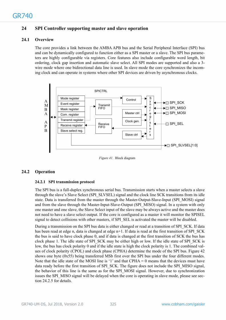
GR740
24 SPI Controller supporting master and slave operation24.1 Overview
The core provides a link between the AMBA APB bus and the Serial Peripheral Interface (SPI) bus and can be dynamically configured to function either as a SPI master or a slave. The SPI bus parame-ters are highly configurable via registers. Core features also include configurable word length, bit ordering, clock gap insertion and automatic slave select. All SPI modes are supported and also a 3-wire mode where one bidirectional data line is used. In slave mode the core synchronizes the incom-ing clock and can operate in systems where other SPI devices are driven by asynchronous clocks.
24.2 Operation
24.2.1 SPI transmission protocol
The SPI bus is a full-duplex synchronous serial bus. Transmission starts when a master selects a slave through the slave’s Slave Select (SPI_SLVSEL) signal and the clock line SCK transitions from its idle state. Data is transferred from the master through the Master-Output-Slave-Input (SPI_MOSI) signal and from the slave through the Master-Input-Slave-Output (SPI_MISO) signal. In a system with only one master and one slave, the Slave Select input of the slave may be always active and the master does not need to have a slave select output. If the core is configured as a master it will monitor the SPISEL signal to detect collisions with other masters, if SPI_SEL is activated the master will be disabled.
During a transmission on the SPI bus data is either changed or read at a transition of SPI_SCK. If data has been read at edge n, data is changed at edge n+1. If data is read at the first transition of SPI_SCK the bus is said to have clock phase 0, and if data is changed at the first transition of SCK the bus has clock phase 1. The idle state of SPI_SCK may be either high or low. If the idle state of SPI_SCK is low, the bus has clock polarity 0 and if the idle state is high the clock polarity is 1. The combined val-ues of clock polarity (CPOL) and clock phase (CPHA) determine the mode of the SPI bus. Figure 42 shows one byte (0x55) being transferred MSb first over the SPI bus under the four different modes. Note that the idle state of the MOSI line is ‘1’ and that CPHA = 0 means that the devices must have data ready before the first transition of SPI_SCK. The figure does not include the SPI_MISO signal, the behavior of this line is the same as for the SPI_MOSI signal. However, due to synchronization issues the SPI_MISO signal will be delayed when the core is operating in slave mode, please see sec-tion 24.2.5 for details.
Figure 41. Block diagram
AMBA
APB
TransmitSPI_MISO
Mode register
Event register
Mask register
Com. register
Transmit register
Receive register
Slave select reg.
FIFO
ReceiveFIFO
SPI_SCKControl
Master ctrl
Slave ctrl
Clock gen.
Syncregisters
SPI_SEL
SPI_SLVSEL[1:0]
SPI_MOSI
SPICTRL
GR740-UM-DS, Jul 2018, Version 2.0 325 www.cobham.com/gaisler

GR740
24.2.2 3-wire transmission protocol
The core can be configured to operate in 3-wire mode, where the controller uses a bidirectional dataline instead of separate data lines for input and output data. In 3-wire mode the bus is thus a half-duplex synchronous serial bus. Transmission starts when a master selects a slave through the slave’s Slave Select (SPI_SLVSEL) signal and the clock line SPI_SCK transitions from its idle state. Only the Master-Output-Slave-Input (SPI_MOSI) signal is used for data transfer in 3-wire mode. The SPI_MISO signal is not used.
The direction of the first data transfer is determined by the value of the 3-wire Transfer Order (TTO) field in the core’s Mode register. If TTO is ‘0’, data is first transferred from the master (through the MOSI signal). After a word has been transferred, the slave uses the same data line to transfer a word back to the master. If TTO is ‘1’ data is first transferred from the slave to the master. After a word has been transferred, the master uses the MOSI line to transfer a word back to the slave.
The data line transitions depending on the clock polarity and clock phase in the same manner as in SPI mode. The aforementioned slave delay of the SPI_MISO signal in SPI mode will affect the SPI_-MOSI signal in 3-wire mode, when the core operates as a slave.
24.2.3 Receive and transmit queues
The core’s transmit queue consists of the transmit register and the transmit FIFO. The receive queue consists of the receive register and the receive FIFO. The total number of words that can exist in each queue is thus the FIFO depth plus one. When the core has one or more free slots in the transmit queue it will assert the Not full (NF) bit in the event register. Software may only write to the transmit register when this bit is asserted. When the core has received a word, as defined by word length (LEN) in the Mode register, it will place the data in the receive queue. When the receive queue has one or more ele-ments stored the Event register bit Not empty (NE) will be asserted. The receive register will only contain valid data if the Not empty bit is asserted and software should not access the receive register
Figure 42. SPI transfer of byte 0x55 in all modes
SCK
MOSI
CPOL = 0
CPHA = 0
CPHA = 1
CPOL = 1
CPHA = 0
CPHA = 1
Mode 0
Mode 1
Mode 2
Mode 3
SCK
MOSI
SCK
MOSI
SCK
MOSI
GR740-UM-DS, Jul 2018, Version 2.0 326 www.cobham.com/gaisler

GR740
unless this bit is set. If the receive queue is full and the core receives a new word, an overrun condi-tion will occur. The received data will be discarded and the Overrun (OV) bit in the Event register will be set.The core will also detect underrun conditions. An underrun condition occurs when the core is selected, via SPISEL, and the SCK clock transitions while the transmit queue is empty. In this sce-nario the core will respond with all bits set to ‘1’ and set the Underrun (UN) bit in the Event register. An underrun condition will never occur in master mode. When the master has an empty transmit queue the bus will go into an idle state.
24.2.4 Clock generation
The core only generates the clock in master mode, the generated frequency depends on the system clock frequency and the Mode register fields DIV16, FACT, and PM. Without DIV16 the SCK fre-quency is:
With DIV16 enabled the frequency of SCK is derived through:
Note that the fields of the Mode register, which includes DIV16, FACT and PM, should not be changed when the core is enabled.
24.2.5 Slave operation
When the core is configured for slave operation it does not drive any SPI signal until the core is selected, via the SPI_SEL input, by a master. If the core operates in SPI mode when SPI_SEL goes low the core configures SPI_MISO as an output and drives the value of the first bit scheduled for transfer. If the core is configured into 3-wire mode the core will first listen to the SPI_MOSI line and when a word has been transferred drive the response on the SPI_MOSI line. If the core is selected when the transmit queue is empty it will transfer a word with all bits set to ‘1’ and the core will report an underflow.
Since the core synchronizes the incoming clock it will not react to transitions on SPI_SCK until two system clock cycles have passed. This leads to a delay of three system clock cycles when the data out-put line should change as the result of a SPI_SCK transition. This constrains the maximum input SPI_SCK frequency of the slave to (system clock) / 8 or less. The controlling master must also allow the decreased setup time on the slave data out line.
The core can also filter the SCK input. The value of the PM field in the Mode register defines for how many system clock cycles the SCK input must be stable before the core accepts the new value. If the PM field is set to zero, then the maximum SCK frequency of the slave is, as stated above, (system clock) / 8 or less. For each increment of the PM field the clock period of SCK must be prolonged by two times the system clock period as the core will require longer time discover and respond to SCK transitions.
24.2.6 Master operation
When the core is configured for master operation it will transmit a word when there is data available in the transmit queue. When the transmit queue is empty the core will drive SPI_SCK to its idle state. If the SPI_SEL input goes low during master operation the core will abort any active transmission and
SCKFrequency AMBAclockfrequency4 2 FACT – PM 1+
---------------------------------------------------------------------=
SCKFrequency AMBAclockfrequency16 4 2 FACT – PM 1+ --------------------------------------------------------------------------------=
GR740-UM-DS, Jul 2018, Version 2.0 327 www.cobham.com/gaisler

GR740
the Multiple-master error (MME) bit will be asserted in the Event register. If a Multiple-master error occurs the core will be disabled. Note that the core will react to changes on SPI_SEL even if the core is operating in loop mode and that the core can be configured to ignore SPI_SEL by setting the IGSEL field in the Mode register.24.3 Registers
The core is programmed through registers mapped into APB address space.
Table 417.SPI controller registers
APB address offset Register
0x00 Capability register
0x04-0x1C Reserved
0x20 Mode register
0x24 Event register
0x28 Mask register
0x2C Command register
0x30 Transmit register
0x34 Receive register
0x38 Slave Select register
0x3C Automatic slave select register
0x3F-0xFF Reserved
GR740-UM-DS, Jul 2018, Version 2.0 328 www.cobham.com/gaisler

GR740
24.3.1 Capability registerTable 418.0x00 - CAP - Capability register
24.3.2 Mode register
31 24 23 20 19 18 17 16 15 8 7 6 5 4 0
SSSZ MAXWLEN T
W
E
N
A
M
O
D
E
A
S
E
L
A
S
S
E
N
FDEPTH SR FT REV
2 0 1 0 1 1 4 1 0 0x5
r r r r r r r r r r
31: 24 Slave Select register size (SSSZ) -This field contains the number of available signals: 2.
23: 20 Maximum word Length (MAXWLEN) - The maximum word length supported by the core: 0b0000 is 4-16, and 32-bit word length.
19 Three-wire mode Enable (TWEN) - ‘1’, the core supports three-wire mode.
18 Auto mode (AMODE) - ‘0’
17 Automatic slave select available (ASELA) - ‘1’, core has support for setting slave select signals automatically.
16 Slave Select Enable (SSEN) - ‘1’, the core has a slave select register.
15: 8 FIFO depth (FDEPTH) - This field contains the depth (16) of the core’s internal FIFOs. The number of words the core can store in each queue is FDEPTH+1, since the transmit and receive registers can contain one word each.
7 SYNCRAM (SR) - ‘1’, signals type of internal buffers. No impact for software.
6: 5 Fault-tolerance (FT) - “00”, internal buffers is implemented with radiation hardended flip-flops.
4: 0 Core revision (REV) - Core has revision 5.
Table 419.0x20 - MODE - Mode register31 30 29 28 27 26 25 24 23 22 21 20 19 18 17 16 15 14 13 12 11 10 9 8 7 6 5 4 3 2 1 0
R L
O
O
P
C
P
O
L
C
P
H
A
D
I
V
1
6
R
E
V
M
S
E
N
LEN PM T
W
E
N
A
S
E
L
F
A
C
T
O
D
CG A
S
E
L
D
E
L
T
A
C
T
T
O
I
G
S
E
L
C
I
T
E
R
0 0 0 0 0 0 0 0 0 0 0 0 0 0 0 0 0 0 0 0 0
r rw rw rw rw rw rw rw rw rw rw rw rw rw rw rw rw rw rw rw r
31 RESERVED
30 Loop mode (LOOP) - When this bit is set, and the core is enabled, the core’s transmitter and receiver are interconnected and the core will operate in loopback mode. The core will still detect, and will be disabled, on Multiple-master errors.
29 Clock polarity (CPOL) - Determines the polarity (idle state) of the SCK clock.
28 Clock phase (CPHA) - When CPHA is ‘0’ data will be read on the first transition of SCK. When CPHA is ‘1’ data will be read on the second transition of SCK.
27 Divide by 16 (DIV16) - Divide system clock by 16, see description of PM field below and see sec-tion 24.2.4 on clock generation. This bit has no significance in slave mode.
26 Reverse data (REV) - When this bit is ‘0’ data is transmitted LSB first, when this bit is ‘1’ data is transmitted MSB first. This bit affects the layout of the transmit and receive registers.
25 Master/Slave (MS) - When this bit is set to ‘1’ the core will act as a master, when this bit is set to ‘0’ the core will operate in slave mode.
24 Enable core (EN) - When this bit is set to ‘1’ the core is enabled. No fields in the mode register should be changed while the core is enabled. This can bit can be set to ‘0’ by software, or by the core if a multiple-master error occurs.
GR740-UM-DS, Jul 2018, Version 2.0 329 www.cobham.com/gaisler
GR740
23: 20 Word length (LEN) - The value of this field determines the length in bits of a transfer on the SPI bus. Values are interpreted as:
0b0000 - 32-bit word length
0b0001-0b0010 - Illegal values
0b0011-0b1111 - Word length is LEN+1, allows words of length 4-16 bits.
19: 16 Prescale modulus (PM) - This value is used in master mode to divide the system clock and generate the SPI SCK clock. The value in this field depends on the value of the FACT bit.
If bit 13 (FACT) is ‘0’:The system clock is divided by 4*(PM+1) if the DIV16 field is ‘0’ and 16*4*(PM+1) if the DIV16 field is set to ‘1’. The highest SCK frequency is attained when PM is set to 0b0000 and DIV16 to ‘0’, this configuration will give a SCK frequency that is (system clock)/4. With this setting the core is compatible with the SPI register interface found in MPC83xx SoCs.
If bit 13 (FACT) is ‘1’: The system clock is divided by 2*(PM+1) if the DIV16 field is ‘0’ and 16*2*(PM+1) if the DIV16 field is set to ‘1’. The highest SCK frequency is attained when PM is set to 0b0000 and DIV16 to ‘0’, this configuration will give a SCK frequency that is (system clock)/2.
In slave mode the value of this field defines the number of system clock cycles that the SCK input must be stable for the core to accept the state of the signal. See section 24.2.5.
15 Three-wire mode (TW) - If this bit is set to ‘1’ the core will operate in 3-wire mode.
14 Automatic slave select (ASEL) - If this bit is set to ‘1’ the core will swap the contents in the Slave select register with the contents of the Automatic slave select register when a transfer is started and the core is in master mode. When the transmit queue is empty, the slave select register will be swapped back. Note that if the core is disabled (by writing to the core enable bit or due to a multiple-master-error (MME)) when a transfer is in progress, the registers may still be swapped when the core goes idle. Also see the ASELDEL field which can be set to insert a delay between the slave select register swap and the start of a transfer.
13 PM factor (FACT) - If this bit is 1 the core’s register interface is no longer compatible with the MPC83xx register interface. The value of this bit affects how the PM field is utilized to scale the SPI clock. See the description of the PM field.
12 Open drain mode (OD) - If this bit is set to ‘0’, all pins are configured for operation in normal mode. If this bit is set to ‘1’ all pins are set to open drain mode. The pins driven from the slave select regis-ter are not affected by the value of this bit.
11: 7 Clock gap (CG) - The value of this field is only significant in master mode. The core will insert CG SCK clock cycles between each consecutive word. This only applies when the transmit queue is kept non-empty. After the last word of the transmit queue has been sent the core will go into an idle state and will continue to transmit data as soon as a new word is written to the transmit register, regardless of the value in CG. A value of 0b00000 in this field enables back-to-back transfers.
6: 5 Automatic Slave Select Delay (ASELDEL) - If the core is configured to use automatic slave select (ASEL field set to ‘1’) the core will insert a delay corresponding to ASELDEL*(SPI SCK cycle time)/2 between the swap of the slave select registers and the first toggle of the SCK clock. As an example, if this field is set to “10” the core will insert a delay corresponding to one SCK cycle between assigning the Automatic slave select register to the Slave select register and toggling SCK for the first time in the transfer.
4 Toggle Automatic slave select during Clock Gap (TAC) - If this bit is set, and the ASEL field is set, the core will perform the swap of the slave select registers at the start and end of each clock gap. The clock gap is defined by the CG field and must be set to a value >= 2 if this field is set.
3 3-wire Transfer Order (TTO) - This bit controls if the master or slave transmits a word first in 3-wire mode.If this bit is ‘0’, data is first transferred from the master to the slave. If this bit is ‘1’, data is first transferred from the slave to the master.
2 Ignore SPISEL input (IGSEL) - If this bit is set to ‘1’ then the core will ignore the value of the SPI-SEL input.
1 Require Clock Idle for Transfer End (CITE) - If this bit is ‘0’ the core will regard the transfer of a word as completed when the last bit has been sampled. If this bit is set to ‘1’ the core will wait until it has set the SCK clock to its idle level (see CI field) before regarding a transfer as completed. This setting only affects the behavior of the TIP status bit, and automatic slave select toggling at the end of a transfer, when the clock phase (CP field) is ‘0’.
0 RESERVED (R) - Read as zero and should be written as zero to ensure forward compatibility.
Table 419.0x20 - MODE - Mode register
GR740-UM-DS, Jul 2018, Version 2.0 330 www.cobham.com/gaisler

GR740
24.3.3 Event registerTable 420.0x24 - EVENT - Event register31 30 15 14 13 12 11 10 9 8 7 0
TIP RESERVED LT R OV UN M
M
E
NE NF RESERVED
0 0 0 0 0 0 0 0 0 0
r r wc r wc wc wc r r r
31 Transfer in progress (TIP) - This bit is ‘1’ when the core has a transfer in progress. Writes have no effect. This bit is set when the core starts a transfer and is reset to ‘0’ once the core considers the transfer to be finished. Behavior affected by setting of CITE field in Mode register.
30: 15 RESERVED (R) - Read as zero and should be written to zero to ensure forward compatibility.
14 Last character (LT) - This bit is set when a transfer completes if the transmit queue is empty and the LST bit in the Command register has been written. This bit is cleared by writing ‘1’, writes of ‘0’ have no effect.
13 RESERVED (R) - Read as zero and should be written to zero to ensure forward compatibility.
12 Overrun (OV) - This bit gets set when the receive queue is full and the core receives new data. The core continues communicating over the SPI bus but discards the new data. This bit is cleared by writ-ing ‘1’, writes of ‘0’ have no effect.
11 Underrun (UN) - This bit is only set when the core is operating in slave mode. The bit is set if the core’s transmit queue is empty when a master initiates a transfer. When this happens the core will respond with a word where all bits are set to ‘1’. This bit is cleared by writing ‘1’, writes of ‘0’ have no effect.
10 Multiple-master error (MME) - This bit is set when the core is operating in master mode and the SPI-SEL input goes active. In addition to setting this bit the core will be disabled. This bit is cleared by writing ‘1’, writes of ‘0’ have no effect.
9 Not empty (NE) - This bit is set when the receive queue contains one or more elements. It is cleared automatically by the core, writes have no effect.
8 Not full (NF) - This bit is set when the transmit queue has room for one or more words. It is cleared automatically by the core when the queue is full, writes have no effect. This field is only updated when the core is enabled (EN field of Mode register is set to ’1’).
7: 0 RESERVED (R) - Read as zero and should be written to zero to ensure forward compatibility.
GR740-UM-DS, Jul 2018, Version 2.0 331 www.cobham.com/gaisler

GR740
24.3.4 Mask registerTable 421.0x28 - MASK - Mask register
24.3.5 Command register
Table 422.0x2C - CMD - Command register
31 30 15 14 13 12 11 10 9 8 7 0
T
I
P
E
RESERVED L
T
E
R O
V
E
U
N
E
M
M
E
E
N
E
E
E
N
F
E
RESERVED
0 0 0 0 0 0 0 0 1 0
rw r rw r rw rw rw rw rw r
31 Transfer in progress enable (TIPE) - When this bit is set the core will generate an interrupt when the TIP bit in the Event register transitions from ‘0’ to ‘1’.
30: 15 RESERVED (R) - Read as zero and should be written to zero to ensure forward compatibility.
14 Last character enable (LTE) - When this bit is set the core will generate an interrupt when the LT bit in the Event register transitions from ‘0’ to ‘1’.
13 RESERVED (R) - Read as zero and should be written to zero to ensure forward compatibility.
12 Overrun enable (OVE) - When this bit is set the core will generate an interrupt when the OV bit in the Event register transitions from ‘0’ to ‘1’.
11 Underrun enable (UNE) - When this bit is set the core will generate an interrupt when the UN bit in the Event register transitions from ‘0’ to ‘1’.
10 Multiple-master error enable (MMEE) - When this bit is set the core will generate an interrupt when the MME bit in the Event register transitions from ‘0’ to ‘1’.
9 Not empty enable (NEE) - When this bit is set the core will generate an interrupt when the NE bit in the Event register transitions from ‘0’ to ‘1’.
8 Not full enable (NFE) - When this bit is set the core will generate an interrupt when the NF bit in the Event register transitions from ‘0’ to ‘1’.
7: 0 RESERVED (R) - Read as zero and should be written to zero to ensure forward compatibility.
31 30 23 22 21
RESERVED L
S
T
RESERVED
0 0 0
r w r
31: 23 RESERVED (R) - Read as zero and should be written to zero to ensure forward compatibility.
22 Last (LST) - After this bit has been written to ‘1’ the core will set the Event register bit LT when a character has been transmitted and the transmit queue is empty. If the core is operating in 3-wire mode the Event register bit is set when the whole transfer has completed. This bit is automatically cleared when the Event register bit has been set and is always read as zero.
21: 0 RESERVED (R) - Read as zero and should be written to zero to ensure forward compatibility.
GR740-UM-DS, Jul 2018, Version 2.0 332 www.cobham.com/gaisler

GR740
24.3.6 Transmit registerTable 423.0x30 - TX - Transmit register
24.3.7 Receive register
Table 424.0x34 - RX - Receive register
24.3.8 Slave select register
Table 425.0x38 - SLVSEL - Slave select register
31 0
TDATA
0
w
31: 0 Transmit data (TDATA) - Writing a word into this register places the word in the transmit queue. This register will only react to writes if the Not full (NF) bit in the Event register is set. The layout of this register depends on the value of the REV field in the Mode register:
Rev = ‘0’: The word to transmit should be written with its least significant bit at bit 0.
Rev = ‘1’: The word to transmit should be written with its most significant bit at bit 31.
31 0
RDATA
0
r
31: 0 Receive data (RDATA) - This register contains valid receive data when the Not empty (NE) bit of the Event register is set. The placement of the received word depends on the Mode register fields LEN and REV:
For LEN = 0b0000 - The data is placed with its MSb in bit 31 and its LSb in bit 0.
For other lengths and REV = ‘0’ - The data is placed with its MSB in bit 15.
For other lengths and REV = ‘1’ - The data is placed with its LSB in bit 16.
To illustrate this, a transfer of a word with eight bits (LEN = 7) that are all set to one will have the following placement:
REV = ‘0’ - 0x0000FF00
REV = ‘1’ - 0x00FF0000
31 2 1 0
RESERVED SLVSEL
0 0b11
r rw
31: 2 RESERVED
1: 0 Slave select (SLVSEL) - The core’s slave select signals are mapped to this register on bits 1:0. Soft-ware is responsible for activating the correct slave select signals.
GR740-UM-DS, Jul 2018, Version 2.0 333 www.cobham.com/gaisler

GR740
24.3.9 Automatic slave select registerTable 426.0x38 - ASLVSEL - Automatic slave select register31 2 1 0
RESERVED A
S
L
V
S
E
L
0 0
r rw
31: 2 RESERVED
1: 0 Automatic Slave select (ASLVSEL) - The core’s slave select signals are assigned from this register when the core is about to perform a transfer and the ASEL field in the Mode register is set to ‘1’. After a transfer has been completed the core’s slave select signals are assigned the original value in the slave select register.
GR740-UM-DS, Jul 2018, Version 2.0 334 www.cobham.com/gaisler

GR740
25 Clock gating unit25.1 Overview
The clock gating unit provides a mean to save power by disabling the clock to unused functional blocks.
25.2 Operation
The operation of the clock gating unit is controlled through three registers: the unlock, clock enable and core reset registers. The clock enable register defines if a clock is enabled or disabled. A ‘1’ in a bit location will enable the corresponding clock, while a ‘0’ will disable the clock. The core reset reg-ister allows to generate a reset signal for each generated clock. A reset will be generated as long as the corresponding bit is set to ‘1’. The bits in clock enable and core reset registers can only be written when the corresponding bit in the unlock register is 1. If a bit in the unlock register is 0, the corre-sponding bits in the clock enable and core reset registers cannot be written.
To gate the clock for a core, the following procedure should be applied:
1. Disable the core through software to make sure it does not initialize any AHB accesses
2. Write a 1 to the corresponding bit in the unlock register
3. Write a 0 to the corresponding bit in the clock enable register
4. Write a 0 to the corresponding bit in the unlock register
To enable the clock for a core, the following procedure should be applied
1. Write a 1 to the corresponding bit in the unlock register
2. Write a 1 to the corresponding bit in the core reset register
3. Write a 1 to the corresponding bit in the clock enable register
4. Write a 0 to the corresponding bit in the clock enable register
5. Write a 0 to the corresponding bit in the core reset register
6. Write a 1 to the corresponding bit in the clock enable register
7. Write a 0 to the corresponding bit in the unlock register
The cores connected to the clock gating unit are defined in the table below:
Table 427.Clocks controlled by CLKGATE unit
Bit Functional module
0 GRETH 10/100/1000 Mbit Ethernet MAC 0
1 GRETH 10/100/1000 Mbit Ethernet MAC 1
2 SpaceWire router
3 PCI master/target controller
4 MIL-STD-1553B controller
5 CAN controller
6 LEON4 Statistics unit
7 UART 0
8 UART 1
9 SPI Controller
10 PROM/IO memory controller
GR740-UM-DS, Jul 2018, Version 2.0 335 www.cobham.com/gaisler

GR740
The clock gating unit also provides gating for the processor cores and floating-point units. A proces-sor core will be automatically gated off when it enters power down mode. A FPU will be gated off when processor core connected to the FPU has floating-point disabled or when the processor core is in power down mode.Processor/FPU clock gating can be disabled by writing 0x000F000F to the CPU/FPU override regis-ter.
25.3 Registers
Table 428 shows the clock gating unit registers.
Table 428.Clock gating unit registers
APB address offset Register
0x00 Unlock register
0x04 Clock enable register
0x08 Core reset register
0x0C CPU/FPU override register
0x10-0xFF Reserved
GR740-UM-DS, Jul 2018, Version 2.0 336 www.cobham.com/gaisler
GR740
25.3.1 Unlock registerTable 429.0x00 - UNLOCK - Unlock register
25.3.2 Clock enable register
Table 430.0x04 - CLKEN - Clock enable register
25.3.3 Core reset register
Table 431. 0x08 - RESET - Reset register
31 11 10 0
RESERVED UNLOCK
0 0
r rw
31: 11 RESERVED
10: 0 Unlock clock enable and reset registers (UNLOCK) - The bits in clock enable and core reset regis-ters can only be written when the corresponding bit in this field is 1.
31 11 10 0
RESERVED ENABLE
0 *
r rw
31: 11 RESERVED
10: 0 Cock enable (ENABLE) - A ‘1’ in a bit location will enable the corresponding clock, while a ‘0’ will disable the clock.
The reset value of this register is set by bootstrap signals. See table 427 and section 4.9.
31 11 10 0
RESERVED RESET
0 *
r rw
31: 11 RESERVED
10: 0 Reset (RESET) - A reset will be generated as long as the corresponding bit is set to ‘1’.
The reset value of this register is set by bootstrap signals. See table 427 and section 4.9.
GR740-UM-DS, Jul 2018, Version 2.0 337 www.cobham.com/gaisler

GR740
25.3.4 CPU/FPU override registerTable 432. 0x0c - OVERRIDE - CPU/FPU override register31 20 19 16 15 4 3 0
RESERVED FOVERRIDE RESERVED OVERRIDE
0 0 0 0
r rw r rw
31: 20 RESERVED
19: 16 Override FPU clock gating (FOVERRIDE) - If bit n of this field is set to ’1’ then the clock for FPU n will be active regardless of the value of %PSR.EF.
15: 4 RESERVED
3: 0 Override CPU clock gating (OVERRIDE) - If bit n of this field is set to ’1’ then the clock for proces-sor n and FPU n will always be active.
GR740-UM-DS, Jul 2018, Version 2.0 338 www.cobham.com/gaisler

GR740
26 LEON4 Statistics Unit (Performance Counters)26.1 Overview
The LEON4 Statistics Unit (L4STAT) is used count events in the LEON4 processor and the AHB bus, in order to create performance statistics for various software applications.
L4STAT consists of sixteen 32-bit counters that increment on a selected event. The counters roll over to zero when reaching their maximum value, but can also be automatically cleared on reading to facil-itate statistics building over longer periods. Each counter has a control register where the event type is selected. The control registers also indicates which particular processor core is monitored. The table 433 below shows the event types that can be monitored.
Table 433.Event types and IDs
ID Event description
Processor events:
0x00 Instruction cache miss
0x01 Instruction MMU TLB miss
0x02 Instruction cache hold
0x03 Instruction MMU hold
0x08 Data cache (read) miss
0x09 Data MMU TLB miss
0x0A Data cache hold
0x0B Data MMU hold
0x10 Data write buffer hold
0x11 Total instruction count
0x12 Integer instructions
0x13 Floating-point unit instruction count
0x14 Branch prediction miss
0x15 Execution time, excluding debug mode
0x17 AHB utilization (per AHB master)
0x18 AHB utilization (total, master/CPU selection is ignored)
0x22 Integer branches
0x28 CALL instructions
0x30 Regular type 2 instructions
0x38 LOAD and STORE instructions
0x39 LOAD instructions
0x3A STORE instructions
AHB events (counted via LEON4 Debug Support Unit):
0x40 AHB IDLE cycles. Filtered on CPU/AHBM if SU(1) = ‘1
0x41 AHB BUSY cycles. Filtered on CPU/AHBM if SU(1) = ‘1
0x42 AHB NON-SEQUENTIAL transfers. Filtered on CPU/AHBM if SU(1) = ‘1
0x43 AHB SEQUENTIAL transfers. Filtered on CPU/AHBM if SU(1) = ‘1
0x44 AHB read accesses. Filtered on CPU/AHBM if SU(1) = ‘1
0x45 AHB write accesses. Filtered on CPU/AHBM if SU(1) = ‘1
0x46 AHB byte accesses. Filtered on CPU/AHBM if SU(1) = ‘1
0x47 AHB half-word accesses. Filtered on CPU/AHBM if SU(1) = ‘1
0x48 AHB word accesses. Filtered on CPU/AHBM if SU(1) = ‘1
0x49 AHB double word accesses. Filtered on CPU/AHBM if SU(1) = ‘1
GR740-UM-DS, Jul 2018, Version 2.0 339 www.cobham.com/gaisler

GR740
0x4A AHB quad word accesses. Filtered on CPU/AHBM if SU(1) = ‘1
0x4B AHB eight word accesses. Filtered on CPU/AHBM if SU(1) = ‘1
0x4C AHB waitstates. Filtered on CPU/AHBM if SU(1) = ‘1
0x4D AHB RETRY responses. Filtered on CPU/AHBM if SU(1) = ‘1
0x4E AHB SPLIT responses. Filtered on CPU/AHBM if SU(1) = ‘1
0x4F AHB SPLIT delay. Filtered on CPU/AHBM if SU(1) = ‘1
0x50 AHB bus locked. Filtered on CPU/AHBM if SU(1) = ‘1
0x51-0x5F Reserved
Device specific events (may be marked as user defined events in generic software drivers):
0x60 L2 cache hit (external event 0, CPU/AHBM field can select AHB master)
0x61 L2 cache miss (external event 1, CPU/AHBM field can select AHB master)
0x62 L2 cache bus access (external event 2, CPU/AHBM field can select AHB master)
0x63 L2 cache tag correctable error (external event 3, CPU/AHBM field must be set to 0)
0x64 L2 cache tag uncorrectable error (external event 4, CPU/AHBM field must be set to 0)
0x65 L2 cache data correctable error (external event 5, CPU/AHBM field must be set to 0)
0x66 L2 cache data uncorrectable error (external event 6, CPU/AHBM field must be set to 0)
0x67 IOMMU cache lookup (external event 7, CPU/AHBM field must be set to 0)
0x68 IOMMU table walk (external event 8, CPU/AHBM field must be set to 0)
0x69 IOMMU access error/denied (external event 9, CPU/AHBM field must be set to 0)
0x6A IOMMU access OK (external event 10, CPU/AHBM field must be set to 0)
0x6B IOMMU access passthrough (external event 11, CPU/AHBM field must be set to 0)
0x6C IOMMU cache/TLB miss (external event 12, CPU/AHBM field must be set to 0)
0x6D IOMMU cache/TLB hit (external event 13, CPU/AHBM field must be set to 0)
0x6E IOMMU cache/TLB parity error (external event 14, CPU/AHBM field must be set to 0)
AHB events (only available if core is connected to a standalone AHB trace buffer):
0x70 AHB IDLE cycles
0x71 AHB BUSY cycles. Filtered on CPU/AHBM if SU(1) = ‘1’
0x72 AHB NON-SEQUENTIAL transfers. Filtered on CPU/AHBM if SU(1) = ‘1
0x73 AHB SEQUENTIAL transfers. Filtered on CPU/AHBM if SU(1) = ‘1
0x74 AHB read accesses. Filtered on CPU/AHBM if SU(1) = ‘1
0x75 AHB write accesses. Filtered on CPU/AHBM if SU(1) = ‘1
0x76 AHB byte accesses. Filtered on CPU/AHBM if SU(1) = ‘1
0x77 AHB half-word accesses. Filtered on CPU/AHBM if SU(1) = ‘1
0x78 AHB word accesses. Filtered on CPU/AHBM if SU(1) = ‘1
0x79 AHB double word accesses. Filtered on CPU/AHBM if SU(1) = ‘1
0x7A AHB quad word accesses. Filtered on CPU/AHBM if SU(1) = ‘1
0x7B AHB eight word accesses. Filtered on CPU/AHBM if SU(1) = ‘1
0x7C AHB waitstates. Filtered on CPU/AHBM if SU(1) = ‘1
0x7D AHB RETRY responses. Filtered on CPU/AHBM if SU(1) = ‘1
0x7E AHB SPLIT responses. Filtered on CPU/AHBM if SU(1) = ‘1
0x7F AHB SPLIT delay. Filtered on CPU/AHBM if SU(1) = ‘1
Events generated from REQ/GNT signals
Table 433.Event types and IDs
ID Event description
GR740-UM-DS, Jul 2018, Version 2.0 340 www.cobham.com/gaisler

GR740
Note that IDs 0x39 (LOAD instructions) and 0x3A (STORE instructions) will both count all LDST and SWAP instructions. The sum of events counted for 0x39 and 0x3A may therefore be larger than the number of events counted with ID 0x38 (LOAD and STORE instructions).
The documentation for the Debug Support Unit contains more information on events 0x40 - 0x5F, see section 33.3.2. Please note that the statistical outputs from the DSU may be subject to AHB trace buf-fer filters. The same applies to events 0x70 to 0x7F that come from the AHBTRACE standalone AHB trace buffer.
Collecting statistics on interrupt latency is possible using the interrupt timestamping mechnism described in section 21.2.6. Interrupt latency can not be measured with the LEON4 statistics unit.
Master indexes are listed in section 2.5.
26.2 Multiple APB interfaces
The core has two AMBA APB interfaces, the first is connected via the Processor AHB bus and the second is connected via the Debug AHB bus. The first APB interface always has precedence when both interfaces handle write operations to the same address.
0x80 - 0x8F Active when master selected by CPU/AHBM field has request asserted while grant is asserted for the master correspoding to the least significant nibble of the event ID.
The following map is a map between least siginificant nibble of this event and CPU/AHBM field to masters in the system
8:6 - Masters 2, 1, 0 on memory AHB bus
5:0 - Masters on Processor AHB bus
0x90 - 0x9F Active when master selected by CPU/AHBM field has request asserted while grant is deas-serted for the master correspoding to the least significant nibble of the event ID. See events 0x80 - 0x8F for a description of masters corresponding to the different events.
Table 433.Event types and IDs
ID Event description
GR740-UM-DS, Jul 2018, Version 2.0 341 www.cobham.com/gaisler

GR740
26.3 RegistersThe L4STAT unit is programmed through registers mapped into APB address space.
Table 434. L4STAT counter control register
APB address offset Register
0x00 Counter 0 value register
0x04 Counter 1 value register
0x08 Counter 2 value register
0x0C Counter 3 value register
0x10 Counter 4 value register
0x14 Counter 5 value register
0x18 Counter 6 value register
0x1C Counter 7 value register
0x20 Counter 8 value register
0x24 Counter 9 value register
0x28 Counter 10 value register
0x2C Counter 11 value register
0x30 Counter 12 value register
0x34 Counter 13 value register
0x38 Counter 14 value register
0x3C Counter 15 value register
0x40 - 0x7C Reserved
0x80 Counter 0 control register
0x84 Counter 1 control register
0x88 Counter 2 control register
0x8C Counter 3 control register
0x90 Counter 4 control register
0x94 Counter 5 control register
0x98 Counter 6 control register
0x9C Counter 7 control register
0xA0 Counter 8 control register
0xA4 Counter 9 control register
0xA8 Counter 10 control register
0xAC Counter 11 control register
0xB0 Counter 12 control register
0xB4 Counter 13 control register
0xB8 Counter 14 control register
0xBC Counter 15 control register
0xC0 - 0xFC Reserved
0x100 Counter 0 max/latch register
0x104 Counter 1 max/latch register
0x108 Counter 2 max/latch register
0x10C Counter 3 max/latch register
0x110 Counter 4 max/latch register
0x114 Counter 5 max/latch register
0x118 Counter 6 max/latch register
GR740-UM-DS, Jul 2018, Version 2.0 342 www.cobham.com/gaisler

GR740
26.3.1 Counter value registers
Table 435.0x00-0x3C - CVAL0-15 - Counter 0-15 value register
0x11C Counter 7 max/latch register
0x120 Counter 8 max/latch register
0x124 Counter 9 max/latch register
0x128 Counter 10 max/latch register
0x12C Counter 11 max/latch register
0x130 Counter 12 max/latch register
0x134 Counter 13 rmax/latch egister
0x138 Counter 14 rmax/latch egister
0x13C Counter 15 max/latch register
0x140 - 0x17C Reserved
0x180 Timestamp register
0x184 - 0x1FC Reserved
31 0
CVAL
NR
rw
31: 0 Counter value (CVAL) - This register holds the current value of the counter. If the core has been implemented with support for keeping the maximum count (MC field of Counter control register is ‘1’) and the Counter control register field CD is ‘1’, then the value displayed by this register will be the maximum counter value reached with the settings in the counter’s control register. Writing to this register will write both to the counter and, if implemented, the hold register for the maximum counter value.
Table 434. L4STAT counter control register
APB address offset Register
GR740-UM-DS, Jul 2018, Version 2.0 343 www.cobham.com/gaisler

GR740
26.3.2 Counter control registersTable 436.0x80-0xCC - CCTRL0-15 - Counter 0-15 control register31 28 27 23 22 21 20 19 18 17 16 15 14 13 12 11 4 3 0
NCPU NCNT MC IA DS EE AE EL CD SU CL EN EVENT ID CPU/AHBM
0x3 0xF 1 1 1 1 1 NR NR NR NR 0 NR NR
r r r r r r r rw rw rw rw rw rw rw
31: 28 Number of CPU (NCPU) - Number of supported processors - 1
27: 23 Number of counters (NCNT) - Number of implemented counters - 1
22 Maximum count (MC) - If this field is ‘1’ then this counter has support for keeping the maximum count value.
21 Internal AHB count (IA) - If this field is ‘1’ the core supports events 0x17 and 0x18
20 DSU support (DS) - If this field is ‘1’ the core supports events 0x40-0x5F
19 External events (EE) - If this field is ‘1’ the core supports external events (events 0x60 - 0x6F)
18 AHBTRACE Events (AE) - If this field is ‘1’ the core supports events 0x70 - 0x7F.
17 Event Level (EL) - The value of this field determines the level where the counter keeps running when the CD field below has been set to ‘1’. If this field is ‘0’ the counter will count the time between event assertions. If this field is ‘1’ the counter will count the cycles where the event is asserted. This field can only be set if the MC field of this register is ‘1’.
16 Count maximum duration (CD) - If this bit is set to ‘1’ the core will save the maximum time the selected event has been at the level specified by the EL field. This also means that the counter will be reset when the event is activated or deactivated depending on the value of the EL field.
When this bit is set to ‘1’, the value shown in the counter value register will be the maximum current value which may be different from the current value of the counter.
This field can only be set if the MC field of this register is ‘1’.
15: 14 Supervisor/User mode filter (SU) - “01” - Only count supervisor mode events, “10” - Only count user mode events, others values - Count events regardless of user or supervisor mode. This setting only applies to events 0x0 - 0x3A.
When SU = “1x” only events generated by the CPU/AHB master specified in the CPU/AHBM field will be counted. This applies to events 0x40 - 0x7F
13 Clear counter on read (CL) - If this bit is set the counter will be cleared when the counter’s value is read. The register holding the maximum value will also be cleared, if implemented.
If an event occurs in the same cycle as the counter is cleared by a read then the event will not be counted. The counter latch register can be used to guarantee that no events are lost
12 Enable counter (EN) - Enable counter
11: 4 Event ID to be counted
3: 0 CPU or AHB master to monitor.(CPU/AHBM) - The value of this field does not matter when select-ing one of the events coming from the Debug Support Unit or one of the external events.
GR740-UM-DS, Jul 2018, Version 2.0 344 www.cobham.com/gaisler

GR740
26.3.3 Counter max/latch registersTable 437.0x100-0x13C - CSVAL0-15 - Counter 0-15 max/latch register
26.3.4 Timestamp register
Table 438.0x180 - TSTAMP - Timestamp register
31 0
CSVAL
NR
rw*
31: 0 Counter max/latch value (CSVAL) - This register holds the current value of the counter max/latch register.
If the counter control register field CD is ‘1’, then the value displayed by this register will be the maximum counter value reached with the settings in the counter’s control register.
If the counter control register field CDis ‘0’, then the value displayed by this register is the latched (saved) counter value. The counter value is saved whenever a write access is made to the core in address range 0x100 - 0x1FC (all counters are saved simultaneously). If the counter control register CL field is set, then the current counter value will be cleared when the counter value is saved into this register.
31 0
TSTAMP
NR
rw*
31: 0 Timestamp (TSTAMP) - Timestamp saved at latch of counters. The timestamp value uses the DSU timer as time source. The same timer is available as the processor’s internal up-counter, for interrupt timestamping and in the time-tag of the trace buffers. The time value is saved whenever a write access is made to the core in address range 0x100 - 0x1FC.
GR740-UM-DS, Jul 2018, Version 2.0 345 www.cobham.com/gaisler

GR740
27 AHB Status Registers27.1 Overview
AHB status registers store information about AMBA AHB accesses triggering an error response. There is a status register and a failing address register capturing the control and address signal values of a failing AMBA bus transaction, or the occurrence of a correctable error being signaled from a fault tolerant core.
The system has two AHB status register cores. One monitoring the Processor AHB bus and one mon-itoring the Slave I/O AHB bus. Both cores are accessed via the AMBA APB bus. The memory scrub-ber core, described in section 11, on the Memory AHB bus also provides the same base functionality as an AHB status register.
27.2 Operation
27.2.1 Errors
The registers monitor AMBA AHB bus transactions and store the current HADDR, HWRITE, HMASTER and HSIZE internally. The monitoring are always active after startup and reset until an error response (HRESP = “01”) is detected. When the error is detected, the status and address register contents are frozen and the New Error (NE) bit is set to one. At the same time an interrupt is gener-ated, as described hereunder.
The fault tolerant memory controllers and L2 cache containing EDAC signal an un-correctable error as an AMBA error response, so that it can be detected by the processor as described above.
27.2.2 Correctable errors
Not only error responses on the AHB bus can be detected. The PROM/IO controller has a correctable error signal that is asserted each time a correctable error is detected. When such an error is detected, the effect will be the same as for an AHB error response. The only difference is that the Correctable Error (CE) bit in the status register is set to one when a correctable error is detected.
When the CE bit is set the interrupt routine can acquire the address containing the correctable error from the failing address register and correct it. When it is finished it resets the NE bit and the monitor-ing becomes active again. Interrupt handling is described in detail hereunder.
Note that only the AHB status register monitoring the Slave I/O AHB bus reacts to correctable errors. Correctable errors on the Processor AHB bus are reported via the L2 cache and correctable errors from the memory controllers on the Memory AHB bus are reported via the memory scrubber core.
27.2.3 Interrupts
The interrupt is connected to the interrupt controller to inform the processor of the error condition. The normal procedure is that an interrupt routine handles the error with the aid of the information in the status registers. When it is finished it resets the NE bit and the monitoring becomes active again. Interrupts are generated for both AMBA error responses and correctable errors as described above.
27.2.4 Filtering and multiple error detection
The status register has two sets of status and failing address registers, supports filtering on errors, and has a status bit that gets set in case additional errors are detected when the New Error (NE) bit is set.
The status register will only react to the first error in a burst operation. After the first error has been detected, monitoring of the burst is suspended. An error event will only be recorded by the first status register that should react based on filter settings. If register set 1 has reacted then register 2 will not be set for the same error event.
GR740-UM-DS, Jul 2018, Version 2.0 346 www.cobham.com/gaisler

GR740
27.3 RegistersThe core is programmed through registers mapped into APB address space.
Table 439.AHB Status registers
APB address offset Registers
0x00 AHB Status register
0x04 AHB Failing address register
0x08 AHB Status register 2
0x0C AHB Failing Address register 2
Table 440.0x00 - AHBS - AHB Status register31 14 13 12 11 10 9 8 7 6 3 2 0
RESERVED ME FW CF AF CE NE HWRITE HMASTER HSIZE
0 0 0 0 0 0 0 NR NR NR
r rw* w* rw* rw* rw rw r r r
31: 14 RESERVED
13 Multiple Error detection (ME) - This field is set to 1 when the New Error bit is set and one more error is detected. Filtering is considered when setting the ME bit.
12 Filter Write (FW) - This bit needs to be set to ‘1’ during a write operation for CF and AF fields to be updated in the same write operation. Always reads as zero.
11 Correctable Error Filter (CF) - If this bit is set to 1 then this status register will ignore correctable errors. This field will only be written if the FW bit is set.
10 AMBA ERROR Filter (AF) - If this bit is set to 1 then this status register will ignore AMBA ERROR. This field will only be written if the FW bit is set.
9 Correctable Error (CE) - Set if the detected error was caused by a correctable error and zero other-wise.
8 New Error (NE) - Deasserted at start-up and after reset. Asserted when an error is detected. Reset by writing a zero to it.
7 The HWRITE signal of the AHB transaction that caused the error.
6: 3 The HMASTER signal of the AHB transaction that caused the error.
2: 0 The HSIZE signal of the AHB transaction that caused the error
Table 441.0x04 - AHBFAR - AHB Failing address register31 0
HADDR
N/R
r
31: 0 Failing address (HADDR) - The HADDR value of the AHB transaction that caused the error.
GR740-UM-DS, Jul 2018, Version 2.0 347 www.cobham.com/gaisler
GR740
28 Register for bootstrap signals28.1 Overview
This interface provides a programmable register that controls the internal values of bootstrap signals in the design.
28.2 Operation
The core contains one register of 20 bits that is mapped into APB address space. The value in bits 15:0 of this register is propagated to other peripherals in the design. The reset value of the register is taken from the GPIO signals and from the bootstrap signals PLL_IGNLOCK, PCIMODE_ENABLE, MEM_CLKSEL and MEM_IFWIDTH. The value of the GPIO and other bootstrap signal is latched when the device’s internal reset signal is deasserted.
28.3 Registers
The peripheral provides one register mapped into APB address space.
Table 442.General purpose register registers
APB address offset Register
0x00 Bootstrap register
0x04 - 0xFF RESERVED (first register is aliased in all words in this area)
GR740-UM-DS, Jul 2018, Version 2.0 348 www.cobham.com/gaisler

GR740
Table 443.0x00 - BOOTSTRAP - Bootstrap register31 26 25 24 23 22 21 20 19 18 17 16 15 0
RESERVED B10
B9 B8 B7 B6 B5 B4 B3 B2 B1 GPIO
*
rw*
31: 26 RESERVED
25 Reset value of JTAG_TRST signal (B10) - The value in this register can be written but the changed value does not affect system operation.
24 Reset value of DSU_EN bootstrap signal (B9) - The value in this register can be written but the changed value does not affect system operation.
23 Reset value of BREAK bootstrap signal (B8) - The value in this register can be written but the changed value does not affect system operation.
22 Reset value of PLL_BYPASS[2] bootstrap signal (B7) - The value in this register can be written but the changed value does not affect system operation.
21 Reset value of PLL_BYPASS[1] bootstrap signal (B6) - The value in this register can be written but the changed value does not affect system operation.
20 Reset value of PLL_BYPASS[0] bootstrap signal (B5) - The value in this register can be written but the changed value does not affect system operation.
19 Reset value of PLL_IGNLOCK bootstrap signal (B4) - The value in this register can be written but the changed value does not affect system operation.
18 Reset value of PCIMODE_ENABLE bootstrap signal (B3) - The value in this register can be written but the changed value does not affect system operation.
17 Reset value of MEM_CLKSEL bootstrap signal (B2) - The value in this register can be written but the changed value does not affect system operation.
16 Reset value of MEM_IFWIDTH (B1) - The value in this register can be written but the changed value does not affect system operation.
15: 0 Bootstrap value (BOOTSTRAP) - Bootstrap value of external general purpose I/O signal GPIO(15:0). Writes to this register will override the current value of the bootstrap signals. Writes do NOT affect the value of the external GPIO signal of the function of the GPIO port.
GR740-UM-DS, Jul 2018, Version 2.0 349 www.cobham.com/gaisler

GR740
29 Temperature sensor controller29.1 Overview
This peripheral provides an interface to the on-chip temperature sensor. It allows software to control the temperature sensor, saves maximum and minimum temperature values and allows generation of alarms.
29.2 Operation
The temperature sensor provides digital measurement of junction temperature. The sensor is con-trolled by software via the register interface described in this documentation.
The sensor has the following design specifications:
* Cobham Gaisler is currently not authorized to disclose these parameters in public data sheets. Please contact support@gais-
ler.com for further information.
The sensor shall be intialised using the following steps:
1. Initialize the control register values DIV, DCORRECT and CLKEN
2. Set control register field SRSTN to ’1’
3. Set control register field PDN to ’1’
The status register DATA value will not be updated with the current temperature reading approxi-mately every 12th sensor clock cycle (sensor clock frequency is determined by the system clock fre-quency and the control register DIV field).
When the status register field UPD is set to ’1’ then the result of the latest temperature measurement is available in the DATA field. The value in the DATA field represents the current junction temperature in degrees Celsius. Software can clear the UPD field in order to be able to detect when a new mea-surement value is detected.
The status register also keeps track of the minimum and maximum DATA values that have been read from the sensor.
A threshold (THRES) can be optionally defined and a alarm can be enabled via the control register ALEN field. When ALEN is enabled then DATA will be compared with THRES every time a new value is read from the sensor. If DATA >= THRES then the ALACT field of the status register will be set to ’1’. The controller will generate an interrupt every time ALACT transitions from ’0’ to ’1’. Software must clear the ALACT field for future threshold violations to generate interrupts.
Table 444.Temperature sensor specifications
APB address offset Value Unit
Temperature measurement range * °C
Sensitivity of temperature measurement * °C
Maximum error in temperature after calibration across temperature range * °C
Start-up time after PDN field in control register is set to ’1’ * ms
Start-up time after SRSTN in control register is set to ’1’ * Sensor clock cycles
GR740-UM-DS, Jul 2018, Version 2.0 350 www.cobham.com/gaisler

GR740
29.3 RegistersThe core is programmed through one register mapped into APB address space.
29.3.1 Temperature sensor control register
Table 446.0x00 - CTRL - Control register
Table 445.Temperature sensor registers
APB address offset Register
0x00 Temperature sensor control register
0x04 Temperature sensor status register
0x08 Temperature sensor threshold register
0x0C - 0xFF Reserved
31 26 25 16 15 9 8 7 6 2 1 0
RESERVED DIV RESERVED A
L
E
N
P
D
N
DCORRECT S
R
S
T
N
C
L
K
E
N
0 0 0 0 0 0 0 0
r rw r rw rw rw rw rw
31: 26 RESERVED
25: 16 Divider value (DIV) - Divider value used to generate the temperature sensor clock input from the system clock.
The temperature sensor will be clocked with the frequency = (System clock frequency)/(2*DIV).
Allowable input clock frequencies for the temperature sensor is 125 kHz to 250 kHz. A suitable DIV value can be calculated with DIV = (System clock frequency in Hz) / 400000.
15: 9 RESERVED
8 Alarm enable (ALEN) - When this field is set to ’1’ and a DATA value which is bigger-or-equal-than the Threshold register’s THRES value then the ALACT field in the status register will get set.
7 Power-down (PDN) - The value of this register is connected to the active-low power-down input of the temperature sensor.
6: 2 Offset correction (DCORRECT) - This field shall be initialised to 0b00011 = 3.
1 Sensor reset (SRSTN) - The value of this register is connected to the active-low reset input of the temperature sensor.
0 Clock/Core enable (CLKEN) - When this field is set to ’1’ then the temperature sensor clock will be generated based on the DIV value in this register.
GR740-UM-DS, Jul 2018, Version 2.0 351 www.cobham.com/gaisler

GR740
29.3.2 Tempereature sensor status registerTable 447.0x04 - STATUS - Status register
29.3.3 Temperature sensor threshold register
Table 448.0x08 - THRES - Threshold register
31 30 24 23 22 16 15 14 11 10 9 8 7 6 0
R MAX R MIN S
C
L
K
RESERVED WE U
P
D
A
L
A
C
T
R DATA
0 0 0 0x7F 0 0 0 0 0 0 0
r rw* r rw* r r rw* r* wc r r
31 RESERVED
30: 24 Maximum value (MAX) - Maximum DATA value read from sensor. Can be written to any value when WE field is set to ’1’.
23 RESERVED
22: 16 Minimum value (MIN) - Minimum DATA value read from sensor. Can be written to any value when WE field is set to ’1’.
15 Sensor clock (SCLK) - Read-only value of current state of sensor clock signal.
14: 11 RESERVED
10 Write enable (WE) - When this field is set to ’1’ then the MAX and MIN fields can be set in the same write operation. This field is immediately reset to ’0’ to prevent accidental writes to the MAX and MIN fields.
9 Updated (UPD) - This bit is set to ’1’ whenever a new DATA value is read from the sensor. The bit is reset to ’0’ when software reads this status register.
8 Alarm active (ALACT) - This bit get set to ’1’ when the DATA value read from the sensor is greater-or-equal to the value in the threshold register. When this bit transitions from 0 to 1 then the core will also generate an interrupt. This bit is cleared by writing ’1’ to this field, writes of ’0’ have no effect.
7 RESERVED
6: 0 Data value (DATA) - Latest data value read from sensor. When this field is updated by the controller, the UPD field will also get set to ’1’.
31 7 6 0
RESERVED THRES
0 0
r rw
31: 7 RESERVED
6: 0 Threshold (THRES) - Threshold value for alarm. When the ALEN field in the core’s control register is set to ’1’ and a new DATA value is read from the sensor then the THRES value is compared with the DATA value. If THRES >= DATA then the status register bit ALACT will be set to ’1’.
GR740-UM-DS, Jul 2018, Version 2.0 352 www.cobham.com/gaisler

GR740
30 Register Bank For I/O and PLL configuration registers30.1 Overview
The core provides an array of programmable registers that are used to control pin sharing and allows controlling the PLL reconfiguration unit.
30.2 Operation
30.2.1 Pin multiplexing control
The core controls the pin multiplexing for the PROM/IO interface shared pins.The pins are controlled by a combination of two register bits according to table 449 below. The pin corresponding to each reg-ister bit position is described in section 3.3.1.
30.2.2 LVDS pad enable control
The LVDS enable control registers allow to turn off unused LVDS output drivers for the spacewire links, as well as the differential memory clock output, in order to reduce power consumption. The sin-gle-ended memory clock output can also be disabled using this register, in case the differential one is only used. All pads are reset to an enabled state.
30.2.3 Pad drive strength control
Register bits allow adjusting the drive strength of the non-differential pads in the design. The pads have been divided by function into 20 groups, as shown in table below.
Table 449.Mapping between register bit and pin function
FTMEN ALTEN Pin function
1 * PROM/IO interface
0 1 Alternate I/O interface
0 0 GPIO2
GR740-UM-DS, Jul 2018, Version 2.0 353 www.cobham.com/gaisler

GR740
30.2.4 PLL reconfiguration interface
Three registers allow the PLLs in the design to be reconfigured. One of them is a read-only register indicating the current configuration, the other two registers are for specifying the new configuration and commanding the reprogramming.
When the PLL is reprogrammed, the entire system will be reset and the new configuration will be reflected in the current configuration register. An extra flag field is included in the configuration which does not fill any function, this can be used by software to preserve a few bits of information across the restart.
The relation between configuration words and resulting PLL programming is described in section 4.5.
30.2.5 Lockdown register
These different configuration can be locked to prevent further modification using the lockdown regis-ter. Locking can be revokable or permanent (until next full system reset). Note that the lockdown reg-ister is not reset when the PLL is reconfigured but only when the external reset signal is asserted.
Table 450.Groups for pad drive strength control
Group Description Pins
0 SDRAM outgoing clock mem_clk_out
1 SDRAM address/command mem_wen, mem_rasn, mem_cke[1:0], mem_casn, mem_ba, mem_addr[12:0]
2 SDRAM chip-select mem_sn[1:0], mem_addr[14:13]
3 SDRAM data-mask mem_dqm[11:0]
4 SDRAM data non-muxed mem_dq[79:64, 41, 32:0]
5 SDRAM data / PCI address / ETH1
mem_dq[95:80, 63:48, 38]
6 SDRAM data / PCI command mem_dq[47:43, 40:39, 37:34]
7 SDRAM data / PCI request mem_dq[42]
8 SDRAM data / PCI inta mem_dq[33]
9 ETH0 eth0_txer, eth0_txd[7:0], eth0_txen
10 PROMIO control non-muxed promio_oen, promio_wen, promio_read, prom_cen[0]
11 PROMIO control / CAN prom_cen[1], io_sn
12 PROMIO address / UART promio_addr[27:26]
13 PROMIO addr / 1553 promio_addr[25:20]
14 PROMIO addr / UART/SPWD promio_addr[19:16]
15 PROMIO address non-muxed promio_addr[15:0]
16 PROMIO data MSB promio_data[15:8]
17 PROMIO data LSB promio_data[7:0]
18 GPIO gpio[15:0]
19 Miscellaneous dsu_active, proc_errorn, eth0_mdio, eth0_mdc, spi_miso, spi_-mosi, spi_sck, spi_slvsel[1:0], pll_locked[5:0], wdogn, jtag_tdo, gr1553_busatxin, gr1553_busbtxin
GR740-UM-DS, Jul 2018, Version 2.0 354 www.cobham.com/gaisler

GR740
30.3 RegistersThe core is programmed through registers mapped into APB address space.
30.3.1 FTMCTRL enable register
Table 452.0x00 - FTMFUNC - FTMCTRL function enable register
30.3.2 Alternative function enable register
Table 453.0x04 - ALTFUNC - Alternative function enable register
Table 451.General purpose register registers
APB address offset Register
0x00 FTMCTRL function enable
0x04 Alternative function enable
0x08 LVDS and memclk pad enable
0x0C PLL new configuration
0x10 PLL reconfigure command
0x14 PLL current configuration (read-only)
0x18 Drive strength configuration register 1
0x1C Drive strength configuration register 2
0x20 Config lockdown register
0x24 - 0xFF Reserved
31 22 21 0
RESERVED FTMEN
0 *
r rw
31: 22 RESERVED
21: 0 Pinmux FTMCTRL function enable (FTMEN) - Bit mask corresponding to table 24, used in con-junction with Alternative function enable to determine pin function. If set to 1, pin is used as FTMC-TRL function, if 0 alternate or GPIO function
Reset value determined by bootstrap signal GPIO[15], see section 3.3.
31 22 21 0
RESERVED ALTEN
0 0x3fffff
r rw
31: 22 RESERVED
21: 0 Pinmux alternative function enable (ALTFN) - Bit mask corresponding to table 24, used in conjunc-tion with FTMCTLR function enable register to determine pin function. If set to 1, pin is used as FTMCTRL or alternative function, if 0 FTMCTRL or GPIO function
GR740-UM-DS, Jul 2018, Version 2.0 355 www.cobham.com/gaisler

GR740
30.3.3 LVDS and memory clock pad enable registerTable 454.0x08 - LVDSMCLK - LVDS and memory clock pad enable register
30.3.4 PLL new configuration register
Table 455.0x0C - PLLNEWCFG - PLL new configuration register
30.3.5 PLL reconfigure command register
Table 456.0x10 - PLLRECFG - PLL reconfigure command register
31 18 17 16 15 8 7 0
RESERVED S
M
E
M
D
M
E
M
RESERVED SPWOE
0 1 1 0 0xFF
r rw rw r rw
31: 18 RESERVED
17 Enable single-ended SDRAM clock output (SMEM) - 1=enabled, 0=disabled
16 Enable differential SDRAM clock output (DMEM) - 1=enabled, 0=disabled
15: 8 RESERVED
7: 0 Enable LVDS output drivers for SPW links 7...0 (SPWOE) - 1=enabled, 0=disabled
31 19 28 27 26 18 17 9 8 0
RESERVED SWTAG SPWPLLCFG MEMPLLCFG SYSPLLCFG
0 0 0 0
r rw rw rw rw
31: 29 RESERVED
28: 27 Software tag (SWTAG) - Not fed to PLL. Can be used freely as tag data.
26: 18 New SPWPLL configuration (SPWPLLCFG) - To be used when reprogramming, see table 32
17: 9 New MEMPLL configuration (MEMPLLCFG) - To be used when reprogramming, see table 31
8: 0 New SYSPLL configuration (SYSPLLCFG) - To be used when reprogramming, see table 30
31 3 2 0
RESERVED RECONF
0 0
r rw
31: 3 RESERVED
2: 0 Reconfigure PLL (RECONF) - Write "000" then "111" to initiate reconfiguration
GR740-UM-DS, Jul 2018, Version 2.0 356 www.cobham.com/gaisler

GR740
30.3.6 PLL current configuration registerTable 457.0x14 - PLLCURCFG - PLL current configuration register31 19 28 27 26 18 17 9 8 0
RESERVED SWTAG SPWPLLCFG MEMPLLCFG SYSPLLCFG
0 0b000010000 0b000001010 0b000010101
r r r r r
31: 29 RESERVED
28: 27 Software tag (SWTAG) - Can be used freely as tag data.
26: 18 Current SPWPLL configuration (SPWPLLCFG) - See table 32
17: 9 Current MEMPLL configuration (MEMPLLCFG) - See table 31
8: 0 Current SYSPLL configuration (SYSPLLCFG) - See table 30
GR740-UM-DS, Jul 2018, Version 2.0 357 www.cobham.com/gaisler

GR740
30.3.7 Drive strength configuration registersTable 458.0x18 - DRVSTR1 - Drive strength configuration register 131 20 19 18 17 16 15 14 13 12 11 10 9 8 7 6 5 4 3 2 1 0
RESERVED S9 S8 S7 S6 S5 S4 S3 S2 S1 S0
0
r rw rw rw rw rw rw rw rw rw rw
31: 20 RESERVED
19: 18 Drive strength setting for output group 9 (S9)
17: 16 Drive strength setting for output group 8 (S8)
15: 14 Drive strength setting for output group 7 (S7)
13: 12 Drive strength setting for output group 6 (S6)
11: 10 Drive strength setting for output group 5 (S5)
9: 8 Drive strength setting for output group 4 (S4)
7: 6 Drive strength setting for output group 3 (S3)
5: 4 Drive strength setting for output group 2 (S2)
3: 2 Drive strength setting for output group 1 (S1)
1: 0 Drive strength setting for output group 0 (S0)
Table 459.0x1C - DRVSTR2 - Drive strength configuration register 231 20 19 18 17 16 15 14 13 12 11 10 9 8 7 6 5 4 3 2 1 0
RESERVED S19 S18 S17 S16 S15 S14 S13 S12 S11 S10
0
r rw rw rw rw rw rw rw rw rw rw
31: 20 RESERVED
19: 18 Drive strength setting for output group 19 (S19)
17: 16 Drive strength setting for output group 18 (S18)
15: 14 Drive strength setting for output group 17 (S17)
13: 12 Drive strength setting for output group 16 (S16)
11: 10 Drive strength setting for output group 15 (S15)
9: 8 Drive strength setting for output group 14 (S14)
7: 6 Drive strength setting for output group 13 (S13)
5: 4 Drive strength setting for output group 12 (S12)
3: 2 Drive strength setting for output group 11 (S11)
1: 0 Drive strength setting for output group 10 (S10)
GR740-UM-DS, Jul 2018, Version 2.0 358 www.cobham.com/gaisler

GR740
30.3.8 Configuration lockdown registerTable 460.0x20 - LOCKDOWN - Configuration lockdown register31 24 23 16 15 8 7 0
RESERVED PERMANENT RESERVED REVOCABLE
0 0 0 0
r rw* r rw
31: 24 RESERVED
23: 16 Permanent lock bit mask (PERMANENT) - Bit N for register at offset 4*N, 1=locked, 0=unlocked
Bits that are set to 1 in this field can only be cleared with a full system reset.
15: 8 RESERVED
7: 0 Revocable lock bit mask (REVOCABLE) - Bit N for register at offset 4*N, 1=locked, 0=unlocked
GR740-UM-DS, Jul 2018, Version 2.0 359 www.cobham.com/gaisler
GR740
31 SpaceWire - Time Distribution Protocol Controller31.1 Overview
This core provides basic time keeping functions such as Elapsed Time counter according to the CCSDS Unsegmented Code specification. It provides support for setting and sampling the Elapsed Time counter. It also includes a frequency synthesizer with which a binary frequency is generated to drive the Elapsed Time counter. This interface also implements the SpaceWire - Time Distribution Protocol (TDP). The protocol provides capability to transfer time values and synchronise them between onboard users of SpaceWire network. The time values are transferred as CCSDS Time Codes and synchronisation is performed through SpaceWire Time-Codes. The core also provides datation services. The AMBA APB bus is used for configuration, control and status handling.
31.2 Protocol
The initiator and target maintain their own time locally. The Time Distribution Protocol provides the means for transferring time of initiator to targets and for providing a synchronization point in time. The time is transferred by means of an RMAP write command carrying a CCSDS Time Code (time message). The synchronization event is signaled by means of transferring a SpaceWire Time-Code. The transfer of the SpaceWire Time-Code is synchronized with time maintained by the initiator. To distinguish which SpaceWire Time-Code is to be used for synchronization, the value of SpaceWire Time-Code is transferred from initiator to target by means of an RMAP write command prior to actual transmission of SpaceWire Time-Code itself. When there is more than one target the CCSDS Time Code need to be transferred to each individual target separately [SPWCUC].
31.3 Functionality
The block diagram below shows how the controller is connected to the system.
Figure 43. Block diagram
The foreseen usage of this core is to distribute and synchronise time between an initiator SPWTDP core and one or more target SPWTDP (slave) cores using the SpaceWire interface for communication between them.
The system can act as initiator (time master) and target being able to send and receive SpaceWire Time-Codes. The initiator requires SpaceWire link interface implements an RMAP initiator. The Tar-get requires SpaceWire link interface implements an RMAP target. The SPWTDP component is a part
Processor
AMBAAHB
Time-Code/Interrupt
SpaceWireRouter
AHB
APB
AMBA
APB
SPWTDP
Slave
GR740-UM-DS, Jul 2018, Version 2.0 360 www.cobham.com/gaisler

GR740
of this system providing SpaceWire Time-Codes, CCSDS Time Codes, datation, time-stamping of distributed interrupts, support for transmission of CCSDS Time Codes through RMAP and support for latency measurement and correction. In this implementation the CCSDS Time Codes carried between the SpaceWire network is based on CCSDS Unsegmented Code format (CUC) which is explained below [CCSDS]. The table below shows an example Preamble Field (P-Field) which corre-sponds to 40 bits of coarse time and 24 bits of fine time.31.3.1 CCSDS Unsegmented Code: Preamble Field (P-Field)
Table 461.CCSDS Unsegmented Code P-Field definition
31.3.2 CCSDS Unsegmented Code: Time Field (T-Field)
For the unsegmented binary time codes described herein, the T-Field consists of a selected number of contiguous time elements, each element being one octet in length. An element represents the state of 8 consecutive bits of a binary counter, cascaded with adjacent counters, which rolls over at a modulo of 256.
The basic time unit is the second. The T-Field coarse time (seconds) can be maximum 56 bits and minimum 8 bits. The T-Field fine time (sub seconds) can be maximum 80 bits and minimum of 0 bits.
The number of bits representing coarse and fine time implemented in this core can be obtained by reading the DPF bits of Datation Preamble Field register.
The coarse time code elements are a count of the number of seconds elapsed from the initial time value. This code is not UTC-based and leap second corrections do not apply according to CCSDS.
31.3.3 Time generation
The core consist of time generator which is the source for time in this system. The core may act as ini-tiator or a target but both have their respective time generator. The Elapsed Time (ET) counter is implemented complying with the CUC T-Field. The number of bits representing coarse and fine time of a ET counter implemented in a design can be obtained by reading the DPF bits of Datation Pream-ble Field register.
Bit Value Interpretation
0 “1” Extension flag, P-Field extended with 2nd octet
1-3 “010” Agency-defined epoch (Level 2) Time code identification
4 - 5 “11” (number of octets of coarse time) + 1 Detail bits for information on the code
6 - 7 “11” (number of octets of fine time)
8 “0” Extension flag, P-Field not extended with 3rd octet
9-10 “01” Number of additional octets of the coarse time.
added to octet 1
11-13 “000” Number of additional octets of the fine time.
added to octet 1
14-15 RESERVED
Table 462.Example CCSDS Unsegmented Code T-Field with 32 bit coarse and 24 bit fine time
CCSDS Unsegmented Code
Preamble
Field
Time Field
Coarse time Fine time
- 231 224 223 216 215 28 27 20 2-1 2-8 2-9 2-15 2-16 2-24
0:15 0 31 32 55
GR740-UM-DS, Jul 2018, Version 2.0 361 www.cobham.com/gaisler

GR740
The ET counter can be incremented either using an internal frequency synthesizer or by using an external enable signal. The External ET Increment Enable bit in Configuration 0 register must be enabled if external inputs are to be used.Increment ET using internal frequency synthesizer:
The counter is incremented on the system clock only when enabled by the frequency synthesizer. The binary frequency required to determine the counter increment is derived from the system clock using a frequency synthesizer (FS). The frequency synthesizer is incremented with a pre-calculated incre-ment value, which matches the available system clock frequency. The frequency synthesizer generates a tick every time it wraps around, which makes the ET time counter to step forward with the precalcu-lated increment value. The output of frequency synthesizer is used for enabling the increment of ET counter. The increment rate of the ET counter and frequency synthesizer counter should be set accord-ing to the system clock frequency. The ET counter increment rate is set by providing values to ETINC bits in Configuration 2 register and frequency synthesizer counter is set by providing values to FSINC bits in Configuration 1 register. The following table specifies some example ETINC and FSINC val-ues for some frequencies. The below values are also obtained for this core’s current implementation consist of Coarse time width 32, Fine time width 24 and Frequency synthesizer width of 30. To calcu-late for other frequencies and configuration refer the spreadsheet provided along with this document.
Increment ET using external input:
The EP register in Configuration 0 specify whether to increment the ET counter based on rising or falling edge of the external enable signal. Also the ETINC bits in Configuration 2 register specify from which bit the ET counter must increment.
The following section describes the cores capabilities if it configured as initiator or target.
31.3.4 Initiator
An initiator is a SpaceWire node distributing CCSDS Time Codes and SpaceWire Time-Codes. It is also an RMAP initiator, capable of transmitting RMAP commands and receiving RMAP replies. There is only one active initiator in a SpaceWire network during a mission phase.
The initiator performs the following tasks
• Transmission of SpaceWire Time-Codes
The SpaceWire Time-Codes are provided by this component and transmission of those codes to tar-gets should be performed by a SpaceWire interface.
• Transmission of CCSDS Time Codes through RMAP
• Datation, time-stamping and latency measurement
31.3.5 Target
A target is a SpaceWire node receiving CCSDS Time Codes and SpaceWire Time-Codes. A target is also an RMAP target, capable of receiving RMAP commands and transmitting RMAP replies. There can be one or more targets in a SpaceWire network.
Table 463.Example values of ETINC and FSINC for corresponding frequencies
Frequency ETINC FSINC
50 MHz 0 360287970
250 MHz 0 72057594
33333333 2 135107990
GR740-UM-DS, Jul 2018, Version 2.0 362 www.cobham.com/gaisler

GR740
The target performs the following tasks• Reception of SpaceWire Time-Codes
The SpaceWire Time-Codes sent from initiator are received by SpaceWire interface and provided to this component in target.
• Reception of CCSDS Time Codes through RMAP
• Qualification of received time messages (CCSDS Time Codes) using SpaceWire Time-Codes
• Initialization and Synchronisation of received CCSDS Time Codes with Elapsed Time counter available in this component
• Datation, time-stamping and latency correction
• Jitter and drift mitigation (the MA bit in Status 0 register specify the availability of this service)
31.3.6 Configuring initiator and target
The core is interfaced via an AMBA Advanced Peripheral Bus (APB) slave interface, providing a reg-ister view that is compatible with the Time Distribution Protocol (TDP). The core must be configured according to the requirement either as initiator or target.
• Initializing initiator
The initiator transmits the SpaceWire Time-Codes out of the core only when the Transmit Enable TE bit in Configuration 0 register is enabled. The ET counter in initiator can be initialized (to provide any initial value). Initialization is done by writing a time value into the Command Elapsed Time registers available in the command field, the NC bit in the Control register of command field should be enabled to initialize the time value stored in the Command Elapsed Time registers to be the local time (Trans-mit Enable TE bit in Configuration 0 register must be enabled). The NC bit in the Control register will disable itself when the time is initialized. The INSYNC bit in Status 0 register will enable when ini-tialization is performed. The MAPPING bits in Configuration 0 register determines the interval between SpaceWire Time-Code transmissions which is explained in detail in the section below.
The target time must be configured with time values from the initiator. The targets register space must be configured and controlled through RMAP by an initiator to achieve time synchronisation. The tar-get time synchronisation is explained in detail under the section initialization and synchronisation of target through RMAP.
31.3.7 SpaceWire Time-Code
SpaceWire Time-Codes are continuously transmitted from an initiator node (time master) to all slave nodes. The transmission of the SpaceWire Time-Code is synchronized with the ET counter in the ini-tiator node. The six bits of the Time-Code time information correspond to six bits of the local ET counter (MAPPING bits in Configuration 0 register determines its exact mapping and interval between SpaceWire Time-Code transmissions). Value of 0b00000 for MAPPING bits in Configura-tion 0 register will send SpaceWire Time-Code at every Second. When the value is 0b00001 Space-Wire Time-Codes are sent at every 0.5 Seconds interval and so on (maximum value of MAPPING can be 0b11111 but this value cannot be more than the number of bits implemented as fine time). The ET bits with lower weights than the size bits mapped to Time Codes time information bits are all zero at time of SpaceWire Time-Codes transmission. The Table below shows an example Local ET counter and Mapping. If the Coarse time is 32 bits and Fine time is 24 bits and mapping value is 6 then 0 to 31 is coarse(32 bits), 32 to 55 is fine time and mapped SpaceWire Time-Code is 32 to 37.
Table 464. Example Local ET counter with Mapping values 0 25 26 27 28 29 30 31 32 33 34 35 36 37 38 55
Mapping Values 0 1 2 3 4 5 6 7 24
If the Mapping value is 6 then the mapped SpaceWire Time-Codes is 32 to 37 32 33 34 35 36 37
GR740-UM-DS, Jul 2018, Version 2.0 363 www.cobham.com/gaisler

GR740
31.3.8 Initialization and synchronisation of target through RMAP
An initiator must provide the time values and set the target in order to get the time synchronized. The below text explains how an initiator can synchronise the target.
The SPWTC in Control register of initiator core component should be configured initially with a SpaceWire Time-Code value at which the time message needed to be transferred. When the Space-Wire Time-Code generated internally using the ET counter matches the SPWTC in Control register a Time Message TM interrupt will be generated (TME bit Time Message Enable should be enabled in the Interrupt Enable register). Based on this interrupt the local time (ET counter) in initiator should be accessed from the Datation registers and used to calculate the time message needed to be transmitted.
• Time message generation
The Time message transmitted using RMAP should be an exact mapping of the Command field (explained under Registers section). The Time message transmitted should write the Command field available in target. Control register available in Command field specify weather the target should be initialized or synchronized, at which SpaceWire Time-Codes it should happen (synchronization event) and details of coarse and fine time available in the time message. The New code NC bit avail-able in Control register should be enabled and if the target should be initialized then Init Sync IS bit in Control register must be enabled otherwise target will be synchronized.
The Command Elapsed Time in time message are calculated from the local time (ET counter) avail-able in the initiator. The local time can be obtained by reading the Datation Field of initiator compo-nent. While reading the Datation registers always the total implemented coarse time and fine time must be read in order (from 0 till the implemented Datation Elapsed Time registers). The DPF of Datation Preamble Field register gives the coarse and fine time implemented which gives the total local ET counter (coarse + fine width).
The current implementation has 32 bit coarse and 24 bit fine time then it is enough to access the first two Datation Elapsed Time registers (0 and 1). The 32 bits of Datation Elapsed Time 0 and only the most significant 24 bits (31 to 8) of Datation Elapsed Time 1 registers (32 + 24 =56 bits) represents the local time. These 56 bits only be used for Command Elapsed time (time message) calculation.
The SpaceWire Time-Codes at which the Time Message interrupt generated is embedded in the local ET counter. The Command Elapsed time which is transmitted as time message should be an incre-mented time value of this SpaceWire Time-Code and Command Elapsed time bits with lower weights than the size bits mapped to SpaceWire Time-Code time information bits are all must be zero.
The incremented time value is to make the initialization or synchronisation of time message in target will happen after the reception of qualifying SpaceWire Time-Codes. The qualifying SpaceWire Time-Code is embedded in the Command Elapsed time (part of time message) sent from initiator. This qualifying SpaceWire Time-Code value should also be written in the SPWTC in Control section of the time message.
• Time qualification in target
In target, the Command field will contain the time message when it is written by the initiator through RMAP. When the SPWTC of Control register in Command field matches with a received SpaceWire Time-Code then initialization or synchronization will occur (according to NC bit and IS bit in the Control register) to the local ET counter of the target SPWTDP component. The Time message quali-fied TCQ bit in the status register will enable itself, this bit will disable itself when the conditions for time message qualification is achieved (SPWTC of Control register matches with a received Space-
If the Mapping value is 0 then the mapped SpaceWire Time-Codes is 26 to 31 26 27 28 29 30 31
If the Mapping value is 5 then the mapped SpaceWire Time-Codes is 31 to 36 31 32 33 34 35 36
If the Mapping value is 7 then the mapped SpaceWire Time-Codes is 33 to 38 33 34 35 36 37 38
Table 464. Example Local ET counter with Mapping values
GR740-UM-DS, Jul 2018, Version 2.0 364 www.cobham.com/gaisler

GR740
Wire Time-Code) but no new time message is received (NC bit is zero). When the local ET counter is initialized or synchronized the NC bit in the control register will disable itself. The INSYNC bit in Status 0 register will enable when initialization is performed specifying the target is initialized. Initial-ization completely writes time message values into the implemented local Elapsed time counter and synchronisation verifies whether the time message Command Elapsed Time and local Elapsed Time counter matches till the mapped SpaceWire Time-Code level (with a tolerance of previous value) and only modifies the local Elapsed Time if their is a mismatch. If the target is not implemented with jitter and mitigation unit then the synchronisation forces the target time (ET counter) with the time message received.For example, the initiator can create time message exactly at 0x00000001 coarse time and 0x040000 fine time (32 bit coarse time and 24 bit fine time, mapping value of 6 i.e. 64 SpaceWire Time-Codes per second, time message is generated at 0b000001 SpaceWire Time-Code), the value in the time message to be sent to the target can be coarse time 0x00000002 and 0x040000 fine time, (32 bit coarse time and 24 bit fine time, mapping value of 6, time message is qualified at the next reception of 0b000001 SpaceWire Time-Code, i.e. after a second). Both SPWTC in Control registers available in the initiator and target can be 0b000001 for this example. The time is synchronized after a second in this example. Depending on the frequency of SpaceWire Time-Codes and data link rate several differ-ent combination of ways to achieve time synchronisation is possible.
31.3.9 Latency measurement using Time-Stamps
The incoming and outgoing SpaceWire Distributed Interrupts are time stamped in initiator and target. The initiator calculates latency based on these time stamp values. The time stamped values in target are accessed from initiator through RMAP. The Latency Enable LE bit in Configuration 0 register must be enabled between the two nodes in the SpaceWire network for which the latency is to be calcu-lated. The core supports 32 distributed interrupts and acknowledgment (Interrupt and acknowledg-ment numbers 0 to 31) or 64 distributed interrupts. The distributed interrupt transmission from initiator (which is the origin for latency calculation) is controlled by a mask register STM available in Configuration 3 register and SpaceWire time code register TSTC available in Time-Stamp SpaceWire Time-Code and Preamble Field Tx register, these registers specifies how often and at which time code distributed interrupt is transmitted and time stamping is performed.
The time stamping can be performed in two methods (only Interrupts or Interrupts and Acknowledg-ment), the DI bit in Configuration 3 register of SPWTDP component in target should be configured to specify which type of method is used. If only distributed interrupts (no acknowledgment) are used then DI bit should be 0. The transmitted and received distributed interrupts INTX and INRX in the Configuration 0 registers of both initiator and target must be configured with the interrupt number which will be used for the latency measurement. For example if the INTX in initiator Configuration 0 is configured with 0b00100 then the target INRX should be configured with the same value. Similarly if the INTX in target Configuration 0 is configured to be 0b00101 then the initiator INRX should be configured with the same value. Initially initiator sends a distributed interrupt when the conditions are matched (STM and TSTC registers match) and when the target received this distributed interrupt it will send another interrupt which will be received by the initiator. At each end transmission and recep-tion is time stamped (current local time is stored in Time Stamp registers) and interrupt transmitted is INTX and received interrupt is checked whether it received INRX.
If both distributed interrupts and acknowledgment method is to be used then DI bit should be 1. The transmitted and received distributed interrupts INTX and INRX in the Configuration 0 registers of both initiator and target can have the same interrupt number (the acknowledgment number for a par-ticular interrupt will be same as interrupt number). Similar to the previous method at each end trans-mission and reception is time stamped which will be used for latency calculations.
The Latency calculation can be started in initiator based on DIR (distributed interrupt received) inter-rupt available in Interrupt Status register (the interrupt should be enabled in the Interrupt Enable regis-ter). The latency is calculated form the time stamp registers based on the equation explained below
GR740-UM-DS, Jul 2018, Version 2.0 365 www.cobham.com/gaisler
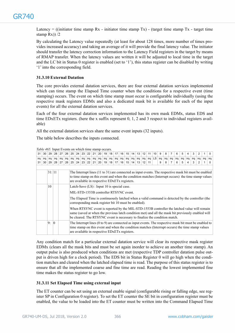
GR740
Latency = ((initiator time stamp Rx - initiator time stamp Tx) - (target time stamp Tx - target time stamp Rx)) /2By calculating the Latency value repeatedly (at least for about 128 times, more number of times pro-vides increased accuracy) and taking an average of it will provide the final latency value. The initiator should transfer the latency correction information to the Latency Field registers in the target by means of RMAP transfer. When the latency values are written it will be adjusted to local time in the targetand the LC bit in Status 0 register is enabled (set to ‘1’), this status register can be disabled by writing ‘1’ into the corresponding field.
31.3.10 External Datation
The core provides external datation services, there are four external datation services implemented which can time stamp the Elapsed Time counter when the conditions for a respective event (time stamping) occurs. The event on which time stamp must occur is configurable individually (using the respective mask registers EDMx and also a dedicated mask bit is available for each of the input events) for all the external datation services.
Each of the four external datation services implemented has its own mask EDMx, status EDS and time EDxETx registers. (here the x suffix represent 0, 1, 2 and 3 respect to individual registers avail-able)
All the external datation services share the same event inputs (32 inputs).
The table below describes the inputs connected.
Any condition match for a particular external datation service will clear its respective mask register EDMx (clears all the mask bits and must be set again inorder to achieve an another time stamp). An output pulse is also produced when conditions are met (respective TDP controller datation pulse out-put is driven high for a clock period). The EDS bit in Status Register 0 will go high when the condi-tion matches and cleared when the latched elapsed time is read. The purpose of this status register is to ensure that all the implemented coarse and fine time are read. Reading the lowest implemented fine time makes the status register to go low.
31.3.11 Set Elapsed Time using external input
The ET counter can be set using an external enable signal (configurable rising or falling edge, see reg-ister SP in Configuration 0 register). To set the ET counter the SE bit in configuration register must be enabled, the value to be loaded into the ET counter must be written into the Command Elapsed Time
Table 465. Input Events on which time stamp occurs.31 30 29 28 27 26 25 24 23 22 21 20 19 18 17 16 15 14 13 12 11 10 9 8 7 6 5 4 3 2 1 0
irq
31
irq
30
irq
29
irq
28
irq
27
irq
26
irq
25
irq
24
irq
23
irq
22
irq
21
irq
20
irq
19
irq
18
irq
17
irq
16
irq
15
irq
14
irq
13
irq
12
irq
11
LS irq
9
irq
8
irq
7
irq
6
irq
5
irq
4
irq
3
irq
2
irq
1
irq
0
31: 11 The Interrupt lines (11 to 31) are connected as input events. The respective mask bit must be enabled to time stamp on this event and when the condition matches (Interrupt occurs) the time stamp values are available in respective EDxETx registers.
10 Latch-Save (LS) : Input 10 is special case.
MIL-STD-1553B controller RTSYNC event.
The Elapsed Time is continuously latched when a valid command is detected by the controller (the corresponding mask register bit 10 must be enabled).
When RTSYNC event is reported by the MIL-STD-1553B controller the latched value will remain same (saved at when the previous latch condition met) and all the mask bit previously enabled will be cleared. The RTSYNC event is necessary to finalize the condition match.
9: 0 The Interrupt lines (0 to 9) are connected as input events. The respective mask bit must be enabled to time stamp on this event and when the condition matches (Interrupt occurs) the time stamp values are available in respective EDxETx registers.
GR740-UM-DS, Jul 2018, Version 2.0 366 www.cobham.com/gaisler

GR740
registers. The ARM bit field in the Status 0 register will set itself to ‘1’ when the first Command Elapsed Time register is written. After the occurrence of the external enable signal the value will be loaded into the ET counter and the ARM bit field in the Status 0 register will set itself to ‘0’. An inter-rupt can also be generated when the ET counter is loaded, the corresponding interrupt (Set ET Exter-nal Interrupt Enable) must be enabled.31.3.12 Synchronisation of target using SpaceWire Time-Codes
It is possible to synchronise the target only using SpaceWire Time-Codes. A master sending Space-Wire Time-Codes (using its Elapsed time counter) at regular interval can synchronise the Elapsed time in the target. The frequency of Time-code transmission in the master and the frequency of (when to expect a) Time-code in the target must match, this can be achieved by setting the Mapping fields in the Configuration 0 register. The incoming SpaceWire Time-Codes and the Time-code position mapped in the target Elapsed Time is compared, if they match the bits available after the compared bits are made zero, if the local time map is less than one (External Time-code arrived early) then the bits available after the compared bits are made zero and the other part (including the mapped part) is incremented by one. If the above two cases occurred then the target time is in sync with the master time and the Insync bit in Status 0 register is enabled. If the incoming Time-code is in out of order (Non consecutive) then the synchronisation is stopped, the Insync bit in Status 0 register is disabled (but the local time keeps running) and an interrupt is generated if corresponding interrupt (Non con-secutive SpaceWire Time-code Interrupt) bit is enabled.
31.4 Registers
The core is programmed through registers mapped into AMBA APB address space.
Table 466.Registers
APB address offset Register
0x000-0x00F Configuration Field
0x000 Configuration 0
0x004 Configuration 1
0x008 Configuration 2
0x00C Configuration 3
0x010 - 0x01F Status Field
0x010 Status 0
0x014 Status 1
0x018 RESERVED
0x01C RESERVED
0x020 - 0x03F Command Field
0x020 Control
0x024 Command Elapsed Time 0
0x028 Command Elapsed Time 1
0x02C Command Elapsed Time 2
0x030 Command Elapsed Time 3
0x034 Command Elapsed Time 4
0x038 RESERVED
0x03C RESERVED
0x040 - 0x05F Datation Field
0x040 - 0x05F Datation Field
0x040 Datation Preamble Field
GR740-UM-DS, Jul 2018, Version 2.0 367 www.cobham.com/gaisler

GR740
0x044 Datation Elapsed Time 00x048 Datation Elapsed Time 1
0x04C Datation Elapsed Time 2
0x050 Datation Elapsed Time 3
0x054 Datation Elapsed Time 4
0x058 RESERVED
0x05C RESERVED
0x060 - 0x09F Time-Stamp Field
0x060 Time-Stamp Preamble Field Rx
0x064 Time-Stamp Elapsed Time 0 Rx
0x068 Time-Stamp Elapsed Time 1 Rx
0x06C Time-Stamp Elapsed Time 2 Rx
0x070 Time-Stamp Elapsed Time 3 Rx
0x074 Time-Stamp Elapsed Time 4 Rx
0x078 RESERVED
0x07C RESERVED
0x080 Time-Stamp SpaceWire Time-Code and Preamble Field Tx
0x084 Time-Stamp Elapsed Time 0 Tx
0x088 Time-Stamp Elapsed Time 1 Tx
0x08C Time-Stamp Elapsed Time 2 Tx
0x090 Time-Stamp Elapsed Time 3 Tx
0X094 Time-Stamp Elapsed Time 4 Tx
0x098 RESERVED
0x09C RESERVED
0x0A0-0x0BF Latency Field
0x0A0 Latency Preamble Field
0x0A4 Latency Elapsed Time 0
0x0A8 Latency Elapsed Time 1
0x0AC Latency Elapsed Time 2
0x0B0 Latency Elapsed Time 3
0x0B4 Latency Elapsed Time 4
0x0B8 RESERVED
0x0BC RESERVED
0x0C0 Interrupt Enable
0x0C4 Interrupt Status
0x0C8 Delay Count
0x0CC Disable Sync
0x0D0-0x0FF RESERVED
0x100-0x18F External Datation Field
0x100 External Datation 0 Mask
0x104 External Datation 1 Mask
0x108 External Datation 2 Mask
0x10C External Datation 3 Mask
0x110-0x12F External Datation 0 Time
0x110 External Datation 0 Preamble Field
0x114 External Datation 0 Elapsed Time 0
0x118 External Datation 0 Elapsed Time 1
GR740-UM-DS, Jul 2018, Version 2.0 368 www.cobham.com/gaisler

GR740
0x11C External Datation 0 Elapsed Time 20x120 External Datation 0 Elapsed Time 3
0x124 External Datation 0 Elapsed Time 4
0x128 RESERVED
0x12C RESERVED
0x130-0x14F External Datation 1 Time
0x150-0x16F External Datation 2 Time
0x170-0x18F External Datation 3 Time
0x190-0x1FF RESERVED
Table 467.0x000 - CONF0 - Configuration 031 25 24 23 21 20 19 18 17 16 15 14 13 12 8 7 6 5 4 3 2 1 0
RESERVED JE RES ST EP ET SP SE LE AE RES MAPPING TD MU SEL ME RE TE RS
0 0 0 0 1 0 1 0 0 0 0 0b00110 0 0 0 0 0 0 0
r rw r rw rw rw rw rw rw rw r rw rw rw rw rw rw rw rw
31: 25 RESERVED
24 Jitter Correction Enable (JE) - (not usable in this implementation).
23: 22 RESERVED
21: Synchronisation using SpaceWire Time-Code Enable (only for target).
20: External ET Increment Polarity (EP) - To select the rising or falling edge of the external enable sig-nal to increment the Elapsed time. Value ‘1’ Rising edge. Value ‘0’ Falling edge.
19: External ET Increment Enable.(ET) - To increment the Elapsed Time based on external signal. When disabled the internal frequency synthesizer is used to increment the Elapsed Time counter.
18: Set ET External Polarity (SP) - To select the rising or falling edge of the external enable signal to load the Elapsed Time with the contents of the command field register.
17: Set ET External Enable (SE) - Based on the external enable signal load the Elapsed Time with the contents of the command field register.
16: Latency Enable (LE) - To calculate latency between an initiator and target this bit must be enabled in both of them.
15: AMBA Interrupt Enable (AE) - The interrupts (explained in interrupt registers) in this core will gen-erate an AMBA interrupt only when this bit is enabled.
14 13 RESERVED
12: 8 Mapping (MAP) - Defines mapping of SpaceWire Time-Codes versus CCSDS Time-code.
Value 0b00000 will send SpaceWire Time-Codes every Second,
Value 0b00001 will send SpaceWire Time-Codes every 0.5 Second,
Value 0b00010 will send SpaceWire Time-Codes every 0.25 Second,
Value 0b00011 will send SpaceWire Time-Codes every 0.125 Second
The maximum value it can take is 0b11000.
7: Enable TDP (TD) - This is to indicate that the TDP provides SpaceWire Time-codes and Distributed interrupts.
6: RESERVED
5: 4 Select (SEL) - Select for SpaceWire Time-Codes and Distributed Interrupt transmission and recep-tion, one of 0 through 3, (must always be 0b00 in this implementation).
3: Mitigation Enable (ME) - (not usable in this implementation).
2: Receiver Enable (RE) - Enabling this will make the core to act as target.
1 Transmit Enable (TE) - Enabling this will make the core to act as initiator.
The core can act only as an initiator or target, both TE and RE cannot be enabled at the same time.
0 Reset (RS) - Reset core. Makes complete reset when enabled, self clears itself (to disable).
GR740-UM-DS, Jul 2018, Version 2.0 369 www.cobham.com/gaisler

GR740
Table 468. 0x004 - CONF 1 - Configuration 131 30 29 0
- FSINC
0 0
r rw
31: 30 RESERVED
29: 0 Frequency synthesizer (FSINC) - Increment value of the Frequency Synthesizer which is added to the counter every system clock cycle. It defines the frequency of the synthesized reference time.
Refer the spreadsheet provided along with this document to obtain this value.
Table 469. 0x008 - CONF 2 - Configuration 231 8 7 0
CV ETINC
0 0
rw rw
31: 8 Compensation Value (CV) - (not usable in this implementation)
7: 0 Elapsed Time Increment (ETINC) - Value of the Elapsed Time counter is to be incremented each time when the Frequency Synthesizer wraps around.
Refer the spreadsheet provided along with this document to obtain this value.
Table 470. 0x00C - CONF3 - Configuration 331 22 21 16 15 14 13 12 11 10 9 5 4 0
- STM - DI64R
DI64T
DI64
DI INRX INTX
0 0 0 0 0 0 0 0 0
r rw r rw rw rw rw rw rw
31: 22 RESERVED
21: 16 SpaceWire Time-Code Mask (STM) - Mask For TSTC register available at Time-Stamp SpaceWire Time-Code and Preamble Field Tx register.
Value all bits zero will send Distributed interrupts at all SpaceWire Time-Codes irrespective of any values in TSTC register.
Value all ones will send Distributed interrupts at complete match of SpaceWire Time-Code with TSTC register.
(only for initiator)
15: 14 RESERVED
13: DI64R - The MSb for received Distributed Interrupt when interrupt numbers 32 to 63 is used. Possi-ble only for DI = ‘0’ (only interrupt mode) and DI64 is enabled.
12: DI64T - The MSb for transmitted Distributed Interrupt when interrupt numbers 32 to 63 is used. Possible only for DI = ‘0’ (only interrupt mode) and DI64 is enabled.
11: Enable Distributed Interrupts 64 (DI64) - when set all 64 Distributed interrupt numbers can be used for latency calculation. Possible only for DI = ‘0’ (only interrupt mode).
10: Distributed Interrupt (DI) - Distributed Interrupt method, when set interrupt and acknowledge mode else only interrupt mode. (only for target)
9: 5 Interrupt Received (INRX) - The distributed interrupt number received by initiator or target.
4: 0 Interrupt Transmitted (INTX) - The distributed interrupt number transmitted by initiator or target.
Table 471. 0x010 - STAT 0 - Status Register 031 30 28 27 24 23 22 16 15 14 13 8 7 4 3 2 1 0
MA - EDS - FW - CW - ARM
LC TCQ INSYNC
0 0 0 0 0 0 0 0 0 0 0 0
r r r r r r r r r wc r r
GR740-UM-DS, Jul 2018, Version 2.0 370 www.cobham.com/gaisler
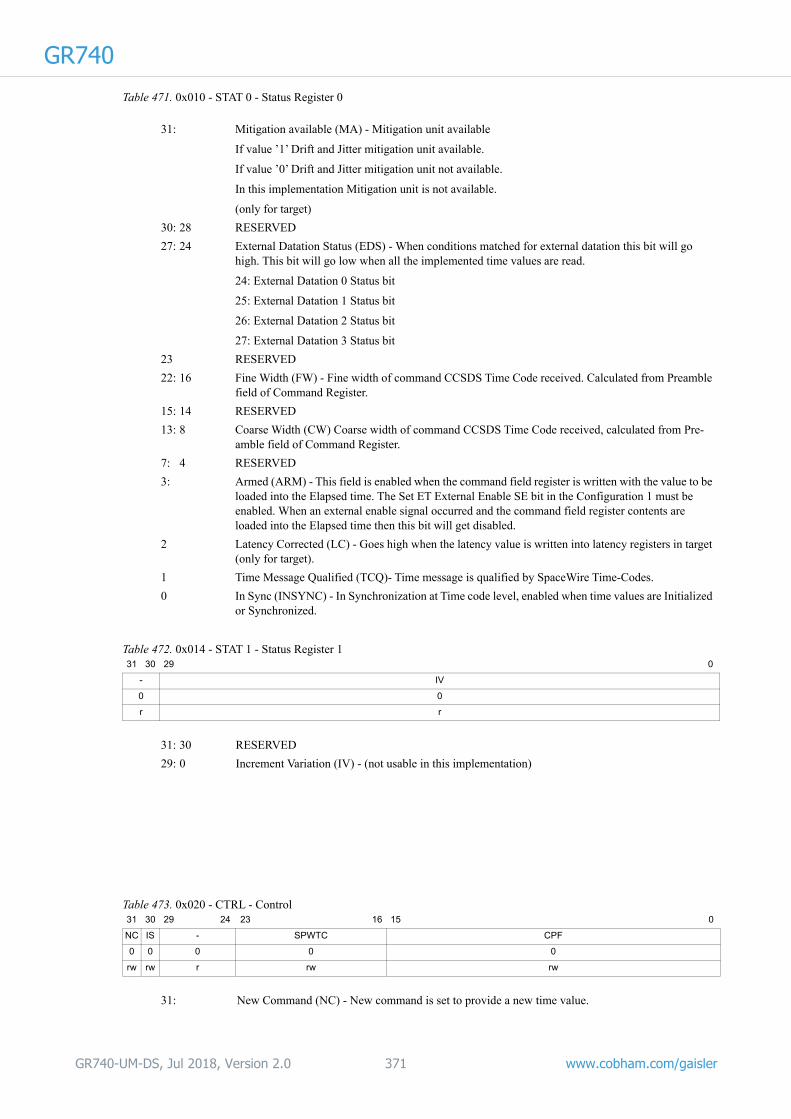
GR740
31: Mitigation available (MA) - Mitigation unit available
If value ’1’ Drift and Jitter mitigation unit available.
If value ’0’ Drift and Jitter mitigation unit not available.
In this implementation Mitigation unit is not available.
(only for target)
30: 28 RESERVED
27: 24 External Datation Status (EDS) - When conditions matched for external datation this bit will go high. This bit will go low when all the implemented time values are read.
24: External Datation 0 Status bit
25: External Datation 1 Status bit
26: External Datation 2 Status bit
27: External Datation 3 Status bit
23 RESERVED
22: 16 Fine Width (FW) - Fine width of command CCSDS Time Code received. Calculated from Preamble field of Command Register.
15: 14 RESERVED
13: 8 Coarse Width (CW) Coarse width of command CCSDS Time Code received, calculated from Pre-amble field of Command Register.
7: 4 RESERVED
3: Armed (ARM) - This field is enabled when the command field register is written with the value to be loaded into the Elapsed time. The Set ET External Enable SE bit in the Configuration 1 must be enabled. When an external enable signal occurred and the command field register contents are loaded into the Elapsed time then this bit will get disabled.
2 Latency Corrected (LC) - Goes high when the latency value is written into latency registers in target (only for target).
1 Time Message Qualified (TCQ)- Time message is qualified by SpaceWire Time-Codes.
0 In Sync (INSYNC) - In Synchronization at Time code level, enabled when time values are Initialized or Synchronized.
Table 472. 0x014 - STAT 1 - Status Register 131 30 29 0
- IV
0 0
r r
31: 30 RESERVED
29: 0 Increment Variation (IV) - (not usable in this implementation)
Table 473. 0x020 - CTRL - Control 31 30 29 24 23 16 15 0
NC IS - SPWTC CPF
0 0 0 0 0
rw rw r rw rw
31: New Command (NC) - New command is set to provide a new time value.
Table 471. 0x010 - STAT 0 - Status Register 0
GR740-UM-DS, Jul 2018, Version 2.0 371 www.cobham.com/gaisler

GR740
30: Init or Sync (IS) - ’1’ Initialization of received time message
’0’ Synchronisation of received time message
(only for target).
29: 24 RESERVED
23: 16 Spacewire Time-code (SPWTC) - Spacewire Time-code value used for initialization and synchroni-sation.
In initiator the SpaceWire Time-Codes generated internally using the local ET counter matches this register a Time Message TM interrupt will be generated which is used to send Time message over the SpaceWire network.
In target this register should match the received SpaceWire Time-code for time qualification.
15: 0 Command Preamble Field (CPF) - The number of coarse and fine time available in Command Elapsed Time registers should be mentioned in this field. Based on this preamble field the target will initialize or synchronise the local ET counter (only for target).
Table 474. 0x024 - CET0 - Command Elapsed Time 031 0
CET0
0
rw
31: 0 Command Elapsed Time 0 (CET0) - Initialize or Synchronise local ET counter value (0 to 31).
Table 475. 0x028 - CET1 - Command Elapsed Time 131 0
CET1
0
rw
31: 0 Command Elapsed Time 1 (CET1) - Initialize or Synchronise local ET counter value (32 to 63).
Table 476.0x02C - CET2 - Command Elapsed Time 231 0
CET2
0
rw
31: 0 Command Elapsed Time 2 (CET2) - Initialize or Synchronise local ET counter value (64 to 95).
Table 477.0x030 - CET0 - Command Elapsed Time 331 0
CET3
0
rw
31: 0 Command Elapsed Time 3 (CET3) - Initialize or Synchronise local ET counter value (96 to 127).
Table 478. 0x034 - CET4 - Command Elapsed Time 431 24 23 0
CET4 RESERVED
0 0
rw r
31: 24 Command Elapsed Time 4 (CET4) - Initialize or Synchronise local ET counter value (128 to 135).
23: 0 RESERVED
Table 473. 0x020 - CTRL - Control
GR740-UM-DS, Jul 2018, Version 2.0 372 www.cobham.com/gaisler

GR740
Table 479.0x040 - DPF - Datation Preamble Field 31 16 15 0RESERVED DPF
0 0x2f00
r r
31: 16 RESERVED
15: 0 Datation Preamble Field (DPF) - The number of coarse and fine time implemented can be obtained from this Preamble Field.
Table 480.0x044 - DET0 - Datation Elapsed Time 031 0
DET0
0
r
31: 0 Datation Elapsed Time 0 (DET0) - CCSDS Time Code value (0 to 31) of local ET counter value.
Table 481.0x048 - DET1 - Datation Elapsed Time 131 0
DET1
0
r
31: 0 Datation Elapsed Time 1 (DET1) - CCSDS Time Code value (32 to 63) of local ET counter value.
Table 482.0x04C - DET2 - Datation Elapsed Time 231 0
DET2
0
r
31: 0 Datation Elapsed Time 2 (DET2) - CCSDS Time Code value (64 to 95) of local ET counter value.
All registers are only readable.
Table 483.0x050 - DET3 - Datation Elapsed Time 331 0
DET3
0
r
31: 0 Datation Elapsed Time 3 (DET3) - CCSDS Time Code value (96 to 127) of local ET counter value.
Table 484.0x054 - DET4 - Datation Elapsed Time 431 24 23 0
DET4 RESERVED
0 0
r r
31: 24 Datation Elapsed Time 4 (DET4) - CCSDS Time Code value (128 to 135) of local ET counter value.
23: 0 RESERVED
GR740-UM-DS, Jul 2018, Version 2.0 373 www.cobham.com/gaisler

GR740
Table 485. 0x060 - TRPFRX - Time-Stamp Preamble Field Rx31 16 15 0RESERVED TRPF
0 0x2f00
r r
31: 16 RESERVED
15: 0 Time stamp Preamble Field (TRPF) - The number of coarse and fine time implemented can be obtained from this Preamble Field.
Table 486. 0x064 - TR0 - Time Stamp Elapsed Time 0 Rx31 0
TR0
0
r
31: 0 Time Stamp Elapsed Time 0 Rx (TR0) - Time stamped local ET value (0 To 31) when distributed interrupt received.
Table 487. 0x068 - TR1 - Time Stamp Elapsed Time 1 Rx31 0
TR1
0
r
31: 0 Time Stamp Elapsed Time 1 Rx (TR1) - Time stamped local ET value (32 to 63) when distributed interrupt received.
Table 488. 0x06C - TR2 - Time Stamp Elapsed Time 2 Rx31 0
TR2
0
r
31: 0 Time Stamp Elapsed Time 2 Rx (TR2) - Time stamped local ET value (64 to 95) when distributed interrupt received.
Table 489. 0x070 - TR3- Time Stamp Elapsed Time 3 Rx31 0
TR3
0
r
31: 0 Time Stamp Elapsed Time 3 Rx (TR3) - Time stamped local ET value (96 to 127) when distributed interrupt received.
Table 490. 0x074 - TR4 - Time Stamp Elapsed Time 4 Rx31 24 23 0
TR4 RESERVED
0 0
r r
31: 24 Time Stamp Elapsed Time 4 Rx (TR4) - Time stamped local ET value (128 to 135) when distributed inter-rupt received.
23: 0 RESERVED
GR740-UM-DS, Jul 2018, Version 2.0 374 www.cobham.com/gaisler

GR740
Table 491. 0x080 - TTPFTX - Time-Stamp SpaceWire Time-Code and Preamble Field Tx31 24 23 16 15 0TSTC RESERVED TTPF
0 0 0x2f00
rw r r
31: 24 Time stamp time code (TSTC) - Time stamp on this time-code value, used for time stamping when this register matched with SpaceWire Time-Codes. The mask for this matching is available in con-figuration register 3.(only for initiator)
23: 16 RESERVED
15: 0 Time stamp Preamble Field (TTPF) - The number of coarse and fine time implemented can be obtained from this Preamble Field.
Table 492. 0x084 - TT0 - Time Stamp Elapsed Time 0 Tx31 0
TT0
0
r
31: 0 Time Stamp Elapsed Time 0 Tx (TT0) - Time stamped local ET value (0 to 31) when distributed interrupt transmitted.
Table 493. 0x088 - TT1 - Time Stamp Elapsed Time 1 Tx31 0
TT1
0
r
31: 0 Time Stamp Elapsed Time 1 Tx (TT1) - Time stamped local ET value (32 to 63) when distributed interrupt transmitted.
Table 494. 0x08C - TT2 - Time Stamp Elapsed Time 2 Tx31 0
TT2
0
r
31: 0 Time Stamp Elapsed Time 2 Tx (TT2) - Time stamped local ET value (64 to 95) when distributed interrupt transmitted.
Table 495. 0x090 - TT3 - Time Stamp Elapsed Time 3 Tx31 0
TT3
0
r
31: 0 Time Stamp Elapsed Time 3 Tx (TT3) - Time stamped local ET value (96 to 127) when distributed interrupt transmitted.
Table 496. 0x094 - TT4 - Time Stamp Elapsed Time 4 Tx31 24 23 0
TT4 RESERVED
0 0
r r
GR740-UM-DS, Jul 2018, Version 2.0 375 www.cobham.com/gaisler

GR740
31: 24 Time Stamp Elapsed Time 4 Tx (TT4) - Time stamped local ET value (128 to 135) when distributed interrupt transmitted.
23: 0 RESERVED
Table 497. 0x0A0 - LPF- Latency Preamble Field 31 16 15 0
RESERVED LPF
0 0x2f00
r r
31: 16 RESERVED
15: 0 Latency Preamble Field (LPF) - The number of coarse and fine time implemented can be obtained from this Preamble Field.(only for target)
Table 498. 0xA4 - LE0 -Latency Elapsed Time 031 0
LE0
0
rw
31: 0 Latency Elapsed Time Value 0 (LE0) - Latency Value (0 to 31) written by initiator.(only for target)
Table 499. 0xA8 - LE1 -Latency Elapsed Time 131 0
LE1
0
rw
31: 0 Latency Elapsed Time Value 1 (LE1) - Latency Value (32 to 63) written by initiator.(only for target)
Table 500. 0xAC - LE2 -Latency Elapsed Time 231 0
LE2
0
rw
31: 0 Latency Elapsed Time Value 2 (LE2) - Latency Value (64 to 95) written by initiator.(only for target)
Table 501. 0xB0 - LE3 -Latency Elapsed Time 331 0
LE3
0
rw
31: 0 Latency Elapsed Time Value 3 (LE3) - Latency Value (96 to 127) written by initiator.(only for target)
Table 502. 0xB4 - LE4 -Latency Elapsed Time 431 24 23 0
LE4 RESERVED
0 0
rw r
31: 24 Latency Elapsed Time Value 4 (LE4) - Latency Value (128 to 135) written by initiator. (only for tar-get)
23: 0 RESERVED
Table 496. 0x094 - TT4 - Time Stamp Elapsed Time 4 Tx
GR740-UM-DS, Jul 2018, Version 2.0 376 www.cobham.com/gaisler

GR740
Table 503. 0x0C0 - IE - Interrupt Enable31 20 19 18 11 10 9 8 7 6 5 4 3 2 1 0- NCTCE - SETE EDIE3 EDIE2 EDIE1 EDIE0 DITE DIRE TTE TME TRE SE
0 0 0 0 0
r rw r rw rw
31: 20 RESERVED
19: Non consecutive SpaceWire Time-Code received Interrupt Enable (NCTCE)
18: 11 RESERVED
10 Set ET External Interrupt Enable (SETE)
9 External Datation Interrupt Enable 3 (EDIE3)
8 External Datation Interrupt Enable 2 (EDIE2)
7 External Datation Interrupt Enable 1 (EDIE1)
6 External Datation Interrupt Enable 0 (EDIE0)
5 Distributed Interrupt TransmittedInterrupt Enable (DITE)
4 Distributed interrupt Received Received Interrupt Enable(DIRE)
3 Time-Code Transmitted Interrupt Enable (TTE) - SpaceWire Time-Code Transmitted Interrupt Enable (only for initiator)
2 Time Message transmit Interrupt Enable (TME) - (only for initiator)
1 Time-Code Received Interrupt Enable (TRE) - SpaceWire Time-Code Received Interrupt Enable (only for target)
0 Sync Interrupt Enable (SE) (only for target)
Table 504. 0xC4 - IS -Interrupt Status31 20 19 18 11 10 9 8 7 6 5 4 3 2 1 0
RESERVED NCTC - SET EDI3 EDI2 EDI1 EDI0 DIT DIR TT TM TR S
0 0 0 0 0
r wc r wc wc
31: 20 RESERVED
19: Generated when Non consecutive SpaceWire Time-Code is received (NCTC)
18: 11 RESERVED
10 Generated when Elapsed Time is loaded with contents of the Command Field register based on external enable signal (SET).
9 External Datation Interrupt 3 (EDI3) - Generated when conditions for External Datation 3 is matched.
8 External Datation Interrupt 2 (EDI2) - Generated when conditions for External Datation 2 is matched.
7 External Datation Interrupt 1 (EDI1) - Generated when conditions for External Datation 1is matched.
6 External Datation Interrupt 0 (EDI0) - Generated when conditions for External Datation 0 is matched.
5 Distributed Interrupt Transmitted (DIT) - Generated when distributed interrupt is transmitted (Latency calculation should be enabled)
4 Distributed interrupt Received (DIR) - Generated when distributed interrupt is Received (Latency calculation should be enabled)
3 Time-Codes Transmitted (TT) - Generated when SpaceWire Time-Codes is transmitted (only for initiator)
GR740-UM-DS, Jul 2018, Version 2.0 377 www.cobham.com/gaisler

GR740
2 Transmit Time Message (TM) - Generated when the conditions for transmitting time message occurred, based on this time message should be transmitted from initiator (only for initiator)
1 Time-Code Received (TR) - Generated when SpaceWire Time-Code is received (only for target)
0 Target initialized or synchronized (S) - Generated when the target is initialized or synchronized with initiator (only for target)
Table 505. 0xC8 - DC - Delay Count
31 15 14 0
- DC
0 0x7FFF
r rw
31: 15 RESERVED
14: 0 Delay Count (DC) - Delay induced between SpaceWire Time-Codes and Distributed Interrupt trans-mission in system clock units. The delay introduced is the value in this register multiplied by the system clock.
(only for initiator)0x7FFF
Table 506. 0xCC - DS - Disable Sync
31 30 24 23 0
EN - CD
0 0 0xFFFFFF
rw r rw
31: Enable for Configurable delay (EN)
30: 24 RESERVED
23: 0 Configurable delay (CD) to capture missing SpaceWire Time-Code (only for target)
The INSYNC bit in the Status 0 register will disable itself when an expected SpaceWire Time-Code is not arrived after the delay mentioned in this register. The delay corresponds to the fine time of Elapsed Time counter and should not overlap with the MAPPING register. Any Overlapping regis-ter must also be set to Zero.
Table 507. 0x100 - EDM0 - External Datation 0 Mask 31 0
EDM0
0x00000000
rw
31: 0 External Datation Mask (EDM0) - External datation can be enabled by writing ‘1’ into the bit for that corresponding external input. When conditions are matched the Elapsed Time will be latched.
The latched values are available at External Datation 0 Time Register.
All the mask bits will go low after any one of the conditions with respect to the enabled mask bits.are matched.
Table 508. 0x110 - EDPF0 - External Datation 0 Preamble Field 31 16 15 0
- EDPF0
0 0x2f00
r r
31: 16 RESERVED
15: 0 External Datation Preamble Field (EDPF0) - The number of coarse and fine time implemented can be obtained from this Preamble Field.
Table 504. 0xC4 - IS -Interrupt Status
GR740-UM-DS, Jul 2018, Version 2.0 378 www.cobham.com/gaisler

GR740
Note:
Reserved register fields should be written as zeros and masked out on read.
The registers which are not mentioned either as only for initiator or target are used in both initiator and target.
The Definition of External Datation 1 Mask, External Datation 2 Mask and External Datation 3 Mask registers are exactly same as External Datation 0 Mask Register.
The Definition of External Datation 1 Time, External Datation 2 Time and External Datation 3 Time registers are exactly same as External Datation 0 Time Registers (i.e. External Datation 0 Preamble Field and External Datation 0 Elapsed Time 0,1,2,3,4).
Table 509.0x114 - ED0ET0 - External Datation 0 Elapsed Time 031 0
ED0ET0
0
r
31: 0 External Datation Elapsed Time 0 (ED0ET0) - Latched CCSDS Time Code value (0 to 31) of local ET counter.
Table 510.0x118 - ED0ET1 - External Datation 0 Elapsed Time 131 0
ED0ET1
0
r
31: 0 External Datation Elapsed Time 1 (ED0ET1) - Latched CCSDS Time Code value (32 to 63) of local ET counter.
Table 511.0x11C - ED0ET2 - External Datation 0 Elapsed Time 231 0
ED0ET2
0
r
31: 0 External Datation 0 Elapsed Time 2 (ED0ET2) - Latched CCSDS Time Code value (64 to 95) of local ET counter.
Table 512.0x120 - ED0ET3 - External Datation 0 Elapsed Time 331 0
ED0ET3
0
r
31: 0 External Datation 0 Elapsed Time 3 (ED0ET3) - Latched CCSDS Time Code value (96 to 127) of local ET counter.
Table 513. 0x124 - ED0ET4 - External Datation 0 Elapsed Time 431 24 23 0
ED0ET4 RESERVED
0 0
r r
31: 24 External Datation 0 Elapsed Time 4 (ED0ET4) - Latched CCSDS Time Code value (128 to 135) of local ET counter.
23: 0 RESERVED
GR740-UM-DS, Jul 2018, Version 2.0 379 www.cobham.com/gaisler

GR740
32 Bridge connecting Debug AHB bus to Processor AHB bus32.1 Overview
The Debug AHB bus is connected to the Processor AHB bus via a uni-directional AHB/AHB bridge. The bridge provides:
• Propagation of single and burst AHB transfers
• Data buffering in internal FIFOs
• Efficient bus utilization through use of AMBA SPLIT response and data prefetching
• Posted writes
• Read and write combining, improves bus utilization and allows connecting cores with differing AMBA access size restrictions.
32.2 Operation
32.2.1 General
For AHB write transfers write data is always buffered in an internal FIFO implementing posted writes. For AHB read transfers the bridge uses AMBA Plug&Play information to determine whether the read data will be prefetched and buffered in an internal FIFO. If the target address for an AHB read burst transfer is a prefetchable location the read data will be prefetched and buffered.
An AHB master initiating a read transfer to the bridge is always splitted on the first transfer attempt to allow other masters to use the slave bus while the bridge performs read transfer on the master bus.
32.2.2 AHB read transfers
When a read transfer is registered on the slave interface the bridge gives a SPLIT response. The mas-ter that initiated the transfer will be de-granted allowing other bus masters to use the slave bus while the bridge performs a read transfer on the master side. The master interface then requests the bus and starts the read transfer on the master side. Single transfers on the slave side are normally translated to single transfers with the same AHB address and control signals on the master side, however read com-bining can translate one access into several smaller accesses. Translation of burst transfers from the slave to the master side depends on the burst type, burst length and access size.
If the transfer is a burst transfer to a prefetchable location, the master interface will prefetch data in the internal read FIFO. If the splitted burst on the slave side was an incremental burst of unspecified length (INCR), the length of the burst is unknown. In this case the master interface performs an incre-mental burst up to a 32-byte address boundary. When the burst transfer is completed on the master side, the splitted master that initiated the transfer (on the slave side) is allowed in bus arbitration by asserting the appropriate HSPLIT signal to the AHB controller. The splitted master re-attempts the transfer and the bridge will return data with zero wait states.
If the burst is to non-prefetchable area, the burst transfer on the master side is performed using sequence of NONSEQ, BUSY and SEQ transfers. The first access in the burst on the master side is of NONSEQ type. Since the master interface can not decide whether the splitted burst will continue on the slave side or not, the master bus is held by performing BUSY transfers. On the slave side the split-ted master that initiated the transfer is allowed in bus arbitration. The first access in the transfer is completed by returning read data. The next access in the transfer on the slave side is extended by asserting HREADY low. On the master side the next access is started by performing a SEQ transfer (and then holding the bus using BUSY transfers). This sequence is repeated until the transfer is ended on the slave side.
GR740-UM-DS, Jul 2018, Version 2.0 380 www.cobham.com/gaisler

GR740
In case of an ERROR response on the master side the ERROR response will be given for the same access (address) on the slave side. SPLIT and RETRY responses on the master side are re-attempted until an OKAY or ERROR response is received.32.2.3 AHB write transfers
The AHB/AHB bridge implements posted writes. Writes are accepted with zero wait states if the bridge is idle. During the AHB write transfer on the slave side the data is buffered in the internal write FIFO and the transfer is completed on the slave side by always giving an OKAY response. The master interface requests the bus and performs the write transfer when the master bus is granted. If the burst transfer crosses the 32-byte write burst boundary, a SPLIT response is given. When the bridge has written the contents of the FIFO out on the master side, the bridge will allow the master on the slave side to perform the remaining accesses of the write burst transfer.
32.2.4 Read and write combining
Read and write combining allows the bridge to assemble or split AMBA accesses from the Debug AHB bus into one or several accesses on the Processor AHB bus. This functionality can improve bus utilization and also allows cores that have differing AMBA access size restrictions to communicate with each other. The effects of read and write combining is shown in the table below.
Read and write combining is disabled for accesses to the area 0xF0000000 - 0xFFFFFFFF to prevent accesses wider than 32 bits to register areas.
Table 514.Read and write combining
Access on slave interface Resulting access(es) on master interface
BYTE or HALF-WORD single read access to any area
Single access of same size
BYTE or HALF-WORD read burst to prefetchable area
Incremental read burst of same access size as on slave interface, the length is the same as the number of 32-bit words in the read buffer, but will not cross the read burst boundary.
BYTE or HALF-WORD read burst to non-prefetchable area
Incremental read burst of same access size as on slave interface, the length is the same as the length of the incoming burst. The master interface will insert BUSY cycles between the sequential accesses.
BYTE or HALF-WORD single write Single access of same size
BYTE or HALF-WORD write burst Incremental write burst of same size and length, the maximum length is the number of 32-bit words in the write FIFO.
Single read access to any area Single access of same size
Read burst to prefetchable area Burst of 128-bit up to 32-byte address boundary.
Read burst to non-prefetchable area Incremental read burst of same access size as on slave interface, the length is the same as the length of the incoming burst. The master interface will insert BUSY cycles between the sequential accesses.
Single write Single write access of same size
Write burst Burst write of maximum possible size. The bridge will use the maxi-mum size (up to 128-bit) that it can use to empty the writebuffer.
GR740-UM-DS, Jul 2018, Version 2.0 381 www.cobham.com/gaisler

GR740
32.2.5 Core latencyThe delay incurred when performing an access over the core depends on several parameters such as operating frequency of the AMBA buses and memory access patterns. Table 515 below shows core behavior for a single read operation initiated while the bridge is idle.
While the transitions shown in table 515 are simplified they give an accurate view of the core delay. If the master interface needs to wait for a bus grant or if the read operation receives wait states, these cycles must be added to the cycle count in the tables.
Table 516 below lists the delays incurred for single operations that traverse the bridge while the bridge is in its idle state. The second column shows the number of cycles it takes the master side to perform the requested access, this column assumes that the master slave gets access to the bus immediately and that each access is completed with zero wait states. The table only includes the delay incurred by traversing the core. For instance, when the access initiating master reads the core’s prefetch buffer, each additional read will consume one clock cycle. However, this delay would also have been present if the master accessed any other slave.
Write accesses are accepted with zero wait states if the bridge is idle, this means that performing a write to the idle core does not incur any extra latency. However, the core must complete the write operation on the master side before it can handle a new access on the slave side. If the core has not transitioned into its idle state, pending the completion of an earlier access, the delay suffered by an access be longer than what is shown in the tables in this section.
Since the core has been implemented to use AMBA SPLIT responses there will be an additional delay where, typically, one cycle is required for the arbiter to react to the assertion of HSPLIT and one clock cycle for the repetition of the address phase. Also, since the core has support for read and/or write combining, the number of cycles required for the master will change depending on the access size and length of the incoming burst access.
Table 515.Example of single read
Clock cycle Core slave side activity Core master side activity
0 Discovers access and transitions from idle state Idle
1 Slave side waits for master side, SPLIT response is given to incoming access, any new incoming accesses also receive SPLIT responses.
Discovers slave side transition. Master interface output signals are assigned.
2 If bus access is granted, perform address phase. Other-wise wait for bus grant.
3 Register read data and transition to data ready state.
4 Discovers that read data is ready, assign read data output and assign SPLIT complete
Idle
5 SPLIT complete output is HIGH
6 Typically a wait cycle for the SPLIT:ed master to be allowed into arbitration. Core waits for master to return. Other masters receive SPLIT responses.
7 Master has been allowed into arbitration and per-forms address phase. Core keeps HREADY high
8 Access data phase. Core has returned to idle state.
Table 516.Access latencies
Access Master acc. cycles Slave cycles Delay incurred by performing access over core
Single read 3 3 6 * clk
Burst read with prefetch 2 + (burst length)x 4 (6 + burst length)* clk
GR740-UM-DS, Jul 2018, Version 2.0 382 www.cobham.com/gaisler

GR740
32.3 Registers
The core does not implement any registers accessible over AMBA AHB or APB.
Single writexx (2) 0 0
Burst writexx (2 + (burst length)) 0 0
x A prefetch operation ends at the address boundary defined by the prefetch buffer’s sizexx The core implements posted writes, the number of cycles taken by the master side can only affect the next access.
Table 516.Access latencies
Access Master acc. cycles Slave cycles Delay incurred by performing access over core
GR740-UM-DS, Jul 2018, Version 2.0 383 www.cobham.com/gaisler

GR740
33 LEON4 Hardware Debug Support Unit33.1 Overview
To simplify debugging on target hardware, the LEON4 processor implements a debug mode during which the pipeline is idle and the processor is controlled through a special debug interface. The LEON4 Debug Support Unit (DSU4) is used to control the processor during debug mode. The DSU acts as an AHB slave and can be accessed by all AHB masters on the Debug AHB bus. An external debug host can therefore access the DSU through several different interfaces.
33.2 Operation
Through the DSU AHB slave interface, any AHB master on the Debug AHB bus can access the pro-cessor registers and the contents of the instruction trace buffer. The DSU control registers can be accessed at any time, while the processor registers and caches can only be accessed when the proces-sor has entered debug mode. In debug mode, the processor pipeline is held and the processor state can be accessed by the DSU. Entering the debug mode can occur on the following events:
• executing a breakpoint instruction (ta 1)
• integer unit hardware breakpoint/watchpoint hit (trap 0xb)
• rising edge of the external break signal (BREAK)
• setting the break-now (BN) bit in the DSU control register
• a trap that would cause the processor to enter error mode
• occurrence of any, or a selection of traps as defined in the DSU control register
• after a single-step operation
• one of the processors in a multiprocessor system has entered the debug mode
• DSU AHB breakpoint or watchpoint hit
Unit
Debug AHB Bus
Debug Support
AHB Slave I/F
Debug I/F
Figure 44. LEON4/DSU Connection
Ethernet
DEBUG HOST
Processor(s)LEON4
JTAGSpaceWire
Connection tosystem via bridge
GR740-UM-DS, Jul 2018, Version 2.0 384 www.cobham.com/gaisler

GR740
The debug mode can only be entered when the debug support unit is enabled through an external sig-nal (DSU_EN). For DSU break (DSU_BREAK), and the break-now (BN) bit, to have effect the Break-on-IU-watchpoint (BW) bit must be set in the DSU control register. This bit is set when DSU_BREAK is active after reset and should also be set by debug monitor software when initializing the DSU. When the debug mode is entered, the following actions are taken:• PC and nPC are saved in temporary registers (accessible by the debug unit)
• an output signal (DSU_ACT) is asserted to indicate the debug state
• the timer units are (optionally) stopped to freeze the LEON timers and watchdog
The instruction that caused the processor to enter debug mode is not executed, and the processor state is kept unmodified. Execution is resumed by clearing the BN bit in the DSU control register or by de-asserting DSU_EN. The timer unit will be re-enabled and execution will continue from the saved PC and nPC. Debug mode can also be entered after the processor has entered error mode, for instance when an application has terminated and halted the processor. The error mode can be reset and the pro-cessor restarted at any address.
When a processor is in the debug mode, an access to ASI diagnostic area is forwarded to the IU which performs access with ASI equal to value in the DSU ASI register and address consisting of 20 LSB bits of the original address.
33.3 AHB Trace Buffer
The AHB trace buffer consists of a circular buffer that stores AHB data transfers. The address, data and various control signals of the AHB bus are stored and can be read out for later analysis. The trace buffer is 224 bits wide. The information stored is indicated in the table below:
In addition to the AHB signals, the low part of the DSU time tag counter is also stored in the trace.
The trace buffer is enabled by setting the enable bit (EN) in the trace control register. Each AHB transfer is then stored in the buffer in a circular manner. The address to which the next transfer is writ-ten is held in the trace buffer index register, and is automatically incremented after each transfer. Trac-ing is stopped when the EN bit is reset, or when a AHB breakpoint is hit. Tracing is temporarily
Table 517.AHB Trace buffer data allocation
Bits Name Definition
223:160 Load/Store data AHB HRDATA/HWDATA(127:64)
159:129 Load/Store data AHB HRDATA/HWDATA(63:32)
127 AHB breakpoint hit Set to ‘1’ if a DSU AHB breakpoint hit occurred.
126 - Not used
125:96 Time tag DSU time tag counter
95 - Not used
94:80 RESERVED RESERVED
79 Hwrite AHB HWRITE
78:77 Htrans AHB HTRANS
76:74 Hsize AHB HSIZE
73:71 Hburst AHB HBURST
70:67 Hmaster AHB HMASTER
66 Hmastlock AHB HMASTLOCK
65:64 Hresp AHB HRESP
63:32 Load/Store data AHB HRDATA/HWDATA(31:0)
31:0 Load/Store address AHB HADDR
GR740-UM-DS, Jul 2018, Version 2.0 385 www.cobham.com/gaisler

GR740
suspended when the processor enters debug mode, unless the trace force bit (TF) in the trace control register is set. If the trace force bit is set, the trace buffer is activated as long as the enable bit is set. The force bit is reset if an AHB breakpoint is hit and can also be cleared by software. Note that neither the trace buffer memory nor the breakpoint registers (see below) can be read/written by software when the trace buffer is enabled.The DSU has an internal time tag counter and this counter is frozen when the processor enters debug mode. When AHB tracing is performed in debug mode (using the trace force bit) it may be desirable to also enable the time tag counter. This can be done using the timer enable bit (TE). Note that the time tag is also used for the instruction trace buffer and the timer enable bit should only be set when using the DSU as an AHB trace buffer only, and not when performing profiling or software debug-ging. The timer enable bit is reset on the same events as the trace force bit.
The AHB trace buffer is enabled after reset when the DSU_EN signal is HIGH and the BREAK signal is low.
33.3.1 AHB trace buffer filters
The DSU has filters that can be applied to the AHB trace buffer, breakpoints and watchpoints. These filters are controlled via the AHB trace buffer filter control and AHB trace buffer filter mask registers. The fields in these registers allows masking access characteristics such as master, slave, read, write and address range so that accesses that correspond to the specified mask are not written into the trace buffer. Address range masking is done using the second AHB breakpoint register set. The values of the LD and ST fields of this register has no effect on filtering.
33.3.2 AHB statistics
The DSU collects statistics from the traced AHB bus and assert signals that are connected to the LEON4 statistics unit (L4STAT). The statistics outputs can be filtered by the AHB trace buffer filters, this is controlled by the Performance counter Filter bit (PF) in the AHB trace buffer filter control reg-ister. The DSU can collect data for the events listed in table 518 below.
Table 518.AHB events
Event Description Note
idle HTRANS=IDLE Active when HTRANS IDLE is driven on the AHB slave inputs and slave has asserted HREADY.
busy HTRANS=BUSY Active when HTRANS BUSY is driven on the AHB slave inputs and slave has asserted HREADY.
nseq HTRANS=NONSEQ Active when HTRANS NONSEQ is driven on the AHB slave inputs and slave has asserted HREADY.
seq HTRANS=SEQ Active when HTRANS SEQUENTIAL is driven on the AHB slave inputs and slave has asserted HREADY.
read Read access Active when HTRANS is SEQUENTIAL or NON-SEQUENTIAL, slave has asserted HREADY and the HWRITE input is low.
write Write access Active when HTRANS is SEQUENTIAL or NON-SEQUENTIAL, slave has asserted HREADY and the HWRITE input is high.
hsize[5:0] Transfer size Active when HTRANS is SEQUENTIAL or NON-SEQUENTIAL, slave has asserted HREADY.
ws Wait state Active when HREADY input to AHB slaves is low and AMBA response is OKAY.
retry RETRY response Active when master receives RETRY response
split SPLIT response Active when master receives SPLIT response
GR740-UM-DS, Jul 2018, Version 2.0 386 www.cobham.com/gaisler

GR740
33.4 Instruction trace buffer
The instruction trace buffer consists of a circular buffer that stores executed instructions. The instruc-tion trace buffer is located in the processor, and read out via the DSU. The trace buffer is 128 bits wide, the information stored is indicated in the table below:
During tracing, one instruction is stored per line in the trace buffer with the exception of for exampleatomic load/store instructions, which are entered twice (one for the load and one for the store opera-tion). Bits [63:32] in the buffer correspond to the store address and the loaded data for load instruc-tions. Bit 126 is set for the second entry.
When the processor enters debug mode, tracing is suspended. The trace buffer and the trace buffer control register can be read and written while the processor is in the debug mode. During the instruc-tion tracing (processor in normal mode), the trace buffer cannot be written and trace buffer control register 0 can not be written. The traced instructions can optionally be filtered on instruction types.
spdel SPLIT delay Active during the time a master waits to be granted access to the bus after reception of a SPLIT response. The core will only keep track of one master at a time. This means that when a SPLIT response is detected, the core will save the master index. This event will then be active until the same master is re-allowed into bus arbitration and is granted access to the bus. This also means that the delay measured will include the time for re-arbitration, delays from other ongoing transfers and delays resulting from other masters being granted access to the bus before the SPLIT:ed master is granted again after receiving SPLIT complete.
If another master receives a SPLIT response while this event is active, the SPLIT delay for the second master will not be measured.
locked Locked access Active while the HMASTLOCK signal is asserted on the AHB slave inputs.
Table 519.Instruction trace buffer data allocation
Bits Name Definition
126 Multi-cycle instruction Set to ‘1’ on the second instance of a multi-cycle instruction
125:96 Time tag The value of the DSU time tag counter
95:64 Result or Store address/data Instruction result, Store address or Store data
63:34 Program counter Program counter (2 lsb bits removed since they are always zero)
33 Instruction trap Set to ‘1’ if traced instruction trapped
32 Processor error mode Set to ‘1’ if the traced instruction caused processor error mode
31:0 Opcode Instruction opcode
Table 518.AHB events
Event Description Note
GR740-UM-DS, Jul 2018, Version 2.0 387 www.cobham.com/gaisler

GR740
Which instructions are traced is defined in the instruction trace buffer control register [31:28], as defined in the table below:The instruction trace buffer is enabled after reset when the DSU_EN signal is HIGH and the BREAK signal is low.
33.5 DSU memory map
The DSU memory map can be seen in table 521 below. In a multiprocessor systems, the register map is duplicated and address bits 27 - 24 are used to index the processor.
Table 520.Trace filter operation
Trace filter Instructions traced
0x0 All instructions
0x1 SPARC Format 2 instructions
0x2 Control-flow changes. All Call, branch and trap instructions including branch targets
0x4 SPARC Format 1 instructions (CALL)
0x8 SPARC Format 3 instructions except LOAD or STORE
0xC SPARC Format 3 LOAD or STORE instructions
0xD SPARC Format 3 LOAD or STORE instructions to alternate space
0xE SPARC Format 3 LOAD or STORE instructions to alternate space 0x80 - 0xFFLoad and stores to ASI 0x80 - 0xFF do not cause operations on the on-chip bus and can be used to implement software trace points.
Table 521.DSU memory map
Address offset Register
0x000000 DSU control register
0x000008 Time tag counter
0x000020 Break and Single Step register
0x000024 Debug Mode Mask register
0x000040 AHB trace buffer control register
0x000044 AHB trace buffer index register
0x000048 AHB trace buffer filter control register
0x00004c AHB trace buffer filter mask register
0x000050 AHB breakpoint address 1
0x000054 AHB mask register 1
0x000058 AHB breakpoint address 2
0x00005c AHB mask register 2
0x000070 Instruction count register
0x000080 AHB watchpoint control register
0x000090 - 0x00009C AHB watchpoint 1 data registers
0x0000A0 - 0x0000AC AHB watchpoint 1 mask registers
0x0000B0 - 0x0000BC AHB watchpoint 2 data registers
0x0000C0 - 0x0000CC AHB watchpoint 2 mask registers
0x100000 - 0x10FFFF Instruction trace buffer (..0: Trace bits 127 - 96, ..4: Trace bits 95 - 64,
..8: Trace bits 63 - 32, ..C : Trace bits 31 - 0)
0x110000 Instruction Trace buffer control register 0
0x110004 Instruction Trace buffer control register 1
0x200000 - 0x210000 AHB trace buffer (..0: Trace bits 127 - 96, ..4: Trace bits 95 - 64,
..8: Trace bits 63 - 32, ..C : Trace bits 31 - 0)
GR740-UM-DS, Jul 2018, Version 2.0 388 www.cobham.com/gaisler

GR740
0x300000 - 0x3007FC IU register file.
The addresses of the IU registers depends on how many register windows has been implemented:
%on: 0x300000 + (((psr.cwp * 64) + 32 + n*4) mod (NWINDOWS*64))
%ln: 0x300000 + (((psr.cwp * 64) + 64 + n*4) mod (NWINDOWS*64))
%in: 0x300000 + (((psr.cwp * 64) + 96 + n*4) mod (NWINDOWS*64))
%gn: 0x300000 + (NWINDOWS*64) + n*4
%fn: 0x301000 + n*4
0x300800 - 0x300FFC IU register file check bits (LEON4FT only)
0x301000 - 0x30107C FPU register file
0x400000 Y register
0x400004 PSR register
0x400008 WIM register
0x40000C TBR register
0x400010 PC register
0x400014 NPC register
0x400018 FSR register
0x40001C CPSR register
0x400020 DSU trap register
0x400024 DSU ASI register
0x400040 - 0x40007C ASR16 - ASR31
0x700000 - 0x7FFFFC ASI diagnostic access (ASI = value in DSU ASI register, address = address[19:0])ASI = 0x9 : Local instruction RAMASI = 0xB : Local data RAMASI = 0xC : Instruction cache tagsASI = 0xD : Instruction cache dataASI = 0xE : Data cache tagsASI = 0xF : Data cache dataASI = 0x1E : Separate snoop tags
Table 521.DSU memory map
Address offset Register
GR740-UM-DS, Jul 2018, Version 2.0 389 www.cobham.com/gaisler

GR740
33.6 DSU registers33.6.1 DSU control register
Table 522. 0x000000- CTRL - DSU control register31 12 11 10 9 8 7 6 5 4 3 2 1 0
RESERVED PW HL PE EB EE DM BZ BX BS BW BE TE
0 0 0 0 * * * * 0 * * *
r r rw wc r r r rw rw rw rw rw rw
31: 12 Reserved
11 Power down (PW) - Returns ‘1’ when processor is in power-down mode.
10 Processor halt (HL) - Returns ‘1’ on read when processor is halted. If the processor is in debug mode, setting this bit will put the processor in halt mode.
9 Processor error mode (PE) - returns ‘1’ on read when processor is in error mode, else ‘0’. If written with ‘1’, it will clear the error and halt mode.
8 External Break (EB) - Value of the external BREAK signal
7 External Enable (EE) - Value of the external DSU_EN signal
6 Debug mode (DM) - Indicates when the processor has entered debug mode.
5 Break on error traps (BZ) - if set, will force the processor into debug mode on all except the follow-ing traps: priviledged_instruction, fpu_disabled, window_overflow, window_underflow, asynchro-nous_interrupt, ticc_trap.
BZ is reset to the value of the external BREAK signal.
4 Break on trap (BX) - if set, will force the processor into debug mode when any trap occurs.
BX is reset to the value of the external BREAK signal.
3 Break on S/W breakpoint (BS) - if set, debug mode will be forced when an breakpoint instruction (ta 1) is executed.
2 Break on IU watchpoint (BW) - if set, debug mode will be forced on a IU watchpoint (trap 0xb).
BW is reset to the value of the external BREAK signal.
1 Break on error (BE) - if set, will force the processor to debug mode when the processor would have entered error condition (trap in trap).
BE is reset to the value of the external BREAK signal.
0 Trace enable (TE) - Enables instruction tracing. If set the instructions will be stored in the trace buffer. Remains set when then processor enters debug or error mode.
TE is reset to ’1’ when external signal BREAK=LOW, otherwise TE is reset to 0.
GR740-UM-DS, Jul 2018, Version 2.0 390 www.cobham.com/gaisler

GR740
33.6.2 Time tag counter registerThe trace buffer time tag counter is incremented each clock as long as the processor is running. The counter is stopped when the processor enters debug mode (unless the timer enable bit in the AHB trace buffer control register is set), and restarted when execution is resumed. The value of this register is used as time tag in the instruction and AHB trace buffers. The same time source is used for the pro-cessors’ internal up-counters.
33.6.3 DSU Break and Single Step register
This register is used to break or single step the processors. This register controls all processors in a multi-processor system, and is only accessible in the DSU memory map of processor 0.
33.6.4 DSU Debug Mode Mask Register
When one of the processors in a multiprocessor LEON4 system enters the debug mode the value of the DSU Debug Mode Mask register determines if the other processors are forced in the debug mode. This register controls all processors in a multi-processor system, and is only accessible in the DSU memory map of processor 0.
Table 523. 0x000008 - DTTC - DSU time tag counter register31 30 29 28 27 26 25 24 23 22 21 20 19 18 17 16 15 14 13 12 11 10 9 8 7 6 5 4 3 2 1 0
TIMETAG
0
rw
31: 0 DSU Time Tag Value (TIMETAG)
Table 524. 0x000020 - BRSS - DSU break and single step register31 30 29 28 27 26 25 24 23 22 21 20 19 18 17 16 15 14 13 12 11 10 9 8 7 6 5 4 3 2 1 0
RESERVED SS[3:0] RESERVED BN[3:0]
0 0 0 *
r rw r rw
31: 17 RESERVED
19: 16 Single step (SSx) - if set, the processor x will execute one instruction and return to debug mode. The bit remains set after the processor goes into the debug mode.
15: 4 RESERVED
3:0 Break now (BNx) -Force processor x into debug mode if the Break on watchpoint (BW) bit in the processors DSU control register is set. If cleared, the processor x will resume execution.
The reset value of this field is taken from the external BREAK signal.
Table 525. 0x000024 - DBGM - DSU debug mode mask register31 30 29 28 27 26 25 24 23 22 21 20 19 18 17 16 15 14 13 12 11 10 9 8 7 6 5 4 3 2 1 0
RESERVED DM[3:0] RESERVED ED[3:0]
0 0 0 0
r rw r rw
31: 17 RESERVED
19: 16 Debug mode mask (DMx) - If set, the corresponding processor will not be able to force running pro-cessors into debug mode even if it enters debug mode.
15: 4 RESERVED
3:0 Enter debug mode (EDx) - Force processor x into debug mode if any of processors in a multiproces-sor system enters the debug mode. If 0, the processor x will not enter the debug mode.
GR740-UM-DS, Jul 2018, Version 2.0 391 www.cobham.com/gaisler

GR740
33.6.5 DSU trap registerThe DSU trap register is a read-only register that indicates which SPARC trap type that caused the processor to enter debug mode. When debug mode is force by setting the BN bit in the DSU control register, the trap type will be 0xb (hardware watchpoint trap).
33.6.6 DSU ASI register
The DSU can perform diagnostic accesses to different ASI areas. The value in the ASI diagnostic access register is used as ASI while the address is supplied from the DSU memory area when per-forming an access at offset 0x700000.
Table 526. 0x400020 - DTR - DSU trap register31 30 29 28 27 26 25 24 23 22 21 20 19 18 17 16 15 14 13 12 11 10 9 8 7 6 5 4 3 2 1 0
RESERVED EM TRAPTYPE RESERVED
0 NR NR 0
r r r r
31: 13 RESERVED
12 Error mode (EM) - Set if the trap would have cause the processor to enter error mode.
11: 4 Trap type (TRAPTYPE) - 8-bit SPARC trap type
3:0 Read as 0x0
Table 527. 0x400024 - DASI- DSU ASI diagnostic access register31 8 7 0
RESERVED ASI
0 NR
r rw
31: 8 RESERVED
7: 0 ASI (ASI) - ASI to be used on diagnostic ASI access
GR740-UM-DS, Jul 2018, Version 2.0 392 www.cobham.com/gaisler

GR740
33.6.7 AHB Trace buffer control registerThe AHB trace buffer is controlled by the AHB trace buffer control register:
33.6.8 AHB trace buffer index register
The AHB trace buffer index register contains the address of the next trace line to be written.
Table 528. 0x000040 - ATBC - AHB trace buffer control register31 24 23 16 15 9 8 7 6 5 4 3 2 1 0
RESERVED DCNT RESERVED DF SF TE TF BW BR DM EN
0 0 0 0 0 0 0 0x10 0 0 *
r rw r rw rw rw rw r rw rw rw
31: 24 RESERVED
23: 16 Trace buffer delay counter (DCNT) - Specifies the number of lines that should be written in the trace buffer befiore entering debug mode after a AHB break/watchpoint has been hit.
15: 9 RESERVED
8 Enable Debug Mode Timer Freeze (DF) - The time tag counter keeps counting in debug mode when at least one of the processors has the internal timer enabled. If this bit is set to ‘1’ then the time tag counter is frozen when the processors have entered debug mode.
7 Sample Force (SF) - If this bit is written to ‘1’ it will have the same effect on the AHB trace buffer as if HREADY was asserted on the bus at the same time as a sequential or non-sequential transfer is made. This means that setting this bit to ‘1’ will cause the values in the trace buffer’s sample regis-ters to be written into the trace buffer, and new values will be sampled into the registers. This bit will automatically be cleared after one clock cycle.
Writing to the trace buffer still requires that the trace buffer is enabled (EN bit set to ‘1’) and that the CPU is not in debug mode or that tracing is forced (TF bit set to ‘1’). This functionality is primarily of interest if the Processor AHB bus appears to have frozen.
6 Timer enable (TE) - Activates time tag counter also in debug mode. Note that this activates the same timer source as used for the processor up-counters described in section 6.10.4.
5 Trace force (TF) - Activates trace buffer also in debug mode.
4: 3 Bus width (BW) - This value corresponds to log2(Supported bus width / 32). Value is 2.
2 Break (BR) - If set, the processor will be put in debug mode when AHB trace buffer stops due to AHB breakpoint hit.
1 Delay counter mode (DM) - Indicates that the trace buffer is in delay counter mode.
0 Trace enable (EN) - Enables the trace buffer.
The reset value of this field is 1 when the external signal BREAK is low, otherwise 0.
Table 529. 0x000044 - ATBI - AHB trace buffer index register31 12 11 4 3 0
RESERVED INDEX RESERVED
0 NR 0
r rw r
31: 12 RESERVED
11: 4 Trace buffer index counter (INDEX) - Address of next trace line to be written.
3: 0 RESERVED
GR740-UM-DS, Jul 2018, Version 2.0 393 www.cobham.com/gaisler
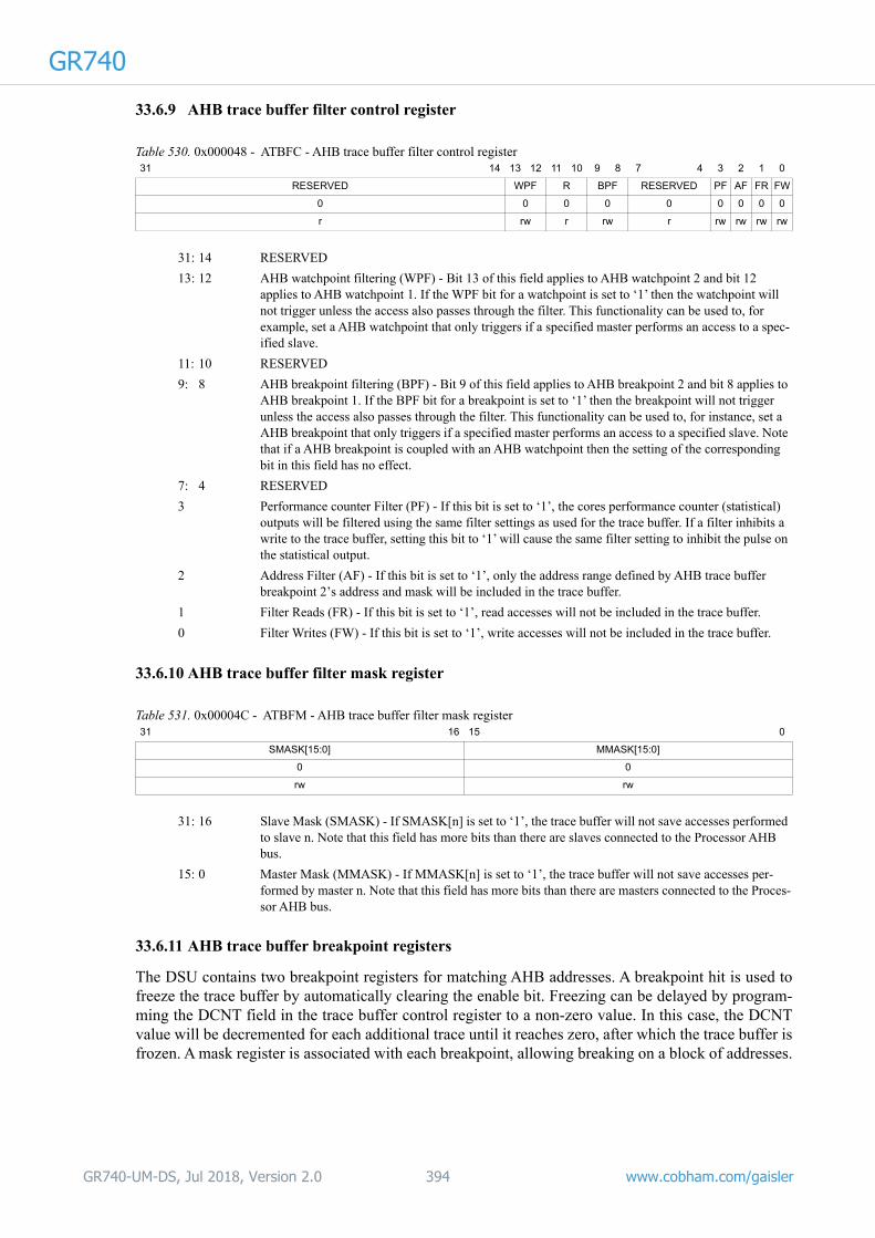
GR740
33.6.9 AHB trace buffer filter control registerTable 530. 0x000048 - ATBFC - AHB trace buffer filter control register
33.6.10 AHB trace buffer filter mask register
Table 531. 0x00004C - ATBFM - AHB trace buffer filter mask register
33.6.11 AHB trace buffer breakpoint registers
The DSU contains two breakpoint registers for matching AHB addresses. A breakpoint hit is used to freeze the trace buffer by automatically clearing the enable bit. Freezing can be delayed by program-ming the DCNT field in the trace buffer control register to a non-zero value. In this case, the DCNT value will be decremented for each additional trace until it reaches zero, after which the trace buffer is frozen. A mask register is associated with each breakpoint, allowing breaking on a block of addresses.
31 14 13 12 11 10 9 8 7 4 3 2 1 0
RESERVED WPF R BPF RESERVED PF AF FR FW
0 0 0 0 0 0 0 0 0
r rw r rw r rw rw rw rw
31: 14 RESERVED
13: 12 AHB watchpoint filtering (WPF) - Bit 13 of this field applies to AHB watchpoint 2 and bit 12 applies to AHB watchpoint 1. If the WPF bit for a watchpoint is set to ‘1’ then the watchpoint will not trigger unless the access also passes through the filter. This functionality can be used to, for example, set a AHB watchpoint that only triggers if a specified master performs an access to a spec-ified slave.
11: 10 RESERVED
9: 8 AHB breakpoint filtering (BPF) - Bit 9 of this field applies to AHB breakpoint 2 and bit 8 applies to AHB breakpoint 1. If the BPF bit for a breakpoint is set to ‘1’ then the breakpoint will not trigger unless the access also passes through the filter. This functionality can be used to, for instance, set a AHB breakpoint that only triggers if a specified master performs an access to a specified slave. Note that if a AHB breakpoint is coupled with an AHB watchpoint then the setting of the corresponding bit in this field has no effect.
7: 4 RESERVED
3 Performance counter Filter (PF) - If this bit is set to ‘1’, the cores performance counter (statistical) outputs will be filtered using the same filter settings as used for the trace buffer. If a filter inhibits a write to the trace buffer, setting this bit to ‘1’ will cause the same filter setting to inhibit the pulse on the statistical output.
2 Address Filter (AF) - If this bit is set to ‘1’, only the address range defined by AHB trace buffer breakpoint 2’s address and mask will be included in the trace buffer.
1 Filter Reads (FR) - If this bit is set to ‘1’, read accesses will not be included in the trace buffer.
0 Filter Writes (FW) - If this bit is set to ‘1’, write accesses will not be included in the trace buffer.
31 16 15 0
SMASK[15:0] MMASK[15:0]
0 0
rw rw
31: 16 Slave Mask (SMASK) - If SMASK[n] is set to ‘1’, the trace buffer will not save accesses performed to slave n. Note that this field has more bits than there are slaves connected to the Processor AHB bus.
15: 0 Master Mask (MMASK) - If MMASK[n] is set to ‘1’, the trace buffer will not save accesses per-formed by master n. Note that this field has more bits than there are masters connected to the Proces-sor AHB bus.
GR740-UM-DS, Jul 2018, Version 2.0 394 www.cobham.com/gaisler

GR740
Only address bits with the corresponding mask bit set to ‘1’ are compared during breakpoint detec-tion. To break on AHB load or store accesses, the LD and/or ST bits should be set.Table 532. 0x000050, 0x000058 - ATBBA - AHB trace buffer break address registers31 2 1 0
BADDR[31:2] RES
NR 0
rw r
31: 2 Break point address (BADDR) - Bits 31:2 of breakpoint address
1 0 RESERVED
Table 533. 0x000054, 0x00005C - ATBBM - AHB trace buffer break mask registers31 2 1 0
BMASK[31:2] LD ST
NR 0 0
rw rw rw
31: 2 Breakpoint mask (BMASK) - See description above tables.
1 Load (LD) - Break on data load address
0 Store (ST) - Break on data store address
GR740-UM-DS, Jul 2018, Version 2.0 395 www.cobham.com/gaisler

GR740
33.6.12 Instruction count registerThe DSU contains an instruction count register to allow profiling of application, or generation of debug mode after a certain clocks or instructions. The instruction count register consists of a 29-bit down-counter, which is decremented on either each clock (IC=0) or on each executed instruction (IC=1). In profiling mode (PE=1), the counter will set to all ones after an underflow without generat-ing a processor break. In this mode, the counter can be periodically polled and statistics can be formed on CPI (clocks per instructions). In non-profiling mode (PE=0), the processor will be put in debug mode when the counter underflows. This allows a debug tool such as GRMON to execute a defined number of instructions, or for a defined number of clocks.
Table 534. 0x000070 - ICNT - Instruction trace count register31 30 29 28 0
CE IC PE ICOUNT[28:0]
0 0 0 NR
rw rw rw rw
31 Counter Enable (CE) - Counter enable
30 Instruction Count (IC) - Instruction (1) or clock (0) counting
29 Profiling Enable (PE) - Profiling enable
28: 0 Instruction count (ICOUNT) - Instruction count
GR740-UM-DS, Jul 2018, Version 2.0 396 www.cobham.com/gaisler

GR740
33.6.13 AHB watchpoint control registerThe DSU has two AHB watchpoints that can be used to freeze the AHB tracebuffer, or put the proces-sor in debug mode, when a specified data pattern occurs on the AMBA bus. These watchpoints can also be coupled with the two AHB breakpoints so that a watchpoint will not trigger unless the AHB breakpoint is triggered. This also means that when a watchpoint is coupled with an AHB breakpoint, the breakpoint will not cause an AHB tracebuffer freeze, or put the processor(s), in debug mode unless also the watchpoint is triggered.
The bus data lines are taken through a register stage before being compared with the watch-point registers in the DSU. Data watchpoints have one extra cycle of latency compared to a AHB breakpoint due to this pipelining.
Table 535. 0x000080 - AHBWPC - AHB watchpoint control register31 7 6 5 4 3 2 1 0
RESERVED IN CP EN R IN CP EN
0 0 0 0 0 0 0 0
r rw rw rw r rw rw rw
31: 7 RESERVED
6 Invert (IN) - Invert AHB watchpoint 2. If this bit is set the watchpoint will trigger if data on the AHB bus does NOT match the specified data pattern (typically only usable if the watchpoint has been cou-pled with an address by setting the CP field).
5 Couple (CP) - Couple AHB watchpoint 2 with AHB breakpoint 1
4 Enable (EN) - Enable AHB watchpoint 2
3 RESERVED
2 Invert (IN) - Invert AHB watchpoint 1. If this bit is set the watchpoint will trigger if data on the AHB bus does NOT match the specified data pattern (typically only usable if the watchpoint has been cou-pled with an address by setting the CP field).
1 Couple (CP) - Couple AHB watchpoint 1 with AHB breakpoint 1
0 Enable (EN) - Enable AHB watchpoint 1
GR740-UM-DS, Jul 2018, Version 2.0 397 www.cobham.com/gaisler

GR740
33.6.14 AHB watchpoint data and mask registersThe AHB watchpoint data and mask registers specify the data pattern for an AHB watchpoint. A watchpoint hit is used to freeze the trace buffer by automatically clearing the enable bit. A watchpoint hit can also be used to force the processors into debug mode.
A mask register is associated with each data register. Only data bits with the corresponding mask bit set to ‘1’ are compared during watchpoint detection.
Table 536. 0x000090 to 0x00009C, 0x0000B0 to 0x0000BC- AHBWPD0-7 - AHB watchpoint data registers31 0
DATA[127-n*32 : 96-n*32]
NR
rw
31: 0 AHB watchpoint data (DATA) - Specifies the data pattern of one word for an AHB watchpoint. The lower part of the register address specifies with part of the bus that the register value will be com-pared against: Offset 0x0 specifies the data value for AHB bus bits 127:96, 0x4 for bits 95:64, 0x8 for 63:32 and offset 0xC for bits 31:0.
Table 537. 0x0000A0 to 0x0000AC, 0x0000C0 to 0x0000CC- AHBWPM0-7 - AHB watchpoint mask registers31 0
MASK[127-n*32 : 96-n*32]
NR
rw
31: 0 AHB watchpoint mask (MASK) - Specifies the mask to select bits for comparison out of one word for an AHB watchpoint. The lower part of the register address specifies with part of the bus that the register value will be compared against: Offset 0x0 specifies the data value for AHB bus bits 127:96, 0x4 for bits 95:64, 0x8 for 63:32 and offset 0xC for bits 31:0.
GR740-UM-DS, Jul 2018, Version 2.0 398 www.cobham.com/gaisler

GR740
33.6.15 Instruction trace buffer control register 0The instruction trace control register contains filter configuration and a pointer that indicates the next line of the instruction trace buffer to be written.
33.6.16 Instruction trace buffer control register 1
The instruction trace control register 1 contains settings used for trace buffer overflow detection. This register can be written while the processor is running.
Table 538. 0x110000 - ITBC0 - Instruction trace buffer control register 031 28 27 9 8 0
TFILT RESERVED ITPOINTER
0 0 NR
rw r rw
31: 28 Trace filter configuration (TFILT) - See table 520.
27: 9 RESERVED
15: 0 Instruction trace buffer pointer (ITPOINTER) - Indicates the next line of the instruction trace buffer to be written
Table 539. 0x110004 - ITBC1 - Instruction trace buffer control register 131 28 27 26 24 23 22 0
RESERVED WO
TLIM TOV
RESERVED
0 0 0 0 0
r rw rw rw r
31: 28 RESERVED
27 Watchpoint on overflow (WO) - If this bit is set, and Break on iu watchpoint (BW) is enabled in the DSU control register, then a watchpoint will be inserted when a trace overflow is detected (TOV field in this register gets set).
26: 24 Trace Limit (TLIM) - TLIM is compared with the top bits of ITBC0.ITPOINTER to generate the value in the TOV field below.
23 Trace Overflow (TOV) - Gets set to ‘1’ when the DSU detects that TLIM equals the top three bits of ITPOINTER.
22: 0 RESERVED
GR740-UM-DS, Jul 2018, Version 2.0 399 www.cobham.com/gaisler

GR740
34 JTAG Debug Link with AHB Master Interface34.1 Overview
The JTAG debug interface provides access to the Debug AHB bus through JTAG. The JTAG debug interface implements a simple protocol which translates JTAG instructions to AHB transfers. Through this link, a read or write transfer can be generated to any address on the AHB bus.
The JTAG debug interface will, together with all other cores on the Debug AHB bus, be gated off when the Debug AHB bus is disabled via the external DSU_EN signal.
34.2 Operation
34.2.1 Transmission protocol
The JTAG Debug link decodes two JTAG instructions and implements two JTAG data registers: the command/address register and data register. A read access is initiated by shifting in a command con-sisting of read/write bit, AHB access size and AHB address into the command/address register. The AHB read access is performed and data is ready to be shifted out of the data register. Write access is performed by shifting in command, AHB size and AHB address into the command/data register fol-lowed by shifting in write data into the data register. Sequential transfers can be performed by shifting in command and address for the transfer start address and shifting in SEQ bit in data register for fol-lowing accesses. The SEQ bit will increment the AHB address for the subsequent access. Sequential transfers should not cross a 1 kB boundary. Sequential transfers are always word based.
Table 540. JTAG debug link Command/Address register34 33 32 31 0
W SIZE AHB ADDRESS
34 Write (W) - ‘0’ - read transfer, ‘1’ - write transfer
33 32 AHB transfer size - “00” - byte, “01” - half-word, “10” - word, “11”- reserved
31 30 AHB address
Table 541. JTAG debug link Data register32 31 0
SEQ AHB DATA
32 Sequential transfer (SEQ) - If ‘1’ is shifted in this bit position when read data is shifted out or write data shifted in, the subsequent transfer will be to next word address. When read out from the device, this bit is ‘1’ if the AHB access has completed and ‘0’ otherwise.
31 30 AHB Data - AHB write/read data. For byte and half-word transfers data is aligned according to big-endian order where data with address offset 0 data is placed in MSB bits.
Figure 45. JTAG Debug link block diagram
AHB master interface
Debug AHB bus
JTAG CommunicationInterface
JTAG TAPController
TCK
TMS
TDI
TDO
GR740-UM-DS, Jul 2018, Version 2.0 400 www.cobham.com/gaisler

GR740
The core will signal AHB access completion by setting bit 32 of the data register. A debug host can look at bit 32 of the received data to determine if the access was successful. If bit 32 is ‘1’ the access completed and the data is valid. If bit 32 is ‘0’, the AHB access was not finished when the host started to read data. In this case the host can repeat the read of the data register until bit 32 is set to ‘1’, signal-ing that the data is valid and that the AMBA AHB access has completed.It should be noted that while bit 32 returns ‘0’, new data will not be shifted into the data register. The debug host should therefore inspect bit 32 when shifting in data for a sequential AHB access to see if the previous command has completed. If bit 32 is ‘0’, the read data is not valid and the command just shifted in has been dropped by the core.
34.3 Registers
The core does not implement any registers mapped in the AMBA AHB or APB address space.
GR740-UM-DS, Jul 2018, Version 2.0 401 www.cobham.com/gaisler

GR740
35 SpaceWire Debug Link35.1 Overview
The SpaceWire core provides an interface between the AHB bus and a SpaceWire network. It imple-ments the SpaceWire standard [SPW] with the protocol identification extension [SPWID]. TheRemote Memory Access Protocol (RMAP) target implements [RMAP].
The SpaceWire interface is configured through a set of registers accessed through an APB interface. Data is transferred through DMA channels using an AHB master interface.
The GRSPW2 SpaceWire core is located on the Debug AHB bus and has an RMAP target that is enabled after system reset. The core APB interface is also available on the Debug AHB bus but cannot be accessed by the processors since the bridge connecting the Debug AHB bus to the Processor AHB bus is uni-directional. The core on the Debug AHB bus thus provides a SpaceWire debug link that can be used to access all parts of the system. The system’s main SpaceWire links are provided through the SpaceWire router, see section 13.
The SpaceWire debug interface will, together with all other cores on the Debug AHB bus, be gated off when the Debug AHB bus is disabled via the external DSU_EN signal.
35.2 Operation
35.2.1 Overview
The main sub-blocks of the core are the link interface, the RMAP target and the AMBA interface. A block diagram of the internal structure can be found in figure 46.
The link interface consists of the receiver, transmitter and the link interface FSM. They handle com-munication on the SpaceWire network. The PHY block provides a common interface for the receiver to the four different data recovery schemes and is external to this core. The AMBA interface consists of the DMA engines, the AHB master interface and the APB interface. The link interface provides FIFO interfaces to the DMA engines. These FIFOs are used to transfer N-Chars between the AMBA and SpaceWire domains during reception and transmission.
The RMAP target handles incoming packets which are determined to be RMAP commands instead of the receiver DMA engine. The RMAP command is decoded and if it is valid, the operation is per-
Figure 46. Block diagram
TRANSMITTER
TXCLK
TRANSMITTERFSM
LINKINTERFACE
SEND
RMAP
D(1:0)
S(1:0)
FSM
FSM
TRANSMITTERDMA ENGINE
RECEIVER DMA ENGINE
TRANSMITTER
RMAP RECEIVER
N-CHAR FIFO
RECEIVER AHB FIFO
RECEIVER DATAPARALLELIZATION
AHB
MASTER INTERFACE
REGISTERSAPB
INTERFACE
D0
S0
RECEIVER0PHY
D
DV
GR740-UM-DS, Jul 2018, Version 2.0 402 www.cobham.com/gaisler

GR740
formed on the AHB bus. If a reply was requested it is automatically transmitted back to the source by the RMAP transmitter.35.2.2 Protocol support
The core only accepts packets with a valid destination address in the first received byte. Packets with address mismatch will be silently discarded (except in promiscuous mode which is covered in section 35.5.10).
The second byte is sometimes interpreted as a protocol ID and described hereafter. The RMAP proto-col (ID=0x1) is the only protocol handled separately in hardware while other packets are stored to a DMA channel. If the RMAP target is present and enabled all RMAP commands will be processed, executed and replied automatically in hardware. Otherwise RMAP commands are stored to a DMA channel in the same way as other packets. RMAP replies are always stored to a DMA channel. More information on the RMAP protocol support is found in section 35.7. When the RMAP target is not present or disabled, there is no need to include a protocol ID in the packets and the data can start immediately after the address.
All packets arriving with the extended protocol ID (0x00) are stored to a DMA channel. This means that the hardware RMAP target will not work if the incoming RMAP packets use the extended proto-col ID. Note also that packets with the reserved extended protocol identifier (ID = 0x000000) are not ignored by the core. It is up to the client receiving the packets to ignore them.
When transmitting packets, the address and protocol-ID fields must be included in the buffers from where data is fetched. They are not automatically added by the core.
Figure 47 shows the packet types accepted by the core. The core also allows reception and transmis-sion with extended protocol identifiers but without support for RMAP CRC calculations and the RMAP target.
35.3 Link interface
The link interface handles the communication on the SpaceWire network and consists of a transmitter, receiver, a FSM and FIFO interfaces. An overview of the architecture is found in figure 46.
35.3.1 Link interface FSM
The FSM controls the link interface (a more detailed description is found in the SpaceWire standard). The low-level protocol handling (the signal and character level of the SpaceWire standard) is handled by the transmitter and receiver while the FSM handles the exchange level.
The link interface FSM is controlled through the control register. The link can be disabled through the link disable bit, which depending on the current state, either prevents the link interface from reaching the started state or forces it to the error-reset state. When the link is not disabled, the link interface FSM is allowed to enter the started state when either the link start bit is set or when a NULL character has been received and the autostart bit is set.
The current state of the link interface determines which type of characters are allowed to be transmit-ted which together with the requests made from the host interfaces determine what character will be sent.
Figure 47. The SpaceWire packet types supported by the core.
Addr ProtID Dn-2..D3D2D1D0 Dn-1 EOP
Addr D0 Dm-2..D4D3D2D1 Dm-1 EOP
GR740-UM-DS, Jul 2018, Version 2.0 403 www.cobham.com/gaisler

GR740
Time-codes are sent when the FSM is in the run-state and a request is made through the time-interface (described in section 35.4).When the link interface is in the connecting- or run-state it is allowed to send FCTs. FCTs are sent automatically by the link interface when possible. This is done based on the maximum value of 56 for the outstanding credit counter and the currently free space in the receiver N-Char FIFO. FCTs are sent as long as the outstanding counter is less than or equal to 48 and there are at least 8 more empty FIFO entries than the counter value.
N-Chars are sent in the run-state when they are available from the transmitter FIFO and there are credits available. NULLs are sent when no other character transmission is requested or the FSM is in a state where no other transmissions are allowed.
The credit counter (incoming credits) is automatically increased when FCTs are received and decreased when N-Chars are transmitted. Received N-Chars are stored to the receiver N-Char FIFO for further handling by the DMA interface. Received Time-codes are handled by the time-interface.
35.3.2 Transmitter
The state of the FSM, credit counters, requests from the time-interface and requests from the DMA-interface are used to decide the next character to be transmitted. The type of character and the charac-ter itself (for N-Chars and Time-codes) to be transmitted are presented to the low-level transmitter which is located in a separate clock-domain.
This is done because one usually wants to run the SpaceWire link on a different frequency than the host system clock. The core has a separate clock input which is used to generate the transmitter clock. Since the transmitter often runs on high frequency clocks (> 100 MHz) as much logic as possible has been placed in the system clock domain to minimize power consumption and timing issues.
The transmitter logic in the host clock domain decides what character to send next and sets the proper control signal and presents any needed character to the low-level transmitter as shown in figure 48. The transmitter sends the requested characters and generates parity and control bits as needed. If no requests are made from the host domain, NULLs are sent as long as the transmitter is enabled. Most of the signal and character levels of the SpaceWire standard is handled in the transmitter. External LVDS drivers are needed for the data and strobe signals.
A transmission FSM reads N-Chars for transmission from the transmitter FIFO. It is given packet lengths from the DMA interface and appends EOPs/EEPs and RMAP CRC values if requested. When it is finished with a packet the DMA interface is notified and a new packet length value is given.
35.3.3 Receiver
The receiver detects connections from other nodes and receives characters as a bit stream recovered from the data and strobe signals by the PHY module which presents it as a data and data-valid signal. Both the receiver and PHY are located in a separate clock domain which runs on a clock generated by the PHY.
Transmitter Clock Domain Host Clock Domain
Transmitter
D
S
Send Time-codeSend FCTSend NCharTime-code[7:0]NChar[8:0]
Figure 48. Schematic of the link interface transmitter.
GR740-UM-DS, Jul 2018, Version 2.0 404 www.cobham.com/gaisler

GR740
The receiver is activated as soon as the link interface leaves the error reset state. Then after a NULL is received it can start receiving any characters. It detects parity, escape and credit errors which causes the link interface to enter the error reset state. Disconnections are handled in the link interface part in the tx clock domain because no receiver clock is available when disconnected.Received Characters are flagged to the host domain and the data is presented in parallel form. The interface to the host domain is shown in figure 49. L-Chars are the handled automatically by the host domain link interface part while all N-Chars are stored in the receiver FIFO for further handling. If two or more consecutive EOPs/EEPs are received all but the first one are discarded.
35.4 Time-Code distribution
Time-codes are control codes that consists of two control flags (bits 7:6) and a time value (bits 5:0), and they are used to distribute time over the SpaceWire network. The current time value (value of lat-est received or transmitted time-code), and control flags, can be read from the Time-code register (TC).
35.4.1 Receiving time-codes
When a control code is received, and either the control flags (bits 7:6) have value “00”, or control flag filtering is disabled (CTRL.TF bit set to 0), then the received control code is considered to be a Time-Code. If Time-Code reception is enabled (CTRL.TR bit set to 1) then the received time value is stored in the TC.TIMECNT field. If the received time value equals TC.TIMECNT+1 (modulo 64), then the Time-Code is considered valid.
When a valid Time-Code is received, in addition to the time value being updated, the received control flags are stored to the TC.TCTRL field. Also, when a valid Time-Code is received, the STS.TO bit is set to 1, and an AMBA interrupt is generated if the CTRL.IE bit and CTRL.TQ bit are both set to 1.
35.4.2 Transmitting time-codes
Time-Codes can be transmitted through the AMBA APB registers. In order to send a Time-code, Time-Code transmission must be enabled by setting the CTRL.TT bit to 1. To transmit a time-code through the register interface the CTRL.TI bit should be written to 1. When the bit is written the cur-rent time value (TC.TIMECNT field) is incremented, and a Time-Code consisting of the new time value together with the current control flags (TC.TCTRL field) is sent. The CTRL.TI bit will stay high until the Time-Code has been transmitted. If Time-Code transmission is disabled, writing the CTRL.TI bit has no effect.
Note that the link interface must be in run-state in order to be able to send a Time-Code.
35.5 Receiver DMA channels
The receiver DMA engine handles reception of data from the SpaceWire network to different DMA channels.
Receiver Clock Domain Host Clock Domain
Receiver
D
DV
Got Time-codeGot FCT
Got NCharTime-code[7:0]NChar[7:0]
Figure 49. Schematic of the link interface receiver.
Got EEPGot EOP
GR740-UM-DS, Jul 2018, Version 2.0 405 www.cobham.com/gaisler
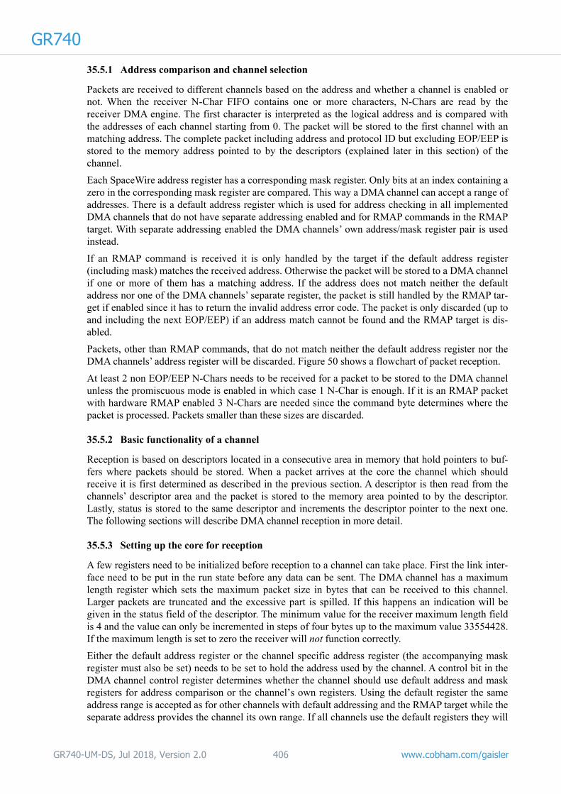
GR740
35.5.1 Address comparison and channel selectionPackets are received to different channels based on the address and whether a channel is enabled or not. When the receiver N-Char FIFO contains one or more characters, N-Chars are read by the receiver DMA engine. The first character is interpreted as the logical address and is compared with the addresses of each channel starting from 0. The packet will be stored to the first channel with an matching address. The complete packet including address and protocol ID but excluding EOP/EEP is stored to the memory address pointed to by the descriptors (explained later in this section) of the channel.
Each SpaceWire address register has a corresponding mask register. Only bits at an index containing a zero in the corresponding mask register are compared. This way a DMA channel can accept a range of addresses. There is a default address register which is used for address checking in all implemented DMA channels that do not have separate addressing enabled and for RMAP commands in the RMAP target. With separate addressing enabled the DMA channels’ own address/mask register pair is used instead.
If an RMAP command is received it is only handled by the target if the default address register (including mask) matches the received address. Otherwise the packet will be stored to a DMA channel if one or more of them has a matching address. If the address does not match neither the default address nor one of the DMA channels’ separate register, the packet is still handled by the RMAP tar-get if enabled since it has to return the invalid address error code. The packet is only discarded (up to and including the next EOP/EEP) if an address match cannot be found and the RMAP target is dis-abled.
Packets, other than RMAP commands, that do not match neither the default address register nor the DMA channels’ address register will be discarded. Figure 50 shows a flowchart of packet reception.
At least 2 non EOP/EEP N-Chars needs to be received for a packet to be stored to the DMA channel unless the promiscuous mode is enabled in which case 1 N-Char is enough. If it is an RMAP packet with hardware RMAP enabled 3 N-Chars are needed since the command byte determines where the packet is processed. Packets smaller than these sizes are discarded.
35.5.2 Basic functionality of a channel
Reception is based on descriptors located in a consecutive area in memory that hold pointers to buf-fers where packets should be stored. When a packet arrives at the core the channel which should receive it is first determined as described in the previous section. A descriptor is then read from the channels’ descriptor area and the packet is stored to the memory area pointed to by the descriptor. Lastly, status is stored to the same descriptor and increments the descriptor pointer to the next one. The following sections will describe DMA channel reception in more detail.
35.5.3 Setting up the core for reception
A few registers need to be initialized before reception to a channel can take place. First the link inter-face need to be put in the run state before any data can be sent. The DMA channel has a maximum length register which sets the maximum packet size in bytes that can be received to this channel. Larger packets are truncated and the excessive part is spilled. If this happens an indication will be given in the status field of the descriptor. The minimum value for the receiver maximum length field is 4 and the value can only be incremented in steps of four bytes up to the maximum value 33554428. If the maximum length is set to zero the receiver will not function correctly.
Either the default address register or the channel specific address register (the accompanying mask register must also be set) needs to be set to hold the address used by the channel. A control bit in the DMA channel control register determines whether the channel should use default address and mask registers for address comparison or the channel’s own registers. Using the default register the same address range is accepted as for other channels with default addressing and the RMAP target while the separate address provides the channel its own range. If all channels use the default registers they will
GR740-UM-DS, Jul 2018, Version 2.0 406 www.cobham.com/gaisler
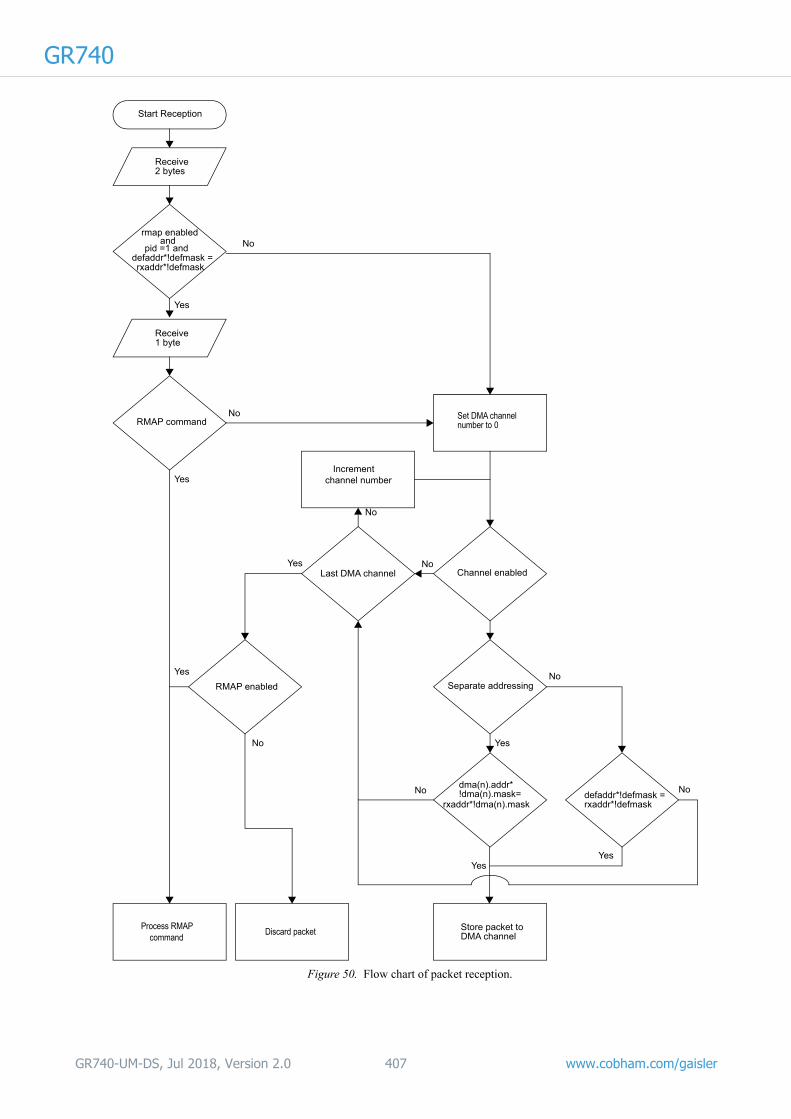
GR740
Start Reception
Receive2 bytes
rmap enabled
defaddr*!defmask =rxaddr*!defmask
Yes
Receive1 byte
RMAP commandNo
Yes
No
Set DMA channel number to 0
Process RMAPcommand
Separate addressing
No
Yes
dma(n).addr*
rxaddr*!dma(n).mask
Channel enabled
Increment channel number
andpid =1 and
defaddr*!defmask =rxaddr*!defmask
!dma(n).mask=
Last DMA channel
No
Yes
Store packet toDMA channel
No
No
Yes
RMAP enabled
Discard packet
Yes
Yes
No
Figure 50. Flow chart of packet reception.
No
GR740-UM-DS, Jul 2018, Version 2.0 407 www.cobham.com/gaisler

GR740
accept the same address range and the enabled channel with the lowest number will receive the packet.Finally, the descriptor table and control register must be initialized. This will be described in the two following sections.
35.5.4 Setting up the descriptor table address
The core reads descriptors from an area in memory pointed to by the receiver descriptor table address register. The register consists of a base address and a descriptor selector. The base address points to the beginning of the area and must start on a 1024 bytes aligned address. It is also limited to be 1024 bytes in size which means the maximum number of descriptors is 128 since the descriptor size is 8 bytes.
The descriptor selector points to individual descriptors and is increased by 1 when a descriptor has been used. When the selector reaches the upper limit of the area it wraps to the beginning automati-cally. It can also be set to wrap at a specific descriptor before the upper limit by setting the wrap bit in the descriptor. The idea is that the selector should be initialized to 0 (start of the descriptor area) but it can also be written with another 8 bytes aligned value to start somewhere in the middle of the area. It will still wrap to the beginning of the area.
If one wants to use a new descriptor table, the receiver enable bit in the corresponding DMA channel control/status register has to be cleared first. When the RX active bit in the same register is cleared it is safe to update the descriptor table register. When this is finished and descriptors are enabled the receiver enable bit can be set again.
35.5.5 Enabling descriptors
As mentioned earlier one or more descriptors must be enabled before reception can take place. Each descriptor is 8 byte in size and the layout can be found in the tables below. The descriptors should be written to the memory area pointed to by the receiver descriptor table address register. When new descriptors are added they must always be placed after the previous one written to the area. Otherwise they will not be noticed.
A descriptor is enabled by setting the address pointer to point at a location where data can be stored and then setting the enable bit. The WR bit can be set to cause the selector to be set to zero when reception has finished to this descriptor. IE should be set if an interrupt is wanted when the reception has finished. The DMA control register interrupt enable bit must also be set for an interrupt to be gen-erated.
Table 542. GRSPW receive descriptor word 0 (address offset 0x0)31 30 29 28 27 26 25 24 0
TR DC HC EP IE WR EN PACKETLENGTH
31 Truncated (TR) - Packet was truncated due to maximum length violation.
30 Data CRC (DC) - 1 if a CRC error was detected for the data and 0 otherwise.
29 Header CRC (HC) - 1 if a CRC error was detected for the header and 0 otherwise.
28 EEP termination (EP) - This packet ended with an Error End of Packet character.
27 Interrupt enable (IE) - If set, an interrupt will be generated when a packet has been received if the receive interrupt enable bit in the DMA channel control register is set.
26 Wrap (WR) - If set, the next descriptor used by the GRSPW will be the first one in the descriptor table (at the base address). Otherwise the descriptor pointer will be increased with 0x8 to use the descriptor at the next higher memory location. The descriptor table is limited to 1 KiB in size and the pointer will be automatically wrap back to the base address when it reaches the 1 KiB boundary.
25 Enable (EN) - Set to one to activate this descriptor. This means that the descriptor contains valid con-trol values and the memory area pointed to by the packet address field can be used to store a packet.
24: 0 Packet length (PACKETLENGTH) - The number of bytes received to this buffer. Only valid after EN has been set to 0 by the GRSPW.
GR740-UM-DS, Jul 2018, Version 2.0 408 www.cobham.com/gaisler

GR740
35.5.6 Setting up the DMA control register
The final step to receive packets is to set the control register in the following steps: The receiver must be enabled by setting the rxen bit in the DMA control register. This can be done anytime and before this bit is set nothing will happen. The rxdescav bit in the DMA control register is then set to indicate that there are new active descriptors. This must always be done after the descriptors have been enabled or the core might not notice the new descriptors. More descriptors can be activated when reception has already started by enabling the descriptors and writing the rxdescav bit. When these bits are set reception will start immediately when data is arriving.
35.5.7 The effect to the control bits during reception
When the receiver is disabled all packets going to the DMA-channel are discarded if the packet’s address does not fall into the range of another DMA channel. If the receiver is enabled and the address falls into the accepted address range, the next state is entered where the rxdescav bit is checked. This bit indicates whether there are active descriptors or not and should be set by the external application using the DMA channel each time descriptors are enabled as mentioned above. If the rxdescav bit is ‘0’ and the nospill bit is ‘0’ the packets will be discarded. If nospill is ’1’ the core waits until rxdescav is set and the characters are kept in the N-Char fifo during this time. If the fifo becomes full further N-char transmissions are inhibited by stopping the transmission of FCTs.
When rxdescav is set the next descriptor is read and if enabled the packet is received to the buffer. If the read descriptor is not enabled, rxdescav is set to ‘0’ and the packet is spilled depending on the value of nospill.
The receiver can be disabled at any time and will stop packets from being received to this channel. If a packet is currently received when the receiver is disabled the reception will still be finished. The rxdescav bit can also be cleared at any time. It will not affect any ongoing receptions but no more descriptors will be read until it is set again. Rxdescav is also cleared by the core when it reads a dis-abled descriptor.
35.5.8 Status bits
When the reception of a packet is finished the enable bit in the current descriptor is set to zero. When enable is zero, the status bits are also valid and the number of received bytes is indicated in the length field. The DMA control register contains a status bit which is set each time a packet has been received. The controller can also be made to generate an interrupt for this event.
The RMAP CRC calculation is always active for all received packets and all bytes except the EOP/EEP are included. The packet is always assumed to be an RMAP packet and the length of the header is determined by checking byte 3 which should be the command field. The calculated CRC value is then checked when the header has been received (according to the calculated number of bytes) and if it is non-zero the HC bit is set indicating a header CRC error.
The CRC value is not set to zero after the header has been received, instead the calculation continues in the same way until the complete packet has been received. Then if the CRC value is non-zero the DC bit is set indicating a data CRC error. This means that the controller can indicate a data CRC error even if the data field was correct when the header CRC was incorrect. However, the data should not be used when the header is corrupt and therefore the DC bit is unimportant in this case. When the header is not corrupted the CRC value will always be zero when the calculation continues with the data field and the behaviour will be as if the CRC calculation was restarted
Table 543. GRSPW receive descriptor word 1 (address offset 0x4)31 0
PACKETADDRESS
31: 0 Packet address (PACKETADDRESS) - The address pointing at the buffer which will be used to store the received packet.
GR740-UM-DS, Jul 2018, Version 2.0 409 www.cobham.com/gaisler

GR740
If the received packet is not of RMAP type the header CRC error indication bit cannot be used. It is still possible to use the DC bit if the complete packet is covered by a CRC calculated using the RMAP CRC definition. This is because the core does not restart the calculation after the header has been received but instead calculates a complete CRC over the packet. Thus any packet format with one CRC at the end of the packet calculated according to RMAP standard can be checked using the DC bit.If the packet is neither of RMAP type nor of the type above with RMAP CRC at the end, then both the HC and DC bits should be ignored.
35.5.9 Error handling
If a packet reception needs to be aborted because of congestion on the network, the suggested solution is to set link disable to ‘1’. Unfortunately, this will also cause the packet currently being transmitted to be truncated but this is the only safe solution since packet reception is a passive operation depending on the transmitter at the other end. A channel reset bit could be provided but is not a satisfactory solu-tion since the untransmitted characters would still be in the transmitter node. The next character (somewhere in the middle of the packet) would be interpreted as the node address which would prob-ably cause the packet to be discarded but not with 100% certainty. Usually this action is performed when a reception has stuck because of the transmitter not providing more data. The channel reset would not resolve this congestion.
If an AHB error occurs (see also the AMBA ERROR propagation description in section 5.10) during reception the current packet is spilled up to and including the next EEP/EOP and then the currently active channel is disabled and the receiver enters the idle state. A bit in the channels control/status register can be configured to be set to indicate this condition.
35.5.10 Promiscuous mode
The core supports a promiscuous mode where all the data received is stored to the first DMA channel enabled regardless of the node address and possible early EOPs/EEPs. This means that all non-EOP/EEP N-Chars received will be stored to the DMA channel. The rxmaxlength register is still checked and packets exceeding this size will be truncated.
RMAP commands will still be handled by the RMAP hardware target when promiscuous mode is enabled, if the RMAP enable bit in the core’s Control register is set. If the RMAP enable bit is cleared, RMAP commands will also be stored to a DMA channel.
35.6 Transmitter DMA channels
The transmitter DMA engine handles transmission of data from the DMA channels to the SpaceWire network. Each receive channel has a corresponding transmit channel which means there can be up to 4 transmit channels. It is however only necessary to use a separate transmit channel for each receive channel if there are also separate entities controlling the transmissions. The use of a single channel with multiple controlling entities would cause them to corrupt each other’s transmissions. A single channel is more efficient and should be used when possible.
Multiple transmit channels with pending transmissions are arbitrated in a round-robin fashion.
35.6.1 Basic functionality of a channel
A transmit DMA channel reads data from the AHB bus and stores them in the transmitter FIFO for transmission on the SpaceWire network. Transmission is based on the same type of descriptors as for the receiver and the descriptor table has the same alignment and size restrictions. When there are new descriptors enabled the core reads them and transfer the amount data indicated.
GR740-UM-DS, Jul 2018, Version 2.0 410 www.cobham.com/gaisler

GR740
35.6.2 Setting up the core for transmissionFour steps need to be performed before transmissions can be done with the core. First the link inter-face must be enabled and started by writing the appropriate value to the ctrl register. Then the address to the descriptor table needs to be written to the transmitter descriptor table address register and one or more descriptors must also be enabled in the table. Finally, the txen bit in the DMA control register is written with a one which triggers the transmission. These steps will be covered in more detail in the next sections.
35.6.3 Enabling descriptors
The descriptor table address register works in the same way as the receiver’s corresponding register which was covered in section 35.5. The maximum size is 1024 bytes as for the receiver but since the descriptor size is 16 bytes the number of descriptors is 64.
To transmit packets one or more descriptors have to be initialized in memory which is done in the fol-lowing way: The number of bytes to be transmitted and a pointer to the data has to be set. There are two different length and address fields in the transmit descriptors because there are separate pointers for header and data. If a length field is zero the corresponding part of a packet is skipped and if both are zero no packet is sent. The maximum header length is 255 bytes and the maximum data length is 16 MiB - 1. When the pointer and length fields have been set the enable bit should be set to enable the descriptor. This must always be done last. The other control bits must also be set before enabling the descriptor.
The transmit descriptors are 16 bytes in size so the maximum number in a single table is 64. The dif-ferent fields of the descriptor together with the memory offsets are shown in the tables below.
The HC bit should be set if RMAP CRC should be calculated and inserted for the header field and correspondingly the DC bit should be set for the data field. The header CRC will be calculated from the data fetched from the header pointer and the data CRC is generated from data fetched from the data pointer. The CRCs are appended after the corresponding fields. The NON-CRC bytes field is set to the number of bytes in the beginning of the header field that should not be included in the CRC cal-culation.
The CRCs are sent even if the corresponding length is zero, but when both lengths are zero no packet is sent not even an EOP.
35.6.4 Starting transmissions
When the descriptors have been initialized, the transmit enable bit in the DMA control register has to be set to tell the core to start transmitting. New descriptors can be activated in the table on the fly (while transmission is active). Each time a set of descriptors is added the transmit enable bit in the corresponding DMA channel control/status register should be set. This has to be done because each time the core encounters a disabled descriptor this register bit is set to 0.
Table 544. GRSPW transmit descriptor word 0 (address offset 0x0)31 18 17 16 15 14 13 12 11 8 7 0
RESERVED DC HC LE IE WR EN NONCRCLEN HEADERLEN
31: 18 RESERVED
17 Append data CRC (DC) - Append CRC calculated according to the RMAP specification after the data sent from the data pointer. The CRC covers all the bytes from this pointer. A null CRC will be sent if the length of the data field is zero.
16 Append header CRC (HC) - Append CRC calculated according to the RMAP specification after the data sent from the header pointer. The CRC covers all bytes from this pointer except a number of bytes in the beginning specified by the non-crc bytes field. The CRC will not be sent if the header length field is zero.
GR740-UM-DS, Jul 2018, Version 2.0 411 www.cobham.com/gaisler

GR740
35.6.5 The transmission process
When the transmitter enable bit in the DMA channel control/status register is set the core starts read-ing descriptors immediately. The number of bytes indicated are read and transmitted. When a trans-mission has finished, status will be written to the first field of the descriptor and a packet sent bit is set in the DMA control register. If an interrupt was requested it will also be generated. Then a new descriptor is read and if enabled a new transmission starts, otherwise the transmit enable bit is cleared and nothing will happen until it is enabled again.
15 Link error (LE) - A Link error occurred during the transmission of this packet.
14 Interrupt enable (IE) - If set, an interrupt will be generated when the packet has been transmitted and the transmitter interrupt enable bit in the DMA control register is set.
13 Wrap (WR) - If set, the descriptor pointer will wrap and the next descriptor read will be the first one in the table (at the base address). Otherwise the pointer is increased with 0x10 to use the descriptor at the next higher memory location.
12 Enable (EN) - Enable transmitter descriptor. When all control fields (address, length, wrap and crc) are set, this bit should be set. While the bit is set the descriptor should not be touched since this might corrupt the transmission. The GRSPW clears this bit when the transmission has finished.
11: 8 Non-CRC bytes (NONCRCLEN)- Sets the number of bytes in the beginning of the header which should not be included in the CRC calculation. This is necessary when using path addressing since one or more bytes in the beginning of the packet might be discarded before the packet reaches its destination.
7: 0 Header length (HEADERLEN) - Header Length in bytes. If set to zero, the header is skipped.
Table 545. GRSPW transmit descriptor word 1 (address offset 0x4)31 0
HEADERADDRESS
31: 0 Header address (HEADERADDRESS) - Address from where the packet header is fetched. Does not need to be word aligned.
Table 546. GRSPW transmit descriptor word 2 (address offset 0x8)31 24 23 0
RESERVED DATALEN
31: 24 RESERVED
23: 0 Data length (DATALEN) - Length in bytes of data part of packet. If set to zero, no data will be sent. If both data- and header-lengths are set to zero no packet will be sent.
Table 547. GRSPW transmit descriptor word 3(address offset 0xC)31 0
DATAADDRESS
31: 0 Data address (DATAADDRESS) - Address from where data is read. Does not need to be word aligned.
Table 544. GRSPW transmit descriptor word 0 (address offset 0x0)
GR740-UM-DS, Jul 2018, Version 2.0 412 www.cobham.com/gaisler

GR740
35.6.6 The descriptor table address registerThe internal pointer which is used to keep the current position in the descriptor table can be read and written through the APB interface. This pointer is set to zero during reset and is incremented each time a descriptor is used. It wraps automatically when the 1024 bytes limit for the descriptor table is reached or it can be set to wrap earlier by setting a bit in the current descriptor.
The descriptor table register can be updated with a new table anytime when no transmission is active. No transmission is active if the transmit enable bit is zero and the complete table has been sent or if the table is aborted (explained below). If the table is aborted one has to wait until the transmit enable bit is zero before updating the table pointer.
35.6.7 Error handling
Abort Tx
The DMA control register contains a bit called Abort TX which if set causes the current transmission to be aborted, the packet is truncated and an EEP is inserted. This is only useful if the packet needs to be aborted because of congestion on the SpaceWire network. If the congestion is on the AHB bus this will not help (This should not be a problem since AHB slaves should have a maximum of 16 wait-states). The aborted packet will have its LE bit set in the descriptor. The transmit enable register bit is also cleared and no new transmissions will be done until the transmitter is enabled again.
AHB error
When an AHB error is encountered during transmission the currently active DMA channel is disabled and the transmitter goes to the idle mode. A bit in the DMA channel’s control/status register is set to indicate this error condition and, if enabled, an interrupt will also be generated. Further error handling depends on what state the transmitter DMA engine was in when the AHB error occurred. If the descriptor was being read the packet transmission had not been started yet and no more actions need to be taken.
If the AHB error occurs during packet transmission the packet is truncated and an EEP is inserted. Lastly, if it occurs when status is written to the descriptor the packet has been successfully transmitted but the descriptor is not written and will continue to be enabled (this also means that no error bits are set in the descriptor for AHB errors). See also the AMBA ERROR propagation description in section 5.10.
The client using the channel has to correct the AHB error condition and enable the channel again. No more AHB transfers are done again from the same unit (receiver or transmitter) which was active during the AHB error until the error state is cleared and the unit is enabled again.
Link error
When a link error occurs during the transmission the remaining part of the packet is discarded up to and including the next EOP/EEP. When this is done status is immediately written (with the LE bit set) and the descriptor pointer is incremented. The link will be disconnected when the link error occurs but the grspw will automatically try to connect again provided that the link-start bit is asserted and the link-disabled bit is deasserted. If the LE bit in the DMA channel’s control register is not set the trans-mitter DMA engine will wait for the link to enter run-state and start a new transmission immediately when possible if packets are pending. Otherwise the transmitter will be disabled when a link error occurs during the transmission of the current packet and no more packets will be transmitted until it is enabled again immediately when possible if packets are pending.
35.7 RMAP
The Remote Memory Access Protocol (RMAP) is used to implement access to resources in the node via the SpaceWire Link. Some common operations are reading and writing to memory, registers and FIFOs. This section describes the basics of the RMAP protocol and the target implementation.
GR740-UM-DS, Jul 2018, Version 2.0 413 www.cobham.com/gaisler

GR740
35.7.1 Fundamentals of the protocolRMAP is a protocol which is designed to provide remote access via a SpaceWire network to memory mapped resources on a SpaceWire node. It has been assigned protocol ID 0x01. It provides three oper-ations write, read and read-modify-write. These operations are posted operations which means that a source does not wait for an acknowledge or reply. It also implies that any number of operations can be outstanding at any time and that no timeout mechanism is implemented in the protocol. Time-outs must be implemented in the user application which sends the commands. Data payloads of up to 16 Mb - 1 is supported in the protocol. A destination can be requested to send replies and to verify data before executing an operation. A complete description of the protocol is found in the RMAP standard [RMAP].
35.7.2 Implementation
The core includes a target for RMAP commands which processes all incoming packets with protocol ID = 0x01, type field (bit 7 and 6 of the 3rd byte in the packet) equal to 01b and an address falling in the range set by the default address and mask register. When such a packet is detected it is not stored to the DMA channel, instead it is passed to the RMAP receiver.
The core implements all three commands defined in the standard with some restrictions. Support is only provided for 32-bit big-endian systems. This means that the first byte received is the msb in a word. The target will not receive RMAP packets using the extended protocol ID which are always dumped to the DMA channel.
The RMAP receiver processes commands. If they are correct and accepted the operation is performed on the AHB bus and a reply is formatted. If an acknowledge is requested the RMAP transmitter auto-matically send the reply. RMAP transmissions have priority over DMA channel transmissions.
There is a user accessible destination key register which is compared to destination key field in incoming packets. If there is a mismatch and a reply has been requested the error code in the reply is set to 3. Replies are sent if and only if the ack field is set to ‘1’.
When a failure occurs during a bus access the error code is set to 1 (General Error). There is predeter-mined order in which error-codes are set in the case of multiple errors in the core. It is shown in table 548.
Read accesses are performed on the fly, that is they are not stored in a temporary buffer before trans-mitting. This means that the error code 1 will never be seen in a read reply since the header has
Table 548.The order of error detection in case of multiple errors in the GRSPW. The error detected first has number 1.
Detection Order Error Code Error
1 12 Invalid destination logical address
2 2 Unused RMAP packet type or command code
3 3 Invalid destination key
4 9 Verify buffer overrun
5 11 RMW data length error
6 10 Authorization failure
7* 1 General Error (AHB errors during non-verified writes)
8 5/7 Early EOP / EEP (if early)
9 4 Invalid Data CRC
10 1 General Error (AHB errors during verified writes or RMW)
11 7 EEP
12 6 Cargo Too Large
*The AHB error is not guaranteed to be detected before Early EOP/EEP or Invalid Data CRC. For very long accesses the AHB error detection might be delayed causing the other two errors to appear first.
GR740-UM-DS, Jul 2018, Version 2.0 414 www.cobham.com/gaisler

GR740
already been sent when the data is read. If the AHB error occurs the packet will be truncated and ended with an EEP. See also the AMBA ERROR propagation description in section 5.10.Errors up to and including Invalid Data CRC (number 8) are checked before verified commands. The other errors do not prevent verified operations from being performed.
The details of the support for the different commands are now presented. All defined commands which are received but have an option set which is not supported in this specific implementation will not be executed and a possible reply is sent with error code 10.
35.7.3 Write commands
The write commands are divided into two subcategories when examining their capabilities: verified writes and non-verified writes. Verified writes have a length restriction of 4 bytes and the address must be aligned to the size. That is 1 byte writes can be done to any address, 2 bytes must be halfword aligned, 3 bytes are not allowed and 4 bytes writes must be word aligned. Since there will always be only one AHB operation performed for each RMAP verified write command the incrementing address bit can be set to any value.
Non-verified writes have no restrictions when the incrementing bit is set to 1. If it is set to 0 the num-ber of bytes must be a multiple of 4 and the address word aligned. There is no guarantee how many words will be written when early EOP/EEP is detected for non-verified writes.
35.7.4 Read commands
Read commands are performed on the fly when the reply is sent. Thus if an AHB error occurs the packet will be truncated and ended with an EEP. There are no restrictions for incrementing reads but non-incrementing reads have the same alignment restrictions as non-verified writes. Note that the “Authorization failure” error code will be sent in the reply if a violation was detected even if the length field was zero. Also note that no data is sent in the reply if an error was detected i.e. if the status field is non-zero.
35.7.5 RMW commands
All read-modify-write sizes are supported except 6 which would have caused 3 B being read and writ-ten on the bus. The RMW bus accesses have the same restrictions as the verified writes. As in the ver-ified write case, the incrementing bit can be set to any value since only one AHB bus operation will be performed for each RMW command. Cargo too large is detected after the bus accesses so this error will not prevent the operation from being performed. No data is sent in a reply if an error is detected i.e. the status field is non-zero.
35.7.6 Control
The RMAP target mostly runs in the background without any external intervention, but there are a few control possibilities.
There is an enable bit in the control register of the core which can be used to completely disable the RMAP target. When it is set to ‘0’ no RMAP packets will be handled in hardware, instead they are all stored to the DMA channel.
There is a possibility that RMAP commands will not be performed in the order they arrive. This can happen if a read arrives before one or more writes. Since the target stores replies in a buffer with more than one entry several commands can be processed even if no replies are sent. Data for read replies is read when the reply is sent and thus writes coming after the read might have been performed already if there was congestion in the transmitter. To avoid this the RMAP buffer disable bit can be set to force the target to only use one buffer which prevents this situation.
The last control option for the target is the possibility to set the destination key which is found in a separate register.
GR740-UM-DS, Jul 2018, Version 2.0 415 www.cobham.com/gaisler

GR740
Table 549.GRSPW hardware RMAP handling of different packet type and command fields.Bit 7 Bit 6 Bit 5 Bit 4 Bit 3 Bit 2 Command Action
ReservedCommand / Response
Write /Read
Verify data before write
Acknow-ledge
Increment Address
0 0 - - - - Response Stored to DMA-channel.
0 1 0 0 0 0 Not used Does nothing. No reply is sent.
0 1 0 0 0 1 Not used Does nothing. No reply is sent.
0 1 0 0 1 0 Read single address
Executed normally. Address has to be word aligned and data size a multiple of four. Reply is sent. If alignment restrictions are vio-lated error code is set to 10.
0 1 0 0 1 1 Read incre-menting address.
Executed normally. No restric-tions. Reply is sent.
0 1 0 1 0 0 Not used Does nothing. No reply is sent.
0 1 0 1 0 1 Not used Does nothing. No reply is sent.
0 1 0 1 1 0 Not used Does nothing. Reply is sent with error code 2.
0 1 0 1 1 1 Read-Mod-ify-Write increment-ing address
Executed normally. If length is not one of the allowed rmw val-ues nothing is done and error code is set to 11. If the length was correct, alignment restric-tions are checked next. 1 byte can be rmw to any address. 2 bytes must be halfword aligned. 3 bytes are not allowed. 4 bytes must be word aligned. If these restrictions are violated nothing is done and error code is set to 10. If an AHB error occurs error code is set to 1. Reply is sent.
0 1 1 0 0 0 Write, sin-gle-address, do not verify before writ-ing, no acknowledge
Executed normally. Address has to be word aligned and data size a multiple of four. If alignment is violated nothing is done. No reply is sent.
0 1 1 0 0 1 Write, incre-menting address, do not verify before writ-ing, no acknowledge
Executed normally. No restric-tions. No reply is sent.
0 1 1 0 1 0 Write, sin-gle-address, do not verify before writ-ing, send acknowledge
Executed normally. Address has to be word aligned and data size a multiple of four. If alignment is violated nothing is done and error code is set to 10. If an AHB error occurs error code is set to 1. Reply is sent.
GR740-UM-DS, Jul 2018, Version 2.0 416 www.cobham.com/gaisler
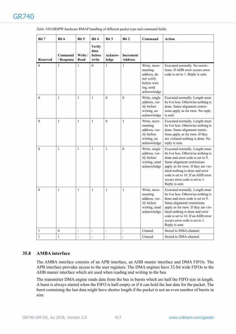
GR740
35.8 AMBA interface
The AMBA interface consists of an APB interface, an AHB master interface and DMA FIFOs. The APB interface provides access to the user registers. The DMA engines have 32-bit wide FIFOs to the AHB master interface which are used when reading and writing to the bus.
The transmitter DMA engine reads data from the bus in bursts which are half the FIFO size in length. A burst is always started when the FIFO is half-empty or if it can hold the last data for the packet. The burst containing the last data might have shorter length if the packet is not an even number of bursts in size.
0 1 1 0 1 1 Write, incre-menting address, do not verify before writ-ing, send acknowledge
Executed normally. No restric-tions. If AHB error occurs error code is set to 1. Reply is sent.
0 1 1 1 0 0 Write, single address, ver-ify before writing, no acknowledge
Executed normally. Length must be 4 or less. Otherwise nothing is done. Same alignment restric-tions apply as for rmw. No reply is sent.
0 1 1 1 0 1 Write, incre-menting address, ver-ify before writing, no acknowledge
Executed normally. Length must be 4 or less. Otherwise nothing is done. Same alignment restric-tions apply as for rmw. If they are violated nothing is done. No reply is sent.
0 1 1 1 1 0 Write, single address, ver-ify before writing, send acknowledge
Executed normally. Length must be 4 or less. Otherwise nothing is done and error code is set to 9. Same alignment restrictions apply as for rmw. If they are vio-lated nothing is done and error code is set to 10. If an AHB error occurs error code is set to 1. Reply is sent.
0 1 1 1 1 1 Write, incre-menting address, ver-ify before writing, send acknowledge
Executed normally. Length must be 4 or less. Otherwise nothing is done and error code is set to 9. Same alignment restrictions apply as for rmw. If they are vio-lated nothing is done and error code is set to 10. If an AHB error occurs error code is set to 1. Reply is sent.
1 0 - - - - Unused Stored to DMA-channel.
1 1 - - - - Unused Stored to DMA-channel.
Table 549.GRSPW hardware RMAP handling of different packet type and command fields.
Bit 7 Bit 6 Bit 5 Bit 4 Bit 3 Bit 2 Command Action
ReservedCommand / Response
Write /Read
Verify data before write
Acknow-ledge
Increment Address
GR740-UM-DS, Jul 2018, Version 2.0 417 www.cobham.com/gaisler

GR740
The receiver DMA works in the same way except that it checks if the FIFO is half-full and then per-forms a burst write to the bus which is half the fifo size in length. The last burst might be shorter. Byte accesses are used for non word-aligned buffers and/or packet lengths that are not a multiple of four bytes. There might be 1 to 3 single byte writes when writing the beginning and end of the received packets.35.8.1 APB slave interface
As mentioned above, the APB interface provides access to the user registers which are 32-bits in width. The accesses to this interface are required to be aligned word accesses. The result is undefined if this restriction is violated.
35.8.2 AHB master interface
The core contains a single master interface which is used by both the transmitter and receiver DMA engines. The arbitration algorithm between the channels is done so that if the current owner requests the interface again it will always acquire it. This will not lead to starvation problems since the DMA engines always deassert their requests between accesses.
The AHB accesses can be of size byte, halfword and word (HSIZE = 0x000, 0x001, 0x010). Byte and halfword accesses are always NONSEQ.
The burst length will be half the AHB FIFO size except for the last transfer for a packet which might be smaller. Shorter accesses are also done during descriptor reads and status writes.
The AHB master also supports non-incrementing accesses where the address will be constant for sev-eral consecutive accesses. HTRANS will always be NONSEQ in this case while for incrementing accesses it is set to SEQ after the first access. This feature is included to support non-incrementing reads and writes for RMAP.
BUSY transfer types are never requested and the core provides full support for ERROR (see also the AMBA ERROR propagation description in section 5.10.), RETRY and SPLIT responses.
35.9 Registers
The core is programmed through registers mapped into APB address space.
Table 550.GRSPW registers
APB address offset Register acronym Register name
0x00 SPW2.CTRL Control
0x04 SPW2.STS Status
0x08 SPW2.DEFADDR Node address
0x0C SPW2.CLKDIV Clock divisor
0x10 SPW2.DKEY Destination key
0x14 SPW2.TC Time
0x18 - 0x1C - RESERVED
0x20 SPW2.DMACTRL DMA control/status, channel 1
0x24 SPW2.DMAMAXLEN DMA RX maximum length, channel 1
0x28 SPW2.DMATXDESC DMA transmit descriptor table address, channel 1
0x2C SPW2.DMARXDESC DMA receive descriptor table address, channel 1
0x30 SPW2.DMAADDR DMA address, channel 1
GR740-UM-DS, Jul 2018, Version 2.0 418 www.cobham.com/gaisler

GR740
Table 551. 0x00 - SPW2.CTRL - Control31 30 29 28 27 26 25 24 23 22 21 20 19 18 17 16 15 14 13 12 11 10 9 8 7 6 5 4 3 2 1 0
RA RX RC NCH PO RESERVED RD RE RES TL TF TR TT LI TQ R RS PM TI IE AS LS LD
1 1 0 0x1 0 0x00 0 1 0x0 0 0 0 0 0 0 0 0 0 0 0 1 0 0
r r r r r r rw rw r rw rw rw rw rw rw r rw rw rw rw rw rw rw
31 RMAP available (RA) - Set to one if the RMAP target is available. Only readable.
30 RX unaligned access (RX) - Set to one if unaligned writes are available for the receiver. Only readable.
29 RMAP CRC available (RC) - Set to one if RMAP CRC is enabled in the core. Only readable.
28: 27 Number of DMA channels (NCH) - The number of available DMA channels minus one (Number of chan-nels = NCH+1).
26 Number of ports (PO) - The number of available SpaceWire ports minus one.
25: 18 RESERVED
17 RMAP buffer disable (RD) - If set only one RMAP buffer is used. This ensures that all RMAP commands will be executed consecutively.
16 RMAP Enable (RE) - Enable RMAP target.
15: 14 RESERVED
13 Transmitter enable lock control (TL) - Enables / disables the transmitter enable lock functionality described by the DMACTRL.TL bit. 0 = Disabled, 1 = Enabled.
12 Time-code control flag filter (TF) - When set to 1, a received time-code must have its control flag bits set to “00” to be considered valid. When set to 0, all control flag bits are allowed.
11 Time Rx Enable (TR) - Enable time-code receptions.
10 Time Tx Enable (TT) - Enable time-code transmissions.
9 Link error IRQ (LI) - Generate interrupt when a link error occurs.
8 Tick-out IRQ (TQ) - Generate interrupt when a valid time-code is received.
7 RESERVED
6 Reset (RS) - Make complete reset of the SpaceWire node. Self clearing.
5 Promiscuous Mode (PM) - Enable Promiscuous mode.
4 Tick In (TI) - The host can generate a tick by writing a one to this field. This will increment the timer counter and the new value is transmitted after the current character is transferred.
3 Interrupt Enable (IE) - If set, an interrupt is generated when one of bit 8 to 10 is set and its corresponding event occurs.
2 Autostart (AS) - Automatically start the link when a NULL has been received.
1 Link Start (LS) - Start the link, i.e. allow a transition from ready to started state.
0 Link Disable (LD) - Disable the SpaceWire codec.
GR740-UM-DS, Jul 2018, Version 2.0 419 www.cobham.com/gaisler

GR740
Table 552. 0x04 - SPW2.STS - Status31 30 28 27 26 25 24 23 22 21 20 19 18 17 16 15 14 13 12 11 10 9 8 7 6 5 4 3 2 1 0
R NRXD NTXD LS RESERVED EE IA RES PE DE ER CE TO
0x0 0 0 0x0 0x000 0 0 0x0 0 0 0 0 0
r r r r r wc wc r wc wc wc wc wc
31: 28 RESERVED
27: 26 Number of receive descriptors (NRXD) - Shows the size of the DMA receive descriptor table. Constant value of 0, indicating 128 descriptors.
25: 24 Number of transmit descriptors (NTXD) - Shows the size of the DMA transmit descriptor table. Constant value of 0, indicating 64 descriptors.
8 Early EOP/EEP (EE) - Set to one when a packet is received with an EOP after the first byte for a non-RMAP packet and after the second byte for an RMAP packet. Cleared when written with a one.
7 Invalid Address (IA) - Set to one when a packet is received with an invalid destination address field, i.e it does not match the nodeaddr register. Cleared when written with a one.
6: 5 RESERVED
4 Parity Error (PE) - A parity error has occurred. Cleared when written with a one.
3 Disconnect Error (DE) - A disconnection error has occurred. Cleared when written with a one.
2 Escape Error (ER) - An escape error has occurred. Cleared when written with a one.
1 Credit Error (CE) - A credit has occurred. Cleared when written with a one.
0 Tick Out (TO) - A new time count value was received and is stored in the time counter field. Cleared when writ-ten with a one.
Table 553. 0x08 - SPW2.DEFADDR - Default address31 16 15 8 7 0
RESERVED DEFMASK DEFADDR
0x0000 0x00 0xFE
r rw rw
31: 8 RESERVED
15: 8 Default mask (DEFMASK) - Default mask used for node identification on the SpaceWire network. This field is used for masking the address before comparison. Both the received address and the DEFADDR field are anded with the inverse of DEFMASK before the address check.
7: 0 Default address (DEFADDR) - Default address used for node identification on the SpaceWire network.
Table 554. 0x0C - SPW2.CLKDIV - Clock divisor31 16 15 8 7 0
RESERVED CLKDIVSTART CLKDIVRUN
0x0000 0x27 x027
r rw rw
31: 16 RESERVED
15: 8 Clock divisor startup (CLKDIVSTART) - Clock divisor value used for the clock-divider during startup (link-interface is in other states than run). The actual divisor value is Clock Divisor register + 1.
7: 0 Clock divisor run (CLKDIVRUN) - Clock divisor value used for the clock-divider when the link-interface is in the run-state. The actual divisor value is Clock Divisor register + 1.
GR740-UM-DS, Jul 2018, Version 2.0 420 www.cobham.com/gaisler
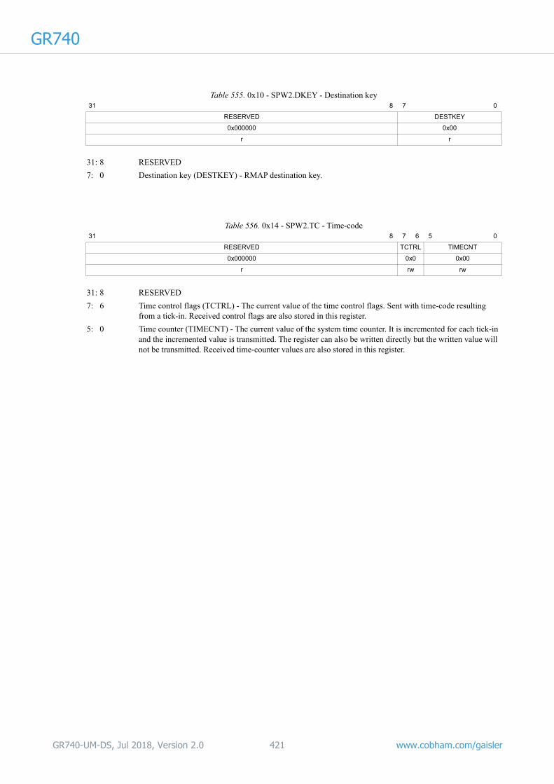
GR740
Table 555. 0x10 - SPW2.DKEY - Destination key31 8 7 0
RESERVED DESTKEY
0x000000 0x00
r r
31: 8 RESERVED
7: 0 Destination key (DESTKEY) - RMAP destination key.
Table 556. 0x14 - SPW2.TC - Time-code31 8 7 6 5 0
RESERVED TCTRL TIMECNT
0x000000 0x0 0x00
r rw rw
31: 8 RESERVED
7: 6 Time control flags (TCTRL) - The current value of the time control flags. Sent with time-code resulting from a tick-in. Received control flags are also stored in this register.
5: 0 Time counter (TIMECNT) - The current value of the system time counter. It is incremented for each tick-in and the incremented value is transmitted. The register can also be written directly but the written value will not be transmitted. Received time-counter values are also stored in this register.
GR740-UM-DS, Jul 2018, Version 2.0 421 www.cobham.com/gaisler

GR740
Table 557. 0x20 - SPW2.DMACTRL - DMA control/status, channel 131 30 29 28 27 26 25 24 23 22 21 20 19 18 17 16 15 14 13 12 11 10 9 8 7 6 5 4 3 2 1 0
RESERVED EP TR RES RP TP TL LE SP SA EN NS RD RX AT RA TA PR PS AI RI TI RE TE
0x00 0 0 0x0 0 0 0 0 0 0 0 0 0 0 0 0 0 0 0 NR NR NR 0 0
r wc wc r wc wc wc rw rw rw rw rw rw r rw wc wc wc wc rw rw rw rw rw
31: 24 RESERVED
23 EEP termination (EP) - Set to 1 when a received packet for the corresponding DMA channel ended with an Error End of Packet (EEP) character.
22 Truncated (TR) - Set to 1 when a received packet for the corresponding DMA channel is truncated due to a maximum length violation.
21: 20 RESERVED
19 Receive packet IRQ (RP) - This bit is set to 1 when an AMBA interrupt was generated due to the fact that a packet was received for the corresponding DMA channel.
18 Transmit packet IRQ (TP) - This bit is set to 1 when an AMBA interrupt was generated due to the fact that a packet was transmitted for the corresponding DMA channel.
17 Transmitter enable lock (TL) - This bit is set to 1 if the CTRL.TL bit is set, and the transmitter for the corresponding DMA channel is disabled due to a link error (controlled by the DMACTRL.LE bit). While this bit is set, it is not possible to re-enable the transmitter (e.g. not possible to set the TE bit to 1).
16 Link error disable (LE) - Disable transmitter when a link error occurs. No more packets will be trans-mitted until the transmitter is enabled again.
15 Strip pid (SP) - Remove the pid byte (second byte) of each packet. The address byte (first byte) will also be removed when this bit is set independent of the SA bit.
14 Strip addr (SA) - Remove the addr byte (first byte) of each packet.
13 Enable addr (EN) - Enable separate node address for this channel.
12 No spill (NS) - If cleared, packets will be discarded when a packet is arriving and there are no active descrip-tors. If set, the GRSPW will wait for a descriptor to be activated.
11 Rx descriptors available (RD) - Set to one, to indicate to the GRSPW that there are enabled descriptors in the descriptor table. Cleared by the GRSPW when it encounters a disabled descriptor:
10 RX active (RX) - Is set to ‘1’ if a reception to the DMA channel is currently active otherwise it is ‘0’.
9 Abort TX (AT) - Set to one to abort the currently transmitting packet and disable transmissions. If no trans-mission is active the only effect is to disable transmissions. Self clearing.
8 RX AHB error (RA) - An error response was detected on the AHB bus while this receive DMA channel was accessing the bus. The AHB error interrupt (AI) field must be set to ’1’ for the RA field to be set. See also the AMBA ERROR propagation description in section 5.10.
7 TX AHB error (TA) - An error response was detected on the AHB bus while this transmit DMA channel was accessing the bus.
6 Packet received (PR) - This bit is set each time a packet has been received. never cleared by the SW-node.
5 Packet sent (PS) - This bit is set each time a packet has been sent. Never cleared by the SW-node.
4 AHB error interrupt (AI) - If set, an interrupt will be generated each time an AHB error occurs when this DMA channel is accessing the bus.
3 Receive interrupt (RI) - If set, an interrupt will be generated each time a packet has been received. This hap-pens both if the packet is terminated by an EEP or EOP.
2 Transmit interrupt (TI) - If set, an interrupt will be generated each time a packet is transmitted. The interrupt is generated regardless of whether the transmission was successful or not.
1 Receiver enable (RE) - Set to one when packets are allowed to be received to this channel.
0 Transmitter enable (TE) - Write a one to this bit each time new descriptors are activated in the table. Writing a one will cause the SW-node to read a new descriptor and try to transmit the packet it points to. This bit is automatically cleared when the SW-node encounters a descriptor which is disabled.
GR740-UM-DS, Jul 2018, Version 2.0 422 www.cobham.com/gaisler

GR740
Table 558. 0x24 - SPW2.DMAMAXLEN - DMA RX maximum length, channel 131 25 24 2 1 0
RESERVED RXMAXLEN RES
0x00 N/R 0x0
r rw r
31: 25 RESERVED
24: 2 RX maximum length (RXMAXLEN) - Receiver packet maximum length in 32-bit words.
1: 0 RESERVED
Table 559. 0x28 - SPW2.DMATXDESC - DMA transmitter descriptor table address, channel 131 10 9 4 3 0
DESCBASEADDR DESCSEL RESERVED
N/R 0x00 0x0
rw rw r
31: 10 Descriptor table base address (DESCBASEADDR) - Sets the base address of the descriptor table
9: 4 Descriptor selector (DESCSEL) - Offset into the descriptor table. Shows which descriptor is currently used by the GRSPW. For each new descriptor read, the selector will increase with 16 and eventually wrap to zero again.
3: 0 RESERVED
Table 560. 0x2C - SPW2.DMARXDESC - DMA receiver descriptor table address, channel 131 10 9 3 2 0
DESCBASEADDR DESCSEL RESERVED
N/R 0x00 0x0
rw rw r
31: 10 Descriptor table base address (DESCBASEADDR) - Sets the base address of the descriptor table.
9: 3 Descriptor selector (DESCSEL) - Offset into the descriptor table. Shows which descriptor is currently used. For each new descriptor read, the selector will increase with 8 and eventually wrap to zero again.
2: 0 RESERVED
Table 561. 0x30 - SPW2.DMAADDR - DMA address, channel 131 16 15 8 7 0
RESERVED MASK ADDR
0x0000 N/R N/R
r rw rw
31: 8 RESERVED
15: 8 Mask (MASK) - Mask used for node identification on the SpaceWire network. This field is used for masking the address before comparison. Both the received address and the ADDR field are anded with the inverse of MASK before the address check.
7: 0 Address (ADDR) - Address used for node identification on the SpaceWire network for the corresponding dma channel when the EN bit in the DMA control register is set.
GR740-UM-DS, Jul 2018, Version 2.0 423 www.cobham.com/gaisler

GR740
36 AHB Trace buffer tracing Master I/O AHB bus36.1 Overview
The trace buffer consists of a circular buffer that stores AMBA AHB data transfers performed on the Master I/O AHB bus. The address, data and various control signals of the AHB bus are stored and can be read out, via the core’s interface attached to the Debug AHB bus, for later analysis. Note that the LEON4 Debug Support Unit (DSU4) also includes an AHB trace buffer, tracing the Processor AHB bus.
The trace buffer will, together with all other cores on the Debug AHB bus, be gated off when the Debug AHB bus is disabled via the external DSU_EN signal.
The trace buffer is 128 bits wide, the information stored is indicated in the table below:
In addition to the AHB signals, a 32-bit counter is also stored in the trace as time tag. The time tag value is taken from the debug support unit and the debug support unit timer must be enabled for this value to increment. The same timer source is also activated when at least one of the processors has the up-counter, described in section 6.10.4, enabled. If the DSU’s AHB trace buffer control register’s DF bit is set, then the timer will be stopped when the processors enter debug mode. This can be overrid-den by clearing the DF bit or by setting the TE bit in the DSU AHB trace buffer control register, see section 33.6.7.
Note that when the processors enter debug mode and stop execution, DMA traffic may still be ongo-ing on the Master I/O bus. If the DSU is configured to stop the time tag counter when the processors enter debug mode, then accesses occurring on the Master I/O bus after the processors have stopped will receive the frozen time stamp. As previously described, his can be avoided by setting the TE bit in the DSU AHB trace buffer control register, see section 33.6.7.
36.2 Operation
The 1 KiB trace buffer is enabled by setting the enable bit (EN) in the trace control register. Each AMBA AHB transfer is then stored in the buffer in a circular manner. The address to which the next transfer is written is held in the trace buffer index register, and is automatically incremented after each transfer. Tracing is stopped when the EN bit is reset, or when a AHB breakpoint is hit. An interrupt is generated when a breakpoint is hit.
Table 562.AHB Trace buffer data allocation
Bits Name Definition
127:96 Time tag The value of the time tag counter
95 AHB breakpoint hit Set to ‘1’ if a AHB breakpoint hit occurred.
94:80 Hirq AHB HIRQ[15:1]
79 Hwrite AHB HWRITE
78:77 Htrans AHB HTRANS
76:74 Hsize AHB HSIZE
73:71 Hburst AHB HBURST
70:67 Hmaster AHB HMASTER
66 Hmastlock AHB HMASTLOCK
65:64 Hresp AHB HRESP
63:32 Load/Store data AHB HRDATA or HWDATA
31:0 Load/Store address AHB HADDR
GR740-UM-DS, Jul 2018, Version 2.0 424 www.cobham.com/gaisler

GR740
36.2.1 AHB statisticsThe core will generate events that can be monitored with the LEON statistics unit (L4STAT). The sta-tistical outputs can be filtered by the AHB trace buffer filters, this is controlled by the Performance counter Filter bit (PF) in the AHB trace buffer control register. The core can collect data for the events listed in table 563 below
Table 563.AHB events
Event Description Note
idle HTRANS=IDLE Active when HTRANS IDLE is driven on the AHB slave inputs and slave has asserted HREADY.
busy HTRANS=BUSY Active when HTRANS BUSY is driven on the AHB slave inputs and slave has asserted HREADY.
nseq HTRANS=NONSEQ Active when HTRANS NONSEQ is driven on the AHB slave inputs and slave has asserted HREADY.
seq HTRANS=SEQ Active when HTRANS SEQUENTIAL is driven on the AHB slave inputs and slave has asserted HREADY.
read Read access Active when HTRANS is SEQUENTIAL or NON-SEQUENTIAL, slave has asserted HREADY and the HWRITE input is low.
write Write access Active when HTRANS is SEQUENTIAL or NON-SEQUENTIAL, slave has asserted HREADY and the HWRITE input is high.
hsize Transfer size Active when HTRANS is SEQUENTIAL or NON-SEQUENTIAL, slave has asserted HREADY.
ws Wait state Active when HREADY input to AHB slaves is low and AMBA response is OKAY.
retry RETRY response Active when master receives RETRY response
split SPLIT response Active when master receives SPLIT response
GR740-UM-DS, Jul 2018, Version 2.0 425 www.cobham.com/gaisler

GR740
36.3 Registers36.3.1 Register address map
The trace buffer occupies 128 KiB of address space in the Debug bus AHB I/O area. The following register address are decoded:
36.3.2 Trace buffer control register
The trace buffer is controlled by the trace buffer control register:
Table 564.Trace buffer address space
Address Register
0x000000 Trace buffer control register
0x000004 Trace buffer index register
0x000008 Time tag value
0x00000C Trace buffer master/slave filter register
0x000010 AHB break address 1
0x000014 AHB mask 1
0x000018 AHB break address 2
0x00001C AHB mask 2
0x010000 - 0x020000 Trace buffer
..0 Trace bits 127 - 96
...4 Trace bits 95 - 64
...8 Trace bits 63 - 32
...C Trace bits 31 - 0
Table 565.0x000000 - CTRL - Trace buffer control register31 23 22 16 15 14 12 11 9 8 7 6 5 4 3 2 1 0
RESERVED DCNT RESERVED PF BW RF AF FR FW DM EN
0 0 0 0 0b00 0 0 0 0 0 *
r rw r rw r rw rw rw rw r rw
31: 23 RESERVED
22: 16 Trace buffer delay counter (DCNT) - Specifies the number of lines that should be written in the trace buffer befiore entering debug mode after a AHB break/watchpoint has been hit.
15: 9 RESERVED
8 Performance counter Filter (PF) - If this bit is set to ‘1’, the cores performance counter (statistical) outputs will be filtered using the same filter settings as used for the trace buffer. If a filter inhibits a write to the trace buffer, setting this bit to ‘1’ will cause the same filter setting to inhibit the pulse on the statistical output, which is connected to the LEON4 statisics unit. The filter settings are con-trolled by fields AF, FT and FW (bits 4:2) below.
7: 6 Bus width (BW) - Read-only register with value "00" indicating a bus width of 32 bits.
5 Retry filter (RF) - If this bit is set to ‘1’, AHB retry responses will not be included in the trace buffer.
4 Address Filter (AF) - If this bit is set to ‘1’, only the address range defined by AHB trace buffer breakpoint 2’s address and mask will be included in the trace buffer.
3 Filter Reads (FR) - If this bit is set to ‘1’, read accesses will not be included in the trace buffer. This bit can only be set of the core has been implemented with support for filtering.
2 Filter Writes (FW) - If this bit is set to ‘1’, write accesses will not be included in the trace buffer. This bit can only be set of the core has been implemented with support for filtering.
1 Delay counter mode (DM) - Indicates that the trace buffer is in delay counter mode.
0 Trace enable (EN) - Enables the trace buffer
This field has reset value 1 if the BREAK signal is LOW and has reset value 0 otherwise.
GR740-UM-DS, Jul 2018, Version 2.0 426 www.cobham.com/gaisler

GR740
36.3.3 Trace buffer index registerThe trace buffer index register indicates the address of the next 128-bit line to be written.
Table 566.0x000004 - INDEX - Trace buffer index register31 11 10 4 3 0
RESERVED INDEX RESERVED
0 NR 0
r rw r
31: 11 RESERVED
10: 4 Trace buffer index counter (INDEX) - Indicates the address of the next 128-bit line to be written.
3: 0 RESERVED
GR740-UM-DS, Jul 2018, Version 2.0 427 www.cobham.com/gaisler

GR740
36.3.4 Trace buffer time tag registerThe time tag value displayed in this register is stored in the trace. The time tag value is taken from the debug support unit and the debug support unit timer must be enabled for this value to increment. The same timer source is also activated when at least one of the processors has the up-counter, described in section 6.10.4, enabled.
36.3.5 Trace buffer master/slave filter register
The master/slave filter register allows filtering out specified master and slaves from the trace. This register can only be assigned if the trace buffer has been implemented with support for filtering.
Table 567.0x000008 - TIMETAG - Trace buffer time tag register31 0
TIMETAG
0
t
31: 0 Time tag value (TIMETAG) - See description above table
Table 568.0x00000C - MSFILT - Trace buffer master/slave filter register31 16 15 0
SMASK[15:0] MMASK[15:0]
0 0
rw rw
31: 16 Slave Mask (SMASK) - If SMASK[n] is set to ‘1’, the trace buffer will not save accesses performed to slave n.
15: 0 Master Mask (MMASK) - If MMASK[n] is set to ‘1’, the trace buffer will not save accesses per-formed by master n.
GR740-UM-DS, Jul 2018, Version 2.0 428 www.cobham.com/gaisler

GR740
36.3.6 Trace buffer breakpoint registersThe trace buffer contains two breakpoint registers for matching AHB addresses. A breakpoint hit is used to freeze the trace buffer by clearing the enable bit. Freezing can be delayed by programming the DCNT field in the trace buffer control register to a non-zero value. In this case, the DCNT value will be decremented for each additional trace until it reaches zero and after two additional entries, the trace buffer is frozen. A mask register is associated with each breakpoint, allowing breaking on a block of addresses. Only address bits with the corresponding mask bit set to ‘1’ are compared during break-point detection. To break on AHB load or store accesses, the LD and/or ST bits should be set.
Table 569. 0x000010, 0x000018 - TBBA - Trace buffer break address registers31 2 1 0
BADDR[31:2] RES
NR 0
rw r
31: 2 Break point address (BADDR) - Bits 31:2 of breakpoint address
1 0 RESERVED
Table 570. 0x000014, 0x00001C - TBBM - Trace buffer break mask registers31 2 1 0
BMASK[31:2] LD ST
NR 0 0
rw rw rw
31: 2 Breakpoint mask (BMASK) - See description above tables.
1 Load (LD) - Break on data load address
0 Store (ST) - Break on data store address
GR740-UM-DS, Jul 2018, Version 2.0 429 www.cobham.com/gaisler

GR740
37 AMBA AHB controller with plug&play support37.1 Overview
The AMBA AHB controller is a combined AHB arbiter, bus multiplexer and slave decoder according to the AMBA 2.0 standard. Each AHB bus in the system has one AHB controller.
Figure 51. AHB controller block diagram
37.2 Operation
37.2.1 Arbitration
The AHB controller supports round-robin arbitration. In round-robin mode, priority is rotated one step after each AHB transfer. If no master requests the bus, the last owner will be granted (bus park-ing).
37.2.2 Decoding
Decoding (generation of HSEL) of AHB slaves is done using the plug&play method explained in the GRLIB User’s Manual. A slave can occupy any binary aligned address space with a size of 1 - 4096 MiB. A specific I/O area is also decoded, where slaves can occupy 256 byte - 1 MiB. Access to unused addresses will cause an AHB error response. See the AMBA ERROR propagation description in section 5.10.
37.2.3 Plug&play information
The plug&play information is mapped on a read-only address area on each AHB bus except the Mas-ter I/O AHB bus. See the memory map in section 2.3 for the Plug&play area base addresses of the buses in the system.
The master information is placed on the first 2 KiB of the block (0xFFFFF000 - 0xFFFFF800 for the Processor AHB bus), while the slave information is placed on the second 2 KiB block. Each unit occupies 32 bytes, which means that the area has place for 64 masters and 64 slaves. The address of the plug&play information for a certain unit is defined by its bus index. The address for masters is thus 0xFFFFF000 + n*32, and 0xFFFFF800 + n*32 for slaves.
MASTER MASTER
SLAVESLAVE
ARBITER/DECODER
AHBCTRL
GR740-UM-DS, Jul 2018, Version 2.0 430 www.cobham.com/gaisler

GR740
Figure 52. AHB plug&play information record
VENDOR ID DEVICE ID VERSION IRQ
31 24 23 12 11 5 4 0
31 20 19 16 15 4 3 0
Identification Register 00
10 9
HADDR P MASK TYPEC0 0ADDR P MASK TYPEC0 0
ADDR P MASK TYPEC0 0
ADDR P MASK TYPEC0 0
ADDR P MASK TYPEC0 0
Bank Address Registers
USER-DEFINED
USER-DEFINED
USER-DEFINED
00
04
08
10
14
18
1C
0C
18 17
BAR0
BAR1
BAR2
BAR3
C = Cacheable
P = PrefetchableTYPE
0010 = AHB Memory space
0011 = AHB I/O space
0001 = APB I/O space
GR740-UM-DS, Jul 2018, Version 2.0 431 www.cobham.com/gaisler

GR740-UM-DS, Jul 2018, Version 2.0 432 www.cobham.com/gaisler
GR74038 AMBA AHB/APB bridge with plug&play support
38.1 Overview
The AMBA AHB/APB bridge is a APB bus master according the AMBA 2.0 standard. The system contains three AHB/APB bridges. Two on the Slave I/O AHB bus and one on the Debug AHB bus.
Figure 53. AHB/APB bridge block diagram
38.2 Operation
38.2.1 Decoding
Decoding (generation of PSEL) of APB slaves is done using the plug&play method explained in the GRLIB IP Library User’s Manual. A slave can occupy any binary aligned address space with a size of 256 bytes - 1 MiB. Writes to unassigned areas will be ignored, while reads from unassigned areas will return an arbitrary value. AHB error responses will never be generated.
38.2.2 Plug&play information
The plug&play information is mapped on a read-only address area at the top 4 KiB of each bridge’s address space. Each plug&play block occupies 8 bytes. The address of the plug&play information for a certain unit is defined by its bus index. If the bridge is mapped on AHB address 0xF0000000, the address for the plug&play records is thus 0xF00FF000 + n*8.
Figure 54. APB plug&play information
APB SLAVE
APB SLAVEAHB Slave
AHB/APB Bridge
Interface
•••
AHB BUS
APBI
APBO[0]
APBO[n]
AHBSI
AHBSO[n]
VENDOR ID DEVICE ID VERSION IRQ
31 24 23 12 11 45 0
ADDR C/P MASK TYPE
31 20 19 16 15 4 3 0
BAR
Configuration wordAPB Plug&play record0x00
0x04
10 9
00

GR740
39 Electrical description39.1 Absolute maximum ratings
Exceeding absolute maximum rating conditions might cause instantaneous or very short-term unre-coverable hard failure (destructive breakdown). Stress from operating near absolute maximum levels will affect long-term reliability of the device.
39.2 Recommended DC operating conditions
Table 572.Recommended DC operating conditions
1) For SDRAM address/control/data and PCI data/control lines, VIH OVERSHOOT = 300 mV and VIL UNDER-
SHOOT = -300 mV with a maximum duration of 3 ns beyond the recommended limits can be tolerated per transi-tion. Alternatively, if DC levels (signals and supplies) are limited to 3.4V then VIH OVERSHOOT = 500 mV and VIL UNDERSHOOT = -500 mV with a maximum duration of 3 ns can be tolerated.
Table 571.Absolute maximum DC ratings
Parameter Abs Max Unit
VDD12 relative to GND 1.8 V
VDDPLLA relative to VSSPLLA 1.8 V
VDDPLLD relative to VSSPLLD 1.8 V
VDIG25 relative to VSS25 4.5 V
VDIG33 relative to VSS33 4.5 V
LVCMOS signals relative to VSS33 4.5 V
LVDS signals relative to VSS25 4.5 V
Parameter Symbol Conditions Minimum Typical Maximum Unit
Temperature Tj -40 25 125 °C
Digital core supply voltage
VDD12 1.100 1.200 1.300 V
I/O bank supply VDIG25 2.300 2.500 2.700 V
VDIG33 3.000 3.300 3.600 V
Analog PLL supply VDDPLLA 1.100 1.200 1.300 V
Digital PLL supply VDDPLLD 1.100 1.200 1.300 V
HIGH (logic 1) level input switching voltage
(LVCMOS) 1)
VIH 2.0 3.3 3.6 V
LOW (logic 0) level input switching voltage
(LVCMOS) 1)
VIL 0.0 0.0 0.7 V
LVDS input common mode voltage
VICM,LVDS 0.8 1.2 1.6 V
LVDS input differen-tial
VIDIFF,LVDS 0.100 0.200 0.400 V
LVDS output termina-tion
RO,LVDS 80 100 120 Ohm
GR740-UM-DS, Jul 2018, Version 2.0 433 www.cobham.com/gaisler
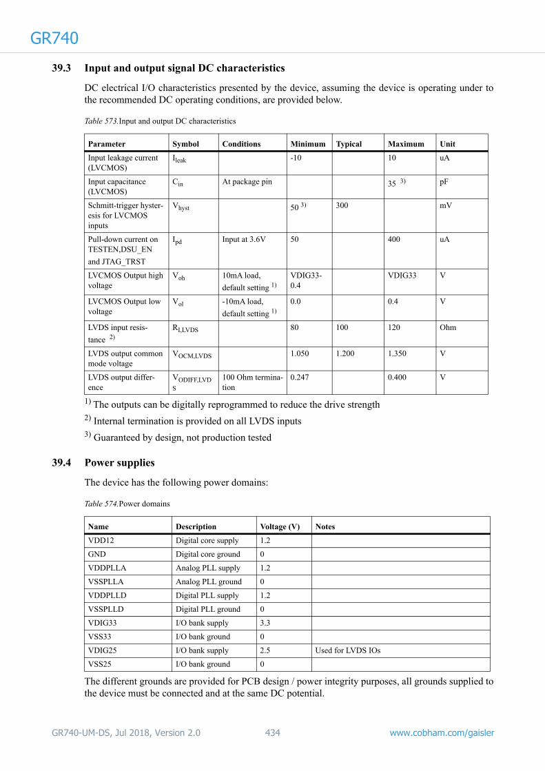
GR740
39.3 Input and output signal DC characteristicsDC electrical I/O characteristics presented by the device, assuming the device is operating under to the recommended DC operating conditions, are provided below.
1) The outputs can be digitally reprogrammed to reduce the drive strength2) Internal termination is provided on all LVDS inputs3) Guaranteed by design, not production tested
39.4 Power supplies
The device has the following power domains:
The different grounds are provided for PCB design / power integrity purposes, all grounds supplied to the device must be connected and at the same DC potential.
Table 573.Input and output DC characteristics
Parameter Symbol Conditions Minimum Typical Maximum Unit
Input leakage current (LVCMOS)
Ileak -10 10 uA
Input capacitance (LVCMOS)
Cin At package pin 35 3) pF
Schmitt-trigger hyster-esis for LVCMOS inputs
Vhyst 50 3) 300 mV
Pull-down current on TESTEN,DSU_EN
and JTAG_TRST
Ipd Input at 3.6V 50 400 uA
LVCMOS Output high voltage
Voh 10mA load,
default setting 1)VDIG33-0.4
VDIG33 V
LVCMOS Output low voltage
Vol -10mA load,
default setting 1)0.0 0.4 V
LVDS input resis-
tance 2)RI,LVDS 80 100 120 Ohm
LVDS output common mode voltage
VOCM,LVDS 1.050 1.200 1.350 V
LVDS output differ-ence
VODIFF,LVDS
100 Ohm termina-tion
0.247 0.400 V
Table 574.Power domains
Name Description Voltage (V) Notes
VDD12 Digital core supply 1.2
GND Digital core ground 0
VDDPLLA Analog PLL supply 1.2
VSSPLLA Analog PLL ground 0
VDDPLLD Digital PLL supply 1.2
VSSPLLD Digital PLL ground 0
VDIG33 I/O bank supply 3.3
VSS33 I/O bank ground 0
VDIG25 I/O bank supply 2.5 Used for LVDS IOs
VSS25 I/O bank ground 0
GR740-UM-DS, Jul 2018, Version 2.0 434 www.cobham.com/gaisler

GR740
39.4.1 Power sequenceThis section is provided as a design guideline.
The recommended power sequence when powering up the device is as below. Between each step there can be an arbitrary amount of delay.
1. The sys_resetn signal must be controlled to a low logic level, and remain at logic low through the sequence up to step 7. Other signals should be within recommended operating conditions.
2. Raise the two I/O voltage rails VIO3V3 and VIO2V5, in arbitrary order, up to nominal voltage
3. Static configuration signals, such as pll_bypass should be controlled to their intended levels at this point.
4. Raise the core and PLL digital supplies VDD12 and VDDPLLD up to their nominal voltage.
5. If necessary, wait until input clocks to the system (SYS_CLK, MEM_EXTCLK, SPW_CLK) are stable. (unused clock inputs should be at constant low or constant high level)
6. Raise the PLL analog supply VDDPLLA up to its nominal voltage
7. Wait for a minimum time of tPLL0 and then raise the sys_resetn input signal
39.4.2 Power-down sequence
This section is provided as a design guideline.
One of the below two means of power-down are recommended:
Natural power-down - stopping the supply of current to all power rails on board level simultaneously and then letting the capacitances of the supply rails discharge at their natural rate. The I/Os should remain within the recommended operating conditions (in other words decrease as the I/O supply falls)
Sequenced power-down - Dropping the voltages one by one in reverse order of the power-up sequence.
GR740-UM-DS, Jul 2018, Version 2.0 435 www.cobham.com/gaisler

GR740
39.4.3 Cold sparing supportWhile all supply rails to the device are powered down, normal I/O level voltages may be present on the device I/O pins without causing any inrush current into the device. The device will draw some minor leakage current (limited by Ileak). Before starting the power-up sequence described above on a device that has been acting as cold spare, all (to become) outputs should have returned to an undriven state.
1) Internal termination is provided on all LVDS inputs also when powered down.
39.5 AC characteristics
39.5.1 Test conditions
For the SDRAM, Ethernet and PCI interfaces, timing is tested using a impedance matched transmis-sion line setup. The propagation delays in the test fixture is calibrated out as part of the test procedure.
The interfaces are tested with the pad drive strength set to maximum (the default, power-up setting) unless noted otherwise. Interface timing measurement (setup, hold, and clock-to-out) are done with reference to inputs or outputs entering or leaving the limits in table 576.
It is up to the end user to translate the timing data to data relevant for the system. An IBIS model of the drivers can be provided to aid in this process.
Table 575.Recommended DC operating conditions and characteristics for device acting as cold spare
Parameter Symbol Conditions Minimum Typical Maximum Unit
Supply voltage VDD12, VDIG25, VDIG33, VDDPLLA, VDDPLLD
0.000 0.000 V
I/O level, LVCMOS -0.300 3.600 V
I/O level, LVDS pins 0.000 2.000 V
I/O leakage current (LVCMOS) in cold-spare
Ileak,LVC-MOS,cs
-0.010 0.010 mA
I/O leakage current (LVDS) in cold-spare
Ileak,LVDS,cs Not counting cur-rent on inputs due to RI,LVDS
0 15 mA
LVDS input resis-
tance 1)RI,LVDS 80 100 120 Ohm
GR740-UM-DS, Jul 2018, Version 2.0 436 www.cobham.com/gaisler

GR740
Table 576.Output thresholds for AC parameter tests
Parameter Symbol Value Unit
High output threshold for AC parameter tests
VOH,ACtest VDIG33-0.4 V
Low output threshold
for AC parameter tests
VOL,ACtest 0.4 V
Figure 55. Test setup for LVCMOS outputs (1), LVCMOS inputs (2), LVDS outputs (3) and LVDS inputs (4)
DUT pin (driving) ATE
Z0=50 ohm +/- 20%100-300 mm
10-20 pF
+
-
DUT pin (receiving) ATE
Z0=50 ohm +/- 20%100-300 mm
50R
DUT diff pins (driving) ATE
Z0_diff=100 ohm +/- 20%100-300 mm
+
-
100R
DUT diff pins (receiving) ATE
Z0_diff=100 ohm +/- 20%100-300 mm
50R
50R
Figure 56. Clock-to-out definition for SDRAM, PCI and Ethernet timings
tcto(min)
outputs
clock input
tcto(max)
(falling)
VOH,ACtest
VOL,ACtest
tcto(min)
outputs
clock input
tcto(max)
(rising)
VOH,ACtest
VOL,ACtest
GR740-UM-DS, Jul 2018, Version 2.0 437 www.cobham.com/gaisler

GR740
39.5.2 ClocksTable 577 summarizes required/recommended conditions for some of the design input clocks that connect to on-chip PLLs. For the remaining clocks please see the interface-specific timing in the sub-sections below
GR740-UM-DS, Jul 2018, Version 2.0 438 www.cobham.com/gaisler

GR740
.Table 577.Recommended AC operating conditions
Parameter Symbol Minimum Nominal Maximum Unit Note(s)
Externally fed PLL input clocks, PLLs enabled (in default configuration)
SYS_CLK frequency fsys_clk 20 50 70 MHz 1
SYS_CLK duty cycle 40 50 60 % 6
SPW_CLK frequency fspw_clk 20 50 55 MHz 1
SPW_CLK duty cycle 40 50 60 % 6
MEM_EXTCLK frequency fmem_extclk 20 50 55 MHz 1, 2
MEM_EXTCLK duty cycle 40 50 60 % 6
Externally fed PLL input clocks, PLLs bypassed
SYS_CLK frequency fsys_clk_bypass 0 50 100 MHz 1
SYS_CLK duty cycle 20 50 80 % 6
SPW_CLK frequency fspw_clk_bypass 0 50 100 MHz 1
SPW_CLK duty cycle 40 50 60 % 6
MEM_EXTCLK frequency fmem_extclk_bypass 0 100 100 MHz 1, 2
MEM_EXTCLK duty cycle 20 50 80 % 6
External fed clocks, non-PLL
MEM_CLK_IN frequency 0 100 100
MEM_CLK_IN duty cycle 20 50 80 % 6
PCI_CLK frequency fpci_clk 33 33 33 MHz 3
PCI_CLK duty cycle 20 50 80 % 6
ETH*_GTXCLK frequency feth_gtxclk 125 125 125 MHz
ETH*_GTXCLK duty cycle 40 50 60 % 6
ETH*_TXCLK frequency feth_txclk 25 25 25 MHz
ETH*_TXCLK duty cycle 20 50 80 % 6
ETH*_RXCLK frequency feth_rxclk 25 25 or 125 125 MHz
ETH*_RXCLK duty cycle 40 50 60 % 6
GR1553_CLK frequency fgr1553_clk 19.999 20 20.001 MHz
GR1553_CLK duty cycle 20 50 80 % 6
GR1553_CLK jitter 5 ns 6, 7
Internally generated clocks
AMBA system clock frequency fsoc_system 40 250 250 MHz 4, 5
Internal SPW clock frequency 10 400 400 MHz
1 Min/max values are maximum for on-chip PLL input, limits for the generated frequencies must also be satisfied. Nominal frequency required for correct operation with PLL power-up configuration and will change if reconfigured.2 Assuming MEM_CLKSEL has been set high so that MEM_EXTCLK is used3 The PCI interface will not be fully compliant to the PCI specification. Interface will be characterised at a later date.4 The minimum clock frequency for the on-chip system is determined by functional interface limitations and has not been fully characterised. A clock frequency over 40 MHz is required for the Ethernet interfaces to function at gigabit speeds.5 The maximum given here is from static timing analysis, and it is also used as clock rate during production tests.6 Supplied as design parameter, not tested7 Limit on rising edge only
GR740-UM-DS, Jul 2018, Version 2.0 439 www.cobham.com/gaisler

GR740
39.5.3 Phase-locked loop timingsThe timing waveforms and timing parameters are shown in figure 57 and are defined in table 578.
39.5.4 Processor error mode signal timing
The timing waveforms and timing parameters are shown in figure 58 and are defined in table 579.
Table 578.Timing parameters
Name Parameter Reference edge Min Max Unit
tPLL0 PLL power-down duration 1) - 10000 2) - ns
tPLL1 PLL locking time rising sys_resetn - 100000 ns
Notes:
1) PLL is in power-down as long as sys_resetn is held low. Unused PLLs for selected configuration are permanently in power-down and their corresponding lock signals never go high.
2) This parameter is not tested.
Table 579.Timing parameters
Name Parameter Reference edge Min Max Unit
tLEON4_0 clock to output tri-state delay rising clk edge 0 1) 30 2) ns
Notes:
1) This parameter is guaranteed by design and is not tested
2) This parameter is determined by static timing analysis and is not tested
Figure 57. Timing waveforms
pll_locked[5:0]
sys_resetn
tPLL0
tPLL1
Figure 58. Timing waveforms
tLEON4_0proc_errorn
internal clk
tLEON4_0
GR740-UM-DS, Jul 2018, Version 2.0 440 www.cobham.com/gaisler

GR740
39.5.5 64-bit PC100 SDRAM Controller with Reeed-Solomon EDAC timingThe timing waveforms and timing parameters are shown in figure 59 and are defined in table 580.
Table 580.Timing parameters - SDRAM accesses
Name Parameter Reference edge Min Max Unit
tSDRAM0 clock to output delay rising mem_clk_in edge
3.12 13.3 ns
tSDRAM1 clock to data output delay rising mem_clk_in edge
3.12 13.3 ns
tSDRAM2 data clock to data tri-state delay rising mem_clk_in edge
0 1) 30.0 2) ns
tSDRAM3 data input to clock setup rising mem_clk_in edge
2.76 - ns
tSDRAM4 data input from clock hold rising mem_clk_in edge
2.1 - ns
Notes:
1) This parameter is guaranteed by design and is not tested
2) This parameter is determined by characterization and is not tested
Figure 59. Timing waveforms - SDRAM accesses
mem_casn, mem_rasn
mem_clk_in
mem_wen, mem_sn[]mem_dqm[]
write nop read nop nop term nop nop nop
mem_addr[]
mem_dq[]
tSDRAM3
tSDRAM0
tSDRAM0
tSDRAM2 tSDRAM1
tSDRAM4
GR740-UM-DS, Jul 2018, Version 2.0 441 www.cobham.com/gaisler

GR740
39.5.6 DSU signals timingThe timing waveforms and timing parameters are shown in figure 60 and are defined in table 581.
39.5.7 JTAG interface timing
The timing waveforms and timing parameters are shown in figure 61 and are defined in table 582.
Table 581.Timing parameters
Name Parameter Reference edge Min Max Unit
tDSU0 clock to output delay rising clk edge 0 1) 30 2) ns
tDSU1 input to clock hold rising clk edge - 3) - 3) ns
tDSU2 input to clock setup rising clk edge - 3) - 3) ns
Notes:
1) This parameter is guaranteed by design and is not tested
2) This parameter is determined by static timing analysis and is not tested
3) The break and dsu_en signals are re-synchronized internally. These signals do not have to meet any setup or hold requirements. As the dsu_en signal controls clock gating for the Debug AHB bus the signal’s value should be kept con-stant from power-up.
Table 582.Timing parameters
Name Parameter Reference edge Min Max Unit
tAHBJTAG0 clock period - 45 - ns
tAHBJTAG1 clock low/high period - 20 - ns
tAHBJTAG2 data input to clock setup rising jtag_tck edge 20 - ns
tAHBJTAG3 data input from clock hold rising jtag_tck edge 20 - ns
tAHBJTAG4 clock to data output delay falling jtag_tck edge 0 15 ns
Figure 60. Timing waveforms
tDSU0dsu_active
internal clk
tDSU0
tDSU1dsu_en, break tDSU2
Figure 61. Timing waveforms
jtag_tdi, jtag_tms
jtag_tck
jtag_tdo
tAHBJTAG3tAHBJTAG4
tAHBJTAG2
tAHBJTAG0 tAHBJTAG1
GR740-UM-DS, Jul 2018, Version 2.0 442 www.cobham.com/gaisler
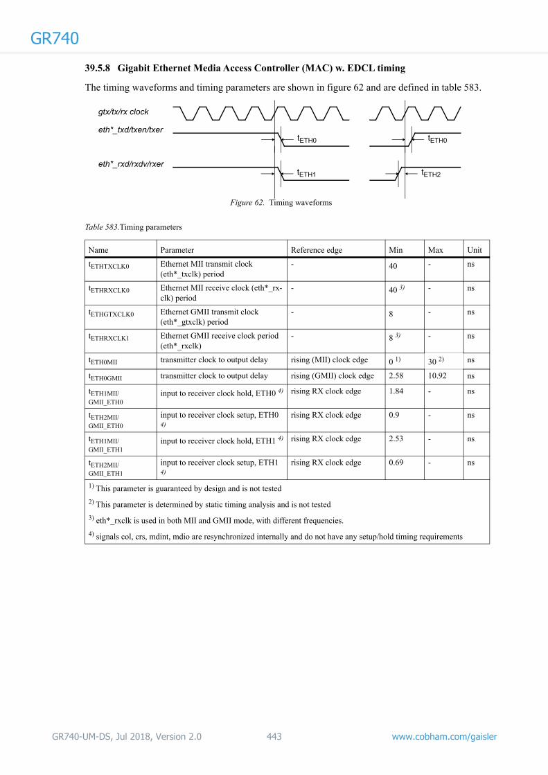
GR740
39.5.8 Gigabit Ethernet Media Access Controller (MAC) w. EDCL timingThe timing waveforms and timing parameters are shown in figure 62 and are defined in table 583.
Table 583.Timing parameters
Name Parameter Reference edge Min Max Unit
tETHTXCLK0 Ethernet MII transmit clock (eth*_txclk) period
- 40 - ns
tETHRXCLK0 Ethernet MII receive clock (eth*_rx-clk) period
- 40 3) - ns
tETHGTXCLK0 Ethernet GMII transmit clock (eth*_gtxclk) period
- 8 - ns
tETHRXCLK1 Ethernet GMII receive clock period (eth*_rxclk)
- 8 3) - ns
tETH0MII transmitter clock to output delay rising (MII) clock edge 0 1) 30 2) ns
tETH0GMII transmitter clock to output delay rising (GMII) clock edge 2.58 10.92 ns
tETH1MII/GMII_ETH0
input to receiver clock hold, ETH0 4) rising RX clock edge 1.84 - ns
tETH2MII/GMII_ETH0
input to receiver clock setup, ETH0 4)
rising RX clock edge 0.9 - ns
tETH1MII/GMII_ETH1
input to receiver clock hold, ETH1 4) rising RX clock edge 2.53 - ns
tETH2MII/GMII_ETH1
input to receiver clock setup, ETH1 4)
rising RX clock edge 0.69 - ns
1) This parameter is guaranteed by design and is not tested
2) This parameter is determined by static timing analysis and is not tested
3) eth*_rxclk is used in both MII and GMII mode, with different frequencies.
4) signals col, crs, mdint, mdio are resynchronized internally and do not have any setup/hold timing requirements
Figure 62. Timing waveforms
tETH0
eth*_txd/txen/txer
gtx/tx/rx clock
tETH0
tETH1 tETH2
eth*_rxd/rxdv/rxer
GR740-UM-DS, Jul 2018, Version 2.0 443 www.cobham.com/gaisler

GR740
39.5.9 Ethernet MDIO timingThe Ethernet MDIO interface is generated synchronously in the system clock domain. The generated MDC clock frequency is set using a scaler register in the IP core.
Table 584.Timing parameters
Name Parameter Reference edge Min Max Unit
tMDIO0 MDIO clock-to-output delay rising clk edge where mdc rises
4 4 Tclk
tMDIO1 MDIO input sampling point rising clk edge where mdc falls
1 1 Tclk
Figure 63. Timing waveforms
eth0_mdio (out)
internal clk
eth0_mdio (in)
tMDIO0
eth0_mdc
tMDIO1
GR740-UM-DS, Jul 2018, Version 2.0 444 www.cobham.com/gaisler

GR740
39.5.10 SpaceWire router interface timingThe specifies the timing for the Spacewire router links that are interfaced via LVDS signals. The tim-ing waveforms are shown in figure 64. Timing parameters are defined in table 585.
Table 585.Timing parameters
Name Parameter Reference edge Min Max Unit
tSPW0 transmit clock period - see Table 577
tSPW1 clock to output delay - - - not applicable
tSPW2 input to clock hold - - - not applicable
tSPW3 input to clock setup - - - not applicable
tSPW4 output data bit period - 2.5 2) - ns
tSPW5 input data bit period - 2.5 2) - ns
tSPW6 data & strobe input edge separa-tion
- 2.0 2) 3) - ns
tSPW7 data & strobe output skew - -0.4 0.4 3) ns
1) Internal SpaceWire clock generated from PLL or from spw_clkin.
2) Assuming SpaceWire PLL used in nominal configuration
3) Edge separation and skew limits refer to each pair of data/strobe signals separately. Global skew and separation over the entire set of eight pairs is not specified.
Figure 64. Timing waveforms
tSPW1spw_txd, spw_txdn
internal spw_clk
tSPW1
tSPW2spw_rxd, spw_rxdn tSPW3
spw_txs, spw_txsn
spw_rxs, spw_rxsn
tSPW0
spw_txd, spw_txdn
spw_txs, spw_txsn
tSPW4
tSPW4
tSPW4
spw_rxd, spw_rxdn
spw_rxs, spw_rxsn
tSPW5
tSPW5
tSPW5
spw_txd, spw_txdn
spw_txs, spw_txsn
tSPW7
tSPW6
tSPW6
GR740-UM-DS, Jul 2018, Version 2.0 445 www.cobham.com/gaisler

GR740
39.5.11 SpaceWire debug interface timingThis specifies the timing for the SpaceWire debug interface that shares pins with the slow interfaces. The timing waveforms are shown in figure 64. Timing parameters are defined in table 585.
Table 586.Timing parameters
Name Parameter Reference edge Min Max Unit
tSPW0 transmit clock period - see Table 577
tSPWD1 clock to output delay - - - not applicable
tSPWD2 input to clock hold - - - not applicable
tSPWD3 input to clock setup - - - not applicable
tSPWD4 output data bit period - 20 - ns
tSPWD5 input data bit period - 20 - ns
tSPWD6 data & strobe edge separation - 10 1) 2) - ns
tSPWD7 data & strobe output skew - -5 5 2) ns
1) Assuming SpaceWire PLL used in nominal configuration
2) Verified by static timing analysis only, not tested
Figure 65. Timing waveforms
tSPWD1spwd_txd
internal spw_clk
tSPWD1
tSPWD2spwd_rxd tSPWD3
spwd_txs
spwd_rxs
tSPW0
spwd_txd
spwd_txs
tSPWD4
tSPW4
tSPWD4
spwd_rxd
spwd_rxs
tSPWD5
tSPWD5
tSPWD5
spwd_txd
spwd_txs
tSPWD7
tSPWD6
tSPWD6
GR740-UM-DS, Jul 2018, Version 2.0 446 www.cobham.com/gaisler

GR740
39.5.12 PCI interface timingThe timing waveforms and timing parameters are shown in figure 66 and are defined in table 587.
Table 587.Timing parameters
Name Parameter Reference edge Min Max Unit
tPCICLK0 PCI clock period - 15, 30 - ns
tPCI0 clock to output delay rising pci_clk edge 3.05 12.78 ns
tPCI1 input to clock hold rising pci_clk edge 1.03 - ns
tPCI2 input to clock setup rising pci_clk edge 6.44 - ns
tPCI3 clock to output delay rising pci_clk edge 3.05 17.91 ns
tPCI4 input to clock hold rising pci_clk edge 1.03 - ns
tPCI5 input to clock setup rising pci_clk edge 6.44 - ns
Figure 66. Timing waveforms
tPCI0
pci_ad[ ], pci_cbe[ ],
pci_clk
tPCI0
tPCI1 tPCI2
tPCI3
pci_gnt, pci_reqtPCI3
tPCI4
pci_gnt, pci_reqtPCI5
pci_frame, pci_irdy,pci_trdy, pci_stop,pci_idsel, pci_devsel,pci_perr, pci_serr,pci_par, pci_int
pci_ad[ ], pci_cbe[ ],pci_frame, pci_irdy,pci_trdy, pci_stop,pci_idsel, pci_devsel,pci_perr, pci_serr,pci_par
GR740-UM-DS, Jul 2018, Version 2.0 447 www.cobham.com/gaisler
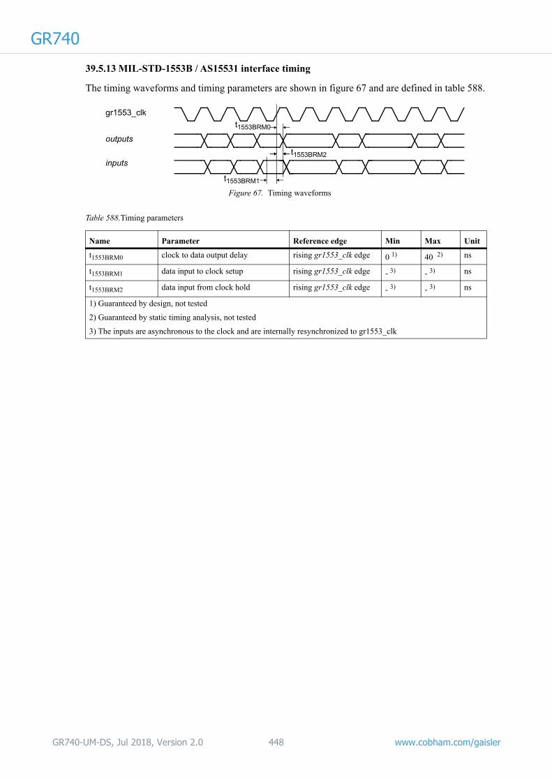
GR740
39.5.13 MIL-STD-1553B / AS15531 interface timingThe timing waveforms and timing parameters are shown in figure 67 and are defined in table 588.
Table 588.Timing parameters
Name Parameter Reference edge Min Max Unit
t1553BRM0 clock to data output delay rising gr1553_clk edge 0 1) 40 2) ns
t1553BRM1 data input to clock setup rising gr1553_clk edge - 3) - 3) ns
t1553BRM2 data input from clock hold rising gr1553_clk edge - 3) - 3) ns
1) Guaranteed by design, not tested
2) Guaranteed by static timing analysis, not tested
3) The inputs are asynchronous to the clock and are internally resynchronized to gr1553_clk
Figure 67. Timing waveforms
t1553BRM0
outputs
gr1553_clk
inputst1553BRM2
t1553BRM1
GR740-UM-DS, Jul 2018, Version 2.0 448 www.cobham.com/gaisler

GR740
39.5.14 Fault-tolerant 8/16-bit PROM/IO memory interface timingThe timing waveforms and timing parameters are shown in figures 68 and 69, and are defined in table 589.
Figure 68. Timing waveforms - PROM accesses
tFTMCTRL0
promio_addr[]
internal sys_clk
tFTMCTRL1
promio_data[](output)
promio_data[](input)
prom_cen[]
tFTMCTRL3, tFTMCTRL4
promio_oen
promio_wen
tFTMCTRL9
promio_brdyn
tFTMCTRL10
tFTMCTRL2 tFTMCTRL2
tFTMCTRL6 tFTMCTRL6
promio_addr[]
internal sys_clk
prom_cen[]
tFTMCTRL7 tFTMCTRL8
tFTMCTRL5
tFTMCTRL1
GR740-UM-DS, Jul 2018, Version 2.0 449 www.cobham.com/gaisler

GR740
Table 589.Timing parameters - PROM and I/O accesses
Name Parameter Reference edge Min Max Unit
tFTMCTRL0 address clock to output delay rising clk edge 1) 0 2) 40 3) ns
tFTMCTRL1 clock to output delay rising clk edge 1) 0 2) 40 3) ns
tFTMCTRL2 clock to output delay rising clk edge 1) 0 2) 40 3) ns
tFTMCTRL3 clock to data output delay rising clk edge 1) 0 2) 40 3) ns
tFTMCTRL4 clock to data non-tri-state delay rising clk edge 1) 0 2) 40 3) ns
tFTMCTRL5 clock to data tri-state delay rising clk edge 1) 0 2) 40 3) ns
tFTMCTRL6 clock to output delay rising clk edge 1) 0 2) 40 3) ns
tFTMCTRL7 data input to clock setup rising clk edge 1) 0 2) - ns
tFTMCTRL8 data input from clock hold rising clk edge 1) - - ns
tFTMCTRL9 input to clock setup rising clk edge 1) 0 2) - ns
tFTMCTRL10 input from clock hold rising clk edge 1) - - ns
1) Timing values are relative to the internal clock for the PROM/IO memory controller.
2) Guaranteed by design, not tested
3) Verified by static timing analysis, not tested
Figure 69. Timing waveforms - I/O accesses
tFTMCTRL0
promio_addr]
internal sys_clk
tFTMCTRL1
promio_data[](output)
promio_data[](input)
io_sn[]
tFTMCTRL3, tFTMCTRL4
promio_oen
promio_wen
tFTMCTRL9
promio_brdyn
tFTMCTRL10
tFTMCTRL2 tFTMCTRL2
tFTMCTRL6 tFTMCTRL6
promio_addr[]
internal sys_clk
io_sn[]
tFTMCTRL7 tFTMCTRL8
tFTMCTRL5
tFTMCTRL1
GR740-UM-DS, Jul 2018, Version 2.0 450 www.cobham.com/gaisler
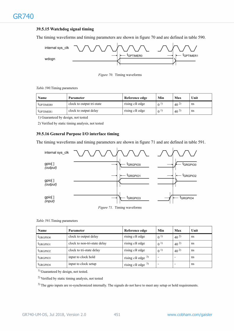
GR740
39.5.15 Watchdog signal timingThe timing waveforms and timing parameters are shown in figure 70 and are defined in table 590.
39.5.16 General Purpose I/O interface timing
The timing waveforms and timing parameters are shown in figure 71 and are defined in table 591.
Table 590.Timing parameters
Name Parameter Reference edge Min Max Unit
tGPTIMER0 clock to output tri-state rising clk edge 0 1) 40 2) ns
tGPTIMER1 clock to output delay rising clk edge 0 1) 40 2) ns
1) Guaranteed by design, not tested
2) Verified by static timing analysis, not tested
Table 591.Timing parameters
Name Parameter Reference edge Min Max Unit
tGRGPIO0 clock to output delay rising clk edge 0 1) 40 2) ns
tGRGPIO1 clock to non-tri-state delay rising clk edge 0 1) 40 2) ns
tGRGPIO2 clock to tri-state delay rising clk edge 0 1) 40 2) ns
tGRGPIO3 input to clock hold rising clk edge 3) - - ns
tGRGPIO4 input to clock setup rising clk edge 3) - - ns
1) Guaranteed by design, not tested.
2) Verified by static timing analysis, not tested
3) The gpio inputs are re-synchronized internally. The signals do not have to meet any setup or hold requirements.
Figure 70. Timing waveforms
tGPTIMER0wdogn
internal sys_clk
tGPTIMER1
Figure 71. Timing waveforms
tGRGPIO0gpio[ ]
internal sys_clk
tGRGPIO0
tGRGPIO1
gpio[ ]
tGRGPIO2
tGRGPIO3gpio[ ] tGRGPIO4
(output)
(output)
(input)
GR740-UM-DS, Jul 2018, Version 2.0 451 www.cobham.com/gaisler
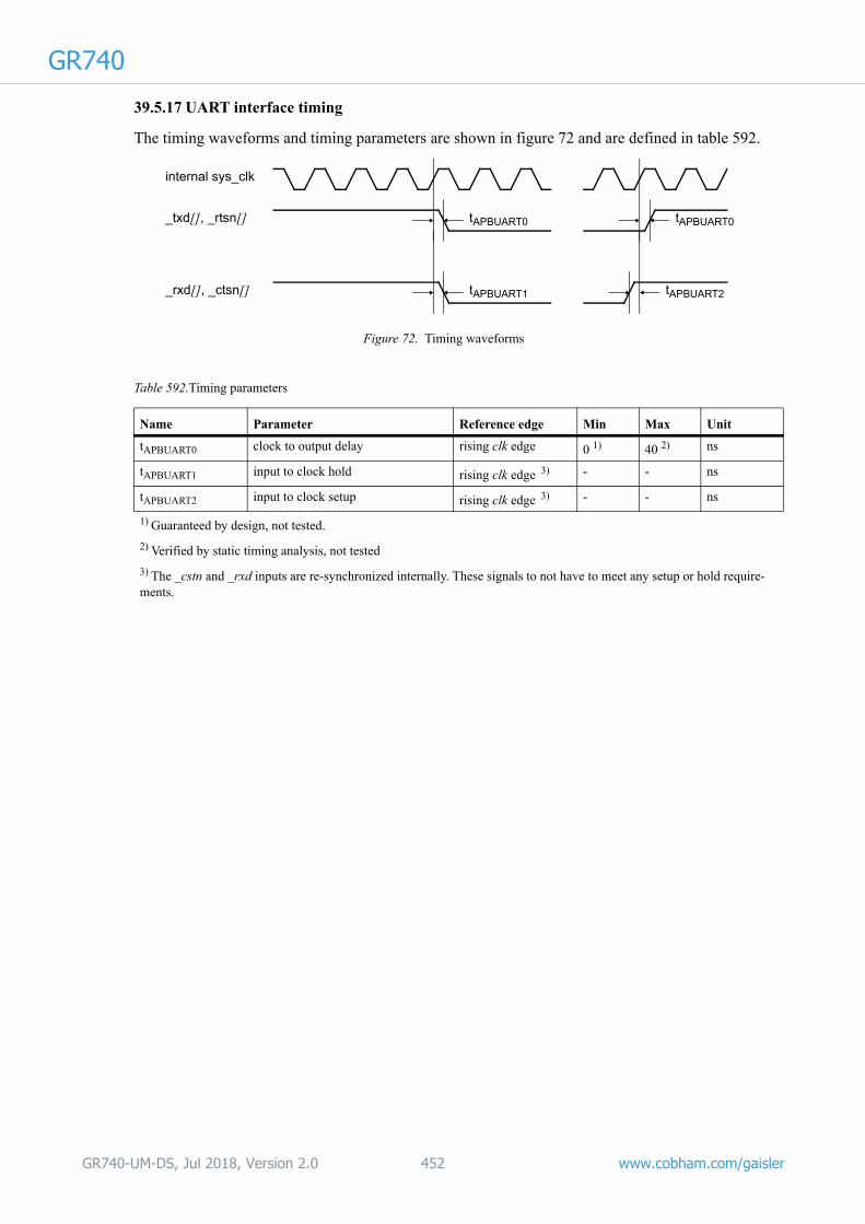
GR740
39.5.17 UART interface timingThe timing waveforms and timing parameters are shown in figure 72 and are defined in table 592.
Table 592.Timing parameters
Name Parameter Reference edge Min Max Unit
tAPBUART0 clock to output delay rising clk edge 0 1) 40 2) ns
tAPBUART1 input to clock hold rising clk edge 3) - - ns
tAPBUART2 input to clock setup rising clk edge 3) - - ns
1) Guaranteed by design, not tested.
2) Verified by static timing analysis, not tested
3) The _cstn and _rxd inputs are re-synchronized internally. These signals to not have to meet any setup or hold require-ments.
Figure 72. Timing waveforms
tAPBUART0_txd[], _rtsn[]
internal sys_clk
tAPBUART0
tAPBUART1_rxd[], _ctsn[] tAPBUART2
GR740-UM-DS, Jul 2018, Version 2.0 452 www.cobham.com/gaisler

GR740
39.5.18 SPI controller timingThe timing waveforms and timing parameters are shown in figure 73 and are defined in table 593.
Table 593.Timing parameters
Name Parameter Reference edge Min Max Unit
tSPICTRL0 clock to output delay rising clk edge 0 1) 40 2) ns
tSPICTRL1 clock to non-tri-state delay rising clk edge 0 1) 40 2) ns
tSPICTRL2 clock to tri-state delay rising clk edge 0 1) 40 2) ns
tSPICTRL3 input to clock hold rising clk edge 3) - - ns
tSPICTRL4 input to clock setup rising clk edge 3) - - ns
1) Guaranteed by design, not tested.
2) Verified by static timing analysis, not tested
3) The spi_sck/miso/mosi/spisel inputs are re-synchronized internally. The signals do not have to meet any setup or hold requirements. However, the input to clock setup value restricts the maximum SPI frequency.
Figure 73. Timing waveforms
tSPICTRL0spi_sck/miso/mosi/slvsel
internal sys_clk
tSPCTRLI0
tSPICTRL1
spi_sck/miso/mosi
tSPICTRL2
tSPICTRL3spi_sck/miso/mosi/sel tSPICTRL4
(output)
(output)
(input)
GR740-UM-DS, Jul 2018, Version 2.0 453 www.cobham.com/gaisler

GR740
39.5.19 CAN Controller interface timingThe timing waveforms and timing parameters are shown in figure 74 and are defined in table 594.
Table 594.Timing parameters
Name Parameter Reference edge Min Max Unit
tGRCAN0 clock to output delay rising clk edge 0 1) 40 2) ns
tGRCAN1 data input to clock setup rising clk edge 3) - - ns
tGRCAN2 data input from clock hold rising clk edge 3) - - ns
1) Guaranteed by design, not tested.
2) Verified by static timing analysis, not tested
3) The can inputs are re-synchronized internally. The signals do not have to meet any setup or hold requirements. However, the input to clock setup value restricts the maximum SPI frequency.
Figure 74. Timing waveforms
tGRCAN0
cantx[]
internal sys_clk
canrx[]tGRCAN2
tGRCAN1
GR740-UM-DS, Jul 2018, Version 2.0 454 www.cobham.com/gaisler

GR740
40 Mechanical description40.1 Component and package
The device is available as CCGA625 and LGA625. Please refer to section 40.4 for the package draw-ing. A placement diagram is available in section 40.2 and pin assignments in section 40.3.
GR740-UM-DS, Jul 2018, Version 2.0 455 www.cobham.com/gaisler

GR740
40.2 Package placement diagramFigure 75. Placement, top view (through package)
Figure 76. Placement, bottom view
GR740-UM-DS, Jul 2018, Version 2.0 456 www.cobham.com/gaisler
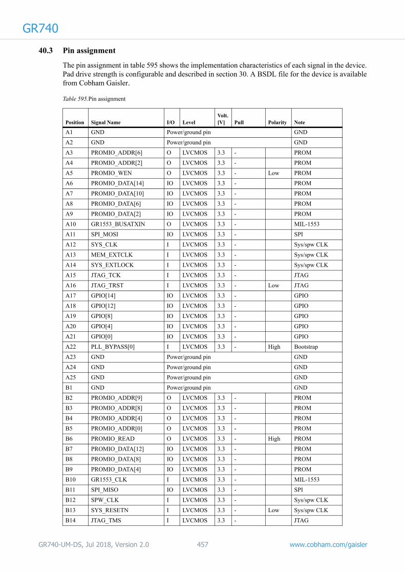
GR740
40.3 Pin assignmentThe pin assignment in table 595 shows the implementation characteristics of each signal in the device. Pad drive strength is configurable and described in section 30. A BSDL file for the device is available from Cobham Gaisler.
Table 595.Pin assignment
Position Signal Name I/O LevelVolt.[V] Pull Polarity Note
A1 GND Power/ground pin GND
A2 GND Power/ground pin GND
A3 PROMIO_ADDR[6] O LVCMOS 3.3 - PROM
A4 PROMIO_ADDR[2] O LVCMOS 3.3 - PROM
A5 PROMIO_WEN O LVCMOS 3.3 - Low PROM
A6 PROMIO_DATA[14] IO LVCMOS 3.3 - PROM
A7 PROMIO_DATA[10] IO LVCMOS 3.3 - PROM
A8 PROMIO_DATA[6] IO LVCMOS 3.3 - PROM
A9 PROMIO_DATA[2] IO LVCMOS 3.3 - PROM
A10 GR1553_BUSATXIN O LVCMOS 3.3 - MIL-1553
A11 SPI_MOSI IO LVCMOS 3.3 - SPI
A12 SYS_CLK I LVCMOS 3.3 - Sys/spw CLK
A13 MEM_EXTCLK I LVCMOS 3.3 - Sys/spw CLK
A14 SYS_EXTLOCK I LVCMOS 3.3 - Sys/spw CLK
A15 JTAG_TCK I LVCMOS 3.3 - JTAG
A16 JTAG_TRST I LVCMOS 3.3 - Low JTAG
A17 GPIO[14] IO LVCMOS 3.3 - GPIO
A18 GPIO[12] IO LVCMOS 3.3 - GPIO
A19 GPIO[8] IO LVCMOS 3.3 - GPIO
A20 GPIO[4] IO LVCMOS 3.3 - GPIO
A21 GPIO[0] IO LVCMOS 3.3 - GPIO
A22 PLL_BYPASS[0] I LVCMOS 3.3 - High Bootstrap
A23 GND Power/ground pin GND
A24 GND Power/ground pin GND
A25 GND Power/ground pin GND
B1 GND Power/ground pin GND
B2 PROMIO_ADDR[9] O LVCMOS 3.3 - PROM
B3 PROMIO_ADDR[8] O LVCMOS 3.3 - PROM
B4 PROMIO_ADDR[4] O LVCMOS 3.3 - PROM
B5 PROMIO_ADDR[0] O LVCMOS 3.3 - PROM
B6 PROMIO_READ O LVCMOS 3.3 - High PROM
B7 PROMIO_DATA[12] IO LVCMOS 3.3 - PROM
B8 PROMIO_DATA[8] IO LVCMOS 3.3 - PROM
B9 PROMIO_DATA[4] IO LVCMOS 3.3 - PROM
B10 GR1553_CLK I LVCMOS 3.3 - MIL-1553
B11 SPI_MISO IO LVCMOS 3.3 - SPI
B12 SPW_CLK I LVCMOS 3.3 - Sys/spw CLK
B13 SYS_RESETN I LVCMOS 3.3 - Low Sys/spw CLK
B14 JTAG_TMS I LVCMOS 3.3 - JTAG
GR740-UM-DS, Jul 2018, Version 2.0 457 www.cobham.com/gaisler

GR740
B15 JTAG_TDO O LVCMOS 3.3 - JTAG
B16 JTAG_TDI I LVCMOS 3.3 - JTAG
B17 GPIO[7] IO LVCMOS 3.3 - GPIO
B18 GPIO[10] IO LVCMOS 3.3 - GPIO
B19 GPIO[6] IO LVCMOS 3.3 - GPIO
B20 GPIO[2] IO LVCMOS 3.3 - GPIO
B21 PCIMODE_ENABLE I LVCMOS 3.3 - High Bootstrap
B22 PLL_BYPASS[1] I LVCMOS 3.3 - High Bootstrap
B23 PLL_IGNLOCK I LVCMOS 3.3 - High Bootstrap
B24 PLL_LOCKED[4] O LVCMOS 3.3 - High Bootstrap
B25 GND Power/ground pin GND
C1 PROMIO_ADDR[10] O LVCMOS 3.3 - PROM
C2 PROMIO_ADDR[12] O LVCMOS 3.3 - PROM
C3 PROMIO_ADDR[7] O LVCMOS 3.3 - PROM
C4 PROMIO_ADDR[3] O LVCMOS 3.3 - PROM
C5 PROMIO_OEN O LVCMOS 3.3 - Low PROM
C6 PROMIO_DATA[15] IO LVCMOS 3.3 - PROM
C7 PROMIO_DATA[9] IO LVCMOS 3.3 - PROM
C8 PROMIO_DATA[5] IO LVCMOS 3.3 - PROM
C9 PROMIO_DATA[0] IO LVCMOS 3.3 - PROM
C10 GR1553_BUSBTXIN O LVCMOS 3.3 - High MIL-1553
C11 SPI_SCK IO LVCMOS 3.3 - SPI
C12 SPI_SEL I LVCMOS 3.3 - Low SPI
C13 SPI_SLVSEL[0] O LVCMOS 3.3 - Low SPI
C14 SPI_SLVSEL[1] O LVCMOS 3.3 - Low SPI
C15 GPIO[13] IO LVCMOS 3.3 - GPIO
C16 GPIO[9] IO LVCMOS 3.3 - GPIO
C17 GPIO[3] IO LVCMOS 3.3 - GPIO
C18 GPIO[1] IO LVCMOS 3.3 - GPIO
C19 DSU_ACTIVE O LVCMOS 3.3 - High Bootstrap
C20 MEM_IFWIDTH I LVCMOS 3.3 - Bootstrap
C21 VSS2V5 Power/ground pin VSS2V5
C22 VSS2V5 Power/ground pin VSS2V5
C23 VSS2V5 Power/ground pin VSS2V5
C24 VSS2V5 Power/ground pin VSS2V5
C25 VSS2V5 Power/ground pin VSS2V5
D1 PROMIO_ADDR[14] O LVCMOS 3.3 - PROM
D2 PROMIO_ADDR[16] IO LVCMOS 3.3 - PROM
D3 PROMIO_ADDR[11] O LVCMOS 3.3 - PROM
D4 PROMIO_ADDR[5] O LVCMOS 3.3 - PROM
D5 PROMIO_BRDYN I LVCMOS 3.3 - Low PROM
D6 PROMIO_DATA[13] IO LVCMOS 3.3 - PROM
D7 PROMIO_DATA[11] IO LVCMOS 3.3 - PROM
D8 PROMIO_DATA[3] IO LVCMOS 3.3 - PROM
Table 595.Pin assignment
Position Signal Name I/O LevelVolt.[V] Pull Polarity Note
GR740-UM-DS, Jul 2018, Version 2.0 458 www.cobham.com/gaisler

GR740
D9 VSS3V3 Power/ground pin VSS3V3
D10 VDIG3V3 Power/ground pin VDIG3V3
D11 VSS3V3 Power/ground pin VSS3V3
D12 VDIG3V3 Power/ground pin VDIG3V3
D13 VSS3V3 Power/ground pin VSS3V3
D14 GPIO[15] IO LVCMOS 3.3 - GPIO
D15 GPIO[11] IO LVCMOS 3.3 - GPIO
D16 GPIO[5] IO LVCMOS 3.3 - GPIO
D17 BREAK I LVCMOS 3.3 - High Bootstrap
D18 DSU_EN I LVCMOS 3.3 - High Bootstrap
D19 WDOGN O LVCMOS 3.3 - Low Bootstrap, Open-drain
D20 PLL_LOCKED[2] O LVCMOS 3.3 - High Bootstrap
D21 VSS2V5 Power/ground pin VSS2V5
D22 SPW_TXS_P[7] O LVDS 2.5 - Pos SpaceWire
D23 SPW_TXS_N[7] O LVDS 2.5 - Neg SpaceWire
D24 SPW_TXD_P[7] O LVDS 2.5 - Pos SpaceWire
D25 SPW_TXD_N[7] O LVDS 2.5 - Neg SpaceWire
E1 PROMIO_ADDR[18] IO LVCMOS 3.3 - PROM
E2 PROMIO_ADDR[20] IO LVCMOS 3.3 - PROM
E3 VDIG3V3 Power/ground pin VDIG3V3
E4 PROMIO_ADDR[15] O LVCMOS 3.3 - PROM
E5 PROMIO_ADDR[13] O LVCMOS 3.3 - PROM
E6 PROMIO_ADDR[1] O LVCMOS 3.3 - PROM
E7 PROMIO_DATA[7] IO LVCMOS 3.3 - PROM
E8 PROMIO_DATA[1] IO LVCMOS 3.3 - PROM
E9 VDIG3V3 Power/ground pin VDIG3V3
E10 VSS3V3 Power/ground pin VSS3V3
E11 VDIG3V3 Power/ground pin VDIG3V3
E12 AGNDPLL1V2_SYSPLL Power/ground pin PLL
E13 AGNDPLL1V2_MEMPLL Power/ground pin PLL
E14 AGNDPLL1V2_SPWPLL Power/ground pin PLL
E15 PROC_ERRORN O LVCMOS 3.3 - Low Bootstrap, Open-drain
E16 MEM_CLKSEL I LVCMOS 3.3 - Bootstrap
E17 PLL_BYPASS[2] I LVCMOS 3.3 - High Bootstrap
E18 PLL_LOCKED[5] O LVCMOS 3.3 - High Bootstrap
E19 PLL_LOCKED[3] O LVCMOS 3.3 - High Bootstrap
E20 PLL_LOCKED[0] O LVCMOS 3.3 - High Bootstrap
E21 VSS2V5 Power/ground pin VSS2V5
E22 SPW_RXS_P[7] I LVDS 2.5 DiffTerm Pos SpaceWire
E23 SPW_RXS_N[7] I LVDS 2.5 DiffTerm Neg SpaceWire
E24 SPW_RXD_P[7] I LVDS 2.5 DiffTerm Pos SpaceWire
E25 SPW_RXD_N[7] I LVDS 2.5 DiffTerm Neg SpaceWire
Table 595.Pin assignment
Position Signal Name I/O LevelVolt.[V] Pull Polarity Note
GR740-UM-DS, Jul 2018, Version 2.0 459 www.cobham.com/gaisler

GR740
F1 PROMIO_ADDR[22] IO LVCMOS 3.3 - PROM
F2 PROMIO_ADDR[24] IO LVCMOS 3.3 - PROM
F3 VSS3V3 Power/ground pin VSS3V3
F4 PROMIO_ADDR[19] IO LVCMOS 3.3 - PROM
F5 PROMIO_ADDR[17] IO LVCMOS 3.3 - PROM
F6 VDIG3V3 Power/ground pin VDIG3V3
F7 VSS3V3 Power/ground pin VSS3V3
F8 VDIG3V3 Power/ground pin VDIG3V3
F9 VSS3V3 Power/ground pin VSS3V3
F10 VDIG3V3 Power/ground pin VDIG3V3
F11 VSS3V3 Power/ground pin VSS3V3
F12 AVDDPLL1V2_SYSPLL Power/ground pin DLL
F13 AVDDPLL1V2_MEMPLL Power/ground pin DLL
F14 AVDDPLL1V2_SPWPLL Power/ground pin DLL
F15 VSS3V3 Power/ground pin VSS3V3
F16 VDIG3V3 Power/ground pin VDIG3V3
F17 VSS3V3 Power/ground pin VSS3V3
F18 VDIG3V3 Power/ground pin VDIG3V3
F19 VSS3V3 Power/ground pin VSS3V3
F20 PLL_LOCKED[1] O LVCMOS 3.3 - High Bootstrap
F21 VSS2V5 Power/ground pin VSS2V5
F22 SPW_TXS_P[6] O LVDS 2.5 - Pos SpaceWire
F23 SPW_TXS_N[6] O LVDS 2.5 - Neg SpaceWire
F24 SPW_TXD_P[6] O LVDS 2.5 - Pos SpaceWire
F25 SPW_TXD_N[6] O LVDS 2.5 - Neg SpaceWire
G1 PROMIO_ADDR[26] IO LVCMOS 3.3 - PROM
G2 IO_SN IO LVCMOS 3.3 - Low PROM
G3 VDIG3V3 Power/ground pin VDIG3V3
G4 PROMIO_ADDR[23] IO LVCMOS 3.3 - PROM
G5 PROMIO_ADDR[21] IO LVCMOS 3.3 - PROM
G6 VSS3V3 Power/ground pin VSS3V3
G7 VDIG3V3 Power/ground pin VDIG3V3
G8 VSS3V3 Power/ground pin VSS3V3
G9 VDIG3V3 Power/ground pin VDIG3V3
G10 VSS3V3 Power/ground pin VSS3V3
G11 VDIG3V3 Power/ground pin VDIG3V3
G12 DVDDPLL1V2_SYSPLL Power/ground pin PLL
G13 DVDDPLL1V2_MEMPLL Power/ground pin PLL
G14 DVDDPLL1V2_SPWPLL Power/ground pin PLL
G15 VDIG3V3 Power/ground pin VDIG3V3
G16 VSS3V3 Power/ground pin VSS3V3
G17 VDIG3V3 Power/ground pin VDIG3V3
G18 VSS3V3 Power/ground pin VSS3V3
G19 VDIG3V3 Power/ground pin VDIG3V3
Table 595.Pin assignment
Position Signal Name I/O LevelVolt.[V] Pull Polarity Note
GR740-UM-DS, Jul 2018, Version 2.0 460 www.cobham.com/gaisler

GR740
G20 VSS3V3 Power/ground pin VSS3V3
G21 VSS2V5 Power/ground pin VSS2V5
G22 SPW_RXS_P[6] I LVDS 2.5 DiffTerm Pos SpaceWire
G23 SPW_RXS_N[6] I LVDS 2.5 DiffTerm Neg SpaceWire
G24 SPW_RXD_P[6] I LVDS 2.5 DiffTerm Pos SpaceWire
G25 SPW_RXD_N[6] I LVDS 2.5 DiffTerm Neg SpaceWire
H1 PROM_CEN[1] IO LVCMOS 3.3 - Low PROM
H2 PROM_CEN[0] O LVCMOS 3.3 - Low PROM
H3 VSS3V3 Power/ground pin VSS3V3
H4 PROMIO_ADDR[27] IO LVCMOS 3.3 - PROM
H5 PROMIO_ADDR[25] IO LVCMOS 3.3 - PROM
H6 VDIG3V3 Power/ground pin VDIG3V3
H7 VSS3V3 Power/ground pin VSS3V3
H8 VDD1V2 Power/ground pin VDD
H9 GND Power/ground pin GND
H10 VDD1V2 Power/ground pin VDD
H11 GND Power/ground pin GND
H12 VDD1V2 Power/ground pin VDD
H13 GND Power/ground pin GND
H14 VDD1V2 Power/ground pin VDD
H15 GND Power/ground pin GND
H16 VDD1V2 Power/ground pin VDD
H17 GND Power/ground pin GND
H18 VDD1V2 Power/ground pin VDD
H19 VSS3V3 Power/ground pin VSS3V3
H20 VDIG3V3 Power/ground pin VDIG3V3
H21 VSS2V5 Power/ground pin VSS2V5
H22 SPW_TXS_P[5] O LVDS 2.5 - Pos SpaceWire
H23 SPW_TXS_N[5] O LVDS 2.5 - Neg SpaceWire
H24 SPW_TXD_P[5] O LVDS 2.5 - Pos SpaceWire
H25 SPW_TXD_N[5] O LVDS 2.5 - Neg SpaceWire
J1 ETH0_MDC O LVCMOS 3.3 - Ethernet
J2 ETH0_RXCLK I LVCMOS 3.3 - Ethernet
J3 VDIG3V3 Power/ground pin VDIG3V3
J4 ETH0_MDINT I LVCMOS 3.3 - Low Ethernet
J5 ETH0_CRS I LVCMOS 3.3 - High Ethernet
J6 VSS3V3 Power/ground pin VSS3V3
J7 VDIG3V3 Power/ground pin VDIG3V3
J8 GND Power/ground pin GND
J9 VDD1V2 Power/ground pin VDD
J10 GND Power/ground pin GND
J11 VDD1V2 Power/ground pin VDD
J12 GND Power/ground pin GND
J13 VDD1V2 Power/ground pin VDD
Table 595.Pin assignment
Position Signal Name I/O LevelVolt.[V] Pull Polarity Note
GR740-UM-DS, Jul 2018, Version 2.0 461 www.cobham.com/gaisler

GR740
J14 GND Power/ground pin GND
J15 VDD1V2 Power/ground pin VDD
J16 GND Power/ground pin GND
J17 VDD1V2 Power/ground pin VDD
J18 GND Power/ground pin GND
J19 VDIG3V3 Power/ground pin VDIG3V3
J20 VSS3V3 Power/ground pin VSS3V3
J21 VDIG2V5 Power/ground pin VDIG2V5
J22 SPW_RXS_P[5] I LVDS 2.5 DiffTerm Pos SpaceWire
J23 SPW_RXS_N[5] I LVDS 2.5 DiffTerm Neg SpaceWire
J24 SPW_RXD_P[5] I LVDS 2.5 DiffTerm Pos SpaceWire
J25 SPW_RXD_N[5] I LVDS 2.5 DiffTerm Neg SpaceWire
K1 ETH0_RXD[0] I LVCMOS 3.3 - Ethernet
K2 ETH0_RXD[2] I LVCMOS 3.3 - Ethernet
K3 VSS3V3 Power/ground pin VSS3V3
K4 ETH0_MDIO IO LVCMOS 3.3 - Ethernet
K5 ETH0_COL I LVCMOS 3.3 - High Ethernet
K6 VDIG3V3 Power/ground pin VDIG3V3
K7 VSS3V3 Power/ground pin VSS3V3
K8 VDD1V2 Power/ground pin VDD
K9 GND Power/ground pin GND
K10 VDD1V2 Power/ground pin VDD
K11 GND Power/ground pin GND
K12 VDD1V2 Power/ground pin VDD
K13 GND Power/ground pin GND
K14 VDD1V2 Power/ground pin VDD
K15 GND Power/ground pin GND
K16 VDD1V2 Power/ground pin VDD
K17 GND Power/ground pin GND
K18 VDD1V2 Power/ground pin VDD
K19 VSS3V3 Power/ground pin VSS3V3
K20 VDIG3V3 Power/ground pin VDIG3V3
K21 VSS2V5 Power/ground pin VSS2V5
K22 SPW_TXS_P[4] O LVDS 2.5 - Pos SpaceWire
K23 SPW_TXS_N[4] O LVDS 2.5 - Neg SpaceWire
K24 SPW_TXD_P[4] O LVDS 2.5 - Pos SpaceWire
K25 SPW_TXD_N[4] O LVDS 2.5 - Neg SpaceWire
L1 ETH0_RXD[4] I LVCMOS 3.3 - Ethernet
L2 ETH0_RXD[6] I LVCMOS 3.3 - Ethernet
L3 VDIG3V3 Power/ground pin VDIG3V3
L4 ETH0_RXD[1] I LVCMOS 3.3 - Ethernet
L5 ETH0_RXDV I LVCMOS 3.3 - High Ethernet
L6 VSS3V3 Power/ground pin VSS3V3
L7 VDIG3V3 Power/ground pin VDIG3V3
Table 595.Pin assignment
Position Signal Name I/O LevelVolt.[V] Pull Polarity Note
GR740-UM-DS, Jul 2018, Version 2.0 462 www.cobham.com/gaisler

GR740
L8 GND Power/ground pin GND
L9 VDD1V2 Power/ground pin VDD
L10 GND Power/ground pin GND
L11 VDD1V2 Power/ground pin VDD
L12 GND Power/ground pin GND
L13 VDD1V2 Power/ground pin VDD
L14 GND Power/ground pin GND
L15 VDD1V2 Power/ground pin VDD
L16 GND Power/ground pin GND
L17 VDD1V2 Power/ground pin VDD
L18 GND Power/ground pin GND
L19 VDIG3V3 Power/ground pin VDIG3V3
L20 VSS3V3 Power/ground pin VSS3V3
L21 VDIG2V5 Power/ground pin VDIG2V5
L22 SPW_RXS_P[4] I LVDS 2.5 DiffTerm Pos SpaceWire
L23 SPW_RXS_N[4] I LVDS 2.5 DiffTerm Neg SpaceWire
L24 SPW_RXD_P[4] I LVDS 2.5 DiffTerm Pos SpaceWire
L25 SPW_RXD_N[4] I LVDS 2.5 DiffTerm Neg SpaceWire
M1 ETH0_RXER I LVCMOS 3.3 - High Ethernet
M2 ETH0_GTXCLK I LVCMOS 3.3 - Ethernet
M3 ETH0_RXD[5] I LVCMOS 3.3 - Ethernet
M4 ETH0_RXD[3] I LVCMOS 3.3 - Ethernet
M5 ETH0_RXD[7] I LVCMOS 3.3 - Ethernet
M6 VDIG3V3 Power/ground pin VDIG3V3
M7 VSS3V3 Power/ground pin VSS3V3
M8 VDD1V2 Power/ground pin VDD
M9 GND Power/ground pin GND
M10 VDD1V2 Power/ground pin VDD
M11 GND Power/ground pin GND
M12 VDD1V2 Power/ground pin VDD
M13 GND Power/ground pin GND
M14 VDD1V2 Power/ground pin VDD
M15 GND Power/ground pin GND
M16 VDD1V2 Power/ground pin VDD
M17 GND Power/ground pin GND
M18 VDD1V2 Power/ground pin VDD
M19 VSS3V3 Power/ground pin VSS3V3
M20 VDIG3V3 Power/ground pin VDIG3V3
M21 VSS2V5 Power/ground pin VSS2V5
M22 SPW_TXS_P[3] O LVDS 2.5 - Pos SpaceWire
M23 SPW_TXS_N[3] O LVDS 2.5 - Neg SpaceWire
M24 SPW_TXD_P[3] O LVDS 2.5 - Pos SpaceWire
M25 SPW_TXD_N[3] O LVDS 2.5 - Neg SpaceWire
N1 ETH0_TXD[0] O LVCMOS 3.3 - Ethernet
Table 595.Pin assignment
Position Signal Name I/O LevelVolt.[V] Pull Polarity Note
GR740-UM-DS, Jul 2018, Version 2.0 463 www.cobham.com/gaisler

GR740
N2 ETH0_TXD[2] O LVCMOS 3.3 - Ethernet
N3 VSS3V3 Power/ground pin VSS3V3
N4 ETH0_TXEN O LVCMOS 3.3 - High Ethernet
N5 ETH0_TXCLK I LVCMOS 3.3 - Ethernet
N6 VSS3V3 Power/ground pin VSS3V3
N7 VDIG3V3 Power/ground pin VDIG3V3
N8 GND Power/ground pin GND
N9 VDD1V2 Power/ground pin VDD
N10 GND Power/ground pin GND
N11 VDD1V2 Power/ground pin VDD
N12 GND Power/ground pin GND
N13 VDD1V2 Power/ground pin VDD
N14 GND Power/ground pin GND
N15 VDD1V2 Power/ground pin VDD
N16 GND Power/ground pin GND
N17 VDD1V2 Power/ground pin VDD
N18 GND Power/ground pin GND
N19 VDIG3V3 Power/ground pin VDIG3V3
N20 VSS3V3 Power/ground pin VSS3V3
N21 VDIG2V5 Power/ground pin VDIG2V5
N22 SPW_RXS_P[3] I LVDS 2.5 DiffTerm Pos SpaceWire
N23 SPW_RXS_N[3] I LVDS 2.5 DiffTerm Neg SpaceWire
N24 SPW_RXD_P[3] I LVDS 2.5 DiffTerm Pos SpaceWire
N25 SPW_RXD_N[3] I LVDS 2.5 DiffTerm Neg SpaceWire
P1 ETH0_TXD[4] O LVCMOS 3.3 - Ethernet
P2 ETH0_TXD[6] O LVCMOS 3.3 - Ethernet
P3 VDIG3V3 Power/ground pin VDIG3V3
P4 ETH0_TXD[3] O LVCMOS 3.3 - Ethernet
P5 ETH0_TXD[1] O LVCMOS 3.3 - Ethernet
P6 VDIG3V3 Power/ground pin VDIG3V3
P7 VSS3V3 Power/ground pin VSS3V3
P8 VDD1V2 Power/ground pin VDD
P9 GND Power/ground pin GND
P10 VDD1V2 Power/ground pin VDD
P11 GND Power/ground pin GND
P12 VDD1V2 Power/ground pin VDD
P13 GND Power/ground pin GND
P14 VDD1V2 Power/ground pin VDD
P15 GND Power/ground pin GND
P16 VDD1V2 Power/ground pin VDD
P17 GND Power/ground pin GND
P18 VDD1V2 Power/ground pin VDD
P19 VSS3V3 Power/ground pin VSS3V3
P20 VDIG3V3 Power/ground pin VDIG3V3
Table 595.Pin assignment
Position Signal Name I/O LevelVolt.[V] Pull Polarity Note
GR740-UM-DS, Jul 2018, Version 2.0 464 www.cobham.com/gaisler

GR740
P21 VSS2V5 Power/ground pin VSS2V5
P22 SPW_TXS_P[2] O LVDS 2.5 - Pos SpaceWire
P23 SPW_TXS_N[2] O LVDS 2.5 - Neg SpaceWire
P24 SPW_TXD_P[2] O LVDS 2.5 - Pos SpaceWire
P25 SPW_TXD_N[2] O LVDS 2.5 - Neg SpaceWire
R1 ETH0_TXER O LVCMOS 3.3 - High Ethernet
R2 MEM_DQ[1] IO LVCMOS 3.3 - SDRAM
R3 VSS3V3 Power/ground pin VSS3V3
R4 ETH0_TXD[7] O LVCMOS 3.3 - Ethernet
R5 ETH0_TXD[5] O LVCMOS 3.3 - Ethernet
R6 VSS3V3 Power/ground pin VSS3V3
R7 VDIG3V3 Power/ground pin VDIG3V3
R8 GND Power/ground pin GND
R9 VDD1V2 Power/ground pin VDD
R10 GND Power/ground pin GND
R11 VDD1V2 Power/ground pin VDD
R12 GND Power/ground pin GND
R13 VDD1V2 Power/ground pin VDD
R14 GND Power/ground pin GND
R15 VDD1V2 Power/ground pin VDD
R16 GND Power/ground pin GND
R17 VDD1V2 Power/ground pin VDD
R18 GND Power/ground pin GND
R19 VDIG3V3 Power/ground pin VDIG3V3
R20 VSS3V3 Power/ground pin VSS3V3
R21 VDIG2V5 Power/ground pin VDIG2V5
R22 SPW_RXS_P[2] I LVDS 2.5 DiffTerm Pos SpaceWire
R23 SPW_RXS_N[2] I LVDS 2.5 DiffTerm Neg SpaceWire
R24 SPW_RXD_P[2] I LVDS 2.5 DiffTerm Pos SpaceWire
R25 SPW_RXD_N[2] I LVDS 2.5 DiffTerm Neg SpaceWire
T1 MEM_DQ[3] IO LVCMOS 3.3 - SDRAM
T2 MEM_DQ[5] IO LVCMOS 3.3 - SDRAM
T3 MEM_DQ[2] IO LVCMOS 3.3 - SDRAM
T4 MEM_DQ[4] IO LVCMOS 3.3 - SDRAM
T5 MEM_DQ[0] IO LVCMOS 3.3 - SDRAM
T6 VDIG3V3 Power/ground pin VDIG3V3
T7 VSS3V3 Power/ground pin VSS3V3
T8 VDD1V2 Power/ground pin VDD
T9 GND Power/ground pin GND
T10 VDD1V2 Power/ground pin VDD
T11 GND Power/ground pin GND
T12 VDD1V2 Power/ground pin VDD
T13 GND Power/ground pin GND
T14 VDD1V2 Power/ground pin VDD
Table 595.Pin assignment
Position Signal Name I/O LevelVolt.[V] Pull Polarity Note
GR740-UM-DS, Jul 2018, Version 2.0 465 www.cobham.com/gaisler

GR740
T15 GND Power/ground pin GND
T16 VDD1V2 Power/ground pin VDD
T17 GND Power/ground pin GND
T18 VDD1V2 Power/ground pin VDD
T19 VSS3V3 Power/ground pin VSS3V3
T20 VDIG3V3 Power/ground pin VDIG3V3
T21 VSS2V5 Power/ground pin VSS2V5
T22 SPW_TXS_P[1] O LVDS 2.5 - Pos SpaceWire
T23 SPW_TXS_N[1] O LVDS 2.5 - Neg SpaceWire
T24 SPW_TXD_P[1] O LVDS 2.5 - Pos SpaceWire
T25 SPW_TXD_N[1] O LVDS 2.5 - Neg SpaceWire
U1 MEM_DQ[7] IO LVCMOS 3.3 - SDRAM
U2 MEM_DQM[1] O LVCMOS 3.3 - Low SDRAM
U3 VDIG3V3 Power/ground pin VDIG3V3
U4 MEM_DQM[0] O LVCMOS 3.3 - Low SDRAM
U5 MEM_DQ[6] IO LVCMOS 3.3 - SDRAM
U6 VSS3V3 Power/ground pin VSS3V3
U7 VDIG3V3 Power/ground pin VDIG3V3
U8 GND Power/ground pin GND
U9 VDD1V2 Power/ground pin VDD
U10 GND Power/ground pin GND
U11 VDD1V2 Power/ground pin VDD
U12 GND Power/ground pin GND
U13 VDD1V2 Power/ground pin VDD
U14 GND Power/ground pin GND
U15 VDD1V2 Power/ground pin VDD
U16 GND Power/ground pin GND
U17 VDD1V2 Power/ground pin VDD
U18 GND Power/ground pin GND
U19 VDIG3V3 Power/ground pin VDIG3V3
U20 VSS3V3 Power/ground pin VSS3V3
U21 VDIG2V5 Power/ground pin VDIG2V5
U22 SPW_RXS_P[1] I LVDS 2.5 DiffTerm Pos SpaceWire
U23 SPW_RXS_N[1] I LVDS 2.5 DiffTerm Neg SpaceWire
U24 SPW_RXD_P[1] I LVDS 2.5 DiffTerm Pos SpaceWire
U25 SPW_RXD_N[1] I LVDS 2.5 DiffTerm Neg SpaceWire
V1 MEM_DQ[9] IO LVCMOS 3.3 - SDRAM
V2 MEM_DQ[11] IO LVCMOS 3.3 - SDRAM
V3 VSS3V3 Power/ground pin VSS3V3
V4 MEM_DQ[10] IO LVCMOS 3.3 - SDRAM
V5 MEM_DQ[8] IO LVCMOS 3.3 - SDRAM
V6 VDIG3V3 Power/ground pin VDIG3V3
V7 VSS3V3 Power/ground pin VSS3V3
V8 VDD1V2 Power/ground pin VDD
Table 595.Pin assignment
Position Signal Name I/O LevelVolt.[V] Pull Polarity Note
GR740-UM-DS, Jul 2018, Version 2.0 466 www.cobham.com/gaisler

GR740
V9 GND Power/ground pin GND
V10 VDD1V2 Power/ground pin VDD
V11 GND Power/ground pin GND
V12 VDD1V2 Power/ground pin VDD
V13 GND Power/ground pin GND
V14 VDD1V2 Power/ground pin VDD
V15 GND Power/ground pin GND
V16 VDD1V2 Power/ground pin VDD
V17 GND Power/ground pin GND
V18 VDD1V2 Power/ground pin VDD
V19 VSS3V3 Power/ground pin VSS3V3
V20 VDIG3V3 Power/ground pin VDIG3V3
V21 VSS2V5 Power/ground pin VSS2V5
V22 SPW_TXS_P[0] O LVDS 2.5 - Pos SpaceWire
V23 SPW_TXS_N[0] O LVDS 2.5 - Neg SpaceWire
V24 SPW_TXD_P[0] O LVDS 2.5 - Pos SpaceWire
V25 SPW_TXD_N[0] O LVDS 2.5 - Neg SpaceWire
W1 MEM_DQ[15] IO LVCMOS 3.3 - SDRAM
W2 MEM_DQ[13] IO LVCMOS 3.3 - SDRAM
W3 VDIG3V3 Power/ground pin VDIG3V3
W4 MEM_DQ[14] IO LVCMOS 3.3 - SDRAM
W5 MEM_DQ[12] IO LVCMOS 3.3 - SDRAM
W6 VSS3V3 Power/ground pin VSS3V3
W7 VDIG3V3 Power/ground pin VDIG3V3
W8 VSS3V3 Power/ground pin VSS3V3
W9 VDIG3V3 Power/ground pin VDIG3V3
W10 VSS3V3 Power/ground pin VSS3V3
W11 VDIG3V3 Power/ground pin VDIG3V3
W12 VSS3V3 Power/ground pin VSS3V3
W13 VDIG3V3 Power/ground pin VDIG3V3
W14 VSS3V3 Power/ground pin VSS3V3
W15 VDIG3V3 Power/ground pin VDIG3V3
W16 VSS3V3 Power/ground pin VSS3V3
W17 VDIG3V3 Power/ground pin VDIG3V3
W18 VSS3V3 Power/ground pin VSS3V3
W19 VDIG3V3 Power/ground pin VDIG3V3
W20 VSS3V3 Power/ground pin VSS3V3
W21 VSS2V5 Power/ground pin VSS2V5
W22 SPW_RXS_P[0] I LVDS 2.5 DiffTerm Pos SpaceWire
W23 SPW_RXS_N[0] I LVDS 2.5 DiffTerm Neg SpaceWire
W24 SPW_RXD_P[0] I LVDS 2.5 DiffTerm Pos SpaceWire
W25 SPW_RXD_N[0] I LVDS 2.5 DiffTerm Neg SpaceWire
Y1 MEM_DQ[19] IO LVCMOS 3.3 - SDRAM
Y2 MEM_DQ[17] IO LVCMOS 3.3 - SDRAM
Table 595.Pin assignment
Position Signal Name I/O LevelVolt.[V] Pull Polarity Note
GR740-UM-DS, Jul 2018, Version 2.0 467 www.cobham.com/gaisler

GR740
Y3 VSS3V3 Power/ground pin VSS3V3
Y4 MEM_DQ[20] IO LVCMOS 3.3 - SDRAM
Y5 MEM_DQ[16] IO LVCMOS 3.3 - SDRAM
Y6 VDIG3V3 Power/ground pin VDIG3V3
Y7 VSS3V3 Power/ground pin VSS3V3
Y8 VDIG3V3 Power/ground pin VDIG3V3
Y9 VSS3V3 Power/ground pin VSS3V3
Y10 VDIG3V3 Power/ground pin VDIG3V3
Y11 VSS3V3 Power/ground pin VSS3V3
Y12 VDIG3V3 Power/ground pin VDIG3V3
Y13 VSS3V3 Power/ground pin VSS3V3
Y14 VDIG3V3 Power/ground pin VDIG3V3
Y15 VSS3V3 Power/ground pin VSS3V3
Y16 VDIG3V3 Power/ground pin VDIG3V3
Y17 VSS3V3 Power/ground pin VSS3V3
Y18 VDIG3V3 Power/ground pin VDIG3V3
Y19 VSS3V3 Power/ground pin VSS3V3
Y20 MEM_CLK_OUT O LVCMOS 3.3 - SDRAM
Y21 VSS2V5 Power/ground pin VSS2V5
Y22 VSS2V5 Power/ground pin VSS2V5
Y23 VSS2V5 Power/ground pin VSS2V5
Y24 VSS2V5 Power/ground pin VSS2V5
Y25 VSS2V5 Power/ground pin VSS2V5
AA1 MEM_DQ[23] IO LVCMOS 3.3 - SDRAM
AA2 MEM_DQ[21] IO LVCMOS 3.3 - SDRAM
AA3 MEM_DQM[2] O LVCMOS 3.3 - Low SDRAM
AA4 MEM_DQ[22] IO LVCMOS 3.3 - SDRAM
AA5 MEM_DQ[18] IO LVCMOS 3.3 - SDRAM
AA6 MEM_DQ[36] IO LVCMOS 3.3 - SDRAM
AA7 MEM_DQ[40] IO LVCMOS 3.3 - SDRAM
AA8 MEM_DQ[46] IO LVCMOS 3.3 - SDRAM
AA9 MEM_SN[1] O LVCMOS 3.3 - Low SDRAM
AA10 MEM_ADDR[7] O LVCMOS 3.3 - SDRAM
AA11 MEM_ADDR[13] O LVCMOS 3.3 - SDRAM
AA12 MEM_CASN O LVCMOS 3.3 - Low SDRAM
AA13 MEM_WEN O LVCMOS 3.3 - Low SDRAM
AA14 MEM_DQ[51] IO LVCMOS 3.3 - SDRAM
AA15 MEM_DQ[53] IO LVCMOS 3.3 - SDRAM
AA16 MEM_DQM[7] IO LVCMOS 3.3 - Low SDRAM
AA17 MEM_DQ[65] IO LVCMOS 3.3 - SDRAM
AA18 MEM_DQ[69] IO LVCMOS 3.3 - SDRAM
AA19 MEM_DQ[73] IO LVCMOS 3.3 - SDRAM
AA20 MEM_DQ[79] IO LVCMOS 3.3 - SDRAM
AA21 MEM_DQ[88] IO LVCMOS 3.3 - SDRAM
Table 595.Pin assignment
Position Signal Name I/O LevelVolt.[V] Pull Polarity Note
GR740-UM-DS, Jul 2018, Version 2.0 468 www.cobham.com/gaisler

GR740
AA22 MEM_DQ[92] IO LVCMOS 3.3 - SDRAM
AA23 MEM_DQ[94] IO LVCMOS 3.3 - SDRAM
AA24 MEM_CLK_OUT_DIFF_P O LVDS 2.5 - Pos SDRAM
AA25 MEM_CLK_OUT_DIFF_N O LVDS 2.5 - Neg SDRAM
AB1 MEM_DQM[3] O LVCMOS 3.3 - Low SDRAM
AB2 MEM_DQ[25] IO LVCMOS 3.3 - SDRAM
AB3 MEM_DQ[26] IO LVCMOS 3.3 - SDRAM
AB4 MEM_DQ[28] IO LVCMOS 3.3 - SDRAM
AB5 MEM_DQ[24] IO LVCMOS 3.3 - SDRAM
AB6 MEM_DQM[4] IO LVCMOS 3.3 - Low SDRAM
AB7 MEM_DQ[44] IO LVCMOS 3.3 - SDRAM
AB8 MEM_CLK_IN I LVCMOS 3.3 - SDRAM
AB9 MEM_ADDR[1] O LVCMOS 3.3 - SDRAM
AB10 MEM_ADDR[3] O LVCMOS 3.3 - SDRAM
AB11 MEM_ADDR[11] O LVCMOS 3.3 - SDRAM
AB12 MEM_BA[0] O LVCMOS 3.3 - SDRAM
AB13 MEM_CKE[1] O LVCMOS 3.3 - High SDRAM
AB14 MEM_DQ[49] IO LVCMOS 3.3 - SDRAM
AB15 MEM_DQ[55] IO LVCMOS 3.3 - SDRAM
AB16 MEM_DQ[59] IO LVCMOS 3.3 - SDRAM
AB17 MEM_DQ[61] IO LVCMOS 3.3 - SDRAM
AB18 MEM_DQ[67] IO LVCMOS 3.3 - SDRAM
AB19 MEM_DQ[71] IO LVCMOS 3.3 - SDRAM
AB20 MEM_DQ[77] IO LVCMOS 3.3 - SDRAM
AB21 MEM_DQ[86] IO LVCMOS 3.3 - SDRAM
AB22 MEM_DQM[10] IO LVCMOS 3.3 - Low SDRAM
AB23 MEM_DQ[90] IO LVCMOS 3.3 - SDRAM
AB24 MEM_DQ[95] IO LVCMOS 3.3 - SDRAM
AB25 MEM_DQ[93] IO LVCMOS 3.3 - SDRAM
AC1 MEM_DQ[29] IO LVCMOS 3.3 - SDRAM
AC2 MEM_DQ[27] IO LVCMOS 3.3 - SDRAM
AC3 MEM_DQ[30] IO LVCMOS 3.3 - SDRAM
AC4 MEM_DQ[32] IO LVCMOS 3.3 - SDRAM
AC5 MEM_DQ[34] IO LVCMOS 3.3 - SDRAM
AC6 MEM_DQ[38] IO LVCMOS 3.3 - SDRAM
AC7 MEM_DQ[42] IO LVCMOS 3.3 - SDRAM
AC8 VDIG3V3 Power/ground pin VDIG3V3
AC9 VSS3V3 Power/ground pin VSS3V3
AC10 MEM_ADDR[5] O LVCMOS 3.3 - SDRAM
AC11 MEM_ADDR[9] O LVCMOS 3.3 - SDRAM
AC12 VDIG3V3 Power/ground pin VDIG3V3
AC13 VSS3V3 Power/ground pin VSS3V3
AC14 GND Power/ground pin GND
AC15 MEM_DQ[52] IO LVCMOS 3.3 - SDRAM
Table 595.Pin assignment
Position Signal Name I/O LevelVolt.[V] Pull Polarity Note
GR740-UM-DS, Jul 2018, Version 2.0 469 www.cobham.com/gaisler

GR740
AC16 MEM_DQ[57] IO LVCMOS 3.3 - SDRAM
AC17 MEM_DQ[63] IO LVCMOS 3.3 - SDRAM
AC18 MEM_DQ[68] IO LVCMOS 3.3 - SDRAM
AC19 MEM_DQM[9] O LVCMOS 3.3 - Low SDRAM
AC20 MEM_DQ[75] IO LVCMOS 3.3 - SDRAM
AC21 MEM_DQ[81] IO LVCMOS 3.3 - SDRAM
AC22 MEM_DQ[82] IO LVCMOS 3.3 - SDRAM
AC23 MEM_DQ[91] IO LVCMOS 3.3 - SDRAM
AC24 MEM_DQ[89] IO LVCMOS 3.3 - SDRAM
AC25 MEM_DQM[11] IO LVCMOS 3.3 - Low SDRAM
AD1 GND Power/ground pin GND
AD2 GND Power/ground pin GND
AD25 GND Power/ground pin GND
AD3 MEM_DQ[31] IO LVCMOS 3.3 - SDRAM
AD4 MEM_DQ[35] IO LVCMOS 3.3 - SDRAM
AD5 MEM_DQ[39] IO LVCMOS 3.3 - SDRAM
AD6 MEM_DQ[41] IO LVCMOS 3.3 - SDRAM
AD7 MEM_DQ[45] IO LVCMOS 3.3 - SDRAM
AD8 MEM_SN[0] O LVCMOS 3.3 - Low SDRAM
AD9 MEM_ADDR[2] O LVCMOS 3.3 - SDRAM
AD10 MEM_ADDR[6] O LVCMOS 3.3 - SDRAM
AD11 MEM_ADDR[10] O LVCMOS 3.3 - SDRAM
AD12 MEM_ADDR[14] O LVCMOS 3.3 - SDRAM
AD13 MEM_RASN O LVCMOS 3.3 - Low SDRAM
AD14 MEM_DQ[50] IO LVCMOS 3.3 - SDRAM
AD15 MEM_DQM[6] IO LVCMOS 3.3 - Low SDRAM
AD16 MEM_DQ[56] IO LVCMOS 3.3 - SDRAM
AD17 MEM_DQ[60] IO LVCMOS 3.3 - SDRAM
AD18 MEM_DQ[64] IO LVCMOS 3.3 - SDRAM
AD19 MEM_DQM[8] O LVCMOS 3.3 - Low SDRAM
AD20 MEM_DQ[74] IO LVCMOS 3.3 - SDRAM
AD21 MEM_DQ[78] IO LVCMOS 3.3 - SDRAM
AD22 MEM_DQ[87] IO LVCMOS 3.3 - SDRAM
AD23 MEM_DQ[85] IO LVCMOS 3.3 - SDRAM
AD24 MEM_DQ[84] IO LVCMOS 3.3 - SDRAM
AE1 GND Power/ground pin GND
AE2 GND Power/ground pin GND
AE3 MEM_DQ[33] IO LVCMOS 3.3 - SDRAM
AE4 MEM_DQ[37] IO LVCMOS 3.3 - SDRAM
AE5 MEM_DQM[5] IO LVCMOS 3.3 - Low SDRAM
AE6 MEM_DQ[43] IO LVCMOS 3.3 - SDRAM
AE7 MEM_DQ[47] IO LVCMOS 3.3 - SDRAM
AE8 MEM_ADDR[0] O LVCMOS 3.3 - SDRAM
AE9 MEM_ADDR[4] O LVCMOS 3.3 - SDRAM
Table 595.Pin assignment
Position Signal Name I/O LevelVolt.[V] Pull Polarity Note
GR740-UM-DS, Jul 2018, Version 2.0 470 www.cobham.com/gaisler

GR740
AE10 MEM_ADDR[8] O LVCMOS 3.3 - SDRAM
AE11 MEM_ADDR[12] O LVCMOS 3.3 - SDRAM
AE12 MEM_BA[1] O LVCMOS 3.3 - SDRAM
AE13 MEM_CKE[0] O LVCMOS 3.3 - High SDRAM
AE14 MEM_DQ[48] IO LVCMOS 3.3 - SDRAM
AE15 MEM_DQ[54] IO LVCMOS 3.3 - SDRAM
AE16 MEM_DQ[58] IO LVCMOS 3.3 - SDRAM
AE17 MEM_DQ[62] IO LVCMOS 3.3 - SDRAM
AE18 MEM_DQ[66] IO LVCMOS 3.3 - SDRAM
AE19 MEM_DQ[70] IO LVCMOS 3.3 - SDRAM
AE20 MEM_DQ[72] IO LVCMOS 3.3 - SDRAM
AE21 MEM_DQ[76] IO LVCMOS 3.3 - SDRAM
AE22 MEM_DQ[80] IO LVCMOS 3.3 - SDRAM
AE23 MEM_DQ[83] IO LVCMOS 3.3 - SDRAM
AE24 GND Power/ground pin GND
AE25 GND Power/ground pin GND
Table 595.Pin assignment
Position Signal Name I/O LevelVolt.[V] Pull Polarity Note
GR740-UM-DS, Jul 2018, Version 2.0 471 www.cobham.com/gaisler

GR740
40.4 Package drawing40.4.1 Overview
The GR740 is available in different package configurations depending on device type, see ordering information in section 42.
40.4.2 Package drawing for GR740-[CP,MP,MSEQ,MSEV,MSQ,MSV]-LG625
GR740-UM-DS, Jul 2018, Version 2.0 472 www.cobham.com/gaisler

GR740
GR740-UM-DS, Jul 2018, Version 2.0 473 www.cobham.com/gaisler

GR740
40.4.3 Package drawing for GR740-[CP,MP,MSEQ,MSEV,MSQ,MSV]-CG625GR740-UM-DS, Jul 2018, Version 2.0 474 www.cobham.com/gaisler

GR740
GR740-UM-DS, Jul 2018, Version 2.0 475 www.cobham.com/gaisler
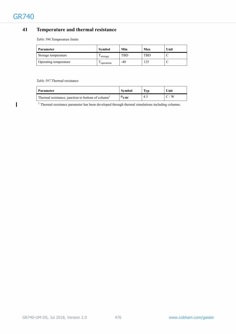
GR740
41 Temperature and thermal resistanceTable 596.Temperature limits
Parameter Symbol Min Max Unit
Storage temperature Tstorage TBD TBD C
Operating temperature Toperation -40 125 C
Table 597.Thermal resistance
Parameter Symbol Typ Unit
Thermal resistance, junction to bottom of column1 J-BC 4.5 C / W
1 Thermal resistance parameter has been developed through thermal simulations including columns.
GR740-UM-DS, Jul 2018, Version 2.0 476 www.cobham.com/gaisler

GR740
42 Ordering informationPlease contact Cobham Gaisler AB through [email protected]. Ordering information is provided in table 598 and a legend in table 599.
1) Users of prototypes with silicon revision 0 (GR740-XX and GR740-YY devices) should see section 1.1 for data sheet information. All devices listed in the table above have silicon revision 1.
A socket for use with the LG625 prototype devices is available from Ironwood Electronics (http://www.ironwoodelectronics.com). The part number is C14992.
Table 598.Ordering information, available models
Product Description Note
GR740-CP-LG625 Engineering model (prototype) 1
GR740-CP-CG625 Engineering model (prototype) 1
GR740-MP-CG625 Electrical Qualification Model
GR740-MSEQ-CG625 Flight Model, Equivalent to QML-Q
GR740-MSEV-CG625 Flight Model, Equivalent to QML-V
GR740-MSQ-CG625 Flight Model, QML-Q
GR740-MSV-CG625 Flight Model, QML-V
GR740-DC-CG625 Daisy-chain. Representative of GR740-YY/CP/MP/MSEQ/MSEV/MSQ/MSV-CG625
GR740-DD-CG625 Dummy package (not electrically functioning) with columns.
Table 599.Ordering legend
Designator Option Description
Product GR740 Quad-Core LEON4FT System-on-Chip
Temperature range and screening flow CP Prototypes, tested at room temperature
MP Electrical Qualification Model, tested at cold, room, hot
MSEQ Flight model, Equivalent to QML-Q
MSEV Flight model, Equivalent to QML-V
MSQ Flight model, QML-Q
MSV Flight model, QML-V
Package type CG Ceramic Column Grid Array (CCGA)
LG Ceramic Land Grid Array (LGA)
Number of pins 625 Number of pins
GR740-UM-DS, Jul 2018, Version 2.0 477 www.cobham.com/gaisler

GR740
43 Errata43.1 Overview
Table 600 below lists errata that are further described in section 43.2.
43.2 Errata descriptions
43.2.1 SpaceWire router missing first byte after EEP on links with downstream congestion
Input port overrun protection can cause the insertion of an Error End of Packet (EEP) to overwrite the first byte of the next packet, when transfer is resumed. For more information about overrun protection see section 13.2.15.
The missing first byte after EEP on link with downstream congestion occurs when all of the following conditions are met:
• Input port is configured to use overrun time-out protection. See section 13.2.15 for more infor-mation.
• Flow control causes output buffer to be entirely filled.
• Overrun time-out has occurred in the input buffer, the current packet is discarded in the input buffer, EEP is scheduled for insertion in the output buffer.
• Output port is resuming normal operation after receiving flow control token, i.e. the downstream receiver is able to accept data.
• After the output port resumes normal operation, the following packet is routed from the same input port as the packet that was discarded and terminated with EEP.
Workaround: Disable overrun protection, and if possible move the overrun protection to the end
node.
43.2.2 PCI master/initiator lockup due to write burst waitstates
A corner case exists where the PCI interface can get into an incorrect locked state. This only occurs when acting as master on the PCI bus and depends on specific response patterns from the target being accessed over the PCI bus.
The PCI master/initiator can lose track of the last word in a write burst transfer, leaving the controller in a state where the master will never consider the transfer as completed. The master will instead remain idle on the PCI bus and will not perform any new accesses
Condition: The issue will occur when the PCI master performs a burst write access on the PCI bus and the accessed PCI target issues at least one wait state on each of the last two data phases in the transfer. Read transfers are not affected. Transfers without wait states on at least one of the two last data phases are not affected.
Table 600.Errata
ID Name / Description
18-1 SpaceWire router missing first byte after EEP on links with downstream congestion
18-2 PCI master/initiator lockup due to write burst waitstates
18-3 L2 cache scrubber malfunction on uncorrectable error when SH option disabled
18-4 SpaceWire router block of output ports used for distributing multicast packets
GR740-UM-DS, Jul 2018, Version 2.0 478 www.cobham.com/gaisler

GR740
Impact: The PCI master/initiator will wait forever to complete the burst. Subsequent write accesses to the controller will be accepted as long as there is room in the controller's buffers. Following that, write accesses will receive AMBA RETRY responses. Read accesses will receive AMBA RETRY responses.The PCI controller in the GR740 is located behind an AHB-to-AHB bridge (connecting Slave IO bus to Processor bus). The bridge will receive the AMBA RETRY responses and the effect for the other masters, including the processor cores, in the system is that they will receive an AMBA SPLIT reply when trying to access the peripheral (slave IO bus) and subsequently never be allowed into arbitration again.
Recovery: It is possible to recover by setting the PCI master reset bit in the GRPCI2 control register. Any new access accepted (buffered) by the PCI master before the reset will be discarded. No reliable way of detecting the issue has been found. Possibly one processor core can detect that another on-chip bus master is waiting to access the Slave IO bus and can issue a reset to the GRPCI2 control register. This detection method is considered to be complicated to implement and one of the workarounds below should be applied.
Workaround: There is no configuration option in the PCI controller to avoid the issue. Possible workarounds:
• Workaround 1: Only generate single accesses to PCI targets that issue wait states before accept-ing data. This means that GR740 peripherals capable of DMA cannot access PCI memory space. The processor cores can access PCI memory space as long as store double (64-bit access) are not used.
• Workaround 2: Configure PCI target to issue disconnect with, or without, data instead of wait-states.
43.2.3 L2 cache scrubber malfunction on uncorrectable error when SH option disabled
There are two corner cases where the L2 cache scrubber can malfunction when encountering an uncorrectable error in the cache’s internal memories. The effect of the malfunction is either a dead-lock or an injection of an uncorrectable error.
Access pattern to trigger issue, requires EDAC to be enabled:
• Cache access (miss) resulting in data fetch form backend
• During the backend data fetch one cache line is scrubbed directly followed by a sub-word write (leads to a read-modify-write operation internally in the cache)
Case 1 (cache lock-up):
• The sub-word write is followed by another cache access which also vis a miss.
• The scrubber detects an uncorrectable data error on a unmodified (not dirty) cache line
• The scrubbed cache line is marked to be re-fetched from memory.
This state cannot be handled and results in a lock-up of the cache
Case 2 (incorrectly injecting uncorrectable data error):
• The scrubber detects an uncorrectable data error in the same cache-way as the miss access (data fetched from backend), or the scrubber accesses a different cache-way and error flags for all other ways (not accessed by the scrubber) are asserted.
• The scrubber access completes at the same clock cycle as data from the backend access is written to the cache memory.
This case will leads to a check bit error being injected (CB bits are inverted) for fetched data
Workaround: Set the scrubber hold (SH) bit and the (DSC) bit in the Access control register to pre-vent a new access entering the cache during the scrub operation.
GR740-UM-DS, Jul 2018, Version 2.0 479 www.cobham.com/gaisler

GR740
43.2.4 SpaceWire router block of output ports used for distributing multicast packetsWhen a subset of the output ports are busy sending a packet, an incoming multicast packet will allo-cate the available outputs ports and then wait for all output ports to become available. If another mul-ticast packet with higher priority (lower input port number) that will be routed to the same set of ports is sent to the router, this packet will allocate the currently occupied output ports when they become available. This results in a blocking state where multiple multicast packets, each allocating a subset of the output ports, blocks each other.
Triggering a blocking state occurs when all of the following conditions are met:
• Multicast packets distributed to multiple output ports from are sent from multiple input ports while a packet is also sent to only a subset of the same output ports.
• A multicast packet with higher priority (lower input port number) is received at the router when multicast packet with lower priority only has successfully allocated a subset of the output ports.
Workaround: All packets routed to output ports within a packet distribution group should use the same routing configuration and packet distribution mapping.
GR740-UM-DS, Jul 2018, Version 2.0 480 www.cobham.com/gaisler

Cobham Gaisler AB Kungsgatan 12411 19 GöteborgSwedenwww.cobham.com/[email protected]: +46 31 7758650F: +46 31 421407
Cobham Gaisler AB, reserves the right to make changes to any products and services described herein at any time without notice. Consult Cobham or an authorized sales representative to verify that the information in this document is current before using this product. Cobham does not assume any responsibility or liability arising out of the application or use of any product or service described herein, except as expressly agreed to in writing by Cobham; nor does the purchase, lease, or use of a product or service from Cobham convey a license under any patent rights, copyrights, trademark rights, or any other of the intellectual rights of Cobham or of third parties. All information is provided as is. There is no warranty that it is correct or suitable for any purpose, neither implicit nor explicit.
Copyright © 2018 Cobham Gaisler AB
GR740-UM-DS, Jul 2018, Version 2.0 481 of 481 www.cobham.com/gaisler
GR740