get pdf (5430 kb)
TRANSCRIPT
Ge-on-Si and Ge-on-SOI thermo-opticphase shifters for the mid-infrared
Aditya Malik,1,2,∗ Sarvagya Dwivedi,1,2 Liesbet Van Landschoot,1,2
Muhammad Muneeb,1,2,3 Yosuke Shimura,4,5 Guy Lepage,4 Joris VanCampenhout,4 Wendy Vanherle,4 Tinneke Van Opstal,4 Roger Loo,4
and Gunther Roelkens1,2,3
1Photonics Research Group, Ghent University-imec, Sint-Pietersnieuwstraat 41, 9000 Ghent,Belgium
2Center for Nano- and Biophotonics, Ghent University, Belgium3COBRA Research Institute, Eindhoven University of Technology, P.O. Box 513, Eindhoven
5600 MB,The Netherlands4imec, Kapeldreef 75, 3001 Leuven, Belgium
5Instituut voor Kern- en Stralingsfysica, KU Leuven, 3001 Leuven, Belgium∗[email protected]
Abstract: Germanium-on-silicon thermo-optic phase shifters are demon-strated in the 5 μm wavelength range. Basic phase shifters require 700 mWof power for a 2π phase shift. The required power is brought down to 80mW by complete undercut using focused ion beam. Finally an efficientthermo-optic phase shifter is demonstrated on the germanium on SOIplatform. A tuning power (for a 2π phase shift) of 105 mW is achieved fora Ge-on-SOI structure which is lowered to 16 mW for a free standing phaseshifter.
© 2014 Optical Society of America
OCIS codes: (250.5300) Photonic integrated circuits; (160.6840) Thermo-optical materials;(250.7360) Waveguide modulators.
References and links1. G. Roelkens, U. Dave, A. Gassenq, N. Hattasan, C. Hu, B. Kuyken, F. Leo, A. Malik, M. Muneeb, E. Ryckeboer,
S. Uvin, Z. Hens, R. Baets, Y. Shimura, F. Gencarelli, B. Vincent, R. Loo, J.Van Campenhout, L. Cerutti, Jean-Baptiste Rodriguez, E. Tournie, X. Chen, M. Nedeljkovic, G. Mashanovich, L. Shen, N. Healy, A. C. Peacock, X.Liu, R. Osgood, and W. Green, “Silicon-based heterogeneous photonic integrated circuits for the mid-infrared,”Opt. Mater. Express 3(9), 1523–1536 (2013).
2. G. Roelkens, U. Dave, A. Gassenq, N. Hattasan, C. Hu, B. Kuyken, F. Leo, A. Malik, M. Muneeb, E. Rycke-boer, D. Sanchez, S. Uvin, R. Wang, Z. Hens, R. Baets, Y. Shimura, F. Gencarelli, B. Vincent, R. Loo, J.VanCampenhout, L. Cerutti, Jean-Baptiste Rodriguez, E. Tournie, X. Chen, M. Nedeljkovic, G. Mashanovich, L.Shen, N. Healy, A. C. Peacock, X. Liu, R. Osgood, and W. Green, “Silicon-based photonic integration beyondthe telecommunication wavelength range,” IEEE J. Sel. Top. Quantum Electronics 20(4), 394–404 (2014).
3. H. Lin, L. Li, Y. Zou, S. Danto, J. D. Musgraves, K. Richardson, S. Kozacik, M. Murakowski, D. Prather, P. T.Lin, V. Singh, A. Agarwal, L. C. Kimerling, and J. Hu, “Demonstration of high-Q mid-infrared chalcogenideglass-on-silicon resonators,” Opt. Lett. 38(9), 1470–1472 (2013).
4. Z. Cheng, X. Chen, C. Y. Wong, K. Xu, and, H. K. Tsang, “Mid-infrared suspended membrane waveguide andring resonator on silicon-on-insulator,” IEEE Photon. J. 4(5), 1510–1519 (2012).
5. Y. Chen, H. Lin, J. Hu, and M. Li, “Heterogeneously integrated silicon photonics for the mid-infrared and spec-troscopic sensing,” ACS Nano 8(7), 6955–6961 (2014).
6. A. Malik, M. Muneeb, Y. Shimura, J. Van Campenhout, R. Loo, and G. Roelkens, “Germanium-on-silicon mid-infrared waveguides and mach-zehnder interferometers,” in Proc. of IEEE Photonics Conference 2013 (IEEE2013) pp. 104–105.
#222405 - $15.00 USD Received 3 Sep 2014; revised 30 Oct 2014; accepted 31 Oct 2014; published 7 Nov 2014(C) 2014 OSA 17 November 2014 | Vol. 22, No. 23 | DOI:10.1364/OE.22.028479 | OPTICS EXPRESS 28479
7. A. Malik, M.Muneeb, S. Pathak, Y. Shimura, J. Van Campenhout, R. Loo, and G. Roelkens, “Germanium-on-silicon mid-infrared arrayed waveguide grating multiplexers,” IEEE Photon. Technol. Lett. 25 (18), 1805-1808(2013).
8. A. Malik, M. Muneeb, Y. Shimura, J. Van Campenhout, R. Loo, and G. Roelkens, “Germanium-on-silicon planarconcave grating wavelength (de)multiplexers in the mid-infrared,” Appl. Phys. Lett. 103, 161119 (2013).
9. A. Masood, M. Pantouvaki, D. Goossens, G. Lepage, P. Verheyen, J. Van Campenhout, P. Absil, D. VanThourhout, and W. Bogaerts, “Fabrication and characterization of CMOS-compatible integrated tungsten heatersfor thermo-optic tuning in silicon photonics devices,” Opt. Mater. Express 4 (7), 1383–1388 (2014).
10. M. Nedeljkovic, S. Stankovic, C. J. Mitchell, A. Z. Khokhar, S. A. Reynolds, D. J. Thomson, F. Y. Gardes, C.G. Littlejohns, G. T. Reed, and G. Z. Mashanovich, “Mid-infrared thermo-optic modulators in SoI,” IEEE Phot.Technol. Lett. 26 (13), 1352–1355, (2014).
11. B. J. Frey, D. B. Leviton, and T. J. Madison, “Temperature-dependent refractive index of silicon and germanium,”Proc. SPIE 6273, 62732 (2006).
12. R. Soref, “Mid-infrared photonics in silicon and germanium,” Nat. Photonics 4(8), 495-497 (2010).13. M. Meuris, S. Arnauts, I. Cornelissen, K. Kenis, M. Lux, S. Degendt, P. Mertens, I. Teerlinck, R. Vos, L. Loewen-
stein, M. M. Heyns, and K. Wolke, “Implementation of the IMEC-Clean in advanced CMOS manufacturing,” inProc. IEEE Int. Symp. Semicond. Manuf.(IEEE 1999), pp. 157–160.
1. Introduction
The germanium-on-silicon waveguide platform is a strong candidate for mid-ir photonic inte-gration [1–2]. Its CMOS compatibility, simple fabrication scheme and wide range transparency(germanium is transparent up to 14 μm) make it a compelling solution compared to other mid-ir integration platforms proposed so far [3–5]. Recent demonstrations of low loss waveguidesand various photonic components such as Mach-Zehnder interferometers (MZIs) [6], arrayedwaveguide gratings (AWGs) [7] and planar concave gratings (PCGs) [8] show the versatility ofthe Ge-on-Si waveguide platform.Tuning of integrated optical components is of critical importance in many applications. Thistuning can be achieved by utilizing thermo-optic phase shifters where heat is generated in thevicinity of the waveguide, which affects the effective index of the optical mode [9–10]. Thermo-optic phase tuning is achieved by either placing a heater on top of the waveguide, which requiresthe deposition of an insulating layer of sufficient thickness, which optically isolates the modein the waveguide from the heater or by placing the heater on the side of the waveguide, whichavoids deposition of any intermediate cladding. In this paper, we describe the realization ofside-integrated thermo-optic phase shifters for mid-ir photonic integrated circuits.
2. General considerations
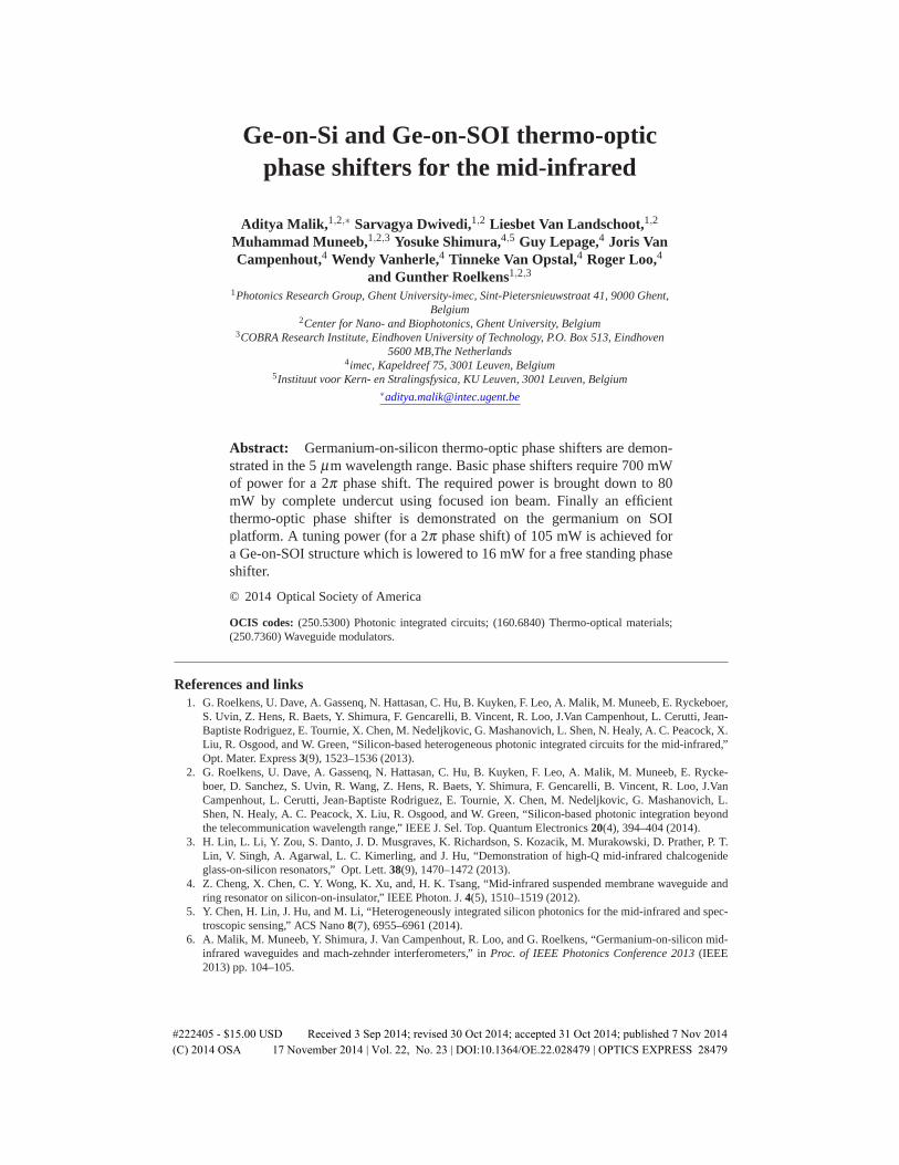
The heater structures were implemented on a germanium-on-silicon waveguide platform usinga 2 μm thick germanium waveguide layer. The waveguides were etched through the germaniumlayer and were 2.2 μm wide, making them single mode in the 5 μm wavelength range. Thedetails on the fabrication and measurement of Ge-on-Si PICs can be found in [7]. We designedthe heaters in a side heating configuration as schematically shown in Fig. 1. The heater itselfconsisted of a 2 μm wide and 100 nm high metal stack (Ti/Au or Cr/Au) deposited on a 4μm wide germanium strip. The distance between the waveguide and neighboring germaniumheater was chosen to be 2 μm, as this is the limit of the lithography tool used in our experiments.The thermal simulations were performed using COMSOL multiphysics. We performed steadystate FEM 3-D simulations to calculate the temperature change as a function of dissipatedpower in the heater. In Fig. 1, a zoomed version of the simulation window is shown where thespatial distribution of the temperature in the waveguide and heater is shown for a specific powerdissipated in the heater. In the COMSOL simulations, the substrate and the air top cladding werekept at a height of 200 μm and at a width of 400 μm. The length of the waveguide was alwayskept 400 μm additional to the length of the heater such that heat flow along the waveguide itself
#222405 - $15.00 USD Received 3 Sep 2014; revised 30 Oct 2014; accepted 31 Oct 2014; published 7 Nov 2014(C) 2014 OSA 17 November 2014 | Vol. 22, No. 23 | DOI:10.1364/OE.22.028479 | OPTICS EXPRESS 28480
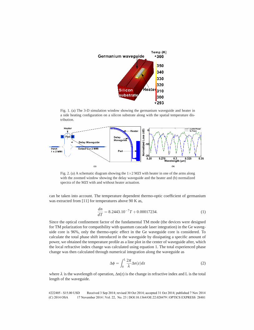
Fig. 1. (a) The 3-D simulation window showing the germanium waveguide and heater ina side heating configuration on a silicon substrate along with the spatial temperature dis-tribution.
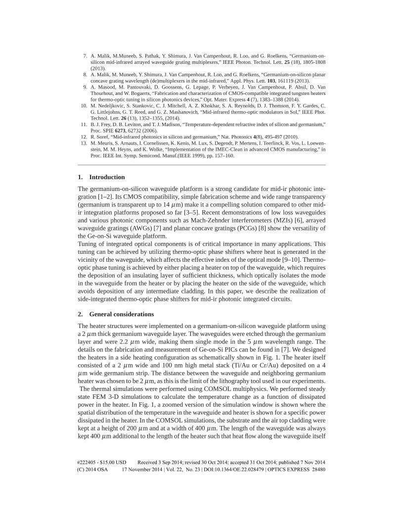
Fig. 2. (a) A schematic diagram showing the 1×2 MZI with heater in one of the arms alongwith the zoomed window showing the delay waveguide and the heater and (b) normalizedspectra of the MZI with and without heater actuation.
can be taken into account. The temperature dependent thermo-optic coefficient of germaniumwas extracted from [11] for temperatures above 90 K as,
dndT
= 8.2443.10−7T +0.00017234. (1)
Since the optical confinement factor of the fundamental TM mode (the devices were designedfor TM polarization for compatibility with quantum cascade laser integration) in the Ge waveg-uide core is 96%, only the thermo-optic effect in the Ge waveguide core is considered. Tocalculate the total phase shift introduced in the waveguide by dissipating a specific amount ofpower, we obtained the temperature profile as a line plot in the center of waveguide after, whichthe local refractive index change was calculated using equation 1. The total experienced phasechange was then calculated through numerical integration along the waveguide as
Δφ =∫ L
0
2πλ
Δn(z)dz (2)
where λ is the wavelength of operation, Δn(z) is the change in refractive index and L is the totallength of the waveguide.
#222405 - $15.00 USD Received 3 Sep 2014; revised 30 Oct 2014; accepted 31 Oct 2014; published 7 Nov 2014(C) 2014 OSA 17 November 2014 | Vol. 22, No. 23 | DOI:10.1364/OE.22.028479 | OPTICS EXPRESS 28481
To experimentally asses the performance of the thermo-optic phase shifters, we designed1×2 Mach Zehnder Interferometers (MZIs) in the 5 μm wavelength range with a fixed pathlength difference of 260 μm, which resulted in a free spectral range (FSR) of 25 nm. Thelength of the heater section was varied from 70 μm to 700 μm in steps of 70 μm and both endswere connected to 100 μm x 100 μm pads. The schematic diagram of the MZI is shown inFig. 2(a) along with a zoomed window showing the heater and the delay waveguide. A typicalmeasured transmission spectrum from the MZIs with and without heater actuation is shown inFig. 2(b). The insertion loss is 0.5 dB and the extinction ratio is -19 dB. The shift in destructiveinterference points is used to experimentally determine the obtained phase shift.
3. Ge-on-Si phase shifters
3.1. Standard phase shifter
We performed a COMSOL simulation for the Ge-on-Si phase shifters as shown in Fig. 3(a) andfound that one requires 700 mW of power to achieve a 2π phase shift. The heater consisted ofa stack of Ti/Au on a germanium strip, the length of which was kept 700 μm and the corre-sponding temperature profile in the center of the waveguide along its length can be seen in Fig.3(b). This simulation was then confirmed by measuring the induced phase shift as a functionof applied power as shown in Fig. 3(c). A good match between theory and experiment can beobserved.We can immediately draw the conclusion that a heater designed in this configuration is verypower inefficient. The main reason behind this is that the underlying silicon (thermal conduc-tivity = 130 W/(m*K)) acts as a perfect heat sink, which can also be seen in the simulationin Fig. 3(a). An improvement in the design is thus needed to bring down the required tuningpower. Since the majority of the heat is being sunk in the silicon substrate, a way to improvethe efficiency of the thermo-optic phase shifter is by thermally isolating it from the siliconsubstrate.
Fig. 3. (a) 2-D cross section in the middle of the simulation window, (b) line plot along thewaveguide showing the temperature profile. The length of the heater was kept 700 μm andthe power dissipated in the heater was 700 mW, (c) experimentally measured phase shift asa function of power dissipation along with the linear fit.
3.2. Fully undercut phase shifters
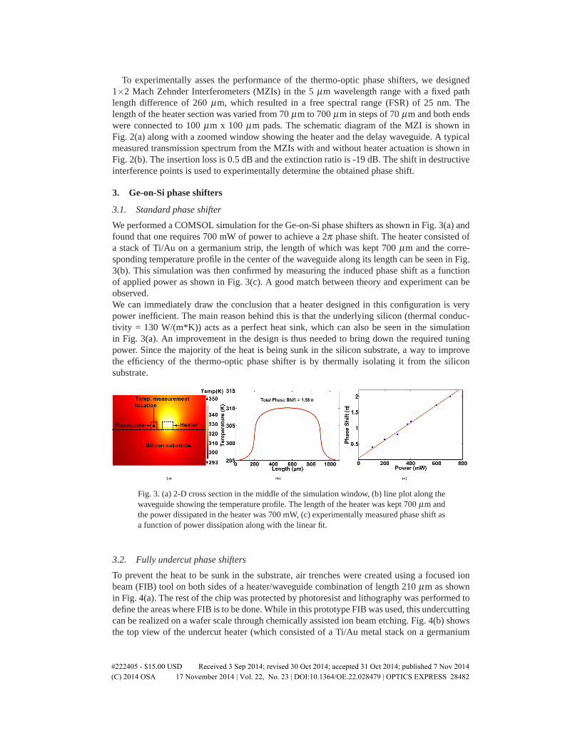
To prevent the heat to be sunk in the substrate, air trenches were created using a focused ionbeam (FIB) tool on both sides of a heater/waveguide combination of length 210 μm as shownin Fig. 4(a). The rest of the chip was protected by photoresist and lithography was performed todefine the areas where FIB is to be done. While in this prototype FIB was used, this undercuttingcan be realized on a wafer scale through chemically assisted ion beam etching. Fig. 4(b) showsthe top view of the undercut heater (which consisted of a Ti/Au metal stack on a germanium
#222405 - $15.00 USD Received 3 Sep 2014; revised 30 Oct 2014; accepted 31 Oct 2014; published 7 Nov 2014(C) 2014 OSA 17 November 2014 | Vol. 22, No. 23 | DOI:10.1364/OE.22.028479 | OPTICS EXPRESS 28482
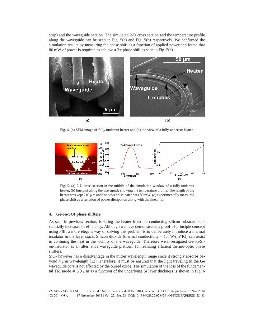
strip) and the waveguide section. The simulated 2-D cross section and the temperature profilealong the waveguide can be seen in Fig. 5(a) and Fig. 5(b) respectively. We confirmed thesimulation results by measuring the phase shift as a function of applied power and found that80 mW of power is required to achieve a 2π phase shift as seen in Fig. 5(c).
Fig. 4. (a) SEM image of fully undercut heater and (b) top view of a fully undercut heater.
Fig. 5. (a) 2-D cross section in the middle of the simulation window of a fully undercutheater, (b) line plot along the waveguide showing the temperature profile. The length of theheater was kept 210 μm and the power dissipated was 80 mW, (c) experimentally measuredphase shift as a function of power dissipation along with the linear fit.
4. Ge-on-SOI phase shifters
As seen in previous section, isolating the heater from the conducting silicon substrate sub-stantially increases its efficiency. Although we have demonstrated a proof-of-principle conceptusing FIB, a more elegant way of solving this problem is to deliberately introduce a thermalinsulator in the layer stack. Silicon dioxide (thermal conductivity = 1.4 W/(m*K)) can assistin confining the heat in the vicinity of the waveguide. Therefore we investigated Ge-on-Si-on-insulator as an alternative waveguide platform for realizing efficient thermo-optic phaseshifters.SiO2 however has a disadvantage in the mid-ir wavelength range since it strongly absorbs be-yond 4 μm wavelength [12]. Therefore, it must be ensured that the light traveling in the Gewaveguide core is not affected by the buried oxide. The simulation of the loss of the fundamen-tal TM mode at 5.3 μm as a function of the underlying Si layer thickness is shown in Fig. 6
#222405 - $15.00 USD Received 3 Sep 2014; revised 30 Oct 2014; accepted 31 Oct 2014; published 7 Nov 2014(C) 2014 OSA 17 November 2014 | Vol. 22, No. 23 | DOI:10.1364/OE.22.028479 | OPTICS EXPRESS 28483
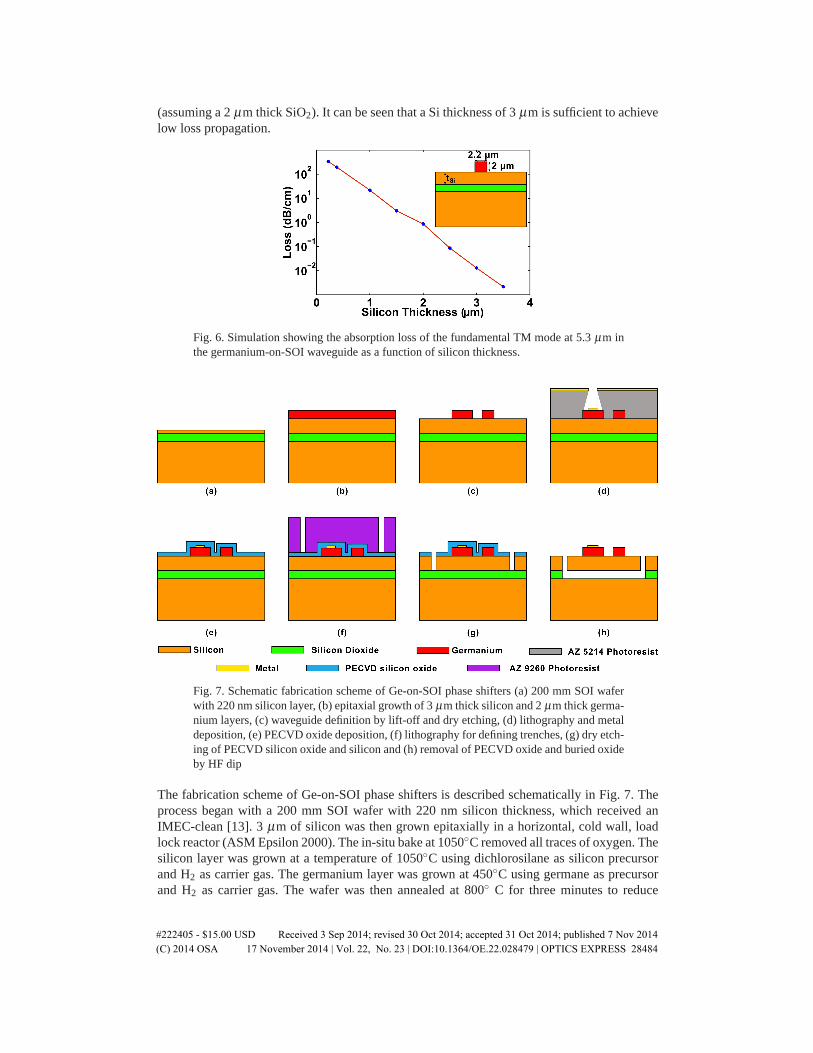
(assuming a 2 μm thick SiO2). It can be seen that a Si thickness of 3 μm is sufficient to achievelow loss propagation.
Fig. 6. Simulation showing the absorption loss of the fundamental TM mode at 5.3 μm inthe germanium-on-SOI waveguide as a function of silicon thickness.
Fig. 7. Schematic fabrication scheme of Ge-on-SOI phase shifters (a) 200 mm SOI waferwith 220 nm silicon layer, (b) epitaxial growth of 3 μm thick silicon and 2 μm thick germa-nium layers, (c) waveguide definition by lift-off and dry etching, (d) lithography and metaldeposition, (e) PECVD oxide deposition, (f) lithography for defining trenches, (g) dry etch-ing of PECVD silicon oxide and silicon and (h) removal of PECVD oxide and buried oxideby HF dip
The fabrication scheme of Ge-on-SOI phase shifters is described schematically in Fig. 7. Theprocess began with a 200 mm SOI wafer with 220 nm silicon thickness, which received anIMEC-clean [13]. 3 μm of silicon was then grown epitaxially in a horizontal, cold wall, loadlock reactor (ASM Epsilon 2000). The in-situ bake at 1050◦C removed all traces of oxygen. Thesilicon layer was grown at a temperature of 1050◦C using dichlorosilane as silicon precursorand H2 as carrier gas. The germanium layer was grown at 450◦C using germane as precursorand H2 as carrier gas. The wafer was then annealed at 800◦ C for three minutes to reduce
#222405 - $15.00 USD Received 3 Sep 2014; revised 30 Oct 2014; accepted 31 Oct 2014; published 7 Nov 2014(C) 2014 OSA 17 November 2014 | Vol. 22, No. 23 | DOI:10.1364/OE.22.028479 | OPTICS EXPRESS 28484
10 μm
Germanium Heater
Germanium Waveguide
Silicon
Undercut
Metal
100 μm
Pads
Delay Waveguide
Trench
Heater
Si Ge
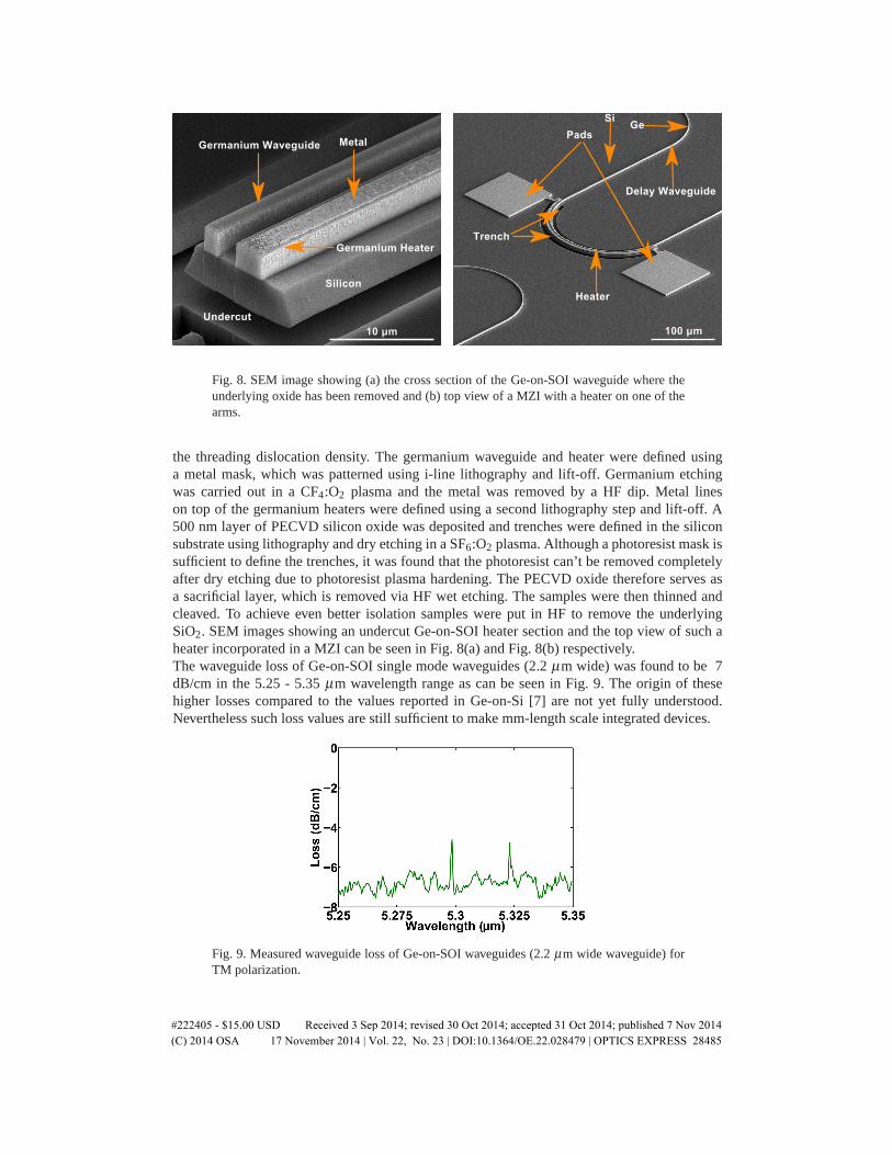
Fig. 8. SEM image showing (a) the cross section of the Ge-on-SOI waveguide where theunderlying oxide has been removed and (b) top view of a MZI with a heater on one of thearms.
the threading dislocation density. The germanium waveguide and heater were defined usinga metal mask, which was patterned using i-line lithography and lift-off. Germanium etchingwas carried out in a CF4:O2 plasma and the metal was removed by a HF dip. Metal lineson top of the germanium heaters were defined using a second lithography step and lift-off. A500 nm layer of PECVD silicon oxide was deposited and trenches were defined in the siliconsubstrate using lithography and dry etching in a SF6:O2 plasma. Although a photoresist mask issufficient to define the trenches, it was found that the photoresist can’t be removed completelyafter dry etching due to photoresist plasma hardening. The PECVD oxide therefore serves asa sacrificial layer, which is removed via HF wet etching. The samples were then thinned andcleaved. To achieve even better isolation samples were put in HF to remove the underlyingSiO2. SEM images showing an undercut Ge-on-SOI heater section and the top view of such aheater incorporated in a MZI can be seen in Fig. 8(a) and Fig. 8(b) respectively.The waveguide loss of Ge-on-SOI single mode waveguides (2.2 μm wide) was found to be 7dB/cm in the 5.25 - 5.35 μm wavelength range as can be seen in Fig. 9. The origin of thesehigher losses compared to the values reported in Ge-on-Si [7] are not yet fully understood.Nevertheless such loss values are still sufficient to make mm-length scale integrated devices.
Fig. 9. Measured waveguide loss of Ge-on-SOI waveguides (2.2 μm wide waveguide) forTM polarization.
#222405 - $15.00 USD Received 3 Sep 2014; revised 30 Oct 2014; accepted 31 Oct 2014; published 7 Nov 2014(C) 2014 OSA 17 November 2014 | Vol. 22, No. 23 | DOI:10.1364/OE.22.028479 | OPTICS EXPRESS 28485

4.1. Ge-on-SOI phase shifters without undercut
To evaluate the performance of the Ge-on-SOI phase shifters, we performed previously de-scribed COMSOL simulations, the results of which are shown in Fig. 10(a) and Fig. 10(b).Since the undercut by FIB was done on a 210 μm long heater, we measured the phase shift asa function of dissipated heat on a heater (consisting of a Ti/Au metal stack on a germaniumstrip) of similar length as shown in Fig. 10(c) and found that the results match well with thesimulations in Fig. 10(b). The heater performance as a function of length was also studied usingCOMSOL by calculating the tuning power required to achieve a phase shift of 2π and it wasfound that it decays rapidly at first becoming almost constant for longer heaters as shown inFig. 11. This can be explained by the longitudinal flow of heat along the waveguide. As seenin the SEM image in Fig. 8(b), the heated waveguide is at its ends is connected to a 3.22 μmthick silicon slab (onto which the germanium waveguides are grown), which extends all overthe circuit. This layer serves as an efficient heat spreader, which is the dominant source of heatsinking in the Ge-on-SOI phase shifters. This especially affects the shorter heaters since forlonger devices the thermal resistance for the longitudinal heat flow becomes larger. This wasalso verified experimentally, the results of which are plotted together with the simulation resultsshown in Fig. 11.
Fig. 10. (a) 2-D cross section in the middle of the simulation window of a Ge-on-SOIheater, (b) line plot along the waveguide showing the temperature profile. The length ofthe heater was kept 210 μm and the power dissipated was 100 mW. (c) experimentallymeasured phase shift as a function of power dissipation along with the linear fit.
Fig. 11. Tuning power to achieve 2π phase shift as a function of length for a Ge-on-SOIphase shifter without undercut.
#222405 - $15.00 USD Received 3 Sep 2014; revised 30 Oct 2014; accepted 31 Oct 2014; published 7 Nov 2014(C) 2014 OSA 17 November 2014 | Vol. 22, No. 23 | DOI:10.1364/OE.22.028479 | OPTICS EXPRESS 28486
4.2. Ge-on-SOI phase shifters with undercut
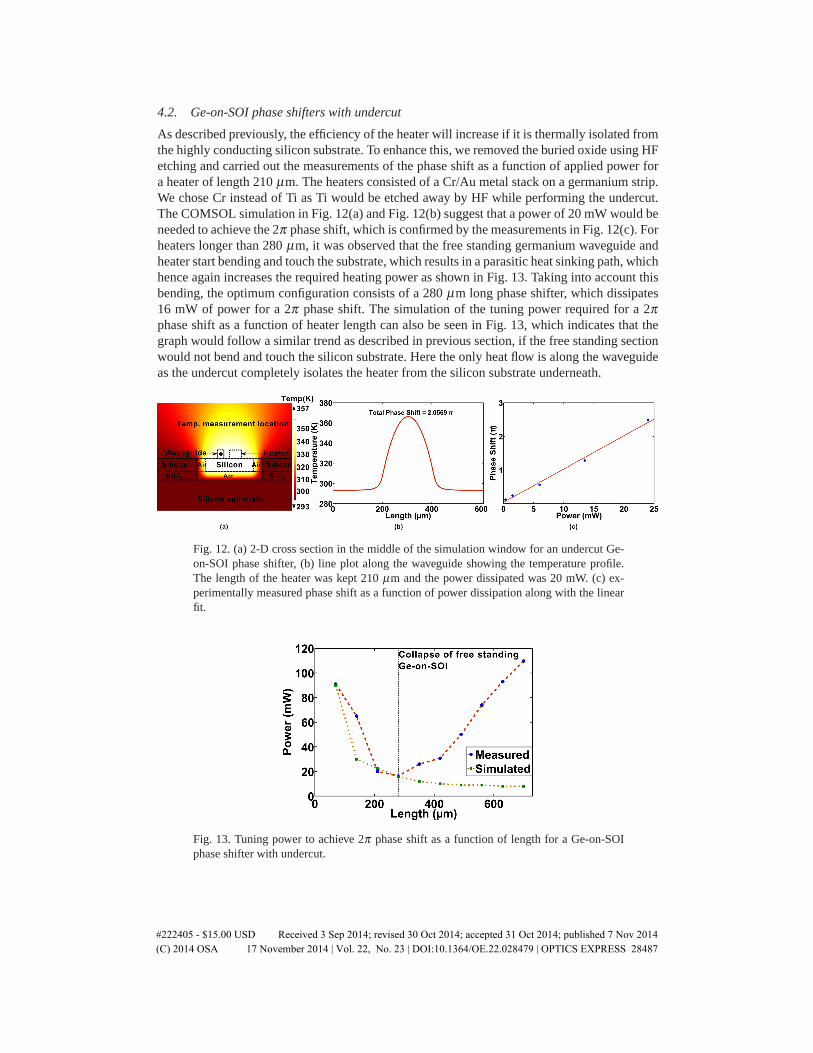
As described previously, the efficiency of the heater will increase if it is thermally isolated fromthe highly conducting silicon substrate. To enhance this, we removed the buried oxide using HFetching and carried out the measurements of the phase shift as a function of applied power fora heater of length 210 μm. The heaters consisted of a Cr/Au metal stack on a germanium strip.We chose Cr instead of Ti as Ti would be etched away by HF while performing the undercut.The COMSOL simulation in Fig. 12(a) and Fig. 12(b) suggest that a power of 20 mW would beneeded to achieve the 2π phase shift, which is confirmed by the measurements in Fig. 12(c). Forheaters longer than 280 μm, it was observed that the free standing germanium waveguide andheater start bending and touch the substrate, which results in a parasitic heat sinking path, whichhence again increases the required heating power as shown in Fig. 13. Taking into account thisbending, the optimum configuration consists of a 280 μm long phase shifter, which dissipates16 mW of power for a 2π phase shift. The simulation of the tuning power required for a 2πphase shift as a function of heater length can also be seen in Fig. 13, which indicates that thegraph would follow a similar trend as described in previous section, if the free standing sectionwould not bend and touch the silicon substrate. Here the only heat flow is along the waveguideas the undercut completely isolates the heater from the silicon substrate underneath.
Fig. 12. (a) 2-D cross section in the middle of the simulation window for an undercut Ge-on-SOI phase shifter, (b) line plot along the waveguide showing the temperature profile.The length of the heater was kept 210 μm and the power dissipated was 20 mW. (c) ex-perimentally measured phase shift as a function of power dissipation along with the linearfit.
Fig. 13. Tuning power to achieve 2π phase shift as a function of length for a Ge-on-SOIphase shifter with undercut.
#222405 - $15.00 USD Received 3 Sep 2014; revised 30 Oct 2014; accepted 31 Oct 2014; published 7 Nov 2014(C) 2014 OSA 17 November 2014 | Vol. 22, No. 23 | DOI:10.1364/OE.22.028479 | OPTICS EXPRESS 28487
5. Conclusion
In conclusion, we have demonstrated thermo-optic phase shifters for the mid-ir for the first timeon the Ge-on-Si and Ge-on-SOI waveguide platform. Thermo-optic phase shifters in differentconfigurations have been studied and a new waveguide platform (Ge-on-SOI) has been demon-strated which brings down the required tuning power for a 2π phase shift from 700 mW to16 mW. This paves the way to the power efficient tuning of mid-infrared photonic integratedcircuits.
Acknowledgments
This work was supported by FP-7-ERC MIRACLE. Yosuke Shimura would like to thank FWOfor a Pegasus scholarship.
#222405 - $15.00 USD Received 3 Sep 2014; revised 30 Oct 2014; accepted 31 Oct 2014; published 7 Nov 2014(C) 2014 OSA 17 November 2014 | Vol. 22, No. 23 | DOI:10.1364/OE.22.028479 | OPTICS EXPRESS 28488