germanium doping of cubic gan grown by molecular beam epitaxy · gan (c-gan) is preferably realized...
TRANSCRIPT
Germanium doping of cubic GaN grownby molecular beam epitaxy
Cite as: J. Appl. Phys. 125, 095703 (2019); doi: 10.1063/1.5066095
View Online Export Citation CrossMarkSubmitted: 12 October 2018 · Accepted: 19 February 2019 ·Published Online: 6 March 2019
M. Deppe,1,a) J. W. Gerlach,2 S. Shvarkov,1 D. Rogalla,3 H.-W. Becker,3 D. Reuter,1 and D. J. As1
AFFILIATIONS
1Department Physik, Universität Paderborn, Warburger Str. 100, 33098 Paderborn, Germany2Leibniz-Institut für Oberflächenmodifizierung (IOM) e.V., Permoserstr. 15, 04318 Leipzig, Germany3RUBION, Ruhr-Universität Bochum, Universitätsstr. 150, 44801 Bochum, Germany
a)Electronic mail: [email protected]
ABSTRACT
We present a study of germanium as an alternative to silicon for n-type doping of cubic GaN. We find that Ge is a well-suited donor impu-rity. Our layers were grown by plasma-assisted molecular beam epitaxy on 3C-SiC/Si (001) substrates. Germanium-doped layers were fabri-cated with donor concentrations ranging over several orders of magnitude up to 3.7 × 1020 cm−3. For comparison, silicon-doped layers withdonor concentrations of up to 3.8 × 1019 cm−3 were also grown. Incorporation of germanium into the cubic GaN layers was verified bytime-of-flight secondary ion mass spectrometry. The crystalline quality of our layers was analyzed using high-resolution x-ray diffraction.Germanium- as well as silicon-doped layers with donor concentrations above 1019 cm−3 exhibited an increase of the dislocation density withincreasing dopant concentration. The surface topography of our layers was investigated by atomic force microscopy. Comparable values forthe surface roughness were measured for germanium- as well as silicon-doped layers. Optical properties were investigated by photolumines-cence spectroscopy at 13 K. Doping with silicon resulted in a spectrally slightly narrower luminescence than doping with germanium.Donor concentrations and carrier mobilities were determined by Hall effect measurements at room temperature and we observe 20% higherelectron mobilities for Ge-doping compared to Si-doping in the case of high dopant concentrations.
Published under license by AIP Publishing. https://doi.org/10.1063/1.5066095
I. INTRODUCTION
GaN-based optoelectronic devices are mostly grown in thethermodynamically stable hexagonal wurtzite crystal structurealong the c-direction. Due to symmetry reasons, spontaneous andpiezoelectric polarization fields are existent and limit the recombi-nation efficiency in, e.g., double heterostructures or quantum wells.There exist several approaches to overcome these effects. One ofthem is to grow the metastable cubic zinc blende phase of GaN,where the aforementioned polarization fields are missing.
For device fabrication, it is essential to control p- and n-typedoping of the semiconductor. Up to now, n-type doping of cubicGaN (c-GaN) is preferably realized by the incorporation ofsilicon.1–4 It is well known that the incorporation of silicon in wurt-zite GaN leads to tensile strain,5 whereas it has recently been shownthat this is not the case for the incorporation of germanium, allow-ing to grow highly doped layers with improved crystalline quality.6
Recently, we have demonstrated the incorporation of germa-nium into c-GaN layers grown by molecular beam epitaxy (MBE)
and have presented first investigations of structural7 and opticalproperties.8 In this paper, we provide an extensive study on thestructural, electrical, and optical properties of germanium dopedc-GaN and give a comparison to silicon doped layers.
II. EXPERIMENTAL DETAILS
Our c-GaN layers were grown by plasma-assisted molecularbeam epitaxy (MBE) in a Riber-32 system equipped with anOxford Applied Research HD25 radio frequency plasma source tosupply activated nitrogen atoms. Not intentionally doped (n.i.d.),germanium-doped, and silicon-doped c-GaN layers were grown.To cover a large range of doping densities, the germanium effusioncell temperature was varied in a range of 600 °C to 1000 °C. Thesilicon effusion cell was operated at temperatures from 950 °C andthe maximum temperature reached was 1100 °C. The layers weredeposited on 3C-SiC/Si (001) substrates at a growth temperatureof 720 °C. A gallium beam equivalent pressure (BEP) of 1.1 × 10⁻⁷
Torr and a nitrogen flow of 0.21 sccm were employed for all layers.
Journal ofApplied Physics ARTICLE scitation.org/journal/jap
J. Appl. Phys. 125, 095703 (2019); doi: 10.1063/1.5066095 125, 095703-1
Published under license by AIP Publishing.

Reflection high energy electron diffraction (RHEED) was employedfor in situ growth control.9 After growth, the c-GaN layer thick-ness was determined by reflectometric interference spectroscopy.Time-of-flight secondary ion mass spectrometry (TOF-SIMS) wasperformed with an ION-TOF TOF-SIMS 5 instrument to analyzethe composition of our layers. A primary ion beam of 15 keV69Ga+ ions scanned a 50 × 50 μm2 area. Depth profiling was doneusing a 1.0 keV Cs+ beam covering an area of 300 × 300 μm2.Negative ion mass spectra were collected. To determine the dislo-cation density and the amount of hexagonal inclusions, high-resolution x-ray diffraction (HRXRD) was carried out on a PhilipsX’Pert MRD. The surface topography of our layers was investigatedusing a Nanosurf Mobile S atomic force microscope (AFM) operat-ing in contact mode. Photoluminescence (PL) spectra were takenusing a continuous wave frequency-quadrupled Nd:YAG laser(266 nm) operating at a power of 5 mW as an excitation source.An Andor iDus 420 CCD detector array mounted on a SPEX 270 Mimaging spectrograph was used for light detection. Carrier densityand mobility were determined by Hall effect measurements in vander Pauw geometry at room temperature.
III. RESULTS AND DISCUSSION
The basic layer properties and effusion cell temperatures,which were used to achieve different doping levels, are summarizedin Table I. The donor concentrations were taken from Hall effectmeasurements, assuming the two highest germanium-doped layersand the highest silicon-doped layer to be degenerate. In this case,the measured carrier density is equal to the donor concentration.Donor concentrations of lower doped layers were extrapolatedbased on the dopants vapor pressure curves.10,11 Since germaniumhas a significantly higher vapor pressure compared to silicon, it ispossible to achieve a two orders of magnitude higher doping levelfor comparable effusion cell temperatures.
A. TOF-SIMS-measurements
The germanium-doped c-GaN samples were investigated byTOF-SIMS to gain depth-resolved information on the Ge incorpo-ration into the cubic GaN epilayers. To obtain absolute values forthe germanium concentration, a calibration of the germanium-related secondary ion signals needs to be done. Therefore, we fab-ricated and analyzed ion-implanted samples, which will be dis-cussed in the following.
Germanium ions were implanted into 580 nm thick notintentionally doped (n.i.d.) c-GaN layers by two different ionimplanters at the Ruhr-University of Bochum. The firstimplanter (100 kV ion accelerator) with low ion energies of 95 keVallows shallow implantation and uses 72Ge, whereas the secondimplanter (4 MV tandem accelerator) with high ion energies of750 keV allows deep implantation and uses 74Ge. In addition, thetwo different Ge isotopes result in two independent TOF-SIMSsignals, which can be used for analysis.
The implantation parameters chosen are depicted in Table II.The germanium fluences resulted in volume concentrations betweenabout 1018 and 1020 cm−3. These Ge concentrations are similar tothose intended to be incorporated during MBE growth. The implan-tation profiles (Ge ions per fluence) in cubic GaN are simulated bythe freeware software package SRIM-2013 (SRIM—The Stopping
TABLE I. Overview of doping characteristics and basic sample properties.
Dopant Cell temp. (°C) Flux (cm−2 s−1)Estimated donor
concentration (cm−3)aTOF-SIMS donor
concentration (cm−3)Carrier mobility(cm2 V−1 s−1) Thickness (nm)
n.i.d.b 612Ge 600 1.8 × 10⁶ 1.7 × 10¹⁴ 1.5 × 10¹⁸ 588Ge 650 3.1 × 10⁷ 3.0 × 10¹⁵ 552Ge 700 3.4 × 10⁸ 3.2 × 10¹⁶ 3.6 × 10¹⁸ 556Ge 750 3.3 × 10⁹ 3.1 × 10¹⁷ 558Ge 800 2.9 × 10¹⁰ 2.7 × 10¹⁸ 6.0 × 10¹⁸ 105 543Ge 900 9.3 × 10¹¹ 8.7 × 10¹⁹ 7.7 × 10¹⁹ 90 460Ge 1000 8.9 × 10¹² 3.7 × 10²⁰ 3.2 × 10²⁰ 63 363Si 950 1.1 × 10¹⁰ 3.0 × 10¹⁷ 607Si 1000 6.2 × 10¹⁰ 1.7 × 10¹⁸ 84 647Si 1050 2.8 × 10¹¹ 7.6 × 10¹⁸ 74 611Si 1100 1.4 × 10¹² 3.8 × 10¹⁹ 77 564
aThe donor concentrations of the two highest germanium-doped samples and the highest silicon-doped sample (bold) are determined by Hall effectmeasurements. Donor concentrations of lower doped samples were extrapolated based on the dopants vapor pressure curves. The extrapolated values areprinted in italics. The GaN layer thickness was measured by reflectivity after growth.bNot intentionally doped.
TABLE II. Parameters for implantation of Ge ions into c-GaN layers.
Implantationsample Isotope
Ion energy(keV)
Fluence(cm−2)
Angle ofincidence (deg)
A 72Ge 95 1.6 × 10¹⁵ 7B 74Ge 750 1.0 × 10¹⁵ 7C 74Ge 750 1.0 × 10¹⁴ 7
Journal ofApplied Physics ARTICLE scitation.org/journal/jap
J. Appl. Phys. 125, 095703 (2019); doi: 10.1063/1.5066095 125, 095703-2
Published under license by AIP Publishing.

and Range of Ions in Matter, Ref. 12) and are shown in Fig. 1 fordifferent ion energies of 95 keV and 740 keV, respectively. TheGermanium concentrations are obtained by multiplying the implan-tation profiles with the respective fluence.
In Fig. 2, the germanium depth profiles of ion-implantedsamples measured by TOF-SIMS are shown together with therespective GaN− signal. As for the GaN layer, the sputtering time isproportional to the depth the signals originate from. The transitionbetween the GaN layer and 3C-SiC substrate occurs after approxi-mately 1050 s of sputtering. For the implanted sample A, twosignals that are related to the implanted 72Ge ions were recorded.
The 72Ge− signal is directly related to the implanted ions, but alsothe 72GeN− signal reflects the germanium depth profile. However,the 72GeN− signal features a higher sensitivity, but it is overlappedby a GaN-related signal (the 72GeN− signal is also present inundoped layers). For the implanted sample B, two signals that arerelated to the implanted 74Ge ions were recorded. Again, the74GeN− signal features a higher sensitivity in comparison to pure74Ge−, and in contrast to the 72GeN− signal, it is not overlapped byanother mass signal.
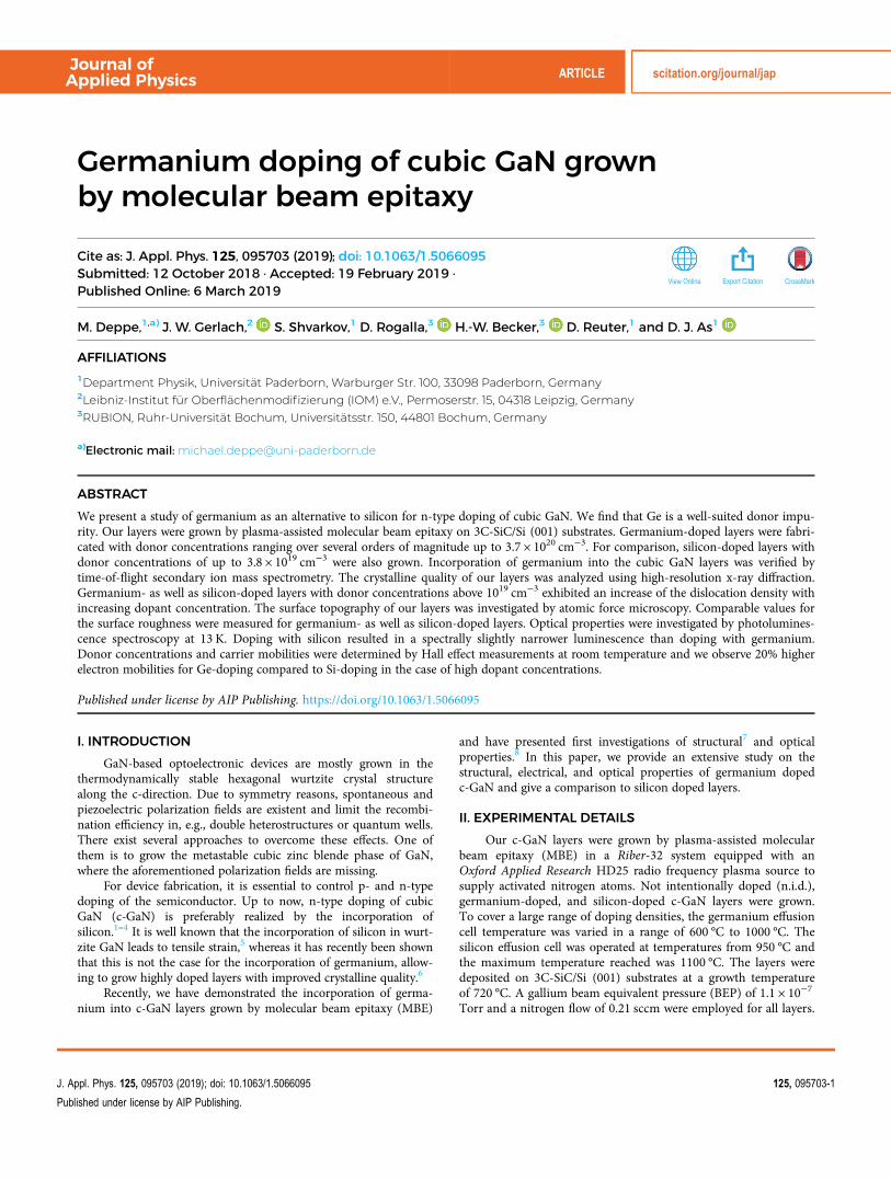
For calculating the absolute germanium concentration, the74GeN− signal from the implanted samples B and C is taken. In thecase of the implanted sample A, the constant GaN-related back-ground is subtracted from the 72GeN− signal. The remaining inten-sity is corrected by the isotopic ratio of germanium to obtain asignal that is adequate to the 74GeN− signal in samples B and C. Inthe next step, the 74GeN− signals are normalized to the respectiveGaN− signal intensity to take varying ion beam currents or sputterparameters into account. At last, the maxima of the simulatedimplantation profiles (multiplied by the fluence) and the maximaof the implantation profiles measured by TOF-SIMS are correlated.In Fig. 3, the maximum 74Ge concentration is plotted versus theintensity ratio of the 74GeN/69GaN mass signal maximum. Fromthe linear regression of the three pairs of data, a linear equation forcalibration is obtained and a proportionality factor of k = 1.5695 ×1021 cm−3 is estimated. The TOF-SIMS measurements for theMBE-grown samples are discussed in the next paragraph.
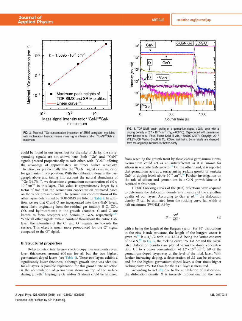
Figure 4 shows the TOF-SIMS depth profile of the layer withan estimated germanium density of 2.7 × 1018 cm−3 (TGe = 800 °C).After a sputter time of approximately 860 s, a significant change ofthe recorded depth profile can be observed, indicating that theinterface between the GaN layer and the 3C-SiC substrate isreached at this point. For the other layers with different thicknesses,the time required until the interface is reached linearly scales withthe layer thickness. The predominant negative secondary ionsignals from the c-GaN layer originate from GaN− and GaO− ions.Two signals, originating from 74Ge− and 74GeN− ions, prove theincorporation of germanium into the GaN layer. Furthermore,several other germanium isotopes (70Ge, 72Ge, 73Ge, and 76Ge)
FIG. 1. Implantation profiles (Ge ions per fluence) of Ge in cubic GaN simu-lated by SRIM-2013 for an angle of incidence of 7° and different ion energies of95 keV and 750 keV, respectively.
FIG. 2. Ge depth profiles of the ion-implanted samples, measured byTOF-SIMS.
Journal ofApplied Physics ARTICLE scitation.org/journal/jap
J. Appl. Phys. 125, 095703 (2019); doi: 10.1063/1.5066095 125, 095703-3
Published under license by AIP Publishing.
could be found in our layers, but for the sake of clarity, the corre-sponding signals are not shown here. Both 74Ge− and 74GeN−
signals proceed proportionally to each other, with 74GeN− offeringthe advantage of approximately six times higher sensitivity.Therefore, we preferentially take the 74GeN− signal as an indicatorfor germanium incorporation. With the calibration done in the par-agraph above and taking into account the natural abundance of74Ge (36.7%13), we determine a germanium concentration of 6.0 ×1018 cm−3 in this layer. This value is approximately larger by afactor of two than the germanium concentration estimated basedon the vapor pressure curve. The germanium concentrations of theother layers determined by TOF-SIMS are listed in Table I. In addi-tion, we see that C and O are incorporated into the c-GaN layers,most likely originating from the residual gas (mainly H2O, CO2,CO, and hydrocarbons) in the growth chamber. C and O areknown to form acceptors and donors in GaN, respectively.1,14
While all other signals remain constant throughout the entire GaNlayer, the intensities of the C− and O− signals rise towards thesurface. This effect is much more pronounced for the C− signalcompared to the O− signal.
B. Structural properties
Reflectometric interference spectroscopy measurements reveallayer thicknesses around 600 nm for all but the two highestgermanium-doped layers (see Table I). These two layers exhibit asignificantly lower thickness, although growth time was identicalfor all layers. A possible explanation for this growth rate reductionis the accumulation of germanium atoms on top of the surfaceduring growth.7 Impinging Ga and/or N atoms could be hindered
from reaching the growth front by these excess germanium atoms.Germanium could act as an antisurfactant as it is known forsilicon in wurtzite GaN growth.15 On the other hand, it is reportedthat germanium acts as a surfactant in a-plane growth of wurtziteGaN at doping levels above 1020 cm−3.16 Further investigation onthe role of silicon and germanium in c-GaN growth kinetics isrequired at this point.
HRXRD rocking curves of the (002) reflections were acquiredto determine the dislocation density as a measure of the crystallinequality of our layers. According to Gay et al.,17 the dislocationdensity D can be estimated from the rocking curve full width athalf maximum (FWHM) Δθ by
D ¼ Δθ2
9b2, (1)
with b being the length of the Burgers vector. For 60° dislocationsin the zinc blende structure, the length of the burgers vector isgiven by18 b ¼ a=
ffiffiffi2
pwith a ¼ 4:503 A
�being the lattice constant
of c-GaN.19 In Fig. 5, the rocking curve FWHM Δθ and the calcu-lated dislocation densities are plotted versus the donor concentra-tion. Up to a donor concentration of 2.7 × 1018 cm−3, Δθ of thegermanium-doped layers stay at the level of the n.i.d. layer. Withfurther increasing doping, a deterioration of Δθ can be observed,and for the highest germanium-doped layer, a four times higherrocking curve FWHM than for the n.i.d. layer is measured.
According to Ref. 20, due to the annihilation of dislocations,the dislocation density D is inversely proportional to the layer
FIG. 3. Maximal 74Ge concentration (maximum of SRIM calculation multipliedwith implantation fluence) versus mass signal intensity ration 74GeN/69GaN inmaximum.
FIG. 4. TOF-SIMS depth profile of a germanium-doped c-GaN layer with adoping density of 2.7 × 1018 cm−3 (TGe = 800 °C). Reproduced with permissionfrom Deppe et al., Phys. Status Solidi B 254, 1600700 (2017). Copyright 2017WILEY-VCH Verlag GmbH & Co. KGaA, Weinheim. Some labels are changedfrom the original publication for better clarity.
Journal ofApplied Physics ARTICLE scitation.org/journal/jap
J. Appl. Phys. 125, 095703 (2019); doi: 10.1063/1.5066095 125, 095703-4
Published under license by AIP Publishing.
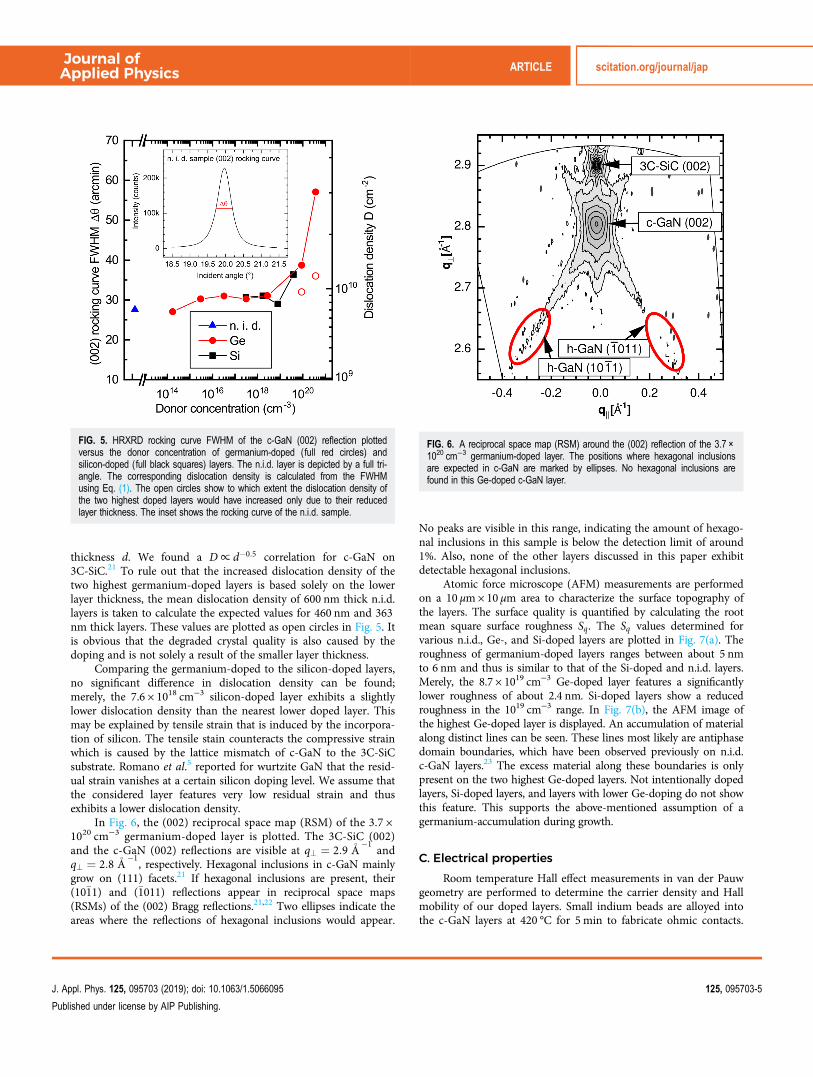
thickness d. We found a D/ d�0:5 correlation for c-GaN on3C-SiC.21 To rule out that the increased dislocation density of thetwo highest germanium-doped layers is based solely on the lowerlayer thickness, the mean dislocation density of 600 nm thick n.i.d.layers is taken to calculate the expected values for 460 nm and 363nm thick layers. These values are plotted as open circles in Fig. 5. Itis obvious that the degraded crystal quality is also caused by thedoping and is not solely a result of the smaller layer thickness.
Comparing the germanium-doped to the silicon-doped layers,no significant difference in dislocation density can be found;merely, the 7.6 × 1018 cm−3 silicon-doped layer exhibits a slightlylower dislocation density than the nearest lower doped layer. Thismay be explained by tensile strain that is induced by the incorpora-tion of silicon. The tensile stain counteracts the compressive strainwhich is caused by the lattice mismatch of c-GaN to the 3C-SiCsubstrate. Romano et al.5 reported for wurtzite GaN that the resid-ual strain vanishes at a certain silicon doping level. We assume thatthe considered layer features very low residual strain and thusexhibits a lower dislocation density.
In Fig. 6, the (002) reciprocal space map (RSM) of the 3.7 ×1020 cm−3 germanium-doped layer is plotted. The 3C-SiC (002)and the c-GaN (002) reflections are visible at q? ¼ 2:9 A
� �1and
q? ¼ 2:8 A� �1
, respectively. Hexagonal inclusions in c-GaN mainlygrow on (111) facets.21 If hexagonal inclusions are present, their(10�11) and (�1011) reflections appear in reciprocal space maps(RSMs) of the (002) Bragg reflections.21,22 Two ellipses indicate theareas where the reflections of hexagonal inclusions would appear.
No peaks are visible in this range, indicating the amount of hexago-nal inclusions in this sample is below the detection limit of around1%. Also, none of the other layers discussed in this paper exhibitdetectable hexagonal inclusions.
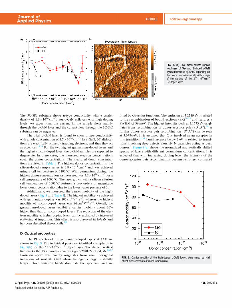
Atomic force microscope (AFM) measurements are performedon a 10 μm× 10 μm area to characterize the surface topography ofthe layers. The surface quality is quantified by calculating the rootmean square surface roughness Sq. The Sq values determined forvarious n.i.d., Ge-, and Si-doped layers are plotted in Fig. 7(a). Theroughness of germanium-doped layers ranges between about 5 nmto 6 nm and thus is similar to that of the Si-doped and n.i.d. layers.Merely, the 8.7 × 1019 cm−3 Ge-doped layer features a significantlylower roughness of about 2.4 nm. Si-doped layers show a reducedroughness in the 1019 cm−3 range. In Fig. 7(b), the AFM image ofthe highest Ge-doped layer is displayed. An accumulation of materialalong distinct lines can be seen. These lines most likely are antiphasedomain boundaries, which have been observed previously on n.i.d.c-GaN layers.23 The excess material along these boundaries is onlypresent on the two highest Ge-doped layers. Not intentionally dopedlayers, Si-doped layers, and layers with lower Ge-doping do not showthis feature. This supports the above-mentioned assumption of agermanium-accumulation during growth.
C. Electrical properties
Room temperature Hall effect measurements in van der Pauwgeometry are performed to determine the carrier density and Hallmobility of our doped layers. Small indium beads are alloyed intothe c-GaN layers at 420 °C for 5 min to fabricate ohmic contacts.
FIG. 5. HRXRD rocking curve FWHM of the c-GaN (002) reflection plottedversus the donor concentration of germanium-doped (full red circles) andsilicon-doped (full black squares) layers. The n.i.d. layer is depicted by a full tri-angle. The corresponding dislocation density is calculated from the FWHMusing Eq. (1). The open circles show to which extent the dislocation density ofthe two highest doped layers would have increased only due to their reducedlayer thickness. The inset shows the rocking curve of the n.i.d. sample.
FIG. 6. A reciprocal space map (RSM) around the (002) reflection of the 3.7 ×1020 cm−3 germanium-doped layer. The positions where hexagonal inclusionsare expected in c-GaN are marked by ellipses. No hexagonal inclusions arefound in this Ge-doped c-GaN layer.
Journal ofApplied Physics ARTICLE scitation.org/journal/jap
J. Appl. Phys. 125, 095703 (2019); doi: 10.1063/1.5066095 125, 095703-5
Published under license by AIP Publishing.
The 3C-SiC substrate shows n-type conductivity with a carrierdensity of 1.6 × 1016 cm−3. For c-GaN epilayers with high dopinglevels, we expect that the current in the sample flows mainlythrough the c-GaN layer and the current flow through the 3C-SiCsubstrate can be neglected.
The n.i.d. c-GaN layer is found to show p-type conductivitywith a hole concentration of 4.7 × 1016 cm−3. In c-GaN, 60° disloca-tions are electrically active by trapping electrons, and thus they actas acceptors.18,24 For the two highest germanium-doped layers andthe highest silicon-doped layer, the c-GaN samples are expected todegenerate. In these cases, the measured electron concentrationsequal the donor concentrations. The measured donor concentra-tions are listed in Table I. The highest donor concentration in thesilicon-doped sample series is 3.8 × 1019 cm−3 and was achievedusing a cell temperature of 1100 °C. With germanium doping, thehighest donor concentration we measured was 3.7 × 1020 cm−3 for acell temperature of 1000 °C. The layer grown with a silicon effusioncell temperature of 1000 °C features a two orders of magnitudelower donor concentration, due to the lower vapor pressure of Si.
Additionally, we measured the carrier mobility of the high-doped layers (Fig. 8 and Table I). The highest mobility we achievedwith germanium doping was 105 cm2 V−1 s−1, whereas the highestmobility of silicon-doped layers was 84 cm2 V−1 s−1. Overall, thegermanium-doped layers exhibit a carrier mobility about 20%higher than that of silicon-doped layers. The reduction of the elec-tron mobility at higher doping levels can be explained by increasedscattering at impurities. This effect is also observed in h-GaN andhas been described theoretically.25
D. Optical properties
The PL spectra of the germanium-doped layers at 13 K areshown in Fig. 9. The individual peaks are identified exemplarily inFig. 9(b) for the 3.2 × 1016 cm−3 doped layer. The dashed verticalline marks the 13 K bandgap energy EG = 3.2928 eV of c-GaN.26,27
Emission above this energy originates from small hexagonalinclusions of wurtzite GaN whose bandgap energy is slightlylarger. Three emission bands dominate the spectrum and are
fitted by Gaussian functions. The emission at 3.2549 eV is relatedto the recombination of bound excitons (BX)28,29 and features aFWHM of 36 meV. The highest intensity peak at 3.1733 eV origi-nates from recombination of donor-acceptor pairs (D0,A0).28 Afurther donor-acceptor pair recombination (D0,A00) can be seenat 3.0784 eV. It is assumed that C is involved as an acceptor inthis transition.1,30 Luminescence below 3 eV is related to transi-tions involving deep defects, possibly N vacancies acting as deepdonors.2 Figure 9(a) shows the normalized and vertically shiftedspectra of layers with different germanium concentrations. It isexpected that with increasing doping level, the intensity of thedonor-acceptor pair recombination becomes stronger compared
FIG. 7. (a) Root mean square surfaceroughness of Ge- and Si-doped c-GaNlayers determined by AFM, depending onthe donor concentration. (b) AFM imageof the surface of the 3.7 × 1020 cm−3
Ge-doped layer.
FIG. 8. Carrier mobility of the high-doped c-GaN layers determined by Halleffect measurements at room temperature.
Journal ofApplied Physics ARTICLE scitation.org/journal/jap
J. Appl. Phys. 125, 095703 (2019); doi: 10.1063/1.5066095 125, 095703-6
Published under license by AIP Publishing.

to the (BX) intensity. The opposite effect is noticed when com-paring the n.i.d. layer and the 1.7 × 1014 cm−3 doped layer. Thus,we conclude that in both these layers, the doping level is domi-nated by the unintentional incorporation of residual oxygen. Inthe 3.2 × 1016 cm−3 doped layer, the (D0,A0) emission becomesmore intense and exhibits a larger intensity than the (BX) peak.A blue shift of the (D0,A0) emission can be observed withincreasing donor concentration, which is due to the Coulombinteraction of donors and acceptors.31 With further increaseddoping, the peaks merge and spectral broadening occurs, indicat-ing degenerate doping. The 3.7 × 1020 cm−3 doped layer showsemission far beyond the bandgap energy which is furthermorecaused by the Burstein-Moss effect. A more detailed report onthe optical properties of germanium-doped layers can be foundin Ref. 8.
In Fig. 10, the PL spectra of germanium- and silicon-dopedlayers with almost identical dopant concentrations are plotted.The (D0,A0) emission is dominating in both spectra and featuresa comparable intensity in both cases. However, the emissionpeaks of the silicon-doped layer exhibit slightly smaller spectralbroadening. The FWHM of the (D0,A0) peak in the spectrum ofthe germanium-doped layer is 62 meV, whereas in the case ofsilicon doping, it is 50 meV. The narrower PL-linewidth of the Sidoped sample may be explained by the larger epilayer thickness ofSi-doped sample (647 nm) in comparison to the Ge-doped sample(543 nm). In the Ge-doped sample, the slightly higher dislocationdensity may contribute to increased scattering, which may causethe linewidth broadening.
E. Incorporation efficiency
Comparing the vapor pressure curves of germanium10 andsilicon11 in the temperature range used for high doping, the vaporpressure of germanium is found to be approximately three ordersof magnitude higher than that of silicon. The measured donor
concentrations of germanium-doped layers by contrast are twoorders of magnitude higher than those of silicon-doped layers withequal dopant cell temperature. Thus, we estimate a 10 times lowerincorporation efficiency of germanium compared to silicon.
The incorporated donor concentrations of the germanium-doped layers determined by TOF-SIMS, PL, and Hall-effect mea-surements are plotted versus the effusion cell temperature inFig. 11. Additionally, the vapor pressure curve of germanium10 isalso depicted in Fig. 11 as a full red curve. The vapor pressure
FIG. 9. (a) The 13 K PL spectra ofGe-doped layers and the not intention-ally doped layer. The spectra are nor-malized and shifted vertically for betterclarity. (b) Gaussian functions are fittedto the PL spectrum of the 3.2 × 10¹⁶
cm−3 Ge-doped layer. The near bandedge emission consists of the recombi-nation of bound excitons (BX) and twodonor-acceptor pair transitions (D0,A0)and (D0,A00). The horizontal solid linevisualizes the constant backgroundsignal of the CCD detector.Reproduced with permission from Aset al., MRS Adv. 2, 283 (2017).Copyright 2016 Materials ResearchSociety.
FIG. 10. Comparison of the 13 K PL spectra of two c-GaN epilayers doped byGe and Si with comparable donor concentration.
Journal ofApplied Physics ARTICLE scitation.org/journal/jap
J. Appl. Phys. 125, 095703 (2019); doi: 10.1063/1.5066095 125, 095703-7
Published under license by AIP Publishing.
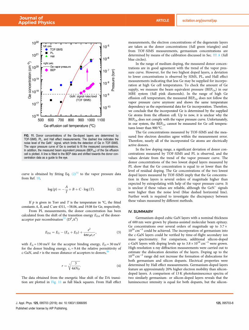
curve is obtained by fitting Eq. (2)32 to the vapor pressure datafrom Ref. 10,
log (p) ¼ �ATþ Bþ C � log (T): (2)
If p is given in Torr and T is the temperature in °C, the fittedconstants A, B, and C are 4311, −58.06, and 19.08 for Ge, respectively.
From PL measurements, the donor concentration has beencalculated from the shift of the transition energy EDA of the donor-acceptor pair recombination31 (D0,A0)
EDA ¼ EG � (EA þ ED)þ e2
4πε0εrr, (3)
with EA = 130 meV for the acceptor binding energy, ED = 30 meVfor the donor binding energy, εr = 9.44 the relative permittivity ofc-GaN, and r is the mean distance of acceptors to donors,26
r ¼ffiffiffiffiffiffiffiffiffiffiffi3
4πND
3
r: (4)
The data obtained from the energetic blue shift of the DA transi-tion are plotted in Fig. 11 as full black squares. From Hall effect
measurements, the electron concentrations of the degenerate layersare taken as the donor concentrations (full green triangles) andfrom TOF-SIMS measurements, germanium concentrations aredetermined by means of the calibration discussed in Sec. III A (fullblue circles).
In the range of medium doping, the measured donor concen-trations are in good agreement with the trend of the vapor pres-sure curve. However, for the two highest doped layers, a deviationto lower concentrations is observed by SIMS, PL, and Hall effectmeasurements indicating that less Ge may be supplied for incorpo-ration at high Ge cell temperatures. To check the amount of Gesupply, we measure the beam equivalent pressure (BEPGe) in ourMBE system (full pink diamonds). In the range of high Geeffusion cell temperature, the measured BEPGe does not follow thevapor pressure curve anymore and shows the same temperaturedependency as the experimental data for Ge incorporation. Therefore,we conclude that the incorporated Ge is determined by the suppliedGe atoms from the effusion cell. Up to now, it is unclear why theBEPGe does not comply with the vapor pressure curve. Unfortunately,in our system, the BEPGe cannot be measured for Ge cell tempera-tures lower than 900 °C.
The Ge concentrations measured by TOF-SIMS and the mea-sured free electron densities agree within the measurement error.Therefore, nearly all of the incorporated Ge atoms are electricallyactive donors.
In the low doping range, a significant deviation of donor con-centrations measured by TOF-SIMS and PL is observed, and thevalues deviate from the trend of the vapor pressure curve. Thedonor concentrations of the two lowest doped layers measured byPL show that the Ge concentration is equal to or lower than thelevel of residual doping. The Ge concentrations of the two lowestdoped layers measured by TOF-SIMS imply that the Ge concentra-tion in these layers is several orders of magnitude higher thanexpected by extrapolating with help of the vapor pressure curve. Itis unclear if these values are reliable, although the GeN− signalswere higher than the noise level (blue dashed horizontal line).Further work is required to investigate the discrepancy betweenthese values measured by different methods.
IV. SUMMARY
Germanium-doped cubic GaN layers with a nominal thicknessof 600 nm were grown by plasma-assisted molecular beam epitaxy.Ge concentrations over several orders of magnitude up to 3.7 ×1020 cm−3 could be achieved. The incorporation of germanium intothe c-GaN layers could be verified by time-of-flight secondary ionmass spectrometry. For comparison, additional silicon-dopedc-GaN layers with doping levels up to 3.8 × 1019 cm−3 were grown.High-resolution x-ray diffraction measurements were carried out toestimate the dislocation densities of the layers. Doping up to the1018 cm−3 range did not increase the formation of dislocations forboth germanium and silicon dopants. Electrical properties weredetermined by Hall effect measurements. Germanium-doped layersfeature an approximately 20% higher electron mobility than silicon-doped layers. A comparison of 13 K photoluminescence spectra oftwo similarly germanium- or silicon-doped layers reveals that theluminescence intensity is equal for both dopants, but the silicon-
FIG. 11. Donor concentrations of the Ge-doped layers are determined byTOF-SIMS, PL, and Hall effect measurements. The dashed line indicates thenoise level of the GeN− signal, which limits the detection of Ge in TOF-SIMS.The vapor pressure curve of Ge is overlaid to fit the measured concentrations.In addition, the measured beam equivalent pressure (BEPGe) of the Ge effusioncell is plotted. A line is fitted to the BEP data and shifted towards the donor con-centration data as a guide to the eye.
Journal ofApplied Physics ARTICLE scitation.org/journal/jap
J. Appl. Phys. 125, 095703 (2019); doi: 10.1063/1.5066095 125, 095703-8
Published under license by AIP Publishing.
doped layer shows a spectrally slightly narrower luminescence. Themeasured donor concentrations in our germanium-doped layerswere compared to the trend of the vapor pressure curve of germa-nium. The donor concentrations follow the vapor pressure curvevery well in the medium doping regime. In the range of lowdoping, the donor concentrations measured by different methodsdeviate from each other. In conclusion, doping with germaniumand silicon results in comparable structural properties of the layers,but germanium doped layers exhibit better electrical properties.
ACKNOWLEDGMENTS
This work was financially supported by the DeutscheForschungsgemeinschaft (DFG, German Research Foundation) -Projektnummer 231447078 - TRR 142 (via project B02).
REFERENCES1D. J. As, Defect Diffus. Forum 206–207, 87 (2002).2R. E. L. Powell, S. V. Novikov, C. T. Foxon, A. V. Akimov, and A. J. Kent, Phys.Status Solidi C 11, 385 (2014).3E. Martinez-Guerrero, B. Daudin, G. Feuillet, H. Mariette, Y. Genuist, S. Fanget,A. Philippe, C. Dubois, C. Bru-Chevallier, G. Guillot, P. Aboughe Nze, T. Chassagne,Y. Monteil, H. Gamez-Cuatzin, and J. Tardy, Mat. Sci. Eng. B 82, 59 (2001).4Z. Q. Li, H. Chen, H. F. Liu, L. Wan, M. H. Zhang, Q. Huang, J. M. Zhou,N. Yang, K. Tao, Y. J. Han, and Y. Luo, Appl. Phys. Lett 76, 3765 (2000).5L. T. Romano, C. G. Van de Walle, B. S. Krusor, R. Lau, J. Ho, T. Schmidt,J. W. Ager III, W. Götz, and R. S. Kern, Physica B 273–274, 50 (1999).6S. Fritze, A. Dadgar, H. Witte, M. Bügler, A. Rohrbeck, J. Bläsing, A. Hoffmann,and A. Krost, Appl. Phys. Lett. 100, 122104 (2012).7M. Deppe, J. W. Gerlach, D. Reuter, and D. J. As, Phys. Status Solidi B 254,1600700 (2017).8D. J. As, M. Deppe, J. W. Gerlach, and D. Reuter, MRS Adv. 2, 283 (2017).9J. Schörmann, S. Potthast, D. J. As, and K. Lischka, Appl. Phys. Lett. 90, 041918(2007).10“Germanium (Ge), heats of fusion and sublimation, enthalpy and entropy,vapor pressure,” in Landolt-Börnstein, Group III, edited by O. Madelung,U. Rössler, and M. Schulz (Springer-Verlag, Berlin, 2002), Vol. 41, Subvol. A1b,Online Document 533, p. 1
11P. D. Desai, J. Phys. Chem. Ref. Data 15, 967 (1986).12J. Ziegler, J. Biersack, and M. Ziegler, see www.srim.org for “SRIM, theStopping and Range of Ions in Matter” (2013).13J. R. de Laeter, J. K. Böhlke, P. de Bièvre, H. Hidaka, H. S. Peiser,K. J. R. Rosman, and P. D. P. Taylor, Pure Appl. Chem. 75, 683 (2003).14C. G. Van de Walle and J. Neugebauer, J. Appl. Phys. 95, 3851 (2004).15T. Markurt, L. Lymperakis, J. Neugebauer, P. Drechsel, P. Stauss, T. Schulz,T. Remmele, V. Grillo, E. Rotunno, and M. Albrecht, Phys. Rev. Lett. 110,036103 (2013).16M. Wieneke, H. Witte, K. Lange, M. Feneberg, A. Dadgar, J. Bläsing,R. Goldhahn, and A. Krost, Appl. Phys. Lett 103, 012103 (2013).17P. Gay, P. B. Hirsch, and A. Kelly, Acta Metall. 1, 315 (1953).18A. T. Blumenau, J. Elsner, R. Jones, M. I. Heggie, S. Öberg, T. Frauenheim,and P. R. Briddon, J. Phys. Condens. Matter 12, 10223 (2000).19I. Akasaki and H. Amano, in Properties of Group III Nitrides, edited byJ. H. Edgar, (INSPEC, London, 1994), p. 30.20J. E. Ayers, J. Appl. Phys. 78, 3724 (1995).21D. J. As and K. Lischka, in Molecular Beam Epitaxy: From Research to MassProduction, edited by M. Henini (Elsevier, Amsterdam, 2013), p. 206.22Z. X. Qin, H. Nagano, Y. Sugure, A. W. Jia, M. Kobayashi, Y. Kato,A. Yoshikawa, and K. Takahashi, J. Cryst. Growth 189/190, 425 (1998).23R. M. Kemper, T. Schupp, M. Häberlen, T. Niendorf, H.-J. Maier,A. Dempewolf, F. Bertram, J. Christen, R. Kirste, A. Hoffmann, J. Lindner, andD. J. As, J. Appl. Phys. 110, 123512 (2011).24A. F. Wright and U. Grossner, Appl. Phys. Lett. 73, 2751 (1998).25S. Dhar and S. Ghosh, J. Appl. Phys. 86, 2668 (1999).26M. Feneberg, M. Röppischer, C. Cobet, N. Esser, J. Schörmann, T. Schupp,D. J. As, F. Hörich, J. Bläsing, A. Krost, and R. Goldhahn, Phys. Rev. B 85,155207 (2012).27G. Ramirez-Flores, H. Navarro-Contreras, A. Lastras-Martinez, R. C. Powell,and J. E. Greene, Phys. Rev. B 50, 8433 (1994).28D. J. As, F. Schmilgus, C. Wang, B. Schöttker, D. Schikora, and K. Lischka,Appl. Phys. Lett. 70, 1311 (1997).29J. Menniger, U. Jahn, O. Brandt, H. Yang, and K. Ploog, Phys. Rev. B 53, 1881(1996).30D. J. As, U. Köhler, M. Lübbers, J. Mimkes, and K. Lischka, Phys. Status SolidiA 188(2), 699 (2001).31D. K. Schroder, Semiconductor Material and Device Characterization (JohnWiley & Sons, Inc., Hoboken, 2006), p. 606.32G. W. Thomson, Chem. Rev. 38, 1 (1946).
Journal ofApplied Physics ARTICLE scitation.org/journal/jap
J. Appl. Phys. 125, 095703 (2019); doi: 10.1063/1.5066095 125, 095703-9
Published under license by AIP Publishing.