generator sweep signal an/usm-203a · an/usm-203a this copy is a reprint which includes current...
TRANSCRIPT
TM 11-6625-2575-14
TECHNICAL MANUAL
OPERATOR’S, ORGANIZATIONAL, DIRECT SUPPORT,
AND GENERAL SUPPORT MAINTENANCE MANUAL
INCLUDING REPAIR PARTS AND SPECIAL TOOLS LIST
(INCLUDING DEPOT REPAIR PARTS AND SPECIAL TOOLS LIST)
GENERATOR
SWEEP SIGNAL
AN/USM-203A
This copy is a reprint which includes currentpages from Change 1.
HEADQUARTERS DEPARTMENT OF THE ARMYNOVEMBER 1973

WARNINGBe careful when working on the 115-volt line connections. Seriousinjury or death may result from contact with these terminals.
DO NOT TAKE CHANCES!

TM 11-6625-2575-14
T E C H N I C A L M A N U A L HEADQUARTERSDEPARTMENT OF THE ARMY
No. 11-6625-2575-14 WASHINGTON , DC, 23 November 1973
OPERATOR’S, ORGANIZATIONAL, DIRECT SUPPORT,AND GENERAL SUPPORT MAINTENANCE
MANUALGENERATOR, SWEEP SIGNAL
AN/USM-203A(NSN 625-00-935-0145)
REPORTING OF ERRORSYou can improve this manual by recommending improvements using DA
Form 2028 located in the back of the manual. Simply tear out the self adressedform, fill it out as shown on the sample, fold it where shown, and drop it in themail.
If there are no blank DA Form 2028-2 in the back of your manual, use thestandard DA Form 2028 (Recommended Changes to Publications and BlankForms) and forward to the Commander, US Army Communications andElectronics Readiness Command, ATTN: DRSEL-ME-MQ, Fort Monmouth, NJ07703.
General . . . . . . . . . . . . . . . . . . . . . . . . . . . . . . . . . . . . . . . . . . . . . . . . . . . . . . . . . . . . . . . . . . . . . . . . . . . ParagraphCHAPTER 1.
Section I.II.
CHAPTER 2.3.
Section I.II.
III.CHAPTER 4.
5.Section I.
II.CHAPTER 6.
7.Section I.
II.III.IV.V.
CHAPTER 8.Section I.
II.III.IV.V.
APPENDIX A.APPENDIX B.APPENDIX C.
Section I.II.
INTRODUCTION- .
1-1Description and data . . . . . . . . . . . . . . . . . . . . . . . . . . . . . . . . . . . . . . . . . . . . . . . . . . . . . . . . . . . . 1-8SERVICE UPON RECEIPT AND INSTALLATION . . . . . . . . . . . . . . . . . . . . . . . . . . . . . 2-1OPERATING INSTRUCTIONS Controls and instruments . . . . . . . . . . . . . . . . . . . . . . . . . . . . . . . . . . . . . . . . . . . . . . . . . . . . . . . 3-1Operation under usual conditions . . . . . . . . . . . . . . . . . . . . . . . . . . . . . . . . . . . . . . . . . . . . . . . 3-3Operation under unusual conditions . . . . . . . . . . . . . . . . . . . . . . . . . . . . . . . . . . . . . . . . . . . . . 3-5OPERATOR/CREW MAINTENANCE INSTRUCTIONS . . . . . . . . . . . . . . . . . . . . . . . . . 4-1ORGANIZATIONAL MAINTENANCE General requirements . . . . . . . . . . . . . . . . . . . . . . . . . . . . . . . . . . . . . . . . . . . . . . . . . . . . . . . . . . 5-1Externally serviceable details . . . . . . . . . . . . . . . . . . . . . . . . . . . . . . . . . . . . . . . . . . . . . . . . . . . 5-3FUNCTIONING OF EQUIPMENT . . . . . . . . . . . . . . . . . . . . . . . . . . . . . . . . . . . . . . . . . . . . . . 6-1DIRECT SUPPORT MAINTENANCE General . . . . . . . . . . . . . . . . . . . . . . . . . . . . . . . . . . . . . . . . . . . . . . . . . . . . . . . . . . . . . . . . . . . . . . . . 7-1Troubleshooting . . . . . . . . . . . . . . . . . . . . . . . . . . . . . . . . . . . . . . . . . . . . . . . . . . . . . . . . . . . . . . . . 7-3Repairs . . . . . . . . . . . . . . . . . . . . . . . . . . . . . . . . . . . . . . . . . . . . . . . . . . . . . . . . . . . . . . . . . . . . . . . . 7-6Test procedures . . . . . . . . . . . . . . . . . . . . . . . . . . . . . . . . . . . . . . . . . . . . . . . . . . . . . . . . . . . . . . . . 7-8Alignment and adjustment procedures . . . . . . . . . . . . . . . . . . . . . . . . . . . . . . . . . . . . . . . . . . 7-12GENERAL SUPPORT MAINTENANCE General . . . . . . . . . . . . . . . . . . . . . . . . . . . . . . . . . . . . . . . . . . . . . . . . . . . . . . . . . . . . . . . . . . . . . . . . . 8-1Troubleshooting and repair . . . . . . . . . . . . . . . . . . . . . . . . . . . . . . . . . . . . . . . . . . . . . . . . . . . . . 8-3Replacement of rf assemblies. . . . . . . . . . . . . . . . . . . . . . . . . . . . . . . . . . . . . . . . . . . . . . . . . . . 8-8Test procedures . . . . . . . . . . . . . . . . . . . . . . . . . . . . . . . . . . . . . . . . . . . . . . . . . . . . . . . . . . . . . . . . . 8-14Alignment and adjustment procedures . . . . . . . . . . . . . . . . . . . . . . . . . . . . . . . . . . . . . . . . . . 8-17REFERENCES . . . . . . . . . . . . . . . . . . . . . . . . . . . . . . . . . . . . . . . . . . . . . . . . . . . . . . . . . . . . . . . . . . . . . . . . . . . . . . .DELETED MAINTENANCE ALLOCATION Introduction . . . . . . . . . . . . . . . . . . . . . . . . . . . . . . . . . . . . . . . . . . . . . . . . . . . . . . . . . . . . . . . . . . . . . . . . . . . . . . . . . .MAINTENANCE ALLOCATION CHART . . . . . . . . . . . . . . . . . . . . . . . . . . . . . . . . . . . . . . . . . . . . . . . . . . . . . .
Table I. TOOL AND TEST EQUIPMENT REQUIREMENTS . . . . . . . . . . . . . . . . . . . . . . . . . . . . . . . . . . . . . . . . . . .
Page
1-11-12-1
3-13-33-44-1
5-15-16-1
7-17-27-97-97-13
8-18-18-58-78-8
A-1
C-1C 3C-4
Index . . . . . . . . . . . . . . . . . . . . . . . . . . . . . . . . . . . . . . . . . . . . . . . . . . . . . . . . . . . . . . . . . . . . . . . . . . . . . . . . . . . . . . . . . . . . . . Index-1
i
TM 11-6625-2575-14LIST OF ILLUSTRATIONS
Number1-11-22-13-13-27-17-27-37-47-57-67-77-87-9
7-107-117-127-137-147-157-168-1.8-2.8-3.8-4.8-5.8-6.8-7.8-8.8-9.
8-10.8-11.8-12.8-13.8-14.
FO-1.FO-2.FO-3.
Title PageFront view of AN/USM-203A . . . . . . . . . . . . . . . . . . . . . . . . . . . . . . . . . . . . . . . . . . . . . . . . . . . . . . . . . . . . . . . . 1-0Typical Setup Using AN/USM-203A . . . . . . . . . . . . . . . . . . . . . . . . . . . . . . . . . . . . . . . . . . . . . . . . . . . . . . . . . . 1-2AN/USM-203A Packaging . . . . . . . . . . . . . . . . . . . . . . . . . . . . . . . . . . . . . . . . . . . . . . . . . . . . . . . . . . . . . . . . . . . 2-1AN/USM-203A Front Panel Features . . . . . . . . . . . . . . . . . . . . . . . . . . . . . . . . . . . . . . . . . . . . . . . . . . . . . . . 3-1AN/USM-203A Rear Panel Features . . . . . . . . . . . . . . . . . . . . . . . . . . . . . . . . . . . . . . . . . . . . . . . . . . . . . . . . 3-2AN/USM-203A With Enclosure Panels Removed . . . . . . . . . . . . . . . . . . . . . . . . . . . . . . . . . . . . . . . . . . . . . 7-2Typical Display at Q102 Collector . . . . . . . . . . . . . . . . . . . . . . . . . . . . . . . . . . . . . . . . . . . . . . . . . . . . . . . . . . 7-4Typical Display at Q105 Emitter.. . . . . . . . . . . . . . . . . . . . . . . . . . . . . . . . . . . . . . . . . . . . . . . . . . . . . . . . . . . . . . . . . 7-4Typical Display at Q106 Collector . . . . . . . . . . . . . . . . . . . . . . . . . . . . . . . . . . . . . . . . . . . . . . . . . . . . . . . . . . 7-4Typical Display at Q107 Collector . . . . . . . . . . . . . . . . . . . . . . . . . . . . . . . . . . . . . . . . . . . . . . . . . . . . . . . . . .7-4Typical Display at J301-4 . . . . . . . . . . . . . . . . . . . . . . . . . . . . . . . . . . . . . . . . . . . . . . . . . . . . . . . . . . . . . . . . . . . 7-4Typical Display at J302-4 and J303-4 . . . . . . . . . . . . . . . . . . . . . . . . . . . . . . . . . . . . . . . . . . . . . . . . . . . . . . . . 7-4Typical Display at Q305 Collector . . . . . . . . . . . . . . . . . . . . . . . . . . . . . . . . . . . . . . . . . . . . . . . . . . . . . . . . . . . . . 7-5Main Printed Circuit Board Assembly . . . . . . . . . . . . . . . . . . . . . . . . . . . . . . . . . . . . . . . . . . . . . . . . . . . . . . 7-7Plug-in Marker/Printed Circuit Board Assembly . . . . . . . . . . . . . . . . . . . . . . . . . . . . . . . . . . . . . . . . . . . . . 7-8Plug-in Marker Switch Bank . . . . . . . . . . . . . . . . . . . . . . . . . . . . . . . . . . . . . . . . . . . . . . . . . . . . . . . . . . . . . . . . 7-9Test Setup for Typical Test Display . . . . . . . . . . . . . . . . . . . . . . . . . . . . . . . . . . . . . . . . . . . . . . . . . . . . . . . . . 7-11High Bank Test Display . . . . . . . . . . . . . . . . . . . . . . . . . . . . . . . . . . . . . . . . . . . . . . . . . . . . . . . . . . . . . . . . . . . . 7-11Low Band Test Display . . . . . . . . . . . . . . . . . . . . . . . . . . . . . . . . . . . . . . . . . . . . . . . . . . . . . . . . . . . . . . . . . . . . . 7-12Connection of Plug-in Markers . . . . . . . . . . . . . . . . . . . . . . . . . . . . . . . . . . . . . . . . . . . . . . . . . . . . . . . . . . . . .7-16115 Volt/230 Volt Input Power Option . . . . . . . . . . . . . . . . . . . . . . . . . . . . . . . . . . . . . . . . . . . . . . . . . . . . . . . . . 7-16Rf Detector Assembly . . . . . . . . . . . . . . . . . . . . . . . . . . . . . . . . . . . . . . . . . . . . . . . . . . . . . . . . . . . . . . . . . . . . . . 8-2Monitor/Mixer Assembly A4A5 . . . . . . . . . . . . . . . . . . . . . . . . . . . . . . . . . . . . . . . . . . . . . . . . . . . . . . . . . . . . . . . 8-4Fixed Oscillator/Mixer/Filter Assembly A4A3 . . . . . . . . . . . . . . . . . . . . . . . . . . . . . . . . . . . . . . . . . . . . . . . . . 8-5AN/USM-203A, Block Diagram.. . . . . . . . . . . . . . . . . . . . . . . . . . . . . . . . . . . . . . . . . . . . . . . . . . . . . . . . . . . . . 8-9Video Amplifier Assembly . . . . . . . . . . . . . . . . . . . . . . . . . . . . . . . . . . . . . . . . . . . . . . . . . . . . . . . . . . . . . . . . . . . . 8-10Video Amplifier Circuit Board A4A2, Resistor Location . . . . . . . . . . . . . . . . . . . . . . . . . . . . . . . . . . . . . . . 8-10Video Amplifier Circuit Board A4A2, Capacitor Location . . . . . . . . . . . . . . . . . . . . . . . . . . . . . . . . . . . . . . 8-11Variable Oscillator Base-Plate Component Layout . . . . . . . . . . . . . . . . . . . . . . . . . . . . . . . . . . . . . . . . . . . . 8-11Rf Band Switch Assembly . . . . . . . . . . . . . . . . . . . . . . . . . . . . . . . . . . . . . . . . . . . . . . . . . . . . . . . . . . . . . . . . . . . 8-12Rotary Attenuator Assembly . . . . . . . . . . . . . . . . . . . . . . . . . . . . . . . . . . . . . . . . . . . . . . . . . . . . . . . . . . . . . . . . 8-13Harmonic Marker Assembly . . . . . . . . . . . . . . . . . . . . . . . . . . . . . . . . . . . . . . . . . . . . . . . . . . . . . . . . . . . . . . . . 8-141.0-MHz Harmonic Marker Printed Circuit Assembly . . . . . . . . . . . . . . . . . . . . . . . . . . . . . . . . . . . . . . . . .8-1410.0-MHz Harmonic Marker Printed Circuit Assembly . . . . . . . . . . . . . . . . . . . . . . . . . . . . . . . . . . . . . . . 8-1450-MHz Harmonic Marker Printed Circuit Assembly . . . . . . . . . . . . . . . . . . . . . . . . . . . . . . . . . . . . . . . . . . 8-15Resistor and Capacitor Color Codes . . . . . . . . . . . . . . . . . . . . . . . . . . . . . . . . . . . . . . . . . . . . . . . . . . . . . . . . . . .Fold-inAN/USM-203A, Wiring Diagram . . . . . . . . . . . . . . . . . . . . . . . . . . . . . . . . . . . . . . . . . . . . . . . . . . . . . . . . . . . . . . .Fold-inAN/USM-203A, Schematic Diagram . . . . . . . . . . . . . . . . . . . . . . . . . . . . . . . . . . . . . . . . . . . . . . . . . . . . . . . . . . . Fold-in
ii

TM
11-6625-2575-14
1-0
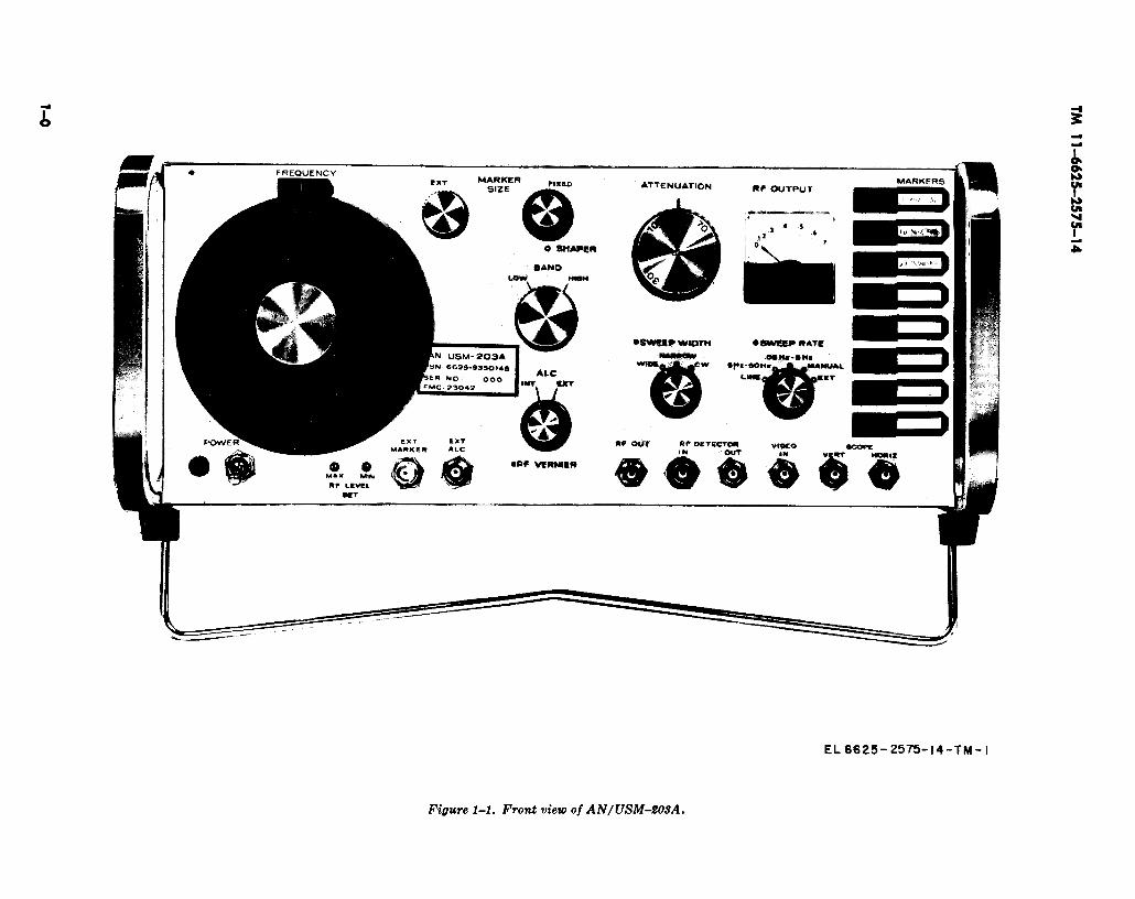
Figure 1-1.

TM 11-6625-2575-14
CHAPTER 1INTRODUCTION
Section I. GENERAL
1-1. ScopeThis manual describes Sweep Signal GeneratorAN/USM-203A. It covers the purpose, use, instruc-tions for installation and operation, and thetechnical characteristics of the AN/USM-203A.The following maintenance categories are covered:operator/crew (C), organizational (0), direct sup-port (F), and general support (H).
1-2. Indexes of Publicationsa. DA Pam 310-4. Refer to DA Pam 310-4 to
determine whether there are new editions,changes, or additional publications pertaining tothe equipment,
b. DA Pam 310-7. Refer to DA Pam 310-7 todetermine whether there are modification workorders (MWO’s) pertaining to the equipment.
1-3. Forms and Recordsa. Reports of Maintenance and Unsatisfactory
Equipment. Maintenance forms, records, and re-ports which are to be used by maintenancepersonnel at all maintenance levels are listed inand prescribed by TM 38-750.
b. Report of Packaging and Handling Deficien-cies. Fill out and forward DD Form 6 (PackagingImprovement Report) as prescribed in AR 700-58/NAVSUPINST 4030.29/AFR 71-13/MCOP4030.29A, and DSAR 4145.8.
c. Discrepancy in Shipment Report (DISREP)(SF 361). Fill out and forward Discrepancy in
Section Il.
1-8. Purpose and Use
Shipment Report (DISREP) (SF 361) as pre-scribed in AR 55-38/NAVSUPINST 4610.33 B/AFR75-18/MCO P4610.19C and DLAR 4500.15.1-4. Reporting Equipment Improvement
Recommendations (EIR)
EIR’s will be prepared using Standard Form 368,Quality Deficiency Report. Instructions for pre-paring EIR’s are provided in TM 38-750, The ArmyMaintenance Management System. EIR’s shouldbe mailed direct to Commander, US Army Com-munications and Electronics Materiel ReadinessCommand, ATTN: DRSEL-ME-MQ, Fort Mon-mouth, NJ 07703. A reply will be furnished direct toyou.
1-5. Administrative StorageThere is no special procedures for preparing thisequipment for limited storage. Place all ancillaryitems in a bag and tie or tape the bag to theequipment. Place equipment in limited storage, ie,organizational storage room. Protect equipmentfrom dust, humidity, and extreme temperaturechanges.
1-4. Destruction of Army MaterialDemolition and destruction of electronic equip-ment will be under the direction of the commanderand in accordance with TM 750-244-2.
1-7. Deleted
DESCRIPTION AND DATA
quency signals. Frequency, sweep frequency, andThe AN/USM-203A is a source of rf energy which sweep rate are adjustable from front panelprovides both fixed frequency and sweep fre- controls. The frequency range covered is 500 kHz
1-1
Figure 1-2.
TM 11-6625-2575-14
to 1200 MHz in two bands. The low band covers500 kHz to 300 MHz, and the high band 300MHz to1200 MHz. The output may be continu-ously adjusted over an 80 dB range to 0.5 voltrms into a 50-ohm load. Provision is made forthe use of both internal and external frequencymarker generators. Internal harmonic markersare provided at 1.0-, 10.0-, and 50.0-MHz inter-vals. The AN/USM-203A is used in the field testradar, if amplifiers, rf communications, andvideo frequency equipment. It can be used as achirp radar simulator and for wideband testing.The stability is sufficient for narrow band circuittesting. A broad choice of sweep rates permitsthe use of either an oscilloscope display or an ex-ternal graphic recorder. Provision is made forexternal detection of rf signals, or an internal de-tector can be used. Front panel connectors areavailable to permit external control of sweeprate, rf level, and frequency identification.
1-9. DescriptionA front view of the AN/USM-203A is shown infigure 1-1. The functions of the controls and re-ceptacles are indicated by the front panel mark-ings associated with each item. See figure 3-2for the power cord entrys, fuse, and externaldrive connector. The AN/USM-203A is con-structed of an aluminum alloy frame consistingof two side rails, a rear panel, and a backingpanel. The frame is assembled with threadedfasteners and inserts. The aluminum front panelis mounted to the frame and covers the backingpanel. Printed circuit assemblies are mountedto the aluminum frame. Aluminum slide panels(dust covers) protect the sides, the top, and thebottom of the AN/USM-203A. Aluminum sur-faces are anodized.
1-10. System ApplicationSweep frequency measurement techniques areused to measure the characteristics of deviceswhich operate at high frequencies, and whoseresponse must be determined over a broad rangeof frequencies. If a device or system containsresonance or antiresonance points within thesweep frequency range of the AN/USM-203A, adisplay can be obtained which shows the reso-nance peaks or depressions in the passband of in-terest. Filters, amplifiers, receivers, and otherpassive. or active devices can be tested. The fol-lowing list of potential applications will suggestthe range of utility of the AN/USM-203A.
1 - 2
a.
b.
c.
d.
e.
f.
g.
h.
Transfer characteristic measurements.
Impedance plots.
System flatness.
Insertion loss measurements.
Return loss measurements.
Small signal analysis.
Open and closed loop response.
Reflectometer systems to measure reflectionand transmission characteristics.
i. Microwave spectroscopy.
j. High Q swept frequency cavity measure-ments.
k. Bandpass measurement-typical test set-up.
NOTEA typical test setup using the AN/USM-203A sweep signal generator isshown in figure 1-2. Other test setupsare possible which use external leveling,an external detector, a graphic re-corder, or a combination of these op-tions. BNC connectors and -50 ohmcoaxial cable are used in the externalcircuit.
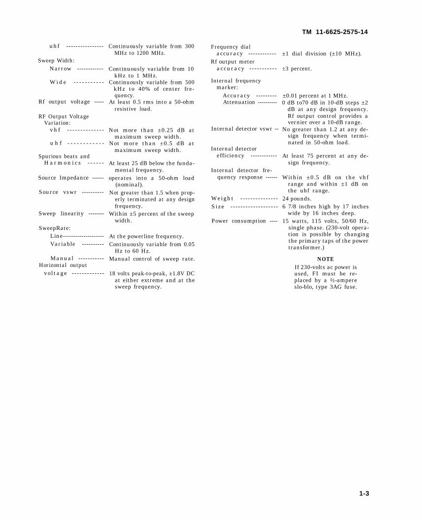
1-11. Technical CharacteristicsCenter frequency range Continuously variable from 500
kHz to 1200 MHz in tworanges.
Range:vhf . . . . . . . . . . . . . . . Continuously variable from 500
kHz to 300 MHz.
TM 11-6625-2575-14
uhf ----------------
Sweep Width:Narrow ------------
W i d e - - - - - - - - - - -
Rf output voltage -----
RF Output VoltageVariation:
vhf - - - - - - - - - - - - - -
u h f - - - - - - - - - - - -
Spurious beats andH a r m o n i c s - - - - - -
Source Impedance ------
Source vswr ----------
Sweep linearity --------
SweepRate:Line--------------------Variable ----------
Manual -----------Horizontal output
voltage - - - - - - - - - - - - -
Continuously variable from 300MHz to 1200 MHz.
Continuously variable from 10kHz to 1 MHz.
Continuously variable from 500kHz to 40% of center fre-quency.
At least 0.5 rms into a 50-ohmresistive load.
Not more than ±0.25 dB atmaximum sweep width.
Not more than ±0.5 dB atmaximum sweep width.
At least 25 dB below the funda-mental frequency.
operates into a 50-ohm load(nominal).
Not greater than 1.5 when prop-erly terminated at any designfrequency.
Within ±5 percent of the sweepwidth.
At the powerline frequency.Continuously variable from 0.05
Hz to 60 Hz.Manual control of sweep rate.
18 volts peak-to-peak, ±1.8V DCat either extreme and at thesweep frequency.
Frequency dialaccuracy ------------
Rf output meteraccuracy -- - - - - - - - - -
Internal frequencymarker:
Accuracy ---------Attenuation ----------
Internal detector vswr --
Internal detectorefficiency ------------
Internal detector fre-quency response ------
Weight - - - - - - - - - - - - - - -Size -- - - - - - - - - - - - - - - - - -
Power consumption ----
±1 dial division (±10 MHz).
±3 percent.
±0.01 percent at 1 MHz.0 dB to70 dB in 10-dB steps ±2
dB at any design frequency.Rf output control provides avernier over a 10-dB range.
No greater than 1.2 at any de-sign frequency when termi-nated in 50-ohm load.
At least 75 percent at any de-sign frequency.
Within ±0.5 dB on the vhfrange and within ±1 dB onthe uhf range.
24 pounds.6 7/8 inches high by 17 inches
wide by 16 inches deep.15 watts, 115 volts, 50/60 Hz,
single phase. (230-volt opera-tion is possible by changingthe primary taps of the powertransformer.)
NOTEIf 230-volts ac power isused, FI must be re-placed by a ½-ampereslo-blo, type 3AG fuse.
1-3

Figure 2-1.
TM 11-6625-2575-14
CHAPTER 2
SERVICE UPON RECEIPT AND INSTALLATION
2-1. Unpacking c. Check to see whether the equipment has
An illustration of the packing of the AN/USM- been modified. (Equipment which has been modi-
203A is shown in figure 2-1. fied will have the MWO number on the frontpanel, near the nomenclature plate.) Check also
2-2. Checking Unpacked Equipmentto see whether all currently applicable MWO’shave been applied. (Current MWO’s applicable
a. Inspect the equipment for damage incurred to the equipment are listed in DA Pam 310-7.)during shipment. If the equipment has been dam-aged, report the damage on DD Form 6, as pre- d. AN/USM-203A, after it is unpacked, is
scribed in AR 700-58. ready for use on a service bench as received. Nospecial mounting procedure is required unless
b. Check the equipment against the packing the equipment is to be rack mounted; specialslip to see if the shipment is complete. Report all adapters are required for rack mounting. Thesediscrepancies in accordance with the instruc- adapters are not supplied as a part of the basictions of TM 38-750. The equipment consists of issue item list and must be obtained througha single unit. normal distribution channels.
2-1

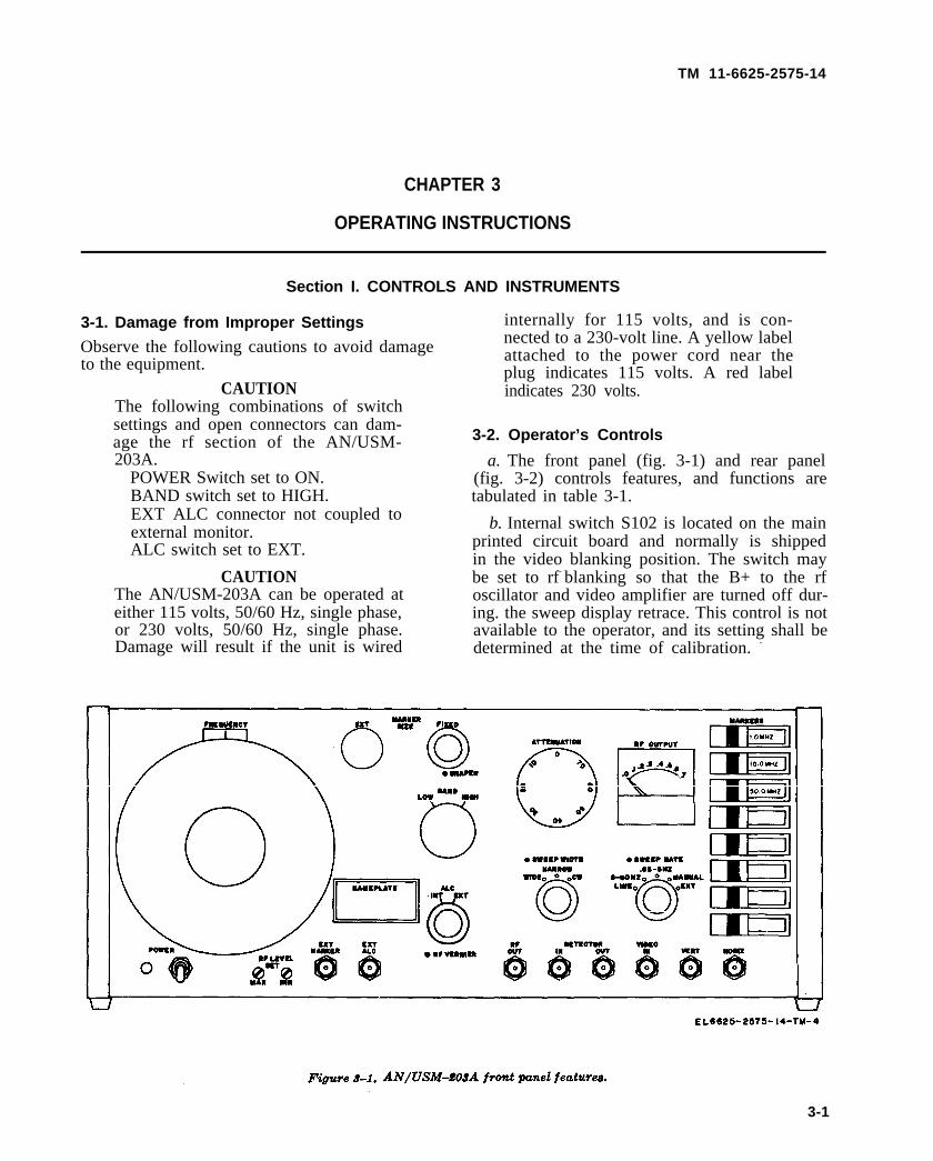
Figure 3-1.
TM 11-6625-2575-14
CHAPTER 3
OPERATING INSTRUCTIONS
Section I. CONTROLS AND INSTRUMENTS
3-1. Damage from Improper Settings
Observe the following cautions to avoid damageto the equipment.
CAUTIONThe following combinations of switchsettings and open connectors can dam-age the rf section of the AN/USM-203A.
POWER Switch set to ON.BAND switch set to HIGH.EXT ALC connector not coupled toexternal monitor.ALC switch set to EXT.
CAUTIONThe AN/USM-203A can be operated ateither 115 volts, 50/60 Hz, single phase,or 230 volts, 50/60 Hz, single phase.Damage will result if the unit is wired
internally for 115 volts, and is con-nected to a 230-volt line. A yellow labelattached to the power cord near theplug indicates 115 volts. A red labelindicates 230 volts.
3-2. Operator’s Controls
a. The front panel (fig. 3-1) and rear panel(fig. 3-2) controls features, and functions aretabulated in table 3-1.
b. Internal switch S102 is located on the mainprinted circuit board and normally is shippedin the video blanking position. The switch maybe set to rf- blanking so that the B+ to the rfoscillator and video amplifier are turned off dur-ing. the sweep display retrace. This control is notavailable to the operator, and its setting shall bedetermined at the time of calibration. -
3-1

Figure 3-2.
TM 11-6625-2575-14
Table 3-1. Operator’s Controls
NOTEThis table covers only items used by the operator;items used by higher category maintenance per-sonnel are covered in instructions for the appli-cable maintenance category.
Control or indicator
ALC switch ---------
RF VERNIER -----
SWEEP WIDTHswitch and vernier.
SWEEP RATEswitch.
SWEEP RATEvernier.
BAND switch --------
3-2
Function
RF OUTPUTMETER.
Vernier control of rf level over a10-dB range.
Narrow: Continuously variablefrom 10 kHz to 1 MHz.
Wide: Continuously variable from500 kHz to 40% of center fre-quency.
External level control.Internal level control.
MARKER switches
Sweep rate at line frequency.Sweep rate 5 to 60 Hz.Sweep rate 0.05 to 5 Hz.Manual control of sweep.Sweep rate controlled by an ex-
ternal signal.
Varies sweep rate in variable andmanual positions.
Frequency range 0.5 MHz to 300MHz.
Frequency range 300 MHz to 1200MHz.
Indicates sweep generator rf out-put in volts rms. Normal maxi-mum is 0.5 volt.
1-, 10-, and 50-MHz harmonicmarkers are added to the sweepdisplay by setting the individualswitches. Five optional plug-inmarkers are controlled fromindividual marker switches.
MARKER SIZE Controls amplitude of marker.FIXED control.
MARKER SHAPE Controls shape of markers.control.
ATTENUATION Provides 0 to 70 dB of attenua-switch. tion in 10-dB steps.
CENTER Selects designated frequency.FREQUENCYcontrol.
RF LEVEL SET Sets upper rf output limit.M A X c o n t r o l .
RF LEVEL SET Sets lower rf output limit.MIN control.
TM 11-6625-2575-14
Table 3-2. Connectors and Rear Panel DevicesDesignation I Application
Designation
RF OUT ---------ALC --- - - - - -EXT
MARKER.VIDEO IN --SCOPE
VERT.SCOPE
HORIZ.
Application
Rf output available at this connector.External level control signal input.External marker generator input.
Input for detected rf output from device.Output to vertical channel of display.
Output to horizontal channel of display.
RF DETEC- Input from device under test.TOR IN.
RF DETEC- Output to VIDEO IN connector.TOR OUT.
REAR PANEL DEVICES
Designation Application
F1 --- - - - - - - - Fuse receptacle.EXT DRIVE. Input for external sweep control signal.LINE -------- Power cord entrance to chassis.
Section Il. OPERATION UNDER USUAL CONDITIONS
3-3. Operator’s Initial Adjustments(fig. 1-2 and 3-1)
a. Initial Control Adjustments. Determine themode of operation pertinent to the test to beaccomplished, and set the controls of the AN/USM-203A as follows:
(1) BAND switch. Set this control to theLOW BAND (500 kHz to 300 MHz), or to theHIGH BAND (300 MHz to 1200 MHz), accord-ing to the frequency range required.
(2) CENTER FREQUENCY dial. Set thisdial to the frequency required.
(3) SWEEP RATE. Determine the sweeprate best suited to display the results of the test.
(4) ALC control. Set the ALC control tothe internal monitor, unless it has been deter-mined that an external level control is required.
(5) ATTENUATION control. Set the at-tenuation control to maximum (70 dB).
(6) MARKER switches. 1-MHz, 10-MHZ,and 50-MHz harmonic markers are provided. De-termine the frequency marker interval (in MHz)best suited to the range of sweep frequency to beobserved.
(7) RF DETECTOR IN. Connect the de-vice under test to the detector input.
(8) RF DETECTOR OUT. Connect the de-tector output to the VIDEO IN connector.
(9) VIDEO IN. Connect the RF DETEC-TOR OUT connector to the VIDEO IN connector.
(10) FIXED MARKER SIZE. Set the fixedmarker size control to midrange.
(11 ) MARKER SHAPER. Set the markershape control to midrange.
(12) EXT MARKER SIZE. If an externalmarker generator is used, the input is connectedto the EXT MARKER connector. Set the fixed
marker size control fully clockwise. Adjust theEXT MARKER SIZE control to produce themaximum marker amplitude required.
b. Initial Adjustment of Associated Equip-ment. Make the necessary adjustments to asso-ciated equipment.
c. Power Cord. Insert the power cord AN/USM-203A into a receptacle supplying 115 volts,60 Hz, single phase.
3-4. Operating Proceduresa. Check interconnections between the AN/
USM-203A and associated equipment.b. Check the initial adjustments of the AN/
USM-203A and any associated equipment.c. Apply power to associated equipment such
as the display device, external oscillators, or rfpower instrumentation.
d. Readjust the associated equipment to quies-cent conditions (absence of inputs from the AN/USM-203A).
e. Set the AN/USM-203A power switch toON. The AN/USM-203A uses solid-state activedevices; the outputs develop immediately whenenergized. Allow a warmup time of 20 minutesfor the equipment to reach optimum stability.
f. Upon applying power to the AN/USM-203A, a signal will be delivered to the deviceunder test and associated instrumentation. Im-mediately scan all associated equipment for evi-dence of out-of-limit operation which could re-sult in damage to instrumentation,
g. Increase rf output of the AN/USM-203Aby decreasing attenuation, until an adequate dis-play is presented on the external device.
h. Readjust associated equipment as necessaryto adequately indicate or display the process un-der observation.
3-3

TM 11-6625-2575-14
i. Readjust the AN/USM-203A controls as re- tinuous operation within its ratings. No particu-quired for optimum presentation on the display lar procedure is required for standby operation.device. k. Operation of the AN/USM-203A may be
j. The AN/USM-203A is designed for con- discontinued by setting the power switch to OFF.
Section. III. OPERATION UNDER UNUSUAL CONDITIONS
3-5. Extreme Dry and Moist Heat 18°C. A 20-minute warmup time should be al-
No particular procedure is required to operatelowed for maximum stability,
under conditions of extreme dry heat (up to b. Salt Air and Sea Spray. Operation in an50°C) or moist heat (up to 50ºC and 90% environment of salt air and sea spray requireshumidity). that the instrument be protected completely from
infiltration of these elements.
Sand, and Dust.
a. Cold Climate. No special procedurequired to operate in temperatures down to
3-6. Extreme Cold, Salt Air and Sea Spray, c. Sand and Dust. Operation in an environ-ment of sand and dust requires that the instru-
is re- ment be protected from infiltration of these ele-minus ments.
3 - 4
TM 11-6625-2575-14
CHAPTER 4
OPERATOR/CREW MAINTENANCE INSTRUCTIONS
4-1. Lubrication, Repair Parts, Tools, and 4-2. Preventive Maintenance ServicesTest Equipment
No lubrication, repair parts, tools,ment are required by the operator.
Preventive maintenance on the AN/USM-203Ais limited to observations by the operator. Dis-
or test equip- connect the power from the unit if the AN/USM-203A does not operate normally. Any instrumentwhich does not operate normally shall be sent toa higher maintenance category.
4-1


TM 11-6625-2575-14
CHAPTER 5
ORGANIZATIONAL MAINTENANCE
Section I. GENERAL REQUIREMENTS
5-1. Scope of Organizational Maintenance b. Material. Trichloroethane.
Organizational maintenance is limited to proce-dures that can be accomplished without remov- WARNINGing the instrument from its case. Operational The fumes of trichloroethanechecks are limited to those determinations which Provide thorough ventilation
are toxic.whenever
can be made using the auxiliary equipment nor-mally associated with the use of the AN/USM- used. DO NOT use near open flame.
203A. Trichloroethane is not flammable, butexposure of the fumes to an open flame
5-2. Tools, Equipment, and MaterialsRequired
converts the fumes to highly toxic, dan-gerous gases.
a. Tools Required. Allen wrenches: #6 (1/16inch), #8 (5/64 inch).
Section Il. EXTERNALLY SERVICEABLE DETAILS
5-3. Fuse Replacement
a. The fuse which protects the instrument inthe event that excessive current is drawn fromthe line is located on the rear panel.
b. Remove the fuse by pressing down on thecap and turning counterclockwise to the stop.Withdrew the fuse and the cap, and then removethe fuse from its receptacle.
c. The fuse is a type 3-AG, rated at 1 ampere.(Littelfuse 312001)
NOTESee paragraph 1.11 for 230-volttion.
d. Insert the fuse in the receptacle
opera-
of the cap.
e. Insert the fuse and cap assembly into thereceptacle at the rear of the instrument.
f. Turn the cap until the two metal protru-sions mate with the notches in the receptacle.Press down and turn clockwise to the stop.
g. If the fuse fails again when the instrumentis turned on, report the condition to higher cate-
gory maintenance.
5-4. Single Function Control Knobs
a. Single function control knobs are used onthe following controls:
(1) ATTENUATION control.(2) BAND switch.(3) EXTERNAL MARKER SIZE.
b. All single function knobs are secured totheir shafts by means of recessed setscrews. Twoscrews are used on the band switch and attenuatorcontrols, while only one is used on the externalmarker size control. These screws require a #8Allen wrench.
c. The band switch and the attenuator con-trols must be properly positioned on their shaftsbefore tightening the setscrews.
(1) The band switch has only two posi-tions, LOW and HIGH. The actual position ofthe shaft may be determined by temporarilytightening one setscrew and establishing that theswitch is in the counterclockwise position. Thesetscrew is then loosened, the knob index lo-cated to indicate the low position, and the knobsecured in this position.
(2) The attenuator controls are capable of360° of rotation, and the 0-dB position must be
5-1
TM 11-6625-2575-14
located electrically. This may be done by con-necting an ohmmeter between ground and thecenter pin of the rf output connector. The high-est resistance reading indicates the 0-dB posi-tion.
5-5. Coaxial Controls
u. Coaxial controls arecontrols:
(1) Fixed markerSHAPE.
used on the following
size and MARKER
(2) ALC AND RF VERNIER.(3) SWEEP WIDTH switch and SWEEP
WIDTH vernier.(4) SWEEP RATE switch and SWEEP
RATE vernier.
b. Two sizes of setscrews are used on the coax-ial controls.
(1) The outer diameter knob requires theuse of #8 Allen wrench.
(2) The inner diameter knob requires theuse of a #6 Allen wrench.
5-2

TM 11-6625-2575-14
CHAPTER 6
FUNCTIONING OF EQUIPMENT
6-1. Block Diagram
a. The AN/USM-203A sweep signal generatoris a solid-state electronic instrument which pro-vides frequency coverage from 0.5 to 1200 MHzin two bands. An external oscilloscope or graphicrecorder is required for external display pur-poses, or the instrument may be operated as acw generator.
b. The block diagram (fig. 8-4) of the AN/USM-203A can be divided into five major sec-tions.
(1) Power supply.(2) Sweep drive circuits.(3) Automatic level control and
circuits.(4) Rf circuits.(5) Marker circuits.
NOTENo power supply connectionsshown.
c. The following paragraphs describetrical operation of the AN/USM-203A.
blanking
are
the elec-Detailed
operation may be followed in the schematic dia-gram (fig. FO-3).
6-2. Power Supply(fig. FO-3)
a. Five separate outputs are provided: +200volts dc, +30 volts dc, and - 30 volts dc (allregulated), +50 volts dc unregulated, and a 60-Hz line-synchronizing signal. The four dc sourcessupply the various sweep generator functionsshown in the schematic diagrams. The line-syncsignal is used in the rate generator.
b. Each regulated dc source is a series-typetransistor regulator. The +30-volt and - 30-voltregulated sources are complementary duals. Cor-responding polarized capacitors and diodes inthe respective supplies are of the same type,but the polarities are reversed. To permit duality,
complementary transistors are interchanged inthe positive and negative supplies.
c. The +30-volt supply uses a constant cur-rent generator ( Q2 ) to provide constant bias cur-rent to Q3 and Q4. Diode VR2 and resistor R3protect the regulator against overloads by lim-iting the drive to series-pass transistor Q1.Zener diode VR3 and temperature-compensatingdiode CR7 provide the voltage reference. Resis-tor R7 is used to adjust the output voltage to+30 volts. Transistor Q4 amplifies differencesbetween the output voltage sample and the refer-ence voltage, and drives Q3 in Darlington connec-tion with Q1 to automatically compensate for loadvoltage error. Capacitors C4, C5, and C6 are used(if required) for stabilization.
d. The +200-volt supply is similar to the otherregulated sources except no constant current gen-erator is used. Gas discharge tube 12 is the 82-volt reference. Other components are specified toprovide the +200-volt output.
6-3. Sweep Drive Circuits(fig. FO-3)
a. Rate Generator. The rate generator has fivemodes of operation. These five modes areachieved by changing the operating characteris-tics of the basic rate generator, which consistsof a Schmitt trigger and a Miller integrator.
(1) The bistable Schmitt trigger consistsof Q101 and, Q102 and associated resistive net-works. The output at the collector of Q102 is asquare wave which is coupled to the blanking cir-cuitry and to the Miller integrator.
(2) The Miller integrator consists of Q103and Q104 and associated resistor and capacitornetworks. The integrated output at the collectorof Q104 is a triangular wave. The free-runningcondition is established by coupling the outputof Q104 to the input of the Schmitt trigger. Theoutput at the collector of Q104 is coupled to thelinearity circuitry through emitter followerQ105.
6-1
TM 11-6625-2575-14
(3) SWEEP RATE switch S103, a frontpanel control, is used to select the desired modeof operation. In the LINE position, the 60-Hzline-sync signal drives the Schmitt trigger at a60-Hz rate. In the 5- to 60-Hz and 0.05- to 5-Hzpositions, the trigger integrator combination isfree-running. The SWEEP RATE may be con-tinuously adjusted by R120B R120C, the frontpanel vernier control. In each case, the respectiverc time constants (R118, R120B, and C102 forthe 5-to 60-Hz rate; and R117, R120C, C102, andC103 for the 0.05- to 5-Hz rate) determine thesweep rate.
(4) In the MANUAL and EXT modes, thetrigger and integrator are inoperative. In theMANUAL mode, the sweep drive and the hori-zontal oscilloscope drive voltages are determinedby the position of R120A in voltage divider net-work R123, R120A, and R127. Resistor R120Ais ganged to R120B and R120C, the front panelvernier adjustment. In the EXT position, an ex-ternal generator is used in place of the internalrate circuit.
b. Linearity Circuit. The linearity circuit am-plifies and reshapes the input triangular wave. Itis required to provide a linear frequency-versus-voltage characteristic in the rf output display atall SWEEP WIDTH settings, and in both theLOW and HIGH frequency bands.
(1) The triangular wave from the rate gen-erator is coupled to emitter follower Q105. Threeoutputs are coupled from separate voltage divid-ers in the emitter circuit of Q105. One output isthe SCOPE HORIZ drive, a triangular signal.
(2) The other two outputs are coupled tocommon-base transistor circuits, linear ampli-fier Q106 and nonlinear amplifier Q107. The non-linear amplifier characteristics are controlled bythe diode break circuit consisting of resistorsR136 through R146, diodes CR104 throughCR113, and resistors R148 through R157. As apositive-going signal is coupled to the emitter ofQ107, the individual diodes are reverse-biased;but as the collector voltage increases, individualdiodes conduct in sequence, and the output signalis reshaped by the nonlinear, diode break cir-cuit.
(3) The outputs of the linear and nonlinearamplifiers are coupled to the front panel SWEEPWIDTH switch and potentiometer combinationS101, R146A, and R146B. The two combinedsignals maintain rf output sweep linearity underall conditions of SWEEP WIDTH and frequency.
The resultant drive signal is coupled to varactordiode CV501 in the tunable oscillator.
6-4. Rf Circuits(fig. FO-3)
a. Bandswitch. The rf sections of bandswitchS601 consist of coaxial switches S601-1A andS601-1B. In the HIGH band position, the vari-able oscillator is direct-coupled to R602, andZ603 to RF OUT connector J611. In the LOWband position, the variable oscillator signal iscoupled to the mixer where it mixes with thefixed 700-MHz oscillator signal. Lowpass filterFL551 couples the mixer difference frequency tothe video amplifier where the signal is amplified.From the video amplifier, the signal is coupledto the output. Bandswitch S601 includes sections2A, 2B, 2C, 2D, 3B, 3C, and 3D in addition tothe rf sections. These additional sections coupleor uncouple B + and rf blanking voltages to therespective high and low band circuits.
b. High Frequency Band. The variable uhf os-cillator uses a mechanically tunable line to tubethe range of 300 MHz to 1200 MHz. Adjustableresistor R509 is ganged to the shaft of the tuned-lined control to provide a nearly constant outputover the tuning range. In the WIDE and NAR-ROW sweep modes, varactor CV501 is electroni-cally varied by the reshaped sweep drive signalto provide a linear frequency-versus-voltagecharacteristic. In the cw mode, the varactor drivevoltage is held constant. Transistor Q501 is theamplifying device in the variable oscillator. Theoscillator output at connector J501 is coupledfrom a grounded loop network of resistors, R500,R501, and R507. In the high frequency range,the variable oscillator output is coupled throughfilter FL501, bandswitch S601, the monitor, andattenuator Z603 to RF OUT connector J611. TheATTENUATION control consists of a series ofresistive pi pads which provide 0 to 70 dB of out-put attenuation in 10-dB steps while maintainingan impedance of 50 ohms.
c. Low Frequency Band. In LOW BAND opera-tion, the variable-oscillator signal is mixed withthe 700-MHz, fixed-oscillator signal. The low-level output is couped through FL551 to thevideo amplifier. The video amplifier output iscoupled to coaxial switch section S601-1B andto the monitor. The amplified signal is coupledto the attenuator and to RF OUT connectorJ611. The sweep signal is generated in the vari-able uhf oscillator.
6-2

(1) Fixed-frequency oscillator. The 700MHz fixed-frequency oscillator consists of tran-sistors Q551 and Q552, a resonant line, a trimmercapacitor, and associated biasing circuits. Theoscillator output is loop-coupled to the mixer byresistor R554. One end of R554 is common tothe case.
(2) Mixer and low-pass filter. The mixer isa double-balanced diode mixer with balancedtransformer inputs from the 700-MHz fixed oscil-lator and the variable oscillator. TransformersT551 and T552 are wound on toroidal ferritecores. The output of the mixer is coupled fromthe common point of the diode star (consistingof CR551 through CR554) to RL551. Low-passfilter FL551 couples the difference frequency ofthe two oscillators to J401, the input to the videoamplifier.
(3) Video amplifier. The input signal is am-plified by four cascaded, rf-coupled, common-emitter amplifier stages. This four-stage videoamplifier has a relatively flat response from 0.5MHz to 300 MHz. Capacitors C402, C408,C415,and C422 permit adjustment of gain in indi-vidual stages to level the output throughout thelow band. The first three stages are supplied byleveled B+. The fourth stage, with dual-emitterlead transistor Q404, has a higher power outputand is supplied by +50 volts dc.
d. Rf Detector Circuit. The rf detector circuitconsists of diode CR603 and associated compo-nents including R613 and R614. Diode CR603detects the signal from the’ device under test andcouples a negative output voltage (when con-nected) to the video input connector.
6-5. Automatic Level Control (ALC) andBlanking Circuits
(fig. FO-3)
a. The monitor senses the rf output signal atthe junction of CR601 and R602. The monitoroutput, a negative detected signal, is coupled tothe base of transistor Q206, the sampling inputof a differential amplifier.
b. The base of Q207, the reference half of thedifferential amplifier, is coupled to a stable, butadjustable bias voltage. Any difference betweenthe negative monitor sample and the referencevoltage appears at the collector of Q206 as anamplified, phase-inverted error signal. The col-lector output of Q206 is further amplified andphase-inverted by Q202. The collector output ofQ202 is coupled to the base of emitter follower
TM 11-6625-2575-14
Q201 where the change in leveled B+ restoresthe rf output to its normal value. The leveledB + is applied to the variable oscillator in theHIGH band mode and to the first three stagesof the video amplifier in the LOW band mode.
c. Any change in rf output voltage is auto-matically corrected by the ALC circuit. Since therf output voltage at the monitor is constant for agiven voltage reference, this point is a zero-im-pedance, constant voltage point, and R602 isthe source impedance of the sweep generator.
d. The DC reference point in the ALC system,the base of Q207, can be adjusted from the frontpanel RF VERNIER control. By adjusting theRF VERNIER control, the leveled B+ is adjustedand the rf output level may be continuously ad-justed over a 10-dB range. The rf output indicat-ing meter ( M601 ) is coupled through R611 andR612 to the base of Q206.
e. Front panel switch S201 bypasses the in-ternal monitor and couples the ALC circuit to thefront panel EXT ALC connector. The AN/USM-203A may be leveled at a remote location if anexternal voltage monitor is used.
f. The blanking circuit reduces the displayedvertical signal to a zero baseline during thesweep retrace. Two blanking modes, rf and VI-DEO, are controlled from internal slide switchS102 on the main printed circuit board. TheSchmitt trigger generates the blanking signal.In rf blanking, the rf output is blanked duringretrace. Transistors Q204 and Q203 saturate,Q201 is cut off, and the leveled B+ is blanked.
g. In the VIDEO blanking position, the blank-ing signal is coupled to the gate of JFET Q109,an electronic switch which shorts the SCOPEVERT connector to ground during the retraceinterval.
6-6. Marker Circuits(fig. FO-3)
a. The AN/USM-203A is supplied witha birdie-bypass marker system. A front panelconnector is provided for an external marker.Internal receptacles are provided for eight plug-in markers. Three internal markers of 1.0, 10.0,and 50.0 MHz are supplied with the AN/USM-203A. All markers are controlled independentlyfrom front panel switches. In the marker system,a sample of the swept rf signal is mixed with thefundamental or a harmonic of the plug-in mark-ers to produce beatnotes, or birdies. These birdies
6 - 3
TM 11-6625-2575-14
are then amplified, shaped, and added to the de-modulated video signal and applied to the verticalchannel of the oscilloscope.
b. Three rf sweep samples are obtained fromthe rf output at the monitor point (the junctionof CR601 and R602), and coupled to the resis-tance bridge consisting of R603, R604, R605,and R606. Two of the samples at J606 and J609are provided for each of four optional internalmarkers. When an EXT MARKER is used, thesignal is coupled to mixer diode CR602 where itmixes with the third sweep sample from the resis-tor bridge. The resulting signal is coupled toexternal amplifier Q306, a high gain, commonemitter amplifier.
c. Resistor R331 is a front panel EXT MARK-ER SIZE control which allows the external mark-er system to accept a wide variation in signalsource amplitudes.
d. Each of the eight plug-in marker receptacleshas its own internal size adjustment. The markersproduced in each plug-in can be independently
controlled in amplitude with potentiometersR305, R306, R311, R312, R317, R318, R324, andR325. This allows each marker to be adjusted toa different amplitude and gives rapid identifica-tion of the various markers on the oscilloscope.display.
e. Four amplifier stage are built on the plug-in marker printed circuit board. Each amplifierstage is fed from two plug-in marker receptacles.The output of all four amplifier stages is fedthrough common emitter amplifier Q305. Theplug-in marker signals from Q305 and the ex-ternal marker signal from Q306 are coupled to acommon birdie amplifier stage which includesthe MARKER SHAPER circuit consisting ofC307, C308, C309, C310, C311, C315, C316, C317,L301, R334, R335, R342, and R343. The shapedmarker is further amplified in Q307.
f. After amplification, the markers are appliedto MARKER SIZE potentiometer R339, which isa f rent panel adjustment. The markers are avail-able at the SCOPE VERT output connector onthe front panel.
6-4
TM 11-6625-2575-14
CHAPTER 7
DIRECT SUPPORT MAINTENANCE
Section I.
NOTEAN/USM-203A Sweep Signal Genera-tors which require direct support main-tenance shall be processed according tothe procedures that follow. If rf assem-blies are defective, the AN/USM-203Awill require general support mainten-ance (chapter 8).
7-1. Test Equipment Required
a. The following test equipment or equal is re-quired:
(1) Multimeter242-6032.
(2) Oscilloscope079-3676.
(3) Voltmeter,
TS-362B/U, FSN : 6626-
AN/USM-273, FSN :6626-
Electronic AN/USM-98B,FSN :6625-753-2116.
(4) Wattmeter AN/USM-260.
b. The following accessory or equal is required:Attenuator pad, standard 2.0 dB, Weinschel,Model 50-2.
GENERAL
7-2. Removal of Enclosure Panels
To gain access to the AN/USM-203A main chas-sis, remove the enclosure panels as follows:
a. Remove the four screws at the rear of theinstrument which retain the two side panels.
b. Slide the two side panels out the rear ofthe instrument.
c. Slide the top panel toward the rear approxi-mately 1 inch to release the retaining lip at thefront of the panel. Lift the top panel off theinstrument.
d. Slide the bottom panel toward the rear ofthe instrument until it clears the four plasticfeet, and remove the bottom panel. Figure 7-1shows the AN/USM-203A with the enclosure pan-els removed.
WARNINGVoltages up to +200 volts are presentin the AN/USM-203A when ac linepower is applied.
7-1
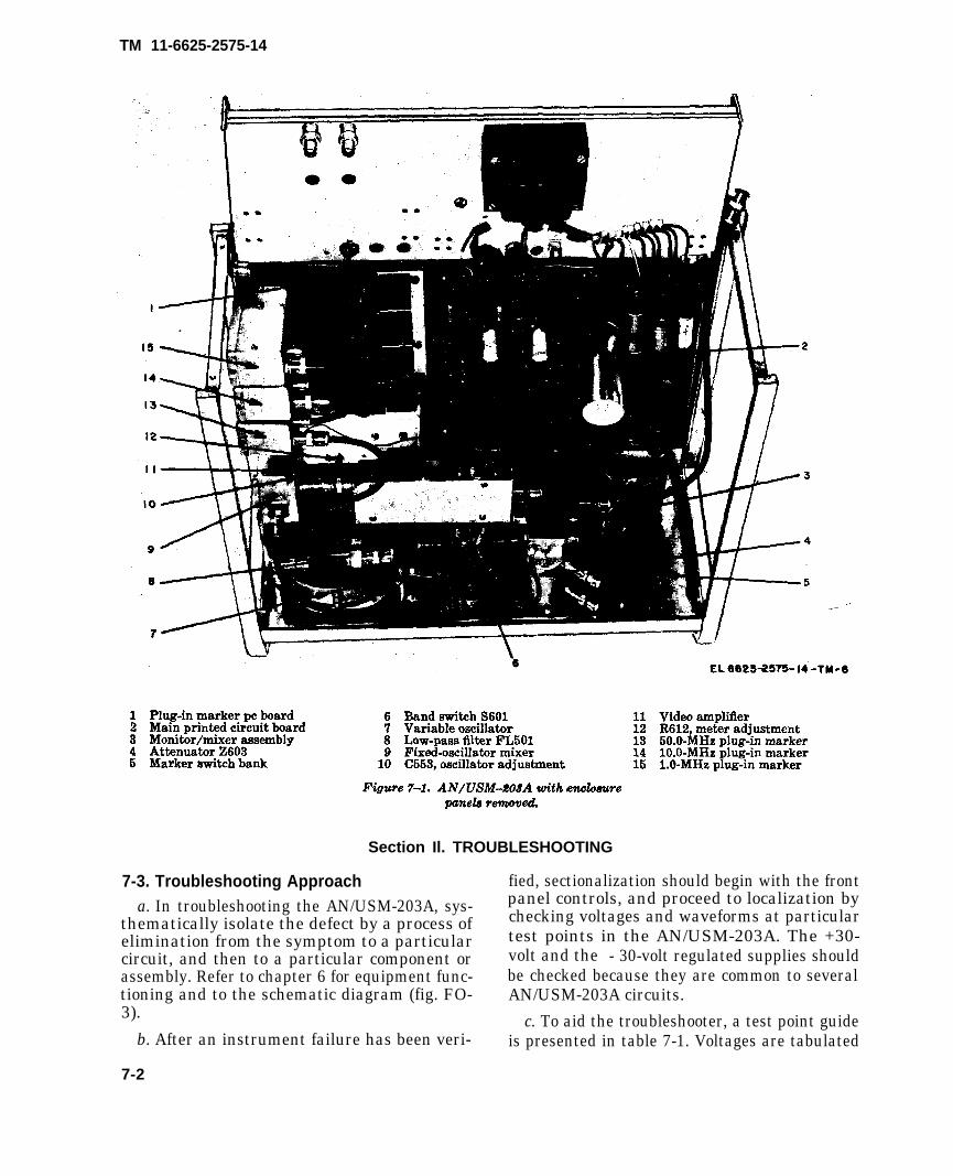
Figure 7-1.
TM 11-6625-2575-14
Section Il. TROUBLESHOOTING
7-3. Troubleshooting Approach fied, sectionalization should begin with the fronta. In troubleshooting the AN/USM-203A, sys- panel controls, and proceed to localization by
thematically isolate the defect by a process of checking voltages and waveforms at particularelimination from the symptom to a particular test points in the AN/USM-203A. The +30-circuit, and then to a particular component or volt and the - 30-volt regulated supplies shouldassembly. Refer to chapter 6 for equipment func- be checked because they are common to severaltioning and to the schematic diagram (fig. FO- AN/USM-203A circuits.3). c. To aid the troubleshooter, a test point guide
b. After an instrument failure has been veri- is presented in table 7-1. Voltages are tabulated
7-2
figure 7-2
figure 7-3
figure 7-4
figure 7-5
figure 7-6
figure 7-7
figure 7-8
and waveforms are shown which are typical ofan operating AN/USM-203A. In addition, a trou-bleshooting guide is presented in table 7-2 whichlists symptoms, probable causes, and recommend-ed corrective actions.
NOTETroubleshooting and repair of rf assem-blies shall be performed at higher main-tenance categories.
7-4. Test Point Guide
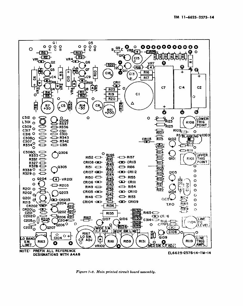
a. The dc voltages in table 7-1 and the wave-forms in figures 7-2 through 7-8 are typical ofthose in a normal AN/USM-203A when the unitis connected to a 115-volt ac line, the POWERswitch is at ON, and a 20-minute warmup is used.Other front panel controls and the internal blank-ing switch are set as follows:
BAND ---------------- HIGH.ATTENUATOR ------------- 0 dB.BLANKING ----- VIDEO (main PC board).SWEEP WIDTH ---------- WIDE.SWEEP WIDTH vernier --- Fully clockwise.CENTER FREQUENCY --- 1000 MHz.
TM 11-6625-2575-14
SWEEP RATE -------------- LINE.RF VERNIER ----------- Set to 0.5 volts rms into a
50-ohm load.ALC-------------------------- INT.MARKERS ------------ ON (1.0, 10.0, and 50 MHz).FIXED MARKER SIZE --- Midrange.
CAUTIONIn making measurements, the chassis ofthe AN/USM-203A shall be connected tothe chassis or ground connection of thetest instrument.
b. To locate test points, see figures 7-9, 7-10,and 7-11. The dc voltage measurements are madewith a high-impedance voltmeter. The shield ofthe voltmeter probe shall be common to the AN/USM-203A chassis. The waveform measurementsare made. with a de-coupled, high-impedance os-cilloscope probe at the test point. The probeshield is common to the AN/USM-203A chassis.The waveforms (fig. 7-2 through 7-8) displayedon the oscilloscope are typical for the AN/USM-203A. Variation from the typical voltages orwaveshapes should be carefully noted during trou-bleshooting.
Table 7-1. Teat Point Guide for AN/USM-203A
Test Point
Q3VR2VR2VR3Q 7VR5VR5VR6Q1OQ11VR7C 2Q201Q202Q206Q207Q102Q105Q106Q107J301J302/J303Q305
Terminal
EmitterCathodeAnodeCathodeEmitterAnodeCathodeAnodeEmitterEmitterAnodePositiveEmitterCollectorBaseBaseCollectorEmitterCollectorCollector
44
Collector
All voltages indicatedrange is given.
Voltage(Test point to mound) Function
Q1 base drive voltageQ3 base drive voltage+ 30v dc regulated outputReference voltage for +30v dcQ5 base drive voltageQ7 base drive voltage- 30v dc regulated outputReference voltage for - 30v dcQ9 base drive voltageQ10 base drive voltage+ 200v dc regulated output+ 50v dc SupplyLeveled B+ voltageQ201 base drive voltageLeveler sample voltageLeveler reference voltageSchmitt trigger outputEmitter followerLinear amplifier outputNonlinear amplifierOutput of LO-MHZ markerOutput of 10.0- and 50-MHz markersOutput of first stage of marker amplifier.
in column 3 are typical, except where a specific tolerance or
7-3

Figure 7-3.
7-4
Figure 7-4.Figure 7-7.
Figure 7-6.
Figure 7-2.
Figure 7-5.
TM 11-6625-2575-14
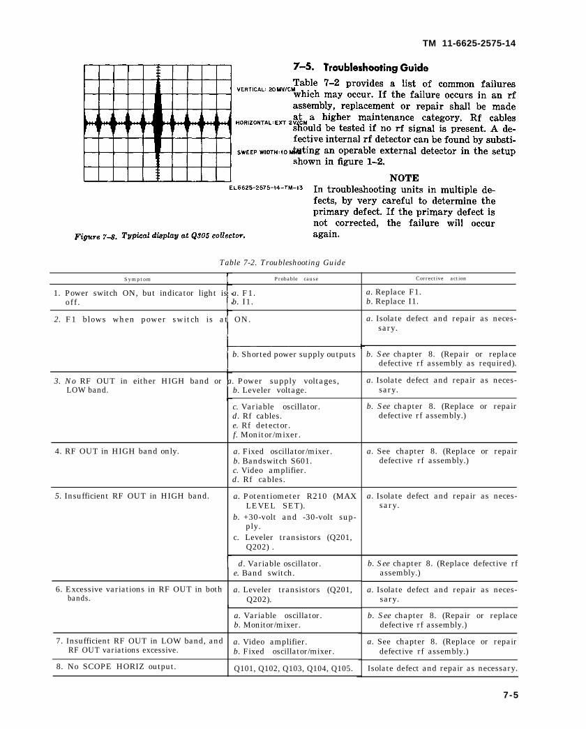
Figure 7-8.
7-5.
Table 7-2
figure 1-2.
TM 11-6625-2575-14
Table 7-2. Troubleshooting Guide
Symptom Probable cause
1. Power switch ON, but indicator light is a. F1.off . b. I1.
2. F1 blows when power switch is at ON.
b. Shorted power supply outputs
3. No RF OUT in either HIGH band or a. Power supply voltages,LOW band. b. Leveler voltage.
c. Variable oscillator.d. Rf cables.e. Rf detector.f. Monitor/mixer.
4. RF OUT in HIGH band only. a. Fixed oscillator/mixer.b. Bandswitch S601.c. Video amplifier.d. Rf cables.
5. Insufficient RF OUT in HIGH band. a. Potentiometer R210 (MAXLEVEL SET).
b. +30-volt and -30-volt sup-ply.
c. Leveler transistors (Q201,Q202) .
d. Variable oscillator.e. Band switch.
6. Excessive variations in RF OUT in both a. Leveler transistors (Q201,bands. Q202).
a. Variable oscillator.b. Monitor/mixer.
7. Insufficient RF OUT in LOW band, and a. Video amplifier.RF OUT variations excessive. b. Fixed oscillator/mixer.
8. No SCOPE HORIZ output. Q101, Q102, Q103, Q104, Q105.
Corrective action
a. Replace F1.b. Replace I1.
a. Isolate defect and repair as neces-sary.
b. See chapter 8. (Repair or replacedefective rf assembly as required).
a. Isolate defect and repair as neces-sary.
b. See chapter 8. (Replace or repairdefective rf assembly.)
a. See chapter 8. (Replace or repairdefective rf assembly.)
a. Isolate defect and repair as neces-sary.
b. See chapter 8. (Replace defective rfassembly.)
a. Isolate defect and repair as neces-sary.
b. See chapter 8. (Repair or replacedefective rf assembly.)
a. See chapter 8. (Replace or repairdefective rf assembly.)
Isolate defect and repair as necessary.
7-5

TM 11-6625-2575-14
Corrective actionSymptom Probable cause
9. No SCOPE HORIZ output.
10. No blanking video mode.
Q101, Q102, Q103, Q104.
Q109, S102.
Isolate defect and repair as necessary.
Isolate defect and repair as necessary.
11. No blanking RF mode.
12. Insufficient SWEEP WIDTH.
Q203, Q204, S102.
a. +200v dc Supply.b. Q106, Q107.
Isolate defect and repair as necessary.
a. Isolate defect and repair as neces-sary.
c. Variable oscillator. b. See chapter 8. (Replace defective rfassembly.)
13. Power supply will not adjust properly. a. VR3, CR7 (+30v dc Supply).b. VR6, CR9 (-30v dc Supply).c. 12.(+ 200v dc Supply) .
Isolate defect and repair as necessary.
14. +30v dc will not regulate.
15. -30v dc will not regulate.
VR3, CR7, Q1, Q4.
VR6, CR9, Q5, Q8.
Isolate defect and repair as necessary.
Isolate defect and repair as necessary.
16. +200v de will not regulate. 12, Q9, Q11. Isolate defect and repair as necessary.
17. +30v dc not present or ripple is excessive. a. CR2, CR6, C1D, C6.b. Q1, Q2, Q3, Q4.
Isolate defect and repair as necessary.
18. -30v dc not present or ripple is excessive. a. CR3, CR5, C7, C10.b. Q5, Q6, Q7, Q8.
Isolate defect and repair as necessary.
19. +200v dc not present or ripple is ex-cessive.
a. CR1, CR4, C1A, C1B.b. C16, C14, Q9, Q10, Q11.
Isolate defect and repair as necessary.
20. RF OUT (output) has excessive voltagevariation in both bands.
a. R210 (RF LEVEL SETMAX) .
b. Q202, Q203, Q206, Q207.
a. Isolate defect and repair as neces-sary.
b. See chapter 8. (Repair defective rfassembly.)
a. Isolate defect and repair as neces-sary.
c. Monitor/mixer;
21. RF OUT (output) frequency does nottrack dial.
a. +200v dc Supply.b. Q106, Q107.c. Loose dial setscrews.
d. Variable oscillator.e. Fixed oscillator.
b. See chapter 8. (Replace or repairdefective rf assembly.)
22. +50v dc not present.
23. No internal or external frequency mark-ers.
24. Internal frequency markers, but no ex-ternal frequency markers.
CR1, CR6, R1, C1C, C2.
Q307
Isolate defect and repair as necessary.
Isolate defect and repair as necessary.
a. Q306 a. Isolate defect and repair as neces-sary.
b. Monitor/mixer b. See chapter 8. (Repair defective rfassembly.)
Isolate defect and repair as necessary.
Isolate defect and repair as necessary.
25. Individual marker produces no displayedfrequency marker.
a. Q301, Q302, Q303, or Q304.b. Individual plug-in marker.c. R301 through R308 require
adjustment.
Q305.26. External frequency marker, but no inter-nal plug-in marker display.
7-6
TM 11-6625-2575-14
Figure 7-9.

TM 11-6625-2575-14
7-8
Figure 7-10.

Figure 7-11.
TM 11-6625-2575-14
Section Ill.
7-6. Repair Procedures
a. Repair procedures shall consist of qualitystandards for wiring and soldering of electronicequipment. Additional precautions are requiredto restore the AN/USM-203A to its original con-dition. When replacing defective parts, be sureto localize heat to the solder joints affected. Allsolder joints shall be smooth, bright, and featheredout to a thin edge, indicating proper flow andwetting action. Leads should be tagged for iden-tification when assemblies are removed. Leadlength and component position should be dupli-cated when components are replaced.
b. Small diameter coaxial cable connections re-quire special attention to prevent breaks and
shorts. Cable shall be replaced if excessive stress-es are caused by shortening the cable to makerepairs.
c. Precautions shall be observed when remov-ing and replacing components on the printed cir-cuit assemblies. Attempt to restore the boardto its original condition. Remove flux and clean-ing agent residue from the board.
7-7. Disposition of Repaired Units
When repairs on a defective AN/USM-203A havebeen completed, perform the alignment and cali-bration required (para 1-5) . Any AN/USM-203A that cannot be satisfactorily repairedshall be sent to a higher maintenance category.
Section IV. TEST PROCEDURES
7-8. General Test Information 7-9. Initial TestsThe extent of repair on the AN/USM-203A will Follow the procedures in paragraph 7-4 anddetermine whether or not alignment is required. Table 7-1, the test point guide. If the unit underIf a repaired AN/USM-203A (unit under test) test is within the stated voltage tolerances, andmeets the test requirements in paragraphs 7-9,7-10, and 7-11, alignment is not required.
is in agreement with the typical voltages andwaveshapes, proceed to paragraph 7-10. If the
7-9
TM 11-6625-2575-14
unit under test is in obvious disagreement withtable 7-1, troubleshoot the unit under test for de-fects (sect. III). If the unit under test appearsquestionable, proceed to the alignment procedurein section V. If the unit under test cannot be re-paired satisfactorily, send it to a higher main-tenance category.
7-10. Typical Test Displays
a. Use the test setup in figure 7-12.
b. Connect the unit under test and the oscillo-scope to a 115-volt, 50/60-Hz, single-phase powersource.
c. Set the front panel POWER switches ofboth the unit under test and the oscilloscope toON. Allow a 20-minute warmup period.
d. Set the front panel controls of the unit un-der test as follows.:
(1)(2).(3)(4)
(5)(6)(7)
(8)(9)
(10)(11)(12)
e. Set(1)(2)(3)(4)
width.
BAND ----------------- HIGH.ATTENUATOR. ------------ 0 dB.SWEEP WIDTH ------------ WIDE.SWEEP WIDTH vernier-- Fully clock-
wise.CENTER FREQUENCY 1000 MHz.SWEEP RATE ------------ LINE.RF VERNIER ------- Set to 0.5 volt
rms on RFOUTPUTmeter.
ALO -- - - - - - - - - - - - - - - - INT.50.0 MHz MARKER ---- ON.FIXED MARKER SIZE Midrange.MARKER SHAPER -------Midrange.BLANKING (main P C
board) ---------------- VIDEO.
the display oscilloscope as follows:Vertical input de-coupled.Vertical sensitivity to 0.1 volt/cm.Horizontal input to external.Adjust horizontal display to 10 cm
f. The oscilloscope display of the unit undertest shall be typically as shown in figure 7-13.
g. To determine the rf output voltage varia-tion in the HIGH BAND (uhf), proceed as fol-lows :
(1) Insert a standard 2-dB attenuator be-
7-10
tween the unit under test RF OUT connector andthe RF DETECTOR IN connector.
(2) Observe the decreased amplitude in thedisplay which represents the attenuated output.
(3) The difference between the attenuatedamplitude and the amplitude observed in f aboverepresents a difference of 2 dB in rf output to thedetector.
(4) Remove the 2-dB attenuator, and re- turn to the conditions in figure 7-12.
(5) Adjust the CENTER FREQUENCYbetween 300 MHz and 1200 MHz.
(6) Using linear interpolation, determinethat the rf output does not vary more than 2.0dB or ±1.0 dB.
NOTEDisregard the sharp decrease in rf out-put at the upper and lower cutoff points.
h. To determine the rf output voltage varia-tion in the LOW BAND (vhf), proceed as fol-lows :
(1) Set the unit under test BAND switchto LOW, and the CENTER FREQUENCY dialto 150 MHz (red scale).
(2) The display shall be typically as shownin figure 7-14.
(3) Using linear interpolation, determinethat the display or detected output does not varymore than 1.0 dB, or ±0.5 dB.
NOTEDisregard the sharp decrease in rf out-put at the zero-beat point, and at thecutoff above 300 MHz.
i. To determine minimum detector efficiency,proceed as follows.
(1) Set the f rent panel controls of the unitunder test as in above.
(2) Set the display oscilloscope as in above.(3) Observe the display in figure 7-13.(4) The minimum amplitude shall be 0.53
volt, or 75-percent detector efficiency.
(5) 0.53 volt is the product of 0.5 by 1.414by 0.75 (the detector efficiency).
j. To determine sweep linearity, proceed as fol-lows.
(1) Set the front panel controls of the unitunder test as in d above.
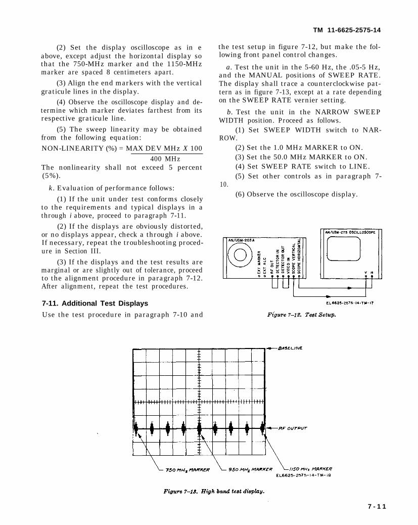
Figure 7-12.
Figure 7-13.
(2) Set the display oscilloscope as in eabove, except adjust the horizontal display sothat the 750-MHz marker and the 1150-MHzmarker are spaced 8 centimeters apart.
(3) Align the end markers with the verticalgraticule lines in the display.
(4) Observe the oscilloscope display and de-termine which marker deviates farthest from itsrespective graticule line.
(5) The sweep linearity may be obtainedfrom the following equation:NON-LINEARITY (%) = MAX DEV MHz X 100
400 MHzThe nonlinearity shall not exceed 5 percent(5%).
k. Evaluation of performance follows:(1) If the unit under test conforms closely
to the requirements and typical displays in athrough i above, proceed to paragraph 7-11.
(2) If the displays are obviously distorted,or no displays appear, check a through i above.If necessary, repeat the troubleshooting proced-ure in Section III.
(3) If the displays and the test results aremarginal or are slightly out of tolerance, proceedto the alignment procedure in paragraph 7-12.After alignment, repeat the test procedures.
7-11. Additional Test Displays
Use the test procedure in paragraph 7-10 and
TM 11-6625-2575-14
the test setup in figure 7-12, but make the fol-lowing front panel control changes.
a. Test the unit in the 5-60 Hz, the .05-5 Hz,and the MANUAL positions of SWEEP RATE.The display shall trace a counterclockwise pat-tern as in figure 7-13, except at a rate dependingon the SWEEP RATE vernier setting.
b. Test the unit in the NARROW SWEEPWIDTH position. Proceed as follows.
(1) Set SWEEP WIDTH switch to NAR-ROW.
(2) Set the 1.0 MHz MARKER to ON.(3) Set the 50.0 MHz MARKER to ON.(4) Set SWEEP RATE switch to LINE.(5) Set other controls as in paragraph 7-
10.(6) Observe the oscilloscope display.
7 - 1 1
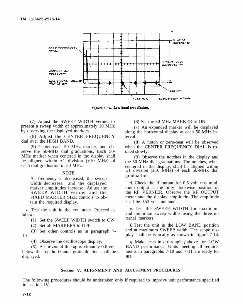
Figure 7-14.
TM 11-6625-2575-14
(7) Adjust the SWEEP WIDTH vernier topresent a sweep width of approximately 10 MHzby observing the displayed markers.
(8) Adjust the CENTER FREQUENCYdial over the HIGH BAND.
(9) Center each 50 MHz marker, and ob-serve the 50-MHz dial graduations. Each 50-MHz marker when centered in the display shallbe aligned within ±1 division (±10 MHz) ofeach dial graduation of 50 MHz.
NOTEAs frequency is decreased, the sweepwidth decreases, and the displayedmarker amplitudes increase. Adjust theSWEEP WIDTH vernier and theFIXED MARKER SIZE controls to ob-tain the required display.
c. Test the unit in the cw mode. Proceed asfollows.
(1)(2)(3)
10.(4)(5)
Set the SWEEP WIDTH switch to CW.Set all MARKERS to OFF.Set other controls as in paragraph 7-
Observe the oscilloscope display.A horizontal line approximately 0.6 volt
below the top horizontal graticule line shall bedisplayed.
Section V. ALIGNMENT AND
(6) Set the 50 MHz MARKER to ON.(7) An expanded marker will be displayed
along the horizontal display at each 50-MHz in-terval.
(8) A notch or zero-beat will be observedwhen the CENTER FREQUENCY DIAL is ro-tated slowly.
(9) Observe the notches in the display andthe 50-MHz dial graduations. The notches, whencentered in the display, shall be aligned within±1 division (±10 MHz) of each 50-MHZ dialgraduation.
d. Check the rf output for 0.5-volt rms mini-mum output at the fully clockwise position ofthe RF VERNIER. Observe the RF OUTPUTmeter and the display amplitude. The amplitudeshall be 0.53 volt minimum.
e. Test the SWEEP WIDTH for maximumand minimum sweep widths using the three in-ternal markers.
f. Test the unit in the LOW BAND positionand at maximum SWEEP width. The scope dis-play shall be typically as shown in figure 7-14.
g. Make tests in a through f above for LOWBAND performance. Units meeting all require-ments in paragraphs 7-10 and 7-11 are ready foruse.
ADJUSTMENT PROCEDURES
The following procedures should be undertaken only if required to improve unit performance specifiedin section IV.
7-12
TM 11-6625-2575-14
NOTEIn some cases, the adjustment and alignment procedures may require a compro-mise between two or more characteristics. When the procedures in section Vare completed, perform the test procedures in section IV.
7-12. Power Supply Adjustment
CAUTIONAdjustment of power supply voltagesmay cause major misalignment. Do notadjust voltage before checking bothLOW and HIGH BAND CENTERFREQUENCY dial calibration.
a. Use the test setup in paragraph 7-4. Moni-tor the voltages as in table 7-1. Do not make ad-justments if voltages are within tolerances.
b. If required, adjust R7 to obtain a voltagereading of +30 volts dc ±1. The peak-to-peak rip-ple as measured with an at-coupled oscilloscopeis 6 mV (typical).
c. If required, adjust R14 to obtain a voltagereading of -30 volts dc ±1. The peak-to-peakripple as measured with an at-coupled oscillo-scope is 4 mV (typical).
d. If required, adjust R21 to obtain a voltagereading of +200 volts dc ±5. The peak-to-peakripple as measured with an at-coupled oscillo-scope is 15 mV (typical).
7-13. Rate Generator Alignment
To align the rate generator, perform the proced-ures in a through o below.
a. Use the test setup in paragraph 7-10 andfigure 7-12 with all MARKERS at OFF.
b. Set the SWEEP RATE switch to MANUAL.
c. Adjust the SWEEP RATE vernier controlfrom one extreme to the other.
d. Adjust the horizontal gain and horizontalposition controls of the oscilloscope so the dot onthe CRT display is visually aligned with the ex-treme left-hand vertical graticule line when theSWEEP RATE vernier control is fully counter-clockwise.
e. In combination with d above, adjust the os-cilloscope controls so the dot on the CRT displayis visually aligned with the extreme right-handvertical graticule line when the SWEEP RATEvernier control is fully clockwise.
f. The SCOPE HORIZ voltage should be 1.0volt ±0.5 in d above and 18 volts ±2 in above.
g. Return the CRT display to the horizontalpositions obtained in d and e above.
h. Set the SWEEP RATE switch to the .05 to5 Hz position. Do not change oscilloscope con-trols.
i. The oscilloscope display shall be viewed astracing a rectangular pattern counterclockwise.
j. Adjust the lower trigger point control(R108) so the upper left-hand corner of the rec-tangle is visually aligned at the upper left-handcorner of the graticule.
k. Adjust the upper trigger point control(R101) so the upper right-hand corner of the rec-tangle is visually aligned at the upper right-hand corner of the graticule.
l. Repeat j and k above as required until bothconditions of alignment occur simultaneously. Donot change the oscilloscope controls.
.
m. Set the SWEEP RATE switch to LINE.n. Adjust the line trigger amplitude control
(R119) and the line DC level control (R106) un-til a rectangular pattern of the same size as thatobtained in j through e above is displayed.
o. Repeat the alternate adjustments of R119and R106 until the rectangular pattern is alignedwith the respective graticule corners.
7-14. Frequency Dial Alignment
Use the test procedures in paragraphs 7-11b andc. Misalignment may be caused by dial slippage,by aging of components, or by incorrect settingsof the regulated power sources.
a. Dial Slippage.(1) Check the HIGH BAND.(2) If the dial error is greater than one di-
vision at 1200 MHz and is either constant orerratic cover the HIGH BAND, slippage mayhave occurred.
(3) Adjust the two #6 setscrews that se-cure the dial-venier collar to the oscillator shaft.Use a 1/16-inch hex key. The collar is locatedbetween the vernier and the variable oscillator(fig. 7-1) .
(4) Position the shaft as required to releaseand then properly reposition the dial for fre-quency alignment.
7-13
TM 11-6625-2575-14
(5) Tighten both setscrews.
b. High Band Alignment. Adjust R161 (fig.7-9) for dial misalignment of approximately 10MHz. Check the entire range for proper align-ment of 50-MHz markers within ±1 dial divi-sion (±10 MHz).
c. Low Band Alignment.(1) Align the HIGH BAND in b above.(2) Set the CENTER FREQUENCY dial
to 700 MHz.(3) Adjust the SWEEP WIDTH vernier to
approximately 20 MHz.(4) Fine-tune the dial until the 700-MHz
marker is centered in the display.(5) Set the BAND switch to LOW.(6) Adjust C553 (fig. 7-1) as required to
center the zero beat.(7) Check the LOW BAND at 50-MHz in-
tervals, and adjust C553 if required for align-ment within ±1 dial division (±10 MHz).
7-15. Sweep Width Alignment
To align the sweep width circuit, proceed as fol-l o w s :
a. Use the test setup in figure 7-12.
b. Set the AN/USM-203A controls as follows:(1) BAND SWITCH to HIGH.(2) CENTER FREQUENCY dial to 300
MHz.(3) SWEEP WIDTH switch to WIDE.(4) SWEEP WIDTH vernier fully clock-
wise.(5) ALC switch to INT.(6) RF VERNIER to 0.5-volt rms output.(7) 1.0 MHz MARKER switch only to ON.(8) FIXED MARKER SIZE to midrange.
c. Set the AN/USM-273 oscilloscope as fol-l ows :
(1) Vertical input de-coupled.(2) Vertical gain to 0.1 volt/cm.(3) Horizontal input to external.(4) Horizontal controls to produce a cen-
tered 10-cm display.
d. Adjust R161 (fig. 7-9) to produce nearlyequal spacings between the 1.0-MHZ markersacross the 10-cm
The marker
7-14
horizontal display.
NOTEspacings at the right-hand
end of the display will increase sharplyas R161 is adjusted. Readjust R161slightly so that the marker spacings aremore equally spaced.
e. Set blanking switch S102 (fig. 7-9 ) to RF.
f. Set 1.0 MHz MARKER switch to OFF.
g. Set 50.0 MHz MARKER switch to ON.
h. Adjust the CENTER FREQUENCY dial to1000 MHz. Observe the 50.0-MHZ displayed mark-ers, so that the 1000-MHZ marker is identifiedin the display. As sweep width increases, moremarkers are displayed.
i. Adjust R159 (fig. 7-9) for 400-MHz sweepwidth. The 1000-MHz marker will shift to theright in the display. This shift is normal.
j. Set S102 (fig. 7-9) for VIDEO blanking,the normal setting.
k. Set SWEEP WIDTH switch to NARROW.
l. Adjust SWEEP WIDTH vernier fully clock-wise.
m. Set the CENTER FREQUENCY dial to1200 MHz.
n. Adjust R131 (fig. 7-9) as required to cen-ter the 1200-MHz marker in the display.
o. Adjust SWEEP WIDTH vernier fully coun-terclockwise.
p. Adjust R167 (fig. 7-9) to display the 1200-MHz marker in the center of the display at NAR-ROW sweep width.
q. Set the BAND switch to LOW, and care-fully adjust the center frequency dial about the300-MHz graduation (red scale) to place the 300-MHz marker in the center of the oscilloscopetrace. Note any deviation from the 300-MHz grad-uation when the marker is in the center of thetrace. If this deviation exceeds the equivalentof 5 MHz, an adjustment of the fixed-frequencyoscillator is indicated. If this adjustment is re-quired, go to r below. If this adjustment is notrequired, go to s below.
r. Adjust the fixed-frequency oscillator, as de-scribed in paragraph 7-14b to place the 300-MHzmarker in the center of the oscilloscope trace.
s. Set
(1)(2)
the unit under test controls as follows:BAND SWITCH to LOW.SWEEP WIDTH switch to WIDE.
(3) SWEEP WIDTH vernier fully clock-wise.
t. Adjust the CENTER FREQUENCY dial toapproximately 150 MHz (red scale), and placethe zero-beat notch at the extreme left of theoscilloscope trace.
u. Alternate] y adjust low band sweep width po-tentiometer (LB SW) R163 (fig. 7-9) and theCENTER FREQUENCY dial. Place the zero-beat notch and the 300-MHz marker at the ex-tremes of the oscilloscope trace.
7-16. Rf Output Voltage Adjustment
Use the following procedures to adjust the rfoutput voltage, and the RF OUTPUT meter.
a. Set the AN/USM-203A front panel controlsand S102 as follows:
(1) BAND ---------- HIGH.(2) ATTENUATOR ---------- 0dB.(3) SWEEP WIDTH ---- CW.(4) BLANKING ---------- S102 to VIDEO.(5) CENTER FREQUENCY 1200 MHz.(6) SWEEP RATE --------------- LINE.(7) RF VERNIER -------- Fully clockwise.(8) ALC ----------------------------- INT.(9) MARKERS----------- A11 OFF.
b. Couple the AN/USM-203A RF OUT con-nector to the AN/USM-260) power meter, using
the associated thermistor mount (477B) andthe 200-ohm negative coefficient thermistor.
NOTEThe thermistor mount uses a type-Nmale connector for the rf input. Noadapter is required to insert this con-nector into the BNC female connectorof the AN/USM-203A.
c. The RF OUTPUT meter should indicate O.Adjust the meter to zero, using the screw adjust-ment if required.
d. Adjust the power meter for measurementsin the 0- to 10-mW range.
e. Connect the power plugs of both the AN/USM-203A and the AN/USM-260 to a 115-volt,50/60-Hz, single-phase power source.
f. Set both power switches to ON, and allowa 20-minute warmup period.
g. Monitor the rf output, and adjust R210, theMAX RF LEVEL SET potentiometer, a slottedfront-panel control, for an indication of 5 mWon the power meter; 5 mW into a 50-ohm loadis 0.5 volt rms.
TM 11-6625-2575-14
h. Adjust R612, the slotted control located onthe main chassis behind the variable oscillator(fig. 7-1) for a reading of 0.5 volt rms on theRF OUTPUT meter.
i. Adjust the RF VERNIER control fullycounterclockwise.
j. Monitor the rf output, and adjust potentiom-eter R209, MIN RF LEVEL SET, a slotted, front-panel control, for an indication of 10 dB downfrom the maximum set in h above. The indi-cated rf output shall be 0.5 mW.
k. Repeat g above with the RF VERNIERfully clockwise.
l. Adjust the CENTER FREQUENCY dialfrom 1200 to 300 MHz in the HIGH BAND. Thepower output shall be 5 mW minimum and 6.3mW maximum in the HIGH BAND.
m. Set the BAND switch to LOW.
n. Adjust the CENTER FREQUENCY dialfrom 500 kHz to 300 MHz (red) in the LOWBAND. The power output shall be 5 mW mini-mum and 5.6 mW maximum.
o. Repeat g through k above for an output of5 mW minimum and 5.6 mW maximum from500 kHz to 300 MHz.
p. Repeat checks on both HIGH and LOWBAND so that l and o above are within requiredlimits.
7-17. Marker Amplitude Adjustment
Refer to figure 7-10 for the location of markeramplitude controls. Use the test setup in figure7-12.
a. Eight individual marker sizes are provided.Refer to figure 7-15 for connection of plug-inmarkers.
b. Resistor R305 adjusts the displayed ampli-tude of the 1.0-MHZ harmonic marker, R311 forthe 10.0-MHZ harmonic marker, and R317 forthe 50. 0-MHZ harmonic marker.
c. With the FIXED MARKER SIZE controlset at midrange, adjust R317 for 0.2-volt ampli-tude of the 50. 0-MHZ marker. Adjust R311 for0.1-volt amplitude for the 10.0-MHZ marker, andR305 for 0.05-volt amplitude. All amplitudes arepeak-to-peak values.
d. When using the external marker, set theFIXED MARKER SIZE fully clockwise.
7-15

TM 11-6625-2575-14
Figure 7-15.
Figure 7-16.
7-18. Blanking Mode Test
Blanking switch S102 (fig. 7-9) located on themain printed circuit board assembly is used toselect VIDEO or RF blanking.
a. Follow the test procedure in paragraph 7-10.
b. Observe the typical test display in figure 7-13.
c. Set switch S102 first to VIDEO and then torf blanking.
d. Little difference shall be noticed in the testdisplay between VIDEO or rf blanking.
e. Set S102 to the VIDEO blanking (normal)position.
7-19. Input Power Option
The unit under test may be wired for 115-voltac, 60-Hz, single-phase or 230-volt- ac, 60-Hz,single-phase operation. See figure 7-16 for theconnection diagram on the main printed circuitboard.
CAUTIONUse a 1.0-ampere slo-blo fuse for 115-volt operation, and a 1/2-ampere slo-blofuse for 230-volt operation. (See rearpanel fuseholder F1 in figure 3-2.)
7-16
TM 11-6625-2575-14
CHAPTER 8
GENERAL SUPPORT MAINTENANCE
Section I.
8-1. Scope of GS Maintenance
AN/USM-203A sweep signal generators whichrequire maintenance at general support can begrouped as follows:
a. Units which require repair of rf assemblies.
b. Units which require replacement of rf as-semblies.
c. Units which cannot be repaired at lowermaintenance categories.
d. Units which are a combination of the pre-ceding groups.
N O T EDefective rf assemblies (fig. 7-1) whichmay be replaced, but shall be repairedonly at depot level, are as follows:
(1) Bandswitch (S601).(2) Attenuator (Z603).(3) Plug-in harmonic markers (1.0, 10.0,
and 50.0 MHz).
GENERAL
(4) Video amplifier.(5) Variable oscillator.
8-2. Test Equipment Requireda. The following test equipment or equal is re-
quired:(1) Multimeter TS-352B/U, FSN: 6625-
242-5032.(2) Oscilloscope AN/USM-281, FSN: 6625-
228–2201.(3) Voltmeter, Electronic AN/USM-98B,
FSN: 6625-753-2115.(4) Wattmeter AN/URM-120, FSN: 6625-
813-8430.(5) Signal Generator AN/USM-44, FSN:
6625-669-4031.(6) Frequency Counter, AN/USM-207A,
FSN: 6625-911-6368.(7) Spectrum Analyzer AN/UPM-84, FSN:
6625-557-8262.b. Adapter UG-274A/U, tee, FSN: 5935-201-
2411 or equal is required.
Section Il. TROUBLESHOOTING AND REPAIR
8-3. Approach
Follow the procedures in chapter 7, section II,but in addition concentrate on the rf circuits.
a. Monitor dc voltages at the input terminalsof active rf assemblies.
b. Carefully test BNC connectors and coaxialcable assemblies for continuity and quality.
c. Use signal substitution techniques in isolat-ing defective rf assemblies.
d. Refer to the troubleshooting guide in table7-2.
e. Refer to the technical characteristics inparagraph 1-11.
f. Refer to the block diagram (fig. 8-4) andschematic diagram (fig. FO-3).
8-4. Procedures
a. Repair Standards. General support mainten-ance procedures, tests, and standards form a partof the repair of defective AN/USM-203A units.
b. Modifications Work Orders. Perform all mod-ification work orders (MWO) applicable to theAN/USM-203A before making specified tests.See DA Pam 310-7 for applicable listings.
c. Special Procedures. Because of the highmaximum frequency and broadband coverage ofthe AN/USM-203A, component lead lengths, posi-tion, and solder connections in rf circuits are cri-tical. Before replacing a defective component,closely observe the physical layout of the associ-ated components which must be repositioned orremoved. The new component should closely con-
8-1
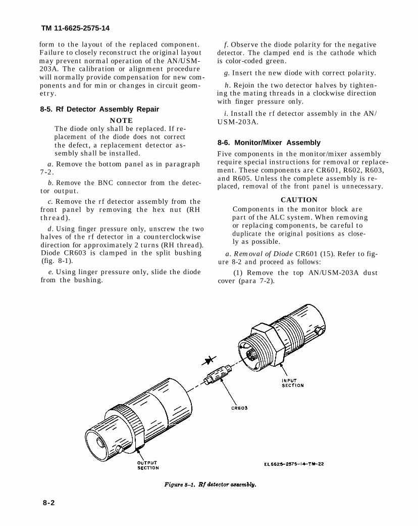
Figure 8-1.
TM 11-6625-2575-14
form to the layout of the replaced component.Failure to closely reconstruct the original layoutmay prevent normal operation of the AN/USM-203A. The calibration or alignment procedurewill normally provide compensation for new com-ponents and for min or changes in circuit geom-etry.
8-5. Rf Detector Assembly Repair
NOTEThe diode only shall be replaced. If re-placement of the diode does not correctthe defect, a replacement detector as-sembly shall be installed.
a. Remove the bottom panel as in paragraph7-2.
b. Remove the BNC connector from the detec-tor output.
c. Remove the rf detector assembly from thefront panel by removing the hex nut (RHthread).
d. Using finger pressure only, unscrew the twohalves of the rf detector in a counterclockwisedirection for approximately 2 turns (RH thread).Diode CR603 is clamped in the split bushing(fig. 8-1).
e. Using linger pressure only, slide the diodefrom the bushing.
f. Observe the diode polarity for the negativedetector. The clamped end is the cathode whichis color-coded green.
g. Insert the new diode with correct polarity.
h. Rejoin the two detector halves by tighten-ing the mating threads in a clockwise directionwith finger pressure only.
i. Install the rf detector assembly in the AN/USM-203A.
8-6. Monitor/Mixer Assembly
Five components in the monitor/mixer assemblyrequire special instructions for removal or replace-ment. These components are CR601, R602, R603,and R605. Unless the complete assembly is re-placed, removal of the front panel is unnecessary.
CAUTIONComponents in the monitor block arepart of the ALC system. When removingor replacing components, be careful toduplicate the original positions as close-ly as possible.
a. Removal of Diode CR601 (15). Refer to fig-ure 8-2 and proceed as follows:
(1) Remove the top AN/USM-203A dustcover (para 7-2).
8-2
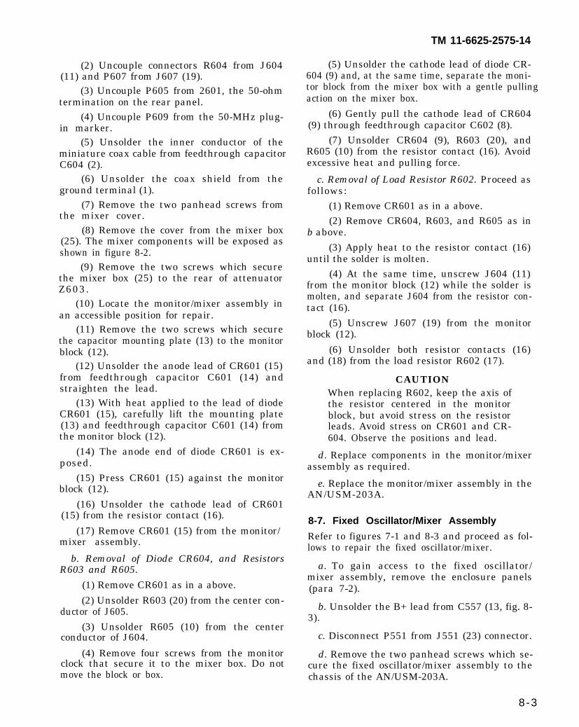
TM 11-6625-2575-14
(2) Uncouple connectors R604 from J604(11) and P607 from J607 (19).
(3) Uncouple P605 from 2601, the 50-ohmtermination on the rear panel.
(4) Uncouple P609 from the 50-MHz plug-in marker.
(5) Unsolder the inner conductor of theminiature coax cable from feedthrough capacitorC604 (2).
(6) Unsolder the coax shield from theground terminal (1).
(7) Remove the two panhead screws fromthe mixer cover.
(8) Remove the cover from the mixer box(25). The mixer components will be exposed asshown in figure 8-2.
(9) Remove the two screws which securethe mixer box (25) to the rear of attenuatorZ603.
(10) Locate the monitor/mixer assembly inan accessible position for repair.
(11) Remove the two screws which securethe capacitor mounting plate (13) to the monitorblock (12).
(12) Unsolder the anode lead of CR601 (15)from feedthrough capacitor C601 (14) andstraighten the lead.
(13) With heat applied to the lead of diodeCR601 (15), carefully lift the mounting plate(13) and feedthrough capacitor C601 (14) fromthe monitor block (12).
(14) The anode end of diode CR601 is ex-posed.
(15) Press CR601 (15) against the monitorblock (12).
(16) Unsolder the cathode lead of CR601(15) from the resistor contact (16).
(17) Remove CR601 (15) from the monitor/mixer assembly.
b. Removal of Diode CR604, and ResistorsR603 and R605.
(1) Remove CR601 as in a above.
(2) Unsolder R603 (20) from the center con-ductor of J605.
(3) Unsolder R605 (10) from the centerconductor of J604.
(4) Remove four screws from the monitorclock that secure it to the mixer box. Do notmove the block or box.
(5) Unsolder the cathode lead of diode CR-604 (9) and, at the same time, separate the moni-tor block from the mixer box with a gentle pullingaction on the mixer box.
(6) Gently pull the cathode lead of CR604(9) through feedthrough capacitor C602 (8).
(7) Unsolder CR604 (9), R603 (20), andR605 (10) from the resistor contact (16). Avoidexcessive heat and pulling force.
c. Removal of Load Resistor R602. Proceed asfollows:
(1) Remove CR601 as in a above.(2) Remove CR604, R603, and R605 as in
b above.(3) Apply heat to the resistor contact (16)
until the solder is molten.(4) At the same time, unscrew J604 (11)
from the monitor block (12) while the solder ismolten, and separate J604 from the resistor con-tact (16).
(5) Unscrew J607 (19) from the monitorblock (12).
(6) Unsolder both resistor contacts (16)and (18) from the load resistor R602 (17).
CAUTIONWhen replacing R602, keep the axis ofthe resistor centered in the monitorblock, but avoid stress on the resistorleads. Avoid stress on CR601 and CR-604. Observe the positions and lead.
d. Replace components in the monitor/mixerassembly as required.
e. Replace the monitor/mixer assembly in theAN/USM-203A.
8-7. Fixed Oscillator/Mixer Assembly
Refer to figures 7-1 and 8-3 and proceed as fol-lows to repair the fixed oscillator/mixer.
a. To gain access to the fixed oscillator/mixer assembly, remove the enclosure panels(para 7-2).
b. Unsolder the B+ lead from C557 (13, fig. 8-3).
c. Disconnect P551 from J551 (23) connector.
d. Remove the two panhead screws which se-cure the fixed oscillator/mixer assembly to thechassis of the AN/USM-203A.
8-3

TM 11-6625-2575-14
Figure 8-2.
f. Remove the four cover screws.
g. Remove the cover, The fixed oscilltorponents, including transistors Q551 (6)
com-and
Q552 (9) are accessible for replacement.
e. Disconnect J401carefully remove thethe AN/USM-203A.
fromfixed
filter FL551 (16) andoscillator/mixer from
NOTEClosely observe the position of compon-ents and their lead lengths. Replacecomponents as closely as possible totheir original position.
h. To gain access to mixer components, theprinted circuit assembly must be removedfrom the enclosure.
i. Unsolder capacitor C555 (20) and resistorR558 (19) from filter FL551.
j. Unsolder capacitor C554 (28) from connec-tor J551.
k. Remove the six panhead screws which se-cure the mounting bracket (3) to the enclosure.
l. Carefully withdraw the mounting bracketand mixer printed circuit board assembly fromthe enclosure.
m. The mixer components are accessible forremoval and replacement.
n. Remove and replace mixer diodes CR-551 (26), CR552 (24), CR553 (22), and CR554(21) if required. Remove and replace other com-ponents if required.
N O T EObserve the same precautions in restor-ing the original layout as in other rfassemblies. When diodes are replaced,use the correct polarities.
o. Assemble the fixed oscillator/mixer in thereverse order of disassembly and with the samecare.
p. Replace the repaired fixed oscillator in theAN/USM-203A assembly.
8-4

TM 11-6625-2575-14
Figure 8-3.
Section III. REPLACEMENT OF RF ASSEMBLIES
8-8. Front Panel Removal N O T ETo replace the band switch, the rotary attenua- The dial and the variable oscillator aretor, and the variable oscillator, remove the front calibrated as an assembly and shouldpanel as follows: be reassembled as a compatible pair.
a. Remove the slide panels (para 7-2). d. Remove the retaining nuts on the powerb. Remove all control knobs. switch and the BNC connectors except the RF
DETECTOR IN connector.c. Remove the three screws which fasten theCENTER FREQUENCY dial to the variable os- e. Unsolder the pilot light leads at the powercillator assembly. switch and at the lead splice.
8 - 5
TM 11-6625-2575-14
f. Remove the two leads from the rf outputmeter.
g. Remove the BNC connector and cable fromthe rear of the rf detector assembly.
h. Remove the two screws from each of thetwo side rails which secure the front panel tothe AN/USM-203A.
i. Remove the front panel assembly includingthe rf detector and the rf output meter. The back-ing panel is now exposed for removal of rf assem-blies and other components.
NOTERefer to figure 7-1 for the location ofthe rf assemblies.
8-9. Bandswitch S601
To replace S601, proceed as follows:a. Remove the AN/USM-203A slide panels
(para 7-2).b. Remove the AN/USM-203A front panel
(para 8-8).c. Disconnect and identify the six BNC cable
connectors.d. Unsolder all leads from the two wafer sec-
tions of the switch.
N O T ECheck the lead and terminal locations sothe leads may be soldered to the correctterminals on the replacement switch.
e. Remove the two 8-32 screws from the back-ing panel which locate the band switch.
f. Remove the band switch from the AN/USM-203A.
g. Replace the band switch with a new or serv-iceable unit.
h. Reassemble all hardware, leads, and cablesas required.
8-10. Attenuator Z603
To replace Z603, proceed as follows:a. Remove the AN/USM-203A enclosure pan-
els (para 7-2).b. Remove the AN/USM-203A front panel
(para 8-8).c. Remove the monitor/mixer assembly (para
8-3a).d. Remove coaxial cable connectors P608 and
P610 from the attenuator.
e. Remove the two 8-32 screws from the back-ing panel which locate the attenuator.
f. Remove the attenuator from the AN/USM-203A.
g. Replace defective attenuator Z603 with anew or serviceable unit.
h. Remount all hardware and cables in theAN/USM-203A as required.
8-11. Video Amplifier
To replace the video amplifier, proceed as follows:
a. Remove the AN/USM-203A enclosurepanels (para 7-2).
CAUTIONTag all leads and note the diode polarityas each lead is unsoldered.
b. Locate the four terminals on the back side ofthe video amplifier, and identify each lead forreassembly.
(1) Unsolder the lead from C433.(2) Unscrew the lug which ties the shield
of the coaxial cable to the case.(3) Unsolder the center conductor of the
coax lead and the cathode lead of VR401 fromthe standoff terminal.
(4) Unsolder the anode lead of VR401 fromC429.
c. Disconnect the BNC connector at the ampli-fier output.
d. Remove the two screws which secure thevideo amplifier bracket to base of the instrument.
e. Disconnect the BNC connector from therigid coaxial filter (FL551).
f. Remove the video amplifier assembly fromthe instrument.
g. Install an operating video amplifier in theinstrument by reversing the disassembly proce-dure.
8-12. Variable Oscillator
To replace the variable oscillator, proceed asfollows.
a. Remove the AN/USM-203A enclosurepanels (para 7-2).
b. Remove the AN/USM-203A front panel(para 8-8).
c. Disconnect the BNC connector (P501) from
8-6
TM 11-625-2575-14
filter FL501. The filter shall remain attached to 8-13. Harmonic Markersthe variable oscillator. To replace the 1.0-, 10.0-, or 50.0-MHZ. plug-in
d. Remove two of the three 6-32 panhead screws harmonic markers, proceed as follows:that secure the variable oscillator assembly tothe backing panel.
e. Hold the oscillator with one hand, and care-fully remove the third screw. Except for twowires, the oscillator is detached.
f. Position the oscillator so that the two wireson the front panel may be unsoldered from feed-through terminals C502 and C503.
g. Remove the variable oscillator from the AN/USM-203A.
h. Using the three screws removed in d and eabove, attach the CENTER FREQUENCY dial
a. Remove the AN/USM-203A enclosure pan-els (para 7-2).
b. Remove the BNC connector which connectsto the adjacent plug-in marker, or, for the 1.0-MHz plug-in marker to Z602, the terminatingimpedance on the rear panel. (See figure 7-15).
c. Remove the screw which holds the markerbracket to the chassis.
d. Unplug the six-pin, plug-in marker from itssocket in the marker printed circuit board as-sembly.
to the mating holes in the vernier drive.e. Replace the defective marker with an opera-
i. Install an operating variable oscillator in theAN/USM-203A by reversing the disassembly
tive marker of the same type.
procedure. f. Reverse the disassembly procedure.
Section IV. TEST PROCEDURES
8-14. General (2) ATTENUATOR - - - - -0dB.
When an AN/USM-203A has been repaired, per-(3) CENTER FRE- 1000 MHz.
QUENCY.form the test procedures in paragraphs 7-4, 7- (4) SWEEP RATE - - - -MANUAL.10, 7-11, 8-15, and 8-16.
N O T EResults of the test procedures may indi-cate that further troubleshooting, re-pair, and alignment must be performed.Section VI provides additional align-ment and adjustment procedures thatshould enable the unit under test tomeet the technical characteristicsin paragraph 1-11.
(5) SWEEP WIDTH N A R R O W .s w i t c h .
(6) SWEEP WIDTH Fully counterclockwise.vernier.
(7) ALC - - - - - - - - - - - - - -INT.(8) MARKERS - - - - - - - -All OFF.
c. Energize both the unit under test and thecounter.
d. Set the SWEEP RATE vernier fully clock-wise, and read the counter frequency.
If the unit cannot be made ready for use, it shall e. Set the SWEEP RATE vernier fully counter-be sent to the depot for evaluation. clockwise, and read the counter frequency.
Calibration procedure can be used in place of the f. Subtract the frequency obtained in e abovetest and adjustment procedures in Chapters 7 and from the frequency obtained in d above.
g. The frequency difference shall be 10 kHz
8-15. Minimum Sweep Width maximum.
a. Connect the RF OUT connector of the unit h. Set the unit under test controls as in b
under test to the input of Electronic Counter, above, but set the SWEEP WIDTH switch toDigital Readout AN/USM-207A. Use a 50-ohm WIDE.BNC-to-BNC cable approximately 30 inches long. i. Set the SWEEP RATE vernier fully clock-
b. Set the front panel controls of the unit under wise, and read the counter frequency.test as follows: j. Set the SWEEP RATE vernier fully counter-
(1) BAND - - - - - - - - - - - - - - - - - - HIGH. clockwise, and read the counter frequency.
8-7
TM 11-6625-2575-14
k. Subtract the frequency obtained in j abovefrom the frequency obtained in i above.
l. The frequency difference shall be 500 kHzmaximum.
8-15. Spurious and Harmonic Distortion
a. Connect the RF OUT connector of the unitunder test to the input of the spectrum analyzer.
b. Set the front panel controls of the unit undertest as follows:
(1)(2)(3)(4)(5)(6)
SWEEP WIDTH switch - - - - - - - CW.MARKERS - - - - - - - - - - - - - - - -All OFF.RF VERNIER - - - - - - - - - - - - - - - - -0.5 volt rms.BAND switch - - - - - - - - - - - - - - - - - LOW.ALC - - - - - - - - - - - - - - - - - - - - INT.ATTENUATOR - - - - - - - - - - - - - 0dB.
c. Adjust the CENTER FREQUENCY from20 to 300 MHz.
d. Follow the instructions in the spectrum
Section V. ALIGNMENT AND
8-17. General Alignment and AdjustmentInformation
a. When a repaired AN/USM-203A has beentested as required in Section V, alignment andadjustment procedures may be required. The pur-pose of Section VI is to enable a repaired unitto meet the technical characteristics in para-graph 1-11 by resetting internal controls.
b. Be careful when making adjustments tocorrect a given out-of-tolerance condition. An ad-justment which corrects one condition may de-grade another. When an adjustment affects morethan one operating characteristic, another ad-justment must be used to bring the system intobalance. A series of alternate adjustments maybe required to achieve the desired results.
c. Because some of the AN/USM-203A adjust-ments do interact, repeat the test procedures inSection V in sequence after final adjustmentsare made.
8-18. Power Supply Adjustment
Follow the procedures in paragraph 7-12.
NOTEAdjustment of the power supply volt-ages may cause major misalignment ofboth the HIGH and LOW BAND CEN-TER FREQUENCY dial calibration.
analyzer operator’s manual, and proceed as fol-lows:
(1) Display the rf amplitude in the fre-quency domain.
(2) Calibrate the display amplitude in dB.(3) Obtain a display of the fundamental
frequency of the unit under test.
e. While gradually adjusting the CENTERFREQUENCY of the unit under test, tune themain dial of the spectrum analyzer, and observespurious and harmonic responses of the unit un-der test. Any spurious signal or harmonic compon-ent shall be at least 25 dB below the fundamentalfrequency (CENTER FREQUENCY) of the unitunder test.
f. Repeat e above with the BAND switch setto HIGH and at the same time, adjust the CEN-TER FREQUENCY of the unit under test from300 to 1200 MHz.
ADJUSTMENT PROCEDURES
8-19. Rate Generator, Frequency Dial, andSweep Width Alignment
To align the rate generator, frequency dial, andsweep width, follow the procedures in para-graphs 7-13 through 7-15, respectively.
8-20. Rf Output Voltage Adjustment
Adjust the rf output voltage by performing theprocedures in paragraph 7-16.
8-21. Marker Amplitude Adjustment
Adjust the marker amplitude by performing theprocedures in paragraph 7-17.
N O T EMarker frequency accuracy may bechecked by zero-beating an external sig-nal generator which is monitored by afrequency counter with displayed 1.0-,10.0-, and 50.0-MHZ internal markersin the AN/USM-203A.
8-22. Blanking Mode Selection
Follow the procedures in paragraph 7-18.
N O T EBLANKING switch S102 must be setto VIDEO (normal position) when set-ting the RF OUTPUT. In the RF posi-
8-8
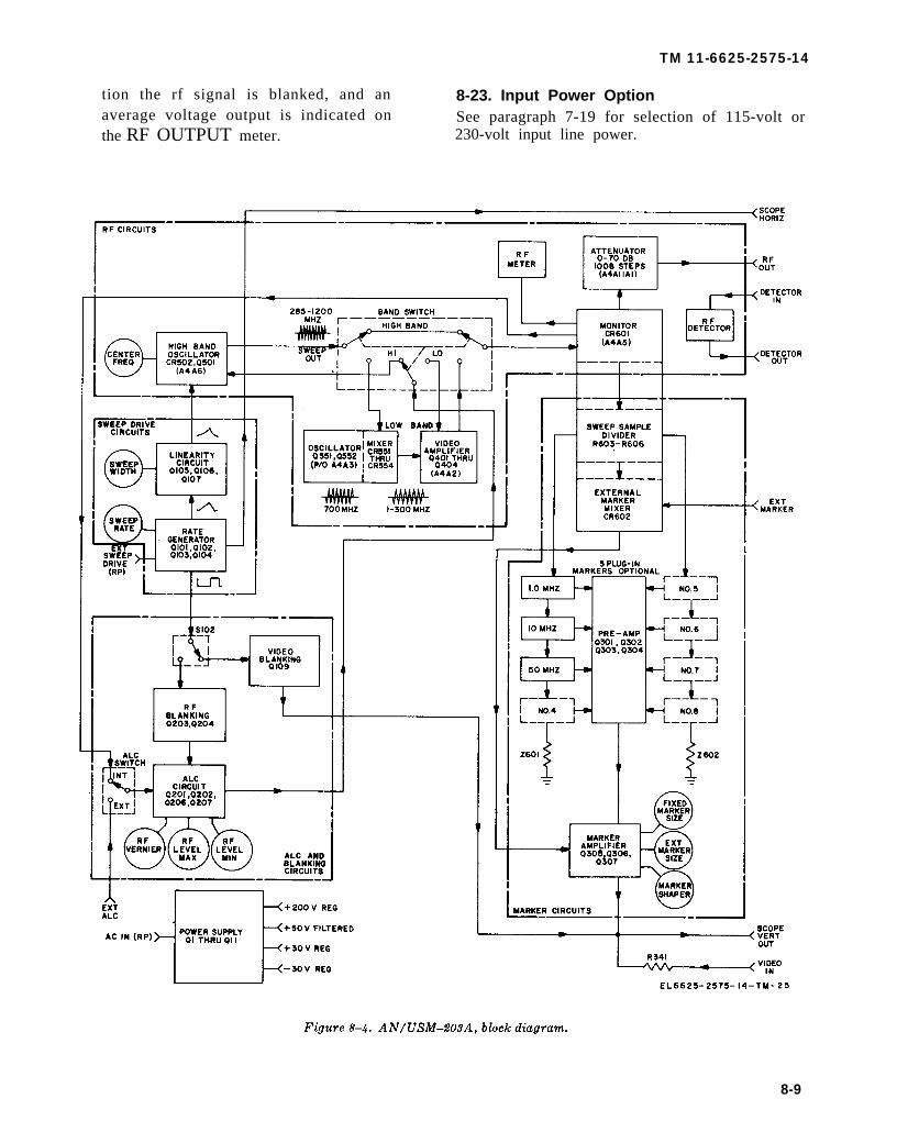
Figure 8-4.
TM 11-6625-2575-14
tion the rf signal is blanked, and anaverage voltage output is indicated onthe RF OUTPUT meter.
8-23. Input Power OptionSee paragraph 7-19 for selection of 115-volt or230-volt input line power.
8-9
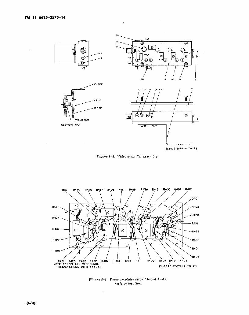
TM 11-6625-2575-14
Figure 8-5.
Figure 8-6.
8-10
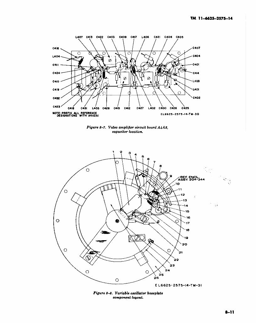
TM 11-6625-2575-14
Figure 8-7.
8-11
Figure 8-8.
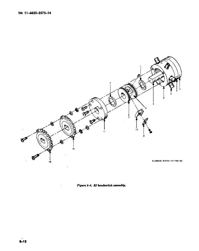
TM 11-6625-2575-14
Figure 8-9.
8-12
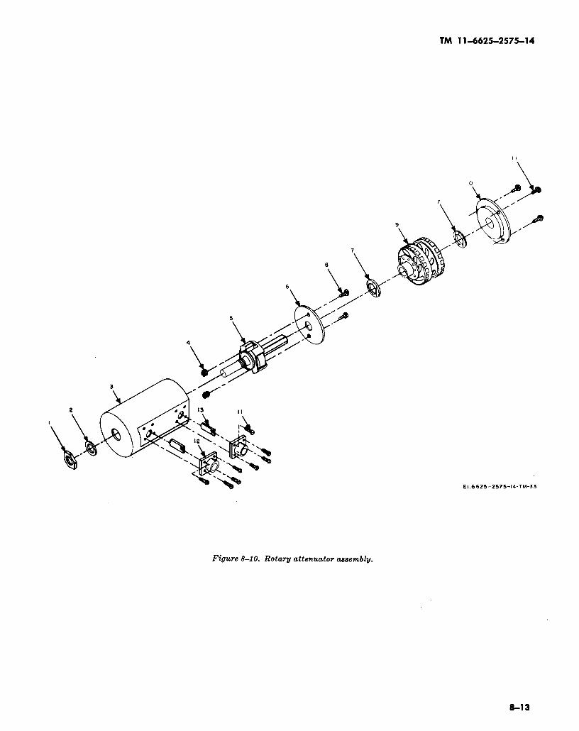
TM 11-6625-2575-14
Figure 8-10.
8-13
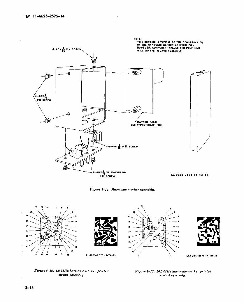
8-14
Figure 8-12. Figure 8-13.
Figure 8-11.
TM 11-6625-2575-14
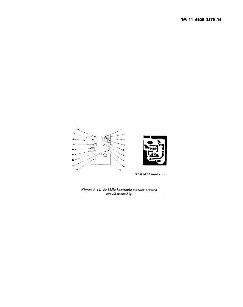
TM 11-6625-2575-14
Figure 8-14.

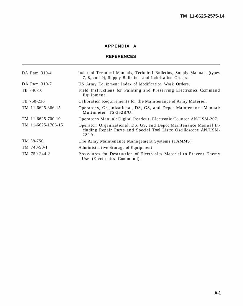
TM 11-6625-2575-14
APPENDIX A
REFERENCES
DA Pam 310-4
DA Pam 310-7TB 746-10
TB 750-236TM 11-6625-366-15
TM 11-6625-700-10TM 11-6625-1703-15
TM 38-750TM 740-90-1TM 750-244-2
Index of Technical Manuals, Technical Bulletins, Supply Manuals (types7, 8, and 9), Supply Bulletins, and Lubrication Orders.
US Army Equipment Index of Modification Work Orders.Field Instructions for Painting and Preserving Electronics Command
Equipment.Calibration Requirements for the Maintenance of Army Materiel.Operator’s, Organizational, DS, GS, and Depot Maintenance Manual:
Multimeter TS-352B/U.
Operator’s Manual: Digital Readout, Electronic Counter AN/USM-207.Operator, Organizational, DS, GS, and Depot Maintenance Manual In-
cluding Repair Parts and Special Tool Lists: Oscilloscope AN/USM-281A.
The Army Maintenance Management Systems (TAMMS).Administrative Storage of Equipment.Procedures for Destruction of Electronics Materiel to Prevent Enemy
Use (Electronics Command).
A-1


TM 11-6625-2575-14
APPENDIX CMAINTENANCE ALLOCATION
Section I. INTRODUCTION
C-1. GeneralThis appendix provides a summary of the mainte-nance operations for AN/USM-203A. It authorizescategories of maintenance for specific mainte-nance functions on repairable items and compo-nents and the tools and equipment required toperform each function. This appendix may be usedas an aid in planning maintenance operations.
C-2. Maintenance FunctionMaintenance functions will be limited to anddefined as follows:
a. Inspect. To determine the serviceability of anitem by comparing its physical, mechanical, and/orelectrical characteristics with established stand-ards through examination.
b. Test. To verify serviceability and to detectincipient failure by measuring the mechanical orelectrical characteristics of an item and comparingthose characteristics with prescribed standards.
c. Service. Operations required periodically tokeep an item in proper operating condition, i.e., toclean (decontaminate), to preserve, to drain, topaint, or to replenish fuel, lubricants, hydraulicfluids, or compressed air supplies.
d. Adjust. To maintain, within prescribed limits,by bringing into proper or exact position, or bysetting the operating characteristics to thespecified parameters.
e. Align. To adjust specified variable elements ofan item to bring about optimum or desiredperformance.
f. Calibrate. To determine and cause correctionsto be made or to be adjusted on instruments or testmeasuring and diagnostic equipments used inprecision measurement. Consists of comparisons oftwo instruments, one of which is a certifiedstandard of known accuracy, to detect and adjustany discrepancy in the accuracy of the instrumentbeing compared.
g. Install. The act of emplacing, seating, or fixinginto position an item, part, module (component orassembly) in a manner to allow the properfunctioning of the equipment or system.
h. Replace. The act of substituting a serviceablelike type part, subassembly, or module (componentor assembly) for an unserviceable counterpart.
i. Repair. The application of maintenance serv-ices (inspect, test, service, adjust, align, calibrate,replace) or other maintenance actions (welding,
grinding, riveting, straightening, facing, re-machining, or resurfacing) to restore serv-iceability to an item by correcting specific damage,fault, malfunction, or failure in a part, subassem-bly, module (component or assembly), end item, orsystem.
j. Overhaul. That maintenance effort (service/action) necessary to restore an item to a completelyserviceable/operational condition as prescribed bymaintenance standards (i.e., DMWR) in appropri-ate technical publications. Overhaul is normallythe highest degree of maintenance performed bythe Army. Overhaul does not normally return anitem to like new condition.
k. Rebuild. Consists of those services/actionsnecessary for the restoration of unserviceableequipment to a like new condition in accordancewith original manufacturing standards. Rebuild isthe highest degree of materiel maintenanceapplied to Army equipment. The rebuild operationincludes the act of returning to zero those agemeasurements (hours, miles, etc.) considered inclassifying Army equipments/components.
C-3. Column Entriesa. Column 1, Group Number. Column 1 lists
group numbers, the purpose of which is to identifycomponents, assemblies, subassemblies, and mod-ules with the next higher assembly.
b. Column 2, Component/Assembly. Column 2contains the noun names of components, as-semblies, subassemblies, and modules for whichmaintenance is authorized.
c. Column 3, Maintenance Functions. Column 3lists the functions to be performed on the itemlisted in column 2. When items are listed withoutmaintenance functions, it is solely for purpose ofhaving the group numbers in the MAC and RPSTLcoincide.
d. Column 4, Maintenance Category. Column 4specifies, by the listing of a “worktime” figure inthe appropriate subcolumn(s), the lowest level ofmaintenance authorized to perform the functionlisted in column 3. This figure represents the activetime required to perform that maintenance func-tion at the indicated category of maintenance. Ifthe number or complexity of the tasks within thelisted maintenance function vary at differentmaintenance categories, appropriate “worktime”figures will be shown for each category. The
C-1
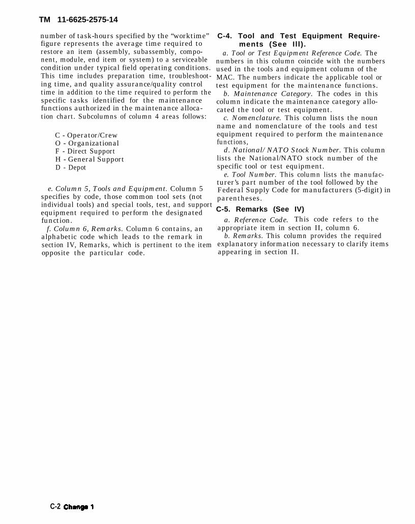
TM 11-6625-2575-14
number of task-hours specified by the “worktime”figure represents the average time required torestore an item (assembly, subassembly, compo-nent, module, end item or system) to a serviceablecondition under typical field operating conditions.This time includes preparation time, troubleshoot-ing time, and quality assurance/quality controltime in addition to the time required to perform thespecific tasks identified for the maintenancefunctions authorized in the maintenance alloca-tion chart. Subcolumns of column 4 areas follows:
C - Operator/CrewO - OrganizationalF - Direct SupportH - General SupportD - Depot
e. Column 5, Tools and Equipment. Column 5specifies by code, those common tool sets (notindividual tools) and special tools, test, and supportequipment required to perform the designatedfunction.
f. Column 6, Remarks. Column 6 contains, analphabetic code which leads to the remark insection IV, Remarks, which is pertinent to the itemopposite the particular code.
C-4. Tool and Test Equipment Require-ments (See Il l) .
a. Tool or Test Equipment Reference Code. Thenumbers in this column coincide with the numbersused in the tools and equipment column of theMAC. The numbers indicate the applicable tool ortest equipment for the maintenance functions.
b. Maintenance Category. The codes in thiscolumn indicate the maintenance category allo-cated the tool or test equipment.
c. Nomenclature. This column lists the nounname and nomenclature of the tools and testequipment required to perform the maintenancefunctions,
d. National/NATO Stock Number. This columnlists the National/NATO stock number of thespecific tool or test equipment.
e. Tool Number. This column lists the manufac-turer’s part number of the tool followed by theFederal Supply Code for manufacturers (5-digit) inparentheses.C-5. Remarks (See IV)
a. Reference Code. This code refers to theappropriate item in section II, column 6.
b. Remarks. This column provides the requiredexplanatory information necessary to clarify itemsappearing in section II.
C-2
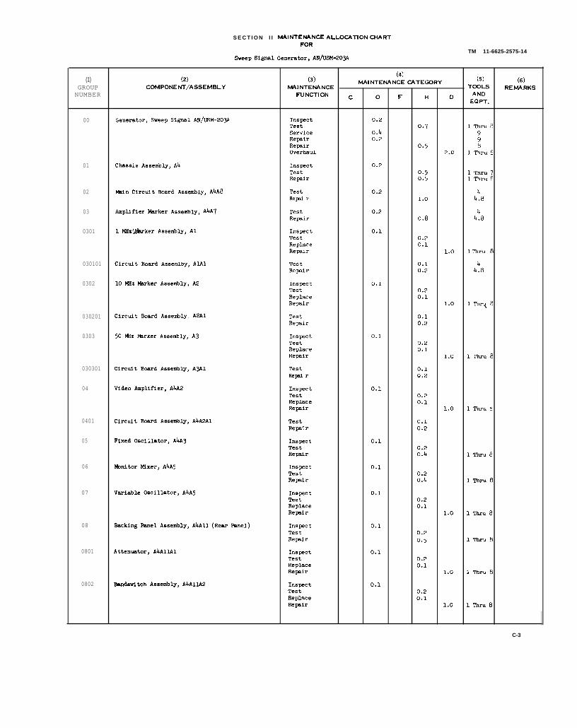
S E C T I O N I I MAINTENANCE ALLOCATION CHARTFOR
TM 11-6625-2575-14Sweep SQIIB1 Generator, AN/USM-203A
(1) (2) (3)(4)
MAINTENANCE ~TEGORY (5) (6)GROUP COMPONENT/ASSEMBLY MAINTENANCE TOOLSNUMBER
REMARKSFUNCTION c o F H D AND
EQPT.
00 Generator, Sweep Signal AN/tSM-203A Inspct 0.2Test 0.7 1 Thru OService 0.4 9Re@r 0.2 9Re@r 0.5 8Overhaul 2.0 1 Thru 8
01 Chassis Assembly, AL Inspect 0.2Test 0.5Repair
1 Thru 70.5 1 Thru 8
02 M?dn Circuit Board Assembly, AbA8 Test 0.2 4Repi r 1.0 J4.8
03 Amplifier Marker Assembly, AkA7 Test 0.2 4Repair 0.8 k.8
0301 1 Miz.wker Assembly, Al Ins~ct 0.1Test 0.2Replace 0.1Repiir 1.0 1 ~lAJ 8
030101 Circuit Board Assemlby, AIAl TestRepair
0.1 b0.2 b.8
0302 10 KRz Karker Assembly, A2 Insp?ct 0.1Test 0.2Replace 0.1Re@r 1.0 1 Thr~ 8
030201 Circuit Board Assembly, A2A1 Test 0.1Repair 0.2
0303 50 MSZ Mrker Assembly, A3 Inspect 0.1Test 0.2Replace 0.1Repair 1.0 lThn18
030301 Circuit Beard Assembly, A3A1 Test 0.1RepM r 0.2
04 Video Amplifier, A4A2 Insp?ct 0.1Test 0.2Replace 0.1Repair 1.0 1 Thru 6
0401 Circuit Board Assembly, A4A2A1 Test 0.1Repair 0.2
05 Fixed Oscillator, A4A3 Inspxt 0.1Test 0.2Repair 0.4 1 Thru 8
06 Monitor Mixer, AbA5 Inspect 0.1Test 0.2Re@r 0.4 lThN8
07 Variable Oscillator, A4A5 Inspect 0.1Test 0.2Replace 0.1Repir 1.0 1 Thru 8
08 Backing Panel Assembly, AkAll (Rear panel) Inspect 0.1Test 0.2Rewir 0.5 lThru8
0801 Attenuator, AbAllAl Inspect 0.1Test 0.2Replace 0.1Repir 1.0 lThru8
0802 I!-andswitch Assembly, A4A11A2 Inspect 0.1Test 0.2Replace 0.1Repair 1.0 1 Thru 8
C-3
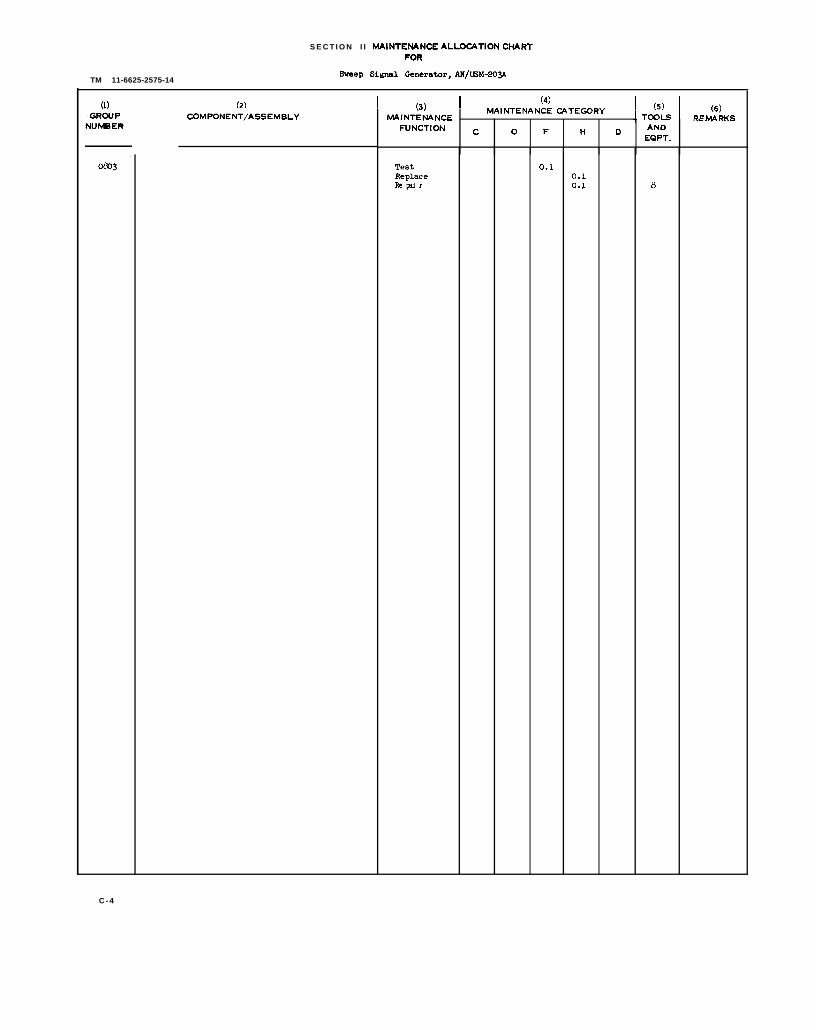
(1) GROUP NUMBER
0803
S E C T I O N I I MAINTENANCE ALLOCATION CHARTFOR
TM 11-6625-2575-14Sweep Signal Generator, AN/tSM-203A
(2)COMPONENT/ASSEMSLY
I (’l) I . ---- (4)lNCE ~TEGORY I (5) I (6)
-l-ml c . . MA R~s
.-, MAINTENAMAINTENANCE 7 .-. — ~- ,
FUNCTION c o F H D ANDEQPT.
TestReplaceRe PI r
0.10.10.1 8
C - 4
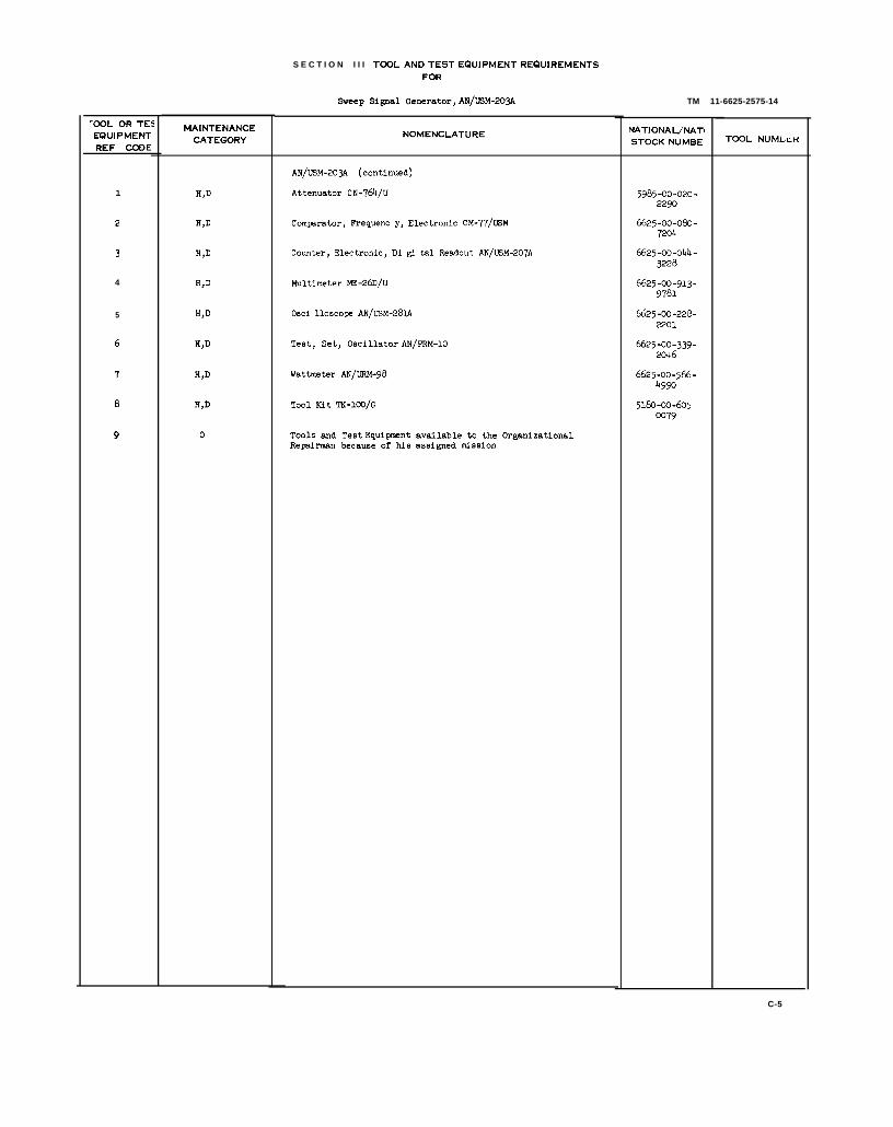
TOOL OR TESTEQUIPMENTREF CODE
1
2
3
4
5
6
7
8
9
MAINTENANCECATEGORY
E,D
E,D
H,D
R,D
H,D
H,D
H,D
H,D
o
S E C T I O N I I I TOOL AND TEST EQuIPMENT REQUIREMENTSFOR
Sweep Signal GeMr8t.Or, AN/U3M-203A
NOMENCLATURE
AN/lBM-203A (continued)
Attenuator CN-7@+/U
Comwator, Frequent y, Electronic CM-77/IJSM
Counter, Electronic, Di gl tal Readout AN/LEM-Z07A
Multimeter ~-26D/u
Oecl 11OSCOP AN/USM-282A
Test, Set, Oscillator AN/FRM-10
Wattmeter AN/URM-98
Tool Klt TK-100/G
Tools and Test Equipment available to the OrganizationalRepiruan because of his assigned mission
TM 11-6625-2575-14
NATiONA~NATISTOCK NUMBE
5985-00-020-2290
6625i+0toeo-
6625-00-044-322a
6625i+0i913-
6625-00-228-2201
6625;40;339-
6625 -oo-566-L99Q
51@o-co-6050079
TOOL NUMkJCH
C-5

TM 11-6625-2575-14
INDEX
Paragraph Page
Adjustments, initial - - - - - - - - - - - - - - - - - - - - - - - -3-3 3 - 3Application- - - - - - - - - - - - - - - - - - - - - - - - - - - - - - - -1-10 1 - 2
Bench use - - - - - - - - - - - - - - - - - - - - - - - - - - - - - - 2 -2 2 - 1Blanking switch - - - - - - - - - - - - - - - - - - - - - 3-2 3 - 1Block diagram - - - - - - - - - - - - - - - - - - - - - - - - - - - -6-1 6 - 1
Calibration - - - - - - - - - - - - - - - - - - - - - - - - - - - - -1-5 1 - 1 Circuit functions:
Automatic level control- - - - - - - - - - - - - - - - - - - -6-5 6 - 3Band switch - - - - - - - - - - - -- - - - - - - - - - - - - - -6-4 6 - 2Blanking - - - - - - - - - - - - - - - - - - - - - - - - - - - -6-5 6 - 3Fixed frequency oscillator - - - - - - - - - - - - - - - - - - - -6-4 6 - 2High frequency band - - - - - - - - - - - - - - - - -6-4 6 - 2Linearity circuit - - - - - - - - - - - - - - - - - - - -6-3 6 - 1Low pass filter - - - - - - - - - - - - - - - - - - - - -6-4 6 - 2Low frequency band - - - - - - - - - - - - - -6-4 6 - 2Marker circuits - - - - - - - - - - - - - - - - -6-6 6 - 3Mixer - - - - -- - -- - - - - - -- - - - - - - - - - - - - - -6-4 6 - 2Power supply - - - - - - - - - - - - - - - -6-2 6 - 1Rate generator - - - - - - -- - - - - - - - -6-3 6 - 1Rf circuits - -- - - - - - - - - - - - - - - - - - -6-4 6 - 2Rf detector - -- - - - - - - - -- - - - - - - - -- - -6-1 6 - 2Sweep drive circuits - - - - - - - - - - - - - - - - - - - -6-3 6 - 1Video amplifier - - - - - -- - - - -- - - - - - -6-4 6 - 2
Controls and receptacles - - - - - - - - - - - - - - - - 1-8, 3-2 1-1,3-1
Damage or discrepancies report - - - - - - - - - - - - - - 2-2 2 - 1Description and purpose of
AN/USM-203A - - - - - - - - - - - - - - - - - - 1-8 1 - 1Destruction of equipment - - - - - - - - - - - - - - - - - -1-3 1 - 1
Forms and records - - - - - - - - - - - - - - - - - - 1-2 1 - 1
Maintenance, direct support: Alignment and adjustment - - - - - - - - - - - - - - - -7-12 7 -13Blanking mode test - - - - - - - - - - - - - - - - - -7-18 7 - 1 6Frequency dial alignment - - - - - - - - - - - - - - - -7-14 7 - 1 3Marker amplitude adjustment - - - - - - - - - - - - - -7-17 7 - 1 5Power supply adjustment - - - - - - - - - - - - - -7-12 7 - 1 3Rate generator alignment - - - - - - - - -7-13 7 - 1 3Repair procedures - - - - - - - - - - - - - - 7-6 7 - 9Repaired unit disposition - - - - - - 7-7 7 - 9Rf output voltage adjustment - - - 7-16 7 - 1 5Sweep width alignment - - - - - - - - - 7-15 7 - 1 4Test equipment - - - - - - - - - - - - - - - - -7-1 7 - 1Test point guide - - - - - - - - - - - -7-4 7-3
Paragraph
Test procedures - - - - - - - - - - - - - - -7-8Troubleshooting - - - - - - - - - - - - - - - -7-3Troubleshooting guide - - - - - - - - - - - -7-5
Maintenance, general support:
Alignment and adjustment procedures - - - - - - - - - - - - - - - - - - - - - - - -8-17
Blanking mode selection - - - - - - - - - - - - -8-22Frequency dial al ignment - - - - - 8-19Marker amplitude adjustment - - - - 8-21Power supply adjustment - - - - - - - - - - - - - - 8-18Rate generator alignment - - - - - - - - - - - 8-19Repair of rf assemblies:
Fixed oscillator/mixer - - - - - 3-7Monitor/mixer assembly - - - - 3-6Rf detector assembly - - - - - - - 8-5
Replacement of rf assemblies:
Attenuator - - - - - - - - - - - - - - - - - - - - - 8-10Band switch - - - - - - - - - - - - - - - 8-9Harmonic markers - - - - - - - - - 3-13Variable oscillator - - - - - - - - 8-12Video amplifier - - - - - - - - - - - - - 8-11
Rf output voltage adjust - - - - - - - - - - - 3-20Spurious and harmonic distribu-
tion - - - - - - - - - - - - - - - - - - - - 8-16Sweep width alignment - - - - - - - - 8-19Test equipment - - - - - - - - - - - - - - - 8-2Test procedures, general - - - - - - - - - - 8-14Troubleshooting approach - - - - - - 8-3Troubleshooting procedures - - - - - 8-4
Operating instructions - - - - - - - - - - - - 3-1
Operation under unusual conditions - - 3-5,3-6
Operating voltages - - - - - - - - - - - - - - - - - 3-1
Purpose and use - - - - - - - - - - - - - 1-8
Rack Mounting - - - - - - - - - - - -- - - - 2-2
Reporting of errors - - - - - - - - - - - - - - - 1-6
Schematic diagram - - - - - - - - - - - - - - FO-3
Scope - - - - - - - - - - - - - - - - - - - - - - - - 1- 1
Serviceability criterion - - - - - - - - - - - - 1-7
System application - - - - - - - - - - - - - 1-10
Test displays - - - - - - - - -- - - - - - - - - 7-10
Page
7 - 97 - 27 - 5
8 - 88 - 88 - 88 - 88 - 88 - 8
8 - 38 - 28 - 2
8 - 68 - 68 - 78 - 68 - 63 - 8
8 - 88 - 88 - 18 - 78 - 18 - 1
3 - 1
3 4
3 - 1
1 - 1
2 - 1
1 - 1
Fold-in
1 - 1
1 - 1
1 - 2
7 - 1 0
Index-1
By Order of the Secretary of the Army:
Official:VERNE L. BOWERSMajor General, UnitedThe Adjutant General
Distribution:
States Army
TM 11-6625-2575-14
CREIGHTON W. ABRAMSGeneral, United States ArmyChief of Staff
To be distributed in accordance with DA Form 12-32, direct and general support maintenance require-ments for AN/FPA-15 and AN/FPA-16; DA Form 12-36, direct and general support maintenance re-quirements for AN/TPN-8, AN/TPN-18, AN/TSQ-71 and AN/TSQ-72.
U.S. GOVERNMENT PRINTING OFFICE : 1990 0 - 262-912 (30225)
THE METRIC SYSTEM AND EQUIVALENTS


This fine document...
Was brought to you by me:
Liberated Manuals -- free army and government manuals
Why do I do it? I am tired of sleazy CD-ROM sellers, who take publicly available information, slap “watermarks” and other junk on it, and sell it. Those masters of search engine manipulation make sure that their sites that sell free information, come up first in search engines. They did not create it... They did not even scan it... Why should they get your money? Why are not letting you give those free manuals to your friends?
I am setting this document FREE. This document was made by the US Government and is NOT protected by Copyright. Feel free to share, republish, sell and so on.
I am not asking you for donations, fees or handouts. If you can, please provide a link to liberatedmanuals.com, so that free manuals come up first in search engines:
<A HREF=http://www.liberatedmanuals.com/>Free Military and Government Manuals</A>
– SincerelyIgor Chudovhttp://igor.chudov.com/
– Chicago Machinery Movers