generalized class-e power amplifier with shunt capacitance
TRANSCRIPT

Generalized Class-E Power Amplifier with Shunt Capacitance andShunt Filter
Safari Mugisho, M., Makarov, D. G., Rassokhina, Y. V., Krizhanovski, V. G., Grebennikov, A., & Thian, M.(2019). Generalized Class-E Power Amplifier with Shunt Capacitance and Shunt Filter. IEEE Transactions onMicrowave Theory and Techniques, 67(8), 3464 - 3474. https://doi.org/10.1109/TMTT.2019.2923514
Published in:IEEE Transactions on Microwave Theory and Techniques
Document Version:Publisher's PDF, also known as Version of record
Queen's University Belfast - Research Portal:Link to publication record in Queen's University Belfast Research Portal
Publisher rights© 2019 The Authors.This is an open access article published under a Creative Commons Attribution License (https://creativecommons.org/licenses/by/4.0/),which permits unrestricted use, distribution and reproduction in any medium, provided the author and source are cited
General rightsCopyright for the publications made accessible via the Queen's University Belfast Research Portal is retained by the author(s) and / or othercopyright owners and it is a condition of accessing these publications that users recognise and abide by the legal requirements associatedwith these rights.
Take down policyThe Research Portal is Queen's institutional repository that provides access to Queen's research output. Every effort has been made toensure that content in the Research Portal does not infringe any person's rights, or applicable UK laws. If you discover content in theResearch Portal that you believe breaches copyright or violates any law, please contact [email protected].
Download date:21. Feb. 2022

This article has been accepted for inclusion in a future issue of this journal. Content is final as presented, with the exception of pagination.
IEEE TRANSACTIONS ON MICROWAVE THEORY AND TECHNIQUES 1
Generalized Class-E Power Amplifier WithShunt Capacitance and Shunt Filter
Moïse Safari Mugisho , Graduate Student Member, IEEE, Denis G. Makarov,Yulia V. Rassokhina, Member, IEEE, Vladimir G. Krizhanovski, Senior Member, IEEE,
Andrei Grebennikov , Senior Member, IEEE, and Mury Thian
Abstract— This paper presents a generalized analysis of theClass-E power amplifier (PA) with a shunt capacitance and ashunt filter, leading to a revelation of a unique design flexibilitythat can be exploited either to extend the maximum operatingfrequency of the PA or to allow the use of larger activedevices with higher power handling capability. The proposed PAfulfills zero voltage switching (ZVS) and zero voltage derivativeswitching (ZVDS) conditions, resulting in a theoretical dc-to-RFefficiency of 100%. Explicit design equations for the load-networkparameters are derived, and the analytical results are confirmedby harmonic-balance simulations. Two PA prototypes were con-structed with one designed at low frequency and the other athigh frequency. The first PA, which employs a MOSFET and alumped-element load-network, delivered a peak drain efficiency(DE) of 93.3% and a peak output power of 37 dBm at 1 MHz.The second PA, which employs a GaN HEMT and a transmission-line (TL) load-network to provide the drain of the transistor withthe required load impedances at the fundamental frequency aswell as even and odd harmonic frequencies, delivered a peak DEof 90.2% and a peak output power of 39.8 dBm at 1.37 GHz.
Index Terms— Class E, GaN, harmonic suppression, har-monic tuning, high efficiency, lumped element, MOSFET, poweramplifier (PA), series reactance, shunt capacitance, shunt filter,transmission line.
I. INTRODUCTION
THE CLASS-E power amplifier (PA) with shunt capac-itance and series filter, introduced by Ewing [1] and
further analyzed by Sokal and Sokal [2] and Raab [3], has beenwidely used due to its simple topology and high-efficiencyoperation. The high efficiency is achieved by applying zerovoltage switching (ZVS) and zero voltage derivative switch-ing (ZVDS) conditions, producing a soft switching at theOFF-to-ON transition. One of the main drawbacks of thistopology is that it employs an ideal RF choke (RFC), which inpractice needs to be replaced by a large, hence lossy and bulky,
Manuscript received March 13, 2019; revised May 9, 2019; acceptedMay 14, 2019. This work was supported by the U.K. Engineering andPhysical Sciences Research Council (EPSRC) under Grant EP/P013031/1.(Corresponding author: Moïse Safari Mugisho.)
M. S. Mugisho and M. Thian are with the School of Electronics,Electrical Engineering, and Computer Science, Queen’s University Belfast,Belfast BT7 1NN, U.K. (e-mail: [email protected]; [email protected]).
D. G. Makarov, Y. V. Rassokhina, and V. G. Krizhanovski are with theRadiophysics Department, Donetsk National University, Vinnytsia 21021,Ukraine.
A. Grebennikov is with Sumitomo Electric Europe, Hertfordshire WD6 3SL,U.K.
Color versions of one or more of the figures in this paper are availableonline at http://ieeexplore.ieee.org.
Digital Object Identifier 10.1109/TMTT.2019.2923514
inductor. An improved variant of this PA topology with a finitedc-feed inductance instead of an RFC is reported in [4]–[8],also known as “Class E with parallel circuit.”
Subsequently, the Class-E PA with series inductance andshunt filter, with switch voltage and current waveforms beingthe duals to those in the Class-E PA with shunt capacitance andseries filter, hence termed as ”inverse Class E,” is introducedin [9] and [10]. In contrast to its predecessor, it adoptszero current switching (ZCS) and zero current derivativeswitching (ZCDS) conditions, producing a soft switching atthe ON-to-OFF transition. Although it offers 20% lower peakswitch voltage than that in [1]–[3] as well as has the abilityto absorb device output inductance (Lout), its implementationis limited to small-to-medium power levels as it does notinherently incorporate a shunt capacitance to absorb deviceoutput capacitance (Cout). For simplicity, the “Class-E PAwith shunt capacitance and series filter” and the “Class-E PAwith series inductance and shunt filter” will be referred to as“Class E” and “inverse Class E,” respectively, hereinafter.
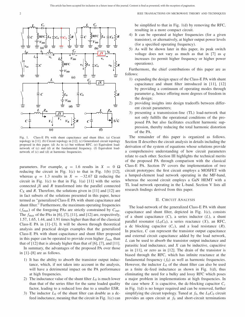
Another high-efficiency PA topology, i.e., the Class-E PAwith shunt capacitance and shunt filter depicted in Fig. 1(a)is introduced in [11]. A similar variant shown in Fig. 1(b)disposing the need for the capacitance CX placed in parallelwith the shunt filter and load resistance is described in [12].These two topologies adopt ZVS and ZVDS conditions, andimportantly, incorporate both shunt capacitance C to absorbCout as in the Class E and series inductance L to absorbLout as in the inverse Class E, rendering it attractive forhigh-frequency implementations where device parasitics playa dominant role in deleteriously affecting the PA performance.Furthermore, in series-filter-based Class-E topologies suchas [1]–[8], a large inductance value is required to implementthe series filter, whereas in shunt-filter-based Class-E topolo-gies such as [9]–[13], the value of the inductor that forms theshunt filter is considerably lower for the same loaded qualityfactor value. A large inductance is typically accompanied witha large parasitic equivalent series resistance (ESR) and a lowself-resonant frequency (SRF), hence rendering the series-filter-based Class-E topologies unattractive.
In this paper, we present a generalized Class-E PA withshunt capacitance and shunt filter, which incorporates a seriesreactance X as illustrated in Fig. 1(c). The system of equationsdescribing the behavior of this PA is derived and expressed interms of parameter q , whose value can be chosen arbitrarily,leading to an infinite number of solutions for the load-network
This work is licensed under a Creative Commons Attribution 4.0 License. For more information, see http://creativecommons.org/licenses/by/4.0/
This article has been accepted for inclusion in a future issue of this journal. Content is final as presented, with the exception of pagination.
2 IEEE TRANSACTIONS ON MICROWAVE THEORY AND TECHNIQUES
Fig. 1. Class-E PA with shunt capacitance and shunt filter. (a) Circuittopology in [11]. (b) Circuit topology in [12]. (c) Generalized circuit topologyproposed in this paper. (d) As in (c) but without RFC. (e) Equivalent load-network of (c) and (d) at the fundamental frequency. (f) Equivalent load-network of (c) and (d) at harmonic frequencies.
parameters. For example, q = 1.6 results in X = 0 �reducing the circuit in Fig. 1(c) to that in Fig. 1(b) [12],whereas q = 1.3 results in X = −32.67 � reducing thecircuit in Fig. 1(c) to that in Fig. 1(a) [11] with the seriesconnected jX and R transformed into the parallel connectedCX and R. Therefore, the solutions given in [11] and [12] arein fact subsets of the solutions presented in this paper, hencetermed as “generalized Class-E PA with shunt capacitance andshunt filter.” Furthermore, the maximum operating frequencies( fmax) of the foregoing PAs are strictly constrained by Cout.The fmax of the PAs in [6], [7], [11], and [12] are, respectively,1.57, 1.65, 1.44, and 1.91 times higher than that of the classicalClass-E PA in [1]–[3]. It will be shown through theoreticalanalysis and practical design examples that the generalizedClass-E PA with shunt capacitance and shunt filter proposedin this paper can be operated to provide even higher fmax thanthat of [12] that is already higher than that of [6], [7], and [11].
In summary, the advantages of the proposed PA over thosein [1]–[8] are as follows.
1) It has the ability to absorb the transistor output induc-tance, which, if not taken into account in the analysis,will have a detrimental impact on the PA performanceat high frequencies.
2) The inductance value of the shunt filter L0 is much lowerthan that of the series filter for the same loaded qualityfactor, leading to a reduced loss due to a smaller ESR.
3) The inductor L0 of the shunt filter can double as a dc-feed inductance, meaning that the circuit in Fig. 1(c) can
be simplified to that in Fig. 1(d) by removing the RFC,resulting in a more compact circuit.
4) It can be operated at higher frequencies (for a giventransistor), or alternatively, at higher output power levels(for a specified operating frequency).
5) As will be shown later in this paper, its peak switchvoltage does not vary as much as that in [7] as qincreases (to permit higher frequency or higher poweroperations).
Furthermore, the chief contributions of this paper are asfollows:
1) expanding the design space of the Class-E PA with shuntcapacitance and shunt filter introduced in [11], [12]by providing a continuum of operating modes throughparameter q , hence offering more degrees of freedom inthe design;
2) providing insights into design tradeoffs between differ-ent circuit parameters;
3) presenting a transmission-line (TL) load-network thatnot only fulfills the operational conditions of the pro-posed PA but also facilitates excellent harmonic sup-pression, thereby reducing the total harmonic distortionof the PA.
The remainder of this paper is organized as follows.Section II describes the circuit analysis in details including thederivation of the system of equations whose solutions providea comprehensive understanding of how circuit parametersrelate to each other. Section III highlights the technical meritsof the proposed PA through comparison with the classicalClass-E PA. Section IV covers the implementation of twocircuit prototypes: the first circuit employs a MOSFET witha lumped-element load network operating in the MF-band,whereas the second circuit employs a GaN HEMT with aTL load network operating in the L-band. Section V lists allresearch findings derived from this paper.
II. CIRCUIT ANALYSIS
The load-network of the generalized Class-E PA with shuntcapacitance and shunt filter, depicted in Fig. 1(c), consistsof a shunt capacitance (C), a series inductor (L), a shuntparallel resonator (L0C0), a series reactance (X), an RFC,a dc blocking capacitor (Cc), and a load resistance (R).In practice, C can represent the transistor output capacitanceand external circuit capacitance added by the load network,L can be used to absorb the transistor output inductance andparasitic lead inductance, and X can be inductive, capacitiveas in [11], or zero as in [12]. The drain of the transistor isbiased through the RFC, which has infinite reactance at thefundamental frequency ( f0) as well as harmonic frequencies.However, the inductor L0 of the shunt filter can also be usedas a finite dc-feed inductance as shown in Fig. 1(d), thuseliminating the need for a bulky and lossy RFC which posesa major problem in implementations at high frequencies. Inthe case where X is capacitive, the dc-blocking capacitor Cc
in Fig. 1(d) is no longer required and can be removed, furthersimplifying the circuit topology. Tuned at f0, the L0C0 circuitprovides an open circuit at f0 and short-circuit terminations
This article has been accepted for inclusion in a future issue of this journal. Content is final as presented, with the exception of pagination.
MUGISHO et al.: GENERALIZED CLASS-E PA 3
at n × f0. As a result, the PA load-network at f0 and n × f0reduces to that shown in Fig. 1(e) and (f), respectively.
To simplify the analysis of the generalized Class-E PAwith shunt capacitance and shunt filter, we adopt the sameassumptions used in [12].
The idealized optimum (nominal) Class-E switching condi-tions are given as follows:
vsw(ωt)|ωt=2π = 0 (1)dvsw(ωt)
dωt
∣∣∣∣ωt=2π
= 0 (2)
where vsw(ωt) is the voltage across the switch.Let the sinusoidal fundamental-frequency voltage v1(ωt)
across the shunt L0C0 filter be expressed as follows:
v1(ωt) = V1 sin(ωt + ϕ1) (3)
where V1 is the fundamental-frequency voltage amplitude andϕ1 is the phase shift due to a complex load.
When the switch is turned ON for 0 ≤ ωt ≤ π , the voltageacross the switch is
vsw(ωt) = VDD − vL(ωt)− v1(ωt) = 0 (4)
where vL(ωt) is the voltage across the series inductor. Using(7)–(13) from [12] and substituting V1, i.e., the voltage acrossthe series connection of the reactance X and load R (instead ofthe voltage VR across the load R as in [12] where X = 0 �),a general nonhomogeneous second-order differential equationfor the switch voltage vsw(ωt) is obtained
ω2 LCd2vsw(ωt)
d(ωt)2+ vsw(ωt)− VDD + V1 sin(ωt + ϕ1) = 0.
(5)
The normalized general solution of (5) is given as
vsw(ωt)
VDD= C1 cos qωt + C2 sin qωt + 1
+ q2
1 − q2
V1
VDDsin(ωt + ϕ1) (6a)
where q is defined as
q = 1
ω√
LC(6b)
and coefficients C1 and C2 are obtained by substituting VR
in (17) and (18) of [12] with V1. It is worth noting here thatparameter q in (6b) has different physical meaning from qin [7], where L is connected in parallel with the transistor(instead of in series as in this paper).
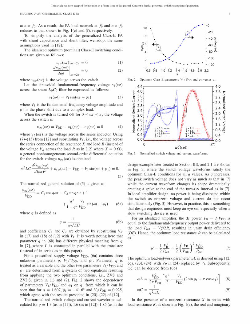
For a prescribed supply voltage VDD, (6a) contains threeunknown parameters q , V1/VDD, and ϕ1. Parameter q istreated as a variable and the other two parameters V1/VDD andϕ1 are determined from a system of two equations resultingfrom applying the two optimum conditions, i.e., ZVS andZVDS, given in (1) and (2). Fig. 2 shows the dependencyof parameters V1/VDD and ϕ1 on q , from which it can beseen that for q = 1.607, ϕ1 = −41.6◦ and V1/VDD = 0.925,which agree with the results presented in (20)–(22) of [12].
The normalized switch voltage and current waveforms cal-culated for q = 1.3 (as in [11]), 1.6 (as in [12]), 1.85 (as in the
Fig. 2. Optimum Class-E parameters V1/VDD and ϕ1 versus q.
Fig. 3. Normalized switch voltage and current waveforms.
design example later treated in Section III), and 2.1 are shownin Fig. 3, where the switch voltage waveforms satisfy theoptimum Class-E conditions for all q values. As q increases,the peak switch voltage does not vary as much as that in [7]while the current waveform changes its shape dramatically,creating a spike at the end of the turn-ON interval as in [7].In ideal amplifier design, no power is being dissipated withinthe switch as nonzero voltage and current do not occursimultaneously (Fig. 3). However, in practice, this is somethingthat design engineers must keep an eye on, especially when aslow switching device is used.
For an idealized amplifier, the dc power P0 = I0VDD isequal to the fundamental-frequency output power delivered tothe load Pout = V 2
R /2R, resulting in unity drain efficiency(DE). Hence, the optimum load resistance R can be calculatedas
R = 1
2
V 2R
Pout= 1
2
(VR
VDD
)2 V 2DD
Pout. (7)
The optimum load-network parameter ωL is derived using [12,eqs. (23), (24)] with VR in (24) replaced by V1. Subsequently,ωC can be derived from (6b)
ωL = V 2DD
2πPout
[π2
2− V1
VDD(2 sin ϕ1 + π cosϕ1)
]
(8)
ωC = 1
q2ωL. (9)
In the presence of a nonzero reactance X in series withload resistance R, as shown in Fig. 1(e), the real and imaginary

This article has been accepted for inclusion in a future issue of this journal. Content is final as presented, with the exception of pagination.
4 IEEE TRANSACTIONS ON MICROWAVE THEORY AND TECHNIQUES
components of voltage amplitude V1 need to be defined. In thiscase, the sinusoidal voltage v1(ωt) in (3) can be expressed as
v1(ωt) = vR(ωt)+ vX (ωt)
= VR sin(ωt + ϕ)+ VX cos(ωt + ϕ) (10)
where ϕ is the initial phase.The ratio of the imaginary and real components of V1, i.e.,
VX and VR , respectively, can be obtained as follows:
q1 = VX
VR= X
R= tan (ϕ1 − ϕ) = tanψ (11)
resulting in
V1 =√
V 2R + V 2
X = VR
√
1 + q21 (12)
where voltage amplitude VR is defined in [12, eq. (12)].As a result, the remaining unknown parameters q1, VR/VDD,
and ϕ can be determined as a function of parameter q froma system of three equations of [12, eqs. (2), (3), (19)]. Fora prescribed supply voltage VDD and output power Pout, theload-network parameters ωL, X , R, and ωC, normalized toVDD and Pout, can be expressed in terms of q .
The normalized optimum series inductance ωLPout/V 2DD,
series reactance XPout/V 2DD, shunt capacitance ωCV2
DD/Pout,and load resistance RPout/V 2
DD are plotted versus parameterq in Fig. 4. From Fig. 4(a), it can be observed that a largervalue of ωL corresponds to a lower q value. To compensatefor such an increased inductive value, the reactance X must,therefore, be decreased. The series reactance X changes fromnegative to positive values (or from capacitive to inductive)as q increases. Fig. 4(b) shows that as q increases, the valueof ωC increases, and consequently for a specific value of Crepresenting the device output capacitance (C = Cout), fmaxincreases with the increasing q . Thus, fmax of the generalizedClass-E PA with shunt capacitance and shunt filter can beexpressed as in the following equation:
fmax = kPout
V 2DDCout
. (13a)
The parameter k is plotted versus q in Fig. 4(b), from whichit follows that q = 1.3 results in k = 0.0728 and q = 1.6results in k = 0.097, that are in line with [11, Table 3] and[12, eq. (32)], respectively, and are 1.44 and 1.91 times higherthan that in [3], respectively. Furthermore, q = 2.1 results ink = 0.227 with the corresponding fmax being 4.5 and 2.7 timeshigher than that in [3] and [7], respectively. Equation (13a)can be rearranged to calculate the required shunt capacitanceC in Fig. 1(d) for a prescribed supply voltage VDD, outputpower Pout, and operating frequency f0. Thus, the increase ink as q increases can also mean that a larger transistor withhigher output capacitance can be used to implement the PA,thus enabling higher output power
C = kPout
V 2DD f0
. (13b)
The maximum operating frequency of the PA can also bedefined in terms of the transistor output inductance, (13c),using (6b) and (13a). Since k increases with increasing q ,m will decrease with increasing q . As a result, for a given
Fig. 4. Normalized optimum load-network parameters for the generalizedClass-E with shunt capacitance and shunt filter. (a) Normalized series reac-tance and inductance. (b) Normalized shunt capacitance and load resistance.
TABLE I
LOAD-NETWORK PARAMETERS OF [11] AND [12]COMPARED TO THIS PAPER
VDD, Pout, and Lout, fmax will also decrease with increasingq . Parameter m is plotted in Fig. 4(b)
fmax = 1
k(2πq)2V 2
DD
PoutLout= m
V 2DD
PoutLout. (13c)
Table I shows that for q = 1.3 and 1.6, the normalized load-network parameters and switch voltage peak factor derived inthis paper are in line with the results obtained in [11] forq = 1.3 and in [12] for q = 1.6; thus, [11] and [12] aresubsets of the work presented in this paper.
III. EXPLORING THE NEW DESIGN SPACE
To accentuate the significance of the theoretical analysis andinsights described in Section II, we designed and simulatedthree distinctive PAs: the Class E with series filter and ideal

This article has been accepted for inclusion in a future issue of this journal. Content is final as presented, with the exception of pagination.
MUGISHO et al.: GENERALIZED CLASS-E PA 5
Fig. 5. Class-E PA with series filter and ideal RFC [1]–[3]. (a) Simulatedcircuit schematic. (b) Simulated PA performance versus Pin at 497.4 MHzand 1.5 GHz with VDD = 28 V and VGG = −2.7 V.
RFC [1]–[3], the Class E with series filter and finite RFC [7],and the proposed Class E with shunt filter and nonzero Xin Fig. 1(c). For fair comparison, the three PAs employ thesame transistor, i.e., Cree CGH40010F GaN HEMT with anoutput capacitance Cout of 1.3 pF and an output inductanceLout of 0.653 nH, and are biased with the same voltages,i.e., VDD = 28 V and VGG = −2.7 V. The PAs were designedto deliver an output power of 10 W at a fixed operatingfrequency f0 = 1.5 GHz.
A. Class-E PA With Series Filter and Ideal RFC [1]–[3]
The design equations in [3] are used to determine the load-network parameters of the PA shown in Fig. 5(a). It followsthat R = 45.2 �, L X = 5.53 nH, C = 0.43 pF, L0 = 48 nH,and C0 = 0.23 pF for a loaded quality factor QL = 10.Notice that the required C is smaller than Cout. The totalseries inductance used in the simulation is L X + L0 − Lout =52.9 nH, i.e., to alleviate the detrimental effect of the parasiticinductance Lout on the PA performance. Fig. 5(b) shows thatthe PA delivers a peak power added efficiency (PAE) of 60.9%and a peak Pout of 38.4 dBm at 1.5 GHz. Substantially,higher peak PAE of 88.9% and peak Pout of 39.4 dBm areobtained if the PA is designed at its maximum operatingfrequency fmax = 497.4 MHz, calculated using (13a) withk = 0.0507 [3], with the circuit component values as follows:R = 45.2 �, L X = 16.7 nH, C = 1.3 pF (= Cout),L0 = 145 nH, and C0 = 0.7 pF for QL = 10. Thus,to fulfill the optimum Class-E conditions and, consequently,high-efficiency operation, the classical Class-E PA in [1]–[3]
Fig. 6. Class-E PA with series filter and finite RFC [7]. (a) Simulatedcircuit schematic. (b) Simulated PA performance versus Pin at 497.4 MHzand 1.5 GHz with VDD = 28 V and VGG = −2.7 V.
should be operated at frequencies below or equal to fmaxwhere the relationship Cout ≤ C holds.
B. Class-E PA With Series Filter and Finite RFC [7].
The design set for maximum operating frequency (q =1.468) in [7, Table VI] is used to determine the load networkparameters of the PA in Fig. 6(a). It follows that R = 104.4 �,LC = 7.3 nH, C = 0.71 pF, CX = 6.39 pF, L0 = 110.8 nH,and C0 = 0.1 pF for QL = 10. Notice that the required Cis greater than that of the design in Section III-A but smallerthan Cout. Fig. 6(b) shows that the PA achieves a peak PAEof 61.9% and a peak Pout of 37.8 dBm at 1.5 GHz.
Substantially higher peak PAE of 89% and peak Poutof 39.15 dBm are obtained if the PA is designed at fmaxof [1]–[3], i.e., 497.4 MHz, given that the same q value(i.e., 1.468) results in C = 2.15 pF.
C. Proposed Class-E PA With Shunt Filter
Fig. 7(a) shows the simulated circuit schematic of the pro-posed topology in Fig. 1(c). The value of q = 1.85 is selectedto give C = 1.272 pF ≈ Cout at f = 1.5 GHz, extracted fromFig. 4(b), which results in k = 0.1496, extending the fmax ofthe Class E with series filter [1]–[3] by a factor of 2.9. Thevalue of L = 2.66 nH is obtained from Fig. 4(a) for q = 1.85and f = 1.5 GHz, resulting in an excess inductor Le = L– Lout ≈ 2 nH. For the given VDD and Pout, X = 20.4 �and R = 25.1 � are determined from Fig. 4(a) and (b),respectively. Fig. 7(b) shows that the PA achieves a peak PAEof 84.3% and a peak Pout of 39 dBm at 1.5 GHz.

This article has been accepted for inclusion in a future issue of this journal. Content is final as presented, with the exception of pagination.
6 IEEE TRANSACTIONS ON MICROWAVE THEORY AND TECHNIQUES
Fig. 7. Proposed Class-E PA with shunt filter. (a) Simulated circuit schematic.(b) Simulated PA performance versus Pin at 497.4 MHz and 1.5 GHz withVDD = 28 V and VGG = −2.7 V.
If designed at fmax of [1]–[3], i.e., 497.4 MHz, the sameq value (i.e., 1.85) results in C = 3.84 pF. Fig. 7(b) showsthat the PA achieves a peak PAE of 87.9% and a peak Poutof 39.9 dBm. This result also shows that at a fixed frequency,f = 497.4 MHz, a larger (hence, higher power capability)transistor with a Cout = 3.84 pF can be used for this PAdesign.
The values of L0 and C0 in Fig. 7(a) are determinedusing (14b) and (14c) with the series connected L X and Rtransformed to its equivalent parallel circuit L P and RP . Fora given QL , the total inductance LT that is formed by theparallel combination of L0 and L P can be calculated usingthe following equation:
LT = Rp
ω0 QL(14a)
L0 = LPLT
LP − LT(14b)
C0 = 1
ω20 L0
. (14c)
D. Discussion
The optimum circuit component values and performancesof the PAs in Section III-A–III-C are summarized and com-pared in Table II. It has been shown that unlike the classi-cal Class-E PAs in [1]–[3], and [7], the proposed PA canbe operated at much higher frequencies while maintainingthe high-efficiency characteristics. Critically, the classical PArequires much higher inductance value (L0) for the sameloaded quality factor, rendering its implementation challengingas high inductance implies high ESR and low SRF, meaningthat substantial power will be dissipated within the series filter.
TABLE II
PA COMPARISONS
TABLE III
LOAD-NETWORK PARAMETERS OF PA PROTOTYPE 1
The Class-E PA with series filter treated in Section III-Aemploys an ideal RFC that has infinite impedance at allfrequencies, and consequently, the series inductors L0 + L X
can be used to absorb the transistor output inductance Lout.However, in practice, the RFC needs to be replaced with
a finite dc-feed inductance, and consequently, Lout can nolonger be absorbed by L0 + L X , as Lout is no longer inseries with L0 + L X . Similarly, in the Class-E PA with seriesfilter and finite RFC treated in Section III-B, Lout cannot beabsorbed by L0. On the contrary, the Class-E PA with shuntfilter proposed in this paper has a mechanism in place to absorbLout, i.e., through the series inductor L [Fig. 1(c)].
IV. IMPLEMENTATION AND MEASUREMENT
To validate the theory and simulation results describedin Sections II and III-C, we built two PA prototypes: oneimplemented with an IRF630 MOSFET and lumped ele-ments at 1 MHz while the other implemented with a CreeCGH40010F GaN HEMT and TLs at 1.5 GHz.
A. Low-Frequency Implementation With Lumped Elements
A power MOSFET IRF630 with an intrinsic output capaci-tance of 200 pF is used in this design. The PA was designed at1 MHz based on the topology in Fig. 1(c). Table III presentsthe load-network parameters extracted from Fig. 4 for two

This article has been accepted for inclusion in a future issue of this journal. Content is final as presented, with the exception of pagination.
MUGISHO et al.: GENERALIZED CLASS-E PA 7
Fig. 8. Constructed PA prototype 1.
Fig. 9. Measured drain and output voltage waveforms of PA prototype 1.q = 1.364. q = 1.831.
arbitrary q values, i.e., 1.364 and 1.831 that results in acapacitive and inductive reactance X , respectively.
For a specified VDD = 24 V and Pout = 5 W, the circuitcomponent values were determined as: Cx = 2.99 nF, L =20.42 μH, C = 667.98 pF, and R = 55.99 � for q = 1.364,and Lx = 4.488 μH, L = 6.39 μH, C = 1.182 nF, and R =39.168 � for q = 1.831. The shunt filter was implementedfor QL = 5, resulting in L0 = 1.57 μH and C0 = 16.14 nF.
The component values were slightly tuned to take intoaccount the nonlinearity effect of the transistor output capac-itance and parasitic ESR of the reactive components whilepreserving the nominal Class-E conditions.
Fig. 8 shows the photograph of the PA prototype 1, wherethe load is realized using four parallel connected 2-W resistors.Fig. 9 shows the measured drain and output voltage wave-forms, with the former satisfying the ZVS and ZVDS condi-tions required for soft-switching and high-efficiency operation.
The measured PA performance in Fig. 10 shows that at1 MHz, the PA delivered a DE of 93.3%, an output power(Pout) of 5 W for q = 1.364 and a DE of 88.6%, a Poutof 4.3 W for q = 1.831. The lower than-specified output powerfor q = 1.831 is mainly due to the parasitic ESR of the shuntL0C0 resonator [14].
B. High-Frequency Implementation With Transmission Lines
The second PA prototype was designed at 1.5 GHz as inSection III-C. The basic circuit schematic of the PA prototype
Fig. 10. Measured DE and output power of PA prototype 1. q = 1.364.q = 1.831.
Fig. 11. Basic circuit schematic of PA prototype 2 using TLs.
2 with a TL load-network is shown in Fig. 11, where Cc is adc blocking capacitor and Cb is a bypass capacitor. The excessinductor Le is realized using a series TL1 with a characteristicimpedance of Z1 and electrical length of θ1, whose value isdetermined using the following equation:
θ1 = tan−1(ω0 Le
Z1
)
. (15)
For θ1 in (15) to be considered sufficiently short at f0,the value of Z1 should be selected to satisfy the relationshipin the following equation:
Z1 >4ω0 Le
π. (16)
A shorted λ/8 stub (TL2A) together with an open-circuitedλ/8 stub (TL2B) with Z2 set to a high value enforce ashort-circuit termination at even harmonic frequencies andan open-circuit termination at fundamental and odd harmonicfrequencies [15]. A series λ/6 TL3 in conjunction with twoopen-circuited λ/12 stubs (TL4A and TL4B) enforce a short-circuit termination at 3 f0. Hence, Z in = 0 � at 2n f0 and 3 f0,satisfying the load impedance requirement in Fig. 1(f). Thecharacteristic impedances of TL3 and TL4A/TL4B, i.e., Z3 andZ4, respectively, are calculated to match Zopt = (R+ jX) � =(25.1 + j20.4) � to the standard 50 � load resistance (RL),thus satisfying the load impedance requirement in Fig. 1(e). At

This article has been accepted for inclusion in a future issue of this journal. Content is final as presented, with the exception of pagination.
8 IEEE TRANSACTIONS ON MICROWAVE THEORY AND TECHNIQUES
Fig. 12. Simulated circuit schematic of PA prototype 2.
Fig. 13. Simulated PA performance versus input power at 1.5 GHz withVDD = 28 V and VGG = −2.7 V.
f0, the input impedance Z in is given by the following equation:
Z in = Z3
[
3Z3 Z4 + j√
3(2Z3 − Z4)RL
(2Z3 + 3Z4)RL − j√
3Z3 Z4
]
(17)
For RL to be matched to Zopt at f0, Re{Z in} = R andIm{Z in} = X , resulting in a system of two equations withtwo unknowns parameters described in (18) and (19), fromwhich Z3 and Z4 are obtained as 50 and 63.5 �, respectively
3Z32 Z42(4RL − R)− R2L R(2Z3 + 3Z4)
2 = 0 (18)
3Z23 Z2
4
(√3Z3 − X
) + R2L(2Z3 + 3Z4)
×[√3Z3(2Z3 − Z4)− X (2Z3 + 3Z4)
] = 0 (19)
Harmonic-balance simulations were performed on the PAcircuit depicted in Fig. 12 within the Keysight’s AdvancedDesign System (ADS) environment. The simulation resultsin Fig. 13 show that the PA delivers a peak DE of 89.2%,a peak PAE of 83.7%, a peak Pout of 38.6 dBm, and a small-signal gain of 22.9 dB at 1.5 GHz.
The PA prototype 2 was constructed on a 0.51-mm-thick Rogers RO4003C substrate with a dielectric constantof 3.55 and a loss tangent of 0.0027, as shown in Fig. 14.A continuous-wave signal was applied to the PA using a Rohde& Schwarz SMR20 signal generator while the output power
Fig. 14. Constructed PA prototype 2.
was measured by a Keysight’s N9320A spectrum analyzer.A 40-dB attenuator was connected between the PA and thespectrum analyzer. The gate and drain biasing voltages wereprovided by a Thurlby 32-V dc power supply.
The measured PA performance in Fig. 15 shows that whenbiased with VGG = −2.7 V and VDD = 28 V, the PA deliversa peak DE of 90.2%, a peak PAE of 82.6%, a peak Poutof 39.8 dBm, and a linear gain of 14 dB at an operatingfrequency of 1.37 GHz. The values of Pout and power gainat the peak PAE are 39.6 dBm and 11.5 dB, respectively. Thedeviation between results in Figs. 13 and 15 is likely due tothe fabrication tolerance and the inaccuracy of the transistor’slarge-signal model, for instance, in capturing the effect of thepackage parasitics.
Fig. 16 shows the measured output power, gain, DE, andPAE with the frequency swept from 1.32 to 1.5 GHz at aninput power level of 28.3 dBm.
The PA delivers DE and PAE> 60%, Pout = 38.6 ± 1 dBm,and power gain > 9.9 dB over the 180-MHz frequency range.
Fig. 17 shows the measured output power, gain, DE, andPAE with the drain supply voltage swept from 14 to 32 V at

This article has been accepted for inclusion in a future issue of this journal. Content is final as presented, with the exception of pagination.
MUGISHO et al.: GENERALIZED CLASS-E PA 9
Fig. 15. Measured PA performance versus input power at 1.37 GHz withVDD = 28 V and VGG = −2.7 V.
Fig. 16. Measured PA performance versus frequency at Pin = 28.3 dBmwith VDD = 28 V and VGG = −2.7 V.
Fig. 17. Measured PA performance versus drain supply voltage at 1.37 GHzwith Pin = 28.3 dBm and VGG = −2.7 V.
an operating frequency of 1.37 GHz and an input power levelof 28.3 dBm. The PA delivers a DE > 85% and a PAE >60% over the specified range of VDD, showing the potential
Fig. 18. Measured instantaneous PAE versus output power with quasi-staticET.
Fig. 19. Measured output power spectrum at VDD = 28 V and VGG =−2.7 V.
of operating the PA efficiently at lower drain supply voltagesfor deployment in polar transmitters or envelope eliminationand restoration (EER) systems.
Fig. 18 shows the plot of the instantaneous PAE of thePA against output power for a constant VDD = 28 V, fromwhich it can be seen that the PAE degrades substantially asPout decreases. It can also be seen that by operating the PAwith reduced VDD values at low Pout, the PAE can be greatlyimproved. Each dashed line in Fig. 18 is obtained by biasingthe PA with a particular VDD value while sweeping the inputpower.
The peaks of these lines are then joined and interpolatedto establish a quasi-static envelope tracking (ET) curve. Forexample, the ET curve gives a PAE of 77.7% at Pout of36.3 dBm. This is achieved by setting the VDD and the inputpower to 20 V and 26.2 dBm. In contrast, to obtain the samelevel of output power, the constant “VDD = 28 V” curve givesa much lower PAE of 59.5% at an input power of 22.48 dBm.
Fig. 19 shows the measured output power spectrum withthe second and third harmonic suppression levels of 25 and39.7 dBc, respectively, showing the effectiveness of the

This article has been accepted for inclusion in a future issue of this journal. Content is final as presented, with the exception of pagination.
10 IEEE TRANSACTIONS ON MICROWAVE THEORY AND TECHNIQUES
TABLE IV
PERFORMANCE SUMMARY AND COMPARISON WITH OTHER GAN PAS
proposed TL load network. The PA performance is summa-rized in Table IV and compared with other pertinent work.
V. CONCLUSION
The theoretical analysis of a generalized Class-E PA withshunt capacitance and shunt filter with 50% duty ratio, includ-ing the explicit derivation of the idealized optimum voltageand current waveforms and load-network parameters has beenpresented and verified through frequency-domain simulationsand experiments. The calculated and simulated switch voltageand current waveforms show good agreement between themwhile fulfilling the ZVS and ZVDS conditions of the Class-Eoperation. Two PA prototypes, i.e., one designed with lumpedelements at low frequency and the other designed with TLs athigh frequency, have been built and measured, with both PAsachieving a peak DE of around 90% and excellent second andthird harmonic suppression levels.
ACKNOWLEDGMENT
The authors would like to thank Wolfspeed for providingthe GaN power device.
REFERENCES
[1] G. D. Ewing, “High-efficiency radio-frequency power amplifiers,”Ph.D. dissertation, Dept. Elect. Eng., Oregon State Univ., Corvallis, OR,USA, 1964.
[2] N. O. Sokal and A. D. Sokal, “Class E—A new class of high-efficiencytuned single-ended switching power amplifiers,” IEEE J. Solid-StateCircuits, vol. SSC-10, no. 3, pp. 168–176, Jun. 1975.
[3] F. Raab, “Idealized operation of the class E tuned power amplifier,” IEEETrans. Circuits Syst., vol. CAS-24, no. 12, pp. 725–735, Dec. 1977.
[4] V. B. Kozyrev, “Single-ended switching-mode generator with filter-ing contour,” (in Russian), Poluprovodnikovye Pribory Tekhnike Elek-trosvyazi, vol. 8, pp. 152–166, 1971.
[5] R. Zulinski and J. Steadman, “Class E power amplifiers and frequencymultipliers with finite DC-feed inductance,” IEEE Trans. Circuits Syst.,vol. CAS-34, no. 9, pp. 1074–1087, Sep. 1987.
[6] A. V. Grebennikov and H. Jaeger, “Class E with parallel circuit—A newchallenge for high-efficiency RF and microwave power amplifiers,” inIEEE MTT-S Int. Microw. Symp. Dig., Jun. 2002, pp. 1627–1630.
[7] M. Acar, A. J. Annema, and B. Nauta, “Analytical design equations forclass-E power amplifiers,” IEEE Trans. Circuits Syst. I, Reg. Papers,vol. 54, no. 12, pp. 2706–2717, Dec. 2007.
[8] J. Cumana, A. Grebennikov, G. Sun, N. Kumar, and R. H. Jansen,“An extended topology of parallel-circuit class-E power amplifier toaccount for larger output capacitances,” IEEE Trans. Microw. TheoryTechn., vol. 59, no. 12, pp. 3174–3183, Dec. 2011.
[9] T. Mury and V. F. Fusco, “Series-L/parallel-tuned comparison withshunt-C/series-tuned class-E power amplifier,” IEE Proc. Circuits,Devices Syst., vol. 152, no. 6, pp. 709–717, Dec. 2005.
[10] T. Mury and V. F. Fusco, “Inverse class-E amplifier with transmission-line harmonic suppression,” IEEE Trans. Circuits Syst. I, Reg. Papers,vol. 54, no. 7, pp. 1555–1561, Jul. 2007.
[11] M. Thian and V. Fusco, “Idealised operation of zero-voltage-switchingseries-L/parallel-tuned class-E power amplifier,” IET Circuits, DevicesSyst., vol. 2, no. 3, pp. 337–346, Jun. 2008.
[12] A. Grebennikov, “High-efficiency class-E power amplifier with shuntcapacitance and shunt filter,” IEEE Trans. Circuits Syst. I, Reg. Papers,vol. 63, no. 1, pp. 12–22, Sep. 2016.
[13] P. Chen, K. Yang, and T. Zhang, “Analysis of a class-E power amplifierwith shunt filter for any duty ratio,” IEEE Trans. Circuits Syst., II, Exp.Briefs, vol. 64, no. 8, pp. 857–861, Aug. 2017.
[14] D. G. Makarov, J. V. Rassokhina, V. G. Krizhanovski, and G. Andrei,“High-frequency class-E power amplifier with shunt filter,” in Proc. Int.Conf. Radio Electron. Info Commun., Sep. 2016, pp. 1–4.
[15] M. Thian, A. Barakat, and V. Fusco, “High-efficiency harmonic-peaking class-EF power amplifiers with enhanced maximum operat-ing frequency,” IEEE Trans. Microw. Theory Techn., vol. 63, no. 2,pp. 659–671, Feb. 2015.
[16] Y. Leng et al., “An extended topology of parallel-circuit class-E poweramplifier using transmission-line compensation,” IEEE Trans. Microw.Theory Techn., vol. 61, no. 4, pp. 1628–1638, Apr. 2013.
[17] M. Thian, A. Barakat, and V. Fusco, “A 1.5 GHz GaN HEMT fifth-harmonic-peaking class-EF power amplifier with 85% drain efficiencyand 42 dBm output power,” in Proc. IEEE APMC, Sendai, Japan,Nov. 2014, pp. 1001–1003.
[18] A. Grebennikov, “High-efficiency class E/F lumped and transmission-line power amplifiers,” IEEE Trans. Microw. Theory Techn., vol. 59,no. 6, pp. 1579–1588, Jun. 2011.
[19] S. Jee, J. Moon, J. Kim, J. Son, and B. Kim, “Switching behavior ofclass-E power amplifier and its operation above maximum frequency,”IEEE Trans. Microw. Theory Techn., vol. 60, no. 1, pp. 89–98, Jan. 2012.
Moïse Safari Mugisho (GS’19) received theNational Diploma, B.Tech., and M.Eng. degreesin electrical engineering from the Cape PeninsulaUniversity of Technology, Cape Town, South Africa,and the M.Sc. degree in electrical and electronicsystems engineering from ESIEE, Paris, France.He is currently pursuing the Ph.D. degree in high-frequency electronic at Queen’s University Belfast,Belfast, U.K.
He was a Research Assistant and a Junior Lecturerwith the Cape Peninsula University of Technology
in 2016 and 2017. He is currently with Queen’s University Belfast.
Denis G. Makarov was born in Kyiv, Ukraine,in 1982. He received the M.S. degree in radiophysics and electronics from the RadiophysicsDepartment, Donetsk National University, Donetsk,Ukraine, in 2005. He is currently pursuing the Ph.D.degree at Vasyl’ Stus Donetsk National University,Vinnytsia, Ukraine.
Since 2014, he has been with Vasyl’ Stus DonetskNational University. His current research interestsinclude high-frequency high-efficiency power ampli-fiers, integrated power amplifiers, and dc–dc powerconverters.
Yulia V. Rassokhina (M’02) was born in Donetsk,Ukraine, in 1966. She received the M.S. degreein physics from Donetsk State University, Donetsk,Ukraine, in 1988, and the Ph.D. degree in radiophysics from the Institute of Radiophysics and Elec-tronics, National Academy of Sciences of Ukraine,Kharkov, Ukarine, in 1997.
Until 2014, she was a Senior Researcher with theRadiophysics Department, Donetsk National Univer-sity. Since 2014, she has been with the Departmentof Radiophysics and Cyber Security, Vasyl’ Stus
Donetsk National University, Vinnytsia, Ukraine. She has authored over50 technical papers. Her current research interests include integrated circuitsand systems based on waveguides, finline and microstrip lines, multilayerstructures, methods of analysis of discontinuities in multilayer planar struc-tures and microwave devices modeling harmonic filters, and matching circuitsfor high-efficiency power amplifiers.

This article has been accepted for inclusion in a future issue of this journal. Content is final as presented, with the exception of pagination.
MUGISHO et al.: GENERALIZED CLASS-E PA 11
Vladimir G. Krizhanovski (M’96–SM’01) receivedthe M.S. degree in radio physics from Donetsk StateUniversity, Donetsk, Ukraine, in 1974, the Ph.D.degree in physical electronics from Kharkov StateUniversity, Kharkov, Ukraine, in 1987, and theD.Sc. degree in technical science from the KharkovNational University of Radio electronics, Kharkov,in 2010.
He is currently a Full Professor with theDepartment of Radiophysics and Cyber Security,Vasyl’ Stus Donetsk National University, Vinnytsia,
Ukraine. He authored Transistor Amplifiers with High Efficiency (Apex, 2004)and coauthored Advanced Design Techniques for RF Power Amplifiers(Springer, 2006). He has authored over 130 technical papers and holds7 patents. His current research interests include UHF electrodynamicsand electronics, traveling wave tubes, and transistor high-efficiency poweramplifiers.
Andrei Grebennikov (M’99−SM’04) received theDipl. Eng. degree in radio electronics from theMoscow Institute of Physics and Technology,Moscow, Russia, in 1980, and the Ph.D. degreein radio engineering from the Moscow Techni-cal University of Communications and Informatics,Moscow, in 1991.
He obtained a long-term academic and indus-trial experience working with the Moscow Techni-cal University of Communications and Informatics,Moscow, the Institute of Microelectronics, Singa-
pore, MACOM, Cork, Ireland, Infineon Technologies, Munich, Germany, andLinz, Austria, Bell Labs, Alcatel-Lucent, Dublin, Ireland, and Microsemi,Aliso Viejo, CA, USA, as an Engineer, Researcher, Lecturer, and educator.He lectured as a Guest Professor with the University of Linz, Linz, Austria.He has authored or coauthored over 100 papers and 9 books dedicated to RFand microwave circuit design. He holds 30 European and U.S. patents andpatent applications.
Dr. Grebennikov has presented short courses and tutorials as an InvitedSpeaker at the IEEE Microwave Theory and Techniques Society (MTT-S)International Microwave Symposium (IMS) and at European and Asia–Pacific Microwave Conferences, the Institute of Microelectronics, Singapore,the Motorola Design Centre, Penang, Malaysia, the Tomsk State Universityof Control Systems and Radioelectronics, Tomsk, Russia, and the AachenTechnical University, Aachen, Germany. He served as a Co-Chair for the IEEETopical Conference on Power Amplifiers for Radio and Wireless Applications(PAWR) in 2016–2017 and was a Guest Editor of an IEEE TRANSACTIONSOF MICROWAVE THEORY AND TECHNIQUES Mini-Special Issue in 2017.
Mury Thian received the B.Sc. degree in electricalengineering from Atma Jaya Catholic University,Jakarta, Indonesia, the M.Sc. degree in microelec-tronics from the Delft University of Technology,Delft, The Netherlands, and the Ph.D. degree inhigh-frequency electronics from Queen’s UniversityBelfast, Belfast, U.K.
He has been a Lecturer with Queen’s UniversityBelfast since 2013. Prior to this appointment, he waswith Astra International ISUZU, Jakarta, Indonesia,NXP Semiconductors, Nijmegen, The Netherlands,
University of Birmingham, Birmingham, U.K., and Infineon Technologies,Villach, Austria. He has authored or coauthored over 60 peer-reviewed journaland conference papers and 3 book chapters and holds several patents.
Dr. Thian was a Marie Curie Fellow and the 2008 finalist of the BritishAssociation for the Advancement of Science. He has been served as a TPCmember of IEEE Radio Wireless Week PAWR since 2016. He was a co-recipient of two Best Paper Awards from the IEEE WAMICON and ICECSconferences.