gate unit with improved short circuit detection and turn
TRANSCRIPT
Gate Unit with improved Short Circuit Detectionand turn-off Capability for 4.5 kV Press-Pack
IGBTs operated at 4 kA Pulse CurrentD. Gerber and J. Biela
Laboratory for High Power Electronic SystemsETH Zurich, Physikstrasse 3, CH-8092 Zurich, Switzerland
Email: [email protected]
A. Kopta and R. LeutwylerABB Switzerland Ltd
Fabrikstrasse 3, CH-5600 Lenzburg, SwitzerlandEmail: [email protected]
Abstract—This paper presents the results of short circuit testsperformed with a 4.5 kV press-pack IGBT designed for pulsedapplications and operated at a pulse current of 4 kA. At thebeginning, a short overview on the gate unit, the implementedgate boosting as well as the two stage turn-off and active clampingis given. An over-di/dt as well as an over-current detection usinga PCB Rogowski coil is used in the gate drive in order to protectthe IGBT during operation. Afterwards, two types of short circuittests were performed. First, the over-di/dt detection was testedby turn-on into a short circuit. The tests show that the over-di/dtdetection reacts very fast. The IGBT was always able to turn-offthe short circuit current. The maximum short circuit currentwas 4.4 kA. Second, additional tests by using an auxiliary switchwere made to investigate short circuit events during pulse top.The IGBT was able to turn-off a maximum short circuit currentof 8.7 kA.
I. INTRODUCTION
In many new solid state modulators, semiconductor switchesare used. The advantage of the semiconductor switches is theirturn-off capability. The disadvantages of these devices are thelower blocking voltage and lower current rating compared withother technologies. In order to overcome the latter limitation,the switches have to be operated at the highest current aspossible. For this purpose a high gate-emitter voltage isrequired to achieve a fast rise time and a high pulse currentper switch. This results in a possibly high maximum collectorcurrent during short circuits. If the collector current exceedsa certain limit, the device will be destroyed.
In order to operate such switches safely, a fast and reliableshort circuit detection is required in combination with a lowinductive setup to turn-off high short circuit currents. To reacton short circuit events as fast as possible, a di/dt detectionhas to be used. In [1], such a detection using the parasiticinductance of the Kelvin contacts of a bonded module hasbeen introduced.
The gate unit presented in this paper uses a PCB Rogowskicoil to detect short circuits. A Rogowski coil is capable ofmeasuring a high di/dt with short delay. It offers also agalvanically isolated measurement of the pulsed current afterintegrating the coil output voltage. The low profile allows asimple integration of the coil in press-pack assemblies and low
THA
vcoil
CG
E
FPGA
Turn-off stage
Turn-on stage Clamping
Status detection
Short circuit detection
17.5V 16V
S1 S2 S3
S4 S5
D1 D2
vce, two stage
di/dt limit
Over-current limit
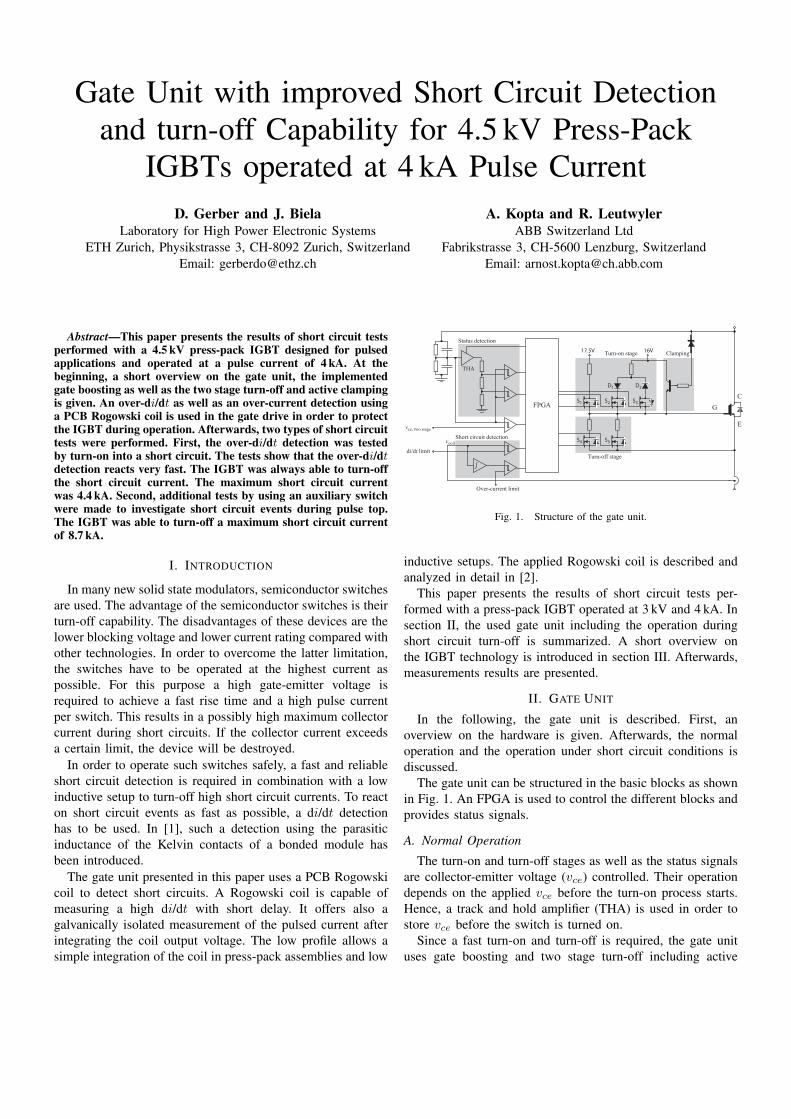
Fig. 1. Structure of the gate unit.
inductive setups. The applied Rogowski coil is described andanalyzed in detail in [2].
This paper presents the results of short circuit tests per-formed with a press-pack IGBT operated at 3 kV and 4 kA. Insection II, the used gate unit including the operation duringshort circuit turn-off is summarized. A short overview onthe IGBT technology is introduced in section III. Afterwards,measurements results are presented.
II. GATE UNIT
In the following, the gate unit is described. First, anoverview on the hardware is given. Afterwards, the normaloperation and the operation under short circuit conditions isdiscussed.
The gate unit can be structured in the basic blocks as shownin Fig. 1. An FPGA is used to control the different blocks andprovides status signals.
A. Normal Operation
The turn-on and turn-off stages as well as the status signalsare collector-emitter voltage (vce) controlled. Their operationdepends on the applied vce before the turn-on process starts.Hence, a track and hold amplifier (THA) is used in order tostore vce before the switch is turned on.
Since a fast turn-on and turn-off is required, the gate unituses gate boosting and two stage turn-off including active

vge
t
17.5V16V
S2, S3 on S5 onvce, ic
t
vce ic
S4, S5 onS1, S2 on
Fig. 2. Gate-Emitter voltage, vce and ic for one switching cycle duringnormal operation with a RL-load.
clamping as proposed in [3] and [4]. The normal operationof these stages will be described in the following.
After the track and hold amplifier is in hold state, the turn-on process starts. Switches S1 and S2 are closed and all otherswitches are opened. When the gate-emitter voltage (vge) ishigher than 16 V, diode D1 is not conducting anymore. Thisresults in a higher turn-on resistance which provides additionaldamping. As soon as vce falls below a certain level or after afixed time limit of 1µs is reached, switch S1 opens and S3 isclosed to pull vge to 16 V.
After the switching signal goes low, the normal turn-offprocedure starts. Switches S1 to S3 are opened and S4 aswell as S5 are closed. When vge reaches a fixed voltage, S4
is opened. Hence, the turn-off resistance becomes higher andthe di/dt during turn-off is reduced. This in turn reduces thepeak voltage of vce. The track and hold amplifier is set intothe track state after the switch turned off.
The waveform of vge, vce and ic for one switching cycleduring normal operation is shown in Fig. 2.
B. Short Circuit Turn-Off
As previously mentioned, a PCB Rogowski coil is usedto detect short circuits. To react as fast as possible on shortcircuits during the turn-on process, a over-di/dt detection isused. Since the Rogowski coil provides an output voltageproportional to the di/dt, the coil signal can directly be usedfor over-di/dt detection.
Since the over-di/dt detection is not sufficient to detect shortcircuits, the coil voltage is integrated to measure the collectorcurrent. As soon as the measured current exceeds a certainlimit, the gate unit detects the short circuit. The over-currentlimit during the performed tests was set to a fixed level.
When the gate unit detects a short circuit, the switchis turned off immediately. At the beginning, the turn-offprocedure is the same as during normal operation. Since vce
vge
t
17.5V16V
S2, S3 on S5 onS4, S5 onvce, ic
t
vce icShort circuit
S1, S2 on
Fig. 3. Voltage vge for one switching cycle during short circuit with aRL-load.
rises much faster than during normal turn-off, the propagationdelay of the normal two stage turn-off circuitry is too high.Therefore, switches S4 and S5 would remain turned on duringthe whole turn-off process. This would result in a high vce.Hence, switch S4 is opened after a fixed time limit (Fig. 3).
III. DEVICE TECHNOLOGY
Fig. 4 shows a cross-section of the used 4.5 kV IGBT chip.The IGBT utilizes an enhanced planar IGBT cell on the emitterside and an optimized buffer and anode design on the collectorside.
The enhanced planar cell ensures a combination of lowlosses and controllable switching behavior. The low losses areachieved by the N-Enhancement layer, which minimizes thedrainage of holes into the P-Base during conduction. In thisway the electron-hole plasma can be enhanced on the emitter-side of the N-Base, which ensures a combination of lowconduction and turn-off losses. The planar cell layout furtherensures a low gate-collector capacitance, which improves theturn-on behavior of the chip. In this way, the IGBT can easily
Fig. 4. Cross-section of the investigated 4.5 kV IGBT.
Lload
Gate unit
CDCVDC
Fig. 5. Setup used for short circuit test at turn on.
be controlled by the gate-unit for a wide range of turn-ontransients.
The buffer and the anode of the IGBT have been carefullyoptimized in order to achieve a high short-circuit ruggedness,which is important in the investigated pulse power application.During short-circuit, the IGBT has to support the applied DC-link voltage and at the same time carry a large current. Thecurrent is thereby transported by electrons injected by theMOS-channel and holes injected by the IGBT anode. In [5] itwas shown that the main IGBT short-circuit failure mechanismis caused by a distortion of the internal electric field triggeredby a positive feedback effect between the drift velocities ofthe mobile carriers and the electric field. This effect can beeffectively suppressed by increasing the injection of holesfrom the anode. In this way, the IGBT short-circuit capabilitycan be significantly increased by increasing the anode emitterefficiency. Because the anode emitter efficiency also stronglydetermines the leakage current of the IGBT, such a designmeasure has to be accompanied by a careful design of theIGBT buffer in order to prevent excessive leakage currents inthe IGBT blocking state.
An additional measure necessary to achieve a high short-circuit ruggedness is an optimization of the IGBT package.The investigated press-pack package has been carefully de-signed to minimize any feedbacks into the IGBT gate circuitduring the short-circuit pulse. Due to the high di/dt encoun-tered in the application, even small coupling inductances caninfluence the effective gate-emitter voltages of the IGBTsand lead to inhomogeneous current distribution between theindividual chips or even premature failures.
IV. MEASUREMENTS
To test the short circuit detection, two different setups wereused. First, a short circuit at turn-on is tested. Second, a shortcircuit during pulse top is investigated.
A. Short Circuit at Turn-on
In order to test the over-di/dt detection, a short circuit atturn-on was simulated.
1) Setup: To simulate a short circuit at turn-on, the ohmicload of the test setup is replaced by a pure inductive load. Aschematic of the setup is shown in Fig. 5. An air coil is usedas inductive load (Fig. 6). To determine the limit of the shortcircuit detection, different inductance values are used. A firsttest is done with an Lload of 650 nH. Afterwards the inductanceis reduced stepwise down to 50 nH. The voltage VDC is set to3 kV for all tests.
(a) (b)
Fig. 6. Test setup (a) and one of the used air-coils connected to the testsetup (b).
Time (μs)
v ce (
kV)
0 0.2 0.4 0.60
1
2
3
4
5
50 nH100 nH195 nH300 nH500 nH650 nH
0 0.2 0.4 0.6−1
0
1
2
3
4
i c (k
A)
Time (μs)
50 nH100 nH195 nH300 nH500 nH650 nH
Fig. 7. Voltage vce and ic with vce controlled turn-off for different loadinductance values.
2) Results: Initially, tests without the previously describedshort circuit turn-off procedure were performed. In Fig. 7, thecollector-emitter voltage and the collector current is shown fordifferent inductance values. The measured results show, thatthe IGBT was able to turn off safely in all cases. The maximumcollector current ic was 3.7 kA, which is lower than the currentduring normal pulsed operation. The maximum voltage of vcewas around 4.3 kV which is an over-voltage of 43 %. This highover-voltage can be explained by the propagation delay of thenormal turn-off circuitry. Voltage vce rises much faster thanduring normal turn-off due to the high current. Also, vge isstill rising due to the RC charging of the gate. Hence, switchS4 opens too late.
After these first tests, the turn off procedure during shortcircuits was modified as described in section II-B. The resultsare shown in Fig. 8. The maximum collector emitter voltagewith a time controlled turn-off sequence is 3.8 kV. Comparedwith the previous results, the over-voltage was reduced by61 %. The lower over-voltage was achieved at the expense ofthe maximum collector current and turn-off time. Current ic isnow around 4.4 kA which is only 10 % more than the nominalcollector current. The time required to turn the current off isaround 500 ns longer.
B. Short Circuit during Pulse
1) Setup: To test short circuits during the pulse, an ohmicload of 0.8Ω is connected to the circuit. An auxiliary switch

0 0.5 10
1
2
3
4
5
Time (μs)
v ce (
kV)
Time controlledvce controlled
(a)
0 0.5 1−1012345
Time (μs)
i c (k
A)
Time controlledvce controlled
(b)
Fig. 8. Voltage vce and ic with vce controlled turn-off and time controlledturn-off for a load inductance of 50 nH.
Rload
Gate unit
CDCVDC
Saux
Fig. 9. Setup used for short circuit test during pulse with an IGCT was asauxiliary switch.
is used to short the load as shown in Fig. 9. Several test areperformed with input voltages from 2 kV to 3 kV and delaysbetween the two switching signals ranging from 1.5µs to13.5µs.
2) Results: The resulting maximum vce and the maximumic are shown in Table I. The results show that the highestshort circuit currents are reached at low input voltages. Thisis a result of the finite turn-on time of the auxiliary switch andthe time between the short circuit event and the detection ofthe short circuit. The level for the over-current detection wasset to a fixed value of 4.2 kA. Therefore, the short circuit isdetected later at lower input voltages VDC . Since the auxiliaryswitch has also a finite turn-on time, it takes around 1µsuntil the di/dt reaches its maximal value (Fig. 10). The resultsalso show, that the highest short circuit currents are reachedat a time delay of 13.5µs. This can be explained by theturn-on characteristics of the IGBT. If the short circuit eventoccurs with at a small delay, the IGBT is not fully turned onyet. Therefore, the turn-off process is faster and the resultingmaximum current is lower.
As in the tests done before, the sample turned off safely inall cases.
TABLE IMAXIMUM COLLECTOR EMITTER VOLTAGE AND COLLECTOR CURRENT
FOR DIFFERENT VOLTAGES VDC AND DELAYS td .
VDC 2 kV 2.5 kV 3 kVtd vce ic vce ic vce ic
1.5 µs 3.3 kV 6.3 kA 3.45 kV 4 kA 3.9 kV 4.3 kA3.5 µs 3.3 kV 6.7 kA 3.5 kV 5.9 kA 3.9 kV 5.3 kA4.5 µs 3.4 kV 7.4 kA 3.6 kV 6.5 kA 3.4 kV 4.3 kA5.5 µs 3.4 kV 7.9 kA 3.7 kV 7.2 kA 3.4 kV 4.3 kA
13.5 µs 3.5 kV 8.6 kA 3.7 kV 8.7 kA 3.8 kV 7.6 kA
0 2 4 6 8 10 12 14−2000
0
2000
4000
6000
8000
10000
Time (μs)
i c (A
)
VDC=3000VVDC=2500VVDC=2000V
Fig. 10. Collector currents for a time delay of 13.5µs with a resistive loadof 0.8Ω.
V. CONCLUSION
In this paper, short circuit tests performed with a press-packIGBT operated at 3 kV, 4 kA pulse current and a gate unit withover-di/dt and over-current detection are presented. The gateunit uses a PCB Rogowski coil to detect short circuits.
Two different types of tests are performed: a short circuitevent during turn-on and a short circuit during the pulse. TheIGBT was able to turn off the short circuit current in all cases.The maximum collector current during turn-off was 8.7 kA.
As a conclusion, the short circuit tests show that the over-di/dt and the over-current detection with a PCB Rogowski coilin combination with a very low inductive press-pack setup iscapable to turn off high short circuit currents. In addition, thetests show the robustness of the used IGBT chips. Also, thecurrent is shared equally between the individual chips insidethe package even at high di/dt during turn off as shown in [6].
ACKNOWLEDGEMENTS
The authors would like to acknowledge Puls-PlasmatechnikGmbH (PPT) for their support and the construction of thestack.
REFERENCES
[1] M. N. Nguyen, R. L. Cassel, J. E. deLamare, and G. C. Pappas, “Gatedrive for high speed, high power IGBTs,” in Proc. PPPS Pulsed PowerPlasma Science Digest of Technical Papers, vol. 2, 2001, pp. 1039–1042.
[2] T. Guillod, D. Gerber, J. Biela, and A. Muesing, “Design of a PCBRogowski coil based on the PEEC method,” in Proc. 7th Int. IntegratedPower Electronics Systems (CIPS) Conf, 2012, pp. 1–6.
[3] D. Gerber, T. Guillod, and J. Biela, “IGBT gate-drive with PCB Rogowskicoil for improved short circuit detection and current turn-off capability,”in Proc. IEEE Pulsed Power Conf. (PPC), 2011, pp. 1359–1364.
[4] D. Bortis, P. Steiner, J. Biela, and J. W. Kolar, “Double-stage gate drivecircuit for parallel connected IGBT modules,” in Proc. IEEE Int. PowerModulators and High Voltage Conf, 2008, pp. 388–391.
[5] A. Kopta, M. Rahimo, U. Schlapbach, N. Kaminski, and D. Silber,“Limitation of the short-circuit ruggedness of high-voltage IGBTs,” inProc. 21st Int. Symp. Power Semiconductor Devices & IC’s (ISPSD),2009, pp. 33–36.
[6] A. Muesing, G. Ortiz, and J. W. Kolar, “Optimization of the currentdistribution in press-pack high power IGBT modules,” in Proc. Int. PowerElectronics Conf. (IPEC), 2010, pp. 1139–1146.