gas sensors based on thick films of semi-conducting single
TRANSCRIPT

C A R B O N 4 9 ( 2 0 1 1 ) 3 5 4 4 – 3 5 5 2
. sc iencedi rec t .com
avai lab le at wwwjournal homepage: www.elsev ier .com/ locate /carbon
Gas sensors based on thick films of semi-conductingsingle walled carbon nanotubes
Yann Battie a,*, Olivier Ducloux b, Philippe Thobois b, Nelly Dorval b,Jean Sebastien Lauret c, Brigitte Attal-Tretout b, Annick Loiseau a
a LEM ONERA-CNRS UMR 104, 29 Av. de la Division Leclerc, 92322 Chatillon, Franceb ONERA – DMPH, 29 Av. de la Division Leclerc, 92322 Chatillon, Francec LPQM, ENS Cachan CNRS, 94245 Cachan, France
A R T I C L E I N F O
Article history:
Received 20 January 2011
Accepted 8 April 2011
Available online 22 April 2011
0008-6223/$ - see front matter � 2011 Elsevidoi:10.1016/j.carbon.2011.04.054
* Corresponding author: Fax: +33 146734155.E-mail address: [email protected] (Y. B
A B S T R A C T
A comparative study was made of sorted semi-conducting single walled carbon nanotube
(SWCNT) films and unsorted SWCNT films for gas sensing applications. The transmission
line method is used to monitor separately the SWCNTs film resistance and the contact
resistance between electrodes and the SWCNTs, thus revealing that the sensing mecha-
nism mainly relies on a modification of the tube conductivity during gas exposure. The fab-
ricated sensors demonstrate a detection limit of 20 ppb NO2 and 600 ppb NH3 mainly
attributed to experimental setup limitations. Moreover, semi-conducting nanotubes hap-
pened to be 2.5 times more sensitive to NH3 than unsorted ones, thus proving that selectiv-
ity can be improved by sorting the SWCNTs. The temperature dependence of the sensor
sensitivity was studied, and a good agreement was found between experimental results
and the Langmuir adsorption model.
� 2011 Elsevier Ltd. All rights reserved.
1. Introduction
The one dimensional molecular structure of single walled car-
bon nanotubes (SWCNTs) consists of a graphene sheet rolled
up into a cylinder. The small size, large surface to volume ra-
tio and highly environment-sensitive electrical properties of
SWCNTs make them a great candidate for gas sensing
applications.
In 2000, Kong et al. [1] showed that the electrical resistance
of SWCNTs was modified when exposed to gaseous molecules
such as NO2 or NH3. Depending on their chirality, SWCNTs
can exhibit metallic or semi-conducting properties. In the
case of sensor devices based on a single nanotube, it can be
a source of irreproducibility. This problem can be overcome
using SWCNT networks, as shown by Nanomix Inc. [2]. This
type of sensor offers better reproducibility due to the overall
averaging of the electrical properties of individual tubes.
er Ltd. All rights reservedattie).
Simultaneously, lots of efforts have been put in the devel-
opment of SWCNT sorting techniques, including dielectro-
phoresis [3], ion exchange chromatography [4] and density
gradient ultracentrifugation (DGU) [5]. This last method en-
ables the separation of metallic carbon nanotubes from
semi-conducting ones and is increasingly used to improve
reproducibility of SWCNT-based devices [6,7]. In the field of
chemical sensors, sorted SWCNTs have been applied to the
detection of organic toxic molecules like TNT and DMMP dis-
solved in water [8]. The authors report intrinsic selectivity of
sorted SWCNTs, with no assistance of any functionalization.
Different gas sensing mechanisms have been reported,
such as adsorption of gas molecules at the interstitial sites
in the SWCNT bundles, direct charge transfer from the gas
molecules adsorbed on the SWCNTs and modulation of the
Schottky barrier (SB) level at the interface between semi-con-
ducting SWCNTs and metallic electrodes or at the contacts
.
C A R B O N 4 9 ( 2 0 1 1 ) 3 5 4 4 – 3 5 5 2 3545
between semi-conducting and metallic SWCNTs [9]. Up to
now, few experimental studies have been undertaken in order
to investigate the gas detection mechanism.
Zhang et al. [10] deposited a PMMA passivation layer on dif-
ferent parts of their device in order to show that the change of
electrical properties during NO2 exposure was consistent with
a modulation of the Schottky barrier (SB) level. On the contrary,
Liu et al. [11] argued that when the nanotube film or the con-
tacts were passivated by PMMA, both the SB and the film were
playing a role in the gas detection mechanism. The possible
diffusion of gas molecules through the passivation layer was
evoked to explain these different results. Studies based on ab
initio calculations [12,13] reported that the adsorption of gas
molecules on the SWCNTs induced a charge transfer between
species, consistent with a modification of the SWCNT conduc-
tivity and with the charge transfer estimated from experimen-
tal results [14]. Moreover, some works based on spectroscopic
impendence measurements [9] evidenced a modulation of
the Schottky barrier between semiconducting SWCNTs and
metallic SWCNTs during the gas exposure which contributes
to modify the SWCNTs film resistance.
On the other hand, Bondavalli et al. [15] developed a
SWCNTs gas sensor taking advantage of the SB between a
SWCNT network and contact electrodes to obtain selectivity
by varying the electrode material. Using this approach, the
authors claimed the recognition of complex gases, highlight-
ing the importance of the Schottky barrier in the sensing
mechanism. The comprehension of the physical interaction
between SWCNT based sensors and gas molecules, has not
reached a consensus yet and seems to be highly dependent
of the device structure.
In this work, we focused on thick SWCNT films for gas
sensing applications and tried to identify the involved gas
sensing mechanisms. The transmission line method (TLM)
[16,17] was used as a non-invasive technique to monitor sep-
arately the SWCNT film resistance and the contact resistance
between SWCNTs and metallic electrodes. We showed that
the adsorption of gas molecules such as NH3 or NO2 on the
SWCNTs is the main contributor to the gas detection mecha-
nism for our sensors. The kinetics of gas sensing, depending
on the temperature, was then described and compared to a
simple adsorption/desorption model. We finally compared
the sensitivity to NH3 and NO2 of sensors based on unsorted
SWCNT films and sorted semi-conducting SWCNT ones,
showing that selectivity can be achieved by playing on the
electronic properties of the SWCNTs.
2. Experimental details
2.1. Sorting of semi-conducting carbon nanotubes
Unsorted purified SWCNTs (P2-SWCNT), produced by the arc
discharge technique were purchased from Carbon Solution
Inc., California.
Forty milligrams of SWCNTs were first dispersed in a 10 ml
solution of distilled water containing 2% w/v of sodium cho-
late (SC). This dispersion was first sonicated during 1 h, using
an ultrasonic tip (240 W), until a homogeneous suspension
was obtained and, second, centrifuged during 1 h at
160,000g using a SW41 Beckmann Coulter rotor in order to re-
move the heaviest particles and bundles. The opaque super-
natant was then collected to elaborate the sensor based on
as-produced unsorted SWCNTs (S1). The same suspension
was also used as a basic solution for sorting SWCNTs by den-
sity gradient ultracentrifugation.
The sorting of semi-conducting SWCNTs from the as-pro-
duced SWCNT suspension was then achieved using the pro-
cess proposed by Posseckardt et al. [7] and its efficiency
determined using the procedure described by Fleurier et al.
[18]. Aqueous dilutions of iodixanol, containing 1.4% w/v SC
and 0.6% w/v sodium dodecyl sulfate (SDS), were used as den-
sity gradient media. Both surfactants (SC and SDS) are known
to enhance the mass difference between metallic and semi-
conducting SWCNTs by non-covalent adsorption. A linear
mass density gradient ranging from 1.08 to 1.19 was formed
in a centrifuge tube using a linear gradient master device (Bio-
comp). After formation of the gradient, 1.5 ml of 60% w/v
iodixanol was added at the bottom of the centrifugation tube.
A 1.8 ml solution of SWCNT supernatant mixed with iodix-
anol (27.5% w/v) was then injected into the gradient. The
top of the tube was then filled with an aqueous solution con-
taining 1.4% w/v of sodium cholate and 0.6% w/v of sodium
dodecyl sulfate. This preparation was finally centrifuged for
14 h at 160,000g. A pink layer was clearly observed at the
top of the density gradient, corresponding to highly concen-
trated semi-conducting SWCNTs. This layer was collected
by using a flat opened needle and used to elaborate the sensor
based on semi-conducting SWCNTs (S2).
2.2. Gas sensor fabrication
The TLM platform was fabricated using standard photolithog-
raphy procedures. The substrate consists of a 400 lm thick
undoped silicon wafer covered with a 200 nm thick thermal
oxide layer. A double layer of LOR 5A/S 1813 photoresist was
then deposited and patterned using standard photolithogra-
phy processes. A 80 nm thick layer of platinum was finally
deposited by sputtering and patterned using the lift-off tech-
nique. Platinum was chosen for its chemical inertness and
temperature stability. The TLM pattern consists of a series
of rectangular electrodes (500 lm · 50 lm) separated by
increasing distances (5 lm, 10 lm, 25 lm, 50 lm and 100 lm).
The dispersed SWCNT solutions were filtered through a
nitrocellulose membrane. The volume of the solution was ad-
justed in order to obtain the desired SWCNT film thickness.
The film was thoroughly washed with deionized water to re-
move the surplus of surfactant and finally reported onto the
TLM pattern. The nitrocellulose membrane was finally dis-
solved with acetone.
The electrical properties of SWCNT films exposed to atmo-
spheric environments are significantly influenced by other
molecules like oxygen [19] and especially water molecules
[20,21]. In addition, organic molecules like iodixanol and sur-
factant can act as chemisorption sites for gas molecules. This
may increase the sensitivity of sensors based on SWCNT net-
works but it also generates drift of the sensor responses when
exposed to gases and during desorption cycles. To overcome
this problem, the sensors were first annealed in a furnace at
300 �C in air during 2 h. After thermal treatment, resistances

ig. 1 – Absorption spectra of unsorted and sorted SWCNTs
uspensions.
3546 C A R B O N 4 9 ( 2 0 1 1 ) 3 5 4 4 – 3 5 5 2
of both sensor S1 and S2 decreased dramatically due to an
improvement of the tube–tube contacts and tube–electrode
contacts induced by the pyrolysis of iodixanol and surfactants
[22].
2.3. Characterization
Optical absorption spectroscopic measurements were per-
formed using a UV–Visible/NIR Perkin Elmer spectrometer in
the wavelength range 320–1200 nm. The E22 band amplitude
of absorption spectra was normalized to unity. The scanning
electron microscopy (SEM) investigations were performed
with a field emission gun scanning electron microscope Zeiss
Gemini operating at 15 kV. The surface topography of SWCNT
films was obtained by a Dimension 3100 Veeco atomic force
microscope operating in taping mode. The transmission elec-
tron microscopy (TEM) investigations were performed with a
Technai CM20 electron microscope operating at 200 kV.
SWCNT film resistances were measured by volt-amperomet-
ric technique using an automated system composed of a
Keithley 705 multichannel scanner and a Keithley 2601
source-meter. The sensitivity S of the sensor was defined as
the ratio between resistance variation DR of sensor during
gas exposure and sensor resistance R0 before gas exposure.
The TLM analysis was performed by scanning the five elec-
trode pairs separated by increasing inter-electrodes distances
d. The voltage applied between each electrodes pair was fixed
to 100 mV. The transmission line method (TLM), used to ex-
tract the sheet resistance of the film Rsh and the average con-
tact resistance Rc between the metallic electrodes and the
film, is based on the following expression:
R ¼ 2Rc þ RshdW
ð1Þ
where W is the electrode width and R the measured resis-
tance between two electrodes.
3. Results and discussion
The normalized UV–visible–IR absorbance spectra of the as-
prepared SWCNTs and sorted SC-SWCNT suspensions are
shown in Fig. 1. The E22 band and the M11 band, centered
respectively at 1015 nm and 710 nm, are clearly observed on
the spectrum of the as-prepared SWCNT suspension. These
bands are also present at the same wavelengths in the spec-
trum of the sorted SWCNT suspension. Since band positions
essentially depend on the nanotube diameter, this result sug-
gests that the tube diameter distribution does not change dur-
ing the sorting procedure. This behavior has been checked by
performing a statistical analysis of the tube diameter using
TEM according to the procedure described in [18]. As shown
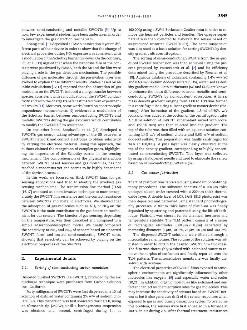
in Fig. 2, sorted and unsorted nanotubes display the same
diameter distribution.
The average SWCNT diameter determined from TEM
images is in the range 1.3–1.4 nm, similar to the one esti-
mated from the position of the E22 band in the UV–visible–IR
analysis [23]. After subtracting the continuous background
of the spectra, the ratio between the amplitudes of the E22
and M11 bands can be used to estimate the relative concentra-
tion of semi-conducting SWCNTs in both suspensions [5]. The
F
s
as-prepared suspension and the sorted suspension are
respectively composed of 67% and 93% of semi-conducting
SWCNTs. Note that the ratio found for unsorted samples is
quite consistent with previous estimations, by electron dif-
fraction, indicating a random chirality distribution in this
kind of samples [24].
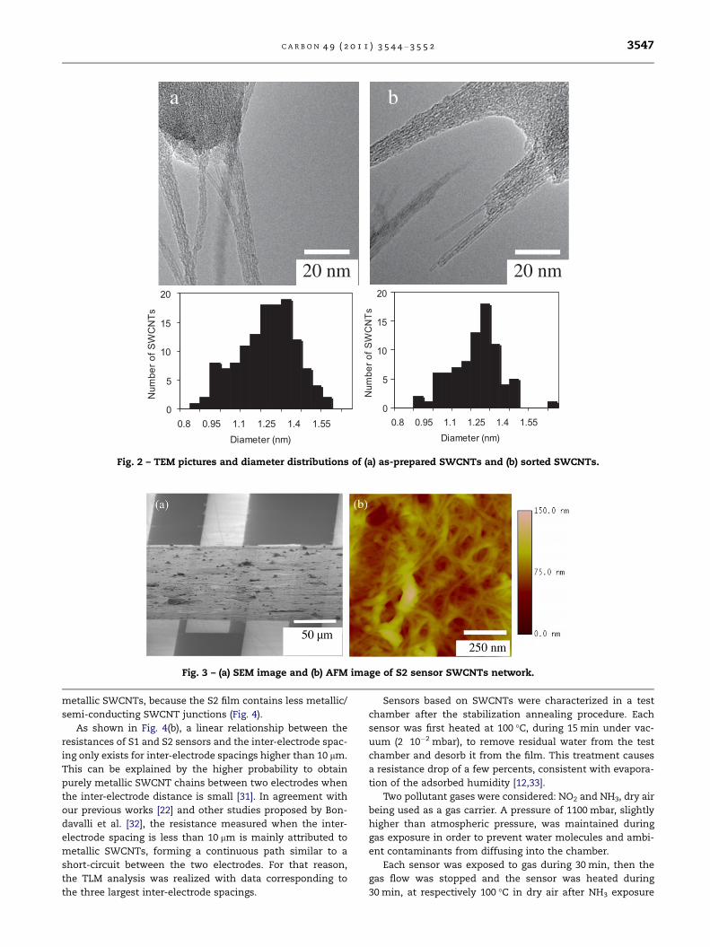
The SEM image of the sensor S2, Fig. 3(a), shows that the
SWCNT film covers the TLM platinum electrodes. The AFM
topography of the sensor based on sorted SWCNTs (S2) is pre-
sented in Fig. 3. It reveals a ‘‘spaghetti’’ like random network
composed of agglomerated SWCNT bundles. The average
thickness and surface coverage of this network are respec-
tively about 120 nm and 80%. The same characteristics are ob-
tained for S1.
The I–V curves obtained for the five electrode pairs of sen-
sors S1 and S2 are linear in the �2 V to +2 V range (Fig. 4(a)),
indicating that ohmic contacts are formed between SWCNTs
and metal electrodes. According to previous observations
[25,26], the transport properties of our thick SWCNT films
can be interpreted using the percolation theory of a random
stick network. The linear dependence of the I–V curve can
be explained by the high thickness and surface coverage of
the ‘‘spaghetti like’’ film which contributes to increase the
probability of percolative transport toward the metallic
SWCNTs for both sensors and thus to minimize the influence
of the SB at the metal electrode/SWCNT film contact on the
electrical properties of our sensors [25].
Both metallic and semi-conducting tubes can carry current
with a similar resistance, the electronic transport being
essentially influenced by the tube-to-tube contact. Indeed,
previous studies have demonstrated that electrons are easily
transmitted between two semi-conducting or two metallic
tubes. However, the junction between semi-conducting and
metallic nanotubes induces a SB that can modulate the cur-
rent flow [27–29]. In accordance with a study conducted by To-
pinka et al. [30], the resistance of the SWCNT film of S1
sensor, which contains 33% of metallic SWCNTs, is similar
to the resistance of the S2 sensor film, which contains 7% of
0
5
10
15
20
0.8 0.95 1.1 1.25 1.4 1.55Diameter (nm)
Num
ber o
f SW
CN
Ts
0
5
10
15
20
0.8 0.95 1.1 1.25 1.4 1.55Diameter (nm)
Num
ber o
f SW
CN
Ts
a b
20 nm20 nm
Fig. 2 – TEM pictures and diameter distributions of (a) as-prepared SWCNTs and (b) sorted SWCNTs.
Fig. 3 – (a) SEM image and (b) AFM image of S2 sensor SWCNTs network.
C A R B O N 4 9 ( 2 0 1 1 ) 3 5 4 4 – 3 5 5 2 3547
metallic SWCNTs, because the S2 film contains less metallic/
semi-conducting SWCNT junctions (Fig. 4).
As shown in Fig. 4(b), a linear relationship between the
resistances of S1 and S2 sensors and the inter-electrode spac-
ing only exists for inter-electrode spacings higher than 10 lm.
This can be explained by the higher probability to obtain
purely metallic SWCNT chains between two electrodes when
the inter-electrode distance is small [31]. In agreement with
our previous works [22] and other studies proposed by Bon-
davalli et al. [32], the resistance measured when the inter-
electrode spacing is less than 10 lm is mainly attributed to
metallic SWCNTs, forming a continuous path similar to a
short-circuit between the two electrodes. For that reason,
the TLM analysis was realized with data corresponding to
the three largest inter-electrode spacings.
Sensors based on SWCNTs were characterized in a test
chamber after the stabilization annealing procedure. Each
sensor was first heated at 100 �C, during 15 min under vac-
uum (2 Æ 10�2 mbar), to remove residual water from the test
chamber and desorb it from the film. This treatment causes
a resistance drop of a few percents, consistent with evapora-
tion of the adsorbed humidity [12,33].
Two pollutant gases were considered: NO2 and NH3, dry air
being used as a gas carrier. A pressure of 1100 mbar, slightly
higher than atmospheric pressure, was maintained during
gas exposure in order to prevent water molecules and ambi-
ent contaminants from diffusing into the chamber.
Each sensor was exposed to gas during 30 min, then the
gas flow was stopped and the sensor was heated during
30 min, at respectively 100 �C in dry air after NH3 exposure
Fig. 4 – (a) I–V curves of the S1 and S2 sensors corresponding to 5 lm and 100 lm inter-electrode distances. (b) TLM analysis of
S1 and S2 sensors.
3548 C A R B O N 4 9 ( 2 0 1 1 ) 3 5 4 4 – 3 5 5 2
and 200 �C in vacuum after NO2 exposure, in order to recover
the initial transport properties of the SWCNT film. The S2
sensor resistance variation during exposure to gases, in the
case of an inter-electrode distance equal to 100 lm, is pre-
sented in Fig. 5.
Similar time dependence was observed with S1 sensor.
Sensors resistances decreased when exposed to NO2 and an
opposite variation was observed during NH3 exposure, in
accordance with other works [1]. The average response time,
at room temperature, was comprised in the range 20–
30 min. Moreover, the annealing procedure allowed the initial
resistance value after gas exposure to be fully recovered. The
baseline resistance (i.e. the resistance in dry air atmosphere
at 20 �C) was repeatable and stable after several exposure cy-
cles, showing complete desorption of the adsorbed gas
molecules.
The measured sensor resolution, at room temperature, in-
creases with the inter-electrode distance. For the higher chan-
nel length of S2 (100 lm), the resolution was estimated to
600 ppb for NH3 and 20 ppb for NO2. Those levels, currently
limited by temperature fluctuations around ambient temper-
ature, are slightly better than those of individual SWCNT sen-
sors and satisfy standards for environmental monitoring
applications.
TLM analysis carried out for 0 ppm and 200 ppm of gases
(Fig. 6(a) and (b)) showed that the contact resistance between
SWCNT films and metallic electrodes (32 X) is independent
Fig. 5 – Variation of S2 sensor resistance (d = 100 lm) during (a) N
grey and dotted lines.
from the gas concentration. This result is in contrast to others
studies [32,34] linking the gas sensing mechanism to a modu-
lation of the Schottky barrier existing between metallic elec-
trodes and SWCNTs. This discrepancy can be explained by
the high density of SWCNT in our films, which minimizes
the SB level and its influence on the sensing mechanism. Only
the slope of the curves presented in Fig. 6(a) and (b), i.e. the
sheet resistance of the film, is affected by gas exposure. This
suggests that gas exposure directly modifies the transport
properties of the SWCNT film.
In order to prevent ambient humidity from tampering the
measurement results [14], the testing environment was dry
and previously dehydrated during gas exposure. According
to previous works, based on the measurement of IR spectra
of SWCNTs exposed to NH3 and NO2 [35] showing that both
gas molecules adsorb on SWCNTs, we can unambiguously
conclude that the charge transfer induced by NH3 or NO2 is
the dominant sensing mechanism at stake in our sensors.
The correspondence between gas concentration and S2
sensor sensitivity is reported in the inserts of Fig. 6(a) and
(b). In agreement with previous works [35], the S2 sensor
exhibits a higher sensitivity to NO2 than NH3. This result is
consistent with theoretical studies showing that the elec-
tronic state density of SWCNTs is dramatically modified by
the adsorption of NO2, but less modified by the adsorption
of NH3 [12]. We can note that the S2 sensor channel with
the smaller inter-electrode spacing is relatively insensitive
H3 and (b) NO2 exposures. Temperature variation is shown in
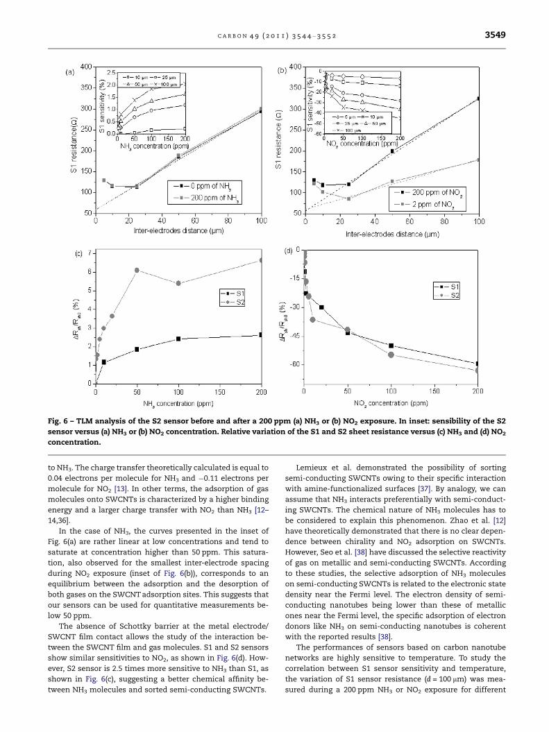
Fig. 6 – TLM analysis of the S2 sensor before and after a 200 ppm (a) NH3 or (b) NO2 exposure. In inset: sensibility of the S2
sensor versus (a) NH3 or (b) NO2 concentration. Relative variation of the S1 and S2 sheet resistance versus (c) NH3 and (d) NO2
concentration.
C A R B O N 4 9 ( 2 0 1 1 ) 3 5 4 4 – 3 5 5 2 3549
to NH3. The charge transfer theoretically calculated is equal to
0.04 electrons per molecule for NH3 and �0.11 electrons per
molecule for NO2 [13]. In other terms, the adsorption of gas
molecules onto SWCNTs is characterized by a higher binding
energy and a larger charge transfer with NO2 than NH3 [12–
14,36].
In the case of NH3, the curves presented in the inset of
Fig. 6(a) are rather linear at low concentrations and tend to
saturate at concentration higher than 50 ppm. This satura-
tion, also observed for the smallest inter-electrode spacing
during NO2 exposure (inset of Fig. 6(b)), corresponds to an
equilibrium between the adsorption and the desorption of
both gases on the SWCNT adsorption sites. This suggests that
our sensors can be used for quantitative measurements be-
low 50 ppm.
The absence of Schottky barrier at the metal electrode/
SWCNT film contact allows the study of the interaction be-
tween the SWCNT film and gas molecules. S1 and S2 sensors
show similar sensitivities to NO2, as shown in Fig. 6(d). How-
ever, S2 sensor is 2.5 times more sensitive to NH3 than S1, as
shown in Fig. 6(c), suggesting a better chemical affinity be-
tween NH3 molecules and sorted semi-conducting SWCNTs.
Lemieux et al. demonstrated the possibility of sorting
semi-conducting SWCNTs owing to their specific interaction
with amine-functionalized surfaces [37]. By analogy, we can
assume that NH3 interacts preferentially with semi-conduct-
ing SWCNTs. The chemical nature of NH3 molecules has to
be considered to explain this phenomenon. Zhao et al. [12]
have theoretically demonstrated that there is no clear depen-
dence between chirality and NO2 adsorption on SWCNTs.
However, Seo et al. [38] have discussed the selective reactivity
of gas on metallic and semi-conducting SWCNTs. According
to these studies, the selective adsorption of NH3 molecules
on semi-conducting SWCNTs is related to the electronic state
density near the Fermi level. The electron density of semi-
conducting nanotubes being lower than these of metallic
ones near the Fermi level, the specific adsorption of electron
donors like NH3 on semi-conducting nanotubes is coherent
with the reported results [38].
The performances of sensors based on carbon nanotube
networks are highly sensitive to temperature. To study the
correlation between S1 sensor sensitivity and temperature,
the variation of S1 sensor resistance (d = 100 lm) was mea-
sured during a 200 ppm NH3 or NO2 exposure for different
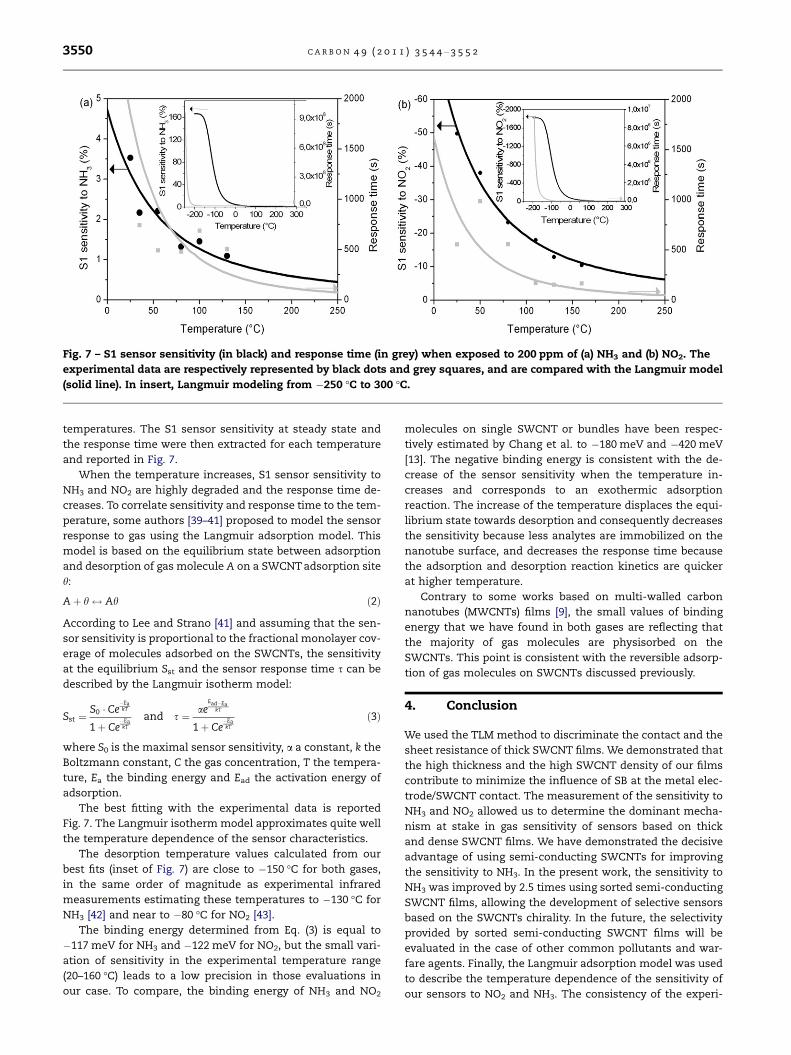
Fig. 7 – S1 sensor sensitivity (in black) and response time (in grey) when exposed to 200 ppm of (a) NH3 and (b) NO2. The
experimental data are respectively represented by black dots and grey squares, and are compared with the Langmuir model
(solid line). In insert, Langmuir modeling from �250 �C to 300 �C.
3550 C A R B O N 4 9 ( 2 0 1 1 ) 3 5 4 4 – 3 5 5 2
temperatures. The S1 sensor sensitivity at steady state and
the response time were then extracted for each temperature
and reported in Fig. 7.
When the temperature increases, S1 sensor sensitivity to
NH3 and NO2 are highly degraded and the response time de-
creases. To correlate sensitivity and response time to the tem-
perature, some authors [39–41] proposed to model the sensor
response to gas using the Langmuir adsorption model. This
model is based on the equilibrium state between adsorption
and desorption of gas molecule A on a SWCNT adsorption site
h:
Aþ h$ Ah ð2Þ
According to Lee and Strano [41] and assuming that the sen-
sor sensitivity is proportional to the fractional monolayer cov-
erage of molecules adsorbed on the SWCNTs, the sensitivity
at the equilibrium Sst and the sensor response time s can be
described by the Langmuir isotherm model:
Sst ¼S0 � Ce
�EakT
1þ Ce�EakT
and s ¼ aeEad�Ea
kT
1þ Ce�EakT
ð3Þ
where S0 is the maximal sensor sensitivity, a a constant, k the
Boltzmann constant, C the gas concentration, T the tempera-
ture, Ea the binding energy and Ead the activation energy of
adsorption.
The best fitting with the experimental data is reported
Fig. 7. The Langmuir isotherm model approximates quite well
the temperature dependence of the sensor characteristics.
The desorption temperature values calculated from our
best fits (inset of Fig. 7) are close to �150 �C for both gases,
in the same order of magnitude as experimental infrared
measurements estimating these temperatures to �130 �C for
NH3 [42] and near to �80 �C for NO2 [43].
The binding energy determined from Eq. (3) is equal to
�117 meV for NH3 and �122 meV for NO2, but the small vari-
ation of sensitivity in the experimental temperature range
(20–160 �C) leads to a low precision in those evaluations in
our case. To compare, the binding energy of NH3 and NO2
molecules on single SWCNT or bundles have been respec-
tively estimated by Chang et al. to �180 meV and �420 meV
[13]. The negative binding energy is consistent with the de-
crease of the sensor sensitivity when the temperature in-
creases and corresponds to an exothermic adsorption
reaction. The increase of the temperature displaces the equi-
librium state towards desorption and consequently decreases
the sensitivity because less analytes are immobilized on the
nanotube surface, and decreases the response time because
the adsorption and desorption reaction kinetics are quicker
at higher temperature.
Contrary to some works based on multi-walled carbon
nanotubes (MWCNTs) films [9], the small values of binding
energy that we have found in both gases are reflecting that
the majority of gas molecules are physisorbed on the
SWCNTs. This point is consistent with the reversible adsorp-
tion of gas molecules on SWCNTs discussed previously.
4. Conclusion
We used the TLM method to discriminate the contact and the
sheet resistance of thick SWCNT films. We demonstrated that
the high thickness and the high SWCNT density of our films
contribute to minimize the influence of SB at the metal elec-
trode/SWCNT contact. The measurement of the sensitivity to
NH3 and NO2 allowed us to determine the dominant mecha-
nism at stake in gas sensitivity of sensors based on thick
and dense SWCNT films. We have demonstrated the decisive
advantage of using semi-conducting SWCNTs for improving
the sensitivity to NH3. In the present work, the sensitivity to
NH3 was improved by 2.5 times using sorted semi-conducting
SWCNT films, allowing the development of selective sensors
based on the SWCNTs chirality. In the future, the selectivity
provided by sorted semi-conducting SWCNT films will be
evaluated in the case of other common pollutants and war-
fare agents. Finally, the Langmuir adsorption model was used
to describe the temperature dependence of the sensitivity of
our sensors to NO2 and NH3. The consistency of the experi-
C A R B O N 4 9 ( 2 0 1 1 ) 3 5 4 4 – 3 5 5 2 3551
mental measurements with the theoretical model suggests a
sensing mechanism based on gas molecules adsorption on
the SWCNTs.
Acknowledgments
This work was conducted in the framework of PRF SANAA, a
research program granted by ONERA. J.S. Lauret and A. Loi-
seau acknowledge the National Agency for Research-France
(A.N.R., contract: CEDONA (ANR-07-NANO-007-04) for finan-
cial support.
R E F E R E N C E S
[1] Kong J, Franklin NR, Zhou C, Chapline MG, Peng S, Cho K,et al. Nanotubes molecular wires as chemical sensors.Science 2000;287(5453):622–5.
[2] Star A, Bradley K, Collins PG, Gabriel J-CP, Grune G. Sensitivitycontrol for nanotube sensors. US Patent 0169798, 2005.
[3] Krupke R, Hennrich F, Lohneysen HV, Kappes MM. Separationof metallic from semiconducting single-walled carbonnanotubes. Science 2003;301(5631):344–7.
[4] Zheng M, Jagota A, Semke ED, Diner BA, Mclean RS, Lustig SR,et al. DNA-assisted dispersion and separation of carbonnanotubes. Nat Mater 2003;2(5):338–42.
[5] Arnold MS, Green AA, Hulvat JF, Stupp SI, Hersam MC. Sortingcarbon nanotubes by electronic structure using densitydifferentiation. Nat Nanotechnol 2006;1(1):60–5.
[6] Engel M, Small JP, Steiner M, Freitag M, Green AA, HersamMC, et al. Thin film nanotube transistors based on self-assembled, aligned, semiconducting carbon nanotube arrays.ACS Nano 2008;2(12):2445–52.
[7] Posseckardt J, Battie Y, Fleurier R, Lauret J-S, Loiseau A, Jost O,et al. Improved sorting of carbon nanotubes according toelectronic type by density gradient ultracentrifugation. PhysStatus Solidi B 2010;247(11–12):2687–90.
[8] Roberts ME, LeMieux MC, Bao Z. Sorted and aligned single-walled carbon nanotube networks for transistor-basedaqueous chemical sensors. ACS Nano 2009;3(10):3287–93.
[9] Varghese OK, Kirchambre PD, Gong D, Ong KG, Dickey EC,Grimes CA. Gas sensing characteristics of multi-wall carbonnanotubes. Sensor Actuator B 2001;81(1):32–3.
[10] Zhang J, Boyd A, Tselev A, Paranjape M, Barbara P.Mechanism of NO2 detection in carbon nanotube field effecttransistor chemical sensors. Appl Phys Lett2006;88(12):123112-1–3.
[11] Liu XL, Luo ZC, Han S, Tang T, Zhang DH, Zhou CW. Bandengineering of carbon nanotube field effect transistors viaselected area chemical gating. Appl Phys Lett2005;86(24):243501-1–3.
[12] Zhao J, Buldum A, Han J, Lu JP. Gas molecule adsorption incarbon nanotubes and nanotube bundles. Nanotechnology2002;13(2):195–200.
[13] Chang H, Lee JD, Lee SM, Lee YH. Adsorption of NH3 and NO2
molecules on carbon nanotubes. Appl Phys Lett2001;79(23):3863–5.
[14] Bradley K, Gabriel J-C P, Briman M, Star A, Gruner G. Chargetransfer from ammonia physisorbed on nanotubes. Phys RevLett 2003;91(21):219301-1–4.
[15] Bondavalli P, Legagneux P, Pribat D. Carbon nanotubes basedtransistors as gas sensors: state of the art and critical review.Sensor Actuator B 2009;140(1):304–18.
[16] Jackson R, Graham S. Specific contact resistance at metal/carbon nanotube interfaces. Appl Phys Lett2009;94(1):012109-1–3.
[17] Koechlin C, Maine S, Haidar R, Tretout B, Loiseau A, PelouardJ-L. Electrical characterization of devices based on carbonnanotube films. Appl Phys Lett 2010;96(10):103501-1–3.
[18] Fleurier R, Lauret JS, Lopez U, Loiseau A. Transmissionelectron microscopy and UV–vis–IR spectroscopy analysis ofdiameter sorting of carbon nanotubes by gradient densityultracentrifugation. Adv Funct Mater 2009;19(14):2219–23.
[19] Collins PG, Bradley K, Ishigami M, Zettl A. Extreme OxygenSensitivity of Electronic Properties of Carbon Nanotubes.Science 2000;287(5459):1801–4.
[20] Na PS, Kim H, So H-M, Kong K-J, Chang H, Ryu BH, et al.Investigation of the humidity effect on the electricalproperties of single-walled carbon nanotube transistors.Appl Phys Lett 2005;87(9):093101–3.
[21] Aguirre CM, Levesque PL, Paillet M, Lapointe F, St-Antoine BC,Desjardins P, et al. The Role of the oxygen/water redoxcouple in suppressing electron conduction in field-effecttransistors. Adv Mater 2009;21(30):3087–91.
[22] Battie Y, Ducloux O, Thobois P, Coffinier Y, Loiseau A.Evaluation of sorted semi-conducting carbon nanotube filmsfor gas sensing application. CRAS 2010;11(5–6):397–404.
[23] Bachilo SM, Strano MS, Kittrell C, Hauge RH, Smalley RE,Weismann RB. Structure-assigned optical spectra of single-walled carbon nanotubes. Science 2002;298(5602):2361–6.
[24] Henrard L, Loiseau A, Journet C, Bernier P. Study of thesymmetry of single-wall nanotubes by electron diffraction.Eur Phys J B 2000;13(4):661–9.
[25] Skakalova V, Kaiser AB, Woo Y-S, Roth S. Electronic transportin carbon nanotubes: from individual nanotubes to thin andthick networks. Phys Rev B 2006;74(8):085403-1–085403-10.
[26] Sangwan VK, Behnam A, Ballarotto VW, Fuher MS, Ural A,Williams ED. Optimizing transistor performance ofpercolating carbon nanotube networks. Appl Phys Lett2010;97(4):043111-1–3.
[27] Fuhrer MS, Nygrd J, Shih L, Forero M, Yoon Y-G, Mazzoni MSC,et al. Crossed nanotube junctions. Science2000;288(5465):494–7.
[28] Bachtold A, Fuhrer MS, Plyasunov S, Forero M, Anderson EH,Zettl A, et al. Scanned probe microscopy of electronictransport in carbon nanotubes. Phys Rev Lett2000;84(26):6082–5.
[29] Purewal MS, Hong BH, Ravi A, Chandra B, Hone J, Kim P.Scaling of resistance and electron mean free path of single-walled carbon nanotubes. Phys Rev Lett 2007;98(18):186808-1–4.
[30] Topinka MA, Rowell MW, Goldhaber-Gordon D, McGehee MD,Hecht DS, Gruner G. Charge transport in interpenetratingnetworks of semiconducting and metallic carbon nanotubes.Nano Lett 2009;9:1866–71.
[31] Stadermann M, Papadakis SJ, Falvo MR, Novak J, Snow E, Fu Q,et al. Nanoscale study of conduction through carbonnanotube networks. Phys Rev B 2004;69(20):201402-1–3.
[32] Bondavalli P, Legagneux P, Pribat D, Balan A, Nazeer S. Gasfingerprinting using carbon nanotubes transistor arrays. JExp Nanosci 2008;3(4):347–56.
[33] Tsai JTH, Lu C-C, Li JG. Fabrication of humidity sensors bymulti-walled carbon nanotubes. J Exp Nanosci2010;5(4):302–9.
[34] Peng N, Zhang Q, Chow CL, Tan OK, Marzari N. Sensingmechanisms for carbon nanotube based NH3 gas detection.Nano Lett 2009;9(4):1626–30.
[35] Ellison MD, Crotty MJ, Koh D, Spray RL, Kaitlin ET. Adsorptionof NH3 and NO2 on single-walled carbon nanotubes. J PhysChem B 2004;108(23):7938–43.

3552 C A R B O N 4 9 ( 2 0 1 1 ) 3 5 4 4 – 3 5 5 2
[36] Bauschlicher CW, Ricca A. Binding of NH3 to graphite and to a(9,0) carbon nanotube. Phys Rev B 2004;70(11):115409-1–6.
[37] Lemieux MC, Roberts M, Barman S, Jin YW, Kim JM, Bao Z.Self sorted, aligned nanotube networks for thin-filmtransistors. Science 2008;321(5885):101–3.
[38] Seo K, Park KA, Kim C, Han S, Kim B, Lee YH. Chirality- anddiameter-dependent reactivity of NO2 on carbon nanotubewalls. J Am Chem Soc 2005;127(45):15724–9.
[39] Wongwiriyapan W, Honda S-I, Konishi H, Mizuta T, Ikuno T,Ito T, et al. Single-walled carbon nanotube thin-film sensorfor ultrasensitive gas detection. Jpn J Appl Phys2005;44(2):482–4.
[40] Robinson JA, Snow ES, Badescu SC, Reinecke TL, Perkins FK.Role of defects in single-walled carbon nanotube chemicalsensors. Nano Lett 2006;6(8):1747–51.
[41] Lee CY, Strano MS. Understanding the dynamics of signaltransduction for adsorption of gases and vapors on carbonnanotube sensors. Langmuir 2005;21(11):5192–6.
[42] Feng X, Irle S, Witek H, Morokuma K, Vidic R, Borguet E.Sensitivity of ammonia interaction with single-walled carbonnanotube bundles to the presence of defect sites andfunctionalities. J Am Chem Soc 2005;127(30):10533–8.
[43] Larciprete R, Petaccia L, Lizzit S, Goldoni A. The role of metalcontact in the sensitivity of single-walled carbon nanotubesto NO2. J Phys Chem C 2007;111(33):12169–74.