ga liquid metal embrittlement for fine pitch interconnect
TRANSCRIPT
Ga Liquid Metal Embrittlement for Fine Pitch Interconnect Rework
E. Nguena, D. Danovitch and M. Kanso Institut interdisciplinaire d’innovation technologique
Université de Sherbrooke Sherbrooke, Québec, Canada
R. Langlois IBM Canada
Bromont, Québec, Canada
Abstract— Heterogeneous integration is considered to be
essential to maximal exploitation of the densification, performance and system cost potential of semiconductor packaging. To ensure high yields of these multiple device systems without sacrificing packaging integrity and reliability, a rework process that can effectively and locally remove defective chips is a sought-after element. Motivated by chip removal challenges on fine pitch interconnects with low volumes of Pb-free solder and relatively high intermetallic content, a novel method of die separation that minimizes the need for high heat is proposed and validated. The approach exploits a known failure mechanism for metal systems known as Liquid Metal Embrittlement (LME) to weaken chip level interconnects and facilitate separation.
Specifically, this work investigated the use of liquid Gallium (Ga) to effect SAC solder interconnect embrittlement. To study the LME effect, SAC BGA samples were exposed to liquid Ga. Subsequent shear force testing demonstrated the embrittlement phenomenon and showed a dependence on exposure time and temperature as well as surface coverage. Characterization of specimens at various stages of liquid Ga exposure proposes an embrittlement mechanism that comprises both intergranular and transgranular diffusion as exhibited by the progressive creation of multiple grain-like structures defined by the liquid Ga penetration.
To enable practical application in flip chip rework processes, a number of means were explored to promote liquid Ga infiltration into the chip to substrate gap. The most effective approach, using liquid Ga micro particles dispersed and suspended in a flux solution, resulted in a solder exposure that enabled some degree of embrittlement with interface separation predominantly within the solder and efficient removal of excess liquid Ga. These results recommend further work to optimize the size and concentration of liquid Ga in the suspension in order to improve exposure conditions and accelerate embrittlement, followed by chip replacement tests to validate wetting and reliability of the newly formed interconnects.
Keywords—Rework, Pb-Free Solder, Flip-Chip, Heterogeneous
Integration, 2.5D, 3D, Liquid Metal Embrittlement
I. INTRODUCTION Heterogeneous integration is becoming increasingly
prevalent in order to maximize the density and performance and optimize the cost of high level semiconductor packages. This may entail the use of very fine pitches in 2.5D and 3D configurations. Clearly, the viability of such integrated packages is tied to ensuring high yields and reliability levels, and could benefit from an efficient means of locally removing (and
subsequently replacing) a defective chip. Although significant work was conducted on rework involving regular pitches on organic Pb-free packages [1], the finer pitches present a greater challenge in large part due to the much reduced solder volume in the joints made from the Cu pillar interconnects that are prevalent at these pitches. With an important volume of intermetallic compounds (IMC) formed in the joints and lower volumes of unreacted solder, die removal by melting may prove difficult, while the heat input required to melt may further promote IMC formation and thus exacerbate the thermal separation challenge.
As a different approach to the rework of very fine pitch 2.5D/3D assemblies, a novel method of chip separation was explored that would minimize the heat input and/or the force required while preserving the surface quality of the carrier pads for the effective replacement of the device. This approach exploits a known metallurgical failure mechanism of liquid metal embrittlement (LME) where certain metals/alloys may experience significant loss of ductility or even undergo brittle fracture when exposed to particular liquid metals. Specifically, this study focused on gallium (Ga) which is liquid slightly above room temperature (at 29.76 C). While previous work has reported the use of Ga to separate gull-winged components from a printed circuit board (PCB) [2], the intent of disassembly was for recycling purposes and therefore did not examine surface solderability for chip replacement or subsequent module integrity.
To apply LME to fine pitch flip chip rework, many issues must be understood. To begin with, the extent to which this mechanism occurs in a typical SnAgCu (SAC) must be determined. Further, its progression with respect to available process parameters such as time and temperature of exposure, as well as the means to infiltrate the liquid Ga to provide such exposure then removing the liquid Ga, are necessary aspects to assess its viability as a rework process. Finally, the surface state after separation and the effects of residual Ga on interconnect integrity and other packaging materials are critical to the acceptance of this technique from a product reliability perspective.
The following sections therefore treat the experimental study of the LME phenomenon of SAC solder by liquid Ga with respect to understanding the mechanism involved and the influence of external parameters pertinent to its use as a chip rework solder separation method. Further to the latter objective, this paper also presents preliminary work on the method proposed to exploit the phenomenon of LME in the context of
2017 IEEE 67th Electronic Components and Technology Conference
2377-5726/17 $31.00 © 2017 IEEE
DOI 10.1109/ECTC.2017.147
1584
simultaneously embrittling thousands of solder interconnections between a chip and its substrate.
II. FUNDAMENTALS OF GALLIUM LME Liquid metal embrittlement (LME) is a phenomenon defined
as a loss of ductility of a solid metal by exposure to a liquid metal [3]. This phenomenon has been recorded for years in the metallurgical industry where liquid metal coatings on certain solid alloys induced a more brittle rupture behavior than that observed in air. Indeed, under certain conditions, the embrittlement could be significant [3]. An apparent specificity of the LME phenomenon has been proposed where only certain liquid metals can weaken certain solid metals. In 1960, Rostoker et al. established a first list which classifies the cases of LME of some liquid metals on certain solid alloys used in engineering [3].
Some empirical rules have therefore been established to predict possible embrittlement couples (liquid metal/solid metal): (1) both metals should not exhibit significant mutual solubility; (2) they should not be involved in the formation of stable, high melting point intermetallic compounds and (3) the electronegativity difference between the elements should be low [3][4]. There are couples reported in the literature that respect these rules, but also many exceptions. Kamdar et al. support the first rule by citing the difficulty of propagating a brittle crack in a solvent environment since dissolution processes will tend to blunt the crack [4]. Yet embrittlement is not observed on the liquid lead/solid copper and liquid lead/solid iron couples despite their low mutual solubility. The absence of the phenomenon has been attributed to the inability of liquid lead to wet copper or iron [5]. This explanation suggests another necessary condition that the liquid metal must be in intimate contact with the surface of the solid to initiate embrittlement and subsequently be present at the tip of the crack to cause failure [4]. Kamdar et al. also suggests that a solid-liquid pair producing intermetallic layers cannot be sensitive to embrittlement, the liquid lithium/solid aluminum pair being a good example [4]. On the other hand, the formation of intermetallic layers in the case of liquid zinc/solid iron and liquid tin/solid iron metal pairs did not prevent the presence of LME [6]. Several examples have been cited to support the third rule, but again exceptions appear to exist. For example, solid aluminum (1.5 electronegativity value on the Pauling scale) is severely embrittled by liquid gallium (1.6) and liquid mercury (1.9), somewhat embrittled by molten indium (1.7), yet not affected by molten thallium (1.8) [5].
A number of studies have investigated the possible mechanisms of LME for particular couples in an effort to establish the associated theoretical models. These mechanisms are classified according to the crystalline nature of the solid metal. For a monocrystalline solid, the preponderant mechanism is the adsorption of the liquid metal atoms on the surface of the solid metal (with a reduction of surface energy by liquid metal action) [7], followed by crack initiation by atomic de-cohesions or at dislocation sites [4] [8] [3] which then propagate the solid metal creating a brittle fracture. For a polycrystalline solid, the dominating mechanism is intergranular diffusion [9], which leads either to penetration of liquid metal films by wetting between the grain boundaries [10], or to the dissolution of the solid metal [8]. Transgranular diffusion by corrosion or reactive
attack (formation of alloys and/or chemical compounds) has also been reported [11].
Internal parameters (crystal structure, grain size, chemical composition of the metals, etc.) therefore influence how the phenomenon occurs. But there are also several external parameters that influence the degree of severity of the phenomenon, such as: temperature, time of exposure to liquid metal, quantity of liquid metal used, existence of internal stress, any applied external stress, etc. [3] [4]. For example, Joseph et al. showed that polycrystalline copper is highly embrittled by liquid bismuth when tested under tension; this embrittlement remains but is less severe in the absence of external stress and is achieved through the penetration of the liquid bismuth into the polycrystalline copper grain boundaries [12]. Hugo & Hoalang have shown that there is an anisotropic intergranular penetration of liquid gallium in aluminum, but this penetration is not spontaneous for low-energy grain boundaries [13]. Narh et al. observed that, while gallium does not embrittle type 316 stainless steel when tensile tests were conducted at 300°C, corrosion of about 12�m was observed on the steel surface after a 3 month exposure to gallium in a furnace [14].
In this work, we are interested in the embrittlement behavior of Pb-free solders such as the SnAgCu (SAC) alloy. The solder joints formed by these alloys are relatively ductile, typically comprising a eutectic granular microstructure composed of �Sn dendrites and fine dispersions of precipitates of Ag3Sn and Cu6Sn5. Cases of LME on solid ternary alloys are nearly nonexistent in the literature. However, among the embrittling couples inventoried in the literature, mercury (Hg) and gallium (Ga) are the only liquid metals which weaken tin (Sn), copper (Cu) and silver (Ag) at the same time [15], proposing a high potential for LME between these liquid metals and a solid SAC alloy. Among the two, the lower toxicity of Ga favors its selection over Hg, considering that Ga becomes liquid at a temperature close to ambient (30°C).
III. EXPERIMENTAL PROCEDURE Experiments were first conducted on individual SAC305
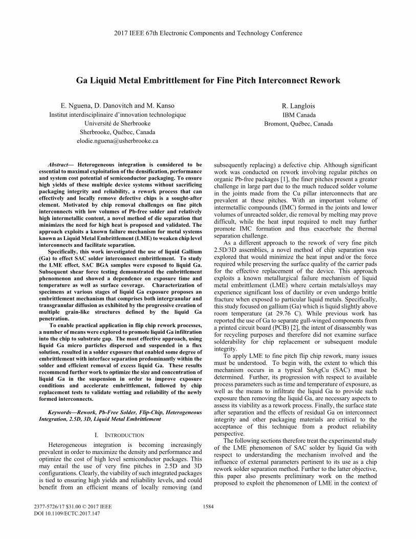
(96.5%Sn-3%Ag-0.5%Cu) balls of 300�m diameter connected onto the bottom side of a Ball Grid Array (BGA) assembly. This permitted a multitude of mechanism and parametric studies while minimizing the use of hardware. To investigate liquid Ga gap penetration and subsequent solder embrittlement, Controlled Collapse Chip Connection (C4) interconnects were studied using an assembly composed of a bottom laminate substrate of dimensions 31�31mm and 1.256mm thick and a top chip of dimensions 8.75�11.07mm and 780�m thick; the 2731 C4 joint’s comprised a Sn-Ag alloy (Sn-1.4%Ag) of about 110�m of diameter at a 150�m pitch connected to Cu pads on the laminate. Fig. 1 illustrates the assemblies.
1585
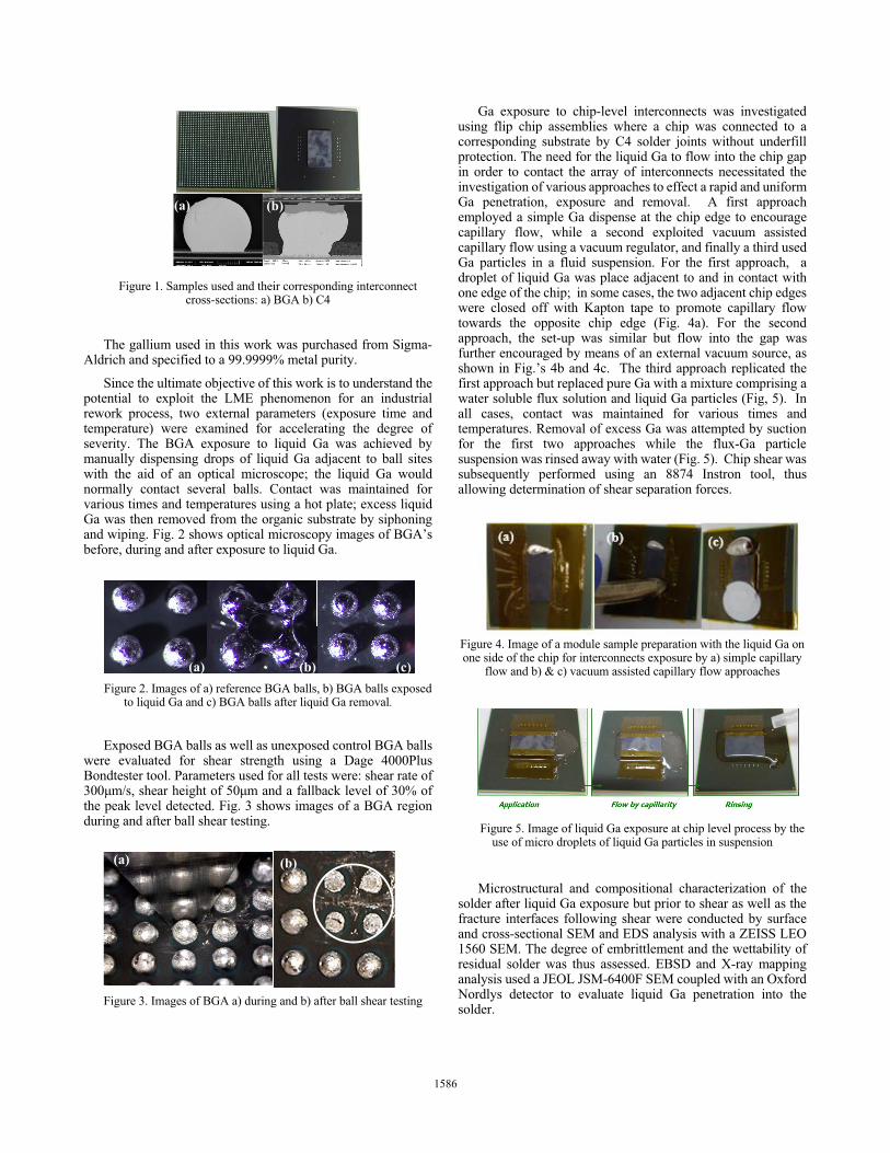
Figure 1. Samples used and their corresponding interconnect
cross-sections: a) BGA b) C4
The gallium used in this work was purchased from Sigma-Aldrich and specified to a 99.9999% metal purity.
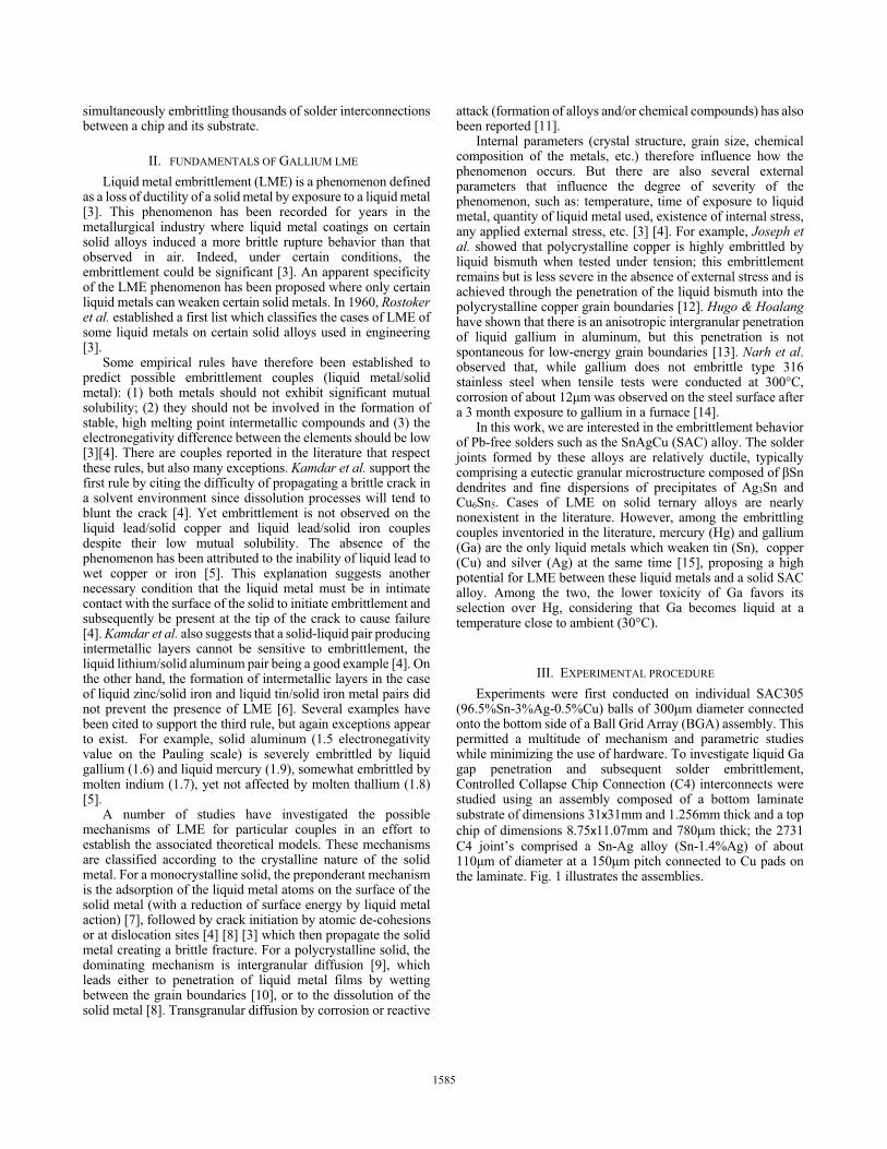
Since the ultimate objective of this work is to understand the potential to exploit the LME phenomenon for an industrial rework process, two external parameters (exposure time and temperature) were examined for accelerating the degree of severity. The BGA exposure to liquid Ga was achieved by manually dispensing drops of liquid Ga adjacent to ball sites with the aid of an optical microscope; the liquid Ga would normally contact several balls. Contact was maintained for various times and temperatures using a hot plate; excess liquid Ga was then removed from the organic substrate by siphoning and wiping. Fig. 2 shows optical microscopy images of BGA’s before, during and after exposure to liquid Ga.
Figure 2. Images of a) reference BGA balls, b) BGA balls exposed
to liquid Ga and c) BGA balls after liquid Ga removal.
Exposed BGA balls as well as unexposed control BGA balls were evaluated for shear strength using a Dage 4000Plus Bondtester tool. Parameters used for all tests were: shear rate of 300�m/s, shear height of 50�m and a fallback level of 30% of the peak level detected. Fig. 3 shows images of a BGA region during and after ball shear testing.
Figure 3. Images of BGA a) during and b) after ball shear testing
Ga exposure to chip-level interconnects was investigated using flip chip assemblies where a chip was connected to a corresponding substrate by C4 solder joints without underfill protection. The need for the liquid Ga to flow into the chip gap in order to contact the array of interconnects necessitated the investigation of various approaches to effect a rapid and uniform Ga penetration, exposure and removal. A first approach employed a simple Ga dispense at the chip edge to encourage capillary flow, while a second exploited vacuum assisted capillary flow using a vacuum regulator, and finally a third used Ga particles in a fluid suspension. For the first approach, a droplet of liquid Ga was place adjacent to and in contact with one edge of the chip; in some cases, the two adjacent chip edges were closed off with Kapton tape to promote capillary flow towards the opposite chip edge (Fig. 4a). For the second approach, the set-up was similar but flow into the gap was further encouraged by means of an external vacuum source, as shown in Fig.’s 4b and 4c. The third approach replicated the first approach but replaced pure Ga with a mixture comprising a water soluble flux solution and liquid Ga particles (Fig, 5). In all cases, contact was maintained for various times and temperatures. Removal of excess Ga was attempted by suction for the first two approaches while the flux-Ga particle suspension was rinsed away with water (Fig. 5). Chip shear was subsequently performed using an 8874 Instron tool, thus allowing determination of shear separation forces.
Figure 4. Image of a module sample preparation with the liquid Ga on one side of the chip for interconnects exposure by a) simple capillary
flow and b) & c) vacuum assisted capillary flow approaches
Figure 5. Image of liquid Ga exposure at chip level process by the
use of micro droplets of liquid Ga particles in suspension
Microstructural and compositional characterization of the solder after liquid Ga exposure but prior to shear as well as the fracture interfaces following shear were conducted by surface and cross-sectional SEM and EDS analysis with a ZEISS LEO 1560 SEM. The degree of embrittlement and the wettability of residual solder was thus assessed. EBSD and X-ray mapping analysis used a JEOL JSM-6400F SEM coupled with an Oxford Nordlys detector to evaluate liquid Ga penetration into the solder.
(a) (b)
(a)
(a) (b) (c)
(b)
1586
IV. RESULTS AND DISCUSION
A. Ga LME of SAC Solder Exposure of liquid Ga to individual SAC BGA balls was
used to establish proof of principle that an LME phenomenon can occur and to what degree. It can already be seen from Fig. 2c that there are changes on the solder surface directly after exposure to liquid Ga.
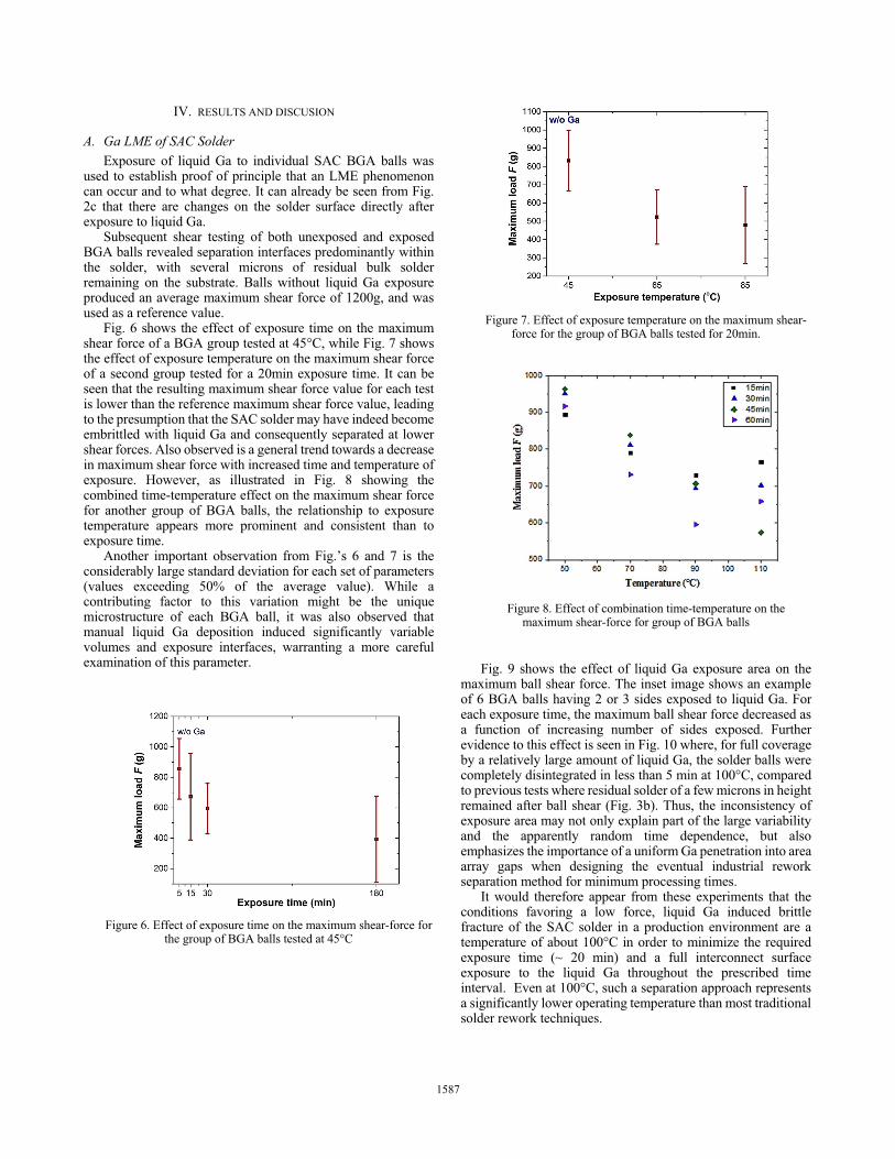
Subsequent shear testing of both unexposed and exposed BGA balls revealed separation interfaces predominantly within the solder, with several microns of residual bulk solder remaining on the substrate. Balls without liquid Ga exposure produced an average maximum shear force of 1200g, and was used as a reference value.
Fig. 6 shows the effect of exposure time on the maximum shear force of a BGA group tested at 45°C, while Fig. 7 shows the effect of exposure temperature on the maximum shear force of a second group tested for a 20min exposure time. It can be seen that the resulting maximum shear force value for each test is lower than the reference maximum shear force value, leading to the presumption that the SAC solder may have indeed become embrittled with liquid Ga and consequently separated at lower shear forces. Also observed is a general trend towards a decrease in maximum shear force with increased time and temperature of exposure. However, as illustrated in Fig. 8 showing the combined time-temperature effect on the maximum shear force for another group of BGA balls, the relationship to exposure temperature appears more prominent and consistent than to exposure time.
Another important observation from Fig.’s 6 and 7 is the considerably large standard deviation for each set of parameters (values exceeding 50% of the average value). While a contributing factor to this variation might be the unique microstructure of each BGA ball, it was also observed that manual liquid Ga deposition induced significantly variable volumes and exposure interfaces, warranting a more careful examination of this parameter.
Figure 6. Effect of exposure time on the maximum shear-force for
the group of BGA balls tested at 45°C
Figure 7. Effect of exposure temperature on the maximum shear-
force for the group of BGA balls tested for 20min.
Figure 8. Effect of combination time-temperature on the
maximum shear-force for group of BGA balls
Fig. 9 shows the effect of liquid Ga exposure area on the maximum ball shear force. The inset image shows an example of 6 BGA balls having 2 or 3 sides exposed to liquid Ga. For each exposure time, the maximum ball shear force decreased as a function of increasing number of sides exposed. Further evidence to this effect is seen in Fig. 10 where, for full coverage by a relatively large amount of liquid Ga, the solder balls were completely disintegrated in less than 5 min at 100°C, compared to previous tests where residual solder of a few microns in height remained after ball shear (Fig. 3b). Thus, the inconsistency of exposure area may not only explain part of the large variability and the apparently random time dependence, but also emphasizes the importance of a uniform Ga penetration into area array gaps when designing the eventual industrial rework separation method for minimum processing times.
It would therefore appear from these experiments that the conditions favoring a low force, liquid Ga induced brittle fracture of the SAC solder in a production environment are a temperature of about 100°C in order to minimize the required exposure time (~ 20 min) and a full interconnect surface exposure to the liquid Ga throughout the prescribed time interval. Even at 100°C, such a separation approach represents a significantly lower operating temperature than most traditional solder rework techniques.
1587

Figure 9. Effect of exposure time and quantity of liquid Ga used
on the maximum shear-force for group of BGA balls tested at 90°C
Figure 10. Images of a) BGA region exposed to a very large
amount of liquid Ga and b) BGA sites after liquid Ga removal with total disintegration of the solder after a few minutes
The occurrence of the LME mechanism is supported by analyses of the surface of the sheared balls. Fig. 11 shows SEM images coupled with EDS spectra on residual solder surfaces. The decrease in maximum shear force correlates to an increase in the presence of liquid Ga on the fracture interface surface. Further, the SEM images show different fracture modes in the solder, with brittle fracture regions seemingly correlating to regions of higher Ga presence as observed by EDS.
Figure 11. SEM pictures and EDS spectra on surfaces of sheared
BGA sites for BGA balls exposed to liquid Ga at 90°C for 60min with a) 3 sides exposed and b) 4 sides exposed
To further understand the manifestation of the liquid Ga LME phenomenon on SAC solders, cross-sectional analysis was conducted on BGA balls that were exposed to liquid Ga under conditions expected to vary the degree of embrittlement. Indeed, there appeared to be a correlation between favorable conditions for solder embrittlement and the degree of penetration of the liquid Ga into the solder, as illustrated in Fig. 12.
Figure 12. SEM cross-sectional pictures showing BGA
microstructure and corresponding X-ray mapping of Ga for BGA tested at a)70°C-45min, b)110°C-15min and c) 110°C-45min
Fig. 12 also shows that the largest microstructural change of the solder is attributed to the greater presence of Ga, to the point that the solder has the semblance of a fine grain structure that is atypical of BGA sized balls. This observation incited an EBSD analysis of the grain structure, as seen in Fig. 13 that demonstrates the evolutionary effect of liquid Ga penetration into the solder on its global microstructure and offers evidence towards the specific LME mechanism. The unexposed reference BGA ball (Fig. 13a) exhibits the more typical large grain microstructure. For a ball with some degree of exposure to liquid Ga (Fig. 13b), a large grain furthest removed from Ga exposure remains intact while the remainder of the solder appears drastically changed, suggesting that Ga atoms have penetrated through grain boundaries and into the grains themselves, leading to a microstructure resembling that of smaller grains. At conditions favoring strong embrittlement (Fig. 13c), the phenomenon appears to have evolved to the entirety of the solder structure including the solder ball-pad interface region.
(a)
(b)
(c)
(a) (b)
25�m
25�m
25�m
(a) (b)
1588

Figure 13. EBSD cross-section pictures showing BGA grain structure for a) BGA reference without exposure to liquid Ga, b) BGA tested at
70°C-15min and c) BGA tested at 110°C-15min
Based on these observations, a mechanism is proposed for
the liquid Ga embrittlement of SAC solder: atoms of liquid Ga are adsorbed onto the solder surface and preferentially affect the weakest atomic bonds that exist at the grain boundaries; as the Ga proceeds along these intergranular paths, the increased concentration of Ga at the grain boundaries incite adsorption and diffusion into the individual grains, most probably along dislocation or weak atomic bond paths, creating new grain boundaries defined by regions of high Ga concentration. As such, the mechanism combines both intergranular and transgranular diffusion.
B. Flow of liquid Ga into a flip chip gap The first approach, whereby liquid Ga was dispensed at the
chip edge to promote gap penetration and interconnect contact by capillary flow, quickly demonstrated limitations. Within the constraints of an ambient air working environment, the liquid Ga instantaneously forms a thin oxide (Ga2O3) of about 0.7 nm thick, allowing the liquid Ga to form stable non-equilibrium shapes [17]. Thus, the liquid Ga drop maintains its original shape and is discouraged from flowing freely into the gap between the chip and the substrate, as seen in Fig. 4a. Moreover, the very high surface tension (715mN/m [18]) of room temperature liquid Ga favors the formation of quasi-spherical shapes with high contact angles (>100°), that do not sufficiently wet most surfaces [19].
Attempts to modify the liquid Ga surface behavior did not improve its capillary action. The negligible effect of temperature (up to 150°C) was somewhat predictable, as surface tension is still high (704mN/m [18]) and the oxide layer is still present. The addition of a droplet of hydrochloric acid to the liquid Ga had
the effect of removing the Ga oxide layer and forming a GaCl3 compound at its surface, thus creating a perfectly spherical droplet of liquid Ga with minimized surface tension [17] [19], but free flow was still not achieved and can probably be attributed to the even higher contact angle of the spherical shape [19].
For the vacuum assisted approach, a minimum required vacuum pressure for breaking the oxide layer was assumed to be the pressure required to overcome the liquid metal-air interfacial forces and was calculated using Young’s-Laplace equation [16] to be >18kPa. Under these conditions, a limited liquid Ga penetration was achieved as illustrated in Fig. 14 showing two sheared chip sites after liquid Ga exposure of 110°C-60min and 130°C-60min. The maximum shear force values of 54Kg and 60Kg respectively (vs approximately 59Kg for unexposed chip) appear to correlate more to the limited extent of penetration than the exposure conditions. An option to use a porous adhesive at the open edge of the chip in order to maintain more liquid Ga in the gap during an extended suction was explored (Fig. 4c), but penetration remained incomplete. Another vacuum approach, whereby liquid Ga was dispensed around the majority of the chip followed by a relatively high (78kPa) vacuum pressure, was not successful in overcoming the surface resistance of the liquid Ga (Fig. 15).
SEM analysis of the sheared chip from Fig. 14a are shown in Fig. 16 and confirm attack of solder interconnects that were exposed to liquid Ga. As expected, the inhomogeneous penetration and resultant variation in solder surface exposure produced equally variable degrees of attack. These images highlight a further disadvantage of the vacuum assisted approach and perhaps any method using pure liquid Ga- the excess Ga, which most probably re-oxidized [20] during gap penetration, adhered to the substrate surface and could not be effectively cleaned from the chip site region by simple mechanical means, implying a need for additional mechanical and or chemical processing.
Figure 14. Sheared chip pictures after liquid Ga exposure of
a) 110°C-60min and b) 130°C-60min
Figure 15. Image of a module sample preparation with the liquid
Ga spread out in U-shape around the chip for interconnects exposure by post dispense vacuum approach.
(b) (a)
1589
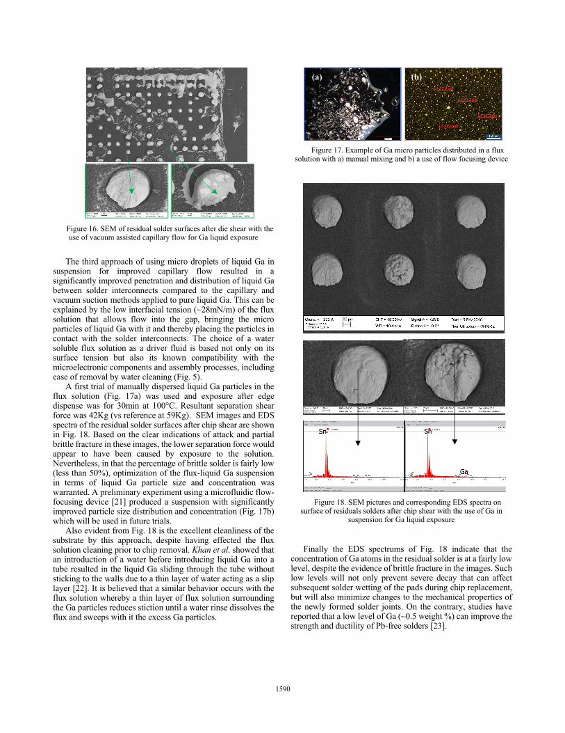
Figure 16. SEM of residual solder surfaces after die shear with the use of vacuum assisted capillary flow for Ga liquid exposure
The third approach of using micro droplets of liquid Ga in
suspension for improved capillary flow resulted in a significantly improved penetration and distribution of liquid Ga between solder interconnects compared to the capillary and vacuum suction methods applied to pure liquid Ga. This can be explained by the low interfacial tension (~28mN/m) of the flux solution that allows flow into the gap, bringing the micro particles of liquid Ga with it and thereby placing the particles in contact with the solder interconnects. The choice of a water soluble flux solution as a driver fluid is based not only on its surface tension but also its known compatibility with the microelectronic components and assembly processes, including ease of removal by water cleaning (Fig. 5).
A first trial of manually dispersed liquid Ga particles in the flux solution (Fig. 17a) was used and exposure after edge dispense was for 30min at 100°C. Resultant separation shear force was 42Kg (vs reference at 59Kg). SEM images and EDS spectra of the residual solder surfaces after chip shear are shown in Fig. 18. Based on the clear indications of attack and partial brittle fracture in these images, the lower separation force would appear to have been caused by exposure to the solution. Nevertheless, in that the percentage of brittle solder is fairly low (less than 50%), optimization of the flux-liquid Ga suspension in terms of liquid Ga particle size and concentration was warranted. A preliminary experiment using a microfluidic flow-focusing device [21] produced a suspension with significantly improved particle size distribution and concentration (Fig. 17b) which will be used in future trials.
Also evident from Fig. 18 is the excellent cleanliness of the substrate by this approach, despite having effected the flux solution cleaning prior to chip removal. Khan et al. showed that an introduction of a water before introducing liquid Ga into a tube resulted in the liquid Ga sliding through the tube without sticking to the walls due to a thin layer of water acting as a slip layer [22]. It is believed that a similar behavior occurs with the flux solution whereby a thin layer of flux solution surrounding the Ga particles reduces stiction until a water rinse dissolves the flux and sweeps with it the excess Ga particles.
Figure 17. Example of Ga micro particles distributed in a flux
solution with a) manual mixing and b) a use of flow focusing device
Figure 18. SEM pictures and corresponding EDS spectra on
surface of residuals solders after chip shear with the use of Ga in suspension for Ga liquid exposure
Finally the EDS spectrums of Fig. 18 indicate that the concentration of Ga atoms in the residual solder is at a fairly low level, despite the evidence of brittle fracture in the images. Such low levels will not only prevent severe decay that can affect subsequent solder wetting of the pads during chip replacement, but will also minimize changes to the mechanical properties of the newly formed solder joints. On the contrary, studies have reported that a low level of Ga (~0.5 weight %) can improve the strength and ductility of Pb-free solders [23].
(a) (b)
1590

V. CONCLUSION The principle of Liquid Metal Embrittlement (LME) was
exploited to effect a low temperature, low force separation of Pb-free interconnects to facilitate device removal in the rework process. Results show that SAC solder, when exposed to liquid Ga, becomes embrittled and can be separated at lower shear forces. Results also show that the degree of embrittlement tends to increase with increasing time & temperature of exposure as indicated by a progressive decrease in maximum shear-force.
Correlation has been demonstrated between brittle fracture surface and the degree of Ga penetration into the solder. Based on EBSD and X-ray mapping of solder exposed to conditions of progressive liquid Ga exposure, a mechanism has been proposed for Ga LME of SAC solder that involves both intergranular and transgranular diffusion.
A promising means to promote liquid Ga exposure to chip level interconnects resulted in separation interfaces within the solder, with low residual Ga and excellent cleanliness. Premised on these findings, it is proposed that flip chip packages whose interconnects comprise a region of unreacted SAC solder would be suitable for rework by a liquid Ga LME exposure process.
Future work will focus on optimization of Ga exposure to chip-level interconnects as well as effective, post-separation chip replacement and subsequent validation of package reliability. Interaction of liquid Ga with IMC compounds will also be investigated.
ACKNOWLEDGMENT The authors thank Edgar Tremblay, Serge Martel, Pierre
Beaulieu and Christian Bergeron for their participation, guidance and expertise in the characterization of the various samples. This work was funded by the NSERC-IBM Canada Industrial Research Chair in ‘Smarter Microelectronics Packaging for Performance Scaling’, as well as by Prompt Quebec and by Mitacs.
REFERENCES [1] Richard Langlois and Christian Bergeron, Chip rework on ceramic and
organic modules, 2016 IEEE 66th Electronic Components and Technology Conference
[2] Naoe Hosoda and Tadatomo Suga, A Novel Approach to Disassembly of Joined Interface, EcoDesign 2005: 4th International Symposium on Environmentally Conscious Design and
[3] Inverse Manufacturing [38] W. ROSTOKER, J. McCaughey, H. Markus, Embrittlement by liquid metals, Reinhold Publishing Corporation, New York, 1960, 162 p.
[4] M. H. Kamdar, Embrittlement by liquid metals, Progress in Materials Science 15, n� 4 (1973): 289 374.
[5] M. H. Kamdar, The Occurrence of Liquid-Metal Embrittlement, phys. stat. sol. (a) 4, 225 (1971)
[6] J. Carpio, J.A. Casado, J.A. Álvarez, et F. Gutiérrez-Solana. « Environmental factors in failure during structural steel hot-dip
galvanizing ». Engineering Failure Analysis 16, n° 2 (mars 2009): 585 595.
[7] Westwood, A. R. C. and R. M. Latanision (1979). Adsorption-induced embrittlement by liquid metals. Corrosion of liquid metal of the 1969 fall meeting of the metallurgical society of AIME, Philadelphia, Pennsylvania, Plenum Press.
[8] Joseph B., Picat M., Barbier F., Liquid metal embrittlement: a state-of-the-art appraisal, European Physical Journal 5, 19-31, 1999.
[9] S.P. Lynch, Metal Induced Embrittlement of Materials, Mater. Charact. 28 (1992): p. 279-289
[10] L. Klinger and E. Rabkin, Strains and stresses caused by penetrative wetting of grain boundaries by the liquid phase Scripta Materialia 62 918–923, 2010
[11] M.G. Nicholas, in Embrittlement by Liquid and Solid Metals, ed. M.H. Kamdar (Warrendale, PA: TMS-AIME, 1984), p. 27.
[12] B. Joseph, F. Barbier and M. Aucouturier, Embrittlement Of Copper By Liquid Bismuth, Scripta Materialia, Vol. 40, No. 8, pp. 893–897, 1999
[13] R.C. Hugo and R.G. Hoagland, In-Situ Tem Observation Of Aluminum Embrittlement By Liquid Gallium, Scripta Materialia, Vol. 38, No. 3, pp. 523–529, 1998
[14] K. A. NARH, V. P. DWIVEDI, J. M. GROW, A. STANA, W. -Y. SHIH, The effect of liquid gallium on the strengths of stainless steel and thermoplastics, Journal Of Materials Science 33 (1998) 329-337
[15] A. Shunk and W. R. Warke, Specificity as an aspect of liquid metal embrittlement, Scripta metall. Volume 8, Issue 5, pp. 519-526 (May 1974)
[16] Michael D. Dickey, Ryan C. Chiechi, Ryan J. Larsen, Emily A. Weiss, David A. Weitz and George M. Whitesides, Eutectic Gallium-Indium (EGaIn): A Liquid Metal Alloy for the Formation of Stable Structures in Microchannels at Room Temperature, Adv. Funct. Mater. 2008, 18, 1097–1104, DOI: 10.1002/adfm.200701216
[17] Michael D. Dickey, Emerging Applications of Liquid Metals Featuring Surface Oxides, ACS Appl. Mater. Interfaces 2014, 6, 18369�18379, dx.doi.org/10.1021/am5043017
[18] B. B. Alchagirov and A. G. Mozgovoi, The Surface Tension of Molten Gallium at High Temperatures, High Temperature. Vol. 43, No. 5, 2005, pp. 791–792.
[19] Daeyoung Kim, Peter Thissen, Gloria Viner, Dong-Weon Lee,�Wonjae Choi, Yves J. Chabal, and Jeong-Bong (J.B.) Lee, Recovery of Nonwetting Characteristics by Surface Modification of Gallium-Based Liquid Metal Droplets Using Hydrochloric Acid Vapor, ACS Appl. Mater. Interfaces 2013, 5, 179�185, dx.doi.org/10.1021/am302357t
[20] B. Kyle Doudrick, Shanliangzi Liu, Eva M. Mutunga, Kate L. Klein, Viraj Damle, Kripa K. Varanasi, and Konrad Rykaczewski, Different Shades of Oxide: From Nanoscale Wetting Mechanisms to Contact Printing of Gallium-Based Liquid Metals, Langmuir 2014, 30, 6867�6877, dx.doi.org/10.1021/la5012023
[21] Jacob Thelen, Michael D. Dickey and Thomas Ward, A study of the production and reversible stability of EGaIn liquid metal microspheres using flow focusing, Lab Chip, 2012, 12, 3961–3967, DOI: 10.1039/c2lc40492c
[22] Mohammad R. Khan, Chris Trlica, Ju-Hee So, Michael Valeri, and Michael D. Dickey, Influence of Water on the Interfacial Behavior of Gallium Liquid Metal Alloys, ACS Appl. Mater. Interfaces 2014, 6, 22467�22473, dx.doi.org/10.1021/am506496u
[23] Kang-I Chen and Kwang-Lung Linz, Effects of Gallium on Wettability, Microstructures and Mechanical Properties of the Sn-Zn-Ag-Ga and Sn-Zn-Ag-AI-Ga Solder Alloys, 2002 Int’l Symposium on Electronic Materials and Packaging
1591