fusb2805 — usb2.0 high-speed otg transceiver with ulpi ... · © 2008 fairchild semiconductor...
TRANSCRIPT
September 2013
© 2008 Fairchild Semiconductor Corporation www.fairchildsemi.com FUSB2805 • Rev. 1.0.3
FU
SB
28
05
— U
SB
2.0
Hig
h-S
pee
d O
TG
Tra
nsc
eiv
er w
ith U
LP
I Inte
rfac
e
FUSB2805 USB2.0 High-Speed OTG Transceiver with ULPI Interface
Features
Complies with USB 2.0, OTG Rev 1.3 Supplement, and ULPI Rev 1.1 Specifications
Supports 480 Mbps, 12 Mbps, and 1.5 Mbps USB2.0 Speeds
- Integrated Termination Resistors Meet USB2.0 Resistor ECN
- Integrated Serializer and Deserializer
- Insertion and Removal of Stuffed Bits as Appropriate
- USB Clock and Data Recovery to ±150ppm
Supports USB OTG Rev 1.3 Host Negotiation Protocol (HNP) and Session Request Protocol (SRP)
15 kV ESD, IEC 61000 Board Level, Air Gap
Applications
Set-Top Box Video Camera, MP3 Player
Cell Phone, Digital Still Camera, PDA
DVD Recorder, Scanner, Printer
Description
The FUSB2805 is a UTMI+ Low-Pin Interface (ULPI) USB2.0 OTG transceiver. It is compliant with the Universal Serial Bus Specification Rev 2.0 (USB2.0), the ULPI Specification Rev. 1.1, and the On-The-Go (OTG) supplement to USB2.0, Rev. 1.3.
The FUSB2805 is optimized to connect the USB2.0 host, peripheral, or OTG-controller to the USB connector via the ULPI link. Data can be transmitted and received at high speed (480 Mbps), full speed (12 Mbps), and low speed (1.5 Mbps) through a 12-bit (SDR) interface.
Related Resources
UTMI+ Low Pin Interface Specification (ULPI), Revision 1.1, October 20, 2004. http://www.ulpi.org
UTMI+ Specification, Revision 1.0, February 22, 2004. http://www.ulpi.org
For additional performance information, please contact [email protected].
Ordering Information
Part Number Top Mark Operating Temperature Range Package
FUSB2805MLX FUSB2805 -40 to +85°C 32-Terminal, Molded Leadless
Package (MLP), Quad, JEDEC MO-220

© 2008 Fairchild Semiconductor Corporation www.fairchildsemi.com FUSB2805 • Rev. 1.0.3 2
FU
SB
28
05
— U
SB
2.0
Hig
h-S
pee
d O
TG
Tra
nsc
eiv
er w
ith U
LP
I Inte
rfac
e
Block Diagram
ULP I
Interf ac e
Co ntro ller
Reg is ter
M ap
US B D ata
S erializer
US B D ata
D es erializer
US B 2.0 A TX
Term inatio n
Res is to rs
Freq uenc y
S elec tP LL
V o ltag e
Reg ulato r
P o wer-O n
Res et
G lo b al
Clo c ks
P O R
ID D etec to r
O TG M o d ule
E x ternal
V B US
& Fault
D etec tio n
Co ntro l
B lo c k
A nalo g
Ref erenc e
M o d ule
Clo c k
D 0-D 7
D IR
S TPNX T
CHIP _S E LE CT_N
CFG 1
CLK IN
V IO
V CC3V 3
V CC1V 2
V CC
0.1µF 4.7µF
0.1µF 4.7µF
D P
D M
ID
V B US
V R E F
Res et_N
FA ULT
RRE F
P S W
100k
IC (F lo at)
Tes t (F lo at)
40
0k
50
k
ID _P ULLUP
V D D 3 V 3
0.1µF
Figure 1. Functional Block Diagram
Pin Configuration
GNDExposed DiePad
1
2
3
4
5
6
7
8
D1
D0
VIO
DM
RREF
DP
VCC
ID
24
23
22
21
20
19
18
17
D2
CH
IP_
SE
LE
CT
_N
D3
VIO
CG
F1
CL
OC
K
D4
D5
32 31 252627282930
9 10 161514131211
D6
D7
NXT
STP
VIO
RESET_N
DIR
VDD1V2
VC
C
TE
ST
(FL
OA
T)
FA
ULT
VC
C3
V3
VB
US
PS
W
CL
IKIN
IC(F
LO
AT
)
Figure 2. Pin Assignments (Through View)

© 2008 Fairchild Semiconductor Corporation www.fairchildsemi.com FUSB2805 • Rev. 1.0.3 3
FU
SB
28
05
— U
SB
2.0
Hig
h-S
pee
d O
TG
Tra
nsc
eiv
er w
ith U
LP
I Inte
rfac
e
Pin Definitions
Symbol Type(1)
Description
Chip Select_N I Active LOW. HIGH – ULPI pin three-stated; LOW – ULPI operates normally. TTL compatible; CMOS input with hysteresis.
RREF AI/O Resistor reference. Connect through 12 k 1% to GND.
DM AI/O USB D- pin. USB mode: data minus (D-) pin of the USB cable.
DP AI/O USB D+ pin. USB mode: data plus (D+) pin of the USB cable.
FAULT I
FAULT is used to signal a VBUS over-current/over-voltage condition from an external SMPS or power management IC. The link must enable this function via the ExternalVbusFault register bit and the polarity must be set via the ExternalVbusActiveLow register bit.
ID I Identification (ID) pin of the micro-USB cable. TTL; if not used, connect to 3V3.
VCC P Input supply voltage or battery source.
PSW O Controls an external, active HIGH, VBUS power switch/charge pump and/or an SMPS
charger IC. An external 100 k pull-down resistor is required. Open source, slew-rate-controlled output; this pin is referenced to VCC3V3.
VBUS AI/O Should be connected to the VBUS pin of the USB cable. Leave open circuit if not used.
An internal 90 k ±11% pull-down resistor is present on this pin.
VCC3V3 P 3.3 V regulator output requiring capacitors. Internally powers OTG, analog core, and ATX.
CLKIN I Clock input; frequency depends on the CFG1 pin. This is a digital input buffer, not analog for a crystal.
I.C. I/O Internally connected; float pin.
TEST I/O Internally connected; float pin.
CFG1 I Configures the clock frequency; 0: input is 19.2 MHz. 1: input is 26 MHz.
VDD1V2 P 1.2 V regulator output requiring capacitors. Internally powers the digital core and analog core.
VIO P Input I/O supply rail; 0.1 µF capacitor connected to power input.
Reset_N I Connect to VIO when not used. Resets the transceiver; active LOW.
GND P Connect to ground.
DIR O ULPI direction output signal.
STP I ULPI stop input signal; CMOS input.
NXT O ULPI next output signal.
D7 I/O ULPI data pin 7; three-state output.
D6 I/O ULPI data pin 6; three-state output.
D5 I/O ULPI data pin 5; three-state output.
D4 I/O ULPI data pin 4; three-state output.
D3 I/O ULPI data pin 3; three-state output.
D2 I/O ULPI data pin 2; three-state output.
D1 I/O ULPI data pin 1; three-state output.
D0 I/O ULPI data pin 0; three-state output.
CLOCK O 60 MHz clock output when digital 19.2 MHz (or 26 MHz) clock is applied; Push-pull output.
Notes: 1. I=input; O=output; I/O=digital input/output; OD=open-drain output; AI/O=analog input/output; P=power or ground. 2. Per USB2.0, below a supply of 2.97 V, USB full-speed and low-speed transactions are not guaranteed; although
some devices may continue to function with the FUSB2805 at the lower supply rail.

© 2008 Fairchild Semiconductor Corporation www.fairchildsemi.com FUSB2805 • Rev. 1.0.3 4
FU
SB
28
05
— U
SB
2.0
Hig
h-S
pee
d O
TG
Tra
nsc
eiv
er w
ith U
LP
I Inte
rfac
e
Functional Description
ULPI Interface Controller
The FUSB2805 provides a 12-pin interface (SDR) compliant with the UTMI+ Low-Pin Interface (ULPI) specification, revision 1.1. This interface must be connected to the USB link controller.
The ULPI controller provides the following functions:
ULPI-compliant interface and register set
Full control of USB peripheral, host, and On-The-Go functionality
Prioritizes USB receive data, USB transmit data, interrupts, and register operations
Parses USB transmit and receive data
Controls the VBUS external source
VBUS monitoring, charging, and discharging
Low-power mode
6- and 3-pin serial modes
Generates RX CMDs (status updates)
Maskable interrupts
Control over the ULPI bus state
USB Serializer and Deserializer
The USB data serializer prepares data for transmitting onto the USB bus. To transmit data, the USB link controller sends a transmit command and data on the ULPI bus. The serializer performs parallel-to-serial conversion, bit stuffing, and Non Return to Zero, Invert (NRZI) encoding. For packets with a PID, the serializer adds a SYNC pattern to the start of the packet and an EOP pattern to the end of the packet. When the serializer is busy and cannot accept more data, the ULPI interface controller de-asserts NXT.
The USB data deserializer decodes data received from the USB bus. When data is received, the deserializer strips the SYNC and EOP patterns, if applicable, then performs serial-to-parallel conversion, NRZI decoding, and bit unstuffing on the data payload. The ULPI interface controller sends the data to the USB link controller by asserting DIR, then asserting NXT whenever a byte is ready. The deserializer also detects various receive errors, including bit-stuff errors, elasticity buffer under-run or over-run, and byte-alignment errors.
USB 2.0 ATX
The USB 2.0 ATX block is an analog front-end containing the circuitry needed for transmitting, receiving, and terminating the USB bus in high speed (HS), full speed (FS), and low speed (LS); for USB peripheral, host, and OTG implementations; per the USB2.0 specification and its relevant supplements. The following circuitry is included:
Differential drivers for transmitting data at HS, FS, and LS
Differential receiver and single-ended receivers for receiving data at HS, FS, and LS
Squelch circuit to detect HS bus activity
HS disconnect detector
45 HS bus terminations on DP and DM for peripheral and host mode
1.5 kΩ pull-up resistor on DP for FS for peripheral mode only (DM resistor pull up for LS peripheral is not supported since FUSB2805 is HS capable.)
15 kΩ bus terminations on DP and DM for host mode only
PLL and Clock Generation
The FUSB2805 has a built-in Phase Locked Loop (PLL) for clock generation.
The PLL takes the square wave clock (19.2 MHz or 26 MHz) from the CLKIN and multiplies or divides it into various frequencies for internal use.
From the clock source, the PLL produces the following frequencies:
60 MHz clock for the ULPI interface controller
1.5 MHz for low-speed USB data
12 MHz for full-speed USB data
480 MHz for high-speed USB data
Interface Protection
To prevent incorrect activity when the ULPI interface is not correctly driven by the link, such as when the link controller powers up slower than the FUSB2805, there is a weak pull-up resistor on the STP pin.
If the STP is unexpectedly HIGH at any time, the FUSB2805 protects the ULPI interface by enabling weak pull-down resistors on D[7:0].
This interface protection scheme can be disabled by setting the INTF_PROT_DIS bit to 1b (INTF_CNTRL[7]).

© 2008 Fairchild Semiconductor Corporation www.fairchildsemi.com FUSB2805 • Rev. 1.0.3 5
FU
SB
28
05
— U
SB
2.0
Hig
h-S
pee
d O
TG
Tra
nsc
eiv
er w
ith U
LP
I Inte
rfac
e
CLOCK
Chip_Select_N
STP
D[7:0]
NXT
3-State (input)
tPWRDN
3-State (input)
3-State (ignored)
3-State (ignored)
3-State (ignored)
DIR3-State
3-State
Figure 3. ULPI Behavior with Chip_Select_N as a Power-Down Control Signal
Power Down Using Chip_Select
When CHIP SELECT_N is de-asserted (HIGH), the FUSB2805 three-states the ULPI interface pins and powers down the internal circuitry. If CHIP SELECT_N is not used as a power-down control signal, it is tied to a LOW. Figure 3 shows the ULPI interface behavior when CHIP SELECT_N is asserted and subsequently de-asserted.
After the tPWRDN duration, the CLOCK output enters three-state and is ignored by the link.
Power-On Reset (POR)
The power supply for the internal regulators is VCC. This supply is fed into the 3.3 V and 1.2 V regulators. The output of the 3.3 V regulator is VCC3V3. The 1.2 V regulator generates VDD1V2.
During the power-up stage, the POR is held in a stable state to ensure that the digital logic does not operate the I/O or any analog circuit in such a way that may be damaging to the rest of the system.
The output of the POR block, PORB (internal signal), should be 1‟b0 during the power supply ramping period. Once the power supplies have completely ramped, PORB should be de-asserted. This signal is driven into the 19.2 / 26 MHz to 12 MHz PLL. The POR signal
(active HIGH reset) in the USB OTG PHY block must remain asserted for no less than 40 µs.
PORB de-assertion is determined via a comparator on VCC3V3 with a POR trigger threshold, VPOR, of 2.0 V.
Figure 4 illustrates how PORB should be pulsed based on the voltage level of VCC3V3. This diagram also shows what the POR should do to PORB when VCC3V3 drops below VPOR for any length of time.
When CLOCK starts toggling after power up, the USB link controller must issue a reset command over the ULPI bus to ensure correct operation.
PORB /
PLL
Reset
VCC3V3
VPOR
T0 T1
VCC3V3 = 3.3V T1 = T0 + 40µs
VPOR = 2.2V
T2 T3 T4
PHY POR
T4 = T3 + 40µs
Figure 4. Power-On Reset Sequence

© 2008 Fairchild Semiconductor Corporation www.fairchildsemi.com FUSB2805 • Rev. 1.0.3 6
FU
SB
28
05
— U
SB
2.0
Hig
h-S
pee
d O
TG
Tra
nsc
eiv
er w
ith U
LP
I Inte
rfac
e
OTG Module
The OTG module contains several sub-blocks that provide the functionality required by the USB On-The-Go Rev. 1.3 supplement. Specifically, it provides the following circuits:
ID detector to sense the ID pin of the micro-USB cable. The ID pin dictates which device is initially configured as the host and which is configured as the peripheral.
VBUS comparators to determine the VBUS voltage
level. This is required for Host Negotiation Protocol (HNP) and Session Request Protocol (SRP).
Resistors to temporarily charge and discharge
VBUS. This is required for SRP.
ID Detector
Detects which end of the mini-USB (or micro-USB) cable is plugged in. The ID detector must first be enabled by setting the ID_PULLUP register bit to 1b. If the FUSB2805 senses a value on ID different from the previously reported value, an RX CMD status update is sent to the USB link controller or an interrupt is asserted.
If the micro-B end of the cable is plugged in, the FUSB2805 reports that ID_GND is logic 1 and the USB link controller changes to peripheral mode.
If the micro-A end of the cable is plugged in, the FUSB2805 reports that ID_GND is logic 0 and the USB link controller changes to host mode.
The ID pin has a weak pull-up resistor (400kΩ) to avoid floating conditions. This resistor is connected when ID_PULLUP register bit is 0. If the application does not use the ID pin, tie this pin to VCC3V3.
VBUS Comparators The FUSB2805 provides three comparators for detecting the VBUS voltage level, as listed in Table 9 and Table 12. The comparators are as follows:
VBUS-Valid Comparator This comparator is used by an A-device (or host) to
determine whether or not the voltage on VBUS is at a
valid level for operation. The minimum threshold for
the VBUS valid comparator is 4.4 V. Any voltage on
VBUS below this threshold is considered a fault.
During power-up, the comparator output is ignored.
Session-Valid Comparator The session-valid comparator is a TTL-level input that
determines when VBUS is high enough for a session
to start. Both the A-device and the B-device use this comparator to detect when a session is being started. The A-device also uses this comparator to determine when a session is completed. The session valid threshold is between 0.8 V to 2.0 V.
Session-End Comparator
The session-end comparator determines when VBUS
is below the B-device session-end threshold of 0.2 V to 0.8 V. The B-device uses this threshold to determine when a session has ended.
SRP Charge and Discharge Resistors The FUSB2805 provides on-chip resistors for short-term
charging and discharging of VBUS. These are used by
the B-device to request a session, prompting the A-
device to restore VBUS power. First, the B-device
verifies that VBUS is fully discharged from the previous
session by setting the DISCHARGE_VBUS register bit to 1b and waiting for SESS_END to be 1b. Then the B-
device charges VBUS by setting the CHARGE_VBUS
register bit to 1b. The A-device detects that VBUS is
charged above the session-valid threshold and starts a
session by turning on VBUS power.
Analog Reference Module
The analog reference module provides stable internal voltage and current references for biasing internal analog circuitry. This module requires an accurate
external reference resistor. A value of 12 k 1% resistor is required between the RREF pin and GND.

© 2008 Fairchild Semiconductor Corporation www.fairchildsemi.com FUSB2805 • Rev. 1.0.3 7
FU
SB
28
05
— U
SB
2.0
Hig
h-S
pee
d O
TG
Tra
nsc
eiv
er w
ith U
LP
I Inte
rfac
e
Detailed Description of Pins
D0 to D7
D0 to D7 are bi-directional ULPI data bus pins. The USB link controller must drive D0-D7 LOW when the ULPI bus is idle (DIR is LOW). When the link has data to transmit to the FUSB2805, it drives a non-zero value.
The data bus can be re-configured to carry different data types. There are four modes of the data bus:
Synchronous mode: default is SDR mode(3)
, with the 8-bit data bytes being synchronous to the rising edge of CLOCK.
Low-power mode: carries asynchronous line state
and VBUS information.
3-pin serial mode: carries asynchronous 3-pin FS/LS serial signaling.
6-pin serial mode: carries asynchronous 6-pin FS/LS serial signaling.
Data pins can also be three-stated by driving chip_select_N HIGH.
Note: 3. DDR is not supported by the FUSB2805.
VIO
VIO is the input power pin that sets the I/O voltage level. VIO powers the on-chip pads of the following pins:
CLOCK DIR STP NXT D0-D7 RESET_N CFG1
RREF
Resistor reference analog I/O pin. A 12 k 1% resistor is required.
DP and DM
When in USB mode, the DP pin functions as USB data plus line; the DM pin functions as USB data minus line.
The DP and DM pins should be connected to the D+ and D- pins of the USB receptacle.
FAULT
This input pin is used by an external SMPS or power management IC to signal an over-current or over-voltage fault condition. This is applicable in OTG host where PSW is used to control driving VBUS or signaling for higher charging currents to an OTG SMPS management IC, as shown in Figure 5.
ID
For OTG implementation, the ID (identification) pin is connected to the ID pin of the mini-USB (or micro-USB) receptacle. As defined in the OTG specification, the ID pin dictates the initial role of the link controller. If ID is detected as HIGH, the link controller must assume the role of peripheral. If ID is detected as LOW, the link controller must assume the host role. Roles can be swapped later using Host Negotiation Protocol (HNP).
The FUSB2805 provides an internal pull-up resistor to sense the value of the ID pin. The pull-up resistor, with
a value of 50 k, must first be enabled by setting the ID_PULLUP register bit to 1b. If the value on ID has changed, the FUSB2805 sends an RX CMD or interrupt
to the link controller by time tID. If the link controller
does not receive any RX CMD or interrupt by tID, then the ID value has not changed.
To avoid a floating ID pin, a 400 k resistor pull-up is switched in when ID_PULLUP register bit is set to 0b.
5VUSB Trans
PSW
VBUS
Digital over-current protection scheme
with external power switch
VBUS
OTG Host
Supply
Source
Switch with
External
Over-
Current
Detector
FAULT
100k
Figure 5. Digital Over-Current Detection Scheme
© 2008 Fairchild Semiconductor Corporation www.fairchildsemi.com FUSB2805 • Rev. 1.0.3 8
FU
SB
28
05
— U
SB
2.0
Hig
h-S
pee
d O
TG
Tra
nsc
eiv
er w
ith U
LP
I Inte
rfac
e
VCC VCC is the main input supply voltage for FUSB2805. The FUSB2805 operates correctly when VCC is between 2.7 V and 4.5 V. The maximum transients that should be seen on VCC are 5.5V for a maximum of 5ms. A 100nF decoupling capacitor is preferred.
PSW This is an active-HIGH, open-source, power-switch analog output. This pin can be connected to an external
VBUS switch or an external charge pump enable circuit
to control the external VBUS power source. If the link
controller is in host mode, this can be set via the DRV_VBUS and DRV_VBUS_EXT bits in the OTG control register to logic 1. The FUSB2805 drives PSW to HIGH to enable the external VBUS supply. If the link controller detects an over-current condition
(VBUS_valid=0), it should disable the external VBUS supply
by setting DRV_VBUS_EXT to 0b. An external 100 k pull-down resistor is used.
In addition, the polarity of the signal that controls PSW can be changed via the INTF_CTRL register.
VBUS
This power I/O pin acts as input to the VBUS
comparators and over-current detector.
When the DRIVE_VBUS bit of the OTG control register
is set to 1b, an external VBUS source tries to drive VBUS
to a voltage of 4.4 V to 5.25 V with an output current capability of at least 8 mA.
VCC3V3 and VDD1V2
Regulator output voltages. These supplies are used to internally power digital and analog circuits.
CLKIN
Clock input pin; CLKIN is the digital clock input. The allowed frequencies on CLKIN are 19.2 MHz and 26 MHz. The frequency tolerance required by the clock is 50 ppm. The link controller requires a 60 MHz clock from the FUSB2805. This is generated from the PLL, which uses the CLKIN as the input clock.
19.2 MHz – CFG1 set to LOW 26 MHz – CFG1 set to HIGH
CHIP SELECT_N
Active LOW chip-select pin. When asserted HIGH; D[0-7], CLOCK, DIR, and NXT pins are three-stated and ignored and all internal circuits are powered down, including the regulator. When LOW, the FUSB2805 wakes up and the ULPI pins operate normally.
IR
Direction output pin. This pin is synchronous to the rising edge of CLOCK and controls the direction of the data bus. By default, the FUSB2805 holds DIR LOW, causing the data bus to be an input. When DIR is LOW, the FUSB2805 listens for data from the link controller. The FUSB2805 pulls DIR HIGH only when it has data to send to the link, which is for one of two reasons:
1. To send USB receive data, RX CMD status updates, and register-read data to the link controller.
2. To block the link controller from driving the data bus during power up, reset, and low-power mode (suspend).
The DIR pin can also be three-stated when Chip_Select_N is de-asserted HIGH .
STP
Stop input pin. This signal is synchronous to the rising edge of CLOCK. The link must assert STP to signal the end of a transmit packet or a register-write operation. When DIR is asserted, the link controller can optionally assert STP to abort the FUSB2805, causing it to de-assert DIR in the next clock cycle.
NXT
Next data output pin. This signal is synchronous to the rising edge of CLOCK. The FUSB2805 holds NXT LOW by default. When DIR is LOW and the link is sending data, NXT is asserted to tell the link to provide the next data byte. When DIR is HIGH and the FUSB2805 is sending data to the link, NXT is asserted to tell the link another valid byte is on the bus. NXT is not used for register read data or the RX CMD status update.
The NXT pin can also be three-stated when Chip_Select_N is de-asserted HIGH.
CLOCK
This is the 60MHz interface clock for synchronizing the ULPI bus. It is configured as an output. Being a 12-pin interface implementation, all the ULPI signals are synchronous to the rising edge of CLOCK. The FUSB2805 accepts a digital clock input and outputs the 60MHz to the link.
GND
The global ground signal acts as a ground to all circuits in the FUSB2805.
Reset_N
Reset_N is an active LOW reset signal with VIO voltage. Tie to VIO 1.8 V if not used. Typically tied to the power-on reset signal of the product.

© 2008 Fairchild Semiconductor Corporation www.fairchildsemi.com FUSB2805 • Rev. 1.0.3 9
FU
SB
28
05
— U
SB
2.0
Hig
h-S
pee
d O
TG
Tra
nsc
eiv
er w
ith U
LP
I Inte
rfac
e
Modes of Operation
ULPI Modes
The ULPI bus can be programmed to operate in four different modes and a power-down mode. Each mode re-configures the signals on the data bus. Setting more than one mode leads to undefined behavior.
Synchronous Mode
This is the default mode. On power-up and when CLOCK is stable, the FUSB2805 enters synchronous mode.
In synchronous mode, the link controller must synchronize all ULPI signals to CLOCK, meeting the setup and hold times defined in the Dynamic Characteristics tables.
This mode is used by the link controller to perform the following tasks:
Detect high-speed handshake (chirp)
Transmit and receive USB packets
Read and write to registers
Receive USB status updates (RX CMDs) from FUSB2805
Please refer to section 3.8 of the ULP Rev. 1.1 specification for further details.
Low-Power Mode
When the USB is idle, the link controller can place the FUSB2805 into low-power mode (also known as “suspend” mode). To enter low-power mode, the link controller clears the SUSPENDM bit in the function control (FUNC_CTRL) register to 0b.
During low-power mode, the FUSB2805 provides line state and interrupt information on the data bus for the link controller to monitor basic USB states and draws less than 200 µA from the VCC supply.
In addition, during low-power mode, the clock on CLKIN may be stopped; but it must be restarted before asserting STP to exit low-power mode.
Once in low-power mode, the FUSB2805 must remain in low-power mode for a minimum of 120 clock cycles (or 2 µs). After the 2 µs delay, low-power mode may be exited by asserting the STP signal. The FUSB2805 then issues an RXCMD to the link if a change was detected in any interrupt source and the change still exists. An RXCMD may not be sent if the interrupt condition is removed before exiting.
In low-power mode, the data bus assignments are changed to those described in Table 1.
Table 1. Signal Mapping on ULPI Bus During Low-Power Mode
Signal Maps To Direction Description
LINESTATE0 D0 Out Combinatorial LINESTATE0 directly driven by the analog receiver
LINESTATE1 D1 Out Combinatorial LINESTATE1 directly driven by the analog receiver
RESERVED D2 Out Reserved; the FUSB2805 drives this pin LOW
INT D3 Out Active-HIGH interrupt signal; asserted and latched whenever any unmasked interrupt occurs
RESERVED D[7:4] Out Reserved; the FUSB2805 drives these pins LOW
Entering Low-Power Mode
The link sets SuspendM=0b (in Function Control Register) to place the FUSB2805 into low-power mode. The CLOCK may be stopped a minimum of five (5) cycles after the FUSB2805 accepts the register write data as described in Figure 6. When entering low-power mode, the FUSB2805 asserts DIR
and holds NXT LOW. There is one cycle of data bus turnaround provided after the assertion of DIR, during which the value of D[7:0] is not valid. Upon completion of the turnaround cycle the FUSB2805 begins driving the signals as described in Table 1.

© 2008 Fairchild Semiconductor Corporation www.fairchildsemi.com FUSB2805 • Rev. 1.0.3 10
FU
SB
28
05
— U
SB
2.0
Hig
h-S
pee
d O
TG
Tra
nsc
eiv
er w
ith U
LP
I Inte
rfac
e
ULPI Signals
D [7:0]
STP
NXT
DIR
TXCMD
RegWr
SuspendM
DataTurn
Around
CLOCK
Low Power Mode Signals
tCS
tSTP1
Note: The second STP pulse indicates the exit of low-power (suspend) mode
Figure 6. Entering Low-Power Mode
Exiting Low-Power Mode
If the FUSB2805 has been in suspend at least 2 µs, the link may signal the FUSB2805 to exit low-power mode by asynchronously asserting STP. The FUSB2805 immediately starts to wake up its internal circuitry. Upon meeting the ULPI timing requirements the FUSB2805 then de-asserts DIR, ensuring a minimum of 5 cycles of CLOCK have been driven before de-asserting DIR and
setting SuspendM=1b (in Function Control Register). The link de-asserts STP in the cycle following the de-assertion of DIR. There is one cycle of data bus turnaround provided after the assertion of DIR, during which the value of D[7:0] is not valid. Upon completion of the turnaround cycle the FUSB2805 begins driving the signals as described in Table 1.
ULPI Signals
D [7:0]
STP
NXT
DIR
SuspendM
Turn
Around
PHY Output CLOCK
Synchronous Mode SignalsLow-Power Mode Signals
tWU
tCWUtCD
Figure 7. Exiting Low-Power Mode when FUSB2805 Provides Output CLOCK
6-Pin Full-Speed / Low-Speed Serial Mode
This mode of operation is provided for links that contain legacy FS/LS functionality and enables a cost-effective upgrade path to HS functionality.
To enter 6-pin serial mode, the link controller sets the 6PIN_FSLS_SERIAL bit in the interface control register to logic 1. To exit 6-pin serial mode, the link controller asserts STP.
An INT signal is also provided to inform the link of USB events. If the link requires CLOCK to be running during 6-pin serial mode, the CLK_SUSPENDM register bit must be set to logic 1b before entering 6-pin serial mode.
The FUSB2805 requires CLKIN to be kept running when in 6-pin mode. In 6-pin serial mode, the data bus assignments are changed to those described in Table 2. Examples of the signaling of data packets are shown in Figure 22.

© 2008 Fairchild Semiconductor Corporation www.fairchildsemi.com FUSB2805 • Rev. 1.0.3 11
FU
SB
28
05
— U
SB
2.0
Hig
h-S
pee
d O
TG
Tra
nsc
eiv
er w
ith U
LP
I Inte
rfac
e
Table 2. Signal Mapping on ULPI Bus During 6-Pin Serial Mode
Signal Maps To Direction Description
TX_ENABLE D0 In Active-HIGH transmit enable
TX_DATA D1 In Transmit the differential data on DP and DM
TX_SE0 D2 In Transmit single-ended zero (SE0) on DP and DM
INT D3 Out Active-HIGH interrupt signal; asserted and latched whenever any unmasked interrupt occurs
RX_DP D4 Out Single-ended receive data from DP
RX_DM D5 Out Single-ended receive data from DM
RX_RCV D6 Out Differential receive data from DP and DM
RESERVED D7 Out Reserved; the FUSB2805 drives this pin LOW
3-Pin FS/LS Serial Mode
This mode is provided for links that contain legacy FS/LS functionality and enables a cost-effective upgrade path to HS functionality.
To enter 3-pin serial mode, the link controller sets the 3PIN_FSLS_SERIAL bit in the interface control register to logic 1. To exit this mode, the link controller asserts STP.
An INT signal is also provided to inform the link of USB events. If the link requires CLOCK to be running during 3-pin serial mode, the CLK_SUSPENDM register bit must be set to logic 1b before entering 3-pin serial mode.
The FUSB2805 requires CLKIN to be kept running when in 3-pin mode. In 3-pin serial mode, the data bus assignments are changed to those described in Table 3. Examples of the signaling of data packets are shown in Figure 21.
Table 3. Signal Mapping on ULPI Bus During 3-Pin Serial Mode
Signal Maps To Direction Description
TX_ENABLE D0 In Active-HIGH transmit enable
DAT D1 I/O Transmit differential data on DP and DM when TX_ENABLE is HIGH Receive differential data from DP and DM when TX_ENABLE is LOW
SE0 D2 I/O Transmit single-ended zero on DP and DM when TX_ENABLE is HIGH Receive single-ended zero on DP and DM when TX_ENABLE is LOW
INT D3 Out Active-HIGH interrupt signal; asserted and latched whenever any unmasked interrupt occurs
RESERVED D[7:4] Out Reserved; the FUSB2805 drives this pin LOW
Power Supply Modes
The FUSB2805 supports two basic modes of supply operation and include the following:
Normal Mode
Power-Down Mode
Normal Mode This mode is entered when VCC and VIO are powered and Chip_Select_N is asserted.
Power-Down Mode
When chip select is inactive, FUSB2805 enters power-down mode, during which the following apply:
Chip_Select_N is HIGH or VIO is not present.
All internal circuits are powered down; total VCC current <36 µA.
D[0-7], CLOCK, NXT, and DIR are three-stated and ignored; STP is ignored.
Voltage regulators powering the OTG PHY are turned off.
Pull-down resistors on the ULPI interface are enabled to prevent a floating bus (VIO present).
The FUSB2805 is forced into a low-power state and ignores any ULPI commands, including wake-up events.
If VIO is not present, those signals referenced to VIO are also not powered.

© 2008 Fairchild Semiconductor Corporation www.fairchildsemi.com FUSB2805 • Rev. 1.0.3 12
FU
SB
28
05
— U
SB
2.0
Hig
h-S
pee
d O
TG
Tra
nsc
eiv
er w
ith U
LP
I Inte
rfac
e
USB State Transitions
A high-speed USB host or On-The-Go (OTG) device handles more than one electrical state, as defined in the USB and OTG specifications. The FUSB2805 accommodates the various states through the register
bit settings of XcvrSelect, TermSelect, OpMode[1:0], DpPulldown, and DmPulldown. Table 4 summarizes the operating states.
Table 4. Operating States and Corresponding Resistor Settings
Signaling Mode
Register Settings Internal Resistor Settings
XcvrS
ele
ct[
1:0
]
Term
Sele
ct
Op
Mo
de
[1:0
]
Dp
Pu
lld
ow
n
Dm
Pu
lld
ow
n
rpu
_d
p_en
rpu
_d
m_en
rpd
_d
p_en
rpd
_d
m_en
hste
rm_en
General Settings
Three-State Drivers XXb Xb 01b Xb Xb 0b 0b 0b 0b 0b
Power-up or VBUS < Vth (SESS_END) 01b 0b 00b 1b 1b 0b 0b 1b 1b 0b
Host Settings
Host Chirp 00b 0b 10b 1b 1b 0b 0b 1b 1b 1b
Host High Speed 00b 0b 00b 1b 1b 0b 0b 1b 1b 1b
Host Full Speed X1b 1b 00b 1b 1b 0b 0b 1b 1b 0b
Host HS/FS Suspend 01b 1b 00b 1b 1b 0b 0b 1b 1b 0b
Host HS/FS Resume 01b 1b 10b 1b 1b 0b 0b 1b 1b 0b
Host Low Speed 10b 1b 00b 1b 1b 0b 0b 1b 1b 0b
Host Low Speed Suspend 10b 1b 00b 1b 1b 0b 0b 1b 1b 0b
Host Low Speed Resume 10b 1b 10b 1b 1b 0b 0b 1b 1b 0b
Host Test_J/Test_K 00b 0b 10b 1b 1b 0b 0b 1b 1b 1b
Peripheral Settings
Peripheral Chirp 00b 1b 10b 0b 0b 1b 0b 0b 0b 0b
Peripheral High Speed 00b 0b 00b 0b 0b 0b 0b 0b 0b 1b
Peripheral Full Speed 01b 1b 00b 0b 0b 1b 0b 0b 0b 0b
Peripheral HS/FS Suspend 01b 1b 00b 0b 0b 1b 0b 0b 0b 0b
Peripheral HS/FS Resume 01b 1b 10b 0b 0b 1b 0b 0b 0b 0b
Peripheral Test_J/Test_K 00b 0b 10b 0b 0b 0b 0b 0b 0b 1b
OTG Device, Peripheral Chirp 00b 1b 10b 0b 1b 1b 0b 0b 1b 0b
OTG Device, Peripheral High Speed 00b 0b 00b 0b 1b 0b 0b 0b 1b 1b
OTG Device, Peripheral Full Speed 01b 1b 00b 0b 1b 1b 0b 0b 1b 0b
OTG Device, Peripheral HS/FS Suspend 01b 1b 00b 0b 1b 1b 0b 0b 1b 0b
OTG Device Peripheral, HS/FS Resume 01b 1b 10b 0b 1b 1b 0b 0b 1b 0b
OTG Device Peripheral, Test_J/Test_K 00b 0b 10b 0b 1b 0b 0b 0b 1b 1b
© 2008 Fairchild Semiconductor Corporation www.fairchildsemi.com FUSB2805 • Rev. 1.0.3 13
FU
SB
28
05
— U
SB
2.0
Hig
h-S
pee
d O
TG
Tra
nsc
eiv
er w
ith U
LP
I Inte
rfac
e
Protocol Description
ULPI References
The FUSB2805 provides a 12-pin (SDR) ULPI interface for communication with the link controller. It is strongly recommended that users of the FUSB2805 read the ULPI and UTMI+ specifications as listed below:
UTMI+ Low Pin Interface Specification (ULPI), Revision 1.1, October 20, 2004. http://www.ulpi.org
UTMI+ Specification, Revision 1.0, February 22, 2004. http://www.ulpi.org
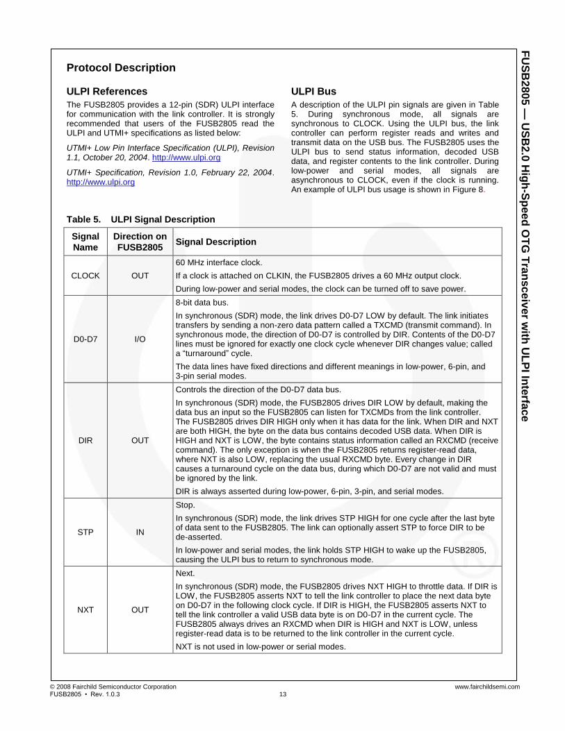
ULPI Bus
A description of the ULPI pin signals are given in Table 5. During synchronous mode, all signals are synchronous to CLOCK. Using the ULPI bus, the link controller can perform register reads and writes and transmit data on the USB bus. The FUSB2805 uses the ULPI bus to send status information, decoded USB data, and register contents to the link controller. During low-power and serial modes, all signals are asynchronous to CLOCK, even if the clock is running. An example of ULPI bus usage is shown in Figure 8.
Table 5. ULPI Signal Description
Signal
Name
Direction on
FUSB2805 Signal Description
CLOCK OUT
60 MHz interface clock.
If a clock is attached on CLKIN, the FUSB2805 drives a 60 MHz output clock.
During low-power and serial modes, the clock can be turned off to save power.
D0-D7 I/O
8-bit data bus.
In synchronous (SDR) mode, the link drives D0-D7 LOW by default. The link initiates transfers by sending a non-zero data pattern called a TXCMD (transmit command). In synchronous mode, the direction of D0-D7 is controlled by DIR. Contents of the D0-D7 lines must be ignored for exactly one clock cycle whenever DIR changes value; called a “turnaround” cycle.
The data lines have fixed directions and different meanings in low-power, 6-pin, and 3-pin serial modes.
DIR OUT
Controls the direction of the D0-D7 data bus.
In synchronous (SDR) mode, the FUSB2805 drives DIR LOW by default, making the data bus an input so the FUSB2805 can listen for TXCMDs from the link controller. The FUSB2805 drives DIR HIGH only when it has data for the link. When DIR and NXT are both HIGH, the byte on the data bus contains decoded USB data. When DIR is HIGH and NXT is LOW, the byte contains status information called an RXCMD (receive command). The only exception is when the FUSB2805 returns register-read data, where NXT is also LOW, replacing the usual RXCMD byte. Every change in DIR causes a turnaround cycle on the data bus, during which D0-D7 are not valid and must be ignored by the link.
DIR is always asserted during low-power, 6-pin, 3-pin, and serial modes.
STP IN
Stop.
In synchronous (SDR) mode, the link drives STP HIGH for one cycle after the last byte of data sent to the FUSB2805. The link can optionally assert STP to force DIR to be de-asserted.
In low-power and serial modes, the link holds STP HIGH to wake up the FUSB2805, causing the ULPI bus to return to synchronous mode.
NXT OUT
Next.
In synchronous (SDR) mode, the FUSB2805 drives NXT HIGH to throttle data. If DIR is LOW, the FUSB2805 asserts NXT to tell the link controller to place the next data byte on D0-D7 in the following clock cycle. If DIR is HIGH, the FUSB2805 asserts NXT to tell the link controller a valid USB data byte is on D0-D7 in the current cycle. The FUSB2805 always drives an RXCMD when DIR is HIGH and NXT is LOW, unless register-read data is to be returned to the link controller in the current cycle.
NXT is not used in low-power or serial modes.

© 2008 Fairchild Semiconductor Corporation www.fairchildsemi.com FUSB2805 • Rev. 1.0.3 14
FU
SB
28
05
— U
SB
2.0
Hig
h-S
pee
d O
TG
Tra
nsc
eiv
er w
ith U
LP
I Inte
rfac
e
Link sends
TXCMD
CLOCK
D0-D7
STP
DIR
NXT
DATARXCMDDATATXCMDTurn
around
Turn
around
FUSB2805
accepts
TXCMD
Link sends
next data.
FUSB2805
accepts
Link signals
end of data
ULPI bus
is idle
FUSB2805
asserts DIR,
causing
turnaround cycle
FUSB2805
sends
RXCMD
(NXT low)
FUSB2805
sends USB
data
(NXT high)
FUSB2805
de-asserts DIR,
causing
turnaround cycle
Figure 8. ULPI Generic Data Transmit Followed by Data Receive
On power-up, the FUSB2805 performs an internal power-on reset and asserts DIR to indicate to the link that the ULPI bus cannot be used. When the internal PLL is stable, the FUSB2805 de-asserts DIR. The power-up time depends on the VCC supply rise time and the PLL startup time (tstartPLL).
Whenever DIR is asserted, the FUSB2805 drives the NXT pin LOW and must drive the data bus (D0-D7) with RXCMD values. When DIR is de-asserted, the link must drive the data bus (D0-D7) to the default LOW. Before beginning USB packets, the FUSB2805 is reset by the link setting the RESET bit in the function control register. After the RESET bit is set, the FUSB2805 asserts DIR until the internal reset completes. The FUSB2805 automatically de-asserts DIR and clears the RESET bit when the reset has completed. After every reset, an RX CMD is sent to the link to update USB status information. After this sequence, the ULPI bus is ready for use and the link can start USB operations.
If Chip_Select_N is de-asserted, the FUSB2805 is retained in power-down mode, where all ULPI interface pins are three-state, internal regulators are shut down, and power consumption is reduced even further than in low-power mode.
If low-power mode is entered due to no VIO, the recommended power-up sequence for the link is:
1. Connect VCC and VIO supplies.
2. Chip_Select_N goes HIGH to LOW to enable the FUSB2805.
3. Link waits for at least tPWRUP, ignoring all ULPI pins‟ status.
4. The link may start to detect DIR status level; if the DIR is detected LOW, the link may send a reset command.
5. The ULPI interface is ready for use.

© 2008 Fairchild Semiconductor Corporation www.fairchildsemi.com FUSB2805 • Rev. 1.0.3 15
FU
SB
28
05
— U
SB
2.0
Hig
h-S
pee
d O
TG
Tra
nsc
eiv
er w
ith U
LP
I Inte
rfac
e
VCC
VIO
Chip_Select_N
Regulator Powerup
Internal PORB
CLKIN
Clock (output)
D[7:0]
NXT
Reset CommandClock Start
Internal clock stable
Internal reset
RXCMDUpdate
Powerup
Bus Idle
DIR
STP
TXCMD DATA
t1 t2 t3 t4 t5 t6
tPWRUP
tstartPLL
Figure 9. Power-up, Reset, and Bus Idle Sequence for ULPI Ready
Notes: 4. With the CLKIN stable, the FUSB2805 drives a 60 MHz clock out from the CLOCK pin when DIR de-asserts.
This is shown as “CLOCK (output)” above. 5. t1: VCC is applied to the FUSB2805. 6. t3: Chip_Select_N transitions to active state (LOW). FUSB2805 internal regulator turns on and the ULPI pins
become active (may be driven HIGH or LOW), but should be ignored during the power-up time tPWRUP. 7. t4: After the POR pulse (Power-On Reset), the ULPI pins are driven to a defined level. DIR is driven HIGH, then
the other ULPI pins are driven LOW. 8. t5: The PLL stabilizes after the PLL startup time, tstartPLL. The CLOCK pin begins to output 60 MHz, the DIR pin
transitions LOW, and the link must drive STP and D[7:0] to LOW (idle). The link then initiates a reset command to initialize the FUSB2805.
9. t6: The power-up sequence is completed and the ULPI bus interface is ready for use.
VBUS Power and Over-Current Detection
Driving 5 V on VBUS – External Only
No internal charge pump is supported by the
FUSB2805. The PSW pin supports an external VBUS
supply and is an active HIGH (open source) signal used to control external power management integrated circuits, such as OTG support SMPS devices.
Over-Current Detection
Only external over-current detection is supported by the FUSB2805. An over-current detection circuit is required for host applications that supply more than 100 mA on
VBUS between voltages of 4.75 V to 5.25 V.
A digital signal from this external circuit must be connected to the FAULT pin, which directly controls the PSW pin (as shown in Figure 5). The polarity of the signal input to this pin, which controls PSW, is selectable.

© 2008 Fairchild Semiconductor Corporation www.fairchildsemi.com FUSB2805 • Rev. 1.0.3 16
FU
SB
28
05
— U
SB
2.0
Hig
h-S
pee
d O
TG
Tra
nsc
eiv
er w
ith U
LP
I Inte
rfac
e
USB Packet Transmit and Receive
When transmitting and receiving USB packets, there are limits set on the link and PHY processing time to ensure that USB inter-packet delays are also met.
These times are determined by the USB event and the packet format (i.e. transmit with PID or NOPID, transmit error, receive error, etc.).
Link sends
TXCMD
CLOCK
D0-D7
STP
DIR
NXT
DATARXCMDDATATXCMDturn
around
turn
around
FUSB2500
accepts
TXCMD
Link sends
next data.
FUSB2500
accepts.
Link signals
end of data
ULPI bus is
idle
FUSB2500
asserts DIR,
causing
turnaround cycle
FUSB2500
sends
RXCMD
(NXT low)
FUSB2500
sends USB
data
(NXT high)
FUSB2500
de-asserts DIR,
causing
turnaround cycle
Figure 10. Example ULPI Packet Transmit and Receive
Note: 10. Please refer to ULPI specifications section 3.8.2 for further detail on USB packet operations and functionality.

© 2008 Fairchild Semiconductor Corporation www.fairchildsemi.com FUSB2805 • Rev. 1.0.3 17
FU
SB
28
05
— U
SB
2.0
Hig
h-S
pee
d O
TG
Tra
nsc
eiv
er w
ith U
LP
I Inte
rfac
e
USB Packet Timing
The USB2.0 specification defines the inter-packet timing and the UTMI/UTMI+ specifications define synchronization and processing delays. The ULPI Rev. 1.1 specification defines the inter-packet delays to ensure compatibility with USB2.0 and supplemental specifications.
Pipeline Delays Table 6 describes the delays (in clock cycles) with which to comply using ULPI. The USB bus events are measured relative to D+ and D-. The ULPI timings are relative to the clock edge on which the transition is detected (i.e. the clock edge on which STP is detected).
Table 6. Pipeline Delays
Parameter Name HS PHY
Delay
FS PHY
Delay
LS PHY
Delay Definition
RXCMD Delay(J/K) 4 4 4
Number of clocks after a change in the internal USB bus state is detected to an RXCMD byte being sent over the ULPI bus. Applies to all changes except SE0.
RXCMD Delay(SE0) 4 4 to 6 16 to 18 Number of clocks between the USB bus state indicating SE0 to an RXCMD byte being sent over the ULPI bus. Delay is increased due to filtering.
TX Start Delay 1 to 2 6 to 10 74 to 75 Number of clocks between the FUSB2805 detecting a TXCMD on the ULPI bus to transmitting the first K of the SYNC pattern on the USB bus.
TX End Delay (packets) 2 to 5 NA NA
Number of clocks between the FUSB2805 detecting STP on the ULPI bus to completing EOP transmission on the USB bus.
HS EOP is completed when all eight consecutive ones have finished transmitting on the USB bus.
FS/LS packets finish many clock cycles after STP is asserted. The link must look for RXCMD bytes indicating SE0-to-J transition to determine when the transmission is completed on the USB bus.
TX End Delay (SOF) 6 to 9 NA NA
HS SOF packets have a long EOP. The link must wait at least nine clocks or for an RXCMD, indicating squelch (LINESTATE=00b), before transmitting the next packet.
RX Start Delay 3 to 8 NA NA
Number of clocks after first K of SYNC pattern is seen on the USB bus to the simultaneous assertion of DIR and NXT or an RXCMD indicating RxActive. Used for HS packets only.
For FS/LS packets, the link must look for RXCMD bytes indicating J-to-K transition.
RX End Delay 3 to 8 17 to 18 122 to 123
Number of clocks after EOP occurs on the USB bus to the FUSB2805 de-asserting DIR or indicating RxActive LOW in an RXCMD byte.
HS EOP is completed when all eight consecutive ones have finished transmitting on the USB bus.
FS/LS EOP occurs when SE0 starts on the USB bus. For FS/LS, the link uses LINESTATE and not RxEnd delay to time USB packets.
Note: 11. Please refer to ULPI Rev 1.1 specifications, section 3.8.2.6.2 for details on PHY pipeline delays.

© 2008 Fairchild Semiconductor Corporation www.fairchildsemi.com FUSB2805 • Rev. 1.0.3 18
FU
SB
28
05
— U
SB
2.0
Hig
h-S
pee
d O
TG
Tra
nsc
eiv
er w
ith U
LP
I Inte
rfac
e
Link Decision TimesThe amount of clock cycles allocated to the link to respond to a received packet and correctly receive back-to-back packets is given in Table 7.
Table 7. Link Decision Times
Parameter Name HS PHY
Delay
FS PHY
Delay
LS PHY
Delay Definition
Transmit-Transmit (Host Only)
15 to 24 7 to 18 77 to 247
Number of clocks a host link must wait before driving the TXCMD for the second packet.
In HS, the link starts counting from the assertion of STP for the first packet.
In FS, the link starts counting from the RXCMD indicating LINESTATE has transitioned from SE0-to-J for the first packet. The timings given ensure inter-packet delays of 2.0 to 6.5 bit times.
Receive-Transmit (Host or Peripheral)
1 to 14 7 to 18 16 to 18
Number of clocks the link must wait before driving the TXCMD for the transmit packet.
In HS, the link starts counting from the end of the receive packet (de-assertion of DIR or an RXCMD indicating RxActive is LOW).
In FS/LS, the link starts counting from the RXCMD indicating LINESTATE has transitioned from SE0-to-J for the receive packet. The timings given ensure inter-packet delays of 2.0 to 6.5 bit times.
Receive-Receive (Peripheral Only)
1 1 1 Minimum number of clocks between consecutive receive packets. The link must be capable of receiving both packets.
Transmit-Receive (Host or Peripheral)
92 80 718 Host or peripheral transmits a packet, then times out after this number of clock cycles if a response is not received. Any subsequent transmission can occur after this time.
CLOCK
D0-D7
STP
DIR
NXT
D0TXCMDDN-1
DATA
turn
aroundD1
RX End Delay
( 3 to 8 clocks)
DN-4 DN-3 DN-2 DN
EOPDP or
DMIDLE SYNC
Link Decision Time (1 to 14 clocks)TX Start Delay
(1 to 2 clocks)
USB Inter Packet Delay (8 to 192 HS bit times)
Figure 11. HS Receive to Transmit Packet Timing, Example 1

© 2008 Fairchild Semiconductor Corporation www.fairchildsemi.com FUSB2805 • Rev. 1.0.3 19
FU
SB
28
05
— U
SB
2.0
Hig
h-S
pee
d O
TG
Tra
nsc
eiv
er w
ith U
LP
I Inte
rfac
e
CLOCK
D0-D7
STP
DIR
NXT
D0TXCMD
DATA
D1
TX End Delay ( 2 to 5 clocks)
DN-1 DN
EOPDP or
DMIDLE SYNC
Link Decision Time (15 to 24 clocks)TX Start Delay
(1 to 2 clocks)
USB Inter Packet Delay (88 to 192 HS bit times)
Figure 12. HS Transmit to Transmit Packet Timing, Example 2
Preamble Preamble packets are headers to low-speed packets that must travel over a FS bus between a host and a hub. To enter preamble mode, the link sets XCVRSELECT[1:0]=11b in the FUNC_CTRL register and, when in this mode (Preamble), the FUSB2805 operates just as in FS mode and sends all the data with the FS rise and fall time characteristics. Whenever the link transmits a USB packet in preamble mode, the FUSB2805 automatically sends a preamble header at
the FS bit rate before sending the packet at low-speed bit rate. The FUSB2805 ensures a minimum gap of four FS bit times between the last bit of the FS PRE_PID and the first bit of the LS SYNC. The FUSB2805 drives a J-state for at least one FS bit time after sending the PRE-PID, after which the resistor can hold the J-state on the bus. In preamble mode, the FUSB2805 can also receive LS packets from the FS bus. Figure 13 shows an example preamble packet.
CLOCK
D0-D7
STP
DIR
NXT
D0TXCMD (LS PID) D1
LS D1DP or
DMLS D0LS PID
LS
SYNC
IDLE(4 FS bits
min)
FS
PRE_ID
FS
SYNC
Figure 13. Preamble Sequence

© 2008 Fairchild Semiconductor Corporation www.fairchildsemi.com FUSB2805 • Rev. 1.0.3 20
FU
SB
28
05
— U
SB
2.0
Hig
h-S
pee
d O
TG
Tra
nsc
eiv
er w
ith U
LP
I Inte
rfac
e
RXCMD and TXCMD
ULPI modifies the original UTMI data stream such that it can fit more data types. Redundancy in the PID byte during transmit is overloaded with ULPI transmit commands (TXCMD). Unused data bytes in the receive stream are overloaded with receive commands (RXCMD). ULPI defines a transmit command byte that is sent by the link and a receive command byte that is sent by the FUSB2805.
Transmit Command (TXCMD)
The link initiates transfers to the FUSB2805 by sending the transmit command (TXCMD) byte, as described in Table 8. TXCMD is comprised of a 2-bit command code and a 6-bit payload.
Table 8. Transmit Commands (TXCMD) from Link to FUSB2805
Command Type
Descriptor
Command
Code [7:6]
Command
Payload [5:0] Description
IDLE 00b
00 0000b (NOOP) No operation. 00h is the idle state of the ULPI bus. The link drives NOOP by default.
XX XXXXb Reserved command space. Values other than those above create undefined behavior.
TRANSMIT 01b
00 0000b (NOPID)
Transmit USB data that does not have a PID (packet ID), such as chirp, and resume signaling. The FUSB2805 starts transmitting on the USB beginning with the next data byte.
00 XXXXb (PID) Transmit USB packet. D[3:0] indicates USB packet identifier PID[3:0].
XX XXXXb (RSVD)
Reserved command space. Values other than those above create undefined behavior.
REGISTER WRITE 10b
10 1111b (EXTW) Extended register write command (optional). The 8-bit address must be in the next clock cycle after the command is accepted.
XX XXXXb (REGW)
Register write command with 6-bit immediate address.
REGISTER READ 11b
10 1111b (EXTR) Extended register read command (optional). The 8-bit address must be provided in the next clock cycle after the command is accepted.
XX XXXXb (REGR)
Register read command with 6-bit immediate address.

© 2008 Fairchild Semiconductor Corporation www.fairchildsemi.com FUSB2805 • Rev. 1.0.3 21
FU
SB
28
05
— U
SB
2.0
Hig
h-S
pee
d O
TG
Tra
nsc
eiv
er w
ith U
LP
I Inte
rfac
e
Receive Command (RXCMD)
The FUSB2805, after asserting DIR, uses the receive command (RXCMD) byte to update the link on line state, USB receive, disconnect, and OTG information via the ULPI data bus.
The FUSB2805 automatically sends an RXCMD whenever there is a change in any of the RXCMD data fields. The link must be able to accept an RXCMD at any time; including single or multiple (back-to-back) RXCMDs and, at any time during USB receive packets, when NXT is LOW.
Table 9. RXCMD Data Byte Format
DATA[7:0] Status Name Description
[1:0] LINESTATE
Line State Signals:
D[0]: LINESTATE0
D[1]: LINESTATE1
LINESTATE[1:0] reflects the current status of DP and DM and is a function of various register settings and whether the device is a host or peripheral. The detailed encoding, and descriptions thereof, is shown in Table 10 and Table 11.
[3:2] VBUS State
Encoded VBUS Voltage State: This encoding is used for over-current detection, session start, and session request (SRP). The Sess_End and Sess_VLD indicators are signals from the internal FUSB2805 VBUS comparators. These encoded VBUS states are:
Value VBUS Voltage Sess_End Sess_VLD A_VBUS_VLD
00b VBUS < VB_Sess_End 1 0 0
01b VB_Sess_End ≤ VBUS <
VA_Sess_Vld 0 0 0
10b VA_Sess_Vld ≤ VBUS <
VA_VBUS_Vld X 1 0
11b VBUS ≥ VA_VBUS_VLD X X 1
[5:4] RxEvent
RxEvent Encoding: This encoding field of RXCMD is used to inform the link of information packets received on the USB bus. These events are:
Value RxError RxActive HostDisconnect
00b 0 0 0
01b 0 1 0
10b X X 1
11b 1 1 0
[6] ID This bit reflects the state of the ID pin. It is valid 50ms after ID_PULLUP is set to 1b.
[7] ALT_INT
Default is not to use this alternate interrupt bit. The link, optionally, can enable the BVALID_RISE and/or BVALID_FALL bits in the PWR_CNTRL register. Corresponding changes in BVALID cause an RXCMD to be sent to the link with this ALT_INT bit asserted.

© 2008 Fairchild Semiconductor Corporation www.fairchildsemi.com FUSB2805 • Rev. 1.0.3 22
FU
SB
28
05
— U
SB
2.0
Hig
h-S
pee
d O
TG
Tra
nsc
eiv
er w
ith U
LP
I Inte
rfac
e
Line State Encoding
As mentioned in Table 9, the LINESTATE[1:0] sent to the link is a function of whether the port is upstream (peripheral) or downstream (host) facing. Dual-role OTG devices must select the correct LINESTATE encoding,
depending upon its mode. Note that the configuration as a LS peripheral (upstream facing port), with DM pull-up, is not supported by the FUSB2805.
Table 10. LINESTATE[1:0] Encoding for Upstream (Peripheral) Facing Ports; DP_PULLDOWN=0b
Mode Value Full Speed High Speed Chirp
XCVRSELECT[0:1] 01, 11 00 00
TERMSELECT 1 0 1
LINESTATE[1:0]
00b SE0 Squelch Squelch
01b FS-J ! Squelch (! Squelch) AND (HS_Differential_Receiver_Output)
10b FS-K Invalid (! Squelch) AND (! HS_Differential_Receiver_Output)
11 SE1 Invalid Invalid
Notes: 12. (! Squelch) indicates inactive squelch. 13. (! HS_Differential_Receiver_Output) indicates inactive HS_Differential_Receiver_Output.
Table 11. LINESTATE[1:0] Encoding for Downstream (Host) Facing Ports; DP_PULLDOWN and
DM_PULLDOWN=1b
Mode Value Low Speed Full Speed High Speed Chirp
XCVRSELECT[0:1] 10 01, 11 00 00
TERMSELECT 1 1 0 0
OPMODE[1:0] X X 00, 01 or 11 10
LINESTATE[1:0]
00b SE0 SE0 Squelch Squelch
01b LS-K FS-J ! Squelch (! Squelch) AND (HS_Differential_Receiver_Output)
10b LS-J FS-K Invalid (! Squelch) AND (! HS_Differential_Receiver_Output)
11 SE1 SE1 Invalid invalid
Notes: 14. (! Squelch) indicates inactive squelch. 15. (! HS_Differential_Receiver_Output) indicates inactive HS_Differential_Receiver_Output.

© 2008 Fairchild Semiconductor Corporation www.fairchildsemi.com FUSB2805 • Rev. 1.0.3 23
FU
SB
28
05
— U
SB
2.0
Hig
h-S
pee
d O
TG
Tra
nsc
eiv
er w
ith U
LP
I Inte
rfac
e
VBUS Voltage State Encoding
As mentioned in Table 9, changes in the VBUS state encoding initiate an RXCMD to the link. For the link to receive VBUS state updates, the link must first enable the corresponding interrupts in the USB_INTR_EN_R and USB_INTR_EN_F registers. Link uses the indicator signals to take action based on typical configurations (host, peripheral, OTG device). Table 12 shows the VBUS indicators in RXCMD based on the configuration.
Table 12. VBUS Indicator Signals in RXCMD
Configuration A_VBUS_
VLD
SESS_
VLD
SESS_
END
Standard Host Yes No No
Standard Peripheral
No Yes No
OTG A-Device Yes Yes No
OTG B-Device No Yes Yes
For the standard USB host controller application, the following applies:
The system must be able to provide 500 mA for 4.75 V ≤ VBUS ≤ 5.25 V.
An external circuit is to be used to detect over-current conditions. If the external over-current detector provides a digital fault signal, the signal must be connected to the FAULT input pin and the link must do the following:
1. Set the IND_COMPL bit in the INTF_CTRL register to 0b or 1b, depending on the polarity of the external fault signal.
2. Set the USE_EXT_VBUS_IND bit in the OTG_CTRL register to 1b.
3. If it is not necessary to qualify the fault indicator with the internal A_VBUS_VLD comparator, set the IND_PASSTHRU bit in the INTF_CTRL register to 1b.
For the standard USB peripheral controller applications, the standard peripherals detect when VBUS is at a sufficient level for operation. SESS_VLD must be enabled to detect the start and end of a USB peripheral operation. Detection of the A_VBUS_VLD and SESS_END thresholds is not needed for standard peripherals.
For a device configured as an OTG B-device, SESS_VLD must be used to detect when VBUS is at a sufficient level for operation. SESS_END must be used to detect when VBUS has dropped to a LOW level, allowing the B-device to safely initiate VBUS pulsing SRP.
A device configured as an OTG A-device must provide a minimum of 8 mA onto VBUS. This 8 mA (minimum) is
provided external to the FUSB2805. If the external charge pump source provides more than 100 mA, the over-current circuit must be used and the host controller application criteria apply. The OTG A-device also uses SESS_VLD to detect when an OTG B-device is initiating VBUS pulsing SRP. The control of this external charge pump is accomplished via the PSW pin.
RxEvent Encoding
As mentioned in Table 9, this encoding provides information to the link related to the packets received on the USB bus. The primary encodings are RxActive, RxError, and HostDisconnect.
RxActive When the FUSB2805 detects a SYNC pattern on the USB bus, it signals an RxActive event to the link. This RxActive event can be communicated in two methods:
FUSB2805 simultaneously asserts DIR and NXT; or
FUSB2805 sends an RXCMD to the link with the RxActive field in the RxEvent bits set to 1b.
The link must be capable of detecting both methods and the RxActive frames the receive packet from the first byte to the last byte. It also must assume that RxActive is set to 0b when indicated in an RXCMD or when DIR is de-asserted, whichever occurs first.
The RxActive is also used by the link to time the high-speed packets and ensure that the bus turn-around times are met.
RxError When the FUSB2805 detects an error while receiving a USB packet, it de-asserts NXT and sends an RXCMD with the RxError field set to 1b. The received packet is no longer valid and must be dropped by the link.
HostDisconnect This encoding is only valid when the FUSB2805 is configured as a host (DP_PULLDOWN= DM_PULLDOWN=1b) and indicates to the host controller when a peripheral is connected (0b) or disconnected (1b). The host controller must enable HostDisconnect by setting the HOST_DISCON_R and HOST_DISC_F bits in the USB_INTR_EN_R and USB_INTR_EN_F registers, respectively. Changes in HostDisconnect cause the FUSB2805 to send an RXCMD to the link with the updated value.
In peripheral mode, HostDisconnect must be ignored and must not mask events on RxActive or RxError.
Refer to ULPI specifications, section 3.8.1 for details on RXCMD and TXCMD operations and functionality.

© 2008 Fairchild Semiconductor Corporation www.fairchildsemi.com FUSB2805 • Rev. 1.0.3 24
FU
SB
28
05
— U
SB
2.0
Hig
h-S
pee
d O
TG
Tra
nsc
eiv
er w
ith U
LP
I Inte
rfac
e
Register Read and Write Operations
The link can read or write register bytes, and set or clear register bits as needed, using the TXCMD byte. The FUSB2805 supports immediate and extended addressing register operations, with the extended register addressing being optional for the link. If the FUSB2805 asserts DIR during an operation, the register operation is aborted. When a register operation is aborted, the link must retry until successful.
Immediate Register Read and Write
Immediate address registers are accessed by first sending the TXCMD byte as either a RegRead or RegWrite command with the required register address.
For RegRead, the link sends its read command request and waits for NXT to assert. In the cycle after NXT asserts, the FUSB2805 asserts DIR to gain control of the bus. In the cycle after DIR asserts, the FUSB2805 must return the register read data. The FUSB2805 does not assert NXT when DIR is asserted during the register read operation, including during the period that the register read data is being returned, to ensure that a USB receive event always overrides the register read during any cycle (see section 3.8.3.2 of ULPI Rev. 1.1 specification). If the FUSB2805 aborts the RegRead by asserting DIR early, the link must retry the RegRead when the bus is idle.
For RegWrite, the link sends its write command request and waits for NXT to assert. In the cycle after NXT asserts, the link sends the register write data and waits for NXT to assert again. When NXT asserts the second time, the link asserts STP in the following cycle to complete the operation. The FUSB2805 must detect STP assertion before it accepts another transmit command. If the FUSB2805 aborts the RegWrite by asserting, DIR the link must retry the RegWrite when the link is idle.
For back-to-back read/write and USB receive signaling, refer to ULPI specifications, section 3.8.3.3 for details and timing waveforms.
Extended Register Read and Write
Extended addressing read (EXTR) and write (EXTW) means that the address is available in the next clock cycle. Accessing immediate address 2Fh indicates an access to the extended register set.
For an EXTR (extended register read), the link sends a register-read command with the address set to 2Fh and waits for NXT to assert. In the cycle after NXT asserts, the link sends the extended register address and waits for NXT to assert again. When NXT asserts the second time, the FUSB2805 asserts DIR to gain control of the bus. In the cycle after DIR asserts, the FUSB2805 must return the register read data. The FUSB2805 does not
assert NXT when DIR is asserted during the register read operation, including during the period that the register read data is being returned, to ensure that a USB receive event always overrides the register read during any cycle (see section 3.8.3.5 of ULPI Rev. 1.1 specification). If the FUSB2805 aborts the RegRead by asserting DIR early, the link must retry the RegRead when the bus is idle.
For an EXTW (extended register write), the link sends a register write command with the address set to 2Fh and waits for NXT to assert. In the cycle after NXT asserts, the link sends the extended register address and waits for NXT to assert again. When NXT asserts the second time, the link sends the register write data and waits for NXT to assert again. When NXT asserts the third time, the link asserts STP in the following cycle to complete the operation. If the FUSB2805 aborts the RegWrite by asserting DIR, the link must retry the RegWrite when the bus is idle.
For back-to-back extended read and USB receive signaling, refer to ULPI specifications section 3.8.3.5 for details and timing waveforms.
Please refer to ULPI specification, section 3.8.3 for details on register read and write operations and functionality.
Aborting ULPI Transfers
There are two ways to abort ULPI transfers:
Link aborted by the FUSB2805
FUSB2805 aborted by the link.
Link Aborted by the FUSB2805
When the link is transferring data, the FUSB2805 can abort the link by asserting DIR.
FUSB2805 Aborted by the Link
When FUSB2805 has DIR asserted (in synchronous mode), the link can abort by asserting STP. There are very specific criteria to meet in the timing diagram to guarantee the link transaction, which is related to the cycle in which STP is asserted by the link to request aborting the FUSB2805 (see section 3.3.4.2 of the ULPI Rev. 1.1 specification for timing details). While this feature can be used at any time, it is provided to terminate a “babbling” port by disabling the FUSB2805. The FUSB2805 cannot guarantee the validity of USB data during the current packet and the next packet if the link asserts STP during a USB receive packet.
Please refer to ULPI specification, section 3.8.4 for details on aborting ULPI transfers.

© 2008 Fairchild Semiconductor Corporation www.fairchildsemi.com FUSB2805 • Rev. 1.0.3 25
FU
SB
28
05
— U
SB
2.0
Hig
h-S
pee
d O
TG
Tra
nsc
eiv
er w
ith U
LP
I Inte
rfac
e
USB High-Speed Detection Handshake (Chirp)
The sequence for detection includes the USB reset and the HS detection handshake (“chirp”) and includes the following sequence of events:
1. USB Reset - The host detects the peripheral attachment (LS if DM is HIGH; FS if DP is HIGH). If LS is detected, the host does not continue with the following sequence of events. If a FS peripheral is detected, it resets the peripheral by writing to FUNC_CTRL and setting XCVRSELECT[1:0]=00b (high speed) and TERMSELECT=0b that drives a SE0 on the bus (DP and DM connected to GND through 45 Ω). The host also sets OPMODE[1:0]=10b for correct chirp transmit and receive. The start of SE0 is defined as T0 time. The peripheral FUSB2805 asserts DIR and informs the link of the LINESTATE change using an RXCMD.
Note: 16. The host must also take into account, when
receiving chirp signaling, the high-speed differential receiver output so as not to see false bus activity.
2. Peripheral Chirp Response - After detecting the SE0 for no less than 2.5 µs; if HS capable, the peripheral sets XCVRSELECT[1:0]=10b and OPMODE[1:0]=10b, then sends immediately after a TXCMD (NOPID) command. This means a transmission of a chirp-K for no less than 1ms and ending no more than 7 ms after the reset time, T0. If the peripheral is in low-power mode, it must wake up the clock within 5.6 ms, leaving 200 µs for the link to start transmitting the chirp-K and 1.2 ms for the chirp-K to complete (based on worst-case 10% slow clock).
3. Host Chirp Response – If the host does not detect the peripheral chirp, it must continue asserting SE0 until the end of reset. If the peripheral chirp response is detected by the host for a period no less than 2.5 µs, then no more than 100 µs after the bus leaves chirp-K, the host sends a TXCMD(NOPID) with an alternating sequence of chirp-Ks and chirp-Js. Each chirp-K or chirp-J must last no less than 40 µs and no longer than 60 µs.
4. High-Speed Idle Response – The peripheral must detect a minimum of chirp K-J-K-J-K-J, with each chirp detection being for at least 2.5 µs. The peripheral sets TERMSELECT=0b and OPMODE[1:0]=00b after seeing the minimum chirp sequence. The peripheral is in high-speed mode and detects the !squelch (LINESTATE=01b). When the peripheral detects squelch (LINESTATE=10b), it recognizes that the host has completed chirp and waits for HS USB traffic to begin. After transmitting the chirp sequence, the host changes OPMODE[1:0]=00b and begins sending packets.
Figure 14 shows the USB reset and HS chirp sequence.
Refer to ULPI Rev. 1.1 specification, section 3.8.5.1 for details on HS detection timing.

© 2008 Fairchild Semiconductor Corporation www.fairchildsemi.com FUSB2805 • Rev. 1.0.3 26
FU
SB
28
05
— U
SB
2.0
Hig
h-S
pee
d O
TG
Tra
nsc
eiv
er w
ith U
LP
I Inte
rfac
e
ULPI HOST
D0-D7
STP
NXT
KTXCMD
NOPID
TXCMD
RegWrK
SE0
TermSelect
OpMode00
(Normal)
FS/LS
Detect
00 J K J…..TXCMD
RegWr
00 (HS)01 (FS)XcvrSelect
USB Reset
10 (chirp)00
(Normal)
LineState J (01b)SE0
(00b)
Peripheral Chirp-K
(10b)
Squelch
(00b)Squelch
(00b)
Host Chirp-K/J
(10b/01b)
DIR
DIR
SE0TXCMD
RegWrK
TXCMD
NOPIDK K... 00
TXCMD
RegWr00K J K J K J
NXT
STP
RXCMDs
D0-D7
00 (HS)01 (FS)XcvrSelect
TermSelect
OpMode00
(Normal)10 (chirp)
00
(Normal)
LineState J (01b)SE0
(00b)
Peripheral Chirp-K
(10b)
Squelch
(00b)Squelch
(00b)
Host Chirp-K/J
(10b/01b)!Squelch
(01b)
Host
Drives
Peripheral
Responds
(chirp)
Host
Responds
(chirp)
HS
Idle
ULPI Peripheral
D+
D-
HS Detection Handshake (chirp)
USB Signals
t0
Figure 14. USB Reset and HS Chirp Handshake Timing
Note: 17. Timing is not to scale and not all the RXCMD updates or bus turn-around cycles are necessarily shown. The bus
turn-around cycles would be included for one cycle after every assertion and de-assertion of DIR.

© 2008 Fairchild Semiconductor Corporation www.fairchildsemi.com FUSB2805 • Rev. 1.0.3 27
FU
SB
28
05
— U
SB
2.0
Hig
h-S
pee
d O
TG
Tra
nsc
eiv
er w
ith U
LP
I Inte
rfac
e
USB Suspend and Resume
This section describes the suspend and resume functionality, when initiated by a host or hub, and how to subsequently wake the downstream peripheral.
Full-Speed Suspend and Resume
The sequence of events for a host and peripheral using FUSB2805 is described below and shown in Figure 15.
Sequence of events:
1. FS Traffic – Initially both the host and peripheral are sending FS traffic over the USB bus (XCVRSELECT = 01b). The host has its 15 kΩ pull-down resistors enabled (DP_PULLDOWN = DM_PULLDOWN = 1b) and the 45 Ω terminations disabled (TERMSELECT=1b). The peripheral has the 1.5 kΩ pull-up connected to DP for full-speed. or DM for low-speed (TERMSELECT is set to 1b).
2. Suspend – If the peripheral detects no bus activity for 3 ms, it enters “suspend” state. The peripheral places the FUSB2805 into low-power mode by
clearing the SUSPENDM bit in the FUNC_CTRL register, causing the FUSB2805 to draw only suspend current. The host may or may not be powered down.
3. Resume K – When the host wishes to wake the peripheral, it sets OPMODE[1:0]=10b and transmits a K-state for at least 20 ms. The peripheral link detects the resume-K on LINESTATE and asserts STP to wake the FUSB2805.
4. EOP – When STP is asserted, the FUSB2805 on the host side automatically appends an EOP (End of Packet) of two bits of SE0 at LS bit rate, followed by one bit of J-state. The FUSB2805 on the host side knows to add the EOP because DP_PULLDOWN and DM_PULLDOWN are set to 1b for a host. After the EOP is completed, the host link sets OPMODE[1:0]=00b for normal FS operation. The peripheral link detects the EOP and resumes normal FS operation.
ULPI HOST
in FS Mode
D0-D7
STP
NXT
KTXCMD
NOPID
TXCMD
RegWr
OpMode00
(Normal)
K K….. TXCMD
FS Traffic
10 (chirp)00
(Normal)
DIR
DIR
TXCMD
RegWr J
NXT
STP
D0-D7
00 (HS)01 (FS)XcvrSelect
OpMode00
(Normal)10 (chirp)
00
(Normal)
LineState J /K J JK SE0
FS Suspend Resume-K
ULPI Peripheral
in FS Mode
D+
D-
EOP
USB Signals
TXCMD
CLOCK
LineState J SE0K J
LINESTATE J LINESTATE K SE0TXCMD
RegWr
SuspendM
FS Traffic
XCVRSELECT[1:0]=01b (FS), DP_PULLDOWN=1b, DM_PULLDOWN=1b, TERMSELECT=1b
XCVRSELECT[1:0]=01b (FS) , DP_PULLDOWN=0b, TERMSELECT=1b
Figure 15. FS Suspend and Resume Timing (Timing Not to Scale)
Note: 18. Timing is not to scale and not all the RXCMD updates or bus turn-around cycles are necessarily shown. The bus
turn-around cycles would be included for one cycle after every assertion and de-assertion of DIR.

© 2008 Fairchild Semiconductor Corporation www.fairchildsemi.com FUSB2805 • Rev. 1.0.3 28
FU
SB
28
05
— U
SB
2.0
Hig
h-S
pee
d O
TG
Tra
nsc
eiv
er w
ith U
LP
I Inte
rfac
e
High-Speed Suspend and Resume
The sequence of events for a host and HS peripheral using FUSB2805 is described below and shown in Figure 16.
Sequence of events:
1. HS Traffic – Initially both the host and peripheral are idle. The host has its 15 kΩ pull-down resistors enabled (DP_PULLDOWN=DM_PULLDOWN=1b) and the 45 Ω terminations enabled (TERMSELECT=0b). The peripheral has its 45 Ω terminations enabled (TERMSELECT=0b).
2. FS Suspend - If the peripheral detects no bus activity for 3 ms, it enters the suspend state. The peripheral link places the FUSB2805 into FS mode (XCVRSELECT[1:0]=01b), removes the 45 Ω terminations, and enables the 1.5 kΩ pull-up resistor on DP (TERMSELECT=1b). The peripheral link then places the FUSB2805 into low-power mode by clearing the SUSPENDM bit in the
FUNC_CTRL register, causing the FUSB2805 to draw only suspend current. The host also changes the FUSB2805 to FS mode (XCVRSELECT[1:0]=01b), removes the 45 Ω terminations (TERMSELECT=1b), and may or may not be powered down.
3. Resume K – When the host wishes to wake the peripheral, it sets OPMODE[1:0]=10b and transmits a full-speed K-state for at least 20 ms. The peripheral link detects the resume-K (10b) on LINESTATE and asserts STP to wake FUSB2805.
4. HS Traffic – the host link sets HS (XCVRSELECT[1:0]=00b) and enables its 45 Ω terminations (TERMSELECT=0b). The peripheral link detects SE0 on LINESTATE, sets HS mode (XCVRSELECT[1:0]=00b), and enables its 45 Ω terminations (TERMSELECT=0b). The host link sets OPMODE[1:0]=00b for normal HS operation.
ULPI HOST
in HS Mode
D0-D7
STP
NXT
KTXCMD
NOPID
TXCMD
RegWr
OpMode00
(Normal)
K K….. TXCMD
HS Traffic
10 (chirp)00
(Normal)
DIR
DIR
TXCMD
RegWr
NXT
STP
D0-D7
01 (FS)00 (HS)XcvrSelect
OpMode00
(Normal)10 (chirp)
00
(Normal)
FS Suspend Resume-K
ULPI Peripheral
in FS Mode
D+
D-
USB Signals
TXCMD
CLOCK
LineState FS J FS K
LINESTATE J LINESTATE K
SE0TXCMD
RegWr
TermSelect
HS Traffic
DP_PULLDOWN=1b, DM_PULLDOWN=1b
DP_PULLDOWN=0b
TXCMD
RegWrTXCMD
RegWr
01 (FS)00(HS)XcvrSelect
TermSelect
SuspendM
00
!squelch
(01b)
squelch
(00b)squelch
(00b)!squelch
(01b)
TXCMD
RegWr
00 (HS)
LineState!squelch
(01b)Squelch
(00b)
FS J
(01b)
FS K
(10b)squelch
(00b)!squelch
(01b)
Figure 16. HS Suspend and Resume Timing
Note: 19. Timing is not to scale and not all the RXCMD updates or bus turn-around cycles are necessarily shown. The bus
turn-around cycles would be included for one cycle after every assertion and de-assertion of DIR.

© 2008 Fairchild Semiconductor Corporation www.fairchildsemi.com FUSB2805 • Rev. 1.0.3 29
FU
SB
28
05
— U
SB
2.0
Hig
h-S
pee
d O
TG
Tra
nsc
eiv
er w
ith U
LP
I Inte
rfac
e
Remote Wake Up
The FUSB2805 supports peripherals that can initiate remote wake-up. When placed into USB suspend, the peripheral remembers the speed at which it was originally operating. Depending on that original operating speed, the link follows one of the protocols described below.
The sequence of events is:
1. Both the host and peripheral are assumed to be in low-power mode.
2. The peripheral begins remote wake-up by re-enabling the clock and setting its SUSPENDM bit=1b.
3. The peripheral begins driving a K-state on the bus to signal resume. The peripheral link must assume that LINESTATE is K (01b) while transmitting (since it does not receive any RXCMDs).
4. The host recognizes the resume, re-enables its clock, and sets its SUSPENDM bit.
5. The host takes over resume driving within 1ms of detecting the remote wake-up.
6. The peripheral stops driving resume.
7. The peripheral recognizes the host continuing to drive the resume.
8. The host stops driving resume and the FUSB2805 automatically adds the EOP to the end of resume. The peripheral recognizes the EOP as the end of resume.
9. Both the host and peripheral revert to normal operation by writing OPMODE[1:0]=00b. If the host or the peripheral was previously in HS mode, it must revert to HS mode before the SE0 of the EOP is completed. This can be achieved by writing XCVRSELECT[1:0]=00b and TERMSELECT=0b after LINESTATE indicates SE0.
Figure 17 shows the remote wake-up timing.
ULPI Peripheral
STP
NXT
T1
LS EOP Interval
DIR
DIR
NXT
ULPI Host
D+
D-
USB Signals
Remote Wake Up Timing
TermSelect=1b
XcvrSelect
TermSelect
OpMode 10 (chirp) 00
(Normal)
D [7:0] TXCMD
NOPID
TXCMD
RegWrRXCMD
TXCMD
RegWrLinestate 00h RXCMD RXCMD
D [7:0]TXCMD
RegWrLinestate 00h
STP
TXCMD
NOPIDTXCMD
RegWr
01 (FS) or 10( LS)XcvrSelect
TermSelect
OpMode 10 (chirp) 00
(Normal)
00 (HS only)
1 2 543 9876
Termselect = 0b for HS only
Termselect = 0b for HS only
00 (HS), 01 (FS) or 10( LS) 00 (HS only)
Figure 17. Remote Wake-Up from Low-Power Mode
Note: 20. Timing is not to scale and not all the RXCMD LINESTATE updates or bus turn-around cycles are necessarily
shown. The bus turn-around cycles are included for one cycle after every assertion and de-assertion of DIR.

© 2008 Fairchild Semiconductor Corporation www.fairchildsemi.com FUSB2805 • Rev. 1.0.3 30
FU
SB
28
05
— U
SB
2.0
Hig
h-S
pee
d O
TG
Tra
nsc
eiv
er w
ith U
LP
I Inte
rfac
e
In some mobile applications; the system clock, CLKIN, may be turned off to conserve battery power. In effect placing the device into a “deep sleep” mode. When this occurs, a remote wakeup event may not be able to start CLKIN or the subsequent internal PHY clock to restore resume signaling in the required 1ms period to the remote wake-up capable device.
To allow for this capability, the FUSB2805 has an autoresume feature.
Autoresume
When a USB host detects remote wake-up signaling (resume-K) from a downstream peripheral (or hub), the host must take over the resume-K signaling within 1ms (see USB2.0 Specification Sections 7.1.7.7 and 7.12).
Depending on the system architecture, the FUSB2805 may utilize the autoresume feature. When the FUSB2805 is configured as a host and is suspended; CLKIN is running; the STP assertion to exit low-power mode results in the PHY clock restarting in under 1ms. The link can immediately take control of the resume
signaling in response to the remote wake-up event. This can be viewed as a „light sleep‟ mode whereby the PHY is suspended, internal PLL and clock trees are powered down, but power is being dissipated in the system to run CLKIN.
If, however, the implementation is such that the CLKIN is also powered down, it is most likely to take >1 ms to wake from suspended (low-power) mode. In this scenario, the FUSB2805 is required to internally drive resume-K until the PHY clocks are restored and it receives a TXCMD (NOPID type) from the link. With the clock restoration, the link takes over the resume-K signaling to keep the remote wake-up capable peripheral awake. The FUSB2805 is responsible for setting the suspendM register back to 1b before exiting low-power mode. The time taken for this clock wake up is specified as the tSTART_HOST timing parameter.
The autoresume feature is enabled or disabled according to Table 18 and is described in Figure 18 (timing is not to scale).
CLOCK
D0-D7
STP
DIR
NXT
KTXCMD
NOPID
turn
around
Clock Wakeup
TSTART_HOST
KLow Power Mode K
SuspendM
D+/D-
Resume-KIdle-J
Downstream
Peripheral
drives
Remote
Wakeup2
Host PHY automatically takes over driving resume-KLink drives resume-K
PHY stops
autoresume
CLKIN
LINK Wakeup1
TSTART_LINK
CLKIN Preparation3
TCLKIN_PREP
1 Link Wakeup time is a function of the application implementation response to LINESTATE[1:0], the time for CLKIN to become active
and for the Link to assert STP within the system. This time needs to meet the UTMI+ and ULPI Specification. 2 The time from the remote wakeup being signaled and the FUSB2500 driving resume-K is of the order of tens of nanoseconds
3 The TCLKIN_PREP is the time for CLKIN to have become active prior to STP going high. This always has to be greater than zero
VIO = 1.8V
Figure 18. Autoresume Signaling

© 2008 Fairchild Semiconductor Corporation www.fairchildsemi.com FUSB2805 • Rev. 1.0.3 31
FU
SB
28
05
— U
SB
2.0
Hig
h-S
pee
d O
TG
Tra
nsc
eiv
er w
ith U
LP
I Inte
rfac
e
No Automatic Generation of SYNC or EOP Packets
This functionality is considered optional in the ULPI specification, but is supported by the FUSB2805 and allows for the link to turn off the automatic generation of SYNC and EOP packets. This is only pertinent to HS packet data. It is provided for backward compatibility for the controllers that include SYNC and EOP bytes in the data payload when transmitting packets. The FUSB2805 does not automatically generate SYNC and EOP when OPMODE[1:0]=11b. The FUSB2805 NRZI encodes the data and performs bit stuffing. The link must always send packets using the TXCMD(NOPID) packet type. The FUSB2805 does not provide bit stuffing on an individual byte basis, but automatically turns off bit stuffing for EOP when STP is asserted with
data set to FEh. If data is set to 00h when STP is asserted, the FUSB2805 does not transmit an EOP. The FUSB2805 also detects if the PID byte is A5h (indicating SOF) and automatically sends a long EOP when STP is asserted. To transmit chirp and resume signaling, the link sets OPMODE[1:0]=10b.
Figure 19 shows USB packets without automatic SYNC and EOP generation.
Please refer to ULPI specification, section 3.8.5.6 for details on no SYNC and EOP generation functionality.
Idle
ULPI Signals
D [7:0]
STP
NXT
TxBitstuffEnable
DIR
USB Signals
TXCMD
TxValid
00h 00h 00h 08h PID D1 FEhDNDN-1….….D3D2
UTMI+ Equivalent Signals
TxReady
Idle Sync PID Data Payload EOPD+/D-
CLOCK
Figure 19. USB Packets without Automatic SYNC and EOP Generation (OpMode=11b)
OTG Operations
The FUSB2805 provides full support for OTG Rev. 1.3 compliance. The supporting functional blocks for dual-role devices include:
Voltage comparators (for VBUS-valid, session-end, and session-valid signaling)
DP and DM pull-up and pull-down resistors compliant to the USB2.0 resistor ECN
ID detection for micro-A or micro-B plug insertion
VBUS charge and discharge resistors
VBUS Comparators The FUSB2805 combines the A-device and B-device session valid signals into VSESS_VLD due to overlapping thresholds that allow for such combination.
The VA_VBUS_VLD threshold allows for the A-device to determine if it is capable of outputting a valid voltage on VBUS. For the FUSB2805, the VBUS source voltage is external to the device when an A-device, so the ExtVBUSIndicator signal must be utilized.
These comparators are controlled, and determine when RXCMDs are sent, by interaction with the INTF_CTRL, OTG_CTRL, USB_INTR_R, USB_INTR_F, USB_INTR_ STAT, and USB_INTR_L registers.
Table 13 defines use of the UseExternalVbusIndicator, IndicatorPassThru, and IndicatorComplement register bits to control the use of the ExternalVbusIndicator input pin and the internal VBUS-valid comparator output to generate the VA_VBUS_VLD indicator for encoding in the RXCMD data byte.
Figure 20 shows a graphical representation of the RXCMD VBUS-valid.
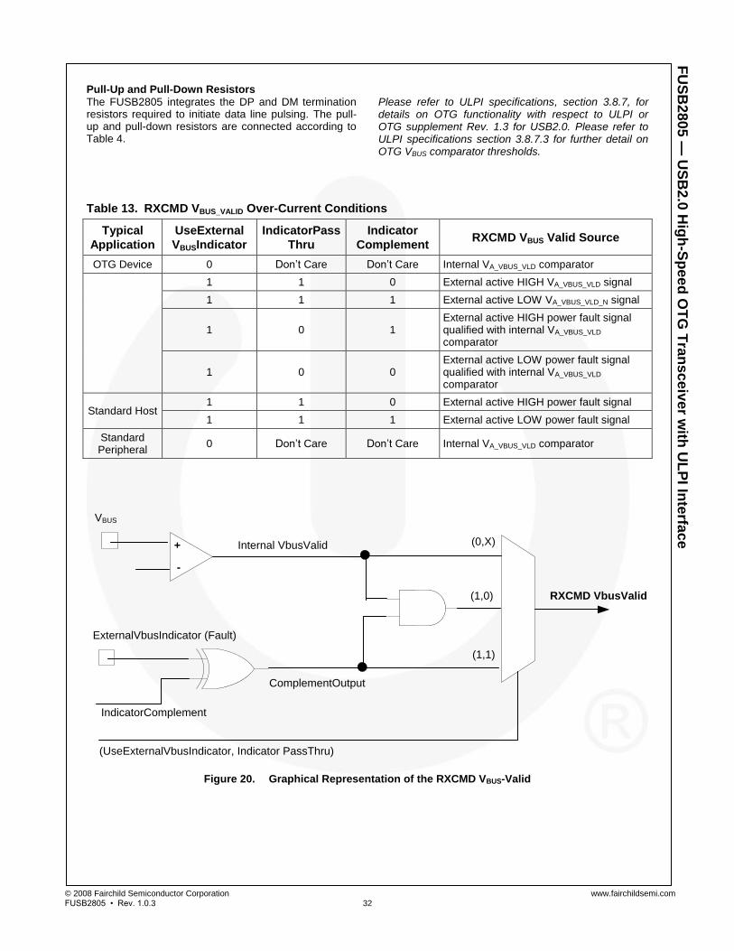
© 2008 Fairchild Semiconductor Corporation www.fairchildsemi.com FUSB2805 • Rev. 1.0.3 32
FU
SB
28
05
— U
SB
2.0
Hig
h-S
pee
d O
TG
Tra
nsc
eiv
er w
ith U
LP
I Inte
rfac
e
Pull-Up and Pull-Down ResistorsThe FUSB2805 integrates the DP and DM termination resistors required to initiate data line pulsing. The pull-up and pull-down resistors are connected according to Table 4.
Please refer to ULPI specifications, section 3.8.7, for details on OTG functionality with respect to ULPI or OTG supplement Rev. 1.3 for USB2.0. Please refer to ULPI specifications section 3.8.7.3 for further detail on OTG VBUS comparator thresholds.
Table 13. RXCMD VBUS_VALID Over-Current Conditions
Typical
Application
UseExternal
VBUSIndicator
IndicatorPass
Thru
Indicator
Complement RXCMD VBUS Valid Source
OTG Device 0 Don‟t Care Don‟t Care Internal VA_VBUS_VLD comparator
1 1 0 External active HIGH VA_VBUS_VLD signal
1 1 1 External active LOW VA_VBUS_VLD_N signal
1 0 1 External active HIGH power fault signal qualified with internal VA_VBUS_VLD comparator
1 0 0 External active LOW power fault signal qualified with internal VA_VBUS_VLD comparator
Standard Host 1 1 0 External active HIGH power fault signal
1 1 1 External active LOW power fault signal
Standard Peripheral
0 Don‟t Care Don‟t Care Internal VA_VBUS_VLD comparator
Internal VbusValid
VBUS
ExternalVbusIndicator (Fault)
IndicatorComplement
ComplementOutput
(UseExternalVbusIndicator, Indicator PassThru)
RXCMD VbusValid
(0,X)
(1,0)
(1,1)
+
-
Figure 20. Graphical Representation of the RXCMD VBUS-Valid

© 2008 Fairchild Semiconductor Corporation www.fairchildsemi.com FUSB2805 • Rev. 1.0.3 33
FU
SB
28
05
— U
SB
2.0
Hig
h-S
pee
d O
TG
Tra
nsc
eiv
er w
ith U
LP
I Inte
rfac
e
Serial Modes
Figure 21 and Figure 22 provide examples of 6-pin and 3-pin serial modes as controlled in the INTF_CTRL register via the 6-pin and 3-pin register bits.
Please refer to ULPI specification, section 3.10 for details on the 3-pin and 6-pin serial mode functionality.
DATA[0]Tx_Enable
DATA[1]Tx_DAT/
RX_RCV
DATA[2]Tx_SE0/
RX_SE0
DP
DM
TRANSMIT
SYNC DATA EOP SYNC DATA EOP
RECEIVE
Figure 21. 3-Pin Serial Mode – Transmit and Receive Example
DATA[0]Tx_Enable
DATA[1]Tx_DAT
DATA[2]Tx_SE0
DP
DM
TRANSMIT
SYNC DATA EOP SYNC DATA EOP
RECEIVE
DATA[5]Rx_DM
DATA[6]Rx_RCV
DATA[4]Rx_DP
Figure 22. 6-Pin Serial Mode – Transmit and Receive Example
Avoiding Contention on the ULPI Data Bus
Because the ULPI data bus is bi-directional, it is necessary to avoid situations in which both the link and FUSB2805 drive the data bus simultaneously.
The following points should be considered while implementing the data bus drive control on the link.
After the power-up and clock stabilization, the default states are:
FUSB2805 drives DIR=0.
Data bus is an INPUT to FUSB2805.
HOST/LINK ULPI data bus is OUTPUT (with all data bus bits driven to 0).
When FUSB2805 wants to take control of data bus to initiate a data transfer, it changes DIR value from 0 to 1.
At this point, HOST/LINK should disable its output pad buffers. This needs to be as fast as possible, so LINK should use a combinational path from DIR.
FUSB2805 does not enable its output buffers immediately, but delays the enabling buffers until the next clock edge, avoiding bus contention.
When data transfer is no longer required by the FUSB2805, it changes DIR from 1 to 0 and starts to turn off its output drivers immediately. The HOST/LINK senses the change of DIR from 1 to 0, but delays enabling its output buffers for one CLOCK cycle, thereby avoiding data bus contention.

© 2008 Fairchild Semiconductor Corporation www.fairchildsemi.com FUSB2805 • Rev. 1.0.3 34
FU
SB
28
05
— U
SB
2.0
Hig
h-S
pee
d O
TG
Tra
nsc
eiv
er w
ith U
LP
I Inte
rfac
e
ULPI Registers
ULPI provides an immediate register set, with a 6-bit address, that is part of the transmit command byte. An extended register set is also provided (8-bit address) that requires an extra clock cycle to complete. The immediate register set is mirrored into the lower end of the extended address space. For example, an operation to the extended address of 00XXXXXX operates on the
immediate register set. The FUSB2805 must support both immediate and extended register operations.
The registers specific to FUSB2805 – vendor ID, product ID, and power control registers, are described in the following sections.
Table 14. Register Map
Field Name Size (bits) Address (6 bits)
Rd Wr Set Clr
Immediate Register Set
Vendor ID Low (see Table 16) 8 00h
Vendor ID High (see Table 16) 8 01h
Product ID Low (see Table 16) 8 02h
Product ID High (see Table 16) 8 03h
Function Control (see Table 17) 8 04-06h 04h 05h 06h
Interface Control (see Table 18) 8 07-09h 07h 08h 09h
OTG Control (see Table 19) 8 0A-0Ch 0Ah 0Bh 0Ch
USB Interrupt Enable Rising (see Table 20) 8 0D-0Fh 0Dh 0Eh 0Fh
USB Interrupt Enable Falling (see Table 21) 8 10-12h 10h 11h 12h
USB Interrupt Status Register (see Table 22) 8 13h
USB Interrupt Latch Register (see Table 23) 8 14h
Debug (see Table 25) 8 15h
Scratch (see Table 26) 8 16-18h 16h 17h 18h
Reserved(21)
8 19-2Eh
Access Extended Register Set (see below) 8 2Fh
Reserved (defined in ULPI specification as vendor specific)
8 30-3Ch
Extended Register Set Address (8 bits)
Maps to Immediate Register Set (see below modes) 8 00-3Fh
Reserved (80-FFh defined in ULPI specification as vendor specific)
8 40-FFh
Note: 21. 19-27h carkit; not supported by FUSB2805.
Table 15. Register Access Legend
Access Code Expanded Name Meaning
rd Read Register can be read. Read-only if this is the only mode given.
wr Write Pattern on the data bus is written over all bits of the register.
s Set Pattern on the data bus is OR‟d with and written into the register.
c Clear Pattern on the data bus is a mask. If a bit in the mask is set, the corresponding register bit is set to zero (cleared).
Notes: 22. The register set above is compliant with the register set defined in the ULPI specifications. For details, please
refer to section 4.0 of the ULPI specifications, version 1.1.

© 2008 Fairchild Semiconductor Corporation www.fairchildsemi.com FUSB2805 • Rev. 1.0.3 35
FU
SB
28
05
— U
SB
2.0
Hig
h-S
pee
d O
TG
Tra
nsc
eiv
er w
ith U
LP
I Inte
rfac
e
ULPI Registers Specific to FUSB2805
Table 16. Vendor ID and Product ID Registers
Register Bits Access Address Value Description
VENDOR_ID_LOW 7:0 rd 00h 79h Lower byte of vendor ID supplied by USB-IF. Fixed value of 79h.
VENDOR_ID_HIGH 7:0 rd 01h 07h Upper byte of vendor ID supplied by USB-IF. Fixed value of 07h.
PRODUCT_ID_LOW 7:0 rd 02h 00h Lower byte of product ID number. Fixed value of 00h.
PRODUCT_ID_HIGH 7:0 rd 03h 25h Upper byte of product ID number. Fixed value of 25h.
Function Control Register– FUNC_CTRL (04h-06h Read, 04h Write, 05h Set, 06h Clear)
These registers control the UTMI function settings of the FUSB2805.
Table 17. Function Control Register
Field Name Bits Access Reset Description
XcvrSelect 1:0 rd/wr/s/c 01b
Selects the transceiver speed: 00b: Enable HS transceiver 01b: Enable FS transceiver 10b: Enable LS transceiver 11b: Enable FS transceiver for LS packets (FS preamble pre-pended by default)
TermSelect 2 rd/wr/s/c 0b
Controls the internal 1.5 kΩ pull-up resistor and 45 Ω HS terminations. Control over the bus resistor changes, as described in Table 4, by the XcvrSelect, OpMode, DpPulldown, and DmPulldown register settings. Since LS peripherals never support FS or HS for HS-capable
transceivers, the FUSB2805 does not support providing 1.5 k on D-.
OpMode 4:3 rd/wr/s/c 00b
Selects the required bit encoding style during transmit. 00b: Normal operation 01b: Non-driving 10b: Disable bit stuffing and NRZI encoding 11b: Do not automatically add SYNC and EOP when transmitting. Must only be used for HS packets.
Reset 5 rd/wr/s/c 0b
Active HIGH transceiver reset. After the link sets this bit, the FUSB2805 must assert DIR and reset the UTMI+ core. When the reset is completed, the FUSB2805 de-asserts DIR and automatically clears this bit. After de-asserting DIR, the FUSB2805 must re-assert DIR and send an RXCMD update to the link. The link must wait for DIR to de-assert before using the ULPI bus. Does not reset the ULPI interface or ULPI register set. 0b: No Reset 1b: Reset
SuspendM 6 rd/wr/s/c 1b
Active LOW PHY suspend. Puts the FUSB2805 into low-power mode. The FUSB2805 can power down all blocks except the FS receiver, OTG comparators, and the ULPI interface pins. The FUSB2805 must automatically set this bit to 1b when low-power mode is exited (prior to exit STP is asserted by the link). 0b: Low-power mode 1b: Powered
RESERVED 7 rd/wr/s/c 0b Reserved
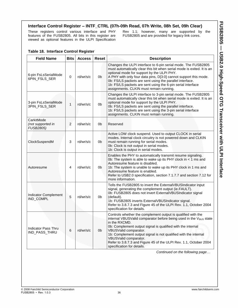
© 2008 Fairchild Semiconductor Corporation www.fairchildsemi.com FUSB2805 • Rev. 1.0.3 36
FU
SB
28
05
— U
SB
2.0
Hig
h-S
pee
d O
TG
Tra
nsc
eiv
er w
ith U
LP
I Inte
rfac
e
Interface Control Register – INTF_CTRL (07h-09h Read, 07h Write, 08h Set, 09h Clear)
These registers control various interface and PHY features of the FUSB2805. All bits in this register are viewed as optional features in the ULPI Specification
Rev 1.1; however, many are supported by the FUSB2805 and are provided for legacy link cores.
Table 18. Interface Control Register
Field Name Bits Access Reset Description
6-pin FsLsSerialMode 6PIN_FSLS_SER
0 rd/wr/s/c 0b
Changes the ULPI interface to 6-pin serial mode. The FUSB2805 must automatically clear this bit when serial mode is exited. It is an optional mode for support by the ULPI PHY. A PHY with only four data pins, D[3:0] cannot support this mode. 0b: FS/LS packets are sent using the parallel interface. 1b: FS/LS packets are sent using the 6-pin serial interface assignments. CLKIN must remain running.
3-pin FsLsSerialMode 3PIN_FSLS_SER
1 rd/wr/s/c 0b
Changes the ULPI interface to 3-pin serial mode. The FUSB2805 must automatically clear this bit when serial mode is exited. It is an optional mode for support by the ULPI PHY. 0b: FS/LS packets are sent using the parallel interface. 1b: FS/LS packets are sent using the 3-pin serial interface assignments. CLKIN must remain running.
CarkitMode (not supported in FUSB2805)
2 rd/wr/s/c 0b Reserved
ClockSuspendM 3 rd/wr/s/c 0b
Active LOW clock suspend. Used to output CLOCK in serial modes. Internal clock circuitry is not powered down and CLKIN must remain running for serial modes. 0b: Clock is not output in serial modes. 1b: Clock is output in serial modes.
Autoresume 4 rd/wr/s/c 0b
Enables the PHY to automatically transmit resume signaling. 0b: The system is able to wake up its PHY clock in < 1 ms and Autoresume feature is disabled. 1b: The system is unable to wake up its PHY clock in 1 ms and Autoresume feature is enabled. Refer to USB2.0 specification, section 7.1.7.7 and section 7.12 for more information.
Indicator Complement IND_COMPL
5 rd/wr/s/c 0b
Tells the FUSB2805 to invert the ExternalVBUSIndicator input signal, generating the complement output (ie.FAULT). 0b: FUSB2805 does not invert ExternalVBUSIndicator signal (default). 1b: FUSB2805 inverts ExternalVBUSIndicator signal. Refer to 3.8.7.3 and Figure 45 of the ULPI Rev. 1.1, October 2004 specification for details.
Indicator Pass Thru IND_PASS_THRU
6 rd/wr/s/c 0b
Controls whether the complement output is qualified with the internal VBUSValid comparator before being used in the VBUS state in the RXCMD. 0b: Complement output signal is qualified with the internal VBUSValid comparator. 1b: Complement output signal is not qualified with the internal VBUSValid comparator. Refer to 3.8.7.3 and Figure 45 of the ULPI Rev. 1.1, October 2004 specification for details.
Continued on the following page…

© 2008 Fairchild Semiconductor Corporation www.fairchildsemi.com FUSB2805 • Rev. 1.0.3 37
FU
SB
28
05
— U
SB
2.0
Hig
h-S
pee
d O
TG
Tra
nsc
eiv
er w
ith U
LP
I Inte
rfac
e
Field Name Bits Access Reset Description
Interface Protect Disable INTF_PROT_DIS
7 rd/wr/s/c 0b
Controls circuitry built into the FUSB2805 for protecting the ULPI interface when the link three-states STP and D[7:0]. Any pull-ups or pull-downs employed by this feature can be disabled. This bit is not intended to affect the operation of the holding state. When this bit is enabled, the FUSB2805 automatically detects when the link stops driving STP. 0b: Enables the interface-protect circuit (default). A weak pull-up resistor is attached to STP and, if STP is unexpectedly HIGH, the FUSB2805 attaches weak pull-down resistors on D[7:0] to protect the data inputs. 1b: Disables the interface-protect circuit. Detaches the weak pull-down resistors on D[7:0] and weak pull-up on STP. Refer to 3.12 of the ULPI Rev. 1.1, October 2004 specification for details.
OTG Control Register – OTG_CTRL (0Ah-0Ch Read, 0Ah Write, 0Bh Set, 0Ch Clear)
These registers control the UTMI+ OTG function settings of the FUSB2805.
Table 19. OTG Control Register
Field Name Bits Access Reset Description
IDPullup 0 rd/wr/s/c 0b Connects a pull-up to ID line and enables sampling the signal level; 0b: Disables sampling of ID pin 1b: Enables sampling of ID pin
DpPulldown 1 rd/wr/s/c 1b Enables the 15 kΩ pull-down resistor on D+
(23)
0b: Pull-down resistor not connected to D+ 1b: Pull-down resistor connected to D+
DmPulldown 2 rd/wr/s/c 1b Enables the 15 kΩ pull-down resistor on D-
(23)
0b: Pull-down resistor not connected to D- 1b: Pull-down resistor connected to D-
DischrgVBUS 3 rd/wr/s/c 0b
Discharges VBUS through a resistor. A minimum of 656 Ω is defined in the OTG specification. If the link sets this bit to 1b, it waits for an RXCMD indicating SessEnd has transitioned from 0b to 1b, then resets this bit to 0b to stop the discharge event. 0b: Do not discharge VBUS
1b: Discharge VBUS
ChrgVBUS 4 rd/wr/s/c 0b
Charges VBUS through a resistor. Used for VBUS pulsing SRP. A minimum output impedance of 281 Ω with a voltage source of 3.0 V as defined in the OTG specification can be used. The link must first check that VBUS has been discharged (see DischrgVBUSbit) and that both D+ and D- have signaled an SE0 for a minimum of 2ms. 0b: Do not charge VBUS
1b: Charge VBUS
Reserved 5 rd/wr/s/c 0b Reserved
DrvVBUS External 6 rd/wr/s/c 0b Selects the external 5 V VBUS supply via PSW pin. 0b: Drive PSW LOW 1b: Drive PSW HIGH
UseExternalVBUS Indicator
7 rd/wr/s/c 0b
Tells the FUSB2805 to use an external VBUS over-current indicator. This bit is optional. 0b: Use the internal OTG comparator (VA_VBUS_VLD) or internal VBUS valid indicator (default). 1b: Use external VBUS valid indicator signal on FAULT Refer to 3.8.7.3 of the ULPI Rev. 1.1, October 2004 specification for details.
Note: 23. Resistor termination implementations conform to USB2.0 resistor ECN.

© 2008 Fairchild Semiconductor Corporation www.fairchildsemi.com FUSB2805 • Rev. 1.0.3 38
FU
SB
28
05
— U
SB
2.0
Hig
h-S
pee
d O
TG
Tra
nsc
eiv
er w
ith U
LP
I Inte
rfac
e
USB Interrupt Enable (Rising) Register – INTR_EN_R_CTRL (0Dh-0Fh Read, 0Dh Write,
0Eh Set, 0Fh Clear)
These register bits control the interrupt event notification settings of the FUSB2805 for LOW-to-HIGH signal changes. By default, all transitions are enabled. Interrupt circuitry can be powered down in any mode
when both rising and falling edge enables are disabled. To ensure interrupts are detectable when CLOCK is powered down, the link should enable both rising and falling edges.
Table 20. USB Interrupt Enable (Rising) Register
Field Name Bits Access Reset Description
HostDisconnect Rise 0 rd/wr/s/c 1b Generates an interrupt event notification when HostDisconnect changes from LOW to HIGH. Applicable only in host mode (DpPulldown and DmPulldown both set to 1b).
VBUSValid Rise 1 rd/wr/s/c 1b Generates an interrupt event notification when VBUSValid changes from LOW to HIGH.
SessValid Rise 2 rd/wr/s/c 1b Generates an interrupt event notification when SessValid changes from LOW to HIGH. SessValid is the same as UTMI+ AValid.
SessEnd Rise 3 rd/wr/s/c 1b Generates an interrupt event notification when SessEnd changes from LOW to HIGH.
IDGnd Rise 4 rd/wr/s/c 1b Generates an interrupt event notification when IDGnd changes from LOW to HIGH. IDGnd is valid 50 ms after IDPullup is set to 1b; otherwise, IDGnd is undefined and should be ignored.
RESERVED 7:5 rd/wr/s/c 0b Reserved
USB Interrupt Enable (Falling) Register – INTR_EN_F_CTRL (10h-12h Read, 10h Write,
11h Set, 12h Clear)
These register bits control the interrupt event notification settings of the FUSB2805 for HIGH-to-LOW signal changes. By default, all transitions are enabled. Interrupt circuitry can be powered down in any mode when both rising and falling edge enables are disabled. To ensure interrupts are detectable when CLOCK is
powered down, the link should enable both rising and falling edges.
Note: 24. RxActive and RxError must always be
communicated immediately, these events are not included in this register.
Table 21. USB Interrupt Enable (Falling) Register
Field Name Bits Access Reset Description
HostDisconnect Fall 0 rd/wr/s/c 1b Generates an interrupt event notification when HostDisconnect changes from HIGH to LOW. Applicable only in host mode (DpPulldown and DmPulldown both set to 1b).
VBUSValid Fall 1 rd/wr/s/c 1b Generates an interrupt event notification when VBUSValid changes from HIGH to LOW.
SessValid Fall 2 rd/wr/s/c 1b Generates an interrupt event notification when SessValid changes from HIGH to LOW. SessValid is the same as UTMI+ AValid.
SessEnd Fall 3 rd/wr/s/c 1b Generates an interrupt event notification when SessEnd changes from HIGH to LOW.
IDGnd Fall 4 rd/wr/s/c 1b Generates an interrupt event notification when IDGnd changes from HIGH to LOW. IDGnd is valid 50ms after IDPullup is set to 1b; otherwise, IDGnd is undefined and should be ignored.
RESERVED 7:5 rd/wr/s/c 0b Reserved

© 2008 Fairchild Semiconductor Corporation www.fairchildsemi.com FUSB2805 • Rev. 1.0.3 39
FU
SB
28
05
— U
SB
2.0
Hig
h-S
pee
d O
TG
Tra
nsc
eiv
er w
ith U
LP
I Inte
rfac
e
USB Interrupt Status Register – USB_INTR_STAT (13h Read Only)
These register bits indicate the current value of the interrupt event source signal. Interrupt circuitry can be powered down in any mode when both rising and falling
edge enables are disabled. To ensure interrupts are detectable when CLOCK is powered down, the link should enable both rising and falling edges.
Table 22. USB Interrupt Status Register
Field Name Bits Access Reset Description
HostDisconnect 0 rd 0b Current value of UTMI+ HostDisconnect output. Applicable only in host mode (DpPulldown and DmPulldown both set to 1b). Automatically reset to 0b when low-power mode is entered.
VBUSValid 1 rd 0b Current value of UTMI+ VBUSValid output.
SessValid 2 rd 0b Current value of UTMI+ SessValid output. SessValid is the same as UTMI+ AValid.
SessEnd 3 rd 0b Current value of UTMI+ SessEnd output.
IDGnd 4 rd 0b Current value of UTMI+ IDGnd output. IDGnd is valid 50ms after IDPullup is set to 1b; otherwise, IDGnd is undefined and should be ignored.
RESERVED 7:5 rd Xb Reserved
USB Interrupt Latch – USB_INTR_L (14h Read Only with Auto-Clear)
These register bits are set by the FUSB2805 when an unmasked change occurs on the corresponding internal signal. The FUSB2805 automatically clears all bits when the link reads this register or when low-power mode is entered. The FUSB2805 also clears this register when either 6-pin or 3-pin serial mode is entered, regardless of the value of ClockSuspendM. Interrupt circuitry can be powered down in any mode
when both rising and falling edge enables are disabled. To ensure interrupts are detectable when CLOCK is powered down, the link should enable both rising and falling edges.
It is optional for the link to read the USB Interrupt Latch register in synchronous mode because the RXCMD byte already indicates the interrupt source directly.
Table 23. USB Interrupt Latch Register
Field Name Bits Access Reset Description
HostDisconnect Latch 0 rd 0b
Set to 1b by the FUSB2805 when an unmasked event occurs on HostDisconnect. Cleared when this register is read.
Applicable only in host mode (DpPulldown and DmPulldown both set to 1b).
VBUSValid Latch 1 rd 0b Set to 1b by the FUSB2805 when an unmasked event occurs on VBUSValid. Cleared when this register is read.
SessValid Latch 2 rd 0b Set to 1b by the FUSB2805 when an unmasked event occurs on SessValid. Cleared when this register is read. SessValid is the same as UTMI+ AValid.
SessEnd Latch 3 rd 0b Set to 1b by the FUSB2805 when an unmasked event occurs on SessEnd. Cleared when this register is read.
IDGnd Latch 4 rd 0b
Set to 1b by the FUSB2805 when an unmasked event occurs on IDGnd. Cleared when this register is read. IDGnd is valid 50 ms after IDPullup is set to 1b; otherwise, IDGnd is undefined and should be ignored.
RESERVED 7:5 rd 0b Reserved

© 2008 Fairchild Semiconductor Corporation www.fairchildsemi.com FUSB2805 • Rev. 1.0.3 40
FU
SB
28
05
— U
SB
2.0
Hig
h-S
pee
d O
TG
Tra
nsc
eiv
er w
ith U
LP
I Inte
rfac
e
The FUSB2805 must follow the rules defined in Table 24 for setting any of the Latch register bits. If register read data is returned to the link in the same cycle, a
USB interrupt latch bit is set, the interrupt condition is given immediately in the register read data and the latch bit is not set to 1b.
Table 24. Interrupt Latch Register Setting Rules
Input Conditions
Register Read Data Returned in
Current Clock Cycle
Interrupt Latch Bit Set (1b) in Current
Clock Cycle
Resultant Value of Latch
Register Bit
NO NO 0b
NO YES 1b
YES NO 0b
YES YES 0b
Debug Register (15h Read Only)
These register bits indicate the current values of various signals useful for debugging.
Table 25. Debug Register
Field Name Bits Access Reset Description
LineState0 0 rd 0b Contains the current value of Linestate0
LineState1 1 rd 0b Contains the current value of Linestate1
RESERVED 7:2 rd 0b Reserved
Scratch Register (16h-18h Read, 16h Write, 17h Set, 18h Clear)
These register bits indicate the current values of various signals useful for debugging.
Table 26. Scratch Register
Field Name Bits Access Reset Description
Scratch 7:0 rd/wr/s/c 00h Empty register byte for testing purposes. Software can read, write, set, and clear this register and the FUSB2805 functionality is not affected.

© 2008 Fairchild Semiconductor Corporation www.fairchildsemi.com FUSB2805 • Rev. 1.0.3 41
FU
SB
28
05
— U
SB
2.0
Hig
h-S
pee
d O
TG
Tra
nsc
eiv
er w
ith U
LP
I Inte
rfac
e
Absolute Maximum Ratings
Stresses exceeding the absolute maximum ratings may damage the device. The device may not function or be operable above the recommended operating conditions and stressing the parts to these levels is not recommended. In addition, extended exposure to stresses above the recommended operating conditions may affect device reliability. The absolute maximum ratings are stress ratings only.
Symbol Parameter Min. Max. Unit
VCC Supply Voltage(25)
Continuous -0.5 +5.5
V Pulse -0.5 +5.5
VIO I/O Supply Voltage -0.5 +5.5 V
VIN DC Input Voltage(26)
Pins: STP, DIR, NXT, D[7:0], CFG1, RESET_N, CLKIN
-0.5 VIO + 0.5
V Pins: FAULT, Chip_Select_N -0.5 +5.5
Pins: DP, DM, VBUS -0.5 5.5(27)
IIK DC Input Diode Current -50 mA
ILU DC Latch-Up Current -100 mA
TSTG Storage Temperature -65 +150 °C
ESD
Human Body Model, JEDEC: JESD22-A114
All Pins 6
kV
I/O to GND 12
Power to GND 12
Charged Device Model, JEDEC: JESD22-C101 2
IEC 61000 Board Level, Air Gap 19
Machine Model, JEDEC: JESD22-A115 350 V
Notes: 25. VCC is able to withstand short (up to 5 ms) pulses of up to 5.5 V peak voltage. 26. The input and output negative ratings may be exceeded only if the input and output diode current ratings
are observed. 27. VBUS is able to withstand higher voltages using an external series resistance. Target is to withstand >10 V for
greater than five (5) seconds with a series resistance of 1 kΩ ±5%.
Recommended Operating Conditions
The Recommended Operating Conditions table defines the conditions for actual device operation. Recommended operating conditions are specified to ensure optimal performance to the datasheet specifications. Fairchild does not recommend exceeding them or designing to Absolute Maximum Ratings.
Symbol Parameter Min. Typ. Max. Unit
VCC Supply Voltage 2.7 3.6 4.5 V
VCC3V3 Internal Regulated Supply Voltages
VCC-0.1 3.30 3.60 V
VDD1V2 1.08 1.20 1.32
VIO I/O Supply Voltage 1.65 3.60 V
VIN
Input Voltage – Digital I/O(28)
(STP, D[7:0], CFG1, NXT, DIR, FAULT, CLKIN, RESET_N)
0 VIO V
VBUS, Chip_Select_N 0 5.25
VAIO Input Voltage – Analog I/O (DP, DM, ID) -0.5 3.6 V
TA Operating Temperature -40 +25 +85 °C
Note: 28. The digital inputs must be held HIGH or LOW; they must not float.

© 2008 Fairchild Semiconductor Corporation www.fairchildsemi.com FUSB2805 • Rev. 1.0.3 42
FU
SB
28
05
— U
SB
2.0
Hig
h-S
pee
d O
TG
Tra
nsc
eiv
er w
ith U
LP
I Inte
rfac
e
Static Characteristics
VCC3V3=VCC-0.1 to 3.6 V; VDD1V2=1.1 V to 1.25 V; VIO=1.65 V to 3.60 V; TJ=-40°C to +85°C; unless otherwise specified.
Symbol Parameter Conditions Min. Typ. Max. Unit
Supply Pins
VPOR Power-On Reset Trip Voltage
Referenced to VDDIO Supply 1.4 V
IVCC Operating Supply Current
Full-Speed Data at 12 MHz, 50 pF Load
25
mA Full-Speed Data at 12 MHz, Idle 23
HS Receiving at 480 MHz 31
HS Transmitting at 480 MHz 36
IVCC(lowpwr) Low-Power Mode Supply Current
(32)
Bit SuspendM=0b, CLKIN=LOW, PSW De-asserted
95 200 µA
IPWRDN Current Drawn from VCC in Power-Down Mode
VIO Off or Chip_Select_N De-asserted, No VBUS Present
22 36 µA
IIO Operating VIO Supply Current 12pF on CLOCK, ULPI Idle 2.1 mA
IIOPWRDN Static VIO Supply Current in Power-Down Mode
Chip_Select_N De-asserted 2 µA
IIOSPND Static VIO Supply Current in Suspend Mode (Low-Power)
I/O Pins Idle 2 µA
IVBUS_SUSPND Static VBUS Supply Current in Suspend Mode (Low-Power)
I/O Pins Idle 60 90 µA
Digital Pins (CLOCK, DIR, STP, NXT, D0-D7, RESET_N)
VIL LOW Level Input Voltage 0.3•VIO V
VIH HIGH Level Input Voltage 0.7•VIO V
VOL LOW Level Output Voltage IOL=4 mA 0.4 V
VOH HIGH Level Output Voltage IOH=4 mA VIO-0.4 V
IPD Input Pull-Down Current (Interface Protect – D[7:0])
VIN=VIO 25 50 90 µA
IPU Input Pull-Up Current (Interface Protect –STP)
VIN=0 V -30 -50 -80 µA
Digital Pins (FAULT)
VIL LOW Level Input Voltage 0.8 V
VIH HIGH Level Input Voltage 2.0 V
IIN Input Leakage Current -1 1 µA
Digital Pins (PSW)
VOHPSW HIGH Level Output Voltage-PSW
External 100 k Pull-Down to GND 2.6 3.6 V
IOHPSW HIGH Level Current-PSW External 100 k Pull-Down to GND 4 mA
Continued on the following page…

© 2008 Fairchild Semiconductor Corporation www.fairchildsemi.com FUSB2805 • Rev. 1.0.3 43
FU
SB
28
05
— U
SB
2.0
Hig
h-S
pee
d O
TG
Tra
nsc
eiv
er w
ith U
LP
I Inte
rfac
e
Static Characteristics (Continued)
VCC3V3=VCC-0.1 to 3.6 V; VDD1V2=1.1 V to 1.25 V; VIO=1.65 V to 3.60 V; TJ=-40°C to +85°C; unless otherwise specified.
Symbol Parameter Conditions Min. Typ. Max. Unit
Analog I/O Pins (DP, DM)
FS/LS Path
VDI Differential Input Sensitivity |VDP – VDM| 0.2 V
VCM Differential Common Mode Voltage Includes VDI Range 0.8 2.5 V
VIL LOW-Level Input Voltage 0.8 V
VIH HIGH-Level Input Voltage 2.0 V
VOL LOW-Level Output Voltage Pull-Up on DP;
RL=1.5 k to 3.6 V 0 0.3 V
VOH HIGH-Level Output Voltage Pull-Down on DP/DM;
RL=15 k to GND 2.8 3.6 V
VTERM Termination Voltage for 1.5 kΩ Pull-Up Resistor 3.0 3.6 V
RPU Pull-Up Resistance on DP Per USB2.0 Resistor ECN 900 1575
RWKPU Weak Pull-Up Resistance on DP Bit DP_WKPU_EN=1, VBUS>VA-SESS_VLD
105.8 132.0 158.0 k
HS Path
VHSSQ High-Speed Squelch Detection Threshold
Squelch Detected 100 mV
No Squelch Detected 150
VDSCHS HS Disconnect Detection Threshold (Differential) 525 625 mV
VDIHS HS Differential Input Sensitivity |VDP – VDM| 300 mV
VCMHS HS Differential Common-Mode Voltage
Includes VDIHS Range -50 +500 mV
VILHS HS Idle-Level Input Voltage (Differential) -10 +10 mV
VIHHS HS LOW-Level Input Voltage (Differential) -10 +10 mV
VOLHS HS HIGH-Level Output Voltage 360 440 mV
VCHIRPJ Chirp-J Output Voltage (Differential) 700 1100 mV
VCHIRPK Chirp-K Output Voltage (Differential) -900 -500 mV
IOZ Leakage Current -4 +4 µA
ZDRV Driver Output Impedance (Both HS and FS)
Steady-State Conditions per USB2.0
40.5 49.5
ZIN Input Impedance 0.8 M
RPD Pull-Down Resistance on DP, DM Per USB2.0 Resistor ECN 14.25 24.80 k
CI/O Capacitance Pin to GND 10 pF
VBUS Comparators
Vth(VBUSVLD) VBUS Valid Threshold 4.40 4.75 V
Vth(SESSEND) VBUS Session-End Comparator Threshold 0.2 0.8 V
Vhys(SESSEND) VBUS Session-End Comparator Hysteresis 150 mV
Vth(SESSVLD) VBUS Session-Valid Comparator Threshold
A-Device and B-Device 0.8 2.0 V
Vhys(SESSVLD) VBUS Session-Valid Comparator Hysteresis 200 mV
Continued on the following page…
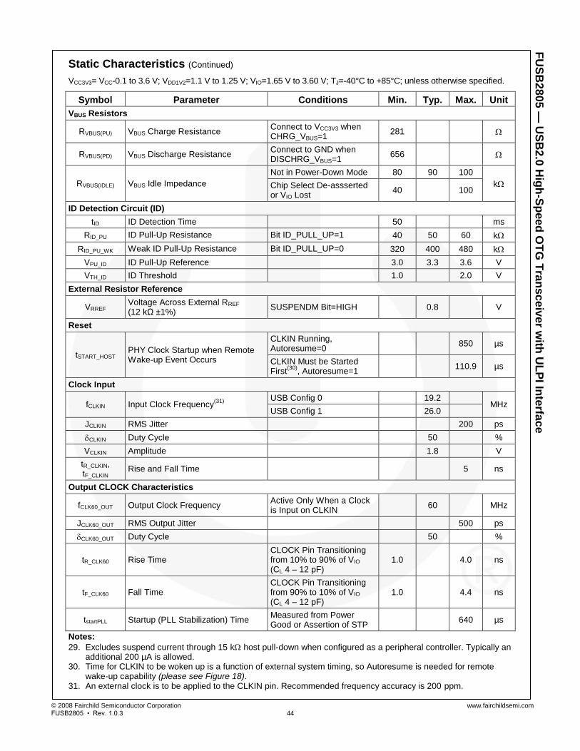
© 2008 Fairchild Semiconductor Corporation www.fairchildsemi.com FUSB2805 • Rev. 1.0.3 44
FU
SB
28
05
— U
SB
2.0
Hig
h-S
pee
d O
TG
Tra
nsc
eiv
er w
ith U
LP
I Inte
rfac
e
Static Characteristics (Continued)
VCC3V3= VCC-0.1 to 3.6 V; VDD1V2=1.1 V to 1.25 V; VIO=1.65 V to 3.60 V; TJ=-40°C to +85°C; unless otherwise specified.
Symbol Parameter Conditions Min. Typ. Max. Unit
VBUS Resistors
RVBUS(PU) VBUS Charge Resistance Connect to VCC3V3 when CHRG_VBUS=1
281
RVBUS(PD) VBUS Discharge Resistance Connect to GND when DISCHRG_VBUS=1
656
RVBUS(IDLE) VBUS Idle Impedance
Not in Power-Down Mode 80 90 100
k Chip Select De-assserted or VIO Lost
40 100
ID Detection Circuit (ID)
tID ID Detection Time 50 ms
RID_PU ID Pull-Up Resistance Bit ID_PULL_UP=1 40 50 60 k
RID_PU_WK Weak ID Pull-Up Resistance Bit ID_PULL_UP=0 320 400 480 k
VPU_ID ID Pull-Up Reference 3.0 3.3 3.6 V
VTH_ID ID Threshold 1.0 2.0 V
External Resistor Reference
VRREF Voltage Across External RREF (12 kΩ ±1%)
SUSPENDM Bit=HIGH 0.8 V
Reset
tSTART_HOST PHY Clock Startup when Remote Wake-up Event Occurs
CLKIN Running, Autoresume=0
850 µs
CLKIN Must be Started First
(30), Autoresume=1
110.9 µs
Clock Input
fCLKIN Input Clock Frequency(31)
USB Config 0 19.2
MHz USB Config 1 26.0
JCLKIN RMS Jitter 200 ps
CLKIN Duty Cycle 50 %
VCLKIN Amplitude 1.8 V
tR_CLKIN, tF_CLKIN
Rise and Fall Time 5 ns
Output CLOCK Characteristics
fCLK60_OUT Output Clock Frequency Active Only When a Clock is Input on CLKIN
60 MHz
JCLK60_OUT RMS Output Jitter 500 ps
CLK60_OUT Duty Cycle 50 %
tR_CLK60 Rise Time CLOCK Pin Transitioning from 10% to 90% of VIO (CL 4 – 12 pF)
1.0 4.0 ns
tF_CLK60 Fall Time CLOCK Pin Transitioning from 90% to 10% of VIO (CL 4 – 12 pF)
1.0 4.4 ns
tstartPLL Startup (PLL Stabilization) Time Measured from Power Good or Assertion of STP
640 µs
Notes:
29. Excludes suspend current through 15 k host pull-down when configured as a peripheral controller. Typically an additional 200 µA is allowed.
30. Time for CLKIN to be woken up is a function of external system timing, so Autoresume is needed for remote wake-up capability (please see Figure 18).
31. An external clock is to be applied to the CLKIN pin. Recommended frequency accuracy is 200 ppm.
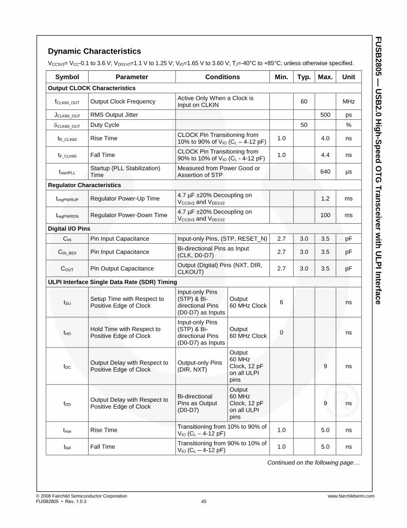
© 2008 Fairchild Semiconductor Corporation www.fairchildsemi.com FUSB2805 • Rev. 1.0.3 45
FU
SB
28
05
— U
SB
2.0
Hig
h-S
pee
d O
TG
Tra
nsc
eiv
er w
ith U
LP
I Inte
rfac
e
Dynamic Characteristics
VCC3V3= VCC-0.1 to 3.6 V; VDD1V2=1.1 V to 1.25 V; VIO=1.65 V to 3.60 V; TJ=-40°C to +85°C; unless otherwise specified.
Symbol Parameter Conditions Min. Typ. Max. Unit
Output CLOCK Characteristics
fCLK60_OUT Output Clock Frequency Active Only When a Clock is Input on CLKIN
60 MHz
JCLK60_OUT RMS Output Jitter 500 ps
CLK60_OUT Duty Cycle 50 %
tR_CLK60 Rise Time CLOCK Pin Transitioning from 10% to 90% of VIO (CL – 4-12 pF)
1.0 4.0 ns
tF_CLK60 Fall Time CLOCK Pin Transitioning from 90% to 10% of VIO (CL - 4-12 pF)
1.0 4.4 ns
tstartPLL Startup (PLL Stabilization) Time
Measured from Power Good or Assertion of STP
640 µs
Regulator Characteristics
tregPWRUP Regulator Power-Up Time 4.7 µF ±20% Decoupling on VCC3V3 and VDD1V2
1.2 ms
tregPWRDN Regulator Power-Down Time 4.7 µF ±20% Decoupling on VCC3V3 and VDD1V2
100 ms
Digital I/O Pins
CIN Pin Input Capacitance Input-only Pins, (STP, RESET_N) 2.7 3.0 3.5 pF
CIN_BIDI Pin Input Capacitance Bi-directional Pins as Input (CLK, D0-D7)
2.7 3.0 3.5 pF
COUT Pin Output Capacitance Output (Digital) Pins (NXT, DIR, CLKOUT)
2.7 3.0 3.5 pF
ULPI Interface Single Data Rate (SDR) Timing
tSU Setup Time with Respect to Positive Edge of Clock
Input-only Pins (STP) & Bi-directional Pins (D0-D7) as Inputs
Output 60 MHz Clock
6 ns
tHD Hold Time with Respect to Positive Edge of Clock
Input-only Pins (STP) & Bi-directional Pins (D0-D7) as Inputs
Output 60 MHz Clock
0 ns
tDC Output Delay with Respect to Positive Edge of Clock
Output-only Pins (DIR, NXT)
Output 60 MHz Clock, 12 pF on all ULPI pins
9 ns
tDD Output Delay with Respect to Positive Edge of Clock
Bi-directional Pins as Output (D0-D7)
Output 60 MHz Clock, 12 pF on all ULPI pins
9 ns
trise Rise Time Transitioning from 10% to 90% of VIO (CL – 4-12 pF)
1.0 5.0 ns
tfall Fall Time Transitioning from 90% to 10% of VIO (CL – 4-12 pF)
1.0 5.0 ns
Continued on the following page…

© 2008 Fairchild Semiconductor Corporation www.fairchildsemi.com FUSB2805 • Rev. 1.0.3 46
FU
SB
28
05
— U
SB
2.0
Hig
h-S
pee
d O
TG
Tra
nsc
eiv
er w
ith U
LP
I Inte
rfac
e
Dynamic Characteristics (Continued)
VCC3V3= VCC-0.1 to 3.6 V; VDD1V2=1.1 V to 1.25 V; VIO=1.65 V to 3.60 V; TJ=-40°C to +85°C; unless otherwise specified.
Symbol Parameter Conditions Min. Typ. Max. Unit
ULPI Interface Exiting and Entering Low-Power Mode
tCS Entering Low-Power Mode Time From DIR LH Transition-to-CLOCK Stop (6 Cycles Minimum)
0.145 µs
tSTP Low-Power Mode Delay(32)
From DIR LH Transition STP to LH Transition
2 µs
tWU Exiting Low-Power Mode (Total Wake-Up Time)
From STOP LH Transition to DIR HL Transition
111 µs
tCWU Exiting Low-Power Mode (Clock Wake-Up Time)
From STOP LH Transition-to-Clock Start
110.9 µs
tCD Exiting Low-Power Mode (Clock-to-DIR)
From Clock Start-to-DIR HL Transition (6 Clock Cycles)
97 ns
Analog I/O Pins
High-Speed Driver Characteristics
tHSR Differential Rise Time 500 ps
tHSF Differential Fall Time 500 ps
Full-Speed Driver Characteristics
tFR Rise Time CL=50 pF; 10 to 90% of |VOH –VOL| 4 20 ns
tFF Fall Time CL=50 pF; 10 to 90% of |VOH –VOL| 4 20 ns
FRFM Differential Rise Time / Fall Time Matching
Excluding First Transition from Idle State
90.0 111.1 %
VCRS Output Signal Crossover Voltage Excluding First Transition from Idle State
1.3 2.0 V
tLR Rise Time CL=200pF to 600pF; 1.5 kΩ pull up on D- enabled; 10 to 90% of |VOH –VOL|
75 300 ns
tLF Fall Time CL=200pF to 600pF; 1.5 kΩ pull up on D- enabled; 10 to 90% of |VOH –VOL|
75 300 ns
LRFM Differential Rise Time / Fall Time Matching
Excluding First Transition from Idle State
80.0 125 %
Serial Mode Driver Timing
tPLHDS Driver Serial Mode Propagation Delay (LOW to HIGH)
TX_DAT [D1], TX_SE0 [D2] to D+/D- 20 ns
tPHLDS Driver Serial Mode Propagation Delay (HIGH to LOW)
TX_DAT [D1], TX_SE0 [D2] to D+/D- 20 ns
tPHZLZDS Driver Serial Mode Disable Delay TX_ENABLE [D0] to D+/D- 12 ns
tPZHZLDS Driver Serial Mode Enable Delay TX_ENABLE [D0] to D+/D- 20 ns
Continued on the following page…

© 2008 Fairchild Semiconductor Corporation www.fairchildsemi.com FUSB2805 • Rev. 1.0.3 47
FU
SB
28
05
— U
SB
2.0
Hig
h-S
pee
d O
TG
Tra
nsc
eiv
er w
ith U
LP
I Inte
rfac
e
Dynamic Characteristics (Continued)
VCC3V3= VCC-0.1 to 3.6 V; VDD1V2=1.1 V to 1.25 V; VIO=1.65 V to 1.95 V; TJ=-40°C to +85°C; unless otherwise specified.
Symbol Parameter Conditions Min. Typ. Max. Unit
Serial Mode Receiver Timing
tPLHRS Receiver Serial Mode Propagation Delay (LOW to HIGH)
D+/D- to RX_RCV [D6] 20 ns
tPHLRS Receiver Serial Mode Propagation Delay (HIGH to LOW)
D+/D- to RX_RCV [D6] 20 ns
tPLHPS Single Ended VP Serial Mode Propagation Delay (LOW to HIGH)
D+ to RX_DP [D4] 20 ns
tPHLPS Single Ended VP Serial Mode Propagation Delay (HIGH to LOW)
D+ to RX_DP[D4] 20 ns
tPLHMS Single Ended VM Serial Mode Propagation Delay (LOW to HIGH)
D- to RX_DM [D5] 20 ns
tPHLMS Single Ended VM Serial Mode Propagation Delay (HIGH to LOW)
D- to RX_DM [D5] 20 ns
Note: 32. This parameter is guaranteed by design.

© 2008 Fairchild Semiconductor Corporation www.fairchildsemi.com FUSB2805 • Rev. 1.0.3 48
FU
SB
28
05
— U
SB
2.0
Hig
h-S
pee
d O
TG
Tra
nsc
eiv
er w
ith U
LP
I Inte
rfac
e
Physical Dimensions
5.104.90
0.80 MAX
0.10 C
SEATING PLANE
0.08 C 0.050.00
(0.20)
SIDE VIEW
C
(2X)
0.15 C
0.15 C
(2X)
PIN #1 IDENT
TOP VIEW
0.50
PIN #1 IDENT
3.203.00
0.500.30
3.203.00
0.50 0.10 C A B
0.05 C
0.18-0.30
BOTTOM VIEW
A
B
1 8
9
16
1724
25
32
5.25 MIN
(0.21 )
(3.75 ) 3.10 MAX
0.28 MAX 0.50
(0.60 )
RECOMMENDED LAND PATTERN
X4
X32
32X
(DATUM B)
(DATUM A)
(0.48 )
NOTES:
A. EXCEPT WHERE NOTED, CONFORMS TO JEDEC REGISTRATION
MO-220, VARIATION WHHD-6.
B. DIMENSIONS ARE IN MILLIMETERS.
C. DIMENSIONS AND TOLERANCES PER ASME Y14.5M-1994.
D. LAND PATTERN PER IPC SM-782.
E. DIMENSIONS ARE NOT INCLUSIVE OF BURRS, MOLD FLASH, OR
TIE BAR PROTRUSIONS.
F. DRAWING FILENAME: MKT-MLP32Brev1.
32X
5.104.90
3.10 MAX
(3.75)
5.25 MIN
0.49
A
Figure 23. 32-Lead, Molded Leadless Package (MLP)
Package drawings are provided as a service to customers considering Fairchild components. Drawings may change in any manner without notice. Please note the revision and/or date on the drawing and contact a Fairchild Semiconductor representative to verify or obtain the most recent revision. Package specifications do not expand the terms of Fairchild’s worldwide terms and conditions, specifically the warranty therein, which covers Fairchild products. Always visit Fairchild Semiconductor’s online packaging area for the most recent package drawings: http://www.fairchildsemi.com/dwg/ML/MLP32B.pdf.

© 2008 Fairchild Semiconductor Corporation www.fairchildsemi.com FUSB2805 • Rev. 1.0.3 49
FU
SB
28
05
— U
SB
2.0
Hig
h-S
pee
d O
TG
Tra
nsc
eiv
er w
ith U
LP
I Inte
rfac
e