fully-integrated lownoiseamplifier wimax systemsidlab/taskandschedule/amber/fetpapers/a … ·...
TRANSCRIPT

A 2 - 11 GHz Fully-Integrated Low Noise Amplifier forWiMAX Systems
C. W. Chang and Z. M. Lin
Abstract - In this paper, a 2 - 11 GHz WiMAX low simultaneously.noise amplifier (LNA) is designed and implemented in In order to simultaneously get better gain, noise and0.18-,m CMOS process. The low noise amplifier good wideband by taking advantage from theutilizes a current-reused technique, a simple feedback current-reused configuration, a LNA based on thesystem and a high-pass input matching network. The current-reused configuration combining with a feedbackLNA presents a maximum power gain of 12.1 dB. The configuration and a high-pass input matching network isLNA obtained 3.6 - 3.628 dB noise figure (NF) in the designed in this paper. The following section introducesfrequency range of 2-11 GHz with a power dissipation the circuit topology and analysis. In the Section III, itof 14.3 mW under a 1.8V power supply. emphasizes on layout techniques for circuit operation at
GHz frequency. Section IV presents the simulation results.Index Terms - Low noise amplifier (LNA), noise Section V makes a brief conclusion.
figure (NF), WiMAX.Vdd Vdd
I. INTRODUCTION -
Worldwide Interoperability for Microwave Access RL 0b3(WiMAX) is a wireless metropolitan access network R, L3 L4(W-MAN) technology, well known as IEEE 802.16-2004, M3is introduced in 2004 [1]. The coverage area of WiMAX isaround 30 to 50 kilometers, which surpass the existing M2 C3 outcoverage barrier in wireless wideband access. It can t_ 0
provide as high as 1OOMbps data rates in a 20MHz C2 2 b2bandwidth. The specification number for WiMAX is IEEE 10b2
802.16a and its subsequent standards. In the receiver chainof a communication system, a LNA is the first stage Rr Vbiaso- M4dominating the noise and sensitivity performance of the in C,communication system. O Si Ml
Recently many topologies have been presented likedistributed amplifiers, common-gate amplifier, current - LI Lsreused amplifier, and resistive shunt feedback. Thedistributed amplifiers provide good matching and flat gain cblbut tend to deliver large dc current due to the multistagestructure. The common-gate (CG) amplifier is a good Vbiascandidate for input matching. But the noise is lager thanother topologies and the gain is not flat enough.Current-reused amplifier is chosen for high gain and lowpower consideration. But the wideband is not enough to Fig. 1. Schematic of the proposed current-reused LNA.application for WiMAX. Resistive shunt feedback hasnumerous advantages for broadband amplificationincluding gain flatness, stability, noise figure, andmatching. But feedback also exchange gain for bandwidth. II. CIRCUIT TOPOLOGY AND ANALYSISIt is not easy to tradeoff between gain and bandwidth
A. Current-Reused TopologyC. W. Chang and Z. M. Lin are with the Graduate Institute of
Integrated Circuit Design, National Changhua University of Fig. 1 shows the schematic of the proposedEducation, Changhua, Taiwan, R.O.C. current-reused LNA. With Ml and M2 sharing the sameE-mail: zrnlin@c ~ncue edu,tw
1-4244-0637-4/07/$20.OO ©C2007 IEEE 441
Authorized licensed use limited to: UNIV OF HAWAII LIBRARY. Downloaded on February 9, 2010 at 04:34 from IEEE Xplore. Restrictions apply.
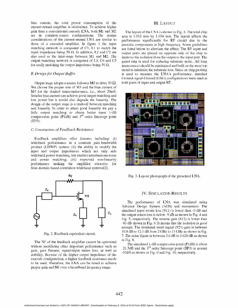
bias current, the total power consumption of the III. LAYOUTcurrent-reused amplifier is minimized. To achieve highergain than a conventional cascade LNA, both MI and M2 The layout of the LNA is shown in Fig. 3. The total chipare in common-source configurations. The design area is 1.013 mm by 1.104 mm. The layout affects theconsiderations of the current-reused LNA are similar to performance significantly for RF circuit due to thethose of a cascaded amplifier. In figure 1 the input parasitic components at high frequency. Some guidelinesmatching network is composed of Cl, LI to match the are listed below to alleviate the effect. The RF input andinput impedance being 50 Q. In addition, L2 and C2 are output ports are placed on opposite side of the chip toalso used as the inter-stage between Ml and M2. The improve the isolation from the output to the input port. Theoutput matching network is composed of L3, C6 and C5 guard-ring is used for reducing substrate noise. All longfor easily matching the output impedance being 50 Q. interconnect should be minimized and built on the most top
metal to minimize the substrate loss. Since on-chip probingB. Designfor Output Buffer is used to measure the LNA's performance, standard
Ground-signal-Ground (GSG) configurations were used atOutput stage adopts a source follower M3 to drive 50 Q.. both ports of input and output RF.
We choose the proper size of M3 and the bias current ofM4 for the desired transconductance, i.e., about 20mS.Smaller bias current can achieve good output matching and
. .
low power but it would also degrade the linearity. Tedesign of the output stage is a tradeoff between matching mis E iIand linearity. In order to attain good linearity we payaya...little output matching to obtain better input l-dB _
rdcompression point (P1dB) and 3 order Intercept point .....
(IIP3). __lill
C. Construction ofFeedback Resistance _____
Feedback amplifiers offer features including: (i) ...........
wideband performance in a constant gain-bandwidth ......
product (GBWP) system; (ii) the ability to modify the...........
input and output impedances which not only aids INwideband power matching, but enables simultaneous noiseand power matching; (iii) improved non-linearityperformance making the amplifier attractive for __time-domain based correlation wideband systems[2].
Rf Fig. 3. Layout photograph of the presented LNA.
IV. SIMULATION RESULTS
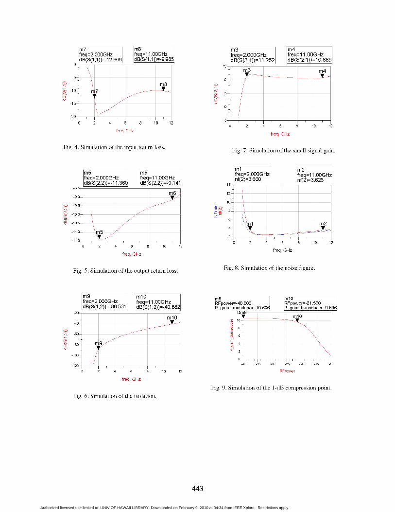
The performance of LNA was simulated usingAdvance Design System (ADS) and momentum. The
l l l l lsimulated input return loss (S 11) is lower than -9 dB andZS ZL the output return loss is below -9 dB as shown in Fig. 4 and
Fig. 5, respectively. The reverse gain (S12) is lower than-40 dB shown in Fig. 6. It means that the isolation is goodenough. The simulated small signal (S21) gain is between10.8 dB to 12.1 dB from 2 GHz to 11 GHz as shown in Fig.
Fig. 2. Feedback equivalent circuit. 7. The noise figure is between 3.6 dB to 3.628 dB as shown
The NF of the feedback amplifier cannot be optimized in Fig.8.The simulated l-dB compression point (P1dB) is aboutwithout sacrificing other important performance such as rd-21.5dB and the 3~ order Intercept point (IIP3) iS aroundgain, gain flatness, input/output return loss, as well as
stability. Because of the higher output impedance of thecascode configuration, a higher feedback resistance needsto be used. Therefore, the LNA can be tuned to achieveproper gain and NF over a broadband frequency range.
442
Authorized licensed use limited to: UNIV OF HAWAII LIBRARY. Downloaded on February 9, 2010 at 04:34 from IEEE Xplore. Restrictions apply.
m7 m8 m3 m4freq=2.OOOGHz freq=1 1.OOGHz freq=2.000GHz freq=1 1 .OOGHzdB(S(1 ,1))=-12.669 dB(S(1 ,1))=-9.985 dB(S(2,1 ))=l 1.252 dB(S(2,1 ))=1 0.889
15-
-5~~~~~~~~~~~~~~~~~~~~0
, 28 1
~~~~~~~~~~~ml _m2
-85 - .___ . .___ - __ - m612-9.0- ~~~ ~ ~ ~ ~ ~ ~ ~ ~~5
10-
-20 X 7 1 o65 0 2 4 6 8 10 12
0 2 4 6 8 10 12
freq, GHz
Fig. 4. Simulation of the input return loss. Fig. 7.Simulation of th e figure.
m9 mlO m9 mlO~~~~~~~~~~~~m mm 6 freq=2.OOOGHz freq=1 1.00H RpwrG4. HRzoe=21.0
dB(S(f2 2))=-11.360 dB(S(2,2))=-9.141 14nrn er=10.06 P nf(2)=3628
-20- - m6____ - ______ - ______ - 12 ____12-9.0- ml.
lo-
N ;X <</ ~~~~~~~~~~~~~~~E ,N' 8
-10.5- \ \m1m
-60-6-
-80- rn9 ~~~~~~~~~~4-
-110 \ f 4 \
2-
-1105 -40 2 4 6 8 10 120 2 4 6 8 10 12
freq, GHzfreq, GH z
Fig. 5. Simulation of the output return loss. Fig. 8. Simulation of the noise figure.
kdB(S(1,2))=-89.531 dB(S(12=OOGHz8 P_gain_ransduce1006 P_gain_transducer=9.606
620 12T
C/)~~~~~~ ~ ~~~~~~~~~ ~ ~ ~ ~~~~~~~~~~~~~~~~~~~~~~~~~~~~~ - o - .........._/ . . m. , . \~~~~~~~~~~~~~~~~~~~~~~~~~I
100 2 4 6 8 10 1 oefreq, GH z
Fig. 9. Simulation of the l-dB compression point.Fig. 6. Simulation of the isolation.
Authorized licensed use limited to: UNIV OF HAWAII LIBRARY. Downloaded on February 9, 2010 at 04:34 from IEEE Xplore. Restrictions apply.

TABLE I PERFORMANCE OF THE LNA
_______________ 11[3] 1[4] 15]1 This WorkTechnology[,um] CMOS 0.18,um CMOS 0.18,um CMOS 0.18,um CMOS 0.18 tmFrequency[GHz] 1.2- 11.9 3.1-9.5 3.1-10.6 2- 11
S11[dB] <-11 <-9 <-9.9 < -9.9Gain[dB] 9.7 15.9-17.5 10.4 10.8 -12.1NF [dB] 4.5 - 5.1 4.7-5.7 4.2-8 3.6 - 3.628
PldB[dBm] -32 -18 -21.5lIP3[dBm] -6.2 * -10 -10Power [mW] 20 33.2 18 14.3
-20
N. -40- i-60-707
-80- ,//ACKNOWLEDGEMENT
E-20- This work was supported in part by the National Chip-140-C_ Implementation Center and by the National Science Council
-140- F1 T FTia,D~ ne rnsO~IC1C)-50 -45 -40 -35 -30 -25 -20 -15 -10 5 of Taiwan, R.O.C., under Grants 96-2221-E-018-024.
RFpower
Fig. 10. Simulation of the 3rd order Intercept point. REFERENCES
[1] IEEE standards, IEEE Std 802.16-2004, Part 16: AirInterface for fixed BWA systems.
V. CONCLUSION [2] Y. Soliman, L. MacEachern, and L. Roy, "A CMOSultra-wideband LNA utilizing a frequency-controlled
A 2 - 11 GHz CMOS LNA fabricated in a TSMC 0.18-pm feedback technique, " in IEEE International Conferencestandard CMOS process with a current-reused technique, a onUltra-Wideband, 2005, pp. 530 - 535.simple feed-back system, and a high-pass input matching [3] C.-F. Liao and S.-I. Liu, "A Broadband Noise-Cancelingnetwork for an IEEE 802.16a WiMAX application is CMOS LNA for 3.1-10.6-GHz UWB Receivers," IEEEpresented. Table I makes a summary and comparison with Journal ofSolid-State Circuits, vol. 42, no. 2, Feb. 2007,other papers reported in the recent literature. The WiMAX pp. 329 - 339.LNA exhibits 10.8 - 12.1 dB gain, 3.6 - 3.628 dB noise [4] Y. Lu, K. S. Yeo, A. Cabuk, J. Ma, A. Do, and Z. Lu, "Afigure while consuming a DC power of 14.3 mW from a novel CMOS low noise amplifier design for 3.1 to 10.61.8V supply. The designed LNA attains the best GHz ultra-wide-band wireless receivers," IEEE Circuitperformance on noise figure and power dissipation with and system, vol. 59, no. 8, Aug. 2006, pp. 1683- 1692.above 10.8 db gain. The gain difference is less than 1.3 dB [5] A. Bevilacqua and A. M. Niknejad, "An ultra-widebandover the whole WiMAX band frequency. It demonstrates CMOS LNA for 3.1 to 10.6 GHz wireless receiver," inthe potential of the designed LNA for applications in IEEEISSCC Dig. Tech.Papers, pp. 382-383, 2004.WiMAX system.
444
Authorized licensed use limited to: UNIV OF HAWAII LIBRARY. Downloaded on February 9, 2010 at 04:34 from IEEE Xplore. Restrictions apply.