ft602 uvc chip configuration guide - ftdi · application note an_435 ft602 uvc chip configuration...
TRANSCRIPT

Use of FTDI devices in life support and/or safety applications is entirely at the user’s risk, and the user agrees to defend, indemnify and hold FTDI harmless from any and all damages, claims, suits
or expense resulting from such use.
Future Technology Devices International Limited (FTDI) Unit 1, 2 Seaward Place, Glasgow G41 1HH, United Kingdom Tel.: +44 (0) 141 429 2777 Fax: + 44 (0) 141 429 2758
Web Site: http://ftdichip.com Copyright © Future Technology Devices International Limited
Application Note
AN_435
FT602 UVC Chip Configuration Guide
Version 1.2
Issue Date: 2017-12-08
This document provides a guide on how to use the FT602 Chip Configuration Programmer application for customizing the chip configuration.
Application Note
AN_435 FT602 UVC Chip Configuration Guide Version 1.2
Document Reference No.: FT_001393 Clearance No.: FTDI#525
2 Product Page
Document Feedback Copyright © Future Technology Devices International Limited
Table of Contents
1 Introduction .............................................................. 4
1.1 Pre-requisite ....................................................................... 4
2 User Interface ........................................................... 5
3 Chip Configuration: Common Configuration ............... 7
3.1 Buffer Configuration ............................................................ 9
4 Advance configuration Settings ............................... 10
4.1 Camera Terminal Controls ................................................. 15
4.2 Processing Unit Control ..................................................... 18
4.3 Enabling UVC Controls ....................................................... 22
4.4 UVC Control in Video Capture applications ........................ 23
5 Auxiliary Interface ................................................... 24
5.1 Hiding Auxiliary interface .................................................. 27
5.2 Re-enable Auxiliary interface ............................................ 27
6 I2C Interface ............................................................ 28
6.1 Writing to a slave on the I2C bus. ...................................... 28
6.2 Reading from a slave on the I2C Bus ................................. 28
6.3 I2C Slave Device Registers ................................................ 29
7 Contact Information ................................................ 33
Appendix A – References ............................................. 34
Document References ............................................................... 34
Acronyms and Abbreviations ..................................................... 34
Appendix B – List of Tables & Figures .......................... 35
List of Tables ............................................................................. 35
List of Figures ........................................................................... 35
Appendix C – Revision History ..................................... 36
Application Note
AN_435 FT602 UVC Chip Configuration Guide Version 1.2
Document Reference No.: FT_001393 Clearance No.: FTDI#525
3 Product Page
Document Feedback Copyright © Future Technology Devices International Limited

Application Note
AN_435 FT602 UVC Chip Configuration Guide Version 1.2
Document Reference No.: FT_001393 Clearance No.: FTDI#525
4 Product Page
Document Feedback Copyright © Future Technology Devices International Limited
1 Introduction
This document explains how to use the FT602 Series Chip Configuration Programmer, a utility application for customizing the chip configuration.
1.1 Pre-requisite
A PC running Windows 7 Operating System or later is required.
The PC should also be installed with the Microsoft Visual C++ 2013 Redistributable (x86) package. Follow the following steps to install it:-
1. Go to https://www.microsoft.com/en-us/download/details.aspx?id=40784
2. Click ‘Download’ button
3. Check the ‘vcredist_x86.exe’ and click ‘Next’.
4. After download completes, run ‘vcredist_x86.exe’ to install the package
Install FT602 WinUSB driver:
1. Run ‘FT602WinUSBInstallation.exe’
2. Click ‘Extract’ button
3. Check License Agreement and click ‘Next’
4. Click ‘Finish’ button when the driver installation is completed.

Application Note
AN_435 FT602 UVC Chip Configuration Guide Version 1.2
Document Reference No.: FT_001393 Clearance No.: FTDI#525
5 Product Page
Document Feedback Copyright © Future Technology Devices International Limited
2 User Interface
Below is a screenshot of the FT602 Chip Configuration Programmer application.
Figure 1 - Application Screenshot
The application allows the user to write and read the device configuration.
Main Buttons Description
Write Configuration The fields from the UI will be selected as a new configuration and written to the device.
Read Configuration Clicking this button will show the current settings that the device is configured with.
Application Note
AN_435 FT602 UVC Chip Configuration Guide Version 1.2
Document Reference No.: FT_001393 Clearance No.: FTDI#525
6 Product Page
Document Feedback Copyright © Future Technology Devices International Limited
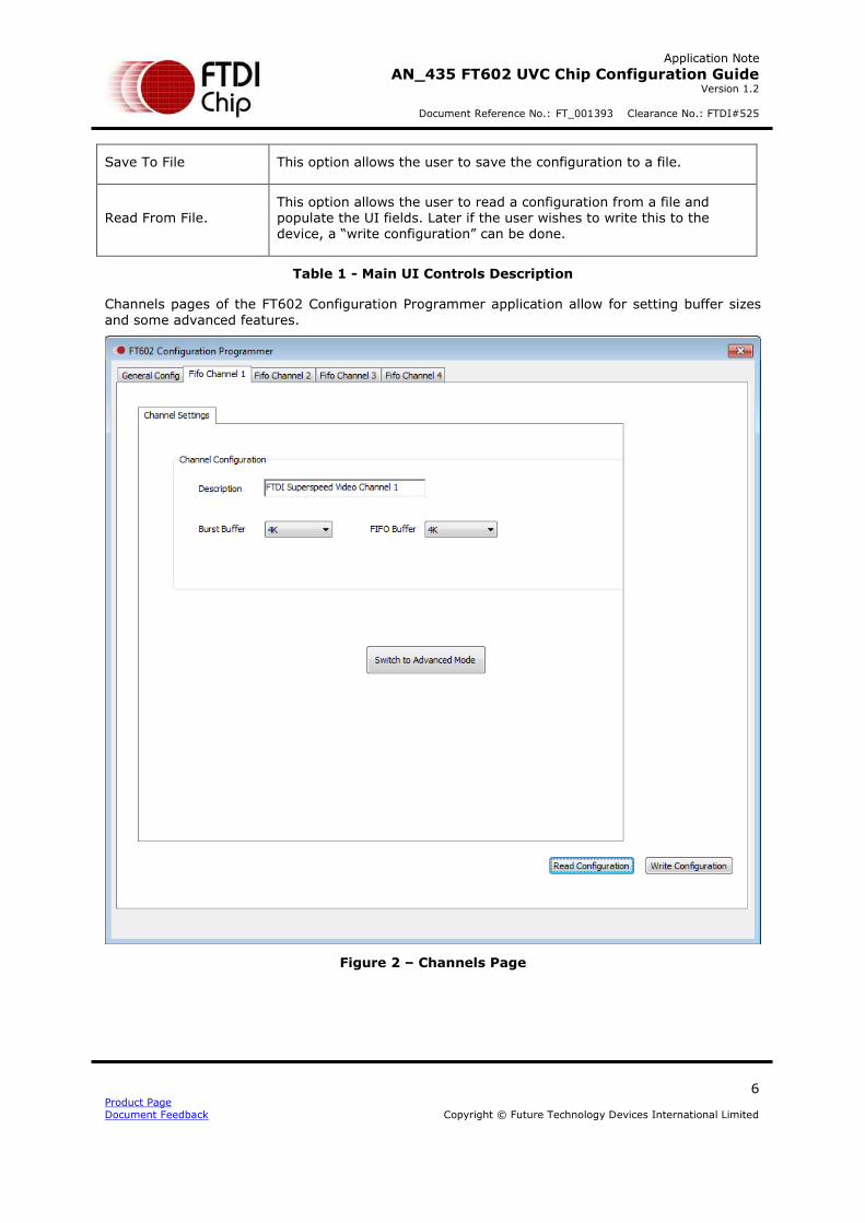
Save To File This option allows the user to save the configuration to a file.
Read From File. This option allows the user to read a configuration from a file and populate the UI fields. Later if the user wishes to write this to the device, a “write configuration” can be done.
Table 1 - Main UI Controls Description
Channels pages of the FT602 Configuration Programmer application allow for setting buffer sizes
and some advanced features.
Figure 2 – Channels Page
Application Note
AN_435 FT602 UVC Chip Configuration Guide Version 1.2
Document Reference No.: FT_001393 Clearance No.: FTDI#525
7 Product Page
Document Feedback Copyright © Future Technology Devices International Limited
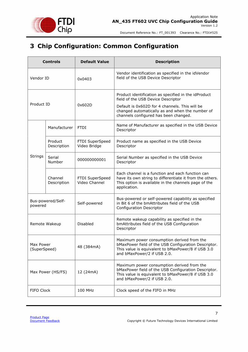
3 Chip Configuration: Common Configuration
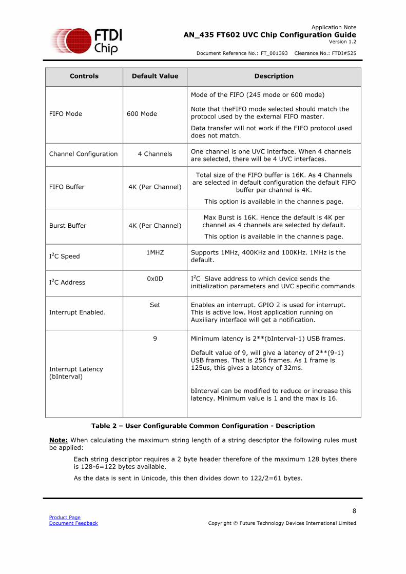
Controls Default Value Description
Vendor ID 0x0403
Vendor identification as specified in the idVendor field of the USB Device Descriptor
Product ID 0x602D
Product identification as specified in the idProduct field of the USB Device Descriptor
Default is 0x602D for 4 channels. This will be
changed automatically as and when the number of channels configured has been changed.
Strings
Manufacturer FTDI Name of Manufacturer as specified in the USB Device Descriptor
Product Description
FTDI SuperSpeed Video Bridge
Product name as specified in the USB Device Descriptor
Serial Number
000000000001 Serial Number as specified in the USB Device Descriptor
Channel Description
FTDI SuperSpeed Video Channel
Each channel is a function and each function can
have its own string to differentiate it from the others. This option is available in the channels page of the application.
Bus-powered/Self-powered
Self-powered Bus-powered or self-powered capability as specified in Bit 6 of the bmAttributes field of the USB Configuration Descriptor
Remote Wakeup Disabled Remote wakeup capability as specified in the bmAttributes field of the USB Configuration Descriptor
Max Power (SuperSpeed)
48 (384mA)
Maximum power consumption derived from the
bMaxPower field of the USB Configuration Descriptor. This value is equivalent to bMaxPower/8 if USB 3.0 and bMaxPower/2 if USB 2.0.
Max Power (HS/FS) 12 (24mA)
Maximum power consumption derived from the bMaxPower field of the USB Configuration Descriptor. This value is equivalent to bMaxPower/8 if USB 3.0
and bMaxPower/2 if USB 2.0.
FIFO Clock 100 MHz Clock speed of the FIFO in MHz
Application Note
AN_435 FT602 UVC Chip Configuration Guide Version 1.2
Document Reference No.: FT_001393 Clearance No.: FTDI#525
8 Product Page
Document Feedback Copyright © Future Technology Devices International Limited
Controls Default Value Description
FIFO Mode 600 Mode
Mode of the FIFO (245 mode or 600 mode)
Note that theFIFO mode selected should match the
protocol used by the external FIFO master.
Data transfer will not work if the FIFO protocol used does not match.
Channel Configuration 4 Channels One channel is one UVC interface. When 4 channels are selected, there will be 4 UVC interfaces.
FIFO Buffer 4K (Per Channel)
Total size of the FIFO buffer is 16K. As 4 Channels are selected in default configuration the default FIFO
buffer per channel is 4K.
This option is available in the channels page.
Burst Buffer 4K (Per Channel)
Max Burst is 16K. Hence the default is 4K per
channel as 4 channels are selected by default.
This option is available in the channels page.
I2C Speed 1MHZ Supports 1MHz, 400KHz and 100KHz. 1MHz is the
default.
I2C Address 0x0D I2C Slave address to which device sends the
initialization parameters and UVC specific commands
Interrupt Enabled. Set Enables an interrupt. GPIO 2 is used for interrupt.
This is active low. Host application running on
Auxiliary interface will get a notification.
Interrupt Latency (bInterval)
9 Minimum latency is 2**(bInterval-1) USB frames.
Default value of 9, will give a latency of 2**(9-1) USB frames. That is 256 frames. As 1 frame is 125us, this gives a latency of 32ms.
bInterval can be modified to reduce or increase this latency. Minimum value is 1 and the max is 16.
Table 2 – User Configurable Common Configuration - Description
Note: When calculating the maximum string length of a string descriptor the following rules must
be applied:
Each string descriptor requires a 2 byte header therefore of the maximum 128 bytes there is 128-6=122 bytes available.
As the data is sent in Unicode, this then divides down to 122/2=61 bytes.

Application Note
AN_435 FT602 UVC Chip Configuration Guide Version 1.2
Document Reference No.: FT_001393 Clearance No.: FTDI#525
9 Product Page
Document Feedback Copyright © Future Technology Devices International Limited
Additional restrictions are also applied:
Max size for SerialNumber is 16 characters
Max size for Description is 32 characters
Max size for Manufacturer is 61-32-16=13 characters when Description and SerialNumber are maxed out.
3.1 Buffer Configuration
Whenever there is a channel configuration change, or FIFO buffer or burst buffer selection change, another configuration pop up will be shown so that buffers for all the channels can be configured at once.
Note: Whenever there is a change in buffer size, the total buffer size must be 16K. Otherwise the tool won’t let the user program the configuration changes.
The picture below shows a configuration for two channels.
Figure 3 –Buffer Management
Application Note
AN_435 FT602 UVC Chip Configuration Guide Version 1.2
Document Reference No.: FT_001393 Clearance No.: FTDI#525
10 Product Page
Document Feedback Copyright © Future Technology Devices International Limited
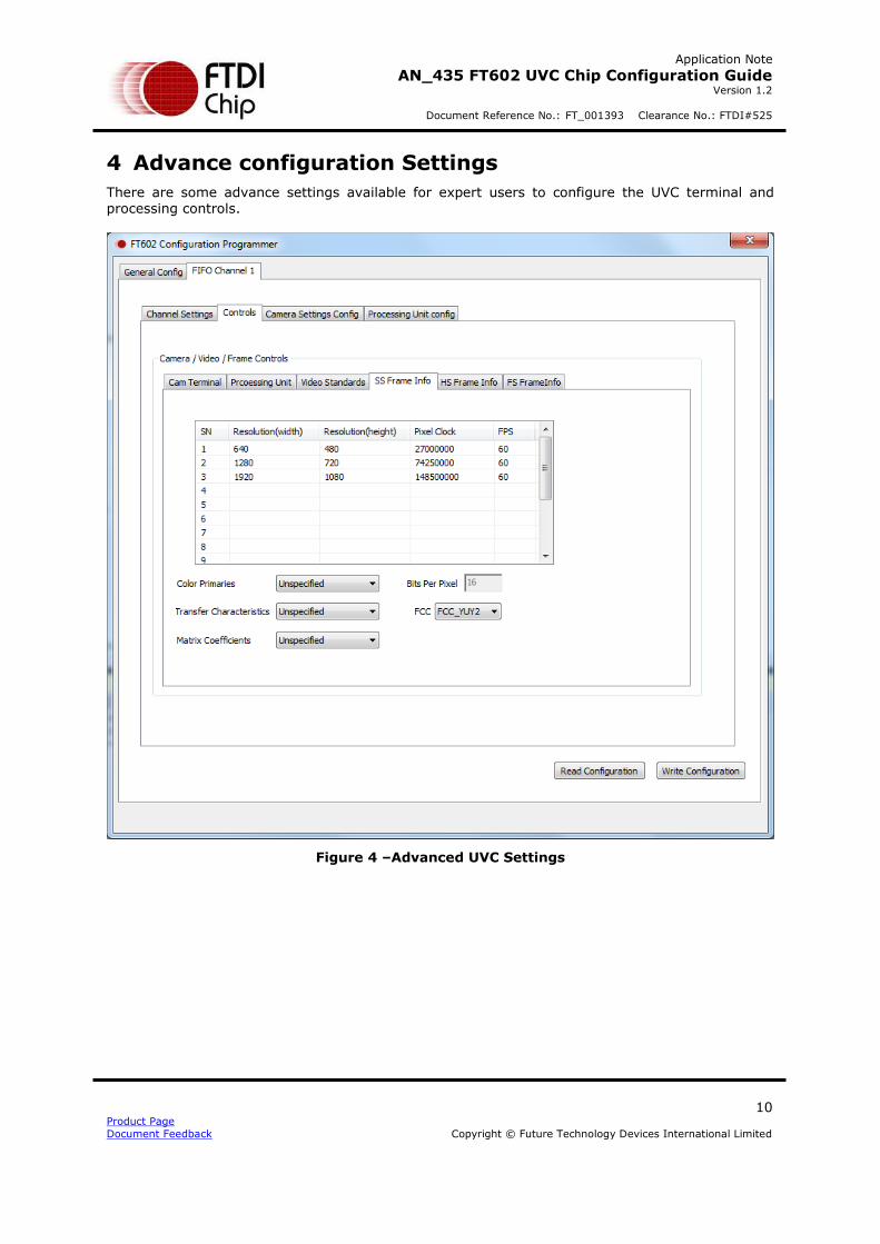
4 Advance configuration Settings
There are some advance settings available for expert users to configure the UVC terminal and processing controls.
Figure 4 –Advanced UVC Settings
Application Note
AN_435 FT602 UVC Chip Configuration Guide Version 1.2
Document Reference No.: FT_001393 Clearance No.: FTDI#525
11 Product Page
Document Feedback Copyright © Future Technology Devices International Limited
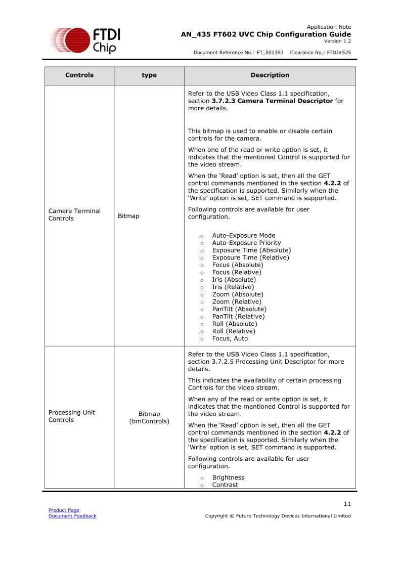
Controls type Description
Camera Terminal Controls Bitmap
Refer to the USB Video Class 1.1 specification, section 3.7.2.3 Camera Terminal Descriptor for more details.
This bitmap is used to enable or disable certain controls for the camera.
When one of the read or write option is set, it indicates that the mentioned Control is supported for the video stream.
When the ‘Read’ option is set, then all the GET control commands mentioned in the section 4.2.2 of
the specification is supported. Similarly when the ‘Write’ option is set, SET command is supported.
Following controls are available for user configuration.
o Auto-Exposure Mode o Auto-Exposure Priority
o Exposure Time (Absolute) o Exposure Time (Relative) o Focus (Absolute) o Focus (Relative) o Iris (Absolute) o Iris (Relative)
o Zoom (Absolute) o Zoom (Relative) o PanTilt (Absolute)
o PanTilt (Relative) o Roll (Absolute) o Roll (Relative) o Focus, Auto
Processing Unit Controls
Bitmap (bmControls)
Refer to the USB Video Class 1.1 specification, section 3.7.2.5 Processing Unit Descriptor for more details.
This indicates the availability of certain processing Controls for the video stream.
When any of the read or write option is set, it indicates that the mentioned Control is supported for the video stream.
When the ‘Read’ option is set, then all the GET control commands mentioned in the section 4.2.2 of the specification is supported. Similarly when the
‘Write’ option is set, SET command is supported.
Following controls are available for user configuration.
o Brightness o Contrast

Application Note
AN_435 FT602 UVC Chip Configuration Guide Version 1.2
Document Reference No.: FT_001393 Clearance No.: FTDI#525
12 Product Page
Document Feedback Copyright © Future Technology Devices International Limited
Controls type Description
o Hue o Saturation o Sharpness o Gamma
o White Balance Temperature o White Balance Component o Backlight Compensation o Gain o Power Line Frequency o Hue, Auto o White Balance Temperature, Auto
o White Balance Component, Auto o Digital Multiplier o Digital Multiplier Limit
o Analog Video Standard
Bitmap
(bmVideoStandards)
A bitmap of all analog video standards supported by the Processing Unit.
A value of zero indicates that this bitmap should be ignored.
Following options are available for user configuration.
o None o NTSC – 525/60
o PAL – 625/50 o SECAM – 625/50 o NTSC – 625/50 o PAL – 525/60
Frame Info
Resolution Width * Height in pixels.
Frame Interval This value indicates the number of frames per second. For example, for a 60fps, the value should be 60.
Color Primaries
This defines the color primaries and the reference white.
Following options are available to choose.
0: Unspecified (Image characteristics unknown)
1: BT.709, sRGB (default)
2: BT.470-2 (M)
3: BT.470-2 (B, G)
4: SMPTE 170M
5: SMPTE 240M
Please refer to 3.9.2.6 Color Matching Descriptor of UVC specification 1.1.

Application Note
AN_435 FT602 UVC Chip Configuration Guide Version 1.2
Document Reference No.: FT_001393 Clearance No.: FTDI#525
13 Product Page
Document Feedback Copyright © Future Technology Devices International Limited
Controls type Description
Transfer Characteristics
This field defines the optoelectronic transfer characteristic of the source picture also called the gamma function.
Following options are available for selection.
0: Unspecified (Image characteristics unknown)
1: BT.709 (default)
2: BT.470-2 M
3: BT.470-2 B, G
4: SMPTE 170M
5: SMPTE 240M
6: Linear (V = Lc)
7: sRGB (very similar to BT.709)
Refer to 3.9.2.6 Color Matching Descriptor of UVC specification 1.1.
Matrix Coefficients
Matrix used to compute luma and chroma values from the color primaries.
0: Unspecified (Image characteristics unknown)
1: BT. 709
2: FCC
3: BT.470-2 B, G
4: SMPTE 170M (BT.601, default)
5: SMPTE 240M
Refer to 3.9.2.6 Color Matching Descriptor of UVC specification 1.1.
FCC (Four Character Code).
It’s a sequence of 4 bytes used to uniquely identify data formats.
Please visit http://www.fourcc.org/ for more information.
Following option formats are available.
o YUY2 o YUYV
o Y41P o YUVP
o YUV4 o IYU2 o AYUV o NV12 o NV16

Application Note
AN_435 FT602 UVC Chip Configuration Guide Version 1.2
Document Reference No.: FT_001393 Clearance No.: FTDI#525
14 Product Page
Document Feedback Copyright © Future Technology Devices International Limited
Controls type Description
o NV24 o YV12 o GREY o Y16
o RGBP o RGB3 o RGB4 o BA24 o BY8 o BYR2
Bits Per Pixel (Read only)
This is read only. And gets generated based on the FCC selected.
Table 3 – Camera Terminal, Processing Unit & Frame Information

Application Note
AN_435 FT602 UVC Chip Configuration Guide Version 1.2
Document Reference No.: FT_001393 Clearance No.: FTDI#525
15 Product Page
Document Feedback Copyright © Future Technology Devices International Limited
4.1 Camera Terminal Controls
A separate tab named “Camera Setting config” is provided in the tool in the channels page .This allows the user to define the default values, steps (Resolution), min and max values of each control.
Refer to the section 4.2.2.1 Camera Terminal Control Requests of UVC specification 1.1.
Figure 5 –Camera Terminal Configurable Options
Application Note
AN_435 FT602 UVC Chip Configuration Guide Version 1.2
Document Reference No.: FT_001393 Clearance No.: FTDI#525
16 Product Page
Document Feedback Copyright © Future Technology Devices International Limited
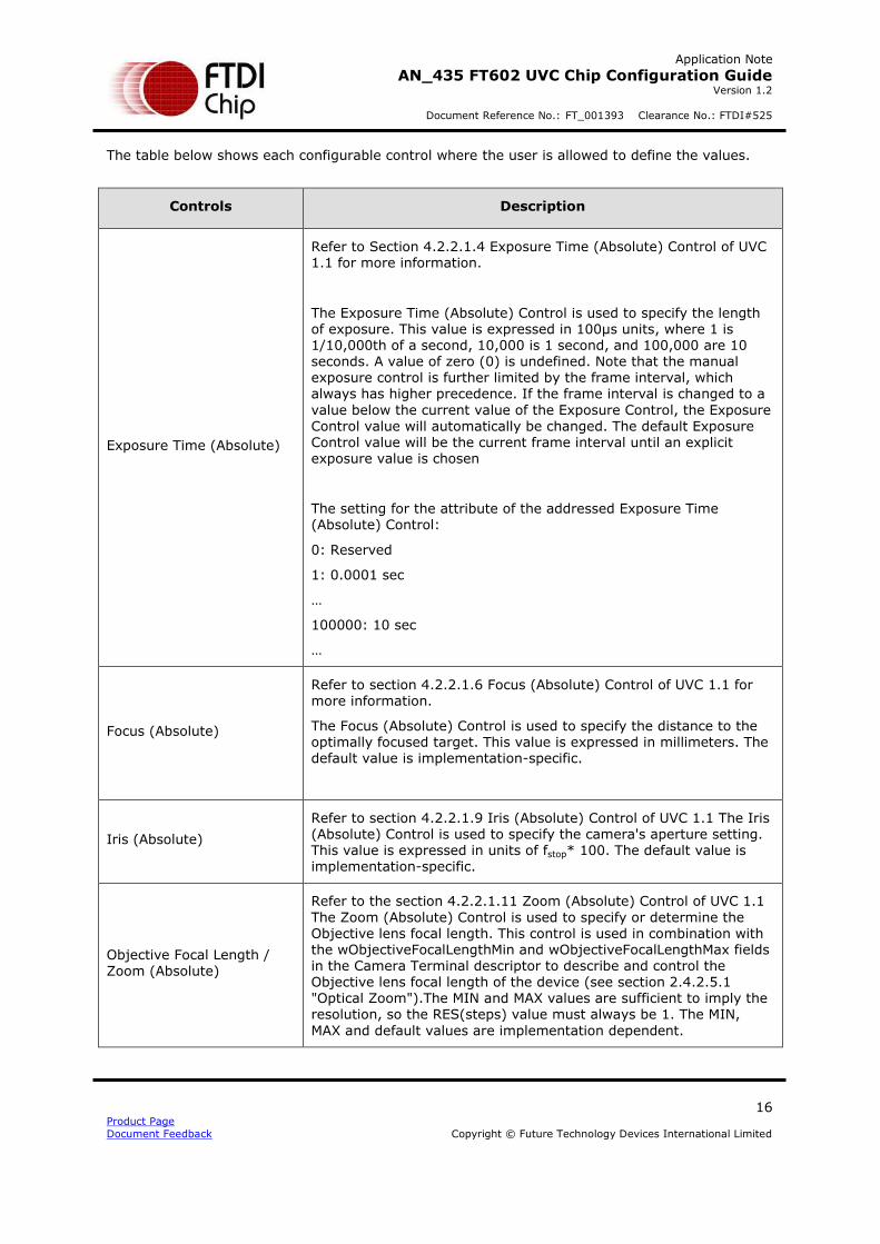
The table below shows each configurable control where the user is allowed to define the values.
Controls Description
Exposure Time (Absolute)
Refer to Section 4.2.2.1.4 Exposure Time (Absolute) Control of UVC 1.1 for more information.
The Exposure Time (Absolute) Control is used to specify the length of exposure. This value is expressed in 100µs units, where 1 is 1/10,000th of a second, 10,000 is 1 second, and 100,000 are 10 seconds. A value of zero (0) is undefined. Note that the manual exposure control is further limited by the frame interval, which always has higher precedence. If the frame interval is changed to a
value below the current value of the Exposure Control, the Exposure
Control value will automatically be changed. The default Exposure Control value will be the current frame interval until an explicit exposure value is chosen
The setting for the attribute of the addressed Exposure Time (Absolute) Control:
0: Reserved
1: 0.0001 sec
…
100000: 10 sec
…
Focus (Absolute)
Refer to section 4.2.2.1.6 Focus (Absolute) Control of UVC 1.1 for
more information.
The Focus (Absolute) Control is used to specify the distance to the optimally focused target. This value is expressed in millimeters. The default value is implementation-specific.
Iris (Absolute)
Refer to section 4.2.2.1.9 Iris (Absolute) Control of UVC 1.1 The Iris (Absolute) Control is used to specify the camera's aperture setting. This value is expressed in units of fstop* 100. The default value is implementation-specific.
Objective Focal Length /
Zoom (Absolute)
Refer to the section 4.2.2.1.11 Zoom (Absolute) Control of UVC 1.1
The Zoom (Absolute) Control is used to specify or determine the Objective lens focal length. This control is used in combination with the wObjectiveFocalLengthMin and wObjectiveFocalLengthMax fields in the Camera Terminal descriptor to describe and control the
Objective lens focal length of the device (see section 2.4.2.5.1 "Optical Zoom").The MIN and MAX values are sufficient to imply the resolution, so the RES(steps) value must always be 1. The MIN,
MAX and default values are implementation dependent.
Application Note
AN_435 FT602 UVC Chip Configuration Guide Version 1.2
Document Reference No.: FT_001393 Clearance No.: FTDI#525
17 Product Page
Document Feedback Copyright © Future Technology Devices International Limited
Controls Description
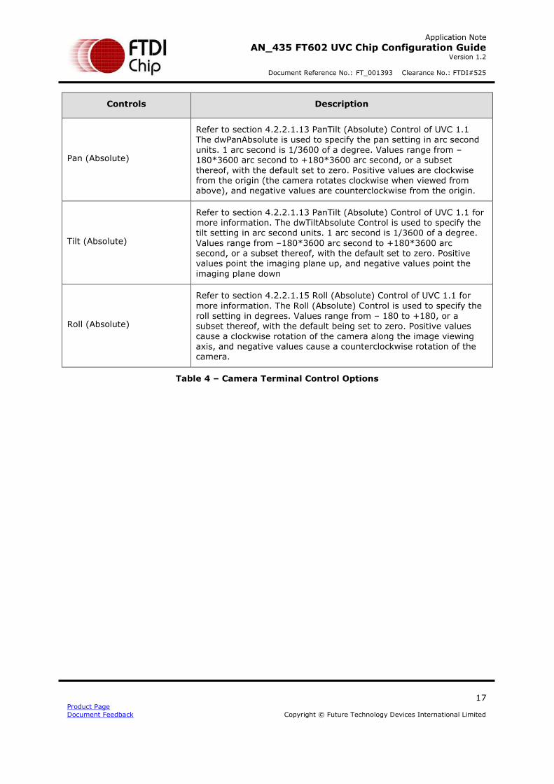
Pan (Absolute)
Refer to section 4.2.2.1.13 PanTilt (Absolute) Control of UVC 1.1 The dwPanAbsolute is used to specify the pan setting in arc second units. 1 arc second is 1/3600 of a degree. Values range from –180*3600 arc second to +180*3600 arc second, or a subset
thereof, with the default set to zero. Positive values are clockwise from the origin (the camera rotates clockwise when viewed from above), and negative values are counterclockwise from the origin.
Tilt (Absolute)
Refer to section 4.2.2.1.13 PanTilt (Absolute) Control of UVC 1.1 for more information. The dwTiltAbsolute Control is used to specify the tilt setting in arc second units. 1 arc second is 1/3600 of a degree.
Values range from –180*3600 arc second to +180*3600 arc second, or a subset thereof, with the default set to zero. Positive
values point the imaging plane up, and negative values point the imaging plane down
Roll (Absolute)
Refer to section 4.2.2.1.15 Roll (Absolute) Control of UVC 1.1 for
more information. The Roll (Absolute) Control is used to specify the roll setting in degrees. Values range from – 180 to +180, or a subset thereof, with the default being set to zero. Positive values cause a clockwise rotation of the camera along the image viewing axis, and negative values cause a counterclockwise rotation of the camera.
Table 4 – Camera Terminal Control Options

Application Note
AN_435 FT602 UVC Chip Configuration Guide Version 1.2
Document Reference No.: FT_001393 Clearance No.: FTDI#525
18 Product Page
Document Feedback Copyright © Future Technology Devices International Limited
4.2 Processing Unit Control
A separate tab named “Processing Unit config” is provided in the tool in the channels page. This allows the user to define the default values, steps (Resolution), min and max values of each control.
Refer to section 4.2.2.3 Processing Unit Control Requests of the UVC specification 1.1.
Figure 6 –Processing Unit Control Options
The following table presents a detailed description of all possible Controls a Processing Unit can incorporate. For each Control, the layout of the parameter block together with the appropriate
Control Selector is listed for all forms of the Get/Set Processing Unit Control request. All values are interpreted as unsigned unless otherwise specified.

Application Note
AN_435 FT602 UVC Chip Configuration Guide Version 1.2
Document Reference No.: FT_001393 Clearance No.: FTDI#525
19 Product Page
Document Feedback Copyright © Future Technology Devices International Limited
Controls Description
Backlight compensation
Refer to section 4.2.2.3.1 Backlight Compensation Control of the UVC spec 1.1 for more information. The Backlight Compensation Control is used to specify the backlight compensation. A value of zero indicates that the backlight compensation is disabled. A non-
zero value indicates that the backlight compensation is enabled. The device may support a range of values, or simply a binary switch. If a range is supported, a low number indicates the least amount of backlight compensation. The default value is implementation-specific, but enabling backlight compensation is recommended.
Brightness
Refer to section 4.2.2.3.2 Brightness Control of the UVC spec 1.1 for
more information.
This is used to specify the brightness. This is a relative value where increasing values indicate increasing brightness. The MIN and MAX values are sufficient to imply the resolution, so the RES value must always be 1. The MIN, MAX and default values are implementation
dependent.
Contrast
Refer to section 4.2.2.3.3 Contrast Control of the UVC spec 1.1 for more information.
This is used to specify the contrast value. This is a relative value where increasing values indicate increasing contrast. The MIN and MAX values are sufficient to imply the resolution, so the RES value
must always be 1. The MIN, MAX and default values are implementation dependent.
Gain
Refer to section 4.2.2.3.4 Gain Control of the UVC spec 1.1 for more
information.
This is used to specify the gain setting. This is a relative value where
increasing values indicate increasing gain. The MIN and MAX values are sufficient to imply the resolution, so the RES value must always be 1. The MIN, MAX and default values are implementation dependent.
Hue
Refer to section 4.2.2.3.6 Hue Control of the UVC spec 1.1 for more
information.
This is used to specify the hue setting. The value of the hue setting is expressed in degrees multiplied by 100. The required range must be a subset of -18000 to 18000 (-180 to +180 degrees). The default value must be zero.
Saturation
Refer to section 4.2.2.3.8 Saturation Control of the UVC spec 1.1 for
more information.
This is used to specify the saturation setting. This is a relative value where increasing values indicate increasing saturation. A Saturation value of 0 indicates grayscale. The MIN and MAX values are
Application Note
AN_435 FT602 UVC Chip Configuration Guide Version 1.2
Document Reference No.: FT_001393 Clearance No.: FTDI#525
20 Product Page
Document Feedback Copyright © Future Technology Devices International Limited
Controls Description
sufficient to imply the resolution, so the RES value must always be 1.
The MIN, MAX and default values are implementation-dependent
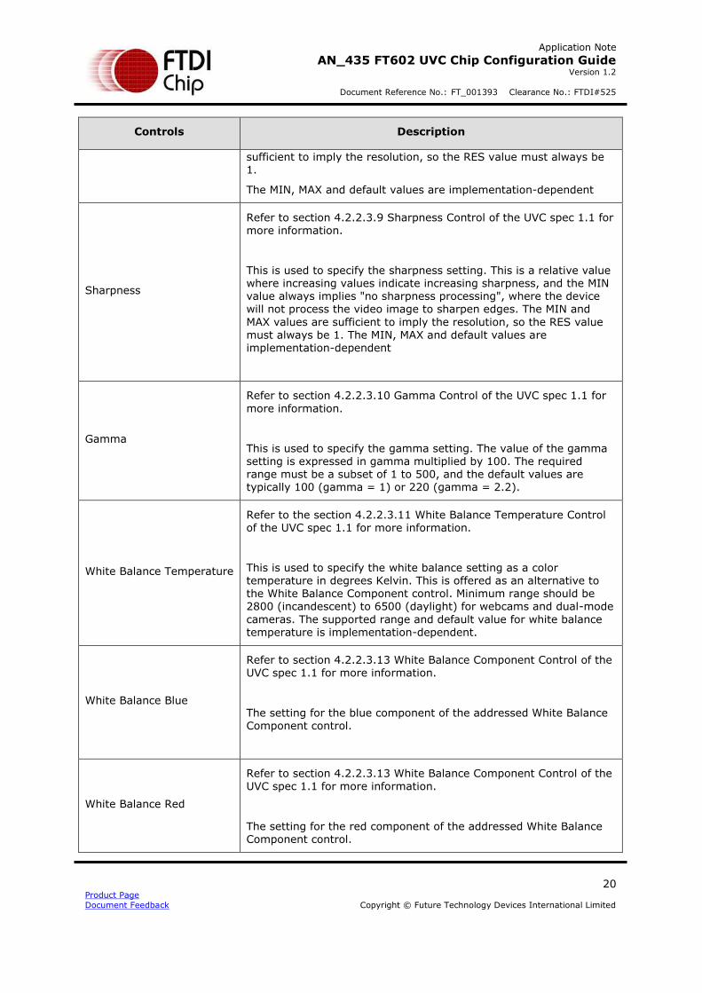
Sharpness
Refer to section 4.2.2.3.9 Sharpness Control of the UVC spec 1.1 for more information.
This is used to specify the sharpness setting. This is a relative value where increasing values indicate increasing sharpness, and the MIN value always implies "no sharpness processing", where the device will not process the video image to sharpen edges. The MIN and
MAX values are sufficient to imply the resolution, so the RES value
must always be 1. The MIN, MAX and default values are implementation-dependent
Gamma
Refer to section 4.2.2.3.10 Gamma Control of the UVC spec 1.1 for
more information.
This is used to specify the gamma setting. The value of the gamma setting is expressed in gamma multiplied by 100. The required range must be a subset of 1 to 500, and the default values are typically 100 (gamma = 1) or 220 (gamma = 2.2).
White Balance Temperature
Refer to the section 4.2.2.3.11 White Balance Temperature Control of the UVC spec 1.1 for more information.
This is used to specify the white balance setting as a color temperature in degrees Kelvin. This is offered as an alternative to the White Balance Component control. Minimum range should be 2800 (incandescent) to 6500 (daylight) for webcams and dual-mode
cameras. The supported range and default value for white balance temperature is implementation-dependent.
White Balance Blue
Refer to section 4.2.2.3.13 White Balance Component Control of the UVC spec 1.1 for more information.
The setting for the blue component of the addressed White Balance Component control.
White Balance Red
Refer to section 4.2.2.3.13 White Balance Component Control of the
UVC spec 1.1 for more information.
The setting for the red component of the addressed White Balance Component control.
Application Note
AN_435 FT602 UVC Chip Configuration Guide Version 1.2
Document Reference No.: FT_001393 Clearance No.: FTDI#525
21 Product Page
Document Feedback Copyright © Future Technology Devices International Limited
Controls Description
Digital Multiplier Step
Refer to section 4.2.2.3.15 Digital Multiplier Control of the UVC spec 1.1 for more information.
This is used to specify the amount of Digital Zoom applied to the
optical image. This is the position within the range of possible values of multiplier m, allowing the multiplier resolution to be described by the device implementation. The MIN and MAX values are sufficient to imply the resolution, so the RES value must always be 1. The MIN, MAX and default values are implementation dependent. If the Digital Multiplier Limit Control is supported, the MIN and MAX values shall match the MIN and MAX values of the Digital Multiplier Control.
Digital Multiplier Limit
Refer to section 4.2.2.3.16 Digital Multiplier Limit Control of the UVC spec 1.1 for more information.
This is used to specify an upper limit for the amount of Digital Zoom applied to the optical image. This is the maximum position within the range of possible values of multiplier m. The MIN and MAX
values are sufficient to imply the resolution, so the RES value must always be 1. The MIN, MAX and default values are implementation dependent.
A value specifying the upper bound for Z′cur (see section 2.4.2.5.2 "Digital Zoom" of UVC spec 1.1.)
Power Line Frequency
Refer to the section 4.2.2.3.5 Power Line Frequency Control of the UVC spec 1.1 for more information.
This control allows the host software to specify the local power line frequency, in order for the device to properly implement anti-flicker processing, if supported. The default is implementation-specific.
The setting for the attribute of the addressed Power Line Frequency control:
0: Disabled
1: 50 Hz
2: 60 Hz
Table 5 – Processing Control & Description
Application Note
AN_435 FT602 UVC Chip Configuration Guide Version 1.2
Document Reference No.: FT_001393 Clearance No.: FTDI#525
22 Product Page
Document Feedback Copyright © Future Technology Devices International Limited
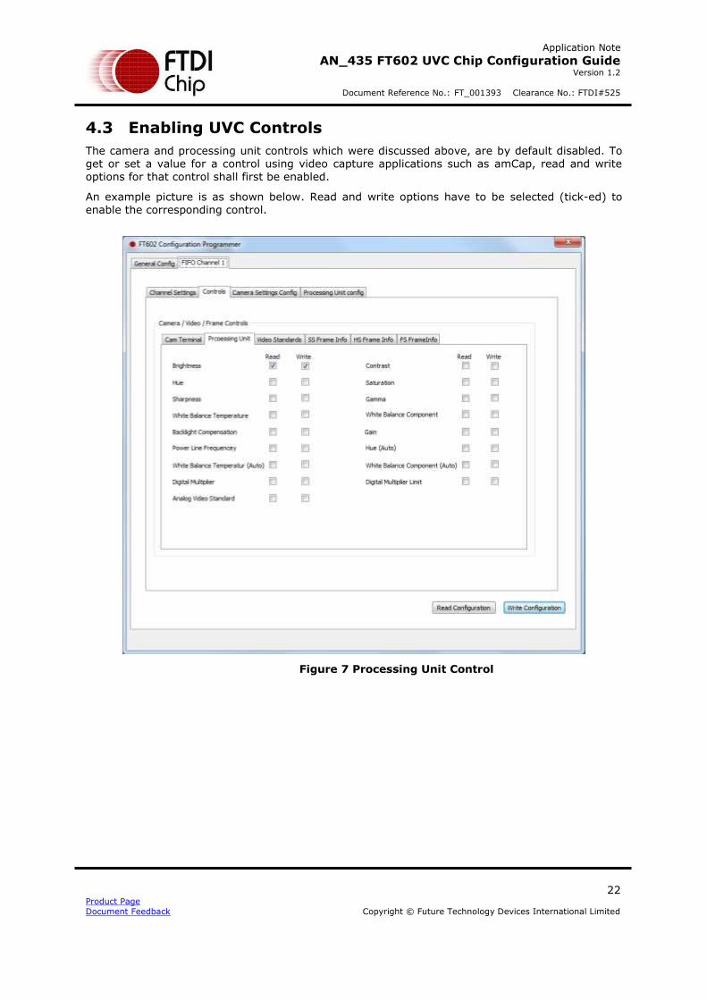
4.3 Enabling UVC Controls
The camera and processing unit controls which were discussed above, are by default disabled. To get or set a value for a control using video capture applications such as amCap, read and write options for that control shall first be enabled.
An example picture is as shown below. Read and write options have to be selected (tick-ed) to enable the corresponding control.
Figure 7 Processing Unit Control

Application Note
AN_435 FT602 UVC Chip Configuration Guide Version 1.2
Document Reference No.: FT_001393 Clearance No.: FTDI#525
23 Product Page
Document Feedback Copyright © Future Technology Devices International Limited
4.4 UVC Control in Video Capture applications
Once the read and write permissions are set in the configuration, video capture applications can change the values of these controls. A sample picture from amCap application is shown below.
Figure 8 Application adjusting a UVC control

Application Note
AN_435 FT602 UVC Chip Configuration Guide Version 1.2
Document Reference No.: FT_001393 Clearance No.: FTDI#525
24 Product Page
Document Feedback Copyright © Future Technology Devices International Limited
5 Auxiliary Interface
The FT602 Chip Configuration Programmer application uses the auxiliary interface to communicate with the device. There is an auxiliary interface in addition to the UVC interface, as seen in the picture below.
Figure 9 Auxiliary interface highlighted
When this auxiliary interface is enumerated, in most of the cases, Windows is able to successfully install the WinUSB drivers. However, depending on certain versions of the Windows operating system, drivers for this interface may not load or install successfully. In such cases, configuration programmer cannot run as it fails to identify the interface and WinUSB installation has to be
performed manually
Follow the below steps to install WinUSB driver.
1. Double click FT602WinUSBInstallation.exe.
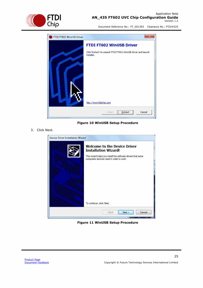
2. Click on the ‘extract’ button to unpack the installer.
Application Note
AN_435 FT602 UVC Chip Configuration Guide Version 1.2
Document Reference No.: FT_001393 Clearance No.: FTDI#525
25 Product Page
Document Feedback Copyright © Future Technology Devices International Limited
Figure 10 WinUSB Setup Procedure
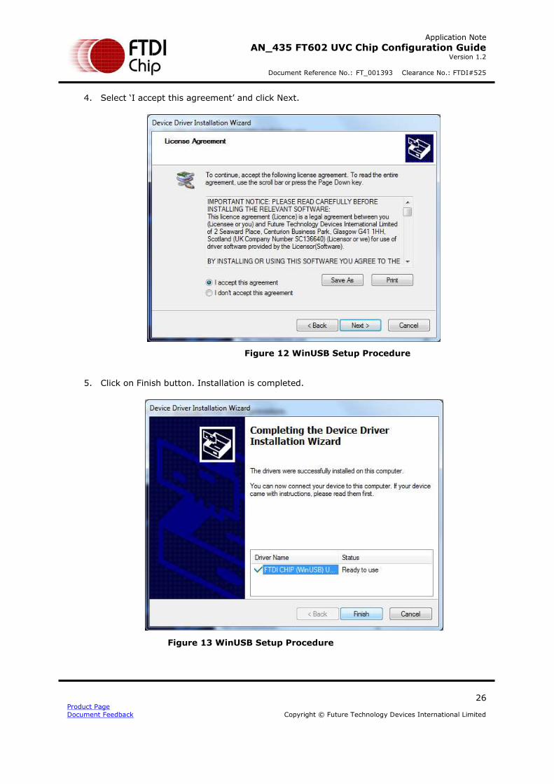
3. Click Next.
Figure 11 WinUSB Setup Procedure
Application Note
AN_435 FT602 UVC Chip Configuration Guide Version 1.2
Document Reference No.: FT_001393 Clearance No.: FTDI#525
26 Product Page
Document Feedback Copyright © Future Technology Devices International Limited
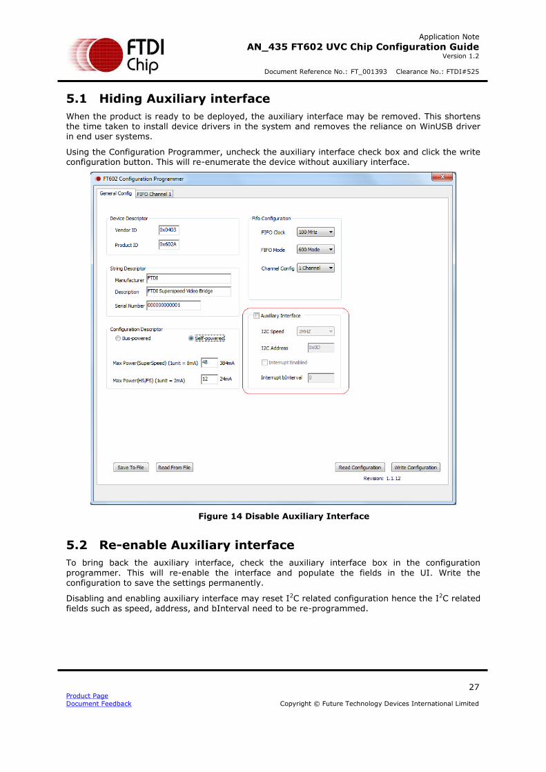
4. Select ‘I accept this agreement’ and click Next.
Figure 12 WinUSB Setup Procedure
5. Click on Finish button. Installation is completed.
Figure 13 WinUSB Setup Procedure
Application Note
AN_435 FT602 UVC Chip Configuration Guide Version 1.2
Document Reference No.: FT_001393 Clearance No.: FTDI#525
27 Product Page
Document Feedback Copyright © Future Technology Devices International Limited
5.1 Hiding Auxiliary interface
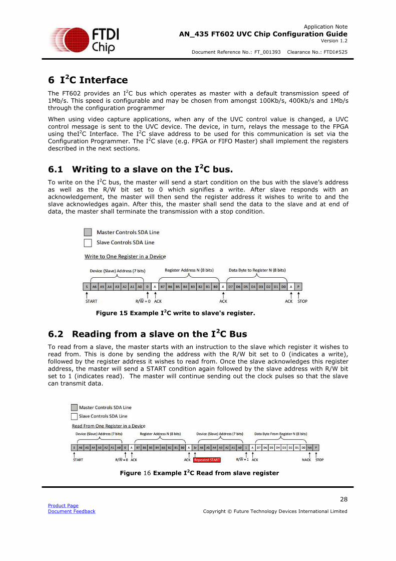
When the product is ready to be deployed, the auxiliary interface may be removed. This shortens the time taken to install device drivers in the system and removes the reliance on WinUSB driver in end user systems.
Using the Configuration Programmer, uncheck the auxiliary interface check box and click the write configuration button. This will re-enumerate the device without auxiliary interface.
Figure 14 Disable Auxiliary Interface
5.2 Re-enable Auxiliary interface
To bring back the auxiliary interface, check the auxiliary interface box in the configuration
programmer. This will re-enable the interface and populate the fields in the UI. Write the configuration to save the settings permanently.
Disabling and enabling auxiliary interface may reset I2C related configuration hence the I2C related
fields such as speed, address, and bInterval need to be re-programmed.
Application Note
AN_435 FT602 UVC Chip Configuration Guide Version 1.2
Document Reference No.: FT_001393 Clearance No.: FTDI#525
28 Product Page
Document Feedback Copyright © Future Technology Devices International Limited
6 I2C Interface
The FT602 provides an I2C bus which operates as master with a default transmission speed of 1Mb/s. This speed is configurable and may be chosen from amongst 100Kb/s, 400Kb/s and 1Mb/s through the configuration programmer
When using video capture applications, when any of the UVC control value is changed, a UVC
control message is sent to the UVC device. The device, in turn, relays the message to the FPGA using theI2C Interface. The I2C slave address to be used for this communication is set via the Configuration Programmer. The I2C slave (e.g. FPGA or FIFO Master) shall implement the registers described in the next sections.
6.1 Writing to a slave on the I2C bus.
To write on the I2C bus, the master will send a start condition on the bus with the slave’s address
as well as the R/W bit set to 0 which signifies a write. After slave responds with an acknowledgement, the master will then send the register address it wishes to write to and the slave acknowledges again. After this, the master shall send the data to the slave and at end of data, the master shall terminate the transmission with a stop condition.
Figure 15 Example I2C write to slave's register.
6.2 Reading from a slave on the I2C Bus
To read from a slave, the master starts with an instruction to the slave which register it wishes to read from. This is done by sending the address with the R/W bit set to 0 (indicates a write), followed by the register address it wishes to read from. Once the slave acknowledges this register address, the master will send a START condition again followed by the slave address with R/W bit
set to 1 (indicates read). The master will continue sending out the clock pulses so that the slave can transmit data.
Figure 16 Example I2C Read from slave register

Application Note
AN_435 FT602 UVC Chip Configuration Guide Version 1.2
Document Reference No.: FT_001393 Clearance No.: FTDI#525
29 Product Page
Document Feedback Copyright © Future Technology Devices International Limited
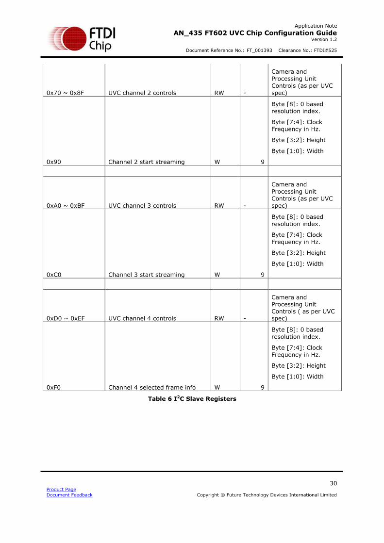
6.3 I2C Slave Device Registers
The I2C master currently supports registers listed in the below table. These are optional registers. The slave need not implement all of them. It can selectively implement the ones it wants to support.
Register address Name Access
Size
(Byte) Description
0x0 FT602 configuration(device reset) W 1
bit[7:4]: reserved
bit[3]: I2C interrupt, 0 = disable, 1 = enable
bit[2:1]:
2’b00 = unknown speed
2’b01 = Super Speed
2’b10 = High Speed
2’b11 = Full Speed
B[0]: FIFO Mode, 0 = FT245, 1 = FT600
0x1 FT602 power status W 1
0 = Wakeup,
1 = Suspend,
2 = PowerOff, (Host PC state)
Others = Reserved
0x40 ~ 0x5F UVC channel 1 controls RW -
Camera and Processing Unit Controls (as per UVC spec)
0x60 Channel 1 start streaming W 9
Byte [8]: 0 based resolution index.
Byte [7:4]: Clock Frequency in Hz.
Byte [3:2]: Height
Byte [1:0]: Width
Application Note
AN_435 FT602 UVC Chip Configuration Guide Version 1.2
Document Reference No.: FT_001393 Clearance No.: FTDI#525
30 Product Page
Document Feedback Copyright © Future Technology Devices International Limited
0x70 ~ 0x8F UVC channel 2 controls RW -
Camera and Processing Unit Controls (as per UVC
spec)
0x90 Channel 2 start streaming W 9
Byte [8]: 0 based resolution index.
Byte [7:4]: Clock Frequency in Hz.
Byte [3:2]: Height
Byte [1:0]: Width
0xA0 ~ 0xBF UVC channel 3 controls RW -
Camera and
Processing Unit Controls (as per UVC spec)
0xC0 Channel 3 start streaming W 9
Byte [8]: 0 based resolution index.
Byte [7:4]: Clock
Frequency in Hz.
Byte [3:2]: Height
Byte [1:0]: Width
0xD0 ~ 0xEF UVC channel 4 controls RW -
Camera and
Processing Unit Controls ( as per UVC spec)
0xF0 Channel 4 selected frame info W 9
Byte [8]: 0 based
resolution index.
Byte [7:4]: Clock Frequency in Hz.
Byte [3:2]: Height
Byte [1:0]: Width
Table 6 I2C Slave Registers
Application Note
AN_435 FT602 UVC Chip Configuration Guide Version 1.2
Document Reference No.: FT_001393 Clearance No.: FTDI#525
31 Product Page
Document Feedback Copyright © Future Technology Devices International Limited
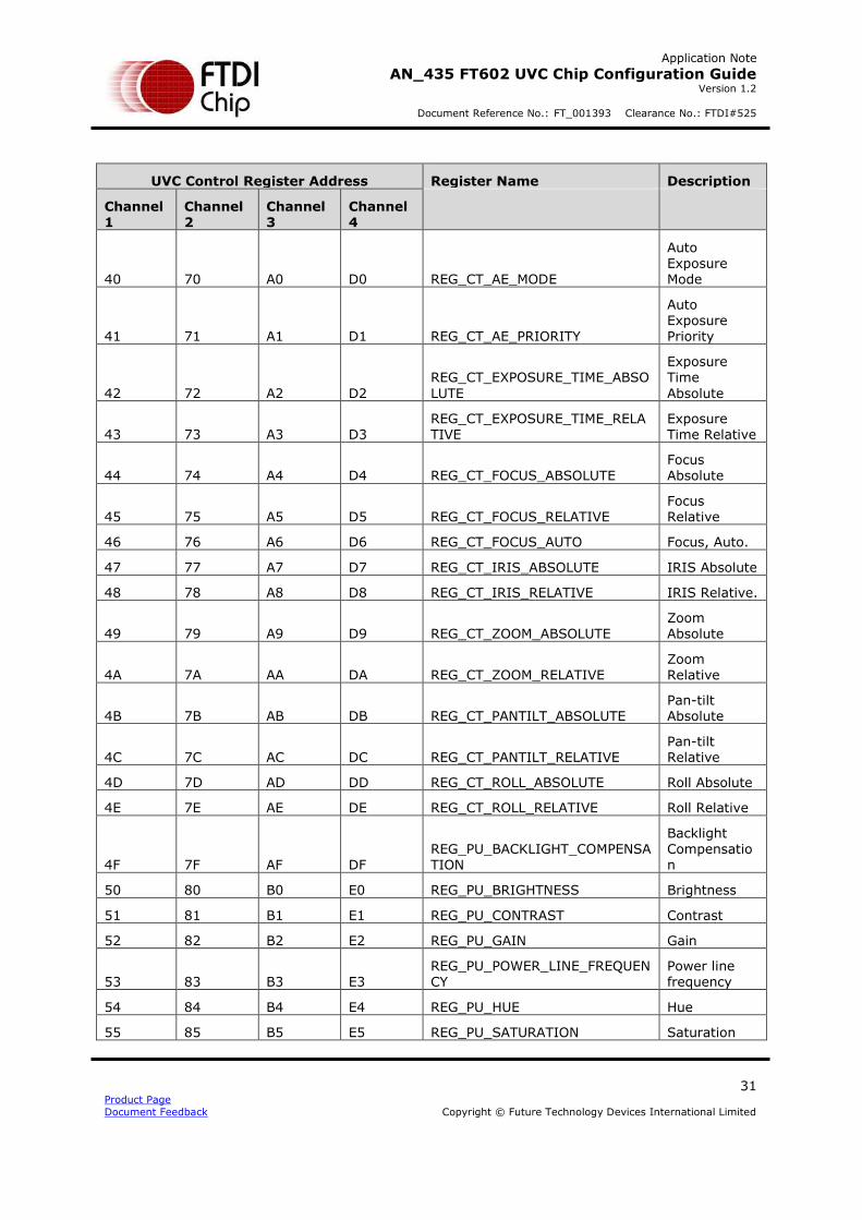
UVC Control Register Address Register Name Description
Channel 1
Channel 2
Channel 3
Channel 4
40 70 A0 D0 REG_CT_AE_MODE
Auto Exposure Mode
41 71 A1 D1 REG_CT_AE_PRIORITY
Auto Exposure Priority
42 72 A2 D2
REG_CT_EXPOSURE_TIME_ABSO
LUTE
Exposure Time
Absolute
43 73 A3 D3 REG_CT_EXPOSURE_TIME_RELATIVE
Exposure Time Relative
44 74 A4 D4 REG_CT_FOCUS_ABSOLUTE Focus Absolute
45 75 A5 D5 REG_CT_FOCUS_RELATIVE Focus Relative
46 76 A6 D6 REG_CT_FOCUS_AUTO Focus, Auto.
47 77 A7 D7 REG_CT_IRIS_ABSOLUTE IRIS Absolute
48 78 A8 D8 REG_CT_IRIS_RELATIVE IRIS Relative.
49 79 A9 D9 REG_CT_ZOOM_ABSOLUTE Zoom Absolute
4A 7A AA DA REG_CT_ZOOM_RELATIVE Zoom Relative
4B 7B AB DB REG_CT_PANTILT_ABSOLUTE Pan-tilt Absolute
4C 7C AC DC REG_CT_PANTILT_RELATIVE Pan-tilt Relative
4D 7D AD DD REG_CT_ROLL_ABSOLUTE Roll Absolute
4E 7E AE DE REG_CT_ROLL_RELATIVE Roll Relative
4F 7F AF DF REG_PU_BACKLIGHT_COMPENSATION
Backlight Compensation
50 80 B0 E0 REG_PU_BRIGHTNESS Brightness
51 81 B1 E1 REG_PU_CONTRAST Contrast
52 82 B2 E2 REG_PU_GAIN Gain
53 83 B3 E3 REG_PU_POWER_LINE_FREQUENCY
Power line frequency
54 84 B4 E4 REG_PU_HUE Hue
55 85 B5 E5 REG_PU_SATURATION Saturation
Application Note
AN_435 FT602 UVC Chip Configuration Guide Version 1.2
Document Reference No.: FT_001393 Clearance No.: FTDI#525
32 Product Page
Document Feedback Copyright © Future Technology Devices International Limited
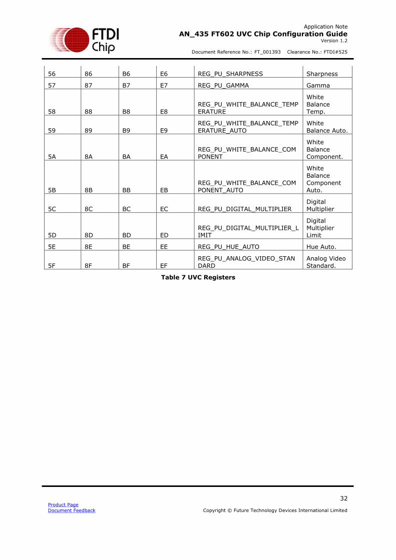
56 86 B6 E6 REG_PU_SHARPNESS Sharpness
57 87 B7 E7 REG_PU_GAMMA Gamma
58 88 B8 E8 REG_PU_WHITE_BALANCE_TEMPERATURE
White Balance Temp.
59 89 B9 E9
REG_PU_WHITE_BALANCE_TEMP
ERATURE_AUTO
White
Balance Auto.
5A 8A BA EA REG_PU_WHITE_BALANCE_COMPONENT
White Balance Component.
5B 8B BB EB
REG_PU_WHITE_BALANCE_COM
PONENT_AUTO
White
Balance Component
Auto.
5C 8C BC EC REG_PU_DIGITAL_MULTIPLIER Digital Multiplier
5D 8D BD ED REG_PU_DIGITAL_MULTIPLIER_LIMIT
Digital Multiplier Limit
5E 8E BE EE REG_PU_HUE_AUTO Hue Auto.
5F 8F BF EF REG_PU_ANALOG_VIDEO_STANDARD
Analog Video Standard.
Table 7 UVC Registers
Application Note
AN_435 FT602 UVC Chip Configuration Guide Version 1.2
Document Reference No.: FT_001393 Clearance No.: FTDI#525
33 Product Page
Document Feedback Copyright © Future Technology Devices International Limited
7 Contact Information
Head Office – Glasgow, UK Future Technology Devices International Limited Unit 1, 2 Seaward Place, Centurion Business Park Glasgow G41 1HH United Kingdom Tel: +44 (0) 141 429 2777 Fax: +44 (0) 141 429 2758 E-mail (Sales) [email protected]
E-mail (Support) [email protected]
E-mail (General Enquiries) [email protected]
Branch Office – Taipei, Taiwan Future Technology Devices International Limited (Taiwan) 2F, No. 516, Sec. 1, NeiHu Road Taipei 114 Taiwan , R.O.C. Tel: +886 (0) 2 8797 1330 Fax: +886 (0) 2 8751 9737 E-mail (Sales) [email protected]
E-mail (Support) [email protected]
E-mail (General Enquiries) [email protected]
Branch Office – Tigard, Oregon, USA Future Technology Devices International Limited (USA) 7130 SW Fir Loop Tigard, OR 97223-8160 USA Tel: +1 (503) 547 0988 Fax: +1 (503) 547 0987 E-Mail (Sales) [email protected]
E-Mail (Support) [email protected]
E-Mail (General Enquiries) [email protected]
Branch Office – Shanghai, China Future Technology Devices International Limited (China) Room 1103, No. 666 West Huaihai Road, Shanghai, 200052 China Tel: +86 21 62351596 Fax: +86 21 62351595 E-mail (Sales) [email protected]
E-mail (Support) [email protected]
E-mail (General Enquiries) [email protected]
Web Site http://ftdichip.com
Distributor and Sales Representatives
Please visit the Sales Network page of the FTDI Web site for the contact details of our distributor(s) and sales representative(s) in your country.
System and equipment manufacturers and designers are responsible to ensure that their systems, and any Future Technology
Devices International Ltd (FTDI) devices incorporated in their systems, meet all applicable safety, regulatory and system-level performance requirements. All application-related information in this document (including application descriptions, suggested
FTDI devices and other materials) is provided for reference only. While FTDI has taken care to assure it is accurate, this
information is subject to customer confirmation, and FTDI disclaims all liability for system designs and for any applications
assistance provided by FTDI. Use of FTDI devices in life support and/or safety applications is entirely at the user’s risk, and the
user agrees to defend, indemnify and hold harmless FTDI from any and all damages, claims, suits or expense resulting from
such use. This document is subject to change without notice. No freedom to use patents or other intellectual property rights is
implied by the publication of this document. Neither the whole nor any part of the information contained in, or the product
described in this document, may be adapted or reproduced in any material or electronic form without the prior written consent
of the copyright holder. Future Technology Devices International Ltd, Unit 1, 2 Seaward Place, Centurion Business Park, Glasgow G41 1HH, United Kingdom. Scotland Registered Company Number: SC136640
Application Note
AN_435 FT602 UVC Chip Configuration Guide Version 1.2
Document Reference No.: FT_001393 Clearance No.: FTDI#525
34 Product Page
Document Feedback Copyright © Future Technology Devices International Limited
Appendix A – References
Document References
USB_Video_Class_1.1.pdf
FT602 USB 3.0 SuperSpeed UVC bridge IC datasheet
UMFT602X development module datasheet
https://www.fourcc.org/fourcc.php
Acronyms and Abbreviations
Terms Description
FIFO First In First Out
ID Identification
UI User Interface
USB Universal Serial Bus
UVC USB Video Class.
VID Vendor Identification
I2C Inter-Integrated Circuit

Application Note
AN_435 FT602 UVC Chip Configuration Guide Version 1.2
Document Reference No.: FT_001393 Clearance No.: FTDI#525
35 Product Page
Document Feedback Copyright © Future Technology Devices International Limited
Appendix B – List of Tables & Figures
List of Tables
Table 1 - Main UI Controls Description ................................................................................... 6
Table 2 – User Configurable Common Configuration - Description ............................................. 8
Table 3 – Camera Terminal, Processing Unit & Frame Information ........................................... 14
Table 4 – Camera Terminal Control Options .......................................................................... 17
Table 5 – Processing Control & Description ........................................................................... 21
Table 6 I2C Slave Registers ................................................................................................ 30
Table 7 UVC Registers ....................................................................................................... 32
List of Figures
Figure 1 - Application Screenshot .......................................................................................... 5
Figure 2 – Channels Page ..................................................................................................... 6
Figure 3 –Buffer Management ............................................................................................... 9
Figure 4 –Advanced UVC Settings ....................................................................................... 10
Figure 5 –Camera Terminal Configurable Options .................................................................. 15
Figure 6 –Processing Unit Control Options ............................................................................ 18
Figure 7 Processing Unit Control ......................................................................................... 22
Figure 8 Application adjusting a UVC control ......................................................................... 23
Figure 9 Auxiliary interface highlighted ................................................................................ 24
Figure 10 WinUSB Setup Procedure ..................................................................................... 25
Figure 11 WinUSB Setup Procedure ..................................................................................... 25
Figure 12 WinUSB Setup Procedure ..................................................................................... 26
Figure 13 WinUSB Setup Procedure ..................................................................................... 26
Figure 14 Disable Auxiliary Interface ................................................................................... 27
Figure 15 Example I2C write to slave's register. .................................................................... 28
Figure 16 Example I2C Read from slave register .................................................................... 28
Application Note
AN_435 FT602 UVC Chip Configuration Guide Version 1.2
Document Reference No.: FT_001393 Clearance No.: FTDI#525
36 Product Page
Document Feedback Copyright © Future Technology Devices International Limited
Appendix C – Revision History
Document Title: AN_435_FT602 UVC Chip Configuration Guide
Document Reference No.: FT_001393
Clearance No.: FTDI#525
Product Page: http://www.ftdichip.com/FTProducts.htm
Document Feedback: Send Feedback
Revision Changes Date
1.0 Initial Release 2017-03-23
1.1 Updated Section 1.1 Pre-requisite (WINUSB driver
pre-installation descriptions added) 2017-04-18
1.2
Added the following section/information –
Auxiliary Interface section
WinUSB Setup Procedure.
I2C related information
I2C register related tables.
Updated the screenshots with new UI
2017-12-08