fsk demodulation based on time discriminant connectionist ...their constructive comments and...
TRANSCRIPT
FSK Demodulation Based on Time
Discriminant Connectionist Theory Using
Verilog HDL
By
Wafa' Nadhmi Hussien Ashara'
Advisor
Dr. Bassam El-asir
JORDAN UNIVERSITY OF SCIENCE AND
TECHNOLOGY
May, 2008
ii
FSK Demodulation Based On Time
Discriminant Connectionist Theory Using
Verilog HDL
By
Wafa' Nadhmi Hussien Ashara'
Thesis Submitted in Partial Fulfillment of the Requirements for the
Degree of M.Sc. in Electrical Engineering
At
Faculty of Graduate Studies
Jordan University of Science and Technology
May, 2008
Signature of Author: …..............................
Committee Members Signature and Date
Dr. Bassam El-asir, (chairman) .……............................
Dr. Mohammad Banat .……............................
Dr. Loai Khalaf, (Cognate, Jordan Univ.) .……............................

i
Dedication
To My Parents, Brothers, Sisters.

ii
Acknowledgment
First of all and always, I would like to thank God "Allah".
I would like to thank my thesis advisor, Dr Bassam El-asir for having given me such a
wonderful opportunity. It was truly a very interesting and exciting experience to have
worked on my thesis topic. I would like to thank him for his supervision and
encouragement. I would like to thank the thesis discussion committee: Dr. Mohammad
Banat, and Dr. Loay Khalaf for their active participation in the review of the thesis, and
their constructive comments and suggestions.
I would like to thank Eng. Emad Hamdoon for his help in understanding the T.D.
MFSK demodulator.
I would like to thank Eng. Ziad Abu Lebdeh fore helping me in synthesizing and
implementing the T.D. demodulator on FPGA.
I am really grateful to my close friend Khawla for her support and help.
Last but not the least, I would like to thank my parents, family, and friends for being a
constant source of inspiration and motivation for me.course.
This thesis work would have been impossible without the help and guidance of Eng.
Emad Hamdoon; thank you very much.
I would also like to thank Dr Ridha Radideh, Dr Mansoor Abadi, Eng.Mohammed
Rawashdeh, Eng. Ahmed Shatnawi, Eng. Mohammed El-basheer for their help.
iii
Table of Contents
Dedication ....................................................................................................................... i
Acknowledgement .......................................................................................................... ii
Table of Contents .......................................................................................................... iii
List of Figures …............................................................................................................ v
Abstract .......................................................................................................................... x
Chapter 1:
1.1 Introduction ....................................................................................................... 1
1.2 Thesis Contributions .......................................................................................... 2
1.3 Softwares and Hardware .............................................................................................. 3
1.3.1 Simulink .......................................................................................................... 3
1.3.2 Verilog HDL ................................................................................................. 4
1.3.2.1 Verilogger Extreme and Bughunter Pro ................................................... 4
1.3.2.2 Quartus II ............................................................................................... 5
1.3.2.3 FPGA ……………………………….................................................... 5
1.4 Thesis Outline ………………………………............................................................ 6
Chapter 2: The Theory of Time Discriminant Connectionist Systems .......................... 8
2.1 Definitions and Assumptions ……....................................………………..….. 8
2.1.1 1:1 Neurons and T-Neurons …………………………………………..…. 8
2.1.2 Frequency and Period ……………………...…...………………………... 9
2.1.3 Pulse Trains ………………………………………………........…............ 9
2.2 A Basic Resonant Network …......................................................................... 10
2.2.1 The Band Detector ……............................................................................. 10
2.2.2 Expanding-Band Detector …..................................................................... 14
2.2.3 Contracting -Band Detector........................................................................ 14

iv
2.2.4 Quantitative Limits Imposed by Neural Parameters …............................. 14
2.3 Mutations of the Band Detector ...................................................................... 17
2.3.1 The Band Detector with Harmonic Suppression ...................................... 17
2.3.2 The Band Suppressor ................................................................................ 19
2.4 Possible Applications of Resonant Networks ................................................. 21
Chapter 3: Demodulation of Noncoherent FSK Signals Using Time
Discriminant Connectionist Systems ........................................................ 22
3.1 FSK Systems, an Overview ............................................................................. 22
3.1.1 Frequency Shift Keying (FSK) .................................................................. 22
3.1.2 Binary FSK System ................................................................................... 23
3.1.2.1 FSK Detection ..................................................................................... 25
3.1.2.2 Noncoherent FSK Detection ............................................................... 25
3.1.3 Demodulation of the FSK Signal Using the Time Discriminant
Theory …………………………………………………………………... 26
3.1.3.1 The Realization of T.D. FSK Signals Demodulator ............................ 27
3.1.3.2 Software Simulation for the T.D. FSK Signal Demodulator............... 30
3.1.3.3 Harmonic Suppression Mechanism ..................................................... 39
Chapter 4: Implementation of Noncoherent MFSK Signals Demodulation Using
Time Discriminant Connectionist System ............................................... 46
4.1 Multiple Frequency Shift Keying (MFSK) Signals ......................................... 46
4.1.1 Demodulation of the MFSK Signal Using the Conventional
Methods ……..............................................................................................47
4.1.2 Demodulation of Noncoherent MFSK Signal Using Time
Discriminant Connectionist System ......................................................... 48
4.1.2.1 The Realization of T.D. MFSK Signal Demodulator .......................... 48
4.1.3 Hardware Design of T.D. MFSK Using Verilog HDL ............................. 53
4.1.3.1 Motivation ........................................................................................... 53
4.1.3.2 Design Methodology of the T.D. MFSK Demodulator ………........... 53

v
Chapter 5: Hardware Implementation of Noncoherent MFSK Signal
Demodulator on FPGA ............................................................................. 71
5.1 Introduction ..................................................................................................... 71
5.2 The FPGA Design Methodology...................................................................... 73
5.2.1 Synthesizing the T.D. MFSK Demodulator .............................................. 75
5.2.2 Analyzing the T.D. MFSK Demodulator Design with the
Quartus II RTL Viewer & Technology Map Viewer ................................ 78
5.2.3 Simulation of the T.D. MFSK Demodulator ........................................... 101
5.2.4 Fitting, Placement, and Routing ............................................................. 106
5.2.5 Pin Assignment ........................................................................................ 107
5.2.5.1 Push Button Switches ........................................................................ 107
5.2.5.2 Dip Switches ...................................................................................... 108
5.2.5.3 LEDs ...................................................................................................108
5.2.5.4 Pin Assignment for the T.D. System ................................................. 108
5.2.6 Design Space Explorer .............................................................................109
5.2.7 Programming FPGA .................................................................................110
Chapter 6 .................................................................................................................... 114
6.1 Conclusions ................................................................................................... 114
6.2 Future Work ……………………………………………………………….. 116
References .................................................................................................................. 117
Appendices ................................................................................................................. 119
Appendix A ................................................................................................................ 119
Appendix B ................................................................................................................. 120

vi
List of Figures
Figure 2.1: The band detector network ……………… …………………..….………............ 10
Figure 2.2: Regular pulse trains produced by N1 arriving at terminals y and z in the
network of Fig. 2.1 ………............…………………........................................... 11
Figure 2.3: The band of component periods detected by the network of Fig. 2.1 ….…….…. 12
Figure 2.4: The regular trains produced by N1 have a fundamental period of 0.5 D ……...… 13
Figure 2.5: Band detector with harmonic suppression ............................................................. 14
Figure 2.6: Time relations for the network of Fig. 2.5 …….…………………………........… 18
Figure 2.7: A band suppressor …………………..………………………………………...… 19
Figure 2.8: Time relations for the network of Fig. 2.7 ……..……….…………………….…. 20
Figure 3.1: Binary data modulates carrier to produce FSK ..................................................... 23
Figure 3.2: Correlation coefficient of FSK signals ………………………………………...... 24
Figure 3.3: Conventional noncoherent demodulator for FSK signal ....................................... 25
Figure 3.4: T.D. bandpass filter ………………………………..….…………………............ 27
Figure 3.5: T.D. FSK demodulator ……………………………………………...…...…........ 28
Figure 3.6: Output of T.D. FSK demodulator .....................…………………….……............ 29
Figure 3.7: T.D. FSK demodulator implementation using monostables .....………..…..…… 30
Figure 3.8: T.D. FSK demodulator implementation using simulink ....................................... 31
Figure 3.9: a- The graph of the received signal and the output of analog to digital
converter .......................................................................................................... 32
Figure 3.9: b- The graphs in the T.D. FSK simulation software .............................................. 33
Figure 3.10: The input and the output of the T.D. filter for each block used in T.D.
filter .................................................................................................................... 38
Figure 3.11: The realization of retriggerable monostable in T.D. filter ................................... 39
Figure 3.12: The output of T.D. filter using harmonic supression mechanism ……............... 41
Figure 3.13: The block diagram of T.D. FSK demodulator to detect noisy signals ................ 42
Figure 3.14: The graphs in the T.D FSK simulation block diagram ........................................ 44
Figure 3.15: The T.D. FSK demodulator performance curve for filter bandwidth=300hz ...... 45
Figure 4.1: Conventional noncoherent receiver for MFSK signals ......................................... 47
Figure 4.2: Frequency zero crossing counter realization for the T.D. MFSK
vii
demodulator .................................................................................................. 48
Figure 4.3: Simulated output of an 8-tone MFSK demodulator ............................................. 49
Figure 4.4: Intra-symbol errors in the T.D. MFSK demodulator, a- 8-tone
demodulator errors due to noise, b- recovery by majority vote ........................... 50
Figure 4.5: 0.3 of the signal peak is used to set the filter bandwidth ....................................... 51
Figure 4.6: Realization for the T.D. MFSK demodulator using majority vote to recover
lost pulses .............................................................................................................. 54
Figure 4.7: The design of the zero crossing circuit .................................................................. 55
Figure 4.8: Zero crossing module ….........................…………………………………….….. 55
Figure 4.9: The design of the edge detector circuit ….............................................................. 56
Figure 4.10: Edge detector module ……………....….............................................................. 56
Figure 4.11: The simulation result of the zero crossing circuit ............................................... 57
Figure 4.12: a-The simulation of rising edge zero crossing, b-The simulation of falling
edge zero crossing ........................................................................................... 58
Figure 4.13: Counter module …………………………………………………………...…… 59
Figure 4.14: Look up table module ..………………………….………………………...….... 60
Figure 4.15: Latch module …………..………………………….……………………...……. 61
Figure 4.16: The simulation of the memory control and latch modules .................................. 62
Figure 4.17: Zooming in the simulation of the memory control and latch modules ………… 63
Figure 4.18: The block diagram of the majority vote decoder ................................................. 64
Figure 4.19: Encoder module .. ................................................................................................ 70
Figure 5.1: Stucture of an FPGA ............................................................................................. 71
Figure 5.2: The Block Diagram of ESDK 1C6 Board ............................................................. 72
Figure 5.3: Typical FPGA CAD design flow .......................................................................... 73
Figure 5.4: The design implementation of T.D. MFSK signal demodulator on FPGA ............74
Figure 5.5: The project navigator of the T.D MFSK demodulator .......................................... 76
Figure 5.6: The design unit hierarchy window of the project navigator of the T.D
MFSK demodulator .............................................................................................. 77
Figure 5.7: The output of RTL viewer in Quartus II ............................................................... 79
Figure 5.8: The hierarchy list of the design of the T.D MFSK demodulator modules
viii
using RTL viewer ................................................................................................. 80
Figure 5.9: The clock divider components in the netlist design unit hierarchy window
of the project navigator of the T.D MFSK demodulator ...................................... 81
Figure 5.10: The Project Navigator of the T.D. MFSK demodulator using wave shaping
module ................................................................................................................. 82
Figure 5.11: The RTL viewer for clock dividers, signal wave shaping, and zero crossing
modules of the T.D. MFSK demodulator ........................................................... 83
Figure 5.12: The RTL viewer for signal wave shaping module .............................................. 83
Figure 5.13: The schematic of the design netlist for the data inserted by matlab
in RTL viewer ................................................................................................... 84
Figure 5.14: The synchronizer circuit that is added to the zero crossing circuit to
avoid metastability ............................................................................................ 85
Figure 5.15: a- The simlation result of the synchronized zero crossing circuit output
(1-clock pulse width )on the rising edge of the input .................................... 86
Figure 5.15: b- The simlation result of the synchronized zero crossing circuit output
(2-clocks pulse width ) on the rising edge of the input ................................. 86
Figure 5.16: The schematic of the design netlist for the synchronized zero crossing circuit in
RTL viewer ........................................................................................................ 87
Figure 5.17: The schematic of the design netlist for the synchronized edge detector
circuit in RTL viewer ........................................................................................ 87
Figure 5.18: The schematic of the design netlist for the counter in RTL viewer ................... 88
Figure 5.19: The analysis & synthesize ROM summary ........................................................ 89
Figure 5.20: The project navigator of the ROM ..................................................................... 90
Figure 5.21: The RTL viewer for ROM (altsynchram component) ....................................... 90
Figure 5.22: The RTL viewer for ROM (altsynchram ja31:auto_generated) ......................... 91
ix
Figure 5.23: The technology map viewer for ROM (altsynchram ja31: auto_
generated) .......................................................................................................... 92
Figure 5.24: The RTL viewer for inferred ROM .................................................................... 93
Figure 5.25: The RTL viewer for latch module ...................................................................... 94
Figure 5.26: The design of the majority vote decoder ............................................................ 96
Figure 5.27: a- The first page of the RTL viewer for majority vote module ......................... 97
Figure 5.27: b- The second page of the RTL viewer for majority vote module ..................... 98
Figure 5.28: The RTL viewer for 8-3 encoder module ........................................................... 99
Figure 5.29: The T.D. MFSK representation in the technology map viewer ....................... 100
Figure 5.30: a- 8 Frequency tones generated in Verilogger pro using function Sin in
label equation generator, b- the output of the wave shaping module that
converts the input signal to uniform pulses ................................................... 102
Figure 5.31: a- 8 Frequency tones generated in Matlab7.3, b- The conversion of the
input signal to uniform pulses ........................................................................ 103
Figure 5.32: The simulation of the T.D. 4-FSK demodulator using Verilogger pro&
Bughunter pro software ......................................................................................104
Figure 5.33: The simulation of the T.D. 8-FSK demodulator using Verilogger pro &
Bughunter pro software ..................................................................................... 105
Figure 5.34: The simulation results of the T.D. BFSK demodulator using Verilogger pro
& Bughunter pro software ................................................................................. 106
Figure 5.35: View of the floorplan of the T.D. demodulator ..................................................107
Figure 5.36: Pins assignment ..................................................................................................108
Figure 5.37: DSE optimization results ....................................................................................110
Figure 5.38: Assembler generated files .................................................................................. 112
Figure 5.39: JTAG mode ....................................................................................................... 112
Figure 5.40: Active serial mode ............................................................................................. 113
Figure 5.41: Assembler report ............................................................................................... 113
Figure A.1: The data stored in the read only memory …...................................................... 119
Figure B.1: Zero crossing module representation in the technology map viewer ................ 120
x
Figure B.2: Edge detector representation in the technology map viewer .............................. 120
Figure B.3: Counter schematic diagram in the technology map viewer ................................ 121
Figure B.4: a- Read only memory schematic diagram in the technology map
viewer …………..…………………………………………………….……... 122
Figure B.4: b- Low hierarchy level of Read only memory schematic diagram in the
technology map viewer ............................................................................... 123
Figure B.5: Latch schematic diagram in the technology map viewer .................................... 124
Figure B.6: Encoder schematic diagram in the technology map viewer ............................... 125
Figure B.7: a- Technology map viewer of the majority vote decoder page (1) ..................... 126
Figure B.7: b- Technology map viewer of the majority vote decoder page (2) ..................... 127
Figure B.7: c- Technology map viewer of the majority vote decoder page (3) ..................... 128
Figure B.7: d- Technology map viewer of the majority vote decoder page (4) ..................... 129
Figure B.7: e- Technology map viewer of the majority vote decoder page (5) ..................... 130
Figure B.7: f- Technology map viewer of the majority vote decoder page (6) ..................... 131
Figure B.7: g- Technology map viewer of the majority vote decoder page (7) ..................... 132
Figure B.7: h- Technology map viewer of the majority vote decoder page (8) ..................... 133
xi
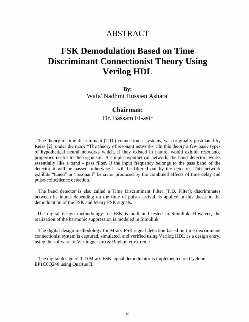
ABSTRACT
FSK Demodulation Based on Time
Discriminant Connectionist Theory Using
Verilog HDL
By:
Wafa' Nadhmi Hussien Ashara'
Chairman:
Dr. Bassam EI-asir
The theory of time discriminant (T.D.) connectionist systems, was originally postulated by
Reiss [2], under the name “The theory of resonant networks”. In this theory a few basic types
of hypothetical neural networks which, if they existed in nature, would exhibit resonance
properties useful to the organism. A simple hypothetical network, the band detector; works
essentially like a band - pass filter. If the input frequency belongs to the pass band of the
detector it will be passed, otherwise it will be filtered out by the detector. This network
exhibits “tuned” or “resonant” behavior produced by the combined effects of time delay and
pulse-coincidence detection.
The band detector is also called a Time Discriminant Filter (T.D. Filter); discriminates
between its inputs depending on the time of pulses arrival, is applied in this thesis in the
demodulation of the FSK and M-ary FSK signals.
The digital design methodology for FSK is built and tested in Simulink. However, the
realization of the harmonic suppression is modeled in Simulink
The digital design methodology for M-ary FSK signal detection based on time discriminant
connectionist system is captured, simulated, and verified using Verilog HDL as a design entry,
using the software of Verilogger pro & Bughunter extreme.
The digital design of T.D.M-ary FSK signal demodulator is implemented on Cyclone
EP1C6Q240 using Quartus II.

1
Chapter One
1.1 Introduction
Current architectures for neural networks are based on gate-like processing nodes with
weighted inputs and non-linear transfer functions [1]. Such networks do not normally exhibit
inherent temporal structure and can therefore be considered as suboptimal for the analysis and
recognition of complex time-varying signals. These networks also constitute a considerable
departure from "living networks" which process information in the form of frequency-coded
pulses. It is considered that pulse-processing networks will be more suitable for time
dependent applications such as those discussed in this thesis.
Time discriminant connectionist systems theory was originally postulated by Reiss [2], under
the name "The Theory of Resonant Networks". Chesmore [9, 10, 11], was the first person who
applied the time discriminant connectionist systems theory in the demodulation of FSK signal
and proposed a system for demodulating the MFSK signals. He predicted that this theory
would have tremendous applications in electronic communication, more specifically in signal
detection and demodulation.
Hamdoon performed a software simulation for the T.D. FSK demodulator for different SNR’s;
and for certain T.D. filters’ bandwidths, obtained the performance curves for T.D. FSK and
compared them with the conventional method performance curves..
Hamdoon performed a software simulation for the T.D. MFSK signal demodulator and setted
the filter bandwidth according to a certain level of the signal, which is a fraction of the peak of
the signal without noise. He also obtained the performance curves for T.D. MFSK and
compared them with the conventional method performance curves.
2
In this thesis, the concept of time discriminant connectionist systems will be applied in the
demodulation of FSK and MFSK signals.
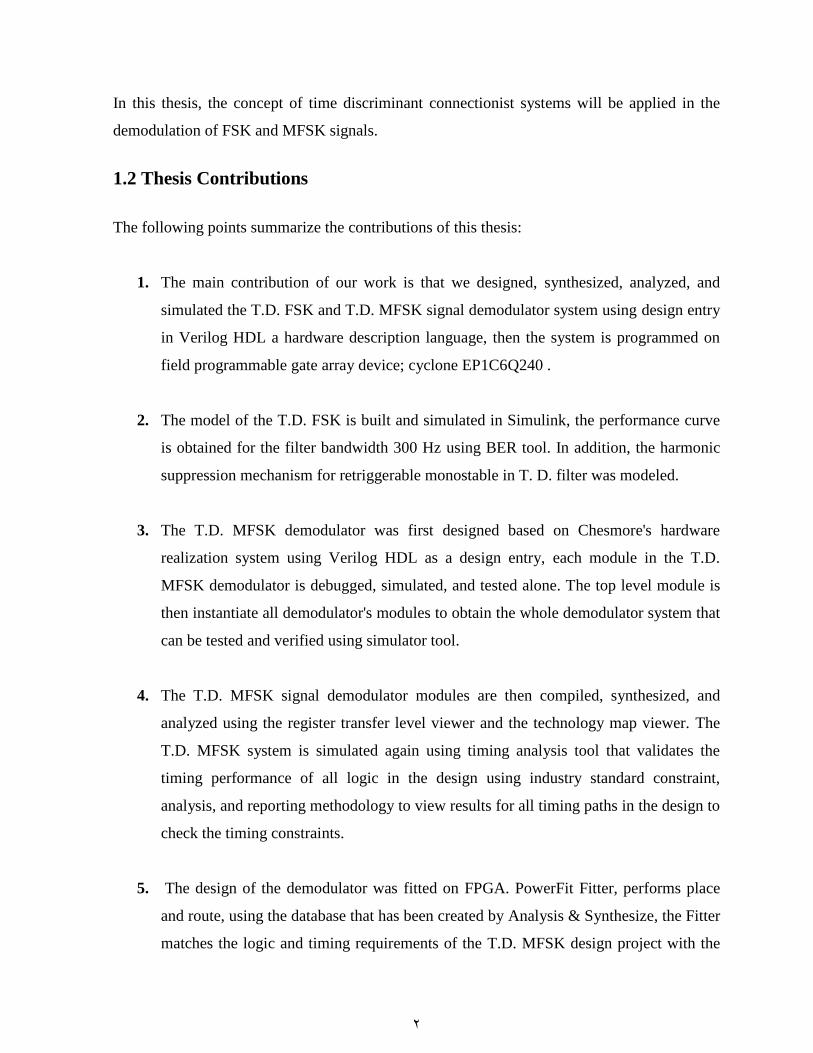
1.2 Thesis Contributions
The following points summarize the contributions of this thesis:
1. The main contribution of our work is that we designed, synthesized, analyzed, and
simulated the T.D. FSK and T.D. MFSK signal demodulator system using design entry
in Verilog HDL a hardware description language, then the system is programmed on
field programmable gate array device; cyclone EP1C6Q240 .
2. The model of the T.D. FSK is built and simulated in Simulink, the performance curve
is obtained for the filter bandwidth 300 Hz using BER tool. In addition, the harmonic
suppression mechanism for retriggerable monostable in T. D. filter was modeled.
3. The T.D. MFSK demodulator was first designed based on Chesmore's hardware
realization system using Verilog HDL as a design entry, each module in the T.D.
MFSK demodulator is debugged, simulated, and tested alone. The top level module is
then instantiate all demodulator's modules to obtain the whole demodulator system that
can be tested and verified using simulator tool.
4. The T.D. MFSK signal demodulator modules are then compiled, synthesized, and
analyzed using the register transfer level viewer and the technology map viewer. The
T.D. MFSK system is simulated again using timing analysis tool that validates the
timing performance of all logic in the design using industry standard constraint,
analysis, and reporting methodology to view results for all timing paths in the design to
check the timing constraints.
5. The design of the demodulator was fitted on FPGA. PowerFit Fitter, performs place
and route, using the database that has been created by Analysis & Synthesize, the Fitter
matches the logic and timing requirements of the T.D. MFSK design project with the
3
available resources of a device. Each logic function is assigned to the best logic cell
location for routing and timing, and selecting appropriate interconnection paths and pin
assignments.
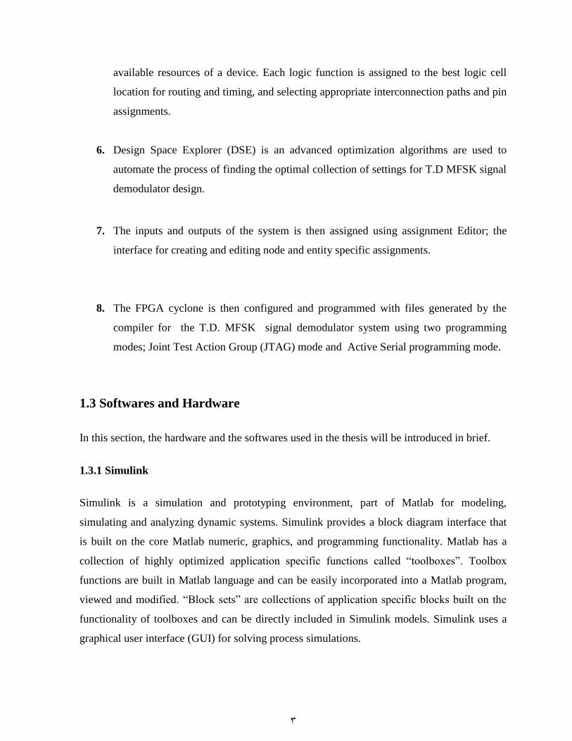
6. Design Space Explorer (DSE) is an advanced optimization algorithms are used to
automate the process of finding the optimal collection of settings for T.D MFSK signal
demodulator design.
7. The inputs and outputs of the system is then assigned using assignment Editor; the
interface for creating and editing node and entity specific assignments.
8. The FPGA cyclone is then configured and programmed with files generated by the
compiler for the T.D. MFSK signal demodulator system using two programming
modes; Joint Test Action Group (JTAG) mode and Active Serial programming mode.
1.3 Softwares and Hardware
In this section, the hardware and the softwares used in the thesis will be introduced in brief.
1.3.1 Simulink
Simulink is a simulation and prototyping environment, part of Matlab for modeling,
simulating and analyzing dynamic systems. Simulink provides a block diagram interface that
is built on the core Matlab numeric, graphics, and programming functionality. Matlab has a
collection of highly optimized application specific functions called “toolboxes”. Toolbox
functions are built in Matlab language and can be easily incorporated into a Matlab program,
viewed and modified. “Block sets” are collections of application specific blocks built on the
functionality of toolboxes and can be directly included in Simulink models. Simulink uses a
graphical user interface (GUI) for solving process simulations.
4
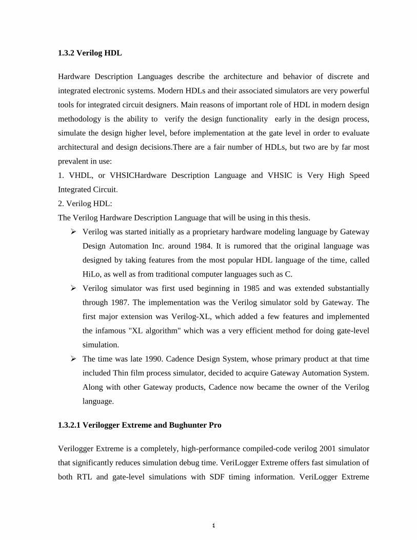
1.3.2 Verilog HDL
Hardware Description Languages describe the architecture and behavior of discrete and
integrated electronic systems. Modern HDLs and their associated simulators are very powerful
tools for integrated circuit designers. Main reasons of important role of HDL in modern design
methodology is the ability to verify the design functionality early in the design process,
simulate the design higher level, before implementation at the gate level in order to evaluate
architectural and design decisions.There are a fair number of HDLs, but two are by far most
prevalent in use:
1. VHDL, or VHSICHardware Description Language and VHSIC is Very High Speed
Integrated Circuit.
2. Verilog HDL:
The Verilog Hardware Description Language that will be using in this thesis.
Verilog was started initially as a proprietary hardware modeling language by Gateway
Design Automation Inc. around 1984. It is rumored that the original language was
designed by taking features from the most popular HDL language of the time, called
HiLo, as well as from traditional computer languages such as C.
Verilog simulator was first used beginning in 1985 and was extended substantially
through 1987. The implementation was the Verilog simulator sold by Gateway. The
first major extension was Verilog-XL, which added a few features and implemented
the infamous "XL algorithm" which was a very efficient method for doing gate-level
simulation.
The time was late 1990. Cadence Design System, whose primary product at that time
included Thin film process simulator, decided to acquire Gateway Automation System.
Along with other Gateway products, Cadence now became the owner of the Verilog
language.
1.3.2.1 Verilogger Extreme and Bughunter Pro
Verilogger Extreme is a completely, high-performance compiled-code verilog 2001 simulator
that significantly reduces simulation debug time. VeriLogger Extreme offers fast simulation of
both RTL and gate-level simulations with SDF timing information. VeriLogger Extreme
5
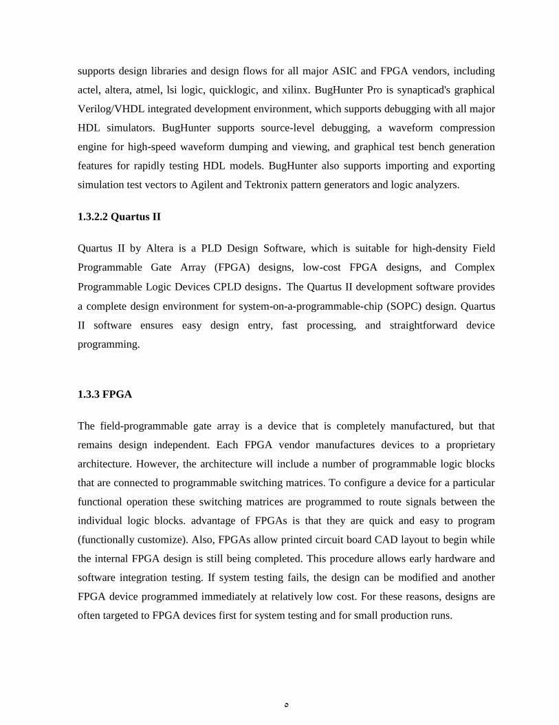
supports design libraries and design flows for all major ASIC and FPGA vendors, including
actel, altera, atmel, lsi logic, quicklogic, and xilinx. BugHunter Pro is synapticad's graphical
Verilog/VHDL integrated development environment, which supports debugging with all major
HDL simulators. BugHunter supports source-level debugging, a waveform compression
engine for high-speed waveform dumping and viewing, and graphical test bench generation
features for rapidly testing HDL models. BugHunter also supports importing and exporting
simulation test vectors to Agilent and Tektronix pattern generators and logic analyzers.
1.3.2.2 Quartus II
Quartus II by Altera is a PLD Design Software, which is suitable for high-density Field
Programmable Gate Array (FPGA) designs, low-cost FPGA designs, and Complex
Programmable Logic Devices CPLD designs. The Quartus II development software provides
a complete design environment for system-on-a-programmable-chip (SOPC) design. Quartus
II software ensures easy design entry, fast processing, and straightforward device
programming.
1.3.3 FPGA
The field-programmable gate array is a device that is completely manufactured, but that
remains design independent. Each FPGA vendor manufactures devices to a proprietary
architecture. However, the architecture will include a number of programmable logic blocks
that are connected to programmable switching matrices. To configure a device for a particular
functional operation these switching matrices are programmed to route signals between the
individual logic blocks. advantage of FPGAs is that they are quick and easy to program
(functionally customize). Also, FPGAs allow printed circuit board CAD layout to begin while
the internal FPGA design is still being completed. This procedure allows early hardware and
software integration testing. If system testing fails, the design can be modified and another
FPGA device programmed immediately at relatively low cost. For these reasons, designs are
often targeted to FPGA devices first for system testing and for small production runs.
6
The hardware Kit used in this thesis is the ESDK, 1C6 Education Kit provides an educational
tool and also a solution for prototyping and developing products rapidly. The board serves as
means for system prototyping and emulation with hardware as well as software development.
The board ships with a powerful Altera Cyclone FPGA providing around 6,000 logic
elements. It allows hardware design engineer to design, prototype hardware design using
HDLs like Verilog or VHDL or any and test IP cores. The board provides industry standard
interconnections, Memory Subsystem, Multiple clocks for system design, JTAG
Configuration, expansion headers for greater flexibility, capacity and additional user interface
features. Further, the board can be used for DSP applications by interfacing directly to a DSP
processor or implementing DSP functions inside the FPGA. In short, it is a dual-purpose kit,
which can be used for prototyping and developing VLSI designs as well as designing and
developing microprocessor based embedded system designs.
1.4 Thesis Outline
This thesis is organized as follows:
Chapter One: this chapter presents introduction and the previous work was given in an
individual section. The other two sections include the thesis main contributions and thesis
outline.
In chapter two, the theory of time discriminant connectionist systems [2], is summarized.
In chapter three, the conventional method of demodulating FSK signals is summarized, and
the time discriminant connectionist systems theory is applied in the demodulation of FSK
signals. The performance curve for the T.D FSK demodulator is plotted for the filter
bandwidth 300 Hz.
The model of the T.D. FSK was simulated in Simulink and the harmonic suppression
mechanism was modeled in Simulink.
In chapter four, the conventional method of demodulating MFSK signals is summarized; the
theory of time discriminant connectionist systems is applied in the demodulation of MFSK
7
signals. The T.D. MFSK modules were debugged, simulated, and verified using Verilog
HDL.The design code for the modules is presented as a design unit entry
In chapter five, the T.D. MFSK demodulator was built, simulated and synthesized using
Quartus II, and the timing requirement is analyzed, then the design of the demodulator was
implemented on FPGA.
Finally, in chapter six, conclusions and a suggestion for future work that can be done in the
direction of the thesis were given.

8
Chapter Two:
The Theory of Time Discriminant Connectionist Systems
In this chapter, the summarization of the time discriminant connectionist systems theory is
presented. The TD theory was originally postulated by Reiss [2], as “The theory of resonant
networks’. This theory shows the possibilities of "resonant networks" in neural systems. A few
basic types of hypothetical neural networks are discussed which, if they existed in nature,
would exhibit resonance properties useful to the organism. This theory stems from two lines of
research. First, during simulation studies of hypothetical neural systems involving reciprocal
inhibition [3], certain unexpected behavioral anomalies drew the attention to a type of
“resonance” effect that can be produced by appropriate combinations of pulse frequency, axon
time delays, temporal summation, and firing thresholds. Second, a general investigation of the
possible roles of pulse-interval coding in computers and other kinds of machines inspired
initially by analogical reasoning from neural systems, led to the conception and study of a
variety of “resonant” mechanisms; although some of these mechanisms could be physically
realized only by electronic devices, others required parameter ranges that might well be within
the capabilities of neurons.
2.1 Definitions and Assumptions:
In this section the basic terms and assumption used in resonant networks is defined.
2.1.1 1:1 Neurons and T-Neurons
The hypothetical neural networks are combinations of two simple types of neuron. A 1-1
neuron which is defined as any neuron which fires once and only once for each excitatory
input spike, And the T neuron which has a temporal threshold T; one excitatory pulse cannot
9
urge firing. If two excitatory input pulses arrive at times t1 & t2 , then the neuron will fire
(once) if and only if t t T2 1 .
2.1.2 Frequency and Period:
Frequency means pulse-repetition rate. The reciprocal of the time interval separating any two
pulses may be considered the frequency at which those two pulses occurred. However, except
in one special case, a pulse train composed of more than two pulses does not have a unique
frequency, and therefore a statistical definition of frequency is required. A period is commonly
defined as a time interval between two particular events. The “period” between the first and
second pulse refers to the amount of time separating the occurrence of the pulses, not to the
historical segment of time itself. In addition, the word “interval” is used to refer to particular
segments of historical time. It is meaningful to say that one interval succeeds or overlaps
another; by contrast, periods cannot succeed or overlap one another.
2.1.3 Pulse Trains:
A pair of pulses is “successive” if there are no intervening pulses. A train of K pulses contains
K-1 successive pairs, and the time intervals between these pairs are called primary intervals of
the train. Two intervals are contiguous if the pulse, which terminates one interval, also initiates
the other interval; a secondary interval is any interval composed of two or more contiguous
primary intervals. If all of the primary intervals in the train have the same magnitude, then the
train is regular, if two or more primary intervals have different magnitudes, then the train is
irregular. In the case of a regular train, all primary intervals have the same magnitude and each
one can therefore be represented by the same component period; then this is called the
fundamental period Pf of a regular train, and its reciprocal is the fundamental
“frequency” Ff . Since the primary intervals of an irregular train are not all of the same size,
no fundamental period is defined for such a train.

10
2.2 A Basic Resonant Network:-
In this section a simple neural hypothetical network that is the basic network in constructing
complex networks and systems, the band detector is introduced.
The network shown in Fig. 2.1 exhibits “tuned” or “resonant” behavior produced by the
combined effects of time delay and pulse-coincidence detection. The band detector is also
called a Time Discriminant Filter (TD Filter) that it discriminates between its inputs depending
on the lime of pulses arrival.
Figure 2.1: The band detector network.
2.2.1 The Band Detector:
Consider the network shown in Fig. 2.1 as shown it consists of three neurons: N2, which is
assumed to be 1-1 neuron, N3 to be a T-neuron, and N1 that doesn't matter what type of neuron
happens to be; it merely provides the input to the system. The axon of N1 branches at point X,
sending an excitatory terminal (Named Y) to N3 and another such terminal (not named) to N2.
Neuron N2 in turn has an axon whose excitatory terminal (named Z) contacts the synaptic
region of N3. A pulse originating in N1 splits at point X, one pulse travels directly to terminal
Y, and the other pulse travels over the longer route through N2, where it encounters a synaptic
delay, to terminal Z. The propagation time from X to Y is assumed to be appreciably less than
that from X to Z. The absolute values of these delays are not of interest, only the net difference
11
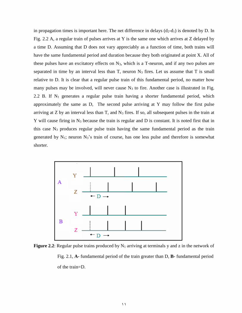
in propagation times is important here. The net difference in delays (d2-d1) is denoted by D. In
Fig. 2.2 A, a regular train of pulses arrives at Y is the same one which arrives at Z delayed by
a time D. Assuming that D does not vary appreciably as a function of time, both trains will
have the same fundamental period and duration because they both originated at point X. All of
these pulses have an excitatory effects on N3, which is a T-neuron, and if any two pulses are
separated in time by an interval less than T, neuron N3 fires. Let us assume that T is small
relative to D. It is clear that a regular pulse train of this fundamental period, no matter how
many pulses may be involved, will never cause N3 to fire. Another case is illustrated in Fig.
2.2 B. If N1 generates a regular pulse train having a shorter fundamental period, which
approximately the same as D, The second pulse arriving at Y may follow the first pulse
arriving at Z by an interval less than T, and N3 fires. If so, all subsequent pulses in the train at
Y will cause firing in N3 because the train is regular and D is constant. It is noted first that in
this case N3 produces regular pulse train having the same fundamental period as the train
generated by N1; neuron N3’s train of course, has one less pulse and therefore is somewhat
shorter.
Figure 2.2: Regular pulse trains produced by N1 arriving at terminals y and z in the network of
Fig. 2.1, A- fundamental period of the train greater than D, B- fundamental period
of the train=D.

12
It is noted further that N3 generates a regular train if the incoming trains have a fundamental
period slightly less than, or equal to, or slightly greater than, the delay difference D, or if the
fundamental period of the regular input train is between D-T and D+T, then N3 generates a
regular train having the same fundamental period but one less pulse. Thus, there is a “band” of
fundamental periods, which will fire N3 .The situation is illustrated in Fig. 2.3 the first pulses
of the trains at Y and Z are represented by solid vertical lines. The second pulse arriving at Y
must fall between the vertical dashed lines at D-T and D+T to initiate a pulse in N3. The width
of the band of periods is 2T. The lower limit of such a band is denoted by PL and the upper
limit by PU. Since the reciprocal of a period is a frequency, a band of frequencies is defined by
any band of periods; the limits of the frequency band are the reciprocals of PL and PU. The
reciprocal of D is called the tuned frequency of the network and is denoted by F0. The upper
limit of the corresponding frequency band will be denoted by FU and the lower limit by FL, so:
FU =1/ PL and FL =1/ PU.
Figure 2.3: The band of component periods detected by the network of Fig. 2.1 has the lower
limit D-T and the upper limit D+T, where T is the temporal threshold of N3.
13
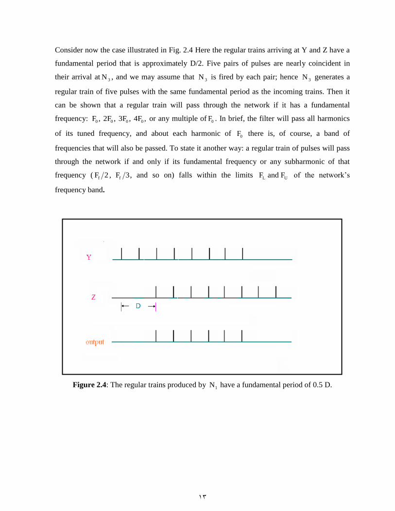
Consider now the case illustrated in Fig. 2.4 Here the regular trains arriving at Y and Z have a
fundamental period that is approximately D/2. Five pairs of pulses are nearly coincident in
their arrival at N 3 , and we may assume that N 3 is fired by each pair; hence N 3 generates a
regular train of five pulses with the same fundamental period as the incoming trains. Then it
can be shown that a regular train will pass through the network if it has a fundamental
frequency: F0 , , , , 2F 3F 4F0 0 0 or any multiple of F0 . In brief, the filter will pass all harmonics
of its tuned frequency, and about each harmonic of F0 there is, of course, a band of
frequencies that will also be passed. To state it another way: a regular train of pulses will pass
through the network if and only if its fundamental frequency or any subharmonic of that
frequency ( Ff 2 3, Ff , and so on) falls within the limits FL and FU of the network’s
frequency band.
Figure 2.4: The regular trains produced by N1 have a fundamental period of 0.5 D.
14
2.2.2 Expanding-Band Detector:
For the network of Fig. 2.1, it will be assumed here that D is constant but that T, although it
has a normal or “resting” value, may vary as a result of N 3 firing. The period bandwidth will
be denoted by B, then B=2T. Suppose that when N 3 fires repeatedly, T gradually becomes
larger, owing to some synaptic facilitation process. Consequently, the bandwidth B increases.
In this case, we shall say that the band “expands” and that the network is an expanding-band
detector. The foregoing hypothetical case suggests one possible role of expanding-band
detectors in neural communications: to “accommodate” increasing noise. Such detectors might
play a related role in processing accelerating or decelerating trains, which are relatively free of
noise. An accelerating train is one in which the successive primary intervals become
progressively smaller, and a decelerating train is one in which they become progressively
larger. Both types of train are common in nervous systems.
2.2.3 Contracting -Band Detector:
For the network of Fig. 2.1, N 3 is a T-neuron in which no appreciable facilitation occurs or
that, in any event, T cannot increase in value; instead, firing causes a decrease of T by
inducing “fatigue” or an equivalent process. Clearly, a reduction in T means a decrease in the
bandwidth of the detector. Hence, this will be called a contracting-band detector. It will be
assumed that when N 3 is not in the act of firing; recuperative processes are able to increase
the neuron’s sensitivity, eventually restoring T to its normal value. The periodic contractions
of bandwidth, “chop” the input train into a sequence of short trains, each containing only a few
pulses of the same fundamental period as the input. The output of this contracting-band
detector is a regular second order train composed of regular first order trains.
2.2.4 Quantitative Limits Imposed by Neural Parameters:
It will be assumed that the “neural spectrum” spans periods from approximately 1ms to 1s,
(i.e., “frequencies” from 1 to 1000 pulses per second (PPS)). Thus, the important factors here
15
are the parameters of band detectors “tuned” to frequencies between 1 and 1000 PPS. The
band detector is “tuned” to a period P (or frequency 1/P) if D=P. A detector tuned to the high-
frequency end of the neural spectrum must have D=1ms. A net delay of this magnitude could
easily be provided by real neurons. However, at the low-frequency end of the spectrum it is
necessary that D=1s. This is a very large delay and would presumably require a long chain of
neurons in place of N 2 in Fig. 2.1. Even if 1-1 neurons were available having large synaptic
delays and long, slow axons providing a total delay per neuron of, say, 25 ms, a chain of 40
such neurons will be needed to provide a net delay of 1s.
Selectivity is another matter, loosely speaking, the smaller the bandwidth of a detector, the
greater its selectivity. However, the bandwidth, as such, is a poor criterion of selectivity. It is
important to know the size of the bandwidth relative to the frequency to which the detector is
tuned. Selectivity is defined in terms of frequencies: let F0 denote the frequency to which the
detector is tuned (i.e., F D0 1 ), and let FL and FU denote the lower and upper limits of the
frequency band. Then the bandwidth is defined as: W F FU L . In terms of the basic
parameters D and T:
222 TDTW (2.1)
However, this does not provide a good measure of selectivity. The ratio of the tuned frequency
F0 to the bandwidth W must be known, and as a measure of selectivity, the ratio F W0 will be
taken. In terms of F0 and T:
21 000 FTFTWF (2.2)
Examination of this equation shows that if high selectivity is to be obtained, either T or F0 , or
both must be small. If there is some practical lower limit to the temporal summation period T,
then the band detector should operate at the lowest possible frequencies in order to achieve the
greatest selectivity. A few additional remarks on parameters are necessary. First, for the sake
of completeness, it is noted that the tuned frequency F D0 1 is not at the “center” of the

16
frequency band unless T=0, and that special case is thrown out on the grounds of unreliability
in the T-neuron. When T 0 , frequency F0 is below the center of the frequency band; the
fractional part of the band that is below F0 is less than one-half. This fraction is defined as the
ratio F F WL0 , and its value is given by:
F F W D T DL0 2 (2.3)
For example, if D=2ms and T=1ms, then only 1/4 of the frequency band is below F0 .
In expanding- and contracting-band detectors, the quantitative relations between frequency
bandwidths W and the parameters D and T are of special interest. Consider a band detector
with reasonably good selectivity of around 10 or greater. T will be small relative
to D T D 005. , and the term T2 can be discarded in Equation (2.1) without introducing
serious error. This gives us the simple approximation equation:
TDW 22 (2.4)
With D constant, the bandwidth is seen to be linearly proportional to T. If D is small, the
absolute change in W produced by a change in T is quite large. This suggests that expanding-
and contracting-band detectors would be most effective at the higher end of the frequency
spectrum. At the lower end of the spectrum, T would have to alter considerably to effect a
given change in bandwidth.
Finally, attention should be drawn to the “sharpness” of a detector’s band. A band detectors
output, when plotted against frequency, is a very square “curve”. This is due to the all-or-none
output, which has only two values: firing or nonfiring.

17
2.3 Mutations of the Band Detector
Three other simple “resonant” networks will be described briefly; they are essentially
variations on the network of Fig. 2.1, but are quite distinctive in their behavior or possible
roles in neural communications. The first two involve inhibitory synapses, and the third
network involves the use of “external” delays.
2.3.1 The Band Detector with harmonic Suppression:
It was shown that a band detector would respond to regular trains whose fundamental
frequencies are integral multiples, or “harmonics” of any frequency in the detector’s band. The
simplest solution for harmonic suppression is represented by the network in Fig. 2.5. This is
merely the network of Fig. 2.1 with an inhibitory terminal added to neuron N1 . The axon
branch with inhibitory terminal Y is longer than the branch with excitatory terminal X; thus, a
pulse arriving at X is followed shortly by a pulse at Y. This short delay between activity at X
and Y will be called D1 . The delay between X and Z, which is tuned period of the detector,
is D 2 .
Figure 2.5: Band detector with harmonic suppression.
18
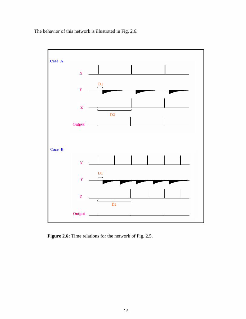
The behavior of this network is illustrated in Fig. 2.6.
Figure 2.6: Time relations for the network of Fig. 2.5.
19
First, consider an input train with a fundamental period approximately equal to D 2 . In Fig. 2.6
A, the first few pulses are shown as they arrive at neuron N 3 . The inhibiting effect of terminal
Y has a sharp rise and gradual decay, as indicated by the solid-black negative sawtooth waves.
It is assumed that during these intervals N 3 will not fire even if two excitatory pulses arrive
simultaneously. However, here the inhibition has died away before the near-coincidence of
pulses at X and Z, so that N 3 fires. However, suppose the input train has a fundamental period
that is half of D 2 , i.e., its fundamental frequency is the first harmonic of the detector’s tuned
frequency. The effect of such a train is shown in Fig. 2.6 B. Neuron N 3 is effectively inhibited
continuously and is unable to fire. Hence, this train is “suppressed”- it does not pass through
the detector. Clearly, higher harmonics will produce even stronger inhibition, and therefore no
harmonic trains can fire the detector. Then a band detector with harmonics suppressed is
obtained.
2.3.2 The Band Suppressor:
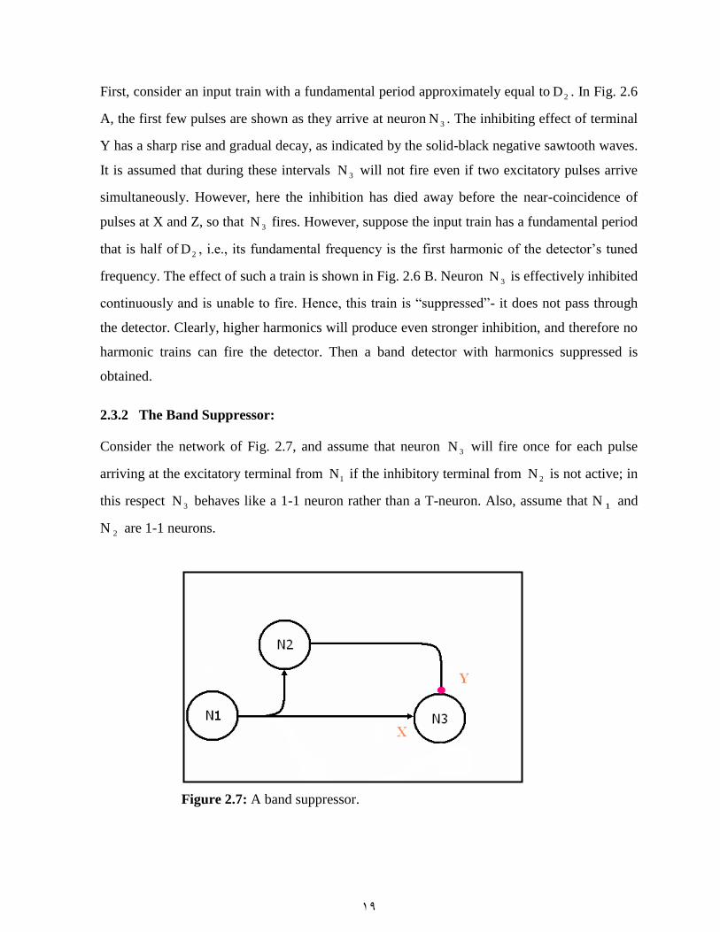
Consider the network of Fig. 2.7, and assume that neuron N 3 will fire once for each pulse
arriving at the excitatory terminal from N1 if the inhibitory terminal from N 2 is not active; in
this respect N 3 behaves like a 1-1 neuron rather than a T-neuron. Also, assume that N 1 and
N 2 are 1-1 neurons.
Figure 2.7: A band suppressor.

20
However, each time a pulse arrives at the inhibitory terminal, N 3 is inhibited for a period I.
Since it was assumed that N 2 is a 1-1 neuron, each pulse arriving at the excitatory terminal X
is followed, after a net delay D, by a pulse arriving at the inhibitory terminal Y. The situation
is summarized in Fig. 2.8. If a pulse reaches X at time t, then N 3 is inhibited over the interval
between t D and t D 1. A second pulse arriving at X during this interval cannot cause
N 3 to fire and is not, therefore represented in the output train from N 3 . Clearly, there is a band
of periods following the first pulse at X, delimited by the dashed vertical marks, which is
suppressed in any input train. Thus, this network is called a band suppressor.
Figure 2.8: Time relations for the network of Fig. 2.7.
21
2.4 Possible Applications of Resonant Networks
A list of some possible applications of TDNN found in the literature, is mentioned here
without any discussion. However, for interested people, you can refer to the work of Reiss [2],
Chesmore [9, 11], and El_asir & Hamdoon [4].
1) FSK Detection
2) PSK Detetcion
3) Velocity Sensing
4) Multiplexing
5) Routing
6) Encoding And Decoding
7) Frequency Counting
8) Modulation
22
Chapter Three
Demodulation of Noncoherent FSK Signals Using Time
Discriminant Connectionist Systems
The application and performance of simple T.D. neural networks for the demodulation of
binary frequency shift keying (FSK) modulation schemes will be discussed in this chapter,
however the conventional methods for the demodulation of the FSK signals will be also
summarized.
3.1 FSK Systems, An Overview
Digital modulation is the process by which digital symbols are transformed into waveforms
that are compatible with the characteristics of the channel. In the case of baseband modulation
these waveforms are pulses, but in the case of band pass modulation, the desired information
signal is modulated to a sinusoid called a carrier wave. FSK modulation is a class of band pass
modulation in which the frequency of the carrier varies in accordance with the information
signal.
3.1.1 Frequency Shift Keying (FSK):
Frequency Shift Keying (FSK) system is a class of wireless systems that is very popular today
and has widespread applications. An FSK system carries its information in the instantaneous
frequency of the received signal.
FSK systems are broadly classified into Coherent and Non-coherent systems. A coherent
system requires carrier or phase synchronization at the receiver end in order to detect the
signals whereas noncoherent detection does not require any sort of synchronization.
23
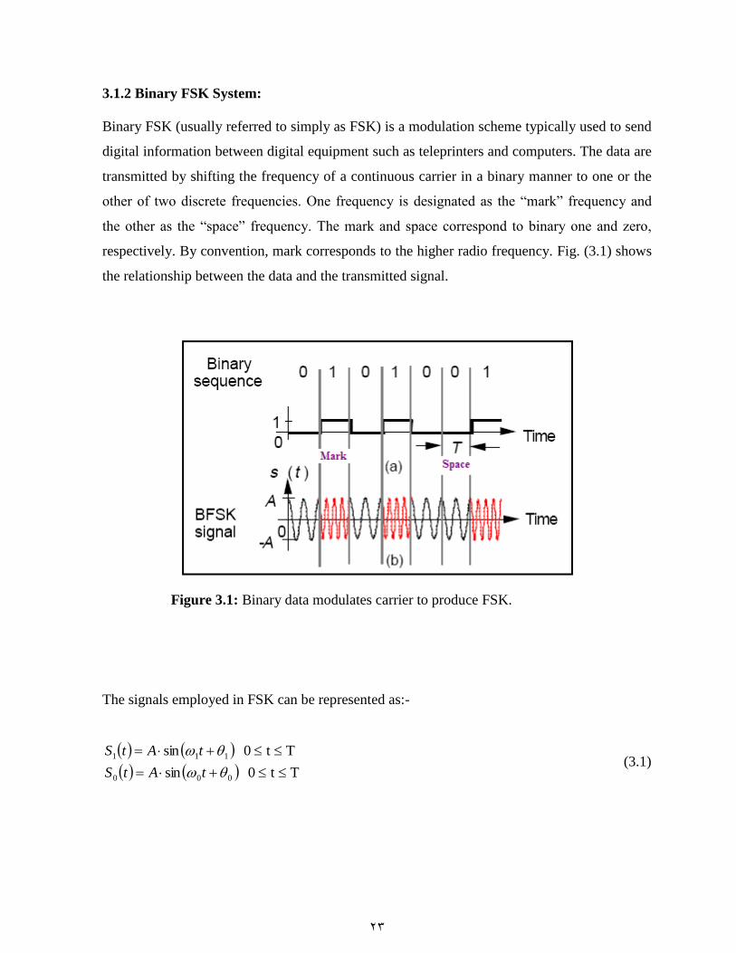
3.1.2 Binary FSK System:
Binary FSK (usually referred to simply as FSK) is a modulation scheme typically used to send
digital information between digital equipment such as teleprinters and computers. The data are
transmitted by shifting the frequency of a continuous carrier in a binary manner to one or the
other of two discrete frequencies. One frequency is designated as the “mark” frequency and
the other as the “space” frequency. The mark and space correspond to binary one and zero,
respectively. By convention, mark corresponds to the higher radio frequency. Fig. (3.1) shows
the relationship between the data and the transmitted signal.
Figure 3.1: Binary data modulates carrier to produce FSK.
The signals employed in FSK can be represented as:-
Tt0 sin
Tt0 sin
000
111
tAtS
tAtS (3.1)
24
Where 1 and 0 are arbitrary phases, and T is the bit interval.
If 1 and 0 are not the same then the above two signals are not coherent. In general, the
waveform is not continuous at bit transitions. This form of FSK is therefore called
noncoherent or discontinuous phase FSK. It can be generated by switching the modulator
output line between two different oscillators.
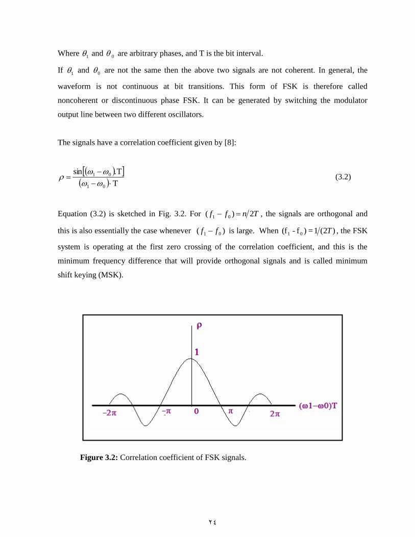
The signals have a correlation coefficient given by [8]:
T
T.sin
01
01
(3.2)
Equation (3.2) is sketched in Fig. 3.2. For Tnff 2)( 01 , the signals are orthogonal and
this is also essentially the case whenever )( 01 ff is large. When )2(1=)f-(f 01 T , the FSK
system is operating at the first zero crossing of the correlation coefficient, and this is the
minimum frequency difference that will provide orthogonal signals and is called minimum
shift keying (MSK).
Figure 3.2: Correlation coefficient of FSK signals.
25
3.1.2.1 FSK Detection:
FSK detection is the process of extracting the information symbols from a modulated carrier
wave. The detection process is mainly categorized into two types namely; coherent detection
and non coherent detection. In the case of coherent detection, the receiver exploits the
knowledge of the carrier’s phase in order to detect the symbols whereas in the case of
noncoherent detection, the receiver does not utilize any phase reference information from the
carrier. Non coherent receivers have simple design, consume less power but have reduced
BER performances.
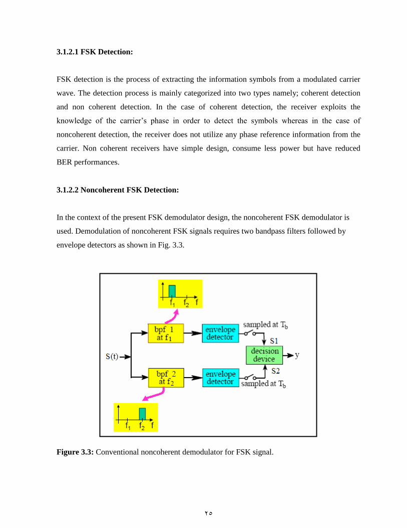
3.1.2.2 Noncoherent FSK Detection:
In the context of the present FSK demodulator design, the noncoherent FSK demodulator is
used. Demodulation of noncoherent FSK signals requires two bandpass filters followed by
envelope detectors as shown in Fig. 3.3.
Figure 3.3: Conventional noncoherent demodulator for FSK signal.

26
The bandpass filters for these signals consist of bandpass filters tuned to the signal
frequencies 1 and 0 . These frequencies must be seperated enough so that each is passed
only by its own bandpass filter.
3.1.3 Demodulation of The FSK Signal Using the Time Discriminant Theory :
The time discriminant neural network architecture described in chapter two do not normally
exhibit inherent temporal structure and can therefore be considered as suboptimal for the
analysis and recognition of copmplex time varying signals such as speech.these networks also
constitute a considerable departure from ''Living Networks ''which processes information in
the form of frequency - coded pulses [9], which is particularly suited to the processing of
time-varying signals such as those encountered in discrete binary and m-ary modulation
schemes. The basic function of TD neuron is that it acts as a pulse processing unit. The term
employed for this type of neuron is "pulse discriminant" (PD).
Since TD neuron consists of two or more inputs and a single output which "fires" (produces a
single narrow pulse) if pulses arrive on all the inputs within a "temporal threshold" of duration
T seconds. Any pulses arriving outside this period will resu1t in no output. The basic time
discriminant neuron [2], can be considered as a near coincidence detector. It is possible to
construct a neural bandpass filter by applying a single pulse train to a two-input neuron one
input being delayed by a factor of D seconds as shown in Fig. 3.4. The centre pulse repetition
frequency (prf), Fc, is given by D-1 and pulses will be output if the coincidence of the input
and delayed version are within –T to +T . limits on the pulse intervals over which the neuron
will fire are given by:
1TD <= cF <= 1
TD
From these conditions, an equation for the equivalent “bandwidth” of the filter is given by
Equation (2.1) which is repeated herefor convenience:
B=2T/ (D2-T2) (3.3)
27
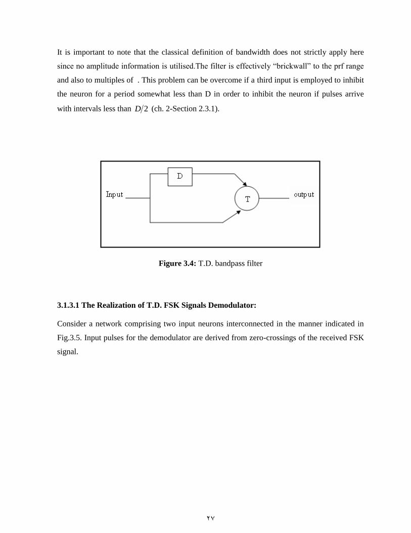
It is important to note that the classical definition of bandwidth does not strictly apply here
since no amplitude information is utilised.The filter is effectively “brickwall” to the prf range
and also to multiples of . This problem can be overcome if a third input is employed to inhibit
the neuron for a period somewhat less than D in order to inhibit the neuron if pulses arrive
with intervals less than 2D (ch. 2-Section 2.3.1).
Figure 3.4: T.D. bandpass filter
3.1.3.1 The Realization of T.D. FSK Signals Demodulator:
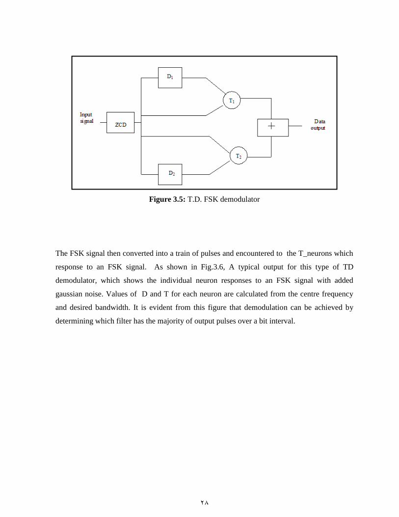
Consider a network comprising two input neurons interconnected in the manner indicated in
Fig.3.5. Input pulses for the demodulator are derived from zero-crossings of the received FSK
signal.
28
Figure 3.5: T.D. FSK demodulator
The FSK signal then converted into a train of pulses and encountered to the T_neurons which
response to an FSK signal. As shown in Fig.3.6, A typical output for this type of TD
demodulator, which shows the individual neuron responses to an FSK signal with added
gaussian noise. Values of D and T for each neuron are calculated from the centre frequency
and desired bandwidth. It is evident from this figure that demodulation can be achieved by
determining which filter has the majority of output pulses over a bit interval.

29
Figure 3.6: Output of T.D. FSK demodulator.
Although it is possible to implement the hardware realization of a T.D. bandpass filter using
delay lines or shift registers to provide delays. However, accurate time resolution requires high
clocking speed and therefore, impractically long register lengths. Amore efficient approach is
to utilize two monostables, the first having a period (D-T) seconds and the second 2T
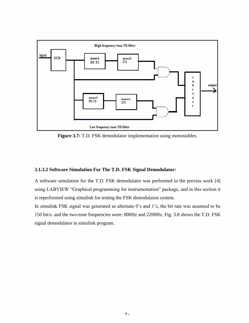
seconds. The T.D. bandpass filter hardware realization consist of two monostables and an
AND gate. for the FSK demodulator two T.D. bandpass filters are needed as shown in
Fig.3.7. each filter act as follows-the first monostable is triggered by a zero crossing and
triggers the second monostable when its time period elapses. The output of the second
monostable opens a “gate” for 2T seconds thus allowing any pulses arriving to be passed to
the output. Automatic harmonic suppression occurs if the first monostable is re-triggerable as
pulses arriving at the intervals less than (D-T) will re-trigger the first monostable before its
time -out, resulting in no output.
30
Figure 3.7: T.D. FSK demodulator implementation using monostables.
3.1.3.2 Software Simulation For The T.D. FSK Signal Demodulator:
A software simulation for the T.D. FSK demodulator was performed in the previos work [4]
using LABVIEW “Graphical programming for instrumentation” package, and in this section it
is reperformed using simulink for testing the FSK demodulaion system.
In simulink FSK signal was generated as alternate 0’s and 1’s, the bit rate was assumed to be
150 bit/s. and the two-tone frequencies were: 800Hz and 2200Hz. Fig. 3.8 shows the T.D. FSK
signal demodulator in simulink program.
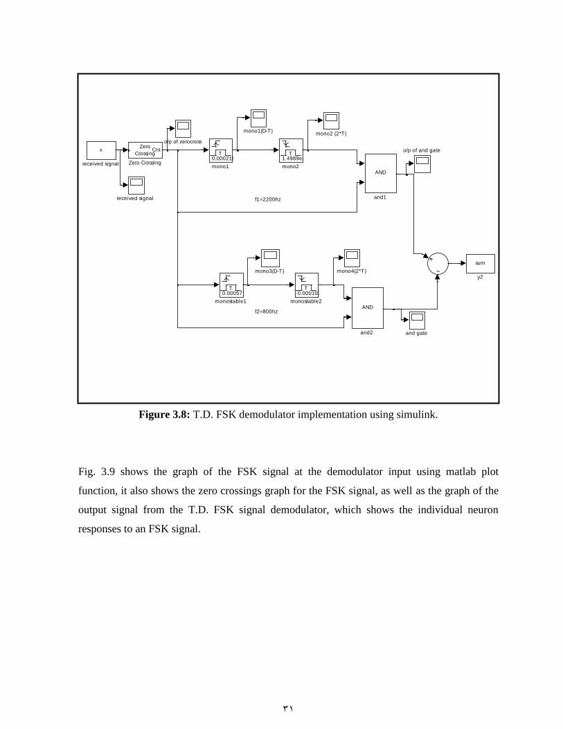
31
f1=2200hz
f2=800hz
sum
y2
received signal
x
received signal
o/p of zerocross
o/p of and gate
T0.0001072 s
monostable2
T0.0005714 s
monostable1
mono4(2*T)mono3(D-T)
mono2 (2*T)
T1.4989e-005 s
mono2
mono1(D-T)
T0.00021978 s
mono1
AND
and2
AND
and1
and gate
Zero
CrossingCnt
Zero Crossing
Figure 3.8: T.D. FSK demodulator implementation using simulink.
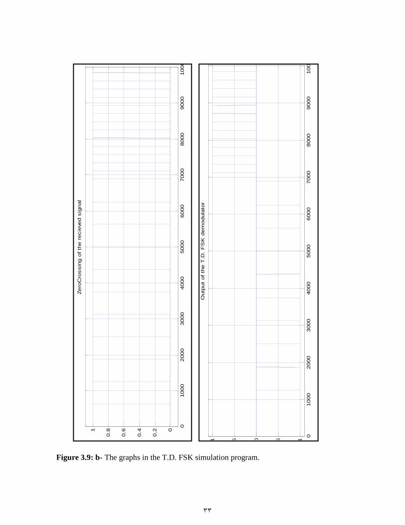
Fig. 3.9 shows the graph of the FSK signal at the demodulator input using matlab plot
function, it also shows the zero crossings graph for the FSK signal, as well as the graph of the
output signal from the T.D. FSK signal demodulator, which shows the individual neuron
responses to an FSK signal.

32
02000
4000
6000
8000
10000
12000
14000
0
0.2
0.4
0.6
0.81
FS
K s
ignal as a
ltern
ate
0's
and 1
's
02000
4000
6000
8000
10000
12000
14000
-10-505
10
Recie
ved S
ignal
Figure 3.9: a- The graph of the received signal and the output of analog to digital converter
33
01000
2000
3000
4000
5000
6000
7000
8000
9000
10000
0
0.2
0.4
0.6
0.81
Zero
Cro
ssin
g o
f th
e r
ecie
ved s
ignal
01000
2000
3000
4000
5000
6000
7000
8000
9000
10000
-1
-0.50
0.51
Outp
ut
of th
e T
.D.
FS
K d
em
odula
tor
Figure 3.9: b- The graphs in the T.D. FSK simulation program.
34
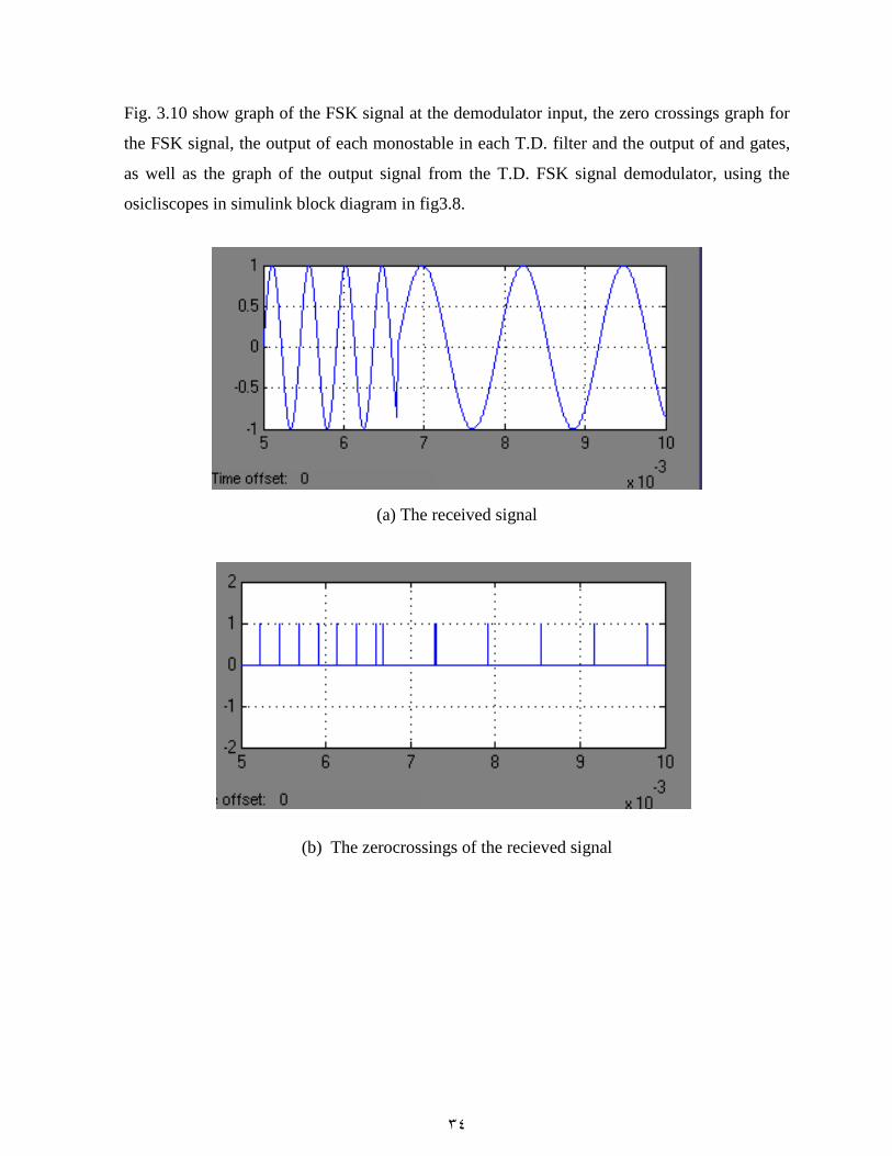
Fig. 3.10 show graph of the FSK signal at the demodulator input, the zero crossings graph for
the FSK signal, the output of each monostable in each T.D. filter and the output of and gates,
as well as the graph of the output signal from the T.D. FSK signal demodulator, using the
osicliscopes in simulink block diagram in fig3.8.
(a) The received signal
(b) The zerocrossings of the recieved signal

35
(c) Output of the 1st mono in the first T.D. filter (used for 2200 hz).
(d) The output of the 2nd mono in the first T.D. filter (used for 2200 hz).
36
(e) The output of the first T.D. filter (used for 2200 hz).
(f) Output of the 1st mono in the 2nd T.D. filter (used for 800 hz).

37
(g) Output of the 2nd mono in the 2nd T.D. filter (used for 800 hz).
(h) The output of the 2nd T.D. filter (used for 800 hz).
38
(i) The output signal from the T.D. FSK signal demodulator
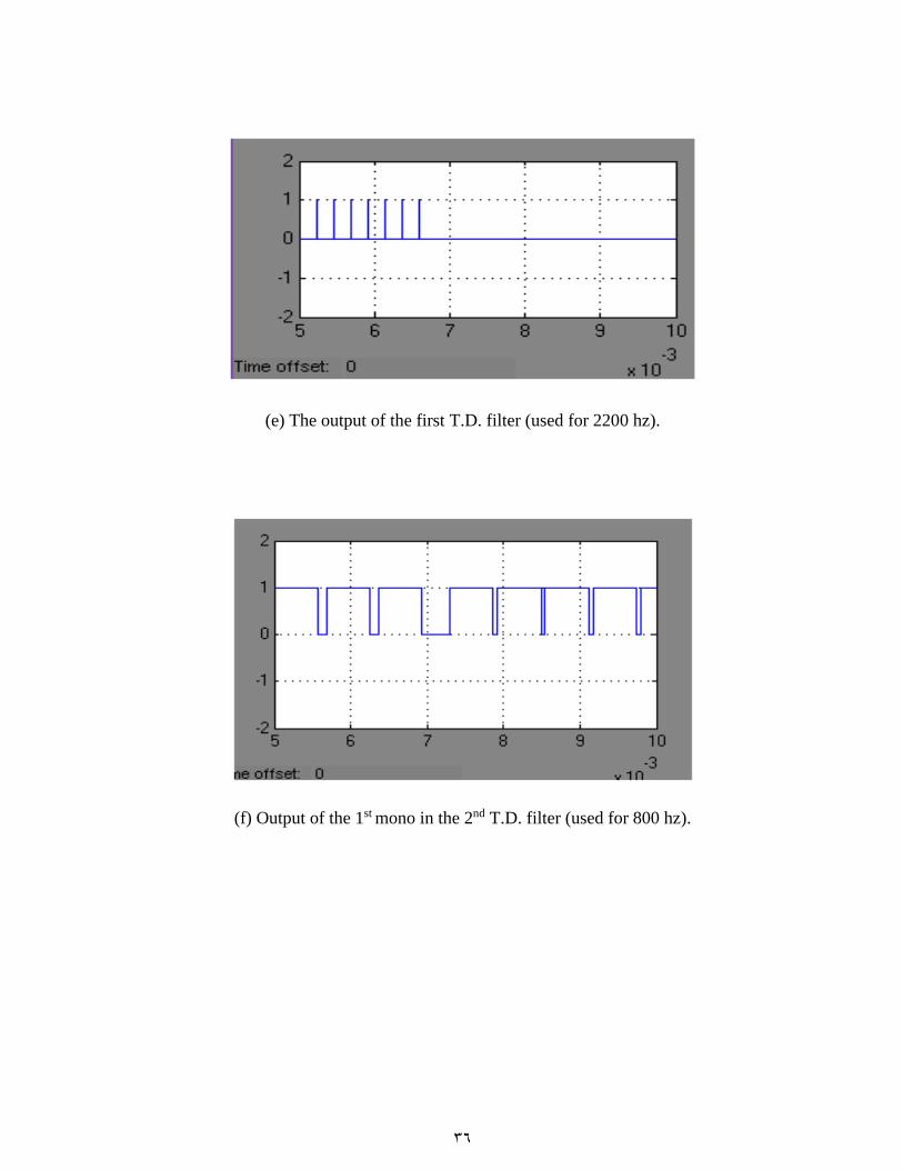
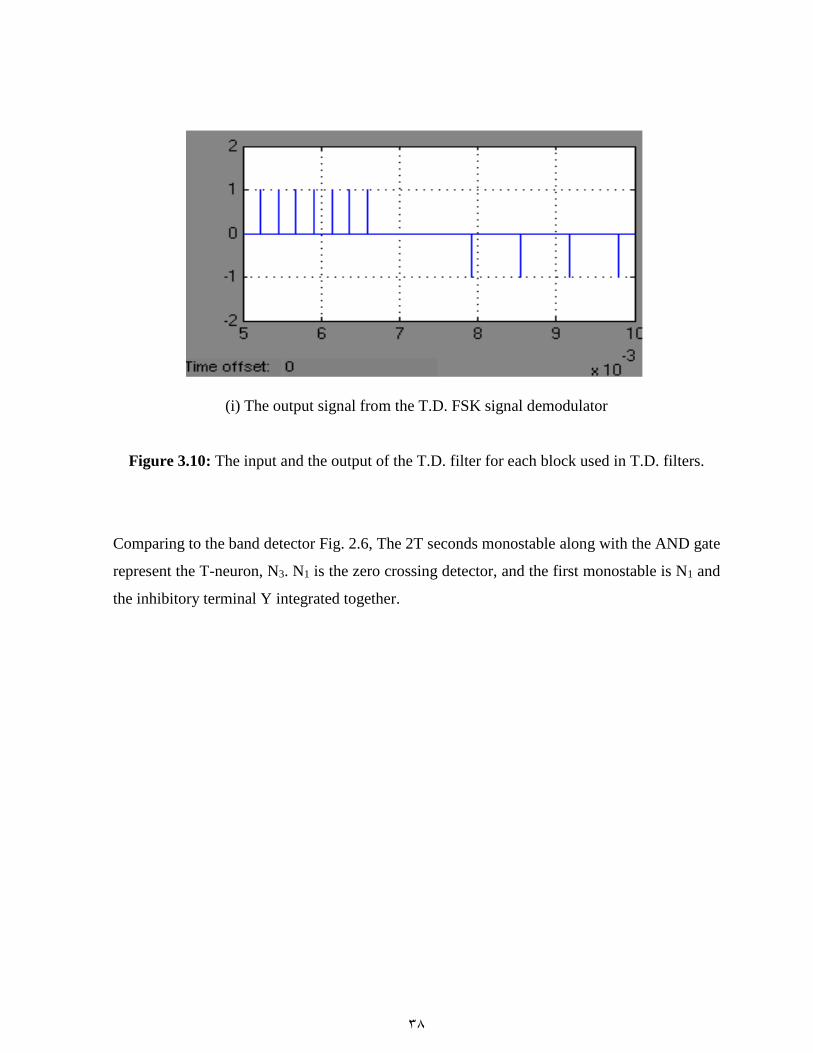
Figure 3.10: The input and the output of the T.D. filter for each block used in T.D. filters.
Comparing to the band detector Fig. 2.6, The 2T seconds monostable along with the AND gate
represent the T-neuron, N3. N1 is the zero crossing detector, and the first monostable is N1 and
the inhibitory terminal Y integrated together.
39
output
DSP
Sine Wave
Pulse
Generator
T0.0001 s
Monostable2
T0.0012 s
Monostable1
AND
Logical
Operator
T7e-005 s
Discrete
Monostable
Clk
RstCntCntUp
Counter
> 0
Compare
To Zero
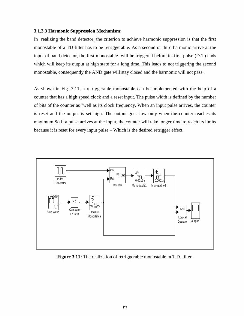
3.1.3.3 Harmonic Suppression Mechanism:
In realizing the band detector, the criterion to achieve harmonic suppression is that the first
monostable of a TD filter has to be retriggerable. As a second or third harmonic arrive at the
input of band detector, the first monostable will be triggered before its first pulse (D-T) ends
which will keep its output at high state for a long time. This leads to not triggering the second
monostable, consequently the AND gate will stay closed and the harmonic will not pass .
As shown in Fig. 3.11, a retriggerable monostable can be implemented with the help of a
counter that has a high speed clock and a reset input. The pulse width is defined by the number
of bits of the counter as "well as its clock frequency. When an input pulse arrives, the counter
is reset and the output is set high. The output goes low only when the counter reaches its
maximum.So if a pulse arrives at the Input, the counter will take longer time to reach its limits
because it is reset for every input pulse – Which is the desired retrigger effect.
Figure 3.11: The realization of retriggerable monostable in T.D. filter.

40
Figure 3.12 shows the input to the T.D filter, and the output of each component used in
realization of retriggerable monostable in T.D. filter.
(a) The received signal
(b) The zero crossings of the signal.
(c) The zero crossing of the signal with narrow pulse width.
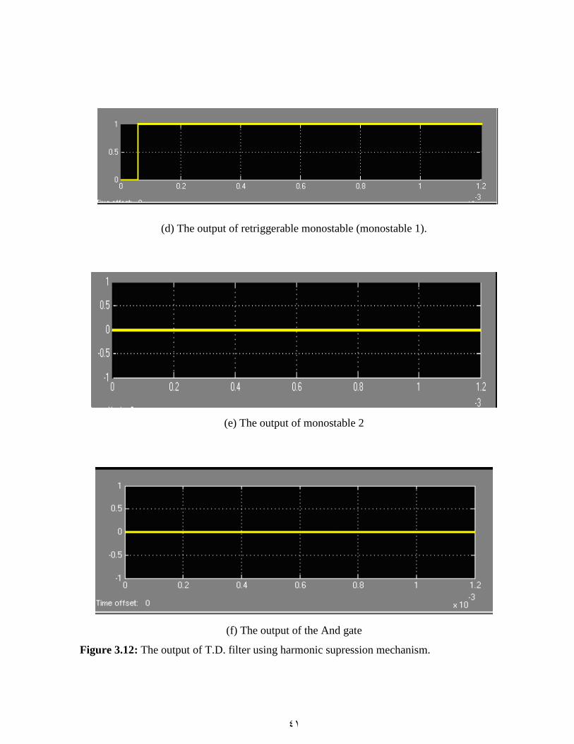
41
(d) The output of retriggerable monostable (monostable 1).
(e) The output of monostable 2
(f) The output of the And gate
Figure 3.12: The output of T.D. filter using harmonic supression mechanism.

42
f1=2200hz
f2=800hz
yout3
y3
yout2
y2
yout1
y1
yout
y
sum
received signal
x
received signal
o/p of zerocross o/p of and gate
noisy signal
T0.0001072 s
monostable2
T0.0005714 s
monostable1
mono2(2*T)f=800hz
mono2 (2*T)
f=2200hz
T1.4989e-005 s
mono2
mono1(D-T)
f=800hz
mono1(D-T)
f=2200hz
T0.00021978 s
mono1
bandpass fi lter
AND
and2
AND
and1
and gate
Zero
CrossingCnt
Zero Crossing
eror
Signal To
Workspace
Error Rate
Calculation
Tx
Rx
Error Rate
Calculation
Convert
Data Type Conversion1
Bandpass
Bandpass Filter
AWGN
AWGN
Channel
The simulation is repeated with an additive white gaussian noise was added to the generated
FSK signal which is alternate 0’s and 1’s, with a channel bandwidth: 0.3-3.4kHz, which is
represented by a bandpass filter, the bit rate was also assumed to be 150 bit/s. and with the
samefrequencytones : 800Hz and 2200Hz. Fig. 3.13 shows the block diagram of the T.D. FSK
demodulator which is used to detect noisy signals, and Fig3.14shows the graph of the noisy
FSK signal at the demodulator input, it also shows the zero crossings graph for the noisy FSK
signal, as well as the graph of the output signal from the T.D. FSK signal demodulator, which
shows the individual neuron responses to an FSK signal with added gaussian noise.
Figure 3.13: The block diagram of T.D. FSK demodulator to detect noisy signals

43
(a) The noisy signal
(b) The filtered noisy signal
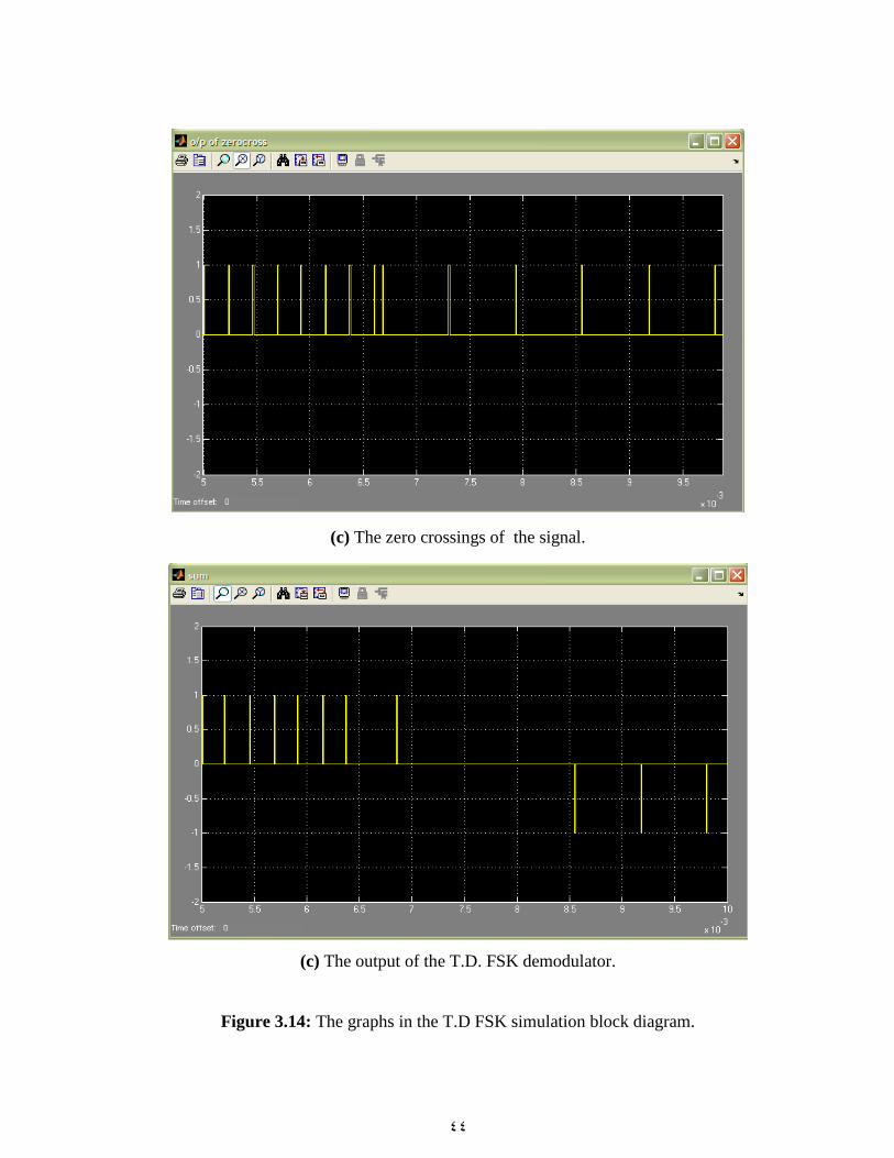
44
(c) The zero crossings of the signal.
(c) The output of the T.D. FSK demodulator.
Figure 3.14: The graphs in the T.D FSK simulation block diagram.
45
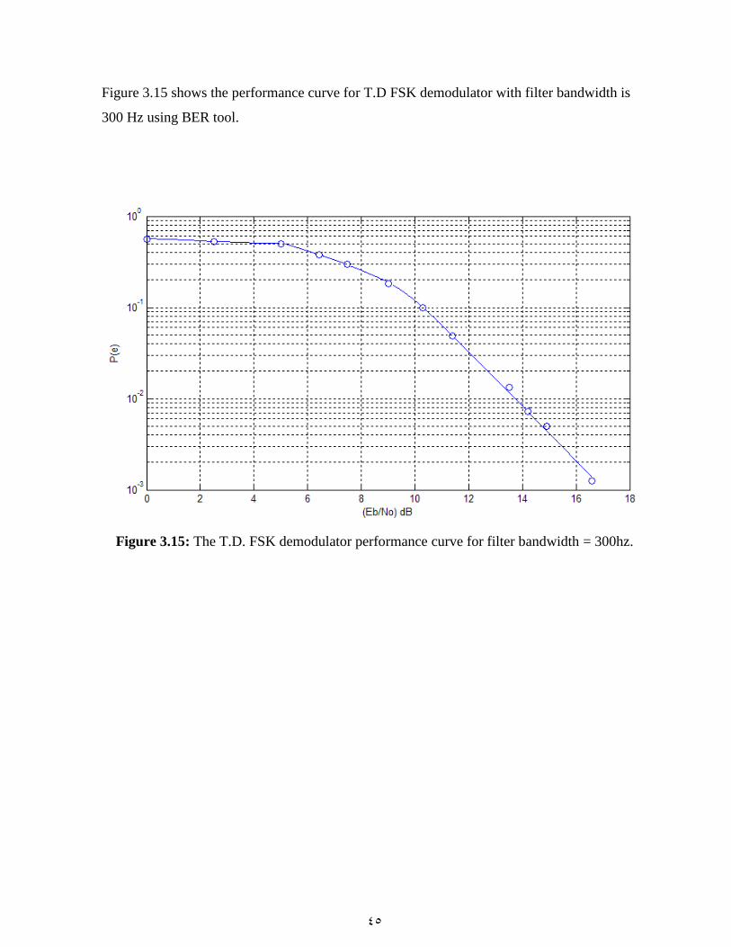
Figure 3.15 shows the performance curve for T.D FSK demodulator with filter bandwidth is
300 Hz using BER tool.
Figure 3.15: The T.D. FSK demodulator performance curve for filter bandwidth = 300hz.
46
Chapter Four
Implementation of Noncoherent MFSK Signals Demodulation
Using Time Discriminant Connectionist System:
In this chapter the demodulation of noncoherent T.D. MFSK signals will be disscussed as well
as the architecture of MFSK demodulator using Verilog HDL will be presented.
4.1 Multiple Frequency Shift Keying (MFSK) Signals.
The MFSK class of signals consists of sinusoids having a duration of Ts, and in this interval
having one frequency selected from a set of M possible frequencies, this can be represented
mathematically as :
elsewhere 0,
to ,1cos 0 s
i
TtitAtS
(4.1)
Where: i=1, 2, ...., M, being the smallest frequency difference between any two signals in
the set, Ts is the symbol interval, and is an arbitrary phase.
For the signals to be orthogonal, it is necessary that be sufficiently large, or it satisfies the
requirement:
,....3,2,1 , ;2 nforT
nfandf
s
47
i.e. must be an integral multiple of the symbol rate sT2 , and 0 is a multiple of half
the symbol rate. The bandwidth for this type of signal (MFSK signal) is:
sTM 1 when sTf 1 .
A special case when M=2 leads to a binary FSK signal set, i.e. either bit “0” or bit “1” are
transmitted.
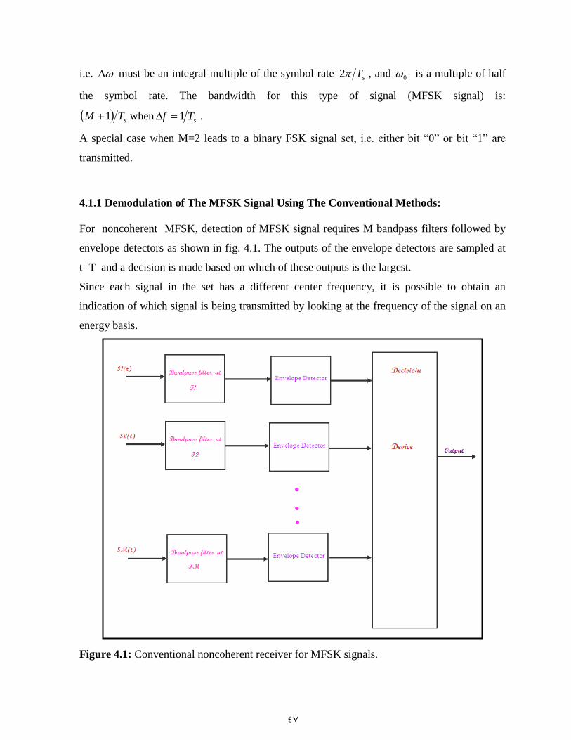
4.1.1 Demodulation of The MFSK Signal Using The Conventional Methods:
For noncoherent MFSK, detection of MFSK signal requires M bandpass filters followed by
envelope detectors as shown in fig. 4.1. The outputs of the envelope detectors are sampled at
t=T and a decision is made based on which of these outputs is the largest.
Since each signal in the set has a different center frequency, it is possible to obtain an
indication of which signal is being transmitted by looking at the frequency of the signal on an
energy basis.
Figure 4.1: Conventional noncoherent receiver for MFSK signals.
48
4.1.2 Demodulation of Noncoherent MFSK Signal Using Time Discriminant
Connectionist System:
To demodulate the MFSK signal using the time discriminant connectionist systems, M “T.D.
bandpass filters” are needed, and each T.D. bandpass filter is a near coincidence detector of
the form shown in chp3 (Fig.3.4). Hardware realization using monostables is complex since M
bandpass filters are needed.
4.1.2.1 The Realization of T.D. MFSK Signal Demodulator:
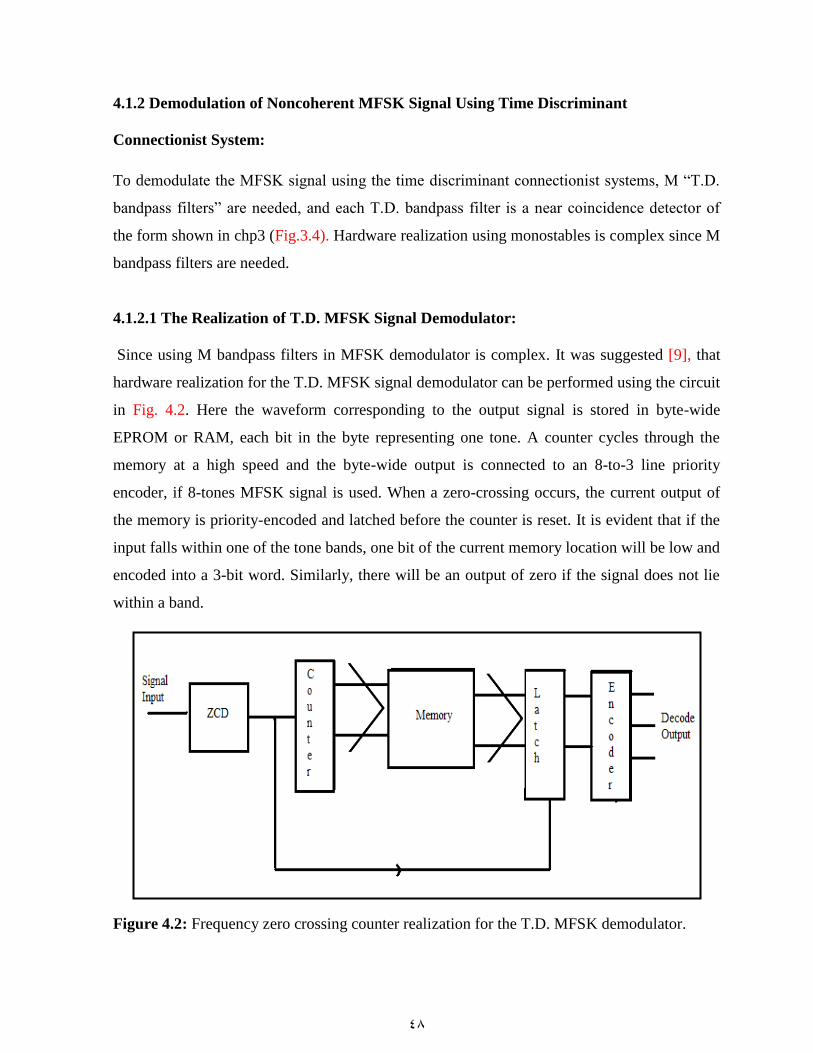
Since using M bandpass filters in MFSK demodulator is complex. It was suggested [9], that
hardware realization for the T.D. MFSK signal demodulator can be performed using the circuit
in Fig. 4.2. Here the waveform corresponding to the output signal is stored in byte-wide
EPROM or RAM, each bit in the byte representing one tone. A counter cycles through the
memory at a high speed and the byte-wide output is connected to an 8-to-3 line priority
encoder, if 8-tones MFSK signal is used. When a zero-crossing occurs, the current output of
the memory is priority-encoded and latched before the counter is reset. It is evident that if the
input falls within one of the tone bands, one bit of the current memory location will be low and
encoded into a 3-bit word. Similarly, there will be an output of zero if the signal does not lie
within a band.
Figure 4.2: Frequency zero crossing counter realization for the T.D. MFSK demodulator.
49
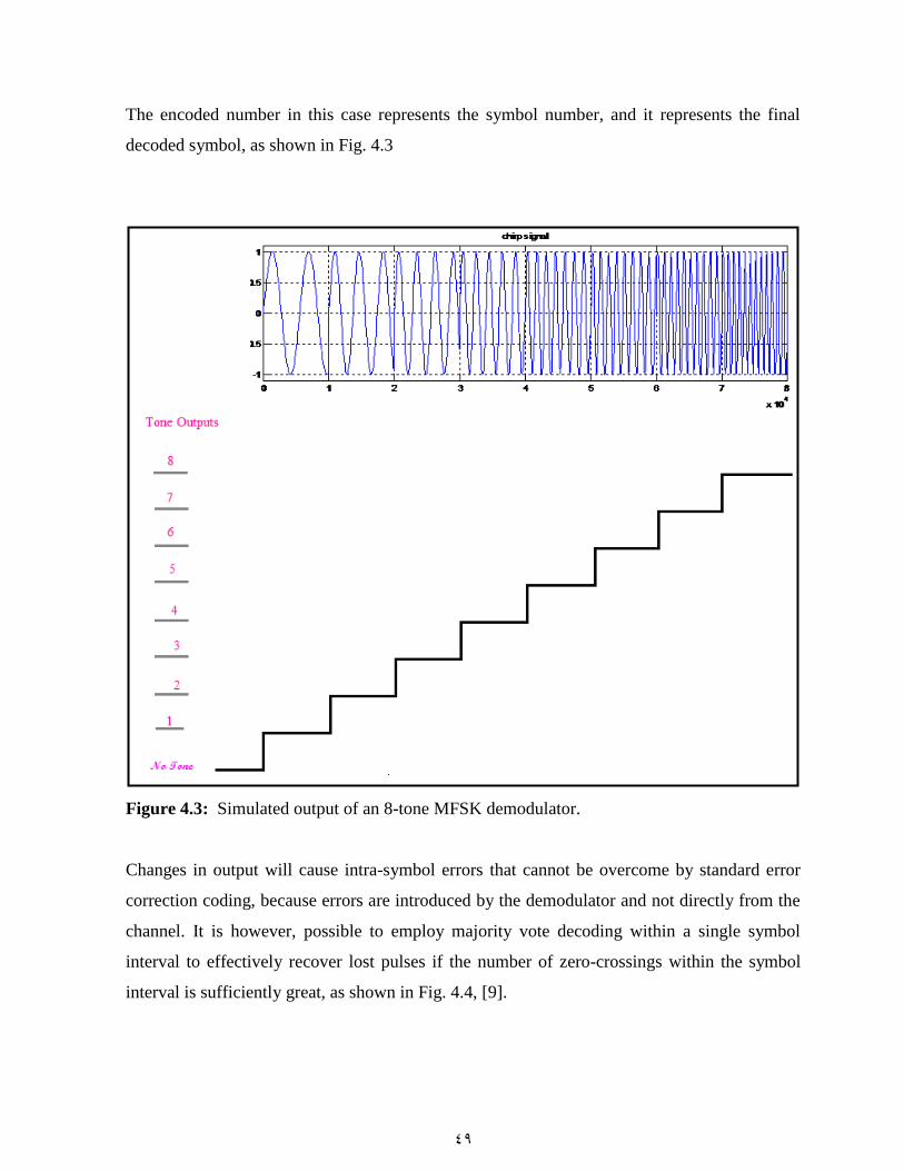
The encoded number in this case represents the symbol number, and it represents the final
decoded symbol, as shown in Fig. 4.3
Figure 4.3: Simulated output of an 8-tone MFSK demodulator.
Changes in output will cause intra-symbol errors that cannot be overcome by standard error
correction coding, because errors are introduced by the demodulator and not directly from the
channel. It is however, possible to employ majority vote decoding within a single symbol
interval to effectively recover lost pulses if the number of zero-crossings within the symbol
interval is sufficiently great, as shown in Fig. 4.4, [9].

50
Figure 4.4: Intra-symbol errors in the T.D. MFSK demodulator, (a) 8-tone demodulator
errors due to noise, (b) recovery by majority vote.
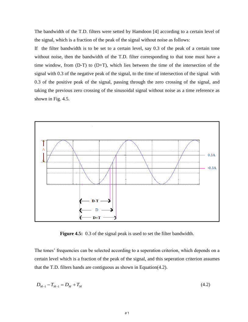
51
The bandwidth of the T.D. filters were setted by Hamdoon [4] according to a certain level of
the signal, which is a fraction of the peak of the signal without noise as follows:
If the filter bandwidth is to be set to a certain level, say 0.3 of the peak of a certain tone
without noise, then the bandwidth of the T.D. filter corresponding to that tone must have a
time window, from (D-T) to (D+T), which lies between the time of the intersection of the
signal with 0.3 of the negative peak of the signal, to the time of intersection of the signal with
0.3 of the positive peak of the signal, passing through the zero crossing of the signal, and
taking the previous zero crossing of the sinusoidal signal without noise as a time reference as
shown in Fig. 4.5.
Figure 4.5: 0.3 of the signal peak is used to set the filter bandwidth.
The tones’ frequencies can be selected according to a seperation criterion, which depends on a
certain level which is a fraction of the peak of the signal, and this seperation criterion assumes
that the T.D. filters bands are contiguous as shown in Equation(4.2).
MMMM TDTD 11
(4.2)
52
For a certain level of the signal peak, K which ranges from 0 to 1 as shown in Equation (4.3),
then the tones’ frequencies can be found using Equations (4.4), and (4.5) [4].
MMTFSinK 2 (4.3)
(4.4)
1
1
M
MMM
F
FTT (4.5)
Where FM is the highest frequency tone which represents the Mth tone, and TM is the
threshold for the M’th T.D.filter, then:
With a certain seperation, the ratio of the two tones FM and FM-1 represents the ratio of any two
consecutive tones for the same seperation, i.e. the frequencies of the other tones can be found
using Equation (4.6):
1
M
M
F
FC (4.6)
Where, C is a constant.
The frequency range for the passband of each T.D. filter in the MFSK demodulator is given by
Equations(4.7) and (4.8):
band band
,
1
xx
bandxlowTD
F
(4.7)
And
band band
,
1
xx
bandxhighTD
F
(4.8)
MM
MMMM
TF
TFFF
42
42 2
1

53
For the same separation criterion, if the bands are not contiguous then the threshold (TM) was
found for a certain fraction of the peak of the signal, which must be less than the value of the
level used for the tones separation criterion. Once this level is assigned, then the other T’s for
the other bands can be obtained from Equation (4.5), then these T values can be substituted
into Equation (4.7) and Equation (4.8) to find the lower and the upper frequency for each band.
4.1.3 Hardware Design of T.D. MFSK Using Verilog HDL:
4.1.3.1 Motivatoin
Verilog is a hardware description language (HDL). A hardware description Language is a
language used to describe a digital system, for example, a computer or a component of a
computer. A digital system can be described at several levels. Verilog allows hardware
designers to express their designs. For example, an HDL might describe the layout of the
wires, resistors and transistors on an Integrated Circuit (IC) chip, i. e., the switch level. Or, it
might describe the logical gates and flip flops in a digital system, i. e., the gate level. An even
higher level describes the registers and the transfers of vectors of information between
registers. This is called the Register Transfer Level (RTL). Verilogsupports all of these levels.
The modules of the T.D. MFSK were built in RTL level.
Since the veilog HDL describes the architecture and behavior of discrete and integrated
electronic systems .The design functionality can be verified early in the design process. Design
simulation at this higher level, before implementation at the gate level, allows to evaluate
architectural and design decisions.
4.1.4.2 Design Methodology of the T.D. MFSK Demodulator.
The design of T.D MFSK demodulator was first built in verilog HDL language and then
simulated using the verilogger pro software, then it was synthesized using Quartus II software.
The design will be presented first using block diagrams and Verilog HDL code as a design
entry, to end up with synthsizing the T.D. MFSK demodulator, simulating, and then
implementing it on the FPGA.
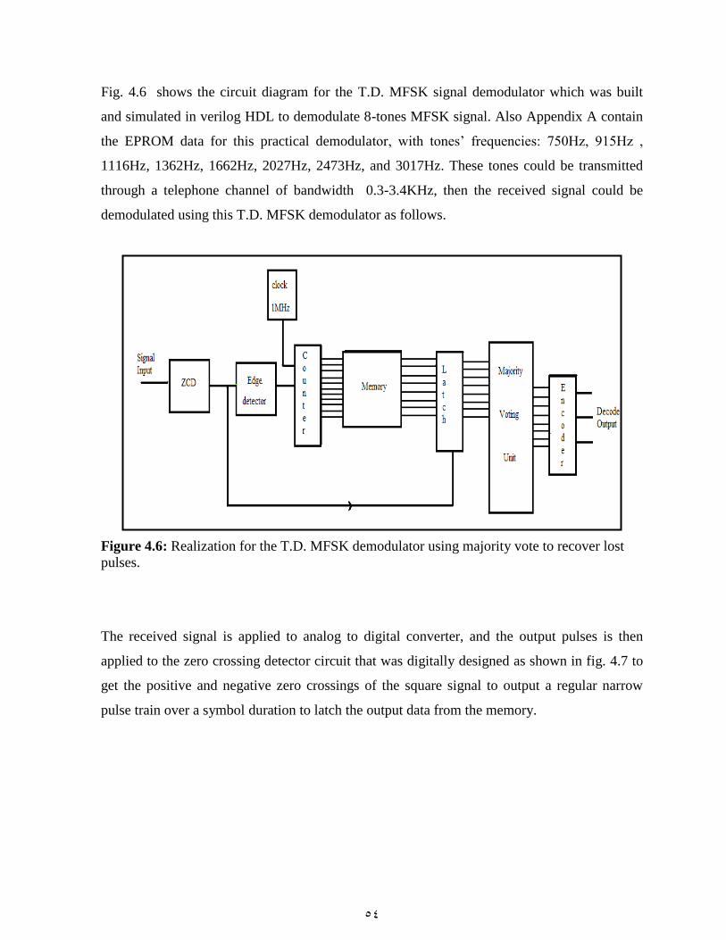
54
Fig. 4.6 shows the circuit diagram for the T.D. MFSK signal demodulator which was built
and simulated in verilog HDL to demodulate 8-tones MFSK signal. Also Appendix A contain
the EPROM data for this practical demodulator, with tones’ frequencies: 750Hz, 915Hz ,
1116Hz, 1362Hz, 1662Hz, 2027Hz, 2473Hz, and 3017Hz. These tones could be transmitted
through a telephone channel of bandwidth 0.3-3.4KHz, then the received signal could be
demodulated using this T.D. MFSK demodulator as follows.
Figure 4.6: Realization for the T.D. MFSK demodulator using majority vote to recover lost
pulses.
The received signal is applied to analog to digital converter, and the output pulses is then
applied to the zero crossing detector circuit that was digitally designed as shown in fig. 4.7 to
get the positive and negative zero crossings of the square signal to output a regular narrow
pulse train over a symbol duration to latch the output data from the memory.
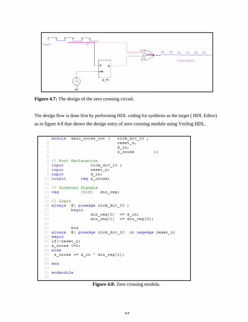
55
Figure 4.7: The design of the zero crossing circuit.
The design flow is done first by performing HDL coding for synthesis as the target ( HDL Editor)
as in figure 4.8 that shows the design entry of zero crossing module using Verilog HDL.
Figure 4.8: Zero crossing module.
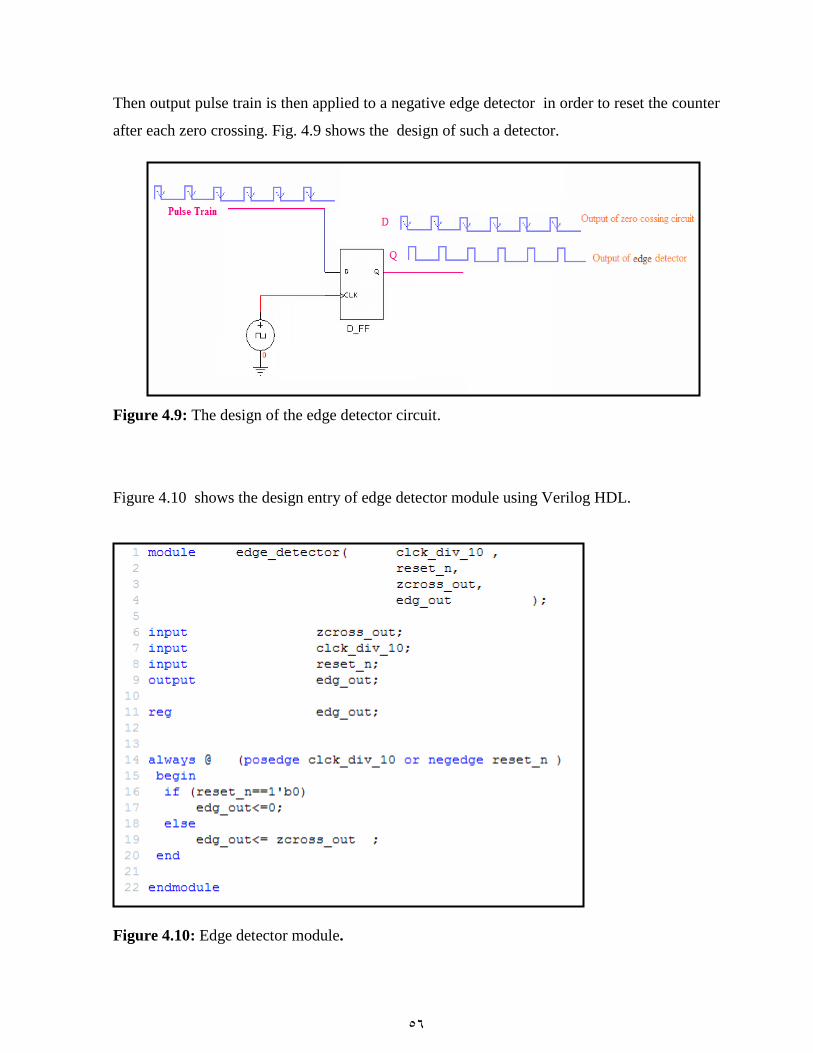
56
Then output pulse train is then applied to a negative edge detector in order to reset the counter
after each zero crossing. Fig. 4.9 shows the design of such a detector.
Figure 4.9: The design of the edge detector circuit.
Figure 4.10 shows the design entry of edge detector module using Verilog HDL.
Figure 4.10: Edge detector module.
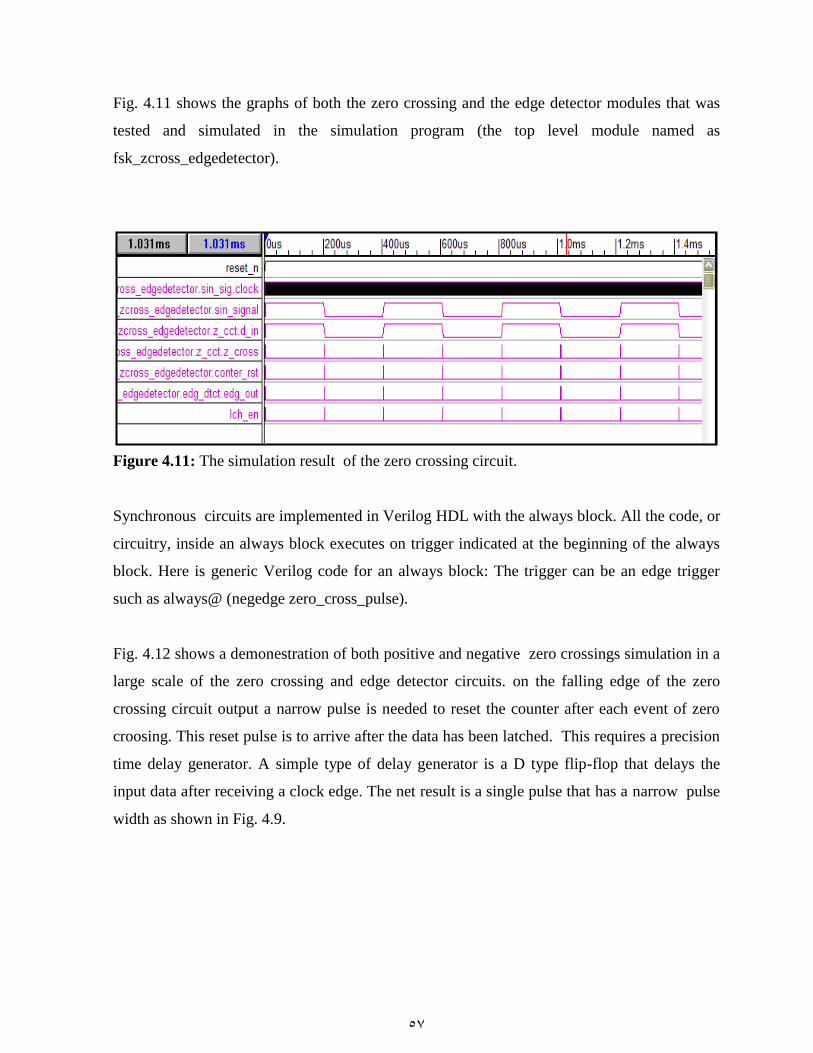
57
Fig. 4.11 shows the graphs of both the zero crossing and the edge detector modules that was
tested and simulated in the simulation program (the top level module named as
fsk_zcross_edgedetector).
Figure 4.11: The simulation result of the zero crossing circuit.
Synchronous circuits are implemented in Verilog HDL with the always block. All the code, or
circuitry, inside an always block executes on trigger indicated at the beginning of the always
block. Here is generic Verilog code for an always block: The trigger can be an edge trigger
such as always@ (negedge zero_cross_pulse).
Fig. 4.12 shows a demonestration of both positive and negative zero crossings simulation in a
large scale of the zero crossing and edge detector circuits. on the falling edge of the zero
crossing circuit output a narrow pulse is needed to reset the counter after each event of zero
croosing. This reset pulse is to arrive after the data has been latched. This requires a precision
time delay generator. A simple type of delay generator is a D type flip-flop that delays the
input data after receiving a clock edge. The net result is a single pulse that has a narrow pulse
width as shown in Fig. 4.9.
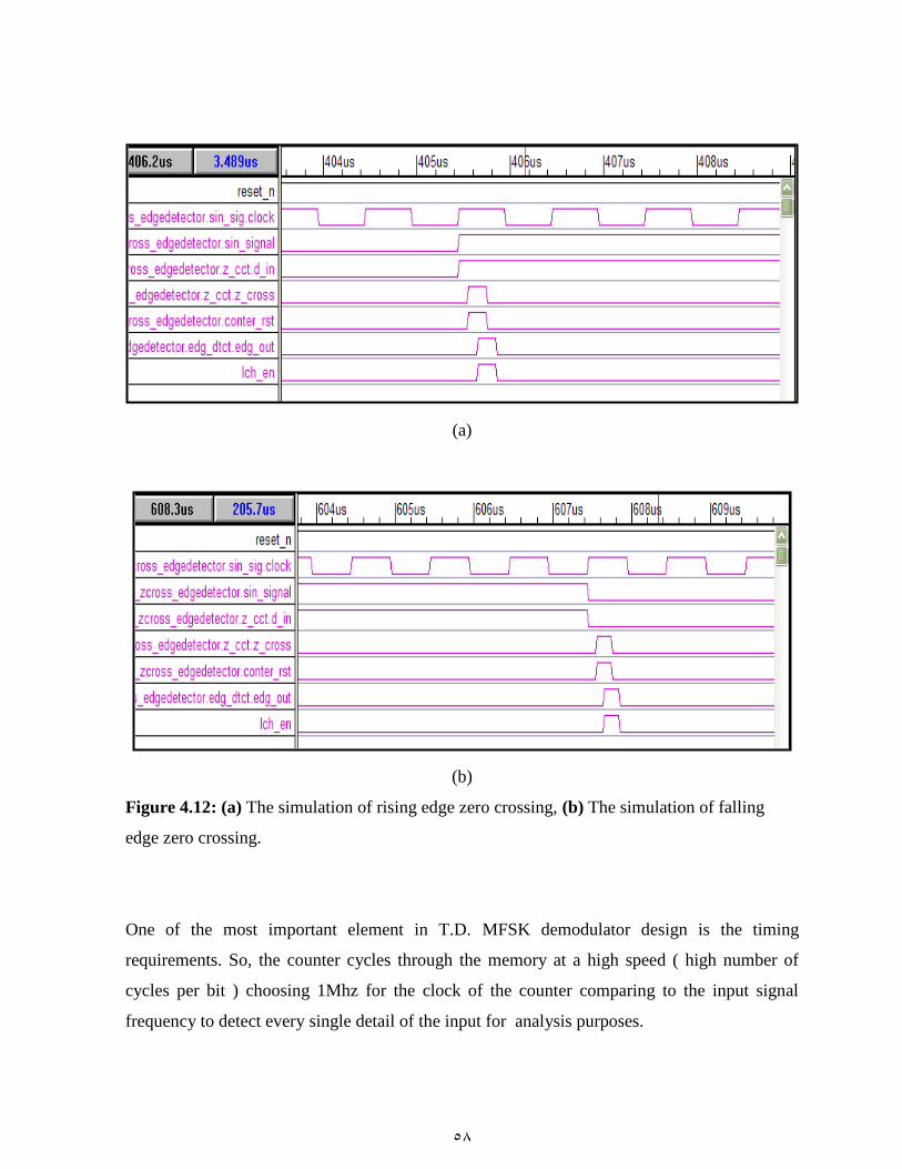
58
(a)
(b)
Figure 4.12: (a) The simulation of rising edge zero crossing, (b) The simulation of falling
edge zero crossing.
One of the most important element in T.D. MFSK demodulator design is the timing
requirements. So, the counter cycles through the memory at a high speed ( high number of
cycles per bit ) choosing 1Mhz for the clock of the counter comparing to the input signal
frequency to detect every single detail of the input for analysis purposes.

59
Figure 4.13 shows the design entry of the counter module using Verilog HDL.
Figure 4.13: Counter module.

60
The data of the T.D. filter bands are stored in memory as discussed before in choosing proper
filters' bandwidths, and written in text file that was instantiated in the look_up_table module
from the (rom_data.text) as shown in fig. 4.14.
Figure 4.14: Look up table module.
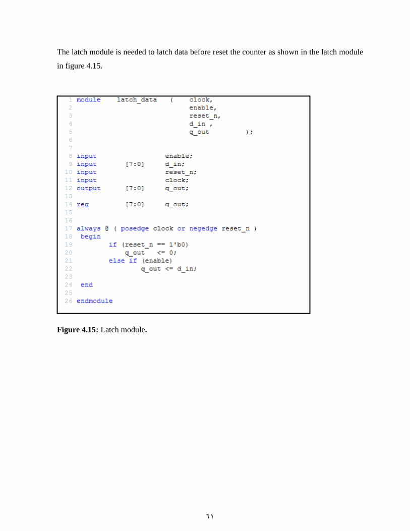
61
The latch module is needed to latch data before reset the counter as shown in the latch module
in figure 4.15.
Figure 4.15: Latch module.

62
Fig. 4.16 shows the output of the memory controling data module that instantiate counter,
memory, and the latch modules. The process can be explained as follows: when a zero-
crossing occurs, the current output of the memory is priority-encoded and latched before the
counter is reset.
Figure 4.16: The simulation of the memory control and latch modules.
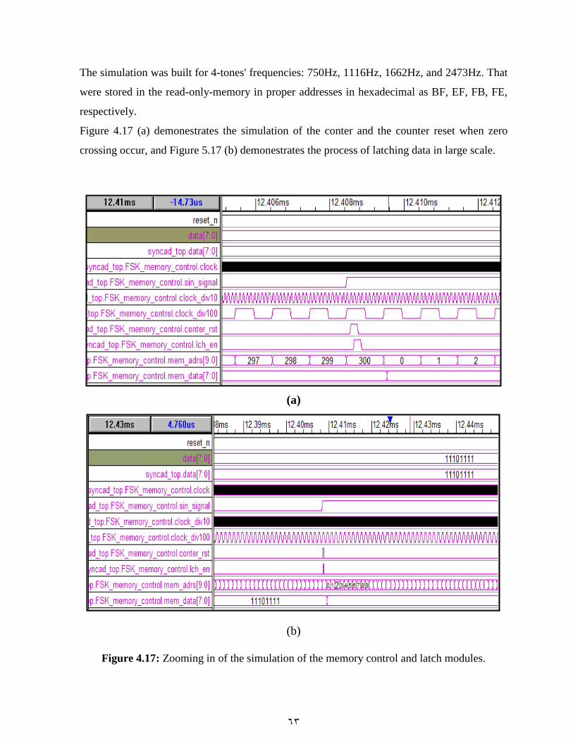
63
The simulation was built for 4-tones' frequencies: 750Hz, 1116Hz, 1662Hz, and 2473Hz. That
were stored in the read-only-memory in proper addresses in hexadecimal as BF, EF, FB, FE,
respectively.
Figure 4.17 (a) demonestrates the simulation of the conter and the counter reset when zero
crossing occur, and Figure 5.17 (b) demonestrates the process of latching data in large scale.
(a)
(b)
Figure 4.17: Zooming in of the simulation of the memory control and latch modules.

64
The latch output is encountered to the majority vote decoding to decide which one of the M-
tones' frequency is recieved. Its function is to employ majority vote decoding within a single
symbol interval to effectively recover lost pulses if the number of zero-crossings within the
symbol interval is sufficiently great.
The methodology of the majority vote decoding is to count the number of zero crossings
within symbol interval. Additional counter, count0 is added in the design to count the number
of out of band zero cossings as shown in Fig. 4.18.
Figure 4.18: The block diagram of the majority vote decoder.
The following Verilog HDL code is for the majority voting module that contains 9-counters.
one for every latched data for every stored band in memory, and after each symbol duration
the decesion is done.
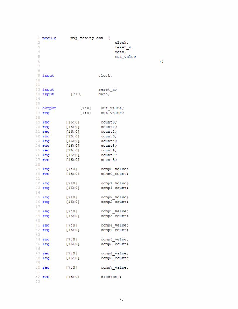
65
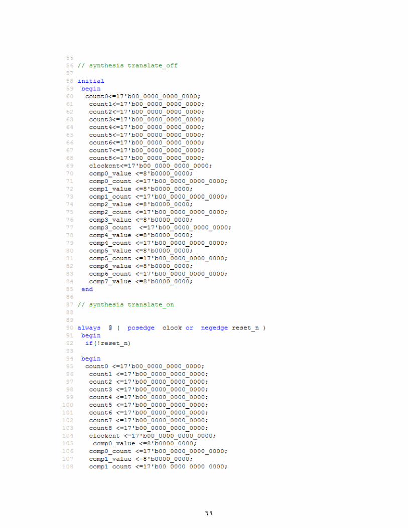
66
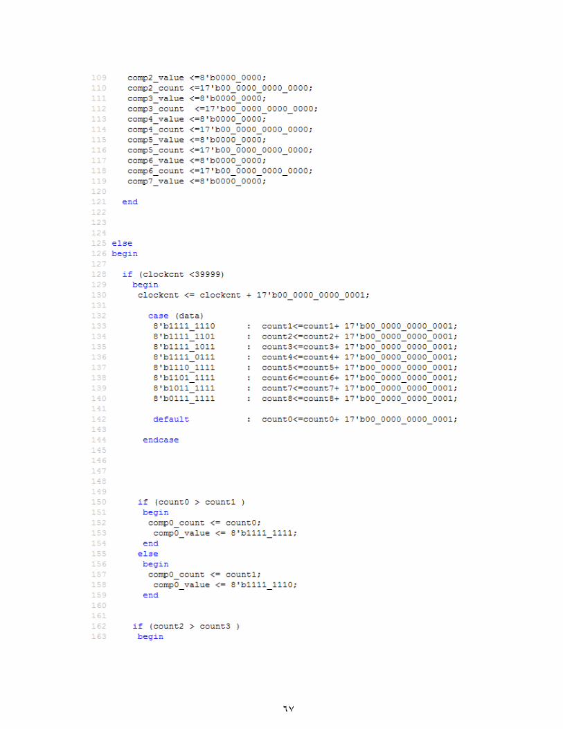
67
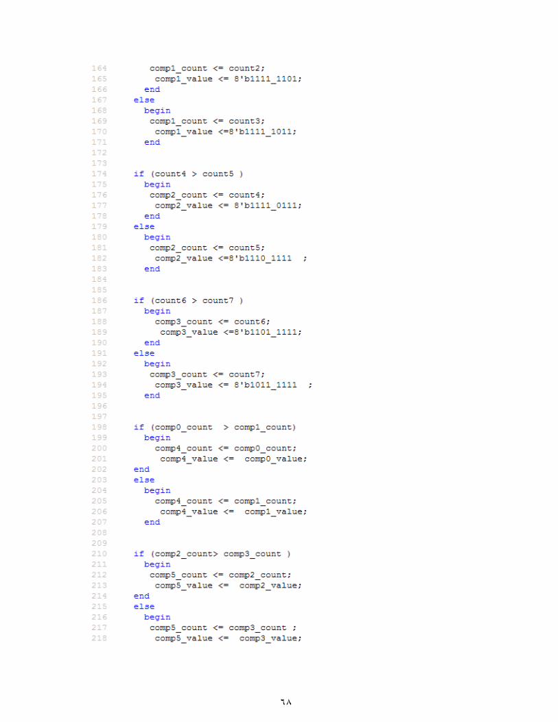
68

69
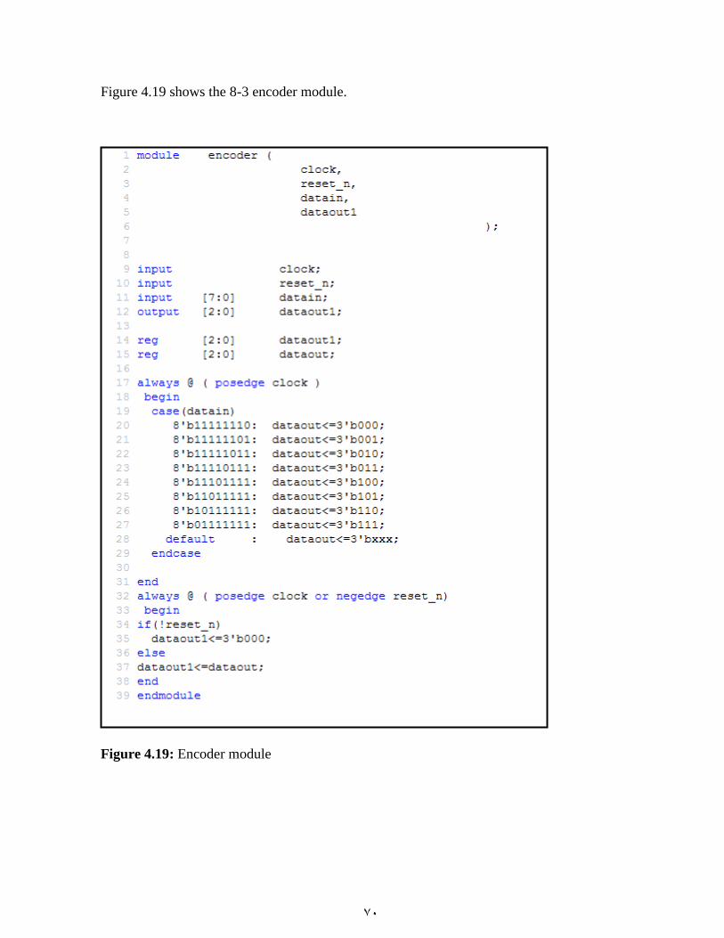
70
Figure 4.19 shows the 8-3 encoder module.
Figure 4.19: Encoder module
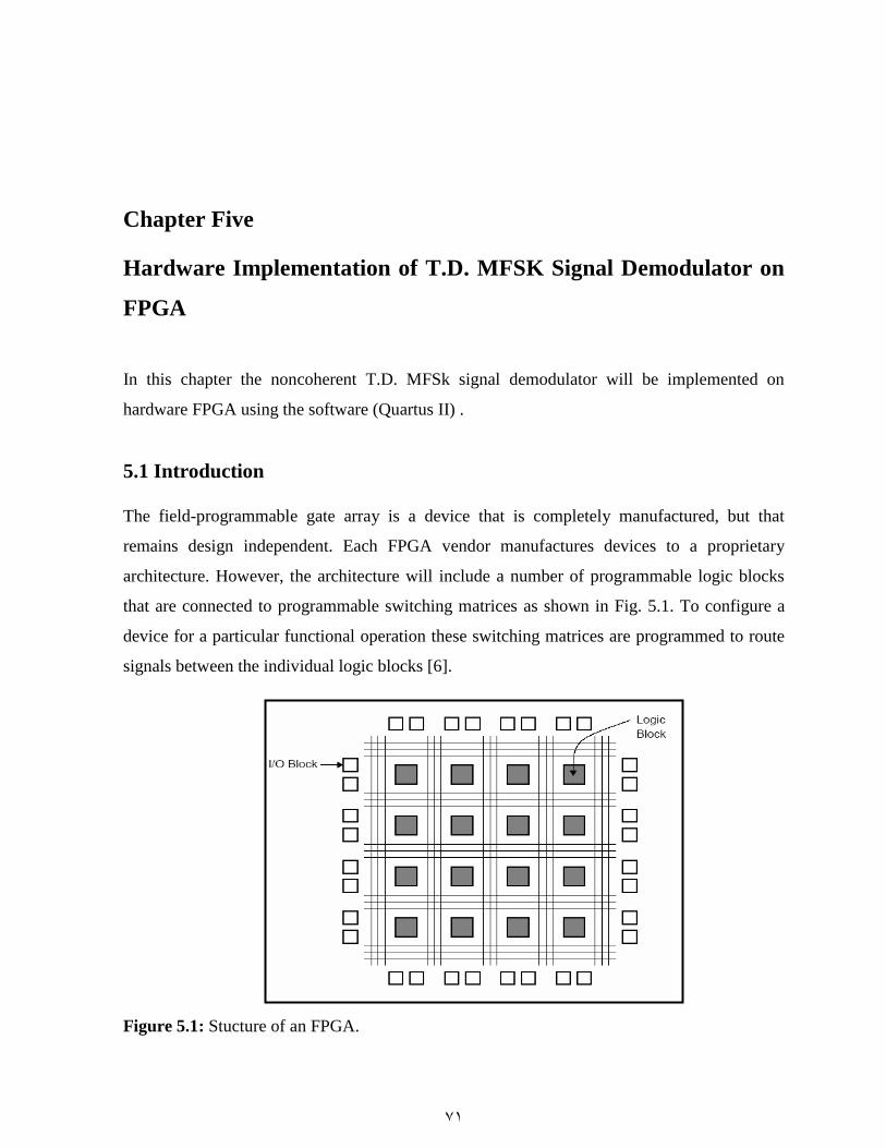
71
Chapter Five
Hardware Implementation of T.D. MFSK Signal Demodulator on
FPGA
In this chapter the noncoherent T.D. MFSk signal demodulator will be implemented on
hardware FPGA using the software (Quartus II) .
5.1 Introduction
The field-programmable gate array is a device that is completely manufactured, but that
remains design independent. Each FPGA vendor manufactures devices to a proprietary
architecture. However, the architecture will include a number of programmable logic blocks
that are connected to programmable switching matrices as shown in Fig. 5.1. To configure a
device for a particular functional operation these switching matrices are programmed to route
signals between the individual logic blocks [6].
Figure 5.1: Stucture of an FPGA.
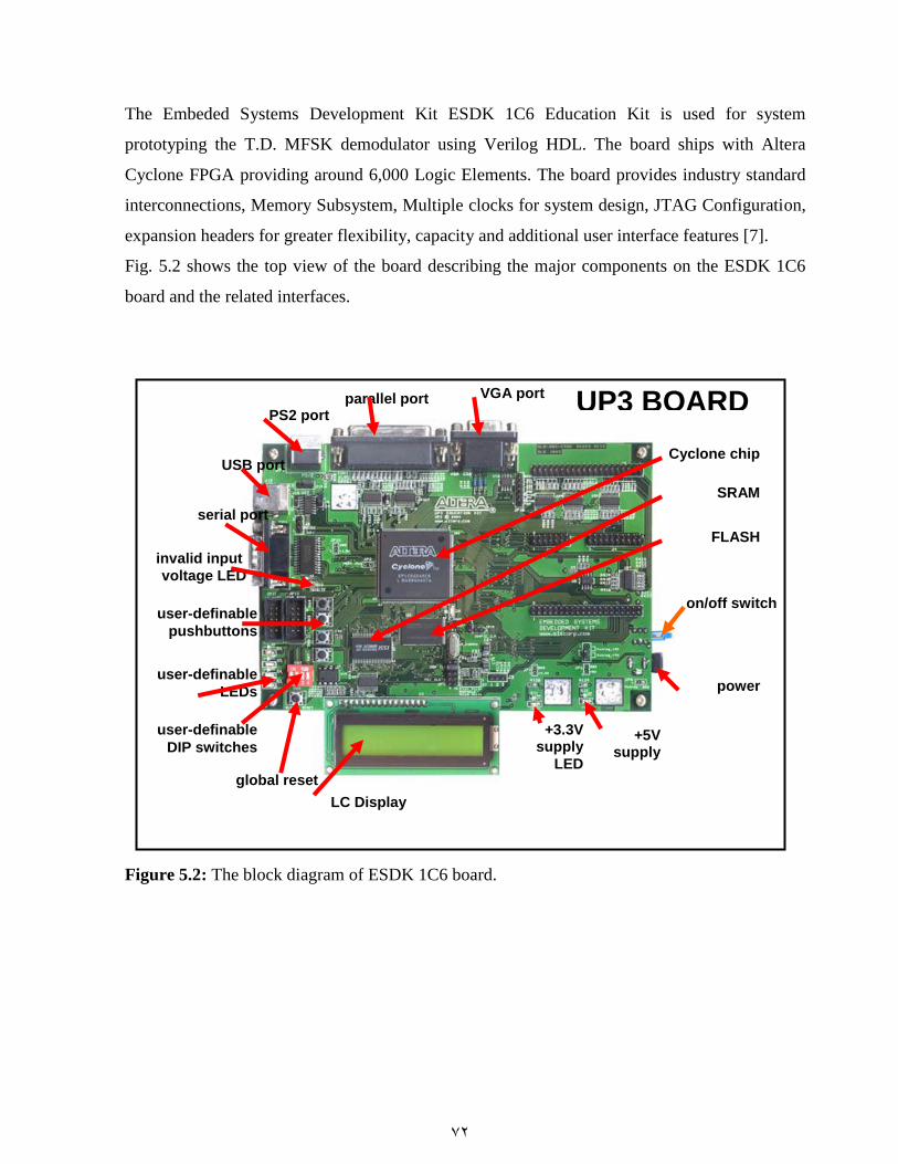
72
power
VGA port parallel port PS2 port
+3.3V supply
LED
on/off switch user-definable
pushbuttons
user-definable
LEDs
user-definable
DIP switches
global reset
USB port
serial port
invalid input
voltage LED
UP3 BOARD
FLASH
SRAM
Cyclone chip
+5V supply
LED
LC Display
The Embeded Systems Development Kit ESDK 1C6 Education Kit is used for system
prototyping the T.D. MFSK demodulator using Verilog HDL. The board ships with Altera
Cyclone FPGA providing around 6,000 Logic Elements. The board provides industry standard
interconnections, Memory Subsystem, Multiple clocks for system design, JTAG Configuration,
expansion headers for greater flexibility, capacity and additional user interface features [7].
Fig. 5.2 shows the top view of the board describing the major components on the ESDK 1C6
board and the related interfaces.
Figure 5.2: The block diagram of ESDK 1C6 board.
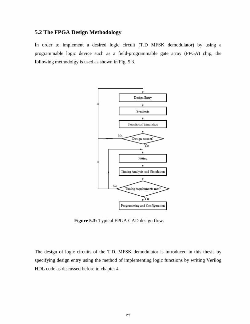
73
5.2 The FPGA Design Methodology
In order to implement a desired logic circuit (T.D MFSK demodulator) by using a
programmable logic device such as a field-programmable gate array (FPGA) chip, the
following methodolgy is used as shown in Fig. 5.3.
Figure 5.3: Typical FPGA CAD design flow.
The design of logic circuits of the T.D. MFSK demodulator is introduced in this thesis by
specifying design entry using the method of implementing logic functions by writing Verilog
HDL code as discussed before in chapter 4.

74
The design of the whole system modules that will be implemented on FPGA is shown in Fig.
5.4
Figure 5.4: The design implementation of T.D. MFSK signal demodulator on FPGA.
75
5.2.1 Synthesizing the T.D. MFSK Demodulator.
Synthesizing the T.D.MFSK demodulator was done using the Quartus II software, where
every module was built and synthesized alone, and then the all modules were instantiated by
top level module, which is called here -MFSK demodulator- to build the demodulator system.
The hardware model is synthesized to a cyclone, EP1C6Q240C8 FPGA.
FPGA device architectures are based on registers, or flipflops. The registers in Altera FPGAs
provide a number of secondary control signals (such as clear and enable signals) that can be
used to implement control logic for each register without using extra logic cells.
To make the most efficient use of the signals in the device, the HDL code should match the
device architecture as closely as possible. The control signals have a certain priority due to
the nature of the architecture, so the HDL code should follow that priority where possible.
synthesis tool can emulate any control signals using regular logic, so it is always possible to
get functionally correct results. However, if the design requirements are flexible in terms of
which control signals are used and in what priority, the most efficient results can be achieved
by matching the device architecture. If the priority of the signals in the design is not the same
as the target architecture, then extra logic may be required to implement the control signals.
The priority order for secondary control signals in Altera devices may be different than the
order for other vendors’ devices. The signal order is the same for all Altera device families,
although, not all device families provide every signal. The priority order is as follows:
Asynchronous Clear, Preset, Asynchronous Load, Enable, Synchronous Clear, Synchronous
Load, and Data In; respectively.
The Analysis and Synthesis stage of the Quartus II compilation were used to perform all levels
of analysis and synthesis,Analyze Current File that Parse the current design source file to
check for syntax errors, Analysis & Elaboration that is used to Check a design for syntax and
semantic errors and perform elaboration to identify the design hierarchy, and Analysis &
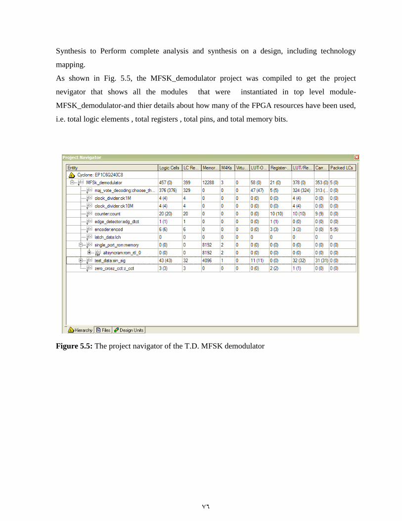
76
Synthesis to Perform complete analysis and synthesis on a design, including technology
mapping.
As shown in Fig. 5.5, the MFSK_demodulator project was compiled to get the project
nevigator that shows all the modules that were instantiated in top level module-
MFSK_demodulator-and thier details about how many of the FPGA resources have been used,
i.e. total logic elements , total registers , total pins, and total memory bits.
Figure 5.5: The project navigator of the T.D. MFSK demodulator
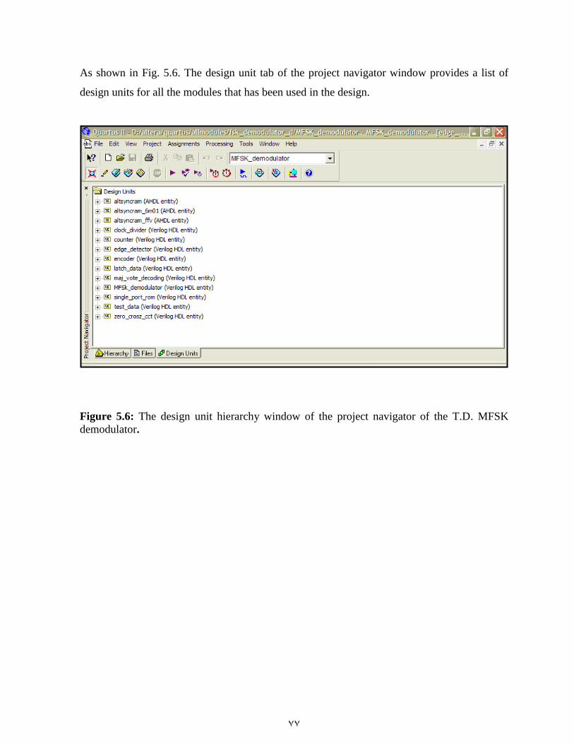
77
As shown in Fig. 5.6. The design unit tab of the project navigator window provides a list of
design units for all the modules that has been used in the design.
Figure 5.6: The design unit hierarchy window of the project navigator of the T.D. MFSK
demodulator.

78
5.2.2 Analyzing the T.D. MFSK Demodulator Design With the Quartus II RTLViewer &
Technology Map Viewer
As FPGA designs grow in size and complexity, the ability to analyze how synthesis tool
interprets the design becomes critical. The Quartus® II provide powerful ways of viewing
initial and fully mapped synthesis results during the debugging, optimization, or constraint
entry process.
Quartus II supports different types of the netlist viewers for analyzing the design to analyze
problems encountered in the design process. The Quartus II RTL Viewer, State Machine
Viewer, and Technology Map Viewer provide powerful ways to view an initial and fully
mapped synthesis results during the debugging, optimization, or constraint entry process.
Using the RTL Viewer is a good way to view an initial synthesis results to determine whether
the desired logic has been created, and that the logic and connections have been interpreted
correctly by the software.
The RTL viewer was used to visually check MFSK demodulator design before other
verification processes that catch the design errors.
As shown in Fig. 5.7 the RTL viewer is used to view a schematic of the internal structure of
the design netlist of the T.D. MFSK demodulator.
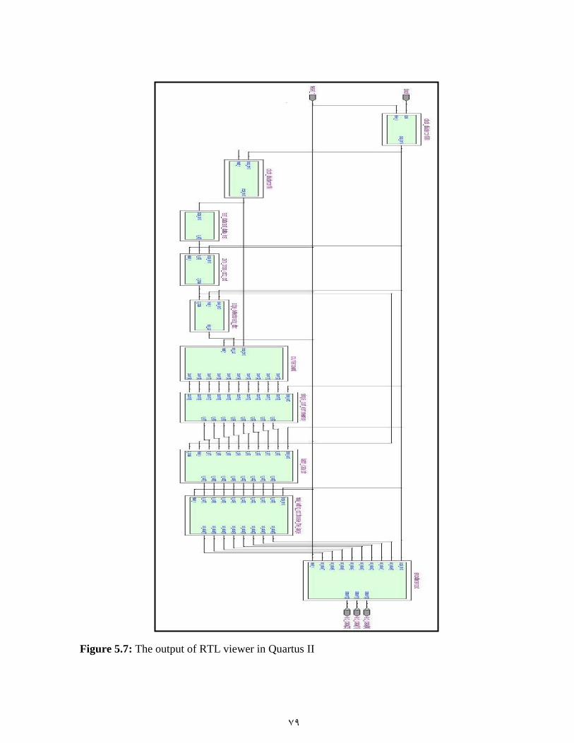
79
Figure 5.7: The output of RTL viewer in Quartus II

80
As shown in Fig. 5.8 The RTL Viewer and was used to provide a hierarchy list that displays a
representation of the project hierarchy of the design element in T.D. MFSK. The hierarchy tree
expands as the schematic view is navigated.
Figure 5.8: The hierarchy list of the design of the T.D. MFSK demodulator modules using
RTL viewer.
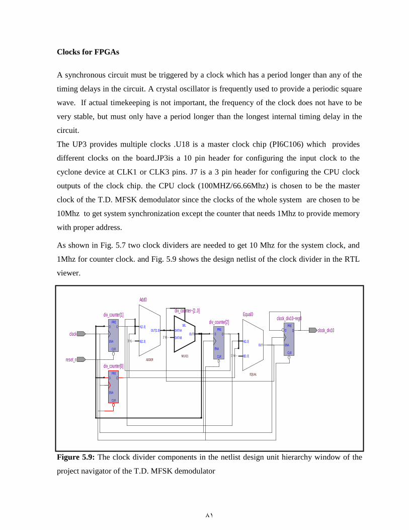
81
A[2..0]
B[2..0]
OUT[2..0]
ADDER
D
ENA
Q
PRE
CLR
A[2..0]
B[2..0]
OUT
EQUAL
SEL
DATAA
DATABOUT0
MUX21
D
ENA
Q
PRE
CLR
D
ENA
Q
PRE
CLR
D
ENA
Q
PRE
CLR
Add0
3' h1 --
clock_div10~reg0Equal0
3' h4 --
div_counter~[2..0]
3' h0 --clock
reset_n
clock_div10
div_counter[2]
div_counter[1]
div_counter[0]
Clocks for FPGAs
A synchronous circuit must be triggered by a clock which has a period longer than any of the
timing delays in the circuit. A crystal oscillator is frequently used to provide a periodic square
wave. If actual timekeeping is not important, the frequency of the clock does not have to be
very stable, but must only have a period longer than the longest internal timing delay in the
circuit.
The UP3 provides multiple clocks .U18 is a master clock chip (PI6C106) which provides
different clocks on the board.JP3is a 10 pin header for configuring the input clock to the
cyclone device at CLK1 or CLK3 pins. J7 is a 3 pin header for configuring the CPU clock
outputs of the clock chip. the CPU clock (100MHZ/66.66Mhz) is chosen to be the master
clock of the T.D. MFSK demodulator since the clocks of the whole system are chosen to be
10Mhz to get system synchronization except the counter that needs 1Mhz to provide memory
with proper address.
As shown in Fig. 5.7 two clock dividers are needed to get 10 Mhz for the system clock, and
1Mhz for counter clock. and Fig. 5.9 shows the design netlist of the clock divider in the RTL
viewer.
Figure 5.9: The clock divider components in the netlist design unit hierarchy window of the
project navigator of the T.D. MFSK demodulator
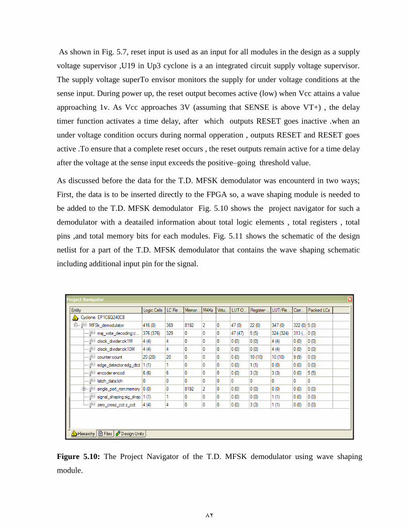
82
As shown in Fig. 5.7, reset input is used as an input for all modules in the design as a supply
voltage supervisor ,U19 in Up3 cyclone is a an integrated circuit supply voltage supervisor.
The supply voltage superTo envisor monitors the supply for under voltage conditions at the
sense input. During power up, the reset output becomes active (low) when Vcc attains a value
approaching 1v. As Vcc approaches 3V (assuming that SENSE is above VT+) , the delay
timer function activates a time delay, after which outputs RESET goes inactive .when an
under voltage condition occurs during normal opperation , outputs RESET and RESET goes
active .To ensure that a complete reset occurs , the reset outputs remain active for a time delay
after the voltage at the sense input exceeds the positive–going threshold value.
As discussed before the data for the T.D. MFSK demodulator was encounterd in two ways;
First, the data is to be inserted directly to the FPGA so, a wave shaping module is needed to
be added to the T.D. MFSK demodulator Fig. 5.10 shows the project navigator for such a
demodulator with a deatailed information about total logic elements , total registers , total
pins ,and total memory bits for each modules. Fig. 5.11 shows the schematic of the design
netlist for a part of the T.D. MFSK demodulator that contains the wave shaping schematic
including additional input pin for the signal.
Figure 5.10: The Project Navigator of the T.D. MFSK demodulator using wave shaping
module.
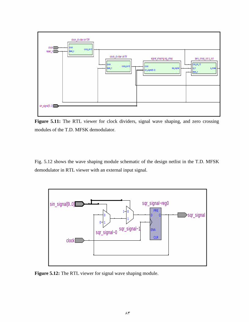
83
D
ENA
Q
PRE
CLR
0
10
0
1
1
sqr_signal~0sqr_signal~1
clock
sin_signal[9..0]
sqr_signal
sqr_signal~reg0
Figure 5.11: The RTL viewer for clock dividers, signal wave shaping, and zero crossing
modules of the T.D. MFSK demodulator.
Fig. 5.12 shows the wave shaping module schematic of the design netlist in the T.D. MFSK
demodulator in RTL viewer with an external input signal.
Figure 5.12: The RTL viewer for signal wave shaping module.

84
A[31..0]
B[31..0]
OUT[31..0]
ADDER
BUF (DC)
0
A[31..0]
B[31..0]
OUT
LESS_THANSEL[11..0]
DATA[4095..0]
OUT
MUX
D
ENA
Q
PRE
CLR
BUF (DC)
D
ENA
Q
PRE
CLR
D
ENA
Q
PRE
CLR
D
ENA
Q
PRE
CLR
D
ENA
Q
PRE
CLR
D
ENA
Q
PRE
CLR
D
ENA
Q
PRE
CLR
D
ENA
Q
PRE
CLR
D
ENA
Q
PRE
CLR
D
ENA
Q
PRE
CLR
D
ENA
Q
PRE
CLR
D
ENA
Q
PRE
CLR
D
ENA
Q
PRE
CLR
D
ENA
Q
PRE
CLR
D
ENA
Q
PRE
CLR
D
ENA
Q
PRE
CLR
D
ENA
Q
PRE
CLR
D
ENA
Q
PRE
CLR
D
ENA
Q
PRE
CLR
D
ENA
Q
PRE
CLR
D
ENA
Q
PRE
CLR
D
ENA
Q
PRE
CLR
D
ENA
Q
PRE
CLR
D
ENA
Q
PRE
CLR
D
ENA
Q
PRE
CLR
D
ENA
Q
PRE
CLR
D
ENA
Q
PRE
CLR
D
ENA
Q
PRE
CLR
D
ENA
Q
PRE
CLR
D
ENA
Q
PRE
CLR
D
ENA
Q
PRE
CLR
D
ENA
Q
PRE
CLR
D
ENA
Q
PRE
CLR
Add0
32' h00000001 --
comb~0
LessThan0
1' h0 --
31' h00000000 --
Mux0
4004' h7FFFFFFFFFFFFFFFE00000000000000003FFFFFFFFFFFFFFFF00000000000000001FFFFFFFFFFFFFFFFC0000000000000000FFFFFFFFFFFFFFFFE00000000000000003FFFFFFFFFFFFFFFF00000000000000001FFFFFFFFFFFFFFFFC0000000000000000FFFFFFFFFFFFFFFFE00000000000000003FFFFFFFFFFFFFFFF7FFF000000000007FFFFFFFFFF800000000003FFFFFFFFFFE00000000000FFFFFFFFFFF800000000007FFFFFFFFFFC00000000001FFFFFFFFFFF000000000007FFFFFFFFFF800000000003FFFFFFFFFFE00000000000FFFFFFFFFFF800000000007FFFFFFFFFFC00000000001FFFFFFFFFFF000000000007FFFFFFFFFF803FFFFFFF00000003FFFFFFF00000003FFFFFFF00000003FFFFFFF00000003FFFFFFF00000001FFFFFFF80000001FFFFFFF80000001FFFFFFF80000001FFFFFFF80000001FFFFFFF80000001FFFFFFF80000000FFFFFFFC0000000FFFFFFFC0000000FFFFFFFC0000000FFFFFFFC0000000FFFFFFFC0000000FFFFFFFC007FFFF800007FFFF800003FFFFC00003FFFFC00001FFFFE00001FFFFE00001FFFFF00000FFFFF00000FFFFF800007FFFF800007FFFF800003FFFFC00003FFFFC00003FFFFE00001FFFFE00001FFFFF00000FFFFF00000FFFFF000007FFFF800007FFFF800003FFFFC00003FFFFC00003FFFFE00001FFFFE00001FFFFE --
sin_signal~reg0
node[108..18]
91' h00000000000000000000000 --
i[0]
i[1]
i[2]
i[3]
i[4]
i[5]
i[6]
i[7]
i[8]
i[9]
i[10]
i[11]
i[12]
i[13]
i[14]
i[15]
i[16]
i[17]
i[18]
i[19]
i[20]
i[21]
i[22]
i[23]
i[24]
i[25]
i[26]
i[27]
i[28]
i[29]
i[30]
i[31]
clock
sin_signal
Second, Fig. 5.13 shows the schematic of the design netlist for the data inserted by
Matlab7.3 code in RTL viewer.
Figure 5.13: The schematic of the design netlist for the data inserted by Matlab in RTL
viewer.
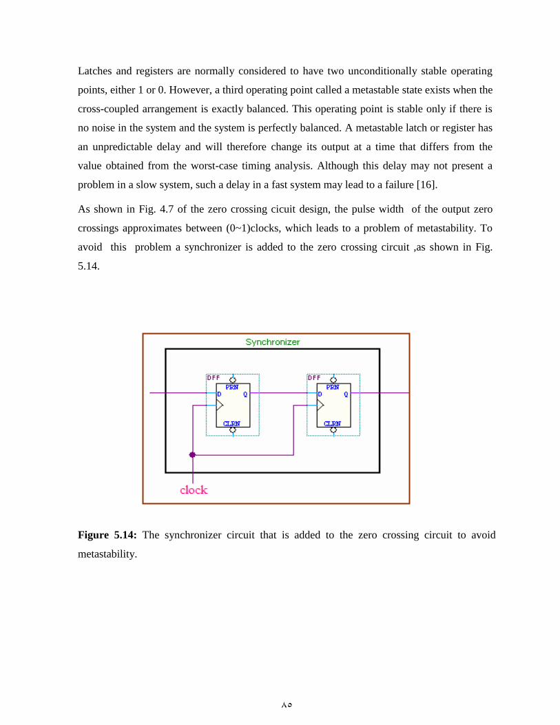
85
Latches and registers are normally considered to have two unconditionally stable operating
points, either 1 or 0. However, a third operating point called a metastable state exists when the
cross-coupled arrangement is exactly balanced. This operating point is stable only if there is
no noise in the system and the system is perfectly balanced. A metastable latch or register has
an unpredictable delay and will therefore change its output at a time that differs from the
value obtained from the worst-case timing analysis. Although this delay may not present a
problem in a slow system, such a delay in a fast system may lead to a failure [16].
As shown in Fig. 4.7 of the zero crossing cicuit design, the pulse width of the output zero
crossings approximates between (0~1)clocks, which leads to a problem of metastability. To
avoid this problem a synchronizer is added to the zero crossing circuit ,as shown in Fig.
5.14.
Figure 5.14: The synchronizer circuit that is added to the zero crossing circuit to avoid
metastability.
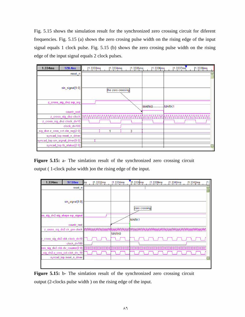
86
Fig. 5.15 shows the simulation result for the synchronized zero crossing circuit for diferent
frequencies. Fig. 5.15 (a) shows the zero crosing pulse width on the rising edge of the input
signal equals 1 clock pulse. Fig. 5.15 (b) shows the zero crosing pulse width on the rising
edge of the input signal equals 2 clock pulses.
Figure 5.15: a- The simlation result of the synchronized zero crossing circuit
output ( 1-clock pulse width )on the rising edge of the input.
Figure 5.15: b- The simlation result of the synchronized zero crossing circuit
output (2-clocks pulse width ) on the rising edge of the input.
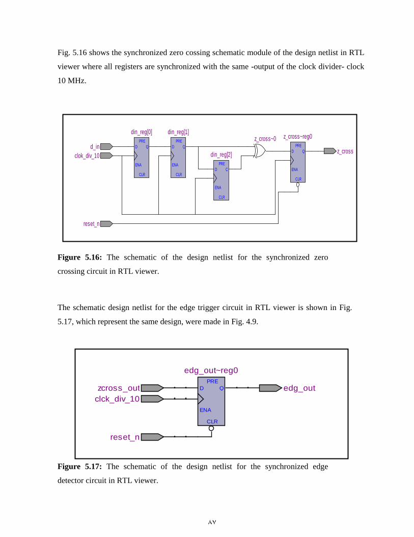
87
D
ENA
Q
PRE
CLR
D
ENA
Q
PRE
CLR
D
ENA
Q
PRE
CLRD
ENA
Q
PRE
CLR
z_cross~0 z_cross~reg0
din_reg[2]clok_div_10
reset_n
d_inz_cross
din_reg[0] din_reg[1]
D
ENA
Q
PRE
CLR
edg_out~reg0
clck_div_10
reset_n
zcross_out edg_out
Fig. 5.16 shows the synchronized zero cossing schematic module of the design netlist in RTL
viewer where all registers are synchronized with the same -output of the clock divider- clock
10 MHz.
Figure 5.16: The schematic of the design netlist for the synchronized zero
crossing circuit in RTL viewer.
The schematic design netlist for the edge trigger circuit in RTL viewer is shown in Fig.
5.17, which represent the same design, were made in Fig. 4.9.
Figure 5.17: The schematic of the design netlist for the synchronized edge
detector circuit in RTL viewer.
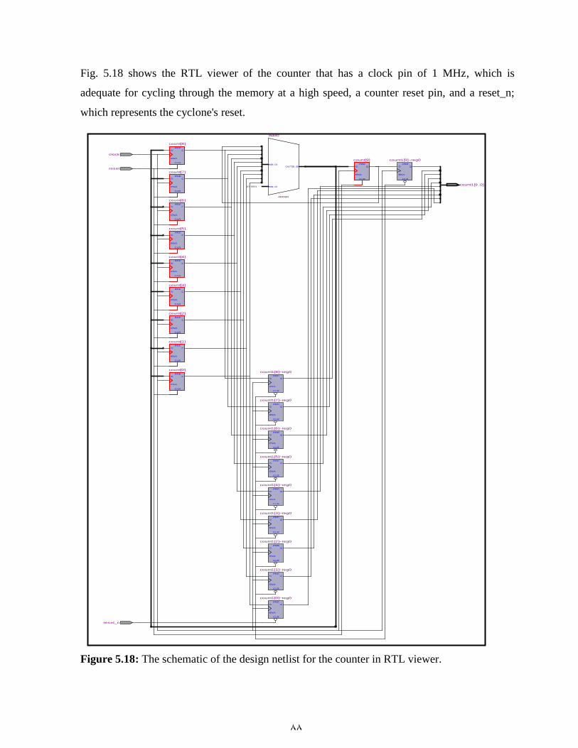
88
A[9..0]
B[9..0]
OUT[9..0]
ADDER
D
ENA
Q
PRE
CLR
D
ENA
Q
PRE
CLR
D
ENA
Q
PRE
CLR
D
ENA
Q
PRE
CLR
D
ENA
Q
PRE
CLR
D
ENA
Q
PRE
CLR
D
ENA
Q
PRE
CLR
D
ENA
Q
PRE
CLR
D
ENA
Q
PRE
CLR
D
ENA
Q
PRE
CLR
D
ENA
Q
PRE
CLR
D
ENA
Q
PRE
CLR
D
ENA
Q
PRE
CLR
D
ENA
Q
PRE
CLR
D
ENA
Q
PRE
CLR
D
ENA
Q
PRE
CLR
D
ENA
Q
PRE
CLR
D
ENA
Q
PRE
CLR
D
ENA
Q
PRE
CLR
D
ENA
Q
PRE
CLR
Add0
10' h001 --
count1[0]~reg0
count1[1]~reg0
count1[2]~reg0
count1[3]~reg0
count1[4]~reg0
count1[5]~reg0
count1[6]~reg0
count1[7]~reg0
count1[8]~reg0
count1[9]~reg0
count[0]
count[1]
count[2]
count[3]
count[4]
count[5]
count[6]
count[8]
count[9]
clock
reset
reset_n
count1[9..0]
count[7]
Fig. 5.18 shows the RTL viewer of the counter that has a clock pin of 1 MHz, which is
adequate for cycling through the memory at a high speed, a counter reset pin, and a reset_n;
which represents the cyclone's reset.
Figure 5.18: The schematic of the design netlist for the counter in RTL viewer.

89
The read only memory (ROM) was instantiated in two methods; First: using Altera
megawizard function in HDL Code in the following method by using the Quartus® II
software MegaWizard® Plug-In Manager to parameterize the function and create a wrapper
file. The wizard provides a graphical interface to customize and parameterize megafunctions,
and ensures that all megafunction parameters are setting properly. The wizard generates an
Altera HDL (AHDL), Verilog HDL, or VHDL wrapper file (the verilog HDL language was
used in insantiating the read only memory function) that instantiates the megafunction with
the correct parameters, as well as other files.
An ASCII text file; Hexadecimal (Intel-Format) File (with the extension .hex) was used to
store the initial memory values for a memory block, ROM, as an input file that is
implemented in an Altera device as shown in Fig. 5.19 in the analysis & synthesis RAM
summary.
Figure 5.19: The analysis & synthesize ROM summary.
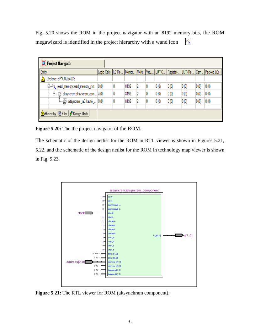
90
aclr0
aclr1
addressstall_a
addressstall_b
clock0
clock1
clocken0
clocken1
clocken2
clocken3
rden_a
rden_b
wren_a
wren_b
data_a[7..0]
data_b[0..0]
address_a[9..0]
address_b[0..0]
byteena_a[0..0]
byteena_b[0..0]
q_a[7..0]
0
0
0
0
1
1
1
1
1
1
1
0
0
address[9..0]
q[7..0]
clock
altsyncram:altsyncram_component
8' hFF --
1' h1 --
1' h1 --
1' h1 --
1' h1 --
Fig. 5.20 shows the ROM in the project navigator with an 8192 memory bits, the ROM
megawizard is identified in the project hierarchy with a wand icon
Figure 5.20: The the project navigator of the ROM.
The schematic of the design netlist for the ROM in RTL viewer is shown in Figures 5.21,
5.22, and the schematic of the design netlist for the ROM in technology map viewer is shown
in Fig. 5.23.
Figure 5.21: The RTL viewer for ROM (altsynchram component).
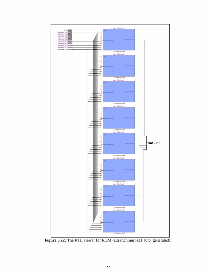
91
CLK0
PORTAADDR[9..0]PORTADATAOUT
CYCLONE_RAM_BLOCK
CLK0
PORTAADDR[9..0]PORTADATAOUT
CYCLONE_RAM_BLOCK
CLK0
PORTAADDR[9..0]PORTADATAOUT
CYCLONE_RAM_BLOCK
CLK0
PORTAADDR[9..0]PORTADATAOUT
CYCLONE_RAM_BLOCK
CLK0
PORTAADDR[9..0]PORTADATAOUT
CYCLONE_RAM_BLOCK
CLK0
PORTAADDR[9..0]PORTADATAOUT
CYCLONE_RAM_BLOCK
CLK0
PORTAADDR[9..0]PORTADATAOUT
CYCLONE_RAM_BLOCK
CLK0
PORTAADDR[9..0]PORTADATAOUT
CYCLONE_RAM_BLOCK
ram_block1a0
ram_block1a1
ram_block1a2
ram_block1a4
clock0
q_a[7..0]
address_a[0]
address_a[2]
address_a[3]
address_a[4]
address_a[5]
address_a[6]
address_a[7]
address_a[8]
address_a[9]
address_a[1]
ram_block1a3
ram_block1a5
ram_block1a6
ram_block1a7
Figure 5.22: The RTL viewer for ROM (altsynchram ja31:auto_generated).

92
ram_block1a7
ram_block1a6
ram_block1a5
ram_block1a4
ram_block1a3
ram_block1a2
ram_block1a1
ram_block1a0
A_address[9..0] A_data_out
RAM
D Q
PRE
ENA
CLR
D
ENA
Q
PRE
CLR
A_address[9..0] A_data_out
RAM
D Q
PRE
ENA
CLR
D
ENA
Q
PRE
CLR
A_address[9..0] A_data_out
RAM
D Q
PRE
ENA
CLR
D
ENA
Q
PRE
CLR
A_address[9..0] A_data_out
RAM
D Q
PRE
ENA
CLR
D
ENA
Q
PRE
CLR
A_address[9..0] A_data_out
RAM
D Q
PRE
ENA
CLR
D
ENA
Q
PRE
CLR
A_address[9..0] A_data_out
RAM
D Q
PRE
ENA
CLR
D
ENA
Q
PRE
CLR
A_address[9..0] A_data_out
RAM
D Q
PRE
ENA
CLR
D
ENA
Q
PRE
CLR
A_address[9..0] A_data_out
RAM
D Q
PRE
ENA
CLR
D
ENA
Q
PRE
CLR
ram_block1a1A_address A_data_out
ram_block1a0A_address A_data_out
ram_block1a2A_address A_data_out
ram_block1a3A_address A_data_out
ram_block1a4A_address A_data_out
ram_block1a5A_address A_data_out
ram_block1a6A_address A_data_out
ram_block1a7A_address A_data_out
q_a[0]
q_a[1]
q_a[2]
q_a[3]
q_a[4]
q_a[5]
q_a[6]
q_a[7]
clock_div10
count1[0]
count1[1]
count1[2]
count1[3]
count1[4]
count1[5]
count1[6]
count1[7]
count1[8]
count1[9]
Figure 5.23: The technology map viewer for ROM (altsynchram ja31: auto_ generated).
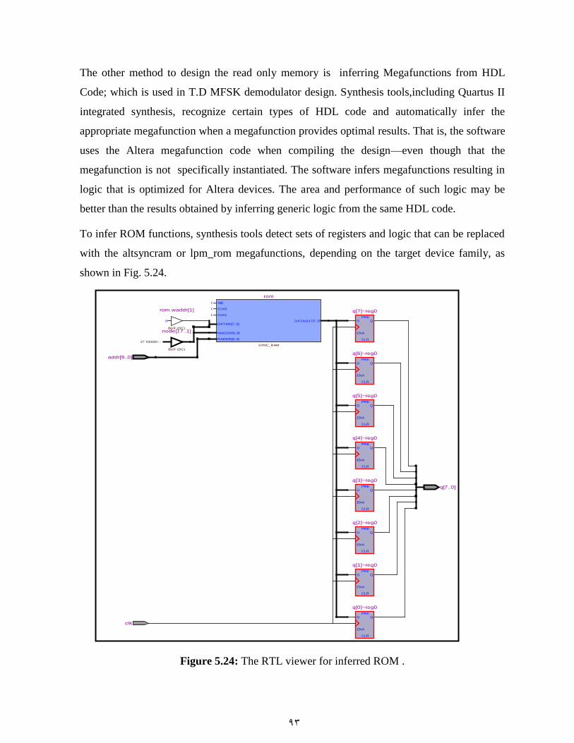
93
WE
CLK0
CLK1
DATAIN[7..0]
WADDR[9..0]
RADDR[9..0]
DATAOUT[7..0]
SYNC_RAM
BUF (DC)
0
BUF (DC)
D
ENA
Q
PRE
CLR
D
ENA
Q
PRE
CLR
D
ENA
Q
PRE
CLR
D
ENA
Q
PRE
CLR
D
ENA
Q
PRE
CLR
D
ENA
Q
PRE
CLR
D
ENA
Q
PRE
CLR
D
ENA
Q
PRE
CLR
0
0
0
rom.waddr[1]
node[17..1]
17' h00000 --
q[0]~reg0
q[1]~reg0
q[2]~reg0
q[4]~reg0
q[6]~reg0
clk
addr[9..0]
q[7..0]
q[3]~reg0
rom
q[5]~reg0
q[7]~reg0
The other method to design the read only memory is inferring Megafunctions from HDL
Code; which is used in T.D MFSK demodulator design. Synthesis tools,including Quartus II
integrated synthesis, recognize certain types of HDL code and automatically infer the
appropriate megafunction when a megafunction provides optimal results. That is, the software
uses the Altera megafunction code when compiling the design—even though that the
megafunction is not specifically instantiated. The software infers megafunctions resulting in
logic that is optimized for Altera devices. The area and performance of such logic may be
better than the results obtained by inferring generic logic from the same HDL code.
To infer ROM functions, synthesis tools detect sets of registers and logic that can be replaced
with the altsyncram or lpm_rom megafunctions, depending on the target device family, as
shown in Fig. 5.24.
Figure 5.24: The RTL viewer for inferred ROM .
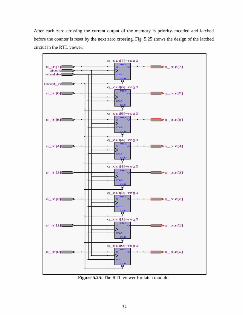
94
D
ENA
Q
PRE
CLR
D
ENA
Q
PRE
CLR
D
ENA
Q
PRE
CLR
D
ENA
Q
PRE
CLR
D
ENA
Q
PRE
CLR
D
ENA
Q
PRE
CLR
D
ENA
Q
PRE
CLR
D
ENA
Q
PRE
CLR
q_out[0]~reg0
q_out[1]~reg0
q_out[2]~reg0
q_out[3]~reg0
q_out[4]~reg0
q_out[5]~reg0
q_out[6]~reg0
q_out[7]~reg0
clock
enable
reset_n
d_in[0]
d_in[1]
d_in[2]
d_in[3]
d_in[4]
d_in[5]
d_in[6]
d_in[7]
q_out[0]
q_out[1]
q_out[2]
q_out[3]
q_out[4]
q_out[5]
q_out[6]
q_out[7]
After each zero crossing the current output of the memory is priority-encoded and latched
before the counter is reset by the next zero crossing. Fig. 5.25 shows the design of the latched
circiut in the RTL viewer.
Figure 5.25: The RTL viewer for latch module.

95
The major part in the design of T.D. MFSK demodulator is the majority vote decoder. When a
symbol is transmitted, the receiver counts the number of zero crossings received over a
symbol interval. The symbol that has the largest number of votes is the symbol which is
being sent as shown in Fig. 5.26.
Figure 5.27 (a) and (b) show the majority voting decoder in the RTL viwer.

96
Figure 5.26: The design of the majority vote decoder.
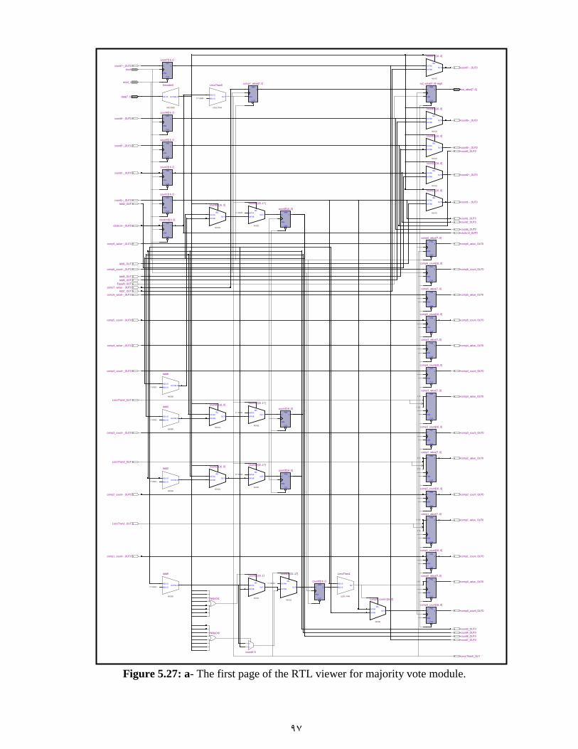
97
D Q
PRE
ENA
CLR
D Q
PRE
ENA
CLR
D Q
PRE
ENA
CLR
D Q
PRE
ENA
CLR
D Q
PRE
ENA
CLR
D Q
PRE
ENA
CLR
D Q
PRE
ENA
CLR
D Q
PRE
ENA
CLR
D Q
PRE
ENA
CLRD Q
PRE
ENA
CLR
D Q
PRE
ENA
CLR
D Q
PRE
ENA
CLR
D Q
PRE
ENA
CLR
D Q
PRE
ENA
CLR
D Q
PRE
ENA
CLR
D Q
PRE
ENA
CLR
D Q
PRE
ENA
CLR
D Q
PRE
ENA
CLR
D Q
PRE
ENA
CLR
D Q
PRE
ENA
CLR
D Q
PRE
ENA
CLR
D Q
PRE
ENA
CLR
D Q
PRE
ENA
CLR
D Q
PRE
ENA
CLR
D Q
PRE
ENA
CLR
D Q
PRE
ENA
CLR
SEL
DATAA
DATABOUT0
MUX21
SEL
DATAA
DATABOUT0
MUX21
SEL
DATAA
DATABOUT0
MUX21
A[16..0]
B[16..0]OUT[16..0]
ADDER
0
1
A[16..0]
B[16..0]OUT
LESS_THAN
IN[7..0] OUT[255..0]
DECODER
SEL
DATAA
DATABOUT0
MUX21
SEL
DATAA
DATABOUT0
MUX21
SEL
DATAA
DATABOUT0
MUX21
SEL
DATAA
DATABOUT0
MUX21
SEL
DATAA
DATABOUT0
MUX21
SEL
DATAA
DATABOUT0
MUX21
SEL
DATAA
DATABOUT0
MUX21
SEL
DATAA
DATABOUT0
MUX21
A[16..0]
B[16..0]OUT[16..0]
ADDER
SEL
DATAA
DATABOUT0
MUX21
A[16..0]
B[16..0]OUT
LESS_THAN
A[16..0]
B[16..0]OUT[16..0]
ADDER
SEL
DATAA
DATABOUT0
MUX21
A[16..0]
B[16..0]OUT[16..0]
ADDER
SEL
DATAA
DATABOUT0
MUX21
count1~_OUT0
count1_OUT0
count2~_OUT0
count2_OUT0
count3_OUT0
count4_OUT0
count5~_OUT0
count5_OUT0
count6~_OUT0
count6_OUT0
count7~_OUT0
count7_OUT0
count8_OUT0
clockcnt~_OUT0
clockcnt_OUT0
comp0_value_OUT0
comp0_count_OUT0
LessThan2_OUT
comp1_value_OUT0
comp1_count~_OUT0 comp1_count_OUT0
LessThan3_OUT
comp2_value_OUT0
comp2_count~_OUT0 comp2_count_OUT0
LessThan4_OUT
comp3_value_OUT0
comp3_count~_OUT0 comp3_count_OUT0
comp4_value~_OUT0 comp4_value_OUT0
comp4_count~_OUT0 comp4_count_OUT0
comp5_value~_OUT0 comp5_value_OUT0
comp5_count~_OUT0 comp5_count_OUT0
comp6_value~_OUT0 comp6_value_OUT0
comp6_count~_OUT0 comp6_count_OUT0
comp7_value~_OUT0
Equal0_OUT
Add1_OUT
count1~_OUT0
Add5_OUT
count5~_OUT0
Add2_OUT
count2~_OUT0
Add6_OUT
count6~_OUT0
Add7_OUT
count7~_OUT0
LessThan0_OUT
count0[16..0]
clock
reset_n
count1[16..0]
count2[16..0]
count3[16..0]
count4[16..0]
count5[16..0]
count6[16..0]
count7[16..0]
count8[16..0]
clockcnt[16..0]
comp0_value[7..0]
7' h7F --
comp0_count[16..0]
comp1_value[7..0]
5' h1F --
1' h1 --
comp1_count[16..0]
comp2_value[7..0]
3' h7 --
3' h7 --
comp2_count[16..0]
comp3_value[7..0]
1' h1 --
5' h1F --
comp3_count[16..0]
comp4_value[7..0]
comp4_count[16..0]
comp5_value[7..0]
comp5_count[16..0]
comp6_value[7..0]
comp6_count[16..0]
comp7_value[7..0] out_value[7..0]~reg0
out_value[7..0]
count0~[33..17]
17' h00000 --
comp0_count~[16..0]
count0~[16..1]Add9
17' h00001 --
count0~0
LessThan1
WideOr1
WideOr0
data[7..0]
count8~[16..0]
count3~[16..0]
count4~[16..0]
count1~[16..0]
count5~[16..0]
count2~[16..0]
count6~[16..0]
count7~[16..0]
Add8
17' h00001 --
count8~[33..17]
17' h00000 --
LessThan0
17' h1869F --
Add3
17' h00001 --
count3~[33..17]
17' h00000 --
Add4
17' h00001 --
count4~[33..17]
17' h00000 --
Decoder0
Figure 5.27: a- The first page of the RTL viewer for majority vote module.

98
A[16..0]
B[16..0]OUT[16..0]
ADDER
SEL
DATAA
DATABOUT0
MUX21
A[16..0]
B[16..0]OUT[16..0]
ADDER
SEL
DATAA
DATABOUT0
MUX21
A[16..0]
B[16..0]OUT[16..0]
ADDER
SEL
DATAA
DATABOUT0
MUX21
A[16..0]
B[16..0]OUT[16..0]
ADDER
SEL
DATAA
DATABOUT0
MUX21
A[16..0]
B[16..0]OUT[16..0]
ADDER
SEL
DATAA
DATABOUT0
MUX21
A[16..0]
B[16..0]OUT[16..0]
ADDER
SEL
DATAA
DATABOUT0
MUX21
A[31..0]
B[31..0]
OUT
EQUAL
A[16..0]
B[16..0]OUT
LESS_THAN
SEL
DATAA
DATABOUT0
MUX21
A[16..0]
B[16..0]OUT
LESS_THAN
SEL
DATAA
DATABOUT0
MUX21
A[16..0]
B[16..0]OUT
LESS_THAN
SEL
DATAA
DATABOUT0
MUX21
A[16..0]
B[16..0]OUT
LESS_THAN
SEL
DATAA
DATABOUT0
MUX21
SEL
DATAA
DATABOUT0
MUX21
A[16..0]
B[16..0]OUT
LESS_THAN
SEL
DATAA
DATABOUT0
MUX21
SEL
DATAA
DATABOUT0
MUX21
A[16..0]
B[16..0]OUT
LESS_THAN
SEL
DATAA
DATABOUT0
MUX21
SEL
DATAA
DATABOUT0
MUX21
A[16..0]
B[16..0]OUT
LESS_THAN
SEL
DATAA
DATABOUT0
MUX21
count1_OUT0Add1_OUT
count1~_OUT0
LessThan0_OUT
count1~_OUT0
count5_OUT0
Add5_OUT
count5~_OUT0
count2_OUT0
Add2_OUT
count2~_OUT0count2~_OUT0
count6_OUT0
Add6_OUT
count6~_OUT0
count7_OUT0
Add7_OUT
count7~_OUT0count7~_OUT0
clockcnt_OUT0 clockcnt~_OUT0
Equal0_OUT
count3_OUT0
LessThan2_OUT
comp1_count~_OUT0
count4_OUT0
LessThan3_OUT
comp2_count~_OUT0
LessThan4_OUT
comp3_count~_OUT0
comp1_count_OUT0
comp0_count_OUT0
comp4_count~_OUT0
comp1_value_OUT0
comp0_value_OUT0comp4_value~_OUT0
comp3_count_OUT0
comp2_count_OUT0
comp3_value_OUT0
comp2_value_OUT0comp5_value~_OUT0
comp5_count~_OUT0
comp5_count_OUT0
comp4_count_OUT0
comp6_count~_OUT0
comp5_value_OUT0
comp4_value_OUT0comp6_value~_OUT0
comp6_count_OUT0
count8_OUT0
comp6_value_OUT0
comp7_value~_OUT0
count5~_OUT0
count6~_OUT0
Add1
17' h00001 --
count1~[33..17]
17' h00000 --
Add5
17' h00001 --
count5~[33..17]
17' h00000 --
Add2
17' h00001 --
count2~[33..17]
17' h00000 --
Add6
17' h00001 --
count6~[33..17]
17' h00000 --
Add7
17' h00001 --
Add0
17' h00001 --
clockcnt~[16..0]
17' h00000 --
Equal0
15' h0000 --
32' h0001869E --
LessThan2
comp1_count~[16..0]
LessThan3
comp2_count~[16..0]
LessThan4
comp3_count~[16..0]
LessThan5
comp4_count~[16..0]
comp4_value~[7..0]
LessThan6
comp5_value~[7..0]
comp5_count~[16..0]
LessThan7
comp6_count~[16..0]
comp6_value~[7..0]
LessThan8
comp7_value~[7..0]
8' hFE --
count7~[33..17]
17' h00000 --
Figure 5.27: b- The second page of the RTL viewer for majority vote module.

99
IN[7..0] OUT[255..0]
DECODER
D
ENA
Q
PRE
CLR
D
ENA
Q
PRE
CLR
D
ENA
Q
PRE
CLR
D
ENA
Q
PRE
CLR
D
ENA
Q
PRE
CLR
D
ENA
Q
PRE
CLR
Decoder0
WideOr1
WideOr3
WideOr5 dataout1[0]~reg0
dataout1[1]~reg0
dataout1[2]~reg0
dataout[0]
dataout[1]
dataout[2]
clock
reset_n
datain[7..0]
dataout1[2..0]
The output of the majority vote decoder is the inserted to 8-3 encoder, which has the
schematic design in the RTL wiewer shown in Fig. 5.28.
Figure 5.28: The RTL viewer for 8-3 encoder module.
The Quartus II technology map viewer provides a low-level, technology-specific, graphical
representation of the design after the synthesis process that includes mapping the design into
the target technology. The technology map viewer shows the hierarchy of atom primitives
(such as device logic cells and I/O ports) in the design.
Fig. 5.29 shows the T.D. MFSK demodulator schematic representaion in the technology map
viewer.

100
clock_
div10
q_out[0
]
q_out[1
]
q_out[2
]
q_out[3
]
q_out[4
]
q_out[5
]
q_out[6
]
q_out[7
]
reset_
n
out_va
lue[0]
out_va
lue[1]
out_va
lue[2]
out_va
lue[3]
out_va
lue[4]
out_va
lue[5]
out_va
lue[6]
out_va
lue[7]
clock_
div10
count1
[0]
count1
[1]
count1
[2]
count1
[3]
count1
[4]
count1
[5]
count1
[6]
count1
[7]
count1
[8]
count1
[9]
q_a[0]
q_a[1]
q_a[2]
q_a[3]
q_a[4]
q_a[5]
q_a[6]
q_a[7]
clock_
div10
reset_
n
z_cros
s
count1
[0]
count1
[1]
count1
[2]
count1
[3]
count1
[4]
count1
[5]
count1
[6]
count1
[7]
count1
[8]
count1
[9]
clock_
div10
q_a[0]
clock_
div10
out_va
lue[0]
out_va
lue[1]
out_va
lue[2]
out_va
lue[3]
out_va
lue[4]
out_va
lue[5]
out_va
lue[6]
out_va
lue[7]
reset_
n
dataou
t1[0]
dataou
t1[1]
dataou
t1[2]
clock
reset_
nclo
ck_div1
0
clock_
div10
edg_ou
t
q_a[0]
q_a[1]
q_a[2]
q_a[3]
q_a[4]
q_a[5]
q_a[6]
q_a[7]
reset_
n
q_out[0
]
q_out[1
]
q_out[2
]
q_out[3
]
q_out[4
]
q_out[5
]
q_out[6
]
q_out[7
]
clock_
div10
reset_
n
z_cros
s
edg_ou
tclo
ck_div1
0
q_a[0]
reset_
n
z_cros
sclo
ck_div1
0
reset_
nclo
ck_div1
0
maj_v
ote_de
coding
:choos
e_the_
large
single
_port_r
om:me
mory
counte
r:count
test_d
ata:sin
_sig
encode
r:encod
clock_
divide
r:ck10M
latch_d
ata:lch
edge_d
etecto
r:edg_d
tct
zero_c
rosz_c
ct:z_cc
tclo
ck_div
ider:ck
1M
encode
d_data
[0]
encode
d_data
[1]
encode
d_data
[2]
reset_
n
clock
Figure 5.29: The T.D. MFSK representation in the technology map viewer.

101
The schematic diagram of the zero crossing, edge detector, counter, read only memory, latch,
encoder, and majority vote decoder modules in the technology map viewer representation is
shown in Appendix B.
5.2.3 Simulation of the T.D. MFSK Demodulator
This step is equivalent to software debugging. The HDL simulator (debugger) is provided for
both functional and timing simulations. The simulation program was performed using
synapticad verilogger extreme & Bughunter pro, to simulate the 8-tone T.D. MFSK
demodulator. The design was accomplished in a bottom-to-top style. Where each primitive
block was designed and tested solely, and then all the blocks were grouped together to produce
the complete system; However, the design is presented in a top-to-bottom fashion.
In this program, the MFSK signals were generated sequentialy from 1 to M then the process
repeated itself, using two ways: first MFSK signals were generated using SynaptiCAD's
WaveFormer Pro and Timing Diagrammer. The function Sin in label equation generator was
used to generate the 8-FSK signals and then applied to signal shaping module that convert the
sinusoidal singnal into a square wave as shown in Fig. 5.30 or the received signal taken from
matlab then applied to the signal shaping module in verilogger.second the 8-FSK was
generated and converted into digital form in matlab7.3 as shown in Fig. 5.31.
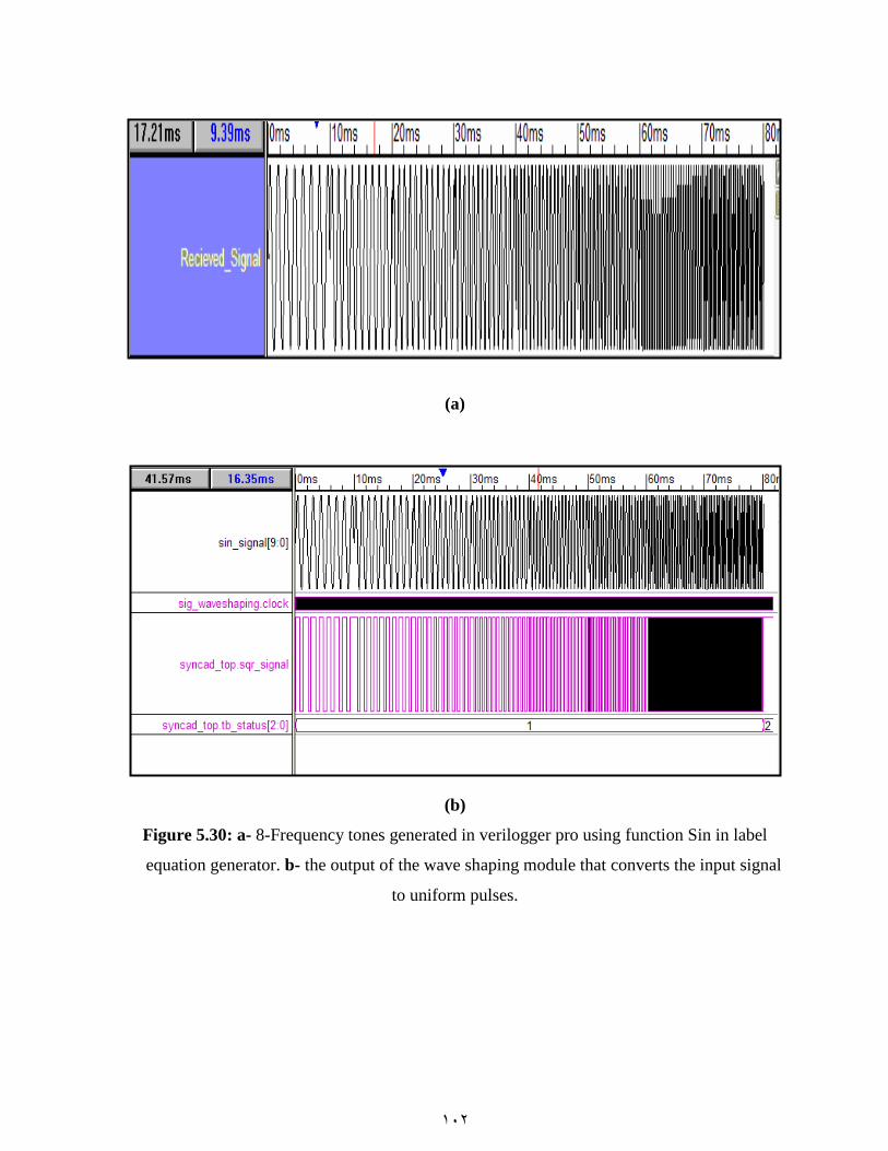
102
(a)
(b)
Figure 5.30: a- 8-Frequency tones generated in verilogger pro using function Sin in label
equation generator. b- the output of the wave shaping module that converts the input signal
to uniform pulses.

103
(a)
(b)
Figure 5.31: a- 8-Frequency tones generated in Matlab7.3. b- The conversion of the input
signal to uniform pulses.
In two cases the simulation was performed for a bit rate of 300 bit/s (i.e. a symbol rate of 100
symbol/s).

104
The simulatoin of the T.D. MFSK demodulator is shown in Fig. 5.32 for 4-FSK, and Fig. 5.33
for 8-FSK.
Figure 5.32: The simulation of the T.D. 4-FSK demodulator using Verilogger pro&
Bughunter pro software.
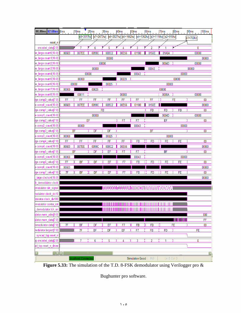
105
Figure 5.33: The simulation of the T.D. 8-FSK demodulator using Verilogger pro &
Bughunter pro software.
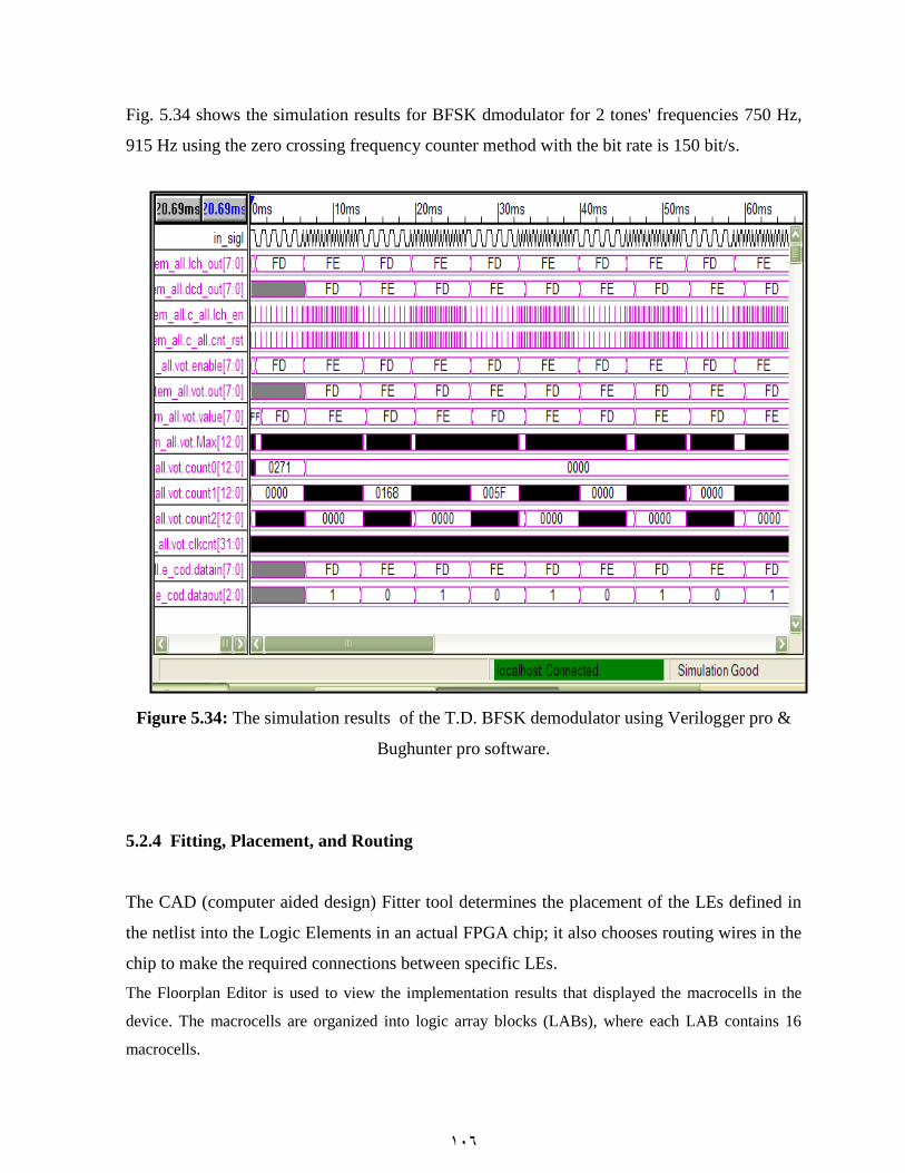
106
Fig. 5.34 shows the simulation results for BFSK dmodulator for 2 tones' frequencies 750 Hz,
915 Hz using the zero crossing frequency counter method with the bit rate is 150 bit/s.
Figure 5.34: The simulation results of the T.D. BFSK demodulator using Verilogger pro &
Bughunter pro software.
5.2.4 Fitting, Placement, and Routing
The CAD (computer aided design) Fitter tool determines the placement of the LEs defined in
the netlist into the Logic Elements in an actual FPGA chip; it also chooses routing wires in the
chip to make the required connections between specific LEs.
The Floorplan Editor is used to view the implementation results that displayed the macrocells in the
device. The macrocells are organized into logic array blocks (LABs), where each LAB contains 16
macrocells.
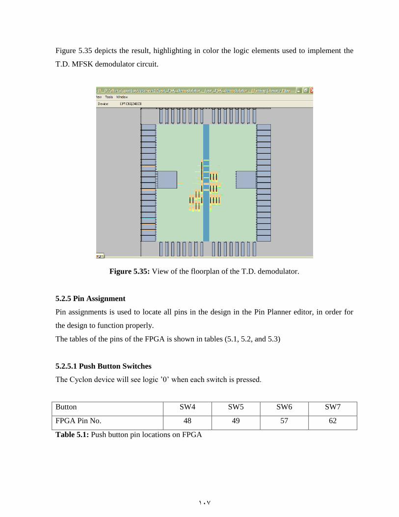
107
Figure 5.35 depicts the result, highlighting in color the logic elements used to implement the
T.D. MFSK demodulator circuit.
Figure 5.35: View of the floorplan of the T.D. demodulator.
5.2.5 Pin Assignment
Pin assignments is used to locate all pins in the design in the Pin Planner editor, in order for
the design to function properly.
The tables of the pins of the FPGA is shown in tables (5.1, 5.2, and 5.3)
5.2.5.1 Push Button Switches
The Cyclon device will see logic ’0’ when each switch is pressed.
Button SW4 SW5 SW6 SW7
FPGA Pin No. 48 49 57 62
Table 5.1: Push button pin locations on FPGA
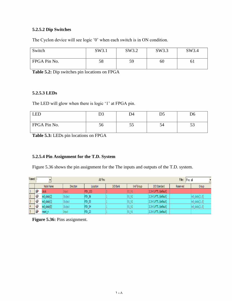
108
5.2.5.2 Dip Switches
The Cyclon device will see logic ’0’ when each switch is in ON condition.
Switch SW3.1 SW3.2 SW3.3 SW3.4
FPGA Pin No. 58 59 60 61
Table 5.2: Dip switches pin locations on FPGA
5.2.5.3 LEDs
The LED will glow when there is logic ‘1’ at FPGA pin.
LED D3 D4 D5 D6
FPGA Pin No. 56 55 54 53
Table 5.3: LEDs pin locations on FPGA
5.2.5.4 Pin Assignment for the T.D. System
Figure 5.36 shows the pin assignment for the The inputs and outputs of the T.D. system.
Figure 5.36: Pins assignment.
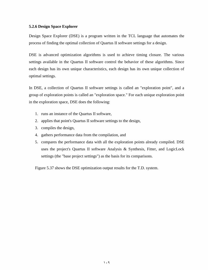
109
5.2.6 Design Space Explorer
Design Space Explorer (DSE) is a program written in the TCL language that automates the
process of finding the optimal collection of Quartus II software settings for a design.
DSE is advanced optimization algorithms is used to achieve timing closure. The various
settings available in the Quartus II software control the behavior of these algorithms. Since
each design has its own unique characteristics, each design has its own unique collection of
optimal settings.
In DSE, a collection of Quartus II software settings is called an "exploration point", and a
group of exploration points is called an "exploration space." For each unique exploration point
in the exploration space, DSE does the following:
1. runs an instance of the Quartus II software,
2. applies that point's Quartus II software settings to the design,
3. compiles the design,
4. gathers performance data from the compilation, and
5. compares the performance data with all the exploration points already compiled. DSE
uses the project's Quartus II software Analysis & Synthesis, Fitter, and LogicLock
settings (the "base project settings") as the basis for its comparisons.
Figure 5.37 shows the DSE optimization output results for the T.D. system.
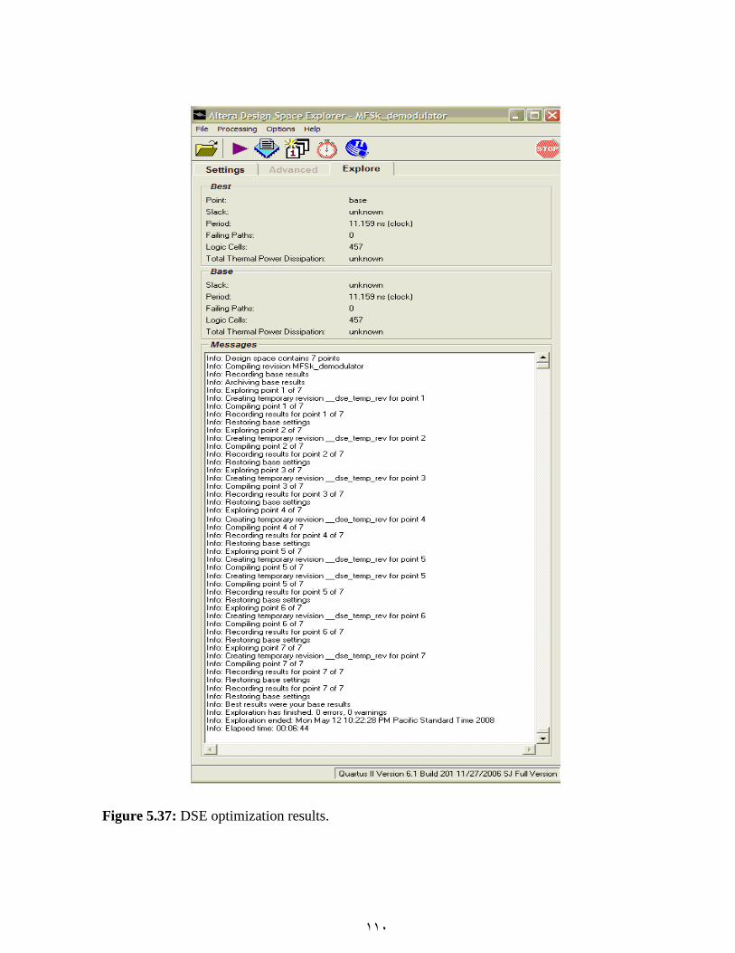
110
Figure 5.37: DSE optimization results.
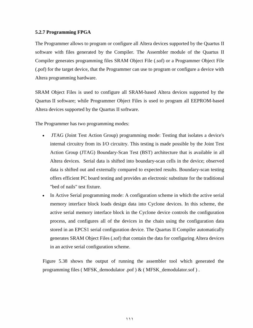
111
5.2.7 Programming FPGA
The Programmer allows to program or configure all Altera devices supported by the Quartus II
software with files generated by the Compiler. The Assembler module of the Quartus II
Compiler generates programming files SRAM Object File (.sof) or a Programmer Object File
(.pof) for the target device, that the Programmer can use to program or configure a device with
Altera programming hardware.
SRAM Object Files is used to configure all SRAM-based Altera devices supported by the
Quartus II software; while Programmer Object Files is used to program all EEPROM-based
Altera devices supported by the Quartus II software.
The Programmer has two programming modes:
JTAG (Joint Test Action Group) programming mode: Testing that isolates a device's
internal circuitry from its I/O circuitry. This testing is made possible by the Joint Test
Action Group (JTAG) Boundary-Scan Test (BST) architecture that is available in all
Altera devices. Serial data is shifted into boundary-scan cells in the device; observed
data is shifted out and externally compared to expected results. Boundary-scan testing
offers efficient PC board testing and provides an electronic substitute for the traditional
"bed of nails" test fixture.
In Active Serial programming mode: A configuration scheme in which the active serial
memory interface block loads design data into Cyclone devices. In this scheme, the
active serial memory interface block in the Cyclone device controls the configuration
process, and configures all of the devices in the chain using the configuration data
stored in an EPCS1 serial configuration device. The Quartus II Compiler automatically
generates SRAM Object Files (.sof) that contain the data for configuring Altera devices
in an active serial configuration scheme.
Figure 5.38 shows the output of running the assembler tool which generated the
programming files ( MFSK_demodulator .pof ) & ( MFSK_demodulator.sof ) .
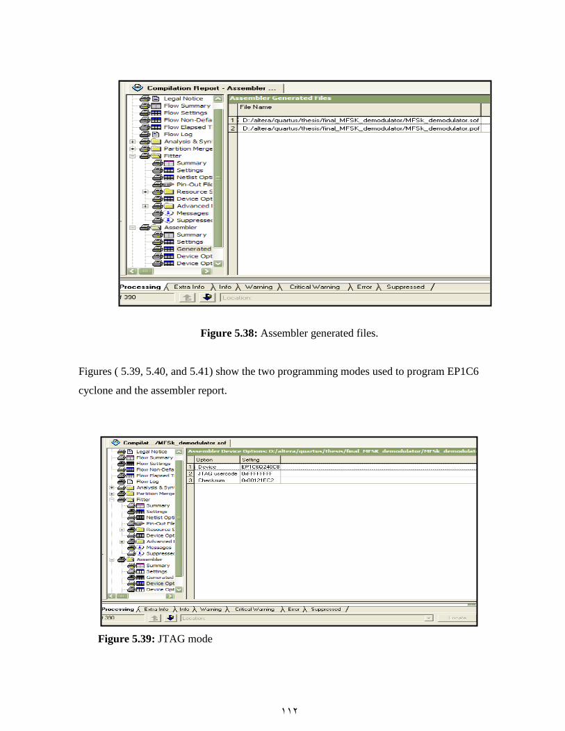
112
Figure 5.38: Assembler generated files.
Figures ( 5.39, 5.40, and 5.41) show the two programming modes used to program EP1C6
cyclone and the assembler report.
Figure 5.39: JTAG mode
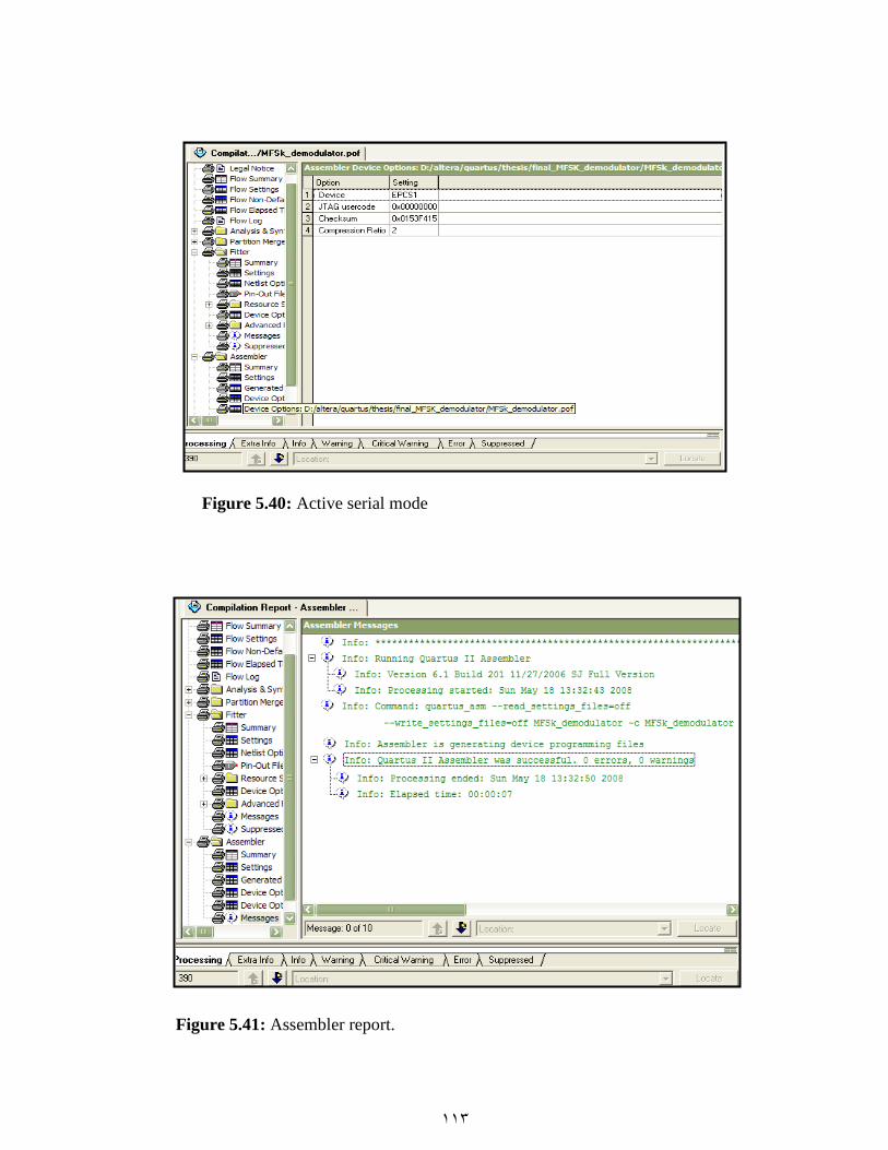
113
Figure 5.40: Active serial mode
Figure 5.41: Assembler report.
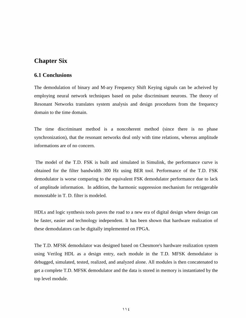
114
Chapter Six
6.1 Conclusions
The demodulation of binary and M-ary Frequency Shift Keying signals can be acheived by
employing neural network techniques based on pulse discriminant neurons. The theory of
Resonant Networks translates system analysis and design procedures from the frequency
domain to the time domain.
The time discriminant method is a noncoherent method (since there is no phase
synchronization), that the resonant networks deal only with time relations, whereas amplitude
informations are of no concern.
The model of the T.D. FSK is built and simulated in Simulink, the performance curve is
obtained for the filter bandwidth 300 Hz using BER tool. Performance of the T.D. FSK
demodulator is worse comparing to the equivalent FSK demodulator performance due to lack
of amplitude information. In addition, the harmonic suppression mechanism for retriggerable
monostable in T. D. filter is modeled.
HDLs and logic synthesis tools paves the road to a new era of digital design where design can
be faster, easier and technology independent. It has been shown that hardware realization of
these demodulators can be digitally implemented on FPGA.
The T.D. MFSK demodulator was designed based on Chesmore's hardware realization system
using Verilog HDL as a design entry, each module in the T.D. MFSK demodulator is
debugged, simulated, tested, realized, and analyzed alone. All modules is then concatenated to
get a complete T.D. MFSK demodulator and the data is stored in memory is instantiated by the
top level module.
115
The majority vote decoder is hardware implemented using 9 counters; one for each frequency
tone's zero crossings output and the additional counter is used to count out of band zero
crossings to effectively recover lost pulses if the number of zero-crossings within the symbol
interval where a clock counter is used to count clock is sufficiently great, within a single
symbol interval.
The majority vote decoder is tested and simulated to get the desired output of the T.D. MFSK
filter. In simultion results, this additional counter is effectively work and the output pulse that
lies out of band of the MFSK filter is removed and the right decesion is taken.
The T.D. MFSK signal demodulator modules are then compiled, synthesized, and analyzed
using the register transfer level viewer and the technology map viewer. The T.D. MFSK
system is simulated again using timing analysis tool that validates the timing performance of
all logic in the design using industry standard constraint, analysis, and reporting methodology
to view results for all timing paths in the design to check the timing constraints and the
frequency of 1Mhz is use for the counter to cycle through the memory.
The design of the demodulator was fitted on FPGA. PowerFit Fitter, performs place and route,
using the database that has been created by Analysis & Synthesize, the Fitter matches the logic
and timing requirements of the T.D. MFSK design project with the available resources of a
device. Each logic function is assigned to the best logic cell location for routing and timing,
and the output T.D. system is formed 8% of the total logic elements and 13% of the total
memory bitswhch represents the frequency tones and the filter bands stored in M4K in the
FPGA. The pins are assigned on the cyclone to form 3% of the total pins.
The design onf the T.D. system is optimized on FPGA using the Design Space Explorer DSE
to automate the process of finding the optimal collection of settings for T.D MFSK signal
demodulator design on the cyclone.
The FPGA cyclone is then configured and programmed with files generated by the compiler
for the T.D. MFSK signal demodulator system using two programming modes; Joint Test
Action Group (JTAG) mode and Active Serial programming mode and the output results can
be seen on the LEDs on the FPGA according to assigning the output pins.

116
6.2 Future Work
Finally, we suggest some research issues opened by our work. These issues can be
summarized in the following points:
Applying the T.D.FSK demodulator on any type of FPGA have the ability to use real FSK
tones and real channel to get the whole system consist of transmitter, channel, and receiver
that help more in obtaining the performance curves of the system and compare the results
with that for conventional method.
Implement the conventional noncoherent frequency shift keying demodulator on FPGA
and compare the complexity of this demodulator with the T.D FSK demodulator.
Implement the complete communication system for T.D. FSK using the megacore
functions; pre-verified HDL design files for complex system-level functions.
Other applications of the Time Discriminant Connectionist Theory:
Implement the complete communication system for phase shift keying using time
discriminant connectionist theory on FPGA.
Implement the frequency counter based on the period analyzer on FPGA [4, 12].
117
References
[1] UP3 education kit, Reference manual Cyclone edition, System level solutions Inc.
(USA), 2004.
[2] Reiss, R.F., A Theory of Resonant Network, in Neural Theory and Modelin, Stanford
University Press, 1964, pp.105-137.
[3] Reiss, R.F., A theory and simulation of rhythmic behavior due to reciprocal inhibition in
small nerve nets, in proceedings of the 1962 A.F.I.P.S spring joint computer conference,
Vol.21, Palo Alto, Calif. : National press, pp.171-194.
[4] Dawood, Emad H.S.; "Time Connectionist Systems", A master thesis, Jordan University
of Science and Technology, February 1996.
[5] Freeman J.A and Skapura D.M., Neural Networks, Algorithms, Applications, and
programming techniques, Addison-wesley publishing company, Inc., 1991.
[6] Douglas J Smith. HDL Chip Design, A practical guide for designing, synthesizing and
simulating ASICs and FPGAs using VHDL or Verilog. Doone Publications, Madis, AL,
USA,1997.
[7] Embeded Systems Development Kit, Cyclone Edition (EP1C6), Reference Manual,
System Level Solutions, Inc. (USA), 2006.
[8] Cooper G.R. and Mc Gillem C.D., Modern communications and spread spectrum, Mc
Graw-Hill book company, 1986.
[9] Chesmore, E.D., Application of pulse processing neural networks in communications and
signal demodulation, IEE conf. On artificial neural networks, 1989. 313, pp.341.
[10] Chesmore, E.D., A connectionist Architicture for signal demodulation in communication
systems, 2nd communications symposium-Bangor, 1990.
[11] Chesmore, E.D., Neural network architectures for signal detection and demodulation,
Fifth international conference on radio receivers and associated Systems, 1990.
[12] El-Asir, B.; Said, E.H., A low-frequency counter using time-discriminant connectionist
systems, Instrumentation and Measurement, IEEE Transactions on Volume 53, Issue 2,
April 2004 Page(s):493 - 497
[13] Glasford, Glenn., Digital Electronic Circuits, 1988
118
[14] Planitkar Samir, Verilog HDL, A Guide to Digital Design and Synthesis, 1996, Printce
Hall.
[15] Proakis J.G., Digital Communications; McGraw-Hill Companies ; Fourth Edition.
[16] Quartus II handbook, Volume 1, Design & synthesis, Altera, 2007.
[17] Quartus II handbook, Volume 2, Design implementation & optimazation, Altera, 2007.
[18] Quartus II handbook, Volume 3, Verification, Altera, 2007.
[19] M. Morris Mano, Digital design, Fourth edition, Upper saddle river, NJ 07458.
[20] Michael D. Ciletti, Advanced digital design with the Verilog HDl, Pearson education,
Inc., 2003.
[21] Wayne Wolf, FPGA-based system design, Prentice hall PTR, 2004.
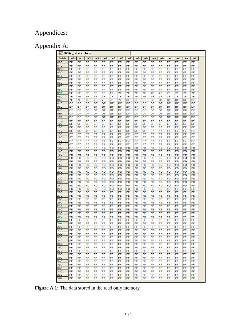
119
Appendices:
Appendix A:
Figure A.1: The data stored in the read only memory

120
z_cross
D
ENA
Q
PRE
CLR
DATAC
DATADOUT
SUM_LUT (0FF0)
CLK
DATAAREGOUT
LOGIC_CELL (AAAA)
CLK
DATAAREGOUT
LOGIC_CELL (AAAA)
CLK
DATAAREGOUT
LOGIC_CELL (AAAA)
din_reg[1]
din_reg[2]
din_reg[0]
clock_div10
z_crossq_a[0]
reset_n
edg_out
D
ENA
Q
PRE
CLR
DATAA OUT
SUM_LUT (AAAA)
clock_div10
edg_outz_cross
reset_n
Appendix B:
Figure B.1: Zero crossing module representation in the technology map veiwer.
Figure B.2: Edge detector representation in the technology map veiwer.
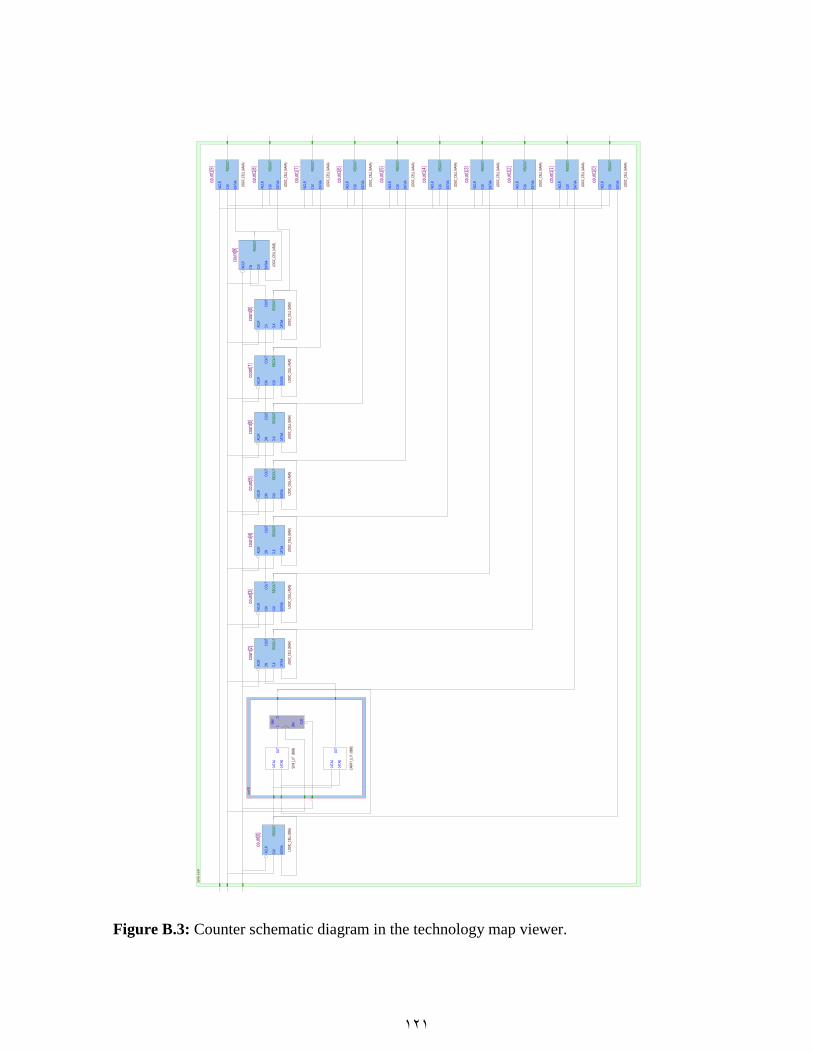
121
coun
ter:c
ount
coun
t[1]
D ENA
Q
PRE
CLR
DAT
AA
DAT
ABO
UT
SUM
_LU
T (6
666)
DAT
AA
DAT
ABO
UT
CAR
RY_
LUT
(888
8)
!AC
LR
CIN
CLK
DAT
AA
CO
UT
REG
OU
T
LOG
IC_C
ELL
(5A5
A)
!AC
LR
CIN
CLK
DAT
AA
CO
UT
REG
OU
T
LOG
IC_C
ELL
(A5A
5)
!AC
LR
CIN
CLK
DAT
AA
CO
UT
REG
OU
T
LOG
IC_C
ELL
(5A5
A)
!AC
LR
CIN
CLK
DAT
AA
CO
UT
REG
OU
T
LOG
IC_C
ELL
(A5A
5)
!AC
LR
CIN
CLK
DAT
AA
CO
UT
REG
OU
T
LOG
IC_C
ELL
(5A5
A)
!AC
LR
CIN
CLK
DAT
AA
CO
UT
REG
OU
T
LOG
IC_C
ELL
(A5A
5)
!AC
LR
CIN
CLK
DAT
AA
CO
UT
REG
OU
T
LOG
IC_C
ELL
(5A5
A)
!AC
LR
CIN
CLK
DAT
AA
REG
OU
T
LOG
IC_C
ELL
(A5A
5)
!AC
LR
CLK
DAT
AA
REG
OU
T
LOG
IC_C
ELL
(AAA
A)
!AC
LR
CLK
DAT
AA
REG
OU
T
LOG
IC_C
ELL
(AAA
A)
!AC
LR
CLK
DAT
AA
REG
OU
T
LOG
IC_C
ELL
(AAA
A)
!AC
LR
CLK
DAT
AA
REG
OU
T
LOG
IC_C
ELL
(AAA
A)
!AC
LR
CLK
DAT
AA
REG
OU
T
LOG
IC_C
ELL
(AAA
A)
!AC
LR
CLK
DAT
AA
REG
OU
T
LOG
IC_C
ELL
(AAA
A)
!AC
LR
CLK
DAT
AA
REG
OU
T
LOG
IC_C
ELL
(AAA
A)
!AC
LR
CLK
DAT
AA
REG
OU
T
LOG
IC_C
ELL
(AAA
A)
!AC
LR
CLK
DAT
AA
REG
OU
T
LOG
IC_C
ELL
(AAA
A)
!AC
LR
CLK
DAT
AA
REG
OU
T
LOG
IC_C
ELL
(AAA
A)
!AC
LR
CLK
DAT
AA
REG
OU
T
LOG
IC_C
ELL
(555
5)
coun
t[2]
coun
t[3]
coun
t[4]
coun
t[5]
coun
t[6]
coun
t[7]
coun
t[8]
coun
t[9]
coun
t1[0
]
coun
t1[1
]
coun
t1[2
]
coun
t1[3
]
coun
t1[4
]
coun
t1[5
]
coun
t1[6
]
coun
t1[7
]
coun
t1[8
]
coun
t1[9
]
coun
t[0]
Figure B.3: Counter schematic diagram in the technology map viewer.
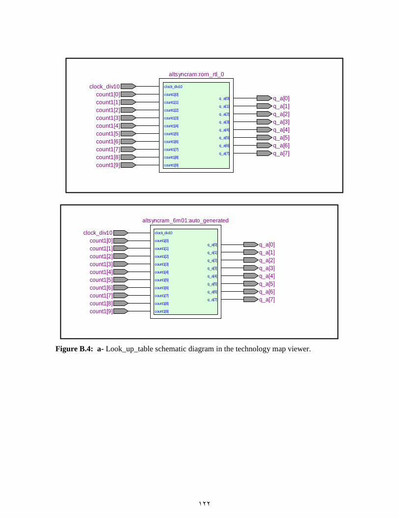
122
clock_div10
count1[0]
count1[1]
count1[2]
count1[3]
count1[4]
count1[5]
count1[6]
count1[7]
count1[8]
count1[9]
q_a[0]
q_a[1]
q_a[2]
q_a[3]
q_a[4]
q_a[5]
q_a[6]
q_a[7]
clock_div10
q_a[7]
q_a[6]
q_a[5]
q_a[0]
q_a[2]
q_a[3]
count1[0]
count1[1]
count1[2]
count1[3]
count1[4]
count1[5]
count1[6]
count1[7]
count1[8]
count1[9]
q_a[4]
q_a[1]
altsyncram:rom_rtl_0
clock_div10
count1[0]
count1[1]
count1[2]
count1[3]
count1[4]
count1[5]
count1[6]
count1[7]
count1[8]
count1[9]
q_a[0]
q_a[1]
q_a[2]
q_a[3]
q_a[4]
q_a[5]
q_a[6]
q_a[7]
clock_div10
q_a[7]
q_a[6]
q_a[5]
q_a[4]
q_a[0]
q_a[1]
q_a[2]
q_a[3]
count1[0]
count1[1]
count1[2]
count1[3]
count1[4]
count1[5]
count1[6]
count1[7]
count1[8]
count1[9]
altsyncram_6m01:auto_generated
Figure B.4: a- Look_up_table schematic diagram in the technology map viewer.
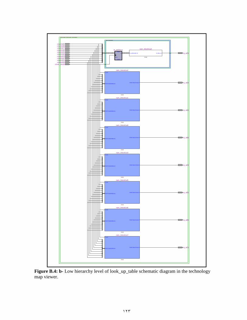
123
altsyncram_6m01:auto_generated
ram_block1a3
A_address[9..0] A_data_out
RAM
D Q
PRE
ENA
CLR
CLK0
PORTAADDR[9..0]PORTADATAOUT
RAM
CLK0
PORTAADDR[9..0]PORTADATAOUT
RAM
CLK0
PORTAADDR[9..0]PORTADATAOUT
RAM
CLK0
PORTAADDR[9..0]PORTADATAOUT
RAM
CLK0
PORTAADDR[9..0]PORTADATAOUT
RAM
CLK0
PORTAADDR[9..0]PORTADATAOUT
RAM
CLK0
PORTAADDR[9..0]PORTADATAOUT
RAM
ram_block1a3A_address
ram_block1a7
ram_block1a6
ram_block1a5
ram_block1a4
ram_block1a0
ram_block1a1
ram_block1a2
clock_div10
q_a[7]
q_a[6]
q_a[5]
q_a[4]
q_a[0]
q_a[1]
q_a[2]
q_a[3]
count1[0]
count1[1]
count1[2]
count1[3]
count1[4]
count1[5]
count1[6]
count1[7]
count1[8]
count1[9]
Figure B.4: b- Low hierarchy level of look_up_table schematic diagram in the technology
map viewer.
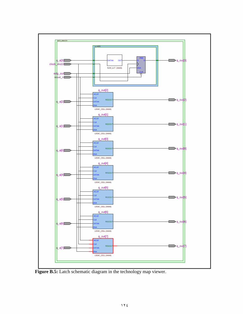
124
latch_data:lch
q_out[3]
D
ENA
Q
PRE
CLR
DATAA OUT
SUM_LUT (AAAA)
!ACLR
CLK
DATAA
ENA
REGOUT
LOGIC_CELL (AAAA)
!ACLR
CLK
DATAA
ENA
REGOUT
LOGIC_CELL (AAAA)
!ACLR
CLK
DATAA
ENA
REGOUT
LOGIC_CELL (AAAA)
!ACLR
CLK
DATAA
ENA
REGOUT
LOGIC_CELL (AAAA)
!ACLR
CLK
DATAA
ENA
REGOUT
LOGIC_CELL (AAAA)
!ACLR
CLK
DATAA
ENA
REGOUT
LOGIC_CELL (AAAA)
!ACLR
CLK
DATAA
ENA
REGOUT
LOGIC_CELL (AAAA)
q_out[7]
q_out[6]
q_out[5]
q_out[4]
q_out[0]
q_out[1]
q_out[2]
clock_div10
q_a[7]
q_a[6]
q_out[7]
q_out[6]
q_a[5]
q_a[4]
q_a[0]
q_a[1]
q_a[2]
q_a[3]
q_out[0]
q_out[1]
q_out[2]
q_out[3]
q_out[5]
q_out[4]
edg_out
reset_n
Figure B.5: Latch schematic diagram in the technology map viewer.

125
en
co
de
r:e
nc
od
Wid
eO
r1~
55
9d
ata
ou
t[2
]d
ata
ou
t1[2
]
D EN
A
Q
PR
E
CLR
DA
TA
AO
UT
SU
M_L
UT
(A
AA
A)
D EN
A
Q
PR
E
CLR
DA
TA
C
DA
TA
A
DA
TA
B
DA
TA
D
OU
T
SU
M_L
UT
(80
00)
DA
TA
A
DA
TA
BO
UT
SU
M_L
UT
(88
88)
!AC
LR
CLK
DA
TA
A
RE
GO
UT
LOG
IC_C
ELL
(A
AA
A)
!AC
LR
CLK
DA
TA
A
RE
GO
UT
LOG
IC_C
ELL
(A
AA
A)
CLK
DA
TA
A
DA
TA
B
DA
TA
C
DA
TA
D
RE
GO
UT
LOG
IC_C
ELL
(80
00)
CLK
DA
TA
A
DA
TA
B
DA
TA
C
DA
TA
D
RE
GO
UT
LOG
IC_C
ELL
(80
00)
DA
TA
A
DA
TA
B
DA
TA
C
DA
TA
D
CO
MB
OU
T
LOG
IC_C
ELL
(68
80)
DA
TA
A
DA
TA
BC
OM
BO
UT
LOG
IC_C
ELL
(88
88)
DA
TA
A
DA
TA
B
DA
TA
C
DA
TA
D
CO
MB
OU
T
LOG
IC_C
ELL
(68
80)
DA
TA
A
DA
TA
B
DA
TA
C
DA
TA
D
CO
MB
OU
T
LOG
IC_C
ELL
(68
80)
da
tao
ut1
[0]
da
tao
ut1
[1]
da
tao
ut[0
]
da
tao
ut[1
]
Wid
eO
r5~
55
8
Wid
eO
r3~
56
5
Wid
eO
r3~
56
6
Wid
eO
r1~
56
0
clo
ck_
div
10
ou
t_va
lue
[0]
ou
t_va
lue
[2]
ou
t_va
lue
[4]
ou
t_va
lue
[6]
ou
t_va
lue
[1]
ou
t_va
lue
[5]
ou
t_va
lue
[3]
ou
t_va
lue
[7]
da
tao
ut1
[0]
da
tao
ut1
[1]
da
tao
ut1
[2]
res
et_
n
Figure B.6: Encoder schematic diagram in the technology map viewer.
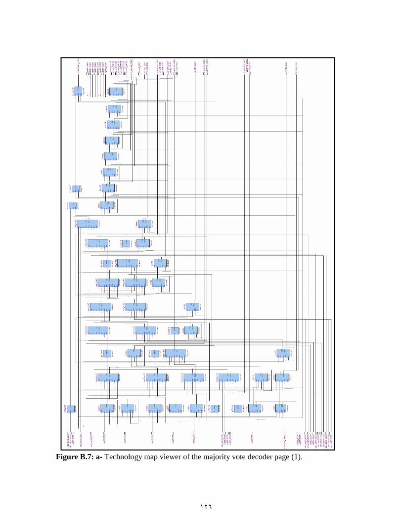
126
Figure B.7: a- Technology map viewer of the majority vote decoder page (1).
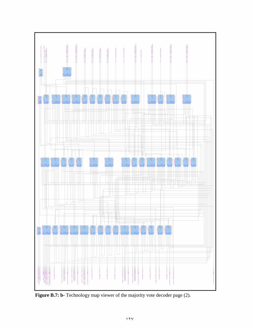
127
!A
CLR
CIN
CLK
DA
TA
A
SC
LR
RE
GO
UT
LO
GIC
_C
ELL (
A5A
5)
!A
CLR
CIN
CLK
DA
TA
A
DA
TA
B
DA
TA
C
EN
A
SLO
AD
CO
UT
RE
GO
UT
LO
GIC
_C
ELL (
AA
AA
)
!A
CLR
CIN
CLK
DA
TA
A
SC
LR
RE
GO
UT
LO
GIC
_C
ELL (
A5A
5)
!A
CLR
CIN
CLK
DA
TA
A
EN
A
SC
LR
RE
GO
UT
LO
GIC
_C
ELL (
A5A
5)
!A
CLR
CIN
CLK
DA
TA
A
DA
TA
B
DA
TA
C
EN
A
SLO
AD
CO
UT
RE
GO
UT
LO
GIC
_C
ELL (
AA
AA
)
!A
CLR
CIN
CLK
DA
TA
A
DA
TA
B
DA
TA
C
EN
A
SLO
AD
CO
UT
RE
GO
UT
LO
GIC
_C
ELL (
AA
AA
)
!A
CLR
CIN
CLK
DA
TA
A
DA
TA
B
DA
TA
C
EN
A
SLO
AD
CO
UT
RE
GO
UT
LO
GIC
_C
ELL (
AA
AA
)
!A
CLR
CIN
CLK
DA
TA
A
SC
LR
CO
UT
RE
GO
UT
LO
GIC
_C
ELL (
5A
5A
)
CIN
DA
TA
A
DA
TA
B
CO
UT
LO
GIC
_C
ELL (
FF
FF
)
!A
CLR
CIN
CLK
DA
TA
A
SC
LR
CO
UT
RE
GO
UT
LO
GIC
_C
ELL (
5A
5A
)
!A
CLR
CIN
CLK
DA
TA
A
SC
LR
CO
UT
RE
GO
UT
LO
GIC
_C
ELL (
5A
5A
)
!A
CLR
CIN
CLK
DA
TA
A
DA
TA
B
DA
TA
C
EN
A
SLO
AD
CO
UT
RE
GO
UT
LO
GIC
_C
ELL (
AA
AA
)
!A
CLR
CIN
CLK
DA
TA
A
SC
LR
CO
UT
RE
GO
UT
LO
GIC
_C
ELL (
5A
5A
)
!A
CLR
CIN
CLK
DA
TA
A
SC
LR
CO
UT
RE
GO
UT
LO
GIC
_C
ELL (
5A
5A
)
!A
CLR
CIN
CLK
DA
TA
A
DA
TA
B
DA
TA
C
EN
A
SLO
AD
CO
UT
RE
GO
UT
LO
GIC
_C
ELL (
AA
AA
)
!A
CLR
CIN
CLK
DA
TA
A
DA
TA
B
DA
TA
C
EN
A
SLO
AD
CO
UT
RE
GO
UT
LO
GIC
_C
ELL (
AA
AA
)
!A
CLR
CIN
CLK
DA
TA
A
SC
LR
CO
UT
RE
GO
UT
LO
GIC
_C
ELL (
5A
5A
)
!A
CLR
CIN
CLK
DA
TA
A
SC
LR
CO
UT
RE
GO
UT
LO
GIC
_C
ELL (
5A
5A
)
!A
CLR
CIN
CLK
DA
TA
A
DA
TA
B
DA
TA
C
EN
A
SLO
AD
CO
UT
RE
GO
UT
LO
GIC
_C
ELL (
AA
AA
)
!A
CLR
CIN
CLK
DA
TA
A
SC
LR
CO
UT
RE
GO
UT
LO
GIC
_C
ELL (
5A
5A
)
!A
CLR
CIN
CLK
DA
TA
A
EN
A
SC
LR
CO
UT
RE
GO
UT
LO
GIC
_C
ELL (
5A
5A
)
!A
CLR
CIN
CLK
DA
TA
A
DA
TA
B
DA
TA
C
EN
A
SLO
AD
CO
UT
RE
GO
UT
LO
GIC
_C
ELL (
AA
AA
)
!A
CLR
CIN
CLK
DA
TA
A
DA
TA
B
DA
TA
C
EN
A
SLO
AD
CO
UT
RE
GO
UT
LO
GIC
_C
ELL (
AA
AA
)
!A
CLR
CIN
CLK
DA
TA
A
DA
TA
B
DA
TA
C
EN
A
SLO
AD
CO
UT
RE
GO
UT
LO
GIC
_C
ELL (
AA
AA
)
!A
CLR
CIN
CLK
DA
TA
A
SC
LR
CO
UT
RE
GO
UT
LO
GIC
_C
ELL (
A5A
5)
CIN
DA
TA
A
DA
TA
B
CO
UT
LO
GIC
_C
ELL (
FF
FF
)
!A
CLR
CIN
CLK
DA
TA
A
SC
LR
CO
UT
RE
GO
UT
LO
GIC
_C
ELL (
A5A
5)
!A
CLR
CIN
CLK
DA
TA
A
SC
LR
CO
UT
RE
GO
UT
LO
GIC
_C
ELL (
A5A
5)
!A
CLR
CIN
CLK
DA
TA
A
DA
TA
B
DA
TA
C
EN
A
SLO
AD
CO
UT
RE
GO
UT
LO
GIC
_C
ELL (
AA
AA
)
!A
CLR
CIN
CLK
DA
TA
A
SC
LR
CO
UT
RE
GO
UT
LO
GIC
_C
ELL (
A5A
5)
!A
CLR
CIN
CLK
DA
TA
A
SC
LR
CO
UT
RE
GO
UT
LO
GIC
_C
ELL (
A5A
5)
!A
CLR
CIN
CLK
DA
TA
A
DA
TA
B
DA
TA
C
EN
A
SLO
AD
CO
UT
RE
GO
UT
LO
GIC
_C
ELL (
AA
AA
)
!A
CLR
CIN
CLK
DA
TA
A
DA
TA
B
DA
TA
C
EN
A
SLO
AD
CO
UT
RE
GO
UT
LO
GIC
_C
ELL (
AA
AA
)
!A
CLR
CIN
CLK
DA
TA
A
SC
LR
CO
UT
RE
GO
UT
LO
GIC
_C
ELL (
A5A
5)
!A
CLR
CIN
CLK
DA
TA
A
SC
LR
CO
UT
RE
GO
UT
LO
GIC
_C
ELL (
A5A
5)
!A
CLR
CIN
CLK
DA
TA
A
DA
TA
B
DA
TA
C
EN
A
SLO
AD
CO
UT
RE
GO
UT
LO
GIC
_C
ELL (
AA
AA
)
!A
CLR
CIN
CLK
DA
TA
A
SC
LR
CO
UT
RE
GO
UT
LO
GIC
_C
ELL (
A5A
5)
!A
CLR
CIN
CLK
DA
TA
A
EN
A
SC
LR
CO
UT
RE
GO
UT
LO
GIC
_C
ELL (
A5A
5)
!A
CLR
CIN
CLK
DA
TA
A
DA
TA
B
DA
TA
C
EN
A
SLO
AD
CO
UT
RE
GO
UT
LO
GIC
_C
ELL (
AA
AA
)
!A
CLR
CIN
CLK
DA
TA
A
DA
TA
B
DA
TA
C
EN
A
SLO
AD
CO
UT
RE
GO
UT
LO
GIC
_C
ELL (
AA
AA
)
!A
CLR
CIN
CLK
DA
TA
A
DA
TA
B
DA
TA
C
EN
A
SLO
AD
CO
UT
RE
GO
UT
LO
GIC
_C
ELL (
AA
AA
)
!A
CLR
CIN
CLK
DA
TA
A
SC
LR
CO
UT
RE
GO
UT
LO
GIC
_C
ELL (
5A
5A
)
CIN
DA
TA
A
DA
TA
B
CO
UT
LO
GIC
_C
ELL (
FF
FF
)
!A
CLR
CIN
CLK
DA
TA
A
SC
LR
CO
UT
RE
GO
UT
LO
GIC
_C
ELL (
5A
5A
)
!A
CLR
CIN
CLK
DA
TA
A
SC
LR
CO
UT
RE
GO
UT
LO
GIC
_C
ELL (
5A
5A
)
!A
CLR
CIN
CLK
DA
TA
A
DA
TA
B
DA
TA
C
EN
A
SLO
AD
CO
UT
RE
GO
UT
LO
GIC
_C
ELL (
AA
AA
)
!A
CLR
CIN
CLK
DA
TA
A
SC
LR
CO
UT
RE
GO
UT
LO
GIC
_C
ELL (
5A
5A
)
!A
CLR
CIN
CLK
DA
TA
A
SC
LR
CO
UT
RE
GO
UT
LO
GIC
_C
ELL (
5A
5A
)
!A
CLR
CIN
CLK
DA
TA
A
DA
TA
B
DA
TA
C
EN
A
SLO
AD
CO
UT
RE
GO
UT
LO
GIC
_C
ELL (
AA
AA
)
!A
CLR
CIN
CLK
DA
TA
A
DA
TA
B
DA
TA
C
EN
A
SLO
AD
CO
UT
RE
GO
UT
LO
GIC
_C
ELL (
AA
AA
)
re
se
t_n
_C
OM
BO
UT
clo
ck_
div
10
_C
OM
BO
UT
Le
ss
Th
an
0~
36
3_
CO
MB
OU
T
co
un
t2[1
6]_
RE
GO
UT
Le
ss
Th
an
2~
69
_C
OM
BO
UT
co
mp
1_
co
un
t[1
5]_
CO
UT
co
mp
1_
co
un
t[1
5]_
RE
GO
UT
co
un
t1[1
6]_
RE
GO
UT
co
un
t0[1
1]~
11
98
_C
OM
BO
UT
co
un
t0[1
6]_
RE
GO
UT
Le
ss
Th
an
1~
69
_C
OM
BO
UT
co
mp
0_
co
un
t[1
5]_
CO
UT
co
mp
0_
co
un
t[1
5]_
RE
GO
UT
Le
ss
Th
an
5~
69
_C
OM
BO
UT
co
mp
4_
co
un
t[1
4]_
CO
UT
co
mp
4_
co
un
t[1
4]_
RE
GO
UT
Le
ss
Th
an
7~
69
_C
OM
BO
UT
co
mp
6_
co
un
t[1
3]_
CO
UT
co
mp
6_
co
un
t[1
3]_
RE
GO
UT
co
un
t8[1
3]_
CO
UT
co
un
t8[1
3]_
RE
GO
UT
Le
ss
Th
an
8~
29
2_
CO
UT
co
un
t7[1
5]_
CO
UT
co
un
t7[1
5]_
RE
GO
UT
co
un
t6[1
5]_
CO
UT
co
un
t6[1
5]_
RE
GO
UT
Le
ss
Th
an
4~
69
_C
OM
BO
UT
co
mp
3_
co
un
t[1
4]_
CO
UT
co
mp
3_
co
un
t[1
4]_
RE
GO
UT
co
un
t5[1
5]_
CO
UT
co
un
t5[1
5]_
RE
GO
UT
co
un
t4[1
5]_
CO
UT
co
un
t4[1
5]_
RE
GO
UT
Le
ss
Th
an
3~
69
_C
OM
BO
UT
co
mp
2_
co
un
t[1
4]_
CO
UT
co
mp
2_
co
un
t[1
4]_
RE
GO
UT
Le
ss
Th
an
6~
69
_C
OM
BO
UT
co
mp
5_
co
un
t[1
3]_
CO
UT
co
un
t3[1
5]_
CO
UT
co
un
t3[1
3]_
CO
UT
co
un
t2[1
3]_
CO
UT
co
mp
1_
co
un
t[1
2]_
CO
UT
co
un
t3[1
3]_
RE
GO
UT
co
un
t2[1
3]_
RE
GO
UT
co
un
t1[1
3]_
CO
UT
co
un
t0[1
3]_
CO
UT
co
mp
0_
co
un
t[1
2]_
CO
UT
co
un
t1[1
3]_
RE
GO
UT
co
un
t0[1
3]_
RE
GO
UT
co
mp
4_
co
un
t[1
1]_
CO
UT
co
mp
1_
co
un
t[1
2]_
RE
GO
UT
co
mp
0_
co
un
t[1
2]_
RE
GO
UT
co
mp
6_
co
un
t[1
0]_
CO
UT
co
mp
4_
co
un
t[1
1]_
RE
GO
UT
co
un
t8[1
0]_
CO
UT
Le
ss
Th
an
8~
30
7_
CO
UT
co
mp
6_
co
un
t[1
0]_
RE
GO
UT
co
un
t8[1
0]_
RE
GO
UT
co
un
t7[1
2]_
CO
UT
co
un
t6[1
2]_
CO
UT
co
mp
3_
co
un
t[1
1]_
CO
UT
co
un
t7[1
2]_
RE
GO
UT
co
un
t6[1
2]_
RE
GO
UT
co
un
t5[1
2]_
CO
UT
co
un
t4[1
2]_
CO
UT
co
mp
2_
co
un
t[1
1]_
CO
UT
co
un
t5[1
2]_
RE
GO
UT
co
un
t4[1
2]_
RE
GO
UT
co
mp
5_
co
un
t[1
0]_
CO
UT
co
mp
3_
co
un
t[1
1]_
RE
GO
UT
co
mp
2_
co
un
t[1
1]_
RE
GO
UT
co
un
t2[1
6]
co
mp
1_
co
un
t[1
5]
co
un
t1[1
6]
co
un
t0[1
6]
co
mp
0_
co
un
t[1
5]
co
mp
4_
co
un
t[1
4]
co
mp
6_
co
un
t[1
3]
co
un
t8[1
3]
Le
ss
Th
an
8~
29
2
co
un
t7[1
5]
co
un
t6[1
5]
co
mp
3_
co
un
t[1
4]
co
un
t5[1
5]
co
un
t4[1
5]
co
mp
2_
co
un
t[1
4]
co
mp
5_
co
un
t[1
3]
co
un
t3[1
5]
co
un
t2[1
5]
co
mp
1_
co
un
t[1
4]
co
un
t1[1
5]
co
un
t0[1
5]
co
mp
0_
co
un
t[1
4]
co
mp
4_
co
un
t[1
3]
co
mp
6_
co
un
t[1
2]
co
un
t8[1
2]
Le
ss
Th
an
8~
29
7
co
un
t7[1
4]
co
un
t6[1
4]
co
mp
3_
co
un
t[1
3]
co
un
t5[1
4]
co
un
t4[1
4]
co
mp
2_
co
un
t[1
3]
co
mp
5_
co
un
t[1
2]
co
un
t3[1
4]
co
un
t2[1
4]
co
mp
1_
co
un
t[1
3]
co
un
t1[1
4]
co
un
t0[1
4]
co
mp
0_
co
un
t[1
3]
co
mp
4_
co
un
t[1
2]
co
mp
6_
co
un
t[1
1]
co
un
t8[1
1]
Le
ss
Th
an
8~
30
2
co
un
t7[1
3]
co
un
t6[1
3]
co
mp
3_
co
un
t[1
2]
co
un
t5[1
3]
co
un
t4[1
3]
co
mp
2_
co
un
t[1
2]
co
mp
5_
co
un
t[1
1]
Figure B.7: b- Technology map viewer of the majority vote decoder page (2).
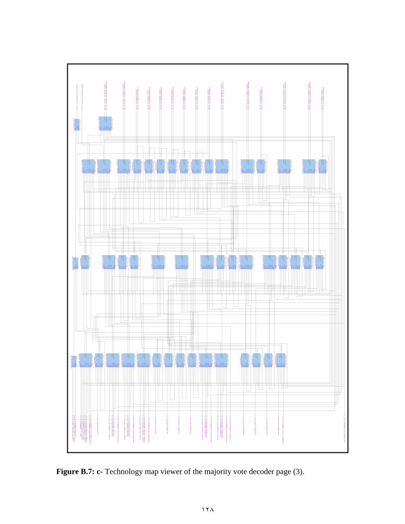
128
!A
CLR
CIN
CLK
DA
TA
A
SC
LR
CO
UT
RE
GO
UT
LO
GIC
_C
ELL (
5A
5A
)
!A
CLR
CIN
CLK
DA
TA
A
SC
LR
CO
UT
RE
GO
UT
LO
GIC
_C
ELL (
5A
5A
)
!A
CLR
CIN
CLK
DA
TA
A
DA
TA
B
DA
TA
C
EN
A
SLO
AD
CO
UT
RE
GO
UT
LO
GIC
_C
ELL (
AA
AA
)
!A
CLR
CIN
CLK
DA
TA
A
SC
LR
CO
UT
RE
GO
UT
LO
GIC
_C
ELL (
5A
5A
)
!A
CLR
CIN
CLK
DA
TA
A
EN
A
SC
LR
CO
UT
RE
GO
UT
LO
GIC
_C
ELL (
5A
5A
)
!A
CLR
CIN
CLK
DA
TA
A
DA
TA
B
DA
TA
C
EN
A
SLO
AD
CO
UT
RE
GO
UT
LO
GIC
_C
ELL (
AA
AA
)
!A
CLR
CIN
CLK
DA
TA
A
DA
TA
B
DA
TA
C
EN
A
SLO
AD
CO
UT
RE
GO
UT
LO
GIC
_C
ELL (
AA
AA
)
!A
CLR
CIN
CLK
DA
TA
A
DA
TA
B
DA
TA
C
EN
A
SLO
AD
CO
UT
RE
GO
UT
LO
GIC
_C
ELL (
AA
AA
)
!A
CLR
CIN
CLK
DA
TA
A
SC
LR
CO
UT
RE
GO
UT
LO
GIC
_C
ELL (
A5A
5)
CIN
DA
TA
A
DA
TA
B
CO
UT
LO
GIC
_C
ELL (
FF
FF
)
!A
CLR
CIN
CLK
DA
TA
A
SC
LR
CO
UT
RE
GO
UT
LO
GIC
_C
ELL (
A5A
5)
!A
CLR
CIN
CLK
DA
TA
A
SC
LR
CO
UT
RE
GO
UT
LO
GIC
_C
ELL (
A5A
5)
!A
CLR
CIN
CLK
DA
TA
A
DA
TA
B
DA
TA
C
EN
A
SLO
AD
CO
UT
RE
GO
UT
LO
GIC
_C
ELL (
AA
AA
)
!A
CLR
CIN
CLK
DA
TA
A
SC
LR
CO
UT
RE
GO
UT
LO
GIC
_C
ELL (
A5A
5)
!A
CLR
CIN
CLK
DA
TA
A
SC
LR
CO
UT
RE
GO
UT
LO
GIC
_C
ELL (
A5A
5)
!A
CLR
CIN
CLK
DA
TA
A
DA
TA
B
DA
TA
C
EN
A
SLO
AD
CO
UT
RE
GO
UT
LO
GIC
_C
ELL (
AA
AA
)
!A
CLR
CIN
CLK
DA
TA
A
DA
TA
B
DA
TA
C
EN
A
SLO
AD
CO
UT
RE
GO
UT
LO
GIC
_C
ELL (
AA
AA
)
!A
CLR
CIN
CLK
DA
TA
A
SC
LR
CO
UT
RE
GO
UT
LO
GIC
_C
ELL (
A5A
5)
!A
CLR
CIN
CLK
DA
TA
A
SC
LR
CO
UT
RE
GO
UT
LO
GIC
_C
ELL (
A5A
5)
!A
CLR
CIN
CLK
DA
TA
A
DA
TA
B
DA
TA
C
EN
A
SLO
AD
CO
UT
RE
GO
UT
LO
GIC
_C
ELL (
AA
AA
)
!A
CLR
CIN
CLK
DA
TA
A
SC
LR
CO
UT
RE
GO
UT
LO
GIC
_C
ELL (
A5A
5)
!A
CLR
CIN
CLK
DA
TA
A
EN
A
SC
LR
CO
UT
RE
GO
UT
LO
GIC
_C
ELL (
A5A
5)
!A
CLR
CIN
CLK
DA
TA
A
DA
TA
B
DA
TA
C
EN
A
SLO
AD
CO
UT
RE
GO
UT
LO
GIC
_C
ELL (
AA
AA
)
!A
CLR
CIN
CLK
DA
TA
A
DA
TA
B
DA
TA
C
EN
A
SLO
AD
CO
UT
RE
GO
UT
LO
GIC
_C
ELL (
AA
AA
)
!A
CLR
CIN
CLK
DA
TA
A
DA
TA
B
DA
TA
C
EN
A
SLO
AD
CO
UT
RE
GO
UT
LO
GIC
_C
ELL (
AA
AA
)
!A
CLR
CIN
CLK
DA
TA
A
SC
LR
CO
UT
RE
GO
UT
LO
GIC
_C
ELL (
5A
5A
)
CIN
DA
TA
A
DA
TA
B
CO
UT
LO
GIC
_C
ELL (
FF
FF
)
!A
CLR
CIN
CLK
DA
TA
A
SC
LR
CO
UT
RE
GO
UT
LO
GIC
_C
ELL (
5A
5A
)
!A
CLR
CIN
CLK
DA
TA
A
SC
LR
CO
UT
RE
GO
UT
LO
GIC
_C
ELL (
5A
5A
)
!A
CLR
CIN
CLK
DA
TA
A
DA
TA
B
DA
TA
C
EN
A
SLO
AD
CO
UT
RE
GO
UT
LO
GIC
_C
ELL (
AA
AA
)
!A
CLR
CIN
CLK
DA
TA
A
SC
LR
CO
UT
RE
GO
UT
LO
GIC
_C
ELL (
5A
5A
)
!A
CLR
CIN
CLK
DA
TA
A
SC
LR
CO
UT
RE
GO
UT
LO
GIC
_C
ELL (
5A
5A
)
!A
CLR
CIN
CLK
DA
TA
A
DA
TA
B
DA
TA
C
EN
A
SLO
AD
CO
UT
RE
GO
UT
LO
GIC
_C
ELL (
AA
AA
)
!A
CLR
CIN
CLK
DA
TA
A
DA
TA
B
DA
TA
C
EN
A
SLO
AD
CO
UT
RE
GO
UT
LO
GIC
_C
ELL (
AA
AA
)
!A
CLR
CIN
CLK
DA
TA
A
SC
LR
CO
UT
RE
GO
UT
LO
GIC
_C
ELL (
5A
5A
)
!A
CLR
CIN
CLK
DA
TA
A
SC
LR
CO
UT
RE
GO
UT
LO
GIC
_C
ELL (
5A
5A
)
!A
CLR
CIN
CLK
DA
TA
A
DA
TA
B
DA
TA
C
EN
A
SLO
AD
CO
UT
RE
GO
UT
LO
GIC
_C
ELL (
AA
AA
)
!A
CLR
CIN
CLK
DA
TA
A
SC
LR
CO
UT
RE
GO
UT
LO
GIC
_C
ELL (
5A
5A
)
!A
CLR
CIN
CLK
DA
TA
A
EN
A
SC
LR
CO
UT
RE
GO
UT
LO
GIC
_C
ELL (
5A
5A
)
!A
CLR
CIN
CLK
DA
TA
A
DA
TA
B
DA
TA
C
EN
A
SLO
AD
CO
UT
RE
GO
UT
LO
GIC
_C
ELL (
AA
AA
)
!A
CLR
CIN
CLK
DA
TA
A
DA
TA
B
DA
TA
C
EN
A
SLO
AD
CO
UT
RE
GO
UT
LO
GIC
_C
ELL (
AA
AA
)
!A
CLR
CIN
CLK
DA
TA
A
DA
TA
B
DA
TA
C
EN
A
SLO
AD
CO
UT
RE
GO
UT
LO
GIC
_C
ELL (
AA
AA
)
!A
CLR
CIN
CLK
DA
TA
A
SC
LR
CO
UT
RE
GO
UT
LO
GIC
_C
ELL (
A5A
5)
CIN
DA
TA
A
DA
TA
B
CO
UT
LO
GIC
_C
ELL (
FF
FF
)
!A
CLR
CIN
CLK
DA
TA
A
SC
LR
CO
UT
RE
GO
UT
LO
GIC
_C
ELL (
A5A
5)
!A
CLR
CIN
CLK
DA
TA
A
SC
LR
CO
UT
RE
GO
UT
LO
GIC
_C
ELL (
A5A
5)
!A
CLR
CIN
CLK
DA
TA
A
DA
TA
B
DA
TA
C
EN
A
SLO
AD
CO
UT
RE
GO
UT
LO
GIC
_C
ELL (
AA
AA
)
!A
CLR
CIN
CLK
DA
TA
A
SC
LR
CO
UT
RE
GO
UT
LO
GIC
_C
ELL (
A5A
5)
!A
CLR
CIN
CLK
DA
TA
A
SC
LR
CO
UT
RE
GO
UT
LO
GIC
_C
ELL (
A5A
5)
!A
CLR
CIN
CLK
DA
TA
A
DA
TA
B
DA
TA
C
EN
A
SLO
AD
CO
UT
RE
GO
UT
LO
GIC
_C
ELL (
AA
AA
)
re
se
t_n
_C
OM
BO
UT
clo
ck_
div
10
_C
OM
BO
UT
Le
ss
Th
an
0~
36
3_
CO
MB
OU
T
co
un
t3[1
3]_
CO
UT
co
un
t3[1
3]_
RE
GO
UT
co
un
t2[1
3]_
CO
UT
co
un
t2[1
3]_
RE
GO
UT
Le
ss
Th
an
2~
69
_C
OM
BO
UT
co
mp
1_
co
un
t[1
2]_
CO
UT
co
mp
1_
co
un
t[1
2]_
RE
GO
UT
co
un
t1[1
3]_
CO
UT
co
un
t1[1
3]_
RE
GO
UT
co
un
t0[1
1]~
11
98
_C
OM
BO
UT
co
un
t0[1
3]_
CO
UT
co
un
t0[1
3]_
RE
GO
UT
Le
ss
Th
an
1~
69
_C
OM
BO
UT
co
mp
0_
co
un
t[1
2]_
CO
UT
co
mp
0_
co
un
t[1
2]_
RE
GO
UT
Le
ss
Th
an
5~
69
_C
OM
BO
UT
co
mp
4_
co
un
t[1
1]_
CO
UT
co
mp
4_
co
un
t[1
1]_
RE
GO
UT
Le
ss
Th
an
7~
69
_C
OM
BO
UT
co
mp
6_
co
un
t[1
0]_
CO
UT
co
mp
6_
co
un
t[1
0]_
RE
GO
UT
co
un
t8[1
0]_
CO
UT
co
un
t8[1
0]_
RE
GO
UT
Le
ss
Th
an
8~
30
7_
CO
UT
co
un
t7[1
2]_
CO
UT
co
un
t7[1
2]_
RE
GO
UT
co
un
t6[1
2]_
CO
UT
co
un
t6[1
2]_
RE
GO
UT
Le
ss
Th
an
4~
69
_C
OM
BO
UT
co
mp
3_
co
un
t[1
1]_
CO
UT
co
mp
3_
co
un
t[1
1]_
RE
GO
UT
co
un
t5[1
2]_
CO
UT
co
un
t5[1
2]_
RE
GO
UT
co
un
t4[1
2]_
CO
UT
co
un
t4[1
2]_
RE
GO
UT
Le
ss
Th
an
3~
69
_C
OM
BO
UT
co
mp
2_
co
un
t[1
1]_
CO
UT
co
mp
2_
co
un
t[1
1]_
RE
GO
UT
Le
ss
Th
an
6~
69
_C
OM
BO
UT
co
mp
5_
co
un
t[1
0]_
CO
UT
co
mp
5_
co
un
t[8
]_C
OU
T
co
un
t3[1
0]_
CO
UT
co
un
t2[1
0]_
CO
UT
co
mp
1_
co
un
t[9
]_C
OU
T
co
un
t3[1
0]_
RE
GO
UT
co
un
t2[1
0]_
RE
GO
UT
co
un
t1[1
0]_
CO
UT
co
un
t0[1
0]_
CO
UT
co
mp
0_
co
un
t[9
]_C
OU
T
co
un
t1[1
0]_
RE
GO
UT
co
un
t0[1
0]_
RE
GO
UT
co
mp
4_
co
un
t[8
]_C
OU
T
co
mp
1_
co
un
t[9
]_R
EG
OU
T
co
mp
0_
co
un
t[9
]_R
EG
OU
T
co
mp
6_
co
un
t[7
]_C
OU
T
co
mp
5_
co
un
t[8
]_R
EG
OU
T
co
mp
4_
co
un
t[8
]_R
EG
OU
T
co
un
t8[7
]_C
OU
T
Le
ss
Th
an
8~
32
2_
CO
UT
co
mp
6_
co
un
t[7
]_R
EG
OU
T
co
un
t8[7
]_R
EG
OU
T
co
un
t7[9
]_C
OU
T
co
un
t6[9
]_C
OU
T
co
mp
3_
co
un
t[8
]_C
OU
T
co
un
t7[9
]_R
EG
OU
T
co
un
t6[9
]_R
EG
OU
T
co
un
t5[9
]_C
OU
T
co
un
t4[9
]_C
OU
T
co
mp
2_
co
un
t[8
]_C
OU
T
co
un
t5[9
]_R
EG
OU
T
co
un
t4[9
]_R
EG
OU
T
co
un
t3[1
3]
co
un
t2[1
3]
co
mp
1_
co
un
t[1
2]
co
un
t1[1
3]
co
un
t0[1
3]
co
mp
0_
co
un
t[1
2]
co
mp
4_
co
un
t[1
1]
co
mp
6_
co
un
t[1
0]
co
un
t8[1
0]
Le
ss
Th
an
8~
30
7
co
un
t7[1
2]
co
un
t6[1
2]
co
mp
3_
co
un
t[1
1]
co
un
t5[1
2]
co
un
t4[1
2]
co
mp
2_
co
un
t[1
1]
co
mp
5_
co
un
t[1
0]
co
un
t3[1
2]
co
un
t2[1
2]
co
mp
1_
co
un
t[1
1]
co
un
t1[1
2]
co
un
t0[1
2]
co
mp
0_
co
un
t[1
1]
co
mp
4_
co
un
t[1
0]
co
mp
6_
co
un
t[9
]
co
un
t8[9
]
Le
ss
Th
an
8~
31
2
co
un
t7[1
1]
co
un
t6[1
1]
co
mp
3_
co
un
t[1
0]
co
un
t5[1
1]
co
un
t4[1
1]
co
mp
2_
co
un
t[1
0]
co
mp
5_
co
un
t[9
]
co
un
t3[1
1]
co
un
t2[1
1]
co
mp
1_
co
un
t[1
0]
co
un
t1[1
1]
co
un
t0[1
1]
co
mp
0_
co
un
t[1
0]
co
mp
4_
co
un
t[9
]
co
mp
6_
co
un
t[8
]
co
un
t8[8
]
Le
ss
Th
an
8~
31
7
co
un
t7[1
0]
co
un
t6[1
0]
co
mp
3_
co
un
t[9
]
co
un
t5[1
0]
co
un
t4[1
0]
co
mp
2_
co
un
t[9
]
Figure B.7: c- Technology map viewer of the majority vote decoder page (3).

129
!A
CLR
CIN
CLK
DA
TA
A
DA
TA
B
DA
TA
C
EN
A
SLO
AD
CO
UT
RE
GO
UT
LO
GIC
_C
ELL (
AA
AA
)
!A
CLR
CIN
CLK
DA
TA
A
SC
LR
CO
UT
RE
GO
UT
LO
GIC
_C
ELL (
A5A
5)
!A
CLR
CIN
CLK
DA
TA
A
SC
LR
CO
UT
RE
GO
UT
LO
GIC
_C
ELL (
A5A
5)
!A
CLR
CIN
CLK
DA
TA
A
DA
TA
B
DA
TA
C
EN
A
SLO
AD
CO
UT
RE
GO
UT
LO
GIC
_C
ELL (
AA
AA
)
!A
CLR
CIN
CLK
DA
TA
A
SC
LR
CO
UT
RE
GO
UT
LO
GIC
_C
ELL (
A5A
5)
!A
CLR
CIN
CLK
DA
TA
A
EN
A
SC
LR
CO
UT
RE
GO
UT
LO
GIC
_C
ELL (
A5A
5)
!A
CLR
CIN
CLK
DA
TA
A
DA
TA
B
DA
TA
C
EN
A
SLO
AD
CO
UT
RE
GO
UT
LO
GIC
_C
ELL (
AA
AA
)
!A
CLR
CIN
CLK
DA
TA
A
DA
TA
B
DA
TA
C
EN
A
SLO
AD
CO
UT
RE
GO
UT
LO
GIC
_C
ELL (
AA
AA
)
!A
CLR
CIN
CLK
DA
TA
A
DA
TA
B
DA
TA
C
EN
A
SLO
AD
CO
UT
RE
GO
UT
LO
GIC
_C
ELL (
AA
AA
)
!A
CLR
CIN
CLK
DA
TA
A
SC
LR
CO
UT
RE
GO
UT
LO
GIC
_C
ELL (
5A
5A
)
CIN
DA
TA
A
DA
TA
B
CO
UT
LO
GIC
_C
ELL (
FF
FF
)
!A
CLR
CIN
CLK
DA
TA
A
SC
LR
CO
UT
RE
GO
UT
LO
GIC
_C
ELL (
5A
5A
)
!A
CLR
CIN
CLK
DA
TA
A
SC
LR
CO
UT
RE
GO
UT
LO
GIC
_C
ELL (
5A
5A
)
!A
CLR
CIN
CLK
DA
TA
A
DA
TA
B
DA
TA
C
EN
A
SLO
AD
CO
UT
RE
GO
UT
LO
GIC
_C
ELL (
AA
AA
)
!A
CLR
CIN
CLK
DA
TA
A
SC
LR
CO
UT
RE
GO
UT
LO
GIC
_C
ELL (
5A
5A
)
!A
CLR
CIN
CLK
DA
TA
A
SC
LR
CO
UT
RE
GO
UT
LO
GIC
_C
ELL (
5A
5A
)
!A
CLR
CIN
CLK
DA
TA
A
DA
TA
B
DA
TA
C
EN
A
SLO
AD
CO
UT
RE
GO
UT
LO
GIC
_C
ELL (
AA
AA
)
!A
CLR
CIN
CLK
DA
TA
A
DA
TA
B
DA
TA
C
EN
A
SLO
AD
CO
UT
RE
GO
UT
LO
GIC
_C
ELL (
AA
AA
)
!A
CLR
CIN
CLK
DA
TA
A
SC
LR
CO
UT
RE
GO
UT
LO
GIC
_C
ELL (
5A
5A
)
!A
CLR
CIN
CLK
DA
TA
A
SC
LR
CO
UT
RE
GO
UT
LO
GIC
_C
ELL (
5A
5A
)
!A
CLR
CIN
CLK
DA
TA
A
DA
TA
B
DA
TA
C
EN
A
SLO
AD
CO
UT
RE
GO
UT
LO
GIC
_C
ELL (
AA
AA
)
!A
CLR
CIN
CLK
DA
TA
A
SC
LR
CO
UT
RE
GO
UT
LO
GIC
_C
ELL (
5A
5A
)
!A
CLR
CIN
CLK
DA
TA
A
EN
A
SC
LR
CO
UT
RE
GO
UT
LO
GIC
_C
ELL (
5A
5A
)
!A
CLR
CIN
CLK
DA
TA
A
DA
TA
B
DA
TA
C
EN
A
SLO
AD
CO
UT
RE
GO
UT
LO
GIC
_C
ELL (
AA
AA
)
!A
CLR
CIN
CLK
DA
TA
A
DA
TA
B
DA
TA
C
EN
A
SLO
AD
CO
UT
RE
GO
UT
LO
GIC
_C
ELL (
AA
AA
)
!A
CLR
CIN
CLK
DA
TA
A
DA
TA
B
DA
TA
C
EN
A
SLO
AD
CO
UT
RE
GO
UT
LO
GIC
_C
ELL (
AA
AA
)
!A
CLR
CIN
CLK
DA
TA
A
SC
LR
CO
UT
RE
GO
UT
LO
GIC
_C
ELL (
A5A
5)
CIN
DA
TA
A
DA
TA
B
CO
UT
LO
GIC
_C
ELL (
FF
FF
)
!A
CLR
CIN
CLK
DA
TA
A
SC
LR
CO
UT
RE
GO
UT
LO
GIC
_C
ELL (
A5A
5)
!A
CLR
CIN
CLK
DA
TA
A
SC
LR
CO
UT
RE
GO
UT
LO
GIC
_C
ELL (
A5A
5)
!A
CLR
CIN
CLK
DA
TA
A
DA
TA
B
DA
TA
C
EN
A
SLO
AD
CO
UT
RE
GO
UT
LO
GIC
_C
ELL (
AA
AA
)
!A
CLR
CIN
CLK
DA
TA
A
SC
LR
CO
UT
RE
GO
UT
LO
GIC
_C
ELL (
A5A
5)
!A
CLR
CIN
CLK
DA
TA
A
SC
LR
CO
UT
RE
GO
UT
LO
GIC
_C
ELL (
A5A
5)
!A
CLR
CIN
CLK
DA
TA
A
DA
TA
B
DA
TA
C
EN
A
SLO
AD
CO
UT
RE
GO
UT
LO
GIC
_C
ELL (
AA
AA
)
!A
CLR
CIN
CLK
DA
TA
A
DA
TA
B
DA
TA
C
EN
A
SLO
AD
CO
UT
RE
GO
UT
LO
GIC
_C
ELL (
AA
AA
)
!A
CLR
CIN
CLK
DA
TA
A
SC
LR
CO
UT
RE
GO
UT
LO
GIC
_C
ELL (
A5A
5)
!A
CLR
CIN
CLK
DA
TA
A
SC
LR
CO
UT
RE
GO
UT
LO
GIC
_C
ELL (
A5A
5)
!A
CLR
CIN
CLK
DA
TA
A
DA
TA
B
DA
TA
C
EN
A
SLO
AD
CO
UT
RE
GO
UT
LO
GIC
_C
ELL (
AA
AA
)
!A
CLR
CIN
CLK
DA
TA
A
SC
LR
CO
UT
RE
GO
UT
LO
GIC
_C
ELL (
A5A
5)
!A
CLR
CIN
CLK
DA
TA
A
EN
A
SC
LR
CO
UT
RE
GO
UT
LO
GIC
_C
ELL (
A5A
5)
!A
CLR
CIN
CLK
DA
TA
A
DA
TA
B
DA
TA
C
EN
A
SLO
AD
CO
UT
RE
GO
UT
LO
GIC
_C
ELL (
AA
AA
)
!A
CLR
CIN
CLK
DA
TA
A
DA
TA
B
DA
TA
C
EN
A
SLO
AD
CO
UT
RE
GO
UT
LO
GIC
_C
ELL (
AA
AA
)
!A
CLR
CIN
CLK
DA
TA
A
DA
TA
B
DA
TA
C
EN
A
SLO
AD
CO
UT
RE
GO
UT
LO
GIC
_C
ELL (
AA
AA
)
!A
CLR
CIN
CLK
DA
TA
A
SC
LR
CO
UT
RE
GO
UT
LO
GIC
_C
ELL (
5A
5A
)
CIN
DA
TA
A
DA
TA
B
CO
UT
LO
GIC
_C
ELL (
FF
FF
)
!A
CLR
CIN
CLK
DA
TA
A
SC
LR
CO
UT
RE
GO
UT
LO
GIC
_C
ELL (
5A
5A
)
!A
CLR
CIN
CLK
DA
TA
A
SC
LR
CO
UT
RE
GO
UT
LO
GIC
_C
ELL (
5A
5A
)
!A
CLR
CIN
CLK
DA
TA
A
DA
TA
B
DA
TA
C
EN
A
SLO
AD
CO
UT
RE
GO
UT
LO
GIC
_C
ELL (
AA
AA
)
!A
CLR
CIN
CLK
DA
TA
A
SC
LR
CO
UT
RE
GO
UT
LO
GIC
_C
ELL (
5A
5A
)
!A
CLR
CIN
CLK
DA
TA
A
SC
LR
CO
UT
RE
GO
UT
LO
GIC
_C
ELL (
5A
5A
)
re
se
t_n
_C
OM
BO
UT
clo
ck_
div
10
_C
OM
BO
UT
Le
ss
Th
an
0~
36
3_
CO
MB
OU
T
Le
ss
Th
an
6~
69
_C
OM
BO
UT
co
mp
5_
co
un
t[8
]_C
OU
T
co
mp
5_
co
un
t[8
]_R
EG
OU
T
co
un
t3[1
0]_
CO
UT
co
un
t3[1
0]_
RE
GO
UT
co
un
t2[1
0]_
CO
UT
co
un
t2[1
0]_
RE
GO
UT
Le
ss
Th
an
2~
69
_C
OM
BO
UT
co
mp
1_
co
un
t[9
]_C
OU
T
co
mp
1_
co
un
t[9
]_R
EG
OU
T
co
un
t1[1
0]_
CO
UT
co
un
t1[1
0]_
RE
GO
UT
co
un
t0[1
1]~
11
98
_C
OM
BO
UT
co
un
t0[1
0]_
CO
UT
co
un
t0[1
0]_
RE
GO
UT
Le
ss
Th
an
1~
69
_C
OM
BO
UT
co
mp
0_
co
un
t[9
]_C
OU
T
co
mp
0_
co
un
t[9
]_R
EG
OU
T
Le
ss
Th
an
5~
69
_C
OM
BO
UT
co
mp
4_
co
un
t[8
]_C
OU
T
co
mp
4_
co
un
t[8
]_R
EG
OU
T
Le
ss
Th
an
7~
69
_C
OM
BO
UT
co
mp
6_
co
un
t[7
]_C
OU
T
co
mp
6_
co
un
t[7
]_R
EG
OU
T
co
un
t8[7
]_C
OU
T
co
un
t8[7
]_R
EG
OU
T
Le
ss
Th
an
8~
32
2_
CO
UT
co
un
t7[9
]_C
OU
T
co
un
t7[9
]_R
EG
OU
T
co
un
t6[9
]_C
OU
T
co
un
t6[9
]_R
EG
OU
T
Le
ss
Th
an
4~
69
_C
OM
BO
UT
co
mp
3_
co
un
t[8
]_C
OU
T
co
un
t5[9
]_C
OU
T
co
un
t5[9
]_R
EG
OU
T
co
un
t4[9
]_C
OU
T
co
un
t4[9
]_R
EG
OU
T
Le
ss
Th
an
3~
69
_C
OM
BO
UT
co
mp
2_
co
un
t[8
]_C
OU
T
co
mp
2_
co
un
t[6
]_C
OU
T
co
mp
5_
co
un
t[5
]_C
OU
T
co
mp
2_
co
un
t[6
]_R
EG
OU
T
co
un
t3[7
]_C
OU
T
co
un
t2[7
]_C
OU
T
co
mp
1_
co
un
t[6
]_C
OU
T
co
un
t3[7
]_R
EG
OU
T
co
un
t2[7
]_R
EG
OU
T
co
un
t1[7
]_C
OU
T
co
un
t0[7
]_C
OU
T
co
mp
0_
co
un
t[6
]_C
OU
T
co
un
t1[7
]_R
EG
OU
T
co
un
t0[7
]_R
EG
OU
T
co
mp
4_
co
un
t[5
]_C
OU
T
co
mp
1_
co
un
t[6
]_R
EG
OU
T
co
mp
0_
co
un
t[6
]_R
EG
OU
T
co
mp
6_
co
un
t[4
]_C
OU
T
co
mp
5_
co
un
t[5
]_R
EG
OU
T
co
mp
4_
co
un
t[5
]_R
EG
OU
T
co
un
t8[4
]_C
OU
T
Le
ss
Th
an
8~
33
7_
CO
UT
co
mp
6_
co
un
t[4
]_R
EG
OU
T
co
un
t8[4
]_R
EG
OU
T
co
un
t7[6
]_C
OU
T
co
un
t6[6
]_C
OU
T
co
mp
3_
co
un
t[5
]_C
OU
T
co
un
t7[6
]_R
EG
OU
T
co
un
t6[6
]_R
EG
OU
T
co
un
t5[6
]_C
OU
T
co
un
t4[6
]_C
OU
T
co
mp
5_
co
un
t[8
]
co
un
t3[1
0]
co
un
t2[1
0]
co
mp
1_
co
un
t[9
]
co
un
t1[1
0]
co
un
t0[1
0]
co
mp
0_
co
un
t[9
]
co
mp
4_
co
un
t[8
]
co
mp
6_
co
un
t[7
]
co
un
t8[7
]
Le
ss
Th
an
8~
32
2
co
un
t7[9
]
co
un
t6[9
]
co
mp
3_
co
un
t[8
]
co
un
t5[9
]
co
un
t4[9
]
co
mp
2_
co
un
t[8
]
co
mp
5_
co
un
t[7
]
co
un
t3[9
]
co
un
t2[9
]
co
mp
1_
co
un
t[8
]
co
un
t1[9
]
co
un
t0[9
]
co
mp
0_
co
un
t[8
]
co
mp
4_
co
un
t[7
]
co
mp
6_
co
un
t[6
]
co
un
t8[6
]
Le
ss
Th
an
8~
32
7
co
un
t7[8
]
co
un
t6[8
]
co
mp
3_
co
un
t[7
]
co
un
t5[8
]
co
un
t4[8
]
co
mp
2_
co
un
t[7
]
co
mp
5_
co
un
t[6
]
co
un
t3[8
]
co
un
t2[8
]
co
mp
1_
co
un
t[7
]
co
un
t1[8
]
co
un
t0[8
]
co
mp
0_
co
un
t[7
]
co
mp
4_
co
un
t[6
]
co
mp
6_
co
un
t[5
]
co
un
t8[5
]
Le
ss
Th
an
8~
33
2
co
un
t7[7
]
co
un
t6[7
]
co
mp
3_
co
un
t[6
]
co
un
t5[7
]
co
un
t4[7
]
Figure B.7: d- Technology map viewer of the majority vote decoder page (4).
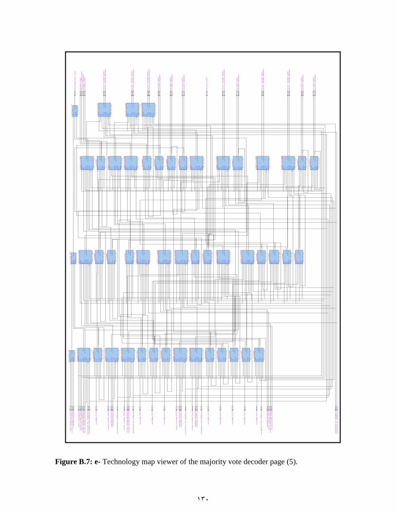
130
!A
CLR
CIN
CLK
DA
TA
A
DA
TA
B
DA
TA
C
EN
A
SLO
AD
CO
UT
RE
GO
UT
LO
GIC
_C
ELL (
AA
AA
)
!A
CLR
CIN
CLK
DA
TA
A
DA
TA
B
DA
TA
C
EN
A
SLO
AD
CO
UT
RE
GO
UT
LO
GIC
_C
ELL (
AA
AA
)
!A
CLR
CIN
CLK
DA
TA
A
SC
LR
CO
UT
RE
GO
UT
LO
GIC
_C
ELL (
5A
5A
)
!A
CLR
CIN
CLK
DA
TA
A
SC
LR
CO
UT
RE
GO
UT
LO
GIC
_C
ELL (
5A
5A
)
!A
CLR
CIN
CLK
DA
TA
A
DA
TA
B
DA
TA
C
EN
A
SLO
AD
CO
UT
RE
GO
UT
LO
GIC
_C
ELL (
AA
AA
)
!A
CLR
CIN
CLK
DA
TA
A
SC
LR
CO
UT
RE
GO
UT
LO
GIC
_C
ELL (
5A
5A
)
!A
CLR
CIN
CLK
DA
TA
A
EN
A
SC
LR
CO
UT
RE
GO
UT
LO
GIC
_C
ELL (
5A
5A
)
!A
CLR
CIN
CLK
DA
TA
A
DA
TA
B
DA
TA
C
EN
A
SLO
AD
CO
UT
RE
GO
UT
LO
GIC
_C
ELL (
AA
AA
)
!A
CLR
CIN
CLK
DA
TA
A
DA
TA
B
DA
TA
C
EN
A
SLO
AD
CO
UT
RE
GO
UT
LO
GIC
_C
ELL (
AA
AA
)
!A
CLR
CIN
CLK
DA
TA
A
DA
TA
B
DA
TA
C
EN
A
SLO
AD
CO
UT
RE
GO
UT
LO
GIC
_C
ELL (
AA
AA
)
!A
CLR
CIN
CLK
DA
TA
A
SC
LR
CO
UT
RE
GO
UT
LO
GIC
_C
ELL (
A5A
5)
CIN
DA
TA
A
DA
TA
B
CO
UT
LO
GIC
_C
ELL (
FF
FF
)
!A
CLR
CIN
CLK
DA
TA
A
SC
LR
CO
UT
RE
GO
UT
LO
GIC
_C
ELL (
A5A
5)
!A
CLR
CIN
CLK
DA
TA
A
SC
LR
CO
UT
RE
GO
UT
LO
GIC
_C
ELL (
A5A
5)
!A
CLR
CIN
CLK
DA
TA
A
DA
TA
B
DA
TA
C
EN
A
SLO
AD
CO
UT
RE
GO
UT
LO
GIC
_C
ELL (
AA
AA
)
!A
CLR
CIN
CLK
DA
TA
A
SC
LR
CO
UT
RE
GO
UT
LO
GIC
_C
ELL (
A5A
5)
!A
CLR
CIN
CLK
DA
TA
A
SC
LR
CO
UT
RE
GO
UT
LO
GIC
_C
ELL (
A5A
5)
!A
CLR
CIN
CLK
DA
TA
A
DA
TA
B
DA
TA
C
EN
A
SLO
AD
CO
UT
RE
GO
UT
LO
GIC
_C
ELL (
AA
AA
)
!A
CLR
CIN
CLK
DA
TA
A
DA
TA
B
DA
TA
C
EN
A
SLO
AD
CO
UT
RE
GO
UT
LO
GIC
_C
ELL (
AA
AA
)
!A
CLR
CIN
CLK
DA
TA
A
SC
LR
CO
UT
RE
GO
UT
LO
GIC
_C
ELL (
A5A
5)
!A
CLR
CIN
CLK
DA
TA
A
SC
LR
CO
UT
RE
GO
UT
LO
GIC
_C
ELL (
A5A
5)
!A
CLR
CIN
CLK
DA
TA
A
DA
TA
B
DA
TA
C
EN
A
SLO
AD
CO
UT
RE
GO
UT
LO
GIC
_C
ELL (
AA
AA
)
!A
CLR
CIN
CLK
DA
TA
A
SC
LR
CO
UT
RE
GO
UT
LO
GIC
_C
ELL (
A5A
5)
!A
CLR
CIN
CLK
DA
TA
A
EN
A
SC
LR
CO
UT
RE
GO
UT
LO
GIC
_C
ELL (
A5A
5)
!A
CLR
CIN
CLK
DA
TA
A
DA
TA
B
DA
TA
C
EN
A
SLO
AD
CO
UT
RE
GO
UT
LO
GIC
_C
ELL (
AA
AA
)
!A
CLR
CIN
CLK
DA
TA
A
DA
TA
B
DA
TA
C
EN
A
SLO
AD
CO
UT
RE
GO
UT
LO
GIC
_C
ELL (
AA
AA
)
!A
CLR
CIN
CLK
DA
TA
A
DA
TA
B
DA
TA
C
EN
A
SLO
AD
CO
UT
RE
GO
UT
LO
GIC
_C
ELL (
AA
AA
)
!A
CLR
CIN
CLK
DA
TA
A
SC
LR
CO
UT
RE
GO
UT
LO
GIC
_C
ELL (
5A
5A
)
CIN
DA
TA
A
DA
TA
B
CO
UT
LO
GIC
_C
ELL (
FF
FF
)
!A
CLR
CIN
CLK
DA
TA
A
SC
LR
CO
UT
RE
GO
UT
LO
GIC
_C
ELL (
5A
5A
)
!A
CLR
CIN
CLK
DA
TA
A
SC
LR
CO
UT
RE
GO
UT
LO
GIC
_C
ELL (
5A
5A
)
!A
CLR
CIN
CLK
DA
TA
A
DA
TA
B
DA
TA
C
EN
A
SLO
AD
CO
UT
RE
GO
UT
LO
GIC
_C
ELL (
AA
AA
)
!A
CLR
CIN
CLK
DA
TA
A
SC
LR
CO
UT
RE
GO
UT
LO
GIC
_C
ELL (
5A
5A
)
!A
CLR
CIN
CLK
DA
TA
A
SC
LR
CO
UT
RE
GO
UT
LO
GIC
_C
ELL (
5A
5A
)
!A
CLR
CIN
CLK
DA
TA
A
DA
TA
B
DA
TA
C
EN
A
SLO
AD
CO
UT
RE
GO
UT
LO
GIC
_C
ELL (
AA
AA
)
!A
CLR
CIN
CLK
DA
TA
A
DA
TA
B
DA
TA
C
EN
A
SLO
AD
CO
UT
RE
GO
UT
LO
GIC
_C
ELL (
AA
AA
)
!A
CLR
CIN
CLK
DA
TA
A
SC
LR
CO
UT
RE
GO
UT
LO
GIC
_C
ELL (
5A
5A
)
!A
CLR
CIN
CLK
DA
TA
A
SC
LR
CO
UT
RE
GO
UT
LO
GIC
_C
ELL (
5A
5A
)
!A
CLR
CIN
CLK
DA
TA
A
DA
TA
B
DA
TA
C
EN
A
SLO
AD
CO
UT
RE
GO
UT
LO
GIC
_C
ELL (
AA
AA
)
!A
CLR
CIN
CLK
DA
TA
A
SC
LR
CO
UT
RE
GO
UT
LO
GIC
_C
ELL (
5A
5A
)
!A
CLR
CIN
CLK
DA
TA
A
EN
A
SC
LR
CO
UT
RE
GO
UT
LO
GIC
_C
ELL (
5A
5A
)
!A
CLR
CIN
CLK
DA
TA
A
DA
TA
B
DA
TA
C
EN
A
SLO
AD
CO
UT
RE
GO
UT
LO
GIC
_C
ELL (
AA
AA
)
!A
CLR
CIN
CLK
DA
TA
A
DA
TA
B
DA
TA
C
EN
A
SLO
AD
CO
UT
RE
GO
UT
LO
GIC
_C
ELL (
AA
AA
)
!A
CLR
CIN
CLK
DA
TA
A
DA
TA
B
DA
TA
C
EN
A
SLO
AD
CO
UT
RE
GO
UT
LO
GIC
_C
ELL (
AA
AA
)
!A
CLR
CIN
CLK
DA
TA
A
SC
LR
CO
UT
RE
GO
UT
LO
GIC
_C
ELL (
A5A
5)
CIN
DA
TA
A
DA
TA
B
CO
UT
LO
GIC
_C
ELL (
FF
FF
)
!A
CLR
CIN
CLK
DA
TA
A
SC
LR
CO
UT
RE
GO
UT
LO
GIC
_C
ELL (
A5A
5)
!A
CLR
CIN
CLK
DA
TA
A
SC
LR
CO
UT
RE
GO
UT
LO
GIC
_C
ELL (
A5A
5)
!A
CLR
CIN
CLK
DA
TA
A
DA
TA
B
DA
TA
C
EN
A
SLO
AD
CO
UT
RE
GO
UT
LO
GIC
_C
ELL (
AA
AA
)
!A
CLR
CIN
CLK
DA
TA
A
SC
LR
CO
UT
RE
GO
UT
LO
GIC
_C
ELL (
A5A
5)
re
se
t_n
_C
OM
BO
UT
clo
ck_
div
10
_C
OM
BO
UT
Le
ss
Th
an
0~
36
3_
CO
MB
OU
T
Le
ss
Th
an
3~
69
_C
OM
BO
UT
co
mp
2_
co
un
t[6
]_C
OU
T
co
mp
2_
co
un
t[6
]_R
EG
OU
T
Le
ss
Th
an
6~
69
_C
OM
BO
UT
co
mp
5_
co
un
t[5
]_C
OU
T
co
mp
5_
co
un
t[5
]_R
EG
OU
T
co
un
t3[7
]_C
OU
T
co
un
t3[7
]_R
EG
OU
T
co
un
t2[7
]_C
OU
T
co
un
t2[7
]_R
EG
OU
T
Le
ss
Th
an
2~
69
_C
OM
BO
UT
co
mp
1_
co
un
t[6
]_C
OU
T
co
mp
1_
co
un
t[6
]_R
EG
OU
T
co
un
t1[7
]_C
OU
T
co
un
t1[7
]_R
EG
OU
T
co
un
t0[1
1]~
11
98
_C
OM
BO
UT
co
un
t0[7
]_C
OU
T
co
un
t0[7
]_R
EG
OU
T
Le
ss
Th
an
1~
69
_C
OM
BO
UT
co
mp
0_
co
un
t[6
]_C
OU
T
co
mp
0_
co
un
t[6
]_R
EG
OU
T
Le
ss
Th
an
5~
69
_C
OM
BO
UT
co
mp
4_
co
un
t[5
]_C
OU
T
co
mp
4_
co
un
t[5
]_R
EG
OU
T
Le
ss
Th
an
7~
69
_C
OM
BO
UT
co
mp
6_
co
un
t[4
]_C
OU
T
co
mp
6_
co
un
t[4
]_R
EG
OU
T
co
un
t8[4
]_C
OU
T
co
un
t8[4
]_R
EG
OU
T
Le
ss
Th
an
8~
33
7_
CO
UT
co
un
t7[6
]_C
OU
T
co
un
t7[6
]_R
EG
OU
T
co
un
t6[6
]_C
OU
T
co
un
t6[6
]_R
EG
OU
T
Le
ss
Th
an
4~
69
_C
OM
BO
UT
co
mp
3_
co
un
t[5
]_C
OU
T
co
un
t5[6
]_C
OU
T
co
un
t4[6
]_C
OU
T
co
un
t4[4
]_C
OU
T
co
mp
2_
co
un
t[3
]_C
OU
T
co
un
t4[4
]_R
EG
OU
T
co
mp
5_
co
un
t[2
]_C
OU
T
co
mp
2_
co
un
t[3
]_R
EG
OU
T
co
un
t3[4
]_C
OU
T
co
un
t2[4
]_C
OU
T
co
mp
1_
co
un
t[3
]_C
OU
T
co
un
t3[4
]_R
EG
OU
T
co
un
t2[4
]_R
EG
OU
T
co
un
t1[4
]_C
OU
T
co
un
t0[4
]_C
OU
T
co
mp
0_
co
un
t[3
]_C
OU
T
co
un
t1[4
]_R
EG
OU
T
co
un
t0[4
]_R
EG
OU
T
co
mp
4_
co
un
t[2
]_C
OU
T
co
mp
1_
co
un
t[3
]_R
EG
OU
T
co
mp
0_
co
un
t[3
]_R
EG
OU
T
co
mp
6_
co
un
t[1
]_C
OU
T
co
mp
5_
co
un
t[2
]_R
EG
OU
T
co
mp
4_
co
un
t[2
]_R
EG
OU
T
co
un
t8[1
]_C
OU
T
Le
ss
Th
an
8~
35
2_
CO
UT
co
mp
6_
co
un
t[1
]_R
EG
OU
T
co
un
t8[1
]_R
EG
OU
T
co
un
t7[3
]_C
OU
T
co
un
t6[3
]_C
OU
T
co
mp
3_
co
un
t[2
]_C
OU
T
co
un
t7[3
]_R
EG
OU
T
co
un
t6[3
]_R
EG
OU
T
co
un
t5[3
]_C
OU
T
co
mp
2_
co
un
t[6
]
co
mp
5_
co
un
t[5
]
co
un
t3[7
]
co
un
t2[7
]
co
mp
1_
co
un
t[6
]
co
un
t1[7
]
co
un
t0[7
]
co
mp
0_
co
un
t[6
]
co
mp
4_
co
un
t[5
]
co
mp
6_
co
un
t[4
]
co
un
t8[4
]
Le
ss
Th
an
8~
33
7
co
un
t7[6
]
co
un
t6[6
]
co
mp
3_
co
un
t[5
]
co
un
t5[6
]
co
un
t4[6
]
co
mp
2_
co
un
t[5
]
co
mp
5_
co
un
t[4
]
co
un
t3[6
]
co
un
t2[6
]
co
mp
1_
co
un
t[5
]
co
un
t1[6
]
co
un
t0[6
]
co
mp
0_
co
un
t[5
]
co
mp
4_
co
un
t[4
]
co
mp
6_
co
un
t[3
]
co
un
t8[3
]
Le
ss
Th
an
8~
34
2
co
un
t7[5
]
co
un
t6[5
]
co
mp
3_
co
un
t[4
]
co
un
t5[5
]
co
un
t4[5
]
co
mp
2_
co
un
t[4
]
co
mp
5_
co
un
t[3
]
co
un
t3[5
]
co
un
t2[5
]
co
mp
1_
co
un
t[4
]
co
un
t1[5
]
co
un
t0[5
]
co
mp
0_
co
un
t[4
]
co
mp
4_
co
un
t[3
]
co
mp
6_
co
un
t[2
]
co
un
t8[2
]
Le
ss
Th
an
8~
34
7
co
un
t7[4
]
co
un
t6[4
]
co
mp
3_
co
un
t[3
]
co
un
t5[4
]
Figure B.7: e- Technology map viewer of the majority vote decoder page (5).
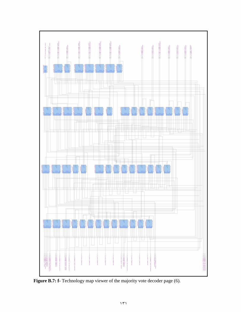
131
!A
CLR
CIN
CLK
DA
TA
A
SC
LR
CO
UT
RE
GO
UT
LO
GIC
_C
ELL (
A5A
5)
!A
CLR
CIN
CLK
DA
TA
A
DA
TA
B
DA
TA
C
EN
A
SLO
AD
CO
UT
RE
GO
UT
LO
GIC
_C
ELL (
AA
AA
)
!A
CLR
CIN
CLK
DA
TA
A
DA
TA
B
DA
TA
C
EN
A
SLO
AD
CO
UT
RE
GO
UT
LO
GIC
_C
ELL (
AA
AA
)
!A
CLR
CIN
CLK
DA
TA
A
SC
LR
CO
UT
RE
GO
UT
LO
GIC
_C
ELL (
A5A
5)
!A
CLR
CIN
CLK
DA
TA
A
SC
LR
CO
UT
RE
GO
UT
LO
GIC
_C
ELL (
A5A
5)
!A
CLR
CIN
CLK
DA
TA
A
DA
TA
B
DA
TA
C
EN
A
SLO
AD
CO
UT
RE
GO
UT
LO
GIC
_C
ELL (
AA
AA
)
!A
CLR
CIN
CLK
DA
TA
A
SC
LR
CO
UT
RE
GO
UT
LO
GIC
_C
ELL (
A5A
5)
!A
CLR
CIN
CLK
DA
TA
A
EN
A
SC
LR
CO
UT
RE
GO
UT
LO
GIC
_C
ELL (
A5A
5)
!A
CLR
CIN
CLK
DA
TA
A
DA
TA
B
DA
TA
C
EN
A
SLO
AD
CO
UT
RE
GO
UT
LO
GIC
_C
ELL (
AA
AA
)
!A
CLR
CIN
CLK
DA
TA
A
DA
TA
B
DA
TA
C
EN
A
SLO
AD
CO
UT
RE
GO
UT
LO
GIC
_C
ELL (
AA
AA
)
!A
CLR
CIN
CLK
DA
TA
A
DA
TA
B
DA
TA
C
EN
A
SLO
AD
CO
UT
RE
GO
UT
LO
GIC
_C
ELL (
AA
AA
)
!A
CLR
CIN
CLK
DA
TA
A
SC
LR
CO
UT
RE
GO
UT
LO
GIC
_C
ELL (
5A
5A
)
DA
TA
A
DA
TA
BC
OU
T
LO
GIC
_C
ELL (
FF
FF
)
!A
CLR
CIN
CLK
DA
TA
A
SC
LR
CO
UT
RE
GO
UT
LO
GIC
_C
ELL (
5A
5A
)
!A
CLR
CIN
CLK
DA
TA
A
SC
LR
CO
UT
RE
GO
UT
LO
GIC
_C
ELL (
5A
5A
)
!A
CLR
CIN
CLK
DA
TA
A
DA
TA
B
DA
TA
C
EN
A
SLO
AD
CO
UT
RE
GO
UT
LO
GIC
_C
ELL (
AA
AA
)
!A
CLR
CIN
CLK
DA
TA
A
SC
LR
CO
UT
RE
GO
UT
LO
GIC
_C
ELL (
5A
5A
)
!A
CLR
CIN
CLK
DA
TA
A
SC
LR
CO
UT
RE
GO
UT
LO
GIC
_C
ELL (
5A
5A
)
!A
CLR
CIN
CLK
DA
TA
A
DA
TA
B
DA
TA
C
EN
A
SLO
AD
CO
UT
RE
GO
UT
LO
GIC
_C
ELL (
AA
AA
)
!A
CLR
CIN
CLK
DA
TA
A
DA
TA
B
DA
TA
C
EN
A
SLO
AD
CO
UT
RE
GO
UT
LO
GIC
_C
ELL (
AA
AA
)
!A
CLR
CIN
CLK
DA
TA
A
SC
LR
CO
UT
RE
GO
UT
LO
GIC
_C
ELL (
5A
5A
)
!A
CLR
CIN
CLK
DA
TA
A
SC
LR
CO
UT
RE
GO
UT
LO
GIC
_C
ELL (
5A
5A
)
!A
CLR
CIN
CLK
DA
TA
A
DA
TA
B
DA
TA
C
EN
A
SLO
AD
CO
UT
RE
GO
UT
LO
GIC
_C
ELL (
AA
AA
)
!A
CLR
CIN
CLK
DA
TA
A
SC
LR
CO
UT
RE
GO
UT
LO
GIC
_C
ELL (
5A
5A
)
!A
CLR
CIN
CLK
DA
TA
A
EN
A
SC
LR
CO
UT
RE
GO
UT
LO
GIC
_C
ELL (
5A
5A
)
!A
CLR
CIN
CLK
DA
TA
A
DA
TA
B
DA
TA
C
EN
A
SLO
AD
CO
UT
RE
GO
UT
LO
GIC
_C
ELL (
AA
AA
)
!A
CLR
CIN
CLK
DA
TA
A
DA
TA
B
DA
TA
C
EN
A
SLO
AD
CO
UT
RE
GO
UT
LO
GIC
_C
ELL (
AA
AA
)
!A
CLR
CLK
DA
TA
A
DA
TA
B
DA
TA
C
EN
A
SLO
AD
CO
UT
RE
GO
UT
LO
GIC
_C
ELL (
AA
AA
)
!A
CLR
CLK
DA
TA
A
DA
TA
B
SC
LR
CO
UT
RE
GO
UT
LO
GIC
_C
ELL (
6666)
!A
CLR
CIN
CLK
DA
TA
A
SC
LR
CO
UT
RE
GO
UT
LO
GIC
_C
ELL (
A5A
5)
!A
CLR
CIN
CLK
DA
TA
A
SC
LR
CO
UT
RE
GO
UT
LO
GIC
_C
ELL (
A5A
5)
!A
CLR
CIN
CLK
DA
TA
A
DA
TA
B
DA
TA
C
EN
A
SLO
AD
CO
UT
RE
GO
UT
LO
GIC
_C
ELL (
AA
AA
)
!A
CLR
CIN
CLK
DA
TA
A
SC
LR
CO
UT
RE
GO
UT
LO
GIC
_C
ELL (
A5A
5)
!A
CLR
CIN
CLK
DA
TA
A
SC
LR
CO
UT
RE
GO
UT
LO
GIC
_C
ELL (
A5A
5)
!A
CLR
CIN
CLK
DA
TA
A
DA
TA
B
DA
TA
C
EN
A
SLO
AD
CO
UT
RE
GO
UT
LO
GIC
_C
ELL (
AA
AA
)
!A
CLR
CLK
DA
TA
A
DA
TA
B
DA
TA
C
EN
A
SLO
AD
CO
UT
RE
GO
UT
LO
GIC
_C
ELL (
AA
AA
)
!A
CLR
CIN
CLK
DA
TA
A
SC
LR
CO
UT
RE
GO
UT
LO
GIC
_C
ELL (
A5A
5)
!A
CLR
CIN
CLK
DA
TA
A
SC
LR
CO
UT
RE
GO
UT
LO
GIC
_C
ELL (
A5A
5)
!A
CLR
CIN
CLK
DA
TA
A
DA
TA
B
DA
TA
C
EN
A
SLO
AD
CO
UT
RE
GO
UT
LO
GIC
_C
ELL (
AA
AA
)
!A
CLR
CIN
CLK
DA
TA
A
SC
LR
CO
UT
RE
GO
UT
LO
GIC
_C
ELL (
A5A
5)
!A
CLR
CIN
CLK
DA
TA
A
EN
A
SC
LR
CO
UT
RE
GO
UT
LO
GIC
_C
ELL (
A5A
5)
!A
CLR
CIN
CLK
DA
TA
A
DA
TA
B
DA
TA
C
EN
A
SLO
AD
CO
UT
RE
GO
UT
LO
GIC
_C
ELL (
AA
AA
)
!A
CLR
CLK
DA
TA
A
DA
TA
B
DA
TA
C
EN
A
SLO
AD
CO
UT
RE
GO
UT
LO
GIC
_C
ELL (
AA
AA
)
!A
CLR
CIN
CLK
DA
TA
A
SC
LR
CO
UT
RE
GO
UT
LO
GIC
_C
ELL (
5A
5A
)
!A
CLR
CIN
CLK
DA
TA
A
SC
LR
CO
UT
RE
GO
UT
LO
GIC
_C
ELL (
5A
5A
)
!A
CLR
CLK
DA
TA
A
DA
TA
B
DA
TA
C
EN
A
SLO
AD
CO
UT
RE
GO
UT
LO
GIC
_C
ELL (
AA
AA
)
!A
CLR
CIN
CLK
DA
TA
A
SC
LR
CO
UT
RE
GO
UT
LO
GIC
_C
ELL (
5A
5A
)
!A
CLR
CIN
CLK
DA
TA
A
SC
LR
CO
UT
RE
GO
UT
LO
GIC
_C
ELL (
5A
5A
)
!A
CLR
CLK
DA
TA
A
DA
TA
B
DA
TA
C
EN
A
SLO
AD
CO
UT
RE
GO
UT
LO
GIC
_C
ELL (
AA
AA
)
!A
CLR
CIN
CLK
DA
TA
A
SC
LR
CO
UT
RE
GO
UT
LO
GIC
_C
ELL (
5A
5A
)
re
se
t_n
_C
OM
BO
UT
clo
ck_
div
10
_C
OM
BO
UT
Le
ss
Th
an
0~
36
3_
CO
MB
OU
T
co
un
t4[4
]_C
OU
T
co
un
t4[4
]_R
EG
OU
T
Le
ss
Th
an
3~
69
_C
OM
BO
UT
co
mp
2_
co
un
t[3
]_C
OU
T
co
mp
2_
co
un
t[3
]_R
EG
OU
T
Le
ss
Th
an
6~
69
_C
OM
BO
UT
co
mp
5_
co
un
t[2
]_C
OU
T
co
mp
5_
co
un
t[2
]_R
EG
OU
T
co
un
t3[4
]_C
OU
T
co
un
t3[4
]_R
EG
OU
T
co
un
t2[4
]_C
OU
T
co
un
t2[4
]_R
EG
OU
T
Le
ss
Th
an
2~
69
_C
OM
BO
UT
co
mp
1_
co
un
t[3
]_C
OU
T
co
mp
1_
co
un
t[3
]_R
EG
OU
T
co
un
t1[4
]_C
OU
T
co
un
t1[4
]_R
EG
OU
T
co
un
t0[1
1]~
11
98
_C
OM
BO
UT
co
un
t0[4
]_C
OU
T
co
un
t0[4
]_R
EG
OU
T
Le
ss
Th
an
1~
69
_C
OM
BO
UT
co
mp
0_
co
un
t[3
]_C
OU
T
co
mp
0_
co
un
t[3
]_R
EG
OU
T
Le
ss
Th
an
5~
69
_C
OM
BO
UT
co
mp
4_
co
un
t[2
]_C
OU
T
co
mp
4_
co
un
t[2
]_R
EG
OU
T
Le
ss
Th
an
7~
69
_C
OM
BO
UT
co
mp
6_
co
un
t[1
]_C
OU
T
co
mp
6_
co
un
t[1
]_R
EG
OU
T
co
un
t8[1
]_C
OU
T
co
un
t8[1
]_R
EG
OU
T
Le
ss
Th
an
8~
35
2_
CO
UT
co
un
t7[3
]_C
OU
T
co
un
t7[3
]_R
EG
OU
T
co
un
t6[3
]_C
OU
T
co
un
t6[3
]_R
EG
OU
T
Le
ss
Th
an
4~
69
_C
OM
BO
UT
co
mp
3_
co
un
t[2
]_C
OU
T
co
un
t5[3
]_C
OU
T
De
co
de
r0
~9
35
_C
OM
BO
UT
co
un
t2[1
]_C
OU
T
co
mp
1_
co
un
t[0
]_C
OU
T
co
un
t2[1
]_R
EG
OU
T
co
un
t1[1
]_C
OU
T
co
un
t0[1
]_C
OU
T
co
mp
0_
co
un
t[0
]_C
OU
T
co
un
t1[1
]_R
EG
OU
T
co
un
t0[1
]_R
EG
OU
T
co
mp
1_
co
un
t[0
]_R
EG
OU
T
co
mp
0_
co
un
t[0
]_R
EG
OU
T
co
un
t7[0
]_C
OU
T
co
un
t6[0
]_C
OU
T
co
un
t7[0
]_R
EG
OU
T
co
un
t6[0
]_R
EG
OU
T
co
un
t5[0
]_C
OU
T
co
un
t4[0
]_C
OU
T
co
un
t5[0
]_R
EG
OU
T
co
un
t4[0
]_R
EG
OU
T
co
un
t3[0
]_C
OU
T
co
un
t4[4
]
co
mp
2_
co
un
t[3
]
co
mp
5_
co
un
t[2
]
co
un
t3[4
]
co
un
t2[4
]
co
mp
1_
co
un
t[3
]
co
un
t1[4
]
co
un
t0[4
]
co
mp
0_
co
un
t[3
]
co
mp
4_
co
un
t[2
]
co
mp
6_
co
un
t[1
]
co
un
t8[1
]
Le
ss
Th
an
8~
35
2
co
un
t7[3
]
co
un
t6[3
]
co
mp
3_
co
un
t[2
]
co
un
t5[3
]
co
un
t4[3
]
co
mp
2_
co
un
t[2
]
co
mp
5_
co
un
t[1
]
co
un
t3[3
]
co
un
t2[3
]
co
mp
1_
co
un
t[2
]
co
un
t1[3
]
co
un
t0[3
]
co
mp
0_
co
un
t[2
]
co
mp
4_
co
un
t[1
]
co
mp
6_
co
un
t[0
]
co
un
t8[0
]
co
un
t7[2
]
co
un
t6[2
]
co
mp
3_
co
un
t[1
]
co
un
t5[2
]
co
un
t4[2
]
co
mp
2_
co
un
t[1
]
co
mp
5_
co
un
t[0
]
co
un
t3[2
]
co
un
t2[2
]
co
mp
1_
co
un
t[1
]
co
un
t1[2
]
co
un
t0[2
]
co
mp
0_
co
un
t[1
]
co
mp
4_
co
un
t[0
]
co
un
t7[1
]
co
un
t6[1
]
co
mp
3_
co
un
t[0
]
co
un
t5[1
]
co
un
t4[1
]
co
mp
2_
co
un
t[0
]
co
un
t3[1
]
Figure B.7: f- Technology map viewer of the majority vote decoder page (6).
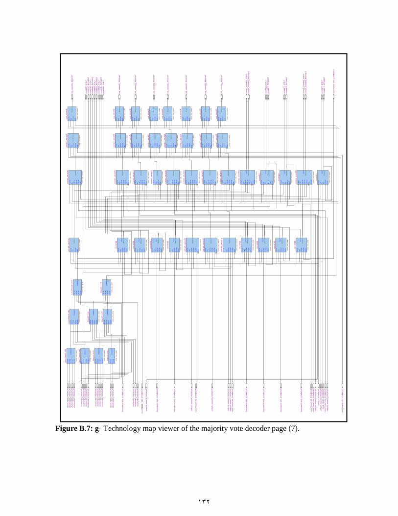
132
!AC
LR
CIN
CLK
DA
TA
A
SC
LR
CO
UT
RE
GO
UT
LO
GIC
_C
ELL (
5A
5A
)
!AC
LR
CLK
DA
TA
A
DA
TA
B
DA
TA
C
EN
A
SLO
AD
CO
UT
RE
GO
UT
LO
GIC
_C
ELL (
AA
AA
)
!AC
LR
CIN
CLK
DA
TA
A
SC
LR
CO
UT
RE
GO
UT
LO
GIC
_C
ELL (
5A
5A
)
!AC
LR
CIN
CLK
DA
TA
A
EN
A
SC
LR
CO
UT
RE
GO
UT
LO
GIC
_C
ELL (
5A
5A
)
!AC
LR
CLK
DA
TA
A
DA
TA
B
DA
TA
C
EN
A
SLO
AD
CO
UT
RE
GO
UT
LO
GIC
_C
ELL (
AA
AA
)
!AC
LR
CLK
DA
TA
A
DA
TA
B
SC
LR
CO
UT
RE
GO
UT
LO
GIC
_C
ELL (
6666)
!AC
LR
CLK
DA
TA
A
DA
TA
B
SC
LR
CO
UT
RE
GO
UT
LO
GIC
_C
ELL (
6666)
!AC
LR
CLK
DA
TA
A
DA
TA
B
SC
LR
CO
UT
RE
GO
UT
LO
GIC
_C
ELL (
6666)
!AC
LR
CLK
DA
TA
A
DA
TA
B
SC
LR
CO
UT
RE
GO
UT
LO
GIC
_C
ELL (
6666)
!AC
LR
CLK
DA
TA
A
DA
TA
B
SC
LR
CO
UT
RE
GO
UT
LO
GIC
_C
ELL (
6666)
!AC
LR
CLK
DA
TA
A
DA
TA
B
SC
LR
CO
UT
RE
GO
UT
LO
GIC
_C
ELL (
6666)
!AC
LR
CLK
DA
TA
A
DA
TA
B
SC
LR
CO
UT
RE
GO
UT
LO
GIC
_C
ELL (
6666)
!AC
LR
CLK
DA
TA
A
EN
A
SC
LR
CO
UT
RE
GO
UT
LO
GIC
_C
ELL (
5555)
!AC
LR
CLK
DA
TA
A
EN
A
RE
GO
UT
LO
GIC
_C
ELL (
AA
AA
)
!AC
LR
CLK
DA
TA
A
EN
A
RE
GO
UT
LO
GIC
_C
ELL (
AA
AA
)
!AC
LR
CLK
DA
TA
A
EN
A
RE
GO
UT
LO
GIC
_C
ELL (
AA
AA
)
!AC
LR
CLK
DA
TA
A
EN
A
RE
GO
UT
LO
GIC
_C
ELL (
AA
AA
)
!AC
LR
CLK
DA
TA
A
EN
A
RE
GO
UT
LO
GIC
_C
ELL (
AA
AA
)
!AC
LR
CLK
DA
TA
A
EN
A
RE
GO
UT
LO
GIC
_C
ELL (
AA
AA
)
!AC
LR
CLK
DA
TA
A
EN
A
RE
GO
UT
LO
GIC
_C
ELL (
AA
AA
)
!AC
LR
CLK
DA
TA
A
EN
A
RE
GO
UT
LO
GIC
_C
ELL (
AA
AA
)
!AC
LR
CLK
DA
TA
A
DA
TA
B
EN
A
RE
GO
UT
LO
GIC
_C
ELL (
EE
EE
)
DA
TA
A
DA
TA
B
DA
TA
C
DA
TA
D
CO
MB
OU
T
LO
GIC
_C
ELL (
0001)
DA
TA
A
DA
TA
B
DA
TA
C
DA
TA
D
CO
MB
OU
T
LO
GIC
_C
ELL (
0002)
DA
TA
A
DA
TA
B
DA
TA
C
DA
TA
D
CO
MB
OU
T
LO
GIC
_C
ELL (
8000)
DA
TA
A
DA
TA
BC
OM
BO
UT
LO
GIC
_C
ELL (
8888)
DA
TA
A
DA
TA
B
DA
TA
C
DA
TA
D
CO
MB
OU
T
LO
GIC
_C
ELL (
8000)
DA
TA
A
DA
TA
B
DA
TA
C
DA
TA
D
CO
MB
OU
T
LO
GIC
_C
ELL (
0080)
!AC
LR
CLK
DA
TA
A
DA
TA
B
EN
A
RE
GO
UT
LO
GIC
_C
ELL (
EE
EE
)
!AC
LR
CLK
DA
TA
A
DA
TA
B
EN
A
RE
GO
UT
LO
GIC
_C
ELL (
EE
EE
)
!AC
LR
CLK
DA
TA
A
DA
TA
B
EN
A
RE
GO
UT
LO
GIC
_C
ELL (
EE
EE
)
!AC
LR
CLK
DA
TA
A
DA
TA
D
EN
A
RE
GO
UT
LO
GIC
_C
ELL (
00A
A)
!AC
LR
CLK
DA
TA
A
DA
TA
B
EN
A
RE
GO
UT
LO
GIC
_C
ELL (
EE
EE
)
!AC
LR
CLK
DA
TA
A
DA
TA
B
EN
A
RE
GO
UT
LO
GIC
_C
ELL (
EE
EE
)
!AC
LR
CLK
DA
TA
A
DA
TA
B
EN
A
RE
GO
UT
LO
GIC
_C
ELL (
EE
EE
)
!AC
LR
CLK
DA
TA
A
DA
TA
B
DA
TA
D
EN
A
RE
GO
UT
LO
GIC
_C
ELL (
AA
CC
)
DA
TA
A
DA
TA
B
DA
TA
C
DA
TA
D
CO
MB
OU
T
LO
GIC
_C
ELL (
1F
FF
)
DA
TA
A
DA
TA
B
DA
TA
C
DA
TA
D
CO
MB
OU
T
LO
GIC
_C
ELL (
8F
FF
)
DA
TA
A
DA
TA
B
DA
TA
C
DA
TA
D
CO
MB
OU
T
LO
GIC
_C
ELL (
5111)
!AC
LR
CLK
DA
TA
A
DA
TA
B
DA
TA
D
EN
A
RE
GO
UT
LO
GIC
_C
ELL (
AA
CC
)
!AC
LR
CLK
DA
TA
A
DA
TA
B
DA
TA
D
EN
A
RE
GO
UT
LO
GIC
_C
ELL (
AA
CC
)
!AC
LR
CLK
DA
TA
A
DA
TA
B
DA
TA
D
EN
A
RE
GO
UT
LO
GIC
_C
ELL (
AA
CC
)
!AC
LR
CLK
DA
TA
A
EN
A
RE
GO
UT
LO
GIC
_C
ELL (
AA
AA
)
!AC
LR
CLK
DA
TA
A
DA
TA
B
DA
TA
D
EN
A
RE
GO
UT
LO
GIC
_C
ELL (
AA
CC
)
!AC
LR
CLK
DA
TA
A
DA
TA
B
DA
TA
D
EN
A
RE
GO
UT
LO
GIC
_C
ELL (
AA
CC
)
!AC
LR
CLK
DA
TA
A
DA
TA
B
DA
TA
D
EN
A
RE
GO
UT
LO
GIC
_C
ELL (
AA
CC
)
!AC
LR
CLK
DA
TA
A
DA
TA
B
DA
TA
D
EN
A
RE
GO
UT
LO
GIC
_C
ELL (
AA
CC
)
!AC
LR
CLK
DA
TA
A
EN
A
RE
GO
UT
LO
GIC
_C
ELL (
AA
AA
)
!AC
LR
CLK
DA
TA
A
DA
TA
B
DA
TA
D
EN
A
RE
GO
UT
LO
GIC
_C
ELL (
AA
CC
)
!AC
LR
CLK
DA
TA
A
DA
TA
B
DA
TA
D
EN
A
RE
GO
UT
LO
GIC
_C
ELL (
AA
CC
)
res
et_
n_
CO
MB
OU
T
clo
ck_
div
10
_C
OM
BO
UT
co
un
t2[1
]_C
OU
T
co
un
t2[1
]_R
EG
OU
T
Le
ss
Th
an
2~
69
_C
OM
BO
UT
co
mp
1_
co
un
t[0
]_C
OU
T
co
mp
1_
co
un
t[0
]_R
EG
OU
T
co
un
t1[1
]_C
OU
T
co
un
t1[1
]_R
EG
OU
T
co
un
t0[1
1]~
11
98
_C
OM
BO
UT
co
un
t0[1
]_C
OU
T
co
un
t0[1
]_R
EG
OU
T
Le
ss
Th
an
1~
69
_C
OM
BO
UT
co
mp
0_
co
un
t[0
]_C
OU
T
co
mp
0_
co
un
t[0
]_R
EG
OU
T
De
co
de
r0~
93
7_
CO
MB
OU
T
co
un
t7[0
]_C
OU
T
co
un
t7[0
]_R
EG
OU
T
De
co
de
r0~
93
8_
CO
MB
OU
T
co
un
t6[0
]_C
OU
T
co
un
t6[0
]_R
EG
OU
T
De
co
de
r0~
93
9_
CO
MB
OU
T
co
un
t5[0
]_C
OU
T
co
un
t5[0
]_R
EG
OU
T
De
co
de
r0~
94
1_
CO
MB
OU
T
co
un
t4[0
]_C
OU
T
co
un
t4[0
]_R
EG
OU
T
De
co
de
r0~
94
3_
CO
MB
OU
T
co
un
t3[0
]_C
OU
T
De
co
de
r0~
94
4_
CO
MB
OU
T
De
co
de
r0~
94
5_
CO
MB
OU
T
ou
t_va
lue
[0]_
RE
GO
UT
ou
t_va
lue
[2]_
RE
GO
UT
ou
t_va
lue
[4]_
RE
GO
UT
ou
t_va
lue
[6]_
RE
GO
UT
ou
t_va
lue
[7]_
RE
GO
UT
ou
t_va
lue
[1]_
RE
GO
UT
ou
t_va
lue
[5]_
RE
GO
UT
ou
t_va
lue
[3]_
RE
GO
UT
Le
ss
Th
an
8~
27
0_
CO
MB
OU
T
clo
ckcn
t[1
1]_
RE
GO
UT
clo
ckcn
t[1
2]_
RE
GO
UT
clo
ckcn
t[1
3]_
RE
GO
UT
clo
ckcn
t[1
4]_
RE
GO
UT
clo
ckcn
t[5
]_R
EG
OU
T
clo
ckcn
t[6
]_R
EG
OU
T
clo
ckcn
t[8
]_R
EG
OU
T
clo
ckcn
t[1
]_R
EG
OU
T
clo
ckcn
t[2
]_R
EG
OU
T
clo
ckcn
t[3
]_R
EG
OU
T
clo
ckcn
t[4
]_R
EG
OU
T
clo
ckcn
t[1
5]_
RE
GO
UT
clo
ckcn
t[1
6]_
RE
GO
UT
clo
ckcn
t[9
]_R
EG
OU
T
clo
ckcn
t[1
0]_
RE
GO
UT
clo
ckcn
t[7
]_R
EG
OU
T
clo
ckcn
t[0
]_R
EG
OU
T
Le
ss
Th
an
7~
69
_C
OM
BO
UT
Le
ss
Th
an
0~
36
3_
CO
MB
OU
T
co
mp
5_
va
lue
[6]_
RE
GO
UT
co
mp
4_
va
lue
[1]_
RE
GO
UT
co
mp
5_
va
lue
[5]_
RE
GO
UT
co
mp
5_
va
lue
[3]_
RE
GO
UT
co
mp
0_
va
lue
[0]_
RE
GO
UT
co
mp
0_
va
lue
[7]_
RE
GO
UT
Le
ss
Th
an
5~
69
_C
OM
BO
UT
co
mp
1_
va
lue
[2]_
RE
GO
UT
co
mp
2_
va
lue
[4]_
RE
GO
UT
Le
ss
Th
an
6~
69
_C
OM
BO
UT
co
un
t2[1
]
co
mp
1_
co
un
t[0
]
co
un
t1[1
]
co
un
t0[1
]
co
mp
0_
co
un
t[0
]
co
un
t7[0
]
co
un
t6[0
]
co
un
t5[0
]
co
un
t4[0
]
co
un
t3[0
]
co
un
t2[0
]
co
un
t1[0
]
co
un
t0[0
]
ou
t_va
lue
[0]
ou
t_va
lue
[2]
ou
t_va
lue
[4]
ou
t_va
lue
[6]
ou
t_va
lue
[7]
ou
t_va
lue
[1]
ou
t_va
lue
[5]
ou
t_va
lue
[3]
co
mp
7_
va
lue
[0]
Le
ss
Th
an
0~
36
0
Eq
ua
l0~
14
4
Eq
ua
l0~
14
5
Eq
ua
l0~
14
6
Eq
ua
l0~
14
7E
qu
al0
~1
48
co
mp
7_
va
lue
[2]
co
mp
7_
va
lue
[4]
co
mp
7_
va
lue
[6]
co
mp
7_
va
lue
[7]
co
mp
7_
va
lue
[1]
co
mp
7_
va
lue
[5]
co
mp
7_
va
lue
[3]
co
mp
6_
va
lue
[0]
Le
ss
Th
an
0~
36
1
Le
ss
Th
an
0~
36
3
co
mp
6_
va
lue
[2]
co
mp
6_
va
lue
[4]
co
mp
6_
va
lue
[6]
co
mp
6_
va
lue
[7]
co
mp
6_
va
lue
[1]
co
mp
6_
va
lue
[5]
co
mp
6_
va
lue
[3]
co
mp
4_
va
lue
[0]
co
mp
4_
va
lue
[7]
co
mp
4_
va
lue
[2]
co
mp
5_
va
lue
[4]
Le
ss
Th
an
0~
36
2
Figure B.7: g- Technology map viewer of the majority vote decoder page (7).

133
!ACLR
CLK
DATAA
DATAB
DATAD
ENA
REGOUT
LOGIC_CELL (AACC)
!ACLR
CLK
DATAA
DATAB
DATAD
ENA
REGOUT
LOGIC_CELL (AACC)
!ACLR
CLK
DATAA
DATAB
DATAD
ENA
REGOUT
LOGIC_CELL (AACC)
!ACLR
CLK
DATAA
DATAB
DATAD
ENA
REGOUT
LOGIC_CELL (AACC)
!ACLR
CLK
DATAA
ENA
REGOUT
LOGIC_CELL (AAAA)
!ACLR
CLK
ENA
REGOUT
LOGIC_CELL (FFFF)
!ACLR
CLK
DATAA
ENA
REGOUT
LOGIC_CELL (AAAA)
!ACLR
CLK
DATAA
ENA
REGOUT
LOGIC_CELL (AAAA)
!ACLR
CLK
DATAA
ENA
REGOUT
LOGIC_CELL (AAAA)
!ACLR
CLK
DATAA
ENA
REGOUT
LOGIC_CELL (5555)
!ACLR
CLK
DATAA
ENA
REGOUT
LOGIC_CELL (5555)
!ACLR
CLK
DATAA
ENA
REGOUT
LOGIC_CELL (5555)
DATAA
DATABCOMBOUT
LOGIC_CELL (8888)
DATAA
DATAB
DATAC
DATAD
COMBOUT
LOGIC_CELL (6880)
DATAA
DATAB
DATAC
DATAD
COMBOUT
LOGIC_CELL (8000)
DATAA
DATAB
DATAC
DATAD
COMBOUT
LOGIC_CELL (6880)
DATAA
DATAB
DATAC
DATAD
COMBOUT
LOGIC_CELL (8000)
DATAA
DATAB
DATAC
DATAD
COMBOUT
LOGIC_CELL (ABBB)
DATAA
DATABCOMBOUT
LOGIC_CELL (8888)
DATAA
DATAB
DATAC
DATAD
COMBOUT
LOGIC_CELL (0080)
DATAA
DATAB
DATAC
COMBOUT
LOGIC_CELL (8080)
DATAA
DATAB
DATAD
COMBOUT
LOGIC_CELL (0088)
DATAA
DATAB
DATAC
DATAD
COMBOUT
LOGIC_CELL (0080)
DATAA
DATAB
DATAC
DATAD
COMBOUT
LOGIC_CELL (0080)
DATAA
DATAB
DATAC
COMBOUT
LOGIC_CELL (8080)
DATAA
DATAB
DATAC
DATAD
COMBOUT
LOGIC_CELL (0080)
DATAA
DATAB
DATAC
DATAD
COMBOUT
LOGIC_CELL (8000)
DATAA
DATAB
DATAD
COMBOUT
LOGIC_CELL (0088)
DATAA
DATAB
DATAD
COMBOUT
LOGIC_CELL (0088)
DATAA
DATAB
DATAC
DATAD
COMBOUT
LOGIC_CELL (0080)
reset_n_COMBOUT
clock_div10_COMBOUT
LessThan6~69_COMBOUT
LessThan0~363_COMBOUT
comp5_value[6]_REGOUT
LessThan5~69_COMBOUT
comp4_value[1]_REGOUT
comp5_value[5]_REGOUT
comp5_value[3]_REGOUT
LessThan1~69_COMBOUTcomp0_value[0]_REGOUT
comp0_value[7]_REGOUT
LessThan2~69_COMBOUTcomp1_value[2]_REGOUT
LessThan3~69_COMBOUTcomp2_value[4]_REGOUT
LessThan4~69_COMBOUT
q_out[7]_COMBOUT
q_out[6]_COMBOUT
q_out[0]_COMBOUT
q_out[1]_COMBOUT
q_out[2]_COMBOUT
q_out[3]_COMBOUT
q_out[5]_COMBOUT
q_out[4]_COMBOUT
count0[11]~1198_COMBOUT
Decoder0~935_COMBOUT
Decoder0~937_COMBOUT
Decoder0~938_COMBOUT
Decoder0~939_COMBOUT
Decoder0~941_COMBOUT
Decoder0~943_COMBOUT
Decoder0~944_COMBOUT
Decoder0~945_COMBOUT
out_value[0]_REGOUT
out_value[2]_REGOUT
out_value[4]_REGOUT
out_value[6]_REGOUT
out_value[1]_REGOUT
out_value[5]_REGOUT
out_value[3]_REGOUT
out_value[7]_REGOUT
comp5_value[6]
comp4_value[1]
comp5_value[5]
comp5_value[3]
comp0_value[0]
comp0_value[7]
comp1_value[2]
comp2_value[4]
comp3_value[6]
comp1_value[1]
comp3_value[5]
comp2_value[3]
count0[11]~1195
WideOr0~297
count0[11]~1196
count0[11]~1197
Decoder0~933
count0[11]~1198
Decoder0~934
Decoder0~935
Decoder0~937
Decoder0~938
Decoder0~939
Decoder0~940
Decoder0~941
Decoder0~942
Decoder0~943
Decoder0~944
Decoder0~945Decoder0~936
Figure B.7: h- Technology map viewer of the majority vote decoder page (8).

134
لتردد التبديلي بواسطة األنظمة المترابطةاكشف تعديل
ذات التميز الزمني باستخدام لغة
Verilog HDL
وفاء نظمي حسين الشرع إعـداد:
د. بسام األسير إشـــراف:
ملخــصال
فرضة صالةً م مةب ة والتة ال منة نظرية األنظمة المترابطةة اا التميية تدرس هذه الرسالة
ث صنها نظرية افتراضةية لدةدوح حةار رنةيب فة الاهةاب التمة لتميية تةردد ت ةرار , حي[2]ريس
الن ضا . ط ق هذه النظرية ف علة ارتمةار فة اسةتًم نةمعيب مةب ااةارا ارتمةار الر ميةة
ومتتددة الترددا تغيير وتتدي تماتر تغيير تردد اراارة