fsi adapter board user s guide - ti.com
TRANSCRIPT

1SWRU555–March 2020Submit Documentation Feedback
Copyright © 2020, Texas Instruments Incorporated
TMDSFSIADAPEVM FSI Adapter Board User’s Guide
User's GuideSWRU555–March 2020
TMDSFSIADAPEVM FSI Adapter Board User’s Guide
This document is provided with the FSI Adapter Board (TMDSFSIADAPEVM) customer evaluationmodule. This user's guide provides details on the setup and hardware implementation of the adapterboard.
NOTE: Follow the general ESD precautionary measures when operating this EVM.
Contents1 Introduction ................................................................................................................... 32 Hardware Overview.......................................................................................................... 43 Using the FSI Adapter Board............................................................................................... 74 FSI Adapter Board Performance ......................................................................................... 135 FSI Adapter Board Capabilities........................................................................................... 176 Evaluation Software........................................................................................................ 227 FSI References ............................................................................................................. 23
List of Figures
1 FSI Adapter Board........................................................................................................... 32 FSI Adapter Board - Front Side Hardware ............................................................................... 53 FSI Adapter Board - Back Side Hardware ............................................................................... 54 LaunchPad Setup............................................................................................................ 75 J1 LaunchPad FSI Connector Signals .................................................................................... 86 controlCARD Setup.......................................................................................................... 87 J2 controlCARD FSI Header Signals ..................................................................................... 98 GND Planes .................................................................................................................. 99 Power Domains Block Diagram .......................................................................................... 1210 CAT5 External Loopback Hardware Setup ............................................................................. 1411 LVDS - FSIRX Setup and Hold Time Measurements ................................................................. 1512 RS485 - FSIRX Setup and Hold Time Measurements ................................................................ 1613 ISO No-Transceiver Loopback Hardware Setup ....................................................................... 1714 Non-Isolated Hardware Setup ............................................................................................ 1815 Delay Line Control Circuit ................................................................................................. 1916 FSI Daisy-chain Block Diagram .......................................................................................... 1917 FSI Star Connection Block Diagram ..................................................................................... 2018 Distributed Multi-axis Servo Example.................................................................................... 21
List of Tables
1 Hardware References ....................................................................................................... 62 Supplying Primary Side Power ........................................................................................... 103 Supplying Secondary Side Power ....................................................................................... 114 Powering the Differential Transceivers .................................................................................. 115 LVDS and RS485 Signal Selection ...................................................................................... 136 LVDS FSI CAT5 Performance............................................................................................ 15

www.ti.com
2 SWRU555–March 2020Submit Documentation Feedback
Copyright © 2020, Texas Instruments Incorporated
TMDSFSIADAPEVM FSI Adapter Board User’s Guide
7 RS485 FSI CAT5 Performance .......................................................................................... 168 C2000WARE FSI Evaluation Software Examples ..................................................................... 229 FSI Software Configurations .............................................................................................. 2210 FSI Reference Documents ................................................................................................ 23
TrademarksC2000 is a trademark of Texas Instruments.All other trademarks are the property of their respective owners.

www.ti.com Introduction
3SWRU555–March 2020Submit Documentation Feedback
Copyright © 2020, Texas Instruments Incorporated
TMDSFSIADAPEVM FSI Adapter Board User’s Guide
1 IntroductionThe FSI (Fast Serial Interface) Adapter Board is hardware that helps in understanding the functionality ofthe FSI peripheral and evaluate it in different system use cases, such as industrial drives, servo, orsensing network topologies. The FSI adapter board supports several on-board reference solutions, relatingto isolated power biasing, digital isolation, and transceivers (high-speed LVDS and medium speedRS485). They are integrated into one adapter to experiment with the FSI serial port in an on-board orboard-to-board system. See the C2000 Peripherals Reference Guide for C2000™ device families thathave the FSI peripheral included.
Figure 1. FSI Adapter Board
WARNINGThe FSI adapter board has several isolated GND sections. Theprimary ground plane, labeled GND1, and the secondary groundplane, labeled GND2, are separated by an isolation boundary. Useextra precaution when powering the separate power sections anduse isolated power supplies. Alternatively, only power the primaryside (1) and take advantage of the built-in isolated power to sourcethe secondary side (2).
FSI is a unique peripheral designed to transfer serial data up to 50 MHz, using one clock line and one ortwo data lines. Because the peripheral is capable of transmitting and receiving data on both edges of aclock pulse, it can offer a throughput of 100 Mbps or 200 Mbps, depending on the number of data linesused. The data transfer is based on a defined packet, frame, or structure, which includes a preamble,CRC byte, postamble, and more. Refer to the device-specific Technical Reference Manual (TRM) for thefull feature set of the FSI peripheral and the device-specific data sheet for timing and electricalspecifications.

Hardware Overview www.ti.com
4 SWRU555–March 2020Submit Documentation Feedback
Copyright © 2020, Texas Instruments Incorporated
TMDSFSIADAPEVM FSI Adapter Board User’s Guide
The FSI peripheral is suited to transfer data across an isolation barrier using digital isolators. This is atypical use case when an MCU controls a power stage which operates on high voltages. Motor control anddigital power applications have a number of system topologies which have components that mustcommunicate with each other, but operate on the hot (high voltage) or cold (low voltage) sides of a controlsystem. While the application depends on the partitioning of the hot and cold planes, this peripheral canalso extend to broader use with or without isolation using LVDS, RS485, and CMOS transceivers.
The FSI adapter board is designed to work directly with existing C2000 evaluation modules, such as thelow-cost LaunchPad as a pluggable adapter or within the control card eco-system. The adapter board onlyworks with select evaluation modules that include a C2000 device with the FSI peripheral.
This document covers the kit contents and hardware details, with explanations of the functions andlocations of various connectors and devices present on the board. It also includes a list of available C2000software examples to assist with evaluating FSI and the adapter board.
2 Hardware Overview
2.1 Kit ContentsThe FSI Adapter Board kit contains these items:• FSI Adapter PCB Board• CAT5 T568B patch cable, 1 ft.• 10 pin 2.00 mm IDC Ribbon Cable
2.2 FeaturesThe FSI Adapter Board has these features:• Two FSI receptacle connectors - 2.54 mm (LaunchPad) and 2 mm (controlCARD) 2×5 male/female
headers• 3.3-V to 3.3-V Isolated Power - SN6505• Digital Isolation - ISO7763• High-speed LVDS transceivers - DSLVDS1047/48
– Intended for point-to-point communications. LVDS TX drivers with multi-drop support should beused for one-to-many communications.
• Medium-speed RS485 transceivers - THVD1452• ESD protection diodes• 20-pin LaunchPad Boosterpack Headers
– Primarily for mechanical purposes• Two pairs of Cat5 capable RJ45 connectors - RX/TX
– LVDS channel– RS485 channel
• Supports full-duplex FSI communications• 5-V to 3.3-V USB power input to provide isolated bias to LVDS/RS485 transceivers (optional)• FSI signal selection jumper matrix routing ISO7763 signals to and from LVDS or RS485 transceivers• Power selection for LVDS or RS485 circuitry
NOTE: The LaunchPad and controlCARD are development boards for evaluating the C2000 MCUproduct line.
Figure 2 shows the major functional blocks of the FSI Adapter Board.

www.ti.com Hardware Overview
5SWRU555–March 2020Submit Documentation Feedback
Copyright © 2020, Texas Instruments Incorporated
TMDSFSIADAPEVM FSI Adapter Board User’s Guide
Figure 2. FSI Adapter Board - Front Side Hardware
Figure 3. FSI Adapter Board - Back Side Hardware

Hardware Overview www.ti.com
6 SWRU555–March 2020Submit Documentation Feedback
Copyright © 2020, Texas Instruments Incorporated
TMDSFSIADAPEVM FSI Adapter Board User’s Guide
2.3 Hardware Reference SummaryA summary of the various hardware connections available on the FSI Adapter Board are provided in thefollowing tables:
Table 1. Hardware References
ConnectorsJ1 LaunchPad FSI header/conectorJ2 controlCARD FSI header/connector
J3/J4 20-pin LaunchPad BoosterPack headers/connectorsJ5 Primary side PWR selection header
J6 LaunchPad 3.3-V primary side PWR header - connects 3.3 V from J3 pin to primaryside
J7 Secondary side PWR selection headerJ8 5-V micro-USB PWR connectorJ9 DNP - Not supported in current revisionJ10 Differential transceiver PWR selection headerJ11 FSI TX CLK signal selection headerJ12 FSI TX D0 signal selection headerJ13 FSI TX D1 signal selection headerJ14 FSI RX CLK signal selection headerJ15 FSI RX D0 signal selection headerJ16 FSI RX D1 signal selection headerJ17 DNP - Not supported in current revisionJ18 RJ45 (CAT5) connector - LVDS FSI TXJ19 RJ45 (CAT5) connector - LVDS FSI RXJ20 RJ45 (CAT5) connector - RS485 FSI RXJ21 RJ45 (CAT5) connector - RS485 FSI TX
LEDsD3 Turns on when 5-V USB is plugged into J9D4 Turns on when primary side of board is poweredD5 Turns on when LVDS transceivers are poweredD6 Turns on when RS485 transceivers are powered

www.ti.com Using the FSI Adapter Board
7SWRU555–March 2020Submit Documentation Feedback
Copyright © 2020, Texas Instruments Incorporated
TMDSFSIADAPEVM FSI Adapter Board User’s Guide
3 Using the FSI Adapter BoardThe following sections describe how to use the FSI Adapter Board.
3.1 Connecting to a LaunchPadTo interface with a LaunchPad development board, plug the 20-pin connectors J3 and J4 of the FSIAdapter Board onto the top headers of the LaunchPad. In doing this, the FSI connector on the LaunchPadshould also be connected to FSI connector J1 of the Adapter Board, as shown in Figure 4.
Figure 4. LaunchPad Setup
The 20-pin connectors J3 and J4 are primarily used for mechanical support when interfacing the adapterboard with a LaunchPad. All of the LaunchPad connector pins are unused, except for the 3.3-V power pin.The through-hole pins can be used if access to the LaunchPad pins are needed or if additionalboosterpacks are to be stacked.
NOTE: If the ground pins on the 20-pin headers are used, they will correspond to GND1.
Connecting the FSI Adapter Board to a LaunchPad as described above completes the connection of theFSI signals from the C2000 Microcontroller to the rest of the board through the J1 connector. The J1LaunchPad FSI connector signal layout is shown in Figure 5.

Using the FSI Adapter Board www.ti.com
8 SWRU555–March 2020Submit Documentation Feedback
Copyright © 2020, Texas Instruments Incorporated
TMDSFSIADAPEVM FSI Adapter Board User’s Guide
Figure 5. J1 LaunchPad FSI Connector Signals
NOTE: The FSI connector on revision 'A' of the LAUNCHXL-F280049C is an 8-pin connector whichdoes not support TX/RX D1 FSI signals or 3.3-V power. See Section 3.3 for information onsupplying power to the FSI Adapter Board.
3.2 Connecting to a controlCARDTo interface with a controlCARD, connect FSI connector J2 on the Adapter Board to the FSI connector onthe respective controlCARD. See the specific controlCARD schematic or User's Guide for the FSIconnector's identifier. This connection can be best accomplished using a 10-pin ribbon cable (notincluded), such as the one shown in Figure 6.
Figure 6. controlCARD Setup

www.ti.com Using the FSI Adapter Board
9SWRU555–March 2020Submit Documentation Feedback
Copyright © 2020, Texas Instruments Incorporated
TMDSFSIADAPEVM FSI Adapter Board User’s Guide
Connecting the FSI Adapter Board to a controlCARD as described above completes the connection of theFSI signals from the C2000 Microcontroller to the rest of the board through the J2 connector. The J2controlCARD FSI connector signal layout is shown in Figure 7.
Figure 7. J2 controlCARD FSI Header Signals
NOTE: The FSI connectors on revision 'B' of the TMDSCNCD280049C and revision 'E2' of theTMDSCNCD28388D are 8-pin connectors which do not support TX/RX D1 FSI signals or3.3-V power. See Section 3.3 for information on supplying power to the FSI Adapter Board.
3.3 Powering the BoardThe adapter board consists of two main GND planes separated by an isolation barrier, shown in Figure 8.The primary ground plane, GND1, is the same ground as the LaunchPad or controlCARD the board isconnected to. The secondary ground plane, GND2, covers the LVDS and RS485 transceivers and theRJ45 connectors.
Figure 8. GND Planes

Using the FSI Adapter Board www.ti.com
10 SWRU555–March 2020Submit Documentation Feedback
Copyright © 2020, Texas Instruments Incorporated
TMDSFSIADAPEVM FSI Adapter Board User’s Guide
The primary side is powered by 3.3 V from a connected LaunchPad or controlCARD. The requiredexternal connections and jumper placements are explained in Table 2.
(1) Not supported on all LaunchPad versions. See the specific LaunchPad User's Guide or schematic for 3.3V support on FSIconnector.
(2) Not supported on all controlCARD versions. See the specific controlCARD User's Guide or schematic for 3.3V support on FSIconnector.
Table 2. Supplying Primary Side Power
EVM External Connections Header ID Jumper Configuration
LaunchPad
As described in Section 3.1
J6 Populate to cross isolation boundary and connectLaunchPad 3.3-V power to primary side
J5
Populate bottom two pins:
As described in Section 3.1 and with3.3-V power supported on theLaunchPad's FSI connector (1)
J5
Populate top two pins:
controlCARD
Jump 3.3-V power fromcontrolCARD HSEC base board toJ8 header middle pin of the adapter
board, as shown in Figure 6
J5
Jump 3.3 V to middle pin:
As described in Section 3.2 and with3.3-V power supported on the
controlCARD's FSI connector (2)J5
Populate top two pins:

www.ti.com Using the FSI Adapter Board
11SWRU555–March 2020Submit Documentation Feedback
Copyright © 2020, Texas Instruments Incorporated
TMDSFSIADAPEVM FSI Adapter Board User’s Guide
The secondary side is powered by 3.3 V from one of the sources described in Table 3.
Table 3. Supplying Secondary Side Power
Power Source External Connections HeaderID Jumper Configuration
Isolated DC/DC 3.3-Vpower from the
primary side
LaunchPad or controlCARD connection withprimary side being powered, as described in
Table 2
J7
Populate the two right most pins:
3.3-V Micro-USBpower 5-V Micro-USB cable to J9
Populate the two left most pins:
The LVDS or RS485 transceivers are powered off of the secondary side and require the jumper placementdescribed in Table 4.
Table 4. Powering the Differential Transceivers
Transceiver Header ID Jumper Configuration
LVDS
J10
Populate the two right most pins:
RS485
Populate the two left most pins:

Using the FSI Adapter Board www.ti.com
12 SWRU555–March 2020Submit Documentation Feedback
Copyright © 2020, Texas Instruments Incorporated
TMDSFSIADAPEVM FSI Adapter Board User’s Guide
A visual representation of the different power domains of the adapter board is provided in the blockdiagram shown in Figure 9
Figure 9. Power Domains Block Diagram

www.ti.com Using the FSI Adapter Board
13SWRU555–March 2020Submit Documentation Feedback
Copyright © 2020, Texas Instruments Incorporated
TMDSFSIADAPEVM FSI Adapter Board User’s Guide
3.4 LVDS or RS485 Signal SelectionThe FSI signals going to and coming from the J1 and J2 connectors make their way across the ISO7763digital isolator. The LVDS / RS485 signal selection headers in the middle of the board are used tocomplete the single-ended FSI signal connections between the ISO7763 and LVDS / RS485 transceivers.Headers J11 to J13 are for the FSI TX signals and J14 to J16 are for the FSI RX signals. Table 5describes the possible LVDS / RS485 signal selection jumper configurations.
Table 5. LVDS and RS485 Signal Selection
Transceiver Functional Description Header ID Jumper ConfigurationLVDS Isolated FSI CLK - TX J11LVDS Isolated FSI D0 - TX J12LVDS Isolated FSI D1 - TX J13RS485 Isolated FSI CLK - TX J11RS485 Isolated FSI D0 - TX J12RS485 Isolated FSI D1 - TX J13LVDS Isolated FSI CLK - RX J14LVDS Isolated FSI D0 - RX J15LVDS Isolated FSI D1 - RX J16RS485 Isolated FSI CLK - RX J14RS485 Isolated FSI D0 - RX J15RS485 Isolated FSI D1 - RX J16
3.5 RJ45 ConnectionDifferential signals going to and coming from the LVDS / RS485 transceivers are connected to RJ45connectors J18 to J21 at the bottom of the board. Two of the RJ45 connectors are for LVDS transceiveruse and two are for RS485 transceiver use, one for TX signals and one for RX signals in each case.Typical T568B CAT5 cables are used to connect the TX RJ45 to the RX RJ45 connectors, either betweenmultiple adapter boards or the same board in a loopback fashion.
4 FSI Adapter Board PerformanceThe following sections discuss the performance of the FSI Adapter Board.
4.1 FSI Performance with CAT5 Cable InterfacePerformance tests were completed to find the lengths of CAT5 cable that can effectively be used betweenthe TX and RX RJ45 connectors of the adapter board when paired with a C2000 LaunchPad orcontrolCARD. An external loopback test was used to determine said CAT5 cable lengths, which consistedof a single C2000 device transmitting and receiving data words (0xAAAA) over FSI and then checking thatthe received data matches what was originally sent. A LAUNCHXL-F280049C was used as the C2000device in these tests and the hardware setup can be seen in Figure 10.

FSI Adapter Board Performance www.ti.com
14 SWRU555–March 2020Submit Documentation Feedback
Copyright © 2020, Texas Instruments Incorporated
TMDSFSIADAPEVM FSI Adapter Board User’s Guide
Figure 10. CAT5 External Loopback Hardware Setup
A cable length was found to be achievable to use if all data transmissions had no bit errors and if the clockand data signals at the FSI connector J1 and J2 met the FSI Timing Requirements listed in the respectiveC2000 device data sheet. See the FSIRX Timing Requirements within the specific device data sheet forcompliance.

www.ti.com FSI Adapter Board Performance
15SWRU555–March 2020Submit Documentation Feedback
Copyright © 2020, Texas Instruments Incorporated
TMDSFSIADAPEVM FSI Adapter Board User’s Guide
4.1.1 LVDS FSI CAT5 PerformanceThe LVDS performance results obtained from the tests described in Section 4.1 are provided below inTable 6. With the high-speed LVDS transceivers the maximum supported FSI clock speed is 50 MHz. Thesetup and hold times measured should be compared with those listed in the FSIRX Electrical Data andTiming section of the respective device data sheet for compliance.
(1) 200 Mbps throughput can be achieved if using two data line FSI. Only 100 Mbps throughput was tested in this case due tocurrent hardware limitations.
(2) See the FSI peripheral section of the C2000 device TRM for FSI data frame protocol in order to calculate effective datathroughput.
Table 6. LVDS FSI CAT5 Performance
CAT5Cable
Length (m)FSI Frequency Number of Data
Lines Throughput (1) (2) Typical RX SetupTime (ns)
Typical RX HoldTime (ns)
1 50 MHz 1 100 Mbps 4.4 4.25 50 MHz 1 100 Mbps 4.6 4.0
10 50 MHz 1 100 Mbps 4.1 4.1
To provide an example of the measurements taken, waveforms for the 10m CAT5 cable length test areshown in Figure 11.
Figure 11. LVDS - FSIRX Setup and Hold Time Measurements

FSI Adapter Board Performance www.ti.com
16 SWRU555–March 2020Submit Documentation Feedback
Copyright © 2020, Texas Instruments Incorporated
TMDSFSIADAPEVM FSI Adapter Board User’s Guide
4.1.2 RS485 FSI CAT5 PerformanceThe RS485 performance results obtained from the tests described in Section 4.1 are provided below inTable 7. With the medium-speed RS485 transceivers the maximum supported FSI clock speed is 25 MHz.The setup and hold times measured should be compared with those listed in the FSIRX Electrical Dataand Timing section of the respective device data sheet for compliance.
(1) 100 Mbps throughput can be achieved if using two data line FSI. Only 50 Mbps throughput was tested in this case due to currenthardware limitations.
(2) See the FSI peripheral section of the C2000 device TRM for FSI data frame protocol in order to calculate effective datathroughput.
Table 7. RS485 FSI CAT5 Performance
CAT5Cable
Length (m)FSI Frequency Number of Data
Lines Throughput (1) (2) Typical RX SetupTime (ns)
Typical RX HoldTime (ns)
5 25 MHz 1 50 Mbps 8.0 8.810 25 MHz 1 50 Mbps 7.6 8.815 25 MHz 1 50 Mbps 8.2 8.6
To provide an example of the measurements taken, waveforms for the 15m CAT5 cable length test areshown in Figure 12.
Figure 12. RS485 - FSIRX Setup and Hold Time Measurements

www.ti.com FSI Adapter Board Capabilities
17SWRU555–March 2020Submit Documentation Feedback
Copyright © 2020, Texas Instruments Incorporated
TMDSFSIADAPEVM FSI Adapter Board User’s Guide
5 FSI Adapter Board CapabilitiesThe following sections discuss the capabilities of the FSI Adapter Board.
5.1 FSI Isolated No-transceiver CapabilityThe Adapter Board has the capability of testing FSI communication across an isolation boundary withoutthe use of the LVDS and RS485 differential transceivers by jumping the FSI signals from the signalselection headers in the middle of the board. This is useful when wanting to evaluate FSI in an isolateddesign that only uses single-ended signals.
A loopback test similar to the one performed in Section 4.1 can be performed for the isolated no-transceiver case. The hardware test setup is shown in Figure 13.
Figure 13. ISO No-Transceiver Loopback Hardware Setup

FSI Adapter Board Capabilities www.ti.com
18 SWRU555–March 2020Submit Documentation Feedback
Copyright © 2020, Texas Instruments Incorporated
TMDSFSIADAPEVM FSI Adapter Board User’s Guide
5.2 FSI Non-Isolated Differential Transceiver CapabilityThe Adapter board has the capability of testing FSI communication with the on-board LVDS/RS485differential transceivers without crossing an isolation barrier by jumping the FSI signals from the signalselection headers in the middle of the board. This is useful when wanting to evaluate FSI in a board-to-board design that makes use of differential transceivers. The hardware implementation described is shownin Figure 14.
Figure 14. Non-Isolated Hardware Setup
NOTE: Only the secondary side of the Adapter Board must be powered for the implementationdescribed in Section 5.2. Proper ground connections from the target device to GND2 shouldbe made.

RXCLK
Input
Delay
Element
1
Delay
Element
2
Delay
Element
3
Delay
Element
29
Delay
Element
30
Delay
Element
31
RXCLK to
FSIRX
www.ti.com FSI Adapter Board Capabilities
19SWRU555–March 2020Submit Documentation Feedback
Copyright © 2020, Texas Instruments Incorporated
TMDSFSIADAPEVM FSI Adapter Board User’s Guide
5.3 FSI RX Skew CompensationThe FSI receiver module has a skew adjustment block that enables programmable delay line control oneach of the signal inputs: RXCLK, RXD0, and RXD1. Delay elements can be introduced on the individualFSI signals to adjust for any signal skew induced by device I/O selection, uneven trace/cable lengths, orfrom system level components, such as isolators, transceivers, and so forth. More information on the skewadjustment block can be found in the FSI section of the respective device Technical Reference Manual.
Figure 15. Delay Line Control Circuit
It is recommended to implement a calibration routine to configure the delay elements to their ideal valuesfor each FSI RX module within a system design. More specific details on the FSI RX skew compensationcapabilities, along with a supporting GUI and relevant software example documentation, can be found inthe FSI Skew Compensation Application Report.
5.4 Example System TopologiesThe FSI Adapter Board can be used to create a communication network topology within a system. A fewsystem topology examples are described below. For more details on implementing system topologies,such as the ones described, see the Multi-device FSI Application Report.
A FSI daisy-chain topology block diagram is shown in Figure 16.
Figure 16. FSI Daisy-chain Block Diagram

FSI Adapter Board Capabilities www.ti.com
20 SWRU555–March 2020Submit Documentation Feedback
Copyright © 2020, Texas Instruments Incorporated
TMDSFSIADAPEVM FSI Adapter Board User’s Guide
A FSI star connection topology block diagram is shown in Figure 17. The topology diagram shownrequires the host device to have more than one FSI RX module. For example, the F2838x device, whichhas eight FSI RX modules, could be used as the host device.
NOTE: For the LVDS case, TX drivers with multi-drop functionality should be used for one TX tomultiple RX communications, such as the star topology demonstrated below.
Figure 17. FSI Star Connection Block Diagram

www.ti.com FSI Adapter Board Capabilities
21SWRU555–March 2020Submit Documentation Feedback
Copyright © 2020, Texas Instruments Incorporated
TMDSFSIADAPEVM FSI Adapter Board User’s Guide
A distributed multi-axis servo example system can be created using FSI Adapter Boards, C2000 MCUs,and motor drive devices. An example of this system in a daisy-chain topology can be seen in Figure 18.See the Distributed multi-axis servo drive over fast serial interface (FSI) reference design for an exampleof the implementation.
Figure 18. Distributed Multi-axis Servo Example
Evaluation Software www.ti.com
22 SWRU555–March 2020Submit Documentation Feedback
Copyright © 2020, Texas Instruments Incorporated
TMDSFSIADAPEVM FSI Adapter Board User’s Guide
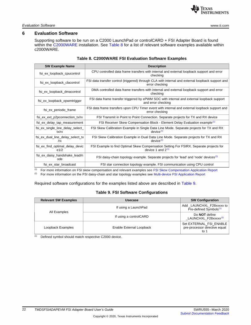
6 Evaluation SoftwareSupporting software to be run on a C2000 LaunchPad or controlCARD + FSI Adapter Board is foundwithin the C2000WARE installation. See Table 8 for a list of relevant software examples available withinc2000WARE.
(1) For more information on FSI skew compensation and relevant examples see FSI Skew Compensation Application Report(2) For more information on the FSI daisy-chain and star topology examples see Multi-device FSI Application Report
Table 8. C2000WARE FSI Evaluation Software Examples
SW Example Name Description
fsi_ex_loopback_cpucontrol CPU controlled data frame transfers with internal and external loopback support and errorchecking
fsi_ex_loopback_clacontrol FSI data transfer control (triggered) through CLA with internal and external loopback support anderror checking
fsi_ex_loopback_dmacontrol DMA controlled data frame transfers with internal and external loopback support and errorchecking
fsi_ex_loopback_epwmtrigger FSI data frame transfer triggered by ePWM SOC with internal and external loopback supportand error checking
fsi_ex_periodic_frame FSI data frame transfers upon CPU Timer event with internal and external loopback support anderror checking
fsi_ex_ext_p2pconnection_tx/rx FSI Transmit in Point to Point Connection. Separate projects for TX and RX devicefsi_ex_delay_tap_measurement FSI Receiver Skew Compensation Block - Element Delay Evaluation example (1)
fsi_ex_single_line_delay_select_tx/rx
FSI Skew Calibration Example in Single Data Line Mode. Separate projects for TX and RXdevice (1)
fsi_ex_dual_line_delay_select_tx/rx
FSI Skew Calibration Example in Dual Data Line Mode. Separate projects for TX and RXdevice (1)
fsi_ex_find_optimal_delay_device1/2
FSI Example to find Optimal Skew Compensation Setting For FSIRX. Separate projects fordevice 1 and 2 (1)
fsi_ex_daisy_handshake_lead/node FSI daisy-chain topology example. Separate projects for 'lead' and 'node' devices (2)
fsi_ex_star_broadcast FSI star connection topology example. FSI communication using CPU control
Required software configurations for the examples listed above are described in Table 9.
(1) Defined symbol should match respective C2000 device.
Table 9. FSI Software Configurations
Relevant SW Examples Usecase SW Configuration
All ExamplesIf using a LaunchPad Add _LAUNCHXL_F28xxxxx to
Pre-defined Symbols (1)
If using a controlCARD Do NOT define_LAUNCHXL_F28xxxxx (1)
Loopback Examples Enable External LoopbackSet EXTERNAL_FSI_ENABLEpre-processor directive equal
to 1

www.ti.com FSI References
23SWRU555–March 2020Submit Documentation Feedback
Copyright © 2020, Texas Instruments Incorporated
TMDSFSIADAPEVM FSI Adapter Board User’s Guide
7 FSI ReferencesOther TI documents relevant to the FSI Adapter Board are described in Table 10.
Table 10. FSI Reference Documents
Document Name Description
Multi-device FSI Application Report Discusses how FSI can be used to communicate between multipledevices within a system.
FSI Skew Compensation Application Report Provides details on the skew compensation functionality built into theFSI peripheral and how it can be utilized.
TMS320F28002x TRM See FSI section in F28002x Technical Reference ManualTMS320F28004x TRM See FSI section in F28004x Technical Reference ManualTMS320F2838x TRM See FSI section in F2838x Technical Reference Manual
C2000 Peripherals Reference Guide Provides an overview of all peripherals available on C2000 devices

IMPORTANT NOTICE AND DISCLAIMER
TI PROVIDES TECHNICAL AND RELIABILITY DATA (INCLUDING DATASHEETS), DESIGN RESOURCES (INCLUDING REFERENCE DESIGNS), APPLICATION OR OTHER DESIGN ADVICE, WEB TOOLS, SAFETY INFORMATION, AND OTHER RESOURCES “AS IS” AND WITH ALL FAULTS, AND DISCLAIMS ALL WARRANTIES, EXPRESS AND IMPLIED, INCLUDING WITHOUT LIMITATION ANY IMPLIED WARRANTIES OF MERCHANTABILITY, FITNESS FOR A PARTICULAR PURPOSE OR NON-INFRINGEMENT OF THIRD PARTY INTELLECTUAL PROPERTY RIGHTS.These resources are intended for skilled developers designing with TI products. You are solely responsible for (1) selecting the appropriate TI products for your application, (2) designing, validating and testing your application, and (3) ensuring your application meets applicable standards, and any other safety, security, or other requirements. These resources are subject to change without notice. TI grants you permission to use these resources only for development of an application that uses the TI products described in the resource. Other reproduction and display of these resources is prohibited. No license is granted to any other TI intellectual property right or to any third party intellectual property right. TI disclaims responsibility for, and you will fully indemnify TI and its representatives against, any claims, damages, costs, losses, and liabilities arising out of your use of these resources.TI’s products are provided subject to TI’s Terms of Sale (www.ti.com/legal/termsofsale.html) or other applicable terms available either on ti.com or provided in conjunction with such TI products. TI’s provision of these resources does not expand or otherwise alter TI’s applicable warranties or warranty disclaimers for TI products.
Mailing Address: Texas Instruments, Post Office Box 655303, Dallas, Texas 75265Copyright © 2020, Texas Instruments Incorporated