fs7805 chip datasheet v1.0 111706 - admiral-ic.com chip datasheet v1.0.pdf · 2.1.2.1. internal...
TRANSCRIPT

Fulhua Microelectronics Corp.
FS7805 Security Built-In
High Speed USB Peripheral Controller
Datasheet
Preliminary Revision 1.0
Nov, 10, 2006

Fulhua Microelectronics Corp.
Copyright: Copyright © 2006 Fulhua Microelectronic Corp.
AL MATERIALS ARE PROVIDED “AS IS” WITHOUT EXPRESSS OR IMPLIED WARRANTY OF ANY
KIND. NO LICENSE OR RIGHT IS GRANTED UNDER NAY APTENT OR TRADEMARK OF FULHUA
MICROELECTRONICS CORP.. FULHUA MICROELECTRONICS CORP HEREBY DISCLAIMS ALL
WARRANTIES AND CONDITIONS IN REGARD TO MATERIALS, INCLUDING ALL WARRANTIES,
IMPLIED OR EXPRESS, OF MERCHANTABILITY, FITNESS FOR ANY PARTICULAR PURPOSE, AND
NON-INFRINGEMENT OF INTELLECTURAL PROPERTY. IN NO EVENT SHALL FULHUA
MICROELECTRONICS CORP BE LIABLE FOR ANY DAMAGES INCLUDING, WITHOUT LIMITATIONM,
DAMAGES RESULTING FROM LOSS OF INFORMATION OR PROFITS. PLEASE BE ADVISED THAT
THE MATERIALS MAY CONTAIN ERRORS OR OMMISIONS. FULHUA MICROELECTRONICS CORP
MAY MAKE CHANGES TO THE MATERIALS OR TO THE PRODUCTS DESCRIBED THEREIN AT ANY
TIME WITHOUT NOTICE.
Trademark:
is a registered trademark of Fulhua Microelectronic Corp..
All trademark are the properties of their respective owners.
Office: Fulhua Microelectronics Corp.
FameG Taiwan FameG Shanghai
6F, No.25, Alley 20, Lane 26, Ray-Guang Rd. 5F, Building 59, No.461, HongCao Road,
Nei-Hu, Taipei, 11491, Taiwan XuHui Dist., Shanghai, 200233,
Tel. : (886)3-6669-888 Tel. : (86)21-5426-2266
Fax: (886)3-6668-999 Fax: (86)21-5426-2699
FameG Shenzhen FameG SOTA
Room 2106-2107, Cyber Times Tower A, 1F, No.10, R&D II Rd., Science-based Ind. Park,
Tianan Cyber Park, Futian District, Shenzhen, 518040 Hsin-chu, 30076, Taiwan
Tel. : (86)755-2533-5930 Tel. : (886)3-5643939
Fax: (86)755-2533-5931 Fax: (886)3-5643737

Fulhua Microelectronics Corp.
FameG Tainan
Rm101, No. 31, Gongye 2nd Rd., Annan District,
Southern Taiwan Innovation & Research Park Tainan, 70955, Taiwan
Tel. : (886)6-3841688
Fax: (886)6-3841699

Fulhua Microelectronics Corp.
Table of Content
1. GENERAL DESCRIPTION .........................................................................................................5
2. FEATURES .................................................................................................................................6
2.1. GENERAL FEATURE ....................................................................................................................6
2.2. FIRMWARE DOWNLOAD FEATURES ..............................................................................................7
2.3. SECURITY FEATURES .................................................................................................................7
2.4. KERNAL SOC (KSOC) FEATURES ...............................................................................................7
3. MAJOR BLOCK FUNCTION DESCRIPTION ............................................................................9
3.1. SYSTEM BLOCK .........................................................................................................................9
3.1.1. E8051D and It’s Memory Blocks ......................................................................................9
3.2. USB BLOCK ............................................................................................................................ 11
3.2.1. USB2.0 Control Block..................................................................................................... 11
3.2.2. Endpoint Control Block...................................................................................................12
3.3. ENCRYPT/DECRYPT BLOCK ......................................................................................................12
3.3.1. TDES ..............................................................................................................................12
3.4. DIRECT MEMORY ACCESS (DMA) .............................................................................................13
3.5. KSOC EXPANSION BLOCK ........................................................................................................13
3.5.1. Slave FIFO Interface (SFI) .............................................................................................13
3.5.2. Programmable Logic Interface (PLIF) ............................................................................13
3.6. FIFO BLOCK............................................................................................................................13
3.7. MISCELLANEOUS......................................................................................................................13
3.7.1. RESET Generator ..........................................................................................................13
3.7.2. Clock Generator .............................................................................................................13
4. PIN ASSIGNMENTS.................................................................................................................15
4.1.1. Pin Descriptions..............................................................................................................15
4.2. PING OUT ................................................................................................................................20
5. PACKAGE DIMENSION ...........................................................................................................21

Fulhua Microelectronics Corp.
General Description
The FameG’s FS7805 is a leading Kernel System-on-a-Chip (KSoC) with built-in USB interface and security
features. The KSoC integrated embedded RISC-base 8-bit 8051 CPU core, USB 2.0 controller/
PIE/SIE/Transceiver, pseudo Random Number Generator (RNG), and hardware DES/3DES security engine.
The FS7805 is designed to be used in FameG’s EZL-8051US development system very suitable for
developing security-base applications such as USB key, RFID Reader, Smart Card Reader, security control
and metering. The EZL-8051US is a complete hardware and software development system that provides an
easy design, verification and debug environment for developing customer’s target systems and/or ASIC chips.
The silicon proven IP cores contained inside of FS7805 KSoC and the related reference software module
provided by FameG can be used by customers to dramatically reduce the effort and time needed to design
their own target system or ASIC chip. Both FS7805 KSoC and EZL-8051US development system can
provide a quick time-to-market product development platform. Please call FameG’s sales or representatives
for additional EZL-8051US development system and the ASIC design service information.
The KSoC integrated a FameG’s unique high performance RISC-base 8-bit 8051 CPU core, E8051D, which
operates up to 48 MHz clock rate that is 10 times faster than traditional standard 8051 and retains the software
compatibility. The chip also provides a hardware DES/TDES engine and a pseudo Random Number
Generator (RNG) for performing up to 64-bit data encryption/decryption. With the high performance 8051
CPU and hardware DES/TDES engine, an operation to cipher and decipher 64-bit data can be done in merely
sixteen cycles. The Serial Interface is used to access of external EEPROM and/or other serial devices.
The FS7805 also provides many comprehensive interfaces. Please refer to Figure 1 Block Diagram. The
USB interface provides a universal “Plug and Play” interface to the Host PC. The Flash memory controller
supports popular types of SD 1.1/MMC 4.0 memory cards, and the data in the SD/MMC cards can be
encrypted or decrypted in real-time during data transfer by using the built-in hardware DES/TDES engine
inside of FS7805. Furthermore, the Programmable Logic Interface (PLIF) and the Slave FIFO (8- or 16-bit
data width) provides an easy and glueless interface for connecting to popular peripheral interfaces such as
ATA, EPP (Enhanced Parallel Port), and most DSP or CPU Host Interface.

Fulhua Microelectronics Corp.
1. Features
1.1. General Feature
� Application: KSoC
� Process and Package: LQFP-128
� Internal 3.3V to 1.8V Regulator.
� External clock source from Crystal or Oscillator running at 12MHz.
� 8~48 GPIO
� 8-bit RISC E8051D
� 100% software compatible with industry standard 8051.
� Pipelined RISC architecture enables to execute instructions 10 times faster compared to
standard 8051.
� Embedded 16K-Byte SRAM for internal program memory. If internal program memory
occupies only a portion of 16K-Byte, the other portion can be converted as external data
memory.
� Embedded 256-Byte SRAM for internal data memory.
� Embedded dedicate 512-Byte SRAM for external data memory.
� Direct support up to 64K-Byte off-chip external data memory.
� Up to 60MHz CPU clock rate.
� Support low power IDLE mode.
� Support debug interface
� Support USB Interface
� Compliance to Universal Serial Bus Specification 2.0 High-Speed interface.
� Support multiple USB configurations and multiple interfaces.
� Support one Control endpoint with one 64-Byte IN FIFO and one 64-Byte OUT FIFO.
� Support programmable bi-directional Interrupt/Bulk/Isochronous endpoints.
� Hardwired USB Download Function (BOOT) which allows the host to update the program
memory while the USB bus still connected.
� Support Serial-Parallel Interface (SPI) master and slave Interface
� Support Two-wired Serial Interface (I2C) with clock rate up to 3.4MHz.
� Support programmable memory download function through SPI and I2C
� SD/MMC Card Interface (SDMI)
� Low Power Mode
� USB suspend mode: all clocks stop and all function blocks are in idle state. Wake up by USB
resume or reset activities.
� 8051 idle mode: only USB block and E8051D peripherals (Interrupt Control, IO PORTS, Reset
Control, TIMERS, UART) are in active state. Wake up by external hardware reset or any
enabled interrupt activation.

Fulhua Microelectronics Corp.
� Support Direct Memory Access (DMA) between Endpoint FIFOs, external 512-Byte data memory,
up to 64K-Byte off-chip external data memory, and Embedded 16K-Byte SRAM program memory
(programmable memory is the firmware download function)
� 8051 code/data memory expansion to allow using off-chip program or data memory when on-chip
program/data memory isn’t enough.
� VID/PID/DID configurable.
1.2. Firmware Download Features
� Support programmable memory download function through P-Port, SPI, I2C, and USB.
� Support auto-detection for connection SPI downloadable through external flash, I2C downloadable
through EEPROM, or USB download, with priority.
1.3. Security Features
� Triple DES
� Hardware DES/TDES.
� FIPS PUB 46-3 DES compliant.
� Support selection of DES and Triple DES.
� Support 64-bit DES encryption/decryption.
� Support 64-bit TDES encryption/decryption.
� Support Triple DES of ECB (Electronic Code Book) mode.
� Feasible for MAC (Message Authentication Code) generation.
� Support DES MAC (Message Authentication Code) processing.
� Support TDES MAC processing.
� 16 cycles for a round of DES.
� 60MHz operation with 120Mbps DES throughput.
� Support DMA to do data movement.
� Random Number Generator (RNG)
� FIPS 140-2 compliant.
� ANSI X9.31 appendix A.2.4 type pseudo random number generator.
� Support 32 or 64 bits pseudo random number output.
� Support free run and one-shot operation mode.
� Seed value base on date/time.
1.4. Kernal SOC (KSoC) Features
� 4MHz ~ 60MHz clock rate
� Support slave FIFO interface (SFI)
� Allow off-chip master device to access on-chip FIFO through this interface.

Fulhua Microelectronics Corp.
� Support synchronous/asynchronous slave FIFO interface.
� Support programmable FIFO clock source, either from an internal derived clock or external
supplied clock.
� Support auto mode and manual mode, Allow to switch from auto mode to manual mode and
vice versa.
� Support 8 or 16 bits slave FIFO interface.
� Support burst read and write mode
� Support programmable logic interface (PLIF)
� Support on-chip programmable master. Software programs the waveform registers to define
and generate the waveforms.
� Allow on-chip programmable master to access wide variety external slave peripherals or
protocols such as NAND Flash, CF card, ATA interface, printer parallel port and Utopia.
� Support 8 or 16 bits PLIF interface.
� Half-Duplex mode or Full-Duplex mode.

Fulhua Microelectronics Corp.
2. Major Block Function Description
The following sections describe major blocks inside core.
2.1. System Block
System Block Diagram
2.1.1. FS7805 and It’s Memory Blocks
FS7805 supports on-chip 3 memory blocks, the 3 on-chip memory blocks are,
1. 16K-byte SRAM as 8051 on chip program/data memory
2. 256-byte SRAM as 8051 internal data memory
3. 512-byte SRAM as 8051 external data memory
FS7805 can operate with internal program memory only or external program memory only and this selection is
defined by a pin “EXROMSEL_N”.
External EEPROM can store user confidential data in specific application, for example, user ID, password, age,
and deposit in the bank…etc. Encryption is done when data is stored into EEPROM and decryption is done
when data is read out from EEPROM.
P-Port (ICE) debug feature is implemented to support the debug. It can access all registers and memories. It
also downloads the program code to internal 16K-Byte SRAM during chip initialization.
FS7805
MCU
(E8051D)
60MHz
SRAM /
FLASH
External
(master/
slave)
SD/MMC SD/MMC
Interface
DES/3DES
MAC
RNG (ANSI
X9.31) .
FIF
O
PLIF
USB
Interface
GPIO
Ports P-Port
USB2.0 Controller
Code/Data
SRAM 16
KB
Slave
FIFO
I/F
SPI Two-wires
interface
USB2.0 Transceiver

Fulhua Microelectronics Corp.
2.1.2. FS7805 Memory Mapping
2.1.2.1. Internal Data Memory Map
The assignments of 256bytes internal data memory are as following:
Internal Data Memory Map
2.1.2.2. Internal Code Memory, EXROMSEL_N = 1
This mode implements the internal 16kbyte block of RAM (starting at 0) as combined code and data memory.
When external RAM or ROM is added, user can use the 43kbytes as external data memory.
Only the internal 16kbytes SRAM spaces have the following access:
• USB download
• I2C-compatible interface boot load.
• SPI-compatible interface boot load.
Internal Code Memory Map
R0~R7 (bank0)
R0~R7 (bank3)
R0~R7 (bank2)
R0~R7 (bank1)
Bit addressable
RAM
General
purpose
Register
bank select
PSW[4:3]
00
11
10
01
0x00
0x07
0x0F
0x17
0x1F
0x2F
0x7F
Upper 128
0x00
0x7F
0xFF
0x80
0xFF
Direct or indirect addressing
Direct addressing only
Indirect addressing onlyLower 128
Lower 128
SFR Space
Fulhua Microelectronics Corp.
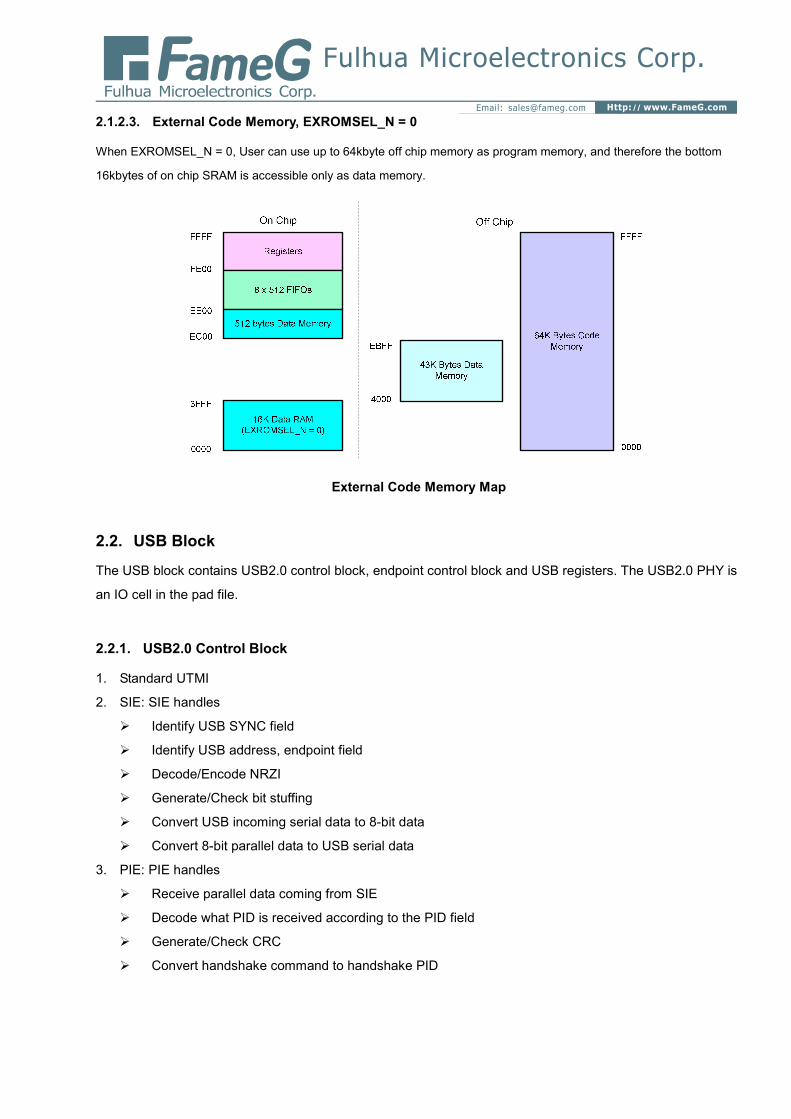
2.1.2.3. External Code Memory, EXROMSEL_N = 0
When EXROMSEL_N = 0, User can use up to 64kbyte off chip memory as program memory, and therefore the bottom
16kbytes of on chip SRAM is accessible only as data memory.
External Code Memory Map
2.2. USB Block
The USB block contains USB2.0 control block, endpoint control block and USB registers. The USB2.0 PHY is
an IO cell in the pad file.
2.2.1. USB2.0 Control Block
1. Standard UTMI
2. SIE: SIE handles
� Identify USB SYNC field
� Identify USB address, endpoint field
� Decode/Encode NRZI
� Generate/Check bit stuffing
� Convert USB incoming serial data to 8-bit data
� Convert 8-bit parallel data to USB serial data
3. PIE: PIE handles
� Receive parallel data coming from SIE
� Decode what PID is received according to the PID field
� Generate/Check CRC
� Convert handshake command to handshake PID

Fulhua Microelectronics Corp.
2.2.2. Endpoint Control Block
There are 5 endpoints.
1. EP0 is the control endpoint with one 8-byte IN FIFO and one 8-byte OUT FIFO.
2. EPA, EPB, EPC and EPD can be programmed as bulk, interrupt or isochronous endpoint. Each endpoint
has two 512-byte FIFOs as ping-pong FIFO. These endpoints transfer data for MCU, TDES, SD/MMC
Interfaces, Slave FIFO Interface, and PLIF blocks. These FIFOs can be configured to a larger ping-pong
FIFO for more advanced application.
Programmable Endpoint FIFO Diagram
2.3. Encrypt/Decrypt Block
2.3.1. DES/TDES
After receive input text and keys, it handles
� 64-bit DES encryption/decryption
� 64-bit TDES encryption/decryption
� DES MAC processing
� TDES MAC processing
� Generate interrupt after completion
512Byte
1024Byte EPA
EPB
EPC
EPD
EPA
EPB
EPC
EPD
EPA
EPC
512Byte
512Byte
512Byte
512Byte
512Byte
512Byte
512Byte
1024Byte
1024Byte
1024Byte
1024Byte
1024Byte
1024Byte
1024Byte
512Byte
EPA
EPB
EPC
EPD
512Byte
512Byte
512Byte

Fulhua Microelectronics Corp.
2.4. Direct Memory Access (DMA)
A DMA function is built in which allows the device to move data between endpoint FIFOs, embedded 512-Byte
data memory, or off-chip data memory. Cycle stealing function is supported which allows high efficient data
through put.
2.5. KSoC Expansion Block
2.5.1. Slave FIFO Interface (SFI)
SFI is an 8 or 16-bit interface driven by external master devices to do data transfer between the external
master device and EPA, EPB, EPC, and EPE FIFOs. Each EPA, EPB, EPC, or EPD FIFO can be selected
individually to do data transfer.
2.5.2. Programmable Logic Interface (PLIF)
The PLIF is an 8 or 16-bit interface driven by user programmable finite state machines. It enables chip to
perform bus master function to connect to external slave devices. It has 6 programmable control outputs, 9
address outputs and 6 ready inputs. Data will be moved between EPA, EPB, EPC, and EPD FIFOs and the
external slave device through the PLIF generated waveforms.
2.6. FIFO Block
There are a total of four 512-byte ping-pong endpoint FIFOs for USB transaction. These FIFOs can also be
configured to be accessed by the embedded 8051 as external data memories.
2.7. Miscellaneous
2.7.1. RESET Generator
Chip reset source includes:
� Hardware resets from pin, will reset the whole chip.
� Hardware detects USB bus reset, will reset USB function.
� Firmware sets proper registers to reset each sub-function.
2.7.2. Clock Generator
Chip clock source includes:
� 12MHz clock from pin.
� Slave FIFO and PLIF clock from pin.
Fulhua Microelectronics Corp.

Fulhua Microelectronics Corp.
3. Pin Assignments
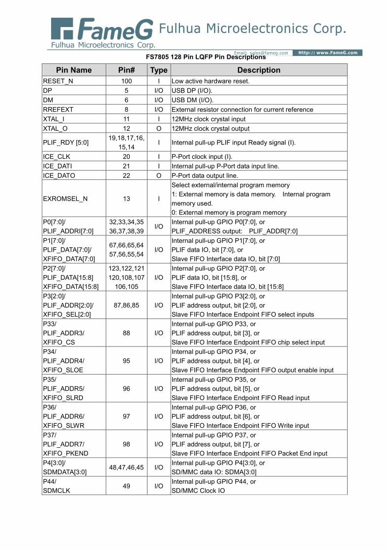
3.1.1. Pin Descriptions
FS7805 128 Pin LQFP Pin List
Pin Pin Name Type Pin Pin Name Type Pin Pin Name Type
1 T0 I 44 XDATWR_N O 87
P32/
XFIFO_SEL2/
PLIF_ADDR2
I/O
2 T1 I 45 P40/
SDMDATA0 I/O 88
P33/
XFIFO_CS/
PLIF_ADDR3
I/O
3 VSSA P 46 P41/
SDMDATA1 I/O 89 VDD(3.3V) P
4 VDDA(3.3V) P 47 P42/
SDMDATA2 I/O 90 VSS P
5 DP I/O 48 P43/
SDMDATA3 I/O 91 XADDR0 O
6 DM I/O 49 P44/SDMCLK I/O 92 XADDR1 O
7 VSSP P 50 P45/SDMCMD I/O 93 XADDR2 O
8 PREFEXT I/O 51 P46/SDMWPD I/O 94 XADDR3 O
9 VDDP(1.8V) P 52 P47/SDMCDB I/O 95
P34/
XFIFO_SLOE/
PLIF_ADDR4
I/O
10 VSS P 53 VDD(1.8V) P 96
P35/
XFIFO_SLRD/
PLIF_ADDR5
I/O
11 XTAL_I I 54
P10/
XFIFO_DATA0/
PLIF_DATA0
I/O 97
P36
XFIFO_SLWR/
PLIF_ADDR6
I/O
12 XTAL_O O 55
P11/
XFIFO_DATA1/
PLIF_DATA1
I/O 98
P37/
XFIFO_PKEND/
PLIF_ADDR7
I/O
13 EXROMSEL_N I 56
P12/
XFIFO_DATA2/
PLIF_DATA2
I/O 99 APLF_ADDR8 O
14 PLIF_RDY0 I 57
P13/
XFIFO_DATA3/
PLIF_DATA3
I/O 100 REST_N I
15 PLIF_RDY1 I 58 VDD(3.3V) P 101 P54/TXD0 I/O
16 PLIF_RDY2 I 59 P52/INT0_N I/O 102 P55/RXD0 I/O
17 PLIF_RDY3 I 60 P53/INT1_N I/O 103 PLIF_CTL5 O
18 PLIF_RDY4 I 61 XDATA0 I/O 104 XFIFO_CLK I/O
19 PLIF_RDY5 I 62 VSS P 105
P20/
XFIFO_DATA8
PLIF_DATA8
I/O
20 ICE_CLK I 63 XDATA1 I/O 106
P21/
XFIFO_DATA9/
PLIF_DATA9
I/O
21 ICE_DATI I 64
P14/
XFIFO_DATA4/
PLIF_DATA4
I/O 107
P22/
XFIFO_DATA10/
PLIF_DATA10
I/O
22 ICE_DATO O 65 P15/
XFIFO_DATA5/ I/O 108
P23/
XFIFO_DATA11/ I/O

Fulhua Microelectronics Corp.
PLIF_DATA5 PLIF_DATA11
23 VDD(3.3V) P 66
P16/
XFIFO_DATA6/
PLIF_DATA6
I/O 109 REG_VSS P
24 XADDR11 O 67
P17/
XFIFO_DATA7/
PLIF_DATA7
I/O 110 REG_VDDOUT
(1.8V) P
25 XADDR12 O 68 XDATA2 I/O 111 REG_VDDIN(3.3
V) P
26 XADDR13 O 69 XDATA3 I/O 112 P56/PWM0 I/O
27 XADDR14 O 70 XFIFO_FLAGA/
PLIF_CTL0 O 113 P57/PWM1 I/O
28 XADDR15 O 71 XFIFO_FLAGB/
PLIF_CTL1 O 114 XADDR4 O
29 VDD(1.8V) P 72 XFIFO_FLAGC/
PLIF_CTL2 O 115 XADDR5 O
30 VDD(1.8V) P 73 PLIF_CTL3 O 116 VSS P
31 XPRGRD_N O 74 PLIF_CTL4 O 117 VSSA P
32 P07/
PLIF_ADDRI7 I/O 75 XPRGWR_N O 118 VDDA P
33 P06/
PLF_ADDRI6 I/O 76 VSS P 119 VDD(3.3V) P
34 P05/
PLIF_ADDRI5 I/O 77
SCLK/
SDMDATA4 I/O 120
P24
XFIFO_DATA12/
PLIF_DATA12
I/O
35 P04/
PLIF_ADDRI4 I/O 78
SSB/
SDMDATA5 I/O 121
P25
XFIFO_DATA13/
PLIF_DATA13
I/O
36 P03/
PLIF_ADDRI3 I/O 79
MISO/
SDMDATA6 I/O 122
P26
XFIFO_DATA14/
PLIF_DATA14
I/O
37 P02/
PLIF_ADDRI2 I/O 80
MOSI/
SDMDATA7 I/O 123
P27
XFIFO_DATA15/
PLIF_DATA15
I/O
38 P01/
PLIF_ADDRI1 I/O 81 XDATA4 I/O 124 XADDR6 O
39 P00/
PLIF_ADDRI0 I/O 82 XDATA5 I/O 125 XADDR7 O
40 VSS p 83 XDATA6 I/O 126 XADDR8 O
41 P50/SCL I/O 84 XDATA7 I/O 127 XADDR9
42 P51/SDA I/O 85
P30/
XFIFO_SEL0/
PLIF_ADDR0
I/O 128 XADDR10 O
43 XDATRD_N O 86
P31/
XFIFO_SEL1/
PLIF_ADDR1
I/O
Fulhua Microelectronics Corp.
FS7805 128 Pin LQFP Pin Descriptions
Pin Name Pin# Type Description
RESET_N 100 I Low active hardware reset.
DP 5 I/O USB DP (I/O).
DM 6 I/O USB DM (I/O).
RREFEXT 8 I/O External resistor connection for current reference
XTAL_I 11 I 12MHz clock crystal input
XTAL_O 12 O 12MHz clock crystal output
PLIF_RDY [5:0] 19,18,17,16,
15,14 I Internal pull-up PLIF input Ready signal (I).
ICE_CLK 20 I P-Port clock input (I).
ICE_DATI 21 I Internal pull-up P-Port data input line.
ICE_DATO 22 O P-Port data output line.
EXROMSEL_N 13 I
Select external/internal program memory
1: External memory is data memory. Internal program
memory used.
0: External memory is program memory
P0[7:0]/
PLIF_ADDRI[7:0]
32,33,34,35
36,37,38,39 I/O
Internal pull-up GPIO P0[7:0], or
PLIF_ADDRESS output: PLIF_ADDR[7:0]
P1[7:0]/
PLIF_DATA[7:0]/
XFIFO_DATA[7:0]
67,66,65,64
57,56,55,54 I/O
Internal pull-up GPIO P1[7:0], or
PLIF data IO, bit [7:0], or
Slave FIFO Interface data IO, bit [7:0]
P2[7:0]/
PLIF_DATA[15:8]
XFIFO_DATA[15:8]
123,122,121
120,108,107
106,105
I/O
Internal pull-up GPIO P2[7:0], or
PLIF data IO, bit [15:8], or
Slave FIFO Interface data IO, bit [15:8]
P3[2:0]/
PLIF_ADDR[2:0]/
XFIFO_SEL[2:0]
87,86,85 I/O
Internal pull-up GPIO P3[2:0], or
PLIF address output, bit [2:0], or
Slave FIFO Interface Endpoint FIFO select inputs
P33/
PLIF_ADDR3/
XFIFO_CS
88 I/O
Internal pull-up GPIO P33, or
PLIF address output, bit [3], or
Slave FIFO Interface Endpoint FIFO chip select input
P34/
PLIF_ADDR4/
XFIFO_SLOE
95 I/O
Internal pull-up GPIO P34, or
PLIF address output, bit [4], or
Slave FIFO Interface Endpoint FIFO output enable input
P35/
PLIF_ADDR5/
XFIFO_SLRD
96 I/O
Internal pull-up GPIO P35, or
PLIF address output, bit [5], or
Slave FIFO Interface Endpoint FIFO Read input
P36/
PLIF_ADDR6/
XFIFO_SLWR
97 I/O
Internal pull-up GPIO P36, or
PLIF address output, bit [6], or
Slave FIFO Interface Endpoint FIFO Write input
P37/
PLIF_ADDR7/
XFIFO_PKEND
98 I/O
Internal pull-up GPIO P37, or
PLIF address output, bit [7], or
Slave FIFO Interface Endpoint FIFO Packet End input
P4[3:0]/
SDMDATA[3:0] 48,47,46,45 I/O
Internal pull-up GPIO P4[3:0], or
SD/MMC data IO: SDMA[3:0]
P44/
SDMCLK 49 I/O
Internal pull-up GPIO P44, or
SD/MMC Clock IO
Fulhua Microelectronics Corp.
P45/
SDMCMD 50 I/O
Internal pull-up GPIO P45, or
SD/MMC Command IO
P46/
SDMWPB 51 I/O
Internal pull-up GPIO P46, or
SD/MMC Write Protect Input, Active Low
P47/
SDMCDB 52 I/O
Internal pull-up GPIO P47, or
SD/MMC Card Detect Input, Active Low
P50 / SCL 41 I/O
Internal pull-up GPIO P50, or
I2C clock, which can connect to the off-chip EEPROM serial
clock
P51 / SDA 42 I/O
Internal pull-up GPIO P51, or
I2C data, which can connect to the off-chip EEPROM serial
data.
P52/
INT0_N 59 I/O
Internal pull-up GPIO P52, or
External Interrupt 0 input, Active Low
P53/
INT1_N 60 I/O
Internal pull-up GPIO P53, or
External Interrupt 1 input, Active Low
P54/
RXD0 101 I/O
Internal pull-up GPIO P54, or
UART Receive Data IO
P55/
TXD0 102 I/O
Internal pull-up GPIO P55, or
UART Transmit Data IO
P56/
PWM0 112 I/O
Internal pull-up GPIO P56, or
PWM output, channel 0
P57/
PWM1 113 I/O
Internal pull-up GPIO P57, or
PWM output, channel 1
SCLK /
SDMDATA4 77 I/O
SPI Clock IO, or
SD/MMC Data IO, bit 4
SSB /
SDMDATA5 78 I/O
SPI Slave Select IO, Active Low, or
SD/MMC Data IO, bit 5
MISO/
SDMDATA6 79 I/O
SPI Master Input Slave output IO signal, or
SD/MMC Data IO, bit 6
MOSI /
SDMDATA7 80 I/O
SPI Master Output Slave Input IO signal, or
SD/MMC Data IO, bit 7
XFIFO_FLAGA/
PLIF_CTL0 70 O
Slave FIFO Interface programmable acknowledge flag
output, or
PLIF handshake control output, bit 0
XFIFO_FLAGB/
PLIF_CTL1 71 O
Slave FIFO Interface programmable acknowledge flag
output, or
PLIF handshake control output, bit 1
XFIFO_FLAGC/
PLIF_CTL2 72 O
Slave FIFO Interface programmable acknowledge flag
output, or
PLIF handshake control output, bit 2
PLIF_CTL[5:3] 103,74,73 O PLIF handshake control output, bit[5:3].
PLIF_ADDR8 99 O PLIF Address output : PLIF ADDR[8]
T0 1 I Timer0 clock line (I).
T1 2 I Timer1 clock line (I).

Fulhua Microelectronics Corp.
XFIFO_CLK 104 I/O
External Clock.
SYSIO_CFG.IFCFG[1:0]:
11: SFI clock.
00/01/10: PLIF clock.
When input from external devices, the clock ranges from
4MHz to 60MHz; Set to input with pull-up during the suspend
mode.
XDATRD_N
XPRGRD_N 43,31 O External data/program memory read signal, Active Low.
XDATWR_N
XPRGWR_N 44,75 O External data/program memory write signal, Active Low.
XADDR[15:0]
28,27,26,25
24,128,127
126,125,124
115,114
94,93,92,91
O External program/data memory address bus(O),bit[15:0]
XDATA[7:0] 84,83,82,81
69,68,63,61 O External program/data memory data bus,bit[7:0]
VDD(3.3V) 23,58,89
119 P IO pad VDD(3.3V)
VDD(1.8V) 29,30,53 P Core VDD(1.8V)
VSS 10,40,62,76,
90,116 P IO pad or Core GND.
REG_VDDIN 111 P 3.3V Regulator Input
REG_VDDOUT 110 P Regulator 1.8V output
REG_VSS 109 P GND for 3.3V to 1.8V Regulator
VDDA(3.3V) 4,118 P Analog VDD(3.3V) for USB2PHYC
VSSA 3,117 P Analog GND for USB2PHYC
VDDP(1.8V) 9 P Analog VDD(1.8V) for USB2PHYC PLL AND DLL
VSSP 7 P Analog GND for USB2PHYC PLLAND DLL

Fulhua Microelectronics Corp.
3.2. Ping out
128 Pin Assignment D
iagram
FS7805 LQFP-128
T0
T1
VSSA
VDDA(3.3V)
DP
DM
VSSP
RREFEXT
VDDP (1
.8V)
VSS
XTAL_I
XTAL_O
EXROMSEL_N
APLIF_RDY0
APLIF_RDY1
APLIF_RDY2
APLIF_RDY3
APLIF_RDY4
APLIF_RDY5
ICE_CLK
ICE_DATI
ICE_DATO
VDD (3
.3V)
XADDR11
XADDR12
XADDR13
XADDR14
XADDR15
VDD(1.8V)
VDD(1.8V)
XPRGRD_N
P07 /PLIF_ADDRI7
P35/XFIFO_SLRD/PLIF_ADDR5
P34/XFIFO_SLOE/PLIF_ADDR4
XADDR3
XADDR2
XADDR1
XADDR0
VSS
VDD (3
.3V)
P33/XFIFO_CS/PLIF_ADDR3
P32/XFIFO_SEL2/PLIF_ADDR2
P31/XFIFO_SEL1/PLIF_ADDR1
P30/XFIFO_SEL0/PLIF_ADDR0
XDATA7
XDATA6
XDATA5
XDATA4
MOSI/S
DMDATA7
MISO/SDMDATA6
SSB/SDMDATA5
SCLK/SDMDATA4
VSS
XPRGWR_N
PLIF_CTL4
PLIF_CTL3
XFIFO_FLAGC/PLIF_CTL2
XFIFO_FLAGB/PLIF_CTL1
XFIFO_FLAGA/PLIF_CTL0
XDATA3
XDATA2
P17/PLIF_DATA7/XFIFO_DATA7
P16/PLIF_DATA6/XFIFO_DATA6
P15/PLIF_DATA5/XFIFO_DATA5
P06/PLIF_ADDRI6P05/PLIF_ADDRI5P04/PLIF_ADDRI4P03/PLIF_ADDRI3P02/PLIF_ADDRI2P01/PLIF_ADDI1P00/PLIF_ADDI0
VSSP50 / SCLP51 / SDA
XDATRD_NXDATWR_N
P40/SDMDATA0 P41/SDMDATA1P42/SDMDATA2P43/SDMDATA3
P44/SDMCLKP45/SDMCMDP46/SDMWPB P47/SDMCDB
VDD(1.8V)P10/XFIFO_DATA0 /PLIF_DATA0P11/XFIFO_DATA1 /PLIF_DATA1P12/XFIFO_DATA2 /PLIF_DATA2P13/XFIFO_DATA3 /PLIF_DATA3
VDD(3.3V)P52/INT0_NP53/INT1_N
XDATA0VSS
XDATA1P14/XFIFO_DATA4 /PLIF_DATA4
XADDR10 XADDR9 XADDR8 XADDR7 XADDR6 P27 /XFIFO_DATA15/PLIF_DATA15 P26 /XFIFO_DATA14/PLIF_DATA14 P25 /XFIFO_DATA13/PLIF_DATA13 P24 /XFIFO_DATA12/PLIF_DATA12 VDD (3.3V) VDDA VSSA VSS XADDR5 XADDR4 P57 / PWM1 P56 / PWM0 REG_VDDIN(3.3V) REG_VDDOUT(1.8V) REG_VSS P23 /XFIFO_DATA11/PLIF_DATA11 P22 /XFIFO_DATA10/PLIF_DATA10 P21 /XFIFO_DATA9/PLIF_DATA9 P20 /XFIFO_DATA8/PLIF_DATA8 XFIFO_CLK PLIF_CTL5 P55/RXD0 P54/TXD0 RESET_N APLIF_ADDR8 P37/XFIFO_PKEND/APLIF_DATA7 P36/XFIFO_SLWR/APLIF_DATA6
33
34
35
36
37
38
39
40
41
42
43
44
45
46
47
48
49
50
51
52
53
54
55
56
57
58
59
60
61
62
63
64
96
95
94
93
92
91
90
89
88
87
86
85
84
83
82
81
80
79
78
77
76
75
74
73
72
71
70
69
68
67
66
65
1
2
3
4
5
6
7
8
9
10
11
12
13
14
15
16
17
18
19
20
21
22
23
24
25
26
27
28
29
30
31
32
128
127
126
125
124
123
122
121
120
119
118
117
116
115
114
113
112
111
110
109
108
107
106
105
104
103
102
101
100
99
98
97

Fulhua Microelectronics Corp.
4. Package Dimension