front cover p44x - ge grid solutions manual p44x/en m/g55 micom p441, p442 & p444 page 1/2...
TRANSCRIPT

MiCOM P441, P442, P444
P44x/EN M/G55 © 2011. ALSTOM, the ALSTOM logo and any alternative version thereof are trademarks and service marks of ALSTOM. The other names mentioned, registered or not, are the property of their respective companies. The technical and other data contained in this document is provided for information only. Neither ALSTOM, its officers or employees accept responsibility for, or should be taken as making any representation or warranty (whether express or implied), as to the accuracy or completeness of such data or the achievement of any projected performance criteria where these are indicated. ALSTOM reserves the right to revise or change this data at any time without further notice.
GRID
Technical Manual
Numerical Distance Protection Relays
Platform Hardware Version: J and K Platform Software Version: C4.x, C5.x and D1.x Publication Reference: P44x/EN M/G55


Technical Manual P44x/EN M/G55 MiCOM P441, P442 & P444
Page 1/2
Numerical Distance Protection MiCOM P44x
GENERAL CONTENT
Safety Section P44x/EN SS/H11
Addendum - Versions C4.x, C5.x and D1.x P44x/EN AD/F55
Introduction P44x/EN IT/G55
Hardware Description P44x/EN HW/G55
Application Guide P44x/EN AP/G55
Technical Data P44x/EN TD/G55
Installation P44x/EN IN/G55
Commissioning & Maintenance P44x/EN CM/G55
Commissioning Test & Record Sheet P44x/EN RS/G55
Connection Diagrams P44x/EN CO/G55
Courier Database P44x/EN GC/G55
Menu Content Tables P44x/EN HI/G55
Hardware/Software Version History and Compatibility P44x/EN VC/G55

P44x/EN M/G55 Technical Manual Page 2/2
MiCOM P441, P442 & P444

Safety Section P44x/EN SS/H11
SS
SAFETY SECTION

P44x/EN SS/H11 Safety Section
SS
Safety Section P44x/EN SS/H11
(SS) - 1
SS
CONTENTS 1. INTRODUCTION 3
2. HEALTH AND SAFETY 3
3. SYMBOLS AND LABELS ON THE EQUIPMENT 4 3.1 Symbols 4 3.2 Labels 4
4. INSTALLING, COMMISSIONING AND SERVICING 4
5. DE-COMMISSIONING AND DISPOSAL 7
6. TECHNICAL SPECIFICATIONS FOR SAFETY 8 6.1 Protective fuse rating 8 6.2 Protective class 8 6.3 Installation category 8 6.4 Environment 8

P44x/EN SS/H11 Safety Section (SS) - 2
SS

Safety Section P44x/EN SS/H11
(SS) - 3
SS
STANDARD SAFETY STATEMENTS AND EXTERNAL LABEL INFORMATION FOR ALSTOM GRID EQUIPMENT
1. INTRODUCTION This Safety Section and the relevant equipment documentation provide full information on safe handling, commissioning and testing of this equipment. This Safety Section also includes reference to typical equipment label markings.
The technical data in this Safety Section is typical only, see the technical data section of the relevant equipment documentation for data specific to a particular equipment.
Before carrying out any work on the equipment the user should be familiar with the contents of this Safety Section and the ratings on the equipment’s rating label.
Reference should be made to the external connection diagram before the equipment is installed, commissioned or serviced.
Language specific, self-adhesive User Interface labels are provided in a bag for some equipment.
2. HEALTH AND SAFETY The information in the Safety Section of the equipment documentation is intended to ensure that equipment is properly installed and handled in order to maintain it in a safe condition.
It is assumed that everyone who will be associated with the equipment will be familiar with the contents of this Safety Section, or the Safety Guide (SFTY/4L M).
When electrical equipment is in operation, dangerous voltages will be present in certain parts of the equipment. Failure to observe warning notices, incorrect use, or improper use may endanger personnel and equipment and also cause personal injury or physical damage.
Before working in the terminal strip area, the equipment must be isolated.
Proper and safe operation of the equipment depends on appropriate shipping and handling, proper storage, installation and commissioning, and on careful operation, maintenance and servicing. For this reason only qualified personnel may work on or operate the equipment.
Qualified personnel are individuals who:
• Are familiar with the installation, commissioning, and operation of the equipment and of the system to which it is being connected;
• Are able to safely perform switching operations in accordance with accepted safety engineering practices and are authorized to energize and de-energize equipment and to isolate, ground, and label it;
• Are trained in the care and use of safety apparatus in accordance with safety engineering practices;
• Are trained in emergency procedures (first aid).
The equipment documentation gives instructions for its installation, commissioning, and operation. However, the manuals cannot cover all conceivable circumstances or include detailed information on all topics. In the event of questions or specific problems, do not take any action without proper authorization. Contact the appropriate ALSTOM Grid technical sales office and request the necessary information.

P44x/EN SS/H11 Safety Section (SS) - 4
SS
3. SYMBOLS AND LABELS ON THE EQUIPMENT For safety reasons the following symbols which may be used on the equipment or referred to in the equipment documentation, should be understood before it is installed or commissioned.
3.1 Symbols Caution: refer to equipment documentation
Caution: risk of electric shock
Protective Conductor (*Earth) terminal
Functional/Protective Conductor (*Earth) terminal
Note: This symbol may also be used for a Protective Conductor (Earth) Terminal if that terminal is part of a terminal block or sub-assembly e.g. power supply.
*NOTE: THE TERM EARTH USED THROUGHOUT THIS TECHNICAL MANUAL IS THE DIRECT EQUIVALENT OF THE NORTH AMERICAN TERM GROUND.
3.2 Labels See Safety Guide (SFTY/4L M) for typical equipment labeling information.
4. INSTALLING, COMMISSIONING AND SERVICING
Equipment connections Personnel undertaking installation, commissioning or servicing work for this equipment should be aware of the correct working procedures to ensure safety. The equipment documentation should be consulted before installing, commissioning, or servicing the equipment. Terminals exposed during installation, commissioning and maintenance may present a hazardous voltage unless the equipment is electrically isolated. The clamping screws of all terminal block connectors, for field wiring, using M4 screws shall be tightened to a nominal torque of 1.3 Nm. Equipment intended for rack or panel mounting is for use on a flat surface of a Type 1 enclosure, as defined by Underwriters Laboratories (UL). Any disassembly of the equipment may expose parts at hazardous voltage, also electronic parts may be damaged if suitable electrostatic voltage discharge (ESD) precautions are not taken. If there is unlocked access to the rear of the equipment, care should be taken by all personnel to avoid electric shock or energy hazards. Voltage and current connections shall be made using insulated crimp terminations to ensure that terminal block insulation requirements are maintained for safety. Watchdog (self-monitoring) contacts are provided in numerical relays to indicate the health of the device. ALSTOM Grid strongly recommends that these contacts are hardwired into the substation's automation system, for alarm purposes.

Safety Section P44x/EN SS/H11
(SS) - 5
SS
To ensure that wires are correctly terminated the correct crimp terminal and tool for the wire size should be used. The equipment must be connected in accordance with the appropriate connection diagram. Protection Class I Equipment
• Before energizing the equipment it must be earthed using the protective conductor terminal, if provided, or the appropriate termination of the supply plug in the case of plug connected equipment.
• The protective conductor (earth) connection must not be removed since the protection against electric shock provided by the equipment would be lost.
• When the protective (earth) conductor terminal (PCT) is also used to terminate cable screens, etc., it is essential that the integrity of the protective (earth) conductor is checked after the addition or removal of such functional earth connections. For M4 stud PCTs the integrity of the protective (earth) connections should be ensured by use of a locknut or similar.
The recommended minimum protective conductor (earth) wire size is 2.5 mm² (3.3 mm² for North America) unless otherwise stated in the technical data section of the equipment documentation, or otherwise required by local or country wiring regulations. The protective conductor (earth) connection must be low-inductance and as short as possible. All connections to the equipment must have a defined potential. Connections that are pre-wired, but not used, should preferably be grounded when binary inputs and output relays are isolated. When binary inputs and output relays are connected to common potential, the pre-wired but unused connections should be connected to the common potential of the grouped connections. Before energizing the equipment, the following should be checked:
• Voltage rating/polarity (rating label/equipment documentation);
• CT circuit rating (rating label) and integrity of connections;
• Protective fuse rating;
• Integrity of the protective conductor (earth) connection (where applicable);
• Voltage and current rating of external wiring, applicable to the application.
Accidental touching of exposed terminals If working in an area of restricted space, such as a cubicle, where there is a risk of electric shock due to accidental touching of terminals which do not comply with IP20 rating, then a suitable protective barrier should be provided.
Equipment use If the equipment is used in a manner not specified by the manufacturer, the protection provided by the equipment may be impaired.
Removal of the equipment front panel/cover Removal of the equipment front panel/cover may expose hazardous live parts, which must not be touched until the electrical power is removed.

P44x/EN SS/H11 Safety Section (SS) - 6
SS
UL and CSA/CUL listed or recognized equipment To maintain UL and CSA/CUL Listing/Recognized status for North America the equipment should be installed using UL or CSA Listed or Recognized parts for the following items: connection cables, protective fuses/fuseholders or circuit breakers, insulation crimp terminals and replacement internal battery, as specified in the equipment documentation. For external protective fuses a UL or CSA Listed fuse shall be used. The Listed type shall be a Class J time delay fuse, with a maximum current rating of 15 A and a minimum d.c. rating of 250 Vd.c., for example type AJT15. Where UL or CSA Listing of the equipment is not required, a high rupture capacity (HRC) fuse type with a maximum current rating of 16 Amps and a minimum d.c. rating of 250 Vd.c. may be used, for example Red Spot type NIT or TIA.
Equipment operating conditions The equipment should be operated within the specified electrical and environmental limits.
Current transformer circuits Do not open the secondary circuit of a live CT since the high voltage produced may be lethal to personnel and could damage insulation. Generally, for safety, the secondary of the line CT must be shorted before opening any connections to it. For most equipment with ring-terminal connections, the threaded terminal block for current transformer termination has automatic CT shorting on removal of the module. Therefore external shorting of the CTs may not be required, the equipment documentation should be checked to see if this applies. For equipment with pin-terminal connections, the threaded terminal block for current transformer termination does NOT have automatic CT shorting on removal of the module.
External resistors, including voltage dependent resistors (VDRs) Where external resistors, including voltage dependent resistors (VDRs), are fitted to the equipment, these may present a risk of electric shock or burns, if touched.
Battery replacement Where internal batteries are fitted they should be replaced with the recommended type and be installed with the correct polarity to avoid possible damage to the equipment, buildings and persons.
Insulation and dielectric strength testing Insulation testing may leave capacitors charged up to a hazardous voltage. At the end of each part of the test, the voltage should be gradually reduced to zero, to discharge capacitors, before the test leads are disconnected.
Insertion of modules and pcb cards Modules and PCB cards must not be inserted into or withdrawn from the equipment whilst it is energized, since this may result in damage.
Insertion and withdrawal of extender cards Extender cards are available for some equipment. If an extender card is used, this should not be inserted or withdrawn from the equipment whilst it is energized. This is to avoid possible shock or damage hazards. Hazardous live voltages may be accessible on the extender card.

Safety Section P44x/EN SS/H11
(SS) - 7
SS
External test blocks and test plugs Great care should be taken when using external test blocks and test plugs such as the MMLG, MMLB and MiCOM P990 types, hazardous voltages may be accessible when using these. *CT shorting links must be in place before the insertion or removal of MMLB test plugs, to avoid potentially lethal voltages. *Note: When a MiCOM P992 Test Plug is inserted into the MiCOM P991 Test Block, the secondaries of the line CTs are automatically shorted, making them safe.
Fiber optic communication Where fiber optic communication devices are fitted, these should not be viewed directly. Optical power meters should be used to determine the operation or signal level of the device.
Cleaning The equipment may be cleaned using a lint free cloth dampened with clean water, when no connections are energized. Contact fingers of test plugs are normally protected by petroleum jelly, which should not be removed.
5. DE-COMMISSIONING AND DISPOSAL
De-commissioning The supply input (auxiliary) for the equipment may include capacitors across the supply or to earth. To avoid electric shock or energy hazards, after completely isolating the supplies to the equipment (both poles of any dc supply), the capacitors should be safely discharged via the external terminals prior to de-commissioning.
Disposal It is recommended that incineration and disposal to water courses is avoided. The equipment should be disposed of in a safe manner. Any equipment containing batteries should have them removed before disposal, taking precautions to avoid short circuits. Particular regulations within the country of operation, may apply to the disposal of the equipment.

P44x/EN SS/H11 Safety Section (SS) - 8
SS
6. TECHNICAL SPECIFICATIONS FOR SAFETY Unless otherwise stated in the equipment technical manual, the following data is applicable.
6.1 Protective fuse rating The recommended maximum rating of the external protective fuse for equipments is 16A, high rupture capacity (HRC) Red Spot type NIT, or TIA, or equivalent. The protective fuse should be located as close to the unit as possible.
DANGER CTs must NOT be fused since open circuiting them may produce lethal hazardous voltages.
6.2 Protective class IEC 60255-27: 2005 Class I (unless otherwise specified in the equipment documentation).
EN 60255-27: 2005 This equipment requires a protective conductor (earth) connection to ensure user safety.
6.3 Installation category IEC 60255-27: 2005 Installation category III (Overvoltage Category III):
EN 60255-27: 2005 Distribution level, fixed installation.
Equipment in this category is qualification tested at 5 kV peak, 1.2/50 µs, 500 Ω, 0.5 J, between all supply circuits and earth and also between independent circuits.
6.4 Environment The equipment is intended for indoor installation and use only. If it is required for use in an outdoor environment then it must be mounted in a specific cabinet of housing which will enable it to meet the requirements of IEC 60529 with the classification of degree of protection IP54 (dust and splashing water protected).
Pollution Degree - Pollution Degree 2 Compliance is demonstrated by reference to safety Altitude - Operation up to 2000m standards.
IEC 60255-27:2005
EN 60255-27: 2005

Update Documentation P44x/EN AD/F55 MiCOM P441, P442 & P444
UPDATE DOCUMENTATION VERSION C4.x
VERSION C5.x
VERSION D1.x

P44x/EN AD/F55 Update Documentation
MiCOM P441, P442 & P444

Update Documentation P44x/EN AD/F55 MiCOM P441, P442 & P444
Page 1/44
P44x UPDATE DOCUMENTATION
The C4.x software, model 35 (hardware J) release includes software changes. New DDB signals have been added and the delta algorithms in the software have been improved. The C5.x software, model 36 (hardware J) release also includes software changes. New settings thresholds, elements and DDB signals have been added. The D1.x software, model 40 (hardware K) release includes software and hardware changes. New DDB signals have been added and the delta algorithms in the software have been improved. High break output relays are available as an option. Function key buttons have been added.
Release Version Documentation
March 2006 P44x/EN T/E44 Technical Manual
(Firmware version C2.x)
Document Ref. Section Page No. Description
10. - New additional functions - version C4.x New reference 0350J
P44x/EN AP/E3310.1 -
New DDB signals New DDB signals for independent distance blocking and under/overvoltage outputs
11. - New additional functions - version D1.x New reference 0400K
P44x/EN AP/E3311.1 -
New DDB signals New DDB signals for function keys and tricolour LEDs
12. - New additional functions - version C5.x New reference 0360J
P44x/EN AP/E3312.1 -
New DDB signals Any internal trip, trip LED, Zone Q, Residual overvoltage and 2nd to 4th NPS stages DDB signals
P44x/EN AP/E3312.2 -
New residual overvoltage element Residual overvoltage settings
P44x/EN AP/E3312.3 - New CT polarity setting
P44x/EN AD/E55 New Sections
P44x/EN TD/E3312.4 -
New residual overvoltage element Residual overvoltage settings
P44x/EN IT/E33 3.1.1 5/24
Software D1.x (model number 40, hardware K) New front panel Front panel new design (function key buttons)
P44x/EN/HW/E33 2.5.2 11/44
Software D1.x (model number 40, hardware K) Output relay board New high break output relay boards
4.3.5 31/44 Software C5.x (model number 36, hardware J) New SOTF/TOR mode 15 setting bits in the SOTF/TOR mode
P44x/EN TD/E33 1.6 7/30
Software D1.x (model number 40, hardware K) Output relay board New high break output relay boards

P44x/EN AD/F55 Update Documentation Page 2/44
MiCOM P441, P442 & P444
Document Ref. Section Page No. Description
P44x/EN TD/E33 Continued
6.3.1 20/30
Software C5.x (model number 36, hardware J) Change of maximum setting for I> Maximum setting for I>1 Current Set and I>2 Current Set changed
I>4 as an overcurrent element I>4 is not only used for STUB bus protection
6.3.3 21/30
Software C5.x (model number 36, hardware J) Change of TMS step size I1> TMS and I2> TMS step size changed
6.4 22/30
Software C5.x (model number 36, hardware J) Negative sequence overcurrent protection Three additional NPS stages
6.6.1 22/30
Software C5.x (model number 36, hardware J) Change in maximum setting for IN> Maximum setting IN>1 Current Set and IN>2 Current Set changed
6.6.3 22/30
Software C5.x (model number 36, hardware J) IN>2 function Second stage earth fault overcurrent function can be configured using IDMT curves Change in TMS step size IN1> TMS and IN2> TMS step size changed
6.16
25/30 Software C5.x, model number 36, hardware J Residual overvoltage protection (NVD) New section added
6.16.1 25/30
NVD Threshold settings New section added
6.16.2 25/30
NVD Time delay characteristics New section added
2.7.1 17/220
Software C5.x (model number 36, hardware J) Voltage memory validity A setting to adjust the validity of the voltage memory is included Additional zone added Earth I detect. threshold The residual current (Earth I Detect.) threshold used to detect earth faults is settable
2.9.1.1 42/220 Software C5.x (model number 36, hardware J) PUP Z2 scheme Timer TZ1 is replaced by Tp
2.9.1.2 43/220 Software C5.x (model number 36, hardware J) PUP FWD scheme Timer TZ1 is replaced by Tp
2.9.2.1 45/220 Software C5.x (model number 36, hardware J) POP Z2 scheme Timer TZ1 is replaced by Tp
P44x/EN AP/E33
2.9.2.2 46/220 Software C5.x (model number 36, hardware J) POP Z1 scheme Timer TZ1 is replaced by Tp
2.12 58/220
Software C5.x (model number 36, hardware J) New SOTF/TOR mode SOTF I>3 enabled setting is included

Update Documentation P44x/EN AD/F55 MiCOM P441, P442 & P444
Page 3/44
Document Ref. Section Page No. Description
P44x/EN AP/E33 Continued 2.13 67/220
Software C5.x (model number 36, hardware J) Power swing detection Zones resistive reaches are kept the same
2.14 73/220 72/220
Software C5.x (model number 36, hardware J) Change of TMS step size I1> TMS and I2> TMS step size changed
Change of maximum setting for I> Maximum setting for I>1 Current Set and I>2 Current Set changed
I>4 as an overcurrent element I>4 is not only used for STUB bus protection
2.15.1 78/220 Software C5.x (model number 36, hardware J) Negative sequence overcurrent protection Three additional NPS stages
2.17 82/220
Software C5.x (model number 36, hardware J) IN>2 function Second stage earth fault overcurrent function can be configured using IDMT curves
Change in TMS step size IN1> TMS and IN2> TMS step size changed
Change in maximum setting for IN> Maximum setting IN>1 Current Set and IN>2 Current Set changed
4.10 172/220 Software C5.x (model number 36, hardware J) New default setting New default setting for disturbance recorder

P44x/EN AD/F55 Update Documentation Page 4/44
MiCOM P441, P442 & P444

Update Documentation P44x/EN AD/F55 MiCOM P441, P442 & P444
Page 5/44
P44x/EN IT/F55: INTRODUCTION

P44x/EN AD/F55 Update Documentation Page 6/44
MiCOM P441, P442 & P444

Update Documentation P44x/EN AD/F55 MiCOM P441, P442 & P444
Page 7/44
3. USER INTERFACES AND MENU STRUCTURE 3.1.1 New front panel (version D1.x, model 40 hardware K)
The new front panel design includes 10 additional function keys as shown in Figure 1 below.
Function key functionality:
The relay front panel, features control pushbutton switches with programmable LEDs that facilitate local control. Factory default settings associate specific relay functions with these 10 direct-action pushbuttons and LEDs e.g. Enable/Disable the auto-recloser function. Using programmable scheme logic, the user can readily change the default direct-action pushbutton functions and LED indications to fit specific control and operational needs.
P0103ENe
FIGURE 1 - RELAY FRONT VIEW

P44x/EN AD/F55 Update Documentation Page 8/44
MiCOM P441, P442 & P444

Update Documentation P44x/EN AD/F55 MiCOM P441, P442 & P444
Page 9/44
P44x/EN HW/F55: RELAY DESCRIPTION

P44x/EN AD/F55 Update Documentation Page 10/44
MiCOM P441, P442 & P444

Update Documentation P44x/EN AD/F55 MiCOM P441, P442 & P444
Page 11/44
1. HARDWARE MODULES 2.5.2 Output relay board (software version D1.x, model 40, hardware K)
‘High break’ output relay boards consisting of four normally open output contacts are available as an option.

P44x/EN AD/F55 Update Documentation Page 12/44
MiCOM P441, P442 & P444
4. DISTANCE ALGORITHMS 4.3.5 Directional decision during SOTF/TOR (Switch On to Fault/Trip On Reclose) (software version C5.x, model 36, hardware J)
…/…
Other modes can be selected to trip selectively by SOFT or TOR according to the fault location (SOTF Zone 1, SOTF Zone 2, etc., TOR Zone 1, TOR Zone 2, etc. depending on the software version - from A3.1 available). There are 15 bits of settings in TOR/SOTF logic.

Update Documentation P44x/EN AD/F55 MiCOM P441, P442 & P444
Page 13/44
P44x/EN TD/F55: TECHNICAL DATA

P44x/EN AD/F55 Update Documentation Page 14/44
MiCOM P441, P442 & P444

Update Documentation P44x/EN AD/F55 MiCOM P441, P442 & P444
Page 15/44
1. RATINGS
1.6 Output relay contacts (software version D1.x, model 40, hardware K)
The technical data for the high break output contacts is as follows:
Relay outputs for tripping
Rated voltage 300V
Continuous current 10 A dc
Short duration current 30 A dc for 3s
Making capacity 250 A dc for 30ms
7500 W resistive Breaking capacity (subject to a maxima of 10 A and 300V) 2500 W inductive (L/R = 50 ms)
10,000 operations minimum for loaded contact Durability
100,000 operations minimum for unloaded contact
…/…

P44x/EN AD/F55 Update Documentation Page 16/44
MiCOM P441, P442 & P444
6. PROTECTION SETTING RANGES
6.3 Back-up overcurrent protection (software version C5.x, model 36, hardware J)
6.3.1 Threshold settings
Setting Stage Range Step Size
I>1 Current Set 1st stage 0.08 to 10.0In 0.01In
I>2 Current Set 2nd stage 0.08 to 10.0In 0.01In
I>3 Current Set 3rd stage also used for TOR/SOTF protection
0.08 to 32.00In 0.01In
I>4 Current Set 4th stage also used for Stub Bus mode 0.08 to 32.00In 0.01In
6.3.2 IDMT characteristics
Name Range Step Size
TMS 0.025 to 1.2 0.005
6.4 Negative sequence overcurrent protection (software version C5.x, model 36, hardware J)
6.4.1 Threshold settings
Setting Stage Range Step Size
I2>1 Current Set 1st stage 0.08 to 10.0In 0.01In
I2>2 Current Set 2nd stage 0.08 to 10.0In 0.01In
I2>3 Current Set 3rd stage 0.08 to 32.00In 0.01In
I2>4 Current Set 4th stage 0.08 to 32.00In 0.01In
6.4.2 Time delay settings
Each overcurrent element has an independent time setting and each time delay can be blocked by an opto-isolated input.
Element Time Delay Type
1st stage Definite time (DT) or IDMT (IEC/UK, IEEE/US curves)
2nd stage DT or IDMT
3rd stage DT
4th stage DT
6.4.3 Inverse time (IDMT) characteristic
IDMT characteristics are selectable from a choice of four IEC/UK and five IEEE/US curves as shown in the table below.
The IEC/UK IDMT curves conform to the following formula:
1−⎟
⎠⎞⎜
⎝⎛
×= α
SII
KTMSt

Update Documentation P44x/EN AD/F55 MiCOM P441, P442 & P444
Page 17/44
The IEEE/US IDMT curves conform to the following formula:
Where:
t = operation time
I = measured current
IS = current threshold setting
TMS = Time Multiplier Setting for IEC/UK curves
TD = Time Dial Setting for IEEE/US curves
K, α and L are constants as shown in the table below:
IDMT Curve Description Standard K Constant α Constant L Constant
Standard Inverse IEC 0.14 0.02 -
Very Inverse IEC 13.5 1 -
Extremely Inverse IEC 80 2 -
Long Time Inverse UK 120 1 -
Moderately Inverse IEEE 0.0515 0.02 0.114
Very Inverse IEEE 19.61 2 0.491
Extremely Inverse IEEE 28.2 2 0.1217
Inverse US-C08 5.95 2 0.18
Short Time Inverse US-C02 0.02394 0.02 0.01694
IDMT characteristics
Name Range Step Size
TMS 0.025 to 1.2 0.025
Time multiplier settings for IEC/UK curves
Name Range Step Size
TD 0.5 to 15 0.1
Time dial settings for IEEE/US curves
6.4.3.1 Definite time characteristic
Element Range Step Size
All stages 0 to 100.0s 0.01s
6.4.3.2 Reset characteristic
Curve Type Reset Time Delay
All curves DT or IDMT
L
II
KTDt
S
+−⎟
⎠⎞⎜
⎝⎛
×=17 α

P44x/EN AD/F55 Update Documentation Page 18/44
MiCOM P441, P442 & P444
If IDMT reset is selected the curve selection and Time Dial setting will apply to both operate and reset.
All inverse reset curves conform to the following formula:
α
⎟⎠⎞
⎜⎝⎛−
×=
S
rset
II
tTDt
17Re
Where:
tReset = reset time
tr = constant
I = measured current
IS = current threshold setting
α = constant
TD = Time Dial Setting (Same setting as that employed by IDMT curve)
IEEE/US IDMT Curve Description Standard tr Constant α Constant
Moderately Inverse IEEE 0.0515 0.02
Very Inverse IEEE 19.61 2
Extremely Inverse IEEE 28.2 2
Inverse US-C08 5.95 2
Short Time Inverse US-C02 0.02394 0.02
Inverse reset characteristics
6.6 Earth fault overcurrent protection (software version C5.x, model 36, hardware J)
Setting Stage Range Step Size
IN>1 Current Set 1st stage 0.08 to 10.0In 0.01In
IN>2 Current Set 2nd stage 0.08 to 10.0In 0.01In
6.6.3 Time delay characteristics
…/…
Name Range Step Size
TMS 0.025 to 1.2 0.005
6.16 Residual overvoltage protection (NVD) (software version C5.x, model 36, hardware J)
The NVD element is of two-stage design, each stage having separate voltage and time delay settings.
6.16.1 Threshold settings
Setting Range Step Size
VN>1 Voltage Set 1.000 to 80.00 1.000
VN>2 Voltage Set 1.000 to 80.00 1.000

Update Documentation P44x/EN AD/F55 MiCOM P441, P442 & P444
Page 19/44
6.16.2 Time delay characteristics
Stage 1 may be set to operate on either an IDMT or DT characteristic, whilst stage 2 may be set to DT only.
Each measuring element time delay can be blocked by an opto-isolated input.
The inverse characteristic is defined by the following formula:
( ))1−=
MTMS
t
Where:
t = Operating time in seconds
TMS = Time Multiplier Setting (TMS)
M = Derived residual voltage/relay setting voltage (VN> Voltage Set)
Setting Range Step Size
DT 0 to 100.0s 0.01s
TMS 0.5 to 100.0 0.5

P44x/EN AD/F55 Update Documentation Page 20/44
MiCOM P441, P442 & P444

Update Documentation P44x/EN AD/F55 MiCOM P441, P442 & P444
Page 21/44
P44x/EN AP/F55: APPLICATION GUIDE

P44x/EN AD/F55 Update Documentation Page 22/44
MiCOM P441, P442 & P444

Update Documentation P44x/EN AD/F55 MiCOM P441, P442 & P444
Page 23/44
2. APPLICATION OF INDIVIDUAL PROTECTION FUNCTIONS 2.7.1 Settings table (software version C5.x, model 36, hardware J)
A new setting was added to set the duration of the voltage memory availability after fault detection. When the voltage memory is declared unavailable (e.g. the V Mem Validity set duration has expired, SOTF Mode, no healthy network to record memory voltage), other polarizing quantities can be considered. These include zero, negative and positive sequence (if voltage is sufficient). Otherwise directional is forced to forward.
Zone Q is a distance zone element. It can be faster or slower than any other zone (except zone 1), and it can be in either direction. The only constraint is that it must be inside the overall Z3/Z4 start-up zone.
The residual current threshold (Earth I Detect.) used by the conventional algorithm to detect earth faults is now settable.
Setting Range Menu Text Default Setting
Min. Max. Step Size
V Mem Validity 10.00 s 0 s 10.00 s 0.01 s
ZoneQ - Direct Directional FWD Directional FWD/ Directional REV
kZq Res Comp 1.000 0 7.000 0.001
kZq Angle 0 deg -180.0 180.0 0.1
Zq 27.00 Ohm 0.001 500.0 0.001
RqG 27.00 Ohm 0 400.0 0.010
RqPh 27.00 Ohm 0 400.0 0.010
tZq 500.0ms 0 10.00 0.010
Earth I Detect. 0.05 0 0.10 0.01
…/…
2.9 Channel-aided distance schemes (software version C5.x, model 36, hardware J)
In PUP Z2, PUP FWD, POP Z1 and POP Z2 schemes the timer TZ1 has been replaced by the timer Tp.
…/…
2.9.1.1 Permissive underreach protection, accelerating zone 2 (PUP Z2)
If the remote relay has picked up in zone 2, then it will trip after the Tp delay upon reception of the permissive signal from the other end of the line.
…/…

P44x/EN AD/F55 Update Documentation Page 24/44
MiCOM P441, P442 & P444
FIGURE 18 - THE PUP Z2 PERMISSIVE UNDERREACH SCHEME (SEE TRIP LOGIC TABLE IN SECTION 2.8.2.4)
2.9.1.2 Permissive underreach protection tripping via forward start (PUP Fwd)
If the remote relay has picked up in a forward zone and the underimpedance element has started, then it will trip after the Tp delay upon reception of the permissive signal from the other end of the line.
…/…

Update Documentation P44x/EN AD/F55 MiCOM P441, P442 & P444
Page 25/44
!"
#
!"
#
FIGURE 19 - THE PUP FWD PERMISSIVE UNDERREACH SCHEME (SEE TRIP LOGIC TABLE IN SECTION 2.8.2.4)
2.9.2.1 Permissive overreach protection with overreaching zone 2 (POP Z2)
The signaling channel is keyed from operation of zone 2 elements of the relay. If the remote relay has picked up in zone 2, then it will operate with Tp delay upon reception of the permissive signal.
…/…

P44x/EN AD/F55 Update Documentation Page 26/44
MiCOM P441, P442 & P444
$
FIGURE 21 - LOGIC DIAGRAM FOR THE POP Z2 SCHEME (SEE TRIP LOGIC TABLE IN SECTION 2.8.2.4)
2.9.2.2 Permissive overreach protection with overreaching zone 1 (POP Z1)
The signaling channel is keyed from operation of zone 1 elements set to overreach the protected line. If the remote relay has picked up in zone 1, then it will operate with Tp delay upon reception of the permissive signal.
…/…

Update Documentation P44x/EN AD/F55 MiCOM P441, P442 & P444
Page 27/44
FIGURE 23 - LOGIC DIAGRAM FOR THE POP Z1 SCHEME (SEE TRIP LOGIC TABLE IN SECTION 2.8.2.4)
2.12 Switch on to fault and trip on reclose protection (software version C5.x, model 36, hardware J)
The SOTF I>3 enabled setting is included in the SOTF/TOR mode.
…/…

P44x/EN AD/F55 Update Documentation Page 28/44
MiCOM P441, P442 & P444
Setting Range Menu Text Default Setting
Min. Max. Step Size
TOR-SOTF Mode 15 bits
TOR Dist scheme Bit 0 to 4 Default: bit 4
Bit 0: TOR Z1 Enabled, Bit 1: TOR Z2 Enabled, Bit 2: TOR Z3 Enabled, Bit 3: TOR All Zones, Bit 4: TOR Dist. Scheme
SOTF all Zones Bit 5 to E Default: bit 5
Bit 5: SOTF All Zones Bit 6: SOTF Lev. Detect. Bit 7: SOTF Z1 Enabled Bit 8: SOTF Z2 Enabled Bit 9: SOTF Z3 Enabled Bit A: SOTF Z1+Rev Bit B: SOTF Z2+Rev Bit C: SOTF Dist. Scheme Bit D: SOTF Disabled Bit E: SOTF I>3 Enabled
2.13 Power swing blocking (PSB) (software version C5.x, model 36, hardware J)
When power swing blocking is detected, the resistive reaches of every distance zone are no longer R3/R4. Instead they are kept the same as adjusted.
…/…
2.14 Directional and non-directional overcurrent protection (software version C5.x, model 36, hardware J)
The maximum setting range and the step size for I> TMS for the two first stages of I> changed.
Setting Range Menu Text Default Setting
Min. Max. Step Size
I>1 TMS 1.000 0.025 1.2 0.005
I>2 TMS 1.000 0.025 1.2 0.005
I>1 Current Set 1.500 80.00 10.00 0.010
I>2 Current Set 2.000 80.00 10.00 0.010
I>4 may be used as a normal overcurrent stage if no stub bus condition is activated through the binary input Stub Bus Enabled.
…/…
2.14.1 Negative sequence overcurrent protection (software version C5.x, model 36, hardware J)
Three additional negative sequence overcurrent stages have been implemented. The second stage includes IDMT curves. The third and fourth stages may be set to operate as definite time or instantaneous negative sequence overcurrent elements.

Update Documentation P44x/EN AD/F55 MiCOM P441, P442 & P444
Page 29/44
Setting Range Menu Text Default Setting
Min. Max. Step Size
I2>1 Function DT Disabled, DT, IEC S Inverse, IEC V Inverse, IEC E Inverse, UK LT Inverse, IEEE M Inverse, IEEE V Inverse, IEEE E Inverse, US Inverse, US ST Inverse
I2>1 Directional Non-directional Non-directional, Directional FWD, Directional REV I2>1 VTS Block Block Block, Non-directional I2>1 Current Set 200.0mA 0.08 10.00 0.01
I2>1 Time Delay 10.00 s 0 100.0 0.01
I2>1 Time VTS 200.0e-3 0 100.0 0.01
I2>1 TMS 1.000 0.025 1.200 0.005
I2>1 Time Dial 1.000 0.01 100.0 0.01
I2>1 Reset Char DT DT, Inverse
I2>1 tReset 0 s 0 100.0 0.01
I2>2 Function DT Disabled, DT, IEC S Inverse, IEC V Inverse, IEC E Inverse, UK LT Inverse, IEEE M Inverse, IEEE V Inverse, IEEE E Inverse, US Inverse, US ST Inverse
I2>2 Directional Non Directional Non-Directional, Directional FWD, Directional REV I2>2 VTS Block Block Block, Non-directional I2>2 Current Set 200.0mA 0.08 10.00 0.01
I2>2 Time Delay 10.00 s 0 100.0 0.01
I2>2 Time VTS 200.0e-3 0 100.0 0.01
I2>2 TMS 1.000 0.025 1.200 0.005
I2>2 Time Dial 1.000 0.01 100.0 0.01
I2>2 Reset Char DT DT, Inverse
I2>2 tReset 0 s 0 100.0 0.01
I2>3 Status Disabled Disabled, Enabled
I2>3 Directional Non Directional Non-directional, Directional FWD, Directional REV
I2>3 VTS Block Block Block, Non-directional
I2>3 Current Set 200.0mA 0.08 32.00 0.01
I2>3 Time Delay 10.00 s 0 100.0 0.01
I2>3 Time VTS 200.0e-3 0 100.0 0.01
I2>4 Status Disabled Disabled, Enabled
I2>4 Directional Non Directional Non-directional, Directional FWD, Directional REV
I2>4 VTS Block Block Block, Non-directional
I2>4 Current Set 200.0mA 0.08 32.00 0.01
I2>4 Time Delay 10.00 s 0 100.0 0.01
I2>4 Time VTS 200.0e-3 0 100.0 0.01
I2> Char angle - 45.00 deg -95.0 95.0 1.000

P44x/EN AD/F55 Update Documentation Page 30/44
MiCOM P441, P442 & P444
2.17 Directional and non-directional earth fault protection (software version C5.x, model 36, hardware J)
The second stage earth fault overcurrent element can be configured as inverse time. The maximum setting range and the step size for IN> TMS for the two first stages of IN> changed.
Setting Range Menu Text Default Setting
Min. Max. Step Size
IN>2 Function DT Disabled, DT, IEC S Inverse, IEC V Inverse, IEC E Inverse, UK LT Inverse, IEEE M Inverse, IEEE V Inverse, IEEE E Inverse, US Inverse, US ST Inverse
IN>1 TMS 1.000 0.025 1.2 0.005
IN>2 TMS 1.000 0.025 1.2 0.005
IN>1 Current Set 0.200 80.00 10.00 0.010
IN>2 Current Set 0.300 80.00 10.00 0.010
4.10 Disturbance recorder (software version C5.x, model 36, hardware J)
…/…
The new default settings for the disturbance recorder are as follows:
Menu Text Default Setting
Duration 1.500 s
TriggerPosition 33.30%
TriggerMode Single
Analog Channel 1 VA
Analog Channel 2 VB
Analog Channel 3 VC
Analog Channel 4 VN
Analog Channel 5 IA
Analog Channel 6 IB
Analog Channel 7 IC
Analog Channel 8 IN
Digital Input 1 Any Start
Input 1 Trigger Trigger L/H
Digital Input 2 Any Trip
Input 2 Trigger No trigger
Digital Input 3 DIST Trip A
Input 3 Trigger No trigger
Digital Input 4 DIST Trip B
Input 4 Trigger No trigger
Digital Input 5 DIST Trip C
Input 5 Trigger No trigger

Update Documentation P44x/EN AD/F55 MiCOM P441, P442 & P444
Page 31/44
Menu Text Default Setting
Digital Input 6 DIST Fwd
Input 6 Trigger No trigger
Digital Input 7 DIST Rev
Input 7 Trigger No trigger
Digital Input 8 Z1
Input 8 Trigger No trigger
Digital Input 9 Z2
Input 9 Trigger No trigger
Digital Input 10 Z3
Input 10 Trigger No trigger
Digital Input 11 Z4
Input 11 Trigger No trigger
Digital Input 12 Any Pole Dead
Input 12 Trigger No trigger
Digital Input 13 All Pole Dead
Input 13 Trigger No trigger
Digital Input 14 SOTF Enable
Input 14 Trigger No trigger
Digital Input 15 SOTF/TOR Trip
Input 15 Trigger No trigger
Digital Input 16 S. Swing Conf
Input 16 Trigger No trigger
Digital Input 17 Out Of Step
Input 17 Trigger No trigger
Digital Input 18 Out Of Step Conf
Input 18 Trigger No trigger
Digital Input 19 Man. Close CB
Input 19 Trigger No trigger
Digital Input 20 I A/R Close
Input 20 Trigger No trigger
Digital Input 21 DIST. Chan Recv
Input 21 Trigger No trigger
Digital Input 22 MCB/VTS Main
Input 22 Trigger No trigger
Digital Input 23 MCB/VTS Synchro
Input 23 Trigger No trigger
Digital Input 24 DEF. Chan Recv

P44x/EN AD/F55 Update Documentation Page 32/44
MiCOM P441, P442 & P444
Menu Text Default Setting
Input 24 Trigger No trigger
Digital Input 25 DEF Rev
Input 25 Trigger No trigger
Digital Input 26 DEF Fwd
Input 26 Trigger No trigger
Digital Input 27 DEF Start A
Input 27 Trigger No trigger
Digital Input 28 DEF Start B
Input 28 Trigger No trigger
Digital Input 29 DEF Start C
Input 29 Trigger No trigger
Digital Input 30 Unused
Digital Input 31 Unused
Digital Input 32 Unused
10.1 New additional functions - version C4.x (model 0350J)
10.2 New DDB signals
DDB signals for first stage undervoltage elements:
V<1 Start A is an input signal. This signal is set when an undervoltage condition on phase A is detected by the first stage undervoltage element.
V<1 Start B is an input signal. This signal is set when an undervoltage condition on phase B is detected by the first stage undervoltage element.
V<1 Start C is an input signal. This signal is set when an undervoltage condition on phase C is detected by the first stage undervoltage element.
DDB signals for second stage undervoltage elements:
V<2 Start A is an input signal. This signal is set when an undervoltage condition on phase A is detected by the second stage undervoltage element.
V<2 Start B is an input signal. This signal is set when an undervoltage condition on phase B is detected by the second stage undervoltage element.
V<2 Start C is an input signal. This signal is set when an undervoltage condition on phase C is detected by the second stage undervoltage element.
DDB #371V<1 Start A
DDB #372V<1 Start B
DDB #373V<1 Start C
DDB #374V<2 Start A
DDB #375V<2 Start B
DDB #376V<2 Start C

Update Documentation P44x/EN AD/F55 MiCOM P441, P442 & P444
Page 33/44
DDB signals for the first stage overvoltage elements:
V>1 Start A is an input signal. This signal is set when an overvoltage condition on phase A is detected by the first stage overvoltage element.
V>1 Start B is an input signal. This signal is set when an overvoltage condition on phase B is detected by the first stage overvoltage element.
V>1 Start C is an input signal. This signal is set when an overvoltage condition on phase C is detected by the first stage overvoltage element.
DDB signals for the second stage overvoltage elements:
V>2 Start A is an input signal. This signal is set when an overvoltage condition on phase A is detected by the second stage overvoltage element.
V>2 Start B is an input signal. This signal is set when an overvoltage condition on phase B is detected by the second stage overvoltage element.
V>2 Start C is an input signal. This signal is set when an overvoltage condition on phase C is detected by the second stage overvoltage element.
DDB signal for NCIT selection:
Select CS(NCIT) is an output signal to select BUS1 or BUS2 voltage for Check Synchronization function. This function is only available for the NCIT acquisition module.
DDB signals for independent timer blocking:
T1 Timer Block is an output signal. The activation of this signal blocks zone 1 timer.
T2 Timer Block is an output signal. The activation of this signal blocks zone 2 timer.
T3 Timer Block is an output signal. The activation of this signal blocks zone 3 timer.
T4 Timer Block is an output signal. The activation of this signal blocks zone 4 timer.
TZp Timer Block is an output signal. The activation of this signal blocks zone p timer.
DDB #377V>1 Start A
DDB #378V>1 Start B
DDB #379V>1 Start C
DDB #380V>2 Start A
DDB #381V>2 Start B
DDB #382V>2 Start C
DDB #163Select CS(NCIT)

P44x/EN AD/F55 Update Documentation Page 34/44
MiCOM P441, P442 & P444
DDB #164T1 Timer Block
DDB #165T2 Timer Block
DDB #166TZp Timer Block
DDB #167T3 Timer Block
DDB #168T4 Timer Block

Update Documentation P44x/EN AD/F55 MiCOM P441, P442 & P444
Page 35/44
11. NEW ADDITIONAL FUNCTIONS - VERSION D1.X (MODEL 0400K) 11.1 Programmable function keys and tricolour LEDs
The relay has 10 function keys for integral scheme or operator control functionality such as circuit breaker control, auto-reclose control etc. via PSL. Each function key has an associated programmable tri-colour LED that can be programmed to give the desired indication on function key activation.
These function keys can be used to trigger any function that they are connected to as part of the PSL. The function key commands can be found in the ‘Function Keys’ menu. In the ‘Fn. Key Status’ menu cell there is a 10 bit word which represent the 10 function key commands and their status can be read from this 10 bit word. In the programmable scheme logic editor 10 function key signals, DDB 676 – 685, which can be set to a logic 1 or On state are available to perform control functions defined by the user.
The “Function Keys” column has ‘Fn. Key n Mode’ cell which allows the user to configure the function key as either ‘Toggled’ or ‘Normal’. In the ‘Toggle’ mode the function key DDB signal output will remain in the set state until a reset command is given, by activating the function key on the next key press. In the ‘Normal’ mode, the function key DDB signal will remain energized for as long as the function key is pressed and will then reset automatically.
A minimum pulse duration can be programmed for a function key by adding a minimum pulse timer to the function key DDB output signal. The “Fn. Key n Status” cell is used to enable/unlock or disable the function key signals in PSL. The ‘Lock’ setting has been specifically provided to allow the locking of a function key thus preventing further activation of the key on consequent key presses. This allows function keys that are set to ‘Toggled’ mode and their DDB signal active ‘high’, to be locked in their active state thus preventing any further key presses from deactivating the associated function. Locking a function key that is set to the “Normal” mode causes the associated DDB signals to be permanently off. This safety feature prevents any inadvertent function key presses from activating or deactivating critical relay functions. The “Fn. Key Labels” cell makes it possible to change the text associated with each individual function key. This text will be displayed when a function key is accessed in the function key menu, or it can be displayed in the PSL.
The status of the function keys is stored in battery backed memory. In the event that the auxiliary supply is interrupted the status of all the function keys will be recorded. Following the restoration of the auxiliary supply the status of the function keys, prior to supply failure, will be reinstated. If the battery is missing or flat the function key DDB signals will set to logic 0 once the auxiliary supply is restored. The relay will only recognise a single function key press at a time and that a minimum key press duration of approximately 200msec. is required before the key press is recognised in PSL. This deglitching feature avoids accidental double presses.
11.2 Setting guidelines
The lock setting allows a function key output that is set to toggle mode to be locked in its current active state. In toggle mode a single key press will set/latch the function key output as high or low in programmable scheme logic. This feature can be used to enable/disable relay functions. In the normal mode the function key output will remain high as long as the key is pressed. The Fn. Key label allows the text of the function key to be changed to something more suitable for the application.

P44x/EN AD/F55 Update Documentation Page 36/44
MiCOM P441, P442 & P444
Setting Range Menu Text Default Setting
Min. Max. Step Size
Fn Key 1 Unlocked Disabled, Locked, Unlocked
Fn Key 1 Mode Normal Toggled, Normal
Fn Key 1 Label Function Key 1
Fn Key 2 Unlocked Disabled, Locked, Unlocked
Fn Key 2 Mode Normal Toggled, Normal
Fn Key 2 Label Function Key 2
Fn Key 3 Unlocked Disabled, Locked, Unlocked
Fn Key 3 Mode Normal Toggled, Normal
Fn Key 3 Label Function Key 3
Fn Key 4 Unlocked Disabled, Locked, Unlocked
Fn Key 4 Mode Normal Toggled, Normal
Fn Key 4 Label Function Key 4
Fn Key 5 Unlocked Disabled, Locked, Unlocked
Fn Key 5 Mode Normal Toggled, Normal
Fn Key 5 Label Function Key 5 Fn Key 6 Unlocked Disabled, Locked, Unlocked
Fn Key 6 Mode Normal Toggled, Normal
Fn Key 6 Label Function Key 6
Fn Key 7 Unlocked Disabled, Locked, Unlocked
Fn Key 7 Mode Normal Toggled, Normal
Fn Key 7 Label Function Key 7 Fn Key 8 Unlocked Disabled, Locked, Unlocked
Fn Key 8 Mode Normal Toggled, Normal
Fn Key 8 Label Function Key 8 Fn Key 9 Unlocked Disabled, Locked, Unlocked
Fn Key 9 Mode Normal Toggled, Normal
Fn Key 9 Label Function Key 9 Fn Key 10 Unlocked Disabled, Locked, Unlocked
Fn Key 10 Mode Normal Toggled, Normal
Fn Key 10 Label Function Key 10
FnKey Key 1
The activation of the function key will drive an associated DDB signal and the DDB signal will remain active depending on the programmed setting i.e. toggled or normal. Toggled mode means the DDB signal will remain latched or unlatched on key press and normal means the DDB will only be active for the duration of the key press. For example, function key 1 should be operated in order to assert DDB #676.
DDB #676
Function Key 1

Update Documentation P44x/EN AD/F55 MiCOM P441, P442 & P444
Page 37/44
FnKey LED 1 Red
Ten programmable tri-colour LEDs associated with each function key are used to indicate the status of the associated pushbutton’s function. Each LED can be programmed to indicate red, yellow or green as required. The green LED is configured by driving the green DDB input. The red LED is configured by driving the red DDB input. The yellow LED is configured by driving the red and green DDB inputs simultaneously. When the LED is activated the associated DDB signal will be asserted. For example, if FnKey Led 1 Red is activated, DDB #656 will be asserted.
FnKey LED 1 Grn
The same explanation as for Fnkey 1 Red applies.
DDB #677Function Key 2
DDB #678Function Key 3
DDB #679Function Key 4
DDB #680Function Key 5
DDB #681Function Key 6
DDB #682Function Key 7
DDB #683Function Key 8
DDB #684Function Key 9
DDB #685Function Key 10
DDB #656FnKey LED 1 Red
DDB #657
FnKey LED 1 Grn
DDB #656Non -
Latching
FnKey LED 1 Red
DDB #657FnKey LED 1 Grn
DDB #658Non
- Latching
FnKey LED 2 Red
DDB #659FnKey LED 2 Grn
DDB #662Non
- Latching
FnKey LED 4 Red
DDB #663FnKey LED 4 Grn
DDB #666Non
- Latching
FnKey LED 6 Red
DDB #667FnKey LED 6 Grn
DDB #660Non
- Latching
FnKey LED 3 Red
DDB #661FnKey LED 3 Grn
DDB #664Non
- Latching
FnKey LED 5 Red
DDB #665FnKey LED 5 Grn
DDB #668Non
- Latching
FnKey LED 7 Red
DDB #669FnKey LED 7 Grn
DDB #670Non
- Latching
FnKey LED 8 Red
DDB #671FnKey LED 8 Grn
DDB #672Non
- Latching
FnKey LED 9 Red
DDB #673FnKey LED 9 Grn
DDB #674Non
- Latching
FnKey LED 10 Red
DDB #675FnKey LED 10 Grn

P44x/EN AD/F55 Update Documentation Page 38/44
MiCOM P441, P442 & P444
FnKey LED 1 Grn
The same explanation as for Fnkey 1 Red applies.
LED 1 Red
LED 1 Red
Eight programmable tri-colour LEDs that can be programmed to indicate red, yellow or green as required. The green LED is configured by driving the green DDB input. The red LED is configured by driving the red DDB input. The yellow LED is configured by driving the red and green DDB inputs simultaneously. When the LED is activated the associated DDB signal will be asserted. For example, if Led 1 Red is activated, DDB #640 will be asserted.
LED 1 Grn
The same explanation as for LED 1 Red applies.
DDB #658FnKey LED 2 Red
DDB #660FnKey LED 3 Red
DDB #662FnKey LED 4 Red
DDB #664FnKey LED 5 Red
DDB #666FnKey LED 6 Red
DDB #668FnKey LED 7 Red
DDB #670FnKey LED 8 Red
DDB #672FnKey LED 9 Red
DDB #674FnKey LED 10 Red
DDB #659FnKey LED 2 Grn
DDB #661FnKey LED 3 Grn
DDB #663FnKey LED 4 Grn
DDB #665FnKey LED 5 Grn
DDB #667FnKey LED 6 Grn
DDB #669FnKey LED 7 Grn
DDB #671FnKey LED 8 Grn
DDB #673FnKey LED 9 Grn
DDB #675FnKey LED 10 Grn
DDB #640LED 1 Red
DDB #641LED 1 Grn
DDB #640Non -
Latching
LED 1 Red
DDB #641LED 1 Grn

Update Documentation P44x/EN AD/F55 MiCOM P441, P442 & P444
Page 39/44
DDB #642Non
- Latching
LED 2 Red
DDB #643LED 2 Grn
DDB #644Non
- Latching
LED 3 Red
DDB #645LED 3 Grn
DDB #646Non
- Latching
LED 4 Red
DDB #647LED 4 Grn
DDB #648Non
- Latching
LED 5 Red
DDB #649LED 5 Grn
DDB #650Non
- Latching
LED 6 Red
DDB #651LED 6 Grn
DDB #652Non
- Latching
LED 7 Red
DDB #653LED 7 Grn
DDB #654Non
- Latching
LED 8 Red
DDB #655LED 8 Grn
DDB #642LED 2 Red
DDB #644LED 3 Red
DDB #646LED 4 Red
DDB #648LED 5 Red
DDB #650LED 6 Red
DDB #652LED 7 Red
DDB #654LED 8 Red
DDB #643LED 2 Grn
DDB #645LED 3 Grn
DDB #647LED 4 Grn
DDB #649LED 5 Grn
DDB #651LED 6 Grn
DDB #653LED 7 Grn
DDB #655LED 8 Grn

P44x/EN AD/F55 Update Documentation Page 40/44
MiCOM P441, P442 & P444
12. NEW ADDITIONAL FUNCTIONS - VERSION C5.X (MODEL 0360J) 12.1 New DDB signals
DDB signals for internal trip
Any Int. Trip is an input signal. It is on when any internal protection element trips single-pole or three-pole.
Any Int. Trip A is an input signal. It is on when any internal protection element trips A phase.
Any Int. Trip B is an input signal. It is on when any internal protection element trips B phase.
Any Int. Trip C is an input signal. It is on when any internal protection element trips C phase.
DDB signal for trip LED
Trip Led DDB signal is an output signal. Any signal can be configured to trigger the trip LED.
Zone Q signals
Tzq Timer block is an output signal. Its activation blocks the timer.
Zq input signal is activated when it starts.
Tzq input signal is activated when the timer has elapsed.
Residual overvoltage (NVD) signals
VN>1 start is an input signal. It is on when a residual overvoltage is detected by the NVD first stage element. Upon this starting, the NVD first stage timer gets triggered.
VN>2 start is an input signal. It is on when a residual overvoltage is detected by the NVD second stage element. Upon this starting, the NVD second stage timer gets triggered.
VN>1 trip is an input signal. It is triggered when the NVD first stage timer expires; as a result, a three pole trip order is performed.
VN>2 trip is an input signal. It is triggered when the NVD second stage timer expires; as a result, a three pole trip order is performed.
VN>1 timer block is an output signal. If it is on, the first stage residual overvoltage timer is blocked.
DDB #393Any Int. Trip
DDB #322Any Int. Trip A
DDB #323Any Int. Trip B
DDB #324Any Int. Trip C
DDB #100Trip LED
DDB #101TZq Timer Block
DDB #394Zq
DDB #395Tzq

Update Documentation P44x/EN AD/F55 MiCOM P441, P442 & P444
Page 41/44
VN>2 timer block is an output signal. If it is on, the second stage residual overvoltage timer is blocked.
Negative sequence overcurrent signals
I2>2 start is an input signal. It is on when a negative sequence current is detected by the NPS second stage element and the direction condition is met. Upon this starting, the NPS second stage timer gets triggered.
I2>3 start is an input signal. It is on when a negative sequence current is detected by the NPS third stage element and the direction condition is met. Upon this starting, the NPS third stage timer gets triggered.
I2>4 start is an input signal. It is on when a negative sequence current is detected by the NPS fourth stage element and the direction condition is met. Upon this starting, the NPS fourth stage timer gets triggered.
I2>2 trip signal is an input signal. It is triggered when the NPS second stage timer expires; as a result, a three pole trip order is performed.
I2>3 trip signal is an input signal. It is triggered when the NPS third stage timer expires; as a result, a three pole trip order is performed.
I2>4 trip signal is an input signal. It is triggered when the NPS fourth stage timer expires; as a result, a three pole trip order is performed.
I2>2 timer block is an output signal. If it is on, the second stage NPS timer is blocked. If the timer is blocked, I2>2 may start but will not perform any trip command.
I2>3 timer block is an output signal. If it is on, the third stage NPS timer is blocked. If the timer is blocked, I2>3 may start but will not perform any trip command.
I2>4 timer block is an output signal. If it is on, the fourth stage NPS timer is blocked. If the timer is blocked, I2>4 may start but will not perform any trip command.
DDB #383I2>2 Start
DDB #384I2>3 Start
DDB #385I2>4 Start
DDB #386I2>2 Trip
DDB #387I2>3 Trip
DDB #388I2>4 Trip
DDB #169I2>2 Timer Block
DDB #170I2>3 Timer Block
DDB #171I2>4 Timer Block
DDB #389VN>1 Start
DDB #390VN>2 Start
DDB #391VN>1 Trip
DDB #392VN>2 Trip
DDB #102VN>1 Timer Block
DDB #103VN>2 Timer Block

P44x/EN AD/F55 Update Documentation Page 42/44
MiCOM P441, P442 & P444
12.2 Residual overvoltage (neutral displacement) protection (software version C5.x model 36, hardware J)
On a healthy three phase power system, the summation of all three phase to earth voltages is normally zero, as it is the vector addition of three balanced vectors at 120° to one another. However, when an earth (ground) fault occurs on the primary system this balance is upset and a ‘residual’ voltage is produced.
Note: This condition causes a rise in the neutral voltage with respect to earth which is commonly referred to as “neutral voltage displacement” or NVD.
The following figures show the residual voltages that are produced during earth fault conditions occurring on a solid and impedance earthed power system respectively.
! " ! "# # #
$ %&"
' ' '
( ( (
' ( ' ( ' (
RESIDUAL VOLTAGE, SOLIDLY EARTHED SYSTEM
As can be seen in the previous figure, the residual voltage measured by a relay for an earth fault on a solidly earthed system is solely dependent upon the ratio of source impedance behind the relay to line impedance in front of the relay, up to the point of fault. For a remote fault, the ZS/ZL ratio will be small, resulting in a correspondingly small residual voltage. As such, depending upon the relay setting, such a relay would only operate for faults up to a certain distance along the system. The value of residual voltage generated for an earth fault condition is given by the general formula shown.

Update Documentation P44x/EN AD/F55 MiCOM P441, P442 & P444
Page 43/44
)
*
' (
'(
* *
(
'
'
(
'
(
'
(
! " ! "# # #
$ %&"
&#
&#
RESIDUAL VOLTAGE, RESISTANCE EARTHED SYSTEM
As shown in the figure above, a resistance earthed system will always generate a relatively large degree of residual voltage, as the zero sequence source impedance now includes the earthing impedance. It follows then, that the residual voltage generated by an earth fault on an insulated system will be the highest possible value (3 x phase-neutral voltage), as the zero sequence source impedance is infinite.
From the above information it can be seen that the detection of a residual overvoltage condition is an alternative means of earth fault detection, which does not require any measurement of zero sequence current. This may be particularly advantageous at a tee terminal where the infeed is from a delta winding of a transformer (and the delta acts as a zero sequence current trap).
It must be noted that where residual overvoltage protection is applied, such a voltage will be generated for a fault occurring anywhere on that section of the system and hence the NVD protection must co-ordinate with other earth/ground fault protection.
12.2.1 Setting guidelines
The voltage setting applied to the elements is dependent upon the magnitude of residual voltage that is expected to occur during the earth fault condition. This in turn is dependent upon the method of system earthing employed and may be calculated by using the formulae’s previously given in the above figures. It must also be ensured that the relay is set above any standing level of residual voltage that is present on the healthy system.
P44x/EN AD/F55 Update Documentation Page 44/44
MiCOM P441, P442 & P444
Note : IDMT characteristics are selectable on the first stage of NVD and a
time delay setting is available on the second stage of NVD in order that elements located at various points on the system may be time graded with one another.
Setting Range Menu Text Default Setting
Min. Max. Step Size
VN>1 Function DT Disabled, DT, IDMT
VN>1 Voltage Set 5.000 1.000 80.00 1.000
VN>1 Time Delay 5.000 0 100.0 0.01
VN>1 TMS 1.000 0.5 100.0 0.5
VN>1 tReset 0 0 100.0 0.01
VN>2 Status Disabled Enabled, Disabled
VN>2 Voltage Set 10.00 1.000 80.00 1.000
VN>2 Time Delay 10.00 0 100.0 0.01
12.3 CT polarity setting
CT polarity setting is included.
Setting Range Menu Text Default Setting
Min. Max. Step Size
CT Polarity Standard Standard, Inverted

Introduction P44x/EN IT/G55 MiCOM P441, P442 & P444
INTRODUCTION

P44x/EN IT/G55 Introduction
MiCOM P441, P442 & P444

Introduction P44x/EN IT/G55 MiCOM P441, P442 & P444
Page 1/24
CONTENT
1. INTRODUCTION TO MiCOM 3
2. INTRODUCTION TO MiCOM GUIDES 3
3. USER INTERFACES AND MENU STRUCTURE 5
3.1 Introduction to the relay 5 3.1.1 Front panel 5 3.1.2 Relay rear panel 6 3.2 Introduction to the user interfaces and settings options 9 3.3 Menu structure 10 3.3.1 Protection settings 11 3.3.2 Disturbance recorder settings 11 3.3.3 Control and support settings 11 3.4 Password protection 12 3.5 Relay configuration 12 3.6 Front panel user interface (keypad and LCD) 13 3.6.1 Default display and menu time-out 14 3.6.2 Menu navigation and setting browsing 14 3.6.3 Password entry 14 3.6.4 Reading and clearing of alarm messages and fault records 15 3.6.5 Setting changes 15 3.7 Front communication port user interface 16 3.8 Rear communication port user interface 18 3.8.1 Courier communication 18 3.8.2 Modbus communication 20 3.8.3 IEC 60870-5 CS 103 communication 21 3.8.4 DNP 3.0 Communication 22 3.9 Second rear Communication Port 23

P44x/EN IT/G55 Introduction Page 2/24
MiCOM P441, P442 & P444
BLANK PAGE

Introduction P44x/EN IT/G55 MiCOM P441, P442 & P444
Page 3/24
1. INTRODUCTION TO MiCOM MiCOM is a comprehensive solution capable of meeting all electricity supply requirements. It comprises a range of components, systems and services from Alstom Grid.
Central to the MiCOM concept is flexibility.
MiCOM provides the ability to define an application solution and, through extensive communication capabilities, to integrate it with your power supply control system.
The components within MiCOM are:
• P range protection relays;
• C range control products;
• M range measurement products for accurate metering and monitoring;
• S range versatile PC support and substation control packages.
MiCOM products include extensive facilities for recording information on the state and behaviour of the power system using disturbance and fault records. They can also provide measurements of the system at regular intervals to a control centre enabling remote monitoring and control to take place.
For up-to-date information on any MiCOM product, visit our website:
www.alstom.com/grid/sas/

P44x/EN IT/G55 Introduction Page 4/24
MiCOM P441, P442 & P444
2. INTRODUCTION TO MiCOM GUIDES The guides provide a functional and technical description of the MiCOM protection relay and a comprehensive set of instructions for the relay’s use and application.
The technical manual include the previous technical documentation, as follows:
Technical Guide, includes information on the application of the relay and a technical description of its features. It is mainly intended for protection engineers concerned with the selection and application of the relay for the protection of the power system.
Operation Guide, contains information on the installation and commissioning of the relay, and also a section on fault finding. This volume is intended for site engineers who are responsible for the installation, commissioning and maintenance of the relay.
The chapter content within the technical manual is summarised below:
Safety Guide
P44x/EN IT Introduction
A guide to the different user interfaces of the protection relay describing how to start using the relay.
P44x/EN HW Relay Description
Overview of the operation of the relay’s hardware and software. This chapter includes information on the self-checking features and diagnostics of the relay.
P44x/EN AP Application Notes (includes a copy of publication P440/EN BR/Eb)
Comprehensive and detailed description of the features of the relay including both the protection elements and the relay’s other functions such as event and disturbance recording, fault location and programmable scheme logic. This chapter includes a description of common power system applications of the relay, calculation of suitable settings, some typical worked examples, and how to apply the settings to the relay.
P44x/EN TD Technical Data
Technical data including setting ranges, accuracy limits, recommendedoperating conditions, ratings and performance data. Compliance with technical standards is quoted where appropriate.
P44x/EN IN Installation
Recommendations on unpacking, handling, inspection and storage of the relay. A guide to the mechanical and electrical installation of the relay is provided incorporating earthing recommendations.
P44x/EN CM Commissioning and Maintenance
Instructions on how to commission the relay, comprising checks on thecalibration and functionality of the relay. A general maintenance policy for the relay is outlined.
P44x/EN CO External Connection Diagrams
All external wiring connections to the relay.
P44x/EN GC Relay Menu Database User interface/Courier/Modbus/IEC 60870-5-103/DNP 3.0
Listing of all of the settings contained within the relay together with a brief description of each.
Default Programmable Scheme Logic
P44x/EN HI Menu Content Tables
P44x/EN VC Hardware / Software Version History and Compatibility
Repair Form
Introduction P44x/EN IT/G55 MiCOM P441, P442 & P444
Page 5/24
3. USER INTERFACES AND MENU STRUCTURE The settings and functions of the MiCOM protection relay can be accessed both from the front panel keypad and LCD, and via the front and rear communication ports. Information on each of these methods is given in this section to describe how to get started using the relay.
3.1 Introduction to the relay
3.1.1 Front panel
The front panel of the relay is shown in figure 1, with the hinged covers at the top and bottom of the relay shown open. Extra physical protection for the front panel can be provided by an optional transparent front cover. With the cover in place read only access to the user interface is possible. Removal of the cover does not compromise the environmental withstand capability of the product, but allows access to the relay settings. When full access to the relay keypad is required, for editing the settings, the transparent cover can be unclipped and removed when the top and bottom covers are open. If the lower cover is secured with a wire seal, this will need to be removed. Using the side flanges of the transparent cover, pull the bottom edge away from the relay front panel until it is clear of the seal tab. The cover can then be moved vertically down to release the two fixing lugs from their recesses in the front panel.
User programable function LEDs
TRIP
ALARM
OUT OF SERVICE
HEALTHY
= CLEAR
= READ
= ENTER
SER No
DIAG No
Zn
Vx
Vn
VV
1/5 A 50/60 Hz
SK 1 SK 2
Serial N˚ and I*, V Ratings Top cover
Fixed function LEDs
Bottom cover
Battery compartment Front comms port Download/monitor port
Keypad
LCD
P0103ENa
FIGURE 1 - RELAY FRONT VIEW
P44x/EN IT/G55 Introduction Page 6/24
MiCOM P441, P442 & P444
The front panel of the relay includes the following, as indicated in figure 1:
• a 16-character by 2-line alphanumeric liquid crystal display (LCD).
• a 7-key keypad comprising 4 arrow keys ( , , and ), an enter key ( ), a clear key ( ), and a read key ( ).
• 12 LEDs; 4 fixed function LEDs on the left hand side of the front panel and 8 programmable function LEDs on the right hand side.
Under the top hinged cover:
• the relay serial number, and the relay’s current and voltage rating information*.
Under the bottom hinged cover:
• battery compartment to hold the 1/2 AA size battery which is used for memory back-up for the real time clock, event, fault and disturbance records.
• a 9-pin female D-type front port for communication with a PC locally to the relay (up to 15m distance) via an EIA(RS)232 serial data connection.
• a 25-pin female D-type port providing internal signal monitoring and high speed local downloading of software and language text via a parallel data connection.
The fixed function LEDs on the left hand side of the front panel are used to indicate the following conditions:
Trip (Red) indicates that the relay has issued a trip signal. It is reset when the associated fault record is cleared from the front display. (Alternatively the trip LED can be configured to be self-resetting)*.
Alarm (Yellow) flashes to indicate that the relay has registered an alarm. This may be triggered by a fault, event or maintenance record. The LED will flash until the alarms have been accepted (read), after which the LED will change to constant illumination, and will extinguish when the alarms have been cleared.
Out of service (Yellow) indicates that the relay’s protection is unavailable.
Healthy (Green) indicates that the relay is in correct working order, and should be on at all times. It will be extinguished if the relay’s self-test facilities indicate that there is an error with the relay’s hardware or software. The state of the healthy LED is reflected by the watchdog contact at the back of the relay.
3.1.2 Relay rear panel
The rear panel of the relay is shown in figure 2. All current and voltage signals, digital logic input signals and output contacts are connected at the rear of the relay. Also connected at the rear is the twisted pair wiring for the rear EIA(RS)485 communication port, the IRIG-B time synchronising input and the optical fibre rear communication port which are both optional.

Introduction P44x/EN IT/G55 MiCOM P441, P442 & P444
Page 7/24
C D E FBA
Current and voltageinput terminals (Terminal block C)
Digital inputconnections (Terminal block D)
Digital output (relays)connections (Terminal blocks B & E)
Rear commsport (RS485)
Power supplyconnection(Terminalblock F)
P3023ENa
FIGURE 2A - RELAY REAR VIEW 40TE CASE
A CB D F GE
RXTX
IRIG-B
H J
Current and voltageinput terminals
(Terminal block C)
Optional fibre opticconnection
(Terminal block A)
Digital input connections(Terminal blocks D & E)
Digital output (relays)connections (Terminal blocks F & H)
Optional IRIG-B board(Terminal Block A)
Rear comms port(RS485) (TB J)
Power supplyconnection (TB J)
P3024ENa
FIGURE 2B - RELAY REAR VIEW 60 TE

P44x/EN IT/G55 Introduction Page 8/24
MiCOM P441, P442 & P444
Optional fibreoptic connectionIEC60870-5-103
(VDEW)
1A/5ACurrent and voltage
input terminals(Terminal block C)
Programmabledigital inputconnections
(Terminal blocks D, E & F)
Rear comms port(RS485)
OptionalIRIG-B board
Programmabledigital outputs (relays) connections
(Terminal blocks J, K, L & M)
Power supplyconnection
(Terminal block N)
1
2
3
4
5
6
7
8
9
10101111
12121313
14141515
16161717
1818
1
2
3
4
5
6
7
8
9
10101111
12121313
14141515
16161717
1818
1
2
3
4
5
6
7
8
9
10101111
12121313
14141515
16161717
1818
1
2
3
4
5
6
7
8
9
10101111
12121313
14141515
16161717
1818
1 2 3 1919
7 8 9 2121
4 5 6 2020
1010 1111 1212 2222
1313 1414 1515 2323
1616 1717 1818 2424
1
2
3
4
5
6
7
8
9
10101111
12121313
14141515
16161717
1818
1
2
3
4
5
6
7
8
9
10101111
12121313
14141515
16161717
1818
1
2
3
4
5
6
7
8
9
10101111
12121313
14141515
16161717
1818
1
2
3
4
5
6
7
8
9
10101111
12121313
14141515
16161717
1818
IRIG-B
TXRX
A B C E F G H J K L M ND
P3025ENa
FIGURE 2C - RELAY REAR VIEW 80 TE
Refer to the wiring diagram in chapter P44x/EN CO for complete connection details. (for 2nd rear port in model 42 or 44)

Introduction P44x/EN IT/G55 MiCOM P441, P442 & P444
Page 9/24
3.2 Introduction to the user interfaces and settings options
The relay has three user interfaces:
• the front panel user interface via the LCD and keypad.
• the front port which supports Courier communication.
• the rear port which supports one protocol of either Courier, Modbus, IEC 60870-5-103 or DNP3.0. The protocol for the rear port must be specified when the relay is ordered.
The measurement information and relay settings which can be accessed from the three interfaces are summarised in Table 1.
Keypad/LCD
Courier Modbus IEC870-5-103
DNP3.0
Display & modification of all settings • • •
Digital I/O signal status • • • • •
Display/extraction of measurements • • • • •
Display/extraction of fault records • • •
Extraction of disturbance records • •
Programmable scheme logic settings •
Reset of fault & alarm records • • • • •
Clear event & fault records • • • •
Time synchronisation • • •
Control commands • • • • •
TABLE 1

P44x/EN IT/G55 Introduction Page 10/24
MiCOM P441, P442 & P444
3.3 Menu structure
The relay’s menu is arranged in a tabular structure. Each setting in the menu is referred to as a cell, and each cell in the menu may be accessed by reference to a row and column address. The settings are arranged so that each column contains related settings, for example all of the disturbance recorder settings are contained within the same column. As shown in figure 3, the top row of each column contains the heading which describes the settings contained within that column. Movement between the columns of the menu can only be made at the column heading level. A complete list of all of the menu settings is given in Appendix A of the manual.
Up to 4 protection setting groups
Columndata
settings
Column header
Control & support Group 1
Repeated for Groups 2, 3, 4
System data View records Overcurrent Earth fault
P4003ENa
FIGURE 3 - MENU STRUCTURE
All of the settings in the menu fall into one of three categories: protection settings, disturbance recorder settings, or control and support (C&S) settings. One of two different methods is used to change a setting depending on which category the setting falls into. Control and support settings are stored and used by the relay immediately after they are entered. For either protection settings or disturbance recorder settings, the relay stores the new setting values in a temporary ‘scratchpad’. It activates all the new settings together, but only after it has been confirmed that the new settings are to be adopted. This technique is employed to provide extra security, and so that several setting changes that are made within a group of protection settings will all take effect at the same time.

Introduction P44x/EN IT/G55 MiCOM P441, P442 & P444
Page 11/24
3.3.1 Protection settings
The protection settings include the following items:
• protection element settings
• scheme logic settings
• auto-reclose and check synchronisation settings (where appropriate)*∗
• fault locator settings (where appropriate)*
There are four groups of protection settings, with each group containing the same setting cells. One group of protection settings is selected as the active group, and is used by the protection elements.
3.3.2 Disturbance recorder settings
The disturbance recorder settings include the record duration and trigger position, selection of analogue and digital signals to record, and the signal sources that trigger the recording.
3.3.3 Control and support settings
The control and support settings include:
• relay configuration settings
• open/close circuit breaker*
• CT & VT ratio settings*
• reset LEDs
• active protection setting group
• password & language settings
• circuit breaker control & monitoring settings*
• communications settings
• measurement settings
• event & fault record settings
• user interface settings
• commissioning settings
∗ may vary according to relay type/model

P44x/EN IT/G55 Introduction Page 12/24
MiCOM P441, P442 & P444
3.4 Password protection
The menu structure contains three levels of access. The level of access that is enabled determines which of the relay’s settings can be changed and is controlled by entry of two different passwords. The levels of access are summarised in Table 2.
Access level Operations enabled
Level 0 No password required
Read access to all settings, alarms, event records and fault records
Level 1 Password 1 or 2
As level 0 plus: Control commands, e.g. circuit breaker open/close. Reset of fault and alarm conditions. Reset LEDs. Clearing of event and fault records.
Level 2 As level 1 plus:
Password 2 required
All other settings.
TABLE 2
Each of the two passwords are 4 characters of upper case text. The factory default for both passwords is AAAA. Each password is user-changeable once it has been correctly entered. Entry of the password is achieved either by a prompt when a setting change is attempted, or by moving to the ‘Password’ cell in the ‘System data’ column of the menu. The level of access is independently enabled for each interface, that is to say if level 2 access is enabled for the rear communication port, the front panel access will remain at level 0 unless the relevant password is entered at the front panel. The access level enabled by the password entry will time-out independently for each interface after a period of inactivity and revert to the default level. If the passwords are lost an emergency password can be supplied - contact Alstom Grid with the relay’s serial number. The current level of access enabled for an interface can be determined by examining the 'Access level' cell in the 'System data' column, the access level for the front panel User Interface (UI), can also be found as one of the default display options.
The relay is supplied with a default access level of 2, such that no password is required to change any of the relay settings. It is also possible to set the default menu access level to either level 0 or level1, preventing write access to the relay settings without the correct password. The default menu access level is set in the ‘Password control’ cell which is found in the ‘System data’ column of the menu (note that this setting can only be changed when level 2 access is enabled).
3.5 Relay configuration
The relay is a multi-function device which supports numerous different protection, control and communication features. In order to simplify the setting of the relay, there is a configuration settings column which can be used to enable or disable many of the functions of the relay. The settings associated with any function that is disabled are made invisible, i.e. they are not shown in the menu. To disable a function change the relevant cell in the ‘Configuration’ column from ‘Enabled’ to ‘Disabled’.
The configuration column controls which of the four protection settings groups is selected as active through the ‘Active settings’ cell. A protection setting group can also be disabled in the configuration column, provided it is not the present active group. Similarly, a disabled setting group cannot be set as the active group.
The column also allows all of the setting values in one group of protection settings to be copied to another group.
To do this firstly set the ‘Copy from’ cell to the protection setting group to be copied, then set the ‘Copy to’ cell to the protection group where the copy is to be placed. The copied settings are initially placed in the temporary scratchpad, and will only be used by the relay following confirmation.
To restore the default values to the settings in any protection settings group, set the ‘Restore defaults’ cell to the relevant group number. Alternatively it is possible to set the ‘Restore

Introduction P44x/EN IT/G55 MiCOM P441, P442 & P444
Page 13/24
defaults’ cell to ‘All settings’ to restore the default values to all of the relay’s settings, not just the protection groups’ settings. The default settings will initially be placed in the scratchpad and will only be used by the relay after they have been confirmed. Note that restoring defaults to all settings includes the rear communication port settings, which may result in communication via the rear port being disrupted if the new (default) settings do not match those of the master station.
3.6 Front panel user interface (keypad and LCD)
When the keypad is exposed it provides full access to the menu options of the relay, with the information displayed on the LCD.
The , , , and keys which are used for menu navigation and setting value changes include an auto-repeat function that comes into operation if any of these keys are held continually pressed. This can be used to speed up both setting value changes and menu navigation; the longer the key is held depressed, the faster the rate of change or movement becomes.
System frequency
Date and time
3-phase voltage
Alarm messages
Other default displays
Column 1 System data
Column 2 View records
Column n Group 4
Overcurrent
Data 1.1 Language
Data 2.1 Last record
Data 1.2 Password
Data 2.2 Time and date
Data 1.n Password level 2
Data 2.n C - A voltage
Data n.n I> char angle
Data n.2 I>1 directional
Data n.1 I>1 function
Other setting cells in
column 1
Other setting cells in
column 2
Other setting cells in
column n
Note: The C key will return to column header from any menu cell
C
C
C
P0105ENa
FIGURE 4 - FRONT PANEL USER INTERFACE

P44x/EN IT/G55 Introduction Page 14/24
MiCOM P441, P442 & P444
3.6.1 Default display and menu time-out
The front panel menu has a selectable default display. The relay will time-out and return to the default display and turn the LCD backlight off after 15 minutes of keypad inactivity. If this happens any setting changes which have not been confirmed will be lost and the original setting values maintained.
The contents of the default display can be selected from the following options: 3-phase and neutral current, 3-phase voltage, power, system frequency, date and time, relay description, or a user-defined plant reference*. The default display is selected with the ‘Default display’ cell of the ‘Measure’t setup’ column. Also, from the default display the different default display options can be scrolled through using the and keys. However the menu selected default display will be restored following the menu time-out elapsing. Whenever there is an uncleared alarm present in the relay (e.g. fault record, protection alarm, control alarm etc.) the default display will be replaced by:
Alarms/Faults Present
Entry to the menu structure of the relay is made from the default display and is not affected if the display is showing the ‘Alarms/Faults present’ message.
3.6.2 Menu navigation and setting browsing
The menu can be browsed using the four arrow keys, following the structure shown in figure 4. Thus, starting at the default display the key will display the first column heading. To select the required column heading use the and keys. The setting data contained in the column can then be viewed by using the and keys. It is possible to return to the column header either by holding the [up arrow symbol] key down or by a single press of the clear key . It is only possible to move across columns at the column heading level. To return to the default display press the key or the clear key from any of the column headings. It is not possible to go straight to the default display from within one of the column cells using the auto-repeat facility of the key, as the auto-repeat will stop at the column heading. To move to the default display, the key must be released and pressed again.
3.6.3 Password entry
When entry of a password is required the following prompt will appear:
Enter password **** Level 1
NOTE: The password required to edit the setting is the prompt as shown above
A flashing cursor will indicate which character field of the password may be changed. Press the and keys to vary each character between A and Z. To move between the character fields of the password, use the and keys. The password is confirmed by pressing the enter key . The display will revert to ‘Enter Password’ if an incorrect password is entered. At this point a message will be displayed indicating whether a correct password has been entered and if so what level of access has been unlocked. If this level is sufficient to edit the selected setting then the display will return to the setting page to allow the edit to continue. If the correct level of password has not been entered then the password prompt page will be returned to. To escape from this prompt press the clear key . Alternatively, the password can be entered using the ‘Password’ cell of the ‘System data’ column.
For the front panel user interface the password protected access will revert to the default access level after a keypad inactivity time-out of 15 minutes. It is possible to manually reset the password protection to the default level by moving to the ‘Password’ menu cell in the ‘System data’ column and pressing the clear key instead of entering a password.

Introduction P44x/EN IT/G55 MiCOM P441, P442 & P444
Page 15/24
3.6.4 Reading and clearing of alarm messages and fault records
The presence of one or more alarm messages will be indicated by the default display and by the yellow alarm LED flashing. The alarm messages can either be self-resetting or latched, in which case they must be cleared manually. To view the alarm messages press the read key . When all alarms have been viewed, but not cleared, the alarm LED will change from flashing to constant illumination and the latest fault record will be displayed (if there is one). To scroll through the pages of this use the key. When all pages of the fault record have been viewed, the following prompt will appear:
Press clear to reset alarms
To clear all alarm messages press ; to return to the alarms/faults present display and leave the alarms uncleared, press . Depending on the password configuration settings, it may be necessary to enter a password before the alarm messages can be cleared (see section on password entry). When the alarms have been cleared the yellow alarm LED will extinguish, as will the red trip LED if it was illuminated following a trip.
Alternatively it is possible to accelerate the procedure, once the alarm viewer has been entered using the key, the key can be pressed, this will move the display straight to the fault record. Pressing again will move straight to the alarm reset prompt where pressing once more will clear all alarms.
3.6.5 Setting changes
To change the value of a setting, first navigate the menu to display the relevant cell. To change the cell value press the enter key which will bring up a flashing cursor on the LCD to indicate that the value can be changed. This will only happen if the appropriate password has been entered, otherwise the prompt to enter a password will appear. The setting value can then be changed by pressing the or keys. If the setting to be changed is a binary value or a text string, the required bit or character to be changed must first be selected using the
and keys. When the desired new value has been reached it is confirmed as the new setting value by pressing . Alternatively, the new value will be discarded either if the clear button is pressed or if the menu time-out occurs.
For protection group settings and disturbance recorder settings, the changes must be confirmed before they are used by the relay. To do this, when all required changes have been entered, return to the column heading level and press the key. Prior to returning to the default display the following prompt will be given:
Update settings? Enter or clear
Pressing will result in the new settings being adopted, pressing will cause the relay to discard the newly entered values. It should be noted that, the setting values will also be discarded if the menu time out occurs before the setting changes have been confirmed. Control and support settings will be updated immediately after they are entered, without ‘Update settings?’ prompt.

P44x/EN IT/G55 Introduction Page 16/24
MiCOM P441, P442 & P444
3.7 Front communication port user interface
The front communication port is provided by a 9-pin female D-type connector located under the bottom hinged cover. It provides EIA(RS)232 serial data communication and is intended for use with a PC locally to the relay (up to 15m distance) as shown in figure 5. This port supports the Courier communication protocol only. Courier is the communication language developed by Alstom Grid to allow communication with its range of protection relays. The front port is particularly designed for use with the relay settings program MiCOM S1 which is a Windows 95/NT based software package.
SK2
MiCOM relay
Laptop
Serial communication port (COM 1 or COM 2)
Serial data connector (up to 15m)
25 pin download/monitor port
Battery9 pin
front comms port
P0107ENa
FIGURE 5 - FRONT PORT CONNECTION
The relay is a Data Communication Equipment (DCE) device. Thus the pin connections of the relay’s 9-pin front port are as follows:
Pin no. 2 Tx Transmit data
Pin no. 3 Rx Receive data
Pin no. 5 0V Zero volts common

Introduction P44x/EN IT/G55 MiCOM P441, P442 & P444
Page 17/24
None of the other pins are connected in the relay. The relay should be connected to the serial port of a PC, usually called COM1 or COM2. PCs are normally Data Terminal Equipment (DTE) devices which have a serial port pin connection as below (if in doubt check your PC manual):
25 Way 9 Way
Pin no. 3 2 Rx Receive data
Pin no. 2 3 Tx Transmit data
Pin no. 7 5 0V Zero volts common
For successful data communication, the Tx pin on the relay must be connected to the Rx pin on the PC, and the Rx pin on the relay must be connected to the Tx pin on the PC, as shown in figure 6. Therefore, providing that the PC is a DTE with pin connections as given above, a ‘straight through’ serial connector is required, i.e. one that connects pin 2 to pin 2, pin 3 to pin 3, and pin 5 to pin 5. Note that a common cause of difficulty with serial data communication is connecting Tx to Tx and Rx to Rx. This could happen if a ‘cross-over’ serial connector is used, i.e. one that connects pin 2 to pin 3, and pin 3 to pin 2, or if the PC has the same pin configuration as the relay.
Pin 2 TxPin 3 RxPin 5 0V
Pin 2 TxPin 3 RxPin 5 0V
Serial data connectorDCE DTE
Note: PC connection shown assuming 9 Way serial port
MiCOM relay PC
P0108ENa
FIGURE 6 - PC – RELAY SIGNAL CONNECTION
Having made the physical connection from the relay to the PC, the PC’s communication settings must be configured to match those of the relay. The relay’s communication settings for the front port are fixed as shown in the table below:
Protocol Courier
Baud rate 19,200 bits/s
Courier address 1
Message format 11 bit - 1 start bit, 8 data bits, 1 parity bit (even parity), 1 stop bit
The inactivity timer for the front port is set at 15 minutes. This controls how long the relay will maintain its level of password access on the front port. If no messages are received on the front port for 15 minutes then any password access level that has been enabled will be revoked.

P44x/EN IT/G55 Introduction Page 18/24
MiCOM P441, P442 & P444
3.8 Rear communication port user interface
The rear port can support one of four communication protocols (Courier, Modbus, DNP3.0, IEC 60870-5-103), the choice of which must be made when the relay is ordered. The rear communication port is provided by a 3-terminal screw connector located on the back of the relay. See Appendix B for details of the connection terminals. The rear port provides K-Bus/EIA(RS)485 serial data communication and is intended for use with a permanently-wired connection to a remote control centre. Of the three connections, two are for the signal connection, and the other is for the earth shield of the cable. When the K-Bus option is selected for the rear port, the two signal connections are not polarity conscious, however for Modbus, IEC 60870-5-103 and DNP3.0 care must be taken to observe the correct polarity.
The protocol provided by the relay is indicated in the relay menu in the ‘Communications’ column. Using the keypad and LCD, firstly check that the ‘Comms settings’ cell in the ‘Configuration’ column is set to ‘Visible’, then move to the ‘Communications’ column. The first cell down the column shows the communication protocol being used by the rear port.
3.8.1 Courier communication
Courier is the communication language developed by Alstom Grid to allow remote interrogation of its range of protection relays. Courier works on a master/slave basis where the slave units contain information in the form of a database, and respond with information from the database when it is requested by a master unit.
The relay is a slave unit which is designed to be used with a Courier master unit such as MiCOM S1, MiCOM S10, PAS&T or a SCADA system. MiCOM S1 is a Windows NT4.0/95 compatible software package which is specifically designed for setting changes with the relay.
To use the rear port to communicate with a PC-based master station using Courier, a KITZ K-Bus to EIA(RS)232 protocol converter is required. This unit is available from Alstom Grid. A typical connection arrangement is shown in figure 7. For more detailed information on other possible connection arrangements refer to the manual for the Courier master station software and the manual for the KITZ protocol converter. Each spur of the K-Bus twisted pair wiring can be up to 1000m in length and have up to 32 relays connected to it.

Introduction P44x/EN IT/G55 MiCOM P441, P442 & P444
Page 19/24
Twisted pair 'K-Bus' RS485 communications link
KITZ protocol converter
RS232 K-Bus
MiCOM relay MiCOM relayMiCOM relay
PC
Modem
Modem
Public switched telephone network
Remote Courier master station eg. area control center
Courier master station eg. substation control room
PC serial port
PC
P0109ENa
FIGURE 7 - REMOTE COMMUNICATION CONNECTION ARRANGEMENTS
Having made the physical connection to the relay, the relay’s communication settings must be configured. To do this use the keypad and LCD user interface. In the relay menu firstly check that the ‘Comms settings’ cell in the ‘Configuration’ column is set to ‘Visible’, then move to the ‘Communications’ column. Only two settings apply to the rear port using Courier, the relay’s address and the inactivity timer. Synchronous communication is used at a fixed baud rate of 64kbits/s.

P44x/EN IT/G55 Introduction Page 20/24
MiCOM P441, P442 & P444
Move down the ‘Communications’ column from the column heading to the first cell down which indicates the communication protocol:
Protocol Courier
The next cell down the column controls the address of the relay:
Remote address 1
Since up to 32 relays can be connected to one K-bus spur, as indicated in figure 7, it is necessary for each relay to have a unique address so that messages from the master control station are accepted by one relay only. Courier uses an integer number between 0 and 254 for the relay address which is set with this cell. It is important that no two relays have the same Courier address. The Courier address is then used by the master station to communicate with the relay.
The next cell down controls the inactivity timer:
Inactivity timer 10.00 mins
The inactivity timer controls how long the relay will wait without receiving any messages on the rear port before it reverts to its default state, including revoking any password access that was enabled. For the rear port this can be set between 1 and 30 minutes.
Note that protection and disturbance recorder settings that are modified using an on-line editor such as PAS&T must be confirmed with a write to the ‘Save changes’ cell of the ‘Configuration’ column. Off-line editors such as MiCOM S1 do not require this action for the setting changes to take effect.
3.8.2 Modbus communication
Modbus is a master/slave communication protocol which can be used for network control. In a similar fashion to Courier, the system works by the master device initiating all actions and the slave devices, (the relays), responding to the master by supplying the requested data or by taking the requested action. Modbus communication is achieved via a twisted pair connection to the rear port and can be used over a distance of 1000m with up to 32 slave devices.
To use the rear port with Modbus communication, the relay’s communication settings must be configured. To do this use the keypad and LCD user interface. In the relay menu firstly check that the ‘Comms settings’ cell in the ‘Configuration’ column is set to ‘Visible’, then move to the ‘Communications’ column.
Four settings apply to the rear port using Modbus which are described below. Move down the ‘Communications’ column from the column heading to the first cell down which indicates the communication protocol:
Protocol Modbus
The next cell down controls the Modbus address of the relay:
Modbus address 23
Up to 32 relays can be connected to one Modbus spur, and therefore it is necessary for each relay to have a unique address so that messages from the master control station are accepted by one relay only. Modbus uses an integer number between 1 and 247 for the relay address. It is important that no two relays have the same Modbus address. The Modbus address is then used by the master station to communicate with the relay.

Introduction P44x/EN IT/G55 MiCOM P441, P442 & P444
Page 21/24
The next cell down controls the inactivity timer:
Inactivity timer 10.00 mins
The inactivity timer controls how long the relay will wait without receiving any messages on the rear port before it reverts to its default state, including revoking any password access that was enabled. For the rear port this can be set between 1 and 30 minutes.
The next cell down the column controls the baud rate to be used:
Baud rate 9600 bits/s
Modbus communication is asynchronous. Three baud rates are supported by the relay, ‘9600 bits/s’, ‘19200 bits/s’ and ‘38400 bits/s’. It is important that whatever baud rate is selected on the relay is the same as that set on the Modbus master station.
The next cell down controls the parity format used in the data frames:
Parity None
The parity can be set to be one of ‘None’, ‘Odd’ or ‘Even’. It is important that whatever parity format is selected on the relay is the same as that set on the Modbus master station.
3.8.3 IEC 60870-5 CS 103 communication
The IEC specification IEC 60870-5-103: Telecontrol Equipment and Systems, Part 5: Transmission Protocols Section 103 defines the use of standards IEC 60870-5-1 to IEC 60870-5-5 to perform communication with protection equipment. The standard configuration for the IEC 60870-5-103 protocol is to use a twisted pair connection over distances up to 1000m. As an option for IEC 60870-5-103, the rear port can be specified to use a fibre optic connection for direct connection to a master station. The relay operates as a slave in the system, responding to commands from a master station. The method of communication uses standardised messages which are based on the VDEW communication protocol.
To use the rear port with IEC 60870-5-103 communication, the relay’s communication settings must be configured. To do this use the keypad and LCD user interface. In the relay menu firstly check that the ‘Comms settings’ cell in the ‘Configuration’ column is set to ‘Visible’, then move to the ‘Communications’ column. Four settings apply to the rear port using IEC 60870-5-103 which are described below. Move down the ‘Communications’ column from the column heading to the first cell which indicates the communication protocol:
Protocol IEC 60870-5-103
The next cell down controls the IEC 60870-5-103 address of the relay:
Remote address 162
Up to 32 relays can be connected to one IEC 60870-5-103 spur, and therefore it is necessary for each relay to have a unique address so that messages from the master control station are accepted by one relay only. IEC 60870-5-103 uses an integer number between 0 and 254 for the relay address. It is important that no two relays have the same IEC 60870-5-103 address. The IEC 60870-5-103 address is then used by the master station to communicate with the relay.

P44x/EN IT/G55 Introduction Page 22/24
MiCOM P441, P442 & P444
The next cell down the column controls the baud rate to be used:
Baud rate 9600 bits/s
IEC 60870-5-103 communication is asynchronous. Two baud rates are supported by the relay, ‘9600 bits/s’ and ‘19200 bits/s’. It is important that whatever baud rate is selected on the relay is the same as that set on the IEC 60870-5-103 master station.
The next cell down controls the period between IEC 60870-5-103 measurements:
Measure’t period 30.00 s
The IEC 60870-5-103 protocol allows the relay to supply measurements at regular intervals. The interval between measurements is controlled by this cell, and can be set between 1 and 60 seconds.
The next cell down the column controls the physical media used for the communication:
Physical link EIA(RS)485
The default setting is to select the electrical EIA(RS)485 connection. If the optional fibre optic connectors are fitted to the relay, then this setting can be changed to ‘Fibre optic’.
The next cell down can be used to define the primary function type for this interface, where this is not explicitly defined for the application by the IEC 60870-5-103 protocol*.
Function type 226
3.8.4 DNP 3.0 Communication
The DNP 3.0 protocol is defined and administered by the DNP User Group. Information about the user group, DNP 3.0 in general and protocol specifications can be found on their website: www.dnp.org
The relay operates as a DNP 3.0 slave and supports subset level 2 of the protocol plus some of the features from level 3. DNP 3.0 communication is achieved via a twisted pair connection to the rear port and can be used over a distance of 1000m with up to 32 slave devices.
To use the rear port with DNP 3.0 communication, the relay’s communication settings must be configured. To do this use the keypad and LCD user interface. In the relay menu firstly check that the ‘Comms setting’ cell in the ‘Configuration’ column is set to ‘Visible’, then move to the ‘Communications’ column. Four settings apply to the rear port using DNP 3.0, which are described below. Move down the ‘Communications’ column from the column heading to the first cell which indicates the communications protocol:
Protocol DNP 3.0
The next cell controls the DNP 3.0 address of the relay:
DNP 3.0 address 232
Upto 32 relays can be connected to one DNP 3.0 spur, and therefore it is necessary for each relay to have a unique address so that messages from the master control station are accepted by only one relay. DNP 3.0 uses a decimal number between 1 and 65519 for the relay address. It is important that no two relays have the same DNP 3.0 address. The DNP 3.0 address is then used by the master station to communicate with the relay.

Introduction P44x/EN IT/G55 MiCOM P441, P442 & P444
Page 23/24
The next cell down the column controls the baud rate to be used:
Baud rate 9600 bits/s
DNP 3.0 communication is asynchronous. Six baud rates are supported by the relay ‘1200bits/s’, ‘2400bits/s’, ‘4800bits/s’, ’9600bits/s’, ‘19200bits/s’ and ‘38400bits/s’. It is important that whatever baud rate is selected on the relay is the same as that set on the DNP 3.0 master station.
The next cell down the column controls the parity format used in the data frames:
Parity None
The parity can be set to be one of ‘None’, ‘Odd’ or ‘Even’. It is important that whatever parity format is selected on the relay is the same as that set on the DNP 3.0 master station.
The next cell down the column sets the time synchronisation request from the master by the relay:
Time Synch Enabled
The time synch can be set to either enabled or disabled. If enabled it allows the DNP 3.0 master to synchronise the time.
3.9 Second rear Communication Port
For relays with Courier, Modbus, IEC60870-5-103 or DNP3 protocol on the first rear communications port there is the hardware option of a second rear communications port, (P442 and P444 only) which will run the Courier language. This can be used over one of three physical links: twisted pair K-Bus (non polarity sensitive), twisted pair EIA(RS)485 (connection polarity sensitive) or EIA(RS)232.
The settings for this port are located immediately below the ones for the first port as described in previous sections of this chapter. Move down the settings unit the following sub heading is displayed.
REAR PORT2 (RP2)
The next cell down indicates the language, which is fixed at Courier for RP2.
RP2 Protocol Courier
The next cell down indicates the status of the hardware, e.g.
RP2 Card Status EIA232 OK
The next cell allows for selection of the port configuration.
RP2 Port Config EIA232
The port can be configured for EIA(RS)232, EIA(RS)485 or K-Bus.
In the case of EIA(RS)232 and EIA(RS)485 the next cell selects the communication mode.
RP2 Comms Mode IEC60870 FT1.2
The choice is either IEC60870 FT1.2 for normal operation with 11-bit modems, or 10-bit no parity.

P44x/EN IT/G55 Introduction Page 24/24
MiCOM P441, P442 & P444
The next cell down controls the comms port address.
RP2 Address 255
Since up to 32 relays can be connected to one K-bus spur, as indicated in figure 7, it is necessary for each relay to have a unique address so that messages from the master control station are accepted by one relay only. Courier uses a integer number between 0 and 254 for the relay address which is set with this cell. It is important that no two relays have the same Courier address. The Courier address is then use by the master station to communicate with the relay.
The next cell down controls how long the relay will wait without receiving any massages on the rear port before it reverts to its default state, including revoking any password access that was enabled. For the rear port this can be set between 1 and 30 minutes.
In the case of EIA(RS)232 and EIA(RS)485 the next cell down controls the baud rate. For K-Bus the baud rate is fixed at 64kbit/second between the relay and the KITZ interface at the end of the relay spur.
RP2 Baud Rate 19200
Courier communications is asynchronous. Three baud rates are supported by the relay, ‘9600 bits/s’, ‘19200 bits/s’ and ‘38400 bits/s’.

Relay Description P44x/EN HW/G55 MiCOM P441, P442 & P444
RELAY DESCRIPTION

P44x/EN HW/G55 Relay Description
MiCOM P441, P442 & P444

Relay Description P44x/EN HW/G55 MiCOM P441, P442 & P444
Page 1/44
CONTENT
1. RELAY SYSTEM OVERVIEW 5
1.1 Hardware overview 5 1.1.1 Power supply module 5 1.1.2 Main processor board 5 1.1.3 Co-processor board 5 1.1.4 Input module 5 1.1.5 Input and output boards 5 1.1.6 IRIG-B board (P442 and P444 only) 5 1.2 Software overview 7 1.2.1 Real-time operating system 7 1.2.2 System services software 7 1.2.3 Platform software 7 1.2.4 Protection & control software 7 1.2.5 Disturbance Recorder 7
2. HARDWARE MODULES 8
2.1 Processor board 8 2.2 Co-processor board 8 2.3 Internal communication buses 8 2.4 Input module 9 2.4.1 Transformer board 9 2.4.2 Input board 9 2.4.3 Universal opto isolated logic inputs 9 2.5 Power supply module (including output relays) 10 2.5.1 Power supply board (including RS485 communication interface) 11 2.5.2 Output relay board 11 2.6 IRIG-B board (P442 and P444 only) 11 2.7 2nd rear communication and InterMiCOM teleprotection board (optional) 11 2.8 Mechanical layout 12
3. RELAY SOFTWARE 13
3.1 Real-time operating system 13 3.2 System services software 13 3.3 Platform software 14 3.3.1 Record logging 14 3.3.2 Settings database 14 3.3.3 Database interface 14

P44x/EN HW/G55 Relay Description Page 2/44
MiCOM P441, P442 & P444
3.4 Protection and control software 14 3.4.1 Overview - protection and control scheduling 15 3.4.2 Signal processing 15 3.4.3 Programmable scheme logic 16 3.4.4 Event and Fault Recording 16 3.4.5 Disturbance recorder 16 3.4.6 Fault locator 16
4. DISTANCE ALGORITHMS 17
4.1 Distance and Resistance Measurement 17 4.1.1 Phase-to-earth loop impedance 19 4.1.2 Impedance measurement algorithms work with instantaneous values (current and voltage).20 4.1.3 Phase-to-phase loop impedance 20 4.2 "Deltas" Algorithms 21 4.2.1 Fault Modelling 22 4.2.2 Detecting a Transition 23 4.2.3 Confirmation 26 4.2.4 Directional Decision 26 4.2.5 Phase Selection 27 4.2.6 Summary 27 4.3 "Conventional" Algorithms 28 4.3.1 Convergence Analysis 28 4.3.2 Start-Up 29 4.3.3 Phase Selection 29 4.3.4 Directional Decision 31 4.3.5 Directional Decision during SOTF/TOR (Switch On To Fault/Trip On Reclose) 31 4.4 Faulted Zone Decision 32 4.5 Tripping Logic 33 4.6 Fault Locator 33 4.6.1 Selecting the fault location data 35 4.6.2 Processing algorithms 35 4.7 Power swing detection 35 4.7.1 Power swing detection 36 4.7.2 Line in one pole open condition (during single-pole trip) 36 4.7.3 Conditions for isolating lines 36 4.7.4 Tripping logic 37 4.7.5 Fault Detection after Single-phase Tripping (one-pole-open condition) 37 4.8 Double Circuit Lines 38

Relay Description P44x/EN HW/G55 MiCOM P441, P442 & P444
Page 3/44
4.9 DEF Protection Against High Resistance Ground Faults 39 4.9.1 High Resistance Ground Fault Detection 40 4.9.2 Directional determination 40 4.9.3 Phase selection 40 4.9.4 Tripping Logic 40 4.9.5 SBEF – Stand-By earth fault (not communication-aided) 42
5. SELF TESTING & DIAGNOSTICS 43
5.1 Start-up self-testing 43 5.1.1 System boot 43 5.1.2 Initialisation software 43 5.1.3 Platform software initialisation & monitoring 44 5.2 Continuous self-testing 44

P44x/EN HW/G55 Relay Description Page 4/44
MiCOM P441, P442 & P444
BLANK PAGE

Relay Description P44x/EN HW/G55 MiCOM P441, P442 & P444
Page 5/44
1. RELAY SYSTEM OVERVIEW 1.1 Hardware overview
The relay hardware is based on a modular design whereby the relay is made up of several modules which are drawn from a standard range. Some modules are essential while others are optional depending on the user’s requirements.
The different modules that can be present in the relay are as follows:
1.1.1 Power supply module
The power supply module provides a power supply to all of the other modules in the relay, at three different voltage levels. The power supply board also provides the RS485 electrical connection for the rear communication port. On a second board the power supply module contains relays which provide the output contacts.
1.1.2 Main processor board
The processor board performs most of the calculations for the relay (fixed and programmable scheme logic, protection functions other than distance protection) and controls the operation of all other modules within the relay. The processor board also contains and controls the user interfaces (LCD, LEDs, keypad and communication interfaces).
1.1.3 Co-processor board
The co-processor board manages the acquisition of analogue quantities, filters them and calculates the thresholds used by the protection functions. It also processes the distance algorithms.
1.1.4 Input module
The input module converts the information contained in the analogue and digital input signals into a format suitable for the co-processor board. The standard input module consists of two boards: a transformer board to provide electrical isolation and a main input board which provides analogue to digital conversion and the isolated digital inputs.
1.1.5 Input and output boards
P441 P442 P444
Opto-inputs 8 x UNI(1) 16 x UNI(1) 24 x UNI(1)
Relay outputs 6 N/O
8 C/O
9 N/O
12 C/O
24 N/O
8 C/O
Universal voltage range opto inputs N/O – normally open
C/O – change over
1.1.6 IRIG-B board (P442 and P444 only)
This board, which is optional, can be used where an IRIG-B signal is available to provide an accurate time reference for the relay. There is also an option on this board to specify a fibre optic rear communication port, for use with IEC60870 communication only.
All modules are connected by a parallel data and address bus which allows the processor board to send and receive information to and from the other modules as required. There is also a separate serial data bus for conveying sample data from the input module to the processor. figure 1 shows the modules of the relay and the flow of information between them.

P44x/EN HW/G55 Relay Description Page 6/44
MiCOM P441, P442 & P444
Main processor board
Relay board
Power supply board Transformer board
Input board
Parallel data bus
E²PROM SRAM Flash
EPROM
CPU
Front LCD panel RS232 Front comms port
Parallel test port
LEDs
Current & voltage inputs (6 to 8)
Dig
ital i
nput
s (x
8 or
x16
or
x24)
Power supply
Rear RS485 communication port
Out
put r
elay
con
tact
s (x
14 o
r x2
1 or
x32
)
ADC
IRIG-B board optional
IRIG-B signal
Fibre optic rear comms port optional
Out
put r
elay
s
Opt
o-is
olat
ed
inpu
ts
Analogue input signalsPower supply (3 voltages), rear comms data
Digital input values
Power supply, rear comms data, output relay status
Timing data
Watchdog contacts
Field voltage
Seria
l dat
a bu
s (s
ampl
e da
ta)
Alarm, event, fault, disturbance & maintenance record
Present values of all
settings
Comms between main & coprocessor
boards
CPU code & data, setting
database data
CPU code & data
Default settings & parameters, language text,
software code
Battery backed-up
SRAM
CPU
FPGA SRAM
Coprocessor board
P3026ENb
FIGURE 1 - RELAY MODULES AND INFORMATION FLOW

Relay Description P44x/EN HW/G55 MiCOM P441, P442 & P444
Page 7/44
1.2 Software overview
The software for the relay can be conceptually split into four elements: the real-time operating system, the system services software, the platform software and the protection and control software. These four elements are not distinguishable to the user, and are all processed by the same processor board. The distinction between the four parts of the software is made purely for the purpose of explanation here:
1.2.1 Real-time operating system
The real time operating system is used to provide a framework for the different parts of the relay’s software to operate within. To this end the software is split into tasks. The real-time operating system is responsible for scheduling the processing of these tasks such that they are carried out in the time available and in the desired order of priority.
The operating system is also responsible for the exchange of information between tasks, in the form of messages.
1.2.2 System services software
The system services software provides the low-level control of the relay hardware. For example, the system services software controls the boot of the relay’s software from the non-volatile flash EPROM memory at power-on, and provides driver software for the user interface via the LCD and keypad, and via the serial communication ports. The system services software provides an interface layer between the control of the relay’s hardware and the rest of the relay software.
1.2.3 Platform software
The platform software deals with the management of the relay settings, the user interfaces and logging of event, alarm, fault and maintenance records. All of the relay settings are stored in a database within the relay which provides direct compatibility with Courier communications. For all other interfaces (i.e. the front panel keypad and LCD interface, Modbus and IEC60870-5-103) the platform software converts the information from the database into the format required. The platform software notifies the protection & control software of all setting changes and logs data as specified by the protection & control software.
1.2.4 Protection & control software
The protection and control software performs the calculations for all of the protection algorithms of the relay. This includes digital signal processing such as Fourier filtering and ancillary tasks such as the measurements. The protection & control software interfaces with the platform software for settings changes and logging of records, and with the system services software for acquisition of sample data and access to output relays and digital opto-isolated inputs.
1.2.5 Disturbance Recorder
The disturbance recorder software is passed the sampled analogue values and logic signals from the protection and control software. This software compresses the data to allow a greater number of records to be stored. The platform software interfaces to the disturbance recorder to allow extraction of the stored records.

P44x/EN HW/G55 Relay Description Page 8/44
MiCOM P441, P442 & P444
2. HARDWARE MODULES The relay is based on a modular hardware design where each module performs a separate function within the relay operation. This section describes the functional operation of the various hardware modules.
2.1 Processor board
The relay is based around a TMS320C32 floating point, 32-bit digital signal processor (DSP) operating at a clock frequency of 20MHz. This processor performs all of the calculations for the relay, including the protection functions, control of the data communication and user interfaces including the operation of the LCD, keypad and LEDs.
The processor board is located directly behind the relay’s front panel which allows the LCD and LEDs to be mounted on the processor board along with the front panel communication ports. These comprise the 9-pin D-connector for RS232 serial communications (e.g. using MiCOM S1 and Courier communications) and the 25-pin D-connector relay test port for parallel communication. All serial communication is handled using a two-channel 85C30 serial communications controller (SCC).
The memory provided on the main processor board is split into two categories, volatile and non-volatile: the volatile memory is fast access (zero wait state) SRAM which is used for the storage and execution of the processor software, and data storage as required during the processor’s calculations. The non-volatile memory is sub-divided into 3 groups: 2MB of flash memory for non-volatile storage of software code and text together with default settings, 256kB of battery backed-up SRAM for the storage of disturbance, event, fault and maintenance record data and 32kB of E2PROM memory for the storage of configuration data, including the present setting values.
2.2 Co-processor board
A second processor board is used in the relay for the processing of the current differential protection algorithms. The processor used on the second board is the same as that used on the main processor board. The second processor board has provision for fast access (zero wait state) SRAM for use with both program and data memory storage. This memory can be accessed by the main processor board via the parallel bus, and this route is used at power-on to download the software for the second processor from the flash memory on the main processor board. Further communication between the two processor boards is achieved via interrupts and the shared SRAM. The serial bus carrying the sample data is also connected to the co-processor board, using the processor’s built-in serial port, as on the main processor board.
The co-processor board also handles all communication with the remote differential relay(s). This is achieved via optical fibre communications and hence the co-processor board holds the optical modules to transmit and receive data over the fibre links.
From software version B1.0, coprocessor board woks at 150Mhz.
2.3 Internal communication buses
The relay has two internal buses for the communication of data between different modules. The main bus is a parallel link which is part of a 64-way ribbon cable. The ribbon cable carries the data and address bus signals in addition to control signals and all power supply lines. Operation of the bus is driven by the main processor board which operates as a master while all other modules within the relay are slaves.
The second bus is a serial link which is used exclusively for communicating the digital sample values from the input module to the main processor board. The DSP processor has a built-in serial port which is used to read the sample data from the serial bus. The serial bus is also carried on the 64-way ribbon cable.

Relay Description P44x/EN HW/G55 MiCOM P441, P442 & P444
Page 9/44
2.4 Input module
The input module provides the interface between the relay processor board and the analogue and digital signals coming into the relay. The input module consist of two PCBs; the main input board and a transformer board. The P441, P442 and P444 relays provide three voltage inputs and four current inputs. They also provide an additional voltage input for the check sync function.
2.4.1 Transformer board
The transformer board holds up to four voltage transformers (VTs) and up to five current transformers (CTs). The current inputs will accept either 1A or 5A nominal current (menu and wiring options) and the nominal voltage input is 110V.
The transformers are used both to step-down the currents and voltages to levels appropriate to the relay’s electronic circuitry and to provide effective isolation between the relay and the power system. The connection arrangements of both the current and voltage transformer secondaries provide differential input signals to the main input board to reduce noise.
2.4.2 Input board
The main input board is shown as a block diagram in figure 2. It provides the circuitry for the digital input signals and the analogue-to-digital conversion for the analogue signals. Hence it takes the differential analogue signals from the CTs and VTs on the transformer board(s), converts these to digital samples and transmits the samples to the processor board via the serial data bus. On the input board the analogue signals are passed through an anti-alias filter before being multiplexed into a single analogue-to-digital converter chip. The A – D converter provides 16-bit resolution and a serial data stream output. The digital input signals are opto isolated on this board to prevent excessive voltages on these inputs causing damage to the relay's internal circuitry.
2.4.3 Universal opto isolated logic inputs
The P441, P442 and P444 relays are fitted with universal opto isolated logic inputs that can be programmed for the nominal battery voltage of the circuit of which they are a part. i.e. thereby allowing different voltages for different circuits e.g. signalling, tripping. They nominally provide a Logic 1 or On value for Voltages ≥80% of the set voltage and a Logic 0 or Off value for the voltages ≤60% of the set voltage. This lower value eliminates fleeting pickups that may occur during a battery earth fault, when stray capacitance may present up to 50% of battery voltage across an input. Each input also has selectable filtering which can be utilised. This allows use of a pre-set filter of ½ cycle which renders the input immune to induced noise on the wiring: although this method is secure it can be slow, particularly for intertripping. This can be improved by switching off the ½ cycle filter in which case one of the following methods to reduce ac noise should be considered. The first method is to use double pole switching on the input, the second is to use screened twisted cable on the input circuit. (See also section 6.2 chapter P44x/EN AP for the hysteresis values of universal optos).

P44x/EN HW/G55 Relay Description Page 10/44
MiCOM P441, P442 & P444
CT
CT
Buffe
r16-b
itA
DC
Sam
ple
co
ntro
l Seria
lIn
terfa
ce
16:1Multiplexer
Up to 5 current inputs
Seria
l sam
ple
data
bus
Para
llel b
us
Parallel bus
Trig
ger fro
m
pro
cesso
r board
Anti-a
lias filte
rs
Up
to5
Up
to5
Up
to5
Diffnto
single
Diffnto
single
Low
pass
filter
Low
pass
filter
VT
VT
3/4 voltage inputs
Transformer board
Input board
44
Diffnto
single
Diffnto
single
Low
pass
filter
Low
pass
filter
Calib
ratio
n
E²P
RO
M
Optica
liso
lato
r
8 d
igita
l inputs
Noise
filter
Optica
liso
lato
r
P3027ENa
4
Buffe
r
Noise
filter
FIGURE 2 - MAIN INPUT BOARD
The other function of the input board is to read the state of the signals present on the digital inputs and present this to the parallel data bus for processing. The input board holds 8 optical isolators for the connection of up to eight digital input signals. The opto-isolators are used with the digital signals for the same reason as the transformers with the analogue signals; to isolate the relay’s electronics from the power system environment. A 48V ‘field voltage’ supply is provided at the back of the relay for use in driving the digital opto-inputs. The input board provides some hardware filtering of the digital signals to remove unwanted noise before buffering the signals for reading on the parallel data bus. Depending on the relay model, more than 8 digital input signals can be accepted by the relay. This is achieved by the use of an additional opto-board which contains the same provision for 8 isolated digital inputs as the main input board, but does not contain any of the circuits for analogue signals which are provided on the main input board.
2.5 Power supply module (including output relays)
The power supply module contains two PCBs, one for the power supply unit itself and the other for the output relays. The power supply board also contains the input and output hardware for the rear communication port which provides an RS485 communication interface.

Relay Description P44x/EN HW/G55 MiCOM P441, P442 & P444
Page 11/44
2.5.1 Power supply board (including RS485 communication interface)
One of three different configurations of the power supply board can be fitted to the relay. This will be specified at the time of order and depends on the nature of the supply voltage that will be connected to the relay. The three options are shown in table 1 below.
Nominal dc range Nominal ac range
24 – 48V dc only
48 – 110V 30 – 100V rms
110 – 250V 100 – 240V rms
TABLE 1 - POWER SUPPLY OPTIONS
The output from all versions of the power supply module are used to provide isolated power supply rails to all of the other modules within the relay. Three voltage levels are used within the relay, 5.1V for all of the digital circuits, 16V for the analogue electronics, e.g. on the input board, and 22V for driving the output relay coils. All power supply voltages including the 0V earth line are distributed around the relay via the 64-way ribbon cable. One further voltage level is provided by the power supply board which is the field voltage of 48V. This is brought out to terminals on the back of the relay so that it can be used to drive the optically isolated digital inputs.
The two other functions provided by the power supply board are the RS485 communications interface and the watchdog contacts for the relay. The RS485 interface is used with the relay’s rear communication port to provide communication using one of either Courier, Modbus or IEC60870-5-103 protocols. The RS485 hardware supports half-duplex communication and provides optical isolation of the serial data being transmitted and received.
All internal communication of data from the power supply board is conducted via the output relay board which is connected to the parallel bus.
The watchdog facility provides two output relay contacts, one normally open and one normally closed which are driven by the processor board. These are provided to give an indication that the relay is in a healthy state.
2.5.2 Output relay board
The output relay board holds seven relays, three with normally open contacts and four with changeover contacts. The relays are driven from the 22V power supply line. The relays’ state is written to or read from using the parallel data bus. Depending on the relay model seven additional output contacts may be provided, through the use of up to three extra relay boards.
2.6 IRIG-B board (P442 and P444 only)
The IRIG-B board is an order option which can be fitted to provide an accurate timing reference for the relay. This can be used wherever an IRIG-B signal is available. The IRIG-B signal is connected to the board via a BNC connector on the back of the relay. The timing information is used to synchronise the relay’s internal real-time clock to an accuracy of 1ms. The internal clock is then used for the time tagging of the event, fault maintenance and disturbance records.
The IRIG-B board can also be specified with a fibre optic transmitter/receiver which can be used for the rear communication port instead of the RS485 electrical connection (IEC60870 only).
2.7 2nd rear communication and InterMiCOM teleprotection board (optional)
On ordring this board within a relay, both 2nd rear communications K-Bus and InterMiCOM (available in next version C1.0) will become connection and settings options. The user may then either one, or both, as demanded by the installation.
SK4 : The second rear communications port runs the courier language. This can be used over one of three physical links : twisted pair K-Bus (non polarity sensitive), twisted pai EIA(RS)485 (connection polarity sensitive) or EIA(RS)232.

P44x/EN HW/G55 Relay Description Page 12/44
MiCOM P441, P442 & P444
SK4 : The InterMiCOM board (available with next version C1.0) is used to connect to an EIA(RS)232 link, allowing up to eight programmable signalling bits to be transferred from/to the remote line end relay. A suitable EIA(RS)232 link must exist between the two line ends, for example a MODEM, or via a compatible multiplexer (check compatibility before ordering the relay).
The second rear comms/InterMiCOM board, and IRIG-B board are mutually exclusive since they use the same hardware slot. For this reason two versions of second rear comms board are available ; one with an IRIG-B input and one without. (See also the Cortec code in P44x/EN BR).
2.8 Mechanical layout
The case materials of the relay are constructed from pre-finished steel which has a conductive covering of aluminium and zinc. This provides good earthing at all joints giving a low impedance path to earth which is essential for performance in the presence of external noise. The boards and modules use a multi-point earthing strategy to improve the immunity to external noise and minimise the effect of circuit noise. Ground planes are used on boards to reduce impedance paths and spring clips are used to ground the module metalwork.
Heavy duty terminal blocks are used at the rear of the relay for the current and voltage signal connections. Medium duty terminal blocks are used for the digital logic input signals, the output relay contacts, the power supply and the rear communication port. A BNC connector is used for the optional IRIG-B signal. 9-pin and 25-pin female D-connectors are used at the front of the relay for data communication.
Inside the relay the PCBs plug into the connector blocks at the rear, and can be removed from the front of the relay only. The connector blocks to the relay’s CT inputs are provided with internal shorting links inside the relay which will automatically short the current transformer circuits before they are broken when the board is removed.
The front panel consists of a membrane keypad with tactile dome keys, an LCD and 12 LEDs mounted on an aluminium backing plate.

Relay Description P44x/EN HW/G55 MiCOM P441, P442 & P444
Page 13/44
3. RELAY SOFTWARE The relay software was introduced in the overview of the relay at the start of this chapter. The software can be considered to be made up of four sections:
• the real-time operating system
• the system services software
• the platform software
• the protection & control software
This section describes in detail the latter two of these, the platform software and the protection & control software, which between them control the functional behaviour of the relay. figure 3 shows the structure of the relay software.
Protection & Control Software
Disturbance recorder task
Programables & fixed scheme logic
Protection task
Fourier signal processing
Protection algorithms
Measurements and event, fault & disturbance records
Platform Software
Protection & control settings
Event, fault, disturbance,
maintenance record logging
Remote communications
interface - CEI 60870-5-103
Remote communications
interface - Modbus
Settings database
Local & Remote communications
interface - Courier
Front panel interface - LCD &
keypad
Relay hardware
System services software
Supervisor task
Sampling function - copies samples into
2 cycle buffer
Sample data & digital logic input
Control of output contacts and programmable LEDs
Control of interfaces to keypad, LCD, LEDs, front & rear comms ports.
Self-checking maintenance records
P0128ENa
FIGURE 3 - RELAY SOFTWARE STRUCTURE
3.1 Real-time operating system
The software is split into tasks; the real-time operating system is used to schedule the processing of the tasks to ensure that they are processed in the time available and in the desired order of priority. The operating system is also responsible in part for controlling the communication between the software tasks through the use of operating system messages.
3.2 System services software
As shown in figure 3, the system services software provides the interface between the relay’s hardware and the higher-level functionality of the platform software and the protection & control software. For example, the system services software provides drivers for items such as the LCD display, the keypad and the remote communication ports, and controls the boot of the processor and downloading of the processor code into SRAM from non-volatile flash EPROM at power up.

P44x/EN HW/G55 Relay Description Page 14/44
MiCOM P441, P442 & P444
3.3 Platform software
The platform software has three main functions:
• to control the logging of records that are generated by the protection software, including alarms and event, fault, and maintenance records.
• to store and maintain a database of all of the relay’s settings in non-volatile memory.
• to provide the internal interface between the settings database and each of the relay’s user interfaces, i.e. the front panel interface and the front and rear communication ports, using whichever communication protocol has been specified (Courier, Modbus, IEC60870-5-103).
3.3.1 Record logging
The logging function is provided to store all alarms, events, faults and maintenance records. The records for all of these incidents are logged in battery backed-up SRAM in order to provide a non-volatile log of what has happened. The relay maintains four logs: one each for up to 32 alarms, 250 event records, 5 fault records and 5 maintenance records. The logs are maintained such that the oldest record is overwritten with the newest record. The logging function can be initiated from the protection software or the platform software is responsible for logging of a maintenance record in the event of a relay failure. This includes errors that have been detected by the platform software itself or error that are detected by either the system services or the protection software function. See also the section on supervision and diagnostics later in this chapter.
3.3.2 Settings database
The settings database contains all of the settings and data for the relay, including the protection, disturbance recorder and control & support settings. The settings are maintained in non-volatile E2PROM memory. The platform software’s management of the settings database includes the responsibility of ensuring that only one user interface modifies the settings of the database at any one time. This feature is employed to avoid conflict between different parts of the software during a setting change. For changes to protection settings and disturbance recorder settings, the platform software operates a ‘scratchpad’ in SRAM memory. This allows a number of setting changes to be applied to the protection elements, disturbance recorder and saved in the database in E2PROM. (See also chapter 1 on the user interface). If a setting change affects the protection & control task, the database advises it of the new values.
3.3.3 Database interface
The other function of the platform software is to implement the relay’s internal interface between the database and each of the relay’s user interfaces. The database of settings and measurements must be accessible from all of the relay’s user interfaces to allow read and modify operations. The platform software presents the data in the appropriate format for each user interface.
3.4 Protection and control software
The protection and control software task is responsible for processing all of the protection elements and measurement functions of the relay. To achieve this it has to communicate with both the system services software and the platform software as well as organise its own operations. The protection software has the highest priority of any of the software tasks in the relay in order to provide the fastest possible protection response. The protection & control software has a supervisor task which controls the start-up of the task and deals with the exchange of messages between the task and the platform software.

Relay Description P44x/EN HW/G55 MiCOM P441, P442 & P444
Page 15/44
3.4.1 Overview - protection and control scheduling
After initialisation at start-up, the protection and control task is suspended until there are sufficient samples available for it to process. The acquisition of samples is controlled by a ‘sampling function’ which is called by the system services software and takes each set of new samples from the input module and stores them in a two-cycle buffer. The protection and control software resumes execution when the number of unprocessed samples in the buffer reaches a certain number. For the P140 feeder protection relay, the protection task is executed twice per cycle, i.e. after every 12 samples for the sample rate of 24 samples per power cycle used by the relay. The protection and control software is suspended again when all of its processing on a set of samples is complete. This allows operations by other software tasks to take place.
3.4.2 Signal processing
The sampling function provides filtering of the digital input signals from the opto-isolators and frequency tracking of the analogue signals. The digital inputs are checked against their previous value over a period of half a cycle. Hence a change in the state of one of the inputs must be maintained over at least half a cycle before it is registered with the protection and control software.
Transformation & Low Pass Filter
ANTI-ALIASINGFILTER
ANTI-ALIASINGFILTER
LOW PASSFILTER
ONE-SAMPLEDELAY
ONE-SAMPLEDELAY
FIRDERIVATOR
SUB-SAMPLE1/2
12 Samples per Cycle
If
I'f
V
P3029ENa
I
V
FIR = Impulse Finite Response Filter
SUB-SAMPLE1/2
SUB-SAMPLE1/2
LOW PASSFILTER
Transformation & Low Pass Filter
A-DDFT
Converter
24 Samplesper Cycle
FIGURE 4 - SIGNAL ACQUISITION AND PROCESSING
The frequency tracking of the analogue input signals is achieved by a recursive Fourier algorithm which is applied to one of the input signals, and works by detecting a change in the measured signal’s phase angle. The calculated value of the frequency is used to modify the sample rate being used by the input module so as to achieve a constant sample rate of 24 samples per cycle of the power waveform. The value of the frequency is also stored for use by the protection and control task.
When the protection and control task is re-started by the sampling function, it calculates the Fourier components for the analogue signals. The Fourier components are calculated using a one-cycle, 24-sample Discrete Fourier Transform (DFT). The DFT is always calculated using the last cycle of samples from the 2-cycle buffer, i.e. the most recent data is used. The DFT used in this way extracts the power frequency fundamental component from the signal and produces the magnitude and phase angle of the fundamental in rectangular component format. The DFT provides an accurate measurement of the fundamental frequency component, and effective filtering of harmonic frequencies and noise. This performance is achieved in conjunction with the relay input module which provides hardware anti-alias filtering to attenuate frequencies above the half sample rate, and frequency tracking to maintain a sample rate of 24 samples per cycle. The Fourier components of the input current and voltage signals are stored in memory so that they can be accessed by all of the protection elements’ algorithms. The samples from the input module are also used in an unprocessed form by the disturbance recorder for waveform recording and to calculate true rms values of current, voltage and power for metering purposes.

P44x/EN HW/G55 Relay Description Page 16/44
MiCOM P441, P442 & P444
3.4.3 Programmable scheme logic
The purpose of the programmable scheme logic (PSL) is to allow the relay user to configure an individual protection scheme to suit their own particular application. This is achieved through the use of programmable logic gates and delay timers.
The input to the PSL is any combination of the status of the digital input signals from the opto-isolators on the input board, the outputs of the protection elements, e.g. protection starts and trips, and the outputs of the fixed protection scheme logic. The fixed scheme logic provides the relay’s standard protection schemes. The PSL itself consists of software logic gates and timers. The logic gates can be programmed to perform a range of different logic functions and can accept any number of inputs. The timers are used either to create a programmable delay, and/or to condition the logic outputs, e.g. to create a pulse of fixed duration on the output regardless of the length of the pulse on the input. The outputs of the PSL are the LEDs on the front panel of the relay and the output contacts at the rear.
The execution of the PSL logic is event driven; the logic is processed whenever any of its inputs change, for example as a result of a change in one of the digital input signals or a trip output from a protection element. Also, only the part of the PSL logic that is affected by the particular input change that has occurred is processed. This reduces the amount of processing time that is used by the PSL. The protection and control software updates the logic delay timers and checks for a change in the PSL input signals every time it runs.
This system provides flexibility for the user to create their own scheme logic design. However, it also means that the PSL can be configured into a very complex system, and because of this setting of the PSL is implemented through the PC support MiCOM S1.
3.4.4 Event and Fault Recording
A change in any digital input signal or protection element output signal causes an event record to be created. When this happens, the protection and control task sends a message to the supervisor task to indicate that an event is available to be processed and writes the event data to a fast buffer in SRAM which is controlled by the supervisor task. When the supervisor task receives either an event or fault record message, it instructs the platform software to create the appropriate log in battery backed-up SRAM. The operation of the record logging to battery backed-up SRAM is slower than the supervisor’s buffer. This means that the protection software is not delayed waiting for the records to be logged by the platform software. However, in the rare case when a large number of records to be logged are created in a short period of time, it is possible that some will be lost if the supervisor’s buffer is full before the platform software is able to create a new log in battery backed-up SRAM. If this occurs then an event is logged to indicate this loss of information.
3.4.5 Disturbance recorder
The disturbance recorder operates as a separate task from the protection and control task. It can record the waveforms for up to 8 analogue channels and the values of up to 32 digital signals. The recording time is user selectable up to a maximum of 10 seconds. The disturbance recorder is supplied with data by the protection and control task once per cycle. The disturbance recorder collates the data that it receives into the required length disturbance record. It attempts to limit the demands it places on memory space by saving the analogue data in compressed format whenever possible. This is done by detecting changes in the analogue input signals and compressing the recording of the waveform when it is in a steady-state condition. The compressed disturbance records can be decompressed by MiCOM S1 which can also store the data in COMTRADE format, thus allowing the use of other packages to view the recorded data.
3.4.6 Fault locator
The fault locator task is also separate from the protection and control task. The fault locator is invoked by the protection and control task when a fault is detected. The fault locator uses a 12-cycle buffer of the analogue input signals and returns the calculated location of the fault to the protection and control task wich includes it in the fault record for the fault. When the fault record is complete (i.e. includes the fault location), the protection and control task can send a message to the supervisor task to log the fault record.

Relay Description P44x/EN HW/G55 MiCOM P441, P442 & P444
Page 17/44
4. DISTANCE ALGORITHMS The operation is based on the combined use of two types of algorithms:
• "Deltas" algorithms using the superimposed current and voltage values that are characteristic of a fault. These are used for phase selection and directional determination. The fault distance calculation is performed by the "impedance measurement algorithms ” using Gauss-Seidel.
• "Conventional" algorithms using the impedance values measured while the fault occurs. These are also used for phase selection and directional determination. The fault distance calculation is performed by the "impedance measurement algorithms." Using Gauss-Seidel.
The "Deltas" algorithms have priority over the "Conventional" algorithms if they have been started first. The latter are actuated only if "Deltas" algorithms have not been able to clear the fault within two cycles of its detection.
4.1 Distance and Resistance Measurement
MiCOM P44x distance protection is a full scheme distance relay. To measure the distance and apparent resistance of a fault, the following equation is solved on the loop with a fault:
(n).ZL
Relay
P3030ENa
RF
ZSL
IL
LocalSource
(1-n).ZL Z
SR
IR
IF
= I + I'RemoteSource
VL
= (ZL x I x D)+ RF x IF
= ((r +jx) x I x D) +RF x IF where
VL
VL = local terminal relay voltage
r = line resistance (ohm/mile)
x =
=
=
=
line reactance (ohm/mile)
current measured by the relay on the faulty phase
current flowing into the fault from local terminal
= current flowing into the fault from remote terminal
= fault location (permile or km from relay to the fault)
current flowing in the fault (I + I')IF I
I'
R F
Assumed Fault Currents:
For Phase to Ground Faults (ex., A-N),
For Phase to Phase Faults (ex., A-B),
IF = 3I0 IA for 40ms, then after 40 ms
IF =IAB
Relay
VR
D
= fault resistance
= apparent fault resistance at relay; R x (1 + I'/I)R
FIGURE 5 - DISTANCE AND FAULT RESISTANCE ESTIMATION
The impedance measurements are used by High Speed and Conventional Algorithms.

P44x/EN HW/G55 Relay Description Page 18/44
MiCOM P441, P442 & P444
The following describes how to solve the above equation (determination of D fault distance and R fault resistance). The line model used will be the 3×3 matrix of the line impedance (resistive and inductive) of the three phases, and mutual values between phases.
Raa + jω Laa Rab + jω Lab Rac + jω Lac
Rab + jω Lab Rbb + jω Lbb Rbc + jω Lbc
Rac + jω Lac Rbc + jω Lbc Rcc + jω Lcc
Where:
Raa=Rbb=Rcc and Rab=Rbc=Rac
3.2 01 XXLccLbbLaa +
=== ωωω and 3
10 XXLacLbcLab −=== ωωω
and
X1 : positive sequence reactance
X0 : zero-sequence reactance
The line model is obtained from the positive and zero-sequence impedance. The use of four different residual compensation factor settings is permitted on the relay, as follows:
kZ1: residual compensation factor used to calculate faults in zones 1 and 1X.
kZ2: residual compensation factor used to calculate faults in zone 2.
kZp: residual compensation factor used to calculate faults in zone p.
kZ3/4: residual compensation factor used to calculate faults in zones 3 and 4.
The solutions "Dfault " and "Rfault " are obtained by solving the system of equations (one equation per step of the calculation) using the Gauss Seidel method.
R fault (n) = ∑
∑∑ −−
n
n
fault
n
nFaultL
n
nnfaultfaultL
I
IIZDIV
0
0.1
0)1(.
)²(
).(..)(
Dfault (n) = ∑
∑∑ −−
n
n
L
n
nFaultL
n
nnfaultLL
IZ
IIZRIZV
0
1
0.1
0)1(.1.
)².(
).(..)(
Rfault and Dfault are computed for every sample (12 samples per cycle).
With IL equal to Iα+k0.3 x I0 for phase-to-earth loop or IL equal to Iαβ for phase-to-phase loop.

Relay Description P44x/EN HW/G55 MiCOM P441, P442 & P444
Page 19/44
4.1.1 Phase-to-earth loop impedance
P3031ENa
VA VB VC
Zs
Zs
iC
iA
Z1
Zs iB Z1
Z1
VCN VBN VAN kS ZS k0Z1RFault
Locationof Distance Relay
R / Phase
X / Phase
Z Fault
Z 1
R Fault / (1+k0)
FIGURE 6 - PHASE-TO-EARTH LOOP IMPEDANCE
The impedance model for the phase-to-earth loop is :
VαN = Z1 x Dfault x (Iα + kO x 3 I0) + Rfault x Ifault
with α = phase A, B or C
The model for the current IF circulating in the fault is (3 x I0) during the first 40 ms and then Iα.
The (3 x I0) current is used for the first 40 milliseconds to model the fault current, thus eliminating the load current before the circuit breakers are operated during the 40ms (one pole tripping). After the 40ms, the phase current is used.
VAN = Z1.Dfault.(IA+k0.3xI0)+Rfault.Ifault
VBN = Z1.Dfault.(IB+k0.3xI0)+Rfault.Ifault
VCN = Z1.Dfault.(IC+k0.3xI0)+Rfault.Ifault
x 4 kO residual compensation factors
= 12 phase-to-earth loops are continuously monitored and computed for each samples.

P44x/EN HW/G55 Relay Description Page 20/44
MiCOM P441, P442 & P444
VαN = Z1.Dfault.(Iα + k0.3I0) + Rfault.Ifault
VαN = Z1.Dfault.(Iα + Z0–Z1
3 .3I0) + Rfault.Ifault
VαN = (R1+j.X1).Dfault.(Iα + R0–R1 + j.(X0–X1)
3.(R1-jX1) .3I0) + Rfault.Ifault
VαN = (R1+j.X1).Dfault.Iα + R0–R1 + j.(X0–X1)
3 .Dfault.3I0 + Rfault.Ifault
VαN = R1.Dfault.Iα + R0–R1
3 .Dfault.3I0 + j.X1. Dfault.Iα + j.(X0–X1)
3 .Dfault.3I0 + Rfault.Ifault
VαN = R1.Dfault.Iα + R0–R1
3 .Dfault.3I0 + j.X1. Dfault.Iα + j.(X0–X1)
3 .Dfault.(IA+IB+IC) + Rfault.Ifault
VAN = R1.Dfault.IA + R0–R1
3 .Dfault.3I0 + j.(X0+2.X1)
3 .Dfault.IA + j.(X0–X1)
3 .Dfault.(IB+IC) + Rfault.Ifault
VAN = R1.Dfault.IA + R0–R1
3 .Dfault.3I0 + (X0+2.X1)
3 .Dfault.dIAdt +
(X0–X1)3 .Dfault.
dIBdt +
(X0–X1)3 .Dfault.
dICdt +
Rfault.Ifault
VAN = R1.Dfault.IA + R0–R1
3 .Dfault.3I0 + LAA.Dfault.dIAdt + LAB.Dfault.
dIBdt + LAC.Dfault.
dICdt + Rfault.Ifault
VBN = R1.Dfault.IB + R0–R1
3 .Dfault.3I0 + LAB.Dfault.dIAdt + LBB.Dfault.
dIBdt + LBC.Dfault.
dICdt + Rfault.Ifault
VCN = R1.Dfault.IC + R0–R1
3 .Dfault.3I0 + LAC.Dfault.dIAdt + LBC.Dfault.
dIBdt + LCC.Dfault.
dICdt + Rfault.Ifault
4.1.2 Impedance measurement algorithms work with instantaneous values (current and voltage).
Derivative current value (dI/dt) is obtained by using FIR filter.
4.1.3 Phase-to-phase loop impedance
P3032ENa
RFault
VC
Zs
Zs
Zs
iC
iB
iA
Z1
Z1
Z1
VCN VAN
Locationof Distance Relay
R / Phase
X / Phase
Z Fault
Z 1
RFault/ 2
VBN
FIGURE 7 - PHASE-TO-PHASE LOOP IMPEDANCE
The impedance model for the phase-to-phase loop is:
Vαβ = ZL x Dfault x Iαβ + Rfault /2 x Ifault
with αβ = phase AB, BC or CA

Relay Description P44x/EN HW/G55 MiCOM P441, P442 & P444
Page 21/44
The model for the current Ifault circulating in the fault Iαβ.
VAB = 2Z1.Dfault.IAB + Rfault.Ifault
VBC = 2Z1.Dfault.IBC + Rfault.Ifault
VCA = 2Z1.Dfault.ICA + Rfault.Ifault
= 3 phase-to-phase loops are continuously monitored and computed for each sample.
Vαβ = 2Z1.Dfault.Iαβ + Rfault.Ifault
Vαβ = 2(R1 + j. X1).Dfault.Iαβ + Rfault.Ifault
Vαβ = 2R1.Dfault.Iαβ + 2j. X1.Dfault.Iαβ + Rfault.Ifault
Vαβ = 2R1.Dfault.Iαβ + 2X1.Dfault.dIαβdt + Rfault.Ifault
VAB = R1.Dfault.(IA – IB) + (LAA–LAB).Dfault.dIAdt + (LAB–LBB).Dfault.
dIBdt + (LAC–LBC).Dfault.
dICdt +
Rfault2 .Ifault
VBC = R1.Dfault.(IB – IC) + (LAB–LAC).Dfault.dIAdt + (LBB–LBC).Dfault.
dIBdt + (LBC–LCC).Dfault.
dICdt +
Rfault2 .Ifault
VCA = R1.Dfault.(IC – IA) + (LAC–LAA).Dfault.dIAdt + (LBC–LAB).Dfault.
dIBdt + (LCC–LAC).Dfault.
dICdt +
Rfault2 .Ifault
Impedance measurement algorithms work with instantaneous values (current and voltage).
Derivative current value (dI/dt) is obtained by using FIR filter.
4.2 "Deltas" Algorithms
The patented high-speed algorithm has been proven with 10 years of service at all voltage levels from MV to EHV networks. The P440 relay has ultimate reliability of phase selection and directional decision far superior to standard distance techniques using superimposed algorithms. These algorithms or delta algorithms are based on transient components and they are used for the following functions:
Detection of the fault
By comparing the superimposed values to a threshold which is low enough to be crossed when a fault occurs and high enough not to be crossed during normal switching outside of the protected zones.
Establishing the fault direction
Only a fault can generate superimposed values; therefore, it is possible to determine direction by measuring the transit direction of the superimposed energy.
Phase selection
As the superimposed values no longer include the load currents, it is possible to make high-speed phase selection.

P44x/EN HW/G55 Relay Description Page 22/44
MiCOM P441, P442 & P444
4.2.1 Fault Modelling
Consider a stable network status-the steady-state load flow prior to any start. When a fault occurs, a new network is established. If there is no other modification, the differences between the two networks (before and after the fault) are caused by the fault. The network after the fault is equivalent to the sum of the values of the status before the fault and the values characteristic of the fault. The fault acts as a source for the latter, and the sources act as passive impedance in this case.
Relay
Relay
Relay
Relay
R F
R F R F
Relay Relay
R F R F
R F
ZS ZL ZR
Unfaulted Network (steady state prefault conditions)
VR IR
ZLZS ZL ZR
VR I R
Fault InceptionP3033ENa
ZL
VF (prefault voltage)
-VF
ZL
RF
RF
ZS ZL ZR
VR' I R'
Faulted Network (steady state)
VR
I R
= Voltage at Relay Location
Current at Relay Location
Voltage at Relay Location
Current at Relay Location
Voltage at Relay Location
Current at Relay Location
=
= VR'
=
=
=
IR'
VR
RI
VR IR
VR' I R'
VR I R
FIGURE 8 - PRE, FAULT AND FAULT INCEPTION VALUE
Network Status Monitoring
The network status is monitored continuously to determine whether the "Deltas" algorithms may be used. To do so, the network must be "healthy," which is characterised by the following:
• The circuit breaker(s) should be closed just prior to fault inception (2 cycles of healthy pre-fault data should be stored) – the line is energised from one or both ends,
• The source characteristics should not change noticeably (there is no power swing or out-of-step detected).
• Power System Frequency is being measured and tracked (24 samples per cycle at 50 or 60Hz).

Relay Description P44x/EN HW/G55 MiCOM P441, P442 & P444
Page 23/44
No fault is detected:
• all nominal phase voltages are between 70% and 130% of the nominal value.
• the residual voltage (3.V0) is less than 10% of the nominal value
• the residual current (3.I0) is less than 10% of the nominal value + 3.3% of the maximum load current flowing on the line
The measured loop impedance are outside the characteristic, when these requirements are fulfilled, the superimposed values are used to determine the fault inception (start), faulty phase selection and fault direction. The network is then said to be "healthy" before the fault occurrence.
4.2.2 Detecting a Transition
In order to detect a transition, the MiCOM P441, P442 and P444 compares sampled current and voltage values at the instant "t" with the values predicted from those stored in the memory one period and two periods earlier.
G
Time
P3034ENa
t-2T t-T t
T
2T
G(t-2T) G(t-T)
G(t)
Gp(t)
G =
Cur
rent
or
Volta
ge
FIGURE 9 - TRANSITION DETECTION
Gp(t) = 2G(t-T) - G(t-2T) where Gp(t) are the predicted values of either the sampled current or voltage
A transition is detected on one of the current or voltage input values if the absolute value of (G(t) - Gp(t)) exceeds a threshold of 0.2 x IN (nominal current) or 0.1 x UN / √3 = 0.1x VN (nominal voltage)
With: U = line-to-line voltage
V = line-to-ground voltage = U / √3
G(t) = G(t) - Gp(t) is the transition value of the reading G.
The high-speed algorithms will be started if ∆U OR ∆I is detected on one sample.

P44x/EN HW/G55 Relay Description Page 24/44
MiCOM P441, P442 & P444
Example: isolated AC fault

Relay Description P44x/EN HW/G55 MiCOM P441, P442 & P444
Page 25/44

P44x/EN HW/G55 Relay Description Page 26/44
MiCOM P441, P442 & P444
4.2.3 Confirmation
In order to eliminate the transitions generated by possible operations or by high frequencies, the transition detected over a succession of three sampled values is confirmed by checking for at least one loop for which the two following conditions are met:
• ∆ V > threshold V, where threshold V = 0.1 Un /√3 = 0.1 Vn
and
• ∆ I > threshold l, where threshold I= 0.2 In.
The start-up of the high-speed algorithms will be confirmed if ∆U AND ∆I are detected on three consecutive samples.
4.2.4 Directional Decision
The "Delta" detection of the fault direction is determined from the sign of the energy per Phase for the transition values characterising the fault.
Relay
ZLZS ZL ZR
Reverse FaultP3035ENa
-VF
RF
Voltage at Relay Location
Current at Relay Location
=
=
V R
RI
V R
R
I R
Relay
ZLZS ZL ZR
Forward Fault
-VF
RF
Voltage at Relay Location
Current at Relay Location
=
=
V R
RI
V R
F
I R
FIGURE 10 - DIRECTIONAL DETERMINATION USING SUPERIMPOSED VALUES
To do this, the following sum per phase is calculated:
)0
0iA
5
iANA I . (S ΔΔ= ∑+≥ nni
n
V
)0
0iB
5
iBNB I . (S ΔΔ= ∑+≥ nni
n
V
)0
0iC
5
iCNC I . (S ΔΔ= ∑+≥ nni
n
V
Where no is the instant at which the fault is detected, ni is the instant of the calculation and S is the calculated transition energy.
If the fault is in the forward direction, then S i <0 (i = A, B or C phase).
If the fault is in the reverse direction, then S i >0.
The directional criterion is valid if
S >5 x (10% x Vn x 20% x In x cos (85° )
This sum is calculated on five successive samples.
RCA angle of the delta algorithms is equal to 60° (-30°) if the protected line is not serie compensated (else RCA is equal to 0°).

Relay Description P44x/EN HW/G55 MiCOM P441, P442 & P444
Page 27/44
4.2.5 Phase Selection
Phase selection is made on the basis of a comparison between the transition values for the derivatives of currents IA, IB and IC:
ΔI'A, ΔI'B, ΔI'C, ΔI'AB, ΔI'BC, ΔI'CA
NOTE: The derivatives of the currents are used to eliminate the effects of the DC current component.
Hence:
∑+≥
Δ=40
0iAAN )²'( S
nni
nI
∑
+≥
Δ=40
0iAB )²'( S
nni
nABI
∑+≥
Δ=40
0iBBN )²'( S
nni
nI ∑
+≥
Δ=40
0iBC )²'( S
nni
nBCI
∑+≥
Δ=40
0iCCN )²'( S
nni
nI ∑
+≥
Δ=40
0iCA )²'( S
nni
nCAI
The phase selection is valid if the sum (SAB+SBC+SCA) is higher than a threshold. This sum is not valid if the positive sequence impedance on the source side is far higher than the zero sequence impedance. In this case, the conventional algorithms are used to select the faulted phase(s).
Sums on one-phase and two-phase loops are performed. The relative magnitudes of these sums determine the faulted phase(s).
For examples, assume :
If SAB<SBC<SCA and If SAB<<SBC, the fault has had little effect on the loop A to B. If SAN<SBN<SCN , the fault declared as single phase fault C.
If the fault is not detected as single-phase by the previous criterion, the fault conditions are multi-phase.
If SAN<SBN<SCN and If SAB<<SBC, the fault is B to C.
If SAN<SBN<SCN and If SAB≈SBC≈SCA and if SAN≈SBN≈SCN, the fault is three-phase (the fault occurs on the three phases).
4.2.6 Summary
A transition is detected if ΔI > 20% x In or ΔV >10% x Vn
Then three tasks are starting in parallel:
• Fault confirmation : ΔI and ΔV (3 consecutive samples)
• Faulty phase selection (4 consecutive samples)
• Fault directional decision (5 consecutive samples)

P44x/EN HW/G55 Relay Description Page 28/44
MiCOM P441, P442 & P444
Confirmation
Phase selection
Directional decision
P3036ENa
Start
FIGURE 11 - DELTAS ALGORITHMS
High speed algorithms are used only during the first 2 cycles following a fault detection.
4.3 "Conventional" Algorithms
These algorithms do not use the superimposed values but use the impedance values measured under fault conditions. They are based on fault distance and resistance measurements.
They are used in the following circumstances:
• The condition before the fault could not be modelled.
• The superimposed values are not exclusively generated by the fault.
This may be true if the following occurs:
• A breaker closing occurs during a fault. By SOTF, only the Conventional Algorithms can be used as there are not 2 cycles of healthy network stored.
• The fault is not recent and so the operating conditions of the generators have changed, or corrective action has been taken, i.e., opening the circuit breakers. This occurs generally after the first trip. High Speed algorithms are used only during the first 2 cycles after the fault detection.
• operating conditions are not linear.
The conventional algorithms are also suited to detect low current faults that do not have the required changes in current and voltage for the "high-speed" (superimposed) algorithms. Therefore, their use assures improved coverage.
The "Conventional" algorithms run continuously with "high-speed" algorithms. If the "high speed" algorithms cannot declare faulted phase(s) and direction, the conventional algorithms will.
NOTE: The distance measurement of the fault is taken on the loop selected by the "high-speed" or "conventional" phase selection algorithms. This measurement uses the fault values.
4.3.1 Convergence Analysis
This analysis is based on the measurements of distance and resistance of the fault. These measurements are taken on each single-phase and two-phase loops. They determine the convergence of these loops within a parallelogram-shaped, start-up characteristic.

Relay Description P44x/EN HW/G55 MiCOM P441, P442 & P444
Page 29/44
D
R
P3037ENa
- R Rlimlim
- Dlim
D = X3
d
lim
= X4
For multi phase fault :θ = argument of Z1 (positivesequenceimpedance)
For single phase fault :
θ = argument of (2Z1 + Z 02)/3for zone 2, etc...
θ = argument of (2Z1 + Z 01)/3for zone 1
L = line length in km or mile sD3 = Z3/Zd x L = X3D4 = Zd x L = X4
1
2
FIGURE 12 - START-UP CHARACTERISTIC
Let Rlim and Dlim be the limits of the starting characteristic.
The pair of solutions (Dfault (n-1), Rfault (n-1)) and (D fault (n), R fault (n)):
• Rfault (n-1)< Rlim, and Rfault (n)< Rlim, and Rfault (n-1) - Rfault (n)< 10% x Rlim
• Dfault (n-1)< Dlim and Dfault (n) < Dlim and Dfault (n-1) - Dfault (n) < 10% x Dlim
with Rlim being the resistance limit for the single and multi phase faults. This convergence is dependent on the equations not being collinear thus allowing the terms in Dfault and Rfault to be discriminated.
Theoretically, zone limits are Z3, Z4, +/- R3G-R4G or +/- R3Ph-R4Ph, if zones 3 and 4 are enabled. The slope of the characteristic mimics the characteristic of the line.
To model the fault current:
• Two-phase loops: the values (IA - IB), (IB - IC), or (IC - IA) are used.
• Single-phase loops: (IA+ k0.3 x I0), (IB + k0.3 x I0), or (IC + k0.3 x I0) are used.
The results of these algorithms are mainly used as a backup; therefore, the circuit breaker located at the other end is assumed to be open.
4.3.2 Start-Up
Start-up is initiated when at least one of the six measuring loops converges within the characteristic (ZAN, ZBN, ZCN, ZAB, ZBC, ZCA).
4.3.3 Phase Selection
If the fault currents are high enough with respect to the maximum load currents current-based phase selection is used; if not, impedance-based phase selection is required.
Current Phase Selection
Amplitudes I'A, I'B, I'C are derived from the measured three-phase currents IA, IB, IC. These values are then compared to each other and to the two thresholds S1 and S2:
• First threshold is S1= 3 x I'N
• Second threshold is S2 = 5 x I' N
P44x/EN HW/G55 Relay Description Page 30/44
MiCOM P441, P442 & P444
Example:
If I'A< I'B < I' C:
• If I'C > S2 and I'A > S1, the fault is three-phase.
• If I'C > S2, I'B > S1 and I'A < S1, the fault is two-phase, on phases B and C.
• If I'C > S2 and I'B < S1, the fault is single-phase, on phase C.
• If I'C < S2, the current phase selection cannot be used. Impedance phase selection should then be used.
Impedance Phase Selection
Impedance phase selection is obtained by checking the convergence of the various measuring loops within the start-up characteristic, as follows:
− T = Presence of zero-sequence voltage or current(Logical Information : 0 or 1).
− ZAN = Convergence within the characteristic of the loop A (Logical Information).
− ZBN = Convergence within the characteristic of the loop B (Logical Information).
− ZCN = Convergence within the characteristic of the loop C (Logical Information).
− ZAB = Convergence within the characteristic of the loop AB (Logical Information).
− ZBC = Convergence within the characteristic of the loop BC (Logical Information).
− ZCA = Convergence within the characteristic of the loop CA (Logical Information).
In addition, the following are also defined:
• RAN = ZAN x BCZ with ZBC = convergence within the characteristic of the loop BC (Logical Information).
• RBN = ZBN x CAZ with ZCA = convergence within the characteristic of the loop CA (Logical Information).
• RCN = ZCN x ABZ with ZAB = convergence within the characteristic of the loop AB (Logical Information).
• RAB = ZAB x CNZ with ZCN = convergence within the characteristic of the loop C (Logical Information).
• RBC = ZBC x ANZ with ZAN = convergence within the characteristic of the loop A (Logical Information).
• RCA = ZCA x BNZ with ZBN= convergence within the characteristic of the loop B (Logical Information).

Relay Description P44x/EN HW/G55 MiCOM P441, P442 & P444
Page 31/44
Following are the different phase selections:
• SAN = T x RAN x BNR x CNR single-phase A to ground fault
• SBN = T x RBN x ANR x CNR single-phase B to ground fault
• SCN = T x RCN x BNR x CNR single-phase C to ground fault
• SABN = T x RAB x ZAN x ZBN double-phase A to B to ground fault
• SBCN = T x RBC x ZBN x ZCN double-phase B to C to ground fault
• SCAN = T x RCA x ZAN x ZCN double-phase C to A to ground fault
• SAB = T x RAB x BCR x CAR double-phase A to B fault
• BC = T x RBC x ABR x CAR double-phase B to C fault
• CA = T x RCA x ABR x BCR double-phase B to C fault
• SABC = ZAN x ZBN x ZCN x ZAB x ZBC x ZCA three-phase fault
For a three-phase fault, the fault resistance of one of the two-phase loops is less than half of the fault resistances of the other two-phase loops, it will be used for the directional and distance measuring function. If not, the loop AB will be used.
NOTE: Impedance phase selection is used only if current phase selection is unable to make a decision.
4.3.4 Directional Decision
The fault direction is defined on the basis of the calculation of the phase shift between the stored voltage and the derivative of a current. The current and the voltage used are those of the measuring loop(s) defined by the phase selection.
For the two-phase loops, the calculation of the phase shift between the stored voltage and the derivative of the current on the faulty two-phases.
For the single-phase loops, the calculation of the phase shift between the stored voltage and the current (I'x + k0 . 3 x I'0), where:
I'x = derivative of current on the faulted single-phase where x = A, B, or C
3 x I’0 = derivative of residual current
k0 = ground compensation factor, where for example k01 = (Z0–Z1)/3Z1
The directional angle is fixed between-30° and +150° (RCA =60°).
4.3.5 Directional Decision during SOTF/TOR (Switch On To Fault/Trip On Reclose)
The directional information is calculated from the stored voltage values if the network is detected as healthy. The calculations vary depending on the type of fault, i.e., single-phase or multiphase.
If the network frequency cannot be measured and tracked, the directional element cannot be calculated from the stored voltage. A zero sequence directional will be calculated if there are enough zero-sequence voltage and current. If the zero-sequence directional is not valid, a negative-sequence directional will be calculated if there are enough negative sequence voltage and current. If both directional cannot be calculated, the directional element will be forced forward.

P44x/EN HW/G55 Relay Description Page 32/44
MiCOM P441, P442 & P444
Single-phase fault
The reference voltage is stored in memory when the fault appears. When the fault is eliminated by single-phase tripping, the high-speed single-phase auto-reclose (HSAR) is started.
If a fault appears less than three cycles after the AR starts, the stored voltage value remains valid as the reference and is used to calculate direction.
If no fault appears during the three cycles after the AR starts, the reference voltage value becomes that of one of the healthy phases.
If a fault appears during the continuation of the AR cycle or reclosure occurs, the stored voltage value remains valid for 10 seconds.
If a stored voltage does not exist (SOTF) when one or more loops are convergent within the start-up characteristic, the directional is forced forward and the trip is instantaneous (if “SOTF All Zones “ is set or according to the zone location if SOTF Zone 2, etc. is set). If the settable switch on to fault current threshold I>3 is exceeded on reclosure, the relay instantaneously trips three-phase.
Two-phase or three-phase fault
The reference voltage is stored in memory when the fault appears. When the fault is cleared, the stored voltage value remains valid for 10 seconds. If reclosure occurs during these 10 seconds, the direction is calculated using the stored voltage value.
If a stored voltage does not exist when one or more loops are convergent within the start-up characteristic, the forward direction is forced and the trip is instantaneous when protection starts (SOTF All Zones). If the switch on to fault current threshold I>3 is exceeded on reclosure, the relay trips instantaneously three-phase (TOR All Zones).
The distance element trips immediately as soon as one or more loops converge within the start-up characteristic during SOTF (SOTF All Zones).
Other modes can be selected to trip selectively by SOFT or TOR according to the fault location (SOTF Zone 1, SOTF Zone 2, etc., TOR Zone 1, TOR Zone 2, etc. depending from the software version - from V3.1 available) – (See section 2.12, in chapter P44x/EN AP).
4.4 Faulted Zone Decision
The Decision of the faulted zone is determined by either the zone "Deltas" or "Conventional" algorithms.
The zones are defined for a convergence between the Dfault and Rfault limits related to each zone. So, the solution pair (Rfault, Dfault) is said to be convergent if:
• Rfault (n-1) < Rfault (i) and Rfault (n) < Rfault (i) and |Rfault (n-1) – Rfault (n)| < 10% x Rfault (i)
• Dfault (n-1) < Dfault (i) and Dfault (n) < Dfault (i) and |Dfault (n-1) - Dfault (n)| < k% x Dfault (i)
where .
k= 5% for zones 1 and 1X
and
10% for other zones Z2, Z3, Zp and Z4.
i=1, 1X, 2, p, 3 and 4.

Relay Description P44x/EN HW/G55 MiCOM P441, P442 & P444
Page 33/44
R
P3028ENa
X
Z1
0123
4..
FIGURE 13 - PHASE-TO-EARTH LOOP IMPEDANCE
4.5 Tripping Logic
Three tripping modes can be selected (in MiCOM S1: Distance Scheme\Trip Mode):
One-pole trip at T1 (if “1P. Z1 & CR” is set): Single-phase trip for fault in zone 1 at T1 and Pilot Aided trip at T1. All other zones trip three-phase at their respective times for any fault types (∅-G, ∅-∅, ∅-∅-G, ∅-∅-∅, ∅-∅-∅-G).
One-pole trip at T1 and T2 (if “1P. Z1Z2 & CR” is set): Single-phase trip for Z1 at T1, Pilot Aided trip at T1, and Z2 at T2. All other zones trip three-phase at their respective times for any fault types (∅-G, ∅-∅, ∅-∅-G, ∅-∅-∅, ∅-∅-∅-G). See section 2.8.2.5 chapter AP (Tripping Mode).
Three- pole trip for all zones (Forces 3 poles): Three-phase trip for all zones at their respective times for any fault types (∅-G, ∅-∅, ∅-∅-G, ∅-∅-∅, ∅-∅-∅-G). Pilot aided trips will be three-phase with times corresponding to the pilot logic applied.
Zone Time
Z1 T1
Z1X T1
Z2 T2
Zp Tp
Z3 T3
Z4 T4
There are five time delays associated with the six zones present. Zone 1 and extended zone 1 have the same time delay.
4.6 Fault Locator
The relay has an integral fault locator that uses information from the current and voltage inputs to provide a distance to fault measurement. The fault locator measures the distance by applying the same distance calculation principle as that used for the fault-clearing, distance-measurement algorithm.
The dedicated fault locator measurement is more accurate as it is based on a greater number of samples, and it uses the fault currents Ifault as models, as shown below:
• For a single-phase fault AN : IfaultΔ (IA – I0)
BN : IfaultΔ (IB – I0)
CN : IfaultΔ (IC – I0)

P44x/EN HW/G55 Relay Description Page 34/44
MiCOM P441, P442 & P444
• For a two-phase fault AB : IfaultΔ (IA–IB)
BC : IfaultΔ (IB–IC)
CA : IfaultΔ (IC–IA)
• For a three-phase fault ABC : IfaultΔ (IA–IB)
The sampled data from the analogue input circuits is written to a cyclic buffer until a fault condition is detected. The data in the input buffer is then held to allow the fault calculation to be made. When the fault calculation is complete the fault location information is available in the relay fault record.
When applied to parallel circuits mutual flux coupling can alter the impedance seen by the fault locator. The coupling will contain positive, negative and zero sequence components. In practice the positive and negative sequence coupling is insignificant. The effect on the fault locator of the zero sequence mutual coupling can be eliminated by using the mutual compensation feature provided. This requires that the residual current on the parallel line is measured, as shown in Appendix B.
The calculation for single phase loop is based on the following equation:
VAN = R1.Dfault.IA + R0–R1
3 .Dfault.3I0 + LAA.Dfault.dIAdt + LAB.Dfault.
dIBdt + LAC.Dfault.
dICdt + Rfault.Ifault + Rm.Im +
Lm.dImdt
VBN = R1.Dfault.IB + R0–R1
3 .Dfault.3I0 + LAB.Dfault.dIAdt + LBB.Dfault.
dIBdt + LBC.Dfault.
dICdt + Rfault.Ifault + Rm.Im +
Lm.dImdt
VCN = R1.Dfault.IC + R0–R1
3 .Dfault.3I0 + LAC.Dfault.dIAdt + LBC.Dfault.
dIBdt + LCC.Dfault.
dICdt + Rfault.Ifault + Rm.Im +
Lm.dImdt
With:
Rm: zero-sequence mutual resistance
Lm: zero-sequence mutual inductance
Im: zero-sequence mutual current
Ifault: fault current = ΔI – I0
The calculation for phase-to-phase loop is based on the following equation:
VAB = R1.Dfault.(IA – IB) + (LAA – LAB).Dfault.dIAdt + (LAB – LBB).Dfault.
dIBdt + (LAC – LBC).Dfault.
dICdt +
Rfault2 .Ifault
VBC = R1.Dfault.(IB – IC) + (LAB – LAC).Dfault.dIAdt + (LBB – LBC).Dfault.
dIBdt + (LBC – LCC).Dfault.
dICdt +
Rfault2 .Ifault
VAC = R1.Dfault.(IC – IA) + (LAC – LAA).Dfault.dIAdt + (LBC – LAB).Dfault.
dIBdt + (LCC – LAC).Dfault.
dICdt +
Rfault2 .Ifault
With:
Ifault= ΔI (ΔI = ΔI' - ΔI")
ΔIA - ΔIB
ΔIB - ΔIC
ΔIC - ΔIA

Relay Description P44x/EN HW/G55 MiCOM P441, P442 & P444
Page 35/44
4.6.1 Selecting the fault location data
Selection of the analogue data that is used depends on
• How the fault is processed by the algorithms.
• The line model.
4.6.2 Processing algorithms
Distance to fault calculation will use the high speed algorithms if
• A fault is detected by the high-speed algorithms
• The tripping occurred within the T1 or T2 time delays
• The distance to the fault is less than 105% of the line.
In this case, the distance to fault saved in the fault report will be displayed as:
Distance to the fault = 24.48 km (L) accuracy 3%
If all three of these conditions are not met, the distance to fault value will be the same value used by the distance protection. The format of the display will then be as follows:
Distance to the fault = 31.02 km accuracy 5%
NOTE: The more accurate fault location will be post scripted with an (L). This will occur when conditions are favourable for using the more accurate algorithm for distance to fault calculation.
4.6.2.1 Line Model Selection
The fault locator can distinguish between two types of line, as follows:
• Single lines.
• Parallel lines with mutual coupling.
Mutual coupling between transmission lines is common on power systems. Significant effects on distance relay operation during faults involving ground may occur. Typically, the positive and negative, mutual-sequence impedance are negligible, but zero-sequence mutual coupling may be large, and either must be factored onto the settings, or accommodated by measurement of parallel, mutually-coupled lines residual (ground) current, where zero-sequence current information is available. The value of the residual currents from parallel lines is then integrated into the distance measurement equation.
The relay is capable of measuring and using mutually coupled residual current information from parallel lines. The mutual current is measured by a dedicated analogue input.
4.7 Power swing detection
Power swings are caused by a lack of stability in the network with sudden load fluctuations. A power swing may cause the two sources connected by the protected line to go out of step (loose synchronism) with each other.
The power swing detection element may be used to selectively prevent when the measured impedance point moves into the start-up characteristic from a power swing and still allows tripping for a fault (fault evolving during a power swing). The power swing detection element may also be used to selectively trip once an out-of-step condition has been declared.
figure 14 illustrates the characteristics of power swing.

P44x/EN HW/G55 Relay Description Page 36/44
MiCOM P441, P442 & P444
Z3
P3038ENa
UnstableSwing
StableSwing
Z4
X
R
PowerswingBoundary
Characteristic
FIGURE 14 - POWER SWING
4.7.1 Power swing detection
The power swing detection element is used to detect a stable power swing or loss of synchronism condition (out-of-step) as it passes through near the loop convergence (start-up) characteristic (Z3 and Z4 if enabled). Power swing detection is based on the status of the line to be protected:
Power swings are characterised by the simultaneous appearance of three impedance points in the start-up zone, passing through the power swing boundary ΔR/ΔX .Their speed of entry (passing through the resistance limits that define the power swing detector) is slower than that in the case of three-phase faults, which is instantaneous.
The P44x does not differentiate a stable power swing from loss of synchronism condition.
A power swing is detected and declared if:
• At least one single-phase impedance is within the start-up zone after having crossed the power swing band in more than 5 ms.
• The three impedance points have been in the power swing band for more than 5 ms.
• At least two poles of the breaker are closed (impedance measurement possible on two phases).
4.7.2 Line in one pole open condition (during single-pole trip)
In this case, the power swing only occurs on two phases. A power swing is detected if:
• At least one single-phase impedance is within the start-up zone after having crossed the power swing band in more than 5ms.
• The two impedance points have been in the power swing band for more than 5 ms.
NOTE: During an open-pole condition, the P44x monitors the power swing on two single-phase loops. No external information is needed if the voltage transformers are on the line side. If the voltage transformers are on the bus side, the «pole discrepancy» signal should be used. The «pole discrepancy» input represents a «one-circuit-breaker-pole-open» condition.
4.7.3 Conditions for isolating lines
If there is a power swing, it may be necessary to trip and disconnect the two out-of-step sources. There are various tripping and blocking options available that are used to select if the line is tripped for power swings or not.

Relay Description P44x/EN HW/G55 MiCOM P441, P442 & P444
Page 37/44
The selective blocking of remote zones allows the P44x to separate the network near the electrical zero by tripping zone 1 only. Therefore, in the example given in figure 15, the relay D trips out.
A B
ElectricalZero
C D E F
P3039ENa
Relay set for out-of-step tripping,zone 1.
FIGURE 15 - SELECTIVE PROTECTION BLOCKING
4.7.4 Tripping logic
Depending on the blocking or unblocking selected, the P44x will trip or block as the swing (stable or unstable) passes through the zones.
NOTE: If selected, tripping will occur if the impedance stays in any zone longer than its time delay.
There is a master unblocking timer that is used to override any blocked zone (unblocking time delay). This is used to separate the sources (open the breaker, 3-phase trip) in the event that a block was taking place, and the impedance remained in the blocked zone for a relatively long time. This would be indicative of a serious overcurrent condition as a result of too great a power transfer after a disturbance (a power swing that does not pass through or recover). If the impedance point moves out of the start-up characteristic again before the time delay expires, a trip is not issued and the adjustable time delay is reset.
Unblocking the Zones Blocked due to Faults
In order to protect the network against a fault that may occur during power swing, blocking signals can be stopped when current thresholds are exceeded. The adjustable unblocking current thresholds are
• A residual current threshold equal to 0.1 In + (kr x Imax(t)).
• A negative-sequence current threshold equal to 0.1 In + (ki x Imax(t)).
• A phase current threshold: IMAX.
Where:
kr = an adjustable coefficient for residual or zero sequence current (3 x I0),
ki: = an adjustable coefficient for negative sequence current (I2),
Imax(t): maximum instantaneous current detected on one phase (A, B or C),
IN: nominal current
4.7.5 Fault Detection after Single-phase Tripping (one-pole-open condition)
After a circuit breaker pole has opened, there is no current and voltage on the applicable phase, which allows the protection unit to detect whether a one-pole cycle of the voltage transformer are on a line side.
The reception of «poles discrepancy» input signal allows the protection unit to detect one-pole-open condition blocking if the voltage transformer is on the bus side.
If another fault appears during a one-pole cycle or just after the voltage has been restored on the applicable phase, direction is defined and phase selection performed.

P44x/EN HW/G55 Relay Description Page 38/44
MiCOM P441, P442 & P444
4.8 Double Circuit Lines
Double circuit lines must be taken into account in the operating principle of the protection scheme to avoid unwanted tripping of «sound» phases, which could be the result of an excessively general phase selection.
Phase selection for an inter-circuit fault
During a two-phase fault selection, for example on loop AB, the P44x checks direction on the two adjacent ground loops, (A to Neutral and B to Neutral). The direction is determined using either the conventional algorithm or the high-speed algorithm (using superimposed quantities), depending on fault severity. If superimposed components are used, the transient (fault) energy is summated phase by phase.
( )∑ ΔΔ=n
nAANAN IVtionLoopFaultDirec
0_ .
and ( )∑ ΔΔ=
n
nBBNBN IVtionLoopFaultDirec
0
._
Z1 BN fault
ANBN
P3040ENa
Z1 AN fault
Trip single pole Trip single pole
The directions of the two adjacent ground loops are compared, as follows:
• If the two directions are forward, the fault is a two-phase fault on the protected line.
• If only one of the directions is forward, for instance Sa, the fault is single-phase (A to Neutral) on the protected line.
• If the two directions are reverse, the fault is not on the protected line.
Protection against Current Reversal (Transient Blocking)
When a fault occurs on a line, which is parallel to the protected line, the pilot schemes on the protected line may be subjected current reversals from sequential clearing on the parallel line. A fault on the parallel line may start by appearing external to the protected line in the reverse direction, and then, after a sequential operation of one of the parallel line breakers, the fault appears forward. This situation can affect security of certain pilot schemes on the protected line.

Relay Description P44x/EN HW/G55 MiCOM P441, P442 & P444
Page 39/44
P3041ENa
Reverse Forward
ReverseForward
Forward
Forward
All breakers closedRelay 3 senses reverse current
1 2
3
3
1
4
1 2
3 4
Breaker 1 opensRelay 3 senses forward current
Forward
WeakSource
StrongSource
StrongSource
WeakSource
4
2
3
1
4
2
FIGURE 16 - DIRECTION REVERSAL FROM SEQUENTIAL CLEARING OF PARALLEL LINES
The P44x provides protection against the effects of this phenomenon by employing transient blocking. An adjustable timer is available that will block direct and permissive transfer trip signals from being used in the P44x logic, and will also block the P44x from sending direct or permissive transfer trip signals. This timer is designated as «Reverse Guard Timer».
This provides protection against fault current reversal and will still allow fast tripping in the event of faults occurring in zone 1, if zone 1 is independent (not used as overreach zone).
4.9 DEF Protection Against High Resistance Ground Faults
Protection against high-resistance ground faults, also called DEF (Directional Earth Fault), is used to protect the network against highly resistive faults. High resistance faults may not be detected by distance protection. DEF Protection can be applied in one of the two following modes: faults using the following:
• The main operating mode, directional comparison protection uses the signalling channel and is a communication-aided scheme.
• In backup-operating mode SBEF (Stand-By Earth Fault), an inverse/definite time ground overcurrent element with 2 stages is selectable. A communication channel is not used - OR – a zero sequence power with IDMT Time Delay (see section 5 in chapter P44x/EN AP)
Both the main and backup mode can use different methods for fault detection and directional determination (negative or zero sequence polarisation, RCA angle settable for backup SBEF protection, etc.)
The use of Aided-Trip logic in conjunction with the DEF element allows faster trip times, and can facilitate single-phase tripping if single-phase tripping is applied to the breaker.
The DEF directional comparison protection may be applied on the same signal channel as the distance protection, or it may be applied on an independent channel (facility to use two different aided-trip logic for distance or DEF element).
When used on the same signalling channel as the distance protection, if the distance protection picks up, it has priority (the output from the DEF element is blocked from asserting the Carrier Send common output).

P44x/EN HW/G55 Relay Description Page 40/44
MiCOM P441, P442 & P444
The use of directional comparison protection with an independent signalling channel allows the distance functions and DEF function to operate in parallel. Each function is routed to its own Carrier Send output. If a ground fault is present where both the distance and DEF elements pick up, the faster of the two functions will perform the trip.
4.9.1 High Resistance Ground Fault Detection
A high resistance fault is detected when residual or zero sequence voltage (3V0), and current thresholds are exceeded or using the high speed algorithms:
• ∆I ≥ 0.05 IN
• ∆V ≥ 0.1 VN (L-G)
A fault is confirmed if these thresholds are exceeded for more then 1 ½ cycles
4.9.2 Directional determination
The fault direction is determined by measuring the angle between the residual voltage and the residual current derivative. The fault is forward if the angle is between –14° and +166°. A negative or zero sequence polarisation is selectable in order to determinate the earth fault direction.
4.9.3 Phase selection The phase is selected in the same way as for distance protection except that the current threshold is reduced (∆I ≥ 5% x IN and ∆V ≥ 10% x VN)
NOTE: If the phase has not been selected within one cycle, a three-phase selection is made automatically.
4.9.4 Tripping Logic
Legend for Tripping Logic Diagrams (DEF)
Abbreviation Definition
Vr> Threshold of residual or zero sequence voltage (3Vo)
Ied Threshold of residual current for forward fault
Forward Forward directional with zero/negative sequence polarisation
Reverse Reverse directional with zero/negative sequence polarisation
DEF blocking Blocking of DEF element
Carrier Receive DEF Carrier received for the principal line protected (same channel as distance protection)
Iev Threshold of residual current (0.6 x Ied)
Tripping mode Single or three-phase tripping (selectable)
Z< starting Convergence at least 1 of 6 loops within the tripping characteristic (internal starting of the distance element)
t_cycle Additional time delay (150ms) of 1 pole AR cycle
t_delay Tripping time delay
t_trans Carrier Send delay settable

Relay Description P44x/EN HW/G55 MiCOM P441, P442 & P444
Page 41/44
& &
&
&
1
1
&
Vr>thresholdIed thresholdForward decisionReverse decision
Iev threshold
Single phase selection
2 Pole or 3 Pole Selection
1 pole dead
Z< starting
Independantchannels DIST/DEF
Tripping mode
0
T
t-cycle
Forward Startup
Single Phase Trip
Three Phase Trip
P3042ENa
&
Carrier Received DEF
Blocking DEF
&0
T
t-delay
Reverse decision
Vr>threshold
&
&
Three
Reversal Startup
Single
Carrier Send DEF
FIGURE 17 - DIRECTIONAL COMPARISON PROTECTION PERMISSIVE SCHEME
& &
&
&
1
1
&
Vr>thresholdIed thresholdForward decisionReverse decision
Iev threshold
Single phase selection
2 Pole or 3 Pole Selection
1 pole dead
Z< starting
Independantchannels DIST/DEF
Tripping Mode
0
T
t-cycle
Forward Startup
Single Phase Trip
Three Phase Trip
&0
T
t-trans
&
Carrier Received DEF
Blocking DEF
&0
T
t-delay
Reverse decision
Vr>threshold
&
&
Three
Reversal Startup
Blocking Carrier Send
Single
P3043ENa
FIGURE 18 - DIRECTIONAL COMPARISON PROTECTION BLOCKING SCHEME
If the DEF directional comparison transmission is selected on the same channel that is used to transmit distance aided-trip messages, the DEF will have the same tripping logic as the main protection (permissive or blocking).

P44x/EN HW/G55 Relay Description Page 42/44
MiCOM P441, P442 & P444
4.9.5 SBEF – Stand-By earth fault (not communication-aided)
This protection trips the local breaker directly, without a aided-trip signal, if a high resistance fault remains after a time delay. The time delay varies inversely with the value of the fault current. The selectable inverse time curves comply with the ANSI and IEC standards (see Appendix A).
This protection three-pole trips and can block autoreclosing.
DirectionalCheck
IN>x start
CTS Block
Slow VTSBlock
SBEF Timer Block
SBEF
TripVx > Vs
Ix > Is
IDMT/DT
&
&
&
&
P3044ENa
FIGURE 19 - SBEF – STAND-BY EARTH FAULT

Relay Description P44x/EN HW/G55 MiCOM P441, P442 & P444
Page 43/44
5. SELF TESTING & DIAGNOSTICS The relay includes a number of self-monitoring functions to check the operation of its hardware and software when it is in service. These are included so that if an error or fault occurs within the relay’s hardware or software, the relay is able to detect and report the problem and attempt to resolve it by performing a re-boot. This involves the relay being out of service for a short period of time which is indicated by the ‘Healthy’ LED on the front of the relay being extinguished and the watchdog contact at the rear operating. If the restart fails to resolve the problem, then the relay will take itself permanently out of service. Again this will be indicated by the LED and watchdog contact.
If a problem is detected by the self-monitoring functions, the relay attempts to store a maintenance record in battery backed-up SRAM to allow the nature of the problem to be notified to the user.
The self-monitoring is implemented in two stages: firstly a thorough diagnostic check which is performed when the relay is booted-up, e.g. at power-on, and secondly a continuous self-checking operation which checks the operation of the relay’s critical functions whilst it is in service.
5.1 Start-up self-testing
The self-testing which is carried out when the relay is started takes a few seconds to complete, during which time the relay’s protection is unavailable. This is signalled by the ‘Healthy’ LED on the front of the relay which will illuminate when the relay has passed all of the tests and entered operation. If the testing detects a problem, the relay will remain out of service until it is manually restored to working order.
The operations that are performed at start-up are as follows:
5.1.1 System boot
The integrity of the flash EPROM memory is verified using a checksum before the program code and data stored in it is copied into SRAM to be used for execution by the processor. When the copy has been completed the data then held in SRAM is compared to that in the flash EPROM to ensure that the two are the same and that no errors have occurred in the transfer of data from flash EPROM to SRAM. The entry point of the software code in SRAM is then called which is the relay initialisation code.
5.1.2 Initialisation software
The initialisation process includes the operations of initialising the processor registers and interrupts, starting the watchdog timers (used by the hardware to determine whether the software is still running), starting the real-time operating system and creating and starting the supervisor task. In the course of the initialisation process the relay checks:
• the status of the battery.
• the integrity of the battery backed-up SRAM that is used to store event, fault and disturbance records.
• the voltage level of the field voltage supply which is used to drive the opto-isolated inputs.
• the operation of the LCD controller.
• the watchdog operation.
At the conclusion of the initialisation software the supervisor task begins the process of starting the platform software.

P44x/EN HW/G55 Relay Description Page 44/44
MiCOM P441, P442 & P444
5.1.3 Platform software initialisation & monitoring
In starting the platform software, the relay checks the integrity of the data held in E2PROM with a checksum, the operation of the real-time clock, and the IRIG-B board if fitted. The final test that is made concerns the input and output of data; the presence and healthy condition of the input board is checked and the analogue data acquisition system is checked through sampling the reference voltage.
At the successful conclusion of all of these tests the relay is entered into service and the protection started-up.
5.2 Continuous self-testing
When the relay is in service, it continually checks the operation of the critical parts of its hardware and software. The checking is carried out by the system services software (see section on relay software earlier in this chapter) and the results reported to the platform software. The functions that are checked are as follows:
• the flash EPROM containing all program code and language text is verified by a checksum.
• the code and constant data held in SRAM is checked against the corresponding data in flash EPROM to check for data corruption.
• the SRAM containing all data other than the code and constant data is verified with a checksum.
• the E2PROM containing setting values is verified by a checksum.
• the battery status.
• the level of the field voltage.
• the integrity of the digital signal I/O data from the opto-isolated inputs and the relay contacts is checked by the data acquisition function every time it is executed. The operation of the analogue data acquisition system is continuously checked by the acquisition function every time it is executed, by means of sampling the reference voltages.
• the operation of the IRIG-B board is checked, where it is fitted, by the software that reads the time and date from the board.
In the unlikely event that one of the checks detects an error within the relay’s subsystems, the platform software is notified and it will attempt to log a maintenance record in battery backed-up SRAM. If the problem is with the battery status or the IRIG-B board, the relay will continue in operation. However, for problems detected in any other area the relay will initiate a shutdown and re-boot. This will result in a period of up to 5 seconds when the protection is unavailable, but the complete restart of the relay including all initialisations should clear most problems that could occur. As described above, an integral part of the start-up procedure is a thorough diagnostic self-check. If this detects the same problem that caused the relay to restart, i.e. the restart has not cleared the problem, then the relay will take itself permanently out of service. This is indicated by the ‘Healthy’ LED on the front of the relay, which will extinguish, and the watchdog contact which will operate.

Application Notes P44x/EN AP/G55 MiCOM P441, P442 & P444
APPLICATION NOTES

P44x/EN AP/G55 Application Notes
MiCOM P441, P442 & P444

Application Notes P44x/EN AP/G55 MiCOM P441, P442 & P444
Page 1/216
CONTENT
1. INTRODUCTION 7
1.1 Protection of overhead lines and cable circuits 7 1.2 MiCOM distance relay 7 1.2.1 Protection Features 7 1.2.2 Non-Protection Features 8 1.2.3 Additional Features for the P441 Relay Model 9 1.2.4 Additional Features for the P442 Relay Model 9 1.2.5 Additional Features for the P444 Relay Model 9 1.3 Remark 9
2. APPLICATION OF INDIVIDUAL PROTECTION FUNCTIONS 10
2.1 Configuration column 10 2.2 Phase fault distance protection 11 2.3 Earth fault distance protection 12 2.4 Consistency between zones 13 2.5 General Distance Trip logic 14 2.5.1 Equation 14 2.5.2 Inputs 14 2.5.3 Outputs 14 2.6 Type of trip 15 2.6.1 Inputs 15 2.6.2 Outputs 15 2.7 Distance zone settings 15 2.7.1 Settings table 16 2.7.2 Zone Logic Applied 18 2.7.3 Zone Reaches 21 2.7.4 Zone Time Delay Settings 22 2.7.5 Residual Compensation for Earth Fault Elements 23 2.7.6 Resistive Reach Calculation - Phase Fault Elements 24 2.7.7 Resistive Reach Calculation - Earth Fault Elements 26 2.7.8 Effects of Mutual Coupling on Distance Settings 26 2.7.9 Effect of Mutual Coupling on Zone 1 Setting 26 2.7.10 Effect of Mutual Coupling on Zone 2 Setting 27 2.8 Distance protection schemes 28 2.8.1 Settings 28 2.8.2 Carrier send & Trip logic 29 2.8.3 The Basic Scheme 31 2.8.4 Zone 1 Extension Scheme 33 2.8.5 Loss of Load Accelerated Tripping (LoL) 36

P44x/EN AP/G55 Application Notes Page 2/216
MiCOM P441, P442 & P444
2.9 Channel-aided distance schemes 39 2.9.1 Permissive Underreach Transfer Trip Schemes PUP Z2 and PUP Fwd 39 2.9.2 Permissive Overreach Transfer Trip Schemes POP Z2 and POP Z1 41 2.9.3 Permissive Overreach Schemes Weak Infeed Features 43 2.9.4 Permissive Scheme Unblocking Logic 47 2.9.5 Blocking Schemes BOP Z2 and BOP Z1 50 2.10 Distance schemes current reversal guard logic 53 2.10.1 Permissive Overreach Schemes Current Reversal Guard 53 2.10.2 Blocking Scheme Current Reversal Guard 53 2.11 Distance schemes in the “open” programming mode 54 2.12 Switch On To Fault and Trip On Reclose protection 54 2.12.1 Initiating TOR/SOTF Protection 56 2.12.2 TOR-SOTF Trip Logic 58 2.12.3 Switch on to Fault and Trip on Reclose by I>3 Overcurrent Element (not filtered for
inruch current): 60 2.12.4 Switch on to Fault and Trip on Reclose by Level Detectors 60 2.12.5 Setting Guidelines 62 2.12.6 Inputs /Outputs in SOTF-TOR DDB Logic 62 2.13 Power swing blocking (PSB) 64 2.13.1 The Power Swing Blocking Element 64 2.13.2 Unblocking of the Relay for Faults During Power Swings 66 2.13.3 Typical Current Settings 69 2.13.4 Removal of PSB to Allow Tripping for Prolonged Power Swings 69 2.14 Directional and non-directional overcurrent protection 69 2.14.1 Application of Timer Hold Facility 71 2.14.2 Directional Overcurrent Protection 72 2.14.3 Time Delay VTS 72 2.14.4 Setting Guidelines 72 2.15 Negative sequence overcurrent protection (NPS) 74 2.15.1 Setting Guidelines 75 2.15.2 Negative phase sequence current threshold, ‘I2> Current Set’ 75 2.15.3 Time Delay for the Negative Phase Sequence Overcurrent Element, ‘I2> Time Delay’ 75 2.15.4 Directionalising the Negative Phase Sequence Overcurrent Element 75 2.16 Broken conductor detection 76 2.16.1 Setting Guidelines 76 2.16.2 Example Setting 77 2.17 Directional and non-directional earth fault protection 78 2.17.1 Directional Earth Fault Protection (DEF) 80 2.17.2 Application of Zero Sequence Polarising 80 2.17.3 Application of Negative Sequence Polarising 81

Application Notes P44x/EN AP/G55 MiCOM P441, P442 & P444
Page 3/216
2.18 Aided DEF protection schemes 81 2.18.1 Polarising the Directional Decision 82 2.18.2 Aided DEF Permissive Overreach Scheme 83 2.18.3 Aided DEF Blocking Scheme 84 2.19 Undervoltage protection 86 2.19.1 Setting Guidelines 87 2.20 Overvoltage protection 87 2.20.1 Setting Guidelines 88 2.21 Circuit breaker fail protection (CBF) 88 2.21.1 Breaker Failure Protection Configurations 88 2.21.2 Reset Mechanisms for Breaker Fail Timers 90 2.21.3 Typical settings 94
3. OTHER PROTECTION CONSIDERATIONS-SETTINGS EXAMPLE 95
3.1 Distance Protection Setting Example 95 3.1.1 Objective 95 3.1.2 System Data 95 3.1.3 Relay Settings 95 3.1.4 Line Impedance 95 3.1.5 Zone 1 Phase Reach Settings 96 3.1.6 Zone 2 Phase Reach Settings 96 3.1.7 Zone 3 Phase Reach Settings 96 3.1.8 Zone 4 Reverse Settings with no Weak Infeed Logic Selected 96 3.1.9 Zone 4 Reverse Settings with Weak Infeed Logic Selected 96 3.1.10 Residual Compensation for Earth Fault Elements 97 3.1.11 Resistive Reach Calculations 97 3.1.12 Power Swing Band 98 3.1.13 Current Reversal Guard 98 3.1.14 Instantaneous Overcurrent Protection 98 3.2 Teed feeder protection 99 3.2.1 The Apparent Impedance Seen by the Distance Elements 99 3.2.2 Permissive Overreach Schemes 99 3.2.3 Permissive Underreach Schemes 100 3.2.4 Blocking Schemes 101 3.3 Alternative setting groups 101 3.3.1 Selection of Setting Groups 102
4. APPLICATION OF NON-PROTECTION FUNCTIONS 104
4.1 Fault locator 104 4.1.1 Mutual Coupling 105 4.1.2 Setting Guidelines 105

P44x/EN AP/G55 Application Notes Page 4/216
MiCOM P441, P442 & P444
4.2 Voltage transformer supervision (VTS) - Main VT for minZ measurement 106 4.2.1 VTS logic description 106 4.2.2 The internal detection FUSE Failure condition 108 4.2.3 Fuse Failure Alarm reset 108 4.2.4 Loss of One or Two Phase Voltages 109 4.2.5 Loss of All Three Phase Voltages Under Load Conditions 109 4.2.6 Absence of Three Phase Voltages Upon Line Energisation 109 4.2.7 Menu Settings 110 4.2.8 INPUT/OUTPUT used in VTS logic: 111 4.3 Current Transformer Supervision (CTS) 111 4.3.1 The CT Supervision Feature 111 4.3.2 Setting the CT Supervision Element 112 4.4 Check synchronisation 112 4.4.1 Dead Busbar and Dead Line 114 4.4.2 Live Busbar and Dead Line 114 4.4.3 Dead Busbar and Live Line 114 4.4.4 Check Synchronism Settings 115 4.4.5 Logic inputs / Outputs from synchrocheck function 119 4.5 Autorecloser 121 4.5.1 Autorecloser Functional Description 121 4.5.2 Benefits of Autoreclosure 123 4.5.3 Auto-reclose logic operating sequence 124 4.5.4 Scheme for Three Phase Trips 130 4.5.5 Scheme for Single Pole Trips 130 4.5.6 Logical Inputs used by the Autoreclose logic 132 4.5.7 Logical Outputs generated by the Autoreclose logic 138 4.5.8 Setting Guidelines 145 4.5.9 Choice of Protection Elements to Initiate Autoreclosure 145 4.5.10 Number of Shots 145 4.5.11 Dead Timer Setting 146 4.5.12 De-Ionising Time 146 4.5.13 Reclaim Timer Setting 147 4.6 Circuit breaker state monitoring 148 4.6.1 Circuit Breaker State Monitoring Features 148 4.6.2 Inputs/outputs DDB for CB logic: 152 4.7 Circuit breaker condition monitoring 153 4.7.1 Circuit Breaker Condition Monitoring Features 153 4.7.2 Setting guidelines 155 4.7.3 Setting the Number of Operations Thresholds 155 4.7.4 Setting the Operating Time Thresholds 156 4.7.5 Setting the Excessive Fault Frequency Thresholds 156 4.7.6 Inputs/Outputs for CB Monitoring logic 156

Application Notes P44x/EN AP/G55 MiCOM P441, P442 & P444
Page 5/216
4.8 Circuit Breaker Control 157 4.9 Event Recorder 161 4.9.1 Change of state of opto-isolated inputs. 163 4.9.2 Change of state of one or more output relay contacts. 163 4.9.3 Relay Alarm conditions. 164 4.9.4 Protection Element Starts and Trips 164 4.9.5 General Events 164 4.9.6 Fault Records 165 4.9.7 Maintenance Reports 165 4.9.8 Setting Changes 165 4.9.9 Resetting of Event/Fault Records 165 4.9.10 Viewing Event Records via MiCOM S1 Support Software 166 4.10 Disturbance recorder 167
5. NEW ADDITIONAL FUNCTIONS - VERSION C1.X 171
5.1 Maximum of Residual Power Protection - Zero Sequence Power Protection 171 5.1.1 Function description 171 5.1.2 Settings & DDB cells assigned to zero sequence power (ZSP) function 173 5.2 Capacitive Voltage Transformers Supervision (CVT) 174 5.2.1 Function description 174 5.2.2 Settings & DDB cells assigned to Capacitive Voltage Transformers Supervision
(CVT) function 175
6. PROGRAMMABLE SCHEME LOGIC DEFAULT SETTINGS 176
6.1 HOW TO USE PSL Editor? 176 6.2 Logic input mapping 178 6.3 Relay output contact mapping 181 6.4 Relay output conditioning 182 6.5 Programmable led output mapping 184 6.6 Fault recorder trigger 184
7. CURRENT TRANSFORMER REQUIREMENTS 185
7.1 CT Knee Point Voltage for Phase Fault Distance Protection 185 7.2 CT Knee Point Voltage for Earth Fault Distance Protection 185 7.3 Recommended CT classes (British and IEC) 185 7.4 Determining Vk for an IEEE “C" class CT 185
8. DDB DESCRIPTION FOR ALL TYPES P441/P442 & P444 MODELS 185

P44x/EN AP/G55 Application Notes Page 6/216
MiCOM P441, P442 & P444
BLANK PAGE

Application Notes P44x/EN AP/G55 MiCOM P441, P442 & P444
Page 7/216
1. INTRODUCTION 1.1 Protection of overhead lines and cable circuits
Overhead lines are amongst the most fault susceptible items of plant in a modern power system. It is therefore essential that the protection associated with them provides secure and reliable operation. For distribution systems, continuity of supply is of para mount importance. The majority of faults on overhead lines are transient or semi-permanent in nature, and multi-shot autoreclose cycles are commonly used in conjunction with instantaneous tripping elements to increase system availability. Thus, high speed, fault clearance is often a fundamental requirement of any protection scheme on a distribution network. The protection requirements for sub-transmission and higher voltage systems must also take into account system stability. Where systems are not highly interconnected the use of single phase tripping and high speed autoreclosure is commonly used. This in turn dictates the need for high speed protection to reduce overall fault clearance times.
Underground cables are vulnerable to mechanical damage, such as disturbance by construction work or ground subsidence. Also, faults can be caused by ingress of ground moisture into the cable insulation, or its buried joints. Fast fault clearance is essential to limit extensive damage, and avoid the risk of fire, etc.
Many power systems use earthing arrangements designed to limit the passage of earth fault current. Methods such as resistance earthing make the detection of earth faults difficult. Special protection elements are often used to meet such onerous protection requirements.
Physical distance must also be taken into account. Overhead lines can be hundreds of kilometres in length. If high speed, discriminative protection is to be applied it will be necessary to transfer information between the line ends. This not only puts the onus on the security of signalling equipment but also on the protection in the event of loss of this signal. Thus, backup protection is an important feature of any protection scheme. In the event of equipment failure, maybe of signalling equipment or switchgear, it is necessary to provide alternative forms of fault clearance. It is desirable to provide backup protection which can operate with minimum time delay and yet discriminate with the main protection and protection elsewhere on the system.
1.2 MiCOM distance relay
MiCOM relays are a range of products from T&D EAI. Using advanced numerical technology, MiCOM relays include devices designed for application to a wide range of power system plant such as motors, generators, feeders, overhead lines and cables.
Each relay is designed around a common hardware and software platform in order to achieve a high degree of commonality between products. One such product in the range is the series of distance relays. The relay series has been designed to cater for the protection of a wide range of overhead lines and underground cables from distribution to transmission voltage levels.
The relay also includes a comprehensive range of non-protection features to aid with power system diagnosis and fault analysis. All these features can be accessed remotely from one of the relays remote serial communications options.
1.2.1 Protection Features
The distance relays offer a comprehensive range of protection functions, for application to many overhead line and underground cable circuits. There are 3 separate models available, the P441, P442 and P444. The P442 and P444 models can provide single and three pole tripping. The P441 model provides three pole tripping only. The protection features of each model are summarised below:
• 21G/21P : Phase and earth fault distance protection, each with up to 5 independent zones of protection. Standard and customised signalling schemes are available to give fast fault clearance for the whole of the protected line or cable.
• 50/51 : Instantaneous and time delayed overcurrent protection - Four elements are available, with independent directional control for the 1st and 2nd element. The fourth element can be configured for stub bus protection in 1½ circuit breaker arrangements. The 3rd element can be used for SOFT/TOR logic.

P44x/EN AP/G55 Application Notes Page 8/216
MiCOM P441, P442 & P444
• 50N/51N : Instantaneous and time delayed neutral overcurrent protection. Two
element are available and four threshold from next version C1.0 (model 020G or 020H).
• 67N : Directional earth fault protection (DEF) - This can be configured for channel aided protection, plus two elements are available for backup DEF.
• 32N : Maximum of Residual Power Protection - Zero sequence Power Protection This element can provide protection element for high resistance fault, eliminated without communication channel.
• 27 : Undervoltage Protection - Two stage, configurable to measure either phase to phase or phase to neutral voltage. Stage 1 may be selected as either IDMT or DT and stage 2 is DT only.
• 59 : Overvoltage Protection - Two stage, configurable to measure either phase to phase or phase to neutral voltage. Stage 1 may be selected as either IDMT or DT and stage 2 is DT only.
• 67/46 : Directional or non-directional negative sequence overcurrent protection - This element can provide backup protection for many unbalanced fault conditions.
• 50/27 : Switch on to fault (SOTF) protection - These settings enhance the protection applied for manual circuit breaker closure.
• 50/27 :Trip on reclose (TOR) protection - These settings enhance the protection applied on autoreclosure of the circuit breaker.
• 78 : Power swing blocking - Selective blocking of distance protection zones ensures stability during the power swings experienced on sub-transmission and transmission systems. From version C1.0, the relay can differentiate between a stable power swing and a loss of synchronism (out of steps).
• VTS : Voltage transformer supervision (VTS). To detect VT fuse failures. This prevents maloperation of voltage dependent protection on AC voltage input failure.
• CTS : Current transformer supervision - To raise an alarm should one or more of the connections from the phase CTs become faulty.
• 46 BC : Broken conductor detection - To detect network faults such as open circuits, where a conductor may be broken but not in contact with another conductor or the earth.
• 50 BF : Circuit breaker failure protection - Generally set to backtrip upstream circuit breakers, should the circuit breaker at the protected terminal fail to trip. Two stages are provided.
1.2.2 Non-Protection Features
The P441, P442 and P444 relays have the following non-protection features:
• 79/25 : Autoreclosure with Check synchronism - This permits up to 4 reclose shots, with voltage synchronism, differential voltage, live line/dead bus, and dead bus/live line interlocking available. Check synchronism is optional.
• Measurements - Selected measurement values polled at the line/cable terminal, available for display on the relay or accessed from the serial communications facility.
• Fault/Event/Disturbance Records - Available from the serial communications or on the relay display (fault and event records only).
• Distance to fault locator - Reading in km, miles or % of line length.
• Four Setting Groups - Independent setting groups to cater for alternative power system arrangements or customer specific applications.
• Remote Serial Communications - To allow remote access to the relays. The following communications protocols are supported: Courier, MODBUS, IEC60870-5/103 and DNP3 (UCA2 soon available).

Application Notes P44x/EN AP/G55 MiCOM P441, P442 & P444
Page 9/216
• Continuous Self Monitoring - Power on diagnostics and self checking routines to
provide maximum relay reliability and availability.
• Circuit Breaker State Monitoring - Provides indication of any discrepancy between circuit breaker auxiliary contacts.
• Circuit Breaker Control - Opening and closing of the circuit breaker can be achieved either locally via the user interface/opto inputs, or remotely via serial communications.
• Circuit Breaker Condition Monitoring - Provides records/alarm outputs regarding the number of CB operations, sum of the interrupted current and the breaker operating time.
• Commissioning Test Facilities.
1.2.3 Additional Features for the P441 Relay Model
• 8 Logic Inputs - For monitoring of the circuit breaker and other plant status.
• 14 Output relay contacts - For tripping, alarming, status indication and remote control.
1.2.4 Additional Features for the P442 Relay Model
• Single pole tripping and autoreclose.
• Real Time Clock Synchronisation - Time synchronisation is possible from the relay IRIG-B input. (IRIG-B must be specified as an option at time of order).
• Fibre optic converter for IEC60870-5/103 communication (optional).
• Second rear port in COURIER Protocol (KBus/RS232/RS485)
• 16 Logic Inputs - For monitoring of the circuit breaker and other plant status.
• 21 Output relay contacts - For tripping, alarming, status indication and remote control.
1.2.5 Additional Features for the P444 Relay Model
• Single pole tripping and autoreclose.
• Real Time Clock Synchronisation - Time synchronisation is possible from the relay IRIG-B input. (IRIG-B must be specified as an option at time of order).
• Fibre optic converter for IEC60870-5/103 communication (optional).
• Second rear port in COURIER Protocol (KBus/RS232/RS485)
• 24 Logic Inputs - For monitoring of the circuit breaker and other plant status.
• 32 Output relay contacts - For tripping, alarming, status indication and remote control.
1.3 Remark
The PSL screen copy extracted from S1, uses the different types of model P44x (07, 09…). (See the DDB equivalent table with the different model number).
Example: check synch OK (model 07) = DDB204 check synch OK (model 09) = DDB236

P44x/EN AP/G55 Application Notes Page 10/216
MiCOM P441, P442 & P444
2. APPLICATION OF INDIVIDUAL PROTECTION FUNCTIONS The following sections detail the individual protection functions in addition to where and how they may be applied. Each section also gives an extract from the respective menu columns to demonstrate how the settings are applied to the relay.
The P441, P442 and P444 relays each include a column in the menu called the ‘CONFIGURATION’ column. As this affects the operation of each of the individual protection functions, it is described in the following section.
2.1 Configuration column
The following table shows the Configuration column:-
Menu text Default setting Available settings
CONFIGURATION
Restore Defaults No Operation No Operation All Settings Setting Group 1 Setting Group 2 Setting Group 3 Setting Group 4
Setting Group Select via Menu Select via Menu Select via Optos
Active Settings Group 1 Group1 Group 2 Group 3 Group 4
Save Changes No Operation No Operation Save Abort
Copy From Group 1 Group1,2,3 or 4
Copy To No Operation No Operation Group1,2,3 or 4
Setting Group 1 Enabled Enabled or Disabled
Setting Group 2 Disabled Enabled or Disabled
Setting Group 3 Disabled Enabled or Disabled
Setting Group 4 Disabled Enabled or Disabled
Distance Enabled Enabled or Disabled
Power Swing Enabled Enabled or Disabled
Back-up I> Disabled Enabled or Disabled
Neg Sequence O/C Disabled Enabled or Disabled
Broken Conductor Disabled Enabled or Disabled
Earth Fault O/C Disabled Enabled or Disabled
Aided DEF Enabled Enabled or Disabled
Zero Seq. power (*) Disabled Enabled or Disabled
Volt Protection Disabled Enabled or Disabled
CB Fail & I< Enabled Enabled or Disabled
Supervision Enabled Enabled or Disabled
System Checks Disabled Enabled or Disabled

Application Notes P44x/EN AP/G55 MiCOM P441, P442 & P444
Page 11/216
Menu text Default setting Available settings
Internal A/R Disabled Enabled or Disabled
Input Labels Visible Invisible or Visible
Output Labels Visible Invisible or Visible
CT & VT Ratios Visible Invisible or Visible
Event Recorder Invisible Invisible or Visible
Disturb Recorder Invisible Invisible or Visible
Measure’t Setup Invisible Invisible or Visible
Comms Settings Visible Invisible or Visible
Commission Tests Visible Invisible or Visible
Setting Values Primary Primary or Secondary
(*) from B1.0
The aim of the Configuration column is to allow general configuration of the relay from a single point in the menu. Any of the functions that are disabled or made invisible from this column do not then appear within the main relay menu.
2.2 Phase fault distance protection
The P441, P442 and P444 relays have 5 zones of phase fault protection, as shown in the impedance plot Figure 1 below.
ZONE 3
ZONE 4
ZONE 2
ZONE 1X
ZONE 1
ZONE P
R1Ph/2 R2Ph/2 RpPh/2 R3Ph/2 = R4Ph/2
P0470ENa
X ( /phase)
R ( /phase)
FIGURE 1 – PHASE/PHASE FAULT QUADRILATERAL CHARACTERISTICS (Ω/PHASE SCHEME)
Remarks: 1. R limit value in MiCOM S1, are in ohms loop. 2. In a Ω/phase scheme the R value must be divided by 2 (for phase/phase diagram). 3. The angle of the start element (Quad) is the angle of the positive impedance of the line (value adjusted in the settings)

P44x/EN AP/G55 Application Notes Page 12/216
MiCOM P441, P442 & P444
All phase fault protection elements are quadrilateral shaped, and are directionalied as follows:
• Zones 1, 2 and 3 - Directional forward zones, as used in conventional three zone distance schemes. Note that Zone 1 can be extended to Zone 1X when required in zone 1 extension schemes (see page 17 §2.5.2).
• Zone P - Programmable. Selectable in MiCOM S1 (Distance scheme\Fault type) as a directional forward or reverse zone.
• Zone 4 - Directional reverse zone. Note that zone 3 and zone 4 can be set with same Rloop value to provide a general start of the relay.
Remark: If any zone i presents a Rloop i bigger than R3=R4, the limit of the start is always given by R3. See also the "Commissioning Test" chapter.
2.3 Earth fault distance protection
The P441, P442 and P444 relays have 5 zones of earth (ground) fault protection, as shown in the earth loop impedance plot Figure 2 below.
Type of fault can be selected in MiCOM S1 (only Phase/Phase or P/P & P/Ground)
R4G=
P0471ENa
R3GRpGR2GR1G
ZONE 3
ZONE 1
ZONE P Reverse
ZONE 4
ZONE 1X
ZONE 2
ZONE P (Programmable)
X ( /phase)
R ( /phase)1+KZ1
1+KZ21+KZp
1+KZ3/41+KZ3/4
FIGURE 2 – PHASE/GROUND FAULT QUADRILATERAL CHARACTERISTICS (Ω/PHASE SCHEME)
Remarks: 1. In a Ω/phase scheme the R value must be divided by 1+KZ (for phase/ground diagram) 2. The angle of the start element (Quad) is the angle of the 2Z1+Z0 (Z1: positive sequence Z, Z0: zero sequence Z) 3. See calculation of KZ in section 2.6.5.

Application Notes P44x/EN AP/G55 MiCOM P441, P442 & P444
Page 13/216
All earth fault protection elements are quadrilateral shaped, and are directionalised as per the phase fault elements. The reaches of the earth fault elements use residual compensation of the corresponding phase fault reach. The residual compensation factors are as follows:
• kZ1 - For zone 1 (and zone 1X);
• kZ2 - For zone 2;
• kZ3/4 - Shared by zones 3 and 4;
• kZp - For zone P.
2.4 Consistency between zones
In order to understand how the different distance zones interact the parameters below should be considered:
• If Zp is a forward zone
− Z1 Z2 < Zp < Z3 − tZ1 < tZ2 < tZp < tZ3 − R1G < R2G < RpG < R3G = R4G − R1Ph < R1extPh < R2Ph < RpPh < R3Ph
• If Zp is a reverse zone
− Z1 < Z2 < Z3 − Zp > Z4 − tZ1 < tZ2 < tZ3 − tZp < tZ4 − R1G < R2G < R3G − RpG < R3G = R4G − R1Ph < R2Ph < R3Ph − RpPh < R3Ph = R4Ph − R3G < UN / (1.2 X √3 IN) − R3Ph < UN / (1.2 X √3 IN)
Remarks: 1. If Z3 is disabled, the forward limit element becomes the smaller zone Z2- (or Zp if selected forward) 2. If Z4 is disabled, the directional limit for the forward zone is: 30° (since version A4.0) 3. For older version than A4.0, the directional limit is: 0° (when Z4 is selected: disable).
Conventional rules are used as follows:
− Distance Timers are initiated as soon as the relay has picked up - CVMR pickup distance (CVMR = Start & Convergence)
− The minimum tripping time even with Carrier received is T1 − Zone 4 is always Reverse

P44x/EN AP/G55 Application Notes Page 14/216
MiCOM P441, P442 & P444
2.5 General Distance Trip logic
2.5.1 Equation
Z1'.T1. BZ1 . PZ1 + Z1x'.(None + Z1xSiAnomTac.UNB_Alarm).[ T1. INP_Z1EXT] + UNB_CR.T1.[ PZ1.Z1'+PZ2.Z2'+PFwd.Aval’] + UNB_CR .T1.(Tp +INP_COS(*)).[ Z1'.BZ1 + (Z2'.BZ2. INP_COS (*)]) + T2 [ Z2' + PZ1.Z1' + BZ1.Z1'] + Z3'.T3 + Zp' .Tzp + Z4'.T4
[(*) from version A2.10 & A3.1]
(See Figure 3 in section 2.7.2.1- Z’ logic description)
Remarks: 4. In case of COS (carrier out of service), the logic swap back to a basic scheme. 5. In the column Data Type:"Configuration" means MiCOM S1 Setting (the parameter is present in the settings).
With the inputs/outputs described above:
2.5.2 Inputs
Data Type Description
T1 to T4 Internal logic Elapse of Distance Timer 1 to 4 (T1/T2/T3/TZp/T4) Tp Internal logic Elapse of transmission time in blocking scheme Z1' to Z4' (*) Internal logic Detection of fault in zones 1 to 4
(lock out by PSWing or Rev Guard) – See figure 3 section 2.7.21
Forward’ Internal logic Fwd Fault Detection l (lockout by reversal guard) UNB_CR Internal logic Carrier Received INP_COS TS Opto Carrier Out of Service CSZ1 Configuration Carrier send in case of zone 1 decision CSZ2 Configuration Carrier send in case of zone 2 decision CSZ4 Configuration Carrier send in case of zone 4 decision (Reverse) None Configuration Scheme without carrier PZ1 Configuration Permissive scheme Z1 PZ2 Configuration Permissive scheme Z2 PFwd Configuration Permissive Scheme with directional Fwd BZ1 Configuration Blocking scheme Z1 BZ2 Configuration Blocking scheme Z2 INP_Z1EXT Internal logic Zone extension (digital input assigned to an opto by
dedicated PSL) Z1xChannel Fail Configuration Z1x logic enabled if channel fail detected (Carrier out of
service = COS) UNBAlarm Internal logic Carrier Out Of Service
(*) the use of an apostrophe in the above logic (Z'1) is explained in section 2.7.2.1 Figure 3
2.5.3 Outputs
Data Type Description
PDist_Dec Internal logic Distance protection Trip

Application Notes P44x/EN AP/G55 MiCOM P441, P442 & P444
Page 15/216
2.6 Type of trip
Single Pole Z1 Single pole Z2 T1 T2 Tzp T3 T4
0 1 1 1 3 3 3
1 0 1 3 3 3 3
0 0 3 3 3 3 3
1: Trip 1P if selected in MiCOM S1 otherwise trip 3P
3: Trip 3P
2.6.1 Inputs
Data Type Description
INP_Dist_Timer_Block TS opto Input for blocking the distance function
Single Pole T1 Configuration Trip 1pole at T1 – 3P in other cases
Single Pole T1 & T2 Configuration Trip 1pole at T1 /T2 – 3P in other cases
PDist_Trip Internal Logic Trip by Distance protection
T1 to T4 Internal Logic End of distance timer by Zone
Fault A Internal Logic Phase A selection
Fault B Internal Logic Phase B selection
Fault C Internal Logic Phase C selection
2.6.2 Outputs
Data Type Description
PDist_Trip A Internal Logic Trip Order phase A
PDist_Trip B Internal Logic Trip Order phase B
PDist_Trip C Internal Logic Trip Order phase C
2.7 Distance zone settings
NOTE: Individual distance protection zones can be enabled or disabled by means of the Zone Status function links. Setting the relevant bit to 1 will enable that zone, setting bits to 0 will disable that distance zones. Note that zone 1 is always enabled, and that zones 2 and 4 will need to be enabled if required for use in channel aided schemes.

P44x/EN AP/G55 Application Notes Page 16/216
MiCOM P441, P442 & P444
Remarks: 1. .Z3 disable means Fwd start becomes Zp .Z3 & Zp Fwd disable means Fwd start becomes Z2 .Z3 & Zp Fwd & Z2 disable means Fwd start becomes Z1 2. Z4 disable (see remark 1/2/3 in section 2.4)
2.7.1 Settings table
Menu text Default setting Setting range Step size
Min Max
GROUP 1 DISTANCE ELEMENTS
LINE SETTING
Line Length 1000 km (625 miles)
0.3 km (0.2 mile)
1000 km (625 miles)
0.010 km (0.005 mile)
Line Impedance 12/In Ω 0.001/In Ω 500/In Ω 0.001/In Ω
Line Angle 70° –90° +90° 0.1°
Zone Setting
Zone Status 00011111 Bit 0: Z1X Enable, Bit 1: Z2 Enable, Bit 2: Zone P Enable, Bit 3: Z3 Enable, Bit 4: Z4 Enable.
KZ1 Res Comp 1 0 7 0.001
KZ1 Angle 0° 0° 360° 0.1°
Z1 10/In Ω 0.001/In Ω 500/In Ω 0.001/In Ω
Z1X 15/In Ω 0.001/In Ω 500/In Ω 0.001/In Ω
R1G 10/In Ω 0 400/In Ω 0.01/In Ω
R1Ph 10/In Ω 0 400/In Ω 0.01/In Ω
tZ1 0 0 10s 0.002s
KZ2 Res Comp 1 0 7 0.001
KZ2 Angle 0° 0° 360° 0.1°
Z2 20/In Ω 0.001/In Ω 500/In Ω 0.001/In Ω
R2G 20/In Ω 0 400/In Ω 0.01/In Ω
R2Ph 20/In Ω 0 400/In Ω 0.01/In Ω
tZ2 0.2s 0 10s 0.01s
KZ3/4 Res Comp 1 0 7 0.01
KZ3/4 Angle 0° 0° 360° 0.1°
Z3 30/In Ω 0.001/In Ω 500/In Ω 0.001/In Ω
R3G - R4G 30/In Ω 0 400/In Ω 0.01/In Ω
R3Ph - R4Ph 30/In Ω 0 400/In Ω 0.01/In Ω
tZ3 0.6s 0 10s 0.01s
Z4 40/In Ω 0.001/In Ω 500/In Ω 0.01/In Ω
tZ4 1s 0 10s 0.01s
Zone P - Direct. Directional Fwd Directional Fwd or Directional Rev
KZp Res Comp 1 0 7 0.001
KZp Angle 0° 0° 360° 0.1°

Application Notes P44x/EN AP/G55 MiCOM P441, P442 & P444
Page 17/216
Menu text Default setting Setting range Step size
Min Max
Zp 25/In Ω 0.001/In Ω 500/In Ω 0.001/In Ω
RpG 25/In Ω 0 400/In Ω 0.01/In Ω
RpPh 25/In Ω 0 400/In Ω 0.01/In Ω
tZp 0.4s 0 10s 0.01s
Serial Cmp.line (*) Disable Enable Disable
Overlap Z Mode (*) Disable Enable Disable
Fault Locator
KZm Mutual Comp 0 0 7 0.001
KZm Angle 0° 0° 360° 0.1°
(*) Serial Cmp. Line Enabled (*) Overlap Z Mode Enabled
(*) These parameters are available from version A4.0 onwards
• Serial Compensated Line : If enabled, the Directional used in the Deltas Algorithms is set at 90°
(Fwd = Quad1&4 / Rev = Quad 2&3)
P0472ENa
X
R
FWDREV
FWDREV
• If disable, the Directional of the Deltas algorithms is set at -30° like conventional algorithms
P0473ENa
X
R
FWD
REV
FWD
-30˚
FWD
REV
• Overlap Z Mode: If enable, for a fault in Zp (fwd), then Z1 & Z2 will be displayed in LCD/Events/Drec – The internal logic is not modified

P44x/EN AP/G55 Application Notes Page 18/216
MiCOM P441, P442 & P444
2.7.2 Zone Logic Applied
Normally the zone logic used by the distance algorithm is as below:
Z1'
P0462XXa
Z2'
Z4'
(with overlap logic the Z2 will cover also the Z1)
2.7.2.1 Zone Logic
The relay internal logic will modify the zones & directionality under the following conditions:
• Power swing detection
• Settings about blocking logic during Power swing
• Reversal Guard Timer
• Type of Logical transmission scheme
For Power swing, two signals are considered:
• Presence of Power swing
• Unblocking during power swing
During Power swing the zones are blocked; but can be unblocked with:
• Start of unblocking logic
• Unblocking logic enable in MiCOM S1 on the concerned zone or all zones
During the Reversal guard logic (in case of parallel lines), the reverse directional decision is latched (until that timer is issued) from the switch from Reverse to Forward (for distance scheme with Z1>ZL).

Application Notes P44x/EN AP/G55 MiCOM P441, P442 & P444
Page 19/216
P0474ENa
≥ 1
Z2'Z3'
Forward'
≥ 1
Z1x'
Zp'
Z4'
Z1'
&
&
&
&
≥ 1&
unblock PS in Z1
unblock PS in Z2
Z1x
Z1
Z4
PermFwd
Zp_Fwd
Forward
≥ 1
Power Swing
Unblock PS
&Z3
Z2
Z1<ZL≥ 1
Reversal Guard
&
&
PermZ2
Z2'
&
≥ 1&
Reverse
≥ 1Reverse'
1
≥ 1
Zp
≥ 1
&
≥ 1
unblock PS in Z3
unblock PS in Z4
unblock PS in Zp
FIGURE 3 - ZONES UNBLOCKING/BLOCKING LOGIC WITH POWER SWING OR REVERSAL GUARD

P44x/EN AP/G55 Application Notes Page 20/216
MiCOM P441, P442 & P444
2.7.2.2 Inputs
Data Type Description
Z1 Internal Logic Fault detected in zone 1
Z1x Internal Logic Fault detected in zone 1 extended
Z2 Internal Logic Fault detected in zone 2
Z3 Internal Logic Fault detected in zone 3
Zp Internal Logic Fault detected in zone p
Z4 Internal Logic Fault detected in zone 4
Forward Internal Logic FWD Fault Detected
Reverse Internal Logic REV Fault Detected
Reversal Guard Internal Logic Reversal guard
Unblock PS Internal Logic Unblocking Power Swing
Power Swing Internal Logic Power Swing Detected
INP_Distance_Timer_block TS opto Zones blocked by external input (*)
Unblock Z1 Configuration Unblocking Pswing with Z1
Unblock Z2 Configuration Unblocking Pswing with Z2
Unblock Zp Configuration Unblocking Pswing with Zp
Unblock Z3 Configuration Unblocking Pswing with Z3
Unblock Z4 Configuration Unblocking Pswing with Z4
Zp_Fwd Configuration Directional Zp set Forward
Z1<ZL Configuration Internal Configuration which determine that Z1 is lower than the length of the line ZL
Perm Z2 Configuration Type of logical distance scheme (PUP Z2– POP Z2) (**)
Perm Fwd Configuration Type of logical distance scheme (PUP Fwd)
Block Z1 Configuration Type of logical distance scheme (BOP Z1)
Block Z2 Configuration Type of logical distance scheme (BOP Z2)
Remarks: *. Usefull for dedicated logic designed in PSL Facility in Commissioning Test **. For Aided Distace Scheme – See description in the TRIP LOGIC Table (section 2.8.2.4)

Application Notes P44x/EN AP/G55 MiCOM P441, P442 & P444
Page 21/216
2.7.2.3 Outputs
Data Type Description
Z1x’ Internal Logic Fault detected in zone 1 extended
Z1’ Internal Logic Fault detected in zone 1
Z2’ Internal Logic Fault detected in zone 2
Z3’ Internal Logic Fault detected in zone 3
Zp’ Internal Logic Fault detected in zone p
Z4’ Internal Logic Fault detected in zone 4
Forward’ Internal Logic Fault Detected in Forward Direction
Reverse’ Internal Logic Fault Detected in Reverse Direction
For guidance on Line Length, Line Impedance, kZm Mutual Compensation and kZm mutual compensation Angle settings, refer to section 4.1.
2.7.3 Zone Reaches
All impedance reaches for phase fault protection are calculated in polar form: Z ∠θ, where Z is the reach in ohms, and θ is the line angle setting in degrees, common to all zones.
The line parameters can be adjusted in polar or rectangular mode to give the total positive impedance of the protected line:
Remark: Z limit in MiCOM S1 are adjusted for Ω/phase

P44x/EN AP/G55 Application Notes Page 22/216
MiCOM P441, P442 & P444
• The zone 1 elements of a distance relay should be set to cover as much of the
protected line as possible, allowing instantaneous tripping for as many faults as possible. In most applications the zone 1 reach (Z1) should not be able to respond to faults beyond the protected line. For an underreaching application the zone 1 reach must therefore be set to account for any possible overreaching errors. These errors come from the relay, the VTs and CTs and inaccurate line impedance data. It is therefore recommended that the reach of the zone 1 distance elements is restricted to 80 - 85% of the protected line impedance (positive phase sequence line impedance), with zone 2 elements set to cover the final 20% of the line. (Note: Two of the channel aided distance schemes described later, schemes POP Z1 and BOP Z1 use overreaching zone 1 elements, and the previous setting recommendation does not apply).
• The zone 2 elements should be set to cover the 20% of the line not covered by zone 1. Allowing for underreaching errors, the zone 2 reach (Z2) should be set in excess of 120% of the protected line impedance for all fault conditions. Where aided tripping schemes are used, fast operation of the zone 2 elements is required. It is therefore beneficial to set zone 2 to reach as far as possible, such that faults on the protected line are well within reach. A constraining requirement is that, where possible, zone 2 does not reach beyond the zone 1 reach of adjacent line protection. Where this is not possible, it is necessary to time grade zone 2 elements of relays on adjacent lines. For this reason the zone 2 reach should be set to cover ≤50% of the shortest adjacent line impedance, if possible. When setting zone 2 earth fault elements on parallel circuits, the effects of zero sequence mutual coupling will need to be accounted for. The mutual coupling will result in the Zone 2 ground fault elements underreaching. To ensure adequate coverage an extended reach setting may be required, this is covered in Section 2.7.7.
• The zone 3 elements would usually be used to provide overall back-up protection for adjacent circuits. The zone 3 reach (Z3) is therefore set to approximately 120% of the combined impedance of the protected line plus the longest adjacent line. A higher apparent impedance of the adjacent line may need to be allowed where fault current can be fed from multiple sources or flow via parallel paths.
• Zone P is a reversible directional zone. The setting chosen for zone P, if used at all, will depend upon its application. Typical applications include its use as an additional time delayed zone or as a reverse back-up protection zone for busbars and transformers. Use of zone P as an additional forward zone of protection may be required by some users to line up with any existing practice of using more than three forward zones of distance protection. Zone P may also be useful for dealing with some mutual coupling effects when protecting a double circuit line, which will be discussed in section 2.7.7.
• The zone 4 elements would typically provide back-up protection for the local busbar, where the offset reach is set to 25% of the zone 1 reach of the relay for short lines (<30km) or 10% of the zone 1 reach for long lines. Setting zone 4 in this way would also satisfy the requirements for Switch on to Fault, and Trip on Reclose protection, as described in later sections. Where zone 4 is used to provide reverse directional decisions for Blocking or Permissive Overreach schemes, zone 4 must reach further behind the relay than zone 2 for the remote relay. This can be achieved by setting: Z4 ≥ ((Remote zone 2 reach) x 120%) minus the protected line impedance.
2.7.4 Zone Time Delay Settings
(initiated with CVMR (General start convergency))
• The zone 1 time delay (tZ1) is generally set to zero, giving instantaneous operation. However, a time delay might be employed in cases where a large transient DC component is expected in the fault current, and older circuit breakers may be unable to break the current until zero crossings appear.

Application Notes P44x/EN AP/G55 MiCOM P441, P442 & P444
Page 23/216
• The zone 2 time delay (tZ2) is set to co-ordinate with zone 1 fault clearance time for
adjacent lines. The total fault clearance time will consist of the downstream zone 1 operating time plus the associated breaker operating time. Allowance must also be made for the zone 2 elements to reset following clearance of an adjacent line fault and also for a safety margin. A typical minimum zone 2 time delay is of the order of 200ms. This time may have to be adjusted where the relay is required to grade with other zone 2 protection or slower forms of back-up protection for adjacent circuits.
• The zone 3 time delay (tZ3) is typically set with the same considerations made for the zone 2 time delay, except that the delay needs to co-ordinate with the downstream zone 2 fault clearance. A typical minimum zone 3 operating time would be in the region of 400ms. Again, this may need to be modified to co-ordinate with slower forms of back-up protection for adjacent circuits.
• The zone 4 time delay (tZ4) needs to co-ordinate with any protection for adjacent lines in the relay’s reverse direction. If zone 4 is required merely for use in a Blocking scheme, tZ4 may be set high.
Remark: In MiCOM S1, timers settable are: tZi but in the DDB corresponding cells are: Ti
2.7.5 Residual Compensation for Earth Fault Elements
For earth faults, residual current (derived as the vector sum of phase current inputs (Ia + Ib + Ic) is assumed to flow in the residual path of the earth loop circuit. Thus, the earth loop reach of any zone must generally be extended by a multiplication factor of (1 + kZ0) compared to the positive sequence reach for the corresponding phase fault element. kZ0 is designated as the residual compensation factor, and is calculated as:
kZ0 Res. Comp, kZ0 = (Z0 – Z1) / 3.Z1 Ie: As a ratio.
kZ0 Angle, ∠kZ0 = ∠ (Z0 – Z1) / 3.Z1 Set in degrees.
Where:
Z1 = Positive sequence impedance for the line or cable;
Z0 = Zero sequence impedance for the line or cable.
kZ0 CALCULATION DESCRIPTION
If we consider a phase to ground fault AN with analog values VA and IA.
Using symetrical components, VA is described as above:
(1) VA = V1 + V2 + V0 = Z1I1 + Z2I2 + Z0I0 Z2 = Z1 (for a line or a cable)
(2) VA = Z1 (I1 + I2) + Z0I0 we can write also: IA = I1 + I2 +I0
(3) (I1 + I2) = IA – I0 with (3) in (2) we obtain:
(4) VA = Z1 (IA – I0) + Z0I0
The physical fault current is IR = 3I0 – if put in (4) – we obtain:
VA = Z1 [IA – IR/3 + Z0IR/3Z1] = Z1 [IA + IR (Z0–Z1)/3Z1] but: (Z0 – Z1)/3Z1 = kZ0
(5) VA = Z1 [IA + kZ0 IR]
(6) Z1 = VA/(IA + kZ0 IR)
Particular case
Resistive fault

P44x/EN AP/G55 Application Notes Page 24/216
MiCOM P441, P442 & P444
(7) VA = Z1 [IA + kZ0 IR] + Rdef. Idef (Rdef = Rloop)
To determine the distance, Z1 term is extracted.
(8) Z1 = (VA – Rdef. Idef)/(IA + kZ0 IR) with
Rdef: fault resistance (loop)
Idef: current crossing the fault resistance
Open line:
Ifault = IR = IA
(9) VA = Z1 IA (1 + kZ0) + Rfault IA
(10) Z1 = (VA/IA – Rfault)/(1 + kZ0)
The impedance detected will be:
Z = Z1 (1 + kZ0) + Rfault
That is the form used for the result of Z measured with injector providing U, I, ϕ
Separate compensation for each zone (KZ1, KZ2, KZ3/4 and KZp) allows more accurate earth fault reach control for elements which are set to overreach the protected line, such that they cover other circuits which may have different zero sequence to positive sequence impedance ratios (Example: underground cable & overhead line in the protected line).
2.7.6 Resistive Reach Calculation - Phase Fault Elements
In MiCOM S1 all resistances are set per loop
The P441, P442 and P444 relays have quadrilateral distance elements, thus the resistive reach (RPh) is set independently of the impedance reach along the protected line/cable. RPh defines the maximum amount of fault resistance additional to the line impedance for which a distance zone will trip, regardless of the location of the fault within the zone. Thus, the right hand and left hand resistive reach constraints of each zone are displaced by +RPh and -RPh either side of the characteristic impedance of the line, respectively. RPh is generally set on a per zone basis, using R1Ph, R2Ph and RpPh. Note that zones 3 and 4 share the resistive reach R3Ph-R4Ph.
When the relay is set in primary impedance terms, RPh must be set to cover the maximum expected phase-to-phase fault resistance. In general, RPh must be set greater than the maximum fault arc resistance for a phase-phase fault, calculated as follows:
Ra = (28710 x L)/If1.4
RPh ≥ Ra
Where:
If = Minimum expected phase-phase fault current (A);
L = Maximum phase conductor separation (m);
Ra = Arc resistance, calculated from the van Warrington formula (Ω).

Application Notes P44x/EN AP/G55 MiCOM P441, P442 & P444
Page 25/216
Typical figures for Ra are given in Table 1 below, for different values of minimum expected phase fault current.
Conductor spacing (m)
Typical system voltage (kV)
If = 1kA If = 5kA If = 10kA
2 33 3.6Ω 0.4Ω 0.2Ω
5 110 9.1Ω 1.0Ω 0.4Ω
8 220 14.5Ω 1.5Ω 0.6Ω
TABLE 1 - TYPICAL ARC RESISTANCES CALCULATED USING THE VAN WARRINGTON FORMULA
The maximum phase fault resistive reach must be limited to avoid load encroachment trips. Thus, R3Ph and other phase fault resistive reach settings must be set to avoid the heaviest allowable loading on the feeder. An example is shown in Figure 3 below, where the worst case loading has been determined as point “Z”, calculated from:
Impedance magnitude, Z = kV2/MVA
Leading phase angle, ∠Z = cos–1 (PF)
Where:
kV = Rated line voltage (kV);
MVA = Maximum loading, taking the short term overloading during out ages of parallel circuits (MVA);
PF = Worst case lagging power factor.
P0475ENa
R3PG-R4PG
Zone 3
Zone 4
LOAD
RΔ
Z
FIGURE 4 - RESISTIVE REACHES FOR LOAD AVOIDANCE
As shown in the Figure, R3Ph-R4Ph is set such as to avoid point Z by a suitable margin. Zone 3 must never reach more than 80% of the distance from the line characteristic impedance (shown dotted), towards Z. However, where power swing blocking is used, a larger impedance (including ΔR) characteristic surrounds zones 3 and 4, and it is essential also that load does not encroach upon this characteristic. For this reason, R3Ph would be set ≤ 60% of the distance from the line characteristic impedance towards Z. A setting between the calculated minimum and maximum should be applied.
R/Z ratio: For best zone reach accuracy, the resistive reach of each zone would not normally be set greater than 10 times the corresponding zone reach. This avoids relay overreach or underreach where the protected line is exporting or importing power at the instant of fault inception. The resistive reach of any other zone cannot be set greater than R3Ph, and where zone 4 is used to provide reverse directional decisions for Blocking or Permissive Overreach schemes, the zone 2 elements used in the scheme must satisfy R2Ph ≤ (R3Ph-R4Ph) x 80%.

P44x/EN AP/G55 Application Notes Page 26/216
MiCOM P441, P442 & P444
2.7.7 Resistive Reach Calculation - Earth Fault Elements
The resistive reach setting of the relay earth fault elements (RG) should be set to cover the desired level of earth fault resistance, but to avoid operation with minimum load impedance. Fault resistance would comprise arc-resistance and tower footing resistance. In addition, for best reach accuracy, the resistive reach of any zone of the relay would not normally be greater than 10 times the corresponding earth loop reach.
EXPERT SECTION
As shown in Figure 4 (section 2.7.6), R3G – R4G is set such as to avoid point Z (minimum load impedance) by a suitable margin.
R3G – R4G ≤ 80% Z minimum load impedance
≤ 80% Umin/√3;12 x Imax
• Umin: minimum phase/phase voltage in normal condition without fault
• Imax: maximum load current in normal condition without fault
However, where Power Swing blocking is used, a larger impedance surrounds zone 3 and zone 4, and it is essential also, that load does not encroach upon the characteristic.
[(R3G – R4G) – ΔR] ≤ 80% Z min load
With ΔR = 0,032 x Δf x R load min Δf: power swing frequency R load min: minimum load resistance
A typical resistive reach coverage would be 40Ω on the primary system. The same load impedance as in section 2.4.4 must be avoided. Thus R3G is set such as to avoid point Z by a suitable margin. Zone 3 must never reach more than 80% of the distance from the line characteristic impedance (shown dotted in Figure 3), towards Z.
For high resistance earth faults, the situation may arise where no distance elements could operate. In this case it will be necessary to provide supplementary earth fault protection, for example using the relay Channel Aided DEF protection.
2.7.8 Effects of Mutual Coupling on Distance Settings
Where overhead lines are connected in parallel or run in close proximity for the whole or part of their length, mutual coupling exists between the two circuits. The positive and negative sequence coupling is small and can be neglected. The zero sequence coupling is more significant and will affect relay measurement during earth faults with parallel line operation.
Zero sequence mutual coupling will cause a distance relay to underreach or overreach, depending on the direction of zero sequence current flow in the parallel line. However, it can be shown that this underreach or overreach will not affect relay discrimination during parallel line operation (ie. it is not be possible to overreach for faults beyond the protected line and neither will it be possible to underreach to such a degree that no zone 1 overlap exists). A channel-aided scheme will therefore still respond to faults within the protected line and remain secure during external faults. Some applications exist, however, where the effects of mutual coupling should be addressed.
2.7.9 Effect of Mutual Coupling on Zone 1 Setting
For the case shown in Figure 5, where one circuit of a parallel line is out of service and earthed at both ends, an earth fault at the remote bus may result in incorrect operation of the zone 1 earth fault elements. It may be desirable to reduce the zone 1 earth loop reach for this application. This can be achieved using an alternative setting group within the relay, in which the residual compensation factor kZ1 is set at a lower value than normal (typically ≤ 80% of normal kZ1).

Application Notes P44x/EN AP/G55 MiCOM P441, P442 & P444
Page 27/216
Z1 G/F (Optional)
Z1 G/F (Normal)
ZMO
P3048ENa
FIGURE 5 - ZONE 1 REACH CONSIDERATIONS
2.7.10 Effect of Mutual Coupling on Zone 2 Setting
If the double circuit line to be protected is long and there is a relatively short adjacent line, it is difficult to set the reach of the zone 2 elements to cover 120% of the protected line impedance for all faults, but not more than 50% of the adjacent line. This problem can be exacerbated when a significant additional allowance has to be made for the zero-sequence mutual impedance in the case of earth faults (see Section 2.4.6). For parallel circuit operation the relay Zone 2 earth fault elements will tend to underreach. Therefore, it is desirable to boost the setting of the earth fault elements such that they will have a comparable reach to the phase fault elements. Increasing the residual compensation factor kZ2 for zone 2 will ensure adequate fault coverage.
Under single circuit operation, no mutual coupling exists, and the zone 2 earth fault elements may overreach beyond 50% of the adjacent line, necessitating time discrimination with other Zone 2 elements. Therefore, it is desirable to reduce the earth fault settings to that of the phase fault elements for single circuit operation, as shown in Figure 5. Changing between appropriate settings can be achieved by using the alternative setting groups available in the relay series relays.
Z2 ' Boost ' G/F
Z2 ' Reduced ' G/F
(i) Group 1
(ii) Group 2
Z2 PH
Z2 PH
ZMO
P3049ENa
FIGURE 6 - MUTUAL COUPLING EXAMPLE - ZONE 2 REACH CONSIDERATIONS
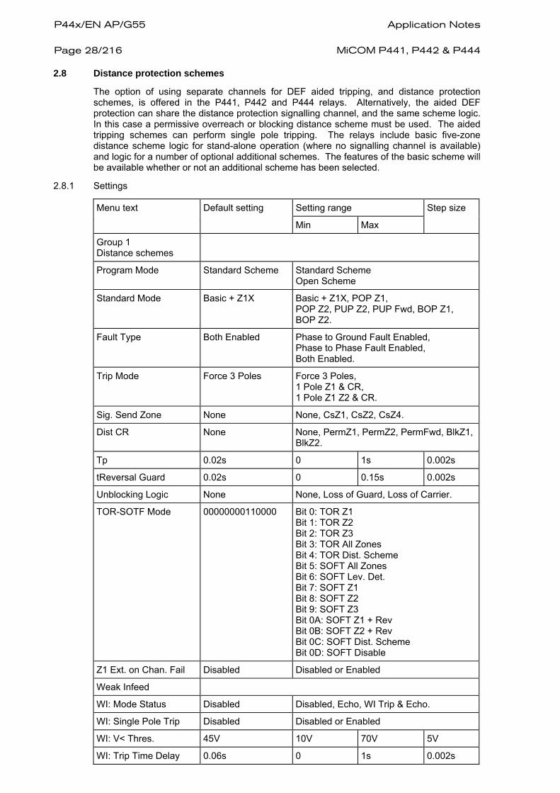
P44x/EN AP/G55 Application Notes Page 28/216
MiCOM P441, P442 & P444
2.8 Distance protection schemes
The option of using separate channels for DEF aided tripping, and distance protection schemes, is offered in the P441, P442 and P444 relays. Alternatively, the aided DEF protection can share the distance protection signalling channel, and the same scheme logic. In this case a permissive overreach or blocking distance scheme must be used. The aided tripping schemes can perform single pole tripping. The relays include basic five-zone distance scheme logic for stand-alone operation (where no signalling channel is available) and logic for a number of optional additional schemes. The features of the basic scheme will be available whether or not an additional scheme has been selected.
2.8.1 Settings
Menu text Default setting Setting range Step size
Min Max
Group 1 Distance schemes
Program Mode Standard Scheme Standard Scheme Open Scheme
Standard Mode Basic + Z1X Basic + Z1X, POP Z1, POP Z2, PUP Z2, PUP Fwd, BOP Z1, BOP Z2.
Fault Type Both Enabled Phase to Ground Fault Enabled, Phase to Phase Fault Enabled, Both Enabled.
Trip Mode Force 3 Poles Force 3 Poles, 1 Pole Z1 & CR, 1 Pole Z1 Z2 & CR.
Sig. Send Zone None None, CsZ1, CsZ2, CsZ4.
Dist CR None None, PermZ1, PermZ2, PermFwd, BlkZ1, BlkZ2.
Tp 0.02s 0 1s 0.002s
tReversal Guard 0.02s 0 0.15s 0.002s
Unblocking Logic None None, Loss of Guard, Loss of Carrier.
TOR-SOTF Mode 00000000110000 Bit 0: TOR Z1 Bit 1: TOR Z2 Bit 2: TOR Z3 Bit 3: TOR All Zones Bit 4: TOR Dist. Scheme Bit 5: SOFT All Zones Bit 6: SOFT Lev. Det. Bit 7: SOFT Z1 Bit 8: SOFT Z2 Bit 9: SOFT Z3 Bit 0A: SOFT Z1 + Rev Bit 0B: SOFT Z2 + Rev Bit 0C: SOFT Dist. Scheme Bit 0D: SOFT Disable
Z1 Ext. on Chan. Fail Disabled Disabled or Enabled
Weak Infeed
WI: Mode Status Disabled Disabled, Echo, WI Trip & Echo.
WI: Single Pole Trip Disabled Disabled or Enabled
WI: V< Thres. 45V 10V 70V 5V
WI: Trip Time Delay 0.06s 0 1s 0.002s

Application Notes P44x/EN AP/G55 MiCOM P441, P442 & P444
Page 29/216
Menu text Default setting Setting range Step size
Min Max
Loss of Load
LoL: Mode Status Disabled Disabled or Enabled
LoL: Chan. Fail Disabled Disabled or Enabled
LoL: I< 0.5 x In 0.05 x In 1 x In 0.05 x In
LoL: Window 0.04s 0.01s 0.1s 0.01s
2.8.2 Carrier send & Trip logic
2.8.2.1 Carrier send can be triggered by
• Zone1 (CSZ1)
• Zone2 (CSZ2)
• Zone4 Reverse (CSZ4)
Remarks: 1. CSZ1 means: "carrier send if Z1 detected" 2. The carrier send in Z4 is managed by "Reverse", instead of Z4 (because Reverse decision starts quicker than Z4).
The zones decision logic is described as below:
P0476XXa
Z1'Z2'
Z2'(*)Z4'
Remark: Z2'(*) if overlapping zone enabled in MiCOM S1
PDist-CS = (Z1' + Z2').CSZ2 + Z1'.CSZ1 + Reverse.CSZ4 + WI_CS
The complete logic – with DEF integrated is:
CS = PDist_CS + ( Share_Logic Share_Logic_DEF. DEF_CS) → logic with canal shared CS_DEF = Not Share_Logic_DEF. DEF_CS → logic with canal independent
(There is a 10ms delay in drop of on the carried send to avoid a logic race between this signal and the zone pick up.)
2.8.2.2 Inputs
Data Type Description
CSZ1 Configuration Carrier send for zone 1
CSZ2 Configuration Carrier send for zone 2
CSZ4 Configuration Carrier send for zone 4 (reverse)
Not Share_Logic_DEF Configuration DEF channel independent
Reverse' Internal Logic Fault detected Reverse
Z1' to Z4' Internal Logic Zone 1 to 4 decision
(blocked by Pswing or Rguard)
WI_CS Internal Logic Winfeed carrier send (Echo)
DEF_CS Internal Logic DEF carrier send

P44x/EN AP/G55 Application Notes Page 30/216
MiCOM P441, P442 & P444
2.8.2.3 Outputs
Data Type Description
CS Internal Logic Main channel Carrier send
CS_DEF Internal Logic DEF channel Carrier send
2.8.2.4 Trip logic
IEC Standard Carrier Send
Trip Logic Application Setting MiCOM
448.15.13 PUR (LFZR) or AUP
Z1 Z2.CR.T1 + Z1T1 + Z2.T2 + Z3T3... Z1 = 80% ZL PUP Z2
PUR2 POR2 (LFZR)
Z2 Z2.CR.T1 + Z1.T1 + Z2.T2 + Z3T3... Z1 = 80% ZL POP Z2
448.15.14 BOR1 orBOP
Z4 Z1. CR .T1.Tp + Z1.T2 + Z2T2 + Z3T3... Z1 > ZL BOP Z1
BOR2 BLOCK2 (LFZR)
Z4 Z2. CR .T1.Tp + Z1.T1 + Z2.T2 + Z3.T3... Z1 = 80% ZL BOP Z2
448.15.11 PUP or PUTT
Z1 Fwd.CR.T1 + Z1.T1 + Z2.T2 +... Z1 = 80% ZL PUP Fwd
448.15.16 POR1 orPOP or POTT
Z1 Z1.CR.T1 + Z1.T2 Z2.T2 + Z3.T3...
Z1 > ZL POP Z1
2.8.2.5 Tripping modes
The tripping mode is settable (Distance scheme\Trip mode):
− Force 3P : Trip 3P in all cases
− 1PZ1 & CR : Trip 1Pole in T1 for fault in Z1 and also in case of Carrier Received (aided Trip)
− 1PZ1, Z2 & CR : Trip 1Pole for T1 & T2 in T1 for fault in Z1 and CR (aided Trip) and also in Z2 with CR
Several defined aided trip logic can be selected or an open logic can be designed by user (see also section 4.5 from chapter P44x/EN HW).

Application Notes P44x/EN AP/G55 MiCOM P441, P442 & P444
Page 31/216
P0477ENa
PSB
PSB: Power swing blockingRVG: Reversal guardLOL: Loss of load
+RVG
Unblocking Basic +
AidedSchemes
+Weak-Infeed
TORSOTF
TripDistance
Protection
LOL
FIGURE 7 - MIMIC DIAGRAM
The zones unblocking/blocking logic with Power swing or Reversal guard is managed as explained in the scheme: Figure 3 (section 2.7)
• The unblocking function if enabled, carries out a function similar to Carrier receive logic. (see explanations in section 2.9.4)
• Weak infeed allows for the case where there may be no zone pick up from local end.
• TOR & SOTF applies specific logic in case of manual closing or AR closing logic.
• Trip Distance Protection manages the Trip order regarding the distance algorithm outputs, the type of trip1P or 3P, the distance timers, and the logic datas such as power swing blocking.
• Loss of Load manages a specific logic for tripping 3P in Z2 accelerated without carrier.
2.8.3 The Basic Scheme
The Basic distance scheme is suitable for applications where no signalling channel is available. Zones 1, 2 and 3 are set as described in Sections 2.7.3 to 2.7.10. In general zones 1 and 2 provide main protection for the line or cable as shown in Figure 9 below, with zone 3 reaching further to provide back up protection for faults on adjacent circuits.

P44x/EN AP/G55 Application Notes Page 32/216
MiCOM P441, P442 & P444
FIGURE 8 - SETTINGS IN MiCOM S1(GROUP1\DISTANCE SCHEME\STANDARD MODE) – 6 DIFFERENTS SETTABLE SCHEMES –
ZL
Z1A B
P3050XXa
A
Z1B
Z2A
Z2B
FIGURE 9 - MAIN PROTECTION IN THE BASIC SCHEME (NO REQUIREMENT FOR SIGNALLING CHANNEL)
Key:
A, B = Relay locations;
ZL = Impedance of the protected line.

Application Notes P44x/EN AP/G55 MiCOM P441, P442 & P444
Page 33/216
&
Protection A Protection B
Z1'
T1
&
Z2'
T2
&
Z3'
T3
&
Zp'
Tzp
Z4'
T4&
≥1
&
&
&
&
&
Z1'
T1
Z2'
T2
Z3'
T3
Zp'
Tzp
Z4'
T4
≥1
tZ1
tZ2
tZ3
tZp
tZ4
tZ1
tZ2
tZ3
tZp
tZ4
Trip Trip
P0543ENa
FIGURE 10 - LOGIC DIAGRAM FOR THE BASIC SCHEME
Figure 10 shows the tripping logic for the Basic scheme. Note that for the P441, P442 and P444 relays, zone timers tZ1 to tZ4 are started at the instant of fault detection, which is why they are shown as a parallel process to the distance zones. The use of an apostrophe in the logic (eg. the ‘ in Z1’) indicates that protection zones are stabilised to avoid maloperation for transformer magnetising inrush current. The method used to achieve stability is based on second harmonic current detection.
The Basic scheme incorporates the following features:
Instantaneous zone 1 tripping. Alternatively, zone 1 can have an optional time delay of 0 to 10s.
Time delayed tripping by zones 2, 3, 4 and P. Each with a time delay set between 0 and 10s.
The Basic scheme is suitable for single or double circuit lines fed from one or both ends. The limitation of the Basic scheme is that faults in the end 20% sections of the line will be cleared after the zone 2 time delay. Where no signalling channel is available, then improved fault clearance times can be achieved through the use of a zone 1 extension scheme or by using loss of load logic, as described below. Under certain conditions however, these two schemes will still result in time delayed tripping. Where high speed protection is required over the entire line, then a channel aided scheme will have to be employed.
2.8.4 Zone 1 Extension Scheme
Auto-reclosure is widely used on radial overhead line circuits to re-establish supply following a transient fault. A Zone 1 extension scheme may therefore be applied to a radial overhead feeder to provide high speed protection for transient faults along the whole of the protected line. Figure 11 shows the alternative reach selections for zone 1: Z1 or the extended reach Z1X.

P44x/EN AP/G55 Application Notes Page 34/216
MiCOM P441, P442 & P444
P3052ENa
ZL
Z1AA B
Z1B
Z1 Extension (A)
Z1 Extension (B)
FIGURE 11 - ZONE 1 EXTENSION SCHEME DEFINIED AS DESCRIBED ABOVE:
Z1 < Z1X < Z2 or Z1 < Z2 < Z1X (with Z1 < ZL < Z1X)
In this scheme, zone 1X is enabled and set to overreach the protected line. A fault on the line, including one in the end 20% not covered by zone 1, will now result in instantaneous tripping followed by autoreclosure. Zone 1X has resistive reaches and residual compensation similar to zone 1. The autorecloser in the relay is used to inhibit tripping from zone 1X such that upon reclosure the relay will operate with Basic scheme logic only, to co-ordinate with downstream protection for permanent faults. Thus, transient faults on the line will be cleared instantaneously, which will reduce the probability of a transient fault becoming permanent. The scheme can, however, operate for some faults on an adjacent line, although this will be followed by autoreclosure with correct protection discrimination. Increased circuit breaker operations would occur, together with transient loss of supply to a substation.
The time delays associated with extended zone Z1X are shown in Table 2 below:
Scenario Z1X Time Delay
First fault trip = tZ1
Fault trip for persistent fault on autoreclose = tZ2
TABLE 2 - TRIP TIME DELAYS ASSOCIATED WITH ZONE 1X
The Zone 1 Extension scheme is selected by setting the Z1X Enable bit in the Zone Status function links to 1.
FIGURE 12 – SETTINGS IN MiCOM S1 (GROUP1\DISTANCE SCHEME\ZONE STATUS)
Remark: To enable the Z1X logic, the DDB "Z1X extension" cell must be linked in the PSL (opto/reclaim time…)
FIGURE 13 - DISTANCE SCHEME WITHOUT CARRIER & Z1 EXTENDED
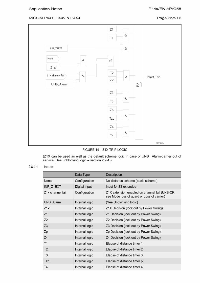
Application Notes P44x/EN AP/G55 MiCOM P441, P442 & P444
Page 35/216
P0478ENa
&
PDist_Trip&T2
Z2'
&
Z3'
T3
&
Zp'
Tzp
Z4'
T4&
≥1
Z1'
T1
>1
Z1x'
INP_Z1EXT
UNB_Alarm
Z1X channel fail &
&
&None
FIGURE 14 – Z1X TRIP LOGIC
(Z1X can be used as well as the default scheme logic in case of UNB _Alarm-carrier out of service (See unblocking logic – section 2.9.4))
2.8.4.1 Inputs
Data Type Description
None Configuration No distance scheme (basic scheme)
INP_Z1EXT Digital input Input for Z1 extended
Z1x channel fail Configuration Z1X extension enabled on channel fail (UNB-CR. see Mode loss of guard or Loss of carrier)
UNB_Alarm Internal logic (See Unblocking logic)
Z1x’ Internal logic Z1X Decision (lock out by Power Swing)
Z1’ Internal logic Z1 Decision (lock out by Power Swing)
Z2’ Internal logic Z2 Decision (lock out by Power Swing)
Z3’ Internal logic Z3 Decision (lock out by Power Swing)
Zp’ Internal logic Zp Decision (lock out by Power Swing)
Z4’ Internal logic Z4 Decision (lock out by Power Swing)
T1 Internal logic Elapse of distance timer 1
T2 Internal logic Elapse of distance timer 2
T3 Internal logic Elapse of distance timer 3
Tzp Internal logic Elapse of distance timer p
T4 Internal logic Elapse of distance timer 4

P44x/EN AP/G55 Application Notes Page 36/216
MiCOM P441, P442 & P444
2.8.4.2 Outputs
Data Type Description
PDist_Dec Internal logic Trip order by Distance Protection
2.8.5 Loss of Load Accelerated Tripping (LoL)
The loss of load accelerated trip logic is shown in Figure 15. The loss of load logic provides fast fault clearance for faults over the whole of a double end fed protected circuit for all types of fault, except three phase. The scheme has the advantage of not requiring a signalling channel. Alternatively, the logic can be chosen to be enabled when the channel associated with an aided scheme has failed. This failure is detected by permissive scheme unblocking logic, or a Channel Out of Service (COS) opto input.
Any fault located within the reach of Zone 1 will result in fast tripping of the local circuit breaker. For an end zone fault with remote infeed, the remote breaker will be tripped in Zone 1 by the remote relay and the local relay can recognise this by detecting the loss of load current in the healthy phases. This, coupled with operation of a Zone 2 comparator causes tripping of the local circuit breaker.
Before an accelerated trip can occur, load current must have been detected prior to the fault. The loss of load current opens a window during which time a trip will occur if a Zone 2 comparator operates. A typical setting for this window is 40ms as shown in Figure 15, although this can be altered in the menu LoL: Window cell. The accelerated trip is delayed by 18ms to prevent initiation of a loss of load trip due to circuit breaker pole discrepancy occurring for clearance of an external fault. The local fault clearance time can be deduced as follows:
t = Z1d + 2CB + LDr + 18ms
Where:
Z1d = maximum downstream zone 1 trip time
CB = Breaker operating time
LDr = Upstream level detector (LoL: I<) reset time
For circuits with load tapped off the protected line, care must be taken in setting the loss of load feature to ensure that the I< level detector setting is above the tapped load current. When selected, the loss of load feature operates in conjunction with the main distance scheme that is selected. In this way it provides high speed clearance for end zone faults when the Basic scheme is selected or, with permissive signal aided tripping schemes, it provides high speed back-up clearance for end zone faults if the channel fails.
Note that loss of load tripping is only available where 3 pole tripping is used.

Application Notes P44x/EN AP/G55 MiCOM P441, P442 & P444
Page 37/216
P3053ENa
Z2
Z2
Trip
Z2
LOL-A
LOL-BLOL-C
Z1
Z1Z1 Z1
&
&&
0
40ms
18ms
01
FIGURE 15 - LOSS-OF-LOAD ACCELERATED TRIP SCHEME
2.8.5.1 Inputs
Data Type Description
Activ_LOL Configuration Loss of Load activated (LOL)
TRIP_Any Internal Logic Any trip (internal or external)
LOL. channel fail Configuration LOL enabled on channel fail (alarm carrier)
Force_3P_Dist Internal Logic Force Trip 3P in Distance Logic
Force_3P_DEF Configuration Force Trip 3P in DEF Logic
Activ_WI Configuration Weak-infeed activated (Trip & Echo)
WI_1pTrip Configuration WI 1Pole trip
PZ1, PZ2, PFwd, None Configuration Underreach scheme : Z1 < ZL PZ1: permissive underreach Z1 PZ2: permissive underreach Z2 PFwd: permissive underreach forward None: no distance scheme (basic scheme)
Z1<ZL Configuration Underreach scheme in Z1
UNB_CR_Alarm Internal Logic Carrier out of service Alarm
LOL Wind Configuration Activated time window for Loss Of Load logic
IA_LOL< Internal Logic Threshold I< for phase A in LOL logic
IB_LOL< Internal Logic Threshold I< for phase B in LOL logic
IC_LOL< Internal Logic Threshold I< for phase C in LOL logic
Flt A Internal Logic Faulty Phase A
Flt B Internal Logic Faulty Phase B
Flt C Internal Logic Faulty Phase C
Flt AB Internal Logic Faulty Phase AB
Flt BC Internal Logic Faulty Phase BC
Flt AC Internal Logic Faulty Phase AC
Z2' Internal Logic Fault in Z2 (lockout by Pswing or RGuard)

P44x/EN AP/G55 Application Notes Page 38/216
MiCOM P441, P442 & P444
2.8.5.2 Outputs
Data Type Description
LOL_Trip3p Internal Logic 3P Trip by LOL logic
P0479ENa
Z2'
LOL. channel fail
Flt C
Flt B
Flt A
IB_LOL<
IC_LOL<
None
&
&
IA_LOL<
TRIP _Any
Activ_LOL
S QR
UNB_CR_Alarm
&&
Activ WI = WI/echo & WI_1pTrip = No
Force3P_DEF
Force_3P_Dist
&
Yes
3p
PZ1, PZ2, PFwd
LOL Wind
Flt AB
Flt BC
Flt AC
18 ms
&
&
&
&
&
T 0
&
0 T
Z1<ZL
S QR
LOL_Trip3P
≥1
≥1
FIGURE 16 – LOSS OF LOAD TRIP LOGIC

Application Notes P44x/EN AP/G55 MiCOM P441, P442 & P444
Page 39/216
2.9 Channel-aided distance schemes
The following channel aided distance tripping schemes are available when the Standard program mode is selected:
• Permissive Underreach Transfer Trip Schemes PUP Z2 and PUP Fwd;
• Permissive Overreach Transfer Trip Schemes POP Z2 and POP Z1;
• Weak infeed logic to supplement permissive overreach schemes;
• Unblocking logic to supplement permissive schemes;
• Blocking Schemes BOP Z2 and BOP Z1;
• Current reversal guard logic to prevent maloperation of any overreaching zone used in a channel aided scheme, when fault clearance is in progress on the parallel circuit of a double circuit line.
2.9.1 Permissive Underreach Transfer Trip Schemes PUP Z2 and PUP Fwd
To provide fast fault clearance for all faults, both transient and permanent, along the length of the protected circuit, it is necessary to use a signal aided tripping scheme. The simplest of these is the permissive underreach protection scheme (PUP), of which two variants are offered in the P441, P442 and P444 relays. The channel for a PUP scheme is keyed by operation of the underreaching zone 1 elements of the relay. If the remote relay has detected a forward fault upon receipt of this signal, the relay will operate with no additional delay. Faults in the last 20% of the protected line are therefore cleared with no intentional time delay.
Listed below are some of the main features/requirements for a permissive underreaching scheme:
• Only a simplex signalling channel is required.
• The scheme has a high degree of security since the signalling channel is only keyed for faults within the protected line.
• If the remote terminal of a line is open then faults in the remote 20% of the line will be cleared via the zone 2 time delay of the local relay.
• If there is a weak or zero infeed from the remote line end, (ie. current below the relay sensitivity), then faults in the remote 20% of the line will be cleared via the zone 2 time delay of the local relay.
• If the signalling channel fails, Basic distance scheme tripping will be available.
P3054XXa
ZL
Z1AA B
Z1B
Z2A
Z2B
FIGURE 17 - ZONE 1 AND 2 REACHES FOR PERMISSIVE UNDERREACH SCHEMES

P44x/EN AP/G55 Application Notes Page 40/216
MiCOM P441, P442 & P444
2.9.1.1 Permissive Underreach Protection, Accelerating Zone 2 (PUP Z2)
This scheme is similar to that used in the other ALSTOM Grid distance relays, allowing an instantaneous Z2 trip on receipt of the signal from the remote end protection. Figure 11 shows the simplified scheme logic.
Send logic: Zone 1
Permissive trip logic: Zone 2 plus Channel Received.
Protection A Protection B
&
Z1'
&
Z3'
&
Zp'
&
Z4'
Z2'
&
&
&
&
&
&
Z1'
Z3'
Zp'
Z4'
Z2'
&
≥1
&
P3055ENa
&
tZ1
tZ2
tZ3
tZp
tZ4
SignalSend Z1'
Trip Trip
SignalSend Z1'
tZ1
tZ2
tZ3
tZp
tZ4
≥1
FIGURE 18 - THE PUP Z2 PERMISSIVE UNDERREACH SCHEME (SEE TRIP LOGIC TABLE IN SECTION 2.8.2.4)
2.9.1.2 Permissive Underreach Protection Tripping via Forward Start (PUP Fwd)
This scheme is similar to that used in the ALSTOM Grid EPAC and PXLN relays, allowing an instantaneous Z2 or Z3 trip on receipt of the signal from the remote end protection. Figure 19 shows the simplified scheme logic.
Send logic: Zone 1
Permissive trip logic: Underimpedance Start within any Forward Distance Zone, plus Channel Received.

Application Notes P44x/EN AP/G55 MiCOM P441, P442 & P444
Page 41/216
Protection A Protection B
&
Z1'
&
Z3'
&
Zp'
&Z4'
Z2'&
&
&
&
&
&
Z1'
Z3'
Zp'
Z4'
Z2'
≥1 ≥1
& &
tZ1
tZ2
tZ3
tZp
tZ4
Fwd'
<Z
TripTrip
tZ1
tZ2
tZ3
tZp
tZ4
Fwd'
<Z
SignalSend Z1'
SignalSend Z1'
P3056ENa
FIGURE 19 - THE PUP FWD PERMISSIVE UNDERREACH SCHEME (SEE TRIP LOGIC TABLE IN SECTION 2.8.2.4)
Key:
Fwd = Forward fault detection;
<Z = Underimpedance start by Z2 or Z3.
2.9.2 Permissive Overreach Transfer Trip Schemes POP Z2 and POP Z1
The P441, P442 and P444 relays offer two variants of permissive overreach protection schemes (POP), having the following common features/requirements:
• The scheme requires a duplex signalling channel to prevent possible relay maloperation due to spurious keying of the signalling equipment. This is necessary due to the fact that the signalling channel is keyed for faults external to the protected line.
• The POP Z2 scheme may be more advantageous than permissive underreach schemes for the protection of short transmission lines, since the resistive coverage of the Zone 2 elements may be greater than that of the Zone 1 elements.
• Current reversal guard logic is used to prevent healthy line protection maloperation for the high speed current reversals experienced in double circuit lines, caused by sequential opening of circuit breakers.
• If the signalling channel fails, Basic distance scheme tripping will be available.
2.9.2.1 Permissive Overreach Protection with Overreaching Zone 2 (POP Z2)
This scheme is similar to that used in the ALSTOM Grid LFZP and LFZR relays. Figure 20 shows the zone reaches, and Figure 21 the simplified scheme logic. The signalling channel is keyed from operation of the overreaching zone 2 elements of the relay. If the remote relay has picked up in zone 2, then it will operate with no additional delay upon receipt of this signal. The POP Z2 scheme also uses the reverse looking zone 4 of the relay as a reverse fault detector. This is used in the current reversal logic and in the optional weak infeed echo feature.
Send logic: Zone 2
Permissive trip logic: Zone 2 plus Channel Received.

P44x/EN AP/G55 Application Notes Page 42/216
MiCOM P441, P442 & P444
P3054XXa
ZL
Z1AA B
Z1B
Z2A
Z2B
FIGURE 20 - MAIN PROTECTION IN THE POP Z2 SCHEME
Protection A Protection B
&
Z1'
&
Z3'
&
Zp'
&
Z4'
Z2'
&
&
&
&
&
&
Z1'
Z3'
Zp'
Z4'
Z2'
& &
≥1 ≥1
tZ1
tZ2
tZ3
tZp
tZ4
Trip Trip
SignalSend Z2'
SignalSend Z2'
tZ1
tZ2
tZ3
tZp
tZ4
P3058ENa
FIGURE 21 - LOGIC DIAGRAM FOR THE POP Z2 SCHEME (SEE TRIP LOGIC TABLE IN SECTION 2.8.2.4)
2.9.2.2 Permissive Overreach Protection with Overreaching Zone 1 (POP Z1)
This scheme is similar to that used in the ALSTOM Grid EPAC and PXLN relays. Figure 22 shows the zone reaches, and Figure 23 the simplified scheme logic. The signalling channel is keyed from operation of zone 1 elements set to overreach the protected line. If the remote relay has picked up in zone 1, then it will operate with no additional delay upon receipt of this signal. The POP Z1 scheme also uses the reverse looking zone 4 of the relay as a reverse fault detector. This is used in the current reversal logic and in the optional weak infeed echo feature.
NOTE: Should the signalling channel fail, the fastest tripping in the Basic scheme will be subject to the tZ2 time delay.
Send logic: Zone 1
Permissive trip logic: Zone 1 plus Channel Received.

Application Notes P44x/EN AP/G55 MiCOM P441, P442 & P444
Page 43/216
P3059XXa
ZL
Z1A
A B
Z1B
Z2A
Z2B
FIGURE 22 - MAIN PROTECTION IN THE POP Z1 SCHEME
Protection A Protection B
&
Z2'
&
Z3'
&
Zp'
&Z4'
&
&
&
&
&
&
Z2'
Z3'
Zp'
Z4'≥1 ≥1
&
Z1' Z1'
&
tZ2
tZ1
tZ3
tZp
tZ4
SignalSend Z1'
SignalSend Z1'
Trip Trip
tZ2
tZ1
tZ3
tZp
tZ4
P3060ENa
FIGURE 23 - LOGIC DIAGRAM FOR THE POP Z1 SCHEME (SEE TRIP LOGIC TABLE IN SECTION 2.8.2.4)
2.9.3 Permissive Overreach Schemes Weak Infeed Features
Weak infeed logic can be enabled to run in parallel with all the permissive schemes. Two options are available: WI Echo, and WI Tripping.
NOTE: The 2 modes are blocked during Fuse failure conditions.

P44x/EN AP/G55 Application Notes Page 44/216
MiCOM P441, P442 & P444
P0480ENa
&
WI Logic confirmed
Power swing detection
Reverse
Distance start
UNB_CR
Activ_WI
FFUS_Confirmed 150 ms
60 ms
0 T
200 ms
0 T
Pulse Timer
Echo or WI/echo
&
Def_Reverse
FIGURE 24 - WEAK INFEED MODE ACTIVATION LOGIC
• Weak Infeed Echo
For permissive schemes, a signal would only be sent if the required signal send zone were to detect a fault. However, the fault current infeed at one line end may be so low as to be insufficient to operate any distance zones, and risks a failure to send the signal. Also, if one circuit breaker had already been left open, the current infeed would be zero. These are termed weak infeed conditions, and may result in slow fault clearance at the strong infeed line end (tripping after time tZ2). To avoid this slow tripping, the weak infeed relay can be set to “echo” back any channel received to the strong infeed relay (ie. to immediately send a signal once a signal has been received). This allows the strong infeed relay to trip instantaneously in its permissive trip zone. The additional signal send logic is:
Echo send:
WI logic
UNB_CR& WI_CS
(NB: For UNB_CR explanation see Unblocking logic in next section 2.9.4)
• Weak Infeed Tripping
Weak infeed echo logic ensures an aided trip at the strong infeed terminal but not at the weak infeed. The P441, P442 and P444 relays also have a setting option to allow tripping of the weak infeed circuit breaker of a faulted line.
Three undervoltage elements, Va<, Vb< and Vc< are used to detect the line fault at the weak infeed terminal, with a common setting typically 70% of rated phase-neutral voltage. This voltage check prevents tripping during spurious operations of the channel or during channel testing.

Application Notes P44x/EN AP/G55 MiCOM P441, P442 & P444
Page 45/216
P0481ENa
VA<_WI
WI_A&CB 52a_phA
CB 52a_phB
CB 52a_phC
VB<_WI
WI_B&
VC<_WI
WI_C&
UNB_CR
&
&
&
FLT_A
FLT_B
FLT_B
FIGURE 25 - WEAK INFEED PHASE SELECTION LOGIC
UNB_CR is used as a filter to avoid a permanent phase selection which could be maintained if Cbaux signals are not mapped in the PSL (when line is opened).
The additional weak infeed trip logic is:
Weak infeed trip: No Distance Zone Operation, plus reverse directional decision, plus V<, plus Channel Received.
Weak infeed tripping is time delayed according to the WI: Trip Time Delay value, usually set at 60ms. Due to the use of phase segregated undervoltage elements, single pole tripping can be enabled for WI trips if required. If single pole tripping is disabled a three pole trip will result after the time delay.
P0482ENa
WI_A
WI_C
WI_B
Activ_WI
&Trip1P_WI
WI_PhaseA
WI_PhaseB
WI_PhaseC
&
&
&
Yes
WI/echo
≥1
≥1
≥1
≥1
FIGURE 26 – WEAK INFEED TRIP DECISION LOGIC
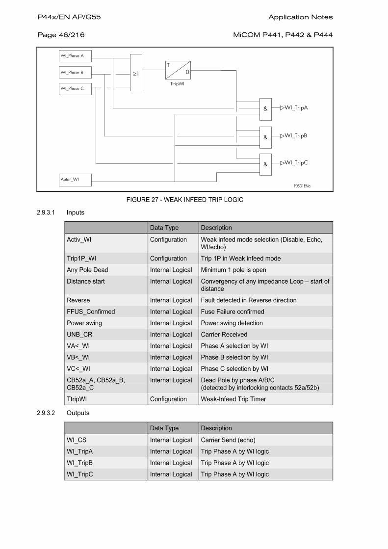
P44x/EN AP/G55 Application Notes Page 46/216
MiCOM P441, P442 & P444
WI_Phase A
&
&
&
WI_TripA
WI_TripB
WI_TripC
TtripWI
Autor_WIP0531ENa
T0≥1WI_Phase B
WI_Phase C
FIGURE 27 - WEAK INFEED TRIP LOGIC
2.9.3.1 Inputs
Data Type Description
Activ_WI Configuration Weak infeed mode selection (Disable, Echo, WI/echo)
Trip1P_WI Configuration Trip 1P in Weak infeed mode
Any Pole Dead Internal Logical Minimum 1 pole is open
Distance start Internal Logical Convergency of any impedance Loop – start of distance
Reverse Internal Logical Fault detected in Reverse direction
FFUS_Confirmed Internal Logical Fuse Failure confirmed
Power swing Internal Logical Power swing detection
UNB_CR Internal Logical Carrier Received
VA<_WI Internal Logical Phase A selection by WI
VB<_WI Internal Logical Phase B selection by WI
VC<_WI Internal Logical Phase C selection by WI
CB52a_A, CB52a_B, CB52a_C
Internal Logical Dead Pole by phase A/B/C (detected by interlocking contacts 52a/52b)
TtripWI Configuration Weak-Infeed Trip Timer
2.9.3.2 Outputs
Data Type Description
WI_CS Internal Logical Carrier Send (echo)
WI_TripA Internal Logical Trip Phase A by WI logic
WI_TripB Internal Logical Trip Phase A by WI logic
WI_TripC Internal Logical Trip Phase A by WI logic

Application Notes P44x/EN AP/G55 MiCOM P441, P442 & P444
Page 47/216
2.9.4 Permissive Scheme Unblocking Logic
Two modes of unblocking logic are available for use with permissive schemes, (Blocking schemes are excluded).
The unblocking logic creates the : "UNB_Alarm" and the : "UNB_CR" signals, which depend upon:
• Inputs signals [binary inputs: CR (Carrier Receive) COS (Carrier Out of Service)]
• Settings used for the distance channel & DEF aided trip channel
• Shared or independent logic between DEF & Distance
• Carrier Out of Service detected
Different modes are selectable:
• None (basic mode)
• Loss of Guard mode
• Loss of Carrier mode
Two types of carrier received signals are used:
• Carrier received (INP_CR - binary input)
• Carrier Out of Service (INP_COS - binary input for distance logic) and (INP_COS_DEF - binary input for DEF logic)
2.9.4.1 None
The status of opto is copied directly:
UNB_ALARM = INP_COS + INP_COS_DEF
UNB_CR = INP_CR
UNB_CR_DEF = INP_CR_DEF
2.9.4.2 Loss of Guard Mode
This mode is designed for use with frequency shift keyed (FSK) power line carrier communications. When the protected line is healthy a guard frequency is sent between line ends, to verify that the channel is in service. However, when a line fault occurs and a permissive trip signal must be sent over the line, the power line carrier frequency is shifted to a new (trip) frequency. Thus, distance relays should receive either the guard, or trip frequency, but not both together. With any permissive scheme, the PLC communications are transmitted over the power line which may contain a fault. So, for certain fault types the line fault can attenuate the PLC signals, so that the permissive signal is lost and not received

P44x/EN AP/G55 Application Notes Page 48/216
MiCOM P441, P442 & P444
at the other line end. To overcome this problem, when the guard is lost and no “trip” frequency is received, the relay opens a window of time during which the permissive scheme logic acts as though a “trip” signal had been received. Two opto inputs to the relay need to be assigned, one is the Channel Receive opto, the second is designated Loss of Guard (the inverse function to guard received). The function logic is summarised in Table 3.
System Condition
Permissive Channel Received
Loss of Guard
Permissive Trip Allowed
Alarm Generated
Healthy Line No No No No
Internal Line Fault Yes Yes Yes No
Unblock No Yes Yes, during a 150ms window
Yes, delayed on pickup by 150ms
Signalling Anomaly
Yes No No Yes, delayed on pickup by 150ms
TABLE 3 - LOGIC FOR THE LOSS OF GUARD FUNCTION
The window of time during which the unblocking logic is enabled starts 10ms after the guard signal is lost, and continues for 150ms. The 10ms delay gives time for the signalling equipment to change frequency as in normal operation.
For the duration of any alarm condition, zone 1 extension logic will be invoked if the option Z1 Ext on Chan. Fail has been Enabled.
P3061ENa
10 ms
0&
&
Pulse Timer
150 ms
S QR
150 ms
0
Pulse Timer
200 ms
S QR
=1
≥1
UNB Alarm
UNB CR
INP COS
Indicates by digital inputthe Loss of guard
INP CR
FIGURE 28 - LOSS OF GUARD LOGIC
INP_CR INP_COS UNB_CR UNB_Alarm
0 0 0 0
1 1 1 0
0 1 1 (Window) 1 (delayed)
1 0 0 1 (delayed)

Application Notes P44x/EN AP/G55 MiCOM P441, P442 & P444
Page 49/216
2.9.4.3 Loss of Carrier
In this mode the signalling equipment used is such that a carrier/data messages are continuously transmitted across the channel, when in service. For a permissive trip signal to be sent, additional information is contained in the carrier (eg. a trip bit is set), such that both the carrier and permissive trip are normally received together. Should the carrier be lost at any time, the relay must open the unblocking window, in case a line fault has also affected the signalling channel. Two opto inputs to the relay need to be assigned, one is the Channel Receive opto, the second is designated Loss of Carrier (the inverse function to carrier received). The function logic is summarised in Table 4.
System Condition
Permissive Channel Received
Loss of Guard
Permissive Trip Allowed
Alarm Generated
Healthy Line No No No No
Internal Line Fault Yes No Yes No
Unblock No Yes Yes, during a 150ms window
Yes, delayed on pickup by 150ms
Signalling Anomaly
No Yes No Yes, delayed on pickup by 150ms
TABLE 4 - LOGIC FOR THE LOSS OF CARRIER FUNCTION
The window of time during which the unblocking logic is enabled starts 10ms after the guard signal is lost, and continues for 150ms.
For the duration of any alarm condition, zone 1 extension logic will be invoked if the option Z1 Ext on Chan. Fail has been Enabled.
P3062ENa
10 ms
&
Pulse Timer
150 ms
150 ms
Pulse Timer
200 ms
≥1
UNB Alarm
INP COS
Indicates by digital inputthe Loss of Carrier
INP CRUNB CR
S0
0
QR
S QR
&
FIGURE 29 - LOSS OF CARRIER

P44x/EN AP/G55 Application Notes Page 50/216
MiCOM P441, P442 & P444
INP_CR INP_COS UNB_CR UNB_Alarm
0 0 0 0
0 1 1 (Window) 1 (delayed)
1 0 1 0
1 1 0 1 (delayed)
NOTE: For DEF the logic will used depende upon which settings are enabled:
• Same channel (shared)
In this case, the DEF channel is the Main Distance channel signal (the scheme & contacts of carrier received will be identical)
• Independent channel (2 Different channels) – (2 independent contacts)
2.9.4.4 Inputs
Data Type Description
INP_CR Digital input Distance channel carrier received
INP_CR_DEF Digital input DEF channel carrier received
INP_COS Digital input Carrier Out of Service - Distance channel
INP_COS_DEF Digital input Carrier Out of Service – DEF channel
2.9.4.5 Outputs
Data Type Description
UNB_CR internal logic Internal carrier received – Distance channel
UNB_CR _DEF internal logic Internal carrier received – DEF channel
UNB_Alarm internal logic Alarm channel Main & DEF
2.9.5 Blocking Schemes BOP Z2 and BOP Z1
The P441, P442 and P444 relays offer two variants of blocking overreach protection schemes (BOP). With a blocking scheme, the signalling channel is keyed from the reverse looking zone 4 element, which is used to block fast tripping at the remote line end. Features are as follows:
• BOP schemes require only a simplex signalling channel.
• Reverse looking Zone 4 is used to send a blocking signal to the remote end to prevent unwanted tripping.
• When a simplex channel is used, a BOP scheme can easily be applied to a multi-terminal line provided that outfeed does not occur for any internal faults.
• The blocking signal is transmitted over a healthy line, and so there are no problems associated with power line carrier signalling equipment.
• BOP schemes provides similar resistive coverage to the permissive overreach schemes.
• Fast tripping will occur at a strong source line end, for faults along the protected line section, even if there is weak or zero infeed at the other end of the protected line.
• If a line terminal is open, fast tripping will still occur for faults along the whole of the protected line length.
• If the signalling channel fails to send a blocking signal during a fault, fast tripping will occur for faults along the whole of the protected line, but also for some faults within the next line section.

Application Notes P44x/EN AP/G55 MiCOM P441, P442 & P444
Page 51/216
• If the signalling channel is taken out of service, the relay will operate in the
conventional Basic mode.
• A current reversal guard timer is included in the signal send logic to prevent unwanted trips of the relay on the healthy circuit, during current reversal situations on a parallel circuit.
• To allow time for a blocking signal to arrive, a short time delay on aided tripping, Tp, must be used, as follows:
Recommended Tp setting = Max. signalling channel operating time + 14ms
2.9.5.1 Blocking Overreach Protection with Overreaching Zone 2 (BOP Z2)
This scheme is similar to that used in the other ALSTOM Grid distance relays. Figure 30 shows the zone reaches, and Figure 31 the simplified scheme logic. The signalling channel is keyed from operation of the reverse zone 4 elements of the relay. If the remote relay has picked up in zone 2, then it will operate after the Tp delay if no block is received.
Send logic: Reverse Zone 4
Trip logic: Zone 2, plus Channel NOT Received, delayed by Tp.
P3063XXa
ZL
Z1AA B
Z1B
Z2A
Z2B
Z4A
Z4B
FIGURE 30 - MAIN PROTECTION IN THE BOP Z2 SCHEME
P0533ENa
Protection A Protection B
&
Z1'
T1
&
Z3'
T3
&
Zp'
Tzp
&
Z4'
T4
T2
Z2'
&
&
&
&
&
Z1'
T1
Z3'
T3
Zp'
Tzp
Z4'
T4
&Tp
&
Emission Téléac
Emission Téléac
Z2'
T2&
Tp
tZ1
tZ2
tZ3
tZp
tZ4
SignalSend Z4'
SignalSend Z4'
tZ1
tZ2
tZ3
tZp
tZ4
Trip Trip≥1 ≥1
FIGURE 31 - LOGIC DIAGRAM FOR THE BOP Z2 SCHEME (SEE TRIP LOGIC TABLE IN SECTION 2.8.2.4)

P44x/EN AP/G55 Application Notes Page 52/216
MiCOM P441, P442 & P444
2.9.5.2 Blocking Overreach Protection with Overreaching Zone 1 (BOP Z1)
This scheme is similar to that used in the ALSTOM Grid EPAC and PXLN relays. Figure 32 shows the zone reaches, and Figure 33 the simplified scheme logic. The signalling channel is keyed from operation of the reverse zone 4 elements of the relay. If the remote relay has picked up in overreaching zone 1, then it will operate after the Tp delay if no block is received.
NOTE: The fastest tripping is always subject to the Tp delay.
Send logic: Reverse Zone 4
Trip logic: Zone 1, plus Channel NOT Received, delayed by Tp.
P3065XXa
ZL
Z1A
A B
Z1B
Z2A
Z2B
Z4A
Z4B
FIGURE 32 - MAIN PROTECTION IN THE BOP Z1 SCHEME
P3066ENa
Protection A Protection B
&
Z2'
&
Z3'
&
Zp'
&
Z4'
Z1'
&
&
&
&
&
Z2'
Z3'
Zp'
Z4'
&
≥1 ≥1
Tp
&
Z1'
&
Tp
tZ2
tZ1
tZ3
tZp
tZ4
TripTrip
SignalSend Z4'
SignalSend Z4'
tZ2
tZ1
tZ3
tZp
tZ4
FIGURE 33 - LOGIC DIAGRAM FOR THE BOP Z1 SCHEME (SEE TRIP LOGIC TABLE IN SECTION 2.8.2.4)

Application Notes P44x/EN AP/G55 MiCOM P441, P442 & P444
Page 53/216
2.10 Distance schemes current reversal guard logic
For double circuit lines, the fault current direction can change in one circuit when circuit breakers open sequentially to clear the fault on the parallel circuit. The change in current direction causes the overreaching distance elements to see the fault in the opposite direction to the direction in which the fault was initially detected (settings of these elements exceed 150% of the line impedance at each terminal). The race between operation and resetting of the overreaching distance elements at each line terminal can cause the Permissive Overreach, and Blocking schemes to trip the healthy line. A system configuration that could result in current reversals is shown in Figure 34. For a fault on line L1 close to circuit breaker B, as circuit breaker B trips it causes the direction of current flow in line L2 to reverse.
A
C
B
D
A BFaultFault
Strongsource
Weaksource
L1
L2
L1
L2 C D
P3067ENa
t2(D)t2(C)
Note how after circuit breaker B on line L1 opensthe direction of current flow in line L2 is reversed.
FIGURE 34 - CURRENT REVERSAL IN DOUBLE CIRCUIT LINES
(See the zone’ description in section 2.4 – unblock/blocking logical scheme)
2.10.1 Permissive Overreach Schemes Current Reversal Guard
The current reversal guard incorporated in the POP scheme logic is initiated when the reverse looking Zone 4 elements operate on a healthy line. Once the reverse looking Zone 4 elements have operated, the relay’s permissive trip logic and signal send logic are inhibited at substation D (Figure 34). The reset of the current reversal guard timer is initiated when the reverse looking Zone 4 resets. A time delay tREVERSAL GUARD is required in case the overreaching trip element at end D operates before the signal send from the relay at end C has reset. Otherwise this would cause the relay at D to over trip. Permissive tripping for the relays at D and C substations is enabled again, once the faulted line is isolated and the current reversal guard time has expired. The recommended setting is:
tREVERSAL GUARD = Maximum signalling channel reset time + 35ms.
2.10.2 Blocking Scheme Current Reversal Guard
The current reversal guard incorporated in the BOP scheme logic is initiated when a blocking signal is received to inhibit the channel-aided trip. When the current reverses and the reverse looking Zone 4 elements reset, the blocking signal is maintained by the timer tREVERSAL GUARD. Thus referring to Figure 34, the relays in the healthy line are prevented from over tripping due to the sequential opening of the circuit breakers in the faulted line. After the faulty line is isolated, the reverse-looking Zone 4 elements at substation C and the forward looking elements at substation D will reset. The recommended setting is:
Where Duplex signalling channels are used:
tREVERSAL GUARD = Maximum signalling channel operating time + 14ms.
Where Simplex signalling channels are used:
tREVERSAL GUARD = Maximum signalling channel operating time - minimum signalling channel reset time + 14ms.

P44x/EN AP/G55 Application Notes Page 54/216
MiCOM P441, P442 & P444
2.11 Distance schemes in the “open” programming mode
When a scheme is required which is not covered in the Standard modes above, the Open programming mode can be selected. The user then has the facility to decide which distance relay zone is to be used to key the signalling channel, and what type of aided scheme runs when the channel is received. The signal send zone options are shown in Table 5, and the aided scheme options on channel receipt are shown in Table 6.
Setting Signal Send Zone Function
None No Signal Send To configure a Basic scheme.
CsZ1 Zone 1 To configure a Permissive scheme.
CsZ2 Zone 2 To configure a Permissive scheme.
CsZ4 Zone 4 To configure a Blocking scheme.
TABLE 5 - SIGNAL SEND ZONES IN OPEN SCHEMES
Setting Aided Scheme Function
None None To configure a Basic scheme.
PermZ1 To configure a Permissive scheme where Zone 1 can only trip if a channel is received.
PermZ2 To configure a Permissive scheme where Zone 2 can trip without waiting for tZ2 timeout if a channel is received.
PermFwd To configure a Permissive scheme where any forward distance zone start will cause an aided trip if a channel is received.
BlkZ1 To configure a Blocking scheme where Zone 1 can only trip if a channel is NOT received.
BlkZ2 To configure a Blocking scheme where Zone 2 can trip without waiting for tZ2 timeout if a channel is NOT received.
TABLE 6 - AIDED SCHEME OPTIONS ON CHANNEL RECEIPT
Where appropriate, the tREVERSAL GUARD and Tp timer (in case of blocking scheme for covering the time transmission) settings will appear in the relay menu. Further customising of distance schemes can be achieved using the Programmable Scheme Logic to condition send and receive logic.
2.12 Switch On To Fault and Trip On Reclose protection
Switch on to fault protection (SOTF) is provided for high speed clearance of any detected fault immediately following manual closure of the circuit breaker. SOTF protection remains enabled for 500ms following circuit breaker closure, detected via the CB Man Close input or CB close with CB control or Internal detection with all pole dead (see Figure 37), or for the duration of the close pulse on internal detection.
[Instantaneous three pole tripping (and auto-reclose blocking) can be also selected (AR lock out by BAR Figure 80 in AR section)– See BAR logic in Figure 80 AR description section].
Trip on reclose protection (TOR) is provided for high speed clearance of any detected fault immediately following autoreclosure of the circuit breaker.
Instantaneous three pole tripping (TOR logic) can be selected for faults detected by various elements, (See MiCOM S1 settings description above). TOR protection remains enabled for 500ms following circuit breaker closure. The use of a TOR scheme is usually advantageous for most distance schemes, since a persistent fault at the remote end of the line can be cleared instantaneously after reclosure of the breaker, rather than after the zone 2 time delay.
The options for SOTF and TOR are found in the “Distance Schemes” menu.
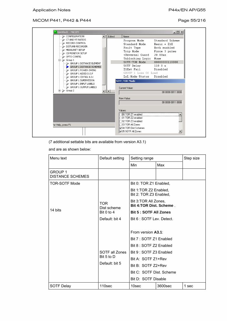
Application Notes P44x/EN AP/G55 MiCOM P441, P442 & P444
Page 55/216
(7 additional settable bits are available from version A3.1)
and are as shown below:
Menu text Default setting Setting range Step size
Min Max
GROUP 1 DISTANCE SCHEMES
TOR-SOTF Mode
14 bits
TOR Dist scheme Bit 0 to 4
Default: bit 4
SOTF all ZonesBit 5 to D
Default: bit 5
Bit 0: TOR Z1 Enabled,
Bit 1:TOR Z2 Enabled, Bit 2: TOR Z3 Enabled,
Bit 3:TOR All Zones, Bit 4:TOR Dist. Scheme .
Bit 5 : SOTF All Zones
Bit 6 : SOTF Lev. Detect.
From version A3.1:
Bit 7 : SOTF Z1 Enabled
Bit 8 : SOTF Z2 Enabled
Bit 9 : SOTF Z3 Enabled
Bit A: SOTF Z1+Rev
Bit B: SOTF Z2+Rev
Bit C: SOTF Dist. Scheme
Bit D: SOTF Disable
SOTF Delay 110sec 10sec 3600sec 1 sec

P44x/EN AP/G55 Application Notes Page 56/216
MiCOM P441, P442 & P444
2.12.1 Initiating TOR/SOTF Protection
SOTF/TOR Activated
2 signals are issued from the logic: TOR Enable - SOTF Enable (See DDB description in appendix from that chapter). There is a difference between them due to the AR (internal or external) which must be blocked in SOTF logic.
The detection of open pole is based on the activation of : Any Pole Dead (at least one pole opened). It is a OR logic between the internal analog detection (level detectors) or the external detection (given by CB status : 52A/52B, which is requested in case of VT Bus side).
The Dead pole Level Detectors V< and I< per phase are settable as described belows:
− V< is either a fixed threshold 20% Vn or equal to V Dead Line threshold of the check synchro function if enabled, (default value for V< dead line = 20% VN)
− I< is either a fixed threshold of 5% In or equal to the I< threshold of the Breaker Failure protection (default value for I< CB fail = 5% IN).
TOR Enable logic is activated in 2 cases :
1. When internal AR is activated or when the reclaim signal from an external AR is connected to a digital input (opto):
As soon as the reclaim time starts, the « TOR Enable » is activated . It will be reset at the end of the internal or external reclaim time.
2. Without any reclaim time (internal AR disabled or external opto input Reclaim Time not assigned in the PSL):
TOR Enable will be activated during a 200 ms time window, following the detection of pole dead detection. The TOR logic will be reset (TOR Enable) ONLY 500 ms after the drop off of any pole dead detection.
This behaviour has been designed to avoid any maloperation on a parallel line, in case of an incorrect Any Pole Dead detection performed by the internal level detectors (Ex: Fault front of Busbar on a parallel line and weak source on the other end of the line)
A delay of 200ms will allow the adjacent line to be tripped and the level detectors will then reset the timer :
• TOR protection logic is enabled any time that any circuit breaker pole has been open longer than 200ms but not longer than 110s default value (ie. First shot autoreclosure is in progress)- the timer is configurable from version A3.0 /allows variation of the duration when dead pole is detected before the internal logic detects line dead and activates the SOTF logic and also where the relay logic detects that further delayed autoreclose shots are in progress.
Trip
Any Pole Dead
TOR Enable200 ms 500 ms
P0532ENa
Reclosing
• SOTF protection is enabled any time that the circuit breaker has been open 3 pole for longer than 110s, that timer is configurable from version A3.0 /allows variation of the duration when dead pole is detected before the internal logic detects line dead and activates the SOTF logic and autoreclosure is not in progress. Thus, SOTF protection is enabled for manual reclosures, not for autoreclosure.

Application Notes P44x/EN AP/G55 MiCOM P441, P442 & P444
Page 57/216
SOTF Enable logic is activated in 2 cases:
1. If no external closing command (manual or by remote communication via control system) is present :
When the internal levels detectors have detected a three pole open for more than 110 s (settable from A3.0); as soon as all poles are closed, then SOTF is enabled for 500 ms and then reset,
2. When an external closing command (manual or by remote communication via control system) is present:
The SOTF logic is activated immediately. As soon as all the poles are closed (after the external closing order if a synchro condition is used in the PSL); SOTF is enable for 500msec and then is reset.
P0485ENa
Any Pole Dead
AR_RECLAIM
>1
S QR
All Pole Dead
R QS
TOR Enable
SOTF Enable
INP_RECLAIM
CBC_Closing Order
>1
>1
INP_RECLAIM Assigned
>1
1P or 3P AR
500 ms
>1
>1
TSOTF Enable (by default:110 s)
T 0
>1
200 ms
T 0&
0 T
CB_Control activated
&
&INP_CB_Man_Close
SOTF HS&
Pulse T
500 ms
FIGURE 35 – SOTF/TOR LOGIC - START

P44x/EN AP/G55 Application Notes Page 58/216
MiCOM P441, P442 & P444
2.12.2 TOR-SOTF Trip Logic
During the TOR/SOTF 500ms window, individual distance protection zones can be enabled or disabled by means of the TOR-SOTF Mode function links. Setting the relevant bit to 1 will enable that zone, setting bits to 0 will disable distance zones. When enabled (Bit = 1), the zones will trip without waiting for their usual time delays. Thus tripping can even occur for close-up three phase short circuits where line connected VTs are used, and memory voltage for a directional decision is unavailable. Setting “All Zones Enabled” allows instantaneous tripping to occur for all faults within the trip characteristic shown in Figure 36 below. Note, the TOR/SOTF element has second harmonic current detection, to avoid maloperation where power transformers are connected in-zone, and inrush current would otherwise cause problems. Harmonic blocking of distance zones occurs when the magnitude of the second harmonic current exceeds 25% of the fundamental.
P0535ENa
X
Directionalline (not used)
Zone 3
Zone 4
R
FIGURE 36 - “ALL ZONES” DISTANCE CHARACTERISTIC AVAILABLE FOR SOTF/TOR TRIPPING
Test results from different settings selected in MiCOM S1.
WARNING: MiCOM S1 DOES NOT DYNAMICALLY CHANGE THE SETTINGS, AND ONE SETTING MAY AFFECT ANOTHER.
SOTF Z2: means that an instantaneous 3 poles trip will occur for fault in Z1 or Z2 without waiting for the issue of the distance timer T1 or T2 only in case Z2 or Z1 are detected by the logic.
T0 = instantaneous Trip
Ts = Trip at the end of SOTF time window (500ms)
T1 = 0, T2=200ms, Tzp=400ms, T3=600ms, T4=1s (Distance timer).
The fault is maintained with a duration bigger than the 500msec SOTF time, until a trip occurs.

Application Notes P44x/EN AP/G55 MiCOM P441, P442 & P444
Page 59/216
SOTF Trip logic results
Type of Fault
SOTF selected Logic
Fault in Z1 Fault in Z2 Fault in Zp Fwd
Fault in Zp Rev
Fault in Z3 Fault in Z4
SOTF All Zone (Zp Fwd)
SOTF trip T0
SOTF trip T0
SOTF trip T0
Same result if Zp Rev T0
SOTF trip T0
SOTF trip T0
SOTF Z1 (Zp Fwd)
SOTF trip T0
DIST trip T2
DIST trip TZp
x DIST trip T3
DIST trip T4
SOTF Z2 (Zp Fwd)
SOTF trip T0
SOTF trip T0
DIST trip TZp
x DIST trip T3
DIST trip T4
SOTF Z3 (Zp Fwd)
SOTF trip T0
SOTF trip T0
SOTF trip T0
x SOTF trip T0
DIST trip T4
SOTF Z1+Rev (Zp Fwd) SOTF trip T0
DIST trip T2
DIST trip TZp
x DIST trip T3
SOTF trip T0
SOTF Z2+Rev (Zp Fwd) SOTF trip T0
SOTF trip T0
DIST trip TZp
x DIST trip T3
SOTF trip T0
SOTF Z1+Rev (Zp Rev) SOTF trip T0
DIST trip T2
x SOTF trip T0
DIST trip T3
DIST trip T4
SOTF Z2+Rev (Zp Rev) SOTF trip T0
SOTF trip T0
x SOTF trip T0
DIST trip T3
DIST trip T4
SOTF Dist. Sch. (Zp fwd) (With a 3Plogic)
SOTF trip T1
SOTF trip T2
SOTF trip TZp
x SOTF trip T3
SOTF trip T4
SOTF Disable (Distance scheme & 1P)
DIST trip T1*
DIST trip T2
DIST trip TZp*
x DIST trip T3
DIST trip T4
No setting in SOTF (All Bits at 0) & No I>3
DIST trip T1*
DIST trip T2
DIST trip TZp
x DIST trip T3
DIST trip T4
Level detectors SOTF trip T0
SOTF trip T0
SOTF trip T0
x SOTF trip T0
SOTF trip T0
*No Ban Tri: Distance trip logic is applied without any 3P trip logic forced by SOTF.
TOR Trip logic results
Type of Fault
TOR selected Logic
Fault in Z1 Fault in Z2 Fault in Zp Fwd
Fault in Zp Rev
Fault in Z3 Fault in Z4
TOR All Zone (Zp Fwd)
TOR trip T0
TOR trip T0
TOR trip T0
TOR trip T0
TOR trip T0
TOR trip T0
TOR Z1 Enabled (Zp Fwd)
TOR trip T0
Dist trip T2
Dist trip Tp
Dist trip Tp
Dist trip T3
Dist trip T4
TOR Z2 Enabled (Zp Fwd)
TOR trip T0
TOR trip T0
Dist trip Tp
Dist trip Tp
Dist trip T3
Dist trip T4
TOR Z3 Enabled (Zp Fwd)
TOR trip T0
TOR trip T0
TOR trip T0
Dist trip Tp
TOR trip T0
Dist trip T4
TOR Dist.Scheme (logic POP/PUP)
Dist trip T1
Dist trip T2
Dist trip Tp
Dist trip Tp
Dist trip T3
Dist trip T4

P44x/EN AP/G55 Application Notes Page 60/216
MiCOM P441, P442 & P444
2.12.3 Switch on to Fault and Trip on Reclose by I>3 Overcurrent Element (not filtered for inruch
current):
Inside the 500 ms time window initiated by SOTF/TOR logic, an instantaneous 3 phases trip logic will be issued, if a faulty current is measured over the I>3 threshold value (adjusted in MiCOM S1).
After the 500 ms TOR/SOTF time windows has ended, the I>3 overcurrent element remains in service with a trip time delay equal to the setting I>3 Time Delay. This element would trip for close-up high current faults, such as those where maintenance earth clamps are inadvertently left in position on line energisation.
2.12.4 Switch on to Fault and Trip on Reclose by Level Detectors
TOR/SOTF level detectors (Bit6 in SOTF logic), allows an instantaneous 3 phases tripping from any low set I< level detector, provided that its corresponding Live Line level detector has not picked up within 20ms. When closing a circuit breaker to energize a healthy line, current would normally be detected above setting, but no trip results as the system voltage rapidly recovers to near nominal. Only when a line fault is present will the voltage fail to recover, resulting in a trip.
• SOTF/TOR trip by level detectors per phase: If Vphase< 70% Vn AND if Iphase> 5% In during 20 ms (to avoid any maloperation due to unstable contact during reclosing order), an instantaneous trip order is issued.

Application Notes P44x/EN AP/G55 MiCOM P441, P442 & P444
Page 61/216
The logic diagram for this, and other modes of TOR/SOTF protection is shown in Figure 37:
P0486ENa
Z1
Z1+Z2+Z3
Z1+Z2
Va >
Ia <
Vc >
Vb >
Ib <
Ic <
&
&
&
PHOC_Start_3Ph_I>3
All Zones
TOR Z3 Enable
TOR Z2 Enable
TOR Z1 Enable
TOR All Zones Enable
Dist. Scheme Enable
Dist Trip
&
&
&
&
&
TOR Enable
SOTF Enable
&
&
&T 0
20 ms
T 0
20 ms
T 0
20 ms
LD EnableSOTF LD Enable
All Zones
SOTF All Zones Enable&
&
&
TOC A
TOC B
Z1
Z1+Z2+Z3
Z1+Z2
SOTF Z3 Enable
SOTF Z2 Enable
SOTF Z1 Enable
&
&
&
SOTF Z1 + rev Enable
Zp Reverse
&
&
Zp
Z4&
1
&SOTF Z2 + rev Enable
SOTF/TOR trip
TOC C
≥1
≥1
≥1
FIGURE 37 - SWITCH ON TO FAULT AND TRIP ON RECLOSE LOGIC DIAGRAM

P44x/EN AP/G55 Application Notes Page 62/216
MiCOM P441, P442 & P444
2.12.5 Setting Guidelines
• When the overcurrent option is enabled, the I>3 current setting applied should be above load current, and > 35% of peak magnetising inrush current for any connected transformers as this element has no second harmonic blocking. Setting guidelines for the I>3 element are shown in more detail in Table below.
• When a Zone 1 Extension scheme is used along with autoreclosure, it must be ensured that only Zone 1 distance protection can trip instantaneously for TOR. Typically, TOR-SOTF Mode bit 0 only would be set to “1”. Also the I>3 element must be disabled to avoid overreaching trips by level detectors.
2.12.5.1 Inputs
Data Type Description
Ia<, Ib<, Ic< Internal Logic No current detected (I< threshold, by default 5% In or I< CB fail)
Dist Trip Internal Logic Trip by Distance logic
AR_RECLAIM Internal Logic Internal AR reclaim in progress
INP_RECLAIM Digital Input External AR in progress (by opto)
CBC_closing order Internal Logic Closing order in progress by CB Control
INP_CB_Man_Close Digital Input CB Closing order (by opto)
CB Control activated Configuration CB control activated
1P or 3 P AR Configuration 1P or 3P AR enabled
TOR Zi Enable Configuration TOR logic enabled in case of fault in Zi
TOR All Zones Enable Configuration TOR logic enabled in case for all zones (Distance Start)
Dist. Scheme Enable Configuration Distance scheme aided Trip logic applied
SOTF LD Enable Configuration Levels detectors in SOTF activated
SOTF All Zones Enable Configuration SOTF logic enabled for all zones (Distance Start)
Va>, Vb>, Vc> Internal Logic Live Voltage detected ( V Live Line threshold, fixed at 70% Vn)
Valid_stx_PHOC Configuration Threshold I>3 must be activated
PHOC_Start_3Ph_I>3 Internal Logic Detection by I>3 overcurrents (not filtered by INRUSH.)
Z1, Z2, Z3, all zones Internal Logic Zones Detected
2.12.5.2 Outputs
Data Type Description
TOC_A Internal Logic Trip phase A by TOR /SOTF
TOC_B Internal Logic Trip phase B by TOR /SOTF
TOC_C Internal Logic Trip phase C by TOR /SOTF
SOTF/TOR trip Internal Logic Trip by SOTF (manual close) or TOR (AR close) logic
2.12.6 Inputs/Outputs in SOTF-TOR DDB Logic
See also, DDB description in appendix of the same section.

Application Notes P44x/EN AP/G55 MiCOM P441, P442 & P444
Page 63/216
2.12.6.1 Inputs
Man Close CB
Digital input (opto) 6 is assigned by default PSL to "Man Close CB"
The DDB Man Close CB if assigned to an opto input in PSL and when energized, will initiate the internal SOTF logic enable (see Figure 35) without CB control.
If CB control is activated SOTF will be enable by internal detection (CB closing order managed by CB control)
AR Reclaim
The DDB AR Reclaim if assigned to an opto input in PSL and when energized, will start the internal logic TOR enable (see Figure 35).- (External AR logic applied).
CB aux A
CB aux B
CB aux C
The DDB CB Aux if assigned to an opto input in PSL and when energized, will be used for Any pole dead & All pole dead internal detection
2.12.6.2 Outputs
SOTF Enable
The DDB SOTF Enable if assigned in PSL, indicates that SOTF logic is enabled in the relay – see logic description in Figure 37
TOR Enable
The DDB TOR Enable if assigned in PSL, indicates that TOR logic is activated in the relay - see logic description in Figure 37
TOC Start A
The DDB TOC Start A if assigned in PSL, indicates a Tripping order on phase A issued by the SOTF levels detectors - see Figure 37
TOC Start B
The DDB TOC Start B if assigned in PSL, indicates a Tripping order on phase B issued by the SOTF levels detectors - see Figure 37
TOC Start C
The DDB TOC Start C if assigned in PSL, indicates a Tripping order on phase C issued by the SOTF levels detectors - see Figure 37
Any Pole Dead
The DDB Any Pole Dead if assigned in PSL, indicates that at least one pole is opened
All Pole Dead
The DDB All Pole Dead if assigned in PSL, indicates all pole are dead (All 3 poles are opened)
SOTF/TOR Trip
The DDB SOTF/TOR Trip if assigned in PSL, indicates a 3poles trip by TOR or SOTF logic - see Figure 37

P44x/EN AP/G55 Application Notes Page 64/216
MiCOM P441, P442 & P444
2.13 Power swing blocking (PSB)
Power swings are oscillations in power flow which can follow a power system disturbance. They can be caused by sudden removal of faults, loss of synchronism across a power system or changes in direction of power flow as a result of switching. Such disturbances can cause generators on the system to accelerate or decelerate to adapt to new power flow conditions, which in turn leads to power swinging. A power swing may cause the impedance presented to a distance relay to move away from the normal load area and into one or more of its tripping characteristics. In the case of a stable power swing it is important that the relay should not trip. The relay should also not trip during loss of stability since there may be a utility strategy for controlled system break up during such an event.
Menu text Default setting Setting range Step size
Min Max
GROUP 1 POWER SWING
Delta R 0.5/In Ω 0 400/In Ω 0.01/In Ω
Delta X 0.5/In Ω 0 400/In Ω 0.01/In Ω
IN > Status Enabled Disabled or Enabled
IN > (% Imax) 40% 10% 100% 1%
I2 > Status Enabled Disabled or Enabled
I2 > (% Imax) 30% 10% 100% 1%
Imax line > Status Enabled Disabled or Enabled
Imax line > 3 x In 1 x In 20 x In 0.01 x In
Unblocking Time delay 30s 0 30s 0.1s
Blocking Zones 00000000 Bit 0: Z1/Z1X Block, Bit 1: Z2 Block, Bit 2: Z3 Block, Bit 3: Zp Block.
2.13.1 The Power Swing Blocking Element
PSB can be disabled on distribution systems, where power swings would not normally be experienced.
Operation of the PSB element is menu selectable to block the operation of any or all of the distance zones (including aided trip logic) or to provide indication of the swing only. The Blocked Zones function links are set to 1 to block zone tripping, or set to 0 to allow tripping as normal. Power swing detection uses a ΔR (resistive) and ΔX (reactive) impedance band which surrounds the entire phase fault trip characteristic. This band is shown in Figure 38 below:

Application Notes P44x/EN AP/G55 MiCOM P441, P442 & P444
Page 65/216
P3068ENa
Zone 4
Zone 3
Δ R
Δ X
Δ X
Δ R
Powerswingbundary
FIGURE 38 - POWER SWING DETECTION CHARACTERISTICS
FIGURE 39 - POWER SWING SETTINGS (SET HIGHZONE IS LOCKED OUT)
A fault on the system results in the measured impedance rapidly crossing the ΔR band, en route to a tripping zone. Power swings follow a much slower impedance locus. A power swing is detected where all three phase-phase measured impedances have remained within the ΔR band for at least 5ms, and have taken longer than 5ms to reach the trip characteristic (the trip characteristic boundary is defined by zones 3 and 4). PSB is indicated on reaching zone 3 or zone 4. Typically, the ΔR and ΔX band settings are both set with: 0.032 x Δf x Rmin load.
NOTE: Δf = Power swing frequency

P44x/EN AP/G55 Application Notes Page 66/216
MiCOM P441, P442 & P444
2.13.2 Unblocking of the Relay for Faults During Power Swings
The relay can operate normally for any fault occurring during a power swing, as there are three selectable conditions which can unblock the relay:
A biased residual current threshold is exceeded - this allows tripping for earth faults occurring during a power swing. The bias is set as: Ir> (as a percentage of the highest measured current on any phase), with the threshold always subject to a minimum of 0.1 x In. Thus the residual current threshold is:
IN > 0.1 In + ( (IN> / 100) . (I maximum) ).
A biased negative sequence current threshold is exceeded - this allows tripping for phase-phase faults occurring during a power swing. The bias is set as: I2> (as a percentage of the highest measured current on any phase), with the threshold always subject to a minimum of 0.1 x In. Thus the negative sequence current threshold is:
I2 > 0.1 In + ( (I2> / 100) . (I maximum) ).
A phase current threshold is exceeded - this allows tripping for three-phase faults occurring during a power swing. The threshold is set as: Imax line> (in A).

Application Notes P44x/EN AP/G55 MiCOM P441, P442 & P444
Page 67/216
Power Swing Detection
S QR
S QR
S QR
S QR
S QR
Loop AN detected in PS bundary
Loop BN detected in PS bundary
Loop CN detected in PS bundary
S QR
S QR
PS loop AN
&
&
AnyPoleDead
&
PS loop BN
Inrush AN
Inrush CN
Inrush BN
Fault clear
Healthy Network
All Pole Dead& /Fuse Failure confirmed
Power Swing unblocking
P0488ENa
S
Q
R
Iphase>(Imax line>)
PS disabled
S QRUnblocking Imax disabled
IN> threshold S QR
S QR
Δ Tunblk
Δ t
Tunb
Δ t
Tunb
Δ
Δ t
Tunb
PS loop CN
Tunblk
Unblocking IN disabled
Unblocking I2> disabled
I2> threshold
≥1
≥1
≥1
≥1
≥1
≥1
≥1
≥1
≥1
≥1
≥1
≥2
FIGURE 40 – POWER SWING DETECTION & UNBLOCKING LOGIC

P44x/EN AP/G55 Application Notes Page 68/216
MiCOM P441, P442 & P444
P0489ENa
≥ 1Power Swing Detection
Z1
Unblock Z1≥ 1
Z2
≥ 1&
Z2'
Zp
≥ 1&
Zp'&
Zp_Fwd
Z1x'
Z1'
&
&
Z1x
Z3
≥ 1&
Z3'
Unblock Z2
Unblock Z3
Unblock Zp
Unblocking Power Swing
FIGURE 41 - DISTANCE PROTECTION BLOCK/UNBLOCKING LOGIC
Data Type Description
ΔR Configuration 0.1/In to 250/In by step 0.01/In
ΔX Configuration 0.1/In to 250/In by step de 0.01/In
ΔTunbk Configuration 0 to 60 s by step de 1 s.
Imax> Configuration 1 to 20 In by step de 0.01
IN> Configuration 0.1In + 10 to 100 % of Imax>
I2> Configuration 0.1In + 10 to 100 % of Imax>
Unblock Z1 Configuration 0 => Z1 blocked during PSwing 1 => Z1 unblocked during PSwing
Unblock Z2 Configuration 0 => Z2 blocked during PSwing 1 => Z2 unblocked during PSwing
Unblock Z3 Configuration 0 => Z3 blocked during PSwing 1 => Z3 unblocked during PSwing
Unblock Zp Configuration 0 => Zp blocked during PSwing 1 => Zp unblocked during PSwing

Application Notes P44x/EN AP/G55 MiCOM P441, P442 & P444
Page 69/216
2.13.3 Typical Current Settings
The three current thresholds must be set above the maximum expected residual current unbalance, the maximum negative sequence unbalance, and the maximum expected power swing current. Generally, the power swing current will not exceed 2.In. Typical setting limits are given in Table 7 and Table 8 below:
Parameter Minimum Setting (to avoid maloperation for asymmetry in power swing currents)
Maximum Setting (to ensure unblocking for line faults)
Typical Setting
IN> > 30% < 100% 40%
I2> > 10% < 50% 30%
TABLE 7 - BIAS THRESHOLDS TO UNBLOCK PSB FOR LINE FAULTS
Parameter Minimum Setting Maximum Setting
Imax line> 1.2 x (maximum power swing current)
0.8 x (minimum phase fault current level)
TABLE 8 - PHASE CURRENT THRESHOLD TO UNBLOCK PSB FOR LINE FAULTS
2.13.4 Removal of PSB to Allow Tripping for Prolonged Power Swings
It is possible to limit the time for which blocking of any distance protection zones is applied. Thus, certain locations on the power system can be designated as split points, where circuit breakers will trip three pole should a power swing fail to stabilise. Power swing blocking is automatically removed after the Unblocking Delay with typical settings:
− 30s if a near permanent block is required;
− 2s if unblocking is required to split the system.
2.14 Directional and non-directional overcurrent protection
The overcurrent protection included in the P441, P442 and P444 relays provides two stage non-directional/directional three phase overcurrent protection and two non directional stages (I>3 and I>4), with independent time delay characteristics. One or more stages may be enabled, in order to complement the relay distance protection. All overcurrent and directional settings apply to all three phases but are independent for each of the four stages. The first two stages of overcurrent protection, I>1 and I>2 have time delayed characteristics which are selectable between inverse definite minimum time (IDMT), or definite time (DT). The third and fourth overcurrent stages can be set as follows:
I>3 - The third element is fixed as non-directional, for instantaneous or definite time delayed tripping. This element can be permanently enabled, or enabled only for Switch on to Fault (SOTF) or Trip on Reclose (TOR). It is also used to detect close-up faults (in SOTF/TOR tripping logic no timer is applied).
I>4 - The fourth element is only used for stub bus protection, where it is fixed as non-directional, and only enabled when the opto-input Stub Bus Isolator Open (Stub Bus Enable) is energised.
All the stages trip three-phase only. (Could be used for back up protection during a VTS logic)
The following Table shows the relay menu for overcurrent protection, including the available setting ranges and factory defaults. Note that all tripping via overcurrent protection is three pole.

P44x/EN AP/G55 Application Notes Page 70/216
MiCOM P441, P442 & P444
Menu text Default setting Setting range Step size Min Max GROUP 1 BACK-UP I>
I>1 Function DT Disabled, DT, IEC S Inverse, IEC V Inverse, IEC E Inverse, UK LT Inverse, IEEE M Inverse, IEEE V Inverse, IEEE E Inverse, US Inverse, US ST Inverse
I>1 Direction Directional Fwd Non-Directional, Directional Fwd, Directional Rev
I>1 VTS Block Non-Directional Block, Non-Directional I>1 Current Set 1.5 x In 0.08 x In 4.0 x In 0.01 x In I>1 Time Delay 1s 0 100s 0.01s I>1 Time Delay VTS 0.2s 0 100s 0.01s I>1 TMS 1 0.025 1.2 0.025 I>1 Time Dial 7 0.5 15 0.1 I>1 Reset Char DT DT or Inverse I>1 tRESET 0 0 100s 0.01s I>2 Function DT Disabled, DT, IEC S Inverse, IEC V
Inverse, IEC E Inverse, UK LT Inverse, IEEE M Inverse, IEEE V Inverse, IEEE E Inverse, US Inverse, US ST Inverse
I>2 Direction Non Directional Non-Directional, Directional Fwd, Directional Rev
I>2 VTS Block Non-Directional Block, Non-Directional I>2 Current Set 2 x In 0.08 x In 4.0 x In 0.01 x In I>2 Time Delay 2s 0 100s 0.01s I>2 Time Delay VTS 2s 0 100s 0.01s I>2 TMS 1 0.025 1.2 0.025 I>2 Time Dial 7 0.5 15 0.1 I>2 Reset Char DT DT or Inverse I>2 tRESET 0 0 100s 0.01s I>3 Status Enabled Disabled or Enabled I>3 Current Set 3 x In 0.08 x In 32 x In 0.01xIn I>3 Time Delay 3s 0s 100s 0.01s I>4 Status Disabled Disabled or Enabled I>4 Current Set 4 x In 0.08 x In 32 x In 0.01xIn I>4 Time Delay 4s 0s 100s 0.01s

Application Notes P44x/EN AP/G55 MiCOM P441, P442 & P444
Page 71/216
The inverse time delayed characteristics listed above, comply with the following formula:
( ) ⎟⎟⎠
⎞+
−⎜⎜⎝
⎛= L
IsIKxTt
1/ α
Where:
t = operation time
K = constant
I = measured current
Is = current threshold setting
α = constant
L = ANSI/IEEE constant (zero for IEC curves)
T = Time multiplier Setting
Curve description Standard K constant α constant L constant
Standard Inverse IEC 0.14 0.02 0
Very Inverse IEC 13.5 1 0
Extremely Inverse IEC 80 2 0
Long Time Inverse UK 120 1 0
Moderately Inverse IEEE 0.0515 0.02 0.0114
Very Inverse IEEE 19.61 2 0.491
Extremely Inverse IEEE 28.2 2 0.1217
Inverse US 5.95 2 0.18
Short Time Inverse US 0.02394 0.02 0.1694
Note that the IEEE and US curves are set differently to the IEC/UK curves, with regard to the time setting. A time multiplier setting (TMS) is used to adjust the operating time of the IEC curves, whereas a time dial setting is employed for the IEEE/US curves. Both the TMS and Time Dial settings act as multipliers on the basic characteristics but the scaling of the time dial is 10 times that of the TMS, as shown in the previous menu. The menu is arranged such that if an IEC/UK curve is selected, the I> Time Dial cell is not visible and vice versa for the TMS setting.
2.14.1 Application of Timer Hold Facility
The first two stages of overcurrent protection in the P441, P442 and P444 relays are provided with a timer hold facility, which may either be set to zero or to a definite time value. (Note that if an IEEE/US operate curve is selected, the reset characteristic may be set to either definite or inverse time in cell I>1 Reset Char; otherwise this setting cell is not visible in the menu). Setting of the timer to zero means that the overcurrent timer for that stage will reset instantaneously once the current falls below 95% of the current setting. Setting of the hold timer to a value other than zero, delays the resetting of the protection element timers for this period. This may be useful in certain applications, for example when grading with upstream electromechanical overcurrent relays which have inherent reset time delays.
Another possible situation where the timer hold facility may be used to reduce fault clearance times is where intermittent faults may be experienced. An example of this may occur in a plastic insulated cable. In this application it is possible that the fault energy melts and reseals the cable insulation, thereby extinguishing the fault. This process repeats to give a succession of fault current pulses, each of increasing duration with reducing intervals between the pulses, until the fault becomes permanent.

P44x/EN AP/G55 Application Notes Page 72/216
MiCOM P441, P442 & P444
When the reset time of the overcurrent relay is instantaneous the relay may not trip until the fault becomes permanent. By using the timer hold facility the relay will integrate the fault current pulses, thereby reducing fault clearance time.
Note that the timer hold facility should not be used where high speed autoreclose with short dead times are set.
The timer hold facility can be found for the first and second overcurrent stages as settings I>1 tRESET and I>2 tRESET. Note that this cell is not visible if an inverse time reset characteristic has been selected, as the reset time is then determined by the programmed time dial setting.
2.14.2 Directional Overcurrent Protection
If fault current can flow in both directions through a relay location, it is necessary to add directional control to the overcurrent relays in order to obtain correct discrimination. Typical systems which require such protection are parallel feeders and ring main systems. Where I>1 or I>2 stages are directionalised, no characteristic angle needs to be set as the relay uses the same directionalising technique as for the distance zones (fixed superimposed power technique).
2.14.3 Time Delay VTS
Should the Voltage Transformer Supervision function detect an ac voltage input failure to the relay, such as due to a VT fuse blow, this will affect operation of voltage dependent protection elements. Distance protection will not be able to make a forward or reverse decision, and so will be blocked. As the I>1 and I>2 overcurrent elements in the relay use the same directionalising technique as for the distance zones, any directional zones would be unable to trip.
To maintain protection during periods of VTS detected failure, the relay allows an I> Time Delay VTS to be applied to the I>1 and I>2 elements. On VTS pickup, both elements are forced to have non-directional operation, and are subject to their revised definite time delay.
2.14.4 Setting Guidelines
I>1 and I>2 Overcurrent Protection
When applying the overcurrent or directional overcurrent protection provided in the P441, P442 and P444 relays, standard principles should be applied in calculating the necessary current and time settings for co-ordination. For more detailed information regarding overcurrent relay co-ordination, reference should be made to ALSTOM Grid’s ‘Protective relay Application Guide’ - Chapter 9. In general, where overcurrent elements are set, these should also be set to time discriminate with downstream and reverse distance protection. The I>1 and I>2 elements are continuously active. However tripping is blocked if the distance protection function starts. An example is shown in Figure 42.
Time
Z1,tZ1
Z2,tZ2
Zp,tZp
Z3,tZ3Z4, tZ4
I>1I>2
Reverse Forward
P3069ENa
FIGURE 42 - TIME GRADING OVERCURRENT PROTECTION WITH DISTANCE PROTECTION (DT EXAMPLE)
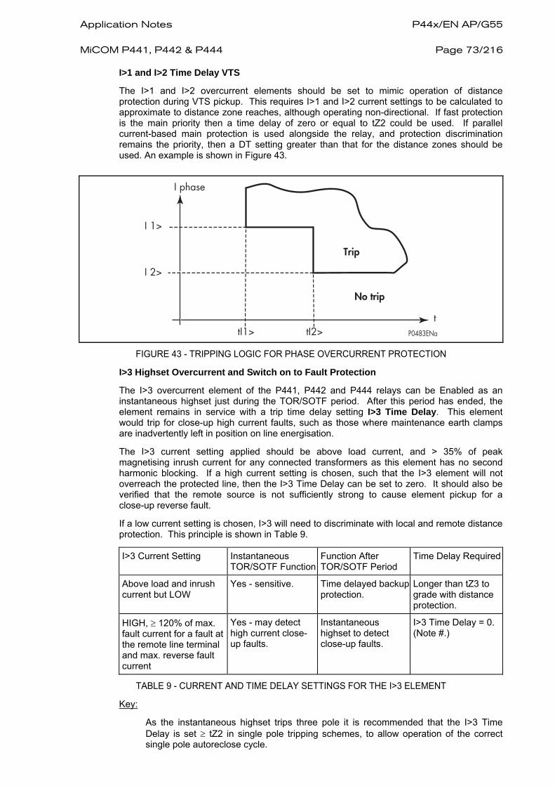
Application Notes P44x/EN AP/G55 MiCOM P441, P442 & P444
Page 73/216
I>1 and I>2 Time Delay VTS
The I>1 and I>2 overcurrent elements should be set to mimic operation of distance protection during VTS pickup. This requires I>1 and I>2 current settings to be calculated to approximate to distance zone reaches, although operating non-directional. If fast protection is the main priority then a time delay of zero or equal to tZ2 could be used. If parallel current-based main protection is used alongside the relay, and protection discrimination remains the priority, then a DT setting greater than that for the distance zones should be used. An example is shown in Figure 43.
I phase
P0483ENa
t
I 1>
I 2>
tI1> tI2>
Trip
No trip
FIGURE 43 - TRIPPING LOGIC FOR PHASE OVERCURRENT PROTECTION
I>3 Highset Overcurrent and Switch on to Fault Protection
The I>3 overcurrent element of the P441, P442 and P444 relays can be Enabled as an instantaneous highset just during the TOR/SOTF period. After this period has ended, the element remains in service with a trip time delay setting I>3 Time Delay. This element would trip for close-up high current faults, such as those where maintenance earth clamps are inadvertently left in position on line energisation.
The I>3 current setting applied should be above load current, and > 35% of peak magnetising inrush current for any connected transformers as this element has no second harmonic blocking. If a high current setting is chosen, such that the I>3 element will not overreach the protected line, then the I>3 Time Delay can be set to zero. It should also be verified that the remote source is not sufficiently strong to cause element pickup for a close-up reverse fault.
If a low current setting is chosen, I>3 will need to discriminate with local and remote distance protection. This principle is shown in Table 9.
I>3 Current Setting Instantaneous TOR/SOTF Function
Function After TOR/SOTF Period
Time Delay Required
Above load and inrush current but LOW
Yes - sensitive. Time delayed backup protection.
Longer than tZ3 to grade with distance protection.
HIGH, ≥ 120% of max. fault current for a fault at the remote line terminal and max. reverse fault current
Yes - may detect high current close-up faults.
Instantaneous highset to detect close-up faults.
I>3 Time Delay = 0. (Note #.)
TABLE 9 - CURRENT AND TIME DELAY SETTINGS FOR THE I>3 ELEMENT
Key:
As the instantaneous highset trips three pole it is recommended that the I>3 Time Delay is set ≥ tZ2 in single pole tripping schemes, to allow operation of the correct single pole autoreclose cycle.

P44x/EN AP/G55 Application Notes Page 74/216
MiCOM P441, P442 & P444
I>4 Stub Bus Protection
When the protected line is switched from a breaker and a half arrangement it is possible to use the I>4 overcurrent element to provide stub bus protection. When stub bus protection is selected in the relay menu, the element is only enabled when the opto-input Stub Bus Isolator Open (Stub Bus Enable) is energised. Thus, a set of 52b auxiliary contacts (closed when the isolator is open) are required.
P0536ENa
I>4 Element: Stub Bus Protection
Busbar 1
Busbar 2
Open isolator
V = 0
I > 0
VT
Protection's blocking using VTs
Stub Stub Bus Protection : I >4Bus Protection : I >4
Although this element would not need to discriminate with load current, it is still common practice to apply a high current setting. This avoids maloperation for heavy through fault currents, where mismatched CT saturation could present a spill current to the relay. The I>4 element would normally be set instantaneous, t>4 = 0s.
2.15 Negative sequence overcurrent protection (NPS)
When applying traditional phase overcurrent protection, the overcurrent elements must be set higher than maximum load current, thereby limiting the element’s sensitivity. Most protection schemes also use an earth fault element operating from residual current, which improves sensitivity for earth faults. However, certain faults may arise which can remain undetected by such schemes.
Any unbalanced fault condition will produce negative sequence current of some magnitude. Thus, a negative phase sequence overcurrent element can operate for both phase-to-phase and phase to earth faults.
The following section describes how negative phase sequence overcurrent protection may be applied in conjunction with standard overcurrent and earth fault protection in order to alleviate some less common application difficulties.
• Negative phase sequence overcurrent elements give greater sensitivity to resistive phase-to-phase faults, where phase overcurrent elements may not operate.
• In certain applications, residual current may not be detected by an earth fault relay due to the system configuration. For example, an earth fault relay applied on the delta side of a delta-star transformer is unable to detect earth faults on the star side. However, negative sequence current will be present on both sides of the transformer for any fault condition, irrespective of the transformer configuration. Therefore, an negative phase sequence overcurrent element may be employed to provide time-delayed back-up protection for any uncleared asymmetrical faults downstream.
• Where rotating machines are protected by fuses, loss of a fuse produces a large amount of negative sequence current. This is a dangerous condition for the machine due to the heating effects of negative phase sequence current and hence an upstream negative phase sequence overcurrent element may be applied to provide back-up protection for dedicated motor protection relays.
• It may be required to simply alarm for the presence of negative phase sequence currents on the system. Operators may then investigate the cause of the unbalance.

Application Notes P44x/EN AP/G55 MiCOM P441, P442 & P444
Page 75/216
The negative phase sequence overcurrent element has a current pick up setting ‘I2> Current Set’, and is time delayed in operation by the adjustable timer ‘I2> Time Delay’. The user may choose to directionalise operation of the element, for either forward or reverse fault protection for which a suitable relay characteristic angle may be set. Alternatively, the element may be set as non-directional.
2.15.1 Setting Guidelines
The relay menu for the negative sequence overcurrent element is shown below:
NEG SEQ O/C Default Min Max Step
I2> Status Enabled Disabled, Enabled
I2> Directional Non-Directional Non-Directional, Directional Fwd, Directional Rev
I2> VTS Non-Directionel Block, Non-Directional
I2> Current Set 0.2In 0.08In 4In 0.01In
I2> Time Delay 10s 0s 100s 0.01s
I2> Char Angle –45° –95° +95° 1°
2.15.2 Negative phase sequence current threshold, ‘I2> Current Set’
The current pick-up threshold must be set higher than the negative phase sequence current due to the maximum normal load unbalance on the system. This can be set practically at the commissioning stage, making use of the relay measurement function to display the standing negative phase sequence current, and setting at least 20% above this figure.
Where the negative phase sequence element is required to operate for specific uncleared asymmetric faults, a precise threshold setting would have to be based upon an individual fault analysis for that particular system due to the complexities involved. However, to ensure operation of the protection, the current pick-up setting must be set approximately 20% below the lowest calculated negative phase sequence fault current contribution to a specific remote fault condition.
Note that in practice, if the required fault study information is unavailable, the setting must adhere to the minimum threshold previously outlined, employing a suitable time delay for co-ordination with downstream devices. This is vital to prevent unnecessary interruption of the supply resulting from inadvertent operation of this element.
2.15.3 Time Delay for the Negative Phase Sequence Overcurrent Element, ‘I2> Time Delay’
As stated above, correct setting of the time delay for this function is vital. It should also be noted that this element is applied primarily to provide back-up protection to other protective devices or to provide an alarm. Hence, in practice, it would be associated with a long time delay.
It must be ensured that the time delay is set greater than the operating time of any other protective device (at minimum fault level) on the system which may respond to unbalanced faults, such as:
• Phase overcurrent elements
• Earth fault elements
• Broken conductor elements
• Negative phase sequence influenced thermal elements
2.15.4 Directionalising the Negative Phase Sequence Overcurrent Element
Where negative phase sequence current may flow in either direction through a relay location, such as parallel lines or ring main systems, directional control of the element should be employed.

P44x/EN AP/G55 Application Notes Page 76/216
MiCOM P441, P442 & P444
Directionality is achieved by comparison of the angle between the negative phase sequence voltage and the negative phase sequence current and the element may be selected to operate in either the forward or reverse direction. A suitable relay characteristic angle setting (I2> Char Angle) is chosen to provide optimum performance. This setting should be set equal to the phase angle of the negative sequence current with respect to the inverted negative sequence voltage (- V2), in order to be at the centre of the directional characteristic.
The angle that occurs between V2 and I2 under fault conditions is directly dependent upon the negative sequence source impedance of the system. However, typical settings for the element are as follows:
• For a transmission system the RCA should be set equal to -60°
• For a distribution system the RCA should be set equal to -45°
2.16 Broken conductor detection
The majority of faults on a power system occur between one phase and ground or two phases and ground. These are known as shunt faults and arise from lightning discharges and other overvoltages which initiate flashovers. Alternatively, they may arise from other causes such as birds on overhead lines or mechanical damage to cables etc. Such faults result in an appreciable increase in current and hence in the majority of applications are easily detectable.
Another type of unbalanced fault which can occur on the system is the series or open circuit fault. These can arise from broken conductors, maloperation of single phase switchgear, or the operation of fuses. Series faults will not cause an increase in phase current on the system and hence are not readily detectable by standard overcurrent relays. However, they will produce an unbalance and a resultant level of negative phase sequence current, which can be detected.
It is possible to apply a negative phase sequence overcurrent relay to detect the above condition. However, on a lightly loaded line, the negative sequence current resulting from a series fault condition may be very close to, or less than, the full load steady state unbalance arising from CT errors, load unbalance etc. A negative sequence element therefore would not operate at low load levels.
The relay incorporates an element which measures the ratio of negative to positive phase sequence current (I2/I1). This will be affected to a lesser extent than the measurement of negative sequence current alone, since the ratio is approximately constant with variations in load current. Hence, a more sensitive setting may be achieved.
2.16.1 Setting Guidelines
The sequence network connection diagram for an open circuit fault is detailed in Figure 1. From this, it can be seen that when a conductor open circuit occurs, current from the positive sequence network will be series injected into the negative and zero sequence networks across the break.
In the case of a single point earthed power system, there will be little zero sequence current flow and the ratio of I2/I1 that flows in the protected circuit will approach 100%. In the case of a multiple earthed power system (assuming equal impedances in each sequence network), the ratio I2/I1 will be 50%.
It is possible to calculate the ratio of I2/I1 that will occur for varying system impedances, by referring to the following equations:-
I1F = Eg (Z2 + Z0)
Z1Z2 + Z1Z0 + Z2Z0
I2F = -EgZ0 Z1Z2 + Z1Z0 + Z2Z0

Application Notes P44x/EN AP/G55 MiCOM P441, P442 & P444
Page 77/216
Where:
Eg = System Voltage
Z0 = Zero sequence impedance
Z1 = Positive sequence impedance
Z2 = Negative sequence impedance
Therefore:
I2F = Z0
I1F Z0 + Z2
It follows that, for an open circuit in a particular part of the system, I2/I1 can be determined from the ratio of zero sequence to negative sequence impedance. It must be noted however, that this ratio may vary depending upon the fault location. It is desirable therefore to apply as sensitive a setting as possible. In practice, this minimum setting is governed by the levels of standing negative phase sequence current present on the system. This can be determined from a system study, or by making use of the relay measurement facilities at the commissioning stage. If the latter method is adopted, it is important to take the measurements during maximum system load conditions, to ensure that all single phase loads are accounted for.
Note that a minimum value of 8% negative phase sequence current is required for successful relay operation.
Since sensitive settings have been employed, it can be expected that the element will operate for any unbalance condition occurring on the system (for example, during a single pole autoreclose cycle). Hence, a long time delay is necessary to ensure co-ordination with other protective devices. A 60 second time delay setting may be typical.
The following table shows the relay menu for the Broken Conductor protection, including the available setting ranges and factory defaults:-
Menu text Default setting Setting range Step size
Min Max
GROUP 1 BROKEN CONDUCTOR
Broken Conductor Enabled Enabled/Disabled N/A
I2/I1 0.2 0.2 1 0.01
I2/I1 Time Delay 60 0s 100s 1s
I2/I1 Trip Disabled* Enabled Disabled N/A
* If disabled, only a Broken Conductor Alarm is possible.
2.16.2 Example Setting
The following information was recorded by the relay during commissioning;
Ifull load = 1000A
I2 = 100A
therefore the quiescent I2/I1 ratio is given by;
I2/I1 = 100/1000 = 0.05
To allow for tolerances and load variations a setting of 200% of this value may be typical: Therefore set I2/I1 = 0.2
Set I2/I1 Time Delay = 60s to allow adequate time for short circuit fault clearance by time delayed protections.

P44x/EN AP/G55 Application Notes Page 78/216
MiCOM P441, P442 & P444
2.17 Directional and non-directional earth fault protection
Three elements of earth fault protection are available, as follows:
• IN> element - Channel aided directional earth fault protection;
• IN>1 element - Directional or non-directional protection, definite time (DT) or IDMT time-delayed.
• IN>2 element - Directional or non-directional, DT delayed.
The IN> element may only be used as part of a channel-aided scheme, and is fully described in the Aided DEF section of the Application Notes which follow.
The IN>1 and IN>2 backup elements always trip three pole, and have an optional timer hold facility on reset, as per the phase fault elements. (The IN> element can be selected to trip single and/or three pole). All Earth Fault overcurrent elements operate from a residual current quantity which is derived internally from the summation of the three phase currents.
The following table shows the relay menu for the Earth Fault protection, including the available setting ranges and factory defaults.
Setting range Menu text Default setting
Min Max Step size
GROUP 1 EARTH FAULT O/C
IN>1 Function DT Disabled, DT, IEC S Inverse, IEC V Inverse, IEC E Inverse, UK LT Inverse, IEEE M Inverse, IEEE V Inverse, IEEE E Inverse, US Inverse, US ST Inverse
IN>1 Directional Directional Fwd Non-Directional, Directional Fwd, Directional Rev
IN>1 VTS Block Non directional Block or Non directional
IN>1 Current Set 0.2 x In 0.08 x In 4.0 x In 0.01 x In
IN>1 Time Delay 1s 0 200s 0.01s
IN>1 Time Delay VTS 0.2s 0 200s 0.01s
IN>1 TMS 1 0.025 1.2 0.025
IN>1 Time Dial 7 0.5 15 0.1
IN>1 Reset Char DT DT or Inverse
IN>1 tRESET 0 0 100s 0.01s
IN>2 Status Enabled Disabled or Enabled
IN>2 Directional Non Directional Non-Directional, Directional Fwd, Directional Rev
IN>2 VTS Block Non directional Block or Non directional
IN>2 Current Set 0.3 x In 0.08 x In 32 x In 0.01 x In
IN>2 Time Delay 2s 0 200s 0.01s
IN>2 Time Delay VTS 2s 0 200s 0.01s
IN> DIRECTIONAL
IN> Char Angle –45° –95° 95° 1°
Polarisation Zero Sequence Zero Sequence or Negative Sequence

Application Notes P44x/EN AP/G55 MiCOM P441, P442 & P444
Page 79/216
Note that the elements are set in terms of residual current, which is three times the magnitude of zero sequence current (Ires = 3I0). The IDMT time delay characteristics available for the IN>1 element, and the grading principles used will be as per the phase fault overcurrent elements.
To maintain protection during periods of VTS detected failure, the relay allows an IN> Time Delay VTS to be applied to the IN>1 and IN>2 elements. On VTS pickup, both elements are forced to have non-directional operation, and are subject to their revised definite time delay.
P0490ENa
DirectionalCalculationVN
V2
I2
IN
IN IN>
SBEF FwdSBEF Rev
IN> Pick-up
IN> Pick-up
Any Pole Dead
CTS Blocking
&IN> Timer Block
IN> TripIDMT/DT
IN> Pick-up
Any Pole Dead
CTS Blocking
&
IN> Timer Block
IN> TripSBEF FwdSBEF Rev
DirectionnalCheck
MCB/VTS Line&
&
&IN> TD VTS
0
>1
IDMT/DT
Negative sequence Polarisation
Residual zero sequence Polarisation
FIGURE 44 - SBEF CALCULATION & LOGIC

P44x/EN AP/G55 Application Notes Page 80/216
MiCOM P441, P442 & P444
SBEF Trip
SBEF Overcurrent
CTS Block
SBEF Trip
P0484ENa
SBEF Timer Block
SBEF Start
IDMT/DT
FIGURE 45 - LOGIC WITHOUT DIRECTIONALITY
SBEF Trip
SBEF Overcurrent
CTS Block
P0533ENa
SBEF Timer Block
SBEF Start
Vx > VsIx > Is
Slow VTSBlock
IDMT/DT
DirectionalCheck
FIGURE 46 - LOGIC WITH DIRECTIONALITY
2.17.1 Directional Earth Fault Protection (DEF)
The method of directional polarising selected is common to all directional earth fault elements, including the channel-aided element. There are two options available in the relay menu:
• Zero sequence polarising - The relay performs a directional decision by comparing the phase angle of the residual current with respect to the inverted residual voltage:
(–Vres = –(Va + Vb + Vc)) derived by the relay.
• Negative sequence polarising - The relay performs a directional decision by comparing the phase angle of the derived negative sequence current with respect to the derived negative sequence voltage.
NOTE: Even though the directional decision is based on the phase relationship of I2 with respect to V2, the operating current quantity for DEF elements remains the derived residual current.
2.17.2 Application of Zero Sequence Polarising
This is the conventional option, applied where there is not significant mutual coupling with a parallel line, and where the power system is not solidly earthed close to the relay location. As residual voltage is generated during earth fault conditions, this quantity is commonly used to polarise DEF elements. The relay internally derives this voltage from the 3 phase voltage input which must be supplied from either a 5-limb or three single phase VT’s. These types of VT design allow the passage of residual flux and consequently permit the relay to derive the required residual voltage. In addition, the primary star point of the VT must be earthed. A three limb VT has no path for residual flux and is therefore incompatible with the use of zero sequence polarising.
The required characteristic angle settings for DEF will differ depending on the application. Typical characteristic angle settings are as follows:
• Resistance earthed systems generally use a 0° RCA setting. This means that for a forward earth fault, the residual current is expected to be approximately in phase with the inverted residual voltage (-Vres).

Application Notes P44x/EN AP/G55 MiCOM P441, P442 & P444
Page 81/216
• When protecting solidly-earthed distribution systems or cable feeders, a -45° RCA
setting should be set.
• When protecting solidly-earthed transmission systems, a -60° RCA setting should be set.
2.17.3 Application of Negative Sequence Polarising
In certain applications, the use of residual voltage polarisation of DEF may either be not possible to achieve, or problematic. An example of the former case would be where a suitable type of VT was unavailable, for example if only a three limb VT were fitted. An example of the latter case would be an HV/EHV parallel line application where problems with zero sequence mutual coupling may exist. In either of these situations, the problem may be solved by the use of negative phase sequence (nps) quantities for polarisation. This method determines the fault direction by comparison of nps voltage with nps current. The operate quantity, however, is still residual current.
When negative sequence polarising is used, the relay requires that the Characteristic Angle is set. The Application Notes section for the Negative Sequence Overcurrent Protection better describes how the angle is calculated - typically set at - 45° (I2 lags (-V2)).
2.18 Aided DEF protection schemes
The option of using separate channels for DEF aided tripping, and distance protection schemes, is offered in the P441, P442 and P444 relays. When a separate channel for DEF is used, the above DEF schemes are independently selectable. When a common signalling channel is employed, the distance and DEF must Share a common scheme. In this case a permissive overreach or blocking distance scheme must be used. The aided tripping schemes can perform single pole tripping. The relay has aided scheme settings as shown in the following table:
Menu text Default setting Setting range Step size Min Max GROUP 1 AIDED D.E.F.
Aided DEF Status Enabled Disabled or Enabled Polarisation Zero Sequence Zero Sequence or Negative Sequence V> Voltage Set 1V 0.5V 20V 0.01V IN Forward 0.1 x In 0.05 x In 4 x In 0.01 x In Time Delay 0 0 10s 0.1s Scheme Logic Shared Shared, Blocking or Permissive Tripping Three Phase Three Phase or Single Phase
FIGURE 47 - MiCOM S1 SETTINGS

P44x/EN AP/G55 Application Notes Page 82/216
MiCOM P441, P442 & P444
DIST. CR
DEF. CR
Opto label 01
Opto Label 02 DEF CS
DIST CS
P0534ENa
Relay Label 02
Relay Label 01
FIGURE 48 - PSL REQUIRED TO ACTIVATE DEF LOGIC WITH AN INDEPENDANT CHANNEL
DIST. CR
DEF. CR
Opto label 01
DEF CS
DIST CS
P0544ENa
>1 Relay label 01
FIGURE 49 - PSL REQUIRED TO ACTIVATE DEF LOGIC WITH SHARED CHANNEL
Directionnal Calculation
NegativePolarisation
ResidualPolarisation
VN
V2
I2
IN
V2
VN
NegativePolarisation
ResidualPolarisation
V>
IN IN>INRev = 0.6*INFwd
DEF FwdDEF Rev
INRev>
P0545ENa
INFwd>
DEF V>
FIGURE 50 - DEF CALCULATION
NOTE: The DEF is blocked in case of VTS or CTS
2.18.1 Polarising the Directional Decision
The relative advantages of zero sequence and negative sequence polarising are outlined on the previous page. Note how the polarising chosen for aided DEF is independent of that chosen for backup earth fault elements.
The relay has a V> threshold which defines the minimum residual voltage required to enable an aided DEF directional decision to be made. A residual voltage measured below this setting would block the directional decision, and hence there would be no tripping from the scheme. The V> threshold is set above the standing residual voltage on the protected system, to avoid operation for typical power system imbalance and voltage transformer errors. In practice, the typical zero sequence voltage on a healthy system can be as high as 1% (ie: 3% residual), and the VT error could be 1% per phase. This could equate to an overall error of up to 5% of phase-neutral voltage, although a setting between 2% and 4% is typical. On high resistance earthed and insulated neutral systems the settings might need to be as high as 10% or 20% of phase-neutral voltage, respectively.
When negative sequence polarising is set, the V> threshold becomes a V2> negative sequence voltage detector.
The characteristic angle for aided DEF protection is fixed at –14°, suitable for protecting all solidly-earthed and resistance earthed systems.

Application Notes P44x/EN AP/G55 MiCOM P441, P442 & P444
Page 83/216
P0491ENa
X
-14˚
FWDFWD
REV REV
R
2.18.2 Aided DEF Permissive Overreach Scheme
P0546ENa
&
DEF Fwd
DEF Timer Block
Reversal Guard
Any Pole Dead
UNB CR DEF
DEF V>
&
0
150 ms
IN Rev>
t_delay
DEF CS
DEF TripT
0
IN Fwd>
FIGURE 51 - INDEPENDANT CHANNEL – PERMISSIVE SCHEME
P0547ENa
&
DEF Fwd
DEF Timer Block
Reversal Guard
Any Pole Dead
Any DIST Start
UNB CR DEF
DEF V>
&0
150 ms
IN Rev>
t_delay
DEF CS
DEF Trip
T
0
IN Fwd>
>1
FIGURE 52 - SHARED CHANNEL – PERMISSIVE SCHEME
This scheme is similar to that used in the ALSTOM Grid LFZP, LFZR, EPAC and PXLN relays. Figure 53 shows the element reaches, and Figure 54 the simplified scheme logic. The signalling channel is keyed from operation of the forward IN> DEF element of the relay. If the remote relay has also detected a forward fault, then it will operate with no additional delay upon receipt of this signal.
Send logic: IN> Forward pickup
Permissive trip logic: IN> Forward plus Channel Received.

P44x/EN AP/G55 Application Notes Page 84/216
MiCOM P441, P442 & P444
P3070ENa
ZL
IN> Fwd (B)
IN> Fwd (A)
A B
FIGURE 53 - THE DEF PERMISSIVE SCHEME
Tri p Trip
Signal
Send IN>
forward
Signal
Send IN>
forward
IN >
IN>1 t0
IN>2 t0
t0&
>1>1
t0 IN>1
t0 IN>2
t0 & IN>
ForwardForward
ProtectionA Protection B
P3964ENa
Tri p Trip
Signal
Send IN>1
forward
Signal
Send IN>1
forward
IN>1
IN>2 t0
IN>3 t0
t0&
>1>1
t0 IN>1
t0 IN>2
t0 & IN>1
ForwardForward
Protection A Protection B
FIGURE 54 - LOGIC DIAGRAM FOR THE DEF PERMISSIVE SCHEME
The scheme has the same features/requirements as the corresponding distance scheme and provides sensitive protection for high resistance earth faults.
Where “t” is shown in the diagram this signifies the time delay associated with an element, noting that the Time Delay for a permissive scheme aided trip would normally be set to zero.
2.18.3 Aided DEF Blocking Scheme
This scheme is similar to that used in the ALSTOM Grid LFZP, LFZR, EPAC and PXLN relays. Figure 57 shows the element reaches, and Figure 58 the simplified scheme logic. The signalling channel is keyed from operation of the reverse DEF element of the relay. If the remote relay forward IN> element has picked up, then it will operate after the set Time Delay if no block is received.

Application Notes P44x/EN AP/G55 MiCOM P441, P442 & P444
Page 85/216
P0548ENa
&
&
DEF Fwd
Reversal Guard
Any Pole Dead
DEF Timer Block
DEF V>
UNB CR DEF
&
0
150 ms
IN Rev>
t_delay
DEF CS
DEF TripT
0
Tp
0
IN Fwd>
DEF Rev
DEF V>
IN Rev>
FIGURE 55 - INDEPENDANT CHANNEL – BLOCKING SCHEME
P0549ENa
&
&
DEF Fwd
Reversal Guard
Any Pole Dead
Any DIST Start
DEF Timer Block
DEF V>
UNB CR DEF&
0
150 ms
IN Rev>
t_delay
DEF CS
DEF Trip
T
0
0
Tp
IN Fwd>
DEF Rev
DEF V>
IN Rev>
>1
FIGURE 56 - SHARED CHANNEL – BLOCKING SCHEME
Send logic: DEF Reverse
Trip logic: IN> Forward, plus Channel NOT Received, with small set delay.
IN> Fwd (A)
P0550ENa
ZL
A B
IN> Fwd (B)
IN> Rev (A)
IN> Rev (B)
FIGURE 57 - THE DEF BLOCKING SCHEME

P44x/EN AP/G55 Application Notes Page 86/216
MiCOM P441, P442 & P444
Trip Trip
SignalSend IN> Reverse
SignalSend IN> Reverse
IN >
IN>1 t 0
IN>2 t 0
t 0&
>1>1
t0 IN>1
t0 IN>2
t0 & IN>ForwardForward
P0551ENa
Protection A Protection B
FIGURE 58 - LOGIC DIAGRAM FOR THE DEF BLOCKING SCHEME
The scheme has the same features/requirements as the corresponding distance scheme and provides sensitive protection for high resistance earth faults.
Where “t” is shown in the diagram this signifies the time delay associated with an element. To allow time for a blocking signal to arrive, a short time delay on aided tripping must be used. The recommended Time Delay setting = max. signalling channel operating time + 14ms.
2.19 Undervoltage protection
Undervoltage conditions may occur on a power system for a variety of reasons, some of which are outlined below:-
• Increased system loading. Generally, some corrective action would be taken by voltage regulating equipment such as AVR’s or On Load Tap Changers, in order to bring the system voltage back to it’s nominal value. If the regulating equipment is unsuccessful in restoring healthy system voltage, then tripping by means of an undervoltage relay will be required following a suitable time delay.
• Faults occurring on the power system result in a reduction in voltage of the phases involved in the fault. The proportion by which the voltage decreases is directly dependent upon the type of fault, method of system earthing and its location with respect to the relaying point. Consequently, co-ordination with other voltage and current-based protection devices is essential in order to achieve correct discrimination.
This function will be blocked with VTS logic or could be disabled if CB open.
Both the under and overvoltage protection functions can be found in the relay menu “Volt Protection”. The following table shows the undervoltage section of this menu along with the available setting ranges and factory defaults.
Menu text Default setting Setting range Step size
Min Max
GROUP 1 VOLT Protection
V< & V> MODE 0 V<1 Trip, V<2 Trip, V>1 Trip, V>2 Trip
UNDER VOLTAGE
V< Measur't Mode Phase-Neutral Phase-phase or Phase-neutral
V<1 Function DT Disabled, DT pr IDMT
V<1 Voltage Set 50V 10V 120V 1V
V<1 Time Delay 10s 0s 100s 0.01s

Application Notes P44x/EN AP/G55 MiCOM P441, P442 & P444
Page 87/216
Menu text Default setting Setting range Step size
Min Max
V<1 TMS 1 0.5 100 0.5
V<2 Status Disabled Disabled or Enabled
V<2 Voltage Set 38V 10V 120V 1V
V<2 Time Delay 5s 0s 100s 0.01s
As can be seen from the menu, the undervoltage protection included within the P441, P442 and P444 relays consists of two independent stages. These are configurable as either phase to phase or phase to neutral measuring within the V< Measur’t Mode cell.
Stage 1 may be selected as either IDMT, DT or disabled, within the V<1 Function cell. Stage 2 is DT only and is enabled/disabled in the V<2 Status cell.
Two stages are included to provide both alarm and trip stages, where required. Alternatively, different time settings may be required depending upon the severity of the voltage dip.
The IDMT characteristic available on the first stage is defined by the following formula:
t = K 1 – M
Where:
K = Time Multiplier Setting (TMS)
T = Operating Time in Seconds
M = Measured Voltage / relay Setting Voltage (V<)
2.19.1 Setting Guidelines
In the majority of applications, undervoltage protection is not required to operate during system earth fault conditions. If this is the case, the element should be selected in the menu to operate from a phase to phase voltage measurement, as this quantity is less affected by single phase voltage depressions due to earth faults.
The voltage threshold setting for the undervoltage protection should be set at some value below the voltage excursions which may be expected under normal system operating conditions. This threshold is dependent upon the system in question but typical healthy system voltage excursions may be in the order of -10% of nominal value.
Similar comments apply with regard to a time setting for this element, i.e. the required time delay is dependent upon the time for which the system is able to withstand a depressed voltage.
2.20 Overvoltage protection
Undervoltage conditions may occur on a power system for a variety of reasons, some of which are outlined below:-
• Under conditions of load rejection, the supply voltage will increase in magnitude. This situation would normally be rectified by voltage regulating equipment such as AVRs or on-load tap changers. However, failure of this equipment to bring the system voltage back within prescribed limits leaves the system with an overvoltage condition which must be cleared in order to preserve the life of the system insulation. Hence, overvoltage protection which is suitably time delayed to allow for normal regulator action, may be applied.
• During earth fault conditions on a power system there may be an increase in the healthy phase voltages. Ideally, the system should be designed to withstand such overvoltages for a defined period of time.
As previously stated, both the over and undervoltage protection functions can be found in the relay menu “Volt Protection”. The following table shows the overvoltage section of this menu along with the available setting ranges and factory defaults.

P44x/EN AP/G55 Application Notes Page 88/216
MiCOM P441, P442 & P444
Menu text Default setting Setting range Step size
Min Max
Group 1 Volt protection
V> Measur't Mode Phase-Neutral Phase-phase or Phase-neutral
V>1 Function DT Disabled, DT pr IDMT
V>1 Voltage Set 75V 60V 185V 1V
V>1 Time Delay 10s 0s 100s 0.01s
V>1 TMS 1 0.5 100 0.5
V>2 Status Enabled Disabled or Enabled
V>2 Voltage Set 90V 60V 185V 1V
V>2 Time Delay 0.5s 0s 100s 0.01s
As can be seen, the setting cells for the overvoltage protection are identical to those previously described for the undervoltage protection. The IDMT characteristic available on the first stage is defined by the following formula:
t = K / (M - 1)
Where:
K = Time Multiplier Setting
T = Operating Time in Seconds
M = Measured Voltage / relay Setting Voltage (V>)
2.20.1 Setting Guidelines
The inclusion of the two stages and their respective operating characteristics allows for a number of possible applications;
• Use of the IDMT characteristic gives the option of a longer time delay if the overvoltage condition is only slight but results in a fast trip for a severe overvoltage. As the voltage settings for both of the stages are independent, the second stage could then be set lower than the first to provide a time delayed alarm stage if required.
• Alternatively, if preferred, both stages could be set to definite time and configured to provide the required alarm and trip stages.
• If only one stage of overvoltage protection is required, or if the element is required to provide an alarm only, the remaining stage may be disabled within the relay menu.
This type of protection must be co-ordinated with any other overvoltage relays at other locations on the system. This should be carried out in a similar manner to that used for grading current operated devices.
2.21 Circuit breaker fail protection (CBF)
Following inception of a fault one or more main protection devices will operate and issue a trip output to the circuit breaker(s) associated with the faulted circuit. Operation of the circuit breaker is essential to isolate the fault, and prevent damage / further damage to the power system. For transmission/sub-transmission systems, slow fault clearance can also threaten system stability. It is therefore common practice to install circuit breaker failure protection, which monitors that the circuit breaker has opened within a reasonable time. If the fault current has not been interrupted following a set time delay from circuit breaker trip initiation, breaker failure protection (CBF) will operate.
CBF operation can be used to backtrip upstream circuit breakers to ensure that the fault is isolated correctly. CBF operation can also reset all start output contacts, ensuring that any blocks asserted on upstream protection are removed.

Application Notes P44x/EN AP/G55 MiCOM P441, P442 & P444
Page 89/216
2.21.1 Breaker Failure Protection Configurations
The phase selection must be performed by creating dedicated PSL.
The circuit breaker failure protection incorporates two timers, ‘CB Fail 1 Timer’ and ‘CB Fail 2 Timer’, allowing configuration for the following scenarios:
S Q R
>1
&
CBF1_Status
External Trip A
Breaker Fail
Alarm
tBF1 Trip 3Ph
tBF2 Trip 3Ph
>1 &
&
&
CBF2_Status
CBA_A
>1
>1
tBF1 0
tBF1
0
tBF1
0
tBF2 - tBF1 0
Enable
Any Internal Trip A
S Q R Ia<
Any Internal Trip A S Q R
Non Current Prot Trip &
Setting: Ext. Trip Reset: 0) I< Only 1) /Trip & I< 2) CB & I< 3) Disable 4) /Trip or I<
External Trip B CBA_B
Any Internal Trip B Ib< Non Current Prot Trip
External Trip C CBA_C
Ic< Any Internal Trip C
Non Current Prot Trip
Enable
Non Current Prot Trip
P0552ENa
>1
WI Trip A
V<1 Trip WI Trip C WI Trip B
V<2 Trip V>1 Trip V>2 Trip
Setting: Non I Trip Reset: 0) I< Only 1) /Trip & I< 2) CB & I< 3) Disable 4) /Trip or I<
Pulsed output latched in UI
>1
0 4 3 2 1
1 0 4 3 2
0 4 3 2 1
0 43 2 1
0 4 3 2 1
0 4 3 2 1 Ia<
&
CBA_A &
>1
PHASE BSame logic as A
phase
PHASE CSame logic as A
phase
FIGURE 59 - CB FAIL GENERAL LOGIC
• Simple CBF, where only ‘CB Fail 1 Timer’ is enabled. For any protection trip, the ‘CB Fail 1 Timer’ is started, and normally reset when the circuit breaker opens to isolate the fault. If breaker opening is not detected, ‘CB Fail 1 Timer’ times out and closes an output contact assigned to breaker fail (using the programmable scheme logic). This contact is used to backtrip upstream switchgear, generally tripping all infeeds connected to the same busbar section.

P44x/EN AP/G55 Application Notes Page 90/216
MiCOM P441, P442 & P444
• A re-tripping scheme, plus delayed backtripping. Here, ‘CB Fail 1 Timer’ is used to
route a trip to a second trip circuit of the same circuit breaker. This requires duplicated circuit breaker trip coils, and is known as re-tripping. Should re-tripping fail to open the circuit breaker, a backtrip may be issued following an additional time delay. The backtrip uses ‘CB Fail 2 Timer’, which is also started at the instant of the initial protection element trip.
CBF elements ‘CB Fail 1 Timer’ and ‘CB Fail 2 Timer’ can be configured to operate for trips triggered by protection elements within the relay or via an external protection trip. The latter is achieved by allocating one of the relay opto-isolated inputs to ‘External Trip’ using the programmable scheme logic.
2.21.2 Reset Mechanisms for Breaker Fail Timers
It is common practice to use low set undercurrent elements in protection relays to indicate that circuit breaker poles have interrupted the fault or load current, as required. This covers the following situations:
• Where circuit breaker auxiliary contacts are defective, or cannot be relied upon to definitely indicate that the breaker has tripped.
• Where a circuit breaker has started to open but has become jammed. This may result in continued arcing at the primary contacts, with an additional arcing resistance in the fault current path. Should this resistance severely limit fault current, the initiating protection element may reset. Thus, reset of the element may not give a reliable indication that the circuit breaker has opened fully.
For any protection function requiring current to operate, the relay uses operation of undercurrent elements (I<) to detect that the necessary circuit breaker poles have tripped and reset the CB fail timers. However, the undercurrent elements may not be reliable methods of resetting circuit breaker fail in all applications. For example:
• Where non-current operated protection, such as under/overvoltage or under/overfrequency, derives measurements from a line connected voltage transformer. Here, I< only gives a reliable reset method if the protected circuit would always have load current flowing. Detecting drop-off of the initiating protection element might be a more reliable method. (in that case setting will be : "Prot. Reset or I<")
• Where non-current operated protection, such as under/overvoltage or under/overfrequency, derives measurements from a busbar connected voltage transformer. Again using I< would rely upon the feeder normally being loaded. Also, tripping the circuit breaker may not remove the initiating condition from the busbar, and hence drop-off of the protection element may not occur. In such cases, the position of the circuit breaker auxiliary contacts may give the best reset method.

Application Notes P44x/EN AP/G55 MiCOM P441, P442 & P444
Page 91/216
+ + +
-- -
TT
Pole Live Pole Dead
P0553ENa
+ +
--
T
Pole Live Pole Dead+
-
I
I
I<
I<
FIGURE 60 - ALGORITHM FOR POLE DEAD DETECTION
Description of open pole detection algorithm :
Each half period after zero crossing of current, the algorithm detects if the current is bigger than the I< threshold. If yes, then the detection timer is restarted, if it is lower than the adjusted value nothing is done.
At the end of the detection timer, open pole decision is given by the algorithm.
Timer value given by: (Number of Samples/2 + 2) * ((1/Freq)/Number of Samples)
With:
T = 13,3 ms (50 Hz) T = 11,1 ms (60 Hz)
The current used is the unfiltered current (only the analog lowPass )
Example:
In the first example, the current line is interrupted by the CB opening.
The detection is confirmed 3 ms after the pole is opened.
In the second example, some residual current remains due to the CT; The detection is confirmed 12 / 15 msec after the pole is opened.

P44x/EN AP/G55 Application Notes Page 92/216
MiCOM P441, P442 & P444
2.21.2.1 Inputs
Data Type Description
CBF1_Status Configuration Breaker Failure 1 activated
CBF2_Status Configuration Breaker Failure 2 activated
CBF1_Timer Configuration Timer Breaker Failure 1
CBF2_Timer Configuration Timer Breaker Failure 2
CBF1_Reset Configuration Type of reset (current, CB status, interlocks).
CBF2_Reset Configuration Type of reset (current, CB Status, interlocks).
CBF_I< Configuration Dead Pole threshold detection
Any Trip A Internal Logic Trip phase A by internal or external protection function
Any Trip B Internal Logic Trip phase B by internal or external protection function
Any Trip C Internal Logic Trip phase C by internal or external protection function
CB 52a_A Internal Logic CB Pole A opened
CB 52a_B Internal Logic CB Pole B opened
CB 52a_C Internal Logic CB Pole C opened
Ia<, Ib<, Ic< Internal Logic Under-current detection for dead pole
2.21.2.2 Outputs
Data Type Description
CBF1_Trip_3p Internal Logic Trip 3P CB fail by TBF1
CBF2_Trip_3p Internal Logic Trip 3P CB fail by TBF2
CB Fail Alarm Internal Logic CB Fail alarm
Resetting of the CBF is possible from a breaker open indication (from the relay’s pole dead logic) or from a protection reset. In these cases resetting is only allowed provided the undercurrent elements have also reset. The resetting options are summarised in the following table.

Application Notes P44x/EN AP/G55 MiCOM P441, P442 & P444
Page 93/216
Initiation (Menu selectable)
CB fail timer reset mechanism
Current based protection - (eg. 50/51/46/21/87..)
The resetting mechanism is fixed. [IA< operates] & [IB< operates] & [IC< operates] & [IN< operates]
Non-current based protection (eg. 27/59/81/32L..)
Three options are available. The user can select from the following options. [All I< and IN< elements operate] [Protection element reset] AND [All I< and IN< elements operate] CB open (all 3 poles) AND [All I< and IN< elements operate]
External protection - Three options are available. The user can select any or all of the options. [All I< and IN< elements operate] [External trip reset] AND [All I< and IN< elements operate] CB open (all 3 poles) AND [All I< and IN< elements operate]
The selection in the relay menu is grouped as follows:
Menu text Default setting Setting range Step size
Min Max
CB FAIL & I<
BREAKER FAIL
CB Fail 1 Status Enabled Enabled, Disabled
CB Fail 1 Timer 0.2s 0s 10s 0.01s
CB Fail 2 Status Disabled Enabled, Disabled
CB Fail 2 Timer 0.4s 0s 10s 0.01s
CBF Non I Reset CB Open & I< I< Only, CB Open & I<, Prot Reset & I<, Prot Reset or I<, Disable
CBF Ext Reset CB Open & I< I< Only, CB Open & I<, Prot Reset & I<, Prot Reset or I<, Disable
UNDER CURRENT
I< Current Set 0.05In 0.05In 3.2In 0.01In
The ‘CBF Blocks I>‘ and ‘CBF Blocks IN>‘ settings are used to remove starts issued from the overcurrent and earth elements respectively following a breaker fail time out. The start is removed when the cell is set to Enabled.

P44x/EN AP/G55 Application Notes Page 94/216
MiCOM P441, P442 & P444
2.21.3 Typical settings
2.21.3.1 Breaker Fail Timer Settings
Typical timer settings to use are as follows:
CB Fail Reset Mechanism tBF time delay Typical delay for 2½ cycle circuit breaker
Initiating element reset CB interrupting time + element reset time (max.) + error in tBF timer + safety margin
50 + 50 + 10 + 50 = 160 ms
CB open CB auxiliary contacts opening/closing time (max.) + error in tBF timer + safety margin
50 + 10 + 50 = 110 ms
Undercurrent elements CB interrupting time + undercurrent element operating time (max.) + safety margin
50 + 25 + 50 = 125 ms
Note that all CB Fail resetting involves the operation of the undercurrent elements. Where element reset or CB open resetting is used the undercurrent time setting should still be used if this proves to be the worst case.
The examples above consider direct tripping of a 2½ cycle circuit breaker. Note that where auxiliary tripping relays are used, an additional 10-15 ms must be added to allow for trip relay operation.
2.21.3.2 Breaker Fail Undercurrent Settings
The phase undercurrent settings (I<) must be set less than load current, to ensure that I< operation indicates that the circuit breaker pole is open. A typical setting for overhead line or cable circuits is 20% In, with 5% In common for generator circuit breaker CBF.

Application Notes P44x/EN AP/G55 MiCOM P441, P442 & P444
Page 95/216
3. OTHER PROTECTION CONSIDERATIONS-SETTINGS EXAMPLE 3.1 Distance Protection Setting Example
3.1.1 Objective
To protect the 100Km double circuit line between Green Valley and Blue River substations using relay protection in the POP Z2 Permissive Overreach mode and to set the relay at Green Valley substation, shown in Figure 61.
Tiger Bay
System DataGreen Valley - Blue River transmission lineSystem voltage 230kvSystem grounding solidCT ratio 1200/5VT ratio 230000/115Line length 100kmLine impedanceZ1 = 0.089 + J0.476 OHM/kmZ0 = 0.426 + J1.576 OHM/kmFaults levelsGreen Valley substation busbars maximum 5000MVA, minimum 2000MVABlue River substation busbars maximum 3000MVA, minimum 1000MVA
80 Km
Green valley
P3074ENa
100 Km
Blue River Rocky bay
60 Km
2121
FIGURE 61 - SYSTEM ASSUMED FOR WORKED EXAMPLE
3.1.2 System Data
Line length: 100Km
Line impedances: Z1= 0.089 + j0.476 = 0.484 / 79.4° Ω/km
Z0 = 0.426 + j1.576 = 1.632 / 74.8° Ω/km
Z0/Z1 = 3.372 / -4.6°
CT ratio: 1 200 / 5
VT ratio: 230 000 / 115
3.1.3 Relay Settings
It is assumed that Zone 1 Extension is not used and that only three forward zones are required. Settings on the relay can be performed in primary or secondary quantities and impedances can be expressed as either polar or rectangular quantities (menu selectable). For the purposes of this example, secondary quantities are used.
3.1.4 Line Impedance
Ratio of secondary to primary impedance = 1200 / 5 = 0.12 230000 / 115
Line impedance secondary = ratio CT/VT x line impedance primary.
Line Impedance = 100 x 0.484/79.4° (primary) x 0.12
= 5.81/79.4° Ω secondary.
Relay Line Angle settings -90° to 90° in 1° steps. Therefore, select Line Angle = 80° for convenience.
Therefore set Line Impedance and Line Angle: = 5.81/80° Ω secondary.

P44x/EN AP/G55 Application Notes Page 96/216
MiCOM P441, P442 & P444
3.1.5 Zone 1 Phase Reach Settings
Required Zone 1 reach is to be 80% of the line impedance between Green Valley and Blue River substations.
Required Zone 1 reach = 0.8 x 100 x 0.484/79.4° x 0.12
Z1 = 4.64/79.4° Ω secondary.
Z2 = 100 x 0.484/79.4° + 50% x 60 x 0.484/79.4°
The Line Angle = 80°.
Therefore actual Zone 1 reach, Z1 = 4.64/80° Ω secondary.
3.1.6 Zone 2 Phase Reach Settings
Required Zone 2 impedance =
(Green Valley-Blue River) line impedance + 50% (Blue River-Rocky Bay) line impedance
Z2 = (100+30) x 0.484/79.4° x 0.12
= 7.56 / 79.4° Ω secondary.
The Line Angle = 80°.
Actual Zone 2 reach setting = 7.56/80° Ω secondary
3.1.7 Zone 3 Phase Reach Settings
Required Zone 3 forward reach =
(Green Valley-Blue River + Blue River-Rocky Bay) x 1.2
= (100+60) x 1.2 x 0.484/79.4° x 0.12
Z3 = 11.15/79.4° ohms secondary
Actual Zone 3 forward reach setting = 11.16/80° ohms secondary
3.1.8 Zone 4 Reverse Settings with no Weak Infeed Logic Selected
Required Zone 4 reverse reach impedance = Typically 10% Zone 1 reach
= 0.1 x 4.64/79.4°
Z4 = 0.464/79.4°
Actual Zone 4 reverse reach setting = 0.46/80° ohms secondary
3.1.9 Zone 4 Reverse Settings with Weak Infeed Logic Selected
Where zone 4 is used to provide reverse directional decisions for Blocking or Permissive Overreach schemes, zone 4 must reach further behind the relay than zone 2 for the remote relay. This can be achieved by setting: Z4 ≥ ((Remote zone 2 reach) x 120%) minus the protected line impedance:
Remote Zone 2 reach =
(Blue River-Green Valley) line impedance + 50% (Green Valley-Tiger Bay) line impedance
= (100+40) x 0.484/79.4° x 0.12
= 8.13/79.4° Ω secondary.
Z4 ≥ ((8.13/79.4°) x 120%) - (5.81/79.4°)
= 3.95/79.4°
Minimum zone 4 reverse reach setting = 3.96/80° ohms secondary

Application Notes P44x/EN AP/G55 MiCOM P441, P442 & P444
Page 97/216
3.1.10 Residual Compensation for Earth Fault Elements
The residual compensation factor can be applied independently to certain zones if required. This feature is useful where line impedance characteristics change between sections or where hybrid circuits are used. In this example, the line impedance characteristics do not change and as such a common KZ0 factor can be applied to each zone. This is set as a ratio “kZ0 Res. Comp”, and an angle “kZ0 Angle”:
kZ0 Res. Comp, kZ0 = (Z0 - Z1) / 3.Z1 Ie: As a ratio.
kZ0 Angle, ∠kZ0 = ∠ (Z0 - Z1) / 3.Z1 Set in degrees.
ZL0 - ZL1 = (0.426 + j1.576) - (0.089 + j0.476)
= 0.337 + j1.1
= 1.15 / 72.9°
kZ0 = 1.15 / 72.9° = 0.79 / –6.5°
3 × 0.484 / 79.4°
Therefore, select:
kZ0 Res. Comp = 0.79 (Set for kZ1, kZ2, kZp, kZ4).
kZ0 Angle = –6.5° (Set for kZ1, kZ2, kZp, kZ4).
3.1.11 Resistive Reach Calculations
All distance elements must avoid the heaviest system loading. Taking the 5A CT secondary rating as a guide to the maximum load current, the minimum load impedance presented to the relay would be:
Vn (phase-neutral) / In = (115 / √3) / 5 = 13.3 Ω (secondary)
Typically, phase fault distance zones would avoid the minimum load impedance by a margin of ≥40% if possible (bearing in mind that the power swing characteristic surrounds the tripping zones), earth fault zones would use a ≥20% margin. This allows maximum resistive reaches of 7.9Ω, and 10.6Ω, respectively.
From Table 1 (see §2.4.4), taking a required primary resistive coverage of 14.5Ω for phase faults, and assuming a typical earth fault coverage of 40Ω, the minimum secondary reaches become:
RPh (min) = 14.5 x 0.12 = 1.74Ω (secondary);
RG (min) = 40 x 0.12 = 4.8Ω (secondary).
Resistive reaches could be chosen between the calculated values as shown in Table 10. The zone 2 elements satisfy R2Ph ≤ (R3Ph x 80%), and R2G ≤ (R3G x 80%).
Minimum Maximum Zone 1 Zone 2 Zones 3 & 4
Phase (RPh) Ω 1.74 7.9 R1Ph = 3 R1Ph = 4 R3Ph-4Ph = 8
Earth (RG) Ω 4.8 10.6 R1G = 5 R1G = 6 R3G-4G = 10
TABLE 10 - SELECTION OF RESISTIVE REACHES
R3Ph-R4Ph should be set ≤ 80% Z minimum load – ΔR.

P44x/EN AP/G55 Application Notes Page 98/216
MiCOM P441, P442 & P444
3.1.12 Power Swing Band
Typically, the ΔR and ΔX band settings are both set between 10 - 30% of R3Ph. This gives a secondary impedance between 0.6 and 1.8Ω. For convenience, 1.0Ω could be set.
The width of the power swing band is calculated as follows:
ΔR = 1.3 × tan(π × Δf × Δt) × RLOAD
Assuming that the load corresponds to 60° angles between sources and if the resistive reach is set so that Rlim = RLOAD/2, the following is obtained:
ΔR = 0.032 × Δf × RLOAD
To ensure that a power swing frequency of 5 Hz is detected, the following is obtained:
ΔR = 0.16 × RLOAD
Where:
ΔR width of the power swing detection band
Δf power swing frequency (fA – fB)
Rlim resistive reach of the starting characteristic (=R3ph-R4ph)
Z network impedance corresponding to the sum of the reverse (Z4) and forward (Z3) impedances
RLOAD load resistance
3.1.13 Current Reversal Guard
The current reversal guard timer available with POP schemes needs a non-zero setting when the reach of the zone 2 elements is greater than 1.5 times the impedance of the protected line. In this example, their reach is only 1.3 times the protected line impedance. Therefore, current reversal guard logic does not need to be used and the recommended settings for scheme timers are:
tREVERSAL GUARD = 0
Tp = 98ms (typical).
3.1.14 Instantaneous Overcurrent Protection
To provide parallel high-speed fault clearance to the distance protection, it is possible to use the I>3 element as an instantaneous highset. It must be ensured that the element will only respond to faults on the protected line. The worst case scenario for this is when only one of the parallel lines is in service.
Two cases must be considered. The first case is a fault at Blue River substation with the relay seeing fault current contribution via Green Valley. The second case is a fault at Green Valley with the relay seeing fault current contribution via Blue River.
Case 1:
Source Impedance = 2302 / 5000 = 10.58Ω
Line Impedance = 48.4Ω
Fault current seen by relay = (230000 / √3)/(10.58 + 48.4)
= 2251A

Application Notes P44x/EN AP/G55 MiCOM P441, P442 & P444
Page 99/216
Case 2:
Source Impedance = 2302 / 3000 = 17.63Ω
Line Impedance = 48.4Ω
Fault current seen by relay = (230000 / √3)/(17.63 + 48.4)
= 2011A
The overcurrent setting must be in excess of 2251A. To provide an adequate safety margin a setting ≥120% the minimum calculated should be chosen, say 2800A.
3.2 Teed feeder protection
The application of distance relays to three terminal lines is fairly common. However, several problems arise when applying distance protection to three terminal lines.
3.2.1 The Apparent Impedance Seen by the Distance Elements
Figure 62 shows a typical three terminal line arrangement. For a fault at the busbars of terminal B the impedance seen by a relay at terminal A will be equal to:
Za = Zat + Zbt + [ Zbt.(Ic/Ia) ]
Relay A will underreach for faults beyond the tee-point with infeed from terminal C. When terminal C is a relatively strong source, the underreaching effect can be substantial. For a zone 2 element set to 120% of the protected line, this effect may result in non-operation of the element for internal faults. This not only effects time delayed zone 2 tripping but also channel-aided schemes. Where infeed is present, it will be necessary for Zone 2 elements at all line terminals to overreach both remote terminals with allowance for the effect of tee-point infeed. Zone 1 elements must be set to underreach the true impedance to the nearest terminal without infeed. Both these requirements can be met through use of the alternative setting groups in the P441, P442 and P444 relays.
Zbt
A
Zat
Ia BIb
C
Zct
Ic
P3075ENa
Va = Ia Zat + Ib Zbt
Ib = Ia + Ic
Va = Ia Zat + Ia Zbt + Ic Zbt
Impedance seen by relay A = VaIa
Za = Zat + Zbt + Ic ZbtIa
FIGURE 62 - TEED FEEDER APPLICATION - APPARENT IMPEDANCES SEEN BY RELAY
3.2.2 Permissive Overreach Schemes
To ensure operation for internal faults in a POP scheme, the relays at the three terminals should be able to see a fault at any point within the protected feeder. This may demand very large zone 2 reach settings to deal with the apparent impedances seen by the relays.
A POP scheme requires the use of two signalling channels. A permissive trip can only be issued upon operation of zone 2 and receipt of a signal from both remote line ends. The requirement for an 'AND' function of received signals must be realised through use of contact logic external to the relay, or the internal Programmable Scheme Logic. Although a POP scheme can be applied to a three terminal line, the signalling requirements make its use unattractive.

P44x/EN AP/G55 Application Notes Page 100/216
MiCOM P441, P442 & P444
3.2.3 Permissive Underreach Schemes
For a PUP scheme, the signalling channel is only keyed for internal faults. Permissive tripping is allowed for operation of zone 2 plus receipt of a signal from either remote line end. This makes the signalling channel requirements for a PUP scheme less demanding than for a POP scheme. A common power line carrier (PLC) signalling channel or a triangulated signalling arrangement can be used. This makes the use of a PUP scheme for a teed feeder a more attractive alternative than use of a POP scheme.
The channel is keyed from operation of zone 1 tripping elements. Provided at least one zone 1 element can see an internal fault then aided tripping will occur at the other terminals if the overreaching zone 2 setting requirement has been met. There are however two cases where this is not possible:
Figure 63 (i) shows the case where a short tee is connected close to another terminal. In this case, zone 1 elements set to 80% of the shortest relative feeder length do not overlap. This leaves a section not covered by any zone 1 element. Any fault in this section would result in zone 2 time delayed tripping.
Figure 63 (ii) shows an example where terminal 'C' has no infeed. Faults close to this terminal will not operate the relay at 'C' and hence the fault will be cleared by the zone 2 time-delayed elements of the relays at 'A' and 'B'.
Figure 63 (iii) illustrates a further difficulty for a PUP scheme. In this example current is outfeed from terminal 'C' for an internal fault. The relay at 'C' will therefore see the fault as reverse and not operate until the breaker at 'B' has opened; i.e. sequential tripping will occur.
A
Z1A
B
C
Z1C= area where no zone 1 overlap exists
Fault
A
Z1A
B
C
Z1B
No infeed
Fault seen by A & B in zone 2
A
P3076ENa
B
C
Relay at C sees reverse fault until B opens
(i)
(ii)
(iii)
FIGURE 63 - TEED FEEDER APPLICATIONS

Application Notes P44x/EN AP/G55 MiCOM P441, P442 & P444
Page 101/216
3.2.4 Blocking Schemes
Blocking schemes are particularly suited to the protection of teed feeders, since high speed operation can be achieved where there is no current infeed from one or more terminals. The scheme also has the advantage that only a common simplex channel or a triangulated simplex channel is required.
The major disadvantage of blocking schemes is highlighted in Figure 63 (iii) where fault current is outfeed from a terminal for an internal fault condition. relay 'C' sees a reverse fault condition. This results in a blocking signal being sent to the two remote line ends, preventing tripping until the normal zone 2 time delay has expired.
3.3 Alternative setting groups
The P441, P442 and P444 relays can store up to four independent groups of settings. The active group is selected either locally via the menu or remotely via the serial communications. The ability to quickly reconfigure the relay to a new setting group may be desirable if changes to the system configuration demand new protection settings. Typical examples where this feature can be used include:
Single bus installations with a transfer bus;
Double bus installations, with or without a separate transfer bus, where the transfer circuit breaker or bus coupler might be used to take up the duties of any feeder circuit breaker when both the feeder circuit breaker and the current transformers are by-passed.
In the case of a double bus installation, it is usual for bus 1 to be referred to as the main bus and bus 2 as the reserve bus, and for any bypass circuit isolator to be connected to bus 2 as shown in Figure 64. This arrangement avoids the need for a current polarity reversing switch that would be required if both buses were to be used for by-pass purposes. The standby relay, associated with the transfer circuit breaker or the bus coupler, can be programmed with the individual setting required for each of the outgoing feeders. For bypass operation the appropriate setting group can be selected as required. This facility is extremely useful in the case of unattended substations where all of the switching can be controlled remotely.
Feeder 1
21 21
21
Feeder 2P3077ENa
Main bus
Reserve bus (2)
P440
(1)
FIGURE 64 - TYPICAL DOUBLE BUS INSTALLATION WITH BYPASS FACILITIES
A further use for this feature is the ability to provide alternative settings for teed feeders or double circuit lines with mutual coupling. Similar alternative settings could be required to cover different operating criteria in the event of the channel failing, or an alternative system configuration (ie. lines being switched in or out).

P44x/EN AP/G55 Application Notes Page 102/216
MiCOM P441, P442 & P444
3.3.1 Selection of Setting Groups
Setting groups can be changed by one of two methods selectable by MiCOM S1:
• Automatic group selection by changes in state of two opto-isolated inputs, assigned as Setting Group Change bit 0 (opto 1), and Setting Group Change bit 1 (opto 2), as shown in Table 11 below. The new setting group binary code must be maintained for 2 seconds before a group change is implemented, thus rejecting spurious induced interference.(See also hysteresis value for level logic 0 & level logic 1 in section 6.1 of this chapter). When this selection is chosen, the two opto-isolated inputs assigned to this function will be opto inputs 1 and 2 and they must not be connected to any output signal in the PSL. Special care should be take into account to avoid use them for another purpose (i.e in the default PSL they have been used for another functions: DIST/DEF Chan. Recv. For opto 1 and DIST/DEF carrier out of service).
• Default PSL: To enable the setting group via binary inpputs, the opto input 1 and 2 must be removed from the PSL. (If assigned in the PSL, instead of Dist DEF Carrier Receive Logic Start, a setting group change will occur)
Note that each setting group has its own dedicated PSL, which should be configured and sent to the relay independently)

Application Notes P44x/EN AP/G55 MiCOM P441, P442 & P444
Page 103/216
• Or using the relay operator interface / remote communications. Should the user issue
a menu command to change group, the relay will transfer to that settings group, and then ignore future changes in state of the bit 0 and bit 1 opto-inputs. Thus, the user is given greater priority than automatic setting group selection.
Binary State of SG Change bit 1
Opto 2
Binary State of SG Change bit 0
Opto 1
Setting Group Activated
0 0 1
0 1 2
1 0 3
1 1 4
TABLE 11 - SETTING GROUP SELECTION
REMINDER : IF SELECTED IN THE MENU (CHANGEMENT GROUPS BY OPTOS), OPTO 1 & 2 MUST BE REMOVED FROM THE PSL (THEY ARE DEDICATED FOR GROUPS SELECTION ONLY)

P44x/EN AP/G55 Application Notes Page 104/216
MiCOM P441, P442 & P444
4. APPLICATION OF NON-PROTECTION FUNCTIONS 4.1 Fault locator
The relay has an integral fault locator that uses information from the current and voltage inputs to provide a distance to fault measurement. The sampled data from the analogue input circuits is written to a cyclic buffer until a fault condition is detected. The data in the input buffer is then held to allow the fault calculation to be made. When the fault calculation is complete the fault location information is available in the relay fault record.
When calculated the fault location can be found in the fault record under the VIEW RECORDS column in the Fault Location cells. Distance to fault is available in km, miles, impedance or percentage of line length. The fault locator can store data for up to five faults. This ensures that fault location can be calculated for all shots on a typical multiple reclose sequence, whilst also retaining data for at least the previous fault.
FIGURE 65 - FAULT LOCATION INFORMATION INCLUDED IN AN EVENT:

Application Notes P44x/EN AP/G55 MiCOM P441, P442 & P444
Page 105/216
The following table shows the relay menu for the fault locator, including the available setting ranges and factory defaults:
Menu text Default setting Setting range Step size
Min Max
GROUP 1 DISTANCE ELEMENTS
LINE SETTING
Line Length 1000 km (625 miles)
0.3 km (0.2 mile)
1000 km (625 miles)
0.015 km (0.005 mile)
Line Impedance 12 / In Ω 0.001 / In Ω 500 / In Ω 0.001 / In Ω
Line Angle 70° –90° +90° 0.1°
FAULT LOCATOR
kZm Mutual Comp 0 0 7 0.01
kZm Angle 0° 0° +360° 1°
4.1.1 Mutual Coupling
When applied to parallel circuits mutual flux coupling can alter the impedance seen by the fault locator. The coupling will contain positive, negative and zero sequence components. In practice the positive and negative sequence coupling is insignificant. The effect on the fault locator of the zero sequence mutual coupling can be eliminated by using the mutual compensation feature provided. This requires that the residual current on the parallel line is measured, as shown in Appendix B. It is extremely important that the polarity of connection for the mutual CT input is correct, as shown.
4.1.2 Setting Guidelines
The system assumed for the distance protection worked example will be used here, refer to section 3.1. The Green Valley – Blue River line is considered.
Line length: 100Km
CT ratio: 1 200 / 5
VT ratio: 230 000 / 115
Line impedances: Z1 = 0.089 + j0.476 = 0.484 / 79.4° Ω/km
ZM0 = 0.107 + j0.571 = 0.581 / 79.4° Ω/km (Mutual)
Ratio of secondary to primary impedance = 1200 /5 = 0.12
230000 / 115
Line Impedance = 100 x 0.484 / 79.4° x 0.12
= 5.81 / 79.4° Ω secondary.
Relay Line Angle settings 0° to 360° in 1° steps. Therefore, select Line Angle = 80° for convenience.

P44x/EN AP/G55 Application Notes Page 106/216
MiCOM P441, P442 & P444
Therefore set Line Impedance and Line Angle: = 5.81 / 80° Ω (secondary).
No residual compensation needs to be set for the fault locator, as the relay automatically uses the kZ0 factor applicable to the distance zone which tripped.
Should a CT residual input be available for the parallel line, mutual compensation could be set as follows:
kZm Mutual Comp, kZm = ZM0 / 3.Z1 Ie: As a ratio.
kZm Angle, ∠kZm = ∠ ZM0 / 3.Z1 Set in degrees.
The CT ratio for the mutual compensation may be different from the Line CT ratio. However, for this example we will assume that they are identical.
kZm = ZM0 / 3.Z1 = 0.581 / 79.4° / (3 x 0.484 / 79.4°)
= 0.40 / 0°
Therefore set kZm Mutual Comp = 0.40
kZm Angle = 0°
4.2 Voltage transformer supervision (VTS) – Main VT for minZ measurement
4.2.1 VTS logic description
The voltage transformer supervision (VTS) feature is used to detect failure of the analog ac voltage inputs to the relay. This may be caused by internal voltage transformer faults, overloading, or faults on the interconnecting wiring to relays. This usually results in one or more VT fuses blowing. Following a failure of the ac voltage input there would be a misrepresentation of the phase voltages on the power system, as measured by the relay, which may result in maloperation of the distance element.
The VTS logic in the relay is designed to detect the voltage failure (with internal thresholds or external opto input), and automatically adjust the configuration of protection elements (Distance element is blocked but may be unblocked on I1,I2 or I0 conditions in case of fault during VTS conditions) whose stability would otherwise be compromised (Distance, DEF, Weak infeed, Directionnal phase current& all directional elements used in the internal logic).
A settable time-delayed alarm output is also available (min1sec to Max 20sec).
The condition of this alarm is given by:
FFUS_Confirmed = (Fuse_Failure And VTS Timer) Or INP_FFUS_Line
P0530ENa
VN >F.Failure
&≥ 1
I2 >F.Failure
I0 >F.Failure
I >F.Failure
V<F.Failure
Δ I>F.Failure
&S QR
INP_F.Failure_Line
≥ 1
Fuse_Failure
FFUS_Confirmed
VTS Timedelay
S QR
≥ 1Healthy network
All Pole Dead
Any_pole_dead
FIGURE 66 - VTS LOGIC (SEE ALSO DDB DESCRIPTION IN THE END OF THAT SECTION)

Application Notes P44x/EN AP/G55 MiCOM P441, P442 & P444
Page 107/216
FIGURE 67 - VT SUPERVISION: VTS SETTINGS IN MiCOM S1
• VTS Timer: A settable alarm from 1 to 20s by step of 1s gives the possibility to signal by an alarm the Failure. This alarm is instantaneous in case of opto energized by external INP FFU signal (issued from contact of MCB). During no load, the timer covers the duration of Dead time1 HSAR cycle (Vo&/IO in case of no load) which could be detected as VT failure 1 pole.
• INP_FFUS Line :The external information given by the MCB to the opto input is secure and will block instantaneously the distance function and the functions which are use directional element.
FIGURE 68 - DEFAULT PSL EXTRACTED
Where a miniature circuit breaker (MCB) is used to protect the voltage transformer ac output circuits, it is common to use MCB auxiliary contacts to indicate a three phase output disconnection. As previously described, it is possible for the VTS logic to operate correctly without this input. However, this facility has been provided for compatibility with various utilities current practices. Energising an opto-isolated input assigned to “MCB Open” on the relay will therefore provide the necessary block.
Fuse failure conditions are confirmed instantaneously if the opto input "INP_FFus line" is energised and assigned in PSL, or after elapse of the VTS Time delay in case of 1, 2 or 3 phases Fuse Failure.
The confirmed Fuse Failure blocks all protection functions which use the voltage measurement (Distance, Weak infeed, Directional overcurrent,…). The directional overcurrent element may be blocked or set to become non directional with dedicated timer (Time VTS in MiCOM S1)- I>1 or IN>1.
A non confirmed Fuse Failure will be a detection of an internal fuse failure before the timer is issued. In that case a fault can be detected by the I2>,I0>,I1>, ΔI> criteria and will force the unblocking functions:
Distance Protection
DEF Protection
Weak-infeed Protection
I> Directional
U>, U<
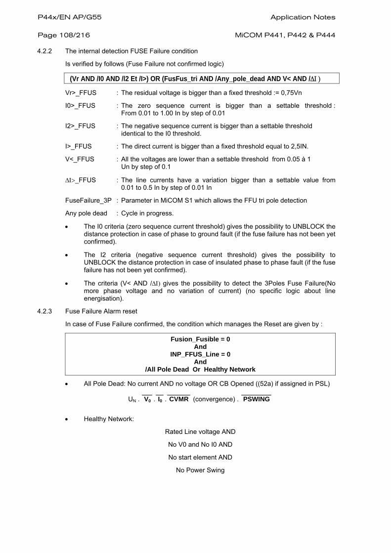
P44x/EN AP/G55 Application Notes Page 108/216
MiCOM P441, P442 & P444
4.2.2 The internal detection FUSE Failure condition
Is verified by follows (Fuse Failure not confirmed logic)
(Vr AND /I0 AND /l2 Et /I>) OR (FusFus_tri AND /Any_pole_dead AND V< AND /ΔΙ )
Vr>_FFUS : The residual voltage is bigger than a fixed threshold := 0,75Vn
I0>_FFUS : The zero sequence current is bigger than a settable threshold : From 0.01 to 1.00 In by step of 0.01
I2>_FFUS : The negative sequence current is bigger than a settable threshold identical to the I0 threshold.
I>_FFUS : The direct current is bigger than a fixed threshold equal to 2,5IN.
V<_FFUS : All the voltages are lower than a settable threshold from 0.05 à 1 Un by step of 0.1
ΔΙ>_FFUS : The line currents have a variation bigger than a settable value from 0.01 to 0.5 In by step of 0.01 In
FuseFailure_3P : Parameter in MiCOM S1 which allows the FFU tri pole detection
Any pole dead : Cycle in progress.
• The I0 criteria (zero sequence current threshold) gives the possibility to UNBLOCK the distance protection in case of phase to ground fault (if the fuse failure has not been yet confirmed).
• The I2 criteria (negative sequence current threshold) gives the possibility to UNBLOCK the distance protection in case of insulated phase to phase fault (if the fuse failure has not been yet confirmed).
• The criteria (V< AND /ΔΙ) gives the possibility to detect the 3Poles Fuse Failure(No more phase voltage and no variation of current) (no specific logic about line energisation).
4.2.3 Fuse Failure Alarm reset
In case of Fuse Failure confirmed, the condition which manages the Reset are given by :
Fusion_Fusible = 0 And
INP_FFUS_Line = 0 And
/All Pole Dead Or Healthy Network
• All Pole Dead: No current AND no voltage OR CB Opened ((52a) if assigned in PSL)
UN . V0 . I0 . CVMR (convergence) . PSWING
• Healthy Network:
Rated Line voltage AND
No V0 and No I0 AND
No start element AND
No Power Swing

Application Notes P44x/EN AP/G55 MiCOM P441, P442 & P444
Page 109/216
There are three main aspects to consider regarding the failure of the VT supply. These are defined below:
1. Loss of one or two phase voltages
2. Loss of all three phase voltages under load conditions
3. Absence of three phase voltages upon line energisation
4.2.4 Loss of One or Two Phase Voltages
The VTS feature within the relay operates on detection of residual voltage without the presence of zero and negative phase sequence current, and earth fault current (ΣIph). This gives operation for the loss of one or two phase voltages. Stability of the VTS function is assured during system fault conditions, by the presence of I0 and/or I2 current. Also, VTS operation is blocked (and distance element unblocked) when any phase current exceeds 2.5 x In.
Zero Sequence VTS Element:
The thresholds used by the element are:
• Fixed operate threshold: VN ≥ 0.75 x Vn;
• Blocking current thresholds, I0 = I2 = 0 to 1 x In; settable (defaulted to 0.05In), and Iph = 2.5 x In.
4.2.5 Loss of All Three Phase Voltages Under Load Conditions
Under the loss of all three phase voltages to the relay, there will be no zero phase sequence quantities present to operate the VTS function. However, under such circumstances, a collapse of the three phase voltages will occur. If this is detected without a corresponding change in any of the phase current signals (which would be indicative of a fault), then a VTS condition will be raised. In practice, the relay detects the presence of superimposed current signals, which are changes in the current applied to the relay. These signals are generated by comparison of the present value of the current with that exactly one cycle previously. Under normal load conditions, the value of superimposed current should therefore be zero. Under a fault condition a superimposed current signal will be generated which will prevent operation of the VTS.
The phase voltage level detectors is settable (default value is adjusted at 30V / setting range : min:10V to Max:70V).
The sensitivity of the superimposed current elements is settable and default value is adjusted at 0.1In (setting range : 0,01In to 5In).
4.2.6 Absence of Three Phase Voltages Upon Line Energisation
If a VT were inadvertently left isolated prior to line energisation, incorrect operation of voltage dependent elements could result. The previous VTS element detected three phase VT failure by absence of all 3 phase voltages with no corresponding change in current. On line energisation there will, however, be a change in current (as a result of load or line charging current for example). An alternative method of detecting 3 phase VT failure is therefore required on line energisation: in that case the SOTF logic is applied.

P44x/EN AP/G55 Application Notes Page 110/216
MiCOM P441, P442 & P444
4.2.7 Menu Settings
The VTS settings are found in the ‘SUPERVISION’ column of the relay menu. The relevant settings are detailed below.
Menu text Default setting Setting range Step size
Min Max
GROUP 1 SUPERVISION
VT Supervision
VTS Time Delay 5s 1s 20s 1s
VTS I2> & I0> Inhibit 0.05 x In 0 1 x In 0.01 x In
Detect 3P Disabled Enabled Disabled
Threshold 3P 30V 10V 70V 1V
Delta I> 0.1×In 0.01×In 5×In 0.01×In
The relay responds as follows, on operation of any VTS element:
• VTS alarm indication (delayed by the set Time Delay);
• Instantaneous blocking of distance protection elements (if opto used); and others protection functions using voltage measurement
• Dedirectionalising of directionalised overcurrent elements with new time delays “I>
VTS”.(if selected)
The VTS block is latched after a user settable time delay ‘VTS Time Delay’. Once the signal has latched then two methods of resetting are available. (See Reset logic description in section 4.2.3).
If not blocked the time delay associated can be modified as well (Time VTS):

Application Notes P44x/EN AP/G55 MiCOM P441, P442 & P444
Page 111/216
4.2.8 INPUT / OUTPUT used in VTS logic:
4.2.8.1 Inputs
MCB/VTS Line
The DDB:MCB/VTS Line if linked to an opto in the PSL and when energized, informs the P44X about an internal maloperation from the VT used for the impedance measurement reference. (Line in this case means Main VT ref measurement / even if the main VT is on the bus side and the Synchro VT is on the line side).
MCB/VTS Bus
The DDB:MCB/VTS Bus if linked to an opto in the PSL and when energized, informs the P44X about an internal maloperation from the VT used for synchrocheck control (See CheckSync logic in section 4.4).
4.2.8.2 Outputs
VTS Fast
Set high for internal FFAilure detection made with internal logic.
VTS Fail Alarm
Set high Set highwhen Opto energised (copy of MCB) OR internal FFAilure confirmed at the end of VTS timer.
Any Pole Dead
The DDB Any Pole Dead if linked in the PSL, indicates that one or more poles is opened.
All Pole Dead
The DDB All Pole Dead if linked in the PSL, indicates all pole are dead (The 3 poles are open).
4.3 Current Transformer Supervision (CTS)
The current transformer supervision feature is used to detect failure of one or more of the ac phase current inputs to the relay. Failure of a phase CT or an open circuit of the interconnecting wiring can result in incorrect operation of any current operated element. Additionally, interruption in the ac current circuits risks dangerous CT secondary voltages being generated.
4.3.1 The CT Supervision Feature
The CT supervision feature operates on detection of derived zero sequence current, in the absence of corresponding derived zero sequence voltage that would normally accompany it.
The voltage transformer connection used must be able to refer zero sequence voltages from the primary to the secondary side. Thus, this element should only be enabled where the VT is of five limb construction, or comprises three single phase units, and has the primary star point earthed.
Operation of the element will produce a time-delayed alarm visible on the LCD and event record (plus DDB 125: CT Fail Alarm), with an instantaneous block for inhibition of protection elements. Protection elements operating from derived quantities (Broken Conductor, Earth Fault, Neg Seq O/C) are always blocked on operation of the CT supervision element.
The following table shows the relay menu for the CT Supervision element, including the available setting ranges and factory defaults:-

P44x/EN AP/G55 Application Notes Page 112/216
MiCOM P441, P442 & P444
Menu text Default setting Setting range step size
Min max
GROUP 1 SUPERVISION
CT SUPERVISION
CTS Status Disabled Enabled/Disabled N/A
CTS VN< Inhibit 1 0.5 / 2V 22 / 88V 0.5 / 2V
CTS IN> Set 0.1 0.08 x In 4 x In 0.01 x In
CTS Time Delay 5 0s 10s 1s
4.3.2 Setting the CT Supervision Element
Ir>
Vr<
P0554ENa
&Temporisation0<->10sec
Calulation Part Logical Part
The residual voltage setting, CTS VN< Inhibit and the residual current setting, CTS IN> set, should be set to avoid unwanted operation during healthy system conditions. For example CTS VN< Inhibit should be set to 120% of the maximum steady state residual voltage. The CTS IN> set will typically be set below minimum load current. The time-delayed alarm, CTS Time Delay, is generally set to 5 seconds.
Where the magnitude of residual voltage during an earth fault is unpredictable, the element be disabled to prevent a protection elements being blocked during fault conditions.
4.3.2.1 Inputs/outputs in CTS logic:
CT Fail Alarm
The DDB cell indicates a CT Fail detected after timer is issued
4.4 Check synchronisation
The check synchronism option is used to qualify reclosure of the circuit breaker so that it can only occur when the network conditions on the busbar and line side of the open circuit breaker are acceptable. If a circuit breaker were closed when the two system voltages were out of synchronism with one another, i.e. a difference in voltage magnitudes or phase angles existed, the system would be subjected to an unacceptable ‘shock’, resulting in loss of stability and possible damage to connected machines.
Check synchronising therefore involves monitoring the voltage on both sides of a circuit breaker and, if both sides are ‘live’, the relative synchronism between the two supplies. Such checking may be required to be applied for both automatic and manual reclosing of the circuit breaker and the system conditions which are acceptable may be different in each case. For this reason, separate check synchronism settings are included within the relay for both manual and automatic reclosure of the circuit breaker. With manual closure, the CB close signal is applied into the logic as a pulse to ensure that an operator cannot simply keep the close signal applied and wait for the system to come into synchronism. This is often referred to as guard logic and requires the close signal to be released and then re-applied if the closure is unsuccessful.

Application Notes P44x/EN AP/G55 MiCOM P441, P442 & P444
Page 113/216
The check synchronising element provides two ‘output’ signals which feed into the manual CB control and the auto reclose logic respectively. These signals allow reclosure provided that the relevant check-synch criteria are fulfilled.
Note that if check-synchronising is disabled, the DDB: signal is automatically asserted and becomes invariant (logical status always forced at 1).
For an interconnected power system, tripping of one line should not cause a significant shift in the phase relationship of the busbar and line side voltages. Parallel interconnections will ensure that the two sides remain in synchronism, and that autoreclosure can proceed safely. However, if the parallel interconnection(s) is/are lost, the frequencies of the two sections of the split system will begin to slip with respect to each other during the time that the systems are disconnected. Hence, a live busbar / live line synchronism check prior to reclosing the breaker ensures that the resulting phase angle displacement, slip frequency and voltage difference between the busbar and line voltages are all within acceptable limits for the system. If they are not, closure of the breaker can be inhibited.
The SYSTEM CHECKS menu contains all of the check synchronism settings for auto (“A/R”) and manual (“Man”) reclosure and is shown in the table below along with the relevant default settings:-
Menu text Default setting Setting range Step size
Min Max
GROUP 1 SYSTEM CHECKS
C/S Check Scheme for A/R 111 Bit 0: Live Bus / Dead Line, Bit 1: Dead Bus / Live Line, Bit 2: Live Bus / Live Line.
Dead / Dead made by PSL only (from version A3.0 model 05)
C/S Check Scheme for Man CB
111 Bit 0: Live Bus / Dead Line, Bit 1: Dead Bus / Live Line, Bit 2: Live Bus / Live Line.
Dead / Dead made by PSL only (from version A3.0 model 05)
V< Dead Line 13V 5V 30V 1V
V> Live Line 32V 30V 120V 1V
V< Dead Bus 13V 5V 30V 1V
V> Live Bus 32V 30V 120V 1V
Diff Voltage 6.5V 0.5V 40V 0.1V
Diff Frequency 0.05Hz 0.02Hz 1Hz 0.01Hz
Diff Phase 20° 5° 90° 2.5°
Bus-Line Delay 0.2s 0.1s 2s 0.1s
KEY: “Diff” denotes the differential between Line VT and Busbar VT measurements.
− At least one condition of c/s scheme must be selected in the 3 bits, to activate the c/s check logic.
− Man CB, check sync condition is tallen in account, only if a logic of STF has been enabled by S1.
− If SOTF is disabled in S1, a dedicated PSL must be created using Deb B (live L or live B/Dead L) – live/live could not be managed – in that case.

P44x/EN AP/G55 Application Notes Page 114/216
MiCOM P441, P442 & P444
Note that the combination of the Diff Phase and Bus-Line Delay settings can also be equated to a differential frequency, as shown below:
• Diff Phase angle set to +/-20°, Bus-Line Delay set to 0.2s.
• The phase angle ‘window’ is therefore 40°, which corresponds to 40/360ths of a cycle = 0.111 cycle. This equates to a differential frequency of:
0.111 / 0.2 = 0.55 Hz
Thus it is essential that the time delay chosen before an “in synchronism” output can be given is not too long, otherwise the synchronising conditions will appear more restrictive than the actual Diff Frequency setting.
The Live Line and Dead Line settings define the thresholds which dictate whether or not the line or bus is determined as being live or dead by the relay logic. Under conditions where either the line or bus are dead, check synchronism is not applicable and closure of the breaker may or may not be acceptable. Hence, setting options are provided which allow for both manual and auto-reclosure under a variety of live/dead conditions. The following paragraphs describe where these may be used.
WARNING: THE SETTINGS VOLTAGE IN MiCOM S1 IS ALLWAYS CALCULATED IN PHASE TO GROUND – EVEN IF PHASE/PHASE REF HAS BEEN SELECTED.
If the threshold : live line has been set too high – the relay will never detect a healthy network (as the line voltage is always measured below the voltage threshold). Without live line condition, the distance protection cannot use the delta algorithms as no prefault detection has been previously detected.
4.4.1 Dead Busbar and Dead Line
This mode is not integrated in the internal logic, however can be created using a dedicated PSL:
(This facility with cells (Dead Line/Dead Bus) is available since version A3.0 model 05)
This setting might also be used to allow manual close with specific test conditions on the CB.
4.4.2 Live Busbar and Dead Line
Where a radial feeder is protected, tripping the circuit breaker will isolate the infeed, and the feeder will be dead. Provided that there is no local generation which can backfeed to energise the feeder, reclosure for live busbar / dead line conditions is acceptable. This setting might also be used to allow re-energisation of a faulted feeder in an interconnected power system, which had been isolated at both line ends. Live busbar / dead line reclosing allows energising from one end first, which can then be followed by live line / live busbar reclosure with voltages in synchronism at the remote end.
4.4.3 Dead Busbar and Live Line
If there was a circuit breaker and busbar at the remote end of the radial feeder mentioned above, the remote breaker might be reclosed for a dead busbar / live line condition.
Application Notes P44x/EN AP/G55 MiCOM P441, P442 & P444
Page 115/216
4.4.4 Check Synchronism Settings
Depending on the particular system arrangement, the main three phase VT for the relay may be located on either the busbar or the line. Hence, the relay needs to be programmed with the location of the main voltage transformer. This is done under the ‘CT & VT RATIOS’ column in the ‘Main VT Location’ cell, which should be programmed as either ‘Line’ or ‘Bus’ to allow the previously described logic to operate correctly. (See DDB description bellow)
Note that the check synch VT input may be driven from either a phase to phase or phase to neutral voltage. The ‘C/S Input’ cell in the ‘CT & VT RATIOS’ column has the options of A-N, B-N, C-N, A-B, B-C or C-A, which should therefore be set according to the actual VT arrangement.
If the VTS feature internal to the relay operates, the check synchronising element is inhibited from giving an ‘Allow Reclosure’ output. This avoids allowing reclosure in instances where voltage checks are selected and a VT fuse failure has made voltage checks unreliable.
Measurements of the magnitude angle and delta frequency (slip frequency - since version A4.0 with model 07) – the rated frequency of network is displayed by default in case of problem with the delta f calculation : No line voltage or no bus voltage or both of the check-synch voltage are displayed in the ‘MEASUREMENTS 1’ column.
Individual System Check logic features can be enabled or disabled by means of the C/S Check Scheme function links. Setting the relevant bit to 1 will enable the logic, setting bits to 0 will disable that part of the logic. Voltage, frequency, angle and timer thresholds are shared for both manual and autoreclosure, it is the live/dead line/bus logic which can differ.

P44x/EN AP/G55 Application Notes Page 116/216
MiCOM P441, P442 & P444
P0492ENa
1
Enable_SYNC
1
CHECKSYNCConditions verified
Any_Pole_Dead
All_Pole_Dead
INP_AR_Cycle_1P
INP_AR_Reclaim
INP_AR_Reclaim_Conf
INP_AR_Cycle_Conf
S QR
&0 t
200ms
100ms
100ms
&
VTS_Slow
1INP_Fuse Failure Bus
Dead L/Live B
V< Dead Line
V> Live Bus
&t 0
&
Live L/Dead B
V> Live L
V< Dead B
&t 0
Live L/Live B
Diff voltage
V> Live B
&
t 0
Bus Line Delay
Diff frequency
Diff phase
V> Live L
1
AR_Force_Sync
FIGURE 69 – CHECK SYNC LOGIC DESCRIPTION

Application Notes P44x/EN AP/G55 MiCOM P441, P442 & P444
Page 117/216
P0493ENa
T
X1 X2
b0
b1
i0
i1
sample
sample
FIGURE 70 – CALCUL OF FREQUENCY
Frequency tracking is calculated by: freq=1/((X2-X1+ Nbsamples)* Tsamples)
With X1 = b0 /(b0 – b1) et X2 = I0 /(I0 – I1).
Tsamples is the sampling period.
Nbsamples is the number of samples per period (between b1 & i1 (b1 being excluded))
The Line & Bus frequencies are calculated with the same principle (described here after).

P44x/EN AP/G55 Application Notes Page 118/216
MiCOM P441, P442 & P444
P0494ENa
Trailing VLine phase
x1 x2
y1
VBus
VLine
Δ T
y2
Ta
Leading VLine phase
x1 x2
y2
VBusVLine
y3
Ta
Δ T
FIGURE 71 - CALCULATION OF DIFF. PHASE
Phase shift = (ΔT/ T) *360
ΔT = Ta + (x1-y2)
A phase shift calculation requests a change of sign from both signals.
All the angles will be between 0° and 180°. For a phase shift of 245°, (360 –245) = 115° will be displayed

Application Notes P44x/EN AP/G55 MiCOM P441, P442 & P444
Page 119/216
4.4.5 Logic inputs / Outputs from synchrocheck function
4.4.5.1 Logic DDB input from the check sync logic
MCB/VTS Bus
The DDB:MCB/VTS Bus if assigned to an opto input in PSL and when energized, will inform the P44X about an internal maloperation from the VT used for synchrocheck ref. (BUS in that case means Checksync ref measurement / even if the main VT is on the bus side and the Synchro VT is on the line side)
When this opto picks up it will block the internal logic of Synchrocheck.
MCB/VTS Line
The DDB:MCB/VTS Line if assigned to an opto input in PSL and when energized, will inform the P44X about an internal maloperation from the VT used for impedance measurement ref. (Line in that case means Main VT ref measurement / even if the main VT are bus side and the Synchro VT is line side)
When that opto picks up it will block the internal logic of Synchrocheck.
4.4.5.2 Logic DDB outputs issued by the check sync logic
Check Sync OK
Set high when Check Synchro conditions are verified
[Used with AR close in dedicated PSL – "AND" gate : [(AR Close) & (CheckSync OK)]
A/R Force Sync
Simulates the CheckSync control and force the logical DDB output "CheckSync OK" at 1 during a 1 pole or 3 poles high speed AR cycle. Without CheckSync control (See the explanation in AR description Figure 76 and Figure 106)
V<Dead Line
Set high when the Dead line condition is verified (voltage below the V<Dead Line threshold value (settable in MiCOM S1) – The measured voltage is always calculated as a single phase voltage
V>Live Line
Set high when the Live line condition is verified (voltage above the V>Live Line threshold value (settable in MiCOM S1) - always calculated as a single phase voltage ref
V<Dead Bus
Set high when the Dead Bus condition is verified (voltage below the V<Dead Bus threshold value (settable in MiCOM S1) - always calculated as a single phase voltage ref
V>Live Bus
Set high when the Live Bus condition is verified (voltage above the V>Live Bus threshold value (settable in MiCOM S1) - always calculated as a single phase voltage ref
Control No C/S
Set high when the internal Check Sync conditions are not verified
Ext Chk Synch OK
The DDB Ext Chk Synch OK if assigned to an opto input in PSL and when energized, indicates that Check Sync conditions are verified by an external device – The DDB cell should be assigned afterwards with an internal AR logic (See also AR description in section 4.5.1).

P44x/EN AP/G55 Application Notes Page 120/216
MiCOM P441, P442 & P444
WARNING: TO ENSURE THAT THE AR CLOSING COMMAND IS CONTROLED BY
THE CHECK SYNC CONDITIONS, THE ABOVE PSL SHOULD BE SET.
(Different schemes can be created with internal AR & external CSync or internal Csync & external AR)
P0537ENa
Synchro Check : Dead Bus / Dead Line
FIGURE 72 – CHECK SYNC PSL LOGIC
P0495ENa
Check Sync
AReclose
CB Control1
&
1
PSL Output assigned
Closing command with check sync conditions verified
SYNC
AR_Force_Sync
AR_Fail
AR_Close
AR_Cycle_1P
AR_Cycle_3P
CBC_No_Check_Sync
CBC_Recl_3P
FIGURE 73 – INTERNAL CHECK SYNC AND INTERNAL AR LOGIC

Application Notes P44x/EN AP/G55 MiCOM P441, P442 & P444
Page 121/216
P0496ENa
External Check Sync Closing command with external C. Syncconditions verified
1
Output_AR_force_Sync
&
Output_closing order
FIGURE 74 - LOGIC WITH EXTERNAL SYNCHRO CHECK
P0497ENa
External AR close order
1Output_AR_force_Sync
&
Output_Sync
External closing orderwith internal C. Syncconditions verified
1
Output_closing order
Output_AR_Close
FIGURE 75 - LOGIC WITH EXTERNAL AR
4.5 Autorecloser
4.5.1 Autorecloser Functional Description
The relay autorecloser provides selectable multishot reclosure of the line circuit breaker. The standard scheme logic is configured to permit control of one circuit breaker. Autoreclosure of two circuit breakers in a 1½ circuit breaker or mesh corner scheme is not supported by the standard logic (Dedicated PSL must be created & tested by user). The autorecloser can be adjusted to perform a single shot, two shot, three shot or four shot cycle. Dead times for all shots (reclose attempts) are independently adjustable (in MiCOM S1).
Where the relay is configured for single and three pole tripping, the recloser can perform a high speed (HSAR) single pole reclose shot, for a single phase to earth fault. This single pole shot may be followed by up to three delayed (DAR) autoreclose shots, each with three phase tripping and reclosure. For a three pole trip, up to four reclose shots are available in the same scheme. Where the relay is configured for three pole tripping only, up to four reclose shots are available, each performing three phase reclosure.

P44x/EN AP/G55 Application Notes Page 122/216
MiCOM P441, P442 & P444
Menu text Default setting Setting range Step size
Min Max
GROUP 1 AUTORECLOSE
AUTORECLOSE MODE
1P Trip Mode Single Single Single/Three Single/Three/Three Single/Three/Three/Three
3P Trip Mode Three Three Three/Three Three/Three/Three Three/Three/Three/Three
1P - Dead Time 1(HSAR) 1s 0.1s 5s 0.01s
3P - Dead Time 1(HSAR) 1s 0.1s 60s 0.01s
Dead Time 2 (DAR) 60s 1s 3600s 1s
Dead Time 3 (DAR) 180s 1s 3600s 1s
Dead Time 4 (DAR) 180s 1s 3600s 1s
Reclaim Time 180s 1s 600s 1s
Close Pulse Time 0.1s 0.1s 10s 0.1s
A/R Inhibit Wind
(CB healthy application)
5s 1s 3600s 1s
C/S on 3P Rcl DT1
(Check Sync with HSAR)
Enabled Enabled, Disabled
AUTORECLOSE LOCKOUT
Block A/R
(Bit = 1 means AR blocked)
11111111 11111111
Bit 0: Block at tZ2, Bit 1: Block at tZ3, Bit 2: Block at tZp, Bit 3: Block for LoL Trip, Bit 4: Block for I2> Trip, Bit 5: Block for I>1 Trip, Bit 6: Block for I>2 Trip, Bit 7: Block for V<1 Trip, Bit 8: Block for V<2 Trip, Bit 9: Block for V>1 Trip, Bit 10: Block for V>2 Trip, Bit 11: Block for IN>2 Trip, Bit 12: Block for IN>2 Trip, Bit 13: Block for Aided DEF Trip.
Discrim. Time 5s 0.1s 5s 0.01s
Remark: 1 PAR or/and 3 PAR logic must be enable in CB control:

Application Notes P44x/EN AP/G55 MiCOM P441, P442 & P444
Page 123/216
4.5.2 Benefits of Autoreclosure
An analysis of faults on any overhead line network has shown that 80-90% are transient in nature. Lightning is the most common cause, other possibilities being clashing conductors and wind blown debris. Such faults can be cleared by the immediate tripping of one or more circuit breakers to isolate the fault, followed by a reclose cycle for the circuit breakers. As the faults are generally self clearing ‘non-damage’ faults, a healthy restoration of supply will result.
The remaining 10 - 20% of faults are either semi-permanent or permanent. A semi-permanent fault could be caused by a small tree branch falling on the line. The cause of the fault may not be removed by the immediate tripping of the circuit, but could be burnt away/thrown clear after several further reclose attempts or “shots”. Thus several time delayed shots may be required in forest areas.
Permanent faults could be broken conductors, transformer faults or cable faults which must be located and repaired before the supply can be restored.
In the majority of fault incidents, if the faulty line is immediately tripped out, and time is allowed for the fault arc to de-ionise, reclosure of the circuit breakers will result in the line being successfully re-energised, with obvious benefits. The main advantages to be derived from using autoreclose can be summarised as follows:
• Minimises interruptions in supply to the consumer;
• A high speed trip and reclose cycle clears the fault without threatening system stability.
When considering feeders which are partly overhead line and partly underground cable, any decision to install auto-reclosing would be influenced by any data known on the frequency of transient faults. When a significant proportion of the faults are permanent, the advantages of auto-reclosing are small, particularly since reclosing on to a faulty cable is likely to aggravate the damage.
At subtransmission and transmission voltages, utilities often employ single pole tripping for earth faults, leaving circuit breaker poles on the two unfaulted phases closed. High speed single phase autoreclosure then follows. The advantages and disadvantages of such single pole trip/reclose cycles are:
• Synchronising power flows on the unfaulted phases, using the line to maintain synchronism between remote regions of a relatively weakly interconnected system.
• However, the capacitive current induced from the healthy phases can increase the time taken to de-ionise fault arcs.

P44x/EN AP/G55 Application Notes Page 124/216
MiCOM P441, P442 & P444
4.5.3 Auto-reclose logic operating sequence
An autoreclose cycle is internally initiated by operation of a protective element (could be started by an internal trip or external trip), provided the circuit breaker is closed at the instant of protection operation. The appropriate dead timer for the shot is started (Dead Time 1, 2, 3 or 4; noting that separate dead times are provided for the first high speed shot of single pole (1P), and three pole (3P), reclosure). At the end of the dead time, a CB close command of set duration = Close Pulse is given, (See Figure 76 with AR Close logic) provided system conditions are suitable. The conditions to be met for closing are that the system voltages satisfy the internal check synchronism criteria (set in the System Checks section of the relay menu – and in a dedicated PSL (needs to be created by user – see section 4.2.8), and that the circuit breaker closing spring, or other energy source, is fully charged indicated from the DDB: CB Healthy input (Optional application / See Figure 78 and Figure 82 AR inputs).
When the CB has closed the reclaim time (Reclaim Time) starts (See Figure 76 with AR Close logic). If the circuit breaker has been not retrip, the autoreclose logic is reset at the end of the reclaim time. The autorecloser is ready again to restart from the first shot a new cycle again (for future faults). If the protection retrips during the reclaim time, the relay either advances to the next shot in the programmed autoreclose cycle, or, if all programmed reclose attempts have been made, goes to lockout.
P0555ENa
Dead Time_1P or Dead Time_3P
Close Pulse
AR_Trip_3ph
Reclaim Time
Trip_1P or Trip_3P
FIGURE 76 - AR CYCLE – GENERAL DESCRIPTION
P0556ENa
Dead Time_1PDead Time_3P
Close Pulse
AR_Trip_3ph
AR_Trip_3ph and ReclaimTime stop with next Trip
Reclaim Time
Trip_1P or Trip_3P
FIGURE 77 - SUCCESSIVE AR CYCLE – SECOND TRIP ORDER BEFORE RECLAIM TIME IS ISSUED

Application Notes P44x/EN AP/G55 MiCOM P441, P442 & P444
Page 125/216
(The reclaim time is reset when the reclaim timer adjusted in MiCOM S1 Timer is issued or if a new trip order 1P or 3P occurs – see Figure 78)
P0498ENa
Any Pole Dead
End of Dead Time 2 AR_Fail
CHECK SYNC OK
R QS&
1
&
&
1
AR_Enable&
Block AR
INP_CBHealthy
1
1TRIP_1P
TRIP_3P
1
& S QR
0 t
AR_Close
AR_RECLAIM
1
1
AR_Force_Sync
0 t
Reclaim Time
Close pulse Time
S QR
S QR
1
1
End of 3P Dead Time 1
End of 1P Dead Time 1
CHECK SYNC 3P HSAR
FIGURE 78 - LOGIC FOR RECLAIM TIME /AR CLOSE / AR FAIL AND AR FORCE_SYNC (AR FAIL is reseted with 3 pole closed)

P44x/EN AP/G55 Application Notes Page 126/216
MiCOM P441, P442 & P444
P0499ENa
TRIP_1P
1
TRIP_3P
1
Reset TRIP 1P
Reset TRIP 3P
S QR
AR_lock out
Block AR
AR lock out
1
inhibit
End of 1P Dead Time 1
1
&
1
S QR
CBA_Discrepency& &
AR_Enable
ReclaimTime
0 t
AR_Cycle_1P
TRIP_3P
AR_Discrimination
TPAR enable
&
1
S QR
& S QR
End of 3P Dead Time 1
Reset TRIP 3P
FIGURE 79 - INTERNAL LOGIC OF AR LOCK OUT
AR lockout logic picks up by: Block AR (see Figure 80) or AR BAR Shots (see Figure 81) or Inhibit (see Figure 82) or No pole discrepancy detected at the end of dead time1 (see Figure 83) or Trip order still present at the end of Dead time or Trip3P issued during 1P cycle after Discrimination Timer or Trip3P issued during 1P cycle with no 3PAR enable.

Application Notes P44x/EN AP/G55 MiCOM P441, P442 & P444
Page 127/216
P0500ENa
>1
T2
BAR_Block_T2 &
T3
BAR_Block_T3
Tzp
BAR_Block_Tzp
Trip_I2>
BAR_Block_I2 >
&
&
&
TRIP 3P_I>1
TRIP 3P_I>2
TRIP 3P_V<1
TRIP 3P_V<2
TRIP 3P_V>1
TRIP 3P_V>2
BAR_Block_I>&
BAR_Block_I>2&
BAR_Block_V<1&
BAR_Block_V<2&
BAR_Block_V>1&
BAR_Block_V>2&
SBEF_TRIP 3P_IN>1
BAR_Block_IN>1&
BAR_Block_IN>2&
DEF_TripA
BAR_Block_DEF&
DEF_TripB
DEF_TripC
>1
BRK_Trip 3P
LOL_Trip_3P
BAR_Block_LOL&
INP_BAR
Block AR
SOTF_Enable
SOTF/TOR trip&
PHOC_Trip_3P_I>4
T4
CBF1_Trip_3P
CBF2_Trip_3P
Enable
Enable
Enable
Enable
Enable
Enable
Enable
Enable
Enable
Enable
Enable
Enable
Enable
Enable
&
>1AR 1P in Prog
AR 3P in Prog
>1S Q &
>1
SBEF_TRIP 3P_IN>2
FIGURE 80 – BLOCK AR LOGIC
− With AR Lock out (Block AR) activated, the AR does not initiate any additional AR cycle. If AR lock out picks up during a cycle, the AR close is blocked.
− A dedicated PSL can be created, for performing an AR lock out in case of Fuse Failure confirmed.

P44x/EN AP/G55 Application Notes Page 128/216
MiCOM P441, P442 & P444
P0501ENa
SPAR enable
TPAR enable
TRIP_1P1
Trip counter =setting
&
1
TRIP_3P
&
Reset TRIP_1P
S QR
AR lockout_Shots>
&
AR_Enable
1
&
Reset TRIP_3P
FIGURE 81 - AR LOCK OUT BY NUMBER OF SHOTS
P0502ENa
AR_Enable
End of 1P_Dead Time
INP_CBHealthy
1
&
& S QR
t 0
Inhibit Window
inhibitEnd of 3P_Dead Time
FIGURE 82 - LOGIC OF INHIBIT WINDOW
The inhibit timer is started at the end of dead time if CB healthy is absent
P0503ENa
Dead time(1P)
AR_BAR
AR_Trip_3ph
CBA_Discrepency
Trip1P
FIGURE 83 - POLES DISCREPENCY (CBA-DISC)
P0557ENa
Dead time1 orDead time 3P
AR_Close
AR_BAR
Trip1P or Trip 3P
FIGURE 84 - TRIP ORDER STILL PRESENT AT THE END OF DEAD TIME WILL FORCE AR LOCK OUT (AR _BAR)

Application Notes P44x/EN AP/G55 MiCOM P441, P442 & P444
Page 129/216
P0504ENa
&
1t 0 CBA_Status_Alarm
&
&
&
&
&
&
&
&
&
&
&
CNF_52b
CNF_52a
INP_52a_A
INP_52b_A
INP_52a_B
INP_52b_B
INP_52a_C
INP_52b_C
&
&
&
&
&
&
S QR
S QR
S QR
1
1
1
xor
xor
xor
CBA_Disc
& CBA_3P
1
& CBA_3P_C
CBA_A
CBA_B
CBA_C
CBA_ANY
CBA_Time_Alarm
&
1INP_DISCREPENCY
t 0
CBA_Time_Disc
FIGURE 85 - LOGICAL CBAUX SCHEME (CBA_DISC LOGIC FOR AR_BAR (AR LOCK OUT))
CBA TIME DISC=150MSEC FIXED VALUE
Logic of pole dead :
− CBA_A = Pole Dead A
− CBA_3P = All pole Dead
− CBA_3P_C = All pole Live
− CBA_Any = Minimum 1Pole dead
The total number of autoreclosures is shown in the “CB Condition” menu from LCD under Total Reclosures. Separate counters for single pole and three pole reclosures are available (See HMI description chapter P44x/EN HI). The counters can be reset to zero with the Reset Total A/R command; by LCD HMI
P44x/EN AP/G55 Application Notes Page 130/216
MiCOM P441, P442 & P444
4.5.4 Scheme for Three Phase Trips
The relay allows up to four reclose shots. The scheme is selected in the relay menu as shown in Table 12:
(The first 3P_HSAR cycle can be controlled by the check Sync logic)
Reclosing Mode Number of Three Phase Shots
3 1
3 / 3 2
3 / 3 / 3 3
3 / 3 / 3 / 3 4
TABLE 12 - RECLOSING SCHEME FOR 3 PHASE TRIPS
4.5.5 Scheme for Single Pole Trips
The relay allows up to four reclose shots, ie. one high speed single pole AR shot (HSAR), plus up to three delayed (DAR) shots. All DAR shots have three pole operation. The scheme is selected in the relay menu as follows:
Scheme Number of Single Pole HSAR Shots Number of Three Pole DAR Shots
1 1 None
1 / 3 1 1
1 / 3 / 3 1 2
1 / 3 / 3 / 3 1 3
TABLE 13 - RECLOSING SCHEME FOR SINGLE PHASE TRIPS
Should a single phase fault evolve to affect other phases during the single pole dead time, the recloser will then move to the appropriate three phase cycle.
When a single pole trip is issued by the relay, a 1 pole AR cycle is initiated. The Dead time1 and Discrimination timer (from version A3.0) are started. If the AR logic detects a single pole or three poles trip (internal or external) during the discrimination timer, the 1P HSAR cycle is disabled and replaced by a 3P HSAR cycle, if enable. If no AR 3P is enable in MiCOM S1, the relay trip 3 poles and AR is blocked. (see Figure 86)

Application Notes P44x/EN AP/G55 MiCOM P441, P442 & P444
Page 131/216
P0505ENa
1P_Dead Time
3P_Dead Time
Trip 1P Trip 3P during Discrimination Timer
AR_Trip_3ph
Trip_1P or Trip_3P
AR_BAR
AR_Discrimination Timer
FIGURE 86 - FAULT DURING A HSAR 1P CYCLE DURING DISCRIMINATION TIMER
If the AR logic detect a 3 poles trip (internal or external) when the Discrimination Timer is issued, and during the 1P dead time; the single pole AR cycle is stopped and the relay trip 3 phases and block the AR. (see Figure 87)
P0506ENa
1P_Dead Time
3P_Dead Time
Trip 1P Trip 3P after Discrim Timer
AR_Trip_3ph
Trip_1P or Trip_3P
AR_BAR
AR_Discrimination Timer
FIGURE 87 - FAULT DURING A HSAR 1P CYCLE WHEN DISCRIMINATION TIMER IS ISSUED
- Figure 86 - Figure 87: Evolving fault during AR 1P cycle -

P44x/EN AP/G55 Application Notes Page 132/216
MiCOM P441, P442 & P444
4.5.6 Logical Inputs used by the Autoreclose logic
Contacts from external equipment (External protection or external synchrocheck or external AR) may be used to influence the auto-recloser via opto-isolated inputs. Such functions can be allocated to any of the opto-isolated inputs on the relay via the programmable scheme logic (Ensure that optos1&2 are not set for setting group change- Otherwise, these optos cannot be mapped to functions in the PSL). The inputs can be selected to accept either a normally open or a normally closed contact, programmable via the PSL editor.
SPAR Enable
The DDB SPAR Enable if assigned to an opto input in the PSL (in default PSL is inverted and recorded to opto8) and when energized, will enable the 1P AR logic (The priority of that input is higher than the settings done via MiCOM S1 or by front panel - that means the 1P AR can be disabled even if activated in MiCOM S1; as the opto input is not energized. (to be valid opto must be energized >1,2 sec).
P0507ENa
1SPAR
INP_SPAR
AR SPAR enable
FIGURE 88
TPAR Enable
The DDB TPAR Enable if assigned to an opto input in the PSL (in default PSL is inverted and recorded to opto8) and when energized, will enable the 3P AR logic (The priority is higher than the settings done via MiCOM S1 or by front panel - that means the 3P AR can be disabled even if activated in MiCOM S1; as that opto is not energized. (to be valid opto must be energized >1,2 sec).
P0508ENa
1TPAR
INP_TPAR
AR TPAR enable
FIGURE 89
NOTE: After a new PSL loaded in the relay (which includes "TPAR" or "SPAR" cells); it is necessary to transfer again the settings configuration (from PC to relay) for adjusting the datas in RAM and EEPROM (otherwise discrepency could appear in the logic status of AR enable).
A/R Internal
The DDB A/R Internal if assigned to an opto input in the PSL and when energized, will enable the internal AR logic. This opto input could be connected to an external condition like the Wdog of protection Main1 – which activates the internal AR of Main 2 (P44x) in case of internal failure of the Main1.
P0509ENa
AR_Internal
AR_Enable1
&SPAR enable
TPAR enable
FIGURE 90 - AR ACTIVATED CONDITIONS

Application Notes P44x/EN AP/G55 MiCOM P441, P442 & P444
Page 133/216
A/R 1p in Prog
The DDB A/R 1P in Prog if assigned to an opto input in the PSL and when energized, will block the internal DEF as an external single pole AR cycle is in progress.
A/R 3p in Prog
The DDB A/R 3P in Prog if assigned to an opto input in the PSL and when energized, will inform the P44X about the presence of an external 3P cycle.That data could be used in case of evolving fault
A/R Close
The DDB A/R Close if assigned to an opto input in the PSL and when energized, could be linked with the internal check sync condition to control the external CB closing command.
A/R Reclaim
The DDB A/R Reclaim if assigned to an opto input in the PSL and when energized, will inform the protection about an external reclaim time in progress; and will initiate the internal TOR logic. (That information extension logic, by using a dedicated PSL could be used also in Z1x.
BAR
Block Autoreclose (via Opto Input or PSL) – see Figure 80.
The DDB: BAR input will block the autoreclose and lockout the AR if in progress. If a single pole cycle is in progress a three pole trip and lockout will be issued. It can be used when protection operation without autoreclose is required. A typical example is on a transformer feeder, where autoreclosing may be initiated from the feeder protection but blocked from the transformer protection. Similarly, where a circuit breaker low gas pressure or loss of vacuum alarm occurs during the dead time, autoreclosure, should be blocked – and BAR can be used to realise that blocking logic.
Ext Chk Synch OK
External Check Synchroniser Used (via Opto Input) – Dedicated PSL required to be configured.
If an opto input is assigned in the PSL (DDB: Ext Chk Synch OK), the AR close command will be controlled by an external check synchronism device. The input is energised when the Check Sync conditions are verified.
CB Healthy
(via Opto Input) The majority of circuit breakers are only capable of providing one trip-close-trip cycle. It is necessary to re-establish sufficient energy in the circuit breaker before the CB can be reclosed. The DDB: CB Healthy input is used to ensure that there is sufficient energy available to close and trip the CB before initiating a CB close command. If on completion of the dead time, sufficient energy is not detected by the relay within a period given by the AR Inhibit Wind window, lockout will result and the CB will remain open (AR BAR Picks up – see Figure 79) If the CB energy becomes healthy during the time window, autoreclosure will occur. This check can be disabled by not allocating an opto input. In this case, the DDB cell “CB Healthy” is considered invariant for the logic of the relay. This will mean that the signal is always high within the relay (when the logic required a high level) and at 0, if low level is requested. It is an invariant status for the firmware (Same logic is applied for every optional opto – if not linked in the PSL these cells are managed as invariant data for internal logic).

P44x/EN AP/G55 Application Notes Page 134/216
MiCOM P441, P442 & P444
P0510ENa
1P Dead Time or3P Dead Time
Close pulse
AR_Trip_3ph
AR_RECLAIM
INP_CB_Healthly
Start ofINhWind
INP_CB_Healthy picks up, before issued of INhWind
INhWind
FIGURE 91 - CB_HEALTHY IS PRESENT BEFORE INHWIND IS ISSUED
P0511ENa
1P_Dead Time or3P_Dead Time
AR_Close
AR_Trip_3ph
AR_BAR
INP_CB_Healthy
Start ofINhWind
INhWind isissued
INhWind
FIGURE 92 - CB_HEALTHY DID NOT PICKS UP WHEN INHWIND IS ISSUED (AR BAR PICKS UP)
The CB healthy logic is used as a negative logic (due to an inverter in the scheme – see Figure 82 (logic of inhibit window) but the DDB takes into account the CB healthy as a positive logic [1=opto energised during inhwind (MiCOM S1 setting) =AR close pulse]
Force 3P Trip
The DDB Force 3P Trip if assigned to an opto input in the PSL and when energized, will force the internal single phase protection to trip three phases. (external order from Main1 to Main2 (P44x)) – next Trip will be 3P (Figure 92 & Figure 93)
P0512ENa
INP_Trp_3P1
AR_Trip_3PhBAN3
SPAR enable &
AR_internal
FIGURE 93 – 3P TRIP LOGIC

Application Notes P44x/EN AP/G55 MiCOM P441, P442 & P444
Page 135/216
P0513ENa
1
1
1
1
1
1
1
&
xorxor
1
Trip_3P_SBEF_IN>1
Trip_3P_SBEF_IN>2
Trip_3P_I2>
TOR_Trip_3P
LOL_Trip_3P
BAN3
PDist_Trip_A
Weak_Trip_A
DEF_Trip_A
Trip_3P_I>1
Trip_3P_I>2
Trip_3P_I>3
Trip_3P_I>4
INP_EXTERNAL_ProtA
INP_EXTERNAL_ProtB
INP_EXTERNAL_ProtC
PDist_Trip_B
Weak_Trip_B
DEF_Trip_B
PDist_Trip_C
Weak_Trip_C
DEF_Trip_C
TRIP_3Poles
TRIP_Any Pole
Trip_A
TRIP_Any_A
Trip_B
TRIP_Any_B
TRIP_1Pole
Trip_C
TRIP_Any_C
BRK_Trip_3P
Trip_timer
Trip_timer
Trip_timer
80 ms
80 ms
80 ms
1
&
1
1
1
1
Dwell
Timer
Dwell
Timer
Dwell
Timer
&
Dwell
Timer
1
1
R QS
1
1
&
1
User_Trip_A
User_Trip_B
User_Trip_C
PW_trip
Trip_3P_V<1
Trip_3P_V<2
Trip_3P_V>1
Trip_3P_V>2
FIGURE 94 - GENERAL TRIP LOGIC
Manual Close CB
(via Opto Input, Local or Remote Control) Manual closure of the circuit breaker will force the autorecloser in a lockout logic, if selected in the menu (see SOTF logic Figure 35).

P44x/EN AP/G55 Application Notes Page 136/216
MiCOM P441, P442 & P444
Any fault detected within 500ms of a manual closure will cause an instantaneous three pole tripping, without autoreclosure (See next Figure 80 BAR logic)
With AR Lock out (AR_BAR) activated, the AR does not initiate any additional AR cycle. If AR lock out picks up during a cycle, the AR close is blocked.
This prevents excessive circuit breaker operations, which could result in increased circuit breaker and system damage, when closing onto a fault.
Manual Trip CB
The DDB Force Manual Trip CB if assigned to an opto input in the PSL and when energized, will inform the protection about an external trip command on the CB by the CB control function (if activated).
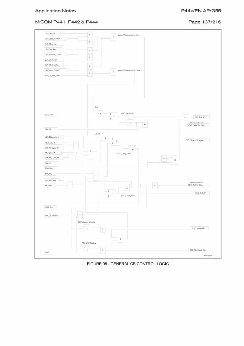
Application Notes P44x/EN AP/G55 MiCOM P441, P442 & P444
Page 137/216
P0514ENa
S QR
t 0 &
&
TRIP
CLOSE
CBA_Status_Alarm
CBA_3P_CCBC_Trip_3P
S QR
CBC_Failed_To_Trip
SUP_Trip_Loc
INP_CB_Trip_Man
SUP_Close_Loc
INP_CB_Man_Close
AR_Cycle_1P
CBA_3P
CBC_Close_In_Progress
t 0
AR_Close
R QS
t 0
CBC_Recl_3P
& CBC_ Fail_To_Close
1
&INP_CB_Healthy
t 0
t 0
&
&SYNC
CBC_UnHeathly
CBC_No_Check_Syn
SUP_Trip_Rem
SUP_Close_Rem
1AR_Cycle_3P
CBC_Trip_Pulse
CBC_Delay_Close
CBC_Close_Pulse
CBC_Healthy_Window
CBC_CS_Window
TRIP_Any
CBC_Local_Control
CBC_Remote_Control
CBC_Input_Control
&
1Manual/Remote/Local Trip
Manual/Remote/Local Close
&
&
&
&
&1
&
1
INP_AR_Close
1INP_AR_Cycle_1P
1
INP_AR_Cycle_3P
Pulsed output latched in UI
Pulsed output latched in UI
1
1
CBA_Disc
&
CBA_3P
S QR
CBA_Any
FIGURE 95 - GENERAL CB CONTROL LOGIC

P44x/EN AP/G55 Application Notes Page 138/216
MiCOM P441, P442 & P444
CB Discrepancy
The DDB CB Discrepancy if assigned to an opto input in the PSL and when energized, will inform the protection about a pole Discrepancy status. 1 pole opened and two other poles closed. Must be Set to high logical level before Dead time 1 is issued (see Figure 83) -can be generated also internally (see Figure 85 and Figure 109 Cbaux logic).
External TripA
External TripB
External TripC
From External Protection Devices (via Opto Inputs)- see General trip logic Figure 94.
Opto inputs are assigned as External Trip A, External Trip B and External Trip C (external Trip Order issued by main 2 or in order to initiate the internal AR backup protection).
External trip is integrated in the DDB: Any Trip. No Dwell timer is associated as for an internal trip (see Figure 94: trip logic).
4.5.7 Logical Outputs generated by the Autoreclose logic
The following DDB signals can be masked to a relay contact in the PSL or assigned to a Monitor Bit in Commissioning Tests, to provide information about the status of the autoreclose cycle. These are described below, identified by their DDB signal text.
AR Lockout Shot>
Indicates an unsuccessful autoreclose (definitive trip following the last AR shot). The relay will be driven to lockout and the autoreclose function will be disabled until the lockout condition has been reset. An alarm, "AR Lockout Shots>" (along with AR Lockout) will be raised. – (see Figure 79 and Figure 81)
AR Fail
If the check sync conditions are not meet prior to reclose within the time window, an alarm "AR Fail" will be raised. (see Figure 78)
AR Close
Initiates the reclosing command pulse for the circuit breaker. This output feeds a signal to the Reclose Time Delay timer, which maintains the assigned reclose contact closed for a sufficient time period to ensure reliable CB mechanism operation. This DDB signal may also be useful during relay commissioning to check the operation of the autoreclose cycle. Where three single pole circuit breakers are used, the AR Close contact will need to energise the closing circuits for all three breaker poles (or alternatively assign three CB Close contacts). (See Figure 78)
AR 1P In Prog.
A single pole autoreclose cycle is in progress. This output will remain activated from the initiating protection trip, until the circuit breaker is closed successfully, or the AR function is Locked Out, thus indicating that dead time timeout is in progress. This signal may be useful during relay commissioning to check the operation of the autoreclose cycle.

Application Notes P44x/EN AP/G55 MiCOM P441, P442 & P444
Page 139/216
P0515ENa
S QR
1P Dead Time 1
AR__1P in prog&CBA_Discrepency
1BAR
SPAR enable
TRIP_1P
&
TRIP_3P
t 0
AR_Cycle_3P
S QR
AR_Discrimination
Discrimination Time
t 0
1
FIGURE 96 – AR 1 POLE IN PROGRESS LOGIC
AR 3P In Prog.
A three phase autoreclose cycle is in progress. This output will remain activated from the initiating protection trip, until the circuit breaker is closed successfully, or the AR function is Locked Out, thus indicating that dead time timeout is in progress. This signal may be useful during relay commissioning to check the operation of the autoreclose cycle.
P0516ENa
AR_3P in prog1
HS_AR_3P
DAR_3P
FIGURE 97 - OUTPUT AR 3 POLES IN PROGRESS
P0517ENa
S QR
&
Dead Time1
HSAR_3PTRIP_3P
TPAR enable
Block AR
Trip counter = 0
t 0
1
&
AR_1P in prog
AR_discrimination&
1
FIGURE 98 - HSAR 3 POLES (HIGH SPEED AR CYCLE 3 POLES)
P0518ENa
S QR
&
Dead Time 2
&
0 < Trip counter < settingDAR_3P
3Par
Block AR
TRIP_3P
t 0
1
FIGURE 99 - DAR 3 POLES (DELAYED AR CYCLE 3 POLES)

P44x/EN AP/G55 Application Notes Page 140/216
MiCOM P441, P442 & P444
AR 1st in Prog.
DDB: AR 1st in Prog. is used to indicate that the autorecloser is timing out its first dead time, whether a high speed single pole or three pole shot.
P0519ENa
AR_1st_Cycle1
HSAR_3P
AR_1P in prog
FIGURE 100 - OUTPUT HSAR (FOR DEAD TIME1)
AR 234 in Prog.
DDB: AR 234 in Prog. is used to indicate that the autorecloser is timing out delayed autoreclose dead times for shots 2, 3 or 4. Where certain protection elements should not initiate autoreclosure for DAR shots, the protection element operation is combined with AR 234 in Prog. as a logical AND operation in the Programmable Scheme Logic, and then set to assert the DDB: BAR input, forcing lockout.
P0520ENa
AR_234th_Cycle1DAR_3P
FIGURE 101 - OUTPUT DAR (FOR DEAD TIME2,3,4)
AR Trip 3 Ph
This is an internal logic signal used to condition any protection trip command to the circuit breaker(s). Where single pole tripping is enabled, fixed logic converts single phase trips for faults on autoreclosure to three pole trips.
P0521ENa
1Block AR
AR_RECLAIM
inhibit&
1
&AR_Internal
SPAR enable
AR_Trip_3Ph
AR_1P in prog
AR_3P in prog
TRIP_1P&
1
FIGURE 102 - -AR LOGIC FOR 3P TRIP DECISION
AR Reclaim
Indicates that the reclaim timer following a particular autoreclose shot is timing out. The DDB: AR Reclaim output would be energised at the same instant as resetting of any Cycle outputs. AR Reclaim could be used to block low-set instantaneous protection on autoreclosure, which had not been time-graded with downstream protection. This technique is commonly used when the downstream devices are fuses, and fuse saving is implemented. This avoids fuse blows for transient faults. See Figure 78.

Application Notes P44x/EN AP/G55 MiCOM P441, P442 & P444
Page 141/216
AR Discrim
Start with the trip order.
When a single pole trip is issued by the relay, a 1 pole AR cycle is initiated. The Dead time1 and Discrimination timer (from version A3.0) are started. If the AR logic detects a single pole or three poles trip (internal or external) during the discrimination timer, the 1P HSAR cycle is disabled and replaced by a 3P HSAR cycle, if enable. If no AR 3P is enable in MiCOM S1, the relay trip 3 poles and AR is blocked. (see Figure 86)
If the AR logic detect a 3 poles trip (internal or external) when the Discrimination Timer is issued, and during the 1P dead time; the single pole AR cycle is stopped and the relay trip 3 phases and block the AR. (see Figure 87 and Figure 96)
P0522ENa
S QR
1P Dead Time 1
AR_1P in prog&CBA_Discrepency
1Block AR
SPAR enable
TRIP_1P
&
TRIP_3P
t 0
AR_3P in prog
S QR
AR_Discrimination
Discrimination Time
t 0
1
FIGURE 103 – AR DISCRIMINATION LOGIC
See also Figure 86 & Figure 87
The discrimination timer is used to differentiate an evolving fault to a second fault in the power system or a long operation of the circuit breaker.

P44x/EN AP/G55 Application Notes Page 142/216
MiCOM P441, P442 & P444
P0523ENa
If an evolving occurs during the discrimination timer, the first single pole high speed AR cycle (1P HSAR) is stopped and removed by a 3 pole high speed AR cycle (3P HSAR)
FIGURE 104 - DEAD TIME 1P=500MSEC / T DISCRIM=100MSEC
If the evolving fault occurs after the discrimination timer, it is considered like a new fault. The 1P cycle is blocked and the CB is kept opened. (No 3P AR cycle is started) (definitive trip – 3 poles are kept opened) – see Figure 105.

Application Notes P44x/EN AP/G55 MiCOM P441, P442 & P444
Page 143/216
FIGURE 105
To inhibit the discrimination timer logic (fixed logic) ; the value should be equal to the 1P cycle dead time. (1P Dead Time 1).
AR Enable
Indicates that the autoreclose function is in service. (See Figure 90)
AR SPAR Enable
Single pole AR is enabled. (See Figure 88)
AR TPAR Enable
Three poles AR is enabled. (See Figure 89)
AR Lockout
If protection operates during the reclaim time, following the final reclose attempt, the relay will be driven to lockout and the autoreclose function will be disabled until the lockout condition is reset. This will produce an alarm, AR Lockout. Secondly, the DDB: BAR input will block autoreclose and cause a lockout if autoreclose is in progress. Lockout will also occur if the CB energy is low and the CB fails to close. Once the autorecloser is locked out, it will not function until a Reset Lockout or CB Manual Close command is received (depending on the Reset Lockout method chosen in CB Monitor Setup).
NOTE: Lockout can also be caused by the CB condition monitoring functions maintenance lockout, excessive fault frequency lockout, broken current lockout, CB failed to trip and CB failed to close, manual close no check synchronism and CB unhealthy. (See Figure 79 & Figure 80)

P44x/EN AP/G55 Application Notes Page 144/216
MiCOM P441, P442 & P444
A/R Force Sync
Force the Check Sync conditions to high logical level – used for SPAR or TPAR with SYNC AR3 fast (Enable by MiCOM S1) - signal is reset with AR reclaim
DEC_3P
AR_Cycle_3P
AR_Close
AR_Trip_3ph
RECLAIM
P0558ENa
SYNC
AR_Force_Sync
FIGURE 106 – CHECK SYNC SIGNAL PICK-UP AT THE END OF THE DEAD TIME (AR CYCLE)
P0559ENa
DEC_3P
AR_Cycle_3P
AR_Close
AR_Trip_3ph
AR_RECLAIM
SYNC
AR_Fail
AR_Force_Sync
FIGURE 107 - THE CHECK SYNC SIGNAL IS FORCED AT THE END OF DEAD TIME (SEE FIGURE 78)
Ext Chk Synch OK
The DDB Ext Chk Synch OK if linked to an opto in a dedicated PSL and when energized, indicates that external conditions of Synchro are fullfiled – This can be linked afterwards with an internal AR logic (See also AR description in Figure 76).
Check Sync;OK
(See Checksync logic description – section 4.4.5.2)
V<Dead Line
(See Checksync logic description – section 4.4.5.2)
V>Live Line
(See Checksync logic description – section 4.4.5.2)
V<Dead Bus
(See Checksync logic description – section 4.4.5.2)

Application Notes P44x/EN AP/G55 MiCOM P441, P442 & P444
Page 145/216
V>Live Bus
(See Checksync logic description – section 4.4.5.2)
Ctrl Cls In Prog
Manual close in progress-using CB control (timer manual closing delay in progress)
Control Trip
CB Trip command by internal CB control
Control Close
CB close command by internal CB control
4.5.8 Setting Guidelines
Should autoreclosure not be required, the function may be Disabled in the relay Configuration menu. Disabling the autorecloser does not prevent the use of the internal check synchronism element to supervise manual circuit breaker closing. If the autoreclose function is Enabled, the setting guidelines now outlined should be read:
4.5.9 Choice of Protection Elements to Initiate Autoreclosure
In most applications, there will be a requirement to reclose for certain types of faults but not for others. The logic is partly fixed so that autoreclosure is always blocked for any Switch on to Fault, Stub Bus Protection, Broken Conductor or Zone 4 trip. Autoreclosure will also be blocked when relay supervision functions detect a Circuit Breaker Failure or Voltage Transformer/Fuse Failure. All other protection trips will initiate autoreclosure unless blocking bits are set in the A/R Block function links. Setting the relevant bit to 1 will block autoreclose initiation (forcing a three pole lockout), setting bits to zero will allow the set autoreclose cycle to proceed.
When autoreclosure is not required for multiphase faults, DDB signals 2Ph Fault and 3Ph Fault can be mapped via the PSL in a logical OR combination onto input DDB: BAR. When blocking is only required for a three phase fault, the DDB signal 3Ph Fault is mapped to BAR alone. Three phase faults are more likely to be persistent, so many utilities may not wish to initiate autoreclose in such instances.
4.5.10 Number of Shots
There are no clear-cut rules for defining the number of shots for any particular application. In order to determine the required number of shots the following factors must be taken into account:
An important consideration is the ability of the circuit breaker to perform several trip close operations in quick succession and the effect of these operations on the maintenance period.
The fact that 80 - 90% of faults are transient highlights the advantage of single shot schemes. If statistical information for the power system shows that a moderate percentage of faults are semi-permanent, further DAR shots may be used provided that system stability is not threatened. Note that DAR shots will always be three pole.

P44x/EN AP/G55 Application Notes Page 146/216
MiCOM P441, P442 & P444
4.5.11 Dead Timer Setting
High speed autoreclose may be required to maintain stability on a network with two or more power sources. For high speed autoreclose the system disturbance time should be minimised by using fast protection, <50 ms, such as distance or feeder differential protection and fast circuit breakers <100 ms. For stability between two sources a system dead time of <300 ms may typically be required. The minimum system dead time considering just the CB is the trip mechanism reset time plus the CB closing time.
Minimum relay dead time settings are governed primarily by two factors:
• Time taken for de-ionisation of the fault path;
• Circuit breaker characteristics.
Also it is essential that the protection fully resets during the dead time, so that correct time discrimination will be maintained after reclosure onto a fault. For high speed autoreclose instantaneous reset of protection is required.
For highly interconnected systems synchronism is unlikely to be lost by the tripping out of a single line. Here the best policy may be to adopt longer dead times, to allow time for power swings on the system resulting from the fault to settle.
4.5.12 De-Ionising Time
The de-ionisation time of a fault arc depends on circuit voltage, conductor spacing, fault current and duration, wind speed and capacitive coupling from adjacent conductors. As circuit voltage is generally the most significant, minimum de-ionising times can be specified as in the Table below.
NOTE: For single pole HSAR, the capacitive current induced from the healthy phases can increase the time taken to de-ionise fault arcs.
Line Voltage (kV) Minimum De-Energisation Time (s)
66 0.1
110 0.15
132 0.17
220 0.28
275 0.3
400 0.5
TABLE 14 - MINIMUM FAULT ARC DE-IONISING TIME (THREE POLE TRIPPING)

Application Notes P44x/EN AP/G55 MiCOM P441, P442 & P444
Page 147/216
Example Minimum Dead Time Calculation
The following circuit breaker and system characteristics are to be used:
• CB Operating time (Trip coil energised → Arc interruption): 50ms (a);
• CB Opening + Reset time (Trip coil energised → Trip mechanism reset): 200ms (b);
• Protection reset time: < 80ms (c);
• CB Closing time (Close command → Contacts make): 85ms (d).
De-ionising time for 220kV line:
• 280ms (e) for a three phase trip. (560ms for a single pole trip).
The minimum relay dead time setting is the greater of:
(a) + (c) = 50 + 80 = 130ms, to allow protection reset;
(a) + (e) - (d) = 50 + 280 - 85 = 245ms, to allow de-ionising (three pole);
= 50 + 560 - 85 = 525ms, to allow de-ionising (single pole).
In practice a few additional cycles would be added to allow for tolerances, so 3P Rcl - Dead Time 1 could be chosen as ≥ 300ms, and 1P Rcl - Dead Time 1 could be chosen as ≥ 600ms. The overall system dead time is found by adding (d) to the chosen settings, and then subtracting (a). (This gives 335ms and 635ms respectively here).
4.5.13 Reclaim Timer Setting
A number of factors influence the choice of the reclaim timer, such as;
• Fault incidence/Past experience - Small reclaim times may be required where there is a high incidence of recurrent lightning strikes to prevent unnecessary lockout for transient faults.
• Spring charging time - For high speed autoreclose the reclaim time may be set longer than the spring charging time. A minimum reclaim time of >5s may be needed to allow the CB time to recover after a trip and close before it can perform another trip-close-trip cycle. This time will depend on the duty (rating) of the CB. For delayed autoreclose there is no need as the dead time can be extended by an extra CB healthy check AR Inhibit Wind window time if there is insufficient energy in the CB.
• Switchgear Maintenance - Excessive operation resulting from short reclaim times can mean shorter maintenance intervals.
• The Reclaim Time setting is always set greater than the tZ2 distance zone delay.

P44x/EN AP/G55 Application Notes Page 148/216
MiCOM P441, P442 & P444
4.6 Circuit breaker state monitoring
An operator at a remote location requires a reliable indication of the state of the switchgear. Without an indication that each circuit breaker is either open or closed, the operator has insufficient information to decide on switching operations. The relay incorporates circuit breaker state monitoring, giving an indication of the position of the circuit breaker, or, if the state is unknown, an alarm is raised.
4.6.1 Circuit Breaker State Monitoring Features
MiCOM relays can be set to monitor normally open (52a) and normally closed (52b) auxiliary contacts of the circuit breaker. Under healthy conditions, these contacts will be in opposite states. Should both sets of contacts be open, this would indicate one of the following conditions:
• Auxiliary contacts / wiring defective
• Circuit Breaker (CB) is defective
• CB is in isolated position
Should both sets of contacts be closed, only one of the following two conditions would apply:
• Auxiliary contacts / wiring defective
• Circuit Breaker (CB) is defective
If any of the above conditions exist, an alarm will be issued after a 5s time delay. A normally open / normally closed output contact can be assigned to this function via the programmable scheme logic (PSL). The time delay is set to avoid unwanted operation during normal switching duties.
In the PSL CB AUX could be used or not, following the four options:
None
52A (1 or 3 optos if it is a single pole logic)
52B (1 or 3 optos)
Both 52A and 52B (2 optos or 6 optos)
Sol1: One opto used for 52a (3 poles breaker)
Sol2: One opto used for 52b (3 poles breaker)

Application Notes P44x/EN AP/G55 MiCOM P441, P442 & P444
Page 149/216
Sol3: Two optos used for 52a & 52b (3 poles breaker)
Sol4: Three optos used for 52a (1 pole breaker)
Sol5: Three optos used for 52b (1 pole breaker)
Sol6: Six optos used for 52a &52b (1 pole breaker)
FIGURE 108 – DIFFERENTS OPTOS/CB AUX SCHEMES

P44x/EN AP/G55 Application Notes Page 150/216
MiCOM P441, P442 & P444
Where ‘None’ is selected no CB status will be available. This will directly affect any function within the relay that requires this signal, for example CB control, auto-reclose, etc. Where only 52a is used on its own then the relay will assume a 52b signal from the absence of the 52a signal. Circuit breaker status information will be available in this case but no discrepancy alarm will be available. The above is also true where only a 52b is used. If both 52a and 52b are used then status information will be available and in addition a discrepancy alarm will be possible, according to the following table. 52a and 52b inputs are assigned to relay opto-isolated inputs via the PSL.
Auxiliary Contact Position CB State Detected Action
52a 52b
Open Closed Breaker Open Circuit breaker healthy
Closed Open Breaker Closed Circuit breaker healthy
Closed Closed CB Failure Alarm raised if the condition persists for greater than 5s
Open Open State Unknown Alarm raised if the condition persists for greater than 5s
Where single pole tripping is used (available on P442 and P444) then an open breaker condition will only be given if all three phases indicate and open condition. Similarly for a closed breaker condition indication that all three phases are closed must be given. For single pole tripping applications 52a-A, 52a-B and 52a-C and/or 52b-A, 52b-B and 52b-C inputs should be used.
With 52a&52b both present, the relay memorizes the last valid status of the 2 inputs (52a=/52b). If no valid status is present (52a=52b) when the Alarm timer is issued (value=150 msec), CBA_Status Alarm is activated. See Figure 109.

Application Notes P44x/EN AP/G55 MiCOM P441, P442 & P444
Page 151/216
P0524ENa
&
1t 0 CBA_Status_Alarm
&
&
&
&
&
&
&
&
&
&
&
CNF_52b
CNF_52a
INP_52a_A
INP_52b_A
INP_52a_B
INP_52b_B
INP_52a_C
INP_52b_C
&
&
&
&
&
&
S QR
S QR
S QR
1
1
1
xor
xor
xor
CBA_Discrepancy
& CBA_3P
1
& CBA_3P_C
CBA_A
CBA_B
CBA_C
CBA_ANY
CBA_Time_Alarm
150 ms
150 ms
&
1INP_DISC
t 0
CBA_Time_Disc
FIGURE 109 - LOGICAL SCHEME OF CBAUX
CBA_A = Dead PoleA
CBA_B = Dead PoleB
CBA_C = Dead PoleC
CBA_3P_C = All Pole live
CBA_3P = All Pole Dead
CBA_ANY = Any Pole dead
CBA_Disc = Pole Discrepancy detection
P0525ENa
INP_52a_A
INP_52a_A
CBA_A
CBA_STATUS_ALARM
FIGURE 110 - NON COMPLEMENTARY OF 52a/52b NOT LONG ENOUGH FOR GETTING THE ALARM

P44x/EN AP/G55 Application Notes Page 152/216
MiCOM P441, P442 & P444
P0526ENa
INP_52a_A
INP_52b_A
CBA_A
CBA_STATUS_ALARM
FIGURE 111 - COMPLEMENTARY OF 52a/52b IS LONG ENOUGH FOR GETTING THE ALARM
P0527ENa
INP_52a_A
CBA_A
CBA_STATUS_ALARM
FIGURE 112 - WITH ONE OPTO 52a- POLE DEAD LOGIC
P0528ENa
INP_52b_A
CBA_A
CBA_STATUS_ALARM
FIGURE 113 - WITH ONE OPTO 52b – POLE DEAD LOGIC
4.6.2 Inputs / outputs DDB for CB logic:
4.6.2.1 Inputs
External TripA
External TripB
External TripC
From External Protection Devices (via Opto Inputs)- see General trip logic Figure 94.
If these optos inputs are assigned as External Trip A, External Trip B and External Trip C – their change will update the CB Operation counter.
(External trip is integrated in the DDB: Any Trip.No Dwell timer is associated as for an internal trip. (see Figure 94: trip logic)
CB aux A(52a)
CB aux B(52a)
CB aux C(52a)
CB aux A(52b)
CB aux B(52b)
CB aux C(52b)
The DDB CB Aux if assigned to an opto input in the PSL and when energized, will be used for Any pole dead & All pole dead internal logic & Discrepency logic
CB Discrepancy
Used for internal CBA_Disc issued by external (opto) or internal detection (CB Aux)
Application Notes P44x/EN AP/G55 MiCOM P441, P442 & P444
Page 153/216
4.6.2.2 Outputs
CB Status Alarm
Picks up when CB Discrepancy status is detected after CBA timer issued externally by opto or internally by CB Aux
CB aux A
CB aux B
CB aux C
Pole A+B+C detected Dead pole by internal logic or CB status
Any Pole Dead
The DDB Any Pole Dead if assigned in the PSL, indicates that one or more poles is open
All Pole Dead
The DDB All Pole Dead if assigned in the PSL, indicates that all pole are dead (All 3 poles are open)
4.7 Circuit breaker condition monitoring
Periodic maintenance of circuit breakers is necessary to ensure that the trip circuit and mechanism operate correctly, and also that the interrupting capability has not been compromised due to previous fault interruptions. Generally, such maintenance is based on a fixed time interval, or a fixed number of fault current interruptions. These methods of monitoring circuit breaker condition give a rough guide only and can lead to excessive maintenance.
The relays record various statistics related to each circuit breaker trip operation, allowing a more accurate assessment of the circuit breaker condition to be determined. These monitoring features are discussed in the following section.
4.7.1 Circuit Breaker Condition Monitoring Features
For each circuit breaker trip operation the relay records statistics as shown in the following table taken from the relay menu. The menu cells shown are counter values only. The Min/Max values in this case show the range of the counter values. These cells can not be set:
Menu text Default setting Setting range Step size
Min Max
CB CONDITION
CB Operations 3 pole tripping
0 0 10000 1
CB A Operations 1 & 3 pole tripping
0 0 10000 1
CB B Operations 1 & 3 pole tripping
0 0 10000 1
CB C Operations 1 & 3 pole tripping
0 0 10000 1
Total IA Broken 0 0 25000In^ 1
Total IB Broken 0 0 25000In^ 1
Total IC Broken 0 0 25000In^ 1In^
CB Operate Time 0 0 0.5s 0.001
Reset All Values No Yes, No
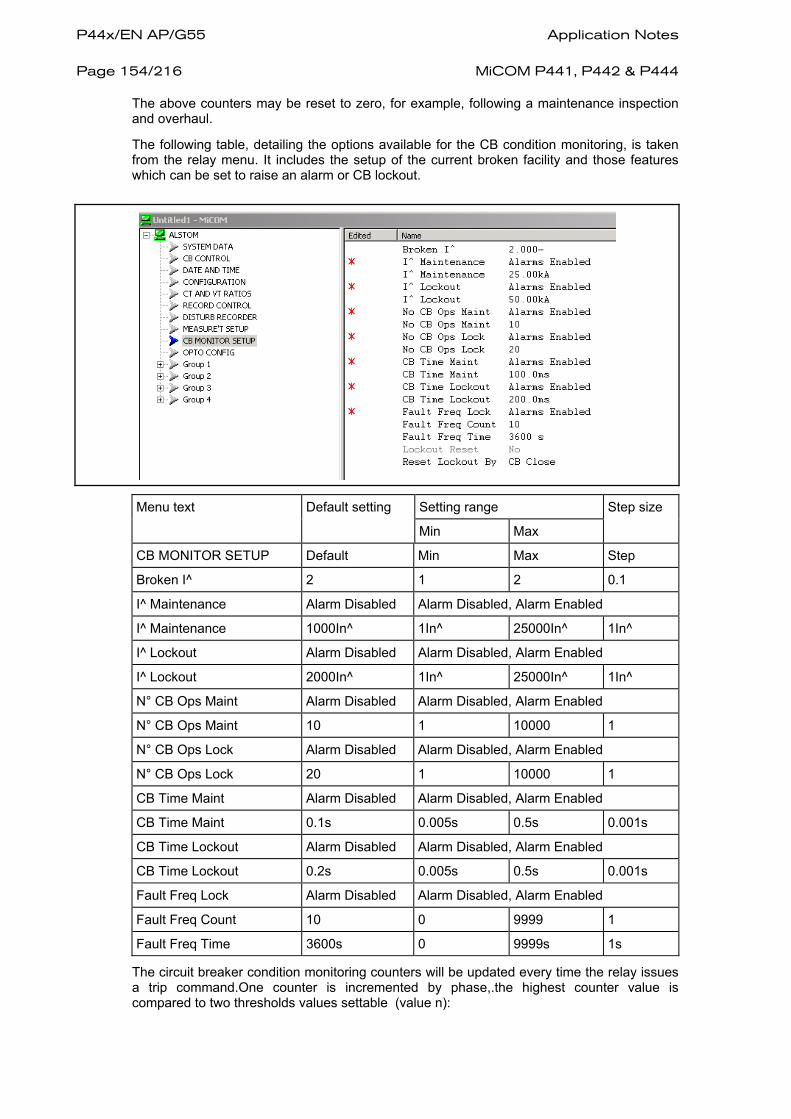
P44x/EN AP/G55 Application Notes Page 154/216
MiCOM P441, P442 & P444
The above counters may be reset to zero, for example, following a maintenance inspection and overhaul.
The following table, detailing the options available for the CB condition monitoring, is taken from the relay menu. It includes the setup of the current broken facility and those features which can be set to raise an alarm or CB lockout.
Menu text Default setting Setting range Step size
Min Max
CB MONITOR SETUP Default Min Max Step
Broken I^ 2 1 2 0.1
I^ Maintenance Alarm Disabled Alarm Disabled, Alarm Enabled
I^ Maintenance 1000In^ 1In^ 25000In^ 1In^
I^ Lockout Alarm Disabled Alarm Disabled, Alarm Enabled
I^ Lockout 2000In^ 1In^ 25000In^ 1In^
N° CB Ops Maint Alarm Disabled Alarm Disabled, Alarm Enabled
N° CB Ops Maint 10 1 10000 1
N° CB Ops Lock Alarm Disabled Alarm Disabled, Alarm Enabled
N° CB Ops Lock 20 1 10000 1
CB Time Maint Alarm Disabled Alarm Disabled, Alarm Enabled
CB Time Maint 0.1s 0.005s 0.5s 0.001s
CB Time Lockout Alarm Disabled Alarm Disabled, Alarm Enabled
CB Time Lockout 0.2s 0.005s 0.5s 0.001s
Fault Freq Lock Alarm Disabled Alarm Disabled, Alarm Enabled
Fault Freq Count 10 0 9999 1
Fault Freq Time 3600s 0 9999s 1s
The circuit breaker condition monitoring counters will be updated every time the relay issues a trip command.One counter is incremented by phase,.the highest counter value is compared to two thresholds values settable (value n):

Application Notes P44x/EN AP/G55 MiCOM P441, P442 & P444
Page 155/216
Maintenance Alarm or Lock Out Alarm can be generated.
A pre-lock out Alarm is generated at value n-1.
All counters can be re-initiated with the command Reset all values (by HMI)
In cases where the breaker is tripped by an external protection device it is also possible to update the CB condition monitoring. This is achieved by allocating one of the relays opto-isolated inputs (via the programmable scheme logic) to accept a trigger from an external device. The signal that is mapped to the opto is called ‘External TripA or B or C’.
Note that when in Commissioning test mode the CB condition monitoring counters will not be updated.
4.7.2 Setting guidelines
Setting the Σ I^ Thresholds
Where overhead lines are prone to frequent faults and are protected by oil circuit breakers (OCB’s), oil changes account for a large proportion of the life cycle cost of the switchgear. Generally, oil changes are performed at a fixed interval of circuit breaker fault operations. However, this may result in premature maintenance where fault currents tend to be low, and hence oil degradation is slower than expected. The Σ I^ counter monitors the cumulative severity of the duty placed on the interrupter allowing a more accurate assessment of the circuit breaker condition to be made.
For OCB’s, the dielectric withstand of the oil generally decreases as a function of Σ I2t. This is where ‘I’ is the fault current broken, and ‘t’ is the arcing time within the interrupter tank (not the interrupting time). As the arcing time cannot be determined accurately, the relay would normally be set to monitor the sum of the broken current squared, by setting ‘Broken I^’ = 2.
For other types of circuit breaker, especially those operating on higher voltage systems, practical evidence suggests that the value of ‘Broken I^’ = 2 may be inappropriate. In such applications ‘Broken I^’ may be set lower, typically 1.4 or 1.5. An alarm in this instance may be indicative of the need for gas/vacuum interrupter HV pressure testing, for example.
The setting range for ‘Broken I^’ is variable between 1.0 and 2.0 in 0.1 steps. It is imperative that any maintenance programme must be fully compliant with the switchgear manufacturer’s instructions.
4.7.3 Setting the Number of Operations Thresholds
Every operation of a circuit breaker results in some degree of wear for its components. Thus, routine maintenance, such as oiling of mechanisms, may be based upon the number of operations. Suitable setting of the maintenance threshold will allow an alarm to be raised, indicating when preventative maintenance is due. Should maintenance not be carried out, the relay can be set to lockout the autoreclose function on reaching a second operations threshold. This prevents further reclosure when the circuit breaker has not been maintained to the standard demanded by the switchgear manufacturer’s maintenance instructions.

P44x/EN AP/G55 Application Notes Page 156/216
MiCOM P441, P442 & P444
Certain circuit breakers, such as oil circuit breakers (OCB’s) can only perform a certain number of fault interruptions before requiring maintenance attention. This is because each fault interruption causes carbonising of the oil, degrading its dielectric properties. The maintenance alarm threshold (N° CB Ops Maint) may be set to indicate the requirement for oil sampling for dielectric testing, or for more comprehensive maintenance. Again, the lockout threshold (N° CB Ops Lock) may be set to disable autoreclosure when repeated further fault interruptions could not be guaranteed. This minimises the risk of oil fires or explosion.
4.7.4 Setting the Operating Time Thresholds
Slow CB operation is also indicative of the need for mechanism maintenance. Therefore, alarm and lockout thresholds (CB Time Maint / CB Time Lockout) are provided and are settable in the range of 5 to 500ms. This time is set in relation to the specified interrupting time of the circuit breaker.
4.7.5 Setting the Excessive Fault Frequency Thresholds
A circuit breaker may be rated to break fault current a set number of times before maintenance is required. However, successive circuit breaker operations in a short period of time may result in the need for increased maintenance. For this reason it is possible to set a frequent operations counter on the relay which allows the number of operations (Fault Freq Count) over a set time period (Fault Freq Time) to be monitored. A separate alarm and lockout threshold can be set.
4.7.6 Inputs/Outputs for CB Monitoring logic
4.7.6.1 Inputs
Reset Lock Out
Provides a reset of the CB monitoring lock out (all counters & values are reset)
Reset All Values
Provides a reset of the CB monitoring (all counters & values are reset)
4.7.6.2 Outputs
I^Maint Alarm
An alarm maintenance is issued when the maximum broken current (1st level) calculated by the CB monitoring function is reached
I^Lock Out Alarm
An alarm Lock Out is issued when the maximum broken current (2nd level) calculated by the monitoring function is reached
CB Ops Maint
An alarm is issued when the maximum of CB operations is reached [initiated by internal (any protection function) or external trip (via opto)] (1st level:CB Ops Maint)
CB Ops Lockout
An alarm is issued when the maximum of CB operations is reached [initiated by internal or external trip] (2nd level:CB Ops Lock)
CB Op Time Maint
An alarm is issued when the operating tripping time on any phase pass over the CB Time Maint adjusted in MiCOM S1 (slowest pole detection calculated by I< from CB Fail logic)
CB Op Time Lock
An alarm is issued when the operating tripping time on any phase pass over the CB Time Lockout adjusted in MiCOM S1 (slowest pole detection calculated by I< from CB Fail logic)

Application Notes P44x/EN AP/G55 MiCOM P441, P442 & P444
Page 157/216
FF Pre Lockout
An alarm is issued at (n-1) value in the counters of Main lock out or Fault frequency
FF Lock
An alarm is issued at (n) value in the counters of Main lock out or Fault frequency
Lockout Alarm
An alarm is issued with: CBC Unhealthy or CBC No check sync or CBC Fail to close or CBC fail to trip or FF Lock or CB Op Time Lock or CB Ops Lock
4.8 Circuit Breaker Control
The relay includes the following options for control of a single circuit breaker:
• Local tripping and closing, via the relay menu
• Local tripping and closing, via relay opto-isolated inputs
• Remote tripping and closing, using the relay communications
It is recommended that separate relay output contacts are allocated for remote circuit breaker control and protection tripping. This enables the control outputs to be selected via a local/remote selector switch as shown in Figure 114. Where this feature is not required the same output contact(s) can be used for both protection and remote tripping.
Protectiontrip
Remotecontroltrip
Remotecontrolclose
ve
P3078ENa
+ ve
Trip0close
LocalRemote
Trip Close
FIGURE 114 - REMOTE CONTROL OF CIRCUIT BREAKER
The following table is taken from the relay menu and shows the available settings and commands associated with circuit breaker control. Depending on the relay model some of the cells may not be visible:

P44x/EN AP/G55 Application Notes Page 158/216
MiCOM P441, P442 & P444
Menu text Default setting Setting range Step size
Min Max
CB CONTROL
CB Control by Disabled Disabled, Local, Remote, Local+Remote, Opto, Opto+local, Opto+Remote, Opto+Rem+local
Close Pulse Time 0.5s 0.1s 10s 0.01s
Trip Pulse Time 0.5s 0.1s 5s 0.01s
Man Close Delay 10s 0.01s 600s 0.01s
Healthy Window 5s 0.01s 9999s 0.01s
C/S Window 5s 0.01s 9999s 0.01s
A/R Single Pole 1&3 pole A/R only
Disabled Disabled, Enabled Refer to Autoreclose notes for further information
A/R Three Pole Disabled Disabled, Enabled Refer to Autoreclose notes for further information
If AR Enable in MiCOM S1 (2 additive lines):
(*) For P442 – P444 only
WARNING: Must be enabled for validating the AR function (if TPAR/SPAR optos are assigned in the PSL, these inputs have a higher priority from the MiCOM S1 settings). The AR single and three poles mode could be enabled in the menu "CB control" via MiCOM S1 or by the front panel. However, if the DDB signals TPAR/SPAR have been assigned in the PSL, these both inputs have a higher priority and depending of their status, will enable/disable the single or three poles AR function independing of the MiCOM S1 or front LCD settings.
Remark: If TPAR is disable, the Dead Time 2 is not used when SPAR logic manages only 1PAR.

Application Notes P44x/EN AP/G55 MiCOM P441, P442 & P444
Page 159/216
P0529ENa
S QR
t 0 &
&
CBA_Status_Alarm
CBA_3P_CCBC_Trip_3P
S QR
CBC_Failed_To_Trip
SUP_Trip_Loc
INP_CB_Trip_Man
SUP_Close_Loc
INP_CB_Man
AR_Cycle_1P
CBA_3P
CBC_Close_In_Progress
t 0
AR_Close
R QS
t 0
CBC_Recl_3P
& CBC_ Fail_To_Close
1
&INP_CB_Healthy
t 0
t 0
&
&SYNC
CBC_UnHeathly
CBC_No_Check_Syn
SUP_Trip_Rem
SUP_Close_Rem
1AR_Cycle_3P
CBC_Trip_Pulse
CBC_Delay_Close
CBC_Close_Pulse
CBC_Healthy_Window
CBC_CS_Window
TRIP_Any
CBC_Local_Control
CBC_Remote_Control
CBC_Input_Control
&
1&
&
&
&
&1
&
1
INP_AR_Close
1INP_AR_Cycle_1P
1
INP_AR_Cycle_3P
Pulsed output latched in UI
Pulsed output latched in UI
1
1
CBA_Disc
&
CBA_3P
S QR
CBA_Any
FIGURE 115 - CB CONTROL LOGIC
A manual trip will be authorised if the circuit breaker has been initially closed. Likewise, a close command can only be issued if the CB is initially open.
Therefor it will be necessary to use the breaker positions 52a and/or 52b contacts via PSL. If no CB auxiliary contacts are available no CB control (manual or auto) will be possible. (See the different solutions proposed in the CBAux logic section 4.6.1)
Once a CB Close command is initiated the output contact can be set to operate following a user defined time delay (‘Man Close Delay’). This would give personnel time to move away from the circuit breaker following the close command. This time delay will apply to all manual CB Close commands.

P44x/EN AP/G55 Application Notes Page 160/216
MiCOM P441, P442 & P444
The length of the trip or close control pulse can be set via the ‘ManualTrip Pulse Time’ and ‘Close Pulse Time’ settings respectively. These should be set long enough to ensure the breaker has completed its open or close cycle before the pulse has elapsed.
NOTE : The manual close commands for each user interface are found in the System Data column of the menu.
If an attempt to close the breaker is being made, and a protection trip signal is generated, the protection trip command overrides the close command.
Where the check synchronism function is set, this can be enabled to supervise manual circuit breaker close commands. A circuit breaker close output will only be issued if the check synchronism criteria are satisfied. A user settable time delay is included (‘C/S Window’) for manual closure with check synchronising. If the checksynch criteria are not satisfied in this time period following a close command the relay will lockout and alarm.
In addition to a synchronism check before manual reclosure there is also a CB Healthy check if required. This facility accepts an input to one of the relays opto-isolators to indicate that the breaker is capable of closing (circuit breaker energy for example). A user settable time delay is included (‘Healthy Window’) for manual closure with this check. If the CB does not indicate a healthy condition in this time period following a close command then the relay will lockout and alarm.
Where auto-reclose is used it may be desirable to block its operation when performing a manual close. In general, the majority of faults following a manual closure will be permanent faults and it will be undesirable to auto-reclose. The "man close" input without CB Control selected OR the "CBClose in progress" with CB control enabled: will initiate the SOTF logic for which auto-reclose will be disabled following a manual closure of the breaker during 500msec (see SOTF logic in section 2.12.1, Figure 35).
If the CB fails to respond to the control command (indicated by no change in the state of CB Status inputs) a ‘CB Fail Trip Control’ or ‘CB Fail Close Control’ alarm will be generated after the relevant trip or close pulses have expired. These alarms can be viewed on the relay LCD display, remotely via the relay communications, or can be assigned to operate output contacts for annunciation using the relays programmable scheme logic (PSL).
CBA_3P_C
SUP_Trip ORINP_CB_Trip_Man
CBC_Trip_3P
CBC_Failed_To_Trip
0.1 to 5 Sec
P0560ENa
FIGURE 116 - STATUS OF CB IS INCORRECT CBA3P C (3POLES ARE CLOSED) STAYS – AN ALARM IS GENERATED “CB FAIL TO TRIP” (SEE ALSO FIGURE 109 & FIGURE 115)

Application Notes P44x/EN AP/G55 MiCOM P441, P442 & P444
Page 161/216
P0561ENa
CBA_3P
SUP_Close ORINP_CB_Man
CBC_ Fail_To_Close
CBC_Recl_3P0.1 to 10 Sec
0 to 60 Sec
CBC_Close_In_Progress
FIGURE 117 - STATUS OF CB IS INCORRECT CBA3P (3POLES ARE OPENED) STAYS – AN ALARM IS GENERATED “CB FAIL TO CLOSE” (SEE ALSO FIGURE 109 & FIGURE 115)
Note that the ‘Healthy Window’ timer and ‘C/S Window’ timer set under this menu section are applicable to manual circuit breaker operations only. These settings are duplicated in the Auto-reclose menu for Auto-reclose applications.
The ‘Lockout Reset’ and ‘Reset Lockout by’ setting cells in the menu are applicable to CB Lockouts associated with manual circuit breaker closure, CB Condition monitoring (Number of circuit breaker operations, for example) and auto-reclose lockouts.
4.9 Event Recorder
The relay records and time tags up to 250 events and stores them in non-volatile (battery backed up – installed behind the plastic cover in front panel of the relay)) memory. This enables the system operator to establish the sequence of events that occurred within the relay following a particular power system condition, switching sequence etc. When the available space is exhausted, the oldest event is automatically overwritten by the new one (First in first out).
The real time clock within the relay provides the time tag to each event, to a resolution of 1ms.
The event records are available for viewing either via the frontplate LCD or remotely, via the communications ports or via MiCOM S1 with a PC. connected to the relay (event extracted from relay & loaded in PC):
1. Established the communication [ Device\open connection\address (always1 by serial front port\Password (AAAA) ]
FIGURE 118
2. Select the extraction of events:
P44x/EN AP/G55 Application Notes Page 162/216
MiCOM P441, P442 & P444
3. Events must be listed, identified (file named) & Stored
Local viewing on the LCD is achieved in the menu column entitled ‘VIEW RECORDS’. This column allows viewing of event, fault and maintenance records and is shown below:-
VIEW RECORDS
LCD Reference Description
Select Event Setting range from 0 to 249. This selects the required event record from the possible 250 that may be stored. A value of 0 corresponds to the latest event and so on.
Time & Date Time & Date Stamp for the event given by the internal Real Time Clock
Event Text Up to 32 Character description of the Event (refer to following sections)
Event Value Up to 32 Bit Binary Flag or integer representative of the Event (refer to following sections)
Select Fault Setting range from 0 to 4. This selects the required fault record from the possible 5 that may be stored. A value of 0 corresponds to the latest fault and so on.
The following cells show all the fault flags, protection starts, protection trips, fault location, measurements etc. associated with the fault, i.e. the complete fault record.
Select Report Setting range from 0 to 4. This selects the required maintenance report from the possible 5 that may be stored. A value of 0 corresponds to the latest report and so on.
Report Text Up to 32 Character description of the occurrence (refer to following sections)
Report Type These cells are numbers representative of the occurrence. They form a specific error code which should be quoted in any related correspondence to ALSTOM Grid.
Report Data
Reset Indication Either Yes or No. This serves to reset the trip LED indications provided that the relevant protection element has reset.
For extraction from a remote source via communications, refer to Chapter P44x/EN CM, (Commissioning) where the procedure is fully explained.
Note that a full list of all the event types and the meaning of their values is given in chapter P44x/EN GC (Configurations Mapping).

Application Notes P44x/EN AP/G55 MiCOM P441, P442 & P444
Page 163/216
Types of Event
An event may be a change of state of a control input or output relay, an alarm condition, setting change etc. The following sections show the various items that constitute an event:-
FIGURE 119 - FILE\OPEN\EVENTS FILE
4.9.1 Change of state of opto-isolated inputs.
If one or more of the opto (logic) inputs has changed state since the last time that the protection algorithm ran, the new status is logged as an event. When this event is selected to be viewed on the LCD, three applicable cells will become visible as shown below;
Time & Date of Event
“LOGIC INPUTS”
“Event Value 0101010101010101”
The Event Value is an 8 or 16 bit word showing the status of the opto inputs, where the least significant bit (extreme right) corresponds to opto input 1 etc. The same information is present if the event is extracted and viewed via PC.
4.9.2 Change of state of one or more output relay contacts.
If one or more of the output relay contacts has changed state since the last time that the protection algorithm ran, then the new status is logged as an event. When this event is selected to be viewed on the LCD, three applicable cells will become visible as shown below;
Time & Date of Event
“OUTPUT CONTACTS”
“Event Value
010101010101010101010”
The Event Value is a 7, 14 or 21 bit word showing the status of the output contacts, where the least significant bit (extreme right) corresponds to output contact 1 etc. The same information is present if the event is extracted and viewed via PC.

P44x/EN AP/G55 Application Notes Page 164/216
MiCOM P441, P442 & P444
4.9.3 Relay Alarm conditions.
Any alarm conditions generated by the relays will also be logged as individual events. The following table shows examples of some of the alarm conditions and how they appear in the event list:-
Alarm Condition Resulting Event
Event Text Event Value
Battery Fail Battery Fail ON/OFF Number from 0 to 31
Field Voltage Fail Field V Fail ON/OFF Number from 0 to 31
Setting group via opto invalid Setting Grp Invalid ON/OFF Number from 0 to 31
Protection Disabled Prot'n Disabled ON/OFF Number from 0 to 31
Frequency out of range Freq out of Range ON/OFF Number from 0 to 31
VTS Alarm VT Fail Alarm ON/OFF Number from 0 to 31
CB Trip Fail Protection CB Fail ON/OFF Number from 0 to 31
The previous table shows the abbreviated description that is given to the various alarm conditions and also a corresponding value between 0 and 31. This value is appended to each alarm event in a similar way as for the input and output events previously described. It is used by the event extraction software, such as MiCOM S1, to identify the alarm and is therefore invisible if the event is viewed on the LCD. Either ON or OFF is shown after the description to signify whether the particular condition has become operated or has reset.
4.9.4 Protection Element Starts and Trips
Any operation of protection elements, (either a start or a trip condition), will be logged as an event record, consisting of a text string indicating the operated element and an event value. Again, this value is intended for use by the event extraction software, such as MiCOM S1, rather than for the user, and is therefore invisible when the event is viewed on the LCD.
4.9.5 General Events
A number of events come under the heading of ‘General Events’ - an example is shown below:-
Nature of Event Displayed Text in Event Record Displayed Value
Level 1 Password Modified
Either from User Interface, Front or Rear Port
PW1 Edited UI, F or R 0
A complete list of the ‘General Events’ is given in chapter P44x/EN GC.

Application Notes P44x/EN AP/G55 MiCOM P441, P442 & P444
Page 165/216
4.9.6 Fault Records
Each time a fault record is generated, an event is also created. The event simply states that a fault record was generated, with a corresponding time stamp.
Note that viewing of the actual fault record is carried out in the ‘Select Fault’ cell further down the ‘VIEW RECORDS’ column, which is selectable from up to 5 records. These records consist of fault flags, fault location, fault measurements etc. Also note that the time stamp given in the fault record itself will be more accurate than the corresponding stamp given in the event record as the event is logged some time after the actual fault record is generated.
4.9.7 Maintenance Reports
Internal failures detected by the self monitoring circuitry, such as watchdog failure, field voltage failure etc. are logged into a maintenance report. The Maintenance Report holds up to 5 such ‘events’ and is accessed from the ‘Select Report’ cell at the bottom of the ‘VIEW RECORDS’ column.
Each entry consists of a self explanatory text string and a ‘Type’ and ‘Data’ cell, which are explained in the menu extract at the beginning of this section and in further detail in Appendix A.
Each time a Maintenance Report is generated, an event is also created. The event simply states that a report was generated, with a corresponding time stamp.
Error codes are in hexadecimal format and must be recalculated in decimal format to check with the table in chapter P44x/EN GC.
4.9.8 Setting Changes
Changes to any setting within the relay are logged as an event. Two examples are shown in the following table:
Type of Setting Change Displayed Text in Event Record Displayed Value
Control/Support Setting C & S Changed 0
Group 1 Change Group 1 Changed 1
NOTE: Control/Support settings are communications, measurement, CT/VT ratio settings etc, which are not duplicated within the four setting groups. When any of these settings are changed, the event record is created simultaneously. However, changes to protection or disturbance recorder settings will only generate an event once the settings have been confirmed at the ‘setting trap’.
4.9.9 Resetting of Event / Fault Records
If it is required to delete either the event, fault or maintenance reports, this may be done from within the ‘RECORD CONTROL’ column.

P44x/EN AP/G55 Application Notes Page 166/216
MiCOM P441, P442 & P444
4.9.10 Viewing Event Records via MiCOM S1 Support Software
When the event records are extracted and viewed on a PC they look slightly different than when viewed on the LCD. The following shows an example of how various events appear when displayed using MiCOM S1:-
− Monday 03 November 1998 15:32:49 GMT I>1 Start ON 2147483881
ALSTOM Grid : MiCOM
Model Number: P441
Address: 001 Column: 00 Row: 23
Event Type: Protection operation
− Monday 03 November 1998 15:32:52 GMT Fault Recorded 0
ALSTOM Grid : MiCOM
Model Number: P441
Address: 001 Column: 01 Row: 00
Event Type: Fault record
− Monday 03 November 1998 15:33:11 GMT Logic Inputs 00000000
ALSTOM Grid : MiCOM
Model Number: P441
Address: 001 Column: 00 Row: 20
Event Type: Logic input changed state
− Monday 03 November 1998 15:34:54 GMT Output Contacts 0010000
ALSTOM Grid : MiCOM
Model Number: P441
Address: 001 Column: 00 Row: 21
Event Type: relay output changed state
As can be seen, the first line gives the description and time stamp for the event, whilst the additional information that is displayed below may be collapsed via the +/- symbol.
For further information regarding events and their specific meaning, refer to chapter P44x/EN GC.

Application Notes P44x/EN AP/G55 MiCOM P441, P442 & P444
Page 167/216
FIGURE 120
4.10 Disturbance recorder
The integral disturbance recorder has an area of memory specifically set aside for record storage. The number of records that may be stored is dependent upon the selected recording duration but the relays typically have the capability of storing a minimum of 20 records, each of 10.5 second duration.
NOTE: 1. Compressed Disturbance Recorder used for Kbus/Modbus/DNP3 reach that typical size value (10.5 sec duration) 2. Uncompressed Disturbance Recorder used for IEC 60870-5/103 could be limited to 2 or 3 secondes.
Disturbance records continue to be recorded until the available memory is exhausted, at which time the oldest record(s) are overwritten to make space for the newest one.
The recorder stores actual samples which are taken at a rate of 24 samples per cycle.
Each disturbance record consists of eight analogue data channels and thirty-two digital data channels. Note that the relevant CT and VT ratios for the analogue channels are also extracted to enable scaling to primary quantities).

P44x/EN AP/G55 Application Notes Page 168/216
MiCOM P441, P442 & P444
The ‘DISTURBANCE RECORDER’ menu column is shown below:
Menu text Default setting Setting range Step size
Min Max
DISTURB RECORDER
Duration 1.5s 0.1s 10.5s 0.01s
Trigger Position 33.3% 0 100% 0.1%
Trigger Mode Single Single or Extended
Analog Channel 1 VA VA, VB, VC, IA, IB, IC, IN
Analog Channel 2 VB VA, VB, VC, IA, IB, IC, IN
Analog Channel 3 VC VA, VB, VC, IA, IB, IC, IN
Analog Channel 4 VN VA, VB, VC, IA, IB, IC, IN
Analog Channel 5 IA VA, VB, VC, IA, IB, IC, IN
Analog Channel 6 IB VA, VB, VC, IA, IB, IC, IN
Analog Channel 7 IC VA, VB, VC, IA, IB, IC, IN
Analog Channel 8 IN VA, VB, VC, IA, IB, IC, IN
Digital Inputs 1 to 32 Relays 1 to 14/21 and Opto’s 1 to 8/16
Any of 14 or 21 O/P Contacts or Any of 8 or 16 Opto Inputs or Internal Digital Signals
Inputs 1 to 32 Trigger No Trigger except Dedicated Trip Relay O/P’s which are set to Trigger L/H
No Trigger, Trigger L/H, Trigger H/L
Note
The available analogue and digital signals may differ between relay types and models and so the individual courier database in Appendix should be referred to when determining default settings etc.
The pre and post fault recording times are set by a combination of the ‘Duration’ and ‘Trigger Position’ cells. ‘Duration’ sets the overall recording time and the ‘Trigger Position’ sets the trigger point as a percentage of the duration. For example, the default settings show that the overall recording time is set to 1.5s with the trigger point being at 33.3% of this, giving 0.5s pre-fault and 1s post fault recording times.
If a further trigger occurs whilst a recording is taking place, the recorder will ignore the trigger if the ‘Trigger Mode’ has been set to ‘Single’. However, if this has been set to ‘Extended’, the post trigger timer will be reset to zero, thereby extending the recording time.
As can be seen from the menu, each of the analogue channels is selectable from the available analogue inputs to the relay. The digital channels may be mapped to any of the opto isolated inputs or output contacts, in addition to a number of internal relay digital signals, such as protection starts, LED’s etc. The complete list of these signals may be found by viewing the available settings in the relay menu or via a setting file in MiCOM S1. Any of the digital channels may be selected to trigger the disturbance recorder on either a low to high or a high to low transition, via the ‘Input Trigger’ cell. The default trigger settings are that any dedicated trip output contacts (e.g. relay 3) will trigger the recorder.

Application Notes P44x/EN AP/G55 MiCOM P441, P442 & P444
Page 169/216
FIGURE 121
Trigger choices:
(Minimum one trigger condition must be present ; for providing Drec file.)
It is not possible to view the disturbance records locally via the LCD; they must be extracted using suitable software such as MiCOM S1. This process is fully explained in Chapter 6.
(Events or Disturbances can be extracted)
This message is displayed if the memory is empty (control in that case the trigger condition):

P44x/EN AP/G55 Application Notes Page 170/216
MiCOM P441, P442 & P444
After extraction the Drec file can be displayed by the viewer integrated in MiCOM S1(See Commissioning test section – chap CT)
Click down to select :

Application Notes P44x/EN AP/G55 MiCOM P441, P442 & P444
Page 171/216
5. NEW ADDITIONAL FUNCTIONS – VERSION B1.X 5.1 Maximum of Residual Power Protection – Zero Sequence Power Protection
5.1.1 Function description
The aim of protection is to provide the system with selective and autonomous protection against resistive Phase to ground faults. High resistive faults such as vegetation fires cannot be detected by distance protection.
When a phase to ground fault occurs, the fault can be considered as a zero-sequence power generator. Zero-sequence voltage is at maximum value at the fault point. Zero-sequence power is, therefore, also at maximum value at the same point. Supposing that zero-sequence current is constant, zero-sequence power will decrease along the lines until null value at the source’s neutral points (see below).
Z os1 x . Zol (1-x).Zol Z os2
PA PB
P3100XXa
With: Zos1: Zero-sequence source side 1 impedance of
Zol: Zero-sequence line impedance
Zos2: Zero-sequence source side2 impedance of
x: Distance to the fault From PA
PoVo
1
0,5
0
1
0,5
0
PA PBFaultP3101ENa
Selective fault clearance of the protection for forward faults is provided by the power measurement combined with a time-delay inversely proportional to the measured power.
The protection does not send any trip commands for reverse faults.
In compliance with sign conventions (the zero-sequence power flows from the fault towards the sources) and with a mean characteristic angle of the zero-sequence source impedances of the equal to 75°, the measured power is determined by the following formula:
Sr = Vrr.m.s x Irr.m.s x cos(ϕ - ϕ0)
With: ϕ: Phaseshift between Vr and Ir
ϕ0: 255° or – 75°
Vrr.m.s, Irr.m.s: R.M.S values of the residual voltage and current
The Vr and Ir values are filtered in order to eliminate the effect of the 3rd and 5th harmonics.

P44x/EN AP/G55 Application Notes Page 172/216
MiCOM P441, P442 & P444
P3837ENa
Sr > Po Fixed TimeDelay
3-pole trip is sent out when the residual power threshold “Residual Power" is overshot, after a time-delay "Basis Time Delay" and a IDMT time-delay adjusted by the “K” time delay factor.
The basis time-delay is set at a value greater than the 2nd stage time of the distance protection of the concerned feeder if the 3-pole trip is active, or at a value greater than the single-phase cycle time if single-pole autorecloser shots are active.
The IDMT time-delay is determined by the following formula:
T(s) = K x (Sref/Sr)
With: K: Adjustable time constant from 0 to 2sec (Time delay factor)
Sref: Reference residual power at:
10 VA for In = 1A
50 VA for In = 5A
Sr: Residual power generated by the fault
The following chart shows the adjustment menu for the zero-sequence residual overcurrent protection, the adjustment ranges and the default in-factory adjustments.
Menu text Default setting Setting range Step size
Min Max
Group1 ZERO-SEQ. POWER
Zero Seq. Power Status Activated Activated / Disabled N/A
K Time Delay Factor 0 0 2 0.2
Basis Time Delay 1sec 0sec 10sec 0.01sec
Residual Current 0.1 x In 0.05 x In 1 x In 0.01 x In
Po threshold 510mVA 300mVA 6.0VA 30.0mVA
Application Notes P44x/EN AP/G55 MiCOM P441, P442 & P444
Page 173/216
5.1.2 Settings & DDB cells assigned to zero sequence power (ZSP) function
DDB cell INPUT associated:
The ZSP TIMER BLOCK cell if assigned to an opto input in a dedicated PSL , Zero Sequence Power function will start, but will not perform a trip command - the associated timer will be blocked
DDB cell OUTPUT associated:
The ZSP START cell at 1 indicates that the Zero Sequence Power function has started - in the same time, it indicates that the timers associated have started and are running (fixed one first and then IDMT timer)
The ZSP TRIP cell at 1 indicates that the Zero Sequence Power function has performed a trip command (after the start and when associated timers are issued)

P44x/EN AP/G55 Application Notes Page 174/216
MiCOM P441, P442 & P444
5.2 Capacitive Voltage Transformers Supervision (CVT)
5.2.1 Function description
This CVT supervision will detect the degradation of one or several capacitors of voltage dividers. It is based on permanent detection of residual voltage.
A “CVT fault” signal is sent out, after a time-delay T which can be set at between 0 and 300 seconds, if the conditions are as follows:
• The residual voltage is greater than the setting threshold during a delay greater then T
• The 3 phase-phase voltages have a value greater than 0.4 Un
Vab(t) > 0,8*Vn
Vr(t) > SVr
T&
Vab(t)
Vr(t)
TCTs - Alarm
Vbc(t) > 0,8*Vn
Vca(t) < 0,4*Vn
Vab(t) < 0,4*Vn
Vbc(t) < 0,4*Vn
Vca(t) > 0,8*Vn
Vbc(t)
Vca(t)
S QR
S Q
R
S Q
R
T
P3102ENa
FIGURE 122 - BASIC CVT SUPERVISION DIAGRAM
The table below shows the CVT supervision settings menu, settings range and the default in-factory settings.
Menu text Default setting Setting range Step size
Min Max
Group1 SUPERVISION
CVTS Status Activated Activated / Disabled N/A
CVTS VN> 1sec 0.5sec 22sec 0.5
CVTS Time Delay 100sec 0sec 300sec 0.01sec

Application Notes P44x/EN AP/G55 MiCOM P441, P442 & P444
Page 175/216
5.2.2 Settings & DDB cells assigned to Capacitive Voltage Transformers Supervision (CVT)
function
FIGURE 123 - FOR ENABLING THE FUNCTION
FIGURE 124 – SETTINGS
DDB cell OUTPUT associated:
The CVT ALARM cell at 1 indicates that the residual voltage is greater than the threshold adjusted in the settings, during a delay greater than the timer adjusted in MiCOM S1. That alarm is also included in the general alarm.

P44x/EN AP/G55 Application Notes Page 176/216
MiCOM P441, P442 & P444
6. PROGRAMMABLE SCHEME LOGIC DEFAULT SETTINGS The relay includes programmable scheme logic (PSL)- one PSL by Group of settings enabled (maximum 4 groups of PSLogic can be assigned in the relay)
The purpose of this logic is multi-functional and includes the following:
• Enables the mapping of opto-isolated inputs, relay output contacts and the programmable LED’s.
• Provides relay output conditioning (delay on pick-up/drop-off, dwell time, latching or self-reset).
• Fault Recorder start mapping, i.e. which internal signals initiate a fault record.
• Enables customer specific scheme logic to be generated through the use of the PSL editor inbuilt into the MiCOM S1 support software.
Further information regarding editing and the use of PSL can be found in the MiCOM S1 user manual. The following section details the default settings of the PSL. Note that changes to these defaults can only be carried out using the PSL editor and not via the relay front-plate.
6.1 HOW TO USE PSL Editor?
OFF Line method:
− Open first the application free software delivered with the relay : MiCOM S1 (can be also downloaded from the web)
− Open the PSL Editor part.
− Open a blancking scheme or a default scheme with the good model number (File\New\Default Scheme or Blanck Scheme)
Selection of type of relay & model number is done in that window (Version software is displayed for compatibility ) – Italian is available with model ?40X?
ON Line method:
− Communication with the relay can be started (Device\open connection\address1\pword AAAA) and the PSL activated in the internal logic of the relay can be extracted, displayed, modified and loaded again in the protection.

Application Notes P44x/EN AP/G55 MiCOM P441, P442 & P444
Page 177/216
− Any group from 1 to 4 can be modified (ref of group must be validated before
resenting the file from PC to relay)
Before creating a dedicated PSL for covering customized application ; please refer to the DDB description cell by cell (conditions of set & reset) in the table included in the annex A at the end of that technical guide.
Some additive cells can be present regarding the type of model used by the software embedded in the relay.
Software Version Model N°
A2.11 04
A3.3 06
A4.5 07
B1.2 09
The type of model used by the relay in the settings or PSL is displayed in the bottom of your screen by that line:
and will inform about the :
− Model number used (last 2 digits:???07??)
− PSL activated for the logic of Group1
− Number of timers still available (15 on a total of 16)
− Number of contacts still available (7 on a total of 21 for P442 model)
− Number of leds still available (0 on 8 – if all already assigned in the PSL)
− Memory Capacity still available (decrease with the numbers of cells & logical gates linked in the dedicated PSL)
(See also the section commissioning for deeper tools explanations)

P44x/EN AP/G55 Application Notes Page 178/216
MiCOM P441, P442 & P444
6.2 Logic input mapping
The default mappings for each of the opto-isolated inputs are as shown in the following table:
− Version A : Optos are in 48VDC polarised (can be energised with the internal field voltage offered by the relay (–J7/J9-J8/J10 in a P441)
− Version B : Optos are universal and opto range can be selected in MiCOM S1 by:
Opto A - 48VDC:
The opto inputs are specified to operate between 30 and 60V to ensure there is enough current flowing through the opto diode to guarantee operation with component tolerances, temperature and CTR degradation over time.
Between 13-29V is the uncertainty band.
Below 12V, logical status is guaranteed Off
Opto B – Universal opto inputs:
Setting Guaranteed No Operation Guaranteed Operation
24/27 <16,2 >19,2
30/34 <20,4 >24,0
48/54 <32,4 >38,4
110/125 <75,0 >88,0
220/250 <150 >176,0
These margins ensure that ground faults on substation batteries do not create mal-operation of the opto inputs.
Or “Custom” can be selected in the menu to offer the possibility to adjust a different voltage pick-up for any optos inputs:

Application Notes P44x/EN AP/G55 MiCOM P441, P442 & P444
Page 179/216

P44x/EN AP/G55 Application Notes Page 180/216
MiCOM P441, P442 & P444
Opto Input N°
P441 Relay P442 Relay P444 Relay
1 Channel Receive (Distance or DEF)
Channel Receive (Distance or DEF)
Channel Receive (Distance or DEF)
2 Channel out of Service (Distance or DEF)
Channel out of Service (Distance or DEF)
Channel out of Service (Distance or DEF)
3 MCB/VTS Line
(Z measurement-Dist)
MCB/VTS Line
(Z measurement-Dist)
MCB/VTS Line
(Z measurement-Dist)
4 Block Autoreclose(LockOut)
Block Autoreclose(LockOut)
Block Autoreclose(LockOut)
5 Circuit Breaker Healthy Circuit Breaker Healthy Circuit Breaker Healthy
6 Circuit breaker Manual Close external order
Circuit breaker Manual Close external order
Circuit breaker Manual Close external order
7 Reset Lockout Reset Lockout Reset Lockout
8 Disable Autoreclose (1pole and 3poles)
Disable Autoreclose (1-pole and 3poles)
Disable Autoreclose (1-pole and 3poles)
9 Not allocated Not allocated
10 Not allocated Not allocated
11 Not allocated Not allocated
12 Not allocated Not allocated
13 Not allocated Not allocated
14 Not allocated Not allocated
15 Not allocated Not allocated
16 Not allocated Not allocated
17 Not allocated
18 Not allocated
19 Not allocated
20 Not allocated
21 Not allocated
22 Not allocated
23 Not allocated
24 Not allocated

Application Notes P44x/EN AP/G55 MiCOM P441, P442 & P444
Page 181/216
6.3 Relay output contact mapping
The default mappings for each of the relay output contacts are as shown in the following table (PSL are equivalent for P441/442/444):-
Relay Contact N°
P441 Relay P442 Relay P444 Relay
1 TripA+B+C & Z1 TripA+B+C & Z1 TripA+B+C & Z1 2 Any Trip Phase A Any Trip Phase A Any Trip Phase A 3 Any Trip Phase B Any Trip Phase B Any Trip Phase B 4 Any Trip Phase C AnyTrip Phase C Any Trip Phase C 5 Signal send (Dist. or DEF) Signal send (Dist. or DEF) Signal send (Dist. or DEF)6 Any Protection Start Any Protection Start Any Protection Start 7 Any Trip Any Trip Any Trip 8 General Alarm General Alarm General Alarm 9 DEF A+B+C Trip
+ IN>1Trip + IN>2Trip
DEF A+B+C Trip + IN>1Trip + IN>2Trip
DEF A+B+C Trip + IN>1Trip + IN>2Trip
10 Dist. Trip &Any Zone&DistUnb CR
Dist. Trip &Any Zone&DistUnb CR
Dist. Trip &Any Zone&DistUnb CR
11 Autoreclose lockout Autoreclose lockout Autoreclose lockout 12 Autoreclose 1P+3P cycle
in progress Autoreclose 1P+3P cycle in progress
Autoreclose 1P+3P cycle in progress
13 A/R Close A/R Close A/R Close 14 Power Swing Detected Power Swing Detected Power Swing Detected 15 Not allocated Not allocated 16 Not allocated Not allocated 17 Not allocated Not allocated 18 Not allocated Not allocated 19 Not allocated Not allocated 20 Not allocated Not allocated 21 Not allocated Not allocated 22 Not allocated Not allocated 23 Not allocated 24 Not allocated 25 Not allocated 26 Not allocated 27 Not allocated 28 Not allocated 29 Not allocated 30 Not allocated 31 Not allocated 32 Not allocated
Note that when 3 pole tripping is selected in the relay menu, all trip contacts: Trip A, Trip B, Trip C, and Any Trip close simultaneously.

P44x/EN AP/G55 Application Notes Page 182/216
MiCOM P441, P442 & P444
6.4 Relay output conditioning
The default conditioning for each of the relay output contacts are as shown in the following table:
Relay Contact N°
P441 Relay P442 Relay P444 Relay
1 Straight Straight Straight 2 Straight Straight Straight 3 Straight Straight Straight 4 Straight Straight Straight 5 Straight Straight Straight 6 Straight Straight Straight 7 Straight Straight Straight 8 Straight Straight Straight 9 Straight Straight Straight 10 Straight Straight Straight 11 Straight Straight Straight 12 Straight Straight Straight 13 Straight Straight Straight 14 Straight Straight Straight 15 Not allocated Not allocated 16 Not allocated Not allocated 17 Not allocated Not allocated 18 Not allocated Not allocated 19 Not allocated Not allocated 20 Not allocated Not allocated 21 Not allocated Not allocated 22 Not allocated Not allocated 23 Not allocated 24 Not allocated 25 Not allocated 26 Not allocated 27 Not allocated 28 Not allocated 29 Not allocated 30 Not allocated 31 Not allocated 32 Not allocated
NOTE: Others conditions of relays logic are available in the relays design by PSL.
Pulse Timer Pick UP/Drop Off Timer
Dwell Timer Pick Up Timer Drop Off Timer
Latching Straight (Transparent)

Application Notes P44x/EN AP/G55 MiCOM P441, P442 & P444
Page 183/216
InputOutput
OutputInput
Pulse setting
Pulse settingPulse Timer
Input
Output
Output
Input
P0562ENa
Tp setting
Tp settingPick Up/Drop Off Timer
Td setting
Td setting
Input
Output Timer setting
Input
Output Timer setting
Dwell Timer
InputOutput
Output
Input
Timer setting
Timer setting
Pick Up Timer
Input
Output Timer setting
Input
Output Timer setting
Drop Off Timer
FIGURE 125 – TIMER DEFINITION IN PSL

P44x/EN AP/G55 Application Notes Page 184/216
MiCOM P441, P442 & P444
6.5 Programmable led output mapping
The default mappings for each of the programmable LED’s are as shown in the following table:-
LED N°
P441 Relay P442 Relay P444 Relay
1 Any Trip A Any Trip A Any Trip A
2 Any Trip B AnyTrip B Any Trip B
3 Any Trip C AnyTrip C Any Trip C
4 Any Start Any Start Any Start
5 Z1+Aided Trip Z1+Aided Trip Z1+Aided Trip
6 Dist FWd Dist Fwd Dist Fwd
7 Dist Rev Dist Rev Dist Rev
8 A/R Enable A/R Enable A/R Enable
NOTE: All the Leds are latched in the default PSL
6.6 Fault recorder trigger
The default PSL trigger which initiates a fault record is as shown in the following table:-
P441 Relay P442 Relay P444 Relay
Any Start Any Start Any Start
Any Trip Any Trip Any Trip
FIGURE 126
If the fault recorder trigger is not assigned in the PSL, no Fault recorder can be initiated and displayed in the list by the LCD front panel.

Application Notes P44x/EN AP/G55 MiCOM P441, P442 & P444
Page 185/216
7. CURRENT TRANSFORMER REQUIREMENTS Two calculations must be performed – once for the three phase fault current at the zone 1 reach, and once for earth (ground) faults. The highest of the two calculated Vk voltages must be used:
7.1 CT Knee Point Voltage for Phase Fault Distance Protection
Vk ≥ KRPA x IF Z1 x (1+ X/R) . (RCT + RL)
Where:
Vk = Required CT knee point voltage (volts),
KRPA = Fixed dimensioning factor = always 0.6
IF Z1 = Max. secondary phase fault current at Zone 1 reach point (A),
X/R = Primary system reactance / resistance ratio,
RCT = CT secondary winding resistance (Ω),
RL = Single lead resistance from CT to relay (Ω).
7.2 CT Knee Point Voltage for Earth Fault Distance Protection
Vk ≥ KRPA x IFe Z1 x (1+ Xe/Re) . (RCT + 2RL)
Where:
KRPA = Fixed dimensioning factor = always 0.6
IFe Z1 = Max. secondary earth fault current at Zone 1 reach point (A),
Xe/Re = Primary system reactance / resistance ratio for earth loop.
7.3 Recommended CT classes (British and IEC)
Class X current transformers with a knee point voltage greater or equal than that calculated can be used.
Class 5P protection CTs can be used, noting that the knee point voltage equivalent these offer can be approximated from:
Vk = (VA x ALF) / In + (RCT x ALF x In)
Where:
VA = Voltampere burden rating,
ALF = Accuracy Limit Factor,
In = CT nominal secondary current.
7.4 Determining Vk for an IEEE “C" class CT
Where American/IEEE standards are used to specify CTs, the C class voltage rating can be checked to determine the equivalent Vk (knee point voltage according to IEC). The equivalence formula is:
Vk = [ (C rating in volts) x 1.05 ] + [ 100 x RCT ]
8. DDB DESCRIPTION FOR ALL TYPES P441/P442 & P444 MODELS

P44x/EN AP/G55 Application Notes Page 186/216
MiCOM P441, P442 & P444
BLANK PAGE

Application Notes P44x/EN AP/G55 MiCOM P441, P442 & P444
Page 187/216
DDB label In
Out Default PSL Set with : Reset with :
Changement of Group by Optos
No cell assigned In Opto1 opto energised (>1 sec)(∗) – Must be not assigned in the PSL At1 :LSB Bit (see table in section 3.3.1 in chap AP)
opto power off At 0 : (see table in section 3.3.1 in chap AP)
No cell assigned In Opto2 opto energised (>1 sec)(*) – Must be not assigned in the PSL At1 :MSB Bit (see table in section 3.3.1 in chap AP)
opto power off At 0 : (see table in section 3.3.1 in chap AP)
SG-opto Invalid Out Setting Group selected via opto are invalid Example :1group is requested by the optos status but that group is not present in the settings (Gr3 requested but only Gr1&2 are present in MiCOM S1-The settings restart with GR1 & that cell switch on at 1)
Set 0 : No alarm is present
OPTOS INPUTS (48Vcc Version A / Universal Version B-C)
Opto Label 1/8
In P441 / P442 / P444
Opto energised for a minimum time : 7 ms (48Vdc), 10 ms (universal) to be validated by internal logic See Hysteresis description in sect 6.2 chapter P44x/EN AP
P441 / P442 / P444
See Hysteresis description in sect 6.2 chapter P44x/EN AP
Opto Label 9/16
In P442 / P444
Opto energised for a minimum time : 7 ms (48Vdc), 10 ms (universal) to be validated by internal logic See Hysteresis description in sect 6.2 chapter P44x/EN AP
P442 / P444
See Hysteresis description in sect 6.2 chapter P44x/EN AP
Opto Label 17/24
In P444
Opto energised for a minimum time : 1,2 sec to be validated by internal logic See Hysteresis description in sect 6.2 chapter P44x/EN AP
P444
See Hysteresis description in sect 6.2 chapter P44x/EN AP
Opto Label 25/32
In Not Used Not Used
∗ Minimum time >1 sec for: changement Gr/TPAR/SPAR/AR enable

P44x/EN AP/G55 Application Notes Page 188/216
MiCOM P441, P442 & P444
DDB label In
Out Default PSL Set with : Reset with :
OUTPUT RELAYS
Relay Label
01/14
Out P441 / P442 / P444
Set1 :For any DDB cell at 1 if linked by PSL & regarding the type of logic selected in PSL by MiCOM S1 Programmable Relays : All relays are assigned in The default PSL (See DDB table description) Type of Logic: Pulse timer Pick Up/Drop Off Timer Dwell Timer Pick Up Timer Drop Off Timer Latching Straight (used in default PSL)
P441 / P442 / P444
Set 0 :For any DDB cell at 0 if linked by PSL & regarding the type of logic selected in PSL by MiCOM S1 Type of Logic: Pulse timer Pick Up/Drop Off Timer Dwell Timer Pick Up Timer Drop Off Timer Latching Straight (used in default PSL)
Relay Label
15/21
Out P442 / P444
Set1 :For any DDB cell at 1 if linked by PSL & regarding the type of logic selected in PSL by MiCOM S1 Programmable Relay – Not assigned in default PSL Type of Logic: (See Description above)
P442 / P444
Set 0 :For any DDB cell at 0 if linked by PSL & regarding the type of logic selected in PSL by MiCOM S1 Type of Logic: (See Description above)
Relay Label
22/32
Out P444
Set1 :For any DDB cell at 1 if linked by PSL & regarding the type of logic selected in PSL by MiCOM S1 Programmable Relay– Not assigned in default PSL Type of Logic: (See Description above)
P444
Set 0 :For any DDB cell at 0 if linked by PSL & regarding the type of logic selected in PSL by MiCOM S1 Type of Logic: (See Description above)
LEDS (Right side – Front panel)
LED 1 Led Set1 : For any DDB cell at 1 if linked by PSL Programmable Led : ANY TRIP A in the default PSL
Set 0 : For any DDB cell at 0 if linked by PSL & regarding the type of logic selected in PSL by MiCOM S1 (Latched or not Latched)

Application Notes P44x/EN AP/G55 MiCOM P441, P442 & P444
Page 189/216
DDB label In
Out Default PSL Set with : Reset with :
LED 2 Led Set1 : For any DDB cell at 1 if linked by PSL Programmable Led : ANY TRIP B in the default PSL
Set 0 : For any DDB cell at 0 if linked by PSL & regarding the type of logic selected in PSL by MiCOM S1 (Latched or not Latched)
LED 3 Led Set1 : For any DDB cell at 1 if linked by PSL Programmable Led : ANY TRIP C in the default PSL
Set 0 : For any DDB cell at 0 if linked by PSL & regarding the type of logic selected in PSL by MiCOM S1 (Latched or not Latched)
LED 4 Led Set1 : For any DDB cell at 1 if linked by PSL Programmable Led : General Start in the default PSL
Set 0 : For any DDB cell at 0 if linked by PSL & regarding the type of logic selected in PSL by MiCOM S1 (Latched or not Latched)
LED 5 Led Set1 : For any DDB cell at 1 if linked by PSL Programmable Led : Z1+Aided Trip in the default PSL
Set 0 : For any DDB cell at 0 if linked by PSL & regarding the type of logic selected in PSL by MiCOM S1 (Latched or not Latched)
LED 6 Led Set1 : For any DDB cell at 1 if linked by PSL Programmable Led : Dist FWD in the default PSL
Set 0 : For any DDB cell at 0 if linked by PSL & regarding the type of logic selected in PSL by MiCOM S1 (Latched or not Latched)
LED 7 Led Set1 : For any DDB cell at 1 if linked by PSL Programmable Led : Dist REV in the default PSL
Set 0 : For any DDB cell at 0 if linked by PSL & regarding the type of logic selected in PSL by MiCOM S1 (Latched or not Latched)
LED 8 Led Set1 : For any DDB cell at 1 if linked by PSL Programmable Led : Auto Reclose Enable in the default PSL
Set 0 : For any DDB cell at 0 if linked by PSL & regarding the type of logic selected in PSL by MiCOM S1 (Latched or not Latched)

P44x/EN AP/G55 Application Notes Page 190/216
MiCOM P441, P442 & P444
DDB label In
Out Default PSL Set with : Reset with :
AUTO RECLOSE (AR) Logic
SPAR Enable In Opto8 +Inv
opto energised (> 1 sec) if linked by PSL At1 :1P AR internal is enabled in the AR logic (higher priority than MiCOM S1)
Reset at 0 : opto power off At 0 : AR 1P internal is disabled (even if selected enable by MiCOM S1) AR logic becomes 3P only with AR 3P cycle -if TPAR =1
TPAR Enable In Opto8 +Inv
opto energised (> 1 sec) if linked by PSL At1 :3P AR internal is enabled in the AR logic (higher priority than MiCOM S1)
Reset at 0 : opto power off At 0 : AR 3P internal is disabled (even if selected enable by MiCOM S1) logic becomes :no more 3P cycle available (1P could exist if SPAR at 1)
A/R Internal In opto energised (> 1 sec) if linked by PSL At1 :AR internal becomes present [AR becomes enable by external contact example :Wdog of Main1 when pick up activates the internal AR in Main2(P44x)]
Reset at 0 : opto power off At 0 :no Ban Tri logic available. AR is disable
A/R 1p in Prog In Relay 12
opto energised if linked by PSL At1 : External 1P AR cycle in progress – requested for blocking the internal DEF function
Reset at 0 : opto power off
A/R 3p in Prog In Relay 12
opto energised if linked by PSL External 3P Arcycle in progress - requested for blocking the internal DEF function – (pb of Pole Operating Time)
Reset at 0 : opto power off
A/R Close In Relay 13
opto energised if linked by PSL At1 :External AR gives a CB closing order – for using internal synchro conditions of P44X
Reset at 0 : opto power off
A/R reclaim In opto energised if linked by PSL At1 :Reclaim time from external AR in progress – requested to initiate internal TOR logic / Used in Z1X logic (by specific PSL)
Reset at 0 : opto power off

Application Notes P44x/EN AP/G55 MiCOM P441, P442 & P444
Page 191/216
DDB label In
Out Default PSL Set with : Reset with :
BAR In Opto 4
opto energised if linked by PSL Set at1 :External condition which blocks the internal AR (other internal blocking conditions can be selected in MiCOM S1 :Autoreclose/Block AR) – see also logic AR lockout figure..
Reset at 0 : opto power off AR Lock out is reseted
Ext Chk Synch OK
In opto energised if linked by PSL At1 :External check synchro condition satisfied – to be used with internal AR close by specific PSL – (With AND logic between Arclose&CsyncExt)
Reset at 0 : opto power off Conditiond of external synchro are unvailable
CB Healthy In Opto 5
opto energised if linked by PSL At1 :contact from CB when CB is operationnal (gas pressure/mechanical state)- Must be at 1 inside the time window (adjusted by MiCOM S1 : group1/Autoreclose mode/AR Inhibit Wind) during an AR cycle (signals :AR close & AR Reclaim pick up when CB healthy is detected during the InhWind timer)
Reset at 0 : opto power off At 0 : AR cycle is stopped (if that cell is assigned in the PSL). At the end of InhWInd the signal AR BAR picks up.
Force 3P trip In opto energised if linked by PSL At1 :External command for tripping 3P only (Order issued from Main1 to Main2) – next trip will be 3P
Reset at 0 : opto power off
Man.Close CB In Opto 6
opto energised if linked by PSL At1 :External manual close command – requested to initiate SOTF logic & to close CB (Arlock out during SOTF logic)
Reset at 0 : opto power off
Man.Trip CB In opto energised if linked by PSL At1 :External manual trip command to provide a CB trip command by CB control if selected in MiCOM S1
Reset at 0 : opto power off
CB Discrepancy
In opto energised if linked by PSL At1 : Contact from external status of CB poles (one pole opened) – that data must be at 1 before end of Dead time1 if assigned in the PSL OR Internal logic = Any pole &Not All pole Dead (CB Aux must be connected 52a or 52b)
Reset at 0 : opto power off OR drop Off Internal Logic At 0 : Stop the 1P cycle if absent at the end of dead time1. AR is ofrced in AR Lock Out
External TripA In opto energised if linked by PSL At1 :External trip command A
Reset at 0 : opto power off

P44x/EN AP/G55 Application Notes Page 192/216
MiCOM P441, P442 & P444
DDB label In
Out Default PSL Set with : Reset with :
Activate a Trip command phase A (DDB :Any TripA) (No dwell timer is associated as for an internal trip) Activate internal AR Integrated in the Any Trip & Any TripA cell
External TripB In opto energised if linked by PSL At1 :External trip command B Activate a Trip command phase B(DDB :Any TripB) (No dwell timer is associated as for an internal trip) Activate internal AR Integrated in the Any Trip & Any TripB cell
Reset at 0 : opto power off
External TripC In opto energised if linked by PSL At1 :External trip command C Activate a Trip command phase C(DDB :Any TripC) (No dwell timer is associated as for an internal trip) Activate internal AR Integrated in the Any Trip & Any TripC cell
Reset at 0 : opto power off
AR Lockout Shot>
Out AR is blocked by passing over the number of shots selected in Auto Reclose/trip mode (in MiCOM S1) Set at 1 : (AR Enable) & [(Trip1P&No SPAR)+(Trip3P&NoTPAR) +(Trip1P+Trip3P)&(Number of shots=MiCOM S1 value)]
At0 : AR Cycles continue if fault still present (not erased by the previous Arcycle) Reset at 0 : Reset Trip1P + Reset Trip3P
AR Fail Out Set at 1 : Absence of check sync condition involve AR failure (For 3P cycle) Reset at 0 : by 3 Poles Closed
A/R close Out Relay 13 Set at 1 :AR internal command :CB Close Starts as AR Reclaim
Reset at 0 with : Close Pulse Time (Setting) OR Trip1P or Trip3P
A/R 1p in Prog Out Relay 12 1P AR cycle in progress (could be connected to external Main2 for Blocking DEF)
Set 0 with : End of 1P Dead Time +AR Lock out (BAR) + 3P TRip
Application Notes P44x/EN AP/G55 MiCOM P441, P442 & P444
Page 193/216
DDB label In
Out Default PSL Set with : Reset with :
A/R 3p in Prog Out Relay 12 3P AR cycle in progress (could be connected to external Main2) Set 0 with : End of 3P Dead time (DAR) +AR Lock Out (BAR) +End of Dead time1 (HSAR)
A/R 1st in Prog Out First high speed AR Cycle in progress (could be connected to external Main2)
Set 0 with : End of 3P Dead time (DAR) +AR Lock Out (BAR) +End of Dead time1 (HSAR)
A/R 234 in Prog Out Further delayed AR Cyles in progress (could be connected to external Main2)
Set 0 with : End of 3P Dead time (DAR) +AR Lock Out (BAR) +End of Dead time1 (HSAR)
A/R Trip 3P Out AR signal which force all trips to be 3P – picks up at the end of the first trip (1P or 3P) - Can be connected to Main2 as an external Ban Tri Set at 1 : (AR enable MiCOM S1)&(No SPAR)
At 0 : AR1P could operate if programmed Reset at 0 : SPAR & AR enable MiCOM S1 + (InhibitWind at 0)
A/R Reclaim Out Set at 1 :Reclaim timer in progress.(Value adjusted in MiCOM S1) Picks up at the end of the dead time –in synchronism with AR Close order- Can be connected to Main2 for cycle in progress external information - Initiate the internal TOR logic
Reset at 0 with : End of Reclaim time (MiCOM S1) OR Reset (Trip1P or Trip3P) (See Figure 78 section 4.5.3)

P44x/EN AP/G55 Application Notes Page 194/216
MiCOM P441, P442 & P444
DDB label In
Out Default PSL Set with : Reset with :
AR Discrim Out Dicrim status detected (inter or Externaly)-timer in progress Rest 0 : End of Discrim timer (MiCOM S1) +Trip 3P (DEC 3P) +AR Lock Out (BAR)
A/R Enable Out Led 8 Copy of status AR Enable Set at 1 : [(optos SPAR) +(optoTPAR)]& (AR enable byMiCOM S1)
Reset at 0: If SPAR and TPAR Optos at 0 (if integrated in PSL) + AR Disable in MiCOM S1
A/R SPAR Enable
Out Set at 1 :1P AR activated (copy of opto SPAR or MiCOM S1) Reset at 0: if SPARopto=0 or AR Disable in MiCOM S1
A/R TPAR Enable
Out Set at 1 :3P AR activated (copy of opto TPAR or MiCOM S1) Reset at 0: if TPARopto=0 or AR Disable in MiCOM S1
A/R Lockout Out Relay 11 AR function locked out/No more cycle is initiated by the AR (Pole is kept opened) – Reset must be done for enabling the AR logic again (AR counters are resetted) Set at 1 = ARenable & [(BAR =1 (see internal logic figure.. section..) +(AR BAR n shot>) AR lockout by number of shots +(No CB Healthy at the end of InhWind(MiCOM S1)) +[No Discrepancy (opto or internal by CBAux if present in PSL) at the end of 1P Dead time1] + (Trip 1P or3P maintained /still present at the end of the1Por3P Dead time) +(After discrim timer if Trip3P occures during a 1PAR Cycle) ]
At0 : AR is activated Reset at 0 = [Reset(Trip1P)+Reset(Trip3P)] & (End of RC timer) & Reset (BAR ) & Reset (AR BAR n shot>) & Reset (No CB Healty) & Reset (No Discrepancy)
A/R Force Sync Out Force the Synchro condition ok at 1 (Could be used during test for getting Arclose whatever are the real conditions of CheckSyn )
Reset 0 : With Reset of A/R Reclaim (See DDB description)
LED 8 AR Enable (See DDB Description)
Latched by PSL design
Application Notes P44x/EN AP/G55 MiCOM P441, P442 & P444
Page 195/216
DDB label In
Out Default PSL Set with : Reset with :
CHECK SYNC Logic
Check Synch .OK
Out Set at 1 : Check Synchro conditions are satisfied Used with AR close in dedicated PSL – AND gate : [(AR Close) or (Manual Close) & (Checksync OK)]
Set at 0 : Conditions of checksyn unsatisfied (thresholds of dead & live definied in MiCOM S1 :system checks)
Control No C/S Out Set at 1 : Internal conditions of Csync are not fulfilled Set at 0 :CSYnc conditions available
V<Dead line Out Set at 1 : Condition of Dead line at 1 (voltage below the threshold value (settable in MiCOM S1) – Default value is 13V
Set at 0 : Condition of Dead line at 0 (voltage above the threshold value (settable in MiCOM S1)
V>Live line Out Set at 1: Condition of Live line at 1 (voltage above the threshold value (settable in MiCOM S1) – Default value is 32V
Set at 0 : Condition of Live line at 0 (voltage below the threshold value (settable in MiCOM S1)
V<Dead Bus Out Set at 1: Condition of Dead Bus at 1 (voltage below the threshold value (settable in MiCOM S1) – Default value is 13V
Set at 0 : Condition of Dead Bus at 0 (voltage above the threshold value (settable in MiCOM S1)
V>Live Bus Out Set at 1: Condition of Live Bus at 1 (voltage above the threshold value (settable in MiCOM S1) – Default value is 32V
Set at 0 : Condition of Live Bus at 0 (voltage below the threshold value (settable in MiCOM S1)
MCB/VTS Bus In Set at 1 :Internal fault in VT used for synchro ref Csync function is blocked
Reset at 0 : opto power off
MCB/VTS Line In Set at 1 :Internal fault in VT used for Z measurement ref (Main VT) Distance &all Directionnal functions are blocked(can unblocked with different VTS timer- see MiCOM S1 settings)
Reset at 0 : opto power off
Ctrl Cls In Prog Out Set at 1 :Manual close in progress – using CB control (Timer manual closing delay in progress)
Set at 0 :End of Timer manual closing
Control Close Out Set at1 :CB Close 3P command by internal CB Control (Control with synchrocheck manual condition could be used in dedicated PSL – MiCOM S1Chk scheme ManCB) See CB Control logic sect 4.8 fig 115
Reset at 0 : End of Timer MiCOM S1 (Close pulse timer) +Any Trip +CBC No Csync +CBC Unhealthy See CB Control logic sect 4.8 fig 115
Control Trip Out Set at 1 :CB Trip 3P command by internal CB Control See CB Control logic sect 4.8 fig 115
Reset at 0 : End of timer MiCOM S1 (Trip pulse timer)
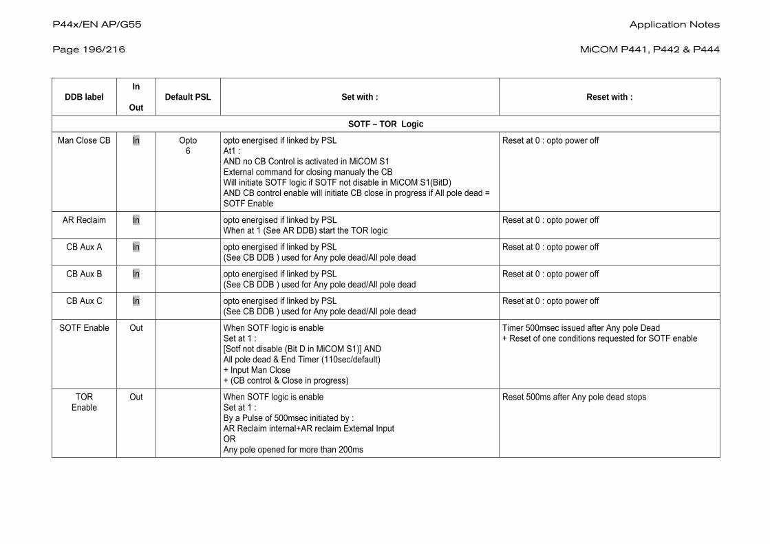
P44x/EN AP/G55 Application Notes Page 196/216
MiCOM P441, P442 & P444
DDB label In
Out Default PSL Set with : Reset with :
SOTF – TOR Logic
Man Close CB In Opto 6
opto energised if linked by PSL At1 : AND no CB Control is activated in MiCOM S1 External command for closing manualy the CB Will initiate SOTF logic if SOTF not disable in MiCOM S1(BitD) AND CB control enable will initiate CB close in progress if All pole dead = SOTF Enable
Reset at 0 : opto power off
AR Reclaim In opto energised if linked by PSL When at 1 (See AR DDB) start the TOR logic
Reset at 0 : opto power off
CB Aux A In opto energised if linked by PSL (See CB DDB ) used for Any pole dead/All pole dead
Reset at 0 : opto power off
CB Aux B In opto energised if linked by PSL (See CB DDB ) used for Any pole dead/All pole dead
Reset at 0 : opto power off
CB Aux C In opto energised if linked by PSL (See CB DDB ) used for Any pole dead/All pole dead
Reset at 0 : opto power off
SOTF Enable Out When SOTF logic is enable Set at 1 : [Sotf not disable (Bit D in MiCOM S1)] AND All pole dead & End Timer (110sec/default) + Input Man Close + (CB control & Close in progress)
Timer 500msec issued after Any pole Dead + Reset of one conditions requested for SOTF enable
TOR Enable
Out When SOTF logic is enable Set at 1 : By a Pulse of 500msec initiated by : AR Reclaim internal+AR reclaim External Input OR Any pole opened for more than 200ms
Reset 500ms after Any pole dead stops

Application Notes P44x/EN AP/G55 MiCOM P441, P442 & P444
Page 197/216
DDB label In
Out Default PSL Set with : Reset with :
TOC Start A Out Set1 :Trip order phase A initiated by levels detectors in SOTF logic (Pickup 20ms delayed )
Set 0 : Reset of Level detectors logic
TOC Start B Out Set1 :Trip order phase B initiated by levels detectors in SOTF logic (Pickup 20ms delayed )
Set 0 : Reset of Level detectors logic
TOC Start C Out Set1 :Trip order phase C initiated by levels detectors in SOTF logic (Pickup 20ms delayed )
Set 0 : Reset of Level detectors logic
AR Reclaim Out When at 1 (See AR DDB) start the TOR logic Set 0 : (See AR DDB)
SOTF/TOR Trip
Out Set1 :Trip order initiated by any condition fulfilled in the SOTF/TOR logic (See logic section 2.12 – fig 37)
Set 0 :When conditions reset (See logic section 2.12 – fig 37)
Any Pole Dead Out Set1 :Minimum 1 pole is open Pole Dead A+Pole DeadB+Pole Dead C Detection of pole status made by Cbaux or internal thresholds (see dead pole logic in SOTF section 2.12 – fig 35)
Set 0 :All poles are detected not dead Detection of pole status made by Cbaux or internal thresholds
All Pole Dead Out Set1 :All poles are open Pole DeadA & P.DeadB & P.Dead C Detection of pole status made by Cbaux or internal thresholds (see dead pole logic in SOTF section 2.12 – fig 35)
Set 0 :1pole is detected not dead Detection of pole status made by Cbaux or internal thresholds
CIRCUIT BREAKER Logic (CB Control / CB Monitoring / CB Fail)
CB Aux A (52a) In opto energised if linked by PSL At1 :Status input from CB-Pole A is closed
Reset at 0 : opto power off Set 0 :Pole A is opened
CB Aux A (52b) In opto energised if linked by PSL At1 :Status input from CB-Pole A is opened
Reset at 0 : opto power off Set 0 :Pole A is closed
CB Aux B (52a) In opto energised if linked by PSL At1 :Status input from CB-Pole B is closed
Reset at 0 : opto power off Set 0 :Pole B is opened
CB Aux B (52b) In opto energised if linked by PSL At1 :Status input from CB-Pole B is opened
Reset at 0 : opto power off Set 0 :Pole B is closed
CB Aux C (52a) In opto energised if linked by PSL At1 :Status input from CB-Pole C is closed
Reset at 0 : opto power off Set 0 :Pole A is opened

P44x/EN AP/G55 Application Notes Page 198/216
MiCOM P441, P442 & P444
DDB label In
Out Default PSL Set with : Reset with :
CB Aux C (52b) In opto energised if linked by PSL At1 :Status input from CB-Pole C is opened
Reset at 0 : opto power off Set 0 :Pole C is closed
CB Healthy In Opto 5 See DDB description of AR Logic (CB control not used) See DDB description of AR Logic
Man Close CB In Opto 6 See DDB Description in SOTF logic (CB control not used) See DDB Description in SOTF logic
Man Trip CB In See DDB description of AR Logic See DDB description of AR Logic
CB Discrepancy In See DDB description of AR Logic See DDB description of AR Logic
Reset Lockout In Opto 7 opto energised if linked by PSL At1 :Provides a CB monitoring lockout reset (all counters & values are reset)
Reset at 0 : opto power off
Reset All Values In opto energised if linked by PSL At1 :Provides a CB monitoring reset (all counters & values are reset)
Reset at 0 : opto power off
CB Fail Alarm Out Set 1 :For any Breaker failure on any trip for any phase Reset 0 : (selectable in MiCOM S1 : CB fail & I< logic) Iphase< + CB open & Iphase< +Trip reset & Iphase +Trip reset OR Iphase<<
I^ Maint Alarm Out Set1 : :Alarm Maintenace picks up when the maximum broken current (1st level) calculated by monitoring task is reached (set in MiCOM S1 :I^Maintenance) (min1/Max 25000A)
I^ Lockout Alarm Out Set1 : Lockout :Alarm picks up when the maximum broken current (2nd level) calculated by monitoring task is reached (set in MiCOM S1 :I^Maintenance) (min1/Max 25000A)
Set 0 :When the maximum broken current (2nd level) calculated by monitoring task is not reached

Application Notes P44x/EN AP/G55 MiCOM P441, P442 & P444
Page 199/216
DDB label In
Out Default PSL Set with : Reset with :
CB Ops Maint Out Set1 :Alarm picks up when the maximum number of CB operations initiated by internal or external Trip (set in MiCOM S1 :CB Ops Maint) is reached (min1/Max 10000)
Set 0 :untill number of operations is bellow the MiCOM S1 value Counter can be reseted by « Reset all values »
CB Ops Lockout Out Set1 :When CB is lockout due to number of CB operations bigger than in MiCOM S1 value(CB Ops Lock) (min1/Max 10000)
Set 0 :untill number of operations is bellow the MiCOM S1 value Counter can be reseted by « Reset all values »
CB Op Time Maint
Out Set1 :Alarm picks up for an excessive operating time on any phase (slowestpole detection calculated by I< of CB Fail logic)) In MiCOM S1-CB Time maint (min5/Max 500 msec)
Set 0 :untill operating time is bellow the MiCOM S1 value
CB Op Time lock Out Set1 :Alarm picks up for an excessive operating time on any phase (slowestpole detection calculated by I< of CB Fail logic) In MiCOM S1-CB Time Lockout (min5/Max 500 msec)
Set 0 :untill operating time is bellow the MiCOM S1 value
F.F Pre Lockout Out Set1 :CB Trip Prelockout Alarm With (Maint Lockout –1) + (Fault Frequency-1) at 1
ReSet 0 : end of timer in MiCOM S1 (Fault Freq Time) (min0/Max 9999 sec)
F.F Lock Out Set1 : CB Trip Lockout Alarm With : (Maint Lockout =1) + (Fault Frequence=1)
Reset 0 : By user interface OR CB Close (selectable in MiCOM S1)
Lockout Alarm Out Set1 :Lockout Alarm with CBC Unhealthy +CBC No Check Sync +CBC Fail to Close +CBC Fail To Trip +FF Lock +CB OpTime Lock +CB Ops Lock
Reset 0 : By user interface OR CB Close (selectable in MiCOM S1)
CB Status Alarm Out Displayed with 2 LSB of « Plan Status « at 00 or 11 from LCD of relay Set1 :When CB discrepency status is detected after CBA timer issued by opto input or internaly by CBAux logic – Alarm issued after 5 sec. See CB aux Logic in sect 4.7.1 Figure 109
Set 0 : When conditions reset Opto or internal logic
Man CB trip Fail Out Set1 :CB Fail on Manual Trip See CB Control logic section 4.8 Figure 115
Set 0 : See CB Control logic section 4.8 Figure 115
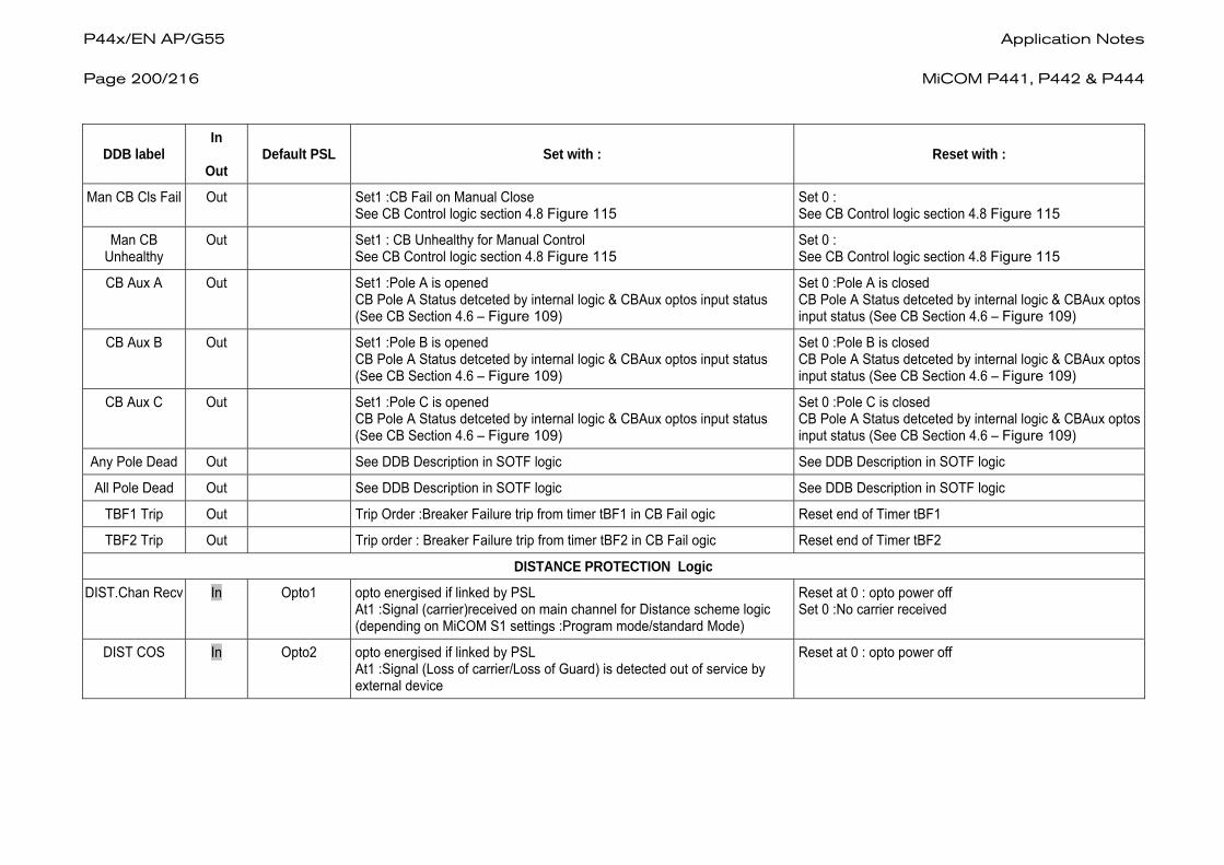
P44x/EN AP/G55 Application Notes Page 200/216
MiCOM P441, P442 & P444
DDB label In
Out Default PSL Set with : Reset with :
Man CB Cls Fail Out Set1 :CB Fail on Manual Close See CB Control logic section 4.8 Figure 115
Set 0 : See CB Control logic section 4.8 Figure 115
Man CB Unhealthy
Out Set1 : CB Unhealthy for Manual Control See CB Control logic section 4.8 Figure 115
Set 0 : See CB Control logic section 4.8 Figure 115
CB Aux A Out Set1 :Pole A is opened CB Pole A Status detceted by internal logic & CBAux optos input status (See CB Section 4.6 – Figure 109)
Set 0 :Pole A is closed CB Pole A Status detceted by internal logic & CBAux optos input status (See CB Section 4.6 – Figure 109)
CB Aux B Out Set1 :Pole B is opened CB Pole A Status detceted by internal logic & CBAux optos input status (See CB Section 4.6 – Figure 109)
Set 0 :Pole B is closed CB Pole A Status detceted by internal logic & CBAux optos input status (See CB Section 4.6 – Figure 109)
CB Aux C Out Set1 :Pole C is opened CB Pole A Status detceted by internal logic & CBAux optos input status (See CB Section 4.6 – Figure 109)
Set 0 :Pole C is closed CB Pole A Status detceted by internal logic & CBAux optos input status (See CB Section 4.6 – Figure 109)
Any Pole Dead Out See DDB Description in SOTF logic See DDB Description in SOTF logic
All Pole Dead Out See DDB Description in SOTF logic See DDB Description in SOTF logic
TBF1 Trip Out Trip Order :Breaker Failure trip from timer tBF1 in CB Fail ogic Reset end of Timer tBF1
TBF2 Trip Out Trip order : Breaker Failure trip from timer tBF2 in CB Fail ogic Reset end of Timer tBF2
DISTANCE PROTECTION Logic
DIST.Chan Recv In Opto1 opto energised if linked by PSL At1 :Signal (carrier)received on main channel for Distance scheme logic (depending on MiCOM S1 settings :Program mode/standard Mode)
Reset at 0 : opto power off Set 0 :No carrier received
DIST COS In Opto2 opto energised if linked by PSL At1 :Signal (Loss of carrier/Loss of Guard) is detected out of service by external device
Reset at 0 : opto power off

Application Notes P44x/EN AP/G55 MiCOM P441, P442 & P444
Page 201/216
DDB label In
Out Default PSL Set with : Reset with :
Z1X Extension In opto energised if linked by PSL OR any internal DDB by dedicated PSL At1 :Signal will initiate Z1 extension logic if selected in MiCOM S1. That cell can be assigned to any external/Internal condition for starting Z1X logic (See Z1X logic section 4.5.4 Figure 13 Figure 14)
Reset at 0 : opto power off
MCB/VTS Line (Z measure VT main)
In Opto3 opto energised if linked by PSL At1 :Fuse Failure by external MCB status on Main VT (Z measurement) .All Distance & Directionnality will be blocked after a FFU timer adjusted by MiCOM S1 (See Fuse Failure logic section 4.2 Figure 66) Even if Main VT are Bus side – that cell must be linked to MCB status)
Reset at 0 : opto power off
MCB/VTS Bus (Sync Ref)
In See Check Sync DDB description (Used in Synchrocheck logic)
See Check Sync DDB description (Used in Synchrocheck logic)
VTS Fast Out Set1 :Copy of Instantaneous unconfirmed Fuse Failure (in internal logic detection) (See Fuse Failure logic section 4.2 Figure 66) Protections blocked.Min Z can be unblocked by I>&I2>&IN&ΔI (for 1P/2P/3P Failure)
Set 0 :Rest of one of the conditions (See FFailure logic in section 4.2 Figure 66)
VTS Fail Alarm Out Set1 :VT Alarm indication with : internal logic after timer is issued+ MCB by opto at1 The Distance/WInfeed & Directionnal functions are blocked (only Non direc I> are working) (See Fuse Failure logic section 4.2 Figure 66)
Reset 0 : Healthy network detected + All pole Dead (See FFailure logic in section 4.2 Figure 66)
Dist Timer Block In opto energised if linked by PSL OR any internal DDB by dedicated PSL (Usefull during test) Set1 :The DIST Timer will be blocked & DIST will start but will not perform a Trip command.
Reset at 0 : opto power off if assigned to an opto OR DDB at 0 if assigned to a DDB cell
COS Alarm Out Set1 :Alarm for Carrier Out Of Service Set 0 : Rest of initiale condition
DIST Sig Send Out Relay 05 Set1 :Signal send in Distance Protection scheme (See logic of distance section 2.8.2.4)
Set 0 :

P44x/EN AP/G55 Application Notes Page 202/216
MiCOM P441, P442 & P444
DDB label In
Out Default PSL Set with : Reset with :
DIST UNB CR Out Set1 :Unblock Main channel signal received See Led 5 / Relay 10 description
Set 0 :
Dist Fwd Out Led6 Set1 :Directionnal Forward detected in distance Algorithms (Deltas or Classical) AND (CVMR) See Description of Algorithms in chapter P44x/EN HW, item 4) Assigned to Led 6 by default
Set 0 : With reset of Any Start/Dist Start
Dist Rev Out Led7 Set1 :Directionnal Reverse detected in distance Algorithms (Deltas or Classical) AND (CVMR) (See Description of Algorithms in chapter P44x/EN HW, item 4) Assigned to Led 7 by default
Set 0 : With reset of Any Start/Dist Start
Dist Trip A Out Set1 :Trip Phase A with Distance protection logic (See Trip logic in Section 2.5 Figure 94)
Set 0 :Reset Dist Trip signal (fixed pulse duration is 80ms)
Dist Trip B Out Set1 :Trip Phase B with Distance protection logic (See Trip logic in Section 2.5 Figure 94)
Set 0 :Reset Dist Trip signal (fixed pulse duration is 80ms)
Dist Trip C Out Set1 :Trip Phase C with Distance protection logic (See Trip logic in Section 2.5 Figure 94)
Set 0 :Reset Dist Trip signal (fixed pulse duration is 80ms)
DIST Start A Out Set1 : Distance Protection logic start phase A (See Description of Algorithms in chapter 3)
Set 0 : Reset of R/X computation made by All pole Dead detection I Dead calculated by Laurent (3 or 4 samples requested) V Dead calculated by CB Fail (More than 10ms requested)
DIST Start B Out Set1 : Distance Protection logic start phase B (See Description of Algorithms in chapter 3)
Set 0 : Reset of R/X computation made by All pole Dead detection I Dead calculated by Laurent (3 or 4 samples requested) V Dead calculated by CB Fail (More than 10ms requested)

Application Notes P44x/EN AP/G55 MiCOM P441, P442 & P444
Page 203/216
DDB label In
Out Default PSL Set with : Reset with :
DIST Start C Out Set1 : Distance Protection logic start phase C (See Description of Algorithms in chapter 3)
Set 0 : Reset of R/X computation made by All pole Dead detection I Dead calculated by Laurent (3 or 4 samples requested) V Dead calculated by CB Fail (More than 10ms requested)
DIST Sch Accel. Out Set1 :Distance scheme accelerating - POP (Copy of MiCOM S1 setting Dist scheme)
Set 0 : If disabled in MiCOM S1
DIST Sch Perm Out Set1 :Distance scheme Permissive - PUP (Copy of MiCOM S1 setting Dist scheme)
Set 0 : If disabled in MiCOM S1
DIST Sch Block Out Set1 :Distance scheme Blocking – BOP Z1 – BOP Z2 (Copy of MiCOM S1 setting Dist scheme)
Set 0 : If disabled in MiCOM S1
Z1 = Z'1 Out Led5 Relay 01-10
Set1 :Fault is detected in Z1(convergence of loop in Z1) See Led 5/Relay01/Relay 10 description
Set 0 : Reset of R/X computation made by All pole Dead detection (See Dist Start DDB reset description)
Z1X = Z'1x Out Led5 Relay
10
Set1 :Fault is detected in Z1x(convergence of loop in Z1x) and filtered by blocking/unblocking PSwing/Rguard logic See Led 5/Relay10 description
Set 0 : Reset of R/X computation made by All pole Dead detection (See Dist Start DDB reset description)
Z2 = Z'2 Out Led5 Relay
10
Set1 :Fault is detected in Z2(convergence of loop in Z2) and filtered by blocking/unblocking PSwing/Rguard logic See Relay 10 / Led5 description
Set 0 : Reset of R/X computation made by All pole Dead detection (See Dist Start DDB reset description)
Z3 = Z'3 Out Led5 Relay
10
Set1 :Fault is detected in Z3(convergence of loop in Z3) and filtered by blocking/unblocking PSwing/Rguard logic See Relay 10 / Led5 description
Set 0 : Reset of R/X computation made by All pole Dead detection (See Dist Start DDB reset description)
Z4 = Z'4 Out Led5 Relay
10
Set1 :Fault is detected in Z4(convergence of loop in Z4) and filtered by blocking/unblocking PSwing/Rguard logic See Relay 10 / Led5 description
Set 0 : Reset of R/X computation made by All pole Dead detection (See Dist Start DDB reset description)

P44x/EN AP/G55 Application Notes Page 204/216
MiCOM P441, P442 & P444
DDB label In
Out Default PSL Set with : Reset with :
Zp Out Led5 Relay
10
Set1 :Fault is detected in Zp(convergence of loop in Zp) – See Relay 10 / Led5 description
Set 0 : Reset of R/X computation made by All pole Dead detection (See Dist Start DDB reset description)
T1 Out Set1 :Timer Distance for Z1 (tZ1 in MiCOM S1) is issued (If T1=0 picks up when relay starts (CVMR or Predef) End of Timer =1
Set 0 : Timer Distance T1 is not issued
T2 Out Set1 :Timer Distance for Z2 (tZ2 in MiCOM S1) is issued End of Timer =1
Set 0 : Timer Distance T2 is not issued
T3 Out Set1 :Timer Distance for Z3 (tZ3 in MiCOM S1) is issued End of Timer =1
Set 0 : Timer Distance T3 is not issued
T4 Out Set1 :Timer Distance for Z4 (tZ4 in MiCOM S1) is issued End of Timer =1
Set 0 : Timer Distance T4 is not issued
Tzp Out Set1 :Timer Distance for Zp (tZp in MiCOM S1) is issued End of Timer =1
Set 0 : Timer Distance T Zp is not issued
Dist Fwd No Filt Out Set1 :Directionnal Forward decision made by Distance logic without any filter by CVMR or Zone Picks up quicker than Dist Fwd
Set 0 : Identical to Dist Fwd reset logic
Dist Rev No Filt Out Set1 :Directionnal Reverse decision made by Distance logic without any filter by CVMR or Zone Picks up quicker than Dist Rev
Set 0 : Identical to Dist Rev reset logic
Dist Convergency
Out Set1 : logic with CVMR at 1 (Minimum 1 loop has been detected in the quad)
Set 0 : Reset of R/X computation made by All pole Dead detection (See Dist Start DDB reset description)
Cross Country Filt
Out Set1 : Cross country logic is activated (1 Fault Fwd/1 Fault Rev detected)
Set 0 : With reset of initiale conditions
Relay Label
01
Out Assigned in default PSL : »TRIP Z1 » - Default logic Z1&[( Dist TripA)+ (Dist TripB)+ (Dist TripC)]
Set 0 : See PSL logic

Application Notes P44x/EN AP/G55 MiCOM P441, P442 & P444
Page 205/216
DDB label In
Out Default PSL Set with : Reset with :
Relay Label
10
Out Assigned in default PSL : »Dist Aided Trip » - Default logic [( Dist TripA)+ (Dist TripB)+ (Dist TripC)] & Dist Unb CR & (Z1+Z1x+Z2+Z3+Zp+Z4)
Set 0 : See PSL logic
LED 5 Led Assigned in default PSL : »Z1+Aided Trip » Relay10 + Z1 + Z1x
Set 0 : See PSL logic
Associated DISTANCE PROTECTION Logic
Power Swing Out Relay 14
Set1 : Power Swing detected (See description logic in section 2.14 Figure 40)
Set 0 : Reset of initiale conditions
Reversal Guard Out Set1 :Reversal guard logic is activated (Directionnal switching from Rev to Fwd in parallel line application) See Description logic in section 2.8.2.4 Figure 3)
Set 0 :
WI Trip A Out Set1 : For Trip phase A in Weak infeed logic (See Weak Infeed logic section 2.9.3 Figure 24)
Set 0 : (See Weak Infeed logic section 2.9.3 Figure 24)
WI Trip B Out Set1 : For Trip phase B in Weak infeed logic (See Weak Infeed logic section 2.9.3 Figure 24)
Set 0 : (See Weak Infeed logic section 2.9.3 Figure 24)
WI Trip C Out Set1 : For Trip phase C in Weak infeed logic (See Weak Infeed logic section 2.9.3 Figure 24)
Set 0 : (See Weak Infeed logic section 2.9.3 Figure 24)
Aided DEF PROTECTION Logic
DEF.Chan Recv In Opto1 opto energised if linked by PSL At1 :Signal (carrier)received on main channel for DEF scheme logic (depending on MiCOM S1 settings :Aided DEF/Scheme logic) Selected shared by default – Can operate as an independant scheme with adifferent opto from Dist
opto power off Set 0 :No carrier received

P44x/EN AP/G55 Application Notes Page 206/216
MiCOM P441, P442 & P444
DDB label In
Out Default PSL Set with : Reset with :
DEF COS In Opto2 opto energised if linked by PSL At1 :Signal (Loss of carrier/Loss of Guard) is detected out of service by external device Selected shared by default – Can operate as an independant scheme with adifferent opto from Dist
Reset at 0 : opto power off
DEF Timer Block In opto energised if linked by PSL OR any internal DDB by dedicated PSL Set1 :The DEF Timer will be blocked & DEF will start but will not perform any Trip command.
Reset at 0 : opto power off if assigned to an opto OR DDB at 0 if assigned to a DDB cell
DEF Sig Send Out Relay 05
Set1 :Signal send in DEF Protection scheme (See logic of DEF section 2.18 Figure 48 and Figure 49)
Set 0 :
DEF UNB CR Out Set1 :Unblock DEF Channel Set 0 :
DEF Rev Out Set1 :Directionnal Reverse detected in DEF Algorithms (Deltas or Classical) See Description of Algorithms in section 2.18 Figure 50)
Set 0 : Reset of R/X computation made by All pole Dead detection (See Dist Start DDB reset description)
DEF Fwd Out Set1 :Directionnal Foward detected in DEF Algorithms (Deltas or Classical)(See Description of Algorithms in section 2.18 Figure 50)
Set 0 : Reset of R/X computation made by All pole Dead detection (See Dist Start DDB reset description)
DEF Start A Out Set1 :Start Phase A with DEF protection logic (See Trip logic in section 2.18)
Set 0 : Reset of R/X computation made by All pole Dead detection (See Dist Start DDB reset description)
DEF Start B Out Set1 :Start Phase B with DEF protection logic (See Trip logic in section 2.18)
Set 0 : Reset of R/X computation made by All pole Dead detection (See Dist Start DDB reset description)
DEF Start C Out Set1 :Start Phase C with DEF protection logic (See Trip logic in section 2.18)
Set 0 : Reset of R/X computation made by All pole Dead detection (See Dist Start DDB reset description)
DEF Trip A Out Relay 09
Set1 : DEF Protection logic Trip phase A (See Description of Algorithms in Figure 52)
Set 0 : Reset DEF Trip Order
DEF Trip B Out Relay 09
Set1 : DEF Protection logic Trip phase B (See Description of Algorithms in Figure 52)
Set 0 : Reset DEF Trip Order
DEF Trip C Out Relay 09
Set1 : DEF Protection logic Trip phase C (See Description of Algorithms in Figure 52)
Set 0 : Reset DEF Trip Order
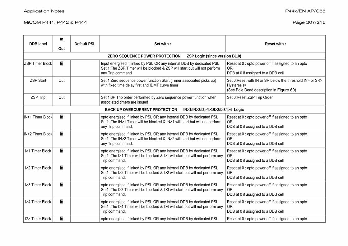
Application Notes P44x/EN AP/G55 MiCOM P441, P442 & P444
Page 207/216
DDB label In
Out Default PSL Set with : Reset with :
ZERO SEQUENCE POWER PROTECTION ZSP Logic (since version B1.0)
ZSP Timer Block In Input energised if linked by PSL OR any internal DDB by dedicated PSL Set 1:The ZSP Timer will be blocked & ZSP will start but will not perform any Trip command
Reset at 0 : opto power off if assigned to an opto OR DDB at 0 if assigned to a DDB cell
ZSP Start Out Set 1:Zero sequence power function Start (Timer associated picks up) with fixed time delay first and IDMT curve timer
Set 0:Reset with IN or SR below the threshold IN> or SR> Hysteresis= (See Pole Dead description in Figure 60)
ZSP Trip Out Set 1:3P Trip order performed by Zero sequence power function when associated timers are issued
Set 0:Reset ZSP Trip Order
BACK UP OVERCURRENT PROTECTION IN>1/IN>2/I2>/I>1/I>2/I>3/I>4 Logic
IN>1 Timer Block In opto energised if linked by PSL OR any internal DDB by dedicated PSL Set1 :The IN>1 Timer will be blocked & IN>1 will start but will not perform any Trip command.
Reset at 0 : opto power off if assigned to an opto OR DDB at 0 if assigned to a DDB cell
IN>2 Timer Block In opto energised if linked by PSL OR any internal DDB by dedicated PSL Set1 :The IN>2 Timer will be blocked & IN>2 will start but will not perform any Trip command.
Reset at 0 : opto power off if assigned to an opto OR DDB at 0 if assigned to a DDB cell
I>1 Timer Block In opto energised if linked by PSL OR any internal DDB by dedicated PSL Set1 :The I>1 Timer will be blocked & I>1 will start but will not perform any Trip command.
Reset at 0 : opto power off if assigned to an opto OR DDB at 0 if assigned to a DDB cell
I>2 Timer Block In opto energised if linked by PSL OR any internal DDB by dedicated PSL Set1 :The I>2 Timer will be blocked & I>2 will start but will not perform any Trip command.
Reset at 0 : opto power off if assigned to an opto OR DDB at 0 if assigned to a DDB cell
I>3 Timer Block In opto energised if linked by PSL OR any internal DDB by dedicated PSL Set1 :The I>3 Timer will be blocked & I>3 will start but will not perform any Trip command.
Reset at 0 : opto power off if assigned to an opto OR DDB at 0 if assigned to a DDB cell
I>4 Timer Block In opto energised if linked by PSL OR any internal DDB by dedicated PSL Set1 :The I>4 Timer will be blocked & I>4 will start but will not perform any Trip command.
Reset at 0 : opto power off if assigned to an opto OR DDB at 0 if assigned to a DDB cell
I2> Timer Block In opto energised if linked by PSL OR any internal DDB by dedicated PSL Reset at 0 : opto power off if assigned to an opto

P44x/EN AP/G55 Application Notes Page 208/216
MiCOM P441, P442 & P444
DDB label In
Out Default PSL Set with : Reset with :
Set1 :The I2> Timer will be blocked & I2> will start but will not perform any Trip command with negative overcurrent detection
OR DDB at 0 if assigned to a DDB cell
IN>1 Trip Out Relay 09
Set1 : Earth Fault stage 1 – 3Poles Trip order performed when associated timer is issued
Set 0 : Reset IN>1 Trip Order
IN>2 Trip Out Relay 09
Set1 : Earth Fault stage 2 – 3Poles Trip order performed when associated timer is issued
Set 0 : Reset IN>2Trip Order
IN>1 Start Out Set1 : Earth Fault stage 1 – Start function (Timer associated picks up) Directionnal or not - with DT or IDMT curves Negative or positive sequence polarisation
Set 0 : Reset with IN below the threshold IN>1 Hysteresis= (See Pole Dead description in Figure 60)
IN>2 Start Out Set1 : Earth Fault stage 2 – Start function (Timer associated picks up) Directionnal or not - DT only Negative or positive sequence polarisation
Set 0 : Reset with IN below the threshold IN>2 Hysteresis= (See Pole Dead description in Figure 60)
I2> Start Out Set1 : Negative sequence current detection – Start function (Timer associated picks up) Directionnal or not - with DT curves Negative polarisation
Set 0 : Reset with IN below the threshold I2> Hysteresis= (See Pole Dead description in Figure 60)
I2> Trip Out Set1 : Negative sequence current detection – 3P Trip order performed when associated timer is issued
Set 0 : Reset I2> Trip Order
I>Start Any A
Out Set1 :Any Overcurrent function start for phase A Set 0 : Reset with Iphase A below the lowest threshold I>1 Hysteresis= (See Pole Dead description in Figure 60)
I>Start Any B
Out Set1 :Any Overcurrent function start for phase B Set 0 : Reset with Iphase B below the lowest threshold I>1 Hysteresis= (See Pole Dead description in Figure 60)
I>Start Any C
Out Set1 :Any Overcurrent function start for phase C Set 0 : Reset with Iphase C below the lowest threshold I>1 Hysteresis= (See Pole Dead description in Figure 60)

Application Notes P44x/EN AP/G55 MiCOM P441, P442 & P444
Page 209/216
DDB label In
Out Default PSL Set with : Reset with :
I>1 Start Out Set1 :Overcurrent stage1 start Directionnal or not - with DT or IDMT curves Directionnal managed by Deltas Algorithms VTS Block timer facility
Set 0 : Reset with Iphase A below the threshold I>1 Hysteresis= (See Pole Dead description in Figure 60)
I>2 Start Out Set1 :Overcurrent stage2 start Directionnal or not - with DT or IDMT curves Directionnal managed by Deltas Algorithms VTS Block timer facility
Set 0 : Reset with Iphase A below the threshold I>2 Hysteresis= (See Pole Dead description in Figure 60)
I>3 Start Out Set1 :Overcurrent stage3 start Not Directionnal with DT curves Use without timer for SOTF (see description in section 2.12 Figure 35)
Set 0 : Reset with Iphase A below the threshold I>3 Hysteresis= (See Pole Dead description in Figure 60)
I>4 Start Out Set1 :Overcurrent stage4 start Not Directionnal with DT curves Use without timer for SOTF (see description in section 2.14)
Set 0 : Reset with Iphase A below the threshold I>4 Hysteresis= (See Pole Dead description in Figure 60)
I>1 Trip Out Set1 :Overcurrent Stage 1 Trip 3P performed when associated timer is issued
Set 0 : Reset I>1 Trip Order
I>2 Trip Out Set1 :Overcurrent Stage 2 Trip 3P performed when associated timer is issued
Set 0 : Reset I>2 Trip Order
I>3 Trip Out Set1 :Overcurrent Stage 3 Trip 3P performed when associated timer is issued
Set 0 : Reset I>3 Trip Order
I>4 Trip Out Set1 :Overcurrent Stage 4 Trip 3P performed when associated timer is issued
Set 0 : Reset I>4 Trip Order
Stub Bus Enable Out opto energised if linked by PSL At1 :Status input from HV line isolator opened – indicates that line is dead & disconnected At1 : I>4 is activated as a back up Stub Bus protection
Reset at 0 : opto power off if assigned to an opto

P44x/EN AP/G55 Application Notes Page 210/216
MiCOM P441, P442 & P444
DDB label In
Out Default PSL Set with : Reset with :
BACK UP VOLTAGE PROTECTION V<1/V<2/V>1/V>2 Logic
V<1 Timer Block In opto energised if linked by PSL OR any internal DDB by dedicated PSL Set1 :The V<1 Timer will be blocked & V<1 will start but will not perform any Trip command.
Reset at 0 : opto power off if assigned to an opto OR DDB at 0 if assigned to a DDB cell
V<2 Timer Block In opto energised if linked by PSL OR any internal DDB by dedicated PSL Set1 :The V<2 Timer will be blocked & V<2 will start but will not perform any Trip command.
Reset at 0 : opto power off if assigned to an opto OR DDB at 0 if assigned to a DDB cell
V>1 Timer Block In opto energised if linked by PSL OR any internal DDB by dedicated PSL Set1 :The V>1 Timer will be blocked & V>1 will start but will not perform any Trip command.
Reset at 0 : opto power off if assigned to an opto OR DDB at 0 if assigned to a DDB cell
V>2 Timer Block In opto energised if linked by PSL OR any internal DDB by dedicated PSL Set1 :The V>2 Timer will be blocked & V>2 will start but will not perform any Trip command.
Reset at 0 : opto power off if assigned to an opto OR DDB at 0 if assigned to a DDB cell
V<1 Alarm Out Set1 :1st stage undervoltage Alarm picks up when V<1 starts Set 0 : Reset with V measure over the threshold V<1 Hysteresis=
V<2 Alarm Out Set1 :2nd stage undervoltage Alarm picks up when V<1 starts Set 0 : Reset with V measure over the threshold V<2 Hysteresis=
V>1 Alarm Out Set1 :1st stage Overvoltage Alarm picks up when V<1 starts Set 0 : Reset with V measure below the threshold V>1 Hysteresis=
V>2 Alarm Out Set1 :2nd stage Overvoltage Alarm picks up when V<1 starts Set 0 : Reset with V measure below the threshold V>2 Hysteresis=
V<Start Any A
Out Set1 :Any Undervoltage function start for phase A Set 0 : Reset with V phase A measure over the lowest threshold V< Hysteresis=
V<Start Any B
Out Set1 :Any Undervoltage function start for phase B Set 0 : Reset with V phase B measure over the lowest threshold V< Hysteresis=
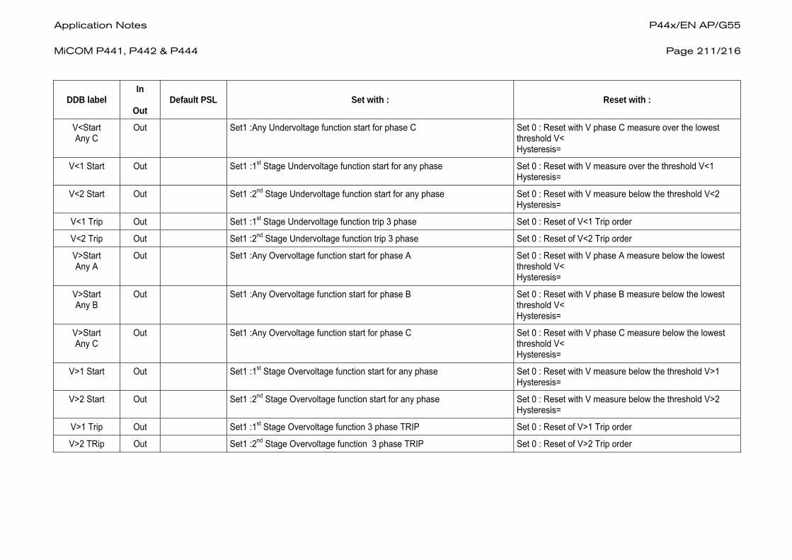
Application Notes P44x/EN AP/G55 MiCOM P441, P442 & P444
Page 211/216
DDB label In
Out Default PSL Set with : Reset with :
V<Start Any C
Out Set1 :Any Undervoltage function start for phase C Set 0 : Reset with V phase C measure over the lowest threshold V< Hysteresis=
V<1 Start Out Set1 :1st Stage Undervoltage function start for any phase Set 0 : Reset with V measure over the threshold V<1 Hysteresis=
V<2 Start Out Set1 :2nd Stage Undervoltage function start for any phase Set 0 : Reset with V measure below the threshold V<2 Hysteresis=
V<1 Trip Out Set1 :1st Stage Undervoltage function trip 3 phase Set 0 : Reset of V<1 Trip order
V<2 Trip Out Set1 :2nd Stage Undervoltage function trip 3 phase Set 0 : Reset of V<2 Trip order
V>Start Any A
Out Set1 :Any Overvoltage function start for phase A Set 0 : Reset with V phase A measure below the lowest threshold V< Hysteresis=
V>Start Any B
Out Set1 :Any Overvoltage function start for phase B Set 0 : Reset with V phase B measure below the lowest threshold V< Hysteresis=
V>Start Any C
Out Set1 :Any Overvoltage function start for phase C Set 0 : Reset with V phase C measure below the lowest threshold V< Hysteresis=
V>1 Start Out Set1 :1st Stage Overvoltage function start for any phase Set 0 : Reset with V measure below the threshold V>1 Hysteresis=
V>2 Start Out Set1 :2nd Stage Overvoltage function start for any phase Set 0 : Reset with V measure below the threshold V>2 Hysteresis=
V>1 Trip Out Set1 :1st Stage Overvoltage function 3 phase TRIP Set 0 : Reset of V>1 Trip order
V>2 TRip Out Set1 :2nd Stage Overvoltage function 3 phase TRIP Set 0 : Reset of V>2 Trip order

P44x/EN AP/G55 Application Notes Page 212/216
MiCOM P441, P442 & P444
DDB label In
Out Default PSL Set with : Reset with :
ALARMS
F out of Range Out Set1 :Alarm when frequency tracking does not operate correctly and provides a Frequency out of range
Set 0 : With frequency tracking operating correctly
CT Fail Alarm Out Set1 :Alarm from the current transformers supervision Set 0 :No CT Fail Alarm detected
Brok.Cond. Alarm
Out Set1 : Alarm from the Start of Broken Conductor function Set 0 :No Brok.Cond.Alarm detected
CVT Alarm Out Set 1:Alarm from the capacitive voltage transformers supervision Set 0 :No CVT Fail Alarm detected
Field Volt Fail Out Set1 : Field Voltage Failure (Internal 48Vcc delivered by the relay can be used for Optos polarisation)
Set 0 :With reset of min Field voltage detection
Alarm User1 In Set1 : Alarm for user – application customized must be linked to dedicated DDB cells
Set 0 :With reset of conditions linked to that cell
Alarm User2 In Set1 : Alarm for user – application customized must be linked to dedicated DDB cells
Set 0 :With reset of conditions linked to that cell
Alarm User3 In Set1 : Alarm for user – application customized must be linked to dedicated DDB cells
Set 0 :With reset of conditions linked to that cell
Alarm User4 In Set1 : Alarm for user – application customized must be linked to dedicated DDB cells
Set 0 :With reset of conditions linked to that cell
Alarm User5 In Set1 : Alarm for user – application customized must be linked to dedicated DDB cells
Set 0 :With reset of conditions linked to that cell
General Alarm
Out
Relay 08
Set1 :For any Alarm started & included in the list : Battery Fail Field Volt Fail General Alarm Prot’n Disabled F out of range VT Fail Alarm CT Fail Alarm CVT Fail Alarm CB Fail Alarm
Set 0 : Reset if all initiale condition reset

Application Notes P44x/EN AP/G55 MiCOM P441, P442 & P444
Page 213/216
DDB label In
Out Default PSL Set with : Reset with :
General Alarm Out Relay 08
I^Maint Alarm I^Lockout Alarm CB Ops Maint CB Ops Lockout CB Op Time Maint CB Op Time Lock F.F. Pre Lockout F.F Lock Lockout Alarm CB Status Alarm Man CB Trip Fail Man CB Cls Fail Man CB Unhealthy Control No C/C AR Lockout Shot> SG-opto Invalid A/R Fail V<1 Alarm V<2 Alarm V>1 Alarm V>2 Alarm COS Alarm User Alarlm1 User Alarm2
Set 0 : Reset if all initiale condition reset
START LOGIC
Any Start Out Led4 Relay
06
Set1 :Any Protection start loig with any phase Assigned to Led 4 by default (Fault record Trigger in default PSL with 20ms Dwell Timer)
Set 0 :Reset with reset from all started function (21/67N/50/51…)
1ph Fault Out Set1 : Single phase fault detected with Distance Funct. Set 0 : with Distance Reset
2ph Fault Out Set1 : Two phase fault detected with Distance Funct. Set 0 : with Distance Reset
3ph Fault Out Set1 : Three phase fault detected with Distance Funct. Set 0 : with Distance Reset
TRIP LOGIC

P44x/EN AP/G55 Application Notes Page 214/216
MiCOM P441, P442 & P444
DDB label In
Out Default PSL Set with : Reset with :
User Trip A In opto energised if linked by PSL OR any internal DDB by dedicated PSL Set1 :Trip A Internal input managed with the general trip logic(With AR/Evolving fault…) Can be assigned by external condition
Reset at 0 : opto power off if assigned to an opto OR DDB at 0 if assigned to a DDB cell
User Trip B In opto energised if linked by PSL OR any internal DDB by dedicated PSL Set1 :Trip B Internal input managed with the general trip logic(With AR/Evolving fault…) Can be assigned by external condition
Reset at 0 : opto power off if assigned to an opto OR DDB at 0 if assigned to a DDB cell
User Trip C In opto energised if linked by PSL OR any internal DDB by dedicated PSL Set1 :Trip C Internal input managed with the general trip logic(With AR/Evolving fault…) Can be assigned by external condition
Reset at 0 : opto power off if assigned to an opto OR DDB at 0 if assigned to a DDB cell
Any Trip Out Relay 07
Set1 :Any Trip 1P or 3P initiated by internal Trip or external Trip decision (Fault record Trigger in default PSL)
Set 0 :Reset conditions
Any Int Trip A Out Set1 : Any Internal Trip with Phase A with any internal protection decision Set 0 :Reset conditions
Any Int Trip B Out Set1 : Any Internal Trip with Phase B with any internal protection decision Set 0 :Reset conditions
Any Int Trip C Out Set1 : Any Internal Trip with Phase C- with any internal protection decision Set 0 :Reset conditions
Any Trip A Out Led1 Relay
02
Set1 :Any Internal or External Trip phase A – with any protection decision (internal or external) Assigned to Led 1 by default
Set 0 :Reset conditions
Any Trip B Out Led2 Relay
03
Set1 :Any Internal or External Trip phase B – with any protection decision (internal or external) Assigned to Led 2 by default
Set 0 :Reset conditions
Any Trip C Out Led3 Relay
04
Set1 :Any Internal or External Trip phase C – with any protection decision (internal or external) Assigned to Led 3 by default
Set 0 :Reset conditions
1P Trip Out Set1 :Single pole Trip decision (int or Ext) Set 0 :Reset conditions
3P Trip Out Set1 :Three pole Trip decision (int or Ext) Set 0 :Reset conditions

Application Notes P44x/EN AP/G55 MiCOM P441, P442 & P444
Page 215/216
DDB label In
Out Default PSL Set with : Reset with :
Brk Conduct. Trip
Out Set1 :3P Trip decision by Broken Conductor protection Set 0 :Reset conditions
Loss.Load Trip
Out Set1 :3P Trip decision by Loss of Load protection (in application without communication scheme & a 3P Trip logic)
Set 0 :Reset conditions
MISCELLANEOUS LOGIC
BLK Protection In opto energised if linked by PSL OR any internal DDB by dedicated PSL Set1 :All protections functions are blocked (21/67N/50/51…)
Set 0 :Reset conditions
Prot’n Disabled Out Set1 :When TEST MODE is enable All the protections functions are out of order.
Set 0 :Reset conditions – No blocking conditions available : (Test mode disable) + (Opto BLK Protec =0)
Reset Latches In opto energised if linked by PSL OR any internal DDB by dedicated PSL Set1 :Permanent Alarms & Leds & relayslatched are reset
Reset at 0 : opto power off if assigned to an opto OR DDB at 0 if assigned to a DDB cell

P44x/EN AP/G55 Application Notes Page 216/216
MiCOM P441, P442 & P444
BLANK PAGE

Technical Data P44x/EN TD/G55 MiCOM P441, P442 & P444
TECHNICAL DATA

P44x/EN TD/G55 Technical Data
MiCOM P441, P442 & P444

Technical Data P44x/EN TD/G55 MiCOM P441, P442 & P444
Page 1/30
CONTENT
1. RATINGS 5
1.1 Currents 5 1.2 Voltages 5 1.3 Auxiliary Voltage 6 1.4 Frequency 6 1.5 Logic inputs 6 1.6 Output Relay Contacts 7 1.7 Field Voltage 7 1.8 Loop through connections 7 1.9 Wiring requirements 7
2. BURDENS 8
2.1 Current Circuit 8 2.2 Voltage Circuit 8 2.3 Auxiliary Supply 8 2.4 Optically-Isolated Inputs 8
3. ACCURACY 9
3.1 Reference Conditions 9 3.2 Measurement Accuracy 9 3.3 Protection accuracy 10 3.4 Influencing Quantities 12 3.5 High Voltage Withstand IEC60255-5:1977 12 3.5.1 Dielectric Withstand 12 3.5.2 Impulse 12 3.5.3 Insulation Resistance 12
4. ENVIRONMENTAL COMPLIANCE 13
4.1 Electrical Environment 13 4.1.1 DC Supply Interruptions IEC60255-11:1979 13 4.1.2 AC Ripple on DC Supply IEC60255-11:1979 13 4.1.3 Disturbances on AC Supply - EN61000-4-11:1994 13 4.1.4 High Frequency Disturbance IEC60255-22-1:1988 13 4.1.5 Fast Transient IEC60255-22-4:1992 13 4.1.6 Electrostatic Discharge IEC60255-22-2:1996 13 4.1.7 Conducted Emissions EN 55011:1991 13 4.1.8 Radiated Emissions EN 55011:1991 13 4.1.9 Radiated Immunity IEC60255-22-3:1989 14

P44x/EN TD/G55 Technical Data Page 2/30
MiCOM P441, P442 & P444
4.1.10 Conducted Immunity IEC61000-4-6:1996 14 4.1.11 Surge Immunity IEC61000-4-5:1995 14 4.1.12 EMC Compliance 14 4.1.13 Power Frequency Interference - Electricity Association (UK) 14 4.2 Atmospheric Environment 14 4.2.1 Temperature IEC60255-6:1988 14 4.2.2 Humidity IEC60068-2-3:1969 14 4.2.3 Enclosure Protection IEC60529:1989 14 4.2.4 Pollution degree IEC61010-1:1990/A2:1995 14 4.3 Mechanical Environment 15 4.3.1 Vibration IEC60255-21-1:1988 15 4.3.2 Shock and Bump IEC60255-21-2:1988 15 4.3.3 Seismic IEC60255-21-3:1993 15
5. ANSI TEST REQUIREMENTS 16
5.1 ANSI / IEEE C37.90.1989 16 5.2 ANSI / IEEE C37.90.1: 1989 16 5.3 ANSI / IEEE C37.90.2: 1995 16
6. PROTECTION SETTING RANGES 17
6.1 Distance Protection 17 6.1.1 Line Settings 17 6.1.2 Zones settings 17 6.1.3 Power-swing settings 18 6.2 Distance protection schemes 18 6.2.1 Programmable distance schemes 19 6.2.2 Distance schemes settings 19 6.2.3 Weak infeed settings 19 6.2.4 Loss of load settings 19 6.3 Back-up Overcurrent Protection 20 6.3.1 Threshold Settings 20 6.3.2 Time Delay Settings 20 6.3.3 Inverse Time (IDMT) Characteristic 20 6.4 Negative sequence overcurrent protection 22 6.5 Broken Conductor Protection 22 6.6 Earth Fault Overcurrent Protection 22 6.6.1 Threshold Settings 22 6.6.2 Polarising Quantities For Earth Fault Measuring Elements 22 6.6.3 Time Delay Characteristics 22 6.7 Zero sequence Power Protection (since B1.0) 23

Technical Data P44x/EN TD/G55 MiCOM P441, P442 & P444
Page 3/30
6.8 Channel Aided Directional Earth Fault Protection 23 6.8.1 Threshold Settings 23 6.9 Under Voltage Protection 23 6.9.1 Threshold Settings 23 6.9.2 Under Voltage Protection Time Delay Characteristics 23 6.10 Over Voltage Protection 24 6.10.1 Threshold Settings 24 6.10.2 Time Delay Characteristics 24 6.11 Voltage Transformer Supervision 24 6.12 Capacitive Voltage Transformer Supervision (since B1.0) 24 6.13 Current Transformer Supervision 25 6.14 Undercurrent Element 25 6.15 Breaker Fail Timers (TBF1 and TBF2) 25
7. MEASUREMENT SETTINGS 26
7.1 Disturbance Recorder Settings 26 7.2 Fault Locator Settings 26
8. CONTROL FUNCTION SETTINGS 27
8.1 Communications Settings 27 8.2 Auto-Reclose 27 8.2.1 Options 27 8.2.2 Auto-recloser settings 27 8.3 Circuit Breaker State Monitoring 28 8.4 Circuit Breaker Control 29 8.5 Circuit Breaker Condition Monitoring 29 8.5.1 Maintenance alarm settings 29 8.5.2 Lockout Alarm Settings 29 8.6 Programmable Logic 30 8.7 CT and VT Ratio Settings 30

P44x/EN TD/G55 Technical Data Page 4/30
MiCOM P441, P442 & P444
BLANK PAGE

Technical Data P44x/EN TD/G55 MiCOM P441, P442 & P444
Page 5/30
1. RATINGS 1.1 Currents
In = 1A or 5A ac rms (dual rated).
Separate terminals are provided for the 1A and 5A windings, with the neutral input of each winding sharing one terminal.
CT Type Operating range
Standard 0 to 64In
Sensitive 0 to 2In
All current inputs will withstand the following, with any current function setting:
Withstand Duration
4 Ιn Continuous rating
4.5 Ιn 10 minutes
5 Ιn 5 minutes
6 Ιn 3 minutes
7 Ιn 2 minutes
30 Ιn 10 seconds
50 Ιn 3 seconds
100 Ιn 1 second
Pass Criteria Winding temperatures <105° C
Dielectric withstand and insulation resistance unimpaired
1.2 Voltages
Nominal Voltage Operating range
100/120Vph - ph rms 0 to 200Vph - ph rms
Duration Withstand (Vn = 100/120V)
Continuous rating (2Vn) 240Vph - ph rms
10 seconds (2.6Vn) 312Vph - ph rms

P44x/EN TD/G55 Technical Data Page 6/30
MiCOM P441, P442 & P444
1.3 Auxiliary Voltage
The relay is available in three auxiliary voltage versions, these are specified in the table below:
Nominal Ranges Operative dc range Operative ac range
24-48V dc 19 - 65 V Not available
48-110 V dc (30 / 100 V ac rms) ** 37 - 150 V 24 - 110 V
110-250 V dc (100 / 240 V ac rms) ** 87 - 300 V 80 - 265 V
** rated for AC or DC operation.
Pass Criteria All functions operate as specified within the operative ranges
All power supplies operate continuously over their operative ranges, and environmental conditions
1.4 Frequency
The nominal frequency (Fn) is dual rated at 50/60Hz, the operate range is 45Hz to 65Hz.
1.5 Logic inputs
All the logic inputs are independent and isolated, relay types P441 provide 8 inputs, 16 inputs are provided by the P442.
Rating Range
Logical “off” 0Vdc 0 - 12Vdc
Logical “on” 50Vdc 30 - 60Vdc
Higher voltages can be used in conjunction with an external resistor, value of the resistor is determined by the following equation:
Resistor = (Required Input Level - 50) x 200Ω.
Hardware ref P441/442B or C or P444A or C (Universal Opto) :
All the logic inputs are independent and isolated, relay types P441 provide 8 inputs, 16 inputs are provided by the P442 and 24 inputs for P444.
Battery Voltage (V dc) Logical “off” (V dc) Logical “on” (V dc)
24/27 <16.2 >19.2
30/34 <20.4 >24
48/54 <32.4 >38.4
110/125 <75 >88
220/250 <150 >176
REMARK: Control the version compatibility in P44x/EN VC chapter

Technical Data P44x/EN TD/G55 MiCOM P441, P442 & P444
Page 7/30
1.6 Output Relay Contacts
Make & Carry 30A for 3s
Carry 250A for 30ms 10A continuous
Break DC: 50W resistive DC: 37.5W inductive (L/R = 40ms) AC: 1250VA AC: 1250VA inductive (P.F. = 0.7)
Maxima: 10A and 300V
Loaded contact: 10,000 operations minimum
Unloaded contact: 100,000 operations minimum
Watchdog Contact
Break DC: 30W resistive DC: 15W inductive (L/R = 40ms) AC: 275W inductive (P.F. = 0.7)
The maximum number of output relays that should be configured to be permanently energized is 50% of those available (minimum 4).
1.7 Field Voltage
The field voltage provided by the relay is nominally 48V dc with a current limit of 112mA. The operating range shall be 40V to 60V with an alarm raised at <35V.
1.8 Loop through connections
Terminals D17-D18 and F17-F18 are internally connected together for convenience when wiring, Maxima 5A and 300V.
1.9 Wiring requirements
The requirements for the wiring of the relay and cable specifications are detailed in the installation section of the Operation Guide (Chapter P44x/EN IN).

P44x/EN TD/G55 Technical Data Page 8/30
MiCOM P441, P442 & P444
2. BURDENS 2.1 Current Circuit
CT burden (at nominal current)
1A <0.04VA
5 A <0.4VA
2.2 Voltage Circuit
Reference voltage (Vn)
Vn = 100/120V <0.03VA
2.3 Auxiliary Supply
Case Size Nominal* Maximum**
Size 8 15VA dc 16W ac 20VA dc 20W ac
Size 12 18VA dc 19W ac 26VA dc 26W ac
* Nominal is with 50% of the optos energised and one relay per card energised ** Maximum is with all optos and all relays energised.
For each energised Opto powered from the Field Voltage or each energised Output Relay:
Each additional energised opto input 0.09W (24/27, 30/34, 48/54V)
Each additional energised opto input 0.12W (110/125V)
Each additional energised opto input 0.19W (220/250V)
Each additional energised output relay 0.13W
2.4 Optically-Isolated Inputs
DC Supply 5mA burden per input. (Current drawn at rated voltage)
2.5mA at minimum voltage (30V)
Maximum input voltage 300V dc (any setting).

Technical Data P44x/EN TD/G55 MiCOM P441, P442 & P444
Page 9/30
3. ACCURACY For all accuracies specified, the repeatability is ±2.5% unless otherwise specified.
If no range is specified for the validity of the accuracy, then the specified accuracy shall be valid over the full setting range.
3.1 Reference Conditions
Quantity Reference conditions Test tolerance
General
Ambient temperature 20 °C ±2°C
Atmospheric pressure 86kPa to 106kPa -
Relative humidity 45 to 75 % -
Input energising quantity
Current In ±5%
Voltage Vn ±5%
Frequency 50 or 60Hz ±0.5%
Auxiliary supply DC 48V or 110V AC 63.5V or 110V
±5%
3.2 Measurement Accuracy
Quantity Range Accuracy
Current 0.1 to 64In 10mA or ±1%
Voltage 1.0 Vn ±1%
Frequency 45 - 65Hz ±0.025Hz
Phase 0 - 360° ±2°
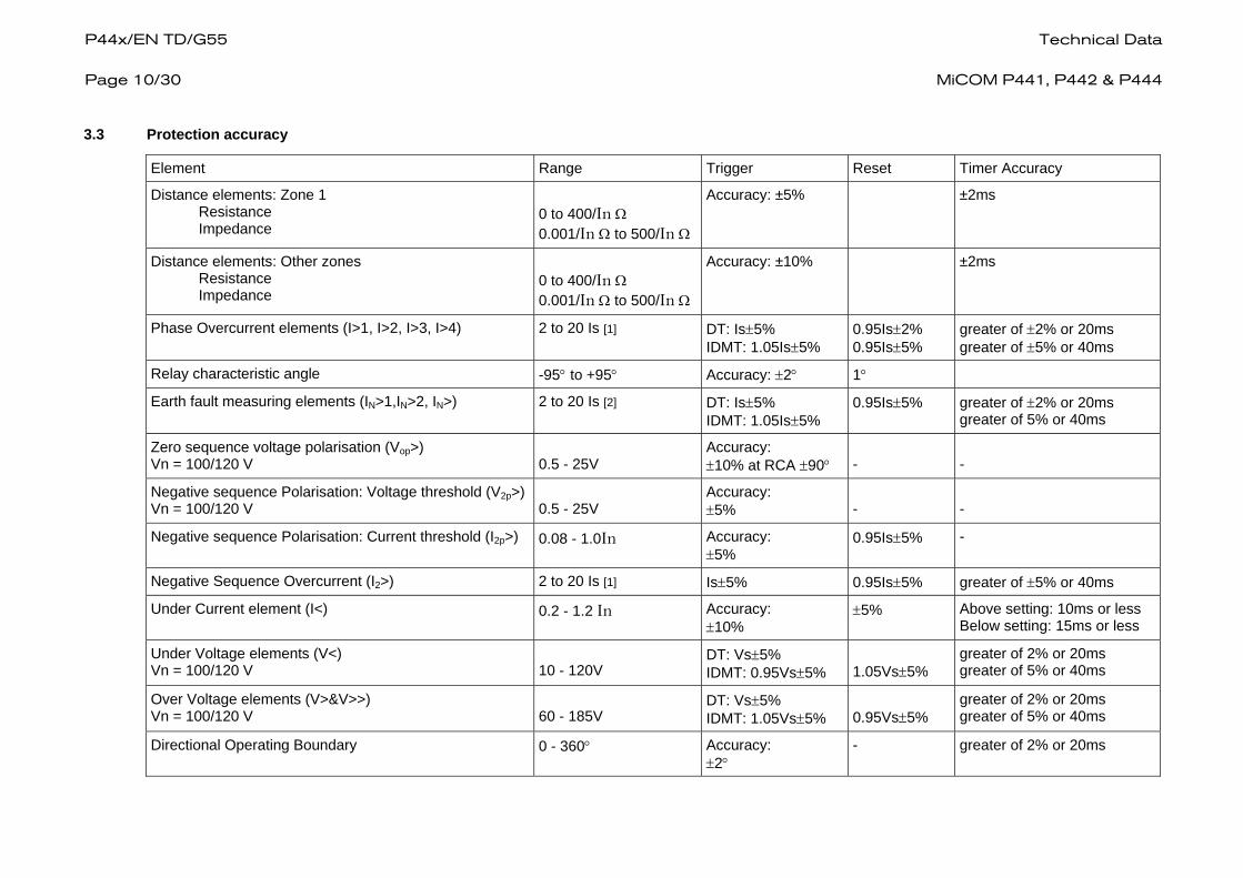
P44x/EN TD/G55 Technical Data Page 10/30
MiCOM P441, P442 & P444
3.3 Protection accuracy
Element Range Trigger Reset Timer Accuracy
Distance elements: Zone 1 Resistance Impedance
0 to 400/In Ω 0.001/In Ω to 500/In Ω
Accuracy: ±5% ±2ms
Distance elements: Other zones Resistance Impedance
0 to 400/In Ω 0.001/In Ω to 500/In Ω
Accuracy: ±10% ±2ms
Phase Overcurrent elements (I>1, I>2, I>3, I>4) 2 to 20 Is [1] DT: Is±5% IDMT: 1.05Is±5%
0.95Is±2% 0.95Is±5%
greater of ±2% or 20ms greater of ±5% or 40ms
Relay characteristic angle -95° to +95° Accuracy: ±2° 1°
Earth fault measuring elements (IN>1,IN>2, IN>) 2 to 20 Is [2] DT: Is±5% IDMT: 1.05Is±5%
0.95Is±5% greater of ±2% or 20ms greater of 5% or 40ms
Zero sequence voltage polarisation (Vop>) Vn = 100/120 V
0.5 - 25V
Accuracy: ±10% at RCA ±90°
-
-
Negative sequence Polarisation: Voltage threshold (V2p>)Vn = 100/120 V
0.5 - 25V
Accuracy: ±5%
-
-
Negative sequence Polarisation: Current threshold (I2p>) 0.08 - 1.0In Accuracy: ±5%
0.95Is±5% -
Negative Sequence Overcurrent (I2>) 2 to 20 Is [1] Is±5% 0.95Is±5% greater of ±5% or 40ms
Under Current element (I<) 0.2 - 1.2 In Accuracy: ±10%
±5% Above setting: 10ms or less Below setting: 15ms or less
Under Voltage elements (V<) Vn = 100/120 V
10 - 120V
DT: Vs±5% IDMT: 0.95Vs±5%
1.05Vs±5%
greater of 2% or 20ms greater of 5% or 40ms
Over Voltage elements (V>&V>>) Vn = 100/120 V
60 - 185V
DT: Vs±5% IDMT: 1.05Vs±5%
0.95Vs±5%
greater of 2% or 20ms greater of 5% or 40ms
Directional Operating Boundary 0 - 360° Accuracy: ±2°
- greater of 2% or 20ms

Technical Data P44x/EN TD/G55 MiCOM P441, P442 & P444
Page 11/30
Element Range Trigger Reset Timer Accuracy
Broken conductor protection II
2
1
⎛⎝⎜
⎞⎠⎟
0.2 to 1.0
II
2
1
⎛⎝⎜
⎞⎠⎟±5% 0.95
II
2
1
⎛⎝⎜
⎞⎠⎟±5%
greater of ±2% or 20ms
Transient Overreach 2 to 20 Is <5% (for a system X/R of up to 90)
- --
Relay overshoot 2 to 20 Is <50ms - -
Breaker fail timers 0 to 10s - - greater of ±2% or 20ms

P44x/EN TD/G55 Technical Data Page 12/30
MiCOM P441, P442 & P444
3.4 Influencing Quantities
No additional errors will be incurred for any of the following influencing quantities:
Quantity Operative range (typical only)
Environmental
Temperature -25°C to +55°C
Mechanical (Vibration, Shock, Bump, Seismic)
According to IEC 60255-21-1:1988 IEC 60255-21-2:1988 IEC 60255-21-3:1995
Quantity Operative range
Electrical
Frequency 45 Hz to 65 Hz
Harmonics (single) 5% over the range 2nd to 17th
Auxiliary voltage range 0.8 LV to 1.2 HV (dc) 0.8 LV to 1.1 HV (ac)
Aux. supply ripple 12% Vn with a frequency of 2.fn
Point on wave of fault waveform 0 - 360°
DC offset of fault waveform No offset to fully offset
Phase angle -90° to + 90°
Magnetising inrush No operation with OC elements set to 35% of peak anticipated inrush level.
3.5 High Voltage Withstand IEC60255-5:1977
3.5.1 Dielectric Withstand
2.0kVrms for one minute between all terminals and case earth.
2.0kVrms for one minute between all terminals of each independent circuit grouped together and all other terminals. This includes the output contacts and loop through connections D17/D18 and E17/E18.
1.5kVrms for one minute across dedicated normally open contacts of output relays.
1.0kVrms for 1 minute across normally open contacts of changeover pairs and watchdog outputs.
3.5.2 Impulse
The product will withstand without damage impulses of 5kV peak, 1.2/50μs, 0.5J across:
Each independent circuit and the case with the terminals of each independent circuit connected together.
Independent circuits with the terminals of each independent circuit connected together.
Terminals of the same circuit except normally open metallic contacts.
3.5.3 Insulation Resistance
The insulation resistance is greater than 100 MΩ at 500Vdc.

Technical Data P44x/EN TD/G55 MiCOM P441, P442 & P444
Page 13/30
4. ENVIRONMENTAL COMPLIANCE The product complies with the following specifications :
4.1 Electrical Environment
4.1.1 DC Supply Interruptions IEC60255-11:1979
The product will withstand a 20ms interruption in the auxiliary voltage in its quiescent condition.
4.1.2 AC Ripple on DC Supply IEC60255-11:1979
The product will operate with 12% AC ripple on the DC auxiliary supply without any additional measurement errors.
4.1.3 Disturbances on AC Supply - EN61000-4-11:1994
The products satisfies the requirements of EN61000-4-11 for voltage dips and short interruptions.
4.1.4 High Frequency Disturbance IEC60255-22-1:1988
The product complies with Class III 2.5kV common mode and 1kV differential mode for 2 seconds at 1MHz with 200Ω source impedance, without any mal-operations or additional measurement errors.
4.1.5 Fast Transient IEC60255-22-4:1992
The product complies with all classes up to and including class IV/4kV without any mal-operations or additional measurement errors.
Fast transient disturbances on power supply (common mode only)
4kV, 5ns rise time, 50ns decay time, 5kHz repetition time, 15ms burst, repeated every 300ms for 1min in each polarity, with a 50Ω source impedance.
Fast transient disturbances on I/O signal, data and control lines (common mode only)
4kV, 5ns rise time, 50ns decay time, 5kHz repetition time, 15ms burst, repeated every 300ms for 1min in each polarity, with a 50Ω source impedance.
4.1.6 Electrostatic Discharge IEC60255-22-2:1996
The product will withstand application of all discharge levels up to the following without mal-operation:
Class IV– 15kV discharge in air to the user interface, display and exposed metal work.
Class III– 8kV discharge in air to all communication ports, 6kV point contact discharge to any part of the front of the product.
4.1.7 Conducted Emissions EN 55011:1991
Group 1 Class A limits.
0.15 - 0.5MHz, 79dBμV (quasi peak) 66dBμV (average).
0.5 - 30MHz, 73dBμV (quasi peak) 60dBμV (average).
4.1.8 Radiated Emissions EN 55011:1991
Group 1 Class A limits.
30 - 230MHz, 40dBμV/m at 10m measurement distance.
230 - 1000MHz, 47dBμV/m at 10m measurement distance.

P44x/EN TD/G55 Technical Data Page 14/30
MiCOM P441, P442 & P444
4.1.9 Radiated Immunity IEC60255-22-3:1989
Class/Level III/3 - 10V/m at 1kHz 80% am., 20MHz to 1GHz.
4.1.10 Conducted Immunity IEC61000-4-6:1996
Level 3 - 10Vrms at 1kHz 80% am.- 0.15 to 80MHz.
4.1.11 Surge Immunity IEC61000-4-5:1995
Level 4 - 4kV peak, 1.2/50µs between all groups and case earth
2kV peak, 1.2/50µs between terminals of each group.
4.1.12 EMC Compliance
Compliance to the European Community Directive 89/336/EEC on EMC is claimed via the Technical Construction File route.
Generic Standards EN 50081-2 :1994 and EN 50082-2 :1995 are used to establish conformity.
4.1.13 Power Frequency Interference - Electricity Association (UK)
EA PAP Document, Environmental Test Requirements for Protection Relays and Systems Issue I, Draft 4.2.1 1995.
Class Length of comms circuit
Unbalanced Comms V rms
Balanced Comms (Unbalance 1%) Vrms
Balanced Comms (Unbalance 0.1%) Vrms
1 1 to 10 metres 0.5 0.005 0.0005
2 10 to 100 metres 5 0.05 0.005
3 100 to 1000 metres 50 0.5 0.05
4 1000 to 10,000m or > 500 5 0.5
4.2 Atmospheric Environment
4.2.1 Temperature IEC60255-6:1988
Storage and transit –25°C to +70°C.
Operating –25°C to +55°C.
IEC60068-2-1:1990 Cold
IEC60068-2-2:1974 Dry heat
4.2.2 Humidity IEC60068-2-3:1969
56 days at 93% relative humidity and 40°C.
4.2.3 Enclosure Protection IEC60529:1989
IP52 - Protected against dust and dripping water at 15° to the vertical.
4.2.4 Pollution degree IEC61010-1:1990/A2:1995
Normally only non conductive pollution occurs. Occasionally a temporary conductivity caused by condensation must be expected.

Technical Data P44x/EN TD/G55 MiCOM P441, P442 & P444
Page 15/30
4.3 Mechanical Environment
4.3.1 Vibration IEC60255-21-1:1988
Vibration Response Class 2 - 1g
Vibration Endurance Class 2 - 2g.
4.3.2 Shock and Bump IEC60255-21-2:1988
Shock response Class 2 - 10g
Shock withstand Class 1 - 15g
Bump Class 1 - 10g
4.3.3 Seismic IEC60255-21-3:1993
Class 2.

P44x/EN TD/G55 Technical Data Page 16/30
MiCOM P441, P442 & P444
5. ANSI TEST REQUIREMENTS The products shall meet the ANSI / IEEE requirements as follows:-
5.1 ANSI / IEEE C37.90.1989
Standards for relays and relay systems associated with electric power apparatus.
5.2 ANSI / IEEE C37.90.1: 1989
Surge withstand capability (SWC) tests for protective relays and relay systems:-
Oscillatory test - 1MHz to 1.5MHz, 2.5kV to 3.0kV,
Fast transient test 4kV to 5kV
5.3 ANSI / IEEE C37.90.2: 1995
Standard for withstand capability of relay systems to radiated electromagnetic interference from transceivers: 35V/m, 25 to 1000Mhz.

Technical Data P44x/EN TD/G55 MiCOM P441, P442 & P444
Page 17/30
6. PROTECTION SETTING RANGES 6.1 Distance Protection
6.1.1 Line Settings
Setting Range Step size
Length of line (Ln) 0.3 - 1000 km 0.2 - 625 miles
0.010 km 0.005 miles
Positive sequence angle (ϑ1) –90° - 90° 0.1°
In = 1 A In = 5 A
Setting Range Step size Range Step size
Positive sequence impedance (Z1)
0.001 - 500 Ω 0.001 Ω 0.002 - 199,8 Ω
0.002 Ω
6.1.2 Zones settings
Setting In = 1 A In = 5 A
Range Step size Range Step size
Impedance reaches (Zone 1, Zone 2, Zone 3, Zone P, Zone 4)
0.001 - 500 Ω 0.001 Ω 0.0002 - 100 Ω
0.0002 Ω
Resistive reaches for phase - earth faults (Zone 1, Zone 2, Zones 3 & 4, Zone P)
0 - 400 Ω 0.01 Ω 0 - 80 Ω 0.002 Ω
Resistive reaches for phase - earth faults (Zone 1, Zone 2, Zones 3 & 4, Zone P)
0 - 400 Ω 0.01 Ω 0 - 80 Ω 0.002 Ω
Setting Range Step size
Residual compensation angles (Zone 1, Zone 2, Zones 3 & 4, Zone P)
–180-180° 0.1°
Residual compensation factors (Zone 1, Zone 2, Zones 3 & 4, Zone P)
0 - 7 0.001
Timer for zone 1/1X 0 - 10s 0.002s
Timers for zone 2, Zone 3, Zone P, Zone 4
0 - 10s 0.01s

P44x/EN TD/G55 Technical Data Page 18/30
MiCOM P441, P442 & P444
6.1.3 Power-swing settings
In = 1 A In = 5 A
Setting Range Step size Range Step size
Powerswing detection boundaries: Delta R Delta X
0 - 400 Ω 0 - 400 Ω
0.01 Ω 0.01 Ω
0 - 80 Ω 0 - 80 Ω
0.002 Ω 0.002 Ω
Setting Range Step size
Imax line In - 20 In 0.01 In
IN threshold 10 - 100 % Imax 1%Imax
I2 threshold 10 - 100 % Imax 1%Imax
Trip mode Single/Three pole -
Unblocking time delay 0 - 30s 0.1s
Power-swing detection boundary 0 - 25 Ω 0.01 Ω
Block zones Bit 0: Z1&Z1X-Block, Bit 1: Z2 block Bit 2: Z3 block, Bit 3: Zp block, Bit 4:Z4block
6.2 Distance protection schemes
Basic scheme functions: Instantaneous zone 1 tripping
Time delayed tripping for all zones
Directional earth fault protection
Zero sequence Power protection (since B1.0)
Switch on to fault logic
Trip on reclose logic
Loss of load logic
Conversion to three pole tripping
Channel-aided distance schemes: Permissive Overreach Protection with Overreaching Zone 1 (POP Z1)
Permissive Overreach Protection with Overreaching Zone 2 (POP Z2)
Permissive Underreach Protection, Accelerating Zone 2 (PUP Z2)
Permissive Underreach Protection Tripping via Forward Start (PUP Fwd)
Blocking Overreach Protection with Overreaching Zone 1 (BOP Z1)
Blocking Overreach Protection with Overreaching Zone 2 (BOP Z2)
Permissive Scheme Unblocking Logic
Permissive Overreach Schemes Weak Infeed Features
Permissive Overreach Schemes Current Reversal Guard
Blocking Scheme Current Reversal Guard

Technical Data P44x/EN TD/G55 MiCOM P441, P442 & P444
Page 19/30
6.2.1 Programmable distance schemes
Setting Range
Signal Send Zone No Signal Send/Signal send on Z1/ Signal send on Z2/ Signal send on Z4
Type of Scheme on signal Receive
None/None+Z1X/Aided scheme for Z1 faults/Aided scheme for Z2 faults/ Aided scheme for forward faults/ Blocking scheme for Z1 faults/ Blocking scheme for Z2 faults
6.2.2 Distance schemes settings
Setting Range Step size
Fault Type/Signal Send Zone Phase-to-Ground Fault Enabled/ Phase-to-Phase Fault Enabled/Both Enabled
-
Trip mode for the distance protection
Force 3 Pole Trip for all zones/1 Pole Trip for zone Z1/1 Pole trip for zones Z1 and Z2
-
Signal Receive Time-Delay for Blocking Schemes (Tp)
0 - 1s 0,002s
Time Delay for Reversal Guard 0 - 0,15s 0,002s
Unblocking Logic/Type of TAC Receive
None (no control of Signal Receive)/Loss of carrier/Loss of Guard (HF Presence)
-
SOTF Delay 10 – 3600 s 1.000 s
TOR-SOTF Mode TOR
Z1 enable/Z2 enable/Z3 enable/ All zones enable/ Distance scheme enable
SOTF
AllZones/Lev.Detect./Z1 enable/Z2 enable/Z3 enable/Z1+Rev en/Z2+Rev en/Dist Scheme/Disable
-
6.2.3 Weak infeed settings
Setting Range Step size
WI :Mode Status Disabled/Echo/Trip&Echo -
WI : Single Pole Trip Disabled/Enabled -
WI : V< Thres. 10 - 70V 5V
WI : Trip Time Delay 0 - 1s 0,002s
6.2.4 Loss of load settings
Setting Range Step Size
Mode status Disabled or enabled
Chan. Fail Disabled or enabled
I< 0.05 x In - 1 x In 0.05 In
Window 0.01s - 0.1s 0.01s
NOTE: For detailed information on distance schemes, please refer to Chapter P44x/EN AP - Application notes.
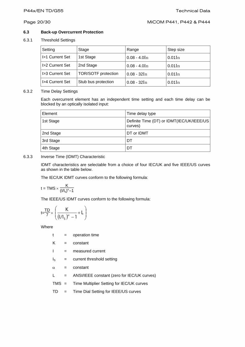
P44x/EN TD/G55 Technical Data Page 20/30
MiCOM P441, P442 & P444
6.3 Back-up Overcurrent Protection
6.3.1 Threshold Settings
Setting Stage Range Step size
I>1 Current Set 1st Stage 0.08 - 4.0In 0.01In
I>2 Current Set 2nd Stage 0.08 - 4.0In 0.01In
I>3 Current Set TOR/SOTF protection 0.08 - 32In 0.01In
I>4 Current Set Stub bus protection 0.08 - 32In 0.01In
6.3.2 Time Delay Settings
Each overcurrent element has an independent time setting and each time delay can be blocked by an optically isolated input:
Element Time delay type
1st Stage Definite Time (DT) or IDMT(IEC/UK/IEEE/US curves)
2nd Stage DT or IDMT
3rd Stage DT
4th Stage DT
6.3.3 Inverse Time (IDMT) Characteristic
IDMT characteristics are selectable from a choice of four IEC/UK and five IEEE/US curves as shown in the table below.
The IEC/UK IDMT curves conform to the following formula:
t = TMS × K
(I/Is)α–1
The IEEE/US IDMT curves conform to the following formula:
t=TD7 ×
( ) ⎟⎟⎠
⎞⎜⎜⎝
⎛+
−L
1I/I
K
Sα
Where
t = operation time
K = constant
I = measured current
IS = current threshold setting
α = constant
L = ANSI/IEEE constant (zero for IEC/UK curves)
TMS = Time Multiplier Setting for IEC/UK curves
TD = Time Dial Setting for IEEE/US curves

Technical Data P44x/EN TD/G55 MiCOM P441, P442 & P444
Page 21/30
IDMT Curve description Standard K Constant α Constant L Constant
Standard Inverse IEC 0.14 0.02
Very Inverse IEC 13.5 1
Extremely Inverse IEC 80 2
Long Time Inverse UK 120 1
Moderately Inverse IEEE 0.0515 0.02 0.114
Very Inverse IEEE 19.61 2 0.491
Extremely Inverse IEEE 28.2 2 0.1217
Inverse US-C08 5.95 2 0.18
Short Time Inverse US-C02 0.02394 0.02 0.01694
IDMT Characteristics
Name Range Step Size
TMS 0.025 to 1.2 0.025
Time Multiplier Settings for IEC/UK curves
Name Range Step Size
TD 0.5 to 15 0.1
Time Dial Settings for IEEE/US curves
6.3.3.1 Definite Time Characteristic
Element Range Step Size
All stages 0 to 100s 10ms
6.3.3.2 Reset Characteristics
Reset options for IDMT stages:
Curve type Reset time delay
IEC / UK curves DT only
All other IDMT or DT
The Inverse Reset characteristics are dependent upon the selected IEEE/US IDMT curve as shown in the table below. Thus if IDMT reset is selected the curve selection and Time Dial setting will apply to both operate and reset.
All inverse reset curves conform to the following formula:
( )t TD tr
I Iset
SRe = ⎛
⎝⎜⎞⎠⎟×
−
⎛
⎝⎜⎜
⎞
⎠⎟⎟7 1 α
Where
tReset = reset time
tr = constant
I = measured current
IS = current threshold setting
α = constant
TD = Time Dial Setting (Same setting as that employed by IDMT curve)

P44x/EN TD/G55 Technical Data Page 22/30
MiCOM P441, P442 & P444
IEEE/US IDMT Curve description Standard tr Constant α Constant
Moderately Inverse IEEE 0.0515 0.02
Very Inverse IEEE 19.61 2
Extremely Inverse IEEE 28.2 2
Inverse US-C08 5.95 2
Short Time Inverse US-C02 0.02394 0.02
Inverse Reset Characteristics
6.4 Negative sequence overcurrent protection
Setting Range Step size
I2> Current Set 0.08 - 4.0In 0.01In
I2> time Delay 0 - 100s 0.01s
Directional None/Fwd/Rev
I2> Char Angle –95° - +95° 1°
6.5 Broken Conductor Protection
Settings Range Step size
I2/I1 Setting 0.2 - 1.0 0.01
I2/I1 Time Delay 0 - 100s 0.1s
I2/I1 Trip Enabled / Disabled
6.6 Earth Fault Overcurrent Protection
6.6.1 Threshold Settings
Setting Range Step Size
IN>1 Current Set 0.08 - 4.0In 0.01In
IN>2 Current Set 0.08 - 32In 0.01In
6.6.2 Polarising Quantities For Earth Fault Measuring Elements
The polarising quantity for earth fault elements can be either zero sequence or negative sequence values.
Setting Range Step Size
IN> Char angle –95° to +95° 1°
6.6.3 Time Delay Characteristics
The time delay options for the two earth fault elements are identical, stage 1 may be selected to be either IDMT or definite time. Stage 2 will provide a definite time delay. The settings and IDMT characteristics are identical to those specified for the phase overcurrent elements. The setting range for the definite time delayed element is as specified below:
Definite Time Characteristic
Element Range Step Size
All stages 0 to 200s 0.01s

Technical Data P44x/EN TD/G55 MiCOM P441, P442 & P444
Page 23/30
6.7 Zero sequence Power Protection (since B1.0)
Threshold Settings
Setting Range Step Size
Po Status Enabled/Disabled. -
Time Delay Fact. 0 – 2s 0.200s
Fix Time Delay 0 – 10s 0.010s
IN current set 0.05 - 4 In 0.01 In
P0 Threshold 0.05IN - IN 0.1IN
6.8 Channel Aided Directional Earth Fault Protection
6.8.1 Threshold Settings
Setting Range Step Size
Polarisation Zero seq. / Neg. seq. -
V> Voltage Set (Vn=100/120 V)
0.500 - 20 V 0.010 V
IN Forward 0.05 - 4 In 0.01 In
Teleprotection Time delay 0 - 10s 0.1s
Scheme logic Shared / Blocking / Permissive
Tripping Any Phase / Three Phases
6.9 Under Voltage Protection
6.9.1 Threshold Settings
Setting Range Step Size
V<1 Voltage Set (Vn = 100/120V)
10 - 120V 1V
V<2 Voltage Set (Vn = 100/120V)
10 - 120V 1V
6.9.2 Under Voltage Protection Time Delay Characteristics
The Under voltage measuring elements are followed by an independently selectable time delay. The first stage has a time delay characteristics selectable as either Inverse Time or Definite Time. The second stage has an associated Definite Time delay setting.
Each measuring element time delay can be blocked by the operation of a user defined logic (optical isolated) input.
The inverse characteristic is defined by the following formula :
( )t K
M=
−1
Where
K = Time Multiplier Setting
T = Operating time in seconds
M = Applied input voltage / Relay setting voltage (Vs)

P44x/EN TD/G55 Technical Data Page 24/30
MiCOM P441, P442 & P444
Setting Range Step Size
DT setting 0 - 100s 0.01s
TMS Setting (K) 0.5 - 100 0.5
Definite time and TMS setting ranges
6.10 Over Voltage Protection
6.10.1 Threshold Settings
Setting Range Step Size
V>1 Voltage Set (Vn = 100/120V)
60 - 185V 1V
V>2 Voltage Set (Vn = 100/120V)
60 - 185V 1V
6.10.2 Time Delay Characteristics
The Overvoltage measuring elements are followed by an independently selectable time delay. The first stage has a time delay characteristics selectable as either Inverse Time or Definite Time. The second stage has an associated Definite Time delay setting.
Each measuring element time delay can be blocked by the operation of a user defined logic (optical isolated) input.
The inverse characteristic is defined by the following formula :
( )t K
M=
− 1
Where
K = Time Multiplier Setting
T = Operating time in seconds
M = Applied input voltage / Relay setting voltage (Vs)
Setting Range Step Size
DT setting 0 - 100s 0.01s
TMS Setting (K) 0.5 - 100s 0.5
Definite time and TMS setting ranges
6.11 Voltage Transformer Supervision
Setting Range Step Size
VTS Time Delay 1.0 - 20s 1s
3 phase undervoltage threshold 10-70V 1V
VTS I2> & I0> Inhibit 0 - In 0.01In
Superimposed current Delta I> 0.01 - 5A 0.01 A
6.12 Capacitive Voltage Transformer Supervision (since B1.0)
Setting Range Step Size
CVTS status Enabled / Disabled
CVTS VN> 0.500 - 22V 0.500V
CVTS Time Delay 0 – 300s 1s

Technical Data P44x/EN TD/G55 MiCOM P441, P442 & P444
Page 25/30
6.13 Current Transformer Supervision
Setting Range Step size
CTS VN< Inhibit 0.5 - 22V (for Vn = 100/120V) 0.5V
CTS IN> Set 0.08In - 4In 0.01In
CTS Time Delay 0 - 10s 1s
6.14 Undercurrent Element
This element is used by the breaker fail and circuit breaker monitoring functions of the relay.
Name Range Step size
I< Current Set 0.05 – 3.2In 0.050In
6.15 Breaker Fail Timers (TBF1 and TBF2)
There are two stages of breaker fail that can be used to re-trip the breaker and back trip in the case of a circuit breaker fail. The timers are reset if the breaker opens, this is generally detected by the undercurrent elements. Other methods of detection can be employed for certain types of trip (see Application notes Volume 1 Chapter 2).
Timer Setting range Step
tBF1 0 to 10s 0.005s
tBF2 0 to 10s 0.005s
CBF non Current reset I<Only/CB open&I</Prot Reset&I</Disable/Prot Reset Or I<
CBF Ext reset I<Only/CB open&I</Prot Reset&I</Disable/Prot Reset Or I<

P44x/EN TD/G55 Technical Data Page 26/30
MiCOM P441, P442 & P444
7. MEASUREMENT SETTINGS 7.1 Disturbance Recorder Settings
Setting Range Step
Record Length 0 - 10.5s 0.1s
Trigger position 0 - 100% 0.1%
Trigger mode Single / Extended
Sample Rate 12 Samples/Cycle Fixed
Digital Signals Selectable from logic inputs and outputs and internal signals
Trigger Logic Each of the digital inputs can be selected to trigger a record
7.2 Fault Locator Settings
Setting Range Step size
Mutual compensation factor 0 to 7.000 0.001
Mutual compensation angle 0 to 360° 1°
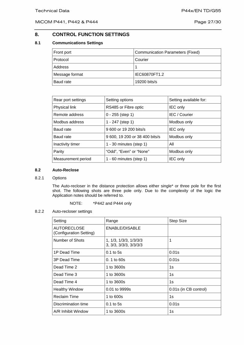
Technical Data P44x/EN TD/G55 MiCOM P441, P442 & P444
Page 27/30
8. CONTROL FUNCTION SETTINGS 8.1 Communications Settings
Front port Communication Parameters (Fixed)
Protocol Courier
Address 1
Message format IEC60870FT1.2
Baud rate 19200 bits/s
Rear port settings Setting options Setting available for:
Physical link RS485 or Fibre optic IEC only
Remote address 0 - 255 (step 1) IEC / Courier
Modbus address 1 - 247 (step 1) Modbus only
Baud rate 9 600 or 19 200 bits/s IEC only
Baud rate 9 600, 19 200 or 38 400 bits/s Modbus only
Inactivity timer 1 - 30 minutes (step 1) All
Parity “Odd”, “Even” or “None” Modbus only
Measurement period 1 - 60 minutes (step 1) IEC only
8.2 Auto-Reclose
8.2.1 Options
The Auto-recloser in the distance protection allows either single* or three pole for the first shot. The following shots are three pole only. Due to the complexity of the logic the Application notes should be referred to.
NOTE: *P442 and P444 only
8.2.2 Auto-recloser settings
Setting Range Step Size
AUTORECLOSE (Configuration Setting)
ENABLE/DISABLE
Number of Shots 1, 1/3, 1/3/3, 1/3/3/3 3, 3/3, 3/3/3, 3/3/3/3
1
1P Dead Time 0.1 to 5s 0.01s
3P Dead Time 0. 1 to 60s 0.01s
Dead Time 2 1 to 3600s 1s
Dead Time 3 1 to 3600s 1s
Dead Time 4 1 to 3600s 1s
Healthy Window 0.01 to 9999s 0.01s (in CB control)
Reclaim Time 1 to 600s 1s
Discrimination time 0.1 to 5s 0.01s
A/R Inhibit Window 1 to 3600s 1s

P44x/EN TD/G55 Technical Data Page 28/30
MiCOM P441, P442 & P444
Setting Range Step Size
Block auto-recloser At T2 At T3 At Tzp LoL Trip I2> Trip I>1 Trip I>2 Trip V<1 Trip V<2 Trip V>1 Trip V>2 trip IN>1 Trip IN>2 Trip Aided D.E.F Trip
AR Close pulse length 0.1 to 10s 0.1s
Check synchronic settings
Setting Range Step Size
C/S Check Scheme for A/R Bit 0: Live Bus/Dead Line, Bit 1: Dead Bus/Live Line Bit 2: Live Bus/Live Line.
Dead Bus/Dead Line with special PSL
C/S Check Scheme for Man CB
Bit 0: Live Bus/Dead Line, Bit 1: Dead Bus/Live Line Bit 2: Live Bus/Live Line.
Dead Bus/Dead Line with special PSL
V< Dead Line 5-30V 1V
V> Live Line 30-120V 1V
V< Dead Bus 5-30V 1V
V> Live Bus 30-120V 1V
Diff Voltage 0.5-40V 0.1V
Diff Frequency 0.02-1Hz 0.01Hz
Diff Phase 5°-90° 2.5°
Bus-Line Delay 0.1 to 2s 0.1s
8.3 Circuit Breaker State Monitoring
The relay can monitor the state of the circuit breaker using either a 52a or 52b signal, it is possible to select which of these is being used on the relay menu. If the menu is used to select the ‘Both 52a and 52b’ option is selected then a discrepancy alarm can be detected. If these contacts remain simultaneously open or simultaneously closed for >5s, then the CB Status alarm will be indicated.

Technical Data P44x/EN TD/G55 MiCOM P441, P442 & P444
Page 29/30
8.4 Circuit Breaker Control
Name Range Step size
CB Control by Disabled/ Local/ Remote/ Local+Remote/ Opto/ Opto+local/ Opto+Remote/ Opto+Rem+local
Manual close pulse time 0.1 to 10s 0.01s
Trip pulse time 0.1 to 5s 0.01s
Man Close Delay 0.01 to 600s 0.01s
Healthy Windows 0.01 to 9999 0.01
C/S Window 0.01 to 9999 0.01
AR single pole Disabled/Enabled -
AR three pole Disabled/Enabled -
8.5 Circuit Breaker Condition Monitoring
8.5.1 Maintenance alarm settings
Name Range Step size
I^ Maintenance 1 to 25000A 1 Summated broken current
No. of CB Ops Maint 1- 10000 1
CB Time Maint 5 - 500ms 1ms Circuit breaker opening time
8.5.2 Lockout Alarm Settings
Name Range Step size
1 to 25000 1
1- 10000 1
5 - 500ms 1ms
0 to 9999 1
Fault Freq Time 0 to 9999s 1s
Lockout reset by: I^ threshold
Manual close reset delay No. of CB Ops Lock 0.01s
CB Time Lockout
Fault Freq Count

P44x/EN TD/G55 Technical Data Page 30/30
MiCOM P441, P442 & P444
8.6 Programmable Logic
The programmable logic is not editable from the relay menu, a dedicated support package is provided as part of the MiCOM S1 support software. This is a graphical editor for the programmable logic. The features of the programmable logic are more fully described within the application section of the user manual. As part of the logic each output contact has a programmable conditioner/timer, there are also eight general purpose timers for use in the logic.
The output conditioners and the general-purpose timers have the following setting range:
Time Range Step size
t1 to t8 0 to 4 hours 0.001s
8.7 CT and VT Ratio Settings
The primary and secondary rating can be independently set for each set of CT or VT inputs, for example the earth fault CT ratio can be different to that used for the phase currents.
Primary range Secondary range
Current transformer 1 - 30000 Amps step size 1 A
1 or 5 Amps
Voltage transformer 100 V - 1000 kV step size 1 V
80 - 140 V step size 1 V

Installation P44x/EN IN/G55 MiCOM P441, P442 & P444
INSTALLATION

P44x/EN IN/G55 Installation
MiCOM P441, P442 & P444

Installation P44x/EN IN/G55 MiCOM P441, P442 & P444
Page 1/10
CONTENT
1. RECEIPT OF RELAYS 3
2. STORAGE 3
3. UNPACKING 3
4. RELAY MOUNTING 4
4.1 Rack mounting 5 4.2 Panel mounting 6
5. RELAY WIRING 8
5.1 Medium and heavy duty terminal block connections 8 5.2 RS485 port 8 5.3 IRIG-B connections (if applicable) 9 5.4 RS232 port 9 5.5 Download/monitor port 9 5.6 Earth connection 9

P44x/EN IN/G55 Installation Page 2/10
MiCOM P441, P442 & P444
BLANK PAGE

Installation P44x/EN IN/G55 MiCOM P441, P442 & P444
Page 3/10
1. RECEIPT OF RELAYS Protective relays, although generally of robust construction, require careful treatment prior to installation on site. Upon receipt, relays should be examined immediately to ensure no external damage has been sustained in transit. If damage has been sustained, a claim should be made to the transport contractor and Alstom Grid should be promptly notified.
Relays that are supplied unmounted and not intended for immediate installation should be returned to their protective polythene bags and delivery carton. Section 3 of this chapter gives more information about the storage of relays.
2. STORAGE If relays are not to be installed immediately upon receipt, they should be stored in a place free from dust and moisture in their original cartons. Where de-humidifier bags have been included in the packing they should be retained. The action of the de-humidifier crystals will be impaired if the bag is exposed to ambient conditions and may be restored by gently heating the bag for about an hour prior to replacing it in the carton.
To prevent battery drain during transportation and storage a battery isolation strip is fitted during manufacture. With the lower access cover open, presence of the battery isolation strip can be checked by a red tab protruding from the positive side.
Care should be taken on subsequent unpacking that any dust which has collected on the carton does not fall inside. In locations of high humidity the carton and packing may become impregnated with moisture and the de-humidifier crystals will lose their efficiency.
Prior to installation, relays should be stored at a temperature of between –25˚C to +70˚C.
3. UNPACKING Care must be taken when unpacking and installing the relays so that none of the parts are damaged and additional components are not accidentally left in the packing or lost.
NOTE: With the lower access cover open, the red tab of the battery isolation strip will be seen protruding from the positive side of the battery compartment. Do not remove this strip because it prevents battery drain during transportation and storage and will be removed as part of the commissioning tests.
Relays must only be handled by skilled persons.
The site should be well lit to facilitate inspection, clean, dry and reasonably free from dust and excessive vibration. This particularly applies to installations which are being carried out at the same time as construction work.

P44x/EN IN/G55 Installation Page 4/10
MiCOM P441, P442 & P444
4. RELAY MOUNTING MiCOM relays are dispatched either individually or as part of a panel/rack assembly.
Individual relays are normally supplied with an outline diagram showing the dimensions for panel cut-outs and hole centres. This information can also be found in the product publication.
Secondary front covers can also be supplied as an option item to prevent unauthorised changing of settings and alarm status. They are available in sizes 40TE (GN0037 001) and 60TE (GN0038 001). Note that the 60TE cover also fits the 80TE case size of the relay.
The design of the relay is such that the fixing holes in the mounting flanges are only accessible when the access covers are open and hidden from sight when the covers are closed.
If a P991 or MMLG test block is to be included, it is recommended that, when viewed from the front, it is positioned on the right-hand side of the relay (or relays) with which it is associated. This minimises the wiring between the relay and test block, and allows the correct test block to be easily identified during commissioning and maintenance tests.
P0146XXa
FIGURE 1 - LOCATION OF BATTERY ISOLATION STRIP
If it is necessary to test correct relay operation during the installation, the battery isolation strip can be removed but should be replaced if commissioning of the scheme is not imminent. This will prevent unnecessary battery drain during transportation to site and installation. The red tab of the isolation strip can be seen protruding from the positive side of the battery compartment when the lower access cover is open. To remove the isolation strip, pull the red tab whilst lightly pressing the battery to prevent it falling out of the compartment. When replacing the battery isolation strip, ensure that the strip is refitted as shown in figure 1, ie. with the strip behind the battery with the red tab protruding.

Installation P44x/EN IN/G55 MiCOM P441, P442 & P444
Page 5/10
4.1 Rack mounting
MiCOM relays may be rack mounted using single tier rack frames (our part number FX0021 001), as illustrated in figure 2. These frames have been designed to have dimensions in accordance with IEC60297 and are supplied pre-assembled ready to use. On a standard 483mm (19”) rack system this enables combinations of widths of case up to a total equivalent of size 80TE to be mounted side by side.
P545 and P546 relays in 80TE cases are also available as direct 19” rack mounting ordering variants, having mounted flanges similar to those shown in figure 2.
The two horizontal rails of the rack frame have holes drilled at approximately 26mm intervals and the relays are attached via their mounting flanges using M4 Taptite self-tapping screws with captive 3mm thick washers (also known as a SEMS unit). These fastenings are available in packs of 5 (our part number ZA0005 104).
NOTE: Conventional self-tapping screws, including those supplied for mounting MIDOS relays, have marginally larger heads which can damage the front cover moulding if used.
Once the tier is complete, the frames are fastened into the racks using mounting angles at each end of the tier.
P0147XXa
FIGURE 2 - RACK MOUNTING OF RELAYS
Relays can be mechanically grouped into single tier (4U) or multi-tier arrangements by means of the rack frame. This enables schemes using products from the MiCOM and MiDOS product ranges to be pre-wired together prior to mounting.
Where the case size summation is less than 80TE on any tier, or space is to be left for installation of future relays, blanking plates may be used. These plates can also be used to mount ancillary components. Table 1 shows the sizes that can be ordered.
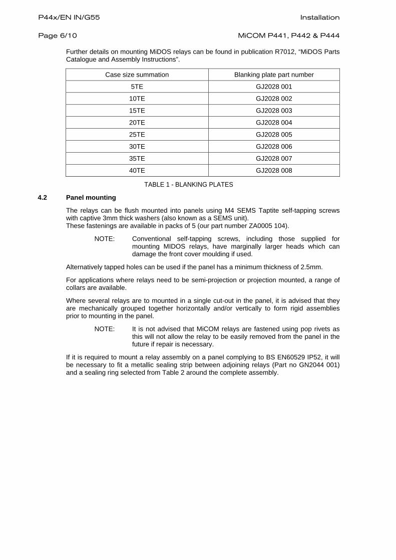
P44x/EN IN/G55 Installation Page 6/10
MiCOM P441, P442 & P444
Further details on mounting MiDOS relays can be found in publication R7012, “MiDOS Parts Catalogue and Assembly Instructions”.
Case size summation Blanking plate part number
5TE GJ2028 001
10TE GJ2028 002
15TE GJ2028 003
20TE GJ2028 004
25TE GJ2028 005
30TE GJ2028 006
35TE GJ2028 007
40TE GJ2028 008
TABLE 1 - BLANKING PLATES
4.2 Panel mounting
The relays can be flush mounted into panels using M4 SEMS Taptite self-tapping screws with captive 3mm thick washers (also known as a SEMS unit). These fastenings are available in packs of 5 (our part number ZA0005 104).
NOTE: Conventional self-tapping screws, including those supplied for mounting MIDOS relays, have marginally larger heads which can damage the front cover moulding if used.
Alternatively tapped holes can be used if the panel has a minimum thickness of 2.5mm.
For applications where relays need to be semi-projection or projection mounted, a range of collars are available.
Where several relays are to mounted in a single cut-out in the panel, it is advised that they are mechanically grouped together horizontally and/or vertically to form rigid assemblies prior to mounting in the panel.
NOTE: It is not advised that MiCOM relays are fastened using pop rivets as this will not allow the relay to be easily removed from the panel in the future if repair is necessary.
If it is required to mount a relay assembly on a panel complying to BS EN60529 IP52, it will be necessary to fit a metallic sealing strip between adjoining relays (Part no GN2044 001) and a sealing ring selected from Table 2 around the complete assembly.

Installation P44x/EN IN/G55 MiCOM P441, P442 & P444
Page 7/10
Width Single tier Double tier
10TE GJ9018 002 GJ9018 018
15TE GJ9018 003 GJ9018 019
20TE GJ9018 004 GJ9018 020
25TE GJ9018 005 GJ9018 021
30TE GJ9018 006 GJ9018 022
35TE GJ9018 007 GJ9018 023
40TE GJ9018 008 GJ9018 024
45TE GJ9018 009 GJ9018 025
50TE GJ9018 010 GJ9018 026
55TE GJ9018 011 GJ9018 027
60TE GJ9018 012 GJ9018 028
65TE GJ9018 013 GJ9018 029
70TE GJ9018 014 GJ9018 030
75TE GJ9018 015 GJ9018 031
80TE GJ9018 016 GJ9018 032
TABLE 2 - IP52 SEALING RINGS
Further details on mounting MiDOS relays can be found in publication R7012, “MiDOS Parts Catalogue and Assembly Instructions”.
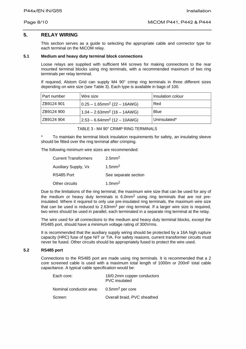
P44x/EN IN/G55 Installation Page 8/10
MiCOM P441, P442 & P444
5. RELAY WIRING This section serves as a guide to selecting the appropriate cable and connector type for each terminal on the MiCOM relay.
5.1 Medium and heavy duty terminal block connections
Loose relays are supplied with sufficient M4 screws for making connections to the rear mounted terminal blocks using ring terminals, with a recommended maximum of two ring terminals per relay terminal.
If required, Alstom Grid can supply M4 90° crimp ring terminals in three different sizes depending on wire size (see Table 3). Each type is available in bags of 100.
Part number Wire size Insulation colour
ZB9124 901 0.25 – 1.65mm2 (22 – 16AWG) Red
ZB9124 900 1.04 – 2.63mm2 (16 – 14AWG) Blue
ZB9124 904 2.53 – 6.64mm2 (12 – 10AWG) Uninsulated*
TABLE 3 - M4 90° CRIMP RING TERMINALS
* To maintain the terminal block insulation requirements for safety, an insulating sleeve should be fitted over the ring terminal after crimping.
The following minimum wire sizes are recommended:
Current Transformers 2.5mm2
Auxiliary Supply, Vx 1.5mm2
RS485 Port See separate section
Other circuits 1.0mm2
Due to the limitations of the ring terminal, the maximum wire size that can be used for any of the medium or heavy duty terminals is 6.0mm2 using ring terminals that are not pre-insulated. Where it required to only use pre-insulated ring terminals, the maximum wire size that can be used is reduced to 2.63mm2 per ring terminal. If a larger wire size is required, two wires should be used in parallel, each terminated in a separate ring terminal at the relay.
The wire used for all connections to the medium and heavy duty terminal blocks, except the RS485 port, should have a minimum voltage rating of 300Vrms.
It is recommended that the auxiliary supply wiring should be protected by a 16A high rupture capacity (HRC) fuse of type NIT or TIA. For safety reasons, current transformer circuits must never be fused. Other circuits should be appropriately fused to protect the wire used.
5.2 RS485 port
Connections to the RS485 port are made using ring terminals. It is recommended that a 2 core screened cable is used with a maximum total length of 1000m or 200nF total cable capacitance. A typical cable specification would be:
Each core: 16/0.2mm copper conductors PVC insulated
Nominal conductor area: 0.5mm2 per core
Screen: Overall braid, PVC sheathed

Installation P44x/EN IN/G55 MiCOM P441, P442 & P444
Page 9/10
5.3 IRIG-B connections (if applicable)
The IRIG-B input and BNC connector have a characteristic impedance of 50Ω. It is recommended that connections between the IRIG-B equipment and the relay are made using coaxial cable of type RG59LSF with a halogen free, fire retardant sheath.
5.4 RS232 port
Short term connections to the RS232 port, located behind the bottom access cover, can be made using a screened multi-core communication cable up to 15m long, or a total capacitance of 2500pF. The cable should be terminated at the relay end with a 9-way, metal shelled, D-type male plug. Chapter 2, Section 3.7 of this manual details the pin allocations.
5.5 Download/monitor port
Short term connections to the download/monitor port, located behind the bottom access cover, can be made using a screened 25-core communication cable up to 4m long. The cable should be terminated at the relay end with a 25-way, metal shelled, D-type male plug. Chapter 2, Section 3.7 of this manual details the pin allocations.
5.6 Earth connection
Every relay must be connected to the local earth bar using the M4 earth studs in the bottom left hand corner of the relay case. The minimum recommended wire size is 2.5mm2 and should have a ring terminal at the relay end. Due to the limitations of the ring terminal, the maximum wire size that can be used for any of the medium or heavy duty terminals is 6.0mm2 per wire. If a greater cross-sectional area is required, two parallel connected wires, each terminated in a separate ring terminal at the relay, or a metal earth bar could be used.
NOTE: To prevent any possibility of electrolytic action between brass or copper earth conductors and the rear panel of the relay, precautions should be taken to isolate them from one another. This could be achieved in a number of ways, including placing a nickel-plated or insulating washer between the conductor and the relay case, or using tinned ring terminals.
Before carrying out any work on the equipment, the user should be familiar with the contents of the Safety and Technical Data sections and the ratings on the equipment's rating label

P44x/EN IN/G55 Installation Page 10/10
MiCOM P441, P442 & P444
BLANK PAGE

Commissioning Test & Record Sheets
P44x/EN RS/G55
MiCOM P441, P442 & P444
COMMISSIONING TEST & RECORD SHEETS

P44x/EN RS/G55 Commissioning Test & Record Sheets
MiCOM P441, P442 & P444

Commissioning Test & Record Sheets
P44x/EN RS/G55
MiCOM P441, P442 & P444
Page 1/10
CONTENT
1. COMMISSIONING TEST RECORD 3
1.1 Product Checks 3 1.1.1 With the Relay De-energised 3 1.1.2 With the Relay Energised 4 1.2 Setting Checks 9 1.2.1 Application-specific function settings applied? 9 1.2.2 Application-specific function settings verified? 9 1.2.3 Application-specific programmable scheme logic tested? 9 1.2.4 Protection Function Timing Tested? 9 1.2.5 Trip and Auto-Reclose Cycle Checked 9 1.3 On-load Checks 9 1.3.1 VT wiring checked? 9 1.3.2 CT wiring checked? 10 1.4 Final Checks 10

P44x/EN RS/G55 Commissioning Test & Record Sheets
Page 2/10
MiCOM P441, P442 & P444
BLANK PAGE

Commissioning Test & Record Sheets
P44x/EN RS/G55
MiCOM P441, P442 & P444
Page 3/10
1. COMMISSIONING TEST RECORD
Date Engineer
Station Circuit
System Frequency
Front Plate Information
Distance protection relay P441/P442/P444*
Model number
Serial number
Rated Current In
Rated Voltage Vn
Auxiliary Voltage Vx
*Delete as appropriate
Have all relevant safety instructions been followed? Yes/No*
1.1 Product Checks
1.1.1 With the Relay De-energised
1.1.1.1 Visual Inspection
Relay damaged? Yes/No*
Rating information correct for installation? Yes/No*
Case earth installed? Yes/No*
1.1.1.2 Current transformer shorting contacts close? Yes/No/Not checked*
1.1.1.3 External Wiring
Wiring checked against diagram? Yes/No*
Test block connections checked? Yes/No/na*
1.1.1.4 Insulation resistance >100MΩ at 500V dc Yes/No/Not tested*

P44x/EN RS/G55 Commissioning Test & Record Sheets
Page 4/10
MiCOM P441, P442 & P444 1.1.1.5 Watchdog Contacts (auxiliary supply off)
Terminals 11 and 12 Contact closed? Yes/No*
Contact resistance ___Ω/Not measured*
Terminals 13 and 14 Contact open? Yes/No*
1.1.1.6 Measured Auxiliary Supply ______V ac/dc*
1.1.2 With the Relay Energised
1.1.2.1 Watchdog Contacts (auxiliary supply on)
Terminals 11 and 12 Contact open? Open/Closed*
Terminals 13 and 14 Contact closed? Open/Closed*
Contact resistance ____Ω/Not measured*
1.1.2.2 Date and Time
Clock set to local time? Yes/No*
Time maintained when auxiliary supply removed? Yes/No*
1.1.2.3 Light Emitting Diodes
Relay healthy (green) LED working? Yes/No*
Alarm (yellow) LED working? Yes/No*
Out of service (yellow) LED working? Yes/No*
Trip (red) LED working? Yes/No*
All 8 programmable LEDs working? Yes/No*
1.1.2.4 Field supply voltage
Value measured between terminals 7 and 9 ______V dc
Value measured between terminals 8 and 10 ______V dc

Commissioning Test & Record Sheets
P44x/EN RS/G55
MiCOM P441, P442 & P444
Page 5/10 1.1.2.5 Input Opto-isolators
Opto input 1 working? Yes/No*
Opto input 2 working? Yes/No*
Opto input 3 working? Yes/No*
Opto input 4 working? Yes/No*
Opto input 5 working? Yes/No*
Opto input 6 working? Yes/No*
Opto input 7 working? Yes/No*
Opto input 8 working? Yes/No*
Opto input 9 working? Yes/No/na*
Opto input 10 working? Yes/No/na*
Opto input 11 working? Yes/No/na*
Opto input 12 working? Yes/No/na*
Opto input 13 working? Yes/No/na*
Opto input 14 working? Yes/No/na*
Opto input 15 working? Yes/No/na*
Opto input 16 working? Yes/No/na*
Opto input 17 working? Yes/No/na*
Opto input 18 working? Yes/No/na*
Opto input 19 working? Yes/No/na*
Opto input 20 working? Yes/No/na*
Opto input 21 working? Yes/No/na*
Opto input 22 working? Yes/No/na*
Opto input 23 working? Yes/No/na*
Opto input 24 working? Yes/No/na*
1.1.2.6 Output Relays
Relay 1 Working? Yes/No*
Contact resistance ____Ω/Not measured*
Relay 2 Working? Yes/No*
Contact resistance ____Ω/Not measured*
Relay 3 Working? Yes/No*
Contact resistance ____Ω/Not measured*
Relay 4 Working? Yes/No*
Contact resistance (N/C) ____Ω/Not measured*
(N/O) ____Ω/Not measured*
Relay 5 Working? Yes/No*
Contact resistance (N/C) ____Ω/Not measured*
(N/O) ____Ω/Not measured*

P44x/EN RS/G55 Commissioning Test & Record Sheets
Page 6/10
MiCOM P441, P442 & P444
Relay 6 Working? Yes/No*
Contact resistance (N/C) ____Ω/Not measured*
(N/O) ____Ω/Not measured*
Relay 7 Working? Yes/No*
Contact resistance (N/C) ____Ω/Not measured*
(N/O) ____Ω/Not measured*
Relay 8 Working? Yes/No*
Contact resistance ____Ω/Not measured*
Relay 9 Working? Yes/No*
Contact resistance ____Ω/Not measured*
Relay 10 Working? Yes/No*
Contact resistance ____Ω/Not measured*
Relay 11 Working? Yes/No*
Contact resistance (N/C) ____Ω/Not measured*
(N/O) ____Ω/Not measured*
Relay 12 Working? Yes/No*
Contact resistance (N/C) ____Ω/Not measured*
(N/O) ____Ω/Not measured*
Relay 13 Working? Yes/No*
Contact resistance (N/C) ____Ω/Not measured*
(N/O) ____Ω/Not measured*
Relay 14 Working? Yes/No*
Contact resistance (N/C) ____Ω/Not measured*
(N/O) ____Ω/Not measured*
Relay 15 Working? Yes/No/na*
Contact resistance (N/C) ____Ω/Not measured*
(N/O) ____Ω/Not measured*
Relay 16 Working? Yes/No/na*
Contact resistance (N/C) ____Ω/Not measured*
(N/O) ____Ω/Not measured*
Relay 17 Working? Yes/No/na*
Contact resistance (N/C) ____Ω/Not measured*
(N/O) ____Ω/Not measured*
Relay 18 Working? Yes/No/na*
Contact resistance (N/C) ____Ω/Not measured*
(N/O) ____Ω/Not measured*
Relay 19 Working? Yes/No/na*
Contact resistance (N/C) ____Ω/Not measured*
(N/O) ____Ω/Not measured*

Commissioning Test & Record Sheets
P44x/EN RS/G55
MiCOM P441, P442 & P444
Page 7/10
Relay 20 Working? Yes/No/na*
Contact resistance (N/C) ____Ω/Not measured*
(N/O) ____Ω/Not measured*
Relay 21 Working? Yes/No/na*
Contact resistance (N/C) ____Ω/Not measured*
(N/O) ____Ω/Not measured*
Relay 22 Working? Yes/No/na*
Contact resistance (N/C) ____Ω/Not measured*
(N/O) ____Ω/Not measured*
Relay 23 Working? Yes/No/na*
Contact resistance (N/C) ____Ω/Not measured*
(N/O) ____Ω/Not measured*
Relay 24 Working? Yes/No/na*
Contact resistance (N/C) ____Ω/Not measured*
(N/O) ____Ω/Not measured*
Relay 25 Working? Yes/No/na*
Contact resistance (N/C) ____Ω/Not measured*
(N/O) ____Ω/Not measured*
Relay 26 Working? Yes/No/na*
Contact resistance (N/C) ____Ω/Not measured*
(N/O) ____Ω/Not measured*
Relay 27 Working? Yes/No/na*
Contact resistance (N/C) ____Ω/Not measured*
(N/O) ____Ω/Not measured*
Relay 28 Working? Yes/No/na*
Contact resistance (N/C) ____Ω/Not measured*
(N/O) ____Ω/Not measured*
Relay 29 Working? Yes/No/na*
Contact resistance (N/C) ____Ω/Not measured*
(N/O) ____Ω/Not measured*
Relay 30 Working? Yes/No/na*
Contact resistance (N/C) ____Ω/Not measured*
(N/O) ____Ω/Not measured*
Relay 31 Working? Yes/No/na*
Contact resistance (N/C) ____Ω/Not measured*
(N/O) ____Ω/Not measured*
Relay 32 Working? Yes/No/na*
Contact resistance (N/C) ____Ω/Not measured*
(N/O) ____Ω/Not measured*

P44x/EN RS/G55 Commissioning Test & Record Sheets
Page 8/10
MiCOM P441, P442 & P444 1.1.2.7 Rear Communications Port
Communication standard K-Bus/Modbus/ IEC60870-5-103*
Communications established? Yes/No*
Protocol converter tested? Yes/No/na*
1.1.2.8 Current Inputs
Displayed Current Primary/Secondary*
Phase CT Ratio ⎟⎠
⎞⎜⎝
⎛y]Sec'CT Phase [
Primary]CT Phase [
_______A/na*
Mutual CT Ratio ⎟⎟⎠
⎞⎜⎜⎝
⎛y]Sec'CT Mutual [
Primary]CT Mutual [
_______A/na*
Input CT Applied value Displayed value
IA _______A _______A
IB _______A _______A
IC _______A _______A
IM _______A _______A
1.1.2.9 Voltage Inputs
Displayed Voltage Primary/Secondary*
Main VT Ratio ⎟⎟⎠
⎞⎜⎜⎝
⎛y]Sec'VT Main [
Primary]VT Main [
_______V/na*
C/S VT Ratio ⎟⎟⎠
⎞⎜⎜⎝
⎛Secondary]VT C/S [Primary]VT C/S [
_______V/na*
Input VT Applied value Displayed value
Va _______V _______V
Vb _______V _______V
Vc _______V _______V
C/S Voltage _______V/na* _______V

Commissioning Test & Record Sheets
P44x/EN RS/G55
MiCOM P441, P442 & P444
Page 9/10 1.2 Setting Checks
1.2.1 Application-specific function settings applied? Yes/No*
Application-specific programmable scheme logic settings applied? Yes/No/na*
If settings applied using a portable computer and software, which software and version was used?
__________________
1.2.2 Application-specific function settings verified? Yes/No/na*
1.2.3 Application-specific programmable scheme logic tested? Yes/No/na*
1.2.4 Protection Function Timing Tested? Yes/No*
Overcurrent type (cell [3502 I>1 Direction]) Directional /Non-directional*
Applied voltage _________V/na*
Applied current _________A
Expected operating time _________s
Measured operating time _________s
1.2.5 Trip and Auto-Reclose Cycle Checked Yes/No/na*
1.3 On-load Checks
Test wiring removed? Yes/No/na*
Disturbed customer wiring re-checked? Yes/No/na*
On-load test performed? Yes/No*
1.3.1 VT wiring checked? Yes/No/na*
Phase rotation correct? Yes/No*
Displayed Voltage Primary/Secondary*
Main VT Ratio ⎟⎟⎠
⎞⎜⎜⎝
⎛y]Sec'VT [Main
Primary]VT [Main
_______V/na*
C/S VT Ratio ⎟⎟⎠
⎞⎜⎜⎝
⎛Secondary]VT [C/SPrimary]VT [C/S
_______V/na*
Voltages Applied value Displayed value
Va _______V _______V
Vb _______V _______V
Vc _______V _______V
C/S Voltage _______V/na* _______V

P44x/EN RS/G55 Commissioning Test & Record Sheets
Page 10/10
MiCOM P441, P442 & P444 1.3.2 CT wiring checked ? Yes/No/na*
CT polarities correct ? Yes/No*
Displayed Current Primary/Secondary*
Phase CT Ratio ⎟⎟⎠
⎞⎜⎜⎝
⎛y]Sec'CT [Phase
Primary]CT [Phase
_______A/na*
Mutual CT Ratio ⎟⎟⎠
⎞⎜⎜⎝
⎛y]Sec'CT [Mutual
Primary]CT [Mutual
_______A/na*
Currents Applied value Displayed value
IA _______A _______A
IB _______A _______A
IC _______A _______A
IM _______A _______A
1.4 Final Checks
Test wiring removed ? Yes/No/na*
Disturbed customer wiring re-checked ? Yes/No/na*
Circuit breaker operations counter reset ? Yes/No/na*
Current counters reset ? Yes/No/na*
Event records reset ? Yes/No*
Fault records reset ? Yes/No*
Disturbance records reset ? Yes/No*
Alarms reset ? Yes/No*
LEDs reset ? Yes/No*
Commissioning Engineer Customer Witness
Date Date

Connection Diagrams P44x/EN CO/G55 MiCOM P441, P442 & P444
CONNECTION DIAGRAMS

P44x/EN CO/G55 Connection Diagrams
MiCOM P441, P442 & P444

Connection Diagrams P44x/EN CO/G55 MiCOM P441, P442 & P444
Page 1/12
CONTENT
1. MiCOM P441 – HARDWARE DESCRIPTION 3
2. MiCOM P441 – WIRING DIAGRAM (1/2) 4
3. MiCOM P441 – WIRING DIAGRAM (2/2) 5
4. MiCOM P442 – HARDWARE DESCRIPTION 6
5. MiCOM P442 – WIRING DIAGRAM (1/2) 7
6. MiCOM P442 – WIRING DIAGRAM (2/2) 8
7. MiCOM P444 – HARDWARE DESCRIPTION 9
8. MiCOM P444 – WIRING DIAGRAM (1/2) 10
9. MiCOM P444 – WIRING DIAGRAM (2/2) 11

P44x/EN CO/G55 Connection Diagrams Page 2/12
MiCOM P441, P442 & P444
BLANK PAGE

Connection Diagrams P44x/EN CO/G55 MiCOM P441, P442 & P444
Page 3/12
1. MiCOM P441 – HARDWARE DESCRIPTION
TERM
INA
LBLO
CK
S-
SEE
DETA
IL
200.0
240.0
INC
L.W
IRIN
G
30.0
157.5
MA
X.
SEC
ON
DA
RY
CO
VER
(WH
EN
FIT
TED
)
8O
FF
HO
LES
3.4
10.3
5181.3
23.3
155.4
159.0
168.0
202.0
177.0
206.0
MiC
OM
4.5
EA
CH
TERM
INATIO
NA
CC
EPTS:-
2x
M4
RIN
GTERM
INA
LS
HEA
VY
DU
TY
FLU
SHM
OU
NTI
NG
PAN
ELC
UT-
OU
TD
ETA
IL
TERM
INA
LBLO
CK
DET
AIL
1
18
REA
RVIE
W
SHO
WN
ARE
TYPI
CA
LO
NLY
THE
TERM
INATI
ON
POSI
TIO
NS
2
17
161
19
3 24
18
SID
EVIE
W
MO
UN
TIN
GSC
REW
S:
M4
x12
SEM
UN
ITSTEEL
TH
REA
DFO
RM
ING
SC
REW
.
TERM
INA
LSC
REW
S:
M4
x6
STEEL
CO
MBIN
ATIO
NPA
NH
EA
DM
AC
HIN
ESC
REW
.
FRO
NT
VIE
W
TX
RX
IRIG
-B
AB
CD
EF
MED
IUM
DU
TY
=E
NT
ER
HEA
LTH
Y
OU
TO
FSE
RVIC
E
ALA
RM
TRIP
==C
LE
AR
RE
AD
TYPE
OF
FIB
RE
OPTIC
CO
NN
EC
TOR
:ST
4

P44x/EN CO/G55 Connection Diagrams Page 4/12
MiCOM P441, P442 & P444
2. MiCOM P441 – WIRING DIAGRAM (1/2)
CO
NN
EC
TIO
N
OPTO
5
CO
MM
ON
OPTO
8
OPTO
7
OPTO
6
OPTO
4
D13
D18
D15
D17
D16
D14
+
-
+
-
+
D12
D11
D10
D9
+
-
+
-
D8
D7
-
SK2
SK1
NO
TC
ON
NEC
TED
SERIA
L
PO
RT
CTS
RTS
0V
TX
RX
4 8 97651 3214
RELA
Y13
RELA
Y12
RELA
Y14
B16
B18
B17
B14
B15
B12
B13
B11
DATA
REA
DY
TEST/
DO
WN
LOA
D
0V
TO-T
7
DO
-D7
DO
WN
LOA
DC
OM
MA
ND
EXTERN
AL
AC
KN
OW
LED
GE
RESET
DATA
1 20,2
1,2
3,2
4
11,1
2,1
5,1
3,
19,1
8,2
2,2
5
2-9
17
16
10
RELA
Y3
RELA
Y7
E17
RELA
Y8
RELA
Y9
RELA
Y11
RELA
Y10
B5
B7
B6
B8
B9
B10
B1 B2
B4
B3
E18
RELA
Y4
RELA
Y6
RELA
Y5
E15
E16
E12
E14
E13
E6
E8
E7
E9
E10
E11
WATC
HD
OG
CO
NTA
CT
RELA
Y2
CO
NTA
CT
RELA
Y1
WATC
HD
OG
F14
E2
E1
E3
E5
E4
F11
F13
F12
EA
RTH
CA
SE
PO
RT
F1
6SC
N
RS4
85
F1
7
F1
8
D6
+
D4
D5
-
+
D3
D2
-
+
D1
-
OPTO
2
OPTO
3
OPTO
1
4.
C.T
.C
ON
NEC
TIO
NS
ARE
SH
OW
N1A
CO
NN
EC
TED
AN
DA
RE
TYPIC
AL
ON
LY.
PH
ASE
RO
TATIO
N
A
CB
C10
C12
C19
C20
C21
C22
C24
C23
2.
IMIN
PU
TIS
FO
RO
PTIO
NA
LM
UTU
AL
CO
MPEN
SATIO
NO
FFA
ULT
LOC
ATO
R.
3.
VBU
SBA
RO
NLY
REQ
UIR
ED
IFC
HEC
KSYN
CH
RO
NIS
MFU
NC
TIO
NEN
ABLE
D.
PIN
TERM
INA
L(P
.C.B
.TYPE)
50
OH
MBN
CC
ON
NEC
TOR
9-W
AY
&25-W
AY
FEM
ALE
D-T
YPE
SO
CKET
(b)
C.T
.SH
ORTIN
GLI
NKS
NO
TES
1. (a
)
BV
(SEE
NO
TE
3.)
VBU
SBA
R
CVV
A
N
a
C1
1SEE
NO
TE
2.
S1
DIR
EC
TIO
NO
FFO
RW
ARD
CU
RREN
TFLO
W
B PARA
LLEL
LIN
EPRO
TEC
TIO
N
C
S2
AP2
PH
ASE
RO
TATIO
N
CB
P1
A
cb
n
C
IM
C9
C8
C7
I
C6
C5
IB
A
A CB
CB
S2
NO
TE
4.
C2
C3
C4
IA
C1
S1
DIR
EC
TIO
NO
FFO
RW
ARD
CU
RREN
TFLO
W
P2
P1
1A
5A
1A
1A
5A
5A
1A
5A
PO
WER
SU
PPLY
VERSIO
N24/5
4V
D.C
.O
NLY
*
48V
DC
FIE
LDVO
LTA
GE
OU
T
F8
+ - -F10F9
- + +F7
F2F1
*
AU
XSU
PPLY
AC
OR
DC
Vx
MiC
OM
P441
(PA
RT)
MiC
OM
P441
(PA
RT)

Connection Diagrams P44x/EN CO/G55 MiCOM P441, P442 & P444
Page 5/12
3. MiCOM P441 – WIRING DIAGRAM (2/2)
D 3
STA
ND
ARD
INPU
TM
OD
ULE
GN
00
10
01
3(1
10
V)
64
-WAY
RIB
BO
NC
ABLE
BO
ARD
CO
NTA
INS
SA
FETY
CRIT
ICA
LC
OM
PO
NEN
TS.
USER
INTERFA
CE
PC
B
CIR
CU
ITD
IAG
.0
1ZN
00
06
01
MA
INPRO
CESSO
R&
BATTERY
SERIA
L
SK2
*PL1
TEST/D
OW
NLO
AD
SK1
16
14
10
86
42
12
CIR
CU
ITD
IAG
.
PO
WER
SU
PPLY
PC
B
01
ZN
00
01
01
*
PL1
FF
1F
F3F
F5F
7F
FF
9F11F
13F
15
F
F
218
16
12
810
14
64
218
RELA
YPC
BC
IRC
UIT
DIA
G.
01
ZN
00
02
01
SK1
*SK1
PL1
PL3
*
E 317
F
F
F
E 1E
E 5E
E7
E
E9
E
E11
E
E13
E
E15
E
E17
E
ED 1
D
PL1
CIR
CU
ITD
IAG
.0
1ZN
00
03
03
CO
-PRO
CESSO
R
75
31
4B2B
6B
BB
BB
15
13
11
9
12
10
8BB
B14B
BB
PL3
BB
CIR
CU
ITD
IAG
.
01
ZN
00
02
01
RELA
YPC
B
PL1
17
16B
18B
B
GN
00
14
01
3TRA
NSFO
RM
ER
ASSY
12
10
86
24
18
16
14
12
10
86
4
INPU
TPC
BC
IRC
UIT
DIA
G.
AN
ALO
GU
E&
OPTO
01
ZN
00
05
01
PL1
PL2
SK1
*SK1
PL1
11
D 7D 5
DD
D 9D
D15
13
D
D
D
D
D
D17
D
D
C1C
C3C
5C7
C
C9
C
C11
C
C
C23
19
21
24
C 20
C22
CC
CC

P44x/EN CO/G55 Connection Diagrams Page 6/12
MiCOM P441, P442 & P444
4. MiCOM P442 – HARDWARE DESCRIPTION
TERM
INA
LSC
REW
S:
M4
x6
STEEL
CO
MBIN
ATIO
NPA
NH
EA
D
MO
UN
TIN
GSC
REW
S:
M4
x1
2SEM
UN
ITSTEEL
TH
REA
DFO
RM
ING
SC
REW
.
TERM
INA
LBLO
CK
DET
AIL
HEA
VY
DU
TY
EA
CH
TERM
INATIO
NA
CC
EPTS:-
12
2x
M4
RIN
GTERM
INA
LS
17
18
SID
EVIE
W
MA
CH
INE
SC
REW
.
REA
RVIE
W
SHO
WN
ARE
TYPI
CA
LO
NLY
THE
TERM
INATI
ON
POSI
TIO
NS
FLU
SHM
OU
NTI
NG
PAN
ELC
UT-
OU
TD
ETA
IL
FRO
NT
VIE
W
1
16
3 19
24
18
RX
TX
IRIG
-B
MED
IUM
DU
TY
SEC
ON
DA
RY
CO
VER
(WH
EN
FIT
TED
)
24
0.0
INC
L.W
IRIN
G
30
.0
15
7.5
MA
X.
TERM
INA
LBLO
CK
S-
SEE
DETA
IL
12
OFF
HO
LES
15
9.0
16
8.0
10
.31
55
.41
29
.53
05
.5
11
6.5
52
3.2
51
42
.45
30
3.5
17
7.0
30
9.6
GA
BC
DE
FH
JM
iCO
M
4.5
4
TYPE
OF
FIB
RE
OPTIC
CO
NN
EC
TOR
:ST
=E
NT
ER
HEA
LTH
Y
OU
TO
FSE
RVIC
E
ALA
RM
TRIP
==C
LE
AR
RE
AD

Connection Diagrams P44x/EN CO/G55 MiCOM P441, P442 & P444
Page 7/12
5. MiCOM P442 – WIRING DIAGRAM (1/2)
OP
TO
16
CO
MM
ON
CO
NN
EC
TIO
N
OP
TO
13
OP
TO
14
OP
TO
15
OP
TO
12
OP
TO
11
OP
TO
10
CO
NN
EC
TIO
N
OP
TO
5
CO
MM
ON
OP
TO
8
OP
TO
7
OP
TO
6
OP
TO
4
OP
TO
9
E4
E1
3
E1
8
E1
7
E1
6
E1
4
E1
5
+-+-+
E1
2
E1
1
E1
0
E9
+-+-
E8
E7
E5
E6
-+-+
D1
3
E3
E2
E1
D1
8
-+-
D1
5
D1
7
D1
6
D1
4
+-+-+
D1
2
D1
1
D1
0
D9
+-+-
D8
D7
-
SK
2
SK
1
NO
TC
ON
NE
CT
ED
SE
RIA
L
PO
RT
CT
S
RT
S
0V
TX
RX
4 8 97651 3214
RE
LA
Y1
3
RE
LA
Y1
2
RE
LA
Y1
4
G1
6
G1
8
G1
7
G1
4
G1
5
G1
2
G1
3
G1
1
DA
TA
RE
AD
Y
TE
ST
/
DO
WN
LO
AD
0V
TO
-T7
DO
-D7
DO
WN
LO
AD
CO
MM
AN
D
EX
TE
RN
AL
AC
KN
OW
LE
DG
E
RE
SE
T
DA
TA
RE
LA
Y2
1
RE
LA
Y2
0
RE
LA
Y1
9
1 20
,21
,23
,24
11
,12
,15
,13
,
19
,18
,22
,25
2-9
17
16
10
F1
7
F1
6
F1
8
F1
3
F1
5
F1
4
F1
0
F1
2
F1
1
RE
LA
Y1
6
RE
LA
Y1
8
RE
LA
Y1
7
RE
LA
Y1
5
F4
F7
F9
F8
F5
F6F1
F2
F3
RE
LA
Y3
RE
LA
Y7
H1
7
RE
LA
Y8
RE
LA
Y9
RE
LA
Y1
1
RE
LA
Y1
0
G5
G7
G6
G8
G9
G1
0
G1
G2
G4
G3
H1
8
RE
LA
Y4
RE
LA
Y6
RE
LA
Y5
H1
5
H1
6
H1
2
H1
4
H1
3
H6
H8
H7
H9
H1
0
H1
1
WA
TC
HD
OG
CO
NTA
CT
RE
LA
Y2
CO
NTA
CT
RE
LA
Y1
WA
TC
HD
OG
J1
4
H2
H1
H3
H5
H4
J1
1
J1
3
J1
2
EA
RT
H
P3
90
9E
Na
FIB
RE
OP
TIC
CO
MM
UN
ICA
TIO
N
(OP
TIO
NA
L)
IRIG
-BIN
PU
T
RX
(OP
TIO
NA
L)
CA
SE
TX
PO
RT
J1
6S
CN
RS
48
5
J1
7
J1
8
D6
+
D4
D5
-+
D3
D2
-+
D1
-
OP
TO
2
OP
TO
3
OP
TO
1
4.
C.T
.C
ON
NE
CT
ION
SA
RE
SH
OW
N1
AC
ON
NE
CT
ED
AN
DA
RE
TY
PIC
AL
ON
LY.
PH
AS
ER
OTA
TIO
N
A
CB
C1
0
C1
2
C1
9
C2
0
C2
1
C2
2
C2
4
C2
3
2.
IMIN
PU
TIS
FO
RO
PT
ION
AL
MU
TU
AL
CO
MP
EN
SA
TIO
NO
FFA
ULT
LO
CA
TO
R.
3.
VB
US
BA
RO
NLY
RE
QU
IRE
DIF
CH
EC
KS
YN
CH
RO
NIS
MF
UN
CT
ION
EN
AB
LE
D.
PIN
TE
RM
INA
L(P
.C.B
.T
YP
E)
50
OH
MB
NC
CO
NN
EC
TO
R
9-W
AY
&2
5-W
AY
FE
MA
LE
D-T
YP
ES
OC
KE
T
(b)
C.T
.S
HO
RT
ING
LIN
KS
NO
TE
S1
. (a)
BV
(SE
EN
OT
E3
.)
VB
US
BA
R
CVV
A
N
a
C1
1S
EE
NO
TE
2.
S1
DIR
EC
TIO
NO
FF
OR
WA
RD
CU
RR
EN
TF
LO
W
B PA
RA
LLE
LLIN
E
PR
OT
EC
TIO
N
C
S2
AP
2
PH
AS
ER
OTA
TIO
N
CB
P1
A
cb
n
C
I M
C9
C8
C7
I
C6
C5
I B
A
A CB
CB
S2
NO
TE
4.
C2
C3
C4
I A
C1
S1
DIR
EC
TIO
NO
FF
OR
WA
RD
CU
RR
EN
TF
LO
W
P2
P1
1A
5A
1A
1A
5A
MV
PLA
TF
OR
MD
ISTA
NC
EP
RO
TE
CT
ION
(PA
RT
)
5A
1A
5A
PO
WE
RS
UP
PLY
VE
RS
ION
24
/54
VD
.C.
ON
LY*
48
VD
CF
IELD
VO
LTA
GE
OU
T
J8
+ - -J1
0J9
- + +J7
J2J1
*
MV
PLA
TF
OR
MD
ISTA
NC
EP
RO
TE
CT
ION
(PA
RT
)
AU
XS
UP
PLY
AC
OR
DC
Vx
P4
42
N.C
.
4 8 97651 32
2nd
RE
AR
CO
M
SK
4(O
PT
ION
NA
L)
RxD
TxD
.
DT
R#
0V
N.C
.
RT
S#
CT
S#
N.C
.
EIA
48
5-1
(+ve)
EIA
48
5-2
(-ve)

P44x/EN CO/G55 Connection Diagrams Page 8/12
MiCOM P441, P442 & P444
6. MiCOM P442 – WIRING DIAGRAM (2/2)
12E
BO
AR
DC
ON
TA
INS
SA
LE
TY
CR
ITIC
AL
CO
MP
ON
EN
TS
.
TE
ST
/DO
WN
LO
AD
SK
2
SE
RIA
L
US
ER
INT
ER
LA
CE
PC
BC
IRC
UIT
DIA
G.
01
ZN
00
06
01
BA
TT
ER
Y
SK
1
MA
INP
RO
CE
SS
OR
&
*
64
-WA
YR
IBB
ON
CA
BLE
5GG
G
G 2
1G 4
3G
GG
G
10
G 6
7G 8
9G 12
G1
1G 14
13
*
EG
G1
7G 16
15
G 18
E 2
1E
EE
EE
5E 4
3E 6
7
10
E 8
9E
11
*
CIR
CU
ITD
IAG
.P
OW
ER
SU
PP
LYP
CB
01
ZN
00
01
01
*
SK
1
J 10
JJ
JJ
J3
J 2
1J 4
5J 6
7J 8
9J
JJ
J1
5
12J
11
J 14
13
17
J 16
J 18
RE
LA
YP
CB
ZN
00
02
00
1o
u
*SK
1
8H
HH
HH 1
H 2
3H 4
5H 6
7H
HH
HH
13
H 10
9H 12
11
15
H 14
H 16
17
*
FF
F
H 18
1F 4
F 2
3F 6
5F
FF
FF
11
F 8
7F 10
91
3F 12
F 14
15
CIR
CU
ITD
IAG
01
ZN
00
07
01
FIB
RE
OP
TIC
TR
AN
SD
UC
ER
S
IRIG
-BP
CB
EE
E 17
14E
13
E 16
15
E 18
BN
C
Tx1
Rx1
10
TR
AN
SF
OR
ME
RA
SS
YG
N0
01
40
13
D 12
AN
ALO
GU
E&
OP
TO
ZN
00
05
00
1o
u
*
INP
UT
PC
B
DF
18
F 16
17
FD 2
1D
DD
DD
5D 4
3D 6
7
10
D 8
9D
11
SK
1
*SK
1
CD
DD
17
D 14
13
D 16
15
D 18
CC
CC
C 2
13
C 4
5C 8
C 6
7C
9C 22
CC
C 12
11
20
C 19
C 21
C 24
C 23
ZN
00
17
00
2(U
I)Z
N0
00
50
02
ou
OP
TO
PC
BC
IRC
UIT
DIA
G0
1Z
N0
00
30
3
CO
-PR
OC
ES
SO
R
ZN
00
31
00
1
ZN
00
02
00
1o
u
ZN
00
31
00
1
RE
LA
YP
CB
PL1
RE
LA
YP
CB
ZN
00
31
00
1
ZN
00
02
00
1o
u
PL1
PL1
PL1
PL1
PL1
PL1
PL1
ZN
00
17
00
1
*
STA
ND
AR
DIN
PU
TM
OD
ULE
GN
00
10
01
3(1
10
V)
01
ZN
00
25
00
1
86
42
13
57
91
5
42
39
7
86
BN
C
RearC
om
2+
IRIG
B(o
ptio
nal)
D-t
yp
eD
-typ
e
SK
4S
K5
(un
used
)(u
nu
sed
)
D-t
yp
e
3
2
1
64
5
2
7
8
91
D-t
yp
e
4
35
6
7
8
9
RearC
om
2(o
ptio
nal)
01
ZN
00
25
00
2
SK
4S
K5
IRIG
-BP
CB
BN
C01
ZN
00
07
00
1
FIB
RE
OP
TIC
TR
AN
SD
UC
ER
S
P3
91
1E
Na
01
ZN
00
07
00
2
Rx1
IRIG
-BP
CB
Tx1
Op
ticalfib
er
+
P4
42

Connection Diagrams P44x/EN CO/G55 MiCOM P441, P442 & P444
Page 9/12
7. MiCOM P444 – HARDWARE DESCRIPTION
TERM
INA
LBLO
CK
DET
AIL
HEA
VY
DU
TY
EA
CH
TERM
INATIO
NA
CC
EPTS:-
12
2x
M4
RIN
GTERM
INA
LS
17
18
1
16
3 19
24
18
MED
IUM
DU
TY
12
OFF
HO
LES
Dia
.3
.4
FLU
SH
MO
UN
TIN
GPA
NEL
CU
T-O
UT
DETA
IL.
14
2.4
51
16
.55
74
.9
15
9.0
62
.01
55
.4
40
8.9
12
9.5
4.5
16
8.0
TERM
INA
LSC
REW
S:
M4
x7
BRA
SS
CH
EESE
HEA
DSC
REW
SW
ITH
MO
UN
TIN
GSC
REW
S:
M4
x1
2SEM
UN
ITSTEEL
TH
REA
DFO
RM
ING
SC
REW
.
30
.0
LOC
KW
ASH
ERS
PRO
VID
ED
.
FRO
NT
VIE
W
EN
TER
REA
D
==
CLE
AR
OU
TO
FSE
RVIC
E
HEA
LTH
Y
=
TRIP
ALA
RM
MiC
OM
40
6.9
41
3.2
17
7.0
SEC
ON
DA
RY
CO
VER
(WH
EN
FIT
TED
)
24
0.0
INC
L.W
IRIN
G
SID
EVIE
W
15
7.5
MA
X.
REA
RVIE
W
SHO
WN
ARE
TYPI
CA
LO
NLY
THE
TERM
INATI
ON
POSI
TIO
NS
TERM
INA
LBLO
CK
S-
SEE
DETA
IL
RX
16
TX
IRIG
-B
TYPE
OF
FIB
RE
OPTIC
CO
NN
EC
TOR
:ST
4

P44x/EN CO/G55 Connection Diagrams Page 10/12
MiCOM P441, P442 & P444
8. MiCOM P444 – WIRING DIAGRAM (1/2)
OP
TO
16
CO
MM
ON
CO
NN
EC
TIO
N
OP
TO
13
OP
TO
14
OP
TO
15
OP
TO
12
OP
TO
11
OP
TO
10
CO
NN
EC
TIO
N
OP
TO
5
CO
MM
ON
OP
TO
8
OP
TO
7
OP
TO
6
OP
TO
4
OP
TO
9
E4
E1
3
E1
8
E1
7
E1
6
E1
4
E1
5
+-+-+
E1
2
E1
1
E1
0
E9
+-+-
E8
E7
E5
E6
-+-+
D1
3
E3
E2
E1
D1
8
-+-
D1
5
D1
7
D1
6
D1
4
+-+-+
D1
2
D1
1
D1
0
D9
+-+-
D8
D7
-
SK
2
SK
1
NO
TC
ON
NE
CT
ED
SE
RIA
L
PO
RT
CT
S
RT
S
0V
TX
RX
4 8 97651 3214
DA
TA
RE
AD
Y
TE
ST
/
DO
WN
LO
AD
0V
TO
-T7
DO
-D7
DO
WN
LO
AD
CO
MM
AN
D
EX
TE
RN
AL
AC
KN
OW
LE
DG
E
RE
SE
T
DA
TA
1 20
,21
,23
,24
11
,12
,15
,13
,
19
,18
,22
,25
2-9
17
16
10
RE
LA
Y2
7
RE
LA
Y3
2J1
7
J1
8
J1
6
J6
WA
TC
HD
OG
CO
NTA
CT
RE
LA
Y2
6
CO
NTA
CT
RE
LA
Y2
5
WA
TC
HD
OG
N1
4
J2
J1
J3
J5
J4
N1
1
N1
3
N1
2
EA
RT
H
P3
91
0E
Na
FIB
RE
OP
TIC
CO
MM
UN
ICA
TIO
N
(OP
TIO
NA
L)
IRIG
-BIN
PU
T
RX
(OP
TIO
NA
L)
CA
SE
TX
PO
RT
N1
6S
CN
RS
48
5
N1
7
N1
8
D6
+
D4
D5
-+
D3
D2
-+
D1
-
OP
TO
2
OP
TO
3
OP
TO
1
4.
C.T
.C
ON
NE
CT
ION
SA
RE
SH
OW
N1
AC
ON
NE
CT
ED
AN
DA
RE
TY
PIC
AL
ON
LY.
PH
AS
ER
OTA
TIO
N
A
CB
C1
0
C1
2
C1
9
C2
0
C2
1
C2
2
C2
4
C2
3
2.
IMIN
PU
TIS
FO
RO
PT
ION
AL
MU
TU
AL
CO
MP
EN
SA
TIO
NO
FFA
ULT
LO
CA
TO
R.
3.
VB
US
BA
RO
NLY
RE
QU
IRE
DIF
CH
EC
KS
YN
CH
RO
NIS
MF
UN
CT
ION
EN
AB
LE
D.
PIN
TE
RM
INA
L(P
.C.B
.T
YP
E)
50
OH
MB
NC
CO
NN
EC
TO
R
9-W
AY
&2
5-W
AY
FE
MA
LE
D-T
YP
ES
OC
KE
T
(b)
C.T
.S
HO
RT
ING
LIN
KS
NO
TE
S1
. (a)
BV
(SE
EN
OT
E3
.)
VB
US
BA
R
CVV
A
N
a
C1
1S
EE
NO
TE
2.
S1
DIR
EC
TIO
NO
FF
OR
WA
RD
CU
RR
EN
TF
LO
W
B PA
RA
LLE
LLIN
E
PR
OT
EC
TIO
N
C
S2
AP
2
PH
AS
ER
OTA
TIO
N
CB
P1
A
cb
n
C
I M
C9
C8
C7
I
C6
C5
I B
A
A CB
CB
S2
NO
TE
4.
C2
C3
C4
I A
C1
S1
DIR
EC
TIO
NO
FF
OR
WA
RD
CU
RR
EN
TF
LO
W
P2
P1
1A
5A
1A
1A
5A
MV
PLA
TF
OR
MD
ISTA
NC
EP
RO
TE
CT
ION
(PA
RT
)
5A
1A
5A
PO
WE
RS
UP
PLY
VE
RS
ION
24
/54
VD
.C.
ON
LY*
48
VD
CF
IELD
VO
LTA
GE
OU
T
N8
+ - -N
10
N9
- + +N
7
N2
N1
*
MV
PLA
TF
OR
MD
ISTA
NC
EP
RO
TE
CT
ION
(PA
RT
)
AU
XS
UP
PLY
AC
OR
DC
Vx
P4
44
F7
+F
17
F1
8C
OM
MO
NC
ON
NE
CT
ION
F8
F9
F1
0
F1
1
F1
2
F1
3
F1
5
F1
6
F1
4
OP
TO
22
OP
TO
24
OP
TO
23
-++ -
OP
TO
20
OP
TO
21
- + -- +
F1
F2
F3
F6
F5
F4
+
OP
TO
19
OP
TO
18
- +- +
OP
TO
17
-
RE
LA
Y2
8
RE
LA
Y2
9
RE
LA
Y3
0
J1
1
J1
2
J1
0
J9
J8
J7
RE
LA
Y3
1J1
5
J1
4
J1
3
K8
RE
LA
Y2
0
RE
LA
Y2
2
RE
LA
Y2
3
RE
LA
Y2
4
RE
LA
Y2
1
K1
8
K1
3
K1
4
K1
5
K1
6
K1
7
K1
0
K1
1
K1
2
K9
RE
LA
Y1
9
RE
LA
Y1
8
RE
LA
Y1
7
K6
K7
K4
K5
K1
K2
K3
L8
RE
LA
Y1
2
M5
RE
LA
Y7
RE
LA
Y8
M1
8
M1
7
M1
6
M1
5
RE
LA
Y3
RE
LA
Y4
RE
LA
Y6
RE
LA
Y5
M1
4
M1
3
M1
2
M1
1
M1
0
M7
M9
M8
M6
RE
LA
Y1
6
RE
LA
Y2
RE
LA
Y1
M4
M3
M2
M1
L1
8
RE
LA
Y1
4
RE
LA
Y1
3
RE
LA
Y1
5
L1
3
L1
4
L1
5
L1
6
L1
7
L1
0
L1
1
L1
2
L9
RE
LA
Y9
RE
LA
Y1
1
RE
LA
Y1
0
L6
L7
L4
L5
L1
L2
L3
N.C
.
4 8 97651 32
2nd
RE
AR
CO
MS
K4
(OP
TIO
NN
AL)
RxD
TxD
.
DT
R#
0V
N.C
.
RT
S#
CT
S#
N.C
.
EIA
48
5-1
(+ve)
EIA
48
5-2
(-ve)

Connection Diagrams P44x/EN CO/G55 MiCOM P441, P442 & P444
Page 11/12
9. MiCOM P444 – WIRING DIAGRAM (2/2)
12E
BO
AR
DC
ON
TA
INS
SA
LE
TY
CR
ITIC
AL
CO
MP
ON
EN
TS
.
EX
AM
PLE
FO
R:
P4
44
11
4A
3A
????A
TE
ST
/DO
WN
LO
AD
SK
2
SE
RIA
L
US
ER
INT
ER
LA
CE
PC
BC
IRC
UIT
DIA
G.0
1Z
N0
00
60
1
BA
TT
ER
Y
SK
1
MA
INP
RO
CE
SS
OR
&
*
64
-WA
YR
IBB
ON
CA
BLE
5JJ
J
J 2
1J 4
3J
JJ
J
10
J 6
7J 8
9J 12
J1
1J 14
13
01
Zn
00
19
01
CIR
CU
ITD
IAG
.
*R
ELA
YP
CB
KJ
J1
7J 16
15
J 18
K 2
1K
KK
KK
5K 4
3K 6
7
10
K 8
9K
11
*
CIR
CU
ITD
IAG
.P
OW
ER
SU
PP
LYP
CB
01
ZN
00
01
01
*
SK
1
N 10
NN
NN
N3
N 2
1N 4
5N 6
7N 8
9N
NN
N1
5
12N
11
N 14
13
17
N 16
N 18
RE
LA
YP
CB
CIR
CU
ITD
IAG
.0
1Z
n0
01
90
1
*SK
1
8M
MM
MM 1
M 2
3M 4
5M 6
7M
MM
MM
13
M 10
9M 12
11
15
M 14
M 16
17
CIR
CU
ITD
IAG
.0
1Z
n0
01
90
1
*
RE
LA
YP
CB
LL
L
M 18
1L 4
L 2
3L 6
5L
LL
LL
11
L 8
7L 10
91
3L 12
L 14
15
CIR
CU
ITD
IAG
01
ZN
00
07
03
FIB
RE
OP
TIC
TR
AN
SD
UC
ER
S
IRIG
-BP
CB
KK
K 17
14K
13
K 16
15
K 18
BN
C
Tx1
Rx1
10
TR
AN
SF
OR
ME
RA
SS
YG
N0
01
40
13
D 12
CIR
CU
ITD
IAG
.
UN
IVE
RS
AL
OP
TO
01
Zn
00
17
01
*
INP
UT
PC
B
DL
18
L 16
17
LD 2
1D
DD
DD
5D 4
3D 6
7
10
D 8
9D
11
SK
1
*SK
1
CD
DD
17
D 14
13
D 16
15
D 18
CC
CC
C 2
13
C 4
5C 8
C 6
7C
9C 22
CC
C 12
11
20
C 19
C 21
C 24
C 23
12E
5FF
F
F 2
1F 4
3F
FF
F
10
F 6
7F 8
9F 12
F1
1F 14
13
*
EF
F1
7F 16
15
F 18
E 2
1E
EE
EE
5E 4
3E 6
7
10
E 8
9E
11
*
EE
E 17
14E
13
E 16
15
E 18
CIR
CU
ITD
IAG
.
UN
IVE
RS
EL
OP
TO
01
ZN
00
17
02
INP
UT
PC
BC
IRC
UIT
DIA
G.
UN
IVE
RS
EL
OP
TO
01
Zn
00
17
02
INP
UT
PC
B
01
Zn
00
19
01
CIR
CU
ITD
IAG
.R
ELA
YP
CB
CIR
CU
ITD
IAG
01
ZN
00
03
03
CO
-PR
OC
ES
SO
R
01
ZN
00
25
00
1
86
42
13
57
91
5
42
39
7
86
BN
C
RearC
om
2+
IRIG
B(o
ptio
nal)
D-t
yp
eD
-typ
e
SK
4S
K5
(un
used
)(u
nu
sed
)
D-t
yp
e
3
2
1
64
5
2
7
8
91
D-t
yp
e
4
35
6
7
8
9
RearC
om
2(o
ptio
nal)
01
ZN
00
25
00
2
SK
4S
K5
IRIG
-BP
CB
BN
C01
ZN
00
07
00
1
FIB
RE
OP
TIC
TR
AN
SD
UC
ER
S P3
91
2E
Na
01
ZN
00
07
00
2
Rx1
IRIG
-BP
CB
Tx1
Op
ticalfib
er
+
P4
44

P44x/EN CO/G55 Connection Diagrams Page 12/12
MiCOM P441, P442 & P444
BLANK PAGE

Courier Data Base P44x/EN GC/G55 MiCOM P441, P442 & P444
CONFIGURATION/ MAPPING

P44x/EN GC/G55 Courier Data Base MiCOM P441, P442 & P444
This documentation version G55 is specific to the following models
Model number
P441-------30-G or J
P442-------30-G or J
P444-------30-G or J or H
For other models/software versions, please contact ALSTOM Grid for the relevant information.

Courier Data Base P44x/EN GC/G55 MiCOM P441, P442 & P444 Page 1
Configuration/Mapping This Chapter is split into several sections, these are as follows:
Part A: Menu database
This database defines the structure of the relay menu for the Courier interface and the front panel user interface. This includes all the relay settings and measurements. Indexed strings for Courier and the user interface are cross referenced to the Menu Datatype Definition section (using a G Number). For all settable cells the setting limits and default value are also defined within this database.
Note: The following labels are used within the database
Label Description Value
V1 Main VT Rating 1 (100/110V)
V2 Checksync VT Rating 1 (100/110V)
I1 Phase CT Rating 1 or 5 (Setting 0A08)
I4 Mutual CT Rating 1 or 5 (Setting 0A0E)
Part B: Menu datatype definition for Modbus
This table defines the datatypes used for Modbus (the datatypes for the Courier and user interface are defined within the Menu Database itself using the standard Courier Datatypes). This section also defines the indexed string setting options for all interfaces. The datatypes defined within this section are cross reference to from the Menu Database using a G number.
Part C: Internal digital signals (DDB)
This table defines all of the relay internal digital signals (opto inputs, output contacts and protection inputs and outputs). A relay may have up to 512 internal signals each reference by a numeric index as shown in this table. This numeric index is used to select a signal for the commissioning monitor port. It is also used to explicitly define protection events produced by the relay.
Part D: Menu Database for MODBUS
This database defines the structure of the menu for the Modbus interface. This includes all the relay settings and measurements.
Part E: IEC60870-5-103 Interoperability Guide
This table fully defines the operation of the IEC60870-5-103 (VDEW) interface for the relay it should be read in conjunction with the relevant section of the Communications Chapter of this Manual (P44x/EN CT).

P44x/EN GC/G55 Courier Data Base Page 2 MiCOM P441, P442 & P444
Part F: DNP3.0 Database
This database defines the structure of the menu for the DNP3.0 interface. This includes all the relay settings and measurements.
Part G: Maintenance records
This section of the Appendix specifies all the maintenance information that can be produced by the relay.
DEFAULT PROGRAMMABLE SCHEME LOGIC (PSL)
References
Chapter IT: Introduction: User Interface operation and connections to relay
Chapter CT: Communications: Overview of communication interfaces
Courier User Guide R6512
Modicon Modbus Protocol Reference Guide PI-MBUS-300 Rev. E
IEC60870-5-103 Telecontrol Equipment and Systems - Transmission Protocols - Companion
Standard for the informative interface of Protection Equipment
Courier Data Base
MiCOM P441, P442 & P444
P44x/EN GC/G55
Page 3
LCD ref Data Group Data Group PasswordCol Row Courier Start End Modbus Level 1 2 4c 4d
SYSTEM DATA 00 00 * * * *
Language 00 01 Indexed String G19 G19 English Setting 0 3 1 2 * * * *
Password 00 02 ASCII Password(4 bytes) G20 40001 40002 G20 AAAA Setting 65 90 1 0 * * * *
Description 00 04 ASCII Text(16 bytes) 40004 40011 G3 MiCOM Setting 32 163 1 2 * * * *
Plant Reference 00 05 ASCII Text(16 bytes) 40012 40019 G3 ALSTOM Setting 32 163 1 2 * * * *
Model Number 00 06 ASCII Text(32 bytes) 30020 30035 G3 Model Number Data * * * *
Serial Number 00 08 ASCII Text(7 bytes) 30044 30051 G3 Serial Number Data * * * *
Frequency 00 09 Unsigned Integer(1 byte) 40020 40020 G1 50 Setting 50 60 10 2 * * * *
Comms Level 00 0A Unsigned Integer(2 bytes) 2 Data * * * *
Relay Address 00 0B Unsigned Integer(2 bytes) G1 255 Setting 0 255 1 1 * * * * Needs to be address of interface Rear Courier Address available via LCD
Plant Status 00 0C Binary Flags(16 bits) 30002 30002 G4 Data * * * *
Control Status 00 0D Binary Flags(16 or 32 bits) 30004 30004 G5 Data * * * *
Active Group 00 0E Unsigned Integer(2 bytes) G1 30006 30006 G1 Data * * * *
CB Trip/Close 00 10 Indexed String(2) G55 No Operation Command 0 2 1 1 * * * * Visible to LCD+Front Port
CB Trip/Close 00 10 Indexed String(2) G55 40021 40021 G55 No Operation Command 0 2 1 0 * * * * Visible to Rear Port
Software Ref. 1 00 11 ASCII Text(16 characters) 30052 30059 G3 Data * * * *
Software Ref. 2 00 12 ASCII Text(16 characters) Data * * * *
Opto I/P Status 00 20 Binary Flag(32 bits) 30727 30728 G27 Data * * * *Indexed String
Relay O/P Status 00 21 Binary Flag(32 bits) G9 Data * * * *Indexed String
Alarm Status 1 00 22 Binary Flag(32 bits) G96 Data * * * *
Relay O/P Status 1 00 40 Binary Flag(32 bits) 30007 30008 G9 Data * * * *Indexed String
Relay O/P Status 2 00 41 Binary Flag(32 bits) 30009 30010 G251 DataIndexed String
Alarm Status 1 00 50 Binary Flag(32 bits) 30011 30012 G96 Data * * * *Indexed String
Alarm Status 2 00 51 Binary Flag(32 bits) 30013 30014 G111 Data * * * *Indexed String
Alarm Status 3 00 52 Binary Flag(32 bits) 30015 30016 G250 Data * * * *Indexed String
Access Level 00 D0 Unsigned Integer(2 bytes) G1 30017 30017 G1 Data * * * *
Password Control 00 D1 Unsigned Integer(2 bytes) G22 40022 40022 G22 2 Setting 0 2 1 2 * * * *
Password Level 1 00 D2 ASCII Password(4 characters) G20 40023 40024 G20 AAAA Setting 65 90 1 1 * * * *
Password Level 2 00 D3 ASCII Password(4 characters) G20 40025 40026 G20 AAAA Setting 65 90 1 2 * * * *
Reserved for levels > 2 00 D4-D8
VIEW RECORDS 01 00 * * * *
Select Event 01 1 Unsigned Integer(2) 40100 40100 G1 0 Setting 0 249 1 0 * * * * Max value is oldest record
Menu Cell Ref 01 2 Cell Reference (From Record) Data * * * * Indicates type of event See Event sheet
Time & Date 01 3 IEC870 Time & Date 30103 30106 G12 (From Record) Data * * * *
Step Model CommentDefault Setting Cell Type Min MaxCourierRefCourier Text Courier Data Type Modbus Address

Courier Data Base
MiCOM P441, P442 & P444
P44x/EN GC/G55
Page 4
LCD ref Data Group Data Group PasswordCol Row Courier Start End Modbus Level 1 2 4c 4d
Step Model CommentDefault Setting Cell Type Min MaxCourierRefCourier Text Courier Data Type Modbus Address
Event Text 01 4 Ascii String(32) Data * * * * See Event sheet
Event Value 01 5 Binary Flag(32)/UINT32 30108 30109 G27 Data * * * * Note DTL depends on event type
See Event sheet of SpreadsheetSelect Fault 01 6 Unsigned Integer 40101 40101 G1 0 Setting 0 4 1 0 * * * * Allows Fault Record to be selected
Active Group 01 7 Unsigned Integer 30113 30113 G1 0 Data * * * *
Distance N/A Data * * * *Trip Z# aided # equal Zonr on the Trip ( Zone 1/ 2/ 3/ P/ 5)Started Phase N/A Data * * * *A B C N A/B/C/N Visible if Start A/B/C/NTripped Phase N/A Data * * * *A B C N A/B/C/N Visible if Trip A/B/C/NOvercurrent N/A Data * * * *Start I> 1 2 3 4 1/2/3/4 Visible if Start I>1/2/3/4Overcurrent N/A Data * * * *Trip I> 1 2 3 4 1/2/3/4 Visible if Trip I>1/2/3/4Neg Seq O/C N/A Data * * * *Start I2> Neg Seq O/C N/A Data * * * *Trip I2> Broken Conductor N/A Data * * * *Trip Earth Fault N/A Data * * * *Start IN> 1 2 3 4 1/2/3/4 visible if Start IN>1/2/3/4Earth Fault N/A Data * * * *Trip IN> 1 2 3 4 1/2/3/4 visible if Trip IN>1/2/3/4Aided D.E.F N/A Data * * * *Start visible if Start DEFAided D.E.F N/A Data * * * *Trip visible if Trip DEFUndervoltage N/A Data * * * *Start V< 1 2 1/2 visible if Start V<1/2Undervoltage N/A Data * * * *Trip V< 1 2 1/2 visible if Trip V<1/2Overvoltage N/A Data * * * *Start V> 1 2 1/2 visible if Start V>1/2Overvoltage N/A Data * * * *Trip V> 1 2 1/2 visible if Trip V>1/2Breaker Fail N/A Data * * * *CB Fail 1 2 1/2 visible if CB Fail 1/2Supervision N/A Data * * * *VTS CTS CVTS VTS/CTS visible if AlarmVTS/CTSLOL N/A Data * * * *Trip visible if Trip LOLSOTF/TOR N/A Data * * * *Trip visible if Start LOLTOC N/A Data * * * *Start visible if Start LOLTOC N/A Data * * * *Trip visible if Start LOLWeak Infeed N/A Data * * * *Trip visible if Start LOLZSP N/A Data * * * *Start visible if Start LOLZSP N/A Data * * * *Trip visible if Start LOLPAP N/A Data * * * *Start visible if Start LOLPAP N/A Data * * * *Trip visible if Start LOLUSER N/A Data * * * *Trip visible if Start LOLFaulted Phase 01 8 Binary Flags (8 Bits) N/A G16 30114 30114 G16 Data * * * * Started phases + tripped phases

Courier Data Base
MiCOM P441, P442 & P444
P44x/EN GC/G55
Page 5
LCD ref Data Group Data Group PasswordCol Row Courier Start End Modbus Level 1 2 4c 4d
Step Model CommentDefault Setting Cell Type Min MaxCourierRefCourier Text Courier Data Type Modbus Address
Start Elements 01 9 Binary Flags (32 Bits) N/A G84 30115 30116 G84 Data * * * * Started elements
Trip Elements 01 0A Binary Flags (32 Bits) N/A G85 30117 30118 G85 Data * * * * Tripped elements 1
Validities 01 0B Binary Flags (8 Bits) N/A G130 30119 30119 G130 Data * * * * Viliditie of Fault Report
Time Stamp 01 0C IEC870 Time & Date G12 30120 30123 G12 Data * * * *
Fault Alarms 01 0D Binary Flags (32 Bits) G87 30124 30125 G87 Data * * * * Faullt Alarms/Warnings
System Frequency 01 0E Courier Number (frequency) 30126 30126 G25 Data * * * *
Fault Duration 01 0F Courier Number (time) 30127 30128 G24 Data * * * *
Relay Trip Time 01 10 Courier Number (time) 30129 30130 G24 Data * * * *
Fault Location 01 11 Courier Number (Metres) 30131 30132 G125 Data * * * * ( (0D08=0 AND 0D07=0) AND 090D <> 0 )
Fault Location 01 12 Courier Number (Miles) 30133 30134 G125 Data * * * * ( (OD08=0 AND 0D07=1) AND 090D <> 0 )
Fault Location 01 13 Courier Number (ohms) 30135 30136 G125 Data * * * * ( 0D08 = 1 AND 090D <> 0 )
Fault Location 01 14 Courier Number(% ) 30137 30138 G125 Data * * * * ( 0D08 = 2 AND 090D <> 0 )
IA 01 15 Courier Number (current) 30139 30140 G24 Data * * * *
IB 01 16 Courier Number (current) 30141 30142 G24 Data * * * *
IC 01 17 Courier Number (current) 30143 30144 G24 Data * * * *
VAN 01 1B Courier Number(voltage) 30145 30146 G24 Data * * * *
VBN 01 1C Courier Number(voltage) 30147 30148 G24 Data * * * *
VCN 01 1D Courier Number(voltage) 30149 30150 G24 Data * * * *
Fault Resistance 01 1E Courier Number (Ohms) 30151 30152 G125 Data * * * * Resistor for Fault Laocator
Fault in Zone 01 1F Indexed string 30153 30153 G110 Data * * * * Resistor for Fault Laocator
Select Report 01 F0 Unsigned Integer 40102 40102 G1 Manual override to s Setting 0 4 1 2 * * * * Allows Self Test Report to be selected
Report Text 01 F1 Ascii String(32) Data * * * *
Maint Type 01 F2 UINT32 30036 30037 G27 Data * * * *
Maint Data 01 F3 UINT32 30038 30039 G27 Data * * * *
Reset Indication 01 FF Indexed String G11 No Command 0 1 1 1 * * * *
MEASUREMENTS 1 02 00 * * * *
IA Magnitude 02 1 Courier Number (current) 30200 30201 G24 Data * * * *30702 30703 G24 Data * * * *
IA Phase Angle 02 2 Courier Number (angle) 30202 30202 G30 Data * * * *
IB Magnitude 02 3 Courier Number (current) 30203 30204 G24 Data * * * *30704 30705 G24 Data * * * *
IB Phase Angle 02 4 Courier Number (angle) 30205 30205 G30 Data * * * *
IC Magnitude 02 5 Courier Number (current) 30206 30207 G24 Data * * * *30706 30707 G24 Data * * * *
IC Phase Angle 02 6 Courier Number (angle) 30208 30208 G30 Data * * * *
IN Derived Mag 02 9 Courier Number (current) 30212 30213 G24 Data * * * *
IN Derived Angle 02 0A Courier Number (current) 30214 30214 G30 Data * * * *
Courier Data Base
MiCOM P441, P442 & P444
P44x/EN GC/G55
Page 6
LCD ref Data Group Data Group PasswordCol Row Courier Start End Modbus Level 1 2 4c 4d
Step Model CommentDefault Setting Cell Type Min MaxCourierRefCourier Text Courier Data Type Modbus Address
I1 Magnitude 02 0D Courier Number (current) 30218 30219 G24 Data * * * *
I2 Magnitude 02 0E Courier Number (current) 30220 30221 G24 Data * * * *
I0 Magnitude 02 0F Courier Number (current) 30222 30223 G24 Data * * * *
VAB Magnitude 02 14 Courier Number (voltage) 30230 30231 G24 Data * * * *
30708 30709 G24 Data * * * *VAB Phase Angle 02 15 Courier Number (angle) 30232 30232 G30 Data * * * *
VBC Magnitude 02 16 Courier Number (voltage) 30233 30234 G24 Data * * * *
30710 30711 G24 Data * * * *VBC Phase Angle 02 17 Courier Number (angle) 30235 30235 G30 Data * * * *
VCA Magnitude 02 18 Courier Number (voltage) 30236 30237 G24 Data * * * *
30712 30713 G24 Data * * * *VCA Phase Angle 02 19 Courier Number (angle) 30238 30238 G30 Data * * * *
VAN Magnitude 02 1A Courier Number (voltage) 30239 30240 G24 Data * * * *
VAN Phase Angle 02 1B Courier Number (angle) 30241 30241 G30 Data * * * *
VBN Magnitude 02 1C Courier Number (voltage) 30242 30243 G24 Data * * * *
VBN Phase Angle 02 1D Courier Number (angle) 30244 30244 G30 Data * * * *
VCN Magnitude 02 1E Courier Number (voltage) 30245 30246 G24 Data * * * *
VCN Phase Angle 02 1F Courier Number (angle) 30247 30247 G30 Data * * * *
VN Derived Mag 02 22 Courier Number (voltage) 30248 30249 G24 Data * * * *
VN Derived Ang 02 23 Courier Number (angle) 30250 30250 G30 Data * * * *
V1 Magnitude 02 24 Courier Number (voltage) 30251 30252 G24 Data * * * *
V2 Magnitude 02 25 Courier Number (voltage) 30253 30254 G24 Data * * * *
V0 Magnitude 02 26 Courier Number (voltage) 30255 30256 G24 Data * * * *
Frequency 02 2A Courier Number (frequency) 30263 30263 G30 Data * * * *
30721 30721 G30 * * * *C/S Voltage Mag 02 2B Courier Number (voltage) 30264 30265 G24 Data * * * *
C/S Voltage Ang 02 2C Courier Number (angle) 30266 30266 G30 Data * * * *
IM Magnitude 02 2F Courier Number (current) 30267 30268 G24 Data * * * *
IM Angle 02 30 Courier Number (angle) 30269 30269 G30 Data * * * *
Slip Frequency 02 31 Courier Number (frequency) 30270 30270 G30 Data * * *
MEASUREMENTS 2 03 00 * * * *
A Phase Watts 03 1 Courier Number (Power) 30300 30302 G29 * * * *
B Phase Watts 03 2 Courier Number (Power) 30303 30305 G29 Data * * * *
C Phase Watts 03 3 Courier Number (Power) 30306 30308 G29 Data * * * *
A Phase VArs 03 4 Courier Number (VAr) 30309 30311 G29 Data * * * *
B Phase VArs 03 5 Courier Number (VAr) 30312 30314 G29 Data * * * *
C Phase VArs 03 6 Courier Number (VAr) 30315 30317 G29 Data * * * *

Courier Data Base
MiCOM P441, P442 & P444
P44x/EN GC/G55
Page 7
LCD ref Data Group Data Group PasswordCol Row Courier Start End Modbus Level 1 2 4c 4d
Step Model CommentDefault Setting Cell Type Min MaxCourierRefCourier Text Courier Data Type Modbus Address
A Phase VA 03 7 Courier Number (VA) 30318 30320 G29 Data * * * *
B Phase VA 03 8 Courier Number (VA) 30321 30323 G29 Data * * * *
C Phase VA 03 9 Courier Number (VA) 30324 30326 G29 Data * * * *
3 Phase Watts 03 0A Courier Number (Power) 30327 30329 G29 Data * * * *30714 30716 G29 Data * * * *
3 Phase VArs 03 0B Courier Number (VAr) 30330 30332 G29 Data * * * *30717 30719 G29 Data * * * *
3 Phase VA 03 0C Courier Number (VA) 30333 30335 G29 Data * * * *
Zero Seq Power 03 0D Courier Number (VA) 30336 30338 G29 Data * * * *
3Ph Power Factor 03 0E Courier Number (decimal) 30339 30339 G30 Data * * * *30720 30720 G30 Data * * * *
APh Power Factor 03 0F Courier Number (decimal) 30340 30340 G30 Data * * * *
BPh Power Factor 03 10 Courier Number (decimal) 30341 30341 G30 Data * * * *
CPh Power Factor 03 11 Courier Number (decimal) 30342 30342 G30 Data * * * *
3Ph W Fix Demand 03 16 30343 30345 G29 Data * * * * 3 Phase Watts - Fixed Demand
3Ph VArs Fix Dem 03 17 30346 30348 G29 Data * * * * 3 Phase VArs - Fixed Demand
3Ph W Peak Demand 03 20 30349 30351 G29 Data * * * * 3 Phase Watts - Peak Demand
3Ph VArs Peak Demand 03 21 Courier Number (decimal) 30352 30354 G29 Data * * * * 3 Phase VArs - Peak Demand
Reset Demand 03 25 Courier Number (decimal) 40103 40103 G1 0 Command 0 1 1 * * * *
MEASUREMENTS 3 04 0 * * * *
Thermal State 04 2 Courier Number (percentage) 30434 30434 G30 Data * * * *
Reset Thermal 04 3 Indexed String G11 40104 40104 G11 Command 0 1 1 1 * * * *
CB CONDITION 06 00 * * * *
CB A Operations 06 1 Unsigned Integer 30600 30600 G1 Data * * * * Number of Circuit Breaker Operations
CB B Operations 06 2 Unsigned Integer 30601 30601 G1 Data * * * * Number of Circuit Breaker Operations
CB C Operations 06 3 Unsigned Integer 30602 30602 G1 Data * * * * Number of Circuit Breaker Operations
Total IA Broken 06 4 Courier Number (current) 30603 30604 G125 Data * * * * Broken Current A Phase
Total IB Broken 06 5 Courier Number (current) 30605 30606 G125 Data * * * * Broken Current B Phase
Total IC Broken 06 6 Courier Number (current) 30607 30608 G125 Data * * * * Broken Current C Phase
CB Operate Time 06 7 Courier Number (time) 30609 30609 G25 Data * * * * Circuit Breaker operating time
Reset CB Data 06 8 Indexed String G11 40140 40140 G11 No Command 0 1 1 1 * * * * Reset All Values
Total 1P Reclosures 06 9 Unsigned Integer (16 bits) 30611 30611 G1 Data * * * * No of Autoreclosures
Total 3P Reclosures 06 0A Unsigned Integer (16 bits) 30612 30612 G1 Data * * * * No of Autoreclosures
Reset Total A/R 06 0B Indexed String G11 40141 40141 G11 No Command 0 1 1 1 * * * * Reset No of Autoreclosures
CB CONTROL 07 00 * * * *
CB Control by 07 1 Indexed String G99 40200 40200 G99 Disabled Setting 0 7 1 2 * * * *
Manual Close Pulse Time 07 2 Courier Number (Time) 40201 40201 G2 0.5 Setting 0.1 10 0.01 2 * * * *

Courier Data Base
MiCOM P441, P442 & P444
P44x/EN GC/G55
Page 8
LCD ref Data Group Data Group PasswordCol Row Courier Start End Modbus Level 1 2 4c 4d
Step Model CommentDefault Setting Cell Type Min MaxCourierRefCourier Text Courier Data Type Modbus Address
Trip Pulse Time 07 3 Courier Number (Time) 40202 40202 G2 0.5 Setting 0.1 5 0.01 2 * * * *
Man Close Delay 07 4 Courier Number (Time) 40203 40203 G2 10 Setting 0.01 600 0.01 2 * * * * Manual Close Delay
Healthy Window 07 5 Courier Number (Time) 40206 40207 G35 5 Setting 0.01 9999 0.01 2 * * * *
C/S Window 07 6 Courier Number (Time) 40208 40209 G35 5 Setting 0.01 9999 0.01 2 * * * * Check Sync Window
A/R Single Pole 07 7 Indexed String G37 40204 40204 G37 Disabled Setting 0 1 1 2 * *
A/R Three Pole 07 8 Indexed String G37 40205 40205 G37 Disabled Setting 0 1 1 2 * * * *
DATE and TIME 08 00 * * * *
Date/Time 08 1 IEC870 Time & Date N/A 40300 40303 G12 Setting 0 * * * *
42049 42052 G12 Setting 0 * * * *Date N/A Front Panel Menu only35807 Time N/A Front Panel Menu only0.5 IRIG-B Sync 08 4 Indexed String G37 40304 40304 G37 Disabled Setting 0 1 1 2 * *
IRIG-B Status 08 5 ASCII String G17 30090 30090 G17 Data * *
Battery Status 08 6 Indexed String G59 30091 30091 G59 Data * * * *
Battery Alarm 08 7 Indexed String G37 40305 40305 G37 Enabled Setting 0 1 1 2 * * * *
CONFIGURATION 09 00 * * * *
Restore Defaults 09 1 Indexed String G53 40402 40402 G53 No Operation Command 0 5 1 2 * * * *
Setting Group 09 2 Indexed String G61 40403 40403 G61 Select via Menu Setting 0 1 1 2 * * * *
Active Settings 09 3 Indexed String G90 40404 40404 G90 Group 1 Setting 0 3 1 1 * * * *
Save Changes 09 4 Indexed String G62 40405 40405 G62 No Operation Command 0 2 1 2 * * * *
Copy From 09 5 Indexed String G90 40406 40406 G90 Group 1 Setting 0 3 1 2 * * * *
Copy to 09 6 Indexed String G98 40407 40407 G98 No Operation Command 0 3 1 2 * * * *
Setting Group 1 09 7 Indexed String G37 40408 40408 G37 Enabled Setting 0 1 1 2 * * * *
Setting Group 2 09 8 Indexed String G37 40409 40409 G37 Disabled Setting 0 1 1 2 * * * *
Setting Group 3 09 9 Indexed String G37 40410 40410 G37 Disabled Setting 0 1 1 2 * * * *
Setting Group 4 09 0A Indexed String G37 40411 40411 G37 Disabled Setting 0 1 1 2 * * * *
Dist. Protection 09 0D Indexed String G37 40412 40412 G37 Enabled Setting 0 1 1 2 * * * *
Power-Swing 09 10 Indexed String G37 40413 40413 G37 Enabled Setting 0 1 1 2 * * * *
Back-Up I> 09 11 Indexed String G37 40414 40414 G37 Disabled Setting 0 1 1 2 * * * *
Neg Sequence O/C 09 12 Indexed String G37 40415 40415 G37 Disabled Setting 0 1 1 2 * * * *
Broken Conductor 09 13 Indexed String G37 40416 40416 G37 Disabled Setting 0 1 1 2 * * * *
Earth Fault Prot 09 14 Indexed String G131 40417 40417 G131 Disabled Setting 0 2 1 2 * * * *
Aided D.E.F 09 15 Indexed String G37 40418 40418 G37 Enabled Setting 0 1 1 2 * * * *
Volt Protection 09 16 Indexed String G37 40419 40419 G37 Disabled Setting 0 1 1 2 * * * *

Courier Data Base
MiCOM P441, P442 & P444
P44x/EN GC/G55
Page 9
LCD ref Data Group Data Group PasswordCol Row Courier Start End Modbus Level 1 2 4c 4d
Step Model CommentDefault Setting Cell Type Min MaxCourierRefCourier Text Courier Data Type Modbus Address
CB Fail & I< 09 17 Indexed String G37 40420 40420 G37 Enabled Setting 0 1 1 2 * * * *
Supervision 09 18 Indexed String G37 40421 40421 G37 Enabled Setting 0 1 1 2 * * * *
System Checks 09 19 Indexed String G37 40422 40422 G37 Disabled Setting 0 1 1 2 * * * *
Thermal Overload 09 1A Indexed String G37 40423 40423 G37 Disabled Setting 0 1 1 2 * * * *
Internal A/R 09 24 Indexed String G37 40424 40424 G37 Disabled Setting 0 1 1 2 * * * *
Input Labels 09 25 Indexed String G80 Visible Setting 0 1 1 1 * * * *
Output Labels 09 26 Indexed String G80 Visible Setting 0 1 1 1 * * * *
CT & VT Ratios 09 28 Indexed String G80 Visible Setting 0 1 1 1 * * * *
Event Recorder 09 29 Indexed String G80 Invisible Setting 0 1 1 1 * * * *
Disturb Recorder 09 2A Indexed String G80 Invisible Setting 0 1 1 1 * * * * Disturbance recorder
Measure't Setup 09 2B Indexed String G80 Invisible Setting 0 1 1 1 * * * *
Comms Settings 09 2C Indexed String G80 Visible Setting 0 1 1 1 * * * *
Commission Tests 09 2D Indexed String G80 Invisible Setting 0 1 1 1 * * * *
Setting Values 09 2E Indexed String G54 Secondary Setting 0 1 1 1 * * * *
Control Input 09 2F Indexed String G80 Visible Setting 0 1 1 1 * * * *
Ctrl I/P Config 09 35 Indexed String G80 G80 Invisible Setting 0 1 1 1 * * * *
Ctrl I/P Labels 09 36 Indexed String G80 unvisible Setting 0 1 1 1 * * * *
Direct Acces 09 39 Indexed String G231 Disabled Setting 0 1 1 1 * * * *
InterMicom 09 40 Indexed String G37 40440 Disabled Setting 0 1 1 * * *
LCD Contrast 09 FF Unsigned Integer (16 bits) 11 Setting 0 31 1 1 * * * *
CT AND VT RATIOS 0A 00 * * * *
Main VT Primary 0A 1 Courier Number (Voltage) 40500 40501 G35 110 Setting 100 1000000 1 2 * * * * Label V1=1
Main VT Sec'y 0A 2 Courier Number (Voltage) 40502 40502 G2 110 Setting 80*V1 140*V1 1*V1 2 * * * * Label M1=0A01/0A02
C/S VT Primary 0A 3 Courier Number (Voltage) 40503 40504 G35 110 Setting 100 1000000 1 2 * * * * Label V2=C/S VT Rating/110
C/S VT Secondary 0A 4 Courier Number (Voltage) 40505 40505 G2 110 Setting 80*V2 140*V2 1*V2 2 * * * * Check Sync VT Secondary Label M2=0A03/0A04
Phase CT Primary 0A 7 Courier Number (Current) 40506 40506 G2 1 Setting 1 30000 1 2 * * * * I1=Phase CT secondary rating
Phase CT Sec'y 0A 8 Courier Number (Current) 40507 40507 G2 1 Setting 1 5 4 2 * * * * Label NM1 = 0A08^1001 Label M4=0A07/0A08
Mcomp CT Primary 0A 0D Courier Number (current) 40508 40508 G2 1 Setting 1 30000 1 2 * * * * Label I4=Mcomp CT Rating Label M7=0A0D/0A0F
Mcomp CT Sec'y 0A 0E Courier Number (current) 40509 40509 G2 1 Setting 1 5 4 2 * * * * Mutua compensation CT Secondary Label M6=0A0B/0A0C
C/S Input 0A 0F Indexed String G302 40510 40510 G302 A-N Setting 0 3 1 2 * * * *
Main VT Location 0A 10 Indexed String G89 40511 40511 G89 Line Setting 0 1 1 2 * * * *
RECORD CONTROL 0B 00 * * * *
Clear Events 0B 1 Indexed String G11 No Command 0 1 1 1 * * * *
Clear Faults 0B 2 Indexed String G11 No Command 0 1 1 1 * * * *

Courier Data Base
MiCOM P441, P442 & P444
P44x/EN GC/G55
Page 10
LCD ref Data Group Data Group PasswordCol Row Courier Start End Modbus Level 1 2 4c 4d
Step Model CommentDefault Setting Cell Type Min MaxCourierRefCourier Text Courier Data Type Modbus Address
Clear Maint 0B 3 Indexed String G11 No Command 0 1 1 1 * * * *
Alarm Event 0B 4 Indexed String G11 40520 G37 No Command 0 1 1 1 * * * *
Relay O/P Event 0B 5 Indexed String G11 40521 G37 No Command 0 1 1 1 * * * *
Opto Input Event 0B 6 Indexed String G11 40522 G37 No Command 0 1 1 1 * * * *
System Event 0B 7 Indexed String G11 40523 G37 No Command 0 1 1 1 * * * *
Fault Rec Event 0B 8 Indexed String G11 40524 G37 No Command 0 1 1 1 * * * *
Maint Rec Event 0B 9 Indexed String G11 40525 G37 No Command 0 1 1 1 * * * *
Protection Event 0B 0A Indexed String G11 40526 G37 No Command 0 1 1 1 * * * *
DDB element 31 - 0 0B 0B Binary Flag (32 bits) 40527 G27 0xFFFFFFFF Setting 0 1 32 1 * * * * Visible if one DDB signal is Protection EVENT
DDB element 63 - 32 0B 0C Binary Flag (32 bits) 40529 G27 0xFFFFFFFF Setting 0 1 32 1 * * * * Visible if one DDB signal is Protection EVENT
DDB element 95 - 64 0B 0D Binary Flag (32 bits) 40531 G27 0xFFFFFFFF Setting 0 1 32 1 * * * * Visible if one DDB signal is Protection EVENT
DDB element 127 - 96 0B 0E Binary Flag (32 bits) 40533 G27 0xFFFFFFFF Setting 0 1 32 1 * * * * Visible if one DDB signal is Protection EVENT
DDB element 159 - 128 0B 0F Binary Flag (32 bits) 40535 G27 0xFFFFFFFF Setting 0 1 32 1 * * * * Visible if one DDB signal is Protection EVENT
DDB element 191 - 160 0B 10 Binary Flag (32 bits) 40537 G27 0xFFFFFFFF Setting 0 1 32 1 * * * * Visible if one DDB signal is Protection EVENT
DDB element 223 - 192 0B 11 Binary Flag (32 bits) 40539 G27 0xFFFFFFFF Setting 0 1 32 1 * * * * Visible if one DDB signal is Protection EVENT
DDB element 255 - 224 0B 12 Binary Flag (32 bits) 40541 G27 0xFFFFFFFF Setting 0 1 32 1 * * * * Visible if one DDB signal is Protection EVENT
DDB element 287 - 256 0B 13 Binary Flag (32 bits) 40543 G27 0xFFFFFFFF Setting 0 1 32 1 * * * * Visible if one DDB signal is Protection EVENT
DDB element 319 - 288 0B 14 Binary Flag (32 bits) 40545 G27 0xFFFFFFFF Setting 0 1 32 1 * * * * Visible if one DDB signal is Protection EVENT
DDB element 351 - 320 0B 15 Binary Flag (32 bits) 40547 G27 0xFFFFFFFF Setting 0 1 32 1 * * * * Visible if one DDB signal is Protection EVENT
DDB element 383 - 352 0B 16 Binary Flag (32 bits) 40549 G27 0xFFFFFFFF Setting 0 1 32 1 * * * * Visible if one DDB signal is Protection EVENT
DDB element 415 - 384 0B 17 Binary Flag (32 bits) 40551 G27 0xFFFFFFFF Setting 0 1 32 1 * * * * Visible if one DDB signal is Protection EVENT
DDB element 447 - 415 0B 18 Binary Flag (32 bits) 40553 G27 0xFFFFFFFF Setting 0 1 32 1 * * * * Visible if one DDB signal is Protection EVENT
DDB element 479 - 448 0B 19 Binary Flag (32 bits) 40555 G27 0xFFFFFFFF Setting 0 1 32 1 * * * * Visible if one DDB signal is Protection EVENT
DDB element 511 - 480 0B 1A Binary Flag (32 bits) 40557 G27 0xFFFFFFFF Setting 0 1 32 1 * * * * Visible if one DDB signal is Protection EVENT
DDB element 543 - 512 0B 1B Binary Flag (32 bits) 40559 G27 0xFFFFFFFF Setting 0 1 32 1 * * * * Visible if one DDB signal is Protection EVENT
DDB element 575 - 544 0B 1C Binary Flag (32 bits) 40561 G27 0xFFFFFFFF Setting 0 1 32 1 * * * * Visible if one DDB signal is Protection EVENT
DDB element 607 - 575 0B 1D Binary Flag (32 bits) 40563 G27 0xFFFFFFFF Setting 0 1 32 1 * * * * Visible if one DDB signal is Protection EVENT
DDB element 639 - 608 0B 1E Binary Flag (32 bits) 40565 G27 0xFFFFFFFF Setting 0 1 32 1 * * * * Visible if one DDB signal is Protection EVENT
DDB element 671 - 640 0B 1F Binary Flag (32 bits) 40567 G27 0xFFFFFFFF Setting 0 1 32 1 * * * * Visible if one DDB signal is Protection EVENT
DDB element 703 - 672 0B 20 Binary Flag (32 bits) 40569 G27 0xFFFFFFFF Setting 0 1 32 1 * * * * Visible if one DDB signal is Protection EVENT
DDB element 735 - 704 0B 21 Binary Flag (32 bits) 40571 G27 0xFFFFFFFF Setting 0 1 32 1 * * * * Visible if one DDB signal is Protection EVENT
DDB element 767 - 736 0B 22 Binary Flag (32 bits) 40573 G27 0xFFFFFFFF Setting 0 1 32 1 * * * * Visible if one DDB signal is Protection EVENT
DDB element 799 - 768 0B 23 Binary Flag (32 bits) 40575 G27 0xFFFFFFFF Setting 0 1 32 1 * * * * Visible if one DDB signal is Protection EVENT

Courier Data Base
MiCOM P441, P442 & P444
P44x/EN GC/G55
Page 11
LCD ref Data Group Data Group PasswordCol Row Courier Start End Modbus Level 1 2 4c 4d
Step Model CommentDefault Setting Cell Type Min MaxCourierRefCourier Text Courier Data Type Modbus Address
DDB element 831 - 800 0B 24 Binary Flag (32 bits) 40577 G27 0xFFFFFFFF Setting 0 1 32 1 * * * * Visible if one DDB signal is Protection EVENT
DDB element 863 - 832 0B 25 Binary Flag (32 bits) 40579 G27 0xFFFFFFFF Setting 0 1 32 1 * * * * Visible if one DDB signal is Protection EVENT
DDB element 895 - 864 0B 26 Binary Flag (32 bits) 40581 G27 0xFFFFFFFF Setting 0 1 32 1 * * * * Visible if one DDB signal is Protection EVENT
DDB element 927 - 896 0B 27 Binary Flag (32 bits) 40583 G27 0xFFFFFFFF Setting 0 1 32 1 * * * * Visible if one DDB signal is Protection EVENT
DDB element 959 - 928 0B 28 Binary Flag (32 bits) 40585 G27 0xFFFFFFFF Setting 0 1 32 1 * * * * Visible if one DDB signal is Protection EVENT
DDB element 991 - 960 0B 29 Binary Flag (32 bits) 40587 G27 0xFFFFFFFF Setting 0 1 32 1 * * * * Visible if one DDB signal is Protection EVENT
DDB element 1022 - 992 0B 2A Binary Flag (31 bits) 40589 G27 0x7FFFFFFF Setting 0 1 31 1 * * * * Visible if one DDB signal is Protection EVENT
Clear Dist Recs 0B 30 Indexed String G11 No Command 0 1 1 1 * * * *
DISTURB RECORDER 0C 00 * * * *
Duration 0C 1 Courier Number (time) 40600 40600 G2 1.5 Setting 0.1 10.5 0.01 2 * * * *
Trigger Position 0C 2 Courier Number (percentage) 40601 40601 G2 33.3 Setting 0 100 0.1 2 * * * *
Trigger Mode 0C 3 Indexed String G34 40602 40602 G34 Single 0 1 1 2 * * * *
Analog Channel 1 0C 4 Indexed String G31 40603 40603 G31 VA Setting 0 10 1 2 * * * *
Analog Channel 2 0C 5 Indexed String G31 40604 40604 G31 VB Setting 0 10 1 2 * * * *
Analog Channel 3 0C 6 Indexed String G31 40605 40605 G31 VC Setting 0 10 1 2 * * * *
Analog Channel 4 0C 7 Indexed String G31 40606 40606 G31 VN Setting 0 10 1 2 * * * *
Analog Channel 5 0C 8 Indexed String G31 40607 40607 G31 IA Setting 0 10 1 2 * * * *
Analog Channel 6 0C 9 Indexed String G31 40608 40608 G31 IB Setting 0 10 1 2 * * * *
Analog Channel 7 0C 0A Indexed String G31 40609 40609 G31 IC Setting 0 10 1 2 * * * *
Analog Channel 8 0C 0B Indexed String G31 40610 40610 G31 IN Setting 0 10 1 2 * * * *
Digital Input 1 0C 0C Indexed String G32 40611 40611 G32 Relay 1 Setting 0 DDB Size 1 2 * * * * DDB Size different for each model
Input 1 Trigger 0C 0D Indexed String G66 40612 40612 G66 No Trigger Setting 0 2 1 2 * * * *
Digital Input 2 0C 0E Indexed String G32 40613 40613 G32 Relay 2 Setting 0 DDB Size 1 2 * * * * DDB Size different for each model
Input 2 Trigger 0C 0F Indexed String G66 40614 40614 G66 No Trigger Setting 0 2 1 2 * * * *
Digital Input 3 0C 10 Indexed String G32 40615 40615 G32 Relay 3 Setting 0 DDB Size 1 2 * * * * DDB Size different for each model
Input 3 Trigger 0C 11 Indexed String G66 40616 40616 G66 No Trigger Setting 0 2 1 2 * * * *
Digital Input 4 0C 12 Indexed String G32 40617 40617 G32 Relay 4 Setting 0 DDB Size 1 2 * * * * DDB Size different for each model
Input 4 Trigger 0C 13 Indexed String G66 40618 40618 G66 No Trigger Setting 0 2 1 2 * * * *
Digital Input 5 0C 14 Indexed String G32 40619 40619 G32 Relay 5 Setting 0 DDB Size 1 2 * * * * DDB Size different for each model
Input 5 Trigger 0C 15 Indexed String G66 40620 40620 G66 No Trigger Setting 0 2 1 2 * * * *
Digital Input 6 0C 16 Indexed String G32 40621 40621 G32 Relay 6 Setting 0 DDB Size 1 2 * * * * DDB Size different for each model
Input 6 Trigger 0C 17 Indexed String G66 40622 40622 G66 No Trigger Setting 0 2 1 2 * * * *
Digital Input 7 0C 18 Indexed String G32 40623 40623 G32 Relay 7 Setting 0 DDB Size 1 2 * * * * DDB Size different for each model
Input 7 Trigger 0C 19 Indexed String G66 40624 40624 G66 No Trigger Setting 0 2 1 2 * * * *

Courier Data Base
MiCOM P441, P442 & P444
P44x/EN GC/G55
Page 12
LCD ref Data Group Data Group PasswordCol Row Courier Start End Modbus Level 1 2 4c 4d
Step Model CommentDefault Setting Cell Type Min MaxCourierRefCourier Text Courier Data Type Modbus Address
Digital Input 8 0C 1A Indexed String G32 40625 40625 G32 Relay 8 Setting 0 DDB Size 1 2 * * * * DDB Size different for each model
Input 8 Trigger 0C 1B Indexed String G66 40626 40626 G66 No Trigger Setting 0 2 1 2 * * * *
Digital Input 9 0C 1C Indexed String G32 40627 40627 G32 Relay 9 Setting 0 DDB Size 1 2 * * * * DDB Size different for each model
Input 9 Trigger 0C 1D Indexed String G66 40628 40628 G66 No Trigger Setting 0 2 1 2 * * * *
Digital Input 10 0C 1E Indexed String G32 40629 40629 G32 Relay 10 Setting 0 DDB Size 1 2 * * * * DDB Size different for each model
Input 10 Trigger 0C 1F Indexed String G66 40630 40630 G66 No Trigger Setting 0 2 1 2 * * * *
Digital Input 11 0C 20 Indexed String G32 40631 40631 G32 Relay 11 Setting 0 DDB Size 1 2 * * * * DDB Size different for each model
Input 11 Trigger 0C 21 Indexed String G66 40632 40632 G66 No Trigger Setting 0 2 1 2 * * * *
Digital Input 12 0C 22 Indexed String G32 40633 40633 G32 Relay 12 Setting 0 DDB Size 1 2 * * * * DDB Size different for each model
Input 12 Trigger 0C 23 Indexed String G66 40634 40634 G66 No Trigger Setting 0 2 1 2 * * * *
Digital Input 13 0C 24 Indexed String G32 40635 40635 G32 Relay 13 Setting 0 DDB Size 1 2 * * * * DDB Size different for each model
Input 13 Trigger 0C 25 Indexed String G66 40636 40636 G66 No Trigger Setting 0 2 1 2 * * * *
Digital Input 14 0C 26 Indexed String G32 40637 40637 G32 Relay 14 Setting 0 DDB Size 1 2 * * * * DDB Size different for each model
Input 14 Trigger 0C 27 Indexed String G66 40638 40638 G66 No Trigger Setting 0 2 1 2 * * * *
Digital Input 15 0C 28 Indexed String G32 40639 40639 G32 Not Used Setting 0 DDB Size 1 2 * * * * DDB Size different for each model
Input 15 Trigger 0C 29 Indexed String G66 40640 40640 G66 No Trigger Setting 0 2 1 2 * * * *
Digital Input 16 0C 2A Indexed String G32 40641 40641 G32 Not Used Setting 0 DDB Size 1 2 * * * * DDB Size different for each model
Input 16 Trigger 0C 2B Indexed String G66 40642 40642 G66 No Trigger Setting 0 2 1 2 * * * *
Digital Input 17 0C 2C Indexed String G32 40643 40643 G32 Not Used Setting 0 DDB Size 1 2 * * * * DDB Size different for each model
Input 17 Trigger 0C 2D Indexed String G66 40644 40644 G66 No Trigger Setting 0 2 1 2 * * * *
Digital Input 18 0C 2E Indexed String G32 40645 40645 G32 Not Used Setting 0 DDB Size 1 2 * * * * DDB Size different for each model
Input 18 Trigger 0C 2F Indexed String G66 40646 40646 G66 No Trigger Setting 0 2 1 2 * * * *
Digital Input 19 0C 30 Indexed String G32 40647 40647 G32 Not Used Setting 0 DDB Size 1 2 * * * * DDB Size different for each model
Input 19 Trigger 0C 31 Indexed String G66 40648 40648 G66 No Trigger Setting 0 2 1 2 * * * *
Digital Input 20 0C 32 Indexed String G32 40649 40649 G32 Not Used Setting 0 DDB Size 1 2 * * * * DDB Size different for each model
Input 20 Trigger 0C 33 Indexed String G66 40650 40650 G66 No Trigger Setting 0 2 1 2 * * * *
Digital Input 21 0C 34 Indexed String G32 40651 40651 G32 Not Used Setting 0 DDB Size 1 2 * * * * DDB Size different for each model
Input 21 Trigger 0C 35 Indexed String G66 40652 40652 G66 No Trigger Setting 0 2 1 2 * * * *
Digital Input 22 0C 36 Indexed String G32 40653 40653 G32 Not Used Setting 0 DDB Size 1 2 * * * * DDB Size different for each model
Input 22 Trigger 0C 37 Indexed String G66 40654 40654 G66 No Trigger Setting 0 2 1 2 * * * *
Digital Input 23 0C 38 Indexed String G32 40655 40655 G32 Not Used Setting 0 DDB Size 1 2 * * * * DDB Size different for each model
Input 23 Trigger 0C 39 Indexed String G66 40656 40656 G66 No Trigger Setting 0 2 1 2 * * * *
Digital Input 24 0C 3A Indexed String G32 40657 40657 G32 Not Used Setting 0 DDB Size 1 2 * * * * DDB Size different for each model
Courier Data Base
MiCOM P441, P442 & P444
P44x/EN GC/G55
Page 13
LCD ref Data Group Data Group PasswordCol Row Courier Start End Modbus Level 1 2 4c 4d
Step Model CommentDefault Setting Cell Type Min MaxCourierRefCourier Text Courier Data Type Modbus Address
Input 24 Trigger 0C 3B Indexed String G66 40658 40658 G66 No Trigger Setting 0 2 1 2 * * * *
Digital Input 25 0C 3C Indexed String G32 40659 40659 G32 Not Used Setting 0 DDB Size 1 2 * * * * DDB Size different for each model
Input 25 Trigger 0C 3D Indexed String G66 40660 40660 G66 No Trigger Setting 0 2 1 2 * * * *
Digital Input 26 0C 3E Indexed String G32 40661 40661 G32 Not Used Setting 0 DDB Size 1 2 * * * * DDB Size different for each model
Input 26 Trigger 0C 3F Indexed String G66 40662 40662 G66 No Trigger Setting 0 2 1 2 * * * *
Digital Input 27 0C 40 Indexed String G32 40663 40663 G32 Not Used Setting 0 DDB Size 1 2 * * * * DDB Size different for each model
Input 27 Trigger 0C 41 Indexed String G66 40664 40664 G66 No Trigger Setting 0 2 1 2 * * * *
Digital Input 28 0C 42 Indexed String G32 40665 40665 G32 Not Used Setting 0 DDB Size 1 2 * * * * DDB Size different for each model
Input 28 Trigger 0C 43 Indexed String G66 40666 40666 G66 No Trigger Setting 0 2 1 2 * * * *
Digital Input 29 0C 44 Indexed String G32 40667 40667 G32 Not Used Setting 0 DDB Size 1 2 * * * * DDB Size different for each model
Input 29 Trigger 0C 45 Indexed String G66 40668 40668 G66 No Trigger Setting 0 2 1 2 * * * *
Digital Input 30 0C 46 Indexed String G32 40669 40669 G32 Not Used Setting 0 DDB Size 1 2 * * * * DDB Size different for each model
Input 30 Trigger 0C 47 Indexed String G66 40670 40670 G66 No Trigger Setting 0 2 1 2 * * * *
Digital Input 31 0C 48 Indexed String G32 40671 40671 G32 Not Used Setting 0 DDB Size 1 2 * * * * DDB Size different for each model
Input 31 Trigger 0C 49 Indexed String G66 40672 40672 G66 No Trigger Setting 0 2 1 2 * * * *
Digital Input 32 0C 4A Indexed String G32 40673 40673 G32 Not Used Setting 0 DDB Size 1 2 * * * * DDB Size different for each model
Input 32 Trigger 0C 4B Indexed String G66 40674 40674 G66 No Trigger Setting 0 2 1 2 * * * *
MEASURE'T SETUP 0D 00 * * * * MEASUREMENT SETTINGS
Default Display 0D 1 Indexed String G52 40700 40700 G52 Description Setting 0 6 1 2 * * * *
Local Values 0D 2 Indexed String G54 40701 40701 G54 Secondary Setting 0 1 1 2 * * * * Local Measurement Values
Remote Values 0D 3 Indexed String G54 40702 40702 G54 Primary Setting 0 1 1 2 * * * * Remote Measurement Values
Measurement Ref 0D 4 Indexed String G56 40703 40703 G56 VA Setting 0 5 1 1 * * * * Measurement Phase Reference
Measurement Mode 0D 5 Unsigned Integer G1 40704 40704 G1 0 Setting 0 3 1 2 * * * *
Demand Interval 0D 6 Courier Number (Time - Minutes) G2 40705 40705 G2 30 Setting 1 99 1 2 * * * *
Distance Unit 0D 7 Indexed String G97 40706 40706 G97 Kilometres Setting 0 1 1 2 * * * *
Fault Location 0D 8 Indexed String G51 40707 40707 G51 Distance Setting 0 2 1 2 * * * *
COMMUNICATIONS 0E 00 * * * *
RP1 Protocol 0E 1 Indexed String G71 Data * * * *
RP1 Address 0E 2 Unsigned integer 255 Setting 0 255 1 1 * * * * Build = Courier
RP1 Address 0E 2 Unsigned integer 40800 40800 G1 1 Setting 0 247 1 1 * * * * Build = Modbus
RP1 Address 0E 2 Unsigned integer 1 Setting 0 255 1 1 * * * * Build = IEC60870-5-103
RP1 Address 0E 2 Unsigned integer 1 Setting 0 65534 1 1 * * * * Build = DNP
RP1 InactivTimer 0E 3 Courier Number (Time-minutes) 40801 40801 G2 15 Setting 1 30 1 2 * * * *
Baud Rate 0E 4 Indexed String G38v 19200 bits/s Setting 0 2 1 2 * * * * Build = Modbus

Courier Data Base
MiCOM P441, P442 & P444
P44x/EN GC/G55
Page 14
LCD ref Data Group Data Group PasswordCol Row Courier Start End Modbus Level 1 2 4c 4d
Step Model CommentDefault Setting Cell Type Min MaxCourierRefCourier Text Courier Data Type Modbus Address
Baud Rate 0E 4 Indexed String G38m 40802 40802 G38 19200 bits/s Setting 0 1 1 2 * * * * Build = IEC60870-5-103
Baud Rate 0E 4 Indexed String G38d 19200 bits/s Setting 0 1 1 2 * * * * Build = DNP
Parity 0E 5 Indexed String G39 40803 40803 G39 None Setting 0 2 1 2 * * * * Build = Modbus
Parity 0E 5 Indexed String G39 None Setting 0 2 1 2 * * * * Build = DNP
Measure't Period 0E 6 Courier Number (Time) 10 Setting 1 60 1 2 * * * * Build = IEC60870-5-103
Physical Link 0E 7 Indexed String G21 RS485 Setting 0 1 1 1 * * * * Fibre Optic board fitted
Time Sync 0E 8 Indexed String G37 Disabled Setting 0 1 1 2 * * * * Build = DNP
CS103 Blocking 0E A Indexed String G210 G1 Disabled Setting 0 2 1 2 * * * * Build = IEC60870-5-103
RP1 Status 0E 0B Indexed String G208 G1 Data * * * *
RP1 Port Config 0E 0C Indexed String G207 G1 K Bus Setting 0 1 1 2 * * * *
RP1 Comms Mode 0E 0D Indexed String G206 G1 IEC60870 FT1.2 Setting 0 1 1 2 * * * *
RP1 Baud Rate 0E 0E Indexed String G38m G1 19200 bits/s Setting 0 2 1 2 * * * *
ETHERNET COMMS 0E 1F (Sub-heading)
IP Address 0E 20 ASCII Text (16 chars) 000.000.000.000 Setting 48 57 1 1 * * * * Build = UCA2.0
Subnet Mask 0E 21 ASCII Text (16 chars) 000.000.000.000 Setting 48 57 1 1 * * * * Build = UCA2.0
Number of Routes 0E 24 Unsigned Integer (16 bits) 0 Setting 0 4 1 1 * * * * Build = UCA2.0
Router Address 1 0E 25 ASCII Text (16 chars) 000.000.000.000 Setting 48 57 1 1 * * * * Build = UCA2.0
Target Network 1 0E 26 ASCII Text (16 chars) 000.000.000.000 Setting 48 57 1 1 * * * * Build = UCA2.0
Router Address 2 0E 27 ASCII Text (16 chars) 000.000.000.000 Setting 48 57 1 1 * * * * Build = UCA2.0
Target Network 2 0E 28 ASCII Text (16 chars) 000.000.000.000 Setting 48 57 1 1 * * * * Build = UCA2.0
Router Address 3 0E 29 ASCII Text (16 chars) 000.000.000.000 Setting 48 57 1 1 * * * * Build = UCA2.0
Target Network 3 0E 2A ASCII Text (16 chars) 000.000.000.000 Setting 48 57 1 1 * * * * Build = UCA2.0
Router Address 4 0E 2B ASCII Text (16 chars) 000.000.000.000 Setting 48 57 1 1 * * * * Build = UCA2.0
Target Network 4 0E 2C ASCII Text (16 chars) 000.000.000.000 Setting 48 57 1 1 * * * * Build = UCA2.0
Inactivity Timer 0E 2D Unsigned Integer (16 bits) 15 Setting 1 30 1 1 * * * * Build = UCA2.0
Default Pass Lvl 0E 2E Unsigned Integer (16 bits) 2 Setting 0 2 1 1 * * * * Build = UCA2.0
GOOSE Min Cycle 0E 2F Unsigned Integer (16 bits) 10 Setting 0 1 1
GOOSE Min Cycle 0E 30 Unsigned Integer (16 bits) 0 Setting 0 1 1
GOOSE Increment 0E 31 Unsigned Integer (16 bits) 900 Setting 0 1 1
GOOSE Startup 0E 32 Indexed String Broadcast Setting
GOOSE VIP Status 0E 34 Binary Flag (32 bits) 0x00000000h Data
NSAP Address 0E 36 ASCII Text 0x00000000h Setting
Transport Select 0E 37 ASCII Text 00.00.00.00 Setting

Courier Data Base
MiCOM P441, P442 & P444
P44x/EN GC/G55
Page 15
LCD ref Data Group Data Group PasswordCol Row Courier Start End Modbus Level 1 2 4c 4d
Step Model CommentDefault Setting Cell Type Min MaxCourierRefCourier Text Courier Data Type Modbus Address
Session Select 0E 38 ASCII Text 00.00 Setting
Present. Select 0E 39 ASCII Text 00.00 Setting
AP Title 0E 3A ASCII Text 000.000.000.000 Setting
AE Qual. Used 0E 3B Indexed String Not Used Setting
AE Qualifier 0E 3C Unsigned Integer (16 bits) 0 Setting
Ethernet Media 0E 3D Indexed String G220 Copper Setting 0 1 1 1 * * * *
GOOSE STATISTICS 0E 3F (Sub Heading)
Enrolled Flags 0E 40 Binary Flag (32 bits) 0x00000000h Data
Our Tx Msg Cnt. 0E 41 Unsigned Integer (16 bits) 0 Data
Our Rx Msg Cnt. 0E 42 Unsigned Integer (16 bits) 0 Data
Our DDB Changes 0E 43 Unsigned Integer (16 bits) 0 Data
Our Last Seq Tx 0E 44 Unsigned Integer (16 bits) 0 Data
Our Last Msg Tx 0E 45 Unsigned Integer (16 bits) 0 Data
Our Msg Rjct Cnt 0E 46 Unsigned Integer (16 bits) 0 Data
IED View Select 0E 50 Unsigned Integer (16 bits) 0 Setting
IED Recvd Msgs 0E 51 Unsigned Integer (16 bits) 0 Data
IED Last Seq Rx 0E 52 Unsigned Integer (16 bits) 0 Data
IED Last Msg Rx 0E 53 Unsigned Integer (16 bits) 0 Data
IED Missed Msgs 0E 54 Unsigned Integer (16 bits) 0 Data
IED Missed Chngs 0E 55 Unsigned Integer (16 bits) 0 Data
IED Timeouts 0E 56 Unsigned Integer (16 bits) 0 Data
IED Stats Reset 0E 5F Indexed String Our IED Setting
Loopback Mode 0E 60 Indexed String No Action Setting
Reload Mode 0E 61 Indexed String No Action Setting
REAR PORT2 (RP2) 0E 80 (Sub Heading) * * * * SMF
RP2 Protocol 0E 81 Indexed String G71 G71 Courier Data * * * * SMF
RP2 Card Status 0E 84 Indexed String G204 G204 Data * * * * SMF
RP2 Port Config 0E 88 Indexed String G205 G205 EIA232 (RS232) Setting 0 1 1 2 * * * * SMF
RP2 Comms Mode 0E 8A Indexed String G206 G206 IEC60870 FT1.2 Setting 0 1 1 2 * * * * SMF
RP2 Address 0E 90 Unsigned Integer (16 bits) 255 Setting 0 255 1 1 * * * * SMF
RP2 InactivTimer 0E 92 Courier Number (time-minutes) 15 Setting 1 30 1 2 * * * * SMF
RP2 Baud Rate 0E 94 Indexed String G38 G38m 19200 bits/s Setting 0 1 1 2 * * * * SMF
COMMISSION TESTS 0F 00 * * * *
Opto I/P Status 0F 1 Binary Flag(32 bits) G27 Data * * * *

Courier Data Base
MiCOM P441, P442 & P444
P44x/EN GC/G55
Page 16
LCD ref Data Group Data Group PasswordCol Row Courier Start End Modbus Level 1 2 4c 4d
Step Model CommentDefault Setting Cell Type Min MaxCourierRefCourier Text Courier Data Type Modbus Address
Indexed String Relay Status 1 0F 2 Binary Flag(32 bits) G27 Data * * * *
Indexed String Relay Status 2 0F 3 Binary Flag(32 bits) G27 Data
Indexed String Test Port Status 0F 4 Binary Flags(8 bits) 30722 30722 G124 Data * * * *
Indexed String LED Status 0F 5 Binary Flags(8 bits) Data * * * *
Monitor Bit 1 0F 6 Unsigned Integer G32 40850 40849 G32 Relay 1 Setting 0 DDB Size 1 2 * * * * DDB Size different for each model
Monitor Bit 2 0F 7 Unsigned Integer G32 40851 40850 G32 Relay 2 Setting 0 DDB Size 1 2 * * * * DDB Size different for each model
Monitor Bit 3 0F 8 Unsigned Integer G32 40852 40851 G32 Relay 3 Setting 0 DDB Size 1 2 * * * * DDB Size different for each model
Monitor Bit 4 0F 9 Unsigned Integer G32 40853 40852 G32 Relay 4 Setting 0 DDB Size 1 2 * * * * DDB Size different for each model
Monitor Bit 5 0F 0A Unsigned Integer G32 40854 40853 G32 Relay 5 Setting 0 DDB Size 1 2 * * * * DDB Size different for each model
Monitor Bit 6 0F 0B Unsigned Integer G32 40855 40854 G32 Relay 6 Setting 0 DDB Size 1 2 * * * * DDB Size different for each model
Monitor Bit 7 0F 0C Unsigned Integer G32 40856 40855 G32 Relay 7 Setting 0 DDB Size 1 2 * * * * DDB Size different for each model
Monitor Bit 8 0F 0D Unsigned Integer G32 40857 40856 G32 Relay 8 Setting 0 DDB Size 1 2 * * * * DDB Size different for each model
Test Mode 0F 0E Indexed String G204 40858 40858 G204 Disabled Setting 0 2 1 2 * * * *
Test Pattern 1 0F 0F Binary Flags (32bits) G9 40859 40860 G9 0 Setting 0 4.295E+09 1 2 * * * *Indexed String
Test Pattern 2 0F 10 Binary Flags (32bits) G9 40861 40862 G9 0 Setting 0 16383 1 2Indexed String
Contact Test 0F 11 Indexed String G93 40863 40863 G93 No Operation Command 0 2 1 2 * * * *
Test LEDs 0F 12 Binary Flags (8bits) G94 40864 40864 G94 No Operation Command 0 1 1 2 * * * *Indexed String
Autoreclose Test 0F 13 Indexed String G36 40865 40865 G36 No Operation Command 0 4 1 2 * * * * 0924=1 AND 0F0E=2
DDB element 31 - 0 0F 20 Binary Flag (32 bits) N/A 30723 30724 G27 Data * * * * Relay Visible by Courier and Modbus
DDB element 63 - 32 0F 21 Binary Flag (32 bits) N/A 30725 30726 G27 Data * * * * Opto Visible by Courier and Modbus
DDB element 95 - 64 0F 22 Binary Flag (32 bits) N/A 30727 30728 G27 Data * * * * Visible by Courier and Modbus
DDB element 127 - 96 0F 23 Binary Flag (32 bits) N/A 30729 30730 G27 Data * * * * Visible by Courier and Modbus
DDB element 159 - 128 0F 24 Binary Flag (32 bits) N/A 30731 30732 G27 Data * * * * Visible by Courier and Modbus
DDB element 191 - 160 0F 25 Binary Flag (32 bits) N/A 30733 30734 G27 Data * * * * Visible by Courier and Modbus
DDB element 223 - 192 0F 26 Binary Flag (32 bits) N/A 30735 30736 G27 Data * * * * Visible by Courier and Modbus
DDB element 255 - 224 0F 27 Binary Flag (32 bits) N/A 30737 30738 G27 Data * * * * Visible by Courier and Modbus
DDB element 287 - 256 0F 28 Binary Flag (32 bits) N/A 30739 30740 G27 Data * * * * Visible by Courier and Modbus
DDB element 319 - 288 0F 29 Binary Flag (32 bits) N/A 30741 30742 G27 Data * * * * Visible by Courier and Modbus
DDB element 351 - 320 0F 2A Binary Flag (32 bits) N/A 30743 30744 G27 Data * * * * Visible by Courier and Modbus
DDB element 383 - 352 0F 2B Binary Flag (32 bits) N/A 30745 30746 G27 Data * * * * Visible by Courier and Modbus
DDB element 415 - 384 0F 2C Binary Flag (32 bits) N/A 30747 30748 G27 Data * * * * Visible by Courier and Modbus
DDB element 447 - 415 0F 2D Binary Flag (32 bits) N/A 30749 30750 G27 Data * * * * Visible by Courier and Modbus
DDB element 479 - 448 0F 2E Binary Flag (32 bits) N/A 30751 30752 G27 Data * * * * Visible by Courier and Modbus

Courier Data Base
MiCOM P441, P442 & P444
P44x/EN GC/G55
Page 17
LCD ref Data Group Data Group PasswordCol Row Courier Start End Modbus Level 1 2 4c 4d
Step Model CommentDefault Setting Cell Type Min MaxCourierRefCourier Text Courier Data Type Modbus Address
DDB element 511 - 480 0F 2F Binary Flag (32 bits) N/A 30753 30754 G27 Data * * * *
DDB element 543 - 512 0F 30 Binary Flag (32 bits) N/A 30755 30756 G27 Data * * * *
DDB element 575 - 544 0F 31 Binary Flag (32 bits) N/A 30757 30758 G27 Data * * * *
DDB element 607 - 575 0F 32 Binary Flag (32 bits) N/A 30759 30760 G27 Data * * * *
DDB element 639 - 608 0F 33 Binary Flag (32 bits) N/A 30761 30762 G27 Data * * * *
DDB element 671 - 640 0F 34 Binary Flag (32 bits) N/A 30763 30764 G27 Data * * * *
DDB element 703 - 672 0F 35 Binary Flag (32 bits) N/A 30765 30766 G27 Data * * * *
DDB element 735 - 704 0F 36 Binary Flag (32 bits) N/A 30767 30768 G27 Data * * * *
DDB element 767 - 736 0F 37 Binary Flag (32 bits) N/A 30769 30770 G27 Data * * * *
DDB element 799 - 768 0F 38 Binary Flag (32 bits) N/A 30771 30772 G27 Data * * * *
DDB element 831 - 800 0F 39 Binary Flag (32 bits) N/A 30773 30774 G27 Data * * * *
DDB element 863 - 832 0F 3A Binary Flag (32 bits) N/A 30775 30776 G27 Data * * * *
DDB element 895 - 864 0F 3B Binary Flag (32 bits) N/A 30777 30778 G27 Data * * * *
DDB element 927 - 896 0F 3C Binary Flag (32 bits) N/A 30779 30780 G27 Data * * * *
DDB element 959 - 928 0F 3D Binary Flag (32 bits) N/A 30781 30782 G27 Data * * * *
DDB element 991 - 960 0F 3E Binary Flag (32 bits) N/A 30783 30784 G27 Data * * * *
DDB element 1022 - 992 0F 3F Binary Flag (31 bits) N/A 30785 30786 G27 Data * * * *
CB MONITOR SETUP 10 00 * * * *
Broken I^ 10 1 Courier Number (Decimal) 40151 40151 G2 2 Setting 1 2 0.1 2 * * * * Broken Current Index
I^ Maintenance 10 2 Indexed String G88 40152 40152 G88 Alarm Disabled Setting 0 1 1 2 * * * * Broken Current to cause maintenance alarm
I^ Maintenance 10 3 Courier Number (Current) 40153 40154 G35 1000 Setting 1*NM1 25000*NM1 1*NM1 2 * * * * IX Maintenance Alarm
I^ Lockout 10 4 Indexed String G88 40155 40155 G88 Alarm Disabled Setting 0 1 1 2 * * * * Broken Current to cause lockout alarm
I^ Lockout 10 5 Courier Number (Current) 40156 40157 G35 2000 Setting 1*NM1 25000*NM1 1*NM1 2 * * * * IX Maintenance Lockout
N° CB Ops Maint 10 6 Indexed String G88 40158 40158 G88 Alarm Disabled Setting 0 1 1 2 * * * * Circuit Breaker Trips to cause maintenance alarm
N° CB Ops Maint 10 7 Unsigned Integer 40159 40159 G1 10 Setting 1 10000 1 2 * * * * Number of Circuit Breaker Trips for maintenance alarm
N° CB Ops Lock 10 8 Indexed String G88 40160 40160 G88 Alarm Disabled Setting 0 1 1 2 * * * * Circuit Breaker Trips to cause lockout alarm
N° CB Ops Lock 10 9 Unsigned Integer 40161 40161 G1 20 Setting 1 10000 1 2 * * * * Number of Circuit Breaker Trips for lockout alarm
CB Time Maint 10 0A Indexed String G88 40162 40162 G88 Alarm Disabled Setting 0 1 1 2 * * * * Circuit Breaker Operating Time to cause maintenance alarm
CB Time Maint 10 0B Courier Number (Time) 40163 40164 G35 0.1 Setting 0.005 0.5 0.001 2 * * * * Circuit Breaker Operating time for maintenance alarm
CB Time Lockout 10 0C Indexed String G88 40165 40165 G88 Alarm Disabled Setting 0 1 1 2 * * * * Circuit Breaker Operating Time to cause lockout alarm
CB Time Lockout 10 0D Courier Number (Time) 40166 40167 G35 0.2 Setting 0.005 0.5 0.001 2 * * * * Circuit Breaker Operating time for lockout alarm
Fault Freq Lock 10 0E Indexed String G88 40168 40168 G88 Alarm Disabled Setting 0 1 1 2 * * * * Excessive fault frequency
Fault Freq Count 10 0F Unsigned Integer 40169 40169 G1 10 Setting 0 9999 1 2 * * * * Excessive Fault Frequency Counter
Fault Freq Time 10 10 Courier Number (time) 40170 40171 G35 3600 Setting 0 9999 1 2 * * * * Excessive Fault Frequency Time

Courier Data Base
MiCOM P441, P442 & P444
P44x/EN GC/G55
Page 18
LCD ref Data Group Data Group PasswordCol Row Courier Start End Modbus Level 1 2 4c 4d
Step Model CommentDefault Setting Cell Type Min MaxCourierRefCourier Text Courier Data Type Modbus Address
Lockout Reset 10 11 Indexed String G11 40172 40172 G11 No Command 0 1 1 2 * * * * Reset Maintenance Alarms
Reset Lockout by 10 12 Indexed String G81 40173 40173 G81 CB Close Setting 0 1 1 2 * * * *
Man Close RstDly 10 13 Courier Number (time) 40174 40174 G2 5 Setting 0.01 600 0.01 2 * * * * Manual Close Reset Delay
UNIVERSAL INPUTS 11 0 * * * *
Global threshold 11 1 Indexed String G200 40900 40900 G200 24-27V Setting 0 5 1 2 * * * *
Opto Input 1 11 2 Indexed String G201 40901 40901 G201 24-27V Setting 0 4 1 2 * * * *
Opto Input 2 11 3 Indexed String G201 40902 40902 G201 24-27V Setting 0 4 1 2 * * * *
Opto Input 3 11 4 Indexed String G201 40903 40903 G201 24-27V Setting 0 4 1 2 * * * *
Opto Input 4 11 5 Indexed String G201 40904 40904 G201 24-27V Setting 0 4 1 2 * * * *
Opto Input 5 11 6 Indexed String G201 40905 40905 G201 24-27V Setting 0 4 1 2 * * * *
Opto Input 6 11 7 Indexed String G201 40906 40906 G201 24-27V Setting 0 4 1 2 * * * *
Opto Input 7 11 8 Indexed String G201 40907 40907 G201 24-27V Setting 0 4 1 2 * * * *
Opto Input 8 11 9 Indexed String G201 40908 40908 G201 24-27V Setting 0 4 1 2 * * * *
Opto Input 9 11 0A Indexed String G201 40909 40909 G201 24-27V Setting 0 4 1 2 * * *
Opto Input 10 11 0B Indexed String G201 40910 40910 G201 24-27V Setting 0 4 1 2 * * *
Opto Input 11 11 0C Indexed String G201 40911 40911 G201 24-27V Setting 0 4 1 2 * * *
Opto Input 12 11 0D Indexed String G201 40912 40912 G201 24-27V Setting 0 4 1 2 * * *
Opto Input 13 11 0E Indexed String G201 40913 40913 G201 24-27V Setting 0 4 1 2 * * *
Opto Input 14 11 0F Indexed String G201 40914 40914 G201 24-27V Setting 0 4 1 2 * * *
Opto Input 15 11 10 Indexed String G201 40915 40915 G201 24-27V Setting 0 4 1 2 * * *
Opto Input 16 11 11 Indexed String G201 40916 40916 G201 24-27V Setting 0 4 1 2 * * *
Opto Input 17 11 12 Indexed String G201 40917 40917 G201 24-27V Setting 0 4 1 2 * *
Opto Input 18 11 13 Indexed String G201 40918 40918 G201 24-27V Setting 0 4 1 2 * *
Opto Input 19 11 14 Indexed String G201 40919 40919 G201 24-27V Setting 0 4 1 2 * *
Opto Input 20 11 15 Indexed String G201 40920 40920 G201 24-27V Setting 0 4 1 2 * *
Opto Input 21 11 16 Indexed String G201 40921 40921 G201 24-27V Setting 0 4 1 2 * *
Opto Input 22 11 17 Indexed String G201 40922 40922 G201 24-27V Setting 0 4 1 2 * *
Opto Input 23 11 18 Indexed String G201 40923 40923 G201 24-27V Setting 0 4 1 2 * *
Opto Input 24 11 19 Indexed String G201 40924 40924 G201 24-27V Setting 0 4 1 2 * *
Opto Input 25 11 1A Indexed String G201 40925 40925 G201 24-27V Setting 0 4 1 2
Opto Input 26 11 1B Indexed String G201 40926 40926 G201 24-27V Setting 0 4 1 2
Opto Input 27 11 1C Indexed String G201 40927 40927 G201 24-27V Setting 0 4 1 2
Opto Input 28 11 1D Indexed String G201 40928 40928 G201 24-27V Setting 0 4 1 2

Courier Data Base
MiCOM P441, P442 & P444
P44x/EN GC/G55
Page 19
LCD ref Data Group Data Group PasswordCol Row Courier Start End Modbus Level 1 2 4c 4d
Step Model CommentDefault Setting Cell Type Min MaxCourierRefCourier Text Courier Data Type Modbus Address
Opto Input 29 11 1E Indexed String G201 40929 40929 G201 24-27V Setting 0 4 1 2
Opto Input 30 11 1F Indexed String G201 40930 40930 G201 24-27V Setting 0 4 1 2
Opto Input 31 11 20 Indexed String G201 40931 40931 G201 24-27V Setting 0 4 1 2
Opto Input 32 11 21 Indexed String G201 40932 40932 G201 24-27V Setting 0 4 1 2
Opto Filter Cntl 11 50 Binary Flag G8 40933 40934 G8 0xFFFFFFFF Setting 0 FFFFFFFF 1 2 * * * *(32 bits)
Characteristic 11 80 Indexed String G237 40935 40935 G1 PLAT_OPTO_CHARSetting 0 1 1 2 * * * * visible if (bit14 of model number = J)
CONTROL INPUTS 12 0 * * * *
Ctrl I/P Status 12 1 Binary Flag (32 bits) G202 40950 40951 G202 0x00000000 Setting 0x00000000 32 1 2 * * * *Indexed String
Control Input 1 12 2 Indexed String G203 40952 G203 No operation Command 0 2 1 2 * * * *
Control Input 2 12 3 Indexed String G203 40953 G203 No operation Command 0 2 1 2 * * * *
Control Input 3 12 4 Indexed String G203 40954 G203 No operation Command 0 2 1 2 * * * *
Control Input 4 12 5 Indexed String G203 40955 G203 No operation Command 0 2 1 2 * * * *
Control Input 5 12 6 Indexed String G203 40956 G203 No operation Command 0 2 1 2 * * * *
Control Input 6 12 7 Indexed String G203 40957 G203 No operation Command 0 2 1 2 * * * *
Control Input 7 12 8 Indexed String G203 40958 G203 No operation Command 0 2 1 2 * * * *
Control Input 8 12 9 Indexed String G203 40959 G203 No operation Command 0 2 1 2 * * * *
Control Input 9 12 0A Indexed String G203 40960 G203 No operation Command 0 2 1 2 * * * *
Control Input 10 12 0B Indexed String G203 40961 G203 No operation Command 0 2 1 2 * * * *
Control Input 11 12 0C Indexed String G203 40962 G203 No operation Command 0 2 1 2 * * * *
Control Input 12 12 0D Indexed String G203 40963 G203 No operation Command 0 2 1 2 * * * *
Control Input 13 12 0E Indexed String G203 40964 G203 No operation Command 0 2 1 2 * * * *
Control Input 14 12 0F Indexed String G203 40965 G203 No operation Command 0 2 1 2 * * * *
Control Input 15 12 10 Indexed String G203 40966 G203 No operation Command 0 2 1 2 * * * *
Control Input 16 12 11 Indexed String G203 40967 G203 No operation Command 0 2 1 2 * * * *
Control Input 17 12 12 Indexed String G203 40968 G203 No operation Command 0 2 1 2 * * * *
Control Input 18 12 13 Indexed String G203 40969 G203 No operation Command 0 2 1 2 * * * *
Control Input 19 12 14 Indexed String G203 40970 G203 No operation Command 0 2 1 2 * * * *
Control Input 20 12 15 Indexed String G203 40971 G203 No operation Command 0 2 1 2 * * * *
Control Input 21 12 16 Indexed String G203 40972 G203 No operation Command 0 2 1 2 * * * *
Control Input 22 12 17 Indexed String G203 40973 G203 No operation Command 0 2 1 2 * * * *
Control Input 23 12 18 Indexed String G203 40974 G203 No operation Command 0 2 1 2 * * * *
Control Input 24 12 19 Indexed String G203 40975 G203 No operation Command 0 2 1 2 * * * *
Control Input 25 12 1A Indexed String G203 40976 G203 No operation Command 0 2 1 2 * * * *
Control Input 26 12 1B Indexed String G203 40977 G203 No operation Command 0 2 1 2 * * * *

Courier Data Base
MiCOM P441, P442 & P444
P44x/EN GC/G55
Page 20
LCD ref Data Group Data Group PasswordCol Row Courier Start End Modbus Level 1 2 4c 4d
Step Model CommentDefault Setting Cell Type Min MaxCourierRefCourier Text Courier Data Type Modbus Address
Control Input 27 12 1C Indexed String G203 40978 G203 No operation Command 0 2 1 2 * * * *
Control Input 28 12 1D Indexed String G203 40979 G203 No operation Command 0 2 1 2 * * * *
Control Input 29 12 1E Indexed String G203 40980 G203 No operation Command 0 2 1 2 * * * *
Control Input 30 12 1F Indexed String G203 40981 G203 No operation Command 0 2 1 2 * * * *
Control Input 31 12 20 Indexed String G203 40982 G203 No operation Command 0 2 1 2 * * * *
Control Input 32 12 21 Indexed String G203 40983 G203 No operation Command 0 2 1 2 * * * *
CTRL I/P CONFIG 13 0 * * * *
Hotkey Enabled 13 1 Binary Flag (32 bits) G233 0xFFFFFFFF Setting 0xFFFFFFFF 32 1 2 * * * * Hotkey Menu - Control Input availabilityIndexed String
Control Input 1 13 10 Indexed String G234 410002 G234 Latched Setting 0 1 1 2 * * * * Individual Control Input Type
Ctrl Command 1 13 11 Indexed String G232 410003 G232 SET/RESET Setting 0 3 1 2 * * * * Individual Control Input Command Text
Control Input 2 13 14 Indexed String G234 410004 G234 Latched Setting 0 1 1 2 * * * * Individual Control Input Type
Ctrl Command 2 13 15 Indexed String G232 410005 G232 SET/RESET Setting 0 3 1 2 * * * * Individual Control Input Command Text
Control Input 3 13 18 Indexed String G234 410006 G234 Latched Setting 0 1 1 2 * * * * Individual Control Input Type
Ctrl Command 3 13 19 Indexed String G232 410007 G232 SET/RESET Setting 0 3 1 2 * * * * Individual Control Input Command Text
Control Input 4 13 1C Indexed String G234 410008 G234 Latched Setting 0 1 1 2 * * * * Individual Control Input Type
Ctrl Command 4 13 1D Indexed String G232 410009 G232 SET/RESET Setting 0 3 1 2 * * * * Individual Control Input Command Text
Control Input 5 13 20 Indexed String G234 410010 G234 Latched Setting 0 1 1 2 * * * * Individual Control Input Type
Ctrl Command 5 13 21 Indexed String G232 410011 G232 SET/RESET Setting 0 3 1 2 * * * * Individual Control Input Command Text
Control Input 6 13 24 Indexed String G234 410012 G234 Latched Setting 0 1 1 2 * * * * Individual Control Input Type
Ctrl Command 6 13 25 Indexed String G232 410013 G232 SET/RESET Setting 0 3 1 2 * * * * Individual Control Input Command Text
Control Input 7 13 28 Indexed String G234 410014 G234 Latched Setting 0 1 1 2 * * * * Individual Control Input Type
Ctrl Command 7 13 29 Indexed String G232 410015 G232 SET/RESET Setting 0 3 1 2 * * * * Individual Control Input Command Text
Control Input 8 13 2C Indexed String G234 410016 G234 Latched Setting 0 1 1 2 * * * * Individual Control Input Type
Ctrl Command 8 13 2D Indexed String G232 410017 G232 SET/RESET Setting 0 3 1 2 * * * * Individual Control Input Command Text
Control Input 9 13 30 Indexed String G234 410018 G234 Latched Setting 0 1 1 2 * * * * Individual Control Input Type
Ctrl Command 9 13 31 Indexed String G232 410019 G232 SET/RESET Setting 0 3 1 2 * * * * Individual Control Input Command Text
Control Input 10 13 34 Indexed String G234 410020 G234 Latched Setting 0 1 1 2 * * * * Individual Control Input Type
Ctrl Command 10 13 35 Indexed String G232 410021 G232 SET/RESET Setting 0 3 1 2 * * * * Individual Control Input Command Text
Control Input 11 13 38 Indexed String G234 410022 G234 Latched Setting 0 1 1 2 * * * * Individual Control Input Type
Ctrl Command 11 13 39 Indexed String G232 410023 G232 SET/RESET Setting 0 3 1 2 * * * * Individual Control Input Command Text
Control Input 12 13 3C Indexed String G234 410024 G234 Latched Setting 0 1 1 2 * * * * Individual Control Input Type
Ctrl Command 12 13 3D Indexed String G232 410025 G232 SET/RESET Setting 0 3 1 2 * * * * Individual Control Input Command Text
Control Input 13 13 40 Indexed String G234 410026 G234 Latched Setting 0 1 1 2 * * * * Individual Control Input Type

Courier Data Base
MiCOM P441, P442 & P444
P44x/EN GC/G55
Page 21
LCD ref Data Group Data Group PasswordCol Row Courier Start End Modbus Level 1 2 4c 4d
Step Model CommentDefault Setting Cell Type Min MaxCourierRefCourier Text Courier Data Type Modbus Address
Ctrl Command 13 13 41 Indexed String G232 410027 G232 SET/RESET Setting 0 3 1 2 * * * * Individual Control Input Command Text
Control Input 14 13 44 Indexed String G234 410028 G234 Latched Setting 0 1 1 2 * * * * Individual Control Input Type
Ctrl Command 14 13 45 Indexed String G232 410029 G232 SET/RESET Setting 0 3 1 2 * * * * Individual Control Input Command Text
Control Input 15 13 48 Indexed String G234 410030 G234 Latched Setting 0 1 1 2 * * * * Individual Control Input Type
Ctrl Command 15 13 49 Indexed String G232 410031 G232 SET/RESET Setting 0 3 1 2 * * * * Individual Control Input Command Text
Control Input 16 13 4C Indexed String G234 410032 G234 Latched Setting 0 1 1 2 * * * * Individual Control Input Type
Ctrl Command 16 13 4D Indexed String G232 410033 G232 SET/RESET Setting 0 3 1 2 * * * * Individual Control Input Command Text
Control Input 17 13 50 Indexed String G234 410034 G234 Latched Setting 0 1 1 2 * * * * Individual Control Input Type
Ctrl Command 17 13 51 Indexed String G232 410035 G232 SET/RESET Setting 0 3 1 2 * * * * Individual Control Input Command Text
Control Input 18 13 54 Indexed String G234 410036 G234 Latched Setting 0 1 1 2 * * * * Individual Control Input Type
Ctrl Command 18 13 55 Indexed String G232 410037 G232 SET/RESET Setting 0 3 1 2 * * * * Individual Control Input Command Text
Control Input 19 13 58 Indexed String G234 410038 G234 Latched Setting 0 1 1 2 * * * * Individual Control Input Type
Ctrl Command 19 13 59 Indexed String G232 410039 G232 SET/RESET Setting 0 3 1 2 * * * * Individual Control Input Command Text
Control Input 20 13 5C Indexed String G234 410040 G234 Latched Setting 0 1 1 2 * * * * Individual Control Input Type
Ctrl Command 20 13 5D Indexed String G232 410041 G232 SET/RESET Setting 0 3 1 2 * * * * Individual Control Input Command Text
Control Input 21 13 60 Indexed String G234 410042 G234 Latched Setting 0 1 1 2 * * * * Individual Control Input Type
Ctrl Command 21 13 61 Indexed String G232 410043 G232 SET/RESET Setting 0 3 1 2 * * * * Individual Control Input Command Text
Control Input 22 13 64 Indexed String G234 410044 G234 Latched Setting 0 1 1 2 * * * * Individual Control Input Type
Ctrl Command 22 13 65 Indexed String G232 410045 G232 SET/RESET Setting 0 3 1 2 * * * * Individual Control Input Command Text
Control Input 23 13 68 Indexed String G234 410046 G234 Latched Setting 0 1 1 2 * * * * Individual Control Input Type
Ctrl Command 23 13 69 Indexed String G232 410047 G232 SET/RESET Setting 0 3 1 2 * * * * Individual Control Input Command Text
Control Input 24 13 6C Indexed String G234 410048 G234 Latched Setting 0 1 1 2 * * * * Individual Control Input Type
Ctrl Command 24 13 6D Indexed String G232 410049 G232 SET/RESET Setting 0 3 1 2 * * * * Individual Control Input Command Text
Control Input 25 13 70 Indexed String G234 410050 G234 Latched Setting 0 1 1 2 * * * * Individual Control Input Type
Ctrl Command 25 13 71 Indexed String G232 410051 G232 SET/RESET Setting 0 3 1 2 * * * * Individual Control Input Command Text
Control Input 26 13 74 Indexed String G234 410052 G234 Latched Setting 0 1 1 2 * * * * Individual Control Input Type
Ctrl Command 26 13 75 Indexed String G232 410053 G232 SET/RESET Setting 0 3 1 2 * * * * Individual Control Input Command Text
Control Input 27 13 78 Indexed String G234 410054 G234 Latched Setting 0 1 1 2 * * * * Individual Control Input Type
Ctrl Command 27 13 79 Indexed String G232 410055 G232 SET/RESET Setting 0 3 1 2 * * * * Individual Control Input Command Text
Control Input 28 13 7C Indexed String G234 410056 G234 Latched Setting 0 1 1 2 * * * * Individual Control Input Type
Ctrl Command 28 13 7D Indexed String G232 410057 G232 SET/RESET Setting 0 3 1 2 * * * * Individual Control Input Command Text
Control Input 29 13 80 Indexed String G234 410058 G234 Latched Setting 0 1 1 2 * * * * Individual Control Input Type
Ctrl Command 29 13 81 Indexed String G232 410059 G232 SET/RESET Setting 0 3 1 2 * * * * Individual Control Input Command Text
Control Input 30 13 84 Indexed String G234 410060 G234 Latched Setting 0 1 1 2 * * * * Individual Control Input Type
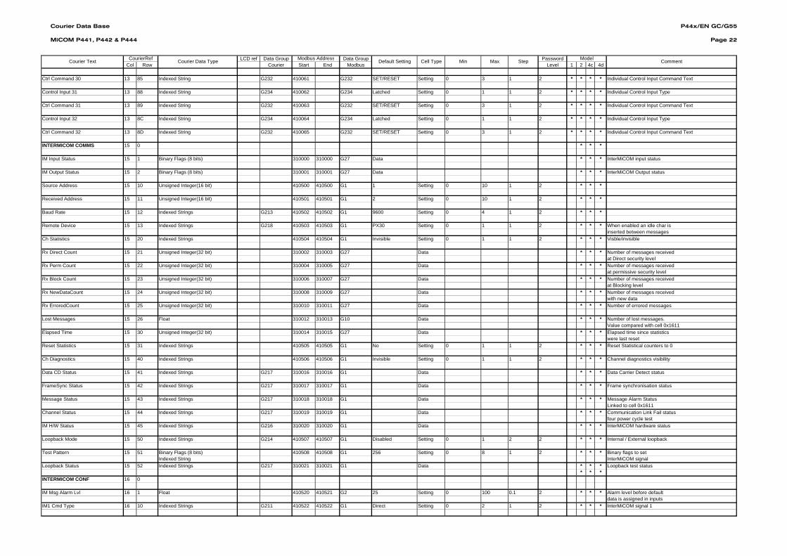
Courier Data Base
MiCOM P441, P442 & P444
P44x/EN GC/G55
Page 22
LCD ref Data Group Data Group PasswordCol Row Courier Start End Modbus Level 1 2 4c 4d
Step Model CommentDefault Setting Cell Type Min MaxCourierRefCourier Text Courier Data Type Modbus Address
Ctrl Command 30 13 85 Indexed String G232 410061 G232 SET/RESET Setting 0 3 1 2 * * * * Individual Control Input Command Text
Control Input 31 13 88 Indexed String G234 410062 G234 Latched Setting 0 1 1 2 * * * * Individual Control Input Type
Ctrl Command 31 13 89 Indexed String G232 410063 G232 SET/RESET Setting 0 3 1 2 * * * * Individual Control Input Command Text
Control Input 32 13 8C Indexed String G234 410064 G234 Latched Setting 0 1 1 2 * * * * Individual Control Input Type
Ctrl Command 32 13 8D Indexed String G232 410065 G232 SET/RESET Setting 0 3 1 2 * * * * Individual Control Input Command Text
INTERMICOM COMMS 15 0 * * *
IM Input Status 15 1 Binary Flags (8 bits) 310000 310000 G27 Data * * * InterMiCOM input status
IM Output Status 15 2 Binary Flags (8 bits) 310001 310001 G27 Data * * * InterMiCOM Output status
Source Address 15 10 Unsigned Integer(16 bit) 410500 410500 G1 1 Setting 0 10 1 2 * * *
Received Address 15 11 Unsigned Integer(16 bit) 410501 410501 G1 2 Setting 0 10 1 2 * * *
Baud Rate 15 12 Indexed Strings G213 410502 410502 G1 9600 Setting 0 4 1 2 * * *
Remote Device 15 13 Indexed Strings G218 410503 410503 G1 PX30 Setting 0 1 1 2 * * * When enabled an idle char isinserted between messages
Ch Statistics 15 20 Indexed Strings 410504 410504 G1 Invisible Setting 0 1 1 2 * * * Visble/invisible
Rx Direct Count 15 21 Unsigned Integer(32 bit) 310002 310003 G27 Data * * * Number of messages receivedat Direct security level
Rx Perm Count 15 22 Unsigned Integer(32 bit) 310004 310005 G27 Data * * * Number of messages receivedat permissive security level
Rx Block Count 15 23 Unsigned Integer(32 bit) 310006 310007 G27 Data * * * Number of messages receivedat Blocking level
Rx NewDataCount 15 24 Unsigned Integer(32 bit) 310008 310009 G27 Data * * * Number of messages receivedwith new data
Rx ErroredCount 15 25 Unsigned Integer(32 bit) 310010 310011 G27 Data * * * Number of errored messages
Lost Messages 15 26 Float 310012 310013 G10 Data * * * Number of lost messages. Value compared with cell 0x1611
Elapsed Time 15 30 Unsigned Integer(32 bit) 310014 310015 G27 Data * * * Elapsed time since statisticswere last reset
Reset Statistics 15 31 Indexed Strings 410505 410505 G1 No Setting 0 1 1 2 * * * Reset Statistical counters to 0
Ch Diagnostics 15 40 Indexed Strings 410506 410506 G1 Invisible Setting 0 1 1 2 * * * Channel diagnostics visibility
Data CD Status 15 41 Indexed Strings G217 310016 310016 G1 Data * * * Data Carrier Detect status
FrameSync Status 15 42 Indexed Strings G217 310017 310017 G1 Data * * * Frame synchronisation status
Message Status 15 43 Indexed Strings G217 310018 310018 G1 Data * * * Message Alarm StatusLinked to cell 0x1611
Channel Status 15 44 Indexed Strings G217 310019 310019 G1 Data * * * Communication Link Fail statusfour power cycle test
IM H/W Status 15 45 Indexed Strings G216 310020 310020 G1 Data * * * InterMiCOM hardware status
Loopback Mode 15 50 Indexed Strings G214 410507 410507 G1 Disabled Setting 0 1 2 2 * * * Internal / External loopback
Test Pattern 15 51 Binary Flags (8 bits) 410508 410508 G1 256 Setting 0 8 1 2 * * * Binary flags to set Indexed String InterMiCOM signal
Loopback Status 15 52 Indexed Strings G217 310021 310021 G1 Data * * * Loopback test status* * *
INTERMICOM CONF 16 0
IM Msg Alarm Lvl 16 1 Float 410520 410521 G2 25 Setting 0 100 0.1 2 * * * Alarm level before default data is assigned in inputs
IM1 Cmd Type 16 10 Indexed Strings G211 410522 410522 G1 Direct Setting 0 2 1 2 * * * InterMiCOM signal 1

Courier Data Base
MiCOM P441, P442 & P444
P44x/EN GC/G55
Page 23
LCD ref Data Group Data Group PasswordCol Row Courier Start End Modbus Level 1 2 4c 4d
Step Model CommentDefault Setting Cell Type Min MaxCourierRefCourier Text Courier Data Type Modbus Address
IM1 FallBackMode 16 11 Indexed Strings G215 410523 410523 G1 Default Setting 0 1 1 2 * * * Latch or Default
IM1 DefaultValue 16 12 Unsigned Integer(16 bit) 410524 410524 G1 0 Setting 0 1 1 2 * * * Assign logic 0 or 1 to InterMiCOM signal
IM1 FrameSyncTim 16 13 Float 410525 410526 G2 1.5 Setting 0.01 1.5 0.01 2 * * *
IM2 Cmd Type 16 18 Indexed Strings G211 410527 410527 G1 Direct Setting 0 2 1 2 * * * InterMiCOM signal 1
IM2 FallBackMode 16 19 Indexed Strings G215 410528 410528 G1 Default Setting 0 1 1 2 * * * Latch or Default
IM2 DefaultValue 16 1A Unsigned Integer(16 bit) 410529 410529 G1 0 Setting 0 1 1 2 * * * Assign logic 0 or 1 to InterMiCOM signal
IM2 FrameSyncTim 16 1B Float 410530 410531 G2 1.5 Setting 0.01 1.5 0.01 2 * * *
IM3 Cmd Type 16 20 Indexed Strings G211 410532 410532 G1 Direct Setting 0 2 1 2 * * * InterMiCOM signal 1
IM3 FallBackMode 16 21 Indexed Strings G215 410533 410533 G1 Default Setting 0 1 1 2 * * * Latch or Default
IM3 DefaultValue 16 22 Unsigned Integer(16 bit) 410534 410534 G1 0 Setting 0 1 1 2 * * * Assign logic 0 or 1 to InterMiCOM signal
IM3 FrameSyncTim 16 23 Float 410535 410536 G2 1.5 Setting 0.01 1.5 0.01 2 * * *
IM4 Cmd Type 16 28 Indexed Strings G211 410537 410537 G1 Direct Setting 0 2 1 2 * * * InterMiCOM signal 1
IM4 FallBackMode 16 29 Indexed Strings G215 410538 410538 G1 Default Setting 0 1 1 2 * * * Latch or Default
IM4 DefaultValue 16 2A Unsigned Integer(16 bit) 410539 410539 G1 0 Setting 0 1 1 2 * * * Assign logic 0 or 1 to InterMiCOM signal
IM4 FrameSyncTim 16 2B Float 410540 410541 G2 1.5 Setting 0.01 1.5 0.01 2 * * *
IM5 Cmd Type 16 30 Indexed Strings G212 410542 410542 G1 Direct Setting 0 2 1 2 * * * InterMiCOM signal 1
IM5 FallBackMode 16 31 Indexed Strings G215 410543 410543 G1 Default Setting 0 1 1 2 * * * Latch or Defaut
IM5 DefaultValue 16 32 Unsigned Integer(16 bit) 410544 410544 G1 0 Setting 0 1 1 2 * * * Assign logic 0 or 1 to InterMiCOM signal
IM5 FrameSyncTim 16 33 Float 410545 410546 G2 1.5 Setting 0.01 1.5 0.01 2 * * *
IM6 Cmd Type 16 38 Indexed Strings G212 410547 410547 G1 Direct Setting 0 2 1 2 * * * InterMiCOM signal 1
IM6 FallBackMode 16 39 Indexed Strings G215 410548 410548 G1 Default Setting 0 1 1 2 * * * Latch or Default
IM6 DefaultValue 16 3A Unsigned Integer(16 bit) 410549 410549 G1 0 Setting 0 1 1 2 * * * Assign logic 0 or 1 to InterMiCOM signal
IM6 FrameSyncTim 16 2B Float 410550 410551 G2 1.5 Setting 0.01 1.5 0.01 2 * * *
IM7 Cmd Type 16 40 Indexed Strings G212 410552 410552 G1 Direct Setting 0 2 1 2 * * * InterMiCOM signal 1
IM7 FallBackMode 16 41 Indexed Strings G215 410553 410553 G1 Default Setting 0 1 1 2 * * * Latch or Default
IM7 DefaultValue 16 42 Unsigned Integer(16 bit) 410554 410554 G1 0 Setting 0 1 1 2 * * * Assign logic 0 or 1 to InterMiCOM signal
IM7 FrameSyncTim 16 43 Float 410555 410556 G2 1.5 Setting 0.01 1.5 0.01 2 * * *
IM8 Cmd Type 16 48 Indexed Strings G212 410557 410557 G1 Direct Setting 0 2 1 2 * * * InterMiCOM signal 1
IM8 FallBackMode 16 49 Indexed Strings G215 410558 410558 G1 Default Setting 0 1 1 2 * * * Latch or Default
IM8 DefaultVa+C358ue 16 4A Unsigned Integer(16 bit) 410559 410559 G1 0 Setting 0 1 1 2 * * * Assign logic 0 or 1 to InterMiCOM signal
IM8 FrameSyncTim 16 4B Float 410560 410561 G2 1.5 Setting 0.01 1.5 0.01 2 * * *
ETHERNET NCIT 18 0 visible if bit6 of model number = A
Physical Link 18 1 Indexed String G300 Electrical Setting 1 2 1 2 * * * *
AntiAlaising Fil 18 2 Indexed String G37 Disabled Setting 0 1 1 2 * * * *
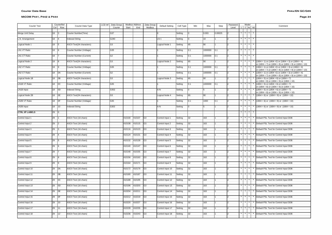
Courier Data Base
MiCOM P441, P442 & P444
P44x/EN GC/G55
Page 24
LCD ref Data Group Data Group PasswordCol Row Courier Start End Modbus Level 1 2 4c 4d
Step Model CommentDefault Setting Cell Type Min MaxCourierRefCourier Text Courier Data Type Modbus Address
Merge Unit Delay 18 3 Courier Number(Time) G37 0 Setting 0 0.003 0.00025 2 * * * *
L.N. Arrangement 18 4 Indexed String G240 LN 1 Setting 0 10 1 2 * * * *
Logical Node 1 18 5 ASCII Text(34 characters) G3 Logical Node 1 Setting 65 90 1 2 * * * *
LN1 VT Ratio 18 6 Courier Number (Voltage) G35 1 Setting 0.1 1000000 0.1 2 * * * *
LN1 CT Ratio 18 7 Courier Number (Current) G2 1 Setting 0.1 1000000 0.1 2 * * * *
Logical Node 2 18 8 ASCII Text(34 characters) G3 Logical Node 2 Setting 65 90 1 2 * * * * (1804 = 1) or (1804 =2) or (1804 = 3) or (1804 = 4) or (1804 = 7) or (1804 = 8) or (1804 = 9) or (1804 = 10)
LN2 VT Ratio 18 9 Courier Number (Voltage) G35 1 Setting 0.1 1000000 0.1 2 * * * * (1804 = 1) or (1804 =2) or (1804 = 3) or (1804 = 4) or (1804 = 7) or (1804 = 8) or (1804 = 9) or (1804 = 10)
LN2 CT Ratio 18 0A Courier Number (Current) G2 1 Setting 0.1 1000000 0.1 2 * * * * (1804 = 1) or (1804 =2) or (1804 = 3) or (1804 = 4) or (1804 = 7) or (1804 = 8) or (1804 = 9) or (1804 = 10)
Logical Node 1B 18 0B ASCII Text(34 characters) G3 Logical Node 3 Setting 65 90 1 2 * * * * (1804 = 5) or (1804 = 6) or (1804 = 7) or (1804 = 8) or (1804 = 9) or (1804 = 10)
LN1B VT Ratio 18 0C Courier Number (Voltage) G35 1 Setting 0.1 1000000 0.1 2 * * * * (1804 = 5) or (1804 = 6) or (1804 = 7) or (1804 = 8) or (1804 = 9) or (1804 = 10)
LN1B Input 18 0D Indexed String G302 A-N Setting 0 5 1 2 * * * * (1804 = 5) or (1804 = 6) or (1804 = 7) or (1804 = 8) or (1804 = 9) or (1804 = 10)
Logical Node 2B 18 0E ASCII Text(34 characters) G3 Logical Node 4 Setting 65 90 1 2 * * * * (1804 = 6) or (1804 = 9) or (1804 = 10)
LN2B VT Ratio 18 0F Courier Number (Voltage) G35 1 Setting 0.1 1000 0.1 2 * * * * (1804 = 6) or (1804 = 9) or (1804 = 10)
LN2B Input 18 10 Indexed String G302 A-N Setting 0 5 1 2 * * * * (1804 = 6) or (1804 = 9) or (1804 = 10)
CTRL I/P LABELS 29 0 * * * *
Control Input 1 29 1 ASCII Text (16 chars) 410100 410107 G3 Control Input 1 Setting 32 163 1 2 * * * * Default PSL Text for Control Input DDB
Control Input 2 29 2 ASCII Text (16 chars) 410108 410115 G3 Control Input 2 Setting 32 163 1 2 * * * * Default PSL Text for Control Input DDB
Control Input 3 29 3 ASCII Text (16 chars) 410116 410123 G3 Control Input 3 Setting 32 163 1 2 * * * * Default PSL Text for Control Input DDB
Control Input 4 29 4 ASCII Text (16 chars) 410124 410131 G3 Control Input 4 Setting 32 163 1 2 * * * * Default PSL Text for Control Input DDB
Control Input 5 29 5 ASCII Text (16 chars) 410132 410139 G3 Control Input 5 Setting 32 163 1 2 * * * * Default PSL Text for Control Input DDB
Control Input 6 29 6 ASCII Text (16 chars) 410140 410147 G3 Control Input 6 Setting 32 163 1 2 * * * * Default PSL Text for Control Input DDB
Control Input 7 29 7 ASCII Text (16 chars) 410148 410155 G3 Control Input 7 Setting 32 163 1 2 * * * * Default PSL Text for Control Input DDB
Control Input 8 29 8 ASCII Text (16 chars) 410156 410163 G3 Control Input 8 Setting 32 163 1 2 * * * * Default PSL Text for Control Input DDB
Control Input 9 29 9 ASCII Text (16 chars) 410164 410171 G3 Control Input 9 Setting 32 163 1 2 * * * * Default PSL Text for Control Input DDB
Control Input 10 29 0A ASCII Text (16 chars) 410172 410179 G3 Control Input 10 Setting 32 163 1 2 * * * * Default PSL Text for Control Input DDB
Control Input 11 29 0B ASCII Text (16 chars) 410180 410187 G3 Control Input 11 Setting 32 163 1 2 * * * * Default PSL Text for Control Input DDB
Control Input 12 29 0C ASCII Text (16 chars) 410188 410195 G3 Control Input 12 Setting 32 163 1 2 * * * * Default PSL Text for Control Input DDB
Control Input 13 29 0D ASCII Text (16 chars) 410196 410203 G3 Control Input 13 Setting 32 163 1 2 * * * * Default PSL Text for Control Input DDB
Control Input 14 29 0E ASCII Text (16 chars) 410204 410211 G3 Control Input 14 Setting 32 163 1 2 * * * * Default PSL Text for Control Input DDB
Control Input 15 29 0F ASCII Text (16 chars) 410212 410219 G3 Control Input 15 Setting 32 163 1 2 * * * * Default PSL Text for Control Input DDB
Control Input 16 29 10 ASCII Text (16 chars) 410220 410227 G3 Control Input 16 Setting 32 163 1 2 * * * * Default PSL Text for Control Input DDB
Control Input 17 29 11 ASCII Text (16 chars) 410228 410235 G3 Control Input 17 Setting 32 163 1 2 * * * * Default PSL Text for Control Input DDB
Control Input 18 29 12 ASCII Text (16 chars) 410236 410243 G3 Control Input 18 Setting 32 163 1 2 * * * * Default PSL Text for Control Input DDB

Courier Data Base
MiCOM P441, P442 & P444
P44x/EN GC/G55
Page 25
LCD ref Data Group Data Group PasswordCol Row Courier Start End Modbus Level 1 2 4c 4d
Step Model CommentDefault Setting Cell Type Min MaxCourierRefCourier Text Courier Data Type Modbus Address
Control Input 19 29 13 ASCII Text (16 chars) 410244 410251 G3 Control Input 19 Setting 32 163 1 2 * * * * Default PSL Text for Control Input DDB
Control Input 20 29 14 ASCII Text (16 chars) 410252 410259 G3 Control Input 20 Setting 32 163 1 2 * * * * Default PSL Text for Control Input DDB
Control Input 21 29 15 ASCII Text (16 chars) 410260 410267 G3 Control Input 21 Setting 32 163 1 2 * * * * Default PSL Text for Control Input DDB
Control Input 22 29 16 ASCII Text (16 chars) 410268 410275 G3 Control Input 22 Setting 32 163 1 2 * * * * Default PSL Text for Control Input DDB
Control Input 23 29 17 ASCII Text (16 chars) 410276 410283 G3 Control Input 23 Setting 32 163 1 2 * * * * Default PSL Text for Control Input DDB
Control Input 24 29 18 ASCII Text (16 chars) 410284 410291 G3 Control Input 24 Setting 32 163 1 2 * * * * Default PSL Text for Control Input DDB
Control Input 25 29 19 ASCII Text (16 chars) 410292 410299 G3 Control Input 25 Setting 32 163 1 2 * * * * Default PSL Text for Control Input DDB
Control Input 26 29 1A ASCII Text (16 chars) 410300 410307 G3 Control Input 26 Setting 32 163 1 2 * * * * Default PSL Text for Control Input DDB
Control Input 27 29 1B ASCII Text (16 chars) 410308 410315 G3 Control Input 27 Setting 32 163 1 2 * * * * Default PSL Text for Control Input DDB
Control Input 28 29 1C ASCII Text (16 chars) 410316 410323 G3 Control Input 28 Setting 32 163 1 2 * * * * Default PSL Text for Control Input DDB
Control Input 29 29 1D ASCII Text (16 chars) 410324 410331 G3 Control Input 29 Setting 32 163 1 2 * * * * Default PSL Text for Control Input DDB
Control Input 30 29 1E ASCII Text (16 chars) 410332 410339 G3 Control Input 30 Setting 32 163 1 2 * * * * Default PSL Text for Control Input DDB
Control Input 31 29 1F ASCII Text (16 chars) 410340 410347 G3 Control Input 31 Setting 32 163 1 2 * * * * Default PSL Text for Control Input DDB
Control Input 32 29 20 ASCII Text (16 chars) 410348 410355 G3 Control Input 32 Setting 32 163 1 2 * * * * Default PSL Text for Control Input DDB
GROUP 1PROTECTION SETTINGSGROUP 1 30 00 * * * *DISTANCE ELEMENTS Line Setting 30 1 (Sub Heading) * * * *
Line Length 30 2 Courier Number (metres) 41000 41001 G35 100000 Setting 300 1000000 10 2 * * * * Length in Km
Line Length 30 3 Courier Number (miles) 41002 41003 G35 62 Setting 0.2 625 0.005 2 * * * * Setting strored in Km, displayed using miles
Line Impedance 30 4 Courier Number(Ohms) 41004 41005 G35 12 Setting 0.001*V1/I1 500*V1/I1 0.001*V1/I1 2 * * * * Positive Sequence Impedance
Line Angle 30 5 Courier Number (Angle) 41006 41006 G2 70 Setting -90 90 0.1 2 * * * * Positive Sequence Angle
Zone Setting 30 6 (Sub Heading) * * * *
Zone Status 30 7 Binary Flag G120 G120 000011110 Setting 0 31 1 2 * * * *
(8 bits) kZ1 Res Comp 30 8 Courier Number 41007 41007 G2 1 Setting 0 7 0.001 2 * * * *
kZ1 Angle 30 9 Courier Number (Angle) 41008 41008 G2 0 Setting -180 180 0.1 2 * * * *
Z1 30 0A Courier Number(Ohm) 41009 41010 G35 10 Setting 0.001*V1/I1 500*V1/I1 0.001*V1/I1 2 * * * *
Z1X 30 0B Courier Number(Ohms) 41011 41012 G35 15 Setting 0.001*V1/I1 500*V1/I1 0.001*V1/I1 2 * * * * (3007 AND 000001b) > 0
R1G 30 0C Courier Number(Ohms) 41013 41013 G2 10 Setting 0 400*V1/I1 0.01*V1/I1 2 * * * *
R1Ph 30 0D Courier Number(Ohms) 41014 41014 G2 10 Setting 0 400*V1/I1 0.01*V1/I1 2 * * * *
tZ1 30 0E Courier Number(Time) 41015 41015 G2 0 Setting 0 10 0.002 2 * * * *
kZ2 Res Comp 30 0F Courier Number 41016 41016 G2 1 Setting 0 7 0.001 2 * * * * (3007 AND 000010b) > 0
kZ2 Angle 30 10 Courier Number (Angle) 41017 41017 G2 0 Setting -180 180 0.1 2 * * * * (3007 AND 000010b) > 0
Z2 30 11 Courier Number(Ohms) 41018 41019 G35 20 Setting 0.001*V1/I1 500*V1/I1 0.001*V1/I1 2 * * * * (3007 AND 000010b) > 0
R2G 30 12 Courier Number(Ohms) 41020 41020 G2 20 Setting 0 400*V1/I1 0.01*V1/I1 2 * * * * (3007 AND 000010b) > 0

Courier Data Base
MiCOM P441, P442 & P444
P44x/EN GC/G55
Page 26
LCD ref Data Group Data Group PasswordCol Row Courier Start End Modbus Level 1 2 4c 4d
Step Model CommentDefault Setting Cell Type Min MaxCourierRefCourier Text Courier Data Type Modbus Address
R2Ph 30 13 Courier Number(Ohms) 41021 41021 G2 20 Setting 0 400*V1/I1 0.01*V1/I1 2 * * * * (3007 AND 000010b) > 0
tZ2 30 14 Courier Number(Time) 41022 41022 G2 0.2 Setting 0 10 0.01 2 * * * * (3007 AND 000010b) > 0
kZ3/4 Res Comp 30 15 Courier Number 41023 41023 G2 1 Setting 0 7 0.001 2 * * * * (3007 AND 001000b) > 0
kZ3/4 Angle 30 16 Courier Number (Angle) 41024 41024 G2 0 Setting -180 180 0.1 2 * * * * (3007 AND 001000b) > 0
Z3 30 17 Courier Number(Ohms) 41025 41026 G35 30 Setting 0.001*V1/I1 500*V1/I1 0.001*V1/I1 2 * * * * (3007 AND 001000b) > 0
R3G - R4G 30 18 Courier Number(Ohms) 41027 41027 G2 30 Setting 0 400*V1/I1 0.01*V1/I1 2 * * * * (3007 AND 001000b) > 0
R3Ph - R4Ph 30 19 Courier Number(Ohms) 41028 41028 G2 30 Setting 0 400*V1/I1 0.01*V1/I1 2 * * * * (3007 AND 001000b) > 0
tZ3 30 1A Courier Number(Time) 41029 41029 G2 0.6 Setting 0 10 0.01 2 * * * * (3007 AND 001000b) > 0
Z4 30 1B Courier Number(Ohms) 41030 41031 G35 40 Setting 0.001*V1/I1 500*V1/I1 0.001*V1/I1 2 * * * * (3007 AND 010000b) > 0
tZ4 30 1C Courier Number(Time) 41032 41032 G2 1 Setting 0 10 0.01 2 * * * * (3007 AND 010000b) > 0
Zone P - Direct. 30 1D Indexed String 41033 41033 G123 Directional Fwd Setting 0 1 1 2 * * * * ((3007 AND 010100b) > 0) and (301D = 1))
or ((3007 AND 000100b) > 0) and (301D = 0))kZp Res Comp 30 1E Courier Number 41034 41034 G2 1 Setting 0 7 0.001 2 * * * * ((3007 AND 010100b) > 0) and (301D = 1))
or ((3007 AND 000100b) > 0) and (301D = 0))kZp Angle 30 1F Courier Number (Angle) 41035 41035 G2 0 Setting -180 180 0.1 2 * * * * ((3007 AND 010100b) > 0) and (301D = 1))
or ((3007 AND 000100b) > 0) and (301D = 0))Zp 30 20 Courier Number(Ohms) 41036 41037 G35 25 Setting 0.001*V1/I1 500*V1/I1 0.001*V1/I1 2 * * * * ((3007 AND 010100b) > 0) and (301D = 1))
or ((3007 AND 000100b) > 0) and (301D = 0))RpG 30 21 Courier Number(Ohms) 41038 41038 G2 25 Setting 0 400*V1/I1 0.01*V1/I1 2 * * * * ((3007 AND 010100b) > 0) and (301D = 1))
or ((3007 AND 001100b) > 0) and (301D = 0))RpPh 30 22 Courier Number(Ohms) 41039 41039 G2 25 Setting 0 400*V1/I1 0.01*V1/I1 2 * * * * ((3007 AND 010100b) > 0) and (301D = 1))
or ((3007 AND 001100b) > 0) and (301D = 0))tZp 30 23 Courier Number(Time) 41040 41040 G2 0.4 Setting 0 10 0.01 2 * * * * ((3007 AND 010100b) > 0) and (301D = 1))
or ((3007 AND 000100b) > 0) and (301D = 0))Serial Comp Line 30 24 Indexed String 41041 41041 G37 Disableb Setting 0 1 1 2 * * * *
Zone Overlap Mode 30 25 Indexed String 41042 41042 G37 Disableb Setting 0 1 1 2 * * * *
Z1m Tilt Angle 30 26 Courier Number (Angle) 41043 41043 G2 0 Setting -45 45 1 2 * * * * (3007 AND 001010b) > 0) or ((3007 AND 000100b) > 0)
and (301D = 0))Z1p Tilt Angle 30 27 Courier Number (Angle) 41044 41044 G2 0 Setting -45 45 1 2 * * * * (3007 AND 001010b) > 0)
or ((3007 AND 000100b) > 0) and (301D = 0))Z2/Zp Tilt Angle 30 28 Courier Number (Angle) 41046 41046 G2 0 Setting -45 45 1 2 * * * * (((3007 AND 000100b) > 0) AND (301D = 0))
OR (3007 AND 001000b) > 0) AND (3007 AND 000010b)) OR (((3007 AND 000100b) > 0)
AND (301D = 0)) AND (3007 AND 001000b) > 0)Fwd Zone Chg Del 30 29 Courier Number(Time) 41045 41045 G2 0.03 Setting 0 0.1 0.01 2 * * * * (3007 AND 001010b) > 0) or ((3007 AND 000100b) > 0)
and (301D = 0))Fault Locator 30 2A (Sub Heading) * * * *
kZm Mutual Comp 30 2B Courier Number 41047 41047 G2 0 Setting 0 7 0.01 2 * * * *
kZm Angle 30 2C Courier Number (Angle) 41048 41048 G2 0 Setting -180 180 0.1 2 * * * *
DISTANCE ELEMENTS GROUP 1 31 00 * * * *DISTANCE SCHEMES Program Mode 31 1 Indexed String G106 41050 41050 G106 Standard Scheme Setting 0 1 1 2 * * * *
Standard Mode 31 2 Indexed String G107 41051 41051 G107 Basic + Z1X Setting 0 6 1 2 * * * *
Fault Type 31 3 Indexed String G115 41052 41052 G115 Both Enabled Setting 0 2 1 2 * * * *
Trip Mode 31 4 Indexed String G114 41053 41053 G114 Force 3 Poles Trip Setting 0 2 1 2 * * * Trip mode for the distance protection
Sig. Send Zone 31 5 Indexed String G108 41054 41054 G108 None Setting 0 3 1 2 * * * * Signal Send Zone

Courier Data Base
MiCOM P441, P442 & P444
P44x/EN GC/G55
Page 27
LCD ref Data Group Data Group PasswordCol Row Courier Start End Modbus Level 1 2 4c 4d
Step Model CommentDefault Setting Cell Type Min MaxCourierRefCourier Text Courier Data Type Modbus Address
DistCR 31 6 Indexed String G109 41055 41055 G109 None Setting 0 5 1 2 * * * * Type of Scheme on signal Recieve
Tp 31 7 Courier Number(Time) 41056 41056 G2 0.02 Setting 0 1 0.002 2 * * * * (((3102 = 5) OR (3102 = 6)) AND (3101 = 0))
OR (((3106 = 4) OR (3106 = 5)) AND (3101 = 1)) tReversal Guard 31 8 Courier Number(Time) 41057 41057 G2 0.02 Setting 0 0.15 0.002 2 * * * * OR (3901 = 1 AND 3906 = 1)Time Delay Reversal Guard
Unblocking Logic 31 9 Indexed String G113 41058 41058 G113 None Setting 0 2 1 * * * * Type of TAC Receive
TOR-SOTF Mode 31 0A Binary Flags (16bits) G118 41059 41059 G118 48 Setting 0 8192 1 2 * * * *
SOFT Delay 31 0B Courier Number(Time) 41060 41060 G2 110 Setting 10 3600 1 2 * * * *
Z1Ext On Chan.Fail 31 0C Indexed String G37 41061 41061 G37 Disabled Setting 0 1 1 2 * * * *
Weak Infeed 31 0D (Sub Heading) * * * *
WI :Mode Status 31 0E Indexed String G116 41062 41062 G116 Disabled Setting 0 3 1 2 * * * *
WI : Single Pole Trip 31 0F Indexed String G37 41063 41063 G37 Disabled Setting 0 1 1 2 * * *
WI : V< Thres. 31 10 Courier Number (Voltage) 41064 41064 G2 45 Setting 10 70 5 2 * * * *
WI : Trip Time Delay 31 11 Courier Number (Time) 41065 41065 G2 0.06 Setting 0 1 0.002 2 * * * *
PAP : TeleTrip Enable 31 12 Indexed String G37 41066 41066 G37 Disabled Setting 0 1 1 2 * * * *
PAP : Trip Delayed Enable 31 13 Indexed String G37 41067 41067 G37 Disabled Setting 0 1 1 2 * * * *
PAP : P1 31 14 Indexed String G37 41068 41068 G37 Disabled Setting 0 1 1 2 * * *
PAP : 1P Trip Time Delay 31 15 Courier Number (Time) 41069 41069 G2 0.5 Setting 0.1 1.5 0.1 2 * * *
PAP : P2 31 16 Indexed String G37 41070 41070 G37 Disabled Setting 0 1 1 2 * * * *
PAP : P3 31 17 Indexed String G37 41071 41071 G37 Disabled Setting 0 1 1 2 * * * *
PAP : 3P Trip Delay 31 18 Courier Number (Time) 41072 41072 G2 2 Setting 1 12 0.1 2 * * * *
PAP : Residual Current 31 19 Courier Number (Current) 41073 41073 G2 0.5*I1 Setting 0.1*I1 1*I1 0.01*I1 2 * * * * (3112=1) OR (3113=1)
PAP : K 31 1A Courier Number 41074 41074 G2 0.5 Setting 0.5 1 0.05 2 * * * * (3112=1) OR (3113=1)
Loss Of Load 31 1B (Sub Heading) * * * *
LoL: Mode Status 31 1C Indexed String G37 41075 41075 G37 Disabled Setting 0 1 1 2 * * * *
LoL. Chan. Fail 31 1D Indexed String G37 41076 41076 G37 Disabled Setting 0 1 1 2 * * * *
LoL: I< 31 1E Courier Number (Current) 41077 41077 G2 0.5 Setting 0.05*I1 1*I1 0.05*I1 2 * * * *
LoL: Window 31 1F Courier Number (Time) 41078 41078 G2 0.04 Setting 0.01 0.1 0.01 2 * * * *DISTANCE SCHEMESGROUP 1 32 00 * * * *POWER-SWING DR 32 1 Courier Number (Ohms) 41150 41150 G2 0.5 Setting 0 400*V1/I1 0.01*V1/I1 2 * * * *
DX 32 2 Courier Number (Ohms) 41151 41151 G2 0.5 Setting 0 400*V1/I1 0.01*V1/I1 2 * * * *
IN > Status 32 3 Indexed String G37 41152 41152 G37 Enabled Setting 0 1 1 2 * * * *
IN > (% Imax) 32 4 Courier Number (%) 41153 41153 G2 40 Setting 10 100 1 2 * * * *
I2 > Status 32 5 Indexed String G37 41154 41154 G37 Enabled Setting 0 1 1 2 * * * *
I2 > (% Imax) 32 6 Courier Number (%) 41155 41155 G2 30 Setting 10 100 1 2 * * * *

Courier Data Base
MiCOM P441, P442 & P444
P44x/EN GC/G55
Page 28
LCD ref Data Group Data Group PasswordCol Row Courier Start End Modbus Level 1 2 4c 4d
Step Model CommentDefault Setting Cell Type Min MaxCourierRefCourier Text Courier Data Type Modbus Address
Imax Line > Status 32 7 Indexed String G37 41156 41156 G37 Enabled Setting 0 1 1 2 * * * *
Imax Line > 32 8 Courier Number (Current) 41157 41157 G2 3 Setting 1*I1 20*I1 0.01*I1 2 * * * *
Delta I Status 32 9 Indexed String G37 41158 41158 G37 Enabled Setting 0 1 1 2 * * * *
Unblocking Time-Delay 32 0A Courier Number (Time) 41159 41159 G2 30 Setting 0 30 0.1 2 * * * *
Blocking Zones 32 0B Binary Flag(8 bits) G119 41160 41160 G119 0 Setting 0 15 1 2 * * * *Indexed String
Out of Step 32 0C Unisgned Integer (16 bits) 41161 41161 1 Setting 1 255 1 2 * * * *
Stable Swing 32 0D Unisgned Integer (16 bits) 41162 41162 1 Setting 1 255 1 2 * * * *
POWER-SWINGGROUP 1 35 00 * * * *BACK-UP I> I>1 Function 35 1 Indexed String G43 41250 41250 G43 DT Setting 0 10 1 2 * * * *
I>1 Directional 35 2 Indexed String G44 41251 41251 G44 Directional Fwd Setting 0 2 1 2 * * * *
I>1 VTS Block 35 3 Indexed String G45 41252 41252 G45 Non-Directional Setting 0 1 1 2 * * * *
I>1 Current Set 35 4 Courier Number (Current) 41253 41253 G2 1.5 Setting 0.08*I1 4.0*I1 0.01*I1 2 * * * *
I>1 Time Delay 35 5 Courier Number (Time) 41254 41254 G2 1 Setting 0 100 0.01 2 * * * *
I>1 Time Delay VTS 35 6 Courier Number (Time) 41255 41255 G2 0.2 Setting 0 100 0.01 2 * * * * 3501 <> 0 AND 3502<>0 AND 3503 = 1
I>1 TMS 35 7 Courier Number (Decimal) 41256 41256 G2 1 Setting 0.025 1.2 0.025 2 * * * * 5>=3501>=2
I>1 Time Dial 35 8 Courier Number (Decimal) 41257 41257 G2 7 Setting 0.5 15 0.1 2 * * * *
I>1 Reset Char 35 9 Indexed String G60 41258 41258 G60 DT Setting 0 1 1 2 * * * *
I>1 tRESET 35 0A Courier Number (Time) 41259 41259 G2 0 Setting 0 100 0.01 2 * * * * 5>=3501>=1 OR (3509=0 AND 3501 >=6)
I>2 Function 35 0B Indexed String G43 41260 41260 G43 DT Setting 0 10 1 2 * * * *
I>2 Directional 35 0C Indexed String G44 41261 41261 G44 Non-Directional Setting 0 2 1 2 * * * *
I>2 VTS Block 35 0D Indexed String G45 41262 41262 G45 Non-Directional Setting 0 1 1 2 * * * *
I>2 Current Set 35 0E Courier Number (Current) 41263 41263 G2 2 Setting 0.08*I1 4.0*I1 0.01*I1 2 * * * *
I>2 Time Delay 35 0F Courier Number (Time) 41264 41264 G2 2 Setting 0 100 0.01 2 * * * *
I>2 Time Delay VTS 35 10 Courier Number (Time) 41265 41265 G2 2 Setting 0 100 0.01 2 * * * * 350B <> 0 AND 350C<>0 AND 350D = 1
I>2 TMS 35 11 Courier Number (Decimal) 41266 41266 G2 1 Setting 0.025 1.2 0.025 2 * * * * 5>=350B>=2
I>2 Time Dial 35 12 Courier Number (Decimal) 41267 41267 G2 7 Setting 0.5 15 0.1 2 * * * *
I>2 Reset Char 35 13 Indexed String G60 41268 41268 G60 DT Setting 0 1 1 2 * * * *
I>2 tRESET 35 14 Courier Number (Time) 41269 41269 G2 0 Setting 0 100 0.01 2 * * * * 5>=350B>=1 OR (3513=0 AND 350B >=6)
I>3 Status 35 15 Indexed String G37 41270 41270 G37 Enabled Setting 0 1 1 2 * * * *
I>3 Current Set 35 16 Courier Number (Current) 41271 41271 G2 3 Setting 0.08*I1 32*I1 0.01*I1 2 * * * *
I>3 Time Delay 35 17 Courier Number (Time) 41272 41272 G2 3 Setting 0 100 0.01 2 * * * *
I>4 Status 35 18 Indexed String G37 41273 41273 G37 Disabled Setting 0 1 1 2 * * * *
I>4 Current Set 35 19 Courier Number (Current) 41274 41274 G2 4 Setting 0.08*I1 32*I1 0.01*I1 2 * * * *

Courier Data Base
MiCOM P441, P442 & P444
P44x/EN GC/G55
Page 29
LCD ref Data Group Data Group PasswordCol Row Courier Start End Modbus Level 1 2 4c 4d
Step Model CommentDefault Setting Cell Type Min MaxCourierRefCourier Text Courier Data Type Modbus Address
I>4 Time Delay 35 1A Courier Number (Time) 41275 41275 G2 4 Setting 0 100 0.01 2 * * * *
BACK-UP I>GROUP 1 36 00 * * * *NEG SEQUENCE O/C I2> Status 36 1 Indexed String G37 41300 41300 G37 Enabled Setting 0 1 1 2 * * * *
I2> Directional 36 2 Indexed String G44 41301 41301 G44 Non-Directional Setting 0 2 1 2 * * * *
I2> VTS 36 3 Indexed String G45 41302 41302 G45 Non-Directional Setting 0 1 1 2 * * * *
I2> Current Set 36 4 Courier Number (Current) 41303 41303 G2 0.2 Setting 0.08*I1 4*I1 0.01*I1 2 * * * *
I2> Time Delay 36 5 Courier Number (Time) 41304 41304 G2 10 Setting 0 100 0.01 2 * * * *
I2> Char Angle 36 6 Courier Number (Angle) 41305 41305 G2 -45 Setting -95 95 1 2 * * * *
NEG SEQUENCE O/CGROUP 1 37 00 * * * *BROKEN CONDUCTOR Broken Conductor 37 1 Indexed String G37 41350 41350 G37 Enabled Setting 0 1 1 2 * * * *
I2/I1 Setting 37 2 Courier Number (Decimal) 41351 41351 G2 0.2 Setting 0.2 1 0.01 2 * * * *
I2/I1 Time Delay 37 3 Courier Number (Time) 41352 41352 G2 60 Setting 0 100 0.1 2 * * * *
I2/I1 Trip 37 4 Indexed String 41353 G37 Disabled Setting 0 1 1 2 * * * *
BROKEN CONDUCTORGROUP 1 38 00 * * * *EARTH FAULT O/C IN>1 Function 38 1 Indexed String G43 41400 41400 G43 DT Setting 0 10 1 2 * * * * I>2 Overcurrent Status
IN>1 Directional 38 2 Indexed String G44 41401 41401 G44 Directional Fwd Setting 0 2 1 2 * * * *
IN>1 VTS Block 38 3 Indexed String G45 41402 41402 G45 Non-Directional Setting 0 1 1 2 * * * *
IN>1 Current Set 38 4 Courier Number (Current) 41403 41403 G2 0.2 Setting 0.08*I1 4.0*I1 0.01*I1 2 * * * *
Change scaling factorIN>1 Time Delay 38 5 Courier Number (Time) 41404 41404 G2 1 Setting 0 200 0.01 2 * * * *
IN>1 Time Delay VTS 38 6 Courier Number (Time) 41405 41405 G2 0.2 Setting 0 200 0.01 2 * * * * 3801<>0 AND 3802<>0 AND 3803=1
IN>1 TMS 38 7 Courier Number (Decimal) 41406 41406 G2 1 Setting 0.025 1.2 0.025 2 * * * * 5>=3801>=2
IN>1 Time Dial 38 8 Courier Number (Decimal) 41407 41407 G2 7 Setting 0.5 15 0.1 2 * * * *
IN>1 Reset Char 38 9 Indexed String G60 41408 41408 G60 DT Setting 0 1 1 2 * * * *
IN>1 tRESET 38 0A Courier Number (Time) 41409 41409 G2 0 Setting 0 100 0.01 2 * * * * 5>=3801>=1 OR (3809=0 AND 3801>=6)
IN>2 Status 38 0B Indexed String G37 41410 41410 G37 Enabled Setting 0 1 1 2 * * * *
IN>2 Directional 38 0C Indexed String G44 41411 41411 G44 Non-Directional Setting 0 2 1 2 * * * *
IN>2 VTS Block 38 0D Indexed String G45 41412 41412 G45 Non-Directional Setting 0 1 1 2 * * * *
IN>2 Current Set 38 0E Courier Number (Current) 41413 41413 G2 0.3 Setting 0.08*I1 32*I1 0.01*I1 2 * * * *
IN>2 Time Delay 38 0F Courier Number (Time) 41414 41414 G2 2 Setting 0 200 0.01 2 * * * *
IN>2 Time Delay VTS 38 10 Courier Number (Time) 41415 41415 G2 2 Setting 0 200 0.01 2 * * * * 380B<>0 AND 380D=1
IN>3 Status 38 11 Indexed String G37 41416 41416 G37 Enabled Setting 0 1 1 2 * * * *
IN>3 Directional 38 12 Indexed String G44 41417 41417 G44 Non-Directional Setting 0 2 1 2 * * * *

Courier Data Base
MiCOM P441, P442 & P444
P44x/EN GC/G55
Page 30
LCD ref Data Group Data Group PasswordCol Row Courier Start End Modbus Level 1 2 4c 4d
Step Model CommentDefault Setting Cell Type Min MaxCourierRefCourier Text Courier Data Type Modbus Address
IN>3 VTS Block 38 13 Indexed String G45 41418 41418 G45 Non-Directional Setting 0 1 1 2 * * * *
IN>3 Current Set 38 14 Courier Number (Current) 41419 41419 G2 0.3 Setting 0.08*I1 32*I1 0.01*I1 2 * * * *
IN>3 Time Delay 38 15 Courier Number (Time) 41420 41420 G2 2 Setting 0 200 0.01 2 * * * *
IN>3 Time Delay VTS 38 16 Courier Number (Time) 41421 41421 G2 2 Setting 0 200 0.01 2 * * * * 3811<>0 AND 3813=1
IN>4 Status 38 17 Indexed String G37 41422 41422 G37 Enabled Setting 0 1 1 2 * * * *
IN>4 Directional 38 18 Indexed String G44 41423 41423 G44 Non-Directional Setting 0 2 1 2 * * * *
IN>4 VTS Block 38 19 Indexed String G45 41424 41424 G45 Non-Directional Setting 0 1 1 2 * * * *
IN>4 Current Set 38 1A Courier Number (Current) 41425 41425 G2 0.3 Setting 0.08*I1 32*I1 0.01*I1 2 * * * *
IN>4 Time Delay 38 1B Courier Number (Time) 41426 41426 G2 2 Setting 0 200 0.01 2 * * * *
IN>4 Time Delay VTS 38 1C Courier Number (Time) 41427 41427 G2 2 Setting 0 200 0.01 2 * * * * 3817<>0 AND 3819=1
IN> Directional 38 1D (Sub Heading) 2 3802 >0 OR 380C > 0 OR 3812 > 0 OR 3818
IN> Char Angle 38 1E Courier Number(Angle) 41428 41428 G2 -45 Setting -95 95 1 2 * * * * 3802 >0 0R 380C > 0 OR 3812 > 0 OR 3818 > 0
Polarisation 38 1F Indexed String G46 41429 41429 G46 Zero Sequence Setting 0 1 1 2 * * * * 3802 > 0 0R 380C > 0 OR 3812 > 0 OR 3818 > 0
EARTH FAULT O/CGROUP 1 39 00AIDED DEF * * * *Channel Aided DEF Status 39 1 Indexed String G37 41450 41450 G37 Enabled Setting 0 1 1 2 * * * *
Polarisation 39 2 Indexed String G46 41451 41451 G46 Zero Sequence Setting 0 1 1 2 * * * *
V> Voltage Set 39 3 Courier Number (Voltage) 41452 41452 G2 1 Setting 0.5 20 0.01 2 * * * *
IN Forward 39 4 Courier Number (Current) 41453 41453 G2 0.1 Setting 0.05*I1 4*I1 0.01*I1 2 * * * *
Time Delay 39 5 Courier Number (Time) 41454 41454 G2 0 Setting 0 10 0.002 2 * * * *
Scheme Logic 39 6 Indexed String 41455 41455 G112 Shared Setting 0 2 1 2 * * * *
Tripping 39 7 Indexed String 41456 41456 G48 Three Phase Setting 0 1 1 2 * * *
Tp 39 8 Courier Number(Time) 41457 41457 G2 0.02 Setting 0 1 0.002 2 * * * *
IN Rev Factor 39 9 Courier Number() 41458 41458 G2 0.6 Setting 0.1 1 0.1 2 * * * *
AIDED DEFGROUP 1 3A 0 * * * *THERMAL OVERLOADCharacteristic 3A 1 Indexed String G67 41500 G67 Single Setting 0 1 2 2 * * * *
Thermal Trip 3A 2 Courier Number (current) 41501 41501 G2 1 Setting 0.08*I1 3.2*I1 0.01*I1 2 * * * *
Thermal Alarm 3A 3 Courier Number (percentage) 41502 41502 G2 70 Setting 50 100 1 2 * * * *
Time Constant 1 3A 4 Courier Number (time-minutes) 41503 41503 G2 10 Setting 1 200 1 2 * * * *
Time Constant 2 3A 5 Courier Number (time-minutes) 41504 41504 G2 5 Setting 1 200 1 2 * * * *
THERMAL OVERLOADGROUP 1 3C 00 * * * *ZERO SEQ. POWER Zero Seq. Power Status 1 Indexed String G37 41600 41600 G37 Enabled Setting 0 1 1 2 * * * *
K Time Delay Factor 2 Courier Number (Time) 41601 41601 G2 0 Setting 0 2 0.2 2 * * * *

Courier Data Base
MiCOM P441, P442 & P444
P44x/EN GC/G55
Page 31
LCD ref Data Group Data Group PasswordCol Row Courier Start End Modbus Level 1 2 4c 4d
Step Model CommentDefault Setting Cell Type Min MaxCourierRefCourier Text Courier Data Type Modbus Address
Basis Time Delay 3 Courier Number (Time) 41602 41602 G2 1 Setting 0 10 0.01 2 * * * *
Residual Current 4 Courier Number (Current) 41603 41603 G2 0.1 Setting 0.05*I1 1*I1 0.01 2 * * * *
Residual Power 5 Courier Number (Power) 41604 41604 G2 0.5 Setting 0.3*I1*V1 6*I1*V1 0.01*I1*V1 2 * * * *
ZERO SEQ. POWERGROUP1 42 00 * * * *VOLT PROTECTION V< & V> MODE 42 1 Binary Flags (8bits) G121 41949 41949 G121 0 Setting 0 15 1 2 * * * * 4204 <> 0 OR 4208 <> 0 OR 420D <> 0 OR 4211 <> 0
UNDER VOLTAGE 42 2 (Sub Heading)
V< Measur't Mode 42 3 Indexed String G47 41950 41950 G47 Phase-Neutral Setting 0 1 1 2 * * * *
V<1 Function 42 4 Indexed String G23 41951 41951 G23 DT Setting 0 2 1 2 * * * *
V<1 Voltage Set 42 5 Courier Number (Voltage) 41952 41952 G2 50 Setting 10 120 1 2 * * * * Range covers Ph-N & Ph-Ph
V<1 Time Delay 42 6 Courier Number (Time) 41953 41953 G2 10 Setting 0 100 0.01 2 * * * *
V<1 TMS 42 7 Courier Number (Decimal) 41954 41954 G2 1 Setting 0.5 100 0.5 2 * * * *
V<2 Status 42 8 Indexed String G37 41955 41955 G37 Disabled Setting 0 1 1 2 * * * *
V<2 Voltage Set 42 9 Courier Number (Voltage) 41956 41956 G2 38 Setting 10 120 1 2 * * * * Phase-Neutral
V<2 Time Delay 42 0A Courier Number (Time) 41957 41957 G2 5 Setting 0 100 0.01 2 * * * *
OVERVOLTAGE 42 0B (Sub Heading)
V> Measur't Mode 42 0C Indexed String G47 41958 41958 G47 Phase-Neutral Setting 0 1 1 2 * * * *
V>1 Function 42 0D Indexed String G23 41959 41959 G23 DT Setting 0 2 1 2 * * * *
V>1 Voltage Set 42 0E Courier Number (Voltage) 41960 41960 G2 75 Setting 60 185 1 2 * * * *
V>1 Time Delay 42 0F Courier Number (Time) 41961 41961 G2 10 Setting 0 100 0.01 2 * * * *
V>1 TMS 42 10 Courier Number (Decimal) 41962 41962 G2 1 Setting 0.5 100 0.5 2 * * * *
V>2 Status 42 11 Indexed String G37 41963 41963 G37 Enabled Setting 0 1 1 2 * * * *
V>2 Voltage Set 42 12 Courier Number (Voltage) 41964 41964 G2 90 Setting 60 185 1 2 * * * *
V>2 Time Delay 42 13 Courier Number (Time) 41965 41965 G2 0.5 Setting 0 100 0.01 2 * * * *
VOLT PROTECTIONGROUP 1 45 00 * * * *CB FAIL & I< BREAKER FAIL 45 1 (Sub Heading) * * * *
CB Fail 1 Status 45 2 Indexed String G37 42100 42100 G37 Enabled Setting 0 1 1 2 * * * *
CB Fail 1 Timer 45 3 Courier Number (Time) G2 42101 42101 G2 0.2 Setting 0 10 0.005 2 * * * *
CB Fail 2 Status 45 4 Indexed String G37 42102 42102 G37 Disabled Setting 0 1 1 2 * * * *
CB Fail 2 Timer 45 5 Courier Number (Time) G2 42103 42103 G2 0.4 Setting 0 10 0.005 2 * * * *
CBF Non I Reset 45 6 Indexed String G205 42104 42104 G205 1 Setting 0 3 1 2 * * * *
CBF Ext Reset 45 7 Indexed String G205 42105 42105 G205 1 Setting 0 3 1 2 * * * *
UNDER CURRENT 45 8 (Sub Heading) * * * *
I < Current Set 45 9 Courier Number (Current) G2 42106 42106 G2 0.05*I1 Setting 0.05*I1 3.2*I1 0.1*I1 2 * * * *
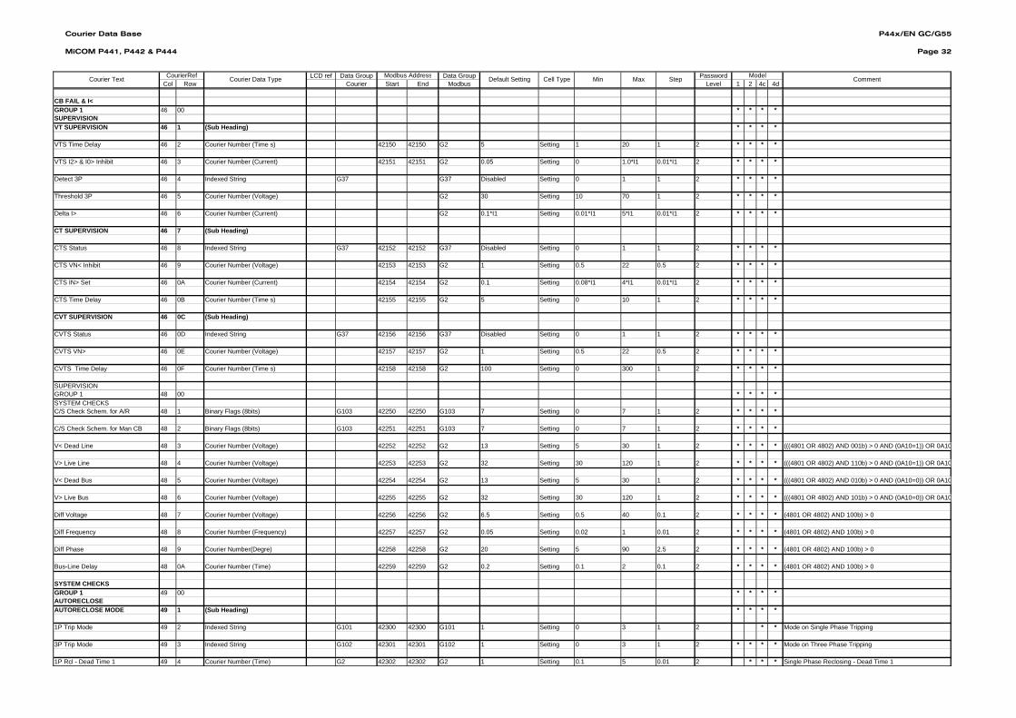
Courier Data Base
MiCOM P441, P442 & P444
P44x/EN GC/G55
Page 32
LCD ref Data Group Data Group PasswordCol Row Courier Start End Modbus Level 1 2 4c 4d
Step Model CommentDefault Setting Cell Type Min MaxCourierRefCourier Text Courier Data Type Modbus Address
CB FAIL & I<GROUP 1 46 00 * * * *SUPERVISION VT SUPERVISION 46 1 (Sub Heading) * * * *
VTS Time Delay 46 2 Courier Number (Time s) 42150 42150 G2 5 Setting 1 20 1 2 * * * *
VTS I2> & I0> Inhibit 46 3 Courier Number (Current) 42151 42151 G2 0.05 Setting 0 1.0*I1 0.01*I1 2 * * * *
Detect 3P 46 4 Indexed String G37 G37 Disabled Setting 0 1 1 2 * * * *
Threshold 3P 46 5 Courier Number (Voltage) G2 30 Setting 10 70 1 2 * * * *
Delta I> 46 6 Courier Number (Current) G2 0.1*I1 Setting 0.01*I1 5*I1 0.01*I1 2 * * * *
CT SUPERVISION 46 7 (Sub Heading)
CTS Status 46 8 Indexed String G37 42152 42152 G37 Disabled Setting 0 1 1 2 * * * *
CTS VN< Inhibit 46 9 Courier Number (Voltage) 42153 42153 G2 1 Setting 0.5 22 0.5 2 * * * *
CTS IN> Set 46 0A Courier Number (Current) 42154 42154 G2 0.1 Setting 0.08*I1 4*I1 0.01*I1 2 * * * *
CTS Time Delay 46 0B Courier Number (Time s) 42155 42155 G2 5 Setting 0 10 1 2 * * * *
CVT SUPERVISION 46 0C (Sub Heading)
CVTS Status 46 0D Indexed String G37 42156 42156 G37 Disabled Setting 0 1 1 2 * * * *
CVTS VN> 46 0E Courier Number (Voltage) 42157 42157 G2 1 Setting 0.5 22 0.5 2 * * * *
CVTS Time Delay 46 0F Courier Number (Time s) 42158 42158 G2 100 Setting 0 300 1 2 * * * *
SUPERVISIONGROUP 1 48 00 * * * *SYSTEM CHECKS C/S Check Schem. for A/R 48 1 Binary Flags (8bits) G103 42250 42250 G103 7 Setting 0 7 1 2 * * * *
C/S Check Schem. for Man CB 48 2 Binary Flags (8bits) G103 42251 42251 G103 7 Setting 0 7 1 2 * * * *
V< Dead Line 48 3 Courier Number (Voltage) 42252 42252 G2 13 Setting 5 30 1 2 * * * * (((4801 OR 4802) AND 001b) > 0 AND (0A10=1)) OR 0A10
V> Live Line 48 4 Courier Number (Voltage) 42253 42253 G2 32 Setting 30 120 1 2 * * * * (((4801 OR 4802) AND 110b) > 0 AND (0A10=1)) OR 0A10
V< Dead Bus 48 5 Courier Number (Voltage) 42254 42254 G2 13 Setting 5 30 1 2 * * * * (((4801 OR 4802) AND 010b) > 0 AND (0A10=0)) OR 0A10
V> Live Bus 48 6 Courier Number (Voltage) 42255 42255 G2 32 Setting 30 120 1 2 * * * * (((4801 OR 4802) AND 101b) > 0 AND (0A10=0)) OR 0A10
Diff Voltage 48 7 Courier Number (Voltage) 42256 42256 G2 6.5 Setting 0.5 40 0.1 2 * * * * (4801 OR 4802) AND 100b) > 0
Diff Frequency 48 8 Courier Number (Frequency) 42257 42257 G2 0.05 Setting 0.02 1 0.01 2 * * * * (4801 OR 4802) AND 100b) > 0
Diff Phase 48 9 Courier Number(Degre) 42258 42258 G2 20 Setting 5 90 2.5 2 * * * * (4801 OR 4802) AND 100b) > 0
Bus-Line Delay 48 0A Courier Number (Time) 42259 42259 G2 0.2 Setting 0.1 2 0.1 2 * * * * (4801 OR 4802) AND 100b) > 0
SYSTEM CHECKSGROUP 1 49 00 * * * *AUTORECLOSE AUTORECLOSE MODE 49 1 (Sub Heading) * * * *
1P Trip Mode 49 2 Indexed String G101 42300 42300 G101 1 Setting 0 3 1 2 * * Mode on Single Phase Tripping
3P Trip Mode 49 3 Indexed String G102 42301 42301 G102 1 Setting 0 3 1 2 * * * * Mode on Three Phase Tripping
1P Rcl - Dead Time 1 49 4 Courier Number (Time) G2 42302 42302 G2 1 Setting 0.1 5 0.01 2 * * * Single Phase Reclosing - Dead Time 1
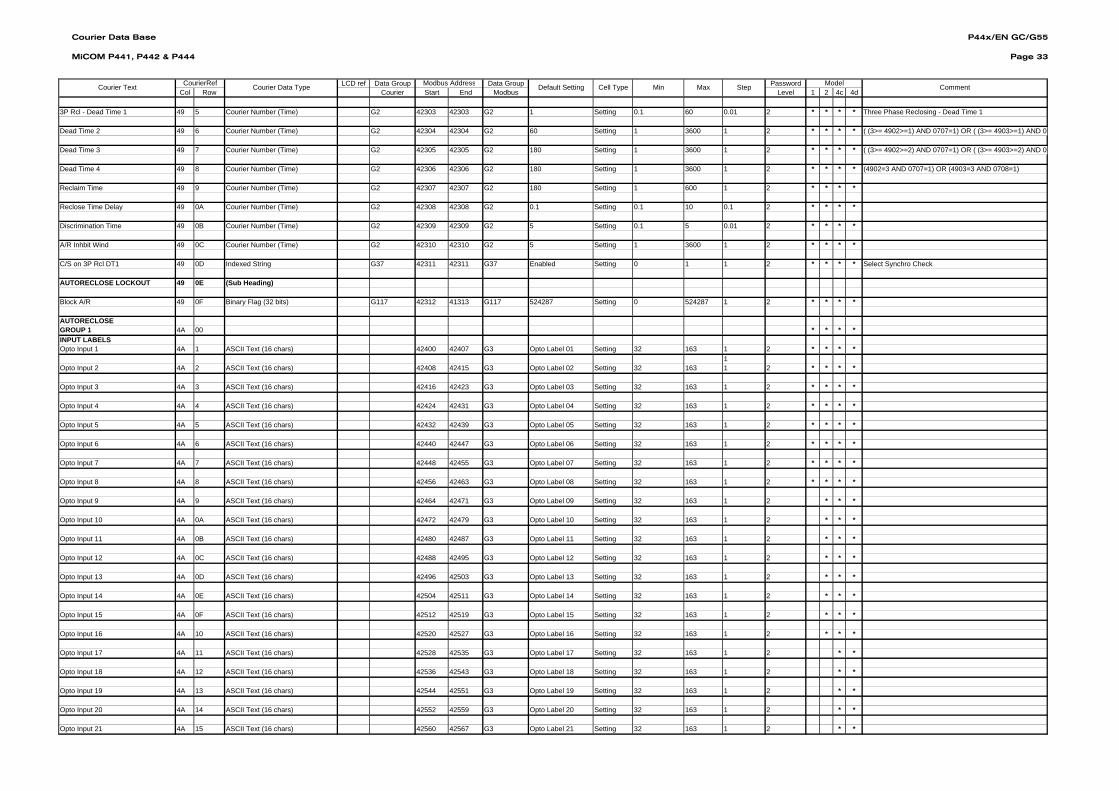
Courier Data Base
MiCOM P441, P442 & P444
P44x/EN GC/G55
Page 33
LCD ref Data Group Data Group PasswordCol Row Courier Start End Modbus Level 1 2 4c 4d
Step Model CommentDefault Setting Cell Type Min MaxCourierRefCourier Text Courier Data Type Modbus Address
3P Rcl - Dead Time 1 49 5 Courier Number (Time) G2 42303 42303 G2 1 Setting 0.1 60 0.01 2 * * * * Three Phase Reclosing - Dead Time 1
Dead Time 2 49 6 Courier Number (Time) G2 42304 42304 G2 60 Setting 1 3600 1 2 * * * * ( (3>= 4902>=1) AND 0707=1) OR ( (3>= 4903>=1) AND 0
Dead Time 3 49 7 Courier Number (Time) G2 42305 42305 G2 180 Setting 1 3600 1 2 * * * * ( (3>= 4902>=2) AND 0707=1) OR ( (3>= 4903>=2) AND 0
Dead Time 4 49 8 Courier Number (Time) G2 42306 42306 G2 180 Setting 1 3600 1 2 * * * * (4902=3 AND 0707=1) OR (4903=3 AND 0708=1)
Reclaim Time 49 9 Courier Number (Time) G2 42307 42307 G2 180 Setting 1 600 1 2 * * * *
Reclose Time Delay 49 0A Courier Number (Time) G2 42308 42308 G2 0.1 Setting 0.1 10 0.1 2 * * * *
Discrimination Time 49 0B Courier Number (Time) G2 42309 42309 G2 5 Setting 0.1 5 0.01 2 * * * *
A/R Inhbit Wind 49 0C Courier Number (Time) G2 42310 42310 G2 5 Setting 1 3600 1 2 * * * *
C/S on 3P Rcl DT1 49 0D Indexed String G37 42311 42311 G37 Enabled Setting 0 1 1 2 * * * * Select Synchro Check
AUTORECLOSE LOCKOUT 49 0E (Sub Heading)
Block A/R 49 0F Binary Flag (32 bits) G117 42312 41313 G117 524287 Setting 0 524287 1 2 * * * *
AUTORECLOSEGROUP 1 4A 00 * * * *INPUT LABELS Opto Input 1 4A 1 ASCII Text (16 chars) 42400 42407 G3 Opto Label 01 Setting 32 163 1 2 * * * *
1 Opto Input 2 4A 2 ASCII Text (16 chars) 42408 42415 G3 Opto Label 02 Setting 32 163 1 2 * * * *
Opto Input 3 4A 3 ASCII Text (16 chars) 42416 42423 G3 Opto Label 03 Setting 32 163 1 2 * * * *
Opto Input 4 4A 4 ASCII Text (16 chars) 42424 42431 G3 Opto Label 04 Setting 32 163 1 2 * * * *
Opto Input 5 4A 5 ASCII Text (16 chars) 42432 42439 G3 Opto Label 05 Setting 32 163 1 2 * * * *
Opto Input 6 4A 6 ASCII Text (16 chars) 42440 42447 G3 Opto Label 06 Setting 32 163 1 2 * * * *
Opto Input 7 4A 7 ASCII Text (16 chars) 42448 42455 G3 Opto Label 07 Setting 32 163 1 2 * * * *
Opto Input 8 4A 8 ASCII Text (16 chars) 42456 42463 G3 Opto Label 08 Setting 32 163 1 2 * * * *
Opto Input 9 4A 9 ASCII Text (16 chars) 42464 42471 G3 Opto Label 09 Setting 32 163 1 2 * * *
Opto Input 10 4A 0A ASCII Text (16 chars) 42472 42479 G3 Opto Label 10 Setting 32 163 1 2 * * *
Opto Input 11 4A 0B ASCII Text (16 chars) 42480 42487 G3 Opto Label 11 Setting 32 163 1 2 * * *
Opto Input 12 4A 0C ASCII Text (16 chars) 42488 42495 G3 Opto Label 12 Setting 32 163 1 2 * * *
Opto Input 13 4A 0D ASCII Text (16 chars) 42496 42503 G3 Opto Label 13 Setting 32 163 1 2 * * *
Opto Input 14 4A 0E ASCII Text (16 chars) 42504 42511 G3 Opto Label 14 Setting 32 163 1 2 * * *
Opto Input 15 4A 0F ASCII Text (16 chars) 42512 42519 G3 Opto Label 15 Setting 32 163 1 2 * * *
Opto Input 16 4A 10 ASCII Text (16 chars) 42520 42527 G3 Opto Label 16 Setting 32 163 1 2 * * *
Opto Input 17 4A 11 ASCII Text (16 chars) 42528 42535 G3 Opto Label 17 Setting 32 163 1 2 * *
Opto Input 18 4A 12 ASCII Text (16 chars) 42536 42543 G3 Opto Label 18 Setting 32 163 1 2 * *
Opto Input 19 4A 13 ASCII Text (16 chars) 42544 42551 G3 Opto Label 19 Setting 32 163 1 2 * *
Opto Input 20 4A 14 ASCII Text (16 chars) 42552 42559 G3 Opto Label 20 Setting 32 163 1 2 * *
Opto Input 21 4A 15 ASCII Text (16 chars) 42560 42567 G3 Opto Label 21 Setting 32 163 1 2 * *

Courier Data Base
MiCOM P441, P442 & P444
P44x/EN GC/G55
Page 34
LCD ref Data Group Data Group PasswordCol Row Courier Start End Modbus Level 1 2 4c 4d
Step Model CommentDefault Setting Cell Type Min MaxCourierRefCourier Text Courier Data Type Modbus Address
Opto Input 22 4A 16 ASCII Text (16 chars) 42568 42575 G3 Opto Label 22 Setting 32 163 1 2 * *
Opto Input 23 4A 17 ASCII Text (16 chars) 42576 42583 G3 Opto Label 23 Setting 32 163 1 2 * *
Opto Input 24 4A 18 ASCII Text (16 chars) 42584 42591 G3 Opto Label 24 Setting 32 163 1 2 * *
INPUT LABELSGROUP 1 4B 00 * * * *OUTPUT LABELS Relay 1 4B 1 ASCII Text (16 chars) 42600 42607 G3 Relay Label 01 Setting 32 163 1 2 * * * *
Relay 2 4B 2 ASCII Text (16 chars) 42608 42615 G3 Relay Label 02 Setting 32 163 1 2 * * * *
Relay 3 4B 3 ASCII Text (16 chars) 42616 42623 G3 Relay Label 03 Setting 32 163 1 2 * * * *
Relay 4 4B 4 ASCII Text (16 chars) 42624 42631 G3 Relay Label 04 Setting 32 163 1 2 * * * *
Relay 5 4B 5 ASCII Text (16 chars) 42632 42639 G3 Relay Label 05 Setting 32 163 1 2 * * * *
Relay 6 4B 6 ASCII Text (16 chars) 42640 42647 G3 Relay Label 06 Setting 32 163 1 2 * * * *
Relay 7 4B 7 ASCII Text (16 chars) 42648 42655 G3 Relay Label 07 Setting 32 163 1 2 * * * *
Relay 8 4B 8 ASCII Text (16 chars) 42656 42663 G3 Relay Label 08 Setting 32 163 1 2 * * * *
Relay 9 4B 9 ASCII Text (16 chars) 42664 42671 G3 Relay Label 09 Setting 32 163 1 2 * * * *
Relay 10 4B 0A ASCII Text (16 chars) 42672 42679 G3 Relay Label 10 Setting 32 163 1 2 * * * *
Relay 11 4B 0B ASCII Text (16 chars) 42680 42687 G3 Relay Label 11 Setting 32 163 1 2 * * * *
Relay 12 4B 0C ASCII Text (16 chars) 42688 42695 G3 Relay Label 12 Setting 32 163 1 2 * * * *
Relay 13 4B 0D ASCII Text (16 chars) 42696 42703 G3 Relay Label 13 Setting 32 163 1 2 * * * *
Relay 14 4B 0E ASCII Text (16 chars) 42704 42711 G3 Relay Label 14 Setting 32 163 1 2 * * * *
Relay 15 4B 0F ASCII Text (16 chars) 42712 42719 G3 Relay Label 15 Setting 32 163 1 2 * * * *
Relay 16 4B 10 ASCII Text (16 chars) 42720 42727 G3 Relay Label 16 Setting 32 163 1 2 * * * *
Relay 17 4B 11 ASCII Text (16 chars) 42728 42735 G3 Relay Label 17 Setting 32 163 1 2 * * * *
Relay 18 4B 12 ASCII Text (16 chars) 42736 42743 G3 Relay Label 18 Setting 32 163 1 2 * * * *
Relay 19 4B 13 ASCII Text (16 chars) 42744 42751 G3 Relay Label 19 Setting 32 163 1 2 * * * *
Relay 20 4B 14 ASCII Text (16 chars) 42752 42759 G3 Relay Label 20 Setting 32 163 1 2 * * * *
Relay 21 4B 15 ASCII Text (16 chars) 42760 42767 G3 Relay Label 21 Setting 32 163 1 2 * * * *
Relay 22 4B 16 ASCII Text (16 chars) 42768 42775 G3 Relay Label 22 Setting 32 163 1 2 * * * *
Relay 23 4B 17 ASCII Text (16 chars) 42776 42783 G3 Relay Label 23 Setting 32 163 1 2 * * * *
Relay 24 4B 18 ASCII Text (16 chars) 42784 42791 G3 Relay Label 24 Setting 32 163 1 2 * * * *
Relay 25 4B 19 ASCII Text (16 chars) 42792 42799 G3 Relay Label 25 Setting 32 163 1 2 * *
Relay 26 4B 1A ASCII Text (16 chars) 42800 42807 G3 Relay Label 26 Setting 32 163 1 2 * *
Relay 27 4B 1B ASCII Text (16 chars) 42808 42815 G3 Relay Label 27 Setting 32 163 1 2 * *
Relay 28 4B 1C ASCII Text (16 chars) 42816 42823 G3 Relay Label 28 Setting 32 163 1 2 * *
Relay 29 4B 1D ASCII Text (16 chars) 42824 42831 G3 Relay Label 29 Setting 32 163 1 2 * *

Courier Data Base
MiCOM P441, P442 & P444
P44x/EN GC/G55
Page 35
LCD ref Data Group Data Group PasswordCol Row Courier Start End Modbus Level 1 2 4c 4d
Step Model CommentDefault Setting Cell Type Min MaxCourierRefCourier Text Courier Data Type Modbus Address
Relay 30 4B 1E ASCII Text (16 chars) 42832 42839 G3 Relay Label 30 Setting 32 163 1 2 * *
Relay 31 4B 1F ASCII Text (16 chars) 42840 42847 G3 Relay Label 31 Setting 32 163 1 2 * *
Relay 32 4B 20 ASCII Text (16 chars) 42848 42855 G3 Relay Label 32 Setting 32 163 1 2 * *
Relay 33 4B 21 ASCII Text (16 chars) 42856 42863 G3 Relay Label 33 Setting 32 163 1 2 *
Relay 34 4B 22 ASCII Text (16 chars) 42864 42871 G3 Relay Label 34 Setting 32 163 1 2 *
Relay 35 4B 23 ASCII Text (16 chars) 42872 42879 G3 Relay Label 35 Setting 32 163 1 2 *
Relay 36 4B 24 ASCII Text (16 chars) 42880 42887 G3 Relay Label 36 Setting 32 163 1 2 *
Relay 37 4B 25 ASCII Text (16 chars) 42888 42895 G3 Relay Label 37 Setting 32 163 1 2 *
Relay 38 4B 26 ASCII Text (16 chars) 42896 42903 G3 Relay Label 38 Setting 32 163 1 2 *
Relay 39 4B 27 ASCII Text (16 chars) 42904 42911 G3 Relay Label 39 Setting 32 163 1 2 *
Relay 40 4B 28 ASCII Text (16 chars) 42912 42919 G3 Relay Label 40 Setting 32 163 1 2 *
Relay 41 4B 29 ASCII Text (16 chars) 42920 42927 G3 Relay Label 41 Setting 32 163 1 2 *
Relay 42 4B 2A ASCII Text (16 chars) 42928 42935 G3 Relay Label 42 Setting 32 163 1 2 *
Relay 43 4B 2B ASCII Text (16 chars) 42936 42943 G3 Relay Label 43 Setting 32 163 1 2 *
Relay 44 4B 2C ASCII Text (16 chars) 42944 42951 G3 Relay Label 44 Setting 32 163 1 2 *
Relay 45 4B 2D ASCII Text (16 chars) 42952 42959 G3 Relay Label 45 Setting 32 163 1 2 *
Relay 46 4B 2E ASCII Text (16 chars) 42960 42967 G3 Relay Label 46 Setting 32 163 1 2 *
OUTPUT LABELGROUP 2 PROTECTION SETTINGS Repeat of Group 1 columns/rows 50 00 43000 44999
GROUP 3 PROTECTION SETTINGS Repeat of Group 1 columns/rows 70 00 45000 46999
GROUP 4 PROTECTION SETTINGS Repeat of Group 1 columns/rows 90 00 47000 48999
This is an invisible column for auto extraction of event records, do not redefine any of its rows but keep it consistent with column [01] (No Header) B0 00 Auto extraction Event Record ColumN/A * * * *Select Event B0 1 Unsigned Integer(2) Setting 0 65535 1 * * * * Unique cyclical fault number(from event)Time & Date B0 2 IEC870 Time & Date (From Record) Data * * * *Record Type B0 3 Ascii String(32) Data * * * *Faulted Phases B0 4 Binary Flag (8 bits) Indexed String Data * * * * Product Specific Bit Flags TargettingActive Setting Group B0 5 Unsigned Integer Data * * * *Time Stamp B0 6 * * * *UNUSED B0 7 Started Elements (1) B0 8 Binary Flags (32 Bits)Indexed String 0..31 0..31 1 bit per elementLSBData * * * * Product Specific Bit Flags TargettingTripped Elements (1) B0 9 Binary Flags (32 Bits)Indexed String 0..31 0..31 1 bit per elementLSBData * * * *UNUSED B0 0A System Frequency B0 0B Courier Number (frequency) Data * * * *Fault Duration B0 0C Courier Number (time) Data * * * *CB Operate Time B0 0D Courier Number (time) Data * * * *Relay Trip Time B0 0E Courier Number (time) Data * * * *Fault Location B0 0F Courier Number(metres) Data * * * *Fault Location B0 10 Courier Number(miles) Data * * * *Fault Location B0 11 Courier Number(ohms) Data * * * *
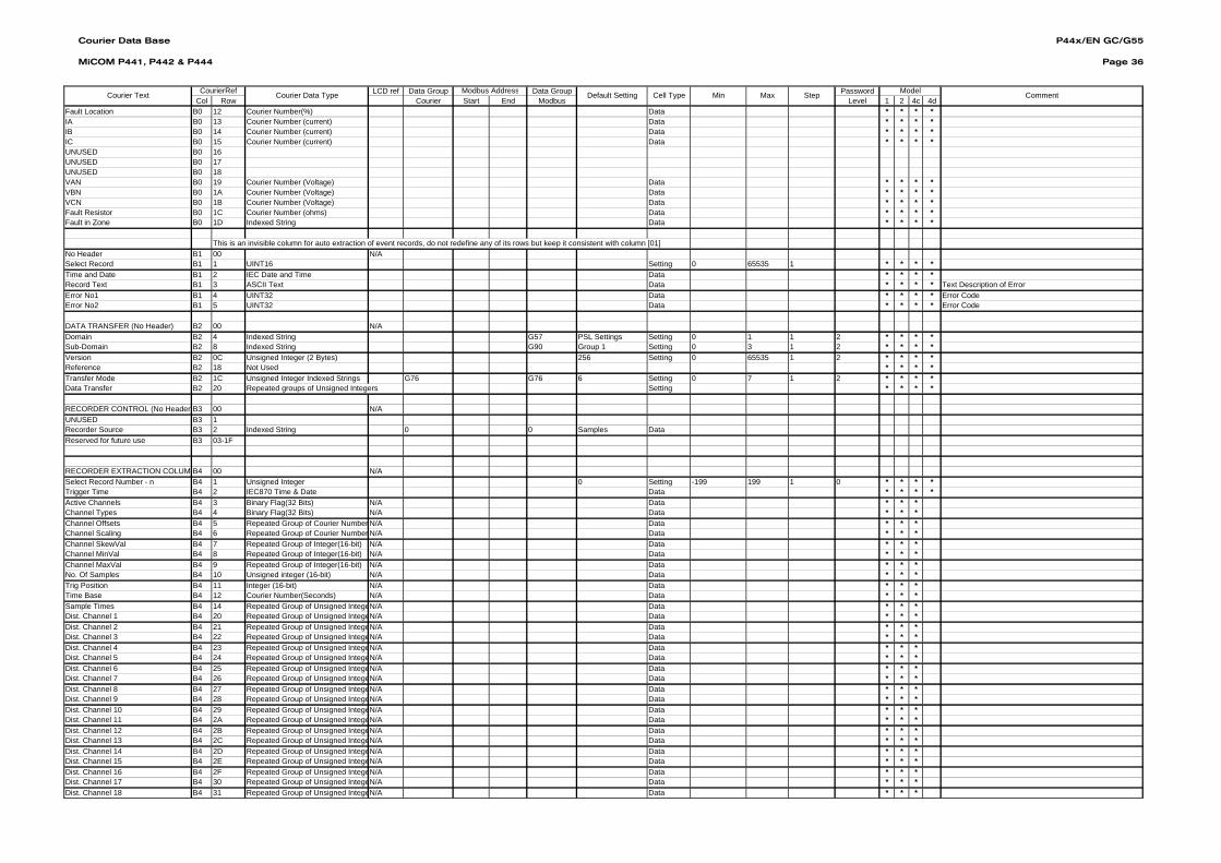
Courier Data Base
MiCOM P441, P442 & P444
P44x/EN GC/G55
Page 36
LCD ref Data Group Data Group PasswordCol Row Courier Start End Modbus Level 1 2 4c 4d
Step Model CommentDefault Setting Cell Type Min MaxCourierRefCourier Text Courier Data Type Modbus Address
Fault Location B0 12 Courier Number(%) Data * * * *IA B0 13 Courier Number (current) Data * * * *IB B0 14 Courier Number (current) Data * * * *IC B0 15 Courier Number (current) Data * * * *UNUSED B0 16 UNUSED B0 17 UNUSED B0 18 VAN B0 19 Courier Number (Voltage) Data * * * *VBN B0 1A Courier Number (Voltage) Data * * * *VCN B0 1B Courier Number (Voltage) Data * * * *Fault Resistor B0 1C Courier Number (ohms) Data * * * *Fault in Zone B0 1D Indexed String Data * * * *
This is an invisible column for auto extraction of event records, do not redefine any of its rows but keep it consistent with column [01] No Header B1 00 N/A Select Record B1 1 UINT16 Setting 0 65535 1 * * * *Time and Date B1 2 IEC Date and Time Data * * * *Record Text B1 3 ASCII Text Data * * * * Text Description of ErrorError No1 B1 4 UINT32 Data * * * * Error CodeError No2 B1 5 UINT32 Data * * * * Error Code
DATA TRANSFER (No Header) B2 00 N/A Domain B2 4 Indexed String G57 PSL Settings Setting 0 1 1 2 * * * *Sub-Domain B2 8 Indexed String G90 Group 1 Setting 0 3 1 2 * * * *Version B2 0C Unsigned Integer (2 Bytes) 256 Setting 0 65535 1 2 * * * *Reference B2 18 Not Used * * * *Transfer Mode B2 1C Unsigned Integer Indexed Strings G76 G76 6 Setting 0 7 1 2 * * * *Data Transfer B2 20 Repeated groups of Unsigned Integers Setting * * * *
RECORDER CONTROL (No Header)B3 00 N/A UNUSED B3 1 Recorder Source B3 2 Indexed String 0 0 Samples Data Reserved for future use B3 03-1F
RECORDER EXTRACTION COLUM B4 00 N/A Select Record Number - n B4 1 Unsigned Integer 0 Setting -199 199 1 0 * * * *Trigger Time B4 2 IEC870 Time & Date Data * * * *Active Channels B4 3 Binary Flag(32 Bits) N/A Data * * *Channel Types B4 4 Binary Flag(32 Bits) N/A Data * * *Channel Offsets B4 5 Repeated Group of Courier Number N/A Data * * *Channel Scaling B4 6 Repeated Group of Courier Number N/A Data * * *Channel SkewVal B4 7 Repeated Group of Integer(16-bit) N/A Data * * *Channel MinVal B4 8 Repeated Group of Integer(16-bit) N/A Data * * *Channel MaxVal B4 9 Repeated Group of Integer(16-bit) N/A Data * * *No. Of Samples B4 10 Unsigned integer (16-bit) N/A Data * * *Trig Position B4 11 Integer (16-bit) N/A Data * * *Time Base B4 12 Courier Number(Seconds) N/A Data * * *Sample Times B4 14 Repeated Group of Unsigned IntegeN/A Data * * *Dist. Channel 1 B4 20 Repeated Group of Unsigned IntegeN/A Data * * *Dist. Channel 2 B4 21 Repeated Group of Unsigned IntegeN/A Data * * *Dist. Channel 3 B4 22 Repeated Group of Unsigned IntegeN/A Data * * *Dist. Channel 4 B4 23 Repeated Group of Unsigned IntegeN/A Data * * *Dist. Channel 5 B4 24 Repeated Group of Unsigned IntegeN/A Data * * *Dist. Channel 6 B4 25 Repeated Group of Unsigned IntegeN/A Data * * *Dist. Channel 7 B4 26 Repeated Group of Unsigned IntegeN/A Data * * *Dist. Channel 8 B4 27 Repeated Group of Unsigned IntegeN/A Data * * *Dist. Channel 9 B4 28 Repeated Group of Unsigned IntegeN/A Data * * *Dist. Channel 10 B4 29 Repeated Group of Unsigned IntegeN/A Data * * *Dist. Channel 11 B4 2A Repeated Group of Unsigned IntegeN/A Data * * *Dist. Channel 12 B4 2B Repeated Group of Unsigned IntegeN/A Data * * *Dist. Channel 13 B4 2C Repeated Group of Unsigned IntegeN/A Data * * *Dist. Channel 14 B4 2D Repeated Group of Unsigned IntegeN/A Data * * *Dist. Channel 15 B4 2E Repeated Group of Unsigned IntegeN/A Data * * *Dist. Channel 16 B4 2F Repeated Group of Unsigned IntegeN/A Data * * *Dist. Channel 17 B4 30 Repeated Group of Unsigned IntegeN/A Data * * *Dist. Channel 18 B4 31 Repeated Group of Unsigned IntegeN/A Data * * *

Courier Data Base
MiCOM P441, P442 & P444
P44x/EN GC/G55
Page 37
LCD ref Data Group Data Group PasswordCol Row Courier Start End Modbus Level 1 2 4c 4d
Step Model CommentDefault Setting Cell Type Min MaxCourierRefCourier Text Courier Data Type Modbus Address
Dist. Channel 19 B4 32 Repeated Group of Unsigned IntegeN/A Data * * *Dist. Channel 20 B4 33 Repeated Group of Unsigned IntegeN/A Data * * *Dist. Channel 21 B4 34 Repeated Group of Unsigned IntegeN/A Data * * *Dist. Channel 22 B4 35 Repeated Group of Unsigned IntegeN/A Data * * *Dist. Channel 23 B4 36 Repeated Group of Unsigned IntegeN/A Data * * *Dist. Channel 24 B4 37 Repeated Group of Unsigned IntegeN/A Data * * *Dist. Channel 25 B4 38 Repeated Group of Unsigned IntegeN/A Data * * *Dist. Channel 26 B4 39 Repeated Group of Unsigned IntegeN/A Data * * *Dist. Channel 27 B4 3A Repeated Group of Unsigned IntegeN/A Data * * *Dist. Channel 28 B4 3B Repeated Group of Unsigned IntegeN/A Data * * *Dist. Channel 29 B4 3C Repeated Group of Unsigned IntegeN/A Data * * *Dist. Channel 30 B4 3D Repeated Group of Unsigned IntegeN/A Data * * *Dist. Channel 31 B4 3E Repeated Group of Unsigned IntegeN/A Data * * *Dist. Channel 32 B4 3F Repeated Group of Unsigned IntegeN/A Data * * *
Calibration Coefficients (Hidden) (NotB5 00 N/A Cal Software Version B5 1 ASCII text 16 chars * * * *Cal Date and Time B5 2 IEC Date and time * * * *Channel Types B5 3 Repeated Group 16 * Binary Flag 8 bits * * * *Cal Coeffs B5 4 Block transfer Repeated Group of UINT32 (4 coeffs voltage channel, 8 coeffs current channel) * * * *
Comms Diagnostics (Hidden) B6 00 Note: No text in column text N/A Bus Comms Err Count Front B6 1 UINT32 * * * *Bus Message Count Front B6 2 UINT32 * * * *Protocol Err Count Front B6 3 UINT32 * * * *Busy Count Front B6 4 UINT32 * * * *Reset front count B6 5 (Reset Menu Cell cmd only) * * * *Bus Comms Err Count Rear B6 6 UINT32 * * * *Bus Message Count Rear B6 7 UINT32 * * * *Protocol Err Count Rear B6 8 UINT32 * * * *Busy Count Rear B6 9 UINT32 * * * *Reset rear count B6 0A (Reset Menu Cell cmd only) * * * *
PSL Data B7 00 Grp1 PSL Ref B7 01 ASCII Text (32 chars) 31000 31015 G3 Default PSL "model number" * * * *Date/Time B7 02 IEC870 Date & Time 31016 31019 G12 * * * *PSL unique ID B7 03 Unsigned Integer (32 bits) 31020 31021 G27 0 * * * *Grp2 PSL Ref B7 11 ASCII Text (32 chars) 31022 31037 G3 Default PSL "model number" * * * *Date/Time B7 12 IEC870 Date & Time 31038 31041 G12 * * * *PSL unique ID B7 13 Unsigned Integer (32 bits) 31042 31043 G27 0 * * * *Grp3 PSL Ref B7 21 ASCII Text (32 chars) 31044 31059 G3 Default PSL "model number" * * * *Date/Time B7 22 IEC870 Date & Time 31060 31063 G12 * * * *PSL unique ID B7 23 Unsigned Integer (32 bits) 31064 31065 G27 0 * * * *Grp3 PSL Ref B7 31 ASCII Text (32 chars) 31066 31079 G3 Default PSL "model number" * * * *Date/Time B7 32 IEC870 Date & Time 31082 31085 G12 * * * *PSL unique ID B7 33 Unsigned Integer (32 bits) 31086 31087 G27 0 * * * *
COMMS SYS DATA BF 00 N/A Dist Record Cntrl Ref BF 1 Menu Cell(2) B300 Data * * * *Dist Record Extract Ref BF 2 Menu Cell(2) B400 Data * * * *Setting Transfer BF 3 Unsigned Integer Setting * * * *UNUSED BF 5 * * * *Block Transfer Ref BF 6 Menu Cell(2) B200 Data * * * *
* * * *UCA 2 Only Data Cells FE 0
CheckSync Bus Volts FE 1 (Note: No Text) UCA 2 Only
CheckSync Line Volts FE 2 (Note: No Text) UCA 2 Only
YN> Set FE 3 Special cell that points to the correct PU setting cell - E/F Pu or SEF Pu.
GN> Set FE 4 Special cell that points to the correct PU setting cell - E/F Pu or SEF Pu.
BN> Set FE 5 Special cell that points to the correct PU setting cell - E/F Pu or SEF Pu.

Courier Data Base
MiCOM P441, P442 & P444
P44x/EN GC/G55
Page 38
LCD ref Data Group Data Group PasswordCol Row Courier Start End Modbus Level 1 2 4c 4d
Step Model CommentDefault Setting Cell Type Min MaxCourierRefCourier Text Courier Data Type Modbus Address
Control Input 1 Config FE 6 (Note: No Text) - Returns "0" for latched configuration, Returns "10" for pulsed configuration * * *
Control Input 2 Config FE 7 (Note: No Text) - Returns "0" for latched configuration, Returns "10" for pulsed configuration * * *
Control Input 3 Config FE 8 (Note: No Text) - Returns "0" for latched configuration, Returns "10" for pulsed configuration * * *
Control Input 4 Config FE 9 (Note: No Text) - Returns "0" for latched configuration, Returns "10" for pulsed configuration * * *
Control Input 5 Config FE 0A (Note: No Text) - Returns "0" for latched configuration, Returns "10" for pulsed configuration * * *
Control Input 6 Config FE 0B (Note: No Text) - Returns "0" for latched configuration, Returns "10" for pulsed configuration * * *
Control Input 7 Config FE 0C (Note: No Text) - Returns "0" for latched configuration, Returns "10" for pulsed configuration * * *
Control Input 8 Config FE 0D (Note: No Text) - Returns "0" for latched configuration, Returns "10" for pulsed configuration * * *
Control Input 9 Config FE 0E (Note: No Text) - Returns "0" for latched configuration, Returns "10" for pulsed configuration * * *
Control Input 10 Config FE 0F (Note: No Text) - Returns "0" for latched configuration, Returns "10" for pulsed configuration * * *
Control Input 11 Config FE 10 (Note: No Text) - Returns "0" for latched configuration, Returns "10" for pulsed configuration * * *
Control Input 12 Config FE 11 (Note: No Text) - Returns "0" for latched configuration, Returns "10" for pulsed configuration * * *
Control Input 13 Config FE 12 (Note: No Text) - Returns "0" for latched configuration, Returns "10" for pulsed configuration * * *
Control Input 14 Config FE 13 (Note: No Text) - Returns "0" for latched configuration, Returns "10" for pulsed configuration * * *
Control Input 15 Config FE 14 (Note: No Text) - Returns "0" for latched configuration, Returns "10" for pulsed configuration * * *
Control Input 16 Config FE 15 (Note: No Text) - Returns "0" for latched configuration, Returns "10" for pulsed configuration * * *
Control Input 17 Config FE 16 (Note: No Text) - Returns "0" for latched configuration, Returns "10" for pulsed configuration * * *
Control Input 18 Config FE 17 (Note: No Text) - Returns "0" for latched configuration, Returns "10" for pulsed configuration * * *
Control Input 19 Config FE 18 (Note: No Text) - Returns "0" for latched configuration, Returns "10" for pulsed configuration * * *
Control Input 20 Config FE 19 (Note: No Text) - Returns "0" for latched configuration, Returns "10" for pulsed configuration * * *
Control Input 21 Config FE 1A (Note: No Text) - Returns "0" for latched configuration, Returns "10" for pulsed configuration * * *
Control Input 22 Config FE 1B (Note: No Text) - Returns "0" for latched configuration, Returns "10" for pulsed configuration * * *
Control Input 23 Config FE 1C (Note: No Text) - Returns "0" for latched configuration, Returns "10" for pulsed configuration * * *
Control Input 24 Config FE 1D (Note: No Text) - Returns "0" for latched configuration, Returns "10" for pulsed configuration * * *
Control Input 25 Config FE 1E (Note: No Text) - Returns "0" for latched configuration, Returns "10" for pulsed configuration * * *
Control Input 26 Config FE 1F (Note: No Text) - Returns "0" for latched configuration, Returns "10" for pulsed configuration * * *
Control Input 27 Config FE 20 (Note: No Text) - Returns "0" for latched configuration, Returns "10" for pulsed configuration * * *
Control Input 28 Config FE 21 (Note: No Text) - Returns "0" for latched configuration, Returns "10" for pulsed configuration * * *
Control Input 29 Config FE 22 (Note: No Text) - Returns "0" for latched configuration, Returns "10" for pulsed configuration * * *
Control Input 30 Config FE 23 (Note: No Text) - Returns "0" for latched configuration, Returns "10" for pulsed configuration * * *
Control Input 31 Config FE 24 (Note: No Text) - Returns "0" for latched configuration, Returns "10" for pulsed configuration * * *
Control Input 32 Config FE 25 (Note: No Text) - Returns "0" for latched configuration, Returns "10" for pulsed configuration * * *
Num Unextracted DR FE 26 (Note: No Text) - Returns the number of unextracted Disturbance Records * * *
Fault Locator Line Length FE 27 Special cell that references [47 01] / [47 02] depending upon the selected distance unit (miles or metres) * * *
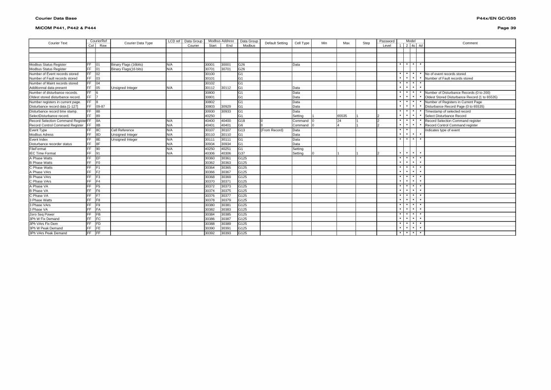
Courier Data Base
MiCOM P441, P442 & P444
P44x/EN GC/G55
Page 39
LCD ref Data Group Data Group PasswordCol Row Courier Start End Modbus Level 1 2 4c 4d
Step Model CommentDefault Setting Cell Type Min MaxCourierRefCourier Text Courier Data Type Modbus Address
Modbus Status Register FF 01 Binary Flags (16bits) N/A 30001 30001 G26 Data * * * *Modbus Status Register FF 01 Binary Flags(16 bits) N/A 30701 30701 G26 Number of Event records stored FF 02 30100 G1 * * * * No of event records storedNumber of Fault records stored FF 03 30101 G1 * * * * Number of Fault records storedNumber of Maint records stored FF 04 30102 G1 * * * *Additionnal data present FF 05 Unsigned Integer N/A 30112 30112 G1 Data * * * *Number of disturbance records. FF 6 30800 G1 Data * * * * Number of Disturbance Records (0 to 200)Oldest stored disturbance record. FF 7 30801 G1 Data * * * * Oldest Stored Disturbance Record (1 to 65535)Number registers in current page. FF 8 30802 G1 Data * * * * Number of Registers in Current PageDisturbance record data [1-127] FF 09-87 30803 30929 G1 Data * * * * Disturbance Record Page (0 to 65535)Disturbance record time stamp. FF 88 30930 30933 G1 Data * * * * Timestamp of selected recordSelectDisturbance record. FF 89 40250 G1 Setting 1 65535 1 2 * * * * Select Disturbance RecordRecord Selection Command RegisterFF 8A N/A 40400 40400 G18 0 Command 0 24 1 2 * * * * Record Selection Command registerRecord Control Command Register FF 8B N/A 40401 40401 G6 0 Command 0 4 1 2 * * * * Record Control Command registerEvent Type FF 8C Cell Reference N/A 30107 30107 G13 (From Record) Data * * Indicates type of eventModbus Adress FF 8D Unsigned Integer N/A 30110 30110 G1 Data * * * *Event Index FF 8E Unsigned Integer N/A 30111 30111 G1 Data * * * *Disturbance recorder status FF 8F N/A 30934 30934 G1 DataFileFormat FF 90 N/A 40250 40251 G1 SettingIEC Time Format FF 91 N/A 40306 40306 G37 Setting 0 1 1 2 * * * *A Phase Watts FF EF 30360 30361 G125 * * * *B Phase Watts FF F0 30362 30363 G125 * * * *C Phase Watts FF F1 30364 30365 G125 * * * *A Phase VArs FF F2 30366 30367 G125 * * * *B Phase VArs FF F3 30368 30369 G125 * * * *C Phase VArs FF F4 30370 30371 G125 * * * *A Phase VA FF F5 30372 30373 G125 * * * *B Phase VA FF F6 30374 30375 G125 * * * *C Phase VA FF F7 30376 30377 G125 * * * *3 Phase Watts FF F8 30378 30379 G125 * * * *3 Phase VArs FF F9 30380 30381 G125 * * * *3 Phase VA FF FA 30382 30383 G125 * * * *Zero Seq Power FF FB 30384 30385 G125 * * * *3Ph W Fix Demand FF FC 30386 30387 G125 * * * *3Ph VArs Fix Dem FF FD 30388 30389 G125 * * * *3Ph W Peak Demand FF FE 30390 30391 G125 * * * *3Ph VArs Peak Demand FF FF 30392 30393 G125 * * * *

Courier Data Base
MiCOM P441, P442 & P444
P44x/EN GC/G55
Page 40
12345671213141516171819202122232425262728293031323334353637383940414243444546474849505152535455565758596061626364656667686970717273747576777879808182
A B CData Types
TYPE VALUE/BIT MASK DESCRIPTIONG1 UNSIGNED INTEGER
eg. 5678 stored as 5678G2 NUMERIC SETTING
See 50300.3110.004G3 ASCII TEXT CHARACTERS
0x00FF Second character0xFF00 First character
G4 PLANT STATUS (1 REGISTER)Reg0x0001 Plant Status 1 (0 = Off, 1 = On)0x0002 Plant Status 2 (0 = Off, 1 = On)0x0004 Plant Status 3 (0 = Off, 1 = On)0x0008 Plant Status 4 (0 = Off, 1 = On)0x0010 Plant Status 5 (0 = Off, 1 = On)0x0020 Plant Status 6 (0 = Off, 1 = On)0x0040 Plant Status 7 (0 = Off, 1 = On)0x0080 Plant Status 8 (0 = Off, 1 = On)0x0100 Plant Status 9 (0 = Off, 1 = On)0x0200 Plant Status 10 (0 = Off, 1 = On)0x0400 Plant Status 11 (0 = Off, 1 = On)0x0800 Plant Status 12 (0 = Off, 1 = On)0x1000 Plant Status 13 (0 = Off, 1 = On)0x2000 Plant Status 14 (0 = Off, 1 = On)0x4000 Plant Status 15 (0 = Off, 1 = On)0x8000 Plant Status 16 (0 = Off, 1 = On)
G5 CONTROL STATUS (1 REGISTER)0x0001 Control Status 1 (0 = Off, 1 = On)0x0002 Control Status 2 (0 = Off, 1 = On)0x0004 Control Status 3 (0 = Off, 1 = On)0x0008 Control Status 4 (0 = Off, 1 = On)0x0010 Control Status 5 (0 = Off, 1 = On)0x0020 Control Status 6 (0 = Off, 1 = On)0x0040 Control Status 7 (0 = Off, 1 = On)0x0080 Control Status 8 (0 = Off, 1 = On)0x0100 Control Status 9 (0 = Off, 1 = On)0x0200 Control Status 10 (0 = Off, 1 = On)0x0400 Control Status 11 (0 = Off, 1 = On)0x0800 Control Status 12 (0 = Off, 1 = On)0x1000 Control Status 13 (0 = Off, 1 = On)0x2000 Control Status 14 (0 = Off, 1 = On)0x4000 Control Status 15 (0 = Off, 1 = On)0x8000 Control Status 16 (0 = Off, 1 = On)
G6 Record Control Command Register0 No Operation1 Clear event Records2 Clear Fault Record3 Clear Maitenance Records4 Reset Indications
G7 VTS Indicate/Block0 Blocking1 Indication
G8 LOGIC INPUT STATUS(Second reg, First Reg)0x0000,0x0001 Opto 1 Input State (0=Off, 1=Energised)0x0000,0x0002 Opto 2 Input State (0=Off, 1=Energised)0x0000,0x0004 Opto 3 Input State (0=Off, 1=Energised)0x0000,0x0008 Opto 4 Input State (0=Off, 1=Energised)0x0000,0x0010 Opto 5 Input State (0=Off, 1=Energised)0x0000,0x0020 Opto 6 Input State (0=Off, 1=Energised)0x0000,0x0040 Opto 7 Input State (0=Off, 1=Energised)0x0000,0x0080 Opto 8 Input State (0=Off, 1=Energised)0x0000,0x0100 Opto 9 Input State (0=Off, 1=Energised)0x0000,0x0200 Opto 10 Input State (0=Off, 1=Energised)0x0000,0x0400 Opto 11 Input State (0=Off, 1=Energised)0x0000,0x0800 Opto 12 Input State (0=Off, 1=Energised)0x0000,0x1000 Opto 13 Input State (0=Off, 1=Energised)0x0000,0x2000 Opto 14 Input State (0=Off, 1=Energised)0x0000,0x4000 Opto 15 Input State (0=Off, 1=Energised)0x0000,0x8000 Opto 16 Input State (0=Off, 1=Energised)0x0001,0x0000 Opto 17 Input State (0=Off, 1=Energised)0x0002,0x0000 Opto 18 Input State (0=Off, 1=Energised)0x0004,0x0000 Opto 19 Input State (0=Off, 1=Energised)0x0008,0x0000 Opto 20 Input State (0=Off, 1=Energised)0x0010,0x0000 Opto 21 Input State (0=Off, 1=Energised)0x0020,0x0000 Opto 22 Input State (0=Off, 1=Energised)

Courier Data Base
MiCOM P441, P442 & P444
P44x/EN GC/G55
Page 41
3A B C
TYPE VALUE/BIT MASK DESCRIPTION8384858687888990919293949596979899100101102103104105106107108109110111112113114115116117118119120121122123124125126127128129130131132133134135136137138139140141142144145146147148149150151152153154155156157158159160
0x0040,0x0000 Opto 23 Input State (0=Off, 1=Energised)0x0080,0x0000 Opto 24 Input State (0=Off, 1=Energised)
G9 RELAY OUTPUT STATUS(Second reg, First Reg)0x0000,0x0001 Relay 1 (0=Not Operated, 1=Operated)0x0000,0x0002 Relay 2 (0=Not Operated, 1=Operated)0x0000,0x0004 Relay 3 (0=Not Operated, 1=Operated)0x0000,0x0008 Relay 4 (0=Not Operated, 1=Operated)0x0000,0x0010 Relay 5 (0=Not Operated, 1=Operated)0x0000,0x0020 Relay 6 (0=Not Operated, 1=Operated)0x0000,0x0040 Relay 7 (0=Not Operated, 1=Operated)0x0000,0x0080 Relay 8 (0=Not Operated, 1=Operated)0x0000,0x0100 Relay 9 (0=Not Operated, 1=Operated)0x0000,0x0200 Relay 10 (0=Not Operated, 1=Operated)0x0000,0x0400 Relay 11 (0=Not Operated, 1=Operated)0x0000,0x0800 Relay 12 (0=Not Operated, 1=Operated)0x0000,0x1000 Relay 13 (0=Not Operated, 1=Operated)0x0000,0x2000 Relay 14 (0=Not Operated, 1=Operated)0x0000,0x4000 Relay 15 (0=Not Operated, 1=Operated)0x0000,0x8000 Relay 16 (0=Not Operated, 1=Operated)0x0001,0x0000 Relay 17 (0=Not Operated, 1=Operated)0x0002,0x0000 Relay 18 (0=Not Operated, 1=Operated)0x0004,0x0000 Relay 19 (0=Not Operated, 1=Operated)0x0008,0x0000 Relay 20 (0=Not Operated, 1=Operated)0x0010,0x0000 Relay 21 (0=Not Operated, 1=Operated)0x0020,0x0000 Relay 22 (0=Not Operated, 1=Operated)0x0040,0x0000 Relay 23 (0=Not Operated, 1=Operated)0x0080,0x0000 Relay 24 (0=Not Operated, 1=Operated)0x0100,0x0000 Relay 25 (0=Not Operated, 1=Operated)0x0200,0x0000 Relay 26 (0=Not Operated, 1=Operated)0x0400,0x0000 Relay 27 (0=Not Operated, 1=Operated)0x0800,0x0000 Relay 28 (0=Not Operated, 1=Operated)0x1000,0x0000 Relay 29 (0=Not Operated, 1=Operated)0x2000,0x0000 Relay 30 (0=Not Operated, 1=Operated)0x4000,0x0000 Relay 31 (0=Not Operated, 1=Operated)0x8000,0x0000 Relay 32 (0=Not Operated, 1=Operated)
G10 PASSWORD LEVEL (May not be needed see modbus)0 Level 01 Level 12 Level 2
G11 YES/NO0 No1 Yes
G12 TIME AND DATE (4 REGISTERS)This will take the IEC 870 format as shown in ref [J] section 5.1.16
0x007F First register - Years0x0FFF Second register - Month of year / Day of month / Day of week0x9FBF Third Register - Summertime and hours / Validity and minutes0xFFFF Fourth Register - Milli-seconds
G13 EVENT RECORD TYPE0 Latched alarm active1 Latched alarm inactive2 Self reset alarm active3 Self reset alarm inactive4 Relay event5 Opto event6 Protection event7 Platform event8 Fault logged event9 Maintenance Record logged event
G14 PAS UTILISE I> Function LinkBit 0 I>1 VTS BlockBit 1 I>1 VTS Block Non-DirectionnalBit 2 I>2 VTS BlockBit 3 I>2 VTS Block Non-DirectionnalBit 4 I>3 VTS BlockBit 5 I>4 VTS BlockBit 6 Not UsedBit 7 Not Used
G15 DISTURBANCE RECORD INDEX STATUS0 No Record1 Un-extracted2 Extracted
G16 FAULTED PHASE0x0001 Start A0x0002 Start B0x0004 Start C

Courier Data Base
MiCOM P441, P442 & P444
P44x/EN GC/G55
Page 42
3A B C
TYPE VALUE/BIT MASK DESCRIPTION161162163164165166167168169170171172173174175176177178179180181182183184185186187188189190191192193194195196197198199200201202203204205206207208209210211212
213214215216217218219220221222223224225226227228229230231232233234235
0x0008 Start N0x0010 Trip A0x0020 Trip B0x0040 Trip C0x0080 Trip N
G17 ACTIVE/INACTIVE0 Card not fitted1 Card failed2 Signal healthy3 No Signal
G18 Record Selection Command Register0x0000 No Operation0x0001 Select next event0x0002 Accept Event0x0004 Select next Disturbance Record0x0008 Accept disturbance record0x0010 Select Next Disturbance record page
G19 LANGUAGE0 English1 Francais2 Deutsch3 Espanol
G20 (Second reg, First Reg) PASSWORD (2 REGISTERS)0x0000, 0x00FF First password character0x0000, 0xFF00 Second password character0x00FF, 0x0000 Third password character0xFF00, 0x0000 Fourth password character
NOTE THAT WHEN REGISTERS OF THIS TYPE ARE READ THE SLAVE WILL ALWAYS INDICATE AN "*" IN EACH CHARACTER POSITION TO PRESERVE THE PASSWORD SECURITY.
G21 IEC870 Interface0 RS4851 Fibre Optic
G22 PASSWORD CONTROL ACCESS LEVEL0 Level 0 - Passwords required for levels 1 & 2.1 Level 1 - Password required for level 2.2 Level 2 - No passwords required.
G23 Voltage Curve selection0 Disabled1 DT2 IDMT
G24 2 REGISTERS UNSIGNED LONG VALUE, 3 DECIMAL PLACESHigh order word of long stored in 1st registerLow order word of long stored in 2nd registerExample 123456.789 stored as 123456789
G25 1 REGISTER UNSIGNED VALUE, 3 DECIMAL PLACESExample 50.050 stored as 50050
G26 Modbus Status RegisterVALUE/BIT MASK RELAY STATUS0x0001 In Service Status (1 = In Service / 0= Out Of Service)0x0002 Minor Self Test Failure (1 = Failure / 0 = No failure)0x0004 New autoextraction event available (1 = Available / 0 = Not Available)
0x0008Time Synchronisation (=1 after Modbus time synch. Resets to 0 after 5 minutes unless it is time synched again. Other time sources do not affect this bit).
0x0010 New auto extraction disturbance record available (1 = Available / 0 = Not available)0x0020 Fault (Not used - always 0).0x0040 Trip LED status (1 = LED on, 0 = LED off).0x0080 Alarm status summary (logical OR of all alarm status bits).0x0100 Unused0x0200 Unused0x0400 Unused0x0800 Unused0x1000 Unused0x2000 Unused0x4000 Unused0x8000 Unused
G27 2 REGISTERS UNSIGNED LONG VALUEHigh order word of long stored in 1st registerLow order word of long stored in 2nd registerExample 123456 stored as 123456
G28 1 REGISTER SIGNED VALUE POWER & WATT-HOURSPower = (Secondary power/CT secondary) * (100/VT secondary)
G29 3 REGISTER POWER MULTIPLERAll power measurments use a signed value of type G28 and a 2 register unsigned long multiplier of type G27Value = Real Value*110/(CTsecondary*VTsecondary)

Courier Data Base
MiCOM P441, P442 & P444
P44x/EN GC/G55
Page 43
3A B C
TYPE VALUE/BIT MASK DESCRIPTION236237238242243244245246247248249250251252253254255256257258259260261262263264265266267268269270271272273274275276277278279280281282283284285286287288289290291292293294295296297298299300301302303304305306307308309310311312313314315
For Primary Power Multipler = CTprimary * VTprimary/110For Secondary Power Multipler = CTsecondary * VTsecondary/110
G30 1 REGISTER SIGNED VALUE, 2 DECIMAL PLACESG31 ANALOGUE CHANNEL ASSIGNMENT SELECTOR (Product Dependent)
0 VA1 VB2 VC3 VN4 IA5 IB6 IC7 IN8 IM9 V Checksync10 unasigned
G32 Digital channel assignment this mapping depend of the model (P441 P442 P444)0 8/16/24 Optos These are example values. Need one to be unassignedto 14/21/32 Relays
8 Feedback1024 72 - 1024 Internal Signals
G33 RECORDER TRIGGERING (2 REGISTERS, 32 BINARY FLAGS)(Second reg, First Reg)0x0000,0x0001 Digital Channel 1 Bit 0 (0 = No Trigger, 1= Trigger)0x0000,0x0002 Digital Channel 1 Bit 1 (0 = No Trigger, 1= Trigger)0x0000,0x0004 Digital Channel 1 Bit 2 (0 = No Trigger, 1= Trigger)0x0000,0x0008 Digital Channel 1 Bit 3 (0 = No Trigger, 1= Trigger)0x0000,0x0010 Digital Channel 1 Bit 4 (0 = No Trigger, 1= Trigger)0x0000,0x0020 Digital Channel 1 Bit 5 (0 = No Trigger, 1= Trigger)0x0000,0x0040 Digital Channel 1 Bit 6 (0 = No Trigger, 1= Trigger)0x0000,0x0080 Digital Channel 1 Bit 7 (0 = No Trigger, 1= Trigger)0x0000,0x0100 Digital Channel 1 Bit 8 (0 = No Trigger, 1= Trigger)0x0000,0x0200 Digital Channel 1 Bit 9 (0 = No Trigger, 1= Trigger)0x0000,0x0400 Digital Channel 1 Bit 10 (0 = No Trigger, 1= Trigger)0x0000,0x0800 Digital Channel 1 Bit 11 (0 = No Trigger, 1= Trigger)0x0000,0x1000 Digital Channel 1 Bit 12 (0 = No Trigger, 1= Trigger)0x0000,0x2000 Digital Channel 1 Bit 13 (0 = No Trigger, 1= Trigger)0x0000,0x4000 Digital Channel 1 Bit 14 (0 = No Trigger, 1= Trigger)0x0000,0x8000 Digital Channel 1 Bit 15 (0 = No Trigger, 1= Trigger)0x0001,0x0000 Digital Channel 2 Bit 0 (0 = No Trigger, 1= Trigger)0x0002,0x0000 Digital Channel 2 Bit 1 (0 = No Trigger, 1= Trigger)0x0004,0x0000 Digital Channel 2 Bit 2 (0 = No Trigger, 1= Trigger)0x0008,0x0000 Digital Channel 2 Bit 3 (0 = No Trigger, 1= Trigger)0x0010,0x0000 Digital Channel 2 Bit 4 (0 = No Trigger, 1= Trigger)0x0020,0x0000 Digital Channel 2 Bit 5 (0 = No Trigger, 1= Trigger)0x0040,0x0000 Digital Channel 2 Bit 6 (0 = No Trigger, 1= Trigger)0x0080,0x0000 Digital Channel 2 Bit 7 (0 = No Trigger, 1= Trigger)0x0100,0x0000 Digital Channel 2 Bit 8 (0 = No Trigger, 1= Trigger)0x0200,0x0000 Digital Channel 2 Bit 9 (0 = No Trigger, 1= Trigger)0x0400,0x0000 Digital Channel 2 Bit 10 (0 = No Trigger, 1= Trigger)0x0800,0x0000 Digital Channel 2 Bit 11 (0 = No Trigger, 1= Trigger)0x1000,0x0000 Digital Channel 2 Bit 12 (0 = No Trigger, 1= Trigger)0x2000,0x0000 Digital Channel 2 Bit 13 (0 = No Trigger, 1= Trigger)0x4000,0x0000 Digital Channel 2 Bit 14 (0 = No Trigger, 1= Trigger)0x8000,0x0000 Digital Channel 2 Bit 15 (0 = No Trigger, 1= Trigger)
G34 TRIGGER MODE0 Single1 Extended
G35 Numeric Setting (as G2 but 2 registers)Number of steps from minimum valueexpressed as 2 register 32 bit unsigned int
G36 Test Mode0 No Operation1 3 Pole Test2 Pole A Test3 Pole B Test4 Pole C Test
G37 ENABLED / DISABLED0 Disabled1 Enabled
G38c COMMUNICATION BAUD RATE (Courier - EIA485)0 9600 bits/s1 19200 bits/s2 38400 bits/s
G38m COMMUNICATION BAUD RATE (MODBUS)0 9600 bits/s1 19200 bits/s2 38400 bits/s

Courier Data Base
MiCOM P441, P442 & P444
P44x/EN GC/G55
Page 44
3A B C
TYPE VALUE/BIT MASK DESCRIPTION316317318319320321322323324325326327328329330331332333334335336337338339340341342343344345346347348349350351352353354355356357358359360361362363364365366367368369370371372373374375376377390391392393394395396397398399400401402403404
G38v COMMUNICATION BAUD RATE (IEC 60870)0 9600 bits/s2 19200 bits/s
G38d COMMUNICATION BAUD RATE (IEC 60870)0 1200 bits/s1 2400 bits/s2 4800 bits/s3 9600 bits/s4 19200 bits/s5 38400 bits/s
G39 COMMUNICATIONS PARITY0 Odd1 Even2 None
G40 CHECK SYNC INPUT SELECTION0 A-N1 B-N2 C-N3 A-B4 B-C5 C-A
G41 CHECK SYNC VOLTAGE BLOCKING0 None1 Undervoltage2 Differential3 Both
G42 CHECK SYNC SLIP CONTROL0 None1 Timer2 Frequency3 Both
G43 IDMT CURVE TYPE0 Disabled1 DT2 IEC S Invervse3 IEC V Inverse4 IEC E Inverse5 UK LT Inverse6 IEEE M Inverse7 IEEE V Inverse8 IEEE E Inverse9 US Inverse10 US ST Inverse
G44 DIRECTION0 Non-Directional1 Directional Fwd2 Directional Rev
G45 VTS BLOCK0 Block1 Non-Directional
G46 POLARISATION0 Zero Sequence1 Neg Sequence
G47 MEASURING MODE0 Phase-Phase1 Phase-Neutral
G48 OPERATION MODE0 Any Phase1 Three Phase
G49 V0 INPUT0 Measured1 Derived
G51 FAULT LOCATION0 Distance1 Ohms2 % of Line
G52 DEFAULT DISPLAY0 Date & Time1 Description2 Plant Reference3 U, I, Freq4 Freq, P, Q
G53 SELECT FACTORY DEFAULTS0 No Operation1 All Settings2 Setting Group 13 Setting Group 2

Courier Data Base
MiCOM P441, P442 & P444
P44x/EN GC/G55
Page 45
3A B C
TYPE VALUE/BIT MASK DESCRIPTION405406407408409410411412413414415416417418419420421422423424425426427428429430431432433434435436437438439440441442443444445446447448449450451452453454455456457458459460461462463464465466467468469470471472473474475476477478479480481
4 Setting Group 35 Setting Group 4
G54 SELECT PRIMARY SECONDARY MEASUREMENTS0 Primary1 Secondary
G55 CIRCUIT BREAKER CONTROL0 No Operation1 Trip2 Close
G56 PHASE MEASUREMENT REFERENCE0 VA1 VB2 VC3 IA4 IB5 IC
G57 Data Transfer Domain0 PSL Settings1 PSL Configuration
G58 SEF SELECTION0 SEF Enabled1 Wattmetric SEF2 REF Enabled
G59 BATTERY STATUS0 Dead1 Healthy
G60 IDMT CURVE TYPE0 DT1 Inverse
G61 ACTIVE GROUP CONTROL0 Select via Menu1 Select via Optos
G62 SAVE AS0 No Operation1 Save2 Abort
G64 ISEF> Func LinkBit 0 ISEF>1 VTS BlockBit 1 ISEF>2 VTS BlockBit 2 ISEF>3 VTS BlockBit 3 ISEF>4 VTS BlockBit 4 ISEF>3 Block A/RBit 5 ISEF>4 Block A/RBit 6 Not UsedBit 7 Not Used
G65 F< Function LinkBit 0 F<1 U/V BlockBit 1 F<2 U/V BlockBit 2 F<3 U/V BlockBit 3 F<4 U/V BlockBit 4 Not UsedBit 5 Not UsedBit 6 Not UsedBit 7 Not Used
G66 MESSAGE FORMAT0 No Trigger1 Trigger L/H2 Trigger H/L
G67 THERMAL OVERLOAD0 Disabled1 Single2 Dual
G68 CB Fail Reset Options0 I< Only1 CB Open & I<2 Prot Reset & I<
G69 VTS RESET MODE0 Manual1 Auto
G70 AUTORECLOSE MODE0 Opto Set1 Auto2 User Set3 Pulse Set
G71 PROTOCOL0 Courier1 IEC60870-5-103
Courier Data Base
MiCOM P441, P442 & P444
P44x/EN GC/G55
Page 46
3A B C
TYPE VALUE/BIT MASK DESCRIPTION482483484485486487488489490491492493494495496497498499500501502503504505506507508509510511512513514515516517518519520521522523524525526527528529530531532533534535536537538539540541542543544545546547548549550551552553554555556557558
2 Modbus3 DNP 3.0
G72 START DEAD TIME0 Protection Reset1 CB Trips
G73 RECLAIM TIME if PROTECTION START0 Suspend1 Continue
G74 RESET LOCKOUT0 User Interface1 Select NonAuto
G75 Auto-Reclose after Control Close0 Enabled1 Inhibited
G76 TRANSFER MODE0 Prepare Rx1 Complete Rx2 Prepare Tx3 Complete Tx4 Rx Prepared5 Tx Prepared6 OK7 Error
G77 Auto-Reclose0 Out of Service1 In Service
G78 A/R Telecontrol0 No Operation1 Auto2 Non-auto
G79 Custom Settings0 Disabled1 Basic2 Complete
G80 Visible/Invisible0 Invisible1 Visible
G81 Reset Lockout by0 User Interface1 CB Close
G82 A/R Protection blocking0 No Block1 Block Inst Prot
G83 A/R Status0 Auto Mode1 Non-auto Mode2 Live Line
G84 Modbus value+bit pos Started Elements(Product Specific)(Second reg, First Reg)0x0000,0x0001 General Start0x0000,0x0002 Start I>10x0000,0x0004 Start I>20x0000,0x0008 Start I>30x0000,0x0010 Start I>40x0000,0x0020 Start I2>0x0000,0x0040 Start IN>10x0000,0x0080 Start IN>20x0000,0x0100 Start IN>30x0000,0x0200 Start IN>40x0000,0x0400 Start DEF0x0000,0x0800 Start V<10x0000,0x1000 Start V<20x0000,0x2000 Start V>10x0000,0x4000 Start V>20x0000,0x8000 Start Broken Cond0x0001,0x0000 Start LOL0x0002,0x0000 Start Distance0x0004,0x0000 Start TOC0x0008,0x0000 Start Zero Seq. Pow.0x0010,0x0000 Start PAP0x0020,0x0000 Thermal Alarm0x0040,0x00000x0080,0x00000x0100,0x00000x0200,0x0000
G85 Modbus value+bit pos Tripped Elements(1)(Product Specific)(Second reg, First Reg)

Courier Data Base
MiCOM P441, P442 & P444
P44x/EN GC/G55
Page 47
3A B C
TYPE VALUE/BIT MASK DESCRIPTION559560561562563564565566567568569570571572573574575576577578579580581582583584585586587588589590591592593594595596597598599600601602603604605606607608609610611612613614615616617618619620621622623624625626627628629630631632633634635
0x0000, 0x0001 Any Trip0x0000, 0x0002 Trip I>10x0000, 0x0004 Trip I>20x0000, 0x0008 Trip I>30x0000, 0x0010 Trip I>40x0000, 0x0020 Trip I2>0x0000, 0x0040 Trip IN>10x0000, 0x0080 Trip IN>20x0000, 0x0100 Trip IN>30x0000, 0x0200 Trip IN>40x0000, 0x0400 Trip DEF0x0000, 0x0800 Trip V<10x0000, 0x1000 Trip V<20x0000, 0x2000 Trip V>10x0000, 0x4000 Trip V>20x0000, 0x8000 Trip Broken line0x0001, 0x0000 Trip Z10x0002, 0x0000 Trip Z20x0004, 0x0000 Trip Z30x0008, 0x0000 Trip Zp0x0010, 0x0000 Trip Z40x0020, 0x0000 Trip Z2 Aided0x0040, 0x0000 Trip LOL0x0080, 0x0000 Trip Soft Tor0x0100, 0x0000 Trip WI0x0200, 0x0000 Trip CB Fail10x0400, 0x0000 Trip CB Fail20x0800, 0x0000 Trip Zero Seq. Pow.0x1000, 0x0000 Trip PAP0x2000, 0x0000 Trip Thermal0x4000, 0x00000x8000,0x0000 Trip User
G86 Bit Description Tripped Elements(2) (Product Specific)(Second reg, First Reg)(Courier and IEC870 Bit Position)0x0000,0x00010x0000,0x00020x0000,0x00040x0000,0x00080x0000,0x00100x0000,0x00200x0000,0x00400x0000,0x00800x0000,0x01000x0000,0x02000x0000,0x04000x0000,0x08000x0000,0x10000x0000,0x20000x0000,0x40000x0000,0x80000x0001,0x00000x0002,0x00000x0004,0x00000x0008,0x00000x0010,0x00000x0020,0x00000x0040,0x00000x0080,0x00000x0100,0x00000x0200,0x00000x0400,0x00000x0800,0x00000x1000,0x00000x2000,0x00000x4000,0x00000x8000,0x0000
G87 Bit Description Fault Alarms (Product Specific)(Second reg, First Reg)(Courier and IEC870 Bit Position)0x0000,0x0001 VT Fail Alarm0x0000,0x0002 CT Fail Alarm0x0000,0x0004 CB Status Alarm0x0000,0x0008 AR Lockout Shot >0x0000,0x0010 V<1 Alarm0x0000,0x0020 V<2 Alarm0x0000,0x0040 V>1 Alarm0x0000,0x0080 V>2 Alarm0x0000,0x0100 COS Alarm

Courier Data Base
MiCOM P441, P442 & P444
P44x/EN GC/G55
Page 48
3A B C
TYPE VALUE/BIT MASK DESCRIPTION636637638639640641642643644645646647648649650651652653654655656657658659660661662663664665666667668669670671672673674675676677678679680681682686687688689690691692693694695696697698699700701702703704705706707708709710711712713714715
0x0000,0x0200 CVT Fail Alarm0x0000,0x04000x0000,0x08000x0000,0x10000x0000,0x20000x0000,0x40000x0000,0x80000x0001,0x00000x0002,0x00000x0004,0x00000x0008,0x00000x0010,0x00000x0020,0x00000x0040,0x00000x0080,0x00000x0100,0x00000x0200,0x00000x0400,0x00000x0800,0x00000x1000,0x00000x2000,0x00000x4000,0x00000x8000,0x0000
G88 Alarms0 Alarm Disabled1 Alarm Enabled
G89 Main VT Location0 Line1 Bus
G90 Group Selection0 Group 11 Group 22 Group 33 Group 4
G91 A/R Protection Blocking0 Allow Tripping1 Block Tripping
G92 Lockout0 No Lockout1 Lockout
G93 Commission Test0 No Operation1 Apply Test2 Remove Test
G94 Commission Test0 No Operation1 Apply Test
G96 Bit Position Alarm 1 Indexed Strings012 General Alarm3 Prot'n Disabled4 f out of Range5 VT Fail Alarm6 CT Fail Alarm7 Broken Cond. Alarm8 CB Fail Alarm9 I^ Maint Alarm10 I^ Lockout Alarm11 CB Ops Maint12 CB Ops Lockout13 CB Op Time Maint14 CB Op Time Lockout15 F.F. Pre Lockout16 F.F. Lock17 Lockout Alarm18 CB Status Alarm19 Man CB Trip Fail20 Man CB Cls Fail21 Man CB Unhealthy22 Control No C/S23 AR Lockout Shot >24 SG-Opto Invalid25 A/R Fail26 V<1 Alarm27 V<2 Alarm28 V>1 Alarm

Courier Data Base
MiCOM P441, P442 & P444
P44x/EN GC/G55
Page 49
3A B C
TYPE VALUE/BIT MASK DESCRIPTION716717718719720721722723724725726727728729730731732733734735736737738739740741742743744745746747748749750751752753754755756757758759760761762763764765766767768769770771772773774775776777778779780781782783784785786787788789790791792
29 V>2 Alarm30 COS Alarm31 CVT Fail Alarm
G97 Distance Unit0 Kilometres1 Miles
G98 Copy to0 No Operation1 Group 12 Group 23 Group 34 Group 4
G99 CB Control0 Disabled1 Local2 Remote3 Local+Remote4 Opto5 Opto+local6 Opto+Remote7 Opto+Rem+local
G100 ADD PRODUCT SPECIFIC DATA GROUPS HEREtoG500G101 Reclosing Mode on Single Phase tripping
0 11 1/32 1/3/33 1/3/3/3
G102 Reclosing Mode on Three Phase tripping0 31 3/32 3/3/33 3/3/3/3
G103 Synchro Check ModeBit 0 Live Bus / Dead LineBit 1 Dead Bus / Live LineBit 2 Live Bus / Live Line
G105 Blocking type0 None1 Zone 1 unblocking2 Zones 1 and 2 unblocking3 Zones 1, 2 and 3 unblocking4 Blocking all zones5 Zone 1 blocking6 Zones 1 and 2 blocking7 Zones 1, 2 and 3 blocking
G106 Program Mode0 Standard Scheme1 Open Scheme
G107 Standard Scheme0 Basic + Z1X1 P.O.P. Z12 P.O.P. Z23 P.U.P. Z24 P.U.P. Fwd5 B.O.P. Z16 B.O.P. Z2
G108 Signal Send Zone0 None1 CsZ12 CsZ23 CsZ4
G109 Type of Scheme0 None1 PermZ12 PermZ23 PermFwd4 BlkZ15 BlkZ2
G110 Zone in Fault0 None1 Zone 12 Zone 23 Zone 34 Zone Programmable5 Zone 4
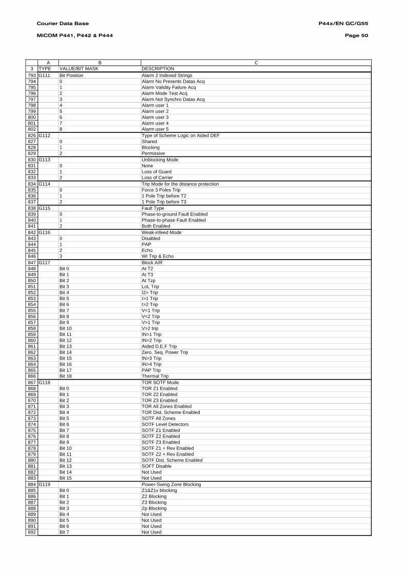
Courier Data Base
MiCOM P441, P442 & P444
P44x/EN GC/G55
Page 50
3A B C
TYPE VALUE/BIT MASK DESCRIPTION793794795796797798799800801802826827828829830831832833834835836837838839840841842843844845846847848849850851852853854855856857858859860861862863864865866867868869870871872873874875876877878879880881882883884885886887888889890891892
G111 Bit Position Alarm 2 Indexed Strings0 Alarm No Presents Datas Acq1 Alarm Validity Failure Acq2 Alarm Mode Test Acq3 Alarm Not Synchro Datas Acq4 Alarm user 15 Alarm user 26 Alarm user 37 Alarm user 48 Alarm user 5
G112 Type of Scheme Logic on Aided DEF0 Shared1 Blocking2 Permissive
G113 Unblocking Mode0 None1 Loss of Guard2 Loss of Carrier
G114 Trip Mode for the distance protection0 Force 3 Poles Trip1 1 Pole Trip before T22 1 Pole Trip before T3
G115 Fault Type 0 Phase-to-ground Fault Enabled1 Phase-to-phase Fault Enabled2 Both Enabled
G116 Weak-infeed Mode0 Disabled1 PAP2 Echo3 WI Trip & Echo
G117 Block A/RBit 0 At T2Bit 1 At T3Bit 2 At TzpBit 3 LoL TripBit 4 I2> TripBit 5 I>1 TripBit 6 I>2 TripBit 7 V<1 TripBit 8 V<2 TripBit 9 V>1 TripBit 10 V>2 tripBit 11 IN>1 TripBit 12 IN>2 TripBit 13 Aided D.E.F TripBit 14 Zero. Seq. Power TripBit 15 IN>3 TripBit 16 IN>4 TripBit 17 PAP TripBit 18 Thermal Trip
G118 TOR SOTF ModeBit 0 TOR Z1 EnabledBit 1 TOR Z2 EnabledBit 2 TOR Z3 EnabledBit 3 TOR All Zones EnabledBit 4 TOR Dist. Scheme EnabledBit 5 SOTF All ZonesBit 6 SOTF Level DetectorsBit 7 SOTF Z1 EnabledBit 8 SOTF Z2 EnabledBit 9 SOTF Z3 EnabledBit 10 SOTF Z1 + Rev EnabledBit 11 SOTF Z2 + Rev EnabledBit 12 SOTF Dist. Scheme EnabledBit 13 SOFT DisableBit 14 Not UsedBit 15 Not Used
G119 Power-Swing Zone BlockingBit 0 Z1&Z1x blockingBit 1 Z2 BlockingBit 2 Z3 BlockingBit 3 Zp BlockingBit 4 Not UsedBit 5 Not UsedBit 6 Not UsedBit 7 Not Used
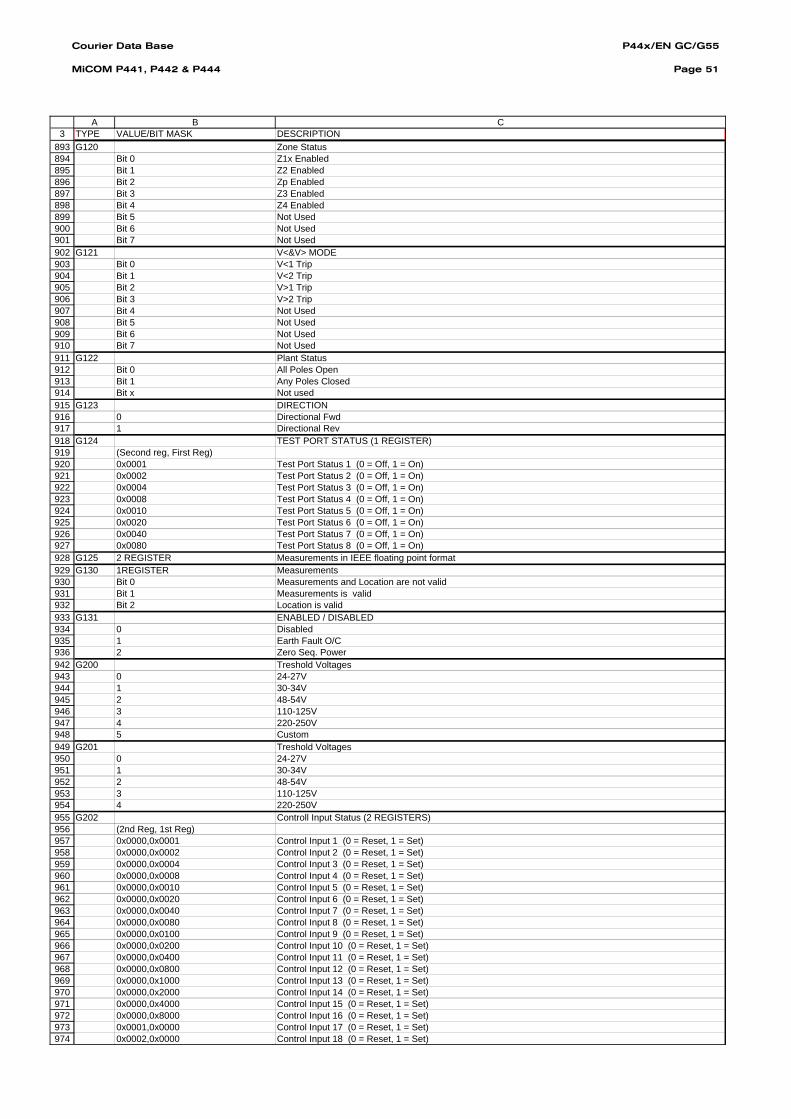
Courier Data Base
MiCOM P441, P442 & P444
P44x/EN GC/G55
Page 51
3A B C
TYPE VALUE/BIT MASK DESCRIPTION893894895896897898899900901902903904905906907908909910911912913914915916917918919920921922923924925926927928929930931932933934935936942943944945946947948949950951952953954955956957958959960961962963964965966967968969970971972973974
G120 Zone StatusBit 0 Z1x EnabledBit 1 Z2 EnabledBit 2 Zp EnabledBit 3 Z3 EnabledBit 4 Z4 EnabledBit 5 Not UsedBit 6 Not UsedBit 7 Not Used
G121 V<&V> MODEBit 0 V<1 TripBit 1 V<2 TripBit 2 V>1 TripBit 3 V>2 TripBit 4 Not UsedBit 5 Not UsedBit 6 Not UsedBit 7 Not Used
G122 Plant StatusBit 0 All Poles OpenBit 1 Any Poles ClosedBit x Not used
G123 DIRECTION0 Directional Fwd1 Directional Rev
G124 TEST PORT STATUS (1 REGISTER)(Second reg, First Reg)0x0001 Test Port Status 1 (0 = Off, 1 = On)0x0002 Test Port Status 2 (0 = Off, 1 = On)0x0004 Test Port Status 3 (0 = Off, 1 = On)0x0008 Test Port Status 4 (0 = Off, 1 = On)0x0010 Test Port Status 5 (0 = Off, 1 = On)0x0020 Test Port Status 6 (0 = Off, 1 = On)0x0040 Test Port Status 7 (0 = Off, 1 = On)0x0080 Test Port Status 8 (0 = Off, 1 = On)
G125 2 REGISTER Measurements in IEEE floating point formatG130 1REGISTER Measurements
Bit 0 Measurements and Location are not validBit 1 Measurements is validBit 2 Location is valid
G131 ENABLED / DISABLED0 Disabled1 Earth Fault O/C2 Zero Seq. Power
G200 Treshold Voltages0 24-27V1 30-34V2 48-54V3 110-125V4 220-250V5 Custom
G201 Treshold Voltages0 24-27V1 30-34V2 48-54V3 110-125V4 220-250V
G202 Controll Input Status (2 REGISTERS)(2nd Reg, 1st Reg)0x0000,0x0001 Control Input 1 (0 = Reset, 1 = Set)0x0000,0x0002 Control Input 2 (0 = Reset, 1 = Set)0x0000,0x0004 Control Input 3 (0 = Reset, 1 = Set)0x0000,0x0008 Control Input 4 (0 = Reset, 1 = Set)0x0000,0x0010 Control Input 5 (0 = Reset, 1 = Set)0x0000,0x0020 Control Input 6 (0 = Reset, 1 = Set)0x0000,0x0040 Control Input 7 (0 = Reset, 1 = Set)0x0000,0x0080 Control Input 8 (0 = Reset, 1 = Set)0x0000,0x0100 Control Input 9 (0 = Reset, 1 = Set)0x0000,0x0200 Control Input 10 (0 = Reset, 1 = Set)0x0000,0x0400 Control Input 11 (0 = Reset, 1 = Set)0x0000,0x0800 Control Input 12 (0 = Reset, 1 = Set)0x0000,0x1000 Control Input 13 (0 = Reset, 1 = Set)0x0000,0x2000 Control Input 14 (0 = Reset, 1 = Set)0x0000,0x4000 Control Input 15 (0 = Reset, 1 = Set)0x0000,0x8000 Control Input 16 (0 = Reset, 1 = Set)0x0001,0x0000 Control Input 17 (0 = Reset, 1 = Set)0x0002,0x0000 Control Input 18 (0 = Reset, 1 = Set)

Courier Data Base
MiCOM P441, P442 & P444
P44x/EN GC/G55
Page 52
3A B C
TYPE VALUE/BIT MASK DESCRIPTION9759769779789799809819829839849859869879889899909919929939949959969979989991000100110021003100410051006100710081009101010111012101310141015101610171018101910201021102210231024102510261027102810291030103110321033103410351036103710381039104010411042104310441045104610471048104910501051
0x0004,0x0000 Control Input 19 (0 = Reset, 1 = Set)0x0008,0x0000 Control Input 20 (0 = Reset, 1 = Set)0x0010,0x0000 Control Input 21 (0 = Reset, 1 = Set)0x0020,0x0000 Control Input 22 (0 = Reset, 1 = Set)0x0040,0x0000 Control Input 23 (0 = Reset, 1 = Set)0x0080,0x0000 Control Input 24 (0 = Reset, 1 = Set)0x0100,0x0000 Control Input 25 (0 = Reset, 1 = Set)0x0200,0x0000 Control Input 26 (0 = Reset, 1 = Set)0x0400,0x0000 Control Input 27 (0 = Reset, 1 = Set)0x0800,0x0000 Control Input 28 (0 = Reset, 1 = Set)0x1000,0x0000 Control Input 29 (0 = Reset, 1 = Set)0x2000,0x0000 Control Input 30 (0 = Reset, 1 = Set)0x4000,0x0000 Control Input 31 (0 = Reset, 1 = Set)0x8000,0x0000 Control Input 32 (0 = Reset, 1 = Set)
G203 Virtual Input0 No Operation1 Set 2 Reset
G204 TEST MODE0 Disabled1 Test Mode2 Blocked
G205 CB Fail Reset Options0 I< Only1 CB Open & I<2 Prot Reset & I<3 Disable4 Prot Reset Or I<
G206 COMMS MODE (RCUR1)0 IEC60870 FT1.21 10-bit
G207 PORT CONFIG (RCUR1)0 K Bus1 EIA485 (RS485)
G208 STATUS (RCUR1)0 K Bus OK1 EIA485 OK2 Fibre Optic
G211 Blocking Command0 Blk_Disable1 Blk_Direct2 Blk_Blocking
G212 Trip Command0 Trip_Disable1 Trip_Permissive2 Trip_Direct
G213 Baud rate0 6001 12002 24003 48004 96005 19200
G215 Trip0 Default1 Latched
G218 Remote device type0 Remote_PX401 Remote PX30
G231 DIRECT ACCESS KEYS0 Disabled1 Enabled
G232 CONTROL INPUT COMMAND TEXT0 ON/OFF1 SET/RESET2 IN/OUT3 ENABLED/DISABLED
G233 HOTKEY ENABLED CONTROL INPUTS0x00000001 Control Input 10x00000002 Control Input 20x00000004 Control Input 30x00000008 Control Input 40x00000010 Control Input 50x00000020 Control Input 60x00000040 Control Input 70x00000080 Control Input 80x00000100 Control Input 9

Courier Data Base
MiCOM P441, P442 & P444
P44x/EN GC/G55
Page 53
3A B C
TYPE VALUE/BIT MASK DESCRIPTION10521053105410551056105710581059106010611062106310641065106610671068106910701071107210731074107510761077107810791080108110821083108410851086108710881089109010911092109310941095109610971098109911001101110211031104110511061107110811091110111111121113111411151116111711181119112011211122112311241125112611271128
0x00000200 Control Input 100x00000400 Control Input 110x00000800 Control Input 120x00001000 Control Input 130x00002000 Control Input 140x00004000 Control Input 150x00008000 Control Input 160x00010000 Control Input 170x00020000 Control Input 180x00040000 Control Input 190x00080000 Control Input 200x00100000 Control Input 210x00200000 Control Input 220x00400000 Control Input 230x00800000 Control Input 240x01000000 Control Input 250x02000000 Control Input 260x04000000 Control Input 270x08000000 Control Input 280x10000000 Control Input 290x20000000 Control Input 300x40000000 Control Input 310x80000000 Control Input 32
G234 CONTROL INPUT SIGNAL TYPE0 Latched1 Pulsed
G235 ETHERNET PROTOCOL0 UCA 2.01 UCA 2.0 GOOSE
G237 Characteristic0 Standard 60%-80%1 50% - 70 %
G250 Alarm Status 30 Battery fail1 Field Volt Fail2 Rear Comms fail3 GOOSE IED Absent4 NIC Not Fitted5 NIC No Response6 NIC Fatal Error7 NIC Soft. Reload8 Bad TCP/IP Cfg.9 Bad OSI Config.10 NIC Link Fail11 NIC SW Mis-Match12 IP Addr Conflict13 Reserved for InterMiCOM and other platform alarms
G251 RELAY OUTPUT STATUS(Second reg, First Reg)0x0000,0x0001 Relay 33 (0=Not Operated, 1=Operated)0x0000,0x0002 Relay 34 (0=Not Operated, 1=Operated)0x0000,0x0004 Relay 35 (0=Not Operated, 1=Operated)0x0000,0x0008 Relay 36 (0=Not Operated, 1=Operated)0x0000,0x0010 Relay 37 (0=Not Operated, 1=Operated)0x0000,0x0020 Relay 38 (0=Not Operated, 1=Operated)0x0000,0x0040 Relay 39 (0=Not Operated, 1=Operated)0x0000,0x0080 Relay 40 (0=Not Operated, 1=Operated)0x0000,0x0100 Relay 41 (0=Not Operated, 1=Operated)0x0000,0x0200 Relay 42 (0=Not Operated, 1=Operated)0x0000,0x0400 Relay 43 (0=Not Operated, 1=Operated)0x0000,0x0800 Relay 44 (0=Not Operated, 1=Operated)0x0000,0x1000 Relay 45 (0=Not Operated, 1=Operated)0x0000,0x2000 Relay 46 (0=Not Operated, 1=Operated)0x0000,0x4000 Unused0x0000,0x8000 Unused0x0001,0x0000 Unused0x0002,0x0000 Unused0x0004,0x0000 Unused0x0008,0x0000 Unused0x0010,0x0000 Unused0x0020,0x0000 Unused0x0040,0x0000 Unused0x0080,0x0000 Unused0x0100,0x0000 Unused0x0200,0x0000 Unused0x0400,0x0000 Unused0x0800,0x0000 Unused

Courier Data Base
MiCOM P441, P442 & P444
P44x/EN GC/G55
Page 54
3A B C
TYPE VALUE/BIT MASK DESCRIPTION11291130113111321133113411351136113711381139114011411142114311441145114611471148114911501151115211531154
0x1000,0x0000 Unused0x2000,0x0000 Unused0x4000,0x0000 Unused0x8000,0x0000 Unused
G239 IEC61850-9.2LE0 Electrical1 Fibre Optic
G240 Logical Node Arrangement0 LN 11 LN1(without I0)-LN2(I0)2 LN1-LN2(I0)3 LN1-LN2(6I)4 LN1-LN2(3 I)5 LN1-LN1B6 LN1-LN1B-LN2B7 LN1-LN2(6I)-LN1B8 LN1-LN2(I0)-LN1B9 4 LN (I0)10 4 LN (6i)
G302 CHECK SYNC INPUT SELECTION0 A-N1 B-N2 C-N3 A-B4 B-C5 C-A

Courier Data Base
MiCOM P441, P442 & P444
P44x/EN GC/G55
Page 55
Part C: Internal Digital Signals - DDB Element
DDB Element Name Ordinal English Text Description SourceDDB_ENTRY (DDB_OUTPUT_RELAY_1 0 Relay Label 01 OUTPUT RELAY 1 RELAYDDB_ENTRY (DDB_OUTPUT_RELAY_2 1 Relay Label 02 OUTPUT RELAY 2 RELAYDDB_ENTRY (DDB_OUTPUT_RELAY_3 2 Relay Label 03 OUTPUT RELAY 3 RELAYDDB_ENTRY (DDB_OUTPUT_RELAY_4 3 Relay Label 04 OUTPUT RELAY 4 RELAYDDB_ENTRY (DDB_OUTPUT_RELAY_5 4 Relay Label 05 OUTPUT RELAY 5 RELAYDDB_ENTRY (DDB_OUTPUT_RELAY_6 5 Relay Label 06 OUTPUT RELAY 6 RELAYDDB_ENTRY (DDB_OUTPUT_RELAY_7 6 Relay Label 07 OUTPUT RELAY 7 RELAYDDB_ENTRY (DDB_OUTPUT_RELAY_8 7 Relay Label 08 OUTPUT RELAY 8 RELAYDDB_ENTRY (DDB_OUTPUT_RELAY_9 8 Relay Label 09 OUTPUT RELAY 9 RELAYDDB_ENTRY (DDB_OUTPUT_RELAY_10 9 Relay Label 10 OUTPUT RELAY 10 RELAYDDB_ENTRY (DDB_OUTPUT_RELAY_11 10 Relay Label 11 OUTPUT RELAY 11 RELAYDDB_ENTRY (DDB_OUTPUT_RELAY_12 11 Relay Label 12 OUTPUT RELAY 12 RELAYDDB_ENTRY (DDB_OUTPUT_RELAY_13 12 Relay Label 13 OUTPUT RELAY 13 RELAYDDB_ENTRY (DDB_OUTPUT_RELAY_14 13 Relay Label 14 OUTPUT RELAY 14 RELAYDDB_ENTRY (DDB_OUTPUT_RELAY_15 14 Relay Label 15 OUTPUT RELAY 15 RELAYDDB_ENTRY (DDB_OUTPUT_RELAY_16 15 Relay Label 16 OUTPUT RELAY 16 RELAYDDB_ENTRY (DDB_OUTPUT_RELAY_17 16 Relay Label 17 OUTPUT RELAY 17 RELAYDDB_ENTRY (DDB_OUTPUT_RELAY_18 17 Relay Label 18 OUTPUT RELAY 18 RELAYDDB_ENTRY (DDB_OUTPUT_RELAY_19 18 Relay Label 19 OUTPUT RELAY 19 RELAYDDB_ENTRY (DDB_OUTPUT_RELAY_20 19 Relay Label 20 OUTPUT RELAY 20 RELAYDDB_ENTRY (DDB_OUTPUT_RELAY_21 20 Relay Label 21 OUTPUT RELAY 21 RELAYDDB_ENTRY (DDB_OUTPUT_RELAY_22 21 Relay Label 22 OUTPUT RELAY 22 RELAYDDB_ENTRY (DDB_OUTPUT_RELAY_23 22 Relay Label 23 OUTPUT RELAY 23 RELAYDDB_ENTRY (DDB_OUTPUT_RELAY_24 23 Relay Label 24 OUTPUT RELAY 24 RELAYDDB_ENTRY (DDB_OUTPUT_RELAY_25 24 Relay Label 25 OUTPUT RELAY 25 RELAYDDB_ENTRY (DDB_OUTPUT_RELAY_26 25 Relay Label 26 OUTPUT RELAY 26 RELAYDDB_ENTRY (DDB_OUTPUT_RELAY_27 26 Relay Label 27 OUTPUT RELAY 27 RELAYDDB_ENTRY (DDB_OUTPUT_RELAY_28 27 Relay Label 28 OUTPUT RELAY 28 RELAYDDB_ENTRY (DDB_OUTPUT_RELAY_29 28 Relay Label 29 OUTPUT RELAY 29 RELAYDDB_ENTRY (DDB_OUTPUT_RELAY_30 29 Relay Label 30 OUTPUT RELAY 30 RELAYDDB_ENTRY (DDB_OUTPUT_RELAY_31 30 Relay Label 31 OUTPUT RELAY 31 RELAYDDB_ENTRY (DDB_OUTPUT_RELAY_32 31 Relay Label 32 OUTPUT RELAY 32 RELAYDDB_ENTRY (DDB_OUTPUT_RELAY_33 32 Relay Label 33 OUTPUT RELAY 33 RELAYDDB_ENTRY (DDB_OUTPUT_RELAY_34 33 Relay Label 34 OUTPUT RELAY 34 RELAYDDB_ENTRY (DDB_OUTPUT_RELAY_35 34 Relay Label 35 OUTPUT RELAY 35 RELAYDDB_ENTRY (DDB_OUTPUT_RELAY_36 35 Relay Label 36 OUTPUT RELAY 36 RELAYDDB_ENTRY (DDB_OUTPUT_RELAY_37 36 Relay Label 37 OUTPUT RELAY 37 RELAYDDB_ENTRY (DDB_OUTPUT_RELAY_38 37 Relay Label 38 OUTPUT RELAY 38 RELAYDDB_ENTRY (DDB_OUTPUT_RELAY_39 38 Relay Label 39 OUTPUT RELAY 39 RELAYDDB_ENTRY (DDB_OUTPUT_RELAY_40 39 Relay Label 40 OUTPUT RELAY 40 RELAYDDB_ENTRY (DDB_OUTPUT_RELAY_41 40 Relay Label 41 OUTPUT RELAY 41 RELAYDDB_ENTRY (DDB_OUTPUT_RELAY_42 41 Relay Label 42 OUTPUT RELAY 42 RELAYDDB_ENTRY (DDB_OUTPUT_RELAY_43 42 Relay Label 43 OUTPUT RELAY 43 RELAYDDB_ENTRY (DDB_OUTPUT_RELAY_44 43 Relay Label 44 OUTPUT RELAY 44 RELAYDDB_ENTRY (DDB_OUTPUT_RELAY_45 44 Relay Label 45 OUTPUT RELAY 45 RELAYDDB_ENTRY (DDB_OUTPUT_RELAY_46 45 Relay Label 46 OUTPUT RELAY 46 RELAYDDB_ENTRY (DDB_OUTPUT_RELAY_47 46 Relay Label 47 OUTPUT RELAY 47 RELAYDDB_ENTRY (DDB_OUTPUT_RELAY_48 47 Relay Label 48 OUTPUT RELAY 48 RELAYDDB_ENTRY (DDB_OUTPUT_RELAY_49 48 Relay Label 49 OUTPUT RELAY 49 RELAYDDB_ENTRY (DDB_OUTPUT_RELAY_50 49 Relay Label 50 OUTPUT RELAY 50 RELAYDDB_ENTRY (DDB_OUTPUT_RELAY_51 50 Relay Label 51 OUTPUT RELAY 51 RELAYDDB_ENTRY (DDB_OUTPUT_RELAY_52 51 Relay Label 52 OUTPUT RELAY 52 RELAYDDB_ENTRY (DDB_OUTPUT_RELAY_53 52 Relay Label 53 OUTPUT RELAY 53 RELAYDDB_ENTRY (DDB_OUTPUT_RELAY_54 53 Relay Label 54 OUTPUT RELAY 54 RELAYDDB_ENTRY (DDB_OUTPUT_RELAY_55 54 Relay Label 55 OUTPUT RELAY 55 RELAYDDB_ENTRY (DDB_OUTPUT_RELAY_56 55 Relay Label 56 OUTPUT RELAY 56 RELAYDDB_ENTRY (DDB_OUTPUT_RELAY_57 56 Relay Label 57 OUTPUT RELAY 57 RELAYDDB_ENTRY (DDB_OUTPUT_RELAY_58 57 Relay Label 58 OUTPUT RELAY 58 RELAYDDB_ENTRY (DDB_OUTPUT_RELAY_59 58 Relay Label 59 OUTPUT RELAY 59 RELAYDDB_ENTRY (DDB_OUTPUT_RELAY_60 59 Relay Label 60 OUTPUT RELAY 60 RELAYDDB_ENTRY (DDB_OUTPUT_RELAY_61 60 Relay Label 61 OUTPUT RELAY 61 RELAYDDB_ENTRY (DDB_OUTPUT_RELAY_62 61 Relay Label 62 OUTPUT RELAY 62 RELAYDDB_ENTRY (DDB_OUTPUT_RELAY_63 62 Relay Label 63 OUTPUT RELAY 63 RELAYDDB_ENTRY (DDB_OUTPUT_RELAY_64 63 Relay Label 64 OUTPUT RELAY 64 RELAYDDB_ENTRY (DDB_OPTO_ISOLATOR_1 64 Opto Label 01 OPTO ISOLATOR 1 OPTODDB_ENTRY (DDB_OPTO_ISOLATOR_2 65 Opto Label 02 OPTO ISOLATOR 2 OPTODDB_ENTRY (DDB_OPTO_ISOLATOR_3 66 Opto Label 03 OPTO ISOLATOR 3 OPTODDB_ENTRY (DDB_OPTO_ISOLATOR_4 67 Opto Label 04 OPTO ISOLATOR 4 OPTODDB_ENTRY (DDB_OPTO_ISOLATOR_5 68 Opto Label 05 OPTO ISOLATOR 5 OPTODDB_ENTRY (DDB_OPTO_ISOLATOR_6 69 Opto Label 06 OPTO ISOLATOR 6 OPTODDB_ENTRY (DDB_OPTO_ISOLATOR_7 70 Opto Label 07 OPTO ISOLATOR 7 OPTODDB_ENTRY (DDB_OPTO_ISOLATOR_8 71 Opto Label 08 OPTO ISOLATOR 8 OPTODDB_ENTRY (DDB_OPTO_ISOLATOR_9 72 Opto Label 09 OPTO ISOLATOR 9 OPTODDB_ENTRY (DDB_OPTO_ISOLATOR_10 73 Opto Label 10 OPTO ISOLATOR 10 OPTODDB_ENTRY (DDB_OPTO_ISOLATOR_11 74 Opto Label 11 OPTO ISOLATOR 11 OPTODDB_ENTRY (DDB_OPTO_ISOLATOR_12 75 Opto Label 12 OPTO ISOLATOR 12 OPTODDB_ENTRY (DDB_OPTO_ISOLATOR_13 76 Opto Label 13 OPTO ISOLATOR 13 OPTODDB_ENTRY (DDB_OPTO_ISOLATOR_14 77 Opto Label 14 OPTO ISOLATOR 14 OPTODDB_ENTRY (DDB_OPTO_ISOLATOR_15 78 Opto Label 15 OPTO ISOLATOR 15 OPTODDB_ENTRY (DDB_OPTO_ISOLATOR_16 79 Opto Label 16 OPTO ISOLATOR 16 OPTODDB_ENTRY (DDB_OPTO_ISOLATOR_17 80 Opto Label 17 OPTO ISOLATOR 17 OPTODDB_ENTRY (DDB_OPTO_ISOLATOR_18 81 Opto Label 18 OPTO ISOLATOR 18 OPTODDB_ENTRY (DDB_OPTO_ISOLATOR_19 82 Opto Label 19 OPTO ISOLATOR 19 OPTODDB_ENTRY (DDB_OPTO_ISOLATOR_20 83 Opto Label 20 OPTO ISOLATOR 20 OPTODDB_ENTRY (DDB_OPTO_ISOLATOR_21 84 Opto Label 21 OPTO ISOLATOR 21 OPTODDB_ENTRY (DDB_OPTO_ISOLATOR_22 85 Opto Label 22 OPTO ISOLATOR 22 OPTODDB_ENTRY (DDB_OPTO_ISOLATOR_23 86 Opto Label 23 OPTO ISOLATOR 23 OPTODDB_ENTRY (DDB_OPTO_ISOLATOR_24 87 Opto Label 24 OPTO ISOLATOR 24 OPTODDB_ENTRY (DDB_OPTO_ISOLATOR_25 88 Opto Label 25 OPTO ISOLATOR 25 OPTODDB_ENTRY (DDB_OPTO_ISOLATOR_26 89 Opto Label 26 OPTO ISOLATOR 26 OPTODDB_ENTRY (DDB_OPTO_ISOLATOR_27 90 Opto Label 27 OPTO ISOLATOR 27 OPTODDB_ENTRY (DDB_OPTO_ISOLATOR_28 91 Opto Label 28 OPTO ISOLATOR 28 OPTODDB_ENTRY (DDB_OPTO_ISOLATOR_29 92 Opto Label 29 OPTO ISOLATOR 29 OPTODDB_ENTRY (DDB_OPTO_ISOLATOR_30 93 Opto Label 30 OPTO ISOLATOR 30 OPTODDB_ENTRY (DDB_OPTO_ISOLATOR_31 94 Opto Label 31 OPTO ISOLATOR 31 OPTODDB_ENTRY (DDB_OPTO_ISOLATOR_32 95 Opto Label 32 OPTO ISOLATOR 32 OPTODDB_ENTRY (DDB_OUTPUT_LED_1 96 LED 1 Programmable LED 1 (By default TRIP A) LEDDDB_ENTRY (DDB_OUTPUT_LED_2 97 LED 2 Programmable LED 2 (By default TRIP B) LEDDDB_ENTRY (DDB_OUTPUT_LED_3 98 LED 3 Programmable LED 3 (By default TRIP C) LEDDDB_ENTRY (DDB_OUTPUT_LED_4 99 LED 4 Programmable LED 4 (By default GENERAL START) LEDDDB_ENTRY (DDB_OUTPUT_LED_5 100 LED 5 Programmable LED 5 (By default ZONE 1 + AIDED TRIP) LEDDDB_ENTRY (DDB_OUTPUT_LED_6 101 LED 6 Programmable LED 6 (By default FORWARD) LEDDDB_ENTRY (DDB_OUTPUT_LED_7 102 LED 7 Programmable LED 7 (By default REVERSE) LEDDDB_ENTRY (DDB_OUTPUT_LED_8 103 LED 8 Programmable LED 8 (By default AUTORECLOSE ENABLE) LEDDDB_ENTRY (DDB_INP_52A_A 104 CB Aux A (52-A) Circuit breaker pole A closed/Status input from CB PSL (IN) CB STATUSDDB_ENTRY (DDB_INP_52B_A 105 CB Aux A (52-B) Circuit breaker pole A closed/Status input from CB PSL (IN) CB STATUSDDB_ENTRY (DDB_INP_52A_B 106 CB Aux B (52-A) Circuit breaker pole A closed/Status input from CB PSL (IN) CB STATUSDDB_ENTRY (DDB_INP_52B_B 107 CB Aux B (52-B) Circuit breaker pole A closed/Status input from CB PSL (IN) CB STATUS

Courier Data Base
MiCOM P441, P442 & P444
P44x/EN GC/G55
Page 56
Part C: Internal Digital Signals - DDB Element
DDB Element Name Ordinal English Text Description SourceDDB_ENTRY (DDB_INP_52A_C 108 CB Aux C (52-A) Circuit breaker pole A closed/Status input from CB PSL (IN) CB STATUSDDB_ENTRY (DDB_INP_52B_C 109 CB Aux C (52-B) Circuit breaker pole A closed/Status input from CB PSL (IN) CB STATUSDDB_ENTRY (DDB_INP_SPAR 110 SPAR Enable Enable internal single pole autorecloser PSL (IN) AutorecloserDDB_ENTRY (DDB_INP_TPAR 111 TPAR Enable Enable internal three pole autorecloser PSL (IN) AutorecloserDDB_ENTRY (DDB_INP_AR_INTERNAL 112 A/R Internal Give internal autorecloser present (visible) PSL (IN) AutorecloserDDB_ENTRY (DDB_INP_AR_CYCLE_1P 113 A/R 1p In Prog. One-pole external autoreclose cycle in progress PSL (IN) AutorecloserDDB_ENTRY (DDB_INP_AR_CYCLE_3P 114 A/R 3p In Prog. Three-pole external autoreclose cycle in progress PSL (IN) AutorecloserDDB_ENTRY (DDB_INP_AR_CLOSING 115 A/R Close Circuit Breaker closing order from external autoreclose PSL (IN) AutorecloserDDB_ENTRY (DDB_INP_RECLAIM 116 A/R Reclaim External autorecloser in reclaim PSL (IN) AutorecloserDDB_ENTRY (DDB_INP_BAR 117 BAR Block internal autoreclose PSL (IN) Autorecloser
DDB_ENTRY (DDB_INP_CTL_CHECK_SYNCH 118 Ext Chk Synch OK Autorisation signal from external check Synchroniser for reclosing with internal A/R PSL (IN) Autorecloser
DDB_ENTRY (DDB_INP_CB_HEALTHY 119 CB Healthy Circuit breaker operational (gas pressure, mechanical state) PSL (IN) CB STATUSDDB_ENTRY (DDB_INP_BLK_PROTECTION 120 BLK Protection Block all protection functions (21/67N/50/51/…) PSL (IN) All protectionDDB_ENTRY (DDB_INP_TRP_3P 121 Force 3P Trip Three pole tripping only PSL (IN)DDB_ENTRY (DDB_INP_CB_MAN 122 Man. Close CB Circuit breaker manual close - order received PSL (IN) CB StatusDDB_ENTRY (DDB_INP_CB_TRIP_MAN 123 Man. Trip CB Circuit breaker manual trip - order received PSL (IN) CB StatusDDB_ENTRY (DDB_INP_DISC 124 CB Discrepancy CB Discrepancy (one pole open) PSL (IN) CB StatusDDB_ENTRY (DDB_INP_PROTA 125 External Trip A Phase A trip by external protection relay PSL (IN)DDB_ENTRY (DDB_INP_PROTB 126 External Trip B Phase B trip by external protection relay PSL (IN)DDB_ENTRY (DDB_INP_PROTC 127 External Trip C Phase C trip by external protection relay PSL (IN)DDB_ENTRY (DDB_INP_CR 128 DIST. Chan Recv Signal receive on main channel (Distance) PSL (IN) Un-blocking logicDDB_ENTRY (DDB_INP_CR_DEF 129 DEF. Chan Recv Signal receive on DEF channel PSL (IN) Un-blocking logic
DDB_ENTRY (DDB_INP_COS 130 DIST. COS Distance scheme channel out of service / Loss of Guard (Carrier out of service) PSL (IN) Un-blocking logic
DDB_ENTRY (DDB_INP_COS_DEF 131 DEF. COS DEF scheme channel out of service / Loss of Guard PSL (IN) Un-blocking logicDDB_ENTRY (DDB_INP_Z1X_EXT 132 Z1X Extension Zone 1 Extension Input PSL (IN)
DDB_ENTRY (DDB_INP_MCB_VTS_BUS 133 MCB/VTS Bus Fuse failure on busbar VT or MCB open (blocks voltage dependant functions) PSL (IN) VTS
DDB_ENTRY (DDB_INP_MCB_VTS_LINE 134 MCB/VTS Line Fuse failure on line VT or MCB open (blocks voltage dependant functions) PSL (IN) VTS
DDB_ENTRY (DDB_INP_SBEF_TIMER_BLOCK_1 135 IN>1 Timer Block Block earth fault stage 1 time delay PSL (IN) Earth FaultDDB_ENTRY (DDB_INP_SBEF_TIMER_BLOCK_2 136 IN>2 Timer Block Block earth fault stage 2 time delay PSL (IN) Earth FaultDDB_ENTRY (DDB_INP_DEF_TIMER_BLOCK 137 DEF Timer Block Block aided DEF time delay PSL (IN) DEFDDB_ENTRY (DDB_INP_PHOC_TIMER_BLOCK_1 138 I>1 Timer Block Block phase overcurrent stage 1 time delay PSL (IN) I>1DDB_ENTRY (DDB_INP_PHOC_TIMER_BLOCK_2 139 I>2 Timer Block Block phase overcurrent stage 2 time delay PSL (IN) I>2DDB_ENTRY (DDB_INP_PHOC_TIMER_BLOCK_3 140 I>3 Timer Block Block phase overcurrent stage 3 time delay PSL (IN) I>3DDB_ENTRY (DDB_INP_PHOC_TIMER_BLOCK_4 141 I>4 Timer Block Block phase overcurrent stage 4 time delay PSL (IN) I>4DDB_ENTRY (DDB_INP_NPS_TIMER_BLOCK 142 I2> Timer Block Block negative sequence overcurrent time delay PSL (IN) I>4DDB_ENTRY (DDB_INP_UNDU_TIMER_BLOCK_1 143 V<1 Timer Block Block phase undervoltage stage 1 time delay PSL (IN) V<1DDB_ENTRY (DDB_INP_UNDU_TIMER_BLOCK_2 144 V<2 Timer Block Block phase undervoltage stage 2 time delay PSL (IN) V<2DDB_ENTRY (DDB_INP_OVEU_TIMER_BLOCK_1 145 V>1 Timer Block Block phase overvoltage stage 1 time delay PSL (IN) V>1DDB_ENTRY (DDB_INP_OVEU_TIMER_BLOCK_2 146 V>2 Timer Block Block phase overvoltage stage 2 time delay PSL (IN) V>2DDB_ENTRY (DDB_INP_DISTANCE_TIMER_BLOCK 147 DIST. Tim. Block Block distance element time delay PSL (IN) DistanceDDB_ENTRY (DDB_INP_CB_RESET_LOCKOUT 148 Reset Lockout CB monitoring lockout reset PSL (IN) CB MonitoringDDB_ENTRY (DDB_INP_CB_RESET_ALL_VALUES 149 Reset All values Reset all values of CB monitoring PSL (IN) CB MonitoringDDB_ENTRY (DDB_INP_RESET_RELAYS_LEDS 150 Reset Latches Reset all permanent alarms + led and relay lached PSl (IN)
DDB_ENTRY (DDB_INP_STUB_BUS 151 Stub Bus Enable Enable I>4 Element for stub bus protection (isolator of HV line open - status isolator must be connected to an opto input) PSL (IN)
DDB_ENTRY (DDB_INP_TRIP_A_USER 152 User Trip A Internal input for trip logic A PSL (IN) Trip LogicDDB_ENTRY (DDB_INP_TRIP_B_USER 153 User Trip B Internal input for trip logic B PSL (IN) Trip LogicDDB_ENTRY (DDB_INP_TRIP_C_USER 154 User Trip C Internal input for trip logic C PSL (IN) Trip LogicDDB_ENTRY (DDB_INP_ZSP_TIMER_BLOCK 155 ZSP Timer Block Zero Sequence Power - Timer Block PSL (IN) ZSPDDB_ENTRY (DDB_INP_PAP_TELETRIP_REC 156 PAP Tele Trip CR PAP Carrier Receive for teletransmission PSL(IN)DDB_ENTRY (DDB_INP_PAP_TELETRIP_HEALT 157 PAP Tele Trip Hea PAP Carrier Out of Service (DT trip decision) PSL(IN)DDB_ENTRY (DDB_INP_PAP_TIMER_BLOCK 158 PAP Timer Block Timer Block for frosen every timer initiated with PAP function PSL(IN)DDB_ENTRY (DDB_INP_SBEF_TIMER_BLOCK_3 159 IN>3 Timer Block Timer Block for frosen timer initiated with IN>3 function PSL(IN)DDB_ENTRY (DDB_INP_SBEF_TIMER_BLOCK_4 160 IN>4 Timer Block Timer Block for frosen timer initiated with IN>4 function PSL(IN)DDB_ENTRY (DDB_INP_RESET_THERMAL 161 Reset Thermal Reset Thermal Overload Protection PSL(IN)DDB_ENTRY (DDB_INP_TIMESYNC 162 Time Synchro External time synchronisation input PSL(IN)DDB_ENTRY (DDB_ALARM_GENERAL 174 General Alarm Groupment of all alarms PSL (OUT) DDB_ENTRY (DDB_ALARM_PROT_DISABLED 175 Prot'n Disabled Test mode enabled every protection out of order PSL (OUT) DDB_ENTRY (DDB_ALARM_F_OUT_OF_RANGE 176 F out of Range Frequency tracking not working correctly PSL (OUT) DDB_ENTRY (DDB_ALARM_VTS_SLOW 177 VT Fail Alarm Fuse failure indication (VT alarm) PSL (OUT) VT SupervisionDDB_ENTRY (DDB_ALARM_CTS 178 CT Fail Alarm Current transformers supervision indication PSL (OUT) CT SupervisionDDB_ENTRY (DDB_ALARM_BREAKER_FAIL 179 CB Fail Alarm Circuit breaker failure on any trip PSL (OUT) Breaker FailDDB_ENTRY (DDB_ALARM_I_BROK_MAINT 180 I^ Maint Alarm Broken current maintenance alarm (1st level) PSL (OUT) CB monitoringDDB_ENTRY (DDB_ALARM_I_BROK_LOCKOUT 181 I^ Lockout Alarm Broken current lockout alarm (2nd level) PSL (OUT) CB monitoringDDB_ENTRY (DDB_ALARM_CB_OPS_MAINT 182 CB Ops Maint Alarm on number of circuit breaker operations PSL (OUT) CB monitoringDDB_ENTRY (DDB_ALARM_CB_OPS_LOCKOUT 183 CB Ops Lockout Lockout on number of circuit breaker operations PSL (OUT) CB monitoringDDB_ENTRY (DDB_ALARM_CB_OP_TIME_MAINT 184 CB Op Time Maint Alarm on CB excessive operating time PSL (OUT) CB monitoringDDB_ENTRY (DDB_ALARM_CB_OP_TIME_LOCKOUT 185 CB Op Time Lock CB locked out due to excessive operating time PSL (OUT) CB monitoring
DDB_ENTRY (DDB_ALARM_PRE_LOCKOUT 186 F.F. Pre Lockout Excessive Fault Frequency CB Trip lockout Alarm (number of fault maxi) PSL (OUT) CB monitoring
DDB_ENTRY (DDB_ALARM_EFF_LOCKOUT 187 F.F. LockExcessive Fault Frequency CB Trip pre lockout Alarm (number of fault maxi) PSL (OUT) CB monitoring
DDB_ENTRY (DDB_LOCKOUT_ALARM 188 Lockout Alarm Lockout alarm PSL (OUT) DDB_ENTRY (DDB_ALARM_CB_STATUS 189 CB Status Alam Alarm Circuit Breaker PSL (OUT) DDB_ENTRY (DDB_ALARM_CB_FAIL_TRIP 190 Man CB Trip Fail Alarm CB Fail for manual trip command PSL (OUT) DDB_ENTRY (DDB_ALARM_CB_FAIL_CLOSE 191 Man CB Cls Fail Alarm CB fail for manual closing command PSL (OUT) DDB_ENTRY (DDB_ALARM_CB_CONTROL_UNHEALTHLY 192 Man CB Unhealthty Alarm CB performed by unhealthy condition PSL (OUT) DDB_ENTRY (DDB_ALARM_NO_CHECK_SYNC_CONTROL 193 Control No C/S Autoreclosed works without checksynchronism PSL (OUT) DDB_ENTRY (DDB_ALARM_AR_LOCKOUT_MAX_SHOTS 194 AR Lockout Shot> Autoreclose lockout following final programmed attempt PSL (OUT) AutorecloserDDB_ENTRY (DDB_ALARM_SG_OPTO_INVALID 195 SG-opto Invalid Setting group selected via opto (1 & 2 only) input invalid PSL (OUT) DDB_ENTRY (DDB_ALARM_CB_FAIL_AR 196 A/R Fail No check sync / autorecloser failed PSL (OUT) AutorecloserDDB_ENTRY (DDB_ALARM_UNDER_V_1 197 V<1 Alarm 1st stage undervoltage alarm PSL (OUT) V<1DDB_ENTRY (DDB_ALARM_UNDER_V_2 198 V<2 Alarm 2nd stage undervoltage alarm PSL (OUT) V<2DDB_ENTRY (DDB_ALARM_OVER_V_1 199 V>1 Alarm 1st stage overvoltage alarm PSL (OUT) V>1DDB_ENTRY (DDB_ALARM_OVER_V_2 200 V>2 Alarm 2nd stage overvoltage alarm PSL (OUT) V>2DDB_ENTRY (DDB_ALARM_COS 201 COS Alarm HF carrier anomaly alarm PSL(OUT) Unblocking logicDDB_ENTRY (DDB_ALARM_BROKEN_COND 202 Brok. Cond. Alarm broken Conductor Alarm PSL(OUT) Broken conductorDDB_ENTRY (DDB_ALARM_CVTS 203 CVT Alarm Alarm for capacitive voltage transformer PSL (OUT) DDB_ENTRY (DDB_ALARM_NOPRESENTS_DATAS_ACQ 204 Analog In Alarm Alarm NCIT - Frame from Merge Units missing PSL (OUT) DDB_ENTRY (DDB_ALARM_VALIDITY_FAILURE_ACQ 205 Val/Fail Acq Al. Alarm NCIT - Frame from Merge Units failed PSL (OUT) DDB_ENTRY (DDB_ALARM_MODE_TEST_ACQ 206 Test Mode Acq Alarm NCIT - Merge Units in test mode PSL (OUT) DDB_ENTRY (DDB_ALARM_NOTSYNCHRO_DATAS_ACQ 207 Synchro Acq Al. Alarm NCIT - frames not syncho PSL (OUT) DDB_ENTRY (DDB_ALARM_USER1 208 alarm user 1 Alarm user for dedicated PSL PSL(IN)DDB_ENTRY (DDB_ALARM_USER2 209 alarm user 2 Alarm user for dedicated PSL PSL(IN)DDB_ENTRY (DDB_ALARM_USER3 210 alarm user 3 Alarm user for dedicated PSL PSL(IN)DDB_ENTRY (DDB_ALARM_USER4 211 alarm user 4 Alarm user for dedicated PSL PSL(IN)DDB_ENTRY (DDB_ALARM_USER5 212 alarm user 5 Alarm user for dedicated PSL PSL(IN)DDB_ENTRY (DDB_PRT_AR_CLOSE 223 A/R Close Autorecloser Close command to CB PSL (OUT) AutorecloserDDB_ENTRY (DDB_PRT_AR_1POLE_IN_PROG 224 A/R 1P In Prog One-pole autoreclose cycle in progress PSL (OUT) AutorecloserDDB_ENTRY (DDB_PRT_AR_3POLE_IN_PROG 225 A/R 3P In Prog Three-pole autoreclose cycle in progress PSL (OUT) AutorecloserDDB_ENTRY (DDB_PRT_AR_1ST_CYCLE_IN_PROG 226 A/R 1st In Prog First high speed autoreclose cycle in progress PSL (OUT) AutorecloserDDB_ENTRY (DDB_PRT_AR_234TH_CYCLE_IN_PROG 227 A/R 234 In Prog Further autoreclose cycles in progress PSL (OUT) AutorecloserDDB_ENTRY (DDB_PRT_AR_TRIP_3PH 228 A/R Trip 3P Autorecloser signal to force all trips to be 3 Ph PSL (OUT) AutorecloserDDB_ENTRY (DDB_PRT_AR_RECLAIM 229 A/R Reclaim Reclaim timer timeout in progress PSL (OUT) AutorecloserDDB_ENTRY (DDB_PRT_AR_DISCRIM 230 AR Discrim. Discrim. Time window in progress PSL (OUT) Autorecloser

Courier Data Base
MiCOM P441, P442 & P444
P44x/EN GC/G55
Page 57
Part C: Internal Digital Signals - DDB Element
DDB Element Name Ordinal English Text Description SourceDDB_ENTRY (DDB_PRT_AR_ENABLE 231 A/R Enable Autorecloser enabled / in service PSL (OUT) AutorecloserDDB_ENTRY (DDB_PRT_AR_1PAR_ENABLE 232 A/R SPAR Enable Single pole autorecloser activated PSL (OUT) AutorecloserDDB_ENTRY (DDB_PRT_AR_3PAR_ENABLE 233 A/R TPAR Enable Three pole autorecloser activated PSL (OUT) AutorecloserDDB_ENTRY (DDB_PRT_AR_LOCKOUT 234 A/R Lockout Autorecloser locked-out (no autoreclosure possible until reset) PSL (OUT) AutorecloserDDB_ENTRY (DDB_PRT_AR_FORCE_SYNC 235 A/R Force Sync. Force synchronism check to be made PSL (OUT) AutorecloserDDB_ENTRY (DDB_PRT_SYNC 236 Check Synch. OK Check Synchronism conditions satisfied PSL (OUT) Synchro CheckDDB_ENTRY (DDB_PRT_DEAD_LINE 237 V< Dead Line Check Synch. Dead Line PSL (OUT) Synchro CheckDDB_ENTRY (DDB_PRT_LIVE_LINE 238 V> Live Line Check Synch. Live Line PSL (OUT) Synchro CheckDDB_ENTRY (DDB_PRT_DEAD_BUS 239 V< Dead Bus Check Synch. Dead Bus PSL (OUT) Synchro CheckDDB_ENTRY (DDB_PRT_LIVE_BUS 240 V> Live Bus Check Synch. Live Bus PSL (OUT) Synchro CheckDDB_ENTRY (DDB_PRT_CONTROL_CLOSE_IN_PROG 241 Ctrl Cls In Prog Manual (control) close in progress PSL (OUT) CB ControlDDB_ENTRY (DDB_PRT_CARRIER_SEND 242 DIST Sig. Send Distance protection schemes - Signal Send PSL (OUT) DistanceDDB_ENTRY (DDB_PRT_UNB_CR 243 DIST UNB CR Unblock main channel received PSL(OUT) Unblocking LogicDDB_ENTRY (DDB_PRT_DIST_FWD 244 DIST Fwd Distance protection: Forward fault detected PSL (OUT) DistanceDDB_ENTRY (DDB_PRT_DIST_REV 245 DIST Rev Distance protection: Reverse fault detected PSL (OUT) DistanceDDB_ENTRY (DDB_PRT_DIST_TRIP_A 246 DIST Trip A Distance protection: Phase A trip PSL (OUT) DistanceDDB_ENTRY (DDB_PRT_DIST_TRIP_B 247 DIST Trip B Distance protection: Phase B trip PSL (OUT) DistanceDDB_ENTRY (DDB_PRT_DIST_TRIP_C 248 DIST Trip C Distance protection: Phase C trip PSL (OUT) DistanceDDB_ENTRY (DDB_PRT_DIST_START_A 249 DIST Start A Distance protection started on phase A PSL (OUT) DistanceDDB_ENTRY (DDB_PRT_DIST_START_B 250 DIST Start B Distance protection started on phase B PSL (OUT) DistanceDDB_ENTRY (DDB_PRT_DIST_START_C 251 DIST Start C Distance protection started on phase C PSL (OUT) DistanceDDB_ENTRY (DDB_PRT_DIST_CR_ACC 252 DIST Sch. Accel. Distance scheme Accelerating PSL (OUT) DistanceDDB_ENTRY (DDB_PRT_DIST_CR_PERM 253 DIST Sch. Perm. Distance scheme Permissive PSL (OUT) DistanceDDB_ENTRY (DDB_PRT_DIST_CR_BLOCK 254 DIST Sch. Block. Distance scheme Blocking PSL (OUT) DistanceDDB_ENTRY (DDB_PRT_Z1 255 Z1 Fault in zone 1 PSL (OUT) DistanceDDB_ENTRY (DDB_PRT_Z1X 256 Z1X Fault in zone 1 extended PSL (OUT) DistanceDDB_ENTRY (DDB_PRT_Z2 257 Z2 Fault in zone 2 PSL (OUT) DistanceDDB_ENTRY (DDB_PRT_Z3 258 Z3 Fault in zone 3 PSL (OUT) DistanceDDB_ENTRY (DDB_PRT_Z4 259 Z4 Fault in zone 4 PSL (OUT) DistanceDDB_ENTRY (DDB_PRT_Zp 260 Zp Fault in zone P PSL (OUT) DistanceDDB_ENTRY (DDB_PRT_T1 261 T1 Timer in zone 1 elapsed (at 1 = end of timer) PSL (OUT) DistanceDDB_ENTRY (DDB_PRT_T2 262 T2 Timer in zone 2 elapsed (at 1 = end of timer) PSL (OUT) DistanceDDB_ENTRY (DDB_PRT_T3 263 T3 Timer in zone 3 elapsed (at 1 = end of timer) PSL (OUT) DistanceDDB_ENTRY (DDB_PRT_T4 264 T4 Timer in zone 4 elapsed (at 1 = end of timer) PSL (OUT) DistanceDDB_ENTRY (DDB_PRT_TZP 265 Tzp Timer in zone p elapsed (at 1 = end of timer) PSL (OUT) DistanceDDB_ENTRY (DDB_PRT_WI_TRIP_A 266 WI Trip A Phase A trip on weak infeed PSL (OUT) DistanceDDB_ENTRY (DDB_PRT_WI_TRIP_B 267 WI Trip B Phase B trip on weak infeed PSL (OUT) DistanceDDB_ENTRY (DDB_PRT_WI_TRIP_C 268 WI Trip C Phase C trip on weak infeed PSL (OUT) DistanceDDB_ENTRY (DDB_PRT_POWER_SWING 269 Power Swing Power swing detected PSL (OUT) DistanceDDB_ENTRY (DDB_PRT_REVERSAL_GUARD 270 Reversal Guard Current reversal guard logic in action PSL (OUT) DistanceDDB_ENTRY (DDB_PRT_DEF_CARRIER_SEND 271 DEF Sig. Send DEF protection schemes - Signal Send PSL (OUT) Aided DEFDDB_ENTRY (DDB_PRT_UNB_CR_DEF 272 DEF UNB CR Unblock DEF channel PSL (OUT) Unblocking logicDDB_ENTRY (DDB_PRT_DEF_REV 273 DEF Rev Channel Aided DEF: reverse fault PSL (OUT) Aided DEFDDB_ENTRY (DDB_PRT_DEF_FWD 274 DEF Fwd Channel Aided DEF: forward fault PSL (OUT) Aided DEFDDB_ENTRY (DDB_PRT_DEF_START_AN 275 DEF Start A Channel Aided DEF: start phase A PSL (OUT) Aided DEFDDB_ENTRY (DDB_PRT_DEF_START_BN 276 DEF Start B Channel Aided DEF: start phase B PSL (OUT) Aided DEFDDB_ENTRY (DDB_PRT_DEF_START_CN 277 DEF Start C Channel Aided DEF: start phase C PSL (OUT) Aided DEFDDB_ENTRY (DDB_PRT_DEF_TRIP_A 278 DEF Trip A Channel Aided DEF: trip phase A PSL (OUT) Aided DEFDDB_ENTRY (DDB_PRT_DEF_TRIP_B 279 DEF Trip B Channel Aided DEF: trip phase B PSL (OUT) Aided DEFDDB_ENTRY (DDB_PRT_DEF_TRIP_C 280 DEF Trip C Channel Aided DEF: trip phase C PSL (OUT) Aided DEFDDB_ENTRY (DDB_PRT_IN_SUP_1_TRIP 281 IN>1 Trip Earth fault stage 1 trip PSL (OUT) Earth Fault 1DDB_ENTRY (DDB_PRT_IN_SUP_2_TRIP 282 IN>2 Trip Earth fault stage 2 trip PSL (OUT) Earth Fault 2DDB_ENTRY (DDB_PRT_IN_SUP_1_PICK_UP 283 IN>1 Start Earth fault stage 1 start PSL (OUT) Earth Fault 1DDB_ENTRY (DDB_PRT_IN_SUP_2_PICK_UP 284 IN>2 Start Earth fault stage 2 start PSL (OUT) Earth Fault 2DDB_ENTRY (DDB_PRT_UNDER_V_ANY_PICK_UP_A 285 V< Start Any A Any undervoltage start detected on phase A PSL (OUT) UndervoltageDDB_ENTRY (DDB_PRT_UNDER_V_ANY_PICK_UP_B 286 V< Start Any B Any undervoltage start detected on phase B PSL (OUT) UndervoltageDDB_ENTRY (DDB_PRT_UNDER_V_ANY_PICK_UP_C 287 V< Start Any C Any undervoltage start detected on phase C PSL (OUT) UndervoltageDDB_ENTRY (DDB_PRT_UNDER_V_1_PICK_UP 288 V<1 Start Undervoltage stage 1 start PSL (OUT) UndervoltageDDB_ENTRY (DDB_PRT_UNDER_V_2_PICK_UP 289 V<2 Start Undervoltage stage 2 start PSL (OUT) UndervoltageDDB_ENTRY (DDB_PRT_UNDER_V_1_TRIP 290 V<1 Trip Undervoltage stage 1 trip PSL (OUT) UndervoltageDDB_ENTRY (DDB_PRT_UNDER_V_2_TRIP 291 V<2 Trip Undervoltage stage 2 trip PSL (OUT) UndervoltageDDB_ENTRY (DDB_PRT_OVER_V_ANY_PICK_UP_A 292 V> Start Any A Any overvoltage start detected on phase A PSl (OUT) OvervoltageDDB_ENTRY (DDB_PRT_OVER_V_ANY_PICK_UP_B 293 V> Start Any B Any overvoltage start detected on phase B PSl (OUT) OvervoltageDDB_ENTRY (DDB_PRT_OVER_V_ANY_PICK_UP_C 294 V> Start Any C Any overvoltage start detected on phase C PSl (OUT) OvervoltageDDB_ENTRY (DDB_PRT_OVER_V_1_PICK_UP 295 V>1 Start Overvoltage stage 1 start PSl (OUT) OvervoltageDDB_ENTRY (DDB_PRT_OVER_V_2_PICK_UP 296 V>2 Start Overvoltage stage 2 start PSl (OUT) OvervoltageDDB_ENTRY (DDB_PRT_OVER_V_1_TRIP 297 V>1 Trip Overvoltage stage 1 trip PSl (OUT) OvervoltageDDB_ENTRY (DDB_PRT_OVER_V_2_TRIP 298 V>2 Trip Overvoltage stage 2 trip PSl (OUT) OvervoltageDDB_ENTRY (DDB_PRT_I2_SUP_PICK_UP 299 I2> Start Negative Sequence Current Start PSL (OUT) Neg Seq. O/CDDB_ENTRY (DDB_PRT_I2_SUP_TRIP 300 I2> Trip Negative Sequence Current Trip PSL (OUT) Neg Seq. O/CDDB_ENTRY (DDB_PRT_I_SUP_ANY_PICK_UP_A 301 I> Start Any A Any overcurrent start for phase A PSL (OUT) Phase Overc.DDB_ENTRY (DDB_PRT_I_SUP_ANY_PICK_UP_B 302 I> Start Any B Any overcurrent start for phase B PSL (OUT) Phase Overc.DDB_ENTRY (DDB_PRT_I_SUP_ANY_PICK_UP_C 303 I> Start Any C Any overcurrent start for phase C PSL (OUT) Phase Overc.DDB_ENTRY (DDB_PRT_I_SUP_1_PICK_UP 304 I>1 Start Overcurrent stage 1 start PSL (OUT) Phase Overc.DDB_ENTRY (DDB_PRT_I_SUP_2_PICK_UP 305 I>2 Start Overcurrent stage 2 start PSL (OUT) Phase Overc.DDB_ENTRY (DDB_PRT_I_SUP_3_PICK_UP 306 I>3 Start Overcurrent stage 3 start PSL (OUT) Phase Overc.DDB_ENTRY (DDB_PRT_I_SUP_4_PICK_UP 307 I>4 Start Overcurrent stage 4 start PSL (OUT) Phase Overc.DDB_ENTRY (DDB_PRT_I_SUP_1_TRIP 308 I>1 Trip Overcurrent stage 1 trip PSL (OUT) Phase Overc.DDB_ENTRY (DDB_PRT_I_SUP_2_TRIP 309 I>2 Trip Overcurrent stage 2 trip PSL (OUT) Phase Overc.DDB_ENTRY (DDB_PRT_I_SUP_3_TRIP 310 I>3 Trip Overcurrent stage 3 trip PSL (OUT) Phase Overc.DDB_ENTRY (DDB_PRT_I_SUP_4_TRIP 311 I>4 Trip Overcurrent stage 4 trip PSL (OUT) Phase Overc.DDB_ENTRY (DDB_PRT_SOTF_ENABLE 312 SOTF Enable Switch On To Fault enable PSL (OUT) SOTFDDB_ENTRY (DDB_PRT_I_TOR_ENABLE 313 TOR Enable Trip On Reclose enable PSL (OUT) TORDDB_ENTRY (DDB_PRT_TOC_START_A 314 TOC Start A Trip on Close start on phase A PSL (OUT) SOTFDDB_ENTRY (DDB_PRT_TOC_START_B 315 TOC Start B Trip on Close start on phase B PSL (OUT) SOTFDDB_ENTRY (DDB_PRT_TOC_START_C 316 TOC Start C Trip on Close start on phase C PSL (OUT) SOTFDDB_ENTRY (DDB_PRT_ANY_START 317 Any start Any protection start PSL (OUT) All protectionDDB_ENTRY (DDB_PRT_1PH 318 1ph Fault Single phase fault PSL (OUT) DistanceDDB_ENTRY (DDB_PRT_2PH 319 2ph Fault Two phase fault PSL (OUT) DistanceDDB_ENTRY (DDB_PRT_3PH 320 3ph Fault Three phase fault PSL (OUT) DistanceDDB_ENTRY (DDB_PRT_ANY_TRIP 321 Any Trip Single or three pole trip or external protection trip PSL (OUT) All protectionDDB_ENTRY (DDB_PRT_ANY_INTERNAL_TRIP_A 322 Any Int. Trip A Any internal protection A phase trip PSL (OUT) All protectionDDB_ENTRY (DDB_PRT_ANY_INTERNAL_TRIP_B 323 Any Int. Trip B Any internal protection B phase trip PSL (OUT) All protectionDDB_ENTRY (DDB_PRT_ANY_INTERNAL_TRIP_C 324 Any Int. Trip C Any internal protection C phase trip PSL (OUT) All protectionDDB_ENTRY (DDB_PRT_ANY_TRIP_A 325 Any Trip A Any trip A (internal or external protection) PSL (OUT) All protectionDDB_ENTRY (DDB_PRT_ANY_TRIP_B 326 Any Trip B Any trip B (internal or external protection) PSL (OUT) All protectionDDB_ENTRY (DDB_PRT_ANY_TRIP_C 327 Any Trip C Any trip C (internal or external protection) PSL (OUT) All protectionDDB_ENTRY (DDB_PRT_1P_TRIP 328 1P Trip Single pole trip (internal or external) PSL (OUT) All protectionDDB_ENTRY (DDB_PRT_3P_TRIP 329 3P Trip Three pole trip (internal or external) PSL (OUT) All protectionDDB_ENTRY (DDB_PRT_BROKEN_CONDUCTOR_TRIP 330 Brk.Conduct.Trip Broken conductor trip PSL (OUT) Broken Cond. DDB_ENTRY (DDB_PRT_LOSS_OF_LOAD_TRIP 331 Loss. Load Trip Loss of load trip PSL (OUT) Loss of loadDDB_ENTRY (DDB_PRT_SOTF_TOR_TRIP 332 SOTF/TOR Trip Switch on to fault trip or trip on reclose PSL (OUT) SOTFDDB_ENTRY (DDB_PRT_TBF1_TRIP_3PH 333 tBF1 Trip Breaker fail trip from tBF1 PSL (OUT) Breaker failureDDB_ENTRY (DDB_PRT_TBF2_TRIP_3PH 334 tBF2 Trip Breaker fail trip from tBF2 PSL (OUT) Breaker failureDDB_ENTRY (DDB_PRT_CONTROL_TRIP 335 Control Trip Control trip command from user PSL (OUT) CB controlDDB_ENTRY (DDB_PRT_CONTROL_CLOSE 336 Control Close Control close command from user PSL (OUT) CB controlDDB_ENTRY (DDB_PRT_VTS_FAST 337 VTS Fast Unstantaneous unconfirmed fuse failure internal detection PSL (OUT) VTSDDB_ENTRY (DDB_PRT_CB_AUX_A 338 CB Aux A CB Phase A status PSL (OUT) CB status

Courier Data Base
MiCOM P441, P442 & P444
P44x/EN GC/G55
Page 58
Part C: Internal Digital Signals - DDB Element
DDB Element Name Ordinal English Text Description SourceDDB_ENTRY (DDB_PRT_CB_AUX_B 339 CB Aux B CB Phase B status PSL (OUT) CB statusDDB_ENTRY (DDB_PRT_CB_AUX_C 340 CB Aux C CB Phase C status PSL (OUT) CB statusDDB_ENTRY (DDB_PRT_ANY_POLE_DEAD 341 Any Pole Dead Any circuit breaker pole dead (one or more poles open) PSL (OUT) PoledeadDDB_ENTRY (DDB_PRT_ALL_POLE_DEAD 342 All Pole Dead All circuit breaker poles dead (breaker open 3 phase) PSL (OUT) PoledeadDDB_ENTRY (DDB_PRT_DIR_AV_WIT_FILT 343 DIST Fwd No Filt Distance protection: Forward fault detected not filted PSL (OUT) DistanceDDB_ENTRY (DDB_PRT_DIR_AM_WIT_FILT 344 DIST Rev No Filt Distance protection: Reverse fault detected not filted PSL (OUT) DistanceDDB_ENTRY (DDB_PRT_CVMR 345 DIST Convergency Distance protection: Internal characteristic PSL (OUT) DistanceDDB_ENTRY (DDB_PRT_CROSS_COUNTRY 346 Cross Count. Flt Cross Country Fault PSL (OUT) DistanceDDB_ENTRY (DDB_PRT_ZSP_START 347 ZSP Start Zero Sequence Power - Start PSL (OUT) ZSPDDB_ENTRY (DDB_PRT_ZSP_TRIP 348 ZSP Trip Zero Sequence Power - Trip PSL (OUT) ZSPDDB_ENTRY (DDB_PRT_Z1_WIT_FILT 349 Z1 Not Filtrated Z1 decision not filtered by phase selection PSL (OUT)DDB_ENTRY (DDB_PRT_OUT_OF_STEP 350 Out Of Step Start of an Out of Step Detection (1st cycle) PSL (OUT)DDB_ENTRY (DDB_PRT_STABLE_SWING 351 S. Swing Start of Stable Swing (1st cycle) PSL (OUT)DDB_ENTRY (DDB_PRT_OUT_OF_STEP_CONF 352 Out Of Step Conf Out of Step Confirmed (number of cycles reached) PSL (OUT)DDB_ENTRY (DDB_PRT_STABLE_SWING_CONF 353 S. Swing Conf Stable Swing confirmed (number of cycles reached) PSL (OUT)DDB_ENTRY (DDB_PRT_DIST_START_N 354 Dist Start N Start of distance protection for phase to ground fault PSL (OUT)DDB_ENTRY (DDB_PRT_IN_SUP_3_TRIP 355 IN>3 Trip Trip decision from IN>3 function (timer issued) PSL (OUT)DDB_ENTRY (DDB_PRT_IN_SUP_4_TRIP 356 IN>4 Trip Trip decision from IN>4 function (timer issued) PSL (OUT)DDB_ENTRY (DDB_PRT_IN_SUP_3_PICK_UP 357 IN>3 Start Start of IN>3 fucntion (timer initiated) PSL (OUT)DDB_ENTRY (DDB_PRT_IN_SUP_4_PICK_UP 358 IN>4 Start Start of IN>4 fucntion (timer initiated) PSL (OUT)DDB_ENTRY (DDB_PRT_PAP_TRIP_A 359 PAP Trip A Trip A Phase decision from PAP function PSL (OUT)DDB_ENTRY (DDB_PRT_PAP_TRIP_B 360 PAP Trip B Trip B Phase decision from PAP function PSL (OUT)DDB_ENTRY (DDB_PRT_PAP_TRIP_C 361 PAP Trip C Trip C Phase decision from PAP function PSL (OUT)DDB_ENTRY (DDB_PRT_PAP_TRIP_IN 362 PAP Trip IN Trip decision from PAP function (Ground Fault detected) PSL (OUT)DDB_ENTRY (DDB_PRT_PAP_START_A 363 PAP Start A Phase A Start with PAP function PSL (OUT)DDB_ENTRY (DDB_PRT_PAP_START_B 364 PAP Start B Phase B Start with PAP function PSL (OUT)DDB_ENTRY (DDB_PRT_PAP_START_C 365 PAP Start C Phase C Start with PAP function PSL (OUT)DDB_ENTRY (DDB_PRT_PAP_PRES_IN 366 PAP Pres IN Residual current detected by PAP function PSL (OUT)DDB_ENTRY (DDB_PRT_PAP_PRE_START 367 PAP Pre Start PAP Picks up by voltage detectors (timer initiated) PSL (OUT)DDB_ENTRY (DDB_PRT_TRACE_TRIG_OK 368 Trace Trig OK Triggering trace has operated correctly PSL (OUT)DDB_ENTRY (DDB_PRT_THERMAL_OVERL_ALARM 369 Thermal Alarm Alarm from Thermal Overload function picks up PSL (OUT)DDB_ENTRY (DDB_PRT_THERMAL_OVERL_TRIP 370 Trip Thermal Trip with Thermal Overload fucntion (timer issued) PSL (OUT)DDB_ENTRY (DDB_UNUSED371 371 Relay 8 PSL Input Equivalent to Relay Output Condition PSLDDB_ENTRY (DDB_UNUSED372 372 Relay 9 PSL Input Equivalent to Relay Output Condition PSLDDB_ENTRY (DDB_UNUSED373 373 Relay 10 PSL Input Equivalent to Relay Output Condition PSLDDB_ENTRY (DDB_UNUSED374 374 Relay 11 PSL Input Equivalent to Relay Output Condition PSLDDB_ENTRY (DDB_UNUSED375 375 Relay 12 PSL Input Equivalent to Relay Output Condition PSLDDB_ENTRY (DDB_UNUSED376 376 Relay 13 PSL Input Equivalent to Relay Output Condition PSLDDB_ENTRY (DDB_UNUSED377 377 Relay 14 PSL Input Equivalent to Relay Output Condition PSLDDB_ENTRY (DDB_UNUSED378 378 Relay 15 PSL Input Equivalent to Relay Output Condition PSLDDB_ENTRY (DDB_UNUSED379 379 Relay 16 PSL Input Equivalent to Relay Output Condition PSLDDB_ENTRY (DDB_UNUSED380 380 Relay 17 PSL Input Equivalent to Relay Output Condition PSLDDB_ENTRY (DDB_UNUSED381 381 Relay 18 PSL Input Equivalent to Relay Output Condition PSLDDB_ENTRY (DDB_UNUSED382 382 Relay 19 PSL Input Equivalent to Relay Output Condition PSLDDB_ENTRY (DDB_UNUSED383 383 Relay 20 PSL Input Equivalent to Relay Output Condition PSLDDB_ENTRY (DDB_UNUSED384 384 Relay 21 PSL Input Equivalent to Relay Output Condition PSLDDB_ENTRY (DDB_UNUSED385 385 Relay 22 PSL Input Equivalent to Relay Output Condition PSLDDB_ENTRY (DDB_UNUSED386 386 Relay 23 PSL Input Equivalent to Relay Output Condition PSLDDB_ENTRY (DDB_UNUSED387 387 Relay 24 PSL Input Equivalent to Relay Output Condition PSLDDB_ENTRY (DDB_UNUSED388 388 Relay 25 PSL Input Equivalent to Relay Output Condition PSLDDB_ENTRY (DDB_UNUSED389 389 Relay 26 PSL Input Equivalent to Relay Output Condition PSLDDB_ENTRY (DDB_UNUSED390 390 Relay 27 PSL Input Equivalent to Relay Output Condition PSLDDB_ENTRY (DDB_UNUSED391 391 Relay 28 PSL Input Equivalent to Relay Output Condition PSLDDB_ENTRY (DDB_UNUSED392 392 Relay 29 PSL Input Equivalent to Relay Output Condition PSLDDB_ENTRY (DDB_UNUSED393 393 Relay 30 PSL Input Equivalent to Relay Output Condition PSLDDB_ENTRY (DDB_UNUSED394 394 Relay 31 PSL Input Equivalent to Relay Output Condition PSLDDB_ENTRY (DDB_UNUSED395 395 Relay 32 PSL Input Equivalent to Relay Output Condition PSLDDB_ENTRY (DDB_UNUSED396 396 Relay 33 PSL Input Equivalent to Relay Output Condition PSLDDB_ENTRY (DDB_UNUSED397 397 Relay 34 PSL Input Equivalent to Relay Output Condition PSLDDB_ENTRY (DDB_UNUSED398 398 Relay 35 PSL Input Equivalent to Relay Output Condition PSLDDB_ENTRY (DDB_UNUSED399 399 Relay 36 PSL Input Equivalent to Relay Output Condition PSLDDB_ENTRY (DDB_UNUSED400 400 Relay 37 PSL Input Equivalent to Relay Output Condition PSLDDB_ENTRY (DDB_UNUSED401 401 Relay 38 PSL Input Equivalent to Relay Output Condition PSLDDB_ENTRY (DDB_UNUSED402 402 Relay 39 PSL Input Equivalent to Relay Output Condition PSLDDB_ENTRY (DDB_UNUSED403 403 Relay 40 PSL Input Equivalent to Relay Output Condition PSLDDB_ENTRY (DDB_UNUSED404 404 Relay 41 PSL Input Equivalent to Relay Output Condition PSLDDB_ENTRY (DDB_UNUSED405 405 Relay 42 PSL Input Equivalent to Relay Output Condition PSLDDB_ENTRY (DDB_UNUSED406 406 Relay 43 PSL Input Equivalent to Relay Output Condition PSLDDB_ENTRY (DDB_UNUSED407 407 Relay 44 PSL Input Equivalent to Relay Output Condition PSLDDB_ENTRY (DDB_UNUSED408 408 Relay 45 PSL Input Equivalent to Relay Output Condition PSLDDB_ENTRY (DDB_UNUSED409 409 Relay 46 PSL Input Equivalent to Relay Output Condition PSLDDB_ENTRY (DDB_UNUSED410 410 Relay 47 PSL Input Equivalent to Relay Output Condition PSLDDB_ENTRY (DDB_UNUSED411 411 Relay 48 PSL Input Equivalent to Relay Output Condition PSLDDB_ENTRY (DDB_UNUSED412 412 Relay 49 PSL Input Equivalent to Relay Output Condition PSLDDB_ENTRY (DDB_UNUSED413 413 Relay 50 PSL Input Equivalent to Relay Output Condition PSLDDB_ENTRY (DDB_UNUSED414 414 Relay 51 PSL Input Equivalent to Relay Output Condition PSLDDB_ENTRY (DDB_UNUSED415 415 Relay 52 PSL Input Equivalent to Relay Output Condition PSLDDB_ENTRY (DDB_UNUSED416 416 Relay 53 PSL Input Equivalent to Relay Output Condition PSLDDB_ENTRY (DDB_UNUSED417 417 Relay 54 PSL Input Equivalent to Relay Output Condition PSLDDB_ENTRY (DDB_UNUSED418 418 Relay 55 PSL Input Equivalent to Relay Output Condition PSLDDB_ENTRY (DDB_UNUSED419 419 Relay 56 PSL Input Equivalent to Relay Output Condition PSLDDB_ENTRY (DDB_UNUSED420 420 Relay 57 PSL Input Equivalent to Relay Output Condition PSLDDB_ENTRY (DDB_UNUSED421 421 Relay 58 PSL Input Equivalent to Relay Output Condition PSLDDB_ENTRY (DDB_UNUSED422 422 Relay 59 PSL Input Equivalent to Relay Output Condition PSLDDB_ENTRY (DDB_UNUSED423 423 Relay 60 PSL Input Equivalent to Relay Output Condition PSLDDB_ENTRY (DDB_UNUSED424 424 Relay 61 PSL Input Equivalent to Relay Output Condition PSLDDB_ENTRY (DDB_UNUSED425 425 Relay 62 PSL Input Equivalent to Relay Output Condition PSLDDB_ENTRY (DDB_UNUSED426 426 Relay 63 PSL Input Equivalent to Relay Output Condition PSLDDB_ENTRY (DDB_UNUSED427 427 Relay 64 PSL Input Equivalent to Relay Output Condition PSLDDB_ENTRY (DDB_LED_CON_1 428 LED Con IN 1 PSL Input Equivalent to LED Output Condition PSLDDB_ENTRY (DDB_LED_CON_2 429 LED Con IN 2 PSL Input Equivalent to LED Output Condition PSLDDB_ENTRY (DDB_LED_CON_3 430 LED Con IN 3 PSL Input Equivalent to LED Output Condition PSLDDB_ENTRY (DDB_LED_CON_4 431 LED Con IN 4 PSL Input Equivalent to LED Output Condition PSLDDB_ENTRY (DDB_LED_CON_5 432 LED Con IN 5 PSL Input Equivalent to LED Output Condition PSLDDB_ENTRY (DDB_LED_CON_6 433 LED Con IN 6 PSL Input Equivalent to LED Output Condition PSLDDB_ENTRY (DDB_LED_CON_7 434 LED Con IN 7 PSL Input Equivalent to LED Output Condition PSLDDB_ENTRY (DDB_LED_CON_8 435 LED Con IN 8 PSL Input Equivalent to LED Output Condition PSLDDB_ENTRY (DDB_TIMERIN_1 436 Timer in 1 PSL Input from Auxiliary Timer 1 Auxiliary TimerDDB_ENTRY (DDB_TIMERIN_2 437 Timer in 2 PSL Input from Auxiliary Timer 2 Auxiliary TimerDDB_ENTRY (DDB_TIMERIN_3 438 Timer in 3 PSL Input from Auxiliary Timer 3 Auxiliary TimerDDB_ENTRY (DDB_TIMERIN_4 439 Timer in 4 PSL Input from Auxiliary Timer 4 Auxiliary TimerDDB_ENTRY (DDB_TIMERIN_5 440 Timer in 5 PSL Input from Auxiliary Timer 5 Auxiliary TimerDDB_ENTRY (DDB_TIMERIN_6 441 Timer in 6 PSL Input from Auxiliary Timer 6 Auxiliary TimerDDB_ENTRY (DDB_TIMERIN_7 442 Timer in 7 PSL Input from Auxiliary Timer 7 Auxiliary TimerDDB_ENTRY (DDB_TIMERIN_8 443 Timer in 8 PSL Input from Auxiliary Timer 8 Auxiliary TimerDDB_ENTRY (DDB_TIMERIN_9 444 Timer in 9 PSL Input from Auxiliary Timer 9 Auxiliary TimerDDB_ENTRY (DDB_TIMERIN_10 445 Timer in 10 PSL Input from Auxiliary Timer 10 Auxiliary TimerDDB_ENTRY (DDB_TIMERIN_11 446 Timer in 11 PSL Input from Auxiliary Timer 11 Auxiliary Timer

Courier Data Base
MiCOM P441, P442 & P444
P44x/EN GC/G55
Page 59
Part C: Internal Digital Signals - DDB Element
DDB Element Name Ordinal English Text Description SourceDDB_ENTRY (DDB_TIMERIN_12 447 Timer in 12 PSL Input from Auxiliary Timer 12 Auxiliary TimerDDB_ENTRY (DDB_TIMERIN_13 448 Timer in 13 PSL Input from Auxiliary Timer 13 Auxiliary TimerDDB_ENTRY (DDB_TIMERIN_14 449 Timer in 14 PSL Input from Auxiliary Timer 14 Auxiliary TimerDDB_ENTRY (DDB_TIMERIN_15 450 Timer in 15 PSL Input from Auxiliary Timer 15 Auxiliary TimerDDB_ENTRY (DDB_TIMERIN_16 451 Timer in 16 PSL Input from Auxiliary Timer 16 Auxiliary TimerDDB_ENTRY (DDB_TIMEROUT_1 452 Timer out 1 PSL Ouput from Auxiliary Timer 1 Auxiliary TimerDDB_ENTRY (DDB_TIMEROUT_2 453 Timer out 2 PSL Ouput from Auxiliary Timer 2 Auxiliary TimerDDB_ENTRY (DDB_TIMEROUT_3 454 Timer out 3 PSL Ouput from Auxiliary Timer 3 Auxiliary TimerDDB_ENTRY (DDB_TIMEROUT_4 455 Timer out 4 PSL Ouput from Auxiliary Timer 4 Auxiliary TimerDDB_ENTRY (DDB_TIMEROUT_5 456 Timer out 5 PSL Ouput from Auxiliary Timer 5 Auxiliary TimerDDB_ENTRY (DDB_TIMEROUT_6 457 Timer out 6 PSL Ouput from Auxiliary Timer 6 Auxiliary TimerDDB_ENTRY (DDB_TIMEROUT_7 458 Timer out 7 PSL Ouput from Auxiliary Timer 7 Auxiliary TimerDDB_ENTRY (DDB_TIMEROUT_8 459 Timer out 8 PSL Ouput from Auxiliary Timer 8 Auxiliary TimerDDB_ENTRY (DDB_TIMEROUT_9 460 Timer out 9 PSL Ouput from Auxiliary Timer 9 Auxiliary TimerDDB_ENTRY (DDB_TIMEROUT_10 461 Timer out 10 PSL Ouput from Auxiliary Timer 10 Auxiliary TimerDDB_ENTRY (DDB_TIMEROUT_11 462 Timer out 11 PSL Ouput from Auxiliary Timer 11 Auxiliary TimerDDB_ENTRY (DDB_TIMEROUT_12 463 Timer out 12 PSL Ouput from Auxiliary Timer 12 Auxiliary TimerDDB_ENTRY (DDB_TIMEROUT_13 464 Timer out 13 PSL Ouput from Auxiliary Timer 13 Auxiliary TimerDDB_ENTRY (DDB_TIMEROUT_14 465 Timer out 14 PSL Ouput from Auxiliary Timer 14 Auxiliary TimerDDB_ENTRY (DDB_TIMEROUT_15 466 Timer out 15 PSL Ouput from Auxiliary Timer 15 Auxiliary TimerDDB_ENTRY (DDB_TIMEROUT_16 467 Timer out 16 PSL Ouput from Auxiliary Timer 16 Auxiliary TimerDDB_ENTRY (DDB_FAULT_RECORD_TRIG 468 Fault_REC_TRIG Trigger for Fault Recorder FRTDDB_ENTRY (DDB_PLAT_BATTERY_FAIL_ALARM 469 Battery Fail Alarm battery fail PSL(OUT)DDB_ENTRY (DDB_PLAT_FIELD_VOLT_FAIL_ALARM 470 Field Volt Fail Alarm field voltage PSL(OUT)DDB_ENTRY (DDB_REAR_COMMS_FAIL_ALARM_66 471 Comm2 H/W FAIL Alarm second rear port PSL(OUT)DDB_ENTRY (DDB_GOOSE_IED_MISSING_ALARM_67 472 GOOSE IED Absent Absence of GOOSE message from dedicated IED PSL(OUT)DDB_ENTRY (DDB_ECARD_NOT_FITTED_ALARM_68 473 NIC Not Fitted Alarm Ethernet (board not fitted) PSL(OUT)DDB_ENTRY (DDB_NIC_NOT_RESPONDING_69 474 NIC No Response Alarm no response from Ethernet Board PSL(OUT)DDB_ENTRY (DDB_NIC_FATAL_ERROR_70 475 NIC Fatal Error Alarm Fatal Error from Ethernet Board PSL(OUT)DDB_ENTRY (DDB_NIC_SOFTWARE_RELOAD_71 476 NIC Soft. Reload Alarm Ethernet Board (Configuraiton in progress) PSL(OUT)DDB_ENTRY (DDB_INVALID_NIC_TCP_IP_CONFIG_72 477 Bad TCP/IP Cfg. Alarm bad configuration TCP/IP Address PSL(OUT)DDB_ENTRY (DDB_INVALID_NIC_OSI_CONFIG_73 478 Bad OSI Config. Alarm Ethernet PSL(OUT)DDB_ENTRY (DDB_NIC_LINK_FAIL_74 479 NIC Link Fail Alarm Ethernet Link Fail PSL(OUT)DDB_ENTRY (DDB_SOFTWARE_MISMATCH_ALARM_75 480 NIC SW Mis-Match Alarm Ethernet version not compatible PSL(OUT)DDB_ENTRY (DDB_NIC_IP_ADDRESS_CONFLICT_76 481 IP Addr Conflict Alam Ethernet IP Adress Conflict PSL(OUT)DDB_ENTRY (DDB_INTERMICOM_LOOPBACK_ALARM_77 482 IM Loopback InterMiCOM indication that loopback testing is in progress PSL(OUT)DDB_ENTRY (DDB_INTERMICOM_MESSAGE_ALARM_78 483 IM Message Fail InterMiCOM message failure alarm PSL(OUT)DDB_ENTRY (DDB_INTERMICOM_DCD_ALARM_79 484 IM Data CD Fail InterMiCOM data channel detect fail PSL(OUT)DDB_ENTRY (DDB_INTERMICOM_CHANNEL_ALARM_80 485 IM Chanel Fail InterMiCOM message channel fail PSL(OUT)DDB_ENTRY (DDB_BACKUP_SETTING_ALARM_81 486 Back Up Setting Back up setting alarm PSL(OUT)

Courier Data Base
MiCOM P441, P442 & P444
P44x/EN GC/G55
Page 60
Part D: Menu Data Base for MODBUS
Modbus Address
Start End Col RowGroup
ModbusP441A
GP441B
G P442AG P442BG P444AG P444BG P444AH P444BH Cell Type Min Max StepRead and write access of Output Relays
1 Contact -1. FF A0 GB 14 14 21 21 32 32 46 462 Contact -2. FF A1 GB 13 13 20 20 31 31 45 453 Contact -3. FF A2 GB 12 12 19 19 30 30 44 444 Contact - 4. FF A3 GB 11 11 18 18 29 29 43 435 Contact - 5. FF A4 GB 10 10 17 17 28 28 42 426 Contact - 6. FF A5 GB 9 9 16 16 27 27 41 417 Contact - 7. FF A6 GB 8 8 15 15 26 26 40 408 Contact -8. FF A7 GB 7 7 14 14 25 25 39 399 Contact - 9. FF A8 GB 6 6 13 13 24 24 38 38
10 Contact -10. FF A9 GB 5 5 12 12 23 23 37 3711 Contact -11. FF AA GB 4 4 11 11 22 22 36 3612 Contact -12. FF AB GB 3 3 10 10 21 21 35 3513 Contact -13. FF AC GB 2 2 9 9 20 20 34 3414 Contact -14. FF AD GB 1 1 8 8 19 19 33 3315 Contact -15. FF AE GB 7 7 18 18 32 3216 Contact -16. FF AF GB 6 6 17 17 31 3117 Contact -17. FF B0 GB 5 5 16 16 30 3018 Contact -18. FF B1 GB 4 4 15 15 29 2919 Contact -19. FF B2 GB 3 3 14 14 28 2820 Contact -20. FF B3 GB 2 2 13 13 27 2721 Contact -21. FF B4 GB 1 1 12 12 26 2622 Contact -22. FF B5 GB 11 11 25 2523 Contact -23. FF B6 GB 10 10 24 2424 Contact -24. FF B7 GB 9 9 23 2325 Contact - 25. FF B8 GB 8 8 22 2226 Contact - 26. FF B9 GB 7 7 21 2127 Contact - 27. FF BA GB 6 6 20 2028 Contact - 28. FF BB GB 5 5 19 1929 Contact - 29. FF BC GB 4 4 18 1830 Contact -30. FF BD GB 3 3 17 1731 Contact -31. FF BE GB 2 2 16 1632 Contact -32. FF BF GB 1 1 15 1533 Contact -33. FF C0 GB 14 1434 Contact -34. FF C1 GB 13 1335 Contact -35. FF C2 GB 12 1236 Contact -36. FF C3 GB 11 1137 Contact -37. FF C4 GB 10 1038 Contact -38. FF C5 GB 9 939 Contact -39. FF C6 GB 8 840 Contact -40. FF C7 GB 7 741 Contact -41. FF C8 GB 6 642 Contact -42. FF C9 GB 5 543 Contact -43. FF CA GB 4 444 Contact -44. FF CB GB 3 345 Contact -45. FF CC GB 2 246 Contact -46. FF CD GB 1 1
Read only access of the Opto-Isolators10001 Input -1 FF D0 GB 8 8 16 16 24 24 24 2410002 Input -2 FF D1 GB 7 7 15 15 23 23 23 2310003 Input -3 FF D2 GB 6 6 14 14 22 22 22 2210004 Input -4 FF D3 GB 5 5 13 13 21 21 21 2110005 Input -5 FF D4 GB 4 4 12 12 20 20 20 2010006 Input -6 FF D5 GB 3 3 11 11 19 19 19 1910007 Input -7 FF D6 GB 2 2 10 10 18 18 18 1810008 Input -8 FF D7 GB 1 1 9 9 17 17 17 1710009 Input -9 FF D8 GB 8 8 16 16 16 1610010 Input -10 FF D9 GB 7 7 15 15 15 1510011 Input -11 FF DA GB 6 6 14 14 14 1410012 Input -12 FF DB GB 5 5 13 13 13 1310013 Input -13 FF DC GB 4 4 12 12 12 1210014 Input -14 FF DD GB 3 3 11 11 11 1110015 Input -15 FF DE GB 2 2 10 10 10 1010016 Input -16 FF DF GB 1 1 9 9 9 910017 Input -17 FF E0 GB 8 8 8 810018 Input -18 FF E1 GB 7 7 7 710019 Input -19 FF E2 GB 6 6 6 610020 Input -20 FF E3 GB 5 5 5 510021 Input -21 FF E4 GB 4 4 4 410022 Input -22 FF E5 GB 3 3 3 310023 Input -23 FF E6 GB 2 2 2 210024 Input -24 FF E7 GB 1 1 1 1
Read only access of Data30001 30001 Modbus Status Register FF 01 G26 1 1 1 1 1 1 1 1 Data30002 30002 Plant Status 0 0C G4 1 1 1 1 1 1 1 1 Data30004 30004 Control Status 0 0D G5 1 1 1 1 1 1 1 1 Data30006 30006 Active Group 0 0E G1 1 1 1 1 1 1 1 1 Data30007 30008 Relay O/P Status 1 0 40 G9 2 2 2 2 2 2 2 2 Data30009 30010 Relay O/P Status 2 0 41 G9 2 2 Data30011 30012 Alarm Status 1 0 50 G96 2 2 2 2 2 2 2 2 Data30013 30014 Alarm Status 2 0 51 G96 2 2 2 2 2 2 2 2 Data30015 30016 Alarm Status 3 0 52 G96 2 2 2 2 2 2 2 2 Data30017 30017 Access Level 0 D0 G1 1 1 1 1 1 1 1 1 Data30020 30035 Model Number 0 6 G3 16 16 16 16 16 16 16 16 Data30036 30037 Maint Type 1 F2 G27 2 2 2 2 2 2 2 2 Data30038 30039 Maint Data 1 F3 G27 2 2 2 2 2 2 2 2 Data30044 30051 Serial Number 0 8 G3 8 8 8 8 8 8 8 8 Data30052 30059 Software Ref. 1 0 11 G3 8 8 8 8 8 8 8 8 Data30090 30090 IRIG-B Status 8 5 G17 1 1 1 1 1 1 Data30091 30091 Battery Status 8 6 G59 1 1 1 1 1 1 1 1 Data30100 30100 Number of Event records stored FF 02 G1 1 1 1 1 1 1 1 1 Data30101 30101 Number of Fault records stored FF 03 G1 1 1 1 1 1 1 1 1 Data30102 30102 Number of Maint records stored FF 04 G1 1 1 1 1 1 1 1 1 Data30103 30106 Time & Date 1 3 G12 4 4 4 4 4 4 4 4 Data30107 30107 Event Type FF 8C G13 1 1 1 1 1 1 1 1 Data30108 30109 Event Value 1 5 G27 2 2 2 2 2 2 2 2 Data30110 30110 Modbus Adress FF 8D G1 1 1 1 1 1 1 1 1 Data30111 30111 Event Index FF 8E G1 1 1 1 1 1 1 1 1 Data30112 30112 Additionnal data present FF 05 G1 1 1 1 1 1 1 1 1 Data30113 30113 Active Group 1 7 G1 1 1 1 1 1 1 1 1 Data30114 30114 Faulted Phase 1 8 G16 1 1 1 1 1 1 1 1 Data30115 30116 Start Elements 1 9 G84 2 2 2 2 2 2 2 2 Data30117 30118 Trip Elements 1 0A G85 2 2 2 2 2 2 2 2 Data30119 30119 Validities 1 0B G130 1 1 1 1 1 1 1 1 Data30120 30123 Time Stamp 1 0C G12 4 4 4 4 4 4 4 4 Data30124 30125 Fault Alarms 1 0D G87 2 2 2 2 2 2 2 2 Data30126 30126 System Frequency 1 0E G25 1 1 1 1 1 1 1 1 Data30127 30128 Fault Duration 1 0F G24 2 2 2 2 2 2 2 2 Data30129 30130 Relay Trip Time 1 10 G24 2 2 2 2 2 2 2 2 Data30131 30132 Fault Location 1 11 G24 2 2 2 2 2 2 2 2 Data30133 30134 Fault Location 1 12 G24 2 2 2 2 2 2 2 2 Data30135 30136 Fault Location 1 13 G24 2 2 2 2 2 2 2 2 Data

Courier Data Base
MiCOM P441, P442 & P444
P44x/EN GC/G55
Page 61
Part D: Menu Data Base for MODBUS
Modbus Address
Start End Col RowGroup
ModbusP441A
GP441B
G P442AG P442BG P444AG P444BG P444AH P444BH Cell Type Min Max Step30137 30138 Fault Location 1 14 G24 2 2 2 2 2 2 2 2 Data30139 30140 IA 1 15 G24 2 2 2 2 2 2 2 2 Data30141 30142 IB 1 16 G24 2 2 2 2 2 2 2 2 Data30143 30144 IC 1 17 G24 2 2 2 2 2 2 2 2 Data30145 30146 VAN 1 1B G24 2 2 2 2 2 2 2 2 Data30147 30148 VBN 1 1C G24 2 2 2 2 2 2 2 2 Data30149 30150 VCN 1 1D G24 2 2 2 2 2 2 2 2 Data30151 30152 Fault Resistance 1 1E G24 2 2 2 2 2 2 2 2 Data30153 30153 Fault in Zone 1 1F G110 1 1 1 1 1 1 1 1 Data30200 30201 IA Magnitude 2 1 G24 2 2 2 2 2 2 2 2 Data30202 30202 IA Phase Angle 2 2 G30 1 1 1 1 1 1 1 1 Data30203 30204 IB Magnitude 2 3 G24 2 2 2 2 2 2 2 2 Data30205 30205 IB Phase Angle 2 4 G30 1 1 1 1 1 1 1 1 Data30206 30207 IC Magnitude 2 5 G24 2 2 2 2 2 2 2 2 Data30208 30208 IC Phase Angle 2 6 G30 1 1 1 1 1 1 1 1 Data30212 30213 IN Derived Mag 2 9 G24 2 2 2 2 2 2 2 2 Data30214 30214 IN Derived Angle 2 0A G30 1 1 1 1 1 1 1 1 Data30218 30219 I1 Magnitude 2 0D G24 2 2 2 2 2 2 2 2 Data30220 30221 I2 Magnitude 2 0E G24 2 2 2 2 2 2 2 2 Data30222 30223 I0 Magnitude 2 0F G24 2 2 2 2 2 2 2 2 Data30230 30231 VAB Magnitude 2 14 G24 2 2 2 2 2 2 2 2 Data30232 30232 VAB Phase Angle 2 15 G30 1 1 1 1 1 1 1 1 Data30233 30234 VBC Magnitude 2 16 G24 2 2 2 2 2 2 2 2 Data30235 30235 VBC Phase Angle 2 17 G30 1 1 1 1 1 1 1 1 Data30236 30237 VCA Magnitude 2 18 G24 2 2 2 2 2 2 2 2 Data30238 30238 VCA Phase Angle 2 19 G30 1 1 1 1 1 1 1 1 Data30239 30240 VAN Magnitude 2 1A G24 2 2 2 2 2 2 2 2 Data30241 30241 VAN Phase Angle 2 1B G30 1 1 1 1 1 1 1 1 Data30242 30243 VBN Magnitude 2 1C G24 2 2 2 2 2 2 2 2 Data30244 30244 VBN Phase Angle 2 1D G30 1 1 1 1 1 1 1 1 Data30245 30246 VCN Magnitude 2 1E G24 2 2 2 2 2 2 2 2 Data30247 30247 VCN Phase Angle 2 1F G30 1 1 1 1 1 1 1 1 Data30248 30249 VN Derived Mag 2 22 G24 2 2 2 2 2 2 2 2 Data30250 30250 VN Derived Ang 2 23 G30 1 1 1 1 1 1 1 1 Data30251 30252 V1 Magnitude 2 24 G24 2 2 2 2 2 2 2 2 Data30253 30254 V2 Magnitude 2 25 G24 2 2 2 2 2 2 2 2 Data30255 30256 V0 Magnitude 2 26 G24 2 2 2 2 2 2 2 2 Data30263 30263 Frequency 2 2A G30 1 1 1 1 1 1 1 1 Data30264 30265 C/S Voltage Mag 2 2B G24 2 2 2 2 2 2 2 2 Data30266 30266 C/S Voltage Ang 2 2C G30 1 1 1 1 1 1 1 1 Data30267 30268 IM Magnitude 2 2F G24 2 2 2 2 2 2 2 2 Data30269 30269 IM Angle 2 30 G30 1 1 1 1 1 1 1 1 Data30270 30270 Slip Frequency 2 31 G30 1 1 1 1 1 1 1 1 Data30300 30302 A Phase Watts 3 1 G29 3 3 3 3 3 3 3 3 Data30303 30305 B Phase Watts 3 2 G29 3 3 3 3 3 3 3 3 Data30306 30308 C Phase Watts 3 3 G29 3 3 3 3 3 3 3 3 Data30309 30311 A Phase VArs 3 4 G29 3 3 3 3 3 3 3 3 Data30312 30314 B Phase VArs 3 5 G29 3 3 3 3 3 3 3 3 Data30315 30317 C Phase VArs 3 6 G29 3 3 3 3 3 3 3 3 Data30318 30320 A Phase VA 3 7 G29 3 3 3 3 3 3 3 3 Data30321 30323 B Phase VA 3 8 G29 3 3 3 3 3 3 3 3 Data30324 30326 C Phase VA 3 9 G29 3 3 3 3 3 3 3 3 Data30327 30329 3 Phase Watts 3 0A G29 3 3 3 3 3 3 3 3 Data30330 30332 3 Phase VArs 3 0B G29 3 3 3 3 3 3 3 3 Data30333 30335 3 Phase VA 3 0C G29 3 3 3 3 3 3 3 3 Data30336 30338 Zero Seq Power 3 0D G29 3 3 3 3 3 3 3 3 Data30339 30339 3Ph Power Factor 3 0E G30 1 1 1 1 1 1 1 1 Data30340 30340 APh Power Factor 3 0F G30 1 1 1 1 1 1 1 1 Data30341 30341 BPh Power Factor 3 10 G30 1 1 1 1 1 1 1 1 Data30342 30342 CPh Power Factor 3 11 G30 1 1 1 1 1 1 1 1 Data30343 30345 3Ph W Fix Demand 3 16 G29 3 3 3 3 3 3 3 3 Data30346 30348 3Ph VArs Fix Dem 3 17 G29 3 3 3 3 3 3 3 3 Data30349 30351 3Ph W Peak Demand 3 20 G29 3 3 3 3 3 3 3 3 Data30352 30354 3Ph VArs Peak Demand 3 21 G29 3 3 3 3 3 3 3 3 Data30360 30361 A Phase Watts FF EF G125 2 2 2 2 2 2 2 2 Data30362 30363 B Phase Watts FF F0 G125 2 2 2 2 2 2 2 2 Data30364 30365 C Phase Watts FF F1 G125 2 2 2 2 2 2 2 2 Data30366 30367 A Phase VArs FF F2 G125 2 2 2 2 2 2 2 2 Data30368 30369 B Phase VArs FF F3 G125 2 2 2 2 2 2 2 2 Data30370 30371 C Phase VArs FF F4 G125 2 2 2 2 2 2 2 2 Data30372 30373 A Phase VA FF F5 G125 2 2 2 2 2 2 2 2 Data30374 30375 B Phase VA FF F6 G125 2 2 2 2 2 2 2 2 Data30376 30377 C Phase VA FF F7 G125 2 2 2 2 2 2 2 2 Data30378 30379 3 Phase Watts FF F8 G125 2 2 2 2 2 2 2 2 Data30380 30381 3 Phase VArs FF F9 G125 2 2 2 2 2 2 2 2 Data30382 30383 3 Phase VA FF FA G125 2 2 2 2 2 2 2 2 Data30384 30385 Zero Seq Power FF FB G125 2 2 2 2 2 2 2 2 Data30386 30387 3Ph W Fix Demand FF FC G125 2 2 2 2 2 2 2 2 Data30388 30389 3Ph VArs Fix Dem FF FD G125 2 2 2 2 2 2 2 2 Data30390 30391 3Ph W Peak Demand FF FE G125 2 2 2 2 2 2 2 2 Data30392 30393 3Ph VArs Peak Demand FF FF G125 2 2 2 2 2 2 2 2 Data30434 30434 Thermal State 4 2 G30 1 1 1 1 1 1 1 1 Data30600 30600 CB A Operations 6 1 G1 1 1 1 1 1 1 1 1 Data30601 30601 CB B Operations 6 2 G1 1 1 1 1 1 1 1 1 Data30602 30602 CB C Operations 6 3 G1 1 1 1 1 1 1 1 1 Data30603 30604 Total IA Broken 6 4 G125 2 2 2 2 2 2 2 2 Data30605 30606 Total IB Broken 6 5 G125 2 2 2 2 2 2 2 2 Data30607 30608 Total IC Broken 6 6 G125 2 2 2 2 2 2 2 2 Data30609 30609 CB Operate Time 6 7 G25 1 1 1 1 1 1 1 1 Data30611 30611 Total 1P Reclosures 6 9 G1 1 1 1 1 1 1 1 1 Data30612 30612 Total 3P Reclosures 6 0A G1 1 1 1 1 1 1 1 1 Data30701 30701 Modbus Status Register FF 01 G26 1 1 1 1 1 1 1 1 Data30702 30703 Measurements1 - IA Magnitude 2 G24 2 2 2 2 2 2 2 2 Data30704 30705 Measurements1 - IB Magnitude 2 G24 2 2 2 2 2 2 2 2 Data30706 30707 Measurements1 - IC Magnitude 2 G24 2 2 2 2 2 2 2 2 Data30708 30709 Measurements1 - VAB Magnitude 2 G24 2 2 2 2 2 2 2 2 Data30710 30711 Measurements1 - VBC Magnitude 2 G24 2 2 2 2 2 2 2 2 Data30712 30713 Measurements1 - VCA Magnitude 2 G24 2 2 2 2 2 2 2 2 Data30714 30716 Measurements2 -3 phase Watts 3 G29 3 3 3 3 3 3 3 3 Data30717 30719 Measurements2 -3 phase Vars 3 G29 3 3 3 3 3 3 3 3 Data30720 30720 Measurements2 -3 phase powerFactor 3 G30 1 1 1 1 1 1 1 1 Data30721 30721 Measurements1 -Frequency 2 G30 1 1 1 1 1 1 1 1 Data30722 30722 Test Port Status 0F 4 G124 1 1 1 1 1 1 1 1 Data30723 30724 DDB element 31 - 0 0F 20 G27 2 2 2 2 2 2 2 2 Data30725 30726 DDB element 63 - 32 0F 21 G27 2 2 2 2 2 2 2 2 Data30727 30728 DDB element 95 - 64 0F 22 G27 2 2 2 2 2 2 2 2 Data30729 30730 DDB element 127 - 96 0F 23 G27 2 2 2 2 2 2 2 2 Data30731 30732 DDB element 159 - 128 0F 24 G27 2 2 2 2 2 2 2 2 Data30733 30734 DDB element 191 - 160 0F 25 G27 2 2 2 2 2 2 2 2 Data30735 30736 DDB element 223 - 192 0F 26 G27 2 2 2 2 2 2 2 2 Data30737 30738 DDB element 255 - 224 0F 27 G27 2 2 2 2 2 2 2 2 Data30739 30740 DDB element 287 - 256 0F 28 G27 2 2 2 2 2 2 2 2 Data

Courier Data Base
MiCOM P441, P442 & P444
P44x/EN GC/G55
Page 62
Part D: Menu Data Base for MODBUS
Modbus Address
Start End Col RowGroup
ModbusP441A
GP441B
G P442AG P442BG P444AG P444BG P444AH P444BH Cell Type Min Max Step30741 30742 DDB element 319 - 288 0F 29 G27 2 2 2 2 2 2 2 2 Data30743 30744 DDB element 351 - 320 0F 2A G27 2 2 2 2 2 2 2 2 Data30745 30746 DDB element 383 - 352 0F 2B G27 2 2 2 2 2 2 2 2 Data30747 30748 DDB element 415 - 384 0F 2C G27 2 2 2 2 2 2 2 2 Data30749 30750 DDB element 447 - 415 0F 2D G27 2 2 2 2 2 2 2 2 Data30751 30752 DDB element 479 - 448 0F 2E G27 2 2 2 2 2 2 2 2 Data30753 30754 DDB element 511 - 480 0F 2F G27 2 2 2 2 2 2 2 2 Data30755 30756 DDB element 543 - 512 0F 30 G27 2 2 2 2 2 2 2 2 Data30757 30758 DDB element 575 - 544 0F 31 G27 2 2 2 2 2 2 2 2 Data30759 30760 DDB element 607 - 575 0F 32 G27 2 2 2 2 2 2 2 2 Data30761 30762 DDB element 639 - 608 0F 33 G27 2 2 2 2 2 2 2 2 Data30763 30764 DDB element 671 - 640 0F 34 G27 2 2 2 2 2 2 2 2 Data30765 30766 DDB element 703 - 672 0F 35 G27 2 2 2 2 2 2 2 2 Data30767 30768 DDB element 735 - 704 0F 36 G27 2 2 2 2 2 2 2 2 Data30769 30770 DDB element 767 - 736 0F 37 G27 2 2 2 2 2 2 2 2 Data30771 30772 DDB element 799 - 768 0F 38 G27 2 2 2 2 2 2 2 2 Data30773 30774 DDB element 831 - 800 0F 39 G27 2 2 2 2 2 2 2 2 Data30775 30776 DDB element 863 - 832 0F 3A G27 2 2 2 2 2 2 2 2 Data30777 30778 DDB element 895 - 864 0F 3B G27 2 2 2 2 2 2 2 2 Data30779 30780 DDB element 927 - 896 0F 3C G27 2 2 2 2 2 2 2 2 Data30781 30782 DDB element 959 - 928 0F 3D G27 2 2 2 2 2 2 2 2 Data30783 30784 DDB element 991 - 960 0F 3E G27 2 2 2 2 2 2 2 2 Data30785 30786 DDB element 1022 - 992 0F 3F G27 2 2 2 2 2 2 2 2 Data30800 30800 Number of disturbance records. FF 6 G1 1 1 1 1 1 1 1 1 Data30801 30801 Oldest stored disturbance record. FF 7 G1 1 1 1 1 1 1 1 1 Data30802 30802 Number registers in current page. FF 8 G1 1 1 1 1 1 1 1 1 Data30803 30929 Disturbance record data [1-127] FF 09-87 G1 127 127 127 127 127 127 127 127 Data30930 30933 Disturbance record time stamp. FF 88 G1 4 4 4 4 4 4 4 4 Data30934 30934 Disturbance recorder status FF 8 F G1 1 1 1 1 1 1 1 1 Data31000 31015 Grp1 PSL Ref B7 01 G3 16 16 16 16 16 16 16 16 Data31016 31019 Date/Time B7 02 G12 4 4 4 4 4 4 4 4 Data31020 31021 PSL unique ID B7 03 G27 2 2 2 2 2 2 2 2 Data31022 31037 Grp2 PSL Ref B7 04 G3 16 16 16 16 16 16 16 16 Data31038 31041 Date/Time B7 05 G12 4 4 4 4 4 4 4 4 Data31042 31043 PSL unique ID B7 06 G27 2 2 2 2 2 2 2 2 Data31044 31059 Grp3 PSL Ref B7 07 G3 16 16 16 16 16 16 16 16 Data31060 31063 Date/Time B7 08 G12 4 4 4 4 4 4 4 4 Data31064 31065 PSL unique ID B7 09 G27 2 2 2 2 2 2 2 2 Data31066 31079 Grp3 PSL Ref B7 0A G3 16 16 16 16 16 16 16 16 Data31082 31085 Date/Time B7 0B G12 4 4 4 4 4 4 4 4 Data31086 31087 PSL unique ID B7 0C G27 2 2 2 2 2 2 2 2 Data
310000 310000 IM Input Status 15 1 G27 1 1 1 1 1 1 1 1 Data310001 310001 IM Output Status 15 2 G27 1 1 1 1 1 1 1 1 Data310002 310003 Rx Direct Count 15 21 G27 2 2 2 2 2 2 2 2 Data310004 310005 Rx Perm Count 15 22 G27 2 2 2 2 2 2 2 2 Data310006 310007 Rx Block Count 15 23 G27 2 2 2 2 2 2 2 2 Data310008 310009 Rx NewDataCount 15 24 G27 2 2 2 2 2 2 2 2 Data310010 310011 Rx ErroredCount 15 25 G27 2 2 2 2 2 2 2 2 Data310012 310013 Lost Messages 15 26 G10 2 2 2 2 2 2 2 2 Data310014 310015 Elapsed Time 15 30 G27 2 2 2 2 2 2 2 2 Data310016 310016 Data CD Status 15 41 G1 1 1 1 1 1 1 1 1 Data310017 310017 FrameSync Status 15 42 G1 1 1 1 1 1 1 1 1 Data310018 310018 Message Status 15 43 G1 1 1 1 1 1 1 1 1 Data310019 310019 Channel Status 15 44 G1 1 1 1 1 1 1 1 1 Data310020 310020 IM H/W Status 15 45 G1 1 1 1 1 1 1 1 1 Data310021 310021 Loopback Status 15 52 G1 1 1 1 1 1 1 1 1 Data
Read and write access of Settings40001 40002 Password 0 2 G20 2 2 2 2 2 2 2 2 Setting 65 90 140004 40011 Description 0 4 G3 8 8 8 8 8 8 8 8 Setting 32 163 140012 40019 Plant Reference 0 5 G3 8 8 8 8 8 8 8 8 Setting 32 163 140020 40020 Frequency 0 9 G1 1 1 1 1 1 1 1 1 Setting 50 60 1040021 40021 CB Trip/Close 0 10 G55 1 1 1 1 1 1 1 1 Command 0 2 140022 40022 Password Control 0 D1 G22 1 1 1 1 1 1 1 1 Setting 0 2 140023 40024 Password Level 1 0 D2 G20 2 2 2 2 2 2 2 2 Setting 65 90 140025 40026 Password Level 2 0 D3 G20 2 2 2 2 2 2 2 2 Setting 65 90 140100 40100 Select Event 1 1 G1 1 1 1 1 1 1 1 1 Setting 0 249 140101 40101 Select Fault 1 6 G1 1 1 1 1 1 1 1 1 Setting 0 4 140102 40102 Select Report 1 F0 G1 1 1 1 1 1 1 1 1 Setting 0 4 140103 40103 Reset Demand 3 25 G1 1 1 1 1 1 1 1 1 Command 0 1 140104 40104 Reset Thermal 4 3 G1 1 1 1 1 1 1 1 1 Command 0 1 140140 40140 Reset CB Data 6 8 G11 1 1 1 1 1 1 1 1 Command 0 1 140141 40141 Reset Total A/R 6 0B G11 1 1 1 1 1 1 1 1 Command 0 1 140151 40151 Broken I^ 10 1 G2 1 1 1 1 1 1 1 1 Setting 1 2 0.140152 40152 I^ Maintenance 10 2 G88 1 1 1 1 1 1 1 1 Setting 0 1 140153 40154 I^ Maintenance 10 3 G35 2 2 2 2 2 2 2 2 Setting 1*NM1 25000*NM1 1*NM140155 40155 I^ Lockout 10 4 G88 1 1 1 1 1 1 1 1 Setting 0 1 140156 40157 I^ Lockout 10 5 G35 2 2 2 2 2 2 2 2 Setting 1*NM1 25000*NM1 1*NM140158 40158 N° CB Ops Maint 10 6 G88 1 1 1 1 1 1 1 1 Setting 0 1 140159 40159 N° CB Ops Maint 10 7 G1 1 1 1 1 1 1 1 1 Setting 1 10000 140160 40160 N° CB Ops Lock 10 8 G88 1 1 1 1 1 1 1 1 Setting 0 1 140161 40161 N° CB Ops Lock 10 9 G1 1 1 1 1 1 1 1 1 Setting 1 10000 140162 40162 CB Time Maint 10 0A G88 1 1 1 1 1 1 1 1 Setting 0 1 140163 40164 CB Time Maint 10 0B G35 2 2 2 2 2 2 2 2 Setting 0.005 0.5 0.00140165 40165 CB Time Lockout 10 0C G88 1 1 1 1 1 1 1 1 Setting 0 1 140166 40167 CB Time Lockout 10 0D G35 2 2 2 2 2 2 2 2 Setting 0.005 0.5 0.00140168 40168 Fault Freq Lock 10 0E G88 1 1 1 1 1 1 1 1 Setting 0 1 140169 40169 Fault Freq Count 10 0F G1 1 1 1 1 1 1 1 1 Setting 0 9999 140170 40171 Fault Freq Time 10 10 G35 2 2 2 2 2 2 2 2 Setting 0 9999 140172 40172 Lockout Reset 10 11 G11 1 1 1 1 1 1 1 1 Command 0 1 140173 40173 Reset Lockout by 10 12 G81 1 1 1 1 1 1 1 1 Setting 0 1 140174 40174 Man Close RstDly 10 13 G2 1 1 1 1 1 1 1 1 Setting 0.01 600 0.0140200 40200 CB Control by 7 1 G99 1 1 1 1 1 1 1 1 Setting 0 7 140201 40201 Manual Close Pulse Time 7 2 G2 1 1 1 1 1 1 1 1 Setting 0.1 10 0.0140202 40202 Trip Pulse Time 7 3 G2 1 1 1 1 1 1 1 1 Setting 0.1 5 0.0140203 40203 Man Close Delay 7 4 G2 1 1 1 1 1 1 1 1 Setting 0.01 600 0.0140204 40204 A/R Single Pole 7 7 G37 1 1 1 1 1 1 Setting 0 1 140205 40205 A/R Three Pole 7 8 G37 1 1 1 1 1 1 1 1 Setting 0 1 140206 40207 Healthy Window 7 5 G35 2 2 2 2 2 2 2 2 Setting 0.01 9999 0.0140208 40209 C/S Window 7 6 G35 2 2 2 2 2 2 2 2 Setting 0.01 9999 0.0140250 40250 SelectDisturbance record. FF 89 G1 1 1 1 1 1 1 1 1 Setting 1 65535 140251 40251 Select dist data format FF 90 G1 1 1 1 1 1 1 1 1 Setting40300 40303 Date/Time 8 1 G12 4 4 4 4 4 4 4 4 Setting40304 40304 IRIG-B Sync 8 4 G37 1 1 1 1 1 1 Setting 0 1 140305 40305 Battery Alarm 8 7 G37 1 1 1 1 1 1 1 1 Setting 0 1 140306 40306 IEC Time Format FF 91 G37 1 1 1 1 1 1 1 1 Setting 0 1 140400 40400 Record Selection Command Register FF 8A G18 1 1 1 1 1 1 1 1 Command 0 24 140401 40401 Record Control Command Register FF 8B G6 1 1 1 1 1 1 1 1 Command 0 4 140402 40402 Restore Defaults 9 1 G53 1 1 1 1 1 1 1 1 Command 0 5 140403 40403 Setting Group 9 2 G61 1 1 1 1 1 1 1 1 Setting 0 1 140404 40404 Active Settings 9 3 G90 1 1 1 1 1 1 1 1 Setting 0 3 1

Courier Data Base
MiCOM P441, P442 & P444
P44x/EN GC/G55
Page 63
Part D: Menu Data Base for MODBUS
Modbus Address
Start End Col RowGroup
ModbusP441A
GP441B
G P442AG P442BG P444AG P444BG P444AH P444BH Cell Type Min Max Step40405 40405 Save Changes 9 4 G62 1 1 1 1 1 1 1 1 Command 0 2 140406 40406 Copy From 9 5 G90 1 1 1 1 1 1 1 1 Setting 0 3 140407 40407 Copy to 9 6 G98 1 1 1 1 1 1 1 1 Command 0 3 140408 40408 Setting Group 1 9 7 G37 1 1 1 1 1 1 1 1 Setting 0 1 140409 40409 Setting Group 2 9 8 G37 1 1 1 1 1 1 1 1 Setting 0 1 140410 40410 Setting Group 3 9 9 G37 1 1 1 1 1 1 1 1 Setting 0 1 140411 40411 Setting Group 4 9 0A G37 1 1 1 1 1 1 1 1 Setting 0 1 140412 40412 Dist. Protection 9 0D G37 1 1 1 1 1 1 1 1 Setting 0 1 140413 40413 Power-Swing 9 10 G37 1 1 1 1 1 1 1 1 Setting 0 1 140414 40414 Back-Up I> 9 11 G37 1 1 1 1 1 1 1 1 Setting 0 1 140415 40415 Neg Sequence O/C 9 12 G37 1 1 1 1 1 1 1 1 Setting 0 1 140416 40416 Broken Conductor 9 13 G37 1 1 1 1 1 1 1 1 Setting 0 1 140417 40417 Earth Fault Prot 9 14 G131 1 1 1 1 1 1 1 1 Setting 0 1 140418 40418 Aided D.E.F 9 15 G37 1 1 1 1 1 1 1 1 Setting 0 1 140419 40419 Volt Protection 9 16 G37 1 1 1 1 1 1 1 1 Setting 0 1 140420 40420 CB Fail & I< 9 17 G37 1 1 1 1 1 1 1 1 Setting 0 1 140421 40421 Supervision 9 18 G37 1 1 1 1 1 1 1 1 Setting 0 1 140422 40422 System Checks 9 19 G37 1 1 1 1 Setting 0 1 140423 40423 Thermal Overload 9 1A G37 1 1 1 1 1 1 1 1 Setting 0 1 140424 40424 Internal A/R 9 24 G37 1 1 1 1 1 1 1 1 Setting 0 1 140440 40440 InterMiCOM 9 40 G37 1 1 1 1 1 1 1 1 Setting 0 1 140500 40501 Main VT Primary 0A 1 G35 2 2 2 2 2 2 2 2 Setting 100 1000000 140502 40502 Main VT Sec'y 0A 2 G2 1 1 1 1 1 1 1 1 Setting 80*V1 140*V1 1*V140503 40504 C/S VT Primary 0A 3 G35 2 2 2 2 2 2 2 2 Setting 100 1000000 140505 40505 C/S VT Secondary 0A 4 G2 1 1 1 1 1 1 1 1 Setting 80*V2 140*V2 1*V240506 40506 Phase CT Primary 0A 7 G2 1 1 1 1 1 1 1 1 Setting 1 30000 140507 40507 Phase CT Sec'y 0A 8 G2 1 1 1 1 1 1 1 1 Setting 1 5 440508 40508 Mcomp CT Primary 0A 0D G2 1 1 1 1 1 1 1 1 Setting 1 30000 140509 40509 Mcomp CT Sec'y 0A 0E G2 1 1 1 1 1 1 1 1 Setting 1 5 440510 40510 C/S Input 0A 0F G40 1 1 1 1 1 1 1 1 Setting 0 3 140511 40511 Main VT Location 0A 10 G89 1 1 1 1 1 1 1 1 Setting 0 1 140520 40520 Alarm Event 0B 4 G37 1 1 1 1 1 1 1 1 Command 0 1 140521 40521 Relay O/P Event 0B 5 G37 1 1 1 1 1 1 1 1 Command 0 1 140522 40522 Opto Input Event 0B 6 G37 1 1 1 1 1 1 1 1 Command 0 1 140523 40523 System Event 0B 7 G37 1 1 1 1 1 1 1 1 Command 0 1 140524 40524 Fault Rec Event 0B 8 G37 1 1 1 1 1 1 1 1 Command 0 1 140525 40525 Maint Rec Event 0B 9 G37 1 1 1 1 1 1 1 1 Command 0 1 140526 40526 Protection Event 0B 0A G37 1 1 1 1 1 1 1 1 Command 0 1 140527 40527 DDB element 31 - 0 0B 0B G27 2 2 2 2 2 2 2 2 Setting 0 1 3240529 40529 DDB element 63 - 32 0B 0C G28 2 2 2 2 2 2 2 2 Setting 0 1 3240531 40531 DDB element 95 - 64 0B 0D G29 2 2 2 2 2 2 2 2 Setting 0 1 3240533 40533 DDB element 127 - 96 0B 0E G30 2 2 2 2 2 2 2 2 Setting 0 1 3240535 40535 DDB element 159 - 128 0B 0F G31 2 2 2 2 2 2 2 2 Setting 0 1 3240537 40537 DDB element 191 - 160 0B 10 G32 2 2 2 2 2 2 2 2 Setting 0 1 3240539 40539 DDB element 223 - 192 0B 11 G33 2 2 2 2 2 2 2 2 Setting 0 1 3240541 40541 DDB element 255 - 224 0B 12 G34 2 2 2 2 2 2 2 2 Setting 0 1 3240543 40543 DDB element 287 - 256 0B 13 G35 2 2 2 2 2 2 2 2 Setting 0 1 3240545 40545 DDB element 319 - 288 0B 14 G36 2 2 2 2 2 2 2 2 Setting 0 1 3240547 40547 DDB element 351 - 320 0B 15 G37 2 2 2 2 2 2 2 2 Setting 0 1 3240549 40549 DDB element 383 - 352 0B 16 G38 2 2 2 2 2 2 2 2 Setting 0 1 3240551 40551 DDB element 415 - 384 0B 17 G39 2 2 2 2 2 2 2 2 Setting 0 1 3240553 40553 DDB element 447 - 415 0B 18 G40 2 2 2 2 2 2 2 2 Setting 0 1 3240555 40555 DDB element 479 - 448 0B 19 G41 2 2 2 2 2 2 2 2 Setting 0 1 3240557 40557 DDB element 511 - 480 0B 1A G42 2 2 2 2 2 2 2 2 Setting 0 1 3240559 40559 DDB element 543 - 512 0B 1B G43 2 2 2 2 2 2 2 2 Setting 0 1 3240561 40561 DDB element 575 - 544 0B 1C G44 2 2 2 2 2 2 2 2 Setting 0 1 3240563 40563 DDB element 607 - 575 0B 1D G45 2 2 2 2 2 2 2 2 Setting 0 1 3240565 40565 DDB element 639 - 608 0B 1E G46 2 2 2 2 2 2 2 2 Setting 0 1 3240567 40567 DDB element 671 - 640 0B 1F G47 2 2 2 2 2 2 2 2 Setting 0 1 3240569 40569 DDB element 703 - 672 0B 20 G48 2 2 2 2 2 2 2 2 Setting 0 1 3240571 40571 DDB element 735 - 704 0B 21 G49 2 2 2 2 2 2 2 2 Setting 0 1 3240573 40573 DDB element 767 - 736 0B 22 G50 2 2 2 2 2 2 2 2 Setting 0 1 3240575 40575 DDB element 799 - 768 0B 23 G51 2 2 2 2 2 2 2 2 Setting 0 1 3240577 40577 DDB element 831 - 800 0B 24 G52 2 2 2 2 2 2 2 2 Setting 0 1 3240579 40579 DDB element 863 - 832 0B 25 G53 2 2 2 2 2 2 2 2 Setting 0 1 3240581 40581 DDB element 895 - 864 0B 26 G54 2 2 2 2 2 2 2 2 Setting 0 1 3240583 40583 DDB element 927 - 896 0B 27 G55 2 2 2 2 2 2 2 2 Setting 0 1 3240585 40585 DDB element 959 - 928 0B 28 G56 2 2 2 2 2 2 2 2 Setting 0 1 3240587 40587 DDB element 991 - 960 0B 29 G57 2 2 2 2 2 2 2 2 Setting 0 1 3240589 40589 DDB element 1022 - 992 0B 2A G58 2 2 2 2 2 2 2 2 Setting 0 1 3140600 40600 Duration 0C 1 G2 1 1 1 1 1 1 1 1 Setting 0.1 10.5 0.0140601 40601 Trigger Position 0C 2 G2 1 1 1 1 1 1 1 1 Setting 0 100 0.140602 40602 Trigger Mode 0C 3 G34 1 1 1 1 1 1 1 1 Setting 0 1 140603 40603 Analog Channel 1 0C 4 G31 1 1 1 1 1 1 1 1 Setting 0 10 140604 40604 Analog Channel 2 0C 5 G31 1 1 1 1 1 1 1 1 Setting 0 10 140605 40605 Analog Channel 3 0C 6 G31 1 1 1 1 1 1 1 1 Setting 0 10 140606 40606 Analog Channel 4 0C 7 G31 1 1 1 1 1 1 1 1 Setting 0 10 140607 40607 Analog Channel 5 0C 8 G31 1 1 1 1 1 1 1 1 Setting 0 10 140608 40608 Analog Channel 6 0C 9 G31 1 1 1 1 1 1 1 1 Setting 0 10 140609 40609 Analog Channel 7 0C 0A G31 1 1 1 1 1 1 1 1 Setting 0 10 140610 40610 Analog Channel 8 0C 0B G31 1 1 1 1 1 1 1 1 Setting 0 10 140611 40611 Digital Input 1 0C 0C G32 1 1 1 1 1 1 1 1 Setting 0 DDB Size 140612 40612 Input 1 Trigger 0C 0D G66 1 1 1 1 1 1 1 1 Setting 0 2 140613 40613 Digital Input 2 0C 0E G32 1 1 1 1 1 1 1 1 Setting 0 DDB Size 140614 40614 Input 2 Trigger 0C 0F G66 1 1 1 1 1 1 1 1 Setting 0 2 140615 40615 Digital Input 3 0C 10 G32 1 1 1 1 1 1 1 1 Setting 0 DDB Size 140616 40616 Input 3 Trigger 0C 11 G66 1 1 1 1 1 1 1 1 Setting 0 2 140617 40617 Digital Input 4 0C 12 G32 1 1 1 1 1 1 1 1 Setting 0 DDB Size 140618 40618 Input 4 Trigger 0C 13 G66 1 1 1 1 1 1 1 1 Setting 0 2 140619 40619 Digital Input 5 0C 14 G32 1 1 1 1 1 1 1 1 Setting 0 DDB Size 140620 40620 Input 5 Trigger 0C 15 G66 1 1 1 1 1 1 1 1 Setting 0 2 140621 40621 Digital Input 6 0C 16 G32 1 1 1 1 1 1 1 1 Setting 0 DDB Size 140622 40622 Input 6 Trigger 0C 17 G66 1 1 1 1 1 1 1 1 Setting 0 2 140623 40623 Digital Input 7 0C 18 G32 1 1 1 1 1 1 1 1 Setting 0 DDB Size 140624 40624 Input 7 Trigger 0C 19 G66 1 1 1 1 1 1 1 1 Setting 0 2 140625 40625 Digital Input 8 0C 1A G32 1 1 1 1 1 1 1 1 Setting 0 DDB Size 140626 40626 Input 8 Trigger 0C 1B G66 1 1 1 1 1 1 1 1 Setting 0 2 140627 40627 Digital Input 9 0C 1C G32 1 1 1 1 1 1 1 1 Setting 0 DDB Size 140628 40628 Input 9 Trigger 0C 1D G66 1 1 1 1 1 1 1 1 Setting 0 2 140629 40629 Digital Input 10 0C 1E G32 1 1 1 1 1 1 1 1 Setting 0 DDB Size 140630 40630 Input 10 Trigger 0C 1F G66 1 1 1 1 1 1 1 1 Setting 0 2 140631 40631 Digital Input 11 0C 20 G32 1 1 1 1 1 1 1 1 Setting 0 DDB Size 140632 40632 Input 11 Trigger 0C 21 G66 1 1 1 1 1 1 1 1 Setting 0 2 140633 40633 Digital Input 12 0C 22 G32 1 1 1 1 1 1 1 1 Setting 0 DDB Size 140634 40634 Input 12 Trigger 0C 23 G66 1 1 1 1 1 1 1 1 Setting 0 2 140635 40635 Digital Input 13 0C 24 G32 1 1 1 1 1 1 1 1 Setting 0 DDB Size 140636 40636 Input 13 Trigger 0C 25 G66 1 1 1 1 1 1 1 1 Setting 0 2 140637 40637 Digital Input 14 0C 26 G32 1 1 1 1 1 1 1 1 Setting 0 DDB Size 140638 40638 Input 14 Trigger 0C 27 G66 1 1 1 1 1 1 1 1 Setting 0 2 140639 40639 Digital Input 15 0C 28 G32 1 1 1 1 1 1 1 1 Setting 0 DDB Size 140640 40640 Input 15 Trigger 0C 29 G66 1 1 1 1 1 1 1 1 Setting 0 2 140641 40641 Digital Input 16 0C 2A G32 1 1 1 1 1 1 1 1 Setting 0 DDB Size 1

Courier Data Base
MiCOM P441, P442 & P444
P44x/EN GC/G55
Page 64
Part D: Menu Data Base for MODBUS
Modbus Address
Start End Col RowGroup
ModbusP441A
GP441B
G P442AG P442BG P444AG P444BG P444AH P444BH Cell Type Min Max Step40642 40642 Input 16 Trigger 0C 2B G66 1 1 1 1 1 1 1 1 Setting 0 2 140643 40643 Digital Input 17 0C 2C G32 1 1 1 1 1 1 1 1 Setting 0 DDB Size 140644 40644 Input 17 Trigger 0C 2D G66 1 1 1 1 1 1 1 1 Setting 0 2 140645 40645 Digital Input 18 0C 2E G32 1 1 1 1 1 1 1 1 Setting 0 DDB Size 140646 40646 Input 18 Trigger 0C 2F G66 1 1 1 1 1 1 1 1 Setting 0 2 140647 40647 Digital Input 19 0C 30 G32 1 1 1 1 1 1 1 1 Setting 0 DDB Size 140648 40648 Input 19 Trigger 0C 31 G66 1 1 1 1 1 1 1 1 Setting 0 2 140649 40649 Digital Input 20 0C 32 G32 1 1 1 1 1 1 1 1 Setting 0 DDB Size 140650 40650 Input 20 Trigger 0C 33 G66 1 1 1 1 1 1 1 1 Setting 0 2 140651 40651 Digital Input 21 0C 34 G32 1 1 1 1 1 1 1 1 Setting 0 DDB Size 140652 40652 Input 21 Trigger 0C 35 G66 1 1 1 1 1 1 1 1 Setting 0 2 140653 40653 Digital Input 22 0C 36 G32 1 1 1 1 1 1 1 1 Setting 0 DDB Size 140654 40654 Input 22 Trigger 0C 37 G66 1 1 1 1 1 1 1 1 Setting 0 2 140655 40655 Digital Input 23 0C 38 G32 1 1 1 1 1 1 1 1 Setting 0 DDB Size 140656 40656 Input 23 Trigger 0C 39 G66 1 1 1 1 1 1 1 1 Setting 0 2 140657 40657 Digital Input 24 0C 3A G32 1 1 1 1 1 1 1 1 Setting 0 DDB Size 140658 40658 Input 24 Trigger 0C 3B G66 1 1 1 1 1 1 1 1 Setting 0 2 140659 40659 Digital Input 25 0C 3C G32 1 1 1 1 1 1 1 1 Setting 0 DDB Size 140660 40660 Input 25 Trigger 0C 3D G66 1 1 1 1 1 1 1 1 Setting 0 2 140661 40661 Digital Input 26 0C 3E G32 1 1 1 1 1 1 1 1 Setting 0 DDB Size 140662 40662 Input 26 Trigger 0C 3F G66 1 1 1 1 1 1 1 1 Setting 0 2 140663 40663 Digital Input 27 0C 40 G32 1 1 1 1 1 1 1 1 Setting 0 DDB Size 140664 40664 Input 27 Trigger 0C 41 G66 1 1 1 1 1 1 1 1 Setting 0 2 140665 40665 Digital Input 28 0C 42 G32 1 1 1 1 1 1 1 1 Setting 0 DDB Size 140666 40666 Input 28 Trigger 0C 43 G66 1 1 1 1 1 1 1 1 Setting 0 2 140667 40667 Digital Input 29 0C 44 G32 1 1 1 1 1 1 1 1 Setting 0 DDB Size 140668 40668 Input 29 Trigger 0C 45 G66 1 1 1 1 1 1 1 1 Setting 0 2 140669 40669 Digital Input 30 0C 46 G32 1 1 1 1 1 1 1 1 Setting 0 DDB Size 140670 40670 Input 30 Trigger 0C 47 G66 1 1 1 1 1 1 1 1 Setting 0 2 140671 40671 Digital Input 31 0C 48 G32 1 1 1 1 1 1 1 1 Setting 0 DDB Size 140672 40672 Input 31 Trigger 0C 49 G66 1 1 1 1 1 1 1 1 Setting 0 2 140673 40673 Digital Input 32 0C 4A G32 1 1 1 1 1 1 1 1 Setting 0 DDB Size 140674 40674 Input 32 Trigger 0C 4B G66 1 1 1 1 1 1 1 1 Setting 0 2 140700 40700 Default Display 0D 1 G52 1 1 1 1 1 1 1 1 Setting 0 6 140701 40701 Local Values 0D 2 G54 1 1 1 1 1 1 1 1 Setting 0 1 140702 40702 Remote Values 0D 3 G54 1 1 1 1 1 1 1 1 Setting 0 1 140703 40703 Measurement Ref 0D 4 G56 1 1 1 1 1 1 1 1 Setting 0 5 140704 40704 Measurement Mode 0D 5 G1 1 1 1 1 1 1 1 1 Setting 0 3 140705 40705 Demand Interval 0D 6 G2 1 1 1 1 1 1 1 1 Setting 1 99 140706 40706 Distance Unit 0D 7 G97 1 1 1 1 1 1 1 1 Setting 0 1 140707 40707 Fault Location 0D 8 G51 1 1 1 1 1 1 1 1 Setting 0 2 140800 40800 Remote Address 0E 2 G1 1 1 1 1 1 1 1 1 Setting 0 247 140801 40801 Inactivity Timer 0E 3 G2 1 1 1 1 1 1 1 1 Setting 1 30 140802 40802 Baud Rate 0E 4 G38 1 1 1 1 1 1 1 1 Setting 0 1 140802 40802 Baud Rate 0E 4 G38 1 1 1 1 1 1 1 1 Setting 0 1 140803 40803 Parity 0E 5 G39 1 1 1 1 1 1 1 1 Setting 0 2 140803 40803 Parity 0E 5 G39 1 1 1 1 1 1 1 1 Setting 0 2 140850 40850 Monitor Bit 1 0F 6 G1 1 1 1 1 1 1 1 1 Setting 0 511 140851 40851 Monitor Bit 2 0F 7 G1 1 1 1 1 1 1 1 1 Setting 0 511 140852 40852 Monitor Bit 3 0F 8 G1 1 1 1 1 1 1 1 1 Setting 0 511 140853 40853 Monitor Bit 4 0F 9 G1 1 1 1 1 1 1 1 1 Setting 0 511 140854 40854 Monitor Bit 5 0F A G1 1 1 1 1 1 1 1 1 Setting 0 511 140855 40855 Monitor Bit 6 0F B G1 1 1 1 1 1 1 1 1 Setting 0 511 140856 40856 Monitor Bit 7 0F C G1 1 1 1 1 1 1 1 1 Setting 0 511 140857 40857 Monitor Bit 8 0F D G1 1 1 1 1 1 1 1 1 Setting 0 511 140858 40858 Test Mode 0F E G204 1 1 1 1 1 1 1 1 Setting 0 1 140859 40860 Test Pattern 1 0F F G9 2 2 2 2 2 2 2 2 Setting 0 4294967295 140861 40862 Test Pattern 2 0F 10 G9 2 2 Setting 0 16383 140863 40863 Contact Test 0F 11 G93 1 1 1 1 1 1 1 1 Command 0 2 140864 40864 Test LEDs 0F 12 G94 1 1 1 1 1 1 1 1 Command 0 1 140865 40865 Autoreclose Test 0F 13 G36 1 1 1 1 1 1 1 1 Command 0 4 140900 40900 Global threshold 11 1 G200 1 1 1 1 1 1 1 1 Setting 0 5 140901 40901 Opto Input 1 11 2 G201 1 1 1 1 1 1 1 1 Setting 0 2 140902 40902 Opto Input 2 11 3 G201 1 1 1 1 1 1 1 1 Setting 0 2 140903 40903 Opto Input 3 11 4 G201 1 1 1 1 1 1 1 1 Setting 0 2 140904 40904 Opto Input 4 11 5 G201 1 1 1 1 1 1 1 1 Setting 0 2 140905 40905 Opto Input 5 11 6 G201 1 1 1 1 1 1 1 1 Setting 0 2 140906 40906 Opto Input 6 11 7 G201 1 1 1 1 1 1 1 1 Setting 0 2 140907 40907 Opto Input 7 11 8 G201 1 1 1 1 1 1 1 1 Setting 0 2 140908 40908 Opto Input 8 11 9 G201 1 1 1 1 1 1 1 1 Setting 0 2 140909 40909 Opto Input 9 11 0A G201 1 1 1 1 1 1 Setting 0 2 140910 40910 Opto Input 10 11 0B G201 1 1 1 1 1 1 Setting 0 2 140911 40911 Opto Input 11 11 0C G201 1 1 1 1 1 1 Setting 0 2 140912 40912 Opto Input 12 11 0D G201 1 1 1 1 1 1 Setting 0 2 140913 40913 Opto Input 13 11 0E G201 1 1 1 1 1 1 Setting 0 2 140914 40914 Opto Input 14 11 0F G201 1 1 1 1 1 1 Setting 0 2 140915 40915 Opto Input 15 11 10 G201 1 1 1 1 1 1 Setting 0 2 140916 40916 Opto Input 16 11 11 G201 1 1 1 1 1 1 Setting 0 2 140917 40917 Opto Input 17 11 12 G201 1 1 1 1 Setting 0 2 140918 40918 Opto Input 18 11 13 G201 1 1 1 1 Setting 0 2 140919 40919 Opto Input 19 11 14 G201 1 1 1 1 Setting 0 2 140920 40920 Opto Input 20 11 15 G201 1 1 1 1 Setting 0 2 140921 40921 Opto Input 21 11 16 G201 1 1 1 1 Setting 0 2 140922 40922 Opto Input 22 11 17 G201 1 1 1 1 Setting 0 2 140923 40923 Opto Input 23 11 18 G201 1 1 1 1 Setting 0 2 140924 40924 Opto Input 24 11 19 G201 1 1 1 1 Setting 0 2 140925 40925 Opto Input 25 11 1A G201 Setting 0 2 140926 40926 Opto Input 26 11 1B G201 Setting 0 2 140927 40927 Opto Input 27 11 1C G201 Setting 0 2 140928 40928 Opto Input 28 11 1D G201 Setting 0 2 140929 40929 Opto Input 29 11 1E G201 Setting 0 2 140930 40930 Opto Input 30 11 1F G201 Setting 0 2 140931 40931 Opto Input 31 11 20 G201 Setting 0 2 140932 40932 Opto Input 32 11 21 G201 Setting 0 2 140933 40934 Opto Filter Cntl 11 50 G8 2 2 2 2 2 2 2 2 Setting 0 4294967295 140935 40935 Characteristic 11 80 G1 1 1 1 1 1 1 1 1 Setting 0 1 140950 40951 Ctrl I/P Status 12 1 G202 1 1 1 1 1 1 1 1 Setting 0x00000000 32 140952 40952 Control Input 1 12 2 G203 1 1 1 1 1 1 1 1 Command 0 2 140953 40953 Control Input 2 12 3 G203 1 1 1 1 1 1 1 1 Command 0 2 140954 40954 Control Input 3 12 4 G203 1 1 1 1 1 1 1 1 Command 0 2 140955 40955 Control Input 4 12 5 G203 1 1 1 1 1 1 1 1 Command 0 2 140956 40956 Control Input 5 12 6 G203 1 1 1 1 1 1 1 1 Command 0 2 140957 40957 Control Input 6 12 7 G203 1 1 1 1 1 1 1 1 Command 0 2 140958 40958 Control Input 7 12 8 G203 1 1 1 1 1 1 1 1 Command 0 2 140959 40959 Control Input 8 12 9 G203 1 1 1 1 1 1 1 1 Command 0 2 140960 40960 Control Input 9 12 0A G203 1 1 1 1 1 1 1 1 Command 0 2 140961 40961 Control Input 10 12 0B G203 1 1 1 1 1 1 1 1 Command 0 2 140962 40962 Control Input 11 12 0C G203 1 1 1 1 1 1 1 1 Command 0 2 140963 40963 Control Input 12 12 0D G203 1 1 1 1 1 1 1 1 Command 0 2 140964 40964 Control Input 13 12 0E G203 1 1 1 1 1 1 1 1 Command 0 2 140965 40965 Control Input 14 12 0 F G203 1 1 1 1 1 1 1 1 Command 0 2 140966 40966 Control Input 15 12 10 G203 1 1 1 1 1 1 1 1 Command 0 2 1

Courier Data Base
MiCOM P441, P442 & P444
P44x/EN GC/G55
Page 65
Part D: Menu Data Base for MODBUS
Modbus Address
Start End Col RowGroup
ModbusP441A
GP441B
G P442AG P442BG P444AG P444BG P444AH P444BH Cell Type Min Max Step40967 40967 Control Input 16 12 11 G203 1 1 1 1 1 1 1 1 Command 0 2 140968 40968 Control Input 17 12 12 G203 1 1 1 1 1 1 1 1 Command 0 2 140969 40969 Control Input 18 12 13 G203 1 1 1 1 1 1 1 1 Command 0 2 140970 40970 Control Input 19 12 14 G203 1 1 1 1 1 1 1 1 Command 0 2 140971 40971 Control Input 20 12 15 G203 1 1 1 1 1 1 1 1 Command 0 2 140972 40972 Control Input 21 12 16 G203 1 1 1 1 1 1 1 1 Command 0 2 140973 40973 Control Input 22 12 17 G203 1 1 1 1 1 1 1 1 Command 0 2 140974 40974 Control Input 23 12 18 G203 1 1 1 1 1 1 1 1 Command 0 2 140975 40975 Control Input 24 12 19 G203 1 1 1 1 1 1 1 1 Command 0 2 140976 40976 Control Input 25 12 1A G203 1 1 1 1 1 1 1 1 Command 0 2 140977 40977 Control Input 26 12 1B G203 1 1 1 1 1 1 1 1 Command 0 2 140978 40978 Control Input 27 12 1C G203 1 1 1 1 1 1 1 1 Command 0 2 140979 40979 Control Input 28 12 1D G203 1 1 1 1 1 1 1 1 Command 0 2 140980 40980 Control Input 29 12 1E G203 1 1 1 1 1 1 1 1 Command 0 2 140981 40981 Control Input 30 12 1 F G203 1 1 1 1 1 1 1 1 Command 0 2 140982 40982 Control Input 31 12 20 G203 1 1 1 1 1 1 1 1 Command 0 2 140983 40983 Control Input 32 12 21 G203 1 1 1 1 1 1 1 1 Command 0 2 1
410002 410002 Control Input 1 13 10 G234 1 1 1 1 1 1 1 1 Setting 0 1 1410003 410003 Ctrl Command 1 13 11 G232 1 1 1 1 1 1 1 1 Setting 0 3 1410004 410004 Control Input 2 13 14 G234 1 1 1 1 1 1 1 1 Setting 0 1 1410005 410005 Ctrl Command 2 13 15 G232 1 1 1 1 1 1 1 1 Setting 0 3 1410006 410006 Control Input 3 13 18 G234 1 1 1 1 1 1 1 1 Setting 0 1 1410007 410007 Ctrl Command 3 13 19 G232 1 1 1 1 1 1 1 1 Setting 0 3 1410008 410008 Control Input 4 13 1C G234 1 1 1 1 1 1 1 1 Setting 0 1 1410009 410009 Ctrl Command 4 13 1D G232 1 1 1 1 1 1 1 1 Setting 0 3 1410010 410010 Control Input 5 13 20 G234 1 1 1 1 1 1 1 1 Setting 0 1 1410011 410011 Ctrl Command 5 13 21 G232 1 1 1 1 1 1 1 1 Setting 0 3 1410012 410012 Control Input 6 13 24 G234 1 1 1 1 1 1 1 1 Setting 0 1 1410013 410013 Ctrl Command 6 13 25 G232 1 1 1 1 1 1 1 1 Setting 0 3 1410014 410014 Control Input 7 13 28 G234 1 1 1 1 1 1 1 1 Setting 0 1 1410015 410015 Ctrl Command 7 13 29 G232 1 1 1 1 1 1 1 1 Setting 0 3 1410016 410016 Control Input 8 13 2C G234 1 1 1 1 1 1 1 1 Setting 0 1 1410017 410017 Ctrl Command 8 13 2D G232 1 1 1 1 1 1 1 1 Setting 0 3 1410018 410018 Control Input 9 13 30 G234 1 1 1 1 1 1 1 1 Setting 0 1 1410019 410019 Ctrl Command 9 13 31 G232 1 1 1 1 1 1 1 1 Setting 0 3 1410020 410020 Control Input 10 13 34 G234 1 1 1 1 1 1 1 1 Setting 0 1 1410021 410021 Ctrl Command 10 13 35 G232 1 1 1 1 1 1 1 1 Setting 0 3 1410022 410022 Control Input 11 13 38 G234 1 1 1 1 1 1 1 1 Setting 0 1 1410023 410023 Ctrl Command 11 13 39 G232 1 1 1 1 1 1 1 1 Setting 0 3 1410024 410024 Control Input 12 13 3C G234 1 1 1 1 1 1 1 1 Setting 0 1 1410025 410025 Ctrl Command 12 13 3D G232 1 1 1 1 1 1 1 1 Setting 0 3 1410026 410026 Control Input 13 13 40 G234 1 1 1 1 1 1 1 1 Setting 0 1 1410027 410027 Ctrl Command 13 13 41 G232 1 1 1 1 1 1 1 1 Setting 0 3 1410028 410028 Control Input 14 13 44 G234 1 1 1 1 1 1 1 1 Setting 0 1 1410029 410029 Ctrl Command 14 13 45 G232 1 1 1 1 1 1 1 1 Setting 0 3 1410030 410030 Control Input 15 13 48 G234 1 1 1 1 1 1 1 1 Setting 0 1 1410031 410031 Ctrl Command 15 13 49 G232 1 1 1 1 1 1 1 1 Setting 0 3 1410032 410032 Control Input 16 13 4C G234 1 1 1 1 1 1 1 1 Setting 0 1 1410033 410033 Ctrl Command 16 13 4D G232 1 1 1 1 1 1 1 1 Setting 0 3 1410034 410034 Control Input 17 13 50 G234 1 1 1 1 1 1 1 1 Setting 0 1 1410035 410035 Ctrl Command 17 13 51 G232 1 1 1 1 1 1 1 1 Setting 0 3 1410036 410036 Control Input 18 13 54 G234 1 1 1 1 1 1 1 1 Setting 0 1 1410037 410037 Ctrl Command 18 13 55 G232 1 1 1 1 1 1 1 1 Setting 0 3 1410038 410038 Control Input 19 13 58 G234 1 1 1 1 1 1 1 1 Setting 0 1 1410039 410039 Ctrl Command 19 13 59 G232 1 1 1 1 1 1 1 1 Setting 0 3 1410040 410040 Control Input 20 13 5C G234 1 1 1 1 1 1 1 1 Setting 0 1 1410041 410041 Ctrl Command 20 13 5D G232 1 1 1 1 1 1 1 1 Setting 0 3 1410042 410042 Control Input 21 13 60 G234 1 1 1 1 1 1 1 1 Setting 0 1 1410043 410043 Ctrl Command 21 13 61 G232 1 1 1 1 1 1 1 1 Setting 0 3 1410044 410044 Control Input 22 13 64 G234 1 1 1 1 1 1 1 1 Setting 0 1 1410045 410045 Ctrl Command 22 13 65 G232 1 1 1 1 1 1 1 1 Setting 0 3 1410046 410046 Control Input 23 13 68 G234 1 1 1 1 1 1 1 1 Setting 0 1 1410047 410047 Ctrl Command 23 13 69 G232 1 1 1 1 1 1 1 1 Setting 0 3 1410048 410048 Control Input 24 13 6C G234 1 1 1 1 1 1 1 1 Setting 0 1 1410049 410049 Ctrl Command 24 13 6D G232 1 1 1 1 1 1 1 1 Setting 0 3 1410050 410050 Control Input 25 13 70 G234 1 1 1 1 1 1 1 1 Setting 0 1 1410051 410051 Ctrl Command 25 13 71 G232 1 1 1 1 1 1 1 1 Setting 0 3 1410052 410052 Control Input 26 13 74 G234 1 1 1 1 1 1 1 1 Setting 0 1 1410053 410053 Ctrl Command 26 13 75 G232 1 1 1 1 1 1 1 1 Setting 0 3 1410054 410054 Control Input 27 13 78 G234 1 1 1 1 1 1 1 1 Setting 0 1 1410055 410055 Ctrl Command 27 13 79 G232 1 1 1 1 1 1 1 1 Setting 0 3 1410056 410056 Control Input 28 13 7C G234 1 1 1 1 1 1 1 1 Setting 0 1 1410057 410057 Ctrl Command 28 13 7D G232 1 1 1 1 1 1 1 1 Setting 0 3 1410058 410058 Control Input 29 13 80 G234 1 1 1 1 1 1 1 1 Setting 0 1 1410059 410059 Ctrl Command 29 13 81 G232 1 1 1 1 1 1 1 1 Setting 0 3 1410060 410060 Control Input 30 13 84 G234 1 1 1 1 1 1 1 1 Setting 0 1 1410061 410061 Ctrl Command 30 13 85 G232 1 1 1 1 1 1 1 1 Setting 0 3 1410062 410062 Control Input 31 13 88 G234 1 1 1 1 1 1 1 1 Setting 0 1 1410063 410063 Ctrl Command 31 13 89 G232 1 1 1 1 1 1 1 1 Setting 0 3 1410064 410064 Control Input 32 13 8C G234 1 1 1 1 1 1 1 1 Setting 0 1 1410065 410065 Ctrl Command 32 13 8D G232 1 1 1 1 1 1 1 1 Setting 0 3 1410100 410107 Control Input 1 29 1 G3 1 1 1 1 1 1 1 1 Setting 32 163 1410108 410115 Control Input 2 29 2 G3 1 1 1 1 1 1 1 1 Setting 32 163 1410116 410123 Control Input 3 29 3 G3 1 1 1 1 1 1 1 1 Setting 32 163 1410124 410131 Control Input 4 29 4 G3 1 1 1 1 1 1 1 1 Setting 32 163 1410132 410139 Control Input 5 29 5 G3 1 1 1 1 1 1 1 1 Setting 32 163 1410140 410147 Control Input 6 29 6 G3 1 1 1 1 1 1 1 1 Setting 32 163 1410148 410155 Control Input 7 29 7 G3 1 1 1 1 1 1 1 1 Setting 32 163 1410156 410163 Control Input 8 29 8 G3 1 1 1 1 1 1 1 1 Setting 32 163 1410164 410171 Control Input 9 29 9 G3 1 1 1 1 1 1 1 1 Setting 32 163 1410172 410179 Control Input 10 29 0A G3 1 1 1 1 1 1 1 1 Setting 32 163 1410180 410187 Control Input 11 29 0B G3 1 1 1 1 1 1 1 1 Setting 32 163 1410188 410195 Control Input 12 29 0C G3 1 1 1 1 1 1 1 1 Setting 32 163 1410196 410203 Control Input 13 29 0D G3 1 1 1 1 1 1 1 1 Setting 32 163 1410204 410211 Control Input 14 29 0E G3 1 1 1 1 1 1 1 1 Setting 32 163 1410212 410219 Control Input 15 29 0 F G3 1 1 1 1 1 1 1 1 Setting 32 163 1410220 410227 Control Input 16 29 10 G3 1 1 1 1 1 1 1 1 Setting 32 163 1410228 410235 Control Input 17 29 11 G3 1 1 1 1 1 1 1 1 Setting 32 163 1410236 410243 Control Input 18 29 12 G3 1 1 1 1 1 1 1 1 Setting 32 163 1410244 410251 Control Input 19 29 13 G3 1 1 1 1 1 1 1 1 Setting 32 163 1410252 410259 Control Input 20 29 14 G3 1 1 1 1 1 1 1 1 Setting 32 163 1410260 410267 Control Input 21 29 15 G3 1 1 1 1 1 1 1 1 Setting 32 163 1410268 410275 Control Input 22 29 16 G3 1 1 1 1 1 1 1 1 Setting 32 163 1410276 410283 Control Input 23 29 17 G3 1 1 1 1 1 1 1 1 Setting 32 163 1410284 410291 Control Input 24 29 18 G3 1 1 1 1 1 1 1 1 Setting 32 163 1410292 410299 Control Input 25 29 19 G3 1 1 1 1 1 1 1 1 Setting 32 163 1410300 410307 Control Input 26 29 1A G3 1 1 1 1 1 1 1 1 Setting 32 163 1410308 410315 Control Input 27 29 1B G3 1 1 1 1 1 1 1 1 Setting 32 163 1410316 410323 Control Input 28 29 1C G3 1 1 1 1 1 1 1 1 Setting 32 163 1410324 410331 Control Input 29 29 1D G3 1 1 1 1 1 1 1 1 Setting 32 163 1410332 410339 Control Input 30 29 1E G3 1 1 1 1 1 1 1 1 Setting 32 163 1410340 410347 Control Input 31 29 1 F G3 1 1 1 1 1 1 1 1 Setting 32 163 1

Courier Data Base
MiCOM P441, P442 & P444
P44x/EN GC/G55
Page 66
Part D: Menu Data Base for MODBUS
Modbus Address
Start End Col RowGroup
ModbusP441A
GP441B
G P442AG P442BG P444AG P444BG P444AH P444BH Cell Type Min Max Step410348 410355 Control Input 32 29 20 G3 1 1 1 1 1 1 1 1 Setting 32 163 1410500 410500 Source Address 15 10 G1 1 1 1 1 1 1 1 1 Setting 0 10 1410501 410501 Received Address 15 11 G1 1 1 1 1 1 1 1 1 Setting 0 10 1410502 410502 Baud Rate 15 12 G1 1 1 1 1 1 1 1 1 Setting 0 4 1410503 410503 Remote Device 1 1 1 1 1 1 1 1 Setting 0 1 1410504 410504 Ch Statistics 15 20 G1 1 1 1 1 1 1 1 1 Setting 0 1 1410505 410505 Reset Statistics 15 31 G1 1 1 1 1 1 1 1 1 Setting 0 1 1410506 410506 Ch Diagnostics 15 40 G1 1 1 1 1 1 1 1 1 Setting 0 1 1410507 410507 Loopback Mode 15 50 G1 1 1 1 1 1 1 1 1 Setting 0 1 2410508 410508 Test Pattern 15 51 G1 1 1 1 1 1 1 1 1 Setting 0 8 1410520 410521 IM Msg Alarm Lvl 16 1 G2 1 1 1 1 1 1 1 1 Setting 0 100 0.1410522 410522 IM1 Cmd Type 16 10 G1 1 1 1 1 1 1 1 1 Setting 0 2 1410523 410523 IM1 FallBackMode 16 11 G1 1 1 1 1 1 1 1 1 Setting 0 1 1410524 410524 IM1 DefaultValue 16 12 G1 1 1 1 1 1 1 1 1 Setting 0 1 1410525 410526 IM1 FrameSyncTim 16 13 G2 2 2 2 2 2 2 2 2 Setting 0.01 1.5 0.01410527 410527 IM2 Cmd Type 16 18 G1 1 1 1 1 1 1 1 1 Setting 0 2 1410528 410528 IM2 FallBackMode 16 19 G1 1 1 1 1 1 1 1 1 Setting 0 1 1410529 410529 IM2 DefaultValue 16 1A G1 1 1 1 1 1 1 1 1 Setting 0 1 1410530 410531 IM2 FrameSyncTim 16 1B G2 2 2 2 2 2 2 2 2 Setting 0.01 1.5 0.01410532 410532 IM3 Cmd Type 16 20 G1 1 1 1 1 1 1 1 1 Setting 0 2 1410533 410533 IM3 FallBackMode 16 21 G1 1 1 1 1 1 1 1 1 Setting 0 1 1410534 410534 IM3 DefaultValue 16 22 G1 1 1 1 1 1 1 1 1 Setting 0 1 1410535 410536 IM3 FrameSyncTim 16 23 G2 2 2 2 2 2 2 2 2 Setting 0.01 1.5 0.01410537 410537 IM4 Cmd Type 16 28 G1 1 1 1 1 1 1 1 1 Setting 0 2 1410538 410538 IM4 FallBackMode 16 29 G1 1 1 1 1 1 1 1 1 Setting 0 1 1410539 410539 IM4 DefaultValue 16 2A G1 1 1 1 1 1 1 1 1 Setting 0 1 1410540 410541 IM4 FrameSyncTim 16 2B G2 2 2 2 2 2 2 2 2 Setting 0.01 1.5 0.01410542 410542 IM5 Cmd Type 16 30 G1 1 1 1 1 1 1 1 1 Setting 0 2 1410543 410543 IM5 FallBackMode 16 31 G1 1 1 1 1 1 1 1 1 Setting 0 1 1410544 410544 IM5 DefaultValue 16 32 G1 1 1 1 1 1 1 1 1 Setting 0 1 1410545 410546 IM5 FrameSyncTim 16 33 G2 2 2 2 2 2 2 2 2 Setting 0.01 1.5 0.01410547 410547 IM6 Cmd Type 16 38 G1 1 1 1 1 1 1 1 1 Setting 0 2 1410548 410548 IM6 FallBackMode 16 39 G1 1 1 1 1 1 1 1 1 Setting 0 1 1410549 410549 IM6 DefaultValue 16 3A G1 1 1 1 1 1 1 1 1 Setting 0 1 1410550 410551 IM6 FrameSyncTim 16 2B G2 2 2 2 2 2 2 2 2 Setting 0.01 1.5 0.01410552 410552 IM7 Cmd Type 16 40 G1 1 1 1 1 1 1 1 1 Setting 0 2 1410553 410553 IM7 FallBackMode 16 41 G1 1 1 1 1 1 1 1 1 Setting 0 1 1410554 410554 IM7 DefaultValue 16 42 G1 1 1 1 1 1 1 1 1 Setting 0 1 1410555 410556 IM7 FrameSyncTim 16 43 G2 2 2 2 2 2 2 2 2 Setting 0.01 1.5 0.01410557 410557 IM8 Cmd Type 16 48 G1 1 1 1 1 1 1 1 1 Setting 0 2 1410558 410558 IM8 FallBackMode 16 49 G1 1 1 1 1 1 1 1 1 Setting 0 1 1410559 410559 IM8 DefaultVa+C358ue 16 4A G1 1 1 1 1 1 1 1 1 Setting 0 1 1410560 410561 IM8 FrameSyncTim 16 4B G2 2 2 2 2 2 2 2 2 Setting 0.01 1.5 0.01
Group 141000 41001 Line Length 30 2 G35 2 2 2 2 2 2 2 2 Setting 300 1000000 1041002 41003 Line Length 30 3 G35 2 2 2 2 2 2 2 2 Setting 0.2 625 0.00541004 41005 Line Impedance 30 4 G35 2 2 2 2 2 2 2 2 Setting 0.001*V1/I1 500*V1/I1 0.001*V1/I141006 41006 Line Angle 30 5 G2 1 1 1 1 1 1 1 1 Setting -90 90 0.141007 41007 kZ1 Res Comp 30 8 G2 1 1 1 1 1 1 1 1 Setting 0 7 0.00141008 41008 kZ1 Angle 30 9 G2 1 1 1 1 1 1 1 1 Setting -180 180 0.141009 41010 Z1 30 0A G35 2 2 2 2 2 2 2 2 Setting 0.001*V1/I1 500*V1/I1 0.001*V1/I141011 41012 Z1X 30 0B G35 2 2 2 2 2 2 2 2 Setting 0.001*V1/I1 500*V1/I1 0.001*V1/I141013 41013 R1G 30 0C G2 1 1 1 1 1 1 1 1 Setting 0 400*V1/I1 0.01*V1/I141014 41014 R1Ph 30 0D G2 1 1 1 1 1 1 1 1 Setting 0 400*V1/I1 0.01*V1/I141015 41015 tZ1 30 0E G2 1 1 1 1 1 1 1 1 Setting 0 10 0.00241016 41016 kZ2 Res Comp 30 0F G2 1 1 1 1 1 1 1 1 Setting 0 7 0.00141017 41017 kZ2 Angle 30 10 G2 1 1 1 1 1 1 1 1 Setting -180 180 0.141018 41019 Z2 30 11 G35 2 2 2 2 2 2 2 2 Setting 0.001*V1/I1 500*V1/I1 0.001*V1/I141020 41020 R2G 30 12 G2 1 1 1 1 1 1 1 1 Setting 0 400*V1/I1 0.01*V1/I141021 41021 R2Ph 30 13 G2 1 1 1 1 1 1 1 1 Setting 0 400*V1/I1 0.01*V1/I141022 41022 tZ2 30 14 G2 1 1 1 1 1 1 1 1 Setting 0 10 0.0141023 41023 kZ3/4 Res Comp 30 15 G2 1 1 1 1 1 1 1 1 Setting 0 7 0.00141024 41024 kZ3/4 Angle 30 16 G2 1 1 1 1 1 1 1 1 Setting -180 180 0.141025 41026 Z3 30 17 G35 2 2 2 2 2 2 2 2 Setting 0.001*V1/I1 500*V1/I1 0.001*V1/I141027 41027 R3G - R4G 30 18 G2 1 1 1 1 1 1 1 1 Setting 0 400*V1/I1 0.01*V1/I141028 41028 R3Ph - R4Ph 30 19 G2 1 1 1 1 1 1 1 1 Setting 0 400*V1/I1 0.01*V1/I141029 41029 tZ3 30 1A G2 1 1 1 1 1 1 1 1 Setting 0 10 0.0141030 41031 Z4 30 1B G35 2 2 2 2 2 2 2 2 Setting 0.001*V1/I1 500*V1/I1 0.001*V1/I141032 41032 tZ4 30 1C G2 1 1 1 1 1 1 1 1 Setting 0 10 0.0141033 41033 Zone P - Direct. 30 1D G123 1 1 1 1 1 1 1 1 Setting 0 1 141034 41034 kZp Res Comp 30 1E G2 1 1 1 1 1 1 1 1 Setting 0 7 0.00141035 41035 kZp Angle 30 1F G2 1 1 1 1 1 1 1 1 Setting -180 180 0.141036 41037 Zp 30 20 G35 2 2 2 2 2 2 2 2 Setting 0.001*V1/I1 500*V1/I1 0.001*V1/I141038 41038 RpG 30 21 G2 1 1 1 1 1 1 1 1 Setting 0 400*V1/I1 0.01*V1/I141039 41039 RpPh 30 22 G2 1 1 1 1 1 1 1 1 Setting 0 400*V1/I1 0.01*V1/I141040 41040 tZp 30 23 G2 1 1 1 1 1 1 1 1 Setting 0 10 0.0141041 41041 Serial Comp line 30 24 G37 1 1 1 1 1 1 1 1 Setting 0 1 141042 41042 Zone Overlap mode 30 25 G37 1 1 1 1 1 1 1 1 Setting 0 1 141043 41043 Z1m Tilt Angle 30 26 G2 1 1 1 1 1 1 1 1 Setting -45 45 141044 41044 Z1p Tilt Angle 30 27 G2 1 1 1 1 1 1 1 1 Setting -45 45 141045 41045 Z2/Zp Tilt Angle 30 28 G2 1 1 1 1 1 1 1 1 Setting -45 45 141046 41046 Fwd Zone Chg Del 30 29 G2 1 1 1 1 1 1 1 1 Setting 0 0.1 0.141047 41047 kZm Mutual Comp 30 2B G2 1 1 1 1 1 1 1 1 Setting 0 7 0.0141048 41048 kZm Angle 30 2C G2 1 1 1 1 1 1 1 1 Setting -180 180 0.141050 41050 Program Mode 31 1 G106 1 1 1 1 1 1 1 1 Setting 0 1 141051 41051 Standard Mode 31 2 G107 1 1 1 1 1 1 1 1 Setting 0 6 141052 41052 Fault Type 31 3 G115 1 1 1 1 1 1 1 1 Setting 0 2 141053 41053 Trip Mode 31 4 G114 1 1 1 1 1 1 Setting 0 2 141054 41054 Sig. Send Zone 31 5 G108 1 1 1 1 1 1 1 1 Setting 0 3 141055 41055 DistCR 31 6 G109 1 1 1 1 1 1 1 1 Setting 0 5 141056 41056 Tp 31 7 G2 1 1 1 1 1 1 1 1 Setting 0 1 0.00241057 41057 tReversal Guard 31 8 G2 1 1 1 1 1 1 1 1 Setting 0 0.15 0.00241058 41058 Unblocking Logic 31 9 G113 1 1 1 1 1 1 1 1 Setting 0 2 141059 41059 TOR-SOTF Mode 31 0A G118 1 1 1 1 1 1 1 1 Setting 0 127 141060 41060 SOFT Delay 31 0B G2 1 1 1 1 1 1 1 1 Setting 10 3600 141061 41061 Z1Ext On Chan.Fail 31 0C G37 1 1 1 1 1 1 1 1 Setting 0 1 141062 41062 WI :Mode Status 31 0E G116 1 1 1 1 1 1 1 1 Setting 0 3 141063 41063 WI : Single Pole Trip 31 0F G37 1 1 1 1 1 1 Setting 0 1 141064 41064 WI : V< Thres. 31 10 G2 1 1 1 1 1 1 1 1 Setting 10 70 541065 41065 WI : Trip Time Delay 31 11 G2 1 1 1 1 1 1 1 1 Setting 0 1 0.00241066 41066 PAP : TeleTrip Enable 31 12 G37 1 1 1 1 1 1 1 1 Setting 0 1 141067 41067 PAP : Trip Delayed Enable 31 13 G37 1 1 1 1 1 1 1 1 Setting 0 1 141068 41068 PAP : P1 31 14 G37 1 1 1 1 1 1 1 1 Setting 0 1 141069 41069 PAP : 1P Trip Time Delay 31 15 G2 1 1 1 1 1 1 1 1 Setting 0.1 1.5 0.141070 41070 PAP : P2 31 16 G37 1 1 1 1 1 1 1 1 Setting 0 1 141071 41071 PAP : P3 31 17 G37 1 1 1 1 1 1 1 1 Setting 0 1 141072 41072 PAP : 3P Trip Delay 31 18 G2 1 1 1 1 1 1 1 1 Setting 1 12 0.141073 41073 PAP : Residual Current 31 19 G2 1 1 1 1 1 1 1 1 Setting 0.2*I1 1*I1 0.01*I141074 41074 PAP : K 31 1A G2 1 1 1 1 1 1 1 1 Setting 0.5*V1 1*V1 0.05*V141075 41075 LoL: Mode Status 31 1C G37 1 1 1 1 1 1 1 1 Setting 0 1 1

Courier Data Base
MiCOM P441, P442 & P444
P44x/EN GC/G55
Page 67
Part D: Menu Data Base for MODBUS
Modbus Address
Start End Col RowGroup
ModbusP441A
GP441B
G P442AG P442BG P444AG P444BG P444AH P444BH Cell Type Min Max Step41076 41076 LoL. Chan. Fail 31 1D G37 1 1 1 1 1 1 1 1 Setting 0 1 141077 41077 LoL: I< 31 1E G2 1 1 1 1 1 1 1 1 Setting 0.05*I1 1*I1 0.05*I141078 41078 LoL: Window 31 1 F G2 1 1 1 1 1 1 1 1 Setting 0.01 0.1 0.0141150 41150 DR 32 1 G2 1 1 1 1 1 1 1 1 Setting 0 400*V1/I1 0.01*V1/I141151 41151 DX 32 2 G2 1 1 1 1 1 1 1 1 Setting 0 400*V1/I1 0.01*V1/I141152 41152 IN > Status 32 3 G37 1 1 1 1 1 1 1 1 Setting 0 1 141153 41153 IN > (% Imax) 32 4 G2 1 1 1 1 1 1 1 1 Setting 10 100 141154 41154 I2 > Status 32 5 G37 1 1 1 1 1 1 1 1 Setting 0 1 141155 41155 I2 > (% Imax) 32 6 G2 1 1 1 1 1 1 1 1 Setting 10 100 141156 41156 Imax Line > Status 32 7 G37 1 1 1 1 1 1 1 1 Setting 0 1 141157 41157 Imax Line > 32 8 G2 1 1 1 1 1 1 1 1 Setting 1*I1 20*I1 0.01*I141158 41158 Delta I Status 32 9 G37 1 1 1 1 1 1 1 1 Setting 0 1 141159 41159 Unblocking Time-Delay 32 0A G2 1 1 1 1 1 1 1 1 Setting 0 30 0.141160 41160 Blocking Zones 32 0B G119 1 1 1 1 1 1 1 1 Setting 0 15 141161 41161 Out Of Step 32 0C G1 1 1 1 1 1 1 1 1 Setting 1 255 141162 41162 Stable Swing 32 0D G1 1 1 1 1 1 1 1 1 Setting 1 25541250 41250 I>1 Function 35 1 G43 1 1 1 1 1 1 1 1 Setting 0 10 141251 41251 I>1 Directional 35 2 G44 1 1 1 1 1 1 1 1 Setting 0 2 141252 41252 I>1 VTS Block 35 3 G45 1 1 1 1 1 1 1 1 Setting 0 1 141253 41253 I>1 Current Set 35 4 G2 1 1 1 1 1 1 1 1 Setting 0.08*I1 4.0*I1 0.01*I141254 41254 I>1 Time Delay 35 5 G2 1 1 1 1 1 1 1 1 Setting 0 100 0.0141255 41255 I>1 Time Delay VTS 35 6 G2 1 1 1 1 1 1 1 1 Setting 0 100 0.0141256 41256 I>1 TMS 35 7 G2 1 1 1 1 1 1 1 1 Setting 0.025 1.2 0.02541257 41257 I>1 Time Dial 35 8 G2 1 1 1 1 1 1 1 1 Setting 0.5 15 0.141258 41258 I>1 Reset Char 35 9 G60 1 1 1 1 1 1 1 1 Setting 0 1 141259 41259 I>1 tRESET 35 0A G2 1 1 1 1 1 1 1 1 Setting 0 100 0.0141260 41260 I>2 Function 35 0B G43 1 1 1 1 1 1 1 1 Setting 0 10 141261 41261 I>2 Directional 35 0C G44 1 1 1 1 1 1 1 1 Setting 0 2 141262 41262 I>2 VTS Block 35 0D G45 1 1 1 1 1 1 1 1 Setting 0 1 141263 41263 I>2 Current Set 35 0E G2 1 1 1 1 1 1 1 1 Setting 0.08*I1 4.0*I1 0.01*I141264 41264 I>2 Time Delay 35 0F G2 1 1 1 1 1 1 1 1 Setting 0 100 0.0141265 41265 I>2 Time Delay VTS 35 10 G2 1 1 1 1 1 1 1 1 Setting 0 100 0.0141266 41266 I>2 TMS 35 11 G2 1 1 1 1 1 1 1 1 Setting 0.025 1.2 0.02541267 41267 I>2 Time Dial 35 12 G2 1 1 1 1 1 1 1 1 Setting 0.5 15 0.141268 41268 I>2 Reset Char 35 13 G60 1 1 1 1 1 1 1 1 Setting 0 1 141269 41269 I>2 tRESET 35 14 G2 1 1 1 1 1 1 1 1 Setting 0 100 0.0141270 41270 I>3 Status 35 15 G37 1 1 1 1 1 1 1 1 Setting 0 1 141271 41271 I>3 Current Set 35 16 G2 1 1 1 1 1 1 1 1 Setting 0.08*I1 32*I1 0.01*I141272 41272 I>3 Time Delay 35 17 G2 1 1 1 1 1 1 1 1 Setting 0 100 0.0141273 41273 I>4 Status 35 18 G37 1 1 1 1 1 1 1 1 Setting 0 1 141274 41274 I>4 Current Set 35 19 G2 1 1 1 1 1 1 1 1 Setting 0.08*I1 32*I1 0.01*I141275 41275 I>4 Time Delay 35 1A G2 1 1 1 1 1 1 1 1 Setting 0 100 0.0141300 41300 I2> Status 36 1 G37 1 1 1 1 1 1 1 1 Setting 0 1 141301 41301 I2> Directional 36 2 G44 1 1 1 1 1 1 1 1 Setting 0 2 141302 41302 I2> VTS 36 3 G45 1 1 1 1 1 1 1 1 Setting 0 1 141303 41303 I2> Current Set 36 4 G2 1 1 1 1 1 1 1 1 Setting 0.08*I1 4*I1 0.01*I141304 41304 I2> Time Delay 36 5 G2 1 1 1 1 1 1 1 1 Setting 0 100 0.0141305 41305 I2> Char Angle 36 6 G2 1 1 1 1 1 1 1 1 Setting -95 95 141350 41350 Broken Conductor 37 1 G37 1 1 1 1 1 1 1 1 Setting 0 1 141351 41351 I2/I1 Setting 37 2 G2 1 1 1 1 1 1 1 1 Setting 0.2 1 0.0141352 41352 I2/I1 Time Delay 37 3 G2 1 1 1 1 1 1 1 1 Setting 0 100 0.141353 41353 I2/I1 Trip 37 4 G37 1 1 1 1 1 1 1 1 Setting 0 1 141400 41400 IN>1 Function 38 1 G43 1 1 1 1 1 1 1 1 Setting 0 10 141401 41401 IN>1 Directional 38 2 G44 1 1 1 1 1 1 1 1 Setting 0 2 141402 41402 IN>1 VTS Block 38 3 G45 1 1 1 1 1 1 1 1 Setting 0 1 141403 41403 IN>1 Current Set 38 4 G2 1 1 1 1 1 1 1 1 Setting 0.08*I1 4.0*I1 0.01*I141404 41404 IN>1 Time Delay 38 5 G2 1 1 1 1 1 1 1 1 Setting 0 200 0.0141405 41405 IN>1 Time Delay VTS 38 6 G2 1 1 1 1 1 1 1 1 Setting 0 200 0.0141406 41406 IN>1 TMS 38 7 G2 1 1 1 1 1 1 1 1 Setting 0.025 1.2 0.02541407 41407 IN>1 Time Dial 38 8 G2 1 1 1 1 1 1 1 1 Setting 0.5 15 0.141408 41408 IN>1 Reset Char 38 9 G60 1 1 1 1 1 1 1 1 Setting 0 1 141409 41409 IN>1 tRESET 38 0A G2 1 1 1 1 1 1 1 1 Setting 0 100 0.0141410 41410 IN>2 Status 38 0B G37 1 1 1 1 1 1 1 1 Setting 0 1 141411 41411 IN>2 Directional 38 0C G44 1 1 1 1 1 1 1 1 Setting 0 2 141412 41412 IN>2 VTS Block 38 0D G45 1 1 1 1 1 1 1 1 Setting 0 1 141413 41413 IN>2 Current Set 38 0E G2 1 1 1 1 1 1 1 1 Setting 0.08*I1 32*I1 0.01*I141414 41414 IN>2 Time Delay 38 0F G2 1 1 1 1 1 1 1 1 Setting 0 200 0.0141415 41415 IN>2 Time Delay VTS 38 10 G2 1 1 1 1 1 1 1 1 Setting 0 200 0.0141416 41416 IN>3 Status 38 11 G37 1 1 1 1 1 1 1 1 Setting 0 1 141417 41417 IN>3 Directional 38 12 G44 1 1 1 1 1 1 1 1 Setting 0 2 141418 41418 IN>3 VTS Block 38 13 G45 1 1 1 1 1 1 1 1 Setting 0 1 141419 41419 IN>3 Current Set 38 14 G2 1 1 1 1 1 1 1 1 Setting 0.08*I1 32*I1 0.01*I141420 41420 IN>3 Calcul Mode 38 15 G132 1 1 1 1 1 1 1 1 Setting 0 1 141420 41420 IN>3 Time Delay 38 15 G2 1 1 1 1 1 1 1 1 Setting 0 200 0.0141421 41421 IN>3 Time Delay VTS 38 16 G2 1 1 1 1 1 1 1 1 Setting 0 200 0.0141422 41422 IN>4 Status 38 17 G37 1 1 1 1 1 1 1 1 Setting 0 1 141423 41423 IN>4 Directional 38 18 G44 1 1 1 1 1 1 1 1 Setting 0 2 141424 41424 IN>4 VTS Block 38 19 G45 1 1 1 1 1 1 1 1 Setting 0 1 141425 41425 IN>4 Current Set 38 1A G2 1 1 1 1 1 1 1 1 Setting 0.08*I1 32*I1 0.01*I141427 41427 IN>4 Calcul Mode 38 1C G132 1 1 1 1 1 1 1 1 Setting 0 1 141426 41426 IN>4 Time Delay 38 1B G2 1 1 1 1 1 1 1 1 Setting 0 200 0.0141427 41427 IN>4 Time Delay VTS 38 1C G2 1 1 1 1 1 1 1 1 Setting 0 200 0.0141428 41428 IN> Char Angle 38 1D G2 1 1 1 1 1 1 1 1 Setting -95 95 141429 41429 Polarisation 38 1E G46 1 1 1 1 1 1 1 1 Setting 0 1 141450 41450 Channel Aided DEF Status 39 1 G37 1 1 1 1 1 1 1 1 Setting 0 1 141451 41451 Polarisation 39 2 G46 1 1 1 1 1 1 1 1 Setting 0 1 141452 41452 V> Voltage Set 39 3 G2 1 1 1 1 1 1 1 1 Setting 0.5 20 0.0141453 41453 IN Forward 39 4 G2 1 1 1 1 1 1 1 1 Setting 0.05*I1 4*I1 0.01*I141454 41454 Time Delay 39 5 G2 1 1 1 1 1 1 1 1 Setting 0 10 0.141455 41455 Scheme Logic 39 6 G112 1 1 1 1 1 1 1 1 Setting 0 2 141456 41456 Tripping 39 7 G48 1 1 1 1 1 1 Setting 0 1 141457 41457 Tp 39 8 G2 1 1 1 1 1 1 1 1 Setting 0 2 0.00241458 41458 IN Rev Factor 39 9 G2 1 1 1 1 1 1 1 1 Setting 0.1 1 0.141501 41501 Characteristic 3A 1 G67 1 1 1 1 1 1 1 1 Setting 0 1 141502 41502 Thermal Trip 3A 2 G2 1 1 1 1 1 1 1 1 Setting 0 1 141503 41503 Thermal Alarm 3A 3 G2 1 1 1 1 1 1 1 1 Setting 0 1 141504 41504 Time Constant 1 3A 4 G2 1 1 1 1 1 1 1 1 Setting 0 1 141505 41505 Time Constant 2 3A 5 G2 1 1 1 1 1 1 1 1 Setting 0 1 141600 41600 Zero Seq. Power Status 3C 1 G37 1 1 1 1 1 1 1 1 Setting 0 1 141601 41601 K Time Delay Factor 3C 1 G2 1 1 1 1 1 1 1 1 Setting 0 2 0.241602 41602 Basis Time Delay 3C 1 G2 1 1 1 1 1 1 1 1 Setting 0 10 0.0141603 41603 Residual Current 3C 1 G2 1 1 1 1 1 1 1 1 Setting 0.05*I1 1 0.0141604 41604 Residual Power 3C 1 G2 1 1 1 1 1 1 1 1 Setting 0.3 0.6 0.0341949 41949 V< & V> MODE 42 1 G121 1 1 1 1 1 1 1 1 Setting 0 15 141950 41950 V< Measur't Mode 42 3 G47 1 1 1 1 1 1 1 1 Setting 0 1 141951 41951 V<1 Function 42 4 G23 1 1 1 1 1 1 1 1 Setting 0 2 141952 41952 V<1 Voltage Set 42 5 G2 1 1 1 1 1 1 1 1 Setting 10 120 141953 41953 V<1 Time Delay 42 6 G2 1 1 1 1 1 1 1 1 Setting 0 100 0.0141954 41954 V<1 TMS 42 7 G2 1 1 1 1 1 1 1 1 Setting 0.5 100 0.541955 41955 V<2 Status 42 8 G37 1 1 1 1 1 1 1 1 Setting 0 1 141956 41956 V<2 Voltage Set 42 9 G2 1 1 1 1 1 1 1 1 Setting 10 120 141957 41957 V<2 Time Delay 42 0A G2 1 1 1 1 1 1 1 1 Setting 0 100 0.01

Courier Data Base
MiCOM P441, P442 & P444
P44x/EN GC/G55
Page 68
Part D: Menu Data Base for MODBUS
Modbus Address
Start End Col RowGroup
ModbusP441A
GP441B
G P442AG P442BG P444AG P444BG P444AH P444BH Cell Type Min Max Step41958 41958 V> Measur't Mode 42 0C G47 1 1 1 1 1 1 1 1 Setting 0 1 141959 41959 V>1 Function 42 0D G23 1 1 1 1 1 1 1 1 Setting 0 2 141960 41960 V>1 Voltage Set 42 0E G2 1 1 1 1 1 1 1 1 Setting 60 185 141961 41961 V>1 Time Delay 42 0F G2 1 1 1 1 1 1 1 1 Setting 0 100 0.0141962 41962 V>1 TMS 42 10 G2 1 1 1 1 1 1 1 1 Setting 0.5 100 0.541963 41963 V>2 Status 42 11 G37 1 1 1 1 1 1 1 1 Setting 0 1 141964 41964 V>2 Voltage Set 42 12 G2 1 1 1 1 1 1 1 1 Setting 60 185 141965 41965 V>2 Time Delay 42 13 G2 1 1 1 1 1 1 1 1 Setting 0 100 0.0142049 42052 Date/Time 1 G12 4 4 4 4 4 4 4 4 Setting 42100 42100 CB Fail 1 Status 45 2 G37 1 1 1 1 1 1 1 1 Setting 0 1 142101 42101 CB Fail 1 Timer 45 3 G2 1 1 1 1 1 1 1 1 Setting 0 10 0.00542102 42102 CB Fail 2 Status 45 4 G37 1 1 1 1 1 1 1 1 Setting 0 1 142103 42103 CB Fail 2 Timer 45 5 G2 1 1 1 1 1 1 1 1 Setting 0 10 0.00542104 42104 CBF Non I Reset 45 6 G68 1 1 1 1 1 1 1 1 Setting 0 2 142105 42105 CBF Ext Reset 45 7 G68 1 1 1 1 1 1 1 1 Setting 0 2 142106 42106 I < Current Set 45 9 G2 1 1 1 1 1 1 1 1 Setting 0.05*I1 3.2*I1 0.1*I142150 42150 VTS Time Delay 46 2 G2 1 1 1 1 1 1 1 1 Setting 1 20 142151 42151 VTS I2> & I0> Inhibit 46 3 G2 1 1 1 1 1 1 1 1 Setting 0 1.0*I1 0.01*I142152 42152 CTS Status 46 8 G37 1 1 1 1 1 1 1 1 Setting 0 1 142153 42153 CTS VN< Inhibit 46 9 G2 1 1 1 1 1 1 1 1 Setting 0.5 22 0.542154 42154 CTS IN> Set 46 0A G2 1 1 1 1 1 1 1 1 Setting 0.08*I1 4*I1 0.01*I142155 42155 CTS Time Delay 46 0B G2 1 1 1 1 1 1 1 1 Setting 0 10 142156 42156 CVTS Status 46 0C G37 1 1 1 1 1 1 1 1 Setting 0 0 142157 42157 CVTS VN> 46 0D G2 1 1 1 1 1 1 1 1 Setting 0.01 0.1 0.0142158 42158 CVTS Time Delay 46 0E G2 1 1 1 1 1 1 1 1 Setting 0 300 142250 42250 C/S Check Schem. for A/R 48 1 G103 1 1 1 1 Setting 0 7 142251 42251 C/S Check Schem. for Man CB 48 2 G103 1 1 1 1 Setting 0 7 142252 42252 V< Dead Line 48 3 G2 1 1 1 1 Setting 5 30 142253 42253 V> Live Line 48 4 G2 1 1 1 1 Setting 30 120 142254 42254 V< Dead Bus 48 5 G2 1 1 1 1 Setting 5 30 142255 42255 V> Live Bus 48 6 G2 1 1 1 1 Setting 30 120 142256 42256 Diff Voltage 48 7 G2 1 1 1 1 Setting 0.5 40 0.142257 42257 Diff Frequency 48 8 G2 1 1 1 1 Setting 0.02 1 0.0142258 42258 Diff Phase 48 9 G2 1 1 1 1 Setting 5 90 2.542259 42259 Bus-Line Delay 48 0A G2 1 1 1 1 Setting 0.1 2 0.142300 42300 1P Trip Mode 49 2 G101 1 1 1 1 1 1 Setting 0 3 142301 42301 3P Trip Mode 49 3 G102 1 1 1 1 1 1 1 1 Setting 0 3 142302 42302 1P Rcl - Dead Time 1 49 4 G2 1 1 1 1 1 1 Setting 0.1 5 0.0142303 42303 3P Rcl - Dead Time 1 49 5 G2 1 1 1 1 1 1 1 1 Setting 0.1 60 0.0142304 42304 Dead Time 2 49 6 G2 1 1 1 1 1 1 1 1 Setting 1 3600 142305 42305 Dead Time 3 49 7 G2 1 1 1 1 1 1 1 1 Setting 1 3600 142306 42306 Dead Time 4 49 8 G2 1 1 1 1 1 1 1 1 Setting 1 3600 142307 42307 Reclaim Time 49 9 G2 1 1 1 1 1 1 1 1 Setting 1 600 142308 42308 Reclose Time Delay 49 0A G2 1 1 1 1 1 1 1 1 Setting 0.1 10 0.142309 42309 Discrimination Time 49 0B G2 1 1 1 1 1 1 1 1 Setting 0.1 5 0.0142310 42310 A/R Inhbit Wind 49 0C G2 1 1 1 1 1 1 1 1 Setting 1 3600 142311 42311 C/S on 3P Rcl DT1 49 0D G37 1 1 1 1 1 1 1 1 Setting 0 1 142312 41313 Block A/R 49 0F G117 2 2 2 2 2 2 2 2 Setting 0 524287 142400 42407 Opto Input 1 4A 1 G3 8 8 8 8 8 8 8 8 Setting 32 163 142408 42415 Opto Input 2 4A 2 G3 8 8 8 8 8 8 8 8 Setting 32 163 142416 42423 Opto Input 3 4A 3 G3 8 8 8 8 8 8 8 8 Setting 32 163 142424 42431 Opto Input 4 4A 4 G3 8 8 8 8 8 8 8 8 Setting 32 163 142432 42439 Opto Input 5 4A 5 G3 8 8 8 8 8 8 8 8 Setting 32 163 142440 42447 Opto Input 6 4A 6 G3 8 8 8 8 8 8 8 8 Setting 32 163 142448 42455 Opto Input 7 4A 7 G3 8 8 8 8 8 8 8 8 Setting 32 163 142456 42463 Opto Input 8 4A 8 G3 8 8 8 8 8 8 8 8 Setting 32 163 142464 42471 Opto Input 9 4A 9 G3 8 8 8 8 8 8 Setting 32 163 142472 42479 Opto Input 10 4A 0A G3 8 8 8 8 8 8 Setting 32 163 142480 42487 Opto Input 11 4A 0B G3 8 8 8 8 8 8 Setting 32 163 142488 42495 Opto Input 12 4A 0C G3 8 8 8 8 8 8 Setting 32 163 142496 42503 Opto Input 13 4A 0D G3 8 8 8 8 8 8 Setting 32 163 142504 42511 Opto Input 14 4A 0E G3 8 8 8 8 8 8 Setting 32 163 142512 42519 Opto Input 15 4A 0F G3 8 8 8 8 8 8 Setting 32 163 142520 42527 Opto Input 16 4A 10 G3 8 8 8 8 8 8 Setting 32 163 142528 42535 Opto Input 17 4A 11 G3 8 8 8 8 Setting 32 163 142536 42543 Opto Input 18 4A 12 G3 8 8 8 8 Setting 32 163 142544 42551 Opto Input 19 4A 13 G3 8 8 8 8 Setting 32 163 142552 42559 Opto Input 20 4A 14 G3 8 8 8 8 Setting 32 163 142560 42567 Opto Input 21 4A 15 G3 8 8 8 8 Setting 32 163 142568 42575 Opto Input 22 4A 16 G3 8 8 8 8 Setting 32 163 142576 42583 Opto Input 23 4A 17 G3 8 8 8 8 Setting 32 163 142584 42591 Opto Input 24 4A 18 G3 8 8 8 8 Setting 32 163 142600 42607 Relay 1 4B 1 G3 8 8 8 8 8 8 8 8 Setting 32 163 142608 42615 Relay 2 4B 2 G3 8 8 8 8 8 8 8 8 Setting 32 163 142616 42623 Relay 3 4B 3 G3 8 8 8 8 8 8 8 8 Setting 32 163 142624 42631 Relay 4 4B 4 G3 8 8 8 8 8 8 8 8 Setting 32 163 142632 42639 Relay 5 4B 5 G3 8 8 8 8 8 8 8 8 Setting 32 163 142640 42647 Relay 6 4B 6 G3 8 8 8 8 8 8 8 8 Setting 32 163 142648 42655 Relay 7 4B 7 G3 8 8 8 8 8 8 8 8 Setting 32 163 142656 42663 Relay 8 4B 8 G3 8 8 8 8 8 8 8 8 Setting 32 163 142664 42671 Relay 9 4B 9 G3 8 8 8 8 8 8 8 8 Setting 32 163 142672 42679 Relay 10 4B 0A G3 8 8 8 8 8 8 8 8 Setting 32 163 142680 42687 Relay 11 4B 0B G3 8 8 8 8 8 8 8 8 Setting 32 163 142688 42695 Relay 12 4B 0C G3 8 8 8 8 8 8 8 8 Setting 32 163 142696 42703 Relay 13 4B 0D G3 8 8 8 8 8 8 8 8 Setting 32 163 142704 42711 Relay 14 4B 0E G3 8 8 8 8 8 8 8 8 Setting 32 163 142712 42719 Relay 15 4B 0F G3 8 8 8 8 8 8 Setting 32 163 142720 42727 Relay 16 4B 10 G3 8 8 8 8 8 8 Setting 32 163 142728 42735 Relay 17 4B 11 G3 8 8 8 8 8 8 Setting 32 163 142736 42743 Relay 18 4B 12 G3 8 8 8 8 8 8 Setting 32 163 142744 42751 Relay 19 4B 13 G3 8 8 8 8 8 8 Setting 32 163 142752 42759 Relay 20 4B 14 G3 8 8 8 8 8 8 Setting 32 163 142760 42767 Relay 21 4B 15 G3 8 8 8 8 8 8 Setting 32 163 142768 42775 Relay 22 4B 16 G3 8 8 8 8 Setting 32 163 142776 42783 Relay 23 4B 17 G3 8 8 8 8 Setting 32 163 142784 42791 Relay 24 4B 18 G3 8 8 8 8 Setting 32 163 142792 42799 Relay 25 4B 19 G3 8 8 8 8 Setting 32 163 142800 42807 Relay 26 4B 1A G3 8 8 8 8 Setting 32 163 142808 42815 Relay 27 4B 1B G3 8 8 8 8 Setting 32 163 142816 42823 Relay 28 4B 1C G3 8 8 8 8 Setting 32 163 142824 42831 Relay 29 4B 1D G3 8 8 8 8 Setting 32 163 142832 42839 Relay 30 4B 1E G3 8 8 8 8 Setting 32 163 142840 42847 Relay 31 4B 1F G3 8 8 8 8 Setting 32 163 142848 42855 Relay 32 4B 20 G3 8 8 8 8 Setting 32 163 142856 42855 Relay 33 4B 21 G3 8 8 Setting 32 163 142864 42863 Relay 34 4B 22 G3 8 8 Setting 32 163 142872 42871 Relay 35 4B 23 G3 8 8 Setting 32 163 142880 42879 Relay 36 4B 24 G3 8 8 Setting 32 163 142888 42887 Relay 37 4B 25 G3 8 8 Setting 32 163 142896 42895 Relay 38 4B 26 G3 8 8 Setting 32 163 142904 42903 Relay 39 4B 27 G3 8 8 Setting 32 163 142912 42911 Relay 40 4B 28 G3 8 8 Setting 32 163 1

Courier Data Base
MiCOM P441, P442 & P444
P44x/EN GC/G55
Page 69
Part D: Menu Data Base for MODBUS
Modbus Address
Start End Col RowGroup
ModbusP441A
GP441B
G P442AG P442BG P444AG P444BG P444AH P444BH Cell Type Min Max Step42920 42919 Relay 41 4B 29 G3 8 8 Setting 32 163 142928 42927 Relay 42 4B 2A G3 8 8 Setting 32 163 142936 42935 Relay 43 4B 2B G3 8 8 Setting 32 163 142944 42943 Relay 44 4B 2C G3 8 8 Setting 32 163 142952 42951 Relay 45 4B 2D G3 8 8 Setting 32 163 142960 42959 Relay 46 4B 2E G3 8 8 Setting 32 163 143000 44999 Repeat of Group 1 columns/rows 50 0045000 46999 Repeat of Group 1 columns/rows 70 0047000 48999 Repeat of Group 1 columns/rows 90 00

Courier Data Base
MiCOM P441, P442 & P444
P44x/EN GC/G55
Page 70
Part E: IEC870-5-103 (VDEW)
P441 P442 P444G P444HSystem Functions(Monitor)
8 10 0 128 End of General Interrogration * * * *6 8 0 128 Time Syncronisation * * * *5 3 2 128 Reset FCB * * * *5 4 3 128 Reset CU * * * *5 5 4 128 Start/Restart * * * *5 6 5 128 Power On * * * *
Note: Identification message in ASDU 5: ALSTOM P44x Software ref i.e. ALSTOM P444 3.0
Status Indications1 1,7,9,11,12,20,21 16 128 Auto-recloser active * * * * DDB_PRT_AR_ENABLE1 1,7,9,11,12,20,21 17 Tele-protection active1 1,7,9,11,12,20,21 18 Protection active1 1,7,9,11,12,20,21 19 128 LED Reset * * * * RESET_INDICATIONS1 9,11 20 Monitor direction blocked1 9,11 21 128 Test mode * * * * * DDB_ALARM_PROT_DISABLED1 9,11 22 Local parameter setting1 1,7,9,11,12,20,21 23 128 Characteristic 1 * * * * * PG1 Changed1 1,7,9,11,12,20,21 24 128 Characteristic 2 * * * * * PG2 Changed1 1,7,9,11,12,20,21 25 128 Characteristic 3 * * * * * PG3 Changed1 1,7,9,11,12,20,21 26 128 Characteristic 4 * * * * * PG4 Changed1 1,7,9,11 27 128 Auxillary input 1 * * * * * DDB_OPTO_ISOLATOR_11 1,7,9,11 28 128 Auxillary input 2 * * * * * DDB_OPTO_ISOLATOR_21 1,7,9,11 29 128 Auxillary input 3 * * * * * DDB_OPTO_ISOLATOR_31 1,7,9,11 30 128 Auxillary input 4 * * * * * DDB_OPTO_ISOLATOR_4
Supervision Indications1 1,7,9 32 Measurand supervision I1 1,7,9 33 Measurand supervision V1 1,7,9 35 Phase sequence supervision1 1,7,9 36 128 Trip circuit supervision * * * * * DDB_ALARM_CTS1 1,7,9 37 I>> back-up supervision1 1,7,9 38 128 VT fuse failure * * * * * DDB_ALARM_VTS_SLOW1 1,7,9 39 128 Teleprotection disturbed * * * * * DDB_ALARM_COS1 1,7,9 46 Group warning1 1,7,9 47 Group alarm
Earth Fault Indications1 1,7,9 48 128 Earth Fault L1 * * * * * DDB_PRT_DEF_START_AN1 1,7,9 49 128 Earth Fault L2 * * * * * DDB_PRT_DEF_START_BN1 1,7,9 50 128 Earth Fault L3 * * * * * DDB_PRT_DEF_START_CN1 1,7,9 51 128 Earth Fault Fwd * * * * * DDB_PRT_DEF_FWD1 1,7,9 52 128 Earth Fault Rev * * * * * DDB_PRT_DEF_REV
Fault Indications
2 1,7,9 64 128 Start /pickup L1 * * * * * DDB_PRT_DIST_START_A2 1,7,9 65 128 Start /pickup L2 * * * * * DDB_PRT_DIST_START_B2 1,7,9 66 128 Start /pickup L3 * * * * * DDB_PRT_DIST_START_C2 1,7,9 67 128 Start /pickup N * * * * * DDB_PRT_IN_SUP_1_PICK_UP2 1,7 68 128 General Trip * * * * DDB_PRT_ANY_TRIP2 1,7 69 128 Trip L1 * * * * DDB_PRT_DIST_TRIP_A2 1,7 70 128 Trip L2 * * * * DDB_PRT_DIST_TRIP_B2 1,7 71 128 Trip L3 * * * * DDB_PRT_DIST_TRIP_C2 1,7 72 Trip I>> (backup)4 1,7 73 128 Fault Location in ohms * * * *2 1,7 74 128 Fault forward * * * * DDB_PRT_DIST_FWD2 1,7 75 128 Fault reverse * * * * DDB_PRT_DIST_REV2 1,7 76 128 Teleprotection signal sent * * * * DDB_PRT_CARRIER_SEND1 1,7 77 128 Teleprotection signal received * * * * DDB_PRT_UNB_CR2 1,7 78 128 Zone 1 * * * * DDB_PRT_Z12 1,7 79 128 Zone 2 * * * * DDB_PRT_Z22 1,7 80 128 Zone 3 * * * * DDB_PRT_Z32 1,7 81 128 Zone 4 * * * * DDB_PRT_Z42 1,7 82 128 Zone 5 * * * * DDB_PRT_ZP2 1,7 83 Zone 62 1,7,9 84 128 General Start * * * * * DDB_PRT_ANY_START2 1,7 85 128 Breaker Failure * * * * DDB_ALARM_BREAKER_FAIL2 1,7 86 Trip measuring system L12 1,7 87 Trip measuring system L22 1,7 88 Trip measuring system L32 1,7 89 Trip measuring system E2 1,7 90 128 Trip I> * * * * DDB_PRT_I_SUP_1_TRIP2 1,7 91 128 Trip I>> * * * * DDB_PRT_I_SUP_2_TRIP2 1,7 92 128 Trip IN> * * * * DDB_PRT_IN_SUP1_TRIP2 1,7 93 128 Trip IN>> * * * * DDB_PRT_IN_SUP2_TRIP
Auto-Reclose Indications (Monitor)1 1,7 128 128 CB 'on' by A/R * * * DDB_PRT_AR_CLOSE1 1,7 129 CB 'on' by long time A/R1 1,7,9 130 128 AR blocked * * * * DDB_PRT_AR_LOCKOUT
ASDU COT INF FUN Description GI InterpretationModel Number

Courier Data Base
MiCOM P441, P442 & P444
P44x/EN GC/G55
Page 71
Measurands (Monitor)3.1 2,7 144 128 Measurand I3.2 2,7 145 128 Measurands I,V3.3 2,7 146 128 Measurands I,V,P,Q3.4 2,7 147 128 Measurands IN,VEN9 2,7 148 128 Measurands IL1,2,3,VL1,2,3,P,Q,f * * * *
Generic Functions(Monitor)10 42,43 240 128 Read Headings10 42,43 241 128 Read attributes of all entries of a group10 42,43 243 128 Read directory of entry10 1,2,7,9,11,12,42,43 244 128 Real attribute of entry10 10 245 128 End of GGI10 41,44 249 128 Write entry with confirm10 40,41 250 128 Write entry with execute10 40 251 128 Write entry aborted
System Functions (Control)7 9 0 Init General Interrogation * * * *6 8 Time Syncronisation * * * *
General Commands20 20 16 128 Auto-recloser on/off * * *20 20 17 Teleprotection on/off20 20 18 Protection on/off20 20 19 128 LED Reset * * * *20 20 23 128 Activate characteristic 1 * * * *20 20 24 128 Activate characteristic 2 * * * *20 20 25 128 Activate characteristic 3 * * * *20 20 26 128 Activate characteristic 4 * * * *
Generic Functions21 42 240 Read headings of all defined groups21 42 241 Read single attribute of all entries of a group21 42 243 Read directory of single entry21 42 244 Read attribute of sngle entry21 9 245 Generic General Interrogation (GGI)10 40 248 Write entry10 40 249 Write with confirm10 40 250 Write with execute10 40 251 Write entry abort
Non Standard Actual Channel for disturbance recorder in monitor directionASDU COT ACC FUN Description GI 1 2 4G 4H27,30,31 31 245 128 Private channel for frequency * * * *
Non Standard Information numbers in monitor directionASDU COT INF FUN Description GI 1 2 4G 4H DDB Element Name Ordinal
1 1,7,9 0 130 * * * * * DDB_OUTPUT_RELAY_1 01 1,7,9 1 130 * * * * * DDB_OUTPUT_RELAY_2 11 1,7,9 2 130 * * * * * DDB_OUTPUT_RELAY_3 21 1,7,9 3 130 * * * * * DDB_OUTPUT_RELAY_4 31 1,7,9 4 130 * * * * * DDB_OUTPUT_RELAY_5 41 1,7,9 5 130 * * * * * DDB_OUTPUT_RELAY_6 51 1,7,9 6 130 * * * * * DDB_OUTPUT_RELAY_7 61 1,7,9 7 130 * * * * * DDB_OUTPUT_RELAY_8 71 1,7,9 8 130 * * * * * DDB_OUTPUT_RELAY_9 81 1,7,9 9 130 * * * * * DDB_OUTPUT_RELAY_10 91 1,7,9 10 130 * * * * * DDB_OUTPUT_RELAY_11 101 1,7,9 11 130 * * * * * DDB_OUTPUT_RELAY_12 111 1,7,9 12 130 * * * * * DDB_OUTPUT_RELAY_13 121 1,7,9 13 130 * * * * * DDB_OUTPUT_RELAY_14 131 1,7,9 14 130 * * * * DDB_OUTPUT_RELAY_15 141 1,7,9 15 130 * * * * DDB_OUTPUT_RELAY_16 151 1,7,9 16 130 * * * * DDB_OUTPUT_RELAY_17 161 1,7,9 17 130 * * * * DDB_OUTPUT_RELAY_18 171 1,7,9 18 130 * * * * DDB_OUTPUT_RELAY_19 181 1,7,9 19 130 * * * * DDB_OUTPUT_RELAY_20 191 1,7,9 20 130 * * * * DDB_OUTPUT_RELAY_21 201 1,7,9 21 130 * * * DDB_OUTPUT_RELAY_22 211 1,7,9 22 130 * * * DDB_OUTPUT_RELAY_23 221 1,7,9 23 130 * * * DDB_OUTPUT_RELAY_24 231 1,7,9 24 130 * * * DDB_OUTPUT_RELAY_25 241 1,7,9 25 130 * * * DDB_OUTPUT_RELAY_26 251 1,7,9 26 130 * * * DDB_OUTPUT_RELAY_27 261 1,7,9 27 130 * * * DDB_OUTPUT_RELAY_28 271 1,7,9 28 130 * * * DDB_OUTPUT_RELAY_29 281 1,7,9 29 130 * * * DDB_OUTPUT_RELAY_30 291 1,7,9 30 130 * * * DDB_OUTPUT_RELAY_31 301 1,7,9 31 130 * * * DDB_OUTPUT_RELAY_32 311 1,7,9 32 130 * * DDB_OUTPUT_RELAY_33 321 1,7,9 33 130 * * DDB_OUTPUT_RELAY_34 331 1,7,9 34 130 * * DDB_OUTPUT_RELAY_35 341 1,7,9 35 130 * * DDB_OUTPUT_RELAY_36 351 1,7,9 36 130 * * DDB_OUTPUT_RELAY_37 361 1,7,9 37 130 * * DDB_OUTPUT_RELAY_38 371 1,7,9 38 130 * * DDB_OUTPUT_RELAY_39 381 1,7,9 39 130 * * DDB_OUTPUT_RELAY_40 391 1,7,9 40 130 * * DDB_OUTPUT_RELAY_41 401 1,7,9 41 130 * * DDB_OUTPUT_RELAY_42 41

Courier Data Base
MiCOM P441, P442 & P444
P44x/EN GC/G55
Page 72
1 1,7,9 42 130 * * DDB_OUTPUT_RELAY_43 421 1,7,9 43 130 * * DDB_OUTPUT_RELAY_44 431 1,7,9 44 130 * * DDB_OUTPUT_RELAY_45 441 1,7,9 45 130 * * DDB_OUTPUT_RELAY_46 451 1,7,9,11 27 128 Opto 1 * * * * * DDB_OPTO_ISOLATOR_1 641 1,7,9,11 28 128 Opto 2 * * * * * DDB_OPTO_ISOLATOR_2 651 1,7,9,11 29 128 Opto 3 * * * * * DDB_OPTO_ISOLATOR_3 661 1,7,9,11 30 128 Opto 4 * * * * * DDB_OPTO_ISOLATOR_4 671 1,7,9,11 68 130 * * * * * DDB_OPTO_ISOLATOR_5 681 1,7,9,11 69 130 * * * * * DDB_OPTO_ISOLATOR_6 691 1,7,9,11 70 130 * * * * * DDB_OPTO_ISOLATOR_7 701 1,7,9,11 71 130 * * * * * DDB_OPTO_ISOLATOR_8 711 1,7,9,11 72 130 * * * * DDB_OPTO_ISOLATOR_9 721 1,7,9,11 73 130 * * * * DDB_OPTO_ISOLATOR_10 731 1,7,9,11 74 130 * * * * DDB_OPTO_ISOLATOR_11 741 1,7,9,11 75 130 * * * * DDB_OPTO_ISOLATOR_12 751 1,7,9,11 76 130 * * * * DDB_OPTO_ISOLATOR_13 761 1,7,9,11 77 130 * * * * DDB_OPTO_ISOLATOR_14 771 1,7,9,11 78 130 * * * * DDB_OPTO_ISOLATOR_15 781 1,7,9,11 79 130 * * * * DDB_OPTO_ISOLATOR_16 791 1,7,9,11 80 130 * * * DDB_OPTO_ISOLATOR_17 801 1,7,9,11 81 130 * * * DDB_OPTO_ISOLATOR_18 811 1,7,9,11 82 130 * * * DDB_OPTO_ISOLATOR_19 821 1,7,9,11 83 130 * * * DDB_OPTO_ISOLATOR_20 831 1,7,9,11 84 130 * * * DDB_OPTO_ISOLATOR_21 841 1,7,9,11 85 130 * * * DDB_OPTO_ISOLATOR_22 851 1,7,9,11 86 130 * * * DDB_OPTO_ISOLATOR_23 861 1,7,9,12 87 130 * * * DDB_OPTO_ISOLATOR_24 871 1.7 96 130 * * * * DDB_OUTPUT_LED_1 961 1.7 97 130 * * * * DDB_OUTPUT_LED_2 971 1.7 98 130 * * * * DDB_OUTPUT_LED_3 981 1.7 99 130 * * * * DDB_OUTPUT_LED_4 991 1.7 100 130 * * * * DDB_OUTPUT_LED_5 1001 1.7 101 130 * * * * DDB_OUTPUT_LED_6 1011 1.7 102 130 * * * * DDB_OUTPUT_LED_7 1021 1.7 103 130 * * * * DDB_OUTPUT_LED_8 1031 1.7 104 130 DDB_INP_52A_A 1041 1.7 105 130 DDB_INP_52B_A 1051 1.7 106 130 DDB_INP_52A_B 1061 1.7 107 130 DDB_INP_52B_B 1071 1.7 108 130 DDB_INP_52A_C 1081 1.7 109 130 DDB_INP_52B_C 1091 1.7 110 130 DDB_INP_SPAR 1101 1.7 111 130 DDB_INP_TPAR 1111 1.7 112 130 DDB_INP_AR_INTERNAL 1121 1.7 113 130 DDB_INP_AR_CYCLE_1P 1131 1.7 114 130 DDB_INP_AR_CYCLE_3P 1141 1.7 115 130 DDB_INP_AR_CLOSING 1151 1.7 116 130 DDB_INP_RECLAIM 1161 1.7 117 130 DDB_INP_BAR 1171 1.7 118 130 DDB_INP_CTL_CHECK_SYNCH 1181 1.7 119 130 DDB_INP_CB_HEALTHY 1191 1.7 120 130 DDB_INP_BLK_PROTECTION 1201 1.7 121 130 DDB_INP_TRP_3P 1211 1.7 122 130 DDB_INP_CB_MAN 1221 1.7 123 130 DDB_INP_CB_TRIP_MAN 1231 1.7 124 130 DDB_INP_DISC 1241 1.7 125 130 DDB_INP_PROTA 1251 1.7 126 130 DDB_INP_PROTB 1261 1.7 127 130 DDB_INP_PROTC 1271 1.7 128 130 DDB_INP_CR 1281 1.7 129 130 DDB_INP_CR_DEF 1291 1.7 130 130 DDB_INP_COS 1301 1.7 131 130 DDB_INP_COS_DEF 1311 1.7 132 130 DDB_INP_Z1X_EXT 1321 1.7 133 130 DDB_INP_MCB_VTS_BUS 1331 1.7 134 130 DDB_INP_MCB_VTS_LINE 1341 1.7 135 130 DDB_INP_SBEF_TIMER_BLOCK_1 1351 1.7 136 130 DDB_INP_SBEF_TIMER_BLOCK_2 1361 1.7 137 130 DDB_INP_DEF_TIMER_BLOCK 1371 1.7 138 130 DDB_INP_PHOC_TIMER_BLOCK_1 1381 1.7 139 130 DDB_INP_PHOC_TIMER_BLOCK_2 1391 1.7 140 130 DDB_INP_PHOC_TIMER_BLOCK_3 1401 1.7 141 130 DDB_INP_PHOC_TIMER_BLOCK_4 1411 1.7 142 130 DDB_INP_NPS_TIMER_BLOCK 1421 1.7 143 130 DDB_INP_UNDU_TIMER_BLOCK_1 1431 1.7 144 130 DDB_INP_UNDU_TIMER_BLOCK_2 1441 1.7 145 130 DDB_INP_OVEU_TIMER_BLOCK_1 1451 1.7 146 130 DDB_INP_OVEU_TIMER_BLOCK_2 1461 1.7 147 130 DDB_INP_DISTANCE_TIMER_BLOCK 1471 1.7 148 130 DDB_INP_CB_RESET_LOCKOUT 1481 1.7 149 130 DDB_INP_CB_RESET_ALL_VALUES 1491 1.7 150 130 DDB_INP_RESET_RELAYS_LEDS 1501 1.7 151 130 DDB_INP_STUB_BUS 1511 1.7 152 130 DDB_INP_TRIP_A_USER 1521 1.7 153 130 DDB_INP_TRIP_B_USER 1531 1.7 154 130 DDB_INP_TRIP_C_USER 1541 1.7 155 130 DDB_INP_ZSP_TIMER_BLOCK 1551 1.7 156 130 DDB_INP_PAP_TELETRIP_REC 1561 1.7 157 130 DDB_INP_PAP_TELETRIP_HEALT 157

Courier Data Base
MiCOM P441, P442 & P444
P44x/EN GC/G55
Page 73
1 1.7 158 130 DDB_INP_PAP_TIMER_BLOCK 1581 1.7 159 130 DDB_INP_SBEF_TIMER_BLOCK_3 1591 1.7 160 130 DDB_INP_SBEF_TIMER_BLOCK_4 1601 1.7 161 130 DDB_INP_RESET_THERMAL 1611 1.7 162 130 DDB_INP_TIMESYNC 1621 1,7,9 174 130 * * * * * DDB_ALARM_GENERAL 1741 9.11 21 128 Test mode * * * * * DDB_ALARM_PROT_DISABLED 1751 1,7,9 176 130 * * * * * DDB_ALARM_F_OUT_OF_RANGE 1761 1,7,9 38 128 VT fuse failure * * * * * DDB_ALARM_VTS_SLOW 1771 1,7,9 36 128 Trip circuit supervision * * * * * DDB_ALARM_CTS 1782 1,7,9 85 128 Breaker Failure * * * * DDB_ALARM_BREAKER_FAIL 1791 1,7,9 180 130 * * * * * DDB_ALARM_I_BROK_MAINT 1801 1,7,9 181 130 * * * * * DDB_ALARM_I_BROK_LOCKOUT 1811 1,7,9 182 130 * * * * * DDB_ALARM_CB_OPS_MAINT 1821 1,7,9 183 130 * * * * * DDB_ALARM_CB_OPS_LOCKOUT 1831 1,7,9 184 130 * * * * * DDB_ALARM_CB_OP_TIME_MAINT 1841 1,7,9 185 130 * * * * * DDB_ALARM_CB_OP_TIME_LOCKOUT 1851 1,7,9 186 130 * * * * * DDB_ALARM_PRE_LOCKOUT 1861 1,7,9 187 130 * * * * * DDB_ALARM_EFF_LOCKOUT 1871 1,7,10 188 130 * * * * * DDB_LOCKOUT_ALARM 1881 1,7,9 189 130 * * * * * DDB_ALARM_CB_STATUS 1891 1,7,9 190 130 * * * * * DDB_ALARM_CB_FAIL_TRIP 1901 1,7,9 191 130 * * * * * DDB_ALARM_CB_FAIL_CLOSE 1911 1,7,9 192 130 * * * * * DDB_ALARM_CB_CONTROL_UNHEALTHLY 1921 1,7,9 193 130 * * * * * DDB_ALARM_NO_CHECK_SYNC_CONTROL 1931 1,7,9 194 130 * * * * * DDB_ALARM_AR_LOCKOUT_MAX_SHOTS 1941 1,7,9 195 130 * * * * * DDB_ALARM_SG_OPTO_INVALID 1951 1,7,9 196 130 * * * * * DDB_ALARM_CB_FAIL_AR 1961 1,7,9 197 130 * * * * * DDB_ALARM_UNDER_V_1 1971 1,7,9 198 130 * * * * * DDB_ALARM_UNDER_V_2 1981 1,7,9 199 130 * * * * * DDB_ALARM_OVER_V_1 1991 1,7,9 200 130 * * * * * DDB_ALARM_OVER_V_2 2001 1,7,9 39 128 Teleprotection disturbed * * * * * DDB_ALARM_COS 2011 1,7,9 202 130 * * * * * DDB_ALARM_BROKEN_COND 2021 1,7,9 203 130 * * * * * DDB_ALARM_CVTS 2031 1,7,9 204 130 * * * * * DDB_ALARM_NOPRESENTS_DATAS_ACQ 2041 1,7,9 205 130 * * * * * DDB_ALARM_VALIDITY_FAILURE_ACQ 2051 1,7,9 206 130 * * * * * DDB_ALARM_MODE_TEST_ACQ 2061 1,7,9 207 130 * * * * * DDB_ALARM_NOTSYNCHRO_DATAS_ACQ 2071 1,7,9 208 130 * * * * * DDB_ALARM_USER1 2081 1,7,9 209 130 * * * * * DDB_ALARM_USER2 2091 1,7,9 210 130 * * * * * DDB_ALARM_USER3 2101 1,7,9 211 130 * * * * * DDB_ALARM_USER4 2111 1,7,9 212 130 * * * * * DDB_ALARM_USER5 2121 1.7 128 128 CB 'on' by A/R * * * * DDB_PRT_AR_CLOSE 2231 1,7,9 224 130 * * * * * DDB_PRT_AR_1POLE_IN_PROG 2241 1,7,9 225 130 * * * * * DDB_PRT_AR_3POLE_IN_PROG 225
226 130 DDB_PRT_AR_1ST_CYCLE_IN_PROG 226227 130 DDB_PRT_AR_234TH_CYCLE_IN_PROG 227
1 1,7,9 228 130 * * * * * DDB_PRT_AR_TRIP_3PH 2281 1,7,9 229 130 * * * * * DDB_PRT_AR_RECLAIM 2291 1,7,9 230 130 * * * * * DDB_PRT_AR_DISCRIM 2301 1,7,9,11,12,20,21 16 128 Auto-recloser active * * * * * DDB_PRT_AR_ENABLE 2311 1,7,9 232 130 * * * * * DDB_PRT_AR_1PAR_ENABLE 2321 1,7,9 233 130 * * * * * DDB_PRT_AR_3PAR_ENABLE 2331 1,7,9 130 128 AR blocked * * * * * DDB_PRT_AR_LOCKOUT 2341 1,7,9 235 130 * * * * DDB_PRT_AR_FORCE_SYNC 2351 1,7,9 236 130 * * * * * DDB_PRT_SYNC 236
237 130 DDB_PRT_DEAD_LINE 237238 130 DDB_PRT_LIVE_LINE 238239 130 DDB_PRT_DEAD_BUS 239240 130 DDB_PRT_LIVE_BUS 240
2 241 130 * * * * * DDB_PRT_CONTROL_CLOSE_IN_PROG 2412 1,7,9 76 128 Teleprotectioon signal sent * * * * DDB_PRT_CARRIER_SEND 2421 1,7,9 77 128 Teleprotection signal received * * * * DDB_PRT_UNB_CR 2432 1,7,9 74 128 Fault forward * * * * DDB_PRT_DIST_FWD 2442 1,7,9 75 128 Fault reverse * * * * DDB_PRT_DIST_REV 2452 1,7,9 69 128 Trip L1 * * * * DDB_PRT_DIST_TRIP_A 2462 1,7,9 70 128 Trip L2 * * * * DDB_PRT_DIST_TRIP_B 2472 1,7,9 71 128 Trip L3 * * * * DDB_PRT_DIST_TRIP_C 2482 1,7,9 64 128 Start/Pickup L1 * * * * * DDB_PRT_DIST_START_A 2492 1,7,9 65 128 Start/Pickup L2 * * * * * DDB_PRT_DIST_START_B 2502 1,7,9 66 128 Start/Pickup L3 * * * * * DDB_PRT_DIST_START_C 2511 1,7,9 252 130 * * * * DDB_PRT_DIST_CR_ACC 2521 1,7,9 253 130 * * * * DDB_PRT_DIST_CR_PERM 2531 1,7,9 254 130 * * * * DDB_PRT_DIST_CR_BLOCK 2542 1,7,9 78 128 Zone 1 * * * * DDB_PRT_Z1 2552 1,7,9 0 131 * * * * DDB_PRT_Z1X 2562 1,7,9 79 128 Zone 2 * * * * DDB_PRT_Z2 2572 1,7,9 80 128 Zone 3 * * * * DDB_PRT_Z3 2582 1,7,9 81 128 Zone 4 * * * * DDB_PRT_Z4 2592 1,7,9 82 128 Zone 5 * * * * DDB_PRT_Zp 260
5 131 DDB_PRT_T1 2616 131 DDB_PRT_T2 2627 131 DDB_PRT_T3 2638 131 DDB_PRT_T4 2649 131 DDB_PRT_TZP 265
2 1,7,9 10 131 * * * * DDB_PRT_WI_TRIP_A 2662 1,7,9 11 131 * * * * DDB_PRT_WI_TRIP_B 2672 1,7,9 12 131 * * * * DDB_PRT_WI_TRIP_C 268

Courier Data Base
MiCOM P441, P442 & P444
P44x/EN GC/G55
Page 74
2 1,7,9 13 131 * * * * * DDB_PRT_POWER_SWING 269
1 1,7,9 14 131 * * * * * DDB_PRT_REVERSAL_GUARD 2702 1,7,9 15 131 * * * * * DDB_PRT_DEF_CARRIER_SEND 2711 1,7,9 16 131 * * * * * DDB_PRT_UNB_CR_DEF 2721 1,7,9 52 128 Earth Fault Rev * * * * * DDB_PRT_DEF_REV 2731 1,7,9 51 128 Earth Fault Fwd * * * * * DDB_PRT_DEF_FWD 2741 1,7,9 48 128 Earth Fault L1 * * * * * DDB_PRT_DEF_START_AN 2751 1,7,9 49 128 Earth Fault L2 * * * * * DDB_PRT_DEF_START_BN 2761 1,7,9 50 128 Earth Fault L3 * * * * * DDB_PRT_DEF_START_CN 2772 1,7,9 22 131 * * * * DDB_PRT_DEF_TRIP_A 2782 1,7,9 23 131 * * * * DDB_PRT_DEF_TRIP_B 2792 1,7,9 24 131 * * * * DDB_PRT_DEF_TRIP_C 2802 1,7,9 92 128 Trip IN> * * * * DDB_PRT_IN_SUP_2_TRIP 2812 1,7,9 93 128 Trip IN>> * * * * DDB_PRT_IN_SUP_3_TRIP 2822 1,7,9 67 128 Start/Pickup N * * * * * DDB_PRT_IN_SUP_2_PICK_UP 2832 1,7,9 28 131 * * * * * DDB_PRT_IN_SUP_3_PICK_UP 2841 1,7,9 29 131 * * * * * DDB_PRT_UNDER_V_ANY_PICK_UP_A 2851 1,7,9 30 131 * * * * * DDB_PRT_UNDER_V_ANY_PICK_UP_B 2861 1,7,9 31 131 * * * * * DDB_PRT_UNDER_V_ANY_PICK_UP_C 2872 1,7,9 32 131 * * * * * DDB_PRT_UNDER_V_1_PICK_UP 2882 1,7,9 33 131 * * * * * DDB_PRT_UNDER_V_2_PICK_UP 2892 1,7,9 34 131 * * * * DDB_PRT_UNDER_V_1_TRIP 2902 1,7,9 35 131 * * * * DDB_PRT_UNDER_V_2_TRIP 2911 1,7,9 36 131 * * * * * DDB_PRT_OVER_V_ANY_PICK_UP_A 2921 1,7,9 37 131 * * * * * DDB_PRT_OVER_V_ANY_PICK_UP_B 2931 1,7,9 38 131 * * * * * DDB_PRT_OVER_V_ANY_PICK_UP_C 2942 1,7,9 39 131 * * * * * DDB_PRT_OVER_V_1_PICK_UP 2952 1,7,9 40 131 * * * * * DDB_PRT_OVER_V_2_PICK_UP 2962 1,7,9 41 131 * * * * DDB_PRT_OVER_V_1_TRIP 2972 1,7,9 42 131 * * * * DDB_PRT_OVER_V_2_TRIP 2982 1,7,9 43 131 * * * * * DDB_PRT_I2_SUP_PICK_UP 2992 1,7,9 44 131 * * * * DDB_PRT_I2_SUP_TRIP 3001 1,7,9 45 131 * * * * * DDB_PRT_I_SUP_ANY_PICK_UP_A 3011 1,7,9 46 131 * * * * * DDB_PRT_I_SUP_ANY_PICK_UP_B 3021 1,7,9 47 131 * * * * * DDB_PRT_I_SUP_ANY_PICK_UP_C 3032 1,7,9 48 131 * * * * * DDB_PRT_I_SUP_1_PICK_UP 3042 1,7,9 49 131 * * * * * DDB_PRT_I_SUP_2_PICK_UP 3052 1,7,9 50 131 * * * * * DDB_PRT_I_SUP_3_PICK_UP 3062 1,7,9 51 131 * * * * * DDB_PRT_I_SUP_4_PICK_UP 3072 1,7,9 90 128 Trip I> * * * * DDB_PRT_I_SUP_1_TRIP 3082 1,7,9 91 128 Trip I>> * * * * DDB_PRT_I_SUP_2_TRIP 3092 1,7,9 54 131 * * * * DDB_PRT_I_SUP_3_TRIP 3102 1,7,9 55 131 * * * * DDB_PRT_I_SUP_4_TRIP 3111 1,7,9 56 131 * * * * * DDB_PRT_SOTF_ENABLE 3121 1,7,9 57 131 * * * * * DDB_PRT_I_TOR_ENABLE 3132 1,7,9 58 131 * * * * * DDB_PRT_TOC_START_A 3142 1,7,9 59 131 * * * * * DDB_PRT_TOC_START_B 3152 1,7,9 60 131 * * * * * DDB_PRT_TOC_START_C 3162 1,7,9 84 128 General Start * * * * * DDB_PRT_ANY_START 317
62 131 DDB_PRT_1PH 31863 131 DDB_PRT_2PH 31964 131 DDB_PRT_3PH 320
2 1,7,9 68 128 General Trip * * * * DDB_PRT_ANY_TRIP 3212 1,7,9 66 131 * * * * DDB_PRT_ANY_INTERNAL_TRIP_A 3222 1,7,9 67 131 * * * * DDB_PRT_ANY_INTERNAL_TRIP_B 3232 1,7,9 68 131 * * * * DDB_PRT_ANY_INTERNAL_TRIP_C 3242 1,7,9 69 131 * * * * DDB_PRT_ANY_TRIP_A 3252 1,7,9 70 131 * * * * DDB_PRT_ANY_TRIP_B 3262 1,7,9 71 131 * * * * DDB_PRT_ANY_TRIP_C 3272 1,7,9 72 131 * * * * DDB_PRT_1P_TRIP 3282 1,7,9 73 131 * * * * DDB_PRT_3P_TRIP 3292 1,7,9 74 131 * * * * DDB_PRT_BROKEN_CONDUCTOR_TRIP 3302 1,7,9 75 131 * * * * DDB_PRT_LOSS_OF_LOAD_TRIP 3312 1,7,9 76 131 * * * * DDB_PRT_SOTF_TOR_TRIP 3322 1,7,9 77 131 * * * * DDB_PRT_TBF1_TRIP_3PH 3332 1,7,9 78 131 * * * * DDB_PRT_TBF2_TRIP_3PH 334
79 131 DDB_PRT_CONTROL_TRIP 33580 131 DDB_PRT_CONTROL_CLOSE 33681 131 DDB_PRT_VTS_FAST 337
1 1,7,9 82 131 * * * * * DDB_PRT_CB_AUX_A 3381 1,7,9 83 131 * * * * * DDB_PRT_CB_AUX_B 3391 1,7,9 84 131 * * * * * DDB_PRT_CB_AUX_C 3401 1,7,9 85 131 * * * * * DDB_PRT_ANY_POLE_DEAD 3411 1,7,9 86 131 * * * * * DDB_PRT_ALL_POLE_DEAD 342
87 131 DDB_PRT_DIR_AV_WIT_FILT 34388 131 DDB_PRT_DIR_AM_WIT_FILT 34489 131 DDB_PRT_CVMR 34590 131 DDB_PRT_CROSS_COUNTRY 346
2 1,7,9 91 131 * * * * * DDB_PRT_ZSP_START 3472 1,7,9 92 131 * * * * DDB_PRT_ZSP_TRIP 3481 1,7,9 93 131 DDB_PRT_Z1_WIT_FILT 3491 1,7,9 94 131 DDB_PRT_OUT_OF_STEP 3501 1,7,9 95 131 DDB_PRT_STABLE_SWING 3511 1,7,9 96 131 DDB_PRT_OUT_OF_STEP_CONF 3521 1,7,9 97 131 DDB_PRT_STABLE_SWING_CONF 3532 1,7,9 98 131 * * * * * DDB_PRT_DIST_START_N 3542 1,7,9 99 131 * * * * DDB_PRT_IN_SUP_3_TRIP 3552 1,7,9 100 131 * * * * DDB_PRT_IN_SUP_4_TRIP 3562 1,7,9 101 131 * * * * * DDB_PRT_IN_SUP_3_PICK_UP 3572 1,7,9 102 131 * * * * * DDB_PRT_IN_SUP_4_PICK_UP 358

Courier Data Base
MiCOM P441, P442 & P444
P44x/EN GC/G55
Page 75
2 1,7,9 103 131 * * * * DDB_PRT_PAP_TRIP_A 3592 1,7,9 104 131 * * * * DDB_PRT_PAP_TRIP_B 3602 1,7,9 105 131 * * * * DDB_PRT_PAP_TRIP_C 3612 1,7,9 106 131 * * * * DDB_PRT_PAP_TRIP_IN 3622 1,7,9 107 131 * * * * * DDB_PRT_PAP_START_A 3632 1,7,9 108 131 * * * * * DDB_PRT_PAP_START_B 3642 1,7,9 109 131 * * * * * DDB_PRT_PAP_START_C 3651 1,7,9 110 131 DDB_PRT_PAP_PRES_IN 3661 1,7,9 111 131 DDB_PRT_PAP_PRE_START 3671 1,7,9 112 131 DDB_PRT_TRACE_TRIG_OK 3682 1,7,9 113 131 * * * * * DDB_PRT_THERMAL_OVERL_ALARM 3692 1,7,9 114 131 * * * * DDB_PRT_THERMAL_OVERL_TRIP 370
172 131 DDB_LED_CON_1 428173 131 DDB_LED_CON_2 429174 131 DDB_LED_CON_3 430175 131 DDB_LED_CON_4 431176 131 DDB_LED_CON_5 432177 131 DDB_LED_CON_6 433178 131 DDB_LED_CON_7 434179 131 DDB_LED_CON_8 435180 131 DDB_TIMERIN_1 436181 131 DDB_TIMERIN_2 437182 131 DDB_TIMERIN_3 438183 131 DDB_TIMERIN_4 439184 131 DDB_TIMERIN_5 440185 131 DDB_TIMERIN_6 441186 131 DDB_TIMERIN_7 442187 131 DDB_TIMERIN_8 443188 131 DDB_TIMERIN_9 444189 131 DDB_TIMERIN_10 445190 131 DDB_TIMERIN_11 446191 131 DDB_TIMERIN_12 447192 131 DDB_TIMERIN_13 448193 131 DDB_TIMERIN_14 449194 131 DDB_TIMERIN_15 450195 131 DDB_TIMERIN_16 451196 131 DDB_TIMEROUT_1 452197 131 DDB_TIMEROUT_2 453198 131 DDB_TIMEROUT_3 454199 131 DDB_TIMEROUT_4 455200 131 DDB_TIMEROUT_5 456201 131 DDB_TIMEROUT_6 457202 131 DDB_TIMEROUT_7 458203 131 DDB_TIMEROUT_8 459204 131 DDB_TIMEROUT_9 460205 131 DDB_TIMEROUT_10 461206 131 DDB_TIMEROUT_11 462207 131 DDB_TIMEROUT_12 463208 131 DDB_TIMEROUT_13 464209 131 DDB_TIMEROUT_14 465210 131 DDB_TIMEROUT_15 466211 131 DDB_TIMEROUT_16 467212 131 DDB_FAULT_RECORD_TRIG 468
1 1,7,9 213 131 * * * * * DDB_PLAT_BATTERY_FAIL_ALARM 4691 1,7,9 214 131 * * * * * DDB_PLAT_FIELD_VOLT_FAIL_ALARM 4701 1,7,9 215 131 * * * * * DDB_REAR_COMMS_FAIL_ALARM_66 471
216 131 DDB_GOOSE_IED_MISSING_ALARM_67 472217 131 DDB_ECARD_NOT_FITTED_ALARM_68 473218 131 DDB_NIC_NOT_RESPONDING_69 474219 131 DDB_NIC_FATAL_ERROR_70 475220 131 DDB_NIC_SOFTWARE_RELOAD_71 476221 131 DDB_INVALID_NIC_TCP_IP_CONFIG_72 477222 131 DDB_INVALID_NIC_OSI_CONFIG_73 478223 131 DDB_NIC_LINK_FAIL_74 479224 131 DDB_SOFTWARE_MISMATCH_ALARM_75 480225 131 DDB_NIC_IP_ADDRESS_CONFLICT_76 481
1,7,9 226 131 * * * * * DDB_INTERMICOM_LOOPBACK_ALARM_77 4821,7,9 227 131 * * * * * DDB_INTERMICOM_MESSAGE_ALARM_78 4831,7,9 228 131 * * * * * DDB_INTERMICOM_DCD_ALARM_79 4841,7,9 229 131 * * * * * DDB_INTERMICOM_CHANNEL_ALARM_80 4851,7,9 230 131 * * * * * DDB_BACKUP_SETTING_ALARM_81 486
231 131 DDB_ALARM_UNUSED_487 487232 131 DDB_ALARM_UNUSED_488 488233 131 DDB_ALARM_UNUSED_489 489234 131 DDB_ALARM_UNUSED_490 490235 131 DDB_ALARM_UNUSED_491 491236 131 DDB_ALARM_UNUSED_492 492237 131 DDB_ALARM_UNUSED_493 493238 131 DDB_ALARM_UNUSED_494 494239 131 DDB_ALARM_UNUSED_495 495240 131 DDB_ALARM_UNUSED_496 496241 131 DDB_ALARM_UNUSED_497 497242 131 DDB_ALARM_UNUSED_498 498243 131 DDB_ALARM_UNUSED_499 499244 131 DDB_ALARM_UNUSED_500 50032 132 DDB_GOOSEIN_1 54433 132 DDB_GOOSEIN_2 54534 132 DDB_GOOSEIN_3 54635 132 DDB_GOOSEIN_4 54736 132 DDB_GOOSEIN_5 548

Courier Data Base
MiCOM P441, P442 & P444
P44x/EN GC/G55
Page 76
37 132 DDB_GOOSEIN_6 54938 132 DDB_GOOSEIN_7 55039 132 DDB_GOOSEIN_8 55140 132 DDB_GOOSEIN_9 55241 132 DDB_GOOSEIN_10 55342 132 DDB_GOOSEIN_11 55443 132 DDB_GOOSEIN_12 55544 132 DDB_GOOSEIN_13 55645 132 DDB_GOOSEIN_14 55746 132 DDB_GOOSEIN_15 55847 132 DDB_GOOSEIN_16 55948 132 DDB_GOOSEIN_17 56049 132 DDB_GOOSEIN_18 56150 132 DDB_GOOSEIN_19 56251 132 DDB_GOOSEIN_20 56352 132 DDB_GOOSEIN_21 56453 132 DDB_GOOSEIN_22 56554 132 DDB_GOOSEIN_23 56655 132 DDB_GOOSEIN_24 56756 132 DDB_GOOSEIN_25 56857 132 DDB_GOOSEIN_26 56958 132 DDB_GOOSEIN_27 57059 132 DDB_GOOSEIN_28 57160 132 DDB_GOOSEIN_29 57261 132 DDB_GOOSEIN_30 57362 132 DDB_GOOSEIN_31 57463 132 DDB_GOOSEIN_32 57564 132 DDB_GOOSEOUT_1 57665 132 DDB_GOOSEOUT_2 57766 132 DDB_GOOSEOUT_3 57867 132 DDB_GOOSEOUT_4 57968 132 DDB_GOOSEOUT_5 58069 132 DDB_GOOSEOUT_6 58170 132 DDB_GOOSEOUT_7 58271 132 DDB_GOOSEOUT_8 58372 132 * * * * * DDB_INTERIN_1 58473 132 * * * * * DDB_INTERIN_2 58574 132 * * * * * DDB_INTERIN_3 58675 132 * * * * * DDB_INTERIN_4 58776 132 * * * * * DDB_INTERIN_5 58877 132 * * * * * DDB_INTERIN_6 58978 132 * * * * * DDB_INTERIN_7 59079 132 * * * * * DDB_INTERIN_8 59180 132 * * * * * DDB_INTEROUT_1 59281 132 * * * * * DDB_INTEROUT_2 59382 132 * * * * * DDB_INTEROUT_3 59483 132 * * * * * DDB_INTEROUT_4 59584 132 * * * * * DDB_INTEROUT_5 59685 132 * * * * * DDB_INTEROUT_6 59786 132 * * * * * DDB_INTEROUT_7 59887 132 * * * * * DDB_INTEROUT_8 599
1 9,11,12,20,21 96 132 Control Input 1 * * * * * DDB_CTRL_IP_1 6081 9,11,12,20,21 97 132 Control Input 2 * * * * * DDB_CTRL_IP_2 6091 9,11,12,20,21 98 132 Control Input 3 * * * * * DDB_CTRL_IP_3 6101 9,11,12,20,21 99 132 Control Input 4 * * * * * DDB_CTRL_IP_4 6111 9,11,12,20,21 100 132 Control Input 5 * * * * * DDB_CTRL_IP_5 6121 9,11,12,20,21 101 132 Control Input 6 * * * * * DDB_CTRL_IP_6 6131 9,11,12,20,21 102 132 Control Input 7 * * * * * DDB_CTRL_IP_7 6141 9,11,12,20,21 103 132 Control Input 8 * * * * * DDB_CTRL_IP_8 6151 9,11,12,20,21 104 132 Control Input 9 * * * * * DDB_CTRL_IP_9 6161 9,11,12,20,21 105 132 Control Input 10 * * * * * DDB_CTRL_IP_10 6171 9,11,12,20,21 106 132 Control Input 11 * * * * * DDB_CTRL_IP_11 6181 9,11,12,20,21 107 132 Control Input 12 * * * * * DDB_CTRL_IP_12 6191 9,11,12,20,21 108 132 Control Input 13 * * * * * DDB_CTRL_IP_13 6201 9,11,12,20,21 109 132 Control Input 14 * * * * * DDB_CTRL_IP_14 6211 9,11,12,20,21 110 132 Control Input 15 * * * * * DDB_CTRL_IP_15 6221 9,11,12,20,21 111 132 Control Input 16 * * * * * DDB_CTRL_IP_16 6231 9,11,12,20,21 112 132 Control Input 17 * * * * * DDB_CTRL_IP_17 6241 9,11,12,20,21 113 132 Control Input 18 * * * * * DDB_CTRL_IP_18 6251 9,11,12,20,21 114 132 Control Input 19 * * * * * DDB_CTRL_IP_19 6261 9,11,12,20,21 115 132 Control Input 20 * * * * * DDB_CTRL_IP_20 6271 9,11,12,20,21 116 132 Control Input 21 * * * * * DDB_CTRL_IP_21 6281 9,11,12,20,21 117 132 Control Input 22 * * * * * DDB_CTRL_IP_22 6291 9,11,12,20,21 118 132 Control Input 23 * * * * * DDB_CTRL_IP_23 6301 9,11,12,20,21 119 132 Control Input 24 * * * * * DDB_CTRL_IP_24 6311 9,11,12,20,21 120 132 Control Input 25 * * * * * DDB_CTRL_IP_25 6321 9,11,12,20,21 121 132 Control Input 26 * * * * * DDB_CTRL_IP_26 6331 9,11,12,20,21 122 132 Control Input 27 * * * * * DDB_CTRL_IP_27 6341 9,11,12,20,21 123 132 Control Input 28 * * * * * DDB_CTRL_IP_28 6351 9,11,12,20,21 124 132 Control Input 29 * * * * * DDB_CTRL_IP_29 6361 9,11,12,20,21 125 132 Control Input 30 * * * * * DDB_CTRL_IP_30 6371 9,11,12,20,21 126 132 Control Input 31 * * * * * DDB_CTRL_IP_31 6381 9,11,12,20,21 127 132 Control Input 32 * * * * * DDB_CTRL_IP_32 639

Courier Data Base
MiCOM P441, P442 & P444
P44x/EN GC/G55
Page 77
Part F: DNP3
P444 DDB Name Col Row Event Class P444H P444G P442G P441G/*Output Relay Status*/
0 DDB_OUTPUT_RELAY_1 2 0 0 0 01 DDB_OUTPUT_RELAY_2 2 1 1 1 12 DDB_OUTPUT_RELAY_3 2 2 2 2 23 DDB_OUTPUT_RELAY_4 2 3 3 3 34 DDB_OUTPUT_RELAY_5 2 4 4 4 45 DDB_OUTPUT_RELAY_6 2 5 5 5 56 DDB_OUTPUT_RELAY_7 2 6 6 6 67 DDB_OUTPUT_RELAY_8 2 7 7 7 78 DDB_OUTPUT_RELAY_9 2 8 8 8 89 DDB_OUTPUT_RELAY_10 2 9 9 9 9
10 DDB_OUTPUT_RELAY_11 2 10 10 10 1011 DDB_OUTPUT_RELAY_12 2 11 11 11 1112 DDB_OUTPUT_RELAY_13 2 12 12 12 1213 DDB_OUTPUT_RELAY_14 2 13 13 13 1314 DDB_OUTPUT_RELAY_15 2 14 14 1415 DDB_OUTPUT_RELAY_16 2 15 15 1516 DDB_OUTPUT_RELAY_17 2 16 16 1617 DDB_OUTPUT_RELAY_18 2 17 17 1718 DDB_OUTPUT_RELAY_19 2 18 18 1819 DDB_OUTPUT_RELAY_20 2 19 19 1920 DDB_OUTPUT_RELAY_21 2 20 20 2021 DDB_OUTPUT_RELAY_22 2 21 2122 DDB_OUTPUT_RELAY_23 2 22 2223 DDB_OUTPUT_RELAY_24 2 23 2324 DDB_OUTPUT_RELAY_25 2 24 2425 DDB_OUTPUT_RELAY_26 2 25 2526 DDB_OUTPUT_RELAY_27 2 26 2627 DDB_OUTPUT_RELAY_28 2 27 2728 DDB_OUTPUT_RELAY_29 2 28 2829 DDB_OUTPUT_RELAY_30 2 29 2930 DDB_OUTPUT_RELAY_31 2 30 3031 DDB_OUTPUT_RELAY_32 2 31 3132 DDB_OUTPUT_RELAY_33 2 3233 DDB_OUTPUT_RELAY_34 2 3334 DDB_OUTPUT_RELAY_35 2 3435 DDB_OUTPUT_RELAY_36 2 3536 DDB_OUTPUT_RELAY_37 2 3637 DDB_OUTPUT_RELAY_38 2 3738 DDB_OUTPUT_RELAY_39 2 3839 DDB_OUTPUT_RELAY_40 2 3940 DDB_OUTPUT_RELAY_41 2 4041 DDB_OUTPUT_RELAY_42 2 4142 DDB_OUTPUT_RELAY_43 2 4243 DDB_OUTPUT_RELAY_44 2 4344 DDB_OUTPUT_RELAY_45 2 4445 DDB_OUTPUT_RELAY_46 2 45
/*Opto Isolator Status*/46 DDB_OPTO_ISOLATOR_1 2 46 32 21 1447 DDB_OPTO_ISOLATOR_2 2 47 33 22 1548 DDB_OPTO_ISOLATOR_3 2 48 34 23 1649 DDB_OPTO_ISOLATOR_4 2 49 35 24 1750 DDB_OPTO_ISOLATOR_5 2 50 36 25 1851 DDB_OPTO_ISOLATOR_6 2 51 37 26 1952 DDB_OPTO_ISOLATOR_7 2 52 38 27 2053 DDB_OPTO_ISOLATOR_8 2 53 39 28 2154 DDB_OPTO_ISOLATOR_9 2 54 40 2955 DDB_OPTO_ISOLATOR_10 2 55 41 3056 DDB_OPTO_ISOLATOR_11 2 56 42 3157 DDB_OPTO_ISOLATOR_12 2 57 43 3258 DDB_OPTO_ISOLATOR_13 2 58 44 3359 DDB_OPTO_ISOLATOR_14 2 59 45 3460 DDB_OPTO_ISOLATOR_15 2 60 46 3561 DDB_OPTO_ISOLATOR_16 2 61 47 3662 DDB_OPTO_ISOLATOR_17 2 62 4863 DDB_OPTO_ISOLATOR_18 2 63 4964 DDB_OPTO_ISOLATOR_19 2 64 5065 DDB_OPTO_ISOLATOR_20 2 65 5166 DDB_OPTO_ISOLATOR_21 2 66 5267 DDB_OPTO_ISOLATOR_22 2 67 5368 DDB_OPTO_ISOLATOR_23 2 68 5469 DDB_OPTO_ISOLATOR_24 2 69 55
/*Alarm Indications*/70 DDB_ALARM_GENERAL 2 70 56 37 2271 DDB_ALARM_PROT_DISABLED 2 71 57 38 2372 DDB_ALARM_F_OUT_OF_RANGE 2 72 58 39 2473 DDB_ALARM_VTS_SLOW 2 73 59 40 2574 DDB_ALARM_CTS 2 74 60 41 2675 DDB_ALARM_BREAKER_FAIL 2 75 61 42 2776 DDB_ALARM_I_BROK_MAINT 2 76 62 43 2877 DDB_ALARM_I_BROK_LOCKOUT 2 77 63 44 2978 DDB_ALARM_CB_OPS_MAINT 2 78 64 45 30

Courier Data Base
MiCOM P441, P442 & P444
P44x/EN GC/G55
Page 78
P444 DDB Name Col Row Event Class P444H P444G P442G P441G79 DDB_ALARM_CB_OPS_LOCKOUT 2 79 65 46 3180 DDB_ALARM_CB_OP_TIME_MAINT 2 80 66 47 3281 DDB_ALARM_CB_OP_TIME_LOCKOUT 2 81 67 48 3382 DDB_ALARM_PRE_LOCKOUT 2 82 68 49 3483 DDB_ALARM_EFF_LOCKOUT 2 83 69 50 3584 DDB_LOCKOUT_ALARM 2 84 70 51 3685 DDB_ALARM_CB_STATUS 2 85 71 52 3786 DDB_ALARM_CB_FAIL_TRIP 2 86 72 53 3887 DDB_ALARM_CB_FAIL_CLOSE 2 87 73 54 3988 DDB_ALARM_CB_CONTROL_UNHEALTHLY 2 88 74 55 4089 DDB_ALARM_NO_CHECK_SYNC_CONTROL 2 89 75 56 4190 DDB_ALARM_AR_LOCKOUT_MAX_SHOTS 2 90 76 57 4291 DDB_ALARM_SG_OPTO_INVALID 2 91 77 58 4392 DDB_ALARM_CB_FAIL_AR 2 92 78 59 4493 DDB_ALARM_UNDER_V_1 2 93 79 60 4594 DDB_ALARM_UNDER_V_2 2 94 80 61 4695 DDB_ALARM_OVER_V_1 2 95 81 62 4796 DDB_ALARM_OVER_V_2 2 96 82 63 4897 DDB_ALARM_COS 2 97 83 64 4998 DDB_ALARM_BROKEN_COND 2 98 84 65 5099 DDB_ALARM_CVTS 2 99 85 66 51
100 DDB_ALARM_NOPRESENTS_DATAS_ACQ 2 100 86 67 52101 DDB_ALARM_VALIDITY_FAILURE_ACQ 2 101 87 68 53102 DDB_ALARM_MODE_TEST_ACQ 2 102 88 69 54103 DDB_ALARM_NOTSYNCHRO_DATAS_ACQ 2 103 89 70 55104 DDB_ALARM_USER1 2 104 90 71 56105 DDB_ALARM_USER2 2 105 91 72 57106 DDB_ALARM_USER3 2 106 92 73 58107 DDB_ALARM_USER4 2 107 93 74 59108 DDB_ALARM_USER5 2 108 94 75 60109 DDB_PLAT_BATTERY_FAIL_ALARM 2 109 95 76 61110 DDB_PLAT_FIELD_VOLT_FAIL_ALARM 2 110 96 77 62111 DDB_REAR_COMMS_FAIL_ALARM_66 2 111 97 78 63112 DDB_GOOSE_IED_MISSING_ALARM_67 2 112 98 79 64113 DDB_ECARD_NOT_FITTED_ALARM_68 2 113 99 80 65114 DDB_NIC_NOT_RESPONDING_69 2 114 100 81 66115 DDB_NIC_FATAL_ERROR_70 2 115 101 82 67116 DDB_NIC_SOFTWARE_RELOAD_71 2 116 102 83 68117 DDB_INVALID_NIC_TCP_IP_CONFIG_72 2 117 103 84 69118 DDB_INVALID_NIC_OSI_CONFIG_73 2 118 104 85 70119 DDB_NIC_LINK_FAIL_74 2 119 105 86 71120 DDB_SOFTWARE_MISMATCH_ALARM_75 2 120 106 87 72121 DDB_NIC_IP_ADDRESS_CONFLICT_76 2 121 107 88 73122 DDB_INTERMICOM_LOOPBACK_ALARM_77 2 122 108 89 74123 DDB_INTERMICOM_MESSAGE_ALARM_78 2 123 109 90 75124 DDB_INTERMICOM_DCD_ALARM_79 2 124 110 91 76125 DDB_INTERMICOM_CHANNEL_ALARM_80 2 125 111 92 77126 DDB_BACKUP_SETTING_ALARM_81 2 126 112 93 78
/*Miscellaneous Indications*/127 0x08 0x06 2 127 113 94 79128 0x08 0x05 2 128 114 95 80
/*Protection Events (DDB Signals)*/129 DDB_INP_52A_A 3 129 115 96 81130 DDB_INP_52B_A 3 130 116 97 82131 DDB_INP_52A_B 3 131 117 98 83132 DDB_INP_52B_B 3 132 118 99 84133 DDB_INP_52A_C 3 133 119 100 85134 DDB_INP_52B_C 3 134 120 101 86135 DDB_INP_SPAR 3 135 121 102 87136 DDB_INP_TPAR 3 136 122 103 88137 DDB_INP_AR_INTERNAL 3 137 123 104 89138 DDB_INP_AR_CYCLE_1P 3 138 124 105 90139 DDB_INP_AR_CYCLE_3P 3 139 125 106 91140 DDB_INP_AR_CLOSING 3 140 126 107 92141 DDB_INP_RECLAIM 3 141 127 108 93142 DDB_INP_BAR 3 142 128 109 94143 DDB_INP_CTL_CHECK_SYNCH 3 143 129 110 95144 DDB_INP_CB_HEALTHY 3 144 130 111 96145 DDB_INP_BLK_PROTECTION 3 145 131 112 97146 DDB_INP_TRP_3P 3 146 132 113 98147 DDB_INP_CB_MAN 3 147 133 114 99148 DDB_INP_CB_TRIP_MAN 3 148 134 115 100149 DDB_INP_DISC 3 149 135 116 101150 DDB_INP_PROTA 3 150 136 117 102151 DDB_INP_PROTB 3 151 137 118 103152 DDB_INP_PROTC 3 152 138 119 104153 DDB_INP_CR 3 153 139 120 105154 DDB_INP_CR_DEF 3 154 140 121 106155 DDB_INP_COS 3 155 141 122 107156 DDB_INP_COS_DEF 3 156 142 123 108157 DDB_INP_Z1X_EXT 3 157 143 124 109158 DDB_INP_MCB_VTS_BUS 3 158 144 125 110159 DDB_INP_MCB_VTS_LINE 3 159 145 126 111160 DDB_INP_SBEF_TIMER_BLOCK_1 3 160 146 127 112

Courier Data Base
MiCOM P441, P442 & P444
P44x/EN GC/G55
Page 79
P444 DDB Name Col Row Event Class P444H P444G P442G P441G161 DDB_INP_SBEF_TIMER_BLOCK_2 3 161 147 128 113162 DDB_INP_DEF_TIMER_BLOCK 3 162 148 129 114163 DDB_INP_PHOC_TIMER_BLOCK_1 3 163 149 130 115164 DDB_INP_PHOC_TIMER_BLOCK_2 3 164 150 131 116165 DDB_INP_PHOC_TIMER_BLOCK_3 3 165 151 132 117166 DDB_INP_PHOC_TIMER_BLOCK_4 3 166 152 133 118167 DDB_INP_NPS_TIMER_BLOCK 3 167 153 134 119168 DDB_INP_UNDU_TIMER_BLOCK_1 3 168 154 135 120169 DDB_INP_UNDU_TIMER_BLOCK_2 3 169 155 136 121170 DDB_INP_OVEU_TIMER_BLOCK_1 3 170 156 137 122171 DDB_INP_OVEU_TIMER_BLOCK_2 3 171 157 138 123172 DDB_INP_DISTANCE_TIMER_BLOCK 3 172 158 139 124173 DDB_INP_CB_RESET_LOCKOUT 3 173 159 140 125174 DDB_INP_CB_RESET_ALL_VALUES 3 174 160 141 126175 DDB_INP_RESET_RELAYS_LEDS 3 175 161 142 127176 DDB_INP_STUB_BUS 3 176 162 143 128177 DDB_INP_TRIP_A_USER 3 177 163 144 129178 DDB_INP_TRIP_B_USER 3 178 164 145 130179 DDB_INP_TRIP_C_USER 3 179 165 146 131180 DDB_INP_ZSP_TIMER_BLOCK 3 180 166 147 132181 DDB_INP_PAP_TELETRIP_REC 3 181 167 148 133182 DDB_INP_PAP_TELETRIP_HEALT 3 182 168 149 134183 DDB_INP_PAP_TIMER_BLOCK 3 183 169 150 135184 DDB_INP_SBEF_TIMER_BLOCK_3 3 184 170 151 136185 DDB_INP_SBEF_TIMER_BLOCK_4 3 185 171 152 137186 DDB_INP_RESET_THERMAL 3 186 172 153 138187 DDB_INP_TIMESYNC 3 187 173 154 139188 DDB_PRT_AR_CLOSE 3 188 174 155 140189 DDB_PRT_AR_1POLE_IN_PROG 3 189 175 156 141190 DDB_PRT_AR_3POLE_IN_PROG 3 190 176 157 142191 DDB_PRT_AR_1ST_CYCLE_IN_PROG 3 191 177 158 143192 DDB_PRT_AR_234TH_CYCLE_IN_PROG 3 192 178 159 144193 DDB_PRT_AR_TRIP_3PH 3 193 179 160 145194 DDB_PRT_AR_RECLAIM 3 194 180 161 146195 DDB_PRT_AR_DISCRIM 3 195 181 162 147196 DDB_PRT_AR_ENABLE 3 196 182 163 148197 DDB_PRT_AR_1PAR_ENABLE 3 197 183 164 149198 DDB_PRT_AR_3PAR_ENABLE 3 198 184 165 150199 DDB_PRT_AR_LOCKOUT 3 199 185 166 151200 DDB_PRT_AR_FORCE_SYNC 3 200 186 167 152201 DDB_PRT_SYNC 3 201 187 168 153202 DDB_PRT_DEAD_LINE 3 202 188 169 154203 DDB_PRT_LIVE_LINE 3 203 189 170 155204 DDB_PRT_DEAD_BUS 3 204 190 171 156205 DDB_PRT_LIVE_BUS 3 205 191 172 157206 DDB_PRT_CONTROL_CLOSE_IN_PROG 3 206 192 173 158207 DDB_PRT_CARRIER_SEND 3 207 193 174 159208 DDB_PRT_UNB_CR 3 208 194 175 160209 DDB_PRT_DIST_FWD 3 209 195 176 161210 DDB_PRT_DIST_REV 3 210 196 177 162211 DDB_PRT_DIST_TRIP_A 3 211 197 178 163212 DDB_PRT_DIST_TRIP_B 3 212 198 179 164213 DDB_PRT_DIST_TRIP_C 3 213 199 180 165214 DDB_PRT_DIST_START_A 3 214 200 181 166215 DDB_PRT_DIST_START_B 3 215 201 182 167216 DDB_PRT_DIST_START_C 3 216 202 183 168217 DDB_PRT_DIST_CR_ACC 3 217 203 184 169218 DDB_PRT_DIST_CR_PERM 3 218 204 185 170219 DDB_PRT_DIST_CR_BLOCK 3 219 205 186 171220 DDB_PRT_Z1 3 220 206 187 172221 DDB_PRT_Z1X 3 221 207 188 173222 DDB_PRT_Z2 3 222 208 189 174223 DDB_PRT_Z3 3 223 209 190 175224 DDB_PRT_Z4 3 224 210 191 176225 DDB_PRT_Zp 3 225 211 192 177226 DDB_PRT_T1 3 226 212 193 178227 DDB_PRT_T2 3 227 213 194 179228 DDB_PRT_T3 3 228 214 195 180229 DDB_PRT_T4 3 229 215 196 181230 DDB_PRT_TZP 3 230 216 197 182231 DDB_PRT_WI_TRIP_A 3 231 217 198 183232 DDB_PRT_WI_TRIP_B 3 232 218 199 184233 DDB_PRT_WI_TRIP_C 3 233 219 200 185234 DDB_PRT_POWER_SWING 3 234 220 201 186235 DDB_PRT_REVERSAL_GUARD 3 235 221 202 187236 DDB_PRT_DEF_CARRIER_SEND 3 236 222 203 188237 DDB_PRT_UNB_CR_DEF 3 237 223 204 189238 DDB_PRT_DEF_REV 3 238 224 205 190239 DDB_PRT_DEF_FWD 3 239 225 206 191240 DDB_PRT_DEF_START_AN 3 240 226 207 192241 DDB_PRT_DEF_START_BN 3 241 227 208 193242 DDB_PRT_DEF_START_CN 3 242 228 209 194243 DDB_PRT_DEF_TRIP_A 3 243 229 210 195244 DDB_PRT_DEF_TRIP_B 3 244 230 211 196

Courier Data Base
MiCOM P441, P442 & P444
P44x/EN GC/G55
Page 80
P444 DDB Name Col Row Event Class P444H P444G P442G P441G245 DDB_PRT_DEF_TRIP_C 3 245 231 212 197246 DDB_PRT_IN_SUP_1_TRIP 3 246 232 213 198247 DDB_PRT_IN_SUP_2_TRIP 3 247 233 214 199248 DDB_PRT_IN_SUP_1_PICK_UP 3 248 234 215 200249 DDB_PRT_IN_SUP_2_PICK_UP 3 249 235 216 201250 DDB_PRT_UNDER_V_ANY_PICK_UP_A 3 250 236 217 202251 DDB_PRT_UNDER_V_ANY_PICK_UP_B 3 251 237 218 203252 DDB_PRT_UNDER_V_ANY_PICK_UP_C 3 252 238 219 204253 DDB_PRT_UNDER_V_1_PICK_UP 3 253 239 220 205254 DDB_PRT_UNDER_V_2_PICK_UP 3 254 240 221 206255 DDB_PRT_UNDER_V_1_TRIP 3 255 241 222 207256 DDB_PRT_UNDER_V_2_TRIP 3 256 242 223 208257 DDB_PRT_OVER_V_ANY_PICK_UP_A 3 257 243 224 209258 DDB_PRT_OVER_V_ANY_PICK_UP_B 3 258 244 225 210259 DDB_PRT_OVER_V_ANY_PICK_UP_C 3 259 245 226 211260 DDB_PRT_OVER_V_1_PICK_UP 3 260 246 227 212261 DDB_PRT_OVER_V_2_PICK_UP 3 261 247 228 213262 DDB_PRT_OVER_V_1_TRIP 3 262 248 229 214263 DDB_PRT_OVER_V_2_TRIP 3 263 249 230 215264 DDB_PRT_I2_SUP_PICK_UP 3 264 250 231 216265 DDB_PRT_I2_SUP_TRIP 3 265 251 232 217266 DDB_PRT_I_SUP_ANY_PICK_UP_A 3 266 252 233 218267 DDB_PRT_I_SUP_ANY_PICK_UP_B 3 267 253 234 219268 DDB_PRT_I_SUP_ANY_PICK_UP_C 3 268 254 235 220269 DDB_PRT_I_SUP_1_PICK_UP 3 269 255 236 221270 DDB_PRT_I_SUP_2_PICK_UP 3 270 256 237 222271 DDB_PRT_I_SUP_3_PICK_UP 3 271 257 238 223272 DDB_PRT_I_SUP_4_PICK_UP 3 272 258 239 224273 DDB_PRT_I_SUP_1_TRIP 3 273 259 240 225274 DDB_PRT_I_SUP_2_TRIP 3 274 260 241 226275 DDB_PRT_I_SUP_3_TRIP 3 275 261 242 227276 DDB_PRT_I_SUP_4_TRIP 3 276 262 243 228277 DDB_PRT_SOTF_ENABLE 3 277 263 244 229278 DDB_PRT_I_TOR_ENABLE 3 278 264 245 230279 DDB_PRT_TOC_START_A 3 279 265 246 231280 DDB_PRT_TOC_START_B 3 280 266 247 232281 DDB_PRT_TOC_START_C 3 281 267 248 233282 DDB_PRT_ANY_START 3 282 268 249 234283 DDB_PRT_1PH 3 283 269 250 235284 DDB_PRT_2PH 3 284 270 251 236285 DDB_PRT_3PH 3 285 271 252 237286 DDB_PRT_ANY_TRIP 3 286 272 253 238287 DDB_PRT_ANY_INTERNAL_TRIP_A 3 287 273 254 239288 DDB_PRT_ANY_INTERNAL_TRIP_B 3 288 274 255 240289 DDB_PRT_ANY_INTERNAL_TRIP_C 3 289 275 256 241290 DDB_PRT_ANY_TRIP_A 3 290 276 257 242291 DDB_PRT_ANY_TRIP_B 3 291 277 258 243292 DDB_PRT_ANY_TRIP_C 3 292 278 259 244293 DDB_PRT_1P_TRIP 3 293 279 260 245294 DDB_PRT_3P_TRIP 3 294 280 261 246295 DDB_PRT_BROKEN_CONDUCTOR_TRIP 3 295 281 262 247296 DDB_PRT_LOSS_OF_LOAD_TRIP 3 296 282 263 248297 DDB_PRT_SOTF_TOR_TRIP 3 297 283 264 249298 DDB_PRT_TBF1_TRIP_3PH 3 298 284 265 250299 DDB_PRT_TBF2_TRIP_3PH 3 299 285 266 251300 DDB_PRT_CONTROL_TRIP 3 300 286 267 252301 DDB_PRT_CONTROL_CLOSE 3 301 287 268 253302 DDB_PRT_VTS_FAST 3 302 288 269 254303 DDB_PRT_CB_AUX_A 3 303 289 270 255304 DDB_PRT_CB_AUX_B 3 304 290 271 256305 DDB_PRT_CB_AUX_C 3 305 291 272 257306 DDB_PRT_ANY_POLE_DEAD 3 306 292 273 258307 DDB_PRT_ALL_POLE_DEAD 3 307 293 274 259308 DDB_PRT_DIR_AV_WIT_FILT 3 308 294 275 260309 DDB_PRT_DIR_AM_WIT_FILT 3 309 295 276 261310 DDB_PRT_CVMR 3 310 296 277 262311 DDB_PRT_CROSS_COUNTRY 3 311 297 278 263312 DDB_PRT_ZSP_START 3 312 298 279 264313 DDB_PRT_ZSP_TRIP 3 313 299 280 265314 DDB_PRT_Z1_WIT_FILT 3 314 300 281 266315 DDB_PRT_OUT_OF_STEP 3 315 301 282 267316 DDB_PRT_STABLE_SWING 3 316 302 283 268317 DDB_PRT_OUT_OF_STEP_CONF 3 317 303 284 269318 DDB_PRT_STABLE_SWING_CONF 3 318 304 285 270319 DDB_PRT_DIST_START_N 3 319 305 286 271320 DDB_PRT_IN_SUP_3_TRIP 3 320 306 287 272321 DDB_PRT_IN_SUP_4_TRIP 3 321 307 288 273322 DDB_PRT_IN_SUP_3_PICK_UP 3 322 308 289 274323 DDB_PRT_IN_SUP_4_PICK_UP 3 323 309 290 275324 DDB_PRT_PAP_TRIP_A 3 324 310 291 276325 DDB_PRT_PAP_TRIP_B 3 325 311 292 277326 DDB_PRT_PAP_TRIP_C 3 326 312 293 278327 DDB_PRT_PAP_TRIP_IN 3 327 313 294 279328 DDB_PRT_PAP_START_A 3 328 314 295 280

Courier Data Base
MiCOM P441, P442 & P444
P44x/EN GC/G55
Page 81
P444 DDB Name Col Row Event Class P444H P444G P442G P441G329 DDB_PRT_PAP_START_B 3 329 315 296 281330 DDB_PRT_PAP_START_C 3 330 316 297 282331 DDB_PRT_PAP_PRES_IN 3 331 317 298 283332 DDB_PRT_PAP_PRE_START 3 332 318 299 284333 DDB_PRT_TRACE_TRIG_OK 3 333 319 300 285334 DDB_PRT_THERMAL_OVERL_ALARM 3 334 320 301 286335 DDB_PRT_THERMAL_OVERL_TRIP 3 335 321 302 287
/*InterMiCOM*/ 336 DDB_INTERIN_1 2 336 322 303 288337 DDB_INTERIN_2 2 337 323 304 289338 DDB_INTERIN_3 2 338 324 305 290339 DDB_INTERIN_4 2 339 325 306 291340 DDB_INTERIN_5 2 340 326 307 292341 DDB_INTERIN_6 2 341 327 308 293342 DDB_INTERIN_7 2 342 328 309 294343 DDB_INTERIN_8 2 343 329 310 295344 DDB_INTEROUT_1 2 344 330 311 296345 DDB_INTEROUT_2 2 345 331 312 297346 DDB_INTEROUT_3 2 346 332 313 298347 DDB_INTEROUT_4 2 347 333 314 299348 DDB_INTEROUT_5 2 348 334 315 300349 DDB_INTEROUT_6 2 349 335 316 301350 DDB_INTEROUT_7 2 350 336 317 302351 DDB_INTEROUT_8 2 351 337 318 303
/*Control Inputs (DDB Signals)*/352 DDB_CTRL_IP_1 3 352 338 319 304353 DDB_CTRL_IP_2 3 353 339 320 305354 DDB_CTRL_IP_3 3 354 340 321 306355 DDB_CTRL_IP_4 3 355 341 322 307356 DDB_CTRL_IP_5 3 356 342 323 308357 DDB_CTRL_IP_6 3 357 343 324 309358 DDB_CTRL_IP_7 3 358 344 325 310359 DDB_CTRL_IP_8 3 359 345 326 311360 DDB_CTRL_IP_9 3 360 346 327 312361 DDB_CTRL_IP_10 3 361 347 328 313362 DDB_CTRL_IP_11 3 362 348 329 314363 DDB_CTRL_IP_12 3 363 349 330 315364 DDB_CTRL_IP_13 3 364 350 331 316365 DDB_CTRL_IP_14 3 365 351 332 317366 DDB_CTRL_IP_15 3 366 352 333 318367 DDB_CTRL_IP_16 3 367 353 334 319368 DDB_CTRL_IP_17 3 368 354 335 320369 DDB_CTRL_IP_18 3 369 355 336 321370 DDB_CTRL_IP_19 3 370 356 337 322371 DDB_CTRL_IP_20 3 371 357 338 323372 DDB_CTRL_IP_21 3 372 358 339 324373 DDB_CTRL_IP_22 3 373 359 340 325374 DDB_CTRL_IP_23 3 374 360 341 326375 DDB_CTRL_IP_24 3 375 361 342 327376 DDB_CTRL_IP_25 3 376 362 343 328377 DDB_CTRL_IP_26 3 377 363 344 329378 DDB_CTRL_IP_27 3 378 364 345 330379 DDB_CTRL_IP_28 3 379 365 346 331380 DDB_CTRL_IP_29 3 380 366 347 332381 DDB_CTRL_IP_30 3 381 367 348 333382 DDB_CTRL_IP_31 3 382 368 349 334383 DDB_CTRL_IP_32 3 383 369 350 335
P444 Object Name Col Row Running Frozen0 CB A Operations 0x06 0x01 Y Y1 CB B Operations 0x06 0x02 Y Y2 CB C Operations 0x06 0x03 Y Y3 Total 1P Reclosures 0x06 0x09 Y Y4 Total 3P Reclosures 0x06 0x0A Y Y5 Direct Trip statistics 0x15 0x21 Y Y6 Permissive statistics 0x15 0x22 Y Y7 Blocking statistics 0x15 0x23 Y Y8 New Data statistics 0x15 0x24 Y Y9 Rx Error statistics 0x15 0x25 Y Y
10 Lost Message statistics 0x15 0x26 Y Y11 Total IA Broken 0x06 0x04 Y Y12 Total IB Broken 0x06 0x05 Y Y13 Total IC Broken 0x06 0x06 Y Y

Courier Data Base
MiCOM P441, P442 & P444
P44x/EN GC/G55
Page 82
P444 Object Name Col Row Event Class Type Deadband Scaling Units
/*Active group*/
0 Active group 0x00 0x0E 1 D9 1 x 1 [None]
/*Measurements 1*/
1 IA Magnitude 0x02 0x01 2 D1 0.005 x In / 500 A
2 IA Phase Angle 0x02 0x02 2 D4 0.01 /100 deg
3 IB Magnitude 0x02 0x03 2 D1 0.005 x In / 500 A
4 IB Phase Angle 0x02 0x04 2 D4 0.01 /100 deg
5 IC Magnitude 0x02 0x05 2 D1 0.005 x In / 500 A
6 IC Phase Angle 0x02 0x06 2 D4 0.01 /100 deg
7 IN Derived Mag 0x02 0x09 2 D1 0.005 x In / 500 A
8 IN Derived Angle 0x02 0x0A 2 D4 0.01 /100 deg
9 I1 Magnitude 0x02 0x0D 2 D1 0.005 x In / 500 A
10 I2 Magnitude 0x02 0x0E 2 D1 0.005 x In / 500 A
11 I0 Magnitude 0x02 0x0F 2 D1 0.005 x In / 500 A
12 VAB Magnitude 0x02 0x14 2 D3 0.01 x Vn /(110 x 100) V
13 VAB Phase Angle 0x02 0x15 2 D4 0.01 /100 deg
14 VBC Magnitude 0x02 0x16 2 D3 0.01 x Vn /(110 x 100) V
15 VBC Phase Angle 0x02 0x17 2 D4 0.01 /100 deg
16 VCA Magnitude 0x02 0x18 2 D3 0.01 x Vn /(110 x 100) V
17 VCA Phase Angle 0x02 0x19 2 D4 0.01 /100 deg
18 VAN Magnitude 0x02 0x1A 2 D3 0.01 x Vn /(110 x 100) V
19 VAN Phase Angle 0x02 0x1B 2 D4 0.01 /100 deg
20 VBN Magnitude 0x02 0x1C 2 D3 0.01 x Vn /(110 x 100) V
21 VBN Phase Angle 0x02 0x1D 2 D4 0.01 /100 deg
22 VCN Magnitude 0x02 0x1E 2 D3 0.01 x Vn /(110 x 100) V
23 VCN Phase Angle 0x02 0x1F 2 D4 0.01 /100 deg
24 VN Derived Mag 0x02 0x22 2 D3 0.01 x Vn /(110 x 100) V
25 VN Derived Ang 0x02 0x23 2 D4 0.01 /100 deg
26 V1 Magnitude 0x02 0x24 2 D3 0.01 x Vn /(110 x 100) V
27 V2 Magnitude 0x02 0x25 2 D3 0.01 x Vn /(110 x 100) V
28 V0 Magnitude 0x02 0x26 2 D3 0.01 x Vn /(110 x 100) V
29 Frequency 0x02 0x2A 2 D5 0.01 /100 Hz
30 C/S Voltage Mag 0x02 0x2B 2 D3 0.01 x Vn /(110 x 100) V
31 C/S Voltage Ang 0x02 0x2C 2 D4 0.01 /100 deg
32 IM Magnitude 0x02 0x2F 2 D1 0.005 x In / 500 A
33 IM Angle 0x02 0x30 2 D4 0.01 /100 deg
34 A Phase Watts 0x03 0x01 2 D6 0.01 0,1 x In .Vn / 110 W/Var/VA
35 B Phase Watts 0x03 0x02 2 D6 0.01 0,1 x In .Vn / 110 W/Var/VA
36 C Phase Watts 0x03 0x03 2 D6 0.01 0,1 x In .Vn / 110 W/Var/VA
37 A Phase VArs 0x03 0x04 2 D6 0.01 0,1 x In .Vn / 110 W/Var/VA
38 B Phase VArs 0x03 0x05 2 D6 0.01 0,1 x In .Vn / 110 W/Var/VA
39 C Phase VArs 0x03 0x06 2 D6 0.01 0,1 x In .Vn / 110 W/Var/VA
40 A Phase VA 0x03 0x07 2 D6 0.01 0,1 x In .Vn / 110 W/Var/VA
41 B Phase VA 0x03 0x08 2 D6 0.01 0,1 x In .Vn / 110 W/Var/VA
42 C Phase VA 0x03 0x09 2 D6 0.01 0,1 x In .Vn / 110 W/Var/VA
43 3 Phase Watts 0x03 0x0A 2 D6 0.01 0,1 x In .Vn / 110 W/Var/VA
44 3 Phase VArs 0x03 0x0B 2 D6 0.01 0,1 x In .Vn / 110 W/Var/VA
45 3 Phase VA 0x03 0x0C 2 D6 0.01 0,1 x In .Vn / 110 W/Var/VA
46 Zero Seq Power 0x03 0x0D 2 D6 0.01 0,1 x In .Vn / 110 W/Var/VA
47 3Ph Power Factor 0x03 0x0E 2 D8 0.01 /1000 [None]
48 APh Power Factor 0x03 0x0F 2 D8 0.01 /1000 [None]
49 BPh Power Factor 0x03 0x10 2 D8 0.01 /1000 [None]
50 CPh Power Factor 0x03 0x11 2 D8 0.01 /1000 [None]
51 3Ph W Fix Demand 0x03 0x16 2 D6 0.01 0,1 x In .Vn / 110 W/Var/VA
52 3Ph VArs Fix Dem 0x03 0x17 2 D6 0.01 0,1 x In .Vn / 110 W/Var/VA
53 3Ph W Peak Demand 0x03 0x20 2 D6 0.01 0,1 x In .Vn / 110 W/Var/VA
54 3Ph VArs Peak Demand 0x03 0x21 2 D6 0.01 0,1 x In .Vn / 110 W/Var/VA
55 Slip Frequency 0x02 0x31 2 D5 0.01 /100 Hz
56 Thermal State 0x04 0x02 2 D7 0.0100 /100 %
57 Fault Location 0x01 0x14 3 D7 10 100 %
Data Type Description Scaling Units Deadband
D1 Phase, RMS and sequence currents x In / 500 A 0.0050
D2 Sensitive neutral currents x In / 10,000 A 0.0010
D3 Voltages x Vn /(110 x 100) V 0.0100
D4 Angles /100 deg 0.0100
D5 Frequency /100 Hz 0.0100
D6 Power 0,1 x In .Vn / 110 W/Var/VA 0.0100
D7 Percentage /100 % 0.0100
D8 Power Factor /1000 [None] 0.0100
D9 Setting Group x 1 [None] 1.0000
D10 Energy x In .Vn / 110 Wh/Varh/Vah 1.0000
D11 Admittance (I Earth Fault) x (In / 1000).(110 / Vn) S 0.0100
D12 Admittance (I Sensitive) x (In / 10000).(110 / Vn) S 0.0010
D13 Time (minutes) /100 min 0.5000
D14 Temperature (Celsius) /10 C 0.01.
D15 Time (ms) /100000 ms 0.0001
D16 CLIO input measurements /10 0.0100

Courier Data Base P44x/EN GC/G55 MiCOM P441, P442 & P444
DEFAULT PROGRAMMABLE SCHEME LOGIC (PSL)

P44x/EN GC/G55 Courier Data Base MiCOM P441, P442 & P444

Courier Data Base P44x/EN GC/G55 MiCOM P441, P442 & P444 Page 1/4
DDB #064Opto Label 01
DDB #066Opto Label 03
DDB #134MCB/VTS Line
DDB #067Opto Label 04
DDB #117BAR
DDB #068Opto Label 05
DDB #119CB Healthy
DDB #069Opto Label 06
DDB #122Man. Close CB
DDB #070Opto Label 07
DDB #148Reset Lockout
DDB #110SPAR Enable
DDB #071Opto Label 08
DDB #111TPAR Enable
DDB #128DIST. Chan Recv
DDB #129DEF. Chan Recv
DDB #065Opto Label 02
DDB #130DIST. COS
DDB #131DEF. COS
Input-Opto Couplers
Files:p441uk30.psl, p442uk30.psl and p444uk30.psl

P44x/EN GC/G55 Courier Data Base Page 2/4 MiCOM P441, P442 & P444
Straight
0
0
Relay Label 02DDB #001
Straight
0
0
Relay Label 03DDB #002
Straight
0Relay Label 04
DDB #003
Straight
0
0
Relay Label 05DDB #004
Straight
0
0
Relay Label 10DDB #009
DDB #100Latching LED 5
DDB #242DIST Sig. Send
DDB #271DEF Sig. Send
DDB #255Z1
DDB #256Z1X
DDB #247DIST Trip B
DDB #248DIST Trip C
DDB #246DIST Trip A
DDB #325Any Trip A
DDB #326Any Trip B
DDB #327Any Trip C
DDB #255Z1
Straight0
0
Relay Label 01DDB #000
DDB #258Z3
DDB #259Z4
DDB #260Zp
DDB #257Z2
DDB #256Z1X
DDB #255Z1
DDB #243DIST UNB CR
0
Output Contact
Trip Z1
Distance
Aided Trip
Z1 +
Aided Trip
Trip A
Trip B
Trip C
Signal Send
(Dist. + DEF)
LED
Files:p441uk30.psl, p442uk30.psl and p444uk30.psl

Courier Data Base P44x/EN GC/G55 MiCOM P441, P442 & P444 Page 3/4
Straight
0
0
Relay Label 06DDB #005
Straight
0
0
Relay Label 07DDB #006
Straight
0
0
Relay Label 08DDB #007
Straight
0
0
Relay 9Label 0DDB #008
Straight
0
0
Relay Label 11DDB #010
Straight
0
0
Relay 12LabelDDB #011
Straight
0
0
Relay 13LabelDDB #012
Straight
0
0
Relay 14LabelDDB #013
Dwell
20
0
DDB #099Latching LED 4
DDB #468Fault_REC_TRIG
DDB #317Any Start
DDB #317Any Start
DDB #174General Alarm
DDB #234A/R Lockout
DDB #224A/R 1P In Prog
DDB #225A/R 3P In Prog
DDB #223A/R Close
DDB #269Power Swing
DDB #321Any Trip
DDB #317Any Start
DDB #321Any Trip
DDB #281IN>1Trip
DDB #282IN>2Trip
DDB #278DEF Trip A
DDB #279DEF Trip B
DDB #280DEFTrip C
Output Contact
General Start
General Start
LED
Starting
Fault R ecorder
General T rip
General Alarm
T rip
DEF + SBEF
A/R lock out
A/R
in Progress
A/R Close
General Start
Power Swing
Files:p441uk30.psl, p442uk30.psl and p444uk30.psl

P44x/EN GC/G55 Courier Data Base Page 4/4 MiCOM P441, P442 & P444
DDB #096Latching LED 1DDB #325Any Trip A
DDB #103Non -
LatchingLED 8
DDB #231A/R Enable
DDB #102Latching LED 7DDB #245DIST Rev
DDB #101Latching LED 6DDB #244DIST Fwd
DDB #098Latching LED 3DDB #327Any Trip C
DDB #097Latching LED 2DDB #326Any Trip B
Leds Front Panel
A/R Enable
Reverse
Forward
Trip C
Trip B
Trip A
Files:p441uk30.psl, p442uk30.psl and p444uk30.psl

Menu Content Tables P44x/EN HI/G55 MiCOM P441, P442 & P444
MENU CONTENT TABLES

P44x/EN HI/G55 Menu Content Tables
MiCOM P441, P442 & P444
Note 1: * Group 1 is shown on the menu map, Groups 2, 3 and 4 are identical to Group 1
and therefore omitted

Menu Content Tables
MiCOM P441, P442 & P444
P44x/EN HI/G55
Page 1/6
Description MiCOM
Plant Reference ALSTOM
0.000 V 0.000 A 50.00Hz
0.000 W 0.000 Var
16:26:14 18 Mar 2004
SYSTEM DATA VIEW RECORDS MEASUREMENTS 1 MEASUREMENTS 2 MEASUREMENT 3 CB CONDITION CB CONTROL DATE and TIME CONFIGURATION CT AND VT RATIOS
Idem for Group 2, 3 and 4
PSL DATAGROUP 1
RECORD CONTROL
OUTPUT LABELSGROUP 1
DISTURB RECORDER
INPUT LABELSGROUP 1
MEASURE'T SETUP
AUTORECLOSEGROUP 1
COMMUNICATIONS
SYSTEM CHECKGROUP 1
COMMISSIONTESTS
SUPERVISIONGROUP 1
CB MONITORSETUP
CB FAIL & I< OPTO CONFIG
VOLT PROTECTION GROUP 1
CONTROL INPUT
ZERO SEQ. POWERGROUP 1
CTRL I/P CONFIG
THERMAL OVERLOADGROUP 1
AIDED DEFGROUP 1
EARTH FAULT O/CGROUP 1
BROKEN CONDUCTOR
GROUP1
NEG SEQUENCE O/CGROUP 1
BACK-UP I>GROUP 1
POWER-SWINGGROUP 1
DISTANCE SCHEMESGROUP 1
DISTANCEGROUP 1
CTRL I/P LABEL

Menu Content Tables
MiCOM P441, P442 & P444
P44x/EN HI/G55
Page 2/6
SYSTEM DATA VIEW RECORDS MEASUREMENTS 1 MEASUREMENTS 2 CB CONDITION CB CONTROL DATE and TIME
Language Select Event IA Magnitude VAN Magnitude A Phase Watts Thermal Status CB A Operations CB Control by DateEnglish [0…256] 0 0 A 0 V 0 W 0.00 % 0 Opto + Rem + Local 01 June 2005
Password Menu Cell Ref IA Phase Angle VAN Phase Angle B Phase Watts Reset Thermal CB B Operations Close Pulse Time TimeXXXX (From Record) 0 o 0 o 0 W No 0 0.5 ms 16:25:53
(1)Description Time & Date IB Magnitude VBN Magnitude C Phase Watts CB C Operations Trip Pulse Time IRIG-B SyncMiCOM (From Record) 0 A 0 V 0 W 0 0.5 ms Disabled
(1)Plant Reference Event Text IB Phase Angle VBN Phase Angle A Phase VArs Total IA Broken Man Close Delay IRIG-B StatusALSTOM 0 o 0 o 0 Var 0 A 10 s 0
(1)Model Number Event Value IC Magnitude VCN Magnitude B Phase VArs Total IB Broken Healthy Window Battery StatusP442311B1M0300J 0 A 0 V 0 Var 0 A 5 s Healthy
(1)Serial Number Select Fault IC Phase Angle VCN Phase Angle C Phase VArs Total IC Broken C/S Window Battery Alarm123456A [0…4] 0 0 o 0 o 0 Var 0 A 5 s Enabled
Frequency Active Group IN Derived Mag VN Derived Mag A Phase VA CB Operate Time A/R Single Pole50 0 0 A 0 V 0 VA 0 s Disabled
Comms Level Select Maintenance IN Derived Angle VN Derived Ang B Phase VA Reset CB Data A/R Three Pole2 [0…0] 0 0 o 0 o 0 VA No Disabled
Relay Address Alarm Status 1 Reset Indication I1 Magnitude V1 Magnitude C Phase VA Total 1P Reclose255 0000000000000000 No 0 A 0 V 0 VA 0
Plant Status Relay Status 1 I2 Magnitude V2 Magnitude 3 Phase Watts Total 3P Reclose0000000000000000 0000000000000000 0 A 0 V 0 W 0
Control Status Alarm Status 1 I0 Magnitude V0 Magnitude 3 Phase VArs Reset Total A/R0000000000000000 0000000000000000 0 A 0 V 0 Var No
Active Group Alarm Status 2 VAB Magnitude Frequency 3 Phase VA1 0000000000000000 0 V 0 0 VA
(1)CB Trip/Close Alarm Status 3 VAB Phase Angle C/S Voltage Mag Zero Seq Power 3 Ph W Fix DemNo Operation 0000000000000000 0 o 0 V 0 0 Wh
Software Ref. 1 Access Level VBC Magnitude C/S Voltage Ang 3Ph Power Factor 3Ph Vars Fix DemC2.6 2 0 V 0 o 0 0 Varh
Software Ref.2 Password Control VBC Phase Angle IM Magnitude APh Power Factor 3Ph W Peak DemC2.6 2 0 o 0 A 0 0 Wh
Opto I/P Status Password Level 1 VCA Magnitude IM Angle BPh Power Factor 3Ph VArs Peak Dem0001100100001000 **** 0 V 0 o 0 0 Varh
Relay Status 1 Password Level 2 VCA Phase Angle Slip Frequency CPh Power Factor Reset Demand0000000000000000 **** 0 o 50 Hz 0 Wh No
(1) CB control must be enable to display the cells above
MEASUREMENTS 3

Menu Content Tables
MiCOM P441, P442 & P444
P44x/EN HI/G55
Page 3/6
CONFIGURATION CT AND VT RATIOS RECORD CONTROL MEASURE'T SETUP COMMUNICATIONS
(2)Restore Defaults Aided D.E.F Main VT Primary Clear Events Duration Default Display RP1 Protocol ETHERNET COMMS NSAP AddressNo Operation Enabled 110.0 V No 1.500 s Description Courier 0 0x00000000h
Setting Group Volt Protection Main VT Sec'y Clear Faults Trigger Position Local Values RP1 Address IP Address Transport SelectSelect via Menu Disabled 110.0 V No 33.30 % Secondary 255 010.022.094.092 00.00.00.00
Active Settings CB Fail & I< C/S VT Primary Clear Maint Trigger Mode Remote Values Remote Address Subnet Mask Session SelectGroup 1 Enabled 110.0 V No Single Primary 1 255.255.242.000 00.00
Save Changes Supervision C/S VT Secondary Alarm Event Analog Channel 1 Measurement Ref Remote Address Mac Address Present. SelectNo Operation Enabled 110.0 V Enabled VA VA 1 00.02.86.92.01.4 00.00
Copy From System Checks Phase CT Primary Relay O/P Event Analog Channel 2 Measurement Mode Remote Address Number of Routes AP TitleGroup 1 Disabled 1 A Enabled VB 0 1 0 000.000.000.000
Copy to Thermal Overload Phase CT Sec'y Opto Input Event Analog Channel 3 Demand Interval RP1 Inactiv Timer Router Address 1 AE Qual. UsedNo Operation Disabled 1 A Enabled VC 30.00 mins 15.00 mins 000.000.000.000 Not Used
Setting Group 1 Internal A/R Mcomp CT Primary General Event Analog Channel 4 Distance Unit Baud Rate Target Network 1 AE QualifierEnabled Disabled 1 A Enabled VN Kilometres 19200 bits/s 000.000.000.000 0
Setting Group 2 Input Labels Mcomp CT Sec'y Fault Rec Event Analog Channel 5 Fault Location Baud Rate Ethernet MediaDisabled Visible 1 A Enabled IA Distance 19200 bits/s Copper
Setting Group 3 Output Labels C/S Input Maint Rec Event Analog Channel 6 Baud Rate Target Network 4 GOOSE STATISTICSDisabled Visible A-N Enabled IB 19200 bits/s 000.000.000.000
Setting Group 4 CT & VT Ratios Main VT Location Protection Event Analog Channel 7 Parity NIC Inactiv Timer Enrolled FlagsDisabled Visible Line Enabled IC None 15 mn 0x00000000h
Dist. Protection Record Control DDB element 31 - 0 Analog Channel 8 Parity Default Pass Lvl Tx Msg countEnabled Invisible 1111111111111111 IN None 2 0
Power-Swing Disturb Recorder DDB element 63 - 32 Digital Input 1 Measure't Period GOOSE Min Cycle Rx Msg countEnabled Invisible 1111111111111111 Relay Label 01 10 10.0 s 0
Back-Up I> Measure't Setup Input 1 Trigger Physical Link GOOSE Max Cycle DDB ChangesDisabled Invisible No Trigger RS485 60 s 0
Neg Sequence O/C Comms Settings Ctrl I/P Config DDB element 639-608 Time Sync GOOSE Increment Last Seq TxDisabled Visible Visible 1111111111111111 Disabled 900 0
Broken Conductor Commission Tests Ctrl I/P Labels Clear Dist -Recs Digital Input 32 CS103 Blocking GOOSE Startup Last Msg TxDisabled Invisible Visible Decs No Unused Disabled Broadcast 0
Earth Fault Prot Setting Values Direct Access GOOSE VIP StatusZero Seq. Power Secondary Enabled (2) Ethernet available with UCA2 protocol 000000000000000Earth Fault O/CDisabled Control Inputs LCD Contrast
Visible 11
DISTURB RECORDER

Menu Content Tables
MiCOM P441, P442 & P444
P44x/EN HI/G55
Page 4/6
IED View Select Opto I/P Status Broken I^ Global Nominal V Ctrl I/P Status Hotkey Enabled Control Input 1 Line Setting R2G tZp0 0001011001000011 2 24-27V 0000000000000000 111--111--111 Control Input 1 Group 1 20 Ω 400 ms
IED Recvd Msgs Relay Status 1 I^ Maintenance Opto Filter Cntl Ctrl Input 1 Control Input 1 Line Length R2Ph Serial Comp Line0 0001011001000011 Alarm Disabled 11111111111 No Operation Latched 100 km 20 Ω Disabled
(3)IED Last Seq/Msg Rx Test Port Status I^ Maintenance Opto Input 1 Ctrl Command 1 Control Input 32 Line Impedance tZ2 Overlap Z Mode
0 00010110 1.000 KA 24-27V Set/Reset Control Input 32 12 Ω 200 ms Disabled
IED Missed Msgs LED Status I^ Lockout Ctrl Input 32 Line Angle kZ3/4 Res Comp Z1m Tilt Angle0 00010110 Alarm Disabled No Operation 70 ° 1 0 °
(3)IED Missed Chngs Monitor Bit 1 I^ Lockout Opto Input 32 Ctrl Command 32 Zone Setting kZ3/4 Angle Z1p Tilt Angle
0 Relay Label 01 2.000 KA 24-27V Set/Reset Group 1 0 ° 0 °
IED Timeouts N° CB Ops Maint Zone Status Z3 Z2/Zp Tilt Angle0 Alarm Disabled 11110 30 Ω 0 °
(3)IED Stats Reset Monitor Bit 8 N° CB Ops Maint kZ1 Res Comp R3G - R4G Fwd Z Chgt DelayOur IED Relay Label 08 10 1 30 Ω 30.00 ms
Loopback Mode Test Mode N° CB Ops Lock kZ1 Angle R3Ph - R4Ph Fault LocatorNo Action Disabled Alarm Disabled 0 ° 30 Ω Group 1
(3)Reload Mode Test Pattern 1 N° CB Ops Lock Z1 tZ3 kZm Mutual CompNo Action 0 20 10 Ω 600 ms 0
(3)RP2 Protocol Test Pattern 2 CB Time Maint Z1X Z4 kZm AngleCourier 0 Alarm Disabled 15 Ω 40 Ω 0 °
(3)RP2 Card Status Contact Test CB Time Maint R1G tZ4
0 No Operation 100.0 ms 10 Ω 1.000 s
RP2 Port Config Test LEDs CB Time Lockout R1Ph Zone P - Direct.EIA232 (RS232) No Operation Alarm Disabled 10 Ω Directional Fwd o
(3)RP2 Comms Mode Autoreclose Test CB Time Lockout tZ1 kZp Res CompIEC60870 FT1.2 No Operation 200.0 ms 0 s 1
RP2 Address Msg Reject Count Fault Freq Lock kZ2 Res Comp kZp Angle255 0 Alarm Disabled 1 0 °
(3)RP2 InactivTimer Report Link Test Fault Freq Count kZ2 Angle Zp
15 Alarm 10 0 ° 25 Ω(3) (3)
RP2 Baud Rate Link Time Out Fault Freq Time Reset Lockout by Z2 RpG19200 bits/s 60.0 s 3.600 Ks CB Close 20 Ω 25 Ω
(3)Lockout Reset Man Close RstDly RpPhNo 5 s 25 Ω
(3) Cells activated, only if functions enabled
COMMISSIONTESTS
CB MONITORSETUP
DISTANCEGROUP 1
CTRL I/P LABELCONTROL INPUT CTRL I/P CONFIGOPTO CONFIG

Menu Content Tables
MiCOM P441, P442 & P444
P44x/EN HI/G55
Page 5/6
(7) (7) (7) (7)BROKEN
CONDUCTOR GROUP1
EARTH FAULT O/CGROUP 1
AIDED D.E.F.GROUP 1
THERMAL OVERLOAD GROUP
1
ZERO SEQ. POWER GROUP1
Program Mode Delta R I>1 Function I2> Status Broken Conductor IN>1 Function Channel Aided DEF Status Characteristic Po statusStandard Scheme 500 mΩ DT Enabled Enabled DT Enabled Simple/Dual Enabled
Standard Mode Delta X I>1 Directional I2> Directional I2/I1 Setting IN>1 Directional Polarisation Thermal Trip Time Delay FactorBasic + Z1X 500 mΩ Directional Fwd Non-Directional 0.2 Directional Fwd Zero Sequence 1.000 A 0.00 s
Fault Type IN > Status I>1 VTS Block I2> VTS I2/I1 Time Delay IN>1 VTS Block V> Voltage Set Thermal Alarm Fix Time DelayBoth Enabled Enabled Non-Directional Non-Directional 60 s Non-Directional 1.0 V 70.0% 1.00 s
Trip Mode PAP: Tele Trip En IN > (% Imax) I>1 Current Set I2> Current Set I2/I1 Trip IN>1 Current Set IN Forward Time Constant 1 IN Current SetForce 3 Poles Disabled 40 % 200 mA Disabled 200.0 mA 100.0 mA 10.00 100.0 mA(5)Sig. Send Zone PAP: Del. Trip En I2 > Status I>1 Time Delay VTS I2> Time Delay IN>1 Time Delay Time Delay Time Constant 2 Po Threshold
10 s 1 s 0 s 5.00 0.5 mVA(5)DistCR PAP: P1 I2 > (% Imax) I>1 TMS I2> Char Angle IN>1 Time Delay VTS Scheme LogicNone Disabled 30 % 1 -45 ° 0.2 s Shared(6)Tp PAP: 1P Time Del Imax Line > Status I>1 Time Dial IN>1 TMS Tripping
20.0 ms 500 ms Enabled 7 1 Three Phase
tReversal Guard PAP: P2 Imax Line> I>1 Reset Char IN>1 Time Dial Tp20.0 ms Disabled 3.000 A DT 7 20.00 ms
Unblocking Logic PAP: P3 Delta I Status I>1 tRESET IN>1 Reset Char IN Rev FactorNone Disabled Enabled 0 s DT 0.600
TOR-SOTF Mode PAP 3P Time Del Unblocking Delay I>2 Function IN>1 tRESET2.000 s 30.0 s DT 0 s
SOFT Delay PAP: IN Thres Blocking Zones I>2 Directional I>2 tRESET IN>2 Status110 s 500.0 mA 00000 Non-Directional 0 s Enabled
Z1Ext Fail PAP; K (%Un) Out Of Step I>2 VTS Block I>3 Status IN>2 DirectionalDisabled 0.500 1 Non-Directional Enabled Non-Directional
Weak Infeed Loss Of Load Stable Swing I>2 Current Set I>3 Current Set IN>2 VTS BlockGroup 1 Group 1 1 2 A 3 A Non-Directional
WI :Mode Status LoL: Mode Status I>2 Time Delay VTS I>3 Time Delay IN>2 Current SetDisabled/PAP/Trip Echo Disabled 2 s 3 s 300.0 mA
WI: Single Pole LoL. Chan. Fail I>2 TMS I>4 Status IN>2 Time Delay VTSDisabled Disabled 1 Disabled 2.0 s(4)WI : V< Thres. LoL: I< I>2 Time Dial I>4 Current Set Idem for
45 V 7 4 A IN>3 & IN>4(4)WI : Trip Time Delay LoL: Window I>2 Reset Char I>4 Time Delay IN> Char Angle Polarisation
DT 4 s -45 Zero Sequence(4) Cells activated with WI Trip & Echo(5) Enable with Open Scheme(6) Enable with Blocking Scheme (7) Activated if enable in Configuration
BACK-UP I>GROUP 1
DISTANCE SCHEMESGROUP 1
60 ms 40ms
500 mA
00000000110000
None
NEG SEQUENCE O/CGROUP 1
1.500 A
1.000 sEnabledDisabled
1 POWER-SWING
GROUP 1

Menu Content Tables
MiCOM P441, P442 & P444
P44x/EN HI/G55
Page 6/6
VOLT PROTECTIONGROUP 1
CB FAIL & I<GROUP 1
SUPERVISIONGROUP 1
SYSTEM CHECKGROUP 1
AUTORECLOSEGROUP 1
INPUT LABELSGROUP 1
OUTPUT LABELSGROUP 1
PSL DATA
V< & V> MODE BREAKER FAIL VT SUPERVISION C/S Check Schem A/R AUTORECLOSE MODE Opto Input 1 Relay 1 Grp 1 PSL Ref0000 GROUP 1 GROUP 1 7 GROUP 1 Opto Label 01 Relay Label 01
UNDER VOLTAGE CB Fail 1 Status VTS Time Delay C/S check Schem Man CB 1P Trip Mode P441/2/4 P441/2/4 26 May 2005GROUP 1 Enabled 5.0 s 111 1/3 11:21:14:441
V< Measur't Mode CB Fail 1 Timer VTS I2> & I0> Inhibit V< Dead Line 3P Trip Mode Opto Input 8 Relay 14 Grp 1 PSL IDPhase-Neutral 200.0 ms 50.0 mA 13.0 V 3/3 Opto Label 08 Relay Label 14 -481741114
V<1 Function CB Fail 2 Status Detect 3P V> Live Line 1P - Dead Time 1 P442/4 P442/4 Grp 2 PSL RefDT Disabled Disabled 32.0 V 1.0 s
V<1 Voltage Set CB Fail 2 Timer Threshold 3P V< Dead Bus 3P - Dead Time 1 Opto Input 16 Relay 21 Idem50.0 V 0.4 30.0 V 13.0 V 1.0 Opto Label 16 Relay Label 21 Group 3 & 4
sV<1 Time Delay CBF Non I Reset Delta I> V> Live Bus Dead Time 2 P444 P444
10.0 s CB Open & I< 100.0 mA 32.0 V 60.0 s
V<1 TMS CBF Ext Reset CT SUPERVISION Diff Voltage Dead Time 3 Opto Input 24 Relay 321 CB Open & I< GROUP 1 6.50 V 180.0 s Opto Label 24 Relay Label 32
V<2 Status Under Current I< CTS Status Diff Frequency Dead Time 4 P444 withDisabled GROUP 1 Disabled 50.00 mHz 180.0 s Option
V<2 Voltage Set I < Current Set CTS VN< Inhibit Diff Phase Reclaim Time Relay 4638.0 V 50.00 mA 1.0 V 20° 180.0 s Relay Label 46
V<2 Time Delay CTS IN> Set Bus-Line Delay Close Pulse Time5.0 s 100.0 mA 200.0 ms 100.0 ms
OVERVOLTAGE CTS Time Delay Discrimination TimeGROUP 1 5.0 s 5.0 s
V> Measur't Mode CVT SUPERVISION A/R Inhbit WindPhase-Neutral GROUP 1 5.0 s
V>1 Function CVTS Status C/S on 3P Rcl DT1DT Disabled Enabled
V>1 Voltage Set CVTS VN> AUTORECLOSE LOCKOUT
75.0 V 1.0 V GROUP 1
V>1 Time Delay CVTS Time Delay Block A/R10.0 s 100.0 s 1111111……111
V>1 TMS V>2 Voltage Set1 90.0 V
V>2 Status V>2 Time DelayEnabled 500.0 ms

Hardware/Software Version P44x/EN VC/G55 MiCOM P441, P442 & P444
HARDWARE/SOFTWARE VERSION HISTORY AND
COMPATIBILITY (Note: Includes versions released and supplied to customers only)

P44x/EN VC/G55 Hardware/Software Version
MiCOM P441, P442 & P444

Hardware/Software Version P44x/EN VC/G55 MiCOM P441, P442 & P444
Page 1/8
Relay type: P441/P442 & P444
Backward Compatibility Softwareversion
Hardware version
Model number
Date of issue Full Description of changes S1
Compatibility PSL Setting Files
Menu Text Files
Branch A2.x: First Model – P441/P442 (P444 not available) – Modbus/Kbus/IEC103 – 4 languages – Optos 48Vcc (Hardware=A)
Documentation: TG 1.1671-C & OG 1.1671-B
03 10/2000 VDEW-ModBus-Kbus cells/CBaux/IRIGB/WeakInfeed/Reset IDMT/SyncCheck/AR Led V1.09 No compatibility with branch
A1.x (model 02)
A2.6 04 10/2000
VDEW-ModBus-Kbus cells/CBaux/IRIGB/ WeakInfeed/Reset IDMT/ SyncCheck/AR Led
New S1 version V2.0 03 03 03
03 04/2001 Freq out of range (major correction)- 1/3 pole AR logic - VTS V1.10 No compatibility with branch A1.x (model 02)
A2.7 04 04/2001
Frequency out of range (major correction)- 1/3 pole AR logic
New S1 version V2.0 03 03 03
A2.8 04 07/2001 Communication improvement/Floc with 5Amp / IrigB V2.0 03 03 03
A2.9 04 01/ 20023P fault in Power Swing/SOTF logic/CB Fail/Ext. Trip + 5 ms/Z1-Z2 measure for small characteristic/SOTF-TOR/U-I prim sec
V2.0 03 03 03
A2.10 04 05/2002 EEPROM correction/RCA angle/DEF correction/New general distance Trip equation (Block scheme)/Fault Locator V2.0 03 03 03
A2.11
A
04 09/2003
Last A2.x branch version: Retrip CB/Ffailure/31th December for DRec/Disturbance compressed function and communication correction/Voltage memory/DEF/Ext Csync/P.Phase ref Csync/Sync live-live/2UN Vref Sync/Z1 & Arg<55°
V2.0 03 03 03
Note: Software version/hardware version/model number can be found by setting in “system data” with MiCOM S1 or LCD front panel.

P44x/EN VC/G55 Hardware/Software Version Page 2/8
MiCOM P441, P442 & P444
Relay type: P441/P442 & P444
Backward Compatibility Software-version
Hardware version
Model number
Date of issue Full Description of changes S1
Compatibility PSL Setting Files
Menu Text Files
Branch A3.x : P444 model with 24optos/32 outputs (Omron) -Universal optos – Italian Language – DNP3
Documentation: TG 1.1671-C & OG 1.1671-B
A3.0 05 05/2001
P444/DNP3/NCIT/universal input/5 languages
Italian model 4050A for P444
P441/P442 models 050A (48Vcc) or 050B (Universal optos)
DDB with 1022cells/Discrimination timer in AR/New DDB distance cells/DEFlogic/SOTF timer/Broken Conductor/Com.
V2.02 + patch No compatibility with branch A2.x (model 03 or 04)
A3.1 06 12/2001SOTF-TOR/Z4 block Pswing/CB Fail/IEC103 disturbance/U-I Prim-sec/Kms-Miles/3P fault in Power Swing/Z1-Z2 measure for small charateristic/Ext Trip+5msec/New settings
V2.02 + patch05
(Same DDB)N/A 05
A3.2 06 05/2002 EEPROM correction/New general distance Trip equation (Block scheme)/RCA angle/IEC 103 correction/Fault Loc/DEF P selec V2.02 + patch
05 (Same DDB)
N/A 05
A3.3
A or B for P441/442
A for P444
06 09/2003
Last A3.x branch version: Retrip CB/Ffailure/31th December for Drec/Disturbance (compressed or not compressed) and communication correction/Voltage memory/DEF/Ext Csync/P.Phase ref Csync/Sync live-live/I broken Cond./Px4X with Px3x in IEC103/2UN Vref Sync/Z1 & Arg<55°
V2.02 + patch05
(Same DDB)N/A 05
Note: Software version/hardware version/model number can be found by setting in “system data” with MiCOM S1 or LCD front panel.

Hardware/Software Version P44x/EN VC/G55 MiCOM P441, P442 & P444
Page 3/8
Relay type: P441/P442 & P444
Backward Compatibility Software-version
Hardware version
Model number
Date of issue Full Description of changes S1
Compatibility PSL Setting Files
Menu Text Files
Branch A4.x : Second Rear Port - more alarms - new application feature
Documentation: P44x/EN T/B22
A4.0 07 09/2002
Second rear port/Slip frequency/Retrip CB/VTS phase selec/PPGround phase selection/Extraction PSL/Serial Cmp Line/New DDB cells/Overlap Z/Rev with X4 limit/Winfeed/Floc in IEC /Dead time2/I Bk conduct.
V2.05 + patch
A4.1 07 12/ 2002 Bi phase ground & phase selection/Synchro VT bus side V2.07
A4.3 07 04/ 2003 Voltage memory improvement/compliant IEC103 with Px3x /DEF/Pswing & glitchZ V2.07
A4.5 07 09/2003
Disturbance (compressed or not compressed) and communication correction/DEF/Ext Csync/P.Phase ref Csync/ Sync live-live/I broken Cond./Px4X with Px3x in IEC103/Battery Alarm IEC 103/31th December for Drec/2UN Vref Sync/Z1 & Arg<55°/Zn-Zn+1 with +30msec
V2.07
A4.8
A or B
for P441/442
A for P444
07 09/2004
Last A4.x branch version: Timesync cell in ModBus/Synchro TP bus/Optos taging in event/Dynamic management Bus-Line for checksync/ModBus correction/DNP3/Frequency tracking/Directionnal with Deltas&Classical are computed in parallel (No delay between the algorithms)
V2.07
No compatibility with branch A3.x (model 05 or 06)
Note 1: Software version/hardware version/model number can be found by setting in “system data” with MiCOM S1 or LCD front panel.
Note 2: Version A4.2 - A4.4 – A4.6 – A4.7 not distributed

P44x/EN VC/G55 Hardware/Software Version Page 4/8
MiCOM P441, P442 & P444
Relay type: P441/P442 & P444
Backward Compatibility Software-version
Hardware version
Model number
Date of issue Full Description of changes S1
Compatibility PSL Setting Files
Menu Text Files
Branch B1.x : New Hardware Platform (Coprocessor Board 150MHz-2nd rear port-Triptime= 1,1Cycle - 48 samples/T) & New functions (32N & 59N)
Documentation: P44x/EN T/E33
B1.0 08 12/2002New platform/model 080C/coprocessor board at 150 MHz/PW (32N)/CVTS (59N) new functions/Px4X with Px3x in IEC103/ Retrip CB/Ffu/31st December for Drec/I Brok.cond./DEF polar.
V2.09 No compatibility with branch A.x
B1.1 09 07/2003Synchrocheck ext correction & PPhase ref & L-Live/32N correction/Line angle<55°/Voltage memory/Power swing & Z glitch
V2.09 + patch* 08 08 08
B1.2 09 09/2003Disturbance compressed & not compressed function and communication correction/2UN Vref Sync/Zn-Zn+1 with +30msec
V2.09 + patch* 08 08 08
B1.3 09 07/2004 Synchro TP bus/Optos taging in event/ZSP angle/Dynamic management Bus-Line for checksync
V2.09 + patch* 08 08 08
B1.4 09 09/2004 New plateform/Timesync cell in ModBus/DNP3 V2.09 + patch* 08 08 08
B1.5 09 11/2004 CB close command is applied 2 time from DNP3 Fault location-Settings group by opto-DNP3 & model N°
V2.09 + patch* 08 08 08
B1.6
C
09 04/2005Last version: 32N corrected (5Amp) - Primary measurement & Im
V2.09 + patch* 08 08 08
Note: Software version/hardware version/model number can be found by setting in “system data” with MiCOM S1 or LCD front panel.
• Patch 09 is included with MiCOM S1 version V2.11

Hardware/Software Version P44x/EN VC/G55 MiCOM P441, P442 & P444
Page 5/8
Relay type: P441/P442 & P444
Backward Compatibility Software-version
Hardware version
Model number
Date of issue Full Description of changes S1
Compatibility PSL Setting Files
Menu Text Files
Branch C1.x : New Hardware Platform (New CPU Board 150MHz + Coprocessor Board 150MHz-2nd rear port-Triptime= 1,1Cycle - 48 samples/T) & Functions as B1.4+ New Distance Features
Documentation: P44x/EN T/E44
C1.0 20 04/2004
New platform/model 20G or 20H/Cpu board at 150 MHz/Fast trip board/46 output-P444 model 20H/Pswing for China
Distance feature: timer from Zn to Zn-1/Tilt settable in Z1Z2Zp/Output “Phaseground detection”/PAP (Winfeed for RTE France)/Drec not compressed with 24 samples by cycle/Control input/InterMicom/Tp in DEF/DEF timer from 2 to 100msec/3rd&4th IN>/Internal trace by Zgraph
Relay-opto event log/Z4Zp indication/
V2.09 + patch*
or
V2.10
C1.1
G
for P441/442
G - H for P444
20 12/2004
Last C1.x branch version:UCA2 / InterMicom with UCA2/Timesync cell in ModBus/Synchro TP bus/Optos taging in event/Dynamic management Bus-Line for checksync
V2.09 + patch*
or
V2.10
No compatibility with branch A.x
No compatibility with branch B.x

P44x/EN VC/G55 Hardware/Software Version Page 6/8
MiCOM P441, P442 & P444
Relay type: P441/P442 & P444
Backward Compatibility Software-version
Hardware version
Model number
Date of issue Full Description of changes S1
Compatibility PSL Setting Files
Menu Text Files
Branch C2.x : Idem C1.x with UCA2 (Ethernet optical support) & new function (49+NCIT) Documentation: P44x/EN T/E44
C2.0
G - J
for P441/442
G - J - Hfor P444
30 08/2004
New plateform- NCIT/ Thermal Overload as P540/Synchro TP bus/Optos taging in event/ZSP angle/Dynamic management Bus-Line for checksync/DEF Reverse sensitivity/Time sync input/ZSP start/Ethernet module NCIT 61850.9.2
V2.10 + patch*
or
V2.11
No compatibility with branch A.x
No compatibility with branch B.x
No compatibility with branch C1

Hardware/Software Version P44x/EN VC/G55 MiCOM P441, P442 & P444
Page 7/8
Relay type: P441/P442 & P444
Backward Compatibility Software-version
Hardware version
Model number
Date of issue Full Description of changes S1
Compatibility PSL Setting Files
Menu Text Files
Branch C2.x : Idem C1.x with UCA2 (Ethernet optical support) & new function (49) Documentation: P44x/EN T/A44
C2.1 30 09/2004 Timer 0/DNP3 correction
V2.10 + patch*
or
V2.11
30 30 30
C2.2
G - J
for P441/442
G - J - Hfor P444
30 10/2004 InterMicom/DEF primary scale/Alstom Grid name in UCA2
V2.10 + patch*
or
V2.11
30 30 30
C2.5 30 11/2004 Phase select. PPground/Reset IN dead/DNP3 & CB Close/Floc/Opto&Changement group/DNP3
V2.10 + patch*
or
V2.11
30 30 30
C2.6 30 05/2005
Last C2.x branch version: Primary measurement & Im - Error during flash with ofiber Floc&Broken currents new cells in DNP3-E2.0 official palform with NCIT
V2.10 + patch*
or
V2.11
30 30 30
Note 1: Software version/hardware version/model number can be found by setting in “system data” with MiCOM S1 or LCD front panel.
Note 2: Version C2.3 - C2.4 not distributed
Note 3: Patch 20 & 30 are included with MiCOM S1 version V2.11

P44x/EN VC/G55 Hardware/Software Version Page 8/8
MiCOM P441, P442 & P444


PXXX Product Description
GRID
Alstom Grid © - ALSTOM 2011. ALSTOM, the ALSTOM logo and any alternative version thereof are trademarks and service marks of ALSTOM. The other names mentioned, registered or not, are the property of their respective companies. The technical and other data contained in this document is provided for information only. Neither ALSTOM, its officers or employees accept responsibility for, or should be taken as making any representation or warranty (whether express or implied), as to the accuracy or completeness of such data or the achievement of any projected performance criteria where these are indicated. ALSTOM reserves the right to revise or change this data at any time without further notice. Alstom Grid Worldwide Contact Centre www.alstom.com/grid/contactcentre/ Tel: +44 (0) 1785 250 070 www.alstom.com