from verilog to mosis section 1:verilog compilation and...
TRANSCRIPT

1
From Verilog to MOSIS (This handout is prepared by: Nabil Abu-Khader, e-mail:[email protected])
- This handout will take you from the design of a four-bit adder using Vreilog HDL language to the submission of your design to MOSIS, CA. - Use your WSU access ID and password to login to one of the servers like (chad, angloa, sudan,…) - You should have your design (code) and its test bench ready in your directory too. (Use ftp to transfer your design files). Section 1:Verilog compilation and simulation
* Setting up the environment
-Modify your “ .cshrc ” file
Double click the text editor icon (see the figure below):
Open the file “.cshrc”(it is a hidden file, you just enter the file name under your home directory to open it), then do the following:
I. Find the following line: source /usr/local/etc/ALLSET II. Comment out that line, i.e. put # sign in front of it, like this: #source /usr/local/etc/ALLSET III. Add these two lines:
source /opt/cds/setup_files/cds_setup
source /opt/cds/setup_files/vhdl/.vhdl_setup
Finally, source the .cshrc file, i.e., (type ”source .cshrc”).
- In your $HOME directory, create the cadence directory.

2
angola% cd $HOME
angola% mkdir cadence
- Create vhdl directory under cadence directory.
angola% cd $HOME/cadence
angola% mkdir vhdl
angola% cd vhdl
- Copy some option files
angola% cp $NCVHDL/cds.lib $CDSVHDL
angola% cp $NCVHDL/hdl.var $CDSVHDL - Once your design directory is ready invoke nclaunch &: angola% cd $HOME/cadence/vhdl angola% nclaunch & The NCLaunch command opens up the NCLaunch graphical user intarface (GUI) main window.
-Note that vhdl directory in the right window is your work directory.

3
-The Verilog code for a four-bit adder is as follows: //fa. v File *************************** //** Full Adder ************************ module fulladder(sum, c_out, x, y, c_in); output sum, c_out; input x, y, c_in; wire a, b, c; xor (a, x, y); xor (sum, a, c_in); and (b, x, y); and (c, a, c_in); or (c_out, c, b); endmodule //** 4-Bit Adder ***************************** module FourBitAdder(sum, c_out, x, y, c_in); output [3:0] sum; output c_out; input [3:0] x, y; input c_in; wire c1, c2, c3; fulladder fa0(sum[0], c1, x[0], y[0], c_in); fulladder fa1(sum[1], c2, x[1], y[1], c1); fulladder fa2(sum[2], c3, x[2], y[2], c2); fulladder fa3(sum[3], c_out, x[3], y[3], c3); endmodule - Click once on your design file. To invoke verilog compiler: (NCL) Tools > Verilog Compiler --- click OK. - Click the (+) sign next to your vhdl work directory, right click on your main module and choose NCELAB. (Elaborator). Or you can choose to elaborate your design using: (NCL) Tools > Elaborator --- click OK. -Repeat the last two steps to compile and elaborate your test bench file. //add4test.v File *************************** module testbed(); reg c_in; reg [3:0] y; reg [3:0] x; wire c_out; wire [3:0]sum; FourBitAdder A1(sum, c_out, x, y, c_in); initial

4
begin x = 4'b0001; y = 4'b0001; c_in = 1'b0;
#25 x = 4'b0001; y = 4'b0010; #25 x = 4'b0010; y = 4'b0011; #25 x = 4'b0001; y = 4'b1111; #25 x = 4'b0001; y = 4'b1111; c_in = 1'b1;
#25 x = 4'b1000; y = 4'b1111; c_in = 1'b0; #25 x = 4'b0001; y = 4'b0001; c_in = 1'b1; #25 x = 4'b0001; y = 4'b0010; #25 x = 4'b0010; y = 4'b0011; #25 x = 4'b0011; y = 4'b1111; #25;
end initial
#250 $finish; endmodule * Simulation with NcSim: (if you already did the simulation using Verilogger Pro, you can skip this step). -Invoke the simulator: (NCL) Tools >Simulator. - Choose to select all signal then click on the waveform symbol at the top-right side of the simulator window. -Click on the run simulation button on the simulator window to simulate your design according to your test bench. The waveform window should look like the following:

5

6
Section 2:Verilog synthesis using Ambit BuildGates -Note: you should be in ~/cadence/vhdl directory. angola% bgx_shell –gui -Type the following commands in the shell window: ac_shell>read_tlf iit06_stdcells_pads.tlf ac_shell>set_global hdl_vhdl_environment synopsys ac_shell>read_verilog fa.v ac_shell>do_build_generic ac_shell>do_optimize ac_shell>write_verilog -hier fa2.v Note: the last file created (fa2.v) will be used in the next section. -Now you can view the schematic of your design: just double click on the module name. Your schematic should look like the following:

7
Section 3:Verilog layout using Silicon Ensemble -Silicon Ensemble Setup: angola% cd $CDSVHDL angola% mkdir se angola% cd se angola% cp /opt/cds/local/lib/iit_stdcells/bin/iitcells_se2icfb . angola% cp /opt/cds/local/lib/iit_stdcells/ami06/main/iit06_stdcells_pads.tlf . angola% ^tlf^lef cp /opt/cds/local/lib/iit_stdcells/ami06/main/iit06_stdcells_pads.lef . angola% ^lef^v cp /opt/cds/local/lib/iit_stdcells/ami06/main/iit06_stdcells_pads.v . - You should copy the file gds2_icfb.map to your se directory too. You can find it under the directory: /opt/cds/local/lib/iit_stdcells/ami06/main -Invoke Silicon Ensemble angola% seultra -Import “.lef” file, which contain the information about the pins of each cell. (SE window) > File > Import > LEF, select the file “iit06_stdcells_pads.lef”, then click OK. -Import the verilog file “iit06_stdcells_pads.v”, which is the verilog description about the stand cells . (SE window)>File >Import>Verilog . Select iit06_stdcells_pads.v and add it, then click OK. -Repeat the previous step to Import the verilog file about your design, which is fa2.v -After you add the file, in the “Import Verilog ” window, you should fill the “FourBitAdder ” at “Verilog Top Module”, and remember to watch any errors in the console window. - Initializing Floorplan: (SE window)>Floorplan>Initialize Floorpan. An Initialize Floorplan window will pop up. Fill the fields like the following: Aspect Ratio=2 Row Utilization=65. 0 % Block Halo per side=2 IO to core distance: L/R =20, T/B=20 Also select: Flip every other row, and Abut rows. -Click Calculate and verify that the ratio is less that 100%. Click OK. -Now you are ready to generate the Layout: (SE)Place>IOs … Click OK.

8
(SE)Place>Cells… Click OK. (SE)Route>Plan Power >Add Ring Core Ring Width=4.00 Horizontal, 4.00 Vertical. (This will specify the width to be =4.00 for vdd and gnd). (SE)Route>Connect Ring… Click OK. (SE)Route>Wroute. Make sure the “global and final route” option is selected. Click OK. (SE)Place > Filler Cells > add cells. Fill in the Model field “FILL”, and Prefix field“f1”. (SE)Verify>Connectivity -If there are errors WRoute again. -Now you are ready to export your design (Here, the exported file will be named FourBitAdder.gds2): (SE)Export>GDSII
File name: FourBitAdder.gds2 Map file: /opt/cds/local/lib/iit_stdcells/ami06/main/gds2_seultra.map Click OK.
-You can close SE window now. -Run the script iitcells_se2icfb: Once a text editor opens, you can use the menu to open your iitcells_se2icfb file. There are some lines that you need to edit. You need to change the values (after the '='sign) to the correct filename and paths for your design: sourceFile= FourBitAdder.gds2 techlibsDir=/opt/cds/local/lib iitcellsDir=/opt/cds/local/lib/iit_stdcells Also, add a # sign in front of the (toplevel line), then specify your own toplevel module: Add the line: toplevel=”FourBitAdder” The last thing you need to modify is: in the echo…infile line, insert “$sourceFile\”. Save the file when you're done. To run (execute) the script, type ./iitcells_se2icfb at the Unix prompt from the directory where your script is located. -After running the script, a library will be created named “FourBitAdder”. - Invoke icfb & from your se directory to add that library there and to see the layout of your design. You should get the path for that library from the command line window. The layout should like the following:
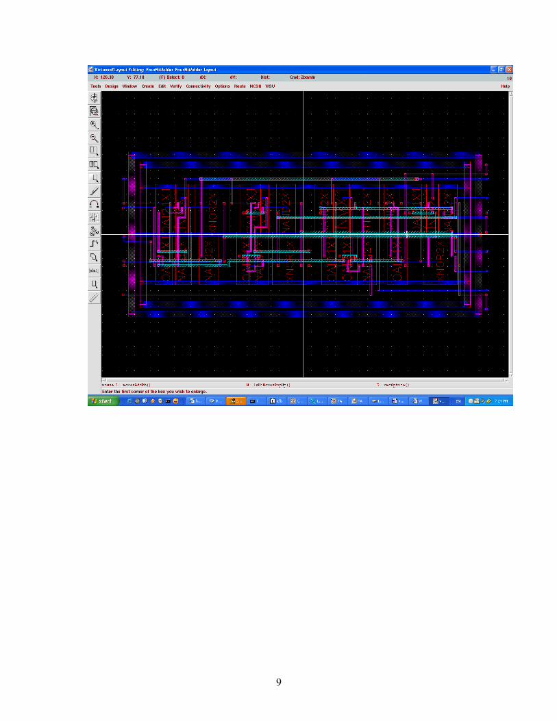
9

10
-Use Shift”f” or Ctrl”f” to switch between the two views. -(VLE) Verify>DRC (Design Rule Check) ….Click OK. -Rename your pin names, vdd, and gnd on your layout to match those in your symbol. If you need to add an M1_M2 contact on some of the pins in your layout do so where appropriate. Fix all the errors before you go on to the next step. -IC extraction: Execute (VLE)Verify>Extract….

11
Click on the set switches button in the extractor pop-up and a list of choice should appear like the following:
Click on Extract_parasitic_caps and press OK. Click OK to run the extractor. The CIW (Command Interface Window) should give no errors.

12
-Post Layout Simulation: Simulation in SpectreS Spice using the Affirma environment: Now that you have created a symbolic view of your full adder, you should create a test bench to test your design.
To simulate your circuit, Execute (CIW)Tools>Analog Environment>Simulation. You will need to customize your environment the first time you run Affirma, execute (Affirma)Setup>Design…. A pop up appears …select the library, cell, and view name as shown below. To view the schematic execute (Affirma)Session>Schematic Window….

13
You will be using the SpectreS Spice simulator. To select the simulator, execute (Affirma)Setup>Simulator/Directory/Host…. A pop-up like the following should appear showing the default simulator hspice. Click on hspice button to display a list of available simulators, select SpecterS, and see the figure below Click OK when done.
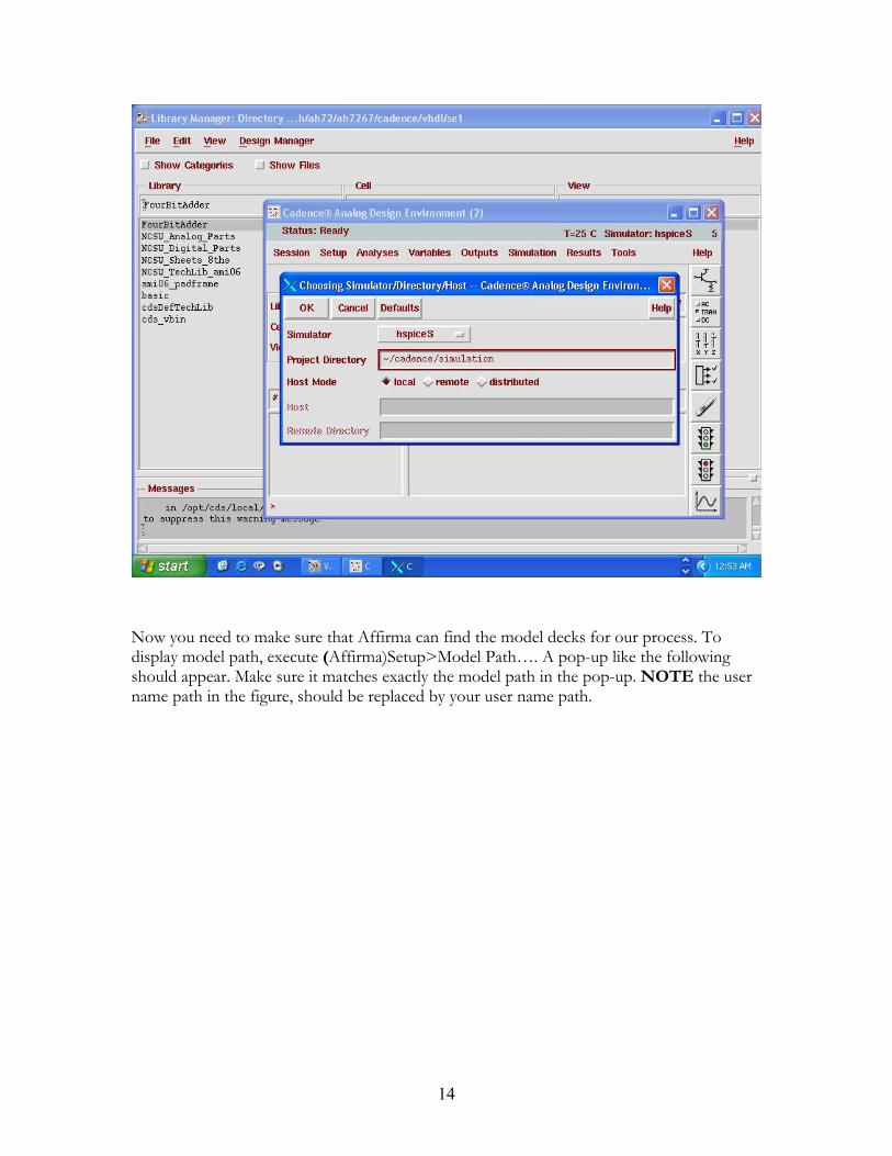
14
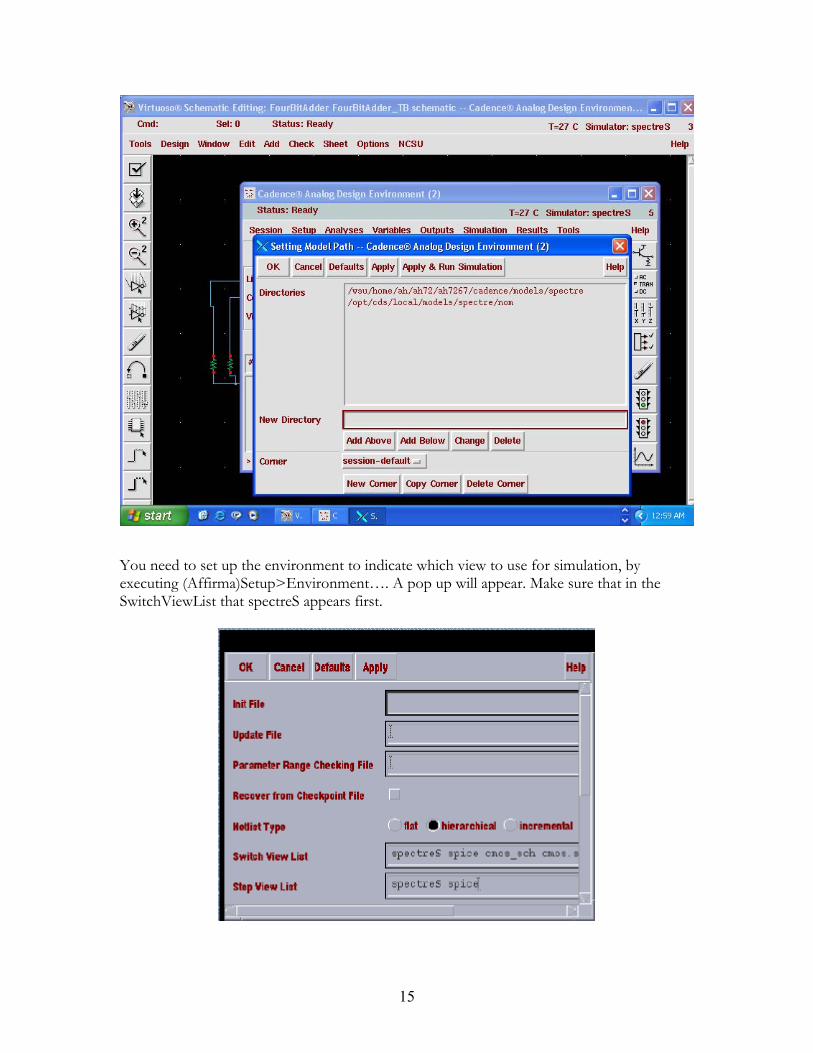
Now you need to make sure that Affirma can find the model decks for our process. To display model path, execute (Affirma)Setup>Model Path…. A pop-up like the following should appear. Make sure it matches exactly the model path in the pop-up. NOTE the user name path in the figure, should be replaced by your user name path.
15
You need to set up the environment to indicate which view to use for simulation, by executing (Affirma)Setup>Environment…. A pop up will appear. Make sure that in the SwitchViewList that spectreS appears first.
16
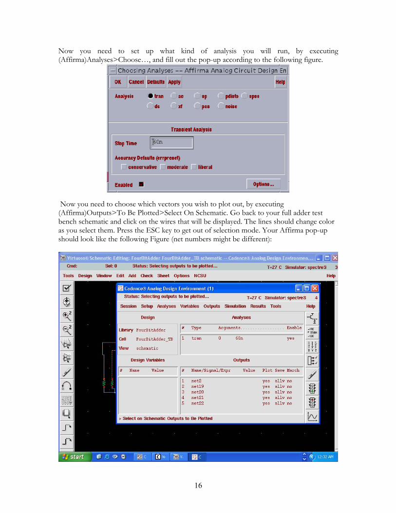
Now you need to set up what kind of analysis you will run, by executing (Affirma)Analyses>Choose…, and fill out the pop-up according to the following figure.
Now you need to choose which vectors you wish to plot out, by executing (Affirma)Outputs>To Be Plotted>Select On Schematic. Go back to your full adder test bench schematic and click on the wires that will be displayed. The lines should change color as you select them. Press the ESC key to get out of selection mode. Your Affirma pop-up should look like the following Figure (net numbers might be different):

17
To simulate, execute (Affirma)Simulation>Run or by clicking on the traffic light icon with a green light. The CIW and the Affirma pop-up will show you the process it goes through to simulate your circuit. If all went well, a plot like the following will pop-up. The following waveforms show the result of adding (1001)+(0001)=(1010). To strip the waveforms we execute (Affirma)Waveform Window)Axes>To Strip.
18
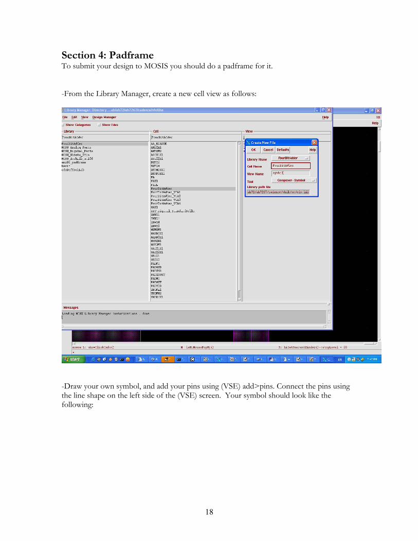
Section 4: Padframe To submit your design to MOSIS you should do a padframe for it. -From the Library Manager, create a new cell view as follows:
-Draw your own symbol, and add your pins using (VSE) add>pins. Connect the pins using the line shape on the left side of the (VSE) screen. Your symbol should look like the following:

19
-Execute (LM)File>New>Cellview…. Fill-up the cell name and view name as FA, and schematic of the pop-up, and then click OK.

20
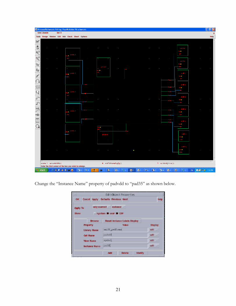
-Using the symbols that you created for the FourBitAdder from library FourBitAdder and padvdd, padgnd, padinc, padout from library AMI06_padframe, draw the schematic shown bellow:
21
Change the “Instance Name” property of padvdd to “pad35” as shown below.
22
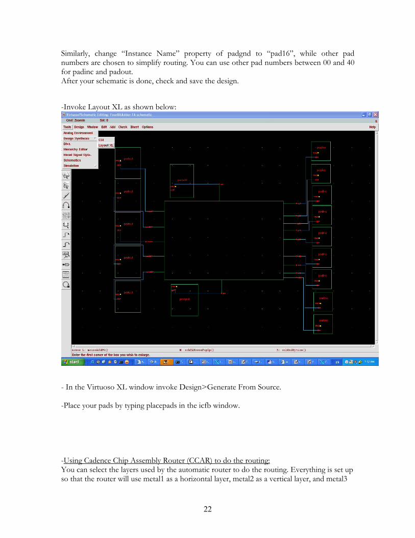
Similarly, change “Instance Name” property of padgnd to “pad16”, while other pad numbers are chosen to simplify routing. You can use other pad numbers between 00 and 40 for padinc and padout. After your schematic is done, check and save the design. -Invoke Layout XL as shown below:
- In the Virtuoso XL window invoke Design>Generate From Source. -Place your pads by typing placepads in the icfb window. -Using Cadence Chip Assembly Router (CCAR) to do the routing: You can select the layers used by the automatic router to do the routing. Everything is set up so that the router will use metal1 as a horizontal layer, metal2 as a vertical layer, and metal3
23
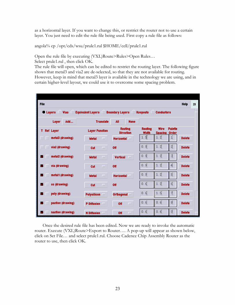
as a horizontal layer. If you want to change this, or restrict the router not to use a certain layer. You just need to edit the rule file being used. First copy a rule file as follows: angola% cp /opt/cds/wsu/prule1.rul $HOME/cell/prule1.rul Open the rule file by executing (VXL)Route>Rules>Open Rules… Select prule1.rul , then click OK. The rule file will open, which can be edited to restrict the routing layer. The following figure shows that metal3 and via2 are de-selected, so that they are not available for routing. However, keep in mind that metal3 layer is available in the technology we are using, and in certain higher-level layout, we could use it to overcome some spacing problem.
Once the desired rule file has been edited. Now we are ready to invoke the automatic router. Execute (VXL)Route>Export to Router…. A pop-up will appear as shown below, click on Set File… and select prule1.rul. Choose Cadence Chip Assembly Router as the router to use, then click OK.

24
The Cadence Chip Assembly Router (CCAR) will open as shown below:
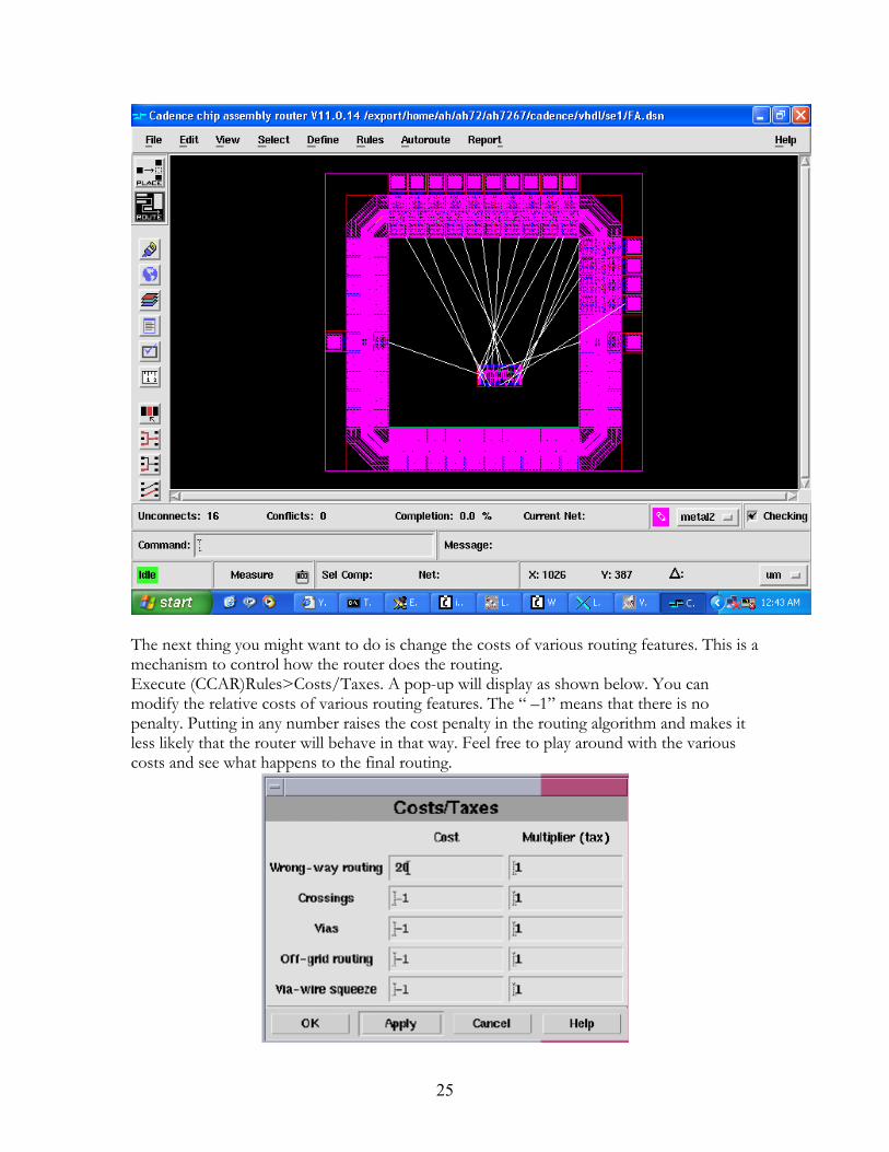
25
The next thing you might want to do is change the costs of various routing features. This is a mechanism to control how the router does the routing. Execute (CCAR)Rules>Costs/Taxes. A pop-up will display as shown below. You can modify the relative costs of various routing features. The “ –1” means that there is no penalty. Putting in any number raises the cost penalty in the routing algorithm and makes it less likely that the router will behave in that way. Feel free to play around with the various costs and see what happens to the final routing.

26
Now we are ready to route, execute (CCAR)Autoroute>Detail Route>Detail Router…. A pop-up will appear as below. This will allow us to control how many routing passes you’d like it to try before giving up. The tighter the layout and the smaller the area you’ve specified, the more passes it’s likely to take to get a successful route. If you have lots of room then it will probably take 5 or less passes. A tighter routing situation may require 25 or more passes.
If you don’t get a successful route, you’ll have go to the costs/taxes and reduce the costs of some of the routing features, or go back to the prule1.rul file and give it more layers to use. You may even need to go back to the layout and give the router some more room by increasing the space around the modules. If you do get a successful route you need to clean up after the route. The router may have introduced errors in the circuit. Execute (CCAR)Autoroute>Clean… to clean up things. This will take a post-pass on the routing and clean up messy bits. This can be executed several times. It is not always the case that the resulting routing is better than the original. They may results in more poly layer being used for routing instead of metal layers. If this is the case, quit without saving, and repeat the routing process without the cleaning operation. You also need to remove notches. These are little gaps in the routing that got left in because of corners being turned, or other features of the routing. The notches if not remove will cause DRC errors. These errors are spacing errors on the same layer, which are not real errors. To remove notches, execute (CCAR)Autoroute>Post Route>Remove Notches. Now you’re done. Exit CCAR, by executing (CCAR)Quit. Then select Save and Quit. To import the route back to VXL, execute (VXL)Route>Import from Router, then accept default and click OK in pop-up.
The final route looks as follows:
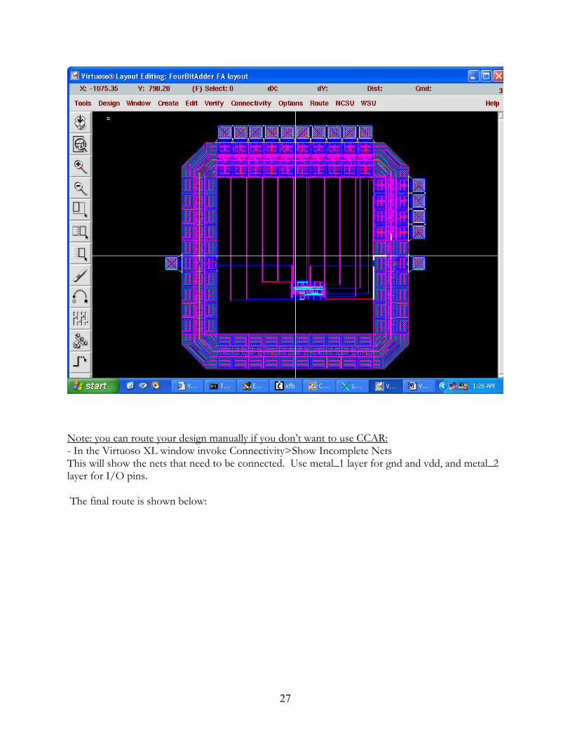
27
Note: you can route your design manually if you don’t want to use CCAR: - In the Virtuoso XL window invoke Connectivity>Show Incomplete Nets This will show the nets that need to be connected. Use metal_1 layer for gnd and vdd, and metal_2 layer for I/O pins. The final route is shown below:

28
-Now your design is ready for submission to MOSIS. Good Luck.
Nabil Abu-Khader