from c4 pbsn flip chip to lead-free µbump flip chip · - si-si stacking : highest alignment...
TRANSCRIPT

© IMEC 2011
FROM C4 PbSn FLIP CHIP TO
LEAD-FREE µBUMP FLIP CHIPERIC BEYNE
“VIJF JAAR LOODVRIJ SOLDEREN”
22 SEPTEMBER 2011
TNO, EINDHOVEN

© IMEC 2011 E.BEYNE 2
o Introduction: Flip chip Scaling
o µbump interconnect
o Improving Bond quality
o Die stacking strategies
o Wafer-level underfill
o Conclusion
OUTLINE

© IMEC 2011
SCALING FLIP-CHIP INTERCONNECTS
- With solder joint scaling, the intermetallics formed by UBM solder interaction are of increasing importance
- For the smallest flip chip pitches : only intermetalliccompounds after solder bump reflow
ERIC BEYNE 3
100µm pad diameter
150-200µm bump pitch
10µm pad
20µm pitch
40µm pad Ø
60µm pitch
20µm pad
40µm pitch
IMC

© IMEC 2011
MICRO-BUMP JOINING
Similar to flip chip interconnect:
▸ Low temperature melting solder metal, UBM metals.
However:
▸ Entire solder volume is transformed into intermetallic compounds
▸ Small dimension : no solder „ball‟, typically < 10m thick
▸ Connection by thermo/compression-reflow method
▸ Requires improved control and flatness of the solder “bumps”
ERIC BEYNE 4
M
Si
Solder
M
Si
M
Si
Solder
M
Si
M
Si
M
Si
IMC
M
M
Solder - IMC

© IMEC 2011
APPLICATION SPACE µBUMP JOINING
Si-Si face-to-face bonding
2.5D integration:
Si chips to Si interposers
3D integration : chip stacking with TSV
ERIC BEYNE 5
DRAM Logic

© IMEC 2011 E.BEYNE 6
o Introduction: Flip chip Scaling
o Baseline µbump interconnect
o Improving Bond quality
o Die stacking strategies
o Wafer-level underfill
o Conclusion
OUTLINE
© IMEC 2011
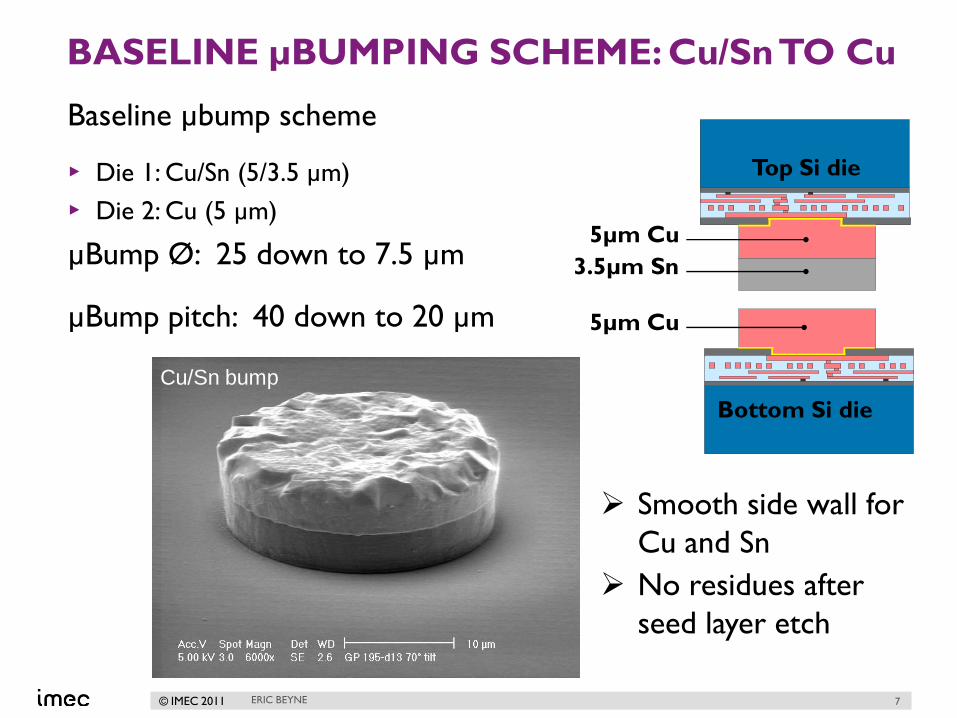
BASELINE µBUMPING SCHEME: Cu/SnTO Cu
Baseline µbump scheme
▸ Die 1: Cu/Sn (5/3.5 µm)
▸ Die 2: Cu (5 µm)
µBump Ø: 25 down to 7.5 µm
µBump pitch: 40 down to 20 µm
Smooth side wall for
Cu and Sn
No residues after
seed layer etch
Cu/Sn bump
Bottom Si die
Top Si die
5µm Cu
5µm Cu
3.5µm Sn
7ERIC BEYNE

© IMEC 2011 ERIC BEYNE 8
DEMONSTRATION OF COLLECTIVE
TRANSIENT-LIQUID PHASE µBUMP BONDING
Bonding procedure:
• Pick & place die on wafer by Flip Chip bonding Tool, at
room temperature
• Collective Bonding in Wafer Bonder @ 250ºC

© IMEC 2011 ERIC BEYNE 9
SOLID METAL BONDING:
CuSn INTERMETALLIC BONDING @ 150ºC
Top die
(Cu/Sn bump)
Bottom wafer
(Cu bump)
150C/50MPa
with no-flow underfill
Ф 25m bump, 40/15m
pitch/spacing
150C/150MPa150°C/50MPa
Ф 25m bump, 40/15m
pitch/spacing

© IMEC 2011
40 µm PITCH, Cu/Sn µBUMP DIE STACKING
PTCM/N TEST CHIPS
10ERIC BEYNE
5x5mm PTCM,
40 µm pitch
µbumps,
2 peripheral rows8x8mm PTCN
“landing”die
PTCN/M stack wire
bonded in BGA package
Cu/Sn microbump samples:
3.5 µm and 8µm thick Sn on 40µm pitch Cu bumps,
100 µm thick Silicon
Si-Si assembly in BGA package and SMD on test board
Use of a no-flow underfill
Package level reliability of TLP bumps demonstrated
>1800 temp cycles
>1000 hrs in electromigration tests
96 hrs HAST

© IMEC 2011
THERMAL CYCLING 40 µm PITCH Cu/Sn
µBUMP PTCM/N BGA ASSEMBLIES ON PCB
THERMAL CYCLING (-45°C/125°C) – IN-SITU
RESISTANCE MONITORING
In-situ resistance monitoring during
30’ 45ºC/30’125ºC thermal cyclingCu/Sn microbump samples:
▸ 3.5 µm and 8µm thick Sn on 40µm pitch
Cu bumps, 100 µm thick Silicon
▸ Use of a no-flow underfill (NCP)
No failures up to 4000 cycles
ERIC BEYNE 11
0
20
40
60
80
100
120
140
160
180
0 200 400 600 800 1000 1200 1400 1600 1800 2000
Time [h] = Cycles [#]
Res
ista
nce
[O
hm
]
8.0µm Sn bump DC
3.5µm Sn bump DC
80
90
100
110
2950 3050 3150 3250 3350 3450 3550 3650 3750 3850 3950 4050
Time [h]R
esis
tan
ce [
Oh
m]
150
160
170
180
3000 3100 3200 3300 3400 3500 3600 3700 3800 3900 4000
Time [h]
Resi
stan
ce [O
hm]
In-situ R @-45°C
In-situ measurement at 125°C
Da
isy c
ha
in R
esis
tan
ce
(O
hm
)
Time (h) = # cycles -45°C/+125°C
Da
isy c
ha
in R
esis
tan
ce
(O
hm
)
In-situ R at 125°C
Dais
y c
hain
Resis
tan
ce (
Oh
m)

© IMEC 2011
AGEING BEHAVIOUR OF LOW T Cu/SnTLP
µBUMP: VOID FORMATION
Shift over time from Cu6Sn5 to Cu3Sn, due to the excess of Cu.
The difference in diffusion rates of Cu and Sn results in vacancies
that aglomerate to form voids : Kirkendall voids.
ERIC BEYNE 12
Cu
Cu
Cu3Sn
Cu
Cu
Cu6Sn5
Cu3Sn
Cu3Sn
Cu6Sn5
Cu3Sn
Cu3Sn
Cu
Cu
Initial stateAfter ageing at 250ºC for 15’
After ageing at 250ºC for
45’

© IMEC 2011
WHY FULL TRANSFORMATION TO IMC?
When using low volume “mini-bumps” with excess Sn, the risk of
electro-migration failure strongly increases
EM reliability test comparison: 40 µm pitch Cu/Sn µbump packaged
F2F chip assemblies on PCB
EM test structure with build-in
temperature monitor
Cu/Sn microbump samples:
3.5 µm and 8µm thick Sn on 40µm pitch
Cu bumps, 100 µm thick Silicon
Si-Si assembly in BGA package and SMD
on test board
Use of a no-flow underfill
13ERIC BEYNE

© IMEC 2011
WHY FULL TRANSFORMATION TO IMC?
When using low volume “mini-bumps” with excess Sn, the risk of
electro-migration failure strongly increases
EM reliability test comparison: Early failures when using excess Sn
(8 vs. 3.5 µm)
150 oC – 200oCeff – 1.1mA/um2
No d
ata
8.0µm Sn µbump
3.5µm Sn µbump
NUF particle entrapment
voiding at Cu-Cu3Sn interface
14ERIC BEYNE
© IMEC 2011 E.BEYNE 15
o Introduction: Flip chip Scaling
o Baseline µbump interconnect
o Improving Bond quality
o Die stacking strategies
o Wafer-level underfill
o Conclusion
OUTLINE

© IMEC 2011
INTERMETALLIC µBUMP CONNECTIONS
Issues with pure Cu/Sn system:
▸ CuSn intermetallics already form at low
temperature: no elevated temperature
processes between bump formation
and assembly
Cu
Sn IMC
voids
• Cu and Sn form 2 intermetallic compounds: Cu3Sn and Cu6Sn5
• When soldering at high T: single Cu3Sn alloy can be obtained
• Unfortunately, low bonding T is required (particularly for memory,
even below 200ºC)
• At practical assembly conditions : Cu3Sn and Cu6Sn5 are formed
• Over time this is transformed to Cu3Sn, causing Kirkendall void
formation
16ERIC BEYNE

© IMEC 2011
µBUMPS WITH THIN Ni UBM
Introduction of solder diffusion layer: Cu/Ni/Sn
This resolves thermal stability of the µbump prior to
assembly, it however does not avoid the formation of
Cu3Sn intermetallics and Kirkendall voids upon ageing at
Cu-bump side
Cu
Sn
NiCu
Sn
Ni
17ERIC BEYNE

© IMEC 2011 ERIC BEYNE 18
No Kirkendall voids and
no cracks observed in the
(Cu, Ni)6Sn5 phase (all
samples), even after long
ageing at high temperature
AVOIDING KIRKENDALLVOIDS AND (Cu, Ni)3Sn
FORMATION IN THE Ni/ Thin Cu/Sn SYSTEM
(Cu,Ni)6Sn5
Sn
Ni
200˚C/96h
2.5h@200C 4h@200C 96h@200C
(Cu,Ni)6Sn5 (Cu,Ni)6Sn5 (Cu,Ni)6Sn5
Sn Sn Sn
0.5 µm ECD Cu
1.5 µm ECD Ni
3.0 µm ECD Sn
Study using blanket layers and controlled thermal ageing at 200ºC
150 nm PVD Cu
30 nm PVD Ti
Sn
Ni
Cu

© IMEC 2011
NOVEL µBUMP SCHEME: Ni/Cu BI-LAYER UBM
3-5 µm Ni bump can also be a Cu/Ni bump
Ni/Cu bump
Ni
Cu
Ni
Sn3-5 µm Ni
0.5-1µm Cu
3-4 µm Sn
Bottom Si die
Top Si die
0.5-1µm Cu
3-5 µm Ni
Ni/Cu/Sn bump
Cu
19ERIC BEYNE

© IMEC 2011
THERMAL AGEING Ni/Cu/SnTO Ni/Cu
µBUMP CONNECTIONS
After ageing at 150°C for 730 hours only a
single phase (Cu,Ni)6Sn5 is observed
• Uniform (Cu, Ni)6Sn5 no (Cu,Ni)3Sn
• No Kirkendall voids in (Cu,Ni)6Sn5
• Some remaining Sn
pt Ni Cu Sn Phase
1 9.23 39.73 51.04 ~(Cu, Ni)6Sn5
2 - 10.31 89.69 ~Sn (diff. Cu)
3 8.54 41.80 49.66 ~(Cu, Ni)6Sn5
4 - 8.65 91.35 ~Sn (diff. Cu)
1
342
150C/730h
Ni/Cu/Sn(2/1/4 um)
Ni/Cu(2.5/0.5 um)
Ni
Ni
20ERIC BEYNE

© IMEC 2011 ERIC BEYNE 21
BUMP-PLANARIZATION
DIAMOND BIT CUTTING TECHNIQUE
Wafer
Cutting bitCutting direction
Fixed distance from chuck table
Planarized bumps
Chuck table
Wafer
As deposited bump structures
Ra ~ 9nm / Rz ~ 50nm
Interconnect line
Cut Cu surface
in collaboration with DISCO

© IMEC 2011 ERIC BEYNE 22
CU-BUMP FLY CUTTING RESULTS
After plating : After fly-cutting:
passivation opening
• Ra = 0.009 µm
• Rt = 0.033 µm
• Within Die variation = 0.020 µm
• Ra = 0.5 µm
• Rt = 1.7 µm
• Within Die variation = 1.0 µmin collaboration with DISCO

© IMEC 2011 ERIC BEYNE 23
SN-BUMP FLY CUTTING RESULTS
After plating : After fly-cutting:
• Ra = 0.01 µm
• Rt = 0.05 µm
• Within Die variation = 0.10 µm
• Ra = 0.25 µm
• Rt = 1.60 µm
• Within Die variation = 0.7 µmin collaboration with DISCO

© IMEC 2011 ERIC BEYNE 24
CU/SN SOLID METAL BONDING @ 150ºC USING
FLY-CUT CU AND CU/SN BUMPS
Cu and Cu/Sn bumps:
▸ 40 µm bump Ø
▸ 15 µm bump spacing
Bonding conditions:
▸ max. temperature 150ºC
▸ Nom. pressure 50 MPa
▸ Using a no-flow underfill
Results:
▸ Clear formation of an intermetallic bond
▸ Very smooth interfaces after bonding
▸ Some misalignment in this sample
Cu
Cu
CuxSny

© IMEC 2011 E.BEYNE 25
o Introduction: Flip chip Scaling
o Baseline µbump interconnect
o Improving Bond quality
o Die stacking strategies
o Wafer-level underfill
o Conclusion
OUTLINE

© IMEC 2011
3D DIE STACKING APPROACHES
1. Sequential Die-to-package-substrate stacking
- Close to standard packaging practice
- Challenge: substrate warpage after first die assembly will limit µbump
assembly capability for next tier die stacking
1. Sequential Die-to-Wafer stacking, followed by stacked die-to-
package stacking.
- Si-Si stacking : highest alignment accuracy, finest pitch and narrow gap between
die possible.
- Challenge: fragile thin TSV bottom wafer Wafer “reconstruction”
ERIC BEYNE
1 32
31
2 2
26

© IMEC 2011

© IMEC 2011
WAFER-LEVEL UNDERFILL ASSEMBLY
ERIC BEYNE 28
Wafer-level Laminated Film Underfill
Wafer-level Spin Coated Underfill
Die-to-Die Assembly
Die-to-Wafer Assembly
Sta
ck
ing A
ssem
bly

© IMEC 2011
Good transparency of the WLUF film
WAFER-LEVEL LAMINATED WLUF
ERIC BEYNE 29
PTCM/PTCN stacks
after Assembly
SAM : No voids or
delamination seen
CSAM
T-SCAN
Particle entrapment seen on some bumps seen.
May be also due to bump topographyInitial results:
• Good electrical yields w/high bond force
• Good material transparency
• Good filling capability (no voids and delamination)
Some (up to 100µm)
underfill squeeze out:
to be minimized

© IMEC 2011 ERIC BEYNE 30
25µm thin ETNA test die stacked on DRAM-Die:
Significant topography after stacking:NUF process requires multiple point dispense & accurate volume control.
WLUF allows for flattest assembly, even flatter than when not using
underfill during stacking
May be a problem for multi-tier stacking
Expected to be less severe with thicker die (Die bending stiffness t3)
TOPOGRAPHY AFTER DIE-TO-WAFER STACKING
Dispensed
NUF (single point) NO underfill Laminated WLUF Sample #1 Sample #2

© IMEC 2011 ERIC BEYNE 31
SAM: No UF Voids
Topo by optical
profilometry < 2μm
ASSEMBLY MODULESUCCESSFUL LOGIC-ON-DRAM STACKING W. FILM-WLUF

© IMEC 2011 E.BEYNE 32
o Introduction: Flip chip Scaling
o Baseline µbump interconnect
o Improving Bond quality
o Die stacking strategies
o Wafer-level underfill
o Conclusion & Outlook
OUTLINE

© IMEC 2011 E.BEYNE 33
CONCLUSIONS
Flip chip scaling results in an increased
importance of the intermetallic phases.
µbump flip-chip for Silicon-to-Silicon relies
on full transformation of the solder joint
into intermetallics
This allows for an improved
electromigration resistance
Requires „bump engineering‟ to
avoid Kirkenadll voiding
What are the pitch limits
µbump solder joining?

© IMEC 2011
BUMP SIZE DEFINED BY BUMP ALIGNMENT
Contact/no contact and/or contact area reduction
34Eric
beyne
Optimum condition : Bump
diameter Øb = Pad spacing Sp
Non-contact
area
Non-contact
area
Misalignment Misalignment
Before reaching an open
connection, the bump to pad
contact area is reduced,
resulting in an increase in
contact resistance
Øp≥ Øb SQRT(HSn/H‟Sn)
Therefore : S = P/(1+SQRT(HSn/H‟Sn))
If e.g. (HSn/H‟Sn )max is 4 : S= P/3
Øb
ØP
HSn
H’Sn
Ø’b
Øp >Øb : Capture Solder squeeze-out
Øb
ØP
HSn
Sp
P
P

© IMEC 2011
SCALING ROADMAP
ALIGNMENT ACCURACY REQUIREMENTSRequired alignment accuracy for a maximum increase in contact resistance
of 100% and a Yield of 99.9999 (4N)
ERIC BEYNE 35
0
0.5
1
1.5
2
2.5
3
3.5
4
4.5
5
0 5 10 15 20 25 30 35 40
St.d
ev.
ali
gnm
en
t (µ
m)
Pad Diameter, Dp (µm)
5
10
15
20
25
5
10
3
4
5
Db (µm) for
P=40µm
Db (µm)for
P=20µm
Db (µm)for
P=10µm
P=40µm
P=20µm
P=10µm
R/Rn < 2
Y = 4N

© IMEC 2011 3D SYSTEM INTEGRATION PROGRAM 36
ACKNOWLEDGEMENT
3D SYSTEM INTEGRATION PROGRAM
3D Program
LamRESEARCH
Foundries
SAT
Memory IDM
EDA
FABLESS
Equipment Suppliers
Logic IDM
Material Suppliers

© IMEC 2011