freescale semiconductor, inc.cache.freescale.com/files/product/doc/mc68lc302um.pdf · freescale...
TRANSCRIPT

MC68LC302
Low Power Integrated Multiprotocol Processor
Reference Manual
Fre
esc
ale
Se
mic
on
du
cto
r, I
Freescale Semiconductor, Inc.
For More Information On This Product, Go to: www.freescale.com
nc
...

iii
MC68LC302 REFERENCE MANUAL
MOTOROLA
PREFACE
The complete documentation package for the MC68LC302 consists of the MC68LC302RM/AD,
MC68LC302 Low Power Integrated Multiprotocol Processor Reference Manual
,M68000PM/AD,
MC68000 Family Programmer’s Reference Manual,
MC68302UM/AD,
MC68302 Integrated Multiprotocol Processor User’s Manual,
and the MC68LC302/D,
MC68LC302 Low Power Integrated Multiprotocol Processor Product Brief
.
The
MC68LC302 Low Power Integrated Multiprotocol Processor Reference Manual
de-scribes the programming, capabilities, registers, and operation of the MC68LC302 that differfrom the original MC68302; the
MC68000 Family Programmer’s Reference Manual
providesinstruction details for the MC68LC302; and
the
MC68LC302 Low Power Integrated Multipro-tocol Processor Product Brief
provides a brief description of the MC68LC302 capabilities.
The
MC68302 Integrated Multiprotocol Processor User’s Manual
is required, since the
MC68LC302
Low Power Integrated Multiprotocol Processor
Reference Manual
only de-scribes the new features of the MC68LC302.
This user’s manual is organized as follows:
Section 1 IntroductionSection 2 Configuration, Clocking, Low Power Modes, and Internal Memory MapSection 3 System Integration Block (SIB)Section 4 Communications Processor (CP)Section 5 Signal DescriptionSection 6 Electrical CharacteristicsSection 7 Mechanical Data And Ordering Information
ELECTRONIC SUPPORT:
The Technical Support BBS, known as AESOP (Application Engineering Support ThroughOn-Line Productivity), can be reach by modem or the internet. AESOP provides commonlyasked application questons, latest device errata, device specs, software code, and manyother useful support functions.
Modem: Call 1-800-843-3451 (outside US or Canada 512-891-3650) on a modem that runsat 14,400 bps or slower. Set your software to N/8/1/F emulating a vt100.
Internet: This access is provided by telneting to pirs.aus.sps.mot.com [129.38.233.1] orthrough the World Wide Web at http://pirs.aus.sps.mot.com.
—
Sales Offices —
For questions or comments pertaining to technical information, questions, and applications,please contact one of the following sales offices nearest you.
Fre
esc
ale
Se
mic
on
du
cto
r, I
Freescale Semiconductor, Inc.
For More Information On This Product, Go to: www.freescale.com
nc
...

MC68LC302 REFERENCE MANUAL
UNITED STATES
ALABAMA
, Huntsville (205) 464-6800
ARIZONA
, Tempe (602) 897-5056
CALIFORNIA
, Agoura Hills (818) 706-1929
CALIFORNIA
, Los Angeles (310) 417-8848
CALIFORNIA
, Irvine (714) 753-7360
CALIFORNIA
, Rosevllle (916) 922-7152
CALIFORNIA
, San Diego (619) 541-2163
CALIFORNIA
, Sunnyvale (408) 749-0510
COLORADO
, Colorado Springs (719) 599-7497
COLORADO
, Denver (303) 337-3434
CONNECTICUT
, Wallingford (203) 949-4100
FLORIDA
, Maitland (407) 628-2636
FLORIDA
, Pompano Beach/ Fort Lauderdal (305) 486-9776
FLORIDA
, Clearwater (813) 538-7750
GEORGlA
, Atlanta (404) 729-7100
IDAHO
, Boise (208) 323-9413
ILLINOIS
, Chicago/Hoffman Estates (708) 490-9500
INDlANA
, Fort Wayne (219) 436-5818
INDIANA
, Indianapolis (317) 571-0400
INDIANA
, Kokomo (317) 457-6634
IOWA
, Cedar Rapids (319) 373-1328
KANSAS
, Kansas City/Mission (913) 451-8555
MARYLAND
, Columbia (410) 381-1570
MASSACHUSETTS
, Marborough (508) 481-8100
MASSACHUSETTS
, Woburn (617) 932-9700
MICHIGAN
, Detroit (313) 347-6800
MINNESOTA
, Minnetonka (612) 932-1500
MISSOURI
, St. Louis (314) 275-7380
NEW JERSEY
, Fairfield (201) 808-2400
NEW YORK
, Fairport (716) 425-4000
NEW YORK
, Hauppauge (516) 361-7000
NEW YORK
, Poughkeepsie/Fishkill (914) 473-8102
NORTH CAROLINA
, Raleigh (919) 870-4355
OHIO
, Cleveland (216) 349-3100
OHIO
, Columbus Worthington (614) 431-8492
OHIO
, Dayton (513) 495-6800
OKLAHOMA
, Tulsa (800) 544-9496
OREGON
, Portland (503) 641-3681
PENNSYLVANIA
, Colmar (215) 997-1020 Philadelphia/Horsham (215) 957-4100
TENNESSEE
, Knoxville (615) 690-5593
TEXAS
, Austin (512) 873-2000
TEXAS
, Houston (800) 343-2692
TEXAS
, Plano (214) 516-5100
VIRGINIA
, Richmond (804) 285-2100
WASHINGTON
, Bellevue (206) 454-4160 Seattle Access (206) 622-9960
WISCONSIN
, Milwaukee/Brookfield (414) 792-0122
CANADABRITISH COLUMBIA
, Vancouver (604) 293-7605
ONTARIO
, Toronto (416) 497-8181
ONTARIO
, Ottawa (613) 226-3491
QUEBEC
, Montreal (514) 731-6881
INTERNATIONALAUSTRALIA
, Melbourne (61-3)887-0711
AUSTRALIA
, Sydney (61(2)906-3855
BRAZIL
, Sao Paulo 55(11)815-4200
CHINA
, Beijing 86 505-2180
FINLAND
, Helsinki 358-0-35161191 Car Phone 358(49)211501
FRANCE
, Paris/Vanves 33(1)40 955 900
GERMANY
, Langenhagen/ Hanover 49(511)789911
GERMANY
, Munich 49 89 92103-0
GERMANY
, Nuremberg 49 911 64-3044
GERMANY
, Sindelfingen 49 7031 69 910
GERMANY
,Wiesbaden 49 611 761921
HONG KONG
, Kwai Fong 852-4808333 Tai Po 852-6668333
INDIA
, Bangalore (91-812)627094
ISRAEL
, Tel Aviv 972(3)753-8222
ITALY
, Milan 39(2)82201
JAPAN
, Aizu 81(241)272231
JAPAN
, Atsugi 81(0462)23-0761
JAPAN
, Kumagaya 81(0485)26-2600
JAPAN
, Kyushu 81(092)771-4212
JAPAN
, Mito 81(0292)26-2340
JAPAN
, Nagoya 81(052)232-1621
JAPAN
, Osaka 81(06)305-1801
JAPAN,
Sendai 81(22)268-4333
JAPAN,
Tachikawa 81(0425)23-6700
JAPAN,
Tokyo 81(03)3440-3311
JAPAN
, Yokohama 81(045)472-2751
KOREA
, Pusan 82(51)4635-035
KOREA
, Seoul 82(2)554-5188
MALAYSIA
, Penang 60(4)374514
MEXICO
, Mexico City 52(5)282-2864
MEXICO
, Guadalajara 52(36)21-8977 Marketing 52(36)21-9023 Customer Service 52(36)669-9160
NETHERLANDS
, Best (31)49988 612 11
PUERTO RICO
, San Juan (809)793-2170
SINGAPORE
(65)2945438
SPAIN
, Madrid 34(1)457-8204 or 34(1)457-8254
SWEDEN
, Solna 46(8)734-8800
SWITZERLAND
, Geneva 41(22)7991111SWITZERLAND, Zurich 41(1)730 4074TAlWAN, Taipei 886(2)717-7089THAILAND, Bangkok (66-2)254-4910UNITED KINGDOM, Aylesbury 44(296)395-252
FULL LINE REPRESENTATIVESCOLORADO, Grand Junction Cheryl Lee Whltely (303) 243-9658KANSAS, Wichita Melinda Shores/Kelly Greiving (316) 838 0190NEVADA, Reno Galena Technology Group (702) 746 0642NEW MEXICO, Albuquerque S&S Technologies, lnc. (505) 298-7177UTAH, Salt Lake City Utah Component Sales, Inc. (801) 561-5099WASHINGTON, Spokane Doug Kenley (509) 924-2322ARGENTINA, Buenos Aires Argonics, S.A. (541) 343-1787
HYBRID COMPONENTS RESELLERSElmo Semiconductor (818) 768-7400Minco Technology Labs Inc. (512) 834-2022Semi Dice Inc. (310) 594-4631
Fre
esc
ale
Se
mic
on
du
cto
r, I
Freescale Semiconductor, Inc.
For More Information On This Product, Go to: www.freescale.com
nc
...

MC68LC302 REFERENCE MANUAL
TABLE OF CONTENTS
Paragraph Title PageNumber Number
Section 1 Introduction
1.1 Block Diagram......................................................................................... 1-11.2 Features .................................................................................................. 1-21.3 LC302 Applications ................................................................................. 1-31.4 LC302 Differences .................................................................................. 1-3
Section 2 Configuration, Clocking, Low Power Modes, and Internal Memory Map
2.1 MC68LC302 and MC68302 Signal Differences ...................................... 2-12.2 IMP Configuration Control....................................................................... 2-22.2.1 Base Address Register ........................................................................... 2-42.3 System Configuration Registers.............................................................. 2-52.4 Clock Generation and Low Power Control .............................................. 2-52.4.1 PLL and Oscillator Changes to IMP ........................................................ 2-52.4.1.1 Clock Control Register ............................................................................ 2-62.4.2 MC68LC302 System Clock Generation .................................................. 2-62.4.2.1 Default System Clock Generation ........................................................... 2-72.4.3 IMP System Clock Generation ................................................................ 2-82.4.3.1 System Clock Configuration.................................................................... 2-82.4.3.2 On-Chip Oscillator................................................................................... 2-82.4.3.3 Phase-Locked Loop (PLL) ...................................................................... 2-92.4.3.4 Frequency Multiplication ......................................................................... 2-92.4.3.4.1 Low Power PLL Clock Divider............................................................... 2-102.4.3.4.2 IMP PLL and Clock Control Register (IPLCR) ...................................... 2-102.4.3.5 IMP Internal Clock Signals .................................................................... 2-122.4.3.5.1 IMP System Clock................................................................................. 2-122.4.3.5.2 BRG Clock ............................................................................................ 2-122.4.3.5.3 PIT Clock............................................................................................... 2-122.4.3.6 IMP PLL Pins ........................................................................................ 2-122.4.3.6.1 VCCSYN ............................................................................................... 2-122.4.3.6.2 GNDSYN............................................................................................... 2-122.4.3.6.3 XFC ....................................................................................................... 2-122.4.3.6.4 MODCLK............................................................................................... 2-122.4.4 IMP Power Management....................................................................... 2-132.4.4.1 IMP Low Power Modes ......................................................................... 2-132.4.4.1.1 STOP Mode .......................................................................................... 2-132.4.4.1.2 DOZE Mode .......................................................................................... 2-132.4.4.1.3 STAND_BY Mode ................................................................................. 2-13
Fre
esc
ale
Se
mic
on
du
cto
r, I
Freescale Semiconductor, Inc.
For More Information On This Product, Go to: www.freescale.com
nc
...

Table of Contents
Paragraph Title PageNumber Number
MC68LC302 REFERENCE MANUAL
2.4.4.1.4 SLOW_GO Mode...................................................................................2-142.4.4.1.5 NORMAL Mode......................................................................................2-142.4.4.1.6 IMP Operation Mode Control Register (IOMCR) ...................................2-142.4.4.1.7 Low Power Drive Control Register (LPDCR) .........................................2-152.4.4.1.8 IMP Power Down Register (IPWRD) .....................................................2-152.4.4.1.9 Default Operation Modes. ......................................................................2-152.4.4.2 Low Power Support................................................................................2-152.4.4.2.1 Enter the SLOW_GO mode ...................................................................2-152.4.4.2.2 Entering the STOP/ DOZE/ STAND_BY Mode......................................2-162.4.4.2.3 IMP Wake-Up from Low Power STOP Modes .......................................2-172.4.4.2.4 IMP Wake-Up Control Register (IWUCR) ..............................................2-172.4.4.3 Fast Wake-Up ........................................................................................2-182.4.4.3.5 Ring Oscillator Control Register (RINGOCR) ........................................2-192.4.4.3.6 Ring Oscillator Event Register (RINGOEVR). .......................................2-202.5 MC68LC302 Dual Port RAM..................................................................2-202.6 Internal Registers map...........................................................................2-23
Section 3 System Integration Block (SIB)
3.1 System Control ........................................................................................3-13.1.1 System Control Register (SCR) ...............................................................3-23.1.2 System Status Bits...................................................................................3-33.1.3 System Control Bits .................................................................................3-33.1.4 Freeze Control .........................................................................................3-53.1.5 Hardware Watchdog ................................................................................3-53.2 Programmable Data Bus Size Switch ......................................................3-63.2.1 Bus Switch Register (BSR) ......................................................................3-63.2.2 Basic Procedure:......................................................................................3-63.3 Load Boot Code from An SCC.................................................................3-73.4 DMA Control ..........................................................................................3-103.4.1 MC68LC302 Differences........................................................................3-103.4.2 IDMA Registers (Independent DMA Controller).....................................3-113.4.2.1 Channel Mode Register (CMR)..............................................................3-113.4.2.2 Source Address Pointer Register (SAPR) .............................................3-133.4.2.3 Destination Address Pointer Register (DAPR).......................................3-133.4.2.4 Function Code Register (FCR) ..............................................................3-133.4.2.5 Byte Count Register (BCR)....................................................................3-133.4.2.6 Channel Status Register (CSR) .............................................................3-133.5 Interrupt Controller .................................................................................3-143.5.1 Interrupt Controller Key Differences.......................................................3-143.5.2 Interrupt Controller Programming Model................................................3-143.5.2.1 Global Interrupt Mode Register (GIMR) .................................................3-143.5.2.2 Interrupt Pending Register (IPR)............................................................3-153.5.2.3 Interrupt Mask Register (IMR)................................................................3-163.5.2.4 Interrupt In-Service Register (ISR).........................................................3-16
Fre
esc
ale
Se
mic
on
du
cto
r, I
Freescale Semiconductor, Inc.
For More Information On This Product, Go to: www.freescale.com
nc
...

Table of Contents
Paragraph Title PageNumber Number
MC68LC302 REFERENCE MANUAL
3.6 Parallel I/O Ports ................................................................................... 3-173.6.1 Parallel I/O Port Differences.................................................................. 3-173.6.2 Port A .................................................................................................... 3-173.6.3 Port B .................................................................................................... 3-183.6.3.1 PB7–PB3............................................................................................... 3-183.6.3.2 PB11–PB8............................................................................................. 3-183.6.4 Port N .................................................................................................... 3-193.6.5 Port Registers........................................................................................ 3-193.7 Timers ................................................................................................... 3-203.7.1 MC68LC302 General Purpose Timer Difference .................................. 3-203.7.2 General Purpose Timers Programming Mode....................................... 3-203.7.2.1 Timer Mode Register (TMR1, TMR2).................................................... 3-203.7.2.2 Timer Reference Registers (TRR1, TRR2) ........................................... 3-213.7.2.3 Timer Capture Registers (TCR1, TCR2) ............................................... 3-213.7.2.4 Timer Counter (TCN1, TCN2) ............................................................... 3-213.7.2.5 Timer Event Registers (TER1, TER2) ................................................... 3-213.7.3 Timer 3 - Software Watchdog Timer ..................................................... 3-223.7.3.1 Software Watchdog Reference Register (WRR)................................... 3-223.7.3.2 Software Watchdog Counter (WCN) ..................................................... 3-223.7.4 Periodic Interrupt Timer (PIT)................................................................ 3-223.7.4.1 Overview ............................................................................................... 3-233.7.4.2 Periodic Timer Period Calculation ......................................................... 3-233.7.4.3 Using the Periodic Timer As a Real-Time Clock ................................... 3-243.7.4.4 Periodic Interrupt Timer Register (PITR)............................................... 3-243.8 External Chip-Select Signals and Wait-State Logic .............................. 3-253.8.1 Chip-Select Registers............................................................................ 3-263.8.1.1 Base Register (BR3–BR0) .................................................................... 3-263.8.1.2 Option Registers (OR3–OR0) ............................................................... 3-263.8.2 Disable CPU Logic (M68000)................................................................ 3-283.8.3 Bus Arbitration Logic ............................................................................. 3-283.8.3.1 Internal Bus Arbitration.......................................................................... 3-283.8.3.2 External Bus Arbitration......................................................................... 3-283.9 Dynamic RAM Refresh Controller ......................................................... 3-29
Section 4 Communications Processor (CP)
4.1 MC68LC302 Key Differences from the MC68302................................... 4-14.2 Serial Channels Physical Interface.......................................................... 4-24.2.1 Serial Interface Registers ........................................................................ 4-24.2.1.1 Serial Interface Mode Register (SIMODE) .............................................. 4-24.2.1.2 Serial Interface Mask Register (SIMASK) ............................................... 4-44.3 Serial Communication Controllers (SCCs) .............................................. 4-44.3.1 SCC Configuration Register (SCON) ...................................................... 4-44.3.1.1 Divide by 2 Input Blocks (New Feature) .................................................. 4-44.3.2 Disable SCC1 Serial Clocks Out (DISC) ................................................. 4-44.3.2.1 RCLK1 and TCLK1 Pin Options.............................................................. 4-5
Fre
esc
ale
Se
mic
on
du
cto
r, I
Freescale Semiconductor, Inc.
For More Information On This Product, Go to: www.freescale.com
nc
...

Table of Contents
Paragraph Title PageNumber Number
MC68LC302 REFERENCE MANUAL
4.3.3 SCC Mode Register (SCM)......................................................................4-54.3.4 SCC Data Synchronization Register (DSR).............................................4-64.3.5 Buffer Descriptors Table ..........................................................................4-64.3.6 SCC Parameter RAM Memory Map.........................................................4-74.3.7 Interrupt Mechanism ................................................................................4-74.3.8 UART Controller.......................................................................................4-74.3.8.1 UART Memory Map .................................................................................4-74.3.8.2 UART Mode Register...............................................................................4-84.3.8.3 UART Receive Buffer Descriptor (Rx BD) ...............................................4-84.3.8.4 UART Transmit Buffer Descriptor (Tx BD)...............................................4-84.3.8.5 UART Event Register...............................................................................4-94.3.8.6 UART MASK Register..............................................................................4-94.3.9 Autobaud Controller (New) ......................................................................4-94.3.9.1 Autobaud Channel Reception Process ....................................................4-94.3.9.2 Autobaud Channel Transmit Process ....................................................4-114.3.9.3 Autobaud Parameter RAM.....................................................................4-114.3.9.4 Autobaud Programming Model ..............................................................4-134.3.9.4.1 Preparing for the Autobaud Process......................................................4-134.3.9.4.2 Enter_Baud_Hunt Command.................................................................4-144.3.9.4.3 Autobaud Command Descriptor.............................................................4-144.3.9.4.4 Autobaud Lookup Table.........................................................................4-154.3.9.5 Lookup Table Example ..........................................................................4-174.3.9.6 Determining Character Length and Parity..............................................4-174.3.9.7 Autobaud Reception Error Handling Procedure.....................................4-184.3.9.8 Autobaud Transmission .........................................................................4-184.3.9.8.1 Automatic Echo......................................................................................4-194.3.9.8.2 Smart Echo ............................................................................................4-194.3.9.9 Reprogramming to UART Mode or Another Protocol ............................4-204.3.10 HDLC Controller.....................................................................................4-204.3.10.1 HDLC Memory Map ...............................................................................4-204.3.10.2 HDLC Mode Register.............................................................................4-204.3.10.3 HDLC Receive Buffer Descriptor (Rx BD) .............................................4-214.3.10.4 HDLC Transmit Buffer Descriptor (Tx BD).............................................4-214.3.10.5 HDLC Event Register.............................................................................4-214.3.10.6 HDLC Mask Register .............................................................................4-214.3.11 BISYNC Controller .................................................................................4-224.3.11.1 BISYNC Memory Map............................................................................4-224.3.11.2 BISYNC Mode Register .........................................................................4-224.3.11.3 BISYNC Receive Buffer Descriptor (Rx BD)..........................................4-224.3.11.4 BISYNC Transmit Buffer Descriptor (Tx BD). ........................................4-224.3.11.5 BISYNC Event Register .........................................................................4-234.3.11.6 BISYNC Mask Register..........................................................................4-234.3.12 Transparent Controller ...........................................................................4-234.3.12.1 Transparent Memory Map......................................................................4-234.3.12.2 Transparent Mode Register ...................................................................4-24
Fre
esc
ale
Se
mic
on
du
cto
r, I
Freescale Semiconductor, Inc.
For More Information On This Product, Go to: www.freescale.com
nc
...

Table of Contents
Paragraph Title PageNumber Number
MC68LC302 REFERENCE MANUAL
4.3.12.3 Transparent Receive Buffer Descriptor (RxBD) .................................... 4-244.3.12.4 Transparent Transmit Buffer Descriptor (Tx BD)................................... 4-254.3.12.5 Transparent Event Register .................................................................. 4-254.3.12.6 Transparent Mask Register ................................................................... 4-254.4 Serial Communication Port (SCP)......................................................... 4-254.4.1 SCP Programming Model...................................................................... 4-254.4.2 SCP Transmit/Receive Buffer Descriptor .............................................. 4-264.5 Serial Management Controllers (SMCs)................................................ 4-264.5.1 SMC Programming Model ..................................................................... 4-264.5.2 SMC Memory Structure and Buffers Descriptors .................................. 4-264.5.2.1 SMC1 Receive Buffer Descriptor .......................................................... 4-264.5.2.2 SMC1 Transmit Buffer Descriptor ......................................................... 4-264.5.2.3 SMC2 Receive Buffer Descriptor .......................................................... 4-274.5.2.4 SMC2 Transmit Buffer Descriptor ......................................................... 4-27
Section 5 Signal Description
5.1 Functional Groups................................................................................... 5-15.2 Power Pins .............................................................................................. 5-25.3 Clock Pins ............................................................................................... 5-45.4 System Control Pins................................................................................ 5-55.5 Address Bus Pins (A19–A1).................................................................... 5-75.6 Data Bus Pins (D15—D0) ....................................................................... 5-85.7 Bus Control Pins...................................................................................... 5-95.8 Bus Arbitration Pins............................................................................... 5-105.9 Interrupt Control Pins ............................................................................ 5-115.10 MC68LC302 Bus Interface Signal Summary......................................... 5-125.11 Physical Layer Serial Interface Pins...................................................... 5-145.12 Typical Serial Interface Pin Configurations ........................................... 5-145.13 NMSI1 or ISDN Interface Pins............................................................... 5-145.14 NMSI2 Port or Port a Pins ..................................................................... 5-175.15 PAIO / SCP Pins ................................................................................... 5-185.16 Timer Pins ............................................................................................. 5-195.17 Parallel I/O Pins with Interrupt Capability .............................................. 5-205.18 Chip-Select Pins.................................................................................... 5-215.19 When to Use Pullup Resistors............................................................... 5-21
Section 6 Electrical Characteristics
6.1 Maximum Ratings.................................................................................... 6-26.2 Thermal Characteristics .......................................................................... 6-26.3 Power Considerations ............................................................................. 6-36.4 Power Dissipation.................................................................................... 6-46.5 DC Electrical Characteristics................................................................... 6-56.6 DC Electrical Characteristics—NMSI1 in IDL Mode................................ 6-66.7 AC Electrical Specifications—Clock Timing ............................................ 6-6
Fre
esc
ale
Se
mic
on
du
cto
r, I
Freescale Semiconductor, Inc.
For More Information On This Product, Go to: www.freescale.com
nc
...

Table of Contents
Paragraph Title PageNumber Number
MC68LC302 REFERENCE MANUAL
6.7.1 AC Electrical Characteristics - IMP Phased Lock Loop (PLL) Characteristics .........................................................................................6-7
6.8 AC Electrical Specifications—IMP Bus Master Cycles ............................6-86.9 AC Electrical Specifications—DMA .......................................................6-136.10 AC Electrical Specifications—External Master
Internal Asynchronous Read/Write Cycles ............................................6-166.11 AC Electrical Specifications—External Master Internal Synchronous
Read/Write Cycles .................................................................................6-196.12 AC Electrical Specifications—Internal Master Internal Read/Write
Cycles ....................................................................................................6-236.13 AC Electrical Specifications—Chip-Select Timing Internal Master .......6-246.14 AC Electrical Specifications—Chip-Select Timing External Master .......6-256.15 AC Electrical Specifications—Parallel I/O .............................................6-266.16 AC Electrical Specifications—Interrupts ...............................................6-266.17 AC Electrical Specifications—Timers.....................................................6-286.18 AC Electrical Specifications—Serial Communications Port ...................6-296.19 AC Electrical Specifications—IDL Timing) .............................................6-306.20 AC Electrical Specifications—GCI Timing .............................................6-326.21 AC Electrical Specifications—PCM Timing............................................6-346.22 AC Electrical Specifications—NMSI Timing...........................................6-36
Section 7 Mechanical Data and Ordering Information
7.1 Pin Assignments ......................................................................................7-17.1.1 Pin Grid Array (PGA) ...............................................................................7-17.1.2 Surface Mount (TQFP )............................................................................7-27.2 Package Dimensions ...............................................................................7-37.2.1 Pin Grid Array (PGA) ...............................................................................7-37.2.2 Surface Mount (TQFP).............................................................................7-47.3 Ordering Information ................................................................................7-5
Fre
esc
ale
Se
mic
on
du
cto
r, I
Freescale Semiconductor, Inc.
For More Information On This Product, Go to: www.freescale.com
nc
...

MC68LC302 REFERENCE MANUAL
SECTION 1INTRODUCTION
Motorola has developed a low-cost version of the well-known MC68302 integrated multipro-tocol processor (IMP) called the MC68LC302. Simply put, the LC302 is a traditional 68302minus the third serial communication controller (SCC3) and has a new static 68000 core, anew timer and low power modes. It is packaged in a low profile 100 TQFP that reducesboard space from the regular 68302, as well as making it suitable for use in height restrictedapplications such as PCMCIA.
The document fully describes all the differences between the LC302 and the regular 68302.Any feature not described in this document will operate as described in the
MC68302 User’sManual
. In addition this document contains the full set of electrical descriptions for theLC302, even though most of them are exactly the same as the 68302.
1.1 BLOCK DIAGRAM
The block diagram is shown in Figure 1-1.
Figure 1-1. MC68LC302 Block Diagram
PERIPHERAL BUS
68000 SYSTEM BUS
4 SDMA CHANNELS
INTERRUPT CONTROLLER
RISC CONTROLLER
STATIC M68000 CORE
1 GENERAL- PURPOSE
DMA CHANNEL
3 TIMERS 4 CHIP SELECTS
PIO SYSTEM CONTROL
RAM / ROM
SCP +
2 SMCs
1152 BYTES DUAL-PORT
RAM
2 SERIAL CHANNELS
(SCCs)
PIT
LOW POWER
CONTROL
20 ADDRESS 8/16 DATA
68LC302
Fre
esc
ale
Se
mic
on
du
cto
r, I
Freescale Semiconductor, Inc.
For More Information On This Product, Go to: www.freescale.com
nc
...
Introduction
MC68LC302 REFERENCE MANUAL
1.2 FEATURES
The features of the LC302 are as follows. The items in
bold face
type show major differenc-es from the MC68302, although a complete list of differences is given in 1.4 LC302 Differ-ences.
• On-Chip
Static 68000 Core
Supporting a 16- or 8-Bit M68000 Family-System
• SIB Including:
Independent Direct Memory Access (IDMA) Controller.
Interrupt Controller with Two Modes of Operation
Parallel Input/Output (I/O) Ports, some with Interrupt Capability
Parallel Input/Output (I/O) Ports on D15-D8 in 8 bit mode
On-Chip 1152-Byte Dual-Port RAM
Three Timers Including a Watchdog Timer
New Periodic Interrupt Timer (PIT)
Four Programmable Chip-Select Lines with Wait-State Generator Logic
Programmable Address Mapping of the Dual-Port RAM and IMP Registers
On-Chip Clock Generator with Output Signal
On-Chip PLL Allows Operation with 32kHz or 4MHz Crystals
Glueless Interface to EPROM, SRAM, Flash EPROM, and EEPROM
Allows Boot in 8-bit Mode, and Running Switch to 16-bit Mode
System Control:System Status and Control Logic Disable CPU Logic (Slave Mode Operation)Hardware Watchdog
New Low-Power (Standby) Modes With Wake-up From 2 Pins or PIT
Freeze Control for Debugging (Available Only in the PGA Package)DRAM Refresh Controller
• CP Including:
Main Controller (RISC Processor)
Two Independent Full-Duplex Serial Communications Controllers (SCCs)
Supporting Various Protocols:
High-Level/Synchronous Data Link Control (HDLC/SDLC)Universal Asynchronous Receiver Transmitter (UART)Binary Synchronous Communication (BISYNC)Transparent Modes
Autobaud Support Instead of DDCMP and V.110Boot from SCC Capability
Fre
esc
ale
Se
mic
on
du
cto
r, I
Freescale Semiconductor, Inc.
For More Information On This Product, Go to: www.freescale.com
nc
...
Introduction
MC68LC302 REFERENCE MANUAL
Four Serial DMA Channels for the Two SCCs
Flexible Physical Interface Accessible by SCCs Including:
Motorola Interchip Digital Link (IDL)General Circuit Interface (GCI, Also Known as IOM
1
-2)Pulse Code Modulation (PCM) Highway InterfaceNonmultiplexed Serial Interface (NMSI) Implementing Standard Modem Signals
SCP for Synchronous Communication
Two Serial Management Controllers (SMCs) To Support IDL and GCI Auxiliary Channels
• 100 Pin Thin Quad Flat Pack (TQFP) Packaging
1.3 LC302 APPLICATIONS
The LC302 excels in several applications areas.
First, any application using the 68302, but not needing all three serial channels is a potentialcandidate for the LC302. Note however, that the LC302 sacrifices most of the provision forexternal bus mastership, thus the LC302 may not be appropriate where the 68302 is usedas part of larger systems.
Second, the LC302 excels in low power and portable applications. The inclusion of a static68000 core coupled with the low power modes built into the device make it ideal for hand-held, or other low power applications. The new 32 kHz or 4 MHz PLL option greatly reducesthe total power budget of the designer’s board, and allows the LC302 to be an effectivedevice in low power systems. The LC302 can then optionally generate a full frequency clockfor use by the rest of the board. During low power modes, the new periodic interrupt timer(PIT) allows the device to be woken up at regular intervals. In addition, two pins allow thedevice to be woken up from low power modes.
Third, given that the LC302 is packaged in a 100TQFP package, it allows the 68302 to beused in space critical applications, as well as height critical applications such as PCMCIAcards.
Fourth, since the disable CPU mode (also known as slave mode) is still retained, the LC302can function as a fully intelligent DMA-driven peripheral chip containing serial channels, tim-ers, and chip selects, etc.
1.4 LC302 DIFFERENCES
The LC302 has some specific differences from the 68302. Most of these differences simplyresult from the reduction in pins from 132 on the original 68302, to 100 pins on the LC302.
1.
IOM is a trademark of Siemens AG
Fre
esc
ale
Se
mic
on
du
cto
r, I
Freescale Semiconductor, Inc.
For More Information On This Product, Go to: www.freescale.com
nc
...

Introduction
MC68LC302 REFERENCE MANUAL
The following features have been removed or modified from the 68302 in order to make theLC302 possible.
• SCC3 and its baud rate generator (BRG3) are removed.
• External masters are not able to take the bus away from the LC302 except through a simple scheme using the HALT pin. This restriction does not apply to using the LC302 in CPU disabled mode (slave mode), in which case BR, BG, and BGACK are all avail-able (they replace the IPL2-0 pins).
• Although the Independent DMA (IDMA) is still available, the external IDMA request pins (DREQ, DACK, and DONE) have been eliminated.
• Four address lines have been eliminated, giving a total of 20 address lines. However, the LC302 supports more than a 1 MB addressing range, since each of the four chip selects still decodes a 24-bit address. This allows a total of 4 MB to be addressed.
• Since the function code pins and AVEC have been removed, interrupt acknowledgment to external devices is only provided on levels one, six, and seven.
• The DDCMP and V.110 protocols have been removed.
• The total list of pins removed is: A23-A20, FC2-FC0
†
, AVEC
†
, RMC, IAC
†
, BERR, BR, BG, BGACK, BCLR, IACK1, IACK6, IACK7, DREQ, DACK, DONE, BRG1, FRZ
†
, TOUT1, NC1, NC3, TCLK3, RTS3, CTS3, CD3, plus 5 power and ground pins.
NOTE
Signals marked with
†
are available in the PGA Package.
• The SCP pins are now muxed with PA8, PA9, and PA10. The TXD3, RXD3, and RCLK3 functions associated with SCC3 are eliminated.
• The UDS, LDS, and R/W pins are not available except in slave mode, where they re-place the WEH, WEL, and OE pins. Instead, the new pins WEH, WEL, and OE have been defined for glueless interfacing to memory.
• PA12 is now muxed with the MODCLK pin, which is associated with the 32 kHz or 4 MHz PLL. The MODCLK pin is sampled after reset, and then becomes PA12.
• New VCCsyn, GNDsyn, and XFC pins have been added in support of the on-chip PLL.
• For purposes of emulation support only, a special 132 PGA version is supported. This version adds back the FC2-0, IAC, FRZ, and AVEC pins. The FC2-0 pins allow bus cy-cles to be distinguished between program and data accesses, interrupt cycles, etc. The IAC, FRZ, and AVEC pins are provided so that emulation vendors can quickly retrofit their existing 68302 emulator designs to support the LC302.
Fre
esc
ale
Se
mic
on
du
cto
r, I
Freescale Semiconductor, Inc.
For More Information On This Product, Go to: www.freescale.com
nc
...

MC68LC302 REFERENCE MANUAL
SECTION 2CONFIGURATION, CLOCKING, LOW POWER MODES, AND INTERNAL MEMORY MAP
The MC68LC302 integrates a high-s/peed M68000 processor with multiple communicationsperipherals. The provision of direct memory access (DMA) control and link layer manage-ment with the serial ports allows high throughput of data for communications-intensive appli-cations, such as basic rate Integrated Services Digital Network (ISDN).
The MC68LC302 can operate either in the full MC68000 mode with a 16-bit data bus or inthe MC68008 mode with an 8-bit data bus by connecting the bus width (BUSW) pin low.
NOTE
The BUSW pin is static and is not intended to be used for dy-namic bus sizing. Instead the BSW and BSWEN bits in the BSRregister should be used to switch the bus width after reset (3.2Programmable Data Bus Size Switch). If the state of the BUSWpin is changed during operation of the MC68LC302, erratic op-eration may occur.
Refer to the MC68000UM/AD,
M68000 8-/16-/32-Bit Microprocessors User's Manual
, andthe MC68302UM/AD,
MC68302 Integrated Multiprotocol Processor User’s Manual
, for com-plete details of the on-chip microprocessor including the programming model and instructionset summary. Throughout this manual, references may use the notation M68000, meaningall devices belonging to this family of microprocessors, or the notation MC68000, MC68008,meaning the specific microprocessor products.
This section is intended to describe configuration of the MC68LC302 and the differencesbetween theLC302 and the MC68000 and the MC68302.This section also includes tablesthat show the registers of the IMP portion of the MC68LC302. All of the registers are memorymapped into the 68000 space
2.1 MC68LC302 AND MC68302 SIGNAL DIFFERENCES
The MC68LC302 in CPU enable mode has Write Enable (WE) signals instead of UDS andLDS signal. The Write Enable High (WEH/A0) signal indicates that most significant data bytewill be accessed, and the Write Enable Low (WEL/DS) indicates that the least significantdata byte will be accessed. When the core is disabled, WEH/A0 and WEL/DS become UDS/A0 and LDS/DS respectively.
Fre
esc
ale
Se
mic
on
du
cto
r, I
Freescale Semiconductor, Inc.
For More Information On This Product, Go to: www.freescale.com
nc
...

Configuration, Clocking, Low Power Modes, and Internal Memory Map
MC68LC302 REFERENCE MANUAL
The MC68LC302 in CPU enable mode has an output enable (OE) signal instead of R/W.The OE signal indicates that the MC68LC302 expects an external device to drive data ontothe data bus. When the core is disabled, OE becomes the R/W signal.
The MC68LC302 in CPU enable mode does not have BR, BG, and BGACK pins. Insteadthe HALT pin is used to force the MC68LC302 off of the bus (see the HALT signal descrip-tion in 5.4 System Control Pins). While the MC68LC302 is halted, the chip selects are stillfunctional. The external master will not be able to access the internal registers and dual-portRAM.
When the core is disabled, the IPL0, IPL1, and IPL2 lines become the BR, BG, and BGACKsignals. The only external interrupts handled are PB8, PB9, PB10, and PB11.
Two M6800 signals are omitted from the 68LC302: valid memory address (VMA) and enable(E). The valid peripheral address (VPA) signal which was used on the MC68302 as AVEChas been removed from the MC68LC302.
The signals for the serial communications port (SCP) have been multiplexed with the PA8,PA9, and PA10 pins and the signals for SCC3 have been removed.
The FC2-0 pins have been removed from the MC68LC302. These signals are still driveninternally by the core depending on the type of bus cycle (i.e. supervisor program space,supervisor data space, etc.) and the internal peripherals. They can still be used for addresscomparison in the chip select registers. In disable CPU mode and when HALT is assertedfor external masters, the FC signals are internally driven to 5 for external master accessesto internal peripherals.
The A23-A20 pins have been removed from the MC68LC302. These signals are still driveninternally by the core and the internal peripherals. The user must program the full 24-bitaddress in the chip select base registers, option registers, and in the pointers used by theinternal DMA and SCCs. In disable CPU mode and when HALT is asserted for external mas-ters, the A23-20 signals are driven to zero for all external master accesses.
The other signals removed from the MC68LC302 are IAC, RMC, BLCR, BERR, FRZ, BRG1,DREQ/PA13, DACK/PA14, DONE/PA15, IACK7/PB0, IACK6/PB1, IACK7/PB2, andTOUT1/PB4.
The signals XFC and MODCLK (multiplexed with PA12) have been added for use with theon-chip phase lock loop.
For purposes of emulation support only, a special 132 PGA version is supported. This ver-sion adds back the FC2-0, IAC, FRZ, and AVEC pins.
2.2 IMP CONFIGURATION CONTROL
A number of reserved entries in the external M68000 exception vector table are used asaddresses for the internal system configuration registers. See Table 2-1.
Fre
esc
ale
Se
mic
on
du
cto
r, I
Freescale Semiconductor, Inc.
For More Information On This Product, Go to: www.freescale.com
nc
...

Configuration, Clocking, Low Power Modes, and Internal Memory Map
MC68LC302 REFERENCE MANUAL
The BAR entry contains the BAR described in this section. The SCR entry contains the SCRdescribed in Section 3 System Integration Block (SIB).
Figure 2-1 shows all the IMP on-chip addressable locations and how they are mapped intosystem memory.
The on-chip peripherals, including those peripherals in both the communications processor(CP) and system integration block (SIB), require a 4K-byte block of address space. This 4K-byte block location is determined by writing the intended base address to the BAR in super-visor data space (FC = 5). The FC2-0 pins are internally driven by the MC68LC302 to super-visor data space.
After a total system reset, the on-chip peripheral base address is undefined, and it is notpossible to access the on-chip peripherals at any address until BAR is written. The BAR andthe SCR can always be accessed at their fixed addresses.
NOTE
The BAR and SCR registers are internally reset only when a to-tal system reset occurs by the simultaneous assertion of RESET
Figure 2-1. IMP Configuration Control
$0F0
$0F4
$0F8
$0FB
BAR ENTRY
SCR ENTRY
IMP MODE CONTROL
IMP POWER DOWN
IMP
SYSTEM RAM (DUAL-PORT)
PARAMETER RAM (DUAL-PORT)
INTERNAL REGISTERS
BASE + $0
BASE + $400
BASE + $800
SYSTEM MEMORY MAP$0
BASE + $FFF
$3FF
$xxx000 = BASE
$FFFFFF
4K BLOCK
BAR POINTS TO THE BASE
4K BLOCK
256 VECTOR ENTRIES
EXCEPTION VECTOR TABLE
PITR
$0F2
$0F7
$0FA
WAKE-UP
IMP PLL
Fre
esc
ale
Se
mic
on
du
cto
r, I
Freescale Semiconductor, Inc.
For More Information On This Product, Go to: www.freescale.com
nc
...

Configuration, Clocking, Low Power Modes, and Internal Memory Map
MC68LC302 REFERENCE MANUAL
and
HALT. The chip-select (CS) lines are not asserted on ac-cesses to these locations. Thus, it is very helpful to use CS linesto select external ROM/RAM that overlaps the BAR and SCRregister locations, since this prevents potential bus contention.
NOTE
In 8-bit system bus operation, IMP accesses are not possible un-til the low byte of the BAR is written. Since the MOVE.W instruc-tion writes the high byte followed by the low byte, this instructionguarantees the entire word is written.
Do not assign other devices on the system bus an address that falls within the addressrange of the peripherals defined by the BAR. If this happens, an internal BERR is generatedto the core (if the address decode conflict enable (ADCE) bit is set) and the address decodeconflict (ADC) bit in the SCR is set.
2.2.1 Base Address Register
The BAR is a 16-bit, memory-mapped, read-write register consisting of the high addressbits, the compare function code bit, and the function code bits. Upon a total system reset, itsvalue may be read as $BFFF, but its value is not valid until written by the user. The addressof this register is fixed at $0F2 in supervisor data space. BAR cannot be accessed in userdata space.
Bits 15–13—FC2–FC0The FC2–FC0 field is contained in bits 15–13 of the BAR. These bits are used to set theaddress space of 4K-byte block of on-chip peripherals. The address compare logic usesthese bits, dependent upon the CFC bit, to cause an address match within its addressspace. When the core is enabled, the function code bits will be driven by the core to indi-cate the type of cycle in process. In disable CPU mode, the FC pins are not present andare internally driven to 5. Since, the user does not have any control over how the FC sig-nals are driven, it is recommended that the user write these bits to zero and write the CFCbit to zero to disable the FC comparison.
NOTE
Do not assign this field to the M68000 core interrupt acknowledge space (FC2–FC0 = 7).
CFC—Compare Function Code0 = The FC bits in the BAR are ignored. Accesses to the IMP 4K-byte block occur with-
out comparing the FC bits.1 = The FC bits in the BAR are compared. The address space compare logic uses the
FC bits to detect address matches.
15 13 12 11 0
FC2–FC0 CFCBASE ADDRESS
23 22 21 20 19 18 17 16 15 14 13 12
Fre
esc
ale
Se
mic
on
du
cto
r, I
Freescale Semiconductor, Inc.
For More Information On This Product, Go to: www.freescale.com
nc
...

Configuration, Clocking, Low Power Modes, and Internal Memory Map
MC68LC302 REFERENCE MANUAL
Bits 11–0—Base AddressThe high address field is contained in bit 11–0 of the BAR. These bits are used to set thestarting address of the dual-port RAM. The address compare logic uses only the most sig-nificant bits to cause an address match within its block size. Even though A23-20 are sig-nals are not available, they are driven internally by the core, or driven to zeroes in disableCPU mode or when HALT has been asserted by an external master.
2.3 SYSTEM CONFIGURATION REGISTERS
A number of entries in the M68000 exception vectors table (located in low RAM) arereserved for the addresses of system configuration registers (see Table 2-1). These regis-ters have seven addresses within $0F0-$0FF. The MC68LC302 uses one of the IMP 32-bitreserved spaces for 3 registers added for the MC68LC302. These registers are used to con-trol the PLL, clock generation and low power modes. See 2.4 Clock Generation and LowPower Control.
2.4 CLOCK GENERATION AND LOW POWER CONTROL
The MC68LC302 includes a clock circuit that consists of crystal oscillator drive circuit capa-ble of driving either an external crystal or accepting an oscillator clock, a PLL clock synthe-sizer capable of multiplying a low frequency clock or crystal such as a 32-kHz watch crystalup to the maximum clock rate of each processor, and a low power divider which allowsdynamic gear down and gear up of the system clock for each processor on the fly.
• On-Chip Clock Synthesizers (with output system clocks)
—Oscillator Drive Circuits and Pins
—PLL Clock Synthesizer Circuits with Low Power Output Clock Divider Block.
• Low Power Control Of IMP
—Slow-Go Modes using PLL Clock Divider Blocks
—Varied Low Power STOP Modes for Optimizing Wake-Up Time to Low PowerMode Power Consumption: Stand-By, Doze and STOP.
2.4.1 PLL and Oscillator Changes to IMP
The oscillator that was on the MC68302 has been replaced by the new clock synthesizerdescribed in this section.The registers related to the oscillator have been either removed or
Table 2-1. System Configuration Registers
Address Name Width Description Reset Value
$0F0 PITR 16 Periodic Interrupt Timer Register 0000$0F2 BAR 16 Base Address Register BFFF$0F4 SCR 24 System Control Register 0000 0F$0F7 IWUCR 8 IMP Wake-Up Control Register 00$0F8 IPLCR 16 IMP PLL Control Register$0FA IOMCR 8 IMP Operations Mode Control Register 00$0FB IPDR 8 IMP Power Down Register 00
$0FC RES 32 Reserved
Fre
esc
ale
Se
mic
on
du
cto
r, I
Freescale Semiconductor, Inc.
For More Information On This Product, Go to: www.freescale.com
nc
...

Configuration, Clocking, Low Power Modes, and Internal Memory Map
MC68LC302 REFERENCE MANUAL
changed according to the description below. Several control bits are still available but havenew locations.
The low power modes on the MC68302 have changed completely and will be discussedlater in 2.4.4.1 IMP Low Power Modes.
2.4.1.1 CLOCK CONTROL REGISTER.
The clock control register address $FA is notimplemented on the MC68LC302. This register location has been reassigned to the IOMCRand ICKCR registers. The clock control register bits have been reassigned as follows:
CLKO Drive Options (CLKOMOD1–2)
These bits are now in the IMP clock control register (IPLCR) on the MC68LC302, see2.4.3.4.2 IMP PLL and Clock Control Register (IPLCR).
Three-State TCLK1 (TSTCLK1)
This bit is now in the DISC register on the MC68LC302, see 4.3.2 Disable SCC1 SerialClocks Out (DISC).
Three-State RCLK1 (TSRCLK1)
This bit is now in the DISC register on the MC68LC302, see 4.3.2 Disable SCC1 SerialClocks Out (DISC).
Disable BRG1 (DISBRG1)
This bit has been removed since the BRG1 pin was removed.
2.4.2 MC68LC302 System Clock Generation
Figure 2-3, the MC68LC302 system clock schematic, shows the IMP clock synthesizer. Theblock includes an on-chip oscillator, a clock synthesizer, and a low-power divider, whichallows a comprehensive set of options for generating the system clock. The choices offermany opportunities to save power and system cost, without sacrificing flexibility and control.In addition to performing frequency multiplication, the PLL block can also provide EXTAL toCLKO skew elimination, and dynamic low power divides of the output PLL system clock.
Clock source and default settings are determined during the reset of the IMP. TheMC68LC302 decodes the MODCLK and VCCSYN pins and the value of these pins deter-mines the initial clocking for the part. Further changes to the clocking scheme can be madeby software. After reset, the 68000 core can control the IMP clocking through the followingregisters:
1. IMP Operation Mode Control Register, IOMCR (2.4.4.1.6 IMP Operation Mode Control Register (IOMCR)).
2. IMP PLL and Clock Control Register, IPLCR (2.4.3.4 Frequency Multiplication).
3. IMP Interrupt Wake-Up Control Register, IWUCR (2.4.4.2.4 IMP Wake-Up Control Register (IWUCR)).
4. Periodic Interrupt Timer Register, PITR (See Section 3 System Integration Block (SIB)
).
Fre
esc
ale
Se
mic
on
du
cto
r, I
Freescale Semiconductor, Inc.
For More Information On This Product, Go to: www.freescale.com
nc
...
Configuration, Clocking, Low Power Modes, and Internal Memory Map
MC68LC302 REFERENCE MANUAL
2.4.2.1 DEFAULT SYSTEM CLOCK GENERATION.
During the assertion of hardwarereset, the value of the MODCLK and VCCSYN input pins determine the initial PLL settingsaccording to Table 2-2. After the deassertion of reset, these pins are ignored.
The MODCLK and VCCSYN pins control the IMP clock selection at hardware reset. The IMPPLL can be enabled or disabled at reset only and the multiplication factor preset to supportdifferent industry standard crystals. After reset, the multiplication factor can be changed inthe IPLCR register, and the IMP PLL divide factor can be set in the IOMCR register.
NOTE
The IMP input frequency ranges are limited to between 25 kHzand the maximum operating frequency, and the PLL output fre-quency range before the low power divider is limited to between10 MHz and the maximum system clock frequency (25 MHz).
Note:By loading the IPLCR register the user can change the multiplication factor of the PLL after RESET.By loading the IOMCR register, the user can change the power saving divide factor of the IMP PLL.
Table 2-2. Default System Clock Generation
CSelectVCCSYNMODCLK
Example IMP EXTAL Freq.
IMP PLLIMP
MF+1IMP System Clock
0 0X 25 MHz Disabled x IMP EXTAL0 10 4.192 MHz Enabled 4 IMP EXTALx40 11 32.768 kHz Enabled 401 IMP EXTALx401
XTAL
EXTAL
IMP PLL
IMP SYSTEM
MULTIPLICATION FACTOR
VCO OUT
IMP
(0 – Max
PIN
PIN BRGMUX
(MF11–MF0)DIVIDE FACTOR(DF3–DF0)
MUXCLK OUT
DIVIDEBY 2
MUXCLOCK
OSC.CLKIN
PIT CLOCK
Figure 2-2. MC68LC302 PLL Clock Generation Schematic
En
FastWake
UpRINGO
CLOCKMUX
Operating Freq)
Fre
esc
ale
Se
mic
on
du
cto
r, I
Freescale Semiconductor, Inc.
For More Information On This Product, Go to: www.freescale.com
nc
...

Configuration, Clocking, Low Power Modes, and Internal Memory Map
MC68LC302 REFERENCE MANUAL
NOTE
It is not possible to start the system with PLL disabled and thenenable the PLL with software programming.
2.4.3 IMP System Clock Generation
2.4.3.1 SYSTEM CLOCK CONFIGURATION.
The IMP has an on-chip oscillator andphased locked loop (Figure 2-2). These features provide flexible ways to save power andreduce system cost. The operation of the clock generation circuitry is determined by the fol-lowing registers.
The IMP Operation Mode Control Register, IOMCR in 2.4.4.1.6 IMP Operation Mode Con-trol Register (IOMCR).
The IMP PLL and Clock Control Register, IPLCR in A 32.768-kHz watch crystal providesan inexpensive reference, but the EXTAL reference crystal frequency can be any frequencyfrom 25 kHz to 6.0 MHz. Additionally, the system clock frequency can be driven directly ontothe EXTAL pin. In this case, the EXTAL frequency should be the exact system frequencydesired (0 to Maximum Operating Frequency) and the XTAL pin should be left floating. Fig-ure 2-4 shows all the external connections required for the on-chip oscillator (as well as thePLL, VCC, and GND connection
.
Figure 2-2 shows the IMP system clocks schematic with the IMP PLL enabled. Figure 2-3shows the IMP system clocks schematic with the IMP PLL disabled.
The clock generation features of the IMP are discussed in the following paragraphs.
2.4.3.2 ON-CHIP OSCILLATOR.
A 32.768-kHz watch crystal provides an inexpensive ref-erence, but the EXTAL reference crystal frequency can be any frequency from 25 kHz to 6.0
XTAL
EXTAL IMP SYSTEM CLOCK
IMP(0 – MOF*)PIN
PIN
* MOF is Maximum Operating Frequency
Figure 2-3. IMP System Clocks Schematic - PLL Disabled
BRG
DIVIDEBY 2
MUXCLOCK
OSC.
PIT CLOCK
CLKIN
Fre
esc
ale
Se
mic
on
du
cto
r, I
Freescale Semiconductor, Inc.
For More Information On This Product, Go to: www.freescale.com
nc
...
Configuration, Clocking, Low Power Modes, and Internal Memory Map
MC68LC302 REFERENCE MANUAL
MHz. Additionally, the system clock frequency can be driven directly onto the EXTAL pin. Inthis case, the EXTAL frequency should be the exact system frequency desired (0 to Maxi-mum Operating Frequency) and the XTAL pin should be left floating. Figure 2-4 shows allthe external connections required for the on-chip oscillator (as well as the PLL, VCC, andGND connection
2.4.3.3 PHASE-LOCKED LOOP (PLL).
The IMP PLL’s main function is frequency multipli-cation. The phase-locked loop takes the CLKIN frequency and outputs a high-frequencysource used to derive the general system frequency of the IMP. The IMP PLL is comprisedof a phase detector, loop filter, voltage-controlled oscillator (VCO), and multiplication block.
2.4.3.4 FREQUENCY MULTIPLICATION.
The IMP PLL can multiply the CLKIN input fre-quency by any integer between 1 and 4096. The multiplication factor may be changed to thedesired value by writing the MF11–MF0 bits in the IPLCR. When the IMP PLL multiplier ismodified in software, the IMP PLL will lose lock, and the clocking of the IMP will stop untillock is regained (worst case is 2500 EXTAL clocks). If an alteration in the system clock rateis desired without losing IMP PLL lock, the value in the low-power clock divider can be tomodified to lower the system clock rate dynamically. The low power clock divider bits arelocated in the IOMCR register.
NOTE
If IMP PLL is enabled, the multiplication value must be largeenough to result in the VCO clock being greater than 10 MHz.
Figure 2-4. PLL External Components
20pf330K
20M
20pf
CRYSTAL
EXTAL XTAL
CLOCK GENERATION
CRYSTALOSCILLATOR
CLKO
VCCSYN GNDSYN
0.01µF
0.1µF~390pf x MF
XFC
0.1µF
VCC
VCC
ICLVCC
ICLGND
Fre
esc
ale
Se
mic
on
du
cto
r, I
Freescale Semiconductor, Inc.
For More Information On This Product, Go to: www.freescale.com
nc
...

Configuration, Clocking, Low Power Modes, and Internal Memory Map
MC68LC302 REFERENCE MANUAL
2.4.3.4.1 Low Power PLL Clock Divider.
The output of the IMP VCO is sent to a lowpower divider block. The clock divider can divide the output frequency of the VCO before itgenerates the system clock. The clock for the baud rate generators (BRGs) bypasses thisclock divider.
The purpose of the clock divider is to allow the user to reduce and restore the operating fre-quency of the IMP without losing the IMP’s PLL lock. Using the clock divider, the user canstill obtain full IMP operation, but at a slower frequency. The BRG is not affected by the lowpower divider circuitry so previous BRG divider settings will not have to be changed whenthe divide factors are changed.
When the PLL low power divider bits (DF0–3) are programmed to a non-zero value, the IMPis in SLOW_GO mode. The selection and speed of the SLOW_GO mode may be changedat any time, with changes occurring immediately.
NOTE
The IMP low power clock divider is active only if the IMP PLL isactive.
The low-power divider block is controlled in the IOMCR. The default state of the low-powerdivider is to divide all clocks by 1.
If the low-power divider block is not used and the user is concerned that errant softwarecould accidentally write the IOMCR, the user may set a write protection bit in IOMCR to pre-vent further writes to the register.
2.4.3.4.2 IMP PLL and Clock Control Register (IPLCR).
IPLCR is a 16-bit read/write reg-ister used to control the IMP’s PLL, multiplication factor and CLKO drive strength. This reg-ister is mapped in the 68000 bus space at address $0F8. If the 68000 bus is set to 8 bits(BUSW grounded at reset), during 8-bit accesses, changes to the IPLCR will take effect inthe IMP PLL after loading the high byte of IPLCR (the low byte is written first). The WP bitin IPLCR is used as a protect mechanism to prevent erroneous writing. When this bit is setfurther accesses to the IPLCR will be blocked.
IMP PLL and Clock Control Register (IPLCR) $0F8
Read/Write
15 14 13 12 11 10 9 8
IPLWP CLKOMOD0–1 PEN MF11 MF10 MF9 MF8
RESET0 0 0 VCCSYN 0 0 0 VCCSYN/MODCLK
7 6 5 4 3 2 1 0
MF7 MF6 MF5 MF4 MF3 MF2 MF1 MF0
RESETVCCSYN/MODCLK1
0 0 VCCSYN/MODCLK 0 0 MODCLK MODCLK
Fre
esc
ale
Se
mic
on
du
cto
r, I
Freescale Semiconductor, Inc.
For More Information On This Product, Go to: www.freescale.com
nc
...

Configuration, Clocking, Low Power Modes, and Internal Memory Map
MC68LC302 REFERENCE MANUAL
MF 11–0—Multiplication FactorThese bits define the multiplication factor that will be applied to the IMP PLL input frequen-cy. The multiplication factor can be any integer from 1 to 4096. The system frequency is((MF bits + 1) x EXTAL). The multiplication factor must be chosen to ensure that the re-sulting VCO output frequency will be in the range from 10 MHz to the maximum allowedclock input frequency (e.g. 20 MHz for a 20 MHz IMP). The value 000 results in a multiplier value of 1. The value $FFF results in a multiplier valueof 4096.Any time a new value is written into the MF11–MF0 bits, the IMP PLL will lose the lockcondition, and after a delay of 2500 EXTAL clocks, will relock. When the IMP PLL losesits lock condition, all the clocks that are generated by the IMP PLL are disabled. Afterhardware reset, the MF11–MF0 bits default to either 0, 3 or 400 ($190 hex) depending onthe MODCLK and VCCSYN pins (giving a multiplication factor of 1, 4 or 401). If the mul-tiplication factor is 401, then a standard 32.768 kHz crystal generates an initial generalsystem clock of 13.14 MHz. If the multiplication factor is 4, then a standard 4.192 MHzcrystal generates an initial general system clock of 16.768 MHz. The user would then writethe MF bits or adjust the output frequency to the desired frequency.
NOTE
Since the clock source for the periodic interrupt timer is CLKIN(see Figure 2-2), the PIT timer is not disturbed when the IMPPLL is in the process of acquiring lock.
PEN—PLL Enable BitThe PEN bit indicates whether the IMP PLL is operating. This bit is written by theMC68LC302 based on the value of VCCSYN during reset. When the IMP PLL is disabled,the VCO is not operating in order to minimize power consumption. During hardware resetthis bit is set if the VCCSYN pin specifies that the IMP PLL is enabled. The only way toclear PEN is to hold the VCCSYN pin low during a hardware reset.
0 = The IMP PLL is disabled. Clocks are derived directly from the EXTAL pin.1 = The IMP PLL is enabled. Clocks are derived from the CLKOUT output of the PLL.
CLKODM0–1—CLKO Drive Mode 0–1These bits control the output buffer strength of the CLKO pin. Those bits can be dynami-cally changed without generating spikes on the CLKO pin. Disabling CLKO will save pow-er and reduce noise.
00 = Clock Out Enabled, Full-Strength Output Buffer.01 = Clock Out Enabled, 2/3-Strength Output Buffer10 = Clock Out Enabled, 1/3-Strength Output Buffer11 = Clock Out Disabled (CLKO is driven high by internal pullup)
NOTE
These IMP bits are in a different address location than in theMC68302, where they are located at address $FA (bits 15, 14).
Fre
esc
ale
Se
mic
on
du
cto
r, I
Freescale Semiconductor, Inc.
For More Information On This Product, Go to: www.freescale.com
nc
...

Configuration, Clocking, Low Power Modes, and Internal Memory Map
MC68LC302 REFERENCE MANUAL
IPLWP—IMP PLL Control Write Protect BitThis bit prevents accidental writing into the IPLCR. After reset, this bit defaults to zero toenable writing. Setting this bit prevents further writing (excluding the first write that setsthis bit).
2.4.3.5 IMP INTERNAL CLOCK SIGNALS.
The following paragraphs describe the IMPinternal clock signals.
2.4.3.5.1 IMP System Clock.
The IMP system clock is supplied to all modules on the IMP(with the exception of the BRG clocks which are connected directly to the VCO output withthe PLL enabled). The IMP can be programmed to operate with or without IMP PLL. If IMPPLL is active, the system clock will be driven by PLL clock divider output. If IMP PLL is notactive, the system clock will be driven by the PLL input clock (CLKIN).
2.4.3.5.2 BRG Clock.
The clock to the BRGs can be supplied from the IMP PLL input(CLKIN) when the IMP PLL is disabled, or from the IMP PLL VCO output (when the PLL isenabled). The BRG prescaler input clock may be optionally programmed to be divided by 2to allow very low baud rates to be generated from the system clock by setting the BCD bitin the IOMCR.
2.4.3.5.3 PIT Clock.
CLKIN is supplied to the periodic interrupt timer (PIT) submodulewhich allows the PIT clock to run independently of the system clock (refer to Figure 2-2 andSection 3 System Integration Block (SIB)).
2.4.3.6 IMP PLL PINS.
The following pins are dedicated to the IMP PLL operation.
2.4.3.6.1 VCCSYN.
This pin is the V
CC
dedicated to the analog IMP PLL circuits. The volt-age should be well regulated, and the pin should be provided with an extremely low-imped-ance path to the V
CC
power rail if the PLL is to be enabled. VCCSYN should be bypassedto GNDSYN by a 0.1-
µ
F capacitor located as close as possible to the chip package.VCCSYN should be tied to ground if the PLL is to be disabled.
2.4.3.6.2 GNDSYN.
This pin is the GND dedicated to the analog IMP PLL circuits. The pinshould be provided with an extremely low-impedance path to ground. GDNSYN should bebypassed to VCCSYN by a 0.1
µF capacitor located as close as possible to the chip pack-age. The user should also bypass GNDSYN to VCCSYN with a 0.01 µF capacitor as closeas possible to the chip package.
2.4.3.6.3 XFC. This pin connects to the off-chip capacitor for the PLL filter. One terminal ofthe capacitor is connected to XFC; the other terminal is connected to IQVCC.
2.4.3.6.4 MODCLK. MODCLK specifies what the initial VCO frequency is after a hardwarereset if VCCSYN is tied high. During the assertion of RESET, the value of the VCCSYN andMODCLK input pins causes the PEN bit and the MF11–0 bits of the IMP PLL and Clock Con-trol Register (IPLCR) $0F8 to be appropriately written.VCCSYN and MODCLK also deter-mines if the oscillator’s prescaler is used. After RESET is negated, the MODCLK pins isignored and becomes PA12. Table 2-2 shows the combinations of VCCSYN and MODCLKpins with the corresponding default settings.
Fre
esc
ale
Se
mic
on
du
cto
r, I
Freescale Semiconductor, Inc.
For More Information On This Product, Go to: www.freescale.com
nc
...

Configuration, Clocking, Low Power Modes, and Internal Memory Map
MC68LC302 REFERENCE MANUAL
2.4.4 IMP Power ManagementThe IMP portion of the MC68LC302 has several low power modes from which to choose.
2.4.4.1 IMP LOW POWER MODES. The MC68LC302 provides a number of low powermodes for the IMP section. Each of the operation modes has different current consumption,wake-up time, and functionality characteristics. The state of the IMP’s 68000 data andaddress bus lines can be either driven high, low or high impedance during low power stopmode by programming the low power drive control register (LPDCR).
NOTE
For lowest current consumption, the SCCs and BRGs should bedisabled before entering the low power modes. Current con-sumption for all operating modes is specified in Section 6 Elec-trical Characteristics.
2.4.4.1.1 STOP Mode. In STOP mode, all parts of IMP are inactive and the current con-sumption is less than 0.1mA. Both the crystal oscillator and the IMP PLL are shut down.Because both the oscillator and the PLL must start up, the wake-up time takes 70000EXTAL clocks (for example, 70000 cycles of 32.768 kHz crystal will take about 2.2 seconds).
The STOP mode is entered by executing the STOP instruction with the LPM0–1 bits in theIOMCR register set to 11. Refer to 2.4.4.2.2 Entering the STOP/ DOZE/ STAND_BY Modefor an example instruction sequence for use with the STOP instruction.
2.4.4.1.2 DOZE Mode. In DOZE mode, the oscillator is active in the IMP but the IMP PLL isshut down. The current consumption depends on the frequency of the external crystal but ison the order of 500 µA. In DOZE mode, the IMP is shut down. The wake-up time is 2500cycles of the external crystal (for example, 2500 cycles of 32.768 kHz crystal will take about80 milliseconds.). Doze mode has faster wake-up time than the STOP mode, at the price ofhigher current consumption.
The DOZE mode is entered by executing the STOP instruction with the LPM1–0 bits in theIOMCR register set to 10. Refer to 2.4.4.2.2 Entering the STOP/ DOZE/ STAND_BY Modefor an example instruction sequence for use with the STOP instruction.
2.4.4.1.3 STAND_BY Mode. In STAND_BY mode, the oscillator is active, and the IMP PLL,if enabled, is active but the IMP clock is not active and the IMP is shut down. Current con-
Table 2-3. IMP Low Power Modes - IMP PLL Enabled
Operation Mode
Oscillator PLL IMP ClockWake_Up
(Osc. Clock Cycles)
Current Consumption(Approximate)
Method of Entry/LPM bits
IMP Functionality
STOP Not Active Not active Not active 70000 osc. clocks <0.1mA Stop instruction/
LPM1–0=11 No
DOZE Active Not active Not active 2500 osc clocks About 500uA Stop instruction/
LPM1–0=10 No
STAND_BY Active Active (if enabled Not active 2–5 system
clock cycles About 5mA Stop instruction/LPM1–0=01
Partial (BRG clock is active)
SLOW_GO/ NORMAL Active Active (if
enabled) Active Low, depends on CLK freq. Write to DF3–0 Full
Fre
esc
ale
Se
mic
on
du
cto
r, I
Freescale Semiconductor, Inc.
For More Information On This Product, Go to: www.freescale.com
nc
...

Configuration, Clocking, Low Power Modes, and Internal Memory Map
MC68LC302 REFERENCE MANUAL
sumption in STAND-BY mode is less than less than 5mA. The wake up time is a few IMPsystem clock cycles.
The STAND_BY mode is entered by executing the STOP instruction with the LPM1–0 bitsin the IOMCR register set to 01. Refer to 2.4.4.2.2 Entering the STOP/ DOZE/ STAND_BYMode for an example instruction sequence for use with the STOP instruction.
2.4.4.1.4 SLOW_GO Mode. In the SLOW-GO mode, the IMP is fully operational but theIMP PLL divider has been programmed with a value that is dividing the IMP PLL VCO outputto the system clock in order to save power. The PLL output divider can only be used withthe IMP PLL enabled. The divider value is programmed in the DF3–0 bits in the IOMCR. Theclock may be divided by a power of 2 (20 – 215). No functionality is lost in SLOW-GO mode.
2.4.4.1.5 NORMAL Mode. In NORMAL mode the IMP part is fully operational and the sys-tem clock from the PLL is not being divided down.
2.4.4.1.6 IMP Operation Mode Control Register (IOMCR). IOMCR is a 8-bit read/ writeregister used to control the operation modes of the IMP. The WP bit in IOMCR is used as aprotect mechanism to prevent erroneous writing of IOMCR.
IOMCR $0FA
Read/Write
IOMWP—IMP Operation Mode Control Write Protect BitThis bit prevents accidental writing into the IOMCR. After reset, this bit defaults to zero toenable writing. Setting this bit prevents further writing (excluding the first write that setsthis bit).
DF 3–0—Divide Factor
The Divide Factor Bits define the divide factor of the low power divider of the PLL. Thesebits specify a divide range between 20 and 215. Changing the value of these bits will notcause a loss of lock condition to the IMP PLL.
BCD—BRG Clock Divide Control
This bit controls whether the divide-by-two block shown in Figure 2-2 is enabled.0 = The BRG clock is divided by 1.1 = The BRG clock is divided by 2.
7 6 5 4 3 2 1 0
IOMWP DF3 DF2 DF1 DF0 BCD LPM1 LPM0
RESET:0 0 0 0 0 0 0 0
Fre
esc
ale
Se
mic
on
du
cto
r, I
Freescale Semiconductor, Inc.
For More Information On This Product, Go to: www.freescale.com
nc
...

Configuration, Clocking, Low Power Modes, and Internal Memory Map
MC68LC302 REFERENCE MANUAL
LPM—Low Power ModesWhen the 68000 core executes the STOP instruction, the IMP will enter the specifiedmode.
LPM1–0:00 = Normal - the IMP PLL and clock oscillator will continue to operate normally.01 = Stand_by Mode10 = DOZE Mode11 = Stop Mode
2.4.4.1.7 Low Power Drive Control Register (LPDCR). This register controls the state ofthe IMP’s 68000 address and data buses during the Standby, Doze, and Stop modes. Byprogramming this register it is possible to minimize power consumption due to external pul-lups or pull downs, or floating inputs.
LPDCR BAR+$82A
Read/Write
LPDEN—Low Power Drive Enable0 - The IMP 68000 data and address buses will be high impedance.1 - The IMP 68000 data and address buses to be driven according to the LPDL bit.
LPDL—Low Power Drive Data Low0 - The data bus will be driven high when the LPDEN bit is set.1 - The data bus will be driven low when the LPDEN bit is set.
LPAL-Low Power Drive Address Low 0 - The address bus will be driven high when the LPDEN bit is set. 1 - The address bus will be driven low when the LPDEN bit is set.
2.4.4.1.8 IMP Power Down Register (IPWRD). The IPWRD is a 8-bit read/ write registerlocated at $0FB that is used to control the low power operation of the IMP. This register mustbe written with the same operand as the STOP instruction that follows. This tells the hard-ware what level of interrupt (and above) will stop the MC68LC302 from entering low powerif it occurs while the clocks are being stopped.
2.4.4.1.9 Default Operation Modes, See 2.4.2.1 Default System Clock Generation.
2.4.4.2 LOW POWER SUPPORT. The following sections describe how to enter the variouslow power modes.
2.4.4.2.1 Enter the SLOW_GO mode. When the required IMP performance can beachieved with a lower clock rate, the user can reduce power consumption by dividing IMP
7 6 5 4 3 2 1 0
LPAL LPDL LPDEN
RESET:0 0 0 0 0 0 0 0
Fre
esc
ale
Se
mic
on
du
cto
r, I
Freescale Semiconductor, Inc.
For More Information On This Product, Go to: www.freescale.com
nc
...
Configuration, Clocking, Low Power Modes, and Internal Memory Map
MC68LC302 REFERENCE MANUAL
PLL output clock that provides the IMP system clock. Switching between the NORMAL andSLOW_GO modes is achieved by changing the DF3–0 field in the IOMCR register to a non-zero value. The IMP PLL will not lose lock when the DF3–0 field in the IOMCR register ischanged.
2.4.4.2.2 Entering the STOP/ DOZE/ STAND_BY Mode. Entering the STOP/ DOZE/STAND_BY mode is achieved by the 68000 core executing the following code:
This code is position independent. The core must be in the supervisor state to execute theSTOP instruction, therefore the write to $000000FB must be done in the supervisor state(function code 5, supervisor data). The core trace exception should be disabled, otherwisethe low power control will not enter the STOP mode.
To guarantee supervisor state and trace exceptions disabled, this code should be part of aTRAP routine. Upon entering the trap routine, examine the stacked status register. If it indi-cates the supervisor state, then execute this code to enter STOP mode. If not supervisor,do NOT execute this code (could perform some application-specific error):
NOTE
The RI/PB9, DTE/PB10, and periodic interrupt timer timeout in-terrupts conditions will generate level 4 interrupts. The usershould set the 68000 interrupt mask register to the appropriatelevel before executing this code.
IMP’s low power control logic will:
1. Detect the write cycle.
2. Check if bit 5 = 1 (supervisor space) (if it is 0, the low power request will be ignored).
3. Sample the interrupt mask bits (bits 0–2). If during this process of stopping the clocks
nop
move.b *+6(PC),$000000FB ;copy STOP operand high byte to addr 000000fb
stop #$xxxx ;xxxx -> SR
nop
TRAP_x btst.b #5,(SP) ; supervisor?
beq.s NO_STOP
nop ; flush execution, bus pipes
move.b *+6(PC),$000000FB ;copy STOP operand high byte to addr 000000fb
stop #$xxxx ; xxxx -> SR
nop
rte
NO_STOP ... ; error routine?
Fre
esc
ale
Se
mic
on
du
cto
r, I
Freescale Semiconductor, Inc.
For More Information On This Product, Go to: www.freescale.com
nc
...

Configuration, Clocking, Low Power Modes, and Internal Memory Map
MC68LC302 REFERENCE MANUAL
an interrupt of higher level than the mask is asserted to the core, this process will abort.
4. Wait for 16 clocks to guarantee the execution of the STOP command by the core. BG and BGACK will reset the 16-clock counter and it will restart its count.
5. Assert bus request signal to the core.
6. Wait for Bus Grant from the core
7. Force the IMP to the selected power-down mode, as defined in Table 2-3.
2.4.4.2.3 IMP Wake-Up from Low Power STOP Modes. The IMP can wake up fromSTOP/DOZE/STAND_BY mode to NORMAL/SLOW_GO mode in response to inputs fromthe following sources:
1. Asserting both RESET and HALT (hard reset) pins.
2. Asserting (high to low transition) either PB9 or PB10 pins (if these interrupts are en-abled).
3. A timeout of the periodic interrupt timer (if the PIT interrupt is enabled).
When one of these events occur (and the corresponding event bit is set), the IMP low powercontroller will asynchronously restart the IMP clocks. Then IMP low power control logic willrelease the 68000 bus and the IMP will return to normal operation. If one of the above wake-up events occurs during the execution of the STOP command, the low power control logicwill abort the power down sequence and return to normal operation.
NOTE
The RI/PB9, DTE/PB10, and periodic interrupt timer timeout in-terrupts conditions will generate level 4 interrupts.The usershould also set the 68000 interrupt mask in the status register(SR) to the appropriate level before executing the STOP com-mand to ensure that the IMP will wake up to the desired events.
2.4.4.2.4 IMP Wake-Up Control Register (IWUCR). The IWUCR contains control for thewake-up options. This register can be read and written by the 68000 core.
IWUCR $0F7
Read/Write
PB9Ev—PB9 EventThis bit will be set to one when there is a high to low transition on the PB9 pin. WhenPB9En is set and PB9Ev is set, the IMP will wake-up from the selected power down state,and a PB9 Interrupt will be generated. The IMP cannot enter the power-down mode if
7 6 5 4 3 2 1 0
0 PITE PB10E PB9Ev 0 PITEn PB10En PB9En
RESET:0 0 0 0 0 0 0 0
Fre
esc
ale
Se
mic
on
du
cto
r, I
Freescale Semiconductor, Inc.
For More Information On This Product, Go to: www.freescale.com
nc
...

Configuration, Clocking, Low Power Modes, and Internal Memory Map
MC68LC302 REFERENCE MANUAL
PB9Ev and PB9En are both set to one. PB9Ev is cleared by writing a one (writing a zerohas no effect). In modem applications RI should be connected to the PB9 pin.
PB10Ev—PB10 EventThis bit will be set to one when there is a high to low transition on the PB10 pin. WhenPB10En is set and PB10Ev is set, the IMP will wake-up from the selected power downstate, and the PB10 Interrupt will be generated. The IMP cannot enter the power-downmode when PB10Ev and PB10En are both set to one. PB10Ev is cleared by writing a one(writing a zero has no effect).In modem applications the DTE TxD line may be connected to the PB10 pin.
PITEv—PIT EventThis bit will be set to one when there is a time-out on the periodic interrupt timer (PIT).When PITEn bit is set and a time-out occurs (PITEv is set), the IMP will wake-up from theselected power down, and a PIT Interrupt will be generated. The IMP cannot enter thepower-down mode if PITEv and PITEn are both set to one. PITEv is cleared by writing aone (writing a zero has no effect).
PB9En—PB9 EnableThis bit, when set, enables the IMP to wake up from power down mode and generate aninterrupt when the PB9 Event bit becomes set.
PB10En—PB10 EnableThis bit, when set, enables the IMP to wake up from power down mode and generate aninterrupt when the PB10 Event bit becomes set.
PITEn—PIT EnableThis bit, when set, enables the IMP to wake up from power down mode and generate aninterrupt when the PIT event bit becomes set, see 3.7.4 Periodic Interrupt Timer (PIT).
2.4.4.3 FAST WAKE-UPIn a system clocked with a 32-kHz oscillator, the wake-up recovery time from doze and stopmodes may be too long for some applications. In order to shorten this time, an internal ringoscillator (called Ringo) can clock the chip (the term “real clock” in the following discussionrefers to the clock whose source is the external oscillator or crystal; the PLL can be eitherenabled or disabled). One reason for using the fast wake-up is:
• To allow logic to operate in the time frame between the wake-up command and the ac-tual real clock recovery (from the external crystal or oscillator).
NOTE
If the SCCs use the internal clock, or if they use external clockand the Ringo/external frequency ratio does not comply with the1 / 2.5 maximum ration specification, then they cannot be en-abled until the real clock has resumed operation.
Fre
esc
ale
Se
mic
on
du
cto
r, I
Freescale Semiconductor, Inc.
For More Information On This Product, Go to: www.freescale.com
nc
...

Configuration, Clocking, Low Power Modes, and Internal Memory Map
MC68LC302 REFERENCE MANUAL
The criteria for enabling Ringo and waking up the CPU (by giving it an interrupt) is: RIN-GOEN=1 and an unmasked PITEv, PB10Ev, or PB9Ev event occurs (please refer to theIWUCR register)
The internal ring oscillator is not enabled if the PLL is disabled. A system with the PLL dis-abled has to have an external oscillator connected in order to shorten the wake-up time.
There are two possible interrupts to the CPU from the Ringo logic:
— Interrupt when Ringo is enabled; the CPU is always interrupted when Ringo starts oscillating (RINGOEN bit enables both ring oscillator and enables the interrupt to the CPU). Event bits for this interrupt are all wake-up events.
— Maskable interrupt when the system clock switches to the real clock. The event bit for this interrupt is in the ring oscillator event register.
The Ringo interrupts can be either at level 1, 6, or 7 according to RICR bits. If the CPU de-termines that the system needs the real clock, it programs the RECLMODE bits which en-ables the oscillator and PLL and interrupts if necessary; if it decides that the system can goback to sleep, it executes the normal power-down sequence which turns off Ringo. Uponswitching to the real clock, the CPU can be interrupted by programming the RICR bits. (Notethat Ringo is turned off either at the end of a power down sequence, or when the PLL hasgained lock). If the RECLMODE bits are programmed to enable the PLL and the oscillator,the user is allowed to enter low power mode after the real clock has resumed. The chip willnot operate correctly if the CPU enters the low power sequence while the PLL is waking up.Resetting of the RINGOEN bit is allowed only if the system is clocked by the real clock. TheCLKO signal can be disabled by software if the user cannot operate the system at the Ringofrequency.
2.4.4.3.5 Ring Oscillator Control Register (RINGOCR)
RINGOCR BAR+$81A
Read/Write
RINGOEN — Ring Oscillator Enable 0 = Ring oscillator is not used 1 = Ring oscillator is enabled
RECLMODE — Real Clock Mode 00 = Do not enable the real clock 01 = Enable the real clock and switch the system clock from Ringo to the real clock
once it is stable 10 = Enable the real clock and generate an interrupt to the CPU after the switch occurs 11 = Reserved
7 6 5 4 3 2 1 0
RICR RECLMODE RINGOEN
RESET:
0 0 0 0 0 0 0 0
Fre
esc
ale
Se
mic
on
du
cto
r, I
Freescale Semiconductor, Inc.
For More Information On This Product, Go to: www.freescale.com
nc
...
Configuration, Clocking, Low Power Modes, and Internal Memory Map
MC68LC302 REFERENCE MANUAL
RICR — Ring Oscillator Interrupt Control 00 = Connect Ringo Interrupts to 68k interrupt request level 1 01 = Connect Ringo Interrupts to 68k Interrupt request level 6 10 = Connect Ringo Interrupts to 68k interrupt request level 7 11 = Reserved
2.4.4.3.6 Ring Oscillator Event Register (RINGOEVR).
RINGOEVR BAR+$81B
Read/Write
RECLSEV — Real Clock Switch Event0 = Event has not occurred1 = Real clock is now the system clock (This bit is reset by writing 1)
Bits 7-1 — Reserved
2.5 MC68LC302 DUAL PORT RAMThe internal 1152-byte dual-port RAM has 576 bytes of system RAM (see Table 2-4) and576 bytes of parameter RAM (see Table 2-5).
The parameter RAM contains the buffer descriptors for each of the two SCC channels, theSCP, and the two SMC channels. The memory structures of the three SCC channels areidentical. When any SCC, SCP, or SMC channel buffer descriptors or parameters are notused, their parameter RAM area can be used for additional memory. For detailed informa-tion about the use of the buffer descriptors and protocol parameters in a specific protocol,see Section 4 Communications Processor (CP). CP. Base + 67E contains the MC68LC302revision number.
7 6 5 4 3 2 1 0
RESERVED RECLSEV
RESET:
0 0 0 0 0 0 0 0
Table 2-4. System RAMAddress Width Block Description
Base + 000•••
Base + 23F
576 Bytes RAM User Data Memory
Base +240•••
Base + 3FF
Reserved(Not Implemented)
Fre
esc
ale
Se
mic
on
du
cto
r, I
Freescale Semiconductor, Inc.
For More Information On This Product, Go to: www.freescale.com
nc
...

Configuration, Clocking, Low Power Modes, and Internal Memory Map
MC68LC302 REFERENCE MANUAL
# Modified by the CP after a CP or system reset.
Table 2-5. Parameter RAMAddress Width Block Description
Base + 400Base + 408Base + 410Base + 418Base + 420Base + 428Base + 430Base + 438Base + 440Base + 448Base + 450Base + 458Base + 460Base + 468Base + 470Base + 478
4 Word4 Word4 Word4 Word4 Word4 Word4 Word4 Word4 Word4 Word4 Word4 Word4 Word4 Word4 Word4 Word
SCC1SCC1SCC1SCC1SCC1SCC1SCC1SCC1SCC1SCC1SCC1SCC1SCC1SCC1SCC1SCC1
Rx BD 0Rx BD 1Rx BD 2Rx BD 3Rx BD 4Rx BD 5Rx BD 6Rx BD 7Tx BD 0Tx BD 1Tx BD 2Tx BD 3Tx BD 4Tx BD 5Tx BD 6Tx BD 7
Base + 480•••
Base + 4BF
SCC1
SCC1
Specific Protocol Parameters
Base + 4C0••
Base + 4FF
Reserved(Not Implemented)
Base + 500Base + 508Base + 510Base + 518Base + 520Base + 528Base + 530Base + 538Base + 540Base + 548Base + 550Base + 558Base + 560Base + 568Base + 570Base + 578
4 Word4 Word4 Word4 Word4 Word4 Word4 Word4 Word4 Word4 Word4 Word4 Word4 Word4 Word4 Word4 Word
SCC2SCC2SCC2SCC2SCC2SCC2SCC2SCC2SCC2SCC2SCC2SCC2SCC2SCC2SCC2SCC2
Rx BD 0Rx BD 1Rx BD 2Rx BD 3Rx BD 4Rx BD 5Rx BD 6Rx BD 7Tx BD 0Tx BD 1Tx BD 2Tx BD 3Tx BD 4Tx BD 5
Tx BD 6/DRAM RefreshTx BD 7/DRAM Refresh
Base + 580 • • •
Base + 5BF
SCC2
SCC2
Specific Protocol Parameters
Base + 5C0••
Base + 5FF
Reserved(Not Implemented)
Base + 600••
Base + 65F48 Words Not Used by CP
(Available to User)
Base + 660Base + 666Base + 668Base + 66ABase + 66C
Base + 66E #Base + 67ABase + 67C
Base + 67E #
3 Word Word Word Word Word6 Word Word Word Word
SMCSMC1SMC1SMC2SMC2
SMC1–SMC2 SCP
SCC1–SCC3 CP
ReservedRx BD Tx BD Rx BD Tx BD
Internal Use Rx/Tx BD
BERR Channel Number MC68PM302 Revision Number
Base + 680•••
Base + 6BF
Reserved
Base + 6C0••
Base + 7FF
Reserved(Not Implemented)
Fre
esc
ale
Se
mic
on
du
cto
r, I
Freescale Semiconductor, Inc.
For More Information On This Product, Go to: www.freescale.com
nc
...

Configuration, Clocking, Low Power Modes, and Internal Memory Map
MC68LC302 REFERENCE MANUAL
In addition to the internal dual-port RAM, a number of internal registers support the functionsof the various M68000 core peripherals. The internal registers (see Table 2-6) are memory-mapped registers offset from the BAR pointer and are located on the internal M68000 bus.
NOTE
All undefined and reserved bits within registers and parameterRAM values written by the user in a given application should bewritten with zero to allow for future enhancements to the device.
Fre
esc
ale
Se
mic
on
du
cto
r, I
Freescale Semiconductor, Inc.
For More Information On This Product, Go to: www.freescale.com
nc
...

Configuration, Clocking, Low Power Modes, and Internal Memory Map
MC68LC302 REFERENCE MANUAL
2.6 INTERNAL REGISTERS MAP
Table 2-6. Internal Registers MapAddress Name Width Block Description Reset Value
Base + 800 RES 16 IDMA ReservedBase + 802 CMR 16 IDMA Channel Mode Register 0000 0000Base + 804 SAPR 32 IDMA Source Address Pointer XXXX XXXXBase + 808 DAPR 32 IDMA Destination Address Pointer XXXXBase + 80C BCR 16 IDMA Byte Count Register 00Base + 80E * CSR 8 IDMA Channel Status RegisterBase + 80F RES 8 IDMA Reserved Base + 810 FCR 8 IDMA Function Code Register XXBase + 811 RES 8 IDMA Reserved
Base + 812 # GIMR 16 Int Cont Global Interrupt Mode Register 0000
Base + 814 * IPR 16 Int Cont Interrupt Pending Register 0000Base + 816 IMR 16 Int Cont Interrupt Mask Register 0000Base + 818 * ISR 16 Int Cont In-Service Register 0000Base + 81A RINGOCR 8 Int Cont Ring Oscillator Control Register 00Base + 81B RINGOEVR 8 Int Cont Ring Oscillator Event Register 00Base + 81C RES 16 Int Cont ReservedBase + 81E # PACNT 16 PIO Port A Control Register 0000Base + 820 # PADDR 16 PIO Port A Data Direction Register 0000Base + 822 # PADAT 16 PIO Port A Data Register XXXX ##Base + 824 # PBCNT 16 PIO Port B Control Register 0080Base + 826 # PBDDR 16 PIO Port B Data Direction Register 0000Base + 828 # PBDAT 16 PIO Port B Data Register XXXX ##Base + 82A LPDCR 8 PIO Low Power Drive Control Register 00Base + 82C BSR 8 CS Bus Switch register 0000Base + 82E RES 16 CS Reserved Base + 830 # BR0 16 CS0 Base Register 0 C001Base + 832 # OR0 16 CS0 Option Register 0 DFFDBase + 834 # BR1 16 CS1 Base Register 1 C000Base + 836 # OR1 16 CS1 Option Register 1 DFFDBase + 838 # BR2 16 CS2 Base Register 2 C000Base + 83A # OR2 16 CS2 Option Register 2 DFFDBase + 83C # BR3 16 CS3 Base Register 3 C000Base + 83E # OR3 16 CS3 Option Register 3 DFFDBase + 840 TMR1 16 Timer Timer Unit 1 Mode Register 0000Base + 842 TRR1 16 Timer Timer Unit 1 Reference Register FFFFBase + 844 TCR1 16 Timer Timer Unit 1 Capture Register 0000Base + 846 TCN1 16 Timer Timer Unit 1 Counter 0000Base + 848 RES 8 Timer ReservedBase + 849 * TER1 8 Timer Timer Unit 1 Event Register 00Base + 84A WRR 16 WD Watchdog Reference Register FFFFBase + 84C WCN 16 WD Watchdog Counter 0000Base + 84E RES 16 Timer ReservedBase + 850 TMR2 16 Timer Timer Unit 2 Mode Register 0000Base + 852 TRR2 16 Timer Timer Unit 2 Reference Register FFFFBase + 854 TCR2 16 Timer Timer Unit 2 Capture Register 0000Base + 856 TCN2 16 Timer Timer Unit 2 Counter 0000Base + 858 RES 8 Timer Reserved
Fre
esc
ale
Se
mic
on
du
cto
r, I
Freescale Semiconductor, Inc.
For More Information On This Product, Go to: www.freescale.com
nc
...

Configuration, Clocking, Low Power Modes, and Internal Memory Map
MC68LC302 REFERENCE MANUAL
# Reset only upon total system reset. (RESET and HALT assert together), but not on the execution of an M68000 RESET instruction. See the RESET pin description for details.## The output latches are undefined at total system reset.* Event register with special properties.
Base + 859 * TER2 8 Timer Timer Unit 2 Event Register 00Base + 85A RES 16 Timer ReservedBase + 85C RES 16 Timer ReservedBase + 85E RES 16 Timer ReservedBase + 860 CR 8 CP Command Register 00Base + 861 Reserved Base + 87FBase + 880 RES 16 SCC1 ReservedBase + 882 SCON1 16 SCC1 SCC1 Configuration Register 0004Base + 884 SCM1 16 SCC1 SCC1 Mode Register 0000Base + 886 DSR1 16 SCC1 SCC1 Data Sync. Register 7E7EBase + 888 * SCCE1 8 SCC1 SCC1 Event Register 00Base + 889 RES 8 SCC1 ReservedBase + 88A SCCM1 8 SCC1 SCC1 Mask Register 00Base + 88B RES 8 SCC1 ReservedBase + 88C SCCS1 8 SCC1 SCC1 Status Register 00Base + 88D RES 8 SCC1 ReservedBase + 88E RES 16 SCC1 ReservedBase + 890 RES 16 SCC2 ReservedBase + 892 SCON2 16 SCC2 SCC2 Configuration Register 0004Base + 894 SCM2 16 SCC2 SCC2 Mode Register 0000Base + 896 DSR2 16 SCC2 SCC2 Data Sync. Register 7E7EBase + 898 * SCCE2 16 SCC2 SCC2 Event Register 0000Base + 899 RES 8 SCC2 ReservedBase + 89A SCCM2 8 SCC2 SCC2 Mask Register 00Base + 89B RES 8 SCC2 ReservedBase + 89C SCCS2 8 SCC2 SCC2 0000Base + 89D RES 8 SCC2 ReservedBase + 89E RES 16 SCC2 ReservedBase + 8A0 Reserved Base + 8AE
Base + 8B0 SPMODE 16 SCM SCP, SMC Mode and Clock Control Register 0000
Base + 8B2 # SIMASK 16 SI Serial Interface Mask Register FFFFBase + 8B4 # SIMODE 16 SI Serial Interface Mode Register 0000Base + 8B6 Reserved Base +8DABase + 8DC # PNDNR 8 PIO Pin IO Data Direction Register 0000Base + 8DE # PNDAT 8 PIO Pin IO Data Register 0000Base + 8E0 Reserved Base +8ECBase + 8EE # DISC 16 SIB Disable SCC1 Serial Clocks 0000Base + 8F0 Reserved Base + FFF
Table 2-6. Internal Registers MapAddress Name Width Block Description Reset Value
Fre
esc
ale
Se
mic
on
du
cto
r, I
Freescale Semiconductor, Inc.
For More Information On This Product, Go to: www.freescale.com
nc
...

MC68LC302 REFERENCE MANUAL
SECTION 3SYSTEM INTEGRATION BLOCK (SIB)
The MC68LC302 contains an extensive SIB that simplifies the job of both the hardware andsoftware designer. Most of the features are taken from the MC68302 without change, fea-tures that have been added are highlighted in
bold
text.
NOTE
This section will only present the register descriptions for eachblock. For more information on the operation of each block,please refer to the
MC68302 Users’ Manual
. Items that are newor have changed will be described in detail.
The SIB includes the following functions:
• IDMA Controller
• Interrupt Controller with Two Modes of Operation
• Parallel Input/Output (I/O) Ports, Some with Interrupt Capability
• Parallel Input/Output Ports on D15-D8 in 8 bit mode
• On-Chip 1152-Byte Dual-Port RAM
• Four Timers Including a Watchdog Timer and
Periodic Interrupt Timer
• Four Programmable Chip-Select Lines with Wait-State Generator Logic
•
Glueless Interface to SRAM, EPROM, Flash EPROM, and EEPROM
• System Control
—System Status and Control Logic
—Disable CPU Logic (M68000)
—Bus Arbitration Logic with Low-Interrupt Latency Support (for internal DMA)
—Hardware Watchdog for Monitoring Bus Activity
—DRAM Refresh Controller
—Programmable Bus Width
• Boot from SCC
3.1 SYSTEM CONTROL
The IMP system functions are configured using the System Control Register (SCR). The fol-lowing systems are configurated:
• System Status and Control Logic
Fre
esc
ale
Se
mic
on
du
cto
r, I
Freescale Semiconductor, Inc.
For More Information On This Product, Go to: www.freescale.com
nc
...
System Integration Block (SIB)
MC68LC302 REFERENCE MANUAL
• AS Control During Read-Modify-Write-Cycles
• Disable CPU (M68000) Logic
• Bus Arbitration Logic with Low-Interrupt Latency Support
(Disable CPU only)
• Hardware Watchdog
• Low-Power (Standby) Modes
• Freeze Control
(Only supported in the PGA package)
3.1.1 System Control Register (SCR)
The SCR is a 32-bit register that consists of system status, control bits, a bus arbiter controlbit, and hardware watchdog control bits. Refer to Figure 3-1 and to the following paragraphsfor a description of each bit in this register. The SCR is a memory-mapped read-write regis-ter. The address of this register is fixed at $0F4 in supervisor data space (FC = 5).
$F4
$F5
$F6
Figure 3-1. System Control Register
31 30 29 28 27 26 25 24
Res 0 0 0 I IPA HWT WPV ADC
23 22 21 20 19 18 17 16
RME ERRE VGE WPVE RMCST EMWS ADCE BCLM
15 14 13 12 11 10 9 8
FRZW FRZ2 FRZ1 SAM HWDEN HWDCN2–HWDCN0
Table 3-1. SCR Register Bits
Bit Name
IPA Interrupt Priority Active
HWT Hardware Watchdog Timeout
WPV Write Protect Violation
ADC Address Decode Conflict
RME Ram Microcode Enable
ERRE External RISC Request Enable
VGE Vector Generation Enable
WPVE Write Protect Violation Enable
RMCST Read-Modify-Write Cycle Special Treatment
EMWS External Master Wait State
ADCE Address Decode Conflict Enable
BCLM Bus Clear Mask
FRZW Freeze Watch Dog Timer Enable
FRZ1 Freeze Timer 1 Enable
FRZ2 Freeze Timer 2 Enable
SAM Synchronous Access Mode
HWDEN Hardware Watchdog Enable
HWDCN Hardware Watchdog Count
Fre
esc
ale
Se
mic
on
du
cto
r, I
Freescale Semiconductor, Inc.
For More Information On This Product, Go to: www.freescale.com
nc
...

System Integration Block (SIB)
MC68LC302 REFERENCE MANUAL
3.1.2 System Status Bits
Bits 27-24 of the SCR are used to report events recognized by the system control logic. Onrecognition of an event, this logic sets the corresponding bit in the SCR. These bits may beread at any time. A bit is reset by a one and is left unchanged by a zero. More than one bitmay be reset at a time. For more information on these bits, please refer to the
MC68302User’ s Manual
.
After system reset (simultaneous assertion of RESET and HALT), these bits are cleared.
IPA—Interrupt Priority Active This bit is set when the M68000 core has an unmasked interrupt request.
NOTE
If BCLM is set, an interrupt handler will normally clear IPA at theend of the interrupt routine to allow an alternate bus master toregain the bus; however, if BCLM is cleared, no additional actionneeds to be taken in the interrupt handler.
HWT—Hardware Watchdog Timeout This bit is set when the hardware watchdog (see 3.1.5 Hardware Watchdog) reaches theend of its time interval; an internal BERR is generated following the watchdog timeout,even if this bit is already set.
WPV—Write Protect Violation This bit is set when a bus master attempts to write to a location that has RW set to zero(read only) in its associated base register (BR3–BR0).
ADC—Address Decode Conflict This bit is set when a conflict has occurred in the chip-select logic because two or morechip-select lines attempt assertion in the same bus cycle.
3.1.3 System Control Bits
The system control logic uses six control bits in the SCR.
WPVE—Write Protect Violation Enable 0 = an internal BERR is not asserted when a write protect violation occurs. 1 = an internal BERR is asserted when a write protect violation occurs.
After system reset, this bit defaults to zero.
NOTE
WPV will be set regardless of the value of WPVE.
RMCST—RMC Cycle Special Treatment 0 = The locked read-modify-write cycles of the TAS instruction will be identical to the
M68000 (AS and CS will be asserted during the entire cycle). The arbiter will issue
Fre
esc
ale
Se
mic
on
du
cto
r, I
Freescale Semiconductor, Inc.
For More Information On This Product, Go to: www.freescale.com
nc
...

System Integration Block (SIB)
MC68LC302 REFERENCE MANUAL
BG, regardless of the M68000 core RMC. If an IMP chip select is used then the DTACK generator will insert wait states on the read cycle only.
1 = The IMP uses the internal RMC to negate AS and CS at the end of the read portion of the RMC cycle and reasserts AS and CS at the beginning of the write portion. BG will not be asserted until the end of the write portion. If an IMP chip select is used, the DTACK generator will insert wait states on both the read and write portion of the cycles.
The assertion of the internal RMC by the M68000 core is seen by the arbiter and will pre-vent the arbiter from issuing bus grants until the completion of M68000-initiated lockedread-modify-write activity. After system reset, this bit defaults to zero.
EMWS—External Master Wait State (EMWS)
(VALID only in Disable CPU Mode)
When EMWS is set and an external master is using the chip-select logic for DTACK gen-eration or is synchronously reading from the internal peripherals (SAM = 1), one additionalwait state will be inserted in every memory cycle to external memory, peripherals, and al-so, in every cycle to internal memory and peripherals. When EMWS is cleared, all syn-chronous internal accesses will be with zero wait states and the chip-select logic willgenerate DTACK after the exact programmed number of wait states. The chip-select linesare asserted slightly earlier for internal master memory cycles than for an external master.EMWS should be set whenever these timing differences will necessitate an additional waitstate for external masters. After system reset, this bit defaults to zero.
ADCE—Address Decode Conflict Enable 0 = an internal BERR is not asserted by a conflict in the chip-select logic when two or
more chip-select lines are programmed to overlap the same area. 1 = an internal BERR is asserted by a conflict in the chip-select logic when two or more
chip-select lines are programmed to overlap the same area.
BCLM—Bus Clear Mask 0 = The arbiter does not use the M68000 core internal IPEND signal to assert the in-
ternal bus clear signals. 1 = The arbiter uses the M68000 core internal IPEND signal to assert the internal bus
clear signals.
SAM—Synchronous Access Mode
(Valid only in Disable CPU Mode)
This bit controls how external masters may access the IMP peripheral area. This bit is notrelevant for applications that do not have external bus masters that access the IMP. In ap-plications such as disable CPU mode, in which the M68000 core is not operating, the usershould note that SAM may be changed by an external master on the first access of theIMP, but that first write access must be asynchronous with three wait states. (If DTACK isused to terminate bus cycles, this change need not influence hardware.)
0 = Asynchronous accesses. All accesses to the IMP internal RAM and registers (in-cluding BAR and SCR) by an external master are asynchronous to the IMP clock. Read and write accesses are with three wait states, and DTACK is asserted by the IMP assuming three wait-state accesses. This is the default value.
Fre
esc
ale
Se
mic
on
du
cto
r, I
Freescale Semiconductor, Inc.
For More Information On This Product, Go to: www.freescale.com
nc
...
System Integration Block (SIB)
MC68LC302 REFERENCE MANUAL
1 = Synchronous accesses. All accesses to the IMP internal RAM and registers (in-cluding BAR and SCR) must be synchronous to the IMP clock. Synchronous read accesses may occur with one wait state if EMWS is also set to one.
RME—Ram Microcode EnableThis bit is used to initiate the execution of Communication Processor microcode that
has been loaded into the dual port RAM. See Appendix C in MC68302UM/AD.
VGE—Vector Generation Enable
(Not supported by the MC68LC302)
This bit must be written to zero. Since the MC68LC302 cannot decode an interrupt ac-knowledge cycle from an external processor without the FC pins, the user should provideeither an autovector signal or a vector back to the host processor during an interrupt ac-knowledge cycle for the MC68LC302. The user should then read the IPR to determinewhich the interrupt source.
3.1.4 Freeze Control
Used to freeze the activity of selected peripherals, FRZ is useful for system debugging pur-poses (For more information on these bits, please refer to the
MC68302 Users’ Manual)
:
FRZ1 — Freeze Timer 1 Enable
0 = Freeze Timer 1 Logic is disabled1= Freeze Timer 1 Logic is enabled
After system reset this bit defaults to zero.
FRZ2 — Freeze Timer 2 Enable
0 = Freeze Timer 2 Logic is disabled1= Freeze Timer 2 Logic is enabled
After system reset this bit defaults to zero.
FRZW — Freeze Watchdog Timer Enable
0 = Freeze Watchdog Timer Logic is disabled1= Freeze Watchdog Timer Logic is enabled
After system reset this bit defaults to zero.
3.1.5 Hardware Watchdog
The hardware watchdog logic is used to assert an internal BERR and set HWT when a buscycle is not terminated by DTACK and after a programmable number of clock cycles haselapsed. The hardware watchdog logic uses four bits in the SCR.
HWDEN—Hardware Watchdog Enable 0 = The hardware watchdog is disabled. 1 = The hardware watchdog is enabled.
After system reset, this bit defaults to one to enable the hardware watchdog.
Fre
esc
ale
Se
mic
on
du
cto
r, I
Freescale Semiconductor, Inc.
For More Information On This Product, Go to: www.freescale.com
nc
...

System Integration Block (SIB)
MC68LC302 REFERENCE MANUAL
HWDCN–HWDCN0—Hardware Watchdog Count 2–0 000 = an internal BERR is asserted after 128 clock cycles (8
µ
s, 16-MHz clock) 001 = an internal BERR is asserted after 256 clock cycles (16
µ
s, 16-MHz clock) 010 = an internal BERR is asserted after 512 clock cycles (32
µ
s, 16-MHz clock) 011 = an internal BERR is asserted after 1K clock cycles (64
µ
s, 16-MHz clock) 100 = an internal BERR is asserted after 2K clock cycles (128
µ
s, 16-MHz clock) 101 = an internal BERR is asserted after 4K clock cycles (256
µ
s, 16-MHz clock) 110 = an internal BERR is asserted after 8K clock cycles (512
µ
s, 16-MHz clock) 111 = an internal BERR is asserted after 16K clock cycles (1 ms, 16-MHz clock)
3.2 PROGRAMMABLE DATA BUS SIZE SWITCH
The following procedure allows 68LC302 to be booted in an 8 or 16 bit bus width and thenswitched to 16 or 8 bit bus width for future accesses. It does not implement true dynamicbus sizing, but allows a software reconfiguration of the BUSW pin.
3.2.1 Bus Switch Register (BSR)
BSR Base +$82C
BWSEN - Bus Width Switch EnableWhen this bit is toggled from a zero to a one, the bus width switch mechanism is enabled.From the point this bit is toggled, the bus width is determined by the BSW bit of this reg-ister. If another bus width switch is necessary, this bit must be toggled back to zero andthen one again.Setting this bit implements a hardware state machine that arbitrates the internal bus awayfrom the 302 core, changes the BUSW pin internally, and then gives the bus back to the302 core.
BUSW - Bus WidthThis bit determines the bus width after the bus width switch is performed.
0 - Data bus width is 8 bits1 - Data bus width is 16 bits.
3.2.2 Basic Procedure:
The MC68LC302 is booted in its 8-bit mode by externally connecting the BUSW pin to GND.It is expected that the MC68LC302 will be executing out of EPROM or flash at this time, andthat no external data memory is available in 8-bit mode.
The MC68LC302 initializes the BAR register to place the 4K block of dual-port RAM andperipherals in an area that does not overlap the EPROM region. Note that this is part of anormal 302 initialization sequence. Also note that the CFC bit of the BAR register shouldNOT be set -- it must be cleared.
7 6 5 4 3-0
0 BSW BSWEN 0 0
0 0 0 0 0
Fre
esc
ale
Se
mic
on
du
cto
r, I
Freescale Semiconductor, Inc.
For More Information On This Product, Go to: www.freescale.com
nc
...

System Integration Block (SIB)
MC68LC302 REFERENCE MANUAL
At this time other desired initialization should be completed on the MC68LC302. No busmasters (IDMA, SDMA, or external) should be enabled.
While in 8-bit mode, the MC68LC302 should initialize the external memory registers thatcontrol the16-bit external memory space. External memory refresh is not enabled at thistime, but all other desired external memory control features should be enabled. Note thatthe MC68LC302 does not access the external memory itself yet, only the external memorycontrol registers.
The 302-based device now copies a special boot code to the user area of the internal dual-port RAM of the 302, and then jumps to the start of that code. This code is copied as “data”to the dual-port RAM.
To summarize, the procedure is then:
• Boot up 302-derivative
• Perform required 8 bit operations
• Write code to the dual port RAM for the bus width change
• Jump to code in the dual port RAM
• When ready to use 16-bit bus width, set the BUSW bit to 1
• Toggle the BWSEN bit from zero to one.
• Allow time for bus arbitration and the instruction pipeline to clear
• Initialize external memory
• Copy boot code from EPROM to external memory space
• Execute code from external memory space
NOTE
The stack which is shared by both codes should be placed in thedual ported RAM. Copy the stack to dual port RAM after switch-ing to the second RAM and change the stack pointer.
3.3 LOAD BOOT CODE FROM AN SCC
The MC68LC302 provides the capability of downloading program code into SCC1 andbeginning program execution in the dual port RAM. The boot function has two clockingoptions: external and internal.
In the first mode, the user provides the chip with an external clock 16* the desired baud rate.In the second mode, the RISC processor programs the SCC into UART mode running atapproximately 9600 baud (assuming the frequency of the clock to the chip has one of twonominal values 32.768 Khz or 4.192 Mhz).
The first 576 bytes that are received into SCC1 are stored in the dual-port RAM. No errorchecking is performed on the incoming serial bit stream. The 68000 processor then begins
Fre
esc
ale
Se
mic
on
du
cto
r, I
Freescale Semiconductor, Inc.
For More Information On This Product, Go to: www.freescale.com
nc
...

System Integration Block (SIB)
MC68LC302 REFERENCE MANUAL
executing from the first location of the dual-port RAM to complete the boot process. Thisfunction is not supported for SCC2.
Three pins are sampled to determine the mode of operation and clock of the boot function:
PA7–Sampled during Hard Reset (RESET and HALT asserted)0 Boot from SCC is enabled1 Boot from SCC is disabled
PA5–Sampled within 100 clocks from the negation of RESET0 Internal Clock1 External Clock 16* the bit rate on TCLK1 and RCLK1
PA12 (MODCLK0) Sampled during Hard Reset (RESET and HALT asserted)0 Nominal input frequency on EXTAL is 4.192 Mhz1 Nominal input frequency on EXTAL is 32.768 Khz
To enable the boot function, the PA7 pin must be pulled low during system reset. (Systemreset is defined by the RESET and HALT pins being asserted.) The PA7 pin must be pulledhigh during system reset, if boot mode is not to be enabled. Once the MC68LC302 detectsthat the PA7 pin is asserted, it internally keeps the HALT signal to the 68K core assertedafter system reset is complete. This action prevents the 68000 from fetching the reset vec-tor.
NOTE
PA7 needs to be either pulled UP or pulled DOWN. Do not leavethis pin floating during reset.
Once system reset is complete, the RISC processor programs the BAR register to $0000 toplace the dual-port RAM at the low end of system memory. It then samples the PA5 pin todetermine the clock source for the UART.
NOTE
PA5 is expected to be valid for 100 clocks after the negation ofRESET.
If PA5 is pulled high, SCC1 is programmed for external clocks. In this mode, the user has toconnect an external clock 16* the bit rate to TCLK1 and RCLK1.
If PA5 is pulled low, the SCC is programmed for internal clocks and the TCLK1 and RCLK1pins are programmed to three-state to avoid contention with user clocks. The RISC proces-sor then programs the SCON register of the SCC based on PA12. The PA12 value sampledduring reset (MODCLK0) is decoded in order to provide ~9600 bps with two input frequen-cies (4.192 Mhz and 32.768 Khz).
• If MODCLK0 = GND, SCON1 is programmed to 0x00D8.
Fre
esc
ale
Se
mic
on
du
cto
r, I
Freescale Semiconductor, Inc.
For More Information On This Product, Go to: www.freescale.com
nc
...

System Integration Block (SIB)
MC68LC302 REFERENCE MANUAL
• If MODCLK0 = VCC, SCON1 is programmed to 0x00A8.
The following baud rates are achieved as a function of VCCSYN, MODCLK, and input clock:
VCCSYN-MODCLK00 20 Mhz 11467 bps (SCON1=0x00D8)10 4.192 Mhz 9614 bps (SCON1=0x00D8)10 4.8 Mhz 11009 bps (SCON1=0x00D8)11 32.768 Khz 9662 bps (SCON1=0x00A8)
The following paragraphs explain the boot process for the 32.768 Khz case in detail. If theclock provided to the MC68LC302 is 32.768 KHz, the system frequency is multiplied by 401to get 13.139968 MHz. The CD10-CD0 bits of the SCON are programmed to 84 decimal giv-ing a UART frequency of 9662. In summary, 13.139968 MHz / (84 + 1) / 16 = 9662. If thestarting frequency is exactly 32.000 KHz, the UART frequency is 9435.
NOTE
The autobaud function cannot be used in the boot download pro-cess.
Values in bit CD10:0 in SCON are not relevant if PA5=1
The RISC processor then programs the SCM register to $013D to program the SCC toUART mode with both the receiver and the transmitter enabled, software operation mode(CD and CTS are don't cares), 8-bit data characters, and no parity. The RISC processor thenbegins receiving data into the dual-port RAM beginning with location $0 of the dual-portRAM. Every character that is received is “echoed” back out of the TXD1 pin. TheMC68LC302 UART must be sent 576 bytes of data from the external UART since the LC302will not leave the boot mode until 576 bytes are received. If the boot program is less than576 bytes, the user is suggested to write $00 into the remaining locations.
After 576 bytes are received, the RISC programs the SCM register to $0, which clears theENR and ENT bits to disable the UART (returns to its reset value).
The RISC processor next negates the HALT signal to the core internally. The 68000 thenreads the reset vector from the first location of the dual-port RAM. In most cases, the codethat is downloaded will enable the chip selects of the MC68LC302, initialize the MC68LC302receive buffer descriptors of SCC1 to continue receiving additional boot code into externalsystem RAM, and re-initialize the UART receiver.
NOTE
The first 576 bytes also overlays the exception vector table,meaning that exception vectors will not work unless the usercarefully maps the code around certain desired vectors andpoints those vectors into the 576 byte code space. In addition
Fre
esc
ale
Se
mic
on
du
cto
r, I
Freescale Semiconductor, Inc.
For More Information On This Product, Go to: www.freescale.com
nc
...
System Integration Block (SIB)
MC68LC302 REFERENCE MANUAL
the stack pointer must point into the 576 bytes if any exceptionsare to be taken within the boot code.
All 68000 accesses to the dual port RAM are visible externallyon the address and data pins so program execution in the 576byte code space can be monitored.
After the boot process is completed by the user, it is suggested that the user issue the CPReset command to the CP command register (CR) before reinitializing the SCCs. This willreturn the CP to its original state and eliminate any possible inconsistencies in the initializa-tion process. The RISC cannot return to boot mode unless a system reset is executed withthe PA7 pin asserted low. Toggling of the PA7 pin when the device is not in system reset isallowed, and in this mode the PA7 pin can be used in its alternate functions.
NOTE
The user may wish to disable the software watchdog timer (Tim-er 3) in the initial boot code if a long delay (i.e. more than 10 sec-onds) can occur between the initial boot download and the restof the download process.
At the end of the Boot from SCC function, the following registers contain values that differfrom their default reset values:
ICR = 0xc000BAR = 0x0000SCON1 = depends on mode.
The SCM1 register is reprogrammed to its reset value of 0x0
NOTE
During the Boot from SCC procedure no external master shouldacquire the bus.
3.4 DMA CONTROL
The IMP includes seven on-chip DMA channels, six serial DMA (SDMA) channels for thethree serial communications controllers (SCCs) and one IDMA. The SDMA channels arediscussed in the
MC68302 User’s Manual
. The IDMA is discussed in the following para-graphs.
3.4.1 MC68LC302 Differences
The DREQ, DACK, and DONE pins have been removed. The user must not program theIDMA for external request generation.
The External Bus Exceptions, BERR and Retry, have been removed. Only HALT or an in-ternal BERR generated by the Hardware Watchdog Timer is supported.
Fre
esc
ale
Se
mic
on
du
cto
r, I
Freescale Semiconductor, Inc.
For More Information On This Product, Go to: www.freescale.com
nc
...
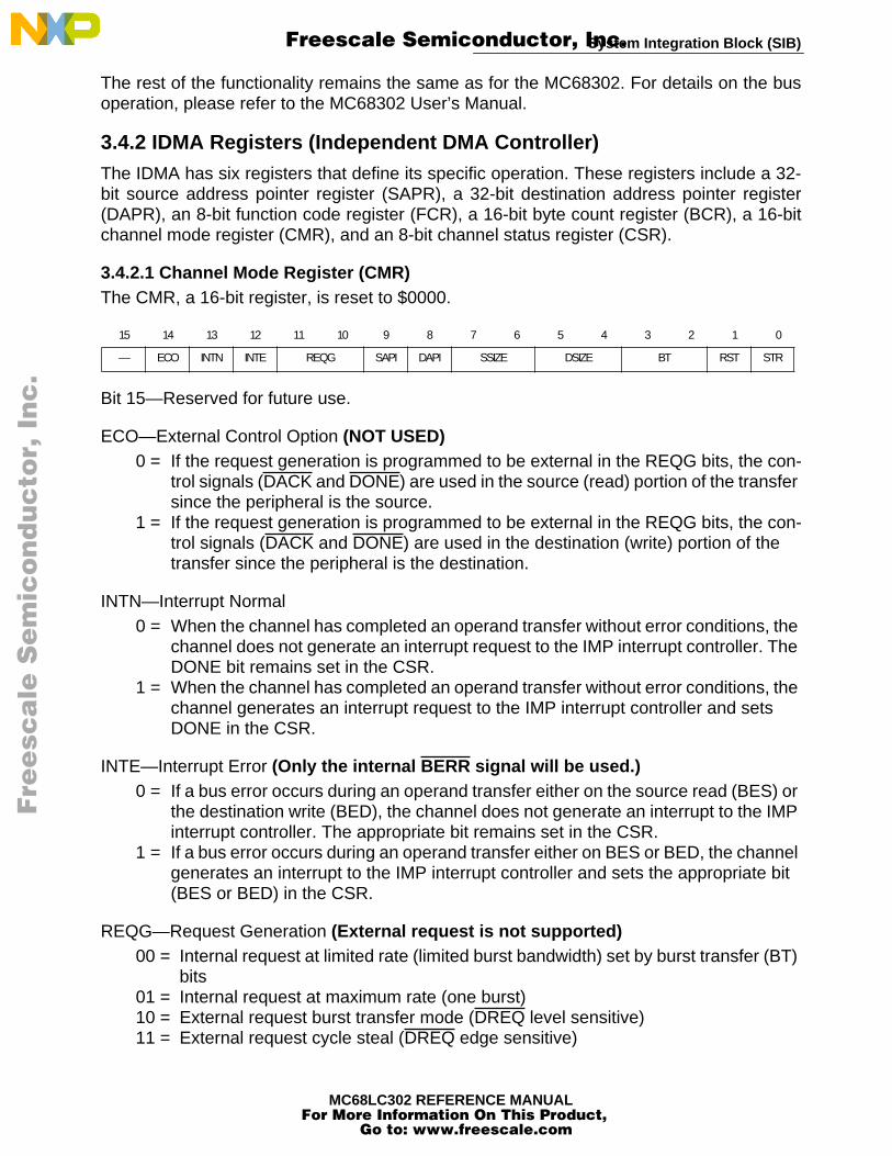
System Integration Block (SIB)
MC68LC302 REFERENCE MANUAL
The rest of the functionality remains the same as for the MC68302. For details on the busoperation, please refer to the MC68302 User’s Manual.
3.4.2 IDMA Registers (Independent DMA Controller)
The IDMA has six registers that define its specific operation. These registers include a 32-bit source address pointer register (SAPR), a 32-bit destination address pointer register(DAPR), an 8-bit function code register (FCR), a 16-bit byte count register (BCR), a 16-bitchannel mode register (CMR), and an 8-bit channel status register (CSR).
3.4.2.1 Channel Mode Register (CMR)
The CMR, a 16-bit register, is reset to $0000.
Bit 15—Reserved for future use.
ECO—External Control Option
(NOT USED)
0 = If the request generation is programmed to be external in the REQG bits, the con-trol signals (DACK and DONE) are used in the source (read) portion of the transfer since the peripheral is the source.
1 = If the request generation is programmed to be external in the REQG bits, the con-trol signals (DACK and DONE) are used in the destination (write) portion of the transfer since the peripheral is the destination.
INTN—Interrupt Normal0 = When the channel has completed an operand transfer without error conditions, the
channel does not generate an interrupt request to the IMP interrupt controller. The DONE bit remains set in the CSR.
1 = When the channel has completed an operand transfer without error conditions, the channel generates an interrupt request to the IMP interrupt controller and sets DONE in the CSR.
INTE—Interrupt Error
(Only the internal BERR signal will be used.)
0 = If a bus error occurs during an operand transfer either on the source read (BES) or the destination write (BED), the channel does not generate an interrupt to the IMP interrupt controller. The appropriate bit remains set in the CSR.
1 = If a bus error occurs during an operand transfer either on BES or BED, the channel generates an interrupt to the IMP interrupt controller and sets the appropriate bit (BES or BED) in the CSR.
REQG—Request Generation
(External request is not supported)
00 = Internal request at limited rate (limited burst bandwidth) set by burst transfer (BT) bits
01 = Internal request at maximum rate (one burst) 10 = External request burst transfer mode (DREQ level sensitive) 11 = External request cycle steal (DREQ edge sensitive)
15 14 13 12 11 10 9 8 7 6 5 4 3 2 1 0
— ECO INTN INTE REQG SAPI DAPI SSIZE DSIZE BT RST STR
Fre
esc
ale
Se
mic
on
du
cto
r, I
Freescale Semiconductor, Inc.
For More Information On This Product, Go to: www.freescale.com
nc
...

System Integration Block (SIB)
MC68LC302 REFERENCE MANUAL
NOTE
The settings 10 and 11 will not work since the DREQ pin is notpresent.
SAPI—Source Address Pointer (SAP) Increment 0 = SAP is not incremented after each transfer. 1 = SAP is incremented by one or two after each transfer, according to the source size
(SSIZE) bits and the starting address.
DAPI—Destination Address Pointer (DAP) Increment 0 = DAP is not incremented after each transfer. 1 = DAP is incremented by one or two after each transfer, according to the destination
size (DSIZE) bits and the starting address.
SSIZE—Source Size 00 = Reserved 01 = Byte 10 = Word 11 = Reserved
DSIZE—Destination Size 00 = Reserved 01 = Byte 10 = Word 11 = Reserved
BT—Burst Transfer 00 = IDMA gets up to 75% of the bus bandwidth. 01 = IDMA gets up to 50% of the bus bandwidth. 10 = IDMA gets up to 25% of the bus bandwidth. 11 = IDMA gets up to 12.5% of the bus bandwidth.
RST—Software Reset 0 = Normal operation 1 = The channel aborts any external pending or running bus cycles and terminates
channel operation. Setting RST clears all bits in the CSR and CMR.
STR—Start Operation 0 = Stop channel; clearing this bit will cause the IDMA to stop transferring data at
the end of the current operand transfer. The IDMA internal state is not altered. 1 = Start channel; setting this bit will allow the IDMA to start (or continue if previously
stopped) transferring data.
NOTE
STR is cleared automatically when the transfer is complete.
Fre
esc
ale
Se
mic
on
du
cto
r, I
Freescale Semiconductor, Inc.
For More Information On This Product, Go to: www.freescale.com
nc
...

System Integration Block (SIB)
MC68LC302 REFERENCE MANUAL
3.4.2.2 Source Address Pointer Register (SAPR)
The SAPR is a 32-bit register.
Note that A23-A20 must be initialized by the user. They are driven internally by the IDMAand can be used by the chip selects for address comparison.
3.4.2.3 Destination Address Pointer Register (DAPR)
The DAPR is a 32-bit register.
Note that A23-A20 must be initialized by the user. They are driven internally by the IDMAand can be used by the chip selects for address comparison.
3.4.2.4 Function Code Register (FCR)
The FCR is an 8-bit register.
The function codes must e initialized by the user. The function code value programmed intothe FCR is driven on the internal FC2-0 signals during a bus cycle to further qualify the ad-dress bus value. These values may be used by the chip selects for address matching.
NOTE
This register is undefined following power-on reset. The usershould always initialize it and should not use the function codevalue “111” in this register.
3.4.2.5 Byte Count Register (BCR)
This 16-bit register specifies the amount of data to be transferred by the IDMA; up to 64Kbytes (BCR = 0) is permitted.
3.4.2.6 Channel Status Register (CSR)
The CSR is an 8-bit register used to report events recognized by the IDMA controller. Onrecognition of an event, the IDMA sets its corresponding bit in the CSR (regardless of theINTE and INTN bits in the CMR).
Bits 7–4—These bits are reserved for future use.
31 24 23 0
RESERVED SOURCE ADDRESS POINTER
31 24 23 0
RESERVED DESTINATION ADDRESS POINTER
7 6 4 3 2 0
1 DFC 1 SFC
7 4 3 2 1 0
RESERVED DNS BES BED DONE
Fre
esc
ale
Se
mic
on
du
cto
r, I
Freescale Semiconductor, Inc.
For More Information On This Product, Go to: www.freescale.com
nc
...

System Integration Block (SIB)
MC68LC302 REFERENCE MANUAL
DNS—Done Not Synchronized
(NOT USED)
BES—Bus Error Source This bit indicates that the IDMA channel terminated with an error during the read cycle.
BED—Bus Error Destination This bit indicates that the IDMA channel terminated with an error during the write cycle.
DONE—Normal Channel Transfer Done This bit indicates that the IDMA channel has terminated normally.
3.5 INTERRUPT CONTROLLERThe IMP interrupt controller accepts and prioritizes both internal and external interrupt re-quests and generates a vector number during the CPU interrupt acknowledge cycle.
3.5.1 Interrupt Controller Key DifferencesSince the function code pins are not connected externally, the MC68LC302 (with the coreenabled) should be programmed to Dedicated Mode and to internally generate the vectorsfor Levels 1, 6, and 7. An external device will not be able to decode an IACK cycle and pro-vide an vector back to the MC68LC302.
In Disable CPU mode, the IRQ1, IRQ6, and IRQ7 become the BR, BGACK, and BG signals.With the core disabled, the MC68LC302 will not be able to decode an external CPU’s inter-rupt acknowledge cycle. The user must poll the Interrupt Pending Register (IPR) during in-terrupt handling to determine which peripheral caused the interrupt.
3.5.2 Interrupt Controller Programming ModelThe user communicates with the interrupt controller using four registers. The global interruptmode register (GIMR) defines the interrupt controller's operational mode. The interruptpending register (IPR) indicates which INRQ interrupt sources require interrupt service. Theinterrupt mask register (IMR) allows the user to prevent any of the INRQ interrupt sourcesfrom generating an interrupt request. The interrupt in-service register (ISR) provides a ca-pability for nesting INRQ interrupt requests.
3.5.2.1 Global Interrupt Mode Register (GIMR)The user normally writes the GIMR soon after a total system reset. The GIMR is initially$0000 and is reset only upon a total system reset.
MOD—Mode (The Mode Should be set to Dedicated)0 = Normal operational mode. Interrupt request lines are configured as IPL2–IPL0.1 = Dedicated operational mode. Interrupt request lines are configured as IRQ7, IRQ6,
and IRQ1.
15 14 13 12 11 10 9 8 7 5 4 0
MOD IV7 IV6 IV1 — ET7 ET6 ET1 V7–V5 RESERVED
Fre
esc
ale
Se
mic
on
du
cto
r, I
Freescale Semiconductor, Inc.
For More Information On This Product, Go to: www.freescale.com
nc
...
System Integration Block (SIB)
MC68LC302 REFERENCE MANUAL
IV7—Level 7 Interrupt Vector (Internal Vector Generation Should Be Used)0 = Internal vector. 1 = External vector.
IV6—Level 6 Interrupt Vector (Internal Vector Generation Should Be Used)0 = Internal vector.1 = External vector.
IV1—Level 1 Interrupt Vector (Internal Vector Generation Should Be Used)0 = Internal vector.1 = External vector.
ET7—IRQ7 Edge-/Level-Triggered 0 = Level-triggered. An interrupt is made pending when IRQ7 is low.
NOTE
The M68000 always treats level 7 as an edge-sensitive interrupt.
1 = Edge-triggered. An interrupt is made pending when IRQ7 changes from one to zero (falling edge).
ET6—IRQ6 Edge-/Level-Triggered 0 = Level-triggered. An interrupt is made pending when IRQ6 is low.1 = Edge-triggered. An interrupt is made pending when IRQ6 changes from one to
zero (falling edge).
ET1—IRQ1 Edge-/Level-Triggered 0 = Level-triggered. An interrupt is made pending when IRQ1 is low.1 = Edge-triggered. An interrupt is made pending when IRQ1 changes from one to
zero (falling edge).
V7–V5—Interrupt Vector Bits 7–5 These three bits are concatenated with five bits provided by the interrupt controller, whichindicate the specific interrupt source, to form an 8-bit interrupt vector number. If these bitsare not written, the vector $0F is provided.
NOTE:
These three bits should be greater than or equal to ‘010’ in orderto put the interrupt vector in the area of the exception vector ta-ble for user vectors.
Bits 11 and 4–0—Reserved for future use.
3.5.2.2 Interrupt Pending Register (IPR)Each bit in the 16-bit IPR corresponds to an INRQ interrupt source. When an INRQ interruptis received, the interrupt controller sets the corresponding bit in the IPR.
Fre
esc
ale
Se
mic
on
du
cto
r, I
Freescale Semiconductor, Inc.
For More Information On This Product, Go to: www.freescale.com
nc
...

System Integration Block (SIB)
MC68LC302 REFERENCE MANUAL
NOTE
The ERR bit is set if the user drives the IPL2–IPL0 lines to inter-rupt level 4 and no INRQ interrupt is pending.
3.5.2.3 Interrupt Mask Register (IMR)Each bit in the 16-bit IMR corresponds to an INRQ interrupt source. The user masks an in-terrupt source by clearing the corresponding bit in the IMR.
3.5.2.4 Interrupt In-Service Register (ISR) Each bit in the 16-bit ISR corresponds to an INRQ interrupt source. In a vectored interruptenvironment, the interrupt controller sets the ISR bit when the vector number correspondingto the INRQ interrupt source is passed to the core during an interrupt acknowledge cycle.The user's interrupt service routine should clear this bit during the servicing of the interrupt.
15 14 13 12 11 10 9 8
PB11 PB10 SCC1 SDMA IDMA SCC2 TIMER1 —
7 6 5 4 3 2 1 0
PB9 TIMER2 SCP TIMER3 SMC1 SMC2 PB8 ERR
15 14 13 12 11 10 9 8
PB11 PB10 SCC1 SDMA IDMA SCC2 TIMER1 —
7 6 5 4 3 2 1 0
PB9 TIMER2 SCP TIMER3 SMC1 SMC2 PB8 —
Fre
esc
ale
Se
mic
on
du
cto
r, I
Freescale Semiconductor, Inc.
For More Information On This Product, Go to: www.freescale.com
nc
...

System Integration Block (SIB)
MC68LC302 REFERENCE MANUAL
3.6 PARALLEL I/O PORTSThe IMP supports three general-purpose I/O ports, port A, port B, and port N, whose pinscan be general-purpose I/O pins or dedicated peripheral interface pins. Some port B pinsare always maintained as four general-purpose I/O pins, each with interrupt capability.
3.6.1 PARALLEL I/O PORT DIFFERENCESThe following port pins were removed: PA11, PA13, PA14, PA15, PB0, PB1, PB2, and PB4.If these signals are programmed to be inputs, the corresponding values in the data registerswill be indeterminate. If these pins are programmed to be output, then the output value willbe read back in the data register.
The SCP pins are now multiplexed onto PA8, PA9, and PA10.
The MODCLK pin is multiplexed with the PA12 port pin. After reset, this pin becomes a gen-eral purpose I/O pin.
An 8-bit port, Port N, has been added. Port N is only available when the MC68LC302 is in8-bit mode (internal BUSW=0).
3.6.2 Port A Each of the port A pins are independently configured as a general-purpose I/O pin if the cor-responding port A control register (PACNT) bit is cleared. Port A pins are configured as ded-icated on-chip peripheral pins if the corresponding PACNT bit is set.When acting as ageneral-purpose I/O pin, the signal direction for that pin is determined by the correspondingcontrol bit in the port A data direction register (PADDR). The port I/O pin is configured as aninput if the corresponding PADDR bit is cleared; it is configured as an output if the corre-sponding PADDR bit is set. The PADAT register is used to read and write values for the PortA pins. All PACNT bits and PADDR bits are cleared on total system reset, configuring allport A pins as general-purpose input pins.
15 14 13 12 11 10 9 8
PB11 PB10 SCC1 SDMA IDMA SCC2 TIMER1 0
7 6 5 4 3 2 1 0
PB9 TIMER2 SCP TIMER3 SMC1 SMC2 PB8 0
Fre
esc
ale
Se
mic
on
du
cto
r, I
Freescale Semiconductor, Inc.
For More Information On This Product, Go to: www.freescale.com
nc
...
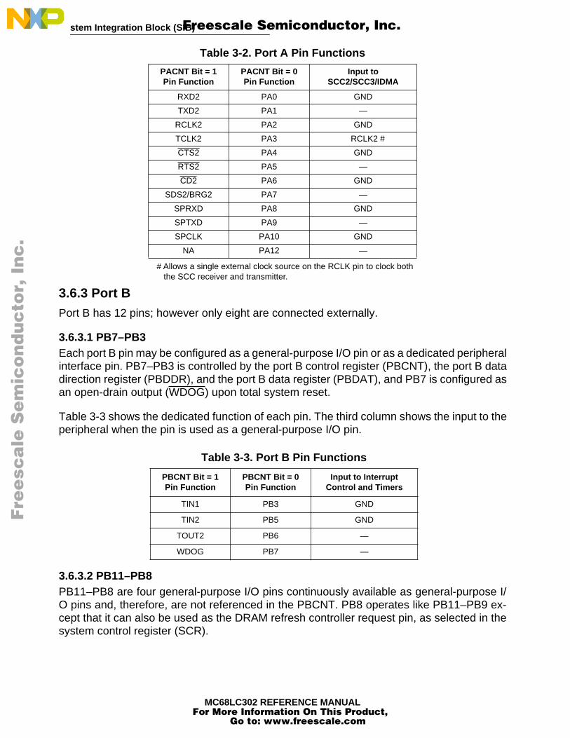
System Integration Block (SIB)
MC68LC302 REFERENCE MANUAL
# Allows a single external clock source on the RCLK pin to clock both the SCC receiver and transmitter.
3.6.3 Port BPort B has 12 pins; however only eight are connected externally.
3.6.3.1 PB7–PB3Each port B pin may be configured as a general-purpose I/O pin or as a dedicated peripheralinterface pin. PB7–PB3 is controlled by the port B control register (PBCNT), the port B datadirection register (PBDDR), and the port B data register (PBDAT), and PB7 is configured asan open-drain output (WDOG) upon total system reset.
Table 3-3 shows the dedicated function of each pin. The third column shows the input to theperipheral when the pin is used as a general-purpose I/O pin.
3.6.3.2 PB11–PB8PB11–PB8 are four general-purpose I/O pins continuously available as general-purpose I/O pins and, therefore, are not referenced in the PBCNT. PB8 operates like PB11–PB9 ex-cept that it can also be used as the DRAM refresh controller request pin, as selected in thesystem control register (SCR).
Table 3-2. Port A Pin Functions
PACNT Bit = 1Pin Function
PACNT Bit = 0Pin Function
Input toSCC2/SCC3/IDMA
RXD2 PA0 GND
TXD2 PA1 —
RCLK2 PA2 GND
TCLK2 PA3 RCLK2 #
CTS2 PA4 GND
RTS2 PA5 —
CD2 PA6 GND
SDS2/BRG2 PA7 —
SPRXD PA8 GND
SPTXD PA9 —
SPCLK PA10 GND
NA PA12 —
Table 3-3. Port B Pin Functions
PBCNT Bit = 1Pin Function
PBCNT Bit = 0Pin Function
Input to InterruptControl and Timers
TIN1 PB3 GND
TIN2 PB5 GND
TOUT2 PB6 —
WDOG PB7 —
Fre
esc
ale
Se
mic
on
du
cto
r, I
Freescale Semiconductor, Inc.
For More Information On This Product, Go to: www.freescale.com
nc
...

System Integration Block (SIB)
MC68LC302 REFERENCE MANUAL
NOTE
If the PIT is enabled, then the PB8 pin will not generate an inter-rupt, since the PIT uses the PB8 interrupt in the IPR, IMR, andISR.
The direction of each pin is determined by the corresponding bit in the PBDDR. The port pinis configured as an input if the corresponding PBDDR bit is cleared; it is configured as anoutput if the corresponding PBDDR bit is set. PBDDR11–PBDDR8 are cleared on total sys-tem reset, configuring all PB11–PB8 pins as general-purpose input pins.When a PB11–PB8pin is configured as an input, a high-to-low change will cause an interrupt request signal tobe sent to the IMP interrupt controller.
3.6.4 Port NWhen the LC302 is in 8-bit mode (internal BUSW=0), 8 more general purpose I/O pins areavailable. The signal direction for each pin is determined by the corresponding control bit inthe port N data direction register (PNDDR). The port I/O pin is configured as an input if thecorresponding PNDDR bit is cleared; it is configured as an output if the corresponding PND-DR bit is set. The PNDAT register is used to read and write values for the Port N pins.
3.6.5 Port Registers The I/O port consists of three memory-mapped read-write 16-bit registers for port A andthree memory-mapped read-write 16-bit registers for port B. Refer to Figure 3-2. Parallel I/O Port Registers for the I/O port registers. The reserved bits are read as zeros.
0 = I/O 1 = Peripheral
0 = Input 1 = Output
0 = I/O 1 = Peripheral
Port A Control Register(PACNT)
15 14 13 12 11 10 9 8 7 6 5 4 3 2 1 0
- - - CA - CA CA CA CA CA CA CA CA CA CA CA
Port A Data Direction Register(PADDR)
15 14 13 12 11 10 9 8 7 6 5 4 3 2 1 0
- - - DA - DA DA DA DA DA DA DA DA DA DA DA
Port A Data Register(PADAT)
15 14 13 12 11 10 9 8 7 6 5 4 3 2 1 0
- - - PA - PA PA PA PA PA PA PA PA PA PA PA
Port B Control Register(PBCNT)
15 8 7 6 5 4 3 2 1 0
RESERVED CB CB CB - CB - - -
Fre
esc
ale
Se
mic
on
du
cto
r, I
Freescale Semiconductor, Inc.
For More Information On This Product, Go to: www.freescale.com
nc
...

System Integration Block (SIB)
MC68LC302 REFERENCE MANUAL
0 = Input 1 = Output
0 = Input 1 = Output
Figure 3-2. Parallel I/O Port Registers
3.7 TIMERSThe IMP includes four timer units: two identical general-purpose timers, a software watch-dog timer, and a periodic interrupt timer (PIT).
Each general-purpose timer consists of a timer mode register (TMR), a timer capture regis-ter (TCR), a timer counter (TCN), a timer reference register (TRR), and a timer event register(TER). The TMR contains the prescaler value programmed by the user. The software watch-dog timer, which has a watchdog reference register (WRR) and a watchdog counter (WCN),uses a fixed prescaler value.
3.7.1 MC68LC302 General Purpose Timer DifferenceThe only difference between the MC68LC302 and the MC68302 general purpose timers isthat Timer 1 output signal is not connected to the externally.
3.7.2 General Purpose Timers Programming Mode3.7.2.1 Timer Mode Register (TMR1, TMR2)TMR1 and TMR2 are identical 16-bit registers. TMR1 and TMR2, which are memory-mapped read-write registers to the user, are cleared by reset.
RST—Reset Timer0 = Reset timer (software reset), includes clearing the TMR, TRR, and TCN.1 = Enable timer
Port B Data Direction Register(PBDDR)
15 12 11 10 9 8 7 6 5 4 3 2 1 0
RESERVED DB DB DB DB DB DB DB - DB - - -
Port B Data Register(PBDAT)
15 12 11 10 9 8 7 6 5 4 3 2 1 0
RESERVED PB PB PB PB PB PB PB - PB - - -
Port N Data Direction Register(PNDDR)
15 14 13 12 11 10 9 8 7 6 5 4 3 2 1 0
DN DN DN DN DN DN DN DN RESERVED
Port N Data Register (PNDAT)
15 14 13 12 11 10 9 8 7 6 5 4 3 2 1 0
PN PN PN PN PN PN PN PN RESERVED
15 8 7 6 5 4 3 2 1 0
PRESCALER VALUE (PS) CE OM ORI FRR ICLK RST
Fre
esc
ale
Se
mic
on
du
cto
r, I
Freescale Semiconductor, Inc.
For More Information On This Product, Go to: www.freescale.com
nc
...
System Integration Block (SIB)
MC68LC302 REFERENCE MANUAL
ICLK—Input Clock Source for the Timer 00 = Stop count 01 = Master clock 10 = Master clock divided by 1611 = Corresponding TIN pin, TIN1 or TIN2 (falling edge)
FRR—Free Run/Restart 0 = Free run—timer count continues to increment after the reference value is reached. 1 = Restart—timer count is reset immediately after the reference value is reached.
ORI—Output Reference Interrupt Enable 0 = Disable interrupt for reference reached 1 = Enable interrupt upon reaching the reference value
OM—Output Mode (Only available for Timer 1)0 = Active-low pulse for one CLKO clock cycle (60 ns at 16.67 MHz) 1 = Toggle output
CE—Capture Edge and Enable Interrupt 00 = Capture function is disabled01 = Capture on rising edge only and enable interrupt on capture event 10 = Capture on falling edge only and enable interrupt on capture event 11 = Capture on any edge and enable interrupt on capture event
PS—Prescaler Value The prescaler is programmed to divide the clock input by values from 1 to 256. The value00000000 divides the clock by 1; the value 11111111 divides the clock by 256.
3.7.2.2 Timer Reference Registers (TRR1, TRR2)Each TRR is a 16-bit register containing the reference value for the timeout. TRR1 andTRR2 are memory-mapped read-write registers.
3.7.2.3 Timer Capture Registers (TCR1, TCR2)Each TCR is a 16-bit register used to latch the value of the counter during a capture opera-tion when an edge occurs on the respective TIN1 or TIN2 pin. TCR1 and TCR2 appear asmemory-mapped read-only registers to the user.
3.7.2.4 Timer Counter (TCN1, TCN2)TCN1 and TCN2 are 16-bit up-counters. Each is memory-mapped and can be read and writ-ten by the user. A read cycle to TCN1 and TCN2 yields the current value of the timer anddoes not affect the counting operation.
3.7.2.5 Timer Event Registers (TER1, TER2)Each TER is an 8-bit register used to report events recognized by any of the timers. On rec-ognition of an event, the timer will set the appropriate bit in the TER, regardless of the cor-responding interrupt enable bits (ORI and CE) in the TMR. TER1 and TER2, which appear
Fre
esc
ale
Se
mic
on
du
cto
r, I
Freescale Semiconductor, Inc.
For More Information On This Product, Go to: www.freescale.com
nc
...

System Integration Block (SIB)
MC68LC302 REFERENCE MANUAL
to the user as memory-mapped registers, may be read at any time. A bit is cleared by writinga one to that bit (writing a zero does not affect a bit's value).
CAP—Capture EventThe counter value has been latched into the TCR. The CE bits in the TMR are used toenable the interrupt request caused by this event.
REF—Output Reference Event The counter has reached the TRR value. The ORI bit in the TMR is used to enable theinterrupt request caused by this event.
Bits 7–2—Reserved for future use.
3.7.3 Timer 3 - Software Watchdog Timer A watchdog timer is used to protect against system failures by providing a means to escapefrom unexpected input conditions, external events, or programming errors. Timer 3 may beused for this purpose. Once started, the watchdog timer must be cleared by software on aregular basis so that it never reaches its timeout value. Upon reaching the timeout value, theassumption may be made that a system failure has occurred, and steps can be taken to re-cover or reset the system. No changes have been made to the Software Watchdog Timer.Please refer to the MC68302 Users’ Manual for more information.
3.7.3.1 Software Watchdog Reference Register (WRR)WRR is a 16-bit register containing the reference value for the timeout. The EN bit of theregister enables the timer. WRR appears as a memory-mapped read-write register to theuser.
3.7.3.2 Software Watchdog Counter (WCN)WCN, a 16-bit up-counter, appears as a memory-mapped register and may be read at anytime. Clearing EN in WRR causes the counter to be reset and disables the count operation.A read cycle to WCN causes the current value of the timer to be read. A write cycle to WCNcauses the counter and prescaler to be reset. A write cycle should be executed on a regularbasis so that the watchdog timer is never allowed to reach the reference value during normalprogram operation.
3.7.4 Periodic Interrupt Timer (PIT)The MC68LC302 IMP provides a timer to generate periodic interrupts for use with a real-time operating system or the application software. The periodic interrupt time period canvary from 122 µs to 128 s (assuming a 32.768-kHz crystal is used to generate the generalsystem clock). This function can be disabled.
7 2 1 0
RESERVED REF CAP
15 1 0
REFERENCE VALUE EN
Fre
esc
ale
Se
mic
on
du
cto
r, I
Freescale Semiconductor, Inc.
For More Information On This Product, Go to: www.freescale.com
nc
...

System Integration Block (SIB)
MC68LC302 REFERENCE MANUAL
3.7.4.1 OverviewThe periodic interrupt timer consists of an 11-bit modulus counter that is loaded with the val-ue contained in the PITR. The modulus counter is clocked by the CLKIN signal derived fromthe IMP EXTAL pin. See Figure 2-2.
The clock source is divided by four before driving the modulus counter (PITCLK). When themodulus counter value reaches zero, an interrupt request signal is generated to the IMP in-terrupt controller.
The value of bits 11–1 in the PITR is then loaded again into the modulus counter, and thecounting process starts over. A new value can be written to the PITR only when the PIT isdisabled.
The PIT interrupt replaces the IMP PB8 interrupt and is mapped to the PB8 interrupt prioritylevel 4. The PIT Interrupt is maskable by setting bit1 (PB8) in the IMR register.
NOTE
When the PIT is enabled, PB8 can still be used as parallel I/Opin or as DRAM refresh controller request pin, but PB8 will notbe capable of generating interrupts.
3.7.4.2 Periodic Timer Period CalculationThe period of the periodic timer can be calculated using the following equation:
Solving the equation using a crystal frequency of 32.768 kHz with the prescaler disabledgives:
This gives a range from 122 µs, with a PITR value of $0, to 250 ms, with a PITR value of$7FF (assuming 32.768 khz at the EXTAL pin.
periodic interrupt timer period PITR count value+1EXTAL( ) 1or512⁄( )
4( )--------------------------------------------------------------------------------------------------------------=
periodic interrupt timer period PITR count value+132768 1⁄
22----------------------
-------------------------------------------------=
periodic interrupt timer period PITR count value8192
-------------------------------------------=
Fre
esc
ale
Se
mic
on
du
cto
r, I
Freescale Semiconductor, Inc.
For More Information On This Product, Go to: www.freescale.com
nc
...

System Integration Block (SIB)
MC68LC302 REFERENCE MANUAL
Solving the equation with the prescaler enabled (PTP=1) gives the following values:
This gives a range from 62.5 ms, with a PITR value of $0 to 128 s, with a PITR value of $7FF.
For a fast calculation of periodic timer period using a 32.768-kHz crystal, the following equa-tions can be used:
With prescaler disabled:
programmable interrupt timer period = PITR (122 µs)
With prescaler enabled:
programmable interrupt timer period = PITR (62.5 ms)
3.7.4.3 Using the Periodic Timer As a Real-Time ClockThe periodic interrupt timer can be used as a real-time clock interrupt by setting it up to gen-erate an interrupt with a one-second period. When using a 32.768-kHz crystal, the PITRshould be loaded with a value of $0F with the prescaler enabled to generate interrupts at aone-second rate. The interrupt is generated, in this case, at a precise 1 second rate, even ifthe interrupt is not serviced immediately. A true real time clock is obtained if the current in-terrupt is serviced completely before the next one occurs.
3.7.4.4 Periodic Interrupt Timer Register (PITR)The PITR contains control for prescaling the periodic timer as well as the count value for theperiodic timer. This register can be read or written only during normal operational mode. Bits14–13 are not implemented and always return a zero when read. A write does not affectthese bits.
PITR $0F0
Read/Write
15 14 13 12 11 10 9 8
PTEN 0 0 PTP PITR10 PITR9 PITR8 PITR7
RESET
0 0 0 0 0 0 0 0
7 6 5 4 3 2 1 0
PITR6 PITR5 PITR4 PITR3 PITR2 PITR1 PITR0 RES
RESET
0 0 0 0 0 0 0 0
periodic interrupt timer period PITR count value32768 512⁄
22----------------------------
-------------------------------------------=
periodic interrupt timer period PITR count value16
-------------------------------------------=
Fre
esc
ale
Se
mic
on
du
cto
r, I
Freescale Semiconductor, Inc.
For More Information On This Product, Go to: www.freescale.com
nc
...
System Integration Block (SIB)
MC68LC302 REFERENCE MANUAL
PTEN—Periodic Timer EnableThis bit contains the enable control for the periodic timer.
0 = Periodic timer is disabled1 = Periodic timer is enabled
PTP—Periodic Timer Prescaler ControlThis bit contains the prescaler control for the periodic timer.
0 = Periodic timer clock is not prescaled 1 = Periodic timer clock is prescaled by a value of 512
PITR10–0—Periodic Interrupt Timer Register BitsThese bits of the PITR contain the remaining bits of the PITR count value for the periodictimer. These bits may be written only when the PIT is disabled (PTEN=0) to modifythe PIT count value.
NOTE
If the PIT is enabled with the PTP bit is set, the first interrupt canbe up to 512 clocks early, depending on the prescaler countervalue when the PIT is enabled.
3.8 EXTERNAL CHIP-SELECT SIGNALS AND WAIT-STATE LOGICThe IMP provides a set of four programmable chip-select signals. Each chip-select signalhas an identical internal structure. For each memory area, the user may also define an in-ternally generated cycle termination signal (DTACK). This feature eliminates board spacethat would be necessary for cycle termination logic.
The chip-select logic is active for memory cycles generated by internal bus masters(M68000 core, IDMA, SDMA, DRAM refresh) or external bus masters (A23-A20 are drivento zero internally and FC2-0 are driven to 5). These signals are driven externally on thefalling edge of AS and are valid shortly after AS goes low.
NOTE
For more information on the operation of the Chip Selects,please refer to Section 3 of the MC68302 Users’ Manual.
NOTE
Internal Masters (CPU, IDMA and SDMA) drive A23:A20 andFC2-FC0 internally. The CS logic compares the signals to thevalues programmed in the registers.
In Disable CPU mode or for External Bus Masters, the A23-A20signals are internally driven to zero, so the user must program
Fre
esc
ale
Se
mic
on
du
cto
r, I
Freescale Semiconductor, Inc.
For More Information On This Product, Go to: www.freescale.com
nc
...

System Integration Block (SIB)
MC68LC302 REFERENCE MANUAL
the corresponding bits in the Chip Select registers to zero, ormask off those address bits.
Also FC2-0 are driven to 5, so we suggest that the function codecomparison be turned off.
3.8.1 Chip-Select RegistersEach of the four chip-select units has two registers that define its specific operation. Theseregisters are a 16-bit base register (BR) and a 16-bit option register (OR) (e.g., BR0 andOR0). The BR should normally be programmed after the OR since the BR contains the chip-select enable bit.
3.8.1.1 Base Register (BR3–BR0)These 16-bit registers consist of a base address field, a read-write bit, and a function codefield.
FC2–FC0 —Function Code FieldThis field is contained in bits 15–13 of each BR. These bits are used to set the addressspace function code. Because of the priority mechanism and the EN bit, only the CS0 lineis active after a system reset.
Bits 12–2—Base AddressThese bits are used to set the starting address of a particular address space.
RW—Read/Write 0 = The chip-select line is asserted for read operations only. 1 = The chip-select line is asserted for write operations only.
EN—Enable 0 = The chip-select line is disabled. 1 = The chip-select line is enabled.
After system reset, only CS0 is enabled; CS3–CS1 are disabled. In disable CPU mode,CS3–CS0 are disabled at system reset. The chip select does not require disabling beforechanging its parameters.
3.8.1.2 Option Registers (OR3–OR0)These four 16-bit registers consist of a base address mask field, a read/write mask bit, acompare function code bit, and a DTACK generation field.
15 13 12 2 1 0
FC2 –FC0 BASE ADDRESS (A23–A13) RW EN
15 13 12 2 1 0
DTACK BASE ADDRESS MASK (M23–M13) MRW CFC
Fre
esc
ale
Se
mic
on
du
cto
r, I
Freescale Semiconductor, Inc.
For More Information On This Product, Go to: www.freescale.com
nc
...

System Integration Block (SIB)
MC68LC302 REFERENCE MANUAL
Bits 15–12—DTACK Field These bits are used to determine whether DTACK is generated internally with a program-mable number of wait states or externally by the peripheral.
Bits 12–2—Base Address Mask These bits are used to set the block size of a particular chip-select line. The address com-pare logic uses only the address bits that are not masked (i.e., mask bit set to one) to de-tect an address match.
0 = The address bit in the corresponding BR is masked. 1 = The address bit in the corresponding BR is not masked.
MRW—Mask Read/Write 0 = The RW bit in the BR is masked. 1 = The RW bit in the BR is not masked.
NOTE
For correct operation of the CS logic, MRW bit cannot be set inSlave Mode or in systems where an External Master can takeownership of the Bus.
CFC—Compare Function Code0 = The FC bits in the BR are ignored. 1 = The FC bits on the BR are compared.
NOTE
Compare Function Code may be useful in systems where onlyInternal Masters (CPU or DMA) take ownership of the Bus be-cause those masters drive the FC2-0 signals internally. In SlaveMode or in systems where External Masters take ownership ofthe bus, CFC should be programmed to 0.
Table 3-4. DTACK Field Encoding
BitsDescription
15 14 13
0 0 0 No Wait State
0 0 1 1 Wait State
0 1 0 2 Wait States
0 1 1 3 Wait States
1 0 0 4 Wait States
1 0 1 5 Wait States
1 1 0 6 Wait States
1 1 1 External DTACK
Fre
esc
ale
Se
mic
on
du
cto
r, I
Freescale Semiconductor, Inc.
For More Information On This Product, Go to: www.freescale.com
nc
...

System Integration Block (SIB)
MC68LC302 REFERENCE MANUAL
3.8.2 Disable CPU Logic (M68000)The IMP can be configured to operate solely as a peripheral to an external processor. In thismode, the on-chip M68000 CPU should be disabled by strapping DISCPU high during sys-tem reset (RESET and HALT asserted simultaneously). The internal accesses to the IMPperipherals and memory may be asynchronous or synchronous. During synchronous reads,one wait state may be used if required (EMWS bit set). The following pins change their func-tionality in this mode:
1. THE IPL0 pin becomes BR and is an output from the IDMA and SDMA to the external M68000 bus.
2. The IPL2 pin becomes BG and is an input to the IDMA and SDMA from the external M68000 bus. When BG is sampled as low by the IMP, it waits for AS, HALT, and BGACK to be negated, and then asserts BGACK and performs one or more bus cy-cles.
3. The IPL1 pin becomes BGACK and is an output from the IDMA and SDMA to indicate bus ownership.
4. The IPL2-0 lines are no longer encoded interrupt lines.The interrupt controller will out-put the MC68LC302’s interrupt request on IOUT2. CS0, which is multiplexed with IOUT2 is not available in this mode.
5. The WEH and WEL signals become UDS and LDS respectively.
6. The OE becomes R/W.
DISCPU should remain continuously high during disable CPU mode operation. Although theCS0 pin is not available as an output from the device in disable CPU mode, it may be en-abled to provide DTACK generation. In disable CPU mode, BR0 is initially $C000.
In disable CPU mode, accesses by an external master to the IMP RAM and registers maybe asynchronous or synchronous to the IMP clock. See the SAM and EMWS bits in the SCRfor details.
3.8.3 Bus Arbitration Logic Both internal and external bus arbitration are discussed in the following paragraphs.
3.8.3.1 Internal Bus ArbitrationThe IMP bus arbiter supports three bus request sources in the following standard priority:
1. External bus master (BR pin) (only in Disable CPU mode)
2. SDMA for the SCCs (six channels)
3. IDMA (one channel)
3.8.3.2 External Bus ArbitrationWhen the CPU is enabled, an external bus master may gain ownership of the M68000 busby asserting the HALT signal. This will cause the LC302 bus master (M68000 core, SDMA,or IDMA) to stop at the completion of the current bus cycle After asserting the HALT signal,the external bus master must wait until AS is negated plus 2 additional system clocks beforeaccessing the bus (to allow the LC302 to threestate all of the bus signals).After gaining own-
Fre
esc
ale
Se
mic
on
du
cto
r, I
Freescale Semiconductor, Inc.
For More Information On This Product, Go to: www.freescale.com
nc
...

System Integration Block (SIB)
MC68LC302 REFERENCE MANUAL
ership, the external master can not access the internal IMP registers or RAM. Chip selectsand system control functions, such as the hardware watchdog, continue to operate.
When an external master desires to gain ownership, the following bus arbitration protocolshould be used:
1. Assert HALT.
2. Wait two system clocks.
3. If AS is negated go to step 5.
4. Wait for AS negation. Then wait two additional system clocks.
5. Execute Access (now the bus is guaranteed to be threestated)
6. When done, threestate bus and negate HALT.
NOTE
The RMCST bit in the SCR should be zero for this arbitrationprocedure to work correctly.
Also, the external master cannot access the internal addressspace of the MC68LC302.
Bus Arbitration is not supported when the MC68LC302 is in oneof the low power modes. The chip does not release the addressand data lines.
3.9 DYNAMIC RAM REFRESH CONTROLLERThe communications processor (CP) main (RISC) controller may be configured to handlethe dynamic RAM (DRAM) refresh task without any intervention from the M68000 core. Useof this feature requires a timer or SCC baud rate generator (either from the IMP or external-ly), the I/O pin PB8, and two transmit buffer descriptors from SCC2 (Tx BD6 and Tx BD7).
No changes have been made to the DRAM controller. For more information, please refer tothe MC68302 Users’ Manual.
Fre
esc
ale
Se
mic
on
du
cto
r, I
Freescale Semiconductor, Inc.
For More Information On This Product, Go to: www.freescale.com
nc
...

System Integration Block (SIB)
MC68LC302 REFERENCE MANUAL
Fre
esc
ale
Se
mic
on
du
cto
r, I
Freescale Semiconductor, Inc.
For More Information On This Product, Go to: www.freescale.com
nc
...

MC68LC302 REFERENCE MANUAL
SECTION 4COMMUNICATIONS PROCESSOR (CP)
The CP includes the following modules:
• Main Controller (RISC Processor)
• Four Serial Direct Memory Access (SDMA) Channels
• A Command Set Register
• Serial Channels Physical Interface Including:
—Motorola Interchip Digital Link (IDL)—General Circuit Interface (GCI), Also Known as IOM-2—Pulse Code Modulation (PCM) Highway Interface—Nonmultiplexed Serial Interface (NMSI) Implementing Standard Modem Signals
• Two Independent Full Duplex Serial Communication Controllers (SCCs) Supporting the Following Protocols:
—High-Level/Synchronous Data Link Control (HDLC/SDLC)—Universal Asynchronous Receiver Transmitter (UART)—Autobaud Function to Detect Baud Rate of the Incoming Asynchronous Bit Stream—Binary Synchronous Communication (BISYNC)—Transparent Modes
• Serial Communication Port (SCP) for Synchronous Communication
• Two Serial Management Controllers (SMCs) to Support the IDL and GCI Management Channels
4.1 MC68LC302 KEY DIFFERENCES FROM THE MC68302
• SCC3 Was Removed.
• The SCP Is Now Multiplexed with the PA8, PA9, and PA10 Pins.
• The DDCMP and V.110 Protocols Were Removed.
• The Autobaud Function Was Added for Detecting the Baud Rate of the Incoming Asyn-chronous Bit Stream.
This section only presents a description of features and registers that have changed or beenadded. Features that have not changed such as UART, HDLC, BIYSYNC transparent, theSMCs, and the SCP will not be discussed. For more information on any function not dis-cussed in this section, please refer to the
MC68302 User’s Manual
.
This section assumes that the user is familiar with the different protocols. For more informa-tion on a specific protocol implementation, please refer to the
MC68302 User’s Manua
l
Fre
esc
ale
Se
mic
on
du
cto
r, I
Freescale Semiconductor, Inc.
For More Information On This Product, Go to: www.freescale.com
nc
...
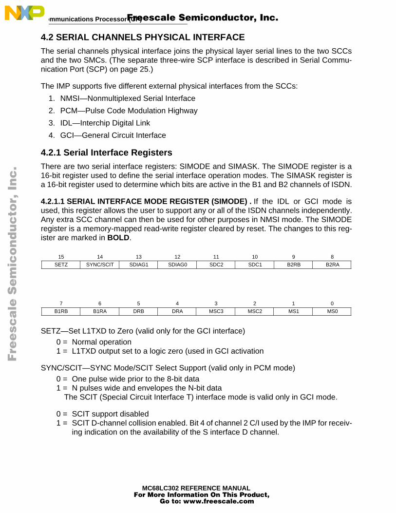
Communications Processor (CP)
MC68LC302 REFERENCE MANUAL
4.2 SERIAL CHANNELS PHYSICAL INTERFACE
The serial channels physical interface joins the physical layer serial lines to the two SCCsand the two SMCs. (The separate three-wire SCP interface is described in Serial Commu-nication Port (SCP) on page 25.)
The IMP supports five different external physical interfaces from the SCCs:
1. NMSI—Nonmultiplexed Serial Interface
2. PCM—Pulse Code Modulation Highway
3. IDL—Interchip Digital Link
4. GCI—General Circuit Interface
4.2.1 Serial Interface Registers
There are two serial interface registers: SIMODE and SIMASK. The SIMODE register is a16-bit register used to define the serial interface operation modes. The SIMASK register isa 16-bit register used to determine which bits are active in the B1 and B2 channels of ISDN.
4.2.1.1 SERIAL INTERFACE MODE REGISTER (SIMODE) .
If the IDL or GCI mode isused, this register allows the user to support any or all of the ISDN channels independently.Any extra SCC channel can then be used for other purposes in NMSI mode. The SIMODEregister is a memory-mapped read-write register cleared by reset. The changes to this reg-ister are marked in
BOLD
.
SETZ—Set L1TXD to Zero (valid only for the GCI interface)0 = Normal operation1 = L1TXD output set to a logic zero (used in GCI activation
SYNC/SCIT—SYNC Mode/SCIT Select Support (valid only in PCM mode)0 = One pulse wide prior to the 8-bit data 1 = N pulses wide and envelopes the N-bit data
The SCIT (Special Circuit Interface T) interface mode is valid only in GCI mode.
0 = SCIT support disabled 1 = SCIT D-channel collision enabled. Bit 4 of channel 2 C/I used by the IMP for receiv-
ing indication on the availability of the S interface D channel.
15 14 13 12 11 10 9 8
SETZ SYNC/SCIT SDIAG1 SDIAG0 SDC2 SDC1 B2RB B2RA
7 6 5 4 3 2 1 0
B1RB B1RA DRB DRA MSC3 MSC2 MS1 MS0
Fre
esc
ale
Se
mic
on
du
cto
r, I
Freescale Semiconductor, Inc.
For More Information On This Product, Go to: www.freescale.com
nc
...

Communications Processor (CP)
MC68LC302 REFERENCE MANUAL
SDIAG1–SDIAG0—Serial Interface Diagnostic Mode (NMSI1 Pins Only)00 = Normal operation 01 = Automatic echo10 = Internal loopback11 = Loopback control
SDC2—Serial Data Strobe Control 2 0 = SDS2 signal is asserted during the B2 channel 1 = SDS1 signal is asserted during the B2 channel
SDC1—Serial Data Strobe Control 1 0 = SDS1 signal is asserted during the B1 channel 1 = SDS2 signal is asserted during the B1 channel
B2RB, B2RA—B2 Channel Route in IDL/GCI Mode or CH-3 Route in PCM Mode 00 = Channel not supported 01 = Route channel to SCC1 10 = Route channel to SCC2 (if MSC2 is cleared) 11 = Route channel to SCC3
(Not Supported in the MCMC68LC302)
B1RB, B1RA—B1 Channel Route in IDL/GCI Mode or CH-2 Route in PCM Mode 00 = Channel not supported 01 = Route channel to SCC1 10 = Route channel to SCC2 (if MSC2 is cleared) 11 = Route channel to SCC3
(Not Supported in the MCMC68LC302)
DRB, DRA—D-Channel Route in IDL/GCI Mode or CH-1 Route in PCM Mode 00 = Channel not supported 01 = Route channel to SCC1 10 = Route channel to SCC2 (if MSC2 is cleared) 11 = Route channel to SCC3
(Not Supported in the MC68LC302)
MSC3—SCC3 Connection (
Not Supported in the MC68LC302)
MSC2—SCC2 Connection 0 = SCC2 is connected to the multiplexed serial interface (PCM, IDL, or GCI) chosen
in MS1–MS0. NMSI2 pins are all available for other purposes. 1 = SCC2 is not connected to a multiplexed serial interface but is either connected di-
rectly to the NMSI2 pins or not used. The choice of general-purpose I/O port pins versus SCC2 functions is made in the port A control register.
MS1—MS0—Mode Supported 00 = NMSI Mode01 = PCM Mode10 = IDL Mode11 = GCI Interface
Fre
esc
ale
Se
mic
on
du
cto
r, I
Freescale Semiconductor, Inc.
For More Information On This Product, Go to: www.freescale.com
nc
...

Communications Processor (CP)
MC68LC302 REFERENCE MANUAL
4.2.1.2 SERIAL INTERFACE MASK REGISTER (SIMASK) .
The SIMASK register, amemory-mapped read-write register, is set to all ones by reset. SIMASK is used in IDL andGCI to determine which bits are active in the B1 and B2 channels. Any combination of bitsmay be chosen. A bit set to zero is not used by the IMP. A bit set to one signifies that thecorresponding B channel bit is used for transmission and reception on the B channel. Notethat the serial data strobes, SD1 and SD2, are asserted for the entire 8-bit time slot inde-pendent of the setting of the bits in the SIMASK register.
NOTE
Bit 0 of this register is the first bit transmitted or received on theIDL/GCI B1 channel.
4.3 SERIAL COMMUNICATION CONTROLLERS (SCCS)
The IMP contains two independent SCCs, each of which can implement different protocols.This configuration provides the user with options for controlling up to two independent full-duplex lines implementing bridges or gateway functions or multiplexing both SCCs onto thesame physical layer interface to implement a two channels on a time-division multiplexed(TDM) bus. Each protocol-type implementation uses identical buffer structures to simplifyprogramming.
4.3.1 SCC Configuration Register (SCON)
Each SCC controller has a configuration register that controls its operation and selects itsclock source and baud rate. This register has not been changed from the MC68302.
4.3.1.1 DIVIDE BY 2 INPUT BLOCKS (NEW FEATURE).
The SCC Baud Rate Generatorshave 2 divide by 2 blocks added to them. With the divide by 2 blocks enabled, the VCO Out-put from the PLL and the TIN1 input clock can be divided by 2 before they are used by theBRG to generate the serial clocks. The divide by two blocks can be enabled by setting theBCD bit in the IOMCR register if the BRG clock source is derived from the IMP system clock,or by setting the BRGDIV bit in the DISC register if the BRG clock source is derived from theTIN pin.
4.3.2 Disable SCC1 Serial Clocks Out (DISC)
The Disable SCC1 Serial Clocks Out (DISC) is an 16-bit read/write register. The upper 8 bitscontrol: (1) enabling the divide by 2 prescaler for the baud rate generator from the TIN1 pin,and (2) options for three stating theTCLK1, and RCLK1 pins.
15 8 7 0
B2
15 14 13 12 11 10 9 8 7 6 5 4 3 2 1 0
WOMS EXTC TCS RCS CD10 CD9 CD8 CD7 CD6 CD5 CD4 CD3 CD2 CD1 CD0 DIV4
Fre
esc
ale
Se
mic
on
du
cto
r, I
Freescale Semiconductor, Inc.
For More Information On This Product, Go to: www.freescale.com
nc
...

Communications Processor (CP)
MC68LC302 REFERENCE MANUAL
DISC Base+$8EE
4.3.2.1 RCLK1 AND TCLK1 PIN OPTIONS.
TSRCLK10 = RCLK1 is driven on its pin when SCC1 RCLK is the baud rate generator output.1 = RCLK1 is three-state.
TSTCLK10 = TCLK1 is driven on its pin when SCC1 RCLK is the baud rate generator output.1 = TCLK1 is three-state.
BRGDIVEnables and disables the divide by two block between the TIN1 pin and the BRG1 pres-caler input.
0 = The divide by two block is disabled.1 = The divide by two block is enabled.
4.3.3 SCC Mode Register (SCM)
Each SCC has a mode register. The functions of bits 5–0 are common to each protocol. Thefunction of the specific mode bits varies according to the protocol selected by the MODE1–MODE0 bits. They are described in the relevant sections for each protocol type. Each SCMis a 16-bit, memory-mapped, read-write register. The SCMs are cleared by reset.
Only the Mode bits have changed functionality. For more information on the other bits,please refer to the
MC68302 Users’ Manual
.
DIAG1–DIAG0—Diagnostic Mode00 = Normal operation (CTS, CD lines under automatic control)01 = Loopback mode10 = Automatic echo11 = Software operation
ENR— Enable Receiver
When ENR is set, the receiver is enabled. When it is cleared, the receiver is disabled, andany data in the receive FIFO is lost. If ENR is cleared during data reception, the receiveraborts the current character. ENR may be set or cleared regardless of whether serial
15 14 13 12 11 10 9 8
TSTCLK1 TSRCLK1 BRGDIV
RESET:0 0 0 0 0 0 0 0
7 6 5 4 3 2 1 0
RESET:0 0 0 0 0 0 0 0
15 6 5 4 3 2 1 0
SPECIFIC MODE BITS DIAG1 DIAG0 ENR ENT MODE1 MODE0
Fre
esc
ale
Se
mic
on
du
cto
r, I
Freescale Semiconductor, Inc.
For More Information On This Product, Go to: www.freescale.com
nc
...

Communications Processor (CP)
MC68LC302 REFERENCE MANUAL
clocks are present. To restart reception, the ENTER HUNT MODE command should beissued before ENR is set again.
ENT—Enable TransmitterWhen ENT is set, the transmitter is enabled; when ENT is cleared, the transmitter is dis-abled. If ENT is cleared, the transmitter will abort any data transmission, clear the transmitdata FIFO and shift register, and force the TXD line high (idle). Data already in the trans-mit shift register will not be transmitted. ENT may be set or cleared regardless of whetherserial clocks are present.
MODE1–MODE0—Channel Mode 00 = HDLC 01 = Asynchronous (UART) 10 =
Reserved
11 = BISYNC, Promiscuous Transparent, and
Autobaud
4.3.4 SCC Data Synchronization Register (DSR)
Each DSR is a 16-bit, memory-mapped, read-write register. DSR specifies the pattern usedin the frame synchronization procedure of the SCC in the synchronous protocols. In theUART protocol it is used to configure fractional stop bit transmission. After reset, the DSRdefaults to $7E7E (two FLAGs); thus, no additional programming is necessary for the HDLCprotocol. For BISYNC the contents of the DSR should be written before the channel isenabled.
4.3.5 Buffer Descriptors Table
Data associated with each SCC channel is stored in buffers. Each buffer is referenced by abuffer descriptor (BD). BDs are located in each channel's BD table (located in dual-portRAM). There are two such tables for each SCC channel: one is used for data received fromthe serial line; the other is used to transmit data.The format of the BDs is the same for eachSCC mode of operation (HDLC, UART, BISYNC, and transparent) and for both transmit orreceive. Only the first field (containing status and control bits) differs for each protocol. TheBD format is shown in Figure 4-1.
Figure 4-1. SCC Buffer Descriptor Format
NOTE
Even though the address bus is only 20 bits, the full 32-bit point-er must be Bits 24-32 must be zero, and bits 20-23 are used in
15 8 7 0
SYN2 SYN1
15 0
OFFSET + 0 STATUS AND CONTROL
OFFSET + 2 DATA LENGTH
OFFSET + 4 HIGH-ORDER DATA BUFFER POINTER (only lower 8 bits use, upper 8 bits must be 0)
OFFSET + 6 LOW-ORDER DATA BUFFER POINTER
Fre
esc
ale
Se
mic
on
du
cto
r, I
Freescale Semiconductor, Inc.
For More Information On This Product, Go to: www.freescale.com
nc
...

Communications Processor (CP)
MC68LC302 REFERENCE MANUAL
the Chip Select address comparison, so they should be pro-grammed to a value which will assert the desired chip select.
4.3.6 SCC Parameter RAM Memory Map
Each SCC maintains a section in the dual-port RAM called the parameter RAM. Each SCCparameter RAM area begins at an offset $80 from each SCC base area ($400 or $500) andcontinues through offset $BF. Part of each SCC parameter RAM (offset $80–$9A), which isidentical for each protocol chosen, is shown in Table 4-1. Offsets $9C–$BF comprise theprotocol-specific portion of the SCC parameter RAM. The SCC parameters have notchanged functionality from the MC68302.
# Should be initialized by the user (M68000 core).##
Modified by the CP following a CP or system reset.
4.3.7 Interrupt Mechanism
The interrupt mechanism for each SCC is the same as the MC68302.
4.3.8 UART Controller
The functionality of the UART controller has not changed. The new Autobaud feature is dis-cussed in 4.3.9 Autobaud Controller (New). For any additional information on parameters,registers, and functionality, please refer to the
MC68302 Users’ Manual
.
4.3.8.1 UART MEMORY MAP.
When configured to operate in UART mode, the IMP over-lays the structure (see Table 4-2) onto the protocol-specific area of that SCC's parameterRAM. Refer to System Configuration Registers on page 5 for the placement of the threeSCC parameter RAM areas and to Table 4-1 for the other parameter RAM values
Table 4-1. SCC Parameter RAM Memory Map
Address Name Width Description
SCC Base + 80 # SCC Base + 81 # SCC Base + 82 # SCC Base + 84 ## SCC Base + 86 ## SCC Base + 87 ## SCC Base + 88 SCC Base + 8C SCC Base + 8E SCC Base + 90 ## SCC Base + 92 ## SCC Base + 93 ## SCC Base + 94 SCC Base + 98 SCC Base + 9A
RFCRTFCR
MRBLR
RBD#
TBD#
ByteByteWordWordByteByte
2 WordsWordWordWordByteByte
2 WordsWordWord
Rx Function CodeTx Function CodeMaximum Rx Buffer LengthRx Internal StateReservedRx Internal Buffer NumberRx Internal Data PointerRx Internal Byte CountRx TempTx Internal StateReservedTx Internal Buffer NumberTx Internal Data PointerTx Internal Byte CountTx Temp
SCC Base + 9C SCC Base + BF
First Word of Protocol-Specific AreaLast Word of Protocol-Specific Area
Fre
esc
ale
Se
mic
on
du
cto
r, I
Freescale Semiconductor, Inc.
For More Information On This Product, Go to: www.freescale.com
nc
...
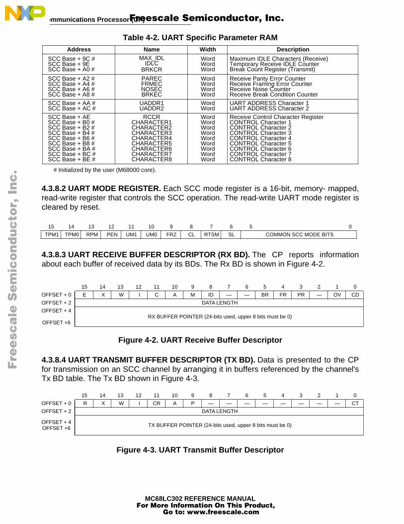
Communications Processor (CP)
MC68LC302 REFERENCE MANUAL
# Initialized by the user (M68000 core).
4.3.8.2 UART MODE REGISTER.
Each SCC mode register is a 16-bit, memory- mapped,read-write register that controls the SCC operation. The read-write UART mode register iscleared by reset.
4.3.8.3 UART RECEIVE BUFFER DESCRIPTOR (RX BD).
The CP reports informationabout each buffer of received data by its BDs. The Rx BD is shown in Figure 4-2.
Figure 4-2. UART Receive Buffer Descriptor
4.3.8.4 UART TRANSMIT BUFFER DESCRIPTOR (TX BD).
Data is presented to the CPfor transmission on an SCC channel by arranging it in buffers referenced by the channel'sTx BD table. The Tx BD shown in Figure 4-3.
Figure 4-3. UART Transmit Buffer Descriptor
Table 4-2. UART Specific Parameter RAM
Address Name Width Description
SCC Base + 9C # SCC Base + 9E SCC Base + A0 #
MAX_IDLIDLC
BRKCR
WordWordWord
Maximum IDLE Characters (Receive) Temporary Receive IDLE Counter Break Count Register (Transmit)
SCC Base + A2 # SCC Base + A4 # SCC Base + A6 # SCC Base + A8 #
PARECFRMECNOSECBRKEC
WordWordWordWord
Receive Parity Error Counter Receive Framing Error Counter Receive Noise Counter Receive Break Condition Counter
SCC Base + AA # SCC Base + AC #
UADDR1UADDR2
WordWord
UART ADDRESS Character 1 UART ADDRESS Character 2
SCC Base + AE SCC Base + B0 # SCC Base + B2 # SCC Base + B4 # SCC Base + B6 # SCC Base + B8 # SCC Base + BA # SCC Base + BC # SCC Base + BE #
RCCRCHARACTER1CHARACTER2CHARACTER3CHARACTER4CHARACTER5CHARACTER6CHARACTER7CHARACTER8
WordWordWordWordWordWordWordWordWord
Receive Control Character Register CONTROL Character 1 CONTROL Character 2 CONTROL Character 3 CONTROL Character 4 CONTROL Character 5 CONTROL Character 6 CONTROL Character 7 CONTROL Character 8
15 14 13 12 11 10 9 8 7 6 5 0
TPM1 TPM0 RPM PEN UM1 UM0 FRZ CL RTSM SL COMMON SCC MODE BITS
15 14 13 12 11 10 9 8 7 6 5 4 3 2 1 0
OFFSET + 0 E X W I C A M ID — — BR FR PR — OV CD
OFFSET + 2 DATA LENGTH
OFFSET + 4
OFFSET +6RX BUFFER POINTER (24-bits used, upper 8 bits must be 0)
15 14 13 12 11 10 9 8 7 6 5 4 3 2 1 0
OFFSET + 0 R X W I CR A P — — — — — — — — CT
OFFSET + 2 DATA LENGTH
OFFSET + 4OFFSET +6 TX BUFFER POINTER (24-bits used, upper 8 bits must be 0)
Fre
esc
ale
Se
mic
on
du
cto
r, I
Freescale Semiconductor, Inc.
For More Information On This Product, Go to: www.freescale.com
nc
...

Communications Processor (CP)
MC68LC302 REFERENCE MANUAL
4.3.8.5 UART EVENT REGISTER.
The SCC event register (SCCE) is called the UARTevent register when the SCC is operating as a UART.
4.3.8.6 UART MASK REGISTER.
The SCC mask register (SCCM) is referred to as theUART mask register when the SCC is operating as a UART. If a bit in the UART mask reg-ister is a one, the corresponding interrupt in the event register will be enabled. If the bit iszero, the corresponding interrupt in the event register will be masked. This register is clearedupon reset.
4.3.9 Autobaud Controller (New)
The autobaud function determines the baud rate and format of an asynchronous datastream starting with a known character. This controller may be used to implement the stan-dard AT command set or other characters.
In order to use the autobaud mode, the serial communication controller (SCC) is initially pro-grammed to BISYNC mode. The SCC receiver then synchronizes on the falling edge of theSTART bit. Once a START bit is detected, each bit received is processed by the autobaudcontroller. The autobaud controller measures the length of the START bit to determine thereceive baud rate and compares the length to values in a user supplied lookup table. Afterthe baud rate is determined, the autobaud controller assembles the character and comparesit against two user-defined characters. If a match is detected, the autobaud controller inter-rupts the host and returns the determined nominal start value from the lookup table. Theautobaud controller continues to assemble the characters and interrupt the host until thehost stops the reception process. The incoming message should contain a mixture of evenand odd characters so that the user has enough information to decide on the proper char-acter format (length and parity). The host then uses the returned nominal start value fromthe lookup table, modifies the SCC configuration register (SCON) to generate the correctbaud rate, and reprograms the SCC to UART mode.
Many rates are supported including: 150, 300, 600, 1200, 2400, 4800, 9600, 14.4K, 19.2K,38.4K, 57.6K, 64K, 96K, 115.2K and 230K. To estimate the performance of the autobaudmode, the performance table in Appendix
A can be used. The maximum full-duplex rate fora BISYNC channel is one-tenth of the system clock rate. So a 25 MHz IMP can support 230Kautobaud rate with another low-speed channel (<50 kbps) and a 20 MHz IMP can support115.2K autobaud rate with 2 low-speed channels. The performance can vary depending onsystem loading, configuration, and echoing mode.
It is important that the highest priority SCC be used for the autobaud function, since it is run-ning at a very high rate. Any SCC that is guaranteed to be idle during the search operationof the autobaud process will not impact the performance of autobaud in an application. Idleis defined as not having any transmit or receive requests to/from the SCC FIFOs.
4.3.9.1 AUTOBAUD CHANNEL RECEPTION PROCESS.
The interface between the auto-baud controller and the host processor is implemented with shared data structures in the
7 6 5 4 3 2 1 0
CTS CD IDL BRK CCR BSY TX RX
Fre
esc
ale
Se
mic
on
du
cto
r, I
Freescale Semiconductor, Inc.
For More Information On This Product, Go to: www.freescale.com
nc
...

Communications Processor (CP)
MC68LC302 REFERENCE MANUAL
SCC parameter RAM and in external memory and through the use of a special command tothe SCC.
The autobaud controller uses receive buffer descriptor number 7 (Rx BD7) for the autobaudcommand descriptor. This Rx BD is initialized by the host to contain a pointer to a lookuptable residing in the external RAM (contains the maximum and nominal START bit length foreach baud rate). The host also prepares two characters against which the autobaud control-ler will compare the received character (usually these characters are ‘a’ and ‘A’) and the hostinitializes a pointer to a buffer in external memory where the assembled characters will bestored until the host stops the autobaud process. Finally, the host initializes the SCC datasynchronization register (DSR) to $7FFF in order to synchronize on the falling edge of theSTART bit.
Once the data structures are initialized, the host programs the SCON register to provide asampling clock that is 16X the maximum supported baud rate. The host then issues theEnter_Baud_Hunt command and enables the SCC in the BISYNC mode.
The autobaud controller reception process begins when the START bit arrives. The auto-baud controller then begins to measure the START bit length. With each byte received fromthe SCC that “belongs” to the START bit, the autobaud controller increments the start lengthcounter and compares it to the current lookup table entry. If the start length counter passedthe maximum bit length defined by the current table entry, the autobaud controller switchesto the next lookup table entry (the next slower baud rate). This process goes on until theautobaud controller recognizes the end of the START bit. Then, the autobaud controllerstarts the character assembly process.
The character assembly process uses the nominal bit length, taken from the current lookuptable entry, to sample each incoming bit in it’s center. Each bit received is stored to form an8-bit character. When the assembly process is completed (a STOP bit is received), the char-acter is compared against two user-defined characters.
If the received character does not match any of the two user defined characters, the auto-baud controller re-enters the Enter_Baud_Hunt process. The host is not notified until amatch is encountered.
If a match is found, the character is written to the received control character register (RCCR)with the corresponding status bit set in Rx BD7. The channel will generate the control char-acter received (CCR) interrupt (bit 3 in the SCCE), if enabled. If the character matched, buta framing error was detected on the STOP bit, the autobaud controller will also set the fram-ing error status bit in Rx BD7.
The autobaud controller then continues to assemble the incoming characters and to storethem in the external data buffer. The host receives a CCR interrupt after each character isreceived.The host is responsible for determining the end of the incoming message (forexample, a carriage return), stopping the autobaud process, and reprogramming the SCCto UART mode. The autobaud controller returns the nominal START bit length value for thedetected baud rate from the lookup table and a pointer to the last character received thatwas written to the external data buffer. The host must be able to handle each character inter-
Fre
esc
ale
Se
mic
on
du
cto
r, I
Freescale Semiconductor, Inc.
For More Information On This Product, Go to: www.freescale.com
nc
...

Communications Processor (CP)
MC68LC302 REFERENCE MANUAL
rupt in order to determine parity and character length (this information may be overwrittenwhen the next character interrupt is presented to the host). The host uses the two receivedcharacters to determine 1) whether a properly formed “at” or “AT” was received, and 2) theproper character format (character length, parity).
Once this is decided, three possible actions can result. First, the host may decide that thedata received was not a proper “at” or “AT”, and issue the Enter_Baud_Hunt command tocause the autobaud controller to resume the search process. Second, the host may decidethe “at” or “AT” is proper and simply continue to receive characters in BISYNC mode. Third,the M68000 core may decide that the “at” or “AT” is proper, but a change in character lengthor parity is required.
4.3.9.2 AUTOBAUD CHANNEL TRANSMIT PROCESS.
The autobaud microcode pack-age supports two methods for transmission. The first method is automatic echo which is sup-ported directly in the SCC hardware, and the second method is a smart echo or softwaretransmit which is supported with an additional clock and software.
Automatic echo is enabled by setting the DIAG bits in the SCC mode register (SCM) to ‘10’and asserting the CD pin (externally on SCC1 and on SCC2 and SCC3, either externally orby leaving the pin as a general purpose input). The ENT bit of the SCC should remaincleared. The transmitter is not used, so this echoing method does not impact performance.
The smart echo or software transmit requires use of an additional clock and the transmitter,so the overall performance could be affected if other SCCs are running. This methodrequires an additional clock for sampling the incoming bit stream since the baud rate gener-ator (BRG) must be used to provide the correct frequency for transmission. The user needsto provide the sampling clock that will be used for the autobaud function on the RCLK pin(for example, a 1.8432 MHz clock for 115.2K). The clock that will be used for the SCC trans-mission can be provided to the BRG from the system clock or on TIN1.The TIN1 and RCLK1pins can be tied together externally. After the first two characters have been received andcharacter length and parity determined, the host programs the DSR to $FFFF, enables thetransmitter (by setting ENT), and programs the transmit character descriptor (overlays CON-TROL Character 8). The host is interrupted after each character is transmitted.
For modem applications with the MC68LC302, SCC2 will be used as the DTE interface andautobauding to the DTE baud rate will often be required. If use of the smart echo feature isdesired, the receive clock can be provided by the baud rate generator 2 (BRG2) internallyby resetting the RCS bit in the SCON2 register to zero. The separate transmit clock can beprovided externally to the TCLK2 pin through a hardwire connection. The TCS bit in theSCON2 register should be set to one to enable the external clock source. After autobaudingis complete, both the transmit and receive clock sources can be derived internally fromBRG2 and the external pin connected to TCLK2 should be three stated to assure that it doesnot contend with the TCLK2 pin.
4.3.9.3 AUTOBAUD PARAMETER RAM.
When configured to operate in the autobaudmode, the IMP overlays some entries of the UART-specific parameter RAM as illustrated inTable 4-3.
Fre
esc
ale
Se
mic
on
du
cto
r, I
Freescale Semiconductor, Inc.
For More Information On This Product, Go to: www.freescale.com
nc
...

Communications Processor (CP)
MC68LC302 REFERENCE MANUAL
* These values should be initialized by the user (M68000 core).
Note the new parameters that have been added to the table. They are MAX_BIT,NOM_START, ABCHR1, ABCHR2, RxPTR (2 words), and TxBD. These parameters areof special importance to the autobaud controller. They must be written prior to issuing theEnter_Baud_Hunt command.
When the channel is operating in the autobaud hunt mode, the MAX_BIT parameter is usedto hold the current maximum START bit length. The NOM_START location contains the cur-rent nominal start from the lookup table. After the autobaud is successful and the first char-acter is matched, the user should use the NOM_START value from the autobaud specificparameter RAM to determine which baud rate from the lookup table was detected. Also theTx internal data pointer (at offset SCC Base + 94) will point to the last character receivedinto external data buffer.
NOTE
When the channel is operating in the UART mode, theNOM_START_/BRKCR is used as the break count register andmust be initialized before a STOP_TRANSMIT command is is-sued.
The characters ABCHR1 and ABCHR2 are the autobaud characters that should besearched for by the autobaud controller. Typically these are ‘a’ and ‘A’ (i.e. $0061 and$0041) if using the Hayes command set. These characters must be odd in order for the auto-baud controller to correctly determine the length of the START bit. Characters are transmit-ted and received least significant bit first, so the autobaud controller detects the end of theSTART bit by the least significant bit of the character being a ‘1’.
Table 4-3. Autobaud Specific Parameter
Address Name Width Description
SCC Base + 9C * MAX_IDL Word Maximum IDLE CharactersSCC Base + 9E MAX_BIT Word Current Maximum START Bit LengthSCC Base + A0 NOM_START Word Current Nom. START Bit (used to determine baud rate)SCC Base + A2 * PAREC Word Receive Parity Error CounterSCC Base + A4 * FRMEC Word Receive Framing Error CounterSCC Base + A6 * NOSEC Word Receive Noise CounterSCC Base + A8 * BRKEC Word Receive Break Error CounterSCC Base + AA * ABCHR1 Word User Defined Character1SCC Base + AC * ABCHR2 Word User Defined Character2SCC Base + AE RCCR Word Receive Control Character RegisterSCC Base + B0 * CHARACTER1 Word CONTROL Character1SCC Base + B2 * CHARACTER2 Word CONTROL Character2SCC Base + B4 * CHARACTER3 Word CONTROL Character3SCC Base + B6 * CHARACTER4 Word CONTROL Character4SCC Base + B8 * CHARACTER5 Word CONTROL Character5SCC Base + BA * CHR6/RxPTR Word CONTRChar6/MSW of pointer to external Rx BufferSCC Base + BC * CHR7RxPTR Word CONTRChar7/LSW of pointer to external Rx BufferSCC Base + BE * CHR8/TxBD Word CONTROL Character8/Transmit BD
Fre
esc
ale
Se
mic
on
du
cto
r, I
Freescale Semiconductor, Inc.
For More Information On This Product, Go to: www.freescale.com
nc
...

Communications Processor (CP)
MC68LC302 REFERENCE MANUAL
The RxPTR is a 2 word location that contains a 32-bit pointer to a buffer in external memoryused for assembling the received characters and must be initialized before theEnter_Baud_Hunt command is issued.
NOTE
Since a length for this external buffer is not given, the user mustprovide enough space in memory for characters to be assem-bled and written until the autobaud process is to avoid overwrit-ing other data in memory. This location is not used as theCHARACTER7 value in the control character table until thechannel operates in normal UART mode. After reception beginsin normal UART mode (i.e. the “a” or “A” is found), this entry isavailable again as a control character table entry.
The TxBD entry is used as the transmit character descriptor for smart echo or softwaretransmit. This location is not used as the CHARACTER8 value in the control character tableuntil the channel operates in normal UART mode. After reception begins in normal UARTmode (i.e. the “a” or “A” is found), this entry is available again as a control character tableentry.
4.3.9.4 AUTOBAUD PROGRAMMING MODEL.
The following sections describe the detailsof initializing the autobaud microcode, preparing for the autobaud process, and the memorystructures used.
4.3.9.4.1 Preparing for the Autobaud Process.
The host begins preparation for the auto-baud process with the following steps. Steps 1 and 2 are required if the SCC has been usedafter reset or after UART mode in order to re-enable the process.
1. Disable the SCC by clearing the ENR and ENT bits. (The host may wish to precede this action with the STOP_TRANSMIT commands to abort transmission in an orderly way).
2. Issue the ENTER_HUNT_MODE command to the SCC (This ensures that an open buffer descriptor is closed).
3. Set up all the autobaud parameters in the autobaud specific parameter RAM shown in Table 4-3, the autobaud command descriptor shown in Table 4-4, and the lookup table shown in Table 4-4. Of these three areas, the autobaud controller only modifies the autobaud specific parameter RAM and the first word of the autobaud command de-scriptor during its operation.
4. Write the SCON to configure the SCC to use the baud rate generator clock of 16x the maximum supported baud rate. A typical value is $4000 assuming a 1.8432 MHz clock rate on TIN1 and a maximum baud rate of 115.2K, but this can change depending on the maximum baud rate and the EXTAL frequency.
5. Write the DSR of the SCC with the value $7FFF in order to detect the START bit.
6. The host initiates the autobaud search process by issuing the Enter_Baud_Hunt com-mand
7. Write the SCM of the SCC with $1133 to configure it for BISYNC mode, with the REVD
Fre
esc
ale
Se
mic
on
du
cto
r, I
Freescale Semiconductor, Inc.
For More Information On This Product, Go to: www.freescale.com
nc
...

Communications Processor (CP)
MC68LC302 REFERENCE MANUAL
and RBCS bits set, software operation mode, and the transmitter disabled. After a few characters have been received, the transmitter can be enabled, and the software echo function may be performed after issuing the RESTART TRANSMIT command.
In general, the autobaud controller uses the same data structure as that of the UART con-troller. The first character (if matched) is stored in the receiver control character register andthe external data buffer, and the status of that character is reported in the autobaud com-mand descriptor. After the first character, each incoming character is then stored in thebuffer pointed to by RxPTR, and the status is updated in the autobaud command autobauddescriptor. The Tx internal data pointer (at offset SCC Base + 94) is updated to point to thelast character stored in the external data buffer.
4.3.9.4.2 Enter_Baud_Hunt Command.
This command instructs the autobaud controllerto begin searching for the baud rate of a user predefined character. Prior to issuing the com-mand the M68000 prepares the autobaud command descriptor to contain the lookup tablesize and pointer.
The Enter_Baud_Hunt uses the GCI command with opcode = 10, and the channel numberset for the corresponding SCC. For example, with SCC1, the value written to the commandregister would be $61.
4.3.9.4.3 Autobaud Command Descriptor.
The autobaud controller uses the receivebuffer descriptor number 7 (Rx BD7) as an autobaud command descriptor. The autobaudcommand descriptor is used by the M68000 core to transfer command parameters to theautobaud controller, and by the autobaud controller to report information concerning thereceived character.
The structure of the autobaud command descriptor for the autobaud process is shown inTable 4-4. The first word of the descriptor or the status word is updated after every characteris received.
FE – Framing Error (Bit 10)If this bit is set, a character with a framing error was received. A framing error is detectedby the autobaud controller when no STOP bit is detected in the received data. FE will beset for a 9-bit character (8 bits + parity) if the parity bit is ‘0’.
NOTE
The user must clear this bit when it is set.
Table 4-4. Autobaud Command Descriptor
Offset 15 14 13 12 11 10 9 8 7 6 5 4 3 2 1 00 FE M2 M1 EOT OV CD2 Lookup Table Size4 Function Code 8 Lookup Table Pointer
Fre
esc
ale
Se
mic
on
du
cto
r, I
Freescale Semiconductor, Inc.
For More Information On This Product, Go to: www.freescale.com
nc
...

Communications Processor (CP)
MC68LC302 REFERENCE MANUAL
M2 – Match Character2 (Bit 9)When this bit is set, the character received matched the User Defined Character 2. Thereceived character is written into the receive control character register (RCCR).
M1 – Match Character1 (Bit 8)When this bit is set, the character received matched the User Defined Character 1. Thereceived character is written into the receive control character register (RCCR).
EOT – End Of Table (bit 3)When this bit is set, the autobaud controller measured start length exceeded the maxi-mum start length of the last entry in the lookup table (lowest baud rate).
NOTE
The user must clear this bit when it is set.
OV – Overrun (bit 1)If this bit is set, a receiver overrun occurred during autobaud reception.
NOTE
The user must clear this bit when it is set.
CD – Carrier Detect Lost (bit 0)If this bit is set, the carrier detect signal was negated during autobaud reception.
NOTE
The user must clear this bit when it is set.
Lookup Table Size - Lookup table size is the number of baud rate entries in the externallookup table.
Lookup Table Pointer - The lookup table pointer is the address in the external RAM wherethe lookup table begins.
NOTE
The lookup table cannot cross a 64k memory block boundary.
4.3.9.4.4 Autobaud Lookup Table. The autobaud controller uses an external lookup tableto determine the baud rate while in the process of receiving a character. The lookup tablecontains two entries for each supported baud rate. The first entry is the maximum startlength for the particular baud rate, and the second entry is the nominal length for a 1/2START bit.
To determine the two values for each table entry, first calculate the autobaud sampling rate(EQ 2). To do this EQ 1 must be used until EQ 2 is satisfied. The sampling rate is the lowestspeed baud rate that can be generated by the SCC baud rate generator that is over a thresh-old defined in EQ 2.
BRG Clk Rate = System Clock or TIN1 / ((Clock Divider bits in SCON) + 1) (EQ 1)
Fre
esc
ale
Se
mic
on
du
cto
r, I
Freescale Semiconductor, Inc.
For More Information On This Product, Go to: www.freescale.com
nc
...

Communications Processor (CP)
MC68LC302 REFERENCE MANUAL
assuming that the DIV bit in SCON is set to 0, (otherwise an additional “divide-by-4” mustbe included).
Sampling Rate = BRG Clk Rate, where BRG Clk rate >= (Max Desired UART Baud Rate) x 16 (EQ 2)
For instance, if a 115.2K baud rate is desired, with a 16.67 MHz system clock, the minimumsampling rate possible is 1.843 MHz = 115.2K x 16. This exact frequency can be input toRCLK1 or TIN1 as the sample clock. If the system clock is to be used, a 16.67 MHz systemclock cannot produce an exact baud rate clock of 1.843 MHz. The lowest one that can beused is Baud Rate = 16.67 MHz / (7+1) = 2.083 MHz. Thus, 2.083 MHz is the sampling rate,and the SCON should be set to $000E to produce this.
Once the sampling rate is known, the other two equations follow easily. The maximumSTART bit length is calculated by the following equation:
Maximum start length = (Sampling Rate/Recognized baud rate) x 1.05 (EQ 3)
Thus, for the first entry in the table, the maximum start length is 1.8432 Mhz/115200 x 1.05= 17 for an external sample clock. The value 1.05 is a suggested margin that allows char-acters 5% larger than the nominal character rate to be accepted. In effect, the margin deter-mines the “split point” between what is considered to be a 56.7K character rate and what isa 38.4K character rate. The margin should not normally be less than 1.03 due to clockingdifferences between UARTs.
The nominal START bit length is calculated by:
Nominal start length = (Sampling Rate/Recognized baud rate) / 2 (EQ 4)
For the 115.2K example in the first table entry, this would be 1.8432 MHz/115.2K/2 = 8.
The structure of the lookup table is shown in Table 4-5. The table starts with the maximumUART baud rate supported and ends with the minimum UART baud rate supported.
NOTE
If less margin is used in the calculation of the maximum startlength above, it is possible to distinguish between close UARTrates such as 64K and 57.6K. However variations in RS232 driv-ers of up to 4%, plus nominal clocking rate variations of 3%, plus
Table 4-5. Autobaud Lookup Table FormatOFFSET from Lookup Table Pointer Description
0 Maximum Start Length2 Nominal Start Length4 Maximum Start Length6 Nominal Start Length• Maximum Start Length• Nominal Start Length
(Lookup Table Size - 1) * 4 Maximum Start Length[(Lookup Table Size - 1) * 4] + 2 Nominal Start Length
Fre
esc
ale
Se
mic
on
du
cto
r, I
Freescale Semiconductor, Inc.
For More Information On This Product, Go to: www.freescale.com
nc
...

Communications Processor (CP)
MC68LC302 REFERENCE MANUAL
the fact that the sampling rate may not perfectly divide into thedesired UART rate, can make this distinction difficult to achievein some scenarios.
4.3.9.5 LOOKUP TABLE EXAMPLE.
Table 4-6 is an example autobaud lookup table. The maximum start and nominal start val-ues are derived assuming a 1.8432 MHz sampling clock on TIN1 or RCLK and a shift factorof 5%.
4.3.9.6 DETERMINING CHARACTER LENGTH AND PARITY. Table 4-7 shows the dif-ferent possible character lengths and parity that will be discussed. The following paragraphswill discuss for each case how to determine the parity.
• Case 1– This case cannot be supported because the autobaud can not separate the first character from the second character.
Table 4-6. Lookup Table ExampleDesired
Baud RateMaximum
StartNominal
Start
115200 17 8
57600 34 16
38400 50 24
28800 67 32
19200 101 48
14400 134 6412000 161 779600 202 967200 269 1284800 403 1922400 806 3841200 1613 768600 3226 1536300 6451 3072110 17594 8378
Table 4-7. Character Lengths and Parity Cases
Case #Character
LengthParity Notes
1 7-bit No parity, 1 STOP bit Not Supported
2 7-bit
Even parityOdd parityParity=1Parity=0
Parity is indicated by the most signif-icant bit of the byte
3 8-bit No parity Same as 7-bit, parity=0
4 8-bitEven parityOdd parityParity=0
Parity is indicated by which charac-ters generate a FE interrupt
5 8-bit Parity=1 Not Supported
Fre
esc
ale
Se
mic
on
du
cto
r, I
Freescale Semiconductor, Inc.
For More Information On This Product, Go to: www.freescale.com
nc
...
Communications Processor (CP)
MC68LC302 REFERENCE MANUAL
• Case 2– As each character is assembled, it is stored into a complete byte. Assuming that the characters are ASCII characters with 7-bit codes, the 8th bit of the byte will con-tain the parity bit. If the parity is either even or odd, then after receiving an odd character and an even character, the 8th bit should be different for the odd and even characters. The parity can be determined by the setting of the parity bit for one of the two charac-ters. If the 8th bit is always a 1, this is the same as a 7-bit character, no parity and at least 2 STOP bits or a 7-bit character with force 1 parity. If the 8th bit is always a zero, then either the character is a 7-bit character with force 0 parity, or the character is a 8-bit character with no parity.
• Case 3– This case is the same as 7-bit character with force 0 parity. The 8th bit of the byte will always be zero.
• Case 4–This case assumes a 8-bit character with the 8th bit of the character equal to a 0 (ASCII character codes define the 8th bit as zero). If the parity is either even or odd, then after receiving an odd and an even character, a framing error (FE) interrupt should have been generated for one of them (the interrupt is generated when the parity bit is zero). The user can determine the parity by which character generated a FE interrupt (if the odd character did, then the parity is odd). If a framing error occurs on every char-acter, then the character is 8-bits with force 0 parity. If no framing error occurs, than this is the same as Case 5.
• Case 5– This case is not supported, because it can not be differentiated from 7-bit force 0 parity and 8-bit no parity. If the 9th bit is a 1, then it will be interpreted as a STOP bit.
4.3.9.7 AUTOBAUD RECEPTION ERROR HANDLING PROCEDURE. The autobaudcontroller reports reception error conditions using the autobaud command descriptor. Threetypes of errors are supported:
• Carrier Detect Lost during reception
When this error occurs and the channel is not programmed to control this line with software,the channel terminates reception, sets the carrier detect lost (CD) bit in the commanddescriptor, and generates the CCR interrupt, if enabled. CCR is bit 3 of the SCCE register.
• Overrun Error
When this error occurs, the channel terminates reception, sets the overrun (OV) bit in thecommand descriptor, and generates the CCR interrupt, if enabled.
• End Of Table Error
When this error occurs, the channel terminates reception, sets the end of table (EOT) bit inthe command descriptor, and generates the CCR interrupt, if enabled.
Any of these errors will cause the channel to abort reception. In order to resume autobaudoperation after an error condition, the M68000 should clear the status bits and issue theEnter_Baud_Hunt command again.
4.3.9.8 AUTOBAUD TRANSMISSION. The autobaud package supports two methods forechoing characters or transmitting characters. The two methods are automatic echo andsmart echo.
Fre
esc
ale
Se
mic
on
du
cto
r, I
Freescale Semiconductor, Inc.
For More Information On This Product, Go to: www.freescale.com
nc
...
Communications Processor (CP)
MC68LC302 REFERENCE MANUAL
4.3.9.8.1 Automatic Echo. This method uses the SCC hardware to automatically echo thecharacters back on the TxD pin. The automatic echo is enabled by setting the DIAG bits inthe SCM to ‘10’. The transmitter should not be enabled. The hardware echo is done auto-matically. The CD pin needs to be asserted in order for the characters to be transmittedback. On SCC1, the external CD pin must be tied low. On SCC2 and SCC3, either the exter-nal CD pin must be tied low or the CD pins should be left configured as general purposeinput pins (the CD signal to the SCC is then connected to ground internally).
Using the automatic echo, the receiver still autobauds correctly and performance is notaffected. The SCC echoes the received data with a few nanoseconds delay.
4.3.9.8.2 Smart Echo. This method requires addition hardware and software to implement.The user must provide two clock sources. One clock source is the sample clock which isinput on RCLK and cannot be divided down. The BRG is used to divide the second clockdown to provide the clock used for transmit. The second clock can be either the system clockor a clock connected to TIN1. The TIN1 and RCLK pins can be connected to each otherexternally.
After the first character is received, the user must take the following steps:
1. Determine the baud rate from the returned NOM_START value and program SCON to (input frequency/baud rate)-1, where the input frequency is either the system clock or the clock on TIN1.
2. Program the DSR to $FFFF. The DSR will need to be programmed back to $7FFF be-fore the Enter_Baud_Hunt command is issued again.
3. Set the ENT bit in the mode register.
4. Program the transmit character BD as show in Table 4-8.
R (ready bit)0 = Character is not ready1 = Character is ready to transmit
CL (character len)0 = 7 bits + parity or 8 bits with no parity1 = 8 bits + parity
PE (parity enable)0 = No parity1 = Parity
15 14 13 12 11 10 9 8 7 6 5 4 3 2 1 0
R CL PE PM CHAR
Table 4-8. Transmit Character BD
Fre
esc
ale
Se
mic
on
du
cto
r, I
Freescale Semiconductor, Inc.
For More Information On This Product, Go to: www.freescale.com
nc
...

Communications Processor (CP)
MC68LC302 REFERENCE MANUAL
PM (parity mode)0 = Even parity1 = Odd parity
The autobaud controller issues a Tx interrupt after each character is transmitted.
4.3.9.9 REPROGRAMMING TO UART MODE OR ANOTHER PROTOCOL. The followingsteps should be followed in order to switch the SCC from autobaud to UART mode or toanother protocol.
• Disable the SCC by clearing ENR and ENT.
• Issue the Enter_Hunt_Mode command.
• Initialize the SCC parameter RAM (specifically, the Rx and Tx internal states and the words containing the Rx and Tx BD#s) to the state immediately after reset and initialize the protocol specific parameter area for the new protocol.
• Re-enable the SCC with the new mode.
4.3.10 HDLC ControllerThe functionality of the HDLC controller has not changed. For any additional information onparameters, registers, and functionality, please refer to the MC68302 Users’ Manual.
4.3.10.1 HDLC MEMORY MAP . When configured to operate in HDLC mode, the IMP over-lays the structure shown in Table 4-8 onto the protocol-specific area of that SCC parameterRAM. Refer to Parameter RAM on page 21 for the placement of the three SCC parameterRAM areas and to Table 4-1 for the other parameter RAM values.
# Should be initialized by the user (M68000 core).
4.3.10.2 HDLC MODE REGISTER . Each SCC mode register is a 16-bit, memory-mapped,read-write register that controls the SCC operation. The read-write HDLC mode register iscleared by reset.
Table 4-9. HDLC-Specific Parameter RAMAddress Name Width Description
SCC Base + 9C SCC Base + 9E SCC Base + A0 # SCC Base + A2 # SCC Base + A4 SCC Base + A6
RCRC_LRCRC_H
C_MASK_LC_MASK_H
TCRC_LTCRC_H
WordWordWordWordWordWord
Temp Receive CRC LowTemp Receive CRC HighConstant ($F0B8 16-Bit CRC, $DEBB 32-Bit CRC)Constant ($XXXX 16-Bit CRC, $20E3 32-Bit CRC)Temp Transmit CRC LowTemp Transmit CRC High
SCC Base + A8 # SCC Base + AA # SCC Base + AC # SCC Base + AE # SCC Base + B0 #
DISFCCRCECABTSCNMARCRETRC
WordWordWordWordWord
Discard Frame CounterCRC Error CounterAbort Sequence CounterNonmatching Address Received CounterFrame Retransmission Counter
SCC Base + B2 # SCC Base + B4
MFLRMAX_cnt
WordWord
Max Frame Length RegisterMax_Length Counter
SCC Base + B6 # SCC Base + B8 # SCC Base + BA # SCC Base + BC # SCC Base + BE #
HMASKHADDR1HADDR2HADDR3HADDR4
WordWordWordWordWord
User-Defined Frame Address MaskUser-Defined Frame AddressUser-Defined Frame AddressUser-Defined Frame AddressUser-Defined Frame Address
Fre
esc
ale
Se
mic
on
du
cto
r, I
Freescale Semiconductor, Inc.
For More Information On This Product, Go to: www.freescale.com
nc
...
Communications Processor (CP)
MC68LC302 REFERENCE MANUAL
4.3.10.3 HDLC RECEIVE BUFFER DESCRIPTOR (RX BD) . The HDLC controller usesthe Rx BD to report information about the received data for each buffer. The Rx BD is shownin Figure 4-4.
Figure 4-4. HDLC Receive Buffer Descriptor
4.3.10.4 HDLC TRANSMIT BUFFER DESCRIPTOR (TX BD) . Data is presented to theHDLC controller for transmission on an SCC channel by arranging it in buffers referencedby the channel's Tx BD table. The Tx BD is shown in Figure 4-5.
Figure 4-5. HDLC Transmit Buffer Descriptor
4.3.10.5 HDLC EVENT REGISTER . The SCC event register (SCCE) is called the HDLCevent register when the SCC is operating as an HDLC controller. It is an 8-bit register usedto report events recognized by the HDLC channel and to generate interrupts. Upon recog-nition of an event, the HDLC controller sets its corresponding bit in the HDLC event register.Interrupts generated by this register may be masked in the HDLC mask register. A bit iscleared by writing a one; writing a zero does not affect a bit's value. All unmasked bits mustbe cleared before the CP will clear the internal interrupt request. This register is cleared atreset.
4.3.10.6 HDLC MASK REGISTER. The SCC mask register (SCCM) is referred to as theHDLC mask register when the SCC is operating as an HDLC controller. It is an 8-bit read-write register that has the same bit formats as the HDLC event register. If a bit in the HDLCmask register is a one, the corresponding interrupt in the event register will be enabled. Ifthe bit is zero, the corresponding interrupt in the event register will be masked. This registeris cleared upon reset.
15 14 13 12 11 10 9 8 7 6 5 0
NOF3 NOF2 NOF1 NOF0 C32 FSE — RTE FLG ENC COMMON SCC MODE BITS
15 14 13 12 11 10 9 8 7 6 5 4 3 2 1 0
OFFSET + 0 E X W I L F — — — — LG NO AB CR OV CD
OFFSET + 2 DATA LENGTH
OFFSET + 4OFFSET +6 RX BUFFER POINTER (24-bits used, upper 8 bits must be 0)
15 14 13 12 11 10 9 8 7 6 5 4 3 2 1 0
OFFSET + 0 R X W I L TC — — — — — — — — UN CT
OFFSET + 2 DATA LENGTH
OFFSET + 4 TX BUFFER POINTER (24-bits used, upper 8 bits must be 0)
OFFSET + 6
7 6 5 4 3 2 1 0
CTS CD IDL TXE RXF BSY TXB RXB
Fre
esc
ale
Se
mic
on
du
cto
r, I
Freescale Semiconductor, Inc.
For More Information On This Product, Go to: www.freescale.com
nc
...

Communications Processor (CP)
MC68LC302 REFERENCE MANUAL
4.3.11 BISYNC ControllerThe functionality of the BISYNC controller has not changed. For any additional informationon parameters, registers, and functionality, please refer to the MC68302 Users’ Manual.
4.3.11.1 BISYNC MEMORY MAP. When configured to operate in BISYNC mode, the IMPoverlays the structure listed in Table 4-10 onto the protocol-specific area of that SCC param-eter RAM. Refer to System Configuration Registers on page 5 for the placement of the threeSCC parameter RAM areas and Table 4-1 for the other parameter RAM values.
# Initialized by the user (M68000 core).
4.3.11.2 BISYNC MODE REGISTER. Each SCC mode register is a 16-bit, memory-mapped, read-write register that controls the SCC operation. The term BISYNC mode reg-ister refers to the protocol-specific bits (15–6) of the SCC mode register when that SCC isconfigured for BISYNC. The read-write BISYNC mode register is cleared by reset.
4.3.11.3 BISYNC RECEIVE BUFFER DESCRIPTOR (RX BD). The CP reports informationabout the received data for each buffer using BD. The Rx BD is shown in Figure 4-6
Figure 4-6. BISYNC Receive Buffer Descriptor
4.3.11.4 BISYNC TRANSMIT BUFFER DESCRIPTOR (TX BD). Data is presented to theCP for transmission on an SCC channel by arranging it in buffers referenced by the chan-nel's Tx BD table. The Tx BD is shown in Figure 4-7.
Table 4-10. BISYNC Specific Parameter RAMAddress Name Width Description
SCC Base + 9C SCC Base + 9E SCC Base + A0 # SCC Base + A2 SCC Base + A4 # SCC Base + A6 SCC Base + A8
RCRCCRCC
PRCRCTCRC
PTCRCRESRES
WordWordWordWordWordWordWord
Temp Receive CRCCRC ConstantPreset Receiver CRC 16/LRCTemp Transmit CRCPreset Transmitter CRC 16/LRCReservedReserved
SCC Base + AA # SCC Base + AC # SCC Base + AE #
PARECBSYNCBDLE
WordWordWord
Receive Parity Error CounterBISYNC SYNC CharacterBISYNC DLE Character
SCC Base + B0 # SCC Base + B2 # SCC Base + B4 # SCC Base + B6 # SCC Base + B8 # SCC Base + BA # SCC Base + BC # SCC Base + BE #
CHARACTER1CHARACTER2CHARACTER3CHARACTER4CHARACTER5CHARACTER6CHARACTER7CHARACTER8
WordWordWordWordWordWordWordWord
CONTROL Character 1CONTROL Character 2CONTROL Character 3CONTROL Character 4CONTROL Character 5CONTROL Character 6CONTROL Character 7CONTROL Character 8
15 14 13 12 11 10 9 8 7 6 5 0
PM EXSYN NTSYN REVD BCS — RTR RBCS SYNF ENC COMMON SCC MODE BITS
15 14 13 12 11 10 9 8 7 6 5 4 3 2 1 0
OFFSET + 0 E X W I C B — — — — — DL PR CR OV CD
OFFSET +2 DATA LENGTH
OFFSET +4 RX BUFFER POINTER (24-bits used, upper 8 bits must be 0)
OFFSET + 6
Fre
esc
ale
Se
mic
on
du
cto
r, I
Freescale Semiconductor, Inc.
For More Information On This Product, Go to: www.freescale.com
nc
...
Communications Processor (CP)
MC68LC302 REFERENCE MANUAL
Figure 4-7. BISYNC Transmit Buffer Descriptor
4.3.11.5 BISYNC EVENT REGISTER. The SCC event register (SCCE) is referred to as theBISYNC event register when the SCC is programmed as a BISYNC controller. It is an 8-bitregister used to report events recognized by the BISYNC channel and to generate inter-rupts. On recognition of an event, the BISYNC controller sets the corresponding bit in theBISYNC event register. Interrupts generated by this register may be masked in the BISYNCmask register. A bit is cleared by writing a one. More than one bit may be cleared at a time.All unmasked bits must be cleared before the CP will negate the internal interrupt requestsignal. This register is cleared at reset.
4.3.11.6 BISYNC MASK REGISTER. The SCC mask register (SCCM) is referred to as theBISYNC mask register when the SCC is operating as a BISYNC controller. It is an 8-bit read-write register that has the same bit format as the BISYNC event register. If a bit in theBISYNC mask register is a one, the corresponding interrupt in the event register will beenabled. If the bit is zero, the corresponding interrupt in the event register will be masked.This register is cleared upon reset.
4.3.12 Transparent ControllerThe functionality of the BISYNC controller has not changed. For any additional informationon parameters, registers, and functionality, please refer to the MC68302 Users’ Manual.
4.3.12.1 TRANSPARENT MEMORY MAP. When configured to operate in transparentmode, the IMP overlays the structure illustrated in Table 4-11 onto the protocol specific areaof that SCC parameter RAM. Refer to Table 2-6 for the placement of the three SCC param-eter RAM areas and Table 4-1 for the other parameter RAM values.
15 14 13 12 11 10 9 8 7 6 5 4 3 2 1 0
OFFSET + 0 R X W I L TB B BR TD TR — — — — UN CT
OFFSET + 2 DATA LENGTH
OFFSET + 4
OFFSET +6TX BUFFER POINTER (24-bits used, upper 8 bits must be 0)
7 6 5 4 3 2 1 0
CTS CD — TXE RCH BSY TX RX
Fre
esc
ale
Se
mic
on
du
cto
r, I
Freescale Semiconductor, Inc.
For More Information On This Product, Go to: www.freescale.com
nc
...

Communications Processor (CP)
MC68LC302 REFERENCE MANUAL
4.3.12.2 TRANSPARENT MODE REGISTER. Each SCC mode register is a 16-bit, mem-ory-mapped, read-write register that controls the SCC operation. The term transparentmode register refers to the protocol-specific bits (15–6) of the SCC mode register when thatSCC is configured for transparent mode. The transparent mode register is cleared by reset.All undefined bits should be written with zero.
4.3.12.3 TRANSPARENT RECEIVE BUFFER DESCRIPTOR (RXBD) . The CP reportsinformation about the received data for each buffer using BD. The RxBD is shown in Figure4-8.
Figure 4-8. Transparent Receive Buffer Descriptor
Table 4-11. Transparent-Specific Parameter RAMAddress Name Width Description
SCC BASE + 9C RES WORD Reserved SCC BASE + 9E RES WORD Reserved SCC BASE + A0 RES WORD Reserved SCC BASE + A2 RES WORD Reserved SCC BASE + A4 RES WORD Reserved SCC BASE + A6 RES WORD Reserved SCC BASE + A8 RES WORD Reserved SCC BASE + AA RES WORD Reserved SCC BASE + AC RES WORD Reserved SCC BASE + AE RES WORD Reserved SCC BASE + B0 RES WORD Reserved SCC BASE + B2 RES WORD Reserved SCC BASE + B4 RES WORD Reserved SCC BASE + B6 RES WORD Reserved SCC BASE + B8 RES WORD Reserved SCC BASE + BA RES WORD Reserved SCC BASE + BC RES WORD Reserved SCC BASE + BE RES WORD Reserved
15 14 13 12 11 10 9 8 7 6 5 0
— EXSYN NTSYN REVD — — — — — — COMMON SCC MODE BITS
15 14 13 12 11 10 9 8 7 6 5 4 3 2 1 0
OFFSET + 0 E X W I — — — — — — — — — — OV CD
OFFSET + 2 DATA LENGTH
OFFSET + 4
OFFSET +6RX BUFFER POINTER (24-bits used, upper 8 bits must be 0)
Fre
esc
ale
Se
mic
on
du
cto
r, I
Freescale Semiconductor, Inc.
For More Information On This Product, Go to: www.freescale.com
nc
...
Communications Processor (CP)
MC68LC302 REFERENCE MANUAL
4.3.12.4 TRANSPARENT TRANSMIT BUFFER DESCRIPTOR (TX BD) . Data is pre-sented to the CP for transmission on an SCC channel by arranging it in buffers referencedby the channel's Tx BD table. The Tx BD is shown in Figure 4-9.
Figure 4-9. Transparent Transmit Buffer Descriptor
4.3.12.5 TRANSPARENT EVENT REGISTER . The SCC event register (SCCE) is referredto as the transparent event register when the SCC is programmed as a transparent control-ler. It is an 8-bit register used to report events recognized by the transparent channel and togenerate interrupts. On recognition of an event, the transparent controller sets the corre-sponding bit in the transparent event register. A bit is cleared by writing a one (writing a zerodoes not affect a bit's value). This register is cleared at reset.
4.3.12.6 TRANSPARENT MASK REGISTER . The SCC mask register (SCCM) is referredto as the transparent mask register when the SCC is operating as a transparent controller.It is an 8-bit read-write register that has the same bit format as the transparent event regis-ter. If a bit in the transparent mask register is a one, the corresponding interrupt in the eventregister will be enabled. If the bit is zero, the corresponding interrupt in the event register willbe masked. This register is cleared at reset.
4.4 SERIAL COMMUNICATION PORT (SCP) The functionality of the SCP has not changed. For any additional information on parameters,registers, and functionality, please refer to the MC68302 Users’ Manual.
4.4.1 SCP Programming ModelThe SCP mode register consists of the upper eight bits of SPMODE. The SCP mode regis-ter, an internal read-write register that controls both the SCP operation mode and clocksource, is cleared by reset.
15 14 13 12 11 10 9 8 7 6 5 4 3 2 1 0
OFFSET + 0 R X W I L — — — — — — — — — UN CT
OFFSET + 2 DATA LENGTH
OFFSET + 4
OFFSET +6TX BUFFER POINTER (24-bits used, upper 8 bits must be 0)
7 6 5 4 3 2 1 0
CTS CD — TXE RCH BSY TX RX
15 14 13 12 11 10 9 8
STR ?LOOP CI PM3 PM2 PM1 PM0 EN
Fre
esc
ale
Se
mic
on
du
cto
r, I
Freescale Semiconductor, Inc.
For More Information On This Product, Go to: www.freescale.com
nc
...

Communications Processor (CP)
MC68LC302 REFERENCE MANUAL
4.4.2 SCP Transmit/Receive Buffer Descriptor The transmit/receive BD contains the data to be transmitted (written by the M68000 core)and the received data (written by the SCP). The done (D) bit indicates that the received datais valid and is cleared by the SCP.
4.5 SERIAL MANAGEMENT CONTROLLERS (SMCS) The functionality of the SMCs has not changed. For any additional information on parame-ters, registers, and functionality, please refer to the MC68302 Users’ Manual.
4.5.1 SMC Programming Model The operating mode of both SMC ports is defined by SMC mode, which consists of the lowereight bits of SPMODE. As previously mentioned, the upper eight bits program the SCP.
4.5.2 SMC Memory Structure and Buffers Descriptors The CP uses several memory structures and memory-mapped registers to communicatewith the M68000 core. All the structures detailed in the following paragraphs reside in thedual-port RAM of the IMP. The SMC buffer descriptors allow the user to define one data byteat a time for each transmit channel and receive one data byte at a time for each receivechannel.
4.5.2.1 SMC1 RECEIVE BUFFER DESCRIPTOR. The CP reports information about thereceived byte using this (BD).
4.5.2.2 SMC1 TRANSMIT BUFFER DESCRIPTOR. The CP reports information about thistransmit byte through the BD.
15 14 8 7 0
D RESERVED DATA
7 6 5 4 3 2 1 0
— SMD3 SMD2 SMD1 SMD0 LOOP EN2 EN1
15 14 13 12 11 10 9 8 7 0
E L ER MS — AB EB DATA
Fre
esc
ale
Se
mic
on
du
cto
r, I
Freescale Semiconductor, Inc.
For More Information On This Product, Go to: www.freescale.com
nc
...

Communications Processor (CP)
MC68LC302 REFERENCE MANUAL
4.5.2.3 SMC2 RECEIVE BUFFER DESCRIPTOR. In the IDL mode, this BD is identical tothe SMC1 receive BD. In the GCI mode, SMC2 is used to control the C/I channel.
4.5.2.4 SMC2 TRANSMIT BUFFER DESCRIPTOR. In the IDL mode, this BD is identical tothe SMC1 transmit BD. In the GCI mode, SMC2 is used to control the C/I channel.
15 14 13 12 10 9 8 7 0
R L AR — AB EB DATA
15 14 6 5 2 1 0
E RESERVED C/I 0 0
15 14 6 5 2 1 0
R RESERVED C/I 0 0
Fre
esc
ale
Se
mic
on
du
cto
r, I
Freescale Semiconductor, Inc.
For More Information On This Product, Go to: www.freescale.com
nc
...

Communications Processor (CP)
MC68LC302 REFERENCE MANUAL
Fre
esc
ale
Se
mic
on
du
cto
r, I
Freescale Semiconductor, Inc.
For More Information On This Product, Go to: www.freescale.com
nc
...

MC68LC302 REFERENCE MANUAL
SECTION 5SIGNAL DESCRIPTION
This section defines the MC68LC302 pinout. The input and output signals of theMC68LC302 are organized into functional groups and are described in the following sec-tions. The MC68LC302 is offered in a 100-lead thin quad flat package (TQFP) and a 132-pin (13 x 13) pin grid array (PGA) for emulator applications.
The MC68LC302 uses a M68000 like bus for communication between both on-chip and ex-ternal peripherals. This bus is a single, continuous bus existing both on-chip and off-chip theMC68LC302. Any access made internal to the device is visible externally. Any access madeexternal is visible internally. Thus, when the M68000 core accesses the dual-port RAM, thebus signals are driven externally. Likewise, in disable CPU mode, when an external deviceaccesses an area of external system memory, the chip-select logic can be used to generatethe chip-select signal and DTACK.
5.1 FUNCTIONAL GROUPS
The input and output signals of the MC68LC302 are organized into functional groups asshown in Table 5-1 and Figure 5-1.
Table 5-1. Signal Definitions (TQFP)
Functional Group Signals Number
Clocks XTAL, EXTAL, XFC, CLKO,VCCSYN 5
System Control RESET, HALT, BUSW, DISCPU 4
Address Bus A19–A1 19
Data Bus/PNIO PN15-PN8/D15-D8 8
Data Bus D7-D0 8
Bus Control AS,OE(R/W),WEH(UDS/A0),WEL(LDS/DS), DTACK 5
Interrupt Control (Bus Arbitration) IPL2–IPL0(BR, BG, BGACK) 3
NMSI1/ISDN I/F RXD1, TXD1, RCLK1, TCLK1, CD1, CTS1, RTS1 7
NMSI2/PAIO RXD2, TXD2, RCLK2, TCLK2, CD2, CTS2, RTS2, BRG2 8
PAIO/SCP SPRXD, SPTXD,SPCLK, MODCLK/PA12 4
Timer/PBIO TIN1, TIN2, TOUT2, WDOG 4
PBIO PB11–PB8 4
Chip Select CS3–CS0 4
VDD 6
GND 11
Fre
esc
ale
Se
mic
on
du
cto
r, I
Freescale Semiconductor, Inc.
For More Information On This Product, Go to: www.freescale.com
nc
...

Signal Description
MC68LC302 REFERENCE MANUAL
All pins except EXTAL, CLKO, and the layer 1 interface pins in IDL mode support TTL levels.EXTAL, when used as an input clock, needs a CMOS level. CLKO supplies a CMOS leveloutput. The IDL interface is specified as a CMOS electrical interface.
All outputs (except CLKO and the GCI pins) drive 100 pF. CLKO is designed to drive 50 pF.The GCI output pins drive 100 pF.
5.2 POWER PINS
The LC302 (TQFP) has 17 power supply pins. Careful attention has been paid to reducingLC302 noise, potential crosstalk, and RF radiation from the output drivers. Inputs may be +5V when V
DD
is 0 V without damaging the device.
• V
DD
(6)—There are 6 power pins.
• GND (11)—There are 11 ground pins.
Fre
esc
ale
Se
mic
on
du
cto
r, I
Freescale Semiconductor, Inc.
For More Information On This Product, Go to: www.freescale.com
nc
...

Signal Description
MC68LC302 REFERENCE MANUAL
Figure 5-1. LC 302 Functional Signal Groups
Data Bus/Port ND0-D7D15-D8/PN15-8
A1-A19
LC302
Bus Control
Chip Select
RESETHALTBUSWDISCPU
CS0/IOUT2CS3-CS1
Address Bus
RXD1/L1RXD
RCLK1/L1CLKTXD1/L1TXD
TCLK1/L1SY0/SDS1CD1/L1SY1CTS1/L1GR
RTS1/L1RQ/GCIDCL
System Control
RXD2/PA0
RCLK2/PA2TXD2/PA1
TCLK2/PA3CTS2/PA4RTS2/PA5
BOOT/BRG2/SDS2/PA7CD2/PA6
SPRXD/PA8
SPCLK/PA10SPTXD/PA9
MODCLKPA12
NMSI1/ ISDN I/F
NMSI2/ PAIO
PAIO/ SCP
Signals
AS
WEL/WE (LDS/DS)WEH/A0 (UDS/A0)
DTACKOE (R/W)
XTALEXTALCLKO
XFC
Clock
PB8 PB9
PB10 PB11
Interrupt Control
IPL0/IRQ1 (BR)
IPL2/IRQ7 (BG)
IPL1/IRQ6 (BGACK)
TIN1/PB3TIN2/PB5
TOUT2/PB6WDOG/PB7
TIMER/PBIO
Note: Pins in parenthesis () are available in slave mode only.
Pins available in PGA Package
FC2-0FRZ
IAC
AVEC
Fre
esc
ale
Se
mic
on
du
cto
r, I
Freescale Semiconductor, Inc.
For More Information On This Product, Go to: www.freescale.com
nc
...

Signal Description
MC68LC302 REFERENCE MANUAL
5.3 CLOCK PINS
The clock pins are shown in Figure 5-2.
Figure 5-2. Clock Pins
EXTAL—External Clock/Crystal Input
This input provides two clock generation options (crystal and external clock). EXTAL maybe used (with XTAL) to connect an external crystal to the on-chip oscillator and clock gen-erator. If an external clock is used, the clock source should be connected to EXTAL, andXTAL should be left unconnected. The oscillator uses an internal frequency equal to theexternal crystal frequency. The frequency of EXTAL may range from 0 MHz to the Maxi-mum Operating Frequency (25Mhz at the time this manual was written). When an externalclock is used, it must provide a CMOS level at this input frequency.
The frequency range of the original MC68LC302 is 0 MHz to the Maximum Operating Fre-quency. In this manual, many references to the frequency “16.67 MHz” are made whenthe maximum operating frequency of the MC68LC302 is discussed. When using fasterversions of the MC68LC302, such as 20 MHz, all references to 16.67 MHz may be re-placed with 20. Note, however, that resulting parameters such as baud rates and timerperiods change accordingly.
XTAL—Crystal Output
This output connects the on-chip oscillator output to an external crystal. If an externalclock is used, XTAL should be left unconnected.
CLKO—Clock Out
This output clock signal is derived from the on-chip clock oscillator. This clock signal isinternally connected to the clock input of the M68000 core, the communication processor,and system integration block. All M68000 bus timings are referenced to the CLKO signal.CLKO supports both CMOS and TTL output levels. The output drive capability of theCLKO signal is programmable to one-third, two-thirds, or full strength, or this output canbe disabled.
EXTAL
XTAL
CLKO
XFC
MODCLK/PA12
VCCSYN
GNDSYN
Fre
esc
ale
Se
mic
on
du
cto
r, I
Freescale Semiconductor, Inc.
For More Information On This Product, Go to: www.freescale.com
nc
...
Signal Description
MC68LC302 REFERENCE MANUAL
XFC—IMP External Filter Capacitor
This pin is a connection for an external capacitor to filter the PLL.
MODCLK/PA12—Clock Mode Select
The state of this input signal along with VCCSYN during reset selects whether the PLL isenabled and the type of external clock that is used by the phase locked loop (PLL) in theclock synthesizer to generate the system clocks. Table 5-2 shows the default values of thePLL. When the PLL is disabled (VCCSYN=0), this pin functions as PA12. When the PLL isenabled (VCCSYN1), this pin is sampled as MODCLK at reset.This pin must be valid as longas RESET and HALT are asserted, and have a hold time of 5ns after RESET and HALT arenegated. After reset, MODCLK/PA12 is a general purpose I/O pin.
VCCSYN—Analog PLL Circuit Power
This pin is dedicated to the LC302 analog PLL circuits and determines whether the PLL isenabled or not. When this pin is connected to Vcc, the PLL is enabled, and when this pin isconnected to ground, the PLL is disabled. The voltage should be well regulated and the pinshould be provided with an extremely low impedance path to the V
CC
power rail. V
CCSYN
should be bypassed to GND by a 0.1
µ
F capacitor located as close as possible to the chippackage.
GNDSYN—Analog PLL Circuits’ Ground
This pin is dedicated to the IMP analog PLL circuits. The pin should be provided with anextremely low impedance path to ground. GNDSYN should be bypassed to VCCSYN bya 0.1
µ
F capacitor located as close as possible to the chip package.
5.4 SYSTEM CONTROL PINS
The system control pins are shown in Figure 5-3.
Table 5-2. Default Operation Mode of the PLL
VCCSYN MODCLKPLL
Multi. Factor(MF+1)
EXTAL Freq.(examples)
CLKIN to the PLL
LC302 System Clock
0 X Disabled x - =EXTAL =EXTAL
1 0 Enabled 4 4.192MHz 4.192MHz 16.768 MHz
1 1 Enabled 401 32.768KHz 32.768KHz 13.14 MHz
Fre
esc
ale
Se
mic
on
du
cto
r, I
Freescale Semiconductor, Inc.
For More Information On This Product, Go to: www.freescale.com
nc
...

Signal Description
MC68LC302 REFERENCE MANUAL
Figure 5-3. System Control Pins
RESET
This bidirectional, open-drain signal, acting as an input and asserted along with the HALTpin, starts an initialization sequence called a total system reset that resets the entireMC68LC302. RESET and HALT should remain asserted for at least 100 ms at power-onreset, and at least 10 clocks otherwise. The on-chip system RAM is not initialized duringreset except for several locations initialized by the CP.
NOTE
With a 32.768Khz external crystal the minimum RESET lengthis 2.3 seconds
An internally generated reset, from the M68000 RESET instruction, causes the RESETline to become an output for 124 clocks. In this case, the M68000 core is not reset; how-ever, the communication processor is fully reset, and the system integration block is al-most fully rese. The user may also use the RESET output signal in this case to reset allexternal devices.
During a total system reset, the address, data, and bus control pins are all three-stated,except for CS3–CS0, WEH, WEL, and OE, which are high, and IAC, which is low. The BGpin output is the same as that on the BR input. The general-purpose I/O pins are config-ured as inputs, except for WDOG, which is an open-drain output. The NMSI1 pins are allinputs, except for RTS1 and TXD1, which output a high value. CLKO is active.
Besides the total system reset and the RESET instruction, some of the MC68LC302 pe-ripherals have reset bits in one of their registers that cause that particular peripheral to bereset to the same state as a total system reset or the RESET instruction. Reset bits maybe found in the CP (in the CR), the IDMA (in the CMR), timer 1 (in the TMR1), and timer2 (in the TMR2).
HALT—Halt
When this bidirectional, open-drain signal is driven by an external device, it will cause theLC302 bus master (M68000 core, SDMA, or IDMA) to stop at the completion of the currentbus cycle. This signal is asserted with the RESET signal to cause a total MC68LC302 sys-tem reset. This signal is also used to force the LC302 off the bus if another bus master
* This pin is available in PGA Package only
RESET
HALT
BUSW
DISCPU
FRZ
Fre
esc
ale
Se
mic
on
du
cto
r, I
Freescale Semiconductor, Inc.
For More Information On This Product, Go to: www.freescale.com
nc
...

Signal Description
MC68LC302 REFERENCE MANUAL
requires the bus, unless the LC302 core is disabled (then the BR, BG, and BGACK pinsshould be used). After asserting the HALT signal, the external bus master must wait untilAS is negated plus 2 additional clocks before accessing the bus (to allow the LC302 tothreestate all of the bus signals).
BUSW—Bus Width Select
This input defines the M68000 processor mode (MC68000 or MC68008) and the data buswidth (16 bits or 8 bits, respectively). BUSW may only be changed upon a total systemreset. In 16-bit mode, all accesses to internal and external memory by the MC68000 core,the IDMA, SDMA, and external master may be 16 bits, according to the assertion of theUDS and LDS pins. In 8-bit mode, all M68000 core and IDMA accesses to internal andexternal memory are limited to 8 bits. Also in 8-bit mode, SDMA accesses to externalmemory are limited to 8 bits, but CP accesses to the CP side of the dual-port RAM con-tinue to be 16 bits. In 8-bit mode, external accesses to internal memory are also limited to8 bits at a time.
Low = 8-bit data bus, MC68008 core processor
High = 16-bit data bus, MC68000 core processor
DISCPU—Disable CPU (M68000 core)
The MC68LC302 can be configured to work solely with an external CPU. In this mode theon-chip M68000 core CPU should be disabled by asserting the DISCPU pin high duringa total system reset (RESET and HALT asserted). DISCPU may only be changed upon atotal system reset.
The DISCPU pin, for instance, allows use of several LC302s to provide more than twoSCC channels without the need for bus isolation techniques. An external processor ser-vices the other LC302s as peripherals (with their respective cores disabled).
FRZ
The FRZ pin is used to freeze the activity of selected peripherals. This is useful for systemdebugging purposes. Refer to 3.1.4 Freeze Control for more details. FRZ should be con-tinuously negated during total system reset.
5.5 ADDRESS BUS PINS (A19–A1)
The address bus pins are shown in Figure 5-4.
Figure 5-4. Address Bus Pins
A19-A1
Fre
esc
ale
Se
mic
on
du
cto
r, I
Freescale Semiconductor, Inc.
For More Information On This Product, Go to: www.freescale.com
nc
...
Signal Description
MC68LC302 REFERENCE MANUAL
A19—A1 form a 20-bit address bus when combined with WEH/UDS. The address bus is abidirectional, three-state bus capable of addressing 1M bytes of data (including the LC302internal address space). It provides the address for bus operation during all cycles exceptCPU space cycles. In CPU space cycles, the CPU reads a peripheral device vector number.
These lines are outputs when the LC302 (M68000 core, SDMA or IDMA) is the bus masterand are inputs otherwise (in DISCPU only).
NOTE:
Since internally the CS logic compares also A23-A20 the effec-tive address space for internal masters is 4 M bytes.
5.6 DATA BUS PINS (D15—D0)
The data bus pins are shown in Figure 5-5. When the MC68LC302 is in 8-bit data bus mode,D15-D8 become general purpose I/O pins, PN15-PN8.
Figure 5-5. Data Bus Pins
This 16-bit, bidirectional, three-state bus is the general-purpose data path. It can transmitand accept data in either word or byte lengths. For all 16-bit LC302 accesses, byte 0, thehigh-order byte of a word, is available on D15–D8, conforming to the standard M68000 for-mat.
When working with an 8-bit bus (BUSW is low), the data is transferred through the low-orderbyte (D7–D0). The high-order byte (D15–D8) is not used for data transfer, and those pinscan be used as 8 general purpose I/O ports (PNIO).
D0-D7D15-D8/PN15-8
Fre
esc
ale
Se
mic
on
du
cto
r, I
Freescale Semiconductor, Inc.
For More Information On This Product, Go to: www.freescale.com
nc
...

Signal Description
MC68LC302 REFERENCE MANUAL
5.7 BUS CONTROL PINS
The bus control pins are shown in Figure 5-6. The signals shown in parentheses are onlyavailable in DISCPU mode.
Figure 5-6. Bus Control Pins
AS—Address Strobe
This bidirectional signal indicates that there is a valid address on the address bus. Thisline is an output when the LC302 (M68000 core, SDMA or IDMA) is the bus master andis an input otherwise.
OE (R/W)— Output Enable (Read/Write)
When the core is enabled, this output is active during a read cycle and indicates that anexternal device should place valid data on the bus.
When the LC302 is in Disable CPU mode, this bidirectional signal defines the data bustransfer as a read or write cycle. It is an output when the LC302 is the bus master and isan input otherwise.
WEH (UDS/A0)—Write Enable High (Upper Data Strobe/Address 0)
When the core is enabled with a 16-bit data bus, this output pin functions as WEH and isactive during a write cycle to indicate that an external device should expect data on theD15-D8 of the data bus.
When the core is enabled with a 8-bit data bus, this bidirectional pin functions as A0.
When the LC302 is in Disable CPU mode, this bidirectional line functions as UDS andcontrols the flow of data on the data bus. When using a 16-bit data bus, this pin functionsas an upper data strobe (UDS). When using an 8-bit data bus, this pin functions as A0.
When used as A0 (i.e., the BUSW pin is low), then the pin takes on the timing of the otheraddress pins, as opposed to the strobe timing. This line is an output when the LC302 isthe bus master and is an input otherwise.
AS
WEH/A0 (UDS/A0)WEL/WE (LDS/DS)DTACK
OE (R/W)
IAC*
* This pin is available in PGA Package only
Fre
esc
ale
Se
mic
on
du
cto
r, I
Freescale Semiconductor, Inc.
For More Information On This Product, Go to: www.freescale.com
nc
...

Signal Description
MC68LC302 REFERENCE MANUAL
WEL (LDS/DS)—Write Enable Low (Lower Data Strobe/Data Strobe)
When the core is enabled, this output pin functions as WEL and is active during a writecycle to indicate that an external device should expect data on the D7-D0 of the data bus.
When the LC302 is in Disable CPU mode, this bidirectional line functions as LDS and con-trols the flow of data on the data bus. When using a 16-bit data bus, this pin functions aslower data strobe (LDS). When using an 8-bit data bus, this pin functions as DS. This lineis an output when the LC302 (M68000 core, SDMA or IDMA) is the bus master and is aninput otherwise.
DTACK—Data Transfer Acknowledge
This bidirectional signal indicates that the data transfer has been completed. DTACK canbe generated internally in the chip-select logic either for an LC302 bus master or for anexternal bus master access to an external address within the chip-select ranges. It willalso be generated internally during any access to the on-chip dual-port RAM or internalregisters. If DTACK is generated internally, then it is an output. It is an input when theLC302 accesses an external device not within the range of the chip-select logic or whenprogrammed to be generated externally.
IAC—Internal Access
The IAC signal is only available in the PGA package. This output indicates that the currentbus cycle accesses an on-chip location. This includes the on-chip 4K byte block of internalRAM and registers (both real and reserved locations), and the system configuration reg-isters ($0F0–$0FF). The above-mentioned bus cycle may originate from the M68000core, the IDMA, or an external bus master. Note that, if the SDMA accesses the internaldual-port RAM, it does so without arbitration on the M68000 bus; therefore, the IAC pin isnot asserted in this case. The timing of IAC is identical to that of the CS3–CS0 pins.
5.8 BUS ARBITRATION PINS
The bus arbitration pins are shown in Figure 5-7.
These signals are only available in dis-able CPU mode. When the core is enabled, the bus arbitration signals are the IPL2-0signals.
Figure 5-7. Bus Arbitration Pins
BR—Bus Request
This input signal indicates to the on-chip bus arbiter that an external device desires to be-come the bus master.
BG
BGACK
BR
Fre
esc
ale
Se
mic
on
du
cto
r, I
Freescale Semiconductor, Inc.
For More Information On This Product, Go to: www.freescale.com
nc
...

Signal Description
MC68LC302 REFERENCE MANUAL
BG—Bus Grant
This signal is an input to the IDMA and SDMA when the internal M68000 core is disabledand indicates that the LC302 has the bus after the current bus cycle completes.
BGACK—Bus Grant Acknowledge
This bidirectional signal indicates that some device has become the bus master. This sig-nal is an input when an external device owns the bus. This signal is an output when theIDMA or SDMA has become the master of the bus. If the SDMA steals a cycle from theIDMA, the BGACK pin will remain asserted continuously.
NOTE
BGACK should always be used in the external bus arbitrationprocess.
5.9 INTERRUPT CONTROL PINS
The interrupt control pins are shown in Figure 5-8.
The IPL2-0 signals are only availablewhen the CPU is enabled. The FC2-0 and AVEC signals are only available in the PGApackage
.
Figure 5-8. Interrupt Control Pins
These inputs have dual functionality:
• IPL0/IRQ1
• IPL1/IRQ6
• IPL2/IRQ7—Interrupt Priority Level 2–0/Interrupt Request 1,6,7
As IPL2–IPL0 (normal mode), these input pins indicate the encoded priority level of theexternal device requesting an interrupt. Level 7 is the highest (nonmaskable) priority;whereas, level 0 indicates that no interrupt is requested. The least significant bit is IPL0,and the most significant bit is IPL2. These lines must remain stable until the M68000 core
IPL0/IRQ1
IPL2/IRQ7FC0*FC1*
IPL1/IRQ6
FC2*
AVEC*
* Those pins are available in PGA Package only
Fre
esc
ale
Se
mic
on
du
cto
r, I
Freescale Semiconductor, Inc.
For More Information On This Product, Go to: www.freescale.com
nc
...

Signal Description
MC68LC302 REFERENCE MANUAL
signals an interrupt acknowledge through A19–A16 to ensure that the interrupt is properlyrecognized.
As IRQ1, IRQ6, and IRQ7 (dedicated mode), these inputs indicate to the MC68LC302 thatan external device is requesting an interrupt. Level 7 is the highest level and cannot bemasked. Level 1 is the lowest level. Each one of these inputs (except for level 7) can beprogrammed to be either level-sensitive or edge-sensitive. The M68000 always treats alevel 7 interrupt as edge sensitive.
FC2–FC0—Function Codes 2–0
These bidirectional signals indicate the state and the cycle type currently being executed.The information indicated by the function code outputs is valid whenever AS is active.
These lines are outputs when the IMP (M68000 core, SDMA, or IDMA) is the bus masterand are inputs otherwise. The function codes output by the M68000 core are predefined;whereas, those output by the SDMA and IDMA are programmable. The function codelines are inputs to the chip-select logic and IMP internal register decoding in the BAR.
AVEC—Autovector Input/Interrupt Output
In normal operation, this signal functions as the input AVEC. AVEC, when asserted duringan interrupt acknowledge cycle, indicates that the M68000 core should use automaticvectoring for an interrupt. This pin operates like VPA on the MC68000, but is used for au-tomatic vectoring only. AVEC instead of DTACK should be asserted during autovectoringand should be high otherwise.
5.10 MC68LC302 BUS INTERFACE SIGNAL SUMMARY
Table 5-3 and Table 5-4 summarize all bus signals discussed in the previous paragraphs.They show the direction of each pin for the following bus masters: M68000 core, IDMA,SDMA (includes DRAM refresh), and external bus masters. When the core is enabled, onlythe LC302 core has access to the internal memory. When the core is disabled, the IDMA,SDMA, and external bus masters can access either internal dual-port RAM and registers oran external device or memory. When an external bus master accesses the internal dual-portRAM or registers, the access may be synchronous or asynchronous.
External masters are only directly supported in the Disable CPU mode. When the core isenabled and an external bus master needs the bus, then the HALT pin must be asserted tothe LC302 to halt the part.
Fre
esc
ale
Se
mic
on
du
cto
r, I
Freescale Semiconductor, Inc.
For More Information On This Product, Go to: www.freescale.com
nc
...

Signal Description
MC68LC302 REFERENCE MANUAL
1
External Masters are only directly supported in Disable CPU mode.
2
Signal Names in parentheses are only available in Disable CPU mode.* WEH,WEL,OE are threestate when External Master Acquires the Bus with HALT
**I
f DTACK
is generated automatically (internally) by the chip-select logic, then it is an output. Otherwise, it is an input.
1 Signal Names in parentheses are only available in Disable CPU mode.
**
If
DTACK
is generated automatically (internally) by the chip-select logic, then it is an output. Otherwise, it is an input.#Applies to disable CPU mode only. The internal signal IBCLR is used otherwise.
##Applies to disable CPU mode only, otherwise N/A.
Table 5-3. Bus Signal Summary—Core and External Master
Signal Name2 Pin Type
M68000 Core MasterAccess To
External Master
Access To1
InternalMemorySpace
ExternalMemorySpace
InternalMemorySpace
ExternalMemorySpace
A19–A1,AS, UDS, LDS, RW I/O O O I I
WEH,WEL,OE I/O O O O* O*
D15–D0 Read I/O O I O I
D15–D0 Write I/O O O I I
DTACK I/O O ** O **
(BR) I/O Open Drain NA NA N/A N/A
(BG) I NA NA N/A N/A
(BGACK) I/O NA NA I I
HALT I/O Open Drain I/O I/O I I
RESET I/O Open Drain I/O I/O I I
IPL2–IPL0 I I I NA NA
AVEC I I I I I
IOUT2 O O O O O
Table 5-4. Bus Signal Summary—IDMA and SDMA
Signal Name1 Pin Type
IDMA MasterAccess To
SDMA MasterAccess To
InternalMemorySpace
ExternalMemorySpace
InternalMemorySpace
ExternalMemorySpace
A19–A1,AS, UDS, LDS, RW I/O O O N/A O
WEH,WEL,OE I/O O O N/A O
D15—D0 Read I/O O I N/A I
D15—D0 Write I/O O O N/A O
DTACK I/O O ** N/A **
(BR) I/O O ## O ## N/A O ##
(BG) I/O I ## I ## N/A I ##
(BGACK) I/O O## O## N/A O##
HALT I/O Open Drain I I N/A I
RESET I/O Open Drain I I N/A I
Fre
esc
ale
Se
mic
on
du
cto
r, I
Freescale Semiconductor, Inc.
For More Information On This Product, Go to: www.freescale.com
nc
...

Signal Description
MC68LC302 REFERENCE MANUAL
5.11 PHYSICAL LAYER SERIAL INTERFACE PINS
The physical layer serial interface has 18 pins, and all of them have multiple functions. Thepins can be used in a variety of configurations in ISDN or non-ISDN environments. Table 5-4 shows the functionality of each group of pins and their internal connection to the two SCCsand one SCP controllers. The physical layer serial interface can be configured for non-mul-tiplexed operation (NMSI) or multiplexed operation that includes IDL, GCI, and PCM high-way modes. IDL and GCI are ISDN interfaces. When working in one of the multiplexedmodes, the NMSI1/ISDN physical interface can be connected to both SCC controllers.
NOTE: Each one of the parallel I/O pins can be configured individually.
5.12 TYPICAL SERIAL INTERFACE PIN CONFIGURATIONS
Table 5-5 shows typical configurations of the physical layer interface pins for an ISDN envi-ronment. Table 5-7 shows potential configurations of the physical layer interface pins for anon-ISDN environment. The timer pins can be used in all applications either as dedicatedfunctions or as PIO pins.
NOTES:1. ISDN environment with SCP port for status/control exchange and with existing terminal (for rate adaption).2. D-ch is used for signaling.3. B-ch is used for voice (external CODEC required) or for data transfer.
NOTE: Generic environment with two SCC ports (any protocol) and the SCP port.
5.13 NMSI1 OR ISDN INTERFACE PINS
The NMSI1 or ISDN interface pins are shown in Figure 5-9.
Table 5-5. Serial Interface Pin Functions
First Function Connected To Second Function Connected To
NMSI1 (7) SCC1 Controller ISDN Interface SCC1/SCC2
NMSI2 (8) SCC2 Controller PIO—Port A Parallel I/O
PAIO/SCP (3) SCP Controller PIO—Port A Parallel I/O
Table 5-6. Example ISDN Configuration
Pins Connected To Used As
NMSI1 or ISDN I/F SCC1 and SCC2SCC1 Used as ISDN D-chSCC2 Used as ISDN B-ch
PAIO or SCPPA12–PA8
SCP
PIOorStatus/Control Exchange
Table 5-7. Typical Generic Configurations
Pins Connected To Used As
NMSI1 or ISDN I/F SCC1 Terminal with Modem
NMSI2 SCC2 Terminal with Modem
PAIO/SCP SCP Status/Control Exchange
Fre
esc
ale
Se
mic
on
du
cto
r, I
Freescale Semiconductor, Inc.
For More Information On This Product, Go to: www.freescale.com
nc
...

Signal Description
MC68LC302 REFERENCE MANUAL
Figure 5-9. NMSI1 or ISDN Interface Pins
These seven pins can be used either as NMSI1 in nonmultiplexed serial interface (NMSI)mode or as an ISDN physical layer interface in IDL, GCI, and PCM highway modes. The in-put buffers have Schmitt triggers.
Table 5-8 shows the functionality of each pin in NMSI, GCI, IDL, and PCM highway modes.
NOTES:1. In IDL and GCI mode, SDS2 is output on the PA7 pin.2. CD1 may be used as an external sync in NMSI mode.3. RTS is the RTS1, RTS2, or RTS3 pin according to which SCCs are connected to the PCM highway.
RXD1/L1RXD—Receive Data/Layer-1 Receive DataThis input is used as the NMSI1 receive data in NMSI mode and as the receive data inputin IDL, GCI, and PCM modes.
TXD1/L1TXD—Transmit Data/Layer-1 Transmit DataThis output is used as NMSI1 transmit data in NMSI mode and as the transmit data outputin IDL, GCI, and PCM modes. TXD1 may be configured as an open-drain output in NMSImode. L1TXD in IDL and PCM mode is a three-state output. In GCI mode, it is an open-drain output.
Table 5-8. Mode Pin Functions
Signal Name NMSI1 GCI IDL PCM
RXD1/L1RXD I RXD1 I L1RXD I L1RXD I L1RXD
TXD1/L1TXD O TXD1 O L1TXD O L1TXD O L1TXD
RCLK1/L1CLK I/O RCLK1 I L1CLK I L1CLK I L1CLK
TCLK1/L1SY0 I/O TCLK1 O SDS1 O SDS1 I L1SY0
CD1/L1SY1 I CD1 I L1SYNC I L1SYNC I L1SY1
CTS1/L1GR I CTS1 I L1GR I L1GR
RTS1/L1RQ O RTS1 O GCIDCL O L1RQ O RTS
RXD1 / L1RXD
TXD1 / L1TXD
RCLK1 / L1CLK
TCLK1 / L1SY0 / SDS1
CD1 / L1SY1
RTS1 / L1RQ / GCIDCL
CTS1 / L1GR
Fre
esc
ale
Se
mic
on
du
cto
r, I
Freescale Semiconductor, Inc.
For More Information On This Product, Go to: www.freescale.com
nc
...

Signal Description
MC68LC302 REFERENCE MANUAL
RCLK1/L1CLK—Receive Clock/Layer-1 ClockThis pin is used as an NMSI1 bidirectional receive clock in NMSI mode or as an input clockin IDL, GCI, and PCM modes. In NMSI mode, this signal is an input when SCC1 is workingwith an external clock and is an output when SCC1 is working with its baud rate generator.
TCLK1/L1SY0/SDS1—Transmit Clock/PCM Sync/Serial Data Strobe 1 This pin is used as an NMSI1 bidirectional transmit clock in NMSI mode, as a sync signalin PCM mode, or as the SDS1 output in IDL/GCI modes. In NMSI mode, this signal is aninput when SCC1 is working with an external clock and is an output when SCC1 is workingwith its baud rate generator.
NOTE
When using SCC1 in the NMSI mode with the internal baud rategenerator operating, the TCLK1 and RCLK1 pins will always out-put the baud rate generator clock unless disabled in the CKCRregister. Thus, if a dynamic selection between an internal andexternal clock source is required in an application, the clock pinsshould be disabled first in the CKCR register before switchingthe TCLK1 and RCLK1 lines. On SCC2, contention may beavoided by disabling the clock line outputs in the PACNT regis-ter.
In PCM mode, L1SY1–L1SY0 are encoded signals used to create channels that can be in-dependently routed to the SCCs.
NOTE: CH-1, 2, and 3 are connected to the SCCs as determined in the SIMODE register.
In IDL/GCI modes, the SDS2–SDS1 outputs may be used to route the B1 and/or B2 chan-nels to devices that do not support the IDL or GCI buses. This is configured in the serial in-terface mode (SIMODE) and serial interface mask (SIMASK) registers.
CD1/L1SY1—Carrier Detect/Layer-1 SyncThis input is used as the NMSI1 carrier detect (CD) pin in NMSI mode, as a PCM syncsignal in PCM mode, and as an L1SYNC signal in IDL/GCI modes.
If the CD1 pin has changed for more than one receive clock cycle, the LC302 asserts theappropriate bit in the SCC1 event register. If the SCC1 channel is programmed not to sup-port CD1 automatically (in the SCC1 mode register), then this pin may be used as an ex-ternal interrupt source. The current value of CD1 may be read in the SCCS1 register. See
Table 5-9. PCM Mode SignalsL1SY1 L1SY0 Data (L1RXD, L1TXD) is Routed to SCC
0 0 L1TXD is Three-Stated, L1RXD is Ignored
0 1 CH-1
1 0 CH-2
1 1 CH-3
Fre
esc
ale
Se
mic
on
du
cto
r, I
Freescale Semiconductor, Inc.
For More Information On This Product, Go to: www.freescale.com
nc
...
Signal Description
MC68LC302 REFERENCE MANUAL
MC68302 User’s Manual for details. CD1 may also be used as an external sync in NMSImode.
CTS1/L1GR—Clear to Send/Layer-1 GrantThis input is the NMSI1 CTS signal in the NMSI mode or the grant signal in the IDL/GCImode. If this pin is not used as a grant signal in GCI mode, it should be connected to VDD.
If the CTS1 pin has changed for more than one transmit clock cycle, the LC302 assertsthe appropriate bit in the SCC1 event register and optionally aborts the transmission ofthat frame.
If SCC1 is programmed not to support CTS1 (in the SCC1 mode register), then this pinmay be used as an external interrupt source. The current value of the CTS1 pin may beread in the SCCS1 register. See the MC68302 User’s Manual for details.
RTS1/L1RQ/GCIDCL—Request to Send/Layer-1 Request/GCI Clock OutThis output is the NMSI1 RTS signal in NMSI mode or PCM Highway mode, the IDL re-quest signal in IDL mode, or the GCI data clock output in GCI mode. In PCM Highwaymode, RTS1 is asserted high.
RTS1 is asserted when SCC1 (in NMSI mode) has data or pad (flags or syncs) to transmit.
In GCI mode this pin is used to output the GCI data clock.
5.14 NMSI2 PORT OR PORT A PINS
The NMSI2 port or port A pins are shown in Figure 5-10.
Figure 5-10. NMSI2 Port or Port A Pins
These eight pins can be used either as the NMSI2 port or as a general-purpose parallel I/Oport. Each one of these pins can be configured individually to be general-purpose I/O pinsor a dedicated function in NMSI2. When they are used as NMSI2 pins, they function exactlyas the NMSI1 pins in NMSI mode.
The PA7 signal in dedicated mode becomes serial data strobe 2 (SDS2) in IDL and GCImodes. In IDL/GCI modes, the SDS2–SDS1 outputs may be used to route the B1 and/or B2channels to devices that do not support the IDL or GCI buses. This is configured in the SI-
RXD2/PA0
RCLK2/PA2TCLK2/PA3CTS2/PA4
TXD2/PA1
RTS2/PA5
CD2/PA6BRG2/SDG2/PA7
Fre
esc
ale
Se
mic
on
du
cto
r, I
Freescale Semiconductor, Inc.
For More Information On This Product, Go to: www.freescale.com
nc
...

Signal Description
MC68LC302 REFERENCE MANUAL
MODE and SIMASK registers. If SCC2 is in NMSI mode, this pin operates as BRG2, the out-put of the SCC2 baud rate generator, unless SDS2 is enabled to be asserted during the B1or B2 channels of ISDN (bits SDC2–SDC1 of SIMODE). SDS2/BRG2 may be temporarilydisabled by configuring it as a general-purpose output pin. The input buffers have Schmitttriggers. TCLK2 acts as the SCC2 baud rate generator output if SCC2 is in one of the mul-tiplexed modes.
• RXD2/PA0
• TXD2/PA1
• RCLK2/PA2
• TCLK2/PA3
• CTS2/PA4
• RTS2/PA5
• CD2/PA6
• BOOT/SDS2/PA7/BRG2
NOTE: In NMSI mode, the baud rate generator outputs can also appear on the RCLK and TCLK pins as programmed in theSCON register.
NOTE
PA7 and PA5 pins are sampled at initialization to determine theboot mode. To enable Boot from SCC2 mode, PA7 has to bepulled LOW during Reset (with 5ns hold time after negation ofRESET and HALT). If Boot mode is enabled, PA5 determinesthe Clock source to SCC2. This pin has to be valid for 100 clocksafter the negation of RESET and HALT. The user can pull itHIGH or LOW with an external resistor. If Boot mode is not en-abled PA5 is not sampled at initialization.
5.15 PAIO / SCP PINS
The NMSI3 port or port A pins or SCP pins are shown in Figure 5-11.
Table 5-10. Baud Rate Generator Outputs
Source NMSI GCI IDL PCM
SCC2 BRG2 TCLK2 TCLK2 TCLK2
Fre
esc
ale
Se
mic
on
du
cto
r, I
Freescale Semiconductor, Inc.
For More Information On This Product, Go to: www.freescale.com
nc
...

Signal Description
MC68LC302 REFERENCE MANUAL
Figure 5-11. PAIO / SCP Pins
These four pins can be used either as the SCP port or parallel I/O pins. If the SCP is enabled(EN bit in SPMODE register is set), then the three lines must be connected to the SCP portby setting the appropriate bits in the Port A Control Register. Otherwise, they are connectedto the general purpose I/O.
Three of the port A I/O pins can be configured individually to be general-purpose I/O pins ora SCP pin.
SPRXD/PA8—SCP Receive Serial Data/Port A pin 8This signal functions as the SCP receive data input or may be used as a general purposeI/O pin.
SPTXD/PA9—SCP Transmit Serial Data/Port A pin 9This output is the SCP transmit data output or may be used as a general purpose I/O pin.
SPCLK/CD3—SCP Clock/NMSI3 CD PinThis bidirectional signal is used as the SCP clock output or may be used as a general pur-pose I/O pin.
MODCLK/PA12After Total System Reset this pin functions as bit 12 of port A.
5.16 TIMER PINSThe timer pins are shown in Figure 5-12.
Figure 5-12. Timer Pins
SPRXD / PA8
SPTXD / PA9
SPCLK / PA10
PA12
TIN1 / PB3
TIN2 / PB5
TOUT2 / PB6
WDOG / PB7
Fre
esc
ale
Se
mic
on
du
cto
r, I
Freescale Semiconductor, Inc.
For More Information On This Product, Go to: www.freescale.com
nc
...
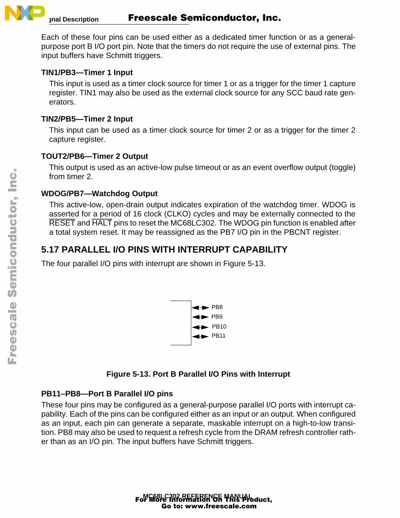
Signal Description
MC68LC302 REFERENCE MANUAL
Each of these four pins can be used either as a dedicated timer function or as a general-purpose port B I/O port pin. Note that the timers do not require the use of external pins. Theinput buffers have Schmitt triggers.
TIN1/PB3—Timer 1 InputThis input is used as a timer clock source for timer 1 or as a trigger for the timer 1 captureregister. TIN1 may also be used as the external clock source for any SCC baud rate gen-erators.
TIN2/PB5—Timer 2 InputThis input can be used as a timer clock source for timer 2 or as a trigger for the timer 2capture register.
TOUT2/PB6—Timer 2 OutputThis output is used as an active-low pulse timeout or as an event overflow output (toggle)from timer 2.
WDOG/PB7—Watchdog OutputThis active-low, open-drain output indicates expiration of the watchdog timer. WDOG isasserted for a period of 16 clock (CLKO) cycles and may be externally connected to theRESET and HALT pins to reset the MC68LC302. The WDOG pin function is enabled aftera total system reset. It may be reassigned as the PB7 I/O pin in the PBCNT register.
5.17 PARALLEL I/O PINS WITH INTERRUPT CAPABILITYThe four parallel I/O pins with interrupt are shown in Figure 5-13.
Figure 5-13. Port B Parallel I/O Pins with Interrupt
PB11–PB8—Port B Parallel I/O pinsThese four pins may be configured as a general-purpose parallel I/O ports with interrupt ca-pability. Each of the pins can be configured either as an input or an output. When configuredas an input, each pin can generate a separate, maskable interrupt on a high-to-low transi-tion. PB8 may also be used to request a refresh cycle from the DRAM refresh controller rath-er than as an I/O pin. The input buffers have Schmitt triggers.
PB8
PB9
PB10
PB11
Fre
esc
ale
Se
mic
on
du
cto
r, I
Freescale Semiconductor, Inc.
For More Information On This Product, Go to: www.freescale.com
nc
...

Signal Description
MC68LC302 REFERENCE MANUAL
5.18 CHIP-SELECT PINS The chip-select pins are shown in Figure 5-14.
Figure 5-14. Chip-Select Pins
CS0/IOUT2—Chip-Select 0/Interrupt Output 2 In normal operation, this pin functions as CS0. CS0 is one of the four active-low outputpins that function as chip selects for external devices or memory. It does not activate onaccesses to the internal RAM or registers (including the BAR, SCR, or CKCR registers).
When the M68000 core is disabled, this pin operates as IOUT2. IOUT2 provides the in-terrupt request output signal from the LC302 interrupt controller to an external CPU whenthe M68000 core is disabled. This signal is asserted if an internal interrupt of level 4, 6, 7is generated.
CS3–CS1—Chip Selects 3–1These three active-low output pins function as chip selects for external devices or mem-ory. CS3—CS0 do not activate on accesses to the internal RAM or registers (including theBAR SCR, or CKCR registers).
5.19 WHEN TO USE PULLUP RESISTORSPins that are input-only or output-only do not require external pullups. The bidirectional buscontrol signals require pullups since they are three-stated by the MC68LC302 when they arenot being driven. Open-drain signals always require pullups.
Unused inputs should not be left floating. If they are input-only, they may be tied directly toVCC or ground, or a pullup or pulldown resistor may be used. Unused outputs may be leftunconnected. Unused I/O pins may be configured as outputs after reset and left unconnect-ed.
If the MC68LC302 is to be held in reset for extended periods of time in an application (otherthan what occurs in normal power-on reset or board test sequences) due to a special appli-cation requirement (such as VDD dropping below required specifications, etc.), then three-stated signals and inputs should be pulled up or down. This decreases stress on the devicetransistors and saves power.
See the RESET pin description for the condition of all pins during reset.
CS0/IOUT2
CS3–CS1
Fre
esc
ale
Se
mic
on
du
cto
r, I
Freescale Semiconductor, Inc.
For More Information On This Product, Go to: www.freescale.com
nc
...

Signal Description
MC68LC302 REFERENCE MANUAL
Fre
esc
ale
Se
mic
on
du
cto
r, I
Freescale Semiconductor, Inc.
For More Information On This Product, Go to: www.freescale.com
nc
...

MC68LC302 REFERENCE MANUAL
SECTION 6ELECTRICAL CHARACTERISTICS
The AC specifications presented consist of output delays
,
input setup and hold times
,
andsignal skew times. All signals are specified relative to an appropriate edge of the clock (CLKO pin) and possibly to one or more other signals. The timing for the LC302 signals isthe same as the corresponding signals of the 68302.
VERY IMPORTANT NOTE REGARDING SIGNALS
A few signals have been added to and removed from the68LC302 or their functionality has changed. Several signals areonly available when 68302 is in CPU disable mode.The IAC,FC2-FC0, AVEC and FRZ signals are only available on the PGApackage. The A23-A20, RMC, BERR, BCLR, IACK1, IACK6,IACK7, DREQ, DACK, DONE, BRG1, TOUT1, NC1, NC3,TCLK3, RTS3, CTS3, CD3 signals have been removed UDS,LDS, R/W, BR, BG, BGACK are available only in Slave Mode.The following diagrams and tables show the timing for all avail-able signals. For complete information on which signals areavailable in which modes (CPU disable), please refer to Section5 of this Addendum.
Fre
esc
ale
Se
mic
on
du
cto
r, I
Freescale Semiconductor, Inc.
For More Information On This Product, Go to: www.freescale.com
nc
...

Electrical Characteristics
MC68LC302 REFERENCE MANUAL
6.1 MAXIMUM RATINGS
6.2 THERMAL CHARACTERISTICS
Rating Symbol Value Unit
This device contains circuitry to protect the inputs against damage due to high static voltages or elec-tric fields; however, it is advised that normal precautions be taken to avoid application of any voltage higher than maximum-rated volt-ages to his high-impedance circuit. Reliability of operation is en-hanced if unused inputs are tied to an appropriate logic voltage level (e.g., either GND or V
DD
)
Supply Voltage V
DD
- 0.3 to + 7.0 V
Input Voltage V
in
- 0.3 to + 7.0 V
Operating Temperature Range
MC68302 MC68302C
T
A
0 to 70- 40 to 85
°
C
Storage Temperature Range
T
stg
- 55 to + 150
°
C
Characteristic Symbol Value Unit
Thermal Resistance for PGA
θ
JA
25
°
C/W
θ
JC
2
°
C/W
Thermal Resistance for TQFP
θ
JA
TBD
°
C/W
θ
JC
TBD
°
C/W
T
J
= T
A
+ (P
D
⋅
A
)P
D
= (V
DD
⋅
I
DD
) + P
I/O
where:
P
I/O
is the power dissipation on pins.For T
A
= 70
°
C and P
I/O
+ 0 W, 16.67 MHz, 5.5 V, and CQFP package, the worst case value of T
J
is: T
J
= 70
°
C + (5.5 V
⋅
30 mA
⋅
40
°
C/W) = 98.65C
Fre
esc
ale
Se
mic
on
du
cto
r, I
Freescale Semiconductor, Inc.
For More Information On This Product, Go to: www.freescale.com
nc
...

Electrical Characteristics
MC68LC302 REFERENCE MANUAL
6.3 POWER CONSIDERATIONS
The average chip-junction temperature
,
T
J
,
in
°
C can be obtained from:T
J
= T
A
+ (P
D
•
θ
JA
)(1)
where:
T
A
= Ambient Temperature
,
°
C
θ
JA
= Package Thermal Resistance
,
Junction to Ambient
,
°
C/W
P
D
= P
INT
+ P
I/O
P
INT
= I
DD
x V
DD
,
Watts—Chip Internal Power
P
I/O
= Power Dissipation on Input and Output Pins—User Determined
For most applications P
I/O
< 0.3
•
P
INT
and can be neglected.
If P
I/O
is neglected
,
an approximate relationship between P
D
and T
J
isP
D
= K
÷
(T
J
+ 273
°
C)(2)
Solving equations (1) and (2) for K gives:K = P
D
•
(T
A
+ 273
°
C) +
θ
JA
• P
D
2(3)
where K is a constant pertaining to the particular part. K can be determined from equation(3) by measuring PD (at equilibrium) for a known TA. Using this value of K
,
the values of P
D
and T
J
can be obtained by solving equations (1) and (2) iteratively for any value of T
A
.
Fre
esc
ale
Se
mic
on
du
cto
r, I
Freescale Semiconductor, Inc.
For More Information On This Product, Go to: www.freescale.com
nc
...

Electrical Characteristics
MC68LC302 REFERENCE MANUAL
6.4 POWER DISSIPATION
Note: These values are preliminary estimates. Test values are TBD.
Characteristic Symbol 5v Typ 5v Max Unit
Normal Mode at 20Mhz PD(I) 70 TBD mA
Norlmal Mode at 16Mhz PD(I) 60 TBD mA
Low Power Standby Mode PDSB(I) 7 TBD mA
Lo Power Doze Mode PDDZ(I) 500 TBD
µ
A
Low Power Stop Mode PDDZ(I) 100 TBD
µ
A
Fre
esc
ale
Se
mic
on
du
cto
r, I
Freescale Semiconductor, Inc.
For More Information On This Product, Go to: www.freescale.com
nc
...

Electrical Characteristics
MC68LC302 REFERENCE MANUAL
6.5 DC ELECTRICAL CHARACTERISTICS
NOTE: The maximum IOH for a given pin is one-half the IOL rating for that pin. For an IOH between 400 µA and IOL/2 mA, the minimum VOH is calculated as: VDD - (1 +.05 V/mA(IOH -.400 mA)).
Characteristic Symbol Min Max Unit
Input High Voltage (Except pins noted below)) VIH 2.0 VDD V
InputHighVoltage CD1,CTS1,RXD1,TXD1,RCLK1,RTS1,TCLK1,PA7-PA10, PA12,CD2, CTS2, RXD2, TXD2, RCLK2,RTS2, TCLK2,TIN1, TIN2, TOUT2, WDOG,PB8-PB11,RESET(These pins have schmitt trigger inputs)
VIH 2.5 VDD V
Input Low Voltage (Except EXTAL) VIL VSS - 0.3 0.8 V
Input Undershoot Voltage VCIL - -0.8 V
Input High Voltage (EXTAL) 3.3 Volt or 5 Volt Part VCIH .8 * VDD VDD V
Input Low Voltage (EXTAL) VCIL VSS - 0.3 0.6 V
Input Leakage Current IIN — 20 µA
Input Capacitance All Pins CIN — 15 pF
Three-State Leakage Current (2.4/0.5 V) ITSI — 20 µA
Open Drain Leakage Current (2.4 V) IOD — 20 µA
Output High Voltage (IOH = 400 µA) (see Note) VOH VDD–1.0 — V
Output Low Voltage (IOL = 3.2 mA) A1–A19, PB3–PB11, CS0–CS3
BG, RCLK1, RCLK2,TCLK1, TCLK2, RTS1, RTS2,SDS2, PA12, RXD2, CTS2, CD2,
(IOL = 5.3 mA) AS, WEH(UDS), WEL(LDS), OE(R/W)
BGACK, DTACK,D0–D15, RESET
(IOL = 7.0 mA) TXD1, TXD2,
(IOL = 8.9 mA) HALT, BR (as output)
(IOL = 3.2 mA) CLKO
VOL
—
—
—
——
0.5
0.5
0.5
0.50.4
V
Output Drive CLKOOutput Drive ISDN I/F (GCI Mode)Output Drive All Other Pins
OCLK
OGCI
OALL
———
50150130
pFpFpF
Output Drive Derating Factor for CLKO of 0.030 ns/pFOutput Drive Derating Factor for CLKO of 0.025 ns/pFOutput Drive Derating Factor for All Other Pins 0.025 ns/pFOutput Drive Derating Factor for All Other Pins 0.05 ns/pF
OKF
OKF
OKF
OKF
205020
100
50130100200
pFpFpFpF
Power 5.0 Volt Part3.3 Volt Part
VDD4.5 5.5
V3.0 3.6
Common VSS 0 0 V
Fre
esc
ale
Se
mic
on
du
cto
r, I
Freescale Semiconductor, Inc.
For More Information On This Product, Go to: www.freescale.com
nc
...

Electrical Characteristics
MC68LC302 REFERENCE MANUAL
6.6 DC ELECTRICAL CHARACTERISTICS—NMSI1 IN IDL MODE
6.7 AC ELECTRICAL SPECIFICATIONS—CLOCK TIMING(see Figure 6-1)
Note: The minimum VCO frequency and the PLL default values put some restrictions on the minimum system frequency.
Figure 6-1. Clock Timing Diagram
Characteristic Symbol Min Max Unit Condition
Input Pin Characteristics: L1CLK, L1SY1, L1RXD, L1GR
Input Low Level Voltage VIL -10% + 20% V (% of VDD)
Input High Level Voltage VIH VDD - 20% VDD + 10% V
Input Low Level Current IIL — ± 10 µA Vin = Vss
Input High Level Current IIH — ± 10 µA Vin = VDD
Output Pin Characteristics: L1TXD, SDS1- SDS2, L1RQ
Output Low Level Voltage VOL 0 1.0 V IOL = 5.0 mA
Output High Level Voltage VOH VDD - 1.0 VDD V IOH = 400 µA
16.67 MHz 20 MHz 25 MHz
Num. Characteristic Symbol Min Max Min Max Min Max Unit
System Frequency fsys dc 16.67 dc 20.00 dc 25.00 MHz
Crystal Frequency fXTAL 25 6000 25 6000 25 6000 kHz
On-Chip VCO System Frequency fsys 10 16.67 10 20 10 25 MHz
Start-up TimeWith external clock (oscillator disabled) or after changing the multiplication factor MF. With external crystal oscillator enabled.
tpll
tosc
2500
75,000
2500
75,000
2500
75,000clks
CLKO stability ∆CLK TBD TBD TBD TBD TBD TBD %
1 CLKO Period tcyc 60 - 50 - 40 - ns
1A EXTAL Duty Cycle tdcyc 40 60 40 60 40 60 %
1C External Clock Input Period tEXTcyc 60 - 50 - 40 - ns
2,3 CLKO Pulse width (measured at 1.5v) tcw TBD - TBD - TBD - ns
4,5 CLKO Rise and fall times (full drive) tCrf - 5 - 4 - 4 ns
5B EXTAL to CLKO skew (PLL disabled) tEXTP 2 11 2 9 2 7 ns
EXTAL
CLKO
(INPUT)
(OUTPUT)
54
1
1C
2 3
5B
VOLTAGE MIDPOINT
1A
Fre
esc
ale
Se
mic
on
du
cto
r, I
Freescale Semiconductor, Inc.
For More Information On This Product, Go to: www.freescale.com
nc
...

Electrical Characteristics
MC68LC302 REFERENCE MANUAL
6.7.1 AC Electrical Characteristics - IMP Phased Lock Loop (PLL) Characteristics
1. f is the maximum operating frequency. Ef is EXTAL frequency. CXFC is the value of the PLL capacitor (connected between XFC pin and VCCSYN) for MF=1. The recommended value for CXFC is 400pF for MF < 5 and 540pF for MF> 5. The maximum VCO frequency is limited to the internal operation frequency, as defined above.
Examples:
1. MODCK1,0 = 01; MF = 1 fi 340 ≤ cXFC ≤ 480 pF
2. MODCK1,0 = 01; crystal is 32.768 KHz (or 4.192 MHz), initial MF = 401, initial frequency= 13.14 MHz; later, MF is changed to 762 to support a frequency of 25 MHz.
Minimum cXFC is: 762 x 380 = 289 nF, maximum cXFC is: 401 x 970 = 390 nF. The recommended cXFC for 25 MHz is: 762 x 540 = 414 nF.
289 nF < cXFC < 390 nF and closer to 414 nF. The proper available value for cXFC is 390 nF.
3. MODCK1 pin = 1, crystal is 32.768 KHz (or 4.192 MHz), initial MF = 401, initial frequency= 13.14 MHz; later, MF is changed to 1017 to support a frequency of 33.34 MHz.
Minimum cXFC is: 1017 x 380 = 386 nF. Maximum cXFC is: 401 x 970 = 390 nF ⇒ 386 nF < cXFC < 390 nF.
The proper available value for cXFC is 390 nF.
3A. In order to get higher range, higher crystal frequency can be used (i.e. 50 KHz), in thiscase:
Minimum cXFC is: 667 x 380 = 253 nF. Maximum cXFC is: 401 x 970 = 390 nF ⇒ 253 nF < cXFC < 390 nF.
Characteristics Expression Min Max Unit VCO frequency when PLL enabled MF * Ef 10 f (Note 1.) MHz
PLL external capacitor (XFC pin to VCCSYN) MF * CXFC (Note 1.) @ MF < 5 @ MF > 5
MF * 340MF * 380
MF * 480MF * 970
pF
Fre
esc
ale
Se
mic
on
du
cto
r, I
Freescale Semiconductor, Inc.
For More Information On This Product, Go to: www.freescale.com
nc
...

Electrical Characteristics
MC68LC302 REFERENCE MANUAL
6.8 AC ELECTRICAL SPECIFICATIONS—IMP BUS MASTER CYCLES(see Figure 6-2, Figure 6-3, and Figure 6-4)
Num. Characteristic Symbol
16.67 [email protected] V
20 [email protected] V
25 [email protected] V
UnitMin Max Min Max Min Max
6 Clock High to FC, Address Valid tCHFCADV 0 45 0 45 0 30 ns
7 Clock High to Address, Data Bus High Im-pedance (Maximum) tCHADZ — 50 — 50 — 33 ns
8 Clock High to Address, FC Invalid (Mini-mum) tCHAFI 0 — 0 — 0 — ns
9 Clock High to AS, DS Asserted (see Note 1) tCHSL 3 30 3 30 3 20 ns
11 Address, FC Valid to AS, DS Asserted (Read) AS Asserted Write (see Note 2) tAFCVSL 15 — 15 — 10 — ns
12 Clock Low to AS, DS Negated (see Note 1) tCLSH — 30 — 30 — 20 ns
13 AS, DS Negated to Address, FC Invalid (see Note 2) tSHAFI 15 — 15 — 10 — ns
14 AS (and DS Read) Width Asserted (see Note 2) tSL 120 — 120 — 80 — ns
14A DS Width Asserted, Write (see Note 2) tDSL 60 — 60 — 40 — ns
15 AS, DS Width Negated (see Note 2) tSH 60 — 60 — 40 — ns
16 Clock High to Control Bus High Impedance tCHCZ — 50 — 50 — 33 ns
17 AS, DS Negated to R/W Invalid (see Note 2) tSHRH 15 — 15 — 10 — ns
18 Clock High to R/W High (see Note 1) tCHRH — 30 — 30 — 20 ns
20 Clock High to R/W Low (see Note 1) tCHRL — 30 — 30 — 20 ns
20A AS Asserted to R/W Low (Write) (see Notes 2 and 6) tASRV — 10 — 10 — 7 ns
21 Address FC Valid to R/W Low (Write) (see Note 2) tAFCVRL 15 — 15 — 10 — ns
22 R/W Low to DS Asserted (Write) (see Note 2) tRLSL 30 — 30 — 20 — ns
23 Clock Low to Data-Out Valid tCLDO — 30 — 30 — 20 ns
25 AS, DS, Negated to Data-Out Invalid (Write) (see Note 2) tSHDOI 15 — 15 — 10 — ns
26 Data-Out Valid to DS Asserted (Write) (see Note 2) tDOSL 15 — 15 — 10 — ns
27 Data-In Valid to Clock Low (Setup Time on Read) (see Note 5) tDICL 7 — 7 — 5 — ns
28 AS, DS Negated to DTACK Negated (Asyn-chronous Hold) (see Note 2) tSHDAH 0 110 0 110 0 75 ns
29 AS, DS Negated to Data-In Invalid (Hold Time on Read) tSHDII 0 — 0 — — — ns
31 DTACK Asserted to Data-In Valid (Setup Time) (see Notes 2 and 5) tDALDI — 50 — 50 — 33 ns
32 HALT and RESET Input Transition Time tRHr, tRHf — 150 — 150 — 150 ns
44 AS, DS Negated to AVEC Negated tSHVPH 0 50 0 50 0 33 ns
47 Asynchronous Input Setup Time (see Note 5) tASI 10 — 10 — 7 — ns
53 Data-Out Hold from Clock High tCHDOI 0 — 0 — 0 — ns
55 R/W Asserted to Data Bus Impedance Change tRLDBD 0 — 0 — 0 — ns
Fre
esc
ale
Se
mic
on
du
cto
r, I
Freescale Semiconductor, Inc.
For More Information On This Product, Go to: www.freescale.com
nc
...

Electrical Characteristics
MC68LC302 REFERENCE MANUAL
NOTES:1. For loading capacitance of less than or equal to 50 pF, subtract 4 ns from the value given in the maximum
columns.2. Actual value depends on clock period since signals are driven/latched on different CLKO edges. To calculate the
actual spec for other clock frequencies, the user may derive the formula for each specification. First, derive the margin factor as: M = N(P/2) - Sa where N is the number of one-half CLKO periods between the two events as derived from the timing diagram, P is the rated clock period of the device for which the specs were derived (e.g., 60 ns with a 16.67-MHz device or 50 ns with a 20 MHz device), and Sa is the actual spec in the data sheet. Thus, for spec 14 at 16.67 MHz: M = 5(60 ns/2) - 120 ns = 30 ns.Once the margin (M) is calculated for a given spec, a new value of that spec (Sn) at another clock frequency with period (Pa) is calculated as: Sn = N(Pa/2) - MThus for spec 14 at 12.5 MHz: Sn = 5(80 ns/2) - 30 ns = 170 ns. These two formulas assume a 50% duty cycle. Otherwise, if N is odd, the previous values N(P/2) and N(Pa/2) must be reduced by X, where X is the difference between the nominal pulse width and the minimum pulse width of the EXTAL input clock for that duty cycle.
4. For power-up, the MC68302 must be held in the reset state for 100 ms (or 2.3sec if MF=401) to allow stabilization of on-chip circuit. After the system is powered up #56 refers to the minimum pulse width required to reset the processor.
5. If the asynchronous input setup (#47) requirement is satisfied for DTACK, the DTACK asserted to data setup time (#31) requirement can be ignored. The data must only satisfy the data-in to clock low setup time (#27) for the following clock cycle.
6. When AS and R/W are equally loaded (±20%), subtract 5 ns from the values given in these columns.
56 HALT/RESET Pulse Width (see Note 4) tHRPW 10 — 10 — 10 — clks
61 Clock High to BCLR High Impedance (See Note 10) tCHBCH — 30 — 30 — 20 ns
Fre
esc
ale
Se
mic
on
du
cto
r, I
Freescale Semiconductor, Inc.
For More Information On This Product, Go to: www.freescale.com
nc
...

Electrical Characteristics
MC68LC302 REFERENCE MANUAL
Figure 6-2. Read Cycle Timing Diagram
86
7
15
9
11
14
12
17
18
28
29
47
32
56
47
32
47
DATA IN
HALT / RESET
ASYNCHRONOUS INPUTS (NOTE 1)
S0 S1 S2 S3 S4 S5 S6
FC2–FC0
A23–A1
AS
LDS–UDS
R/W
DTACK
CLKO
S7
27
13
NOTES: 1. Setup time for the asynchronous inputs IPL2–IPL0 guarantees their recognition at the next falling edge of the clock. 2. BR need fall at this time only to insure being recognized at the end of the bus cycle. 3. Timing measurements are referenced to and from a low voltage of 0.8 volt and a high voltage of 2.0 volts, unless otherwise noted. The voltage swing through this range should start outside and pass through the range such that the rise or fall is linear between 0.8 volts and 2.0 volts.
CS, OE
47
17831
175
150174
173
176
152
151
171
Fre
esc
ale
Se
mic
on
du
cto
r, I
Freescale Semiconductor, Inc.
For More Information On This Product, Go to: www.freescale.com
nc
...

Electrical Characteristics
MC68LC302 REFERENCE MANUAL
Figure 6-3. Write Cycle Timing Diagram
86
7
15
9
11
14
12
18
47 28
47
32
56
47
32
47
DATA OUT
HALT / RESET
ASYNCHRONOUS INPUTS (NOTE 1)
S0 S1 S2 S3 S4 S5 S6
FC2-FC0
A23-A1
AS
LDS-UDS,
R/W
DTACK
CLKO
S7
20A
9
20
55
7
2553
NOTES: 1. Timing measurements are referenced to and from a low voltage of 0.8 volt and a high voltage of 2.0 volts, unless otherwise noted. The voltage swing through this range should start outside and pass through the
21
23
13
151
22
172
152 175
150
173
177
26
CS,
3. Each wait state is a full clock cycle inserted between S4 and S5.
174
14A
range such that the rise or fall is linear between between 0.8 volt and 2.0 volts. 2. Because of loading variations, R/W may be valid after AS even though both are initiated by the rising edge
of S2 (specification #20A)
17617
WEL, WEH
150
Fre
esc
ale
Se
mic
on
du
cto
r, I
Freescale Semiconductor, Inc.
For More Information On This Product, Go to: www.freescale.com
nc
...

Electrical Characteristics
MC68LC302 REFERENCE MANUAL
Figure 6-4. Read-Modify-Write Cycle Timing Diagram
CLKO
S13 S14 S15 S16 S17 S18S0 S1 S2 S3 S4 S5 S6 S7 S8 S12S9 S10 S11 S19
12
9 912
9
18
DATA IN
20
DATA OUT
23 2529
27
18
INDIVISIBLE CYCLE
AS (NOTE 2)
(OUTPUT)
UDS–LDS (OUTPUT)
DTACK
D15–D0
R/W (OUTPUT)
AS (NOTE 3)
(OUTPUT)
Fre
esc
ale
Se
mic
on
du
cto
r, I
Freescale Semiconductor, Inc.
For More Information On This Product, Go to: www.freescale.com
nc
...

Electrical Characteristics
MC68LC302 REFERENCE MANUAL
6.9 AC ELECTRICAL SPECIFICATIONS—DMA (see Figure 6-5 and Figure 6-6)
NOTES:1. BR will not be asserted while AS, HALT, or BERR is asserted.2. Specifications are for DISABLE CPU mode only.3. DMA and SDMA read and write cycle timing is the same as that for the M68000 core.
Num. Characteristic Symbol
16.67 MHz 20 MHz 25 MHz
UnitMin Max Min Max Min Max
83 Clock High to BR Low (see Notes 3 and 4) tCHBRL — 30 — 25 — 20 ns
84 Clock High to BR High Impedance (see Notes 3 and 4) tCHBRZ — 30 — 25 — 20 ns
85 BGACK Low to BR High Impedance (see Notes 3 and 4) tBKLBRZ 30 — 25 — 20 — ns
86 Clock High to BGACK Low tCHBKL — 30 — 25 — 20 ns
87AS and BGACK High (the Latest One) to BGACK Low (when BG Is Asserted)
tABHBKL 1.52.5+30
1.52.5+25
1.52.5+20
clksns
88 BG Low to BGACK Low (No Other Bus Master) (see Notes 3 and 4) tBGLBKL 1.5
2.5+30
1.52.5+25
1.52.5+20
clksns
89 BR High Impedance to BG High (see Notes 3 and 4) tBRHBGH 0 — 0 — 0 — ns
90 Clock on which BGACK Low to Clock on which AS Low tCLBKLAL 2 2 2 2 2 2 clks
91 Clock High to BGACK High tCHBKH — 30 — 25 — 20 ns
92 Clock Low to BGACK High Impedance tCLBKZ — 15 — 15 — 10 ns
Fre
esc
ale
Se
mic
on
du
cto
r, I
Freescale Semiconductor, Inc.
For More Information On This Product, Go to: www.freescale.com
nc
...

Electrical Characteristics
MC68LC302 REFERENCE MANUAL
Figure 6-5. DMA Timing Diagram (IDMA)
NO
TE
S:
1
. B
R a
nd B
G s
how
n ab
ove
are
only
act
ive
in d
isab
le C
PU
mod
e; o
ther
wis
e, th
ey d
o no
t app
ly to
the
diag
ram
.
(OU
TPU
T)
BGAC
K(I/
O)
AS
CLK
O
(OU
TPU
T)BR
(INPU
T)BG
(OU
TPU
T)R
/W
NO
TE 1
NO
TE 1
S0S1
S2S3
S4S5
S6S7
92
91
908788
86
81
80
4789
83 8285
SEE
M68
000
REA
D C
YCLE
S FO
R
ADD
ITIO
NAL
BU
S SI
GN
ALS
AN
D T
IMIN
G.
S0S1
S2S3
S4S5
S6S7
SEE
M68
000
WR
ITE
CYC
LES
FOR
AD
DIT
ION
AL B
US
SIG
NAL
S
AND
TIM
ING
.
84
Fre
esc
ale
Se
mic
on
du
cto
r, I
Freescale Semiconductor, Inc.
For More Information On This Product, Go to: www.freescale.com
nc
...

Electrical Characteristics
MC68LC302 REFERENCE MANUAL
Figure 6-6. DMA Timing Diagram (SDMA)
(OU
TPU
T)
BGAC
K(I/
O)
AS
CLK
O
(OU
TPU
T)BR
(INPU
T)BG
(NO
TE 2
)
(NO
TE 2
)
S0S1
S2S3
S4S5
S6S7
92
91
90
8788
4789
83
85
SEE
M68
000
REA
D/W
RIT
E
CYC
LES
FOR
AD
DIT
ION
AL
BU
S SI
GN
ALS
AND
TIM
ING
.
6
86
NO
TE
S:
1.
DR
AM
ref
resh
con
trol
ler
timin
g is
iden
tical
to S
DM
A ti
min
g.
2.
BR
and
BG
sho
wn
abov
e ar
e on
ly a
ctiv
e in
dis
able
CP
U m
ode;
oth
erw
ise
they
do
not
appl
y to
the
diag
ram
.
Fre
esc
ale
Se
mic
on
du
cto
r, I
Freescale Semiconductor, Inc.
For More Information On This Product, Go to: www.freescale.com
nc
...

Electrical Characteristics
MC68LC302 REFERENCE MANUAL
6.10 AC ELECTRICAL SPECIFICATIONS—EXTERNAL MASTERINTERNAL ASYNCHRONOUS READ/WRITE CYCLES
(see Figure 6-7 and Figure 6-8)
NOTE: If AS is negated before DS, the data bus could be three-stated (spec 126) before DS is negated.
Num. Characteristic Symbol
16.67 MHz 20 MHz 25 MHz
UnitMin Max Min Max Min Max
100 R/W Valid to DS Low tRWVDSL 0 — 0 — 0 — ns
101 DS Low to Data-In Valid tDSLDIV — 30 — 25 — 20 ns
102 DTACK Low to Data-In Hold Time tDKLDH 0 — 0 — 0 — ns
103 AS Valid to DS Low tASVDSL 0 — 0 — 0 — ns
104 DTACK Low to AS, DS High tDKLDSH 0 — 0 — 0 — ns
105 DS High to DTACK High tDSHDKH — 45 — 40 — 30 ns
106 DS Inactive to AS Inactive tDSIASI 0 — 0 — 0 — ns
107 DS High to R/W High tDSHRWH 0 — 0 — 0 — ns
108 DS High to Data High Impedance tDSHDZ — 45 — 40 — 30 ns
108A DS High to Data-Out Hold Time (see Note) tDSHDH 0 — 0 — 0 — ns
109A Data Out Valid to DTACK Low tDOVDKL 15 — 15 — 10 — ns
Fre
esc
ale
Se
mic
on
du
cto
r, I
Freescale Semiconductor, Inc.
For More Information On This Product, Go to: www.freescale.com
nc
...

Electrical Characteristics
MC68LC302 REFERENCE MANUAL
Figure 6-7. External Master Internal Asynchronous Read Cycle Timing Diagram
S0S1
S2S3
SwS5
S6S7
S0Sw
SwSw
SwSw
S4
CLK
O(O
UTP
UT)
A23-
A1(IN
PUT) IAC
(OU
TPU
T)
D15
-D0
(OU
TPU
T)AS(IN
PUT)
R/W
(INPU
T)
128
106
114
110
103
129
119
104
120
108
108A
125
122
109A
124
105
47
DTA
CK
(OU
TPU
T)
(INPU
T)
UD
SLD
S
Fre
esc
ale
Se
mic
on
du
cto
r, I
Freescale Semiconductor, Inc.
For More Information On This Product, Go to: www.freescale.com
nc
...
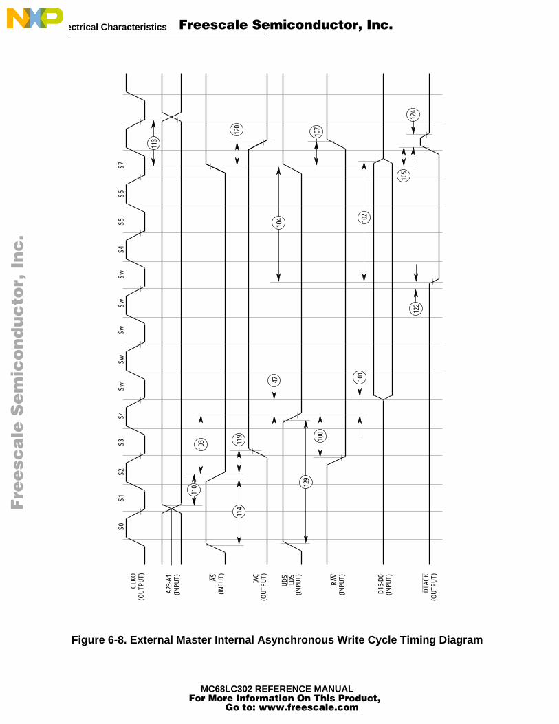
Electrical Characteristics
MC68LC302 REFERENCE MANUAL
Figure 6-8. External Master Internal Asynchronous Write Cycle Timing Diagram
S0S1
S2S3
S4S5
S6S7
SwSw
SwSw
SwS4
CLK
O(O
UTP
UT)
A23-
A1(IN
PUT) IAC
(OU
TPU
T)
D15
-D0
(INPU
T)AS(IN
PUT)
R/W
(INPU
T)
113
114
110 12
9
119
104
120
102
101
122
124
105
47
DTA
CK
(OU
TPU
T)
100
103
107
(INPU
T)
UD
SLD
S
Fre
esc
ale
Se
mic
on
du
cto
r, I
Freescale Semiconductor, Inc.
For More Information On This Product, Go to: www.freescale.com
nc
...

Electrical Characteristics
MC68LC302 REFERENCE MANUAL
6.11 AC ELECTRICAL SPECIFICATIONS—EXTERNAL MASTER INTERNAL SYNCHRONOUS READ/WRITE CYCLES
(see Figure 6-9, Figure 6-10, and Figure 6-11)
NOTES:
1. Synchronous specifications above are valid only when SAM = 1 in the SCR.
2. It is required that this signal not be asserted prior to the previous rising CLKO edge (i.e., in the previous clock cycle). It must be recognized by the IMP no sooner than the rising CLKO edge shown in the diagram.
Num. Characteristic Symbol
16.67 MHz 20 MHz 25 MHz
UnitMin Max Min Max Min Max
110 Address Valid to AS Low tAVASL 15 — 12 — 10 — ns
111 AS Low to Clock High tASLCH 30 — 25 — 20 — ns
112 Clock Low to AS High tCLASH — 45 — 40 — 30 ns
113 AS High to Address Hold Time on Write tASHAH 0 — 0 — 0 — ns
114 AS Inactive Time tASH 1 — 1 — 1 — clk
115 UDS/LDS Low to Clock High (see Note 2) tSLCH 40 — 33 — 27 — ns
116 Clock Low to UDS/LDS High tCLSH — 45 — 40 — 30 ns
117 R/W Valid to Clock High (see Note 2) tRWVCH 30 — 25 — 20 — ns
118 Clock High to R/W High tCHRWH — 45 — 40 — 30 ns
119 AS Low to IAC High tASLIAH — 40 — 35 — 27 ns
120 AS High to IAC Low tASHIAL — 40 — 35 — 27 ns
121 AS Low to DTACK Low (0 Wait State) tASLDTL — 45 — 40 — 30 ns
122 Clock Low to DTACK Low (1 Wait State) tCLDTL — 30 — 25 — 20 ns
123 AS High to DTACK High tASHDTH — 45 — 40 — 30 ns
124 DTACK High to DTACK High Impedance tDTHDTZ — 15 — 15 — 10 ns
125 Clock High to Data-Out Valid tCHDOV — 30 — 25 — 20 ns
126 AS High to Data High Impedance tASHDZ — 45 — 40 — 30 ns
127 AS High to Data-Out Hold Time tASHDOI 0 — 0 — 0 — ns
128 AS High to Address Hold Time on Read tASHAI 0 — 0 — 0 — ns
129 UDS/LDS Inactive Time tSH 1 — 1 — 1 — clk
130 Data-In Valid to Clock Low tCLDIV 30 — 25 — 20 — ns
131 Clock Low to Data-In Hold Time tCLDIH 15 — 12 — 10 — ns
Fre
esc
ale
Se
mic
on
du
cto
r, I
Freescale Semiconductor, Inc.
For More Information On This Product, Go to: www.freescale.com
nc
...

Electrical Characteristics
MC68LC302 REFERENCE MANUAL
Figure 6-9. External Master Internal Synchronous Read Cycle Timing Diagram
(OUTPUT)
(OUTPUT)
110
114
129
116
120
112
128
111
119
115
125 127
126
121 123124
A23-A1(INPUT)
IAC(OUTPUT)
LDSUDS
(INPUT)
D15–D0
AS (INPUT)
R/W (INPUT)
DTACK (OUTPUT)
S0 S1 S2 S3 S4 S5 S6 S7 S0
CLKO
Fre
esc
ale
Se
mic
on
du
cto
r, I
Freescale Semiconductor, Inc.
For More Information On This Product, Go to: www.freescale.com
nc
...
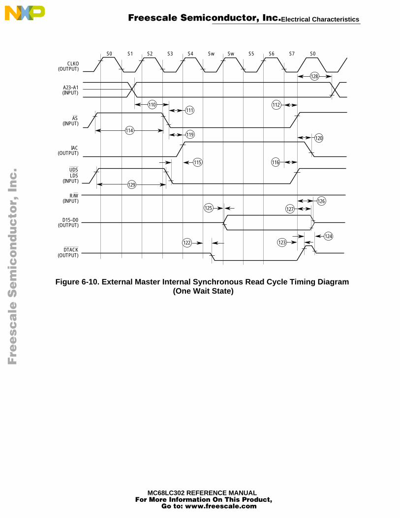
Electrical Characteristics
MC68LC302 REFERENCE MANUAL
Figure 6-10. External Master Internal Synchronous Read Cycle Timing Diagram (One Wait State)
A23–A1
CLKO(OUTPUT)
(INPUT)
IAC(OUTPUT)
AS (INPUT)
119120
112
S0 S1 S2 S3 Sw S5 S6 S7 S0S4 Sw
111
128
110
LDSUDS
(INPUT)
R/W(INPUT)
DTACK (OUTPUT)
D15–D0(OUTPUT)
116
123124
127
126125
115
129
114
122
Fre
esc
ale
Se
mic
on
du
cto
r, I
Freescale Semiconductor, Inc.
For More Information On This Product, Go to: www.freescale.com
nc
...

Electrical Characteristics
MC68LC302 REFERENCE MANUAL
Figure 6-11. External Master Internal Synchronous Write Cycle Timing Diagram
S0 S1 S2 S3 S4 S5 S6 S7 S0
AS
IAC(OUTPUT)
110111
119
114
113
112
120
A23–A1
CLKO
115116
UDS LDS
(INPUT)
(INPUT)R/W
D0–D15 (INPUT)
117
130 131
DTACK
123124
121
(INPUT)
(INPUT)
129
(OUTPUT)
118
Fre
esc
ale
Se
mic
on
du
cto
r, I
Freescale Semiconductor, Inc.
For More Information On This Product, Go to: www.freescale.com
nc
...

Electrical Characteristics
MC68LC302 REFERENCE MANUAL
6.12 AC ELECTRICAL SPECIFICATIONS—INTERNAL MASTERINTERNAL READ/WRITE CYCLES (see Figure 6-12)
Figure 6-12. Internal Master Internal Read Cycle Timing Diagram
Num. Characteristic Symbol
16.67 MHz 20 MHz 25 MHz
UnitMin Max Min Max Min Max
140 Clock High to IAC High tCHIAH — 40 — 35 — 27 ns
141 Clock Low to IAC Low tCLIAL — 40 — 35 — 27 ns
142 Clock High to DTACK Low tCHDTL — 45 — 40 — 30 ns
143 Clock Low to DTACK High tCLDTH — 40 — 35 — 27 ns
144 Clock High to Data-Out Valid tCHDOV — 30 — 25 — 20 ns
145 AS High to Data-Out Hold Time tASHDOH 0 — 0 — 0 — ns
AS (OUTPUT)
(OUTPUT)
IAC(OUTPUT)
140 141
R/W(OUTPUT)
D15-D0
145144
(OUTPUT)
DTACK (OUTPUT)
143142
LDSUDS
(OUTPUT)
A23-A1(OUTPUT)
CLKO
S0 S1 S2 S3 S4 S5 S6 S7 S0
Fre
esc
ale
Se
mic
on
du
cto
r, I
Freescale Semiconductor, Inc.
For More Information On This Product, Go to: www.freescale.com
nc
...

Electrical Characteristics
MC68LC302 REFERENCE MANUAL
6.13 AC ELECTRICAL SPECIFICATIONS—CHIP-SELECT TIMING INTERNAL MASTER (see Figure 6-13)
NOTE:1. This specification is valid only when the ADCE or WPVE bits in the SCR are set.
2.For loading capacitance less than or equal to 50 pF, subtract 4 ns from the maximum value given.3. Since AS and CS are asserted/negated on the same CLKO edges, no AS to CS relative timings can be
specified. However, CS timings are given relative to a number of other signals, in the same manner as AS. See Figure 6-2 and Figure 6-3 for diagrams.
Figure 6-13. Internal Master Chip-Select Timing Diagram
Num. Characteristic Symbol
16.67 MHz 20 MHz 25 MHz
UnitMin Max Min Max Min Max
150 Clock High to CS, IACK, OE, WEL, WEH Low (see Note 2) tCHCSIAKL 0 40 0 35 0 27 ns
151 Clock Low to CS, IACK, OE, WEL, WEH High (see Note 2) tCLCSIAKH 0 40 0 35 0 27 ns
152 CS Width Negated tCSH 60 — 50 — 40 — ns
153 Clock High to DTACK Low (0 Wait State) tCHDTKL — 45 — 40 — 30 ns
154 Clock Low to DTACK Low (1–6 Wait States) tCLDTKL — 30 — 25 — 20 ns
155 Clock Low to DTACK High tCLDTKH — 40 — 35 — 27 ns
158 DTACK High to DTACK High Impedance tDTKHDTKZ — 15 — 15 — 27 ns
171 Input Data Hold Time from S6 Low tIDHCL 5 — 5 — — 27 ns
172 CS Negated to Data-Out Invalid (Write) tCSNDOI 10 — 10 — — 10 ns
173 Address, FC Valid to CS Asserted tAFVCSA 15 — 15 — 5 — ns
174 CS Negated to Address, FC Invalid tCSNAFI 15 — 15 — 7 — ns
175 CS Low Time (0 Wait States) tCSLT 120 — 100 — 15 — ns
176 CS Negated to R/W Invalid tCSNRWI 10 — 10 — 12 — ns
177 CS Asserted to R/W Low (Write) tCSARWL — 10 — 10 80 — ns
178 CS Negated to Data-In Invalid (Hold Time on Read) tCSNDII 0 — 0 — 7 — ns
CLKO(OUTPUT)
(OUTPUT)
IACK1,IACK6,CS0–CS3
IACK7
DTACK (OUTPUT)
150 151152
Sw Sw S5 S6 S7 S0S0 S1 S2 S3 S4 S5 S6 S7 S0 S4
153 155
158
154
S1 S2 S3
Fre
esc
ale
Se
mic
on
du
cto
r, I
Freescale Semiconductor, Inc.
For More Information On This Product, Go to: www.freescale.com
nc
...

Electrical Characteristics
MC68LC302 REFERENCE MANUAL
6.14 AC ELECTRICAL SPECIFICATIONS—CHIP-SELECT TIMING EXTERNAL MASTER (see Figure 6-14)
Figure 6-14. External Master Chip-Select Timing Diagram
Num. Characteristic Symbol
16.67 MHz 20 MHz 25 MHz
UnitMin Max Min Max Min Max
154 Clock Low to DTACK Low (1-6 Wait States) tCLDTKL — 30 — 25 — 20 ns
160 AS Low to CS Low tASLCSL — 30 — 25 — 20 ns
161 AS High to CS High tASHCSH — 30 — 25 — 20 ns
162 Address Valid to AS Low tAVASL 15 — 12 — 10 — ns
164 AS Negated to Address Hold Time tASHAI 0 — 0 — 0 — ns
165 AS Low to DTACK Low (0 Wait State) tASLDTKL — 45 — 40 — 30 ns
167 AS High to DTACK High tASHDTKH — 30 — 25 — 20 ns
A23-A1 (INPUT)
DTACK (OUTPUT)
R/W (INPUT)
BERR(OUTPUT)
CLKO
S0 S1 S2 S3 S4 S5 S6 S7 S0
CS3-CS0,
165 158
169
161
167
164
168
162
AS (INPUT)
163
OE
160
WEH, WEL, (OUTPUT)
150
Fre
esc
ale
Se
mic
on
du
cto
r, I
Freescale Semiconductor, Inc.
For More Information On This Product, Go to: www.freescale.com
nc
...

Electrical Characteristics
MC68LC302 REFERENCE MANUAL
6.15 AC ELECTRICAL SPECIFICATIONS—PARALLEL I/O (see Figure 6-15)
Figure 6-15. Parallel I/O Data-In/Data-Out Timing Diagram
6.16 AC ELECTRICAL SPECIFICATIONS—INTERRUPTS (see Figure 6-16)
NOTE: Setup time for the asynchronous inputs IPL2–IPL0 and AVEC guarantees their recognition at the next falling edge of the clock.
Num. Characteristic Symbol
16.67 MHz 20 MHz 25 MHz
UnitMin Max Min Max Min Max
180 Input Data Setup Time (to Clock Low) tDSU 20 — 20 — 14 — ns
181 Input Data Hold Time (from Clock Low) tDH 10 — 10 — 19 — ns
182 Clock High to Data-out Valid (CPU Writes Data, Control, or Direction) tCHDOV — 35 — 30 — 24 ns
Num. Characteristic Symbol
16.67 MHz 20 MHz 25 MHz
UnitMin Max Min Max Min Max
190 Interrupt Pulse Width Low IRQ (Edge Trig-gered Mode) tIPW 50 — 42 — 34 — ns
191 Minimum Time Between Active Edges tAEMT 3 — 3 — 3 — clk
DATA OUT
DATA IN
181
CPU WRITE (S6) OF PORT DATA, CONTROL, OR DIRECTION REGISTER
182
CLKO
180
Fre
esc
ale
Se
mic
on
du
cto
r, I
Freescale Semiconductor, Inc.
For More Information On This Product, Go to: www.freescale.com
nc
...

Electrical Characteristics
MC68LC302 REFERENCE MANUAL
Figure 6-16. Interrupts Timing Diagram
IRQ (INPUT)
191
190
Fre
esc
ale
Se
mic
on
du
cto
r, I
Freescale Semiconductor, Inc.
For More Information On This Product, Go to: www.freescale.com
nc
...

Electrical Characteristics
MC68LC302 REFERENCE MANUAL
6.17 AC ELECTRICAL SPECIFICATIONS—TIMERS NOTE: The FRZ pin is not implemented on the LC302.
(see Figure 6-17)
NOTES:1. FRZ should be negated during total system reset.2. The TIN specs above do not apply to the use of TIN1 as a baud rate generator input clock. In such a case, specifications 1–3 may be used.
Figure 6-17. Timers Timing Diagram
Num. Characteristic Symbol
16.67 MHz 20 MHz 25 MHz
UnitMin Max Min Max Min Max
200 Timer Input Capture Pulse Width tTPW 50 — 42 — 34 — ns
201 TIN Clock Low Pulse Width tTICLT 50 — 42 — 34 — ns
202 TIN Clock High Pulse Width and Input Capture High Pulse Width tTICHT 2 — 2 — 2 — clk
203 TIN Clock Cycle Time tcyc 3 — 3 — 3 — clk
204 Clock High to TOUT Valid tCHTOV — 35 — 30 — 24 ns
205 FRZ Input Setup Time (to Clock High) (see Note 1) tFRZSU 20 — 20 — 14 — ns
206 FRZ Input Hold Time (from Clock High) tFRZHT 10 — 10 — 7 — ns
CLKO
204
202201
203
TIN (INPUT)
TOUT (OUTPUT)
206205
FRZ (INPUT)
200
Fre
esc
ale
Se
mic
on
du
cto
r, I
Freescale Semiconductor, Inc.
For More Information On This Product, Go to: www.freescale.com
nc
...
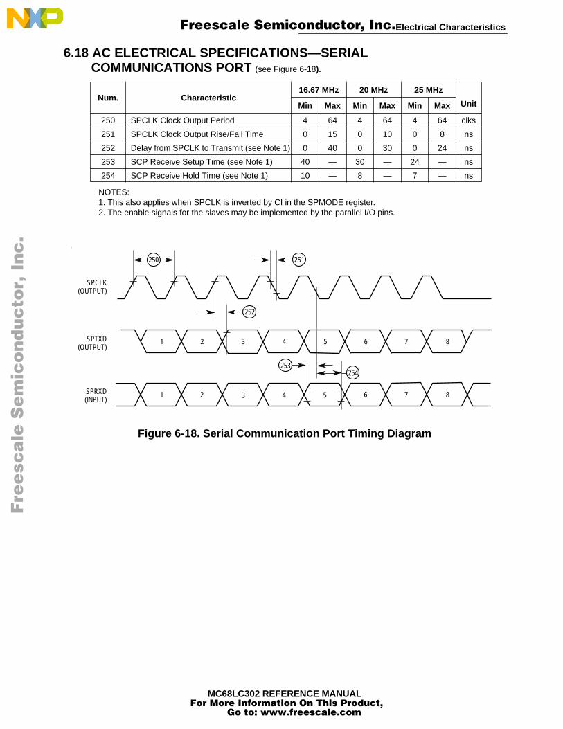
Electrical Characteristics
MC68LC302 REFERENCE MANUAL
6.18 AC ELECTRICAL SPECIFICATIONS—SERIALCOMMUNICATIONS PORT (see Figure 6-18).
NOTES:1. This also applies when SPCLK is inverted by CI in the SPMODE register.2. The enable signals for the slaves may be implemented by the parallel I/O pins.
Figure 6-18. Serial Communication Port Timing Diagram
Num. Characteristic16.67 MHz 20 MHz 25 MHz
UnitMin Max Min Max Min Max
250 SPCLK Clock Output Period 4 64 4 64 4 64 clks
251 SPCLK Clock Output Rise/Fall Time 0 15 0 10 0 8 ns
252 Delay from SPCLK to Transmit (see Note 1) 0 40 0 30 0 24 ns
253 SCP Receive Setup Time (see Note 1) 40 — 30 — 24 — ns
254 SCP Receive Hold Time (see Note 1) 10 — 8 — 7 — ns
1 2 3 4 5 6 7 8
1 2 3 4 5 6 7 8
SPCLK (OUTPUT)
SPTXD (OUTPUT)
SPRXD (INPUT)
250
252
251
253254
Fre
esc
ale
Se
mic
on
du
cto
r, I
Freescale Semiconductor, Inc.
For More Information On This Product, Go to: www.freescale.com
nc
...

Electrical Characteristics
MC68LC302 REFERENCE MANUAL
6.19 AC ELECTRICAL SPECIFICATIONS—IDL TIMING (All timing measurements,
unless otherwise specified, are referenced to the L1CLK at 50% point of VDD) (see Figure 6-19)
NOTES:1. The ratio CLKO/L1CLK must be greater than 2.5/1.2. High impedance is measured at the 30% and 70% of VDD points, with the line at VDD/2 through
10K in parallel with 130 pF.3. Where P = 1/CLKO. Thus, for a 16.67-MHz CLKO rate, P = 60 ns.
Num. Characteristic
16.67 MHz 20 MHz 25 MHz
UnitMin Max Min Max Min Max
260 L1CLK (IDL Clock) Frequency (see Note 1) — 6.66 — 8 — 10 MHz
261 L1CLK Width Low 55 — 45 — 37 — ns
262 L1CLK Width High (see Note 3) P+10 — P+10 — P+10 — ns
263 L1TXD, L1RQ, SDS1–SDS2 Rising/Falling Time — 20 — 17 — 14 ns
264 L1SY1 (sync) Setup Time (to L1CLK Falling Edge) 30 — 25 — 20 — ns
265 L1SY1 (sync) Hold Time (from L1CLK Fall-ing Edge) 50 — 40 — 34 — ns
266 L1SY1 (sync) Inactive Before 4th L1CLK 0 — 0 — 0 — ns
267 L1TxD Active Delay (from L1CLK Rising Edge) 0 75 0 65 0 50 ns
268 L1TxD to High Impedance (from L1CLK Ris-ing Edge) (see Note 2) 0 50 0 42 0 34 ns
269 L1RxD Setup Time (to L1CLK Falling Edge) 50 — 42 — 34 — ns
270 L1RxD Hold Time (from L1CLK Falling Edge) 50 — 42 — 34 — ns
271 Time Between Successive IDL syncs 20 — 20 — 20 — L1CLK
272 L1RQ Valid before Falling Edge of L1SY1 1 — 1 — 1 — L1CLK
273 L1GR Setup Time (to L1SY1 Falling Edge) 50 — 42 — 34 — ns
274 L1GR Hold Time (from L1SY1 Falling Edge) 50 — 42 — 34 — ns
275 SDS1–SDS2 Active Delay from L1CLK Ris-ing Edge 10 75 10 65 7 50 ns
276 SDS1–SDS2 Inactive Delay from L1CLK Falling Edge 10 75 10 65 7 50 ns
Fre
esc
ale
Se
mic
on
du
cto
r, I
Freescale Semiconductor, Inc.
For More Information On This Product, Go to: www.freescale.com
nc
...

Electrical Characteristics
MC68LC302 REFERENCE MANUAL
Figure 6-19. IDL Timing Diagram
(OU
TPU
T)
L1C
LK(IN
PUT)
L1R
XD
L1SY
1(IN
PUT)
SDS1
–SD
S2(O
UTP
UT)
L1TX
D
L1R
Q(O
UTP
UT)
L1G
R(IN
PUT)
265
261
263
272
268
(INPU
T)
27326
9
267
264
270
260
1011
1213
1617
1814
1519
B10
276
D1
B10
B11
AB2
7B2
6B2
5B2
4B2
3B2
2B2
1B2
0D
2M
B17
B15
B14
B12
B13
B16
68
12
34
57
920
D1
B11
AB2
7B2
6B2
5B2
4B2
3B2
2B2
1B2
0D
2M
B17
B15
B14
B12
B13
B16
275
262
266
271
274
Fre
esc
ale
Se
mic
on
du
cto
r, I
Freescale Semiconductor, Inc.
For More Information On This Product, Go to: www.freescale.com
nc
...
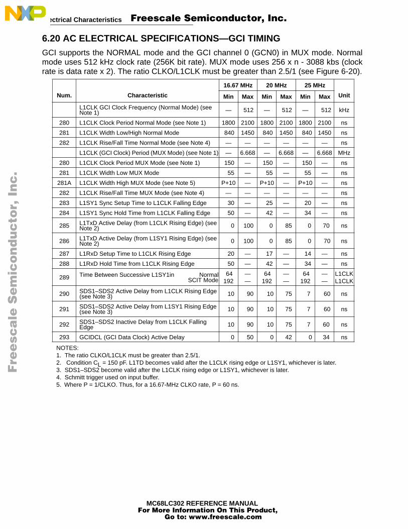
Electrical Characteristics
MC68LC302 REFERENCE MANUAL
6.20 AC ELECTRICAL SPECIFICATIONS—GCI TIMINGGCI supports the NORMAL mode and the GCI channel 0 (GCN0) in MUX mode. Normalmode uses 512 kHz clock rate (256K bit rate). MUX mode uses 256 x n - 3088 kbs (clockrate is data rate x 2). The ratio CLKO/L1CLK must be greater than 2.5/1 (see Figure 6-20).
NOTES:1. The ratio CLKO/L1CLK must be greater than 2.5/1.2. Condition CL = 150 pF. L1TD becomes valid after the L1CLK rising edge or L1SY1, whichever is later.3. SDS1–SDS2 become valid after the L1CLK rising edge or L1SY1, whichever is later.4. Schmitt trigger used on input buffer.5. Where P = 1/CLKO. Thus, for a 16.67-MHz CLKO rate, P = 60 ns.
Num. Characteristic
16.67 MHz 20 MHz 25 MHz
UnitMin Max Min Max Min Max
L1CLK GCI Clock Frequency (Normal Mode) (see Note 1) — 512 — 512 — 512 kHz
280 L1CLK Clock Period Normal Mode (see Note 1) 1800 2100 1800 2100 1800 2100 ns
281 L1CLK Width Low/High Normal Mode 840 1450 840 1450 840 1450 ns
282 L1CLK Rise/Fall Time Normal Mode (see Note 4) — — — — — — ns
L1CLK (GCI Clock) Period (MUX Mode) (see Note 1) — 6.668 — 6.668 — 6.668 MHz
280 L1CLK Clock Period MUX Mode (see Note 1) 150 — 150 — 150 — ns
281 L1CLK Width Low MUX Mode 55 — 55 — 55 — ns
281A L1CLK Width High MUX Mode (see Note 5) P+10 — P+10 — P+10 — ns
282 L1CLK Rise/Fall Time MUX Mode (see Note 4) — — — — — — ns
283 L1SY1 Sync Setup Time to L1CLK Falling Edge 30 — 25 — 20 — ns
284 L1SY1 Sync Hold Time from L1CLK Falling Edge 50 — 42 — 34 — ns
285 L1TxD Active Delay (from L1CLK Rising Edge) (see Note 2) 0 100 0 85 0 70 ns
286 L1TxD Active Delay (from L1SY1 Rising Edge) (see Note 2) 0 100 0 85 0 70 ns
287 L1RxD Setup Time to L1CLK Rising Edge 20 — 17 — 14 — ns
288 L1RxD Hold Time from L1CLK Rising Edge 50 — 42 — 34 — ns
289 Time Between Successive L1SY1in Normal SCIT Mode
64 192
——
64 192
——
64 192
——
L1CLKL1CLK
290 SDS1–SDS2 Active Delay from L1CLK Rising Edge (see Note 3) 10 90 10 75 7 60 ns
291 SDS1–SDS2 Active Delay from L1SY1 Rising Edge (see Note 3) 10 90 10 75 7 60 ns
292 SDS1–SDS2 Inactive Delay from L1CLK Falling Edge 10 90 10 75 7 60 ns
293 GCIDCL (GCI Data Clock) Active Delay 0 50 0 42 0 34 ns
Fre
esc
ale
Se
mic
on
du
cto
r, I
Freescale Semiconductor, Inc.
For More Information On This Product, Go to: www.freescale.com
nc
...

Electrical Characteristics
MC68LC302 REFERENCE MANUAL
Figure 6-20. GCI Timing Diagram
L1C
LK(IN
PUT)
L1SY
1(IN
PUT)
SDS1
–SD
S2(O
UTP
UT)
GC
IDC
L(O
UTP
UT)
L1TX
D(O
UTP
UT)
L1R
XD(IN
PUT)
291
285
284
28028
228
1
289
292
293
288
290
286
283
287
Fre
esc
ale
Se
mic
on
du
cto
r, I
Freescale Semiconductor, Inc.
For More Information On This Product, Go to: www.freescale.com
nc
...

Electrical Characteristics
MC68LC302 REFERENCE MANUAL
6.21 AC ELECTRICAL SPECIFICATIONS—PCM TIMINGThere are two sync types:
Short Frame—Sync signals are one clock cycle prior to the dataLong Frame—Sync signals are N-bits that envelope the data, N > 0; see Figure 6-21 and Figure 6-22).
NOTES:1. The ratio CLK/L1CLK must be greater than 2.5/1.2. L1TxD becomes valid after the L1CLK rising edge or the sync enable, whichever is later, if long frames are
used.3. Specification valid for both sync methods.4. Where P = 1/CLKO. Thus, for a 16.67-MHz CLKO rate, P = 60 ns.
Num. Characteristic
16.67 MHz 20 MHz 25 MHz
UnitMin Max Min Max Min Max
300 L1CLK (PCM Clock) Frequency (see Note 1) — 6.66 — 8.0 — 10.0 MHz
301 L1CLK Width Low 55 — 45 — 37 — ns
301A L1CLK Width High (see Note 4) P+10 — P+10 — P+10 — ns
302 L1SY0–L1SY1 Setup Time to L1CLK Rising Edge 0 — 0 — 0 — ns
303 L1SY0–L1SY1 Hold Time from L1CLK Falling Edge 40 — 33 — 27 — ns
304 L1SY0–L1SY1 Width Low 1 — 1 — 1 — L1CLK
305 Time Between Successive Sync Signals (Short Frame) 8 — 8 — 8 — L1CLK
306 L1TxD Data Valid after L1CLK Rising Edge (see Note 2) 0 70 0 60 0 47 ns
307 L1TxD to High Impedance (from L1CLK Rising Edge) 0 50 0 42 0 34 ns
308 L1RxD Setup Time (to L1CLK Falling Edge) (see Note 3) 20 — 17 — 14 — ns
309 L1RxD Hold Time (from L1CLK Falling Edge) (see Note 3) 50 — 42 — 34 — ns
Fre
esc
ale
Se
mic
on
du
cto
r, I
Freescale Semiconductor, Inc.
For More Information On This Product, Go to: www.freescale.com
nc
...

Electrical Characteristics
MC68LC302 REFERENCE MANUAL
Figure 6-21. PCM Timing Diagram (SYNC Envelopes Data)
Figure 6-22. PCM Timing Diagram (SYNC Prior to 8-Bit Data)
L1CLK(INPUT)
L1SY0/1(INPUT)
L1TXD(OUTPUT)
L1RXD(INPUT)
1 2 3 5 n-1 n
1 2 3
4
n-1 n
1 n-1 n2 3
306 307
303302
302
308
309
L1CLK(INPUT)
L1SY0/1(INPUT)
L1TXD(OUTPUT)
L1RXD(INPUT)
NOTE: (*) If L1SYn is guaranteed to make a smooth low to high transition (no spikes) while the clock is high, setup time can be defined as shown (min 20 ns).
1 2 3 5 6 7 8
8
4
5 6 7
302
304
305306
307
4 81 2 3 5 6 7
308309
303
(*)
41 2 3
Fre
esc
ale
Se
mic
on
du
cto
r, I
Freescale Semiconductor, Inc.
For More Information On This Product, Go to: www.freescale.com
nc
...

Electrical Characteristics
MC68LC302 REFERENCE MANUAL
6.22 AC ELECTRICAL SPECIFICATIONS—NMSI TIMINGThe NMSI mode uses two clocks, one for receive and one for transmit. Both clocks can beinternal or external. When t he clock is internal, it is generated by the internal baud rate gen-erator and it is output on TCLK or RCLK. All the timing is related to the external clock pin.The timing is specified for NMSI1. It is also valid for NMSI2 and NMSI3 (see Figure 6-23).
NOTES:1. The ratio CLKO/TCLK1 and CLKO/RCLK1 must be greater than or equal to 2.5/1 for external clock. The input clock
to the baud rate generator may be either an internal clock or TIN1, and may be as fast as EXTAL. However, the output of the baud rate generator must provide a CLKO/TCLK1 a nd CLKO/RCLK1 ratio greater than or equal to3/1.In asynchronous mode (UART), the bit rate is 1/16 of the TCLK1/RCLK1 clock rate.
2. Also applies to CD hold time when CD is used as an external sync in BISYNC or totally transparent mode.3. Schmitt triggers used on input buffers.4. Where P = 1/CLKO. Thus, for a 16.67-MHz CLKO rate, P = 60 ns.
Num. Characteristic
16.67 MHz 16.67 MHz 20 MHz 20 MHz 25 MHz 25 MHz
UnitInternal Clock
External Clock
Internal Clock
External Clock
Internal Clock
External Clock
Min Max Min Max Min Max Min Max Min Max Min Max
315 RCLK1 and TCLK1 Fre-quency (see Note 1) — 5.55 — 6.668 — 6.66 — 8 — 8.33 — 10 MHz
316 RCLK1 and TCLK1 Low(see Note 4) 65 — P+10 — 55 — P+10 — 45 — P+10 — ns
316a RCLK1 and TCLK1 High 65 — 55 — 55 — 45 — 45 — 35 — ns
317 RCLK1 and TCLK1 Rise/Fall Time (see Note 3) — 20 — — — 17 — — — 14 — — ns
318 TXD1 Active Delay from TCLK1 Falling Edge 0 40 0 70 0 30 0 50 0 25 0 40 ns
319 RTS1 Active/Inactive Delay from TCLK1 Falling Edge 0 40 0 100 0 30 0 80 0 25 0 65 ns
320 CTS1 Setup Time to TCLK1 Rising Edge 50 — 10 — 40 — 7 — 35 — 7 — ns
321 RXD1 Setup Time to RCLK1 Rising Edge 50 — 10 — 40 — 7 — 35 — 7 — ns
322RXD1 Hold Time from RCLK1 Rising Edge (see Note 2)
10 — 50 — 7 — 40 — 7 — 35 — ns
323 CD1 Setup Time to RCLK1 Rising Edge 50 — 10 — 40 — 7 — 35 — 7 — ns
Fre
esc
ale
Se
mic
on
du
cto
r, I
Freescale Semiconductor, Inc.
For More Information On This Product, Go to: www.freescale.com
nc
...

Electrical Characteristics
MC68LC302 REFERENCE MANUAL
Figure 6-23. NMSI Timing Diagram
RXD
1 (IN
PUT)
RC
LK1
323
322
321
317
317
315
316
CD
1 (IN
PUT)
322
CD
1 (S
YNC
INPU
T)
TXD
1 (O
UTP
UT)
TCLK
1
319
318
315
316
317
317
320
CTS
1 (IN
PUT)
RTS
1 (O
UTP
UT)
319
Fre
esc
ale
Se
mic
on
du
cto
r, I
Freescale Semiconductor, Inc.
For More Information On This Product, Go to: www.freescale.com
nc
...

Electrical Characteristics
MC68LC302 REFERENCE MANUAL
Fre
esc
ale
Se
mic
on
du
cto
r, I
Freescale Semiconductor, Inc.
For More Information On This Product, Go to: www.freescale.com
nc
...

MC68LC302 USER’S MANUAL SUPPLEMENT
SECTION 7MECHANICAL DATA AND ORDERING INFORMATION
7.1 PIN ASSIGNMENTS
7.1.1 Pin Grid Array (PGA)
A
B
C
D
E
F
G
H
J
K
L
M
N
1 2 3 4 5 6 7 8 9 10 11 12 13
MC68LC302RCBottom
View
PB11
CS0
IAC
A1
A2
A3A4
GNDA2
FC2
A8
A9
A10
A11
A15
A5
NC
PB8
CS3
CS1
GNDA3
FC1
A6
VCCA1
A12
A14
A19
D13
TIN1
WDOG
PB9
CS2
VCCA2
FC0
A7
VCCA1
A13
A18
GNDQ3
D12
NC
WEL
TN2
TOUT2
PB10
A16
GNDA1
D15
D14
D10
GNDP2
WEH
VCCP1
GNDP
A17
GNDD1
D11
D9
VCCQ1
OE
AS
NC
NC
D8
GNDQ1
VCCQ1
GNDQ1
GNDQ2
VCCQ2
NC
IPL0
IPL1
IPL2
NC
GNDQ2
VCCD1
EXTAL
XTAL
NC
NC
RXD1
D5
D6
NC
FRZ
DISCPU
BUSW
HALT
CD1
D3
GNDD2
D7
VCCSYN
PA8
PA7
XFC
GNDSYN
NC
NC
AVEC
RTS2
GNDS1
RXD2
D0
D2
D4
TCLK1
CLKO
NC
RESET
DTACK
PA10
VCCS1
CD2
NC
TXD2
PA9
D1
GNDQ4
TXD1
NC
NC
RTS1
GNDS2
RCLK1
VCCQ3
NC
CTS2
TCLK2
NC
RCLK2
CTS1
PA12
Fre
esc
ale
Se
mic
on
du
cto
r, I
Freescale Semiconductor, Inc.
For More Information On This Product, Go to: www.freescale.com
nc
...

Mechanical Data and Ordering Information
MC68LC302 USER’S MANUAL SUPPLEMENT
7.1.2 Surface Mount (TQFP )
1
25
100
26 5051
7576
PB09
HA
LT
RE
SE
T
DT
AC
K
TX
D2
PA
10
RT
S1
GN
DS
2
CD
1
RC
LK1
TC
LK1
TX
D1
VC
CS
1
PA
12
PA
7
CD
2
RT
S2
CT
S2
TC
LK2
GN
DS
1
RC
LK2
RX
D2
PA
9
RX
D1
PA
8
CT
S1
GN
DP
GN
DP
PB
10
PB
11
A10
CS
2
CS
3
CS
1
GN
DA
1
CS
0
A1
A2 A4
A3
A5
GN
DA
2
A6
A7 A8
A9
VC
CA
1
A11
A12 A14
A13
A15
PB08
TIN2
TOUT2
WDOG
TIN1
VCCP1
GNDP2
(LDS)WEL
(UDS)WEH
AS
(R/W)OE
(BR) IPL0
GNDQ1
VCCQ1
(BGACK)IPL1
EXTAL
DISCPU
CLK0
XTAL
BUSW
VCCSYN
XFC
GNDSYN
(BG) IPL2
A16
A17
D15
A19
A18
D14
D13
D11
GNDD1
D12
D10
D9
GNDQ2
VCCQ2
D8
D7
D4
D5
D6
GNDD2
D0
D1
D3
VCCD1
D2
MC68LC302PU
Top View
Fre
esc
ale
Se
mic
on
du
cto
r, I
Freescale Semiconductor, Inc.
For More Information On This Product, Go to: www.freescale.com
nc
...

Mechanical Data and Ordering Information
MC68LC302 USER’S MANUAL SUPPLEMENT
7.2 PACKAGE DIMENSIONS
7.2.1 Pin Grid Array (PGA)
C
K
1 2 3 4 5 6 7 8 9 10 11 12 13
ABCDEFGH
KLMN
J
G
G
MC68EC030RP SUFFIX PACKAGECASE 789B-01
A
B
T
NOTES: 1. A AND B ARE DATUMS AND T IS A DATUM SURFACE. 2. POSITIONAL TOLERANCE FOR LEADS (132 PL).
3. DIMENSIONING AND TOLERANCING PER Y14.5M,1982. 4. CONTROLLING DIMENSION: INCH.
0D
0.13 (0.005) M T A S B Sφ
DIM
MILLIMETERS INCHES
MIN MAX MIN MAX
A
B
C
D
G
1.340 1.380
1.340 1.380
0.100 0.150
34.04 35.05
34.04 35.05
2.54 3.81
0.43 0.55 0.017 0.022
0.100 BSC2.54 BSC
K 4.32 4.95 0.170 0.195
Fre
esc
ale
Se
mic
on
du
cto
r, I
Freescale Semiconductor, Inc.
For More Information On This Product, Go to: www.freescale.com
nc
...

Mechanical Data and Ordering Information
MC68LC302 USER’S MANUAL SUPPLEMENT
7.2.2 Surface Mount (TQFP)
CASE 983-01ISSUE A
DATE 07/14/94
���!��(�$�
���
�
��� ��� ��� ���
�����
�������$� �������$�
�����������
�� ������$� ��� ��$�
�������$� �������$�
� ������$� ��� ��$�
�� � ���
� ���� ���� ���� ����
� ��� ���� ���� �����
� ���� ��� ����� �����
� ���� ���� ����� ����
���� �� ����� �����
� ������$� �����$�
� ���� ��� ����� �����
� �����#�� �����#��
�� ���� ��� ����� �����
� � �����$� �� ���$�
�� ������$� ������$�
� ���� ��� ����� ����
� � �����$� �� ���$�
�� ������$� ������$�
� ����#�� ������#��
� �����#�� �����#��
θ �� �� �� ��
θ �� ��
θ �� ��
θ �� �� �� ��
!%�$��� ���� $�! � �� � �� %!��#� �� �� "�#� � $�
*������� ����� �! %#!��� �� ���� $�! �� �������%�#�� ��%&�� ���� �$� �!��%��� �%� �!%%!�� !�� ����
� �� �$� �!� ���� %� (�%�� %��� ����� (��#�� %������� �)�%$� %��� "��$%��� �!�*� �%� %��� �!%%!�!�� %��� "�#%� �� �� ��
�� ��%&�$� ����� ���� � �� � �� %!� ��� ��%�#�� ���%� ��%&�� ����
�� ���� $�! $� $� � �� '� %!� ��� ��%�#�� ��� �%$��%� �� "�� �� �%��
� ���� $�! $� �� � �� �� �!� !%� � ��&��� �!��"#!%#&$�! �� � ���!(����� "#!%#&$�! � �$����� �������� "�#� $����� � ���� $�! $� �� � �� �� �!� ��&��� �!��� ��$��%��� � �� �#���%�#�� ��� �%� ��%&�� ����
�� ���� $�! � �� �!�$� !%� � ��&��� �����#"#!%#&$�! �� � �����#� "#!%#&$�! � $���� !%� ��&$�� %��� ����� (��%�� %!� �)����� ������������� � �� ��&�� $"���� ��%(�� � "#!%#&$�! � �� ������ %� ����� !#� "#!%#&$�! � ������������
�
�
� � � � �
� �
� � � �
��
V1 B1 3X VIEW Y
S1
A1
4X 25 TIPS4X
V
S
A
B
��
��� ��
��
��
�� ��
�
2X 02
$��%� �
"�� � VIEW AA2X 03
C
–L–
����������� � ���
����������� % ���
–M–
����������� %
–H–
–T–
–N–
C2
C1K
Z
W
�����"�� �
VIEW AA
AB)�������
G
VIEW Y
AB
"��%� �
UJ
D
F
#!%�%�����°
��$����%��
SECTION AB–AB
$�����������
E
Θ1
Θ
�����������
2XR R1
��
–X– $��������������� $%
Fre
esc
ale
Se
mic
on
du
cto
r, I
Freescale Semiconductor, Inc.
For More Information On This Product, Go to: www.freescale.com
nc
...

Mechanical Data and Ordering Information
MC68LC302 USER’S MANUAL SUPPLEMENT
7.3 ORDERING INFORMATION
Package TypeFrequency
(MHz)Temperature Order Number
Pin Grid Array (RC Suffix)
16.67
16.67
20
20
0
°
C to 70
°
C- 40
°
C to + 85
°
C0
°
C to 70
°
C- 40
°
C to + 85
°
C
MC68LC302RC16
MC68LC302CRC16
MC68LC302RC20
MC68LC302CRC20
Surface Mount (PU Suffix)
16.67
20 0
°
C to 70
°
C0
°
C to 70
°
C
MC68LC302PU16
MC68LC302PU20
Fre
esc
ale
Se
mic
on
du
cto
r, I
Freescale Semiconductor, Inc.
For More Information On This Product, Go to: www.freescale.com
nc
...

Mechanical Data and Ordering Information
MC68LC302 USER’S MANUAL SUPPLEMENT
Fre
esc
ale
Se
mic
on
du
cto
r, I
Freescale Semiconductor, Inc.
For More Information On This Product, Go to: www.freescale.com
nc
...

MC68LC302 REFERENCE MANUAL
INDEX
A
AddressAS
3-25
DecodeConflict
2-4
Decode Conflict
3-3, 3-4
Address Bus Pins
5-7
AS
3-3, 3-25, 5-9
AT command set
4-9
Autobaud Controller
4-9
Autobaud Command Descriptor
4-14
Autobaud Lookup Table Format
4-16
Autobaud Parameter RAM
4-11
Autobaud Sampling Rate
4-15
Autobaud Transmission
4-18
Automatic Echo
4-19
Carrier Detect Lost
4-18
Channel Reception Process
4-9
Determining Character Length and Parity
4-17
End Of Table Error
4-18
Enter_Baud_Hunt Command
4-14
Lookup Table
4-15
Lookup Table Example
4-17
Lookup Table Pointer
4-15
Lookup Table Size
4-15
Maximum START bit length
4-16
Overrun Error
4-18
Performance
4-9
Preparing for the Autobaud Process
4-13
Programming Model
4-13
Reception Error Handling Procedure
4-18
Reprogramming to UART Mode or another protocol
4-20
Smart Echo
4-11, 4-19
Smart Echo Hardware Setup
4-11
START bit
4-9
Transmit Process
4-11
Automatic echo
4-5
B
Base Address Regisrter
2-4
Baud Rate Generator
5-18
BCR
3-13
BERR
2-4, 3-3, 3-4, 3-5, 3-6
BERR See SignalsBG
3-28, 5-11
BGACK
5-11
BISYNC Controller
4-22
BISYNC Event Register
4-23
BISYNC Mask Register
4-23
BISYNC Memory Map
4-22
BISYNC Mode Register
4-22
BISYNC Receive Buffer Descriptor
4-22
BISYNC Transmit Buffer Descriptor
4-22
Bootstrap
3-7
BR
3-28, 3-29, 5-10
BR3–BR0
3-26
BRG
2-12
BRG Clock
2-12
BRG Divide by twoSystem Clock
2-14
BSR
3-6
BufferBuffer Descriptor
4-6
Descriptors
2-20, 3-29
Buffer Descriptor
4-6
Buffer Descriptors Table
4-6
BusArbitration
3-28, 5-11
Bandwidth
3-12
Error
2-4
Grant (BG)
5-11
Grant Acknowledge (BGACK)
5-11
Master
3-28
Request (BR)
5-10
Signal Summary
5-13
Bus Arbitration Logic
3-28
External Bus Arbitration
3-28
Internal Bus Arbitration
3-28
Fre
esc
ale
Se
mic
on
du
cto
r, I
Freescale Semiconductor, Inc.
For More Information On This Product, Go to: www.freescale.com
nc
...
Index
MC68LC302 REFERENCE MANUAL
Bus Arbitration Pins
5-10
Bus Control Pins
5-9
Bus States during Low power modes68000
2-15
BUSW
2-1, 5-7
C
Changes to IMPCLKO Drive Options
2-6
Three-state TCLK1
2-6
Three-state RCLK1
2-6
Chip-Select
2-4
AS
3-25
Base Address
3-27
Base Register
3-26
CS0
3-26, 3-28, 5-21
DTACK
3-26
Option Register
3-26
Chip-Select Pins
5-21
Chip-Select Registers
3-26
Chip-Select Timing
6-24
CLKOOutput Buffer Strength
2-11
CLKOMOD1–2
2-6Clock
CLKO 5-4Clock Pins 5-4CMOS Level 5-2CMR 3-11Communications Processor 4-1Configuration
MC68302 IMP Control 2-3CQFP 7-2Crystal Oscillator 2-8Crystal Oscillator Circuit (IMP) 2-9CS0 3-26, 3-28, 5-21CS1 2-23, 2-24, 5-21CS2 2-23, 2-24CS3 2-23, 3-26, 5-1, 5-10, 5-21CS3–CS1 5-21CSelect 2-7CSR 3-13
DDAPR 3-13Data Bus Pins 5-8Default System Clock Generation 2-7
DF0–3 2-10Disable CPU 5-7
BG 3-28BR 3-28CS0 3-28DTACK 3-28EMWS 3-28SAM 3-28
Disable CPU Logic 3-28Disable SCC1 Serial Clocks Out 4-4DISC 4-4DISCPU 3-28, 5-7Divide by Two Block
From Tin1 pin 4-5DMA Control 3-10DOZE 2-13, 2-16DRAM Refresh
Buffer Descriptors 3-29PB8 3-18
Drive 2-13DSR 4-6DTACK 3-4, 3-26, 3-28, 5-10, 5-12Dynamic RAM Refresh Controller 3-29
EEMWS (External Master Wait State) 3-4, 3-5,
3-28Enable Receiver 4-5Enable Transmitter 4-6Exception
PB8 3-29EXTAL 5-2, 5-4External
Bus Master 3-28External Bus Arbitration using HALT 3-28Master Wait State (EMWS) 3-5
External Bus Arbitration 3-28External Master Wait State 3-4
FFCR 3-13Freeze Control 3-5FRZ 5-7Function Codes 3-13, 5-12
Comparison 2-4FC2-FC0 2-4, 5-12Register 3-13
Fre
esc
ale
Se
mic
on
du
cto
r, I
Freescale Semiconductor, Inc.
For More Information On This Product, Go to: www.freescale.com
nc
...

Index
MC68LC302 REFERENCE MANUAL
GGCI 4-2, 5-14, 5-15
SCIT 4-2SIMASK 4-4SIMODE 4-2
GCI See SignalsGIMR 3-14GNDSYN 2-12, 5-5
HHALT 2-4, 5-6HALT See SignalsHardware Watchdog 3-5
BERR 3-5, 3-6HDLC
HDLC Event Register 4-21HDLC Mask Register 4-21HDLC Memory Map 4-20HDLC Mode Register 4-20Rx BD 4-21SCCE 4-21SCCM 4-21Tx BD 4-21
HDLC Controller 4-20HDLC Event Register 4-21HDLC Mask Register 4-21HDLC Memory Map 4-20HDLC Mode Register 4-20HDLC Receive Buffer Descriptor 4-21HDLC Transmit Buffer Descriptor 4-21
IIAC 5-10IDL 4-2, 5-14, 5-15
SIMASK 4-4SIMODE 4-2
IDL See SignalsIDMA (Independent DMA Controller)
DREQ 3-11IMP Features
CP 1-2IMP Operation Mode Control Register
(IOMCR) 2-14, 2-15IMP PLL and Clock Control Register
(IPLCR) 2-10IMP PLL Pins 2-12
GNDSYN 2-12MODCLK 2-12VCCSYN 2-12XFC 2-12
IMP System Clock GenerationIOMCR 2-8, 2-9, 2-10IPLCR 2-8, 2-10
IMP System Clocks SchematicPLL Disabled 2-8
IMP Wake-Up from Low Power STOP Modes 2-17
IMR 3-16Internal Loopback 4-3Internal Registers 2-22Internal Registers Map 2-23Interrupt
Acknowledge 2-4Control Pins 5-11Controller 3-14IPR 3-15ISR 3-16
Interrupt Control Pins 5-11Interrupt Controller 3-14IOMCR 2-7, 2-14, 2-16IPL 5-11IPL0 5-11IPL1 5-11IPL2 5-11IPL2-IPL0 5-11IPLCR 2-7, 2-10IPR 3-15IPWRD 2-15IRQ1 5-12ISDN 5-14ISR 3-16IWUCR 2-17
LLoopback Control 4-3Loopback Mode
Internal Loopback 4-3Loopback Control 4-3
Loopback mode 4-5Low Power 2-13
68000 bus 2-13Low Power Drive Control Register 2-13Low Power Drive Control Register (LPDCR)
Fre
esc
ale
Se
mic
on
du
cto
r, I
Freescale Semiconductor, Inc.
For More Information On This Product, Go to: www.freescale.com
nc
...
Index
MC68LC302 REFERENCE MANUAL
2-15Low Power Modes
IMP 2-13Low Power Support 2-15
FAST WAKE-UP 2-18STOP/ DOZE/ STAND_BY Mode 2-16Wake-Up from Low Power STOP Modes
2-17Low-Power Clock Divider 2-9LPDCR 2-15LPM1–0 2-15
MMC68000/MC68008 Modes 2-1MC68LC302 System Clock Generation
IOMCR 2-6IPLCR 2-6IWUCR 2-6MODCLK 2-7PITR 2-6VCCSYN 2-7
MF 11–0 2-11MODCLK 2-12MODCLK/PA12 5-5MODCLK1–0 2-7Multiplication Factor 2-11
NNMSI 4-2, 5-14
CD1 5-16CTS1 5-17NMSI1 5-15NMSI2 5-17NMSI3 5-18RTS1 5-17SIMODE 4-2
NMSI1 or ISDN Interface Pins 5-14NMSI2 Port or Port a Pins 5-17Normal Operation 4-5
OOE (R/W) 5-9OR3–OR0 3-26Oscillator 2-8
PPACNT 3-19PADDR 3-19PAIO / SCP Pins 5-18Parallel 5-20Parallel I/O Pins with Interrupt Capability 5-
20Parallel I/O Port
PB11 3-18PB8 3-18, 3-29Port A 3-17, 5-17, 5-18
Control Register 3-17Data Direction Register (PADDR) 3-
17Port B 3-17, 5-20
Control Register 3-18Parallel I/O Ports 3-17Parameter RAM 2-21PB11 3-18PB11 See DRAM RefreshPB11 See Parallel I/O PortPB8 3-18, 3-29PBCNT 3-18, 3-19PBDAT 3-20PBDDR 3-18, 3-20PCM 4-2PCM Highway 5-14, 5-15
SIMODE 4-2Periodic Timer Period Calculation 3-23Physical Layer Serial Interface Pins 5-14Pin Assignments 7-1Pin Grid Array 7-1PIT 2-11, 2-12, 3-22
As a Real-Time Clock 3-24Period Calculation 3-23
PIT Clock 2-12PITR 3-24PLL 2-10PLL and Oscillator Changes to IMP 2-5
CLKO Drive Options 2-6Three-State RCLK1 2-6Three-State TCLK1 2-6
PLL Clock Divider 2-10PLL External Components 2-9PLL Pins
pgnd 5-5pinit 2-7
Fre
esc
ale
Se
mic
on
du
cto
r, I
Freescale Semiconductor, Inc.
For More Information On This Product, Go to: www.freescale.com
nc
...

Index
MC68LC302 REFERENCE MANUAL
PNDAT 3-20PNDDR 3-20Port A 3-17
Port A Pin Functions 3-18Port A Pin Functions 3-18Port A/B
Parallel I/O 3-17Port B 3-18
Port B Pin Functions 3-18Port N 3-19
PADAT 3-19Power Dissipation 6-4Power Pins 5-2Programmable Data Bus Size Switch 3-6Protocol Parameters 2-20Pullup Resistors 5-21
RRCLK1
Disabling 4-5RCLK1/L1CLK 5-16Read-Modify-Write Cycle 6-12Real-Time Clock 3-24Registers
Internal 2-22Interrupt In-Service (ISR) 3-16Interrupt Pending (IPR) 3-15Port A
Control (PACNT) 3-17Data Direction (PADDR) 3-17
Port BData Direction Register (PBDDR) 3-
18System Control (SCR) 2-4
Reprogramming to UART Mode or Another Protocol 4-20
RESET 5-6, 5-20Instruction 2-3
ResetSMC Memory Structure 4-26Total System 2-3
Revision Number 2-20Ring Oscillator 2-18Ringo 2-18RINGOCR 2-19RINGOEVR 2-20RMC 3-4
RXD1/L1RXD 5-15
SSAM 3-4, 3-28SAPR 3-13SCC 2-20
Buffer Descriptor 4-6DSR 4-6Enable Receiver 4-5Normal Operation 4-5SCON 4-4Software Operation 4-5TIN1/TIN2 5-20
SCC Mode Register 4-5SCC Parameter RAM 4-7SCC Parameter RAM Memory Map 4-7SCCs 4-4SCIT 4-2SCM 4-5SCON 4-4SCP 2-20
Serial Communication Port 4-25SCP Port 5-19SCR 3-2SCR (System Control Register) 2-4SCR Register Bits 3-2Serial Channels Physical Interface 4-2Serial Communication Controllers 4-4Serial Communication Port 4-25, 6-29Serial Management Controllers 4-26
SMC1 Receive Buffer Descriptor 4-26SMC1 Transmit Buffer Descriptor 4-26SMC2 Receive Buffer Descriptor 4-27SMC2 Transmit Buffer Descripto 4-27
SignalsAS 3-3, 3-25BERR 2-4, 3-3, 3-4, 3-5, 3-6BG 3-28, 5-11BGACK 5-11BR 3-28, 3-29, 5-10BUSW 2-1, 5-7CD1 5-16CLKO 5-4CS 2-4, 3-3CS0 3-26, 3-28, 5-21CTS1 5-17DISCPU 3-28, 5-7
Fre
esc
ale
Se
mic
on
du
cto
r, I
Freescale Semiconductor, Inc.
For More Information On This Product, Go to: www.freescale.com
nc
...

Index
MC68LC302 REFERENCE MANUAL
DREQ 3-11DTACK 3-4, 3-26, 3-28, 5-12EXTAL 5-2, 5-4FC2-FC0 5-12GCI 5-15HALT 2-4, 5-6IAC 5-10IDL 5-15, 5-17ILP0 5-11IRQ1 5-12NMSI2 5-17NMSI3 5-18PCM Highway 5-15Port A 5-17, 5-18Port B 5-20RESET 2-3, 5-6, 5-20RMC 3-4RTS1 5-17SCP 5-19TIN1/TIN2 5-20WDOG 3-18, 5-20XTAL 5-4
SIMASK 4-2, 4-4SIMODE 4-2SLOW_GO 2-10, 2-13, 2-14, 2-15SLOW_GO Mode 2-14SMC 2-20
Serial Management Controllers 4-26SMC Memory Structure 4-26Software Operation 4-5Software Watchdog Timer 3-22STAND_BY 2-13, 2-16STAND_BY Mode 2-13STOP 2-13, 2-16STOP Mode 2-13Supervisor
Data Space 2-3System Control Registers (SCR) 2-4System Clock
IMP 2-12System Control 3-1System Control Bits 3-3System Control Pins 5-5System Control Register (SCR) 3-2System Status Bits 3-3
TTCLK1
Disabling 4-5TCLK1/L1SY0/SDS1 5-16TCN1, TCN2 3-21TCR1, TCR2 3-21TER1, TER2 3-21Thermal Characteristics 6-2Timer
PIT 3-22Timer Pins 5-19Timers 3-20
TIN1/TIN2 5-20WDOG 3-18, 3-22
TIN1/TIN2 5-20TIN1/TIN2 See SCCTMR1, TMR2 3-20Transparent Controller 4-23
Transparent Event Register 4-25Transparent Mask Register 4-25Transparent Mode Register 4-24Transparent Receive Buffer Descriptor
4-24Transparent Transmit Buffer Descriptor
4-25TRR1, TRR2 3-21TTL Levels 5-2TXD1/L1TXD 5-15
UUART Controller 4-7
UART Event Register 4-9UART Mask Register 4-9UART Memory Map 4-7UART Mode Register 4-8UART Receive Buffer Descriptor 4-8UART Transmit Buffer Descriptor 4-8
VVCCSYN 2-12, 5-5VCO 2-10, 2-11Vector Generation Enable 3-5
WWake_Up
Clock cycles, IMP 2-13
Fre
esc
ale
Se
mic
on
du
cto
r, I
Freescale Semiconductor, Inc.
For More Information On This Product, Go to: www.freescale.com
nc
...

Index
MC68LC302 REFERENCE MANUAL
Wake-upPB10 2-18PIT 2-18PIT Event 2-18
Watchdog (WDOG) 3-18, 5-20Hardware 3-5Timer 3-22
Watchdog (WDOG) See SignalsWatchdog (WDOG) See TimersWCN 3-22WEH (UDS/A0) 5-9WEL (LDS/DS) 5-10Write Protect Violation 3-3WRR 3-22
XXFC 2-12, 5-5XTAL 5-4
Fre
esc
ale
Se
mic
on
du
cto
r, I
Freescale Semiconductor, Inc.
For More Information On This Product, Go to: www.freescale.com
nc
...

Index
MC68LC302 REFERENCE MANUAL
Fre
esc
ale
Se
mic
on
du
cto
r, I
Freescale Semiconductor, Inc.
For More Information On This Product, Go to: www.freescale.com
nc
...