fpga introduction lab · 2020-01-28 · lab 1. fpga introduction lab version 15.0 9 1.2.1.4 enter...
TRANSCRIPT

FPGA Introduction Lab
TABLE OF CONTENTSLAB 1. FPGA INTRODUCTION LAB .....................................................................................................................6
1.1 Getting Started .............................................................................................................................................61.1.1 Getting your DECA Kit .........................................................................................................................61.1.2 Review the DECA Development Platform ...........................................................................................6
1.2 Create a Quartus II Project ..........................................................................................................................71.2.1 Create a Project in Quartus II ..............................................................................................................7
1.3 Build the Design ........................................................................................................................................ 121.3.1 Block Diagram................................................................................................................................... 121.3.2 Components of the Design ............................................................................................................... 131.3.3 IP Catalog ......................................................................................................................................... 131.3.4 Create the PLL.................................................................................................................................. 131.3.5 Configure the PLL ............................................................................................................................. 141.3.6 Create the Counter ........................................................................................................................... 191.3.7 Creating the Multiplexer .................................................................................................................... 211.3.8 Adding Components to the Schematic file........................................................................................ 251.3.9 Connect the Components ................................................................................................................. 281.3.10 Analysis and Synthesis ..................................................................................................................... 371.3.11 Adding Timing Constraints................................................................................................................ 381.3.12 Adding Pin Assignments ................................................................................................................... 391.3.13 Compiling the Design........................................................................................................................ 431.3.14 Configuring the Device...................................................................................................................... 431.3.15 Testing the Design ............................................................................................................................ 46
Version 15.0 6/07/2015

LAB 1. FPGA Introduction Lab
6 Max10 DECA Workshop Manual
LAB 1. FPGA INTRODUCTION LABOverview: This Lab will guide the student through the complete design cycle from Design Entry to Configuringthe MAX 10 on the DECA board.
If you are a new user, this Lab will walk you through the steps in the Quartus II tool suite to build a design, compile it,and download it to a board.
1.1 Getting Started
1.1.1 Getting your DECA KitIf you are attending a DECA Workshop, you will receive your DECA kit in the 3-in-1 evaluation kit bundle when youarrive at the workshop location. If you are working on this lab independently, a DECA kit can be purchased throughyour Arrow sales representative or at parts.arrow.com.
Make sure you have a USB cable to connect the on-board USB Blaster to your laptop. If youare attending the workshop, USB cables are included in your evaluation kit bundle.
1.1.2 Review the DECA Development PlatformReview the components on the DECA board. This development board provides a full system built around the MAX10,including external memory, LEDs, sensors, buttons, and power supplies.
There are many components on the DECA board including the LEDs, capacitive push buttons, USB, Ethernet, HDMIand MIPI Interfaces.
This simple FPGA design will use a PLL, a push-button and a counter to output a value to the LEDs.
LAB 1. FPGA Introduction Lab
Version 15.0 7
1.2 Create a Quartus II ProjectIn this module, you will create an FPGA design using the Quartus II Tool Suite. You will then compile this design and
download it to the DECA board.
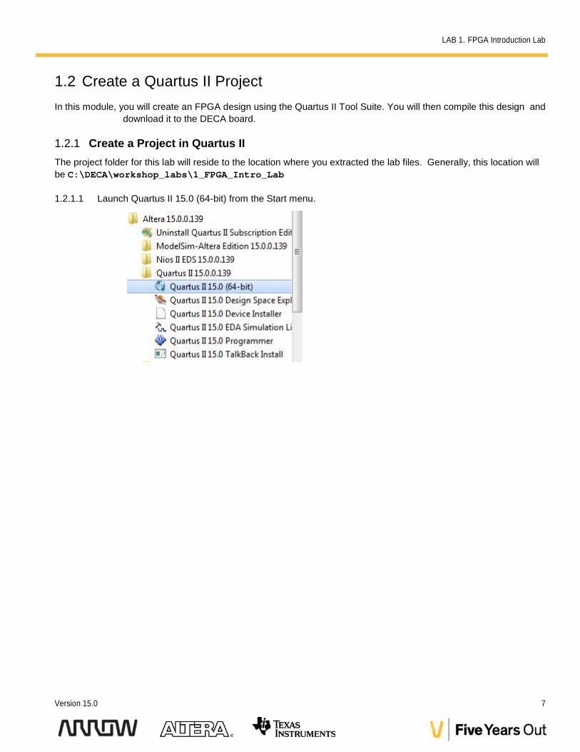
1.2.1 Create a Project in Quartus IIThe project folder for this lab will reside to the location where you extracted the lab files. Generally, this location willbe C:\DECA\workshop_labs\1_FPGA_Intro_Lab
1.2.1.1 Launch Quartus II 15.0 (64-bit) from the Start menu.

LAB 1. FPGA Introduction Lab
8 Max10 DECA Workshop Manual
1.2.1.2 In the Quartus tool Create a new project: File New Project
The New Project Wizard walks you through the project settings, such as the name, directories, files,directories, device family, and other settings. These settings can be changed later if needed.
Click Next
1.2.1.3 Browse to the Project directory: C:\DECA\workshop_labs\1_FPGA_Intro_Lab

LAB 1. FPGA Introduction Lab
Version 15.0 9
1.2.1.4 Enter the project Name "toplevel"
Click Next
1.2.1.5 Project Type
This page will be to create the Project type. In this lab, a new project will be created, and thus the default settings ofempty project should be selected.
Click Next

LAB 1. FPGA Introduction Lab
10 Max10 DECA Workshop Manual
1.2.1.6 Add Project Files
The Add File window will appear. For this lab, new design files will be created so no files will be added. For otherdesigns, files can be added here.
Click Next
1.2.1.7 Select DECA Board MAX 10 Device Part Number
In the Family and Device Settings, use the pull down menu to select the family as Max 10. Then in the Name Filter,enter: 10M50DAF484C6GES

LAB 1. FPGA Introduction Lab
Version 15.0 11
Rather than entering the exact part number, the pull-down menus can be used to select the correct family, package,pin count, and speed grade. Quartus II will use these settings to compile the design, and also provide theprogramming file that you will use later to program the device.
Click Next
1.2.1.8 EDA Tool Settings
In the EDA tool Settings window, disable any EDA tools, if there are any present. EDA tools are third party tools thatwork with Quartus II for design entry, simulation, verification and board-level timing. For this workshop, no EDAsoftware will be used, as only Quartus II will be used.
Click Next
1.2.1.9 Project Summary Page
This is the Summary Page that showing the settings Quartus II will use for this Project. These settings can bechanged, as needed at a later time.

LAB 1. FPGA Introduction Lab
12 Max10 DECA Workshop Manual
Click Finish.
1.3 Build the DesignOverview: In this section, you will create the components to a design, make connections, set the pins and compile
the design.
1.3.1 Block DiagramThe final system that will be built as described with the following steps, will look as follows when complete:

LAB 1. FPGA Introduction Lab
Version 15.0 13
1.3.2 Components of the DesignThere are three components in the system: a PLL, a counter, and a mux. The components, in the following steps,will be built separately and then connected together. A push button on the board controls the mux. The mux in turncontrol which of the counter outputs (slow counting or fast counting) will be shown on the LEDs.
There are different ways to create components, such as RTL or schematic. In this lab, schematics will be used.
There are also different ways for entering schematics such as Qsys and IP Catalog. This lab will focus on the IPCatalog.
1.3.3 IP CatalogThe IP Catalog allows you to create and modify design files with custom variations. The IP catalog window is openby default when you open Quartus. If it is not present, you can open it by selecting Tools IP Catalog
1.3.4 Create the PLL

LAB 1. FPGA Introduction Lab
14 Max10 DECA Workshop Manual
In the IP Catalog, browse for ALTPLL, via: Basic Functions Clocks; PLLs and Resets PLL
1.3.4.1 Click ALTPLL, where ALTPLL stands for Altera Phase Locked Loop
1.3.4.2 Click Add
When the Save IP Variation window appears, enter the file name variation as PLL_toplevel and select Verilog (VHDLcould be used as well). Both Verilog and schematic code will be created.
1.3.4.3 Click OK
1.3.5 Configure the PLLThe next step is to configure the PLL Component.
LAB 1. FPGA Introduction Lab
Version 15.0 15
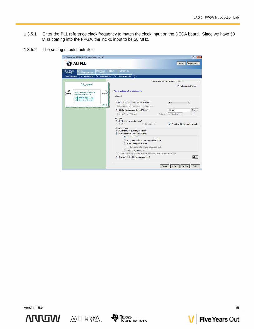
1.3.5.1 Enter the PLL reference clock frequency to match the clock input on the DECA board. Since we have 50MHz coming into the FPGA, the inclk0 input to be 50 MHz.
1.3.5.2 The setting should look like:

LAB 1. FPGA Introduction Lab
16 Max10 DECA Workshop Manual
1.3.5.3 Click Next
1.3.5.4 Simplify the PLL, by disabling the areset and locked outputs

LAB 1. FPGA Introduction Lab
Version 15.0 17
1.3.5.5 Click Next
1.3.5.6 Continue to select Next to go through the various options (e.g. Pages 3 to Pages 5), but leaving the defaultoptions as they are. The Page numbers can be seen on the top of the windows.
1.3.5.7 On page 6, (c0 - Core/External Output Clock) ensure that the output clock is set to one for the clockmultiplication and one for the clock division. For simplification, there is one input to the PLL (50 MHz), andone output of the PLL (50 MHz).
1.3.5.8 Click Next.
1.3.5.9 Click Next for Pages 7 to 11, as the default settings are to be used.
1.3.5.10 Click Next.
On Page 12, there is a list of output files that will be generated. The default settings are seen below:
LAB 1. FPGA Introduction Lab
18 Max10 DECA Workshop Manual
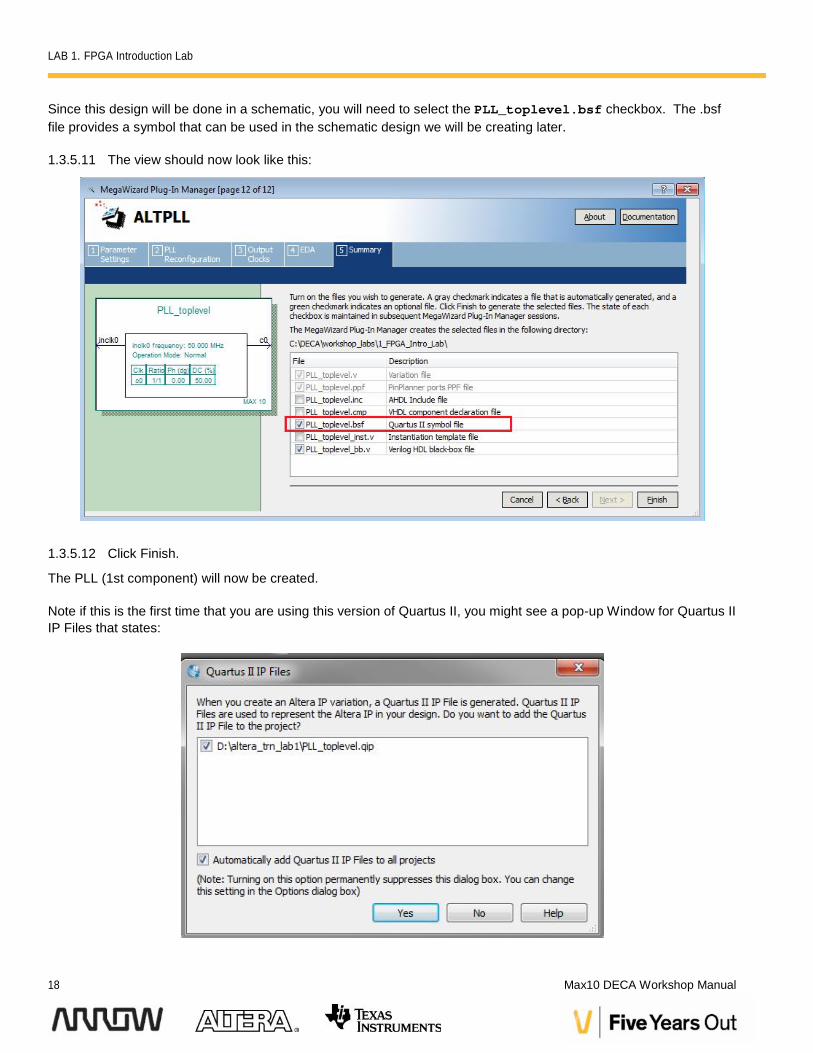
Since this design will be done in a schematic, you will need to select the PLL_toplevel.bsf checkbox. The .bsffile provides a symbol that can be used in the schematic design we will be creating later.
1.3.5.11 The view should now look like this:
1.3.5.12 Click Finish.
The PLL (1st component) will now be created.
Note if this is the first time that you are using this version of Quartus II, you might see a pop-up Window for Quartus IIIP Files that states:

LAB 1. FPGA Introduction Lab
Version 15.0 19
1.3.5.13 Select Automatically Add Quartus II IP Files to all projects.
1.3.5.14 Click Yes to allow all of the IP to automatically be added to the project, and so that this message will not beseen for other designs.
1.3.6 Create the CounterThe next step is to create a counter which will drive the LEDS on the DECA Board
1.3.6.1 To create this counter, select the IP Catalog and Expand the Basic Functions Arithmetic and selectLPM_COUNTER.
(LPM stands for Library of Parameterized Modules.).
1.3.6.2 Click Add
1.3.6.3 When the Save IP Variation pop up appears, enter simple_counter and select Verilog as below
LAB 1. FPGA Introduction Lab
20 Max10 DECA Workshop Manual
1.3.6.4 Click OK.
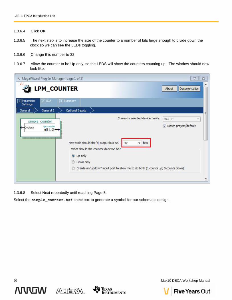
1.3.6.5 The next step is to increase the size of the counter to a number of bits large enough to divide down theclock so we can see the LEDs toggling.
1.3.6.6 Change this number to 32
1.3.6.7 Allow the counter to be Up only, so the LEDS will show the counters counting up. The window should nowlook like:
1.3.6.8 Select Next repeatedly until reaching Page 5.
Select the simple_counter.bsf checkbox to generate a symbol for our schematic design.

LAB 1. FPGA Introduction Lab
Version 15.0 21
1.3.6.9 The screen should now look like:
1.3.6.10 Click Finish
The Counter is now created.
1.3.7 Creating the MultiplexerThe next step is to create a mux component. This mux would be used along with a push button on the board tocontrol the speed of the counter, where the counter outputs will be seen on the LEDS.

LAB 1. FPGA Introduction Lab
22 Max10 DECA Workshop Manual
1.3.7.1 To create this mux, select IP Catalog and expand Basic Function Miscellaneous and select LPM_MUX
1.3.7.2 Click Add
1.3.7.3 In the Save IP Variation, enter the name of counter_mux and the File type is to be Verilog.
LAB 1. FPGA Introduction Lab
Version 15.0 23
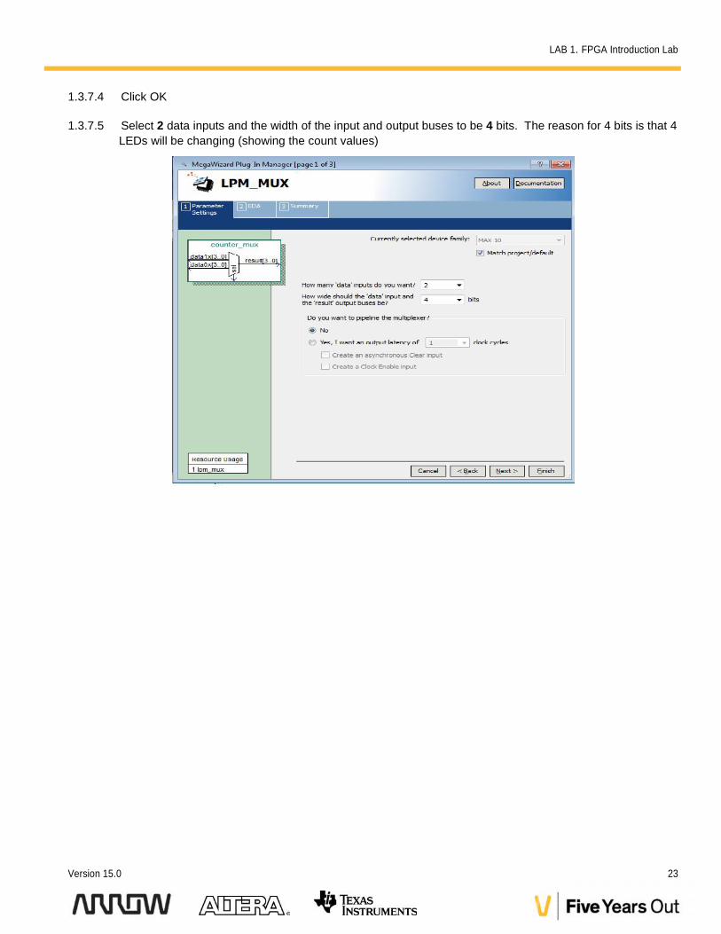
1.3.7.4 Click OK
1.3.7.5 Select 2 data inputs and the width of the input and output buses to be 4 bits. The reason for 4 bits is that 4LEDs will be changing (showing the count values)

LAB 1. FPGA Introduction Lab
24 Max10 DECA Workshop Manual
1.3.7.6 Click Next
1.3.7.7 Continue to select Next until Page 3
1.3.7.8 On this page, select counter_mux.bsf so that a symbol will be generated.
1.3.7.9 The view of this now looks like:

LAB 1. FPGA Introduction Lab
Version 15.0 25
Click Finish
1.3.8 Adding Components to the Schematic fileThe next step is to connect the components together.
1.3.8.1 To do so, select the File menu - then select New and select Block Diagram/Schematic File
1.3.8.2 Click OK.
A new schematic page will be created, where the components can be added.

LAB 1. FPGA Introduction Lab
26 Max10 DECA Workshop Manual
1.3.8.3 Right click on the schematic page, and select Insert Symbol, as seen below
1.3.8.4 Expand Project, where the three components that were created, can now be seen
1.3.8.5 Select PLL_toplevel
1.3.8.6 Click OK.
The PLL component is now added to the schematic page. The PLL component can be added anywhere for now.

LAB 1. FPGA Introduction Lab
Version 15.0 27
1.3.8.7 To add the counter_mux, right click on the schematic page, select Insert Symbol, and select Symbol.
(The order of adding components to the schematic does not matter, as the connections will in later steps connect thecomponents correctly together)
1.3.8.8 Select the counter_mux, as shown
1.3.8.9 Click OK.
1.3.8.10 Put the counter_mux anywhere for now in the schematic page.
1.3.8.11 To add the counter, right click on the schematic page, select Insert Symbol, and select Symbol.
(The order of adding components to the schematic again does not matter, as the connections will in later stepsconnect the components correctly together)
LAB 1. FPGA Introduction Lab
28 Max10 DECA Workshop Manual
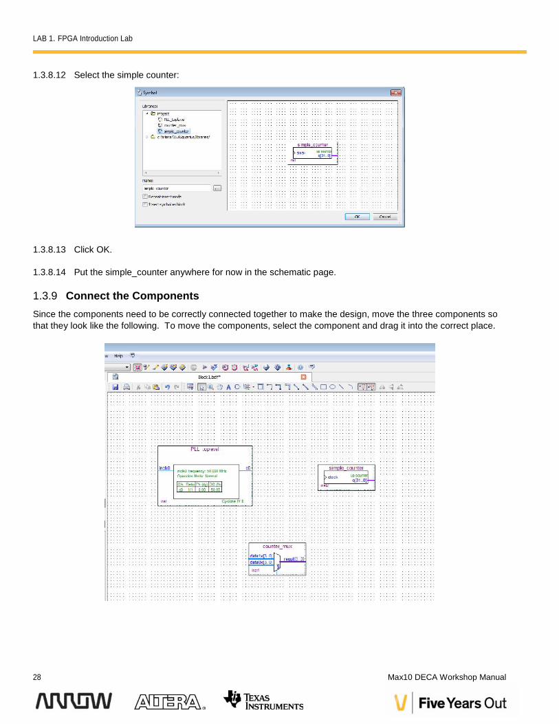
1.3.8.12 Select the simple counter:
1.3.8.13 Click OK.
1.3.8.14 Put the simple_counter anywhere for now in the schematic page.
1.3.9 Connect the ComponentsSince the components need to be correctly connected together to make the design, move the three components sothat they look like the following. To move the components, select the component and drag it into the correct place.
LAB 1. FPGA Introduction Lab
Version 15.0 29
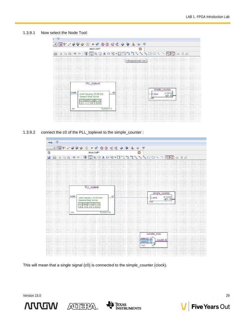
1.3.9.1 Now select the Node Tool:
1.3.9.2 connect the c0 of the PLL_toplevel to the simple_counter :
This will mean that a single signal (c0) is connected to the simple_counter (clock).
LAB 1. FPGA Introduction Lab
30 Max10 DECA Workshop Manual
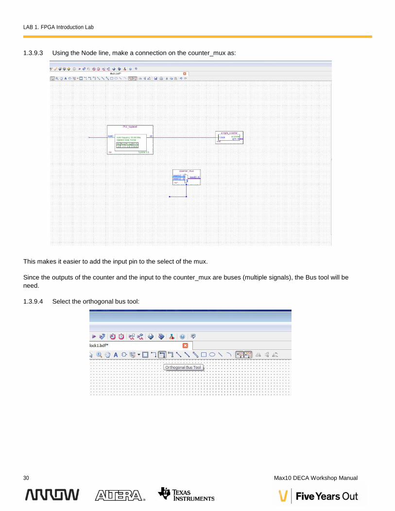
1.3.9.3 Using the Node line, make a connection on the counter_mux as:
This makes it easier to add the input pin to the select of the mux.
Since the outputs of the counter and the input to the counter_mux are buses (multiple signals), the Bus tool will beneed.
1.3.9.4 Select the orthogonal bus tool:

LAB 1. FPGA Introduction Lab
Version 15.0 31
1.3.9.5 Using the Bus tool, connect the counter outputs and the mux inputs as the following:
The next step will be to add pins (input and output pins).
1.3.9.6 Select the Arrow button (Selection Tool) as seen below:

LAB 1. FPGA Introduction Lab
32 Max10 DECA Workshop Manual
1.3.9.7 Then select anywhere free in the schematic, select Insert Insert Symbol and then under the Namewrite the word input
An input pin will appear.
1.3.9.8 Click OK.
1.3.9.9 Connect the input pin to the PLL_toplevel as below.
To make the connection, connect the input pin to the inclk0 of PLL_toplevel and then drag to the left. (This will makethe connection for you).

LAB 1. FPGA Introduction Lab
Version 15.0 33
1.3.9.10 Copy and paste the input pin and then connect it to the counter_mux:
1.3.9.11 The next step is to add output pins. To add an output pin, right click on the schematic, select InsertInsert Symbol and enter under the name output. This is an output pin
1.3.9.12 Click OK.
Rather than drawing the bus line manually, put the output pin next to the counter_mux output (result[3..0]) and thendrag to the right. A bus connection will be created.
LAB 1. FPGA Introduction Lab
34 Max10 DECA Workshop Manual
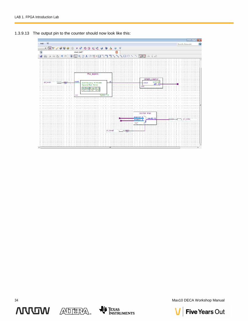
1.3.9.13 The output pin to the counter should now look like this:

LAB 1. FPGA Introduction Lab
Version 15.0 35
1.3.9.14 The next step will be to name the input and output pins, as well as the connection of the counter and mux.
Select on the pin_name1 (input pin to the PLL_toplevel) and type the name to beMAX10_CLK1_50.
Select on the pin_name2 (input to the counter_mux) and type the name to be KEY[0]
Select on the pin_name3 (output of the counter_mux) and type the name to be LED[3..0]
1.3.9.15 The schematic should now look like this:
LAB 1. FPGA Introduction Lab
36 Max10 DECA Workshop Manual
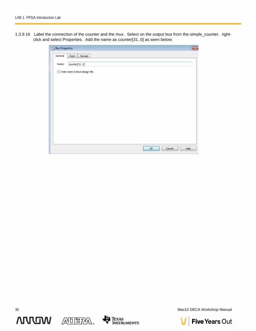
1.3.9.16 Label the connection of the counter and the mux. Select on the output bus from the simple_counter, right-click and select Properties. Add the name as counter[31..0] as seen below:

LAB 1. FPGA Introduction Lab
Version 15.0 37
1.3.9.17 Click OK
1.3.9.18 This will label the bus signals.
1.3.9.19 Select on the upper bus signal of the counter_mux right-click and select Properties. Add the name ascounter[28..25]. Select the lower bus signal of the counter_mux, right click and select Properties. Add thename as counter[24..21] as seen below.
Even though the buses are not connected together by wires, the names of counter tell Quartus II to connect thesignals together. Overall, the key will toggle between displaying higher 4 bits of the counter and 4 lower bits of thecounter. The signals of the counter that are not connected will not be used by Quartus II.
1.3.9.20 Save your design. Use the File menu and select Save, and save it as toplevel.bdf. Click Save
1.3.10 Analysis and SynthesisThe next step is to run Analysis and Synthesis to ensure that there are no errors.: ProcessingStart Analysisand Synthesis.

LAB 1. FPGA Introduction Lab
38 Max10 DECA Workshop Manual
There should be no errors. If there are errors, fix the error message and re run Analysis and Synthesis
1.3.11 Adding Timing ConstraintsTiming Constraints tell the Quartus what the timing requirements are for this design. Timing Constraints are requiredin every CPLD/FPGA design.
To add timing, select File New and under the Other File section, select Synopsys Design Constraints File andselect OK.
Type the following lines in this new file:
create_clock -name MAX10_CLK1_50 -period 20.000 -waveform { 0.00010.000 } [get_ports { MAX10_CLK1_50}]
derive_pll_clocks
derive_clock_uncertainty
(Three separate lines will be needed).

LAB 1. FPGA Introduction Lab
Version 15.0 39
1.3.11.1 The first line tells Quartus II that the clock, MAX10_CLK1_50 is 20 ns (50 MHz), with a 50/50 duty cycle(waveform of 0 10). It assigns the MAX10_CLK1_50 to a pin (port) in the .sdc format).
1.3.11.2 The second line tells the software to look if there are any PLLs, and if so, automatically derive the clockmultiplication/division of the outputs of the PLL even if they are used internally within the CPLD/FPGA.
1.3.11.3 The third line tells the software to automatically determine the internal clock uncertainty. No clock is ideal,and thus there will be some internal jitter within the FPGA associated with it.
1.3.11.4 Use File Save to save it as toplevel.sdc.
1.3.11.5 Ensure that this file is added to the Project: Assignments Settings and select TimeQuest TimingAnalyzer. The toplevel.sdc should be added already by default. (If it is not, it will need to be added).
1.3.12 Adding Pin AssignmentsBefore the design can be downloaded, pin assignments that match the hardware on the board are needed. There aredifferent ways to do this, such as the Pin Planner, Assignment Editor, and text files.
The following steps will show one of these ways – the Pin Planner. Since there are only 6 pins that need to beassigned, the Pin Planner can be used If many pins are needed, other ways can be used such as the QuartusAssignment Editor, or by importing constraints from a text file or spreadsheet.

LAB 1. FPGA Introduction Lab
40 Max10 DECA Workshop Manual
1.3.12.1 Open the Pin planner: Assignments Pin Planner. A new window will appear as seen below.
1.3.12.2 To make pin assignments, select the MAX10_CLK1_50 (node name) on the bottom portion (last node ofthe bottom window) and drag and drop it to pin M8. The window should now look like this:
Note the Location for MAX10_CLK1_50 is now set to Location Pin_M8 (as seen in blue color in the top view of theFPGA).

LAB 1. FPGA Introduction Lab
Version 15.0 41
1.3.12.3 The other pins need to be assigned as well. They can be assigned by dragging and dropping or evenclicking in the location column (bottom of the window) and then using the pull down menu to assign the pinsas follows (in order to match the board).
Node Name Pin Location
KEY[0] PIN_H21
LED[3] PIN_B7
LED[2] PIN_A6
LED[1] PIN_C8
LED[0] PIN_C7
1.3.12.4 After completing the pin assignments, the screen should now look like this:
The specific pins are now selected, but the I/O standards now need to be set as well. The switch, LEDS, and clockpins are different I/O standards (due to how they are connected on the board). The KEY[0] is a 1.5 V Schmitt Trigger,the LEDs are 1.2V and the clock pin is 2.5V.
These I/O standards can be set in the Pin Planner, by selecting the I/O standard. Select on the I/O standard at thebottom of the page, and change the 2.5 V (default) to the specific I/O standard.
LAB 1. FPGA Introduction Lab
42 Max10 DECA Workshop Manual
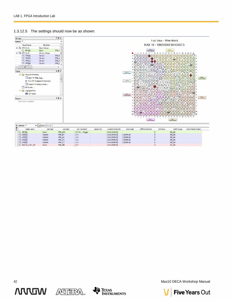
1.3.12.5 The settings should now be as shown:

LAB 1. FPGA Introduction Lab
Version 15.0 43
1.3.12.6 Close this Pin Planner window. The pin assignments are automatically saved.
1.3.12.7 For the DECA board, another setting will need to be changed regarding one bank Select AssignmentsDevice and select Device and Pin Options. Under General, disable all of the general device options. Thewindow should now look like:
1.3.12.8 Click OK.
1.3.12.9 Select OK for the Device window.
1.3.13 Compiling the DesignThe next step is to compile the complete design. This step will verify there are no errors, create internal databases,as well as create a programming file that will be used in the next step.
1.3.13.1 Compile the design: ProcessingStart Compilation
If there are errors, they will need to be resolved and re-compiled before the design can be programmed to the board.When Compiling finishes and there are no errors, there will be a message at the bottom of the window that states:Full Compilation was successful.
1.3.14 Configuring the Device

LAB 1. FPGA Introduction Lab
44 Max10 DECA Workshop Manual
1.3.14.1 Open the Quartus II Programmer from Tools Programmer or double-click on Program Device (OpenProgrammer) from the Tasks pane. Since the DECA isn't connected yet, the Programmer should show ablank configuration.
1.3.14.2 Connect your DECA board to your PC using a USB cable. Be sure to connect it to the mini-USB connectorlabeled UB2 J10 (on the bottom right of the board). Since the USB Blaster II driver software should alreadybe installed, the Window's Device Manager should display two entries under "JTAG Cables".
You should see a few LEDs light up on your DECA including the blue LED labeled 3.3V and the green LED labeledCONF_D.
If the Device Manager shows an unconfigured USB Blaster, if Windows tries to look for drivers,or if the LEDs on the DECA do not light up, ask your workshop trainer for help.

LAB 1. FPGA Introduction Lab
Version 15.0 45
1.3.14.3 In the Programmer window, click Hardware Setup and double-click the Arrow MAX10 DECA entry in theHardware Settings tab. The Currently selected hardware drop-down should now show Arrow MAX10 DECA[USB-1]. Depending on your PC, the USB port number may be different. Click Close.
1.3.14.4 The programming window should now have a Hardware Setup such as:
LAB 1. FPGA Introduction Lab
46 Max10 DECA Workshop Manual
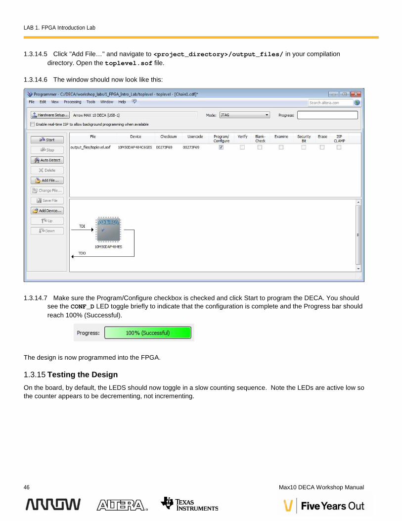
1.3.14.5 Click "Add File…" and navigate to <project_directory>/output_files/ in your compilationdirectory. Open the toplevel.sof file.
1.3.14.6 The window should now look like this:
1.3.14.7 Make sure the Program/Configure checkbox is checked and click Start to program the DECA. You shouldsee the CONF_D LED toggle briefly to indicate that the configuration is complete and the Progress bar shouldreach 100% (Successful).
The design is now programmed into the FPGA.
1.3.15 Testing the DesignOn the board, by default, the LEDS should now toggle in a slow counting sequence. Note the LEDs are active low sothe counter appears to be decrementing, not incrementing.

LAB 1. FPGA Introduction Lab
Version 15.0 47
1.3.15.1 Push and hold the push button, KEY0, to see the LEDs now toggle in a very fast counting sequence.KEY0 is the second button to the right under the power connector, as seen below:
Releasing the push buttons should have the LEDs toggle in the slow counting sequence again.
After you are finished testing your design, you can disconnect the USB connector, and close Quartus II.
CONGRATULATIONS! YOU HAVE COMPLETED YOUR DESIGN.