fpga implementation of area-delay and power efficient ... fpga implementation of area-delay and...
TRANSCRIPT

International Journal of Innovative Research in Electronics and Communications (IJIREC)
Volume 2, Issue 8, 2015, PP 37-49
ISSN 2349-4042 (Print) & ISSN 2349-4050 (Online)
www.arcjournals.org
©ARC Page 37
FPGA Implementation of Area-Delay and Power Efficient Carry
Select Adder
V.Narayana Reddy1, Shaik.Rizwan
2,
1Associate Professor, Dept. of ECE, PBR Visvodaya Institute of Technology, Kavali, Andhra Pradesh
2PG Scholar, Dept. of ECE, PBR Visvodaya Institute of Technology, Kavali, Andhra Pradesh
Abstract: In this brief, the logic operations involved in conventional Carry Select Adder (CSLA) and binary to
excess-1 converter (BEC)-based Carry Select Adder (CSLA) are analyzed to study the data dependence and to
identify redundant logic operations. We have eliminated all the redundant logic operations present in the
conventional Carry Select Adder, BEC-based Carry Select Adder and proposed a new logic formulation for
Carry Select Adder. In this paper a new architectures for carry select adder using AOI based logic and
optimized logic expressions based structure is proposed. A simple approach is proposed using AOI logic to reduce the area, delay and power of Square root (SQRT) Carry Select Adder architecture. The reduced number
of gates of this work offers the great advantage in the reduction of area and also the total power. Due to the
optimized area, power and delay, the proposed Carry Select Adder design is a good substitution for all the
existing Carry Select Adder. The proposed architecture is designed using Verilog HDL (Hardware Description
Language) and is then synthesized using XILINX 14.5and is simulated in ISim for Spartan 3E FPGA.
Keywords: Binary to Excess-1 converter (BEC), Carry Select Adder (CSLA).
1. INTRODUCTION
Low Power, Area-efficient, and high-performance VLSI systems are increasingly used in portable and
mobile devices, multi-standard wireless receivers, and biomedical instrumentation [1], [2]. An adder
is the main component of an arithmetic unit. A complex digital signal processing (DSP) system
involves several adders. An efficient adder design essentially improves the performance of a complex
DSP system. A ripple carry adder (RCA) uses a simple design, but carry propagation delay (CPD) is
the main concern in this adder. Carry look-ahead and carry select (CS) methods have been suggested
to reduce the CPD of adders. Ripple carry adder is one of the conventional methods of adder. The
ripple carry adder consists of a chain of full adders with length n. It can add multi bits using less area
but the problem occurs due to its bigger carry propagation delay. So we go for carry look ahead adder,
carry skip adder, carry select adder etc. Carry select adder is the fastest adder among these.
The most common scheme for accelerating carry propagation is carry look-ahead scheme proposed by
Weinberger and Smith in 1958 [1]. Here they proposed look-ahead technique rather than carry-
rippling technique to speed-up the carry propagation. In Carry Look Ahead adder, the delay for
adding two numbers depends on the logarithm of the size of the operands and hence it is theoretically
one of the fastest schemes used for the addition. A carry-skip adder reduces the time needed to
propagate the carry by skipping over groups of consecutive adder stages. In VLSI technology the
carry skip adder is compatible in speed to the carry look-ahead technique. But it need only low power
and area. The basic theme of carry select adder is to divide a long adder into fixed size adder sections
and proceed with simultaneous section additions with appropriate carry input to select the true sum
output. Like carry skip schemes, carry select scheme divides adder into blocks of ripple carry adder
each with two replicas, one replica evaluates for carry in of 1, while the other one evaluates with
carry-in of 0.
This system was proposed by Bedrij in 1962 [3]. In this scheme, the carryout from less significant
block selects the sum and carryout of more blocks. In this way, the critical signal is generated at the
least significant bit, and ripples through the least significant block and then conditionally selects the
output of succeeding blocks. The Carry select adder generally consists of two Ripple Carry Adders
and one multiplexer. Addition of two n-bit numbers with a Carry select adder is done with two adders
in order to perform the calculation twice, one time with assumption of the carry being zero and the
V.Narayana Reddy& Shaik.Rizwan
International Journal of Innovative Research in Electronics and Communications (IJIREC) Page 38
other being one. As the two results are calculated, the required sum as well as the apt carry is then
selected with a carry selector (multiplexer) and is controlled by the carry from previous adders.
The rest of this brief is organized as follows. Literature Survey is presented in section II. Existing
carry select adder model is presented in Section III. The proposed Carry select adder model is
presented in Section IV and the performance comparison is presented in Section V. The conclusion is
given in Section VI.
2. LITERATURE SURVEY
A conventional carry select adder is a configuration of dual Ripple Carry Adder (RCA) in which one RCA generates sum and carry output by assuming Cin = 0and the other RCA produce carry and sum
assuming Cin = 1. This conventional carry select adder has less carry propagation delay than Ripple
Carry Adder (RCA) , but increases the complexity due to dual RCA structure. A carry select adder
generating carry of block with carry in as 1 from the block with carry in as 0 was proposed by Tyagi.A [4] in 1990. Later in 1998 T.Y.Ceiang and M.J.Hsiao [5] proposed a carry select adder
consisting of single ripple carry adder. This was a real breakthrough in the carry select adder history.
In 2001 a further modified carry select adder with increased delay but reduced area and power was presented by Kim and Kim [6]. Here the RCA section with cin=1 was replaced using an add-one
circuit using multiplexer (MUX). Later in the year 2005 a further modified carry select adder which
reduces the area and power consumption was proposed by Amelifard B, Fallah F and Pedram.M [7]. It
reduces the gap between carry select adder and ripple carry adder.
Later a SQRT-CSLA was proposed by B. Ramkumar and H. M. Kittur [8], which helps in
implementing large bit width adders with less delay. In this system the CSLA’s with increasing bit
widths are cascaded with each other. It helps in reducing the overall adder delay. A BEC based CSLA was further proposed by Ram Kumar and Kittur which had less resource than conventional CSLA but
with more delay. A CBL (common Boolean logic) based CSLA was also proposed which requires less
logic resources but CPD (carry propagation delay) was similar to that of RCA. A CBL based SQRT CSLA was also proposed but the design requires more logic resource and delay is more than BEC
based SQRT CSLA.
Now a further modification of CSLA called Area- Delay-Power Efficient Carry Select Adder was
proposed. Here the carry generation is faster but the area consumption is not much reduced. The carry of the system is calculated before the sum generation. Also the carry generation unit was also replaced
using an optimised logic. Thus the systems have lesser carry output delay than all other system.
Though the carry generation is faster, the area and power consumption are not much reduced. So a further modification with a reduction in area and power consumption, thus obtaining an optimized
area-delay and power carry efficient carry select adder is proposed here.
3. EXISTING CARRY SELECT ADDER MODEL
The Carry Select Adder (CSLA) has two units:
The sum and carry generator unit (SCG).
The sum and carry selection unit (SCS).
The SCG unit consumes most of the logic resources of CSLA and significantly contributes to the
critical path. Different logic designs have been suggested for efficient implementation of the SCG unit. We made a study of the logic designs suggested for the SCG unit of conventional and BEC-
based CSLAs by suitable logic expressions. The main objective of this study is to identify redundant
logic operations and data dependence. Accordingly, we remove all redundant logic operations and sequence logic operations based on their data dependence.
3.1. Conventional Carry Select Adder
As shown in Figure.1, the SCG unit of the conventional Carry Select adder is composed of two n-bit
Ripple Carry Adders, where n is the adder bit-width. The logic operation of the n-bit RCA is performed in four stages: 1) half-sum generation (HSG); 2) half-carry generation (HCG); 3) full-sum
generation (FSG); and 4) full carry generation (FCG). Suppose two n-bit operands are added in the
conventional CSLA, then RCA-1 and RCA-2 generate n-bit sum (s0 and s1) and output-carry (c0out and c1out) corresponding to input-carry (cin = 0 and cin = 1), respectively.

Adder FPGA Implementation of Area-Delay and Power Efficient Carry Select
International Journal of Innovative Research in Electronics and Communications (IJIREC) Page 39
Fig1. Conventional Carry Select Adder
N is the input operand bit-width. RCA = Ripple Carry Adder.
The redundant logic operations can be removed to have an optimized design for RCA-2, in which the HSG and HCG of RCA-1 is shared to construct RCA-2. Based on this, the BEC-based CSLA offers
the best area–delay–power efficiency among the existing CSLAs.
3.2. BEC-Based Carry Select Adder(CSLA)
BEC-1(Binary to Excess-1 Converter) instead of the RCA with Cin=1 in order to reduce the area and
power consumption of the conventional CSLA. To replace the n-bit RCA, an n+1bit BEC-1 is required. As shown in Figure 2, the RCA calculates n-bit sum s
01 and c
0out corresponding to cin = 0.
The BEC unit receives s0
1 and c0out from the RCA and generates (n + 1)-bit excess-1 code.
Fig2. Structure of the BEC-based CSLA;
N is the input operand bit-width.
The BEC method increases data dependence in the CSLA. The importance of the BEC logic stems from the large silicon area reduction when the CSLA with large number of bits are designed.
We have considered logic expressions of the conventional CSLA and made a further study on the data dependence to find an optimized logic expression for the CSLA. We have removed all the redundant
logic operations and rearranged logic expressions based on the proposed logic formulation for the
CSLA.
Fig3. BEC based SQRT-Carry Select Adder (CSLA) for n = 16. All intermediate and output signals are labeled

V.Narayana Reddy& Shaik.Rizwan
International Journal of Innovative Research in Electronics and Communications (IJIREC) Page 40
Fig3a. 2-bit adder with BEC and MUX unit
\Fig3b. 3-bit adder with BEC and MUX unit
Fig3c.4-bit adder with BEC and MUX unit
Fig3d. 5-bit adder with BEC and MUX unit
Adder FPGA Implementation of Area-Delay and Power Efficient Carry Select
International Journal of Innovative Research in Electronics and Communications (IJIREC) Page 41
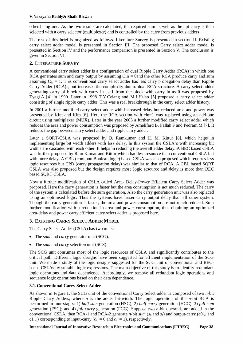
BEC based SQRT-Carry Select Adder for n = 16 shown in figure 3.Number of gates used in BEC logic is calculated using figure 3a 2-bit adder is,
Gate count = 43 (FA + HA +BEC+ Mux)
Where, FA= Full Adder, HA = Half Adder, Mux =Multiplexer.
FA = 13(1 * 13)
HA = 6(1* 6)
Mux = 12(3 * 4) AND = 1(1* 1)
XOR =10(2*5)
NOT = 1(1*1)
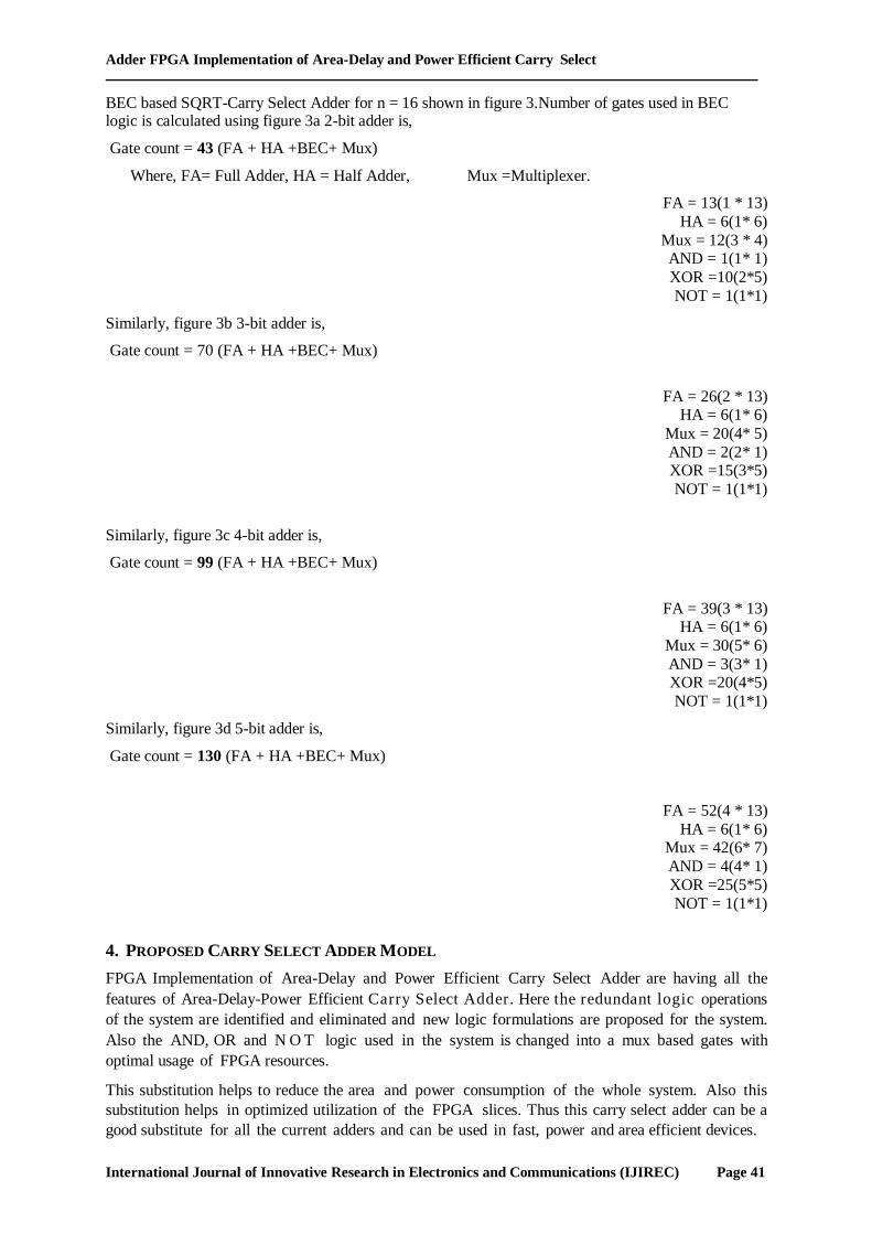
Similarly, figure 3b 3-bit adder is,
Gate count = 70 (FA + HA +BEC+ Mux)
FA = 26(2 * 13) HA = 6(1* 6)
Mux = 20(4* 5)
AND = 2(2* 1) XOR =15(3*5)
NOT = 1(1*1)
Similarly, figure 3c 4-bit adder is,
Gate count = 99 (FA + HA +BEC+ Mux)
FA = 39(3 * 13) HA = 6(1* 6)
Mux = 30(5* 6)
AND = 3(3* 1) XOR =20(4*5)
NOT = 1(1*1)
Similarly, figure 3d 5-bit adder is,
Gate count = 130 (FA + HA +BEC+ Mux)
FA = 52(4 * 13)
HA = 6(1* 6) Mux = 42(6* 7)
AND = 4(4* 1)
XOR =25(5*5)
NOT = 1(1*1)
4. PROPOSED CARRY SELECT ADDER MODEL
FPGA Implementation of Area-Delay and Power Efficient Carry Select Adder are having all the
features of Area-Delay-Power Efficient Carry Select Adder. Here the redundant logic operations
of the system are identified and eliminated and new logic formulations are proposed for the system.
Also the AND, OR and N O T logic used in the system is changed into a mux based gates with
optimal usage of FPGA resources.
This substitution helps to reduce the area and power consumption of the whole system. Also this
substitution helps in optimized utilization of the FPGA slices. Thus this carry select adder can be a
good substitute for all the current adders and can be used in fast, power and area efficient devices.
V.Narayana Reddy& Shaik.Rizwan
International Journal of Innovative Research in Electronics and Communications (IJIREC) Page 42
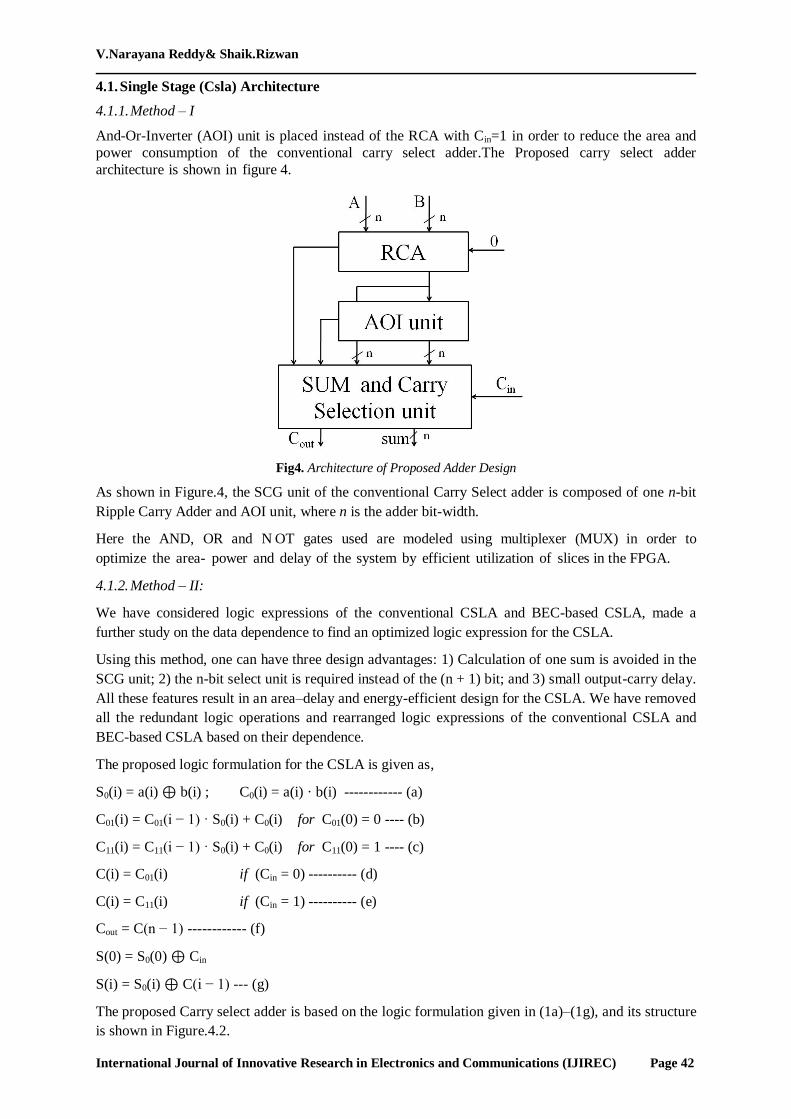
4.1. Single Stage (Csla) Architecture
4.1.1. Method – I
And-Or-Inverter (AOI) unit is placed instead of the RCA with Cin=1 in order to reduce the area and
power consumption of the conventional carry select adder.The Proposed carry select adder
architecture is shown in figure 4.
Fig4. Architecture of Proposed Adder Design
As shown in Figure.4, the SCG unit of the conventional Carry Select adder is composed of one n-bit
Ripple Carry Adder and AOI unit, where n is the adder bit-width.
Here the AND, OR and N OT gates used are modeled using multiplexer (MUX) in order to
optimize the area- power and delay of the system by efficient utilization of slices in the FPGA.
4.1.2. Method – II:
We have considered logic expressions of the conventional CSLA and BEC-based CSLA, made a
further study on the data dependence to find an optimized logic expression for the CSLA.
Using this method, one can have three design advantages: 1) Calculation of one sum is avoided in the
SCG unit; 2) the n-bit select unit is required instead of the (n + 1) bit; and 3) small output-carry delay.
All these features result in an area–delay and energy-efficient design for the CSLA. We have removed
all the redundant logic operations and rearranged logic expressions of the conventional CSLA and
BEC-based CSLA based on their dependence.
The proposed logic formulation for the CSLA is given as,
S0(i) = a(i) ⊕ b(i) ; C0(i) = a(i) · b(i) ------------ (a)
C01(i) = C01(i − 1) · S0(i) + C0(i) for C01(0) = 0 ---- (b)
C11(i) = C11(i − 1) · S0(i) + C0(i) for C11(0) = 1 ---- (c)
C(i) = C01(i) if (Cin = 0) ---------- (d)
C(i) = C11(i) if (Cin = 1) ---------- (e)
Cout = C(n − 1) ------------ (f)
S(0) = S0(0) ⊕ Cin
S(i) = S0(i) ⊕ C(i − 1) --- (g)
The proposed Carry select adder is based on the logic formulation given in (1a)–(1g), and its structure
is shown in Figure.4.2.

Adder FPGA Implementation of Area-Delay and Power Efficient Carry Select
International Journal of Innovative Research in Electronics and Communications (IJIREC) Page 43
Fig4.2. Structure of single stage Proposed Carry select adder
The optimized carry select adder architecture is shown in figure 4.2.The carry select adder mainly consist of four
sections,
Half sum generator (HSG)
Carry generator (CG)
Carry selection (CS)
Full sum generator (FSG)
The sum generation unit makes use of full adder implementation using two half adders. Here the
first half adder receives the n-bit input and provides half adder sum and carry. The Half Sum Generator generates half-sum word s0 and half-carry word c0from the given inputs. It simply uses
a half adder. The number of adders needed is same as the number of input bits.
S0 (i) = A (i) B (i)
C0 (i) = A (i)*B (i)
Fig4.2a. Half sum generation unit
This half adder results are given as input for carry generator and full sum generator. The full sum
generator obtains output after receiving the carry input. The output of the half adder is given as
input to the carry generator circuit. Two carry generator circuits are used in the design, CG0 and
CG1. CG0 is used to generate carry by assuming carry input as 0 and CG1 is used to generate
carry by assuming input carry as 1. Both CG0 and CG1 receives half carry word and half sum word
from the half adder and generate two n-bit full carry words C10 and C1
1 corresponding to input carry
0 and 1 respectively.
C10 (i) = C1
0 (i-1)*S0 (i) +C0 (i) for (C1
0 (0) =0)

V.Narayana Reddy& Shaik.Rizwan
International Journal of Innovative Research in Electronics and Communications (IJIREC) Page 44
C11 (i) = C1
1 (i-1)* S0 (i) +C0 (i) for (C1
1 (0) =1)
Fig4.2b. Carry generation unit for Cin=0
Figure 4 . 2 b shows the multiplexer implementation for the carry generator CG0. The output of
this section is given as input to the carry selection section.
Fig4.2c. Carry generation unit for Cin=1
Figure 4.2c is the MUX implementation of carry generator CG1. Here the output carry for carry input
1 is generated. This is also given as input to the carry selection section. The carry selection unit selects one the final carry from the two carry words available at its input line using the input carry
cin. Here the carry select unit selects the output of CG0 if the input carry (cin) is 0 and selects
the output of CG1 If the input carry (cin) is 1. The carry select unit here is implemented using an
optimized design.
C (i) = C10 (i) if (Ci n= 0)
C (i) = C10 (i) if (Ci n= 1)
Cout = C(n-1)
Figure 4 . 2 d shows the implementation of carry selection unit using MUX. The selection of
carry output according to input carry is done here. The full sum of the system is generated by adding the selected carry with the half sum obtained in the half adder.
Fig4.2d. Carry selection unit

Adder FPGA Implementation of Area-Delay and Power Efficient Carry Select
International Journal of Innovative Research in Electronics and Communications (IJIREC) Page 45
The full sum of the system is generated by XOR-ing the selected carry from carry selection unit with
the half sum obtained in the half adder. Thus the half sum and the obtained carry are both XOR-ed to get the final sum of the system.
Fig4.2e. Full sum generation unit
Figure 4.2e shows the multiplexer implementation of full sum generation. Here the circuit is used
to XOR the selected carry from carry selection unit with the half sum obtained in the half sum generator. The MSB of c is sent to output as cout, and (n−1). LSBs are XOR-ed with (n−1) MSBs
of half-sum (s0) in the FSG to obtain the final sum.
4.2. Multistage (SQRT-CSLA) Architecture
4.2.1. Method – I
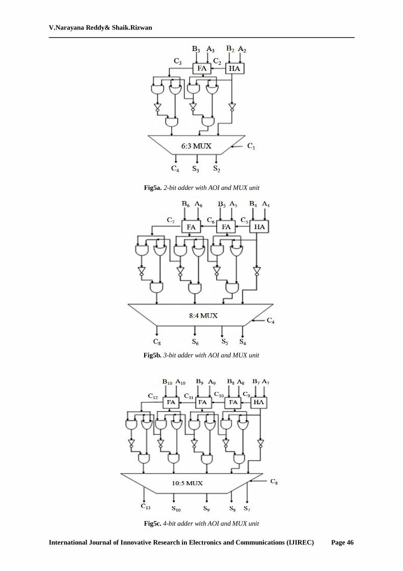
Implementation of multi-stage architecture for Proposed AOI logic based CSLA is shown in Figure 5.
The multipath carry propagation feature of the CSLA is fully exploited in the Square root Carry select
adder (SQRT-CSLA), which is composed of a chain of CSLAs. CSLAs of increasing size are used in
the SQRT-CSLA to extract the maximum concurrence in the carry propagation path. Using the SQRT-
CSLA design, large-size adders are implemented with significantly less delay than a single-stage
CSLA of same size. We have analyzed the logic operations involved in the conventional and BEC-
based CSLAs and identify gate counts of 2-bit, 3-bit, 4-bit, 5-bit adder. Propose a new logic design for
the Carry Select Adder. It is giving less Area, Power and significant delay reduction than existing
models.
A 16-bit Square root Carry select adder (SQRT-CSLA) design using Method-I proposed carry select
adder is shown in Figure 5, where the 2-bit RCA, 2-bit CSLA, 3-bit CSLA, 4-bit CSLA, and 5-bit
CSLA are used.
Fig5. Proposed Square root (SQRT) Carry Select Adder (CSLA) for n = 16.
All intermediate and output signals are labeled
V.Narayana Reddy& Shaik.Rizwan
International Journal of Innovative Research in Electronics and Communications (IJIREC) Page 46
Fig5a. 2-bit adder with AOI and MUX unit
Fig5b. 3-bit adder with AOI and MUX unit
Fig5c. 4-bit adder with AOI and MUX unit

Adder FPGA Implementation of Area-Delay and Power Efficient Carry Select
International Journal of Innovative Research in Electronics and Communications (IJIREC) Page 47
Fig5d. 5-bit adder with AOI and MUX unit
Proposed SQRT-Carry Select Adder for n = 16 shown in figure 5.Number of gates for proposed AOI
logic is calculated using figure 5a 2-bit adder is,
Gate count = 40 (FA + HA +AOI+ Mux)
Where, FA= Full Adder, HA = Half Adder, Mux =Multiplexer.
FA = 13(1 * 13)
HA = 6(1* 6)
Mux = 12(3 * 4) AND = 4
OR = 2
NOT = 3
Similarly, figure 5b 3-bit adder is,
Gate count = 65 (FA + HA +AOI+ Mux)
FA = 26(2 * 13) HA = 6(1* 6)
Mux = 20(4 * 5)
AND = 6 OR = 3
NOT = 4
Similarly, figure 5c 4-bit adder is,
Gate count = 92 (FA + HA +AOI+ Mux)
FA = 39(3 * 13)
HA = 6(1* 6) Mux = 30(5 * 6)
AND = 8
OR = 4 NOT = 5
Similarly, figure 5d 5-bit adder is,
Gate count = 121 (FA + HA +AOI+ Mux)
FA = 52(4 * 13)
HA = 6(1* 6)
Mux = 42(6 * 7) AND = 10
OR = 5
NOT = 6
V.Narayana Reddy& Shaik.Rizwan
International Journal of Innovative Research in Electronics and Communications (IJIREC) Page 48
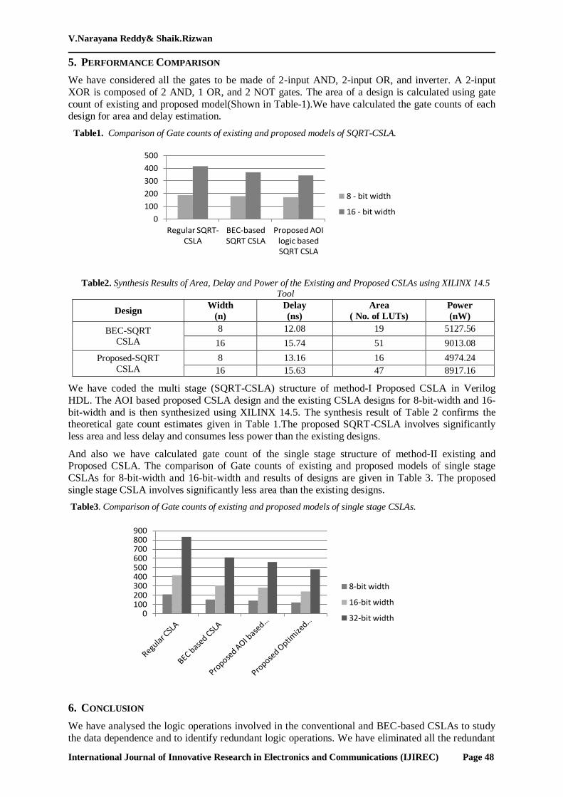
5. PERFORMANCE COMPARISON
We have considered all the gates to be made of 2-input AND, 2-input OR, and inverter. A 2-input
XOR is composed of 2 AND, 1 OR, and 2 NOT gates. The area of a design is calculated using gate
count of existing and proposed model(Shown in Table-1).We have calculated the gate counts of each design for area and delay estimation.
Table1. Comparison of Gate counts of existing and proposed models of SQRT-CSLA.
0
100
200
300
400
500
Regular SQRT-CSLA
BEC-based SQRT CSLA
Proposed AOI logic based SQRT CSLA
8 - bit width
16 - bit width
Table2. Synthesis Results of Area, Delay and Power of the Existing and Proposed CSLAs using XILINX 14.5 Tool
Design Width
(n)
Delay
(ns)
Area
( No. of LUTs)
Power
(nW)
BEC-SQRT CSLA
8 12.08 19 5127.56
16 15.74 51 9013.08
Proposed-SQRT
CSLA
8 13.16 16 4974.24
16 15.63 47 8917.16
We have coded the multi stage (SQRT-CSLA) structure of method-I Proposed CSLA in Verilog
HDL. The AOI based proposed CSLA design and the existing CSLA designs for 8-bit-width and 16-
bit-width and is then synthesized using XILINX 14.5. The synthesis result of Table 2 confirms the theoretical gate count estimates given in Table 1.The proposed SQRT-CSLA involves significantly
less area and less delay and consumes less power than the existing designs.
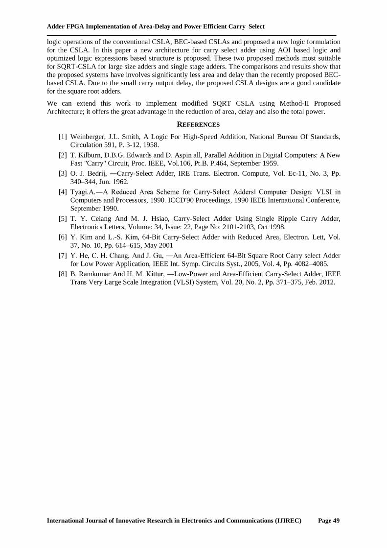
And also we have calculated gate count of the single stage structure of method-II existing and Proposed CSLA. The comparison of Gate counts of existing and proposed models of single stage
CSLAs for 8-bit-width and 16-bit-width and results of designs are given in Table 3. The proposed
single stage CSLA involves significantly less area than the existing designs.
Table3. Comparison of Gate counts of existing and proposed models of single stage CSLAs.
0100200300400500600700800900
8-bit width
16-bit width
32-bit width
6. CONCLUSION
We have analysed the logic operations involved in the conventional and BEC-based CSLAs to study
the data dependence and to identify redundant logic operations. We have eliminated all the redundant
Adder FPGA Implementation of Area-Delay and Power Efficient Carry Select
International Journal of Innovative Research in Electronics and Communications (IJIREC) Page 49
logic operations of the conventional CSLA, BEC-based CSLAs and proposed a new logic formulation
for the CSLA. In this paper a new architecture for carry select adder using AOI based logic and optimized logic expressions based structure is proposed. These two proposed methods most suitable
for SQRT-CSLA for large size adders and single stage adders. The comparisons and results show that
the proposed systems have involves significantly less area and delay than the recently proposed BEC-based CSLA. Due to the small carry output delay, the proposed CSLA designs are a good candidate
for the square root adders.
We can extend this work to implement modified SQRT CSLA using Method-II Proposed Architecture; it offers the great advantage in the reduction of area, delay and also the total power.
REFERENCES
[1] Weinberger, J.L. Smith, A Logic For High-Speed Addition, National Bureau Of Standards, Circulation 591, P. 3-12, 1958.
[2] T. Kilburn, D.B.G. Edwards and D. Aspin all, Parallel Addition in Digital Computers: A New Fast "Carry" Circuit, Proc. IEEE, Vol.106, Pt.B. P.464, September 1959.
[3] O. J. Bedrij, ―Carry-Select Adder, IRE Trans. Electron. Compute, Vol. Ec-11, No. 3, Pp.
340–344, Jun. 1962.
[4] Tyagi.A.―A Reduced Area Scheme for Carry-Select Adders‖ Computer Design: VLSI in
Computers and Processors, 1990. ICCD'90 Proceedings, 1990 IEEE International Conference,
September 1990.
[5] T. Y. Ceiang And M. J. Hsiao, Carry-Select Adder Using Single Ripple Carry Adder,
Electronics Letters, Volume: 34, Issue: 22, Page No: 2101-2103, Oct 1998.
[6] Y. Kim and L.-S. Kim, 64-Bit Carry-Select Adder with Reduced Area, Electron. Lett, Vol.
37, No. 10, Pp. 614–615, May 2001
[7] Y. He, C. H. Chang, And J. Gu, ―An Area-Efficient 64-Bit Square Root Carry select Adder
for Low Power Application, IEEE Int. Symp. Circuits Syst., 2005, Vol. 4, Pp. 4082–4085.
[8] B. Ramkumar And H. M. Kittur, ―Low-Power and Area-Efficient Carry-Select Adder, IEEE Trans Very Large Scale Integration (VLSI) System, Vol. 20, No. 2, Pp. 371–375, Feb. 2012.