fpga implementation of a baseband mimo mc-cdma …cradpdf.drdc-rddc.gc.ca/pdfs/unc88/p532072.pdf ·...
TRANSCRIPT
FPGA implementation of a baseband MIMO MC-CDMA downlink receiver Final report Minh-Quang Nguyen, Isabelle LaRoche, Paul Fortier and Sébastien Roy The scientific or technical validity of this Contract Report is entirely the responsibility of the Contractor and the contents do not necessarily have the approval or endorsement of Defence R&D Canada.
Defence R&D Canada – Ottawa Contract Report
DRDC Ottawa CR 2009-145 September 2009


FPGA implementation of a baseband MIMOMC-CDMA downlink receiverFinal report
Minh-Quang NguyenIsabelle LaRochePaul FortierSebastien Roy
Prepared by:
Laboratoire de radiocommunications et de traitement du signalDepartement de genie electrique et de genie informatiquePavillon Adrien-Pouliot1065, avenue de la Medecine, Bureau 1300Universite Laval, Quebec (Quebec), G1V 0A6
Project Manager: Jean-Francois BeaumontContract Number: W7714-5-0942Contract Scientific Authority: Jean-Francois Beaumont
The scientific or technical validity of this Contract Report is entirely the responsibility of the contractorand the contents do not necessarily have the approval or endorsement of Defence R&D Canada.
Defence R&D Canada – OttawaContract ReportDRDC Ottawa CR 2009-145September 2009
Scientific Authority
Original signed by Jean-Francois Beaumont
Jean-Francois Beaumont
Approved by
Original signed by Bill Katsube
Bill KatsubeHead/Communications and Navigation Electronic Warfare
Approved for release by
Original signed by Brian Eatock
Brian EatockChair/Document Review Panel
c⃝ Her Majesty the Queen in Right of Canada as represented by the Minister ofNational Defence, 2009
c⃝ Sa Majeste la Reine (en droit du Canada), telle que representee par le ministrede la Defense nationale, 2009
Abstract
Orthogonal Frequency Division Multiplexing (OFDM) has become a very attractivemulticarrier transmission technique for wireless high speed data communications.OFDM offers robustness to multipath fading without having to provide powerfulchannel equalization. In order to support multiple users with high speed data com-munications, the Multi-Carrier Code Division Multiple Access (MC-CDMA) tech-nique is used to address these challenges. MC-CDMA is a combination of OFDMand Code Division Multiple Access (CDMA) and has the benefits of both systems.Thus, the parameters of OFDM become the basic parameters of MC-CDMA. Further-more, Multi-Input Multi-Ouput (MIMO) was integrated to the MC-CDMA system toimprove the bit error rate and data throughput. Simulations were performed for anMC-CDMA system and an MIMO MC-CDMA under different channel environments.The simulation parameters considered were: guard time interval, symbol duration,sampling rate, number of data subcarriers, modulation scheme, number of activeusers, and number of transmit and receive antennas. The goal of the simulationswas to allow for different MIMO MC-CDMA configurations to be tested in orderto obtain the best system parameters. The MC-CDMA receiver was implementedinto an FPGA development platform based on the simulation results. Finally, theMC-CDMA transceiver was fully tested in a laboratory wireless channel environment.Design size prevented the implementation and live tests of the MIMO MC-CDMAreceiver.
Resume
Le multiplexage par repartition orthogonale de la frequence (MROF) est devenu unetechnique de transmission multiporteuse tres interessante pour la transmission dedonnees haute vitesse sans fil. Le MROF offre une resistance a l’evanouissement dua la propagation par trajets multiples sans devoir fournir une egalisation puissantede canaux. Pour fournir des services de transmission de donnees haute vitesse a denombreux usagers, la technique d’acces multiple par repartition de code sur multipor-teuses (MC CDMA) est utilisee pour resoudre ces problemes. Le MC CDMA combinele MROF et l’acces multiple par repartition de code (AMRC) et possede les avan-tages des deux systemes. Ainsi, les parametres du MROF deviennent les parametresde base du MC CDMA. De plus, le systeme a entrees et a sorties multiples (MIMO)a ete integre au systeme MC CDMA pour reduire le taux d’erreur sur les bits (BER)et ameliorer le debit de donnees. Des simulations ont ete effectuees pour un systemeMC CDMA et un systeme MC CDMA MIMO dans divers environnements de canal.Les parametres de simulation suivants ont ete etudies : intervalle de temps de garde,duree des symboles, taux d’echantillonnage, nombre de sous porteuses de donnees,schema de modulation, nombre d’usagers actifs et nombre d’antennes d’emission et
DRDC Ottawa CR 2009-145 i
de reception. Les simulations visaient a mettre a l’essai diverses configurations MCCDMA MIMO de facon a obtenir les meilleurs parametres de systeme. Ensuite, lerecepteur MC CDMA a ete mis en œuvre dans une plate forme de developpementde reseau logique programmable (FPGA) axee sur les resultats de simulation. Pourterminer, l’emetteur recepteur MC CDMA a ete soumis a des essais exhaustifs dansun environnement de laboratoire a canal sans fil. La taille de la maquette a empechela mise en œuvre et la mise a l’essai en conditions reelles du recepteur MC CDMAMIMO.
ii DRDC Ottawa CR 2009-145
Executive summary
FPGA implementation of a baseband MIMO MC-CDMAdownlink receiver
Minh-Quang Nguyen, Isabelle LaRoche, Paul Fortier, Sebastien Roy; DRDCOttawa CR 2009-145; Defence R&D Canada – Ottawa; September 2009.
This work presents the FPGA implementation of a downlink baseband Multi-CarrierCode Division Multiple Access (MC-CDMA) receiver, with and without Multiple-Input Multiple-Output (MIMO). Since the Code Division Multiple Access (CDMA)component of MC-CDMA is not defined yet, it was assumed for this work that Wide-band CDMA (WCDMA) will be used. The use of different modulation schemes suchas Quadrature Phase Shift Keying (QPSK), 16-level Quadrature Amplitude Modu-lation (16QAM), and 64-level Quadrature Amplitude Modulation (64QAM) alongwith the Orthogonal Frequency Division Multiplexing (OFDM) technique providehigh speed data transmission over multipath fading channels. The channel modelsused are as specified in the Third Generation Partnership Project (3GPP) Techni-cal Specification TS 25.101v2.10, namely indoor-to-outdoor/pedestrian and vehicularenvironments with a channel bandwidth of 5 MHz.
The MIMO system used is based on a Layered Space-Time (LST) receiver using Mini-mum Mean Square Error (MMSE) weight calculation. This method requires a matrixinversion operation which is implemented using the Sherman Morrison technique. Toreduce computing time, MMSE weights are computed at the pilots and interpolatedfor the remaining frequencies.
First, the computer simulations of the stand-alone MC-CDMA and MIMO MC-CDMA systems are performed in order to evaluate their performance before switchingto the FPGA implementation phase. MC-CDMA systems employ coherent detectionbased on the use of comb-type channel estimation in order to obtain knowledge of thechannel. Multi-user support in MC-CDMA is based on the principle of spreading inthe frequency domain. Because WCDMA was used, Orthogonal Variable SpreadingFactor (OVSF) codes were also assumed to be used in MC-CDMA. A spreading factorof 8 was also assumed. Thus, the MC-CDMA systems that were studied can servicesimultaneously up to 8 different users. Computer simulations of the MC-CDMA sys-tems indicate that the bit error rate (BER) performance degrades as the number ofactive users increases. Given a channel bandwidth of 5 MHz, MC-CDMA systemscan achieve a maximum average data rate of 900 kbps, 1.8 Mbps, and 2.7 Mbps peruser for QPSK, 16QAM, and 64QAM modulations, respectively.
Second, the implementation of the receiver for indoor-to-outdoor channel was chosento be an initial version leading to the implementation of the vehicular channel confi-
DRDC Ottawa CR 2009-145 iii
guration. The receiver exploits modular implementation and a temporal multiplexingtechnique so that it can be reused and expanded for future requirements. For theMIMO MC-CDMA system, the matrix inversion and LST receivers were implementedusing a floating-point format to achieve the high range and precision required by theSherman Morrison inversion technique. However, the MIMO MC-CDMA receiver wasfound to be too large to fit in the FPGA device of the development cards initiallyselected for the project, before the addition of the MIMO component in the design.The MIMO component requires a larger than anticipated portion of the FPGA device.A much larger device is therefore required. Register Transfer Level (RTL) simulationshave demonstrated the correct functionality of the system with MIMO. Hence, theimplementation of the complete MIMO MC-CDMA receiver on a larger device shouldnot represent a significant issue.
Finally, the MC-CDMA receiver was tested in a laboratory wireless channel environ-ment. Test patterns were generated with Matlab software and transmitted over thewireless channel. A test pattern consisted of a training symbol and 5 data symbolsand could be downloaded to the transmitter which was implemented in the sameFPGA platform as the one used to implement the receiver.
iv DRDC Ottawa CR 2009-145

Sommaire
FPGA implementation of a baseband MIMO MC-CDMAdownlink receiver
Minh-Quang Nguyen, Isabelle LaRoche, Paul Fortier, Sebastien Roy ; DRDCOttawa CR 2009-145 ; R & D pour la defense Canada – Ottawa ; septembre 2009.
Le present document porte sur la mise en œuvre du FPGA d’un recepteur d’accesmultiple par repartition de code sur multiporteuses (MC CDMA) en bande de base aliaison descendante dans un FPGA, avec ou sans systeme a entrees et a sorties mul-tiples (MIMO). Comme l’element d’acces multiple par repartition de code (AMRC)du MC CDMA n’est pas encore defini, nous avons decide d’utiliser l’AMRC a largebande (AMRCLB). L’utilisation de divers schemas de modulation, comme la manipu-lation par deplacement de phase quadrivalente (MDPQ), la modulation d’amplitudeen quadrature (QAM) a 16 niveaux et la QAM a 64 niveaux, ainsi que la techniquede multiplexage par repartition orthogonale de la frequence (MROF) permettent latransmission de donnees haute vitesse sur canaux a evanouissement du a la pro-pagation par trajets multiples. Les modeles de canaux utilises sont conformes a laspecification technique TS 25.101v2.10 du Projet de partenariat de 3e generation, enl’occurrence les environnements interne externe/pietonnier et vehiculaire, et ont unelargeur de bande de canal de 5 MHz.
Le systeme MIMO employe est base sur un recepteur Layered Space Time (LST)[espace temps a plusieurs niveaux] qui utilise le calcul du poids de l’erreur quadratiquemoyenne minimale (EQMM). Cette methode necessite une operation d’inversion dematrice mise en œuvre a l’aide de la technique Sherman Morrison. Pour reduire letemps de calcul, les poids EQMM sont calcules aux pilotes et interpoles pour lesfrequences restantes.
Pour commencer, les simulations informatiques des systemes autonomes MC CDMAet MC CDMA MIMO sont effectuees en vue d’evaluer leurs performances avant depasser a la phase de mise en œuvre dans le FPGA. Les systemes MC CDMA em-ploient la detection coherente axee sur l’utilisation de l’estimation de canaux de typepeigne en vue de recueillir des informations sur le canal. La prise en charge d’usagersmultiples dans un MC CDMA est axee sur le principe de l’etalement du domainefrequence. En raison de l’utilisation de l’AMRCLB, des codes de facteur d’etalementvariable orthogonal (FEVO) ont aussi ete utilises dans le MC CDMA. On a presumeun facteur d’etalement de huit. Par consequent, les systemes MC CDMA etudiespeuvent supporter simultanement jusqu’a huit usagers differents. Les simulations in-formatiques des systemes MC CDMA indiquent que les performances du taux d’erreursur les bits (BER) se deteriorent avec l’augmentation du nombre d’usagers actifs.
DRDC Ottawa CR 2009-145 v
Etant donne une largeur de bande de canal de 5 MHz, les systemes MC CDMApeuvent atteindre un debit de donnees moyen maximal de 900 kbit/s, de 1,8 Mbit/set de 2,7 Mbit/s par usager pour les modulations MDQP, QAM a 16 niveaux et QAMa 64 niveaux, respectivement.
Ensuite, la realisation du recepteur pour le canal interne externe a ete selectionneecomme version initiale et qui devrait donner lieu a la mise en œuvre de la configurationde canal vehiculaire. Le recepteur exploite la mise en œuvre modulaire et une tech-nique de multiplexage temporel, et peut ainsi etre reutilise et etendu ulterieurement.Pour le systeme MC CDMA MIMO, l’inversion de matrice et les recepteurs LST ontete mis en œuvre au moyen d’un format de point flottant pour obtenir la grandeplage et la haute precision requises par la technique d’inversion Sherman Morrison.Par contre, le recepteur MC CDMA MIMO etait trop gros pour entrer dans le dis-positif FPGA des cartes de developpement choisies au depart pour le projet, avantl’ajout de l’element MIMO a la maquette. L’element MIMO prend plus d’espace queprevu dans le dispositif FPGA, et, par consequent, il faut un dispositif beaucoup plusgros. Des simulations au niveau du transfert registre a registre (RTL) ont montre lebon fonctionnement du systeme dote du systeme MIMO. Par consequent, la mise enœuvre du recepteur MC CDMA MIMO complet sur un dispositif plus gros ne devraitpas constituer un probleme important.
Enfin, le recepteur MC CDMA a ete mis a l’essai dans un environnement de labo-ratoire a canal sans fil. Des sequences d’essai ont ete produites au moyen du logicielMatlab et transmises sur le canal sans fil. Une sequence d’essai se compose d’unsymbole d’apprentissage et de cinq symboles de donnees et peut etre telechargee versl’emetteur installe sur la meme plate forme FPGA que celle utilisee pour le recepteur.
vi DRDC Ottawa CR 2009-145
Table of contents
Abstract . . . . . . . . . . . . . . . . . . . . . . . . . . . . . . . . . . . . . . . i
Resume . . . . . . . . . . . . . . . . . . . . . . . . . . . . . . . . . . . . . . . i
Executive summary . . . . . . . . . . . . . . . . . . . . . . . . . . . . . . . . . iii
Sommaire . . . . . . . . . . . . . . . . . . . . . . . . . . . . . . . . . . . . . . v
Table of contents . . . . . . . . . . . . . . . . . . . . . . . . . . . . . . . . . . vii
List of figures . . . . . . . . . . . . . . . . . . . . . . . . . . . . . . . . . . . . xi
List of tables . . . . . . . . . . . . . . . . . . . . . . . . . . . . . . . . . . . . xvii
1 Introduction . . . . . . . . . . . . . . . . . . . . . . . . . . . . . . . . . . . 1
2 Fundamentals of MC-CDMA . . . . . . . . . . . . . . . . . . . . . . . . . 3
2.1 MC-CDMA transmitter model . . . . . . . . . . . . . . . . . . . . . 3
2.2 MC-CDMA receiver model . . . . . . . . . . . . . . . . . . . . . . . 5
3 Fundamentals of MIMO . . . . . . . . . . . . . . . . . . . . . . . . . . . . 7
3.1 Alamouti scheme . . . . . . . . . . . . . . . . . . . . . . . . . . . . . 7
3.2 Layered space-time architecture . . . . . . . . . . . . . . . . . . . . 9
4 MC-CDMA system simulation . . . . . . . . . . . . . . . . . . . . . . . . . 13
4.1 Channel parameters . . . . . . . . . . . . . . . . . . . . . . . . . . . 13
4.2 MC-CDMA code spreading . . . . . . . . . . . . . . . . . . . . . . . 13
4.3 Block diagram of the MC-CDMA system and design parameters . . 17
4.4 Some important MC-CDMA simulation results . . . . . . . . . . . . 20
4.4.1 Number of subcarriers impact . . . . . . . . . . . . . . . . . 20
4.4.2 Pilot tone spacing and modulation scheme impact . . . . . . 21
4.4.3 Impact of the number of active users . . . . . . . . . . . . . 23
4.5 Integration of MIMO within the MC-CDMA system . . . . . . . . . 25
DRDC Ottawa CR 2009-145 vii
4.5.1 Receiver with perfect channel knowledge . . . . . . . . . . . 26
4.5.2 Receiver without channel knowledge . . . . . . . . . . . . . 27
4.5.3 Simulation results . . . . . . . . . . . . . . . . . . . . . . . . 32
5 MC-CDMA system implementation . . . . . . . . . . . . . . . . . . . . . . 35
5.1 Development platform overview . . . . . . . . . . . . . . . . . . . . 35
5.2 Design partitioning in the User FPGA . . . . . . . . . . . . . . . . . 36
5.3 MC-CDMA implementation . . . . . . . . . . . . . . . . . . . . . . . 38
5.3.1 MC-CDMA system’s architecture . . . . . . . . . . . . . . . 38
5.3.2 Digital front-end implementation . . . . . . . . . . . . . . . 40
5.3.3 Digital AGC circuit implementation . . . . . . . . . . . . . . 49
5.3.4 Phase derotator implementation . . . . . . . . . . . . . . . . 50
5.3.5 Coarse frame detector implementation . . . . . . . . . . . . 53
5.3.6 Fractional CFO estimator implementation . . . . . . . . . . 56
5.3.7 FFT processor implementation . . . . . . . . . . . . . . . . 58
5.3.8 Reference pilot generator implementation . . . . . . . . . . . 60
5.3.9 Pilot tone extractor implementation . . . . . . . . . . . . . . 62
5.3.10 Fine timing synchronization implementation . . . . . . . . . 63
5.3.11 Integer CFO estimator implementation . . . . . . . . . . . . 65
5.3.12 Loop filter implementation . . . . . . . . . . . . . . . . . . . 66
5.3.13 Channel estimator implementation . . . . . . . . . . . . . . 69
5.3.14 Zero forcing channel equalizer implementation . . . . . . . . 70
5.3.15 Despreader implementation . . . . . . . . . . . . . . . . . . 71
5.3.16 Demapper implementation . . . . . . . . . . . . . . . . . . . 72
5.3.17 Data descrambler implementation . . . . . . . . . . . . . . . 76
viii DRDC Ottawa CR 2009-145

5.3.18 Debug interface implementation . . . . . . . . . . . . . . . . 76
5.3.19 Host interface implementation . . . . . . . . . . . . . . . . . 77
5.3.20 Implementation summary . . . . . . . . . . . . . . . . . . . 85
5.4 MIMO MC-CDMA hardware integration . . . . . . . . . . . . . . . 87
5.4.1 Matrix inversion . . . . . . . . . . . . . . . . . . . . . . . . 87
5.4.2 Layered Space-Time receiver . . . . . . . . . . . . . . . . . . 88
5.4.3 Fixed point to floating point conversion . . . . . . . . . . . . 89
5.4.4 Floating point to fixed point conversion . . . . . . . . . . . . 90
5.4.5 Weight calculation . . . . . . . . . . . . . . . . . . . . . . . 91
5.4.6 Optimal combining . . . . . . . . . . . . . . . . . . . . . . . 92
5.4.7 Pilot detection . . . . . . . . . . . . . . . . . . . . . . . . . 92
5.4.8 Floating point despreader . . . . . . . . . . . . . . . . . . . 92
5.4.9 Floating point mapper . . . . . . . . . . . . . . . . . . . . . 93
5.4.10 Floating point spreader . . . . . . . . . . . . . . . . . . . . . 93
5.4.11 Interference reconstruction . . . . . . . . . . . . . . . . . . . 94
5.4.12 Interference suppression . . . . . . . . . . . . . . . . . . . . 95
5.4.13 MIMO MC-CDMA system . . . . . . . . . . . . . . . . . . . 95
6 Functional test results . . . . . . . . . . . . . . . . . . . . . . . . . . . . . 100
6.1 Measurement setup . . . . . . . . . . . . . . . . . . . . . . . . . . . 100
6.2 Static wireless channel measurement results . . . . . . . . . . . . . . 102
6.3 BER performance results . . . . . . . . . . . . . . . . . . . . . . . . 112
7 Conclusion . . . . . . . . . . . . . . . . . . . . . . . . . . . . . . . . . . . . 117
References . . . . . . . . . . . . . . . . . . . . . . . . . . . . . . . . . . . . . . 119
Annex A: MC-CDMA transmitter . . . . . . . . . . . . . . . . . . . . . . . . 123
A.1 MC-CDMA transmitter implementation . . . . . . . . . . . 123
DRDC Ottawa CR 2009-145 ix
Annex B: Interface with RF front-ends . . . . . . . . . . . . . . . . . . . . . 127
B.1 Preliminaries . . . . . . . . . . . . . . . . . . . . . . . . . . 127
B.2 Original card design . . . . . . . . . . . . . . . . . . . . . . 127
B.3 Proposed new version of card . . . . . . . . . . . . . . . . . 132
B.4 Source code . . . . . . . . . . . . . . . . . . . . . . . . . . . 133
List of acronyms . . . . . . . . . . . . . . . . . . . . . . . . . . . . . . . . . . 137
x DRDC Ottawa CR 2009-145

List of figures
Figure 1: MC-CDMA transmitter. . . . . . . . . . . . . . . . . . . . . . . . 3
Figure 2: Modified version of the MC-CDMA transmitter. . . . . . . . . . . 4
Figure 3: Example of a pilot tone grid. . . . . . . . . . . . . . . . . . . . . . 5
Figure 4: MC-CDMA receiver. . . . . . . . . . . . . . . . . . . . . . . . . . 6
Figure 5: An M ×M MIMO system. . . . . . . . . . . . . . . . . . . . . . . 7
Figure 6: Alamouti space-time encoder. . . . . . . . . . . . . . . . . . . . . 7
Figure 7: Alamouti space-time receiver for a 2× 1 system. . . . . . . . . . . 8
Figure 8: Interference MMSE Suppression and Successive CancelationAlgorithm. . . . . . . . . . . . . . . . . . . . . . . . . . . . . . . . 11
Figure 9: MC-CDMA transmitter. . . . . . . . . . . . . . . . . . . . . . . . 14
Figure 10: MC-CDMA receiver. . . . . . . . . . . . . . . . . . . . . . . . . . 14
Figure 11: Spreading code function in downlink. . . . . . . . . . . . . . . . . 15
Figure 12: Spreading code function in uplink. . . . . . . . . . . . . . . . . . . 15
Figure 13: Spreading for a downlink physical channel. . . . . . . . . . . . . . 16
Figure 14: Code-tree for generation of the OVSF codes. . . . . . . . . . . . . 16
Figure 15: Downlink scrambling code generator. . . . . . . . . . . . . . . . . 17
Figure 16: Simulation block diagram for the MC-CDMA system (QPSKmodulation case). . . . . . . . . . . . . . . . . . . . . . . . . . . . 18
Figure 17: Influence of the number of subcarriers on the performance ofQPSK-MC-CDMA. . . . . . . . . . . . . . . . . . . . . . . . . . . 20
Figure 18: Influence of the number of subcarriers on the performance ofQPSK-MC-CDMA at Eb/N0 = 30 dB. . . . . . . . . . . . . . . . . 21
Figure 19: BER performances under different pilot spacing values. . . . . . . 22
Figure 20: BER performances under different numbers of active users, Nf = 64. 24
DRDC Ottawa CR 2009-145 xi
Figure 21: Block diagram of the MIMO MC-CDMA system [1]. . . . . . . . . 25
Figure 22: Architecture of the MIMO MC-CDMA receiver with perfectchannel knowledge. . . . . . . . . . . . . . . . . . . . . . . . . . . 26
Figure 23: Simulation results for MIMO MC-CDMA system with perfectchannel knowledge using QPSK modulation in an indoor channelwith 1 user for various antenna configurations. . . . . . . . . . . . 27
Figure 24: Simulation results for MIMO MC-CDMA system with perfectchannel knowledge using QPSK modulation in a vehicular channelwith 1 user for various antenna configurations. . . . . . . . . . . . 28
Figure 25: Simulation results for an LMS-based MIMO MC-CDMA systemfor various antenna configurations. . . . . . . . . . . . . . . . . . . 29
Figure 26: Effect of weight interpolation on various receiver architectures. . . 30
Figure 27: MIMO OFDM pilot symbol structure proposed in [2]. . . . . . . . 31
Figure 28: Architecture of the MIMO MC-CDMA receiver without channelknowledge. . . . . . . . . . . . . . . . . . . . . . . . . . . . . . . . 31
Figure 29: Impact of the number of antennas on the MIMO MC-CDMAsystem . . . . . . . . . . . . . . . . . . . . . . . . . . . . . . . . . 32
Figure 30: Impact of channel type on the MIMO MC-CDMA system. . . . . 34
Figure 31: Block diagram of Xtreme DSP development kit. . . . . . . . . . . 35
Figure 32: The partition of the design in the User FPGA. . . . . . . . . . . . 36
Figure 33: Clock and reset managers detail. . . . . . . . . . . . . . . . . . . . 37
Figure 34: Implementation block diagram of the MC-CDMA receiver. . . . . 39
Figure 35: Multistage decimation filter structure. . . . . . . . . . . . . . . . . 40
Figure 36: Characteristics of the half-band filters. . . . . . . . . . . . . . . . 41
Figure 37: Polyphase partition for the half-band decimation filter. . . . . . . 42
Figure 38: Polyphase partition for the half-band decimation filter with inputdownsamplers. . . . . . . . . . . . . . . . . . . . . . . . . . . . . . 43
xii DRDC Ottawa CR 2009-145

Figure 39: Polyphase partition for the half-band decimation filter with inputcommutator. . . . . . . . . . . . . . . . . . . . . . . . . . . . . . . 43
Figure 40: Polyphase half-band decimation filter structure. . . . . . . . . . . 44
Figure 41: Characteristics of the polyphase decimation filter. . . . . . . . . . 45
Figure 42: Implementation block diagram of the polyphase decimation filter. 46
Figure 43: Structure of first-order digital DC notch filter. . . . . . . . . . . . 47
Figure 44: First-order digital DC notch filter characteristics with � = 0.95. . 47
Figure 45: I/Q mismatch corrector unit architecture. . . . . . . . . . . . . . . 49
Figure 46: Digital AGC circuit architecture. . . . . . . . . . . . . . . . . . . 50
Figure 47: Architecture for the CORDIC processing element. . . . . . . . . . 52
Figure 48: Architecture for the serial CORDIC. . . . . . . . . . . . . . . . . 52
Figure 49: Training symbol structure. . . . . . . . . . . . . . . . . . . . . . . 53
Figure 50: Architecture for the convolution block. . . . . . . . . . . . . . . . 54
Figure 51: Simulation result for the convolution circuit. . . . . . . . . . . . . 55
Figure 52: Direct implementation of the moving sum circuit. . . . . . . . . . 56
Figure 53: Architecture for the convolution moving sum circuit. . . . . . . . . 56
Figure 54: Simulation results for the convolution moving sum circuit. . . . . 57
Figure 55: Architecture for the fractional CFO estimator. . . . . . . . . . . . 58
Figure 56: Simulation results for the fractional CFO estimator. . . . . . . . . 59
Figure 57: FFT processor architecture. . . . . . . . . . . . . . . . . . . . . . 59
Figure 58: State machine for the FFT processor. . . . . . . . . . . . . . . . . 61
Figure 59: Pilot tone generator architecture. . . . . . . . . . . . . . . . . . . 61
Figure 60: Simulation results for the pilot tones generator. . . . . . . . . . . 62
Figure 61: Pilot tone extractor architecture. . . . . . . . . . . . . . . . . . . 62
DRDC Ottawa CR 2009-145 xiii

Figure 62: Simulation results of the pilot extractor unit. . . . . . . . . . . . . 63
Figure 63: Fine timing synchronization unit architecture. . . . . . . . . . . . 64
Figure 64: Post FFT frequency offset correction unit architecture. . . . . . . 65
Figure 65: Structure of first-order digital loop filter. . . . . . . . . . . . . . . 66
Figure 66: Simplified closed-loop frequency offset correction diagram. . . . . 67
Figure 67: Linearized closed-loop frequency offset correction diagram. . . . . 67
Figure 68: Channel estimator architecture. . . . . . . . . . . . . . . . . . . . 69
Figure 69: Channel equalizer architecture. . . . . . . . . . . . . . . . . . . . . 71
Figure 70: Simulation of the channel equalizer unit. . . . . . . . . . . . . . . 72
Figure 71: Despreader unit architecture. . . . . . . . . . . . . . . . . . . . . . 73
Figure 72: Bit position in an M-QAM symbol. . . . . . . . . . . . . . . . . . 74
Figure 73: Bit demapping for QPSK. . . . . . . . . . . . . . . . . . . . . . . 74
Figure 74: Bit demapping for 16-QAM. . . . . . . . . . . . . . . . . . . . . . 74
Figure 75: Bit demapping for 64-QAM. . . . . . . . . . . . . . . . . . . . . . 74
Figure 76: Demapper architecture. . . . . . . . . . . . . . . . . . . . . . . . . 75
Figure 77: Data descrambler architecture. . . . . . . . . . . . . . . . . . . . . 76
Figure 78: Debug interface architecture. . . . . . . . . . . . . . . . . . . . . . 77
Figure 79: Host interface logic module. . . . . . . . . . . . . . . . . . . . . . 78
Figure 80: Detail VHDL implementation diagram. . . . . . . . . . . . . . . . 86
Figure 81: Modelsim simulation of the matrix inversion module. . . . . . . . 87
Figure 82: Block diagram of the Layered Space-Time receiver. . . . . . . . . 88
Figure 83: Modelsim simulation of the Layered-Space receiver. . . . . . . . . 89
Figure 84: Fixed point to floating point conversion module. . . . . . . . . . . 90
Figure 85: Floating point to fixed point conversion module. . . . . . . . . . . 91
xiv DRDC Ottawa CR 2009-145

Figure 86: Block diagram of the weight computation module. . . . . . . . . . 91
Figure 87: Block diagram of the optimal combining module. . . . . . . . . . . 92
Figure 88: Block diagram of the pilot detection module. . . . . . . . . . . . . 92
Figure 89: Block diagram of the floating point despreader module. . . . . . . 93
Figure 90: Block diagram of the floating point spreader module. . . . . . . . 94
Figure 91: Block diagram of the interference reconstruction module. . . . . . 94
Figure 92: Block diagram of the interference suppression module. . . . . . . . 95
Figure 93: General architecture of the integrated MIMO MC-CDMA system. 96
Figure 94: Measurement setup. . . . . . . . . . . . . . . . . . . . . . . . . . . 100
Figure 95: User control software. . . . . . . . . . . . . . . . . . . . . . . . . . 101
Figure 96: Fixed indoor-to-outdoor test scenario. . . . . . . . . . . . . . . . . 102
Figure 97: The Digital front-end output (block 1). . . . . . . . . . . . . . . . 103
Figure 98: Output result of the convolution unit (block 3). . . . . . . . . . . 104
Figure 99: Output result of the auto-correlator unit (block 4). . . . . . . . . 104
Figure 100: Output result of the peak detector unit (block 3). . . . . . . . . . 105
Figure 101: Output result of the derotator unit (block 2). . . . . . . . . . . . . 105
Figure 102: Output result of the cyclic prefix removal unit (block 5). . . . . . 106
Figure 103: Output result of the FFT processor unit (block 6). . . . . . . . . . 106
Figure 104: Zoomed-in version at 5th symbol of the FFT processor output(block 6). . . . . . . . . . . . . . . . . . . . . . . . . . . . . . . . 107
Figure 105: Output result of the channel estimator unit (block 8). . . . . . . . 107
Figure 106: Output result of the channel equalizer unit (block 9). . . . . . . . 108
Figure 107: Zoomed-in version at 5th symbol of the channel equalizer unit(block 9). . . . . . . . . . . . . . . . . . . . . . . . . . . . . . . . 108
DRDC Ottawa CR 2009-145 xv

Figure 108: Output result of the data extractor unit (block 10). . . . . . . . . 109
Figure 109: Zoomed-in version at 5th symbol of the data extractor unit (block10). . . . . . . . . . . . . . . . . . . . . . . . . . . . . . . . . . . . 109
Figure 110: Output result of the despreader unit (block 11). . . . . . . . . . . 110
Figure 111: Zoomed-in version at 5th symbol of the despreader unit (block 11). 110
Figure 112: Output result of the demapper unit (block 12). . . . . . . . . . . . 111
Figure 113: Measured BER performance under different modulation schemes. . 114
Figure 114: QPSK performance under different numbers of active users. . . . . 115
Figure 115: 16-QAM performance under different numbers of active users. . . 115
Figure 116: 64-QAM performance under different numbers of active users. . . 116
Figure A.1: Simple MC-CDMA transmitter block diagram. . . . . . . . . . . . 123
Figure A.2: Data scrambler. . . . . . . . . . . . . . . . . . . . . . . . . . . . . 123
Figure A.3: Preamble for an indoor MC-CDMA transmitter. . . . . . . . . . . 125
Figure B.1: Block diagram of the interface card within the system. . . . . . . 128
Figure B.2: Schematic of original interface card design. . . . . . . . . . . . . . 130
Figure B.3: PCB layout of original interface card. . . . . . . . . . . . . . . . . 131
xvi DRDC Ottawa CR 2009-145
List of tables
Table 1: Parameters for indoor-to-outdoor and vehicular channels. . . . . . 13
Table 2: Simulation parameters for the indoor-to-outdoor channel. . . . . . 19
Table 3: Simulation parameters for the vehicular channel. . . . . . . . . . . 19
Table 4: Bandwith efficiency of MIMO MC-CDMA system for the indoorto outdoor environment and a pilot spacings of 64. . . . . . . . . . 33
Table 5: Bandwith efficiency of MIMO MC-CDMA system for the indoorto outdoor environment and a pilot spacings of 94. . . . . . . . . . 33
Table 6: Bandwith efficiency of MIMO MC-CDMA system for thevehicular environment and a pilot spacing of 64. . . . . . . . . . . 33
Table 7: Bandwith efficiency of MIMO MC-CDMA system for thevehicular environment and a pilot spacing of 94. . . . . . . . . . . 33
Table 8: Half-band filter specifications. . . . . . . . . . . . . . . . . . . . . 41
Table 9: Polyphase decimation filter specifications. . . . . . . . . . . . . . . 44
Table 10: Device utilization summary for the digital front-end circuit. . . . . 48
Table 11: Device utilization summary for the digital AGC circuit. . . . . . . 49
Table 12: Device utilization summary for the serial CORDIC processor. . . . 53
Table 13: Device utilization summary for the convolution circuit. . . . . . . 55
Table 14: Device utilization summary for the convolution moving sum circuit. 56
Table 15: Device utilization summary for the fractional CFO estimator. . . . 58
Table 16: Device utilization summary for the FFT processor. . . . . . . . . 60
Table 17: Device utilization summary for the pilot generator. . . . . . . . . 62
Table 18: Device utilization summary for the pilot tone extractor. . . . . . . 63
Table 19: Device utilization summary for the fine timing synchronization unit. 64
Table 20: Device utilization summary for the integer CFO estimator. . . . . 66
DRDC Ottawa CR 2009-145 xvii
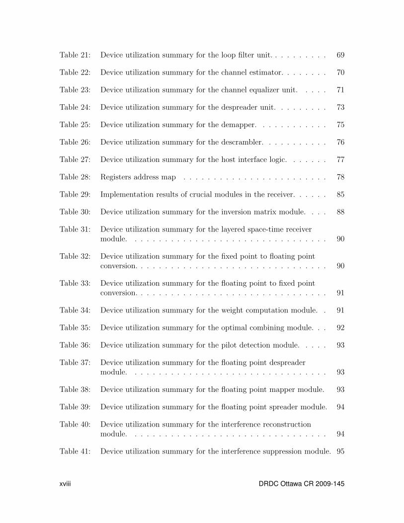
Table 21: Device utilization summary for the loop filter unit. . . . . . . . . . 69
Table 22: Device utilization summary for the channel estimator. . . . . . . . 70
Table 23: Device utilization summary for the channel equalizer unit. . . . . 71
Table 24: Device utilization summary for the despreader unit. . . . . . . . . 73
Table 25: Device utilization summary for the demapper. . . . . . . . . . . . 75
Table 26: Device utilization summary for the descrambler. . . . . . . . . . . 76
Table 27: Device utilization summary for the host interface logic. . . . . . . 77
Table 28: Registers address map . . . . . . . . . . . . . . . . . . . . . . . . 78
Table 29: Implementation results of crucial modules in the receiver. . . . . . 85
Table 30: Device utilization summary for the inversion matrix module. . . . 88
Table 31: Device utilization summary for the layered space-time receivermodule. . . . . . . . . . . . . . . . . . . . . . . . . . . . . . . . . 90
Table 32: Device utilization summary for the fixed point to floating pointconversion. . . . . . . . . . . . . . . . . . . . . . . . . . . . . . . . 90
Table 33: Device utilization summary for the floating point to fixed pointconversion. . . . . . . . . . . . . . . . . . . . . . . . . . . . . . . . 91
Table 34: Device utilization summary for the weight computation module. . 91
Table 35: Device utilization summary for the optimal combining module. . . 92
Table 36: Device utilization summary for the pilot detection module. . . . . 93
Table 37: Device utilization summary for the floating point despreadermodule. . . . . . . . . . . . . . . . . . . . . . . . . . . . . . . . . 93
Table 38: Device utilization summary for the floating point mapper module. 93
Table 39: Device utilization summary for the floating point spreader module. 94
Table 40: Device utilization summary for the interference reconstructionmodule. . . . . . . . . . . . . . . . . . . . . . . . . . . . . . . . . 94
Table 41: Device utilization summary for the interference suppression module. 95
xviii DRDC Ottawa CR 2009-145

Table 42: Device utilization summary for the MIMO MC-CDMA (excludingthe inversion) system on the Virtex-4 SX35. . . . . . . . . . . . . 97
Table 43: Device utilization summary for the MIMO MC-CDMA (excludingthe inversion) system on the Virtex-4 FX140. . . . . . . . . . . . . 97
Table 44: Device utilization summary for the MIMO MC-CDMA (excludingthe inversion) system on the Virtex-5 FX200. . . . . . . . . . . . . 98
Table 45: Device utilization summary for a 1× 2 MIMO MC-CDMA(including the inversion) system on the Virtex-4 FX140. . . . . . . 98
Table 46: Device utilization summary for a 1× 2 MIMO MC-CDMA(including the inversion) system on the Virtex-5 FX200. . . . . . . 98
Table 47: Device utilization summary for a 2× 2 MIMO MC-CDMA(including the inversion) system on the Virtex-4 FX140. . . . . . . 99
Table 48: Device utilization summary for a 2× 2 MIMO MC-CDMA(including the inversion) system on the Virtex-5 FX200. . . . . . . 99
Table 49: BER performance of the receiver in static wireless indoor channel,1 user. . . . . . . . . . . . . . . . . . . . . . . . . . . . . . . . . . 112
Table 50: BER performance of the receiver in static wireless indoor channel,4 users. . . . . . . . . . . . . . . . . . . . . . . . . . . . . . . . . . 113
Table 51: BER performance of the receiver in static wireless indoor channel,8 users. . . . . . . . . . . . . . . . . . . . . . . . . . . . . . . . . . 113
Table B.1: Bill of materials for original version of card. . . . . . . . . . . . . 132
DRDC Ottawa CR 2009-145 xix

This page intentionally left blank.
xx DRDC Ottawa CR 2009-145
1 Introduction
This report presents the FPGA implementation of a complete downlink basebandMulti-Carrier Code Division Multiple Access (MC-CDMA) receiver. The integrationof a Multi-Input Multi-Output (MIMO) system within the MC-CDMA system willalso be presented. Since the Code Division Multiple Access (CDMA) component ofMC-CDMA is not defined yet, it was assumed for this work that Wideband CDMA(WCDMA) will be used. The use of different modulation schemes such as QuadraturePhase Shift Keying (QPSK), 16-level Quadrature Amplitude Modulation (16QAM),and 64-level Quadrature Amplitude Modulation (64QAM) along with the Orthog-onal Frequency Division Multiplexing (OFDM) technique provide high speed datatransmission over multipath fading channels. The channel models used are as speci-fied in the Third Generation Partnership Project (3GPP) Technical Specification TS25.101v2.10, namely indoor to outdoor/pedestrian and vehicular environments [3].
Since variations of the multipath fading channel affect the performance of the system,knowledge of the channel is crucial for accurate signal demodulation. Pilot-symbol-aided-modulation (PSAM) is one of the well known techniques to estimate the channelstate at pilot symbol positions. In an OFDM system, the channel estimation can beperformed by either inserting pilot tones into all subcarriers of the OFDM symbol(time domain) with a given period, also know as block type-pilot channel estimation,or inserting pilot tones into each OFDM symbol (frequency domain), also known ascomb-type pilot channel estimation [4, 5]. The block-type pilot channel estimationhas been developed under the assumption of a slow fading channel (i.e. the channeltransfer function does not change very rapidly). The comb-type pilot channel estima-tion has been developed under the assumption that the channel does not significantlychange from one OFDM block to the next. The comb-type channel estimation esti-mates the channel at pilot frequencies. Then, the frequency response of the channelat frequencies where pilot tones are not located can be interpolated using variousinterpolation techniques such as linear, spline, Fast Fourier Transform (FFT), or lowpass filtering [5].
Furthermore, if the multipath channel is time varying, the interpolation in the timedomain must track variations of the channel. MC-CDMA systems employ coherentdetection based on the use of pilot tones in order to obtain the knowledge of thechannel (comb-type channel estimation). Multi-user support in MC-CDMA systemsis based on the principle of spreading in the frequency domain. Because WidebandCode Division Multiple Access (WCDMA) is used, Orthogonal Variable SpreadingFactor (OVSF) codes are assumed to be the MC-CDMA spreading codes. OVSF codeshave good cross-correlation properties that preserve orthogonality between differentusers. MC-CDMA systems also use various modulation schemes in the indoor tooutdoor and vehicular channel environments [3].
DRDC Ottawa CR 2009-145 1

Recently, several conceptual variations of MC-CDMA have been developed and theyremain an open research topic in terms of architecture, algorithm, and hardwareimplementation. Several MC-CDMA receiver designs were introduced with differentimplementation parameters to meet the requirements of 3G mobile cellular systems[6, 7].
In this report, an implementation of a downlink baseband MC-CDMA receiver isproposed. The receiver is first simulated in both indoor-to-outdoor and vehicularchannel models provided by 3GPP. The implementation for the indoor-to-outdoorconfiguration is chosen as an initial version leading to the implementation of thevehicular channel configuration. The receiver exploits modular implementation anda temporal multiplexing technique so that it can be reused and expanded for futurerequirements.
Many forms of MIMO systems exist, but this report proposes an architecture usingthe Layered Space-Time (LST) technique. A fully functional software simulation ofan integrated MIMO MC-CDMA system will first be presented. A VHDL implemen-tation of the system will also be presented. Several issues arose preventing on-chiplive tests. However, a proof of concept was done and further work would ultimatelyresult in a working on-chip implementation.
2 DRDC Ottawa CR 2009-145
2 Fundamentals of MC-CDMA
MC-CDMA, a novel digital modulation and multiple access scheme [7,8], is a combi-nation of OFDM and CDMA. Such a combination has the benefits of both OFDM andCDMA [9]. In MC-CDMA, symbols are modulated on many subcarriers to introducefrequency diversity instead of using only one carrier like in CDMA. Thus, MC-CDMAis robust against deep frequency selective fading compared to DS-CDMA [10]. Eachuser data is first spread using a given high rate spreading code in the frequency do-main. A fraction of the symbol corresponding to a chip of the spreading code istransmitted through different subcarriers [8].
2.1 MC-CDMA transmitter model
ΣCopier
jC1 ( )tf12cos π
jC2 ( )tf22cos π
jGMC
C ( )tfMCGπ2cos
ja
Data stream
Time
ja
Time
( )tS jMC
IFFT
( )tf02cos π
Insert Cyclic Prefix
P/S
Copier
jC1 ( )tf12cos π
jC2 ( )tf22cos π
jGMC
C ( )tfMCGπ2cos
ja1
Time
ja
Time
( )tS jMC
IFFT
( )tf02cos π
Insert Cyclic Prefix
P/SS/P
Data stream
jPaP:1
jC
1j
C3
jC
2jGM
CC Frequency
jC
1j
C3j
C2
jGM
CC Frequency
Figure 1: MC-CDMA transmitter.
The MC-CDMA transmitter configuration for the jtℎ user is shown in Figure 1. Inthis figure, the main difference is that the MC-CDMA scheme transmits the samesymbol in parallel through several subcarriers whereas the OFDM scheme transmitsdifferent symbols. cj(t) = [cj1, c
j2, ..., c
jGMC
] is the spreading code of the jtℎ user in thefrequency domain, GMC denotes the processing gain, sometimes called the spreadingfactor. The input data stream is multiplied by the spreading code of length GMC .Each chip of the code modulates one subcarrier. The number of subcarriers is N =GMC . The users are separated by different codes. All data corresponding to thetotal number of subcarriers are modulated in baseband by an inverse fast Fouriertransform (IFFT) and converted back into serial data. Then, a cyclic prefix is insertedbetween the symbols to combat the inter-symbol interference (ISI) and the inter-
DRDC Ottawa CR 2009-145 3

carrier interference (ICI) caused by multipath fading. Finally, the signal is digital toanalog converted and upconverted for transmission.
In MC-CDMA transmission, it is essential to have frequency nonselective fading overeach subcarrier. Therefore, if the original symbol rate is high enough to becomesubject to frequency selective fading [8], the input data have to be serial to parallel(S/P) converted into P parallel data sequences [aj1, a
j2, ..., a
jP ] and each S/P output is
multiplied with the spreading code of length GMC . Then, each sequence is modulatedusing GMC subcarriers. Thus, all N = P × GMC subcarriers are also modulatedin baseband by the IFFT. Figure 2 shows the modified version of the MC-CDMAtransmitter.
ΣCopier
jC1 ( )tf12cos π
jC2 ( )tf22cos π
jGMC
C ( )tfMCGπ2cos
ja
Data stream
Time
ja
Time
( )tS jMC
IFFT
( )tf02cos π
Insert Cyclic Prefix
P/S
ΣCopier
jC1 ( )tf12cos π
jC2 ( )tf22cos π
jGMC
C ( )tfMCGπ2cos
ja1
Time
ja
Time
( )tS jMC
IFFT
( )tf02cos π
Insert Cyclic Prefix
P/SS/P
Data stream
jPaP:1
Σ
jC
1j
C3
jC
2jGM
CC Frequency
jC
1j
C3j
C2
jGM
CC Frequency
Figure 2: Modified version of the MC-CDMA transmitter.
In order to improve the performance of the system, an appropriate approach forchannel estimation is to use dedicated pilot symbols that are periodically inserted inthe transmission frame (in the time domain), also known as block-type pilot channelestimation. The pilot tones can also be inserted into each symbol (in the frequencydomain) with a given frequency spacing; this is known as comb-type pilot channelestimation [4, 5]. Block-type pilot channel estimation has been developed under theassumption of a slow fading channel, i.e. the channel transfer function does not changevery rapidly. Whereas comb-type pilot channel estimation has been developed underthe assumption that the channel changes from one OFDM block to the other. Comb-type channel estimation estimates the channel at pilot frequencies. In comb-typepilot channel estimation, the frequency response of the channel at frequencies where
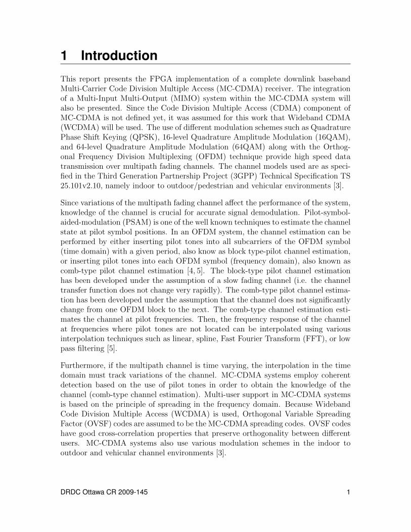
4 DRDC Ottawa CR 2009-145
pilot tones are not located can be interpolated using various interpolation techniquessuch as linear, spline, FFT, or low pass filtering [5]. Furthermore, pilot tones maybe inserted in both time and frequency domains as shown in Figure 3 (Figure 4.35in [9]) where we can see the rectangular pilot insertion grid with pilot tones insertedevery third frequency and every fourth time slot. The pilot density is thus 1
12, that
is, 112
of the whole capacity is used for channel estimation.182 OFDM
Time
Freq
uenc
y
4TS
3�f
Figure 4.35 Example of a rectangular pilot grid.
numerical example, we consider the grid of Figure 4.35 for an OFDM system with carrierspacing �f = 1/T = 1 kHz and symbol duration TS = 1250 µs. At every third frequency,the channel will be measured once in the time 4TS = 5 ms, that is, the unknown signal(the time-variant channel) is sampled at the sampling frequency of 200 Hz. For a noise-freechannel, we can conclude from the sampling theorem that the signal can be recovered fromthe samples if the maximum Doppler frequency νmax fulfills the condition
νmax < 100 Hz.
More generally, for a pilot spacing of 4TS , the condition
νmaxTS < 1/8must be fulfilled.
In frequency direction, the sample spacing is 3 kHz. From the (frequency domain)sampling theorem, we conclude that the delay power spectrum must be inside an intervalof the length of 333 µs. Since the guard interval already has the length 250 µs, this conditionis automatically fulfilled if we can assume that all the echoes lie within the guard interval.We can now start the interpolation (according to the sampling theorem) either in timeor in frequency direction and then calculate the interpolated values for the other direction.Simpler interpolations are possible and may be used in practice for a very coherent channel,for example, linear interpolation or piecewise constant approximation. However, for a reallytime-variant and frequency-selective channel, these methods are not adequate. For a noisychannel, even the interpolation given by the sampling theorem is not the best choice becausethe noise is not taken into account. The optimum linear estimator will be derived in thenext subsection.
In some systems, the pilot symbols are boosted, that is, they are transmitted with ahigher energy than the modulation symbols. In that case, a rectangular grid as shown in
Figure 3: Example of a pilot tone grid.
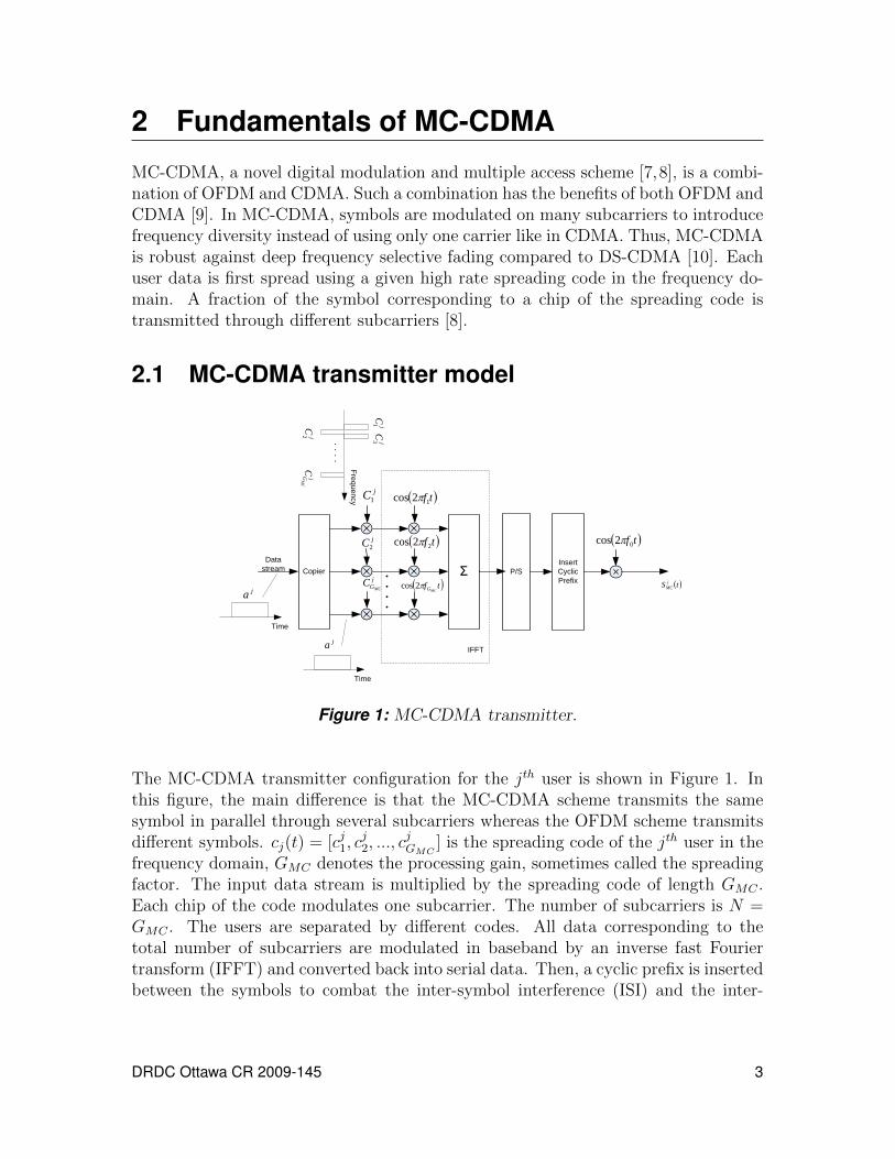
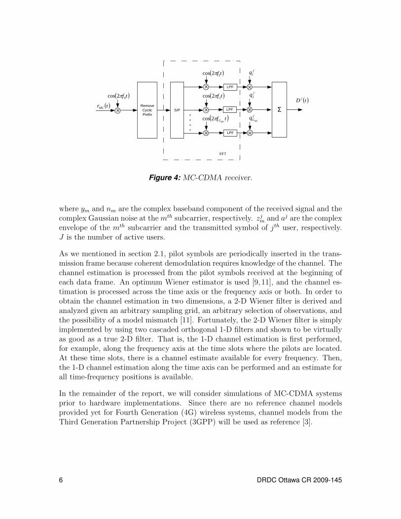
2.2 MC-CDMA receiver modelThe MC-CDMA receiver configuration for the jtℎ user is shown in Figure 4. Thereceived signal is first down converted. Then, the cyclic prefix is removed and theremaining samples are serial to parallel converted to obtain the m-subcarriers com-ponents (corresponding to the ajP data), where m = 1, 2, ..., GMC .
The m-subcarriers are first demodulated by a fast Fourier transform (FFT) (OFDMdemodulation) and then multiplied by the gain qjm to combine the received signalenergy scattered in the frequency domain. In [8], the decision variable is given by
Dj =m=1∑GMC
qmym (1)
with
ym =
j=1∑J
zjmajcjm + nm (2)
DRDC Ottawa CR 2009-145 5
Remove Cyclic Prefix
( )tf02cos π
( )trMCS/P
FFT
( )tf12cos π
( )tf22cos π
( )tfMCGπ2cos
'1jq
'2jq
'jGMC
qΣ
( )tD j '
LPF
LPF
LPF
Figure 4: MC-CDMA receiver.
where ym and nm are the complex baseband component of the received signal and thecomplex Gaussian noise at the mtℎ subcarrier, respectively. zjm and aj are the complexenvelope of the mtℎ subcarrier and the transmitted symbol of jtℎ user, respectively.J is the number of active users.
As we mentioned in section 2.1, pilot symbols are periodically inserted in the trans-mission frame because coherent demodulation requires knowledge of the channel. Thechannel estimation is processed from the pilot symbols received at the beginning ofeach data frame. An optimum Wiener estimator is used [9, 11], and the channel es-timation is processed across the time axis or the frequency axis or both. In order toobtain the channel estimation in two dimensions, a 2-D Wiener filter is derived andanalyzed given an arbitrary sampling grid, an arbitrary selection of observations, andthe possibility of a model mismatch [11]. Fortunately, the 2-D Wiener filter is simplyimplemented by using two cascaded orthogonal 1-D filters and shown to be virtuallyas good as a true 2-D filter. That is, the 1-D channel estimation is first performed,for example, along the frequency axis at the time slots where the pilots are located.At these time slots, there is a channel estimate available for every frequency. Then,the 1-D channel estimation along the time axis can be performed and an estimate forall time-frequency positions is available.
In the remainder of the report, we will consider simulations of MC-CDMA systemsprior to hardware implementations. Since there are no reference channel modelsprovided yet for Fourth Generation (4G) wireless systems, channel models from theThird Generation Partnership Project (3GPP) will be used as reference [3].
6 DRDC Ottawa CR 2009-145

3 Fundamentals of MIMO
Systems using antenna arrays at both ends of the wireless link, i.e. Multi-Input,Multi-Output (MIMO) systems (see Figure 5), increase the bit rate without consum-ing additional bandwidth through spatial multiplexing of multiple signal streams.Space-time coding nearly achieves the complete MIMO channel capacity in an effi-cient and practical manner. Also, it allows transmit diversity and a power gain overnon spatially coded systems without sacrificing bandwidth. There are many space-time code structures, but this report will describe space-time block codes (STBC)and the layered space-time (LST) technique.
s1
s2
sM
r1
r2
rM
Tx Rx
Figure 5: An M ×M MIMO system.
3.1 Alamouti schemeThis space-time block code was introduced by Alamouti in 1998 [12]. It was the firstcode to provide full transmit diversity to systems with two transmit antennas, and isa good example of STBCs.
Information
sourceModulator
( ) 1 21 2
2 1
x xx x
x x
∗
∗
−→
Encoder
Tx 1
Tx 2
( )22 1x x x∗=
( )11 2x x x∗= −
Figure 6: Alamouti space-time encoder.
The encoder is very simple and is shown in Figure 6. Assuming that M -ary modu-lation is used, the encoding consists simply of mapping two modulated symbols, x1
and x2, to the transmit antennas, according to the following code matrix:
X =
[x1 −x∗2x2 x∗1
]. (3)
DRDC Ottawa CR 2009-145 7
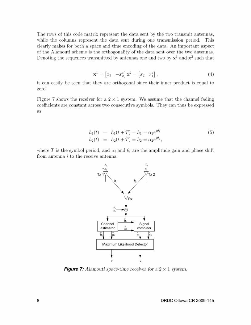
The rows of this code matrix represent the data sent by the two transmit antennas,while the columns represent the data sent during one transmission period. Thisclearly makes for both a space and time encoding of the data. An important aspectof the Alamouti scheme is the orthogonality of the data sent over the two antennas.Denoting the sequences transmitted by antennas one and two by x1 and x2 such that
x1 =[x1 −x∗2
]x2 =
[x2 x∗1
], (4)
it can easily be seen that they are orthogonal since their inner product is equal tozero.
Figure 7 shows the receiver for a 2 × 1 system. We assume that the channel fadingcoefficients are constant across two consecutive symbols. They can thus be expressedas
ℎ1(t) = ℎ1(t+ T ) = ℎ1 = �1ej�1 (5)
ℎ2(t) = ℎ2(t+ T ) = ℎ2 = �2ej�2 ,
where T is the symbol period, and �i and �i are the amplitude gain and phase shiftfrom antenna i to the receive antenna.
Tx 1 Tx 2
Rx
+
Channel
estimator
Signal
combiner
Maximum Likelihood Detector
1x
2x∗−2x
1x∗
1h 2h
1n2n
1hɵ
2hɵ
1hɵ 2hɵ
1xɵ 2xɵ
2xɶ1xɶ
Figure 7: Alamouti space-time receiver for a 2× 1 system.
8 DRDC Ottawa CR 2009-145
The received signals over two consecutive symbols can be expressed as
r1 = r(t) = ℎ1x1 + ℎ2x2 + n1 (6)
r2 = r(t+ T ) = −ℎ1x∗2 + ℎ2x
∗1 + n2,
where n1 and n2 are complex random variables representing the noise and interference.
At the receiver, a combiner uses information provided by a channel estimator toproduce the following signals
x1 = ℎ∗1r1 + ℎ2r∗2 (7)
x2 = ℎ∗2r1 − ℎ1r∗2.
Using (5) and (6), (7) becomes
x1 = (�21 + �2
2)x1 + ℎ∗1n1 + ℎ2n∗2 (8)
x2 = (�21 + �2
2)x2 − ℎ1n2 + ℎ∗2n1.
These combined signals are then used by a maximal likelihood detector to retrievethe transmitted signals. Systems with multiple receive antennas can easily be derivedfrom this basic system.
3.2 Layered space-time architectureOriginally proposed by Foschini [13], the layered space-time architecture has theunique and novel aspect of using M 1-dimension (1, N) systems to build a fullymultidimensional (M,N) system, such as the one shown in Figure 5. This type ofarchitecture allows the use of 1-D signal processing techniques, which greatly reducessystem complexity. The layered aspect refers to each antenna having its own pro-cessing chain called a “layer”. Coding in the spatial domain consists of the layers,while coding in time domain consists of optional error correction coding or optionalperiodical data reassignment within all transmit antennas.
Since the original Foschini architecture was proposed, many variants were introducedby various labs and researchers. In this overview, we will concentrate on the verticalBell Laboratories layered space-time (V-BLAST) scheme [14]. Transmission is simply
DRDC Ottawa CR 2009-145 9

done by splitting the signal into M different streams sent using the M transmissionantennas, one symbol at a time. The code matrix is shown below, in which, as withthe Alamouti code matrix, each column represents the symbols to be sent at a specifictime and each row represents the symbols to be sent from one antenna:
X =
[x1
1 x12 . . .
x21 x2
2 . . .
], (9)
where xit are the symbols sent on layer i at time t.
The channel is represented by matrix H, whose elements ℎij represent the channelfading coefficients from the i-th transmit to the j-th receive antenna. The receivedsignal at each antenna consists of a combination of the M transmitted faded symbolsplus additive white Gaussian noise:
rt = Hxt + nt, (10)
where r is an N -component column matrix of the received signals, H is the channelmatrix, xt is the t-th column of the code matrix X and nt is an N -component columnmatrix of additive white Gaussian noise.
The original V-BLAST receiver is based on a non-linear, iterative algorithm usingboth interference suppression and cancelation to detect the signals. The algorithmdescribed in this overview is a modified version of the original one. For each trans-mitted signal, the remaining signals are considered to be interferers.
These interferers are first suppressed by using the Minimum Mean Square Error(MMSE) diversity combining technique. Like all combining techniques, weights areapplied to the received signals to obtain the desired signal of the current layer:
si = wHi ri. (11)
In MMSE combining, the weights are computed using the autocorrelation matrix ofthe received signals:
wi = �R−1rr c∗i , (12)
where � is a constant, c∗i is the desired channel vector, i.e. a column of channelmatrix H, and R−1
rr is the autocorrelation matrix. Assuming the noise and interferingsignals are uncorrelated, the autocorrelation matrix is given by
Rrr = �2I +M∑i=1
cicHi , (13)
10 DRDC Ottawa CR 2009-145
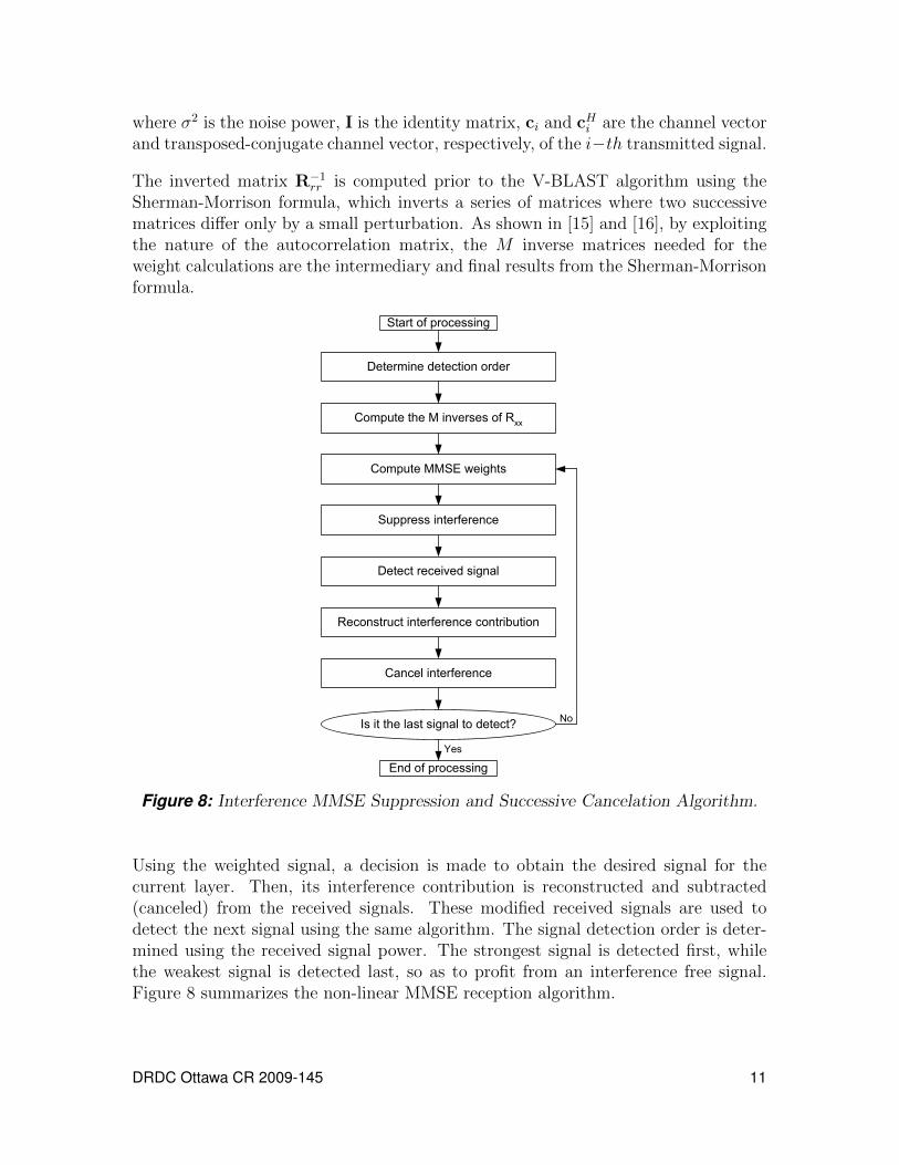
where �2 is the noise power, I is the identity matrix, ci and cHi are the channel vectorand transposed-conjugate channel vector, respectively, of the i−tℎ transmitted signal.
The inverted matrix R−1rr is computed prior to the V-BLAST algorithm using the
Sherman-Morrison formula, which inverts a series of matrices where two successivematrices differ only by a small perturbation. As shown in [15] and [16], by exploitingthe nature of the autocorrelation matrix, the M inverse matrices needed for theweight calculations are the intermediary and final results from the Sherman-Morrisonformula.
Determine detection order
Compute MMSE weights
Suppress interference
Compute the M inverses of Rxx
Detect received signal
Reconstruct interference contribution
Cancel interference
Is it the last signal to detect?
End of processing
Yes
No
Start of processing
Figure 8: Interference MMSE Suppression and Successive Cancelation Algorithm.
Using the weighted signal, a decision is made to obtain the desired signal for thecurrent layer. Then, its interference contribution is reconstructed and subtracted(canceled) from the received signals. These modified received signals are used todetect the next signal using the same algorithm. The signal detection order is deter-mined using the received signal power. The strongest signal is detected first, whilethe weakest signal is detected last, so as to profit from an interference free signal.Figure 8 summarizes the non-linear MMSE reception algorithm.
DRDC Ottawa CR 2009-145 11
It is also possible to use a linear MMSE reception algorithm that performs interferencesuppression, but no cancelation. This algorithm simply consists of simultaneouslycomputing all weights using the MMSE technique and applying them to all receivedsignals to obtain all desired signals.
12 DRDC Ottawa CR 2009-145

4 MC-CDMA system simulation4.1 Channel parametersThe 3GPP’s WCDMA indoor-to-outdoor and vehicular channels, with velocity ofabout 3 km/h and 120 km/h [3], were respectively used as channel models for thesystem simulations. In order to be consistent with these models and to meet theWCDMA bandwidth requirements, an RF carrier frequency of 2160 MHz and a 5MHz signal bandwidth were also assumed according to 3GPP downlink frequencybands and bandwidth allocation [3]. The indoor-to-outdoor model was chosen asa worst case for a slow time-varying channel environment. This model has lowerDoppler shift and shorter delay spread than the vehicular channel. Better perfor-mance is therefore expected for the indoor-to-outdoor case. Table 1 summarizessome important parameters of the channel models.
Table 1: Parameters for indoor-to-outdoor and vehicular channels.
Parameters Indoor-to-outdoor VehicularNumber of paths 3 8Maximum delay spread (�s) 0.488 1.708Mean excess delay (�s) 0.0145 0.2396RMS delay spread (�s) 0.0609 0.3298Coherence bandwidth (kHz) 328.4 60.64Coherence time (s) 0.0705 0.0018Maximum Doppler spread (Hz) 6 240
4.2 MC-CDMA code spreadingAs mentioned in section 2, MC-CDMA is a combination of OFDM and CDMA. Sucha combination has the benefits of both OFDM and CDMA. In MC-CDMA, symbolsare modulated on several subcarriers to introduce frequency diversity instead of usingonly one carrier like in CDMA. Figures 9 and 10 show MC-CDMA transmitter andreceiver configurations for the jtℎ user. Cj
cℎ,SF,k = [Cjcℎ,SF,0 C
jcℎ,SF,1 ⋅ ⋅ ⋅ C
jcℎ,SF,SF−1] is
the channelization code, Sjdl,k = [Sjdl,0 Sjdl,1 ⋅ ⋅ ⋅ S
jdl,SF−1] is the complex-valued scram-
bling code of the jtℎ user in the frequency domain, and SF denotes the spreadingfactor of the code. As shown in Figure 9, the modulated data symbol sequence isserial-to-parallel converted to N parallel sequences (i.e. N is equal to the number ofdata subcarriers and the number of pilot subcarriers. Each of the parallel sequencesis duplicated into SF parallel copies and each of the duplicated symbols is multipliedby a chip from the spreading code, which is the combination of a chip from the chan-nelization code and a chip from the scrambling code. Finally, an IFFT is performedand a guard interval is inserted to generate the MC-CDMA signal.
DRDC Ottawa CR 2009-145 13

S/P
D0 D1 …. Dp
D0
D1
…...
Dp
COPIER
COPIER
D0
D0
…...
D0
Dp
Dp
…...
Dp
IFFTP/S
jSFchC 0,,
CP
Spreading
jSFSFchC 1,, −
jSFSFchC 1,, −
jSFchC 0,,
jdlS 0,
jSFdlS 1, −
jdlS 0,
jSFdlS 1, −
Figure 9: MC-CDMA transmitter.
P/S
D0
D1
…...
Dp
FFTS/P
CP
Received signal
Despreading
D0 D1 …. Dp
jSFchC 0,,
jSFSFchC 1,, −
jSFSFchC 1,, −
jSFchC 0,,
jdlS 0,
jSFdlS 1, −
jdlS 0,
jSFdlS 1, −
Figure 10: MC-CDMA receiver.
In WCDMA, the scrambling codes are used to identify cells (base station), and thechannelization codes are Orthogonal Variable Spreading Factor (OVSF) codes thatare used to separate downlink connections to different users within one cell as shownin Figure 11. In the uplink, scrambling codes are used to identify mobiles, andchannelization codes are used to identify physical channels from the same mobile,(i.e. to preserve the orthogonality between a user’s different physical channels such asDedicated Physical Data Channel (DPDCH) and Dedicated Physical Control Channel(DPCCH) from the same mobile user [17]) as shown in Figure 12.
One can see that in the downlink, a base station uses only a single scrambling codeand several channelization codes. Meanwhile, in the uplink, all mobile have different
14 DRDC Ottawa CR 2009-145

Cell 1
Scrambling code 1
Channelisation code 1
Channelisation code 2
Channelisation code 3 Cell 3
Scrambling code 3
Channelisation code 1
Channelisation code 2
Channelisation code 3
Cell 2
Scrambling code 2
Channelisation code 1
Channelisation code 2
Channelisation code 3
Figure 11: Spreading code function in downlink.
Cell 1
Scrambling code 2
Scrambling code 3
Scrambling code 1
Channelisation code 1
Channelisation code 2
Channelisation code 3
Cell 2
Scrambling code 2
Scrambling code 3
Scrambling code 1
Channelisation code 1
Channelisation code 2
Channelisation code 3
Cell 3
Scrambling code 2
Scrambling code 3
Scrambling code 1
Channelisation code 1
Channelisation code 2
Channelisation code 3
Channelisation code 2
Figure 12: Spreading code function in uplink.
scrambling codes for separating users. The downlink spreading in WCDMA is illus-trated in Figure 13 [17]. In this figure, the I and Q branches are spread by the samereal-valued channelization codes which are uniquely described as Cj
cℎ,SF,k in Figure 14,where k is the code number, 0 ≤ k ≤ SF − 1. Then, the sequence of chips is scram-bled (complex chip-wise multiplication) by a complex-valued scrambling code Sdl,k.The scrambling codes in the downlink direction use Gold codes which are constructedby combining two real sequences into a complex-valued sequence. In the WCDMAdownlink, the scrambling codes are constructed by using polynomials 1 + X7 + X18
and 1 +X5 +X7 +X10 +X18 as shown in Figure 15 [17].
DRDC Ottawa CR 2009-145 15

3GPP
3G TS 25.213 V5.0.0 (2002-03)19Release 5
except the indicator channels using signatures (AICH, AP-AICH and CD/CA-ICH) and HS-PDSCH the symbols cantake the three values +1, -1, and 0, where 0 indicates DTX. For the indicator channels using signatures, the symbolvalues depend on the exact combination of indicators to be transmitted, compare [2] Sections 5.3.3.7, 5.3.3.8 and5.3.3.9.
For physical channel using QPSK each pair of two consecutive symbols is first serial-to-parallel converted and mappedto an I and Q branch. The behaviour of the modulation mapper is such that even and odd numbered symbols are mappedto the I and Q branch respectively. For all channels using QPSK except the indicator channels using signatures, symbolnumber zero is defined as the first symbol in each frame. For the indicator channels using signatures, symbol numberzero is defined as the first symbol in each access slot. The I and Q branches are then both spread to the chip rate by thesame real-valued channelisation code Cch,SF,m. The channelisation code sequence shall be aligned in time with thesymbol boundary. The sequences of real-valued chips on the I and Q branch are then treated as a single complex-valuedsequence of chips. This sequence of chips is scrambled (complex chip-wise multiplication) by a complex-valuedscrambling code Sdl,n. In case of P-CCPCH, the scrambling code is applied aligned with the P-CCPCH frame boundary,i.e. the first complex chip of the spread P-CCPCH frame is multiplied with chip number zero of the scrambling code. Incase of other downlink channels, the scrambling code is applied aligned with the scrambling code applied to the P-CCPCH. In this case, the scrambling code is thus not necessarily applied aligned with the frame boundary of thephysical channel to be scrambled.
I
downlink physical channel
S→→→→P
Cch,SF,m
j
Sdl,n
Q
I+jQ S Modulation Mapper
Figure 8: Spreading for all downlink physical channels except SCH
For physical channel using 16QAM, a set of consecutive symbols is serial-to-parallel converted and then mapped to16QAM by Modulation mapper. The I and Q branches are then both spread to the chip rate by the same real-valuedchannelisation code Cch,16,m. The channelisation code sequence shall be aligned in time with the symbol boundary. Thesequences of real-valued chips on the I and Q branch are then treated as a single complex-valued sequence of chips.This sequence of chips from all multi-codes is summed and then scrambled (complex chip-wise multiplication) by acomplex-valued scrambling code Sdl,n. The scrambling code is applied aligned with the scrambling code applied to theP-CCPCH.
The serial to parallel conversion uses four bits which result in index bits allocated to I and Q according to table 4. Theseindex bits are mapped to the modulated constellation symbols as illustrated in figure xx.
Figure 13: Spreading for a downlink physical channel.
3GPP
3G TS 25.213 V5.0.0 (2002-03)11Release 5
SF = 1 SF = 2 SF = 4
C ch,1 ,0 = (1)
C ch,2 ,0 = (1 ,1)
C ch,2 ,1 = (1 ,-1 )
C ch,4 ,0 = (1 ,1 ,1 ,1 )
C ch,4 ,1 = (1 ,1 ,-1 ,-1)
C ch,4 ,2 = (1 ,-1 ,1 ,-1)
C ch,4 ,3 = (1 ,-1 ,-1 ,1)
Figure 4: Code-tree for generation of Orthogonal Variable Spreading Factor (OVSF) codes
In figure 4, the channelisation codes are uniquely described as Cch,SF,k, where SF is the spreading factor of the code andk is the code number, 0 ≤ k ≤ SF-1.
Each level in the code tree defines channelisation codes of length SF, corresponding to a spreading factor of SF infigure 4.
The generation method for the channelisation code is defined as:
1Cch,1,0 = ,
−
=
−
=
11
11
0,1,
0,1,
0,1,
0,1,
1,2,
0,2,
ch
ch
ch
ch
ch
ch
CC
CC
CC
( )
( )
( )
( )
( ) ( )
( ) ( )
−
−
−
=
−−
−−
−++
−++
+
+
+
+
12,2,12,2,
12,2,12,2,
1,2,1,2,
1,2,1,2,
0,2,0,2,
0,2,0,2,
112,12,
212,12,
3,12,
2,12,
1,12,
0,12,
:::
nnchnnch
nnchnnch
nchnch
nchnch
nchnch
nchnch
nnch
nnch
nch
nch
nch
nch
CCCC
CCCCCC
CC
CC
CCCC
The leftmost value in each channelisation code word corresponds to the chip transmitted first in time.
4.3.1.2 Code allocation for DPCCH/DPDCH/HS-DPCCH
For the DPCCH, DPDCHs and HS-DPCCH the following applies:
- The DPCCH is always spread by code cc = Cch,256,0.
- The HS-DPCCH is spread by cc = Cch,256,64.
- When only one DPDCH is to be transmitted, DPDCH1 is spread by code cd,1 = Cch,SF,k where SF is the spreadingfactor of DPDCH1 and k= SF / 4.
- When more than one DPDCH is to be transmitted, all DPDCHs have spreading factors equal to 4. DPDCHn isspread by the the code cd,n = Cch,4,k , where k = 1 if n ∈ {1, 2}, k = 3 if n ∈ {3, 4}, and k = 2 if n ∈ {5, 6}.
Figure 14: Code-tree for generation of the OVSF codes.
16 DRDC Ottawa CR 2009-145

3GPP
3G TS 25.213 V5.0.0 (2002-03)23Release 5
I
Q
1
1 0
02
2
3
3
4
4
5
5
6
6
7
7
8
8
9
9
17
17
16
16
15
15
14
14
13
13
12
12
11
11
10
10
Figure 11: Configuration of downlink scrambling code generator
5.2.3 Synchronisation codes
5.2.3.1 Code generation
The primary synchronisation code (PSC), Cpsc is constructed as a so-called generalised hierarchical Golay sequence.The PSC is furthermore chosen to have good aperiodic auto correlation properties.
Define:
- a = <x1, x2, x3, …, x16> = <1, 1, 1, 1, 1, 1, -1, -1, 1, -1, 1, -1, 1, -1, -1, 1>
The PSC is generated by repeating the sequence a modulated by a Golay complementary sequence, and creating acomplex-valued sequence with identical real and imaginary components. The PSC Cpsc is defined as:
- Cpsc = (1 + j) × <a, a, a, -a, -a, a, -a, -a, a, a, a, -a, a, -a, a, a>;
where the leftmost chip in the sequence corresponds to the chip transmitted first in time.
The 16 secondary synchronization codes (SSCs), {Cssc,1,…,C ssc,16}, are complex-valued with identical real andimaginary components, and are constructed from position wise multiplicationof a Hadamard sequence and a sequence z,defined as:
- z = <b, b, b, -b, b, b, -b, -b, b, -b, b, -b, -b, -b, -b, -b>, where
- b = <x1, x2, x3, x4, x5, x6, x7, x8, -x9, -x10, -x11, -x12, -x13, -x14, -x15, -x16> and x1, x2 , …, x15, x16, are same as in thedefinition of the sequence a above.
The Hadamard sequences are obtained as the rows in a matrix H8 constructed recursively by:
1,
)1(
11
11
0
≥
−
=
=
−−
−− kHH
HHH
H
kk
kkk
The rows are numbered from the top starting with row 0 (the all ones sequence).
Denote the n:th Hadamard sequence as a row of H8 numbered from the top, n = 0, 1, 2, …, 255, in the sequel.
Figure 15: Downlink scrambling code generator.
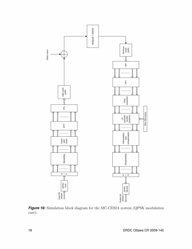
4.3 Block diagram of the MC-CDMA system anddesign parameters
A simulation block diagram for the downlink Single-Input Single-Output (SISO) MC-CDMA system (QPSK modulation case) is shown in Figure 16. The design parame-ters for both indoor-to-outdoor and vehicular channels are also summarized in Table 2and 3, respectively.
DRDC Ottawa CR 2009-145 17
QP
SK
mod
S / P
Inpu
t bit
stre
amIF
FTP
/S
Rem
ove
cycl
ic
pref
ixFF
TP
ilot
extra
ctio
nAdd
cyc
lic
pref
ix
S/P
Inse
rt pi
lot
tone
s
LS
estim
ate
at p
ilot
posi
tions
Ref
. Pilo
t ton
es
Inte
rpol
atio
n an
d co
mpe
nsat
ion
P / S
QPS
K de
mod
Out
put b
it st
ream
Spr
eadi
ng
Des
prea
ding
Oth
er u
sers
Mul
tipat
h +
AW
GN
Figure 16: Simulation block diagram for the MC-CDMA system (QPSK modulationcase).
18 DRDC Ottawa CR 2009-145

Table 2: Simulation parameters for the indoor-to-outdoor channel.
Available bandwidth 5 MHzFFT sampling rate 5 MHz
Spreading factor 8Spreading codes OVSF codes
FFT size 512Subcarrier spacing 9.765625 kHz
Effective symbol duration 102.4 �sGuard time duration 25.6 �s
MC-CDMA symbol duration 128 �sPilot spacing 64 94
Number of pilot subcarriers 8 6Number of data subcarriers 440 464
Number of subcarriers 448 470Occupied bandwidth 4.38 MHz 4.59 MHz
Actual symbol rate 429.6875 KSps 453.125 KSps
Table 3: Simulation parameters for the vehicular channel.
Available bandwidth 5 MHzFFT sampling rate 5 MHz
Spreading factor 8Spreading codes OVSF codes
FFT size 2048Subcarrier spacing 2.4414 kHz
Effective symbol duration 409.6 �sGuard time duration 102.4 �s
MC-CDMA symbol duration 512 �sPilot spacing 64 94
Number of pilot subcarriers 32 22Number of data subcarriers 1952 1952
Number of subcarriers 1984 1974Occupied bandwidth 4.85 MHz 4.77 MHz
Actual symbol rate 476.5625 KSps 476.5625 KSps
DRDC Ottawa CR 2009-145 19

4.4 Some important MC-CDMA simulation resultsIn this section, in order to validate the MC-CDMA systems, Monte Carlo simulationsare performed to obtain performance results. These systems are simulated in bothindoor-to-outdoor and vehicular wireless channels with various conditions such asmodulation schemes QPSK, 16-QAM and 64-QAM, pilot tone spacing Nf = 64, and94, number of active users Nu = 1, 4, and 8. Since the FIR filter approach for sincinterpolation technique proposed in [18] will be used for hardware implementation,only the performance of this method was considered.
4.4.1 Number of subcarriers impact
First, the influence of the number of subcarriers on the performance of MC-CDMAsystems was considered. Figure 17 illustrates the influence of the number of subcarri-ers on the performance of QPSK-MC-CDMA over the worst case channel (vehicularchannel). The system with 2048 subcarriers had a performance improvement of about4 dB over the system with 256 subcarriers at a BER of 10−4.
0 5 10 15 20 25 3010
−5
10−4
10−3
10−2
10−1
Eb/N0 per user
BE
R
FFT=2048FFT=1024FFT=512FFT=256
Figure 17: Influence of the number of subcarriers on the performance of QPSK-MC-CDMA.
Figure 18 shows the bit error rate performance as a function of the number of sub-carriers at Eb/N0 = 30 dB. The more the number of subcarriers is increased, thebetter the performance is. Since the subcarrier spacing is inversely proportional tothe number of subcarriers, the spectrum around each subcarrier is flatter and leads tobetter performance. However, as shown on Figure 18, the performance gain obtained
20 DRDC Ottawa CR 2009-145

by using more subcarriers is bounded by a lower limit for an infinite number of sub-carriers. It becomes then a question of assessing how much performance is neededversus the complexity and cost of the implementation.
0 500 1000 1500 2000 2500
10−5
10−4
FFT size
BE
R
Figure 18: Influence of the number of subcarriers on the performance of QPSK-MC-CDMA at Eb/N0 = 30 dB.
4.4.2 Pilot tone spacing and modulation scheme impact
Figure 19 illustrates the influence of the pilot tone spacing on the performance ofMC-CDMA systems over both indoor-to-outdoor and vehicular channels. In thisfigure, the solid curves represent systems with a pilot spacing of Nf = 64 and thedash curves represent for pilot spacing Nf = 94. The curves with diamond, circle andsquare markers represent performance of the single user system with QPSK, 16-QAMand 64-QAM modulations, respectively.
We can see that the system with shorter pilot tone spacing Nf = 64 has betterperformances than the system with pilot spacing Nf = 94 at high signal-to-noiseratio values. This is because there are more pilots packed within a symbol in thecase Nf = 64, leading to more precise channel estimation. Furthermore, it is clearlyseen that higher modulation schemes such as 16-QAM and 64-QAM have better datathroughput but require more transmit power to get the same BER performance aswith QPSK modulation. As expected, the performances of the system in the indoor-to-outdoor channel are better than in the vehicular channel because the fading is lesssevere in the former.
DRDC Ottawa CR 2009-145 21
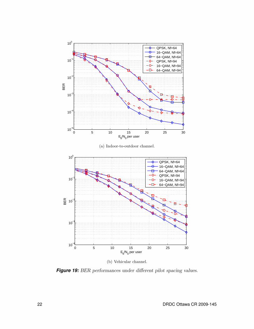
0 5 10 15 20 25 3010
−5
10−4
10−3
10−2
10−1
100
Eb/N0 per user
BE
R
QPSK, Nf=6416−QAM, Nf=6464−QAM, Nf=64QPSK, Nf=9416−QAM, Nf=9464−QAM, Nf=94
(a) Indoor-to-outdoor channel.
0 5 10 15 20 25 3010
−4
10−3
10−2
10−1
100
Eb/N0 per user
BE
R
QPSK, Nf=6416−QAM, Nf=6464−QAM, Nf=64QPSK, Nf=9416−QAM, Nf=9464−QAM, Nf=94
(b) Vehicular channel.
Figure 19: BER performances under different pilot spacing values.
22 DRDC Ottawa CR 2009-145

4.4.3 Impact of the number of active users
The impact of the number of the active users on the performance of the system isshown in Figure 20. The BER, as a function of the signal-to-noise ratio for the QPSKmodulation, is also presented in this figure. The pilot spacing Nf = 64 was used sinceit will be used for hardware implementation.
In this figure, the solid curves with diamond markers represent performance of thesystem using perfect knowledge of the channel for benchmarking purposes. The solidcurves with circle markers represent performance of the system for a single user(Nu = 1). The solid curves with square markers represent performance of the systemfor 4 users (Nu = 4). Finally, the solid curves with downward-pointing trianglemarkers represent performance of the system for 8 users (Nu = 8).
For the desired user only in Figure 20(a), Nu = 1, this figure shows the differencebetween the perfect and the interpolation curves to be constant at about 2.7 dB ata BER of 10−3. For 4 users (Nu = 4), the difference between the perfect and theinterpolation curves is also constant at about 7 dB. The difference is about 9.2 dBfor 8 users (Nu = 8). The performance of the desired user decreases as the numberof interferers increases. Since the interferers are perceived approximately as additivewhite noise by the desired user receiver (because of the system’s CDMA property),these results are logical.
Similarly, the impact of number of the active users in a vehicular channel is illustratedin Figure 20(b). The differences between the perfect and the interpolation curves ofthe desired user is shown to be constant at about 3 dB, 8 dB, and 11 dB at a BERof 2× 10⁻³ for 1, 4, and 8 active users, respectively.
DRDC Ottawa CR 2009-145 23

0 5 10 15 20 25 3010
−6
10−5
10−4
10−3
10−2
10−1
100
Eb/N0 per user
BE
R
Single user4 active users8 active usersPerfect
(a) Indoor-to-outdoor channel.
0 5 10 15 20 25 3010
−4
10−3
10−2
10−1
100
Eb/N0 per user
BE
R
Single user4 active users8 active usersPerfect
(b) Vehicular channel.
Figure 20: BER performances under different numbers of active users, Nf = 64.
24 DRDC Ottawa CR 2009-145

4.5 Integration of MIMO within the MC-CDMA systemThe V-Blast and MC-CDMA system discussed in [1] will be used as the basis of ourdesign. Figure 21 shows the block diagram of the MIMO MC-CDMA system usingM transmit antennas and N receive antennas.
Figure 21: Block diagram of the MIMO MC-CDMA system [1].
For the transmitter, the major difference between the MIMO MC-CDMA systemand the original MC-CDMA system is the addition of a serial-to-parallel converterseparating the QPSK modulated user signals into M blocks of P symbols to be senton each transmit antenna. The original MC-CDMA system is then replicated for eachtransmit antenna.
DRDC Ottawa CR 2009-145 25

For the receiver, the block diagram shown in Figure 21 is for a single user. This struc-ture is replicated for the other users. First, as in the original MC-CDMA receiver, foreach of the N received signals, the cyclic prefix is removed and the FFT is performed.At this stage, one V-Blast detector per subcarrier is added to the receiving chain torecover the M signals sent on the specific subcarrier. These signals are then despreadand rearranged to be used as decision statistics.
Results presented in [1] show that using a non-linear detector (V-BLAST) like theone described previously does not offer improvements over linear MMSE detectors,i.e. with no interference cancelation. The authors surmise that the decision processbefore despreading could be very noisy and thus cause significant error propagationacross the iterations. However, as it will be shown in the following sections, thebest performance was obtained using a modified V-BLAST detection algorithm thatincludes despreading and respreading within the detection chain.
4.5.1 Receiver with perfect channel knowledge
A MIMO MC-CDMA receiver with perfect channel knowledge was first designed.Figure 22 shows the block diagram for the system. Blocks in gray are the componentsof the MIMO aspect of the system. The MMSE algorithm presented in Figure 8 issuccessively applied to all nfft frequencies obtained by the FFT operation.
FFTFrom
ant #1
From
ant #2FFT
Matrix
inversion
nfft
nfft
Weights
Despread Demap
Despread Demap
Optimal
combining
Interference
reconstructionDetection
Interference
cancellation
Figure 22: Architecture of the MIMO MC-CDMA receiver with perfect channelknowledge.
In figures 23 and 24, results are presented for QPSK modulation and 1 user underboth the indoor and vehicular channels to show the effect of the number of antennason the error probability in comparison with a SISO case. As expected, it can beseen that the cases where Nr ≥ Nt show an improvement, where Nr and Nt arerespectively the number of receive and transmit antennas. On the other hand, thecases where Nr < Nt do not perform well. This is normal, since Nr must be at leastequal to Nt to have enough diversity to properly separate the different transmittedsignals.
26 DRDC Ottawa CR 2009-145
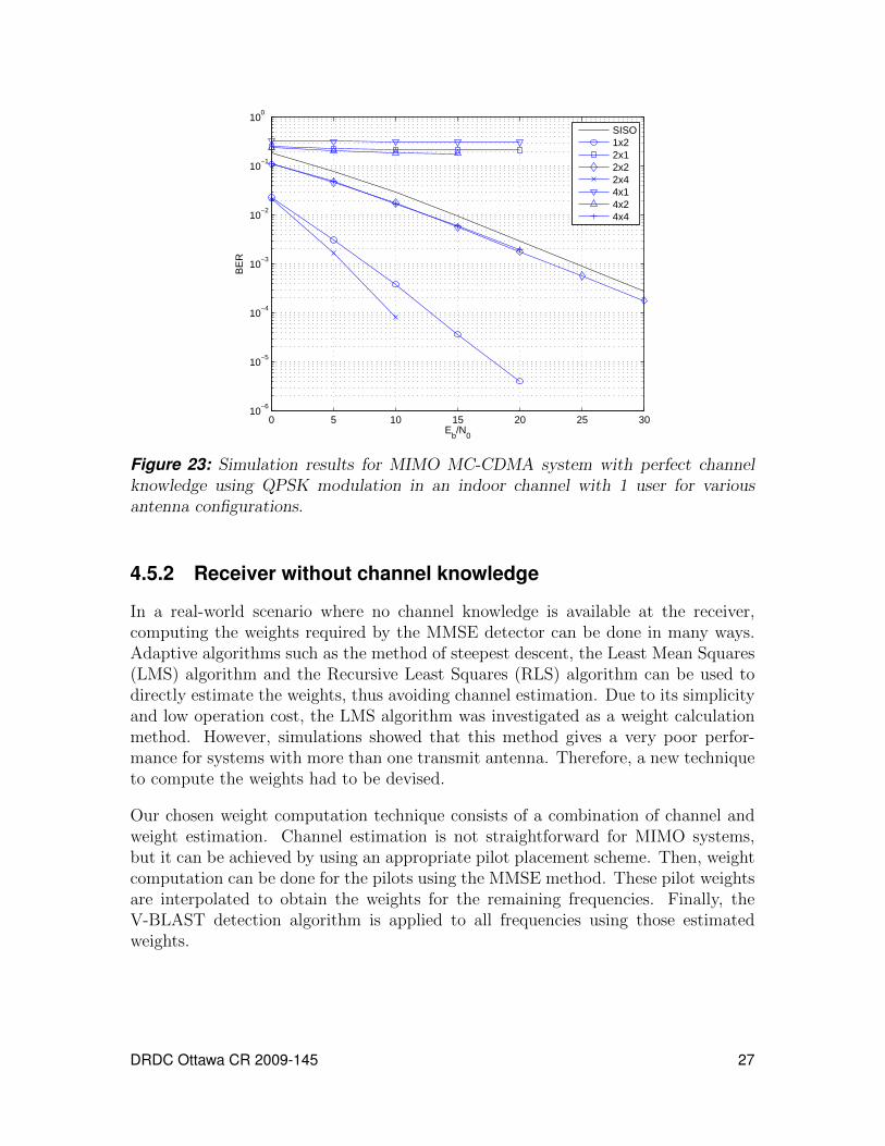
0 5 10 15 20 25 3010
−6
10−5
10−4
10−3
10−2
10−1
100
Eb/N
0
BE
R
SISO1x22x12x22x44x14x24x4
Figure 23: Simulation results for MIMO MC-CDMA system with perfect channelknowledge using QPSK modulation in an indoor channel with 1 user for variousantenna configurations.
4.5.2 Receiver without channel knowledge
In a real-world scenario where no channel knowledge is available at the receiver,computing the weights required by the MMSE detector can be done in many ways.Adaptive algorithms such as the method of steepest descent, the Least Mean Squares(LMS) algorithm and the Recursive Least Squares (RLS) algorithm can be used todirectly estimate the weights, thus avoiding channel estimation. Due to its simplicityand low operation cost, the LMS algorithm was investigated as a weight calculationmethod. However, simulations showed that this method gives a very poor perfor-mance for systems with more than one transmit antenna. Therefore, a new techniqueto compute the weights had to be devised.
Our chosen weight computation technique consists of a combination of channel andweight estimation. Channel estimation is not straightforward for MIMO systems,but it can be achieved by using an appropriate pilot placement scheme. Then, weightcomputation can be done for the pilots using the MMSE method. These pilot weightsare interpolated to obtain the weights for the remaining frequencies. Finally, theV-BLAST detection algorithm is applied to all frequencies using those estimatedweights.
DRDC Ottawa CR 2009-145 27
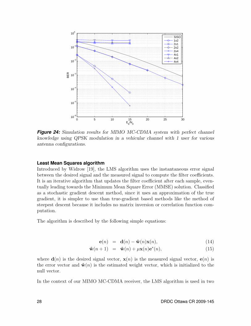
0 5 10 15 20 25 3010
−6
10−5
10−4
10−3
10−2
10−1
100
Eb/N
0
BE
R
SISO1x22x12x22x44x14x24x4
Figure 24: Simulation results for MIMO MC-CDMA system with perfect channelknowledge using QPSK modulation in a vehicular channel with 1 user for variousantenna configurations.
Least Mean Squares algorithmIntroduced by Widrow [19], the LMS algorithm uses the instantaneous error signalbetween the desired signal and the measured signal to compute the filter coefficients.It is an iterative algorithm that updates the filter coefficient after each sample, even-tually leading towards the Minimum Mean Square Error (MMSE) solution. Classifiedas a stochastic gradient descent method, since it uses an approximation of the truegradient, it is simpler to use than true-gradient based methods like the method ofsteepest descent because it includes no matrix inversion or correlation function com-putation.
The algorithm is described by the following simple equations:
e(n) = d(n)− w(n)x(n), (14)
w(n+ 1) = w(n) + �x(n)e∗(n), (15)
where d(n) is the desired signal vector, x(n) is the measured signal vector, e(n) isthe error vector and w(n) is the estimated weight vector, which is initialized to thenull vector.
In the context of our MIMO MC-CDMA receiver, the LMS algorithm is used in two
28 DRDC Ottawa CR 2009-145
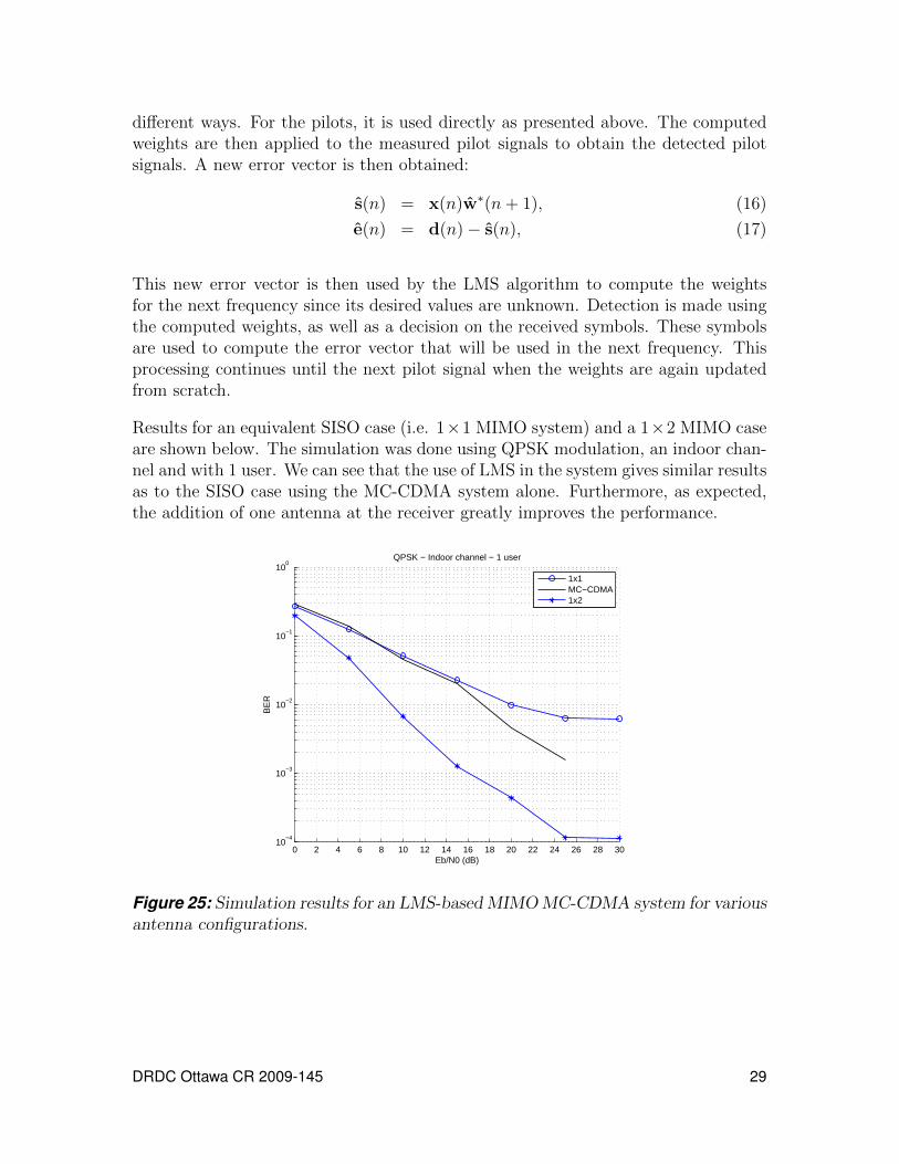
different ways. For the pilots, it is used directly as presented above. The computedweights are then applied to the measured pilot signals to obtain the detected pilotsignals. A new error vector is then obtained:
s(n) = x(n)w∗(n+ 1), (16)
e(n) = d(n)− s(n), (17)
This new error vector is then used by the LMS algorithm to compute the weightsfor the next frequency since its desired values are unknown. Detection is made usingthe computed weights, as well as a decision on the received symbols. These symbolsare used to compute the error vector that will be used in the next frequency. Thisprocessing continues until the next pilot signal when the weights are again updatedfrom scratch.
Results for an equivalent SISO case (i.e. 1×1 MIMO system) and a 1×2 MIMO caseare shown below. The simulation was done using QPSK modulation, an indoor chan-nel and with 1 user. We can see that the use of LMS in the system gives similar resultsas to the SISO case using the MC-CDMA system alone. Furthermore, as expected,the addition of one antenna at the receiver greatly improves the performance.
0 2 4 6 8 10 12 14 16 18 20 22 24 26 28 3010
−4
10−3
10−2
10−1
100
QPSK − Indoor channel − 1 user
Eb/N0 (dB)
BE
R
1x1MC−CDMA1x2
Figure 25: Simulation results for an LMS-based MIMO MC-CDMA system for variousantenna configurations.
DRDC Ottawa CR 2009-145 29

Channel and weight estimation methodWeights are first computed at the pilot symbols using the inverted autocorrelationmatrix. These weights are then used to interpolate the weights of the remaining datasymbols by using the same method as the channel estimation.
Figure 26 shows the results for various MIMO systems using three detection algo-rithms (MMSE linear, LMS and V-BLAST) having a single user, using QPSK mod-ulation in an indoor channel. The interpolation method used was FIR interpolationusing the Matlab function interp. It can be seen that using weight interpolationoffers a good compromise between performance and complexity, especially with theV-BLAST algorithm.
0 5 10 15 20 25 3010
−4
10−3
10−2
10−1
100
Eb/N
0
BE
R
1x2 − MMSE Linear2x2 − MMSE Linear1x2 − V−Blast2x2 − V−Blast1x2 − LMS
Figure 26: Effect of weight interpolation on various receiver architectures.
In [2], Jones and Raleigh propose a channel estimation method for an OFDM systemwith multiple antennas. As part of the channel estimation technique, they proposea MIMO estimator consisting of transmitting Np sequences of length Nt of pilotsymbols instead of transmitting Np single pilot symbols. This structure uses NtNp
total frequencies to completely train a Nt × Nr system, where Nr is the number ofreceive antennas. This scheme is shown in Figure 27, where T (n) is the ntℎ pilotsymbol and D is a data symbol.
Using this scheme, when an antenna transmits a pilot symbol, there is no interferingsignal coming from the other antennas. The transmitted training symbols can thusbe completely distinguished at the receiver, which allows the use of classical SISOchannel estimation techniques to estimate the MIMO channel.
30 DRDC Ottawa CR 2009-145

Figure 27: MIMO OFDM pilot symbol structure proposed in [2].
Using this pilot scheme, it is possible to use classical SISO channel estimation meth-ods. As a proof-of-concept, the same channel estimation method used in the MC-CDMA system was used in the MIMO MC-CDMA system. As a reminder, thismethod consists of dividing the received symbols by the pilot symbols’ value to ob-tain channel coefficients at the pilots. These coefficients are then interpolated toobtain the remaining channel coefficients. In the Matlab simulator, all pilot symbolsare set to one, which makes the channel coefficients directly equal to the receivedsymbols. The interpolation method used was again FIR interpolation using the Mat-lab function interp. This method is applied to all NtNr received pilot symbols toobtain the channel coefficients at the pilots.
FFTFrom
ant #1
From
ant #2 FFT
Matrix
inversion
npilots
WeightsOptimal
combining
Interference
reconstructionDetection
Interference
cancellation
Despread Demap
Despread Demap
Channel
estimation
Weight
estimation
npilots
ndata
ndata
Optimal
combining
Interference
reconstructionDetection
Interference
cancellation
Figure 28: Architecture of the MIMO MC-CDMA receiver without channel knowl-edge.
Using these channel coefficients, the V-BLAST algorithm, including MMSE weightcomputation, is applied successively to all pilots. The channel coefficients and weightscorresponding to the remaining data samples are then interpolated. Finally, the V-
DRDC Ottawa CR 2009-145 31

BLAST algorithm is applied to all the remaining samples using the interpolatedchannel coefficients and weights. It is important to note that in order for the inter-ference reconstruction to be accurate, the despreaded and demapped symbol must beused. Also, to correctly cancel the interference from the received signal, respreadingof the detected symbol must be done. To do that, we must include despreading,mapping and respreading modules within the V-BLAST detection chain. Figure 28shows the block diagram for the final MIMO MC-CDMA receiver without channelknowledge. Blocks in gray correspond to the MIMO components of the system.
4.5.3 Simulation results
Since simulation time can be quite long, only two figures have been included in thisreport to illustrate the effect of the use of multiple antennas with the MC-CDMAsystem. Both figures include simulation results for a system having one user, usingthe QPSK modulation and a pilot spacing of 64.
Firstly, the effect of having multiple antennas at the transmitter and receiver areshown on Figure 29. The 1×2, 1×4 and 2×4 cases show that having extra antennasat the receiver improves the bit error rate. While the bit error rate is worse for the2× 2 and 4× 4 case, the data throughput is better than in the typical 1× 1 (SISO)case, as can be seen in tables 4, 5, 6 and 7.
0 5 10 15 20 25 3010
−4
10−3
10−2
10−1
100
Eb/N
0
BE
R
SISO1x21x42x22x44x4
Figure 29: Impact of the number of antennas on the MIMO MC-CDMA system .
An interesting phenomenon can be seen when comparing the performance of thesystem for the two channel types. Figure 30 shows that for a SISO case, at SNRshigher than 16 dB, the bit error rate in a vehicular channel is better than in anindoor-to-outdoor channel. Moreover, for the 1 × 2 and 2 × 2 cases, the vehicularchannel offers a better performance than the indoor-to-outdoor channel for all SNRs.
32 DRDC Ottawa CR 2009-145
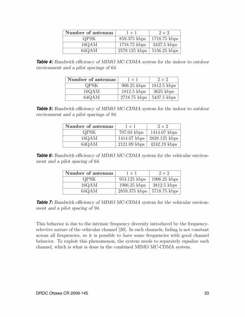
Number of antennas 1× 1 2× 2QPSK 859.375 kbps 1718.75 kbps
16QAM 1718.75 kbps 3437.5 kbps64QAM 2578.125 kbps 5156.25 kbps
Table 4: Bandwith efficiency of MIMO MC-CDMA system for the indoor to outdoorenvironment and a pilot spacings of 64.
Number of antennas 1× 1 2× 2QPSK 906.25 kbps 1812.5 kbps
16QAM 1812.5 kbps 3625 kbps64QAM 2718.75 kbps 5437.5 kbps
Table 5: Bandwith efficiency of MIMO MC-CDMA system for the indoor to outdoorenvironment and a pilot spacings of 94.
Number of antennas 1× 1 2× 2QPSK 707.03 kbps 1414.07 kbps
16QAM 1414.07 kbps 2828.125 kbps64QAM 2121.09 kbps 4242.19 kbps
Table 6: Bandwith efficiency of MIMO MC-CDMA system for the vehicular environ-ment and a pilot spacing of 64.
Number of antennas 1× 1 2× 2QPSK 953.125 kbps 1906.25 kbps
16QAM 1906.25 kbps 3812.5 kbps64QAM 2859.375 kbps 5718.75 kbps
Table 7: Bandwith efficiency of MIMO MC-CDMA system for the vehicular environ-ment and a pilot spacing of 94.
This behavior is due to the intrinsic frequency diversity introduced by the frequency-selective nature of the vehicular channel [20]. In such channels, fading is not constantacross all frequencies, so it is possible to have some frequencies with good channelbehavior. To exploit this phenomenon, the system needs to separately equalize eachchannel, which is what is done in the combined MIMO MC-CDMA system.
DRDC Ottawa CR 2009-145 33
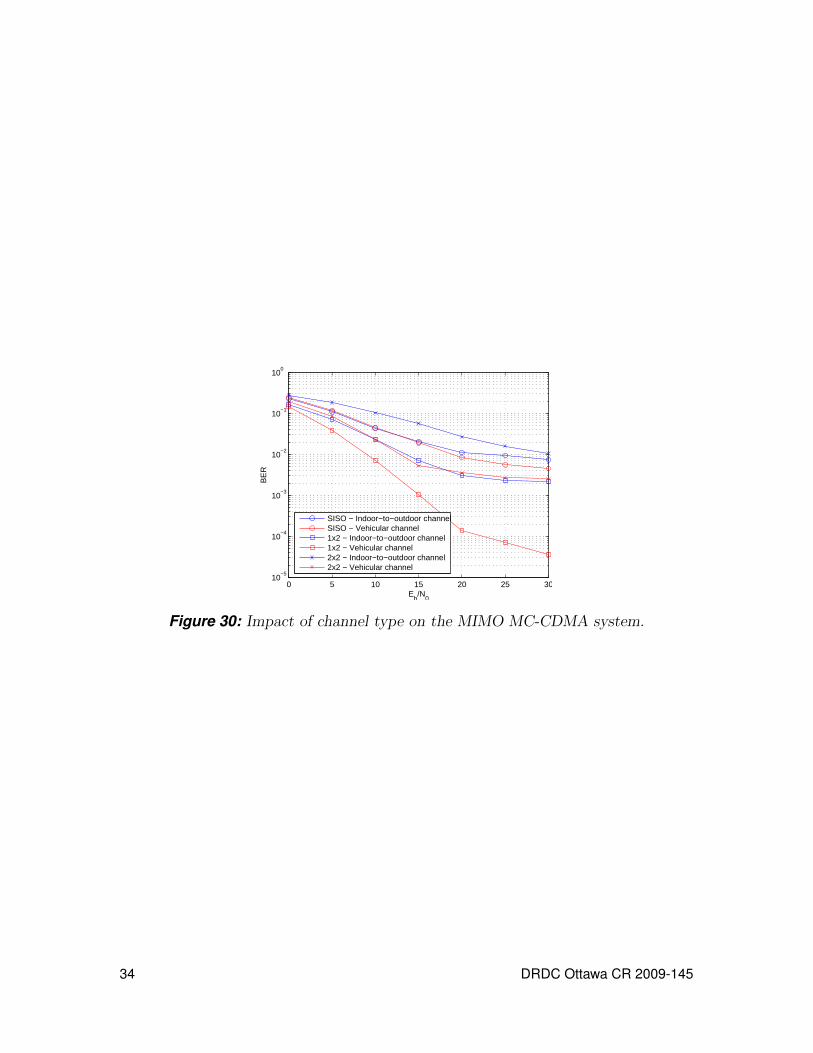
0 5 10 15 20 25 3010
−5
10−4
10−3
10−2
10−1
100
Eb/N
0
BE
R
SISO − Indoor−to−outdoor channelSISO − Vehicular channel1x2 − Indoor−to−outdoor channel1x2 − Vehicular channel2x2 − Indoor−to−outdoor channel2x2 − Vehicular channel
Figure 30: Impact of channel type on the MIMO MC-CDMA system.
34 DRDC Ottawa CR 2009-145

5 MC-CDMA system implementation
In this section, the implementation of the receiver for the indoor-to-outdoor channelconfiguration is chosen as an initial version leading to the implementation of thevehicular channel configuration. The receiver exploits modular implementation anda temporal multiplexing technique so that it can be reused and expanded for futurerequirements. The SISO MC-CDMA receiver is first implemented into a developmentplatform in order to be a basis for the development of the MIMO MC-CDMA receiver.
5.1 Development platform overviewThe following block diagram illustrates the FPGAs and other components and theirbasic interactions with one another.
6 www.nallatech.com NT107-0272 Issue 1 March 9, 2005
XtremeDSP Development Kit-IV Overview
1.2 XtremeDSP Development Kit-IV Functional DiagramThe XtremeDSP Development Kit-IV features three Xilinx FPGAs - a Virtex-4 User FPGA, a Virtex-II FPGA for clockmanagement and a Spartan-II Interface FPGA. The Virtex-4 device is available exclusively for user designs whilst theSpartan-II is supplied pre-configured with firmware for PCI/USB interfacing. The PCI/USB interfacing firmware and lowlevel drivers abstract the PCI/USB interfacing from the user resulting in a simplified design process for user designs/applications. The Interface FPGA communicates directly with the larger User FPGA (XC4VSX35-10FF668) via adedicated communications bus that is made up of the LBUS and ADJOUT busses shown in Figure 2 on page 6.
The Virtex-4 XC4VSX35-10FF668 device is intended to be used for the main part of a user’s design. The Virtex-IIXC2V80-4CS144 is intended to be used as a clock configuration device in a design.
For more information on:
• communications between the User FPGA and the Spartan-II Interface FPGA, refer to “InterfaceFPGA to User FPGA Interface Core” on page 114.
• ADCs, refer to the features section “ADCs” on page 19.
• DACs, refer to the features section “DACs” on page 29.
• ZBT SRAM memory, refer to the features section “ZBT SRAM Memory” on page 41.
• status LEDs, refer to the features section “LEDs” on page 53.
Figure 2: XtremeDSP Development Kit-IV Functional Diagram
Spartan-II
Interface FPGA
Configured with Appropriate
Interface Control Firmware
(i.e. USB/PCI)
Power Supply Status LEDs
32bit 33MHz PCI
Interface
USB Interface
P-Link 0 Digital I/O
Header
Adj In [0:27] Digital I/O
Header
Flying lead JTAG
Header
Programmable Clock Source A
Programmable Clock Source B
*Clock C : Crystal or External
* Note that clock C is NOT initially available in the Kit. It is a socket to allow users to populate their own crystals if required.
2 x ADC
(MCX Inputs)
2 x DAC
(MCX Outputs)
2 banks ZBT
Memory
105 MHz Crystal
Oscillator
2x tri-color
User LEDs
MCX External
Clock Input
Virtex-4 (XC4VSX35-10FF668)
Main User FPGA
Adjacent Out Bus (ADJOUT)
Local Bus (LBUS)
Virtex-II (XC2V80-4CS144) User Clock FPGA
Nallatech Test Headers
(JTAG + RS232)
uP JTAG Header
Parallel-IV JTAG
Header
Connected bus Inter-FPGA Clock nets (source clocks, generated clocks and feedback clock nets)
KEY
Adjacent In Bus
(ADJIN)
Comms P-Link 0
Signals predominantly associated with the general kit, i.e. JTAG access. User Signals part or in whole associated with the FPGAs.
2 pin User Header
(J16)
Figure 31: Block diagram of Xtreme DSP development kit.
The XtremeDSP Development Kit features three Xilinx FPGAs: a Virtex-4 UserFPGA, a Virtex-II FPGA for clock management and a Spartan-II Interface FPGA.
DRDC Ottawa CR 2009-145 35

The User FPGA and Clock FPGA can be configured via USB/PCI interfacing. Moreinformation about the Xtreme DSP development kit is available in the manufacturer’sdatasheet [21].
5.2 Design partitioning in the User FPGA
Reset manager
Host interface logic
Register map
Receiver
DACs control logic
User software (host PC)
User FPGA XC4VSX35F688
ADCs control logicClock manager
Figure 32: The partition of the design in the User FPGA.
We partitioned the design in the User FPGA into several modules which are graphi-cally shown in Figure 32. A host interface communication logic module performs thedata exchange between the host computer and other modules within the user design.The Clock manager manages various clock sources from external oscillators and feed-back clock from the Clock FPGA. The Reset manager manages both synchronous andasynchronous reset signals from multiple sources. The clock and reset manager mod-ules are detailed in Figure 33. The receiver module consists of multiple sub-moduleswhich are mapped to appropriate register addresses and will be explained in moredetails later.
36 DRDC Ottawa CR 2009-145

Programmable oscillator
CLKA
GE
N_C
LKA C
LK_FB3
DCM internal deskew circuit
DAC
DAC
ADC
ADC
Clock FPGA(XC2V80)
User FPGA(XC4VSX35)
DCM internal deskew circuit
CLK
_FP
GA
RE
SE
T
RES
ET_FB
Reset manager
Host interface logic
User control software
(Host PC)
DCM_RESET
DCM_LOCKED
Clock buffers
HW
_RES
ET
SW
_RES
ET
SYS_
CLK
INT_
RE
SET
PC
I_C
LKProgrammable
oscillator
CLKB
Figure 33: Clock and reset managers detail.
DRDC Ottawa CR 2009-145 37

In this figure, the clock source for the receiver design is SYS CLK, which deskewsthe internal feedback clock CLK3 FB from the Clock FPGA in order to allow datagoing to and from the User FPGA to be clocked on the same clock edge as the datain the DACs and ADCs. The clock source for the clock FPGA is provided by theprogrammable oscillator, namely CLKA. The clock source for the host interface logicis PCI CLK, which deskews the external clock source CLKB provided by the secondprogrammable oscillator. The available operating frequencies of the programmableoscillators are as follows: 20 MHz, 25 MHz, 30 MHz, 33.33 MHz, 40 MHz, 45 MHz,50 MHz, 60 MHz, 66.66 MHz, 70 MHz, 75 MHz, 80 MHz, 90 MHz, 100 MHz and120 MHz. Both programmable oscillators are controlled via the user control softwarein the host computer. In this design, clock frequency of 80 MHz and 33.33 MHzare used for the system clock (SYS CLK) and the host interface clock (PCI CLK),respectively. The Reset manager block in the User FPGA is to manage the resetsignal from multiple sources such as the hardware reset signal HW RESET, softwarereset signal SW RESET, digital clock management (DCM) locked signal in bothUser and Clock FPGAs. The software reset source comes from User software inthe host computer via the host interface logic (shaded blocks in Figure 33). TheReset manager generates the internal reset signal INT RESET for the user designfrom either asynchronous HW RESET source or synchronous SW RESET source.It also generates the reset signal CLK FPGA RESET for the Clock FPGA on thedevelopment kit and uses the DCM locked signal RESET FB to generate the resetsignal for the DCM in the User FPGA.
5.3 MC-CDMA implementationIn this section, the FPGA implementation of baseband processing components of theMC-CDMA receiver is considered. The architecture of the receiver is first partitionedinto several blocks in order to perform modular implementation. The main goal ofthis implementation is to minimize the use of multiplier, memory size, and logicswhile achieving the specific functionality.
5.3.1 MC-CDMA system’s architecture
Figure 34 illustrates the block diagram of the receiver. The baseband downlink MC-CDMA receiver works at a system clock rate of 80 MHz and consists of the followingblocks.– Digital front-end: decimates the input data from the analog-to-digital (ADC) de-
vices, sampled at 40 Msps, down to a sampling rate of 5 Msps. This structure alsocompensates for DC offset, amplitude and phase mismatch for both in-phase andquadrature (I&Q) rails.
– Automatic gain control (AGC): maintains the average power of the received signal
38 DRDC Ottawa CR 2009-145
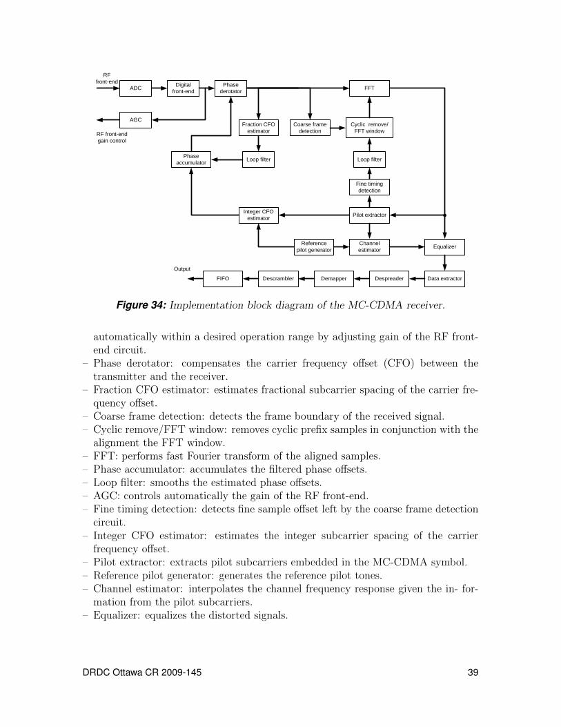
Digital front-end
PhasederotatorADC
RF front-end
Coarse frame detection
Fraction CFO estimator
Cyclic remove/FFT window
FFT
RF front-end gain control
Loop filterPhase accumulator
Pilot extractor
Reference pilot generator
Channel estimator
Fine timing detection
Integer CFO estimator
Equalizer
Loop filter
Data extractorDespreaderDemapperDescramblerFIFO
Output
AGC
Figure 34: Implementation block diagram of the MC-CDMA receiver.
automatically within a desired operation range by adjusting gain of the RF front-end circuit.
– Phase derotator: compensates the carrier frequency offset (CFO) between thetransmitter and the receiver.
– Fraction CFO estimator: estimates fractional subcarrier spacing of the carrier fre-quency offset.
– Coarse frame detection: detects the frame boundary of the received signal.– Cyclic remove/FFT window: removes cyclic prefix samples in conjunction with the
alignment the FFT window.– FFT: performs fast Fourier transform of the aligned samples.– Phase accumulator: accumulates the filtered phase offsets.– Loop filter: smooths the estimated phase offsets.– AGC: controls automatically the gain of the RF front-end.– Fine timing detection: detects fine sample offset left by the coarse frame detection
circuit.– Integer CFO estimator: estimates the integer subcarrier spacing of the carrier
frequency offset.– Pilot extractor: extracts pilot subcarriers embedded in the MC-CDMA symbol.– Reference pilot generator: generates the reference pilot tones.– Channel estimator: interpolates the channel frequency response given the in- for-
mation from the pilot subcarriers.– Equalizer: equalizes the distorted signals.
DRDC Ottawa CR 2009-145 39
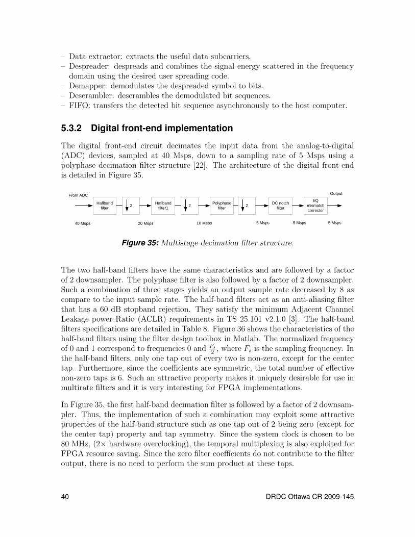
– Data extractor: extracts the useful data subcarriers.– Despreader: despreads and combines the signal energy scattered in the frequency
domain using the desired user spreading code.– Demapper: demodulates the despreaded symbol to bits.– Descrambler: descrambles the demodulated bit sequences.– FIFO: transfers the detected bit sequence asynchronously to the host computer.
5.3.2 Digital front-end implementation
The digital front-end circuit decimates the input data from the analog-to-digital(ADC) devices, sampled at 40 Msps, down to a sampling rate of 5 Msps using apolyphase decimation filter structure [22]. The architecture of the digital front-endis detailed in Figure 35.
Haflband filter
Haflband filter1
Polyphase filter2 2 2
From ADC
40 Msps 20 Msps 10 Msps 5 Msps
DC notch filter
I/Q mismatch corrector
5 Msps 5 Msps
Output
Figure 35: Multistage decimation filter structure.
The two half-band filters have the same characteristics and are followed by a factorof 2 downsampler. The polyphase filter is also followed by a factor of 2 downsampler.Such a combination of three stages yields an output sample rate decreased by 8 ascompare to the input sample rate. The half-band filters act as an anti-aliasing filterthat has a 60 dB stopband rejection. They satisfy the minimum Adjacent ChannelLeakage power Ratio (ACLR) requirements in TS 25.101 v2.1.0 [3]. The half-bandfilters specifications are detailed in Table 8. Figure 36 shows the characteristics of thehalf-band filters using the filter design toolbox in Matlab. The normalized frequencyof 0 and 1 correspond to frequencies 0 and Fs
2, where Fs is the sampling frequency. In
the half-band filters, only one tap out of every two is non-zero, except for the centertap. Furthermore, since the coefficients are symmetric, the total number of effectivenon-zero taps is 6. Such an attractive property makes it uniquely desirable for use inmultirate filters and it is very interesting for FPGA implementations.
In Figure 35, the first half-band decimation filter is followed by a factor of 2 downsam-pler. Thus, the implementation of such a combination may exploit some attractiveproperties of the half-band structure such as one tap out of 2 being zero (except forthe center tap) property and tap symmetry. Since the system clock is chosen to be80 MHz, (2× hardware overclocking), the temporal multiplexing is also exploited forFPGA resource saving. Since the zero filter coefficients do not contribute to the filteroutput, there is no need to perform the sum product at these taps.
40 DRDC Ottawa CR 2009-145

Parameter ValueNormalized Passband Frequency 0.25Passband Ripple (dB) 0.001Normalized Stopband Frequency 0.5Stopband Attenuation (dB) 60Filter Taps 19
Table 8: Half-band filter specifications.
0 0.1 0.2 0.3 0.4 0.5 0.6 0.7 0.8 0.9
−70
−60
−50
−40
−30
−20
−10
0
Normalized Frequency (×π rad/sample)
Mag
nitu
de (
dB)
Magnitude Response (dB)
(a) Magnitude response.
0 0.1 0.2 0.3 0.4 0.5 0.6 0.7 0.8 0.9
−20
−18
−16
−14
−12
−10
−8
−6
−4
−2
0
Normalized Frequency (×π rad/sample)
Pha
se (
radi
ans)
Phase Response
(b) Phase response.
0 2 4 6 8 10 12 14 16 18−0.1
0
0.1
0.2
0.3
0.4
0.5
Samples
Am
plitu
de
Impulse Response
(c) Impulse response.
0 2 4 6 8 10 12 14 16 18
0
0.2
0.4
0.6
0.8
1
Samples
Am
plitu
de
Step Response
(d) Step response.
Figure 36: Characteristics of the half-band filters.
We define the z-transform of the non-zero values of the half-band filter structurerepresenting a set of delayed filter coefficients as Equation(18).
H(Z) =18∑n=0
ℎ(n)Z−n (18)
Equation (19) is the polyphase partition of Equation (18) representing the filter as thesum of successively delayed subfilter with the coefficients separated by a decimationfactor of 2.
DRDC Ottawa CR 2009-145 41

H(Z) = ℎ(0) + ℎ(2)Z−2 + ℎ(4)Z−4 + ℎ(6)Z−6 + ℎ(8)Z−8 + ℎ(10)Z−10
+ ℎ(12)Z−12 + ℎ(14)Z−14 + ℎ(16)Z−16 + ℎ(18)Z−18) + Z−1ℎ(9)Z−8 (19)
We define H0(Z2) and H1(Z2) as the set of even and odd taps, respectively, and wehave
H0(Z2) = ℎ(0) + ℎ(2)Z−2 + ℎ(4)Z−4 + ℎ(6)Z−6 + ℎ(8)Z−8 + ℎ(10)Z−10
+ ℎ(12)Z−12 + ℎ(14)Z−14 + ℎ(16)Z−16 + ℎ(18)Z−18
= ℎ(0)(1 + Z−18) + ℎ(2)(Z−2 + Z−18) + ℎ(4)(Z−4 + Z−14)
+ ℎ(6)(Z−6 + Z−12) + ℎ(8)(Z−8 + Z−10)
(20)
H1(Z2) = ℎ(9)Z−8 (21)
Finally, Equation (22) is a compact representation of Equation (19).
H(Z) = H0(Z2) + Z−1H1(Z2) (22)
These definitions naturally leads to the 2-arm polyphase structure as shown in Fig-ure 37.
( )20H Z
( )21H Z
2
1Z −
Figure 37: Polyphase partition for the half-band decimation filter.
The output downsampler operates on every second input sample. Applying the equiv-alent conversions in [22, p. 750], a downsampler factor of 2 is pulled to the inputside of each subfilter as shown in Figure 38, thus yielding 4 clock cycles per outputsample for filtering operations (2 clock cycles per input sample). We can see thatthe interaction of delays lines in each arm with the synchronous downsamplers can
42 DRDC Ottawa CR 2009-145

( )20H Z
( )21H Z
2
1Z −
( )0H Z
( )1H Z
1Z −
2
2
Figure 38: Polyphase partition for the half-band decimation filter with input down-samplers.
( )20H Z
( )21H Z
2
1Z −
( )0H Z
( )1H Z
1Z −
2
2
( )0H Z
( )1H Z
Figure 39: Polyphase partition for the half-band decimation filter with input com-mutator.
be understood as an input commutator that feeds successive samples to successiveinput of the subfilters as illustrated in Figure 39. It is also noteworthy that the uppersubfilter H0(Z) can exploit tap symmetry in order to obtain a folded structure. Thisleads to the structure of the half-band decimation filter in Figure 40. Since there areonly 5 taps in the upper arm and 4 clock cycles per input sample, it is possible toimplement the upper arm with 2 embedded multipliers which are time multiplexed.The lower arm has only one tap and its coefficient is the center tap which is equalto 0.5. Thus, the lower arm is implemented by shifting the input sample to the leftone bit instead of using a multiplier. Therefore, a small 8×16 ROM bank is requiredto store 5 tap coefficients which are quantized into 16-bit values for the upper arm(unused address locations are set to zero).
The polyphase decimation filter is also designed based on the minimum ACLR re-quirements. The specifications are detailed in Table 9 and its characteristics aregraphically shown in Figure 41. The resulting polyphase filter has 128 symmetricaltaps; the number of effective tap is therefore 64 taps per arm.
DRDC Ottawa CR 2009-145 43

1Z− 1Z − 1Z − 1Z −
h(0)
h(2)
h(4)
h(6)
h(8)
1Z− 1Z − 1Z − 1Z −
1Z −
5Z − h(9)
Figure 40: Polyphase half-band decimation filter structure.
Parameter ValueNormalized Passband Frequency 0.45Passband Ripple (dB) 0.01Normalized Stopband Frequency 0.5Stopband Attenuation (dB) 80Filter Taps 128
Table 9: Polyphase decimation filter specifications.
44 DRDC Ottawa CR 2009-145

0 0.1 0.2 0.3 0.4 0.5 0.6 0.7 0.8 0.9
−90
−80
−70
−60
−50
−40
−30
−20
−10
0
Normalized Frequency (×π rad/sample)
Mag
nitu
de (
dB)
Magnitude Response (dB)
(a) Magnitude response.
0 0.1 0.2 0.3 0.4 0.5 0.6 0.7 0.8 0.9
−100
−90
−80
−70
−60
−50
−40
−30
−20
−10
0
Normalized Frequency (×π rad/sample)
Pha
se (
radi
ans)
Phase Response
(b) Phase response.
0 20 40 60 80 100 120−0.1
0
0.1
0.2
0.3
0.4
Samples
Am
plitu
de
Impulse Response
(c) Impulse response.
0 20 40 60 80 100 120
0
0.2
0.4
0.6
0.8
1
Samples
Am
plitu
de
Step Response
(d) Step response.
Figure 41: Characteristics of the polyphase decimation filter.
DRDC Ottawa CR 2009-145 45
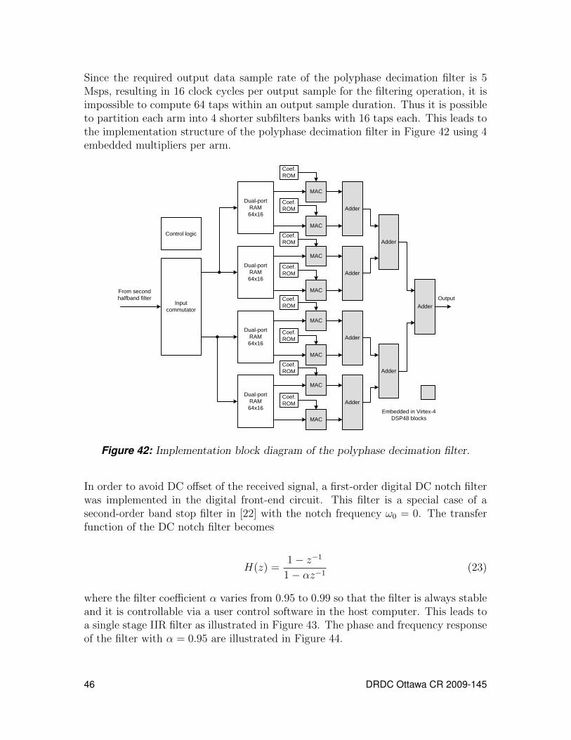
Since the required output data sample rate of the polyphase decimation filter is 5Msps, resulting in 16 clock cycles per output sample for the filtering operation, it isimpossible to compute 64 taps within an output sample duration. Thus it is possibleto partition each arm into 4 shorter subfilters banks with 16 taps each. This leads tothe implementation structure of the polyphase decimation filter in Figure 42 using 4embedded multipliers per arm.
Input commutator
Dual-port RAM64x16
From second halfband filter
Dual-port RAM64x16
Dual-port RAM64x16
Control logic
Coef. ROM
Output
Embedded in Virtex-4 DSP48 blocks
Dual-port RAM64x16
Adder
MAC
MAC
MAC
MAC
Coef. ROM
Coef. ROM
Coef. ROM
Coef. ROM
MAC
MAC
MAC
MAC
Coef. ROM
Coef. ROM
Coef. ROM
Adder
Adder
Adder
Adder
Adder
Adder
Figure 42: Implementation block diagram of the polyphase decimation filter.
In order to avoid DC offset of the received signal, a first-order digital DC notch filterwas implemented in the digital front-end circuit. This filter is a special case of asecond-order band stop filter in [22] with the notch frequency !0 = 0. The transferfunction of the DC notch filter becomes
H(z) =1− z−1
1− �z−1(23)
where the filter coefficient � varies from 0.95 to 0.99 so that the filter is always stableand it is controllable via a user control software in the host computer. This leads toa single stage IIR filter as illustrated in Figure 43. The phase and frequency responseof the filter with � = 0.95 are illustrated in Figure 44.
46 DRDC Ottawa CR 2009-145

Output
1−Z
α
Input
Figure 43: Structure of first-order digital DC notch filter.
−1 −0.8 −0.6 −0.4 −0.2 0 0.2 0.4 0.6 0.8−3.5
−3
−2.5
−2
−1.5
−1
−0.5
0
0.5
1
Normalized Frequency (×π rad/sample)
Mag
nitu
de (
dB)
Magnitude Response (dB)
(a) Frequency response
−0.8 −0.6 −0.4 −0.2 0 0.2 0.4 0.6 0.8 1
−1.5
−1
−0.5
0
0.5
1
1.5
Normalized Frequency (×π rad/sample)
Pha
se (
radi
ans)
Phase Response
(b) Phase response
Figure 44: First-order digital DC notch filter characteristics with � = 0.95.
DRDC Ottawa CR 2009-145 47

In practical receivers, the phase and amplitude response of the I and Q branches arenever exactly the same. This causes frequency translation in the I and Q branches.Therefore, it is necessary to perform I/Q mismatch correction at the end of the front-end unit. To illustrate this, consider a simple form of the I/Q mismatch signal as
I(t) = � cos(!t) (24)
Q(t) = sin(!t+ �) (25)
where � and � are amplitude and phase mismatch, respectively. Ideally, � = 1 and� = 0, but in practical cases � and � are always different from the ideal values. Asimple scheme to correct a small amount of phase and amplitude mismatch derivedfrom [23] is described in the following equations
I ′(t) = � cos(!t)1
�= cos(!t) (26)
Q′(t) =1
�tan(�)� cos(!t) +
sin(!t+ �)
cos(�)≈ sin(!t) (27)
Using this principle, the architecture of the I/Q mismatch corrector is illustrated inFigure 45. This architecture exploits temporal multiplexing with the use of a realmultiplier to perform the phase and amplitude correction for both I and Q branches.In this figure, the ROMs contain the pre-computed values of the inversion of theamplitude mismatch 1
�, the tangent of the phase mismatch tan(�) and the inversion
of the cosine of the phase mismatch 1cos(�)
, so that the value of � and � can be adjustedby user control software in the host computer.
The FPGA resource utilization for the digital front-end circuit is given in Table 10.Timing analysis results show that the critical path is 5.841 ns, i.e. the maximumclock frequency is 171.208 MHz.
Logic utilization Total Used UtilizationNumber of Slices 15360 1020 6 %
Number of FIFO16/RAMB16s 192 34 17 %Number of DSP48s 192 24 12 %
Table 10: Device utilization summary for the digital front-end circuit.
48 DRDC Ottawa CR 2009-145

1/Alpha ROM
Real
Alpha
Multiplier
Tan(Phi) ROM
MUX
Phi
1/cos(Phi) ROM
MUX
Imag
Adder
Real
DFF
Truncate
Truncate
Imag
DFFDEMUX
Embedded in Virtex-4 DSP48 blocks
Figure 45: I/Q mismatch corrector unit architecture.
5.3.3 Digital AGC circuit implementation
The automatic gain control (AGC) circuit is implemented as illustrated in Figure 46.The power approximation block calculates ∣Re∣ + ∣Im∣ of the decimated complexsample from the digital front-end for the power calculation. The accumulator andscaling circuit performs averaging of the approximated power of the signal. Theerror power is fed to a loop filter to track the variation of the power error. Thecharacteristics of the loop filter affect the settling time and tracking behavior of theAGC loop. The loop filter will be detailed in the loop filter implementation section.The RF front-end controller converts the filtered power error signal to appropriatepower control word for the RF front-end.
The FPGA resource utilization for the digital AGC circuit is given in Table 11.Timing analysis results show that the critical path is 3.552 ns, i.e. the maximumclock frequency is 281.524 MHz.
Logic utilization Total Used UtilizationNumber of Slices 15360 300 1 %
Number of FIFO16/RAMB16s 192 1 < 1 %
Table 11: Device utilization summary for the digital AGC circuit.
DRDC Ottawa CR 2009-145 49
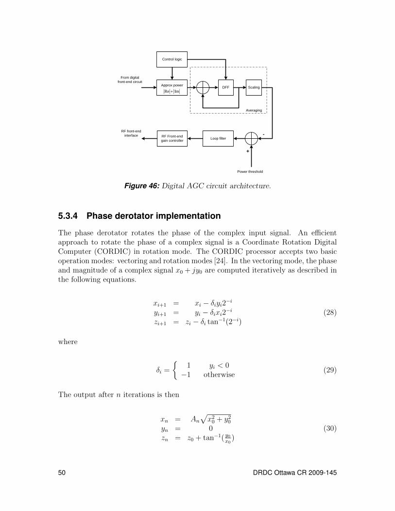
From digital front-end circuit
RF front-end interface
Approx power
Re Im+DFF
Power threshold
Loop filter
+
-RF Front-end gain controller
Control logic
Scaling
Averaging
Figure 46: Digital AGC circuit architecture.
5.3.4 Phase derotator implementation
The phase derotator rotates the phase of the complex input signal. An efficientapproach to rotate the phase of a complex signal is a Coordinate Rotation DigitalComputer (CORDIC) in rotation mode. The CORDIC processor accepts two basicoperation modes: vectoring and rotation modes [24]. In the vectoring mode, the phaseand magnitude of a complex signal x0 + jy0 are computed iteratively as described inthe following equations.
xi+1 = xi − �iyi2−iyi+1 = yi − �ixi2−izi+1 = zi − �i tan−1(2−i)
(28)
where
�i =
{1 yi < 0−1 otherwise
(29)
The output after n iterations is then
xn = An√x2
0 + y20
yn = 0zn = z0 + tan−1( y0
x0)
(30)
50 DRDC Ottawa CR 2009-145
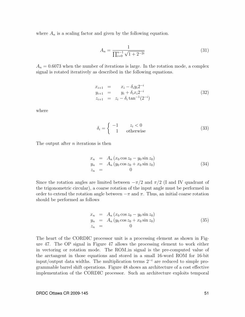
where An is a scaling factor and given by the following equation.
An =1∏n−1
i=0
√1 + 2−2i
(31)
An = 0.6073 when the number of iterations is large. In the rotation mode, a complexsignal is rotated iteratively as described in the following equations.
xi+1 = xi − �iyi2−iyi+1 = yi + �ixi2
−i
zi+1 = zi − �i tan−1(2−i)(32)
where
�i =
{−1 zi < 0
1 otherwise(33)
The output after n iterations is then
xn = An (x0 cos z0 − y0 sin z0)yn = An (y0 cos z0 + x0 sin z0)zn = 0
(34)
Since the rotation angles are limited between −�/2 and �/2 (I and IV quadrant ofthe trigonometric circular), a coarse rotation of the input angle must be performed inorder to extend the rotation angle between −� and �. Thus, an initial coarse rotationshould be performed as follows
xn = An (x0 cos z0 − y0 sin z0)yn = An (y0 cos z0 + x0 sin z0)zn = 0
(35)
The heart of the CORDIC processor unit is a processing element as shown in Fig-ure 47. The OP signal in Figure 47 allows the processing element to work eitherin vectoring or rotation mode. The ROM in signal is the pre-computed value ofthe arctangent in those equations and stored in a small 16-word ROM for 16-bitinput/output data widths. The multiplication terms 2−i are reduced to simple pro-grammable barrel shift operations. Figure 48 shows an architecture of a cost effectiveimplementation of the CORDIC processor. Such an architecture exploits temporal
DRDC Ottawa CR 2009-145 51
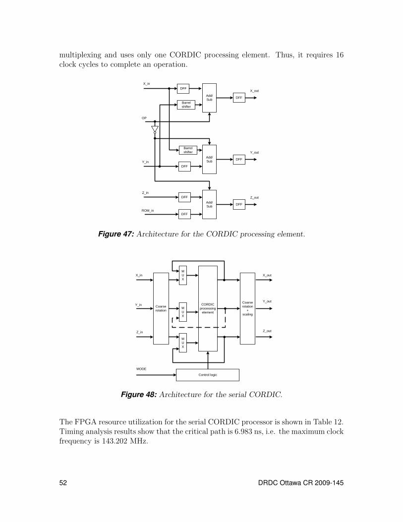
multiplexing and uses only one CORDIC processing element. Thus, it requires 16clock cycles to complete an operation.
Add/Sub
Barrel shifter
DFF
DFF
X_in
X_out
OP
Add/Sub DFF
Y_in
Y_out
DFF
Barrel shifter
Add/Sub DFF
Z_inZ_outDFF
ROM_inDFF
Figure 47: Architecture for the CORDIC processing element.
X_in
Y_in
Z_in
Coarse rotation
CORDIC processing
element
Coarse rotation
+ scaling
X_out
Y_out
Z_out
Control logic
MODE
MUX
MUX
MUX
Figure 48: Architecture for the serial CORDIC.
The FPGA resource utilization for the serial CORDIC processor is shown in Table 12.Timing analysis results show that the critical path is 6.983 ns, i.e. the maximum clockfrequency is 143.202 MHz.
52 DRDC Ottawa CR 2009-145

Logic utilization Total Used UtilizationNumber of Slices 15360 252 1 %
Number of DSP48s 192 2 1 %
Table 12: Device utilization summary for the serial CORDIC processor.
5.3.5 Coarse frame detector implementation
In our design, a training symbol structure typical of wireless LANs (e.g. 802.11)is periodically transmitted in the time domain in order to help the receiver detectthe transmit frame and track the carrier frequency offset (CFO) as illustrated inFigure 49. In this figure, TS denotes the duration of an MC-CDMA symbol and t1 tot10 are the repeat sequences within the preamble duration.
1t 3t 4t 5t 6t 8t 9t7t 10t
ST
2t GI DATA
ST
Figure 49: Training symbol structure.
A training-symbol-based coarse frame detection block detects the frame boundaryusing convolution between the received samples and the training symbol [25]. Thetiming metric M1(�) is computed by convolution of the received sequence with theknown training-symbol S and is expressed as
M1(�) =Ns−1∑k=0
r(� + k)× S∗(k) (36)
where Ns is the number of samples in one duration of ti (i = 1, .., 10) in the trainingsymbol, (.)∗ denotes complex conjugate and r is the received samples. Direct FIRfilter implementation of the convolution block requires much logic resources, i.e. thenumber of complex multipliers in the direct implementation is in proportion to thelength of the short preamble sequence Ns (in this case, Ns = 64 samples). Byexploiting the system clock of 80 MHz (16 times faster than the data rate), thetemporal multiplexing is also exploited for FPGA resource savings. This leads to theconvolution block architecture as shown in Figure 50.
The proposed architecture uses only 4 complex multipliers that consists of 3 real mul-tipliers each. The accumulators are implemented by exploiting the advance featuresof the Virtex-4 DSP48 blocks without any extra logic. The delay elements are imple-mented using dual-port block RAM in FPGA. It is also noteworthy that the delay
DRDC Ottawa CR 2009-145 53

16-word DPRAM
To moving sum
From decimation filter
16-word DPRAM
16-word DPRAM
16-word DPRAM
MAC
ROM1
MAC
MAC
MAC
To auto-correlator
MUX ACCROM2
ROM3
ROM4Embedded in Virtex-4
DSP48 blocks
Magnitude
Figure 50: Architecture for the convolution block.
elements can be shared for the autocorrelator circuit inside the fractional CFO esti-mator block in order to save the memory block. Both input and output of the blockare truncated to 16-bit precision to maintain the same dynamic range and precision.
The FPGA resource utilization for the convolution circuit is given in Table 13. Fur-thermore, timing analysis result shows that the critical path is 5.136 ns, i.e. themaximum clock frequency is 194.708 MHz. Figure 51 shows the VHDL simulationresults of a received frame. There are 10 peaks at the beginning of the output of theconvolution circuit indicating that the received preamble correlates the known shortpreamble sequence of length Ns at the receiver.
The convoluted output results must perform moving sums over 10 consecutive repeat
54 DRDC Ottawa CR 2009-145
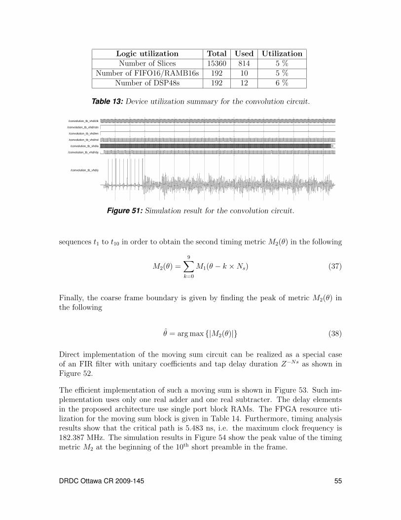
Logic utilization Total Used UtilizationNumber of Slices 15360 814 5 %
Number of FIFO16/RAMB16s 192 10 5 %Number of DSP48s 192 12 6 %
Table 13: Device utilization summary for the convolution circuit.
0
0 200000000 400000000 600000000 800000000
/convolution_tb_vhd/clk
/convolution_tb_vhd/rstn
/convolution_tb_vhd/en
/convolution_tb_vhd/nd
/convolution_tb_vhd/a 0
/convolution_tb_vhd/rdy
/convolution_tb_vhd/y
Entity:convolution_tb_vhd Architecture:behavior Date: Mon Dec 03 4:45:00 PM Eastern Standard Time 2007 Row: 1 Page: 1
Figure 51: Simulation result for the convolution circuit.
sequences t1 to t10 in order to obtain the second timing metric M2(�) in the following
M2(�) =9∑
k=0
M1(� − k ×Ns) (37)
Finally, the coarse frame boundary is given by finding the peak of metric M2(�) inthe following
� = arg max {∣M2(�)∣} (38)
Direct implementation of the moving sum circuit can be realized as a special caseof an FIR filter with unitary coefficients and tap delay duration Z−Ns as shown inFigure 52.
The efficient implementation of such a moving sum is shown in Figure 53. Such im-plementation uses only one real adder and one real subtracter. The delay elementsin the proposed architecture use single port block RAMs. The FPGA resource uti-lization for the moving sum block is given in Table 14. Furthermore, timing analysisresults show that the critical path is 5.483 ns, i.e. the maximum clock frequency is182.387 MHz. The simulation results in Figure 54 show the peak value of the timingmetric M2 at the beginning of the 10th short preamble in the frame.
DRDC Ottawa CR 2009-145 55

Input NsZ− NsZ− NsZ− NsZ− NsZ− NsZ− NsZ− NsZ−
To peak detector
NsZ−
SUM
Figure 52: Direct implementation of the moving sum circuit.
640-word BRAMFrom convolution
64-word BRAM
To peak detector
Figure 53: Architecture for the convolution moving sum circuit.
Logic utilization Total Used UtilizationNumber of Slices 15360 64 < 1 %
Number of Slice Flip Flops 30720 93 < 1 %Number of FIFO16/RAMB16s 192 2 1 %
Table 14: Device utilization summary for the convolution moving sum circuit.
5.3.6 Fractional CFO estimator implementation
The purpose of fractional CFO estimator is to find the fractional subcarrier spacingfor the CFO. The fractional CFO is estimated based on the correlation between thereceived sequence and its delayed version. Such correlation gives the phase differencebetween the repeat sequence in the preamble and its delayed version at the timingestimate. The correlation of Ns samples is given by
56 DRDC Ottawa CR 2009-145
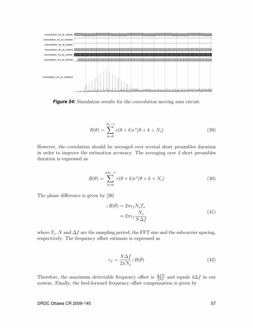
0
0 200000000 400000000 600000000 800000000
/convolution_ms_tb_vhd/clk
/convolution_ms_tb_vhd/rstn
/convolution_ms_tb_vhd/en
/convolution_ms_tb_vhd/nd
/convolution_ms_tb_vhd/din 0
/convolution_ms_tb_vhd/rdy
/convolution_ms_tb_vhd/dout
Entity:convolution_ms_tb_vhd Architecture:behavior Date: Mon Dec 03 4:49:43 PM Eastern Standard Time 2007 Row: 1 Page: 1
Figure 54: Simulation results for the convolution moving sum circuit.
R(�) =Ns−1∑k=0
r(� + k)r∗(� + k +Ns) (39)
However, the correlation should be averaged over several short preambles durationin order to improve the estimation accuracy. The averaging over 4 short preamblesduration is expressed as
R(�) =4Ns−1∑k=0
r(� + k)r∗(� + k +Ns) (40)
The phase difference is given by [26]
∕ R(�) = 2��fNsTs
= 2��fNs
NΔf
(41)
where Ts, N and Δf are the sampling period, the FFT size and the subcarrier spacing,respectively. The frequency offset estimate is expressed as
�f =NΔf
2�Ns
∕ R(�) (42)
Therefore, the maximum detectable frequency offset is ΔfN2Ns
and equals 4Δf in oursystem. Finally, the feed-forward frequency offset compensation is given by
DRDC Ottawa CR 2009-145 57
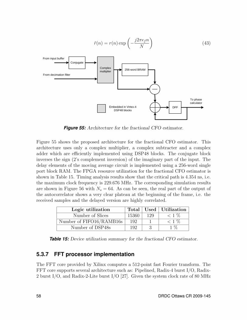
r(n) = r(n) exp
(−j2��fn
N
)(43)
ConjugateFrom input buffer
DFF
To phase calculator
From decimation filter
Complex multiplier 256-word BRAM
Embedded in Virtex-4 DSP48 blocks
Figure 55: Architecture for the fractional CFO estimator.
Figure 55 shows the proposed architecture for the fractional CFO estimator. Thisarchitecture uses only a complex multiplier, a complex subtracter and a complexadder which are efficiently implemented using DSP48 blocks. The conjugate blockinverses the sign (2’s complement inversion) of the imaginary part of the input. Thedelay elements of the moving average circuit is implemented using a 256-word singleport block RAM. The FPGA resource utilization for the fractional CFO estimator isshown in Table 15. Timing analysis results show that the critical path is 4.354 ns, i.e.the maximum clock frequency is 229.676 MHz. The corresponding simulation resultsare shown in Figure 56 with Ns = 64. As can be seen, the real part of the output ofthe autocorrelator shows a very clear plateau at the beginning of the frame, i.e. thereceived samples and the delayed version are highly correlated.
Logic utilization Total Used UtilizationNumber of Slices 15360 129 < 1 %
Number of FIFO16/RAMB16s 192 1 < 1 %Number of DSP48s 192 3 1 %
Table 15: Device utilization summary for the fractional CFO estimator.
5.3.7 FFT processor implementation
The FFT core provided by Xilinx computes a 512-point fast Fourier transform. TheFFT core supports several architecture such as: Pipelined, Radix-4 burst I/O, Radix-2 burst I/O, and Radix-2-Lite burst I/O [27]. Given the system clock rate of 80 MHz
58 DRDC Ottawa CR 2009-145

0
0
0 0
0 0
0 200000000 400000000 600000000 800000000
/autocorrelator_tb_vhd/clk
/autocorrelator_tb_vhd/rstn
/autocorrelator_tb_vhd/en
/autocorrelator_tb_vhd/nd
/autocorrelator_tb_vhd/a_re 0
/autocorrelator_tb_vhd/a_im 0
/autocorrelator_tb_vhd/b_re 0 0
/autocorrelator_tb_vhd/b_im 0 0
/autocorrelator_tb_vhd/rdy
/autocorrelator_tb_vhd/y_re
/autocorrelator_tb_vhd/y_im
Entity:autocorrelator_tb_vhd Architecture:behavior Date: Mon Dec 03 4:36:59 PM Eastern Standard Time 2007 Row: 1 Page: 1
Figure 56: Simulation results for the fractional CFO estimator.
and data rate of 5 Msps, the Radix-2-Lite burst I/O architecture took 70.787 �s totransform 512 data points. This is less than a MC-CDMA symbol duration of 128 �s.Therefore, we choose this architecture for our design in order to save logic resourceswhile maintaining the performance.
512x32 input FIFO
From the pre-FFT frequency offset corrector
FFT control logic
FIFO
full
FIFO
em
pty
FFT core 512x32 block RAM
FFT
requ
est
WR address
Reordered frequency bins output
RD address
Don
e MUX
Up counter
FFT output
Figure 57: FFT processor architecture.
Since the actual input sample rate to the FFT core is 80 Msps, it is necessary to
DRDC Ottawa CR 2009-145 59
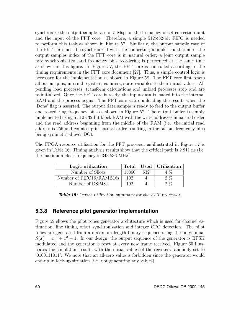
synchronize the output sample rate of 5 Msps of the frequency offset correction unitand the input of the FFT core. Therefore, a simple 512×32-bit FIFO is neededto perform this task as shown in Figure 57. Similarly, the output sample rate ofthe FFT core must be synchronized with the connecting module. Furthermore, theoutput samples index of the FFT core is in natural order; a joint output samplerate synchronization and frequency bins reordering is performed at the same timeas shown in this figure. In Figure 57, the FFT core is controlled according to thetiming requirements in the FFT core document [27]. Thus, a simple control logic isnecessary for the implementation as shown in Figure 58. The FFT core first resetsall output pins, internal registers, counters, state variables to their initial values. Allpending load processes, transform calculations and unload processes stop and arere-initialized. Once the FFT core is ready, the input data is loaded into the internalRAM and the process begins. The FFT core starts unloading the results when the‘Done’ flag is asserted. The output data sample is ready to feed to the output bufferand re-ordering frequency bins as shown in Figure 57. The output buffer is simplyimplemented using a 512×32-bit block RAM with the write addresses in natural orderand the read address beginning from the middle of the RAM (i.e. the initial readaddress is 256 and counts up in natural order resulting in the output frequency binsbeing symmetrical over DC).
The FPGA resource utilization for the FFT processor as illustrated in Figure 57 isgiven in Table 16. Timing analysis results show that the critical path is 2.911 ns (i.e.the maximum clock frequency is 343.536 MHz).
Logic utilization Total Used UtilizationNumber of Slices 15360 632 4 %
Number of FIFO16/RAMB16s 192 4 2 %Number of DSP48s 192 4 2 %
Table 16: Device utilization summary for the FFT processor.
5.3.8 Reference pilot generator implementation
Figure 59 shows the pilot tones generator architecture which is used for channel es-timation, fine timing offset synchronization and integer CFO detection. The pilottones are generated from a maximum length binary sequence using the polynomialS(x) = x10 + x3 + 1. In our design, the output sequence of the generator is BPSKmodulated and the generator is reset at every new frame received. Figure 60 illus-trates the simulation results with the initial values of the registers randomly set to‘0100111011’. We note that an all-zero value is forbidden since the generator wouldend-up in lock-up situation (i.e. not generating any values).
60 DRDC Ottawa CR 2009-145

RESET = ‘0’
PROCESSING
BUSY = ‘0’
LOAD
CLEAR
IDLE
UNLOAD
FFT_REQUEST = ‘1’
BUSY = ‘1’
DONE = ‘0’
DONE = ‘1’
Figure 58: State machine for the FFT processor.
DFF9
DFF8
DFF3
DFF2
DFF1
DFF0
DFF4
BPSK modulator
Pilot tones
Figure 59: Pilot tone generator architecture.
The FPGA resource utilization for the pilot tone generator is given in Table 17.Timing analysis results show that the critical path is 0.986 ns (i.e. the maximumclock frequency is 1013.787 MHz).
DRDC Ottawa CR 2009-145 61

0100111011
0 18318 -18318 18318 -18318 18318 -18318 18318 -18318 18318
0 1000000 2000000 3000000 4000000 5000000
/pilot_generator_tb_vhd/clk
/pilot_generator_tb_vhd/rstn
/pilot_generator_tb_vhd/en
/pilot_generator_tb_vhd/load
/pilot_generator_tb_vhd/init 0100111011
/pilot_generator_tb_vhd/rdy
/pilot_generator_tb_vhd/uut/ser_out
/pilot_generator_tb_vhd/pout 0 18318 -18318 18318 -18318 18318 -18318 18318 -18318 18318
Entity:pilot_generator_tb_vhd Architecture:behavior Date: Mon Mar 31 9:23:57 PM Eastern Daylight Time 2008 Row: 1 Page: 1
Figure 60: Simulation results for the pilot tones generator.
Logic utilization Total Used UtilizationNumber of Slices 15360 8 <1 %
Table 17: Device utilization summary for the pilot generator.
5.3.9 Pilot tone extractor implementation
The pilot tone extractor unit in Figure 61 exploits temporal multiplexing of the FFToutput buffer between data subcarriers and pilot tone subcarriers. It is implementedin conjunction with the frequency bins re-ordering inside the FFT processor unit.The pilot tone subcarriers indexes are pre-computed and stored in a small ROM.Figure 62 shows the simulation results of the pilot extractor with 8 pilot subcarriersextracted from the FFT output buffer.
Pilot tone subcarrier index ROM
From FFT output
Up counter
512 x 32block RAM
Address
Pilot tones output
FFT output buffer
Figure 61: Pilot tone extractor architecture.
The FPGA resource utilization for the pilot tone extractor unit excluding the FFTprocessor and buffers is given in Table 18. Timing analysis results show that thecritical path is 2.155 ns, i.e. the maximum clock frequency is 464.113 MHz.
62 DRDC Ottawa CR 2009-145

FD7CFF66 FD9A0119 019700B0 FF3FFFC2 FFD9FFAA 007F00EB FF20FFAE 0019FFA4 FDBA0028 021AFF89 060E006A 00820101 00B500E2
0
0
0
256 257 258 259 260 261 262 263 264 265 266 267 268
31 95 159 223 287 351 415 479 31
00000000 2D07FFD3 2D38FFEC D276FFF4 D2B7FFF4 2D850007 2D4E000A D2CEFFFA 2CFB000E
353500000 ps 354000000 ps 354500000 ps 355000000 ps 355500000 ps
/top_tb_vhd/clk
/top_tb_vhd/rstn
/top_tb_vhd/en
/top_tb_vhd/nd
/top_tb_vhd/din FD7CFF66 FD9A0119 019700B0 FF3FFFC2 FFD9FFAA 007F00EB FF20FFAE 0019FFA4 FDBA0028 021AFF89 060E006A 00820101 00B500E2
/top_tb_vhd/uut/inst_fft_processor/y_re 0
/top_tb_vhd/uut/inst_fft_processor/y_im 0
/top_tb_vhd/uut/inst_fft_processor/wr_addr 0
/top_tb_vhd/uut/inst_fft_processor/inst_freq_mapper/rd_addr 256 257 258 259 260 261 262 263 264 265 266 267 268
/top_tb_vhd/uut/inst_fft_processor/pilot_addr 31 95 159 223 287 351 415 479 31
/top_tb_vhd/uut/inst_fft_processor/pilot_rdy
/top_tb_vhd/uut/inst_fft_processor/pilot_dout 00000000 2D07FFD3 2D38FFEC D276FFF4 D2B7FFF4 2D850007 2D4E000A D2CEFFFA 2CFB000E
Entity:top_tb_vhd Architecture:behavior Date: Tue Jun 10 7:08:41 AM Eastern Daylight Time 2008 Row: 1 Page: 1
Figure 62: Simulation results of the pilot extractor unit.
Logic utilization Total Used UtilizationNumber of Slices 15360 35 < 1 %
Table 18: Device utilization summary for the pilot tone extractor.
5.3.10 Fine timing synchronization implementation
Figure 63 shows the architecture of the fine timing synchronization unit. It works inthe frequency domain by finding the phase difference between adjacent pilot subcar-riers as proposed by the authors in [28, 29]. The fine timing offset can be accuratelyestimated as follows
Δn =N
2�Nf
arg
{P∑i=2
Zl,piZ∗l,pi−1
}(44)
where N is the FFT size, Nf = 64 is the pilot tone spacing, P is the number ofpilot tones in an MC-CDMA symbol (in this case, P = 8), Zl,pi is the ith receivedpilot tone in the lth MC-CDMA symbol and (.)∗ denotes complex conjugate. Thephase difference of the two adjacent pilot tones is done by a complex multiplicationbetween Zl,pi and Z∗l,pi−1
using the dedicated DSP48s blocks. The estimation of thetiming offset is implemented by reusing the CORDIC processor in vectoring mode.Given the FFT size of 512, it can be shown that the algorithm can track the timingoffset up to 4 samples.
The FPGA resource utilization for the fine timing synchronization unit is given inTable 19. Timing analysis results show that the critical path is 4.422 ns, i.e. themaximum clock frequency is 226.124 MHz.
DRDC Ottawa CR 2009-145 63
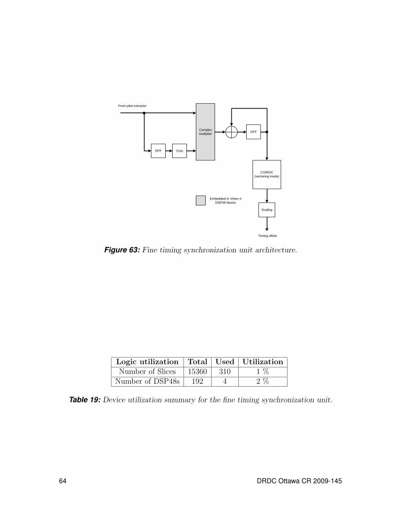
From pilot extractor
DFFComplex multiplier
Embedded in Virtex-4 DSP48 blocks
DFF Conj
Timing offset
CORDIC(vectoring mode)
Scaling
Figure 63: Fine timing synchronization unit architecture.
Logic utilization Total Used UtilizationNumber of Slices 15360 310 1 %
Number of DSP48s 192 4 2 %
Table 19: Device utilization summary for the fine timing synchronization unit.
64 DRDC Ottawa CR 2009-145

5.3.11 Integer CFO estimator implementation
From pilot exrtactor
DFFComplex multiplier
Embedded in Virtex-4 DSP48 blocks
DFF Conj
Frequency offset
Pilot generator
Complex multiplier
Control logic Peak detector
2Im2Re +
Figure 64: Post FFT frequency offset correction unit architecture.
The purpose of integer CFO estimator is to find the integer subcarrier spacing for theCFO. The integer CFO estimator architecture is illustrated in Figure 64. The integerCFO estimator performs multiple cross-correlation between the received pilot toneswith the time-shifted version of original pilot tones as follows [29]
Λ�f =P∑i=2
Zl,piZ∗l,pi−1
(45)
where �f is the estimate of the integer frequency offset and Zl,pi is the product of ith
received pilot tone with a shifted version of the ith original pilot tone and (.)∗ denotescomplex conjugate. A magnitude comparison is performed to find the maximum ofthe metric Λ�f at the end of each correlation process. Therefore, the integer frequencyoffset �f is then given by
�f = arg{
max∣∣Λ�f
∣∣2} (46)
Finally, the feed-backward frequency offset compensation is given by
DRDC Ottawa CR 2009-145 65

r′(n) = r(n) exp
(−j2��fn
N
)(47)
The FPGA resource utilization for the integer CFO estimator is given in Table 20.Timing analysis results show that the critical path is 4.422 ns, i.e. the maximumclock frequency is 226.124 MHz.
Logic utilization Total Used UtilizationNumber of Slices 15360 272 1 %
Number of DSP48s 192 3 1 %
Table 20: Device utilization summary for the integer CFO estimator.
5.3.12 Loop filter implementation
Output
1−Z
Ki
Input
Kp
Figure 65: Structure of first-order digital loop filter.
Figure 65 shows the loop filter structure which is based on the classical first-orderloop filter in [30]. Its transfer function is sketched directly as follows
H(z) =Kp + (Ki −Kp)z
−1
1− z−1(48)
The coefficients Ki (integral) and Kp (proportional) are very small and chosen to bea power of 2 in order to reduce hardware complexity. The transfer function of theloop filter H(z) itself is not stable because of a pole at the unit circle in the z-plane.However, the loop filter is used as a component of a closed-loop frequency offsetcorrection circuit as shown in Figure 66. The corresponding linearized equivalent
66 DRDC Ottawa CR 2009-145

model of this closed-loop is illustrated in Figure 67. The overall transfer function isthen
G(z) =Φ(z)
Φ(z)=
U(z)
1 + U(z)(49)
InputDerotator
Phase Error Estimator
Loop Filter
Phase Accumulator
Output
Figure 66: Simplified closed-loop frequency offset correction diagram.
K(z)
To peak detector
( )nφ
H(z)
( )nφ∧
( )nφInput Output
Figure 67: Linearized closed-loop frequency offset correction diagram.
where Φ(n), Φ(n) are estimated phase error and input phase error at sample n,respectively, and U(z) = K(z)H(z) where K(z) = z−1
1−z−1 is the transfer function ofthe phase accumulator. We define the input phase error at symbol n as follows
Φ(n) = 2�ΔfcnT = Δ!nT (50)
where Δfc is the frequency offset and T = 1fs
is the sampling period. The looptransfer function is also represented as
DRDC Ottawa CR 2009-145 67

R(z) =ΔΦ(z)
Φ(z)=
1
1 + U(z)(51)
Inserting K(z) and H(z) into equation (49) and (51), these transfer functions arerewritten as follows
G(z) =Kp(z − 1) +Ki
(z − 1)2 +Kp(z − 1) +Ki
(52)
R(z) =(z − 1)2
(z − 1)2 +Kp(z − 1) +Ki
(53)
The phase error due to the input Φ(z) is
ΔΦ(z) =(z − 1)2
(z − 1)2 +Kp(z − 1) +Ki
⋅ Φ(z) (54)
where Φ(z) = Δ!T z−1
(1−z−1)2 is the z-transform of the Φ(n). The steady-phase errorbecomes
ΔΦ(z) =Δ!Tz
(z − 1)2 +Kp(z − 1) +Ki
(55)
Applying the final theorem of the z-transform to ΔΦ(z), we get the steady-phaseerror is zero as follows
ΔΦ = limz→ 1
(z − 1) ⋅ΔΦ(z)
= limz→ 1
Δ!T (z − 1)z
(z − 1)2 +Kp(z − 1) +Ki
= 0
(56)
To determine the range of stability for the loop, the poles of G(z) must be inside theunit circle in the z-plane. The condition for stability is derived directly from [30]
2Kp − 4 < Ki < Kp, Ki > 0. (57)
68 DRDC Ottawa CR 2009-145

The coefficients Kp and Ki are similar to C2 and C1 in [30], which are defined as
Kp = 2�!nT (58)
Ki =K2p
4�2(59)
where !n = 2�fn is the natural frequency (!nT << 1) and 0 ≤ � ≤ 1 is the dampingfactor. Since Kp and Ki affect the settling time and tracking performance of thefrequency loop, the loop filter coefficients are programmable so that it is easy todebug, control the loop frequency and also these coefficients can be reused in othermodules.
The FPGA resource utilization for the loop filter unit is given in Table 21. Timinganalysis results show that the critical path is 2.476 ns, i.e. the maximum clockfrequency is 403.910 MHz.
Logic utilization Total Used UtilizationNumber of Slices 15360 100 < 1 %
Table 21: Device utilization summary for the loop filter unit.
5.3.13 Channel estimator implementation
DPRAM
From pilot tone extractor
Embedded in Virtex-4 DSP48 blocks
Control logic
DOUTB
ADD
RA
ADD
RB
Interpolation coefficients
ROM
ADDR
Split
Real
Imag
MAC
MAC
Scaling
Scaling
Channel estimated
Real
Imag
Multiplier
Pilot generator
Figure 68: Channel estimator architecture.
The channel estimator unit is illustrated in Figure 68. Since the reference pilot toneamplitude is assumed to be one, the channel responses at the kth pilot subcarriers
DRDC Ottawa CR 2009-145 69

Hkp are obtained by a simple multiplication between the received pilot and the corre-
sponding reference pilot. The remaining channel responses at subcarriers other thanpilot subcarriers are interpolated using a serial FIR filter approach for the sinc in-terpolation technique proposed in [18]. The channel frequency response at the mth
subcarrier can be estimated by
Hm =
⌊K2 ⌋∑k=−⌊K−1
2 ⌋Hkp × fkm (60)
where ⌊x⌋ denotes the largest integer such that ⌊x⌋ ≤ x, K is the number of filtertaps, m is the subcarrier index between two consecutive pilot subcarriers, and fkm isthe interpolator coefficient, which is given by
fkm = sinc
(m
Nf
− k)
(61)
where m = 1, 2, . . . , Nf − 1, and Nf is the pilot subcarrier spacing. In Figure 68,a serial architecture for the FIR filter exploits the temporal multiplexing techniqueto save silicon area while maintaining the performance. The filter coefficients arepre-computed and stored in a small ROM.
The FPGA resource utilization for the channel estimator unit excluding the pilotgenerator and the multiplication between received pilot and reference pilot is givenin Table 22. Timing analysis results show that the critical path is 3.744 ns, i.e. themaximum clock frequency is 267.087 MHz.
Logic utilization Total Used UtilizationNumber of Slices 15360 150 < 1 %
Number of FIFO16/RAMB16s 192 1 < 1 %Number of DSP48s 192 2 1 %
Table 22: Device utilization summary for the channel estimator.
5.3.14 Zero forcing channel equalizer implementation
The equalizer divides the data subcarriers from the FFT processor by the correspond-ing channel response estimated by the channel estimator. This leads to a complexdivision architecture as illustrated in Figure 69. The equalizer also exploits the tem-poral multiplexing and overclocking techniques for resources savings. The real divider
70 DRDC Ottawa CR 2009-145
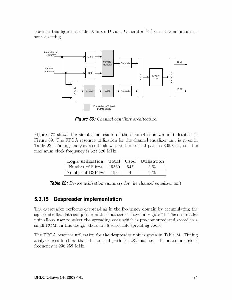
block in this figure uses the Xilinx’s Divider Generator [31] with the minimum re-source setting.
Conj
From channel estimator
Embedded in Virtex-4 DSP48 blocks
MUX
Real
Imag
DFF
From FFT processor
Complex multiplier Truncate
SquareMUX
ACC Truncate
Divider core
DEMUX
Figure 69: Channel equalizer architecture.
Figures 70 shows the simulation results of the channel equalizer unit detailed inFigure 69. The FPGA resource utilization for the channel equalizer unit is given inTable 23. Timing analysis results show that the critical path is 3.093 ns, i.e. themaximum clock frequency is 323.326 MHz.
Logic utilization Total Used UtilizationNumber of Slices 15360 547 3 %
Number of DSP48s 192 4 2 %
Table 23: Device utilization summary for the channel equalizer unit.
5.3.15 Despreader implementation
The despreader performs despreading in the frequency domain by accumulating thesign-controlled data samples from the equalizer as shown in Figure 71. The despreaderunit allows user to select the spreading code which is pre-computed and stored in asmall ROM. In this design, there are 8 selectable spreading codes.
The FPGA resource utilization for the despreader unit is given in Table 24. Timinganalysis results show that the critical path is 4.233 ns, i.e. the maximum clockfrequency is 236.259 MHz.
DRDC Ottawa CR 2009-145 71
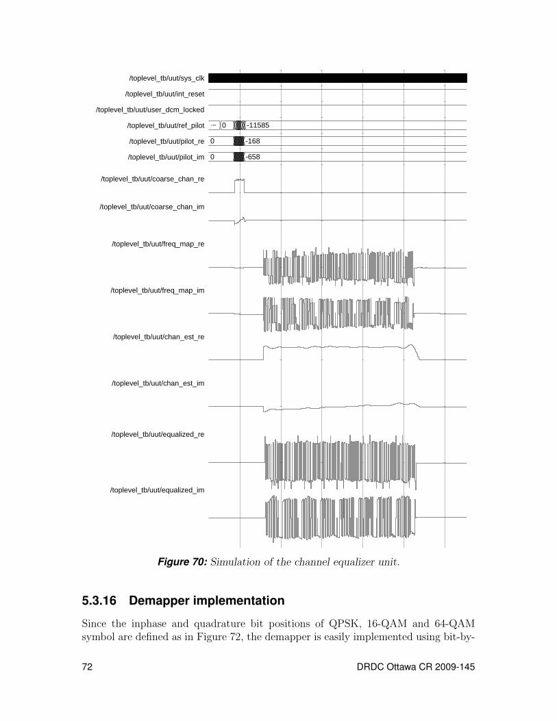
-11585 0 -11585 0 -11585 0 -11585
0 -168 -1151 -174
0 -658 -1224 -543
500000000 550000000 600000000 650000000 700000000 750000000
/toplevel_tb/uut/sys_clk
/toplevel_tb/uut/int_reset
/toplevel_tb/uut/user_dcm_locked
/toplevel_tb/uut/ref_pilot -11585 0 -11585 0 -11585 0 -11585
/toplevel_tb/uut/pilot_re 0 -168 -1151 -174
/toplevel_tb/uut/pilot_im 0 -658 -1224 -543
/toplevel_tb/uut/coarse_chan_re
/toplevel_tb/uut/coarse_chan_im
/toplevel_tb/uut/freq_map_re
/toplevel_tb/uut/freq_map_im
/toplevel_tb/uut/chan_est_re
/toplevel_tb/uut/chan_est_im
/toplevel_tb/uut/equalized_re
/toplevel_tb/uut/equalized_im
Entity:toplevel_tb Architecture:behavior Date: Tue Sep 02 10:00:13 AM Eastern Daylight Time 2008 Row: 1 Page: 1
Figure 70: Simulation of the channel equalizer unit.
5.3.16 Demapper implementation
Since the inphase and quadrature bit positions of QPSK, 16-QAM and 64-QAMsymbol are defined as in Figure 72, the demapper is easily implemented using bit-by-
72 DRDC Ottawa CR 2009-145
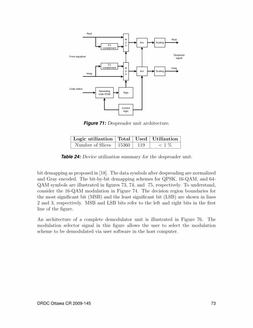
From equalizer
Real
Imag
Real
Imag
Code selectSpreading code ROM
MUX
Control logic
Acc
Acc
Scaling
Scaling
Despread signal
MUX
Sign
2's complement
2's complement
Figure 71: Despreader unit architecture.
Logic utilization Total Used UtilizationNumber of Slices 15360 119 < 1 %
Table 24: Device utilization summary for the despreader unit.
bit demapping as proposed in [18]. The data symbols after despreading are normalizedand Gray encoded. The bit-by-bit demapping schemes for QPSK, 16-QAM, and 64-QAM symbols are illustrated in figures 73, 74, and 75, respectively. To understand,consider the 16-QAM modulation in Figure 74. The decision region boundaries forthe most significant bit (MSB) and the least significant bit (LSB) are shown in lines2 and 3, respectively. MSB and LSB bits refer to the left and right bits in the firstline of the figure.
An architecture of a complete demodulator unit is illustrated in Figure 76. Themodulation selector signal in this figure allows the user to select the modulationscheme to be demodulated via user software in the host computer.
DRDC Ottawa CR 2009-145 73

QPSK
b1 b0 b1 b0b3 b2 b1 b0b3 b2b5 b4
16-QAM 64-QAM
i0 i1 i0 i0i1i2
q0 q1 q0 q0q1q2
Figure 72: Bit position in an M-QAM symbol.
d- d
Inphase/Quadrature
00
3d-3d
011011
d- d
0
3d-3d
011
d- d
0
3d-3d
101
MSB
LSB
d- d
Inphase/Quadrature
001
3d 5d 7d-5d -3d-7d
000 010 011101100110111
0 0 0 01111
0 0 1 10011
1 0 0 11001
MSB
LSB
Middle
d- d
Inphase/Quadrature
01
Figure 73: Bit demapping for QPSK.
d- d
Inphase/Quadrature
00
3d-3d
011011
d- d
0
3d-3d
011
d- d
0
3d-3d
101
MSB
LSB
d- d
Inphase/Quadrature
001
3d 5d 7d-5d -3d-7d
000 010 011101100110111
0 0 0 01111
0 0 1 10011
1 0 0 11001
MSB
LSB
Middle
d- d
Inphase/Quadrature
01
Figure 74: Bit demapping for 16-QAM.
d- d
Inphase/Quadrature
00
3d-3d
011011
d- d
0
3d-3d
011
d- d
0
3d-3d
101
MSB
LSB
d- d
Inphase/Quadrature
001
3d 5d 7d-5d -3d-7d
000 010 011101100110111
0 0 0 01111
0 0 1 10011
1 0 0 11001
MSB
LSB
Middle
d- d
Inphase/Quadrature
01
Figure 75: Bit demapping for 64-QAM.
74 DRDC Ottawa CR 2009-145
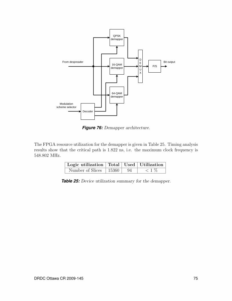
From despreader
Modulation scheme selector
Bit outputDEMUX
Decoder
QPSK demapper
16-QAM demapper
64-QAM demapper
P/S
Figure 76: Demapper architecture.
The FPGA resource utilization for the demapper is given in Table 25. Timing analysisresults show that the critical path is 1.822 ns, i.e. the maximum clock frequency is548.802 MHz.
Logic utilization Total Used UtilizationNumber of Slices 15360 94 < 1 %
Table 25: Device utilization summary for the demapper.
DRDC Ottawa CR 2009-145 75
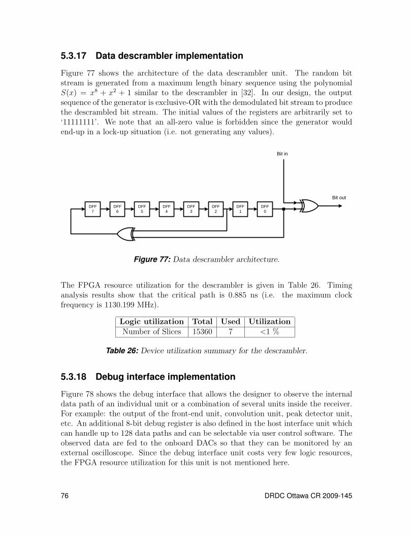
5.3.17 Data descrambler implementation
Figure 77 shows the architecture of the data descrambler unit. The random bitstream is generated from a maximum length binary sequence using the polynomialS(x) = x8 + x2 + 1 similar to the descrambler in [32]. In our design, the outputsequence of the generator is exclusive-OR with the demodulated bit stream to producethe descrambled bit stream. The initial values of the registers are arbitrarily set to‘11111111’. We note that an all-zero value is forbidden since the generator wouldend-up in a lock-up situation (i.e. not generating any values).
DFF3
DFF2
DFF1
DFF0
DFF4
DFF5
DFF6
DFF7
Bit in
Bit out
Figure 77: Data descrambler architecture.
The FPGA resource utilization for the descrambler is given in Table 26. Timinganalysis results show that the critical path is 0.885 ns (i.e. the maximum clockfrequency is 1130.199 MHz).
Logic utilization Total Used UtilizationNumber of Slices 15360 7 <1 %
Table 26: Device utilization summary for the descrambler.
5.3.18 Debug interface implementation
Figure 78 shows the debug interface that allows the designer to observe the internaldata path of an individual unit or a combination of several units inside the receiver.For example: the output of the front-end unit, convolution unit, peak detector unit,etc. An additional 8-bit debug register is also defined in the host interface unit whichcan handle up to 128 data paths and can be selectable via user control software. Theobserved data are fed to the onboard DACs so that they can be monitored by anexternal oscilloscope. Since the debug interface unit costs very few logic resources,the FPGA resource utilization for this unit is not mentioned here.
76 DRDC Ottawa CR 2009-145
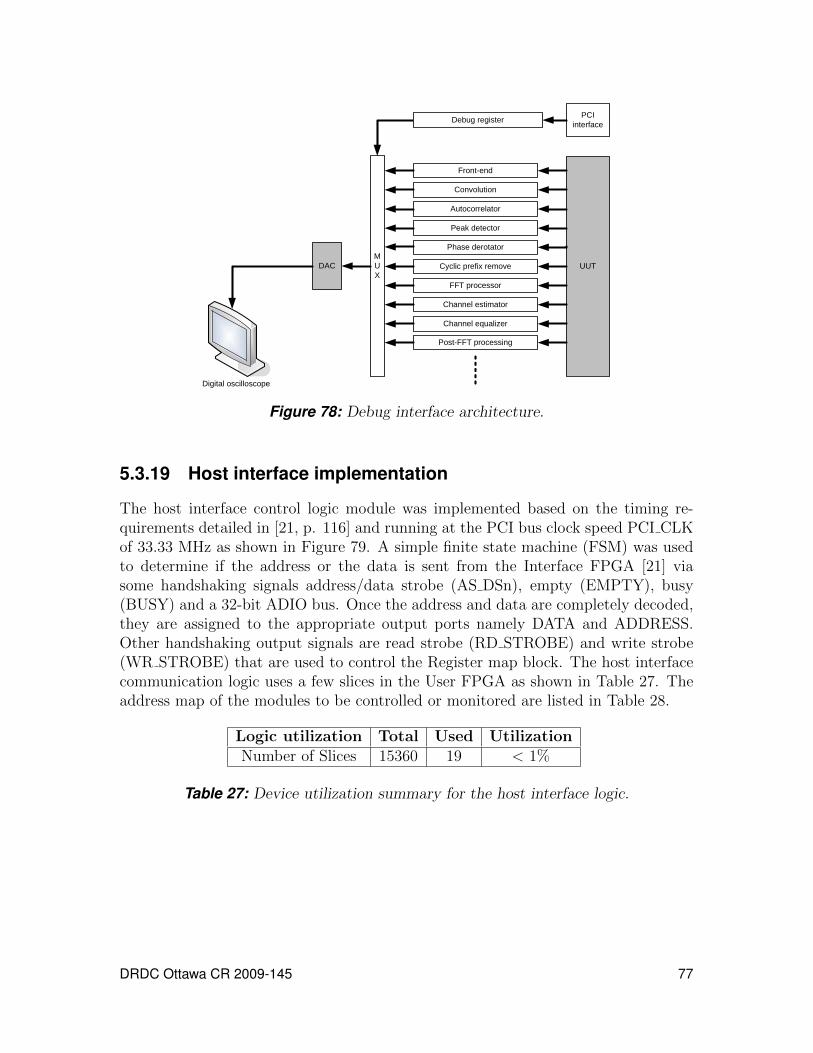
DAC UUT
Digital oscilloscope
MUX
Front-end
Convolution
Autocorrelator
Peak detector
Phase derotator
Cyclic prefix remove
FFT processor
Channel estimator
Channel equalizer
PCI interfaceDebug register
Post-FFT processing
Figure 78: Debug interface architecture.
5.3.19 Host interface implementation
The host interface control logic module was implemented based on the timing re-quirements detailed in [21, p. 116] and running at the PCI bus clock speed PCI CLKof 33.33 MHz as shown in Figure 79. A simple finite state machine (FSM) was usedto determine if the address or the data is sent from the Interface FPGA [21] viasome handshaking signals address/data strobe (AS DSn), empty (EMPTY), busy(BUSY) and a 32-bit ADIO bus. Once the address and data are completely decoded,they are assigned to the appropriate output ports namely DATA and ADDRESS.Other handshaking output signals are read strobe (RD STROBE) and write strobe(WR STROBE) that are used to control the Register map block. The host interfacecommunication logic uses a few slices in the User FPGA as shown in Table 27. Theaddress map of the modules to be controlled or monitored are listed in Table 28.
Logic utilization Total Used UtilizationNumber of Slices 15360 19 < 1%
Table 27: Device utilization summary for the host interface logic.
DRDC Ottawa CR 2009-145 77

ADIO
PCI_CLK
Host interface logic
BUSY
EMPTY
AD_DSn
RSTn
Register map
DATA
ADDRESS
WR_STROBE
Modules to be controlled
Modules to be monitored
RD_STROBE
Figure 79: Host interface logic module.
Address Register name Description0x00 DEV ID User design identification register0x01 DEBUG CNTRL Debug interface control register0x02 ONBOARD CNTRL Onboard peripherals control register0x03 TX CNTRL DACs control register0x04 FRONTEND CNTRL Front-end circuit control register0x05 BUFFER CNTRL RAM-based delay control register0x06 CORR PEAK CNTRL Correlator status register0x07 CONV PEAK CNTRL Convolution status register0x08 OFFSET CNTRL Timing/phase offset status register0x09 FREQ CNTRL Integer CFO status register0x0A SPREADING CNTRL Spreading code control register0x0B FIFO CNTRL Receive FIFO status register0x0C LF CNTRL Freq./timing loop filters control register0x0D PEAK THRES CNTRL Peak detector control register0x0E AGC CNTRL AGC loop filter control register0x0F AGC POWER CNTRL AGC power threshold control register
Table 28: Registers address map
78 DRDC Ottawa CR 2009-145

Register 1 DEV ID REGISTER (ADDRESS 0x00)
The user design identification (ID) register is a 32-bit readable register which con-tains the identification number of the whole design in the user FPGA. This registercontains a unique 32-bit number. In our design, we chose the value of the user designidentification register as 0xAAAA5555.
Register 2 DEBUG CNTL REGISTER (ADDRESS 0x01)
The debug register is an 8-bit writable register which allows a user to monitor theinternal data paths within the receiver design.
bit 7-0: Internal path to be selected
Register value Internal path name0x00 Digital front-end0x01 Convolution output0x02 Peak detector output0x03 Auto-correlator output0x04 Phase derotator output0x05 Cyclic prefix removal output0x06 FFT processor output0x07 Channel estimator output0x08 Channel equalizer output0x09 Frequency offset output0x0A Data subcarrier extractor output0x0B Despreader output0x0C Demodulator output0x0D Descrambler output
Register 3 ONBOARD CNTL REGISTER (ADDRESS 0x02)
The onboard control register is a 5-bit writable register which allows a user to controlonboard LEDs, generates a reset signal for the receiver design via the user controlsoftware.
bit 4: SW RESET, active low software reset signal.
bit 3: RED2, red diode for LED21: led off0: led on
DRDC Ottawa CR 2009-145 79
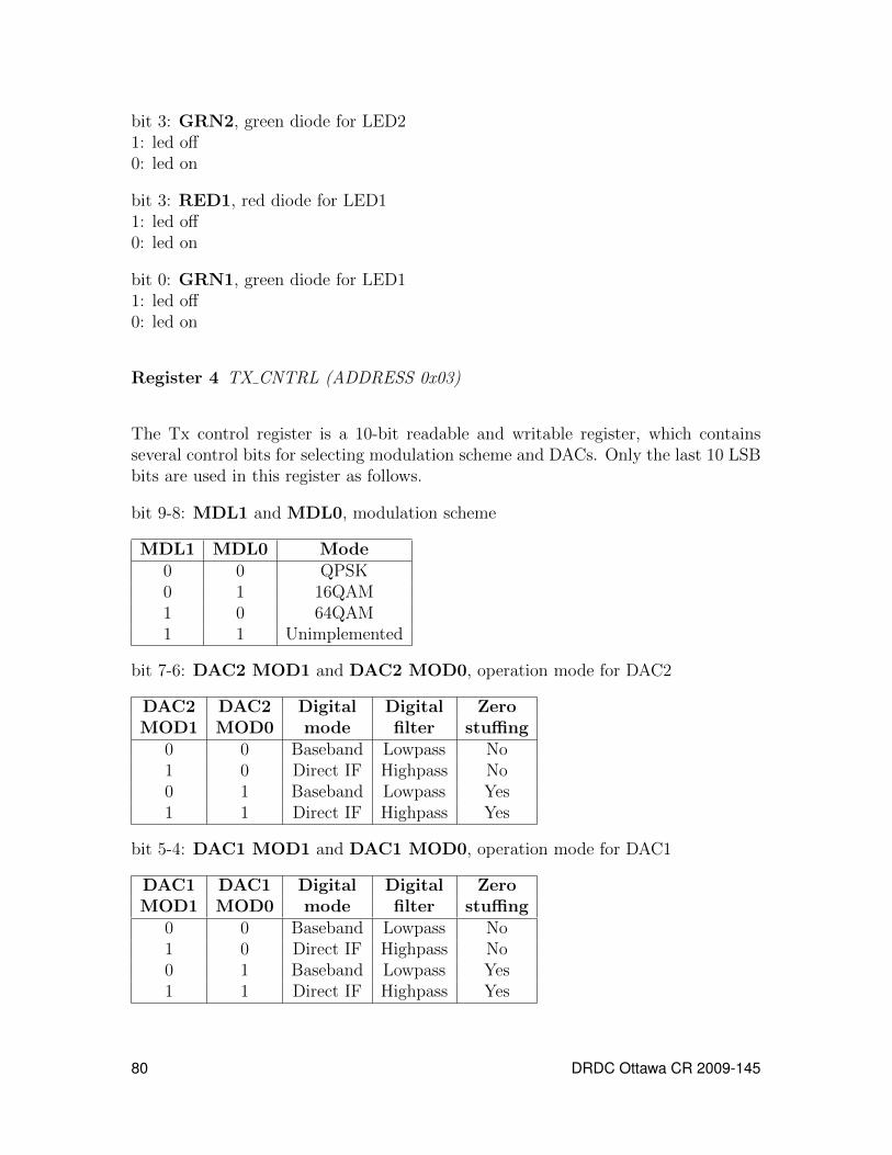
bit 3: GRN2, green diode for LED21: led off0: led on
bit 3: RED1, red diode for LED11: led off0: led on
bit 0: GRN1, green diode for LED11: led off0: led on
Register 4 TX CNTRL (ADDRESS 0x03)
The Tx control register is a 10-bit readable and writable register, which containsseveral control bits for selecting modulation scheme and DACs. Only the last 10 LSBbits are used in this register as follows.
bit 9-8: MDL1 and MDL0, modulation scheme
MDL1 MDL0 Mode0 0 QPSK0 1 16QAM1 0 64QAM1 1 Unimplemented
bit 7-6: DAC2 MOD1 and DAC2 MOD0, operation mode for DAC2
DAC2 DAC2 Digital Digital ZeroMOD1 MOD0 mode filter stuffing
0 0 Baseband Lowpass No1 0 Direct IF Highpass No0 1 Baseband Lowpass Yes1 1 Direct IF Highpass Yes
bit 5-4: DAC1 MOD1 and DAC1 MOD0, operation mode for DAC1
DAC1 DAC1 Digital Digital ZeroMOD1 MOD0 mode filter stuffing
0 0 Baseband Lowpass No1 0 Direct IF Highpass No0 1 Baseband Lowpass Yes1 1 Direct IF Highpass Yes
80 DRDC Ottawa CR 2009-145

bit 3-2: DAC2 DIV1 and DAC2 DIV0, input data rate for DAC2
DAC2 DAC2 Zero DataDIV1 DIV0 stuffing rate (Msps)
0 0 No 48-1601 0 No 24-1000 1 No 12-501 1 No 6-25
0 0 Yes 24-1000 1 Yes 12-501 0 Yes 6-251 1 Yes 3-12.5
bit 1-0: DAC1 DIV1 and DAC1 DIV0, input data rate for DAC1
DAC1 DAC1 Zero DataDIV1 DIV0 stuffing rate (Msps)
0 0 No 48-1601 0 No 24-1000 1 No 12-501 1 No 6-25
0 0 Yes 24-1000 1 Yes 12-501 0 Yes 6-251 1 Yes 3-12.5
Register 5 FRONTEND CNTRL (ADDRESS 0x04)
The digital front-end control register is a 32-bit writable register, which allows theuser to change the phase/gain mismatch of the I/Q rails and the DC notch filtercoefficient.
bit 31-16: DC notch filter coefficient
bit 15-8: I/Q rails phase mismatch
bit 7-0: I/Q rails gain mismatch
Register 6 BUFFER CNTRL (ADDRESS 0x05)
The buffer control register is a 16-bit writable register, which allows the user to adjustthe output delay (in samples) of the autocorrelator and channel estimator circuits.
DRDC Ottawa CR 2009-145 81

bit 24-18: Channel estimator output delay
bit 17-8: Auto-correlator output delay
Register 7 CORR PEAK CNTRL (ADDRESS 0x06)
The correlation peak register is a 32-bit readable register, which allows the user tomonitor the output of the auto-correlation circuit inside the fractional CFO estimator.
bit 31-16: Real component output
bit 15-0: Imaginary component output
Register 8 CONV PEAK CNTRL (ADDRESS 0x07)
The correlation peak register is a 16-bit readable register, which allows the user tomonitor the output of the convolution circuit inside the coarse frame detector.
bit 15-0: Convolution output
Register 9 OFFSET CNTRL (ADDRESS 0x08)
The offset control register is a 30-bit readable register, which allows the user tomonitor the coarse, fine timing offset and the normalized phase offset.
bit 29-22: Coarse timing offset (in sample)
bit 21-16: Fine timing offset (in sample)
bit 15-0: Normalized phase offset (normalized by �)
Register 10 FREQ CNTRL (ADDRESS 0x09)
The frequency control register is a 16-bit readable register, which allows the user tomonitor the integer carrier frequency offset estimated by the integer CFO estimator.
bit 15-0: Normalized integer CFO (normalized by subcarrier spacing)
Register 11 SPREADING CNTRL (ADDRESS 0x0A)
82 DRDC Ottawa CR 2009-145

The spreading control register is a 11-bit readable/writable register, which allows theuser to select the spreading code of the desired user. This register also monitors thestatus of control signals of the receive FIFO and the overload status of the onboardADCs.
bit 10: ADC overload status
bit 9: Receive FIFO almost full status
bit 8: Receive FIFO programmable full threshold status
bit 7: Receive FIFO full status
bit 6: Receive FIFO empty status
bit 2-0: Spreading code select bits
bit 2 bit 1 bit 0 Spreading code0 0 0 Code 00 0 1 Code 10 1 0 Code 20 1 1 Code 31 0 0 Code 41 0 1 Code 51 1 0 Code 61 1 1 Code 7
Register 12 FIFO CNTRL (ADDRESS 0x0B)
The FIFO control register is a 4-bit readable register, which allows the user to monitordata in the FIFO buffer.
bit 3-0: 4-bit word output from the FIFO.
Register 13 LF CNTRL (ADDRESS 0x0C)
The loop filters control register is a 24-bit writable register, which allows the user tocontrol the frequency and timing recovery loop filters.
bit 23-20: Proportional factor Kp of the frequency loop filter
bit 19-16: Integral factor Ki of the frequency loop filter
DRDC Ottawa CR 2009-145 83
bit 15-12: Proportional factor Kp of the timing loop filter
bit 11-8: Integral factor Ki of the timing loop filter
bit 1: Timing loop filter enable
bit 0: Frequency loop filter enable
Register 14 PEAK THRES CNTRL (ADDRESS 0x0D)
The peak threshold control register is a 16-bit writable register, which allows the userto control the peak threshold of the peak detector inside the coarse frame detectorcircuit.
bit 15-0: Reference peak threshold
Register 15 AGC CNTRL (ADDRESS 0x0E)
The AGC control register is a 16-bit writable register, which allows the user to controlthe loop filter inside the AGC circuit and gain of the RF front-end.
bit 15-12: Integral factor Ki of the AGC loop filter
bit 11-8: Proportional factor Kp of the AGC loop filter
bit 6-5: RF front-end low noise amplifier (LNA) gain
bit 4-0: RF front-end variable gain amplifier (VGA) gain.
Register 16 AGC POWER CNTRL (ADDRESS 0x0F)
The AGC power control register is a 32-bit writable register, which allows the user tocontrol the reference noise power and desired power thresholds for the AGC circuit.
bit 31-16: Reference noise power threshold
bit 15-0: Reference desired power threshold
84 DRDC Ottawa CR 2009-145

5.3.20 Implementation summary
Table 29 summarizes the implementation results of crucial modules in the receiverusing Xilinx Synthesis Tool (XST). Each module is listed in terms of logic slices,block RAMs, hardware multipliers and in percentage of the target FPGA device.The detail implementation block diagram of the receiver is sketched out from theregister transfer level (RLT) schematic on Figure 80 in order to reveal the internaldata paths for measurement purposes.
Table 29: Implementation results of crucial modules in the receiver.
System clock (MHz) 80Sampling rate (MHz) 5OVSF codes length 8Receiver configuration indoor-to-outdoorTotal slices 15360Total block-RAM 192Total multipliers 192Module Slice % RAM % Multiplier %Digital front-end 1020 6 34 17 24 12AGC 300 2 1 1∗ 0 0Coarse frame detection 814 5 10 5 12 6Fractional CFO estimator 129 1∗ 1 1∗ 3 1CORDIC 252 1 0 0 2 1FFT processor 632 4 3 1 4 2Channel estimator 150 1∗ 1 1∗ 2 1Channel equalizer 547 3 0 0 4 2Pilot generator 8 1∗ 0 0 0 0Loop filter 100 1∗ 0 0 0 0Fine timing detection 310 2 0 0 3 1Integer CFO estimator 272 1 0 0 3 1Despreader 119 1∗ 0 0 0 0Demapper 94 1∗ 0 0 0 0Desrambler 7 1∗ 0 0 0 0
∗ less than 1%
DRDC Ottawa CR 2009-145 85
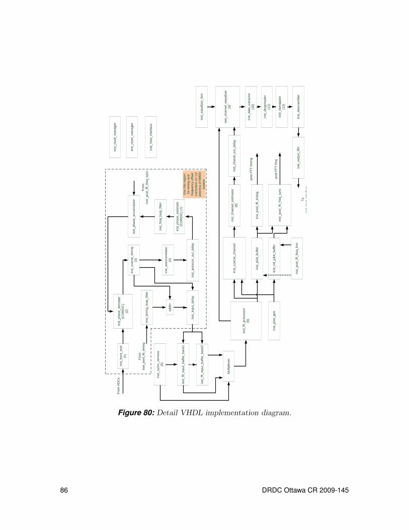
Inst
_fro
nt_e
nd(1
)
From
AD
Cs
inst
_coa
rse_
timin
g (3
)
Inst
_inp
ut_d
elay
adde
rin
st_a
utoc
orre
lato
r(4
)
inst
_aut
ocor
r_ou
t_de
lay
inst
_fft_
inpu
t_bu
ffer_
bank
1
inst
_fft_
inpu
t_bu
ffer_
bank
0
inst
_cyc
lic_r
emov
e(5
)
From
in
st_p
ost_
fft_t
imin
g
Mul
tiple
xer
inst
_fft_
proc
esso
r(6
)
inst
_pilo
t_bu
ffer
inst
_pilo
t_ge
nin
st_r
ef_p
ilot_
buffe
r
inst
_coa
rse_
chan
nel
inst
_cha
nnel
_est
imat
or(8
)
inst
_pos
t_fft
_tim
ing
inst
_pos
t_fft
_fre
q_sy
nc
post
-FFT
tim
ing
post
-FFT
freq
inst
_pos
t_fft
_fre
q_fs
m
inst
_cha
nel_
est_
dela
y
inst
_equ
aliz
er_f
sm
inst
_cha
nnel
_equ
aliz
er(9
)
inst
_dat
a_ex
tract
or(1
0)
inst
_des
prea
der
(11)
inst
_dem
appe
r(1
2)
inst
_des
cram
bler
inst
_out
put_
fifo
To
inst
_hos
t_in
terfa
ce
inst
_clo
ck_m
anag
er
Use
this
regi
on
for t
imin
g an
d fre
quen
cy o
ffset
co
rrect
ion
on 1
st
ante
nna
of M
IMO
sy
stem
inst
_res
et_m
anag
er
inst
_hos
t_in
terfa
ce
inst
_pha
se_e
stim
ate
(CO
RD
IC) (
7)
inst
_fre
q_lo
op_f
ilter
inst
_pha
se_d
erot
ate
(CO
RD
IC)
(2)
inst
_pha
se_a
ccum
ulat
or
From
in
st_p
ost_
fft_f
req_
sync
inst
_tim
ing_
loop
_filt
er
Figure 80: Detail VHDL implementation diagram.
86 DRDC Ottawa CR 2009-145

5.4 MIMO MC-CDMA hardware integrationThe integration of a MIMO module within the existing MC-CDMA hardware imple-mentation is based on the Matlab simulation model. Significant design time and effortis saved by using a previous MIMO receiver design [15, 16]. However, several mod-ifications were done to both the MIMO and the MC-CDMA modules. This sectionwill first present the architecture of the MIMO module and its components. Then,the final architecture of the MIMO MC-CDMA module will be presented, as well asModelsim simulation results.
It should be noted that the device utilization summaries presented in this section arefor a 1 × 2 system and for a floating point format of Ne = 5 bits for the exponentand Nm = 8 bits for the mantissa. Through Modelsim simulations, we found theselengths to be the smallest we could use; anything smaller resulted in extensive biterrors at the receiver.
5.4.1 Matrix inversion
The matrix inversion module does not require much adaptation to fit within theMIMO MC-CDMA system. Detailed description of its structure can be found in[15,16]. The only modification that was done is a tweaking of the finite state machines.The pilot samples are received at such a rate that inversion is impossible to dobetween each sample. Therefore, the pilot samples are saved to a memory beforethe inverted matrices are computed. Figure 81 shows the waveform for the inversionof all Npilots = 8 pilots in a 1× 2 system.
Figure 81: Modelsim simulation of the matrix inversion module.
A notable aspect is that its size precludes its inclusion on the same FPGA chip as
DRDC Ottawa CR 2009-145 87

the rest of the MIMO MC-CDMA receiver. Instead, it will need to be implementedon a second card. The number of communication lines between the cards being lim-ited, parallel-to-serial and serial-to-parallel conversion modules were included in thedesigns of both the matrix inversion module and the layered space-time receiver.These conversion modules consist of simple shift registers. Table 30 shows the re-source utilization for the matrix inversion. A frequency of 6.760 MHz is reached, butfurther optimizations could be made by introducing pipelining in the design. Thiswould require significant redesign work to ensure the control signals are all properlysynchronized.
Logic utilization Total Used UtilizationNumber of Slices 15360 5639 36 %
Number of Slice Flip Flops 30720 1885 6 %Number of 4 input LUTs 30720 10050 32 %
Number of FIFO16/RAMB16s 192 24 12 %Number of DSP48s 192 28 14 %
Table 30: Device utilization summary for the inversion matrix module.
5.4.2 Layered Space-Time receiver
Figure 82 shows the block diagram for the modified MIMO receiver. Not shown inthis diagram are the finite state machines that generate the necessary control logic.The main difference between this system and the original MIMO receiver [15, 16] isthe splitting of the symbol detection into two separate paths : one for the pilots andone for the data symbols. The data symbol path includes despreading, mapping andrespreading operations to properly reconstruct the interference contributed by theprocessed layer.
Weight
computation
Combination
Despreading Mapping Spreading
Pilot
detection
Interference
reconstruction
Interference
supressionNr
channel
Rxx
-1
received
Nr
Nr
Nr
weights
SF SF
Nr
Nr
Nr
Nr
Figure 82: Block diagram of the Layered Space-Time receiver.
The processing is also split in time. First, the LST receiver uses the inverted matricesand pilot samples to compute their weights. Then, in a second phase, the estimated
88 DRDC Ottawa CR 2009-145

weight samples are applied to the received data samples in groups of SF = 8 samples.The two processing phases are clearly shown on Figure 83, which shows the waveformfor the input and output signals of the LST receiver.
Figure 83: Modelsim simulation of the Layered-Space receiver.
.
Table 31 shows the resource utilization summary for this module. A frequency of23.455 MHz was reached, but further optimizations could be made by introducingpipelining in the design. This would require significant redesign work to ensure thecontrol signals are all properly synchronized.
5.4.3 Fixed point to floating point conversion
The data provided by both the FFT processor (pilots) and the channel estimationmodule are in a fixed point format using 1 bit for the integer part and 15 bits forthe fractional part of a given number. Since the existing MIMO implementation is ina floating point format, a conversion module is needed. The chosen biased floating
DRDC Ottawa CR 2009-145 89
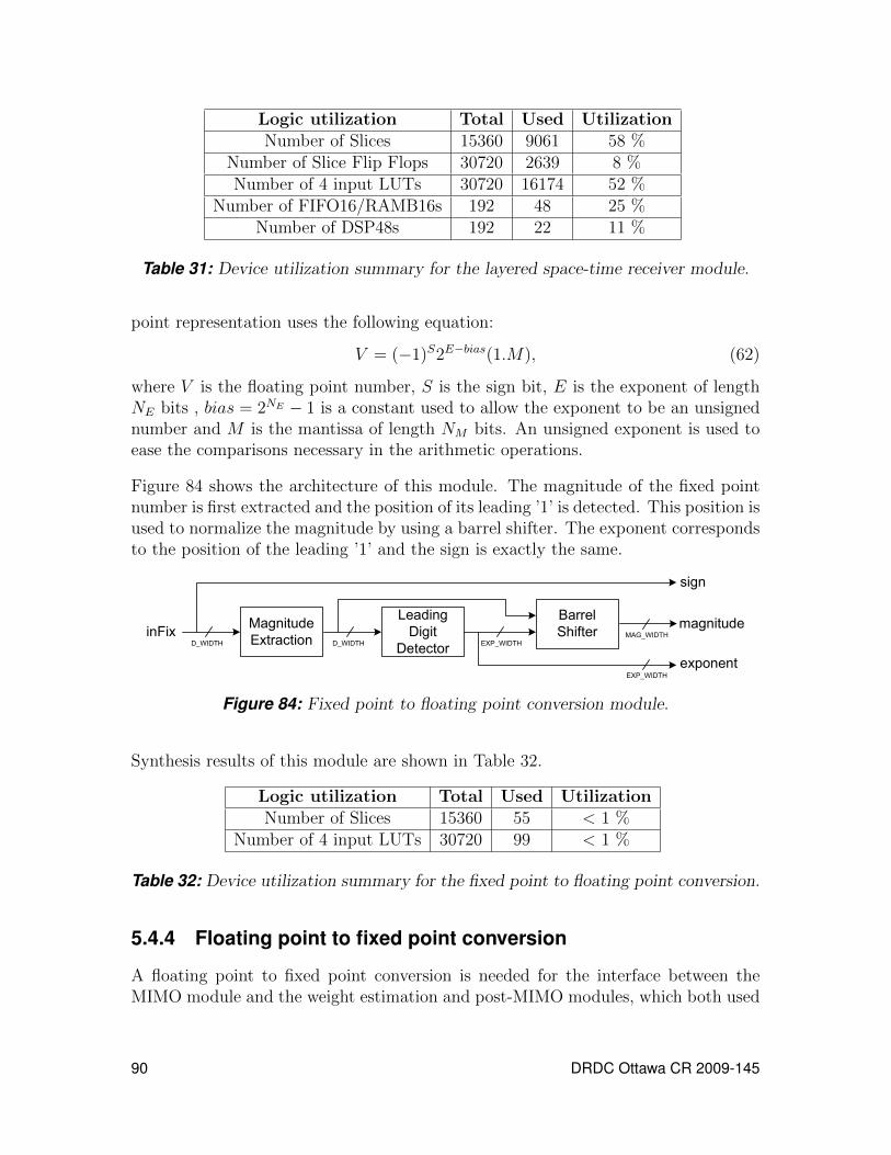
Logic utilization Total Used UtilizationNumber of Slices 15360 9061 58 %
Number of Slice Flip Flops 30720 2639 8 %Number of 4 input LUTs 30720 16174 52 %
Number of FIFO16/RAMB16s 192 48 25 %Number of DSP48s 192 22 11 %
Table 31: Device utilization summary for the layered space-time receiver module.
point representation uses the following equation:
V = (−1)S2E−bias(1.M), (62)
where V is the floating point number, S is the sign bit, E is the exponent of lengthNE bits , bias = 2NE − 1 is a constant used to allow the exponent to be an unsignednumber and M is the mantissa of length NM bits. An unsigned exponent is used toease the comparisons necessary in the arithmetic operations.
Figure 84 shows the architecture of this module. The magnitude of the fixed pointnumber is first extracted and the position of its leading ’1’ is detected. This position isused to normalize the magnitude by using a barrel shifter. The exponent correspondsto the position of the leading ’1’ and the sign is exactly the same.
Magnitude
Extraction
Leading
Digit
Detector
Barrel
ShifterinFixD_WIDTH D_WIDTH EXP_WIDTH
MAG_WIDTH
sign
magnitude
exponentEXP_WIDTH
Figure 84: Fixed point to floating point conversion module.
Synthesis results of this module are shown in Table 32.
Logic utilization Total Used UtilizationNumber of Slices 15360 55 < 1 %
Number of 4 input LUTs 30720 99 < 1 %
Table 32: Device utilization summary for the fixed point to floating point conversion.
5.4.4 Floating point to fixed point conversion
A floating point to fixed point conversion is needed for the interface between theMIMO module and the weight estimation and post-MIMO modules, which both used
90 DRDC Ottawa CR 2009-145

fixed point notation. Figure 85 shows the architecture of this module. First, theunbiased exponent is computed. Then, this value is used to shift the mantissa tofit within the fixed point scheme. Finally, if necessary, the fixed point number isconverted to a 2’s complement signed number.
Unbiased
Exponent
exponent
sign
magnitude
EXP_WIDTH
MAN_WIDTH Barrel
ShifterEXP_WIDTH
2's compD_WIDTH
D_WIDTH
Figure 85: Floating point to fixed point conversion module.
Synthesis results of this module are shown in Table 33.
Logic utilization Total Used UtilizationNumber of Slices 15360 71 < 1 %
Number of 4 input LUTs 30720 127 < 1 %
Table 33: Device utilization summary for the floating point to fixed point conversion.
5.4.5 Weight calculation
Figure 86 shows the diagram for the weight computation module. It is an Nr-cellssystolic array which multiplies the inverted autocorrelation matrix with the Nr chan-nel coefficients. Each cell consists of a multiply-accumulate structure. The FPGAresource utilization is shown in Table 34.
ci
Rrr-1
wi1 wi2 wiM
wi1 wi2 wiM
Figure 86: Block diagram of the weight computation module.
Logic utilization Total Used UtilizationNumber of Slices 15360 1768 11 %
Number of Slice Flip Flops 30720 84 < 1 %Number of 4 input LUTs 30720 3179 10 %
Number of DSP48s 192 6 3 %
Table 34: Device utilization summary for the weight computation module.
DRDC Ottawa CR 2009-145 91
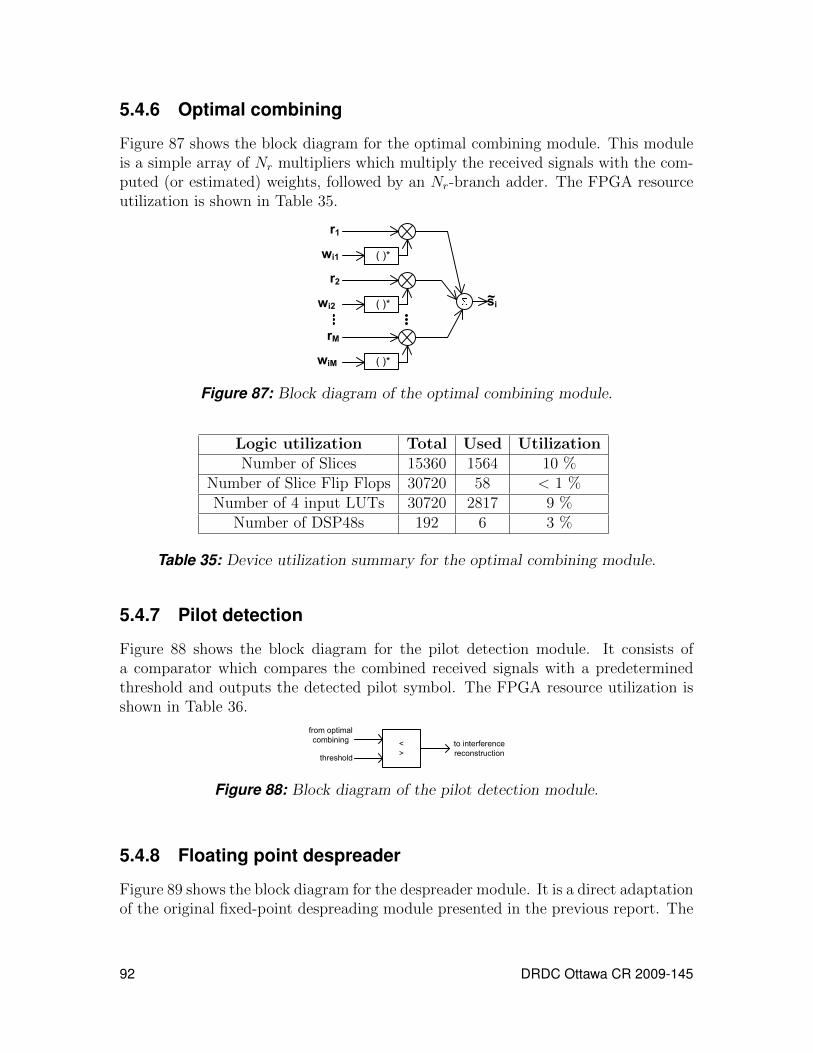
5.4.6 Optimal combining
Figure 87 shows the block diagram for the optimal combining module. This moduleis a simple array of Nr multipliers which multiply the received signals with the com-puted (or estimated) weights, followed by an Nr-branch adder. The FPGA resourceutilization is shown in Table 35.
r1
wi1
r2
wi2
rM
wiM
si~
( )*
( )*
( )*
Figure 87: Block diagram of the optimal combining module.
Logic utilization Total Used UtilizationNumber of Slices 15360 1564 10 %
Number of Slice Flip Flops 30720 58 < 1 %Number of 4 input LUTs 30720 2817 9 %
Number of DSP48s 192 6 3 %
Table 35: Device utilization summary for the optimal combining module.
5.4.7 Pilot detection
Figure 88 shows the block diagram for the pilot detection module. It consists ofa comparator which compares the combined received signals with a predeterminedthreshold and outputs the detected pilot symbol. The FPGA resource utilization isshown in Table 36.
<
>
from optimal
combiningto interference
reconstructionthreshold
Figure 88: Block diagram of the pilot detection module.
5.4.8 Floating point despreader
Figure 89 shows the block diagram for the despreader module. It is a direct adaptationof the original fixed-point despreading module presented in the previous report. The
92 DRDC Ottawa CR 2009-145
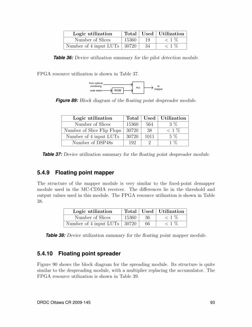
Logic utilization Total Used UtilizationNumber of Slices 15360 19 < 1 %
Number of 4 input LUTs 30720 34 < 1 %
Table 36: Device utilization summary for the pilot detection module.
FPGA resource utilization is shown in Table 37.
ROMAcc
from optimal
combining
code select
to
mapper
Figure 89: Block diagram of the floating point despreader module.
Logic utilization Total Used UtilizationNumber of Slices 15360 564 3 %
Number of Slice Flip Flops 30720 38 < 1 %Number of 4 input LUTs 30720 1011 5 %
Number of DSP48s 192 2 1 %
Table 37: Device utilization summary for the floating point despreader module.
5.4.9 Floating point mapper
The structure of the mapper module is very similar to the fixed-point demappermodule used in the MC-CDMA receiver. The differences lie in the threshold andoutput values used in this module. The FPGA resource utilization is shown in Table38.
Logic utilization Total Used UtilizationNumber of Slices 15360 36 < 1 %
Number of 4 input LUTs 30720 66 < 1 %
Table 38: Device utilization summary for the floating point mapper module.
5.4.10 Floating point spreader
Figure 90 shows the block diagram for the spreading module. Its structure is quitesimilar to the despreading module, with a multiplier replacing the accumulator. TheFPGA resource utilization is shown in Table 39.
DRDC Ottawa CR 2009-145 93

ROMMult
from mapper
code select
to interference
reconstruction
Figure 90: Block diagram of the floating point spreader module.
Logic utilization Total Used UtilizationNumber of Slices 15360 358 2 %
Number of Slice Flip Flops 30720 11 < 1 %Number of 4 input LUTs 30720 641 2 %
Number of DSP48s 192 2 1 %
Table 39: Device utilization summary for the floating point spreader module.
5.4.11 Interference reconstruction
Figure 91 shows the block diagram for the interference reconstruction module. Likethe optimal combination module, this module consists of an Nr-element multiplierarray which multiplies the detected symbol with the channel coefficients, thus recon-structing the interference contribution of the particular symbol. The FPGA resourceutilization is shown in Table 40.
from pilot detection
or spreader1
2
Nr
from channel
coefficients memory
bank
to interference
suppression
Figure 91: Block diagram of the interference reconstruction module.
Logic utilization Total Used UtilizationNumber of Slices 15360 1314 8 %
Number of 4 input LUTs 30720 2372 7 %Number of DSP48s 192 6 3 %
Table 40: Device utilization summary for the interference reconstruction module.
94 DRDC Ottawa CR 2009-145

5.4.12 Interference suppression
Figure 92 shows the block diagram for the interference suppression module. It consistsof an Nr-element subtractor array which subtracts the reconstructed interference fromthe received signals. The FPGA resource utilization is shown in Table 41.
1
2
Nr
to received signals
memory bank
from interference
reconstruction
from received signals
memory bank
Figure 92: Block diagram of the interference suppression module.
Logic utilization Total Used UtilizationNumber of Slices 15360 526 3 %
Number of Slice Flip Flops 30720 358 1 %Number of 4 input LUTs 30720 72 23 %
Table 41: Device utilization summary for the interference suppression module.
5.4.13 MIMO MC-CDMA system
Figure 93 shows the block diagram of the final MIMO MC-CDMA system for a 2× 2case. By using more than one receive antenna, several components had to be dupli-cated. To simplify the code, these components were grouped together into modulesaccording to their function, as can be seen in the block diagram. Furthermore, ad-ditions to the original MC-CDMA system had to be made. This section will presentall of these changes.
First, modules pertaining to the front-end processing were grouped together in or-der to have one instance per receive antenna. This module includes the automaticgain control module and the interface with Comlab’s Quad Dual-band transceiver.Synchronization and correlation of the received packets are included in the pre-FFTmodule. We make the assumption that the packets received at both antennas willhave very similar timing characteristics. In order to have perfect synchronization be-tween the packets from all antennas, we use only one instance of this pre-FFT module.The other branch is delayed to compensate for the pre-FFT processing time. Signalsfrom the pre-FFT module are used by both FFT modules which include the FFT
DRDC Ottawa CR 2009-145 95

Front End
Pre-FFT FFT
Post-FFT
Channel
estimation
Weight
estimation
MIMO
Front EndFrom
ant #1
From
ant #2Delay
N_Rx
FFT
NOTE : Channel & weight estimation and deinterleaving
consist of (N_Rx * N_Tx) identical modules
Pilot
separation
N_Rx
Deinterleaving
Deinterleaving
data
pilots
Deinter-
leaving
Deinter-
leaving
Post-MIMO
Post-MIMO
N_Tx
To host
interface
N_Rx
Figure 93: General architecture of the integrated MIMO MC-CDMA system.
processor, a finite state machine and the pilot generation logic. From the FFT pro-cessor, signals are sent to the post-FFT module which includes timing and frequencysynchronization logic. Since this is solely used by the pre-FFT module, only oneinstance of the post-FFT module is needed.
The FFT processor also separates the pilot samples from the data samples. In orderfor each individual channel link (i, j), such that 0 < i ≤ Nt and 0 < j ≤ Nr to beproperly estimated, the pilot samples must be split into Nt×Nr different signals. Thepilot separation box shown on the diagram consists of a memory bank to save thepilot samples and a finite state machine to control their writing and reading. Theseseparated pilot samples are then sent to Nt ×Nr instances of the channel estimationmodules used in the original MC-CDMA system. In that system, the estimatedchannel samples were used to equalize the received data samples. These equalizedsamples were then deinterleaved so that they would be in the correct order for thedespreading operation. However, in the MIMO MC-CDMA system, with the use ofan MMSE detector, equalization becomes obsolete. The various samples used by theMIMO module still have to be deinterleaved since there is a despreading operation inthe V-BLAST processing chain. Therefore, deinterleaver modules are used for boththe estimated channel samples and the data samples returned by the FFT processor.
Communication between the MIMO module and the off-chip inversion module is notshown on this block diagram. Since the number of communication lines between thetwo cards is limited, parallel-to-serial components are used to convert the channel
96 DRDC Ottawa CR 2009-145

samples sent to the inversion module. Similarly, serial-to-parallel components areused to convert the returned inverted matrices to a format acceptable by the MIMOmodule. Also, the MIMO module returns Nt × Nr weights, one for each link in thesystem. Weight estimation is thus a carbon-copy of the channel estimation, includingestimation and deinterleaving modules. Finally, the weighted samples computed bythe MIMO module are sent to Nt post-MIMO modules, which include the despreader,demapper, descrambler and output FIFO.
Table 42 shows the FPGA resource utilization. As it can be seen, the receiver will notfit in the FPGA chip provided on the Nallatech card. The results shown here are thesmallest that could be obtained by changing the various synthesis options availablein the Xilinx software.
Logic utilization Total Used UtilizationNumber of Slices 15360 17827 116 %
Number of Slice Flip Flops 30720 12920 42 %Number of 4 input LUTs 30720 32140 104 %
Number of FIFO16/RAMB16s 192 263 136 %Number of DSP48s 192 103 53 %
Table 42: Device utilization summary for the MIMO MC-CDMA (excluding the in-version) system on the Virtex-4 SX35.
A few options are possible for the continuation of this work. Firstly, the design couldbe split once more to exploit the space still available on the second card’s FPGA chip.However, since the resource utilization for a 2× 2 system would certainly be greaterthan those shown here, this solution may not be the best one.
Logic utilization Total Used UtilizationNumber of Slices 63168 17317 27 %
Number of Slice Flip Flops 126336 12666 10 %Number of 4 input LUTs 126336 31283 24 %
Number of FIFO16/RAMB16s 552 277 50 %Number of DSP48s 192 103 53 %
Table 43: Device utilization summary for the MIMO MC-CDMA (excluding the in-version) system on the Virtex-4 FX140.
Secondly, more recent and bigger chips could be used to implement this design. Weinvestigated this solution by synthesizing the design for other Xilinx FPGA chips.Tables 43 and 44 show the resource utilization results for the chips Virtex-4 FX140and Virtex-5 FX200. It can be seen that both chips still have sufficient space toimplement a 2× 2 system.
DRDC Ottawa CR 2009-145 97

Logic utilization Total Used UtilizationNumber of Slice Registers 122880 11522 9 %
Number of Slice LUTs 122880 23573 19 %Number of Block RAM/FIFO 456 145 31 %
Number of DSP48Es 384 103 26 %
Table 44: Device utilization summary for the MIMO MC-CDMA (excluding the in-version) system on the Virtex-5 FX200.
Logic utilization Total Used UtilizationNumber of Slices 63168 23839 37 %
Number of Slice Flip Flops 126336 14141 11 %Number of 4 input LUTs 126336 44960 35 %
Number of FIFO16/RAMB16s 552 161 29 %Number of DSP48s 192 107 55 %
Table 45: Device utilization summary for a 1× 2 MIMO MC-CDMA (including theinversion) system on the Virtex-4 FX140.
Logic utilization Total Used UtilizationNumber of Slice Registers 122880 13013 10 %
Number of Slice LUTs 122880 33919 27 %Number of Block RAM/FIFO 456 88 19 %
Number of DSP48Es 384 107 27 %
Table 46: Device utilization summary for a 1× 2 MIMO MC-CDMA (including theinversion) system on the Virtex-5 FX200.
Moreover, it appears from these results that there would be enough space to includethe matrix inversion module within the same chip. Tables 45 and 46 show that itis indeed the case. We can also see that even when including the matrix inversionmodule with the rest of the receiver, there could be enough space for a 2× 2 system.Tables 47 and 48 show the resource utilization results for a 2 × 2 system. Theseresults show that the best solution to the space problem would be to use cards witha bigger chip, since in addition to having a full scale 2 × 2 system-on-chip, it wouldalso remove the need to split the design thus reducing testing and debugging time.
98 DRDC Ottawa CR 2009-145

Logic utilization Total Used UtilizationNumber of Slices 63168 29662 46 %
Number of Slice Flip Flops 126336 17371 13 %Number of 4 input LUTs 126336 55991 44 %
Number of FIFO16/RAMB16s 552 199 36 %Number of DSP48s 192 121 63 %
Table 47: Device utilization summary for a 2× 2 MIMO MC-CDMA (including theinversion) system on the Virtex-4 FX140.
Logic utilization Total Used UtilizationNumber of Slice Registers 122880 15112 12 %
Number of Slice LUTs 122880 41351 33 %Number of Block RAM/FIFO 456 108 23 %
Number of DSP48Es 384 123 32 %
Table 48: Device utilization summary for a 2× 2 MIMO MC-CDMA (including theinversion) system on the Virtex-5 FX200.
DRDC Ottawa CR 2009-145 99

6 Functional test results6.1 Measurement setupIn this section, the receiver was tested in a static wireless channel environment asillustrated in Figure 94. The transmit PC sends a periodic data frame consistingof 5 MC-CDMA symbols in 2.467 GHz band with FFT size of 512, a pilot spacingof 64 subcarriers (Nf = 64) subcarriers, and spreading factor of 8 (SF = 8). Testpatterns were generated with Matlab software and transmitted over the wireless chan-nel. A test pattern consisted of a training symbol and 5 data symbols and could bedownloaded to the transmitter which was implemented in the same FPGA platformas the one used to implement the receiver (please refer to Annex A for the trans-mitter’s implementation details). All results were measured using an Agilent digitaloscilloscope with an input scaling factor of 10:1 and plotted using Matlab. The usercontrol software on the receiver PC was written using Visual C++ 2005 as shown inFigure 95.
`
Transmit PC
DAC
ADC DAC
ADC
`
Receive PC
Nallatech PCI card
Nallatech PCI card
Digital oscilloscope
Figure 94: Measurement setup.
100 DRDC Ottawa CR 2009-145
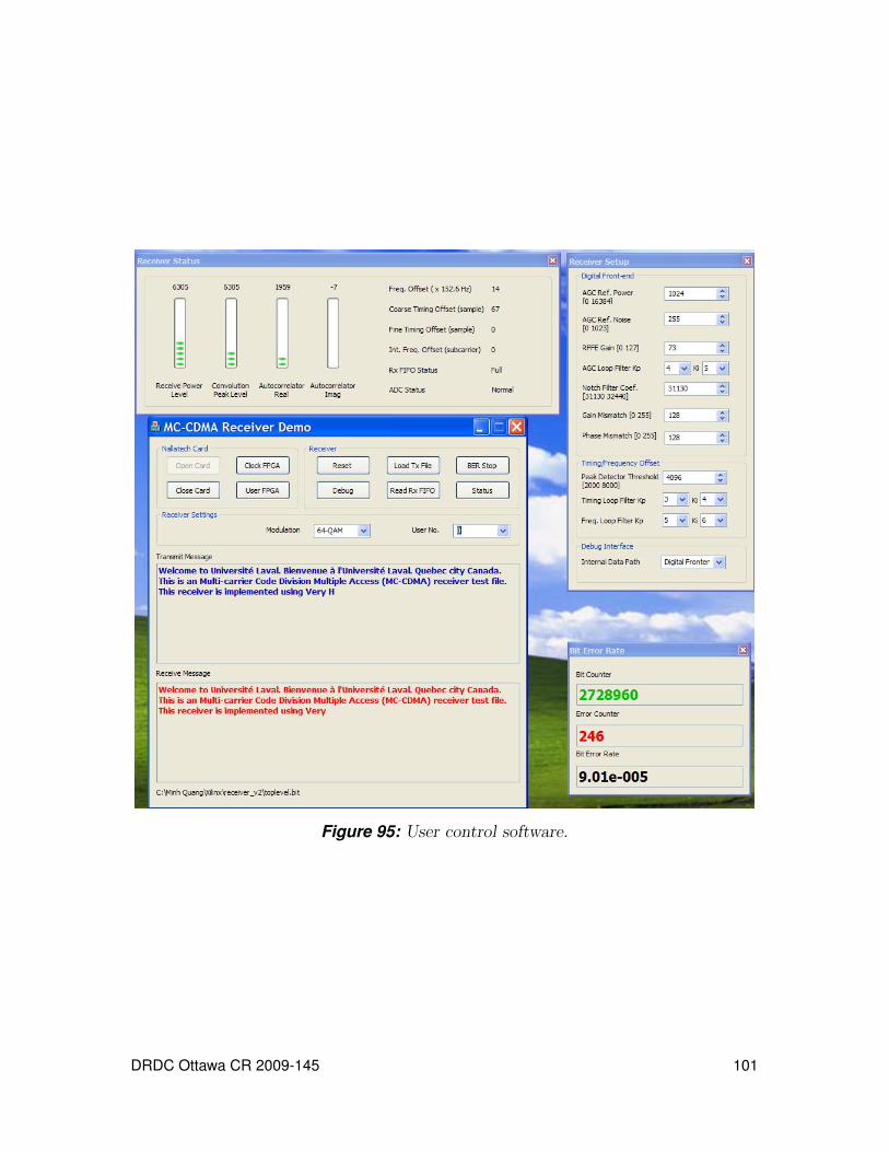
Figure 95: User control software.
DRDC Ottawa CR 2009-145 101
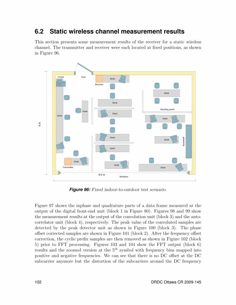
6.2 Static wireless channel measurement resultsThis section presents some measurement results of the receiver for a static wirelesschannel. The transmitter and receiver were each located at fixed positions, as shownin Figure 96.
Desk
Desk
Desk
Windows
Door
Desk
Desk
Transmitter
Receiver
Boo
kshe
lf
Desk
Desk
Desk
Desk
Desk
Desk
Printer
Standing panel
6 m
8.5 m
Desk
Desk
Figure 96: Fixed indoor-to-outdoor test scenario.
Figure 97 shows the inphase and quadrature parts of a data frame measured at theoutput of the digital front-end unit (block 1 in Figure 80). Figures 98 and 99 showthe measurement results at the output of the convolution unit (block 3) and the auto-correlator unit (block 4), respectively. The peak value of the convoluted samples aredetected by the peak detector unit as shown in Figure 100 (block 3). The phaseoffset corrected samples are shown in Figure 101 (block 2). After the frequency offsetcorrection, the cyclic prefix samples are then removed as shown in Figure 102 (block5) prior to FFT processing. Figures 103 and 104 show the FFT output (block 6)results and the zoomed version at the 5th symbol with frequency bins mapped intopositive and negative frequencies. We can see that there is no DC offset at the DCsubcarrier anymore but the distortion of the subcarriers around the DC frequency
102 DRDC Ottawa CR 2009-145
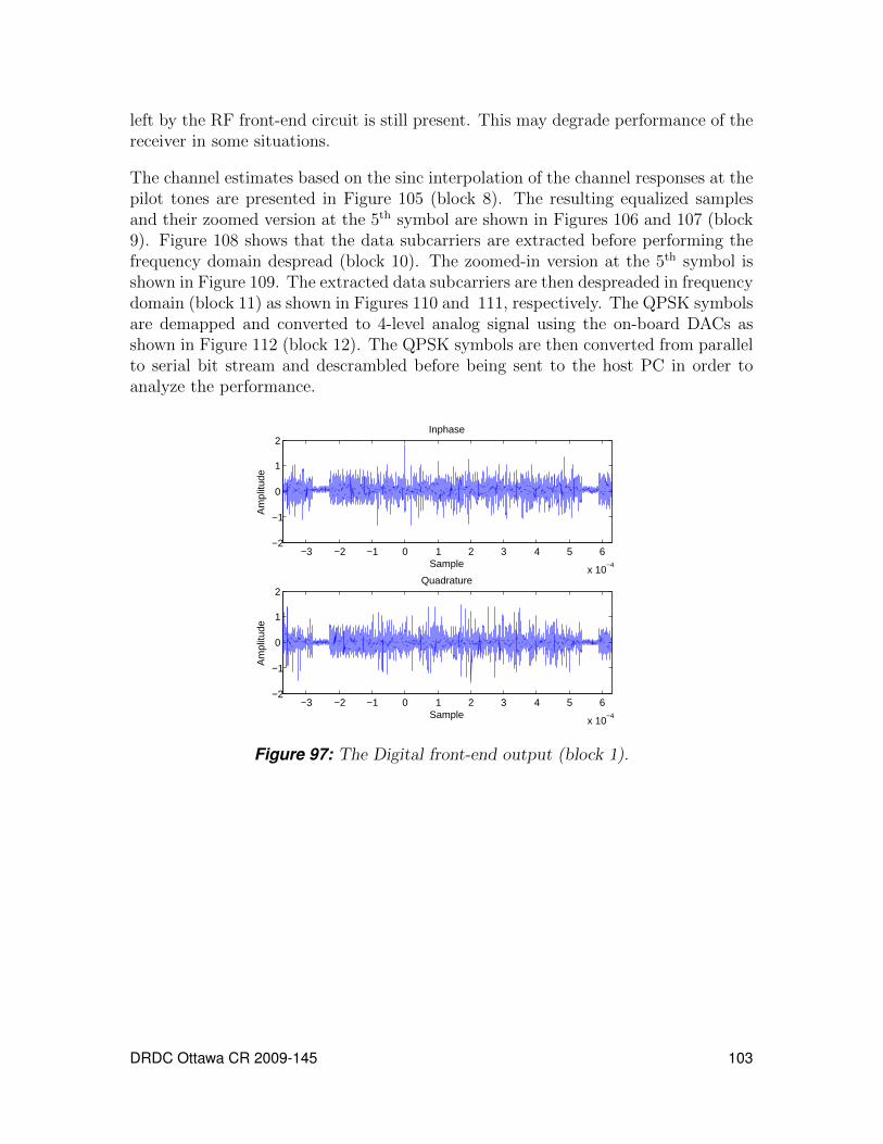
left by the RF front-end circuit is still present. This may degrade performance of thereceiver in some situations.
The channel estimates based on the sinc interpolation of the channel responses at thepilot tones are presented in Figure 105 (block 8). The resulting equalized samplesand their zoomed version at the 5th symbol are shown in Figures 106 and 107 (block9). Figure 108 shows that the data subcarriers are extracted before performing thefrequency domain despread (block 10). The zoomed-in version at the 5th symbol isshown in Figure 109. The extracted data subcarriers are then despreaded in frequencydomain (block 11) as shown in Figures 110 and 111, respectively. The QPSK symbolsare demapped and converted to 4-level analog signal using the on-board DACs asshown in Figure 112 (block 12). The QPSK symbols are then converted from parallelto serial bit stream and descrambled before being sent to the host PC in order toanalyze the performance.
−3 −2 −1 0 1 2 3 4 5 6
x 10−4
−2
−1
0
1
2
Sample
Am
plitu
de
Inphase
−3 −2 −1 0 1 2 3 4 5 6
x 10−4
−2
−1
0
1
2
Sample
Am
plitu
de
Quadrature
Figure 97: The Digital front-end output (block 1).
DRDC Ottawa CR 2009-145 103
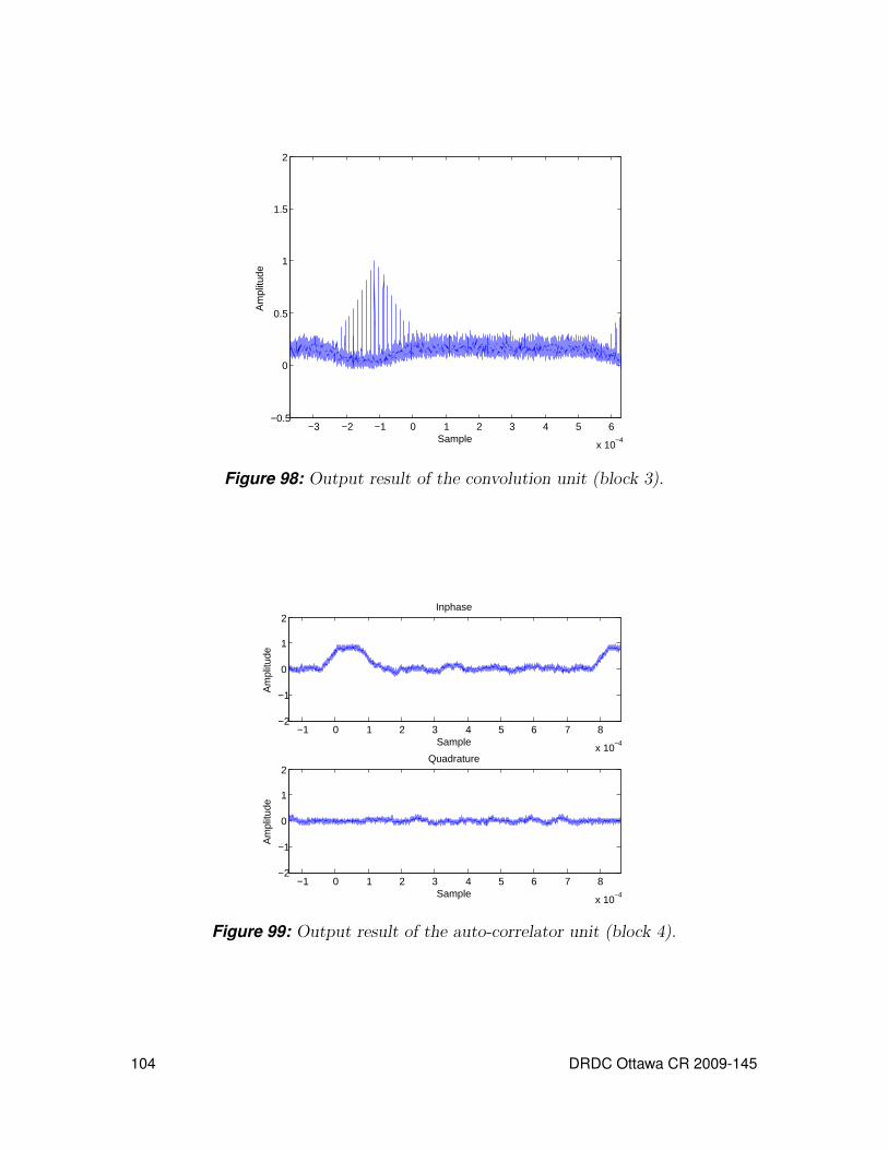
−3 −2 −1 0 1 2 3 4 5 6
x 10−4
−0.5
0
0.5
1
1.5
2
Sample
Am
plitu
de
Figure 98: Output result of the convolution unit (block 3).
−1 0 1 2 3 4 5 6 7 8
x 10−4
−2
−1
0
1
2
Sample
Am
plitu
de
Inphase
−1 0 1 2 3 4 5 6 7 8
x 10−4
−2
−1
0
1
2
Sample
Am
plitu
de
Quadrature
Figure 99: Output result of the auto-correlator unit (block 4).
104 DRDC Ottawa CR 2009-145
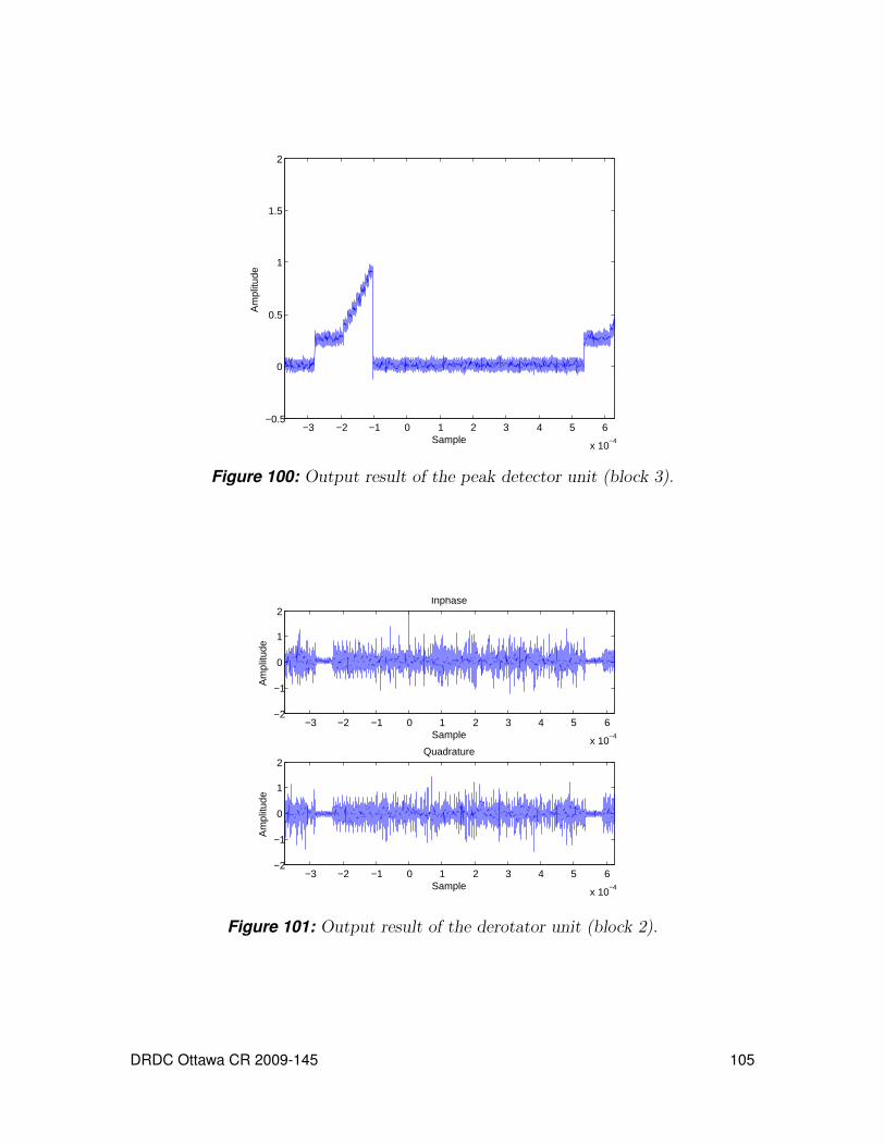
−3 −2 −1 0 1 2 3 4 5 6
x 10−4
−0.5
0
0.5
1
1.5
2
Sample
Am
plitu
de
Figure 100: Output result of the peak detector unit (block 3).
−3 −2 −1 0 1 2 3 4 5 6
x 10−4
−2
−1
0
1
2
Sample
Am
plitu
de
Inphase
−3 −2 −1 0 1 2 3 4 5 6
x 10−4
−2
−1
0
1
2
Sample
Am
plitu
de
Quadrature
Figure 101: Output result of the derotator unit (block 2).
DRDC Ottawa CR 2009-145 105
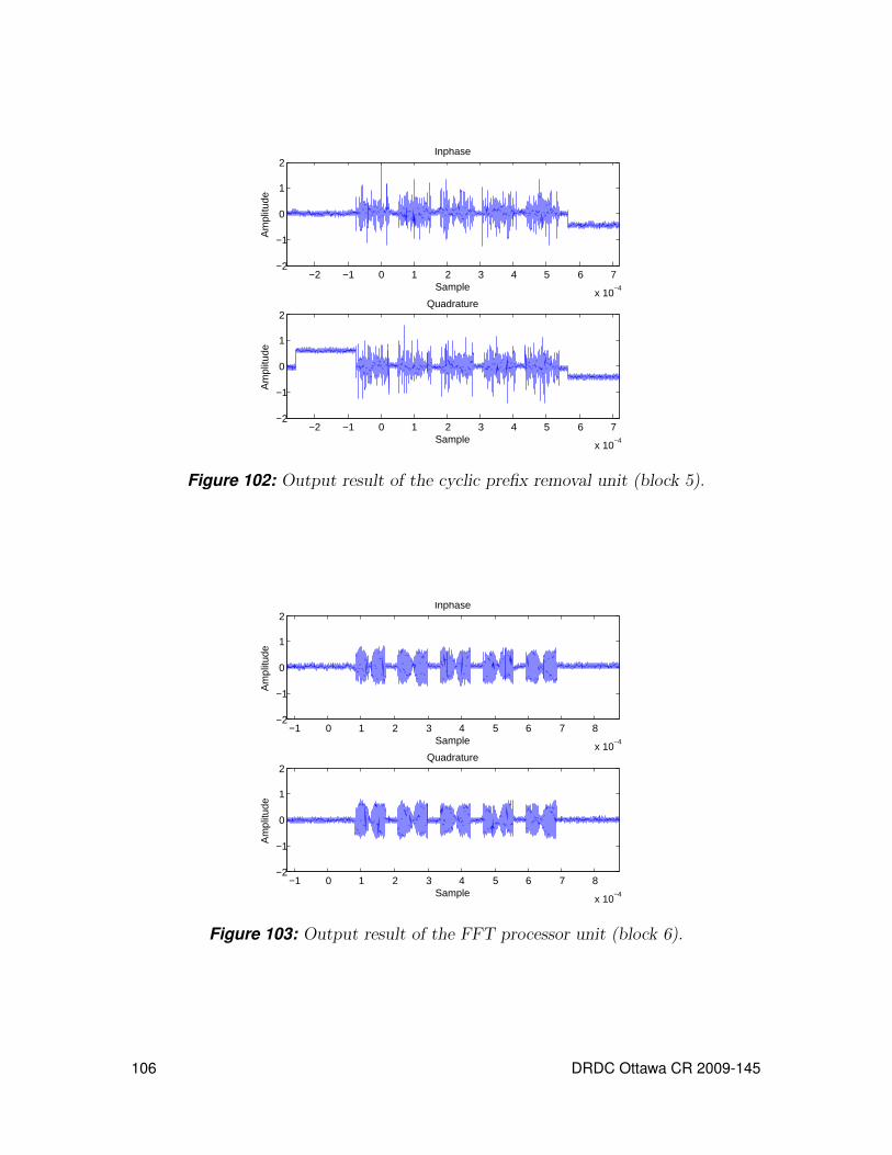
−2 −1 0 1 2 3 4 5 6 7
x 10−4
−2
−1
0
1
2
Sample
Am
plitu
de
Inphase
−2 −1 0 1 2 3 4 5 6 7
x 10−4
−2
−1
0
1
2
Sample
Am
plitu
de
Quadrature
Figure 102: Output result of the cyclic prefix removal unit (block 5).
−1 0 1 2 3 4 5 6 7 8
x 10−4
−2
−1
0
1
2
Sample
Am
plitu
de
Inphase
−1 0 1 2 3 4 5 6 7 8
x 10−4
−2
−1
0
1
2
Sample
Am
plitu
de
Quadrature
Figure 103: Output result of the FFT processor unit (block 6).
106 DRDC Ottawa CR 2009-145
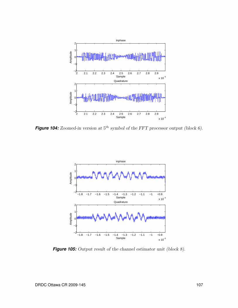
2 2.1 2.2 2.3 2.4 2.5 2.6 2.7 2.8 2.9
x 10−4
−2
−1
0
1
2
Sample
Am
plitu
de
Inphase
2 2.1 2.2 2.3 2.4 2.5 2.6 2.7 2.8 2.9
x 10−4
−2
−1
0
1
2
Sample
Am
plitu
de
Quadrature
Figure 104: Zoomed-in version at 5th symbol of the FFT processor output (block 6).
−1.8 −1.7 −1.6 −1.5 −1.4 −1.3 −1.2 −1.1 −1 −0.9
x 10−3
−2
−1
0
1
2
Sample
Am
plitu
de
Inphase
−1.8 −1.7 −1.6 −1.5 −1.4 −1.3 −1.2 −1.1 −1 −0.9
x 10−3
−2
−1
0
1
2
Sample
Am
plitu
de
Quadrature
Figure 105: Output result of the channel estimator unit (block 8).
DRDC Ottawa CR 2009-145 107

−14 −13 −12 −11 −10 −9 −8 −7 −6 −5
x 10−4
−2
−1
0
1
2
Sample
Am
plitu
de
Inphase
−14 −13 −12 −11 −10 −9 −8 −7 −6 −5
x 10−4
−2
−1
0
1
2
Sample
Am
plitu
de
Quadrature
Figure 106: Output result of the channel equalizer unit (block 9).
−7.4 −7.3 −7.2 −7.1 −7 −6.9 −6.8 −6.7 −6.6 −6.5
x 10−4
−2
−1
0
1
2
Sample
Am
plitu
de
Inphase
−7.4 −7.3 −7.2 −7.1 −7 −6.9 −6.8 −6.7 −6.6 −6.5
x 10−4
−2
−1
0
1
2
Sample
Am
plitu
de
Quadrature
Figure 107: Zoomed-in version at 5th symbol of the channel equalizer unit (block 9).
108 DRDC Ottawa CR 2009-145
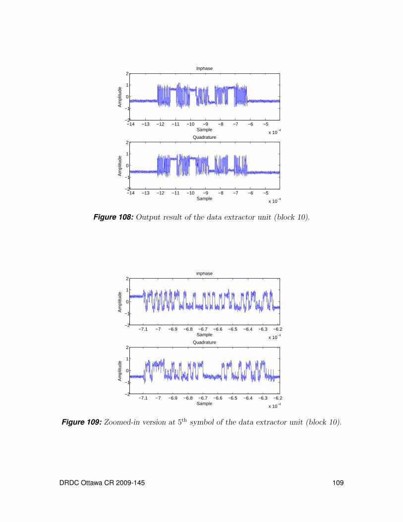
−14 −13 −12 −11 −10 −9 −8 −7 −6 −5
x 10−4
−2
−1
0
1
2
Sample
Am
plitu
de
Inphase
−14 −13 −12 −11 −10 −9 −8 −7 −6 −5
x 10−4
−2
−1
0
1
2
Sample
Am
plitu
de
Quadrature
Figure 108: Output result of the data extractor unit (block 10).
−7.1 −7 −6.9 −6.8 −6.7 −6.6 −6.5 −6.4 −6.3 −6.2
x 10−4
−2
−1
0
1
2
Sample
Am
plitu
de
Inphase
−7.1 −7 −6.9 −6.8 −6.7 −6.6 −6.5 −6.4 −6.3 −6.2
x 10−4
−2
−1
0
1
2
Sample
Am
plitu
de
Quadrature
Figure 109: Zoomed-in version at 5th symbol of the data extractor unit (block 10).
DRDC Ottawa CR 2009-145 109
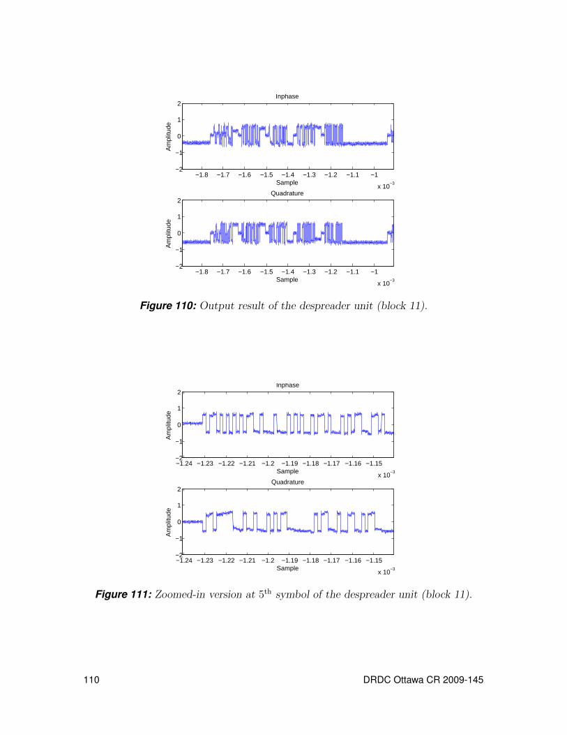
−1.8 −1.7 −1.6 −1.5 −1.4 −1.3 −1.2 −1.1 −1
x 10−3
−2
−1
0
1
2
Sample
Am
plitu
de
Inphase
−1.8 −1.7 −1.6 −1.5 −1.4 −1.3 −1.2 −1.1 −1
x 10−3
−2
−1
0
1
2
Sample
Am
plitu
de
Quadrature
Figure 110: Output result of the despreader unit (block 11).
−1.24 −1.23 −1.22 −1.21 −1.2 −1.19 −1.18 −1.17 −1.16 −1.15
x 10−3
−2
−1
0
1
2
Sample
Am
plitu
de
Inphase
−1.24 −1.23 −1.22 −1.21 −1.2 −1.19 −1.18 −1.17 −1.16 −1.15
x 10−3
−2
−1
0
1
2
Sample
Am
plitu
de
Quadrature
Figure 111: Zoomed-in version at 5th symbol of the despreader unit (block 11).
110 DRDC Ottawa CR 2009-145

−1.8 −1.7 −1.6 −1.5 −1.4 −1.3 −1.2 −1.1 −1 −0.9
x 10−3
−0.5
0
0.5
1
1.5
2
Sample
Am
plitu
de
Figure 112: Output result of the demapper unit (block 12).
DRDC Ottawa CR 2009-145 111

6.3 BER performance resultsIn order to control the signal’s dynamic range at the receiver, a custom interfacecard between the receiver’s AGC circuit and the RF front-end had to be designedto serve that purpose. However, since the design of that interface card was notcompleted at the time the measurements were taken, the gain of the RF front-endhad to be manually adjusted so that the received signal level was within the operatingrange of the receiver during the tests. Also, because of this limitation and of thegeneral laboratory setup, tests could only be performed at fix locations (as indicatedin section 6.2). Therefore, the BER performance results provided here apply to astatic wireless indoor channel only. The measured BERs for various signal-to-noisevalues are summarized in tables 49 to 51.
SNR (dB) QPSK 16-QAM 64-QAM-4 4.9E-2 2.56E-1 3.52E-1-2 1.99E-2 2.21E-1 3.18E-10 4.4E-3 1.29E-1 2.09E-12 5.42E-4 8.43E-2 1.48E-14 3.09E-5 2.64E-2 1.19E-16 1.63E-6 8.64E-3 8.6E-28 N/A1 2.7E-3 4.72E-210 N/A1 1.95E-4 2.76E-212 N/A1 2.78E-5 1.09E-214 N/A1 2.82E-6 4.51E-3
Table 49: BER performance of the receiver in static wireless indoor channel, 1 user.
1. BER is low
112 DRDC Ottawa CR 2009-145

SNR (dB) QPSK 16-QAM 64-QAM-4 1.82E-1 3.1E-1 3.7E-1-2 1.52E-1 2.96E-1 3.61E-10 9.87E-2 2.57E-1 3.18E-12 5.19E-2 1.98E-1 2.69E-14 2.12E-2 1.52E-1 2.24E-16 3.97E-3 1.09E-1 1.75E-18 3.8E-4 6.07E-2 1.31E-110 1.41E-5 2.28E-2 9.39E-212 N/A1 5.54E-3 6.84E-214 N/A1 7.73E-4 3.26E-216 N/A1 N/A2 1.64E-2
Table 50: BER performance of the receiver in static wireless indoor channel, 4 users.
SNR (dB) QPSK 16-QAM 64-QAM-4 2.72E-1 3.49E-1 3.89E-1-2 2.08E-1 3.39E-1 3.64E-10 1.56E-1 3.17E-1 3.36E-12 1.18E-1 2.65E-1 3.03E-14 6.37E-2 2.12E-1 2.79E-16 2.29E-2 1.66E-1 2.45E-18 6.7E-3 1.55E-1 2.08E-110 5.86E-4 5.95E-2 1.45E-112 7.44E-5 2.51E-2 1.14E-114 N/A1 8.42E-3 7.82E-216 N/A1 1.96E-3 5.14E-2
Table 51: BER performance of the receiver in static wireless indoor channel, 8 users.
The BER performances of the receiver in the static indoor tests are plotted in thefollowing figures. Since a static indoor channel was used for the measurements, com-puter simulations using an AWGN channel model (dash curves in these figures) wereused for comparison with the measurement results. Figure 113 shows the performanceof the receiver under different modulation schemes for a single user setup. It is log-ical to see that higher modulation schemes (i.e. 16-QAM or 64-QAM) require moretransmit power than QPSK modulation. Figures 114 to 116 show the performance ofthe receiver for QPSK, 16-QAM and 64-QAM modulation under different numbersof active users.
1. BER is low2. The transmitter can not reach the required power
DRDC Ottawa CR 2009-145 113

In these figures, the greater the number of users simultaneously transmitting over thechannel, the less the BER performance. This was true for all modulation schemes.This is normal because, in the context of a MC-CDMA system, all users act asinterferers to each other and therefore can be considered as additive noise to thereceiver. The measured BER results presented here are in close agreement with thesimulations. Remaining discrepancies stem from synchronization errors and roundofferrors due to the fixed-point arithmetic implementation (Matlab simulations reliedon floating point arithmetic).
−5 0 5 10 15 20 2510
−6
10−5
10−4
10−3
10−2
10−1
100
Average SNR
BE
R
QPSK16−QAM64−QAMQPSK sim16−QAM sim64−QAM sim
Figure 113: Measured BER performance under different modulation schemes.
114 DRDC Ottawa CR 2009-145

−5 0 5 10 15 20 2510
−6
10−5
10−4
10−3
10−2
10−1
100
Average SNR
BE
R
QPSK 1−userQPSK 4−userQPSK 8−userQPSK 1−user simQPSK 4−user simQPSK 8−user sim
Figure 114: QPSK performance under different numbers of active users.
−5 0 5 10 15 20 2510
−6
10−5
10−4
10−3
10−2
10−1
100
Average SNR
BE
R
16QAM 1−user16QAM 4−user16QAM 8−user16QAM 1−user sim16QAM 4−user sim16QAM 8−user sim
Figure 115: 16-QAM performance under different numbers of active users.
DRDC Ottawa CR 2009-145 115
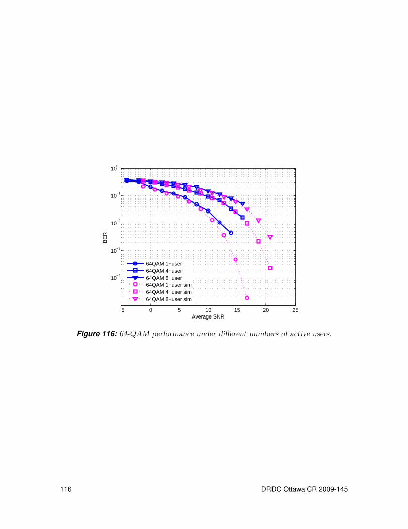
−5 0 5 10 15 20 25
10−4
10−3
10−2
10−1
100
Average SNR
BE
R
64QAM 1−user64QAM 4−user64QAM 8−user64QAM 1−user sim64QAM 4−user sim64QAM 8−user sim
Figure 116: 64-QAM performance under different numbers of active users.
116 DRDC Ottawa CR 2009-145

7 Conclusion
This report presented an implementation of a complete Multi-Carrier Code DivisionMultiple Access (MC-CDMA) receiver into an FPGA platform. The receiver is firstsimulated in a complete MC-CDMA system (modulation, transmission over multipathfading channel, reception, and demodulation). The simulation results showed thatat a BER of 10−3 the performance of the SISO MC-CDMA system over the indoor-to-outdoor/pedestrian channel is better than for the vehicular channel by about 12dB, 11 dB, and 10 dB for QPSK-, 16QAM-, and 64QAM-MC-CDMA, respectively.If the channel condition is better, higher modulation orders can be used to improvethe transmission rate. Increasing the modulation order implies that the signal con-stellation points are closer, leading to a higher BER for the same transmission power.Thus, there is a trade-off between the data rate and the transmission power in or-der to keep a low cost. In fact, coding techniques will have to be used in order toimprove the performance of the system for both channels. Turbo codes and LowDensity Parity Check (LDPC) codes are the best candidates for further performanceimprovement.
The implementation of the receiver for indoor configuration was modularly imple-mented in native VHDL language so that it is possible to maximize reuse of thecodes for future enhancements. The implementation also exploited temporal multi-plexing techniques in order to minimize logic gates, embedded multipliers, embeddedmemory blocks while maintaining the same performance as the traditional imple-mentation technique. Polyphase filtering was chosen to be used for decimation filtersin the digital front-end circuit in order to maximize hardware usage, resulting inlow complexity overall. The receiver used a WLAN-based preamble for acquisitionand tracking the symbol timing and carrier frequency offset. A nearly optimum sincinterpolation method was used in the pilot assisted modulation channel estimationtechnique. This algorithm reduces hardware complexity significantly by exploitingthe temporal multiplexing technique. Furthermore, the CORDIC algorithm was usedto compute the carrier frequency offset and compensate for these errors. A serialCORDIC architecture was implemented due to its low complexity in this receiver.The lowest complexity radix-2 FFT core from Xilinx was used in this design. Inter-nal controllable signals were mapped to registers in order to allow the user to changetheir values in run time. The SISO MC-CDMA receiver for indoor-to-outdoor channelconfiguration used less than 50% resource of the Virtex4-SX35 device and achievinga maximum clock frequency of about 150 MHz.
Functional tests of the receiver were performed in the static laboratory channel envi-ronment. The results of these tests were compared with simulations in a static wirelessindoor channel to demonstrate that the receiver functions as expected. Further testsin the moving laboratory channel were not performed due to the lack of time for the
DRDC Ottawa CR 2009-145 117
integration of the interface card between the AGC circuit in the receiver and the RFfront-end box in order to maintain the signal dynamic range within the operatingrange for the test. Future work should be concentrated on the test of the receiverin the moving channel so that the performance of the receiver can be evaluated andcompared with the results of the Matlab simulations for the indoor-to-outdoor andvehicular channels.
This report also presented an integrated MIMO MC-CDMA system. The bit errorrate was improved by the use of multiple antennas at the receiver. It was also shownthrough simulations that although the bit error rate was not improved by the use ofmultiple antennas at both the transmitter and receiver, the increase data throughputis high enough to warrant the use of such a system.
VHDL implementation of the system was based on a previously existing MIMO designemploying a LST receiver with a matrix inversion circuit to compute MMSE weights.The architecture of the MIMO components uses a floating point format to increaseprecision and range, a requirement necessary for the matrix inversions. Contrary toour initial thoughts, the LST receiver had to be considerably modified. The symboldetection first had to be split in two for the pilot and data symbols. Many finite statemachines also had to be designed to conform to the original MC-CDMA system’stiming requirements. These modifications were verified in a stand-alone system inModelsim before integration with the MC-CDMA system. Given the size of theimplementation, another necessary requirement is the splitting of the design on thetwo available cards. A logical split lies within the separation of the matrix inversionmodule from the rest of the MIMO components. Also, significant changes to theoriginal MC-CDMA circuit were made, including the addition of a weight estimationmodule.
Proof-of-concept for the system was shown using Modelsim simulations, but, due tothe size of the design, it was impossible to implement the system in the Nallatechcards. The best solution to this problem was found to be the use of a bigger chip.It was shown that using a bigger chip would also eliminate the need to separate thematrix inversion from the rest of the receiver.
118 DRDC Ottawa CR 2009-145

References
[1] Lei, Zhongding, Peng, Xiaoming, and Chin, Francois P. S. (2003), V-BLASTReceivers for Downlink MC-CDMA Systems, In Vehicular TechnologyConference, pp. 866–970.
[2] Jones, V. K. and Raleigh, Gregory G. (1998), Channel Estimation for WirelessOFDM Systems, In Global Telecommunications Conference, pp. 980–985,Sydney, Australia.
[3] 3GPP (1999), TS 25.101v2.1.0, 3rd Generation Partnership Project (3GPP),Technical Specification Group (TSG), RAN WG4 UE Radio transmission andReception (FDD).
[4] Hsieh, M.-H. and Wei, C.-H. (1998), Channel estimation for OFDM systemsbased on comb-type pilot arrangement in frequency selective fading channels,IEEE Transactions on Consumer Electronics, 44, 217–225.
[5] Coleri, S., Ergen, M., Puri, A., and Bahai, A. (2002), A study of channelestimation in OFDM systems, In 56th IEEE Vehicular Technology Conference,pp. 894 – 898.
[6] Tsai, P-Y and Chiueh, T-D (2005), A 1.1-V 9.9-mW MC-CDMA DownlinkBaseband Receiver IC for Next-Generation of Cellular CommunicationSystems, Asian Solid-State Circuits Conference, 54, 489 – 492.
[7] Le-Nous, Sebastien, Nouvel, Fabienne, and Helard, Jean-Francois (2004),Design and Implementation of MC-CDMA Systems for Future WirelessNetworks, EURASIP Journal on Applied Signal Processing, pp. 1604–1615.
[8] Hara, Shinsuke and Prasad, Ramjee (1997), Overview of Multicarrier CDMA,IEEE Communications Magazine, 35, 126–123.
[9] Schulze, Henrik and Luders, Christian (2005), Theory and applications ofOFDM and CDMA, Wiley.
[10] Lui, Hui (2000), Signal processing application in CDMA communication,Artech House Publisher.
[11] Hoecher, P., Kaiser, S., and Roberson, P. (1997), Two-dimensionalPilot-Symbol-Aided Channel Estimation by Wienner Filtering, In IEEEInternational Conference on Acoustics, Speech, and Signal Processing, Munich.
[12] Alamouti, S. M. (1998), A Simple Transmit Diversity Technique for WirelessCommunications, IEEE Journal on Select Areas in Communications, Vol. 16.
[13] Foschini, G. J. (1996), Layered Space-Time Architecture for WirelessCommunication in a Fading Environment When Using Multi-ElementAntennas, Bell Labs Technical Journal.
[14] Wolniansky, P. W. and al. (1998), V-BLAST : An Architecture for RealizingVery High Data Rates Over the Rich-Scattering Wireless Channel, VRSIInternational Symposium On Signals, Systems and Electronics.
DRDC Ottawa CR 2009-145 119

[15] LaRoche, Isabelle and Roy, Sebastien (2006), An Efficient Regular MatrixInversion Circuit Architecture for MIMO Processing, In IEEE InternationalSymposium on Circuits and Systems, Kos, Greece.
[16] LaRoche, Isabelle and Roy, Sebastien (2007), An Efficient VLSI Architecture ofa Layered Space-Time Receiver, In IEEE 65th Vehicular TechnologyConference, Dublin, Ireland.
[17] 3GPP (2002), TS 25.213v5.0.0, 3rd Generation Partnership Project, TechnicalSpecification Group Radio Access Network, Spreading and modulation (FDD)(Release 5).
[18] Tang, X., Alouini, M. S., and Goldsmith, A. J. (1999), Effect of ChannelEstimation Error on M-QAM BER Performance in Rayleigh Fading, IEEETransactions on Communications, 47, 1856–1864.
[19] Widrow, B. (1971), Adaptive Filters, In N. de Claris, R. Kalman, (Ed.),Aspects of Network and System Theory, Holt, Rinehart, and Winston.
[20] Clark, Martin V., Greenstein, Larry J., and annd Mansoor Shafi, WilliamK. Kennedy (1992), Matched Filter Bounds for Diversity Combining Receiversin Digital Mobile Radio, IEEE Transactions on Vehicular Technology, 41,356–362.
[21] Nallatech (2005), XtremeDSP Development Kit-IV User Guide.
[22] Mitra, Sanjit K. (2006), Digital Signal Processing: A Computer-BasedApproach, McGraw Hill.
[23] Churchill, F.E., Ogar, G.W., and Thompson, B.J. (1981), The Correction of Iand Q Errors in a Coherent Processor, IEEE Transactions on Aerospace andElectronic Systems, AES-1, 131 – 137.
[24] Volder, J.E (1959), The CORDIC Trigonometric Computing Technique, IRETransactions on Electronics Computers, EC-8, 330–334.
[25] Wang, Y., Jian-Hua, G., Ai, B., Zong-Qiang, L., and Yuan-Fei, N. (2005), ANovel Scheme for Symbol Timing in OFDM WLAN Systems, ECTITransactions on Electrical Eng. Electronics, and Communications, 3, 86–91.
[26] Hanzo, L., Munster, M., Choi, B. J., and Keller, T. (2003), OFDM andMC-CDMA for Broadband Multi-User Communications, WLANs andbroadcasting, Wiley.
[27] Xilinx, Corp. (2005), Fast Fourier Transform v3.2.
[28] Mcnair, B., Cimini, L. J., and Sollenberger, N. R. (1999), A robust timing andfrequency offset estimation scheme for orthogonal frequency divisionmultiplexing (OFDM) systems, IEEE 49th Vehicular Technology Conference, 1,690 – 694.
[29] Zou, H., McNair, B., and Daneshrad, B. (2001), An integrated OFDM receiverfor high-speed mobile data communications, IEEE GLOBECOM ’01 GlobalTelecommunications Conference, 5, 3090 – 3094.
120 DRDC Ottawa CR 2009-145

[30] Shayan, Y.R. and Le-Ngoc, T. (1989), All digital phase-locked loop: concepts,design and applications, IEE Proceeding of Radar and Signal Processing, 136,53 – 56.
[31] Xilinx, Corp. (2006), Divider v1.0.
[32] IEEE (2003), Part 11: Wireless LAN Medium Access Control (MAC) andPhysical Layer (PHY) specifications - High-speed Physical Layer in the 5 GHzBand.
DRDC Ottawa CR 2009-145 121

This page intentionally left blank.
122 DRDC Ottawa CR 2009-145
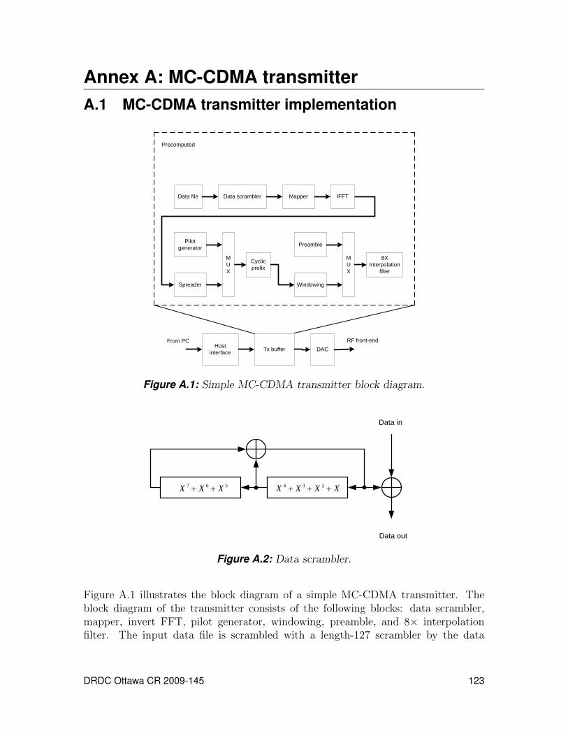
Annex A: MC-CDMA transmitterA.1 MC-CDMA transmitter implementation
Data file Data scrambler Mapper
Cyclic prefix
MUX
Preamble
Windowing
8X Interpolation
filter
Precomputed
Spreader
MUX
Pilot generator
IFFT
Tx bufferHost interface DAC
RF front-endFrom PC
Figure A.1: Simple MC-CDMA transmitter block diagram.
Data in
Data out
4 3 2X X X X+ + +7 6 5X X X+ +
Figure A.2: Data scrambler.
Figure A.1 illustrates the block diagram of a simple MC-CDMA transmitter. Theblock diagram of the transmitter consists of the following blocks: data scrambler,mapper, invert FFT, pilot generator, windowing, preamble, and 8× interpolationfilter. The input data file is scrambled with a length-127 scrambler by the data
DRDC Ottawa CR 2009-145 123

scrambler block that uses the same generator polynomial as in the IEEE 802.11aOFDM system. The generator polynomial S(x) is given by
S(x) = x7 + x4 + 1 (A.1)
and is illustrated in Figure A.2. The same generator polynomial is used to scramblethe transmit data and to descramble the receive data.
The windowing block is based also on the windowing specifications of the IEEE802.11a OFDM system. In a typical implementation, the windowing function willbe represented in discrete time. The windowing function for an MC-CDMA symbolwith symbol duration TS = 128 �s, 512-point IFFT, is defined as
w(n) =
⎧⎨⎩1 2 ≤ n ≤ 639
0.5 1, 640
0 otherwise
(A.2)
The preamble structure for MC-CDMA system was described earlier. Given such apreamble structure, the generated preamble for an indoor MC-CDMA transmitter isshown in Figure A.3. In this figure, the preamble has 640 samples which is exactlythe same length of an MC-CDMA symbol.
The 8× interpolation filter is implemented using a multistage polyphase interpolationtechnique. The filters characteristics are the same as the receiver’s decimation filter.We assumed that a transmit frame consists of a preamble and 5 data symbols. Theresulting interpolated complex samples preprocessed in Matlab are stored in a binaryfile so that it is downloadable to the transmit buffer (block RAM) in the user FPGAvia user control software for transmitting to the wireless channel.
Integrating MIMO with the existing MC-CDMA transmitter is straightforward. Sincethe transmitter implementation remains exactly the same, it is only a matter ofreplicating the transmitter for every transmit antenna in the system. With the MIMOsystem implemented in this project, all complexity lies in the receiver.
124 DRDC Ottawa CR 2009-145

100 200 300 400 500 600−0.5
−0.4
−0.3
−0.2
−0.1
0
0.1
0.2
0.3
0.4
0.5
Sample index
Am
plitu
de
(a) Real component.
100 200 300 400 500 600−0.5
−0.4
−0.3
−0.2
−0.1
0
0.1
0.2
0.3
0.4
0.5
Sample index
Am
plitu
de
(b) Imaginary component.
Figure A.3: Preamble for an indoor MC-CDMA transmitter.
DRDC Ottawa CR 2009-145 125

This page intentionally left blank.
126 DRDC Ottawa CR 2009-145
Annex B: Interface with RF front-endsB.1 PreliminariesA pair of Quad Dual Band RF Transceiver RF front-ends from Comlab is used tointerface the digital subsystem (residing on the Nallatech cards) with the antennas.Unfortunately, these front-ends were not designed to interface with Nallatech cards,but rather with SignalMaster systems form Lyretch. Furthermore, the number ofinterface pins required to configure and control one RF front-end is relatively high,while the number of general-purpose I/O pins off the main FPGA on the Nallatechcards is rather limited — 42 altogether on three separate headers (ADJIN header –28 pins, P-Link 0 — 12 usable pins, User Header – 2 pins).
Furthermore, a certain number of these pins must be dedicated to a high-bandwidthdirect connection between two Nallatech cards, as required to implement a 4-antennatransceiver, with each card handling two antennas. In determining how many of the42 available pins should be allocated to each of these two functions (RF front-endcontrol and card-to-card interface), a number of issues must be examined. Obviously,some sort of multiplexing scheme must be employed in both cases. For the card-to-card interface, the multiplexing can be implemented directly in the FPGA fabric.This is not a problem as such, but bandwidth is an issue. The latency introduced inthe interface will somehow have to be integrated in the signal processing algorithmswithout undue complexity, and this consideration will drive the partitioning schemerequired to split the circuit between the two FPGAs.
For the RF front-end, the multiplexing must be addressed using an interface cardsituated between the front-end and the controlling Nallatech board. Some of theconfiguration commands of the RF front-end can be performed via a serial 3-wire(SPI - Serial Peripheral Interconnect) bus, while others are performed by directlyactivating the appropriate line(s), in a totally parallel fashion. There is some overlapbetween the two command styles, so that some commands can be performed usingboth parallel lines or SPI.
B.2 Original card designThe card that was originally designed to exploit a 9-pin interface with a microcon-troller for multiplexing purposes. This leaves 33 pins free for other purposes, includingcard-to-card interfacing. It was also designed with the previous versions of the RFfront-end in mind, and thus had two 34-pin 0.05” output connectors instead of one.
Figure B.1 shows the original interface card scheme which was planned for the originalversion of the RF front-end. The latter is controlled via 2 34-pin 0.05” Samtec GPIOconnectors which together comprise 42 distinct signals. The card consists of 2 main
DRDC Ottawa CR 2009-145 127
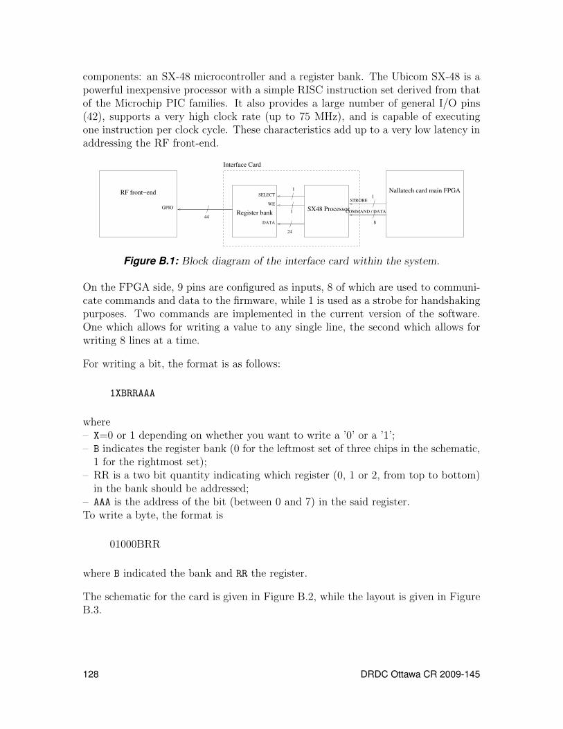
components: an SX-48 microcontroller and a register bank. The Ubicom SX-48 is apowerful inexpensive processor with a simple RISC instruction set derived from thatof the Microchip PIC families. It also provides a large number of general I/O pins(42), supports a very high clock rate (up to 75 MHz), and is capable of executingone instruction per clock cycle. These characteristics add up to a very low latency inaddressing the RF front-end.
Interface Card
RF front−end
GPIO
Nallatech card main FPGA
8
1
24
1
144
COMMAND / DATA
STROBEWE
DATA
SELECT
SX48 ProcessorRegister bank
Figure B.1: Block diagram of the interface card within the system.
On the FPGA side, 9 pins are configured as inputs, 8 of which are used to communi-cate commands and data to the firmware, while 1 is used as a strobe for handshakingpurposes. Two commands are implemented in the current version of the software.One which allows for writing a value to any single line, the second which allows forwriting 8 lines at a time.
For writing a bit, the format is as follows:
1XBRRAAA
where– X=0 or 1 depending on whether you want to write a ’0’ or a ’1’;– B indicates the register bank (0 for the leftmost set of three chips in the schematic,
1 for the rightmost set);– RR is a two bit quantity indicating which register (0, 1 or 2, from top to bottom)
in the bank should be addressed;– AAA is the address of the bit (between 0 and 7) in the said register.To write a byte, the format is
01000BRR
where B indicated the bank and RR the register.
The schematic for the card is given in Figure B.2, while the layout is given in FigureB.3.
128 DRDC Ottawa CR 2009-145

Currently, a VHDL implementation of the RFFE control IP block has been realized.This IP block is implemented and was tested in the main Nallatech card FPGA.
It should be noted that the power supply circuit is built around a LM2937ET-3.3three-pin voltage regulator which provides power at 3.3V. This is because the RFfront-end expects 3.3V input signals. It is noteworthy, however, that all the digitalcomponents on the card can work at either 3.3 or 5V. The 74xx family registers areof the “HC” (high-speed CMOS) variety. They are therefore capable of operatingseamlessly over a wide range of supply voltages, in addition to being very frugalin terms of power requirements. The SX48 can also operate at both supply voltagelevels, but can only operate at frequencies up to 50MHz at 3.3V (as opposed to 75MHzat 5V). Thus, the board could be converted to 5V operation simply by replacing theLM2937ET-3.3 by a LM7805 (5V regulator).
This version of the card has been built and tested with the VHDL core and in generalseems to work, although a number of issues have had to be resolved during testing:1. It appears that the layout itself is not robust enough for very high speed operation.
Indeed, the card does not operate properly at 50 MHz, but it does at 20 MHz.2. It was found that the pinout of the RF front-ends has changed and that fewer
control signals are now required. In fact, only one 34-pin connector is required. Itwas possible to adapt the card by simply exchanging a GND pin (whose location hadchanged between the two RF front-end versions) on the second 34-pin connector.
3. An unresolved issue, apparently a weird hardware/software interaction, lead usto exchange the position on the connector of a critical signal. This effectivelycircumvented the problem.
4. A layout error was found on the four pin programming connector where GNDand Vdd pins were interchanged. This was corrected, both on the card and in theschematics.
5. An error was found in the signal assignments of the original RF front-end signals.This point, however, is made moot by the fact that the pin assignments havechanged in the newer RF front-end version.
It is also noteworthy that because the card interface works with polling, one shouldallow up to 100 clock cycles to write a bit, and approximately 50 clock cycles towrite a byte (using the byte write command). Nonetheless, the possibility remainsto implement higher-level commands in firmware for e.g. rapid and autonomous gainadjustments by the card itself.
DRDC Ottawa CR 2009-145 129
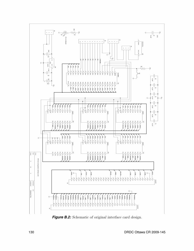
25R
C5
26R
C6
27R
C7
28R
D0
29R
D1
30R
D2
31R
D3
34R
D4
35R
D5
36R
D6
37R
D7
38R
E0
39R
E1
40R
E2
41R
E3
42R
E4
43R
E5
44R
E6
45R
E7
48R
TC
C
1M
CLR
2O
SC
1
3O
SC
2
6R
A0
7R
A1
8R
A2
9R
A3
10R
B0
11R
B1
12R
B2
13R
B3
14R
B4
15R
B5
16R
B6
17R
B7
20R
C0
21R
C1
22R
C2
23R
C3
24R
C4
SX
48BD
U1
B23
B22 B
21
B20
B19
B18
B17
B16
B15
B14
B13
B12
B11
B10
B9
B7
B6
B5
B8
B15
B14
B13
B12
B11
B10
B9
B8 B
7
B6
B5
B4
B3
B2
B1
B0
B0
B1
B2
B3
B4
B5
B6
B7
B8
B9
B10
B11
B12
B13
B14
B15
OS
CS
LD1B
LD2B
LD3B
LD4B
DO
UT
B
DIN
2
SC
LK2
#CS
B
SC
LK
DIN
DS
W
#PA
EN
3
#PA
EN
4
#PA
EN
2
AD
D0
#TX
EN
1
BB
3
#RX
HP
2
BB
7
#RX
HP
1
BB
6
SH
DN
2
BB
5
SH
DN
1
BB
4
#RX
EN
2
#RX
HP
3
#RX
EN
1
#RX
HP
4
SH
DN
4
#TX
EN
3
1O
E
31D
42D
73D
84D
135D
146D
177D
188D
21Q
52Q
63Q
94Q
125Q
156Q
167Q
198Q
11C
LK
74374U
2
1O
E
31D
42D
73D
84D
135D
146D
177D
188D
21Q
52Q
63Q
94Q
125Q
156Q
167Q
198Q
11C
LK
74374U
3
1O
E
31D
42D
73D
84D
135D
146D
177D
188D
21Q
52Q
63Q
94Q
125Q
156Q
167Q
198Q
11C
LK
74374U
4
1O
E
31D
42D
73D
84D
135D
146D
177D
188D
21Q
52Q
63Q
94Q
125Q
156Q
167Q
198Q
11C
LK
74374U
5
2468 135710 9
J5
ST
RO
BE
D0
D1
D2
D3
D4
D5
D6
2 13
J3
5O
SC
_OU
T1
OE
/NC
EC
SX
TA
LU
9
3 24 1
J4
Vcc
FILE
:R
EV
ISIO
N:
DR
AW
N B
Y:
PA
GE
OF
TIT
LE
11
22
33
44
55
66
77
88
99
1010
1111
1212
1313
1414
1515
1616
1717
1818
1919
2020
2121
2222
2323
2424
2525
2626
2727
2828
2929
3030
3131
3232
3333
3434
conn34J1
11
22
33
44
55
66
77
88
99
1010
1111
1212
1313
1414
1515
1616
1717
1818
1919
2020
2121
2222
2323
2424
2525
2626
2727
2828
2929
3030
3131
3232
3333
3434
conn34J2
OS
CS
LD1B
LD2B
LD3B
LD4B
DO
UT
B
DIN
2
SC
LK2
#CS
B
SC
LK
DIN
DS
W
#RX
EN
4
#RX
EN
3
#TX
EN
4
SH
DN
3
#TX
EN
3
SH
DN
4
#RX
HP
4
#RX
EN
1
#RX
HP
3
#RX
EN
2
BB
4
SH
DN
1
BB
5
SH
DN
2
BB
6
#RX
HP
1
BB
7
#RX
HP
2
BB
3
#TX
EN
1
BB
2
#TX
EN
2
BB
1
PA
BS
#GE
N
#SP
IEN
AD
D1
#PA
EN
1
AD
D0
#PA
EN
2
#PA
EN
4
#PA
EN
3
1O
E
31D
42D
73D
84D
135D
146D
177D
188D
21Q
52Q
63Q
94Q
125Q
156Q
167Q
198Q
11C
LK
74374U
7
1O
E
31D
42D
73D
84D
135D
146D
177D
188D
21Q
52Q
63Q
94Q
125Q
156Q
167Q
198Q
11C
LK
74374U
6
B4
B3
B2
B1
B23
B22
B21
B20
B19
B18
B17
B16
#PA
EN
1
AD
D1
#SP
IEN
#GE
N
PA
BS
BB
1
#TX
EN
2
BB
2
B19
B18
B17
B16
SH
DN
3
#TX
EN
4
#RX
EN
3
#RX
EN
4
RF
front−end generic interface card
12
S1
R2
Vcc
2 13
J6
INO
UT
LM2937
GN
D
1
2
3
U8
12
C8
10uF
12
C10
1uF
C9
0.1uF
Vcc
Vcc
R1
200
12D1
5V on indicator
Vcc
C10.1uF
(U3)
C20.1uF
C30.1uF
C40.1uF
C50.1uF
C60.1uF
C70.1uF
Vcc
D7
B0
11
1.2Sebastien R
oy
Figure B.2: Schematic of original interface card design.
130 DRDC Ottawa CR 2009-145
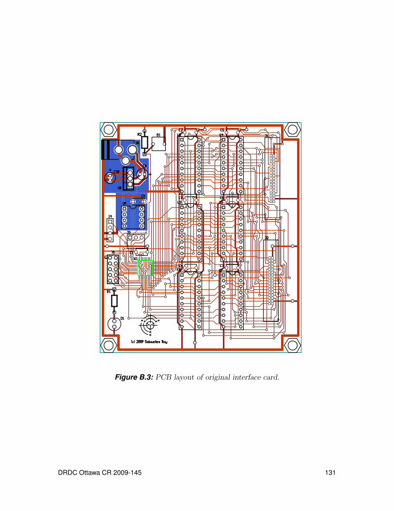
Figure B.3: PCB layout of original interface card.
DRDC Ottawa CR 2009-145 131

Ref Part No. Manufacturer Value Package Description
U1 SX48BD Parallax TQFP-48 MicrocontrollerU2-U7 74HC374 Fairchild et al. DIP20 Register
U8 LM2937ET-3.3 National Semi. 3.3V TO-220 Linear voltage regulatorU9 ACHL-25.000MHZ-EK Abracon 25MHx, 3.3V DIP-8 Half-size TTL oscillatorD1 SSL-LX5063GT Lumex 100mcd T-1 3/4 Green LEDS1 B3F-6000 Omron Momentary switch
C1-C7, C9 K104K15X7RF5TH5 Vishay / BC Comp. 0.1�F .2” spacing ceramic capacitorC8 ECE-A1HKG100 Panasonic 10�F, 50V 200mm spacing electrolytic capacitorC10 ECE-A1HKG010 Panasonic 1�F, 50V 200mm spacing electrolytic capacitorJ6 PJ-202AH CUI Inc. 2.1× 5.5. mm Power jack connectorJ4 .1” header, 1×4 .1” header, 1×4J5 .1” header, 2×5 .1” header, 2×6J3 .1” header, 1×3 .1” header, 1×3
J1-J2 EHF-117-01-F-D-RA Samtec 2×17 twin-row 0.05” 34 position headerR1 200Ω resistorR2 5K resistor
Table B.1: Bill of materials for original version of card.
B.3 Proposed new version of cardIt is proposed that a new version of the interface card be built, exploiting the factthat fewer interface signals are required for controlling the new front-ends than wasoriginally anticipated, and profiting from the lessons of the first design.
The new pin-out of the front-ends requires only 32 lines (a single 34 pin Samtecconnector is used, with 2 pins being tied to ground). Of these, 6 are used to control thetwo SPI bus connections (one for configuring the transceivers, with adjunct addressinglines, and one for exchanging with the power monitoring ADC). It is suggested thatthese 6 lines be routed directly to the FPGA for more responsive control of the SPIbus.
Then, only 26 lines are left to be addressed by the microcontroller. Four of theselines, T-EN1 through T-EN4, are used to latch some signals (#PAEN, #TXEN, #RXEN,SHDN and RXHP) to one of the four transceivers. There are also two address lines ADD1and ADD0 which serve to address one of the four transceivers for SPI access or forparallel gain control. These two mechanisms seem redundant, and the card could bedesigned to exploit ADD1 and ADD0 to generate T-EN1 – T-EN4; there would be noambiguity, since the latter four signals are only validated when #LATCHEN goes low.This would reduce the total number of lines to be addressed by the microcontrollerto 22.
Since the SX48 has 24 available output pins in this application, this approach ob-viates the need for any external registers, provided a simple multiplexing circuitryis provided to handle the generation of T-EN1 – T-EN4 described above. Since eachoutput pin is able to source up to 30 mA, no buffers are required either.
This would make the card much smaller. The layout would also be improved toallow high speed (50 MHz) operation. This would require more care in positioningand selecting decoupling capacitors, using shorter traces, and placing a ground planeunder the microcontroller. For the latter, it would probably be necessary to use a
132 DRDC Ottawa CR 2009-145

4-layer board, thus providing ground planes and power planes across the entire board.Since 4-layer boards nowadays are not that significantly more expensive than 2-layerPCBs, this is a viable approach.
Also, it is proposed to redirect the strobe signal to an SX48 input capable of triggeringan interrupt. Thus, it would be possible to write interrupt-driven code which wouldimprove the responsiveness of the card.
B.4 Source code[numbers=left,obeytabs=true]
;=======================================================================
;TITLE: RFFEintcard.SRC
;
;PURPOSE: Source code for interface card between FPGA and Comlab / Lyrtech
; RF front-end.
;
;AUTHOR: Sebastien Roy
;
;REVISIONS:
; 2009/05/18 - last bug removed (fingers crossed)
;
;=======================================================================
;-------------------------- DEVICE DIRECTIVES --------------------------
DEVICE SX48,OSCHS3
IFDEF __SASM ;SASM Directives
IRC_CAL IRC_SLOW
ELSE ;Parallax Assember Directives
DEVICE STACKX_OPTIONX
ENDIF
RESET Main
;------------------------------ VARIABLES ------------------------------
Count1 EQU $10
;---------------------------- DEBUG SETTINGS ---------------------------
FREQ 25_000_000
WATCH Count1,16,UDEC
;------------------------ INITIALIZATION ROUTINE -----------------------
Init
;Configure port settings
mov w, #$1f ; setup mode register
mov m, w ; for port direction
mov ra, #%00000000 ;Port A output zero
mov !ra, #%00001000 ;Port A is 3 outs, one input
mov rb, #%00000000 ;Port B output zero
mov !rb, #%11111111 ;Port B is all inputs
DRDC Ottawa CR 2009-145 133

mov rc, #%00000000 ;Port C output zero
mov !rc, #%00000000 ; Port C is all outputs
mov rd, #%00000000 ; Port D output zero
mov !rd, #%00000000 ; Port D is all outputs
mov re, #%00000000 ; Port E output zero
mov !re, #%00000000 ; Port E is all outputs
mov w, #$1e ; setup mode register
mov m, w ; for pull-up mode
mov !ra, #$00000000 ; pull-ups disabled
mov !rb, #$00000000 ; pull-ups disabled
mov !rc, #$00000000 ; pull-ups disabled
mov !rd, #$00000000 ; pull-ups disabled
mov !re, #$00000000 ; pull-ups disabled
bank 0 ; select register bank 0
clr $19 ; clear shadow register E
clr $18 ; clear shadow register D
clr $17 ; clear shadow register C
bank $20 ; select register bank 1
clr $19 ; clear shadow register E
clr $18 ; clear shadow register D
clr $17 ; clear shadow register C
ret
;--------------------------- BIT COPY ROUTINE ----------------------------
bitcopy mov $0b, w ; Save data byte to $0b
rr $0b ;rotate right 3 times
rr $0b
rr $0b
mov w, $0b
and w, #%00000011 ;recover 2 ls bits
mov $0b, w ;store in $0b for addition
mov w, #$07 ;store constant in register w
add w, $0b ;add appropriate offset
mov fsr, w ;set up indirect addressing to register
mov w, $0c ;recover data byte from $0c
and w, #%00000111 ;recover 3 ls bits
mov $0f, w ;transfer to counter
mov $0e, #$01 ;load ’1’ in $0e
clc ;clear carry
jmp :Loopa ;start looping
:Loop rl $0e ;rotate left $0e
dec $0f ;decrement counter
:Loopa test $0f ;test!
sz ;skip if zero
jmp :Loop ;loop until bit is in position
;initially specified by w
mov w, $0c ;recover data byte
clrb fsr.5 ;register bank select
and w, #%00100000 ;isolate bank select bit
test w ;test!
sz ;skip if zero
setb fsr.5
setb fsr.4 ;point to shadow port
mov w, $0c ;recover data byte
and w, #%01000000 ;should we write a one or a zero?
test w ;test!
snz ;skip if not zero
jmp WRZERO ;if zero, jump to write zero section
134 DRDC Ottawa CR 2009-145

mov w,INDF ;get current port content
or w, $0e ;or with contents of $0c - turns on
;the required bit
mov INDF, w ;send back to port - shadow version first
jmp WRFINALIZE ;jump to final step
WRZERO mov w, $0e ;recover rotated bit from $0e
not w ;invert all bits
mov $0e, w ;store result (rotated zero)
mov w, INDF ;get current port contents
and w, $0e ;set appropriate bit to zero
mov INDF, w ;send back to port - shadow version first
WRFINALIZE mov w, $19 ;copy shadow port E to port E
mov $09, w ;
mov w, $18 ;copy shadow port D to port D
mov $08, w ;
mov w, $17 ;copy shadow port C to port C
mov $07, w ;
mov w, $0c ;recover data byte from $0b
and w, #%00100000 ;isolate bank select bit
test w ;test!
sz ;skip if zero
jmp :BANK1 ;if not zero, then proceed for bank 1
;otherwise signal for bank 0
setb ra.1 ;raise clock on bank 0 (latching data)
clrb ra.1 ;lower clock on bank 0
jmp :WROVER
:BANK1 setb ra.0 ;raise clock on bank 1 (latching data)
clrb ra.0 ;lower clock on bank 1
:WROVER clrb ra.2 ;output enable
ret ;return from subroutine
;----------------------------- BYTE COPY -------------------------------
bytecopy mov w, $0c ;recover first data byte (command)
and w, #%00000011 ;isolate the two low-order bits
;which provide byte address within bank
mov $0b, w ;store in $0b for addition
mov w, #$07 ;store constant in register w
add w, $0b ;add appropriate offset
mov FSR, w ;setup for indirect access to proper reg.
mov w, $0d ;recover data byte
mov INDF, w ;write to proper address
mov w, $0c ;recover command byte again
and w, #$00000100 ;isolate bank ID bit
test w ;test!
sz ;skip if zero
jmp :BANK1 ;if not zero, then proceed to bank 1
;if zero write to bank 0
setb ra.1 ;raise clock for bank 0 (latch data)
clrb ra.1 ;lower clock for bank 0
jmp :WROVER ;write operation now over
:BANK1 setb ra.0 ;raise clock for bank 1 (latch data)
clrb ra.0
DRDC Ottawa CR 2009-145 135

:WROVER clrb ra.2 ;output enable
ret ;return from subroutine
;---------------------------- MAIN PROGRAM -----------------------------
Main call Init
Poll mov w, ra ;Fetch RA to test strobe line
and w, #%00001000 ;Isolate strobe line
test w ;Test
snz ;If strobe low, then loop
jmp poll
mov $0c, rb ;save incoming data byte to $0c
stlow mov w, ra ;fetch RA to test strobe line
and w, #%00001000 ;isolate strobe line
test w ;Test
sz ;loop while strobe high
jmp stlow
mov w, $0c ;recover received data byte
and w, #%11000000 ;extract the two higher order bits
test w ;test!
sz ;skip if zero
jmp cont ;if not zero, continue parsing
call Init ;If zero, then command is ’clear all’
jmp Poll ;return to polling for next command
cont mov w, $0c ;recover received data byte
and w, #%10000000 ;isolate higher order bit
test w ;test!
snz ;skip if not zero
jmp cont2 ;if zero, keep going
mov w, $0c ;recover received data byte
call bitcopy ;write appropriate output line
;command is ’bit copy’
jmp Poll ;return to polling for next command
cont2 mov w, ra ;Fetch RA to test strobe line
and w, #%00001000 ;isolate strobe line
test w ;test!
snz ;skip if not zero
jmp cont2 ;while zero, loop (waiting for 2nd data byte)
mov $0d, rb ;if strobe high, save data byte
stlow2 mov w, ra ;fetch RA to test strobe line
and w, #%00001000 ;isolate strobe line
test w ;test!
sz ;skip if zero
jmp stlow2 ;loop while strobe is high
call bytecopy ;execute ’byte copy’ command
jmp Poll
ret ;then return
136 DRDC Ottawa CR 2009-145
List of acronyms16QAM 16-Level Quadrature Amplitude Modulation3G Third Generation3GPP Third Generation Partnership Project4G Fourth Generation64QAM 64-Level Quadrature Amplitude ModulationADC Analog to Digital ConverterAWGN Additive White Gaussian NoiseBER Bit Error RateCDMA Code Division Multiple AccessDAC Digital to Analog ConverterDPCCH Dedicated Physical Control ChannelDPDCH Dedicated Physical Data ChannelFFT Fast Fourier TransformFIR Finite Impulse ResponseFPGA Field Programmable Gate ArrayIFFT Inverse Fast Fourier TransformISI Inter-Symbol InterferenceICI Inter-Carrier InterferenceITU International Telecommunication UnionLDPC Low Density Parity Check CodeLOS Line Of SightLAN Local Area NetworkLFSR Linear Feedback Shift RegisterMAI Multiple Access InterferenceMC-CDMA Multi-Carrier Code Division Multiple AccessMFB Matched Filter BoundMIMO Multiple-Input Multiple-OutputOFDM Orthogonal Frequency Division MultiplexingOVSF Orthogonal Variable Spreading FactorPN Pseudo NoiseP/S Parallel-to-SerialQPSK Quadrature Phase Shift KeyingSF Spreading FactorSISO Single-Input Single-OutputS/P Serial-to-ParallelSNR Signal-to-Noise RatioTS Technical SpecificationUTRA Universal Terrestrial Radio AccessUARFCN UTRA Absolute Radio Frequency Channel NumberWCDMA Wideband Code Division Multiple Access
DRDC Ottawa CR 2009-145 137

This page intentionally left blank.
138 DRDC Ottawa CR 2009-145

DOCUMENT CONTROL DATA(Security classification of title, body of abstract and indexing annotation must be entered when document is classified)
1. ORIGINATOR (The name and address of the organization preparing thedocument. Organizations for whom the document was prepared, e.g. Centresponsoring a contractor’s report, or tasking agency, are entered in section 8.)
Laboratoire de radiocommunications et de traitementdu signalDepartement de genie electrique et de genieinformatiquePavillon Adrien-Pouliot1065, avenue de la Medecine, Bureau 1300Universite Laval, Quebec (Quebec), G1V 0A6
2. SECURITY CLASSIFICATION (Overallsecurity classification of the documentincluding special warning terms if applicable.)
UNCLASSIFIED
3. TITLE (The complete document title as indicated on the title page. Its classification should be indicated by the appropriateabbreviation (S, C or U) in parentheses after the title.)
FPGA implementation of a baseband MIMO MC-CDMA downlink receiver
4. AUTHORS (Last name, followed by initials – ranks, titles, etc. not to be used.)
Nguyen, M.-Q.; LaRoche, I.; Fortier, P.; Roy, S.
5. DATE OF PUBLICATION (Month and year of publication ofdocument.)
September 2009
6a. NO. OF PAGES (Totalcontaining information.Include Annexes,Appendices, etc.)
162
6b. NO. OF REFS (Totalcited in document.)
32
7. DESCRIPTIVE NOTES (The category of the document, e.g. technical report, technical note or memorandum. If appropriate, enterthe type of report, e.g. interim, progress, summary, annual or final. Give the inclusive dates when a specific reporting period iscovered.)
Contract Report
8. SPONSORING ACTIVITY (The name of the department project office or laboratory sponsoring the research and development –include address.)
Defence R&D Canada – Ottawa3701, Carling avenue, Ottawa, Ontario, K1A-0Z4
9a. PROJECT NO. (The applicable research and developmentproject number under which the document was written.Please specify whether project or grant.)
15dg02
9b. GRANT OR CONTRACT NO. (If appropriate, the applicablenumber under which the document was written.)
W7714-5-0942
10a. ORIGINATOR’S DOCUMENT NUMBER (The officialdocument number by which the document is identified by theoriginating activity. This number must be unique to thisdocument.)
DRDC Ottawa CR 2009-145
10b. OTHER DOCUMENT NO(s). (Any other numbers which maybe assigned this document either by the originator or by thesponsor.)
11. DOCUMENT AVAILABILITY (Any limitations on further dissemination of the document, other than those imposed by securityclassification.)( X ) Unlimited distribution( ) Defence departments and defence contractors; further distribution only as approved( ) Defence departments and Canadian defence contractors; further distribution only as approved( ) Government departments and agencies; further distribution only as approved( ) Defence departments; further distribution only as approved( ) Other (please specify):
12. DOCUMENT ANNOUNCEMENT (Any limitation to the bibliographic announcement of this document. This will normally correspondto the Document Availability (11). However, where further distribution (beyond the audience specified in (11)) is possible, a widerannouncement audience may be selected.)
Unlimited distribution

13. ABSTRACT (A brief and factual summary of the document. It may also appear elsewhere in the body of the document itself. It is highlydesirable that the abstract of classified documents be unclassified. Each paragraph of the abstract shall begin with an indication of thesecurity classification of the information in the paragraph (unless the document itself is unclassified) represented as (S), (C), (R), or (U).It is not necessary to include here abstracts in both official languages unless the text is bilingual.)
Orthogonal Frequency Division Multiplexing (OFDM) has become a very attractive multicarriertransmission technique for wireless high speed data communications. OFDM offers robustnessto multipath fading without having to provide powerful channel equalization. In order to supportmultiple users with high speed data communications, the Multi-Carrier Code Division Multiple Ac-cess (MC-CDMA) technique is used to address these challenges. MC-CDMA is a combination ofOFDM and Code Division Multiple Access (CDMA) and has the benefits of both systems. Thus,the parameters of OFDM become the basic parameters of MC-CDMA. Furthermore, Multi-InputMulti-Ouput (MIMO) was integrated to the MC-CDMA system to improve the bit error rate anddata throughput. Simulations were performed for an MC-CDMA system and an MIMO MC-CDMAunder different channel environments. The simulation parameters considered were: guard timeinterval, symbol duration, sampling rate, number of data subcarriers, modulation scheme, num-ber of active users, and number of transmit and receive antennas. The goal of the simulationswas to allow for different MIMO MC-CDMA configurations to be tested in order to obtain thebest system parameters. The MC-CDMA receiver was implemented into an FPGA developmentplatform based on the simulation results. Finally, the MC-CDMA transceiver was fully tested ina laboratory wireless channel environment. Design size prevented the implementation and livetests of the MIMO MC-CDMA receiver.
14. KEYWORDS, DESCRIPTORS or IDENTIFIERS (Technically meaningful terms or short phrases that characterize a document and couldbe helpful in cataloguing the document. They should be selected so that no security classification is required. Identifiers, such asequipment model designation, trade name, military project code name, geographic location may also be included. If possible keywordsshould be selected from a published thesaurus. e.g. Thesaurus of Engineering and Scientific Terms (TEST) and that thesaurus identified.If it is not possible to select indexing terms which are Unclassified, the classification of each should be indicated as with the title.)
Wireless, MC-CDMA, FPGA, MIMO, OFDM, 3G, 4G

