fpga based system design dr. nazar abbas saqib nust institute of information technology (niit)...
TRANSCRIPT
FPGA Based System DesignFPGA Based System Design
Dr. Nazar Abbas SaqibDr. Nazar Abbas SaqibNUST Institute of NUST Institute of Information Technology Information Technology (NIIT)(NIIT)
Lecture 3: Introduction to FPGAs

We will discuss..We will discuss..
• Programming Architectures• Historical Perpective
• PALs, PLDs, CPLDs & FPGAs
The Design Warrior’s Guide to FPGAsDevices, Tools, and Flows. ISBN 0750676043
Copyright © 2004 Mentor Graphics Corp. (www.mentor.com)
Pl note source of the figures included in this lecture

1945 1950 1955 1960 1965 1970 1975 1980 1985 1990 1995 2000
FPGAs
ASICs
CPLDs
SPLDs
Microprocessors
SRAMs & DRAMs
ICs (General)
Transistors
Historical PerspectiveHistorical Perspective
1. First programmable logic devices to appear in 19702. Can implement any set of sum of the product logic equations

SRAMs, DRAMs & MicroprocessorsSRAMs, DRAMs & Microprocessors
1. Late 1960s and early 1970s – New development in technology
2. Intel introduced first 1024 bit DRAM in 1970 (the 1103)
3. Fairchild introduced first 256-bit static RAM in 1970 (the 4100)
4. Intel also introduced first Microprocessor in 1971 (the 4004)
5. Our intrest: Most of today FPGAs are SRAM based with embedded microprocessors

PLD PLD (Programmable Logic (Programmable Logic Devices)Devices)
1. The first programmable ICs were generally refered to as PLDs2. They are grouped as
• SPLDs : Simple PLDs• CPLDs: Complex PLDs
3. SPLDs being less sophisticated, less logic• The firs programmable chip comes in the form of PROM in 1970s
4. CPLDs being more complex, late 1970s and early 1980s • MegaPAL from MMI in 1984
PLDs
SPLDs CPLDs
PLAsPROMs PALs GALs etc.
a b c
l l l
Address 0 &
Address 1 &
Address 2 &
Address 3 &
Address 4 &
Address 5 &
Address 6 &
Address 7 &
a !a b !b c !c
!a !c!b& &
!a c!b& &
!a !cb& &
!a cb& &
a !c!b& &
a c!b& &
a !cb& &
a cb& &
Predefined AND array
Prog
ram
mab
le O
R a
rray
w x y
Predefined linkProgrammable link
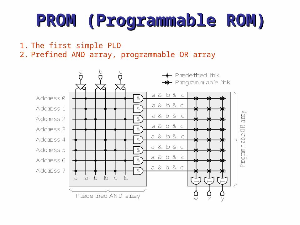
PROM (Programmable ROM)PROM (Programmable ROM)1. The first simple PLD2. Prefined AND array, programmable OR array

a b c
l l lAddress 0 &
Address 1 &
Address 2 &
Address 3 &
Address 4 &
Address 5 &
Address 6 &
Address 7 &
a !a b !b c !c
!a !c!b& &
!a c!b& &
!a !cb& &
!a cb& &
a !c!b& &
a c!b& &
a !cb& &
a cb& &
Predefined AND array
Pro
gram
mab
le O
R a
rray
w x y
Predefined linkProgrammable link
w = (a & b)
x = !(a & b)
y = (a & b) ^ c
PROM (Programmable ROM)PROM (Programmable ROM)
• Programmed PROM• Lighter, cheaper, fast logic

a b c
&
&
&
a !a b !b c !c
N/A
Predefined AND array
Prog
ram
mab
leO
R a
rray
Predefined linkProgrammable link
l l l
w x y
N/A
N/A
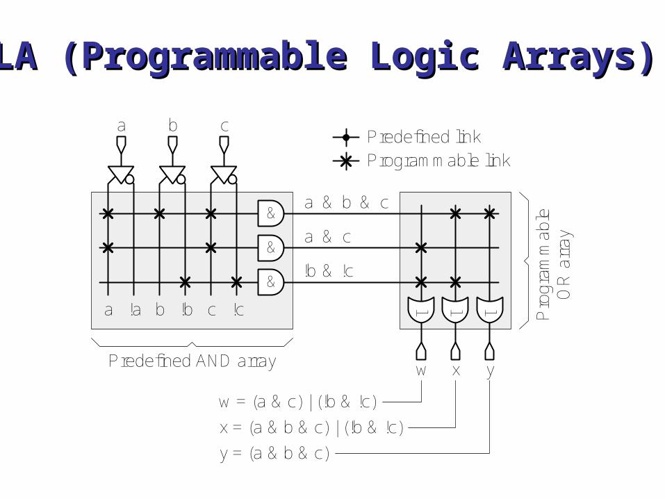
PLA (Programmable Logic Arrays)PLA (Programmable Logic Arrays)• Programmable AND array, programmable OR array
a b c
&
&
&
a !a b !b c !c
a cb& &
a c&
!b !c&
Predefined AND array
Pro
gram
mab
leO
R a
rray
Predefined linkProgrammable link
l l l
w x y
w = (a & c) | (!b & !c)
x = (a & b & c) | (!b & !c)
y = (a & b & c)
PLA (Programmable Logic Arrays)PLA (Programmable Logic Arrays)

a b c
l l l
&
&
&
&
&
&
a !a b !b c !c
ProgrammableAND array
Pre
def
ine
d O
R a
rra
yw x y
Predefined linkProgrammable link
PAL (Programmable Array PAL (Programmable Array Logic) GAL (Generic Array Logic) GAL (Generic Array Logic)Logic)1. Exactly opposite to PROM2. Programmable AND arrays, predefined OR arrays3. Address speed issues in PLAs
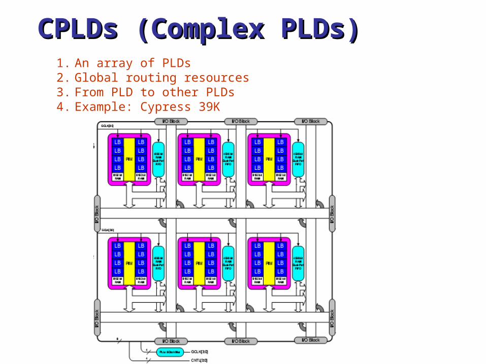
CPLDs (Complex PLDs)CPLDs (Complex PLDs)1. An array of PLDs2. Global routing resources3. From PLD to other PLDs4. Example: Cypress 39K

ASICs
StructuredASICs
Gate Arrays
Standard Cell
Full Custom
Increasing complexity
ASICs (Application Specific ASICs (Application Specific Integerated Circuits)Integerated Circuits)

PLDs ASICs
Standard Cell
Full Custom
Gate Arrays
Structured ASICs*
SPLDs
CPLDs
*Not available circa early 1980s
TheGAP
The Gap between PLDs & The Gap between PLDs & ASICsASICs
1. PLDs : Programmable but less complexity2. ASICs: High complexity but no programmability
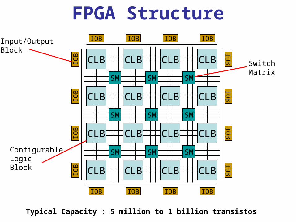
FPGA Structure
CLB CLB
CLB CLB
SM SM
SM SM
CLB CLB
CLB CLB
SM
SM
CLB CLB
CLB CLB
SM SM
CLB CLB
CLB CLB
SM
IOB IOB IOB IOB
IOB IOB IOB IOB
IOB
IOB
IOB
IOB
IOB
IOB
IOB
IOB
Input/Output Block
SwitchMatrix
ConfigurableLogic Block
Typical Capacity : 5 million to 1 billion transistos
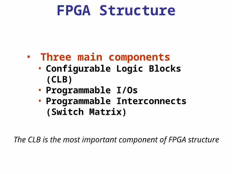
FPGA Structure
• Three main components• Configurable Logic Blocks
(CLB)• Programmable I/Os• Programmable Interconnects
(Switch Matrix)
The CLB is the most important component of FPGA structure
CLB CLB
CLB CLB
Logic cell
Slice
Logic cell
Logic cell
Slice
Logic cell
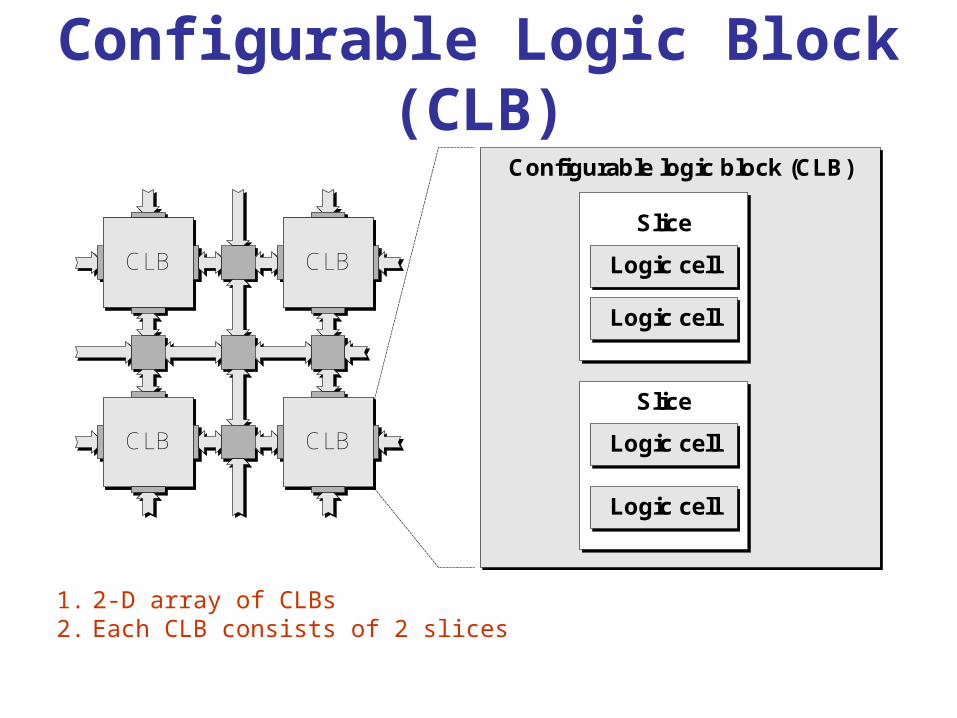
Configurable logic block (CLB)
Configurable Logic Block (CLB)
1. 2-D array of CLBs2. Each CLB consists of 2 slices

16-bit SR
16x1 RAM
4-inputLUT
LUT MUX REG
Logic Cell (LC)
16-bit SR
16x1 RAM
4-inputLUT
LUT MUX REG
Logic Cell (LC)
Slice
CLB Slice
1. Each slice has 2 logic Cell (LC)2. Each Logic cell comprises a LUT, and some additional
components i-e Multiplexers, Registers

FPGA CLB Slice (Internal View)

&|
a
b
cy
AND
OR
y = (a & b) | c
0
1
0
1
0
1
MUX
MUX
MUX
0
b
a
1
x
0
y
0
1
MUX0
1
c
mux Based CLB (Altera)mux Based CLB (Altera)
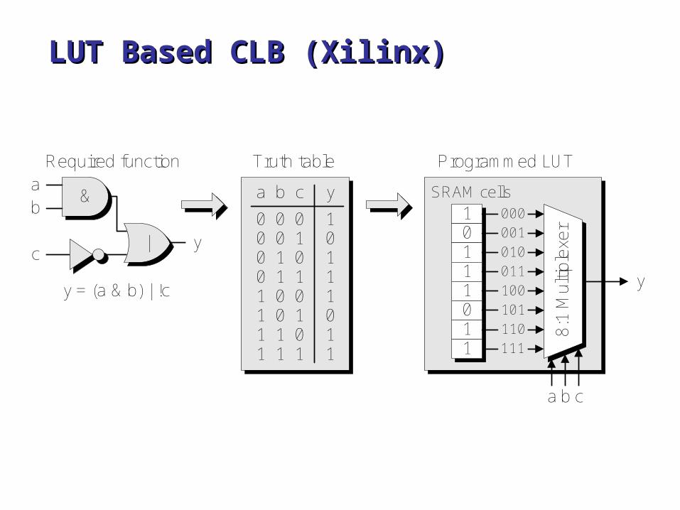
LUT Based CLB (Xilinx)LUT Based CLB (Xilinx)
|
&ab
cy
y = (a & b) | !c
Required function Truth table
1011101
0000010100111001011101111
y
a b c y
00001111
00110011
01010101
10111011
SRAM cells
Programmed LUT
8:1
Mul
tiple
xer
a b c

0
1
1
1
0
1
1
1
0
1
1
1
0
1
1
1
abc
ySRAM cells
Transmission gate(active low)
Transmission gate(active high)
LUT Based CLB – How to load SRAM cellLUT Based CLB – How to load SRAM cell

0
1
From the previouscell in the chain
0
0
To the next cellin the chain
SRAMcells
LUT Based CLB – How to load SRAM cellLUT Based CLB – How to load SRAM cell