fpga based l-band pulse doppler radardocshare04.docshare.tips/files/31388/313886107.pdf · ·...
TRANSCRIPT
i
FPGA BASED L-BAND PULSE DOPPLER RADAR
DESIGN AND IMPLEMENTATION
by
Kubilay Savci
A Dissertation Presented to the
FACULTY OF THE USC GRADUATE SCHOOL
UNIVERSITY OF SOUTHERN CALIFORNIA
In Partial Fulfillment of the
Requirements for the Degree
MASTER OF SCIENCE
(ELECTRICAL ENGINEERING)
August 2013
Copyright 2013 Kubilay Savci

ii
To My Country, Turkish Navy and My Family

iii
Acknowledgements
I would like to offer my respect and sincere appreciation to my advisor Professor
Mahta Moghaddam for her support, guidance and patience during my radar
project. Specifically, I would like to thank her for giving me the opportunity to
conduct my research in MiXIL Lab and keeping her faith in me during the course
of project. She enlightened my way with her insight on the subject and she has
always been a role model and a wise mentor to me more than an advisor.
Special thanks to MiXIL Lab colleagues Ruzbeh Akbar, Xueyang Duan, Agnelo
Silva, Pratik Shah, Richard Chen, Mariko Burgin, Guanbo Chen, Daniel Clewley,
Uday Khankhoje, John Stang, Mark Haynes, Majid Albahkali, Jane Whitcomb,
Alireza Tabatabaeenejad and Mariko Burgin for your company, help and
encouragement. I learned many new things from you and discussing ideas and
hearing your experiences contributed a lot in my academic growth. Your profound
wisdom has always been an invaluable resource of information all along my
studies in the lab.
I would like to express my gratitude to M. Batuhan Gundogdu, Bahri Maras,
Deniz Kumlu, Mehmet Savran, Ihsan Burak Tolga, Alptekin Yilmazer, Ahmet
Asena, Cansu Pazarbasioglu, Jay Hsueh, Benjamin Ries, Sara Lanier, Cathy Liu,
Maria Minin, Sue Caroll, Lance Parr, Cathy Parr and Camillia Lee for their
sincere friendship, hospitality, support and making my staying enjoyable in US
during my education. I vividly recall every moment we spent and had fun together
and these memories will last forever just as our precious friendship.

iv
I am very thankful to Emine Bozyurt and Tugce Tuncay for their caring and
hospitality. I believe families are made in the heart and you always made me feel
the warmth of home while being far away from my homeland as you have been
my second family here in Los Angeles.
I further would like to thank to my brothers in arms in Turkish Navy and Turkish
Navy for giving me the opportunity to study at University of Southern California
and supporting me financially for my education. I am very proud of serving as a
Naval Officer.
From the bottom of my heart, I say a big “THANK YOU” to my great family. I
made it to this stage and I couldn’t have done it without you.

v
Table of Contents
Dedication ii
Acknowledgements iii
List of Figures vii
List of Tables ix
Abstract x
Chapter 1 Introduction .............................................................................................. 1
1.1 Objective .............................................................................................................. 1
1.2 Challenges ............................................................................................................ 2
1.3 Outline of Thesis .................................................................................................. 4
Chapter 2 Algorithm .................................................................................................. 6
2.1 Background .......................................................................................................... 6
2.2 Pulse Doppler Processing .................................................................................... 8
2.3 Target Detection - Constant False Alarm Rate .................................................. 12
Chapter 3 Radar System Overview ........................................................................ 15
3.1 General Architecture of the Radar ..................................................................... 15
3.2 RF Module ........................................................................................................... 17
3.3 Radar Control and Processor Module ................................................................ 21
3.4 Power Module .................................................................................................... 22
3.5 Radar Link Budget ............................................................................................. 23
Chapter 4 FPGA Implementation .......................................................................... 24
4.1 Xilinx ML605 Virtex-6 FPGA Board and System Generator for DSP® ............ 24
4.2 Radar Processor Implementation ........................................................................ 25
4.3 Radar State Machine ........................................................................................... 27
4.4 ADC Configuration and Calibration ..................................................................... 30
4.5 Clock Distribution for Radar System Coherency .............................................. 32
4.6 Digital Baseband Filtering ................................................................................... 33
4.7 Detection and CFAR Algorithm Implementation .............................................. 36
4.8 Pulse-Doppler Processing .................................................................................. 41
4.9 1 Gigabit Ethernet Design.................................................................................... 45
Chapter 5 Software .................................................................................................. 47
5.1 C# Radar GUI .................................................................................................... 47

vi
Chapter 6 Results and Conclusion .......................................................................... 50
6.1 Laboratory and Field Tests ................................................................................ 50
6.2 Challenges with Doppler Calculation ................................................................ 52
6.3 Pulse Coherency and PRF Relation ................................................................... 54
6.4 Clock Jitter in FPGA MMCMs and PRF relation .............................................. 55
6.5 ADC Sensivity and Baseband Signal Frequency ............................................... 56
6.6 CA-CFAR and Automatic Gain Adjustment ..................................................... 57
6.7 Concluding Remarks and Future Works ............................................................ 58
References .................................................................................................................. 59

vii
List of Figures
Figure 1 Basic Radar Operation and Timing ...............................................................6
Figure 2 Doppler Effect ...............................................................................................7
Figure 3 CW Doppler Radar Operation .......................................................................8
Figure 4 Doppler Frequency Cycle vs Pulse Length ...................................................9
Figure 5 Radar Pulse In Frequency Domain ..............................................................10
Figure 6 Reconstructing Doppler Frequency in Slow Time ......................................11
Figure 7 CA-CFAR Algorithm ..................................................................................14
Figure 8 Radar Cabinet ..............................................................................................15
Figure 9 Radar System Diagram ................................................................................16
Figure 10 RF Module-Transmit and Receive Chain ..................................................17
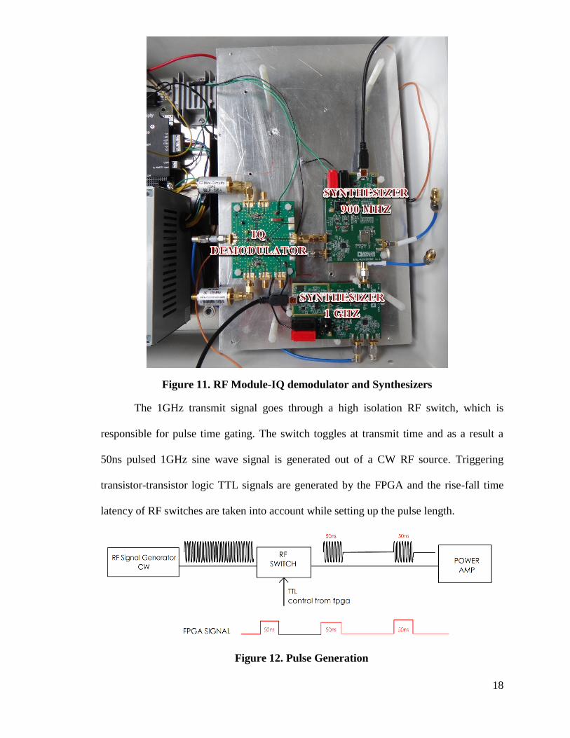
Figure 11 RF Module-IQ demodulator and Synthesizers ..........................................18
Figure 12 Pulse Generation ........................................................................................18
Figure 13 RF Module Diagram ..................................................................................19
Figure 14 Radar Contol and Processor Module and Power Module .........................22
Figure 15 Xilinx ML605 FPGA Board ......................................................................24
Figure 16 Radar Processor Organization ...................................................................26
Figure 17 Radar State Machine Pseudo Code............................................................27
Figure 18 TX Trigger Signal......................................................................................28
Figure 19 Handshaking Signals with Submodules ....................................................30
Figure 20 ADC Data Channel Calibration .................................................................31
Figure 21 Clock Distribution for Coherency .............................................................32
viii
Figure 22 Spectrum Analyzer Output at Baseband....................................................33
Figure 23 Block Design of 100Mhz Digital Bandpass Filter ....................................34
Figure 24 Unfiltered/Filtered Outputs .......................................................................35
Figure 25 Magnitude Samples and Range Bins .........................................................36
Figure 26 Magnitude Module ....................................................................................38
Figure 27 Magnitude Accumulator Module ..............................................................39
Figure 28 CA-CFAR Detection Module ....................................................................40
Figure 29 Phase Difference Module ..........................................................................43
Figure 30 Speed Module ............................................................................................44
Figure 31 Ethernet Interface ......................................................................................46
Figure 32 Scope Displays ..........................................................................................47
Figure 33 A-Scope PC GUI .......................................................................................48
Figure 34 Pulse Waveform ........................................................................................50
Figure 35 CW loop test and Speed Calculation .........................................................51
Figure 36 Field Test ...................................................................................................52
Figure 37 Antenna Pattern .........................................................................................53
Figure 38 MMCM Clock Wizard ..............................................................................55
Figure 39 Time delay plot vs Velocity and PRF........................................................56
Figure 40 ADC Sensivity vs. Voltage Difference due to Phase Shift .......................57

ix
List of Tables
Table 1 Doppler Frequencies .......................................................................................8
Table 2 Radar Link Budget ........................................................................................23
Table 3 Phase Correction ...........................................................................................42

x
Abstract
As its name implies RADAR (Radio Detection and Ranging) is an
electromagnetic sensor used for detection and locating targets from their return signals.
Radar systems propagate electromagnetic energy from the antenna, which is in part
intercepted by an object. Objects reradiate a portion of energy, which is captured by the
radar receiver. The received signal is then processed for information extraction. Radar
systems are widely used for surveillance, air security, navigation, weather hazard
detection, as well as remote sensing applications. In this work, an FPGA based L-band
pulse Doppler radar prototype, which is used for target detection, localization and
velocity calculation has been built and a general-purpose pulse Doppler radar processor
has been developed. This radar is a ground based stationary monopulse radar, which
transmits a short pulse with a certain pulse repetition frequency (PRF). Return signals
from the target are processed and information about their location and velocity is
extracted. Discrete components are used for the transmitter and receiver chain. The
hardware solution is based on Xilinx Virtex-6 ML605 FPGA board, responsible for the
control of the radar system and the digital signal processing of the received signal, which
involves Constant False Alarm Rate (CFAR) [1] [2] detection and pulse Doppler
processing [2] [4]. The algorithm is implemented in MATLAB/SIMULINK® using the
Xilinx System Generator for DSP® [12] tool. The field programmable gate arrays
(FPGA) implementation of the radar system provides the flexibility of changing
parameters such as the PRF and pulse length therefore it can be used with different radar
configurations as well. A very-high-speed integrated circuits hardware description
language (VHDL) design has been developed for 1Gbit Ethernet [5] connection to
xi
transfer digitized return signal and detection results to PC. An A-Scope software has been
developed with C# programming language to display time domain radar signals and
detection results on PC. Data are processed both in FPGA chip and on PC. FPGA uses
fixed point arithmetic operations since it is fast and facilitates source requirement as it
consumes less hardware than floating point arithmetic operations. The software uses
floating point arithmetic operations, which ensures precision in processing at the expense
of speed. The functionality of the radar system has been tested for experimental
validation in the field with a moving car and the validation of submodules are tested with
synthetic data simulated on MATLAB®.

1
Chapter 1
INTRODUCTION
1.1 Objective
The invention and initial development of radars date back to early 20th
century. In
1904, Christian Hulsmeyer gave a public demonstration of his ship collision avoidance
radar. After that, the theory and the primitive radar technology continued to advance and
many operational radar systems has been developed rapidly during World War II. Since
that time radars have been in use mainly for military applications especially for
surveillance, target tracking and navigation. Early detection of object is crucial on
battlefields and object information such as distance and velocity is needed. If the object is
an enemy aircraft or a missile prior knowledge of the threat can bring up advantages to
take prompt action. In navigation, if the object is a ship, collisions at sea can be avoided
in advance since radars allow over the horizon detection beyond the line of sight.
Since World War II, technology has evolved and the signal processing has shifted
from analog to digital world gradually and with the advent of silicon chips, many
efficient hardware implementations have been devised for signal-processing algorithms
such as filtering, modulation and transforms. In past, conventional signal processing
applications were running on DSP processors and mostly their task was on radar auxiliary
functions. Today as FPGAs get more powerful and allow flexibility in design,
implementing a lot of DSP functions in these chips becomes a new standard for advanced
radar systems. Traditional DSP processors use an instruction based operation, which

2
brings up a bottleneck for real-time radar signal processing applications whereas FPGAs
can outcome by delivering parallelism in design and much higher performance than
traditional DSPs.
That being said, the key task is to pack a radar system in an FPGA thereby
developing a general-purpose real-time radar signal processor, which can localize the
target and then find the corresponding velocity from the average phase difference of
consecutive pulses. Another goal in this project is to develop and implement the system
level design of an RF system and examine the probable bottlenecks and challenges in
detail. As a result, a prototype has been developed with fundamental features of a pulse
Doppler radar and this work provides a basis for further system on chip (SOC) radars.
1.2 Challenges
When designing an RF system from scratch a lot of details come into play and we
should always bear in mind that we cannot reach a perfect system hence an optimum
system parameters are defined as a compromise of all the constraints, which are inherent
in an RF system. These constraints are noise, clock jitter, analog-to-digital converter
(ADC) sensitivity, sampling rate, coherency, target geometry and environment. All these
constraints play a major role on defining system specifications, which will be addressed
in the following chapters in detail.
The first challenging part is to generate simulated radar signal on PC for
verification of the FPGA radar processor. Since environment features such as clutter,
interference and the characteristics of the radar transmitter and receiver chain such as
noise figure, gain, losses are not known as a priori some assumptions are made at the very
beginning and revised later on as the system is being implemented.
3
Another issue is that simulating a moving target return signal on MATLAB®
requires very high sampling rate resolution i.e. in picoseconds because a moving target
return signal shifts in tens of picoseconds between two consecutive pulses. Thus
considering the duration of receive time, the return signal data from a single pulse require
huge amount of memory to store on PC.
The second challenge is that once a specification is defined sometimes you cannot
always find the discrete components off the shelf, which exactly match with your system
requirement. In this case, we deviate from what is decided and change the spec. As a
result we go through the whole specs to revise if any other change has to be done.
The third challenge is the system integration in FPGA as high speed modules
tends to fail in placement and routing when they come all together in the FPGA even if
their simulation results produce correct results. The reason is that when the system design
gets larger too many resources are consumed in order to build the structures instantiated
by the VHDL code and long paths shows up between components after placement of
modules. Therefore meeting the timing constraints defined by the user constraint file [16]
cannot be met due to the long path delay of signal propagation. In this case, a workaround
for this problem is decreasing the clock rate for processing thereby allowing longer cycle
period for logic arithmetic operations to complete its task at the expense of overall speed.
The fourth challenge is the radar coherency as it is a must have in pulse Doppler
radars for a proper phase calculation. For this reason, components solutions are selected
attentively such as the circulator has a linear phase response over the bandwidth of
interest, filters in the receiver chain have a flat group delay and IQ demodulator has low
phase imbalance between in phase (I) and quadrature (Q) outputs. The biggest hurdle is

4
the FPGA mixed mode clock manager (MMCM) clock jitter as it causes an average of
50ps clock jitter in other words it has the largest phase noise contribution to the system,
which will be explained in detail in the next chapters.
1.3 Outline of Thesis
The structure of this thesis is as follows: In Chapter 2, a brief background about
radar operation and Doppler frequency is given, a comparison between continuous wave
(CW) radars and pulsed radars is made and the proposed algorithms, Doppler
processing[3][4] for velocity calculation, target detection with Cell Averaging-Constant
False Alarm Rate (CA-CFAR)[1][2] algorithms are explained. This chapter also refers to
the importance of coherency of system clocks for Doppler processing. In Chapter 3, the
general system overview is described, modules of the radar system are explained and
defined system specifications are presented. The operation of the radar is explained
briefly and the discrete components used in the transmitter and receiver chain of the radar
are presented and based on their specifications the radar link budget [14] is calculated and
important aspects of component selections are discussed. Chapter 4 explains the design of
the proposed algorithms in Xilinx System Generator for DSP® tool and fixed point
implementation in FPGA, addresses the challenges of system integration. This chapter
explains how the finite state machines are established in FPGA to manage timing and
processing data, how coherency is achieved with clocks and touches on precision loss
issues arouse with fixed point representation of numbers. It also explains the details of
1Gigabit Ethernet controller design [5] [6]. Chapter 5 presents the A-Scope graphical
user interface on PC developed using C# programming language. Chapter 6 describes
how the functionality of the system is tested and explains the details about the field

5
experiments of the radar with a moving and concludes our work with some evaluation on
what has been done, how this work can be extended and present closing remarks for
future improvements on proposed FPGA based radar systems.

6
Chapter 2
Algorithm
2.1 Background
Pulse Doppler radar systems transmit a short pulse with a given interval called
pulse repetition interval (PRI) and intercept the return signals from the targets. Fig. 1
shows the principal operation and timing of pulse Doppler radars. The elapsed time
between the beginning of transmission and interception of target return signal can help us
calculating the distance to target as we know the radar signal travels with the speed of
light.
If the target is stationary, the signal is reflected from the exact same location over
successive pulses. However if the target is moving then there is a change in the receive
time of the return signal from the target over consecutive pulses and the frequency of the
signal will shift slightly due to Doppler Effect. The Doppler frequency is the amount of
frequency shift, which is a result of the target radial movement. If the target is
approaching to the observer, the Doppler frequency will be positive and conversely, if the
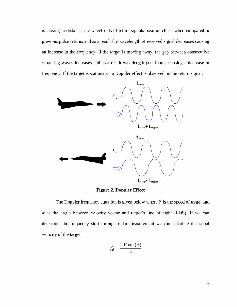
target is receding from the observer it will be negative. As depicted in Fig. 2, if the target
Figure 1. Basic Radar Operation and Timing
7
is closing in distance, the wavefronts of return signals position closer when compared to
previous pulse returns and as a result the wavelength of received signal decreases causing
an increase in the frequency. If the target is moving away, the gap between consecutive
scattering waves increases and as a result wavelength gets longer causing a decrease in
frequency. If the target is stationary no Doppler effect is observed on the return signal.
The Doppler frequency equation is given below where is the speed of target and
is the angle between velocity vector and target’s line of sight (LOS). If we can
determine the frequency shift through radar measurement we can calculate the radial
velocity of the target.
Figure 2. Doppler Effect
8
The range of Doppler frequency depends on the velocity and frequency of the
transmitted signal. Table 1 shows some numeric examples of Doppler frequencies for the
given transmit frequency and radial velocity.
Table 1. Doppler Frequencies
Transmitted Frequency
X band C Band S Band L band
Radial velocity 9 GHz 5 GHz 3 GHz 1 GHz
1m/s 60 Hz 33 Hz 20 Hz 6 Hz
10m/s 600 Hz 333 Hz 200 Hz 66 Hz
50m/s 3 KHz 1.66 KHz 1 KHz 333 Hz
2.2 Pulse-Doppler Processing
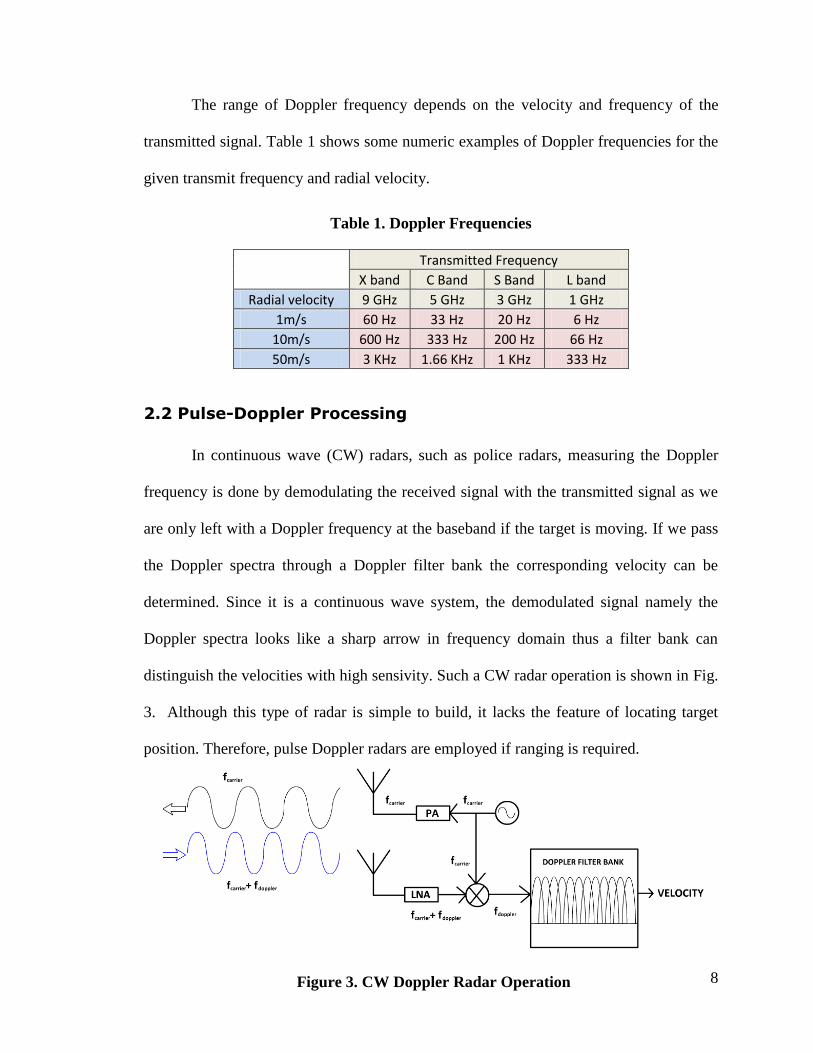
In continuous wave (CW) radars, such as police radars, measuring the Doppler
frequency is done by demodulating the received signal with the transmitted signal as we
are only left with a Doppler frequency at the baseband if the target is moving. If we pass
the Doppler spectra through a Doppler filter bank the corresponding velocity can be
determined. Since it is a continuous wave system, the demodulated signal namely the
Doppler spectra looks like a sharp arrow in frequency domain thus a filter bank can
distinguish the velocities with high sensivity. Such a CW radar operation is shown in Fig.
3. Although this type of radar is simple to build, it lacks the feature of locating target
position. Therefore, pulse Doppler radars are employed if ranging is required.
Figure 3. CW Doppler Radar Operation
9
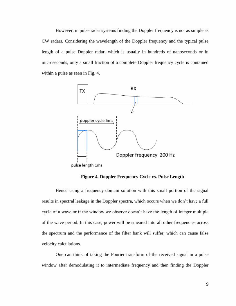
However, in pulse radar systems finding the Doppler frequency is not as simple as
CW radars. Considering the wavelength of the Doppler frequency and the typical pulse
length of a pulse Doppler radar, which is usually in hundreds of nanoseconds or in
microseconds, only a small fraction of a complete Doppler frequency cycle is contained
within a pulse as seen in Fig. 4.
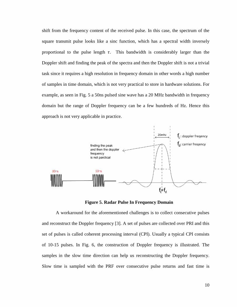
Hence using a frequency-domain solution with this small portion of the signal
results in spectral leakage in the Doppler spectra, which occurs when we don’t have a full
cycle of a wave or if the window we observe doesn’t have the length of integer multiple
of the wave period. In this case, power will be smeared into all other frequencies across
the spectrum and the performance of the filter bank will suffer, which can cause false
velocity calculations.
One can think of taking the Fourier transform of the received signal in a pulse
window after demodulating it to intermediate frequency and then finding the Doppler
Figure 4. Doppler Frequency Cycle vs. Pulse Length
10
shift from the frequency content of the received pulse. In this case, the spectrum of the
square transmit pulse looks like a sinc function, which has a spectral width inversely
proportional to the pulse length . This bandwidth is considerably larger than the
Doppler shift and finding the peak of the spectra and then the Doppler shift is not a trivial
task since it requires a high resolution in frequency domain in other words a high number
of samples in time domain, which is not very practical to store in hardware solutions. For
example, as seen in Fig. 5 a 50ns pulsed sine wave has a 20 MHz bandwidth in frequency
domain but the range of Doppler frequency can be a few hundreds of Hz. Hence this
approach is not very applicable in practice.
A workaround for the aforementioned challenges is to collect consecutive pulses
and reconstruct the Doppler frequency [3]. A set of pulses are collected over PRI and this
set of pulses is called coherent processing interval (CPI). Usually a typical CPI consists
of 10-15 pulses. In Fig. 6, the construction of Doppler frequency is illustrated. The
samples in the slow time direction can help us reconstructing the Doppler frequency.
Slow time is sampled with the PRF over consecutive pulse returns and fast time is
Figure 5. Radar Pulse In Frequency Domain

11
sampled with the ADC sampling rate. In this approach we can collect enough pulse
returns such that a complete Doppler cycle can be achieved with enough samples in slow
time thus the velocity can be determined from the frequency domain.
However, collecting many pulses turns out to be cumbersome in hardware as it
requires a lot of memory for storing many pulse returns. Thus a better approach is to
calculate the phase difference between consecutive pulse returns and average it over a
small set of CPI. The advantage of this approach is that a lower number of pulses
required namely less memory usage is ensured and the pulse data can be discarded right
after the phase difference is calculated. This phase shift can be related to the radial
velocity of the target.
Distance target moves in one PRI;
( )
Figure 6. Reconstructing Doppler Frequency in Slow Time
12
The phase shift corresponding to a fraction of wavelength traversed between two
successive pulse returns;
Solving the above equation for radial velocity we can derive;
(
)
where is the wavelength of the baseband signal and is the phase difference between
two consecutive pulse returns.
In practice, a received pulse can contain many targets with different speeds and
also noise can result some error in calculation, therefore an average phase difference must
be calculated over a train of pulses.
Intuitively, pulse Doppler processing requires pulse coherency so that the transmit
pulse waveform doesn’t change in other words starts with the same phase every time it is
propagated. Thus all the other clocks in the system must be in sync with the transmit
signal.
2.3 Target Detection- Constant False Alarm Rate
In radar systems, the return signals are passed through an envelope detector
(square-law detector) at the receiver backend to localize the echoes from the target. Since
the power level of the echoes from the target is much higher than the background echoes
a threshold based approach can be used to detect targets. However, there is an existence
of noise, clutter (unwanted signal returns from ground or sea surface), interference and
also the received signal power is not equal since its power attenuates as it travels further
13
in distance. Therefore an adaptive algorithm called constant false alarm rate (CFAR) is
required for threshold and detection of signals probably originate from targets.
In constant false alarm rate algorithm, a certain power threshold is to be
determined in order to lower the number of false detections. If the threshold is too high
then fewer targets will be detected at the expense of missing some of actual targets and
conversely if the threshold is too low then false detection rate will increase. Usually in
radar systems, this threshold is set to achieve a certain level of false alarm probability. If
the clutter, noise and interference are considered to be constant temporally and spatially
e.g. sea surface or flat ground then a fixed threshold can be chosen in which the signal to
noise ratio from the target plays the deterministic role.
There are many sophisticated CFAR techniques and in our radar system the
proposed method is the Cell-Averaging CFAR(CA-CFAR)[1]. In CA-CFAR algorithm,
the fast time samples (ADC samples) are divided into overlapping range bins or range
gates the length of which is determined by the radar range resolution. The radar range
resolution for monopulse radars is proportional to the pulse length or inversely
proportional to the bandwidth as defined below;
Once the cells are formed up in fast time direction, each magnitude samples
within a cell are summed up to find a power level for the cell. If there is no target
contained in the cell then the power level will be a good estimate of aggregate sum of the
noise floor and clutter power level. In order to detect if a cell contains a target or not, the
power level of the cell referred to cell under test (CUT) is compared with the average
power level of its surrounding cells, which is a good representative of the local noise and

14
clutter. Usually the adjacent cells are ignored during average calculation due to the
imperfect pulse shape, which can overlay on other cells and therefore can corrupt
calculation. If the CUT power level is greater than the average power level by a certain
factor (CFAR Constant) then a target is declared to be present in the CUT. This process is
done for each range cell with a sliding window over the whole range via CA-CFAR
algorithm. Fig. 7 shows the range bins and depicts how the operation is done. Pseudo
code is given as below;
Figure 7. CA-CFAR Algorithm

15
Chapter 3
Radar System Overview
3.1 General Architecture of the Radar
The FPGA based L-band Pulse Doppler radar works at 1GHz and propagates a
50ns pulse with the pulse repetition frequency (PRF) of 100Hz. As the developed
processor is a generic processor, these parameters can be changed if someone wants to
configure this processor to another radar front end by changing parameters in the FPGA
design. However for the field experiment, the above mentioned settings are adopted in
order to detect slow moving targets such as ground vehicles.
This radar system has a compact design as seen in Fig. 8 and all subsystems are
packed in a small enclosure. The small form factor brings up the ease of operation and
makes it flexible to deploy. This radar system has three subsystems: RF Module, radar
control and processor module and power module. The system diagram is given in Fig. 9
Figure 8. Radar Enclosure
16
Figure 9. Radar System Diagram
17
3.2 RF Module
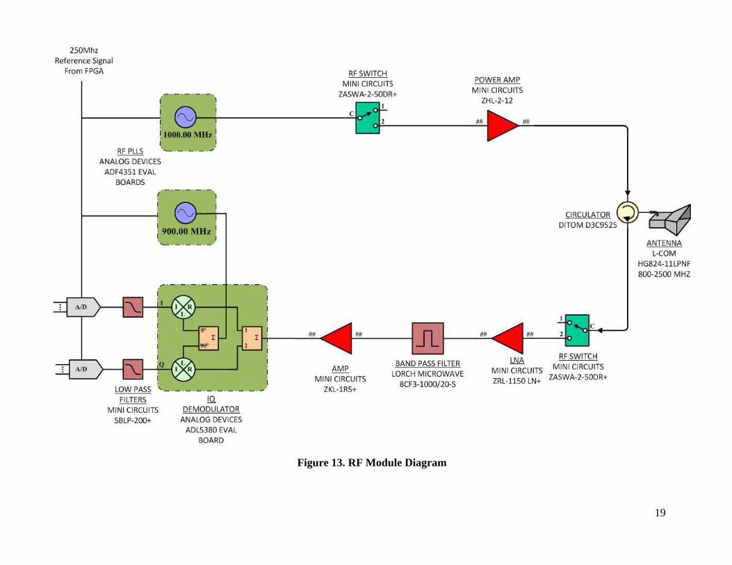
RF module shown in Fig. 13 consists of the radio-frequency synthesizers, transmit
chain, antenna, receive chain and in phase/quadrature (IQ) demodulator. The diagram of
the RF module is shown in Fig. 11. The RF sources are ADF4351-EVAL frequency
synthesizer boards from Analog Devices, which can generate 35 MHz to 4400 MHz at -
4dBm to 5dBm output power with 3dB steps. These two synthesizers have a PC interface
and they are programmed to generate 1 Hz transmit signal and 900 MHz demodulating
signal. These synthesizers use a 250 MHz reference clock generated from the FPGA in
order to ensure system coherency for Doppler processing.
Figure 10. RF Module-Transmit and Receive Chain
18
The 1GHz transmit signal goes through a high isolation RF switch, which is
responsible for pulse time gating. The switch toggles at transmit time and as a result a
50ns pulsed 1GHz sine wave signal is generated out of a CW RF source. Triggering
transistor-transistor logic TTL signals are generated by the FPGA and the rise-fall time
latency of RF switches are taken into account while setting up the pulse length.
Figure 11. RF Module-IQ demodulator and Synthesizers
Figure 12. Pulse Generation
19
Figure 13. RF Module Diagram
20
The pulsed signal continuing in the transmit chain is amplified by the power
amplifier by 24dB and then passes through a circulator to the antenna. A wideband
directional log periodic antenna is used, which covers the frequency band from 800MHz-
2500MHz. Measured output power at the antenna is 29dBm. Since a single antenna is
used both for transmit and receive, a circulator isolates the transmitter and receiver chain.
The circulator isolation is 20dB. Thus the TX and RX switches must have a high isolation
in OFF mode so that the leakage from the transmitter to receiver can be minimized. This
is very important because such a leakage in transmit time is very high in terms of power
(~8dBm) and when it is amplified in the receiver chain it can damage the ADC’s at the
backend. For this reason, high isolation switches, which has 100dB isolation (OFF mode)
at 1GHz are used both in transmitter and receiver chain.
In the receiver chain the target return signal is intercepted by the antenna goes
through circulator, passes the RX switch and enters the low noise amplifier (LNA). The
RX switch is used to protect the receiver circuit from high power transmission leakage
and close distance return signals. An LNA and another amplifier are used in order to
amplify the received signal up to the input power range of IQ demodulator. A 1Ghz band
pass filter cancels out the unwanted frequency signals outside the bandwidth, which is
centered at 1 Hz.
ADL5380 Eval board IQ demodulator in the receiver chain, which has a low
phase and amplitude imbalance downconverts the received 1Ghz RF signal into in phase
(I) and quadrature (Q) components (real and imaginary parts) in order to preserve the
phase information of RF signal. A 900MHz demodulating signal generated with
synthesizer is used as a demodulating signal and 100MHz baseband signal is derived at

21
the output of the low pass filters at the backend. Low pass filters are used to filter out the
high frequency components appearing at the IQ demodulator output due to mixing
signals. The baseband signal frequency is selected to be 100MHz in order to detect small
variations in phase with the given ADC sensivity. Small phase changes in low frequency
signals don’t provide enough voltage difference and as a result it falls below the ADC
resolution and phase change is not detected due to the quantization of sample values.
3.3 Radar Control and Processor Module
Radar Control and Processor Module show in Fig. 14 comprises the 4DSP
FMC150 ADC/DAC mezzanine board and ML605 Virtex-6 FPGA board. 4DSP
FMC150 ADC board has 2 channels and a maximum sampling rate of 250 MSPS with 14
bit resolution. Considering the 100MHz baseband signal and the Nyquist criterion [11],
250MHz clock is generated by the FPGA and used as a sampling clock for the ADC
board. I and Q baseband signals are sampled via ADC board and processed in the FPGA.
ML605 Virtex-6 FPGA board is responsible for the radar control and processing data. It
configures the ADC board over serial peripheral interface (SPI), calibrates the ADC for
proper sampling, generates the reference signals for the synthesizers and ADC board,
establishes 1gigabit user datagram protocol (UDP) Ethernet bridge for data transfer,
filters baseband signals digitally, manages the radar data for the CFAR and Doppler
processing, produces the results and generates trigger signals for the TX and RX
switches.

22
3.4 Power Module
Power module transforms AC to DC and provides the voltages required for the
radar system. A PC power supply is used as a main power supply. 12-24V converter is
used for the radar power amplifier. High efficient DC-DC converter produces +12V,-
12V, +5V, -5V voltage outputs, which are required for the other discrete components in
the transmitter and receiver chain.
Figure 14. Radar Control and Processor Module and Power Module
23
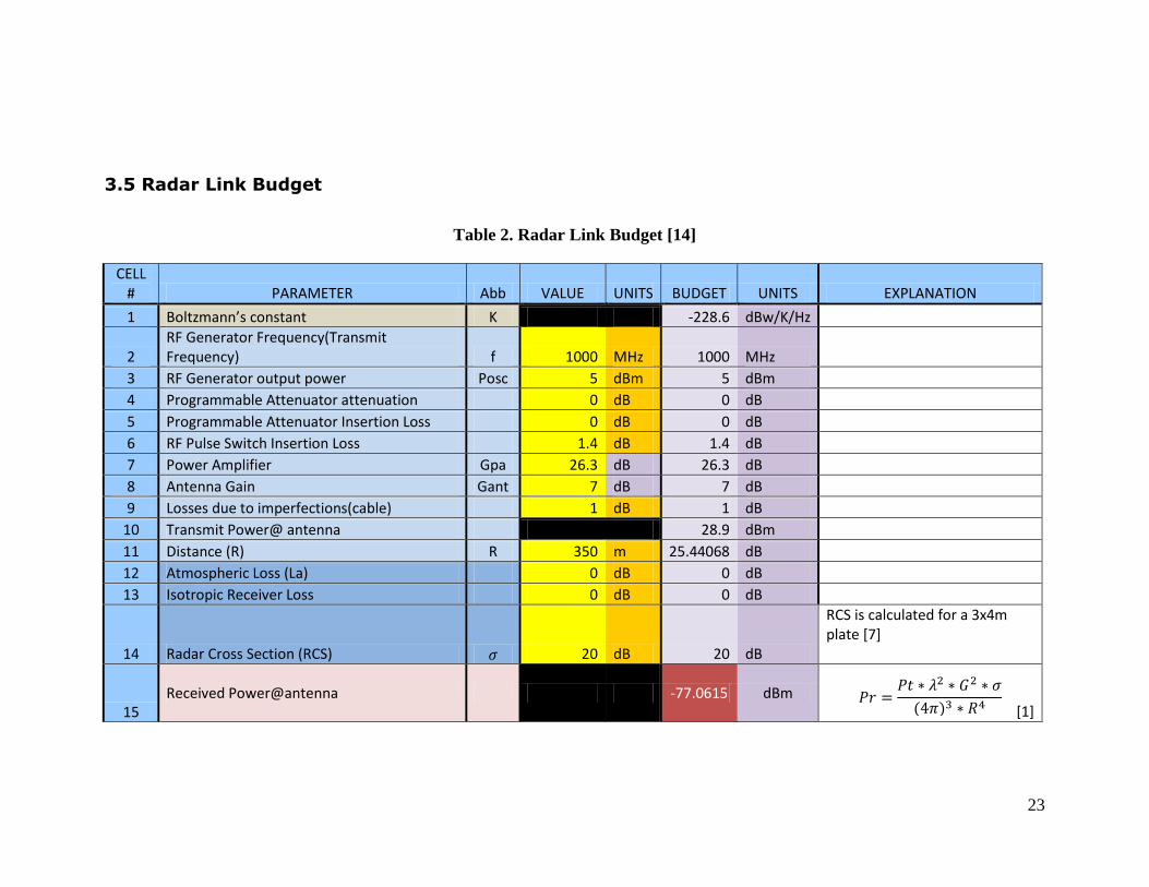
3.5 Radar Link Budget
Table 2. Radar Link Budget [14]
CELL # PARAMETER Abb VALUE UNITS BUDGET UNITS EXPLANATION
1 Boltzmann’s constant K -228.6 dBw/K/Hz
2 RF Generator Frequency(Transmit Frequency) f 1000 MHz 1000 MHz
3 RF Generator output power Posc 5 dBm 5 dBm
4 Programmable Attenuator attenuation 0 dB 0 dB
5 Programmable Attenuator Insertion Loss 0 dB 0 dB
6 RF Pulse Switch Insertion Loss 1.4 dB 1.4 dB
7 Power Amplifier Gpa 26.3 dB 26.3 dB
8 Antenna Gain Gant 7 dB 7 dB
9 Losses due to imperfections(cable) 1 dB 1 dB
10 Transmit Power@ antenna 28.9 dBm
11 Distance (R) R 350 m 25.44068 dB
12 Atmospheric Loss (La) 0 dB 0 dB
13 Isotropic Receiver Loss 0 dB 0 dB
14 Radar Cross Section (RCS) 𝜎 20 dB 20 dB
RCS is calculated for a 3x4m plate [7]
15 Received Power@antenna -77.0615 dBm
[1] 𝑃𝑟
𝑃𝑡 𝜆 𝐺 𝜎
𝜋 3 𝑅4

24
Chapter 4
FPGA Implementation
4.1 Xilinx ML605 Virtex-6 FPGA board and System Generator
for DSP Tool
Xilinx ML605 Virtex-6 FPGA DSP [15] development kit is used in this work as it
offers reasonable DSP performance, speed for real-time applications and flexibility in
design. As it is a configurable logic array, each submodule is designed in hardware
description language (VHDL) separately and integrated on a chip.
DSP algorithms are designed using Xilinx System Generator for DSP® tool,
which runs on MATLAB/SIMULINK® environment. This tool allows block based
system modeling, instant simulation/debugging, automatic code generation and
translation to VHDL language.
Figure 15. Xilinx ML605 FPGA Board

25
4.2 Radar Processor Implementation
Radar Processor is the core part of the radar system and the embedded radar state
machine commands the operation of the radar system. It consists of submodules, which
have certain tasks. These submodules are ;
Radar State Machine
Ethernet Module and Ethernet State Machine
ADC Configuration Module
ADC Calibration Module
Digital Baseband Filter Module
Detection State Machine
Magnitude Module
Magnitude Accumulator Module
CFAR Detection Module
Doppler State Machine
Phase Difference Module
Speed Module
Result State Machine
The FPGA processor organization is shown in Fig. 16.

26
Figure 16. Radar Processor Organization
27
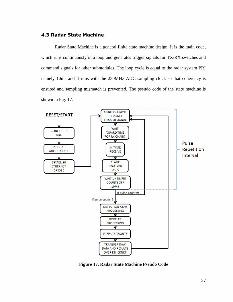
4.3 Radar State Machine
Radar State Machine is a general finite state machine design. It is the main code,
which runs continuously in a loop and generates trigger signals for TX/RX switches and
command signals for other submodules. The loop cycle is equal to the radar system PRI
namely 10ms and it runs with the 250MHz ADC sampling clock so that coherency is
ensured and sampling mismatch is prevented. The pseudo code of the state machine is
shown in Fig. 17.
Figure 17. Radar State Machine Pseudo Code

28
When the bitfile (programming file for FPGA) is loaded on the FPGA, the radar
processor starts running. At startup, the radar state machine sets up the peripherals such
as FMC150 ADC/DAC board, Ethernet MAC core [5] [6] and the mixed mode clock
managers (MMCMs) [17]. MMCMs are internal PLLs of FPGA and can be used for
generating required clocks out of the 200MHz board oscillator clock. In this processor
three MMCMs are instantiated and utilized for the system, ADC board and Ethernet
bridge. When the environment is all set, then the processor goes into transmit/receive
loop where the loop cycle is equal to the pulse repetition interval (10ms). The loop starts
with generating a 50ns trigger TTL signal, which toggles the TX switch. Oscilloscope
outputs are shown in Fig. 18.
Figure 18. TX Trigger Signal

29
After transmission is over, trigger signal is de-asserted and the processor waits
idle for 200ns to protect the receiver from short distance return signals, which can
potentially saturate or damage the receiver chain. Then the receive trigger TTL signal is
asserted to open the receiver chain. Since the filters in the receiver chain lags the
incoming RF signals due to their group delay storing the data begins 36ns after the RX
switch turns on. 2036 samples are stored in pulse memory and the number of samples
corresponds to a range of 1221.6 meters. After storing data is completed, RX trigger
signal is de-asserted and the receiver chain is closed.
Then, the state machine waits idle until the timer counts off 10ms since the PRF
is 100Hz. A pulse counter increments after each pulse return data is stored completely
and it determines the memory in, which the pulse return data is stored. There are 9 pulse
memories and if the pulse counter is lower than 9 radar state machine loops back to the
transmission after timer counts off 10ms. When the counter reaches 9, which means 9
pulse returns are collected, the radar state machine initiates DSP submodules for
processing of the data.
Handshaking signals are implemented for submodules and clock domain crossing
is established since submodules use different clock rates than the radar state machine. In
handshaking scheme, the radar state machine sends out a Boolean type initialization
signal for the submodule and this signal is double registered to prevent metastability.
When the submodule captures the initialization signal, it starts processing immediately
and when it finishes its task, it sends out a ‘done’ signal to the radar state machine. Then
the radar state machine moves on to the next state as shown in Fig. 19. In the final state
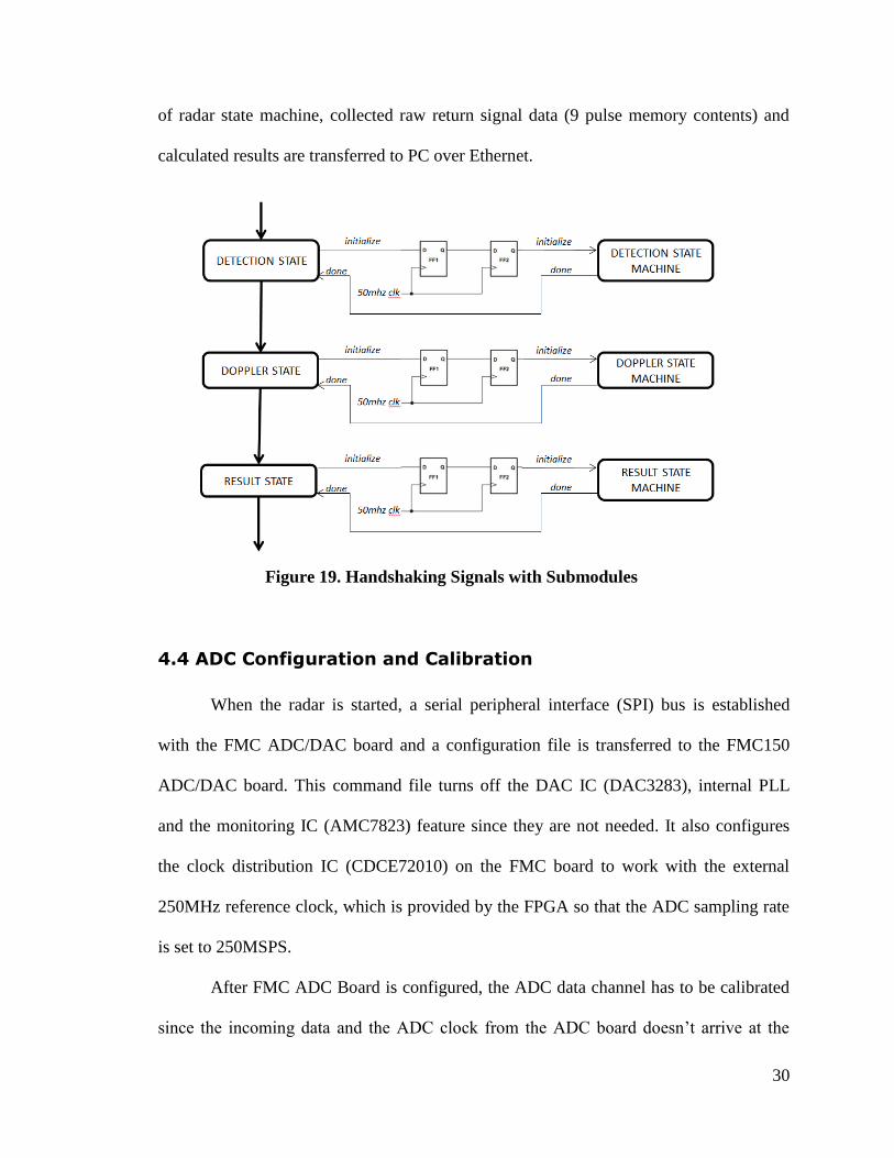
30
of radar state machine, collected raw return signal data (9 pulse memory contents) and
calculated results are transferred to PC over Ethernet.
4.4 ADC Configuration and Calibration
When the radar is started, a serial peripheral interface (SPI) bus is established
with the FMC ADC/DAC board and a configuration file is transferred to the FMC150
ADC/DAC board. This command file turns off the DAC IC (DAC3283), internal PLL
and the monitoring IC (AMC7823) feature since they are not needed. It also configures
the clock distribution IC (CDCE72010) on the FMC board to work with the external
250MHz reference clock, which is provided by the FPGA so that the ADC sampling rate
is set to 250MSPS.
After FMC ADC Board is configured, the ADC data channel has to be calibrated
since the incoming data and the ADC clock from the ADC board doesn’t arrive at the
Figure 19. Handshaking Signals with Submodules

31
same time into the FPGA fabric due to their different length path to the FPGA. Hence an
input-output delay (IODELAY) primitive is instantiated in the FPGA so that the data
channel is delayed and aligned with the ADC clock in such a way that it can be captured
accurately. The correct and false data capture with/without IODELAYE1 primitive is
illustrated in Fig. 20.
Calibration module sends a command to the ADS62P49 ADC IC on the FMC
board and puts the chip in test mode where the ADC IC starts sending a test pattern signal
to the FPGA, which is a digital ramp signal data. The calibration module changes the
delay amount the IODELAYE1 primitive in steps until it captures the test pattern signal
and when the values of the ramp signal are copied accurately, the delay amount is set and
fixed to that particular value. Calibration circuit works for both data channel and when
the channels are calibrated the user led #6 on the FPGA board turns green.
Figure 10. ADC Data Channel Calibration

32
4.5 Clock Distribution for Radar System Coherency
The clock coherency in pulse Doppler radar systems is a must have since Doppler
processing depends on slow time samples to calculate the phase difference or construct
the Doppler frequency. In each case, if there is no target motion the phase difference
should be zero ideally and this brings the requirement coherency over consecutive pulses
meaning the pulse waveform must start with the same phase every time a pulse is
propagated. For this reason the clocks generating the transmit signal frequency,
demodulating signal frequency and the radar state machine clock and ADC sampling
clock must be in sync.
250MHz system main clock is generated in FPGA MMCM using the onboard
200MHz oscillator as shown in Fig. 21 and it is taken out of the board with one of the
SMA connectors on the board and connected to the ADC REF IN port. ADC uses this
clock for sampling and this clock is routed back to the FPGA. Since FMC150 ADC board
has a clock jitter cleaner stage the 250 MHz ADC clock, which comes from the FMC150,
is used as a reference for radar state machine and the synthesizers instead of the 250 MHz
system main clock.
Figure 11. Clock Distribution for Coherency
33
4.6 Digital Baseband Filtering
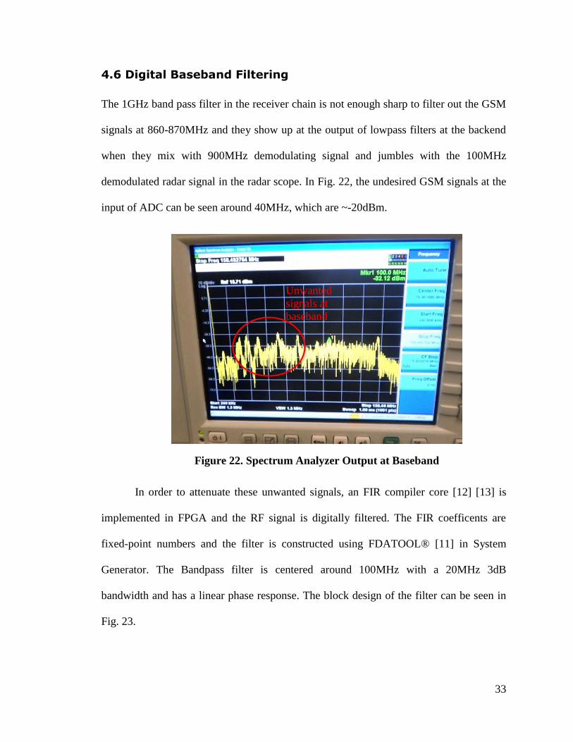
The 1GHz band pass filter in the receiver chain is not enough sharp to filter out the GSM
signals at 860-870MHz and they show up at the output of lowpass filters at the backend
when they mix with 900MHz demodulating signal and jumbles with the 100MHz
demodulated radar signal in the radar scope. In Fig. 22, the undesired GSM signals at the
input of ADC can be seen around 40MHz, which are ~-20dBm.
In order to attenuate these unwanted signals, an FIR compiler core [12] [13] is
implemented in FPGA and the RF signal is digitally filtered. The FIR coefficents are
fixed-point numbers and the filter is constructed using FDATOOL® [11] in System
Generator. The Bandpass filter is centered around 100MHz with a 20MHz 3dB
bandwidth and has a linear phase response. The block design of the filter can be seen in
Fig. 23.
Figure 22. Spectrum Analyzer Output at Baseband
Unwanted
signals at
baseband

34
Figure 23. Block Design of 100MHz Digital Bandpass Filter

35
The PC scope GUI displays the unfiltered and filtered results in time domain shown in
Fig. 24.
Figure 24. Unfiltered/Filtered Outputs
(Filtered Output)
(Unfiltered Output)
36
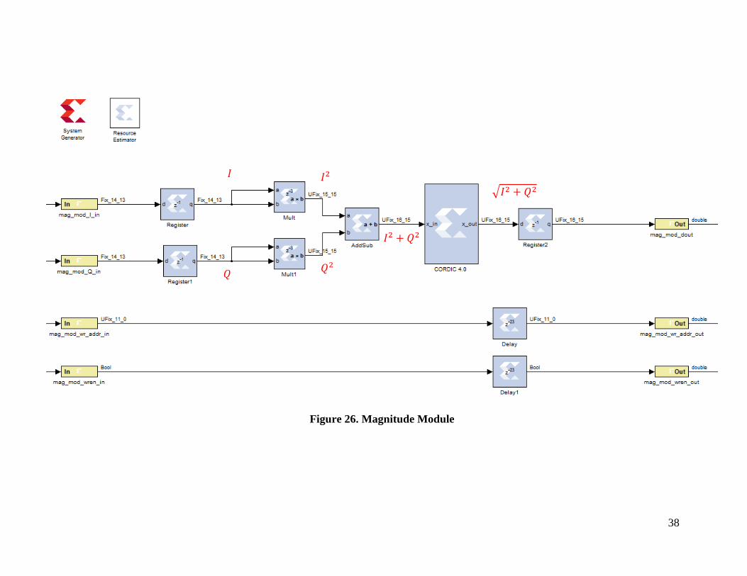
4.7 Detection and CFAR implementation
When 9 pulse returns are collected and the radar state machine initiates detection
state machine and the target locations are estimated using the first pulse return data of
CPI stored in pulse memory #1. The magnitude module calculates the magnitudes for
2036 fast time samples. Since we have I and Q samples for each sample point we can
calculate the magnitude using the equation below
√
Taking the power of samples is realized using multipliers and for the square root
operation coordinate rotation digital computer(CORDIC)[8][9] is implemented in FPGA.
Calculated magnitude values are stored in 2036x16bit magnitude memory. The block
design is presented in Fig. 26.
After magnitudes are calculated the weights of each rangebins are determined by
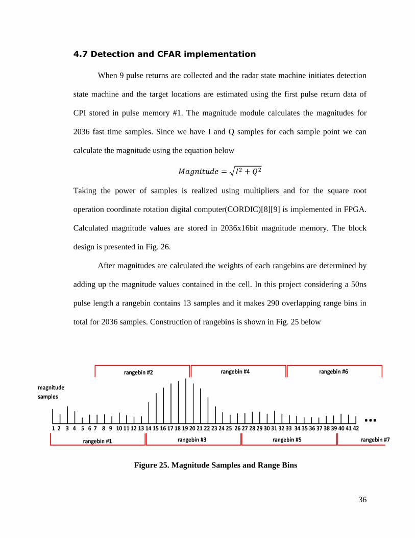
adding up the magnitude values contained in the cell. In this project considering a 50ns
pulse length a rangebin contains 13 samples and it makes 290 overlapping range bins in
total for 2036 samples. Construction of rangebins is shown in Fig. 25 below
Figure 25. Magnitude Samples and Range Bins

37
In magnitude accumulator module, an accumulator core sums 13 magnitude
samples sequentially contained in the range bin and resets once every 13 samples are
added up so that the accumulator is initialized with the first magnitude sample of the next
rangebin once reset. Output values are stored in a 290x16bit rangebin memory and each
value represents the weight of the range bin, which is necessary for the CFAR algorithm.
The block design of the magnitude accumulator module is shown in Fig. 27.
In the final step, CA-CFAR algorithm as explained in chapter 2, is realized in
hardware with adders, multipliers and logic blocksets. Since we have the rangebin
weights stored in a memory, a sliding window is utilized and tapped line is constructed
for the detection scheme as seen in the block design in Fig. 28. The center tap represents
the cell under test and it is compared with the factor of the average of the neighboring
cells. The factor is called the CA-CFAR constant. The pseudo code of the detection is
given below.
The Boolean detection results are stored in 290x1bit detection memory and the results are
shown on PC A-Scope when the data is transferred over Ethernet.
38
Figure 26. Magnitude Module
𝐼 𝐼
𝑄 𝑄
√𝐼 𝑄
𝐼 𝑄

39
Figure 27. Magnitude Accumulator Module

40
Figure 28. CA-CFAR Detection Module
1
6
41
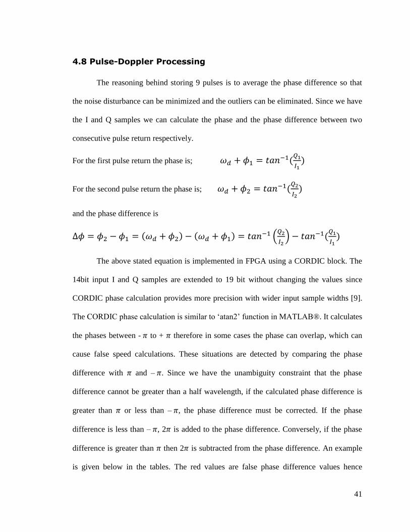
4.8 Pulse-Doppler Processing
The reasoning behind storing 9 pulses is to average the phase difference so that
the noise disturbance can be minimized and the outliers can be eliminated. Since we have
the I and Q samples we can calculate the phase and the phase difference between two
consecutive pulse return respectively.
For the first pulse return the phase is;
For the second pulse return the phase is;
and the phase difference is
(
)
The above stated equation is implemented in FPGA using a CORDIC block. The
14bit input I and Q samples are extended to 19 bit without changing the values since
CORDIC phase calculation provides more precision with wider input sample widths [9].
The CORDIC phase calculation is similar to ‘atan2’ function in MATLAB®. It calculates
the phases between - to + therefore in some cases the phase can overlap, which can
cause false speed calculations. These situations are detected by comparing the phase
difference with and – . Since we have the unambiguity constraint that the phase
difference cannot be greater than a half wavelength, if the calculated phase difference is
greater than or less than – , the phase difference must be corrected. If the phase
difference is less than – , 2 is added to the phase difference. Conversely, if the phase
difference is greater than then 2 is subtracted from the phase difference. An example
is given below in the tables. The red values are false phase difference values hence

42
should be corrected as explained above. A correction circuit is designed as it is presented
in the block diagram of the phase calculation module in Fig. 29.
Table 3. Phase Correction
(a) leads lags (2 )
0 /4 /2 /4 /2 /4
/2 /4 /2 /2 /4 /4
/2 /2 /2 /2 /2 /2 /2
(b) leads lags (2 )
/2 /4 /2 /2 /4 /4
0 /4 /2 /4 /2 /4
/2 /2 /2 /2 /2 /2 /2
Phase difference module calculates phase difference between 2 consecutive pulses
for9 pulse returns as a result phase differences are calculated and stored in 8 2036x16bit
phase difference memories.
Speed module shown in Fig. 30 gets the calculated phase difference values from 8
phase difference memories at the same time in parallel and divides it by 8 to find the
average value. Hereafter the velocity (km/h) can be calculated by multiplying the
average phase difference with 85.94 the constant part of the speed equation.
(
)
1 1 3
6

43
Figure 29. Phase Difference Module
Δ𝜙
Δ𝜙 𝜋
Δ𝜙 𝜋
Δ𝜙
𝜙
𝜙
44
Figure 30. Speed Module
Δ𝜙
Δ𝜙
Δ𝜙3
Δ𝜙4
Δ𝜙5
Δ𝜙
Δ𝜙7
Δ𝜙8

45
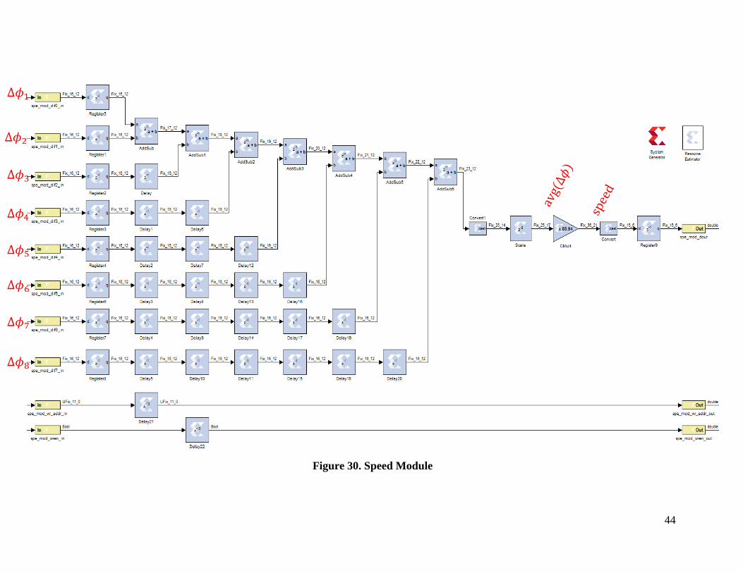
4.9 1Gigabit Ethernet Design
A fast, efficient Ethernet core has been designed in order to transfer raw radar
data and results to PC environment using the open source Ethernet core [5] as a template.
In our modified design Jumbo frame capability is enabled in other words a single frame
can contain up to 9000bytes, which allows the transfer of single pulse memory content in
one packet.
User Datagram Protocol (UDP) is preferred as a transport layer protocol since it
doesn’t require handshaking signals between host and client, which makes it suitable for
high bandwidth real-time data transfer rates. Contrary to Transmission Control Protocol
(TCP), UDP doesn’t verify the transfer of data with the client after each transmission and
transmits the data no matter if the recipient receives it or not. TCP/IP retransmits the data
if the recipient has not received the data but allows maximum 1500 bytes in a single
packet at a time. Therefore TCP/IP is not practical for real-time applications. With the
above disclaimers, UDP protocol is selected but a packet labeling system is developed in
order to check if the data packets are received completely on PC side.
The packet header, which contains the information e.g. protocol type, data length,
mac addresses, IP addresses, checksum is hardcoded into the top of the Ethernet buffer
and is never overwritten. Data to be transferred is always appended to this header.
When radar state machine initiates Ethernet state machine, Ethernet module
appends the content of the pulse memories and results memory into the Ethernet buffer
under the Ethernet header file in turn so that the raw data and calculated results can be
transferred to the PC. A label (the number of pulse memory) is padded to the Ethernet
46
buffer and is sent to PC along with the data. This labeling helps to detect dropped
package on PC side as the PC software can anticipate the next incoming package label.
Version Cat6 shielded Ethernet cable is used between PC and FPGA board since
in older version cables e.g. Cat5, Cat4 packet losses are inherent at 1Gigabit transfer rate.
Over 10000 packets were transferred to PC with 25ft Cat6 Ethernet cable and none of the
packets were dropped in the observations with the help of WIRESHARK® network
analyzer software.
Figure 31. Ethernet Interface

47
Chapter 5
Software
5.1 C# A-Scope GUI
A-Scope graphical user interface (GUI) shown in Fig. 33 is developed with C#
programming language, which serves as a PC interface for the radar system. An A-Scope
shows the trace of received and demodulated RF signal in Volts instantaneously on the
range axis in a single direction to target. Raw pulse return data and results are received
over the Ethernet port and can be saved to PC hard drive if desired. It allows us to plot I
and Q samples and magnitude. CA-CFAR Constant can be set dynamically for software
processing. Fixed point raw data is converted to floating point values and processed on
PC as well. Same algorithms mentioned in previous chapters are used for the DSP on
software. The magnitude plot and I-Q plots are presented in Fig. 32.
Figure 32. Scope Displays
(magnitude plot) (I and Q plots)

48
Figure 33. A-Scope PC GUI
49
Packets received by the software are checked for its label appended to the end of
packet to ensure a complete set of CPI is transferred from the FPGA. It is essential since
a complete set of CPI is necessary otherwise software Doppler processing would prove
false. Pulse data is labeled from 0 to 8 and the packet containing the FPGA results is
labeled as ‘9’. The labels are numbers tells the software, which pulse data is received and
what label to anticipate in the next packet. For example if the first pulse is received, the
label at the end should be ‘0’ and the next package’s label should be ‘1’ intuitively.
However if a data packet is received after the first packet and if its label is ‘2’ it means
that the pulse data labeled as ‘1’ has been dropped in the previous transfer. Thus the
software discards the current set of CPI and waits for the first pulse of the next CPI.
However, these data losses are so rare that it doesn’t affect the overall performance of the
radar system.
Since arithmetic operations on PC are floating point operations, the fixed point
FPGA data should be converted to floating point before software processing begins.
50
Chapter 6
Results and Conclusion
6.1 Laboratory and Field Tests
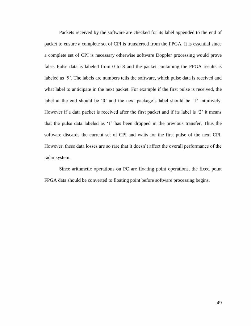
Pulse coherency is achieved as seen on the oscilloscope view of pulse in Fig. 34
as whenever we capture a single pulse, the waveform doesn’t change, which means we
always transmit the same pulse waveform from the antenna. Note that the pulse is not a
perfect square wave due to the rise and fall time of RF switches.
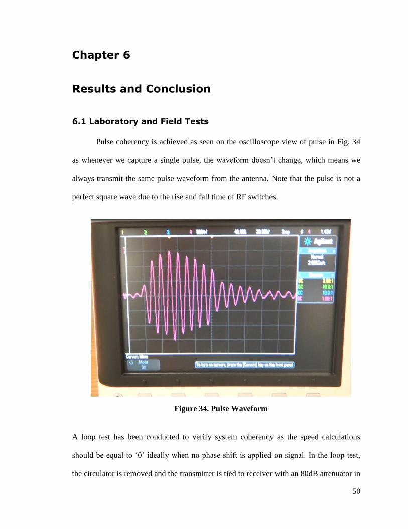
A loop test has been conducted to verify system coherency as the speed calculations
should be equal to ‘0’ ideally when no phase shift is applied on signal. In the loop test,
the circulator is removed and the transmitter is tied to receiver with an 80dB attenuator in
Figure 34. Pulse Waveform
51
between and the TX switch was kept in ‘ON’ mode all the time. The speed calculationS
seen in Fig. 35 show that the closed loop speed calculation is ~0km/h. The variation is
1 6 , which is due to the overall phase noise of the system.
Since there is no way of delaying the pulse between consecutive pulses without a
delay liner in the laboratory, the performance of Doppler processing algorithms couldn’t
be tested in the laboratory. However the functionality of modules have been tested with
simulated data on MATLAB/SIMULINK® environment and field tests has been
conducted in order to see the actual performance of the designed radar system.
Field tests are conducted on 06/09/2013 in a dry lake bed in Victorville, CA. We
wanted the test location to be as flat as possible since flat surfaces tend to have specular
reflections as a result less clutter signal from background was expected. The antenna was
25ft high above the ground and in the test scenario; a 14 feet long truck was approaching
to the radar from the boresight direction of the antenna. In Fig. 36 the measurement with
the target is seen as the truck is approaching. In tests, the radar system was able to detect
Figure 35. CW loop Test and Speed Calculation

52
the truck from ~350meters far away. Observations showed that the CFAR algorithm
proves to produce correct results. However speed calculations tends to be erroneous.
6.2 Challenges with Doppler Calculation
A generic approach in order to calculate the phase difference and then the speed is
presented in this project however in the field tests, the speed calculations proved to be
erroneous with a wide dispersion i.e. +-100km/h. The reasons for this problem can be
listed as;
Low power target return signal
Wideband antenna and wide antenna pattern on horizontal plane
Imperfect Gaussian waveform of the transmit pulse
Figure 36. Field test

53
In order to calculate the phase reliably the signal to noise ratio must be high
enough such that the noise floor would not influence the pulse signal adversely. In Fig.
36, in time domain plot of the samples it can be seen that the target return signal is less
than 0,1V, which can be potentially affected by the noise floor.
Since a wideband antenna is used, noise contribution is spread over the
continuous bandwidth between 800-2500MHz, which rises up the noise floor. The noise
power can be calculated with the given equation [14];
N = K*T*B
K = Boltzmann’s constant = 1.38 *10-23
Joules/Kelvin
T = Absolute Temperature (0°C = 273K)
B = Bandwidth, Hz
Antenna pattern should be narrow in both horizontal and vertical ideally to focus
the radar beam solely on target as much as possible so that the clutter power can be
minimized and a good level of signal to clutter ratio can be achieved. For air search radar
there isn’t an existence of background clutter unless there is rain or dense fog in the air
but for land radars background clutter due to the topography always poses a problem.
Figure 37. Antenna Pattern at 1Ghz

54
Another problem is the imperfect Gaussian pulse waveform in Doppler
processing. Ideally a pulse should be square and the top of the pulse should be flat so that
the phase calculations wouldn’t be influenced by the amplitude changes in pulse.
However when we have a Gaussian pulse shape, as the return pulse is shifted over time
with the motion of the target at some point we pick up samples from the edge of pulse for
phase calculation and this samples points are not reliable since they are generated at rise
and fall time of the RF switches. Another problem arises due to the long fall time of RF
switches as it results a tail at the end of pulse, which can potentially superimpose on the
pulse return from the next rangebin and can corrupt phase calculation.
6.3 Pulse Coherency and PRF relation
System coherency requirement for pulse Doppler radars puts a constraint on PRF
selection. In such a coherent system, the ADC clock, the clock, which runs the state
machine in the FPGA, demodulating signal, demodulated signal and the transmit signal
must preserve their relative phase relationship with each other all the time. If we assume
that they start with ‘0’ phase when a transmit pulse is propagated, then after one PRI they
must have the same phase ‘0’. This is guaranteed only if the PRI is equal to an integer
multiple of the least common multiple (LCM) of these clock periods.
In our radar, we have 1 GHz transmit signal, 900MHz demodulating signal,
100Mhz demodulated signal, 250MHz ADC clock and 250MHz reference clocks for
synthesizers. The LCM period of these clocks 40ns. Hence the PRI must be an integer
multiple of 40ns.
55
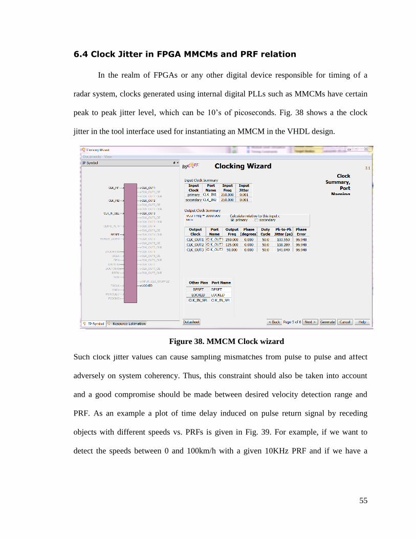
6.4 Clock Jitter in FPGA MMCMs and PRF relation
In the realm of FPGAs or any other digital device responsible for timing of a
radar system, clocks generated using internal digital PLLs such as MMCMs have certain
peak to peak jitter level, which can be 10’s of picoseconds. Fig. 38 shows a the clock
jitter in the tool interface used for instantiating an MMCM in the VHDL design.
Such clock jitter values can cause sampling mismatches from pulse to pulse and affect
adversely on system coherency. Thus, this constraint should also be taken into account
and a good compromise should be made between desired velocity detection range and
PRF. As an example a plot of time delay induced on pulse return signal by receding
objects with different speeds vs. PRFs is given in Fig. 39. For example, if we want to
detect the speeds between 0 and 100km/h with a given 10KHz PRF and if we have a
Figure 38. MMCM Clock wizard
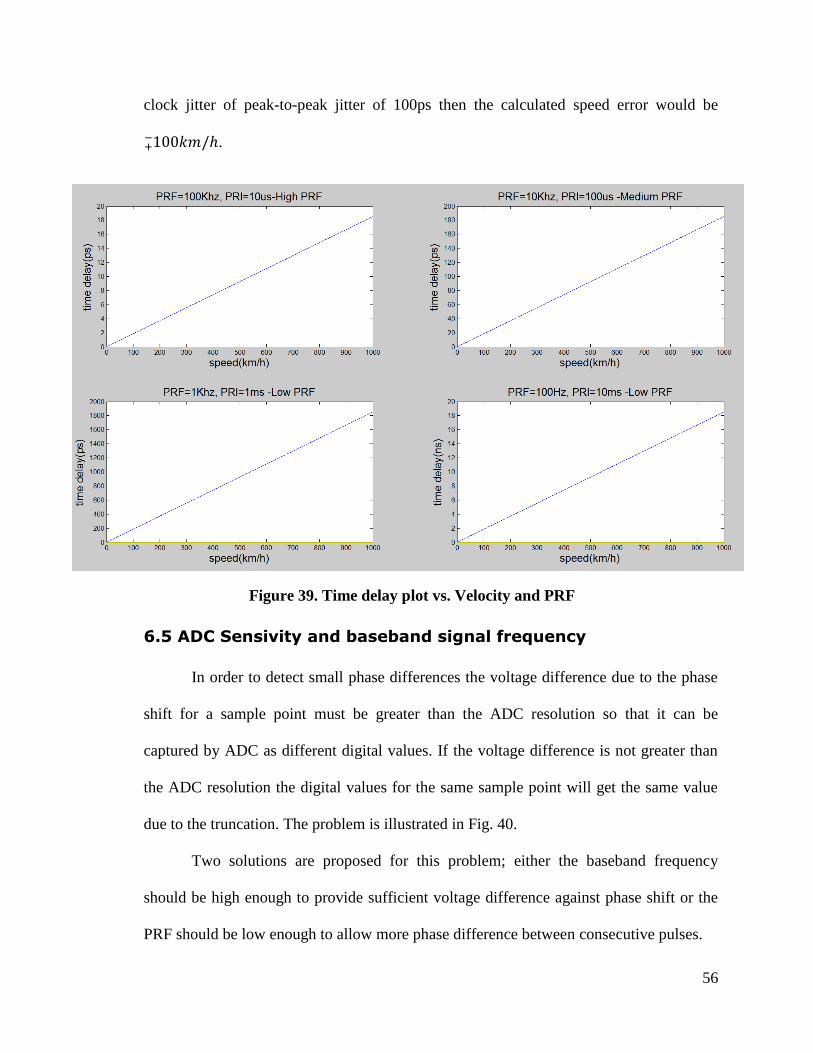
56
clock jitter of peak-to-peak jitter of 100ps then the calculated speed error would be
1 .
6.5 ADC Sensivity and baseband signal frequency
In order to detect small phase differences the voltage difference due to the phase
shift for a sample point must be greater than the ADC resolution so that it can be
captured by ADC as different digital values. If the voltage difference is not greater than
the ADC resolution the digital values for the same sample point will get the same value
due to the truncation. The problem is illustrated in Fig. 40.
Two solutions are proposed for this problem; either the baseband frequency
should be high enough to provide sufficient voltage difference against phase shift or the
PRF should be low enough to allow more phase difference between consecutive pulses.
Figure 39. Time delay plot vs. Velocity and PRF

57
6.6 CA-CFAR and Automatic Gain Adjustment
CFAR algorithm is an adaptive algorithm, which finds a threshold by estimating
the noise floor around the cell under test. However, the target return signal power level is
not same over the range axis as the signal power varies due to path loss from different
distances. Therefore the CFAR constant should be changed dynamically with distance if
an automatic gain control (AGC) is not existent in the radar system. If AGC is present in
the radar, then a fixed CFAR constant can be set corresponding to a certain detection
probability.
Figure 40. ADC Sensivity vs. Voltage Difference due to Phase Shift

58
6.7 Concluding Remarks and Future Works
In this work, we tried to develop a generic radar processor, which is capable of
CFAR and Doppler processing. In our approach we designed a radar transmitter and
receiver to investigate the bottlenecks, challenges, and potential problems, which can
occur in implementation and integration phase of a coherent radar system. Most of time
was spent on developing the hardware and VHDL designs as less time was left for the
detailed performance analysis at the end. We showed that a radar system can be packed
on a configurable hardware such as FPGAs and depending on the capability of the FPGA
a lot of DSP features such as filtering, arithmetic operations, transforms can be realized
with configurable logic blocks as they allow flexibility and high level of performance for
real-time applications. Mostly, we achieved our objectives as we got convincible results
along with RF system level design, software development, hardware implementation and
digital system design with FPGAs.
This project can be further extended to;
In this work, we used 9 pulses to average phase differences, the number of pulses
can be increased such that the result would be a good representative of the
absolute phase difference.
CA-CFAR detection algorithm has been applied in this work as other detection
schemes can also be implemented in FPGA and tested with the current radar set.
A rotational antenna can be used to scan 6 degrees and a scanning capability
can be utilized.

59
References
[1] M.I. Skolnik, Radar Handbook, McGraw Hill Companies, 2008.
[2] Hermann Rohling, "Radar CFAR Thresholding in Clutter and Multiple Target
Situations," IEEE Trans. On Aerospace and Electronics Systems, Vol, AES-19,
No.4, pp. 608-621,July 1983.
[3] D.C. Schleher, MTI and Pulsed Doppler Radar with MATLAB, Artech House
Radar Library, 2009.
[4] Vijayendra, V.; Siqueira, P.; Chandrikakutty, H.; Krishnamurthy, A.; Tessier, R.,
"Real-time estimates of differential signal phase for spaceborne systems using
FPGAs," Adaptive Hardware and Systems (AHS), 2011 NASA/ESA Conference on
, vol., no., pp.121,128, 6-9 June 2011
[5] Alachiotis, N.; Berger, S.A.; Stamatakis, A., "Efficient PC-FPGA Communication
over Gigabit Ethernet," Computer and Information Technology (CIT), 2010 IEEE
10th International Conference on , vol., no., pp.1727,1734, June 29 2010-July 1
2010
[6] Xilinx Corporation, Virtex-6 FPGA Embedded Tri-Mode Ethernet MAC User
Guide UG368, March 2011.
[7] Bassem R. Mahafza, Radar System Analysis and Design Using MATLAB,
Chapman&Hall/CRC, 2000
[8] Volder, Jack E., "The CORDIC Trigonometric Computing Technique," Electronic
Computers, IRE Transactions on , vol.EC-8, no.3, pp.330,334, Sept. 1959
[9] Xilinx Corporation, LogiCORE IP CORDIC v4.0 DS249 Datasheet. March, 2011.
[10] Bassem R. Mahafza, Radar System Analysis and Design Using MATLAB,
Chapman&Hall/CRC, 2000
[11] S.K,Mitra, Digital Signal Processing A Computer-based Approach, McGraw Hill
Education, 2011.
[12] Xilinx Corporation, System Generator for DSP User Guide UG640, March 2011.
[13] Meyer-Baese, U, Digital Signal Processing with Field Programmable Gate Arrays,
Springer, 2007
[14] D.M. Pozar, Microwave Engineering, Wiley (India), 2011.
[15] Xilinx Corporation, ML605 Hardware User Guide UG534, October 2012.
60
[16] Xilinx Corporation, Constraints User Guide UG625, March 2011.
[17] Xilinx Corporation, Mixed Mode Clock Manager Module DS737 Datasheet, June
2009.