forming-free nitrogen-doped aluminum …cs381qx1114/sung il park...we have demonstrated...
TRANSCRIPT

FORMING-FREE NITROGEN-DOPED ALUMINUM OXIDE RESISTIVE RANDOM ACCESS MEMORY GROWN BY ATOMIC LAYER DEPOSITION TECHNIQUE
A DISSERTATION
SUBMITTED TO THE DEPARTMENT OF ELECTRICAL ENGINEERING
AND THE COMMITTEE ON GRADUATE STUDIES
OF STANFORD UNIVERSITY
IN PARTIAL FULFILLMENT OF THE REQUIREMENTS FOR THE DEGREE OF
DOCTOR OF PHILOSOPHY
Sung Il Park
November 2013

http://creativecommons.org/licenses/by-nc/3.0/us/
This dissertation is online at: http://purl.stanford.edu/cs381qx1114
© 2013 by Sung Il Park. All Rights Reserved.
Re-distributed by Stanford University under license with the author.
This work is licensed under a Creative Commons Attribution-Noncommercial 3.0 United States License.
ii

I certify that I have read this dissertation and that, in my opinion, it is fully adequatein scope and quality as a dissertation for the degree of Doctor of Philosophy.
S Simon Wong, Primary Adviser
I certify that I have read this dissertation and that, in my opinion, it is fully adequatein scope and quality as a dissertation for the degree of Doctor of Philosophy.
Yoshio Nishi
I certify that I have read this dissertation and that, in my opinion, it is fully adequatein scope and quality as a dissertation for the degree of Doctor of Philosophy.
Philip Wong
Approved for the Stanford University Committee on Graduate Studies.
Patricia J. Gumport, Vice Provost for Graduate Education
This signature page was generated electronically upon submission of this dissertation in electronic format. An original signed hard copy of the signature page is on file inUniversity Archives.
iii

iv
Abstract
As flash memory devices begin to scale into the sub-20nm lithographical regime, scaling is
becoming a challenge because of high electric field requirements for a high programming or erase voltage
and rigid leakage requirements for long term storage. In addition, the flash memory design has been based
on a two-dimensional approach and density of integration is reaching its limits. To tackle these issues,
many candidates for next generation non-volatile memory such as phase change random access memory
(PCRAM), STT-magnetic random access memory (STT-RAM), ferroelectric random access memory
(FeRAM), and resistive random access memory (RRAM) have been introduced and studied. Among these
devices concepts RRAM is a prime candidate because of its unique characteristics. In order for RRAM
technology to be adopted for manufacturing, the technology must meet the following requirements. First,
the direct integration of metal oxide RRAM on MOSFET should be feasible and RRAM cells must be
compatible with the standard CMOS process. Second, it must not require a high forming voltage and it
should be programmed with an applied current below sub-uA at high data rates for many switching cycles.
Finally, RRAM cells must be feasible for storing multiple bits. We demonstrated nitrogen-doped aluminum
oxide RRAM that meets the requirements and the RRAM cell was deposited by a physical vapor deposition
technique. However, it has been found that more uniform films can be deposited by an atomic layer
deposition technique, and we believe that more uniform films are responsible for uniform switching
characteristics. That is the motivation of this dissertation.
We have demonstrated nitrogen-doped aluminum oxide RRAM grown by an atomic layer
deposition technique and have monolithically integrated such RRAM cells on top of selection transistors to
achieve accurate control of the voltage and current waveforms for programming. We have studied the
control of the on-and off-behavior of the RRAM cell by gathering the statistics on the turn-on and turn-off
voltage, current and resistance as a function of the bias voltages and the limiting current on the selection
MOSFET, and thereby evaluated the feasibility of multi-level programming, reliability, endurance and
retention of nitrogen-doped aluminum oxide RRAM. Through this study, novel multi-bit programming
strategies were investigated through accurate control of the programming waveform. The data collected

v
through this extensive study will provide important information on the viability of metal-oxide films for
future generation stand-alone and embedded non-volatile memory applications. The demonstration of
multi-level programming will greatly extend the scalability of RRAM. The evaluation methodology we
develop can be extended to other resistance-change films.

vi
Acknowledgments
I would like to express my thanks to my academic advisor, Professor S.Simon Wong. During my
graduate study, he has been academically and financially supportive. An important lesson that I have
learned from him is knowing the difference between science and engineering; science asks how nature
works and engineering asks how nature can be used. He always asked his students to focus on practical
issues and the lesson will be a long term asset for my research journey. Also, I would like to extend my
thanks to Professor Yoshio Nishi and Professor H.S. Philip Wong. They gave valuable feedback to my
thesis and without them my thesis could not be finished. Next gratitude is reserved for our group members,
Wanki Kim, Zhiping Zhang, Jeongha Park, Stanley Yeh, Chaohao Wang, Young-yang Liew, and Alex
Omid-zohor. Wanki, Zhiping, and myself worked together to develop RRAM stacks and integrate RRAM
cells on top of MOSFET, and I cannot imagine the end of my Ph.D study without them. Next, I want to
thank June Wang who is our group secretary, Jim Mcvittee who is in charge of AJA sputtering machine,
and Michelle Rinconn who is in charge of Fiji atomic layer deposition tool. When the machine had a
problem or even was broken, they always took prompt actions to fix the problem. Next, I am deeply
indebted to many friends at Stanford University for their support.
Last but not least, I really thank my family. My depth of gratitude is too great to express in words.
My parent raised me by sacrificing their life, and my lovely wife, Areum Han, has supported my study by
taking care of our lovely kids, Hans and Yoon.
vii
Table of Contents Abstract ........................................................................................................................................... iv
Acknowledgments .......................................................................................................................... vi
List of Tables .................................................................................................................................. ix
List of Illustrations .......................................................................................................................... x
Chapter 1: Introduction .................................................................................................................. 1
1.1. Resistive Random Access Memory (RRAM) technology .................................................. 1
1.2. Basic operations of RRAM ................................................................................................ 4
1.3. Introduction of nitrogen-doped aluminum oxide RRAM grown by PVD .......................... 5
1.4. Atomic Layer Deposition Vs. Physical Vapor deposition .................................................. 7
1.5. Introduction of RRAM grown by ALD ............................................................................ 10
1.6. Overview of dissertation .................................................................................................. 11
Chapter 2: Investigation of RRAM stacks.................................................................................... 13
2.1. TiN electrode for nitrogen-doped AlOx RRAM ............................................................... 13
2.2. Aluminum nitride grown by ALD .................................................................................... 14
2.3. Incorporation of nitrogen into aluminum oxide ............................................................... 15
2.3.1. AlOxNy composite material ..................................................................................... 15
2.3.2. AlN grown on Al2O3 ............................................................................................... 17
2.3.3. AlN grown on TiN electrode .................................................................................. 22
2.3.3.1 Al2O3 / AlN with TiN electrode ..................................................................... 22
2.3.3.2. XPS analysis for nitrogen-doped aluminum oxide RRAM ........................... 25
Chapter 3: Optimization of Al2O3 / AlN with TiN electrode ........................................................ 30
3.1. Switching characteristics in terms of AlN thickness ........................................................ 30
3.2. Switching characteristics in terms of Al2O3 thickness ..................................................... 32
3.3. Switching characteristics dependency on annealing time ................................................ 33
Chapter 4: Fabrication of N-doped AlOX RRAM grown by ALD 1T1R system ......................... 35
4.1. Introduction of selection transistors ................................................................................. 35

viii
4.2. Integration of N-doped AlOx RRAM with CMOS ........................................................... 37
4.3. Description of 1Transistor 1RRAM structure .................................................................. 42
Chapter 5: Electrical switching characteristics of N-doped AlOX RRAM grown by ALD ......... 44
5.1. Measurement setup for 1T1R structure ............................................................................ 44
5.2. I-V switching characteristics ............................................................................................ 45
5.3. Programming voltage distribution .................................................................................... 49
5.4. Set/reset current versus on resistance ............................................................................... 51
5.5. Linear and non-linear I-V characteristics of HRS and various LRS ................................ 53
5.6. Conduction mechanism in ALD N-AlOx RRAM ............................................................. 56
5.7. Reliability characteristics of ALD N-AlOx RRAM. ......................................................... 63
5.7.1. Retention results at 120 °C ..................................................................................... 63
5.7.2. Read disturb characteristics .................................................................................... 64
5.7.3. Endurance switching characteristics ....................................................................... 65
Chapter 6: Incorporation of nitrogen into Al2O3 films ................................................................ 68
6.1. Role of nitrogen for resistive switching characteristics .................................................... 68
6.2. Electrical switching characteristics in terms of nitrogen concentration ........................... 69
6.2.1. Set / reset current versus on-resistance ................................................................... 69
6.2.2. Extrapolated energy barrier ..................................................................................... 71
6.2.3. Endurance characteristics ........................................................................................ 74
Chapter 7: Conclusion .................................................................................................................. 79
7.1. Summary .......................................................................................................................... 79
7.2. Recommendation for future works ................................................................................... 80
Bibliography .................................................................................................................................. 81

ix
List of Tables Number Page
Table 2.1: Summary of ALD TiN properties. ................................................................................ 13
Table 3.1: Summary of switching parameters versus AlN thickness. ............................................ 31
Table 3.2: Summary of switching characteristics versus Al2O3 thickness. .................................... 33
Table 3.3: Dependency on annealing time of switching characteristics. ....................................... 34
Table 4.1: Description of NMOS transistors with different sizes.W and L indicate channel width and length of selection transistors, respectively. .............................................. 36
Table 4.2: RRAM cells of different sizes. The numbering corresponds to those shown in Figure 4.5 (b). ............................................................................................................. 43
Table 6.1: N-AlOx with various nitrogen concentrations. .............................................................. 68
Table 6.2: Summary of extrapolated trap barrier height for HRS. ................................................. 73
Table 6.3: Summary of extrapolated trap barrier height for each LRS. ......................................... 74
Table 6.4: Summary of endurance characteristics. ........................................................................ 78

x
List of Illustrations Number Page
Figure 1.1: Scaling trend of NAND flash technology [1]. ............................................................... 1
Figure 1.2: Basic I-V characteristics of RRAM; (a) unipolar operations with a forming process (b) bipolar operations with a forming process[17]. ......................................... 4
Figure 1.3: Nitrogen-doped aluminum oxide RRAM deposited by the PVD system;(a) cross-sectional view of a RRAM cell, (b) basic switching characteristics, and (c) retention characteristics of N-AlOx RRAM cells[21]. .................................................. 6
Figure 1.4: Illustration of deposition cycles consisting of 4 steps in the atomic layer deposition system; (a) exposure of metal precursors, (b) evacuation of reactants or any by-products, (c) exposure of H2O, and (d) purging out of reactants or by-products. (e) Illustration of Al2O3 layer grown on a silicon substrate after one deposition cycle is reached[22]. ................................................................................... 7
Figure 1.5: Illustration of deposition processes in the physical vapor deposition system[23]. ........ 8
Figure 1.6: Summary of characteristics of films deposited by several deposition techniques[22]. ............................................................................................................. 9
Figure 1.7: Switching characteristics of hafnium-based RRAM deposited by an atomic layer deposition technique. (a) Illustration of a forming process, (b) basic I-V characteristics, (c) endurance characteristics, and (d) retention characteristics of HfOX RRAM[24]. ....................................................................................................... 10
Figure 2.1: AFM picture of TiN films deposited by ALD. ............................................................ 13
Figure 2.2: Atomic profiles of AlN grown on TiN layer. .............................................................. 14
Figure 2.3: Cross-sectional view of layered aluminum oxynitride (AlOXNY). .............................. 16
Figure 2.4: Illustration of a set process of AlOXNY. ...................................................................... 16
Figure 2.5: Atomic profiles of alternating layers of Al2O3 and AlN. ............................................. 17
Figure 2.6: Cross-sectional view of AlN / Al2O3 stacks. ............................................................... 18
Figure 2.7: Illustration of a set process of AlN / Al2O3 stacks. ...................................................... 18
Figure 2.8: Atomic profiles of (a) as-deposited AlN / Al2O3 stacks and (b) annealed AlN / Al2O3 stacks. ............................................................................................................... 19
Figure 2.9: Atomic profiles of (a) AlN grown on top of SiO2 and (b) AlN grown on top of HfO2............................................................................................................................ 21
Figure 2.10: Process flow of nitrogen-doped aluminum oxide RRAM stacks (50 um X 50 um); (a) cross-sectional view of N-AlOx, (b) patterning for the bottom electrode, (c) patterning for the top electrode, and (d) after annealing at 400 °C for 15 minutes. ...................................................................................................................... 23

xi
Figure 2.11: Illustration of forming free switching behavior. ........................................................ 24
Figure 2.12: Basic I-V characteristics of nitrogen-doped aluminum oxide RRAM with TiN electrodes. ................................................................................................................... 25
Figure 2.13: Atomic profiles of (a) as-deposited stacks and (b) annealed stacks at 400 °C for 30 minutes. ................................................................................................................. 26
Figure 2.14: Bonding information;(a) Al2p, (b) O1s, and (c) N1s. ............................................... 28
Figure 2.15: The peak signals of N1s[33]. ..................................................................................... 29
Figure 4.1: (a) ID-VD and (b) ID-VG characteristics of a 10 um / 1 um NMOS transistor. ............. 36
Figure 4.2: Illustration of the process flow for integration of N-AlOx on top of selection transistors. .................................................................................................................. 39
Figure 4.3: (a) Cross-sectional view of RRAM stacks, (b) top view of 1T1R structure, and (c) cross-sectional schematic of 1T1R structure. ............................................................. 40
Figure 4.4: Cross-sectional view of RRAM stacks that were deposited in a via region. ............... 41
Figure 4.5: (a) Test chip snapshot and (b) an enlarged view of 1T1R RRAM area. ..................... 42
Figure 5.1: Illustration of measurement set-up for (a) set and (b) reset switching. ....................... 44
Figure 5.2: I-V switching characteristics of ALD N-AlOx RRAM. .............................................. 45
Figure 5.3: Illustration of set switching behaviors showing no forming process. ......................... 46
Figure 5.4: Set switching behavior as a function of the gate bias of selection transistors for (a) ALD N-AlOx 1T1R structure and (b) PVD N-AlOx 1T1R structure, respectively. ... 48
Figure 5.5: Distributions of (a) set and (b) reset voltages of N-AlOx. The set and reset current are limited to 300nA and 1uA, respectively. .............................................................. 49
Figure 5.6: (a) Set current versus on-resistance and (b) reset current versus on-resistance........... 51
Figure 5.7: Plot of natural log of current versus square root of voltage for HRS and various LRS............................................................................................................................. 53
Figure 5.8: Dependency on temperature of HRS and various LRS. .............................................. 54
Figure 5.9: I-V relationship of (a) HRS and (b) LRS at various temperatures. ............................. 57
Figure 5.10: Temperature dependence of HRS and LRS. .............................................................. 58
Figure 5.11: Illustration of curve-fitting for the Frenkel-Poole emission model. .......................... 59
Figure 5.12: Illustration of curve-fitting for the Schottky emission model. .................................. 59
Figure 5.13: Energy band diagram of (a) after an annealing process and (b) after a set process... 60
Figure 5.14: Macroscopic conduction model of ALD N-AlOx RRAM. ........................................ 61

xii
Figure 5.15: Retention results of the high resistance state and various resistance states at 120 °C. ........................................................................................................................ 63
Figure 5.16: Read disturb characteristics of various resistance states. .......................................... 64
Figure 5.17: Endurance characteristics of (a) without using smart programming and (b) with using smart programming for N-AlOx. ....................................................................... 65
Figure 6.1: (a) Set current versus on-resistance and (b) reset current versus on-resistance for Al2O3, 3 % N-AlOx, and 6 % N-AlOx, respectively. .................................................. 69
Figure 6.2: (a) Set current versus on-resistance and (b) reset current versus on-resistance for 6 % N-AlOx, 12 % N-AlOx, and AlN, respectively. ................................................... 70
Figure 6.3: Fitting results for the Frenkel-Poole emission model of HRS. .................................... 72
Figure 6.4: Fitting results for the Frenkel-Poole emission model of 1MΩ LRS. ........................... 73
Figure 6.5: Pulse endurance characteristics of (a) Al2O3, (b) 3 % N-AlOx, (c) 6 % N-AlOx, (d) 12 % N-AlOx, and (e) AlN. ........................................................................................ 77

1
Chapter 1: Introduction
1.1. Resistive Random Access Memory (RRAM) technology
In order to satisfy society's seemingly insatiable demand for new computers, video games,
and smart phones, Moore's law dictates that a new generation of technology be introduced every
two years or so. Many studies pertaining to advanced technologies follow this guideline. The
main reasons for scaling down the dimensions of logic devices are higher device density and
better performance. Scaling allows more transistors to be integrated into a chip with the same
dimensions, and integrated chips based on this new technology operate faster and consume less
power.
Figure 1.1: Scaling trend of NAND flash technology [1].

2
However, silicon, which is the most important material in the semiconductor industry and
the major reason why the semiconductor business has become successful, is reaching its physical
limits. Thus, an integration density based on a two-dimensional approach, where transistors and
passive components are placed in the same plane, is approaching its limit. From a structural point
of view, traditional non-volatile memory structures such as NAND and NOR flash memory will
be vulnerable to breakdown because a high programming voltage over 10 V is required as we
scale down below 15 nm. In addition, a programming time of micro-second range for flash
memory is not desirable for nano-second scale operation. To overcome these issues, many
candidates such as Resistive Random Access Memory (RRAM)[2-4], Phase Change Random
Access Memory (PCRAM)[5], Magnetic Random Access Memory (MRAM)[6], and
Ferroelectric Random Access Memory (FeRAM)[7] have been introduced and extensively
investigated. Among these candidates, the RRAM technology is the most promising non-volatile
memory technology. The structure of RRAM is a simple metal-insulator-metal structure (MIM)
that consists of a resistive dielectric material sandwiched between two metal electrodes.
Operation of RRAM is also simple. Memory cells start in the high resistance state (HRS) which
corresponds to logic ‘0’ state. At about 2 V, it will be set to the low resistance state (LRS)
associated with logic ‘1’ state. That is, its state can be easily switched by applying low voltages.
Compared with flash memory in which a high voltage over 10 V is required when switching the
state of memory cells, the voltage required to switch the state of RRAM cells is low. Hence, no
extra circuits such as a charge pump circuit is required to implement a high voltage, which
simplifies the design of memory array.
Simple MIM structure and operation of RRAM have triggered interest, and many
candidate resistive dielectric materials based on oxides of nickel[8,9], titanium[10], hafnium[11],
and aluminum[12] with different electrodes for the dielectric films have been introduced and
extensively investigated. At an early stage, nickel oxide and titanium oxide based RRAM were
studied and those RRAM cells showed moderate performances such as uA-range current levels[8-

3
10]. Hafnium based RRAM showed low power operation and a fast programming cycle[11], but
the RRAM requires a forming process by which a resistive switching behavior is facilitated.
Recently, we demonstrated nitrogen-doped aluminum oxide (N-AlOX) RRAM technology with
very promising switching characteristics. This technology was based on the physical vapor
deposition (PVD) system. Although the N-doped AlOX RRAM technology shows low power
operation and fast switching cycles, the control and reproducibility of PVD is marginal. We have
studied N-doped AlOX RRAM grown by an atomic layer deposition (ALD) technique to make the
RRAM technology more consistent. It is well known that films grown by ALD outweigh films
deposited by PVD in term of the step coverage and uniformity of films[13]. We believe that more
uniform films guarantee more consistent switching characteristics which are desirable for the
design of memory cell arrays, and this is why we started ALD work.
Along with studies to improve performance by investigating materials, switching
mechanisms such as the filament theory[14], the ion migration model[15], and the Schottky or
Frenkel-Poole emission model[16] to understand what principle RRAM cells operate on and to
identify how they change its state from HRS (LRS) to LRS (HRS) from a physical point of view
have been proposed. The filament theory involves oxygen vacancies which is associated with
LRS. When a current is passed through the filament, heat is released and the filament is broken
[14]. The ion migration model explains that the migration of oxygen ions is responsible for
resistive switching behaviors of RRAM. When ions are aligned in series or form a current path,
the state of memory cells is LRS. When an opposite polarity bias is applied across memory cells,
however, ions are repelled or the chain of ions are broken by the bias and this results in HRS[15].
Two common models such as the Schottky emission and Frenkel-Poole emission model explain
rectifying conduction behavior in dielectric films. Both models have almost linear dependency
between the natural log of current and the square root of voltage, and the energy barrier plays an
important role in resistive switching characteristics[16]. In this dissertation, we studied two

4
models to understand resistive switching characteristics in the N-doped AlOX RRAM, and
Chapter 5 will deal with this topic in detail.
In order for a RRAM technology to be adopted for manufacturing, it must meet the
following requirements. It must be compatible with the standard CMOS process and feasible for
three dimensional stacking. It must be scalable to nm dimensions. In terms of programming
performance, it must not require a high forming voltage. It should be programmed with a low
current at high speed for many cycles. Finally, the RRAM cell must be capable of storing
multiple bits reliably. For the rest of the dissertation, a RRAM with ALD nitrogen-doped
aluminum oxide resistive dielectric that meets these requirements will be described.
1.2. Basic operations of RRAM
(a) (b)
Figure 1.2: Basic I-V characteristics of RRAM; (a) unipolar operations with a forming
process (b) bipolar operations with a forming process[17].
One unique characteristic of RRAM is a high voltage forming process that initiates the
programming functions[17-19]. Figure 1.2 shows the forming process and basic switching
characteristics of RRAM[17]. As shown in Figure 1.2 (a), a RRAM cell starts in the high

5
resistance state. At about 2.5 V, memory cells will be set into the low resistance state with an
applied current 0.5 mA. This low resistance state indicates that a memory cell store '1' bit. A
voltage of 0.6 V will be applied to reset the memory cells back to the high resistance state
associated with '0' bit. At the subsequent set cycle, RRAM cells can be set into the low resistance
state with an applied voltage less than the forming voltage. Since this forming process is not
reversible and complicates the design of selection devices and peripheral circuits, eliminating the
forming process is desirable. For RRAM operations, there are two operation modes, one is
unipolar switching mode and the other one is bipolar switching mode. As shown in Figure 1.2 (a),
in unipolar mode the same polarity of bias will be applied across memory cells when we reset
memory cells. In bipolar mode, a reverse polarity of bias will be applied across RRAM cells
when we reset RRAM cells as shown in Figure 1.2 (b). In general, bipolar switching mode is
more reliable than unipolar switching mode[20]. For this reason, we will focus on bipolar
switching mode.
1.3. Introduction of nitrogen-doped aluminum oxide RRAM grown by PVD
We demonstrated a forming free RRAM with nitrogen-doped aluminum oxide (N- AlOX)
resistance change film[21]. It is composed of 20 nm thick aluminum bottom electrode, 10 nm
thick nitrogen-doped aluminum oxide resistive dielectric film, and 20 nm thick aluminum top
electrode. These layers were deposited in-situ by a physical vapor deposition technique to prevent
any contamination or oxidation along the interfaces. Figure 1.3 shows a cross-sectional view of
the RRAM, basic switching characteristics, and retention characteristics. RRAM cells can be
programmed or erased with an applied current below 50 nA and no significant change of the
resistances is observed for 105 seconds at 120 °C. Recently, it has been found that more uniform
and conformal films can be deposited by an atomic layer deposition technique. We believe that
the uniformity of films affects the uniform switching characteristics. To achieve more uniform
switching characteristics, we have developed N-AlOx film grown by ALD and integrated such

6
RRAM on top of CMOS wafers. In the next section, we will introduce an ALD technique and
discuss its advantages over a PVD technique.
(a)
(b) (c)
Figure 1.3: Nitrogen-doped aluminum oxide RRAM deposited by the PVD system;(a)
cross-sectional view of a RRAM cell, (b) basic switching characteristics, and (c) retention
characteristics of N-AlOx RRAM cells[21].

7
1.4. Atomic Layer Deposition Vs. Physical Vapor deposition
(a) (b)
(c) (d)
(e)
Figure 1.4: Illustration of deposition cycles consisting of 4 steps in the atomic layer
deposition system; (a) exposure of metal precursors, (b) evacuation of reactants or any
by-products, (c) exposure of H2O, and (d) purging out of reactants or by-products. (e)
Illustration of Al2O3 layer grown on a silicon substrate after one deposition cycle is
reached[22].

8
Atomic layer deposition (ALD) is a cyclic process that consists of an iterated sequence of
deposition cycles[13,22]. Film thickness and properties are controlled at each cycle, and
reproducible deposition of film composites by alternating layer composition is feasible. Because
gas uniformity or flow does not affect layer growth, highly uniform and conformal films can be
deposited. Figure 1.4 illustrates deposition cycles of the ALD system. In step 1, metal precursors
are introduced into a chamber and react with atoms on the bottom layer. In the next step,
precursors that do not have any bonding to the atom on the surface or any by-products are purged
out of the chamber. In step 3, other precursors are delivered into the chamber and react with
atoms in the layer deposited at step 1. Finally, un-reacted precursors and any by-products are
evacuated. One of the most important requirements for the first step is the self-limitation of the
precursor molecule absorption process. Usually, the ligands bonded to the metal atoms in the
precursors, such as halogen or organic ligands, limit further absorption of the metal precursor by
passivating the absorption sites after one monolayer is deposited.
Figure 1.5: Illustration of deposition processes in the physical vapor deposition
system[23].

9
Figure 1.5 shows the deposition process in a PVD system based on sputtering. Highly
energetic particles such as argon ions bombard the surface in the presence of high electric field.
Then, atoms are ejected from the surface of a target material as a result of collision with high-
energy particles according to Newton's law. Finally, the dislodged atoms or molecules condense
on a substrate as a thin film.
Figure 1.6: Summary of characteristics of films deposited by several deposition
techniques[22].
Figure 1.6 compares the uniformity of films deposited by several deposition techniques
and the film deposited by ALD shows better step coverage as expected. We believe that
improved uniformity will result in uniform switching characteristics, which will be discussed in
Chapter 5.

10
1.5. Introduction of RRAM grown by ALD
Figure 1.7: Switching characteristics of hafnium-based RRAM deposited by an atomic
layer deposition technique. (a) Illustration of a forming process, (b) basic I-V
characteristics, (c) endurance characteristics, and (d) retention characteristics of HfOX
RRAM[24].
As a replacement for silicon oxide, hafnium oxide has been extensively investigated due
to its high dielectric constant and thermal stability. Such intensive studies about hafnium oxide
have triggered research for RRAM applications[24]. Figure 1.7 shows basic I-V switching
characteristics and reliability characteristics of hafnium oxide RRAM, and the hafnium oxide
resistive dielectric film with TiN electrodes was grown by ALD. The RRAM cell requires a

11
forming process and the cell can be programmed or erased with an applied current of about 10 uA
as shown in Figure 1.7 (a) & (b). Hafnium oxide RRAM cells are switchable over 103 switching
cycles, and are expected to retain stored data for an extended time, as shown in Figure 1.7 (c) &
(d).
However, the problem of hafnium oxide based RRAM grown by ALD is that the RRAM
cell requires a forming process by which RRAM operation is facilitated. As discussed in the
previous section, the process is necessary for RRAM operation and requires a higher voltage,
which complicates the peripheral circuit. To remove the forming process, a PVD metal film is
deposited on top or bottom of a resistive dielectric film so that the layer scavenges oxygen from a
resistive dielectric and as a result oxygen vacancies, which are necessary for RRAM operation,
are generated[11]. The reason for using a PVD film instead of an ALD film is that a pure metal
cannot be deposited in the ALD system. However, PVD metal films are deposited under an ex-
situ condition and as a result the surfaces or interfaces are exposed to air and are vulnerable to
contamination or extra-oxidation by oxygen in air. This will impact the operations of the RRAM.
To avoid this issue, we developed RRAM stacks including electrodes that are deposited under an
in-situ condition. The following chapter will introduce the fabrication of the N-doped AlOX
RRAM and deal with material analysis, especially XPS, for films grown by ALD.
1.6. Overview of dissertation
This dissertation is organized as follows: Chapter 1 introduces the basic operation of
RRAM technology, our previous works based on physical vapor deposition (PVD), atomic layer
deposition (ALD), and RRAM grown by ALD. Chapter 2 discusses the investigation of RRAM
stacks with various combinations of layers. The compositions of RRAM stacks have been
analyzed by X-ray photoelectron spectroscopy (XPS) technique. Chapter 3 describes the
optimization of RRAM stacks that were investigated in Chapter 2. Switching characteristics in
terms of the thickness of different layer, and annealing time have been analyzed to optimize the

12
stack. Chapter 4 introduces the integration of nitrogen-doped aluminum oxide RRAM on top of
CMOS wafers. Chapter 5 discusses in details, the switching characteristics and the reliability
characteristics of RRAM. We also study the switching mechanism. Chapter 6 discusses the role
of nitrogen in resistive switching behavior. Finally, Chapter 7 summarizes the discussions that
have been addressed in this dissertation and suggests topics for future research.

13
Chapter 2: Investigation of RRAM stacks 2.1. TiN electrode for nitrogen-doped AlOx RRAM
Resistivity Roughness Deposition rate
Plasms TiN 10 u~25 uΩ*cm 0.2 nm 0.7 A/cycle
Table 2.1: Summary of ALD TiN properties.
Figure 2.1: AFM picture of TiN films deposited by ALD.
In our previous work of PVD nitrogen-doped aluminum oxide RRAM, the electrodes are
aluminum[21]. However, it is very difficult to grow pure aluminum metal layers in an ALD
system due to the unique deposition method; ligands cannot be bonded to the bottom aluminum
layer at the subsequent deposition cycle because they are already bonded to the same metal atom.
14
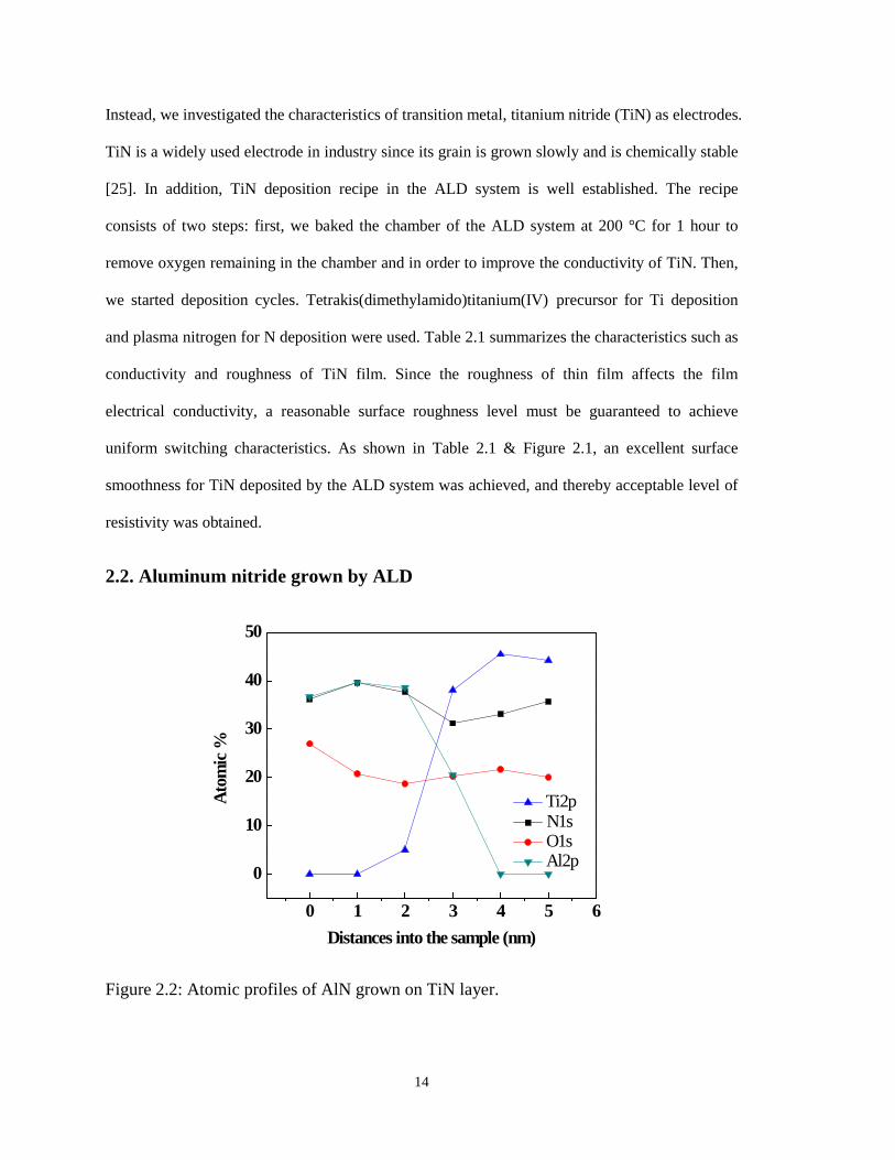
Instead, we investigated the characteristics of transition metal, titanium nitride (TiN) as electrodes.
TiN is a widely used electrode in industry since its grain is grown slowly and is chemically stable
[25]. In addition, TiN deposition recipe in the ALD system is well established. The recipe
consists of two steps: first, we baked the chamber of the ALD system at 200 °C for 1 hour to
remove oxygen remaining in the chamber and in order to improve the conductivity of TiN. Then,
we started deposition cycles. Tetrakis(dimethylamido)titanium(IV) precursor for Ti deposition
and plasma nitrogen for N deposition were used. Table 2.1 summarizes the characteristics such as
conductivity and roughness of TiN film. Since the roughness of thin film affects the film
electrical conductivity, a reasonable surface roughness level must be guaranteed to achieve
uniform switching characteristics. As shown in Table 2.1 & Figure 2.1, an excellent surface
smoothness for TiN deposited by the ALD system was achieved, and thereby acceptable level of
resistivity was obtained.
2.2. Aluminum nitride grown by ALD
0 1 2 3 4 5 6
0
10
20
30
40
50
Atom
ic %
Distances into the sample (nm)
Ti2p N1s O1s Al2p
Figure 2.2: Atomic profiles of AlN grown on TiN layer.
15
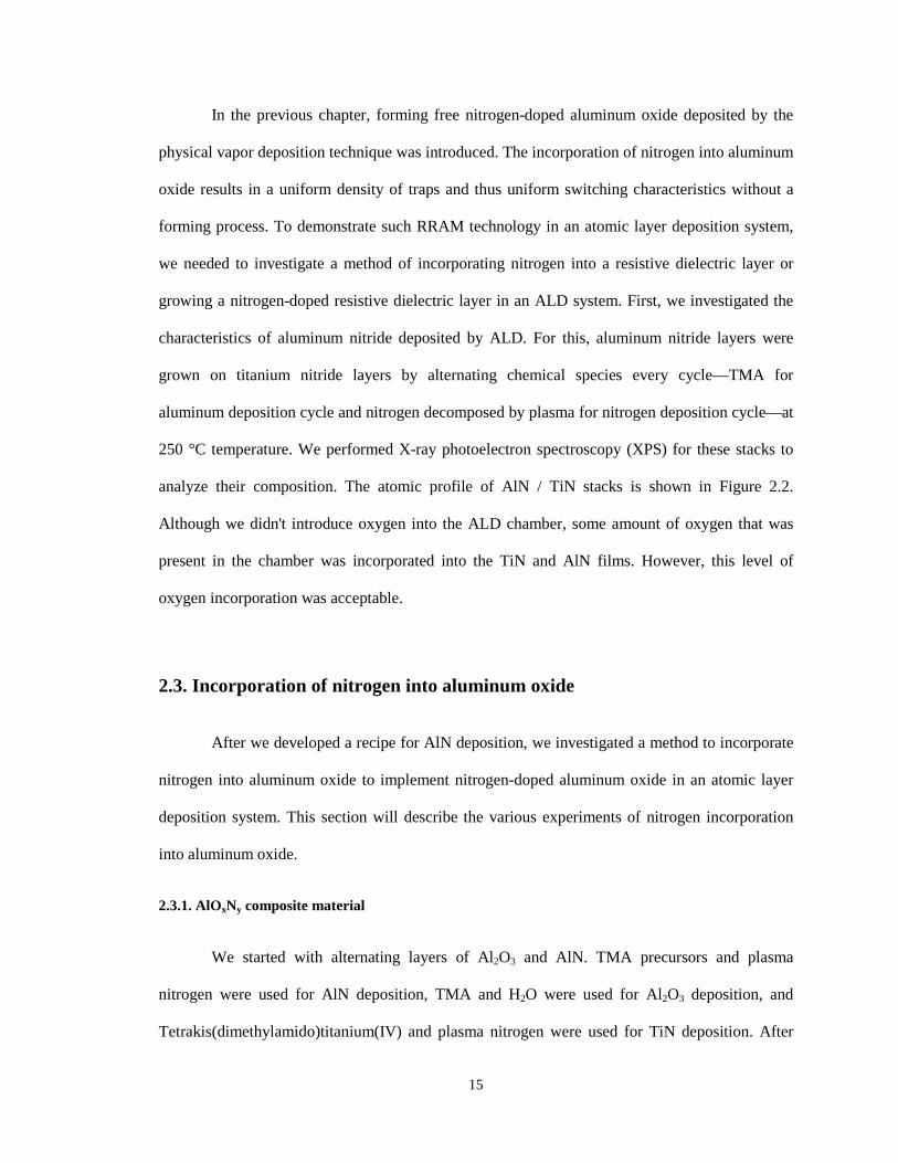
In the previous chapter, forming free nitrogen-doped aluminum oxide deposited by the
physical vapor deposition technique was introduced. The incorporation of nitrogen into aluminum
oxide results in a uniform density of traps and thus uniform switching characteristics without a
forming process. To demonstrate such RRAM technology in an atomic layer deposition system,
we needed to investigate a method of incorporating nitrogen into a resistive dielectric layer or
growing a nitrogen-doped resistive dielectric layer in an ALD system. First, we investigated the
characteristics of aluminum nitride deposited by ALD. For this, aluminum nitride layers were
grown on titanium nitride layers by alternating chemical species every cycle—TMA for
aluminum deposition cycle and nitrogen decomposed by plasma for nitrogen deposition cycle—at
250 °C temperature. We performed X-ray photoelectron spectroscopy (XPS) for these stacks to
analyze their composition. The atomic profile of AlN / TiN stacks is shown in Figure 2.2.
Although we didn't introduce oxygen into the ALD chamber, some amount of oxygen that was
present in the chamber was incorporated into the TiN and AlN films. However, this level of
oxygen incorporation was acceptable.
2.3. Incorporation of nitrogen into aluminum oxide
After we developed a recipe for AlN deposition, we investigated a method to incorporate
nitrogen into aluminum oxide to implement nitrogen-doped aluminum oxide in an atomic layer
deposition system. This section will describe the various experiments of nitrogen incorporation
into aluminum oxide.
2.3.1. AlOxNy composite material
We started with alternating layers of Al2O3 and AlN. TMA precursors and plasma
nitrogen were used for AlN deposition, TMA and H2O were used for Al2O3 deposition, and
Tetrakis(dimethylamido)titanium(IV) and plasma nitrogen were used for TiN deposition. After
16
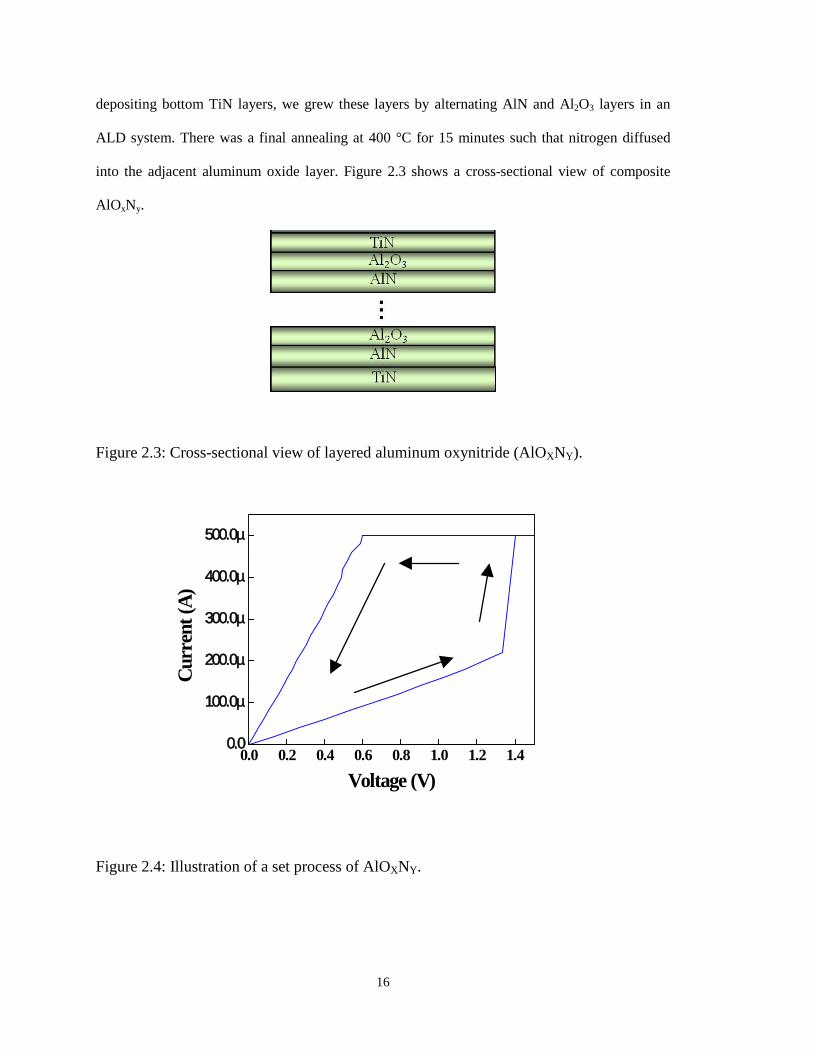
depositing bottom TiN layers, we grew these layers by alternating AlN and Al2O3 layers in an
ALD system. There was a final annealing at 400 °C for 15 minutes such that nitrogen diffused
into the adjacent aluminum oxide layer. Figure 2.3 shows a cross-sectional view of composite
AlOxNy.
Figure 2.3: Cross-sectional view of layered aluminum oxynitride (AlOXNY).
0.0 0.2 0.4 0.6 0.8 1.0 1.2 1.40.0
100.0µ
200.0µ
300.0µ
400.0µ
500.0µ
Curr
ent (
A)
Voltage (V)
Figure 2.4: Illustration of a set process of AlOXNY.

17
0 400 800 1200 1600
0
10
20
30
40
50
60
70
Al2p
O1s
N1s
Atom
ic %
Sputtering time (sec)
Ti2p N1s O1s Al2p
Ti2p
Figure 2.5: Atomic profiles of alternating layers of Al2O3 and AlN.
Figure 2.4 shows the switching characteristics. Although a composite AlOxNy RRAM cell
shows resistive switching behaviors, its switching characteristics are very poor. Figure 2.5 shows
the XPS analysis. There is no significant incorporation of nitrogen in the resistive dielectric. This
suggests that a composite AlOxNy is not an appropriate choice due to the ineffective incorporation
of nitrogen in the resistive dielectric.
2.3.2. AlN grown on Al2O3
One way to incorporate nitrogen into resistive dielectric films is to implement AlN and
Al2O3 bi-layer configuration and anneal the bi-layer so that nitrogen can diffuse into dielectric
films. In this experiment, we investigated AlN / Al2O3 RRAM stacks where AlN is grown on top
of Al2O3. It is composed of 20 nm thick bottom TiN electrode, 5 nm thick Al2O3 resistive
dielectric layer, 4 nm thick AlN layer, and 20 nm thick top TiN electrode. The bottom electrode is
composed of 5nm ALD TiN on top of 15 nm PVD TiN, whereas the top electrode is 15nm PVD
0 2 4 6 8 10 12 14
Distances into the sample (nm)
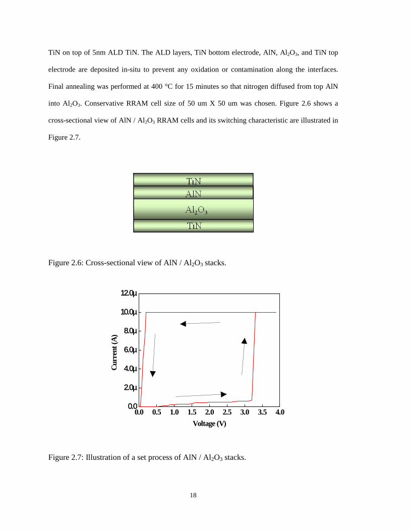
18
TiN on top of 5nm ALD TiN. The ALD layers, TiN bottom electrode, AlN, Al2O3, and TiN top
electrode are deposited in-situ to prevent any oxidation or contamination along the interfaces.
Final annealing was performed at 400 °C for 15 minutes so that nitrogen diffused from top AlN
into Al2O3. Conservative RRAM cell size of 50 um X 50 um was chosen. Figure 2.6 shows a
cross-sectional view of AlN / Al2O3 RRAM cells and its switching characteristic are illustrated in
Figure 2.7.
Figure 2.6: Cross-sectional view of AlN / Al2O3 stacks.
0.0 0.5 1.0 1.5 2.0 2.5 3.0 3.5 4.00.0
2.0µ
4.0µ
6.0µ
8.0µ
10.0µ
12.0µ
Curr
ent (
A)
Voltage (V)
Figure 2.7: Illustration of a set process of AlN / Al2O3 stacks.
19
0
10
20
30
40
50
60
70
Al2p
O1s
N1s
Atom
ic %
Ti2p N1s O1s Al2p
Ti2p
(a)
0
10
20
30
40
50
60
70
Al2p
O1s
N1s
Atom
ic %
Ti2p N1s O1s Al2p
Ti2p
(b)
Figure 2.8: Atomic profiles of (a) as-deposited AlN / Al2O3 stacks and (b) annealed AlN /
Al2O3 stacks.
Ti2p N1s O1s Al2p
Ti2p N1s O1s Al2p
0 2 4 6 8 10 12 14
Distances into the sample (nm)
0 2 4 6 8 10 12 14
Distances into the sample (nm)

20
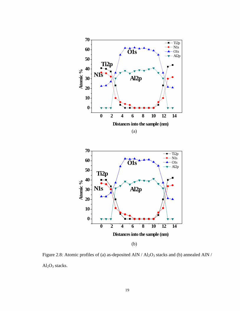
Contrary to our expectation that nitrogen diffusion from top AlN layer into bottom Al2O3
layer occurs during an annealing process and the incorporation of nitrogen facilitates RRAM
operations, these RRAM cells didn't show resistive switching behaviors. The RRAM cell became
short, during set, and cannot be reset back to the high resistance state. To understand their
switching behaviors, we performed X-ray photoelectron spectroscopy for these stacks. The
atomic profiles of AlN / Al2O3 stacks are plotted in Figure 2.8. For as-deposited case, there was a
very small amount of nitrogen in the AlN region as shown in Figure 2.8 (a). In a previous section,
we verified that AlN layers were successfully grown on TiN layers. However, it seems that AlN
layers did not grow on top of Al2O3. As a result, there is no significant nitrogen diffusion from
AlN into Al2O3 during the annealing process at 400 °C for 30 minutes, as shown in Figure 2.8 (b).
The XPS results raised a question: Is AlN deposition dependent on the substrate?
To answer the question, we conducted a few experiments. First, we deposited AlN on top
of oxide-based dielectric films such as hafnium oxide and silicon dioxide using the following
procedure. After depositing the oxide films in the ALD system, we transferred samples from the
chamber to the load lock without breaking vacuum and baked the chamber at 200 °C for 2 hours
to get rid of oxygen remaining in the chamber before the deposition of AlN layer. Finally, we
annealed the samples at 400 °C for 30 minutes to trigger diffusion of nitrogen into oxide
dielectric films, and their compositions were analyzed by XPS. Figure 2.9 shows atomic profiles
of each case. As shown in Figure 2.9, no significant nitrogen was incorporated in the AlN region
and therefore noticeable diffusion didn't occur during the annealing process. Although we cannot
explain the phenomena physically, the experimental results suggest that it is difficult to
incorporate nitrogen into AlN that is grown on oxide dielectric films.

21
0 2 4 6 8 10
0
10
20
30
40
50
60
70
N1s O1s Al2p Si2p
Al2p
O1s
N1s
Atom
ic %
Distances into the sample (nm)
AlN SiO2
Si2p
(a)
0 2 4 6 8 10
0
10
20
30
40
50
60
70
N1s O1s Al2p Hf4f
Al2p
O1s
N1s
Atom
ic %
Distances into the sample (nm)
AlN HfO2
Hf4f
(b)
Figure 2.9: Atomic profiles of (a) AlN grown on top of SiO2 and (b) AlN grown on top
of HfO2.

22
2.3.3. AlN grown on TiN electrode
In previous sections, we investigated switching characteristics of a composite AlOxNy
and AlN / Al2O3 stacks where AlN is grown on top of Al2O3 and found that these stacks were not
appropriate for RRAM stacks because there was no significant nitrogen incorporation in the
resistive dielectric. We showed that AlN can be grown on TiN electrode. In this section, we will
describe RRAM stacks based on AlN grown on TiN electrode.
2.3.3.1 Al2O3 / AlN with TiN electrode
(a)
(b)
(c)

23
(d)
Figure 2.10: Process flow of nitrogen-doped aluminum oxide RRAM stacks (50 um X 50
um); (a) cross-sectional view of N-AlOx, (b) patterning for the bottom electrode, (c)
patterning for the top electrode, and (d) after annealing at 400 °C for 15 minutes.
We investigated another type of stacks where Al2O3 is grown on top of AlN. In this
experiment, 20 nm thick bottom TiN electrode, 4 nm thick AlN diffusion layer, 5 nm thick Al2O3
resistive dielectric, and 20 nm thick top TiN electrode were deposited. The bottom electrode is
composed of 5nm ALD TiN on top of 15 nm PVD TiN, whereas the top electrode is 15nm PVD
TiN on top of 5nm ALD TiN. The ALD layers, TiN bottom electrode, AlN, Al2O3, and TiN top
electrode are deposited in-situ to prevent any oxidation or contamination along the interfaces.
TMA precursor and H2O were used for Al2O3 deposition, TMA precursor and plasma nitrogen
were used for AlN deposition, and Tetrakis(dimethylamido)titanium(IV) precursor and plasma
nitrogen were used for TiN deposition. Figure 2.10 illustrates the process flow for fabricating
nitrogen-doped aluminum oxide RRAM stacks. After in-situ deposition of RRAM stacks, we etch
these stacks all the way down until the bottom TiN electrode is reached. Then, an etching process
for the top electrode is performed as shown in Figure 2.10 (c). In this step, smaller size of mask
image is used to avoid a leakage problem caused by etching of the sidewalls. Sidewalls of these
stacks may be damaged during the etching process and as a result act as leakage paths. When the
same size of mask image is used, effective cell area is determined by either top or bottom

24
electrode. However, the leakage paths caused by etching of the sidewalls can affect switching
characteristics. This leakage problem can be prevented with two different sizes of electrodes
where the image for top electrode is smaller than it for bottom electrode. Finally, we anneal these
stacks at 400 °C for 15 minutes so that nitrogen diffuses from bottom AlN into Al2O3.
0.0 0.5 1.0 1.5 2.00.00
2.30µ
4.60µ
6.90µ
9.20µ
Curr
ent (
A)
Voltage(V)
1st cycle 2nd cycle
Figure 2.11: Illustration of forming free switching behavior.
Conservative RRAM cell size of 50 um X 50 um was chosen. Figure 2.11 compares 1st
set cycle with subsequent set cycle, and no significant voltage difference between 1st and 2nd set
cycle was observed, which indicates that a forming process is not required. As shown in Figure
2.12, a RRAM cell starts in the high resistance state of about 1 MΩ. At about 1 V, it will be set
from the high resistance state into the low resistance state with an applied current 10 uA. A
negative voltage of 1.4 V is applied to reset to cells back to the high resistance state, and the
current required to reset is as low as 15 uA. Overall, very promising switching characteristics
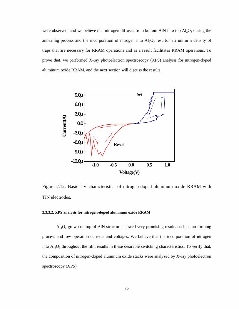
25
were observed, and we believe that nitrogen diffuses from bottom AlN into top Al2O3 during the
annealing process and the incorporation of nitrogen into Al2O3 results in a uniform density of
traps that are necessary for RRAM operations and as a result facilitates RRAM operations. To
prove that, we performed X-ray photoelectron spectroscopy (XPS) analysis for nitrogen-doped
aluminum oxide RRAM, and the next section will discuss the results.
-1.0 -0.5 0.0 0.5 1.0-12.0µ
-9.0µ
-6.0µ
-3.0µ
0.0
3.0µ
6.0µ
9.0µ
Curr
ent(A
)
Voltage(V)
Set
Reset
Figure 2.12: Basic I-V characteristics of nitrogen-doped aluminum oxide RRAM with
TiN electrodes.
2.3.3.2. XPS analysis for nitrogen-doped aluminum oxide RRAM
Al2O3 grown on top of AlN structure showed very promising results such as no forming
process and low operation currents and voltages. We believe that the incorporation of nitrogen
into Al2O3 throughout the film results in these desirable switching characteristics. To verify that,
the composition of nitrogen-doped aluminum oxide stacks were analyzed by X-ray photoelectron
spectroscopy (XPS).

26
0 2 4 6 8 10 12 14 16
0
20
40
60
Al2pN1s
O1s
Ato
mic
%
Distances into the sample (nm)
Ti2p N1s O1s Al2p
Ti2p
TiN TE Al2O3 AlN TiN BE
(a)
0 2 4 6 8 10 12 14 16
0
20
40
60
Ato
mic
%
Distances into the sample (nm)
Ti2p N1s O1s Al2p
Ti2p
O1s
N1sAl2p
TiN BEAl2O3 AlNTiN TE
(b)
Figure 2.13: Atomic profiles of (a) as-deposited stacks and (b) annealed stacks at 400 °C
for 30 minutes.

27
Figure 2.13 shows atomic profiles of aluminum in green, nitrogen in red, oxygen in blue,
and titanium in black for (a) as-deposited and (b) annealed stacks. The limited depth resolution of
XPS causes the gradual change of the composition, but this does not affect conclusions that will
be discussed. For as-deposited films, no nitrogen was detected in the bulk of the Al2O3 region. On
the other hand, at least 6 % nitrogen was incorporated in the same region for annealed films.
Oxygen concentration in the bulk of the AlN region also increased after annealing. This suggests
that nitrogen incorporated into Al2O3 comes from bottom AlN, not top TiN electrode and nitrogen
diffuses from bottom AlN into Al2O3 during the annealing process.
69 72 75 78 81 84
Energy (eV)
At 2nm depth
At 4nm depth
At 6nm depth
76eV(Al2O3)
74eV(AlN)
(a)

28
520 525 530 535 540 5450
1000
2000
3000
4000
5000
6000
Al-O
CPS
Energy (eV)
O1s
(b)
390 395 400 405 41050
100
150
200
250
300
350
400
CPS
Energy (eV)
N1s
Al-N
(c)
Figure 2.14: Bonding information;(a) Al2p, (b) O1s, and (c) N1s.

29
XPS can also provide bonding information. The Al2p, O1s, and N1s signals are plotted in
Figure 2.14. The Al2p signals at each depth, 2nm, 4nm, and 6nm below TiN top electrode are
plotted in Figure 2.14 (a). The signal at each depth can be expressed as the sum of two sub-peak
signals, one at 74 eV corresponding to Al-N bonding[26-29] and another one at 76 eV associated
with Al-O bonding[30,31]. In addition, the peak shifts from 76 eV (the top Al2O3) to 74 eV (the
bottom AlN)[32]. As shown in Figure 2.14 (b) and (c), the peak signal of O1s was detected at
532 eV which indicates oxygen is bonded to aluminum, and the peak signal of N1s was found at
398 eV which means nitrogen is bonded to aluminum, not oxygen.
Figure 2.15: The peak signals of N1s[33].
Figure 2.15 from reference [33] supports an observation. The N1s peak associated with
AlN is found at 398 eV, and the N1s peak related to composite AlON is detected at 402 eV.
These results confirm that after annealing, our resistive dielectric is a mixture of AlN and Al2O3,
not a composite AlON material[34].
30
Chapter 3: Optimization of Al2O3 / AlN with TiN electrode
In the previous chapter, we investigated several RRAM stacks and found that Al2O3 /
AlN structure with TiN electrode, where AlN layer is grown on TiN, is a prime candidate among
them. Based on the stack information, we optimized its switching characteristics by varying the
thickness of each layer and annealing time. In this experiment, 20 nm thick bottom TiN electrode,
4 nm thick AlN diffusion layer, 5 nm thick Al2O3 resistive dielectric, and 20 nm thick top TiN
electrode were deposited. The bottom electrode is composed of 5nm ALD TiN on top of 15 nm
PVD TiN, whereas the top electrode is 15nm PVD TiN on top of 5nm ALD TiN. The ALD layers,
TiN bottom electrode, AlN, Al2O3, and TiN top electrode are deposited in-situ to prevent any
oxidation or contamination along the interfaces. In this chapter, optimization results—what
thicknesses of aluminum oxide and aluminum nitride layer result in best performance, and how
long RRAM cells need to be annealed—will be discussed.
3.1. Switching characteristics in terms of AlN thickness
In this section, we will discuss switching characteristics in terms of AlN thickness. To
find how the thickness of AlN layer affects switching characteristics, we varied the thickness of
AlN layer from 0 nm to 4 nm at a given Al2O3 thickness (5 nm). TMA precursor and nitrogen
decomposed by plasma were used for AlN layer deposition, and TMA precursor and H2O were
used for aluminum oxide deposition. It was followed by annealing at 400 °C for 15 minutes.
Conservative RRAM cell size of 50 um X 50 um was chosen. Table 3.1 summarizes switching

31
characteristics versus AlN thickness. The negative Vreset and Ireset indicate that the memory cells
were programmed by bipolar switching mode.
0 nm(Al2O3) 1 nm 2 nm 3 nm 4 nm
Ron Breakdown Breakdown 30 k~100 kΩ 20 k~100 kΩ 20 k~90 kΩ
Roff 1.1 M ~ 2.1 MΩ
1.1 M ~ 2.1 MΩ
0.8 M ~ 1 MΩ
0.8 M ~ 1 MΩ
0.7 M ~ 1 MΩ
Vset ~ 3.5 V 2.5 ~ 3.2 V 0.8 ~ 1.2 V 0.8 ~ 1.2 V 0.8 ~ 1.2 V
Vreset N/A N/A -(1.2 ~ 1.6) V -(1.2 ~ 1.6) V -(1.2 ~ 1.6) V
Iset ~ uA ~ uA uA ~ 10 uA uA ~ 10 uA uA ~ 10 uA
Ireset N/A N/A -(10 u ~ 90 u) A
-(10 u ~ 100 u) A
-(10 u ~ 100 u) A
Table 3.1: Summary of switching parameters versus AlN thickness.
For a 0 nm AlN or pure aluminum oxide sample, no resistive switching behaviors were
shown. At about 3.5 V, the RRAM cell changed its state from the high resistance state to the low
resistance state with an applied current as low as a few uA. However, it cannot be reset and no
subsequent switching behaviors were observed. As the thickness of AlN layer increases, RRAM
cells start showing resistance switching behaviors. In addition, the number of switchable memory
cells increases with AlN thickness and RRAM cells can be programmed at lower voltages. In the
case of thinner AlN layer samples, not enough traps required for initiating resistive switching

32
behaviors exist in Al2O3 layer, which explains why thinner AlN layer structures require a high
forming voltage. In the case of thicker AlN layer structures, there is enough diffusion of nitrogen
from AlN into Al2O3 to create a moderate amount of traps during the annealing process. Hence,
the RRAM cells can be programmed at a lower voltage. This suggests that a sufficiently thick
AlN layer is required for facilitating RRAM operations. It is determined experimentally that 4 nm
thick AlN layer samples resulted in best performance.
3.2. Switching characteristics in terms of Al2O3 thickness
In the previous section, we found that the optimum AlN thickness was 4 nm. Next, we
investigated switching characteristics in terms of Al2O3 thickness to optimize characteristics. For
this, we varied the thickness of aluminum oxide resistive layer from 4 nm to 7 nm to see how
Al2O3 thickness affects switching characteristics. Same precursors for AlN and Al2O3 layer
deposition were used and these layers were deposited in-situ in an atomic layer deposition system.
Final annealing at 400 °C for 15 minutes was performed such that nitrogen diffuses from AlN
into Al2O3.
The experimental results are summarized in Table 3.2. On–resistance and off-resistance
were determined at 0.3 V. The negative Vreset and Ireset indicate that the memory cells were
programmed by bipolar switching mode. As Al2O3 thickness increases, the number of switchable
memory cells decreases and at the same time a forming process is required. For 7 nm Al2O3
structures, resistive switching behaviors were observed for only a few memory cells and for those
cells a forming process was required. This indicates that diffusion of nitrogen from bottom AlN
layer into thick Al2O3 were not enough to create the amount of traps that are necessary for RRAM
operations. The remaining region in Al2O3 layer where nitrogen does not penetrate is not an
effective resistive dielectric. This also explains why a forming process is required for thick Al2O3
structures. In this experiment, we found that the optimum combination of layers is 5 nm thick
Al2O3 and 4 nm thick AlN layer.

33
4 nm 5 nm 6 nm 7 nm
Ron 20 k ~ 90 kΩ 30 k ~ 100 kΩ 10 k ~ 150 kΩ 15k ~ 110 kΩ
Roff 0.5 M ~ 0.9 MΩ 0.8 M ~ 1.1 MΩ 0.8M ~ 1 MΩ 0.8 M ~ 1 MΩ
Vset 0.7 ~ 1.1 V 0.8 ~ 1.2 V 1.2 ~ 1.5 V 1.3 ~ 1.5 V
Vreset -(1 ~ 1.5) V -(1.2 ~ 1.6) V -(1.4 ~ 1.7) V -(1.4 ~ 2.1) V
Iset uA ~ 10 uA uA ~ 10 uA uA ~ 10 uA uA ~ 10 uA
Ireset -(20 u ~ 70 u)A -(30 u ~ 100 u)A -(40 u ~ 140 u)A -(45u ~ 160 u)A
Forming Not required Not required Only a few samples
Required
Table 3.2: Summary of switching characteristics versus Al2O3 thickness.
3.3. Switching characteristics dependency on annealing time
In previous sections, we optimized switching characteristics of Al2O3 / AlN RRAM cells
by controlling thickness of AlN or Al2O3 layer and found that 5 nm thick Al2O3 and 4 nm thick
AlN results in best performance. Next, we will discuss the dependency of switching
characteristics on annealing time. The purposes of this experiment are to investigate the optimum
extent of nitrogen diffusion and to check if Al2O3 /AlN RRAM stacks are compatible with the
standard CMOS process. In the standard CMOS process, final annealing in forming gas at 400 °C
for 30 minutes is typically performed. The effects of annealing time on switching characteristics

34
are summarized in Table 3.3. On-resistance and off-resistance were determined at 0.3 V and
bipolar switching mode was applied. As deposited samples, an RRAM cell changed its state from
the high resistance state to the low resistance state, but no subsequent switching behaviors were
observed. Their switching characteristics are similar to those of pure Al2O3 RRAM stacks. As
annealing time increases, the number of switchable memory cells increases without a forming
process. This is because more nitrogen diffuses from AlN into Al2O3 as annealing time increases
and as a result more traps in Al2O3 that are necessary for RRAM operations are created. No
significant dependency on annealing time over 15 minutes was observed, and this indicates that
Al2O3 / AlN RRAM stacks are compatible with the standard CMOS process.
As deposited
5min @400C
10min @400C
15min @400C
30min @400C
Ron Breakdown 30 k ~ 100 kΩ
20 k ~ 100 kΩ
20 k ~ 90 kΩ
10 k ~ 80 kΩ
Roff 1.1 M ~ 2.1 MΩ
0.8M ~ 1 MΩ
0.8 M ~ 1 MΩ
0.7 M ~ 1 MΩ
0.5 M~ 0.9 MΩ
Vset 2.5 ~ 3.2 V 0.8 ~ 1.2 V 0.8 ~ 1.2 V 0.8 ~ 1.2 V 0.6 ~ 1 V
Vreset N/A -(1.2 ~ 1.6) V -(1.2 ~ 1.6) V -(1.2 ~ 1.6) V -(1 ~ 1.5) V
Iset ~uA uA ~ 10 uA uA ~ 10 uA uA ~ 10 uA uA ~ 10 uA
Ireset N/A -(10 u ~ 90 u)A
-(10 u ~ 100 u)A
-(10 u ~ 100 u)A
-(30 u ~ 150 u)A
Table 3.3: Dependency on annealing time of switching characteristics.

35
Chapter 4: Fabrication of N-doped AlOX RRAM grown by ALD 1T1R system
In previous chapters, we showed that Al2O3 / AlN stacks where Al2O3 layer grown on
AlN is appropriate for RRAM stacks and optimized the switching characteristics by varying the
thickness of each layer and controlling the annealing time. Based on the stack information and
optimization results obtained, we monolithically integrated such RRAM on top of CMOS wafers
to achieve accurate control of the voltage and current waveforms for programming. This chapter
will describe how we integrate nitrogen-doped aluminum oxide grown by an atomic layer
deposition technique on top of selection transistors and control selection transistors during setting
or resetting memory cells.
4.1. Introduction of selection transistors
In this section, description of selection transistors and switching characteristics will be
introduced. First, NMOS selection transistors have four different sizes of channel width or length
as shown in Table 4.1. Figure 4.1 illustrates ID-VD and ID-VG characteristics of a selection
transistor. The minimum driving current level exceeds micro-Ampere when transistors are fully
turned on. Because our nitrogen-doped aluminum oxide RRAM cells can be programmed with an
applied current below micro-Ampere (which will be discussed in the next chapter), selection
transistors need to operate in the sub-threshold region to accurately control the programming
current.

36
0.0 0.5 1.0 1.5 2.0 2.5 3.00.0
0.5
1.0
1.5
2.0
2.5
3.0
I D(mA)
VD(V)
VG=0V VG=1V VG=2V VG=3V
(a)
VD=0.2V VD=0.4V VD=0.6V
10-5
10-10
321
I D(A)
VG(V)0
(b)
Figure 4.1: (a) ID-VD and (b) ID-VG characteristics of a 10 um / 1 um NMOS transistor.
M1 M2 M3 M4
W/L 10 um / 1 um 20 um / 2 um 100 um / 5 um 100 um / 1 um
Table 4.1: Description of NMOS transistors with different sizes.W and L indicate channel
width and length of selection transistors, respectively.

37
4.2. Integration of N-doped AlOx RRAM with CMOS
Figure 4.2 illustrates the process flow for integration of N-AlOx RRAM on top of
selection transistors. Figure 4.2 (a) starts with CMOS transistors already integrated in the
substrate (not shown), connected with the Al layer shown. The Al layer is connected to the drain
contact of a selection transistor, but the connections to source and gate contacts are not shown in
Figure 4.2. We started with silicon oxide layer where LTO densification was performed at 400 °C
as shown in Figure 4.2 (a). On top of LTO layer, we deposited RRAM stacks consisting of 20 nm
thick bottom TiN electrode, 4 nm thick AlN, 5 nm thick Al2O3, and 20 nm thick top TiN electrode
as shown in Figure 4.2 (b). The bottom electrode is composed of 5nm ALD TiN on top of 15 nm
PVD TiN, whereas the top electrode is 15nm PVD TiN on top of 5nm ALD TiN. The ALD layers,
TiN bottom electrode, AlN, Al2O3, and TiN top electrode are deposited in-situ to prevent any
oxidation or contamination along the interfaces.
(a)
(b)
(c)

38
(d)
(e)
(f)
(g)
(h)
39
(i)
(j)
Figure 4.2: Illustration of the process flow for integration of N-AlOx on top of selection
transistors.
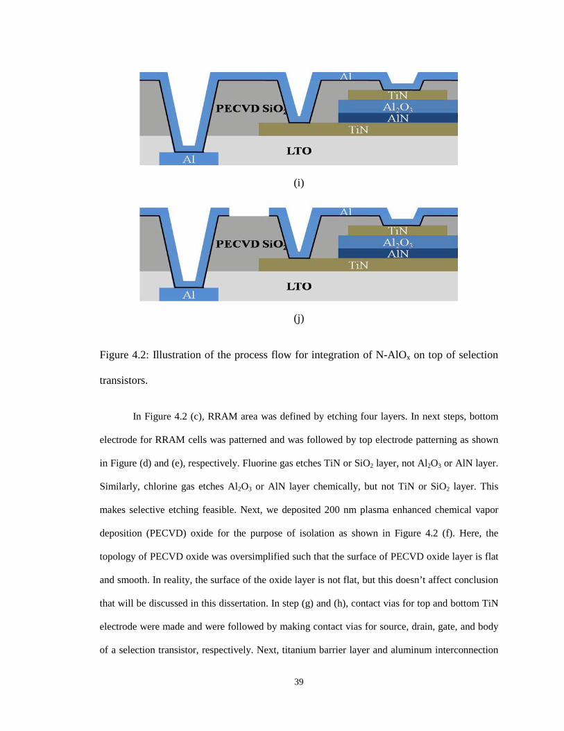
In Figure 4.2 (c), RRAM area was defined by etching four layers. In next steps, bottom
electrode for RRAM cells was patterned and was followed by top electrode patterning as shown
in Figure (d) and (e), respectively. Fluorine gas etches TiN or SiO2 layer, not Al2O3 or AlN layer.
Similarly, chlorine gas etches Al2O3 or AlN layer chemically, but not TiN or SiO2 layer. This
makes selective etching feasible. Next, we deposited 200 nm plasma enhanced chemical vapor
deposition (PECVD) oxide for the purpose of isolation as shown in Figure 4.2 (f). Here, the
topology of PECVD oxide was oversimplified such that the surface of PECVD oxide layer is flat
and smooth. In reality, the surface of the oxide layer is not flat, but this doesn’t affect conclusion
that will be discussed in this dissertation. In step (g) and (h), contact vias for top and bottom TiN
electrode were made and were followed by making contact vias for source, drain, gate, and body
of a selection transistor, respectively. Next, titanium barrier layer and aluminum interconnection

40
layer were deposited and were patterned as shown in Figure 4.2 (i) and (j), respectively. For the
last step, final annealing at 400 °C for 15 minutes were performed. Figure 4.3 (a) shows a SEM
cross-sectional view of RRAM stacks. Figure 4.3 (b) illustrates top view of fabricated 1T1R
structure and how TiN bottom electrode is connected to the drain region of a NMOS selection
transistor. Figure 4.3 (c) shows a cross section schematic of 1T1R structure.
(a) (b)
(c)
Figure 4.3: (a) Cross-sectional view of RRAM stacks, (b) top view of 1T1R structure,
and (c) cross-sectional schematic of 1T1R structure.

41
Figure 4.4: Cross-sectional view of RRAM stacks that were deposited in a via region.
In this experiment, we also considered topography of RRAM stacks. The RRAM stacks
were not deposited in a via region directly. If RRAM stacks were deposited in the via region as
shown in Figure 4.4, films that were deposited on the sidewalls of the via tend to be thinned, and
therefore most current will flow across the thinned RRAM stacks on the sidewalls. This will
affect the reliability of RRAM stacks. For this reason, we prefer planar structure.
4.3. Description of 1Transistor 1RRAM structure
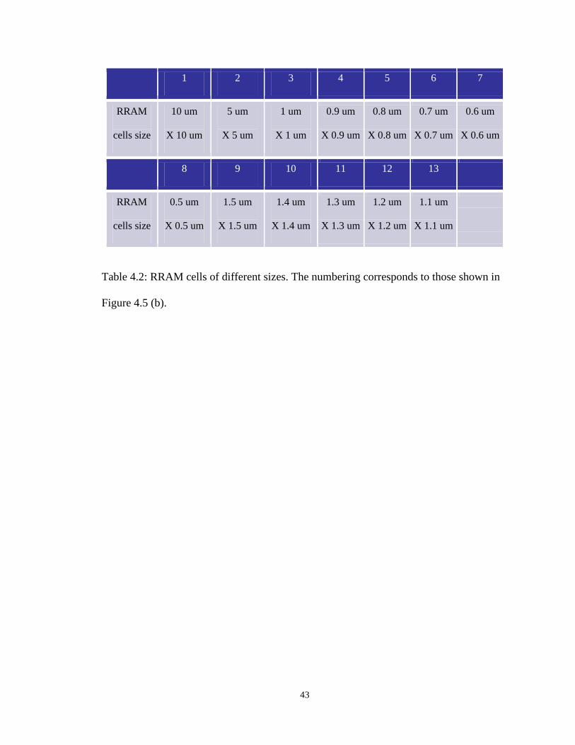
Figure 4.5 (a) shows a snap shot of the test chip. The 1T1R cell area is enlarged in Figure
4.5 (b). In Figure 4.5, m1 to m4 correspond to column of transistors with different width or length
as summarized in Table 4.1. In each column, 13 RRAM cells with different sizes are located and
these are summarized in Table 4.2. In these RRAM sets, we conservatively chose RRAM cell size
of 1um X 1um for detailed characterization.

42
(a)
(b)
Figure 4.5: (a) Test chip snapshot and (b) an enlarged view of 1T1R RRAM area.
43
1 2 3 4 5 6 7
RRAM
cells size
10 um
X 10 um
5 um
X 5 um
1 um
X 1 um
0.9 um
X 0.9 um
0.8 um
X 0.8 um
0.7 um
X 0.7 um
0.6 um
X 0.6 um
8 9 10 11 12 13
RRAM
cells size
0.5 um
X 0.5 um
1.5 um
X 1.5 um
1.4 um
X 1.4 um
1.3 um
X 1.3 um
1.2 um
X 1.2 um
1.1 um
X 1.1 um
Table 4.2: RRAM cells of different sizes. The numbering corresponds to those shown in
Figure 4.5 (b).
44
Chapter 5: Electrical switching characteristics of N-doped AlOX RRAM grown by ALD
In this chapter, switching characteristics of 1T1R N-AlOx RRAM cells will be discussed
in details. Before we discuss characteristics, measurement set-up for characterization of N-AlOx
will be introduced in the following section.
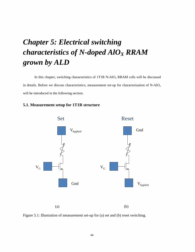
5.1. Measurement setup for 1T1R structure
Set Reset
Gnd
VApplied
VG
VApplied
Gnd
VG
(a) (b)
Figure 5.1: Illustration of measurement set-up for (a) set and (b) reset switching.

45
Figure 5.1 illustrates the configurations for measuring the 1T1R structure. As shown in
Figure 5.1, VG indicates a gate bias and RRAM cells are connected to the drain contact directly.
With this configuration, the parasitic capacitance is minimized, and instantaneous switching
prevents over-programming [35]. This explains why 1T1R structures show reliable and uniform
switching characteristics. When we set a memory cell, a small bias is applied to the gate so that
the selection transistor operates in the sub-threshold region and as a result controls current level
of nano-Ampere. This is because our N-AlOx RRAM cells can be programmed with an applied
current below micro-Ampere range.
5.2. I-V switching characteristics
-2 -1 0 1 2 3
-600.0p
-300.0p
0.0
300.0p
600.0p
Cur
rent
(A)
Voltage(V)
Set
Reset
Figure 5.2: I-V switching characteristics of ALD N-AlOx RRAM.
46
0.0 0.5 1.0 1.5 2.0 2.5 3.00.0
200.0p
400.0p
600.0p
800.0p
Set c
urre
nt(A
)
Voltage(V)
1st set cycle 2nd set cycle
Figure 5.3: Illustration of set switching behaviors showing no forming process.
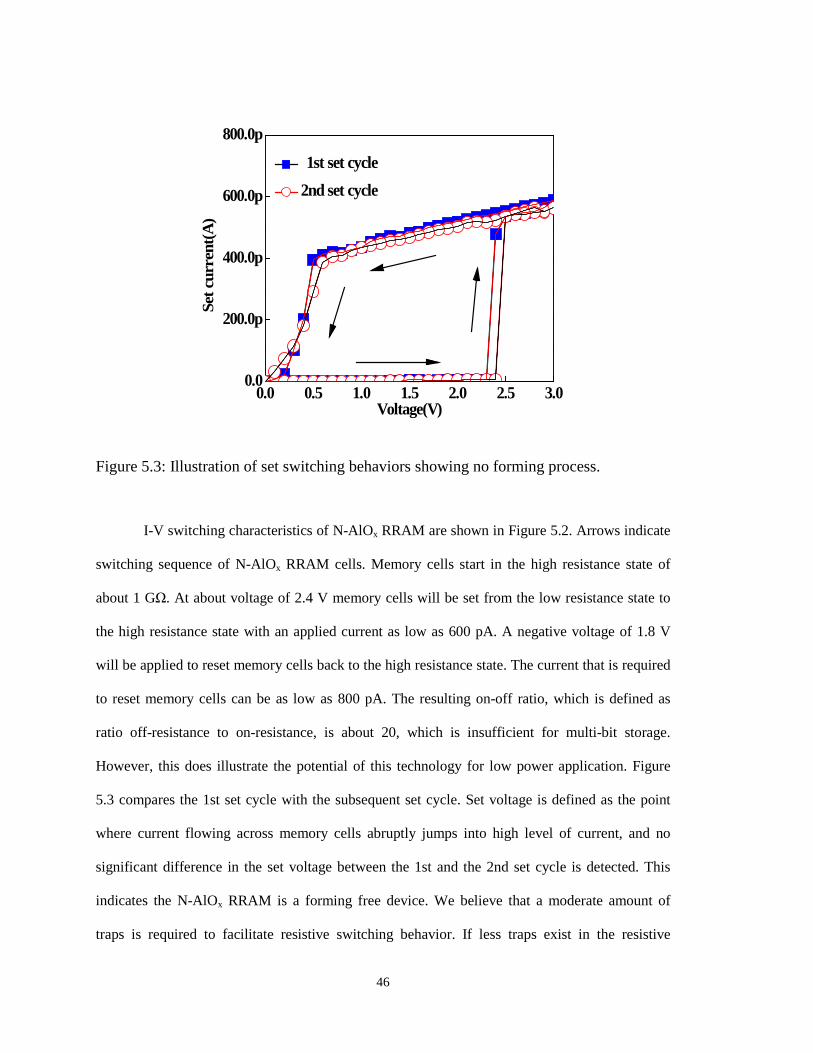
I-V switching characteristics of N-AlOx RRAM are shown in Figure 5.2. Arrows indicate
switching sequence of N-AlOx RRAM cells. Memory cells start in the high resistance state of
about 1 GΩ. At about voltage of 2.4 V memory cells will be set from the low resistance state to
the high resistance state with an applied current as low as 600 pA. A negative voltage of 1.8 V
will be applied to reset memory cells back to the high resistance state. The current that is required
to reset memory cells can be as low as 800 pA. The resulting on-off ratio, which is defined as
ratio off-resistance to on-resistance, is about 20, which is insufficient for multi-bit storage.
However, this does illustrate the potential of this technology for low power application. Figure
5.3 compares the 1st set cycle with the subsequent set cycle. Set voltage is defined as the point
where current flowing across memory cells abruptly jumps into high level of current, and no
significant difference in the set voltage between the 1st and the 2nd set cycle is detected. This
indicates the N-AlOx RRAM is a forming free device. We believe that a moderate amount of
traps is required to facilitate resistive switching behavior. If less traps exist in the resistive

47
dielectric films, a high voltage is needed to be applied across the film to create traps that are
necessary for RRAM operations, which explains a forming process. On the other hand, many
traps in resistive dielectric films may result in forming free switching behavior but at the same
time make the films leaky which is not desirable for low power application. In addition, it is
difficult to precisely control the amount of traps caused by oxygen vacancies due to strong
preference of aluminum to bond with oxygen. However, we can obtain a moderate amount of
traps by incorporating nitrogen into aluminum oxide because chemical reaction of nitrogen to
aluminum is not as strong as that of oxygen to aluminum and the incorporation of nitrogen into
aluminum oxide is limited. We believe that the incorporation of nitrogen results in a uniform
density of traps that are necessary for RRAM operations and removes the forming process.
0.0 0.5 1.0 1.5 2.0 2.5 3.00.0
30.0n
60.0n
90.0n
120.0n
150.0n 15nA-VG=300mV
35nA-VG=310mV
80nA-VG=320mV
120nA-VG=330mV
Curr
ent(A
)
Voltage(V)
(a)

48
0.0 0.5 1.0 1.5 2.0 2.5 3.00.0
30.0n
60.0n
90.0n
120.0n
150.0n
Curr
ent(A
)
Voltage(V)
15nA-VG=300mV
35nA-VG=310mV
80nA-VG=320mV
120nA-VG=330mV
(b)
Figure 5.4: Set switching behavior as a function of the gate bias of selection transistors
for (a) ALD N-AlOx 1T1R structure and (b) PVD N-AlOx 1T1R structure, respectively.
Since we have a 1T1R configuration, we can control set current by adjusting the gate bias
of the selection transistor. Figure 5.4 shows set switching behavior of ALD and PVD N-AlOx
1T1R structure as a function of the gate bias of the selection transistor. The switching conditions
such as set compliance current and the gate bias are inserted. For both ALD and PVD 1T1R
structure, a few hundreds mV for the gate bias indicates the selection transistor operates in the
sub-threshold region, and drain current of the selection transistor increases with the gate bias.
Figure 5.4 also shows that the set voltage of ALD N-AlOx 1T1R is less sensitive to the gate bias.

49
5.3. Programming voltage distribution
-2.0 -1.8 -1.6 -1.4 -1.2 -1.0
0
20
40
60
80
100
Cum
. Pro
babi
lity
Reset Voltage(V)
PVD ALD
(a)
1.0 1.5 2.0 2.5 3.0 3.5 4.0
0
20
40
60
80
100
PVD ALD
Cum
. pro
babi
lity
Set voltage(V)
(b)
Figure 5.5: Distributions of (a) set and (b) reset voltages of N-AlOx. The set and reset current are limited to 300 nA and 1 uA, respectively.

50
Distributions of set and reset voltages for ALD and PVD N-AlOx 1T1R structure are
plotted in Figure 5.5. This type of statistical study such as distributions of switching parameters
will be a useful guideline when array of RRAM cells are implemented in circuit systems. If these
parameters are distributed broadly, circuits must be designed to guarantee reliable operation,
usually with a sacrifice in circuit performance. Therefore, a tight distribution of switching
parameters is highly desirable. As shown in Figure 5.5, ALD N-AlOx RRAM cells show a tighter
distribution of set and reset voltages than that of PVD N-AlOx RRAM cells. We believe that the
tight distribution is due to the improved uniformity of films deposited by ALD.

51
5.4. Set/reset current versus on resistance
100k 1M 10M 100M 1G
10n
100n
1µ
Set C
urre
nt(A
)
On-Resistance(Ω)
PVD ALD
(a)
100k 1M 10M 100M 1G
10n
100n
1µ
10µ
Res
et C
urre
nt(A
)
On-Resistance(Ω)
PVDALD
(b)
Figure 5.6: (a) Set current versus on-resistance and (b) reset current versus on-resistance.
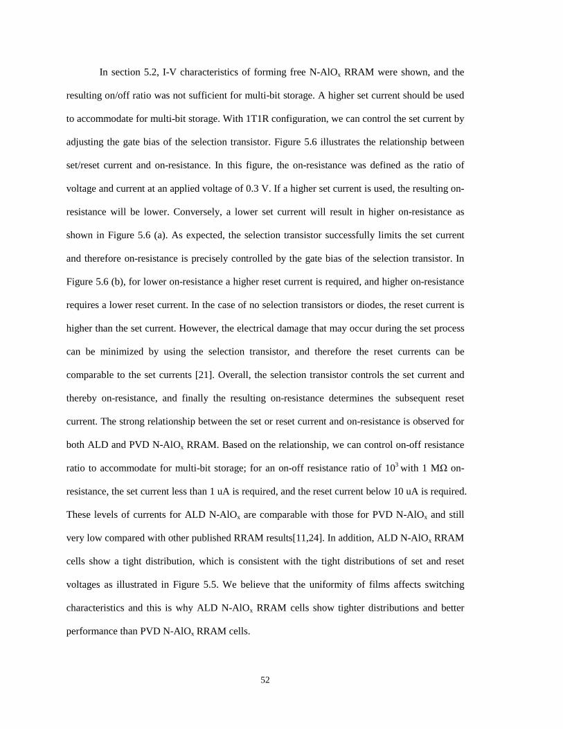
52
In section 5.2, I-V characteristics of forming free N-AlOx RRAM were shown, and the
resulting on/off ratio was not sufficient for multi-bit storage. A higher set current should be used
to accommodate for multi-bit storage. With 1T1R configuration, we can control the set current by
adjusting the gate bias of the selection transistor. Figure 5.6 illustrates the relationship between
set/reset current and on-resistance. In this figure, the on-resistance was defined as the ratio of
voltage and current at an applied voltage of 0.3 V. If a higher set current is used, the resulting on-
resistance will be lower. Conversely, a lower set current will result in higher on-resistance as
shown in Figure 5.6 (a). As expected, the selection transistor successfully limits the set current
and therefore on-resistance is precisely controlled by the gate bias of the selection transistor. In
Figure 5.6 (b), for lower on-resistance a higher reset current is required, and higher on-resistance
requires a lower reset current. In the case of no selection transistors or diodes, the reset current is
higher than the set current. However, the electrical damage that may occur during the set process
can be minimized by using the selection transistor, and therefore the reset currents can be
comparable to the set currents [21]. Overall, the selection transistor controls the set current and
thereby on-resistance, and finally the resulting on-resistance determines the subsequent reset
current. The strong relationship between the set or reset current and on-resistance is observed for
both ALD and PVD N-AlOx RRAM. Based on the relationship, we can control on-off resistance
ratio to accommodate for multi-bit storage; for an on-off resistance ratio of 103 with 1 MΩ on-
resistance, the set current less than 1 uA is required, and the reset current below 10 uA is required.
These levels of currents for ALD N-AlOx are comparable with those for PVD N-AlOx and still
very low compared with other published RRAM results[11,24]. In addition, ALD N-AlOx RRAM
cells show a tight distribution, which is consistent with the tight distributions of set and reset
voltages as illustrated in Figure 5.5. We believe that the uniformity of films affects switching
characteristics and this is why ALD N-AlOx RRAM cells show tighter distributions and better
performance than PVD N-AlOx RRAM cells.

53
5.5. Linear and non-linear I-V characteristics of HRS and various LRS
0.0 0.2 0.4 0.6 0.8 1.0
-25
-20
-15
-10 LRS(1.2kΩ) LRS(1.2MΩ) LRS(29.2MΩ) HRS(0.91GΩ)
ln(I)
Voltage(√V)
Figure 5.7: Plot of natural log of current versus square root of voltage for HRS and
various LRS.
As illustrated in Section 5.2, RRAM cells can be set to various low resistance states by
controlling the gate bias of the selection transistor. Natural log of current versus square root of
voltage for various low resistance states and the high resistance state are plotted in Figure 5.7.
The on-resistance was determined by the ratio of the applied voltage of 0.3 V to an applied
current. The low voltage applied across RRAM cells during resistance measurement prevents any
programming. For on-resistance of below 100 kΩ, the RRAM shows Ohmic linear conduction
behavior. When the RRAM is set to above 100 kΩ, the on-state conduction is no longer linear,
but exhibits rectifying behavior instead. In addition, the off-conduction is not Ohmic. This non-
linear conduction behavior can be shown in natural log of current versus square root of voltage
plot. This relationship implies that the carrier flow in the resistive dielectric films is limited by a

54
potential barrier. There are two well-known conduction models, Frankel-Poole emission model
and Schottky emission model, that describe this type of behavior.
We believe that Frenkel-Poole conduction behavior is associated with the AlN traps and
oxygen-vacancy traps in the AlOx where these traps are involved in the conduction. Larger set
currents would increase the density of traps, and as a result the increased traps lead to the
lowering of the potential barrier[36]. This explains that the on-resistance decreases when the set
current is increased. If the set current is further increased, the density of traps can reach the point
where the current conduction behavior becomes Ohmic.
20 40 60 80 1001k
10k
100k
1M
10M
100M
1G
HRS (290MΩ) LRS (1.6M) LRS (510kΩ) LRS (1.5kΩ)
Resis
tanc
e(Ω)
Temperature(°C)
Figure 5.8: Dependency on temperature of HRS and various LRS.
To understand switching characteristics, we also studied temperature dependence of the
non-Ohmic conduction behavior. The RRAM cells were programmed in the high resistance state
and various low resistance states at room temperature. They were heated from 30 °C to 90 °C
where their resistances were measured at each temperature. Figure 5.8 shows the dependency of
those resistance states on temperature. For LRS below 100 kΩ, the resistance increases with
HRS(290MΩ) LRS(1.6MΩ) LRS(510kΩ) LRS(1.5kΩ)

55
temperature. This implies that the conduction is Ohmic conduction, which is consistent with the
result discussed in the previous section. On the other hand, for HRS and LRS above 100 kΩ, the
resistance decreases with temperature. This is consistent with non-linear conduction behavior. As
temperature increases, carriers in resistive dielectric films gain energy, and therefore more
carriers can surmount the potential barrier and contribute to the conduction. This is typical of
Frenkel-Poole conduction behavior at high temperature.

56
5.6. Conduction mechanism in ALD N-AlOx RRAM In the previous section, two different conduction behaviors, metallic and rectifying
conduction, of ALD N-AlOx RRAM were observed. In this section, we will focus on the non-
linear rectifying conduction behavior. To understand non-linear conduction behavior, we applied
two common models, Frenkel-Poole emission model as described by equation 5.1, and Schottky
emission model as described by equation 5.2, to our experimental data [37]. An almost linear
dependency between the natural log of current and the square root of voltage exists in both
models.
𝐽 ∝ 𝐴𝑇2exp (−𝑞(𝜙𝐵− 𝑞𝐸/(4πε𝑟ε0)𝑘𝐵𝑇
) (5.1)
𝐽 ∝ 𝐸exp (−𝑞(𝜙𝑇− 𝑞𝐸/(πε𝑟ε0)𝑘𝐵𝑇
) (5.2)
In the equations, A is the effective Richardson constant, T is the absolute temperature, kB
is the Boltzmann constant, ɛ0 is the permittivity of free space, ɛr is relative permittivity of the
resistive dielectric films. E is the intensity of electric field and is given by the ratio of the applied
voltage to the dielectric thickness. ϕB and ϕT are the energy barrier height in the respective model.
In this experiment, we measured I-V characteristics of various resistance states. Under
different temperature from 40 °C to 55 °C, each I-V curve is fitted to a linear dependence
between the natural log of current and the square root of voltage as shown in Figure 5.9 [21].
These results show that current increases as temperature is increased and there is a linear
dependence between the natural log of current and the square root of voltage at each temperature.
The current conduction mechanism is the same at these ranges.

57
0.0 0.2 0.4 0.6 0.8 1.0-32
-31
-30
-29
-28
-27
-26
-25
-24
ln(I)
Voltage1/2(√V)
55°C
40°C
Increase by 5°C
(a)
0.0 0.2 0.4 0.6 0.8 1.0-24
-23
-22
-21
-20
-19
-18
-17
-16
ln(I)
Voltage1/2(√V)
55°C
40°CIncrease by 5°C
(b)
Figure 5.9: I-V relationship of (a) HRS and (b) LRS at various temperatures.
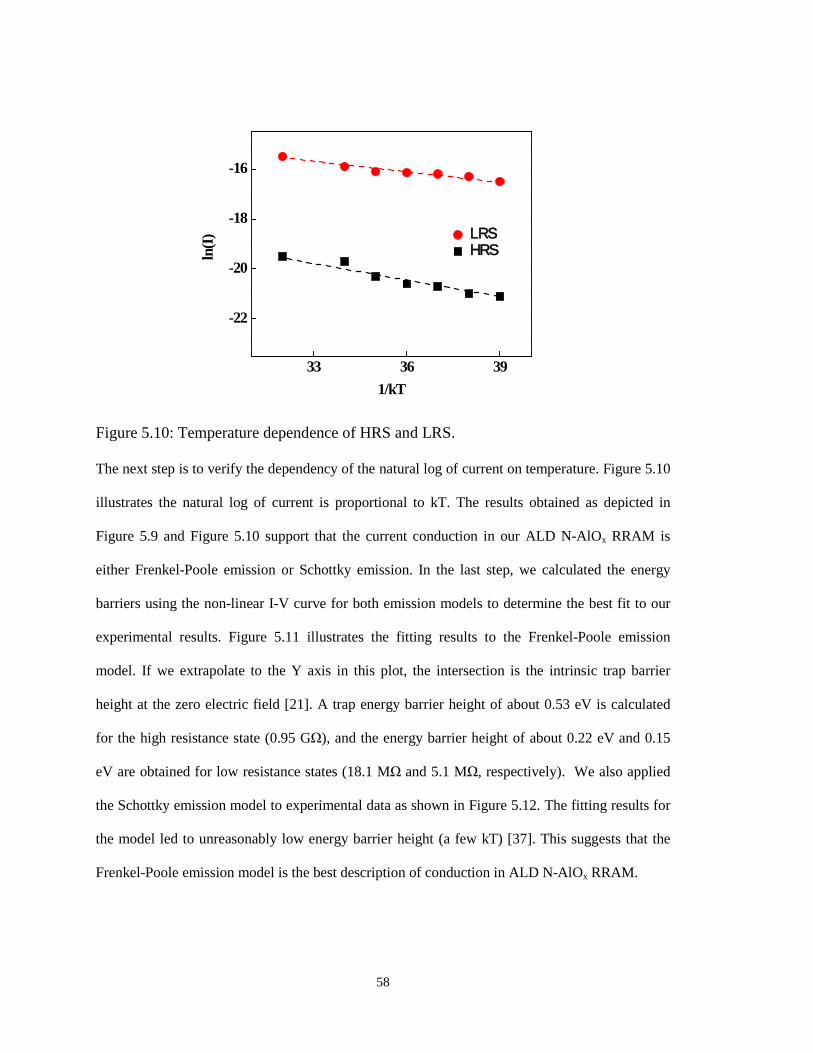
58
33 36 39
-22
-20
-18
-16
LRSHRSln
(I)
1/kT
Figure 5.10: Temperature dependence of HRS and LRS.
The next step is to verify the dependency of the natural log of current on temperature. Figure 5.10
illustrates the natural log of current is proportional to kT. The results obtained as depicted in
Figure 5.9 and Figure 5.10 support that the current conduction in our ALD N-AlOx RRAM is
either Frenkel-Poole emission or Schottky emission. In the last step, we calculated the energy
barriers using the non-linear I-V curve for both emission models to determine the best fit to our
experimental results. Figure 5.11 illustrates the fitting results to the Frenkel-Poole emission
model. If we extrapolate to the Y axis in this plot, the intersection is the intrinsic trap barrier
height at the zero electric field [21]. A trap energy barrier height of about 0.53 eV is calculated
for the high resistance state (0.95 GΩ), and the energy barrier height of about 0.22 eV and 0.15
eV are obtained for low resistance states (18.1 MΩ and 5.1 MΩ, respectively). We also applied
the Schottky emission model to experimental data as shown in Figure 5.12. The fitting results for
the model led to unreasonably low energy barrier height (a few kT) [37]. This suggests that the
Frenkel-Poole emission model is the best description of conduction in ALD N-AlOx RRAM.

59
0.0 0.1 0.2 0.3 0.4 0.5 0.60.0
0.2
0.4
0.6
Ener
y ba
rrie
r(eV
)
Voltage1/2(V1/2)
HRS(0.95GΩ) LRS(18.1MΩ) LRS(5.1MΩ)
0.525eV
0.219eV
0.145eV
Figure 5.11: Illustration of curve-fitting for the Frenkel-Poole emission model.
0.0 0.1 0.2 0.3 0.4 0.5 0.60.0
0.2
0.4
Ener
gy b
arrie
r (eV
)
Voltage1/2(V1/2)
HRS (0.95 GΩ) LRS (5.1 MΩ)
0.41eV
0.07eV
Figure 5.12: Illustration of curve-fitting for the Schottky emission model.

60
(a)
(b)
Figure 5.13: Energy band diagram of (a) after an annealing process and (b) after a set
process.
Figure 5.13 shows a speculative band model for ALD N-doped AlOx RRAM. As shown
in Figure 5.13 (a), the discrete energy level that is located 0.53 eV below conduction band is
created after the annealing process. This discrete energy level is caused by AlNx traps that are

61
generated from the diffusion of nitrogen into Al2O3. The energy level of 0.53 eV corresponds to
the calculated traps barrier for 1 GΩ HRS. This energy level is similar to the offset of conduction
bands in Al2O3 and AlN, which is 0.54 eV. In Figure 5.13 (b), a discrete energy level is created
after the set process. The traps energy level is caused by oxygen vacancies, not AlNx traps. For 1
MΩ LRS, the discrete energy level is located 0.2 eV below conduction band. The energy level of
0.2 eV corresponds to the extrapolated traps barrier height for 1MΩ LRS. Overall, HRS is
associated with AlNx traps, and LRS is related to oxygen vacancies [38].
TE
BE
AlOX
AlNX
Traps
On-state conduction path
Off-state conduction path
Figure 5.14: Macroscopic conduction model of ALD N-AlOx RRAM.
Figure 5.14 illustrates a macroscopic conduction model of ALD N-doped AlOx RRAM.
The thick black dotted line indicates on-state conduction path which consists of aligned oxygen
vacancies. Thin black dotted lines are associated with off-state conduction paths which consist of
AlNx traps. Normally, more AlNx traps exist in the bottom AlNx region. We believe that these off-
state conduction paths are distributed throughout the resistive dielectric films. This ensures
uniform switching characteristics. If we increase the gate bias during set, more oxygen vacancies
are generated to support the on-state conduction, and therefore the potential barrier between traps
caused by oxygen vacancies reduces. The increased trap density essentially reduces the distance
between traps, and more carriers can travel via traps. This is referred to the barrier lowering effect.
Finally, the on-state conduction reaches the point where the conduction behavior is no longer

62
rectifying conduction behavior if the set current is further increased. In this conduction regime,
carriers can tunnel from trap to trap through the resistive dielectric films, which exhibits metallic
conduction behavior.

63
5.7. Reliability characteristics of ALD N-AlOx RRAM.
5.7.1. Retention results at 120 °C
1 10 100 1k 10k 100k 1M 10M 100M10k
100k
1M
10M
100M
1G
Resis
tanc
e(Ω)
Time(sec)
HRS(950MΩ) LRS(27MΩ) LRS(0.95MΩ) LRS(110kΩ))
Figure 5.15: Retention results of the high resistance state and various resistance states at
120 °C.
It is very important to evaluate the stability of various resistance states for multi-bit
storage. NAND flash memory is typically required to retain data for 10 years. This is verified by
monitoring the various resistance states of RRAM cells especially at high temperature. The
results are projected to evaluate the retention for 10 years. In this experiment, RRAM cells were
programmed in various resistance states at room temperature, and then heated up to 120 °C where
their resistance states are monitored as a function of time under a constant DC voltage of 0.2 V.
The results are summarized in Figure 5.15. Strong stability for all resistance states without
noticeable degradation for 105 seconds was detected. In addition, as the results are extrapolated,
this experiment projects that multi-bit storage can be retained for 10 years.

64
5.7.2. Read disturb characteristics
0.0 50.0k 100.0k100k
1M
10M
100M
1G
10G
HRS(1GΩ) LRS(9MΩ) LRS(1MΩ)
Time(sec)
Res
istan
ce(Ω
)
Figure 5.16: Read disturb characteristics of various resistance states.
When an RRAM cell is read, the state being stored must not be disturbed. Read disturb
testing is designed to evaluate the robustness of data storage of the RRAM cell when the memory
cell is repeatedly read. This test is performed by applying the low read voltage to the RRAM cell
and monitoring the resistance during the read operation. A failure indicates that the initial state of
the RRAM cell was disturbed to the other state as a result of continuous reading operations, and
the read disturb error can be caused by a high number of read operations. In this experiment,
RRAM cells were programmed in various resistance states at room temperature, and we
monitored the resistance of various resistance states under a constant voltage of 0.5 V for 105
seconds as the RRAM cells were read. Figure 5.16 shows read disturb characteristics of ALD N-
AlOx RRAM. No significant degradation of the resistance states was observed up to 105 seconds,
which corresponds to 1012 read cycles assuming a conservative read time of 100 nano seconds
and indicates that the potential usage of this technology for multi-bit storage.

65
5.7.3. Endurance switching characteristics
0.0 20.0k 40.0k 60.0k 80.0k 100.0k10k
100k
1M
10M
100M
1G
10G
HRSLRS
Resis
tanc
e(Ω
)
Number of switching cycles
(a)
0.0 20.0k 40.0k 60.0k 80.0k 100.0k100k
1M
10M
100M
1G
10G
HRS LRS
Res
istan
ce(Ω
)
Number of switching cycles
(b)
Figure 5.17: Endurance characteristics of (a) without using smart programming and (b)
with using smart programming for N-AlOx.

66
Endurance is one of the important characteristics of non-volatile memory cells and is
verified by a method of how many switching cycles the RRAM cells can be repeatedly
programmed. This also evaluates how reusable the RRAM cells are. In this experiment, the
endurance characteristics of the RRAM cell as it was set and reset were measured. The pulse
width used for this endurance test was about 100 ns for the set and reset switching, and the
programming voltages for the set and reset switching were 5 V and -6 V, respectively. Resistance
of HRS and LRS was determined by the ratio of an applied voltage of 0.3 V to the measured
current. Figure 5.17 shows endurance results for both cases without using smart programming
and with using smart programming. In general, the measurement for endurance consists of 4
steps: In step 1, a pulse is applied to set the RRAM cells. In the next step, their resistances are
measured at a voltage of 0.3 V. In step 3, a reverse polarity of pulse is applied to reset the RRAM
cells, and their resistances are measured at a voltage of 0.3 V in the last step. This is a normal
endurance test procedure. However, applying the same pulse height to the RRAM cells may lead
to the variation of resistance states. In addition, we cannot rule out the possibility of overstressing
because there is no way to check whether the RRAM cells are overprogrammed or not. Therefore,
a strategy to minimize the variation of resistance states and avoid the overstress that may be
caused by applying the same pulse height every switching cycle is highly desirable. An
alternative is to use a smart programming scheme. In this scheme, the height of pulse that will be
applied in the next switching cycle is adjusted by their resistance states determined in the
previous switching cycle. For example, a pulse with low height is applied in the first cycle, and
the resistance state of the memory cell is measured. If the memory cell is successfully set to a low
resistance state, the pulse with the same height will be applied in the next cycle. If the memory
cell has not achieved the desired resistance state, a pulse with higher height will be applied. The
height of pulse will be increased until a set switching event occurs. A similar procedure is used to
reset the memory cell. By using this smart programming scheme, we can minimize the variation
of resistance states and the electrical stress caused by an applied pulse. Figure 5.17 illustrates how

67
smart programming improves pulse endurance characteristics. For both cases, no noticeable
narrowing of the on-off window was observed up to 105 switching cycles. However, the result
based on smart programming shows less variation of HRS and LRS.

68
Chapter 6: Incorporation of nitrogen into Al2O3 films
6.1. Role of nitrogen for resistive switching characteristics
As discussed in Chapter 2 and 5, the incorporation of nitrogen into Al2O3 results in a
uniform density of traps with the energy barrier height of about 0.53 eV throughout the film, and
these trap sites are beneficial to the operation of the RRAM cell. In order to understand the role of
nitrogen and the effect of nitrogen concentration on resistive switching characteristics, we
investigated N-AlOx RRAM with different nitrogen concentrations. In atomic layer deposition, it
is very hard to control the concentration of nitrogen because deposition is independent of
concentration of reactants [13]. Instead, we used a physical vapor deposition technique to control
the concentration of nitrogen. N-AlOx dielectrics with various concentrations were obtained by
controlling oxygen and nitrogen flow rates in the chamber of PVD system. Finally, we integrated
these PVD N-AlOx RRAM cells on top of selection transistors. Nitrogen concentration of each
sample was verified by XPS analysis. N-AlOx with various nitrogen concentrations were
summarized in Table 6.1.
Al2O3 N-AlOx N-AlOx N-AlOx AlN
N concentration 0 % 3 % 6 % 12 %
Table 6.1: N-AlOx with various nitrogen concentrations.

69
6.2. Electrical switching characteristics in terms of nitrogen concentration
6.2.1. Set / reset current versus on-resistance
100k 1M 10M 100M 1G10n
100n
1µ
Set C
urre
nt(A
)
On-Resistance(Ω)
Al2O3 3 % 6 %
0 %3 %
6 %
(a)
100k 1M 10M 100M 1G10n
100n
1µ
10µ
Res
et C
urre
nt(A
)
On-Resistance(Ω)
Al2O3 3 % 6 %
0 %3 %
6 %
(b)
Figure 6.1: (a) Set current versus on-resistance and (b) reset current versus on-resistance
for Al2O3, 3 % N-AlOx, and 6 % N-AlOx, respectively.
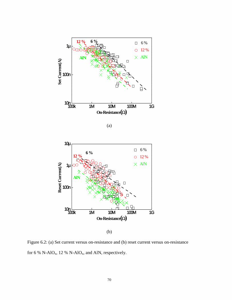
70
100k 1M 10M 100M 1G10n
100n
1µ
Set C
urre
nt(A
)
On-Resistance(Ω)
6 % 12 % AlN
6 %12 %
AlN
(a)
100k 1M 10M 100M 1G10n
100n
1µ
10µ
Res
et C
urre
nt(A
)
On-Resistance(Ω)
6 % 12 % AlN
6 %12 %
AlN
(b)
Figure 6.2: (a) Set current versus on-resistance and (b) reset current versus on-resistance
for 6 % N-AlOx, 12 % N-AlOx, and AlN, respectively.

71
We studied the relationship between set (reset) current and on-resistance for N-AlOx with
various nitrogen concentrations. The relationship for each case from Al2O3 to AlN is illustrated in
Figure 6.1. We observed the same trend as shown in Chapter 5 for all cases. If a higher set current
is used, the resulting on-resistance will be lower. For a lower on-resistance, a higher reset current
will be required. However, set and reset current decrease at a given on-resistance as more
nitrogen is incorporated into Al2O3. In Figure 6.1 and Figure 6.2, this trend was shown
consistently from Al2O3 to AlN and can be explained as following: as more nitrogen is
incorporated into the film, nitrogen traps density increases. Under this circumstance, less oxygen
vacancy traps are needed to form a current path or conduction filament during a set process,
which explains the reduction of set current. Similarly, in the reset process, less oxygen vacancy
traps are needed to be restored to break the conduction filament, the reset current is reduced.
6.2.2. Extrapolated energy barrier
We measured I-V switching characteristics at various temperatures. Based on I-V
characteristics, we calculated an energy barrier for each case from Al2O3 to AlN. We also
calculated the dielectric constant of each sample by measuring capacitance-voltage (C-V) curve,
which was used in equation 5.1. Figure 6.3 shows fitting results for the Frenkel-Poole emission
model for HRS, and the results are summarized in Table 6.2. For Al2O3, an energy barrier of 0.59
eV was calculated. For 3, 6, and 12 % N-AlOx, energy barriers of 0.57, 0.55, 0.53 eV were
calculated, respectively and 0.51 eV was obtained for AlN. As more nitrogen is incorporated into
the resistive film, the energy barrier reduces. The reduction is consistent with the decrease of a
high resistance state. More incorporation of nitrogen into the resistive film leads to an increase of
the density of traps and as a result decreases a high resistance state. For the energy barrier of a
low resistance state, five samples with different nitrogen concentrations were programmed to 1

72
MΩ low resistance state, and their switching characteristics were measured at various
temperatures. Based on I-V characteristics, energy barriers were extrapolated. The fitting results
for Frenkel-Poole emission are shown in Figure 6.4 and summarized in Table 6.3. An energy
level of about 0.2 eV for each case was extrapolated, which indicates that traps barrier height for
LRS is independent of nitrogen concentration. This is consistent with our model. We believe that
HRS is related to AlNx traps and LRS is associated with oxygen vacancies. If we incorporate
more nitrogen into resistive dielectric films, effective trap barrier height for HRS should reduce,
but the barrier height for LRS is independent of nitrogen concentration and remains unchanged.
Thus, the fitting results for LRS of each sample support our conduction model.
0.0 0.1 0.2 0.3 0.4 0.5 0.6 0.7 0.80.1
0.2
0.3
0.4
0.5
0.6
Al2O3 3 % 6 % 12 % AlN
Trap
bar
rier h
eight
(eV)
Voltage1/2(V1/2)
Nitrogen contentAl2O33 %6 %
12 %
AlN
Figure 6.3: Fitting results for the Frenkel-Poole emission model of HRS.
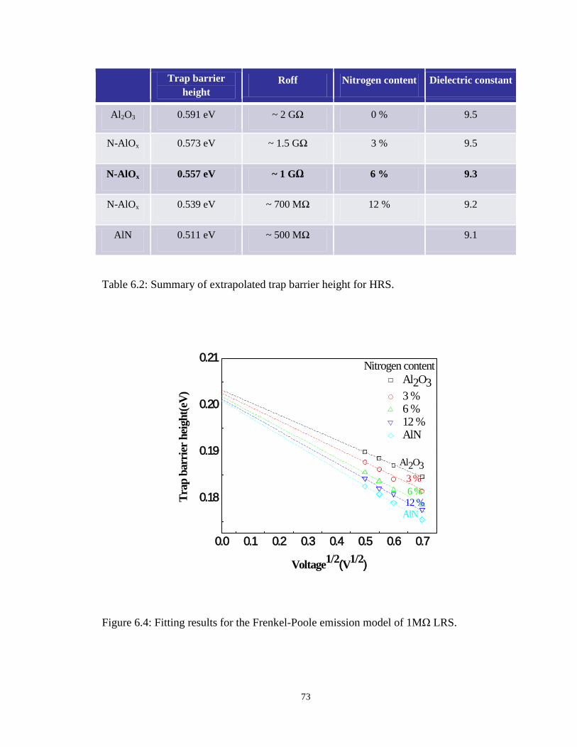
73
Trap barrier
height Roff Nitrogen content Dielectric constant
Al2O3 0.591 eV ~ 2 GΩ 0 % 9.5
N-AlOx 0.573 eV ~ 1.5 GΩ 3 % 9.5
N-AlOx 0.557 eV ~ 1 GΩ 6 % 9.3
N-AlOx 0.539 eV ~ 700 MΩ 12 % 9.2
AlN 0.511 eV ~ 500 MΩ
9.1
Table 6.2: Summary of extrapolated trap barrier height for HRS.
0.0 0.1 0.2 0.3 0.4 0.5 0.6 0.7
0.18
0.19
0.20
0.21
AlN12 %6 %3 %
Al2O3 3 % 6 % 12 % AlN
Trap
bar
rier h
eight
(eV)
Voltage1/2(V1/2)
Al2O3
Nitrogen content
Figure 6.4: Fitting results for the Frenkel-Poole emission model of 1MΩ LRS.

74
Trap barrier
height Ron Nitrogen content Dielectric constant
Al2O3 0.2034 eV 1 MΩ 0 % 9.3
N-AlOx 0.2031 eV 1 MΩ 3 % 9
N-AlOx 0.2023 eV 1 MΩ 6 % 8.6
N-AlOx 0.2014 eV 1 MΩ 12 % 8.4
AlN 0.2009 eV 1 MΩ
8
Table 6.3: Summary of extrapolated trap barrier height for each LRS.
6.2.3. Endurance characteristics
We investigated endurance characteristics for samples from Al2O3 to AlN to further
understand the role of nitrogen for resistive switching behavior. A smart programming scheme
was applied, and the endurance characteristics of the RRAM cells of each sample as the cells
were set and reset were monitored. The resistance of HRS and LRS was determined at 0.3 V. In
Figure 6.5 (a), Al2O3 RRAM showed large variation for HRS and LRS during 1000 switching
cycles, and the RRAM cell failed at the end of switching cycles. In Figure 6.5 (b), 3 % N-AlOx
RRAM showed better endurance characteristics and the RRAM cell remained functional at the
end of switching cycles. However, there was still large variation for HRS and LRS. In Figure 6.5
(c), 6 % N-AlOx yielded best performance with least variation for HRS and LRS. In Figure 6.5
(d), 12 % N-AlOx RRAM cell showed larger variation of HRS and LRS, and a smaller on-off

75
window when compared with 6 % N-AlOx. Finally, almost no on-off window was observed for
the AlN RRAM cell.
We believe that a moderate amount of nitrogen traps is required for RRAM operations.
For Al2O3 RRAM, the following situation appears. If insufficient nitrogen traps exist in the
resistive dielectric films, a forming process is required to initiate resistive switching behavior.
However, the forming process involves a high voltage and may damage the resistive films. The
current path created by the forming process may not be uniform. Therefore, switching
characteristics of those RRAM cells are not uniform with poor endurance. Conversely, if too
many nitrogen traps exist in the resistive dielectric films, the forming process is not required.
However, the high resistance state tends to be leaky which degrades the on-off window.
0.0 200.0 400.0 600.0 800.0 1.0k10k
100k
1M
10M
100M
1G
10G
HRSLRS
Resis
tanc
e(Ω
)
Number of switching cycles
(a) Al2O3
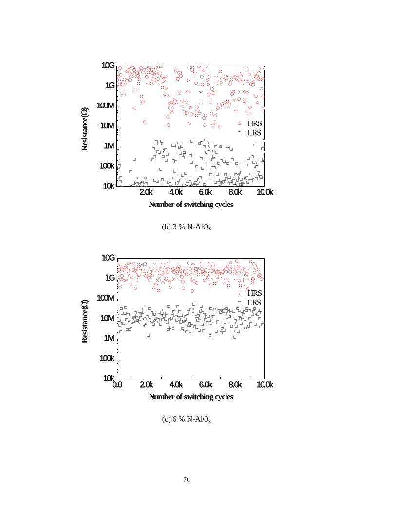
76
2.0k 4.0k 6.0k 8.0k 10.0k10k
100k
1M
10M
100M
1G
10G
HRSLRS
Resis
tanc
e(Ω
)
Number of switching cycles
(b) 3 % N-AlOx
0.0 2.0k 4.0k 6.0k 8.0k 10.0k10k
100k
1M
10M
100M
1G
10G
HRSLRS
Resis
tanc
e(Ω
)
Number of switching cycles
(c) 6 % N-AlOx

77
0.0 2.0k 4.0k 6.0k 8.0k 10.0k10k
100k
1M
10M
100M
1G
10G
HRSLRS
Resis
tanc
e(Ω
)
Number of switching cycles
(d) 12 % N-AlOx
0.0 200.0 400.0 600.0 800.0 1.0k10k
100k
1M
10M
100M
1G
10G
HRSLRS
Resis
tanc
e(Ω
)
Number of switching cycles
(e) AlN
Figure 6.5: Pulse endurance characteristics of (a) Al2O3, (b) 3 % N-AlOx, (c) 6 % N-AlOx,
(d) 12 % N-AlOx, and (e) AlN.

78
Summary
Al2O3 Endurance of about 1K cycles
3 % Variation of HRS and LRS
6 % Least variation of HRS and LRS
12 % Variation of HRS and LRS and small on-off window
AlN Almost no on/off window
Table 6.4: Summary of endurance characteristics.

79
Chapter 7: Conclusion
7.1. Summary
We have demonstrated a nitrogen-doped aluminum oxide based RRAM cell deposited by
an atomic layer deposition technique (ALD) and have monolithically integrated such a RRAM on
top of a selection transistor to accurately control programming current. ALD N-doped AlOx
RRAM cells have shown uniform switching characteristics without a forming process. Compared
with PVD N-AlOx RRAM cells, ALD N-AlOx RRAM cells have shown less variation of
switching parameters. This technology is compatible with the standard CMOS process and
feasible for 3D stacking. To analyze the composition of the resistive film as a result of
incorporation of nitrogen into AlOx, we have performed X-ray photoelectron spectroscopy. The
results of this study have confirmed that our ALD RRAM cell is a mixture of AlN and Al2O3.
We have also studied the conduction mechanism in ALD N-doped AlOx RRAM by
applying rectifying conduction model to experimental data measured at various temperatures.
Frenkel-Poole emission has given the best description of conduction in ALD N-doped AlOx
RRAM.
ALD 1T1R N-doped AlOx RRAM cell has demonstrated reproducible and reversible
switching, nondestructive readout, good cycling performance, and non-volatility. The RRAM cell
can be programmed with sub-nA and is capable of storing multiple bits for 1012 read cycles and
10 years.
We have also investigated the role of nitrogen for resistive switching behavior by
controlling nitrogen concentrations in N-AlOx RRAM with physical vapor deposition. The results
have confirmed that HRS is associated with AlN traps and LRS is related to oxygen vacancies.

80
The results of this dissertation demonstrate that ALD N-AlOx has great potential for a
resistance change material in next generation non-volatile memories. The accurate control of the
trap energy level through different set currents allows the optimization of this technology for
program efficiency, high endurance, and long retention.
7.2. Recommendation for future works
In this dissertation, we conservatively chose RRAM cell size of 1um X 1um for detailed
characterization. Scaling N-AlOx technology below 10 nm is needed for future works. The size of
RRAM cells can be reduced to below 10 nm by using electron beam lithography. Investigating
how scaling affects switching characteristics will help to understand the switching mechanism in
N-AlOx RRAM.
Next recommendation is to understand why AlN layer cannot be deposited on top of
Al2O3 layer in ALD systems and find a solution. If AlN layer can be deposited on top of Al2O3,
we can precisely control the incorporation of nitrogen in the resistive dielectric film: during an
annealing process, nitrogen from top AlN and bottom AlN can diffuse into the resistive dielectric
film. This will also allow us to investigate switching characteristics of ALD N-AlOx in terms of
nitrogen concentration.
Last recommendation is to apply the concept of nitrogen incorporation to other resistive
dielectric films such as HfO2 and TiO2 and look into ab-initio for doping effects. This experiment
and in-depth physics study will give a clue to a deeper understanding of the role of nitrogen for
resistive switching behavior and allow us to consider it from a different point of view.
81
Bibliography
[1] S. Hisashi and A. Hiroyuki, "Functional Stacks for Logic and Memory Devices", International Symposium on Advanced Gate Stack Technology Sep 29, Albany, NY.
[2] A. Beck, J. G. Bednorz, C. Gerber, C. Rossel, and D. Widmer, “Reproducible
switching effect in thin oxide films for memory applications,” Appl. Phys. Lett., vol. 77, pp. 139, 2000.
[3] A. Chen, S. Haddad, Y.-C. Wu, T.-N. Fang, Z. D. Lan, S. Avanzino, S.Pangrle, M.
Buynoski, M. Rathor, W. Cai, N. Tripsas, C. Bill, M.V. Buskirk, and M. Taguchi, "Non-volatile resistive switching for advanced memory applications," IEDM Technical Digest. IEEE, pp. 746-749, 2005.
[4] D. Lee, D. Seong, H. Choi, I. Jo, R. Dong ,W.Xiang, S. Oh, M., P. Seo, S. Heo, M.
Jo, D. Hwang, H. K Park, M. Chang, M. Hasan, and H. Hwang,"Excellent uniformity and reproducible resistance switching characteristics of doped binary metal oxides for non-volatile resistance memory applications," IEDM Tech. Dig., pp. 1-4, 2006.
[5] GH. Koh, Y.N. Hwang, S.H. Lee, S.Y. Lee, K.C. Ryoo, J.H. Park, Y. J . Song,S.J.
Ahn, C.W. Jeong, F. Yeung, Y.-T Kim, J.-B. Park, GT. Jeong, H.S.Jeong and Kinam Kim,"PRAM process technology," IEEE International Conference on Integrated Circuit Design and Technology, pp. 53-57, 2004.
[6] Tehrani S., "Status and outlook of MRAM memory technology," IEDM Tech. Dig,
pp. 1-4, 2006.
[7] J. Rodrıguez Contreras, H. Kohlstedt, U. Poppe, R. Waser, C. Buchal, and N.A. Pertsev, "Resistive switching in metal–ferroelectric–metal junctions," Appl. Phys. Lett., vol. 83, pp. 4595-4597, 2003.
[8] K Tsunoda, K Kinoshita, H Noshiro, Y Yamazaki, T Iizuka, Y. Ito, A.Takahashi,
A.Okano, Y. Sato, T. Fukano, M. Aoki, Y. Sugiyama, "Low Power and High Speed Switching of Ti-doped NiO ReRAM under the Unipolar Voltage Source of less than 3 V," IEEE International Electron Devices Meeting, pp. 767-770, 2007.
[9] S. Seo, M. J. Lee, D. H. Seo, E. J. Jeoung, D.-S. Suh, Y. S. Joung, I. K. Yoo, I. R.
Hwang, S. H. Kim, I. S. Byun, J.-S. Kim, J. S. Choi, and B. H. Park,"Reproducible resistance switching in polycrystalline NiO films," Appl. Phys.Lett., vol. 85, pp. 5655, 2004.

82
[10] B. J. Choi, D. S. Jeong, S. K. Kim, C. Rohde, S. Choi, J. H. Oh, H. J. Kim, C.S. Hwang, K. Szot, R. Waser, B. Reichenberg, and S. Tiedke, "Resistive switching mechanism of TiO2 thin films grown by atomic-layer deposition," J. Appl. Phys., vol. 98, 033715, 2005.
[11] Y. S. Chen, H. Y. Lee, P. S. Chen, P. Y. Gu, C. W. Chen, W. P. Lin, W. H. Liu, Y.
Y. Hsu, S. S. Sheu, P. C. Chiang, W. S. Chen, F. T. Chen, C. H. Lien,and M.-J. Tsai, "Highly Scalable Hafnium Oxide Memory with Improvements of Resistive Distribution and Read Disturb Immunity," IEDM Tech. Dig., pp. 105-108, 2009.
[12] K. M. Kim, B. J. Choi, B. W. Koo, S. Choi, D. S. Jeong, and C. S. Hwang,
"Resistive Switching in Pt/Al2O3/TiO2/Ru Stacked Structures," Electrochem. Solid-State Lett., vol. 9, pp. 343-346, 2006.
[13] S. M. George, "Atomic Layer Deposition", Chemical Review, vol. 110, pp. 111-
131, 2010.
[14] U. Russo, D. Jelmini, C. Cagli, A. L. Lacaita, S. Spigat, C. Wiemert, M. Peregot and M. Fanciullit, "Conductive-filament switching analysis and self accelerated thermal dissolution model for reset in NiO-based RRAM," IEDM Tech. Dig., pp. 775-778, 2007.
[15] D. Seong, J. Park, N. Lee, M. Hasan, S. Jung, H. Choi, J. Lee, M. Jo, W. Lee, S.
Park, S. Kim, Y. Jang, Y. Lee, M. Sung, D. Kil, Y. Hwang, S. Chung, S. Hong, J. Roh, and H. Hwang, "Effect of Oxygen Migration and Interface Engineering on Resistance Switching Behavior of Reactive Metal/Polycrystalline Pr0.7Ca0.3MnO3
Device for Nonvolatile Memory Applications," IEDM Tech. Dig., pp. 1-4, 2009.
[16] A. E. Rakhshani, Y. Makdisi, and X. Mathew, J., “The Poole–Frenkel conduction mechanism in Mo–Cu2O–Au thin film structures,” JOURNAL OF MATERIALS SCIENCE: MATERIALS IN ELECTRONICS, vol. 8, pp. 207, 1997.
[17] H. Shima, T. Nakano, and H. Akinaga, "Nanoscale chemical state analysis of
resistance random access memory device reacting with Ti", Appl. Phys.Lett. 96, 192107 (2010).
[18] H. B. Lv, M. Yin, Y. L. Song, X. F. Fu, L. Tang, P. Zhou, C. H. Zhao, T. A. Tang,
B. A. Chen, and Y. Y. Lin, "Forming Process Investigation of CuxO Memory Films," IEEE Electron Device Lett., vol. 29, pp. 47-49, 2008.
[19] N. Xu, L. Liu, X. Sun, X. Liu, D. Han, Y. Wang, R. Han, J. Kang, and B. Yu,
"Characteristics and Mechanism of Conduction/SET Process in the TiN/ZnO/Pt Resistance Switching Random Access Memories," Appl. Phys. Lett., vol. 92, 232112, 2008.
[20] Wei Wang, Ph.D dissertation, Stanford University, 2008.

83
[21] Wanki Kim, Ph.D dissertation, Stanford University, 2012
[22] J Provine and Michelle Rincon, "Atomic Layer Deposition: Introduction to the
Theory and Cambridge Nanotech Savannah and Fiji", Nov 2012.
[23] C. F. Powell, J.H Oxley, and J.M Blocher Jr, Vapor Deposition; Wiley, New York, 1967.
[24] Y. Chen, L.Goux, J.Swerts, M.Toeller, C.Adelmann, J.Kittl, C.Jurczak,
G.Groeseneken, and D.J.Wouters, "Hydrogen-Induced Resistive Switching in TiN/ALD HfO2/PECVD TiN RRAM Device", IEEE Electron Device Letters, Vol.33, No.4, April 2012. pp.483-485.
[25] M. A. Ryan, R. M.Willams, M. L.Homer, V. B.Shields, S. Wright,"Performance
parameters of TiN electrodes for AMTEC cells", AIP Conf.Proc. 458,1301-1305 (1999)
[26] W. M. Yim, E.J. Stofko, P. J. Zanzucchi, J. I. Pankove, M. Et tenberg, and S. L.
Gilbert Park, "Epitaxially grown AlN and its optical band gap," Appl. Phys. Lett. 44, pp. 292-296, 1973.
[27] P. Zhang, P. Huang, and Z. Jin, "Study of the Preferred Crystallographic
Orientation of Polycrystalline Aluminum on Silicon Dioxide and Silicon," Electron Devices and Semiconductor Technology (EDST), 2007.
[28] S. Simson, T. Reier, J.W. Schultze, Chr. Buchal, "Electrochemical and surface
analytical characterization of radiation effects after N2 implantation into Al and Al2O3,"Surface and Coatings Technology, vol. 83, pp. 49-54 ,1996.
[29] J. Baltrusaitis , P. M. Jayaweera, and V. H. Grassian, "XPS study of nitrogen
dioxide adsorption on metal oxide particle surfaces under different environmental conditions," Phys. Chem. Chem. Phys., vol. 11, pp. 8295-8305, 2009.
[30] T. Maruyama and S. Arai, "Aluminum Oxide Thin Films Prepared by Chemical
Vapor Deposition from Aluminum acetylacetonate," Appl. Phys. Lett., vol. 60, pp.322-323, 1992.
[31] S. K. Pranhan, P. J. Reucroft and Y. Ko, "Crystallinity of Al2O3 Films Deposited by Metalorganic Chemical Vapor Deposition," Surf. Caot. Technol., vol. 176, pp.382-384, 2004.

84
[32] C. Hwangbo, L. J. Ling, J.P. Lehan, H. A. Macleod, and F. Suits, "Reactive ion assisted deposition of aluminum oxynitride thin films," Applied Optics, vol. 28, Issue 14, pp. 2779-2784, 1989.
[33] T. Goto, T. Iwaki, Y. Ito, "Electrochemical formation of AlN in molten LiCl–
KCl–Li3N systems," Electrochimica Acta, vol. 50, pp. 1283-1288, 2005.
[34] R. H. French, "Electronic Structure of α-Al2O3, with Comparison to AlON and AlN," Journal of the American Ceramic Society, vol. 73, pp. 477-489, 1990.
[35] K. Kinoshita, et al., "Reduction in the reset current in a resistive random access memory consisting of NiOx brought about by reducing a parasitic capacitance," Appl. Phys. Lett., vol. 93, 033506, 2008.
[36] R. S.Muller and T. I.Kamins, Device Electronics for Integrated Circuits, 3rd
edition, John Wiley & Sons 2003.
[37] S. S. Sze, Physics of semiconductor devices, 2nd edition, John Wiley & Sons 1981.
[38] K. Matsunaga, T.Tanaka, and T.Yamamoto, “First-principles calculations of intrinsic defects in Al2O3,” Physical Review B 68, 085110 (2003).