for models pvi 50/60tl - solectria · pdf file32-bit integer value ... the modbus read...
TRANSCRIPT

Modbus Communications
For Models
PVI 50/60TL
Revision A
©2017, Yaskawa – Solectria Solar
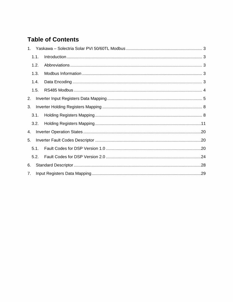
Table of Contents
1. Yaskawa – Solectria Solar PVI 50/60TL Modbus ................................................................ 3
1.1. Introduction .................................................................................................................. 3
1.2. Abbreviations ............................................................................................................... 3
1.3. Modbus Information ..................................................................................................... 3
1.4. Data Encoding ............................................................................................................. 3
1.5. RS485 Modbus ............................................................................................................ 4
2. Inverter Input Registers Data Mapping ................................................................................ 5
3. Inverter Holding Registers Mapping .................................................................................... 8
3.1. Holding Registers Mapping .......................................................................................... 8
3.2. Holding Registers Mapping .........................................................................................11
4. Inverter Operation States ...................................................................................................20
5. Inverter Fault Codes Descriptor .........................................................................................20
5.1. Fault Codes for DSP Version 1.0 ................................................................................20
5.2. Fault Codes for DSP Version 2.0 ................................................................................24
6. Standard Descriptor ...........................................................................................................28
7. Input Registers Data Mapping ............................................................................................29

Modbus Communications PVI 50/60TL (Rev A)
DOCR-070810-A Page 3 of 34
1. Yaskawa – Solectria Solar PVI 50/60TL Modbus
1.1. Introduction
This manual explains the Modbus protocol used for Yaskawa – Solectria Solar’s PVI 50/60TL
inverters. This does not include all the Modbus protocol details. It is expected that the person(s)
reading this manual have a clear understanding of Modbus protocol.
Each register/data point contains a raw 16-bit signed or unsigned number. The appropriate
multiplier must be applied to each word to obtain the scaled representation.
1.2. Abbreviations
IP Internet Protocol
MB Modbus
TCP Transport Control Protocol
uint16 16bit unsigned integer
uint32 32bit unsigned integer
uint64 64bit unsigned integer
int16 16bit signed integer
int32 32bit signed integer
1.3. Modbus Information
The Yaskawa – Solectria Solar PVI 50/60TL inverters Modbus register listing may contain some
registers that are not supported for all inverter models. The inverter will respond with the
following values if a feature is not supported for a specific inverter model.
Not Implemented for an int16 is 0x8000.
Not Implemented for an uint16 is 0xFFFF.
Not Implemented for an int32 is 0x80000000.
Not Implemented for an uint32 is 0xFFFFFFFF.
Not Implemented for a string is 0x00.
1.4. Data Encoding
The Modbus specification is not explicit on how to encode numbers other than 16-bit integers.
Differences do exist between one manufacturer’s implementation and another’s. 32 bit and 64 bit
data for PVI 50/60TL inverters is encoded as described below.

Modbus Communications PVI 50/60TL (Rev A)
DOCR-070810-A Page 4 of 34
32-bit integer Value
Values are stored in big-endian order per the Modbus specification and consist of two consecutive
16-bit registers.
Modbus
Register 1 2
byte 0 1 2 3
bits 31 - 24 23 - 16 15 - 8 7 - 0
64-bit integer Value
64-bit integers are stored using for registers in big-endian order and consists of 4 consecutive
16-bit registers.
Modbus
Register 1 2 3 4
byte 0 1 2 3 4 5 6 7
bits 63 - 56 55 - 48 47 - 40 39 - 32 31 - 24 23 - 16 15 - 8 7 - 0
1.5. RS485 Modbus
Modbus Mode: RTU
Data Bits: 8
Parity: None
Stop Bits: 1
Mode: Half-Duplex
Baud Rate: 9600 or 19200
Modbus Communications PVI 50/60TL (Rev A)
DOCR-070810-A Page 5 of 34
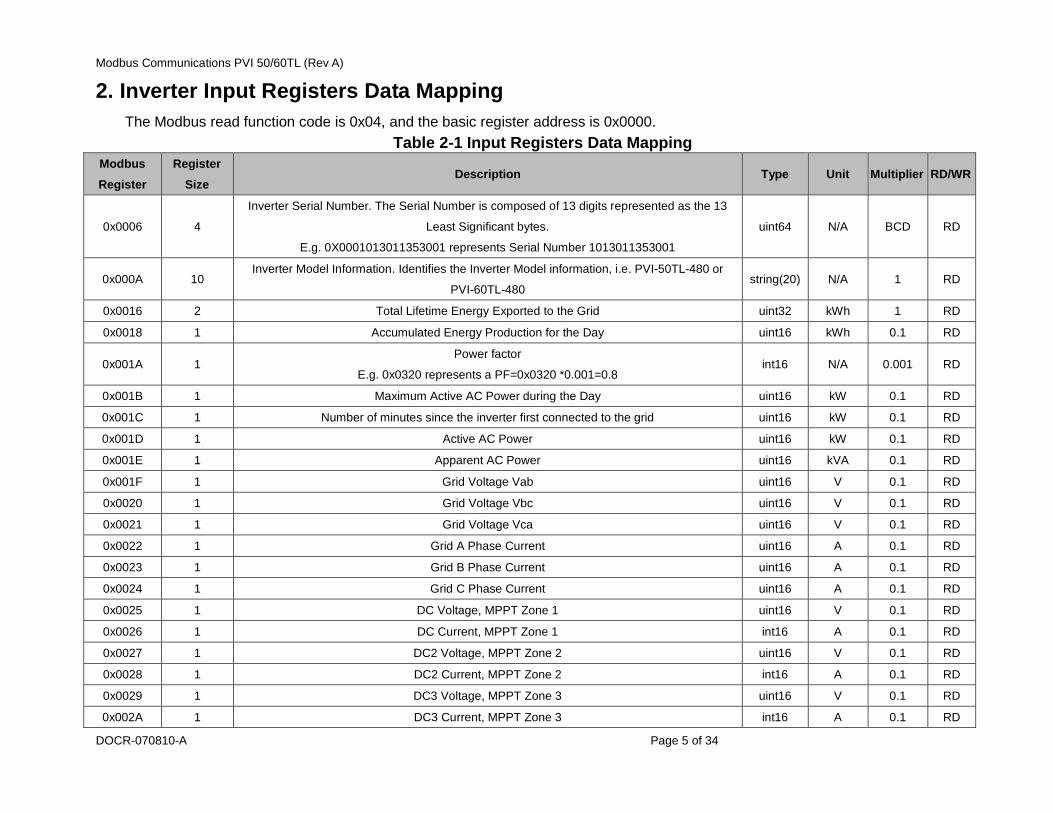
2. Inverter Input Registers Data Mapping
The Modbus read function code is 0x04, and the basic register address is 0x0000.
Table 2-1 Input Registers Data Mapping
Modbus
Register
Register
Size Description Type Unit Multiplier RD/WR
0x0006 4
Inverter Serial Number. The Serial Number is composed of 13 digits represented as the 13
Least Significant bytes.
E.g. 0X0001013011353001 represents Serial Number 1013011353001
uint64 N/A BCD RD
0x000A 10 Inverter Model Information. Identifies the Inverter Model information, i.e. PVI-50TL-480 or
PVI-60TL-480 string(20) N/A 1 RD
0x0016 2 Total Lifetime Energy Exported to the Grid uint32 kWh 1 RD
0x0018 1 Accumulated Energy Production for the Day uint16 kWh 0.1 RD
0x001A 1 Power factor
E.g. 0x0320 represents a PF=0x0320 *0.001=0.8 int16 N/A 0.001 RD
0x001B 1 Maximum Active AC Power during the Day uint16 kW 0.1 RD
0x001C 1 Number of minutes since the inverter first connected to the grid uint16 kW 0.1 RD
0x001D 1 Active AC Power uint16 kW 0.1 RD
0x001E 1 Apparent AC Power uint16 kVA 0.1 RD
0x001F 1 Grid Voltage Vab uint16 V 0.1 RD
0x0020 1 Grid Voltage Vbc uint16 V 0.1 RD
0x0021 1 Grid Voltage Vca uint16 V 0.1 RD
0x0022 1 Grid A Phase Current uint16 A 0.1 RD
0x0023 1 Grid B Phase Current uint16 A 0.1 RD
0x0024 1 Grid C Phase Current uint16 A 0.1 RD
0x0025 1 DC Voltage, MPPT Zone 1 uint16 V 0.1 RD
0x0026 1 DC Current, MPPT Zone 1 int16 A 0.1 RD
0x0027 1 DC2 Voltage, MPPT Zone 2 uint16 V 0.1 RD
0x0028 1 DC2 Current, MPPT Zone 2 int16 A 0.1 RD
0x0029 1 DC3 Voltage, MPPT Zone 3 uint16 V 0.1 RD
0x002A 1 DC3 Current, MPPT Zone 3 int16 A 0.1 RD
Modbus Communications PVI 50/60TL (Rev A)
DOCR-070810-A Page 6 of 34
Modbus
Register
Register
Size Description Type Unit Multiplier RD/WR
0x002B 1 Grid Frequency uint16 Hz 0.1 RD
0x002C 1 Power Module Heatsink Temperature int16 C 0.1 RD
0x002D 1 Internal Inverter Temperature int16 C 0.1 RD
0x002F 1 Inverter Operation State
For details see "Section 4 Operation States" uint16 N/A 1 RD
0x0030 4 Error Timestamp (yyyy-mm-dd-hh-mm-ss-NULL),
E.g. 0x2012071615181000=2012-7-16 15:18:10 uint64 N/A BCD RD
0x0034 1
Permanent Fault Alarm Register
Severity – High
The inverter has detected a serious fault and has ceased to generate power. Requires site visit
to check the cause. The inverter will stay off until power is cycled.
For details see "Section 5 Inverter Fault Codes Descriptor"
uint16 N/A 1 RD
0x0035 1
Warning Alarm Register
Severity – Low
The inverter detected an anomaly, but will continue to generate power.
For details see "Section 5 Inverter Fault Codes Descriptor"
uint16 N/A 1 RD
0x0036 1
Fault0 Alarm Register
Severity – Medium
The inverter detected a failure such as an AC or DC out of range condition and has ceased to
generate power. The inverter will resume power generation when the condition clears.
For details see "Section 5 Inverter Fault Codes Descriptor"
uint16 N/A 1 RD
0x0037 1
Fault1 Alarm Register
Severity – Medium
The inverter detected a failure such as an AC or DC out of range condition and has ceased to
generate power. The inverter will resume power generation when the condition clears.
For details see "Section 5 Inverter Fault Codes Descriptor"
uint16 N/A 1 RD
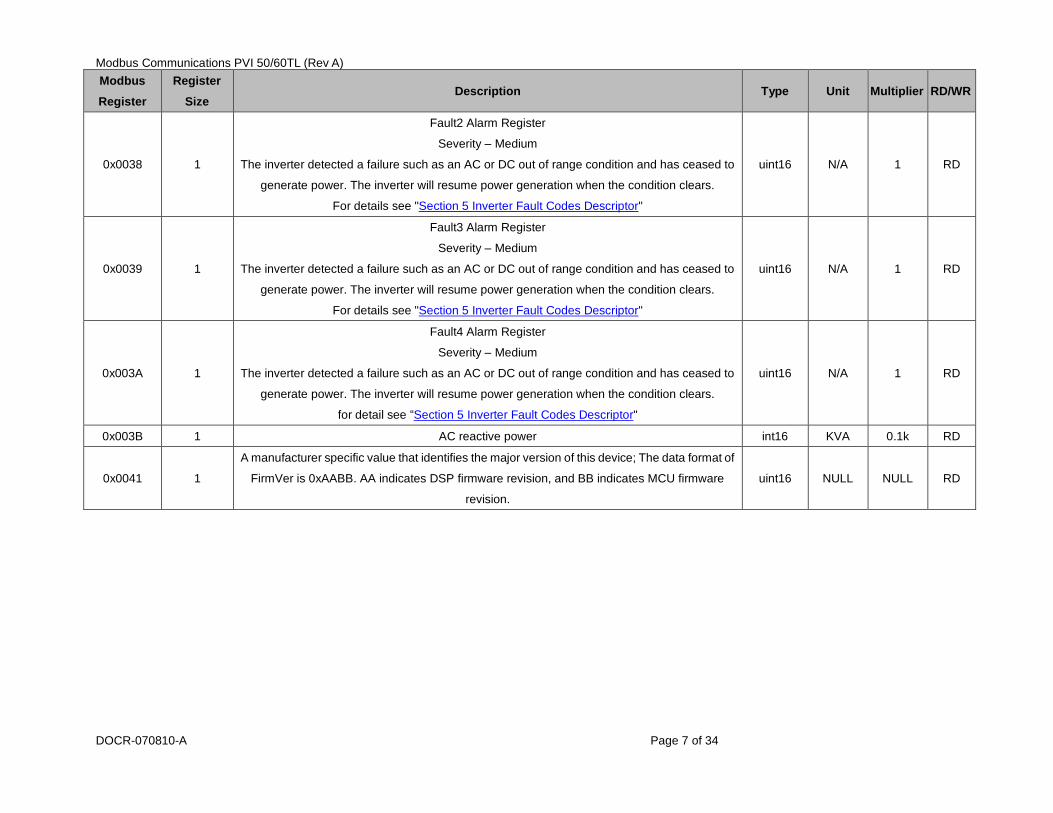
Modbus Communications PVI 50/60TL (Rev A)
DOCR-070810-A Page 7 of 34
Modbus
Register
Register
Size Description Type Unit Multiplier RD/WR
0x0038 1
Fault2 Alarm Register
Severity – Medium
The inverter detected a failure such as an AC or DC out of range condition and has ceased to
generate power. The inverter will resume power generation when the condition clears.
For details see "Section 5 Inverter Fault Codes Descriptor"
uint16 N/A 1 RD
0x0039 1
Fault3 Alarm Register
Severity – Medium
The inverter detected a failure such as an AC or DC out of range condition and has ceased to
generate power. The inverter will resume power generation when the condition clears.
For details see "Section 5 Inverter Fault Codes Descriptor"
uint16 N/A 1 RD
0x003A 1
Fault4 Alarm Register
Severity – Medium
The inverter detected a failure such as an AC or DC out of range condition and has ceased to
generate power. The inverter will resume power generation when the condition clears.
for detail see “Section 5 Inverter Fault Codes Descriptor"
uint16 N/A 1 RD
0x003B 1 AC reactive power int16 KVA 0.1k RD
0x0041 1
A manufacturer specific value that identifies the major version of this device; The data format of
FirmVer is 0xAABB. AA indicates DSP firmware revision, and BB indicates MCU firmware
revision.
uint16 NULL NULL RD

Modbus Communications PVI 50/60TL (Rev A)
DOCR-070810-A Page 8 of 34
3. Inverter Holding Registers Mapping
The Modbus read function code for the holding (RD/WR) registers is 0x03.
The Modbus write function code is 0x06 for a single register write and 0x10 for multiple register writes.
Note: Please do not write to any of the reserved or unlisted register addresses. Doing so could damage the inverter and void the
warranty.
3.1. Holding Registers Mapping
Table 3-1 Holding Register Mapping
Modbus
Register
Register
Size Name Description Type Multiplier Unit
Default
Value
Min
value
Max
value
0x1000 1 On/Off
Inverter Power On or Power Off Command
0xAAAA turns the unit power production on
0X5555 turns the unit power production off
The Inverter will automatically turn back on whenever DC power is
cycled.
uint16 1 N/A 0xAAAA
(On)
0x5555
(Off)
0xAAAA
(On)
0x1001 1 PSet
Temporary Active Power Setting (Curtailment)
This setting will be reset overnight or when the inverter is power
cycled.
Curtailment mode must be enabled by writing 1 to register 0x1046.
Range [0.0%, 100.%] of nameplate kW rating,
e.g. for 75%, then PSet = 0x02EE
For PVI 60TL: 60kW * 75% = 45kW
uint16 0.1 % 1000 0 1000
Modbus Communications PVI 50/60TL (Rev A)
DOCR-070810-A Page 9 of 34
Modbus
Register
Register
Size Name Description Type Multiplier Unit
Default
Value
Min
value
Max
value
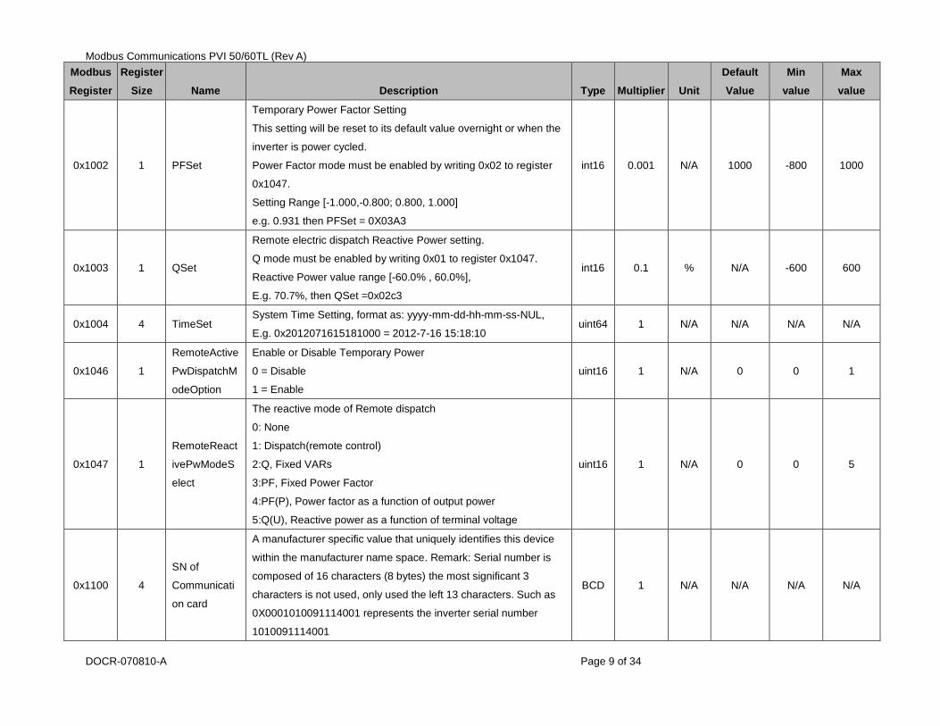
0x1002 1 PFSet
Temporary Power Factor Setting
This setting will be reset to its default value overnight or when the
inverter is power cycled.
Power Factor mode must be enabled by writing 0x02 to register
0x1047.
Setting Range [-1.000,-0.800; 0.800, 1.000]
e.g. 0.931 then PFSet = 0X03A3
int16 0.001 N/A 1000 -800 1000
0x1003 1 QSet
Remote electric dispatch Reactive Power setting.
Q mode must be enabled by writing 0x01 to register 0x1047.
Reactive Power value range [-60.0% , 60.0%],
E.g. 70.7%, then QSet =0x02c3
int16 0.1 % N/A -600 600
0x1004 4 TimeSet System Time Setting, format as: yyyy-mm-dd-hh-mm-ss-NUL,
E.g. 0x2012071615181000 = 2012-7-16 15:18:10 uint64 1 N/A N/A N/A N/A
0x1046 1
RemoteActive
PwDispatchM
odeOption
Enable or Disable Temporary Power
0 = Disable
1 = Enable
uint16 1 N/A 0 0 1
0x1047 1
RemoteReact
ivePwModeS
elect
The reactive mode of Remote dispatch
0: None
1: Dispatch(remote control)
2:Q, Fixed VARs
3:PF, Fixed Power Factor
4:PF(P), Power factor as a function of output power
5:Q(U), Reactive power as a function of terminal voltage
uint16 1 N/A 0 0 5
0x1100 4
SN of
Communicati
on card
A manufacturer specific value that uniquely identifies this device
within the manufacturer name space. Remark: Serial number is
composed of 16 characters (8 bytes) the most significant 3
characters is not used, only used the left 13 characters. Such as
0X0001010091114001 represents the inverter serial number
1010091114001
BCD 1 N/A N/A N/A N/A

Modbus Communications PVI 50/60TL (Rev A)
DOCR-070810-A Page 10 of 34
Modbus
Register
Register
Size Name Description Type Multiplier Unit
Default
Value
Min
value
Max
value
0x1104 2 IP Address
IP of the connected Ethernet network card
Example: 0x0A7A0136
represents the IP address 10.122.1.54
uint32 1 N/A N/A N/A N/A
0x1106 2 Subnet mask The same as above uint32 1 N/A N/A N/A N/A
0x1108 2 Default
gateway The same as above uint32 1 N/A N/A N/A N/A
0x1110 2 DNS server The same as above uint32 1 N/A N/A N/A N/A
0x1112 1 Address
range
The address range that the Ethernet network card uses.
value=1: 1-32
value=2: 33-64
value=3: 65-96
value=4: 97-128
value=5: 129-160
value=6: 161-192
value=7: 193-224
value=8: 225-255
uint16 1 N/A N/A 1 8

Modbus Communications PVI 50/60TL (Rev A)
DOCR-070810-A Page 11 of 34
3.2. Holding Registers Mapping
Note: Some registers are used internally and are not disclosed in this document.
Table 3-2 Assignment of Holding Register Groups
Address Range Group Number Group Name
0x2000 ~ 0x20FF 0 Grid Protection Parameters
0x2100 ~ 0x21FF 1 Active Power Derating Parameters
0x2200 ~ 0x22FF 2 Reactive Power Derating Parameters
0x2300 ~ 0x23FF 3 NULL
0x2400 ~ 0x24FF 4 LVRT/HVRT Parameters
0x2500 ~ 0x25FF 5 Others Parameters
0x2600 ~ 0x26FF 6 Enable/Disable Control Parameters
0x2700 ~ 0x27FF 7 Control Command
0x2800 ~ 0x28FF 8 NULL
0x2900 ~ 0x29FF 9 Inverter Basic Information
Table 3-3 Holding Registers Data Mapping
Modbus
Register
Register
Size Description Name Type Multiplier Unit Min value Max value
Group 0 Grid Protection Parameters
0x2000 1 The 1st maximum operational grid voltage GridV.Max1 uint16 0.01 % 10000 13500
0x2001 1 The 1st maximum grid voltage trip time VolMaxTripTime_1 uint16 0.01 s 0 65500
0x2002 1 The 2nd
maximum operational grid voltage GridV.Max2 uint16 0.01 % 10000 13500
0x2003 1 The 2nd
maximum grid voltage trip time VolMaxTripTime_2 uint16 0.01 s 0 65500
0x2004 1 The 3rd
maximum operational grid voltage GridV.Max3 uint16 0.01 % 10000 13500
0x2005 1 The 3rd
maximum grid voltage trip time VolMaxTripTime_3 uint16 0.01 s 0 65500
Modbus Communications PVI 50/60TL (Rev A)
DOCR-070810-A Page 12 of 34
Modbus
Register
Register
Size Description Name Type Multiplier Unit Min value Max value
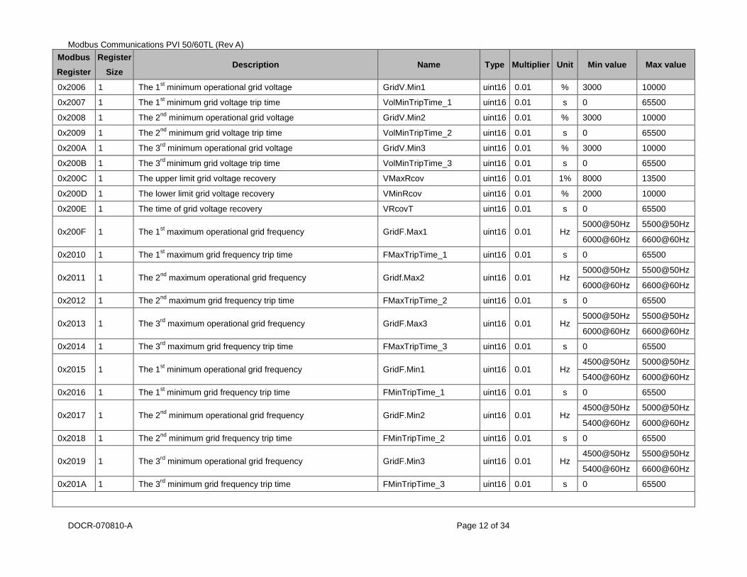
0x2006 1 The 1st minimum operational grid voltage GridV.Min1 uint16 0.01 % 3000 10000
0x2007 1 The 1st minimum grid voltage trip time VolMinTripTime_1 uint16 0.01 s 0 65500
0x2008 1 The 2nd
minimum operational grid voltage GridV.Min2 uint16 0.01 % 3000 10000
0x2009 1 The 2nd
minimum grid voltage trip time VolMinTripTime_2 uint16 0.01 s 0 65500
0x200A 1 The 3rd
minimum operational grid voltage GridV.Min3 uint16 0.01 % 3000 10000
0x200B 1 The 3rd
minimum grid voltage trip time VolMinTripTime_3 uint16 0.01 s 0 65500
0x200C 1 The upper limit grid voltage recovery VMaxRcov uint16 0.01 1% 8000 13500
0x200D 1 The lower limit grid voltage recovery VMinRcov uint16 0.01 % 2000 10000
0x200E 1 The time of grid voltage recovery VRcovT uint16 0.01 s 0 65500
0x200F 1 The 1st maximum operational grid frequency GridF.Max1 uint16 0.01 Hz
5000@50Hz 5500@50Hz
6000@60Hz 6600@60Hz
0x2010 1 The 1st maximum grid frequency trip time FMaxTripTime_1 uint16 0.01 s 0 65500
0x2011 1 The 2nd
maximum operational grid frequency Gridf.Max2 uint16 0.01 Hz 5000@50Hz 5500@50Hz
6000@60Hz 6600@60Hz
0x2012 1 The 2nd
maximum grid frequency trip time FMaxTripTime_2 uint16 0.01 s 0 65500
0x2013 1 The 3rd
maximum operational grid frequency GridF.Max3 uint16 0.01 Hz 5000@50Hz 5500@50Hz
6000@60Hz 6600@60Hz
0x2014 1 The 3rd
maximum grid frequency trip time FMaxTripTime_3 uint16 0.01 s 0 65500
0x2015 1 The 1st minimum operational grid frequency GridF.Min1 uint16 0.01 Hz
4500@50Hz 5000@50Hz
5400@60Hz 6000@60Hz
0x2016 1 The 1st minimum grid frequency trip time FMinTripTime_1 uint16 0.01 s 0 65500
0x2017 1 The 2nd
minimum operational grid frequency GridF.Min2 uint16 0.01 Hz 4500@50Hz 5000@50Hz
5400@60Hz 6000@60Hz
0x2018 1 The 2nd
minimum grid frequency trip time FMinTripTime_2 uint16 0.01 s 0 65500
0x2019 1 The 3rd
minimum operational grid frequency GridF.Min3 uint16 0.01 Hz 4500@50Hz 5500@50Hz
5400@60Hz 6600@60Hz
0x201A 1 The 3rd
minimum grid frequency trip time FMinTripTime_3 uint16 0.01 s 0 65500

Modbus Communications PVI 50/60TL (Rev A)
DOCR-070810-A Page 13 of 34
Modbus
Register
Register
Size Description Name Type Multiplier Unit Min value Max value
0x201B 1 The upper limit grid frequency recovery FMaxRcov uint16 0.01 Hz 4500@50Hz 5500@50Hz
5400@60Hz 6600@60Hz
0x201C 1 The lower limit grid frequency recovery FMinRcov uint16 0.01 Hz 4500@50Hz 5000@50Hz
5400@60Hz 6000@60Hz
0x201D 1 The time of grid frequency recovery FRcovT uint16 0.01 s 0 65500
0x201E 1 The upper limit grid voltage of moving average filter VMaxMovAvg uint16 0.01 % 10000 13500
0x201F 1 The trip time of the upper limit grid voltage of moving average
filter VMaxMovAvgT uint16 0.01 s 0 65500
0x2020 1 The lower limit grid voltage of moving average filter VMinMovAvg uint16 0.01 % 8000 10000
0x2021 1 The trip time of the lower limit grid voltage of moving average
filter VMinMovAvgT uint16 0.01 s 0 65500
0x2022 1 The moving average filter recovery time VMovAvgRcovT uint16 0.01 s 0 65500
0x2023 1 Unbalance rate of grid voltage VUnbal uint16 0.01 % 1 1000
Group 1 Active Power Derating Parameters
0x2100 1 The trigger voltage of overvoltage derating OVDeratStart uint16 0.01 % 10000 13500
0x2101 1 The end voltage of overvoltage derating OVDeratStop uint16 0.01 % 10000 11000
0x2102 1 The rate of overvoltage derating OVDeratRate uint16 0.1 % 1 1000
0x2103 1 The filtering time of overvoltage derating OVDeratFilterTime uint16 1 s 1 90
0x2104 1 The trigger frequency of overfrequency derating OFDeratStart uint16 0.01 Hz 5000@50Hz 6000@50Hz
6000@60Hz 7200@60Hz
0x2105 1 The end frequency or Rate of overfrequency derating
(Depends on the specific standard) OFDeratStopOrRate uint16 0.01 Hz
5000@50Hz 6000@50Hz
6000@60Hz 7200@60Hz
0x2106 1 The Rate of overfrequency derating. OFDeratRate uint16 0.01 % 1 10000
0x2107 1 The recovery frequency of overfrequency derating OFDeratRcovFre uint16 0.01 Hz 4900@50Hz 5500@50Hz
5880@60Hz 6600@60Hz
0x2108 1 The recovery time of overfrequency derating OFDeratRcovT uint16 1 s 0 1200
0x2109 1 The trigger frequency of underfrequency derating UFDeratStart uint16 0.01 Hz 4500@50Hz 5000@50Hz
5400@60Hz 6000@60Hz
Modbus Communications PVI 50/60TL (Rev A)
DOCR-070810-A Page 14 of 34
Modbus
Register
Register
Size Description Name Type Multiplier Unit Min value Max value
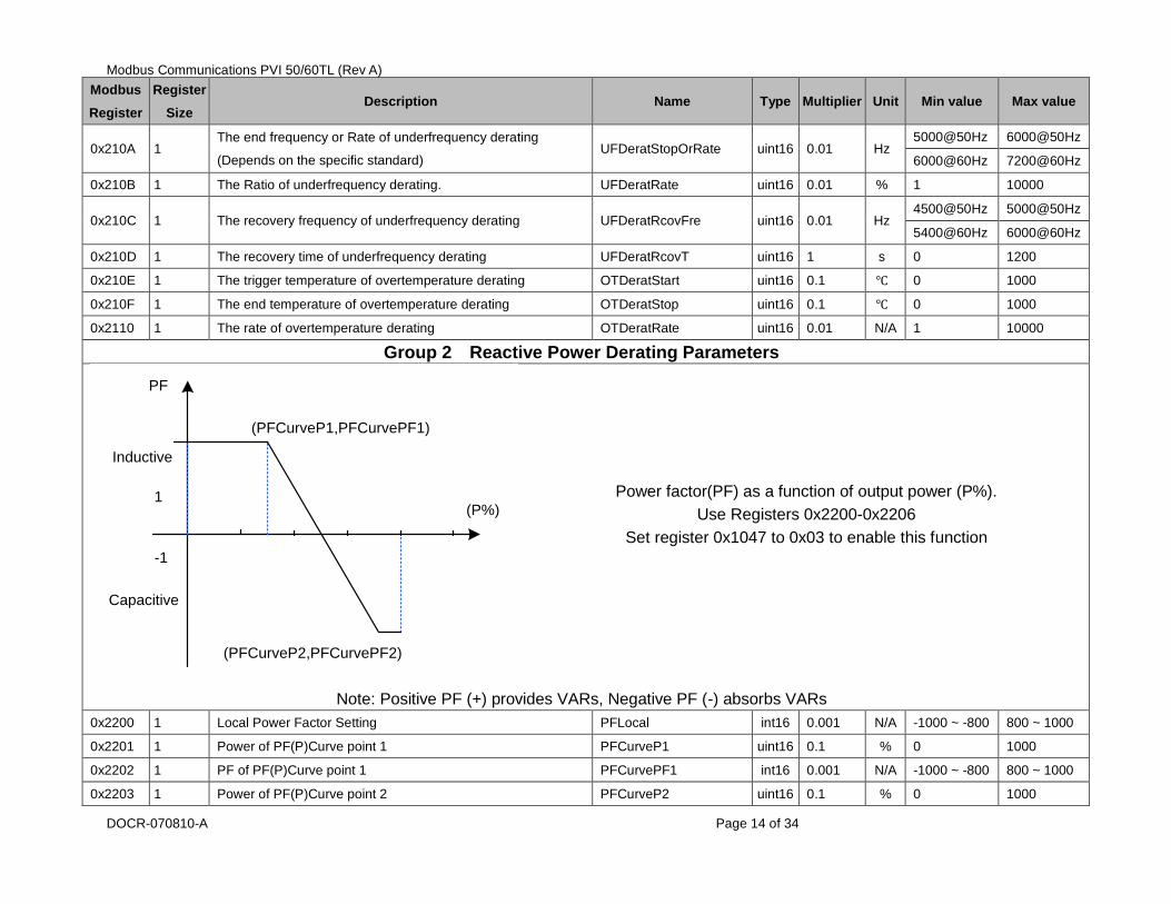
0x210A 1 The end frequency or Rate of underfrequency derating
(Depends on the specific standard) UFDeratStopOrRate uint16 0.01 Hz
5000@50Hz 6000@50Hz
6000@60Hz 7200@60Hz
0x210B 1 The Ratio of underfrequency derating. UFDeratRate uint16 0.01 % 1 10000
0x210C 1 The recovery frequency of underfrequency derating UFDeratRcovFre uint16 0.01 Hz 4500@50Hz 5000@50Hz
5400@60Hz 6000@60Hz
0x210D 1 The recovery time of underfrequency derating UFDeratRcovT uint16 1 s 0 1200
0x210E 1 The trigger temperature of overtemperature derating OTDeratStart uint16 0.1 ℃ 0 1000
0x210F 1 The end temperature of overtemperature derating OTDeratStop uint16 0.1 ℃ 0 1000
0x2110 1 The rate of overtemperature derating OTDeratRate uint16 0.01 N/A 1 10000
Group 2 Reactive Power Derating Parameters
Power factor(PF) as a function of output power (P%).
Use Registers 0x2200-0x2206
Set register 0x1047 to 0x03 to enable this function
Note: Positive PF (+) provides VARs, Negative PF (-) absorbs VARs
0x2200 1 Local Power Factor Setting PFLocal int16 0.001 N/A -1000 ~ -800 800 ~ 1000
0x2201 1 Power of PF(P)Curve point 1 PFCurveP1 uint16 0.1 % 0 1000
0x2202 1 PF of PF(P)Curve point 1 PFCurvePF1 int16 0.001 N/A -1000 ~ -800 800 ~ 1000
0x2203 1 Power of PF(P)Curve point 2 PFCurveP2 uint16 0.1 % 0 1000
Capacitive
PF
-1
1
Inductive
(PFCurveP1,PFCurvePF1)
(PFCurveP2,PFCurvePF2)
(P%)
Modbus Communications PVI 50/60TL (Rev A)
DOCR-070810-A Page 15 of 34
Modbus
Register
Register
Size Description Name Type Multiplier Unit Min value Max value
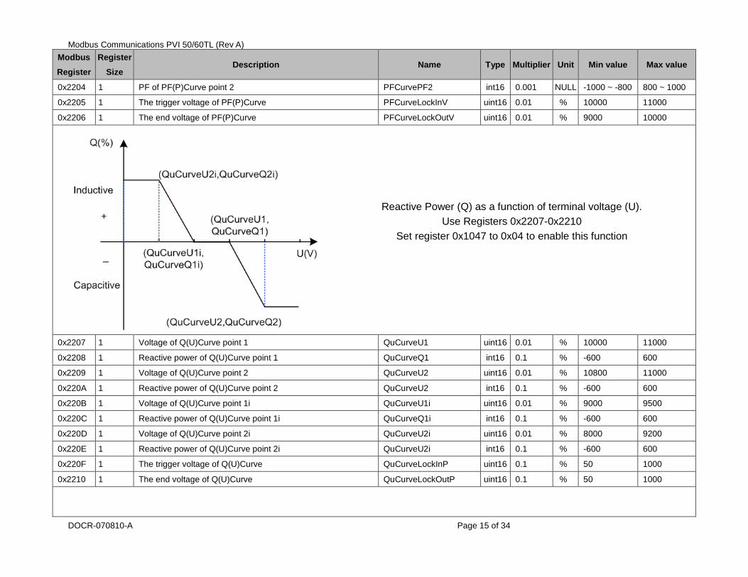
0x2204 1 PF of PF(P)Curve point 2 PFCurvePF2 int16 0.001 NULL -1000 ~ -800 800 ~ 1000
0x2205 1 The trigger voltage of PF(P)Curve PFCurveLockInV uint16 0.01 % 10000 11000
0x2206 1 The end voltage of PF(P)Curve PFCurveLockOutV uint16 0.01 % 9000 10000
Reactive Power (Q) as a function of terminal voltage (U).
Use Registers 0x2207-0x2210
Set register 0x1047 to 0x04 to enable this function
0x2207 1 Voltage of Q(U)Curve point 1 QuCurveU1 uint16 0.01 % 10000 11000
0x2208 1 Reactive power of Q(U)Curve point 1 QuCurveQ1 int16 0.1 % -600 600
0x2209 1 Voltage of Q(U)Curve point 2 QuCurveU2 uint16 0.01 % 10800 11000
0x220A 1 Reactive power of Q(U)Curve point 2 QuCurveU2 int16 0.1 % -600 600
0x220B 1 Voltage of Q(U)Curve point 1i QuCurveU1i uint16 0.01 % 9000 9500
0x220C 1 Reactive power of Q(U)Curve point 1i QuCurveQ1i int16 0.1 % -600 600
0x220D 1 Voltage of Q(U)Curve point 2i QuCurveU2i uint16 0.01 % 8000 9200
0x220E 1 Reactive power of Q(U)Curve point 2i QuCurveU2i int16 0.1 % -600 600
0x220F 1 The trigger voltage of Q(U)Curve QuCurveLockInP uint16 0.1 % 50 1000
0x2210 1 The end voltage of Q(U)Curve QuCurveLockOutP uint16 0.1 % 50 1000
Modbus Communications PVI 50/60TL (Rev A)
DOCR-070810-A Page 16 of 34
Modbus
Register
Register
Size Description Name Type Multiplier Unit Min value Max value
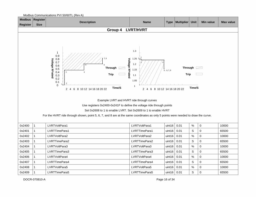
Group 4 LVRT/HVRT
1
0.9
0.8
0.7
0.6
0.5
0.4
0.3
0.2
0.1
0
2 4 6 8 10 12 14 16 18 20 22
1 2
3 4
5 6
7,8
Through
Trip
Vo
ltag
e N
*rate
d
Time/S
1.3
1.25
1.2
1.15
1.1
1.05
1
2 4 6 8 10 12 14 16 18 20 22
1 2
3 4
5,6,7,8
Through
Trip
Vo
ltag
e N
*rate
d
Time/S
Example LVRT and HVRT ride through curves
Use registers 0x2400-0x241F to define the voltage ride through points
Set 0x2608 to 1 to enable LVRT. Set 0x2609 to 1 to enable HVRT
For the HVRT ride through shown, point 5, 6, 7, and 8 are at the same coordinates as only 5 points were needed to draw the curve.
0x2400 1 LVRTVoltPara1 LVRTVoltPara1 uint16 0.01 % 0 10000
0x2401 1 LVRTTimePara1 LVRTTimePara1 uint16 0.01 S 0 65500
0x2402 1 LVRTVoltPara2 LVRTVoltPara2 uint16 0.01 % 0 10000
0x2403 1 LVRTTimePara2 LVRTTimePara2 uint16 0.01 S 0 65500
0x2404 1 LVRTVoltPara3 LVRTVoltPara3 uint16 0.01 % 0 10000
0x2405 1 LVRTTimePara3 LVRTTimePara3 uint16 0.01 S 0 65500
0x2406 1 LVRTVoltPara4 LVRTVoltPara4 uint16 0.01 % 0 10000
0x2407 1 LVRTTimePara4 LVRTTimePara4 uint16 0.01 S 0 65500
0x2408 1 LVRTVoltPara5 LVRTVoltPara5 uint16 0.01 % 0 10000
0x2409 1 LVRTTimePara5 LVRTTimePara5 uint16 0.01 S 0 65500
Modbus Communications PVI 50/60TL (Rev A)
DOCR-070810-A Page 17 of 34
Modbus
Register
Register
Size Description Name Type Multiplier Unit Min value Max value
0x240A 1 LVRTVoltPara6 LVRTVoltPara6 uint16 0.01 % 0 10000
0x240B 1 LVRTTimePara6 LVRTTimePara6 uint16 0.01 S 0 65500
0x240C 1 LVRTVoltPara7 LVRTVoltPara7 uint16 0.01 % 0 10000
0x240D 1 LVRTTimePara7 LVRTTimePara7 uint16 0.01 S 0 65500
0x240E 1 LVRTVoltPara8 LVRTVoltPara8 uint16 0.01 % 0 10000
0x240F 1 LVRTTimePara8 LVRTTimePara8 uint16 0.01 S 0 65500
0x2410 1 HVRTVoltPara1 HVRTVoltPara1 uint16 0.01 % 10000 13500
0x2411 1 HVRTTimePara1 HVRTTimePara1 uint16 0.01 S 0 65500
0x2412 1 HVRTVoltPara2 HVRTVoltPara2 uint16 0.01 % 10000 13500
0x2413 1 HVRTTimePara2 HVRTTimePara2 uint16 0.01 S 0 65500
0x2414 1 HVRTVoltPara3 HVRTVoltPara3 uint16 0.01 % 10000 13500
0x2415 1 HVRTTimePara3 HVRTTimePara3 uint16 0.01 S 0 65500
0x2416 1 HVRTVoltPara4 HVRTVoltPara4 uint16 0.01 % 10000 13500
0x2417 1 HVRTTimePara4 HVRTTimePara4 uint16 0.01 S 0 65500
0x2418 1 HVRTVoltPara5 HVRTVoltPara5 uint16 0.01 % 10000 13500
0x2419 1 HVRTTimePara5 HVRTTimePara5 uint16 0.01 S 0 65500
0x241A 1 HVRTVoltPara6 HVRTVoltPara6 uint16 0.01 % 10000 13500
0x241B 1 HVRTTimePara6 HVRTTimePara6 uint16 0.01 S 0 65500
0x241C 1 HVRTVoltPara7 HVRTVoltPara7 uint16 0.01 % 10000 13500
0x241D 1 HVRTTimePara7 HVRTTimePara7 uint16 0.01 S 0 65500
0x241E 1 HVRTVoltPara8 HVRTVoltPara8 uint16 0.01 % 10000 13500
0x241F 1 HVRTTimePara8 HVRTTimePara8 uint16 0.01 S 0 65500
Group 5 Others Parameters
0x2500 1 Startup delay time StartDelay uint16 1 s 1 1200
0x2504 1 Normal power step in soft stop StopPowerStep uint16 0.01 % 1 10000
0x2505 1 Normal power step in soft startup PsoftStaStep uint16 0.01 % 1 10000
0x2506 1 Normal power derating step PDeratingStep uint16 0.01 % 1 10000
0x250A 1 The trigger voltage of HVRT HVRTTripVol uint16 0.1 % 1000 1350
0x250B 1 The trigger voltage of LVRT LVRTTripVol uint16 0.1 % 700 1000
Modbus Communications PVI 50/60TL (Rev A)
DOCR-070810-A Page 18 of 34
Modbus
Register
Register
Size Description Name Type Multiplier Unit Min value Max value
0x250C 1 The coefficient of positive sequence reactive current LVRTPosCurrK uint16 0.1 % 0 3000
0x250D 1 The coefficient of negative sequence reactive current LVRTNegCurrK uint16 0.1 % 0 3000
0x250E 1 Remote electric dispatch Active Power setting value PSet_Percent uint16 0.1 % 0 1000
0x250F 1 Remote electric dispatch Reactive Power setting value QSet_ Percent uint16 0.1 % -600 600
Group 6 Enable/Disable Control Parameters
0x2600 1 The enabled control parameters group. CtrlParaGroup uint16 N/A N/A 0 4
0x2601 1
The control mode of reactive power
0: Disable dispatch mode.
1: Remote dispatch mode.
2: Local control, by Q
3: Local control, by PF
4: PF(P)curve
5: Q(U) curve
ReactivePwModeSelect uint16 N/A N/A 0 5
0x2602 1
The control mode of active power
0: Disable dispatch mode.
1: Remote dispatch mode.
2: Local control.
ActivePwModeSelect uint16 N/A N/A 0 2
0x2603 1
MPPT scan enable/disable control
0: Disable
1: Enable
MPPTScanEn uint16 N/A N/A 0 1
0x2606 1
PV voltage at start up adjusting enable/disable control
0: Disable
1: Enable
VpvStartUpSetEn uint16 N/A N/A 0 1
0x2608 1
LVRT Mode
0: Disable
1: Enable, no reactive power output
2: Enable, reactive power output
LvrtMode uint16 N/A N/A 0 2
Modbus Communications PVI 50/60TL (Rev A)
DOCR-070810-A Page 19 of 34
Modbus
Register
Register
Size Description Name Type Multiplier Unit Min value Max value
0x2609 1
HVRT Mode
0: Disable
1: Enable, no reactive power output
HvrtMode uint16 N/A N/A 0 2
0x260A 1 Soft stop enable/disable control SoftStopEn uint16 N/A N/A 0 1
0x2622 1
Soft startup function
0: Disable
1: Enable
PowerMutateRatio
(HECO) uint16 N/A N/A 0 1
Group 7 Control Command
0x2700 1 Power on or power off device command, 0x5555 power on,
0x7777 power off CMD_PowerOnOff uint16 N/A N/A
0x5555
(On)
0x7777
(Off)
0x2701 1 Device force restart command, valid value is 0x5AAA CMD_ForceRestart uint16 N/A N/A 0x5AAA 0x5AAA
0x2702 1 Device factory reset command, valid value is 0x5AAA CMD_FactoryReset uint16 N/A N/A 0x5AAA 0x5AAA
0x2703 1 Device auto test command, valid value is 0x5AAA CMD_AutoTest uint16 N/A N/A 0x5AAA 0x5AAA
0x2704 1 MPPT scan command, valid value is 0x5AAA CMD_MPPTScan uint16 N/A N/A 0x5AAA 0x5AAA
0x2705 1 Arc Detection command, valid value is 0x5AAA CMD_ArcDetect uint16 N/A N/A 0x5AAA 0x5AAA
0x2707 1 Remote electric dispatch Power Factor setting value PF_Remote uint16 0.001 N/A -800 800
0x2708 1 Remote electric dispatch Active Power setting value P_Remote uint16 0.1% N/A 0 1000
0x2709 1 Remote electric dispatch Reactive Power setting value Q_Remote uint16 0.1% N/A -600 600
Group 9 Inverter Basic Information
0x2901 1 DSP Firmware Version, used by Section 5: Inverter Fault
Codes Descriptor DSPFW Version BCD N/A N/A N/A N/A
0x290C 1 Standard setting, Section 6: Standard Descriptor GridStandard Hex N/A N/A N/A N/A
0x290D 1
Neutral Line
0x5A5A:connected to N line
0xA5A5:not connected to N line
NeutralLine Hex N/A N/A N/A N/A
Modbus Communications PVI 50/60TL (Rev A)
DOCR-070810-A Page 20 of 34
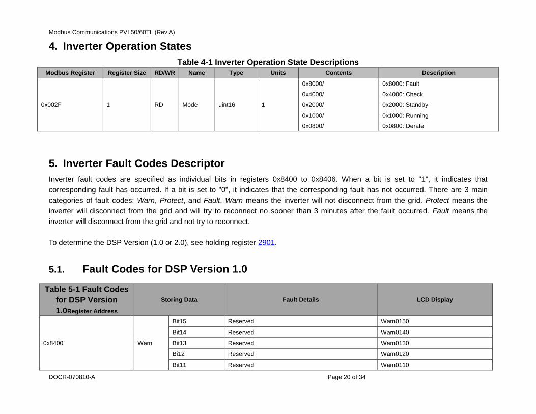
4. Inverter Operation States
Table 4-1 Inverter Operation State Descriptions
Modbus Register Register Size RD/WR Name Type Units Contents Description
0x002F 1 RD Mode uint16 1
0x8000/
0x4000/
0x2000/
0x1000/
0x0800/
0x8000: Fault
0x4000: Check
0x2000: Standby
0x1000: Running
0x0800: Derate
5. Inverter Fault Codes Descriptor
Inverter fault codes are specified as individual bits in registers 0x8400 to 0x8406. When a bit is set to "1", it indicates that
corresponding fault has occurred. If a bit is set to "0", it indicates that the corresponding fault has not occurred. There are 3 main
categories of fault codes: Warn, Protect, and Fault. Warn means the inverter will not disconnect from the grid. Protect means the
inverter will disconnect from the grid and will try to reconnect no sooner than 3 minutes after the fault occurred. Fault means the
inverter will disconnect from the grid and not try to reconnect.
To determine the DSP Version (1.0 or 2.0), see holding register 2901.
5.1. Fault Codes for DSP Version 1.0
Table 5-1 Fault Codes
for DSP Version
1.0Register Address
Storing Data Fault Details LCD Display
0x8400 Warn
Bit15 Reserved Warn0150
Bit14 Reserved Warn0140
Bit13 Reserved Warn0130
Bi12 Reserved Warn0120
Bit11 Reserved Warn0110

Modbus Communications PVI 50/60TL (Rev A)
DOCR-070810-A Page 21 of 34
Bit10 Reserved Warn0100
Bit9 Reserved Warn0090
Bit8 Reserved Warn0080
Bit7 AC side MOV anomaly Warn0070
Bit6 Reserved Warn0060
Bit5 Temperature sensor anomaly Warn0050
Bit4 DC side lightning protection exception Warn0040
Bit3 EEPROM fault Warn0030
Bit2 Reserved CommErr
Bit1 Internal fan alarm IntFanErr
Bit0 External fan alarm ExtFanErr
0x8401 Fault0
Bit15 Inverter current bias Protect0010
Bit14 Over temperature protection TempOver
Bit13 Grid connected relay protection Protect0020
Bi12 Out of phase GridV.OutLim
Bit11 Low frequency of power grid GridF.OutLim
Bit10 High frequency of power grid GridF.OutLim
Bit9 Inverter current too high Protect0030
Bit8 Grid phase voltage over limit GridV.OutLim
Bit7 Grid line voltage over limit GridV.OutLim
Bit6 PV1 High current Protect0040
Bit5 Reserved N/A
Bit4 Inverter soft start time out Protect0050
Bit3 Bus soft start time out Protect0060
Bit2 BUS difference is high Protect0070
Bit1 Reserved Protect0080
Bit0 BUS sum high Protect0090
0x8402 Fault1
Bit15 Leakage current sensor fault Protect0100
Bit14 Bus hardware over voltage Protect0110
Bit13 Reserved N/A
Modbus Communications PVI 50/60TL (Rev A)
DOCR-070810-A Page 22 of 34
Bit12 Power module protection Protect0120
Bit11 Inverter current imbalance Protect0130
Bit10 Reserved N/A
Bit9 Unbalanced grid voltage GridV.OutLim
Bit8 inverter hardware over current Protect0140
Bit7 MCU Protect Protect0150
Bit6 Reserved N/A
Bit5 Inverter cannot identify the frequency Protect0160
Bit4 Leakage current is too high GFCIErr
Bit3 Insulation impedance is too low IsolationErr
Bit2 DCI High current Protect0170
Bit1 DCI current bias Protect0180
Bit0 Reserved Protect0190
0x8403 Fault2
Bit15 Reserved N/A
Bit14 Reserved Protect0290
Bit13 Reserved Protect0300
Bi12 PV3 voltage is too high PV3VoltOver
Bit11 PV3 input reverse connection PV3Reverse
Bit10 PV1 voltage is too high PV1VoltOver
Bit9 PV1 input reverse connection PV1Reverse
Bit8 Reserved N/A
Bit7 Turn on the inverter open loop detection Protect0230
Bit6 Abnormal PV source input Protect0260
Bit5 PV2 voltage is too high PV2VoltOver
Bit4 PV2 input over current Protect0240
Bit3 PV2 reverse connection PV2Reverse
Bit2 Input / output power mismatch Protect0220
Bit1 Internal hardware exception Protect0210
Bit0 Reserved Protect0200
0x8404 Fault3 Bit15 ARC protection ARC Protect

Modbus Communications PVI 50/60TL (Rev A)
DOCR-070810-A Page 23 of 34
Bit14 Reserved Protect0320
Bit13 Reserved Protect0330
Bi12 Reserved Protect0340
Bit11 Reserved Protect0350
Bit10 Reserved Protect0360
Bit9 Reserved Protect0370
Bit8 Reserved Protect0380
Bit7 Reserved Protect0390
Bit6 Reserved Protect0400
Bit5 CPLD software version exception Protect0410
Bit4 Abnormal product model Protect0420
Bit3 Abnormal source for drive hardware Protect0430
Bit2 Reserved Protect0440
Bit1 Boost Hardware overcurrent Protect0450
Bit0 Control board 3.3V voltage low Protect0460
0x8405 Fault4
Bit15 Reserved Protect0470
Bit14 Reserved Protect0480
Bit13 Reserved Protect0490
Bi12 Reserved Protect0500
Bit11 Reserved Protect0510
Bit10 Reserved Protect0520
Bit9 Reserved Protect0530
Bit8 Reserved Protect0540
Bit7 Reserved Protect0550
Bit6 Reserved Protect0560
Bit5 Capture phase locked loop check exception Protect0570
Bit4 PV3 input over current Protect0580
Bit3 Reserved Protect0590
Bit2 Arc board fault Arcboard Err
Bit1 Steady state GFCI protection Protect0610

Modbus Communications PVI 50/60TL (Rev A)
DOCR-070810-A Page 24 of 34
Bit0 Control board 5V voltage low Protect0620
0x8406 PFault
Bit15 Control board voltage and drive power failure Fault0160
Bit14 Open loop self-detection failure Fault0150
Bit13 Internal hardware failure Fault0140
Bit12 Permanent fault of power module Fault0010
Bit11 Reserved Fault0020
Bit10 Reserved Fault0030
Bit9 Permanent fault of driver source Fault0040
Bit8 Inverter hardware overcurrent fault Fault0050
Bit7 Bus hardware overvoltage fault Fault0060
Bit6 DCI too high fault Fault0070
Bit5 Boost hardware overcurrent fault Fault0080
Bit4 Steady state GFCI fault Fault0090
Bit3 Relay fault Fault0100
Bit2 Bus differential high fault Fault0110
Bit1 Permanent fault of 3.3V voltage low Fault0120
Bit0 Bus sum high fault Fault0130
5.2. Fault Codes for DSP Version 2.0
Table 5-2 Fault Codes for DSP Version 2.0
Register Address Storing Data Fault Details LCD Display
0x8400 Warn
Bit15 Reserved Warn0150
Bit14 Reserved Warn0140
Bit13 Reserved Warn0130
Bi12 Reserved Warn0120
Bit11 Reserved Warn0110
Bit10 AC side MOV anomaly Warn0100
Bit9 Reserved Warn0090
Modbus Communications PVI 50/60TL (Rev A)
DOCR-070810-A Page 25 of 34
Bit8 Reserved Warn0080
Bit7 Reserved Warn0070
Bit6 Reserved Warn0060
Bit5 Temperature sensor anomaly Warn0050
Bit4 DC side lightning protection exception Warn0040
Bit3 EEPROM fault Warn0030
Bit2 Reserved CommErr
Bit1 Internal fan alarm IntFanErr
Bit0 External fan alarm ExtFanErr
0x8401 Fault0
Bit15 Inverter current bias Protect0010
Bit14 Over temperature protection TempOver
Bit13 Grid connected relay protection Protect0020
Bi12 Out of phase GridV.OutLim
Bit11 Low frequency of power grid GridF.OutLim
Bit10 High frequency of power grid GridF.OutLim
Bit9 High inverter current Protect0030
Bit8 Grid phase voltage over limit GridV.OutLim
Bit7 Grid line voltage over limit GridV.OutLim
Bit6 PV1 High current Protect0040
Bit5 Reserved N/A
Bit4 Inverter Soft start time out Protect0050
Bit3 Bus Soft start time out Protect0060
Bit2 BUS difference is high Protect0070
Bit1 Reserved Protect0080
Bit0 BUS sum high Protect0090
0x8402 Fault1
Bit15 Leakage current sensor fault Protect0100
Bit14 Bus hardware over voltage Protect0110
Bit13 Reserved N/A
Bit12 Power module protection Protect0120
Bit11 Inverter current imbalance Protect0130

Modbus Communications PVI 50/60TL (Rev A)
DOCR-070810-A Page 26 of 34
Bit10 Reserved N/A
Bit9 Unbalanced grid voltage GridV.OutLim
Bit8 inverter hardware over current Protect0140
Bit7 MCU Protect Protect0150
Bit6 Reserved N/A
Bit5 Inverter cannot identify the frequency Protect0160
Bit4 Leakage current is too high GFCIErr
Bit3 Insulation impedance is too low IsolationErr
Bit2 DCI High current Protect0170
Bit1 DCI current bias Protect0180
Bit0 Reserved Protect0190
0x8403 Fault2
Bit15 Reserved N/A
Bit14 Reserved Protect0290
Bit13 Reserved Protect0300
Bi12 PV3 voltage is too high PV3VoltOver
Bit11 PV3 input reverse connection PV3Reverse
Bit10 PV1 voltage is too high PV1VoltOver
Bit9 PV1 input reverse connection PV1Reverse
Bit8 Reserved N/A
Bit7 Turn on the inverter Open loop detection Protect0230
Bit6 Reserved Protect0260
Bit5 PV2 voltage is too high PV2VoltOver
Bit4 PV2 input over current Protect0240
Bit3 PV2 reverse connection PV2Reverse
Bit2 Reserved Protect0220
Bit1 Internal hardware exception Protect0210
Bit0 Reserved Protect0200
0x8404 Fault3
Bit15 ARC protection ARC Protect
Bit14 Reserved Protect0320
Bit13 Hardware driver power exception Protect0330

Modbus Communications PVI 50/60TL (Rev A)
DOCR-070810-A Page 27 of 34
Bi12 Reserved Protect0340
Bit11 Reserved Protect0350
Bit10 Reserved Protect0360
Bit9 Reserved Protect0370
Bit8 Reserved Protect0380
Bit7 Reserved Protect0390
Bit6 Reserved Protect0400
Bit5 Reserved Protect0410
Bit4 Reserved Protect0420
Bit3 Reserved Protect0430
Bit2 Reserved Protect0440
Bit1 Reserved Protect0450
Bit0 Reserved Protect0460
0x8405 Fault4
Bit15 Reserved Protect0470
Bit14 Reserved Protect0480
Bit13 Reserved Protect0490
Bi12 Reserved Protect0500
Bit11 Reserved Protect0510
Bit10 CPLD clock exception Protect0520
Bit9 CPLD program version exception Protect0530
Bit8 Product model exception Protect0540
Bit7 Boost hardware overcurrent Protect0550
Bit6 Control board 3.3V voltage low Protect0560
Bit5 Capture phase locked loop check exception Protect0570
Bit4 PV3 input over current Protect0580
Bit3 DC/AC overload protection Protect0590
Bit2 Arc board fault Arcboard Err
Bit1 Steady state GFCI protection Protect0610
Bit0 Control board 5V voltage low Protect0620
0x8406 PFault Bit15 Control board voltage and drive power failure Fault0160
Modbus Communications PVI 50/60TL (Rev A)
DOCR-070810-A Page 28 of 34
Bit14 Open loop self-detection failure Fault0150
Bit13 Internal hardware failure Fault0140
Bit12 Permanent fault of power module Fault0010
Bit11 Bus hardware overvoltage fault Fault0020
Bit10 Reserved Fault0030
Bit9 Reserved Fault0040
Bit8 Inverter hardware overcurrent fault Fault0050
Bit7 CPLD clock failure Fault0060
Bit6 DCI too high fault Fault0070
Bit5 Boost hardware overcurrent fault Fault0080
Bit4 Steady state GFCI fault Fault0090
Bit3 Relay fault Fault0100
Bit2 Bus differential high fault Fault0110
Bit1 Reserved Fault0120
Bit0 Bus sum high fault Fault0130
6. Standard Descriptor
Holding register 0x290C refers to a hex value denoting which standard the inverter settings comply with, as shown below.
Table 6-1 Standard Descriptor
Standard Value Corresponding Standards and Regulations
0 NONE
10 IEEE1547
19 Rule-21
20 HECO-HM
21 HECO-ML
Modbus Communications PVI 50/60TL (Rev A)
DOCR-070810-A Page 29 of 34
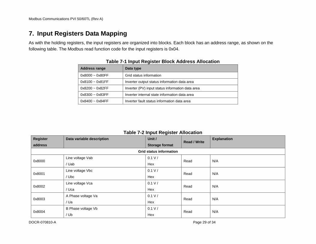
7. Input Registers Data Mapping
As with the holding registers, the input registers are organized into blocks. Each block has an address range, as shown on the
following table. The Modbus read function code for the input registers is 0x04.
Table 7-1 Input Register Block Address Allocation
Address range Data type
0x8000 ~ 0x80FF Grid status information
0x8100 ~ 0x81FF Inverter output status information data area
0x8200 ~ 0x82FF Inverter (PV) input status information data area
0x8300 ~ 0x83FF Inverter internal state information data area
0x8400 ~ 0x84FF Inverter fault status information data area
Table 7-2 Input Register Allocation
Register
address
Data variable description
Unit /
Storage format Read / Write
Explanation
Grid status information
0x8000 Line voltage Vab
/ Uab
0.1 V /
Hex Read N/A
0x8001 Line voltage Vbc
/ Ubc
0.1 V /
Hex Read N/A
0x8002 Line voltage Vca
/ Uca
0.1 V /
Hex Read N/A
0x8003 A Phase voltage Va
/ Ua
0.1 V /
Hex Read N/A
0x8004 B Phase voltage Vb
/ Ub
0.1 V /
Hex Read N/A
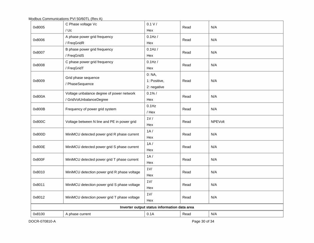
Modbus Communications PVI 50/60TL (Rev A)
DOCR-070810-A Page 30 of 34
0x8005 C Phase voltage Vc
/ Uc
0.1 V /
Hex Read N/A
0x8006 A phase power grid frequency
/ FreqGridR
0.1Hz /
Hex Read N/A
0x8007 B phase power grid frequency
/ FreqGridS
0.1Hz /
Hex Read N/A
0x8008 C phase power grid frequency
/ FreqGridT
0.1Hz /
Hex Read N/A
0x8009 Grid phase sequence
/ PhaseSequence
0: NA,
1: Positive,
2: negative
Read N/A
0x800A Voltage unbalance degree of power network
/ GridVolUnbalanceDegree
0.1% /
Hex Read N/A
0x800B Frequency of power grid system 0.1Hz
/ Hex Read N/A
0x800C Voltage between N line and PE in power grid 1V /
Hex Read NPEVolt
0x800D MiniMCU detected power grid R phase current 1A /
Hex Read N/A
0x800E MiniMCU detected power grid S phase current 1A /
Hex Read N/A
0x800F MiniMCU detected power grid T phase current 1A /
Hex Read N/A
0x8010 MiniMCU detection power grid R phase voltage 1V/
Hex Read N/A
0x8011 MiniMCU detection power grid S phase voltage 1V/
Hex Read N/A
0x8012 MiniMCU detection power grid T phase voltage 1V/
Hex Read N/A
Inverter output status information data area
0x8100 A phase current 0.1A Read N/A

Modbus Communications PVI 50/60TL (Rev A)
DOCR-070810-A Page 31 of 34
/ Ia / Hex
0x8101 B phase current
/ Ic
0.1A
/ Hex Read N/A
0x8102 C phase current
/ Ic
0.1A
/ Hex Read N/A
0x8103 A phase active power 0.1KW
/ Hex Read N/A
0x8104 B phase active power 0.1KW
/ Hex Read N/A
0x8105 C phase active power 0.1KW
/ Hex Read N/A
0x8106 3 phase total active power 0.1KW
/ Hex Read N/A
0x8107 A phase Reactive power 0.1KVar
/ Hex Read N/A
0x8108 B phase Reactive power 0.1KVar
/ Hex Read N/A
0x8109 C phase Reactive power 0.1KVar
/ Hex Read N/A
0x810A 3 phase Total reactive power 0.1KVar
/ Hex Read N/A
0x810B A phase power factor 0.01
/ Hex Read N/A
0x810C B phase power factor 0.01
/ Hex Read N/A
0x810D C phase power factor 0.01
/ Hex Read N/A
0x810E Three phase power factor 0.1V
/ Hex Read N/A
0x810F Inverter A phase voltage 0.1V
/ Hex Read N/A
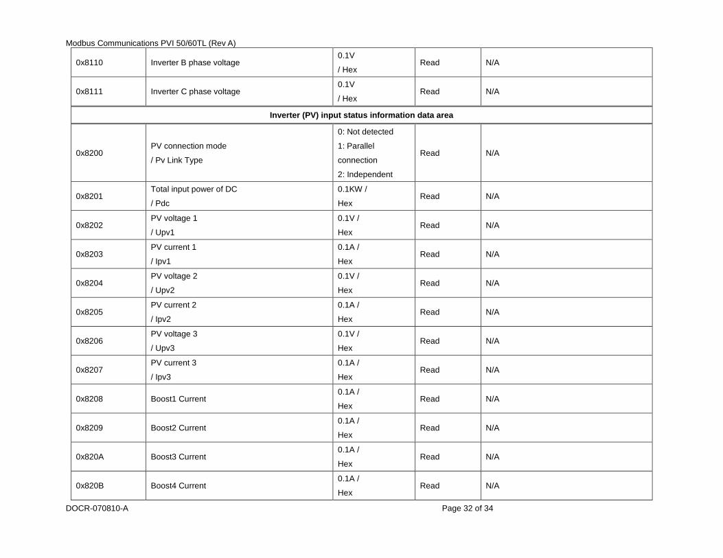
Modbus Communications PVI 50/60TL (Rev A)
DOCR-070810-A Page 32 of 34
0x8110 Inverter B phase voltage 0.1V
/ Hex Read N/A
0x8111 Inverter C phase voltage 0.1V
/ Hex Read N/A
Inverter (PV) input status information data area
0x8200 PV connection mode
/ Pv Link Type
0: Not detected
1: Parallel
connection
2: Independent
Read N/A
0x8201 Total input power of DC
/ Pdc
0.1KW /
Hex Read N/A
0x8202 PV voltage 1
/ Upv1
0.1V /
Hex Read N/A
0x8203 PV current 1
/ Ipv1
0.1A /
Hex Read N/A
0x8204 PV voltage 2
/ Upv2
0.1V /
Hex Read N/A
0x8205 PV current 2
/ Ipv2
0.1A /
Hex Read N/A
0x8206 PV voltage 3
/ Upv3
0.1V /
Hex Read N/A
0x8207 PV current 3
/ Ipv3
0.1A /
Hex Read N/A
0x8208 Boost1 Current 0.1A /
Hex Read N/A
0x8209 Boost2 Current 0.1A /
Hex Read N/A
0x820A Boost3 Current 0.1A /
Hex Read N/A
0x820B Boost4 Current 0.1A /
Hex Read N/A
Modbus Communications PVI 50/60TL (Rev A)
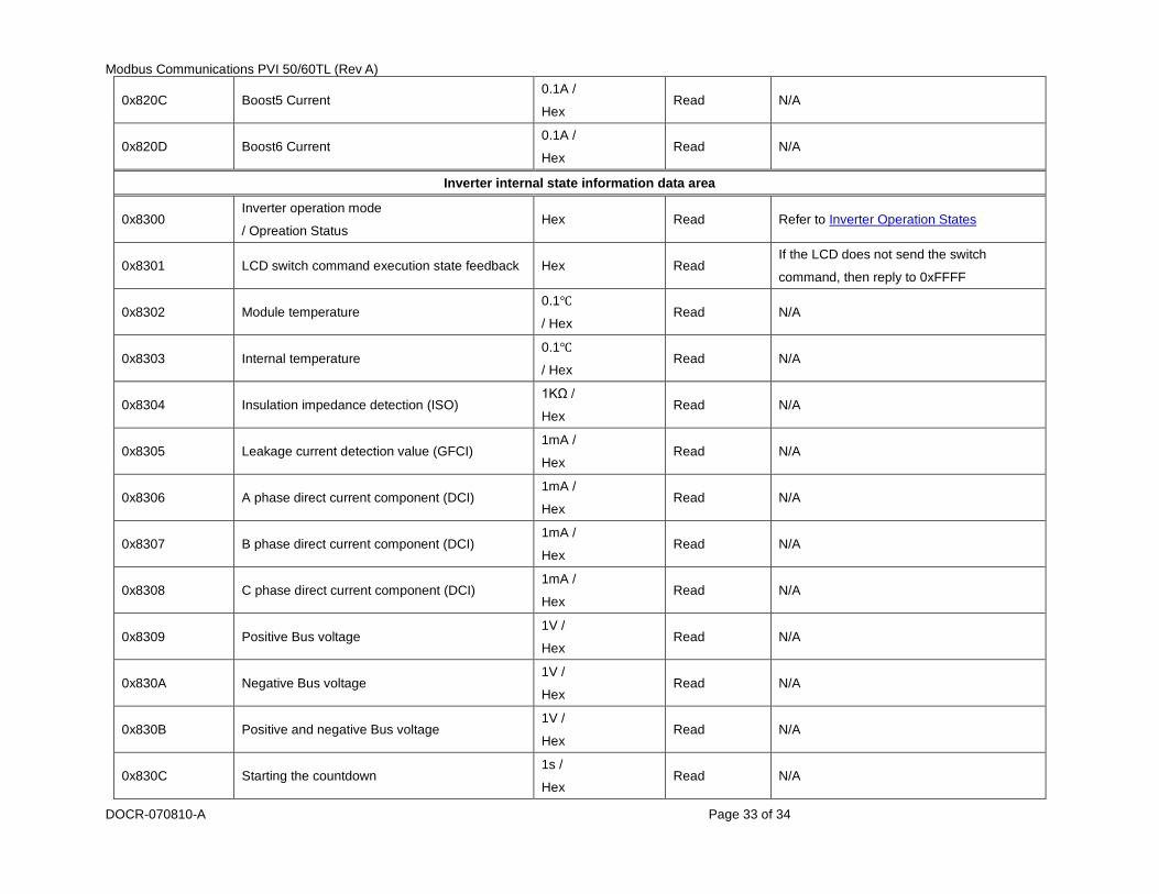
DOCR-070810-A Page 33 of 34
0x820C Boost5 Current 0.1A /
Hex Read N/A
0x820D Boost6 Current 0.1A /
Hex Read N/A
Inverter internal state information data area
0x8300 Inverter operation mode
/ Opreation Status Hex Read Refer to Inverter Operation States
0x8301 LCD switch command execution state feedback Hex Read If the LCD does not send the switch
command, then reply to 0xFFFF
0x8302 Module temperature 0.1℃
/ Hex Read N/A
0x8303 Internal temperature 0.1℃
/ Hex Read N/A
0x8304 Insulation impedance detection (ISO) 1KΩ /
Hex Read N/A
0x8305 Leakage current detection value (GFCI) 1mA /
Hex Read N/A
0x8306 A phase direct current component (DCI) 1mA /
Hex Read N/A
0x8307 B phase direct current component (DCI) 1mA /
Hex Read N/A
0x8308 C phase direct current component (DCI) 1mA /
Hex Read N/A
0x8309 Positive Bus voltage 1V /
Hex Read N/A
0x830A Negative Bus voltage 1V /
Hex Read N/A
0x830B Positive and negative Bus voltage 1V /
Hex Read N/A
0x830C Starting the countdown 1s /
Hex Read N/A

Modbus Communications PVI 50/60TL (Rev A)
DOCR-070810-A Page 34 of 34
0x830D ISO sampling circuit detection voltage 1V /
Hex Read N/A
Inverter fault status information data area
0x8400 Internal warning failure
/ Warn
Hex Read
Bit resolution:
See Fault Codes for DSP Version 1.0 or
Fault Codes for DSP Version 2.0
0x8401 Internal recoverable failure 1 / Fault 0
0x8402 Internal recoverable failure 2 / Fault 1
0x8403 Internal recoverable failure 3 / Fault 2
0x8404 Internal recoverable failure 4 / Fault 3
0x8405 Internal recoverable failure 5 / Fault 4
0x8406 Internal permanent fault