focusing waveguide grating coupler using a diffractive doublet
TRANSCRIPT

Focusing waveguidegrating coupler using a diffractive doublet
Stephen Sheard, Tingdi Liao, Guoguang Yang, Philip Prewett, and Jianguo Zhu
A novel focusing waveguide grating coupler comprising an integrated uniform grating coupler andbinary-phase-only diffractive lens is proposed, designed, and fabricated. Experimental results are alsopresented to demonstrate the device performance. This device is in direct competition with single-element focusing grating couplers defined by direct-write electron-beam lithography and its structure isattractive because the fabrication procedure is better suited for mass production. © 1997 Optical Societyof America
Key words: Integrated optics, focusing grating coupler, diffractive optics, photolithography.
1. Introduction
A focusing waveguide grating coupler ~FWGC!1–3 im-plements simultaneously two optical functions: tocouple out the guided wave propagating in thewaveguide structure and to focus the outgoing beaminto a small spot. Although combining two opticalfunctions into a single diffractive optical element isquite attractive, the submicrometer feature sizes nec-essary to implement high-numerical-aperture focus-ing elements impose a significant burden on thelithography. So far, FWGC’s with a high numericalaperture ~NA . 0.25! have been rarely reported.4The NA of typical FWGC’s available is ;0.25, whichis not high enough for many practical applications.Furthermore, fabrication of such FWGC’s largely re-lies upon direct-write electron-beam lithography.This is an inherently expensive technique that is notideally suited for mass production of optoelectroniccircuits.
Waveguide grating couplers without focusingpower and that exhibit spatially periodic featureshave been intensively and widely investigated.5–8
Such lower complexity gratings can be defined withsimple two-beam optical-interference methods, even
S. Sheard, T. Liao, and G. Yang are with the Department ofEngineering Science, University of Oxford, Parks Road, Oxford,OX1 3PJ, UK. P. Prewett and J. Zhu are with the Central Mi-crostructure Facility, Rutherford Appleton Laboratory, Chilton,Didcot, Oxon, OX11 0QX, UK.
Received 12 August 1996; revised manuscript received 22 No-vember 1996.
0003-6935y97y194349-05$10.00y0© 1997 Optical Society of America
though the grating pitch is of submicrometer order.Furthermore, high coupling efficiency is achievablewith various grating structures.8–10 On the otherhand, diffractive lenses ~or diffractive zone plates!have been successfully used as focusing elements andthe fabrication of diffractive lenses with variousNA’s11 can be realized by conventional photolithog-raphy. However, a focusing grating coupler thatcombines the above two diffractive optical elementsand relies only on planar integration technology hasnot been reported until recently.12
In principle, a focusing grating coupler can be re-alized with the use of a waveguide grating coupler tocouple out the guided wave into the superstrate ~clad-ding! and then with a diffractive lens to focus theoutgoing beam into a spot in the cladding or air. Theimportant thing is that these two diffractive elementsshould be sufficiently physically separated in the ver-tical direction so that they manipulate the guidedwave and the outgoing beam independently. Theresulting diffractive doublet is therefore opticallyequivalent to the single-element FWGC describedpreviously. However, so far to our knowledge, noinvestigation has been reported on this compositeFWGC when considered as a single integrated ele-ment. In this paper, the design procedure and fab-rication technology of this composite FWGC ispresented. We believe that this type of componentmight find application in optoelectronic hybrid cir-cuits.
2. Focusing Waveguide Grating Coupler Design
As described above, the output coupling characteris-tics of the composite FWGC are determined by thewaveguide grating coupler, and the focusing function
1 July 1997 y Vol. 36, No. 19 y APPLIED OPTICS 4349
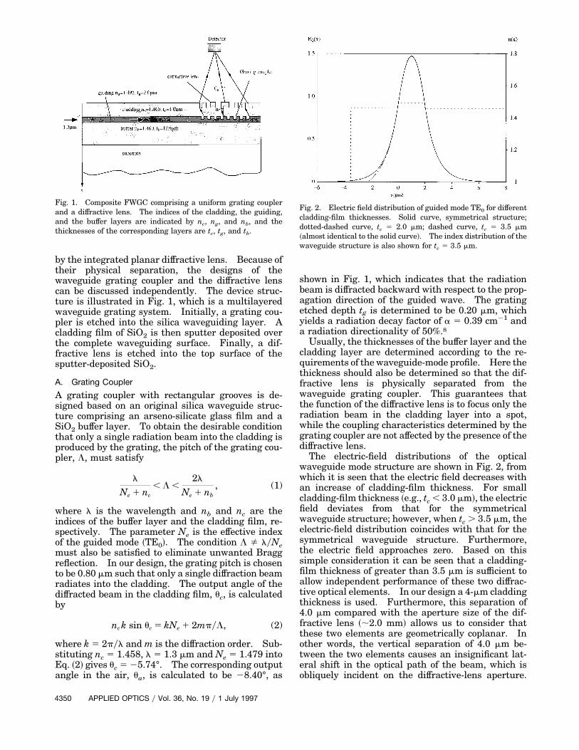
by the integrated planar diffractive lens. Because oftheir physical separation, the designs of thewaveguide grating coupler and the diffractive lenscan be discussed independently. The device struc-ture is illustrated in Fig. 1, which is a multilayeredwaveguide grating system. Initially, a grating cou-pler is etched into the silica waveguiding layer. Acladding film of SiO2 is then sputter deposited overthe complete waveguiding surface. Finally, a dif-fractive lens is etched into the top surface of thesputter-deposited SiO2.
A. Grating Coupler
A grating coupler with rectangular grooves is de-signed based on an original silica waveguide struc-ture comprising an arseno-silicate glass film and aSiO2 buffer layer. To obtain the desirable conditionthat only a single radiation beam into the cladding isproduced by the grating, the pitch of the grating cou-pler, L, must satisfy
l
Ne 1 nc, L ,
2l
Ne 1 nb, (1)
where l is the wavelength and nb and nc are theindices of the buffer layer and the cladding film, re-spectively. The parameter Ne is the effective indexof the guided mode ~TE0!. The condition L Þ lyNemust also be satisfied to eliminate unwanted Braggreflection. In our design, the grating pitch is chosento be 0.80 mm such that only a single diffraction beamradiates into the cladding. The output angle of thediffracted beam in the cladding film, uc, is calculatedby
nc k sin uc 5 kNe 1 2mpyL, (2)
where k 5 2pyl and m is the diffraction order. Sub-stituting nc 5 1.458, l 5 1.3 mm and Ne 5 1.479 intoEq. ~2! gives uc 5 25.74°. The corresponding outputangle in the air, ua, is calculated to be 28.40°, as
Fig. 1. Composite FWGC comprising a uniform grating couplerand a diffractive lens. The indices of the cladding, the guiding,and the buffer layers are indicated by nc, ng, and nb, and thethicknesses of the corresponding layers are tc, tg, and tb.
4350 APPLIED OPTICS y Vol. 36, No. 19 y 1 July 1997
shown in Fig. 1, which indicates that the radiationbeam is diffracted backward with respect to the prop-agation direction of the guided wave. The gratingetched depth tg is determined to be 0.20 mm, whichyields a radiation decay factor of a 5 0.39 cm21 anda radiation directionality of 50%.8
Usually, the thicknesses of the buffer layer and thecladding layer are determined according to the re-quirements of the waveguide-mode profile. Here thethickness should also be determined so that the dif-fractive lens is physically separated from thewaveguide grating coupler. This guarantees thatthe function of the diffractive lens is to focus only theradiation beam in the cladding layer into a spot,while the coupling characteristics determined by thegrating coupler are not affected by the presence of thediffractive lens.
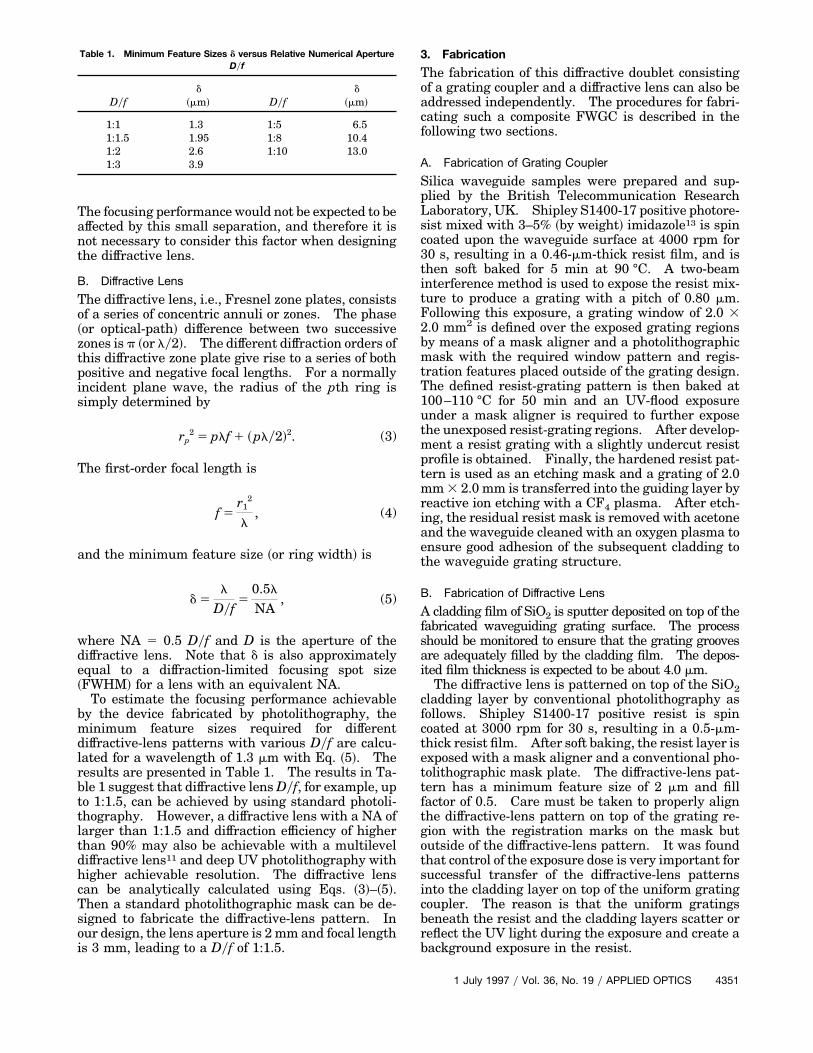
The electric-field distributions of the opticalwaveguide mode structure are shown in Fig. 2, fromwhich it is seen that the electric field decreases withan increase of cladding-film thickness. For smallcladding-film thickness ~e.g., tc , 3.0 mm!, the electricfield deviates from that for the symmetricalwaveguide structure; however, when tc . 3.5 mm, theelectric-field distribution coincides with that for thesymmetrical waveguide structure. Furthermore,the electric field approaches zero. Based on thissimple consideration it can be seen that a cladding-film thickness of greater than 3.5 mm is sufficient toallow independent performance of these two diffrac-tive optical elements. In our design a 4-mm claddingthickness is used. Furthermore, this separation of4.0 mm compared with the aperture size of the dif-fractive lens ~;2.0 mm! allows us to consider thatthese two elements are geometrically coplanar. Inother words, the vertical separation of 4.0 mm be-tween the two elements causes an insignificant lat-eral shift in the optical path of the beam, which isobliquely incident on the diffractive-lens aperture.
Fig. 2. Electric field distribution of guided mode TE0 for differentcladding-film thicknesses. Solid curve, symmetrical structure;dotted-dashed curve, tc 5 2.0 mm; dashed curve, tc 5 3.5 mm~almost identical to the solid curve!. The index distribution of thewaveguide structure is also shown for tc 5 3.5 mm.
The focusing performance would not be expected to beaffected by this small separation, and therefore it isnot necessary to consider this factor when designingthe diffractive lens.
B. Diffractive Lens
The diffractive lens, i.e., Fresnel zone plates, consistsof a series of concentric annuli or zones. The phase~or optical-path! difference between two successivezones is p ~or ly2!. The different diffraction orders ofthis diffractive zone plate give rise to a series of bothpositive and negative focal lengths. For a normallyincident plane wave, the radius of the pth ring issimply determined by
rp2 5 plf 1 ~ply2!2. (3)
The first-order focal length is
f 5r1
2
l, (4)
and the minimum feature size ~or ring width! is
d 5l
Dyf5
0.5l
NA, (5)
where NA 5 0.5 Dyf and D is the aperture of thediffractive lens. Note that d is also approximatelyequal to a diffraction-limited focusing spot size~FWHM! for a lens with an equivalent NA.
To estimate the focusing performance achievableby the device fabricated by photolithography, theminimum feature sizes required for differentdiffractive-lens patterns with various Dyf are calcu-lated for a wavelength of 1.3 mm with Eq. ~5!. Theresults are presented in Table 1. The results in Ta-ble 1 suggest that diffractive lens Dyf, for example, upto 1:1.5, can be achieved by using standard photoli-thography. However, a diffractive lens with a NA oflarger than 1:1.5 and diffraction efficiency of higherthan 90% may also be achievable with a multileveldiffractive lens11 and deep UV photolithography withhigher achievable resolution. The diffractive lenscan be analytically calculated using Eqs. ~3!–~5!.Then a standard photolithographic mask can be de-signed to fabricate the diffractive-lens pattern. Inour design, the lens aperture is 2 mm and focal lengthis 3 mm, leading to a Dyf of 1:1.5.
Table 1. Minimum Feature Sizes d versus Relative Numerical ApertureDyf
Dyfd
~mm! Dyfd
~mm!
1:1 1.3 1:5 6.51:1.5 1.95 1:8 10.41:2 2.6 1:10 13.01:3 3.9
3. Fabrication
The fabrication of this diffractive doublet consistingof a grating coupler and a diffractive lens can also beaddressed independently. The procedures for fabri-cating such a composite FWGC is described in thefollowing two sections.
A. Fabrication of Grating Coupler
Silica waveguide samples were prepared and sup-plied by the British Telecommunication ResearchLaboratory, UK. Shipley S1400-17 positive photore-sist mixed with 3–5% ~by weight! imidazole13 is spincoated upon the waveguide surface at 4000 rpm for30 s, resulting in a 0.46-mm-thick resist film, and isthen soft baked for 5 min at 90 °C. A two-beaminterference method is used to expose the resist mix-ture to produce a grating with a pitch of 0.80 mm.Following this exposure, a grating window of 2.0 32.0 mm2 is defined over the exposed grating regionsby means of a mask aligner and a photolithographicmask with the required window pattern and regis-tration features placed outside of the grating design.The defined resist-grating pattern is then baked at100–110 °C for 50 min and an UV-flood exposureunder a mask aligner is required to further exposethe unexposed resist-grating regions. After develop-ment a resist grating with a slightly undercut resistprofile is obtained. Finally, the hardened resist pat-tern is used as an etching mask and a grating of 2.0mm 3 2.0 mm is transferred into the guiding layer byreactive ion etching with a CF4 plasma. After etch-ing, the residual resist mask is removed with acetoneand the waveguide cleaned with an oxygen plasma toensure good adhesion of the subsequent cladding tothe waveguide grating structure.
B. Fabrication of Diffractive Lens
A cladding film of SiO2 is sputter deposited on top of thefabricated waveguiding grating surface. The processshould be monitored to ensure that the grating groovesare adequately filled by the cladding film. The depos-ited film thickness is expected to be about 4.0 mm.
The diffractive lens is patterned on top of the SiO2cladding layer by conventional photolithography asfollows. Shipley S1400-17 positive resist is spincoated at 3000 rpm for 30 s, resulting in a 0.5-mm-thick resist film. After soft baking, the resist layer isexposed with a mask aligner and a conventional pho-tolithographic mask plate. The diffractive-lens pat-tern has a minimum feature size of 2 mm and fillfactor of 0.5. Care must be taken to properly alignthe diffractive-lens pattern on top of the grating re-gion with the registration marks on the mask butoutside of the diffractive-lens pattern. It was foundthat control of the exposure dose is very important forsuccessful transfer of the diffractive-lens patternsinto the cladding layer on top of the uniform gratingcoupler. The reason is that the uniform gratingsbeneath the resist and the cladding layers scatter orreflect the UV light during the exposure and create abackground exposure in the resist.
1 July 1997 y Vol. 36, No. 19 y APPLIED OPTICS 4351

Finally, once again the resist is used as an etchingmask after an UV flood exposure for 30 min and hardbaking for 30 min at 125 °C. Reactive ion etching isthen used to transfer the binary diffractive-lens pat-tern approximately 0.40 mm deep into the SiO2 filmby means of a CF3H plasma. The remaining resistmask is removed, yielding a transmissive SiO2 binaryphase diffractive lens.
C. Results
The focusing performance of the fabricated compositeFWGC is evaluated with a spot-size measurement, inwhich a laser diode with a working wavelength of 1.3mm is used as the light source. The focused spot ismagnified by a 203 microscope objective and the cor-responding CCD intensity profile is examined withimage-processing software. The CCD image and in-tensity profiles of the focused spot are shown in Figs. 3and 4. The measured spot size ~FWHM! is 5.0 mm inthe horizontal direction and 6.6 mm in the verticaldirection as viewed from the focused spot, while thetheoretically determined diffraction-limited spot size is1.7 mm. There exists astigmatism in the focused spot,which arises from the divergent cylindrical wave-frontpropagation in the planar waveguide and the consec-utive oblique and divergent incident beam on thediffractive-lens plane. These effects cause broadeningof the focused spot size. Alignment errors and fabri-cation errors in the diffractive-lens pattern also con-tribute to a loss in the focusing performance.
It should be pointed out that the exponentially de-caying radiation field on the diffractive-lens aperturewill affect the focusing performance, but as long asthe radiation-decay factor is satisfied by aL , 2 ;3,1,14 the diffraction-limited focusing performance isstill achievable, which is the case for our device.
Fig. 3. CCD image of the focused spot produced by the compositeFWGC.
4352 APPLIED OPTICS y Vol. 36, No. 19 y 1 July 1997
Furthermore, the planarity of the SiO2 surface on thetop of the grating coupler after sputter deposition issufficiently good in our fabricated device, and it isexpected that the surface flatness should not affectthe focusing performance and coupling efficiency.
4. Conclusions
A novel focusing waveguide grating coupler consist-ing of a uniform grating coupler and a diffractive lenshas been successfully fabricated and its working prin-ciple demonstrated. Although diffraction-limited fo-cusing performance has not been achieved in thisdevice, it is significant to note that the fabricationprocedure offers considerable advantages when com-pared with conventional FWGC fabrication usingdirect-write electron beam lithography. Calcula-tions have shown that high NA is achievable with acompact planar structure. A near-vertical output fo-cusing beam can be obtained when the pitch of thegrating coupler L ' lyNe. In our device the theo-retical coupling efficiency is ;20%; however, a higherdiffraction efficiency of larger than 80% could beachieved with high-efficiency waveguide grating cou-pler structures and a multilevel binary phase diffrac-tive lens. Fabrication of this device is compatiblewith microlithography fabrication technology, andfabrication cost can be reduced owing to the less de-manding challenge of the lithography. It is expectedthat this novel device will find potential applicationsin integrated optoelectronic systems.
This work is supported by the UK Engineering andPhysical Science Research Council, grant referenceGRyH21128. Tingdi Liao thanks the K. C. WongScholarship and British Council for an Overseas Re-search Scholarship Award for his study at Oxford.The authors also thank the British Telecom ResearchLaboratory for supplying the waveguide samples.
Fig. 4. Normalized intensity distribution of focused spot producedby the fabricated combined FWGC with D 5 2.0 mm and f 5 3.0mm ~NA 5 0.33!. The focused spot size ~FWHM! is determined tobe 5.0 mm in the horizontal direction. The dashed curve corre-sponds to diffraction-limited profiles with a focused spot size~FWHM! of 1.7 mm.

References1. S. Ura, T. Suhara, H. Nishihara, and J. Koyama, “An
integrated-optic disk pickup device,” J. Lightwave Technol. 4,913–917 ~1986!.
2. F. Sogawa, Y. Hori, and M. Kato, “Fabrication of aberration-free focusing grating couplers,” Appl. Opt. 29, 5103–5105~1990!.
3. S. Nishiwaki, J. Asada, and S. Uchida, “Optical head employ-ing a concentric-circular focusing grating coupler,” Appl. Opt.33, 1819–1828 ~1994!.
4. I. Kawakubo, J. Funazaki, K. Shirane, and A. Yoshizawa, “In-tegrated optical-disk pickup that uses a focusing grating cou-pler with a high numerical aperture,” Appl. Opt. 33, 6855–6859 ~1994!.
5. T. Tamir and S. T. Peng, “Analysis and design of grating cou-plers,” Appl. Phys. 14, 235–254 ~1977!.
6. W. Streifer, D. R. Scifres, and R. D. Burnham, “Analysis ofgrating-coupled radiation in GaAs: GaAlAs lasers andwaveguides,” IEEE J. Quantum Electron. QE-12, 422–428~1976!.
7. W. Streifer, R. D. Burnham, and D. R. Scifres, “Analysis ofgrating-coupled radiation in GaAs: GaAlAs lasers andwaveguides—II: Blazing effects,” IEEE J. Quantum Electron.QE-12, 494–499 ~1976!.
8. M. Li and S. J. Sheard, “Waveguide couplers usingparallelogramic-shaped blazed gratings,” Opt. Commun. 109,239–245 ~1994!.
9. L. A. Avrutsky, A. S. Svakhin, V. A. Sychugov, and O. Parri-aux, “High-efficiency single-order waveguide grating coupler,”Opt. Lett. 15, 1446–1448 ~1990!.
10. R. L. Roncone, L. Li, K. A. Bates, J. J. Burke, L. Weisenbach,and B. J. J. Zelinski, “Design and fabrication of a singleleakage-channel grating coupler,” Appl. Opt. 32, 4522–4528~1993!.
11. W. H. Welch, J. E. Morris, and M. R. Feldman, “Iterativediscrete on-axis encoding of radially symmetrical computer-generated holograms,” J. Opt. Soc. Am. A 10, 1729–1738~1993!.
12. S. J. Sheard, T. Liao, G. Yang, P. R. Prewett, and J. G. Zhu,“Focusing waveguide grating coupler using diffractive dou-blet,” in Diffractive Optics and Micro-Optics, Vol. 5 of 1996OSA Technical Digest Series ~Optical Society of America,Washington, D.C., 1996!, pp. 360–363.
13. H. Moritz, “Optical single layer lift-off process,” IEEE Trans.Electron. Devices 32, 672–676 ~1985!.
14. T. Liao, “Integrated waveguide diffractive optics for guidedwave manipulation,” Ph.D. dissertation ~Oxford University,Oxford, UK, 1996!.
1 July 1997 y Vol. 36, No. 19 y APPLIED OPTICS 4353