focus plasma technology - balticnet-plasmatec · federal ministry of education and research 04...
TRANSCRIPT

FOC
US
PLA
SM
A T
EC
HN
OLO
GY
FOC
US
PLA
SM
A T
EC
HN
OLO
GY

03
Plasma has many faces
pag
e
Content
Federal Ministry of Education and Research 04
About Plasma Technology and BalticNet-PlasmaTec 05
The Project 07
BalticNet-PlasmaTec 09
H.C. Starck 11
INP Greifswald 13
The Leibniz Association 15
neoplas control 17
Pfeiffer Vacuum 19
Roth & Rau 21
C-Met 23
Fraunhofer IGB 25
IfOD Wismar 27
Milman 29
Plazma India 31
Universität Greifswald 33

05pag
e
In addition to their fundamental importance as the so called “fourth state of matter,” plasma offers a
multitude of technological applications. Plasma technology embraces a large potential of current and
promising fields of application so that it has become a key technology. This technology plays an impor-
tant role for example in the automotive industry; modern engine needs different plasma based hard and
low friction coatings, in electronics; each semiconductor is etched by plasma, in medicine; on many
implants plasma produced functional coatings can be find, in the development of new materials; many
micro- and nano particle are produced or modified with plasma but also such easy consumer goods like
plastic bags are often activated by plasma before they get there colour design. Germany is one of the
world innovation and market leader of plasma technology leader alongside Japan and the United States.
The international network BalticNet-PlasmaTec is one of the most important clusters in Europe in the
field of plasma technology. BalticNet-PlasmaTec became during the last years an attractive platform for
users and researchers within the field of plasma technology. The network has reliable contacts with
scientific and public facilities, as well as with numerous relations to industrial partners particularly in all
countries bordering the Baltic Sea, but also in Italy, Netherlands and India. As an international plasma
technology network, BalticNet-PlasmaTec aims to support the creation of new jobs in the long term by
introducing and disseminating the plasma technology in the universities, industry, SME and public faci-
lities. The main aims include opening up new business fields, fostering company spin-offs, and intense
joint marketing and common research and development activities.
About Plasma Technology and BalticNet-PlasmaTec
The Federal Ministry of Education and Research (BMBF) is supporting Indo-German cooperation through
its initiative: “India and Germany - Strategic Partners for Innovation.” Starting in September 2008 and
scheduled until December 2010, Germany has been presenting itself to India as a Centre of Innovation
under the motto “Research in Germany – Land of Ideas”; highlighting Germany’s vast array of universi-
ties, research institutes, networks and clusters, as well as companies with a strong research base. One
of the prime goals of the Federal Government’s “Internationalisation Initiative” is to expand cooperation
in growth markets into countries that actively engage in dynamic research activities.
Scientific and Technological Collaboration (STC)
During a visit by Indian Prime Minister Manmohan Singh to Germany on 23 April 2006, both he and
Chancellor Angela Merkel acknowledged the importance of the Scientific and Technological Collabora-
tion (STC) to promote the dialogue between scientists from both countries. To date the collaboration
has enabled 1,000 joint Indo-German research projects, involving 4,000 scientists from both countries.
Incorporating input from both sides, STC has also completed a total of 100 workshops and produced
1,500 scientific publications.
The Federal Ministry of Education and Research

07From the Baltic Sea to the Indian Ocean
Aims and results of the project
The aim of the project was to initiate German-Indian cooperation of science and industry for R&D and further
education in the field of plasma technology. One main focus is the contact initiation to innovative companies and
research institutes in the field of metal working, medical technology, environmental protection and energy sector.
The other aims ranges from the project-related cooperation up to acquisition of joint venture partner. But also the
cooperation with Indian research facilities is from large interest particularly for the adjustment of the technologies
in consideration of the local peculiarities.
The most important results of the project are:
• one research and development contract between a Indian company and a German research institute
• one CLIENT project proposal (German grant); two IGSTC project proposals (joint German and Indian grant)
• joint signature of German and Indian partners: three Letter Of Intent, two Non-Disclosure Agreements
and one Memorandum Of Understanding
• establishment of a new company (GmbH) in Greifswald, Germany (founder and owner of the company
are Indian partner)
• three new network partners
• successful fair participation and organisation of an own three days workshop in India
The network would like to establish in medium-term and in the long term a long-lasting (sustainable) cooperation in
different levels of the Indian scientific landscape. The constancy of the marketing activities should be realised by a
systematically integration of Indian partners in bilateral and international activities. Actual the network organises to
join with 2 projects at the IGSTC-Call for Proposal for Joint R&D Projects between India and Germany. Interested
parties are always welcome. For further information please contact the branch office of the BalticNet-PlasmaTec.
pag
e

09The network BalticNet-PlasmaTec stands for a technology and market oriented cooperation of science,
research and economy in the field of the plasma technology. The network supports existing and initiates
new cooperation between universities, industry, small and medium-sized companies and public facili-
ties from the field of the plasma technology. BalticNet-PlasmaTec is working to enhance the perception
of the plasma technology in this society. To this end, the network takes over coordination duties for
implementation of common, and in particular, cross-border activities. BalticNet-PlasmaTec is a platform
for the cooperation between the academic world, public facilities, private companies and individuals.
Technology
• Preparation and coordination of projects & Co operations
• Search and procurement of partners from R&D and from industry
• Acquisition and organization of projects (EU)
Education
• On the job learning
• Postgraduate education
• Placement for PhD students, staff exchange organizations, and apprenticeships
Marketing
• Technology marketing for new procedures & products
• Presentation of R&D - results, services and products
• Preparation of market and feasibility study e.g. for R&D - results
• Event management and company representation at fairs.
BalticNet-PlasmaTec
Alexander Schwock
Brandteichstr. 20
17489 Greifswald, Germany
Phone: +49 (0)3834 550 102
Fax: +49 (0)3834 550 111
www.balticnet-plasmatec.org
Contact
pag
e

H.C. Starck GmbH / Martina Woelfert
Im Schleeke 78 - 91 / 38642 Goslar / Germany
Phone: +49 5321 751 3177 / Fax: +49 5321 751 4177
[email protected] / www.amperit.info
METALLIZING EQUIPMENT CO. PVT. LTD.
E-101, M.I.A., Phase-II, Basni, Jodhpur-342005 (India)
Phone: +91 291 2747601 Fax: +91 291 2746359
[email protected] / [email protected] / [email protected]
www.mecpl.com
Contact
11Offering unique expertise in high-tech materials, H.C. Starck is, now more than ever, your best choice
for innovative high-value products. Refractory metals, ceramics, and electronic chemicals form the core
of the wide-ranging products and services that secure our important role in each of today’s fastest
growing industries.
AMPERIT ® and AMPERWELD ® powders for thermal spraying and welding are prime examples of the
high standards we set for our products and of our commitment to helping our clients create functional
solutions in the three key areas of materials, development and solutions. The names AMPERIT ® and
AMPERWELD ® are worldwide synonymous with high quality, versatile materials in surface technology,
that are capable of being developed and adjusted according to need and application.
Customer-specific product solutions from H.C. Starck’s unique product range are increasingly becoming
indispensable for innovative applications and new markets, as the following examples show:
• Aircraft turbines
• Automotive
• Pulp and paper
• Printing industry
• Hard-chrome replacement
• Energy
• Industrial applications
pag
e
INP Greifswald
Dr. Hans Sawade
Felix-Hausdorff-Str. 2
17489 Greifswald, Germany
Phone: +49 (0)3834 554 3899
Fax: +49 (0)3834 554 301
www.inp-greifswald.de
Contact
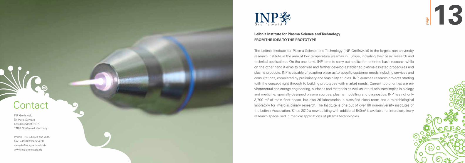
13Leibniz Institute for Plasma Science and Technology
FROM THE IDEA TO THE PROTOTYPE
The Leibniz Institute for Plasma Science and Technology (INP Greifswald) is the largest non-university
research institute in the area of low temperature plasmas in Europe, including their basic research and
technical applications. On the one hand, INP aims to carry out application-oriented basic research while
on the other hand it aims to optimize and further develop established plasma-assisted procedures and
plasma products. INP is capable of adapting plasmas to specific customer needs including services and
consultations, completed by preliminary and feasibility studies. INP launches research projects starting
with the concept right through to building prototypes with market needs. Current top priorities are en-
vironmental and energy engineering, surfaces and materials as well as interdisciplinary topics in biology
and medicine, specially-designed plasma sources, plasma modelling and diagnostics. INP has not only
3,700 m2 of main floor space, but also 26 laboratories, a classified clean room and a microbiological
laboratory for interdisciplinary research. The Institute is one out of over 86 non-university institutes of
the Leibniz Association. Since 2010 a new building with additional 540m² is available for interdisciplinary
research specialised in medical applications of plasma technologies.
pag
e

Leibniz Association
Head of press and public relations :
Josef Zens
Phone: +49 (0)30 2060 4942
Fax: +49 (0)30 2060 4955
www.wgl.de
Contact
15The Leibniz Association is a network of 86 scientifically, legally and economically independent re-
search institutes and scientific service facilities. Leibniz Institutes perform strategic and thematically
oriented research and offer scientific service of national significance and strive for scientific solutions
for major social challenges.
Leibniz Institutes employ more than 14,200 employees, thereof 6,500 are academics, including 2,500
junior scientists. Leibniz Institutes maintain 2,200 major national and 1,300 international scientific
cooperations. About 2,300 foreign scientists come for temporary work at Leibniz Institutes each year.
Third party funds of 230 million Euro per year indicate high competitiveness and excellence.
Leibniz Institutes have collected 26 million Euro from the European Union, 45 million Euro from the
Deutsche Forschungsgemeinschaft (German Research Foundation, DFG) and 59 million Euro from in-
dustry cooperations in 2007. The total budget of all Leibniz Institutes amounts to more than 1,1 billion
Euro.
Leibniz Institutes contribute to clusters of excellence on fields as Mathematics, Optic Technologies,
Materials Research, Medicine, Climate and Environmental Research, Bio- and Nanotechnology as well
as humanities, economics and social sciences. Leibniz Institutes foster close cooperations with uni-
versities, industry, and other research institutes, both in Germany and abroad. The Leibniz Association
has developed a comprehensive system of quality management. In the unique peer review evaluation
process, independent experts assess every institute at regular intervals.
pag
e

neoplas control GmbH
Henrik Zimmermann
Walther-Rathenau-Str. 49a
17489 Greifswald, Germany
Phone: +49 (0)3834 515 400
Fax: +49 (0)3834 515 401
www.neoplas-control.de
Contact
17Highest Precision - with Measurement and Control Systems for Gases and Plasmas
Environmental and safety requirements are becoming stricter. The demands on quality and efficiency of
industrial production are rising not only for economical reasons in many industries. Optical spectrome-
ters help to optimize processes, where high degrees of reliability, security and readiness are required
as well as excellent accuracy of measurement. neoplas control is a centre of competence for gas and
plasma analysis based on laser spectroscopy in the mid-infrared range.
With the product series Q-MACS (Quantum Cascade Laser Measurement and Control System) it is
possible to detect lowest absolute concentrations of molecules in gaseous media up to parts per trillion
(ppt) in real-time. The Q-MACS technology was developed for various applications like the high sensitive
analysis of plasma processes or trace gases. neoplas control also offers components such as laser
supplies and detectors, multi-pass optics and equipment for calibration. The portfolio is completed with
software solutions and services.
Product Features
• Measurements with very high precision and time resolution up to nano second range
• Simultaneous monitoring of different molecules through the use of multiple lasers
• Lasers and detectors operate at room temperature without extensive cooling
• Compact, modular, expandable and user-friendly
pag
e

Pfeiffer Vacuum GmbH / Headquarters Germany
Berliner Str. 43 / 35614 Asslar
Phone: +49 (0)6441 802 0 / Fax: +49 (0)6441 802 202
[email protected] / www.pfeiffer-vacuum.net
Pfeiffer Vacuum India Ltd.
25/5, Nicholson Road, Tarbund
500 009 Secunderabad / India
Phone: +91 (0)40 2775 0014 / Fax: +91 (0)40 2775 7774
Contact
19Transforming Ideas into Solutions!
• Leading Vacuum Provider for Metallurgy for more than 40 Years
• Supplier of Vacuum Components and Systems
- Roots, Rotary Vane and Dry Pumps
- Roots Pumping Units
- Turbopumps
- Vacuum Gauges
- Mass Spectrometers
- Helium Leak Detectors
- Customized Vacuum Solutions
• Local Sales and Service Organization
pag
e

Roth & Rau MicroSystems GmbH
Gewerbering 3
09337 Hohenstein-Ernstthal, Germany
Phone: +49 (0) 3723 49 88 0
Fax: +49 (0) 3723 49 88 25
www.roth-rau.de/microsystems
Contact
21Advanced Plasma and Ion Beam Technologies
Roth & Rau MicroSystems GmbH is a worldwide operating company that provides advanced technology
solutions for the coating, structuring and processing of surface areas through the application of plasma
and ion beam processes. The company‘s process systems feature a modular composition that ensures
an easy adaptation of different methods of surface modification, such as Reactive Ion Etching (RIE),
Plasma Enhanced Chemical Vapor Deposition (PECVD), Ion Beam Etching (IBE) and Ion Beam Sputter
Deposition (IBSD). The process systems are applied in the semiconductor industry, in the production of
high precision optics and sensors as well as for research and development.
In-house developed plasma and ion beam sources in various configurations build the basis of all process
systems that are developed by Roth & Rau MicroSystems. These are available in form of a conventional
parallel-plate-arrangement, as ICP sources and as microwave excited sources with adjustable geome-
trical configurations. The company has a vast amount of experience in the production of sources and
constantly works on the technological development of these.
The product portfolio of Roth & Rau MicroSystems includes process systems for application on single
wafers as well as on flat samples. The modular design enables their optimization for the individual requi-
rements of each process (RIE, PECVD, IBE). Furthermore the range of services of the company reaches
from consultancy, design, construction, assembly to software development as well as installation and
an after sale service.
pag
e

23About C-MET
Dedicated to the furtherance of competent research and development in the firmament of Electronic
Materials, the Centre for Materials for Electronics Technology (C-MET) functions as a scientific institu-
tion under Dept. of Information Technology, Ministry of Communications and Information Technology
(MCIT), Govt. of India. Besides augmenting core competence, C-MET envisions attainment of self-suf-
ficiency in the sphere of Electronic Materials, Components and Devices to cater to India’s strategic- and
industrial- applications, exploiting indigenous resources of raw materials.
C-MET is operating with three laboratories located at Pune,Hyderabad and Thrissur.The laboratory at
Pune functions as headquarter and extends central coordination support. Each Laboratory has its own
area of specialization with requisite infrastructure and expertise. This approach has proven to be suc-
cessful in creating core competence at each laboratory.
C-MET’s Core Competence
• Integrated Electronic Packaging
• Nanomaterials and Devices
• Ultra High Purity Materials
• Materials for Renewable Energy
• Pizosensors and Actuators
Centre for Materials for Electronics Technology
(C-MET)
Executive Director: Dr. Dinesh P. Amalnerkar
Under DIT, Govt. Of India, Panchawati,
Off Pashan Road, Pune-411008, India
Phones: (O) 020-25899273/ 25898141/25898390
(R) 020-25889272
www.cmet.gov.in
Contact
pag
e

Fraunhofer Institute for Interfacial
Engineering and Biotechnology
Nobelstrasse 12
70569 Stuttgart, Germany
Phone: +49 711 970 4401
Fax: +49 711 970 4200
www.igb.fraunhofer.de
Contact
25Fraunhofer Institute for Interfacial Engineering and Biotechnology IGB
The Fraunhofer Institute for Interfacial Engineering and Biotechnology IGB in Stuttgart, Germany, deve-
lops and optimizes processes and products for the business areas of medicine, pharmacy, chemistry,
the environment and energy. Under direction of Professor Thomas Hirth, the Fraunhofer IGB is engaged
in a broad spectrum of R&D in its fields of competence – Interfacial Engineering and Materials Science,
Molecular Biotechnology, Physical Process Technology, Environmental Biotechnology and Bioprocess
Engineering, and Cell and Tissue Engineering.
Our abiding goal is the direct translation of research results into sustainable cost-effective and profitable
processes and products. Our strengths are to offer complete solutions from laboratory to pilot plant
scale. Customers benefit from the synergies and multidisciplinary potential at our institute, which faci-
litate novel approaches and innovative solutions in areas such as medical engineering, nanotechnology,
industrial biotechnology and environmental technology.
In addition to contract R&D, we offer analytical and testing services of reliable and constant quality ful-
filling international standards. Applications of plasma technology belong to the main research interests
of the Fraunhofer IGB in the field of materials research. The used plasmas are low temperature, low-to-
medium pressure ones, enabling a gentle and controlled surface processing. This way we are able to
etch surfaces, to graft new chemical functionalities onto the surface or to polymerize a thin film onto
the surface providing functions such as as scratch-resistance, dirt-repellency, or corrosion protection. By
controlling the gas composition, power and other process parameters, a broad spectrum of chemical,
physical and biological surface modifications is attainable.
pag
e

Hochschule Wismar,
Fachhochschule für Technik, Wirtschaft
und Gestaltung / Institut für Oberflächen-
und Dünnschichttechnik (IfOD)
General manager: Dr. rer. nat. Torsten Barfels
Philipp-Müller-Straße / Postfach 1210
23952 Wismar / Germany
Fon: +49 3841 753175 / Fax: +49 3841 753136
http://hermes.et.hs-wismar.de/ifod/
Contact
27Institute of Surface and Thin Film Technology (IfOD)
The Institute of Surface and Thin Film Technology (IfOD) was founded in 2000 within the
Hochschule Wismar – University of Applied Sciences, Technology, Business and Design.
The IfOD is a research Institute within the Faculty of Engineering and was conceived as an
almost completely third party supported research and educational institute. The intention
is to carry the regional economic development and to reinforce the cooperation of science and industry
by realising of applied research projects.
Modern scientific processes and methods were bunched on high scientific level in the areas of thin-
and thick film technology, plastics engineering and physical analytics like material testing and electron
microscopic analysis.
The educational offer, basically addressed to students of the Mechanical-, Process-, Environmental- and
Electrical Engineering consists of practicals, lectures, Bachelor and Master Themes to the point of co
operational PhD – programs. Besides this educational offer the IfOD has committed itself to the applied,
practice focussed research in the named areas. One core area is development and characterisation of
new functional materials and composite materials respectively and the development of its production in
laboratory and small batch scale. One essential aspect of the strategic focusing thereby consists in de-
velopment of new materials for chemical sensor technology, fuel cell technology, medical engineering
and polymer technology. Hereby a close cooperation with resident companies is rising, allowing for its
demands of consulting in materials science and aiming at common development of innovative products.
The working group of the IfOD, actually consisting of four professors, nine scientific co-workers (ma-
terial scientists, physicists, chemists and engineers) and fife technicians has attended to more than 30
research projects during the past years with a total volume of fife millions of euro.
pag
e

MILMAN THIN FILM SYSTEMS PVT. LTD.
Executive Director: Dr.Milind G. Acharya
322 A 1/2, Vishwachaya Industry Road,
PIRANGUT Tal. Mulshi, PUNE 412 111,
MAHARASHTRA, INDIA
Phone: +91-20-66748971-75, Fax: +91-20-66748970
Mobile: +91-9822409634
[email protected], [email protected]
www.milmanthinfilms.com
Contact
29MILMAN© a start-up company established in 1996 by a group of Technocrats is a major player in state-
of-the-art Thin Film Equipment and Plasma Process. The main objective of the company is indigenous
development of frontline technologies in the area of Thin Films and manufacturing of finest quality phy-
sical vapour deposition equipment based on them.
MILMAN enjoys a large customer base in Scientific Research Laboratories, Universities, Institutes of
Technology and Industries.
MILMAN specializes in offering complete solutions to customers in the field of Thin Films, Plasma
Processing and associated Technologies. The entire chain of activities from Computer Aided design
to final production, quality control and Installation of all the equipment manufactured by this group, is
strongly supported by specially developed vendor base and state-of-the-art in-house assembly shop run
by experts.
Milman provides value added solutions in:
• Custom built thin film coating equipments
• Advance plasma processing equipment based on magnetron sputtering, arc deposition
• Customized solutions for industrial physical vapour deposition equipments
• Plasma Ion Nitriding technology
• Specialized Sub-system viz. Magnetron Cathode, Pulsed Power Supplies,
Corona Poling Equipment etc.
pag
e
Photo: IHP Frankfurt/Oder

31Plazma Technologies Pvt. Ltd.
Since 1994 Plazma has sustained long-term growth in turnover & profit. It is based on continuous develop-
ment of self financed proprietary technology innovations. Research will continue to remain Plazma’s core.
It’s founders Hughen & Arundhati share this passion with over 1,000 Plazma & 37 RoboPlazma customers,
which has resulted in numerous patents & awards (like Indian, South African, Canadian, US and European
patents). Plazma plans to initiate a multi-year growth to capture market share in growth segment of Robo-
Plazma enhanced cutting market to take it from current turnover of $3.5 Million to $100 Million in 5 years.
Plazma vision
• Be a leader in research and development of various Plasma applications
• Be a global supplier of artificial intelligence driven, vision enhanced RoboPlazma™
systems that reduce manufacturing cycle times drastically.
• Set up Plazma cutting application training centers to benefit customers and students alike.
• Expand the scope of Plazma products & RoboPlazma™ Systems beyond cutting and welding in to other applications.
• Set up strategic alliances with companies with complementary product range to be a global technology leader
Plazma intellectual property
• Protection of Plazma designs, drawings with trademarks, patents & copyrights worldwide to safe guard
its intellectual property.
• RoboSwift is a licensed web based encrypted software with embedded server management to control piracy,
virus, theft and such related issues.
• Plazma implements Non disclosure agreements with all its employees, suppliers, consultants and vendors.
Plazma Technologies Pvt. Ltd.
Managing Director: Arundhati Thomas
E-10/19, B-3, MIDC Bhosari, Pune-411 026, India
Phone: +91 20 2712 1617 /3859
Fax: +91 20 2712 3062
www.plazmasolutions.com
Contact
pag
e

Institute for Physics
Dr. Abhijit Majumdar
Felix-Hausdorff-Str. 6
17489 Greifswald, Germany
Phone: +49 3834 864784
Fax: +49 3834 864701
www.physik.uni-greifswald.de/~abhijit/
Contact
33Ernst Moritz Arndt University of Greifswald
One working group at the Institute of Physics from the Ernst Moritz Arndt University is mostly occupied
with atmospheric pressure dielectric barrier discharge plasma and its application on biology as well as
thin film deposition. The working group deposit hard coating by magnetron sputtering, RF sputtering and
soft polymer (hydrogenated) thin film or amorphous coating by dielectric barrier discharge (DBD) plas-
ma. In case of biological studies they have used CH4/N2 gas mixture DBD plasma to deposit amorphous
hydrogenated carbon nitride aH–CNx film. In vitro studies with three different cancer cell lines were
carried out on the coated surfaces. Preliminary biocompatibility and effect of CH4/N2 films have been
investigated by measuring cell proliferation. Three different cancer cell MCF-7, Colo-357, and LNCaP
suspensions have been exposed on the surface of aH–CNx film to investigate the effect of deposited
films on viability of cells. Direct plasma treatment also has been done in case sterilization or to kill
the different bacteria. As for example atmospheric pressure dielectric barrier discharge (DBD) plasma
has been employed on gram-negative bacteria, Escherichia coli BL21. Treatment was carried out using
plasma generated with different compositions of gases: CH4 /N2, O2, N2, and Ar, and by varying plasma
power and treatment time.
The group have studied the influence of nitrogen on the chemical properties of the hydrogenated car-
bon nitride (a-CNx:H) film deposited by CH4/N2 DBD plasma. X-ray photoelectron spectroscopy (XPS)
indicates that carbon and nitrogen form an unpolarised covalent bond in these C 1s, N 1s materials,
and the observed chemical shift in the C 1s and N 1s binding energy is explained with respect to N 1s
incorporation.
pag
e

Break new groundPlasma could be your solution. So please join us in our pursuit of new horizons.