flying capacitor docx
DESCRIPTION
flying capacitorTRANSCRIPT

A FLYING CAPACITOR BASED II LEVEL GRID
CONNECTED INVERTER FOR TRANSFORMER LESS PV
SYSTEMS

ABSTRACT- This paper presents a grid-connected single-phase
Transformer less photovoltaic converter based on two cascaded full bridges
with different dc-link voltages. The converter can synthesize up to eleven
voltage levels with a single dc bus, since one of the full bridges is supplied by a
flying capacitor. Harmonic distortion and electromagnetic interference (EMI)
can be reduced in the multilevel output. The switching strategy is employed
such that to regulate the flying-capacitor voltage, improves the efficiency for
most devices switch at the frequency and will minimize the minimum the
common-mode leakage cuurent with the help of a novel dedicated circuit.
Simulation results confirm the feasibility and good performance of the
proposed converter.
Index Terms—pulse width modulation (PWM) inverters, photovoltaic (PV)
systems, leakage current, multilevel systems.
CHAPTER-1
INTRODUCTION
GRID connected PV systems provides best solution for small-scale and

domestic applications. . While classical designs of PV converters feature a grid
frequency transformer, which is a typically heavy and costly component, at the
interface between the converter and the electrical grid, researchers are now
considering Transformerless architectures in order to reduce costs and weight and
improve efficiency. With the removal of grid frequency transformer involves all
benefits but worsens the output power quality and increases ground leakage current
Though fossil fuel resources are limited and depleting at an alarming rate, the
global demand for oil has increased significantly in recent years. Energy consumed
and demanded by transportation sector has risen exponentially due to increasing
number of vehicles. Transportation accounts for above 20% of the total energy-
related emissions .Today most of the world’s vehicles are dependent on
conventional energy sources. In this regard, alternative solutions for “sustainable
and green mobility” are being researched and implemented by researchers,
industries as well as policy makers.
The active parts of PV modules might be electrically insulated from the
ground-connected mounting frame; a path for ac ground leakage currents generally
exists due to a parasitic capacitance between the modules and the frame and to the

connection between the neutral wire and the ground, usually realized at the low-
voltage/medium-voltage (LV/MV) transformer [3]. In addition to deteriorating
power quality, the ground leakage current increases the generation of
electromagnetic interference and can represent a safety hazard, so that international
regulations pose strict limits to its magnitude.
This issue must be confronted in all transformer less PV converters, regardless of
architecture. In particular, in full-bridge-based topologies, the ground leakage
current is mainly due to high frequency variations of the common-mode voltage at
the output of the power converter [4]. Several solutions can be found in literature
aiming at the reduction of the common-mode voltage harmonic content [5]–[7].
Once the grid frequency transformer is removed from a PV converter, the bulkiest
wound and reactive components that remain are those that form the output filter
used to clean the output voltage and current from high frequency switching
components.
Further reduction in cost and weight and improvement in efficiency can be
achieved by reducing the filter size, and this is the goal of multilevel converters.
For years multilevel converters have been investigated [8], but only recently have
the results of such researches found their way to commercial PV converters.
Multilevel converters outperform conventional two- and three-level converters in
terms of harmonic distortion since they can synthesize the output voltages using
more levels the input voltage among several power devices, allowing for the use of
more efficient devices.
Fig.1 expected 11-level output Moreover, multilevel converters subdivid

Multilevel converters were initially employed in high-voltage industrial
and power train applications. They were first introduced in renewable energy
converters inside utility-scale plants, in which they are still largely employed [9].
Recently, they have found their way to residential-scale single-phase PV
converters; currently represent a hot research topic Single-phase multilevel
converters can be roughly divided into three categories based on design: neutral
point clamped (NPC), cascaded full bridge (CFB), and custom. In NPC topologies,
the electrical potential between the PV cells and the ground is fixed by connecting
the neutral wire of the grid to a constant potential, resulting from a dc-link
capacitive divider .
A huge advantage is that single-phase NPC converters are virtually immune from
ground leakage currents, although the same is not true for three-phase NPC
converters A recent paper has proposed an interesting NPC design for exploiting
next-generation devices such as super junction or SiC MOSFETs [16]. The main
drawback of NPC designs is that they need twice the dc-link voltage, with respect
to full bridge. CFBs make for highly modular designs. Usually, each full bridge
inside a CFB converter needs an insulated power supply, matching well with multi-
string PV fields [16].

Full bridges are sequentially permuted can be used to evenly share the power
among the parts and to mitigate the effects of the partial shading [17]. As an
alternative, only one power supply can be used if the output voltage is obtained
through a transformer [18].CFB can also be used for stand-alone application which
provides many degrees of freedom the control strategy to the developers. With
aforementioned sequential permutation with phase shifting [19], artificial neural
networks [20] and predictive control have been proposed to minimize harmonic
distortion and achieve maximum power point tracking (MPPT). When the supply
voltage is the same for each full bridge CFB can synthesize 2n+1 voltage levels
when CFB made up of n full bridges (and at least 4n power switches).
Custom architectures can generally provide more output levels with a given
number of active devices, and custom converters generally need custom pulse-
width modulation (PWM) and control schemes, although unified control schemes
for different types of multilevel converters can be implemented. In addition to
using fewer switches, custom architectures can be devised so that some of the
switches commutate at the grid frequency, thus improving the efficiency.
Reduction in the switches-per-output voltage-level ratio can be achieved in CFB
structures if different supply voltages are chosen for each full bridge (asymmetrical
CFBs). The topology proposed in this paper consists of two asymmetrical CFBs,
generating eleven output voltage levels.

In the proposed converter, one full bridge is supplied by dc source whereas a
flying capacitor supplies other one. Different sets of output voltages can be
obtained by suitably controlling the ratio between the two voltages, the flying
capacitor used as a secondary energy source allows for limited voltage boosting, as
it will result clear in the following section.
The number of output levels per switch (ten switches, eleven levels) is comparable
to what can be achieved using custom architectures. In order to reduce the ground
leakage current two additional very low power switches and a line frequency
switching device [transient circuit (TC)] were included in the final topology. The
custom converter proposed in [25] generates five levels with six switches but has
no intrinsic boosting capability. In [24], Rahimet al.used three dc-bus capacitors in
series together with two bidirectional switches (diode bridge+ unidirectional
switch) and an H-bridge to generate seven output levels; however, they give no
explanations on how they keep the capacitor voltages balanced. In [26], five
switches, four diodes, and two dc-bus capacitors in series are used to generate five
levels with boosting capability. Again, no mention is made about how the
capacitors are kept balanced.

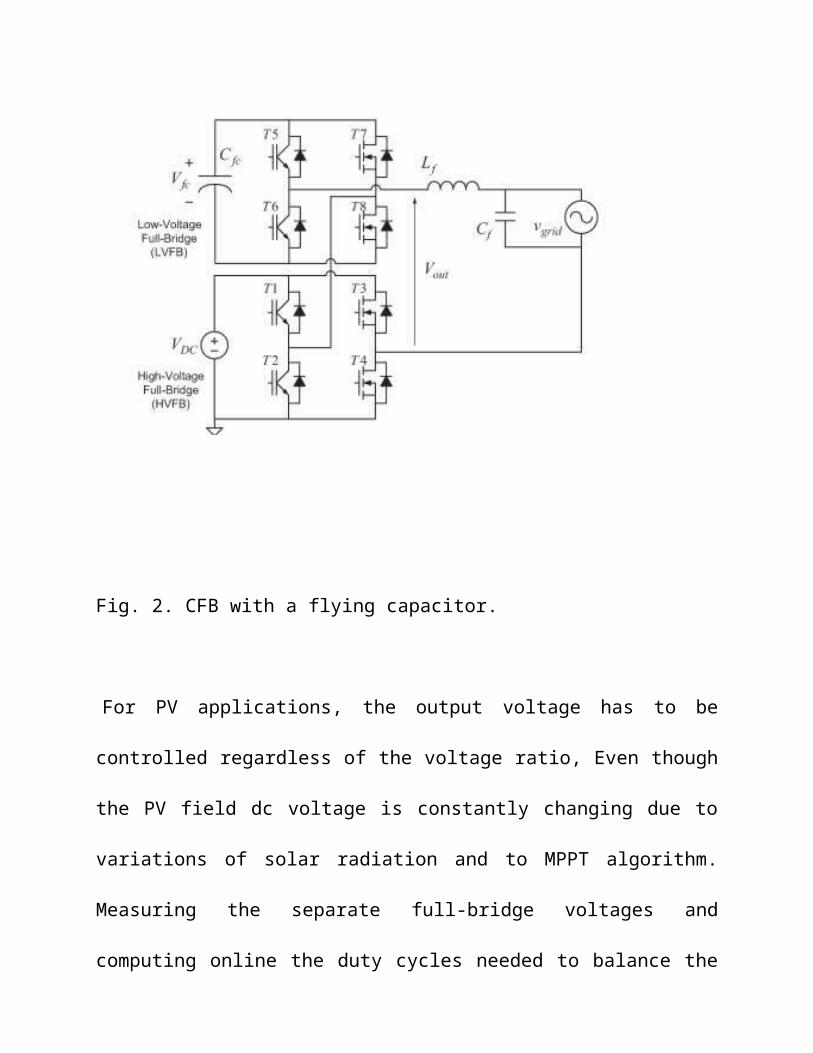
Fig. 2. CFB with a flying capacitor.
For PV applications, the output voltage has to be controlled regardless of the
voltage ratio, Even though the PV field dc voltage is constantly changing due to
variations of solar radiation and to MPPT algorithm. Measuring the separate full-
bridge voltages and computing online the duty cycles needed to balance the
different voltages, and analyzing also the power balance between the separate cells.
A similar approach is followed in this paper. The developed PWM strategy, in
addition to controlling the flying capacitor voltage, with the help of the specific TC
illustrated in Section IV, minimizes the ground leakage current.
Finally, it is important to put in evidence that the proposed converter can work at
any power factor as reported in Section III, while not all the alternative proposals
can continuously supply reactive power. The proposed topology was presented by
the authors in a previous paper [27]. With respect to the previous work, this paper
was rewritten for 11-level output and presents a better organization and a new set
of simulation.
This paper is organized as follows: Section II presents converter topology with
PWM control strategy chosen in order to maximize the performance. Section III
discusses about CFB topology for the regulation of flying capacitor used to supply
the second full bridge. Section IV describes the principle of operation of the
additional components to reduce the ground leakage current. Section V shows the
simulation results, Whereas Section VI reports the concluding remarks.

CHAPTER 2
ELEVEN-LEVEL CONVERTER AND PWM CONTROL STRATEGY
The proposed converter is composed of two CFBs, one of which is supplied by a
flying capacitor (see Fig. 2). This basic topology is well known. In this paper, in
order to allow grid-connected operation with no galvanic isolation (transformerless
solution) different PWM strategy was developed for this basic topology. Using
PWM strategy alone is not going to maintain a low ground leakage current, other
components were added which will be discussed in next section. As it will be
described in the following, the proposed PWM strategy stretches the efficiency by
using, for the two legs where PWM frequency switching does not occur, devices
with extremely low voltage drop, such as MOSFETs lacking a fast recovery diode.
In fact, the low commutation frequency of those two legs allows, even in a reverse
conduction state the conduction in the channel instead of the body diode (i.e.,
active rectification). Insulated-gate bipolar transistors (IGBTs) with fast anti-
parallel diodes are required in the legs where high-frequency hard switching
commutations occur. For grid-connected operation, one full-bridge leg is directly
connected to the grid neutral wire, whereas the phase wire is connected to the
converter through an LC filter. Flying-capacitor

The full bridge supplied by the dc link is called the high-voltage full bridge
(HVFB), whereas the one with the flying capacitor is the low-voltage full-bridge
(LVFB). CFB can also be used for stand-alone application which provides many
degrees of freedom the control strategy, so that different PWM schemes can be
considered. However, the chosen solution needs to satisfy the following
requirements.
1)To limit the switching losses, most commutations must take place in the LVFB.
2) To reduce the ground leakage current, the neutral-connected leg of the
HVFB needs to switch at grid frequency
3) To control the flying-capacitor voltage the redundant states of the converter
must be properly used.
4) The driving signals must be obtained from a single carrier for a low-cost to
be used as a controller.
The switching pattern described in Table I was developed starting from the above
requirements. Requirement 2), in particular, is due to the aforementioned parasitic
capacitive coupling between the PV panels and their frames, usually connected to
the earth. Capacitive coupling provides the common-mode current inversely
proportional to the switching frequency of the neutral-connected leg. The converter
can operate in different output voltage zones, where the output voltage switches
between two specific levels. The operating zone boundaries vary according to the
dc-link and flying-capacitor voltages, and adjacent zones can overlap (see Fig. 3).
In zones A, the contribution of the flying-capacitor voltage to the converter output
voltage is positive (+ve), whereas it is negative (-ve) in B zones. Constructive
cascading of the two full bridges can, therefore, result in limited output voltage
boosting.

The operation of the converter does not differ much in the two cases. If two
overlapping operating zones can supply the same output voltage, the regulation of
will determine the operating zone, will be described in section III. the duty cycles
are calculated on-line by a simple equation, similarly to the approach presented in.
The instantaneous fundamental component of output voltage ∗ and switches
pattern.
Fig. 3. Operating zones under different ranges

CHAPTER 3
REGULATION OF FLYING-CAPACITOR VOLTAGE
Controlling the voltage of the flying capacitor voltage is critical when a grid-
connected PV converter is transferring the active power to the electrical grid. By
suitably choosing the operating zone flying-capacitor voltage is regulated
depending on the instantaneous output voltage request. Depending on the operating
zone of the converter (see Fig. 3), can be added to (A zones) or subtracted from (B
zones) the HVFB output voltage, charging or discharging the flying capacitor. In
accordance, considering a positive value of the current injected into the grid, the
flying capacitor is discharged in a zone and charged in B zone. Since a number of
redundant switch configurations can be used to synthesize the same output voltage
waveform, it is possible to control the voltage of the flying capacitor, forcing the
converter to operate more in A zones when the flying-capacitor voltage is higher
than a reference value or more in B zones when it is lower than a reference value.
Similar

(a). Flying-capacitor charge

Due to MPPT strategy, the DC-link voltage can go through sudden variations, it is
important that
the converter is able to work in any [ , ] condition. Through on-line duty cycle
computation, the distortion of the output voltage is minimized. It is important to
estimate the capability of the converter to regulate the flying-capacitor voltage
under different operating conditions. The ability to control flying-capacitor voltage
through proposed PWM strategy has been studied in simulation by average
sinusoidal with amplitude of 230√2V in simulations.
The white area and cannot be controllable in the gray and black regions. In
detail, cannot be decreased in the black region, whereas in gray region, it cannot be
increased. The safe operating area for the converter is the white region located
between the gray and black ones for stable operation. If failed in controlling , it can
be a constraint that ensuring flying capacitor cannot be over charged nor
completely discharged inside the white region.

CHAPTER 4
TRANSFORMERLESS PV CONVERTER
The commutation pattern of Table 1 is that T3 and T4 switch at grid frequency,
will commutate at every zero crossing of . If negative derivative with zero crossing
is considered.T3 closes and T4 opens, changing the neutral wire voltage (and thus
the voltage across the parasitic capacitance of the PV field) from zero to .because
of this reason the commutation can cause a large surge of leakage current which
will decrease the power quality and damage the PV modules.
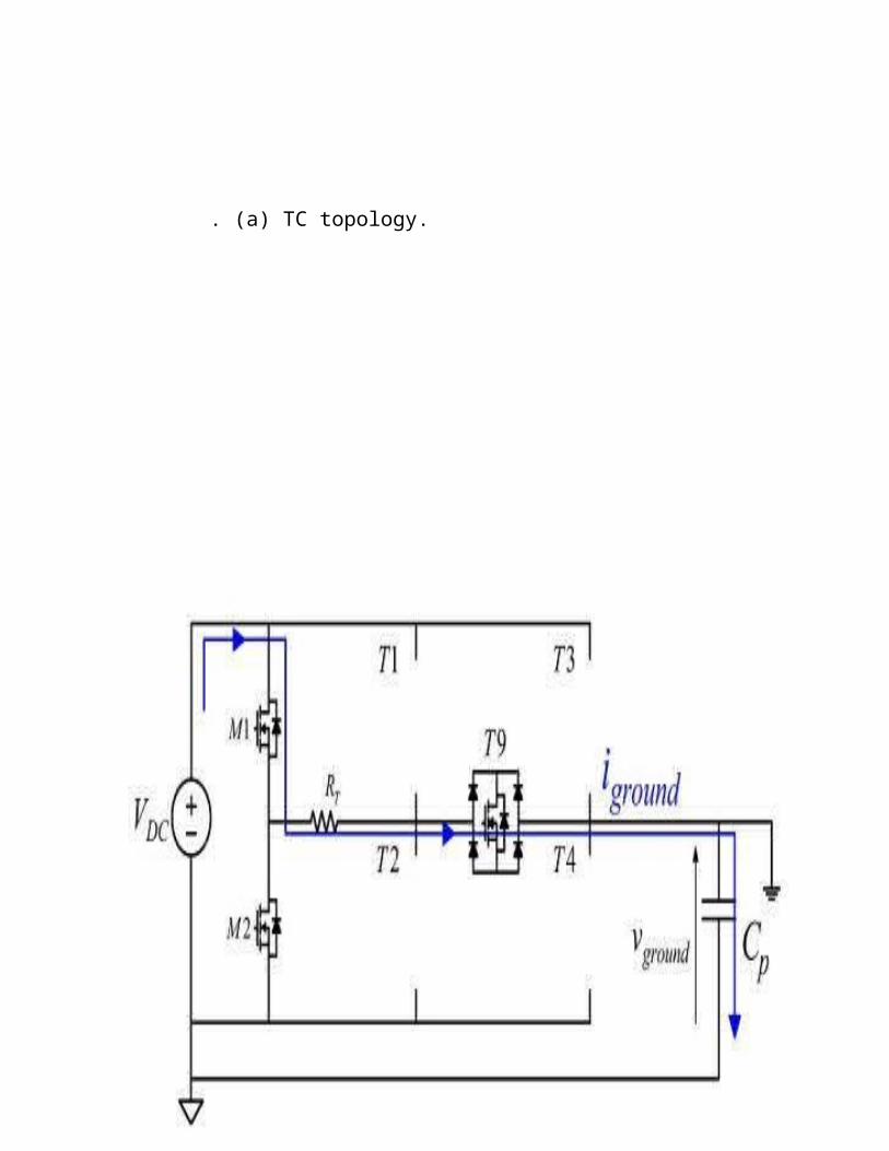
Proper TC must be designed to decrease these surge currents. The proposed
converter topology constitute two-cell CFB described in Fig 2 with the addition of
TC components. For better understand of TC, the distributed parasitic capacitance
of the PV source was modeled with equivalent simple capacitance i.e., between
negative pole and the ground. The TC is formed from two low-power MOSFETs
M1 and M2,

Volume 3, Issue 1 JULY 2015 bidirectional switch T9, and resistor .
When converter enters operating zone 1, the HVFB output voltage must be zero by
switching T1 and T3 or T2 and T4 on. Nevertheless, to operate the TC, when
entering zone 1, T1, T2, T3, and T4 are all kept off, while T9 is on which
maintains neutral point floating and voltage on the parasitic capacitor stays
constant.
. (a) TC topology.

(a) TC operation

(c) TC waveforms.
Fig. 5. Ground leakage current limitation circuit topology and behavior.
One of M1 and M2 is turned on (M1 if the slope of the zero crossing is negative
and M2 if positive). At the same time is charged through with a first-order
transient, limiting the surge current. Whereas the TC introduces additional
components, they can be selected with current ratings much lower than the devices
of the CFB considering the power loss in the additional resistor is negligible.


.
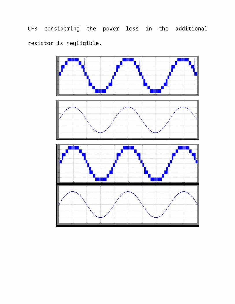
Fig. 7. Simulation results with VDC = 300 V
In grid-connected operation, the output voltage is very close to the grid voltage
will not going to affect the power factor in the operation of TC. For correct
operation of the TC requires the grid voltage instantaneous angle obtained from a
grid voltage through phase locked loop (PLL) [20].

CHAPTER 5
MATLAB
MATLAB is a high-performance language for technical computing. It integrates
computation, visualization, and programming in an easy-to-use environment where
problems and solutions are expressed in familiar mathematical notation. Typical
uses include
Math and computation
Algorithm development
Data acquisition
Modeling, simulation, and prototyping
Data analysis, exploration, and visualization
Scientific and engineering graphics
MATLAB is an interactive system whose basic data element is an array that does
not require dimensioning. This allows solving many technical computing problems,
especially those with matrix and vector formulations, in a fraction of the time it
would take to write a program in a scalar non-interactive language such as C or
FORTRAN.

The MATLAB system consists of six main parts:
(a)Development Environment.
This is the set of tools and facilities that help to use MATLAB functions and files.
Many of these tools are graphical user interfaces. It includes the MATLAB desktop
and Command Window, a command history, an editor and debugger, and browsers
for viewing help, the workspace, files, and the search path.
(b) The MATLAB Mathematical Function Library.
This is a vast collection of computational algorithms ranging from elementary
functions, like sum, sine, cosine, and complex arithmetic, to more sophisticated
functions like matrix inverse, matrix Eigen values, Bessel functions, and fast
Fourier transforms.
(c)The MATLAB Language.
This is a high-level matrix/array language with control flow statements, functions,
data structures, input/output, and object-oriented programming features. It allows

both "programming in the small" to rapidly create quick and dirty throw-away
programs, and "pro
gramming in the large" to create large and complex application programs.
(d) Graphics.
MATLAB has extensive facilities for displaying vectors and matrices as graphs, as
well as annotating and printing these graphs. It includes high-level functions for
two-dimensional and three-dimensional data visualization, image processing,
animation, and presentation graphics. It also includes low-level functions that allow
to fully customize the appearance of graphics as well as to build complete graphical
user interfaces on MATLAB applications.
(e)The MATLAB Application Program Interface (API). This is a library that
allows writing in C and FORTRAN programs that interact with MATLAB. It
includes facilities for calling routines from MATLAB (dynamic linking), calling
MATLAB as a computational engine, and for reading and writing MAT-files.

(f) MATLAB Documentation
MATLAB provides extensive documentation, in both printed and online
format, to help to learn about and use all of its features. It covers all the primary
MATLAB features at a high level, including many examples. The MATLAB online
help provides task-oriented and reference information about MATLAB features.
MATLAB documentation is also available in printed form and in PDF format.
MATLAB TOOLS :-
(g) Three phase source
The Three-Phase Source block implements a balanced three-phase voltage source
with an internal R-L impedance. The three voltage sources are connected in Y with
a neutral connection that can be internally grounded or made accessible. You can
specify the source internal resistance and inductance either directly by entering R
and L values or indirectly by specifying the source inductive short-circuit level and
X/R ratio.
(h) Universal bridge
The Universal Bridge block implements a universal three-phase power converter
that consists of up to six power switches connected in a bridge configuration. The
type of power switch and converter configuration are selectable from the dialog
box.
The Universal Bridge block allows simulation of converters using both naturally
commutated (or line-commutated) power electronic devices (diodes or thyristors)
and forced-commutated devices (GTO, IGBT, MOSFET).
The Universal Bridge block is the basic block for building two-level voltage-
sourced converters (VSC).

(i)current measurement block
The Current Measurement block is used to measure the instantaneous current
flowing in any electrical block or connection line. The Simulink output provides a
Simulink signal that can be used by other Simulink blocks.
(j) rate transition
The Rate Transition block transfers data from the output of a block operating at one
rate to the input of another block operating at a different rate. The Rate Transition
block's parameters allows you to specify options that trade data integrity and
deterministic transfer for faster response and/or lower memory requirements.

(k)multi port switch
The Multiport Switch block chooses between a number of inputs. The first (top)
input is called the control input, while the rest of the inputs are called data inputs.
The value of the control input determines which data input is passed through to the
output port.
If the control input is an integer value, then the specified data input is passed
through to the output. For example, suppose the Use zero-based indexing parameter
is not selected. If the control input is 1, then the first data input is passed through to
the output. If the control input is 2, then the second data input is passed through to
the output, and so on.
If the control input is not an integer value, the block first truncates the value to an
integer by rounding to floor. If the truncated control input is less than 1 or greater
than the number of input ports, an out-of-bounds error is returned.
You specify the number of data inputs with the Number of input ports parameter.
The data inputs can be scalar or vector. The block output is determined by these
rules: If you specify only one data input and that input is a vector, the block
behaves as an "index selector," and not as a multi-port switch. The block output is
the vector element that corresponds to the value of the control input. If you specify
more than one data input, the block behaves like a multi-port switch. The block
output is the data input that corresponds to the value of the control input. If at least
one of the data inputs is a vector, the block output is a vector. Any scalar inputs are
expanded to vectors. If the inputs are scalar, the output is a scalar.
The Index Vector block, also in the Signal Routing library, is another
implementation of the Multiport Switch block that has different default parameter
settings.

(l) direct look up table
The Direct Lookup Table (n-D) block uses its block inputs as zero-based indices
into an n-D table. The number of inputs varies with the shape of the output desired.
The output can be a scalar, a vector, or a 2-D matrix. The lookup table uses zero-
based indexing, so integer data types can fully address their range. For example, a
table dimension using the uint8 data type can address all 256 elements.
You define a set of output values as the Table data parameter. You specify what the
output shape is: a scalar, a vector, or a 2-D matrix. The first input specifies the
zero-based index to the first dimension higher than the number of dimensions in the
output, the second input specifies the index to the next table dimension, and so on,
as shown by this figure

(j)Zero-Order Hold
The Zero-Order Hold block samples and holds its input for the specified sample
period. The block accepts one input and generates one output, both of which can be
scalar or vector. If the input is a vector, all elements of the vector are held for the
same sample period.
You specify the time between samples with the Sample time parameter. A setting
of -1 means the Sample time is inherited.
This block provides a mechanism for discretizing one or more signals in time, or
resampling the signal at a different rate. If your model contains multirate
transitions, you must add Zero-Order Hold blocks between the fast-to-slow
transitions. The sample rate of the Zero-Order Hold must be set to that of the
slower block. For slow-to-fast transitions, use the Unit Delay block. For more
information about multirate transitions, refer to the Simulink or the Real-Time
Workshop documentation.
(k)Sum
The Sum block performs addition or subtraction on its inputs. This block can add or
subtract scalar, vector, or matrix inputs. It can also collapse the elements of a single
input vector.
You specify the operations of the block with the List of Signs parameter. Plus (+),
minus (-), and spacer (|) characters indicate the operations to be performed on the
inputs: If there are two or more inputs, then the number of characters must equal
the number of inputs.
For example, "+-+" requires three inputs and configures the block to subtract the
second (middle) input from the first (top) input, and then add the third (bottom)
input.

All nonscalar inputs must have the same dimensions. Scalar inputs will be
expanded to have the same dimensions as the other inputs. A spacer character
creates extra space between ports on the block's icon. If only addition of all inputs
is required, then a numeric parameter value equal to the number of inputs can be
supplied instead of "+" characters. If only one vector is input, then a single "+" or
"-" will collapse the vector using the specified operation.
The Sum block first converts the input data type(s) to the output data type using the
specified rounding and overflow modes, and then performs the specified
operations.
(l) Demux
The Demux block extracts the components of an input signal and outputs the
components as separate signals. The block accepts either vector (1-D array) signals
or bus signals (see Signal Buses in the Using Simulink documentation for more
information). The Number of outputs parameter allows you to specify the number
and, optionally, the dimensionality of each output port. If you do not specify the
dimensionality of the outputs, the block determines the dimensionality of the
outputs for you.

The Demux block operates in either vector or bus selection mode, depending on
whether you selected the Bus selection mode parameter. The two modes differ in
the types of signals they accept. Vector mode accepts only a vector-like signal, that
is, either a scalar (one-element array), vector (1-D array), or a column or row vector
(one row or one column 2-D array). Bus selection mode accepts only the output of
a Mux block or another Demux block.
The Demux block's Number of outputs parameter determines the number and
dimensionality of the block's outputs, depending on the mode in which the block
operates.
(m)Gain
The Gain block multiplies the input by a constant value (gain). The input and the
gain can each be a scalar, vector, or matrix.
You specify the value of the gain in the Gain parameter. The Multiplication
parameter lets you specify element-wise or matrix multiplication. For matrix
multiplication, this parameter also lets you indicate the order of the multiplicands.

The gain is converted from doubles to the data specified in the block mask offline
using round-to-nearest and saturation. The input and gain are then multiplied, and
the result is converted to the output data type using the specified rounding and
overflow modes.
(n) Outport
Outport blocks are the links from a system to a destination outside the system.
Simulink assigns Outport block port numbers according to these rules: It
automatically numbers the Outport blocks within a top-level system or subsystem
sequentially, starting with 1. If you add an Outport block, it is assigned the next
available number. If you delete an Outport block, other port numbers are
automatically renumbered to ensure that the Outport blocks are in sequence and
that no numbers are omitted. If you copy an Outport block into a system, its port
number is not renumbered unless its current number conflicts with an Outport block
already in the system. If the copied Outport block port number is not in sequence,
you must renumber the block or you will get an error message when you run the
simulation or update the block diagram.

(o)Real-Imag to Complex
The Real-Imag to Complex block converts real and/or imaginary inputs to a
complex-valued output signal.
The inputs can both be arrays (vectors or matrices) of equal dimensions, or one
input can be an array and the other a scalar. If the block has an array input, the
output is a complex array of the same dimensions. The elements of the real input
are mapped to the real parts of the corresponding complex output elements. The
imaginary input is similarly mapped to the imaginary parts of the complex output
signals. If one input is a scalar, it is mapped to the corresponding component (real
or imaginary) of all the complex output signals.
The input signals and real or imaginary output parameter can be of any data type
supported by Simulink, except Boolean. The Real-Imag to Complex block supports
fixed-point data types. The output is of the same type as the input or parameter that
determines the output.
For a discussion on the data types supported by Simulink, refer to Data Types
Supported by Simulink in the Using Simulink documentation.

(p)Complex to Magnitude-Angle
The Complex to Magnitude-Angle block accepts a complex-valued signal of type
double. It outputs the magnitude and/or phase angle of the input signal, depending
on the setting of the Output parameter.
The outputs are real values of type double. The input can be an array of complex
signals, in which case the output signals are also arrays. The magnitude signal array
contains the magnitudes of the corresponding complex input elements. The angle
output similarly contains the angles of the input elements.

(q)Relay
The Relay block allows its output to switch between two specified values. When
the relay is on, it remains on until the input drops below the value of the Switch off
point parameter.
When the relay is off, it remains off until the input exceeds the value of the Switch
on point parameter. The block accepts one input and generates one output.
The Switch on point value must be greater than or equal to the Switch off point.
Specifying a Switch on point value greater than the Switch off point value models
hysteresis, whereas specifying equal values models a switch with a threshold at that
value.

(r)Saturation
The Saturation block imposes upper and lower bounds on a signal. When the input
signal is within the range specified by the Lower limit and Upper limit parameters,
the input signal passes through unchanged. When the input signal is outside these
bounds, the signal is clipped to the upper or lower bound.
When the Lower limit and Upper limit parameters are set to the same value, the
block outputs that value
(s)Relational Operator
The Relational Operator block performs the specified comparison of its two inputs.
You select the relational operator connecting the two inputs with the Relational
Operator parameter. The block updates to display the selected operator. The
supported operations are given below.

You can specify inputs as scalars, arrays, or a combination of a scalar and an array:
For scalar inputs, the output is a scalar. For array inputs, the output is an array of
the same dimensions, where each element is the result of an element-by-element
comparison of the input arrays. For mixed scalar/array inputs, the output is an
array, where each element is the result of a comparison between the scalar and the
corresponding array element.

The input with the smaller positive range is converted to the data type of the other
input offline using round-to-nearest and saturation. This conversion is performed
prior to comparison.
The output data type is specified with the Output data type mode and Output data
type parameters. The output equals 1 for TRUE and 0 for FALSE.
(t)Lookup Table (2-D)
The Lookup Table (2-D) block computes an approximation to some function
z=f(x,y) given x, y, z data points.
The Row index input values parameter is a 1-by-m vector of x data points, the
Column index input values parameter is a 1-by-n vector of y data points, and the
Matrix of output values parameter is an m-by-n matrix of z data points. Both the
row and column vectors

must be monotonically increasing. These vectors must be strictly monotonically
increasing in the following cases: The input and output data types are both fixed-
point. The input and output data types are different. The lookup method is not
Interpolation-Extrapolation. The matrix of output values is complex. Minimum,
maximum, and overflow logging is on.
The block generates output based on the input values using one of these methods
selected from the Look-up method parameter list: Interpolation-Extrapolation--This
is the default method; it performs linear interpolation and extrapolation of the
inputs. If the inputs match row and column parameter values, the output is the value
at the intersection of the row and column. If the inputs do not match row and
column parameter values, then the block generates output by linearly interpolating
between the appropriate row and column values.
If either or both block inputs are less than the first or greater than the last row or
column values, the block extrapolates using the first two or last two points.
Interpolation-Use End Values--This method performs linear interpolation as
described above but does not extrapolate outside the end points of x and y. Instead,
the end-point values are used. Use Input Nearest--This method does not interpolate
or extrapolate. Instead, the elements in x and y nearest the current inputs are found

The corresponding element in z is then used as the output. Use Input Below--This
method does not interpolate or extrapolate. Instead, the elements in x and y nearest
and below the current inputs are found. The corresponding element in z is then used
as the output. If there are no elements in x or y below the current inputs, then the
nearest elements are found. Use Input Above--This method does not interpolate or
extrapolate. Instead, the elements in x and y nearest and above the current inputs
are found.
The corresponding element in z is then used as the output. If there are no elements
in x or y above the current inputs, then the nearest elements are found.

CHAPTER 6
SIMULATION RESULTS
Under MATLAB/Simulink, The simulations cover entire range of active and
reactive power
injected into the grid, Dc-link voltage= 300v was used in the simulations.
The PWM frequency was =20 kHz, and the flying capacitor had a capacitance
of = 500μF. Surge limiting resistance was selected as 1.5 kΩ. With feedforward
through proportional-integral regulator plus feed forward at =8.5A rms. The
instantaneous commutations and the injection of both active and reactive power
was simulated the entire performance will not depend on the power factor. As
outputs are independent of power factor simulations are done for unity power
factor only. As grid voltage angle information is available. So, PLL is needed.
With the DC voltage ratio the THD of the grid currents increases, being 2.7%, 3%
and 3.3%, respectively.

Fig. 8. TC behavior with a 200 nF parasitic capacitor
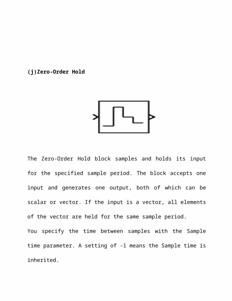
fig. 6. Block scheme of the delay-based PLL

TABLE I
DESCRIPTION OF THE CONVERTER OPERATING
ZONES

Fig. 9. Vfc step variation response.

CHAPTER 7
CONCLUSION
This paper has proposed a novel eleven-level grid connected transformerless
PV converter with full bridges with CFB topology, one of which is supplied by a
floating capacitor, in order to improve the efficiency a suitable PWM strategy was
developed (at low frequency most devices commutate) and with the help of
specific TC, the ground leakage current is minimized. The proposed PWM strategy
can regulate the voltage across the flying capacitor. Simulations were performed to
assess the ability to regulate the flying capacitor voltage in wide range of operating
conditions. Extensive simulations and experiments confirm the results of the
theoretical analysis and show the good performance of the converter as far as
Harmonic distortion and ground leakage current are concerned. The proposed
converter can continuously operate at arbitrary power factors, has limited boosting
capability and can produce eleven output voltage levels.

REFERENCES
[1]G. Buticchi, L. Consolini, and E. Lorenzani, “Active filter for the removal of the dc current component for single-phase power lines,”IEEE Trans. Ind. Electron., vol. 60, no. 10, pp. 4403–4414, Oct. 2013.
[2] G. Buticchi and E. Lorenzani, “Detection method of the dc bias in distribution power transformers,” IEEE Trans. Ind. Electron., vol. 60, no. 8, pp. 3539– 3549, Aug. 2013.
[3] H. Xiao and S. Xie, “Leakage current analytical model and application in single-phase transformerless photovoltaic grid-connected inverter,”IEEE Trans. Electromagn. Compat., vol. 52, no. 4, pp. 902–913, Nov. 2010.
[4] O. Lopez, F. Freijedo, A. Yepes, P. Fernandez Comesaa, J. Malvar, R. Teodorescu, and J. Doval-Gandoy, “Eliminating ground current in a transformerless photovoltaic application,” IEEE Trans. Energy Convers., vol. 25, no. 1, pp. 140–147, Mar. 2010.
[5] S. Araujo, P. Zacharias, and R. Mallwitz, “Highly efficient single-phase transformerless inverters for grid-connected photovoltaic systems,”IEEE Trans. Ind. Electron., vol. 57, no. 9, pp. 3118–3128, Sep. 2010.
[6] D. Barater, G. Buticchi, A. Crinto, G. Franceschini, and E. Lorenzani, “Unipolar PWM strategy for transformerless PV grid-connected Volume 3, Issue 1 JULY 2015 converters,”IEEE Trans. Energy Convers., vol. 27,
no. 4, pp. 835–843, Dec. 2012.
[7]T. Kerekes, R. Teodorescu, P. Rodridguez, G. Vazquez, and E. Aldabas, “A
new high-efficiency single-phase transformerless PV inverter topology,” IEEE

Trans. Ind. Electron., vol. 58, no. 1, pp. 184 191, Jan. 2011.