first principles study of molecular electronic devices9856/fulltext01.pdf · transport mechanisms...
TRANSCRIPT
First Principles Study of Molecular
Electronic Devices
Wenyong Su
Department of Theoretical Chemistry
Royal Institute of Technology
Stockholm 2006

c© Wenyong Su, 2006
ISBN 91-7178-290-7
Printed by Universitetsservice US AB,
Stockholm, Sweden, 2006

3
Abstract
Molecular electronics is an active research area for the future information technology. The
fabrication of basic electronic elements with molecules as the core-operators has been made
experimentally in the laboratory in recent years. However, the underlying electron or charge
transport mechanisms for most devices are still under debate, Theoretical modelling based
on the first-principles methods are expected to play an important role in this field.
A generalized quantum chemical approach based on Green’s function scattering theory has
been developed and applied to two- and three-terminal molecular devices. It allows to study
both elastic and inelastic electron scattering at hybrid density functional theory levels. It can
treat molecular devices where the metal electrodes and the molecule are either chemically or
physically bonded on equal footing. As one of the applications, we have studied the length
dependence of electron transport in gold-oligophenylene-gold junctions. We have shown that
the experimental results for molecular junctions of oligophenylene with different lengths can
be well reproduced by hybrid density functional theory calculations. It is also found that
the current-voltage characteristics of the junctions depend strongly on the metal-molecule
bonding distances. With the help of the calculations, the possible gold-molecule bonding
distances in the experimental devices are identified.
The central focus of this thesis is to study the three-terminal molecular devices, namely the
field effect transistor (FET). An extension of our quantum chemical approach to FET devices
has been made and successfully applied to different FET devices constructed with polymer,
small and middle sized conjugated molecules. The experimentally observed conductance
oscillation in polymer FET and three orders of magnitude enhancement of the current in
electrochemical gated molecular FET have been verified by the calculations. The electron
transport mechanisms of these devices are revealed.

4
Preface
The work presented in this thesis has been carried out at Department of Theoretical Chem-
istry, School of Biotechnology, Royal Institute of Technology, Stockholm, Sweden.
List of papers included in the thesis
Paper I Wenyong Su, Jun Jiang and Yi Luo, Quantum Chemical Study of coherent elec-
tron transport in oligophenylene molecular junctions of different lengths, Chem. Phys. Lett.
412, 406, 2005.
Paper II Wenyong Su, Jun Jiang, Wei Lu and Yi Luo, Understanding the Performance
of a Single Molecular Field Effect Transistor by Hybrid Density Functional Theory, Appl.
Phys. Lett. submitted.
Paper III Wenyong Su, Jun Jiang and Yi Luo, A generalized quantum chemical approach
for modeling of single molecular field effect transistors, J. Chem. Phys. submitted.

5
Comments on my contribution to the papers included
• I was responsible for calculations and for the writing of Paper I.
• I was responsible for calculations and the writing of the first draft for Paper II.
• I was responsible for most of the calculations and for the writing of the first draft for
Paper III.

6
Acknowledgements
First of all, I would like to thank Prof. Yi Luo for introducing me to my research field,
helping me with great patient and optimism attitude. And special thanks to Luo’s help to
my family, which makes our days in Sweden relaxing and joyful. I sincerely thank Prof. Hans
Agren, the head of the Department of Theoretical Chemistry, for providing such wonderful,
fresh working and studying environment.
I would like to thank Docent Ying Fu, who advised me and helped me in many aspects of
my work, and give me positive encouragement.
Thanks to Jun Jiang for nice collaborations.
I would like to thank Prof. Faris Gel’mukhanov, Prof. Boris Minaev, Dr. Fahmi Himo,
Dr.Pawel Salek, Dr. Olav Vahtras, Dr. Pekka Makka, Dr. Hakan Hugosson, Dr. Frediani,
Dr. Zilvinas, Dr. Prokash, Viktor, Barbarar, Mathias, Viviane, Freddy, Ivo, Polina, Stepan,
Lyudmila, Cornel, Sergey, Peter, Kathrin, Elias, Emanuel, Laban, Emil, and Robin for their
helps.
I would like to thank my Chinese friends and colleagues, Prof. Chuanqui Wang, Dr. Yaoquan
Tu, Dr. Jingdong Guo, Ke Zhao, Yanhua Wang, Kai Liu, Guangde Tu, TianTian Han, Shilv
Chen, Yong Zeng, Yuanpin Yi, Bin Gao for their supporting.
Finally, I thank my family for always being there when I most need them, and for supporting
me during these years.

Contents
1 Introduction 9
2 Elastic Scattering Theory 13
2.1 Background . . . . . . . . . . . . . . . . . . . . . . . . . . . . . . . . . . . . 13
2.2 Generalized quantum chemical approach . . . . . . . . . . . . . . . . . . . . 15
3 Gate Field Effect 23
4 Applications 27
4.1 Molecular junctions . . . . . . . . . . . . . . . . . . . . . . . . . . . . . . . . 27
4.2 Single molecular field effect transistors . . . . . . . . . . . . . . . . . . . . . 30
4.2.1 Polymer device . . . . . . . . . . . . . . . . . . . . . . . . . . . . . . 31
4.2.2 1,3-benzenedithiol molecular device . . . . . . . . . . . . . . . . . . . 34
4.2.3 Perylene tetracarboxylic diimide(PTCDI) molecular device . . . . . . 37
7

8 CONTENTS

Chapter 1
Introduction
Molecular electronics is to use molecules as basic elements, such as wires, switches, and
transistors, in the construction of electronic circuitry. It is expected to be a possible physical
limit to Moore’s Law as well as a solution to problems with making small-scale conventional
silicon integrated circuits even smaller. However, the use of molecular electronics can still
only be found in science fiction.
In the 1940s, Robert Mulliken and Albert Szent-Gyorgi advanced the study of charge trans-
fer in the ”donor-acceptor” molecular systems. Since then, extensive experimental and
theoretical investigations have been devoted to the understanding of charge transfer and
energy transfer processes in molecules. Perhaps the first theoretical proof of molecular elec-
tronics for devices came from a paper of Mark Ratner and Avi Aviram in 1974,1 illustrating
a molecular rectifier. They have theoretically constructed a very simple electronic device, a
rectifier, based on the use of a single organic molecule, which consists of a donor and an ac-
ceptor π systems, separated by a σ-bonded (methylene) tunneling bridge. Their calculations
have shown that the response of such a molecule to an applied field can demonstrate recti-
fier properties. Later, Aviram and Ratner detailed a single-molecule field-effect transistor
in 1998.2
Recent progress in nanotechnology and nanoscience have facilitated both experimental and
theoretical study of molecular electronics. In particular, the development of the scanning
tunneling microscope (STM) and later the atomic force microscope (AFM) have made it
possible to build and to manipulate single-molecule electronic devices. However, it remains
a major challenge for wiring up molecules some half a nanometer wide and a few nanometers
long to the electrodes, and an understanding of electrical transport through single molecules
only beginning to emerge. A number of groups have been able to demonstrate molecular
switches, for example, that could conceivably be used in computer memory or logic arrays.3
9

10 CHAPTER 1. INTRODUCTION
However, the possible switching mechanism is still under debate. Both theoretical and
experimental works have attempted to explain conductance changes through a variety of
schemes, including reduction of functional groups,4 rotation of functional groups,5 backbone
phenyl ring rotations,6 neighboring molecule interactions,7,8 bond fluctuations,9 and changes
in bond hybridization.10–13
It is also relevant to mention that work has also being done on the use of single-wall car-
bon nanotubes as molecular electronic devices, like field-effect transistors.14 Carbon nan-
otubes have remarkable electronic, mechanical, and chemical properties. They exhibit either
metallic or semiconducting behaviour, depending on the specific diameter and the bonding
arrangement of their carbon atoms. Electrical conduction within a perfect nanotube is bal-
listic (negligible scattering), with low thermal dissipation. As a result, a wire made from
a nanotube, or a nanowire, can carry much more current than an ordinary metal wire of
comparable size. As a reference, nanotubes with 1.4 nm in diameter are about one hun-
dred times smaller than the gate width of silicon semiconductor devices. In addition to
nanowires for conduction, transistors, diodes, and simple logic circuits have been demon-
strated by combining metallic and semiconductor carbon nanotubes. A major challenge for
nanowire circuits, as for molecular electronics, is connecting and integrating these devices
into a workable high-density architecture. Ideally, the structure would be grown and as-
sembled in place. Crossbar architectures that combine the function of wires and devices
are of particular interest. More-radical approaches in the field of molecular electronics in-
clude DNA computing,15–17 where single-stranded DNA on a silicon chip would encode all
possible variable values and complementary strand interactions would be used for a parallel
processing approach to finding solutions. An area related to molecular electronics is that
of organic thin-film transistors and light emitters, which promise new applications such as
video displays that can be rolled out like wallpaper and flexible electronic newspapers.
In this thesis, we present our contributions to the field of molecular electronics, with focus
on the understanding of electron transport in two-terminal molecular junctions and three-
terminal molecular field effect transistors. The methods discussed in the thesis can also be
extended to the systems containing carbon nanotubes and DNA molecules.
A widely used strategy to reliably wire a molecule to electrodes is to attach the molecule
with two appropriate terminal groups, such as thiols, that can bond covalently to the metal
electrodes.18–24 Two kinds of dithiol molecules have been extensively studied. One of them
is the alkanedithiol chains. These molecules are considered highly insulating because of
their large energy gap between the highest occupied molecular orbital (HOMO) and the
lowest unoccupied molecular orbital (LUMO), but they are relatively simple and chemi-
cally inert, which make them a nice model system to test an experimental technique or
theoretical method.25,26 The second dithiol is based on conjugated aryl oligomers, such as

11
oligophenyl-dithiols and oligophenylene-ethynylene-dithiols.27,28 The conjugation, smaller
HOMO-LUMO gap and the possibility of functionalizing these molecules make them more
attractive for potential molecular electronic applications. The simplest molecules of the
latter group, benzenedithiol(BDT) and benzenedimethanethiol(BDMT), have been investi-
gated experimentally by scanning tunneling microscope(STM)29 and break junction tech-
niques.19 These pioneering works have stimulated a large theoretical effort to investigate the
electron transport properties of these molecules.30–32 Other functional devices based on the
molecular junctions, like molecular wires, rectification and switching have also been demon-
strated.19,33–36 In this thesis, we have applied a generalized quantum chemical approach
to investigate the electron tunneling properties of the gold-oligophenylene-gold junctions
of different lengths.28 The experimentally measured length dependence of current flow in
the junctions has been well reproduced by the hybrid density functional theory calcula-
tions. It is found that the current-voltage characteristics of the junctions depend strongly
on the metal-molecule bonding distances. With the help of the calculations, the possible
gold-molecule bonding distances in the experimental devices are identified.
It is known from the conventional electronics, three-terminal device, like the field effect
transistor (FET), is the essential basic element for any applications. In practice, it is not
simple to make a single molecular field effect transistor because of the difficulty of putting
the third electrode (gate) onto the short molecule. The first molecular FET was based on
the C60 molecules,37 from which noticeable gate effect was observed. Until now, only very
few three-terminal devices have been fabricated.33,37–42 Among FET devices made of self-
assembled monolayer of short (around 1nm) phyenylene-based conjugated molecules,39 weak
gate effect has only been detected for devices with 1,3-benzenedithiol molecule.39 An inter-
esting gate effect has been discovered for thioacetyl-end-functionalized poly(para-pheneylene
ethynylene)(TA-PPE) polymer device,42 in which the conductance is found to oscillate with
high periodicity with gate voltage, appearing as a series of sharp and narrow peaks. A spec-
tacular single molecular FET device based on perylene tetracarboxylic diimide (PTCDI)
molecule made by Xu et al. has shown very strong gate effect.41 It was demonstrated that
the current through the molecule can be reversibly controlled with a gate electrode over
nearly 3 orders of magnitude at room temperature. The use of electrochemical gate ensured
the generation of large gate field acting on the molecule. The huge current gain observed in
the PTCDI molecular FET is certainly very attractive for future applications. Despite var-
ious theoretical proposals,43–46 the general physical principles of the single molecular FETs
are not yet well understood.
We present an extension of the generalized quantum chemical approach to include the gate
field effects, which allows to treat different gate configurations very efficiently. This new
method will also be applied to three known experimental devices that posses noticeable gate

12 CHAPTER 1. INTRODUCTION
effects, namely 1,3-benzenedithiol molecule,39 perylene tetracarboxylic diimide (PTCDI)
molecule41 and thioacetyl-end-functionalized poly(para-pheneylene ethynylene)(TA-PPE)
polymer,42 and to shed the light on the underlying transport mechanisms of different devices.

Chapter 2
Elastic Scattering Theory
2.1 Background
In recent years, electron transport through molecules sandwiched between metallic elec-
trodes has attracted increasing attention both for fundamental reasons and future applica-
tions of molecular electronic technology.47–49 Experimentally, neither the precisely manipu-
lating nor measuring the atomic structure of the molecule-electrode contacts is an easy task.
Therefore, it is difficult either to determine the influence of atomic structure on transport
through the devices or to find a path to improve performance of the device. Consequently,
the ability to calculate the atomic and electronic structures as well as the transport prop-
erties of molecule-metal junctions is important and useful in this field.
Electron transport through nanoscale molecular devices differs significantly from that through
macroscopic semiconductor heterostructures. In the latter, the effective-mass approximation
is generally successful because of the periodic lattice structure and large electron wavelength.
In contrast, in a molecular device a carrier electron will be scattered by only a few atoms
whose particular arrangement, then, matters a great deal. Consequently, the effective-mass
approximation breaks down, and the electronic structure of the molecular device must be
taken into account explicitly. For this purpose, methods based on density functional theory
(DFT) are sufficiently accurate and efficient.50,51 However, a connection between electronic
structures and electron transport can not be established by DFT methods alone and new
computational approaches need to be developed.
One way to do this was suggested by Lang et al.43,52using the so-called jellium model
for the two metallic electrodes. They mapped the Kohn-Sham equation of the electrode-
molecule-electrode system into the Lippmann-Schwigner scattering equation and solved for
13
14 CHAPTER 2. ELASTIC SCATTERING THEORY
the scattering states self-consistently. They then calculated the current by summing up the
contributions from all the scattering states, following a Landauer-type approach.53 In this
way, both the conductance and I-V characteristics of the system can be obtained. The use
of the jellium model for electrodes is convenient and simple but limited: it cannot include
the effects of different contact geometries and surface relaxation, for instance. It also cannot
deal with directional bonding such as in semiconductors and transition metals. As a result,
the molecule-electrode charge transfer, which is one of the key factors affecting transport,
may not be quantitatively correct in this approach.
Another way to develop the desired DFT approach is to use the nonequilibrium Green func-
tion (NEGF) method.54 The required open and nonequilibrium conditions can be treated
rigorously, at least in a formal sense. This method is also closely related to the Landauer
approach and has proven to be powerful for studying electron transport through nanoscale
devices. Therefore, by combining the NEGF method with conventional DFT-based elec-
tronic structure methods used in quantum chemistry or solid-state physics, the coherent
transport properties of an electrode-molecule-electrode system can be determined fully self-
consistently from first principles. A further advantage of the NEGF+DFT combination
is that the atomic structure of the device region and the metallic electrodes are treated
explicitly on the same footing. Based on this combined NEGF-DFT method, there are
several successful implementateions for molecular conduction and extensive theoretical re-
sults in the recent literature.55–58 According to the way of treating the extended molecule,
the semi-infinite leads, and their couplings in a lead-molecule-lead (LML) system, these
implementations can be roughly divided into two categories.
In one category a cluster geometry for all the subsystems of a LML system or for the
extended molecule with the leads treated by a tight binding approach is adopted.47 It
is then convenient to employ well-established quantum chemistry code (like Gaussian or
Dalton) to do the electronic structure calculation for the subsystem(s). However, there are
potential problems with these treatments for strong molecule-lead couplings:47 in this case it
is obviously necessary to include large parts of the leads into the extended molecule so that
the strong molecule-lead interaction can be fully accommodated. To eliminate the artificially
introduced surface effects an even larger system is needed, which is usually difficult to deal
with by a quantum chemistry code. So in practice only several (or even only one) lead
atoms are attached to the molecule to form an extended molecule. In this case, artificial
surface effects might not be inevitable, the contact atomic relaxation cannot be completely
included, and an accurate molecule-lead coupling becomes available. However, for certain
metallic systems, like the gold, the deficits of this approach might not be very significant.
The generalized quantum chemical approach presented in this thesis follows in this category.
We have shown that for many cases, the performance of such an approach is superior to

2.2. GENERALIZED QUANTUM CHEMICAL APPROACH 15
other alternatives.
In the other category,57,58 one adopted periodic boundary conditions (PBC) (as in solid
state physics) with larger parts of the leads included in the extended molecule, so that the
interaction between the molecule and its images will be screened off by the metallic lead in
between. In this case all the potential problems mentioned above will be absent and the
whole LML system becomes nearly perfect in geometry and all the subsystems are treated
exactly on the same footing. Two examples of successful implementations adopting the PBC
are the TranSiesta package57 and the MCDCAL package.58 On the other hand, a drawback
is introduced by PBC: When a bias is applied, the Hartree potential must jump unphysically
between unit cells. This has previously been addressed by having an independent solution
of the Poisson equation.
A fully self-consistent NEGF+DFT method with PBC, which has small but important
differences from the two previous implementations.47 The advantage of this method is that
the nonequilibrium condition under a bias is fully included in the NEGF part, and as a
result, one does not need to make changes in the conventional electronic structure part. It
is thus straightforward to combine with any electronic structure method that uses a localized
basis set. More importantly, in this way the problem of the unphysical jumps in the Hartree
potential is avoided. A shortcoming of the full self-consistent NEGF+DFT approach is
the large computational effort involved, especially for large systems, large bias voltages,
or cases where many bias voltages need to be calculated as for I-V characteristics.47 As
a result, a non-self-consistent method with much higher efficiency and useful accuracy is
highly desirable.
2.2 Generalized quantum chemical approach
Our theoretical framework was originally proposed few years ago59–61 which was an extension
of the scattering theory approaches developed by the groups of Ratner,62–64 and Datta.30,54,65
The method adopts the chemical bonding concept, such as the frontier orbital picture, to
describe the interaction between molecule and electrodes. Recently, it has been generalized
to include the inelastic scattering processes.66
Considering a system that consists of two electron reservoirs connected by a molecule, under
the external bias, electrons in the source electrode will be driven to the drain electrodes.
The whole process is dominated by electrons scattering through the scattering channels:
molecular orbitals in the molecule. A typical molecular junction that consists of two electron
reservoirs, namely the source (S) and the drain (D), connected by a molecule (M).
16 CHAPTER 2. ELASTIC SCATTERING THEORY
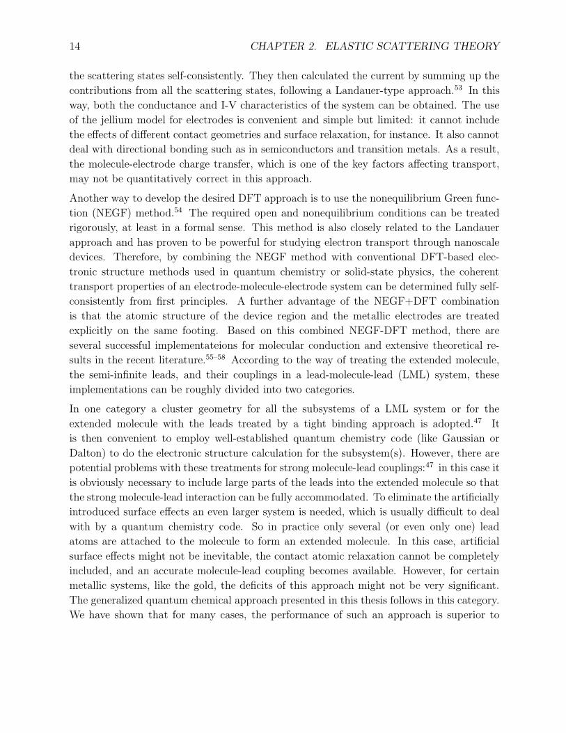
Figure 2.1: The energy schematic diagram of a molecular junction The bias voltage adding
on the left electrode is −VD. W is the work function, EF and EC are the energies of Fermi
level and conduction band.
Figure 2.1 shows the general energy schematic diagram of the molecular junction. The bias
voltage adding on the left electrode is −VD. The system obeys
H | Ψη〉 = εη | Ψη〉 (2.1)
where H is the Hamiltonian of the system, and can be written in a matrix format as
H =
HSS US M US D
UMS HMM UMD
UDS UDM HDD
(2.2)
where HSS,DD,MM is the Hamiltonian of subsystems S, D and M, respectively. The Hamil-

2.2. GENERALIZED QUANTUM CHEMICAL APPROACH 17
tonian of the electrodes can be further described as:
HSS =
HJNJN ... ... ...
... ... ... ...
... ... HJ2J2 UJ2J1
... ... UJ1J2 HJ1J1
HDD =
HL1L1 UL1L2 ... ...
UL2L1 HL2L2 ... ...
... ... ... ...
... ... ... HLNLN
(2.3)
Here J (L) runs over the metal sites (denoted as J1 (L1) , J2 (L2), ... ,JN (LN), where
metal layer J1 (L1) is the end layer that connects with the molecule) in the source (drain)
electrode. U is the interaction between or among subsystems. Ψη is the eigenstate at energy
level εη, which can be partitioned into three parts:
| Ψη〉 = | Ψη,S〉+ | Ψη,M 〉+ | Ψη,D〉| Ψη,S〉 =
∑
aη,Si | φS
i 〉
| Ψη,M 〉 =∑
aη,Mi | φM
i 〉
| Ψη,D〉 =∑
aη,Di | φD
i 〉 (2.4)
where ΨS,D,M and φS,D,Mi are the wavefunction and basis functions of subsystems S, D and
M, respectively.
It is convenient to work in the site representation for describing an electron transport process.
In this case, the wavefunction can be described in the site basis | J〉, | K〉 and | L〉, for
subsystems S, D and M, respectively, as
| Ψη,S〉 =
JN∑
J
(∑
i
aη,Ji | φJ
i 〉) =
JN∑
J
| Jη〉
| Ψη,M〉 =
KN∑
K
(∑
i
aη,Ki | φK
i 〉) =
KN∑
K
| Kη〉
| Ψη,D〉 =
LN∑
L
(∑
i
aη,Li | φL
i 〉) =
LN∑
L
| Lη〉 (2.5)
Here K runs over the atomic sites (denoted as K1,K2,...,KN , where site K1 and KN are two
end sites that connect with two electron reservoirs, respectively) in the molecule.

18 CHAPTER 2. ELASTIC SCATTERING THEORY
The interaction between subsystems can be written as
U =∑
J,K
VJK
∑
η
| Jη〉〈Kη | +∑
K,J
VKJ
∑
η
| Kη〉〈Jη |
+∑
K′,L
VK′L
∑
η
| K ′η〉〈Lη | +∑
L,K′
VLK′
∑
η
| Lη〉〈K ′η |
+∑
J ′,J
VJ ′J
∑
η
| J ′η〉〈Jη | +∑
L,L′
VLL′
∑
η
| Lη〉〈L′η |
+∑
J,L
VJL
∑
η
| Jη〉〈Lη | +∑
L,J
VLJ
∑
η
| Lη〉〈Jη | (2.6)
where VJL and VLJ are the coupling energy between source and drain, which can be set to
zero assuming that there is no direct coupling between them. VJ ′J (VLL′) represents the
coupling energy between the layer site J ′ (L) and J (L′) of the source (drain) reservoirs.
And VJK(VK′L) is the coupling energy between site K (K ′) of the molecule and site J (L)
of the reservoirs. The coupling energies between the electron reservoirs and the molecule,
i.e., VSM and VMD, are the key parameters in determining the electronic conductance of
the device. They could be obtained at an empirical level67 or by using the simple frontier
orbital binding concept as in our previous work.59,60 More rigorously, one can calculate
them analytically with quantum chemistry methods using the following expression:
VJK =
OCC∑
ν
〈Jν | H | Kν〉 (2.7)
=∑
ν
∑
Ji,Ki
aνJi
aνKi〈φJi
| H | φKi〉
where 〈φJi| H | φKi
〉 = FJi,Kiis the interaction energy between two atomic basis functions,
which can be deduced directly from the given Hamiltonian. Here OCC represents all the
occupied orbitals. It is noticed that at the Hartree-Fock level, it represents the off diagonal
elements of the Fock matrix.
In the elastic-scattering Green’s function theory, the transition operator is defined as
T = U + UG0T = U + UGU (2.8)
where G0 and G are Green’s functions,
G0(z) = (z − H0)−1, G(z) = (z − H)−1 (2.9)
Because of the energy conservation, the incoming and outgoing electrons should have the
same energy, i.e. belonging to the same orbital. If an electron with energy εµ is scattered

2.2. GENERALIZED QUANTUM CHEMICAL APPROACH 19
from the initial sites∑ | ξµ
m〉 of reservoirs S to the final sites∑ | ξ′µn 〉 of reservoirs D (where
m and n runs over the atomic site of the infinite source and drain electrode, respectively),
the transition matrix element will be
T µξ′ξ =
∑
m,n
〈ξ′µn | U | ξµm〉 +
∑
m,n
〈ξ′µn | UGU | ξµm〉 (2.10)
Begin from Eq. (2.6), one can easily find U can be written as U =∑
η Uη. Also due to the
energy conservation, only the element U η(η = µ) remains in the transition matrix element
T µξ′ξ. By substituting Uµ into Eq. (2.10) and taking into account the fact that there is no
direct coupling between two reservoirs, we obtain
T µξ′ξ =
∑
m,n
∑
K,K′
Vξ′nK′gµK′KVKξm
+∑
m,n
∑
L6=ξ′n,K
Vξ′nLgµLKVKξm
+∑
m,n
∑
K′,J 6=ξi
Vξ′nK′gµK′JVJξm
(2.11)
where K ′ and K denote the atomic sites in the molecule, and J (L) runs over the metal sites
in the source (drain) electrode. gµK′K is the carrier-conduction contribution from scattering
channel εµ, which can be expressed as
gµK′K = 〈K ′µ | 1
z − H| Kµ〉
= 〈K ′µ | 1
z − H| Ψµ〉〈Ψµ | Kµ〉
=〈K ′µ | Ψµ〉〈Ψµ | Kµ〉
z − εµ
(2.12)
Quantum mechanically, 〈K ′µ | Ψµ〉 (〈Ψµ | Kµ〉) is the projection of site K ′µ(Kµ) in the
eigenstate Ψµ. Here parameter z in the Green’s function is a complex variable, z = Ei + iΓi,
where Ei is the energy at which the scattering process is observed, and therefore corresponds
to the energy of the tunneling electron when it enters the scattering region from reservoir
S. This is also the energy at which the electron is collected at time +∞ by reservoir D (we
have assumed an elastic scattering process). 1/Γi is the escape rate, which is determined

20 CHAPTER 2. ELASTIC SCATTERING THEORY
by the Fermi Golden rule
Γµξ′K′Kξ = πV 2
ξ′K′ | 〈K ′µ | Ψµ〉 |2∑
p
δ(Ef − ESp )
+πV 2Kξ | 〈Ψµ | Kµ〉 |2
∑
p
δ(Ef − EDp )
= πnS(Ef )V2ξ′K′ | 〈K ′µ | Ψµ〉 |2
+πnD(Ef)V2Kξ | 〈Ψµ | Kµ〉 |2 (2.13)
where nS(Ef ) and nD(Ef ) are the density of states (DOS) of the source and drain at the
Fermi level Ef , respectively.
So that we get
gµK′K =
〈K ′µ | Ψµ〉〈Ψµ | Kµ〉(Ei − εµ) + iΓµ
ξ′K′Kξ
(2.14)
The metal atomic orbital is known to be more localized than its molecular counterparts. It is
expected that 〈Lµ | Ψµ〉〈Ψµ | Kµ〉 and 〈K ′µ | Ψµ〉〈Ψµ | Jµ〉 should be extremely small if the
extended molecule is sufficiently large, an observation that is confirmed by the calculations
based on the local density approximation (LDA).68,69 Therefore the terms
gµLK =
〈Lµ | Ψµ〉〈Ψµ | Kµ〉z − εµ
,
gµK′J =
〈K ′µ | Ψµ〉〈Ψµ | Jµ〉z − εµ
in Eq. (2.11) can be neglected, which is supported by the numerical calculations for the real
molecular devices as discussed later. Actually, the localized properties of the metal orbitals
are reflected by the fact that the potential of the metal-molecule-metal configuration drops
mostly at the metal-molecule interface.25
The transition probability can thus be written as
T = |T |2 = |∑
µ
(∑
i,m
∑
K,K′
Vξ′mK′gµK′KVKξi
)|2 (2.15)
Electron transport through a molecular wire can often be considered as a one-dimensional
process. However, the metal electrodes can have different dimensionalities. We have shown
that the current through a molecular device depends much on the dimensionality of the

2.2. GENERALIZED QUANTUM CHEMICAL APPROACH 21
metal electrodes used.61 Here we recapitulate the key formula derived from our previous
work.61
We assume that the molecule is aligned along the z direction, which is also the direction of
current transport. Energy states in the conduction band of the reservoir can be expressed
as the summation, E = Ex,y + Ez + Ec, in the effective mass approximation, where Ec is
the conduction band edge and is used as energy reference. It is assumed that the parabolic
dispersion relation for the energy states in metal holds. The electrons in the reservoir are
assumed to be all in equilibrium at a temperature T and Fermi level Ef . When an applied
voltage V is introduced, the tunneling current density from source (S) to drain (D) is59,62,70
iSD =2πe
h
∑
Ex,y
∑
Elz,El′
z
f(Ex,y + Elz − eV )[1 − f(Ex,y + El′
z )]
×Tl′l δ(El′
z − Elz) (2.16)
where f(E) is the Fermi distribution function,
f(E) =1
e[(E−Ef )/kBT] + 1,
Here kB is the Boltzmann constant and Tl′l is the transition probability describing the
scattering process from the initial state | l〉 to the final state | l′〉, and this transition
probability is a function of the quantized injection energy along the z axis, E lz and El′
z .
For high temperatures there is a corresponding term for reverse tunneling. The net current
density from S to D can thus be written as59,60,62
iSD =2πe
h
∑
Ex,y
∑
Elz ,El′
z
[f(Ex,y + Elz − eV ) − f(Ex,y + El′
z )]
×Tl′l δ(El′
z − Elz) (2.17)
In energy representation, the metal contacts can in principle be classified as one-, two-,
or three-dimensional electron systems. Depending on the dimensionality of the electrodes,
different working formulas for current can be derived.61
When energies in both x and y directions are continuous, the current can be evaluated by
I3D =2πe
h
∫ ∞
0
ρS1D(Ez)ρ
D1D(Ez)dEz
∫
|T |2[f(Exy + Ez − eVD) − f(Exy + Ez)]Adkxdky
2π2(2.18)
Here A is the effective injection area, A ≈ πr2s and we have
ρ1D(E) = rsN1D(E) = (9π
4)1/3 1
π√
EEf
(2.19)

22 CHAPTER 2. ELASTIC SCATTERING THEORY
where N1D(E) = (1/π)√
2m∗
h2Eis the one-dimensional density of state per length per electron
volt, rs is defined as the radius of a sphere whose volume is equal to the volume per conduc-
tion electron. rs = (3/4πn)1/3, n = (2m∗Ef )3/2/(3h3π2) is the density of electronic states of
the bulk metal. rs = (9π/4)1/3 h√2m∗Ef
, Ef is the fermi level.
Therefore, we can integrate the current density(i3D) in the whole k-space:
I3D = A2πe
h
m∗kBT
2πh2
∫ ∞
eVD
ln1 + exp(
Ef+eVD−Ez
kBT)
1 + exp(Ef−E
kBT)
|T |2ρS(Ez)ρD(Ez)dEz
= Aem∗kBT
h3
∫ ∞
eVD
ln1 + exp(
Ef+eVD−Ez
kBT)
1 + exp(Ef−E
kBT)
|T |2ρS(Ez)ρD(Ez)dEz (2.20)
In the above equation, we have used the equation (11.14) and (11.15) of Fu’s work:71
∫ ∞
0
dkxdky
2π2[1 + exp(Exy+Ez−Ef
kBT)]
=
∫ ∞
0
2πkxydkxy
2π2[1 + exp(Exy+Ez−Ef
kBT)]
=m∗
2πh2
∫ ∞
0
dExy
1 + exp(Exy+Ez−Ef
kBT)
=m∗kBT
2πh2 ln[1 + exp(Ef − Ez
kBT)] (2.21)
So that we have current:
I3D =em∗kBT
h3
∫ ∞
eVD
ln1 + exp(
Ef+eVD−Ez
kBT)
1 + exp(Ef−Ez
kBT)
|T (Ez)|2ρS(Ez)ρD(Ez)dEz (2.22)
where VD is the external voltage, Ef is the Fermi energy, T is the device working tempera-
ture, Ez is the kinetic energy along z direction, and T (Ez) is transition matrix. ρS(Ez) and
ρD(Ez) are the density of states (DOS) of the source and drain, respectively.

Chapter 3
Gate Field Effect
The ability to control current through a single molecule is an important goal in molecular
electronics. The construction of three-terminal devices, like the field effect transistor (FET),
and the understanding of their performance become extremely important for the future de-
velopment of molecular electronics. There are several ways to make single molecular field
effect transistors. One is to fabricate gate electrode directly using electron-beam lithogra-
phy,39 another is to use an electrochemical gate in which the gate voltage falls across the
double electrolytes to produce a high electric field on molecule.41 In both cases, the gate
effects can be treated as interaction between molecule and external electric fields. The elec-
tric field strengths and orientations can be different in different FET devices depending on
the construction methods used for. For instance, for a standard transistor shown in Figure
3.1a, the gate effect are dependent on the mutual orientation between external field and the
molecular dipole.46
In a standard silicon FET, the gate modulates the current by controlling the channel charge
through its electrostatic potential. In the semiconductor transport theory, the third terminal
gate effect can often be treated as the uniform movement of the conducting band that is
determined directly by the external gate voltage eVg. Such a situation is quite common in
the semi-conductor device because of the uniform spatial distribution of the electrons in the
conduction band. However, the discrete molecular orbitals can often not cover the entire
molecule, sometime, they can be completely localized at one or few atoms. Depending on
the characters of the molecular orbitals, different gate effects would be expected for different
orbitals. A schematic energy diagram of a molecular FET device is displayed in Figure 3.1b.
The occupied and unoccupied orbitals can be affected by the gate voltage differently, leading
to different energy shifting. In this case, the interaction between molecule and external gate
voltage should be taken into account nonperturbatively.
23

24 CHAPTER 3. GATE FIELD EFFECT
Figure 3.1: Schematic diagrams for a standard setup of a molecular field effect transistor
(A) and for the energy distributions (B), where it shows that the gate voltage Vg controls
the current I by controlling the molecular orbtials.
The total Hamiltonian of the system depends on the external electric field when the external
bias is added. In this case, we divide the total Hamiltonian into two parts:
H = H0 + H ′ (3.1)
where H0 is the Hamiltonian of the system without field, and H ′ is the interaction Hamil-
tonian between electrons in the molecule-metal complex and the external electric fields.
H ′ = e~ri · ~Ei (3.2)
ri is the position operator of the electron and Ei is the electric field at the position of i,
which can be obtained from either the source-drain voltage or the third gate voltage, or both.
By solving the Schrodinger equation non-perturbatively with this well-defined Hamiltonian,
the field-dependent wavefunctions, orbital energies, and coupling constants can be obtained
and the current-voltage characteristics of the field effect transistor is ready to explore. The
computational scheme is quite simple when the conventional Gaussian basis sets are em-
ployed. The only extra integral should be computed is the length integral, 〈φi|~r|φj〉, where

25
φi,j the gaussian basis functions, which are available in any standard quantum chemistry
codes. We can thus take advantage of the existing quantum chemistry programs to carry
out the calculations using different first-principles methods.
There are quite few theoretical works on molecular FET in the literature.46,64,72–74 The
first theoretical modeling of molecular FET was done by Di Ventra et al.,72 who carried out
first principles calculations for a device with a benzene-1,4-dithiolate molecule (BDT). In
their approach, the gate is introduced as a capacitor field generated by two circular charged
disks at a certain distance from each other.72 It was predicted that the amplification of
current would be more than one order of magnitude. Bratkovsky and Kornilovitch studied
also the benzene-1,4-dithiolate device using a different approach and found that the gate
effect should be very small for this device.64 It is interesting to note that the most recent
experiments on benzene-1,4-dithiolate molecular device show no gating effect.39 A more
general result has been derived by Ghosh et al.46 that can be used to evaluate and compare
different mechanisms in FET. The effects of electrostatic and conformational changes on the
performance of the FET devices have been discussed quantitatively. The extended Huckel
Hamiltonian was used for numerical simulations. However, these studies have not been able
to fully explore the potential of the theoretical modelling for the understanding and design
of the FET devices, since the most studied device is based on the BDT molecule that is
known to be lack of gating effect in experiment.39 We have applied our approach to three
different FET devices that have shown measurable gating effects. Our calculations have
been able to reproduce most of the experimental observations.

26 CHAPTER 3. GATE FIELD EFFECT

Chapter 4
Applications
In this chapter, we present our studies on several molecular junctions and field effect tran-
sistors that have been fabricated by different experimental groups. Geometry optimization
and electronic structure calculations for extended molecular systems are done with Gaussian
03 program75 at the hybrid density functional theory (DFT) B3LYP level with LANL2DZ
basis set, and all electron transport properties are carried out using the QCME code.76
4.1 Molecular junctions
The gold-oligophenylene-gold junctions of different lengths have been studied using our
generalized quantum chemical approach. oligophenylene molecule is a typical conjugated
molecule that possesses good conductivity. The study of length dependence of the electron
transport in these conjugated chains is important for the future applications. The same
system was also studied by Kaun et al. using a solid-state physics based approach.77 One
can thus compare the results of two different theoretical approaches and to find the possible
internal connections between them.
Three gold-oligophenylene-gold devices with one, two and three benzene units are illustrated
in Fig. 4.1, which are labeled as phenyl-I, phenyl-II and phenyl-III, respectively. In each
case, one side of the molecule is chemically connected to the gold electrode through Au-S
bond. Another side of the molecule is only physically absorbed on the gold surface through
hydrogen atom. In our simulations, the extended molecules always consist of molecule
and three gold atoms attached on each sides. Since the experimental bonding structure is
unknown, we have chosen the gold clusters to resemble the (111) orientation of the gold
substrate as adapted in the previous theoretical studies.78 The sulfur atom is located at the
27
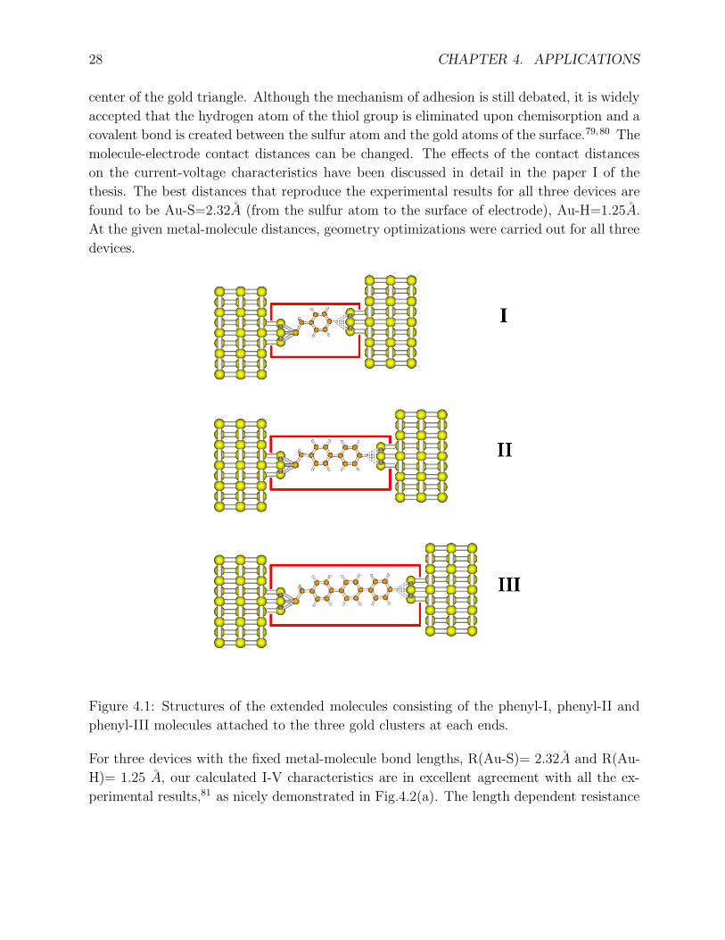
28 CHAPTER 4. APPLICATIONS
center of the gold triangle. Although the mechanism of adhesion is still debated, it is widely
accepted that the hydrogen atom of the thiol group is eliminated upon chemisorption and a
covalent bond is created between the sulfur atom and the gold atoms of the surface.79,80 The
molecule-electrode contact distances can be changed. The effects of the contact distances
on the current-voltage characteristics have been discussed in detail in the paper I of the
thesis. The best distances that reproduce the experimental results for all three devices are
found to be Au-S=2.32A (from the sulfur atom to the surface of electrode), Au-H=1.25A.
At the given metal-molecule distances, geometry optimizations were carried out for all three
devices.
Figure 4.1: Structures of the extended molecules consisting of the phenyl-I, phenyl-II and
phenyl-III molecules attached to the three gold clusters at each ends.
For three devices with the fixed metal-molecule bond lengths, R(Au-S)= 2.32A and R(Au-
H)= 1.25 A, our calculated I-V characteristics are in excellent agreement with all the ex-
perimental results,81 as nicely demonstrated in Fig.4.2(a). The length dependent resistance

4.1. MOLECULAR JUNCTIONS 29
(dI/dV) is found to follow the exponent decay, R = R0e−βd, where β is the dacay rate
and d is the molecular length. At external bias of 0.25 V, our calculated decay rate is
β=1.76/phenl, very close to the experimental value of β=1.76/phenl.
0 0.1 0.2 0.3Tip Voltage (V)0
200
400
600
Cur
rent
(nA
)
1 2 3Number of Phenyls
0.1
1
10
Res
istan
ce (M
Ω)
I
IIIII
β=1.76/Ph
(a)
(b)
Figure 4.2: (a) Current versus tip voltage between 0-0.5V for phenyl-I, phenyl-II, and phenyl-
III. The molecule-electrode contact distance is fixed to be: the Au-S 2.32A, Au-H 1.25 A.
Experimental data are represented as empty circles for phenyl-I, empty squares for phenyl-II,
and empty triangles for phenyl-III. (b) A semilog plot of resistance versus number of phenyl
groups. The resistances (dI/dV) are calculated at external bias of 0.25V. The calculated
decay rate of β=1.76/phenyl is the same to the experimental value of β=1.76/phenyl.81
The transmission spectra for three devices are shown in Figure 4.3. The currents depend
most on the transmission rate correspond to region between 0eV to 0.5eV, which are the
tails of orbitals located from 3.5eV to 5eV. This also explains the approximately linear of
the currents. From the calculated transmission spectra, one might be able to predict that
when the external bias increases, the linear depended current curves will be distorted around
0.5V for phenyl-I and phenyl-II.
The previous study of Kaun et al77 on the same systems has adopted different bond lengths
with R(Au-S)=2.12A and R(Au-H)=1.06A. Both distances are shorter than what we have

30 CHAPTER 4. APPLICATIONS
0.1
1
10
0.010.1
110
Tran
smiss
ion
0 1 2 3 4 5E (eV)
0.0010.01
0.11
10
I
II
III
(a)
(b)
(c)
Figure 4.3: Transmission spectra of the three devices, (a) for phenyl-I, (b) for phenyl-II, and
(c) for phenyl-III. The molecule-electrode contact distance is fixed to be: the Au-S 2.32A,
Au-H 1.25 A. The Fermi energy is set to be zero.
used. Their calculations have also produced the right length dependence in comparison with
the experiments. Our calculations have shown that with their distances, the interaction
energy between molecule and electrodes becomes excessively large. We have also noticed
that the decay rate β is sensitive to the choice of the bond distances between molecules and
electrodes. It is shown that with Au-S of 2.32A and Au-H of 3.0A, the value of β reduces
to 1.39/phenyl.
4.2 Single molecular field effect transistors
The central focus of this thesis is the study of single molecular field effect transistors. We
have applied our computational method to three different molecular field effect transistors
that have been experimentally measured and shown large gate effects.

4.2. SINGLE MOLECULAR FIELD EFFECT TRANSISTORS 31
Figure 4.4: Model device of the TA-PPE polymer in contact with two Au electrodes. The
laboratory coordination (X,Y,Z) is given and the thrid gate is not shown.
4.2.1 Polymer device
Conjugated polymers have been widely used for electronic and photonic applications. How-
ever, studies of single polymer molecular devices are scare,42,83,84 mainly due to difficul-
ties of wiring the conjugated polymer molecules into an electrical circuit. Poly(para-
phenylene ethynylene)s (PPEs) have demonstrated good conductivity,85,86 rigidity,87 and can
be modified with thiol/thioacetate-end-functionalized groups.88,89 The thiol/thioacetate-
end-functionalized PPEs have recently been used to fabricate two-terminal84 and three-
terminal42 devices. The three-terminal TA-PPEs device showed highly periodic conduc-
tance under different gate voltage.42 It was suggested that such a feature might be related
to single-electron charging oscillations or Coulomb-blockade oscillations, which could be
viewed as a manifestation of single-electron sequential tunneling through the system of two
self-assembled tunnel junctions in series.42 However, Room temperature current-voltage
characteristics of the TA-PPEs two-terminal molecular junction exhibited also highly peri-
odic, repeatable, and identical stepwise features. Theoretical calculations have shown that
they can be attributed to the opening of different conducting channels, corresponding to
the unoccupied molecular orbitals of the polymer in the junction.84 It was found that the
charging effects can not be responsible for the observed highly periodic oscillation.42 The
major difference between these two devices is the size of TA-PPEs molecule employed, which
are determined by the distance between the gold nanogaps. They are 18 nm and 40nm for
the two-terminal84 and three-terminal devices,42 respectively. It is reasonable to believe that
the periodic oscillation of the conductance under the third gate in the three-terminal device
is also due to the opening of the different unoccupied molecular orbitals of the polymer
molecule.

32 CHAPTER 4. APPLICATIONS
The model device used in the calculation is sketched in Figure 4.4. The end thiol/thioacetate-
end-functionalized group was dissociated upon the bonding to form the S-Au bonds between
TA-PPEs and electrodes. It is found that the length of a TA-PPEs polymer molecule with
55 sub-units (55-TA-PPEs) is about 40nm. Geometry optimization for the polymer molecule
was done with the PM3 method. The sulfur atom is assumed to bond to the center of a
triangle gold plan and Au-S bond length is set to be 2.93 A for systems under investiga-
tion. The choice of Au-S bond length and the Fermi level is taken from our previous study
on a 24 sub-units TA-PPE junction.84 Electronic structures of the polymer molecule are
calculated using a newly developed elongation method90 implemented in the QCME code.
Our elongation method takes advantage of the unique feature of a finite periodic system,
namely when a system is large enough, the interaction between different units in the middle
of the system is converged, and consequently those units in the middle become identical. It
is thus possible to elongate the initial system by adding the identical units in the middle of
the system continuously. This can be easily done when the Hamiltonian of the system is
described in the site representation. This technique allows to compute electronic structures
and transport properties of sub-60nm single walled carbon nanotubes (SWCNT),90 and the
40nm long polymer presented in this study.
0 0.5 1 1.5 2 2.5Electron energy (eV)
10-8
10-4
100
Tran
smiss
ion
Figure 4.5: Transmission spectrum of the TA-PPEs molecule with 55 sub-units above Fermi
level under zero gate voltage.

4.2. SINGLE MOLECULAR FIELD EFFECT TRANSISTORS 33
The distribution of the unoccupied molecular orbitals of the 55-TA-PPEs is represented
by its transmission spectrum under zero gate voltage in Figure 4.5. It can be seen that
the energy separation between these molecular orbitals is quite even, around 0.05eV, which
could be the reason for the periodic behavior.
40
80Exp. 40nm, VDS=1.05V, T(Vg)=0.05V
0 0.2 0.4 0.6 0.8 1Gate Voltage (V)
30
40
50
Con
duct
ance
(pS)
Cal. 40nm, n=55, VDS=1.05V, T(Vg)=0.05V
Figure 4.6: Experimental conductance oscillations of a TA-PPE transistor with gate bias
variation at 147K under Vsd=1.05V, and the corresponding calculated results for a 55-TA-
PPEs device.
The gate configuration is not explicitly defined in the experiment.42 Calculations show that
the TA-PPEs polymer has a gap of 2.78 eV and behaves like a semi-conductor. According
to the transmission spectrum, all unoccupied orbitals close to the gap have almost identical
transmission probability, reflecting the fact that all of them are highly conjugated π orbitals.
Furthermore, the side chains attached on the polymer has made the distance between two
gate electrodes quite large. With consideration of all these facts, it might be reasonable to
assume that the gate effect can be simply treated as a perturbation, i.e H ′ = eV g. The
function of the third gate is thus to shift the orbitals uniformly.
The calculated current-voltage characteristics of the 55-TA-PPEs device is shown in Figure
4.6, together with the experimental results of Hu et al.42 for comparison. The experimentally

34 CHAPTER 4. APPLICATIONS
observed periodic oscillations are well reproduced by the calculations. The separation of the
conductance peaks is around 0.10 to 0.12 eV, twice of the energy separation of the orbitals.
The amplitude of oscillation for the calculated conductance at low gate voltage region is
smaller than that of experiment, which might be caused by the uncertainly of the Fermi
energy used in the calculations. The occupied molecular orbitals of the polymer are found
to be more densely and unevenly distributed. Therefore, this polymer FET should be a
n-type device. It is interesting to see that the single polymer molecular transistor operates
similarly to the semi-conductor device, showing a dependence linearly with respect to the
gate voltage. It should also mentioned that the electron transport in a 40nm long polymer
is still dominated by the one electron resonant tunneling processes.
4.2.2 1,3-benzenedithiol molecular device
Lee et al.39 measured several FET devices with phyenylen-based conjugated molecules and
found that only the device with 1,3-benzenedithiol molecule shows a measurable gating
effect. One can immediately understand that the lack of the gating effects in other devices
is largely due to their high symmetry. The relative low symmetry of 1,3-benzenedithiol
molecule has uneven electron distribution and has thus higher probability to be disturbed
by the gate field.
Figure 4.7: Model device of 1,3-benzenedithiol molecule connected with two Au electrodes.
The third gate is not shown. The laboratory coordination (X,Y,Z) is given.
In Figure 4.7, the model device of 1,3-benzenedithiol molecule within two gold electrodes is
shown. The electronic structure calculations are performed for the molecule-metal complex
that contains the molecule attached to two three triangle gold clusters through S-Au bonds.
Geometry optimization leads to the equilibrium S-Au bond length of 2.85 A.
The experimental results for 1,3-benzenedithiol molecular FET is displayed in Figure 4.8a.
The current-voltage curves at different gate voltages are asymmetric around the zero bias.

4.2. SINGLE MOLECULAR FIELD EFFECT TRANSISTORS 35
Figure 4.8: Experimental (a) and calculated I-V characteristics of a 1,3-benzenedithiol
molecule sandwiched between two Au electrodes under different gate voltages and con-
figurations: (b) Vg(0,1,0) and (c) Vg(0,0,1).
The source-drain current under the positive voltage is larger than that under the negative
voltage. Furthermore, the gate effect increases the current by a factor of 3 going from Vg=0
to Vg=1.5V.
In the calculation, the source-drain electric field is set along the X-axis (-1,0,0) which goes
through two sulfur atoms. We have considered two different gate configurations, one is along
the Y-axis (0,1,0) (normal to the phenyl ring) and another along the Z-axis (0,0,1). The
calculated I-V curves are shown in Figure 4.8b and c, respectively. Both gate configurations
result in noticeable gating effect. In particular, the maximum on/off ration in the gate
configuration Y(0,1,0) is found to be around 2, close to what has been observed experimen-
tally. Calculations have also produced the asymmetric behavior of the I-V curves. In the
experiment, the current appears only when the external source-drain voltage is set above
0.5 V, whereas the calculated current has none zero value at much smaller voltage. This
could be related to the sensitivity of the experimental detector, but might be more due to
the factor that the bonding between molecule and electrodes may be stronger in the model
system than in the real device. In another word, the Au-S bond distance in the real device
might be longer.
The gate effect can be better understood by looking at the distribution of the unoccupied
orbitals. In Figure 4.9, the transmission spectra of the device above the Fermi level with
the gate configuration Y(0,1,0) under three different gate voltages, +1.5, 0 and -1.5V are
shown. Within the spectral window (below 1.0eV), there are four orbitals with considerable
intensity. They depend differently on the gate voltage. The orbital with largest transmission
probability obeys the normal gating effect, namely pushing up with positive voltage and

36 CHAPTER 4. APPLICATIONS
Figure 4.9: Transmission spectra of a 1,3-benzenedithiol FET device under three different
gate voltages, +1.5V, 0V, and -1.5V under the configuration of Vg(0,1,0). Here Vsd keeps to
be -0.5V.
pulling down with negative voltage. However, the current at low energy region, like -0.5V,
is mostly determined by the tail of the strong transmission peaks, which results in the larger
current under positive gate voltage than negative gate voltage. It should also be mentioned
that the transmission spectra shown in Figure 4.9 are obtained at zero source-drain bias and
thus mostly for the illustrative purpose. They can only help to understand the behavior of
the device under small external source-drain bias. For the I-V curves shown in Figure 4.8,
the source-drain field effect has also been taken into fully account.
The asymmetric behavior of the I-V curves is mostly caused by the asymmetric geometrical
structure of the molecule-gold complex in the laboratory coordination. The external fields,
including both source-drain and gate voltages, act on the devices asymmetrically, leading
to different dependence.

4.2. SINGLE MOLECULAR FIELD EFFECT TRANSISTORS 37
4.2.3 Perylene tetracarboxylic diimide(PTCDI) molecular device
It is an enormous challenge to fabricate small single molecular field effect transistors because
it is extremely difficult to wire a small molecule to the source-drain electrodes and to add
a third gate on it to achieve the require gate field. The solution given by Xu et al.41 seems
to be quite promising. They have used an electrochemical gate to obtain very large gate
field on a molecule wired to gold electrodes (source and drain) via gold-thiol bonds. In their
setup, the gate voltage is applied between the source and a gate in the electrolyte. The
current through the molecule can be reversibly controlled with a gate electrode over nearly
3 orders of magnitude at room temperature.41
Figure 4.10: Model device of PTCDI molecule in contact with two Au electrodes. The
laboratory coordination (X,Y,Z) is given and the third gate is not shown.
Figure 4.10 plots the schematic of the molecular device with a perylene tetracarboxylic
diimide(PTCDI) molecule attached to the gold electrodes that was studied by Xu et al.41
In our simulations, we set the sulfur atom to sulfur atom direction as X-axis,(1,0,0), and
the oxygen to oxygen atoms direction perpendicular to the X axis as Y-axis, (0,1,0). The
direction Z, (0,0,1), is thus normal to the central perylene rings. A PTCDI molecule and
two triangle gold clusters bonded through Au-S bonds is used as the model system. The
sulfur atoms are located about 2.32 A above the center of the gold triangles. The gate is
assumed to be about 1.2 A away from the molecular surface in order to fit the experimental
gate voltage. This distance also corresponds to the averaged Van der Waals radii of the
atoms in the molecule.
The simplest approach that one can think of is to consider the external gate field as a
perturbation. The interacting Hamiltonian becomes a constant and is determined by the
product of the permanent dipole moment of the system and the external gate filed. In
this case, the effect of the external gate is simply to shift up/down of the molecular or-
bitals. Calculations show that this approach can only produce very small gate effect. The
largest current gain is less then one order of magnitude. A more realistic approach is to
treat the interaction between electrons and the external fields precisely and to solve the

38 CHAPTER 4. APPLICATIONS
Figure 4.11: (a) Experimental data41 of source-drain current(Isd) versus gate voltage (Vg)
for a single PTCDI molecule transistor. (b) experimental data41 of Isd versus bias voltage
(Vsd) characteristic curves at various gate voltages. (c) our calculation result of source-
drain current(Isd) versus gate voltage (Vg) for a single PTCDI molecule transistor. (d)
our calculation result of Isd versus bias voltage (Vsd) characteristic curves at various gate
voltages.
Schrodinger equation non-perturbatively. Here the interaction energy is represented as a
three dimensional potential in the real space and is sensitive to the direction of the external
gate field.
In the experiment of Xu et. al,41 the distribution of external field in the space can not be
determined experimentally since the shape of the electrochemical cell around the molecule
is unknown. We would like to demonstrate that theoretical simulations can provide useful
information about the effect of different gate configurations on the performance of the de-
vice. It should be mentioned that the effect of molecular dipole moment on the performance
of the FET device was discussed by Ghosh et al.46 We present here an alterative compu-
tational approach and numerical solutions for a real device. We have tested many different

4.2. SINGLE MOLECULAR FIELD EFFECT TRANSISTORS 39
configurations. The results that fit the best with the experiment are presented in Figure 1.
They are obtained from one particular device configuration, where the source-drain field is
oriented 150o with respect to the X axis in the X-Z plane and can be described by a vector
(-0.87,0,0.5). The gate field follows the vector of (-0.5,0,-0.87), perpendicular to the source-
drain field. As one can see from Figure 1, the agreement between theory and experiment is
very good for both absolute current and relative changes induced by the gate voltage. The
experimental source-drain current (Isd) shows a non-monotonic dependence on the gate volt-
age (Ig) when source-drain voltage (Vsd) is set to 0.1V, see Figure 4.11. The experimentally
observed plateau between gate voltages of 0.7 and 0.8 V is also largely reproduced by the
calculations. To understand this behavior, we have plotted out the transmission spectra of
the device under the gate voltage of -0.1V, -0.6V, -0.8V, and -0.9V, respectively, with Vsd=
0.1V in Figure 2. It should be noted that the current flow at Vsd=0.1V is determined by
the tail of the conducting bands. When gate voltage Vg=-0.1V, the first conducting band is
located about 3.8eV above the Fermi level. The transmission intensity at 0.1eV is thus very
weak. At Vg=-0.6V, the first conducting band has shifted down to 2.2 eV and becomes much
broader. The transmission intensity at 0.1eV has increased by three order of magnitudes in
comparison with the case of gate voltage Vg=-0.1V. This explains well the large gate effects
shown in Figure 4.11. It is noted that between these two gate voltage, the orbital energy
shifting, 1.6eV, is much larger than the increase of the gate voltage, 0.5V, indicating that
the molecular orbitals are largely affected by the strength of the electric field, rather than
by the voltage itself. Increasing the gate voltage Vg to -0.8V, the transmission intensity at
0.1 eV is actually dropped to below the corresponding value for Vg=-0.6V and it explains
the formation of the plateau in the Isd-Vg curve. The transmission intensity under gate
voltage of -0.9V is enhanced due to the near resonance effect. The molecular orbitals are
not shifted linearly with respect to the increase of the gate voltage. Theoretical calculations
thus become very important for understanding the microscopic processes of the device.

40 CHAPTER 4. APPLICATIONS
Figure 4.12: Transmission spectra of the single PTCDI FET above Fermi level under
different gate voltages (Vg) with Vsd at 0.1V. *: the spectrum for Vg =-0.1V has been
multiplied by a factor of 100 for a better presentation. The insert shows that the small peak
in the transmission spectra is corresponding to the real molecular orbitals.

Bibliography
[1] A. Aviram and M. A. Ratner, Chem. Phys. lett. 29, 277 (1974).
[2] A. Aviram and M. A. Ratner, Molecular Electronics: Science and Technology (New
York Acad. Sci. New York, 1998).
[3] C. Zhou, M. R. Deshpande, M. A. Reed, L. Jones II and J. M. Tour, ”Nanoscale
Metal/Self-Assembled Monolayer/Metal Heterostructures”, Appl. Phys. Lett. 71, 611
(1997).
[4] J. M. Seminario, A. G. Zacarias and J. M. Tour, J. Am. Chem. Soc. 122, 3015 (2000).
[5] M. Di Ventra, S. G. Kim, S. T. Pantelides and N. D. Lang, Phys. Rev. Lett. 86, 288
(2001).
[6] J. Cornil, Y. Karzazi and J. L. Bredas, J. Am. Chem. Soc. 124, 3516 (2002).
[7] N. D. Lang and P. Avouris, Phys. Rev. B 62, 7325 (2000).
[8] J. M. Seminario, A. G. Zacarias and J. M. Tour, J. Am. Chem. Soc. 120, 3970 (1998).
[9] G. K. Ramachandran, T. J. Hopson, A. M. Rawlett, L. A. Nagahara, A. Primak and
S. M. Lindsay, Science 300, 1413 (2003).
[10] Z. J. Donhauser, B. A. Mantooth, K. F. Kelly, L. A. Bumm, J. D. Monnell, J. J.
Stapleton, D. W. Price, A. M. Rawlett, D. L. Allara, J. M. Tour and P. S. Weiss,
Science 292, 2303 (2001).
[11] Z. J. Donhauser, B. A. Mantooth, T. P. Pearl, K. F. Kelly, S. U. Nanayakkara and P.
S. Weiss, Jpn. J. Appl. Phys. 41, 4871 (2002).
[12] H. Sellers, A. Ulman, Y. Shnidman and J. E. Eilers, J. Am. Chem. Soc. 115, 9389
(1993).
41

42 BIBLIOGRAPHY
[13] Y.-T. Tao, C.-C. Wu, J.-Y. Eu and W.-L. Lin, Langmuir 13, 4018 (1997).
[14] ”nanotechnology.” Encyclopedia Britannica from Encyclopedia Britannica Premium
Service. 〈http://www.britannica.com/eb/article-236446〉.
[15] E. Braun, Y. Eichen, U. Sivan, and G. Ben-Yoseph, Nature 391, 775 (1998).
[16] H.-W. Fink and C. Schonenberger, Nature 398, 407 (1999).
[17] D. Porath, A. Bezryadin, S. de Vries and C. Dekker, Nature 403, 635 (2000).
[18] X.-Y. Xiao, B.-Q. Xu and N.-J. Tao, Nano lett. 4, 267 (2004).
[19] M. A. Reed, C. Zhou, C. J. Muller, T. P. Burgin and J. M. Tour, Science 278, 252
(1997).
[20] W. J. Liang, M. Shore, M. Bockrath, J. R. Long and H. Park, Nature 417, 725 (2002).
[21] J. Reichert, R. Ochs, D. Beckmann, H. B. Weber, M. Mayor and H. v. Lohneysen,
Phys. Rev. Lett. 88, 176804 (2002).
[22] X. D. Cui, A. Primak, X. Zarate, J. Tomfohr, O. F. Sankey, A. L. Moore, T. A. Moore,
D. Gust, G. Harris and S. M. Lindsay, Science 294, 571 (2001).
[23] J. G. Kushmerick, D. B. Holt, S. K. Pollack, M. A. Ratner, J. C. Yang, T. L. Schull,
J. Naciri, M. H. Moore and R. Shashidhar,J. Am. Chem. Soc. 124, 10654 (2002).
[24] R. H. M. Smit, Y. Noat, C. Untiedt, N. D. Lang, M. C. van Hemert and J. M. van
Ruitenbeek, Nature 419, 906 (2002).
[25] D. J. Wold and C. D. Frisbie, J. Am. Chem. Soc. 123, 5549 (2001).
[26] R. L. York, P. T. Nguyen and K. Slowinski, J. Am. Chem. Soc. 121, 7257 (1999).
[27] M. Magoga and C. Joachim, Phys. Rev. B 56, 4722 (1997).
[28] W.-Y. Su, J. Jiang and Y. Luo Chem. Phys. Lett. 412, 406 (2005).
[29] M. Dorogi,J. Gomez, R. Osifchin, R. P. Andres and R. Reifenberger, Phys. Rev. B 52,
9071 (1995).
[30] M. P. Samanta, W. Tian, S. Datta, J. I. Henderson and C. P. Kubiak, Phys. Rev. B
53, R7626 (1996).
[31] Y. Luo, C.-K. Wang and Y. Fu, J. Chem. Phys. 117, 10283 (2002).

BIBLIOGRAPHY 43
[32] K. Stokbro, J. Taylor, M. Brandbyge, J.-L. Mozos and P. Ordejon, Comput. Mater.
Sci. 27, 151 (2003).
[33] C. Joachim and J. K. Gimzewski, Chem. Phys. lett. 407, 57 (1997).
[34] D. H. Waldeck and D. N. Beratan, Science 261, 576 (1993).
[35] A. S. Martin, J. R. Sambles and G. J. Ashwell, Phys. Rev. Lett. 70, 218 (1993).
[36] R. M. Metzger, B. Chen, U. Hopfner, M. V. Lakshmikantham, D. Vuillaume, T. Kawai,
X. Wu, H. Tachibana, T. V. Hughes, H. Sakurai, J. W. Baldwin, C. Hosch, M. P. Cava,
L. Brehmer and G. J. Ashwell, J. Am. Chem. Soc. 119, 10455 (1997).
[37] H. Park, J. Park, A. K. L. Lim, E. H. Anderson, A. P. Alivisatos and P. L. McEuen,
Nature 294, 2138 (2001).
[38] H. Park, J. Park, A. K. L. Lim, E. H. Anderson, A. P. Alivisatos and P. L. McEuen.
Nature 407, 57 (2000).
[39] J. Lee, G. Lientschnig, F. Wiertz, M. Struijk, R. A. J. Janssen, R. Egberink, D. N.
Reinhoudt, P. Hadley and C. Dekker, Nano Lett. 3, 113 (2003).
[40] C. R. Kagan, A. Afzali, R. Martel, L. M. Gignac, P. M. Solomon, A. G. Schrott and
B. Ek, Nano Lett. 3, 119 (2003).
[41] B. Xu, X. Yang, L. Zang and N. Tao, J. Am. Chem. SOC. 127, 2386 (2005).
[42] W. Hu, H. Nakashima, K. Furukawa, Y. Kashimura, K. Ajito, Y. Liu, D. Zhu and K.
Torimitsu, J. Am. Chem. Soc. 127, 2804 (2005).
[43] M. Di Ventra, S. T. Pantelides and N. D. Lang, Appl. Phys. lett. 76, 3448 (2000).
[44] Y. Wada, Proc. IEEE 2001, 89, 1147.; P. Von Allmen and K. Hess, Phys. Rev. B 52,
5243 (1995).
[45] D. GoldhaberGordon, M. S. Montemerlo, J. C. Love, G. J. Opiteck and J. C. Ellenbo-
gen, Proc. IEEE 85, 521 (1997).
[46] A. W. Ghosh, T. Rakshit and S. Datta, Nano. lett. 4, 565 (2004).
[47] S.-H. Ke, H. U. Baranger and W. Yang, Phys. Rev. B 70, 085410 (2004).
[48] M. C. Petty and M. Bryce An Introduction to Molecular Electronics, (Oxford University
Press, New York, 1995).
44 BIBLIOGRAPHY
[49] J. M. Tour Molecular Electronics , (World Scientific, Singapore, 2003).
[50] W. Kohn and L. J. Sham Phys. Rev. 140, A1133 (1965).
[51] R. G. Parr and W. Yang. Density-Functional Theory of Atoms and Molecules, (Oxford
University Press, New York, 1989).
[52] N. D. Lang, Phys. Rev. B 52, 5335 (1995).
[53] R. Landauer, IBM J. Res. Dev. 1, 223 (1957).; R. Landauer, Philos. Mag. 21, 863
(1970).
[54] S. Datta, Electronic Transport in Mesoscopic Systems (Cambridge University Press,
Cambridge, 1995).
[55] P. S. Damle, A. W. Ghosh and S. Datta, Phys. Rev. B 64, 210403(R) (2001).
[56] Y. Xue, S. Datta and M. A, Ratner, Chem. Phys. 281, 151 (2002).
[57] M. Brandbyge, J. L. Mozos, P. Ordejon, J. Taylor and K. Stokbro, Phys. Rev. B 65,
165401 (2002).
[58] J. Taylor, H. Guo and J. Wang, Phys. Rev. B 63, 245407 (2001).
[59] C.-K. Wang, Y. Fu and Y. Luo, Phys. Chem. Chem. Phys. 3, 5017 (2001).
[60] Y. Luo, C.-K. Wang and Y. Fu, J. Chem. Phys. 117, 10283 (2002).
[61] C.-K. Wang and Y. Luo, J. Chem. Phys. 119, 4923 (2003).
[62] V. Mujica, M. Kemp and M. A. Ratner, J. Chem. Phys. 101, 6849 (1994).
[63] V. Mujica, A. Nitzan, Y. Mao, W. Davis, M. Kemp, A. Roitberg and M. A. Ratner,
Adv. Chem. Phys. 107, 403 (1999).
[64] A. M. Bratkovsky and P. E. Kornilovitch, Phys. Rev. B 67, 115307 (2003).
[65] W. Tian, S. Datta, S. Hong, R. Reifenberger, J. I. Henderson and C. P. Kubiak, J.
Chem. Phys. 109, 2874 (1998).
[66] J. Jiang, M. Kula and Y. Luo, J. Chem. Phys. 124, 034708 (2006).
[67] A. Hansson, M. Paulsson and S. Stafstrom, Phys. Rev. B 62, 7639 (1997).
[68] N. Kobayashi, M. Brandbyge and M. Tsukada, Phys. Rev. B 62, 8430 (2000).

BIBLIOGRAPHY 45
[69] J. P. Perdew and A. Zunger, Phys. Rev. B 23, 5048 (1981).
[70] Richard P. Feynman, Staticstical Mechanics, (ABP, PERSEUS BOOKS, 1972) p. 286-
289.
[71] Y. Fu and W. Lu, Semiconductor quantum device physics, (Chinese Science Press,
Beijing, 2005), p. 325 .
[72] M. Di Ventra, S. T. Pantelides and N. D. Lang, Appl. Phys. lett. 76, 3448 (2000).
[73] E. G. Emberly and G. Kirczenow, Phys. Rev. B 62, 10451 (2000).
[74] P. Damle, T. Rakshit, M. Paulsson and S. Datta, IEEE. Transactions on nanotechnol-
ogy 1, 145 (2002).
[75] Gaussian 03, Revision A.1, M. J. Frisch, et al. Gaussian, Inc. Pittsburgh PA, 2003.
[76] J. Jiang and Y. Luo, QCME-V1.0 (Quantum Chemistry for Molecular Electronics,
Stockholm, 2005).
[77] C. Kaun, B. Larade and H. Guo, Phys. Rev. B 67, 121411(R) (2003).
[78] S. N. Yaliraki, M. Kemp and M. A. Ratner, J. Am. Chem. Soc. 121, 3428 (1999).
[79] P. E. Labinis, G. M. Whitesides, D. L. Allara, Y. -T. Tao, A. N. Parikh and R. G.
Nuzzo, J. Am. Chem. Soc. 113, 7152 (1991).
[80] M. A. Bryant and J. E. Pemberton, J. Am. Chem. Soc. 113, 8284 (1991).
[81] D. J. Wold, R. Haag, M. A. Rampi and C.D. Frisbie, J. Phys. Chem. B 106, 2813
(2002).
[82] J. Jiang, W. Lu and Y. Luo, Chem. Phys. Lett. 400, 336 (2004).
[83] J. H. Burroughes, D. D. C. Bradley, A.R. Brown, R. N. Marks, K. Mackay, R.H. Friend,
P. L. Burns and A. B. Holmes, Nature (London) 347, 539 (1990).
[84] W. Hu, J. Jiang, H. Nakashima, Y. Luo, K.-Q. Chen, Z. Shuai, K. Furukawa, W. Lu,
Y. Liu, D. Zhu and K. Torimitsu, Phys. Rev. Lett. 96, 027801 (2006).
[85] U. H. F. Bunz, Chem. Rev. 100, 1605 (2000).
[86] A. Kokil, I. Shiyanovskaya, K. D. Singer and C. Weder, J. Am. Chem. Soc. 124, 9978
(2002).

46 BIBLIOGRAPHY
[87] M. Moroni and J. Le Moigne, Macromolecules 27, 562 (1994).
[88] V. Francke, T. Mangel and K. Muellen, Macromolecules 31, 2447 (1998).
[89] P. Samori, N. Severin, K. Muellen and J. P. Rabe, Adv. Mater. 12, 579 (2000).
[90] J. Jiang, W. Lu and Y. Luo, Chem. Phys. Lett. 416, 272 (2005).