fir compiler ii megacore function user guide digital systems use signal filtering to remove unwanted...
TRANSCRIPT
101 Innovation DriveSan Jose, CA 95134www.altera.com
UG-01072-8.0
User Guide
FIR Compiler II MegaCore Function
Document last updated for Altera Complete Design Suite version:Document publication date:
13.0May 2013
Feedback Subscribe

© 2013 Altera Corporation. All rights reserved. ALTERA, ARRIA, CYCLONE, HARDCOPY, MAX, MEGACORE, NIOS, QUARTUS and STRATIX words and logosare trademarks of Altera Corporation and registered in the U.S. Patent and Trademark Office and in other countries. All other words and logos identified astrademarks or service marks are the property of their respective holders as described at www.altera.com/common/legal.html. Altera warrants performance of itssemiconductor products to current specifications in accordance with Altera's standard warranty, but reserves the right to make changes to any products andservices at any time without notice. Altera assumes no responsibility or liability arising out of the application or use of any information, product, or servicedescribed herein except as expressly agreed to in writing by Altera. Altera customers are advised to obtain the latest version of device specifications before relyingon any published information and before placing orders for products or services.
May 2013 Altera Corporation FIR Compiler II MegaCore FunctionUser Guide
ISO 9001:2008 Registered

May 2013 Altera Corporation
Contents
Chapter 1. About This MegaCore FunctionFeatures . . . . . . . . . . . . . . . . . . . . . . . . . . . . . . . . . . . . . . . . . . . . . . . . . . . . . . . . . . . . . . . . . . . . . . . . . . . . . . . . 1–2Device Family Support . . . . . . . . . . . . . . . . . . . . . . . . . . . . . . . . . . . . . . . . . . . . . . . . . . . . . . . . . . . . . . . . . . . 1–2MegaCore Verification . . . . . . . . . . . . . . . . . . . . . . . . . . . . . . . . . . . . . . . . . . . . . . . . . . . . . . . . . . . . . . . . . . . 1–3Performance and Resource Utilization . . . . . . . . . . . . . . . . . . . . . . . . . . . . . . . . . . . . . . . . . . . . . . . . . . . . . . 1–4Release Information . . . . . . . . . . . . . . . . . . . . . . . . . . . . . . . . . . . . . . . . . . . . . . . . . . . . . . . . . . . . . . . . . . . . 1–12
Chapter 2. Getting StartedInstallation and Licensing . . . . . . . . . . . . . . . . . . . . . . . . . . . . . . . . . . . . . . . . . . . . . . . . . . . . . . . . . . . . . . . . 2–1MegaWizard Plug-In Manager Design Flow . . . . . . . . . . . . . . . . . . . . . . . . . . . . . . . . . . . . . . . . . . . . . . . . 2–2
Specifying Parameters . . . . . . . . . . . . . . . . . . . . . . . . . . . . . . . . . . . . . . . . . . . . . . . . . . . . . . . . . . . . . . . . . 2–2Simulating the Design . . . . . . . . . . . . . . . . . . . . . . . . . . . . . . . . . . . . . . . . . . . . . . . . . . . . . . . . . . . . . . . . . 2–4
Simulating in the ModelSim-Altera Software . . . . . . . . . . . . . . . . . . . . . . . . . . . . . . . . . . . . . . . . . . . 2–4Simulating in MATLAB . . . . . . . . . . . . . . . . . . . . . . . . . . . . . . . . . . . . . . . . . . . . . . . . . . . . . . . . . . . . . 2–4Simulating in Third-Party Simulation Tools Using NativeLink . . . . . . . . . . . . . . . . . . . . . . . . . . . . 2–4
Compiling the Design and Programing a Device . . . . . . . . . . . . . . . . . . . . . . . . . . . . . . . . . . . . . . . . . . 2–5
Chapter 3. Parameter SettingsFilter Specification Page . . . . . . . . . . . . . . . . . . . . . . . . . . . . . . . . . . . . . . . . . . . . . . . . . . . . . . . . . . . . . . . . . . 3–1
Loading Coefficients from a File . . . . . . . . . . . . . . . . . . . . . . . . . . . . . . . . . . . . . . . . . . . . . . . . . . . . . . . . 3–2Input and Output Options Page . . . . . . . . . . . . . . . . . . . . . . . . . . . . . . . . . . . . . . . . . . . . . . . . . . . . . . . . . . . 3–3
Signed Fractional Binary . . . . . . . . . . . . . . . . . . . . . . . . . . . . . . . . . . . . . . . . . . . . . . . . . . . . . . . . . . . . . . . 3–4MSB and LSB Truncation, Saturation, and Rounding . . . . . . . . . . . . . . . . . . . . . . . . . . . . . . . . . . . . . . . 3–4
Implementation Options Page . . . . . . . . . . . . . . . . . . . . . . . . . . . . . . . . . . . . . . . . . . . . . . . . . . . . . . . . . . . . . 3–5Memory and Multiplier Trade-Offs . . . . . . . . . . . . . . . . . . . . . . . . . . . . . . . . . . . . . . . . . . . . . . . . . . . . . . 3–6
Chapter 4. Functional DescriptionArchitecture . . . . . . . . . . . . . . . . . . . . . . . . . . . . . . . . . . . . . . . . . . . . . . . . . . . . . . . . . . . . . . . . . . . . . . . . . . . . 4–1Interfaces . . . . . . . . . . . . . . . . . . . . . . . . . . . . . . . . . . . . . . . . . . . . . . . . . . . . . . . . . . . . . . . . . . . . . . . . . . . . . . . 4–1
Avalon-ST Sink and Source Interfaces . . . . . . . . . . . . . . . . . . . . . . . . . . . . . . . . . . . . . . . . . . . . . . . . . . . 4–2Avalon-ST Sink Interface . . . . . . . . . . . . . . . . . . . . . . . . . . . . . . . . . . . . . . . . . . . . . . . . . . . . . . . . . . . . 4–2
Avalon-ST Source Interface . . . . . . . . . . . . . . . . . . . . . . . . . . . . . . . . . . . . . . . . . . . . . . . . . . . . . . . . . . . . . 4–5Clock and Reset Interfaces . . . . . . . . . . . . . . . . . . . . . . . . . . . . . . . . . . . . . . . . . . . . . . . . . . . . . . . . . . . . . 4–6
Time-Division Multiplexing . . . . . . . . . . . . . . . . . . . . . . . . . . . . . . . . . . . . . . . . . . . . . . . . . . . . . . . . . . . . . . 4–7Multichannel Operation . . . . . . . . . . . . . . . . . . . . . . . . . . . . . . . . . . . . . . . . . . . . . . . . . . . . . . . . . . . . . . . . . . 4–8
Vectorized Inputs . . . . . . . . . . . . . . . . . . . . . . . . . . . . . . . . . . . . . . . . . . . . . . . . . . . . . . . . . . . . . . . . . . . . . 4–8Channelization . . . . . . . . . . . . . . . . . . . . . . . . . . . . . . . . . . . . . . . . . . . . . . . . . . . . . . . . . . . . . . . . . . . . . . . 4–9Channel Input/Output Format . . . . . . . . . . . . . . . . . . . . . . . . . . . . . . . . . . . . . . . . . . . . . . . . . . . . . . . . 4–12
Example—Eight Channels on Three Wires . . . . . . . . . . . . . . . . . . . . . . . . . . . . . . . . . . . . . . . . . . . . 4–12Example—Four Channels on Four Wires . . . . . . . . . . . . . . . . . . . . . . . . . . . . . . . . . . . . . . . . . . . . . 4–12Example—15 Channels with 15 Valid Cycles and 17 Invalid Cycles . . . . . . . . . . . . . . . . . . . . . . . 4–13Example—22 Channels with 11 Valid Cycles and 9 Invalid Cycles . . . . . . . . . . . . . . . . . . . . . . . . 4–15Example—Super Sample Rate . . . . . . . . . . . . . . . . . . . . . . . . . . . . . . . . . . . . . . . . . . . . . . . . . . . . . . . 4–17
Multiple Coefficient Banks . . . . . . . . . . . . . . . . . . . . . . . . . . . . . . . . . . . . . . . . . . . . . . . . . . . . . . . . . . . . . . . 4–18Coefficient Reloading . . . . . . . . . . . . . . . . . . . . . . . . . . . . . . . . . . . . . . . . . . . . . . . . . . . . . . . . . . . . . . . . . . . 4–19Signals . . . . . . . . . . . . . . . . . . . . . . . . . . . . . . . . . . . . . . . . . . . . . . . . . . . . . . . . . . . . . . . . . . . . . . . . . . . . . . . . 4–22
Additional Information
FIR Compiler II MegaCore FunctionUser Guide

iv Contents
Document Revision History . . . . . . . . . . . . . . . . . . . . . . . . . . . . . . . . . . . . . . . . . . . . . . . . . . . . . . . . . . . Info–1How to Contact Altera . . . . . . . . . . . . . . . . . . . . . . . . . . . . . . . . . . . . . . . . . . . . . . . . . . . . . . . . . . . . . . . . Info–1Typographic Conventions . . . . . . . . . . . . . . . . . . . . . . . . . . . . . . . . . . . . . . . . . . . . . . . . . . . . . . . . . . . . . Info–2
FIR Compiler II MegaCore Function May 2013 Altera CorporationUser Guide

May 2013 Altera Corporation
1. About This MegaCore Function
This document describes the Altera® FIR Compiler II intellectual property (IP) core. The FIR Compiler II MegaCore® function provides a fully integrated finite impulse response (FIR) filter function optimized for use with Altera FPGA devices. The FIR Compiler II MegaCore function has an interactive parameter editor that allows you to easily create custom FIR filters. The parameter editor outputs IP functional simulation model files for use with Verilog HDL and VHDL simulators.
You can use the parameter editor to implement a variety of filter types, including single rate, decimation, interpolation, and fractional rate filters.
Many digital systems use signal filtering to remove unwanted noise, to provide spectral shaping, or to perform signal detection or analysis. FIR filters and infinite impulse response (IIR) filters provide these functions. Typical filter applications include signal preconditioning, band selection, and low-pass filtering.
Figure 1–1 shows a FIR filter configured as a weighted, tapped delay line.
The filter design process involves identifying coefficients that match the frequency response specified for the system. These coefficients determine the response of the filter. You can change which signal frequencies pass through the filter by changing the coefficient values in the parameter editor.
Figure 1–1. Basic FIR Filter
xin
yout
Z -1 Z -1 Z -1 Z -1 TappedDelay Line
CoefficientMultipliers
Adder Tree
C01
C02
C11
C12
C21
C22
C31
C32CoefficientBanks
FIR Compiler II MegaCore FunctionUser Guide

1–2 Chapter 1: About This MegaCore FunctionFeatures
FeaturesThe Altera FIR Compiler II MegaCore function implements a finite impulse response (FIR) filter and supports the following features:
■ Exploiting maximal designs efficiency through hardware optimizations such as:
■ Interpolation
■ Decimation
■ Symmetry
■ Decimation half-band
■ Time sharing
■ Easy system integration using Avalon® Streaming (Avalon-ST) interfaces.
■ Memory and multiplier trade-offs to balance the implementation between logic elements (LEs) and memory blocks (M512, M4K, M9K, M10K, M20K, or M144K).
■ Support for run-time coefficient reloading capability and multiple coefficient banks.
■ User-selectable output precision via truncation, saturation, and rounding.
Device Family SupportThe MegaCore functions provide either final or preliminary support for target Altera device families:
■ FPGA Device Families
■ Final support means the core is verified with final timing models for this device family. The core meets all functional and timing requirements for the device family and can be used in production designs.
■ Preliminary support means the core is verified with preliminary timing models for this device family. The core meets all functional requirements, but might still be undergoing timing analysis for the device family. It can be used in production designs with caution.
■ HardCopy Device Families
■ HardCopy Compilation means the core is verified with final timing models for the HardCopy device family. The core meets all functional and timing requirements for the device family and can be used in production designs.
■ HardCopy Companion means the core is verified with preliminary timing models for the HardCopy companion device. The core meets all functional requirements, but might still be undergoing timing analysis for HardCopy device family. It can be used in production designs with caution.
FIR Compiler II MegaCore Function May 2013 Altera CorporationUser Guide

Chapter 1: About This MegaCore Function 1–3MegaCore Verification
Table 1–1 lists the level of support offered by the FIR Compiler II MegaCore function for each Altera device family.
MegaCore VerificationBefore releasing a version of the FIR Compiler II MegaCore function, Altera runs comprehensive regression tests to verify its quality and correctness. Custom variations of the FIR Compiler II MegaCore function are generated to exercise its various parameter options, and the resulting simulation models are thoroughly simulated with the results verified against master simulation models.
Table 1–1. Device Family Support
Device Family Support
Arria® GX Final
Arria II GX Final
Arria II GZ Final
Arria V Refer to the What’s New in Altera IP page of the Altera website.
Arria V GZ Refer to the What’s New in Altera IP page of the Altera website.
Cyclone® II Final
Cyclone III Final
Cyclone III LS Final
Cyclone IV GX Final
Cyclone V Refer to the What’s New in Altera IP page of the Altera website.
HardCopy® II HardCopy Compilation
HardCopy III HardCopy Compilation
HardCopy IV HardCopy Compilation
Stratix® Final
Stratix II Final
Stratix II GX Final
Stratix III Final
Stratix IV Final
Stratix IV GT Final
Stratix IV GX Final
Stratix V Refer to the What’s New in Altera IP page of the Altera website.
Other device families No support (1)
Note to Table 1–1:
(1) If you want to use HardCopy Stratix devices, select the Stratix family and then browse through the available devices for <device>_HARDCOPY_FPGA_PROTOTYPE.
May 2013 Altera Corporation FIR Compiler II MegaCore FunctionUser Guide

1–4 Chapter 1: About This MegaCore FunctionPerformance and Resource Utilization
Performance and Resource UtilizationThis section shows typical, expected performance of the FIR Compiler II MegaCore function using the current version of Quartus II software.
Table 1–2 lists the parameter settings of the FIR filter used to generate the performance and resource utilization data. Backpressure support is also disabled in the FIR filter.
Table 1–2. Sample FIR filter Input Parameterization (1)
Variant Interpolation Decimation L-th Band No. of Channels
Clock Rate
Input Sample Rate (MSPS)
Single channel, single rate 1 1 All Taps 1 300 300
Single channel, decimation 1 4 All Taps 1 300 300
Single channel, interpolation 4 1 All Taps 1 320 80
Single channel, fractional rate 3 2 All Taps 1 320 80
Single channel, single rate, half band 1 1 Half Band 1 300 300
Single channel, decimation, half band 1 2 Half Band 1 300 300
Single channel, interpolation, half band 2 1 Half Band 1 300 150
Single channel, fractional rate, half band 3 2 Half Band 1 320 80
Single channel, single rate, super sample 1 1 All Taps 1 300 600
Single channel, interpolation, super sample 1 4 All Taps 1 300 600
Single channel, single rate, multiple coefficient banks 1 1 All Taps 1 300 600
Multi-channel, single wire, single rate 1 1 All Taps 8 300 300
Multi-channel, single wire, decimation 1 4 All Taps 8 300 300
Multi-channel, single wire, interpolation 4 1 All Taps 8 320 80
Multi-channel, single wire, fractional rate 3 2 All Taps 8 320 80
Multi-channel, single wire, decimation, multiple coefficient banks 1 4 All Taps 8 300 300
Multi-channel, multi wire, single rate 1 1 All Taps 8 320 80
Multi-channel, multi wire, decimation 1 4 All Taps 8 320 320
Multi -channel, multi wire, interpolation 4 1 All Taps 8 320 80
Multi-channel, multi wire, fractional rate 3 2 All Taps 8 320 80
Multi-channel, multi wire, fractional rate, output options 3 2 All Taps 8 320 80
Multi-channel, multi wire, interpolation, multiple coefficient banks 4 1 All Taps 8 320 80
Note to Table 1–2:
(1) Super sample mode is only supported in single rate and interpolation filter.
FIR Compiler II MegaCore Function May 2013 Altera CorporationUser Guide

Chapter 1: About This MegaCore Function 1–5Performance and Resource Utilization
Table 1–3 lists the estimated resource utilization and performance of the FIR filter for the Cyclone III device family. The FIR filter is configured using the settings in Table 1–2.
Table 1–3. FIR Compiler II Performance for Cyclone III Devices—EP3C80F780C6 Device (Part 1 of 2)
Combinational look-up tables
(LUTs)Logic Registers
MemoryMultipliers (9 × 9) Restricted
fMAX (MHz)Bits M9K
Single channel, single rate
1,489 6,514 0 0 24 250
Single channel, decimation
414 1,868 340 2 10 250
Single channel, interpolation
644 2,997 102 3 18 250
Single channel, fractional rate
588 2,224 544 4 10 250
Single channel, single rate, half band
723 3,811 0 0 16 250
Single channel, decimation, half band
444 1,761 935 4 10 250
Single channel, interpolation, half band
484 2,240 289 3 10 250
Single channel, fractional rate, half band
361 1,046 476 5 6 250
Single channel, single rate, super sample
2,930 12,082 0 0 48 250
Single channel, interpolation, super sample
3,322 12,450 0 0 76 250
Single channel, single rate, multiple coefficient banks
1,301 4,654 0 0 36 250
Multi-channel, single wire, single rate
1,571 12,384 0 0 24 250
Multi-channel, single wire, decimation
497 2,961 4,794 5 10 250
Multi-channel, single wire, interpolation
699 2,362 1,904 8 18 250
Multi-channel, single wire, fractional rate
854 3,218 9,962 7 16 250
Multi-channel, single wire, decimation, multiple coefficient banks
566 3,004 4,858 6 10 250
Multi-channel, multi wire, single rate
3,137 19,842 0 0 48 250
May 2013 Altera Corporation FIR Compiler II MegaCore FunctionUser Guide

1–6 Chapter 1: About This MegaCore FunctionPerformance and Resource Utilization
Table 1–4 lists the estimated resource utilization and performance of the FIR filter for the Arria II GX device family. The FIR filter is configured using the settings in Table 1–2.
Multi-channel, multi wire, decimation
3,670 16,406 2,856 16 80 250
Multi -channel, multi wire, interpolation
4,680 27,320 0 0 76 245.1
Multi-channel, multi wire, fractional rate
2,412 12,478 2,176 8 64 250
Multi-channel, multi wire, fractional rate, output options
2,691 12,605 2,176 8 64 250
Multi-channel, multi wire, interpolation, multiple coefficient banks
4,008 18,670 0 0 108 250
Table 1–3. FIR Compiler II Performance for Cyclone III Devices—EP3C80F780C6 Device (Part 2 of 2)
Combinational look-up tables
(LUTs)Logic Registers
MemoryMultipliers (9 × 9) Restricted
fMAX (MHz)Bits M9K
Table 1–4. FIR Compiler II Performance in Arria II GX Devices—EP2AGX65DF25C4 Device (Part 1 of 2)
Combinational LUTs
Logic Registers
Memory
Block Bits(M9K/M144K)
MLAB Bits
Multiplier(18 × 18)
Restricted fMAX (MHz)Bits
Adaptive look-up tables (ALUTs)
M9K M144K
Single channel, single rate
459 1,495 0 0 0 0 0 0 20 260.01
Single channel, decimation
251 887 782 187 0 0 0 782 6 260.01
Single channel, interpolation
127 894 527 187 0 0 0 527 10 260.01
Single channel, fractional rate
294 919 748 170 0 0 0 748 6 260.01
Single channel, single rate, half band
242 1,120 0 0 0 0 0 0 10 260.01
Single channel, decimation, half band
286 906 1,275 187 0 0 0 1,275 6 260.01
Single channel, interpolation, half band
290 1,037 833 221 0 0 0 833 6 260.01
Single channel, fractional rate, half band
144 496 391 85 0 0 0 391 4 260.01
Single channel, single rate, super sample
918 2,336 68 34 0 0 0 68 40 260.01
FIR Compiler II MegaCore Function May 2013 Altera CorporationUser Guide

Chapter 1: About This MegaCore Function 1–7Performance and Resource Utilization
Single channel, interpolation, super sample
1,084 2,679 0 0 0 0 0 0 52 260.01
Single channel, single rate, multiple coefficient banks
507 1,935 0 0 0 0 0 0 20 260.01
Multi-channel, single wire, single rate
493 2,222 4,284 612 0 0 0 4,284 20 260.01
Multi-channel, single wire, decimation
331 1,097 6,145 228 0 0 0 6,145 6 260.01
Multi-channel, single wire, interpolation
170 979 4,930 187 0 0 0 4,930 10 260.01
Multi-channel, single wire, fractional rate
597 1,843 10,735 305 0 0 0 10,735 10 260.01
Multi-channel, single wire, decimation, multiple coefficient banks
405 1,134 6,209 230 0 0 0 6,209 6 260.01
Multi-channel, multi wire, single rate
968 4,369 3,672 1,224 0 0 0 3,672 40 260.01
Multi-channel, multi wire, decimation
2,058 7,018 6,460 1,496 0 0 0 6,460 48 260.01
Multi -channel, multi wire, interpolation
1,652 7,584 4,054 1,466 0 0 0 4,054 52 260.01
Multi-channel, multi wire, fractional rate
1,175 5,027 6,333 914 0 0 0 6,333 32 260.01
Multi-channel, multi wire, fractional rate, output options
1,454 5,154 6,333 914 0 0 0 6,333 32 260.01
Multi-channel, multi wire, interpolation, multiple coefficient banks
1,435 8,229 4,058 1,468 0 0 0 4,058 64 260.01
Table 1–4. FIR Compiler II Performance in Arria II GX Devices—EP2AGX65DF25C4 Device (Part 2 of 2)
Combinational LUTs
Logic Registers
Memory
Block Bits(M9K/M144K)
MLAB Bits
Multiplier(18 × 18)
Restricted fMAX (MHz)Bits
Adaptive look-up tables (ALUTs)
M9K M144K
May 2013 Altera Corporation FIR Compiler II MegaCore FunctionUser Guide
1–8 Chapter 1: About This MegaCore FunctionPerformance and Resource Utilization
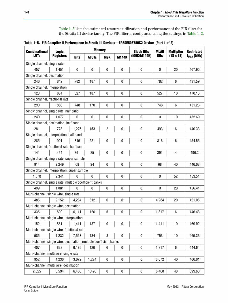
Table 1–5 lists the estimated resource utilization and performance of the FIR filter for the Stratix III device family. The FIR filter is configured using the settings in Table 1–2.
Table 1–5. FIR Compiler II Performance in Stratix III Devices—EP3SE50F780C2 Device (Part 1 of 2)
Combinational LUTs
Logic Registers
Memory Block Bits(M9K/M144K)
MLAB Bits
Multiplier(18 × 18)
Restricted fMAX (MHz)Bits ALUTs M9K M144K
Single channel, single rate
457 1,451 0 0 0 0 0 0 20 467.95
Single channel, decimation
246 842 782 187 0 0 0 782 6 431.59
Single channel, interpolation
123 834 527 187 0 0 0 527 10 470.15
Single channel, fractional rate
290 866 748 170 0 0 0 748 6 451.26
Single channel, single rate, half band
240 1,077 0 0 0 0 0 0 10 452.69
Single channel, decimation, half band
281 773 1,275 153 2 0 0 493 6 440.33
Single channel, interpolation, half band
285 991 816 221 0 0 0 816 6 454.55
Single channel, fractional rate, half band
141 454 391 85 0 0 0 391 4 490.2
Single channel, single rate, super sample
914 2,249 68 34 0 0 0 68 40 446.03
Single channel, interpolation, super sample
1,070 2,341 0 0 0 0 0 0 52 453.51
Single channel, single rate, multiple coefficient banks
499 1,881 0 0 0 0 0 0 20 456.41
Multi-channel, single wire, single rate
485 2,152 4,284 612 0 0 0 4,284 20 421.05
Multi-channel, single wire, decimation
335 800 6,111 126 5 0 0 1,317 6 446.43
Multi-channel, single wire, interpolation
152 881 1,411 187 0 0 0 1,411 10 469.92
Multi-channel, single wire, fractional rate
585 1,232 7,553 134 8 0 0 753 10 465.33
Multi-channel, single wire, decimation, multiple coefficient banks
407 823 6,175 126 6 0 0 1,317 6 444.64
Multi-channel, multi wire, single rate
952 4,230 3,672 1,224 0 0 0 3,672 40 406.01
Multi-channel, multi wire, decimation
2,025 6,594 6,460 1,496 0 0 0 6,460 48 399.68
FIR Compiler II MegaCore Function May 2013 Altera CorporationUser Guide

Chapter 1: About This MegaCore Function 1–9Performance and Resource Utilization
Table 1–6 lists the estimated resource utilization and performance of the FIR filter for the Stratix IV device family. The FIR filter is configured using the settings in Table 1–2.
Multi -channel, multi wire, interpolation
1,626 7,148 4,054 1,466 0 0 0 4,054 52 423.55
Multi-channel, multi wire, fractional rate
1,119 4,703 6,333 914 0 0 0 6,333 32 418.24
Multi-channel, multi wire, fractional rate, output options
1,399 4,830 6,333 914 0 0 0 6,333 32 385.21
Multi-channel, multi wire, interpolation, multiple coefficient banks
1,411 7,789 4,058 1,468 0 0 0 4,058 64 411.02
Table 1–5. FIR Compiler II Performance in Stratix III Devices—EP3SE50F780C2 Device (Part 2 of 2)
Combinational LUTs
Logic Registers
Memory Block Bits(M9K/M144K)
MLAB Bits
Multiplier(18 × 18)
Restricted fMAX (MHz)Bits ALUTs M9K M144K
Table 1–6. FIR Compiler II Performance in Stratix IV Devices—EP4SGX70DF29C2X Device (Part 1 of 2)
Combinational LUTs
Logic Registers
Memory Block Bits(M9K/M144K)
MLAB Bits
Multiplier(18 × 18)
Restricted fMAX (MHz)Bits ALUTs M9K M144K
Single channel, single rate
457 1,451 0 0 0 0 0 0 20 510.2
Single channel, decimation
246 842 782 187 0 0 0 782 6 481.7
Single channel, interpolation
123 834 527 187 0 0 0 527 10 510.2
Single channel, fractional rate
290 866 748 170 0 0 0 748 6 510.2
Single channel, single rate, half band
240 1,077 0 0 0 0 0 0 10 510.2
Single channel, decimation, half band
281 861 1,275 187 0 0 0 1,275 6 510.2
Single channel, interpolation, half band
285 991 816 221 0 0 0 816 6 510.2
Single channel, fractional rate, half band
141 454 391 85 0 0 0 391 4 510.2
Single channel, single rate, super sample
914 2,249 68 34 0 0 0 68 40 510.2
Single channel, interpolation, super sample
1,070 2,340 0 0 0 0 0 0 52 509.68
Single channel, single rate, multiple coefficient banks
499 1,881 0 0 0 0 0 0 20 509.42
May 2013 Altera Corporation FIR Compiler II MegaCore FunctionUser Guide

1–10 Chapter 1: About This MegaCore FunctionPerformance and Resource Utilization
Table 1–7 lists the estimated resource utilzation and performance of the FIR filter for the Stratix V device family. The FIR filter is configured using the settings in Table 1–2.
Multi-channel, single wire, single rate
485 2,152 4,284 612 0 0 0 4,284 20 479.39
Multi-channel, single wire, decimation
317 1,029 6,145 228 0 0 0 6,145 6 510.2
Multi-channel, single wire, interpolation
166 919 4,930 187 0 0 0 4,930 10 510.2
Multi-channel, single wire, fractional rate
563 1,672 10,735 305 0 0 0 10,735 10 510.2
Multi-channel, single wire, decimation, multiple coefficient banks
391 1,066 6,209 230 0 0 0 6,209 6 504.54
Multi-channel, multi wire, single rate
952 4,230 3,672 1,224 0 0 0 3,672 40 466.2
Multi-channel, multi wire, decimation
2,025 6,594 6,460 1,496 0 0 0 6,460 48 457.04
Multi -channel, multi wire, interpolation
1,626 7,148 4,054 1,466 0 0 0 4,054 52 468.38
Multi-channel, multi wire, fractional rate
1,120 4,704 6,333 914 0 0 0 6,333 32 484.26
Multi-channel, multi wire, fractional rate, output options
1,400 4,831 6,333 914 0 0 0 6,333 32 495.54
Multi-channel, multi wire, interpolation, multiple coefficient banks
1,411 7,789 4,058 1,468 0 0 0 4,058 64 459.14
Table 1–6. FIR Compiler II Performance in Stratix IV Devices—EP4SGX70DF29C2X Device (Part 2 of 2)
Combinational LUTs
Logic Registers
Memory Block Bits(M9K/M144K)
MLAB Bits
Multiplier(18 × 18)
Restricted fMAX (MHz)Bits ALUTs M9K M144K
Table 1–7. FIR Compiler II Performance in Stratix V Devices—5SGSMD4H2F35C2 Device (Part 1 of 2)
Combinational LUTs
Logic Registers
Memory Block Bits(M20K)
MLAB Bits
DSP Blocks
Restricted fMAX (MHz)Bits ALUTs M20K
Single channel, single rate
1 698 0 0 0 0 0 10 450.05
Single channel, decimation
93 209 782 187 0 0 782 3 450.05
Single channel, interpolation
162 203 408 204 0 0 408 5 450.05
Single channel, fractional rate
400 720 1,156 119 0 0 1,156 3 450.05
FIR Compiler II MegaCore Function May 2013 Altera CorporationUser Guide

Chapter 1: About This MegaCore Function 1–11Performance and Resource Utilization
Single channel, single rate, half band
7 279 272 136 0 0 272 5 450.05
Single channel, decimation, half band
129 247 1,156 187 0 0 1,156 3 450.05
Single channel, interpolation, half band
133 360 748 204 0 0 748 3 450.05
Single channel, fractional rate, half band
172 256 612 102 0 0 612 2 450.05
Single channel, single rate, super sample
143 424 5,406 918 0 0 5,406 20 450.05
Single channel, interpolation, super sample
95 881 1.190 340 0 0 1,190 32 450.05
Single channel, single rate, multiple coefficient banks
20 770 289 17 0 0 289 10 450.05
Multi-channel, single wire, single rate
30 147 4,284 612 0 0 4,284 10 450.05
Multi-channel, single wire, decimation
228 423 6,145 228 0 0 6,145 3 450.05
Multi-channel, single wire, interpolation
284 335 6,834 255 0 0 6,834 5 450.05
Multi-channel, single wire, fractional rate
703 1,068 10,624 308 0 0 10,624 5 450.05
Multi-channel, single wire, decimation, multiple coefficient banks
415 621 6,848 231 0 0 6,848 3 450.05
Multi-channel, multi wire, single rate
23 225 3,672 1,224 0 0 3,672 20 450.05
Multi-channel, multi wire, decimation
792 1,524 6,460 1,496 0 0 6,460 24 450.05
Multi -channel, multi wire, interpolation
549 2,315 3,510 1,466 0 0 3,510 32 450.05
Multi-channel, multi wire, fractional rate
934 2,395 6,673 914 0 0 6,673 16 450.05
Multi-channel, multi wire, fractional rate, output options
1,214 2,521 6,673 914 0 0 6,673 16 450.05
Multi-channel, multi wire, interpolation, multiple coefficient banks
568 2,571 3,752 1,502 0 0 3,752 32 450.05
Table 1–7. FIR Compiler II Performance in Stratix V Devices—5SGSMD4H2F35C2 Device (Part 2 of 2)
Combinational LUTs
Logic Registers
Memory Block Bits(M20K)
MLAB Bits
DSP Blocks
Restricted fMAX (MHz)Bits ALUTs M20K
May 2013 Altera Corporation FIR Compiler II MegaCore FunctionUser Guide
1–12 Chapter 1: About This MegaCore FunctionRelease Information
Release InformationTable 1–8 provides information about this release of the Altera FIR Compiler II MegaCore function.
f For more information about this release, refer to the MegaCore IP Library Release Notes and Errata.
Altera verifies that the current version of the Quartus® II software compiles the previous version of each MegaCore function. The MegaCore IP Library Release Notes and Errata report any exceptions to this verification. Altera does not verify compilation with MegaCore function versions older than one release.
Table 1–8. FIR Compiler II MegaCore Function Release Information
Item Description
Version 12.1
Release Date November 2012
Ordering Code IP-FIRIIIPR-FIRII (renewal)
Product ID 00D8
Vendor ID 6AF7
FIR Compiler II MegaCore Function May 2013 Altera CorporationUser Guide

May 2013 Altera Corporation
2. Getting Started
This chapter provides a general overview of the Altera IP core design flow to help you quickly get started with any Altera IP core. The Altera IP library is installed as part of the Quartus II installation process. You can select and parameterize any Altera IP core from the library. Altera provides an integrated parameter editor that allows you to customize IP cores to support a wide variety of applications. The parameter editor guides you through the setting of parameter values and selection of optional ports.
The following sections describe the general installation, design flow, evaluation, and production use of Altera IP cores.
Installation and LicensingThe Altera IP Library is distributed with the Quartus II software and downloadable from the Altera website, www.altera.com.
Figure 2–1 shows the directory structure after you install an Altera IP core, where <path> is the installation directory. The default installation directory on Windows is C:\altera\<version number>; on Linux it is /opt/altera<version number>.
You can evaluate an IP core in simulation and in hardware before you purchase a license. For most Altera IP cores, you can use Altera’s free OpenCore Plus evaluation feature for this purpose. Some Altera IP cores do not require use of this special feature for evaluation. You can evaluate the IP core until you are satisfied with its functionality and performance. You must purchase a license for the IP core when you want to take your design to production.
After you purchase a license for an Altera IP core, you can request a license file from the Altera website at www.altera.com/licensing and install it on your computer. When you request a license file, Altera emails you a license.dat file. If you do not have internet access, contact your local Altera representative.
Figure 2–1. Directory Structure
srcContains the libraries.
ast_componentContains the lower-level design files.
ipContains the Altera MegaCore IP Library and third-party IP cores.
<path>Installation directory.
alteraContains the Altera MegaCore IP Library.
commonContains shared components.
fir_compiler_iiContains the FIR Compiler II MegaCore function files.
FIR Compiler II MegaCore FunctionUser Guide

2–2 Chapter 2: Getting StartedMegaWizard Plug-In Manager Design Flow
f For additional information about installation and licensing, refer to Altera Software Installation and Licensing.
MegaWizard Plug-In Manager Design FlowThe MegaWizard™ Plug-in Manager flow allows you to customize a FIR Compiler II MegaCore function, and manually integrate the MegaCore function variation in a Quartus II design.
Specifying ParametersTo launch the MegaWizard Plug-In Manager, perform the following steps:
1. Create a new project using the New Project Wizard available from the File menu in the Quartus II software.
2. Launch MegaWizard Plug-In Manager from the Tools menu, and select the option to create a new custom megafunction variation.
3. Click Next and select FIR Compiler II under Filters under Installed Plug-Ins.
4. Verify the appropriate device family name.
5. Select the top-level output file type for your design; the wizard supports VHDL and Verilog HDL.
6. Specify the top-level output file name for your MegaCore function variation and click Next.
7. Specify the parameters on the Parameter Settings pages. For detailed explanations of these parameters, refer to Chapter 3, Parameter Settings.
8. Click Finish. Generation might take several minutes to complete. The generation progress and status is displayed in a report window. The parameter editor generates the top-level HDL code for your IP core, a .qip file containing all of the necessary assignments and information required to process the IP core in the Quartus II Compiler, and a simulation directory which includes files for simulation. The parameter editor also interface generates a MATLAB m-file that contains functions you can use to analyze a FIR Compiler II MegaCore function design in the MATLAB environment. A testbench is also generated.
You can now integrate your custom IP core instance in your design, simulate, and compile. While integrating your IP core instance into your design, you must make appropriate pin assignments. You can create virtual pin to avoid making specific pin assignments for top-level signals while you are simulating and not ready to map the design to hardware.
1 For information about the Quartus II software, including virtual pins and the MegaWizard Plug-In Manager, refer to Quartus II Help.
FIR Compiler II MegaCore Function May 2013 Altera CorporationUser Guide

Chapter 2: Getting Started 2–3MegaWizard Plug-In Manager Design Flow
Table 2–1 describes the files created in the project directory during generation of the MegaCore function. The design synthesis and simulation files are generated in the following two folders:
■ <variation name> folder — Contains files used for Quartus II synthesis
■ <variation name>_sim folder— Contains files used for simulation purposes
The names and types of files specified in the report vary based on whether you selected the VHDL or Verilog HDL output format.
Table 2–1. Generated Files (Part 1 of 2) (1) (2)
Filename Description
Compilation files in the project directory
<variation name>.qip
Contains all of the assignments and other information required to process your MegaCore function variation in the Quartus II Compiler. You are prompted to add this file to the current Quartus II project when you exit from the parameter editor.
<variation name>.vhd or .v
A VHDL or Verilog HDL file that defines a VHDL or Verilog HDL top-level description of the custom MegaCore function variation. Instantiate the entity defined by this file inside of your design. Include this file when compiling your design in the Quartus II software.
<variation name>.bsf A Quartus II block symbol file for the MegaCore function variation. You can use this file in the Quartus II block diagram editor.
Synthesis files in the <variation name> folder
<variation name>_<index>_ast.vhd A VHDL wrapper file for the Avalon-ST interface.
<variation name>_<index>.sdc This file contains timing constraints for FIR Compiler II IP core based on your variation settings.
<variation name>.<index>.vhd A VHDL file that defines the design entity.
Simulation files in the <variation name>_sim folder
<variation name>_ast.vhd A VHDL wrapper file for the Avalon-ST interface.
<variation name>.vhd A VHDL file that defines the design entity.
<variation name>_nativelink.tcl A Tcl script that can be used to assign NativeLink simulation testbench settings to the Quartus II project.
<variation name>_msim.tcl This Tcl script can be used to simulate the VHDL testbench together with the simulation model of the customized FIR MegaCore function variation.
<variation name>_mlab.m This MATLAB m-file provides the kernel of the MATLAB simulation model for the customized FIR II MegaCore function variation.
<variation name>_model.m This MATLAB m-file provides a MATLAB simulation model for the customized FIR Compiler II MegaCore function variation.
<variation name>_input.txtThis text file provides input data and bank switching pattern (when multiple coefficient banks are used) for the MATLAB model and the simulation testbench.
<variation name>_param.txt This text file records the input and output parameters for customized FIR Compiler II MegaCore function variation.
<variation name>_coef_int.txt This text file provides coefficient inputs for the testbench (incomplete coefficients for symmetry/anti-symmetry filter).
<variation name>_coef_reload.txt This text file provides new random coefficients input for the MATLAB model when the coefficient reloading option is enabled.
May 2013 Altera Corporation FIR Compiler II MegaCore FunctionUser Guide

2–4 Chapter 2: Getting StartedMegaWizard Plug-In Manager Design Flow
Simulating the DesignThe FIR Compiler II MegaCore function generates a number of output files for design simulation. After you have created a custom FIR filter, you can simulate your design in the ModelSim®-Altera software, MATLAB, or another third-party simulation tool.
Simulating in the ModelSim-Altera SoftwareUse the Tcl script (<variation name>_msim.tcl) to load the VHDL testbench into the ModelSim-Altera software.
This script uses the file <variation name>_input.txt to provide input data to the FIR filter. The output from the simulation is stored in a file <variation name>_output.txt.
Simulating in MATLABTo simulate in a MATLAB environment, run the <variation_name>_model.m testbench m-file, which also is located in your design directory. This script also uses the file <variation name>_input.txt to provide input data. The output from the MATLAB simulation is stored in the file <variation name>_model_output.txt.
Simulating in Third-Party Simulation Tools Using NativeLinkYou can perform a simulation in a third-party simulation tool from within the Quartus II software, using NativeLink.
The Tcl script file <variation name>_nativelink.tcl can be used to assign default NativeLink testbench settings to the Quartus II project.
To perform a simulation in the Quartus II software using NativeLink, perform the following steps:
1. Create a custom MegaCore function variation as described earlier in this chapter but ensure you specify a variation name that exactly matches the Quartus II project name.
2. Verify that the absolute path to your third-party EDA tool is set in the Options page under the Tools menu in the Quartus II software.
3. On the Processing menu, point to Start and click Start Analysis & Elaboration.
4. On the Tools menu, click Tcl scripts. In the Tcl Scripts dialog box, select <variation name>_nativelink.tcl and click Run. A message indicates that the Tcl script is successfully loaded.
<variation name>_coef_reload_rtl.txt
This text file contains the same coeffificient inputs as <variation name>_coef_reload.txt. However, this file contains incomplete coefficients for symmetry/anti-symmetry filter and is used for simulation testbench when the coefficient reloading option is enabled.
Note to Table 2–1
(1) <variation name> is a prefix variation name supplied automatically.(2) <index> is a variable that indicates the number of times a component has been used. For example, <variation name>_<index>_ast.vhd is
defined as FIR_0002_ast.vhd.
Table 2–1. Generated Files (Part 2 of 2) (1) (2)
Filename Description
FIR Compiler II MegaCore Function May 2013 Altera CorporationUser Guide

Chapter 2: Getting Started 2–5MegaWizard Plug-In Manager Design Flow
5. On the Assignments menu, click Settings, expand EDA Tool Settings, and select Simulation. Select a simulator under Tool name then in NativeLink Settings, select Compile test bench and click Test Benches.
6. On the Tools menu, point to EDA Simulation Tool and click Run EDA RTL Simulation.
The Quartus II software selects the simulator, and compiles the Altera libraries, design files, and testbenches. The testbench runs and the waveform window shows the design signals for analysis.
f For more information, refer to the Simulating Altera IP in Third-Party Simulation Tools chapter in volume 3 of the Quartus II Handbook.
1 IP functional simulation models output correct data only when data storage is clear. When data storage is not clear, functional simulation models will output non-relevant data. The number of clock cycles it takes before relevant samples are available is N; where N = (number of channels) × (number of coefficients) × (number of clock cycles to calculate an output).
For a full list of files generated by the FIR Compiler II MegaCore function, refer to Table 2–1 on page 2–3.
Compiling the Design and Programing a DeviceAfter using the MegaWizard Plug-In Manager to define and instantiate your IP core, you must compile your design to create programming files to configure the FPGA.
Some Altera IP cores require that you apply constraints before compilation. These constraint files make pin assignments and ensure that your IP core instance meets design timing requirements.
After applying constraint files if appropriate for your IP core, you can use the Start Compilation command on the Processing menu in the Quartus II software to compile your design. After successfully compiling your design, program the targeted Altera device with the Programmer and verify the design in hardware.
May 2013 Altera Corporation FIR Compiler II MegaCore FunctionUser Guide

2–6 Chapter 2: Getting StartedMegaWizard Plug-In Manager Design Flow
FIR Compiler II MegaCore Function May 2013 Altera CorporationUser Guide

May 2013 Altera Corporation
3. Parameter Settings
This chapter describes the parameters available in the FIR Compiler II MegaCore function.
For information about using the parameter editor, refer to “MegaWizard Plug-In Manager Design Flow” on page 2–2.
The Parameter Settings contains the following three pages:
■ Filter Specification Page
■ Input and Output Options Page
■ Implementation Options Page
Filter Specification PageA FIR filter is defined by its coefficients. The FIR Compiler II MegaCore function provides the following options for obtaining coefficients:
■ You can specify the filter settings and coefficient options in the parameter editor. The FIR Compiler II MegaCore function provides a default 37-tap coefficient set regardless of the configurations from filter settings. The scaled value and fixed point value are recalculated based on the coefficient bit width setting. The higher the coefficient bit width, the closer the fixed frequency response is to the intended original frequency response with the expense of higher resource usage.
■ You can load the coefficients from a file. For example, you can create the coefficients in another application such as MATLAB or a user-created program, save the coefficients to a file, and import them into the FIR Compiler II MegaCore function. For more information, refer to “Loading Coefficients from a File” on page 3–2.
Table 3–1 lists the filter specification parameters.
Table 3–1. Filter Specification Parameters (Part 1 of 2)
Parameter Value Description
Filter Settings
Filter Type
Single Rate
Decimation
Interpolation
Fractional Rate
Specifies the type of FIR filter. The default value is Single Rate.
Interpolation Factor 1 to 128 Specifies the number of extra points to generate between the original samples. The default value is 1.
Decimation Factor 1 to 128 Specifies the number of data points to remove between the original samples. The default value is 1.
L-th Band Filter
All taps
Half band
3rd–5th
Specifies the apropriate L-band Nyquist filters. Every Lth coefficient of these filters is zero, counting out from the center tap. The default value is All taps.
FIR Compiler II MegaCore FunctionUser Guide
3–2 Chapter 3: Parameter SettingsFilter Specification Page
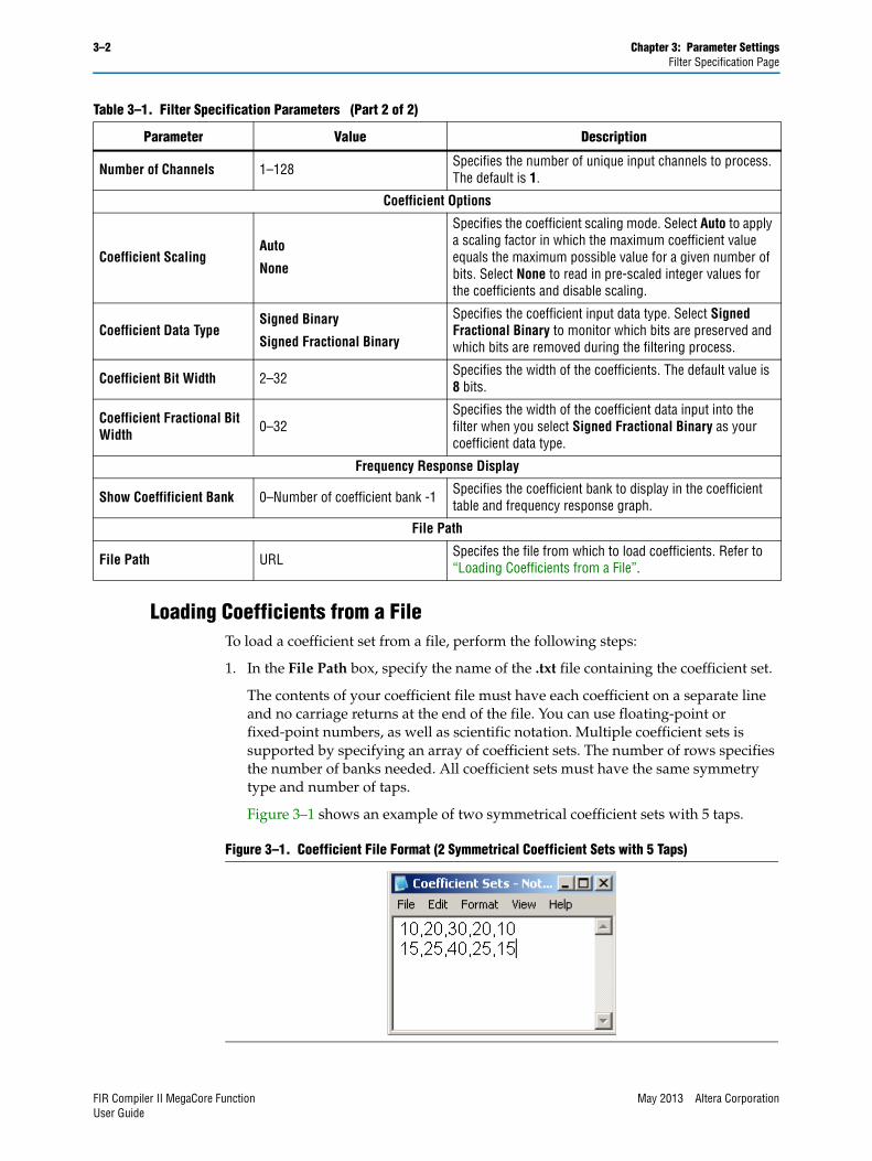
Loading Coefficients from a FileTo load a coefficient set from a file, perform the following steps:
1. In the File Path box, specify the name of the .txt file containing the coefficient set.
The contents of your coefficient file must have each coefficient on a separate line and no carriage returns at the end of the file. You can use floating-point or fixed-point numbers, as well as scientific notation. Multiple coefficient sets is supported by specifying an array of coefficient sets. The number of rows specifies the number of banks needed. All coefficient sets must have the same symmetry type and number of taps.
Figure 3–1 shows an example of two symmetrical coefficient sets with 5 taps.
Number of Channels 1–128 Specifies the number of unique input channels to process. The default is 1.
Coefficient Options
Coefficient ScalingAuto
None
Specifies the coefficient scaling mode. Select Auto to apply a scaling factor in which the maximum coefficient value equals the maximum possible value for a given number of bits. Select None to read in pre-scaled integer values for the coefficients and disable scaling.
Coefficient Data TypeSigned Binary
Signed Fractional Binary
Specifies the coefficient input data type. Select Signed Fractional Binary to monitor which bits are preserved and which bits are removed during the filtering process.
Coefficient Bit Width 2–32 Specifies the width of the coefficients. The default value is 8 bits.
Coefficient Fractional Bit Width 0–32
Specifies the width of the coefficient data input into the filter when you select Signed Fractional Binary as your coefficient data type.
Frequency Response Display
Show Coeffificient Bank 0–Number of coefficient bank -1 Specifies the coefficient bank to display in the coefficient table and frequency response graph.
File Path
File Path URL Specifes the file from which to load coefficients. Refer to “Loading Coefficients from a File”.
Table 3–1. Filter Specification Parameters (Part 2 of 2)
Parameter Value Description
Figure 3–1. Coefficient File Format (2 Symmetrical Coefficient Sets with 5 Taps)
FIR Compiler II MegaCore Function May 2013 Altera CorporationUser Guide
Chapter 3: Parameter Settings 3–3Input and Output Options Page
1 Do not insert additional carriage returns at the end of the file. The FIR Compiler II MegaCore function interprets each carriage return as an extra coefficient with the value of the most recent past coefficient. The file must have a minimum of five non-zero coefficients.
2. In the Filter Specification tab of the parameter editor, click Apply to import the coefficient set.
When you import a coefficient set, the frequency response of the floating-point coefficients is displayed in blue and the frequency response of the fixed-point coefficients is displayed in red.
The FIR Compiler II MegaCore function supports scaling on the coefficient set.
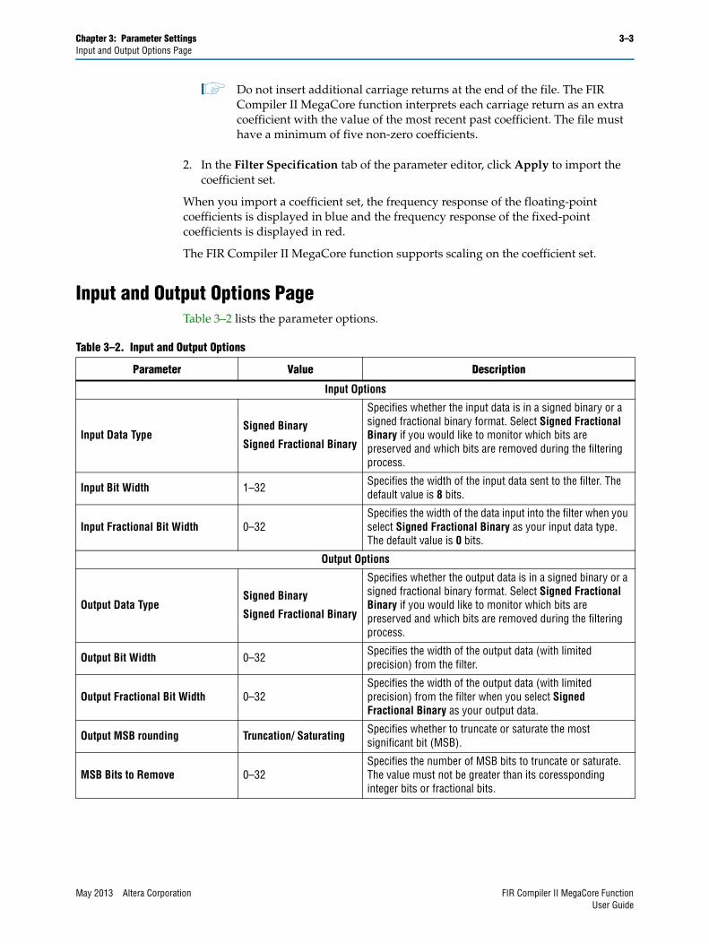
Input and Output Options PageTable 3–2 lists the parameter options.
Table 3–2. Input and Output Options
Parameter Value Description
Input Options
Input Data TypeSigned Binary
Signed Fractional Binary
Specifies whether the input data is in a signed binary or a signed fractional binary format. Select Signed Fractional Binary if you would like to monitor which bits are preserved and which bits are removed during the filtering process.
Input Bit Width 1–32 Specifies the width of the input data sent to the filter. The default value is 8 bits.
Input Fractional Bit Width 0–32Specifies the width of the data input into the filter when you select Signed Fractional Binary as your input data type. The default value is 0 bits.
Output Options
Output Data TypeSigned Binary
Signed Fractional Binary
Specifies whether the output data is in a signed binary or a signed fractional binary format. Select Signed Fractional Binary if you would like to monitor which bits are preserved and which bits are removed during the filtering process.
Output Bit Width 0–32 Specifies the width of the output data (with limited precision) from the filter.
Output Fractional Bit Width 0–32Specifies the width of the output data (with limited precision) from the filter when you select Signed Fractional Binary as your output data.
Output MSB rounding Truncation/ Saturating Specifies whether to truncate or saturate the most significant bit (MSB).
MSB Bits to Remove 0–32Specifies the number of MSB bits to truncate or saturate. The value must not be greater than its coressponding integer bits or fractional bits.
May 2013 Altera Corporation FIR Compiler II MegaCore FunctionUser Guide

3–4 Chapter 3: Parameter SettingsInput and Output Options Page
Signed Fractional BinaryThe FIR Compiler II supports two’s complement, signed fractional binary notation, which allows you to monitor which bits are preserved and which bits are removed during filtering. A signed binary fractional number has the format:
<sign> <integer bits>.<fractional bits>
A signed binary fractional number is interpreted as shown below:
<sign> <x1 integer bits>.<y1 fractional bits> Original input data
<sign> <x2 integer bits>.<y2 fractional bits> Original coefficient data
<sign> <i integer bits>.<y1 + y2 fractional bits> Full precision after FIR calculation
<sign> <x3 integer bits>.<y3 fractional bits> Output data after limiting precision
where i = ceil(log2(number of coefficients)) + x1 + x2
For example, if the number has 3 fractional bits and 4 integer bits plus a sign bit, the entire 8-bit integer number is divided by 8, which yields a number with a binary fractional component.
The total number of bits equals to the sign bits + integer bits + fractional bits. The sign + integer bits is equal to Input Bit Width – Input Fractional Bit Width with a constraint that at least 1 bit must be specified for the sign.
MSB and LSB Truncation, Saturation, and RoundingThe output options on the parameter editor allows you to truncate or saturate the MSB and to truncate or round the LSB. Saturation, truncation, and rounding are non-linear operations.
Table 3–1 lists the options for limiting the precision of your filter.
Output LSB rounding Truncation/ Rounding Specifies whether to truncate or round the least significant bit (LSB).
LSB Bits to Remove 0–32Specifies the number of LSB bits to truncate or round. The value must not be greater than its coressponding integer bits or fractional bits.
Table 3–2. Input and Output Options
Parameter Value Description
Table 3–1. Options for Limiting Precision
Bit Range Option Result
MSB Truncate In truncation, the filter disregards specified bits. (Figure 3–1).
Saturate In saturation, if the filtered output is greater than the maximum positive or negative value that can be represented, the output is forced (or saturated) to the maximum positive or negative value.
LSB Truncate Same process as for MSB.
Round The output is rounded away from zero.
FIR Compiler II MegaCore Function May 2013 Altera CorporationUser Guide

Chapter 3: Parameter Settings 3–5Implementation Options Page
Figure 3–1 shows an example of removing bits from the MSB and LSB.
Implementation Options PageTable 3–3 lists the implementation options.
Figure 3–1. Removing Bits from the MSB and LSB
D15D14D13D12D11D10D9D8..D0
D9D8..D0
Bits Removed from MSB
FullPrecision
LimitedPrecision
D15D14....D4D3D2D1D0
D11D10...D1D0
Bits Removed from LSB
FullPrecision
LimitedPrecision
D15D14D13D12...D3D2D1D0
D10D9...D1D0
Bits Removed from both MSB & LSB
FullPrecision
LimitedPrecision
Table 3–3. Implementation Options (Part 1 of 2)
Parameter Value Description
Frequency Specification
Clock Frequency (MHz) 1–500 Specifies the frequency of the input clock. The default value is 100 MHz.
Clock Slack Integer Enables you to control the amount of pipelining independently of the clock frequency and therefore independently of the clock to sample rate ratio. The default value is 0.
Input Sample Rate (MSPS) Integer Specifies the sample rate of the incoming data. The default is 100.
Speed Grade
Fast
Medium
Slow
Specifies the speed grade of the target device to balance the size of the hardware against the resources required to meet the clock frequency. The default value is Medium.
Symmetry Option
Symmetry Mode
Non Symmetry
Symmetrical
Anti-Symmetrical
Specifies whether your filter design uses non-symmetric, symmetric, or anti-symmetric coefficients. The default value is Non Symmetry.
Coefficients Reload Options
Coefficients Reload —
Turn on this option to allow coefficient reloading. This option allows you to change coefficient values during run time. When this option is turned on, additional input ports are added to the filter.
Base Address Integer Specifies the base address of the memory-mapped coefficients.
Read/Write mode
Read
Write
Read/Write
Specifies the read and write mode that determines the type of address decode to build.
May 2013 Altera Corporation FIR Compiler II MegaCore FunctionUser Guide

3–6 Chapter 3: Parameter SettingsImplementation Options Page
Memory and Multiplier Trade-OffsWhen your design is synthesized to logic, delay blocks are often created. The FIR Compiler II MegaCore function tries to balance the implementation between logic elements (LEs) and memory blocks (M512, M4K, M9K, or M144K). The exact trade-off depends on the target FPGA family, but generally the trade-off attempts to minimize the absolute silicon area used. For example, if a block of RAM occupies the silicon area of two logic array blocks (LABs), a delay requiring more than 20 LEs (two LABs) is implemented as a block of RAM. This is usually appropriate, but there might be cases when you want to influence this trade-off.
Table 3–4, Table 3–5, Table 3–6, and Table 3–7 list the memory and multiplier threshold trade-offs, and provide some usage examples.
Flow Control
Back Pressure Support —
Turn on this option to enable backpressure support. When this option is turned on, the sink signals the source to stop the flow of data when its FIFOs are full or when there is congestion on its output port.
Resource Optimization Settings
Device Family Menu of supported devices Specifies the target device family.
LEs / Small RAM Block Threshold Integer
Specifies the balance of resources between LEs/Small RAM block threshold in bits. The default value is 20. For more information, refer to “Memory and Multiplier Trade-Offs” on page 3–6.
Small / Medium RAM Block Threshold Integer
Specifies the balance of resources between small to medium RAM block threshold in bits.The default value is 1280. For more information, refer to “Memory and Multiplier Trade-Offs” on page 3–6.
Medium / Large RAM Block Threshold Integer
Specifies the balance of resources between medium to large RAM block threshold in bits. The default value is 1000000. For more information, refer to “Memory and Multiplier Trade-Offs” on page 3–6.
LEs / DSP Block Multiplier Threshold Integer
Specifies the balance of resources between LEs/ DSP block multiplier threshold in bits. The default value is -1. For more information, refer to “Memory and Multiplier Trade-Offs” on page 3–6.
Table 3–3. Implementation Options (Part 2 of 2)
Parameter Value Description
Table 3–4. CDelay RAM Block Threshold (Part 1 of 2)
Description Trade-off between simple delay LEs and small ROM blocks. If any delay’s size is such that the number of LEs used is greater than this parameter, the delay is implemented as block RAM.
Default (-1) 20 bits
FIR Compiler II MegaCore Function May 2013 Altera CorporationUser Guide
Chapter 3: Parameter Settings 3–7Implementation Options Page
Usage
To make more delays using block RAM, enter a lower number, such as a value in the range of 20–30.
To use fewer block memories, enter a larger number, such as 100.
To never use block memory for simple delays, enter a very large number, such as 10000.
Notes Delays of less than three cycles must be implemented in LEs due to the nature of the block RAM behavior.
This threshold only applies to implementing simple delays in memory blocks or logic elements. Dual memories cannot be pushed back into logic elements.
Table 3–4. CDelay RAM Block Threshold (Part 2 of 2)
Table 3–5. CDualMem Dist RAM Threshold
Description
Trade-off between small and medium RAM blocks. This threshold is similar to the CDelay RAM Block Threshold except that it applies only to the dual-port memories.
Any dual-port memory is always implemented in a block memory rather than logic elements, but for some device families there might be different sizes of block memory available. The threshold value determines which medium-size RAM memory blocks are used instead of small-memory RAM blocks. For example, the threshold that determines whether to use M9K blocks rather than MLAB blocks on Stratix III and Stratix IV devices.
Default (-1) 1,280 bits
Usage
Using Stratix III devices with the default threshold value (-1), dual memories greater than 1,280 bits are implemented as M9K blocks and dual memories less than or equal to 1,280 bits are implemented as MLABs. If you change this threshold to a lower value such as 200, dual memories greater than 200 bits are implemented as M9K blocks and dual memories less than or equal to 200 bits are implemented as MLAB blocks.
Notes For device families with only one type of memory block (for example, Cyclone II devices with only M4K blocks or Cyclone III devices with only M9K blocks), this threshold has no effect.
Table 3–6. M-RAM Threshold
Description Trade-off between medium and large RAM blocks. For larger delays, memory can be implemented in medium-block RAM (M4K, M9K) or using larger M-RAM blocks (M512K, M144K).
Default (-1) 1,000,000 bits
Usage If the number of bits in a memory or delay is greater than this threshold, M-RAM is used for the implementation. If you set a large value such as the default of 1,000,000 bits, M-RAM blocks are never used.
Table 3–7. Hard Multiplier Threshold (Part 1 of 2)
Description
Trade-off between hard and soft multipliers. For devices that support hard multipliers or DSP blocks, these resources can be used instead of a soft multiplier made from LEs. For example, a 2-bit × 10-bit multiplier consumes very few LEs. The hard multiplier threshold value corresponds to the number of logic elements that are used to save a multiplier. If the hard multiplier threshold value is 100, you are allowing 100 LEs. Therefore, an 18 × 18 multiplier (that requires approximately 182–350 LEs) is not transferred to LEs because it requires more LEs than the threshold value. However, a 16 × 4 multiplier that requires approximately 64 LEs is implemented as a soft multiplier with this setting.
Default (-1) —
May 2013 Altera Corporation FIR Compiler II MegaCore FunctionUser Guide
3–8 Chapter 3: Parameter SettingsImplementation Options Page
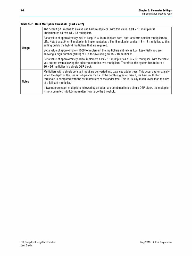
Usage
The default (-1) means to always use hard multipliers. With this value, a 24 × 18 multiplier is implemented as two 18 × 18 multipliers.
Set a value of approximately 300 to keep 18 × 18 multipliers hard, but transform smaller multipliers to LEs. Note that a 24 × 18 multiplier is implemented as a 6 × 18 multiplier and an 18 × 18 multiplier, so this setting builds the hybrid multipliers that are required.
Set a value of approximately 1000 to implement the multipliers entirely as LEs. Essentially you are allowing a high number (1000) of LEs to save using an 18 × 18 multiplier.
Set a value of approximately 10 to implement a 24 × 16 multiplier as a 36 × 36 multiplier. With the value, you are not even allowing the adder to combine two multipliers. Therefore, the system has to burn a 36 × 36 multiplier in a single DSP block.
Notes
Multipliers with a single constant input are converted into balanced adder trees. This occurs automatically when the depth of the tree is not greater than 2. If the depth is greater than 2, the hard multiplier threshold is compared with the estimated size of the adder tree. This is usually much lower than the size of a full soft multiplier.
If two non-constant multipliers followed by an adder are combined into a single DSP block, the multiplier is not converted into LEs no matter how large the threshold.
Table 3–7. Hard Multiplier Threshold (Part 2 of 2)
FIR Compiler II MegaCore Function May 2013 Altera CorporationUser Guide
May 2013 Altera Corporation
4. Functional Description
This chapter describes in detail about the FIR Compiler II MegaCore function, its architecture, interfaces, features, and interface signals.
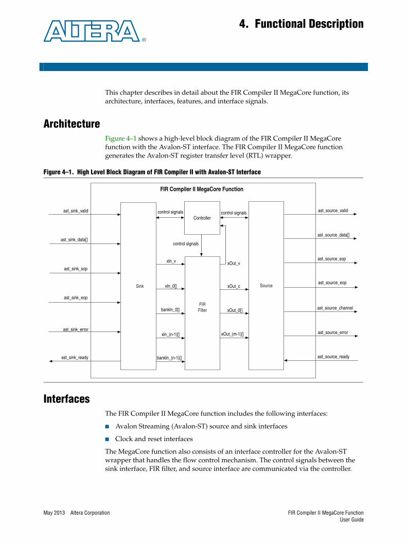
ArchitectureFigure 4–1 shows a high-level block diagram of the FIR Compiler II MegaCore function with the Avalon-ST interface. The FIR Compiler II MegaCore function generates the Avalon-ST register transfer level (RTL) wrapper.
InterfacesThe FIR Compiler II MegaCore function includes the following interfaces:
■ Avalon Streaming (Avalon-ST) source and sink interfaces
■ Clock and reset interfaces
The MegaCore function also consists of an interface controller for the Avalon-ST wrapper that handles the flow control mechanism. The control signals between the sink interface, FIR filter, and source interface are communicated via the controller.
Figure 4–1. High Level Block Diagram of FIR Compiler II with Avalon-ST Interface
FIRFilter
xln_v
bankln_0[]
xln_(n-1)[]
xOut_v
xOut_c
xOut_0[]
xOut_(m-1)[]
ast_sink_valid
ast_sink_data[]
ast_sink_sop
ast_sink_eop
ast_sink_error
ast_source_valid
ast_source_data[]
ast_source_sop
ast_source_eop
ast_source_error
ast_source_channel
Controller
ast_sink_ready ast_source_ready
FIR Compiler II MegaCore Function
Sink Source
control signals control signals
control signals
xln_0[]
bankln_(n-1)[]
FIR Compiler II MegaCore FunctionUser Guide

4–2 Chapter 4: Functional DescriptionInterfaces
Avalon-ST Sink and Source InterfacesThe sink and source interfaces of the MegaCore function implements the Avalon-ST protocol, which is a unidirectional flow of data. The number of bits per symbol represents the data width and the number of symbols per beat is the number of channel wires. The MegaCore function symbol type supports signed and unsigned binary format. The ready latency on the FIR Compiler II MegaCore function is 0.
When designing a datapath that includes the FIR Compiler II MegaCore function, you might not need backpressure if you know the downstream components can always receive data. You might achieve a higher clock rate by driving the ast_source_ready signal of the FIR Compiler II MegaCore function high, and not connecting the ast_sink_ready signal.
f For more information about the Avalon-ST interface properties, protocol and the data transfer timing, refer to the Avalon Interface Specifications.
Avalon-ST Sink InterfaceThe sink interface is capable of handling single or multiple channels on a single wire as well as multiple channels on multiple wires.
Single Channel on Single Wire
Figure 4–2 shows the connection between the sink interface and the FIR Compiler II MegaCore function when transferring a single channel of 8-bit data.
Figure 4–2. Single Channel on Single Wire (Sink -> FIR Compiler II)
FIR Filter
xln_v
xln_0[7:0]ast_sink_valid
ast_sink_data[7:0]
Controller
ast_sink_ready
FIR Compiler II MegaCore Function
Sink
sink_ready
control signals
FIR Compiler II MegaCore Function May 2013 Altera CorporationUser Guide

Chapter 4: Functional Description 4–3Interfaces
Multiple Channels on Single Wire
Figure 4–3 shows the connection between the sink interface and the FIR Compiler II MegaCore function when transferring a packet of data over multiple channels on a single wire. The data width of each channel is 8 bits.
Multiple Channels on Multiple Wires
Figure 4–4 and Figure 4–5 show the connection between the sink interface and the FIR Compiler II MegaCore function when transferring a packet of data over multiple channels on multiple wires. The data width of each channel is 8 bits. Consider a case when the number of channels = 6, clock rate = 200 MHz, and sample rate = 100 MHz.
Figure 4–3. Multiple Channels on Single Wire (Sink -> FIR Compiler II)
FIR Filter
xln_v
xln_0[7:0]ast_sink_valid
ast_sink_data[7:0]
Controller
ast_sink_ready
FIR Compiler II MegaCore Function
Sink
sink_ready
control signals
ast_sink_eop
ast_sink_sop
ast_sink_error
packet error
Avalon StreamingInterface
Signals Check
May 2013 Altera Corporation FIR Compiler II MegaCore FunctionUser Guide

4–4 Chapter 4: Functional DescriptionInterfaces
In this example, hardware optimization produces a TDM factor of 2, number of channel wires = 3, and channels per wire = 2.
Figure 4–4. Multiple Channels on Multiple Wires
FIR Filter
xln_v
xln_0[7:0]
ast_sink_valid
ast_sink_data[23:0]
Controller
ast_sink_ready
FIR Compiler II MegaCore Function
Sink
xln_1[7:0]
xln_2[7:0]
control signals
ast_sink_eop
ast_sink_sop
ast_sink_error
sink_ready
packet error
Avalon StreamingInterface
Signals Check
Figure 4–5. Timing Diagram of Multiple Channels on Multiple Wires
clk
ast_sink_valid
ast_sink_data[7:0]
ast_sink_data[15:8]
ast_sink_data[23:16]
ast_sink_sop
ast_sink_eop
xln_v[7:0]
xln_0[7:0]
xln_1[7:0]
xln_2[7:0]
A0 B0 A1 B1 A2 B2
C0 D0 C1 D1 C2 D2
E0 F0 E1 F1 E2 F2
A0 B0 A1 B1 A2 B2
C0 D0 C1 D1 C2 D2
E0 F0 E1 F1 E2 F2
X
X
X
FIR Compiler II MegaCore Function May 2013 Altera CorporationUser Guide
Chapter 4: Functional Description 4–5Interfaces
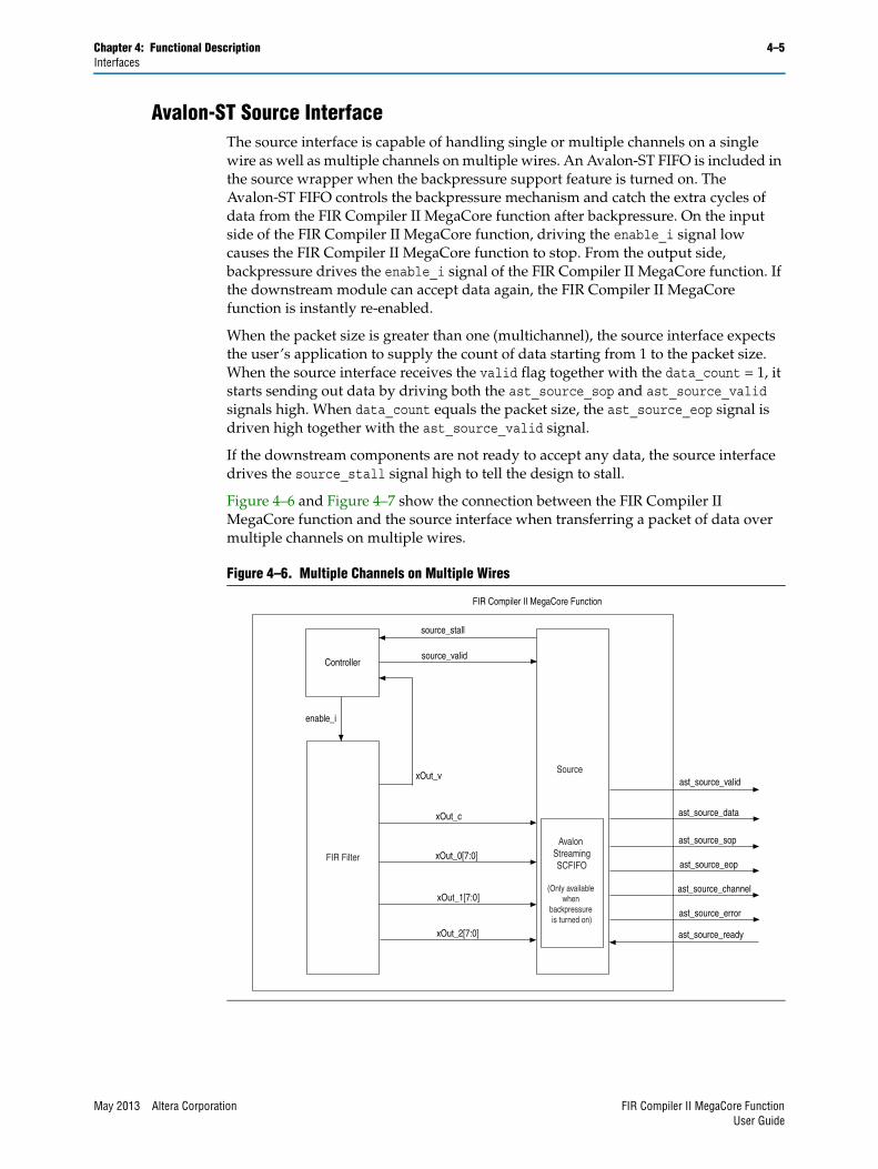
Avalon-ST Source InterfaceThe source interface is capable of handling single or multiple channels on a single wire as well as multiple channels on multiple wires. An Avalon-ST FIFO is included in the source wrapper when the backpressure support feature is turned on. The Avalon-ST FIFO controls the backpressure mechanism and catch the extra cycles of data from the FIR Compiler II MegaCore function after backpressure. On the input side of the FIR Compiler II MegaCore function, driving the enable_i signal low causes the FIR Compiler II MegaCore function to stop. From the output side, backpressure drives the enable_i signal of the FIR Compiler II MegaCore function. If the downstream module can accept data again, the FIR Compiler II MegaCore function is instantly re-enabled.
When the packet size is greater than one (multichannel), the source interface expects the user’s application to supply the count of data starting from 1 to the packet size. When the source interface receives the valid flag together with the data_count = 1, it starts sending out data by driving both the ast_source_sop and ast_source_valid signals high. When data_count equals the packet size, the ast_source_eop signal is driven high together with the ast_source_valid signal.
If the downstream components are not ready to accept any data, the source interface drives the source_stall signal high to tell the design to stall.
Figure 4–6 and Figure 4–7 show the connection between the FIR Compiler II MegaCore function and the source interface when transferring a packet of data over multiple channels on multiple wires.
Figure 4–6. Multiple Channels on Multiple Wires
FIR Filter
xOut_v
xOut_c
xOut_0[7:0]
ast_source_valid
ast_source_data
ast_source_sop
ast_source_eop
ast_source_error
ast_source_channel
Controller
ast_source_ready
FIR Compiler II MegaCore Function
Source
enable_i
xOut_1[7:0]
xOut_2[7:0]
source_stall
source_valid
Avalon StreamingSCFIFO
(Only available when
backpressure is turned on)
May 2013 Altera Corporation FIR Compiler II MegaCore FunctionUser Guide

4–6 Chapter 4: Functional DescriptionInterfaces
Clock and Reset InterfacesThe clock and reset interfaces drive or receive the clock and reset signals to synchronize the Avalon-ST interfaces and provide reset connectivity.
Figure 4–7. Timing Diagram of Multiple Channels on Multiple Wires
clk
xOut_v
xOut_c[7:0]
xOut_0[7:0]
xOut_1[7:0]
xOut_2[7:0]
ast_source_valid
ast_source_data[7:0]
ast_source_data[15:8]
ast_source_data[23:16]
ast_source_sop
ast_source_eop
ast_source_channel
ast_source_error
A0 B0 A1 B1 A2 B2
C0 D0 C1 D1 C2 D2
E0 F0 E1 F1 E2 F2
0 1 0 1 0 1
A0 B0 A1 B1 A2 B2
C0 D0 C1 D1 C2 D2
E0 F0 E1 F1 E2 F2
0 1 0 1 0 1
X
X
X
X
00
FIR Compiler II MegaCore Function May 2013 Altera CorporationUser Guide

Chapter 4: Functional Description 4–7Time-Division Multiplexing
Time-Division MultiplexingHardware utilization is optimized by using time-division multiplexing (TDM). The TDM factor (or folding factor) is the ratio of the clock rate to the sample rate.
By clocking a FIR Compiler II MegaCore function faster than the sample rate, you can reuse the same hardware. For example, by implementing a filter with a TDM factor of 2 and an internal clock multiplied by 2, you can halve the required hardware, as shown in Figure 4–8.
To achieve TDM, a serializer and deserializer are required before and after the reused hardware block to control the timing. The ratio of system clock frequency to sample rate determines the amount of resource saving except for a small amount of additional logic for the serializer and deserializer.
Table 4–1 shows the estimated resources required for a 49-tap symmetric FIR filter.
When the sample rate equals the clock rate, the filter is symmetric and you only need 25 multipliers. When the clock rate is increased to twice the sample rate, the number of multipliers required drops to 13. When the clock rate is set to 4 times the sample rate, the number of multipliers required drops to 7. If the clock rate stays the same while the new data sample rate is only 36 MSPS (million samples per second), the resource consumption is the same as twice the sample rate case.
Figure 4–8. Time-Division Multiplexing to Save Hardware Resources
Table 4–1. Estimated Resources Required for a 49-Tap Single Rate FIR Compiler II Filter
Clock Rate(MHz)
Sample Rate(MSPS) Logic Multipliers Memory Bits TDM Factor
72 72 2230 25 0 1
144 72 1701 13 468 2
288 72 1145 7 504 4
72 36 1701 13 468 2
Clock Rate = Sample Rate
Clock Rate = 2 x Sample Rate
Read
Read
Write
WriteSerialize Deserialize
May 2013 Altera Corporation FIR Compiler II MegaCore FunctionUser Guide
4–8 Chapter 4: Functional DescriptionMultichannel Operation
Multichannel OperationYou can build multichannel systems directly using the required channel count, rather than creating a single channel system and scaling it up. The MegaCore function uses vectors of wires to scale without having to cut and paste multiple blocks.
The FIR Compiler II MegaCore function can be vectorized, meaning that if data going into the block is a vector requiring multiple instances of a FIR filter, then multiple FIR blocks are created in parallel behind a single FIR Compiler II block. If a decimating filter requires a smaller vector on the output, the data from individual filters is automatically time-division multiplexed onto the output vector. This feature relieves the necessity of gluing filters together with custom logic.
Vectorized InputsThe data inputs and outputs for the FIR Compiler II blocks can be vectors. This capability is used when the clock rate is insufficiently high to carry the total aggregate data. For example, 10 channels at 20 MSPS require 10 × 20 = 200 MSPS aggregate data rate. If the system clock rate is set to 100 MHz, two wires are required to carry this data, and so the FIR Compiler II uses a vector of width 2.
This approach is unlike traditional methods because you do not need to manually instantiate two FIR filters and pass a single wire to each in parallel. Each FIR Compiler II block internally vectorizes itself. For example, a FIR Compiler II block can build two FIR filters in parallel and wire one element of the vector up to each FIR. The same paradigm is used on outputs, where high data rates on multiple wires are represented as vectors.
The input and output wire counts are determined by each FIR Compiler II MegaCore function, based on the clock rate, sample rate, and number of channels.
The output wire count is also affected by any rate changes in the FIR Compiler II MegaCore function. If there is a rate change, such interpolating by two, the output aggregate sample rate doubles. The output channels are then packed into the fewest number of wires (vector width) that will support that rate. For example, an interpolate by two FIR Compiler II filters might have two wires at the input, but three wires at the output.
Any necessary multiplexing and packing is performed by the FIR Compiler II MegaCore function. The blocks connected to the inputs and outputs must have the same vector widths. Vector width errors can usually be resolved by carefully changing the sample rates.
FIR Compiler II MegaCore Function May 2013 Altera CorporationUser Guide

Chapter 4: Functional Description 4–9Multichannel Operation
ChannelizationThe number of wires and the number of channels carried on each wire are determined by parameterization, which you can specify using the following variables:
■ clockRate is the system clock frequency (MHz).
■ inputRate is the data sample rate per channel (MSPS).
■ inputChannelNum is the number of channels. Channels are enumerated from 0 to inputChannelNum–1.
■ The period (or TDM factor) is the ratio of the clock rate to the sample rate and determines the number of available time slots.
■ ChanWireCount is the number of channel wires required to carry all the channels. It can be calculated by dividing the number of channels by the TDM factor. More specifically:
■ PhysChanIn = Number of channel input wires
■ PhysChanOut = Number of channel output wires
■ ChanCycleCount is the number of channels carried per wire. It is calculated by dividing the number of channels by the number of channels per wire. The channel signal counts from 0 to ChanCycleCount–1. More specifically:
■ ChansPerPhyIn = Number of channels per input wire
■ ChansPerPhyOut = Number of channels per output wire
If the number of channels is greater than the clock period, multiple wires are required. Each FIR Compiler II MegaCore function in your design is internally vectorized to build multiple FIR filters in parallel.
Figure 4–9 shows how a TDM factor of 3 combines two input channels into a single output wire. (inputChannelNum = 2, ChanWireCount = 1, ChanCycleCount = 2).
Figure 4–9. Channelization of Two Channels with a TDM Factor of 3 (1)
Note to Figure 4–9:
(1) In this example, there are three available time slots in the output channel and every third time slot has a ‘don't care’ value when the valid signal is low. The value of the channel signal while the valid signal is low does not matter.
clock
input_valid
input_data_channel_0
input_data_channel_1
input_channel
output_valid
TDM_output_data
output_channel
c0(0) c0(1) c0(2)
c1(0) c1(1) c2(2)
c0(0) c1(0) don’t care c0(0) c1(0) don’t care c0(0) c1(0)
May 2013 Altera Corporation FIR Compiler II MegaCore FunctionUser Guide

4–10 Chapter 4: Functional DescriptionMultichannel Operation
Figure 4–10 shows how a TDM factor of 3 combines four input channels into two wires (inputChannelNum = 4, ChanWireCount = 2, ChanCycleCount = 2).
The channel signal is used for synchronization and scheduling of data. It specifies the channel data separation per wire. Note that the channel signal counts from 0 to ChanCycleCount–1 in synchronization with the data. Thus, for ChanCycleCount = 1, the channel signal is the same as the channel count, enumerated from 0 to inputChannelNum–1.
For a case with single wire, the channel signal is the same as a channel count. For example, Figure 4–11 shows the case for four channels of data on one data wire with no invalid cycles.
For ChanWireCount > 1, the channel signal specifies the channel data separation per wire, rather than the actual channel number. The channel signal counts from 0 to ChanCycleCount–1 rather than 0 to inputChannelNum–1. Figure 4–12 shows the case for four channels on two wires with no invalid cycles.
Figure 4–10. Channelization for Four Channels with a TDM Factor of 3 (1)
Note to Figure 4–10:
(1) In this example, two wires are required to carry the four channels and the cycle count is two on each wire. The channels are evenly distributed on each wire leaving the third time slot as don't care on each wire.
clock
input_valid
input_data_channel_0
input_data_channel_1
input_data_channel_2
input_data_channel_3
input_channel
output_valid
output_data_wire_1
output_data_wire_2
output_channel
c0(0) c0(1) c0(2)
c1(0) c1(1) c1(2)
c2(0) c2(1) c2(2)
c3(0) c3(1) c3(2)
c0(0) c0(1) c0(2)c1(0) c1(1) c1(2)
c2(0) c2(1) c2(2)c3(0) c3(1) c3(2)
don’t care
don’t care
don’t care
don’t care
Figure 4–11. Four Channels on One Wire
valid
channel
data0
0 1 2 3 0 1 2 3
c0(0) c1(0) c2(0) c3(0) c0(1) c1(1) c2(1) c3(1)
Figure 4–12. Four Channels on Two Wires
valid
channel
data0
data1
0 1 0 1 0 1 0 1
c0(0) c1(0) c0(1) c1(1) c0(2) c1(2) c0(3) c1(3)
c2(0) c3(0) c2(1) c3(1) c2(2) c3(2) c2(3) c2(3)
FIR Compiler II MegaCore Function May 2013 Altera CorporationUser Guide
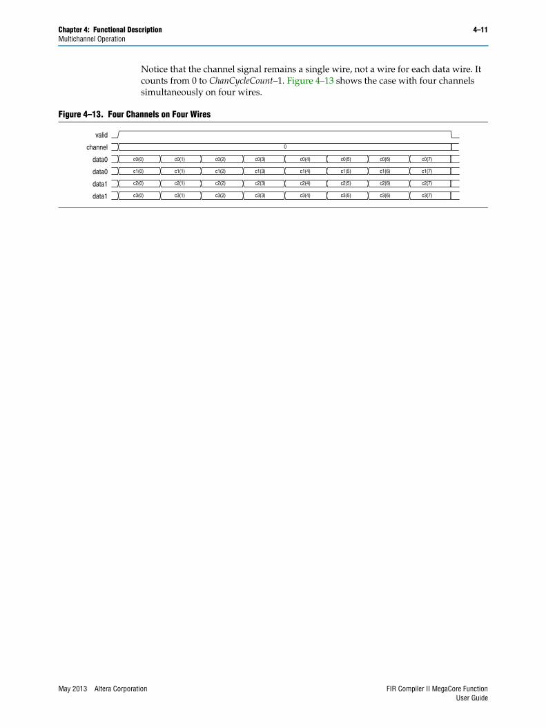
Chapter 4: Functional Description 4–11Multichannel Operation
Notice that the channel signal remains a single wire, not a wire for each data wire. It counts from 0 to ChanCycleCount–1. Figure 4–13 shows the case with four channels simultaneously on four wires.
Figure 4–13. Four Channels on Four Wires
valid
channel
data0
data0
data1
data1
c0(0) c0(1) c0(2) c0(3) c0(4) c0(5) c0(6) c0(7)
0
c1(0) c1(1) c1(2) c1(3) c1(4) c1(5) c1(6) c1(7)
c2(0) c2(1) c2(2) c2(3) c2(4) c2(5) c2(6) c2(7)
c3(0) c3(1) c3(2) c3(3) c3(4) c3(5) c3(6) c3(7)
May 2013 Altera Corporation FIR Compiler II MegaCore FunctionUser Guide
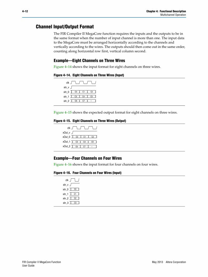
4–12 Chapter 4: Functional DescriptionMultichannel Operation
Channel Input/Output FormatThe FIR Compiler II MegaCore function requires the inputs and the outputs to be in the same format when the number of input channel is more than one. The input data to the MegaCore must be arranged horizontally according to the channels and vertically according to the wires. The outputs should then come out in the same order, counting along horizontal row first, vertical column second.
Example—Eight Channels on Three WiresFigure 4–14 shows the input format for eight channels on three wires.
Figure 4–15 shows the expected output format for eight channels on three wires.
Example—Four Channels on Four WiresFigure 4–16 shows the input format for four channels on four wires.
Figure 4–14. Eight Channels on Three Wires (Input)
Figure 4–15. Eight Channels on Three Wires (Output)
Figure 4–16. Four Channels on Four Wires (Input)
clk
xln_v
xln_0
xln_1
xln_2
C0 C1 C2
C3 C4 C5
C6 C7 --
clk
xOut_v
xOut_1
xOut_2
xOut_0 C0 C1 C2
C3 C4 C5
C6 C7 --
clk
xln_v
xln_0
xln_1
xln_2
C0
C1
C2
xln_3 C3
FIR Compiler II MegaCore Function May 2013 Altera CorporationUser Guide
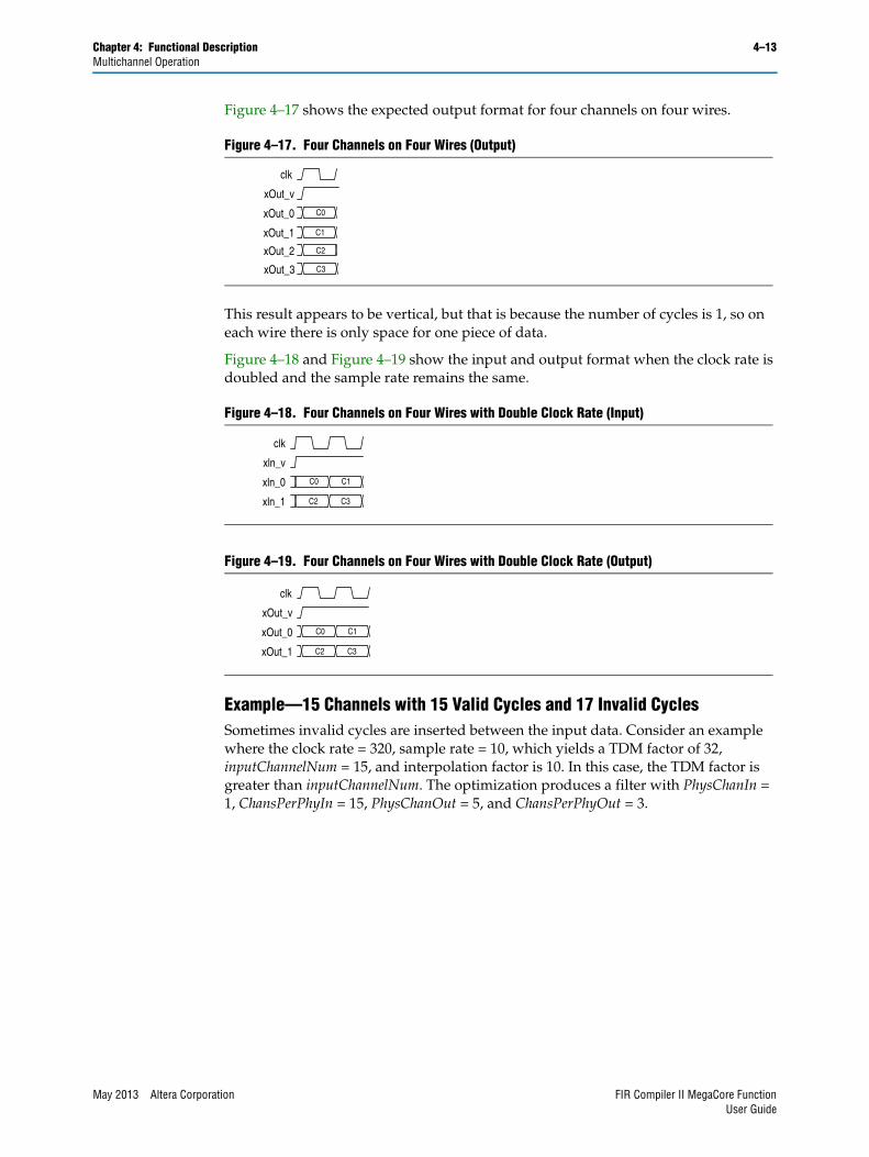
Chapter 4: Functional Description 4–13Multichannel Operation
Figure 4–17 shows the expected output format for four channels on four wires.
This result appears to be vertical, but that is because the number of cycles is 1, so on each wire there is only space for one piece of data.
Figure 4–18 and Figure 4–19 show the input and output format when the clock rate is doubled and the sample rate remains the same.
Example—15 Channels with 15 Valid Cycles and 17 Invalid CyclesSometimes invalid cycles are inserted between the input data. Consider an example where the clock rate = 320, sample rate = 10, which yields a TDM factor of 32, inputChannelNum = 15, and interpolation factor is 10. In this case, the TDM factor is greater than inputChannelNum. The optimization produces a filter with PhysChanIn = 1, ChansPerPhyIn = 15, PhysChanOut = 5, and ChansPerPhyOut = 3.
Figure 4–17. Four Channels on Four Wires (Output)
Figure 4–18. Four Channels on Four Wires with Double Clock Rate (Input)
Figure 4–19. Four Channels on Four Wires with Double Clock Rate (Output)
clk
xOut_v
xOut_0
xOut_1
xOut_2
C0
C1
C2
xOut_3 C3
clk
xln_v
xln_0
xln_1
C0 C1
C2 C3
clk
xOut_v
xOut_0
xOut_1
C0 C1
C2 C3
May 2013 Altera Corporation FIR Compiler II MegaCore FunctionUser Guide
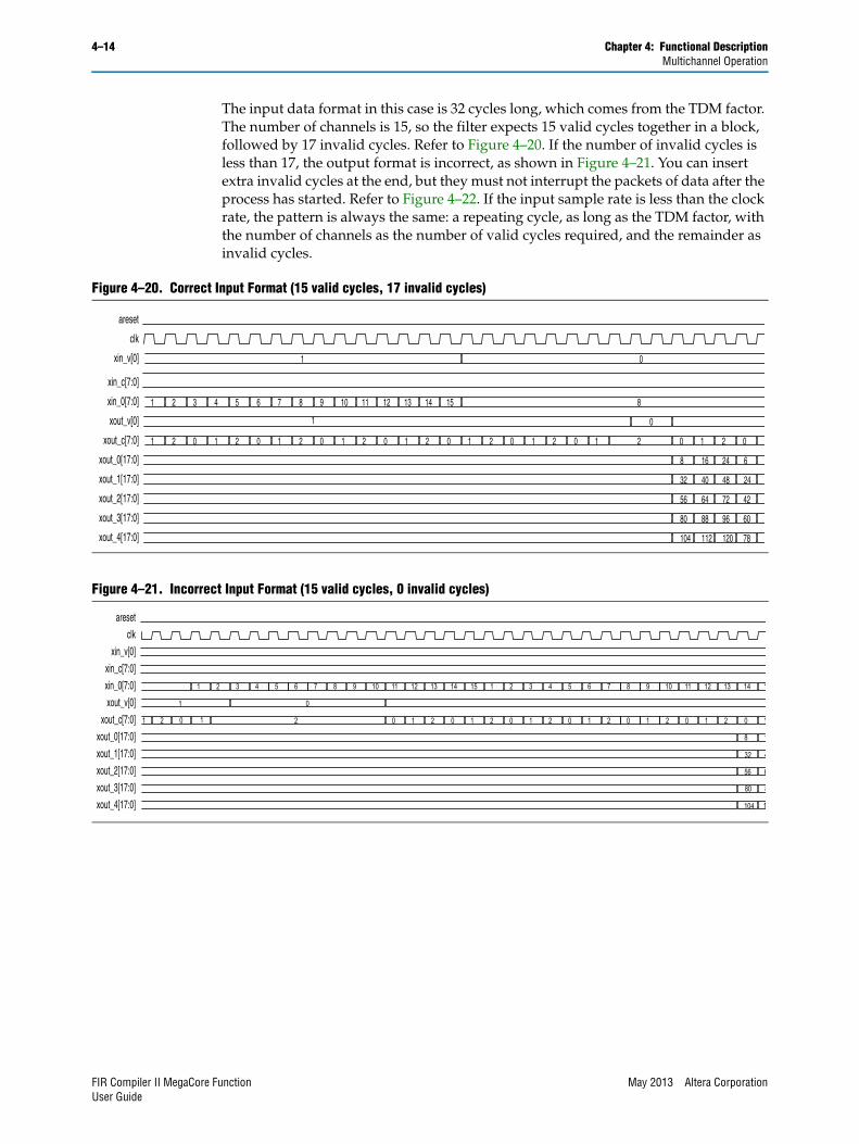
4–14 Chapter 4: Functional DescriptionMultichannel Operation
The input data format in this case is 32 cycles long, which comes from the TDM factor. The number of channels is 15, so the filter expects 15 valid cycles together in a block, followed by 17 invalid cycles. Refer to Figure 4–20. If the number of invalid cycles is less than 17, the output format is incorrect, as shown in Figure 4–21. You can insert extra invalid cycles at the end, but they must not interrupt the packets of data after the process has started. Refer to Figure 4–22. If the input sample rate is less than the clock rate, the pattern is always the same: a repeating cycle, as long as the TDM factor, with the number of channels as the number of valid cycles required, and the remainder as invalid cycles.
Figure 4–20. Correct Input Format (15 valid cycles, 17 invalid cycles)
areset
clk
xin_v[0]
xin_c[7:0]
xin_0[7:0]
xout_v[0]
xout_c[7:0]
xout_0[17:0]
xout_1[17:0]
xout_2[17:0]
xout_3[17:0]
xout_4[17:0]
1 0
1 2 3 4 5 6 7 8 9 10 11 12 13 14 15 8
1 0
1 2 0 1 2 0 1 2 0 1 2 0 1 2 0 1 2 0 1 2 0 1 2 0 1 2 0
8 16 24 6
32 40 48 24 3
56 64 72 42
80 88 96 60
104 112 120 78
Figure 4–21. Incorrect Input Format (15 valid cycles, 0 invalid cycles)
areset
clk
xin_v[0]
xin_c[7:0]
xin_0[7:0]
xout_v[0]
xout_c[7:0]
xout_0[17:0]
xout_1[17:0]
xout_2[17:0]
xout_3[17:0]
xout_4[17:0]
1 2 3 4 5 6 7 8 9 10 11 12 13 14 15 1 2 3 4 5 6 7 8 9 10 11 12 13 14 1
1 0
1 2 0 1 2 0 1 2 0 1 2 0 1 2 0 1 2 0 1 2 0 1 2 0 1
8 1
32 4
56 6
80 8
104 1
FIR Compiler II MegaCore Function May 2013 Altera CorporationUser Guide
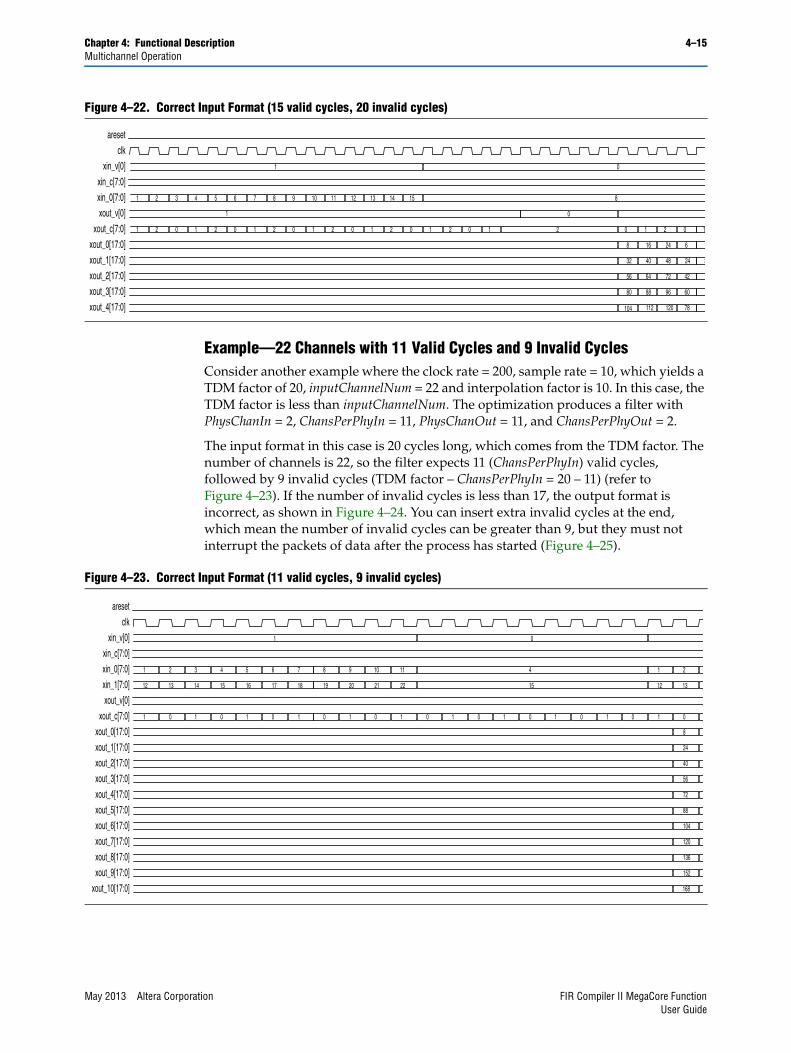
Chapter 4: Functional Description 4–15Multichannel Operation
Example—22 Channels with 11 Valid Cycles and 9 Invalid CyclesConsider another example where the clock rate = 200, sample rate = 10, which yields a TDM factor of 20, inputChannelNum = 22 and interpolation factor is 10. In this case, the TDM factor is less than inputChannelNum. The optimization produces a filter with PhysChanIn = 2, ChansPerPhyIn = 11, PhysChanOut = 11, and ChansPerPhyOut = 2.
The input format in this case is 20 cycles long, which comes from the TDM factor. The number of channels is 22, so the filter expects 11 (ChansPerPhyIn) valid cycles, followed by 9 invalid cycles (TDM factor – ChansPerPhyIn = 20 – 11) (refer to Figure 4–23). If the number of invalid cycles is less than 17, the output format is incorrect, as shown in Figure 4–24. You can insert extra invalid cycles at the end, which mean the number of invalid cycles can be greater than 9, but they must not interrupt the packets of data after the process has started (Figure 4–25).
Figure 4–22. Correct Input Format (15 valid cycles, 20 invalid cycles)
areset
clk
xin_v[0]
xin_c[7:0]
xin_0[7:0]
xout_v[0]
xout_c[7:0]
xout_0[17:0]
xout_1[17:0]
xout_2[17:0]
xout_3[17:0]
xout_4[17:0]
1 0
1 2 3 4 5 6 7 8 9 10 11 12 13 14 15 8
1 0
1 2 0 1 2 0 1 2 0 1 2 0 1 2 0 1 2 0 1 2 0 1 2 0 1
8 16 24 6 1
32 40 48 24 3
56 64 72 42 4
80 88 96 60 6
104 112 120 78 8
Figure 4–23. Correct Input Format (11 valid cycles, 9 invalid cycles)
areset
clk
xin_v[0]
xin_c[7:0]
xin_0[7:0]
xin_1[7:0]
xout_v[0]
xout_c[7:0]
xout_0[17:0]
xout_1[17:0]
xout_2[17:0]
xout_3[17:0]
xout_4[17:0]
xout_5[17:0]
xout_6[17:0]
xout_7[17:0]
xout_8[17:0]
xout_9[17:0]
xout_10[17:0]
1 0
1 2 3 4 5 6 7 8 9 10 11 4 1 2
12 13 14 15 16 17 18 19 20 21 22 15 12 13
1 0 1 0 1 0 1 0 1 0 1 0 1 0 1 0 1 0 1 0 1 0
8
24
40
56
72
88
104
120
136
152
168
May 2013 Altera Corporation FIR Compiler II MegaCore FunctionUser Guide

4–16 Chapter 4: Functional DescriptionMultichannel Operation
Figure 4–24. Incorrect Input Format (11 valid cycles, 0 invalid cycles)
areset
clk
xin_v[0]
xin_c[7:0]
xin_0[7:0]
xin_1[7:0]
xout_v[0]
xout_c[7:0]
xout_0[17:0]
xout_1[17:0]
xout_2[17:0]
xout_3[17:0]
xout_4[17:0]
xout_5[17:0]
xout_6[17:0]
xout_7[17:0]
xout_8[17:0]
xout_9[17:0]
xout_10[17:0]
1 2 3 4 5 6 7 8 9 10 11 1 2 3 4 5 6 7 8 9 10 11 0 150 186 177
12 13 14 15 16 17 18 19 20 21 22 12 13 14 15 16 17 18 19 20 21 22 0 206 172 212
0
00 01 00 01 00 01 00 01 00 01 0
Figure 4–25. Correct Input Format (11 valid cycles, 11 invalid cycles)
clk
areset
xin_v[0]
xin_c[7:0]
xin_0[7:0]
xin_1[7:0]
xout_v[0]
xout_c[7:0]
xout_0[17:0]
xout_1[17:0]
xout_2[17:0]
xout_3[17:0]
xout_4[17:0]
xout_5[17:0]
xout_6[17:0]
xout_7[17:0]
xout_8[17:0]
xout_9[17:0]
xout_10[17:0]
1 0
2 3 4 5 6 7 8 9 10 11 4 1
13 14 15 16 17 18 19 20 21 22 15 12
11 0
0 1 0 1 0 1 0 1 0 1 0 1 0 1 0 1 0 1 0 1
8 16
24 32
40 48
56 64
72 80
88 96
104 112
120 128
136 144
152 160
168 176
1
12
FIR Compiler II MegaCore Function May 2013 Altera CorporationUser Guide

Chapter 4: Functional Description 4–17Multichannel Operation
Example—Super Sample RateConsider an example of a “super sample rate” filter where the sample rate is greater than the clock rate. In this example, clock rate = 100, sample rate = 200, inputChannelNum = 1, and single rate. The optimization produces a filter with PhysChanIn = 2, ChansPerPhyIn = 1, PhysChanOut = 2, and ChansPerPhyOut = 1.
The input format expected by the FIR filter is shown in Figure 4–26. A0 is the first sample of channel A, A1 is the second sample of channel A, and so forth.
If inputChannelNum = 2, then the expected input format is shown in Figure 4–27.
Figure 4–26. Super Sample Rate Filter (clkRate=100, inputRate=200) with inChans=1
clk
xln_v
xln_0
xln_1
xOut_v
xOut_c
xOut_0
xOut_1
A0 A2 A4 A6 A8 A10 A12 A14 A16 A18 A20 A22 A24 A26 A28
A1 A3 A5 A7 A9 A11 A13 A15 A17 A19 A21 A23 A25 A27 A29
A0 A2 A4 A6 A8 A10 A12 A14
A1 A3 A5 A7 A9 A11 A13 A15
00
00
Figure 4–27. Super Sample Rate Filter (clkRate=100, inputRate=200) with inChans=2
clk
xln_v
xln_0
xln_1
xOut_v
xOut_c
xOut_0
xOut_1
xOut_2
xOut_3
xln_2
xln_3
A0 A2 A4 A6 A8 A10 A12 A14 A16 A18 A20 A22 A24 A26 A28
A1 A3 A5 A7 A9 A11 A13 A15 A17 A19 A21 A23 A25 A27 A29
A0 A2 A4 A6 A8 A10 A12 A14 A16 A18 A20 A22 A24 A26 A28
A1 A3 A5 A7 A9 A11 A13 A15 A17 A19 A21 A23 A25 A27 A29
A0 A2 A4 A6 A8 A10 A12 A14
A1 A3 A5 A7 A9 A11 A13 A15
A0 A2 A4 A6 A8 A10 A12 A14
A1 A3 A5 A7 A9 A11 A13 A15
00
00
00
00
May 2013 Altera Corporation FIR Compiler II MegaCore FunctionUser Guide
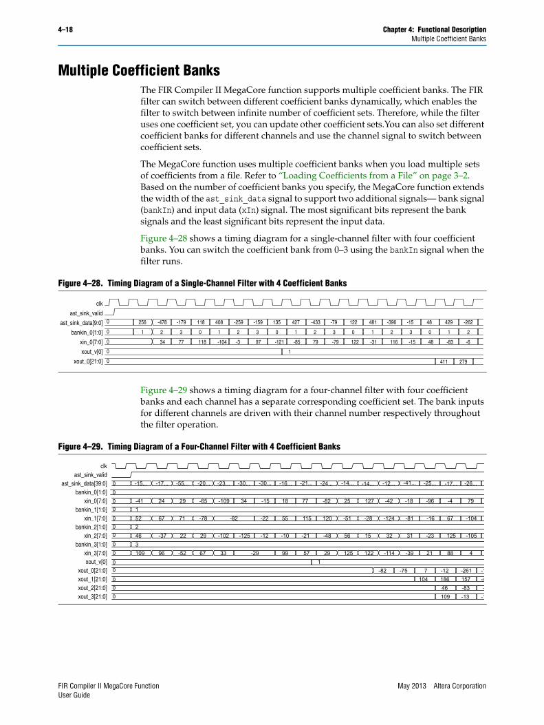
4–18 Chapter 4: Functional DescriptionMultiple Coefficient Banks
Multiple Coefficient BanksThe FIR Compiler II MegaCore function supports multiple coefficient banks. The FIR filter can switch between different coefficient banks dynamically, which enables the filter to switch between infinite number of coefficient sets. Therefore, while the filter uses one coefficient set, you can update other coefficient sets.You can also set different coefficient banks for different channels and use the channel signal to switch between coefficient sets.
The MegaCore function uses multiple coefficient banks when you load multiple sets of coefficients from a file. Refer to “Loading Coefficients from a File” on page 3–2. Based on the number of coefficient banks you specify, the MegaCore function extends the width of the ast_sink_data signal to support two additional signals— bank signal (bankIn) and input data (xIn) signal. The most significant bits represent the bank signals and the least significant bits represent the input data.
Figure 4–28 shows a timing diagram for a single-channel filter with four coefficient banks. You can switch the coefficient bank from 0–3 using the bankIn signal when the filter runs.
Figure 4–29 shows a timing diagram for a four-channel filter with four coefficient banks and each channel has a separate corresponding coefficient set. The bank inputs for different channels are driven with their channel number respectively throughout the filter operation.
Figure 4–28. Timing Diagram of a Single-Channel Filter with 4 Coefficient Banks
clk
ast_sink_valid
ast_sink_data[9:0]
bankin_0[1:0]
xin_0[7:0]
xout_v[0]
xout_0[21:0]
256 -478 -179 118 408 -259 -159 135 427 -433 -79 122 481 -396 -15 48 429 -262
1 2 3 0 1 2 3 0 1 2 3 0 1 2 3 0 1 2
34 77 118 -104 -3 97 -121 -85 79 -79 122 -31 116 -15 48 -83 -6
411 279
0
0
0
0
0
1
Figure 4–29. Timing Diagram of a Four-Channel Filter with 4 Coefficient Banks
clkast_sink_valid
ast_sink_data[39:0]bankin_0[1:0]
xin_0[7:0]bankin_1[1:0]
xin_1[7:0]bankin_2[1:0]
xin_2[7:0]bankin_3[1:0]
xin_3[7:0]xout_v[0]
xout_0[21:0]xout_1[21:0]xout_2[21:0]xout_3[21:0]
-15... -17... -55... -20... -23... -30... -30... -16... -21... -24... -14... -14... -12... -41... -25... -17... -26...
-41 24 29 -65 -109 34 -15 18 77 -82 25 127 -42 -18 -96 -4 79
52 67 71 -78 -82 -22 55 115 120 -51 -28 -124 -81 -16 67 -104
46 -37 22 29 -102 -125 -12 -10 -21 -48 56 15 32 31 -23 125 -105
109 96 -52 67 33 -29 99 57 29 125 122 -114 -39 21 88 4
-82 -75 7 -12 -261 -1104 186 157 -4
46 -83 -109 -13 -1
0000
000
00
0 10
000
1
2
3
FIR Compiler II MegaCore Function May 2013 Altera CorporationUser Guide

Chapter 4: Functional Description 4–19Coefficient Reloading
Coefficient ReloadingThe internal data coefficients are accessed via a memory-mapped interface that consists of the input address, write data, write enable, read data, and read valid signals. The Avalon Memory-Mapped (Avalon-MM) interfaces function as read/write interfaces on the master and slave components in a memory-mapped system. The memory-mapped system components include microprocessors, memories, UARTs, timers, and a system interconnect fabric that connects the master and slave interfaces. The Avalon-MM interfaces describe a wide variety of components, from an SRAM that supports simple, fixed -cycle read/write transfers to a complex, pipelined interface capable of burst transfers. In Read mode, the memory-mapped coefficients are read over a specified address range while in Write mode, the coefficients are written over a specified address range. In Read/Write mode, the coefficients can be read or written over a specified address range. You can use a separate bus clock for this interface. When coefficient reloading option is not enabled, the processor cannot access the specified address range, and the coefficient data is not read or written.
Coefficient reloading starts anytime during the filter run time. However, you must reload the coefficients only after all the desired output data are obtained to avoid unpredictable results. If you are using multiple coefficient banks, you can reload coefficient banks that are not used and switch over to the new coefficient set when coefficient reloading is completed. You must toggle the coeff_in_areset signal before reloading the coefficient with new data. The new coefficient data is read out after coefficient reloading to verify whether the coefficient reloading process is successful. When the coefficient reloading ends by deasserting the coeff_in_we, the input data is inserted immediately to the filter that is reloaded with the new coefficients.
The symmetrical or anti-symmetrical filters have fewer genuine coefficients, use fewer registers, and require fewer writes to reload the coefficients. For example, only the first 19 addresses must be written for a 37-tap symmetrical filter. When you write to all 37 addresses, the last 18 addresses are ignored because they are not part of the address space of the filter. Similarly, reading coefficient data from the last 18 addresses is also ignored.
When multiple coefficient banks are used, the addresses of all the coefficients are arranged in consecutive order according to the bank number.The following example shows a 37-tap symmetrical/anti-symmetrical filter with four coefficient banks:
Address 0–18: Bank 0
Address 19–37: Bank 1
Address 38–56: Bank 2
Address 57–75: Bank 3
The following example shows a 37-tap non-symmetrical/anti-symmetrical filter with 2 coefficient banks:
Address 0–36: Bank 0
Address 37–73: Bank 1
If the coefficient bit width parameter is equal to or less than 16 bits, the width of the write data is fixed at 16 bits. If the coefficient bit width parameter is more than 16 bits, the width of the write data is fixed at 32 bits.
May 2013 Altera Corporation FIR Compiler II MegaCore FunctionUser Guide

4–20 Chapter 4: Functional DescriptionCoefficient Reloading
Figure 4–30 shows the timing diagram for a coefficient reloading configuration with Read/Write mode. There are a total of nine coefficients in this configuration. A write cycle of 9 clock cycles are performed to reload the whole coefficient data set shown in Figure 4–30. To complete the write cycle, assert the coeff_in_we signal, and provide the address (from base address to the max address) together with the new coefficient data. Then, load the new coefficient data into the memory corresponding to the address of the coefficient. The new coefficient data is read during the write cycle when you deassert the coeff_in_we signal. When the coeff_out_valid signal is high, the read data is available on coeff_out_data.
Figure 4–31 shows the timing diagram of a coefficient reloading configuration in Write mode. In this mode, one coefficient data is reloaded. The new coefficient data (123) is loaded into a single address (7).
Figure 4–30. Timing Diagram of Coefficient Reloading in Read or Write mode
clk
coeff_in_areset
coeff_in_address[11:0]
coeff_in_data[15:0]
coeff_in_we[0]
coeff_out_data[15:0]
coeff_out_valid[0]
-1 0 1 2 3 4 5 6 7 8 0 1 2 3 4 5 6 7 8
-1
0 -26 45
-1
45 -50 7 -121 -32 49 -1 108 124 -1
-25 13 80 127 80 0 -26 0 -50 7 -1 -32 49 -1 108 124 45
Figure 4–31. Timing Diagram of Coefficient Reloading in Write mode
clk
coeff_in_areset
coeff_in_address[11:0]
coeff_in_data[15:0]
coeff_in_we[0]
-1 7
0 123
-1
0
FIR Compiler II MegaCore Function May 2013 Altera CorporationUser Guide
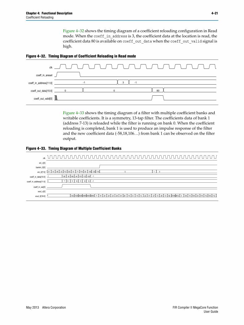
Chapter 4: Functional Description 4–21Coefficient Reloading
Figure 4–32 shows the timing diagram of a coefficient reloading configuration in Read mode. When the coeff_in_address is 3, the coefficient data at the location is read, the coefficient data 80 is available on coeff_out_data when the coeff_out_valid signal is high.
Figure 4–33 shows the timing diagram of a filter with multiple coefficient banks and writable coefficients. It is a symmetry, 13-tap filter. The coefficients data of bank 1 (address 7-13) is reloaded while the filter is running on bank 0. When the coefficient reloading is completed, bank 1 is used to produce an impulse response of the filter and the new coefficient data (-58,18,106…) from bank 1 can be observed on the filter output.
Figure 4–32. Timing Diagram of Coefficient Reloading in Read mode
clk
coeff_in_areset
coeff_in_address[11:0]
coeff_out_data[15:0]
coeff_out_valid[0]
-1 3
0 0 80
-1
Figure 4–33. Timing Diagram of Multiple Coefficient Banks
clk
xin_v[0]
bankin_0[0]
xin_0[7:0]
coeff_in_data[15:0]
coeff_in_address[11:0]
coeff_in_we[0]
xout_v[0]
xout_0[19:0]
51 -14 -48 33 112 125 -10 -71 119 40 -105 -125 -114 0 1 0
-58 18 106 -34 119 112 105 -1
7 8 9 10 11 12 13
342 1530 3636 5490 6400 8064 11 16 20 20 23 28 30 26 16 12 -14 12 -22 -51 -27 -26 -13 5198 6612 0 -58 18 106 119 112 105 112
-1
6
0
-1
-13 -82 -34
May 2013 Altera Corporation FIR Compiler II MegaCore FunctionUser Guide
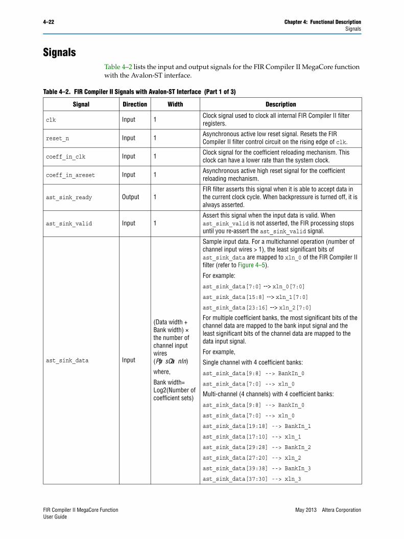
4–22 Chapter 4: Functional DescriptionSignals
SignalsTable 4–2 lists the input and output signals for the FIR Compiler II MegaCore function with the Avalon-ST interface.
Table 4–2. FIR Compiler II Signals with Avalon-ST Interface (Part 1 of 3)
Signal Direction Width Description
clk Input 1 Clock signal used to clock all internal FIR Compiler II filter registers.
reset_n Input 1 Asynchronous active low reset signal. Resets the FIR Compiler II filter control circuit on the rising edge of clk.
coeff_in_clk Input 1 Clock signal for the coefficient reloading mechanism. This clock can have a lower rate than the system clock.
coeff_in_areset Input 1 Asynchronous active high reset signal for the coefficient reloading mechanism.
ast_sink_ready Output 1FIR filter asserts this signal when it is able to accept data in the current clock cycle. When backpressure is turned off, it is always asserted.
ast_sink_valid Input 1Assert this signal when the input data is valid. When ast_sink_valid is not asserted, the FIR processing stops until you re-assert the ast_sink_valid signal.
ast_sink_data Input
(Data width + Bank width) × the number of channel input wires (PhysChanIn)
where,
Bank width= Log2(Number of coefficient sets)
Sample input data. For a multichannel operation (number of channel input wires > 1), the least significant bits of ast_sink_data are mapped to xln_0 of the FIR Compiler II filter (refer to Figure 4–5).
For example:
ast_sink_data[7:0] --> xln_0[7:0]
ast_sink_data[15:8] --> xln_1[7:0]
ast_sink_data[23:16] --> xln_2[7:0]
For multiple coefficient banks, the most significant bits of the channel data are mapped to the bank input signal and the least significant bits of the channel data are mapped to the data input signal.
For example,
Single channel with 4 coefficient banks:
ast_sink_data[9:8] --> BankIn_0
ast_sink_data[7:0] --> xln_0
Multi-channel (4 channels) with 4 coefficient banks:
ast_sink_data[9:8] --> BankIn_0
ast_sink_data[7:0] --> xln_0
ast_sink_data[19:18] --> BankIn_1
ast_sink_data[17:10] --> xln_1
ast_sink_data[29:28] --> BankIn_2
ast_sink_data[27:20] --> xln_2
ast_sink_data[39:38] --> BankIn_3
ast_sink_data[37:30] --> xln_3
FIR Compiler II MegaCore Function May 2013 Altera CorporationUser Guide
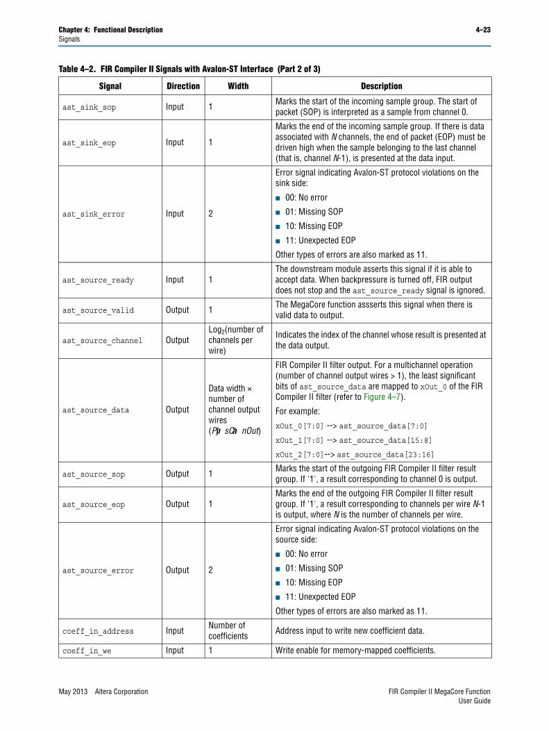
Chapter 4: Functional Description 4–23Signals
ast_sink_sop Input 1 Marks the start of the incoming sample group. The start of packet (SOP) is interpreted as a sample from channel 0.
ast_sink_eop Input 1
Marks the end of the incoming sample group. If there is data associated with N channels, the end of packet (EOP) must be driven high when the sample belonging to the last channel (that is, channel N-1), is presented at the data input.
ast_sink_error Input 2
Error signal indicating Avalon-ST protocol violations on the sink side:
■ 00: No error
■ 01: Missing SOP
■ 10: Missing EOP
■ 11: Unexpected EOP
Other types of errors are also marked as 11.
ast_source_ready Input 1The downstream module asserts this signal if it is able to accept data. When backpressure is turned off, FIR output does not stop and the ast_source_ready signal is ignored.
ast_source_valid Output 1 The MegaCore function assserts this signal when there is valid data to output.
ast_source_channel OutputLog2(number of channels per wire)
Indicates the index of the channel whose result is presented at the data output.
ast_source_data Output
Data width × number of channel output wires (PhysChanOut)
FIR Compiler II filter output. For a multichannel operation (number of channel output wires > 1), the least significant bits of ast_source_data are mapped to xOut_0 of the FIR Compiler II filter (refer to Figure 4–7).
For example:
xOut_0[7:0] --> ast_source_data[7:0]
xOut_1[7:0] --> ast_source_data[15:8]
xOut_2[7:0]--> ast_source_data[23:16]
ast_source_sop Output 1 Marks the start of the outgoing FIR Compiler II filter result group. If '1', a result corresponding to channel 0 is output.
ast_source_eop Output 1Marks the end of the outgoing FIR Compiler II filter result group. If '1', a result corresponding to channels per wire N-1 is output, where N is the number of channels per wire.
ast_source_error Output 2
Error signal indicating Avalon-ST protocol violations on the source side:
■ 00: No error
■ 01: Missing SOP
■ 10: Missing EOP
■ 11: Unexpected EOP
Other types of errors are also marked as 11.
coeff_in_address Input Number of coefficients Address input to write new coefficient data.
coeff_in_we Input 1 Write enable for memory-mapped coefficients.
Table 4–2. FIR Compiler II Signals with Avalon-ST Interface (Part 2 of 3)
Signal Direction Width Description
May 2013 Altera Corporation FIR Compiler II MegaCore FunctionUser Guide
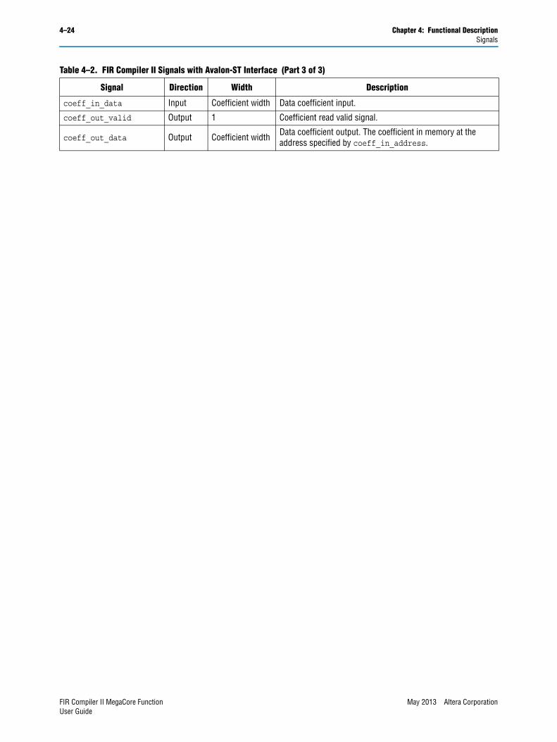
4–24 Chapter 4: Functional DescriptionSignals
coeff_in_data Input Coefficient width Data coefficient input.
coeff_out_valid Output 1 Coefficient read valid signal.
coeff_out_data Output Coefficient width Data coefficient output. The coefficient in memory at the address specified by coeff_in_address.
Table 4–2. FIR Compiler II Signals with Avalon-ST Interface (Part 3 of 3)
Signal Direction Width Description
FIR Compiler II MegaCore Function May 2013 Altera CorporationUser Guide

May 2013 Altera Corporation
Additional Information
This chapter provides additional information about the document and Altera.
Document Revision HistoryThe following table shows the revision history for this document.
How to Contact AlteraTo locate the most up-to-date information about Altera products, refer to the following table.
Date Version Changes
May 2013 13.0 Updated interpolation and decimation factor ranges.
November 2012 12.1 Added support for Arria V GZ devices.
February 2012 11.1 Added a new parameter.
November 2011 11.1 Updated Chapter 1, About This MegaCore Function with new resource utilization information for Stratix V and Cyclone III.
May 2011 11.0■ Updated Chapter 1, About This MegaCore Function with new resource utilization
information for Stratix V.
■ Updated Chapter 3, Parameter Settings.
December 2010 10.1
■ Updated Chapter 3, Parameter Settings and Chapter 4, Functional Description to include new output options and multiple coefficient bands.
■ Updated Chapter 1, About This MegaCore Function with new resource utilization information.
July 2010 10.0 Updated Chapter 3, Parameter Settings and Chapter 4, Functional Description with backpressure and coefficient reloading features.
January 2010 9.1 SP1 Initial release.
Contact (1) Contact Method Address
Technical support Website www.altera.com/support
Technical trainingWebsite www.altera.com/training
Email [email protected]
Product literature Website www.altera.com/literature
Nontechnical support (general) Email [email protected]
(software licensing) Email [email protected]
Note to Table:
(1) You can also contact your local Altera sales office or sales representative.
FIR Compiler II MegaCore FunctionUser Guide
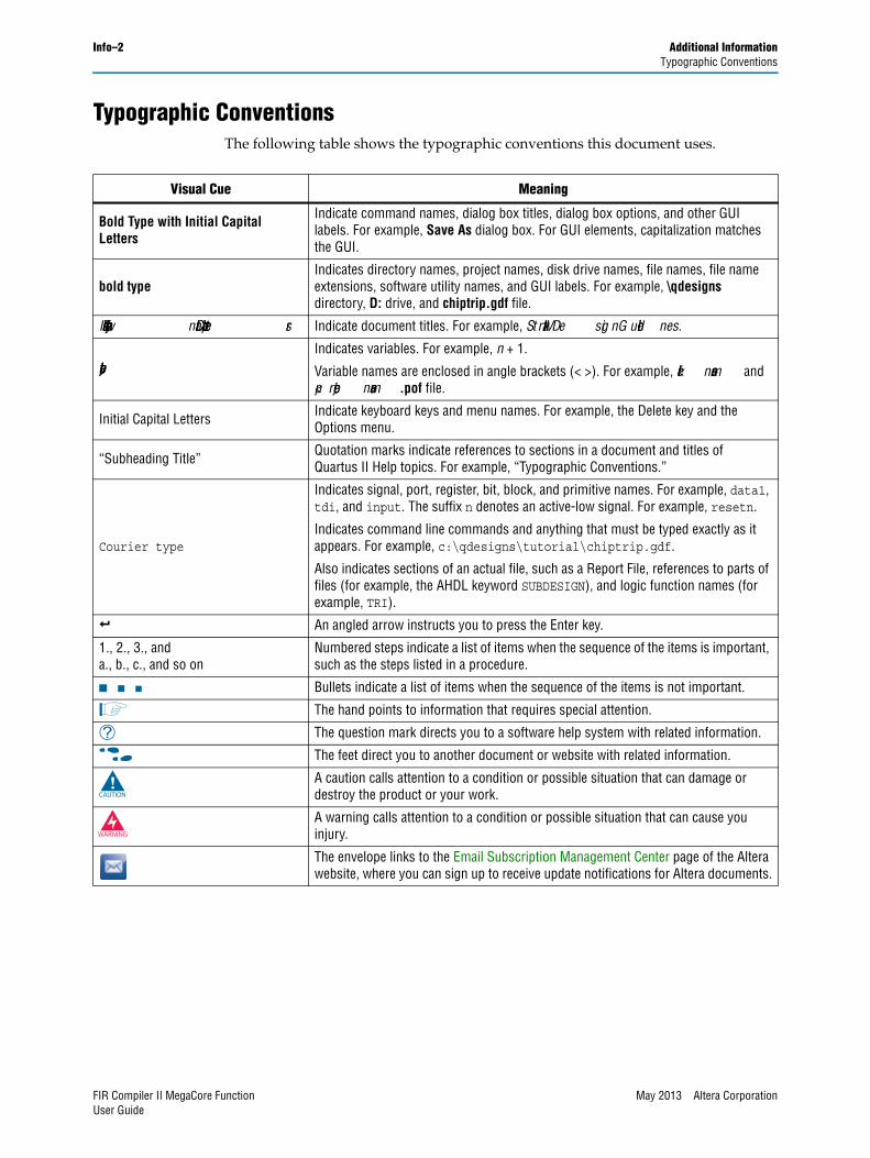
Info–2 Additional InformationTypographic Conventions
Typographic ConventionsThe following table shows the typographic conventions this document uses.
Visual Cue Meaning
Bold Type with Initial Capital Letters
Indicate command names, dialog box titles, dialog box options, and other GUI labels. For example, Save As dialog box. For GUI elements, capitalization matches the GUI.
bold typeIndicates directory names, project names, disk drive names, file names, file name extensions, software utility names, and GUI labels. For example, \qdesigns directory, D: drive, and chiptrip.gdf file.
Italic Type with Initial Capital Letters Indicate document titles. For example, Stratix IV Design Guidelines.
italic typeIndicates variables. For example, n + 1.
Variable names are enclosed in angle brackets (< >). For example, <file name> and <project name>.pof file.
Initial Capital Letters Indicate keyboard keys and menu names. For example, the Delete key and the Options menu.
“Subheading Title” Quotation marks indicate references to sections in a document and titles of Quartus II Help topics. For example, “Typographic Conventions.”
Courier type
Indicates signal, port, register, bit, block, and primitive names. For example, data1, tdi, and input. The suffix n denotes an active-low signal. For example, resetn.
Indicates command line commands and anything that must be typed exactly as it appears. For example, c:\qdesigns\tutorial\chiptrip.gdf.
Also indicates sections of an actual file, such as a Report File, references to parts of files (for example, the AHDL keyword SUBDESIGN), and logic function names (for example, TRI).
r An angled arrow instructs you to press the Enter key.
1., 2., 3., anda., b., c., and so on
Numbered steps indicate a list of items when the sequence of the items is important, such as the steps listed in a procedure.
■ ■ ■ Bullets indicate a list of items when the sequence of the items is not important.
1 The hand points to information that requires special attention.
h The question mark directs you to a software help system with related information.
f The feet direct you to another document or website with related information.
c A caution calls attention to a condition or possible situation that can damage or destroy the product or your work.
w A warning calls attention to a condition or possible situation that can cause you injury.
The envelope links to the Email Subscription Management Center page of the Altera website, where you can sign up to receive update notifications for Altera documents.
FIR Compiler II MegaCore Function May 2013 Altera CorporationUser Guide