finding the perfect memory:
TRANSCRIPT

WHITE PAPER
AgigA Tech White Paper September 3, 2009 www.agigatech.com
Finding the Perfect Memory:
How to Build Cost-Effective, Blackout-Proof Servers, RAID Controllers, and
Other Systems That Ride Through Power Failures... However Long They Last
The Problems with Memories Memories are and always have been a thorny problem for designers of computers, servers, caching RAID and other caching hard-disk controllers, and many other types of processor-based embedded systems. Memory-centric design problems aren’t unique to microprocessor-based systems and they even predate the semiconductor era. The problems go all the way back to day one. ENIAC, often called the world’s first electronic computer, used punched paper cards for data storage. The one million punched cards needed to store the data for ENIAC’s first shakedown program, which was developed by two Manhattan Project computer scientists in late 1945, filled an entire railroad boxcar when the scientists traveled from Los Alamos, New Mexico to ENIAC’s birthplace at the Moore School of Electrical Engineering at the University of Pennsylvania in Philadelphia. It quickly became apparent that such voluminous memory-storage technology needed radical improvement and memory has been shrinking ever since.
Because of memory’s extreme importance to computing, researchers and design engineers have now pursued “perfect” electronic memory technologies for more than 60 years.
A perfect electronic memory has the following attributes:
• Very low cost per bit (ideally free) • Very high capacity (ideally infinite) • Very low power consumption (ideally none) • Very low access time (ideally zero) • Very high data-retention time without power (ideally forever)

Page 2
AgigA Tech White Paper September 3, 2009 www.agigatech.com
It should come as no surprise to you that all memory technologies developed to date are imperfect; they fall short of the listed ideals. It should also not surprise you to read that memories are likely to remain imperfect. Although it’s possible to approach several of the desired ideals with one single memory technology, it’s not possible to approach all of them using only one memory technology.
For example, the first nearly “perfect” memory technology was magnetic core memory, which appeared around 1953. Back then, magnetic-core memory’s access time—measured in microseconds—was relatively fast; computers of the day were built with comparatively slow vacuum tubes and processor clock rates were well under 1MHz. Magnetic-core memory permitted a big jump in memory capacity from the tens, hundreds, or thousands of bits that could be stored with the earliest computer-memory technologies (which included Williams tubes, mercury delay lines, magnetic drums, and vacuum-tube flip-flops) to tens of thousands, hundreds of thousands, or millions of bits. At first, magnetic-core memory looked pretty good. Almost perfect.
Because it was nearly perfect for the time, magnetic-core memory became a mainstay memory technology and stayed in top position for almost twenty years. Mainframe computers from IBM and many other vendors, minicomputers from companies such as Digital Equipment Corp and Data General, and even early desktop calculators such as HP’s 9100A all employed magnetic-core memory for non-volatile, rewritable storage.
However, the ever-expanding demand for memory capacity and rapidly increasing processor speeds had stretched magnetic-core memory technology beyond its limits by the end of the 1960s. The magnetic cores got smaller so that more of them fit in the same volume but they didn’t get much faster and they were hand-woven, so the cost/bit of magnetic-core memory remained fairly high. The industry was ripe for something new, something better.
That new, better technology turned out to be semiconductor memory. By the start of the 1970s, vendors such as Fairchild Semiconductor and Intel were selling early commercial semiconductor memories based on both static and dynamic bit-cell designs. Static RAMs (SRAMs) store bits as a logic state held in individual bit-cell flip-flops while dynamic RAMs (DRAMs) store bits as charge in individual bit-cell capacitors. Unsurprisingly, neither memory technology is perfect. SRAMs require either four or six transistors per bit cell and consume relatively large amounts of power, which forever restricts SRAMs to smaller capacities. DRAMs need only one transistor and a capacitor for bit-cell storage and are therefore relatively compact but DRAMs require control signals with complex timing and they must

Page 3
AgigA Tech White Paper September 3, 2009 www.agigatech.com
constantly be refreshed to maintain the appropriate charge levels in the bit-cell capacitors. Both DRAM attributes (complex timing and the need for refresh cycles) complicate the design of memory-subsystems.
Worse, both SRAMs and DRAMs are volatile; they lose state when the power disappears. All processor-based systems need some amount of non-volatile memory if only to boot up. Consequently, systems designers have always needed supplemental memory technologies to add non-volatile storage to their designs. Most systems also need non-volatile storage for data. Although many embedded systems need as little as a few kilobytes of non-volatile memory for boot code and data, many systems need megabytes or gigabytes of non-volatile storage to prevent data loss in the face of a power failure. While ROMs and EPROMs provide unalterable, non-volatile memory and were common in many early embedded systems, they didn’t scale well with increasing memory-capacity needs and these devices can’t be used to store dynamic data. For many large servers including RAID storage servers, data loss is catastrophic and must be avoided at all costs.
With no viable non-volatile semiconductor memory available for read/write applications, early system designers inevitably resorted to magnetic disks and tape for non-volatile storage. However magnetic disks are horribly slow and tape is slower still. Magnetic storage is at least five orders of magnitude slower than semiconductor memory—a gigantic speed difference.
The need for “perfect,” non-volatile semiconductor memory was well known very early in the life of semiconductor memory, as demonstrated by this quote from an old book on semiconductor memory published in 1973, just three years into the era of commercial semiconductor memory:
“Thus the goals that semiconductor memory must meet to serve the mass memory market are clear: high density, low cost, and access time shorter than magnetic disk.” 1
The race to find a more perfect, non-volatile, semiconductor memory has been run for nearly forty years and it continues today.
1 Gerald Luecke, Jack P Mize, and William N Carr, Semiconductor Memory Design and Application, McGraw-Hill Book Company, 1973, page 6.

Page 4
AgigA Tech White Paper September 3, 2009 www.agigatech.com
Enter the Flash The search for a perfect semiconductor memory produced the most successful non-volatile semiconductor memory to date: Flash memory, developed by Toshiba’s Dr. Fujio Masuoka in 1984 and announced the following year. Flash memory, a space-efficient version of the EEPROM (electrically-erasable programmable read-only memory), is available in two flavors: NAND and NOR. Both types provide many “perfect” features including low-power operation, non-volatile memory storage, and low cost per bit. NAND Flash memories became the semiconductor memory with the lowest cost per bit in 2004, when the cost/bit of NAND Flash memory dipped below that of the previous low-cost leader, DRAM.
However, NAND Flash semiconductor memory has undesirable characteristics that make it less than perfect. These undesirable features include relatively long write-cycles times measured in microseconds, long-but-finite data-retention time, and—perhaps most important—write/erase-induced wearout-failure mechanisms that really preclude Flash memory from being used as main memory in high-end, processor-based systems because of the very real possibility of memory failure. (Note: embedded systems are another story entirely.)
Consequently, semiconductor vendors have experimented with many new non-volatile memory technologies in their quest to find a more perfect memory approach. Some of these experiments stretch back 25 years. Alternative and experimental non-volatile technologies include ferroelectric and magnetic RAMs (FRAMs and MRAMs), polymer, molecular-switch, chalcogenic, and carbon-nanotube memories.2 All of these technologies beckon designers with enticing promises of more perfect memories to come, but most of these technologies have yet to emerge from the R&D labs and none come close to competing on cost/bit or offer the capacity of the current semiconductor-memory champions: DRAMs and NAND Flash.
Predicting the success of new memory technologies turns out to be a very tricky business. For example, after discussing the relatively small capacities of the bipolar SRAMs and MOS DRAMs in 1973, the authors of the very early book on memory design quoted above wrote: “...presently a suitable semiconductor form of circuitry is not available for the mass memory market. Let us, therefore, discuss several semiconductor approaches that may find application in mass memory products for the market.” 3
2 Betty Prince, Emerging Memories: Technologies and Trends, Kluwer Academic Publishers, 2002. 3 Gerald Luecke, Jack P Mize, and William N Carr, Semiconductor Memory Design and Application, McGraw-Hill Book Company, 1973, page 88.

Page 5
AgigA Tech White Paper September 3, 2009 www.agigatech.com
This ancient book then discusses three memory technologies likely to break out of the labs and into the mass market: charge-coupled devices (CCDs), bucket-brigade devices (BBDs), and magnetic-bubble devices (BMDs). Note that none of these technologies ever became a mainstream memory technology. Although CCDs did become a mainstream technology for imaging devices, BBDs and BMDs silently sank onto the ever-growing heap of discarded memory technologies that fail to catch on due to one imperfection or another. Memory prognostication is truly a tough business.
While waiting decades for the more exotic non-volatile memory technologies to emerge from the R&D labs into commercial production, system designers have devised many ways to make do with the less-than-perfect characteristics of semiconductor SRAMs and DRAMs. For example, they’ve coupled batteries to semiconductor-memory subsystems to create non-volatile memory subsystems.
Battery backup makes memory subsystems impervious to power failure, but only for a while. Eventually, typically in 72 hours or less, the battery’s electrical capacity is depleted and then the memory subsystem loses the stored data—a catastrophic failure for most systems.
Batteries themselves have several wearout mechanisms and therefore require frequent monitoring, periodic maintenance, and replacement. Maintenance schedules often call for annual battery replacement in mission-critical subsystems to ensure blackout-proof operation. Frequent replacement increases the memory subsystem’s total cost of ownership (TCO) and complicates clean and green corporate initiatives—because batteries do not recycle cleanly. They’re full of hazardous materials.
Batteries Also Have Hidden Problems A hidden problem with battery-backed memory subsystems is the need for ad hoc engineering of such subsystems. Semiconductor memory vendors do not develop or alter their memories’ characteristics to account for the special needs of battery backup. There are no industry standards for backing up SRAMs and DRAMs with batteries so every system vendor must develop its own approach. Consequently, each system vendor learns about the problems and pitfalls of battery-backed memory-subsystem design on its own and the opportunity for this education usually occurs immediately after the first few production systems reach customers, start to operate, and then fail. That’s particularly bad timing for such systems because these lessons tend to be expensive and they tend to badly damage customer relationships.

Page 6
AgigA Tech White Paper September 3, 2009 www.agigatech.com
One important aspect of battery backup is that its efficiency improves the closer you put the battery to the semiconductor memory. For example, when the battery resides in a mains-based uninterruptable power supply (UPS), the battery’s dc voltage must be inverted to ac—which imposes an efficiency penalty—and then converted back into dc by the memory subsystem’s power supply, which imposes an additional efficiency penalty. In addition, a UPS powers the entire system, not just the system’s memory, which further degrades the efficiency of this approach. A UPS is the easiest but least power-efficient approach to backing up memory-subsystem power.
A more efficient approach is to put the battery directly into the memory subsystem’s power supply, after the power supply performs the ac-dc conversion. At this point, the battery’s dc voltage is entirely appropriate and there are no energy losses due to a dc-ac followed by an ac-dc conversion. This is precisely the approach Google has used with its Web-search server designs since 2005.4 In Google’s server design, a small, 12V, lead-acid battery taps directly into the dc side of the server’s power supply and takes over in the event of a power failure.
The Google server’s lead-acid battery supplies 12Vdc to the server’s power supply, which in turn delivers that voltage to the server’s motherboard either by generating the dc voltage from the power mains or by switching over and directly relaying the battery voltage during a power failure. Conversion from 12Vdc to other required voltages occurs on the server’s motherboard so the power supply has only one 12Vdc output. The lead-acid battery has sufficient capacity to power the server motherboard for 2 to 3 minutes5, which is enough time to ride out most of the expected power failures and provides sufficient time for a diesel-powered emergency backup power generator to spin up if needed and if available.
According to Ben Jai, an engineer who’s been designing Google’s servers since 2005, UPS power-conversion efficiencies range from 92-95% while Google’s battery-backed power supply achieves a conversion efficiency of better than 99.7%. While that may seem like a small difference, a 5-8% difference in power-conversion efficiency plus the additional (and roughly equivalent as shown in Figure 1) saving in the energy needed to cool such systems can reduce electrical energy costs by hundreds of thousands or millions of dollars per year for server farms like Google’s that consume many megawatts of electrical power. Of course, more savings are possible if only the contents of the system memory are maintained during a power failure. Because the entire system need not have backup power in such situations, backup energy requirements are much lower.
4 Stephen Shankland, “Google uncloaks once-secret server,” CNET News, April 1, 2009, http://news.cnet.com/8301-1001_3-10209580-92.html 5 http://perspectives.mvdirona.com/2009/04/05/DataCenterEfficiencySummitPosting4.aspx

Page 7
AgigA Tech White Paper September 3, 2009 www.agigatech.com
Figure 1: Data centers use approximately the same amount of electrical energy
to cool server systems as they do to power such servers.
Save Energy: Get Up Close and Personal With Your Battery Continuing the trajectory of this design approach to its most logical end, putting the battery immediately adjacent to the semiconductor memory in a memory subsystem might well represent the most energy-efficient way to add non-volatility to semiconductor memory.
Although moving the battery close to the semiconductor memory may relieve most of the problems associated with power-conversion efficiency, this design approach alone does not solve three of the other problems associated with battery backup:
• The battery can only sustain a system for a relatively short time • Batteries must be regularly maintained because they fail over time • Batteries are environmentally unfriendly
If a server or system must continue to operate during a power failure, either a battery-powered UPS, a battery-backed power supply, or a backup generator is required. However, many systems need not continue to operate during a power failure although they do need to safely ride out the power failure while preserving data integrity and then return to normal operation once power
Page 8
AgigA Tech White Paper September 3, 2009 www.agigatech.com
returns. Such systems need to be able to recover their precise state prior to the power loss, however long that loss lasts.
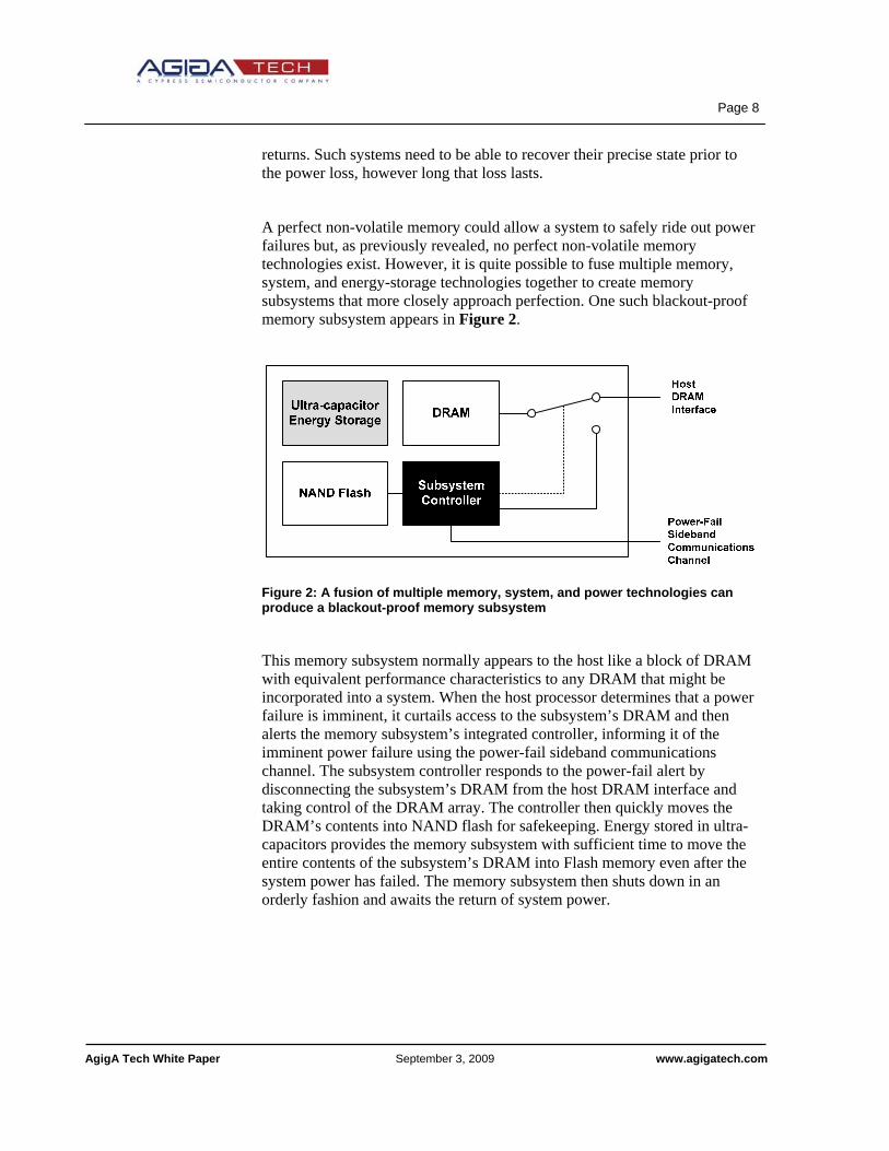
A perfect non-volatile memory could allow a system to safely ride out power failures but, as previously revealed, no perfect non-volatile memory technologies exist. However, it is quite possible to fuse multiple memory, system, and energy-storage technologies together to create memory subsystems that more closely approach perfection. One such blackout-proof memory subsystem appears in Figure 2.
Figure 2: A fusion of multiple memory, system, and power technologies can produce a blackout-proof memory subsystem
This memory subsystem normally appears to the host like a block of DRAM with equivalent performance characteristics to any DRAM that might be incorporated into a system. When the host processor determines that a power failure is imminent, it curtails access to the subsystem’s DRAM and then alerts the memory subsystem’s integrated controller, informing it of the imminent power failure using the power-fail sideband communications channel. The subsystem controller responds to the power-fail alert by disconnecting the subsystem’s DRAM from the host DRAM interface and taking control of the DRAM array. The controller then quickly moves the DRAM’s contents into NAND flash for safekeeping. Energy stored in ultra-capacitors provides the memory subsystem with sufficient time to move the entire contents of the subsystem’s DRAM into Flash memory even after the system power has failed. The memory subsystem then shuts down in an orderly fashion and awaits the return of system power.

Page 9
AgigA Tech White Paper September 3, 2009 www.agigatech.com
NAND Flash Supplies Non-Volatility First, note that the memory subsystem relies on NAND Flash’s 10-year data retention (not the energy stored in the ultra-capacitor array) for nonvolatility and on the DRAM for high speed, high-capacity storage during normally powered system operation. This design approach pairs the two semiconductor memory technologies that have the lowest commercial cost/bit and overcomes both the DRAM’s lack of non-volatility and the Flash memory’s relatively slow write speed.
This subsystem design also circumvents the Flash memory’s wearout-failure problems. The memory subsystem only writes to Flash memory in the event of a power failure and only reads from Flash memory when the power is restored so Flash-memory accesses are relatively infrequent and there’s no chance for wearout failure even over many years of service.
Next, note that this subsystem employs an ultra-capacitor array for energy storage instead of a battery. Ultra-capacitors are superior to batteries for this application in many ways. Issues with battery maintenance, battery failure, and problems with recycling have been discussed above. In addition, properly selected, qualified, and burned-in ultra-capacitors have the following desirable traits:
• Ultra-capacitors do not need maintenance, in-system conditioning, or periodic replacement. Batteries do.
• Ultra-capacitors have infinite lifetime when off line. Batteries degrade over time whether they’re used or not.
• Ultra-capacitors recharge in seconds. Recharging batteries takes dozens of minutes or hours and during the recharge period, the system is subject to catastrophic data loss if another power failure occurs.
• Ultra-capacitors tolerate many charge/discharge cycles. Batteries tolerate relatively few charge/discharge cycles.
• Ultra-capacitors have a long operating life, even at elevated temperatures. Batteries do not tolerate elevated operating temperatures well.
• Ultra-capacitors are environmentally friendly and inherently safe. Batteries are made with hazardous materials and must be handled in an environmentally safe manner.

Page 10
AgigA Tech White Paper September 3, 2009 www.agigatech.com
Although ultra-capacitors have much better power density than do batteries, the smaller ultra-capacitors have less energy capacity than the much bigger batteries. However, that’s not an issue with the design approach shown in Figure 2 because the memory subsystem only consumes energy from the ultra-capacitor during a power failure and only for as long as needed to move data from the DRAM to the Flash memory. Once the move is complete, the memory subsystem can safely power down, relying on the Flash memory’s non-volatility to safely store the data.
When the Lights go on Again When power is restored, the memory subsystem senses the return of system power and immediately presents a “busy” status to the host system over the power-fail sideband communications channel to prevent system access while the data is being restored. Then the memory subsystem copies the saved data from Flash memory back to DRAM, recharges the ultra-capacitors to prepare the memory subsystem for the next power failure, and then finally signals a “ready” status to the host so that the system can resume operation. The host system can then resume operation from the point where it stopped because the memory subsystem’s DRAM contains precisely the same contents that it held just prior to the power failure.
Figure 3 is a photograph of a memory module based on the subsystem architecture just described. The photograph shows an AGIGARAM Capri NVS (non-volatile system) module developed by AgigA Tech. The photo also shows a separate board called the Power GEM (Green Energy Module) that contains the ultra-capacitor array and the associated charging and control circuits. The Power GEM delivers power to the AGIGARAM Capri NVS via a cable plugged into the white connector at the upper left corner of the AGIGARAM module. The extra power connector is required because the DIMM connectors connect to the standard system-power bus, which is not blackout-proof.

Page 11
AgigA Tech White Paper September 3, 2009 www.agigatech.com
Figure 3: AGIGARAM Non-Volatile Memory Subsystem with Power GEM board
The AGIGARAM Capri NVS memory subsystem combines several technologies, many of them proprietary to AgigA Tech, to create a blackout-proof, non-volatile memory subsystem integrated onto one relatively compact, standard-width DIMM module. The AGIGARAM Capri NVS module is available in capacities ranging from 256 Mbytes to 2 Gbytes. Note that the prototype memory subsystem shown in Figure 3 measures 82x70 mm. The final version of the memory subsystem, with an ASIC replacing the prototype module’s FPGA (currently mounted on the back side of the memory module) will measure 82x45 mm or less.
On the bottom of the AGIGARAM Capri NVS module, you see a standard 244-pad DIMM connector pair. The AGIGARAM Capri NVS module uses the standard JEDEC DIMM connector familiar to any designer that’s incorporated SDRAM DIMMs into a design. However, AgigA Tech has modified the standard 244-pad connector pinout slightly by using pins specified as NC (no connection) in the JEDEC DIMM connector standard to accommodate the power-fail sideband communications signals. Otherwise, the AGIGARAM Capri NVS module appears to the host system like a standard, registered DDR2 SDRAM module with a 400MHz, DDR2-800,

Page 12
AgigA Tech White Paper September 3, 2009 www.agigatech.com
64/72-bit electrical interface. Conformance to this widely used memory-interface standard makes it easy for system designers to incorporate AGIGARAM non-volatile memory modules into their systems. Figure 4 shows a block diagram of the AGIGARAM Capri NVS module and the companion Power GEM (green energy module) backup power supply.
Figure 4: Block diagram of an AGIGARAM Capri NVS memory subsystem module and Power GEM (green energy module) backup power source. (Note: The SCU is the AGIGARAM module’s system-control unit and the PMU is the Power GEM’s power-management unit.)
The AGIGARAM module incorporates several standard, commercial DDR2 SDRAM chips, multiple NAND Flash memory chips, and a system controller that contains both an SDRAM controller and a NAND Flash memory controller plus a local microprocessor.
The module’s multiple banks of NAND Flash memory help to speed backup and restore operations because the write speed of a single NAND Flash chip is the limiting factor for memory backup. Backing up to multiple NAND Flash memories in parallel helps to speed the operation and reduce backup time. An AGIGARAM Capri NVS module with eight banks of on-board
Page 13
AgigA Tech White Paper September 3, 2009 www.agigatech.com
flash memory can back up 1 Gbyte of DRAM in 9 seconds. In addition to moving data between the module’s SDRAM and NAND Flash memories, the local processor manages the NAND Flash and handles key Flash algorithms such as wear leveling and bad-block management, so that the host system need know nothing about the Flash memory on the AGIGARAM Capri NVS module.
AgigA Tech developed a high-speed, proprietary bus-multiplexer chip to connect the AGIGARAM module’s on-board DDR2 SDRAM either to the host system or the memory subsystem’s local processor. The bus switch is a critical element in the memory subsystem’s design because it must not alter the extremely tight DDR2-800 timing specifications of the on-board SDRAM. In other words, it must not introduce detectable delay into the DDR2 interface.
Performance and aging characteristics of the ultra-capacitors used on the AGIGARAM Capri NVS subsystem’s Power GEM board have been extensively studied by AgigA Tech. The company has compiled terabytes of information and years of data about how the electrical characteristics of these parts age over time and temperature. Power GEM’s design is based on that data so that the ultra-capacitors in the Power GEM module can provide extremely reliable backup energy storage over an extended, well-understood service life and over a wide temperature range without the need for frequent maintenance.
In addition to the built-in reliability ensured by thorough component qualification and quality control, the AGIGARAM Capri NVS module’s local processor monitors the condition of the Power GEM’s on-board ultra-capacitors to ensure that they stand ready to immediately provide backup power to the AGIGARAM Capri NVS memory module in the event of a power failure. If there is a fault in the Power GEM’s backup energy source, the AGIGARAM module can report the problem to the host system so that a repair can be made. Because of the thorough characterization and active monitoring of the ultra-capacitor array’s performance, AgigA Tech can offer and warranty versions of the AGIGARAM Capri NVS memory subsystem with working life spans of five to ten years over a 0 to 70° C operating temperature range.

Page 14
AgigA Tech White Paper September 3, 2009 www.agigatech.com
Key Questions for System Designers If you are designing RAID controllers, other types of disk controllers, servers, or embedded systems that cannot afford to catastrophically lose data during a power failure, here are some key questions you should be asking yourself or your design team:
• How will our system maintain mission-critical data (for example: the write cache, hash tables, financial data, data logging, etc.) when power is lost?
• How will our system design deal with data corruption of the system
image when a power loss occurs?
• Does our system design require maintenance-free, long-term reliability (3+ years)? How will we achieve it?
• If our system design incorporates batteries, how will our customers
need to address the environmental, safety, and reconditioning/replacement issues associated with batteries and will our dependence on battery technology put us at a competitive disadvantage?
• Do we fully understand how a high-density, high-speed, non-volatile
memory can reduce power consumption and heat generation in our product design?
If you are having problems answering any or all of these questions, AgigA Tech can help you find good answers. Call AgigA Tech at (858) 375-4530 and ask for a free, no-obligation technical consultation.
“Today's memory technologies all have a problem. DRAM is volatile, Flash is slow, SRAM with batteries is unreliable, and alternative technologies are too costly to use in large densities. Products like AgigA Tech's that combine the best attributes of DRAM
and NAND are likely to meet with broad acceptance."
Jim Handy, Director of research firm Objective Analysis

Page 15
AgigA Tech White Paper September 3, 2009 www.agigatech.com
AGIGA Tech, Inc
12700 Stowe Drive, Suite 280 Poway, CA 92064
Phone: (858) 375-4530
email: [email protected]