film metrics and measurements - mycourses.aalto.fi
TRANSCRIPT


Table of contents
• Film quality measures
• Defect, impurity & contamination effects
• Film characterization measurements

Film quality
• Density (non-porous)
• Step coverage (conformality)
• Low stress (or tailored stress)
• Defect-free
• Low impurity content
• Stability
• Smoothness ?
SiO2/Ti; Weileun Fang

Impurities
Impurities are unwanted, embedded foreign atom in films:
• atoms from reactor chamber walls & films on walls
• source gases and reaction products that have been
embedded into growing film
• source/target impurities
Impurities can be thought of as chemical defects.
Dopant atoms above solubility limit precipitate. Precipitates
are called defects because they are aggregates, not
individual foreign atoms.

Defects
Defects are permanent physical imperfections:
• Volume and line defects: dislocations, stacking faults,
voids, precipitates …
• Surface defects: pits and protrusions, local roughness
enhancement, precipitate at surface…
Defects cannot usually be cleaned away.
Some defects can be annealed away (e.g. surface
roughness, or voids at grain boundaries)
Atomic steps/terraces are crystal property, not defects.
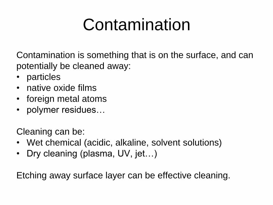
Contamination
Contamination is something that is on the surface, and can
potentially be cleaned away:
• particles
• native oxide films
• foreign metal atoms
• polymer residues…
Cleaning can be:
• Wet chemical (acidic, alkaline, solvent solutions)
• Dry cleaning (plasma, UV, jet…)
Etching away surface layer can be effective cleaning.
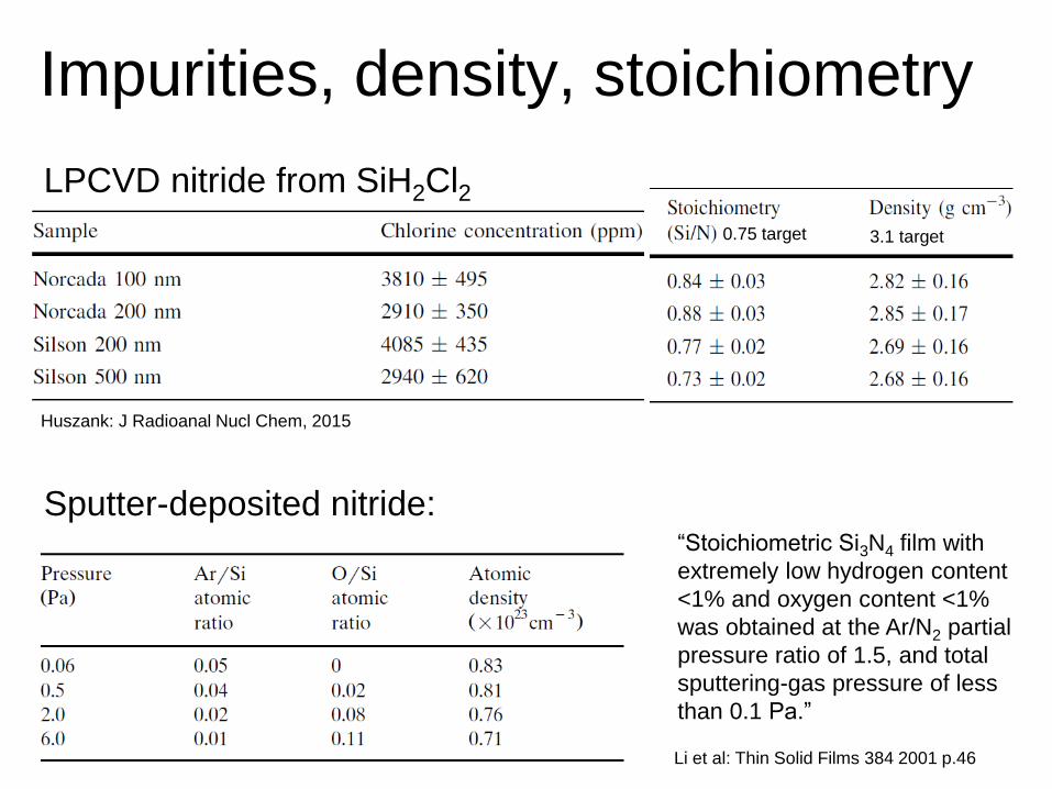
Impurities, density, stoichiometry
Huszank: J Radioanal Nucl Chem, 2015
Sputter-deposited nitride:“Stoichiometric Si3N4 film with
extremely low hydrogen content
<1% and oxygen content <1%
was obtained at the Ar/N2 partial
pressure ratio of 1.5, and total
sputtering-gas pressure of less
than 0.1 Pa.”
Li et al: Thin Solid Films 384 2001 p.46
LPCVD nitride from SiH2Cl20.75 target 3.1 target

Film quality measures
Uniformity:
across-the-sample uniformity of thickness, resistivity,
refractive index…
Usually given as U = (max-min):(2*ave), 1-10% typical
Homogeneity:
Film has same structure and composition all over.
e.g. grain size or dopant concentration is independent of
position, no stress gradient, no interfacial layer, …

ALD uniformity
(=thickness across the wafer)
HfO2 dielectric marathon test: 2000 wafers


Inhomogenous films
PSG (phoshorous
doped silica glass) has
doped polysilicon
partially. PSG is
homogenous, but
polysilicon displays
inhomogenous dopant
concentration.
Grain size gradient
Messier JVST 1986
GLAD/sculpted film:
rotation and inclined
deposition used to
create inhomogenous
film on purpose
(evaporated MgF2;
Messier book)
polysilicon
PSG

Deposition rate vs. thruput
Deposition rate is measured in nm/min.
Thruput is measured in WPH (wafers per hour)
A batch LPCVD polysilicon reactor loads 100 wafers,
depo rate is 10 nm/min, which corresponds to process
time 40 min for 400 nm thick film. Load, ramp etc. take 60
min. ➔ thruput is 60 WPH.
A single wafer PECVD tool deposits silicon at 100 nm/min
rate, with load, ramp etc. 1 min/wafer. 400 nm thick film is
achieved in 5 min ➔ thruput is 12 WPH.

Rate vs. impurities
Slow deposition rate means that gas phase impurities in the
reactor atmosphere have time to incorporate into growing film.
In the previous example then, batch reactor wafers have 10X
impurities relative to single wafer reactor.
In reality
sticking
coefficient is
important: O2
and H2O stick
readily, N2 not.
10-5
Franssila: Introduction to Microfabrication

Resistivity: impurity effects
Murarka: Metallization
Doubling of TaSi2resistivity due to
2% oxygen.

ALD TaN impurities
Carbon and hydrogen contents determined
by TOF-ERDA of films deposited by the
TaCl5-TMA-NH3 pulsing process as a
function of deposition temperature.
Petra Alen, PhD thesis, University of Helsinki, 2005
Carbon and chlorine contents of
films deposited by the TaCl5-tBuNH2 process as a function of
the deposition temperature.
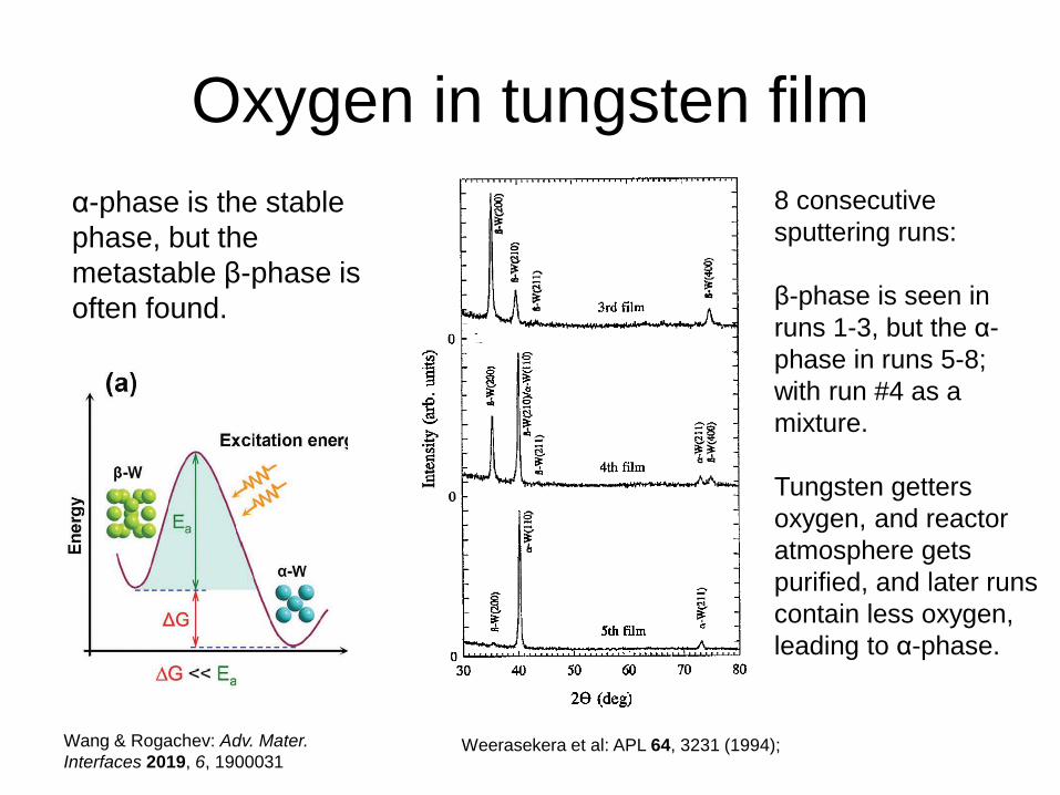
Oxygen in tungsten film
Wang & Rogachev: Adv. Mater.
Interfaces 2019, 6, 1900031Weerasekera et al: APL 64, 3231 (1994);
α-phase is the stable
phase, but the
metastable β-phase is
often found.
8 consecutive
sputtering runs:
β-phase is seen in
runs 1-3, but the α-
phase in runs 5-8;
with run #4 as a
mixture.
Tungsten getters
oxygen, and reactor
atmosphere gets
purified, and later runs
contain less oxygen,
leading to α-phase.

Oxygen impurity in W-films
“The decrease in the lattice parameter of the β-W phase,
and the eventual transition to the α-W phase with increasing
sputtering time, strongly suggests that oxygen impurities
stabilize the β -W phase. Both effects can be accounted for by a
decrease in the oxygen partial pressure as the deposition process
continues due to the oxygen gettering ability of freshly
sputtered W.
In this context it is important to note, however,
that the actual amount of incorporated oxygen depends not
only on the oxygen partial pressure, but also on the deposition
rate. Even though the oxygen partial pressure is relatively
low, the slow deposition rate allows significant
amounts of oxygen to be incorporated within the growing
films.”
Weerasekera et al: APL 64, 3231 (1994);

Smoothness vs. flatness
• Smoothness is atomic scale topography,
measured over e.g. 5*5 µm area by AFM.
• Silicon wafer smoothness is ≈0.5 nm
• Flatness is macroscopic property, measured
over, for example, 20 mm.
For silicon wafers flatness is e.g. 0.25 µm.
• As a rule of thumb, surface smoothness must be
less than film thickness in order to deposit
reasonable films.

Is smooth good ?
Fluorine-doped zinc oxide
(FZO)
Poortmans: Thin film solar cells
Superstrate solar cell
Repmann
3 depos:
1st
2nd
3rd

Measurement needs
-in-situ: during wafer processing in the process chamber
-in-line: after wafer processing inside the process tool
(e.g. exit load lock)
-on-line: in the wafer fab by wafer fab personnel
-ex-situ: outside analytical laboratory by expert users

Measurement needs (2)
R&D Pilot production Volume manufacturing
samples anything full wafers full wafers
(monitors) (scribe line measurement)
analysis spot anything not a concern test site
time anything minutes/hours minutes/seconds
Destructive measurement discards the wafer after measurement ➔
measurement cost is >wafer cost.
Non-destructive measurement does not destroy the wafer, but maybe it cannot
be sold to the customer for cosmetic or reliability reasons.
Non-contact measurement does not physically touch the wafer, e.g. thickness by
ellipsometer or resisitivity by eddy currents.
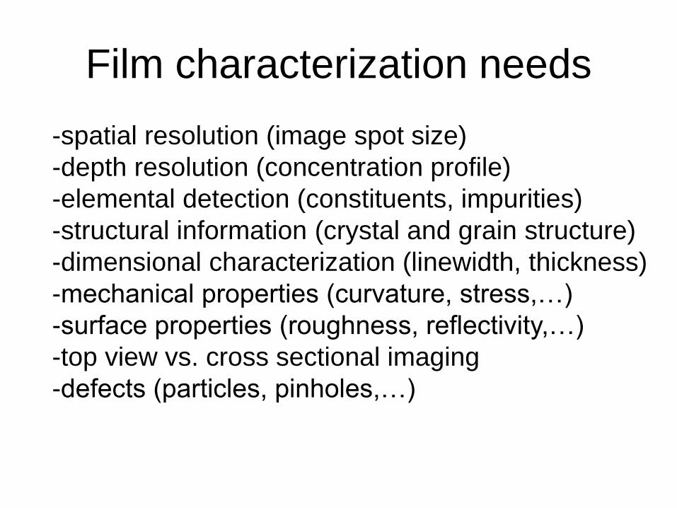
Film characterization needs
-spatial resolution (image spot size)
-depth resolution (concentration profile)
-elemental detection (constituents, impurities)
-structural information (crystal and grain structure)
-dimensional characterization (linewidth, thickness)
-mechanical properties (curvature, stress,…)
-surface properties (roughness, reflectivity,…)
-top view vs. cross sectional imaging
-defects (particles, pinholes,…)

Normal vs. collimated sputtering
Chia-Hao Chan
Ir.nctu.tw.edu
Collimator prevents
high-angle ions ➔
more directional flux
➔ more uniform
step coverage.
Deposition rate
reduced because
collimator captures
some atoms.

Sputtered TiN characterization

Sputtered TiN (2)

Method vs. substrate
Effect of substrate and deposition
method on film crystallinity.
Monitor wafers have to match
product wafers !
Sputtered Cu 0.5 µm on Ta
CVD Cu 0.5 µm on Ta
CVD Cu 0.5 µm on TiN

Crystallinity and depo time
Wang & Rogachev: Adv. Mater.
Interfaces 2019, 6, 1900031
Tungsten films
deposited under the
constant RF bias of
50 W for different
durations.
β-tungsten is
formed initially.

Crystallinity and bias-power
“XRD patterns of W films
deposited under various
RF biases with a
deposition time of 10 min
The inset shows the
magnified views of the
corresponding diffraction
peaks.”
Higher bias power seems
to purify the film (e.g. by
sputtering oxygen away,
or simply modifying W-
surface crystallinity). Wang & Rogachev: Adv. Mater.
Interfaces 2019, 6, 1900031

Tungsten crystallinity development
Wang & Rogachev: Adv. Mater.
Interfaces 2019, 6, 1900031
“…the competitive growth between α- and β-
W happened all the time during the
deposition process, where the plasma-
assisted ion bombardment on the film
surface is crucial to create α-phase-
dominated tungsten thin films. In this
study, β-phase is like Lord Voldemort, hard
to be eradicated completely.”
“Lattice mismatch, unintentional
substrate heating, and oxygen
residual (low vacuum ≈2*10−4 Pa)
are always conducive to form
metastable β-W phase.”

Nanoindentation test
Higher deposition
temperature ➔ better
mechanical properties
As a rule of thumb,
penetration depth should be
≤10% of film thickness,
otherwise we measure
substrate properties, not
film properties.
Walmsley et al: JOURNAL OF APPLIED PHYSICS 98, 044904 2005

Etch rate as film quality
SiNx etch
rate in
40 wt% KOH
Walmsley et al: JOURNAL OF APPLIED
PHYSICS 98, 044904 2005
13.6-MHz Oxford Instruments
PECVD 80 system.
silane, ammonia, and nitrogen.
Only the substrate temperature
was varied, which ranged from
100 to 300 °C.
Oxides
Thermal oxide as reference,
since its etch rate is always the
same (not dependent on
oxidation furnace parameters).
Plasma-Therm lecture notes 2015
Logarithmic scale !

Interaction effects
Hey et al: Solid State Technology April 1990, p. 139
Lower pressure equals more ion
bombardment, and thus denser film
➔ lower etch rate;
BUT stress state also changes !
PECVD oxide PECVD SiNx
Tang Longjuan et al 2009 J. Semicond. 30 096005
Si:N ratio changes as a function of
silane flow: stoichiometric Si3N4
has smaller etch rate;
BUT refractive index also changes.

Mechanical quality
Walmsley et al: JOURNAL OF APPLIED PHYSICS 98, 044904 2005
Stoichiometric LPCVD
nitride Si3N4 density is
3.1-3.4 g/cm3.
LPCVD nitride
Young’s modulus 220 GPa
But:
Size-dependent effective Young’s
modulus of silicon nitride
cantilevers, Appl. Phys. Lett. 94,
233108 (2009);
https://doi.org/10.1063/1.3152772
PECVD
nitride

Stress
580oC deposition, i.e.
amorphous initially
Henri Gückel
Stress reduction is
anneal temperature and
time dependent !
Remember: thermal budget = f (t,T)

Productivity measures
Deposition rate
Thru-put (very different from rate !)
Wide process window (robust against parameter drift)
Yield of precursors (source gases/targets expensive)
Deposition on one side or both sides simultaneously
Uniformity across the substrate
Uniformity across the batch
Repeatability run-to-run
Repeatability day-to-day

Use qualityWhat stressors the film is going to experience ?
-mechanical (bending, contact, abrasion…)
-chemical (humidity, sea water, acids, solvents…)
-electrochemical (metal-metal contacts,
electrolytes, anodic oxidation…)
-electrical (high current density, high E-field…)
-thermal (high-T, low-T, T-cycling, T-shock…)
-optical (UV)
-biological (protein adsorption, biofilms,…)