features bluecore - iczoom · up to 120 mips dsp for intensive digital signal ... green and rohs...
TRANSCRIPT

Features BlueCore® CSR8675 BGA Bluetooth® v4.1 specification fully qualified Radio includes integrated balun 80 MHz RISC MCU and 120 MHz Kalimba DSP Up to 120 MIPS DSP for intensive digital signal
processing algorithms 24-bit audio 16 Mb internal flash; optional support for 64 Mb of
external SPI flash Stereo codec with 2 channels of ADC and up to 6
microphone inputs (includes bias generation anddigital microphone support)
Audio interfaces: 2 x I²S/PCM 1 x SPDIF (independent of I²S/PCM ports)
Serial interfaces: UART, USB 2.0 full-speed, I²Cand SPI
Integrated dual switch-mode regulators, linearregulators and battery charger
3 hardware LED controllers (for RGB) and ability todrive LCD segment display directly
Support for up to 6 capacitive touch sensor inputs 6.5 x 6.5 x 1 mm, 0.5 mm pitch 112‑ball VFBGA CSR8675 BGA application boards back compatible
with CSR8670 BGA Green (RoHS compliant and no antimony or
halogenated flame retardants)
Bluetooth Smart Ready
Low-power Solution forDSP Intensive Audio Applications
Production Information
CSR8675BIssue 5
General DescriptionCSR8675 BGA consumer audio platform for wired andwireless applications integrates an ultra‑low‑powerDSP and application processor with embedded flashmemory, a high-performance stereo codec, a powermanagement subsystem, LED and LCD drivers andcapacitive touch sensor inputs in a SoC IC.
2.4 GHz Radio
+Balun
I/O
BT_RF RAM
Baseband
MCU
Kalimba DSP
FlashXTAL Serial FlashExternalMemory
UART/USB
PIOAudio In /Out
PCM/I2SSPI/I2C
LED /PIO
Audio Interface Capacitive
Sense
ClockGeneration
SPDIF
PCM/I2S
Applications High-end wired/wireless stereo headphones High-end wired/wireless stereo headsets High-end wired/wireless active headsets Wireless stereo speakers Low-end docking stations and soundbars Gaming headsetsThe dual-core architecture with flash memory enablesmanufacturers to easily differentiate their products withnew features without extending development cycles.The enhanced Kalimba DSP coprocessor with up to120 MIPS supports more digital signal processingrequirements in stereo headphones, headsets, gamingheadsets and soundbars.The audio codec supports 2 ADC channels, up to 6microphone inputs, stereo output and a variety of audiostandards.CSR's popular BlueCore® CSR8670™ andBlueCore®5‑Multimedia platforms aresoftware‑portable to the CSR8675 BGA, with easymigration of a broad range of solutions from CSR'seXtension partners. This enables rapid time-to-marketdeployment for a broad range of consumer electronicproducts.
Production Information© Cambridge Silicon Radio Limited 2013-2014Confidential Information - This Material is Subject to CSR's Non-Disclosure Agreement
Page 1 of 112CS-232426-DSP5
www.csr.com
CSR
8675 BGA D
ata Sheet

Ordering Information
Device
Package
Order NumberType Size Shipment
Method
CSR8675VFBGA‑112‑ball
(Pb free)6.5 x 6.5 x 1 mm
0.5 mm pitchTape and reel CSR8675B‑IBBH‑R
Note:
Minimum order quantity is 2kpcs taped and reeled.
Supply chain: CSR's manufacturing policy is to multisource volume products. For further details, contact your localsales account manager or representative.
Contacts
General informationInformation on this productCustomer support for this productDetails of compliance and standardsHelp with this document
[email protected]@[email protected]
CSR8675 Development Kit Ordering Information
Description Order Number
CSR8675 BGA Audio Development Kit DK-CSR8675-10197-1A
CSR8675 BGA Development Kit (Board Only) DB-CSR8675-10200-1A
Production Information© Cambridge Silicon Radio Limited 2013-2014Confidential Information - This Material is Subject to CSR's Non-Disclosure Agreement
Page 2 of 112CS-232426-DSP5
www.csr.com
CSR
8675 BGA D
ata Sheet

Device DetailsBluetooth low energy Dual‑mode Bluetooth low energy radio Support for Bluetooth basic rate / EDR and low energy
connections 3 Bluetooth low energy connections at the same time as
basic rate A2DPBluetooth Radio On‑chip balun (50 Ω impedance in TX and RX modes) No external trimming is required in production Bluetooth v4.1 specification software/hardwareBluetooth Transmitter Typical RF transmit power
Basic rate 10 dBm EDR -1 dB (relative power) Bluetooth low energy 9 dBm
6‑bit DAC level control Class 1, Class 2 and Class 3 support without the need for
an external power amplifier or TX/RX switchBluetooth Receiver Typical RF receiver sensitivity:
Basic rate -90 dBm EDR -92 dBm Bluetooth low energy -93 dBm
Integrated channel filters Digital demodulator for improved sensitivity and co‑channel
rejection Real‑time digitised RSSI available to application Fast AGC for enhanced dynamic range Channel classification for AFHBluetooth Synthesiser Fully integrated synthesiser requires no external VCO,
varactor diode, resonator or loop filter Compatible with crystals 19.2 MHz to 32 MHz or an external
clock 19.2 MHz to 40 MHz (default 26 MHz)Kalimba DSP Enhanced Kalimba 5 DSP coprocessor 120 MHz clock, up to 120 MIPS performance 24‑bit fixed-point core Single‑cycle MAC:
24 x 24‑bit multiply 56‑bit accumulate
Improved architecture and instructions for betterperformance over CSR8670 BGA
32‑bit instruction word Dual 24‑bit data memory 12 K x 32‑bit program RAM including 1 K instruction cache
for executing out of internal flash 2‑bank data RAM:
DM1 32 K x 24‑bit DM2 32 K x 24‑bit
Baseband and Software 16 Mb internal flash Memory protection unit supporting accelerated VM 56 KB internal RAM, enables full‑speed data transfer, mixed
voice/data and full piconet support Logic for forward error correction, header error control,
access code correlation, CRC, demodulation, encryption bitstream generation, whitening and transmit pulse shaping
Transcoders for A‑law, µ‑law and linear voice via PCM andA‑law, µ‑law and CVSD voice over air
Audio Interfaces Audio codec with 2 high‑quality dedicated ADCs 24-bit audio processing support 2 microphone bias generators and up to 2 analogue
microphone inputs Up to 6 digital microphone inputs (MEMS) G.722 compatible, includes improved digital IIR filter path
for stop‑band attenuation required for G.722 compliance Enhanced side‑tone gain control Supported sample rates of 8, 11.025, 16, 22.05, 32, 44.1,
48, 96 kHz and 192kHz (DAC only)Physical Interfaces UART interface USB 2.0 interface (full‑speed) Master and slave bit‑serialiser (I²C and SPI) Up to 32 PIOs (includes 12 general purpose PIOs and
unused digital interfaces also available as PIOs) SPI debug and programming interface with read access
disable locking 2 x PCM/I²S and 1 x SPDIF supported simultaneously Dual/quad external serial flash memory interface 3 LED drivers (includes RGB) with PWM flasher on sleep
clock Support for up to 6 capacitive touch sensor inputs 2 analogue PIOsIntegrated Power Control and Regulation 2 high‑efficiency switch‑mode regulators with 1.8 V and
1.35 V outputs from battery supply 3.3 V USB pad supply linear regulator Low‑voltage linear regulator for internal digital supply Low‑voltage linear regulator for internal analogue supply
with 1.35 V output Power‑on‑reset detects low supply voltage Power management includes digital shutdown and wake‑up
commands with low‑power crystal drive for ultra‑low powerPark/Sniff/Hold mode
Battery Charger Lithium ion / Lithium polymer battery charger with instant‑on Fast charging support up to 200 mA with no external
components Higher charge currents using external pass device Supports USB BCv1.2 CDP, DCP and SDP charger
detection Charger pre‑calibrated by CSR PSE compliance:
Design to JIS‑C 8712/8714 (batteries) Testing based on IEEE 1725
Auxiliary Features Customer application space available Crystal oscillator with built‑in digital trimming Auxiliary ADC and DAC available to applicationsPackage Option 6.5 x 6.5 x 1 mm, 0.5 mm pitch 112‑ball VFBGA
Production Information© Cambridge Silicon Radio Limited 2013-2014Confidential Information - This Material is Subject to CSR's Non-Disclosure Agreement
Page 3 of 112CS-232426-DSP5
www.csr.com
CSR
8675 BGA D
ata Sheet

Functional Block Diagram
G-T
W-0
0127
58.3
.2
Memory Management
Unit
Bluetooth Modem
120 MHz DSP
I2C/SPIMaster/Slave
PIO
SPI(Debug)
UART4 Mbps
SystemRAM
Serial Quad I/O
Flash (SQIF)
Interface
DMA ports
DM
A p
orts
2 x PCM /
I2S
eFlash
SPI_DEBUG Serial Flash/RAM I2C
MIC_LN
UART
80 MHz MCU
SPKR_LN
AudioInterface
MIC Bias
MIC_BIAS_B
MIC_BIAS_A
USB v2.0 Full-speed
USB
3.3V
MIC Bias
6xMEMS
MIC
Digital M
ICs
SPI–Lock/DFU
Encrypt
VM Accelerator(MPU)
LCD Segment
Driver
PMUInterface
andBIST
Engine
LED PWMControl and
Output
PM
DM1
DM2
R G B
Digital A
udio
1.35VSwitch-mode
Regulator
BypassLDO
SMP_VBAT
LXL_1V
8
Li-ion Charger
VCHG
SM
PS_3V
3
1.8VSwitch-mode
Regulator
LX_1V
35
SM
PS_1V
8_SEN
SE
VO
UT_3V3
Voltage / Temperature Monitor
BT_RF
CAP_SENSE[0]
ClockGeneration
AnalogueTest
AUX ADC
XTAL AIO[1:0]
Capacitive Touch
Controller
CAP_SENSE[1]CAP_SENSE[2]CAP_SENSE[3]CAP_SENSE[4]CAP_SENSE[5]
MIC_LP
MIC_RNMIC_RP
SPKR_LP
SPKR_RNSPKR_RP
SENSE SENSE
Bluetooth Baseband
Bluetooth Radioand Balun
TX
RX
High-quality ADC
High-quality ADC
High-quality DAC
High-quality DAC
1.35VLow-voltage VDD_AUX
Linear Regulator
1.35VLow-voltage VDD_ANA
Linear Regulator
Low-voltage VDD_DIG
Linear Regulator
DM
A p
orts
VDD
_AUX
SENSE
VDD
_ANA
SENSE
VDD
_BT_RAD
IO
VDD
_DIG_E
FLASH
SENSE
CHG_EXT
Switch
SM
PS_1V
35_SEN
SE
SENSE
VBAT
External Connection
Exte
rnal
C
onne
ctio
n
VDD
_AUX_1V
8
VRE
GIN
_DIG
SPDIF
PIO
Production Information© Cambridge Silicon Radio Limited 2013-2014Confidential Information - This Material is Subject to CSR's Non-Disclosure Agreement
Page 4 of 112CS-232426-DSP5
www.csr.com
CSR
8675 BGA D
ata Sheet

Document HistoryRevision Date Change Reason
1 27 FEB 13 Original publication of this document.Issue 1 content set as: Technical Overview material Functional block diagram Package information PIO configuration Example application schematic Green and RoHS information Tape and reel information
2 12 FEB 14 Full-version of Advance Information data sheet created.
3 25 SEP 14 Production Information added.
4 26 SEP 14 Additional Power Consumption information added.
5 08 OCT 14 Integrated Digital IIR Filter information updated.
Production Information© Cambridge Silicon Radio Limited 2013-2014Confidential Information - This Material is Subject to CSR's Non-Disclosure Agreement
Page 5 of 112CS-232426-DSP5
www.csr.com
CSR
8675 BGA D
ata Sheet

Status InformationThe status of this Data Sheet is Production Information. CSR Product Data Sheets progress according to the following format: Advance Information:
Information for designers concerning CSR product in development. All values specified are the target values of the design.Minimum and maximum values specified are only given as guidance to the final specification limits and must not beconsidered as the final values.
Engineering Sample: Information about initial devices. Devices are untested or partially tested prototypes, their status is described in an
Engineering Sample Release Note. All values specified are the target values of the design. Minimum and maximum valuesspecified are only given as guidance to the final specification limits and must not be considered as the final values.
All detailed specifications including pinouts and electrical specifications may be changed by CSR without notice. Pre-production Information:
Pinout and mechanical dimension specifications finalised. All values specified are the target values of the design. Minimumand maximum values specified are only given as guidance to the final specification limits and must not be considered asthe final values.
All electrical specifications may be changed by CSR without notice. Production Information:
Final Data Sheet including the guaranteed minimum and maximum limits for the electrical specifications. Production Data Sheets supersede all previous document versions.
Device ImplementationImportant Note:
As the feature-set of the CSR8675 BGA is firmware build-specific, see the relevant software release note for the exactimplementation of features on the CSR8675 BGA.
Life Support Policy and Use in Safety-critical ApplicationsCSR's products are not authorised for use in life-support or safety-critical applications. Use in such applications is done at the solediscretion of the customer. CSR will not warrant the use of its devices in such applications. CSR Green Semiconductor Products and RoHS ComplianceCSR8675 BGA devices meet the requirements of Directive 2011/65/EU of the European Parliament and of the Council on theRestriction of Hazardous Substance (RoHS). CSR8675 BGA devices are free from halogenated or antimony trioxide-based flameretardants and other hazardous chemicals. For more information, see CSR's Environmental Compliance Statement for CSR GreenSemiconductor Products. Trademarks, Patents and LicencesUnless otherwise stated, words and logos marked with ™ or ® are trademarks registered or owned by CSR plc or its affiliates.Bluetooth ® and the Bluetooth ® logos are trademarks owned by Bluetooth ® SIG, Inc. and licensed to CSR. Other products, servicesand names used in this document may have been trademarked by their respective owners.The publication of this information does not imply that any license is granted under any patent or other rights owned by CSR plcand/or its affiliates.CSR reserves the right to make technical changes to its products as part of its development programme.While every care has been taken to ensure the accuracy of the contents of this document, CSR cannot accept responsibility for anyerrors.Refer to www.csrsupport.com for compliance and conformance to standards information.
Production Information© Cambridge Silicon Radio Limited 2013-2014Confidential Information - This Material is Subject to CSR's Non-Disclosure Agreement
Page 6 of 112CS-232426-DSP5
www.csr.com
CSR
8675 BGA D
ata Sheet

ContentsOrdering Information ........................................................................................................................................... 2
Contacts ..................................................................................................................................................... 2CSR8675 Development Kit Ordering Information ...................................................................................... 2
Device Details ..................................................................................................................................................... 3Functional Block Diagram .................................................................................................................................. 4
1 Package Information ......................................................................................................................................... 131.1 Pinout Diagram ........................................................................................................................................ 131.2 Device Terminal Functions ....................................................................................................................... 141.3 Package Dimensions ............................................................................................................................... 231.4 PCB Design and Assembly Considerations ............................................................................................. 241.5 Typical Solder Reflow Profile ................................................................................................................... 24
2 System Architecture .......................................................................................................................................... 253 Bluetooth Modem .............................................................................................................................................. 26
3.1 RF Ports ................................................................................................................................................... 263.1.1 BT_RF ........................................................................................................................................ 26
3.2 RF Receiver ............................................................................................................................................. 263.2.1 Low Noise Amplifier .................................................................................................................... 263.2.2 RSSI Analogue to Digital Converter ........................................................................................... 26
3.3 RF Transmitter ......................................................................................................................................... 263.3.1 IQ Modulator ............................................................................................................................... 263.3.2 Power Amplifier .......................................................................................................................... 27
3.4 Bluetooth Radio Synthesiser .................................................................................................................... 273.5 Baseband ................................................................................................................................................. 27
3.5.1 Burst Mode Controller ................................................................................................................. 273.5.2 Physical Layer Hardware Engine ............................................................................................... 27
4 Clock Generation ............................................................................................................................................... 284.1 Clock Architecture .................................................................................................................................... 284.2 Input Frequencies and PS Key Settings .................................................................................................. 284.3 External Reference Clock ........................................................................................................................ 28
4.3.1 Input: XTAL_IN ........................................................................................................................... 284.3.2 XTAL_IN Impedance in External Mode ...................................................................................... 294.3.3 Clock Timing Accuracy ............................................................................................................... 29
4.4 Crystal Oscillator: XTAL_IN and XTAL_OUT ........................................................................................... 304.4.1 Crystal Calibration ...................................................................................................................... 304.4.2 Crystal Specification ................................................................................................................... 30
5 Bluetooth Stack Microcontroller ......................................................................................................................... 315.1 VM Accelerator ......................................................................................................................................... 31
6 Kalimba DSP ..................................................................................................................................................... 327 Memory Interface and Management ................................................................................................................. 33
7.1 Memory Management Unit ....................................................................................................................... 337.2 System RAM ............................................................................................................................................ 337.3 Kalimba DSP RAM ................................................................................................................................... 337.4 eFlash Memory (16 Mb) ........................................................................................................................... 337.5 Serial Quad I/O Flash Interface (SQIF) .................................................................................................... 33
8 Serial Interfaces ................................................................................................................................................ 358.1 USB Interface ........................................................................................................................................... 358.2 UART Interface ........................................................................................................................................ 35
8.2.1 UART Configuration While Reset is Active ................................................................................. 368.3 Programming and Debug Interface .......................................................................................................... 36
Production Information© Cambridge Silicon Radio Limited 2013-2014Confidential Information - This Material is Subject to CSR's Non-Disclosure Agreement
Page 7 of 112CS-232426-DSP5
www.csr.com
CSR
8675 BGA D
ata Sheet

8.3.1 Instruction Cycle ......................................................................................................................... 378.3.2 Multi-slave Operation .................................................................................................................. 378.3.3 SPI-lock ...................................................................................................................................... 37
8.4 I²C Interface ............................................................................................................................................. 379 Interfaces ........................................................................................................................................................... 38
9.1 Programmable I/O Ports, PIO .................................................................................................................. 389.2 Analogue I/O Ports, AIO ........................................................................................................................... 399.3 Capacitive Touch Sensor ......................................................................................................................... 39
9.3.1 Capacitive Range Control: .......................................................................................................... 409.3.2 Sampling Front End .................................................................................................................... 409.3.3 ADC ............................................................................................................................................ 409.3.4 Digital Signal Conditioning (Digital Processing) ......................................................................... 409.3.5 Software Signal Conditioning (Firmware) ................................................................................... 419.3.6 VM .............................................................................................................................................. 41
9.4 LED Drivers .............................................................................................................................................. 4110 Audio Interface .................................................................................................................................................. 43
10.1 Audio Input and Output ............................................................................................................................ 4410.2 Audio Codec Interface .............................................................................................................................. 44
10.2.1 Audio Codec Block Diagram ....................................................................................................... 4510.2.2 Codec Set-up .............................................................................................................................. 4510.2.3 ADC ............................................................................................................................................ 4510.2.4 ADC Sample Rate Selection ...................................................................................................... 4610.2.5 ADC Audio Input Gain ................................................................................................................ 4610.2.6 ADC Pre-amplifier and ADC Analogue Gain .............................................................................. 4610.2.7 ADC Digital Gain ........................................................................................................................ 4610.2.8 ADC Digital IIR Filter .................................................................................................................. 4710.2.9 DAC ............................................................................................................................................ 4710.2.10 DAC Sample Rate Selection ...................................................................................................... 4710.2.11 DAC Digital Gain ........................................................................................................................ 4710.2.12 DAC Analogue Gain ................................................................................................................... 4810.2.13 DAC Digital FIR Filter ................................................................................................................. 4810.2.14 IEC 60958 Interface .................................................................................................................... 4810.2.15 Microphone Input ........................................................................................................................ 4910.2.16 Digital Microphone Inputs ........................................................................................................... 5010.2.17 Line Input .................................................................................................................................... 5110.2.18 Output Stage .............................................................................................................................. 5110.2.19 Mono Operation .......................................................................................................................... 5210.2.20 Side Tone ................................................................................................................................... 5310.2.21 Integrated Digital IIR Filter .......................................................................................................... 54
10.3 PCM1 and PCM2 Interface ...................................................................................................................... 5510.3.1 PCM Interface Master/Slave ....................................................................................................... 5510.3.2 Long Frame Sync ....................................................................................................................... 5610.3.3 Short Frame Sync ....................................................................................................................... 5710.3.4 Multi-slot Operation .................................................................................................................... 5710.3.5 GCI Interface .............................................................................................................................. 5710.3.6 Slots and Sample Formats ......................................................................................................... 5810.3.7 Additional Features ..................................................................................................................... 5910.3.8 PCM Timing Information ............................................................................................................. 5910.3.9 PCM_CLK and PCM_SYNC Generation .................................................................................... 6310.3.10 PCM Configuration ..................................................................................................................... 63
10.4 I²S1 and I²S2 Interface ............................................................................................................................. 6411 WLAN Coexistence Interface ............................................................................................................................ 67
Production Information© Cambridge Silicon Radio Limited 2013-2014Confidential Information - This Material is Subject to CSR's Non-Disclosure Agreement
Page 8 of 112CS-232426-DSP5
www.csr.com
CSR
8675 BGA D
ata Sheet

12 Power Control and Regulation .......................................................................................................................... 6812.1 1.8V Switch-mode Regulator ................................................................................................................... 7112.2 1.35V Switch-mode Regulator ................................................................................................................. 7212.3 1.8V and 1.35V Switch-mode Regulators Combined ............................................................................... 7312.4 Bypass LDO Linear Regulator ................................................................................................................. 7412.5 Low-voltage VDD_DIG Linear Regulator ................................................................................................. 7512.6 Low-voltage VDD_AUX Linear Regulator ................................................................................................ 7512.7 Low-voltage VDD_ANA Linear Regulator ................................................................................................ 7512.8 Voltage Regulator Enable ........................................................................................................................ 7512.9 External Regulators and Power Sequencing ........................................................................................... 7512.10Reset, RST# ............................................................................................................................................. 76
12.10.1 Digital Pin States on Reset ......................................................................................................... 7612.10.2 Status After Reset ...................................................................................................................... 77
12.11Automatic Reset Protection ...................................................................................................................... 7713 Battery Charger ................................................................................................................................................. 78
13.1 Battery Charger Hardware Operating Modes ........................................................................................... 7813.1.1 Disabled Mode ............................................................................................................................ 7913.1.2 Trickle Charge Mode .................................................................................................................. 7913.1.3 Fast Charge Mode ...................................................................................................................... 7913.1.4 Standby Mode ............................................................................................................................ 7913.1.5 Error Mode .................................................................................................................................. 79
13.2 Battery Charger Trimming and Calibration ............................................................................................... 7913.3 VM Battery Charger Control ..................................................................................................................... 7913.4 Battery Charger Firmware and PS Keys .................................................................................................. 7913.5 External Mode .......................................................................................................................................... 80
14 Example Application Schematic ........................................................................................................................ 8115 Example Application Using Different Power Supply Configurations .................................................................. 8216 Electrical Characteristics ................................................................................................................................... 85
16.1 Absolute Maximum Ratings ..................................................................................................................... 8516.2 Recommended Operating Conditions ...................................................................................................... 8616.3 Input/Output Terminal Characteristics ...................................................................................................... 87
16.3.1 Regulators: Available For External Use ...................................................................................... 8716.3.2 Regulators: For Internal Use Only .............................................................................................. 8916.3.3 Regulator Enable ........................................................................................................................ 9016.3.4 Battery Charger .......................................................................................................................... 9016.3.5 Reset .......................................................................................................................................... 9216.3.6 USB ............................................................................................................................................ 9316.3.7 Clocks ......................................................................................................................................... 9316.3.8 Stereo Codec: Analogue to Digital Converter ............................................................................. 9416.3.9 Stereo Codec: Digital to Analogue Converter ............................................................................. 9516.3.10 Digital .......................................................................................................................................... 9616.3.11 LED Driver Pads ......................................................................................................................... 9616.3.12 Auxiliary ADC ............................................................................................................................. 9716.3.13 Auxiliary DAC ............................................................................................................................. 97
16.4 ESD Protection ......................................................................................................................................... 9816.4.1 USB Electrostatic Discharge Immunity ....................................................................................... 98
17 Power Consumption ........................................................................................................................................ 10018 CSR Green Semiconductor Products and RoHS Compliance ........................................................................ 10119 Software .......................................................................................................................................................... 102
19.1 On-chip Software ................................................................................................................................... 10219.1.1 Stand-alone CSR8675 BGA and Kalimba DSP Applications ................................................... 10219.1.2 BlueCore HCI Stack ................................................................................................................ 102
Production Information© Cambridge Silicon Radio Limited 2013-2014Confidential Information - This Material is Subject to CSR's Non-Disclosure Agreement
Page 9 of 112CS-232426-DSP5
www.csr.com
CSR
8675 BGA D
ata Sheet

19.2 Off-chip Software ................................................................................................................................... 10319.2.1 CSR8675 Development Kit ....................................................................................................... 10319.2.2 eXtension Program Support ..................................................................................................... 104
20 Tape and Reel Information .............................................................................................................................. 10520.1 Tape Orientation .................................................................................................................................... 10520.2 Tape Dimensions ................................................................................................................................... 10520.3 Reel Information ..................................................................................................................................... 10620.4 Moisture Sensitivity Level ....................................................................................................................... 106
21 Document References ..................................................................................................................................... 107Terms and Definitions .............................................................................................................................................. 108
List of FiguresFigure 1.1 Pinout Diagram .................................................................................................................................... 13Figure 2.1 Standard Headset ................................................................................................................................ 25Figure 2.2 Extended Headset .............................................................................................................................. 25Figure 2.3 Processing 5.1 Channels ..................................................................................................................... 25Figure 2.4 DDFA Companion Device .................................................................................................................... 25Figure 3.1 Simplified Circuit BT_RF ...................................................................................................................... 26Figure 4.1 Clock Architecture ................................................................................................................................ 28Figure 4.2 TCXO Clock Accuracy ......................................................................................................................... 29Figure 6.1 Kalimba DSP Interface to Internal Functions ....................................................................................... 32Figure 7.1 Serial Quad I/O Flash Interface ........................................................................................................... 33Figure 8.1 Universal Asynchronous Receiver Transmitter (UART) ...................................................................... 35Figure 8.2 Break Signal ........................................................................................................................................ 36Figure 9.1 Capacitive Touch Sensor Block Diagram ............................................................................................ 39Figure 9.2 LED Equivalent Circuit ......................................................................................................................... 41Figure 10.1 Audio Interface ..................................................................................................................................... 43Figure 10.2 Audio Codec Input and Output Stages ................................................................................................ 45Figure 10.3 Audio Input Gain .................................................................................................................................. 46Figure 10.4 Example Circuit for SPDIF Interface (Co-axial) ................................................................................... 49Figure 10.5 Example Circuit for SPDIF Interface (Optical) ..................................................................................... 49Figure 10.6 Microphone Biasing ............................................................................................................................. 50Figure 10.7 Differential Input ................................................................................................................................... 51Figure 10.8 Single-ended Input ............................................................................................................................... 51Figure 10.9 Speaker Output .................................................................................................................................... 52Figure 10.10 Side Tone ............................................................................................................................................ 53Figure 10.11 PCM Interface Master .......................................................................................................................... 56Figure 10.12 PCM Interface Slave ............................................................................................................................ 56Figure 10.13 Long Frame Sync (Shown with 8-bit Companded Sample) ................................................................. 56Figure 10.14 Short Frame Sync (Shown with 16-bit Sample) ................................................................................... 57Figure 10.15 Multi-slot Operation with 2 Slots and 8-bit Companded Samples ........................................................ 57Figure 10.16 GCI Interface ....................................................................................................................................... 58Figure 10.17 16-bit Slot Length and Sample Formats .............................................................................................. 59Figure 10.18 PCM Master Timing Long Frame Sync ................................................................................................ 60Figure 10.19 PCM Master Timing Short Frame Sync ............................................................................................... 61Figure 10.20 PCM Slave Timing Long Frame Sync .................................................................................................. 62Figure 10.21 PCM Slave Timing Short Frame Sync ................................................................................................. 63Figure 10.22 I²S Digital Audio Interface Modes ........................................................................................................ 64Figure 10.23 Digital Audio Interface Slave Timing .................................................................................................... 65Figure 10.24 Digital Audio Interface Master Timing .................................................................................................. 66Figure 12.1 1.80V and 1.35V Dual-supply Switch-mode System Configuration ..................................................... 69
Production Information© Cambridge Silicon Radio Limited 2013-2014Confidential Information - This Material is Subject to CSR's Non-Disclosure Agreement
Page 10 of 112CS-232426-DSP5
www.csr.com
CSR
8675 BGA D
ata Sheet
Figure 12.2 1.80V Parallel-supply Switch-mode System Configuration .................................................................. 70Figure 12.3 External 1.8V System Configuration .................................................................................................... 71Figure 12.4 1.8V Switch-mode Regulator Output Configuration ............................................................................. 72Figure 12.5 1.35V Switch-mode Regulator Output Configuration ........................................................................... 73Figure 12.6 1.8V and 1.35V Switch-mode Regulators Outputs Parallel Configuration ........................................... 74Figure 13.1 Battery Charger Mode-to-Mode Transition Diagram ............................................................................ 78Figure 13.2 Battery Charger External Mode Typical Configuration ........................................................................ 80Figure 15.1 External 1.8V Supply Example Application .......................................................................................... 82Figure 15.2 External 3.3V Supply Example Application .......................................................................................... 83Figure 15.3 USB Dongle Example Application ....................................................................................................... 84Figure 19.1 Stand-alone CSR8675 BGA and Kalimba DSP Applications ............................................................ 102Figure 19.2 BlueCore HCI Stack ........................................................................................................................... 103Figure 20.1 Tape Orientation ................................................................................................................................ 105Figure 20.2 Tape Dimensions ............................................................................................................................... 105Figure 20.3 Reel Dimensions ................................................................................................................................ 106
List of TablesTable 1.1 RF Interface .......................................................................................................................................... 14Table 1.2 Clock Interface ...................................................................................................................................... 14Table 1.3 UART Interface ..................................................................................................................................... 14Table 1.4 USB Interface ....................................................................................................................................... 14Table 1.5 Debug SPI Interface ............................................................................................................................. 15Table 1.6 PIO Port: LED Drivers ........................................................................................................................... 15Table 1.7 PIO Port: Serial Quad I/O Flash/SRAM Interface ................................................................................. 16Table 1.8 PIO Port: PCM 1/I²S 1 Interface ........................................................................................................... 17Table 1.9 PIO Port: UART Interface ..................................................................................................................... 17Table 1.10 PIO Port: General I/O PIO[15:8] ........................................................................................................... 18Table 1.11 PIO Port: PCM 2/I²S 2 Interface ........................................................................................................... 18Table 1.12 PIO Port: General I/O PIO[3:0] ............................................................................................................. 19Table 1.13 Analogue I/O Interface .......................................................................................................................... 19Table 1.14 Capacitive Touch Sensor Interface ....................................................................................................... 19Table 1.15 Reset .................................................................................................................................................... 19Table 1.16 Analogue Audio Interface ..................................................................................................................... 19Table 1.17 Power Supplies and Control ................................................................................................................. 20Table 1.18 Grounds ................................................................................................................................................ 22Table 4.1 PS Key Values for CDMA/3G Phone TCXO ......................................................................................... 28Table 4.2 External Clock Specifications ............................................................................................................... 29Table 8.1 Possible UART Settings ....................................................................................................................... 36Table 8.2 Instruction Cycle for a SPI Transaction ................................................................................................ 37Table 9.1 Alternative PIO Functions ..................................................................................................................... 38Table 10.1 Shared Pins on PCM/I²S Interfaces ...................................................................................................... 44Table 10.2 ADC Audio Input Gain Rate .................................................................................................................. 47Table 10.3 DAC Digital Gain Rate Selection .......................................................................................................... 48Table 10.4 DAC Analogue Gain Rate Selection ..................................................................................................... 48Table 10.5 Side Tone Gain ..................................................................................................................................... 53Table 10.6 PCM Master Timing .............................................................................................................................. 59Table 10.7 PCM Slave Timing ................................................................................................................................ 62Table 10.8 Digital Audio Interface Slave Timing ..................................................................................................... 65Table 10.9 I²S Slave Mode Timing ......................................................................................................................... 65Table 10.10 Digital Audio Interface Master Timing ................................................................................................... 66Table 10.11 I²S Master Mode Timing Parameters, WS and SCK as Outputs .......................................................... 66
Production Information© Cambridge Silicon Radio Limited 2013-2014Confidential Information - This Material is Subject to CSR's Non-Disclosure Agreement
Page 11 of 112CS-232426-DSP5
www.csr.com
CSR
8675 BGA D
ata Sheet
Table 12.1 Recommended Configurations for Power Control and Regulation ....................................................... 68Table 12.2 Pin States on Reset .............................................................................................................................. 76Table 13.1 Battery Charger Operating Modes Determined by Battery Voltage and Current .................................. 78Table 16.1 ESD Handling Ratings .......................................................................................................................... 98Table 16.2 USB Electrostatic Discharge Protection Level ...................................................................................... 98
List of EquationsEquation 4.1 Crystal Calibration Using PSKEY_ANA_FTRIM_OFFSET .................................................................. 30Equation 4.2 Example of PSKEY_ANA_FTRIM_OFFSET Value for 2402.0168MHz ............................................... 30Equation 4.3 Example of PSKEY_ANA_FTRIM_OFFSET Value for 2401.9832MHz ............................................... 30Equation 9.1 LED Current ......................................................................................................................................... 41Equation 9.2 LED PAD Voltage ................................................................................................................................ 41Equation 10.1 IIR Filter Transfer Function, H(z) ......................................................................................................... 55Equation 10.2 IIR Filter Plus DC Blocking Transfer Function, HDC(z) ........................................................................ 55Equation 10.3PCM_CLK Frequency Generated Using the Internal 48MHz Clock .................................................... 63Equation 10.4PCM_SYNC Frequency Relative to PCM_CLK ................................................................................... 63
Production Information© Cambridge Silicon Radio Limited 2013-2014Confidential Information - This Material is Subject to CSR's Non-Disclosure Agreement
Page 12 of 112CS-232426-DSP5
www.csr.com
CSR
8675 BGA D
ata Sheet

1 Package Information1.1 Pinout Diagram
G-T
W-0
0047
71.1
.1
K3
M4
J3
M9 M10M8M7M6M5
B8
C1 C2
B3B2B1
A3
C3
E3
D3
C4 C5 C6
F3
E1
B5
A4
B4
A5
G3
J1
G1
F1
C8
K1
A8A1
D1
H3H1
A2
G2
F2
E2
L1 L2
D2
B6 B7
A6 A7
K2
L3
H2
J2
C7
A
B
C
D
E
F
G
H
J
K
L
1 2 3 4 5 6 7 8 9 10 11
A9 A10 A11
B9 B10
C9 C10
A12
12
M1M
B11 B12
C11 C12
M2 M3 M11 M12
Orientation from Top of Device
H12
J12
K12
G12
H11
J11
K11
G11
F12F11
D12
E12
L12L11L4 L5
K4 K5 K8 K9 K10K6 K7
L8 L9 L10L6 L7
D11
E11
H10
J10
G10
F10
D10
E10
G6 G7
F6 F7
Figure 1.1: Pinout Diagram
Production Information© Cambridge Silicon Radio Limited 2013-2014Confidential Information - This Material is Subject to CSR's Non-Disclosure Agreement
Page 13 of 112CS-232426-DSP5
www.csr.com
CSR
8675 BGA D
ata Sheet
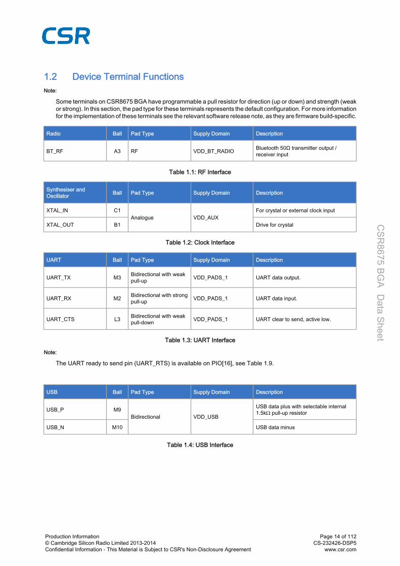
1.2 Device Terminal FunctionsNote:
Some terminals on CSR8675 BGA have programmable a pull resistor for direction (up or down) and strength (weakor strong). In this section, the pad type for these terminals represents the default configuration. For more informationfor the implementation of these terminals see the relevant software release note, as they are firmware build-specific.
Radio Ball Pad Type Supply Domain Description
BT_RF A3 RF VDD_BT_RADIO Bluetooth 50Ω transmitter output /receiver input
Table 1.1: RF Interface
Synthesiser andOscillator Ball Pad Type Supply Domain Description
XTAL_IN C1Analogue VDD_AUX
For crystal or external clock input
XTAL_OUT B1 Drive for crystal
Table 1.2: Clock Interface
UART Ball Pad Type Supply Domain Description
UART_TX M3 Bidirectional with weakpull-up VDD_PADS_1 UART data output.
UART_RX M2 Bidirectional with strongpull-up VDD_PADS_1 UART data input.
UART_CTS L3 Bidirectional with weakpull-down VDD_PADS_1 UART clear to send, active low.
Table 1.3: UART Interface
Note:
The UART ready to send pin (UART_RTS) is available on PIO[16], see Table 1.9.
USB Ball Pad Type Supply Domain Description
USB_P M9Bidirectional VDD_USB
USB data plus with selectable internal1.5kΩ pull-up resistor
USB_N M10 USB data minus
Table 1.4: USB Interface
Production Information© Cambridge Silicon Radio Limited 2013-2014Confidential Information - This Material is Subject to CSR's Non-Disclosure Agreement
Page 14 of 112CS-232426-DSP5
www.csr.com
CSR
8675 BGA D
ata Sheet

SPI Interface Ball Pad Type Supply Domain Description
SPI_MISO L2 Output with weak pull-down
VDD_PADS_1
SPI data output
SPI_MOSI G3 Input with weak pull-down SPI data input
SPI_CS# M1 Input with strong pull-up Chip select for SPI, active low
SPI_CLK E1 Input with weak pull-down SPI clock
Table 1.5: Debug SPI Interface
Note:
Table 1.6 to Table 1.12 list alternative functions mapped on to the PIO ports. For more information, including wherethe SPDIF is mapped on to the PIO ports, see Section 9.1.
PIO Port: LED Drivers Ball Pad Type Supply Domain Description
PIO[31] K5 Open drainVDD_PADS_1Open drain tolerant to4.25 V
Programmable I/O line 31.Main function: LED[1]: LED driver 1.
PIO[30] K4 Open drainVDD_PADS_1Open drain tolerant to4.25 V
Programmable I/O line 30.Main function: LED[0]: LED driver 0.
PIO[29] M4 Open drainVDD_PADS_1Open drain tolerant to4.25 V
Programmable I/O line 29.Main function: LED[2]: LED driver 2.
Table 1.6: PIO Port: LED Drivers
Production Information© Cambridge Silicon Radio Limited 2013-2014Confidential Information - This Material is Subject to CSR's Non-Disclosure Agreement
Page 15 of 112CS-232426-DSP5
www.csr.com
CSR
8675 BGA D
ata Sheet

PIO Port: Serial QuadI/O Flash Ball Pad Type Supply Domain Description
PIO[28] D12 Bidirectional with strongpull-down VDD_PADS_3
Programmable I/O line 28.Alternative function: QSPI_FLASH_IO[3]: serial quad I/O
flash data bit 3.
PIO[27] C10 Bidirectional with strongpull-down VDD_PADS_3
Programmable I/O line 27.Alternative function: QSPI_FLASH_IO[2]: serial quad I/O
flash data bit 2.
PIO[26] B11 Bidirectional with strongpull-down VDD_PADS_3
Programmable I/O line 26.Alternative function: QSPI_FLASH_IO[1]: serial quad I/O
flash data bit 1.
PIO[25] C11 Bidirectional with strongpull-down VDD_PADS_3
Programmable I/O line 25.Alternative function: QSPI_FLASH_IO[0]: serial quad I/O
flash data bit 0.
PIO[24] B10 Bidirectional with strongpull-up VDD_PADS_3
Programmable I/O line 24.Alternative function: QSPI_SRAM_CS#: SPI RAM chip
select.
PIO[23] D11 Bidirectional with strongpull-up VDD_PADS_3
Programmable I/O line 23.Alternative function: QSPI_FLASH_CS#: SPI flash chip
select.
PIO[22]. B12 Bidirectional with strongpull-down VDD_PADS_3
Programmable I/O line 22.Alternative function: QSPI_SRAM_CLK: SPI RAM clock.
PIO[21] C12 Bidirectional with strongpull-down VDD_PADS_3
Programmable I/O line 21.Alternative function: QSPI_FLASH_CLK: SPI flash clock
Table 1.7: PIO Port: Serial Quad I/O Flash/SRAM Interface
Production Information© Cambridge Silicon Radio Limited 2013-2014Confidential Information - This Material is Subject to CSR's Non-Disclosure Agreement
Page 16 of 112CS-232426-DSP5
www.csr.com
CSR
8675 BGA D
ata Sheet

PIO Port: PCM 1/I²S 1Interface Ball Pad Type Supply Domain Description
PIO[20] G2 Bidirectional with weakpull-down VDD_PADS_1
Programmable I/O line 20.Alternative function: PCM1_CLK: synchronous data
clock. SCK1: I²S clock
PIO[19] H2 Bidirectional with weakpull-down VDD_PADS_1
Programmable I/O line 19.Alternative function: PCM1_SYNC: synchronous data
sync. WS1: I²S word select
PIO[18] H3 Bidirectional with weakpull-down VDD_PADS_1
Programmable I/O line 18.Alternative function: PCM1_OUT: synchronous data
output. SD1_OUT: I²S data output
PIO[17] F1 Bidirectional with weakpull-down VDD_PADS_1
Programmable I/O line 17.Alternative function: PCM1_IN: synchronous data input. SD1_IN: I²S data input
Table 1.8: PIO Port: PCM 1/I²S 1 Interface
PIO Port: UART Ball Pad Type Supply Domain Description
PIO[16] K3 Bidirectional with weakpull-up VDD_PADS_1
Programmable I/O line 16.Alternative function: UART_RTS: UART request to send,
active low.
Table 1.9: PIO Port: UART Interface
Production Information© Cambridge Silicon Radio Limited 2013-2014Confidential Information - This Material is Subject to CSR's Non-Disclosure Agreement
Page 17 of 112CS-232426-DSP5
www.csr.com
CSR
8675 BGA D
ata Sheet

PIO Port: General I/O Ball Pad Type Supply Domain Description
PIO[15] L6 Bidirectional with weakpull-down VDD_PADS_2 Programmable I/O line 15.
PIO[14] M7 Bidirectional with weakpull-down VDD_PADS_2 Programmable I/O line 14.
PIO[13] J10 Bidirectional with weakpull-down VDD_PADS_2 Programmable I/O line 13.
PIO[12] K10 Bidirectional with weakpull-down VDD_PADS_2 Programmable I/O line 12.
PIO[11] L9 Bidirectional with weakpull-down VDD_PADS_2 Programmable I/O line 11.
PIO[10] M8 Bidirectional with weakpull-down VDD_PADS_2 Programmable I/O line 10.
PIO[9] L10 Bidirectional with weakpull-down VDD_PADS_2 Programmable I/O line 9.
PIO[8] L8 Bidirectional with weakpull-down VDD_PADS_2 Programmable I/O line 8.
Table 1.10: PIO Port: General I/O PIO[15:8]
PIO Port: PCM 2/I²S 2Interface Ball Pad Type Supply Domain Description
PIO[7] K9 Bidirectional with weakpull-down VDD_PADS_2
Programmable I/O line 7.Alternative function: PCM2_CLK: synchronous data
clock. SCK2: I²S clock
PIO[6] M6 Bidirectional with weakpull-down VDD_PADS_2
Programmable I/O line 6.Alternative function: PCM2_SYNC: synchronous data
sync. WS2: I²S word select
PIO[5] L7 Bidirectional with weakpull-down VDD_PADS_2
Programmable I/O line 5.Alternative function: PCM2_OUT: synchronous data
output. SD2_OUT: I²S data output
PIO[4] K8 Bidirectional with weakpull-down VDD_PADS_2
Programmable I/O line 4.Alternative function: PCM2_IN: synchronous data input. SD2_IN: I²S data input
Table 1.11: PIO Port: PCM 2/I²S 2 Interface
Production Information© Cambridge Silicon Radio Limited 2013-2014Confidential Information - This Material is Subject to CSR's Non-Disclosure Agreement
Page 18 of 112CS-232426-DSP5
www.csr.com
CSR
8675 BGA D
ata Sheet

PIO Port: General I/O Ball Pad Type Supply Domain Description
PIO[3] K6 Bidirectional with weakpull-down VDD_PADS_1 Programmable I/O line 3.
PIO[2] M5 Bidirectional with weakpull-down VDD_PADS_1 Programmable I/O line 2.
PIO[1] L5 Bidirectional with weakpull-down VDD_PADS_1 Programmable I/O line 1.
PIO[0] L4 Bidirectional with weakpull-down VDD_PADS_1 Programmable I/O line 0.
Table 1.12: PIO Port: General I/O PIO[3:0]
Analogue I/O Ball Pad Type Supply Domain Description
AIO[1] D1 Bidirectional VDD_AUX Analogue programmable I/O line 1.
AIO[0] C4 Bidirectional VDD_AUX Analogue programmable I/O line 0.
Table 1.13: Analogue I/O Interface
Capacitive TouchSensor Ball Pad Type Supply Domain Description
CAP_SENSE[5] F2
Analogue input VDD_AUX_1V8 Capacitive touch sensor input.
CAP_SENSE[4] F3
CAP_SENSE[3] E3
CAP_SENSE[2] E2
CAP_SENSE[1] D3
CAP_SENSE[0] D2
Table 1.14: Capacitive Touch Sensor Interface
Reset Ball Pad Type Supply Domain Description
RST# L1 Input with strong pull-up VDD_PADS_1 Reset if low. Input debounced so must below for >5ms to cause a reset.
Table 1.15: Reset
Codec Ball Pad Type Supply Domain Description
MIC_LP A10Analogue in VDD_AUDIO
Microphone input positive, left
MIC_LN A11 Microphone input negative, left
MIC_RP C7Analogue in VDD_AUDIO
Microphone input positive, right
MIC_RN C8 Microphone input negative, right
Production Information© Cambridge Silicon Radio Limited 2013-2014Confidential Information - This Material is Subject to CSR's Non-Disclosure Agreement
Page 19 of 112CS-232426-DSP5
www.csr.com
CSR
8675 BGA D
ata Sheet

Codec Ball Pad Type Supply Domain Description
MIC_BIAS_A A9 Analogue out VBAT / VOUT_3V3 Microphone bias A
MIC_BIAS_B B8 Analogue out VBAT / VOUT_3V3 Microphone bias B
SPKR_LP C5Analogue out VDD_AUDIO_DRV
Speaker output positive, left
SPKR_LN C6 Speaker output negative, left
SPKR_RP B7Analogue out VDD_AUDIO_DRV
Speaker output positive, right
SPKR_RN A7 Speaker output negative, right
AU_REF B9 Analogue in VDD_AUDIO Decoupling of audio reference (for high-quality audio)
Table 1.16: Analogue Audio Interface
Power Supplies and Control Ball Description
CHG_EXT F11 External battery charger control.
LX_1V35 L12 1.35 V switch-mode power regulator output.
LX_1V8 J12 1.8 V switch-mode power regulator output.
SMP_VBAT K121.8 V and 1.35 V switch-mode power supply regulator inputs.Must be at the same potential as VBAT.
SMPS_1V35_SENSE M11 1.35 V switch-mode power regulator sense input.
SMPS_1V8_SENSE F10 1.8 V switch-mode power regulator sense input.
SMPS_3V3 K11Alternative supply via bypass regulator for 1.8 V and 1.35 V switch-mode power supply regulator inputs.Must be at the same potential as VOUT_3V3.
VBAT H12 Battery positive terminal.
VBAT_SENSE H11 Battery charger sense input.
VCHG G11, G12 Battery charger input.
VOUT_3V3 F12 3.3 V bypass linear regulator output.
VDD_ANA C2 Analogue LDO linear regulator output (1.35 V).
VDD_AUDIO A8 Positive supply for audio (1.35 V).
VDD_AUDIO_DRV A6 Positive supply for audio driver (1.8 V).
VDD_AUX C3 Auxiliary LDO.
VDD_AUX_1V8 A1 Auxiliary and analogue LDO linear regulator input (1.8 V) / auxiliarycircuits.
Production Information© Cambridge Silicon Radio Limited 2013-2014Confidential Information - This Material is Subject to CSR's Non-Disclosure Agreement
Page 20 of 112CS-232426-DSP5
www.csr.com
CSR
8675 BGA D
ata Sheet

Power Supplies and Control Ball Description
VDD_BT_LO A2
Bluetooth radio local oscillator supply. Connect to the 1.35 V rail viaa 2.2 Ω resistor and decouple locally with a 4.7 µF capacitor, asschematics in Section 14 and Section 15 show. These additionalcomponents are required to meet published 3Mb EDR performancewith heavy DSP use. This configuration is also compatible withCSR8670 BGA in applications requiring common layout.
VDD_BT_RADIO A5 Bluetooth radio supply, also optional sense input for 1.35 V analoguelinear regulator.
VDD_DIG_EFLASH E12, K2
Digital LDO linear regulator output (0.85 to 1.2 V). CSR recommendsdue to increased current draw that K2 is connected to E12 onCSR8675 BGA designs. This is back compatible withCSR8670 BGA.
VDD_EFLASH_1V8 J1 Flash supply input.
VDD_PADS_1 K1
1.7 V to 3.6 V positive supply input for input/output ports: RST# UART PCM 1 SPI LED[2:0]/PIO[31:29] PIO[3:0]Note:
VDD_PADS1 must be present for CSR8675 BGA to exit resetstate.
VDD_PADS_2 K7 1.7 to 3.6 V positive supply input for digital input/output portsPIO[15:4].
VDD_PADS_3 A12 1.7 to 3.6 V positive supply input for PIO[28:21] (serial quad I/O flashport).
VDD_USB L11 Positive supply for USB ports.
VREGENABLE E10 Regulator enable input.
VREGIN_DIG E11 Digital LDO linear regulator input.
Table 1.17: Power Supplies and Control
Production Information© Cambridge Silicon Radio Limited 2013-2014Confidential Information - This Material is Subject to CSR's Non-Disclosure Agreement
Page 21 of 112CS-232426-DSP5
www.csr.com
CSR
8675 BGA D
ata Sheet

Grounds Ball Description
VSS_AUDIO C9 Ground connection for audio.
VSS_AUDIO_DRV B6 Ground connection for audio driver.
VSS_BT_LO_AUX B2 Ground connections for analogue circuitry and Bluetooth radio localoscillator.
VSS_BT_RF A4, B5 Bluetooth radio ground.
VSS_DIG D10, F7, G7, G10, H10 Ground connection for internal digital circuitry and pads
VSS_SMPS_1V35 M12 1.35 V switch-mode regulator ground.
VSS_SMPS_1V8 J11 1.8 V switch-mode regulator ground.
Table 1.18: Grounds
Unconnected Terminals Ball Description
NC or optional ground B3, B4 Leave unconnected or ground connection.
NC F6, G1, G6, H1, J2, J3 Leave unconnected.
Production Information© Cambridge Silicon Radio Limited 2013-2014Confidential Information - This Material is Subject to CSR's Non-Disclosure Agreement
Page 22 of 112CS-232426-DSP5
www.csr.com
CSR
8675 BGA D
ata Sheet

1.3 Package Dimensions
G-T
W-0
0047
69.4
.3
Ca2X
A1 CornerIndex Area
C
C3f
g
CSeatingPlane
2
ØhØj
ØbnX 1
MM C
CA B
C
A
a2X D C A
(A3)(A2)A1
E
E1
SE
e
SD e
Bottom View
D1
Top View
12 11 10 9 8 7 6 5 4 3 2 1
L
K
J
H
G
F
E
D
C
B
A
M
Dimension Min Typ Max Dimension Min Typ Max
A 0.8 0.87 1.0 e - 0.5 -
A1 0.16 - 0.26 f - 0.10 -
A2 - 0.21 - g - 0.08 -
A3 - 0.45 - h - 0.15 -
a - 0.05 - j - 0.08 -
b 0.27 - 0.37 n - 112 -
D 6.45 6.5 6.55 SD - 0.25 -
D1 - 5.5 - SE - 0.25 -
E 6.45 6.5 6.55 Ball diameter - 0.3 -
E1 - 5.5 - Solder landopening - 0.275 -
Notes 1. Dimension b is measured at the maximum solder ball diameter, parallel to datumplane C.
2. Datum C (seating plane) is defined by the spherical crowns of the solder ball.3. Parallelism measurement shall exclude any effect of mark on top surface of package.
Description 112-ball Very Thin, Fine Pitch Ball Grid Array (VFBGA) Package
Size 6.5 x 6.5 x 1 mm JEDEC MO-225
Pitch 0.5 Units mm
Production Information© Cambridge Silicon Radio Limited 2013-2014Confidential Information - This Material is Subject to CSR's Non-Disclosure Agreement
Page 23 of 112CS-232426-DSP5
www.csr.com
CSR
8675 BGA D
ata Sheet

1.4 PCB Design and Assembly ConsiderationsThis section lists recommendations to achieve maximum board-level reliability of the 6.5 x 6.5 x 1 mm VFBGA 112‑ballpackage:
NSMD lands, i.e. lands smaller than the solder mask aperture, are preferred because of the greater accuracyof the metal definition process compared to the solder mask process. With solder mask defined pads, theoverlap of the solder mask on the land creates a step in the solder at the land interface, which can causestress concentration and act as a point for crack initiation.
Ideally, use via-in-pad technology to achieve truly NSMD lands. Where this is not possible, a maximum of onetrace connected to each land is preferred and this trace should be as thin as possible, this needs to take intoconsideration its current carrying and the RF requirements.
35µm thick (1oz) copper lands are recommended rather than 17µm thick (0.5oz). This results in a greaterstandoff which has been proven to provide greater reliability during thermal cycling.
Land diameter should be the same as that on the package to achieve optimum reliability. Solder paste is preferred to flux during the assembly process because this adds to the final volume of solder
in the joint, increasing its reliability. When using a nickel gold plating finish, the gold thickness should be kept below 0.5µm to prevent brittle gold/
tin intermetallics forming in the solder.
1.5 Typical Solder Reflow ProfileSee Typical Solder Reflow Profile for Lead-free Devices for information.
Production Information© Cambridge Silicon Radio Limited 2013-2014Confidential Information - This Material is Subject to CSR's Non-Disclosure Agreement
Page 24 of 112CS-232426-DSP5
www.csr.com
CSR
8675 BGA D
ata Sheet
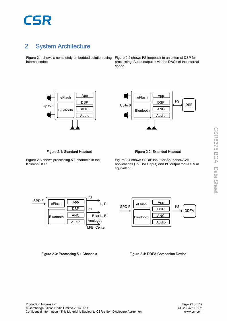
2 System ArchitectureFigure 2.1 shows a completely embedded solution usinginternal codec.
Figure 2.2 shows I²S loopback to an external DSP forprocessing. Audio output is via the DACs of the internalcodec.
Bluetooth
DSP
AppeFlash
Audio
Up to 6ANC
Figure 2.1: Standard Headset
Bluetooth
DSP
AppeFlash
Audio
Up to 6ANC
I2SDSP
Figure 2.2: Extended Headset
Figure 2.3 shows processing 5.1 channels in theKalimba DSP.
Figure 2.4 shows SPDIF input for Soundbar/AVRapplications (TV/DVD input) and I²S output for DDFA orequivalent.
SPDIF
I2S
I2S
Analogue
L, R
Rear L, R
LFE, Center
Bluetooth
DSP
AppeFlash
Audio
ANC
Figure 2.3: Processing 5.1 Channels
SPDIF I2SDDFA
Bluetooth
DSP
AppeFlash
Audio
ANC
Figure 2.4: DDFA Companion Device
Production Information© Cambridge Silicon Radio Limited 2013-2014Confidential Information - This Material is Subject to CSR's Non-Disclosure Agreement
Page 25 of 112CS-232426-DSP5
www.csr.com
CSR
8675 BGA D
ata Sheet

3 Bluetooth Modem3.1 RF Ports3.1.1 BT_RFCSR8675 BGA contains an on-chip balun which combines the balanced outputs of the PA on transmit and producesthe balanced input signals for the LNA required on receive. No matching components are needed as the receive modeimpedance is 50Ω and the transmitter has been optimised to deliver power into a 50Ω load.
G-T
W-0
0055
23.2
.2
+
_PA
+
_LNA
BT_RFOn-chip Balun
VDD
VSS_BT_RF
Figure 3.1: Simplified Circuit BT_RF
3.2 RF ReceiverThe receiver features a near-zero IF architecture that enables the channel filters to be integrated onto the die. Sufficientout-of-band blocking specification at the LNA input enables the receiver to operate in close proximity to GSM andW‑CDMA cellular phone transmitters without being desensitised. A digital FSK discriminator means that nodiscriminator tank is needed and its excellent performance in the presence of noise enables CSR8675 BGA to exceedthe Bluetooth requirements for co‑channel and adjacent channel rejection.
For EDR, the demodulator contains an ADC which digitises the IF received signal. This information is then passed tothe EDR modem.
3.2.1 Low Noise AmplifierThe LNA operates in differential mode and takes its input from the balanced port of the on-chip balun.
3.2.2 RSSI Analogue to Digital ConverterThe ADC implements fast AGC. The ADC samples the RSSI voltage on a slot-by-slot basis. The front-end LNA gainis changed according to the measured RSSI value, keeping the first mixer input signal within a limited range. Thisimproves the dynamic range of the receiver, improving performance in interference-limited environments.
3.3 RF Transmitter3.3.1 IQ ModulatorThe transmitter features a direct IQ modulator to minimise frequency drift during a transmit timeslot, which results in acontrolled modulation index. Digital baseband transmit circuitry provides the required spectral shaping.
Production Information© Cambridge Silicon Radio Limited 2013-2014Confidential Information - This Material is Subject to CSR's Non-Disclosure Agreement
Page 26 of 112CS-232426-DSP5
www.csr.com
CSR
8675 BGA D
ata Sheet

3.3.2 Power AmplifierThe internal PA output power is software controlled and configured through a PS Key. The internal PA on theCSR8675 BGA has a maximum output power that enables it to operate as a Class 1, Class 2 and Class 3 Bluetoothradio without requiring an external RF PA.
3.4 Bluetooth Radio SynthesiserThe Bluetooth radio synthesiser is fully integrated onto the die with no requirement for an external VCO screening can,varactor tuning diodes, LC resonators or loop filter. The synthesiser is guaranteed to lock in sufficient time across theguaranteed temperature range to meet the Bluetooth v4.1 specification.
3.5 Baseband3.5.1 Burst Mode ControllerDuring transmission the BMC constructs a packet from header information previously loaded into memory-mappedregisters by the software and payload data/voice taken from the appropriate ring buffer in the RAM. During reception,the BMC stores the packet header in memory-mapped registers and the payload data in the appropriate ring buffer inRAM. This architecture minimises the intervention required by the processor during transmission and reception.
3.5.2 Physical Layer Hardware EngineDedicated logic performs the following:
Forward error correction Header error control Cyclic redundancy check Encryption Data whitening Access code correlation Audio transcoding
Firmware performs the following voice data translations and operations: A-law/µ-law/linear voice data (from optional host) A-law/µ-law/CVSD (over the air) Voice interpolation for lost packets Rate mismatch correction
The hardware can be used as part of a fully compliant Bluetooth v4.1 specification system.
Production Information© Cambridge Silicon Radio Limited 2013-2014Confidential Information - This Material is Subject to CSR's Non-Disclosure Agreement
Page 27 of 112CS-232426-DSP5
www.csr.com
CSR
8675 BGA D
ata Sheet

4 Clock GenerationCSR8675 BGA requires a Bluetooth reference clock frequency of 19.2 MHz to 40 MHz (default 26 MHz) from either anexternally connected crystal or from an external TCXO source.
All CSR8675 BGA internal digital clocks are generated using a phase locked loop, which is locked to the frequency ofeither the external 19.2 MHz to 40 MHz (default 26 MHz) reference clock source or safely free-runs at a reducedfrequency.
The Bluetooth operation determines the use of the watchdog clock in low-power modes.
4.1 Clock Architecture
G-T
W-0
0001
89.3
.3
Bluetooth Radio
Auxiliary PLL
Digital Circuitry
Reference Clock
Figure 4.1: Clock Architecture
4.2 Input Frequencies and PS Key SettingsConfigure the CSR8675 BGA to operate with the chosen reference frequency. Set PSKEY_ANA_FREQ for allfrequencies with an integer multiple of 250kHz. The input frequency default setting in CSR8675 BGA is 26 MHzdepending on the software build. Full details are in the software release note for the specific build fromwww.csrsupport.com.
The following CDMA/3G phone TCXO frequencies are supported: 19.2, 19.44, 19.68, 19.8 and 38.4 MHz. The valueof the PS Key is a multiple of 1kHz, so 38.4MHz is selected by using a PS Key value of 38400.
Reference Crystal Frequency (MHz) PSKEY_ANA_FREQ (kHz)
19.20 19200
19.44 19440
19.68 19680
19.80 19800
38.40 38400
n x 0.25 n x 250
26.00 (default) 26000
Table 4.1: PS Key Values for CDMA/3G Phone TCXO
4.3 External Reference Clock4.3.1 Input: XTAL_INApply the external reference clock to the CSR8675 BGA XTAL_IN input. CSR8675 BGA is configured to accept theexternal reference clock at XTAL_IN by connecting XTAL_OUT to ground.
Production Information© Cambridge Silicon Radio Limited 2013-2014Confidential Information - This Material is Subject to CSR's Non-Disclosure Agreement
Page 28 of 112CS-232426-DSP5
www.csr.com
CSR
8675 BGA D
ata Sheet

Supply the external clock with either a digital level square wave or low-level sinusoidal, coupling this directly to theXTAL_IN without the need for additional components. The DC clock level is permitted at any voltage level between thesupply rails, i.e. VSS_BT_LO_AUX to VDD_AUX.
The external reference clock is required in active and deep sleep modes, so must be present when CSR8675 BGA isenabled.
Table 4.2 lists the specification for the external reference clock signal.
Min Typ Max Unit
Frequency(a) 19.2 26 40 MHz
Duty cycle 40:60 50:50 60:40 -
Edge jitter (at zero crossing) - - 10 ps rms
DC level -0.4 - VDD_AUX + 0.4 V
Signal level
AC coupled sinusoid 0.2 0.4 VDD_AUX(b) V pk-pk
DC coupleddigital
VIL - VSS_BT_LO_AUX - V
VIH - VDD_AUX(b) - V
Table 4.2: External Clock Specifications(a) The frequency should be an integer multiple of 250kHz except for the CDMA/3G frequencies(b) VDD_AUX is 1.35V nominal
4.3.2 XTAL_IN Impedance in External ModeThe impedance of XTAL_IN does not change significantly between operating modes. When transitioning from deepsleep to active states the capacitive load can change, see PSKEY_XTAL_OSC_CONFIG. For this reason CSRrecommends using a buffered clock input.
4.3.3 Clock Timing AccuracyFigure 4.2 shows the 250ppm timing accuracy on the external clock is required 2ms after the firmware begins to run.This guarantees that the firmware maintains timing accuracy in accordance with the Bluetooth v4.1 specification. Radioactivity occurs after 6ms after the firmware starts. Therefore, at this point the timing accuracy of the external clocksource must be within ±20ppm.
G-T
W-0
0001
90.3
.2
Clock Accuracy
0
20ppm
6
250ppm
2
1000ppm
ms After Firmware
CLK_REQ
Firmware Activity PSKEY_CLOCK_STARTUP_DELAYFirmware Activity
Radio Activity
Figure 4.2: TCXO Clock Accuracy
Production Information© Cambridge Silicon Radio Limited 2013-2014Confidential Information - This Material is Subject to CSR's Non-Disclosure Agreement
Page 29 of 112CS-232426-DSP5
www.csr.com
CSR
8675 BGA D
ata Sheet

4.4 Crystal Oscillator: XTAL_IN and XTAL_OUTCSR8675 BGA contains a crystal driver circuit that acts as a transconductance amplifier driving an external crystalbetween XTAL_IN and XTAL_OUT. The crystal driver circuit forms a Pierce oscillator with the external crystal. Noexternal crystal load capacitors are required for typical crystals.
4.4.1 Crystal CalibrationThe actual crystal frequency depends on the capacitance of XTAL_IN and XTAL_OUT on the PCB and theCSR8675 BGA, as well as the capacitance of the crystal. Correct calibration of the Bluetooth radio is done on a per-device basis on the production line, with the trim value stored in non-volatile memory (PS Key).
Crystal calibration uses a single measurement. The measurement finds the actual offset from the desired frequencyand the offset is stored in PSKEY_ANA_FTRIM_OFFSET. The firmware then compensates for the frequency offset onthe CSR8675 BGA. Typically, a TXSTART radio test is performed to obtain the actual frequency and it is comparedagainst the output frequency with the requested frequency using an RF analyser. The test station calculates the offsetratio and programs it into PSKEY_ANA_FTRIM_OFFSET. The value in PSKEY_ANA_FTRIM_OFFSET is a 16-bit 2'scomplement signed integer which specifies the fractional part of the ratio between the true crystal frequency, factual,and the value set in PSKEY_ANA_FREQ, fnominal. Equation 4.1 shows the value of PSKEY_ANA_FTRIM_OFFSET inparts per 220 rounded to the nearest integer.
For more information on TXSTART radio test see BlueTest User Guide.
PSKEY_ANA_FTRIM_OFFSET = (factual
fnominal− 1) × 220
Equation 4.1: Crystal Calibration Using PSKEY_ANA_FTRIM_OFFSET
For a requested frequency of 2402MHz with an actual output of 2402.0168MHz the PSKEY_ANA_FTRIM_OFFSETvalue is 7, see Equation 4.2.
PSKEY_ANA_FTRIM_OFFSET = ( 2402.01682402 − 1) × 220 ≈ 7
Equation 4.2: Example of PSKEY_ANA_FTRIM_OFFSET Value for 2402.0168MHz
For a requested frequency of 2402MHz with an actual output of 2401.9832MHz the PSKEY_ANA_FTRIM_OFFSETvalue is -7 (0xfff9), see Equation 4.3.
PSKEY_ANA_FTRIM_OFFSET = ( 2401.98322402 − 1) × 220 ≈ −7
Equation 4.3: Example of PSKEY_ANA_FTRIM_OFFSET Value for 2401.9832MHz
4.4.2 Crystal SpecificationSection 16.3.7 shows the specification for an external crystal.
Production Information© Cambridge Silicon Radio Limited 2013-2014Confidential Information - This Material is Subject to CSR's Non-Disclosure Agreement
Page 30 of 112CS-232426-DSP5
www.csr.com
CSR
8675 BGA D
ata Sheet

5 Bluetooth Stack MicrocontrollerThe CSR8675 BGA uses a 16-bit RISC 80MHz MCU for low power consumption and efficient use of memory. It containsa single-cycle multiplier and a memory protection unit for the VM accelerator, see Section 5.1.
The MCU, interrupt controller and event timer run the Bluetooth software stack and control the Bluetooth radio and hostinterfaces.
5.1 VM AcceleratorCSR8675 BGA contains a VM accelerator alongside the MCU. This hardware accelerator improves the performanceof VM applications.
Production Information© Cambridge Silicon Radio Limited 2013-2014Confidential Information - This Material is Subject to CSR's Non-Disclosure Agreement
Page 31 of 112CS-232426-DSP5
www.csr.com
CSR
8675 BGA D
ata Sheet

6 Kalimba DSPThe Kalimba DSP is an open platform DSP enabling signal processing functions to be performed on over‑air data orcodec data to enhance audio applications. Figure 6.1 shows the Kalimba DSP interfaces to other functional blockswithin CSR8675 BGA.
G-T
W-0
0055
22.4
.2
MemoryManagement
Unit
MCU Register Interface (including Debug)
DSP MMU Port
PIO In/Out
IRQ to Subsystem
IRQ from Subsystem
1µs Timer Clock
Programmable Clock
Data MemoryInteface
AddressGenerators
Instruction Decode
Program Flow
Clock Select
Internal Control Register
MMU Interface
Interrupt Controller
Timer
MCU Window
NV Memory
DEBUG
ALU
PIO
DS
P P
rogr
am C
ontro
l
Reg
iste
rs
DSP RAMs
DM2
DM1
PM
Kalimba DSP Core
DSP, MCU and Memory Window Control
DSP Data Memory 2 Interface (DM2)
DSP Data Memory 1 Interface (DM1)
DSP Program Memory Interface (PM)
NV Memory
Figure 6.1: Kalimba DSP Interface to Internal Functions
The key features of the DSP include: 120 MHz clock, giving up to 120 MIPS performance 24‑bit fixed-point DSP core Single-cycle MAC:
24 x 24‑bit multiply 56‑bit accumulate includes 2 rMAC registers
New instructions for improved performance over previous CSR8670 BGA architecture 32‑bit instruction word Separate program memory and dual data memory, enabling an ALU operation and up to 2 memory accesses
in a single cycle Zero overhead looping Zero overhead circular buffer indexing Single cycle barrel shifter with up to 56-bit input and 56-bit output Multiple cycle divide (performed in the background) Bit reversed addressing Orthogonal instruction set Low overhead interrupt
.
Production Information© Cambridge Silicon Radio Limited 2013-2014Confidential Information - This Material is Subject to CSR's Non-Disclosure Agreement
Page 32 of 112CS-232426-DSP5
www.csr.com
CSR
8675 BGA D
ata Sheet

7 Memory Interface and Management7.1 Memory Management UnitThe MMU provides dynamically allocated ring buffers that hold the data that is in transit between the host, the air orthe Kalimba DSP. The dynamic allocation of memory ensures efficient use of the available RAM and is performed bya hardware MMU to minimise the overheads on the processor during data/voice transfers. The use of DMA ports alsohelps with efficient transfer of data to other peripherals.
7.2 System RAM56 KB of integrated RAM supports the RISC MCU and is shared between the ring buffers for holding voice/data foreach active connection and the general-purpose memory required by the Bluetooth stack.
7.3 Kalimba DSP RAMAdditional integrated RAM provides support for the Kalimba DSP:
32 K x 24‑bit for data memory 1 (DM1) 32 K x 24‑bit for data memory 2 (DM2) 12 K x 32‑bit for program memory (PM)
Note:
The Kalimba DSP can also execute directly from internal flash or external SQIF, using a 1K-instruction on-chipcache.
7.4 eFlash Memory (16 Mb)The internal flash memory provides 16 Mb of internal code and data storage. The internal flash stores CSR8675 BGAsettings and program code, and Kalimba DSP coprocessor code and data. For improved performance, the internalflash memory has 45 ns access time and is organised as 64-bit wide.
7.5 Serial Quad I/O Flash Interface (SQIF)CSR8675 BGA supports external serial flash and SRAM ICs. This enables additional data storage areas fordevice‑specific data. CSR8675 BGA supports serial single, dual or quad I/O devices with a 1-bit, 2-bit or 4-bitmultiplexed I/O flash-memory interface. Figure 7.1 shows a typical connection between the CSR8675 BGA and a serialflash and SRAM IC.
G-T
W-0
0055
14.5
.2
MemoryManagement
Unit
Serial QuadI/O Flash
SPI SRAM
MCU Program
MCU Data
Kalimba DSP Data
Kalimba DSP Program
MCU
Kalimba DSP
QSPI_FLASH_CLK
QSPI_SRAM_CS#
QSPI_SRAM_CLK
QSPI_FLASH_CS#
QSPI_IO[0]
QSPI_IO[1]
QSPI_IO[2]
QSPI_IO[3]
SQIF
CLK
CS#
DI/IO0
DO/IO1
WP#/IO2
RESET#/HOLD#/IO3
CLK
CS#
HOLD#
SI
SO
Figure 7.1: Serial Quad I/O Flash Interface
The SQIF interface on the CSR8675 BGA supports: Flash and SRAM serial memory, which are also visible in the MCU and Kalimba DSP program address space
Production Information© Cambridge Silicon Radio Limited 2013-2014Confidential Information - This Material is Subject to CSR's Non-Disclosure Agreement
Page 33 of 112CS-232426-DSP5
www.csr.com
CSR
8675 BGA D
ata Sheet
Note:
SRAM serial memory support depends on firmware version, for more information contact CSR. MCU and Kalimba DSP data access through a generic window Concurrent program and / or data accesses from the MCU and / or Kalimba DSP (although efficiency suffers) Separate prefetch buffers for MCU program, MCU data, Kalimba DSP program, Kalimba DSP data:
Each buffer is 4 x 16-bit Defined minimum length prefetch Prefetch continues if accesses are contiguous (and buffer not full) Prefetch does not automatically restart as buffer empties Prefetch is enabled and disabled by software control, which enables optimisation of sequential / random
data access patterns Flash and SRAM use same prefetch buffer
Serial flash devices up to 64Mb with 1-bit, 2-bit and 4-bit wide transfers, see firmware release note for up-to-date device support
Selected serial SRAM devices up to 512Kb with 1-bit wide transfers, see firmware release note for up-to-datedevice support
Flash / SRAM performance: Clocks up to 80/16MHz The control and address overhead is 14/24 cycles per burst read, with support for Word Read Quad
Continuous (Winbond) and High Speed Read Quad (Microchip (SST)). Microchip (SST) indexedinstructions are not supported.
Data transfer is 4/16 cycles per 16-bits Flash instruction sequences:
Requires considerable (run-time) programmable configuration Set up for either read, or write (not both) Software configures SQIF for specific flash attached
SRAM instruction sequences: Interface is hard wired Reads and writes can interleave without need for any reconfiguration
All other management of serial flash / SRAM via software: Memory mapped registers support transfers of data to and from the flash Software needs to read the serial flash JEDEC ID in order to index a table of flash characteristics Software driven sequence to enable, e.g. the Winbond Continuous Read Mode
Note:
CSR8675 BGA cannot boot up from serial flash.
Production Information© Cambridge Silicon Radio Limited 2013-2014Confidential Information - This Material is Subject to CSR's Non-Disclosure Agreement
Page 34 of 112CS-232426-DSP5
www.csr.com
CSR
8675 BGA D
ata Sheet

8 Serial Interfaces8.1 USB InterfaceCSR8675 BGA has a full-speed (12 Mbps) USB interface for communicating with other compatible digital devices. TheUSB interface on CSR8675 BGA acts as a USB peripheral, responding to requests from a master host controller.
CSR8675 BGA supports the Universal Serial Bus Specification, Revision v2.0 (USB v2.0 Specification) and USB BatteryCharging Specification, available from http://www.usb.org. For more information on how to integrate the USB interfaceon CSR8675 BGA see the Bluetooth and USB Design Considerations Application Note.
As well as describing USB basics and architecture, the application note describes: Power distribution for high and low bus-powered configurations Power distribution for self-powered configuration, which includes USB VBUS monitoring (when VBUS is >3.1) USB enumeration Electrical design guidelines for the power supply and data lines, as well as PCB tracks and the effects of ferrite
beads USB suspend modes and Bluetooth low-power modes:
Global suspend Selective suspend, includes remote wake Wake on Bluetooth, includes permitted devices and set-up prior to selective suspend Suspend mode current draw PIO status in suspend mode Resume, detach and wake PIOs
Battery charging from USB, which describes dead battery provision, charge currents, charging in suspendmodes and USB VBUS voltage consideration
USB termination when interface is not in use Internal modules, certification and non-specification compliant operation
8.2 UART InterfaceThis is a standard UART interface for communicating with other serial devices.
CSR8675 BGA UART interface provides a simple mechanism for communicating with other serial devices using theRS-232 protocol.
G-T
W-0
0001
98.3
.2
UART_TX
UART_RX
UART_RTS
UART_CTS
Figure 8.1: Universal Asynchronous Receiver Transmitter (UART)
Figure 8.1 shows the 4 signals that implement the UART function. When CSR8675 BGA is connected to another digitaldevice, UART_RX and UART_TX transfer data between the 2 devices. The remaining 2 signals, UART_CTS andUART_RTS, implement RS232 hardware flow control where both are active low indicators.
If UART_CTS and UART_RTS are not required for hardware flow control, they are reconfigurable as PIO.
UART configuration parameters, such as baud rate and packet format, are set using CSR8675 BGA firmware.
Production Information© Cambridge Silicon Radio Limited 2013-2014Confidential Information - This Material is Subject to CSR's Non-Disclosure Agreement
Page 35 of 112CS-232426-DSP5
www.csr.com
CSR
8675 BGA D
ata Sheet

Note:
To communicate with the UART at its maximum data rate using a standard PC, an accelerated serial port adaptercard is required for the PC.
Table 8.1 shows the possible UART settings.
Parameter Possible Values
Baud rateMinimum
1200 baud (≤2%Error)
9600 baud (≤1%Error)
Maximum 4 Mbaud (≤1%Error)
Flow control RTS/CTS or None
Parity None, Odd or Even
Number of stop bits 1 or 2
Bits per byte 8
Table 8.1: Possible UART Settings
The UART interface resets CSR8675 BGA on reception of a break signal. A break is identified by a continuous logiclow (0V) on the UART_RX terminal, as Figure 8.2 shows. If tBRK is longer than the value defined by thePSKEY_HOSTIO_UART_RESET_TIMEOUT, a reset occurs. This feature enables a host to initialise the system to aknown state. Also, CSR8675 BGA can issue a break character for waking the host.
G-T
W-0
0002
50.5
.2
UART_TX tBRK
Figure 8.2: Break Signal
Refer to PSKEY_UART_BITRATE for more information about the baud rates and their values.
Generated baud rate is independent of selected incoming clock frequency.
8.2.1 UART Configuration While Reset is ActiveThe UART interface is tristate while CSR8675 BGA is being held in reset. This enables the user to connect other devicesonto the physical UART bus. The restriction with this method is that any devices connected to this bus must tristatewhen CSR8675 BGA reset is de-asserted and the firmware begins to run.
8.3 Programming and Debug InterfaceImportant Note:
The SPI is for programming, configuring (PS Keys) and debugging the CSR8675 BGA. It is required in production.Ensure the 4 SPI signals are brought out to either test points or a header.
CSR provides development and production tools to communicate over the SPI from a PC, although a level translatorcircuit is often required. All are available from CSR.
CSR8675 BGA uses a 16-bit data and 16-bit address programming and debug interface. Transactions occur when theinternal processor is running or is stopped.
Data is written or read one word at a time, or the auto-increment feature is available for block access.
Production Information© Cambridge Silicon Radio Limited 2013-2014Confidential Information - This Material is Subject to CSR's Non-Disclosure Agreement
Page 36 of 112CS-232426-DSP5
www.csr.com
CSR
8675 BGA D
ata Sheet

8.3.1 Instruction CycleThe CSR8675 BGA is the slave and receives commands on SPI_MOSI and outputs data on SPI_MISO. Table 8.2shows the instruction cycle for a SPI transaction.
1 Reset the SPI interface Hold SPI_CS# high for two SPI_CLK cycles
2 Write the command word Take SPI_CS# low and clock in the 8-bit command
3 Write the address Clock in the 16-bit address word
4 Write or read data words Clock in or out 16-bit data word(s)
5 Termination Take SPI_CS# high
Table 8.2: Instruction Cycle for a SPI Transaction
With the exception of reset, SPI_CS# must be held low during the transaction. Data on SPI_MOSI is clocked into theCSR8675 BGA on the rising edge of the clock line SPI_CLK. When reading, CSR8675 BGA replies to the master onSPI_MISO with the data changing on the falling edge of the SPI_CLK. The master provides the clock on SPI_CLK.Taking SPI_CS# high terminates the transaction.
Sending a command word and the address of a register for every time it is to be read or written is a significant overhead,especially when transferring large amounts of data. To overcome this CSR8675 BGA offers increased data transferefficiency via an auto increment operation. To invoke auto increment, SPI_CS# is kept low, which auto increments theaddress, while providing an extra 16 clock cycles for each extra word to be written or read.
8.3.2 Multi-slave OperationAvoid connecting CSR8675 BGA in a multi-slave arrangement by simple parallel connection of slave MISO lines. WhenCSR8675 BGA is deselected (SPI_CS# = 1), the SPI_MISO line does not float. Instead, CSR8675 BGA outputs 0 ifthe processor is running or 1 if it is stopped.
8.3.3 SPI-lockCSR8675 BGA contains an SPI-lock security feature to prevent unauthorised access to CSR8675 BGA and its firmware.
Warranty:
While exercising all reasonable care and diligence in the design of the SPI-lock feature, CSR does not warrantits functionality. CSR disclaims any liability arising out of the SPI-lock feature to the maximum extent permittedby law.
8.4 I²C InterfaceCSR8675 BGA contains a configurable hardware I²C interface. For more information contact CSR.
Note:
CSR8675 BGA supports a software I²C interface for low speed functions, including driving a dot matrix LCD,keyboard scanner or EEPROM.
Production Information© Cambridge Silicon Radio Limited 2013-2014Confidential Information - This Material is Subject to CSR's Non-Disclosure Agreement
Page 37 of 112CS-232426-DSP5
www.csr.com
CSR
8675 BGA D
ata Sheet

9 Interfaces9.1 Programmable I/O Ports, PIOCSR8675 BGA provides 32 lines of programmable bidirectional I/O, PIO[31:0]. Some of the PIOs on the CSR8675 BGAhave alternative functions, see Table 9.1.
PIOFunction
PCM I²S SPI Flash UART LED
PIO[31] - - - - LED[1]
PIO[30] - - - - LED[0]
PIO[29] - - - - LED[2]
PIO[28] - - QSPI_FLASH_IO[3] - -
PIO[27] - - QSPI_FLASH_IO[2] - -
PIO[26] - - QSPI_FLASH_IO[1] - -
PIO[25] - - QSPI_FLASH_IO[0] - -
PIO[24] - - QSPI_SRAM_CS# - -
PIO[23] - - QSPI_FLASH_CS# - -
PIO[22] - - QSPI_SRAM_CLK - -
PIO[21] - - QSPI_FLASH_CLK - -
PIO[20] PCM1_CLK SCK1 - - -
PIO[19] PCM1_SYNC WS1 - - -
PIO[18] PCM1_OUT SD1_OUT - - -
PIO[17] PCM1_IN SD1_IN - - -
PIO[16] - - - UART_RTS -
PIO[15:8] - - - - -
PIO[7] PCM2_CLK SCK2 - - -
PIO[6] PCM2_SYNC WS2 - - -
PIO[5] PCM2_OUT SD2_OUT - - -
PIO[4] PCM2_IN SD2_IN - - -
PIO[3:0] - - - - -
Table 9.1: Alternative PIO Functions
Production Information© Cambridge Silicon Radio Limited 2013-2014Confidential Information - This Material is Subject to CSR's Non-Disclosure Agreement
Page 38 of 112CS-232426-DSP5
www.csr.com
CSR
8675 BGA D
ata Sheet

Note:
The SPDIF interface is available on any unused PIO. The data output (SPDIF_OUT) is restricted to even numberedPIO, and the data input (SPDIF_IN) is restricted to odd numbered PIO.
See the relevant software release note for the implementation of these PIO lines, as they are firmware build-specific.
9.2 Analogue I/O Ports, AIOCSR8675 BGA has 2 general-purpose analogue interface pins, AIO[1:0], for accessing internal circuitry and controlsignals. Auxiliary functions available on the analogue interface include a 10-bit ADC and a 10-bit DAC. Signalsselectable on this interface include the band gap reference voltage. When configured for analogue signals the voltagerange is constrained by the analogue supply voltage. When configured to drive out digital level signals generated fromwithin the analogue part of the device, the output voltage level is determined by VDD_AUX.
9.3 Capacitive Touch SensorCSR8675 BGA capacitive touch sensor interface features:
Support for up to 6 capacitive touch sensing electrodes: Printed on the PCB Made from flex PCB
Configuration for individual buttons Configuration for a wipe-type arrangement where 2 or more pads sense taps at each end or a wipe from one
side to the other Operates in deep sleep and is a programmable source for wake-up
Figure 9.1 shows the system block diagram for the capacitive touch sensor interface. The interface depends on thecapacitive touch sensor type. Therefore the overall control of the capacitive touch sensor interface resides in the VM,so it is easily modified in each end-user application.
G-T
W-0
0055
33.3
.2
Mux
CAP_SENSE[0]CAP_SENSE[1]CAP_SENSE[2]CAP_SENSE[3]CAP_SENSE[4]CAP_SENSE[5]
Capacitive Range Control
SamplingFront-end
Firmware
Digital Processing
VM
ADC
Figure 9.1: Capacitive Touch Sensor Block Diagram
The overall system-level specification for the capacitive touch sensor interface on the CSR8675 BGA is: 6 inputs multiplexed in to 1 touch sensor on the front-end Capacitances of 0 pF to 50 pF measured with a resolution of 4fF, where a touch is assumed to be between
±50 fF and ±1 pF Each reading takes 172 µs:
6 pads read every 1.03 ms System auto-calibrates to remove parasitic and environmental effects including:
PCB construction Temperature Humidity
Works in normal and deep sleep modes System current is approximately 50 µA from the battery The touch sensor also functions like a PIO
Production Information© Cambridge Silicon Radio Limited 2013-2014Confidential Information - This Material is Subject to CSR's Non-Disclosure Agreement
Page 39 of 112CS-232426-DSP5
www.csr.com
CSR
8675 BGA D
ata Sheet

Figure 9.1 shows the system block diagram, it highlights the top-level architecture for the capacitive touch sensorinterface and consists of:
Capacitive range control, see Section 9.3.1 Sampling front end, see Section 9.3.2 ADC, see Section 9.3.3 Digital signal conditioning (digital processing), see Section 9.3.4 Software signal conditioning (firmware), see Section 9.3.5 VM, see Section 9.3.6
For more information on CSR8675 BGA capacitive touch sensor configuration see Configuring the Touch Sensor onCSR867x.
9.3.1 Capacitive Range Control:Figure 9.1 shows the capacitive range control function:
Sets the rough capacitance of the touch sensor pad, which is product dependent Splits into 4 integrated capacitors The VM selects which capacitors are enabled, i.e. the range capacitance
9.3.2 Sampling Front EndFigure 9.1 shows the sampling front end function:
An internal capacitance is trimmed by the digital state machine ensuring: Touch Capacitance = Range Capacitance + Internal Capacitance
When the internal capacitance is correctly trimmed: The sense voltage is 0 V A touch changes the touch capacitance, which then changes the sense voltage
9.3.3 ADCFigure 9.1 shows the ADC:
Uses a successive approximation, charge redistribution ADC Clocked at 64 kHz 9-bit resolution, where LSB is ±2 fF and full range is ±1 pF The internal capacitance is a 7-bit variable capacitor with 114 fF steps and 14.5 pF range The internal capacitance is trimmed, putting it in the mid range of the ADC. This enables measurements from
0 pF to 50 pF, where a capacitive touch is between ±50 fF and ±1 pF.
9.3.4 Digital Signal Conditioning (Digital Processing)Figure 9.1 shows the digital processing block which is responsible for digital signal conditioning:
Only the enabled inputs are scanned Enabling fewer inputs increases readings per second Averaging of ADC readings reduces noise, this is software programmable from 1 to 64 readings in intervals
to the power of 2 The internal capacitance updates using a rolling average of the ADC readings, software programmable from
1 to 215 readings in intervals to the power of 2. For example, 32768 readings take approximately: 5.6 s if polling one pad (no averaging) 33.8 s if polling 6 pads (no averaging)
Pulse skipping mode is possible, reducing the current consumption. Here the system waits a programmablenumber of 64 kHz clock cycles (maximum 29) before the next read, i.e. an 8 ms maximum pause.
ADC trigger level is software programmable. If the threshold is crossed the firmware gets an interrupt. 6 hardware event registers store the pad number and trigger time, which enables the system to sense swipes. Programmable hysteresis, with one value for all pads
Production Information© Cambridge Silicon Radio Limited 2013-2014Confidential Information - This Material is Subject to CSR's Non-Disclosure Agreement
Page 40 of 112CS-232426-DSP5
www.csr.com
CSR
8675 BGA D
ata Sheet

9.3.5 Software Signal Conditioning (Firmware)Figure 9.1 shows the firmware block which is responsible for software signal conditioning:
The firmware reads ADC and Cint values after an interrupt as the hardware only stores the pad number andtrigger time
Digital state machine scans pads and calibrates the internal capacitance If a swipe happens in deep sleep the firmware reads the trigger order and event time when it wakes up. It then
reads the last ADC reading for each input, not the reading that triggered the interrupt.
9.3.6 VMFigure 9.1 shows the VM block for the capacitive touch sensor interface:
Configures the hardware and gets an interrupt when a programmable threshold is crossed Selects the range capacitance Decides whether an event is a valid touch
9.4 LED DriversCSR8675 BGA includes a 3-pad synchronised PWM LED driver for driving RGB LEDs for producing a wide range ofcolours. All LEDs are controlled by firmware.
The terminals are open-drain outputs, so the LED must be connected from a positive supply rail to the pad in serieswith a current-limiting resistor.
G-T
W-0
0055
34.2
.2
LED Forward Voltage, VF
Pad Voltage, VPAD; RON = 20Ω
RLED
LED[2, 1 or 0]Resistor Voltage Drop, VR
LED Supply
I LED
Figure 9.2: LED Equivalent Circuit
From Figure 9.2 it is possible to derive Equation 9.1 to calculate ILED. If a known value of current is required throughthe LED to give a specific luminous intensity, then the value of RLED is calculated.
ILED =VDD − VF
RLED + RON
Equation 9.1: LED Current
For the LED pads to act as resistance, the external series resistor, RLED, needs to be such that the voltage drop acrossit, VR, keeps VPAD below 0.5V. Equation 9.2 also applies.
VDD = VF + VR + VPAD
Equation 9.2: LED PAD Voltage
Production Information© Cambridge Silicon Radio Limited 2013-2014Confidential Information - This Material is Subject to CSR's Non-Disclosure Agreement
Page 41 of 112CS-232426-DSP5
www.csr.com
CSR
8675 BGA D
ata Sheet
Note:
The supply for domain in Section 1.2 for LED[2:0] must remain powered for LED functions to operate.
The LED current adds to the overall current. Conservative LED selection extends battery life.
Production Information© Cambridge Silicon Radio Limited 2013-2014Confidential Information - This Material is Subject to CSR's Non-Disclosure Agreement
Page 42 of 112CS-232426-DSP5
www.csr.com
CSR
8675 BGA D
ata Sheet

10 Audio InterfaceThe audio interface circuit consists of:
Stereo/dual-mono audio codec Dual analogue audio inputs Dual analogue audio outputs 6 digital MEMS microphone inputs 2 configurable PCM/I²S interfaces SPDIF interface
For more information on CSR8675 BGA audio path configuration see the CSR8675 Audio Development Kit (DK-CSR8675-10197-1A).
Figure 10.1 shows the functional blocks of the interface. The codec supports stereo/dual-mono playback and recordingof audio signals at multiple sample rates with a 24-bit resolution. The ADC and the DAC of the codec each contain 2independent high-quality channels. Any ADC or DAC channel runs at its own independent sample rate.
G-T
W-0
0135
07.1
.1
Stereo / Dual-mono Codec
Memory Management
Unit
MMU Audio Port
Register Interface
Audio Port
Registers
PCM 2
I2S 2
StereoAudioCodecDriver
PCM/I2S 2 Interface
SPDIF SPDIF Interface
2 x DifferentialDAC Outputs
2 x DifferentialADC Inputs
PCM 1
I2S 1
PCM/I2S 1 Interface
DigitalMICs
6 x DigitalMICs
Figure 10.1: Audio Interface
CSR8675 BGA supports various digital audio bus interfaces: 2 configurable PCM/I²S interfaces:
PCM1 interface shares the same pins as I²S1 interface but the audio buses are mutually exclusive in theirusage. Table 10.1 shows shared pins for the PCM/I²S 1 interface.
PCM2 interface shares the same pins as I²S2 interface but the audio buses are mutually exclusive in theirusage. Table 10.1 shows shared pins for the PCM/I²S 2 interface.
SPDIF interface which is available on any unused PIO. The data output (SPDIF_OUT) is restricted to evennumbered PIO, and the data input (SPDIF_IN) is restricted to odd numbered PIO, see the relevant softwarerelease note for the implementation of these PIO lines, as they are firmware build-specific.
Production Information© Cambridge Silicon Radio Limited 2013-2014Confidential Information - This Material is Subject to CSR's Non-Disclosure Agreement
Page 43 of 112CS-232426-DSP5
www.csr.com
CSR
8675 BGA D
ata Sheet

PIO PCM Interface I²S Interface
PIO[20] PCM1_CLK SCK1
PIO[19] PCM1_SYNC WS1
PIO[18] PCM1_OUT SD1_OUT
PIO[17] PCM1_IN SD1_IN
PIO[7] PCM2_CLK SCK2
PIO[6] PCM2_SYNC WS2
PIO[5] PCM2_OUT SD2_OUT
PIO[4] PCM2_IN SD2_IN
Table 10.1: Shared Pins on PCM/I²S Interfaces
10.1 Audio Input and OutputThe audio input circuitry consists of:
2 independent 24-bit high-quality ADC channels: Programmable as either microphone or line input Programmable as either stereo or dual-mono inputs Multiplexed with 2 of the digital microphone inputs, see Section 10.2.16 Each channel is independently configurable to be either single-ended or fully differential Each channel has an analogue and digital programmable gain stage for optimisation of different
microphones 6 digital MEMS microphone channels, of which 4 have independent codec channels and 2 share their codecs
with the 2 high-quality audio inputs
The audio output circuitry consists of a dual differential class A-B output stage.
Note:
CSR8675 BGA is designed for a differential audio output. If a single-ended audio output is required, use an externaldifferential to single-ended converter.
10.2 Audio Codec InterfaceThe main features of the interface are:
Stereo and mono analogue input for voice band and audio band Stereo and mono analogue output for voice band and audio band Support for up to 2 PCM interfaces including PCM master codecs that require an external system clock Support for up to 2 stereo I²S digital audio bus standard Support for IEC-60958 standard stereo digital audio bus standards, e.g. SPDIF and AES3 (also known as
AES/EBU)
Important Note:
To avoid any confusion regarding stereo operation this data sheet explicitly states which is the left and right channelfor audio output. With respect to audio input, software and any registers, channel 0 or channel A represents theleft channel and channel 1 or channel B represents the right channel.
Production Information© Cambridge Silicon Radio Limited 2013-2014Confidential Information - This Material is Subject to CSR's Non-Disclosure Agreement
Page 44 of 112CS-232426-DSP5
www.csr.com
CSR
8675 BGA D
ata Sheet

10.2.1 Audio Codec Block Diagram
G-T
W-0
0053
84.6
.2
Digital Mic
Digital Mic
Digital Mic
Digital Mic
Digital Mic
Digital Mic
Digital Codec
Digital Codec
Digital Codec
Digital Codec
16
16
16
16
Input F
Input E
Input D
Input C
Input B
Input A
High-quality ADC
High-quality ADC
Data
Mux
Mux
16
16
Data
Data
Data
Data
MIC_RPMIC_RN
MIC_LPMIC_LN
Clock
Clock
Clock
Clock
DataClock
PIO[EVEN]PIO[ODD]
PIO[ODD]
PIO[ODD]
Digital Codec
Digital Codec
Clock
Note:L/R pins on digital microphones pulled up or down on the PCB
Stereo Audio and Voice Band Output
High-quality DAC
Low-pass Filter
SPKR_LNSPKR_LP
16
High-quality DACSPKR_RNSPKR_RP
16
Digital Circuitry
Stereo Audio, Voice Band and Digital Microphone Input
PIO[EVEN]
PIO[EVEN]
Low-pass Filter
Digital MIC Interface
Digital MIC Interface
Digital MIC Interface
Figure 10.2: Audio Codec Input and Output Stages
The CSR8675 BGA audio codec uses a fully differential architecture in the analogue signal path, which results in lownoise sensitivity and good power supply rejection while effectively doubling the signal amplitude. It operates from adual power supply, VDD_AUDIO for the audio circuits and VDD_AUDIO_DRV for the audio driver circuits.
10.2.2 Codec Set-upThe configuration and control of the ADC is through software functions described in appropriate development kitdocumentation. This section is an overview of the parameters set up using the software functions.
The Kalimba DSP communicates its codec requirements to the MCU, and therefore also to the VM, by exchangingmessages. Messages between the Kalimba DSP and the embedded MCU are based on interrupts:
1 interrupt between the MCU and Kalimba DSP 1 interrupt between the Kalimba DSP and the MCU
Message content is transmitted using shared memory. There are VM and DSP library functions to send and receivemessages; see appropriate development kit documentation for further details.
10.2.3 ADCFigure 10.2 shows the CSR8675 BGA consists of 2 high-quality ADCs:
Each ADC has a second-order Sigma-Delta converter. Each ADC is a separate channel with identical functionality. There are 2 gain stages for each channel, 1 of which is an analogue gain stage and the other is a digital gain
stage, see Section 10.2.5.
Production Information© Cambridge Silicon Radio Limited 2013-2014Confidential Information - This Material is Subject to CSR's Non-Disclosure Agreement
Page 45 of 112CS-232426-DSP5
www.csr.com
CSR
8675 BGA D
ata Sheet

10.2.4 ADC Sample Rate SelectionEach ADC supports the following pre-defined sample rates, although other rates are programmable, e.g. 40 kHz:
8 kHz 11.025 kHz 16 kHz 22.050 kHz 24 kHz 32 kHz 44.1 kHz 48 kHz 96 kHz
10.2.5 ADC Audio Input GainFigure 10.3 shows that the CSR8675 BGA audio input gain consists of:
An analogue gain stage based on a pre-amplifier and an analogue gain amplifier, see Section 10.2.6 A digital gain stage, see Section 10.2.7
G-T
W-0
0055
35.4
.3
ADC Pre-amplifierand ADC Analogue Gain:-3dB to 42dB in 3dB steps
ADC Pre-amplifier:0dB, 9dB, 21dB and 30dB
ADC Analogue Gain:-3dB to 12dB in 3dB steps
ADC Digital Gain:-24dB to 21.5dB in alternating2.5dB and 3dB steps
Audio Input To Digital Codec
System Gain = ADC Pre-amplifier + ADC Analogue Gain + ADC Digital Gain
Figure 10.3: Audio Input Gain
10.2.6 ADC Pre-amplifier and ADC Analogue Gain
CSR8675 BGA has an analogue gain stage based on an ADC pre-amplifier and ADC analogue amplifier: The ADC pre-amplifier has 4 gain settings: 0dB, 9dB, 21dB and 30dB The ADC analogue amplifier gain is -3dB to 12dB in 3dB steps The overall analogue gain for the pre-amplifier and analogue amplifier is -3dB to 42dB in 3dB steps, see Figure
10.3 At mid to high gain levels it acts as a microphone pre-amplifier, see Section 10.2.15 At low gain levels it acts as an audio line level amplifier
10.2.7 ADC Digital GainA digital gain stage inside the ADC varies from -24dB to 21.5dB, see Table 10.2. There is also a fine gain interface witha 9-bit gain setting allowing gain changes in 1/32 steps, for more infomation contact CSR.
The firmware controls the audio input gain.
Production Information© Cambridge Silicon Radio Limited 2013-2014Confidential Information - This Material is Subject to CSR's Non-Disclosure Agreement
Page 46 of 112CS-232426-DSP5
www.csr.com
CSR
8675 BGA D
ata Sheet

Digital Gain SelectionValue
ADC Digital Gain Setting(dB)
Digital Gain SelectionValue
ADC Digital Gain Setting(dB)
0 0 8 -24
1 3.5 9 -20.5
2 6 10 -18
3 9.5 11 -14.5
4 12 12 -12
5 15.5 13 -8.5
6 18 14 -6
7 21.5 15 -2.5
Table 10.2: ADC Audio Input Gain Rate
10.2.8 ADC Digital IIR FilterThe ADC contains 2 integrated anti-aliasing filters:
A default IIR filter suitable for music (>44.1kHz) G.722 filter is a digital IIR filter that improves the stop-band attenuation required for G.722 compliance (which
is the best selection for 8kHz / 16kHz / voice)
For more information contact CSR.
10.2.9 DACThe DAC consists of:
2 fourth-order Sigma-Delta converters enabling 2 separate channels that are identical in functionality, as Figure10.2 shows.
2 gain stages for each channel, 1 of which is an analogue gain stage and the other is a digital gain stage.
10.2.10 DAC Sample Rate SelectionEach DAC supports the following sample rates:
8 kHz 11.025 kHz 16 kHz 22.050 kHz 32 kHz 40 kHz 44.1 kHz 48 kHz 96 kHz 192 kHz
10.2.11 DAC Digital GainA digital gain stage inside the DAC varies from -24dB to 21.5dB, see Table 10.3. There is also a fine gain interface witha 9-bit gain setting enabling gain changes in 1/32 steps, for more information contact CSR.
The overall gain control of the DAC is controlled by the firmware. Its setting is a combined function of the digital andanalogue amplifier settings.
Production Information© Cambridge Silicon Radio Limited 2013-2014Confidential Information - This Material is Subject to CSR's Non-Disclosure Agreement
Page 47 of 112CS-232426-DSP5
www.csr.com
CSR
8675 BGA D
ata Sheet

Digital Gain SelectionValue
DAC Digital Gain Setting(dB)
Digital Gain SelectionValue
DAC Digital Gain Setting(dB)
0 0 8 -24
1 3.5 9 -20.5
2 6 10 -18
3 9.5 11 -14.5
4 12 12 -12
5 15.5 13 -8.5
6 18 14 -6
7 21.5 15 -2.5
Table 10.3: DAC Digital Gain Rate Selection
10.2.12 DAC Analogue GainTable 10.4 shows that the DAC analogue gain stage consists of 8 gain selection values that represent seven 3dB steps.
The firmware controls the overall gain control of the DAC. Its setting is a combined function of the digital and analogueamplifier settings.
Analogue Gain SelectionValue
DAC Analogue GainSetting (dB)
Analogue Gain SelectionValue
DAC Analogue GainSetting (dB)
7 0 3 -12
6 -3 2 -15
5 -6 1 -18
4 -9 0 -21
Table 10.4: DAC Analogue Gain Rate Selection
10.2.13 DAC Digital FIR FilterThe DAC contains an integrated digital FIR filter with the following modes:
A default long FIR filter for best performance at ≥ 44.1kHz. A short FIR to reduce latency. A narrow FIR (a very sharp roll-off at Nyquist) for G.722 compliance. Best for 8kHz / 16kHz.
10.2.14 IEC 60958 InterfaceThe IEC 60958 interface is a digital audio interface that uses bi-phase coding to minimise the DC content of thetransmitted signal and enables the receiver to decode the clock information from the transmitted signal. The IEC 60958specification is based on the 2 industry standards:
AES3 (also known as AES/EBU) Sony and Philips interface specification SPDIF
The interface is compatible with IEC 60958-1, IEC 60958-3 and IEC 60958-4.
Production Information© Cambridge Silicon Radio Limited 2013-2014Confidential Information - This Material is Subject to CSR's Non-Disclosure Agreement
Page 48 of 112CS-232426-DSP5
www.csr.com
CSR
8675 BGA D
ata Sheet

The SPDIF interface signals, SPDIF_IN and SPDIF_OUT, interface to: A 75Ω coaxial cable with an RCA connector, see Figure 10.4 An optical link that uses Toslink optical components, see Figure 10.5.
G-T
W-0
0002
11.3
.3
SPDIF_OUT (PCM_OUT)8 9
U4D
10 11
U4E
12 13
U4F
1
3
4
2
CONN2 6 5
U4C
SPDIF COAXIAL PC
ESD PROTECTION
C26
150n R15120R
C20
10nR9150R
R8150R
R101K
R111K
R16
560R
R17
560R
R18
560R
R19100K
3V3
4
31
25
U3
R1210K
3V3 C22
100n
C211u
R13
10K
R14470K
3
7 16 4
5 2
8D5
TN33
TN34
3V3
SPDIF_IN (PCM_IN)
Figure 10.4: Example Circuit for SPDIF Interface (Co-axial)
G-T
W-0
0002
12.3
.3
SPDIF_OUT (PCM_OUT)
SPDIF TOSLINK RECEIVER
SPDIF TOSLINK TRANSMITTER
3V3
3V3
C24
100n
C25
100n
L347u
OUT 1
GN
D2
VC
C3
NC
4N
C5
NC
6
NC
7
U6
INPUT 3G
ND
1V
CC
2N
C4
NC
5
NC
6N
C7
U5
SPDIF_IN (PCM_IN)
Figure 10.5: Example Circuit for SPDIF Interface (Optical)
10.2.15 Microphone InputCSR8675 BGA contains 2 independent low-noise microphone bias generators. The microphone bias generators arerecommended for biasing electret condensor microphones. Figure 10.6 shows a biasing circuit for microphones with asensitivity between about ‑40 to ‑60dB (0dB = 1V/Pa).
Where: The microphone bias generators derive their power from VBAT (via SMP_VBAT) or VOUT_3V3 (via
SMPS_3V3) and require no capacitor on their output. The microphone bias generators maintain regulation within the limits 70μA to 2.8mA, supporting a 2mA source
typically required by 2 electret condensor microphones. If the microphone sits below these limits, then themicrophone output must be pre-loaded with a large value resistor to ground.
Biasing resistors R1 and R2 equal 2.2kΩ. When the input pre-amplifier is enabled, the input impedance at MIC_LN, MIC_LP, MIC_RN and MIC_RP
varies between 6kΩ (pre-amplifier gain >0dB) and 12kΩ (pre-amplifier gain = 0dB). C1, C2, C3 and C4 are 100/150nF if bass roll-off is required to limit wind noise on the microphone. R1 and R2 set the microphone load impedance and are normally around 2.2kΩ.
Production Information© Cambridge Silicon Radio Limited 2013-2014Confidential Information - This Material is Subject to CSR's Non-Disclosure Agreement
Page 49 of 112CS-232426-DSP5
www.csr.com
CSR
8675 BGA D
ata Sheet

G-T
W-0
0055
36.3
.2
C2R1
C1
Microphone Bias(MIC_BIAS_A or MIC_BIAS_B)
MIC_LP
MIC_LN
MIC1+
Input Amplifier
C4R2
C3
Microphone Bias(MIC_BIAS_A or MIC_BIAS_B)
MIC_RP
MIC_RN
MIC2+
Input Amplifier
Figure 10.6: Microphone Biasing
The microphone bias characteristics include: Power supply:
CSR8675 BGA microphone supply is VBAT (via SMP_VBAT) or VOUT_3V3 (via SMPS_3V3) Minimum input voltage = Output voltage + drop-out voltage Maximum input voltage is 4.3V
Drop-out voltage: 300mV maximum
Output voltage: 1.8V or 2.6V Tolerance 90% to 110%
Output current: 70μA to 2.8mA
No load capacitor required
10.2.16 Digital Microphone InputsThe CSR8675 BGA interfaces to 6 digital MEMS microphones. Figure 10.2 shows that 4 of the inputs have dedicatedcodec channels and 2 are multiplexed with the high-quality ADC channels.
Figure 10.2 shows that the digital microphone interface on the CSR8675 BGA has: Clock lines shared between 2 microphone outputs, linked to any even-numbered PIO pin as determined by
the firmware.
Note:
Multiple digital microphones can share the same clock if they are configured for the same frequency,e.g. 1 clock for 6 digital microphones.
Data lines shared beween 2 microphone inputs, linked to any odd-numbered PIO as determined by thefirmware.
Note:
For the digital microphone interface to work in this configuration ensure the microphone uses a tristatebetween edges.
The left and right selection for the digital microphones are appropriately pulled up or down for selection on thePCB.
Production Information© Cambridge Silicon Radio Limited 2013-2014Confidential Information - This Material is Subject to CSR's Non-Disclosure Agreement
Page 50 of 112CS-232426-DSP5
www.csr.com
CSR
8675 BGA D
ata Sheet

10.2.17 Line InputFigure 10.7 and Figure 10.8 show 2 circuits for line input operation and show connections for either differential or single-ended inputs.
In line input mode, the input impedance of the pins to ground varies from 6kΩ to 34kΩ depending on input gain setting.
G-T
W-0
0055
11.2
.2
C3
C4
MIC_RN
MIC_RP
C1
C2
MIC_LN
MIC_LP
Figure 10.7: Differential Input
G-T
W-0
0055
12.2
.2
C3
C4
MIC_RP
MIC_RN
C1
C2
MIC_LP
MIC_LN
Figure 10.8: Single-ended Input
10.2.18 Output StageThe output stage digital circuitry converts the signal from linear PCM of variable sampling frequency to bit stream, whichis fed into the analogue output circuitry.
The analogue output circuit comprises a DAC, a buffer with gain-setting, a low-pass filter and a class AB output stageamplifier. Figure 10.9 shows that the output is available as a differential signal between SPKR_LN and SPKR_LP forthe left channel, and between SPKR_RN and SPKR_RP for the right channel.
Production Information© Cambridge Silicon Radio Limited 2013-2014Confidential Information - This Material is Subject to CSR's Non-Disclosure Agreement
Page 51 of 112CS-232426-DSP5
www.csr.com
CSR
8675 BGA D
ata Sheet

G-T
W-0
0055
37.1
.1
SPKR_LP
SPKR_LN
SPKR_RP
SPKR_RN
Figure 10.9: Speaker Output
10.2.19 Mono OperationMono operation is a single-channel operation of the stereo codec. The left channel represents the single mono channelfor audio in and audio out. In mono operation, the right channel is the auxiliary mono channel for dual-mono channeloperation.
In single channel mono operation, disable the other channel to reduce power consumption.
Production Information© Cambridge Silicon Radio Limited 2013-2014Confidential Information - This Material is Subject to CSR's Non-Disclosure Agreement
Page 52 of 112CS-232426-DSP5
www.csr.com
CSR
8675 BGA D
ata Sheet

10.2.20 Side ToneIn some applications it is necessary to implement side tone. This side tone function involves feeding a properly gainedmicrophone signal in to the DAC stream, e.g. earpiece. The side tone routing selects the version of the microphonesignal from before or after the digital gain in the ADC interface and adds it to the output signal before or after the digitalgain of the DAC interface, see Figure 10.10.
G-T
W-0
0137
83.1
.1
Routing Option 1
MUX
MU
X
Digital Gain
Filter
ADC Data
Sidetone Data
DAC Data
Analogue Input
Digital Output
ADC_INTERFACE
Mixer
Digital Gain
DAC_INTERFACE
MUX
DigitalGain
Routing Option 2
MU
XM
UX
Digital Gain
ADC Data
Sidetone Data
DAC Data
Analogue Input
Digital Output
ADC_INTERFACE
Mixer
Digital Gain
DAC_INTERFACE
MUX
DigitalGain
Filter
Figure 10.10: Side Tone
The ADC provides simple gain to the side tone data. The gain values range from -32.6dB to 12.0dB in alternating stepsof 2.5dB and 3.5dB, see Table 10.5.
Value Side Tone Gain Value Side Tone Gain
0 -32.6dB 8 -8.5dB
1 -30.1dB 9 -6.0dB
2 -26.6dB 10 -2.5dB
3 -24.1dB 11 0dB
4 -20.6dB 12 3.5dB
5 -18.1dB 13 6.0dB
6 -14.5dB 14 9.5dB
7 -12.0dB 15 12.0dB
Table 10.5: Side Tone Gain
Production Information© Cambridge Silicon Radio Limited 2013-2014Confidential Information - This Material is Subject to CSR's Non-Disclosure Agreement
Page 53 of 112CS-232426-DSP5
www.csr.com
CSR
8675 BGA D
ata Sheet

Note:
The values of side tone are shown for information only. During standard operation, the application software controlsthe side tone gain.
The following PS Keys configure the side tone hardware: PSKEY_SIDE_TONE_ENABLE PSKEY_SIDE_TONE_GAIN PSKEY_SIDE_TONE_AFTER_ADC PSKEY_SIDE_TONE_AFTER_DAC
10.2.21 Integrated Digital IIR FilterCSR8675 BGA has a programmable digital filter integrated into the ADC channel of the codec. The filter is a 2-stage,second order IIR and is for functions such as custom wind noise reduction. The filter also has optional DC blocking.
The filter has 11 configuration words: 2 for gain values 8 for coefficient values 1 for enabling and disabling the DC blocking
The gain and coefficients are all 12-bit 2's complement signed integer with the format NN.NNNNNNNNNN.
Note:
The position of the binary point is between bit[10] and bit[9], where bit[11] is the most significant bit.
For example:
01.1111111111
01.0000000000
00.0000000000
11.0000000000
10.0000000000
=
=
=
=
=
most positive number, close to 21
0
-1
-2, most negative number
Equation 10.1 shows the equation for the IIR filter. Equation 10.2 shows the equation for when the DC blocking isenabled.
The filter is configured, enabled and disabled from the VM via the CodecSetIIRFilter trap. This requires firmwaresupport. The configuration function takes 11 variables in the following order:
0 : Gain0 and Exp0
1 : b01
2 : b02
3 : a01
4 : a02
Production Information© Cambridge Silicon Radio Limited 2013-2014Confidential Information - This Material is Subject to CSR's Non-Disclosure Agreement
Page 54 of 112CS-232426-DSP5
www.csr.com
CSR
8675 BGA D
ata Sheet

5 : Gain1
6 : b11
7 : b12
8 : a11
9 : a12
a : DC Block (1 = enable, 0 = disable)
Filter, H(z) = (1 − z−1 ) x 2Exp0 x Gain0 x ( 1 + b01 z−1 + b02 z−2
1 + a01 z−1 + a02 z−2 ) x Gain1 x ( 1 + b11 z−1 + b12 z−2
1 + a11 z−1 + a12 z−2 )/2Exp0
Equation 10.1: IIR Filter Transfer Function, H(z)
Filter with DC Blocking, HDC (z) = H(z) × ( 1 − z−1 )
Equation 10.2: IIR Filter Plus DC Blocking Transfer Function, HDC(z)
10.3 PCM1 and PCM2 InterfaceImportant Note:
The term PCM in Section 10.3 and its subsections, Section 10.3.1 to Section 10.3.10, refers to PCM1 and PCM2interfaces.
The PCM interface shares the same pins as I²S interface but the audio buses are mutually exclusive in their usage.Section 10.3 shows shared pins for the PCM/I²S interface.
The audio PCM interface on the CSR8675 BGA supports: On-chip routing to Kalimba DSP Continuous transmission and reception of PCM encoded audio data over Bluetooth. Processor overhead reduction through hardware support for continual transmission and reception of PCM
data A bidirectional digital audio interface that routes directly into the baseband layer of the firmware. It does not
pass through the HCI protocol layer. Hardware on the CSR8675 BGA for sending data to and from a SCO connection. Up to 3 SCO connections on the PCM interface at any one time. PCM interface master, generating PCM_SYNC and PCM_CLK. PCM interface slave, accepting externally generated PCM_SYNC and PCM_CLK. Various clock formats including:
Long Frame Sync Short Frame Sync GCI timing environments
24-bit / 16-bit / 13-bit linear, 8-bit µ-law or A-law companded sample formats. Receives and transmits on any selection of 3 of the first 4 slots following PCM_SYNC.
The PCM configuration options are enabled by setting the PS Key PSKEY_PCM_CONFIG32.
10.3.1 PCM Interface Master/SlaveWhen configured as the master of the PCM interface, CSR8675 BGA generates PCM_CLK and PCM_SYNC.
Production Information© Cambridge Silicon Radio Limited 2013-2014Confidential Information - This Material is Subject to CSR's Non-Disclosure Agreement
Page 55 of 112CS-232426-DSP5
www.csr.com
CSR
8675 BGA D
ata Sheet
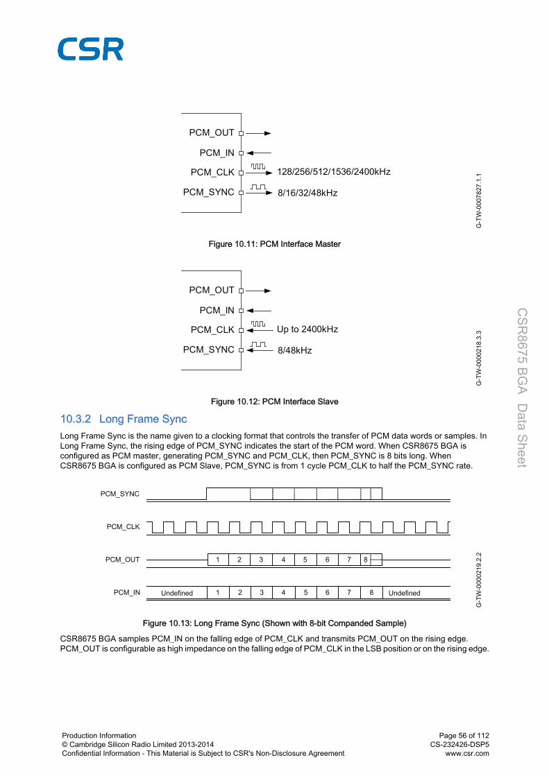
G-T
W-0
0078
27.1
.1128/256/512/1536/2400kHz
8/16/32/48kHz
PCM_OUT
PCM_IN
PCM_CLK
PCM_SYNC
Figure 10.11: PCM Interface Master
G-T
W-0
0002
18.3
.3Up to 2400kHz
8/48kHz
PCM_OUT
PCM_IN
PCM_CLK
PCM_SYNC
Figure 10.12: PCM Interface Slave
10.3.2 Long Frame SyncLong Frame Sync is the name given to a clocking format that controls the transfer of PCM data words or samples. InLong Frame Sync, the rising edge of PCM_SYNC indicates the start of the PCM word. When CSR8675 BGA isconfigured as PCM master, generating PCM_SYNC and PCM_CLK, then PCM_SYNC is 8 bits long. WhenCSR8675 BGA is configured as PCM Slave, PCM_SYNC is from 1 cycle PCM_CLK to half the PCM_SYNC rate.
G-T
W-0
0002
19.2
.2
PCM_SYNC
PCM_CLK
PCM_OUT
PCM_IN
1 2 3 4 5 6 7 8
1 2 3 4 5 6 7 8Undefined Undefined
Figure 10.13: Long Frame Sync (Shown with 8-bit Companded Sample)
CSR8675 BGA samples PCM_IN on the falling edge of PCM_CLK and transmits PCM_OUT on the rising edge.PCM_OUT is configurable as high impedance on the falling edge of PCM_CLK in the LSB position or on the rising edge.
Production Information© Cambridge Silicon Radio Limited 2013-2014Confidential Information - This Material is Subject to CSR's Non-Disclosure Agreement
Page 56 of 112CS-232426-DSP5
www.csr.com
CSR
8675 BGA D
ata Sheet

10.3.3 Short Frame SyncIn Short Frame Sync, the falling edge of PCM_SYNC indicates the start of the PCM word. PCM_SYNC is always 1clock cycle long.
G-T
W-0
0002
20.2
.3
PCM_SYNC
PCM_CLK
PCM_OUT
PCM_IN
1 2 3 4 5 6 7 8 9 10 11 12 13 14 15 16
1 2 3 4 5 6 7 8 9 10 11 12 13 14 15 16 UndefinedUndefined
Figure 10.14: Short Frame Sync (Shown with 16-bit Sample)
As with Long Frame Sync, CSR8675 BGA samples PCM_IN on the falling edge of PCM_CLK and transmits PCM_OUTon the rising edge. PCM_OUT is configurable as high impedance on the falling edge of PCM_CLK in the LSB positionor on the rising edge.
10.3.4 Multi-slot OperationMore than 1 SCO connection over the PCM interface is supported using multiple slots. Up to 3 SCO connections arecarried over any of the first 4 slots.
G-T
W-0
0002
21.3
.2
LONG_PCM_SYNC
Or
SHORT_PCM_SYNC
PCM_CLK
PCM_OUT
PCM_IN
1 2 3 4 5 6 7 8 1 2 3 4 5 6 7 8
1 2 3 4 5 6 7 8 1 2 3 4 5 6 7 8 Do Not CareDo Not Care
Figure 10.15: Multi-slot Operation with 2 Slots and 8-bit Companded Samples
10.3.5 GCI InterfaceCSR8675 BGA is compatible with the GCI, a standard synchronous 2B+D ISDN timing interface. The 2 64kbps Bchannels are accessed when this mode is configured.
Production Information© Cambridge Silicon Radio Limited 2013-2014Confidential Information - This Material is Subject to CSR's Non-Disclosure Agreement
Page 57 of 112CS-232426-DSP5
www.csr.com
CSR
8675 BGA D
ata Sheet

G-T
W-0
0002
22.2
.3
PCM_SYNC
PCM_CLK
PCM_OUT
PCM_IN
1 2 3 4 5 6 7 8 1 2 3 4 5 6 7 8
1 2 3 4 5 6 7 8 1 2 3 4 5 6 7 8Do NotCare
Do NotCare
B1 Channel B2 Channel
Figure 10.16: GCI Interface
The start of frame is indicated by the rising edge of PCM_SYNC and typically runs at 8kHz/16kHz.
10.3.6 Slots and Sample FormatsCSR8675 BGA receives and transmits on any selection of the first 4 slots following each sync pulse. Slot durations areeither 8 or 16 clock cycles:
8 clock cycles for 8-bit sample formats. 16 clocks cycles for 8-bit, 13-bit or 16-bit sample formats.
CSR8675 BGA supports: 13-bit linear, 16-bit linear and 8-bit µ-law or A-law sample formats. A sample rate of 8ksamples/s, 16ksamples/s or 32ksamples/s. Little or big endian bit order. For 16-bit slots, the 3 or 8 unused bits in each slot are filled with sign extension, padded with zeros or a
programmable 3-bit audio attenuation compatible with some codecs.
Production Information© Cambridge Silicon Radio Limited 2013-2014Confidential Information - This Material is Subject to CSR's Non-Disclosure Agreement
Page 58 of 112CS-232426-DSP5
www.csr.com
CSR
8675 BGA D
ata Sheet

G-T
W-0
0002
23.2
.3
PCM_OUT
PCM_OUT
PCM_OUT
PCM_OUT
1 2 3 4 5 6 7 8 9 10 11 12 13 14 15 16
1 2 3 4 5 6 7 8 9 10 11 12 13 14 15 16
1 2 3 4 5 6 7 8 9 10 11 12 13 14 15 16
1 2 3 4 5 6 7 8 9 10 11 12 13 14 15 16
Sign Extension
8-bit Sample
8-bit Sample
Zeros Padding
Sign Extension
13-bit Sample
13-bit Sample
Audio Gain
A 16-bit slot with 8-bit companded sample and sign extension selected.
A 16-bit slot with 8-bit companded sample and zeros padding selected.
A 16-bit slot with 13-bit linear sample and sign extension selected.
A 16-bit slot with 13-bit linear sample and audio gain selected.
Figure 10.17: 16-bit Slot Length and Sample Formats
10.3.7 Additional FeaturesCSR8675 BGA has a mute facility that forces PCM_OUT to be 0. In master mode, CSR8675 BGA is compatible withsome codecs which control power down by forcing PCM_SYNC to 0 while keeping PCM_CLK running.
10.3.8 PCM Timing Information
Symbol Parameter Min Typ Max Unit
fmclk PCM_CLK frequency
4MHz DDS generation.Selection of frequencyis programmable. SeeSection 10.3.10.
-
128
- kHz256
512
48MHz DDSgeneration. Selection offrequency isprogrammable. SeeSection 10.3.10.
2.9 - - kHz
- PCM_SYNC frequency for SCO connection - 8 - kHz
tmclkh (a) PCM_CLK high 4MHz DDS generation 980 - - ns
Production Information© Cambridge Silicon Radio Limited 2013-2014Confidential Information - This Material is Subject to CSR's Non-Disclosure Agreement
Page 59 of 112CS-232426-DSP5
www.csr.com
CSR
8675 BGA D
ata Sheet

Symbol Parameter Min Typ Max Unit
tmclkl (a) PCM_CLK low 4MHz DDS generation 730 - - ns
- PCM_CLK jitter 48MHz DDS generation - - 21 ns pk-pk
tdmclksynchDelay time from PCM_CLK high to PCM_SYNChigh - - 20 ns
tdmclkpoutDelay time from PCM_CLK high to validPCM_OUT - - 20 ns
tdmclklsynclDelay time from PCM_CLK low to PCM_SYNC low(Long Frame Sync only) - - 20 ns
tdmclkhsynclDelay time from PCM_CLK high to PCM_SYNClow - - 20 ns
tdmclklpoutzDelay time from PCM_CLK low to PCM_OUT highimpedance - - 20 ns
tdmclkhpoutzDelay time from PCM_CLK high to PCM_OUT highimpedance - - 20 ns
tsupinclkl Set-up time for PCM_IN valid to PCM_CLK low 20 - - ns
thpinclkl Hold time for PCM_CLK low to PCM_IN invalid 0 - - ns
Table 10.6: PCM Master Timing(a) Assumes normal system clock operation. Figures vary during low-power modes, when system clock speeds are reduced.
G-T
W-0
0002
24.2
.3PCM_SYNC
PCM_CLK
PCM_OUT
PCM_IN
MSB (LSB) LSB (MSB)
MSB (LSB) LSB (MSB)
fmlk
tmclkh
tmclkl
tsupinclkl
tdmclksynch
tdmclkpout
thpinclkl
tdmclklsyncl
tdmclkhsyncl
tdmclklpoutz
tdmclkhpoutz
tr,t
f
Figure 10.18: PCM Master Timing Long Frame Sync
Production Information© Cambridge Silicon Radio Limited 2013-2014Confidential Information - This Material is Subject to CSR's Non-Disclosure Agreement
Page 60 of 112CS-232426-DSP5
www.csr.com
CSR
8675 BGA D
ata Sheet

G-T
W-0
0002
25.3
.3
PCM_SYNC
PCM_CLK
PCM_OUT
PCM_IN
MSB (LSB) LSB (MSB)
MSB (LSB) LSB (MSB)
fmlk
tmclkh
tmclkl
tsupinclkl
t
tdmclkpout
thpinclkl
dmclkhsyncl
tdmclklpoutz
tdmclkhpoutz
tr,t
f
tdmclksynch
Figure 10.19: PCM Master Timing Short Frame Sync
Production Information© Cambridge Silicon Radio Limited 2013-2014Confidential Information - This Material is Subject to CSR's Non-Disclosure Agreement
Page 61 of 112CS-232426-DSP5
www.csr.com
CSR
8675 BGA D
ata Sheet

Symbol Parameter Min Typ Max Unit
fsclk PCM clock frequency (Slave mode: input) 64 - (a) kHz
fsclk PCM clock frequency (GCI mode) 128 - (b) kHz
tsclkl PCM_CLK low time 200 - - ns
tsclkh PCM_CLK high time 200 - - ns
thsclksynch Hold time from PCM_CLK low to PCM_SYNC high 2 - - ns
tsusclksynch Set-up time for PCM_SYNC high to PCM_CLK low 20 - - ns
tdpoutDelay time from PCM_SYNC or PCM_CLK,whichever is later, to valid PCM_OUT data (LongFrame Sync only)
- - 20 ns
tdsclkhpout Delay time from CLK high to PCM_OUT valid data - - 15 ns
tdpoutzDelay time from PCM_SYNC or PCM_CLK low,whichever is later, to PCM_OUT data line highimpedance
- - 15 ns
tsupinsclkl Set-up time for PCM_IN valid to CLK low 20 - - ns
thpinsclkl Hold time for PCM_CLK low to PCM_IN invalid 2 - - ns
Table 10.7: PCM Slave Timing(a) Max frequency is the frequency defined by PSKEY_PCM_MIN_CPU_CLOCK(b) Max frequency is twice the frequency defined by PSKEY_PCM_MIN_CPU_CLOCK
G-T
W-0
0002
26.3
.2
PCM_CLK
PCM_SYNC
PCM_OUT
PCM_IN MSB (LSB) LSB (MSB)
fsclk
tsclkh
ttsclkl
thsclksynch
tsusclksynch
tdpout
tdsclkhpout
tdpoutz
tdpoutz
tsupinsclkl
thpinsclkl
tr,t
f
LSB (MSB)MSB (LSB)
Figure 10.20: PCM Slave Timing Long Frame Sync
Production Information© Cambridge Silicon Radio Limited 2013-2014Confidential Information - This Material is Subject to CSR's Non-Disclosure Agreement
Page 62 of 112CS-232426-DSP5
www.csr.com
CSR
8675 BGA D
ata Sheet

G-T
W-0
0002
27.3
.2
PCM_CLK
PCM_SYNC
PCM_OUT
PCM_IN MSB (LSB) LSB (MSB)
fsclk
tsclkh
ttsclkl
thsclksynch
tsusclksynch
tdpoutz
tdpoutz
tsupinsclkl
thpinsclkl
tr,t
f
LSB (MSB)MSB (LSB)
tdsclkhpout
Figure 10.21: PCM Slave Timing Short Frame Sync
10.3.9 PCM_CLK and PCM_SYNC GenerationCSR8675 BGA has 2 methods of generating PCM_CLK and PCM_SYNC in master mode:
Generating these signals by DDS from CSR8675 BGA internal 4MHz clock. Using this mode limits PCM_CLKto 128, 256 or 512kHz and PCM_SYNC to 8kHz.
Generating these signals by DDS from an internal 48MHz clock, which enables a greater range of frequenciesto be generated with low jitter but consumes more power. To select this second method set bit48M_PCM_CLK_GEN_EN in PSKEY_PCM_CONFIG32. When in this mode and with long frame sync, thelength of PCM_SYNC is either 8 or 16 cycles of PCM_CLK, determined by LONG_LENGTH_SYNC_EN inPSKEY_PCM_CONFIG32.
Equation 10.3 describes PCM_CLK frequency when generated from the internal 48MHz clock:
f = CNT_RATECNT_LIMIT × 24MHz
Equation 10.3: PCM_CLK Frequency Generated Using the Internal 48MHz Clock
Set the frequency of PCM_SYNC relative to PCM_CLK using Equation 10.4:
f = PCM_CLKSYNC_LIMIT × 8
Equation 10.4: PCM_SYNC Frequency Relative to PCM_CLK
CNT_RATE, CNT_LIMIT and SYNC_LIMIT are set using PSKEY_PCM_LOW_JITTER_CONFIG. As an example, togenerate PCM_CLK at 512kHz with PCM_SYNC at 8kHz, set PSKEY_PCM_LOW_JITTER_CONFIG to0x08080177.
10.3.10 PCM ConfigurationConfigure the PCM by using PSKEY_PCM_CONFIG32 and PSKEY_PCM_USE_LOW_JITTER_MODE, see BlueCoreAudio API Specification and the PS Key file. The default for PSKEY_PCM_CONFIG32 is 0x00800000, i.e. first slotfollowing sync is active, 13-bit linear voice format, long frame sync and interface master generating 256kHz PCM_CLKfrom 4MHz internal clock with no tristate of PCM_OUT.
Production Information© Cambridge Silicon Radio Limited 2013-2014Confidential Information - This Material is Subject to CSR's Non-Disclosure Agreement
Page 63 of 112CS-232426-DSP5
www.csr.com
CSR
8675 BGA D
ata Sheet

10.4 I²S1 and I²S2 InterfaceImportant Note:
The term I²S refers to I²S1 and I²S2 interfaces.
The I²S interface shares the same pins as PCM interface but the audio buses are mutually exclusive in their usage.Section 10.3 shows shared pins for the PCM/I²S interface.
The I²S interface supports left-justified or right-justified.
Figure 10.22 shows the timing diagram.
G-T
W-0
0002
30.3
.2
WS
SCK
SD_IN/OUT
WS
SCK
SD_IN/OUT
WS
SCK
SD_IN/OUT
LSB
MSB LSB MSB LSB
MSB LSB MSB LSB
Left -justified Mode
Right -justified Mode
Left Channel Right Channel
Right ChannelLeft Channel
Left Channel Right Channel
MSB LSB MSB
I2 S Mode
Figure 10.22: I²S Digital Audio Interface Modes
Configure the digital audio interface using PSKEY_DIGITAL_AUDIO_CONFIG, see Firmware Configuration Keys forCSR8675 and the PS Key file.
Production Information© Cambridge Silicon Radio Limited 2013-2014Confidential Information - This Material is Subject to CSR's Non-Disclosure Agreement
Page 64 of 112CS-232426-DSP5
www.csr.com
CSR
8675 BGA D
ata Sheet

Symbol Parameter Min Typ Max Unit
- SCK Frequency - - 6.2 MHz
- WS Frequency - - 96 kHz
tch SCK high time 80 - - ns
tcl SCK low time 80 - - ns
Table 10.8: Digital Audio Interface Slave Timing
Symbol Parameter Min Typ Max Unit
tssuWS valid to SCK high set-uptime 20 - - ns
tsh SCK high to WS invalid hold time 2.5 - - ns
topdSCK low to SD_OUT valid delaytime - - 20 ns
tisuSD_IN valid to SCK high set-uptime 20 - - ns
tihSCK high to SD_IN invalid holdtime 2.5 - - ns
Table 10.9: I²S Slave Mode Timing
G-T
W-0
0002
31.2
.2
SD_OUT
SD_IN
t
t
t
t
t
t
WS(Input)
SCK(Input)
ch
opd
ih
shssu
cl
isut
Figure 10.23: Digital Audio Interface Slave Timing
Production Information© Cambridge Silicon Radio Limited 2013-2014Confidential Information - This Material is Subject to CSR's Non-Disclosure Agreement
Page 65 of 112CS-232426-DSP5
www.csr.com
CSR
8675 BGA D
ata Sheet

Symbol Parameter Min Typ Max Unit
- SCK Frequency - - 6.2 MHz
- WS Frequency - - 96 kHz
Table 10.10: Digital Audio Interface Master Timing
Symbol Parameter Min Typ Max Unit
tspd SCK low to WS valid delay time - - 39.27 ns
topdSCK low to SD_OUT valid delaytime - - 18.44 ns
tisuSD_IN valid to SCK high set-uptime 18.44 - - ns
tihSCK high to SD_IN invalid holdtime 0 - - ns
Table 10.11: I²S Master Mode Timing Parameters, WS and SCK as Outputs
G-T
W-0
0002
32.2
.2
WS(Output)
SCK(Output)
SD_OUT
SD_IN
t isu t ih
topd
t spd
Figure 10.24: Digital Audio Interface Master Timing
Production Information© Cambridge Silicon Radio Limited 2013-2014Confidential Information - This Material is Subject to CSR's Non-Disclosure Agreement
Page 66 of 112CS-232426-DSP5
www.csr.com
CSR
8675 BGA D
ata Sheet

11 WLAN Coexistence InterfaceDedicated hardware is provided to implement a variety of WLAN coexistence schemes. There is support for:
Channel skipping AFH Priority signalling Channel signalling Host passing of channel instructions
Planned support for WLAN coexistence schemes includes: Unity-3 Unity-3e Unity+
For more information on WLAN coexistence schemes see BlueCore Bluetooth/IEEE 802.11 Coexistence ApplicationNote.
For more information on WLAN coexistence schemes supported on CSR8675 BGA see software release note or contactCSR.
Production Information© Cambridge Silicon Radio Limited 2013-2014Confidential Information - This Material is Subject to CSR's Non-Disclosure Agreement
Page 67 of 112CS-232426-DSP5
www.csr.com
CSR
8675 BGA D
ata Sheet

12 Power Control and RegulationFor greater power efficiency the CSR8675 BGA contains 2 switch-mode regulators:
1 generates a 1.80V supply rail with an output current of 185mA, see Section 12.1. 1 generates a 1.35V supply rail with an output current of 160mA, see Section 12.2. Combining the 2 switch-mode regulators in parallel generates a single 1.80V supply rail with an output current
of 340mA, see Section 12.3.CSR8675 BGA contains 4 LDO linear regulators:
3.30V bypass regulator, see Section 12.4. 0.85 V to 1.20 V VDD_DIG linear regulator, see Section 12.5. 1.35V VDD_AUX linear regulator, see Section 12.6. 1.35V VDD_ANA linear regulator, see Section 12.7.
The recommended configurations for power control and regulation on the CSR8675 BGA are: 3 switch-mode configurations:
A 1.80V and 1.35V dual-supply rail system using the 1.80V and 1.35V switch-mode regulators, see Figure12.1. This is the default power control and regulation configuration for the CSR8675 BGA.
A 1.80V single-supply rail system using the 1.80V switch-mode regulator. A 1.80V parallel-supply rail system for higher currents using the 1.80V and 1.35V switch-mode regulators
with combined outputs, see Figure 12.2. A linear configuration using an external 1.8V rail omitting all regulators
Table 12.1 shows settings for the recommended configurations for power control and regulation on the CSR8675 BGA.
SupplyConfiguration
RegulatorsSupply Rail
Switch-mode VDD_AUXLinear
Regulator
VDD_ANALinear
Regulator1.8V 1.35V 1.8V 1.35V
Dual-supplySMPS ON ON OFF OFF SMPS SMPS
Single-supplySMPS ON OFF ON ON SMPS LDO
Parallel-supply SMPS ON ON ON ON SMPS LDO
External 1.8Vlinear supply OFF OFF ON ON External LDO
Table 12.1: Recommended Configurations for Power Control and Regulation
For more information on CSR8675 BGA power supply configuration see Configuring the Power Supplies onCSR867x application note.
Production Information© Cambridge Silicon Radio Limited 2013-2014Confidential Information - This Material is Subject to CSR's Non-Disclosure Agreement
Page 68 of 112CS-232426-DSP5
www.csr.com
CSR
8675 BGA D
ata Sheet

G-T
W-0
0055
45.7
.2Mic Bias 1
Charge Reference
MIC_BIAS_A
Bypass Linear Regulator
300mA
Charger50 to 200mA
Reference
1.8V Switch-mode
Regulator 185mA
1.35V Switch-mode
Regulator 160mA
VCHG
VBAT
VBAT_SENSE
Mic Bias 2MIC_BIAS_B
LX_1V35
LX_1V8
VOUT_3V3
3.3V1.35V1.8V
Audio Driver
Audio Core
VDD_AUDIO_DRV
VDD_AUDIO
Audio Circuits
VDD_AUX Regulator
VDD_ANA Regulator
e-Flash
I/O
Analogue and Auxiliary
Bluetooth
SMPS_1V8_SENSE
SMPS_1V35_SENSE
SENSE
IN
OUT
OUT
VDD_AUX
SENSE
OUT
OUT
VDD_ANASENSE
VDD_BT_RADIO
IN
SENSE
Auxiliary Circuits
VDD_BT_LO
SMP_VBAT
IN
IN
SMPS_3V3
Digital Core Circuits
VDD_DIGRegulator
OUT
SENSE
IN
VDD_DIG_EFLASHVREGIN_DIG
VDD_EFLASH_1V8
VDD_USB
EN
EN
EN
EN
EN
EN
OUT
SENSE
VREGENABLE
VDD_PADS_1VDD_PADS_2VDD_PADS_3
VDD_AUX_1V8
Figure 12.1: 1.80V and 1.35V Dual-supply Switch-mode System Configuration
Production Information© Cambridge Silicon Radio Limited 2013-2014Confidential Information - This Material is Subject to CSR's Non-Disclosure Agreement
Page 69 of 112CS-232426-DSP5
www.csr.com
CSR
8675 BGA D
ata Sheet

G-T
W-0
0055
46.5
.2Mic Bias 1
Charge Reference
MIC_BIAS_A
Bypass Linear Regulator
300mA
Charger50 to 200mA
Reference
1.8V Switch-mode
Regulator 340mA
1.35V Switch-mode
Regulator
VCHG
VBAT
VBAT_SENSE
Mic Bias 2MIC_BIAS_B
LX_1V35
LX_1V8
VOUT_3V3
3.3V1.35V1.8V
Audio Driver
Audio Core
VDD_AUDIO_DRV
VDD_AUDIO
Audio Circuits
VDD_AUX Regulator
VDD_ANA Regulator
e-Flash
I/O
Analogue and Auxiliary
Bluetooth
SMPS_1V8_SENSE
SMPS_1V35_SENSE
SENSE
IN
OUT
OUT
VDD_AUX
SENSE
OUT
OUT
VDD_ANASENSE
VDD_BT_RADIO
IN
SENSE
Auxiliary Circuits
VDD_BT_LO
SMP_VBAT
IN
IN
SMPS_3V3
Digital Core Circuits
VDD_DIGRegulator
OUT
SENSE
IN
VDD_DIG_EFLASHVREGIN_DIG
VDD_EFLASH_1V8
VDD_USB
EN
EN
EN
EN
EN
EN
OUT
SENSE
VREGENABLE
VDD_PADS_1VDD_PADS_2VDD_PADS_3
VDD_AUX_1V8
Figure 12.2: 1.80V Parallel-supply Switch-mode System Configuration
Production Information© Cambridge Silicon Radio Limited 2013-2014Confidential Information - This Material is Subject to CSR's Non-Disclosure Agreement
Page 70 of 112CS-232426-DSP5
www.csr.com
CSR
8675 BGA D
ata Sheet

G-T
W-0
0083
49.1
.1Mic Bias 1
Charge Reference
MIC_BIAS_A
Bypass Linear Regulator
300mA
Charger50 to 200mA
Reference
1.8V Switch-mode
Regulator 340mA
1.35V Switch-mode
Regulator
VCHG
VBAT
VBAT_SENSE
Mic Bias 2MIC_BIAS_B
LX_1V35
LX_1V8
VOUT_3V3
3.3V1.35V1.8V
Audio Driver
Audio Core
VDD_AUDIO_DRV
VDD_AUDIO
Audio Circuits
VDD_AUX Regulator
VDD_ANA Regulator
e-Flash
I/O
Analogue and Auxiliary
Bluetooth
SMPS_1V8_SENSE
SMPS_1V35_SENSE
SENSE
IN
OUT
OUT
VDD_AUX
SENSE
OUT
OUT
VDD_ANASENSE
VDD_BT_RADIO
IN
SENSE
Auxiliary Circuits
VDD_BT_LO
SMP_VBAT
IN
IN
SMPS_3V3
Digital Core Circuits
VDD_DIGRegulator
OUT
SENSE
IN
VDD_DIG_EFLASHVREGIN_DIG
VDD_EFLASH_1V8
VDD_USB
EN
EN
EN
EN
EN
EN
OUT
SENSE
VREGENABLE
VDD_PADS_1VDD_PADS_2VDD_PADS_3
VDD_AUX_1V8
Figure 12.3: External 1.8V System Configuration
12.1 1.8V Switch-mode RegulatorCSR recommends using the integrated switch-mode regulator to power the 1.80V supply rail.
Production Information© Cambridge Silicon Radio Limited 2013-2014Confidential Information - This Material is Subject to CSR's Non-Disclosure Agreement
Page 71 of 112CS-232426-DSP5
www.csr.com
CSR
8675 BGA D
ata Sheet

Figure 12.4 shows that an external LC filter circuit of a low-resistance series inductor, L1 (4.7µH), followed by a lowESR shunt capacitor, C3 (2.2µF), is required between the LX_1V8 terminal and the 1.80V supply rail. Connect the1.80V supply rail and the SMPS_1V8_SENSE pin.
G-T
W-0
0055
42.3
.2
SMPS_1V8_SENSE
LX_1V81.8V Switch-mode
RegulatorSENSE
LX
L14.7µH
C32.2µF
1.8V Supply Rail
VSS_SMPS_1V8
SMP_VBATSMPS_3V3
To 1.35V Switch-mode Regulator Input
C12.2µF
C22.2µF
VBATVOUT_3V3
Figure 12.4: 1.8V Switch-mode Regulator Output Configuration
Minimise the series resistance of the tracks between the regulator input, SMP_VBAT and SMPS_3V3, ground terminals,the filter and decoupling components, and the external voltage source to maintain high-efficiency power conversionand low supply ripple.
Ensure a solid ground plane between C1, C2, C3 and VSS_SMPS_1V8.
Also minimise the collective parasitic capacitance on the track between LX_1V8 and the inductor L1, to maximiseefficiency.
For the regulator to meet the specifications in Section 16.3.1.1 requires a total resistance of <1.0Ω (<0.5Ωrecommended) for the following:
The track between the battery and SMP_VBAT. The track between LX_1V8 and the inductor. The inductor, L1, ESR. The track between the inductor, L1, and the sense point on the 1.80V supply rail.
The following enable the 1.80V switch-mode regulator: VREGENABLE pin The CSR8675 BGA firmware with reference to PSKEY_PSU_ENABLES VCHG pin
The switching frequency is adjustable by setting an offset from 4.00MHz using PSKEY_SMPS_FREQ_OFFSET, whichalso affects the 1.35V switch-mode regulator.
When the 1.80V switch-mode regulator is not required, leave unconnected: The regulator input SMP_VBAT and SMPS_3V3 The regulator output LX_1V8
12.2 1.35V Switch-mode RegulatorCSR recommends using the integrated switch-mode regulator to power the 1.35V supply rail.
Figure 12.5 shows that an external LC filter circuit of a low-resistance series inductor L1 (4.7µH), followed by a lowESR shunt capacitor, C3 (4.7µF), is required between the LX_1V35 terminal and the 1.35V supply rail. Connect the1.35V supply rail and the SMPS_1V35_SENSE pin.
Production Information© Cambridge Silicon Radio Limited 2013-2014Confidential Information - This Material is Subject to CSR's Non-Disclosure Agreement
Page 72 of 112CS-232426-DSP5
www.csr.com
CSR
8675 BGA D
ata Sheet

G-T
W-0
0055
43.4
.2
SMPS_1V35_SENSE
LX_1V351.35V Switch-
mode RegulatorSENSE
LX
L14.7µH
C34.7µF
1.35V Supply Rail
VSS_SMPS_1V35
SMP_VBATSMPS_3V3
To 1.8V Switch-mode Regulator Input
C12.2µF
C22.2µF
VBATVOUT_3V3
Figure 12.5: 1.35V Switch-mode Regulator Output Configuration
Minimise the series resistance of the tracks between the regulator input, SMP_VBAT and SMPS_3V3, ground terminals,the filter and decoupling components, and the external voltage source to maintain high-efficiency power conversionand low supply ripple.
Ensure a solid ground plane between C1, C2, C3 and VSS_SMPS_1V35.
Also minimise the collective parasitic capacitance on the track between LX_1V35 and the inductor L1, to maximiseefficiency.
For the regulator to meet the specifications in Section 16.3.2.1 requires a total resistance of <1.0Ω (<0.5Ωrecommended) for the following:
The track between the battery and SMP_VBAT. The track between LX_1V8 and the inductor. The inductor, L1, ESR. The track between the inductor, L1, and the sense point on the 1.35V supply rail.
The following enable the 1.35V switch-mode regulator: VREGENABLE pin The CSR8675 BGA firmware with reference to PSKEY_PSU_ENABLES VCHG pin
The switching frequency is adjustable by setting an offset from 4.00MHz using PSKEY_SMPS_FREQ_OFFSET, whichalso affects the 1.80V switch-mode regulator.
When the 1.35V switch-mode regulator is not required, leave unconnected: The regulator input SMP_VBAT and SMPS_3V3 The regulator output LX_1V35
12.3 1.8V and 1.35V Switch-mode Regulators CombinedFor applications that require a single 1.80V supply rail with higher currents CSR recommends combining the outputsof the integrated 1.80V and 1.35V switch-mode regulators in parallel to power a single 1.80V supply rail, see Figure12.6.
Figure 12.6 shows that an external LC filter circuit of a low-resistance series inductor L1 (4.7µH), followed by a lowESR shunt capacitor, C3 (2.2µF), is required between the LX_1V8 terminal and the 1.80V supply rail. Connect the1.80V supply rail and the SMPS_1V8_SENSE pin and ground the SMPS_1V35_SENSE pin.
Production Information© Cambridge Silicon Radio Limited 2013-2014Confidential Information - This Material is Subject to CSR's Non-Disclosure Agreement
Page 73 of 112CS-232426-DSP5
www.csr.com
CSR
8675 BGA D
ata Sheet

G-T
W-0
0055
44.3
.2SMPS_1V8_SENSE
LX_1V81.8V Switch-mode
RegulatorSENSE
LX
L14.7µH
C32.2µF
1.8V Supply Rail
VSS_SMPS_1V8
SMPS_1V35_SENSE
LX_1V351.35V Switch-
mode RegulatorSENSE
LX
VSS_SMPS_1V35
SMP_VBATSMPS_3V3
C12.2µF
C22.2µF
VBATVOUT_3V3
Figure 12.6: 1.8V and 1.35V Switch-mode Regulators Outputs Parallel Configuration
Minimise the series resistance of the tracks between the regulator input SMP_VBAT and SMPS_3V3, ground terminals,the filter and decoupling components, and the external voltage source to maintain high-efficiency power conversionand low supply ripple.
Ensure a solid ground plane between C1, C2, C3, VSS_SMPS_1V8 and VSS_SMPS_1V35.
Also minimise the collective parasitic capacitance on the track between LX_1V8, LX_1V35 and the inductor L1, tomaximise efficiency.
For the regulator to meet the specifications in Section 16.3.1.2 requires a total resistance of <1.0Ω (<0.5Ωrecommended) for the following:
The track between the battery and SMP_VBAT. The track between LX_1V8, LX_1V35 and the inductor. The inductor L1, ESR. The track between the inductor, L1, and the sense point on the 1.80V supply rail.
The following enable the 1.80V switch-mode regulator: VREGENABLE pin The CSR8675 BGA firmware with reference to PSKEY_PSU_ENABLES VCHG pin
The switching frequency is adjustable by setting an offset from 4.00MHz using PSKEY_SMPS_FREQ_OFFSET.
When the 1.80V switch-mode regulator is not required, leave unconnected: The regulator input SMP_VBAT and SMPS_3V3 The regulator output LX_1V8
12.4 Bypass LDO Linear RegulatorThe integrated bypass LDO linear regulator is available as a 3.30V supply rail and is an alternative supply rail to thebattery supply. This is especially useful when the battery has no charge and the CSR8675 BGA needs to power up.The input voltage should be between 4.25V and 6.50V. The maximum current from this regulator is 250mA.
Note:
The integrated bypass LDO linear regulator can operates down to 3.1V with a reduced performance.
Externally decouple the output of this regulator using a low ESR MLC capacitor of a minimum 2.2µF to the VOUT_3V3pin. With careful PCB layout this bypass capacitor can be shared with SMPS_3V3.
The output voltage is switched on when VCHG gets above 3.0V.
Production Information© Cambridge Silicon Radio Limited 2013-2014Confidential Information - This Material is Subject to CSR's Non-Disclosure Agreement
Page 74 of 112CS-232426-DSP5
www.csr.com
CSR
8675 BGA D
ata Sheet
12.5 Low-voltage VDD_DIG Linear RegulatorThe integrated low-voltage VDD_DIG linear regulator is available to power a 0.85 V to 1.20 V supply rail which includesthe digital circuits on CSR8675 BGA. The input voltage range is between 1.30V and 1.95V. The maximum current fromthis regulator is 80mA.
Externally decouple the output of this regulator using a low ESR MLC capacitor of 470nF to VDD_DIG_EEFLASH1 andVDD_DIG_EEFLASH2 pins for optimum phase margin. CSR recommends due to increased current draw that K2(VDD_DIG_EEFLASH2) is connected to E12 (VDD_DIG_EEFLASH1) on CSR8675 BGA designs. This is backcompatible with CSR8670 BGA
The output voltage is enabled by VREGENABLE and the low-voltage VDD_DIG linear regulator must be on to runsoftware code.
12.6 Low-voltage VDD_AUX Linear RegulatorThe integrated low-voltage VDD_AUX linear regulator is available to power a 1.35V auxiliary supply rail (when the 1.35Vswitch-mode regulator is not used) which includes the analogue circuits on CSR8675 BGA. The input voltage shouldbe between 1.70V and 1.95V. The maximum current from this regulator is 5mA.
Externally decouple the output of this regulator using a low ESR MLC capacitor of a minimum 470nF to the VDD_AUXpin.
Connect a 2.2µF capacitor between the input to the regulator and ground to ensure stability.
This regulator is enabled by taking VREGENABLE or VCHG high and also the software controls the regulator enable/disable through PSKEY_PSU_ENABLES.
For safety, the initial output voltage of the low-voltage VDD_AUX linear regulator is 1.25V.
12.7 Low-voltage VDD_ANA Linear RegulatorThe integrated low-voltage VDD_ANA linear regulator is available to power an optional 1.35V analogue supply railwhich includes the analogue circuits on CSR8675 BGA. The input voltage should be between 1.70V and 1.95V. Themaximum current from this regulator is 60mA.
If this regulator is required: Externally decouple the output of this regulator using a 2.2µF low ESR MLC capacitor to the VDD_ANA pin Connect a 2.2µF capacitor between the input to the regulator and ground to ensure stability
The software controls the regulator enable/disable through PSKEY_PSU_ENABLES.
12.8 Voltage Regulator EnableWhen using the integrated regulators the voltage regulator enable pin, VREGENABLE, enables the CSR8675 BGAand the following regulators:
1.8V switch-mode regulator 1.35V switch-mode regulator Low-voltage VDD_DIG linear regulator Low-voltage VDD_AUX linear regulator
The VREGENABLE pin is active high, with a weak pull-down.
CSR8675 BGA boots-up when the voltage regulator enable pin is pulled high, enabling the regulators. The firmwarethen latches the regulators on. The voltage regulator enable pin can then be released.
The status of the VREGENABLE pin is available to firmware through an internal connection. VREGENABLE also worksas an input line.
Note:
VREGENABLE should be asserted after the VBAT supply when VREGENABLE is not used as a power-on button.
12.9 External Regulators and Power SequencingCSR recommends that the integrated regulators supply the CSR8675 BGA and it is configured based on the informationin this data sheet.
Production Information© Cambridge Silicon Radio Limited 2013-2014Confidential Information - This Material is Subject to CSR's Non-Disclosure Agreement
Page 75 of 112CS-232426-DSP5
www.csr.com
CSR
8675 BGA D
ata Sheet

If any of the supply rails for the CSR8675 BGA are supplied from an external regulator, then it should match or be betterthan the internal regulator available on CSR8675 BGA. For more information see regulator characteristics in Section16.
Note:
The internal regulators described in Section 12.1 to Section 12.7 are not recommended for external circuitry otherthan that shown in Section 14.
For information about power sequencing of external regulators to supply the CSR8675 BGA contact CSR.
12.10 Reset, RST#CSR8675 BGA is reset from several sources:
RST# pin Power-on reset USB charger attach reset UART break character Software configured watchdog timer
The RST# pin is an active low reset and is internally filtered using the internal low frequency clock oscillator. CSRrecommends applying RST# for a period >5ms.
The power-on reset occurs when: The VDD_DIG supply falls below typically 0.97V
or The VDD_AUX_1V8 supply falls below typically 1.46V
And is released when: VDD_DIG rises above typically 1.10V
or VDD_AUX_1V8 rises above typically 1.65V
At reset the digital I/O pins are set to inputs for bidirectional pins and outputs are set to tristate. Following a reset,CSR8675 BGA assumes the maximum XTAL_IN frequency, which ensures that the internal clocks run at a safe (low)frequency until CSR8675 BGA is configured for the actual XTAL_IN frequency. If no clock is present at XTAL_IN, theoscillator in CSR8675 BGA free runs, again at a safe frequency.
12.10.1 Digital Pin States on ResetTable 12.2 shows the pin states of CSR8675 BGA on reset. PU and PD default to weak values unless specifiedotherwise.
Pin Name / Group I/O Type Full Chip Reset
USB_DP Digital bidirectional N/A
USB_DN Digital bidirectional N/A
UART_RX Digital bidirectional with PU Strong PU
UART_TX Digital bidirectional with PU Weak PU
UART_CTS Digital bidirectional with PD Weak PD
UART_RTS Digital bidirectional with PU Weak PU
SPI_CS# Digital input with PU Strong PU
SPI_CLK Digital input with PD Weak PD
Production Information© Cambridge Silicon Radio Limited 2013-2014Confidential Information - This Material is Subject to CSR's Non-Disclosure Agreement
Page 76 of 112CS-232426-DSP5
www.csr.com
CSR
8675 BGA D
ata Sheet

Pin Name / Group I/O Type Full Chip Reset
SPI_MISO Digital tristate output with PD Weak PD
SPI_MOSI Digital input with PD Weak PD
PCM_IN Digital bidirectional with PD Weak PD
PCM_OUT Digital bidirectional with PD Weak PD
PCM_SYNC Digital bidirectional with PD Weak PD
PCM_CLK Digital bidirectional with PD Weak PD
RST# Digital input with PU Strong PU
PIO[15:0] Digital bidirectional with PD Weak PD
QSPI_FLASH_IO[3:0] Digital bidirectional with PD Strong PD
QSPI_SRAM_CS# Digital bidirectional with PU Strong PU
QSPI_FLASH_CS# Digital bidirectional with PU Strong PU
QSPI_SRAM_CLK Digital bidirectional with PD Strong PD
QSPI_FLASH_CLK Digital bidirectional with PD Strong PD
Table 12.2: Pin States on Reset
12.10.2 Status After ResetThe status of CSR8675 BGA after a reset is:
Warm reset: baud rate and RAM data remain available Cold reset: baud rate and RAM data not available
12.11 Automatic Reset ProtectionCSR8675 BGA includes an automatic reset protection circuit which restarts/resets CSR8675 BGA when an unexpectedreset occurs, e.g. ESD strike or lowering of RST#. The automatic reset protection circuit enables resets from the VMwithout the requirement for external circuitry.
Note:
The reset protection is cleared after typically 2s (1.6s min to 2.4s max).
If RST# is held low for >2.4s CSR8675 BGA turns off. A rising edge on VREGENABLE or VCHG is required topower on CSR8675 BGA.
Production Information© Cambridge Silicon Radio Limited 2013-2014Confidential Information - This Material is Subject to CSR's Non-Disclosure Agreement
Page 77 of 112CS-232426-DSP5
www.csr.com
CSR
8675 BGA D
ata Sheet

13 Battery Charger13.1 Battery Charger Hardware Operating ModesThe battery charger hardware is controlled by the VM, see Section 13.3.The battery charger has 5 modes:
Disabled Trickle charge Fast charge Standby: fully charged or float charge Error: charging input voltage, VCHG, is too low
The battery charger operating mode is determined by the battery voltage and current, see Table 13.1 and Figure13.1.
The internal charger circuit can provide up to 200mA of charge current, for currents higher than this the CSR8675 BGAcan control an external pass transistor, see Section 13.5.
Mode Battery Charger Enabled VBAT_SENSE
Disabled No X
Trickle charge Yes >0 and <Vfast
Fast charge Yes >Vfast and <Vfloat
Standby Yes Iterm (a) and >(Vfloat - Vhyst)
Error Yes >(VCHG - 50mV)
Table 13.1: Battery Charger Operating Modes Determined by Battery Voltage and Current(a) Iterm is approximately 10% of Ifast for a given Ifast setting
Figure 13.1 shows the mode-to-mode transition voltages. These voltages are fixed and calibrated by CSR, see Section13.2. The transition between modes can occur at any time.
G-T
W-0
0055
83.3
.2
Battery Voltage
Cha
rge
Cur
rent
Vfast
Ifast
ItermVhystItrickle
Vfloat
Trickle Charge Mode
Fast Charge ModeConstant Current
Fast Charge ModeConstant Voltage
Standby Mode
Figure 13.1: Battery Charger Mode-to-Mode Transition Diagram
Production Information© Cambridge Silicon Radio Limited 2013-2014Confidential Information - This Material is Subject to CSR's Non-Disclosure Agreement
Page 78 of 112CS-232426-DSP5
www.csr.com
CSR
8675 BGA D
ata Sheet

Note:
The battery voltage remains constant in Fast Charge Constant Voltage Mode, the curved line on Figure 13.1 is forclarity only.
13.1.1 Disabled ModeIn the disabled mode the battery charger is fully disabled and draws no active current on any of its terminals.
13.1.2 Trickle Charge ModeIn the trickle charge mode, when the voltage on VBAT_SENSE is lower than the Vfast threshold, a current ofapproximately 10% of the fast charge current, Ifast, is sourced from the VBAT pin.
The Vfast threshold detection has hysteresis to prevent the charger from oscillating between modes.
13.1.3 Fast Charge ModeWhen the voltage on VBAT_SENSE is greater than Vfast, the current sourced from the VBAT pin increases to Ifast.Ifast is between 10mA and 200mA set by PS Key or a VM trap. In addition, Ifast is calibrated in production test to correctfor process variation in the charger circuit.
The current is held constant at Ifast until the voltage at VBAT_SENSE reaches Vfloat, then the charger reduces the currentsourced to maintain a constant voltage on the VBAT_SENSE pin.
When the current sourced is below the termination current, Iterm, the charging stops and the charger enters standbymode. Iterm is typically 10% of the fast charge current.
13.1.4 Standby ModeWhen the battery is fully charged, the charger enters standby mode, and battery charging stops. The battery voltageon the VBAT_SENSE pin is monitored, and when it drops below a threshold set at Vhyst below the final charging voltage,Vfloat, the charger re-enters fast charge mode.
13.1.5 Error ModeThe charger enters the error mode if the voltage on the VCHG pin is too low to operate the charger correctly(VBAT_SENSE is greater than VCHG - 50mV (typical)).
In this mode, charging is stopped. The battery charger does not require a reset to resume normal operation.
13.2 Battery Charger Trimming and CalibrationThe battery charger default trim values are written by CSR into non-volatile memory when each IC is characterised.CSR provides various PS Keys for overriding the default trims, see Section 13.4.
13.3 VM Battery Charger ControlThe VM charger code has overall supervisory control of the battery charger and is responsible for:
Responding to charger power connection/disconnection events Monitoring the temperature of the battery Monitoring the temperature of the die to protect against silicon damage Monitoring the time spent in the various charge states Enabling/disabling the charger circuitry based on the monitored information Driving the user visible charger status LED(s)
13.4 Battery Charger Firmware and PS KeysThe battery charger firmware sets up the charger hardware based on the PS Key settings and traps called from theVM charger code. It also performs the initial analogue trimming. Settings for the charger current depend on the batterycapacity and type, which are set by the user in the PS Keys.
For more information on the CSR8675 BGA, including details on setting up, calibrating, trimming and the PS Keys, seeLithium Polymer Battery Charger Calibration and Operation for CSR867x application note.
Production Information© Cambridge Silicon Radio Limited 2013-2014Confidential Information - This Material is Subject to CSR's Non-Disclosure Agreement
Page 79 of 112CS-232426-DSP5
www.csr.com
CSR
8675 BGA D
ata Sheet

13.5 External ModeThe external mode is for charging higher capacity batteries using an external pass device. The current is controlled bysinking a varying current into the CHG_EXT pin, and the current is determined by measuring the voltage drop acrossa resistor, Rsense, connected in series with the external pass device, see Figure 13.2. The voltage drop is determinedby looking at the difference between the VBAT_SENSE and VBAT pins. The voltage drop across Rsense is typically200mV. The value of the external series resistor determines the charger current. This current can be trimmed with aPS Key.
In Figure 13.2, R1 (220mΩ) and C1 (4.7µF) form an RC snubber that is required to maintain stability across all batteryESRs. The battery ESR must be <1.0Ω.
G-T
W-0
0055
85.2
.3
VCHG
CHG_EXT
VBAT_SENSE
VBAT
BAT 1 Li+ Cell
Rsense
TR 1External Pass Device
R1220mΩ
C14.7µF
Figure 13.2: Battery Charger External Mode Typical Configuration
For optimum stability select TR1 to have Hfe current gain within the specification in Section 16.3.4 while ensuring thatthe CHG_EXT current remains below the limit stated in Section 16.3.4 at the desired charge current.
Ensure heat dissipation within TR1 and Rsense are considered within the design. Selectable external charge rates arepossible with additional PIO controlled switches to change overall Rsense.
Production Information© Cambridge Silicon Radio Limited 2013-2014Confidential Information - This Material is Subject to CSR's Non-Disclosure Agreement
Page 80 of 112CS-232426-DSP5
www.csr.com
CSR
8675 BGA D
ata Sheet

14 Example Application Schematic
G-T
W-0
0127
59.2
.2
2u2C4
4u7L1
VBAT
2u2C2
VBUS 3V3_USB 1V8_SMPS
16R / 32R 16R / 32RLEFT RIGHT
LEDS / PIO
AIOS
Capacitor Touch Sensors
SPI
PIO / PCM / I2S Port 1
USB
470nC12
100nC5
2u2C3
1V8_SMPS
2u2C1
UART
15pC10
4u7C8
4u7L2
10nC11
VBAT
Serial Flash / SRAM
15nH
L3
15pC20
2u2C15
MIC B
MIC A
15nH
L4
15pC21
2u2C16
2k2
R1
2u2C17
2u2C18
2u2C19
2k2
R2
10nC6
3V3_USB
OUT 2IN4
GND1 GND 3
2.45GHz
U2
26MHzX1
BT_RF
XTAL_IN
XTAL_OUT
LED_0LED_1LED_2
PIO_0PIO_1PIO_2PIO_3
PIO_4PIO_5PIO_6PIO_7
PIO_8PIO_9PIO_10PIO_11PIO_12PIO_13PIO_14PIO_15
QSI_SRAM_CS#QSI_SRAM_CLKQSI_FLASH_CS#QSI_FLASH_CLKQSI_FLASH_IO0QSI_FLASH_IO1QSI_FLASH_IO2QSI_FLASH_IO3
AIO_0AIO_1
CAP_SENSE_5CAP_SENSE_4CAP_SENSE_3CAP_SENSE_2CAP_SENSE_1CAP_SENSE_0
UART_RTSUART_TXUART_CTSUART_RX
USB_PUSB_N
SPI_MOSISPI_MISOSPI_CS#SPI_CLK
PCM_INPCM_OUTPCM_SYNCPCM_CLK
RST#
SLN
SLP
SRN
SRPM
B2
M2P
M2N
M1N
M1P
MB1
AU
DCP
L
ANT
CHG
_EX
T
VD
D_D
IG
1V35_SMPS
STAR
SP1
MA
MB
VBA
T_SE
NSE
PIO / PCM / I2S Port 2
PIO
PIO
RST#
2u2C13
GR
EEN
D103
Li+ CELL
VBAT
3.7VCON101
1V8
VBAT
1V81V8
F2S102
F3S101
F4S100
RED D102
BLU
E
D101
1V81V8
VOL-S104
VOL+S103
LED
_0
LED
_1
LED
_2
VBUS
GND 5ID 4D+ 3D- 2VBUS 1
GN
D6
GN
D7
USBCON100
USB_PUSB_N
BCX51Q100
VBUS
1%400mR
R104
CHG_EXT
VBAT_SENSE
VBAT
BAT54CD100
VBUS
Optional Ancilliary Circuits
Optional Fast ChargeR104 = 400mΩ = 500mA
USB / Charger Interface Lithium Polymer Battery(Built-in Battery Protection)
Typical LEDs and Buttons
Connect VBAT_SENSE to VBATand Leave CHG_EXT No ConnectIf Not Using This Circuit
220RR101
330RR102
330RR103
PIO
_n
PIO
_n
PIO
_n
PIO
_n
PIO
_n
PIO_n (odd)
DigitalMic(s)
PIO_n (even)CLOCK
DATA
1V8_SMPS
4u7C105
220mRR108
10kTHERM
AIO_0
Battery Temperature Sensor
9k1
R1001V35_SMPS
10nC102
S
D
G
Q1
PIO_n
Bluetooth RF
PCB Layout NotesEnsure the following components are placed next to CSR8675 BGAand have good low impedance connections both to signal and GND
C2 and C3
Ensure the following tracks have good low impedance connections(no via share and short thick tracks)VSS_SMPS_1V8 to Battery GroundVSS_SMPS_1V35 to Battery Ground
LX_1V8 to InductorLX_1V35 to Inductor
L1 to C4 trackL2 to C8 track
C4 to GNDC8 to GND
VBAT to Battery and C2 - should be <1Ω fro m batteryVCHG to charger connector and C1
VDD_DIG to Ground
Ensure good low impedance ground return path through GND plane for SMPSUcurrent from C4 to VSS_SMPS_1V8 and C8 to VSS_SMPS_1V35 back to C2 & C3
CSR recommend low Rdc inductors (<0.5R) for L1 & L2 for optimum power efficiencyFor example Taiyo Yuden CB2012T4R7M
Suggest analogue and digital grounds are separated if possible
and star connected near VSS_AUDIO as shown.Ensure analogue tracks stay over Analogue ground as much as possible.
220 mΩ and 4.7 µF Required to Compensate for Battery Resistance.Place Close to R104
See Optional Fast Charge Circuit
VOU
T_3V
3F1
2
VDD
_PAD
S_1
K1
VSS
_BT_
LO_A
UX
B2
VSS
_BT_
RAD
IOA
4
UART_CTS L3UART_RX M2
PIO[16] / UART_RTS K3
UART_TX M3
PIO[2] M5PIO[1] L5
PIO[19] / PCM_SYNC H2PIO[20] / PCM_CLK G2
RST# L1
PIO[3] K6
XTAL_IN C1
MIC
_LP
A10
BT_RFA3
CSR8675 BGA
XTAL_OUT B1
PIO[0] L4
AIO[1] D1
SPI_MOSI G3
SPI_MISO L2SPI_CS# M1
AIO[0] C4
MIC
_RP
C7
MIC
_LN
A11
MIC
_RN
C8
PIO[9] L10PIO[8] L8
PIO[11] L9
PIO[13] J10PIO[12] K10
PIO[14] M7
PIO[10] M8
VDD
_PAD
S_2
K7
VSS
_AU
DIO
C9
MIC
_BIA
S_A
A9
AU
_REF
B9
VSS
_AU
DIO
_DR
VB6
SPK
R_R
NA
7SP
KR_
RP
B7SP
KR_
LNC6
SPK
R_LP
C5
VR
EGEN
ABL
EE1
0
VCH
GG
12
CH
G_E
XTF1
1
VBAT
_SEN
SEH
11
VBAT
H12
LX_1
V8J1
2
BYPASS REG
CHARGER
PIO[31] / LED[1] K5PIO[30] / LED[0] K4
PIO[29] / LED[2] M4
MIC BIASSPI_CLK E1
PIO[17] / PCM_IN F1PIO[18] / PCM_OUT H3
USB_P M9
USB_N M10
VSS
_SM
PS_1
V8
J11
VDD
_EFL
ASH
_1V8
J1
VDD
_DIG
_EEF
LAS
H2
K2
NC
J2
NC
J3
MIC
_BIA
S_B
B8
MIC BIAS
NC
F6
1V8 SMPS
1V35 SMPS
VSS
_SM
PS_1
V35
M12
NC
G6
NC
H1
NC
G1
CAP_SENSE_5 F2
CAP_SENSE_4 F3CAP_SENSE_3 E3CAP_SENSE_2 E2CAP_SENSE_1 D3CAP_SENSE_0 D2
VD
D_A
UD
IOA
8
VD
D_B
T_RA
DIO
A5
VD
D_A
NA
C2
VD
D_A
UX
C3
AUX LDO
ANA LDO
1V35
1V35
(OPTIONAL)
LX_1
V35
L12
SMP
S_SE
NSE
_1V3
5M
11
VD
D_A
UX
_1V
8A
1
1V35
VD
D_B
T_LO
A2
VDD
_DIG
_EEF
LAS
H1
E12
DIG LDO
VR
EGIN
_DIG
E11
PIO[15] L6
PIO[25] / QSPI_FLASH_IO0 C11PIO[26] / QSPI_FLASH_IO1 B11
PIO[27] / QSPI_FLASH_IO2 C10
PIO[28] / QSPI_FLASH_IO3 D12
PIO[23] / QSPI_FLASH_CS# D11PIO[21] / QSPI_FLASH_CLK C12
VDD
_PAD
S_3
A12
VSS
_DIG
G10
VSS
_DIG
G7
SM
PS_3
V3K
11
SMP_
VBA
TK
12
VDD
_USB
L11
VD
D_A
UD
IO_D
RV
A6
NC
(opt
iona
l GN
D)
B4N
C (o
ptio
nal G
ND
)B3
VSS
_BT_
RAD
IOB5
VSS
_DIG
F7V
SS_D
IGD
10
VSS
_DIG
H10
PIO[24] / QSPI_SRAM_CS# B10
PIO[22] / QSPI_SRAM_CLK B12
SMPS
_1V8
_SEN
SEF1
0
VCH
GG
11
PIO[5] / PCM2_OUT L7
PIO[6] / PCM2_SYNC M6
PIO[4] / PCM2_IN K8
PIO[7] / PCM2_CLK K9
VDD_PADS1
VDD_PADS1
VDD_USB
VDD_PADS1
VDD_PADS1
VDD_PADS3
VDD_PADS1
VDD_PADS2
VDD_PADS2
2R2R3
4u7C9
10nC7
MFB
VBAT
0RR4
Note 1
Note 2Note 3
Note 1 To ensure compatibility with future power saving modes, CSR suggests PCBs are designed to enable future fit/removal of 0R link at position R4 and allow for increase of C7 to 470nF.
Note 2 R3 / C9 are additional components (over CSR8670) required to meet published RF performance with heavy DSP use. This is also compatible for CSR8670 in applications requiring common layout for CSR8675 and CSR8670.
Note 3 Because of the increased DSP current requirements of CSR8675 CSR recommends connection of K2 as well as E12. This is also compatible for CSR8670 in applications requiring common layout for CSR8675 and CSR8670.
Note 4 Values of C16 to C19 can be adjusted for bass response. 100n is suitable for most microphone use.
Note 4
Production Information© Cambridge Silicon Radio Limited 2013-2014Confidential Information - This Material is Subject to CSR's Non-Disclosure Agreement
Page 81 of 112CS-232426-DSP5
www.csr.com
CSR
8675 BGA D
ata Sheet

15 Example Application Using Different Power Supply Configurations
G-T
W-0
0135
08.2
.3
2u2C3
R23 / R61R23 / R61THGIRTFEL
LEDS / PIO
AIOS
CAPACITIVE TOUCH SENSORS
SPI
PIO / PCM / I2S Port 1
USB
470nC12
100nC2
100nC1
1V8
UART
15pC6
10nC7
SERIAL FLASH / SRAM
15nH
L3
15pC20
2u2C15
MIC B
MIC A
15nH
L4
15pC21
2u2C16
2k2
R1
2u2C17
2u2C18
2u2C19
2k2
R2
OUT 2IN4
GND1 GND 3
2.45GHz
U2
26MHzX1
BT_RF
XTAL_IN
XTAL_OUT
LED_0LED_1LED_2
PIO_0PIO_1PIO_2PIO_3
PIO_4PIO_5PIO_6PIO_7
PIO_8PIO_9PIO_10PIO_11PIO_12PIO_13PIO_14PIO_15
QSI_SRAM_CS#QSI_SRAM_CLKQSI_FLASH_CS#QSI_FLASH_CLKQSI_FLASH_IO0QSI_FLASH_IO1QSI_FLASH_IO2QSI_FLASH_IO3
AIO_0AIO_1
CAP_SENSE_5CAP_SENSE_4CAP_SENSE_3CAP_SENSE_2CAP_SENSE_1CAP_SENSE_0
UART_RTSUART_TXUART_CTSUART_RX
USB_PUSB_N
SPI_MOSISPI_MISOSPI_CS#SPI_CLK
PCM_INPCM_OUTPCM_SYNCPCM_CLK
RST#
SLN
SLP
SRN
SRPM2P
M2N
M1N
M1P
AUD
CPL
ANT
VDD
_DIG
STAR
SP1
MA
MB
PIO / PCM / I2S port 2
PIO
PIO
RST#
i50R
Bluetooth RF
i50R
VOU
T_3V
3F1
2
VDD
_PAD
S_1
K1
VSS_
BT_
LO_A
UX
B2VS
S_B
T_R
AD
IOA4
UART_CTS L3UART_RX M2
PIO[16] / UART_RTS K3
UART_TX M3
PIO[2] M5PIO[1] L5
PIO[19] / PCM_SYNC H2PIO[20] / PCM_CLK G2
RST# L1
PIO[3] K6
XTAL_IN C1
MIC
_LP
A10
BT_RFA3
CSR8675 BGA
XTAL_OUT B1
PIO[0] L4
AIO[1] D1
SPI_MOSI G3SPI_MISO L2
SPI_CS# M1
AIO[0] C4
MIC
_RP
C7
MIC
_LN
A11
MIC
_RN
C8
PIO[9] L10PIO[8] L8
PIO[11] L9
PIO[13] J10PIO[12] K10
PIO[14] M7
PIO[10] M8
VDD
_PAD
S_2
K7
VSS_
AUD
IOC
9
MIC
_BIA
S_A
A9
AU_R
EF
B9
VSS_
AUD
IO_D
RV
B6
SPKR
_RN
A7SP
KR_R
PB7
SPKR
_LN
C6
SPKR
_LP
C5
VREG
ENAB
LEE1
0
VCH
GG
12
CH
G_E
XTF1
1
VB
AT_S
ENSE
H11
VBAT
H12
LX_1
V8J1
2
BYPASS REG
CHARGER
PIO[31] / LED[1] K5PIO[30] / LED[0] K4
PIO[29] / LED[2] M4
MIC BIASSPI_CLK E1
PIO[17] / PCM_IN F1PIO[18] / PCM_OUT H3
USB_P M9USB_N M10
VSS_
SMPS
_1V8
J11
VDD
_EFL
ASH
_1V
8J1
VDD
_DIG
_EEF
LASH
2K2
NC
J2N
CJ3
MIC
_BIA
S_B
B8
MIC BIAS
NC
F6
1V8 SMPS
1V35 SMPS
VSS_
SMPS
_1V3
5M
12
NC
G6
NC
H1
NC
G1
CAP_SENSE_5 F2CAP_SENSE_4 F3CAP_SENSE_3 E3CAP_SENSE_2 E2CAP_SENSE_1 D3CAP_SENSE_0 D2
VDD
_AU
DIO
A8
VD
D_B
T_R
ADIO
A5
VDD
_AN
AC
2
VDD
_AU
XC
3
AUX LDO
ANA LDO
1V35
1V35
(OPTIONAL)
LX_1
V35
L12
SM
PS_S
ENS
E_1V
35M
11
VDD
_AU
X_1V
8A1
1V35
VDD
_BT_
LOA2
VDD
_DIG
_EEF
LASH
1E1
2
DIG LDO
VR
EGIN
_DIG
E11
PIO[15] L6
PIO[25] / QSPI_FLASH_IO0 C11PIO[26] / QSPI_FLASH_IO1 B11PIO[27] / QSPI_FLASH_IO2 C10PIO[28] / QSPI_FLASH_IO3 D12
PIO[23] / QSPI_FLASH_CS# D11PIO[21] / QSPI_FLASH_CLK C12
VDD
_PAD
S_3
A12
VSS_
DIG
G10
VSS_
DIG
G7
SMPS
_3V3
K11
SM
P_VB
ATK1
2
VDD
_USB
L11
VDD
_AU
DIO
_DR
VA6
NC
(opt
iona
l GN
D)
B4N
C (o
ptio
nal G
ND
)B3
VSS_
BT_
RA
DIO
B5
VSS_
DIG
F7VS
S_D
IGD
10
VSS_
DIG
H10
PIO[24] / QSPI_SRAM_CS# B10PIO[22] / QSPI_SRAM_CLK B12
SM
PS_1
V8_S
ENSE
F10
VCH
GG
11PIO[5] / PCM2_OUT L7
PIO[6] / PCM2_SYNC M6
PIO[4] / PCM2_IN K8
PIO[7] / PCM2_CLK K9
VDD_PADS1
VDD_PADS1
VDD_USB
VDD_PADS1
VDD_PADS1
VDD_PADS3
VDD_PADS1
VDD_PADS2
VDD_PADS2
4u7C5
470nC4
MFB
1V8
Note 1
Note 1 Because of the increased DSP current requirements of CSR8675 CSR recommend connection of K2 as well as E12.This is also compatible for CSR8670 in applications requiring common layout for CSR8675 and CSR8670.
Note 2 Values of C16-C19 can be adjusted for bass response. 100n is suitable for most microphone use.
Note 2
Note 3
Connect VCHG and VBAT to GND
1V8
Connect VOUT_3V3 to 1V8. Requiredfor internal references.
1V8 Connect SMPS_SENSE_1V35 to GNDTurn off both SMPS in PS Key PSU_ENABLES 1V8
MICBIAS_A MICBIAS_B
Note 3 With 1V8 input it is not possible to maintain internal Mic bias performance.CSR recommend external mic bias supply used if required.
Figure 15.1: External 1.8V Supply Example Application
Production Information© Cambridge Silicon Radio Limited 2013-2014Confidential Information - This Material is Subject to CSR's Non-Disclosure Agreement
Page 82 of 112CS-232426-DSP5
www.csr.com
CSR
8675 BGA D
ata Sheet

G-T
W-0
0135
09.2
.2
2u2C2
4u7L1
3V3
2u2C1
1V8_SMPS
R23 / R61R23 / R61THGIRTFEL
LEDS / PIO
AIOS
CAPACITIVE TOUCH SENSORS
SPI
PIO / PCM / I2S Port 1
USB
470nC12
100nC3
1V8_SMPS
UART
15pC10
4u7C8
4u7L2
10nC11
3V3
SERIAL FLASH / SRAM
15nH
L3
15pC20
2u2C15
MIC B
MIC A
15nH
L4
15pC21
2u2C16
2k2
R1
2u2C17
2u2C18
2u2C19
2k2
R2
10nC4
3V3
OUT 2IN4
GND1 GND 3
2.45GHz
U2
26MHzX1
BT_RF
XTAL_IN
XTAL_OUT
LED_0LED_1LED_2
PIO_0PIO_1PIO_2PIO_3
PIO_4PIO_5PIO_6PIO_7
PIO_8PIO_9PIO_10PIO_11PIO_12PIO_13PIO_14PIO_15
QSI_SRAM_CS#QSI_SRAM_CLKQSI_FLASH_CS#QSI_FLASH_CLKQSI_FLASH_IO0QSI_FLASH_IO1QSI_FLASH_IO2QSI_FLASH_IO3
AIO_0AIO_1
CAP_SENSE_5CAP_SENSE_4CAP_SENSE_3CAP_SENSE_2CAP_SENSE_1CAP_SENSE_0
UART_RTSUART_TXUART_CTSUART_RX
USB_PUSB_N
SPI_MOSISPI_MISOSPI_CS#SPI_CLK
PCM_INPCM_OUTPCM_SYNCPCM_CLK
RST#
SLN
SLP
SRN
SRPMB2
M2P
M2N
M1N
M1P
MB1
AUD
CPL
ANT
VDD
_DIG
1V35_SMPS
STAR
SP1
MA
MB
PIO / PCM / I2S port 2
PIO
PIO
RST#
2u2C13
i50R
Bluetooth RF
i50R
VOU
T_3V
3F1
2
VD
D_P
ADS
_1K
1
VSS
_BT_
LO_A
UX
B2
VSS
_BT_
RA
DIO
A4
UART_CTS L3UART_RX M2
PIO[16] / UART_RTS K3
UART_TX M3
PIO[2] M5PIO[1] L5
PIO[19] / PCM_SYNC H2PIO[20] / PCM_CLK G2
RST# L1
PIO[3] K6
XTAL_IN C1
MIC
_LP
A10
BT_RFA3
CSR8675 BGA
XTAL_OUT B1
PIO[0] L4
AIO[1] D1
SPI_MOSI G3SPI_MISO L2
SPI_CS# M1
AIO[0] C4
MIC
_RP
C7
MIC
_LN
A11
MIC
_RN
C8
PIO[9] L10PIO[8] L8
PIO[11] L9
PIO[13] J10PIO[12] K10
PIO[14] M7
PIO[10] M8
VD
D_P
ADS
_2K
7
VSS
_AU
DIO
C9
MIC
_BIA
S_A
A9
AU_R
EF
B9
VSS
_AU
DIO
_DR
VB
6
SPK
R_R
NA
7SP
KR
_RP
B7
SPK
R_L
NC
6SP
KR
_LP
C5
VR
EGE
NA
BLE
E10
VC
HG
G12
CH
G_E
XTF1
1
VB
AT_
SEN
SE
H11
VBA
TH
12
LX_1
V8J1
2
BYPASS REG
CHARGER
PIO[31] / LED[1] K5PIO[30] / LED[0] K4
PIO[29] / LED[2] M4
MIC BIASSPI_CLK E1
PIO[17] / PCM_IN F1PIO[18] / PCM_OUT H3
USB_P M9
USB_N M10
VSS
_SM
PS_1
V8J1
1
VD
D_E
FLA
SH_1
V8J1
VDD
_DIG
_EEF
LASH
2K2
NC
J2
NC
J3
MIC
_BIA
S_B
B8
MIC BIAS
NC
F6
1V8 SMPS
1V35 SMPS
VSS
_SM
PS_1
V35
M12
NC
G6
NC
H1
NC
G1
CAP_SENSE_5 F2CAP_SENSE_4 F3CAP_SENSE_3 E3CAP_SENSE_2 E2
CAP_SENSE_1 D3CAP_SENSE_0 D2
VD
D_A
UD
IOA8
VDD
_BT_
RA
DIO
A5
VDD
_AN
AC
2
VDD
_AU
XC
3
AUX LDO
ANA LDO
1V35
1V35
(OPTIONAL)
LX_1
V35
L12
SM
PS_
SEN
SE_
1V35
M11
VDD
_AU
X_1V
8A
1
1V35
VD
D_B
T_LO
A2
VDD
_DIG
_EEF
LASH
1E1
2
DIG LDO
VR
EGIN
_DIG
E11
PIO[15] L6
PIO[25] / QSPI_FLASH_IO0 C11PIO[26] / QSPI_FLASH_IO1 B11PIO[27] / QSPI_FLASH_IO2 C10PIO[28] / QSPI_FLASH_IO3 D12
PIO[23] / QSPI_FLASH_CS# D11PIO[21] / QSPI_FLASH_CLK C12
VD
D_P
ADS
_3A
12
VSS
_DIG
G10
VSS
_DIG
G7
SMPS
_3V
3K1
1
SMP_
VBAT
K12
VDD
_USB
L11
VD
D_A
UD
IO_D
RV
A6
NC
(opt
iona
l GN
D)
B4
NC
(opt
iona
l GN
D)
B3
VSS
_BT_
RA
DIO
B5
VSS
_DIG
F7VS
S_D
IGD
10
VSS
_DIG
H10
PIO[24] / QSPI_SRAM_CS# B10PIO[22] / QSPI_SRAM_CLK B12
SM
PS_
1V8_
SEN
SE
F10
VC
HG
G11
PIO[5] / PCM2_OUT L7PIO[6] / PCM2_SYNC M6
PIO[4] / PCM2_IN K8
PIO[7] / PCM2_CLK K9
VDD_PADS1
VDD_PADS1
VDD_USB
VDD_PADS1
VDD_PADS1
VDD_PADS3
VDD_PADS1
VDD_PADS2
VDD_PADS2
2R2R3
4u7C9
10nC7
MFB
3V3
0RR4
Note 1
Note 2Note 3
Note 1 To ensure compatibility with future power saving modes, CSR suggest PCB's are designedto allow future fit/removal of 0R link at position R4, and also allow for increase of C7 to 470nF
Note 2 R3 / C9 are additional components (over CSR8670) required to meet published RF performance with heavy DSP use.
Note 3 Because of the increased DSP current requirements of CSR8675 CSR recommend connection of K2 as well as E12.This is also compatible for CSR8670 in applications requiring common layout for CSR8675 & CSR8670.
This is also compatible for CSR8670 in applications requiring common layout for CSR8675 & CSR8670.
Note 4 Values of C16-C19 can be adjusted for bass response. 100n is suitable for most microphone use.
Note 4
If USB used, additional PIO required forVBUS detect. See CSR application note
Figure 15.2: External 3.3V Supply Example Application
Production Information© Cambridge Silicon Radio Limited 2013-2014Confidential Information - This Material is Subject to CSR's Non-Disclosure Agreement
Page 83 of 112CS-232426-DSP5
www.csr.com
CSR
8675 BGA D
ata Sheet

G-T
W-0
0135
10.3
.2
2u2C4
4u7L1
VBUS
3V3_USB
1V8_SMPS
R23 / R61R23 / R61RIGHTLEFT
LEDS / PIO
AIOS
CAPACITIVE TOUCH SENSORS
SPI
PIO / PCM / I2S Port 1
USB
470nC12
100nC5
2u2C3
1V8_SMPS
2u2C1
UART
15pC10
10nC11
SERIAL FLASH / SRAM
15nH
L3
15pC20
2u2C15
MIC B
MIC A
15nH
L4
15pC21
2u2C16
2k2
R1
2u2C17
2u2C18
2u2C19
2k2
R2
10nC6
3V3_USB
OUT 2IN4
GND1
GND3
2.45GHz
U2
26MHzX1
BT_RF
XTAL_IN
XTAL_OUT
LED_0LED_1LED_2
PIO_0PIO_1PIO_2PIO_3
PIO_4PIO_5PIO_6PIO_7
PIO_8PIO_9PIO_10PIO_11PIO_12PIO_13PIO_14PIO_15
QSI_SRAM_CS#QSI_SRAM_CLKQSI_FLASH_CS#QSI_FLASH_CLKQSI_FLASH_IO0QSI_FLASH_IO1QSI_FLASH_IO2QSI_FLASH_IO3
AIO_0AIO_1
CAP_SENSE_5CAP_SENSE_4CAP_SENSE_3CAP_SENSE_2CAP_SENSE_1CAP_SENSE_0
UART_RTSUART_TXUART_CTSUART_RX
USB_PUSB_N
SPI_MOSISPI_MISOSPI_CS#SPI_CLK
PCM_INPCM_OUTPCM_SYNCPCM_CLK
RST#
SLN
SLP
SRN
SRPMB2
M2P
M2N
M1N
M1P
MB1
AUD
CPL
ANT
VDD
_DIG
1V35_LDO
STAR
SP1
MA
MB
PIO / PCM / I2S Port 2
PIO
PIO
RST#
VBUS
GND 5ID 4D+ 3D- 2VBUS 1
GN
D6
GN
D7
USBCON100
USB_PUSB_N
USB Interface
Bluetooth RF
VOU
T_3V
3F1
2
VD
D_P
AD
S_1
K1
VSS_
BT_
LO_A
UX
B2
VSS_
BT_
RAD
IOA
4
UART_CTS L3UART_RX M2
PIO[16] / UART_RTS K3
UART_TX M3
PIO[2] M5PIO[1] L5
PIO[19] / PCM_SYNC H2PIO[20] / PCM_CLK G2
RST# L1
PIO[3] K6
XTAL_IN C1
MIC
_LP
A10
BT_RFA3
CSR8675 BGA
XTAL_OUT B1
PIO[0] L4
AIO[1] D1
SPI_MOSI G3SPI_MISO L2
SPI_CS# M1
AIO[0] C4
MIC
_RP
C7
MIC
_LN
A11
MIC
_RN
C8
PIO[9] L10PIO[8] L8
PIO[11] L9
PIO[13] J10PIO[12] K10
PIO[14] M7
PIO[10] M8
VD
D_P
AD
S_2
K7
VSS_
AU
DIO
C9
MIC
_BIA
S_A
A9
AU_R
EF
B9
VSS_
AU
DIO
_DR
VB
6
SPKR
_RN
A7
SPKR
_RP
B7
SPKR
_LN
C6
SPKR
_LP
C5
VR
EGE
NAB
LEE1
0
VC
HG
G12
CH
G_E
XTF1
1
VB
AT_S
EN
SE
H11
VBA
TH
12
LX_1
V8J1
2
BYPASS REG
CHARGER
PIO[31] / LED[1] K5PIO[30] / LED[0] K4
PIO[29] / LED[2] M4
MIC BIASSPI_CLK E1
PIO[17] / PCM_IN F1PIO[18] / PCM_OUT H3
USB_P M9
USB_N M10
VSS_
SM
PS
_1V8
J11
VD
D_E
FLA
SH_1
V8J1
VD
D_D
IG_E
EFL
ASH
2K2
NC
J2N
CJ3
MIC
_BIA
S_B
B8
MIC BIAS
NC
F6
1V8 SMPS
1V35 SMPS
VSS_
SM
PS
_1V3
5M
12
NC
G6
NC
H1
NC
G1
CAP_SENSE_5 F2CAP_SENSE_4 F3CAP_SENSE_3 E3CAP_SENSE_2 E2
CAP_SENSE_1 D3CAP_SENSE_0 D2
VD
D_A
UD
IOA8
VDD
_BT_
RA
DIO
A5
VDD
_AN
AC
2
VDD
_AU
XC
3
AUX LDO
ANA LDO
1V35
1V35
(OPTIONAL)
LX_1
V35
L12
SM
PS_
SEN
SE_1
V35
M11
VDD
_AU
X_1V
8A1
1V35
VD
D_B
T_LO
A2
VD
D_D
IG_E
EFL
ASH
1E1
2
DIG LDO
VR
EGIN
_DIG
E11
PIO[15] L6
PIO[25] / QSPI_FLASH_IO0 C11PIO[26] / QSPI_FLASH_IO1 B11PIO[27] / QSPI_FLASH_IO2 C10PIO[28] / QSPI_FLASH_IO3 D12
PIO[23] / QSPI_FLASH_CS# D11PIO[21] / QSPI_FLASH_CLK C12
VD
D_P
AD
S_3
A12
VSS_
DIG
G10
VSS_
DIG
G7
SMPS
_3V
3K1
1
SM
P_V
BAT
K12
VDD
_US
BL1
1
VD
D_A
UD
IO_D
RV
A6
NC
(opt
iona
l GN
D)
B4
NC
(opt
iona
l GN
D)
B3
VSS_
BT_
RAD
IOB
5
VSS_
DIG
F7VS
S_D
IGD
10
VSS_
DIG
H10
PIO[24] / QSPI_SRAM_CS# B10PIO[22] / QSPI_SRAM_CLK B12
SM
PS_
1V8_
SEN
SEF1
0
VC
HG
G11
PIO[5] / PCM2_OUT L7PIO[6] / PCM2_SYNC M6
PIO[4] / PCM2_IN K8
PIO[7] / PCM2_CLK K9
VDD_PADS1
VDD_PADS1
VDD_USB
VDD_PADS1
VDD_PADS1
VDD_PADS3
VDD_PADS1
VDD_PADS2
VDD_PADS2
2u2C9
470nC7
Note 1
Note 1 Because of the increased DSP current requirements of CSR8675. CSR recommend connection of K2 as well as E12.This is also compatible for CSR8670 in applications requiring common layout for CSR8675 & CSR8670.
Note 2 Values of C16-C19 can be adjusted for bass response. 100n is suitable for most microphone use.
Note 2
H12 & K12 must be connectedwhen SMPS are used.
Ganged 1V8 SMPS mode. GND SMPS_SENSE_1V35.
GANGED_LX
1V8_SMPS
Figure 15.3: USB Dongle Example Application
Production Information© Cambridge Silicon Radio Limited 2013-2014Confidential Information - This Material is Subject to CSR's Non-Disclosure Agreement
Page 84 of 112CS-232426-DSP5
www.csr.com
CSR
8675 BGA D
ata Sheet
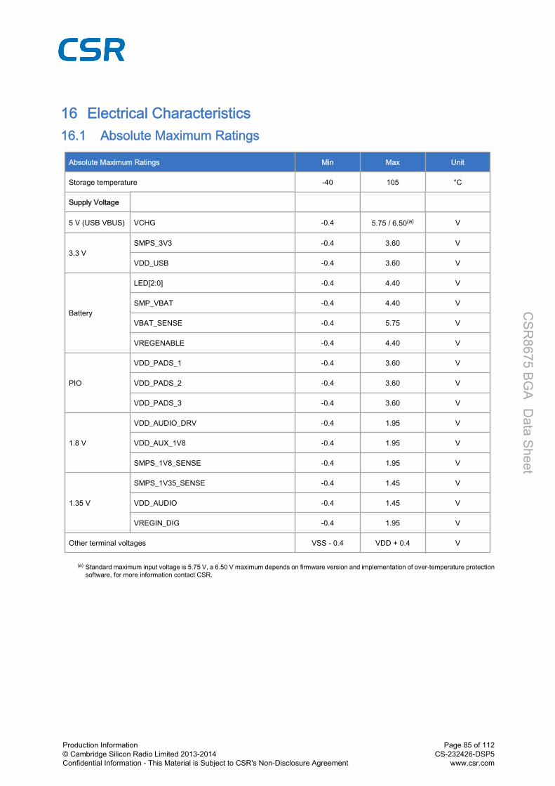
16 Electrical Characteristics16.1 Absolute Maximum Ratings
Absolute Maximum Ratings Min Max Unit
Storage temperature -40 105 °C
Supply Voltage
5 V (USB VBUS) VCHG -0.4 5.75 / 6.50(a) V
3.3 VSMPS_3V3 -0.4 3.60 V
VDD_USB -0.4 3.60 V
Battery
LED[2:0] -0.4 4.40 V
SMP_VBAT -0.4 4.40 V
VBAT_SENSE -0.4 5.75 V
VREGENABLE -0.4 4.40 V
PIO
VDD_PADS_1 -0.4 3.60 V
VDD_PADS_2 -0.4 3.60 V
VDD_PADS_3 -0.4 3.60 V
1.8 V
VDD_AUDIO_DRV -0.4 1.95 V
VDD_AUX_1V8 -0.4 1.95 V
SMPS_1V8_SENSE -0.4 1.95 V
1.35 V
SMPS_1V35_SENSE -0.4 1.45 V
VDD_AUDIO -0.4 1.45 V
VREGIN_DIG -0.4 1.95 V
Other terminal voltages VSS - 0.4 VDD + 0.4 V
(a) Standard maximum input voltage is 5.75 V, a 6.50 V maximum depends on firmware version and implementation of over-temperature protectionsoftware, for more information contact CSR.
Production Information© Cambridge Silicon Radio Limited 2013-2014Confidential Information - This Material is Subject to CSR's Non-Disclosure Agreement
Page 85 of 112CS-232426-DSP5
www.csr.com
CSR
8675 BGA D
ata Sheet

16.2 Recommended Operating Conditions
Recommended Operating Conditions Min Typ Max Unit
Operating temperature range -40 20 85 °C
Supply Voltage
5 V (USB VBUS) VCHG 4.75 / 3.10(a) 5.00 5.75 / 6.50(b) V
3.3 VSMPS_3V3 3.10 3.30 3.60 V
VDD_USB 3.10 3.30 3.60 V
Battery
LED[2:0] 1.10 3.70 4.30 V
SMP_VBAT 2.80 3.70 4.30 V
VBAT_SENSE 0 3.70 4.30 V
VREGENABLE 0 3.70 4.25 V
PIO
VDD_PADS_1 1.70 1.80 3.60 V
VDD_PADS_2 1.70 1.80 3.60 V
VDD_PADS_3 1.70 1.80 3.60 V
1.8 V
VDD_AUDIO_DRV 1.70 1.80 1.95 V
VDD_AUX_1V8 1.70 1.80 1.95 V
SMPS_1V8_SENSE 1.70 1.80 1.95 V
1.35 V
SMPS_1V35_SENSE 1.30 1.35 1.40 V
VDD_AUDIO 1.30 1.35 1.40 V
VREGIN_DIG 1.30 1.35 or 1.80(c) 1.95 V
(a) Minimum input voltage of 4.75 V is required for full specification, regulator operates at reduced load current from 3.1 V.(b) Standard maximum input voltage is 5.75 V, a 6.50 V maximum depends on firmware version and implementation of over-temperature protection
software, for more information contact CSR.(c) Typical value depends on output required by the low-voltage VDD_DIG linear regulator, see Section 16.3.2.2.
Production Information© Cambridge Silicon Radio Limited 2013-2014Confidential Information - This Material is Subject to CSR's Non-Disclosure Agreement
Page 86 of 112CS-232426-DSP5
www.csr.com
CSR
8675 BGA D
ata Sheet

16.3 Input/Output Terminal CharacteristicsNote:
For all I/O terminal characteristics: Current drawn into a pin is defined as positive; current supplied out of a pin is defined as negative.
16.3.1 Regulators: Available For External Use16.3.1.1 1.8V Switch-mode Regulator
1.8V Switch-mode Regulator Min Typ Max Unit
Input voltage 2.80 3.70 4.25 V
Output voltage 1.70 1.80 1.90 V
Normal Operation
Transient settling time - 30 - μs
Load current - - 185 mA
Current available for external use, stereo audio with 16Ω load(a) - - 25 mA
Peak conversion efficiency(b) - 90 - %
Switching frequency 3.63 4.00 4.00 MHz
Inductor saturation current, stereo and 16Ω load 250 - - mA
Inductor ESR 0.1 0.3 0.8 Ω
Low-power Mode, Automatically Entered in Deep Sleep
Transient settling time - 200 - μs
Load current 0.005 - 5 mA
Current available for external use - - 5 mA
Peak conversion efficiency - 85 - %
Switching frequency 100 - 200 kHz
(a) More current available for audio loads above 16Ω.(b) Conversion efficiency depends on inductor selection.
Note:
The regulator undershoots and overshoots when transitioning between modes.
Production Information© Cambridge Silicon Radio Limited 2013-2014Confidential Information - This Material is Subject to CSR's Non-Disclosure Agreement
Page 87 of 112CS-232426-DSP5
www.csr.com
CSR
8675 BGA D
ata Sheet

16.3.1.2 Combined 1.8V and 1.35V Switch-mode Regulator
Combined 1.8V and 1.35V Switch-mode Regulator Min Typ Max Unit
Input voltage 2.80 3.70 4.25 V
Output voltage 1.70 1.80 1.90 V
Normal Operation
Transient settling time - 30 - μs
Load current - - 340 mA
Current available for external use, stereo audio with 16Ω load(a) - - 25 mA
Peak conversion efficiency(b) - 90 - %
Switching frequency 3.63 4.00 4.00 MHz
Inductor saturation current, stereo and 16Ω load 400 - - mA
Inductor ESR 0.1 0.3 0.8 Ω
Low-power Mode, Automatically Entered in Deep Sleep
Transient settling time - 200 - μs
Load current 0.005 - 5 mA
Current available for external use - - 5 mA
Peak conversion efficiency - 85 - %
Switching frequency 100 - 200 kHz
(a) More current available for audio loads above 16Ω.(b) Conversion efficiency depends on inductor selection.
Note:
The regulator undershoots and overshoots when transitioning between modes.
Production Information© Cambridge Silicon Radio Limited 2013-2014Confidential Information - This Material is Subject to CSR's Non-Disclosure Agreement
Page 88 of 112CS-232426-DSP5
www.csr.com
CSR
8675 BGA D
ata Sheet

16.3.1.3 Bypass LDO Regulator
Normal Operation Min Typ Max Unit
Input voltage 4.25(a) 5.00 6.50(b) V
Output voltage (Vin > 4.25V) 3.20 3.30 3.40 V
Output current (Vin > 4.75V) - - 250 mA
(a) Minimum input voltage of 4.25 V is required for full specification, regulator operates at reduced load current from 3.1 V.(b) Standard maximum input voltage is 5.75 V, a 6.50 V maximum depends on firmware version and implementation of over-temperature protection
software, for more information contact CSR.
16.3.2 Regulators: For Internal Use Only16.3.2.1 1.35V Switch-mode Regulator
1.35V Switch-mode Regulator Min Typ Max Unit
Input voltage 2.80 3.70 4.25 V
Output voltage 1.30 1.35 1.40 V
Normal Operation
Transient settling time - 30 - μs
Load current - - 160 mA
Current available for external use - - 0 mA
Peak conversion efficiency(a) - 88 - %
Switching frequency 3.63 4.00 4.00 MHz
Inductor saturation current, stereo and 16Ω load 220 - - mA
Inductor ESR 0.1 0.3 0.8 Ω
Low-power Mode, Automatically Entered in Deep Sleep
Transient settling time - 200 - μs
Load current 0.005 - 5 mA
Current available for external use - - 0 mA
Peak conversion efficiency - - 85 %
Switching frequency 100 - 200 kHz
(a) Conversion efficiency depends on inductor selection.
Note:
The regulator undershoots and overshoots when transitioning between modes.
Production Information© Cambridge Silicon Radio Limited 2013-2014Confidential Information - This Material is Subject to CSR's Non-Disclosure Agreement
Page 89 of 112CS-232426-DSP5
www.csr.com
CSR
8675 BGA D
ata Sheet

16.3.2.2 Low-voltage VDD_DIG Linear Regulator
Normal Operation Min Typ Max Unit
Input voltage 1.30 1.35 or 1.80 1.95 V
Output voltage(a) 0.80 0.90 / 1.20 1.25 V
Internal load current - - 80 mA
(a) Output voltage level is software controlled
16.3.2.3 Low-voltage VDD_AUX Linear Regulator
Normal Operation Min Typ Max Unit
Input voltage 1.70 1.80 1.95 V
Output voltage 1.30 1.35 1.45 V
Internal load current - - 5 mA
16.3.2.4 Low-voltage VDD_ANA Linear Regulator
Normal Operation Min Typ Max Unit
Input voltage 1.70 1.80 1.95 V
Output voltage 1.30 1.35 1.45 V
Load current - - 60 mA
16.3.3 Regulator Enable
VREGENABLE, Switching Threshold Min Typ Max Unit
Rising threshold - - 1.0 V
16.3.4 Battery Charger
Battery Charger Min Typ Max Unit
Input voltage, VCHG 4.75 / 3.10(a) 5.00 5.75 / 6.50(b) V
(a) Reduced specification from 3.1V to 4.75V. Full specification >4.75V.(b) Standard maximum input voltage is 5.75V, a 6.50V maximum depends on firmware version and implementation of over-temperature protection
software, for more information contact CSR.
Production Information© Cambridge Silicon Radio Limited 2013-2014Confidential Information - This Material is Subject to CSR's Non-Disclosure Agreement
Page 90 of 112CS-232426-DSP5
www.csr.com
CSR
8675 BGA D
ata Sheet

Trickle Charge Mode Min Typ Max Unit
Charge current Itrickle, as percentage of fast charge current 8 10 12 %
Vfast rising threshold - 2.9 - V
Vfast rising threshold trim step size - 0.1 - V
Vfast falling threshold - 2.8 - V
Fast Charge Mode Min Typ Max Unit
Charge current during constant currentmode, Ifast
Max, headroom > 0.55V 194 200 206 mA
Min, headroom > 0.55V - 10 - mA
Reduced headroom charge current, asa percentage of Ifast
Mid, headroom = 0.15V 50 - 100 %
Charge current step size - 10 - mA
Vfloat threshold, calibrated 4.16 4.20 4.24 V
Charge termination current Iterm, as percentage of Ifast 7 10 20 %
Standby Mode Min Typ Max Unit
Voltage hysteresis on VBAT, Vhyst 100 - 150 mV
Error Charge Mode Min Typ Max Unit
Headroom(a) error falling threshold - 50 - mV
(a) Headroom = VCHG - VBAT
External Charge Mode(a) Min Typ Max Unit
Fast charge current, Ifast 200 - 500 mA
Control current into CHG_EXT 0 - 20 mA
Voltage on CHG_EXT 0 - 5.75 / 6.50(b) V
External pass device hfe 25 50 250 -
Sense voltage, between VBAT_SENSE and VBAT at maximumcurrent 195 200 205 mV
(a) In the external mode, the battery charger meets all the previous charger electrical characteristics and the additional or superseded electricalcharacteristics are listed in this table.
(b) Standard maximum input voltage is 5.75 V, a 6.50 V maximum depends on firmware version and implementation of over-temperature protectionsoftware, for more information contact CSR.
Production Information© Cambridge Silicon Radio Limited 2013-2014Confidential Information - This Material is Subject to CSR's Non-Disclosure Agreement
Page 91 of 112CS-232426-DSP5
www.csr.com
CSR
8675 BGA D
ata Sheet

16.3.5 Reset
Power-on Reset Min Typ Max Unit
VDD_DIG falling threshold (active mode) - 0.97 - V
VDD_DIG rising threshold (active mode) - 1.10 - V
VDD_DIG hysteresis (active mode) - 130 - mV
VDD_DIG falling threshold (deep sleep mode) - 0.77 - V
VDD_AUX_1V8 falling threshold(a) - 1.46 - V
VDD_AUX_1V8 rising threshold - 1.65 - V
VDD_AUX_1V8 hysteresis - 190 - mV
(a) The 1.8V switch-mode power supply rail can briefly drop to >1.3V during deep sleep exit. This is expected behaviour and does not cause a reset.
Production Information© Cambridge Silicon Radio Limited 2013-2014Confidential Information - This Material is Subject to CSR's Non-Disclosure Agreement
Page 92 of 112CS-232426-DSP5
www.csr.com
CSR
8675 BGA D
ata Sheet

16.3.6 USB
USB Min Typ Max Unit
VDD_USB for correct USB operation 3.10 3.30 3.60 V
Input Threshold
VIL input logic level low - - 0.30 xVDD_USB V
VIH input logic level high 0.70 xVDD_USB - - V
Output Voltage Levels to Correctly Terminated USB Cable
VOL output logic level low 0 - 0.2 V
VOH output logic level high 2.80 - VDD_USB V
16.3.7 Clocks
Crystal Oscillator Min Typ Max Unit
Frequency 19.2 26 32 MHz
External crystal load capacitance - 0 - pF
On-chip crystal load capacitance - 9 - pF
Frequency stability - - ±20 ppm
Transconductance 2 - - mS
External Clock Min Typ Max Unit
Input frequency(a) 19.2 26 40 MHz
Clock input level(b) 0.2 0.4 VDD_AUX V pk-pk
Edge jitter (allowable jitter), at zero crossing - - 10 ps rms
XTAL_IN input impedance 30 - - kΩ
XTAL_IN input capacitance - - 1 pF
DC level -0.4 - VDD_AUX +0.4 V
(a) Clock input is any frequency from 19.2 MHz to 40 MHz (default 26 MHz) in steps of 250 kHz plus CDMA/3G TCXO frequencies of 19.2, 19.44,19.68, 19.8 and 38.4 MHz.
(b) Clock input is either sinusoidal or square wave. If the peaks of the signal are below VSS_BT_LO_AUX or above VDD_AUX. A DC blockingcapacitor is required between the signal and XTAL_IN.
Production Information© Cambridge Silicon Radio Limited 2013-2014Confidential Information - This Material is Subject to CSR's Non-Disclosure Agreement
Page 93 of 112CS-232426-DSP5
www.csr.com
CSR
8675 BGA D
ata Sheet

16.3.8 Stereo Codec: Analogue to Digital Converter
Analogue to Digital Converter
Parameter Conditions Min Typ Max Unit
Resolution - - 16 - Bits
Input Sample Rate,Fsample
- 8 - 96 kHz
SNR
fin = 1kHzB/W = 20Hz→Fsample/2(20kHz max)A-WeightedTHD+N < 0.1%1.6Vpk-pk input
Fsample
8kHz - 93 - dB
16kHz - 92 - dB
32kHz - 92 - dB
44.1kHz - 92 - dB
48kHz - 92 - dB
THD+N
fin = 1kHzB/W = 20Hz→Fsample/2(20kHz max)1.6Vpk-pk input
Fsample
8kHz - 0.004 - %
48kHz - 0.008 - %
Digital gain Digital gain resolution = 1/32 -24 - 21.5 dB
Analogue gain
Pre-amplifier setting = 0dB, 9dB, 21dB or30dBAnalogue setting = -3dB to 12dB in 3dBsteps
-3 - 42 dB
Stereo separation(crosstalk)
Measurement bandwidth = 20Hz to 20kHzAmplitude response = RMSNo weightingInput amplitude = 300mVrms, 20Hz, 1kHz,20kHz tones, 48kHz sample rateAnalogue gain set to 2, digital gain set to 0
- -89 - dB
Production Information© Cambridge Silicon Radio Limited 2013-2014Confidential Information - This Material is Subject to CSR's Non-Disclosure Agreement
Page 94 of 112CS-232426-DSP5
www.csr.com
CSR
8675 BGA D
ata Sheet

16.3.9 Stereo Codec: Digital to Analogue Converter
Digital to Analogue Converter
Parameter Conditions Min Typ Max Unit
Resolution - - 16 - Bits
Output SampleRate, Fsample
- 8 - 192 kHz
SNR
fin = 1kHzB/W = 20Hz→20kHzA-WeightedTHD+N < 0.01%0dBFS input
Fsample Load
48kHz 100kΩ - 96 - dB
48kHz 32Ω - 96 - dB
48kHz 16Ω - 96 - dB
THD+Nfin = 1kHzB/W = 20Hz→20kHz0dBFS input
Fsample Load
8kHz 100kΩ - 0.002 - %
8kHz 32Ω - 0.002 - %
8kHz 16Ω - 0.003 - %
48kHz 100kΩ - 0.003 - %
48kHz 32Ω - 0.003 - %
48kHz 16Ω - 0.004 - %
Digital Gain Digital Gain Resolution = 1/32 -24 - 21.5 dB
Analogue Gain Analogue Gain Resolution = 3dB -21 - 0 dB
Output voltage Full-scale swing (differential) - - 778 mV rms
Stereo separation(crosstalk)
Measurement bandwidth = 20Hz to 20kHzAmplitude response = RMSNo weightingInput amplitude = 0dBFS, 20Hz, 1kHz, 20kHztones, 48kHz sample rateAnalogue gain set to 7, digital gain set to 0
- -88 - dB
Production Information© Cambridge Silicon Radio Limited 2013-2014Confidential Information - This Material is Subject to CSR's Non-Disclosure Agreement
Page 95 of 112CS-232426-DSP5
www.csr.com
CSR
8675 BGA D
ata Sheet

16.3.10 Digital
Digital Terminals Min Typ Max Unit
Input Voltage
VIL input logic level low -0.4 - 0.4 V
VIH input logic level high 0.7 x VDD - VDD + 0.4 V
Tr/Tf - - 25 ns
Output Voltage
VOL output logic level low, lOL = 4.0mA - - 0.4 V
VOH output logic level high, lOH = -4.0mA 0.75 X VDD - - V
Tr/Tf - - 5 ns
Input and Tristate Currents
Strong pull-up -150 -40 -10 μA
Strong pull-down 10 40 150 μA
Weak pull-up -5 -1.0 -0.33 μA
Weak pull-down 0.33 1.0 5.0 μA
CI Input Capacitance 1.0 - 5.0 pF
16.3.11 LED Driver Pads
LED Driver Pads Min Typ Max Unit
Current, IPAD
High impedance state - - 5 µA
Current sink state - - 10 mA
LED pad voltage, VPAD IPAD = 10mA - - 0.55 V
LED pad resistance VPAD < 0.5V - - 40 Ω
VOL output logic level low(a) - 0 - V
VOH output logic level high(a) - 0.8 - V
VIL input logic level low - 0 - V
VIH input logic level high - 0.8 - V
(a) LED output port is open-drain and requires a pull-up
Production Information© Cambridge Silicon Radio Limited 2013-2014Confidential Information - This Material is Subject to CSR's Non-Disclosure Agreement
Page 96 of 112CS-232426-DSP5
www.csr.com
CSR
8675 BGA D
ata Sheet

16.3.12 Auxiliary ADC
Auxiliary ADC Min Typ Max Unit
Resolution - - 10 Bits
Input voltage range(a) 0 - VDD_AUX V
Accuracy(Guaranteed monotonic)
INL -1 - 1 LSB
DNL 0 - 1 LSB
Offset -1 - 1 LSB
Gain error -0.8 - 0.8 %
Input bandwidth - 100 - kHz
Conversion time 1.38 1.69 2.75 µs
Sample rate(b) - - 700 Samples/s
(a) LSB size = VDD_AUX/1023(b) The auxiliary ADC is accessed through a VM function. The sample rate given is achieved as part of this function.
16.3.13 Auxiliary DAC
Auxiliary DAC Min Typ Max Unit
Resolution - - 10 Bits
Supply voltage, VDD_AUX 1.30 1.35 1.40 V
Output voltage range 0 - VDD_AUX V
Full-scale output voltage 1.30 1.35 1.40 V
LSB size 0 1.32 2.64 mV
Offset -1.32 0 1.32 mV
Integral non-linearity -1 0 1 LSB
Settling time(a) - - 250 ns
(a) The settling time does not include any capacitive load
Important Note:
Access to the auxiliary DAC is firmware-dependent, for more information about its availability contact CSR.
Production Information© Cambridge Silicon Radio Limited 2013-2014Confidential Information - This Material is Subject to CSR's Non-Disclosure Agreement
Page 97 of 112CS-232426-DSP5
www.csr.com
CSR
8675 BGA D
ata Sheet
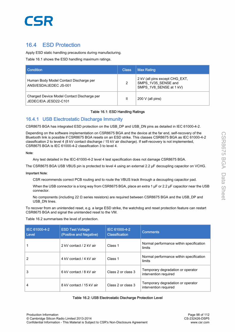
16.4 ESD ProtectionApply ESD static handling precautions during manufacturing.
Table 16.1 shows the ESD handling maximum ratings.
Condition Class Max Rating
Human Body Model Contact Discharge perANSI/ESDA/JEDEC JS‑001
22 kV (all pins except CHG_EXT,SMPS_1V35_SENSE andSMPS_1V8_SENSE at 1 kV)
Charged Device Model Contact Discharge perJEDEC/EIA JESD22‑C101
II 200 V (all pins)
Table 16.1: ESD Handling Ratings
16.4.1 USB Electrostatic Discharge ImmunityCSR8675 BGA has integrated ESD protection on the USB_DP and USB_DN pins as detailed in IEC 61000‑4‑2.
Depending on the software implementation on CSR8675 BGA and the device at the far end, self-recovery of theBluetooth link is possible if CSR8675 BGA resets on an ESD strike. This classes CSR8675 BGA as IEC 61000‑4‑2classification 2 to level 4 (8 kV contact discharge / 15 kV air discharge). If self-recovery is not implemented,CSR8675 BGA is IEC 61000‑4‑2 classification 3 to level 4.
Note:
Any test detailed in the IEC-61000-4-2 level 4 test specification does not damage CSR8675 BGA.
The CSR8675 BGA USB VBUS pin is protected to level 4 using an external 2.2 µF decoupling capacitor on VCHG.
Important Note:
CSR recommends correct PCB routing and to route the VBUS track through a decoupling capacitor pad.
When the USB connector is a long way from CSR8675 BGA, place an extra 1 µF or 2.2 µF capacitor near the USBconnector.
No components (including 22 Ω series resistors) are required between CSR8675 BGA and the USB_DP andUSB_DN lines.
To recover from an unintended reset, e.g. a large ESD strike, the watchdog and reset protection feature can restartCSR8675 BGA and signal the unintended reset to the VM.
Table 16.2 summarises the level of protection.
IEC 61000‑4‑2Level
ESD Test Voltage(Positive and Negative)
IEC 61000‑4‑2Classification
Comments
1 2 kV contact / 2 kV air Class 1 Normal performance within specificationlimits
2 4 kV contact / 4 kV air Class 1 Normal performance within specificationlimits
3 6 kV contact / 8 kV air Class 2 or class 3 Temporary degradation or operatorintervention required
4 8 kV contact / 15 kV air Class 2 or class 3 Temporary degradation or operatorintervention required
Table 16.2: USB Electrostatic Discharge Protection Level
Production Information© Cambridge Silicon Radio Limited 2013-2014Confidential Information - This Material is Subject to CSR's Non-Disclosure Agreement
Page 98 of 112CS-232426-DSP5
www.csr.com
CSR
8675 BGA D
ata Sheet

For more information contact CSR.
Production Information© Cambridge Silicon Radio Limited 2013-2014Confidential Information - This Material is Subject to CSR's Non-Disclosure Agreement
Page 99 of 112CS-232426-DSP5
www.csr.com
CSR
8675 BGA D
ata Sheet

17 Power Consumption
DUT Role Connection Packet Type AverageCurrent Unit
N/A Deep sleep With UART host connection - 76 µA
N/A Page scanPage = 1280ms intervalWindow = 11.25ms
- 261 µA
N/A Inquiry andpage scan
Inquiry = 1280ms intervalPage = 1280ms intervalWindow = 11.25ms
- 482 µA
Master ACL Sniff = 500ms, 1 attempt, 0 timeout DH1 173 µA
Master ACL Sniff = 1280ms, 8 attempts, 1 timeout DH1 150 µA
Master SCO Sniff = 100ms, 1 attempt, PCM HV3 9.9 mA
Master SCO Sniff = 100ms, 1 attempt, mono audio codec HV3 10.7 mA
Master eSCO Setting S3, sniff = 100ms, PCM 2EV3 8.0 mA
Master eSCO Setting S3, sniff = 100ms, PCM 3EV3 7.7 mA
Master eSCO Setting S3, sniff = 100ms, mono audio codec 2EV3 9.9 mA
Master eSCO Setting S3, sniff = 100ms, mono audio codec 3EV3 9.5 mA
Slave ACL Sniff = 500ms, 1 attempt, 0 timeout DH1 182 µA
Slave ACL Sniff = 1280ms, 8 attempts, 1 timeout DH1 187 µA
Slave SCO Sniff = 100ms, 1 attempt, PCM HV3 10.2 mA
Slave SCO Sniff = 100ms, 1 attempt, mono audio codec HV3 12.0 mA
Slave eSCO Setting S3, sniff = 100ms, PCM 2EV3 8.4 mA
Slave eSCO Setting S3, sniff = 100ms, PCM 3EV3 8.1 mA
Slave eSCO Setting S3, sniff = 100ms, mono audio codec 2EV3 10.3 mA
Slave eSCO Setting S3, sniff = 100ms, mono audio codec 3EV3 10.0 mA
Note:
Current consumption values are taken with: HCI only VBAT pin = 3.7 V Firmware ID = 10528 RF TX power set to 0dBm No RF retransmissions in case of eSCO Audio gateway transmits silence when SCO/eSCO channel is open LEDs disconnected AFH off Pulse skipping mode disabled
Production Information© Cambridge Silicon Radio Limited 2013-2014Confidential Information - This Material is Subject to CSR's Non-Disclosure Agreement
Page 100 of 112CS-232426-DSP5
www.csr.com
CSR
8675 BGA D
ata Sheet

18 CSR Green Semiconductor Products and RoHS ComplianceCSR confirms that CSR Green semiconductor products comply with the following regulatory requirements:
Restriction on Hazardous Substances directive guidelines in the EU RoHS Directive 2011/65/EU1. EU REACH, Regulation (EC) No 1907/20061:
List of substances subject to authorisation (Annex XIV) Restrictions on the manufacture, placing on the market and use of certain dangerous substances,
preparations and articles (Annex XVII). This Annex now includes requirements that were contained withinEU Directive, 76/769/EEC. There are many substance restrictions within this Annex, including, but notlimited to, the control of use of Perfluorooctane sulfonates (PFOS).
When requested by customers, notification of substances identified on the Candidate List as Substancesof Very High Concern (SVHC)1.
POP regulation (EC) No 850/20041
EU Packaging and Packaging Waste, Directive 94/62/EC1
Montreal Protocol on substances that deplete the ozone layer. Conflict minerals, Section 1502, Dodd-Frank Wall Street Reform and Consumer Protection act, which affects
columbite-tantalite (coltan / tantalum), cassiterite (tin), gold, wolframite (tungsten) or their derivatives. CSR isa fabless semiconductor company: all manufacturing is performed by key suppliers. CSR have mandated thatthe suppliers shall not use materials that are sourced from "conflict zone mines" but understand that thisrequires accurate data from the EICC programme. CSR shall provide a complete EICC / GeSI template uponrequest.
CSR has defined the "CSR Green" standard based on current regulatory and customer requirements including freefrom bromine, chlorine and antimony trioxide.
Products and shipment packaging are marked and labelled with applicable environmental marking symbols inaccordance with relevant regulatory requirements.
This identifies the main environmental compliance regulatory restrictions CSR specify. For more information on the full"CSR Green" standard, contact [email protected].
1 Including applicable amendments to EU law which are published in the EU Official Journal, or SVHCCandidate List updates published by the European Chemicals Agency (ECHA).
Production Information© Cambridge Silicon Radio Limited 2013-2014Confidential Information - This Material is Subject to CSR's Non-Disclosure Agreement
Page 101 of 112CS-232426-DSP5
www.csr.com
CSR
8675 BGA D
ata Sheet

19 SoftwareCSR8675 BGA:
Is supplied with on-chip Bluetooth v4.1 specification qualified HCI stack firmware Has on-chip software that can be loaded with applications from CSR's audio development kit, see Section
19.2.1.1 Has on-chip software that can be loaded with applications from CSR's eXtension Program
19.1 On-chip Software19.1.1 Stand-alone CSR8675 BGA and Kalimba DSP ApplicationsFigure 19.1 shows the structure of the stack for running on-chip software and applications, it is built on top of the HCIstack in Section 19.1.2. The stack firmware requires no host processor, but uses a host processor for debugging etc,as Figure 19.1 shows. The software layers for the application software run on the internal MCU in a protected user-software execution environment known as a VM and the DSP application code runs from the DSP program memoryRAM.
G-T
W-0
0055
32.2
.2
LC
Pro
gram
Mem
ory
56KB RAM BasebandMCU
Host I/O
Radio
Digital Audio
USB
UART
Host for Debugging and Programming
RFCOMM SDP
VM Application Software DSP Application
DSP Control
DM1 DM2 PM
Internal MCU Kalimba DSP
PCM / SPDIF / I2S
Digital Microphones
Analogue Audio
LM
L2CAPHCI
Microphones
Speakers
Figure 19.1: Stand-alone CSR8675 BGA and Kalimba DSP Applications
Note:
Program memory in Figure 19.1 is internal flash.
CSR provides a development kit that customers can configure to meet their audio and consumer end-productrequirements.
The development kit include firmware components, applications and appropriate profile support. For more informationsee Section 19.2.1.
19.1.2 BlueCore HCI StackFigure 19.2 shows HCI stack implementation. The internal MCU runs the Bluetooth stack up to the HCI.
Production Information© Cambridge Silicon Radio Limited 2013-2014Confidential Information - This Material is Subject to CSR's Non-Disclosure Agreement
Page 102 of 112CS-232426-DSP5
www.csr.com
CSR
8675 BGA D
ata Sheet

G-T
W-0
0060
97.1
.1
HCI
LM
LC
Pro
gram
Mem
ory
56KB RAM Bluetooth StackMCU
Host I/O
Radio
Digital Audio
Host for Debugging
andProgramming
Analogue AudioMicrophones
USB
UART
PCM / SPDIF / I2S
Digital Microphones
Speakers
Figure 19.2: BlueCore HCI Stack
Note:
Program Memory in Figure 19.2 is internal flash.
19.1.2.1 Latest Features of the HCI StackCSR8675 BGA is qualified to the Bluetooth v4.1 specification.
19.2 Off-chip Software19.2.1 CSR8675 Development KitCSR's audio development kit for the CSR8675 BGA, order code DK-CSR8675-10197-1A, includes a CSR8675 BGAdemonstrator board (DB-CSR8675-10200-1A) and necessary interface adapters and cables are available. Inconjunction with the CSR8675 Configurator tool and other supporting utilities the development kit provides the bestenvironment for designing audio solutions with the CSR8675 BGA.
Important Note:
The CSR8675 BGA audio development kit is subject to change and updates, for up-to-date information seewww.csrsupport.com.
Production Information© Cambridge Silicon Radio Limited 2013-2014Confidential Information - This Material is Subject to CSR's Non-Disclosure Agreement
Page 103 of 112CS-232426-DSP5
www.csr.com
CSR
8675 BGA D
ata Sheet

19.2.1.1 Audio Development Kit SoftwareIn conjunction with the CSR8675 audio development kit, software is available, it requires a Bluetooth Developer'sLicence to use. CSR’s current software includes:
Bluetooth Profiles: Bluetooth v4.1 specification support HFP v1.6 HSP v1.2 A2DP v1.2 AVRCP v1.4 PBAP v1.0 MAP v1.0 SPP v1.0
Improved Audio Quality: CVC 1-mic far-end audio enhancements (narrowband) CVC 2-mic far-end audio enhancements (narrowband) CVC 1-mic far-end audio enhancements (hands-free) CVC 1-mic far-end audio enhancements (wideband) CVC 2-mic far-end audio enhancements (wideband) CVC near-end audio enhancements PLC / BEC 1-mic WNR 2-mic WNR Sidetone Frequency expansion for improved speech intelligibility
Music Enhancements: aptX codec technology 5-band EQ 3D stereo separation Dynamic range control Faststream codec SBC decoder MP3 decoder AAC decoder
Additional Functionality: Multipoint for HFP, A2DP and advance user-cases Programmable audio prompts (compressed / SBC) Support for capacitive touch control Support for speech recognition Support for multi-language programmable audio prompts CSR's proximity pairing and CSR's proximity connection Multipoint support for HFP connection to 2 handsets for voice Multipoint support for A2DP connection to 2 A2DP sources for music playback Talk-time extension
19.2.2 eXtension Program SupportA wide range of software options is available from CSR's eXtension Program Support, see www.csr.com.
Production Information© Cambridge Silicon Radio Limited 2013-2014Confidential Information - This Material is Subject to CSR's Non-Disclosure Agreement
Page 104 of 112CS-232426-DSP5
www.csr.com
CSR
8675 BGA D
ata Sheet

20 Tape and Reel InformationFor tape and reel packing and labelling see IC Packing and Labelling Specification.
20.1 Tape OrientationFigure 20.1 shows the general orientation of the CSR8675 BGA package in the carrier tape.
G-T
W-0
0024
34.3
.2
Circular Holes
User Direction of Feed
B
A
A ≥ B
Pin A1 Marker
Figure 20.1: Tape Orientation
20.2 Tape DimensionsFigure 20.2 shows the dimensions of the tape for the CSR8675 BGA.
G-T
W-0
0056
77.1
.1
5
6.00TYP.
0.10.01.50
SECTION A-A
SECTION B-B
R0.50(TYP.)
R0.30(TYP.)
0.00.11.50
16.00 0.3
7.50See Note 6
1.75
See Note 14.00
KoK1
Bo 6.00TYP.
0.30 0.05
12.00
Ao
A
See Note 62.00
B B
A
Figure 20.2: Tape Dimensions
Production Information© Cambridge Silicon Radio Limited 2013-2014Confidential Information - This Material is Subject to CSR's Non-Disclosure Agreement
Page 105 of 112CS-232426-DSP5
www.csr.com
CSR
8675 BGA D
ata Sheet
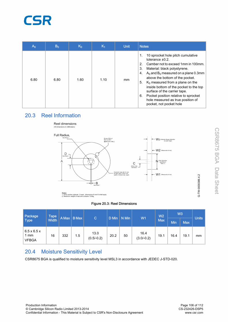
A0 B0 K0 K1 Unit Notes
6.80 6.80 1.60 1.10 mm
1. 10 sprocket hole pitch cumulativetolerance ±0.2.
2. Camber not to exceed 1mm in 100mm.3. Material: black polystyrene.4. A0 and B0 measured on a plane 0.3mm
above the bottom of the pocket.5. K0 measured from a plane on the
inside bottom of the pocket to the topsurface of the carrier tape.
6. Pocket position relative to sprockethole measured as true position ofpocket, not pocket hole
20.3 Reel Information
G-T
W-0
0003
86.4
.2
Φ
Figure 20.3: Reel Dimensions
PackageType
TapeWidth A Max B Max C D Min N Min W1 W2
Max
W3Units
Min Max
6.5 x 6.5 x1 mmVFBGA
16 332 1.513.0
(0.5/-0.2)20.2 50
16.4(3.0/-0.2)
19.1 16.4 19.1 mm
20.4 Moisture Sensitivity LevelCSR8675 BGA is qualified to moisture sensitivity level MSL3 in accordance with JEDEC J-STD-020.
Production Information© Cambridge Silicon Radio Limited 2013-2014Confidential Information - This Material is Subject to CSR's Non-Disclosure Agreement
Page 106 of 112CS-232426-DSP5
www.csr.com
CSR
8675 BGA D
ata Sheet

21 Document References
Document Reference, Date
BlueCore Audio API Specification CS-209064-DD
BlueCore Bluetooth/IEEE 802.11 CoexistenceApplication Note CS-207808-AN
BlueTest User Guide CS-102736-UG
Bluetooth and USB Design Considerations CS-101412-AN
Configuring the Power Supplies on CSR867x CS-204573-AN
Configuring the Touch Sensor on CSR867x CS-204575-AN
Core Specification of the Bluetooth System Bluetooth Specification Version 4.1, 03 December 2013
CSR8675 BGA Performance Specification CS-303731-SP
CVC Two Microphone Headset Design Guidelines CS-218321-DC
ESDA/JEDEC Joint Standard For Electrostatic DischargeSensitivity Testing Human Body Model (HBM) -Component Level
ANSI/ESDA/JEDEC JS-001-2011
Field-Induced Charged-Device Model Test Method forElectrostatic- Discharge-Withstand Thresholds ofMicroelectronic Components
JESD22-C101E
Firmware Configuration Keys for CSR8670 CS-219481-AN
IC Packing and Labelling Specification CS-112584-SP
IEC 61000-4-2Electromagnetic compatibility (EMC) – Part 4-2: Testingand measurement techniques – Electrostatic dischargeimmunity test
IEC 61000-4-2, Edition 2.0, 2008-12
Kalimba Architecture 5 DSP User Guide CS-318059-UG
Lithium Polymer Battery Charger Calibration andOperation for CSR867x CS-204572-AN
Moisture / Reflow Sensitivity Classification forNonhermitic Solid State Surface Mount Devices IPC / JEDEC J-STD-020
Selection of I²C EEPROMS for Use with BlueCore bcore-an-008P
Typical Solder Reflow Profile for Lead-free Device CS-116434-AN
Universal Serial Bus Specification v2.0, 27 April 2000
USB Battery Charging Specification v1.1, 15 April 2009
Production Information© Cambridge Silicon Radio Limited 2013-2014Confidential Information - This Material is Subject to CSR's Non-Disclosure Agreement
Page 107 of 112CS-232426-DSP5
www.csr.com
CSR
8675 BGA D
ata Sheet

Terms and DefinitionsTerm Definition
3G 3rd Generation of mobile communications technology
µ-law Audio companding standard (G.711)
A-law Audio companding standard (G.711)
A2DP Advanced Audio Distribution Profile
AAC Advanced Audio Coding
AC Alternating Current
ACL Asynchronous Connection-oriented
ADC Analogue to Digital Converter
AES Audio Engineering Society
AFC Automatic Frequency Control
AFH Adaptive Frequency Hopping
AGC Automatic Gain Control
ALU Arithmetic Logic Unit
AVRCP Audio/Video Remote Control Profile
BCCMD BlueCore CoMmanD
BCSP BlueCore Serial Protocol
BEC Bit Error Concealment
BIST Built-In Self-Test
Bluetooth® Set of technologies providing audio and data transfer over short-range radio connections
BMC Burst Mode Controller
CDMA Code Division Multiple Access
codec Coder decoder
CRC Cyclic Redundancy Check
CSR Cambridge Silicon Radio
CVC Clear Voice Capture
CVSD Continuously Variable Slope Delta Modulation
DAC Digital to Analogue Converter
DC Direct Current
DDS Direct Digital Synthesis
DFU Device Firmware Upgrade
DMA Direct Memory Access
Production Information© Cambridge Silicon Radio Limited 2013-2014Confidential Information - This Material is Subject to CSR's Non-Disclosure Agreement
Page 108 of 112CS-232426-DSP5
www.csr.com
CSR
8675 BGA D
ata Sheet

Term Definition
DNL Differential Non Linearity (ADC accuracy parameter)
DSP Digital Signal Processor (or Processing)
DUT Device Under Test
e.g. exempli gratia, for example
EBU European Broadcasting Union
EDR Enhanced Data Rate
EEPROM Electrically Erasable Programmable Read Only Memory
EIA Electronic Industries Alliance
EMC ElectroMagnetic Compatibility
EQ EQualiser
eSCO extended SCO
ESD Electrostatic Discharge
ESR Equivalent Series Resistance
etc et cetera, and the rest, and so forth
FIR Finite Impulse Response (filter)
FSK Frequency Shift Keying
G.722 An ITU-T standard wideband speech codec operating at 48, 56 and 64 kbps
GCI General Circuit Interface
GSM Global System for Mobile communications
H4DS H4 Deep Sleep
HBM Human Body Model
HCI Host Controller Interface
HFP Hands-Free Profile
HSP HeadSet Profile
I²C Inter-Integrated Circuit Interface
I²S Inter-Integrated Circuit Sound
i.e. Id est, that is
I/O Input/Output
IC Integrated Circuit
ID IDentifier
IEEE Institute of Electronic and Electrical Engineers
IF Intermediate Frequency
IIR Infinite Impulse Response (filter)
Production Information© Cambridge Silicon Radio Limited 2013-2014Confidential Information - This Material is Subject to CSR's Non-Disclosure Agreement
Page 109 of 112CS-232426-DSP5
www.csr.com
CSR
8675 BGA D
ata Sheet

Term Definition
INL Integral Non-Linearity (ADC accuracy parameter)
IQ In-Phase and Quadrature
ISDN Integrated Services Digital Network
JEDEC Joint Electron Device Engineering Council (now the JEDEC Solid State Technology Association)
Kalimba An open platform DSP co-processor, enabling support of enhanced audio applications, such asecho and noise suppression and file compression / decompression
Kb Kilobit
LC An inductor (L) and capacitor (C) network
LCD Liquid-Crystal Display
LDO Low (voltage) Drop-Out
LED Light-Emitting Diode
LM Link Manager
LNA Low Noise Amplifier
LSB Least Significant Bit (or Byte)
MAC Multiplier and ACcumulator
MAP Message Access Profile
Mb Megabit
MCU MicroController Unit
MEMS Micro Electro Mechanical System
MIPS Million Instructions Per Second
MISO Master In Slave Out
MLC MultiLayer Ceramic
MMU Memory Management Unit
MP3 MPEG-1 audio layer 3
N/A Not Applicable
NC Not Connect
NSMD Non-Solder Mask Defined
PA Power Amplifier
PBAP PhoneBook Access Profile
PC Personal Computer
PCB Printed Circuit Board
PCM Pulse Code Modulation
PD Pull-down
PIO Parallel Input/Output
Production Information© Cambridge Silicon Radio Limited 2013-2014Confidential Information - This Material is Subject to CSR's Non-Disclosure Agreement
Page 110 of 112CS-232426-DSP5
www.csr.com
CSR
8675 BGA D
ata Sheet

Term Definition
PIO Programmable Input/Output, also known as general purpose I/O
PLC Packet Loss Concealment
plc public limited company
ppm parts per million
PS Key Persistent Store Key
PU Pull-Up
PWM Pulse Width Modulation
RAM Random Access Memory
RC A Resistor and Capacitor network
RCA Radio Corporation of America, normally used to refer to a RCA connector (also known as phonoconnector or Cinch connector)
RF Radio Frequency
RGB Red Green Blue
RISC Reduced Instruction Set Computer
RoHS Restriction of Hazardous Substances in Electrical and Electronic Equipment Directive (2002/95/EC)
RS-232 Recommended Standard-232, a TIA/EIA standard for serial transmission between computersand peripheral devices (modem, mouse, etc.)
RSSI Received Signal Strength Indication
RX Receive or Receiver
SBC Sub-Band Coding
SCO Synchronous Connection-Oriented
SIG (Bluetooth) Special Interest Group
SMPS Switch-Mode Power Supply
SNR Signal-to-Noise Ratio
SoC System On-Chip
SPDIF Sony/Philips Digital InterFace (also IEC 958 type II, part of IEC-60958). An interface designedto transfer stereo digital audio signals between various devices and stereo components withminimal loss.
SPI Serial Peripheral Interface
SPP Serial Port Profile
SQIF Serial Quad I/O Flash (interface)
SRAM Static Random Access Memory
TBD To Be Defined
TCXO Temperature Compensated crystal Oscillator
THD+N Total Harmonic Distortion and Noise
Production Information© Cambridge Silicon Radio Limited 2013-2014Confidential Information - This Material is Subject to CSR's Non-Disclosure Agreement
Page 111 of 112CS-232426-DSP5
www.csr.com
CSR
8675 BGA D
ata Sheet

Term Definition
TX Transmit or Transmitter
UART Universal Asynchronous Receiver Transmitter
Unity Collective name for CSR’s Bluetooth/Wi-Fi coexistence schemes
Unity+ CSR’s advanced coexistence scheme. Extra signalling wire used in conjunction with Unity-3 orUnity-3e for improved coexistence with periodic Bluetooth activity.
Unity-3 De facto industry standard 3-wire coexistence signalling scheme
USB Universal Serial Bus
VCO Voltage Controlled Oscillator
VFBGA Very thin, Fine pitch, Ball Grid Array
VM Virtual Machine
W-CDMA Wideband Code Division Multiple Access
WLAN Wireless Local Area Network
WNR Wind Noise Reduction
Production Information© Cambridge Silicon Radio Limited 2013-2014Confidential Information - This Material is Subject to CSR's Non-Disclosure Agreement
Page 112 of 112CS-232426-DSP5
www.csr.com
CSR
8675 BGA D
ata Sheet