fairchild imaging systems syosset n y f/0 analog … · ad-aosi 979 fairchild imaging systems...
TRANSCRIPT

AD-AOSI 979 FAIRCHILD IMAGING SYSTEMS SYOSSET N Y F/0 17/2ANALOG FRAME STORE MEMORY. CU)JAN 80 OAAK77-C-0165
UNCLASSIFIED ED-CX-141-5 M

1 .0 H " 1
I 1111i1.25 11I111.6
MICROCOPY RESOLUTION TEST CH*T
NAT'*NOAL BUR[AU O STANDARDS- 1963-

I FAIRCHILD IMAJ31NG 5 ST~EMJ~A Division of Fairchild Camera and Instrument Corporation
I Report '#D-CX-14-5,C "i 4Fifth Quarterly Technical Report
/T)Analog Frame Store Memorys15 January 1980
CDRL SEQ. NO. A002
I S3198
Contract, DAAK7/0-78-C- 165 ANIGHT VISION LABORATORY
This document is furnished in response to theNight Vision Laboratory Contract No. DAAK70-78-C-0165. The Government shall have the right toduplicate, use, or disclose the data to the extentprovided in the contract. This restriction does notlimit the Government's right to use information con-tained in the data if it is obtained from anotherI source
DWIMPBUTFION STATEMENT AI Approved for publicDistributihou DimitedI
IA. Roberts I. Hirsche'rg
Program Manager Director, Electro-Oi 1 EquipmentI

FAIRCHILD IMAGING SYSTEMS
A Division of Fairchild Camera and Instrument Corporation
THIS FIFTH QUARTERLY REPORT
I COVERS THE PERIOD FROM
1 OCT. 1979 THROUGH DEC. 1979
A._7
Dis
I FAIRCHILD IMAGING SYSTEMSA Division of Fairchild Camera and Instrument Corporation
I TABLE OF CONTENTS
SECTION TITLE PAGE
1.0 INTRODUCTION 1-1
1.1 SYSTEM DESCRIPTION 1-2
1.1.1 Analog Frame Store Memory 1-2
1.1.2 Analog Field Storage Device 1-4
1.1.3 Image Analyzer Digital Display (IADD) 1-4
1.2 PROGRAM'S GOAL 1-5
1.3 TEST RESULTS 1-6
2.0 PROGRAM STATUS 2-1
2.1 SCHEDULE 2-1
2.2 TECHNICAL 2-1
2.2.1 Analog Field Storage Device (001AA) 2-1
2.2.2 IADD (00lAD) 2-3
2.2.3 Analog Frame Store Memory (001AC) 2-3
1 2.3 ACTIVITIES FOR NEXT QUARTER 2-3
3.0 DESIGN 3-1
3.1 ANALOG FIELD STORAGE DEVICE 3-1
3.1.1 Input Circuit 3-1
I 3.1.2 Parallel Register 3-1
3.1.3 Output Circuit 3-2
S3.1.4 Timing Requirement 3-33.2 ANALOG FRAME STORE MEMORY 3-41 3.2.1 Input Circuits 3-4
3.2.2 Timing Circuits 3-5
3.2.3 Output Circuits 3-63.2.4 Control ID 3-7
3.2.5 Temperature Control Circuit 3-7
3.2.6 Mode 3 Operation 3-8
3.3 IMAGE ANALYZER DIGITAL DISPLAY (IADD) 3-10
3.3.1 Input Section 3-12
i Ii

I FAIRCHILO IMACING SYSTEMSA Division of Fairchild Camera and Instrument Corporation
TABLE OF CONTENTS (Continued)
SECTION TITLE PAGE
3.3.2 Memory Subsystem 3-13
3.3.3 Output Logic 3-17
3.3.4 TV Sync Generator/Master Oscillator 3-17
3.3.5 Video Processor 3-18
3.4 POWER REQUIREMENTS 3-18
3.4.1 Analog Frame Store Memory 3-18
3.4.2 IADD 3-18
3.5 PACKAGING 3-19
3.5.1 Analog Field Storage Device 3-19
3.5.2 Analog Frame Store Memory 3-19
3.5.3 IADD 3-20
1!II
I --. A -2:
I .in
I ..- -ii-. 2 j ....-- = ,

I =FAIRCHIL IMAGING SYSTEMSA Division of Fairchild Camera and Instrument Corporation
I
[ APPENDIX
TITLE PAGE
1 CHARGE SPILLAGE IN A FOUR PHASE SYSTEM Al - 1
2 DESCRIPTION OF BURIED-TO-SURFACE CHANNEL A2 - 1TRANSFER REGION IN FIELD STORAGE DEVICE
*1
II
I
-iii-

II FAIRCHILD IMAGING SYSTEMS
A Division of Fairchild Camera and Instrument Corporation
LIST OF FIGURES
FOLLOWS
FIGURE TITLE PAGE NO.
1-1 Analog Frame Store Memory 1-2PRV Application
1-2 Mode 3 Composite Display 1-4
2-1 Project Schedule 2-1
2-1A Project Schedule (Revised Plan) 2-1
2-2 Chip Layout 2-1
3-1 Analog Field Storage Device 3-1
Block Diagram
3-2 Input Circuit 3-1
3-3 Interleaved Clocking 3-2
3-4 Output Circuit 3-23-5 Timing Diagram 3-3
3-6 Analog Frame Store Memory 3-4-1 Block Diagram
3-7 Algorithm; Dual Data Rate 3-8INon-Interlaced3-8 Algorithm; Dual Data Rate 3-8
Non-Interlaced
3-9 Dual Data Rate Output 3-93-10 IADD Block Diagram 3-113-11 Control Codes 3-13
3-12 Field Storage Device (3071Z) 3-19
A1-l Clocking Schemes Al-1
A2-1 N+ Diffusion on pg. A2-1
A2-2 Well Diagram A2-1
IivI -iv

FAIRCHILO IMAGING SYSTEMSA Division of Fairchild Camera and Instrument Corporation
LIST OF TABLES
FollowsTable Title Page No.
2-1 Device Pin Outs 2-2
3-1 Field Storage Device Design 3-1Objectives
v
IiIIII

FAIRCHILD IMAGING SYSTEMSA Division of Fairchild Camera and Instrument Corporation
SECTION I
1.0 INTRODUCTION/I
-1
The Analog Frame Store Memory is an all solid state high density
storage unit capable of storing a full frame of TV information in
analog form for periods up to ten (i0)seconds. The storage element
is a state-of-the-art monolithic charge coupled device (CCD) which
contains a sufficient number of storage sites for a field of TV
information. The Frame Store Memory combines two (2) devices to
obtain a full frame of storage. Data is inputted to memory in
analog form at the standard TV rate of 30 Frames Per Isecond (FPS)
and is outputted through an A/D converter at one of six (6)
selectable rates; 0.1 to 7.5 FPS.
When installed in the RPV, the Analog Frame Store Memory provides
a frame storage buffer between the TV camera and the data compression
encoder. Full frame storage of the TV imagery minimizes the com-
plexity of the data compressor when transmitting over the RPV's
narrow band data link. The small size, low power and ruggedness of
the Analog Frame Store Memory make it an attractive candidate for
the Army RPV application, in particular, and to act as an intermediate
buffer for general TV based imaging systems.
Image reconstruction of the received signal, after decoding, is
accomplished in the Image Analyzer Digital Display (IADD). The IADD
consists of two (2) full frame dynamic random-access digital memories
operating in a "ping-pong* fashion to provide a continuous display
on a standard TV monitor. The IADD also provides the operating
instructions (Mode Select, Data Rate, etc.) for the Analog Frame
Store Memory.
~1- 1

FAIRCHILO IMA31NG SYSTEMS
A Division of Fairchild Camera and Instrument Corporation
1.1 SYSTEM DESCRIPTION
Figure 1-1 illustrates the Analog Frame Store Memory System concept
in the RPV application. Those elements designed and developed underthis contract are shown in heavy outline.
1.1.1 Analog Frame Store Memory
The Analog Frame Store Memory combines two (2) field storage deviceswith the necessary electronics (drivers, logic, video processor, etc.)
to operate on the incoming video in the following modes:
A. Mode 1 - In this mode the Analog Frame Store Memory operates
in a scan rate reduction mode. Data is inputted to memory
at 30 FPS in either interlaced or non-interlaced format.
The storage capacity is 512 lines at 640 samples per line.Data is digitized and outputted at one of six (6) selectable
rates from 0.1 to 7.5 FPS.
B. Mode 2 - Sampling theory dictates that at leasttwo samples*per pixel are required in order to resolve imagery unambigu-
ously at the Nyquist limit. However, this would require 1280
samples per line. Mode 2 requires only 640 samples to achieve
unambiguous resolution at Nyquist.
In this mode, multiplexed sampling is used at twice the
Nyquist limit for each horizontal line. In this fashion, twoTV lines contain interleaved sampling data which is at twice
the Nyquist limit. Twice Nyquist data is stored in the framestore memory by inputting data to device 2 with input transfer
clocks that are 1/2 pixel delayed with respect to the transfer
clocks for device 1. For example, a black-white pattern at
1 -2
- = - -

>4
0
oz
'W ~E-4
ICI2
i0v
II H0U
cl 0
' I
I
a--
FAIRCHILD IMAGING SYSTEMSA Division of Fairchild Camera and Instrument Corporation
I twice Nyquist frequency will result in all white levels
being stored in device 1 for lines 1,3,5, etc. and all
I black levels in device 2 for lines 2,4,5, etc. This data is
scan converted, digitized and sent to the IADD as in Mode 1.
The IADD will reconstruct the picture by reading lines 2,4,6,
etc. out of memory with a 1/2 pixel shift. Prior to the D/A
conversion, the odd and even fields are chopped at twice
Nyquist with in phase and 1800 out of phase signals, respect-
ively. This will result in a dot pattern display on the
monitor of a full TV frame having increased horizontal
resolution greater than the Nyquist limit of the storage
devices.
From the above, it is apparent that as long as the display is
reconstructed in the same mode, and with the same timing, as
the original sampled video a "dot matrix" display is obtained
which contains video frequency components proportioned to the
width of the sample pulse. This technique will be evaluated
from a human factors standpoint as well as from a resolution
standpoint.
C. Mode 3 - There are applications where it is necessary to view
a portion of a scene, containing targets of interest, with
more frequent updates than are available in the scan rate re-
duction mode and still maintain compatibility with the informa-
tion handling capability of the data link. It is also desirable
to preserve the remainder of the scene as background. This is
typical of a system operating in a target acquisition or
tracking mode. In Mode 3, this is accomplished by storing two
sets of data in the Analog Frame Store Memory. One set of data
represents a field of the incoming video and is updated at a
rate of 1 FPS. The other set of data represents the center 112
lines of a frame of the same incoming video. These 112 lines
S1- 3

I FAIRCHILD IMAGING SYSTEMSA Division of Fairchild Camera and Instrument Corporation
are truncated so that only the center 112 of the 640 available
Isamples are stored. This data is updated at a rate of 7.5 or15 FPS. The two sets of data are transmitted to the IADD in
a time interleaved fashion. The resulting composite picture
displayed on the TV monitor is illustrated in Figure 1-2.
This concept can readily be adapted to target tracking by
providing variable position information to move the 112 x
112 area to any point in the raster.
The outputs from the field storage devices are combined and A/D
converted into an eight bit serial format. The code idents for
start of line, start of frame, etc., are added to the combined
output and formatted to operate directly into the IADD.
1.1.2 Analog Field Storage Device
The Analog Field Storage Device is a solid state monolithic array
operating on the "charge coupled" principle. It consists of 640
columns of storage registers with each column containing 256
I storage sites. An input register, capable of clocking data in at
rates from 40KHz to 12.0MHz, is located at the top of the array,
I with an ouput register having the same clocking capability located
along the bottom edge. A device is thus capable of storing 164K
samples of analog data or one field of standard TV. Data can be
held in storage for periods up to 10 seconds with cooling. The
f entire device is contained on a single 199 x 740 mil chip.
1.1.3 Image Analyzer Digital Display (IADD)
The IADD performs the picture reconstruction function. It accepts
1 the digital data stream from the Analog Frame Store Memory and
creates a digital image frame of 488 x 640 x 8 bits. It performs
Idigital to analog conversions to create a 30 FPS composite videoS1- 4

175 FPS UPDATE I FPS UPDATE
(FULL FRAME) (1/2 FRAME)
I FIGURE 1-2. ILLUSTRATED TV MONITOR DISPLAY OF THE IMAGERYAT THE IADD OUTPUT DURING MODE 3 OPE RATION

FAIRCHILD IMAGING SYSTEMSA Division of Fairchild Camera and Instrument Corporation
signal for display on a standard TV monitor. The IADD consists of
two (2) 512 x 1024 x 8 bit dynamic random-access memories operating
j in a "ping-pong" fashion to provide a continuous display of the
video signals from the Analog Frame Store Memory in modes 1 and 2.
j In Mode 3, two (2) 112 x 112 static memories are operated to
re-construct the high speed data while the dynamic memory is used toreconstruct the background.
1.2 PROGRAM'S GOAL
The program's goal is to demonstrate an operational capability
to provide scan rate reduction of standard TV signals employing
solid state analog storage techniques using charge coupled devices.
To achieve this goal, the program provides for the development of
a state-of-the-art analog field storage CCD and the design,
fabrication and evaluation of the Analog Frame Store Memory.
The program is to be carried out in three (3) phases. Phase Iprovides for the design, fabrication (six devices) and characteriza-
tion of the analog field storage device. Phase II provides for the
design, fabrication, test and evaluation of one Analog Frame
Store Memory. The frame store memory will be fabricated, using
two (2) field storage devices from Phase I. During Phase II, the
IADD will be designed and built for use during evaluation. The
results of both the Phase I characterization and Phase II evaluation
will be used to optimize the storage device during Phase III.
Twelve (12) optimized devices will be fabricated, two will be used
to retrofit the Analog Frame Store Memory and the remainder
delivered to NVL.
i
I1 - 5

FAIRCHILD IMAAGING SYSTEMSA Division of Fairchild Camera and Instrument Corporation
S1.3 TEST RESULTS
The storage function of the field storage device, hereafter
referred to by P/N 3071Z, has been demonstrated by the
operation of the reduced scale test device. This includes
operation of the input/output registers, amplifers and storage
sites. The test device included in the 3071Z wafer contains
209 x 254 storage sites and is a direct scaling of the 3071Z
device, except that it does not contain on-chip logic and
drivers. Additional testing is in progress to quantify the
results, and will be included in the next quarterly report.
The results obtained form the initial testing of the 3071Z
device is inconclusive. The presence of a mask error in the
on-chip logic circuitry precluded testing of the device. The
mask error has been verified in the testing of the logic and
driver test chip which is fabricated from the same mask set
as the on-chip logic and drivers for the 3071Z device and is
located on the same wafer.
As presently configured, the error in the on-chip logic circuit
! I results in an inoperative 3071Z device. A two-chip approach
has been formulated and approved by NVL which will correct
J this error during the current phase, using the existing wafers,
by implementing a minor mask change. This two-chip approach
removes the logic and driver circuit from the storage chip
ad re-locates only the drivers in a separate chip. The
driver circuit is identical to the driver test circuit already
Idesigned into the wafer mask set. During this phase, the logic
will be provided by discrete circuitry.II
1-6I
-I -
FAIRCHILD IMAGING SYSTEMSA Division of Fairchild Camera and Instrument Corporation
The two chip approach offers several advantages over the
present configuration, including a more effective distribu-
tion of power and complexity. To retain these benefits in
the optimization phase, while minimizing the perpheral circuitry,
a new mask set will be generated to include the logic in the
driver chip. The storage chip will be modified as required
by the results of phase 1. The resulting two-chip configura-
tion from this phase will maintain the TTL interfaces required
by the one-chip design. Each individual chip will be assembled
into a dual-in-line package (dip).
Ii
ji 1-7,
fl~w ~ ,#. --- _________________

FAIRCHILD IMAGING SYSTEMSA Division of Fairchild Camera and Instrument Corporation
I SECTION II
2.0 PROGRAM STATUS
2.1 SCHEDULE
There are two schedules included in this report. The schedule
shown in Figure 2-1 represents the program status prior to
the implementation of the two-chip approach described in section
1.3 and contains the entire program history. The schedule
shown in Figure 2-1A details the planning for the implementation
of the corrective action. A three-month slip in delivery of
the full system will result with integration test taking place
in June 1980.
The major milestones achieved during this quarter are:
o Achieved device yield, from the initial wafer fab, for
jtest and evaluation.
o Verfied the device packaging through assembly.
I o Began device test and evaluation.
0 Completed fabrication of the IADD and Frame Store Memory.
o Began Frame Store Memory and IADD debug.
2.2 TECHNICAL
J 2.2.1 Analog Field Storage Device
j Twelve wafers of the first run came out of fab, six wafers
were assembled for test. A wafer consists of 23 3071Z
I devices, 10 test storage chips and 10 test logic and driver
chips. The test storage chip is a reduced scale 3071Z con-
I taining only 209 x 254 storage sites and no on-chip logic
2-1

I
PAIRCHILO IMAGING SYSTEMSA Division of Fairchild Camera and Instrument Corporation
and drivers. The test logic and driver chip is identical
to the on-chip logic and drivers of the 3071Z.IInitial testing of the test storage chip is encouraging.
The storage function, including input/output registers,
amplifiers and storage sites, appear to be functioning as
expected. Testing is continuing to quantify the results.
Testing of the 3071Z device was inconclusive. The on-chip
logic and driver circuits did not provide the necessary out-
put required to operate the storage registers. The logic
and driver test chip exhibited the same malfunction. The
driver circuits in the test chip were successfully exercised
by external logic circuitry. The malfunction was isolated
to the logic circuits and subsequently to an error in the
mask set.
The corrective action outlined in Section 1.3 has been initiated
to correct this error. This action will result in a two chip
configuration which offers a more effective distribution of
power and complexity while preserving the integrity of the
present mask set. The removal of the on-chip logic and drivers
from the storage chip reduces the power consumption of the
packaged storage device to where the T.E. cooler need only to
cool the mass of the package. (See Figure 3-12 for a photo-
graph of the fully assembled storage device). The individual
chips of the two-chip set, being less complex than the single
chip combining their functions, will be more manufacturable.
Those items in this report that a-re effected by this corrective
action (i.e., block diagrams, narrative, etc.) will be updated
in the next quarterly report.
2-2
I

I FAIRCHILO IMAGING UVUTUMSA Division of Fairchild Camera and Instrument Corporation
2.2.2 IADD
I Fabrication of the IADD has been completed and the test isin progress. The IADD is unaffected by two-chip configuration.
2.2.3 Analog Frame Store Memory
Minor modifications to the Frame Store Memory will be required
to accept the the two-chip configuration. These modifications
will be configured after evaluation of the devices. However,
testing of the Frame Store Memory will continue with simulated
inputs. Debug of the microprocessor program and hardware is
in progress.
2.3 ACTIVITIES FOR NEXT QUARTER
a Complete MASK set modifications
0 Begin fabrication of modified devices.
a Complete test and debug of IADD and Frame Store Memory.
2-3.III
- ----- - ---

I , I I
I _____ _____ ____ __t__ i, ,
4 , i / I~ t -T -, , , -
I Ic.o
-I -_ .! ! I: I,. -
" :. : i ' i I : ''! / 7:. "
I,-- c
-TIIT
I 'I ri : , i', ,
, I, / , , , I I . I I I , Ii ii i , : -:- .
I iI
, k j tf,1
tr - .: ' / ! t , i l i I I l! ' i '
- -i ' ' I/ iI,
,-,c ~ ii I , I
-_ _ $-' l '
oo
I i
0 j
.tF~f ______ i -iI-
qj Pi
CAt 'E - E - I'S E4o E- E- I I
-E-4
I " I 1
I I I 4,

- - - -I I
*'0 4F
(1IT1 71 I I
Oo 01- __ _ _ __ _
'N X E-4
t 1 >1i I1
r-41'
0 0
;w V - E 4-l I I I- 1I1
Q): $4 :I _I_ _ _ I I__
IFAIRCHILO IMAGING SYSTEMSA Division of Fairchild Camera and Instrument Corporation
SECTION III
3.0 DESIGN
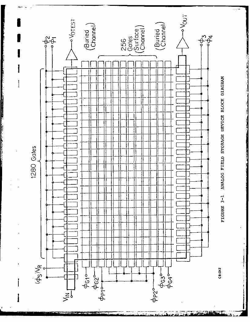
3.1 ANALOG FIELD STORAGE DEVICE
The design objectives for the field storage device are listed in
Table 3-1. The device block diagram is shown in Figure 3-1.
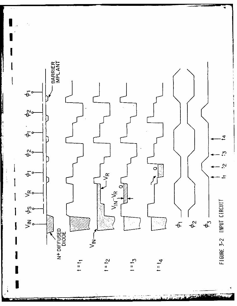
3.1.1 Input Circuit
The input circuit consists of a diffused diode V IN and two
polysilicon gates 03 and VR The input structure and clocking
is shown in Figure 3-2. The input voltage is applied to VIN.
0S is clocked high to sample VIN during the 01 low time. After
0S has returned to the low state, a charge packet Q is stored in
the input circuit and can be transferred along the input register
by clocks 01 and 02. These input horizontal clocks are generated
by off-chip clock drivers. It can be seen that the magnitude of
Q is determined by the difference of the potentials between VIN
and VR. By applying an appropriate dc voltage to VR, the magnitude
of the charge packet Q is proportional to the input voltage VIN.
The input register is designed using buried channel technology to
insure good charge transfer efficiency at the high speed clocking
rates.
3.1.2 Parallel Register
The parallel registers are surface channel devices. Surface
channel technology allows more charge to be stored per unit area.
Since the major portion of the chip is taken up by these registers,
this greatly influences the chip size. The parallel registers are
low frequency registers so the speed advantage of buried channel
3 1
*-*: X A
W: -0 cI-~a Qa c
0 )C )0 = *q) :3
Fln Tn2 F O
0cv~c,
I co0LC)~~~ roC
....... DHI.l..i..l[I .p
r __ _ _ _ _
Li _:
-17 FH
II 2_ II
_ -- C

IFIELD STORE DEVICE
DESIGN OBJECTIVES
I
STORAGE CAPACITY 640 X 256
MAX. HORIZONTAL DATA RATE 12 MHz
SMAX. VERTICAL DATA RATE 16 KHz
INPUT SIGNAL SWING 1 V TYP.
OUTPUT SIGNAL SWING 1 V TYP.
NONLINEARITY + 3% TYP. + 5% MAX.
CTE 0.99995 MIN.
SATURATION CHARGE 0.9 X 10⁶ ELECTRONS TYP.
SIGNAL-TO-NOISE RATIO 50 dB MIN.
MAX. DC SUPPLY + 15 V
AC CLOCK INPUT 4 TTL CLOCKS + 2 MOS CLOCKS
POWER DISSIPATION 300 mW MAX.
CHIP AREA 199 mil X 740 mil
I{
I
II
I.-jU<
I L
0 C14
LL >E
zz
-wL

FAIRCHILO IMAGING SYSTEMSA Division of Fairchild Camera and Instrument Corporation
technology is unnecessary. A discussion of buried to surfacechannel transfer is contained in Appendix 2.S IThe parallel registers are clocked by two phase clocks. The input
ri-gister and output register clocks are also two phase. Therefore,
when a line is clocked in, the signal charge resides under every
other gate. As this line is clocked through the parallel registers,
only half the available space is used. Each signal charge is
clocked down a vertical register adjacent to the gate it was stopped
at in the input register. Since only every other gate had charge
under it in the input register, only every other vertical register
is used by each line. So as not to waste half the vertical register
area, alternate lines are clocked in and stopped under different
sets of gates in the input register. Odd lines are stopped under
the "2 gates and even lines under the 01 gates. With this inter-
lacing scheme all parallel register area is used, (see figure 3-3).
There are two special gates at each end of the parallel registers.
Charge is not stored under these gates. They are included to
isolate the storage area from the high speed input and output
registers. Capacitive coupling between the parallel and I/O
registers during input and output clocking is minimized by the
insertion of these gates Gl, G2, G3, and G4, (see Figure 3-1).
All clocks to run the parallel registers and Gl, G2, G3, and G4
are generated on chip from 2 TTL clocks supplied to the chip.
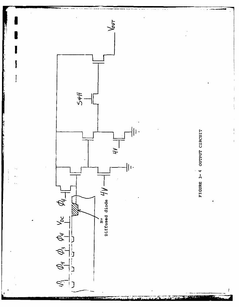
3.1.3 Output Circuit
A schematic diagram of the output circuit is shown in Figure 3-4.
The output register employs the same two phase structure as the
input register. The on-chip generated clocks % and 0 (SEE NOTE 1)
transfer the charge packets along the output register into a diffused
I3 -2
.1
L ... ..... . .. .. .. .. . ... . .,.-- . 4.

I.(4*2
W OAz
E-I a -4E-4o
z U3
= 04 UCI E-
E-4 E-i
134 z
0E-4
= H .4 U
E-
*1m
. ri)
FAIRCHILD IMAGING SYSTEMSA Division of Fairchild Camera and Instrument Corporation
!diode. The potential of this diode is monitored by a three stage
source-follower output amplifier. A gating transistor is positionedbetween the two stages so that a sample-and-hold output waveform
can be obtained. The sample and hold clock 0 SH is also generatedon-chip.
Note 1: For clocking speeds in excess of 400KHz, off-chip
clock drivers must be provided.
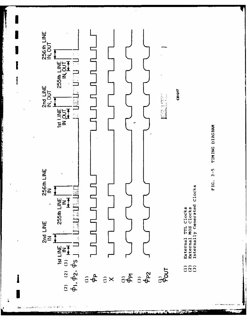
3.1.4 Timing Requirement
As illustrated by the block diagram of Figure 3-1, a maximum of
three external TTL level clocks and two MOS clocks are required
to operate the device, at output rates less than 400KHz. A
detailed timing diagram is shown in Figure 3-5. 01 is acontinuous MOS level input clock which controls the input circuit
and the input serial registers. OUT is a continuous TTL levelclock which controls the output register and the output amplifier.
OP is a TTL level input clock which controls the parallel registers.OP is typically operated at the 15.7KHz line rate with 10 us high
time. During this 10 us horizontal blanking time, the serialregister clocks are stopped and the parallel clock generators
are activated. In this manner, the internal logic circuits to
generate the parallel clocks are disabled during the 53.5 us
active line time when read-in and read-out occur. No coupling
of the parallel clocks will be visible in the output waveform.
3.2 ANALOG FRAME STORE MEMORY
The block diagram of the Analog Frame Store Memory is shown in
Figure 3-6.
3-3
J__ , , • . .Z-: . " t . --' . " ' -- - - " = .7T,
z
UL)
w N~
Z F--i 6)o 0
z ~
-j0
-4
w u
I6C~ 0 04
W C\i uU uz W
E-OX >
c z -4 -4 q
~JIZtM t
- a.
C-OJ N

4 c
- WEO
aZUU
4 -0
0-' -, III
o2 11L,wr
pc
Ae I,-

Iif FAIRCI4ILO IMAAG1NG SYSTEMS
, |A Division of Fairchild Camera and Instrument Corporation
3.2.1 Input Circuits
The 30 FPS composite video is clamped during the "back porch"
period of each line and the sync is removed from the signal. The
resulting video passes through the input video multiplexer to thetwo independent adjustable gain amplifiers. The input is grounded
for the first right pixels to provide a black clamp level for the
outputs. Although the video is present at the input of each device,
gating of the input clocks determines when video is to be stored in
the devices.
Each video channel is independently adjustable to the desired gain
and offset for the particular storage device through a wide band
video amplifier. This data is inputted to the device via 0 as
described in paragraph 3.1.1. During Mode 2, alternate line video
is inputted 1800 out of phase. In this fashion, two TV lines con-tain interleaved sampling data which is at twice the Nyquist limit.
For example a black-white pattern at twice Nyquist results in all
white levels being stored for lines 1, 3, 5 etc., and all blacklevels for lines 2,4, 6 etc. This data is scan converted, digitized
and sent to the IADD as in Mode 1.
The sync stripper circuit derives Horizontal and Frame Sync fromstandard EIA composite video. If the video input is in the form of
non-interlaced serial data, Horizontal and Frame Syncs must be supplied.
3.2.2 Timing/Control Circuits
An 8085A microprocessor provides overall control for the system.
The instructions for the microprocessor are stored in a UV Eraseablej PROM of 2K x 8 bits. 256 x 8 bits of RAM are available for use by
the microprocessor for temporary storage. The microprocessor con-
trols the input and output functions of the field storage memories
on a line oriented basis.
3-4

FAIRCHILD IMAGING SYSTEMSI1 A Division of Fairchild Camera and Instrument Corporation
*Real-time control is attained by the use of three hard-wired
interrupts-line sync, frame sync, and output sync. The first two
interrupts permit the microprocessor to maintain an input line-count of the incoming composite video, while the latter interrupt
Iindicates the completion of one line of output. Status information
from the I.A.D.D. is converted to an 8 bit word in the serial to
parallel input shift register, and then input to the microprocessor
via an 8 bit input port. Control I.D. words are generated by the
microprocessor and inserted into the data path via the preamble/
video multiplexer.
The maximum clock frequency required to output the slow scan digital
data is 24.48 MHz at 7.5 FPS. The clock frequency required to input
* data to the storage device at 30 FPS is 12.24 MHz. In order to*maintain a synchronous system, a master 24.48 MHz oscillator will
be used with all clocks derived from this source. The input clockmust be gated to provide precise synchronization with the incoming
- video. Since the input clock is derived from the master oscillator,
the master oscillator must be capable of being gated at the start
of each line during the input operation. Start-up of the oscillator
will be delayed for an additional half cycle for alternate lines
in Mode 2 operation. All clocking rates will be binary multiples
of the master clock frequency. Therefore, the actual frame rates
are .117, .469, .938, 1.88, 3.75 and 7.5 FPS.
The output clock divider, under microprocessor control, provides
f the output clock generator with the proper frequency clocks corres-
ponding to the frame rate selected. The output clock generator,
upon receipt of a command from the microprocessor, generates the
clock pulses necessary for outputting one line of video from either
jof the two field storage devices. Upon completion of one line, an
output complete interrupt is sent to the microprocessor. Each
line outputted requires a separate output command.
3-5 4

FAIRCHILD IMAINO SYSTE M8*A Division of Fairchild Camera and Instrument Corporation
The input clock generator, upon reciept of a command from the
3 microprocessor and at the beginning of a line of video generates
the appropriate clock pulses necessary for inputting video into
one or both of the field storage devices. Inputting will continue for
I the multiple lines until a stop input command is received.
3.2.3 Output Circuits
The output from each device is independently amplified and filtered
to eliminate clock modulation in the output amplifier. Independent
black clamp circuits are provided to establish a dc reference for
each device. The dc reference is derived from the first 8 pixels
of each line which were referenced to black during input. The
data is outputted from the storage device via 0 as described in
paragarph 3.1.3
The output multiplexer recombines the slow scan outputs from the
storage devices into a serial output data format by "ping-pong"
action between devices. The multiplexing is controlled via the
Mux control signal.
J The analog video information is converted to an 8 bit binary word
by the A/D converter. A sample and hold circuit (internal to the
A/D) provides the means to store the analog video level presentat strobe time and hold this level for the entire conversion time.
Strobe repetition rates from 47.8KHz to 3.06MHz are possible,
I yielding an equal number of A/D conversions. The A/D converter
selected is capable of conversions from d.c. to 11 mega-conversions
I per second. The conversion time is 150 nanoseconds.
I
I 3-6

!FAIRCHILO IMAGING SYSTEMSA Division of Fairchild Camera and Instrument Corporation
Each pixel time is :ivired into 8 bits representing 256 intensity
levels. The bit time is eight times the pixel clock, yield-
ing a maximum rate of 24.,jAHz. At the beginning of each pixel
time the next characteL is loaded in parallel to an 8 bit shift
register. The data is then shifted out under control of the bit
clock. The bit clock and S/R output are sent to the IADD for re-
construction and display through differential line drivers.
3.2.4 Control ID
In any transmission system involving serial digital data, synchron-
izing information must be inserted to identify the data and to
establish the "frame" of the serialized byte (in this case, pixel).
This synchronizing data must be unique in that the actual data
must not be confused with the synchronizing data. In this system,
the Frame Store Memory A/D converter generates data from 0 - 255
with 255 having the binary value of all ones. The A/D output will
be tested for this condition and if it occurs, the least signifi-
cant bit will be inverted changing the value to 254. Thus, the
all ones condition cannot occur in normal data. This code will be
reserved for synchronizing purposes. Each line of transmitted
video will be preceded by three characters. The first two characters
will be all ones. The third character will be uniquely defined by
its relationship to the all ones data. This byte will always begin
with a zero bit to establish the byte or pixel frame. Each line
of video will contain a start of line character unless it is the
first line of a frame.
Each line of video will contain:
2 characters of all ones
1 control character
640 image pixels
3-7

IFAIRCHILO IMAGING SYSTEMSA Division of Fairchild Camera and instrument Corporation
These characters will be inserted to read from the Frame Store
Memory at the appropriate time under control of the central timing
logic.
3.2.5 Mode 3 Operation
The implementation if the dual data rate mode is in accordance with
the algorithms described in Figure 3-7 or Figure 3-8 depending uponthe interlaced nature of the input video. The first set of data,stored in device 2, consists of 256 lines x 640 pixels representing
a field of TV data and shall be referred to as the slow speed data.
The second set of data, stored in device 1, is the center 112 pixelsof the center 112 lines of the input video. This data shall be re-
ferred to as high speed data. Using an actual count of 112 rather
than 100 maintains compatibility with the counting sequence of theIADD.
The slow speed data is outputted at .938 FPS and is time interleaved
with the high speed data. After each high speed output, slow speed
data is transmitted. The slow speed data requires several cycles
to complete a full field. At 7.5 FPS the time allocated for slow
speed transmission is:
T = (4 x Tst) - Ths (EQ 1)
Where Tst is the standard frame time 33.33 msec., and Ths is the
time required to output 112 lines at 7.5 FPS.
Substituting the above in EQ 1 we have
T = (4 x 33.33) - 9.0 = 124.32 msec.
3-8

I
INITIALIZE INITIALIZECCD 1 CCD 2D INII SLO SCAN
OUTPUT DURING0 30 FPS UPDATEI , G0 To C
START ENTRY ATI LINE 94 OF FIELD 1
THRU LINE 149 1. FILL 264PIXELS AS3.55 ms 3.55 ms BLACK
2. ENTER 112 PIXELSAS DATA
3. FILL 264PIXELS ASWAIT FOR LINE BLACK94 OF FIELD 2 63.5 ls
16.67 ms 13.12 ms
ENTER LINES 94
THRU 149 OFFIELD 2
20.22 ms 3.55 ms REPEAT ABOVE
r63.5 ps
SHIFT 144 LINESSY@ 63.5 a SEC
PER LINE CLEAR OUTPUT29.36 ms4 9.14 ms REGISTER @
r n 12.5 MHZ
NSERT CONTROL IDOUTPUT 112 LINES
38.36 ms 9.00 ms INSERT CONTROL ID
TQ .DELETE FIRST 264PIXELS
_2.OUTPUT NEXT 112 [email protected] MHz
WAIT FOR D LNEXT UPDATE IDELETE LAST264PIXELS
7.5 OR 15 FPS BO4 Ms
IINSERT CONTROL 10
OUTPUT 61 LINES @ 7.5 FPSOR INSE RT CONTROL IDOUTPUT 28 LINES - 15 FPS OUTPUT 870 PIXELSGO TOB 0390.6 KHz
AFTER OUTPUTTING256 LINESWAIT FOR NEXT FRAMEGO TO D
FIGURE 3-7. ALGORITHM; DUAL DATA RATE, INTERLACED
i

INITIALIZE IIILZ
DAT
ENTERETE LEAIINEBAC2.4 LINE AS 63.5 IN IITSOWSA@B3LAP 1 OUPU DUIN
25.25 LIN 186 2.OUPTTEXER2XL
DELET LAST 297IEL
2. NTR12 IS CANSI
UPDATA7.5~3 ORL 26P5EL AS FTRTPTN
GOTLNESAS26IE
WAI FORPU NEXT FRAMEXELGO ~ ~ ~ G [email protected] ~
FIGURE 3-8 ALGORETHMTDUAL DAT RATE, NONINTERLACE
CLEAR EXT 1
LINES @ 625A -S TCNR

IFAIRCHILD IMAGING SYSTEMSA Division of Fairchild Camera and Instrument Corporation
The number of lines transmitted per cycle is
#Lines/Cycle = T Cycle (EQ 2)T Line
Where Tline is the time required to output one line at .938 FPS.
Substituting the above in EQ 2 we have
# Lines/Cycles = 124.32 61.47
Using 61 lines, the number of cycles for 256 lines is:
256
# Cycles = 3a = 4.19 Cycles61
or the time to output a complete field of slow speed data is:
Ts = (#Lines x #Cycles x T line) + (Tline X Overflow)
+ Update time (EQ 3)
Substituting in EQ 3:
Ts = (61 x 4 x 2.022) + (2.022 x 12) + 45
T s =562.63 msec
The interleaved output is shown in Figure 3-9. With the high
speed data rate at 15 FPS, the total time to complete a field
at slow speed is:
Ts = (28 x 9 x 2.022) + (4 x 2.022) + 90 - 607.5 msec.
The data received by the IADD is reconstructed into a split
J screen display with the center 112 lines x 112 pixels being
updated at 7.5 or 15 FPS, and the remainder of the display at
3 -9

0<
NI ik/ zu,
LI; -
ui z <
< <<
0~0U.i
-~ -<
IT

IFAIRCHILD IMAGING SYSTEMSA Division of Fairchild Camera and Instrument Corporation
.938 FPS. The horizontal resolution of both sections will be the
same while the vertical resolution of the center portion will be~greater than that of the outer portion.
3.3 IMAGE ANALYZER DIGITAL DISPLAY (IADD)
The function of the IADD is to reconstruct the digital video
information received from the Frame Store Memory for display on
a standard TV monitor.
The digital video information is received via a simulated trans-
mission data link from the Frame Store Memory at data rates from
0.1 to 7.5 frames per second. All IADD operations (mode, update
rate, and interlace format) are controlled by front panel switches.
This status information is provided to the Frame Store Memory over
the same data link, when the Frame Store is being reloaded.
The IADD memory is required to store 488 lines, 640 pixels per
line, with 8 intensity bits per pixel. A memory configuration of
512 x 1024 x 8 will store one frame of data. To provide an
uninterrupted display while the memory is being updated requires
two full frame memories of storage. While one frame is updated with
the latest low speed video information, the other frame is providing
the display with 30 frames per second video. Following completion
of the low speed update and at the beginning of the next display
frame, the memories' roles are reversed providing continuous
display. Two additonal partial frame memories are provided for use
during mode 3 operation when the center 112 pixels of the center
112 lines are updated at a higher rate than the remaining background
data. The two partial frame memories, each consisting of 128 x 128
x 8 bits of storage, provide the same "ping-pong" updating operation
as the full frame memories for uninterrupted display of the center
area in mode 3 operation.
3 - 10

FAIRCHILO IMAGING SYSTEMSA Division of Fairchild Camera and Instrument Corporation
Refer to Figure 3-10 for the overall block diagram of the IADD.
The input data is clocked into the Input Shift Register by the
j input clock to provide a single 8 bit pixel. The Control Decode
detects the control identification codes being transferred (such
as start frame, start line, etc.) and also provides synchronization
information with respect to the 8 bit pixels. The Pixel Group
assembly shift register assembles eight, 8 bit pixels into a single
64 bit word for writing into one of the four frame memories. The
memory addressing circuitry sequentially counts through the 80
pixel groups (of 8 pixels each) per line and 488 lines per frame,
converting each screen position to a memory address for write-in
into one of the four frame memories. The Master Control logic,
evaluating the mode/data rate status switches and the control
identification decode, selects one of the frame memories. Display
readout utilizes equivalent pixel group and line counters to
address one of the four frame memories selected for the display mode.
The Sync Generator/Output Video Control circuitry generates the
timing signals necessary to sequentially read the memory in synchron-
4ization with composite sync applied to the video processor. The
memory outputs, 64 bits wide each, are tri-state outputs enabling
one of the four memories to be presented to the Video Bit Assembly
Shift Register as eight pixels. The video shift register sequent-
ially clocks one pixel at a time (8 intensity bits per pixel) to
the Digital to Analog Converter for conversion to one of 255 levels
of video. The Video Processor mixes this video signal with composite
sync and composite blanking to provide the composite video necessary
for display on a standard TV monitor. The Video Chop Circuit isenabled in mode 2 only to present the D/A converter with two digitalcodes per pixel time consisting of the pixel's actual bit weight
and then all zeroes; this provides resolution enhancement when
coupled with the video acquisition performed by the Frame Store
Memory in mode 2.
3 -11
It

cr (A
3
coJ
0(kLL
P.-
FAIRCHILO IMAGING SYSTEMSI: A Division of Fairchild Camera and Instrument Corporation
3.3.1 Input Section
The primary function of the input circuitry is to convert the serial
data stream into a 64 bit parallel word for memory write-in. As
discussed previously, the speed of the input data ranges from 0.1
to 7.5 frames per second. This corresponds to pixel rate from
47.8KHz to 3.06MHz. However, since there are 8 intensity bits per
pixel, the actual data rates range from 382.5KHZ to 24.48MHz. There-
fore, Shottky TTL devices have been selected for the input shift
register and control decode areas to handle the 25MHz data rates.
As an 8 bit pixel appears at the output of the input shift register,
each bit is transferred to the input of one of the eight shift re-
gisters composing the Pixel Group Assembly Shift Register. This
transfer occurs once for every eight input clock cycles enabling the
use of low power Shottky technology in this and succeeding stages.
Following the filling of all 64 bits of the Pixel Assembly shift
register, the Memory Buffer is strobed. Clocked once per 64 input
clocks, the clock rate ranges from 6.1KHz to 382.5KHz. This implies
a memory cycle time of less than 2.56 microseconds - well within the
500 nanosecond cycle time of the memories selected.
The control decode sequence involves two steps. First a preamble
of sixteen "ones" followed by two "zeroes" must be detected. The
first zero following the sixteen ones if the first bit of the
eight bit control identification word. As all input data is re-
ceived in eight bit multiples, this detection provides synchroni-
zation for all succeeding pixels until another control code is
detected. The control identification will be Start Frame, Start
Line, Start Hi Frequency, Start Lo Frequency, or Status Request.
The absence of a valid code detection will enable a front panel
3-12
.. . . ..... . T.. . '. . . ..: -

IFAIRCHILD IMAGING SYSTEMSA Division of Fairchild Camera and Instrument Corporation
fault light to indicate transmission unlock. The combination of this
code and the front panel switch information provides all the data
required for the Master Control Logic to enter the eight pixels in
the correct address of the correct memory.
Decoding the "Status Request" code indicates to the IADD that the
Frame Store Memory is about to go "OFF LINE" on the data line while
still providing a clock signal. The Master Control will then enable
its own tri-state data driver and shift out the mode/data rate
status of the front panel switches to the Frame Store Memory. The
clock frequency during this transfer will be 1.56MHz (slow enough
to prevent errors due to clock/data skew arising from unequal
delays). This sequence will occur only during normally "dead"
time for the link, i.e., when the Frame Store Memory is reloading.
Figure 3-11 illustrates the control identification codes to be used.
3.3.2 Memory Subsystem
I
The Memory System consists of two full frame dynamic random access
memories and two partial frame static random access memories. Each
of the four memories is completely independent with separate
read/write controls and addressing logic. Two full frames of
storace are recuired to provide an uninterrupted disDlaV while
asynchronously receiving a new frame of data. In addition, during
mode 3 operation only, the center, 112 Pixels of the center 112
lines are stored in the two partial frame memories with one frame
servinq as the display memory while the other partial frame serves
as the update memory.
The 30 frame per second display refreshinq imposes a 12.6MHz video
update rate unon the memories. This would correspond to a memorv
read cycle time of 80 nanoseconds. Bv readina 8 Pixels of video
simultaneously, the cycle time can be increased to 640 nanoseconds -
a realistic time for commerciallv available memory svstems. 8 Pixels
3 -13
L . .... . .. . . ... . .... . .. ... .... -- l i l li . .

I0E-4
a'C' U
wz ow 40 n
Ei E-4 u- r-4 HO OE-
C~'4
o0 H- 0 H- 0 H
o 40 4 r- 0 0
00 a~ 0 (0 fq QwI nE nE n t
co o- 04 04 04 CL N N 440 0r- 4o A*., t 4fl 44I 0Z - 4
0 -4 t, NC o )rE- 0 H- 0f or n a U
0 0D 0 0 0 Hi
0 0 EH 4 H -H -H - 40H H 0O 4O z
0
E-1 HI H4 H- H- H- H~~~~~- H -4 H H 0
Z H4
H4 P 4 H4 H4 0
r-4 P-4 r4 E-4EF-
zH4 H4 H- H- H0
H- -4 H H
H- H4 H-- H- H
H 4 F- H -H H
H- 1- H- H- -

FAIRCHILO IMAGING SYSTEMSA Division of Fairchild Camera and instrument Corporation
3 of video, with 8 intensity bits per pixel requires 64 bits of
data to be read simultaneously from the memory-defining the memory
architecture as 64 bits wide. Each TV line containing 640 pixels
is organized as 80 pixel-groups bf 8 pixels each). The 8 pixelsare loaded into shift registers following each memory read cycle
and shifted out at the proper 12.6MHz rate while the memory is
operating at 1.56MHz. 488 lines of 80 pixel groups each requires
the storage of 39,040 64 bit words per frame. A commerciallyavailable memory system of 65,536 words by 64 bits has been selected
to fulfill these requirements for each frame of dynamic memory.
Four printed circuit boards of 65K by 16 each will provide the
desired one frame storage. Each board is composed of sixty-four
16,384 bit dynamic RAM devices. Four additional boards of buffering
and control are required to complete one frame of storage. Two
full frames of 8 boards each are required.
The partial frame memories require considerably less storage.
112 lines of 14 pixel groups each yields 1,568 64 bit words.
Thirty-two static RAM devices (1,024 x 4) will be configured to
provide a partial frame memory of 2,048 by 64. Two partial frame
memories, as described above, are required.
The two dynamic full frame memories impose an additonal constraint
on operation, a need for period refreshing of the stored data to
prevent data loss. 128 memory cycles performed on certain addresses
are required within a 2 millisecond period to prevent data loss.
The memory controller P.C. board associated with each frame memory
contains circuitry to automatically provide one of these memory
cycles every 16 microseconds. This function is not possible durinq
display readout as every memory cycle durinq the active line period
(53 microseconds) is utilized. However. normal display readout
cycles will also refresh the memory as lona as all of the 128 addresses
3 - 14
'6"

1 FAIRCHILO IMAGING SYSTEMSA Division of Fairchild Camera and Instrument Corporation
of all of the memory devices are utilized within a two millisecondperiod. By proper direction of the address lines to the memory,
this mode of refresh would be possible. Another factor to beconsidered is the time period during vertical retrace (approximately
13 milliseconds) and in mode 3 during the center 112 lines when the
memory is not being accessed. Switching to the automatic refresh
mode during these time periods is not practical because the refresh
address counter of the memory controller would not be synchronized
with the display readout address. This condition could leave a
gap of greater than 2 milliseconds between refreshes during the
transition periods to and from automatic refresh.
A solution compatible with all modes of operation which has been
selected involves no dependence upon normal read or write cycles
to provide refreshing. Instead the TV Sync-Generator circuitry
will provide refresh requests during the horizontal retrace time
(a 10 microsecond period where no memory cycles are required).
This refresh will continue through vertical retrace. The memory
controller will provide the refresh address for this mode. Then
when the frame memory is switched from display readout to frame
update mode, the refresh mode can switch to automatic (using the
same refresh address counter) without any refresh gaps. The
automatic mode is allowed during frame update because successive
memory cycles are not necessary (one write cycle every 2.56 micro-
seconds is the fastest update rate).
The three modes of operation present various requirements to the
memories' operation. Mode 1 and 2 are indistinguishable to the
memories, the video of mode 2 is "chopped" following memory
readout. The input data of modes 1 and 2 consists of 488 lines
of pixel groups (640 pixels) per line in either interlaced or
non-interlaced format. One write-in counter ( composed of a modulo
80 pixel group counter, modulo 244 field line counter, and field
flip/flop) is used for both full frame memories; the frame memory
being updated has the write-in counters multiplexed onto its
3-15

IFAIRCHILD IMAGING SYSTEMSA Division of Fairchild Camera and Instrument Corporation
Iaddress lines. Non-interlaced input involves interchanging the
field flip/flop with the l.s.b. of the field line counter. One
read out counter (with an identical configuration as the write-in
counter) is utilized by all four frame memories. In mode 1 or 2, the
frame memory not updated is addressed by the readout counter for
readout synchronized with the TV Sync Generator.
Mode 3 operation involves the storage of one field of data (back-
ground) in one of the full frame memories, and a partial field of
data (center 112 pixels of center 112 lines) received in either
interlaced or non-interlaced form stored in one of the partial
frame memories. The two data types are received at different
update rates with the low speed (1 frame per second) background
data being interrupted several times during the field transfer
by the high speed (7.5 or 15 frames per second) center area data.
This fact necessitates an additional set of write-in counters
for the high speed data so that the line number at which the low speed
data was interrupted can be maintained for use when that data transfer
is resumed. At the start of a display frame, the most recently
updated full frame and partial frame memories are selected for
readout; if either frame's alternate memory completes a new update
following this time, the memories are not switched until the start
of the next display frame. The single readout counter (interlaced
readout only) will initially be addressed to one of the full frame
memories at the start of a field and begin readout or pseudo-
readout (in the odd field there is no available data and consequen-
tially all "zeroes" are substituted for memory data) until the
center 112 area is decoded. At this time the readout address is
directed to the partial frame memory selected at the start of the
frame and readout then continues with this memory. Display readcuts
will continue alternating between these two memories as the center
area is traversed. Following the center 112 lines, control and
addressing will revert back to the full frame memory for the
3 - 16

FAIRCHILO IMAAING SYSTEMSA Division of Fairchild Camera and Instrument Corporation
* remainder of the field. The partial frame memory will not actually
see the same address as the full frame memory, but will instead
i pass through a subtraction circuit (pixel group minus 33, and
field line minus 94) which compensates for the different memory
sizes of the full frame and partial frame memories.
3.3.3 Output Logic
The digital representation of the video at the output of the memory
consists of 64 bits representing 8 pixels. At the end of each
memory cycle all 64 bits are loaded into eight parallel to serial
shift registers. During the time the next memory cycle is in
process, each of the 8 pixels is individually presented to the
Digital to Analog Converter. In modes 1 and 3, the D/A converter
is clocked once for each 8 bit pixel (12.6Mhz) with the resulting
analog voltage appearing at its output. Mode 2 provides a slight
complication to this scheme. In this mode the D/A converter isclocked twice per each pixel output from the shift register. The
video chopper sequentially presents the 8 bit pixel and then all"zeroes" (or vice versa) to the D/A converter once per pixel output.
The resulting analog video output appears as normal video for one-
half the normal pixel time of 80 nanoseconds and is zero for the
other half of the normal pixel time. The phasing of the chopped
video is reversed on alternate fields to provide enhanced resolution.
The Digital to Analog converter selected must be capable of updating
at either 12.5 or 25 MHz, providing a relatively "glitchless" output.
A commuercally available 30MHz D/A converter with an add-on deglitcher
has been selected to perform this function.
3.3.4 TV Sync Generator/Master Oscillator
The main component of the TV Sync Generator is a CMOS LSI TV sync
generator integrated circuit. Clocked by 504KHz (obtained by a
synchronous countdown of the Master 25.2MHz oscillator), this I.C.
3-17
- -

FAIRCHILD IMAGING SYSTEMSA Division of Fairchild Camera and Instrument Corporation
provides all TV line, field, and frame related signals used in the
IADD. Combining these signals with 25.2MHz and its derivatives
yields the video, chop, and D/A clocks used in the output area.
3.3.5 Video Processor
The video processor passes the D/A converter analog output through
a low pass filter prior to mixing the video with composite sync
and blanking to produce a composite video output suitable for
display on a standard TV monitor.
3.4 POWER REQUIREMENTS
3.4.1 Analog Frame Store Memory
The operating voltages for the analog frame store memory circuitry
will be derived from commercially available power supply modules
operating off 115V, 60Hz laboratory power.
The A/D converter will be powered by a separate dedicated power
module. The power to the TE coolers will be derived from a separate
dedicated power module.
3.4.2 IADD
The power supplies selected for the IADD will be standard commercially
available computer grade supplies operating off the laboratory
lI5VAC, 60Hz line.
The two full frame dynamic memories require +12V, +5V, and -5V at
currents under 13, 33 and 1 Amp, respectively. Additionally, a
power-on sequence and failure control will not enable the +12V and
+5V supplies without the presence of the -5V (VBB) supply.
3-18

I FAIRCHILD IMAGING SYSTEMSA Division of Fairchild Camera and Instrument Corporation
The two static partial frame memories require +5V at approximately
6 Amps. The remaining TTL logic circuitry requires +5V at
approximately 8 Amps. The D/A converter requires +15V, -15V,
+5V, and -5.2V at currents under 150ma., 250ma., 30ma., and 100ma.,
respectively.
3.5 PACKAGING
3.5.1 Analog Field Storage Device
The Analog Field Storage Device (3071Z) packaged in its heremtic
DIP is shown in the photograph in Figure 3-12. The cover has
been left off to show the internal connections and the chip.
This arrangement provides the flexibility for both cooling
and ease of handling in uncooled breadboards. The device
pinouts and their associated functions are listed in Table 3-2.
For breadboard use, the top brazed pins are bent over to form
a standard dip package. For cooled applications, these pins
are cut back and wire bonds attached. In this way, there is no
cooling losses through the pins.
3.5.2 Analog Frame Store Memory
The Analog Frame Store Memory electronic components, A/D con-verter, connectors, associated harness, and the field storage
devices are contained in the electronics enlcosure detailed
in Figure 3-13. The circuitry is mounted on five plug-in
circuit cards. The logic cards are standard wire wrapped boards
and the processing circuit card are vector boards with the same
outline dimensions. The A/D converter is hard mounted to the
chassis.
Each analog field storage device is contained in a sealed plug-in
assembly containing a thermoelectric cooler. The storage device
is mounted to the TE cooler. The module will plug into a receptacle
3-19
lit.

p
~i ~N
(2
w1ij w
0H-LI;
W
U-
CI;
U-
CU-

n TABLE 3-2
FIELD STORAGE DEVICE
PINOUTS
1. Vss SUBSTRATE GROUND
2. 0 31N 03 GATE
3. 3OOT 3 CLOCK
4 041N 04 GATE5. 04 0UT 04 CLOCK
6. R TTL CLOCK TO BE SUPPLIED
7. vCD 2 12V
8. TTL CLOCK TO BE SUPPLIEDOUT
9. p TTL CLOCK TO BE SUPPLIEDP
10. SHG SAMPLE AND HOLD CLOCK GROUND
ii. SH SAMPLE AND HOLD CLOCK TEST POINT
12. VOUT OUTPUT SIGNAL
13. V CLOCK GROUNDVCG
SG14. v SIGNAL GROUND
15. VOTEST TEST OUTPUT
16. VDD 14V
17. OG OUTPUT GATE BIAS
18. VCD1 5V
N. D TTL CLOCK TO BE SUPPLIED
20. TTL CLOCK TO BE SUPPLIED
21. 0 2 MOS CLOCK TO BE SUPPLIED
22. 0 1 MOS CLOCK TO BE SUPPLIED
23. V INPUT REFERENCE VOTLAGER
24. V1 INPUT SIGNAL
II
- - - - ---ir i

I | - ------ & * I * ~ II-J
, c•iS 1IA
lILII
_____....
II -l- iii,,
/ -3-
-
'i'nu
.. .......
.. -,r . .. .. .-

1I FAIRCHILO IMAGING SYSTEMS
A Division of Fairchild Camera and Instrument Corporation
at the rear of the enclosure bringing it into contact with an
externally mounted heat sink. To minimize the heat rise in the
unit, power supplies for the Analog Frame Store Memory will be
I' |contained in a separate enclosure.
3. 5.3 I__ DI
The IADD electronics is contained in a 42 x 19 inch equipment rack.
The main power supplies are positioned at the bottom of the rack
and are provided withfan cooling. The control panel is situated
in the rack at average "eye ball" level. It contains the master
ON/OFF controls, several status lamps, the mode select switch and
frame rate select switch. A 33 position card assembly positioned
in the equipment rack contains all of the IADD circuitry. The
dynamic full frame memory system occupies 16 positions, the static
partial frame memories occupy 2 positions, and the remaining
circuitry occupies 4 positions. The dynamic memory system is
composed of printed circuit boards while all other functions are
implemented with wire-wrap or vector board conforming to the
I dimensions of the card assembly.
IIIIIII
3-20

I
SI FAIRCHILO IMAGING SYSTEMSA Division of Fairchild Camera and Instrument Corporation
APPENDIX 1ICHARGE SPILLAGE IN A FOUR PHASE SYSTEM
In a four phase clocking scheme, charge is stored under adjacent
gates. Any coupling between a gate, whose voltage is high, and
the adjacent gates, whose voltages are low, could cause signal
charges to mix, as illustrated in Figure A-1.
I When V1 goes high, the wells under V1 drop, collecting charges
D and G as they should. However, the wells under V2 drop slightly
due to the coupling effect. This causes some of charge E to mix
with D, and H to mix with G. In the two phase scheme charge
is stored under alternate gates so this problem does not arise.
A
Al-

'3VA V-7 V2 V' V V.3 V i V4 V3 V2 VI
Barrier Implant
Charge mixing over lowered barriers
F
G A
-. 1 4 PHASE RIPPLE CLOCKS
V2 V1 V2 Vi V2 Vi V2 Vi V2 Vi V2 vi
Barrier Implant
j 2 PHASE CLOCKS
-. FIGURE Al-i CLOCKING SCHEMES

II FAIRCHILO IMAGING SYSTEMS
A Division of Fairchild Camera and Instrument Corporation
APPENDIX 2
I DESCRIPTION OF BURIED-TO-SURFACE
CHANNEL TRANSFER REGION IN FIELD
STORAGE DEVICE
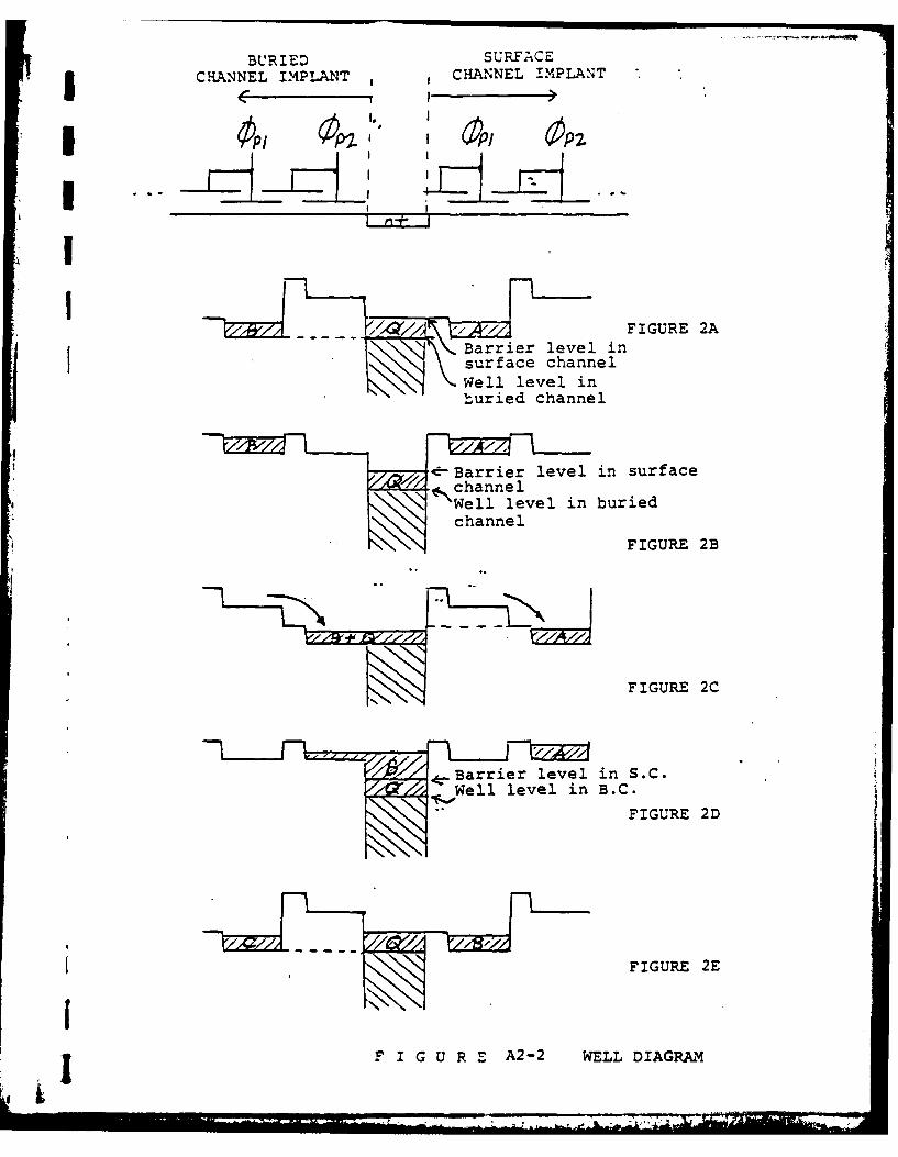
In the design of the field storage device, a strip of n+
diffusion (see Figure 1) is positioned between the buried channel
and surface channel areas. This n+ area acts as a conductor between
the buried and surface channel regions. Both the buried and surface
channel implants overlap the n+ strip to allow for alignment
S I tolerances. This overlap assures us that there will be no small
potential wells at the interface where signal charge may be
! jtrapped.
I ..Q/ ,SI FA CE
C/WAME L C, ., 7 CL
Signal charge transfer across the n+ strip is shown by the
potential well diagrams of Figure 2. The shaded areas show the
level to which the wells are filled. originally the charge isI distributed as shown in Figure 2A. All voltages then go low as
~stored in the n+ area, between the barrier level in the surface
channel and the well level in the buried channel, mixes with signalI

II FAIRCHILO IMAGING SYSTEMS
A Division of Fairchild Camera and Instrument Corporation
chargeB, spreading over the n+ area and the well of the last P2
I gate before the n+ area (Figure 2C). All clocks then go low,
dumping the mixed charge into the n+ area. The n+ area is now filled
I above the barrier level in the surface channel by an amount corres-
ponding to the signal charge B. All charge in the n+ area above the
barrier level of the surface channel is signal charge B, (Figure 2D);Iitherefore, when 0 P1 goes high, signal charge B and only B moves
into the first P1 gate past the n+ region (Figure 2E). Sianal
charge B has been transferred past the n+ strip, without gain or
loss of charge, and we have the situation we started with in
Figure 2A.
A similar scheme is used at the surface to buried channel interface.
A
!!
A2 - 2
BURIED SURFACECHANNEL IMPIANT CHANNEL IMPLANT
OP I O
-/ '7FIGURE 2ABarrier level insurface channelWell level inb-uried channel
Vc-Barrier level in surface
" Well level in buried
FIGURE 2B
FIGURE 2C
- ~.Barrier level in S.C.Wellevel in B.C.
FIGURE 2D
FIGURE 2E
F FI G URE A2-2 WELL DIAGRAM