faculty of engineering - near east universitydocs.neu.edu.tr/library/6073186793.pdf · ·...
TRANSCRIPT
NEAR EAST UNIVERSITY
Faculty of Engineering
Department of Electrical and Electronic Engineering
Signal Conditioning Elements of Mechatronics
Graduation Project
EE-400
Student: WAEL AL-HABIBI (20000519)
Supervisor: Assist. Prof. Dr. Kadri Bürüncük
Nicosia - 2002

ACKNOWLEDGEMENT
"First of all, I would like to thanks Allah (God) for guiding me through my
studies, also I would like to pay my regards to everyone who contributed in the
preparation of my Graduation Project. I am also thankful to my supervisor "Assist.
Prof Dr. Kadri Buruncuk" whose guidance kept me on the right path towards the
completion of my project.
I would like to thank my parents and who gave their lasting encouragement in my
studies, so that I could be successful in my lifetime. I am also thankful to my beloved
friend Ali Al-Ali from Computer Engineering department and Eng.Suleman Bakhsh
from Electrical and Electronic department, who helped me a lot in solving any kind of
computer problem so that I could complete my project in time. I am also thankful to my
friend M Asfor from Computer Engineering department and M. Qunjfrom Electrical &
Electronic department, who gave me their ever devotion and all valuable information
which I really needed to complete my project.
/ Further I am thankful to Near East University academic staff and all those
persons who helped me or encouraged me in completion ofmy project. Thanks!"

ABSTRACT
The Mechatronics, process control, and their elements that perform all type of the
systems, such as, measurement systems, display systems, and control systems. Also in
the study of mechatronics there are four types of control systems: the principal control,
the automatic control, the servomechatronic control, and the sequential control. Open
loop and close-loop, we use both these methods in the control systems to make the
control easy. There are two general types in the processing control, the analog
processing control and the digital processing control. Thus, we use Logic gates in the
digital control.
/
The analog signal conditioning related to the standard techniques employed for
providing signal compatibility and measurement in analog system, the need for analog
signal conditioning was reviewed and resolved in to the requirement of signal level
changes, linearization, signal conversion, and filtering and impedance matching. Bridge
circuits are common example of a conversion process where a changing resistance is
measured either by a current or a voltage signal. Operational amplifier (op-amps) is a
special signal conditioning building block around which many special function circuit
can be developed. The device was demonstrated in application involving amplifier,
converter, integrators, and several other functions.
The digital signal conditioning depends on the digital electronic in the principle of
working, digital electronic gates and comparators allow the implementation process~
Boolean equation. Digital to analog converter (DAC) are used to convert digital word in
to analog number using a fractional number representation. ~ analog to digital
converter (ADC) of the successive approximation type determines an output digital
word for an input analog voltage in as many steps as bits to the word. Also in the word
of digital signal conditioning elements there are many types, such as, multiplexing,
modulation, and buffering.
11
TABLE OF CONTENTS
ACKNOWLEDGEMENT i
ABSTRACT ii
INTRODUCTION vi
1. T:HEMECRA TRONICS ı
1.1 IN"TRODUCTION ...........•.•.•..................................•..••..............•...................•........ 1
1.2 SYSTEM ..........................................•.......•.......•.•....•.....•.......•...............................•. 2
1 .•3 MEASUREMENT SYSTEM ......................................................•......................... 4
1.3.1 The sensors 4
1.3.2 A signal conditional 4
1.3.3 A display system 5
1.4 Control system ..............•......................................................................................... 5
1.4.1 Process-Control Principle 6
1.4.2 Servomechanisms 9
1.4.3 Open Loop and Close Loop 9
1.4.4 Basic Elements of a Close Loop 1 1
1.4.5 Sequential Controller 15
1.4.6 Microprocessor Controller : ~ 17
1.5 Analog and Digital Processing Control ...........................................................•..18
1. 5 .1 Data Representation 18
1.5.2 Analog Control. 21
1.5.3 Digital Control 22
1.6 Logic Gates ......•....•..........................................•.....•.........•.........................•.......••• 23
1.6.1 AND Gate 23
1.6.2 OR Gate 24
ll1

1.6.3 NOT Gate 24
1.6.4 NAND Gate 24
1.6.5 NOR Gate 25
1.6.6 EXCLUSIVE Gate 25
1.7 The mechatronics approach 26
2. ANALOG SIGNAL CONDITIONING ELEMENTS 28
2.1 Introduction 28
2. 1. 1 Interfacing 28
2.2 Principles of analog signal conditioning 29
2.2. 1 Signal-Level Changes 29
2.2.2 Linearization 30
2.2.3 Conversion 31
2.2.4 Filtering and Impedance Matching 32
2.2.5 Concept ofLoading 32
2.3 Passive Circuits 33
2.3. 1 Divider Circuits 34
2.3.2 Bridge Circuits 35
2.3.3 Filtering 45
2.4 Operational Am plifıer 50~
2.4. 1 Symbol and Terminals 50
2.4.2 Basic Operational Amplifier ··················································~························51
2.4.2. 1 Comparators '. 52
2.4.2.2 Summing Amplifier 57
2.4.2.3 The Op-amp Integrator 59
2.4.2.4 The Op-amp Differentiator 61
2.4.2.5 The Instrumental Amplifier 63
2.5 Protection 66
2.6 Design Guidelines 67
ıv

3. DIGITAL SIGNAL CONDITIONING ELEMENTS 70
3.1 Introduction ............•...............................................................•.............................70
3.2 Review of Digital Fundamentals .......•..............................................•..................71
3.2.1 Digital Information 71
3.2.2 Fractional Binary Numbers 72
3.2.3 Boolean Algebra 73
3 .2.4 Digital Electronics 75
3.2.5 Programmable Logic Controllers 76
3.2.6 Computer Interface 76
3.3 Buffering ...................................................................................................•...........78
3.4 Converters ............................•...............................................................................•78
3.4.1 Multiplexers 79
3.4.2 Comparators 79
3.4.3 Digital-to-Analog Converters 82
3.4.4 Analog-to-Digital Converters 89
3.5 Modulation .......................................•...........................•••..............••..............•.....•.97
CONCLUSION 100
REFERENCES 1O 1
V

INTRODUCTION
The first engineering, that combine between two kinds of engineering, which
spread in our world is called the Mechatronics engineering, this new technology is very
Important for the electronic and mechanical control.
The component of an instrument that take the output signal from the sensor of a
measurement system has generally to be processed in some way to make it suitable for
the next stage of the operation is called the signal conditioning elements.
The first chapter is about the general information for the Mechatronics, in this
chapter I concentrated to explain all the principles of mechatronics, and it will consider
the overall process control loop, and it is description. Also in this chapter we shall be
able to know, the definition of mechatronics, system, and measurement system. And to
draw a block diagram of a process control loop with a description of each element.
The second chapter is about the analog signal conditioning elements, the purpose
of this chapter is to familiarize the reader with the basic techniques of signal
conditioning in process control. After you have read this chapter, you should be able to
know the purpose and techniques of analog signal conditioning, design an application of
the wheatstone bridge to convert resistance changes to voltage change, analyze the
operation of types of filters to determine its effect on a signal, draw schematics of types
of the basic op-amp signal J;Onditioning circuit and provide their transfer function,
design an analog signal conditioning system that converts a given input voltage
variation into a required output voltage variation.
The third chapter is about digital signal conditioning elements. After this chapter
we shall able to know convert a fractional binary number to decimal, octal, and
hexadecimal representation, calculate the expected output voltage of a DAC for any
digital input, explain the principle of a successive approximation ADC, draw a diagram
of a general digital to analog converter and analog to digital converter, explain theprincipal operation of modulation.
Vl

1.THE MECHATRONICS
1.1 Introduction To Mechatronics
Mechanical engineering, as a widespread professional practice, experienced a
surge of growth during the 19th century because it provided a necessary foundation for
the rapid and successful development of the industrial revolution. At that time, mines
needed large pumps never before seen to keep their shafts; transportation systems needed
more than real power to move goods; structures began to stretch across ever wider
abysses and to climb to dizzying heights; manufacturing moved from the shop bench to
large factories; and to support these technical feats, people began to specialize build
bodies of knowledge that formed the beginnings of the engineering disciplines.
Now, more than a century later, we are witnessing a new scientific and social in
previous paragraph, this a new kind of science called by mechatronics. What is a
mechatronics? and when did it start?
The word mechatronics was first coined by a senior engineer of a Japanese
company; Yaskawa, in 1969, as combination of "mecha " of mechanisms and "tronics "
of electronics and the company was granted the trademark rights on the world in 1971.
The world soon received broad acceptance in industry and in order to allow its free use,
Yaskawa elected to abandon its rights on the world in 1982. The world has taken a wider
meaning since then and is now widely being used as a technical jargon to describe a
philosophy in engineering technology, more than the technology itself. Mechatronics are
the synergistic integration of mechanical engineering with electronics and intelligentIi'
computer control in the design and manufacture of products and processes.
A mechatronics system has two main components as sh~wn in Figure 1.1. The
controlled system is the mechanical process that is in contact with the world with all of its
sensors and actuators. The distinguishing features of a mechatronic system from other
systems are the three sub-systems of the controlling system used for perception,
knowledge representation and planning and control. The intelligence is usually embedded
in the planning and control sub-system. Here, based on the information gathered from the
sensors, computational intelligence methodologies are exploited to plan a course of action
that will enable the controlled system to achieve the given tasks.

Conventional microprocessors, artificial neural networks, fuzzy logic and
probabilistic reasoning are among the tools used in the sub-system for information
processing and decision-making.
In the design now of car, robots machine tools, washing machine, cameras, and
many other machines, such as integrated approach to engineering design is increasingly
being adopted. The integration across the traditional boundaries of mechanical
engineering, electronics and control engineering has to occur at the earliest stage of the
design process if cheaper, more reliable, more flexible systems are to be developed.
MECHATRONIC SYSTEM
CoatrollingSyııte•
Processmonitoriııg/visualization
ControlledSyıtem
~WORLD
Figure 1.1 The architecture of a mechatronic system
1.2 Systems
Mechatronics involves, what are termed, systems. A system can be thought of as a
black box, which has an input and an output. It is a black box because we are not
concerned with what goes on inside the box but only the relationship between the output
2

and the input.
Thus, for example, a motor may be thought of as a system, which has as its input
electric power and as output the rotation of a shaft. Figure 1.2 shows a representation of
such a system.
Input Output
.. Motor ..•..Electric power Rotation
Figure 1.2 An example of a system
A measurement system can be thought of as a black box, which is used for making
measurements. It has as its input the quantity being measured and its output the value of
that quantity. For example, a temperature measurement system, i.e. a thermometer, has an
input of temperature and an output of a number on a scale. Figure 1 .3 shows a
representation of such a system.
Input Output- •.. Termometer •..
Temperature Number on a scale
Figure 1.3 An example of a measurement system
A control system can be thought of as a black box, which is used to control its
output to some particular value or particular sequence of values.For example, a central
heating control system has, as its input the temperature required in the house and as its
output the house at that temperature, i.e. you dial up the required temperature on the
thermostat or controller and the heating furnace adjusts itself to produce that temperature.
Figure 1.4 shows a representation of such a system.
3

•..Centralheatingsystem
OutputInput
Requiredtemperature
Temperature at theset value
Figure 1.4 Measurement system
1.3 Measurement System
A fundamental part of many mechatronic systems is a measurement system that is
composed of the three basic illustrated in figures 1. 5.
Quantitybeingmeasured
Value of the
quantity
SensorSignal
conditionerDisplay
Figure 1.5 A measurement system and its constituent elements
1.3.1 The Sensors
A sensing device that convert a physical input in to an output, also we can say the
sensor which responds to the quantity being measured by giving as its output a signal
which is related to the quantity. For example, a thermocouple is a temperature sensor. TheI\
input to the sensor is a temperature and the output is an e.m.f. Which is related to the
temperature value. A Bourdon pressure gauge has a curled tube, which straightens out to
some extent when the pressure inside it is increased.
1.3.2 A signal conditional
Which takes the signal from the sensor and converts it into a condition as filtering,
amplification, or other signal conditional, which is suitable for either display, or, in the
case of a control system, for use to exercise control. Thus, for example, the output from a
thermocouple is a rather small e.m.f. and might be fed through an amplifier to obtain a
bigger signal. The amplifier is the signal conditioner. A Bourdon pressure gauge has the
4

curled tube output magnified by gearing to give a larger output.
1.3.3 A display system
Where the output from the signal conditioner is displayed. This might, for
example, be a pointer moving across a scale, a digital readout, a computer, a hardcopy
device, or a simply a display that maintains the sensor data for online monitoring.
These three building blocks of measurement systems come in many types with
wide variations in cost and performance. It is important for designers and users of
measurement systems to develop confidence in their use, to know their important
characteristics and limitations, and to be able to select the best elements for the
measurement task at hand.
Shown below in figure 1.6 an example of a measurement system (digital
thermometer). The thermocouple is a transducer that converts temperature to a small
voltage; the amplifier increases the magnitude of the voltage; the AID (analog to digital)
converter is a device that converts the analog voltage to a digital signal; and the LEDs
(light emitting diodes) display the value of the temperature.
ı thermocouple ıt II It Ii ıt Il If tI
r----------, r-----,ıı amplifier•
I tt II f
IL..-.-..-.ı""'••
Sipru~sor
Figure 1.6 An example of a measurement system
1.4 control system
The basic strategy by which a control system operates is logical and
natural. Infect, the same strategy is employed in living organisms. To maintain
temperature, fluid flow rate, and a host of other biological functions. This is natural
5

process control. The technology of artificial control was first developed using a human as
an integral part of the control action.
When we learned how to use machines, electronics, and computers to replace the
human function, the term automatic control came into use.
1.4.1 Process-Control Principles
In process control, the basic objective is to regulate the value of some quantity. To
regulate means to maintain that quantity at some desired value regardless of external
influences. The desired value is called the reference value or set point. The following
paragraphs are uses the development of a control system for specific process control
example to introduce some of the terms and expressions in the field.
The Process Figure 1. 7 shows the process to be used for this discussion. Liquid is
flowing into a tank at some rate Qin and out of the tank at some rate Qout. The liquid in
the tank has some height or level h. It is known that the flow rate out varies as the square
root of the height, so the higher the level the faster the liquid flows out. If the output flow
rate is not exactly equal to the input flow rate, the tank will either empty, if Qout > Qin.
Or overflow, if Qout < Qin .
This process has a property called self-regulation. This means that for some input
flow rate. The liquid height will rise until it reaches a height for which the output flow
rate matches the input flow rate. A self-regulating system does not provide regulation of a
variable to any particular reference value. In this example the liquid level will adopt some
value for which input and output flow rates are the same and there it will stay. But if the
input flow rate changed, then the level would change also, so it is not regulated to areference value.
Suppose we want to maintain the level at some particular value Hin Figure 1.7,
regardless of the input flow rate. Then something more than self-regulation is needed.
Human-Aided Control Figure 1.8 shows a modification of the tank system to
allow artificial regulation of the level by a human. To regulate the level so that it
maintains the value Hit will be necessary to employ a sensor to measure the level. This
has been provided via a "sight tube" S as shown in Figure 1.8. The actual liquid level or
height is called the controlled variable. In addition, a valve has been added so the human
can change the output flow rate. The output flow rate is called the manipulated variable orcontrolling variable.
6
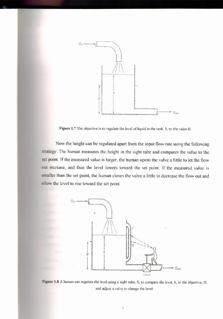
Figure 1. 7 The objective is to regulate the level ofliquid in the tank, h, to the value H.
Now the height can be regulated apart from the input flow rate using the following
strategy: The human measures the height in the sight tube and compares the value to the
set point. If the measured value is larger, the human opens the valve a little to let the flow
out increase, and thus the level lowers toward the set point. If the measured value is
smaller than the set point, the human closes the valve a little to decrease the flow out and
allow the level to rise toward the set point.
IH
Ih
I
Figure 1.8 A human can regulate the level using a sight tube, S, to compare the level, h, to the objective, H.
and adjust a valve to change the level.
7

l .4 •Q.'" ' . ®•
Figure 1.9 An automatic level-control system replaces the human by a controller and uses a sensor to
measure the level.
By a succession of incremental opening and closing of the valve, the human can
bring the level to the set point value H and maintain it there by continuous monitoring of
the sight tube and adjustment of the valve. The height is regulated.
Automatic Control To provide automatic control, the system is modified as shown
in Figure 1.9 so machines, electronics, or computers replace the operation of the human.
An instrument called a sensor is added that is able to measure the value of the level and
convert it into a proportional signals. This signal is provided as input to a machine,
electronic circuit, or computer, called the controller. This performs the function of the
human in evaluating the measurement and providing an output signal a to change the
valve setting via an actuator connected to the valve by a mechanical linkage.
When automatic control is applied to systems like the one shown in Figurel.9,
which are designed to regulate the value of some variable to a setpoint, it is called processcontrol.
8

1.4.2 Servomechanisms
Another type of control system in common use, which has a slightly different
objective from process control, is called servomechanism. In this case the objective is to
force some parameter to vary in a specific manner. This may be called a tracking control
system. Instead of regulating a variable value to a setpoint. The servomechanism forces
the controlled variable value to follow variation of the reference value.
Figure 1.10 Servomechanism-typecontrol systems are used to move a robot arm from point A to point B in
a controlled fashion.
For example, in an industrial robot arm like the one shown in Figure 1. 10,
servonnechanisms force the robot arm to follow a path from point A to point B. This is
done by controlling the speed of motors driving the arm and the angles of the arm parts.
The strategy for servomechanisms is similar to process-control systems, but the
dynamic differences between regulation and tracking result in differences in design and
operation of the control system. This text is directed toward process-control technology.
1.4.3 Open-Loop and Close-Loop Systems
There are two basic forms of control system, one being called open loop and the
other dosed loop. The difference between these can be illustrated by a simple example.
Consider an electric fire which has a selection switch which allows a 1 kW or a 2 kW
heating element to be selected. If a person used the fire to heat a room, he or she might
just switch on the 1 kW element if the room is not required to be at too high a
temperature. The room will heat up and reach a temperature which is only determined by
9

the fact the 1 kW element was switched off and not the 2 kW element. If there is changes
in the conditions, perhaps someone opening a window, there is no way the heat output is
adjusted to compensate.
This is an example of open-loop control in that there is no information feed back
to the element to adjust it and maintain constant temperature. The heating system with the
electric fire could be made a closed loop system if the person has a thermometer and
switches the 1 kW and 2kW elements on or off, according to the difference between the
actual temperature and the required temperature, to maintain the temperature of the room
constant. In this situation there is feedback, the input to the system being adjusted
according to whether its output is the required temperature. This means that the input to
the switch depends on the deviation of the actual temperature from the required
temperature, the difference between them determined by a comparison element the person
in this case. Figure 1.11 illustrates these two types of systems.
&ctrie;power
E~fked~onto
~oner .••et~mperawr&change
,eomp~eJement
lnput. +,",,··_ııı;··· ti
~tıttd-terrıparatur&
Omnations~
Beetriefirel I Etectnc ~ . . ..
~ · ······PoW~r • w !a~ntmmp•ıature
I ~ • ...~ -~ J ~.ıuu~.· '.n·ng•...•. & • • ~vıoe·
(b)
Figure 1.11 Heating a room: (a) an open-loop system, (b) a closed-loop system
To illustrate further the differences between open-loop and closed-loop systems,
consider a motor. With an open-loop system the speed of rotation of the shaft might be
determined solely by the initial setting of a knob, which affects the voltage applied to the
motor. Any changes in the supply voltage, the characteristics of the motor as a result of
temperature changes, or the shaft load will change the shaft speed but not be compensated
10
for. There is no feedback loop. With a closed-loop system, however, the initial setting of
the control knob will be for a particular shaft speed and this will be maintained by
feedback, regardless of any changes in supply voltage, motor characteristics or load. In an
open-loop control system the output from the system has no effect on the input signal. In a
closed-loop control system the output does have an effect on the input signal, modifying it
to maintain an output signal at the required value.
Open-loop systems have the advantage of being relatively simple and consequently
low cost with generally good reliability. However, they are often inaccurate since there is
no correction for error. Closed-loop systems have the advantage of being relatively
accurate in matching the actual to the required values. They are, however, more complex
and so more costly with a greater chance of breakdown as a consequence of the greater
number of components.
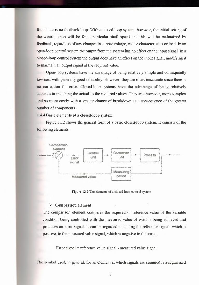
1.4.4 Basic elements of a closed-loop system
Figure 1.12 shows the general form of a basic closed-loop system. It consists of the
following elements:
Coınp;WQtı:eta9men1~+
ErrorSiignli
ContrQiunit
Figure 1:'12 The elements of a closed-loop control system
)"" Comparison element
The comparison element compares the required or reference value of the variable
condition being controlled with the measured value of what is being achieved and
produces an error signal. It can be regarded as adding the reference signal, which is
positive, to the measured value signal, which is negative in this case:
Error signal = reference value signal - measured value signal
The symbol used, in general, for an element at which signals are summed is a segmented
11

circle, inputs going into segments. The inputs are all added, hence the feedback input is
marked as negative and the reference signal positive so that the sum gives the difference
between the signals, A feedback loop is a means where by a signal related to the actual
condition being achieved is feed back to modify the input signal to a process. The
feedback is said to be negative feedback when the signal, which is feedback subtracts
from the input value. It is negative feedback that is required to control a system. Positive
feedback occurs when the signal fed back adds to the input signal.
::ı,.. Control element
The control element decides what action to take when it receives an error signal. It may
be, for example, a signal to operate a switch or open a valve. The control plan being used
by the element may be just to supply a signal, which switches on or off when there is an
error, as in a room thermostat, or perhaps a signal, which proportionally opens or closes a
valve according to the size of the error. Control plans may be Hard-wired systems in
which the control plan is permanently fixed by the way the elements are connected
together or programmable systems where the control plan is stored within a memory unit
and may be altered by reprogramming it.
::ı,.. Correction element
The correction element produces a change in the process to correct or change the
controlled condition. Thus it might be a switch, which switches on a heater and so
increases the temperature of the process or a valve, which opens and allows more liquid to
enter the process. The term actuator is used for the element of a correction unit that
provides the power to carry out the control action.::ı,.. Process element
~The process is what is being controlled. It could be a room in a house with its
temperature being controlled or a tank of water with its level being controlled.
::ı,.. Measurement element
The measurement element produces a signal related to the variable condition of the
process that is being controlled. It might be, for example, a switch, which is switched on
when a particular position is reached or a thermocouple, which gives an e.m.f. related tothe temperature.
With the closed loop system illustrated in figure 1.11 for a person controlling the
temperature of a room, the various elements are:
o Controlled variable: the room temperature
12

o Reference value: the required room temperature
o Comparison element: the person comparing the measured value with the
Required value of temperature
o Error signal: the difference between the measured and required
Temperatures.
o Control unit: the person
o Correction unit: the switch on the fire.
o Process: the heating by the fire.
An automatic control system for the control of the room temperature could involve a
temperature sensor, after suitable signal conditioning, feeding an electrical signal to the
input of, computer where it is compared with the set value and an error signal generated.
This is then acted on by the computer to give at its output a signal, which, after suitable
signal conditioning, might be used to control a heater and hence the room temperature.
Such a system can readily be programmed to give different temperature at different times
of the day.
Wat•·inpuı
Pivot
Figure 1.13 The automatic control ofwater level.
Figure 1.13 shows an example of a simple control system used to maintain a
constant water level in a tank. The reference value is the initial setting of the lever arm
arrangement so that it just cut off the water supply at the required level. When water is
drawn from the tank the float moves downwards with the water level. This causes the
lever arrangement to rotate and so allow water to enter the tank. This flow continues until
the ball has risen to such; height that it has moved the lever arrangement to cut off the
water supply. It is a closed-loop control system with the elements being:
13

o Controlled variable: water level in tank
o Reference value: initial setting of the float and level position
o Comparison element: the lever
o Error signal: the difference between the actual and initial settings of the
Lever positions
o Control unit: the pivoted
o Correction unit: the flap opening or closing the water supply
o Process: the water level in the tank
o Measuring device: the floating ball and level
The above is an example of a closed-loop control system involving just mechanical
elements. We could, however, have controlled the liquid level by means of an electronic
control system. We thus might have had a level sensor supplying an electrical signal,
which is used, after suitable signal conditioning, as an input to a computer where it is
compared with a set value signal and the difference between them, the error signal, then
used to give an appropriate response from the computer output. This is then, after suitable
signal conditioning, used to control the movement of an actuator in a flow control valve
and so determine the amount of water feed into the tank.
r-1'"P~~ı rL_~~ L._--i
l Speed measurmant
I .Differ~J
I Bevel
amp!ifıer___r---1L
Reference -value
r\_
Tacho-generator__ _J
~ I
'Process, Output,rotating -r c~rıstantshaft
1speedshaft
+ Amplifier Motor
Me.;surement r--------...ıtachcçeneraıor
Figure 1.14 shaft speed control
Figure 1. 14 shows a simple automatic control system for the speed of rotation of a
shaft. A potentiometer is used to set the reference value, i.e. what voltage is supplied to
the differential amplifier as the reference value for the required speed of rotation.
14

The differential amplifier is used to both compare and amplify the difference
between the reference and feedback values, i.e. it amplifiers the error signal. The
amplified error signal is then feed to a motor, which in tum adjusts the speed of the
rotating shaft. The speed of the rotating shaft is measured using a tachogenerator,
connected to the rotating shaft by means of a pair of bevel gears. The signal from the
tachogenerator is then feed back to the differential amplifier.
1.4.5 Sequential Controllers
There are many situations where control is exercised by items being switched on
or off at particular preset times or values to control processes and involve a step sequence
of operations. After step I is complete then step 2 starts. When step 2 is complete then
step 3 starts, etc. The term sequential control is used when control is such that actions are
strictly ordered in a time sequence. This could be by sets of relays. Such mechanical
witches are now more likely to have been replaced by microprocessors, such devices
behaving like switches, which are user programmable.
As an illustration of sequential control, consider the domestic washing machine. The
machine has to carry out a number of operations in the correct sequence. These may
involve a program consisting of a pre-wash cycle when the clothes in the drum are given a
wash in cold water, followed by a main wash cycle where they are washed in hot water,
then a rinse cycle when the clothe; are rinsed with cold water a number of times, followed
by spinning to remove water from the clothes. Each of these operations involves a number
of steps, e.g. a pre-wash cycle involves opening a valve to fill the machine drum to the
required level, closing the valve, switching on the drum motor to rotate the drum for a~
specific time, and operating the pump to empty the water from the drum. The system
operating sequence is called a program and there will be a number of programs, which
can be selected, the program depending on the type of clothes being washed in the
machine. The sequence of instructions in each program is predefined and built into thecontroller used.
Figure 1.15 shows the basic washing machine system and gives a rough idea of its
constituent elements. The system that has generally been used for the washing machine
controller involves a set of cam-operated switches, i.e. mechanical switches.
15

I- • tl Temperıııımı sensor
Motor
Figure 1.15 Washing machine system
Figure1.16 shows the basic principle of one such switch.
Figure 1.16 Cam-operated switch
When the machine is switched on, a small electric motor slowly turns the
controller cams so that each in turn operates electrical switches and so switches on
circuits in the correct sequence. The contour of a cam determines the time at which itJ
operates a switch. Thus the Contours of the cams are the means by which the program is
specified and stored in the machine. The sequence of instructions and the instructions
used in a particular washing program are determined by the set of cams chosen.
For the pre-wash cycle an electrically operated valve is opened when a current is
supplied and switched off when it ceases. This valve allows cold water into the drum for a
16

period of time determined by the profile of the cam used to operate its switch.
However, since the requirement is a specific level of water in the washing
machine drum, there needs to be another mechanism which will stop the water going into
the tank, during the permitted time, when it reaches the required level. In series with the
cam-operated switch is a water level switch. This is a sensor that gives a signal when the
water level has reached the preset level and switches off the current to the valve.
For the main wash cycle, the cam has a profile such that it starts in operation when
the pre-wash cycle is completed. It switches a current into a circuit lo open a valve to
allow cold water into the drum. This is in series with a water level switch so that the water
shuts off when the required level is reached. The cams then supply a current to activate a
switch, which applies a larger current to an electric heater to heat the water. A
temperature sensor is used to switch off the current when the water temperature reaches
the preset value. The cams then switch on the drum motor to rotate the drum. This will
continue for the time determined by the cam profile before switching off. Then a cam
switches on the current to a discharge pump to empty the water from the drum.
The rinse part of the operation is now switched as a sequence of signals to open
valves which allow cold water into the machine, switch it off, operate the motor to rotate
the drum, operate a pump to empty the water from the drum, and repeat this sequence a
number of times.
The final part of the operation is when a cam switches on just the motor, at a
higher speed than for the rinsing, to spin the clothes.
1.4.6 Microprocessor-Based Controller
Microprocessors are now rapidly replacing the mechanical cam-operated
controllers and being used in general to carry out control functions. They have the great..advantage that a greater variety of programs become feasible. The term programmable
logic controller is used for a microprocessor-based controller, which uses programmable
memory to store instruct- ions and to implement functions such as logic, sequence, timing
counting and arithmetic to control events.
17

Control Program
C
Inputs Outputs,, .
- ..p ~
- .•. ~CONTROLER - .•. ...
. •..~ ~
pA
B Q
R
D s
Figure 1.17 Programmable logic controller
Figure 1. 17 shows the control action of a programmable logic controller, the
inputs being signals from, say, switches being closed and the program used to determine
how the controller should respond to the inputs and the output it should then give.
Chapters 3 discuss microprocessors and their use as controllers (signal conditioningelement).
1.5 Analog And Digital Processing Control
Until recently the functions of the controller in a control sophisticated electronic
circuits performed system. Data were represented by the magnitude of voltages and
currents in such systems. This is referred lo as analog processing."Most modem control systems now employ digital computers to perform controller
operations. In computers data are represented as binary numbers consisting of a specific
number of bits. This is referred to as digital processing. The paragraphs that follow
contrast the analog and digital approaches to control system operation.
1.5.1 Data Representation
The representation of data refers to how the magnitude of some physical variable
is represented in the control loop. For example, if a sensor outputs a voltage whose
magnitude varies with temperature, then the voltage represents the temperature Analog
and digital system represent data in very different fashions.
18

Analog data an analog representation of data means that there is a smooth and
continuous variation between a representation of a variable value and the value itself.
Figure 1. 18 shows an analog relationship between some variable c and its representation,
b. Notice that for every value of c within the range covered there is a unique value ofb. In
principle, if c changes by some small amount ôc. Then b will change by a proportional
amount. ôb.
The relationship in Figure 1.19 is called nonlinear because the same ôb does not result
from fixed changes ôc over the range covered. This is described in more detail later in
this chapter.
Digital Data The consequence of digital representations of data is that the smooth
and continuous relation between the representation and the variable data value is lost.
Instead, the digital representation can only take on discrete values. This can be seen in
Figure 1.19 where a variable c is represented by a digital quantity N. Notice that arbitrarily
small variations of c. such as ôc 1. May not result in any change in N. The variable must
change by more than some minimum amount. Depending on where in the curve, the
change occurs, such as ôc2, before a change in representation is assured.
The reason for this discrete representation is that a finite number of binary number
digits are used to represent data digitally. For example, suppose a variable voltage is to be
represented digitally by a four-digit binary number. If each bit represents one volt, then
the resulting representation is shown in Table 1.1. Note that the minimum resolution is
one volt. The representation cannot distinguish between 4.25 and 4.75 volts because both
are represented by the binary number O 1002 .
Figure 1.18 Analog Data
19
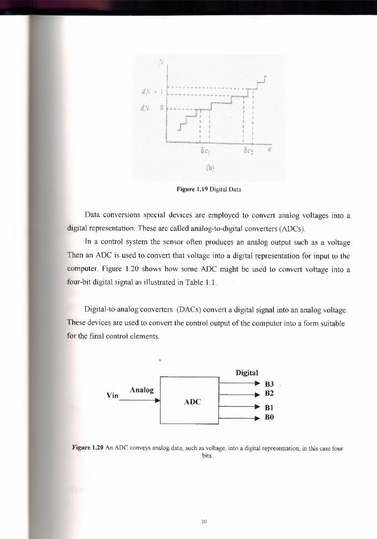
Figure 1.19 Digital Data
Data conversions special devices are employed to convert analog voltages into a
digital representation. These are called analog-to-digital converters (ADCs).
In a control system the sensor often produces an analog output such as a voltage
Then an ADC is used to convert that voltage into a digital representation for input to the
computer. Figure 1.20 shows how some ADC might be used to convert voltage into a
four-bit digital signal as illustrated in Table 1. 1.
Digital-to-analog converters (DACs) convert a digital signal into an analog voltage.
These devices are used to convert the control output of the computer into a form suitable
for the final control elements.
Vin
..Analog •...•.- ADC.. •.....
-..
DigitalBJ,B2
BlBO
Figure 1.20 An ADC conveys analog data, such as voltage, into a digital representation, in this case fourbits.
20
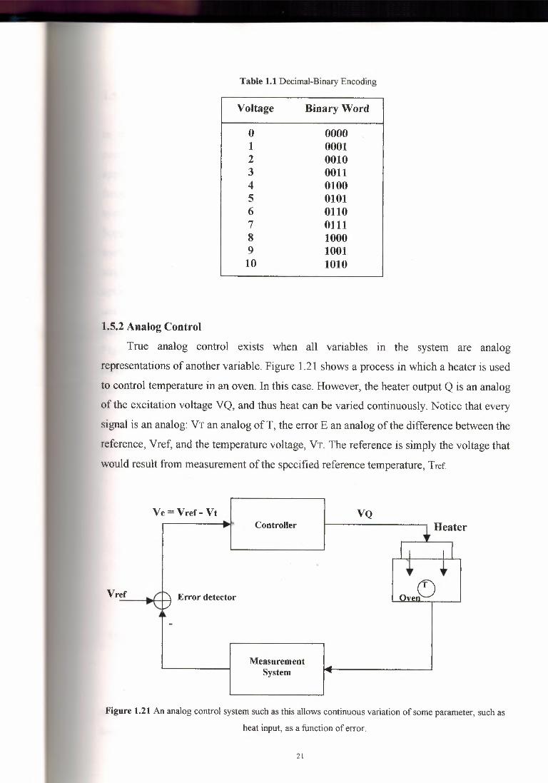
Table 1.1 Decimal-Binary Encoding
Voltage Binary Word
o 0000 C
1 0001 2 0010 3 0011 4 0100 5 0101 6 0110 7 0111 8 1000 9 1001 10 1010
1.5.2 Analog Control
True analog control exists when all variables in the system are analog
representations of another variable. Figure 1.21 shows a process in which a heater is used
to control temperature in an oven. In this case. However, the heater output Q is an analog
of the excitation voltage VQ, and thus heat can be varied continuously. Notice that every
signal is an analog: VT an analog of T, the error E an analog of the difference between the
reference, Vref, and the temperature voltage, VT. The reference is simply the voltage that
would result from measurement of the specified reference temperature, Tref.
Ve= Vref- Vt VQ Controller
Vref Error detector
MeasurementSystem
Figure 1.21An analog control system such as this allows continuous variation of some parameter, such as
heat input, as a function of error.
21

1.5.3 Digital Control
True digital control involves the use of a computer in modem applications, although
in the past digital logic circuits were also used. There are two approaches to using
computers for control. Supervisory Control When computers were first considered for
applications in control systems, they did not have a good reliability: they suffered
frequent failures and breakdown. The necessity for continuous operation of control
system precluded the use of computers to perform the actual control operations.
Supervisory control emerged as an intermediate step wherein the computer was used to
monitor the operation of analog control loops and to determine appropriate set points. A
single computer could monitor many control loops and use appropriate software to
optimize the set points for the best overall plant operation. If the computer failed, the
analog loops kept the process running using the last set points until the computer cameback on line.
Figure 1.22 shows how a supervisory computer would be connected to the analog heater
control system of figure 1.21 Notice how the ADC and DAC provide interface between
the analog signals and the computer.
Figure 1.22 In supervisory control, the computer monitors measurements and updates set points, but the
loops are still analog in nature.
Direct Digital Control (DDC). As computers have become more reliable and
miniaturized, they have taken over the controller function. Thus, the analog-processing
loop is discarded. Figure 1 .23 shows how, in a full computer control system, the
22

operations of the controller have been replaced by software in the computer. The ADC
and DAC provide interface with the process measurement and control action. The
computer inputs a digital representation of the temperature, NT, as an analog-to-digital
conversion of the voltage. VT. Error detection and controller actions are determined by
software. The computer then provides output directly to the heater via a digital
representation, No, which is converted to the excitation voltage Vo by the DAC.
Figure 1.23 This direct digital control system lets the computer perform the error detection and controllerfunctions.
1.6 Logic gatesThe relationships between inputs to a logic gate and the outputs can be tabulated in a
form known as a truth table. This specifies the relation- ships between the inputs and
outputs.
1.6.1 AND gate
Thus for an AND gatewith inputs A and B and a single output Q, we will have a 1
output when, and only when, A = 1 and B = 1. All other combinations of A and B will
generate a O output. We can thus write the truth table as:
A B OUTPUT
o o oo 1 o1 o o1 1 1
23

The Boolean symbol for AND is a dot(.); this can be omitted, and usually is," A
AND B" is written A. B, or simply AB.
1.6.2 OR gate
An OR gate with inputs A and B gives an output of a 1 when A or B is 1. We can
visualize such a gate as an electrical circuit involving two switches in parallel. When
switch or B is closed then there is a current. The following is the truth table:
A B OUTPUT
o o oo 1 1
1 o 1
1 1 1
The Boolean symbol for OR is+. "A ORB" is written A+ B.
1.6.3 NOT gate
A NOT gate has just one input and one output, giving a 1 output when the input is O
and a O output when the input is 1. The NOT gate gives an output which is the inversion
of the input and is called an inverter. The following is the truth table:
INPUT OUTPUT
1 o" o 1
The Boolean symbol for NOT is a bar over the symbol, or sometimes a prime
symbol. "NOT A" is written A, or A'. For the convenience of typesetters, the symbols/,*
, -, and ' are often used, in place of the over bar, to indicate NOT; thus, "NOT A" might
be written as any of the following: A', -A, *A, IA, Al.
1.6.4 NAND gate
The NAND gate can be considered as a combination of an AND gate followed by a
NOT gate. Thus when input A is 1 and input B is 1 there is an output of O, all other inputs
giving an output of 1. It is just the AND gate truth table with the outputs inverted. An
alternative way of considering the gate is as an AND gate with a NOT gate applied to
24

invert both the inputs before they reach the AND gate. The following is the truth table:
A B OUTPUT
o o 1
o 1 1
1 o 1
1 ' 1 o
1.6.5 NOR gate
The NOR gate can be considered as a combination of an OR gate followed by a
NOT gate. Thus when input A or input Bis I there is an output of O. It is just the OR gate
with the outputs inverted. An alternative way of considering the gate is as an OR gate
with a NOT gate applied to invert both the inputs before they reach the OR gate. The
following is the truth table:
A B OUTPUT
o o 1
o 1 o1 o oI 1 o
1.6.6 EXCLUSIVE gate
The EXCLUSIVE-ORgate (XOR) can be considered to be an OR gate with a NOT
gates applied to one of the inputs to invert it before the inputs reach the OR gate.
Alternatively it can be considered as an AND gate with a NOT gate applied to one of the
inputs to invert it before the inputs reach the AND gate. The following is the truth table:
A B OUTPUT
o o 1
o I o1 o o1 1 1
25

The symbols used to represent the function of the gate are shown in the figure 1.24.
NOT GATE -{)=O=D=0-=D-
AND GATE
OR GATE
NANDGATE
NOR GATE
Fig.1.24 symbolsoflogic gates
1.7 The Mechatronics Approach
The domestic washing machine referred to earlier in this chapter used cam-operated
switches in order to control the washing cycle. Such mechanical switches are being
replaced by microprocessors. This can be considered . an example of a mechatronics
approach in that a mechanical system has become integrated with electronic controls. As a
consequence, a bulky mechanical system is replaced by a much more compact
microprocessor system, which is readily adjustable to give a greater variety of programs.
Mechatronics involves the bringing together of a number of technologies:
mechanical engineering, electronic engineering, electrical engineering, computer
technology, and control engineering. This can be considered to be the application of'computer-based digital control techniques, through electronic and electric interfaces, to
mechanical engineering problems. Mechatronics provides an opportunity to take a new
look at problems, with mechanical engineers not just seeing a problem in terms of
mechanical principles but also having to see it in terms of a range of technologies. The
electronics, etc., should not be seen as a bolt-on item to existing mechanical hardware.
There needs to be a complete rethink of the requirements in terms of what an item isrequired to do.
There are many applications of mechatronics in the mass-produced products used in
the home. Microprocessor-based controllers are to be found in domestic washing
26

machines, dish washers, microwave ovens, cameras, camcorders, watches, hi-fi, and video
recorder systems, central heating thermostat controls, sewing machines, etc. They are to
be found in cars in the active suspension, antiskid brakes, engine control, speedometer
display, transmission, etc. A larger scale application of mechatronics is a flexible
manufacturing engineering system (FMS) involving computer-controlled machines,
robots, and automatic material conveying and overall supervisory control.
27

2. ANALOG SIGNAL CONDITIONING ELEMENTS
2.1 INTRODUCTION
Signal conditioning refers to operations performed on signals to convert them to a
form suitable for interface with other elements in the process-control loop, in other ward,
The output signal from the sensor of a measurement system has generally to be processed
in some way to make it suitable for the next stage of the operation. The signal may be, for
example, too small and have to be amplified, contain interference, which has to be
removed, be non-linear and require linearisation, be analogue and have to be made digital,
be digital and have to be made analogue, be a resistance change and have to be made into
a current change, be a voltage change and have to be made into a suitable size current
change, etc. All these changes can be referred to as signal conditioning. For example, the
output from a thermocouple is a small voltage, a few millivolts. A signal-conditioning
module might then be used to convert this into a suitable size current signal, provide noise
rejection, linearisation. In this chapter, we are concerned only with analog conversions,
where the conditioned output is still an analog representation of the variable. Even in
applications involving digital processing. Some type or analog conditioning usually is
required before analog-to-digital conversion is made. Specifics of digital signal
conditioning are considered in Chapter 3.
2.1.1 Interfacing
Input and output devices are connected to a microprocessor system through ports.
The term interface is used for the item that is used to make connections between devices
and a port. Thus there could be inputs from sensors, switches, and'keyboards and outputs
to displays and actuators. The simplest interface could be just a piece of wire. However,
the interface often contains signal conditioning and protection, the protection being to
prevent damage to the microprocessor system. For example, inputs needed to be protected
against excessive voltages or signals of the wrong polarity. Microprocessors require
inputs which are digital, thus a conversion of analogue to digital signal is necessary if the
output from a sensor is analogue. However, many sensors generate only a very small
signal, perhaps a few millivolts. Such a signal is insufficient to be directly converted from
analogue to digital without first being amplified. Signal conditioning might also be
28

needed with digital signals to improve their quality. The interface may thus contain a
number of elements. There is also the output from a microprocessor, perhaps to operate an
actuator. A suitable interface is also required here. The actuator might require an analogue
ignal and so the digital output from the microprocessor needs converting to an analogue
ignal. There can also be a need for protection to stop any signal becoming inputted back
through the output port to damage the microprocessor.
2.2 PRINCIPLES OF ANALOG SIGNAL CONDITIONING
A sensor measures a variable by converting information about that variable into a
dependent signal of either electrical or pneumatic nature. To develop such transducers.
We take advantage of fortuitous circumstances in nature where a dynamic variable
influences some characteristic of a material. Consequently, there is little choice of the
type or extent of such proportionality. For example, once we have researched nature and
found that cadmium sulfide resistance varies inversely and nonlinearly with light
intensity, we must then learn to employ this device for tight measurement within the
confines of that dependence. Analog signal conditioning provides the operations
necessary to transform a sensor output into a form necessary to interface with other
elements of the process-control loop. We will confine our attention to electrical
transformations.
We often describe the effect of the signal conditioning by the term transfer function.
By this term we mean the effect of the signal conditioning on the input signal. Thus. A
simple voltage amplifier has a transfer function of some constant that. When multiplied
by the input voltage, gives the ı;ıutput voltage.
It is possible to categorize signal conditioning into several general types.
2.2.1 Signal-Level Changes
The simplest method of signal conditioning is to change the level of a signal. The
most common example is the necessity to either amplify or attenuate a voltage level.
Generally, process-control applications result in slowly varying signals where de or low
frequency response amplifiers can be employed. An important factor in the selection of an
amplifier is the input impedance that the amplifier offers to the sensor (or any other
element that serves as an input). In process control, the signals are always representative
of a process variable, and any loading effects obscure the correspondence between the
29

measured signal and the variable value. In some cases, such as accelerometers and optical
detectors, the frequency response of the amplifier is very important.
2.2.2 Linearization
As pointed out earlier, the process-control designer has little choice of the
characteristics of a sensor output versus process variable. Often, the dependence that
exists between input and output is nonlinear. Even those devices that are approximately
linear may present problems when precise measurements of the variable are required.
Historically, specialized analog circuits were devised to linearize signals. For
example, suppose a sensor output varied nonlinearly with a process variable, as shown in
Figure 2.1. A linearization circuit, indicated symbolically in Figure 2.2. Would ideally be
one that conditioned the sensor output so that a voltage was produced which was linear
with the process variable, as shown in Figure 2.3. Such circuits are difficult to design and
usually operate only within narrow limits.
The modem approach to this problem is to provide the nonlinear signal as input to a
computer and perform the linearization using software. Virtually any nonlinearity can be
handled in this manner and with the speed of modem computers in nearly real time.
t '~I .
rI
b
ı._~-,..~~...-~~~~~~-----t,c=~cu;...iu C
Figure 2.1 Output sensor varied nonlinearly
b Linearizationcircuit
•...v ...._...
Figure 2.2 A linearization circuit
30

C
Figure 2.3 The ideal output of sensor
2.2.3 Conversions
Often, signal conditioning is used to convert one type of electrical variation into
another. Thus, a large class of sensors exhibits changes of resistance with changes in a
dynamic variable. In these cases, it is necessary to provide a circuit to convert this
resistance change either to a voltage or a current signal. This is generally accomplished by
bridges when the fractional resistance change is small and/or by amplifiers whose gainvaries with resistance.
Signal Transmission, an important type of conversion is associated with the process
control standard of transmitting signals as 4-20 mA current levels in wire. This gives rise
to the need for converting resistance and voltage levels to an appropriate current level at
the transmitting end and for converting the current back to voltage at the receiving end.
Of course, current transmission is used because such a signal is independent of load
variations other than accidental shunt conditions that may draw off some current. Thus.
Voltage-to-current and current-to-voltage converters are often required.'Digital Interface, the use of computers in process control requires conversion of
analog data into a digital format by integrated circuit devices called analog-to-digital
converters (ADCs). Analog signal conversion is usually required to adjust the analog
measurement signal to match the input requirements of the ADC. For example, the ADC
may need a voltage that varies between O and 5 volts, but the sensor provides a signal that
varies from 30 to 80 mV. Signal conversion circuits can be developed to interface the
output to the required ADC input.
31

2.2.4 Filtering and Impedance Matching
Two other common signal conditioning requirements are filtering and matching
impedance.
Often, spurious signals of considerable strength are present in the industrial
environment, such as the 60-Hz line frequency signals. Motor start transients also may
cause pulses and other unwanted signals in the process-control loop. In many cases, it is
necessary to use high-pass, low-pass, or notch filters to eliminate unwanted signals from
the loop. Passive filters using only resistors, capacitors, and inductors can accomplish
such filtering; or active filters, using gain and feedback.
Impedance matching is an important element of signal conditioning when transducer
internal impedance or line impedance can cause errors in measurement of a dynamic
variable. Both active and passive networks are employed to provide such matching.
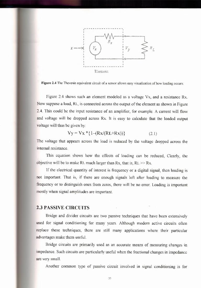
2.2.5 Concept of Loading
One of the most important concerns in analog signal conditioning is the loading of
one circuit by another. This introduces uncertainty in the amplitude of a voltage as it is
passed through the measurement process. If this voltage represents some process variable,
then we have uncertainty in the value of the variable.
Qualitatively, loading can be described as follows. Suppose the open circuit output
of some element is a voltage, say Vx, when the element input is some variable of value x.
Open circuit means that nothing is connected to the output. Loading occurs when we do
connect something, a load, across the output, and the output voltage of the element drops
to some value. Vy < Vx, different loads will result in different drops. Quantitatively, we-can evaluate loading as follows. Thevenins theorem tells us that the output terminals of
any element can be defined as a voltage source in series with output impedance. Let's
assume this is a resistance (the output resistance) to make the description easier to follow.
This is often called the Thevenin equivalent circuit model of the element.
32
I •• ~••.. w ~ - ••• "" - - ""' ••••••••.• "!! •• ""'
. '
R LVy
Figure 2.4 The Thevenin equivalent circuit of a sensor allows easy visualizationofhow loading occurs.
Figure 2.4 shows such an element modeled as a voltage Vx, and a resistance Rx.
Now suppose a load, RL, is connected across the output of the element as shown in Figure
2.4. This could_be the input resistance of an amplifier, for example. A current will flow
and voltage will be dropped across Rx. It is easy to calculate that the loaded output
voltage will thus be given by:
Vy= Vx *{1-(Rx/(RL+Rx))} (2. 1)
The voltage that appears across the load is reduced by the voltage dropped across theinternal resistance.
This equation shows how the effects of loading can be reduced, Clearly, the
objective will be to make RL much larger than Rx, that is, RL >>Rx.
If the electrical quantity of interest is frequency or a digital signal, then loading is
not important. That is, if there are enough signals left after loading to measure the
frequency or to distinguish ones from zeros, there will be no error. Loading is important
mostly when signal amplitudes are important.
2.3 PASSIVE CIRCUITSBridge and divider circuits are two passive techniques that have been extensively
used for signal conditioning for many years. Although modem active circuits often
replace these techniques, there are still many applications where their particularadvantages make them useful.
Bridge circuits are primarily used as an accurate means of measuring changes in
impedance. Such circuits are particularly useful when the fractional changes in impedanceare very small.
Another common type of passive circuit involved in signal conditioning is for
33

filtering unwanted frequencies from the measurement signal. It· is quite common in the
industrial environment to find signals that possess high- and/or low frequency noise as
well as the desired measurement data. For example, a transducer may convert temperature
information into a de voltage, proportional to temperature. Because of the ever-present ac
power lines, however, there may be a 60-Hz noise voltage impressed on the output that
makes determination of the temperature difficult. A passive circuit consisting of a resistor
and capacitor often can be used to eliminate both high- and low-frequency noise without
changing the desired signal information.
2.3.1 Divider Circuits
The elementary voltage divider shown in Figure 2.5 often can be used to provide
conversion of resistance variation into a voltage variation. The voltage of such a divider is
given by the well-known relationship:
VD= ( R2 .vs ı I (Rı + R2) (2.2)
Where Vs : supply voltage
Rı.Rz : divider resistors
Either R ı or R2 can be the sensor whose resistance varies with some measured variable.
It is important to consider the following issues when using a divider for conversion
of resistance to voltage variation:
1. The variation of VD with either Rı or R2 is nonlinear; that is, even if the resistance"varies linearly with the measured variable, the divider voltage will not vary
linearly.
Figure 2.5 The simplevoltage divider can often be used to convert resistance variation into voltage
variation.
34

2. The effective output impedance of the divider is the parallel combination of Rı and R2.
This may not necessarily be high, so loading effects must be considered.
3. In a divider circuit, current flows through both resistors: that is, power will be
dissipated by both, including the sensor. The power rating of both the resistor and sensor
must be considered.
2.3.2 Bridge Circuits
Bridge circuits are used to convert impedance variations into voltage variations. One
of the advantages of the bridge for this task is that it can be designed so the voltage
produced varies around zero. This means that amplification can be used to increase the
voltage level for increased sensitivity to variation of impedance.
Another application of bridge circuits is in the precise static measurement of an
impedance.
Wheatstone Bridge
The simplest and most common bridge circuit is the de Wheatstone bridge, as
shown in Figure 2.6. This network is used in signal conditioning applications where a
sensor changes resistance with process variable changes. Many modifications of this basic
bridge are employed for other specific applications. In Figure 2.6 the object labeled Dis a
voltage detector used to compare the potentials of points a and b of the network. In most!il
modem applications the detector is a very high-input impedance differentia amplifier. In
some cases, a highly sensitive galvanometer with relatively low impedance may be used.
Especially for calibration purposes and spot measurement instruments.
For our initial analysis, assume the detector impedance is infinite, that is. An opencircuit.
35

V -:-
Figure 2.6 The basic de Wheatstone bridge.
In this case the potential difference. öV between points a and b, is simply
öV=Va-Vb (2.3)
where Va = potential of point a with respect to c
Vb = potential of point b with respect to c
The values of Va and Vb now can be found by noting that Va is just the supply voltage V
divided between Rı and R3.
Va=(V*RJ)/(Rı+RJ) (2.4)
In a similar fashion, Vb is a divided voltage given by
Vb= (V*R4)I (Rı + R4)"
(2.5)
Where V = bridge supply voltage
If we now combine Equations (2.3), (2.4), and (2.5), the voltage difference or voltage
Offset can be written.
öV = {(V*R3) I (Rl + R3)}- {(V* R4) I (R2 + R4)} (2.6)
Using some algebra, the reader can show that this equation reduces to
zv = {V * [(R3*R2- Rl *R4) I (Rl + R3) * (R2 + R4)]} (2.7)
36

Equation (2.7) shows how the difference in potential across the detector is a function
of the supply voltage and the values of the resistors. Because a difference appears in the
numerator of Equation (2.7), it is clear that a particular combination of resistors can be
found that will result in zero difference and zero voltage across the detector, that is, a null.
Obviously, this combination, from examination of equation (2.7), is:
R3*R2 = Rl*R4 (2.8)
Equation (2. 8) indicates that whenever a Wheatstone bridge is assembled and resistors are
adjusted for a detector null. The resistor values must satisfy the indicated equality. It does
not matter if the supply voltage drifts or changes; the null is maintained. Equations (2.7)
and (2.8) underlie the application of Wheatstone bridges to process-control applications
using high-input impedance detectors.
Galvanometer Detector, the use of a galvanometer as a null detector in the bridge
circuit introduces some differences in our calculations because the detector resistance may
be low and because we must determine the bridge offset as current offset. When the
bridge is nulled. Equation (2.8) still defines the relationship between the resistors in the
bridge arms. Equation (2.7) must be modified to allow determination of current drawn by
the galvanometer when a null condition is not present. Perhaps the easiest way to
determine this offset current is first to find the Thevenin equivalent circuit between points
a and b of the bridge (as drawn in Figure 2.6 with the detector removed). The Thevenin
voltage is simply the open circuit voltage difference between points a and b of the circuit.~
But wait! Equation (2.7) is the open circuit voltage, so
VTh= { V * [ ( R3*R2 - Rl *R4) I (Rl + R3) * ( R2 + R4 ) ] } (2.9)
The Thevenin resistance is found by replacing the supply voltage by its internal resistance
and calculating the resistance between terminals a and b of the network. We may assume
that the internal resistance of the supply is negligible compared to the bridge arm
resistances. It is left as an exercise for the reader to show that the Thevenin resistance
seen at points a and b of the bridge is
RTh= {(Rl * R3)/(Rl + R3)}+{(R2* R4)/(R2 + R4)} (2.10)
37
The Thevenin equivalent circuit for the bridge enables us easily to determine the
current through any galvanometer with internal resistance RG. As shown in Figure 2.7. In
particular, the offset current is:
IG ={VTh I (RTh + RG)} (2. 11)
Using this equation in conjunction with Equation (2.8) defines the Wheatstone
bridge response whenever a galvanometer null detector is used.
Bridge Resolution, the resolution of the bridge circuit is a function of the resolution
of the detector used to determine the bridge offset. Thus, referring primarily to the case
where a voltage offset occurs, we define the resolution in resistance as that resistance
change in one arm of the bridge that causes an offset voltage that is equal to the resolution
of the detector. If a detector can measure a change of 100 µV. This sets a limit on the
minimum measurable resistance change in a bridge using this detector. In general, once
given the detector resolution, we may use Equation (2.7) to find the change in resistance
that causes this offset.
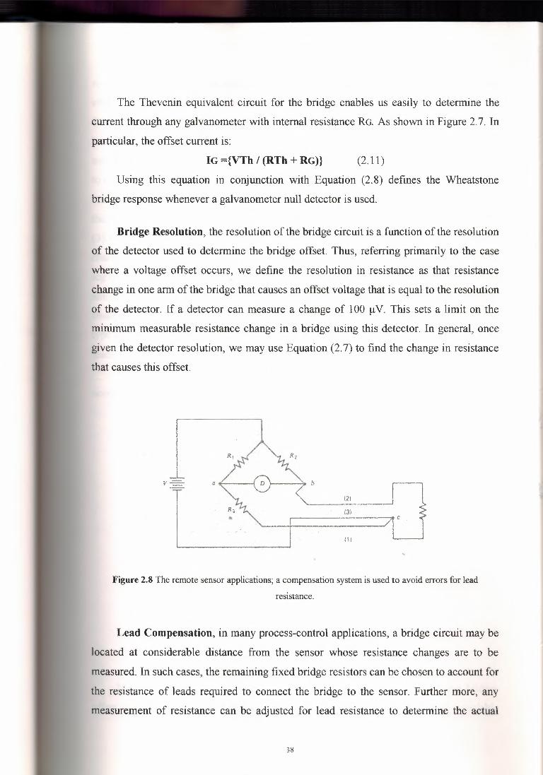
Figure 2.8 The remote sensor applications; a compensation system is used to avoid errors for lead
resistance.
Lead Compensation, in many process-control applications, a bridge circuit may be
located at considerable distance from the sensor whose resistance changes are to be
measured. In such cases, the remaining fixed bridge resistors can be chosen to account for
the resistance of leads required to connect the bridge to the sensor. Further more, any
measurement of resistance can be adjusted for lead resistance to determine the actual
38

resistance. Another problem exists that is not so easily handled. However. There are many
effects that can change the resistance of the Ions lead wires on a transient basis, such as
frequency, temperature, stress, and chemical vapors. Such changes will show up as a
bridge offset and be interpreted as changes in the sensor output. This problem is reduced
using lead compensation, where any changes in lead resistance are introduced equally in
to two (both) arms of the bridge circuit, thus causing no effective change in bridge offset.
Lead compensation is shown in Figure 2.8. Here we see that R4, which is assumed to be
the sensor, has been removed to a remote location with lead wires (1), (2), and (3). Wire
(3) is the power lead and has no influence on the bridge balance condition. If wire (2)
changes in resistance because of spurious influences, it introduces this change into the R4
leg of the bridge. Wire (1) is exposed to the same environment and changes by the same
amount, but is in the R3 leg of the bridge. Effectively, both R3 and R4 are identically
changed, and thus Equation (2. 8) shows that no change in the bridge null occurs. This
type of compensation is often employed where bridge circuits must be used with long
leads to the active element of the bridge.
Current Balance Bridge, one disadvantage of the simple Wheatstone bridge is the
need to obtain a null by variation of resistors in bridge arms. In the past.
Figure 2.9 The current balance bridge.
Many process-control applications used a feedback system in which the bridge
offset voltage was amplified and used to drive a motor whose shaft altered a variable
39
resistor to renull the bridge. Such a system does not suit the modem technology of
electronic processing because it is not very fast. Is subject to wear, and generates
electronic noise. A technique that provides for an electronic nulling of the bridge and that
uses only fixed resistors (except as may be required for calibration) can be used with the
bridge. This method uses a current to null the bridge. A closed-loop system can even be
constructed that provides the bridge with a self-nulling ability.
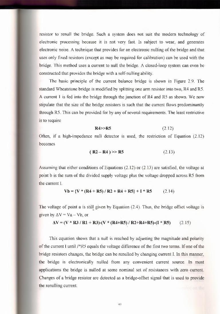
The basic principle of the current balance bridge is shown in Figure 2.9. The
standard Wheatstone bridge is modified by splitting one arm resistor into two, R4 and R5.
A current 1 is fed into the bridge through the junction of R4 and R5 as shown. We now
stipulate that the size of the bridge resistors is such that the current flows predominantly
through R5. This can be provided for by any of several requirements. The least restrictive
is to require
R4>>RS (2.12)
Often, if a high-impedance null detector is used, the restriction of Equation (2.12)
becomes
( R2 - R4 ) >> RS (2.13)
Assuming that either conditions of Equations (2.12) or (2.13) are satisfied, the voltage at
point b is the sum of the divided supply voltage plus the voltage dropped across R5 from
the current I.
Vb = {V * (R4 + RS) I R2 + R4 + RS} + I * RS (2.14)
The voltage of point a is still given by Equation (2.4). Thus, the bridge offset voltage is"given by !ıV =Va-Vb, or
AV= (V * RJ I Rl + RJ)-(V * (R4+RS) I R2+R4+RS)-(I * ,RS) (2.15)
This equation shows that a null is reached by adjusting the magnitude and polarity
of the current I until I*R5 equals the voltage difference of the first two terms. If one of the
bridge resistors changes, the bridge can be renulled by changing current I. In this manner,
the bridge is electronically nulled from any convenient current source. In most
applications the bridge is nulled at some nominal set of resistances with zero current.
Changes of a bridge resistor are detected as a bridge-offset signal that is used to provide
the renulling current.
40

Temperature compensation, in many measurements involving a resistive sensor
the actual sensing element may have to be at the end of long leads. Not only the sensor
but also the resistance of these leads will be affected by changes in temperature. For
example, a platinum resistance temperature sensor consists of a platinum coil at the ends
of leads. When the temperature changes, not only will the resistance of the coil change but
so also will the resistance of the leads. What is required is just the resistance of the coil
and so some means has to be employed to compensate for the resistance of the leads to the
coil. One method of doing this is to use three leads to the coil, as shown in figure 2.11.
The coil is connected into the Wheatstone bridge in such a way that lead 1 is in series
with the R3 resistor while lead 3 is in series with the platinum resistance coil Rl. Lead 2
is the connection to the power supply. Any change in lead resistance is likely to affect all
three leads equally, since they are of the same material, diameter and length and held
close together. The result is that changes in lead resistance occur equally in two arms of
the bridge and cancels out ifRl and R3 are the same resistance.
8
11 21 3
d. c.
Figure 2.10 compensation for leads
The electrical resistance strain gauge is another sensor where compensation has to
be made for temperature effects. The strain gauge changes resistance when the strain
applied to it changes. Unfortunately, it also changes if the temperature changes. One way
of eliminating the temperature effect is to use a dummy strain gauge. This is a strain
gauge, which is identical to the one under strain, the active gauge, and is mounted on the
41
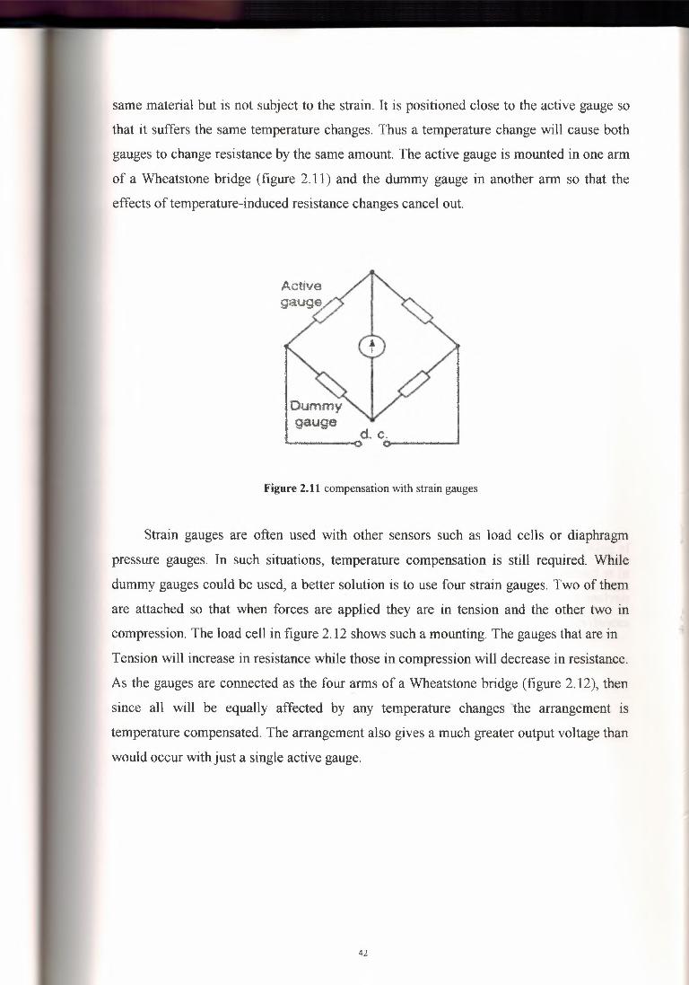
same material but is not subject to the strain. It is positioned close to the active gauge so
that it suffers the same temperature changes. Thus a temperature change will cause both
gauges to change resistance by the same amount. The active gauge is mounted in one arm
of a Wheatstone bridge (figure 2. 11) and the dummy gauge in another arm so that the
effects of temperature-induced resistance changes cancel out.
d. C.
Figure 2.11 compensation with strain gauges
Strain gauges are often used with other sensors such as load cells or diaphragm
pressure gauges. In such situations, temperature compensation is still required. While
dummy gauges could be used, a better solution is to use four strain gauges. Two of them
are attached so that when forces are applied they are in tension and the other two in
compression. The load cell in figure 2.12 shows such a mounting. The gauges that are in
Tension will increase in resistance while those in compression will decrease in resistance.
As the gauges are connected as the four arms of a Wheatstone bridge (figure 2.12), then
since all will be equally affected by any temperature changes 'the arrangement is
temperature compensated. The arrangement also gives a much greater output voltage than
would occur with just a single active gauge.
42

com pr es.si on
• d. c. •"'-------o o
tension
tLoad cell
Figure 2.12 Four active arm strain gauge bridge
Ac Bridges, the bridge concept described in this can be applied to the matching of
impedance in general, as well as to resistance. In this case, the bridge is represented as in
figure 2.13 and employs an ac excitation, usually a sine wave voltage signal. The analysis
of bridge behavior is basically the same as in the previous treatment, but impedances
replace resistances. The bridge offset voltage then is represented as"'
AE = E [(Z3Z2-Z1Z4) I (Zl+Z3)(Z2+Z4)] (2.16)
AE = ac off set voltage
Where E = sine wave excitation voltageZl, Z2, Z3, Z4 = bridge impedances
A null condition is defined as before by a zero offset voltage ~E =O.From Equation
(2.16), this condition is met if the impedances satisfy the relation:
Z2Z3 =Z1Z4 (2.17)
43
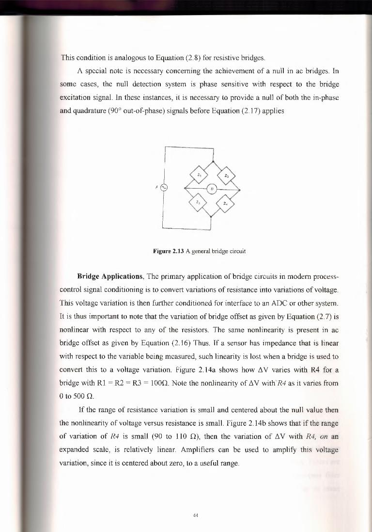
This condition is analogous to Equation (2.8) for resistive bridges.
A special note is necessary concerning the achievement of a null in ac bridges. In
some cases, the null detection system is phase sensitive with respect to the bridge
excitation signal. In these instances, it is necessary to provide a null of both the in-phase
and quadrature (90° out-of-phase) signals before Equation (2.17) applies.
LFigure 2.13 A general bridge circuit
Bridge Applications, The primary application of bridge circuits in modem process
control signal conditioning is to convert variations of resistance into variations of voltage.
This voltage variation is then further conditioned for interface to an ADC or other system.
It is thus important to note that the variation of bridge offset as given by Equation (2.7) is
nonlinear with respect to any of the resistors. The same nonlinearity is present in ac
bridge offset as given by Equation (2.16) Thus. If a sensor has impedance that is linear
with respect to the variable being measured, such linearity is lost when a bridge is used to
convert this to a voltage variation. Figure 2.14a shows how 11V varies with R4 for a
bridge with Rl = R2 = R3 = 1000. Note the nonlinearity of 11V with'R4 as it varies from
O to 500 rıIf the range of resistance variation is small and centered about the null value then
the nonlinearity of voltage versus resistance is small. Figure 2.14b shows that if the range
of variation of R4 is small (90 to 110 O), then the variation of 11V with R4, on an
expanded scale, is relatively linear. Amplifiers can be used to amplify this voltage
variation, since it is centered about zero, to a useful range.
44

\
'\I \j I I .·
AV (volts) ~ t . ""K: •.• ; • I . I . I
LI ı --1-1 I
o HlO 200 JOO
R, (Q)
(a)
9, ıoo 105 ı I()
R4 (Q)
" (b)
Figure 2.14 Bridge off-null voltage is clearly nonlinear for large-scale changes inresistance, but for small
ranges of resistance change the off-null voltage is nearly linear.
2.3.3 Filtering
The term filtering is used to describe the process of removing a certain band of
frequencies from a signal and permitting others to be transmitted. The range of
frequencies passed by a filter is known as the pass band, the range not passed as the stop
band and the boundary between stopping and passing as the cut-off frequency. Filters are
classified according to the frequency ranges they transmit or reject. A low-pass filter
(figure 2.15(a)) has a pass band, which allows all frequencies from O up to some
45
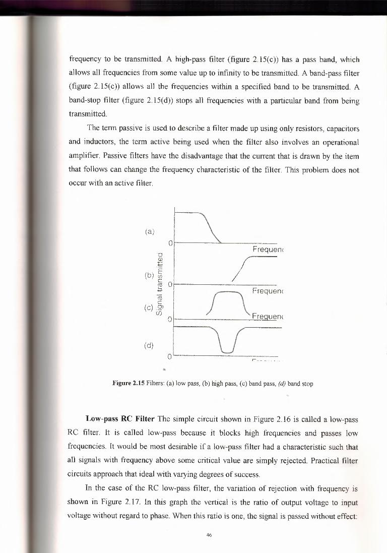
frequency to be transmitted. A high-pass filter (figure 2.15(c)) has a pass band, which
allows all frequencies from some value up to infinity to be transmitted. A band-pass filter
(figure 2.15(c)) allows all the frequencies within a specified band to be transmitted. A
band-stop filter (figure 2.15(d)) stops all frequencies with a particular band from being
transmitted.
The term passive is used to describe a filter made up using only resistors, capacitors
and inductors, the term active being used when the filter also involves an operational
amplifier. Passive filters have the disadvantage that the current that is drawn by the item
that follows can change the frequency characteristic of the filter. This problem does not
occur with an active filter.
(a)
oı- Frequenc
~ I rlb)~ I I' ! O Frequenc
(c) ~ ol nFrequen,
(d)
o r-."~---~ - .
Figure 2.15 Filters: (a) low pass, (b) high pass, (c) band pass, (d) band stop
Low-pass RC Filter The simple circuit shown in Figure 2.16 is called a low-pass
RC filter. It is called low-pass because it blocks high frequencies and passes low
frequencies. It would be most desirable if a low-pass filter had a characteristic such that
all signals with frequency above some critical value are simply rejected. Practical filter
circuits approach that ideal with varying degrees of success.
In the case of the RC low-pass filter, the variation of rejection with frequency is
shown in Figure 2.17. In this graph the vertical is the ratio of output voltage to input
voltage without regard to phase. When this ratio is one, the signal is passed without effect:
46

when it is very small or zero. the signal is effectively blocked.
The horizontal is actually the logarithm of the ratio of the input voltage signal
frequency to a critical frequency. This critical frequency is that frequency for which the
ratio of the output to the input voltage is O. 707, In terms of the resistor and capacitor, the
critical frequency is given by
Fe= 1 I (2nRC) (2. 18)
R..
Figure 2.16 Circuit for the low-pass RC filter
0.1 10 100
Figure 2.17 response of the low-pass RC filter as a function of frequency ratio
The voltage ratio for any signal frequency can be determined graphically from Figure
2. 17 or can be computed by:
47
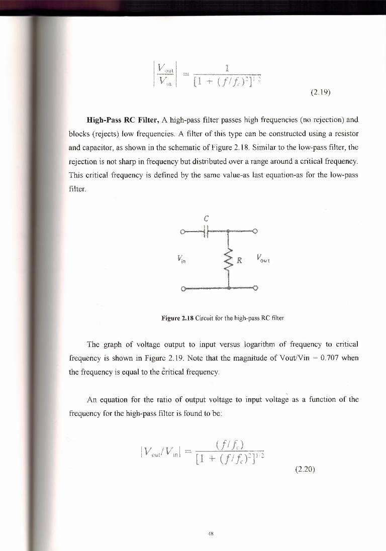
1[1 + (fl J:.f]12
(2.19)
High-Pass RC Filter, A high-pass filter passes high frequencies (no rejection) and
blocks (rejects) low frequencies. A filter of this type can be constructed using a resistor
and capacitor, as shown in the schematic of Figure 2.18. Similar to the low-pass filter, the
rejection is not sharp in frequency but distributed over a range around a critical frequency.
This critical frequency is defined by the same value-as last equation-as for the low-pass
filter.
R
Figure 2.18 Circuit for the high-pass RC filter
The graph of voltage output to input versus logarithm of frequency to critical
frequency is shown in Figure 2. 19. Note that the magnitude of Vout/Vin = 0.707 when
the frequency is equal to the critical frequency.
...An equation for the ratio of output voltage to input voltage as a function of the
frequency for the high-pass filter is found to be:
111 ıv ıI ~· ı:ıı.H' ın [1 + (flfcf]I:2(2.20)
48

! ıııı l l I l I
II ! I ! l ı u l lI. ı ı
l i I ! i / ı.--1 llI I l ı . lt / f!
I ·/ iI I·
tı''
I 'I
I.I', .. / I I
1 ,_ '- .. •. ·ı j I I II
e.o: ıool
Figure 2.19 Response of the high-pass RC filter as a function of frequency ratio.
Practical Considerations
There are a number of issues that arise when designing a system, which will use the
RC high-pass or low-pass filters. Consider the following items.
1. After the critical frequency is determined, the values of R and C are selected to
satisfy Equation (2.18). In principle, any values of R and C can be employed that will
satisfy this critical frequency equation. A number of practical issues limit the selection,
however. Some of these are:
a. Very small values of resistance are to be avoided because they can lead to
large currents, and thus large loading effects. Similarly, very large capacitance
should be avoided. In general, we try to keep the resistance in the kn and above
range, and capacitors in the µF or less range.
b. Often, the exact critical frequency is not important, so that fixed resistors and..•
capacitors of approximately the computed values can he employed. If exact
values are necessary, it is usually easier to select and measure a capacitor, then
compute and obtain the appropriate resistance using a trimmer resistance.
2. The effective input impedance and output impedance of the RC filter may have an
effect on the circuit in which it is used because of loading effects. If the input impedance
of the circuit being fed by the filter is low, you may want to place a voltage follower
between the filter output and the next stage. Similarly, if the output impedance of the
feeding stage to the filter is high. You may want to isolate the input of the filter with a
voltage follower.
49
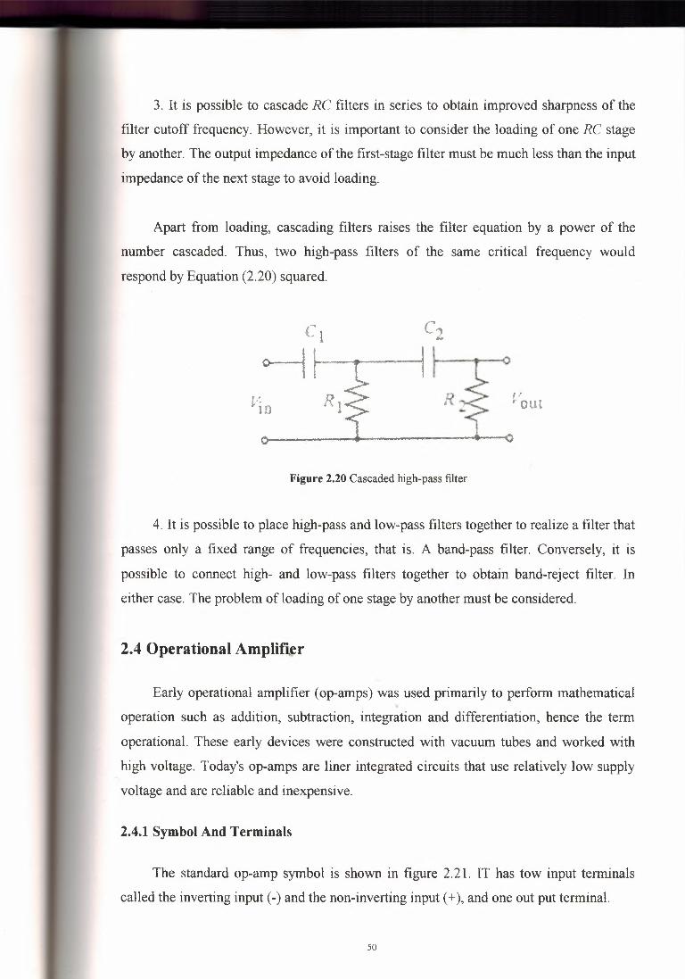
3. It is possible to cascade RC filters in series to obtain improved sharpness of the
filter cutoff frequency. However, it is important to consider the loading of one RC stage
by another. The output impedance of the first-stage filter must be much less than the input
impedance of the next stage to avoid loading.
Apart from loading, cascading filters raises the filter equation by a power of the
number cascaded. Thus, two high-pass filters of the same critical frequency would
respond by Equation (2.20) squared.
-¢
Figure 2.20 Cascaded high-pass filter
4. It is possible to place high-pass and low-pass filters together to realize a filter that
passes only a fixed range of frequencies, that is. A band-pass filter. Conversely, it is
possible to connect high- and low-pass filters together to obtain band-reject filter. In
either case. The problem of loading of one stage by another must be considered.
2.4 Operational Amplifier
Early operational amplifier (op-amps) was used primarily to perform mathematical
operation such as addition, subtraction, integration and differentiation, hence the term
operational. These early devices were constructed with vacuum tubes and worked with
high voltage. Today's op-amps are liner integrated circuits that use relatively low supply
voltage and are reliable and inexpensive.
2.4.1 Symbol And Terminals
The standard op-amp symbol is shown in figure 2.21. IT has tow input terminals
called the inverting input (-) and the non-inverting input (+), and one out put terminal.
50

• -i·---~
• ı+_~
Figure 2.21 Op-amp symbol
The typical op-amp operates with tow de supply voltage, one positive and the
other negative, as shown in figure 2.22. Usually these de voltage terminals are left off the
schematic symbol for simplicity but are always understood to be there .
. +V
Inverting lnpp~t- ':_·• t. ' ': ),,,-..
Noninve,ling,nput ~
-V
Output
•••
Figure 2.22 symbol with power connection.
2.4.2 Basic Operational Amplifier
Amplifiers (op-amp) are used primarily to perform mathematical operations such as
addition, subtraction, integration, differentiation, as its name is operational. But now op
amps are linear integrated circuits that use relatively low supply voltages. There are four
basic main operations of an operational amplifier.
• Comparators Amplifier.
• Summing Amplifier.
• The Integrator Amplifier.
• The Differentiator Amplifier.
• The Instrumental Amplifier.
51

2.4.2.1 Comparators
Operation Amplifiers are often used as nonlinear devices to compare the amplitude
of one voltage with another. In this application, the op-amp is used in open-loop
configuration; with the input voltage on one input and a reference voltage on the other e.g.
it is used as over temperature sensing also used as analog to digital conversions.
Zero-Level Detection
The basic application of the op-amp as a comparator is in determining when an
input voltage exceeds the certain level. Figure 2.23 shows a zero-level detector. The
inverting (-) input is grounded and the input signal voltage is applied to non-inverting (+)
input. Because of the high open-loop voltage gain, a very small difference voltage
between the two inputs drives the amplifier into saturation, causing the output voltage to
go its limit. For example, an op-amp have Aouı=l00,000.A voltage difference of 0.25mA
between the input could produce an output voltage of (0.25mA) (100,000) =25V if the op
amp were capable. However, since most op-amp have output voltage limitation of less
than :±)5V, the device would be driven into saturation.
VouT)"--~o
Figure 2.23 The Op-amp as zero-level Detector~
Figure 2.24 shows sine wave input voltage applied to the non-inverting input of
the zero-level detector. When sine wave is negative, the output is atits maximum negative
level. When the sine wave cross O, the amplifier is driven to it's opposite state and output
goes to its maximum positive level. The zero-level detector can also be used to produce a
square wave from sine wave.
52
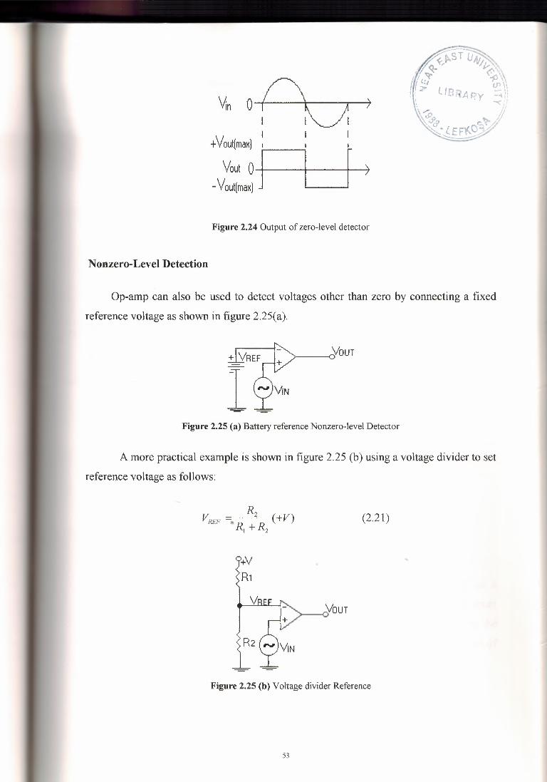
Oı 0ıI I I
7
+Voutlma,] , , ~
_ v~:~.~ JI L- _ ____.
1
Figure 2.24 Output of zero-level detector
Nonzero-Level Detection
Op-amp can also be used to detect voltages other than zero by connecting a fixed
reference voltage as shown in figure 2.25(a).
~.,___0Vour
Figure 2.25 (a) Battery reference Nonzero-level Detector
A more practical example is shown in figure 2.25 (b) using a voltage divider to set
reference voltage as follows:
(2.21)
V
R2
>---0Vour
Figure 2.25 (b) Voltage divider Reference
53

Where +Vis the positive op-amp supply voltage. We can also use zener voltage as a
reference voltage (v2 =RF) by applying a zener diode with the same circuit as shown in
figure 2.25 (c).
+V
R
,,__ ___,c}/OUT
Figure 2.25 (c) Zener Diode sets reference voltage
As long as the input voltage Vnı is less than VREF, the output remains at the
maximum negative level. When the input voltage exceeds the reference voltage, the
output goes to its maximum positive state as shown in figure 2.25(d) with a sine wave as
input voltage.
VRE.E - -
III I
+Vout(m:R F\/out Oı~~~-t-~-+-~~~~--1.r--1
-Vout(ma.:)JFigure 2.25(d) Output of Nonzero-level Detector
~
Out Bounding
In some applications, it is necessary to limit the output voltage levels of a
comparator to a value less than that provided by the saturated op-amp. A single zener
diode can be used as shown in the figure 2.26(a) to limit the output voltage swing to the
zener voltage in one direction and to the forward diode drop in the other. This process of
limiting the output voltage is called bounding.
54

Figure 2.26 (a) Comparator with output bounding
Since the anode of zener is connected to the inverting input, it is at virtual
groundll/ ~ o). Therefore, when the output reaches a positive value equal to zener
voltage, it limits at that value. When the output switches negative, the zener acts as
regular diode and becomes forward biased at 0.7V, limiting the negative output swing to
this value, as shown in figure 2.26 (b). Turning the zener around limits the output in
opposite direction as shown in figure 2.26(c).
V7no~
-0.7V
Figure 2.26 (b) Bounded at positive value
+0.7Vau::<::
Figure 2.26 (c) Bounded at negative value
Two zener diodes arranged in figure 2.26(d) limit the output voltage to the zener
voltage plus the voltage drop (0.7 V) of the forward biased zener, both positively and
negatively as shown.
55

+&Vz+07VO -Vz
-0.7V
Figure 2.26 (d) Double bounded comparator
Window Comparator
Two comparators as in figure 2.27 (a) form a window comparator. This is used to
detect input voltage between two limits, an upper and lower, called the "window". The
upper and lower limits are set by reference voltages designated Vu and V1. As long as the
input voltage VIN is within these two limits. The output of each comparator is at its low
saturated level. Both diodes are reverse biased making Voırrzero. When input goes above
Vu and V1, the output of that comparator goes to its saturated level.
Figure 2.27 (a) A basic window Comparator
This action forward biased and produces a high level Voırr illustrated in figure 2.27
(b) with VIN changing arbitrarily.
VıNIVL - ı- -,... - -
Oı_;_-+~~t--~-+-~\uurJLJoFigure 2.27 (b) Output of window comparator operation
56

2.4.2.2 Summing Amplifier
The summing amplifier is a variation of the inverting op-amp configuration. It is
two or more inputs and its output voltage is proportional to the negative of the algebraic
sum of its input voltages.
Ann-input summing amplifier is shown in figure 2.28 (a). It operates like n inputs
(Ynıı, Ynı2, Ynın) are applied at its input and produce current (lı, 12 .In). The
inverting input of the op-amp is almost O Y, and there is no current into the input. This
means that all inputs currents come together at this summing point and from the total
current, which goes through Rf, as indicated.
Rt ,'y'
vour
Figure 2.28 (a) SummingAmplifierwith n inputs
Ir=Ir+Ir+ +I, (2.22)
Since Yom= -h Rf
Yom= - (lı+Iı+ +In) Rf (2.23)
(2.24)
If all the resistances are of the same value that is E. (Rf =R1=R2=Rn), then
Vour = -(VıNı + VıN2 + · + VJNn) (2.26)
When Rf is larger than the input resistors, the amplifier has a gain factor Rj!R, where R is
the value of the each input resistor then Expression will be.
57
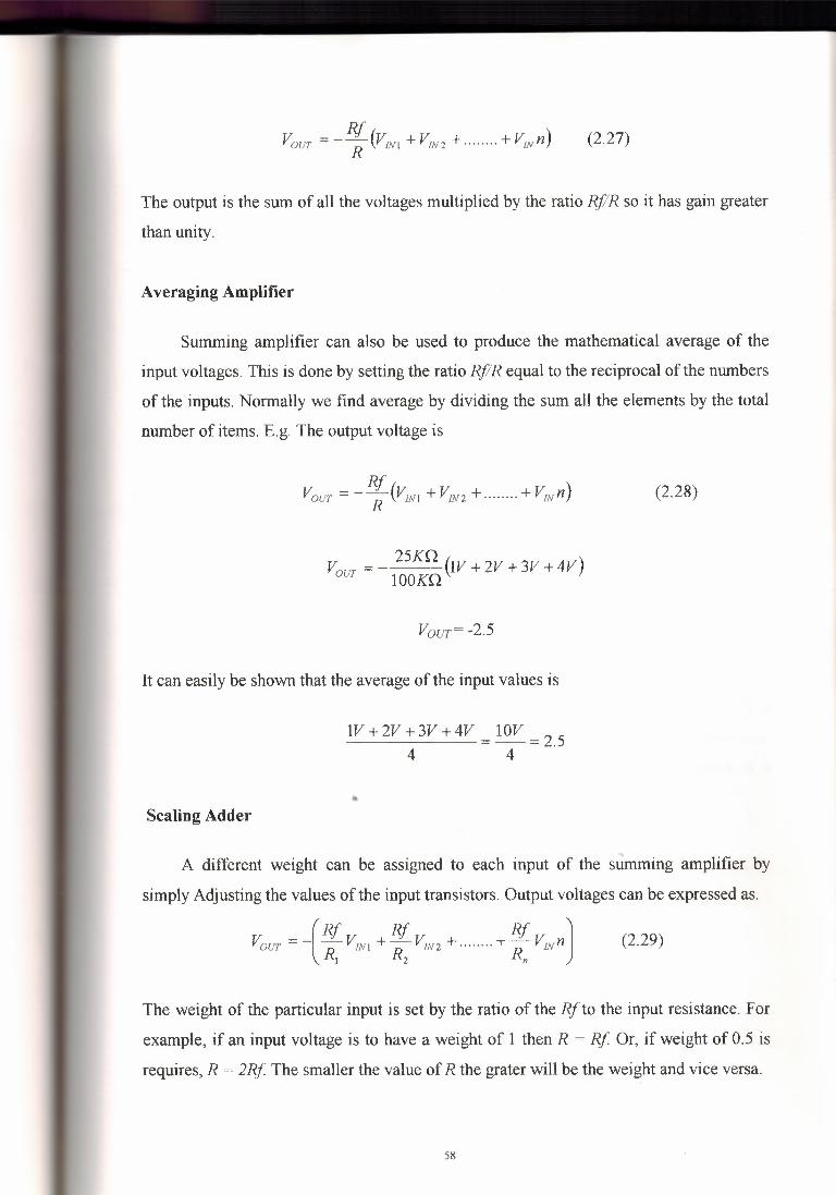
RfVour = --(vlNl + VIN2 + + v!Nn)
R(2.27)
The output is the sum of all the voltages multiplied by the ratio Rj!R so it has gain greater
than unity.
Averaging Amplifier
Summing amplifier can also be used to produce the mathematical average of the
input voltages. This is done by setting the ratio Rj!R equal to the reciprocal of the numbers
of the inputs. Normally we find average by dividing the sum all the elements by the total
number of items. E.g. The output voltage is
RfVour = --(v!NI + VIN2 + + VlNn)
R(2.28)
25KD.Vour = - (1V + 2V + 3V + 4V)
lOOKD.
Vour= -2.5
It can easily be shown that the average of the input values is
ıv +2v +3V +4V = ıov = 2.54 4
Scaling Adder
A different weight can be assigned to each input of the summing amplifier by
simply Adjusting the values of the input transistors. Output voltages can be expressed as.
Vour = -(Rf VIN,+ Rf vlN2 + +Rf VlNnJRı n, Rn
(2.29)
The weight of the particular input is set by the ratio of the Rf to the input resistance. For
example, if an input voltage is to have a weight of 1 then R = Rf Or, if weight of 0.5 is
requires, R = 2Rf The smaller the value ofR the grater will be the weight and vice versa.
58

We can calculate weight of input voltages if R 1 = 50Kn, R2 = 100 Kn, R3 = 1 OKn & Rf
= 10 Kn and Vnn = +3V, Vnı2 = +2V & Vnı3 = +8V as shown in figure 2.29 then
Weight of input 1 :
Weight of input 2:
Weight of input 3:
And Vour will be
Vour
Figure 2.29 Labeled Diagram of scalar adder
Rf = IOKn = 0_2R1 50KQ
Rf= IOKQ = O.lR2 lOOKQ
Rf= IOKQ = lR3 IOKQ
Voın= - [0.2(3V) + 0.1(2V) + 1(8V)]
= - (0.6V + 0.2V + 8V)
= - 8.8V
2.4.2.3 The Op-Amp Integrator
An op-amp integrator simulates mathematical integration, which is basically a
summing process that determines the total area under the curve of a function. The basic
integrator circuit is shown in the figure 2.30 (a). In this the feedback element is a
capacitor that forms and RC circuit with the input resistor.
--+le_C ..
Vour
Figure 2. 30 (a) An op-amp Integrator with shown current
59

The expression for capacitor voltage is Ve = ( ~}. As this expression is a straight-line
beginning at zero with a constant slope of lc/C and from algebra equation for straight line
isy = mx + b. In this case y = Ve, m= Jc/C, x = t, and b = O.
Capacitor voltage in a simple RC circuit is not linear but exponential. This is
because of the charging current continuously decreases as the capacitor charges and cause
the rate of change of voltage to continuously decrease. The key thing about using an op
amp with an RC circuit to form an integrator is that the capacitor's charging current is
made constant, thus producing a straight-line (linear) voltage rather than an exponentialvoltage.
In the figure 2.30 (b) the inverting input of the op-amp is at ground (O V), so that
voltage across Ri equals ViN- As
VıN Ri
Figure 2.30 (b) A linear ramp voltage is produces across C
If VIN is the constant voltage, t}ı;n JIN is also a constant because the inverting input always
remains zero volts. Because of the very high impedance of the op-amp, there is negligible
current into the inverting input. This makes all the current flow through the capacitor.
fe = JIN
Since le & JIN are constants, so le charges the capacitor linearly and produces a linear
voltage across C. the positive side of the capacitor is held at O V by the virtual ground of
the op-amp. The voltage on the negative side of the capacitor decreases linearly from zero
as the capacitor charges this voltage is called negative ramp. Vour is same as the voltage
on the negative side of the capacitor. When the constant input voltage is in the form of the
pulse is applied, the output ramp decreases negatively until the op-amp saturates at its
maximum negative level as shown in figure 2.30 (c)
60
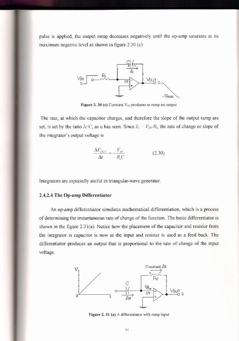
pulse is applied, the output ramp decreases negatively until the op-amp saturates at its
maximum negative level as shown in figure 2.30 (c)
C+ı \-~
VıN.ı r:- Rio~~
~ '""-Vmax~
Figure 2. 30 (c) Constant VIN produces as ramp on output
The rate, at which the capacitor charges, and therefore the slope of the output ramp are
set, is set by the ratio Jc!C, as u has seen. Since le= VJN/Ri, the rate of change or slope of
the integrator's output voltage is
(2.30)
Integrators are especially useful in triangular-wave generator.
2.4.2.4 The Op-amp Differentiator
An op-amp differentiator simulates mathematical differentiation, which is a process
of determining the instantaneous rate of change of the function. The basic differentiator is
shown in the figure 2.31(a). Notice how the placement of the capacitor and resistor from
the integrator is capacitor is now at the input and resister is used as a feed back. The
differentiator produces an output that is proportional to the rate of-change of the input
voltage.
V Constant IR·----1'+ -".../V'v"-
Rr
o
Co-Lt /IN
Your0') • o
Figure 2. 31 (a) A differentiatorwith ramp input
61

We apply a positive-going ramp voltage to the input making le = JIN and voltage
across the capacitor is equal to VIN at all times because of virtual ground on the inverting
input from the basic formula, Ve = (1Yc} , we get:
(2.31)
Since the current into the inverting input is negligible, IR = le. Both current are
constant because the slope of the capacitor voltage (Ve! t) is constant. The output voltage
is also constant and equals to the voltage across Rf because one side of the feedback
resistor is always O V.
(2.32)
(2.33)
The output is negative when the input is a positive-going ramp and positive when
the input is a negative-going ramp as shown in figure 2.31(b). During the positive slope of
the input, the capacitor is charging from the input source and the constant current through
the feedback resistor is in direction. During the negative slope of the input, the current is
in opposite direction because the capacitor is discharging.
tı-t2)+ -
y~~ fr O Io to £1 t2 ------ı+( to- tı
vour ol ı t2'> • 0 to t
Figure 2. 31 (b) Output with a series of positive and negative ramps on input
62

As from the equation V0ur = ( ~c )RfC , term VeI t is the slope of the input. If the
slope increases, VouT increases. If the slope decreases, VouT decreases. So, the output
voltage is proportional to the slope (rate of change) of the input. The constant of
proportionality is the time constant, RfC.
2.4.2.5 The Instrumental Amplifier
Instrumental amplifier consists of three op-amp and several resistors. IC
manufacturers provide this circuit in a package as one device. Common characteristics are
high input resistance, high voltage gain and excellent common-mode rejection ratio.
Instrumental amplifiers are commonly used in data acquisitions systems where remote
sensing of input variable is required.
Inverted Inputo-:--
GainSet Vowr
GainSet
Noninverted Input
Figure 2. 32 (a) Basic Instrumentation Amplifier
A simple instrumental amplifier is shown in figure 2.32(a). Op:amps A1 and A2 are
non-inverting amplifier stage that provides high input impedance and voltage gain. Op
amp A3 is a unity gain amplifier. When Ro is connected externally as shown in figure
2.32(b) op-amp receives a differential input signal Vnıı on its non-inverting input and
amplifies it with a gain ofl + R11 / Re . Op-amp A 1 also receives an input signal ViN2
through A2, R/2 and Ro. ViN2 appears on the inverting input of op-amp A1 and is amplified
by a gain ofR11 / Re . Also the common-mode voltage on the non-inverting is amplified by
the common mode of Aı. (Vem is typically less then unity) The total input voltage of op
amp is as follows.
63

(2.34)
VıN1+Vcm VoUT1
~T+
VIN2+Vcm
Figure 2. 32 (b) Instrumentation amplifierwith Gain resistor set
A similar analysis can be applied to op-amp A2, as shown below
(2.35)
The differential voltage to the op-amp A3 is Vourr Voun
(R1ı R1ı J (Rrz R1ı JVourı -Vourı = ı+--+-- VIN2 - --+ı+-- VIN! +Vem -vemRe Re Re Re
(2.36)
For R/2 = RJJ = R1
(2.37)
Since the common-mode voltage (Vem) are equal, they cancel out. Factoring gives
the following result, which is differential input to op-amp A3
64
(2.38)
Because op-amp A3 has unity gain, the final output of the instrumental amplifier is
Vour = (ıXvoUT2 - VouT2)
(2.39)
The close loop gain is
This equation shows the differential gain of the instrumentation amplifier can be
set by value Ro. Rıı and R12 are internal to the IC chip and manufacturer sets their values.
The instrumental amplifier is normally used to measure differential signal voltage
that is superimposed on a common-mode voltage often larger than the signal voltage.
Applications often include a situation where a quantity is measured by remote sensing
device (transducer), and resulting small electrical signal is sent over a long line subject to
large common-mode voltages. Instrumental amplifier at the end of the line must amplify
the small signal and reject the large common mode voltage as shown in Figure 2.32(c)."'
s mailer diffrential signal ridi~ıavon larger common-modesi~
10fI (\ I\ - 'InstrumentationAmplifier
/0J\J\f\fL_Amplified diffrential signal
no common-modesignal
Figure 2. 32 (c) Showing rejection oflarge common-mode signal
65
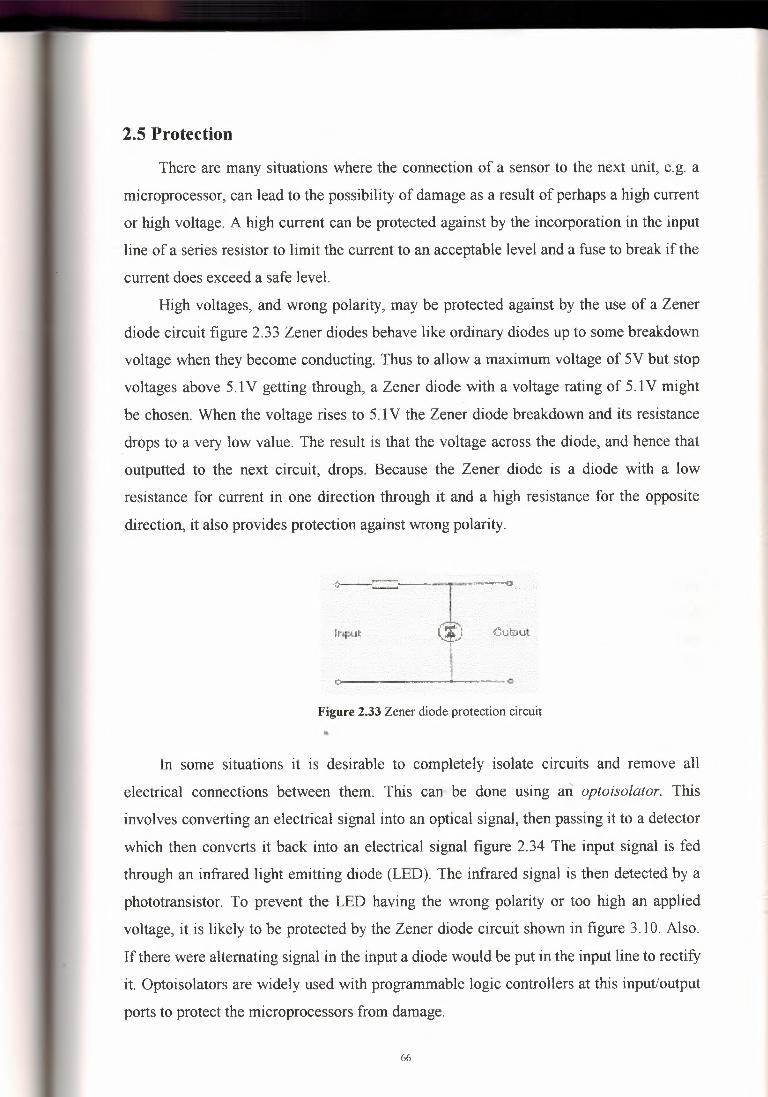
2.5 Protection
There are many situations where the connection of a sensor to the next unit, e.g. a
microprocessor, can lead to the possibility of damage as a result of perhaps a high current
or high voltage. A high current can be protected against by the incorporation in the input
line of a series resistor to limit the current to an acceptable level and a fuse to break if the
current does exceed a safe level.
High voltages, and wrong polarity, may be protected against by the use of a Zener
diode circuit figure 2.33 Zener diodes behave like ordinary diodes up to some breakdown
voltage when they become conducting. Thus to allow a maximum voltage of 5V but stop
voltages above 5. 1 V getting through, a Zener diode with a voltage rating of 5. 1 V might
be chosen. When the voltage rises to 5. 1 V the Zener diode breakdown and its resistance
drops to a very low value. The result is that the voltage across the diode, and hence that
outputted to the next circuit, drops. Because the Zener diode is a diode with a low
resistance for current in one direction through it and a high resistance for the opposite
direction, it also provides protection against wrong polarity.
Figure 2.33 Zener diode protection circuit
In some situations it is desirable to completely isolate circuits and remove all
electrical connections between them. This can be done using an optoisolator. This
involves converting an electrical signal into an optical signal, then passing it to a detector
which then converts it back into an electrical signal figure 2.34 The input signal is fed
through an infrared light emitting diode (LED). The infrared signal is then detected by a
phototransistor. To prevent the LED having the wrong polarity or too high an applied
voltage, it is likely to be protected by the Zener diode circuit shown in figure 3. 10. Also.
If there were alternating signal in the input a diode would be put in the input line to rectify
it. Optoisolators are widely used with programmable logic controllers at this input/output
ports to protect the microprocessors from damage.
66

Figure 2.34 Optoisolator
2.6 Design Guidelines This section discusses typical issues that should be considered when designing an
analog signal-conditioning system. The examples show how the guidelines can be used to
develop a design. The guidelines ensure that the problem is clearly understood and that
the important issues are included.
Not every guideline will be important in every design, so some will not be
applicable. In many cases, not enough information will be available to address an issue
properly: then the designer must exercise good technical judgment in accounting for that
part of the design.Figure 2.35 shows the measurement and signal-conditioning model. In some cases
the entire system is to be developed from selecting the sensor to designing the signal
conditioning. In other cases, only the signal conditioning will be developed. The
guidelines are generalized. Since the sensor is selected from what is available, the actual
design is really for the signal conditioning.
Process
Ymu bmaxCmax
Signalconditioning
Cmın Ymirı
Figure 2.35 Model for measurement and signal-conditioning objectives.
67

Guidelines for Analog Signal Conditioning Design
1. Define the measurement objective.
a. Parameter: What is the nature of the measured variable: pressure, temperature,
flow, level, voltage, current, resistance, etc.?
b. Range: What is the range of the measurement: 100 to 200°C, 45 to 85 psi. 2 to 4
V?
c. Accuracy: What is the required accuracy: 5% FS, 3% of reading, etc.?
d. Linearity: Must the measurement output be linear?
e. Noise: What is the noise level and frequency spectrum of the measurement
environment?
2. Select a sensor (if applicable).
a. Parameter: What is the nature of the sensor output: resistance, voltage. etc.?
b. Transfer function: What is the relationship between the sensor output and the
measured variable: linear, graphical, equation, accuracy, etc.?
c. Time response: What is the time response of the sensor: first-order time constant,
second-order damping, and frequency?
d. Range: What is the range of sensor parameter output for the given measurment
range?
e. Power: What is the power specification of the sensor: resistive dissipation
maximum, current draw. etc.?
3. Design the analog signal conditioning (S/C).
a. Parameter: What is the nature of the desired output? The most common is
voltage, but current and frequency are sometimes specified. In the latter cases. Conversion
to voltage is still often a first step.
b. Range: What is the desired range of the output parameter (e.g., O to 5 V, 4 to
20mA, 5 to 10 kHz)?
c. Input impedance: What input impedance should the S/C present to the input
signal source? This is very important in preventing loading of a voltage signal input.
d. Output impedance: What output impedance should the S/D coffer to the output
load circuit?
68
4. Notes on analog signal conditioning design.
a. If the input is a resistance change and a bridge or divider must be used, be sure to
consider both the effect of output voltage nonlinearity with resistance and the effect of
current through the resistive sensor.
b. For the op amp portion of the design, the easiest design approach is to develop an
equation for output versus input. From this equation, it will be clear what types of circuits
may be used. This equation represents the static transfer function of the signal
conditioning.
c. Always consider any possible loading of voltage sources by the signal
conditioning. Such loading is a direct error in the measurement system.
69

3.DIGITAL SIGNSL CONDITIONING ELEMENTS
3.1 INTRODUCTION Perhaps the best way to start this chapter is to consider briefly why we are
interested in digital signal conditioning. An overall survey of electronics applications in
industry shows that conversions to digital techniques are occurring rapidly. There are
many reasons for this conversion, but two in particular are important. One is the reduction
in uncertainty when dealing with digitally encoded information, compared with analog
information. Note that we said uncertainly, not accuracy. If a system presents analog
information, great care must be taken to account for electrical noise influence.
Drift of amplifier gains, loading effects, and a host of other problems familiar to the
analog electronics designer. In a digitally encoded signal, however, a wire carries either a
high or low level and is not particularly susceptible to the problems associated with
analog processing. Thus, there is an inherent certainty in representing information by
digital encoding because of the isolation of digital representation from spurious
influences. The accuracy of this signal in representing the information is discussed in
Section 3.3.A second reason for conversion to digital electronics is the growing desire to use
digital computers in the industrial process. The digital computer, by nature, requires
information to be encoded in digital format before it can be used. The need for digital
signal conditioning thus becomes a question of why computers are so widely used in
industry. As discussed, a few reasons are:"'1. A computer easily controls a multivariable process-control system.
2. Through computer programming, nonlinearities in a ~ensor output can be
linearized.3. Complicated control equations can be solved to determine required
control functions.4. Computers have the ability to microminiaturize complex digital processing
circuits as integrated circuits (ICs).
Finally, the development of microprocessors has brought about a transformation of
process control to digitally based control systems. With microprocessor-based computers,
implementation of computer-based control systems has become practical, and with it, the
70

need for knowledge of digital signal conditioning. This technology reduces not only
physical size but also both power consumption and failure rate.
With the growing use of computers in process-control technology, it is clear that any
individual trained to work in this field also must be versed in the technology of digital
electronics. But how far should such preparation extend into this related complex field of
study. The answer is that a process-control technologist must understand the elements and
characteristics of process-control loops. In this context, digital electronics is used as a tool
to implement necessary features of process control, and therefore the technician should
understand how such devices affect the characteristics of the loop. Consider that one does
not need to know detailed physics of stretched wires to understand the application of
strain gauges and use these devices successfully in process control. Similarly, one does
not need to know the internal design of logic gates and microcomputers to use such
devices in process control. Thus the objectives of this chapter have been carefully chosen
to provide the reader with sufficient background in digital technology to understand its
application to process control.
3.2 REVIEW OF DIGITAL FUNDAMENTALS A working understanding of the application of digital techniques to process
control requires a foundation of basic digital electronics. The design and implementation
of control logic systems and microcomputer control systems require a depth of
understanding that can be obtained only by taking several courses devoted to the subject.
In this text. we assume a sufficient background that the reader can appreciate the essential
features of digital electronic design and its application to process control.
3.2.1 Digital Information
The use of digital techniques in process control requires that process variable
measurements and control information be encoded into a digital form. Digital signals
themselves are simply two-state (binary) levels of voltage on a wire. We speak, then. of
the digital information as a high state (H or 1) or a low state (L or O) on a wire that
carries the digital signal.
71

Digital Words Given the simple binary information that is carried by a digital
signal, it is clear that a more complicated arrangement must be used to describe analog
information. Generally, this is done by using an assemblage of digital levels to construct a
word. The individual digital levels are referred to as bits of the word. Thus. for example, a
6-bit word consists of six independent digital levels, such as 1010112, which can be
thought of as a 6-digit base 2 number. An important consideration, then, is how the
process-control information is encoded into this digital word.
Decimal Whole Numbers One of the most common schemes for encoding analog
data into a digital wor~ is to use the straight counting of decimal (or base 10) and binary
representations.
Octal and Hex Numbers It is cumbersome for humans to work with digital words
expressed as numbers in the binary representation. For this reason, it has become common
to use either the octal (base 8) or hexadecimal (base 16. called hex) representations, Octal
numbers are conveniently formed from groupings of three binary digits: that is. 0002; is Os
and 1112; is 'l«, Thus. a binary number like 1010112; is equivalent to 53s. Hex numbers
are formed easily from groupings of four binary digits: that is, 00002; is OH and 11112; is
FH. The capital His used to designate a hex number instead of a subscript 16. Also recall
that the hex counting sequence is O, 1, 2, 3, 4, 5, 6, 7, 8, 9, A, B, C, D, E, and F to cover
the possible states. Because microcomputers must frequently use either 4-bit, 8-bit. Or 16-
bit words, the hex notation are commonly used with these machines. In hex, a binary
number like 1 O 11O1102 would be written B6H."
3.2.2 Fractional Binary Numbers
Although not as commonly used. It is possible to define a fractional binary number
in the same manner as whole numbers using only the 1 and O of this counting system.
Such numbers, just as in the decimal framework, represent divisions of the counting
system to values less than unity. A correlation can be made to decimal numbers in a
similar fashion to binary Equation, as
where N10 = base 1 O number less than one
bıb: ..... bm-ıb« = base 2 number less than one, m =number of digits in base 2 number.
72
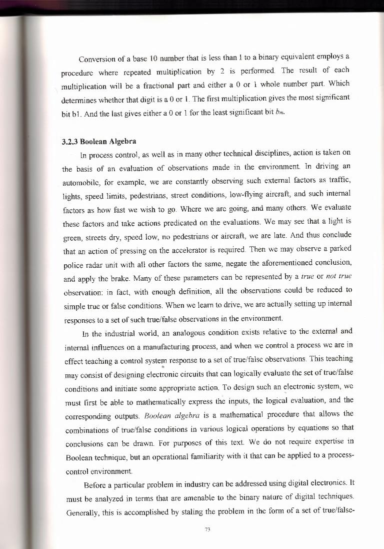
Conversion of a base 1 O number that is less than I to a binary equivalent employs a
procedure where repeated multiplication by 2 is performed. The result of each
multiplication will be a fractional part and either a O or 1 whole number part. Which
determines whether that digit is a O or 1. The first multiplication gives the most significant
bit b 1. And the last gives either a O or 1 for the least significant bit b»:
3.2.3 Boolean Algebra In process control, as well as in many other technical disciplines, action is taken on
the basis of an evaluation of observations made in the environment. In driving an
automobile, for example, we are constantly observing such external factors as traffic,
lights, speed limits, pedestrians, street conditions, low-flying aircraft, and such internal
factors as how fast we wish to go. Where we are going, and many others. We evaluate
these factors and take actions predicated on the evaluations. We may see that a light is
green, streets dry, speed low, no pedestrians or aircraft, we are late. And thus conclude
that an action of pressing on the accelerator is required. Then we may observe a parked
police radar unit with all other factors the same, negate the aforementioned conclusion,
and apply the brake. Many of these parameters can be represented by a true or not true
observation: in fact, with enough definition, all the observations could be reduced to
simple true or false conditions. When we learn to drive, we are actually setting up internal
responses to a set of such true/false observations in the environment.
In the industrial world, an analogous condition exists relative to the external and
internal influences on a manufacturing process, and when we control a process we are in
effect teaching a control system response to a set of true/false observations. This teaching~
may consist of designing electronic circuits that can logically evaluate the set of true/false
conditions and initiate some appropriate action. To design such an ~lectronic system, we
must first be able to mathematically express the inputs, the logical evaluation, and the
corresponding outputs. Boolean algebra is a mathematical procedure that allows the
combinations of true/false conditions in various logical operations by equations so that
conclusions can be drawn. For purposes of this text. We do not require expertise in
Boolean technique, but an operational familiarity with it that can be applied to a process
control environment.Before a particular problem in industry can be addressed using digital electronics. It
must be analyzed in terms that are amenable to the binary nature of digital techniques.
Generally, this is accomplished by staling the problem in the form of a set of true/false-
73
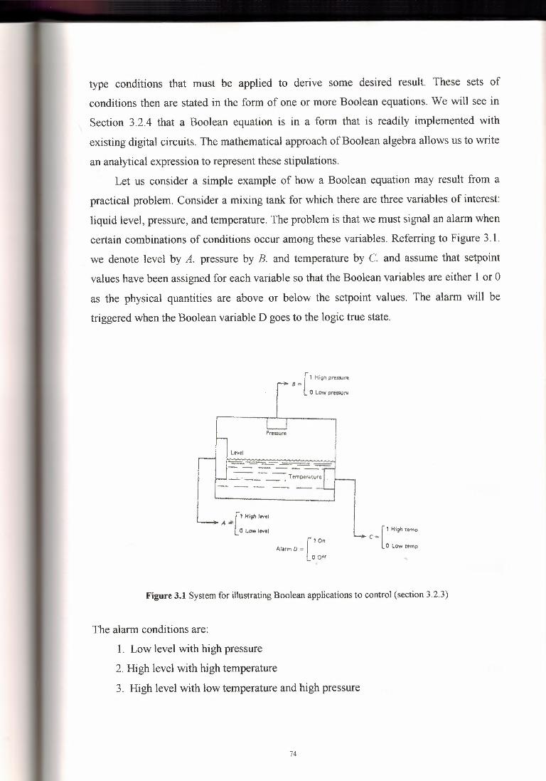
type conditions that must be applied to derive some desired result. These sets of
conditions then are stated in the form of one or more Boolean equations. We will see in
Section 3.2.4 that a Boolean equation is in a form that is readily implemented with
existing digital circuits. The mathematical approach of Boolean algebra allows us to write
an analytical expression to represent these stipulations.
Let us consider a simple example of how a Boolean equation may result from a
practical problem. Consider a mixing tank for which there are three variables of interest:
liquid level, pressure, and temperature. The problem is that we must signal an alarm when
certain combinations of conditions occur among these variables. Referring to Figure 3 .1.
we denote level by A. pressure by B. and temperature by C. and assume that setpoint
values have been assigned for each variable so that the Boolean variables are either 1 or O
as the physical quantities are above or below the setpoint values. The alarm will be
triggered when the Boolean variable D goes to the logic true state.
[
1 High pre=-ıreJJ =
O low preı,unı
Pressure
Level
---· ·-·-·-·-· -- --------
[
1 Hiçi> ,.,...,,A.,;,
O Lew level
1 1 OnAlarm O=
~O Ott
[
1 High tempC=
o Low remp
Figure 3.1 System for illustratingBoolean applications to control (section 3.2.3)
The alarm conditions are:
1. Low level with high pressure
2. High level with high temperature
3. High level with low temperature and high pressure
74

We now define a Boolean expression with AND operations that will give a D = 1 for
each condition.
1. D = A . B will give D = 1 for condition 1.
2. D =A. C will give D = 1 for condition 2.
3. D =A. C. B will give D = 1 for condition 3.
The final logic equation results from combining all three conditions so that if any is true,
the alarm will sound (D = 1 ). This is accomplished with the OR operation
D=A·B+A·C-ı..A·C·B
This equation would now from the starting point for a design of electronic digital circuitry
that would perform the indicated operations.
3.2.4 Digital Electronics
The electronic building blocks of digital electronics are designed .to operate on the
binary levels present on digital signal lines. These building blocks are based on families
of types of electronic circuits, that have their specific stipulations of power supplies and
voltage levels of the 1 and O states The basic structure involves the use of AND/OR logic
and NAND/NOR logic to implement Boolean equations.
EXAMPLE Develop a digital circuit using AND/OR gates that implements the equation developed in
Section 3.2.3.
Solution'
The problem posed in Section 3.2.3 (with Figure 3.1) has a Boolean equation
solution of
D=A·B+A·C+A·C·B
The implementation of this equation using AND/OR gates is shown in Figure 3.2. The
AND, OR and inverter are used in a straightforward implementation of the equation.
75

L...,,eıAo----,----~
TemperarureCo- _ _. _ _,.__...,
D
PressureBo---+-,,-.--~-----'
A B C
Figure 3.2 Solution for example
3.2.5 Programmable Logic Controllers
The move toward digital logic techniques and computers in industrial control
paralleled the development of special controllers called programmable logic controllers
(PLCs) or simply programmable controllers (PCs). These devices are particularly suited
to the solution of control problems associated with Boolean equations and binary logic
problems in general. They are a computer-based outgrowth of relay sequence controllers.
3.2.6 Computer Interface Figure 3.3 shows a simple model of a computer system. The processor is
connected to external equipment via three parallel sets of digital lines. The data lines carry
data to and from the processor. The address lines allow the computer to select external
locations for input and output. The control lines carry information to and from the
computer related to operations such as reading, writing, interrupts, and so on. This
collection of lines is called the bus of the computer.
76
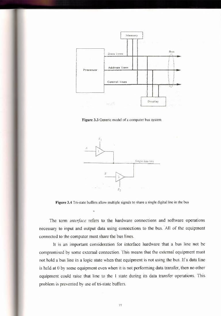
Merrıory
BusData l ın es
ProcessorAddress ii nes
Control lines
.II.
.Display
Figure 3.3 Generic model of a computer bus system
Figure 3.4 Tri-state buffers allow multiple signalsto share a singledigital line in the bus
The term interface refers to the hardware connections and software operations
necessary to input and output data using connections to the bus....All of the equipment
connected to the computer must share the bus lines.
It is an important consideration for interface hardware that a bus line not be
compromised by some external connection. This means that the external equipment must
not hold a bus line in a logic state when that equipment is not using the bus. If a data line
is held at O by some equipment even when it is not performing data transfer, then no other
equipment could raise that line to the 1 state during its data transfer operations. This
problem is prevented by use of tri-state buffers.
77

Tri-State Buffers Isolation of a bus line is accomplished by making all connections
via a special digital device called a tri-state buffer. This device acts like a simple switch.
When the switch is closed, the logic level on its input is impressed upon the output. When
open, the output is placed in a high impedance state that is, an open circuit.
Figure 3.4 shows how two digital signals can both be connected to a single data
line through tri-state buffers. Normally, both tri-states are disabled, that is. In the high
impedance state. When the computer needs to input signal A, an enable signal, EI, is sent
to tri-state 1 so that the state of A is placed on the data line. After the computer reads the
line, tri-state 1 is disabled again. Similarly, when the computer needs the state of signal B,
an enable, E2, is sent to tri-state 2 to place B on the line.
3.3 BUFFERING Frequently the signals reaching the inputs of a microprocessor are spasmodic.
Sometimes the signals come in rapid bursts, which may be too fast for the microprocessor
to accept. Sometimes the microprocessor is engaged in some other activity and cannot
accept them at the time they arrive. The output from a microprocessor may be too fast for
an actuator or other device, new data being transmitted to it before it has had time to
accept the previous data. For these reasons, external storage is provided for signals. This
is provided in what are termed buffers.
For a buffer on the input, data is transferred out of it at a rate determined by the
microprocessor. For a buffer on the output, data is transferred out of it at a rate
determined by the peripheralıodevice being fed. The buffer memory fills and empties to
compensate for the difference between the input rate of the data into the buffer and the
required output rate. The ability of the buffer to cope is determined by the size if its
memory and the difference in input and output transfer rates.
3.4 CONVERTERS The most important digital tool for the process-control technologist is one the
translates digital information to analog and vice versa. Most measurements of process
variables are performed by devices that translate information about the variable to an
analog electrical signal. To interface this signal with a compute or digital logic circuit, it
is necessary first to perform an analog-to-digital (AID) conversion. The specifics of this
78
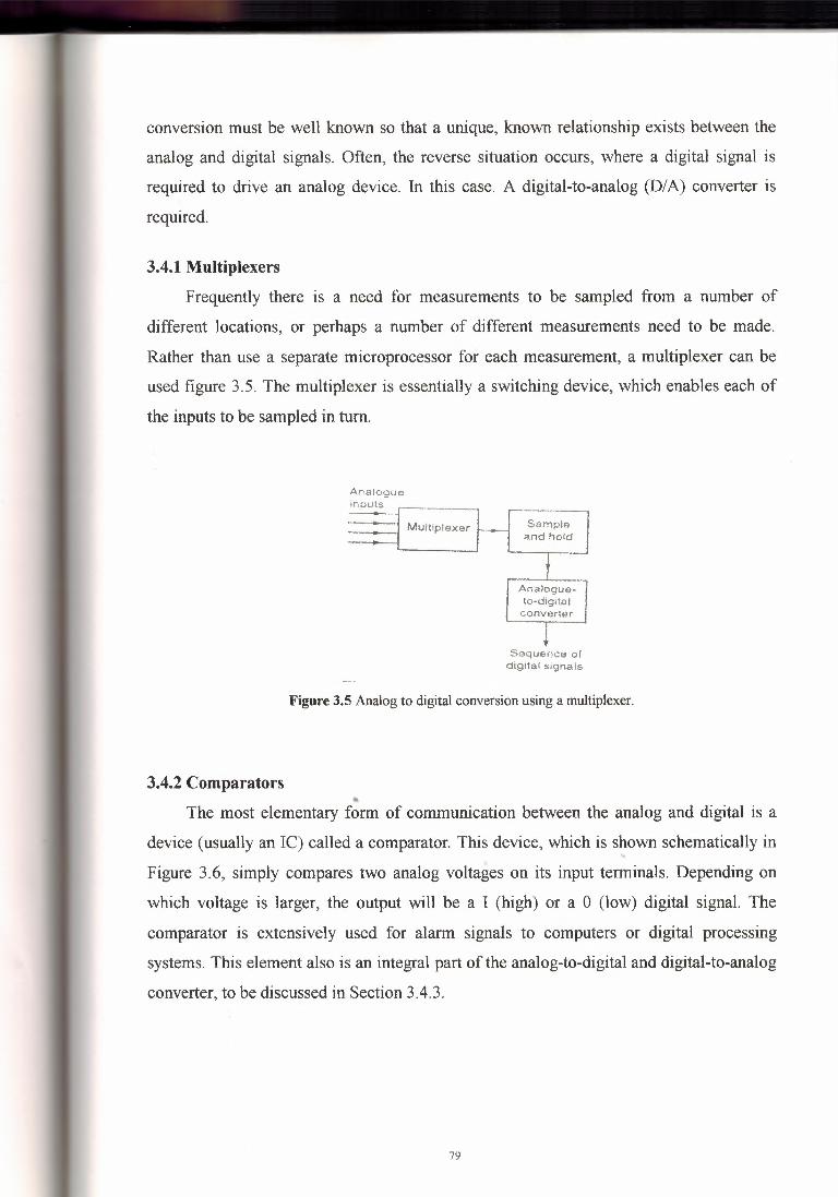
conversion must be well known so that a unique, known relationship exists between the
analog and digital signals. Often, the reverse situation occurs, where a digital signal is
required to drive an analog device. In this case. A digital-to-analog (D/A) converter is
required.
3.4.1 Multiplexers
Frequently there is a need for measurements to be sampled from a number of
different locations, or perhaps a number of different measurements need to be made.
Rather than use a separate microprocessor for each measurement, a multiplexer can be
used figure 3.5. The multiplexer is essentially a switching device, which enables each of
the inputs to be sampled in tum.
Analogueinputs·-- Multiplexer Sample
and hofd
Arıatoçueto-digital
converter
Sequence ofdigital signals
Figure 3.5 Analog to digital conversion using a multiplexer.
3.4.2 Comparators ~
The most elementary form of communication between the analog and digital is a
device (usually an IC) called a comparator. This device, which is shown schematically in..•Figure 3.6, simply compares two analog voltages on its input terminals. Depending on
which voltage is larger, the output will be a I (high) or a O (low) digital signal. The
comparator is extensively used for alarm signals to computers or digital processing
systems. This element also is an integral part of the analog-to-digital and digital-to-analog
converter, to be discussed in Section 3.4.3.
79
-,.-- --- -- ·--··--
Figure 3.6 A basic comparator has an output digital logic state that
depends on tow analog input voltages.
One of the voltages on the comparator inputs, Va, or Vb, in Figure 3.6, will be the
variable input, and the other a fixed value called a trip, trigger, or reference voltage. The
reference value is computed from the specifications of the problem and then applied to the
appropriate comparator input terminal, as the following Example. The reference voltage is
provided from a divider using available power supplies.
Example
A process-control system specifies that temperature should never exceed 160°C if the
pressure also exceeds 1 O Pa. Design an alarm system to detect this condition. using
temperature and pressure transducers with transfer functions of 2.2 mV/C and 0.2 V/Pa,
respectively.
Solution
The alarm conditions will be a temperature signal of (2.2 mV/°C)(160°C) = 0.352 V
coincident with a pressure signal of (0.2 V/Pa)(lO Pa)= 2 volts. The circuit of Figure 3.7
shows how this alarm can be implemented with comparators and one AND gate. The
reference voltages could be provided from dividers.~
Temperatureıt>==-ı
JI I~ I0.352 V ·
Pressure
Ateemonhigh
2.0 V
Figure 3.7 Diagram of a solution to Example
80
Hysteresis Comparator When using comparators, there is often a problem if the
signal voltage has noise or approaches the reference value too slowly. The comparator
output may ''jiggle" back and forth between high and low as the reference level is reached.
This effect is shown in Figure 3.8. Such fluctuation of output may cause problems with
the equipment designed to interpret the comparator output signal.
This problem often can be solved by providing a deadband or hysteresis to the
reference level around which output changes occur. Once the comparator has been
triggered high. the reference level is automatically reduced so that the signal must fall to
some value below the old reference before the comparator goes to the low state.
Time Time
Figure 3.8 A comparator output will "jiggle" when a noisy signal passes through the reference voltage
level.
There are many ways this hysteresis can be provided, but Figure 3.9a shows one
common technique. Feedbacle resistor Rf is provided between the output and one of the
inputs of the comparator, and that input is separated from the signal by another resistor, R.
Under the condition that Rf>>R, the response of the comparator is shown in Figure 3.9b.
The condition for which the output will go high (Vo) is defined by the following
condition:
-ı /: ::::> "\/ .Y ;n -· - · re r
(3.1)
Once having been driven high. the condition for the output to drop back to the low (OV)
state is given by the relation:
(3.2)
81
The dead band or hysteresis is given by (R/Rf)Vo, and is thus selectable by choice of
the resistors, as long as this relation is satisfied. The response of this comparator is shown
by the graph in Figure 3.9b. The arrows indicate increasing or decreasing input voltage.
V,.ıo--
(A)
Vout
Vo
VL VH Vin
(B)
Where, Vref = VH, VL = Vref- RI Rr " Vo
Figure 3.9 A hysteresis comparator has an input voltage window within which output changes donot occur. This provides noise immunity.
••3.4.3 Digital-to-Analog Converters (DACs)A DAC accepts digital information and transforms it into an analog voltage. The
digital information is in the form of a binary number with some fixed number of digits.
Especially when used in connection with a computer, this binary number is called a
binary word or computer word. The digits are called bits of the word. Thus an 8-bit word
would be a binary number having eight digits, such as 101101102. A unipolar DAC
converts a digital word into an analog voltage by scaling the analog output to be zero
when all bits are zero and some maximum value when all bits are one. This can be
mathematically represented by treating the binary numbel that the word represents as a
fractional number. In this context, the output of the DAC can be defined using equation
(3.3) as a scaling of some reference voltage.
82

... bnz-n](3.3)
Where Vout = analog voltage output
VR = reference voltage
bı.bz, ,bn = n-bit binary word
The minimum Vout is zero, and the maximum is determined by the size of the binary
word because, with all bits set to one, the decimal equivalent approaches Vg as the
number of bits increases. Thus, a 4-bit word has a maximum of
V :::; \/ ['7-i + J< '"'- ı-3 + "'···1 = o 937,ıımax R - ı 1w ' '- ; t · ...l Y R
and an 8-bit word has a maximum of
An alternative equation to Equation (3.3) is often easier to use. This is based on
noting that the expression in brackets in Equation (3.3) is really just the fraction of total
counting states possible with the n-bits being used. With this recognition, we can write:
(3.4)
"Where N = base 10 whole number equivalent ofDAC input
Suppose an 8-bit converter with a 5.0-volt reference has an input of 101001112, or A7H.
If this input is converted to base 10, we get N = 16710 and 2/\8 = 256. From Equation
(3.4), the output of the ADC will be:
167V,ut = -~ 5.0 = 3.2617 voltsL 256
Bipolar DAC Some DACs are designed to output a voltage that ranges from plus to
minus some maximum when the input binary ranges over the counting states. Although
computers frequently use 2s complement to represent negative numbers, this is not
83
common with DACs. Instead, a simple offset-binary is frequently used, wherein the
output is simply biased by half the reference voltage of Equation (3.4). The bipolar DAC
relationship is then given by:
lV 1Vouı = 2n VR - 2 V R
(3.5)
Notice that ifN = O the output voltage will be given by the minimum value. Vout(min)= -
VR/2. However, the maximum value For N is equal to (2/\n - 1 ), so that the maximum
value of output voltage will be:
V . (2:' - 1) r IV l V V,'""\max)""-1-,,- 'ii - :; R "':; R -1n
- •.• i,. ~ (3.6)
DAC Characteristics For modem applications, most DACs are integrated circuit
(IC) assemblies, viewed as a black box having certain input and output characteristics. In
Figure 3 .1 O, we see the essential elements of the DAC in terms of required input and
output. The associated characteristics can be summarized by reference to this figure.
Oigitıtl--to~analog ~(DACI
1----;,..Vout ~=·ou-cput
••+ V GNO - V
Figure 3.10 A generic DAC diagram, showing typical input and output signal.
1. Digital input Typically, a parallel binary word of a number of bits specified by the
device specification sheet. Typically, TTL logic levels are required
2. Power supply This is bipolar at a level of ±12 to ±18 V as required for internal
amplifiers. Some DACs operate from a single supply.
3. Reference supply Required to establish the range of output voltage and resolution of
the converter. This must be a stable, low-ripple source. In some units, an internal
reference is provided.
84

4. Output A voltage representing the digital input. This voltage changes in steps as the
digital input changes by bits, with the step determined. The actual output may be bipolar
if the converter is designed to interpret negative digital inputs.
5. Offset Because the DAC is usually implemented with op amps, there may be the
typical output offset voltage with a zero input. Typically, connections will be provided to
facilitate a zeroing of the DAC output with a zero word input.
6. Data latch Many DACs have a data latch built into their inputs. When a logic
command is given to latch data, whatever data are on the input bus will be latched into the
DAC and the analog output will be updated for that input data. The output will stay at that
value until new digital data are latched into the input. In this way the input of the DAC
can be connected directly onto the data bus of a computer, but it will be updated only
when a latch command is given by the computer.
7. Conversion -time A DAC performs the conversion of digital input to analog output
virtually instantaneously. From the moment that the digital signal is placed on the inputs
to the presence of the analog output voltage is simply the propagation time of the signal
through internal amplifiers. Typically, settling time of the internal amplifiers will be a few
microseconds.
DAC Structure Generally speaking, a DAC is used as a black box, and no
knowledge of the internal workings is required. There is some value, however, in briefly
showing how such conversion can be implemented. The simplest conversion uses a series
of op amps for input for which the gains have been selected to provide an output as given
by Equation (3.3). The most common variety, however, uses a resistive ladder network toI"
provide the transfer function. This is shown in Figure 3. 1 O for the case of a 4-bit
converter. With the R-2R choice of resistors, it can be shown through network analysis
that the output voltage is given by Equations (3.3) or (3.4). The switches are analog
electronic switches.
85
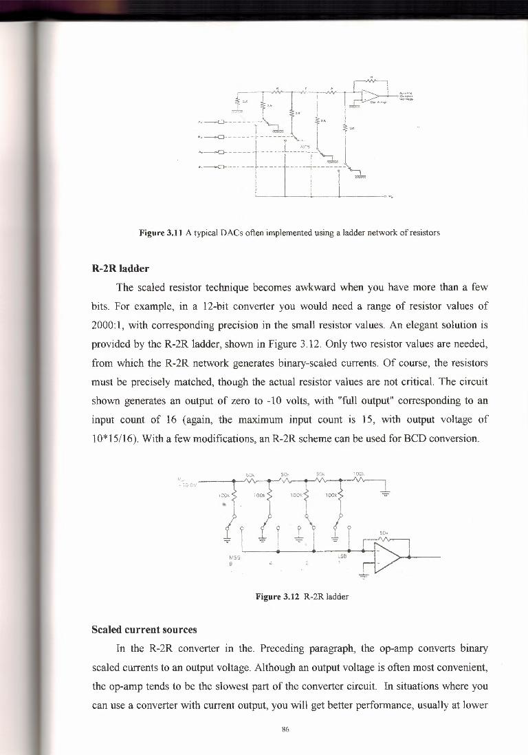
Figure 3.11 A typical DACs often implemented using a ladder network of resistors
R-2R ladder
The scaled resistor technique becomes awkward when you have more than a few
bits. For example, in a 12-bit converter you would need a range of resistor values of
2000:1, with corresponding precision in the small resistor values. An elegant solution is
provided by the R-2R ladder, shown in Figure 3.12. Only two resistor values are needed,
from which the R-2R network generates binary-scaled currents. Of course, the resistors
must be precisely matched, though the actual resistor values are not critical. The circuit
shown generates an output of zero to -1 O volts, with "full output'' corresponding to an
input count of 16 (again, the maximum input count is 15, with output voltage of
10*15/16).With a few modifications, an R-2R scheme can be used for BCD conversion.
Figure 3.12 R-2R ladder
Scaled current sources
In the R-2R converter in the. Preceding paragraph, the op-amp converts binary
scaled currents to an output voltage. Although an output voltage is often most convenient,
the op-amp tends to be the slowest part of the converter circuit. In situations where you
can use a converter with current output, you will get better performance, usually at lower
86

_, _
price. Figure 3 .13 shows the general idea. The currents can be generated by an array of
transistor current sources with scaled emitter resistors, although IC designers usually use
instead an R-2R ladder of emitter resistors. In most converters of this type, the current
sources are ON all the time, and their output current is switched to the output terminal or
to ground, under control of the digital input code. Watch out for limited output
compliance in current-output DACs; it can be as little as 0.5 volt, though values of a few
volts are typical.
MSBIIIII
MSB-1II
fh
IV..
Figure 3.13 Classic current switched DAC.
Generating a voltage output
There are a few ways to generate an out-put voltage from a current DAC. Figure
3.14 shows some ideas. If the load capacitance is low, and large voltage swings aren't
needed, a simple resistor to ground will do nicely. With the usual lmA full-scale output
current, a 100 ohm load resistor will give lOOmV full-scale output with 100 ohms output
impedance: If the capacitance of the DAC's output combined with the load capacitance
doesn't exceed lOOpF, you will get lOOns settling time in the preceding example,
assuming the DAC is that fast. When worrying about the effect of RC time constants on
DAC output response, don't forget that it takes quite a few RC time constants for the
output to settle to within Yı LSB of the final voltage. It takes 7.6 RC time constants, for
instance, to settle to within I part in 2048, which is what you would want for a 1 O-bit
converter output.
To generate large swings, or to buffer into small load resistances or large load
capacitances, an op-amp can be used in the transresistance configuration (current-to
voltage amplifier), as shown. The capacitor across the feedback resistor may be necessary
87

for stability, because the DAC's output capacitance in combination with the feedback
resistance introduces a lagging phase shift; unfortunately, that compromises the speed of
the amplifier. It is an irony of this circuit that a relatively expensive high-speed (fast
settling) op-amp may be necessary to maintain the high speed of even an inexpensive
DAC. In practice, the last circuit may give better performance, since no compensation
capacitor is needed. Watch out for offset voltage error, since the op-amp's input offset
voltage is amplified 100 times.
0-100mV
(a)
C,
O to - ıov
(b)
I"/.lOAC ~/ j • I
Cou,*ı -L.
O to +10V
99k
(c)
Figure 3.14 Generating voltages from current output DACs.

Data Output Boards
It is now common and convenient to obtain a printed circuit board that plugs into a
personal computer expansion slot and is a complete data output system. The board has all
necessary DACs. address decoding, and bus interface. In most cases, the supplier of the
board will also provide elementary software, often written in C. BASIC, or assembly
language, as necessary to use the board for data output.
3.4.4 Analog-to-Digital Converters (ADCs) Although many sensors that provide a direct digital signal output exist and are being
developed, most still convert the measured variable into an analog electrical signal. With
the growing use of digital logic and computers in process control, it is necessary to
employ an ADC to provide a digitally encoded signal for the computer. The transfer
function of the ADC can be expressed in the same manner as Equation (3.3) in that some
analog voltage is provided as input, and the converter finds a binary number that, when
substituted into Equation (3.3), gives the analog input. Thus,
(3.7)
where Vin= analog voltage input
VR = reference voltage
bı.bz, bn = n-bit digital outputs
We use an approximate equality in this equation because the voltage on the right can~
change by only a finite step size given by Equation (3.5).
Therefore, there is an inherent uncertainty of tJ.V in any conversion of analog voltage to
digital signal. This uncertainty must be taken into account in design applications. If the
problem under consideration specifies a certain resolution in analog voltage, then the
word size and reference must be selected to provide this in the converted digital number.
Equation (3.7) can be written in a simpler fashion, by expressing the fractional number as
the fraction of counting states, as was done for the DAC. In this case the base-10 value of
the digital output can be expressed as:
89

(3.8)
where INT( ) means to take the integer part of the quantity in brackets. This is not a
round-off, but rather a truncation, so that INT(3.3) = 3 and INT(3.99) = 3 also. The value
of N is then converted to hex and/or binary to demonstrate the ADC output. In the
previous example, we would have:
(''"'ı.,~ \
N = INT -'·5"-..!...
25) = INT(20.0128) = 2010
(3.9)
or 14H= 101002, as already found.
Bipolar Operation
A bipolar ADC is one that accepts bipolar input voltage for conversion into an appropriate
digital output. The most common bipolar ADCs provide an output called offset binary.
This simply means that the normal output is shifted by half the scale so that all zeros
corresponds to the negative maximum input voltage instead of O. In equation form, the
relation would be written from Equation (3.7) as
/\/ = fN-f [(,,V_',n ..•... _.!_·) )"]' ~ ı,r ' ') -\ R "'-, (3.10)
From this equation, you can see that if Vin= - VR/2,then the output is zero, N =O.If Vin=
O, then the output would be half of 2/\n. The output will be the maximum count when the
input is VR/2 - VR2/\n. For example, for 8 bits with a 10.0-volt reference, the step size is
tıVin= (10)2/\8 = 0.039 volts. Looking at the possible states, we would have
\ '" = - 5 000 N = 00000000,v,,, = -4.96 l ,y = 00000001,
ele.V., = --0.039 N = 011111111
V, = 0.000 .Y = 10000000,\/'" = +0.039 N = 100000012
etc.
v,, = +-1-.961 N = llllllllı
90

----~-~~-
There is an asymmetry to the result so that the converter cannot represent the full range
from minus to plus VR/2.
ADC Characteristics
Figure 3.15 shows a generic ADC with all the typical connections. It is quite
possible and even appropriate in many cases to regard the ADC as simply a black box
with certain input and output characteristics, The following list summarizes the important
characteristics of the ADC.
1. Analog voltage intput This is for connection of the voltage to be converted. As
will be explained later, it is important that this voltage be constant during the
conversıon process.
2. Power supplies Generally, an ADC requires bipolar supply voltages for internal
op amps and a digital logic supply connection.
3. Reference voltage The reference voltage must be from a stable, well-regulated
source. Special, integrated circuit reference-source voltages are available for this
purpose.
4. Digital outputs The converter will have n output lines for connection to digital
interface circuitry. Generally, the levels are typical TTL values for definition of the
high and low states. It is common for the output lines to be tri-state outputs so that
the ADC can be connected directly to a bus .
~.ı,; . v, VL
•.. I EOC
ADC
ı,,,ı,,,.J
Vin Conversion time'tc
Paralleloutputlines
'--~~~~~~- RD
~~~~~~~~~~ SC
Figure 3.15 A generic ADC diagram, showing typical input and output signals and noting the conversion
time.
91

--.--
5. Control lines The ADC has a number of control lines that are single-bit digital
inputs and outputs designed to control operation of the ADC and allow for interface
to a computer. The most common lines are:
a. SC (Start convert) This is a digital input to the ADC that starts the converter
on the process of finding the correct digital outputs for the given analog voltage
input. Typically, conversion starts on a falling edge.
b. EOC (End of convert) This is a digital output from the ADC to receiving
equipment, such as a computer. Typically, this line will be high during the
conversion process. When the conversion is complete the line will go low, Thus.
the falling edge indicates that the conversion is complete.
c. RD (Read) Since the output is typically buffered with tri-states. even though
the conversion is complete, the correct digital results do not appear on the output
lines. The receiving equipment must take the RD line low to enable the tri-states
and place the data on the output lines.
6. Conversion time This is not an input or an output, but a very important
characteristic of ADCs. A typical ADC does not produce the digital output
instantaneously when the analog voltage is applied to its input terminal. The ADC
must sequence through a process to find the appropriate digital output, and this
process takes time. This is one of the reasons that handshaking lines are required.
Figure 3 .16 shows a typical timing diagram for taking a sample of data via an ADC.
The existence of a finite conversion time complicates the use of ADCs in data
acquisition. The computer cannot have a data input at any time: rather, it must request an••
input, wait for the ADC to perform a conversion, and then input the data.
~ fJ-1
~· 'c -l,J----·vFigure 3.16 A typical data-acquisition timing diagramusing an ADC. The read operation may occur at any
time after the end-of-convert has been issued by the ADC.
92

ADC Structure Most ADCs are available in the form of integrated circuit (IC)
assemblies that can be used as a black box in applications. To fully appreciate the
characteristics of these devices, however, it is valuable to examine the standard
techniques employed to perform the conversions. There are two methods in use that
represent very different approaches to the conversion problem.
Parallel-Feedback ADC The parallel-feedback AID converter employs a feedback
system to perform the conversion, as shown in Figure 3.17, Essentially, a comparator is
used to compare the input voltage Vx to a feedback voltage VFthatcomes from a DAC as
shown. The comparator output signal drives a logic network that steps the digital output
(and hence DAC input) until the comparator indicates the two signals are the same within
the resolution of the converter. The most popular parallel-feedback converter is the
successive approximation device. The logic circuitry is such that it successively sets and
tests each bit, starting with the most significant bit of the word. We start with all bits zero.
Thus, the first operation will be to set bı = 1 and test VF = VR.2/'-1 against Vx through the
comparator.
If Vx is greater, then bl will be 1; bz is set to l and a test is made of Vx versus Vy=
VR(2A-l + 2A-2), and so on.
If Vx is less than VR2A-J, then b ı is reset to zero; b: is set to 1, and a test is made for
Vx versus VRY'-2. This process is repeated to the least significant bit of the word.
••
O/A
"""""""
Svpply
Figure 3.17 One common method of implementingan ADC is the successiveapproximation or parallel
feed back system. This uses an internal DAC.
93

The conversion time of successive approximation-type ADCs is on the order of 1 to
5 µs per bit. Thus, a low-priced 8-bit ADC might require 5µslbit for a total conversion
time of about 40 µs. A higher-quality (and price) 12-bit might be able to perform the full
conversion in only 15 µs.
These conversion times depend on a clock that is internal to the ADC and not
crystal controlled. Thus, there will be variation of the conversion time from unit to unit.
Ramp ADC The ramp-type AID converters essentially compare the input voltage
against a linearly increasing ramp voltage. A binary counter is activated that counts ramp
steps until the ramp voltage equals the input. The output of the counter is then the digital
word representing conversion of the analog input. An op amp integrator circuit typically
generates the ramp itself.
Dual Slope Ramp ADC This ADC is the most common type of ramp converter. A
simplified diagram of this device is shown in Figure 3. 18. The principle of operation is
based on allowing the input signal to drive the integrator for a fixed time Ti, thus
generating an output of
V1 = 1 JRC Vxdt(3.11)
or, because Vx is constant.
(3.12)
..After time Tı, the input of the integrator is electronically switched to the reference supply.
The comparator then sees an input voltage that decreases from VI as
(3.13)
94

-------- -- ------ ------
L....-------C""""'1.,UO't
Figure 3.18 The dual-slope ADC uses an op amp integrator, comparator, and counter. This is commonly
used in digital voltmeters.
or, because VR is constant and VI is given From Equation (3.12),
(3.14)
A counter is activated at time T1 and counts until the comparator indicates Vi = O, at
which time Ix [Equation (3 .14)] indicates that Vx will be
vx [- _x V
T, R(3.15)
Thus, the counter time tx is linearly related to Vx and is independent of the integrator
characteristics, that is, R and C. This procedure is shown in the timing diagram of Figure
3.19. Conversion start and complete digital signals are also used in these devices, and (in
many cases) internal or external references may be used.
V
Figure 3.19 A typical timing diagram of a dual-slope ADC. Sinceboth slopes depend upon R
and C, the ADC output is independent of the values ofR and C.
95
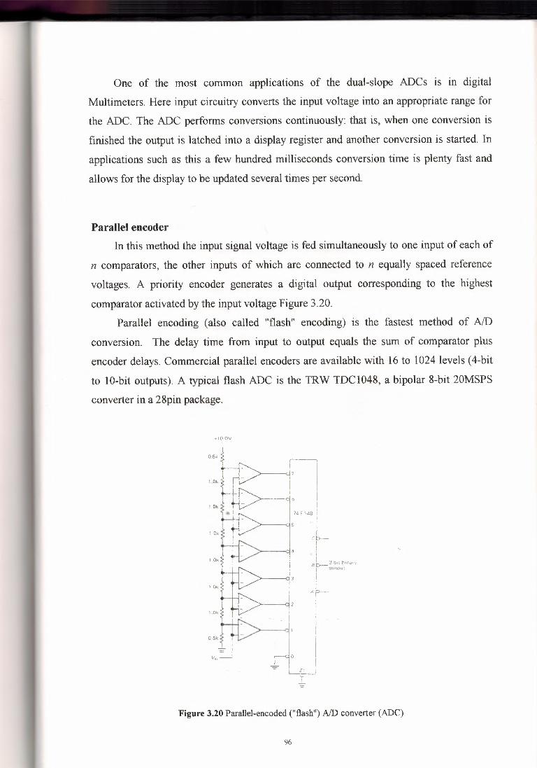
One of the most common applications of the dual-slope ADCs is in digital
Multimeters. Here input circuitry converts the input voltage into an appropriate range for
the ADC. The ADC performs conversions continuously: that is, when one conversion is
finished the output is latched into a display register and another conversion is started. In
applications such as this a few hundred milliseconds conversion time is plenty fast and
allows for the display to be updated several times per second.
Parallel encoder In this method the input signal voltage is fed simultaneously to one input of each of
n comparators, the other inputs of which are connected to n equally spaced reference
voltages. A priority encoder generates a digital output corresponding to the highest
comparator activated by the input voltage Figure 3.20.
Parallel encoding (also called "flash" encoding) is the fastest method of AID
conversion. The delay time from input to output equals the sum of comparator plus
encoder delays. Commercial parallel encoders are available with 16 to 1024 levels (4-bit
to 10-bit outputs). A typical flash ADC is the TRW TDC1048, a bipolar 8-bit 20MSPS
converter in a 28pin package.
Figure 3.20 Parallel-encoded ("flash") AID converter (ADC).

A variant on the simple parallel encoder is the so-called half-flash technique, a two
step process in which the input is flash-converted to half the final precision; an internal
DAC converts this approximation back to analog, where the difference "error" between it
and the input is flash-converted to obtain the least significant bits (Fig. 9.50). This
technique yields low-cost converters that are faster than any thing else except full flash
converters. It is used in inexpensive converters like the 8-bit ADC0820 (national) and
AD7820/4/8 (Analog Devices).
Flash encoders are worth considering in waveform digitizing applications even
when the conversion rate is relatively slow, because their high speed ensures that the input
signal is effectively not changing during the conversion. The alternative - the slower
converters we'll describe-next - usually requires an analog sample-and-hold circuit to
freeze the input waveform while conversion is going on .
.•. V,ıı,
MSB
Figure 3.21 Half-flashADC
3.5 MODULATION
A problem that is often encountered with dealing with the transmission of low level
d.c. signals from sensors is that the gain of an operational amplifier used to amplify them
may drift and so the output drifts. This problem can be overcome if the signal is
alternating rather than direct. In addition, the conversion of the signal to alternating can
assist in the elimination of external interference from the signal.

-··- .---------·--·-·--
One way this conversion can be achieved is by chopping the d.c. signal in the way
suggested in figure 3.22. The output from the chopper is a chain of pulses, the heights of
which are related to the d.c. level of the input signal. This process is called pulse
amplitude modulation. After amplification and any other signal conditioning, the
modulated signal can be demodulated to give a d.c. output. With pulse amplitude
modulation, the height of the pulses is related to the size of the d.c. voltage. An alternative
to this is pulse width modulation where the width, i.e. duration, of a pulse depends on the
size of the voltage (figure 3.23).
t ı~ J=====-jl JrrnITmmıf JnnCTUon
Tıme]r-~~.@ c;e·~~
o -----Time
Figure 3.22 pulse amplitudemodulation
I~JL'~ı I ı I
o';--- , :; : Tim,_e ··
''IIııOr--1:Tııne, · -!' I
I
'''J\
Figure 3.23 pulse duration modulation
98

The above refers to d.c. signals, however it is often necessary to modulate a.c.
signals. This enables data transmission at much higher frequencies and so allows the use
of high-pass filters to eliminate the noise signals that usually occur at much lower
frequencies. Modulation techniques used are amplitude modulation figure 3.24(a), phase
modulation and frequency modulation figure 3.24(b). With amplitude modulation the
amplitude of a carrier wave, of much higher frequency than the input, is varied according
to the size of the voltage input, i.e. the wave carrying the signal from the sensor. Thus for
a carrier wave that can be represented by
V = Vsin (rot+ cp)
The amplitude term Vis varied according to the way the voltage input varies. Phase
modulation involves varying the phase cp of the carrier wave according to the size of the
voltage input. Another method is to vary the angular frequency oı according to the size of
the voltage input. This is known as frequency modulation. Both phase modulation and
frequency modulation produce similar effects, a modulated wave with a frequency, which
relates to the input voltage. After transmission, the signal can be demodulated so that an
output can be obtained which is related to the original signal before it was modulated.
(a) (b)
Figure 3.24 Modulation: a) Amplitude, b) Frequency.
99
-------- ----
CONCLUSION
The objective of the signal conditioning elements in Mechatronics is the search for
new engineering solutions for industrial applications inspired by principles, functions,
mechanisms and architectures found in living organisms. Currently the focus is on the
signal conditioning systems featuring an efficient implementation of control system and
information processing tasks in Analog, digital, and mixed circuitry.
The application scope for signal conditioning elements that include information
processing for making decisions or eliciting actions on a local and autonomous basis is
quite large. It extends to surveillance, industrial control, robotics, environmental
control, the automotive sector, consumer electronics and multimedia applications.
Typical requirements for sensor systems in these domains are reliability, real-time
processing, high accuracy, compactness, low power consumption, and finally low-cost.
Many of the results that have been obtained in research are introduced into new
industrial developments, such as, for example, analog or digital conditioning elements
that we use it after the torque sensors for electrical power steering in cars. And much
other application.
These are the some of the important features of signal conditioning elements:
• Includes a detailed treatment of linear and nonlinear analog signal processing.
• Introduces elements of digital signal conditioning used in measurement...• Discusses current industry trends.
• Contains challenging problems.
• By using signal conditioning elements we can get complete isolation.
• Banishment all types of environment noise by using the compensation elements.
• For the op-amp portion of design, the easiest design approach is to develop an
equation for the output versus input.
• In this type of elements we can get full linearized for the signal, which we take it
from the output of the sensors.
• Banishment all the noise and take some levels of the signal by using the
filtering.
100

REFERENCES
[1] W.Bolton, Mechatronics, Electronic control systems in mechanical engineering,
London 1995.
[2] Curtis D. Johnson, Process Control Instrumentation Technology, 5th ed., Prentice
Hall International Inc., University of Houston, 1997.
[3] M. Histad and D. Alciatore, Introduction to Mechatronics and Measurement
Systems, McGraw-Hill, 1999.
[4] J. R. Hewit, An Introduction, in Mechatronics, Springer-Verlag, New York, 1993.
[5] Dr. Kadri Bürüncük, Mecatronics, Lecture Notes, Near East University Nicosia
Turkey, 2001.
101