fabricationofcomplex metallicnanostructures … (spl) ,43–47 including dip-pen lithography...
TRANSCRIPT
Fabrication of ComplexMetallic Nanostructuresby NanoskivingQiaobing Xu, Robert M. Rioux, and George M. Whitesides*
Department of Chemistry and Chemical Biology, Harvard University, 12 Oxford Street, Cambridge, Massachusetts 02138
This article describes several routesto fabricate complex metallic nano-structures by nanoskiving. The origin
of the term “nanoskiving” is in the word“skiving” (a procedure used to cut thin slicesfrom a thicker bulk material).1 Nanoskivingcombines deposition of thin films of metalon an epoxy substrate, with sectioning of anepoxy block (containing the thin metalfilms) using an ultramicrotome. It is experi-mentally simple and requires little in theway of facilities (for example, access to acleanroom or a high-resolution e-beamwriter is unnecessary). It is applicable tomany classes of structures and materialswith which conventional methods of nano-fabrication (e.g., EUV or X-ray photolithogra-phy, e-beam lithography (EBL), focused ion-beam (FIB)) fail. The technique described inthis paper has the ability both to generate“master” structures (that is, it does not re-quire the nanostructures to be written in aseparate step using a technique such ase-beam writing or FIB) and to “manufac-ture” (that is to make hundreds of copiesof a nanostructure). It thus provides a newcapability to nanofabrication. In this tech-nique, we embed thin (20 –100 nm) metalstructures in an epoxy substrate and sectionthe resulting structure into thin (50 –1000nm) slabs in a plane perpendicular (or paral-lel) to the thin metal film using an ultrami-crotome (Figure 1). The thickness of the de-posited metal film and the thickness of thesections cut by the ultramicrotome deter-mine the cross-section of the metal struc-tures in these epoxy sections.
Conventional top-down techniques togenerate nanoscale structures and nano-structured materials includephotolithography2–5 and scanning-beam li-thography (e.g., electron beam and FIBlithography).6–9 Although these techniques
are useful, versatile, and highly developed,they also have limitations: high capital andoperating costs, limited availability of the fa-cilities required to use them, an inability tofabricate structures on nonplanar surfaces,and restrictions on the classes of materialsthat can be fabricated with them caused byconcerns for cross-contamination (espe-cially in microelectronics fabrication). An ad-ditional limitation of the scanning-beammethods is that they are serial. Fabricationof three-dimensional (3D) nanostructuresstill remains a challenge and often requirescomplicated techniques such as multipho-ton absorption lithography; this techniqueis a serial process and is limited to minimalfeature sizes of 100 nm.10 Nanoscience andnanotechnology would benefit from new,low-cost techniques to fabricate electricallyand optically functional structures with
See the accompanying Perspective byRogers on p 151.
*Address correspondence [email protected].
Received for review August 15, 2007and accepted September 28, 2007.
Published online October 31, 2007.10.1021/nn700172c CCC: $37.00
© 2007 American Chemical Society
ABSTRACT This paper describes the use of nanoskiving to fabricate complex metallic nanostructures by
sectioning polymer slabs containing small, embedded metal structures. This method begins with the deposition
of thin metallic films on an epoxy substrate by e-beam evaporation or sputtering. After embedding the thin
metallic film in an epoxy matrix, sectioning (in a plane perpendicular or parallel to the metal film) with an
ultramicrotome generates sections (which can be as thin as 50 nm) of epoxy containing metallic nanostructures.
The cross-sectional dimensions of the metal wires embedded in the resulting thin epoxy sections are controlled by
the thickness of the evaporated metal film (which can be as small as 20 nm) and the thickness of the sections cut
by the ultramicrotome; this work uses a standard 45° diamond knife and routinely generates slabs 50 nm thick. The
embedded nanostructures can be transferred to, and positioned on, planar or curved substrates by manipulating
the thin polymer film. Removal of the epoxy matrix by etching with an oxygen plasma generates free-standing
metallic nanostructures. Nanoskiving can fabricate complex nanostructures that are difficult or impossible to
achieve by other methods of nanofabrication. These include multilayer structures, structures on curved surfaces,
structures that span gaps, structures in less familiar materials, structures with high aspect ratios, and large-area
structures comprising two-dimensional periodic arrays. This paper illustrates one class of application of these
nanostructures: frequency-selective surfaces at mid-IR wavelengths.
KEYWORDS: nanoskiving · microtome sectioning · nanofabrication ·manipulation · nonplanar · nanophotonics
ARTIC
LE
www.acsnano.org VOL. 1 ▪ NO. 3 ▪ 215–227 ▪ 2007 215
dimensions of tens of nanometers, even if (or perhaps
especially if) these techniques have a different range of
application than do photolithography and scanning-
beam lithography.11–13
Exploration of unconventional methods for nano-
fabrication has, of course, generated a number of new
techniques:13 these include soft lithography (in a num-
ber of embodiments),12–28 templated
electrodeposition,29,30 nanoimprint lithography
(NIL),31–34 step-and-flash imprinting lithography,35,36
edge lithography,37–42 and scanning-probe lithogra-
phies (SPL),43–47 including dip-pen lithography
(DPL).45,48–51 Recently, we described a method40,52–54
that we call “nanoskiving” to fabricate nanoscale struc-
tures based on thin metal film deposition and section-
ing by microtomy.55 This paper describes routes that
use nanoskiving to fabricate complex nanostructures.
These routes include (i) nanoskiving in a direction per-
pendicular to a patterned substrate, (ii) nanoskiving in a
direction parallel to a patterned substrate, and (iii) posi-
tioning and stacking of the epoxy slabs generated by
nanoskiving. The work presented here introduces new
capabilities—fabrication of new nanostructures, posi-
tioning these nanostructures on unconventional sub-
strates, and stacking the slabs containing the nano-structures to form quasi-3D structures—which we havenot described in previous publications.40,52–54
Nanoskiving is not competitive with photolithogra-phy or scanning-beam methods for making the multi-layer, registered structures required for microelectronicdevices. In particular, it does not have the layer-to-layerdimensional stability required in multilayer registeredstructures. Instead, it provides a simpler and substan-tially more accessible and practical alternative to thesemethods for making simple nanostructures, and we be-lieve that it will allow nonspecialists (i.e., biologists,chemists, and materials scientists) to fabricate func-tional nanostructures for research in materials science,surface science, optics, and biomedicine. The methodwe describe here is especially useful for single-layerstructures (e.g., those useful in photonics), for nano-structures on curved and nonplanar surfaces (e.g., sus-pended wires and wires supported on the surface ofsmall lenses or cylinders), and for structures fabricatedin materials that are difficult to manipulate using con-ventional methods.
RESULTS AND DISCUSSIONMethods of Nanoskiving. “Nanoskiving” is the name we
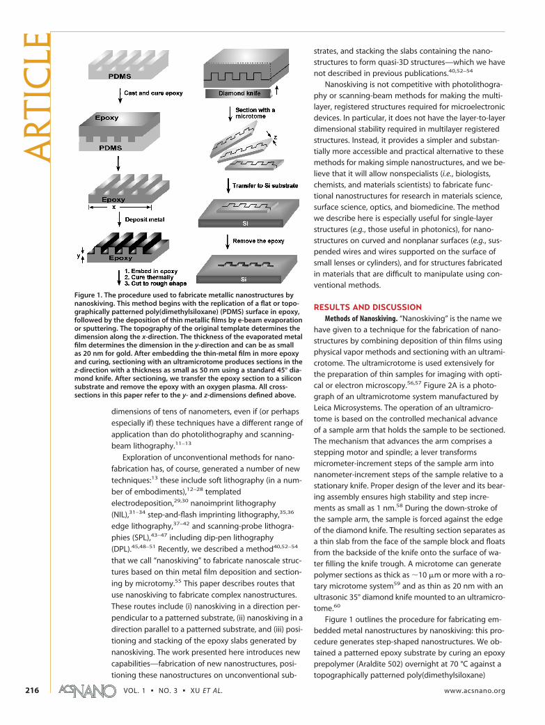
have given to a technique for the fabrication of nano-structures by combining deposition of thin films usingphysical vapor methods and sectioning with an ultrami-crotome. The ultramicrotome is used extensively forthe preparation of thin samples for imaging with opti-cal or electron microscopy.56,57 Figure 2A is a photo-graph of an ultramicrotome system manufactured byLeica Microsystems. The operation of an ultramicro-tome is based on the controlled mechanical advanceof a sample arm that holds the sample to be sectioned.The mechanism that advances the arm comprises astepping motor and spindle; a lever transformsmicrometer-increment steps of the sample arm intonanometer-increment steps of the sample relative to astationary knife. Proper design of the lever and its bear-ing assembly ensures high stability and step incre-ments as small as 1 nm.58 During the down-stroke ofthe sample arm, the sample is forced against the edgeof the diamond knife. The resulting section separates asa thin slab from the face of the sample block and floatsfrom the backside of the knife onto the surface of wa-ter filling the knife trough. A microtome can generatepolymer sections as thick as �10 �m or more with a ro-tary microtome system59 and as thin as 20 nm with anultrasonic 35° diamond knife mounted to an ultramicro-tome.60
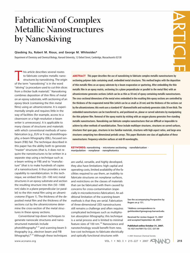
Figure 1 outlines the procedure for fabricating em-bedded metal nanostructures by nanoskiving: this pro-cedure generates step-shaped nanostructures. We ob-tained a patterned epoxy substrate by curing an epoxyprepolymer (Araldite 502) overnight at 70 °C against atopographically patterned poly(dimethylsiloxane)
Figure 1. The procedure used to fabricate metallic nanostructures bynanoskiving. This method begins with the replication of a flat or topo-graphically patterned poly(dimethylsiloxane) (PDMS) surface in epoxy,followed by the deposition of thin metallic films by e-beam evaporationor sputtering. The topography of the original template determines thedimension along the x-direction. The thickness of the evaporated metalfilm determines the dimension in the y-direction and can be as smallas 20 nm for gold. After embedding the thin-metal film in more epoxyand curing, sectioning with an ultramicrotome produces sections in thez-direction with a thickness as small as 50 nm using a standard 45° dia-mond knife. After sectioning, we transfer the epoxy section to a siliconsubstrate and remove the epoxy with an oxygen plasma. All cross-sections in this paper refer to the y- and z-dimensions defined above.
ART
ICLE
VOL. 1 ▪ NO. 3 ▪ XU ET AL. www.acsnano.org216
(PDMS) substrate. The low free energy of the surface ofPDMS enabled the two polymers to be separated eas-ily. We used Araldite 502 epoxy to embed the thin metalfilms or structures,61,62 because this polymer has (i) me-chanical properties appropriate for microtome section-ing at room temperature;40 (ii) the physical propertiesrequired to provide support for the nanostructures thatare formed upon sectioning (this support allows thesesections to be manipulated); (iii) rapid rates of etchingin an oxygen plasma, so it can be removed easily; and(iv) good adhesion to gold without a titanium adhesionlayer.63 Other polymers may be more appropriate thanAraldite 502 for specific applications.
After replicating a PDMS master in epoxy, we depos-ited a thin gold film (10 –100 nm) directly onto the ep-oxy, without a titanium adhesion layer, using e-beamevaporation. We cut this epoxy-supported metal film inthin strips (�1 mm width � �5 mm length) using a ra-zor blade and placed these strips into a flat embed-ding mold. After filling the embedding mold with moreepoxy of the same kind, we cured the epoxy for 12 hat 70 °C. After removing the cured polymer from themold, we trimmed its face to dimensions of 0.5 mmheight � 0.5 mm width using a razor blade under a ste-reomicroscope, mounted it on the ultramicrotome,and sectioned it with a diamond knife with a wedgeangle of 45°. There are several types of commerciallyavailable diamond knives for use with microtomy,60
each suited for specific applications. In this work, weused a 45° diamond knife (Diatome USA, Hatfield, PA)to generate epoxy slabs with a thickness between 50and 1000 nm. After sectioning, the slabs floated awayfrom the edge of the diamond knife onto the surface ofwater filling the sample-collecting reservoir. Sectioningrequires about 3 s for a slice with areal dimensions of 0.5mm � 0.5 mm, and with a 50-nm thickness; sectioningcan, thus, generate a large number of slabs rapidly (wehave made 200 in 10 min).
We used two methods to transfer these thin epoxyslabs from the surface of the water onto a solid sub-strate (e.g., a TEM grid or a silicon wafer) (Figure 2B,C).The first method involves the transfer of an epoxy cross-section slab from the surface of the water to a sub-strate using a 2-mm diameter collection loop. The thinfilm of water on the collection loop supported the slabof epoxy containing the embedded gold nanostruc-tures. We brought the collection loop into physical con-tact with a substrate (i.e., silicon substrate or TEM grid)and wicked away the water using a paper tissue; thisprocedure left the epoxy section supported on thesubstrate.
The second method relies on the direct transfer ofthe epoxy slab from the surface of water onto a sub-strate by submerging the substrate (a silicon wafer inFigure 2C) directly below the floating epoxy section(s)and pulling the substrate toward the section(s) in sucha way that it (or they) settle(s) on the substrate. Figure
2D is a bright-field optical micrograph of an ordered as-
sembly of multiple thin sections of epoxy containing
embedded metallic nanostructures supported on a
SiO2/Si(100) substrate, illuminated with white light. The
uniformity of the color (determined by optical interfer-
ence at the two faces of the slab) of the individual thin-
film slabs (Figure 2D) demonstrates the high unifor-
mity (in thickness) obtained with microtomy.64 The self-
assembly of the thin-film epoxy slabs is a route to the
fabrication of large-area patterned arrays.53,65
Fabrication of Complex Nanostructures Using Topographically
Patterned Substrates as a Template. Sectioning Perpendicular to the
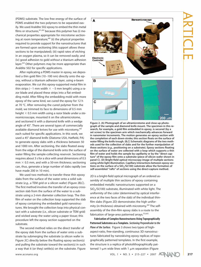
Plane of the Surface. Figure 3 shows two types of high-
aspect-ratio, free-standing, continuous 3D nanostruc-
tures fabricated by nanoskiving epoxy replicas of topo-
graphically patterned templates. In the first example,
the structure is a replica of photolithographically pat-
terned 1-�m wide lines with 1 �m separation (Figure
Figure 2. (A) Photograph of an ultramicrotome and close-up photo-graph of the sample and diamond knife mount. The specimen in this re-search, for example, a gold film embedded in epoxy, is secured (by aset screw) to the specimen arm which mechanically advances forwardin nanometer increments. The motion generates an epoxy section withthe completion of each down-stroke; this section floats on the surface ofwater filling the knife trough. (B,C) Schematic diagrams of the two meth-ods used for the collection of slabs and for the further manipulation ofthese sections (e.g., positioning on a substrate). Epoxy sections floatingon the surface of water are collected with a loop which supports a thinfilm of water and holds the sample by capillarity or by the “direct cap-ture” of the epoxy film onto a substrate (piece of silicon wafer shown inpanel C). (D) Bright-field optical microscopy image of multiple sectionsusing white light illumination. Capillary interactions between epoxy sec-tions on the surface of a SiO2/Si(100) substrate allow the formation ofself-assembled “rafts” of sections using the direct-capture method.
ARTIC
LE
www.acsnano.org VOL. 1 ▪ NO. 3 ▪ 215–227 ▪ 2007 217
3A), generated by standard methods of soft lithogra-
phy.14 Figure 3B shows a zig-zag-shaped nanostructure
sectioned using a gold-coated epoxy replica of a blazed
glass diffraction grating. After replica molding the sur-
faces in PDMS and again in epoxy, we deposited a
100-nm layer of gold by sputtering on the topographi-
cally patterned epoxy. The non-collimated flux of the
metal atoms in sputtering (due to their multiple colli-
sions in the high-pressure environment of the sputter-ing chamber) enables metal coverage on sidewalls andforms continuous coatings. Following the procedureoutlined in Figure 1, we embedded these metal-coatedsurfaces in more epoxy and sectioned into slabs(1000-nm thickness) with an ultramicrotome. Thesestructures have an aspect ratio (defined as the ratio ofthe height of the structure(s) determined by sectioningwith an ultramicrotome (z) to the width of the nano-structure(s) determined by the thickness of the evapo-rated metal film (y)) of 10. After supporting the epoxyslabs on a SiO2/Si(100) substrate, we removed the ep-oxy with an oxygen plasma to expose the goldnanostructures.
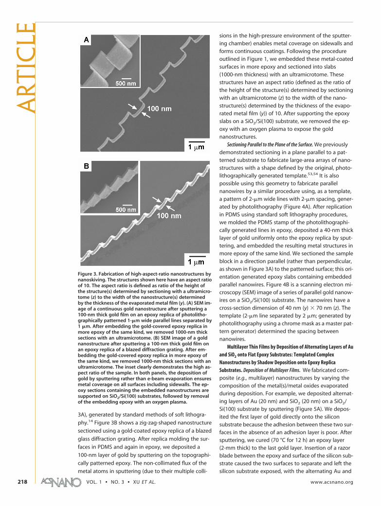
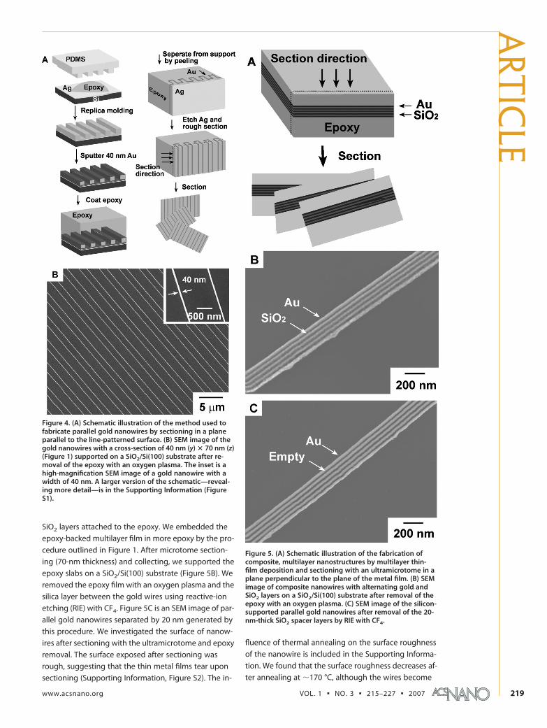
Sectioning Parallel to the Plane of the Surface. We previouslydemonstrated sectioning in a plane parallel to a pat-terned substrate to fabricate large-area arrays of nano-structures with a shape defined by the original, photo-lithographically generated template.53,54 It is alsopossible using this geometry to fabricate parallelnanowires by a similar procedure using, as a template,a pattern of 2-�m wide lines with 2-�m spacing, gener-ated by photolithography (Figure 4A). After replicationin PDMS using standard soft lithography procedures,we molded the PDMS stamp of the photolithographi-cally generated lines in epoxy, deposited a 40-nm thicklayer of gold uniformly onto the epoxy replica by sput-tering, and embedded the resulting metal structures inmore epoxy of the same kind. We sectioned the sampleblock in a direction parallel (rather than perpendicular,as shown in Figure 3A) to the patterned surface; this ori-entation generated epoxy slabs containing embeddedparallel nanowires. Figure 4B is a scanning electron mi-croscopy (SEM) image of a series of parallel gold nanow-ires on a SiO2/Si(100) substrate. The nanowires have across-section dimension of 40 nm (y) � 70 nm (z). Thetemplate (2-�m line separated by 2 �m; generated byphotolithography using a chrome mask as a master pat-tern generator) determined the spacing betweennanowires.
Multilayer Thin Films by Deposition of Alternating Layers of Auand SiO2 onto Flat Epoxy Substrates: Templated ComplexNanostructures by Shadow Deposition onto Epoxy ReplicaSubstrates. Deposition of Multilayer Films. We fabricated com-posite (e.g., multilayer) nanostructures by varying thecomposition of the metal(s)/metal oxides evaporatedduring deposition. For example, we deposited alternat-ing layers of Au (20 nm) and SiO2 (20 nm) on a SiO2/Si(100) substrate by sputtering (Figure 5A). We depos-ited the first layer of gold directly onto the siliconsubstrate because the adhesion between these two sur-faces in the absence of an adhesion layer is poor. Aftersputtering, we cured (70 °C for 12 h) an epoxy layer(2-mm thick) to the last gold layer. Insertion of a razorblade between the epoxy and surface of the silicon sub-strate caused the two surfaces to separate and left thesilicon substrate exposed, with the alternating Au and
Figure 3. Fabrication of high-aspect-ratio nanostructures bynanoskiving. The structures shown here have an aspect ratioof 10. The aspect ratio is defined as ratio of the height ofthe structure(s) determined by sectioning with a ultramicro-tome (z) to the width of the nanostructure(s) determinedby the thickness of the evaporated metal film (y). (A) SEM im-age of a continuous gold nanostructure after sputtering a100-nm thick gold film on an epoxy replica of photolitho-graphically patterned 1-�m wide parallel lines separated by1 �m. After embedding the gold-covered epoxy replica inmore epoxy of the same kind, we removed 1000-nm thicksections with an ultramicrotome. (B) SEM image of a goldnanostructure after sputtering a 100-nm thick gold film onan epoxy replica of a blazed diffraction grating. After em-bedding the gold-covered epoxy replica in more epoxy ofthe same kind, we removed 1000-nm thick sections with anultramicrotome. The inset clearly demonstrates the high as-pect ratio of the sample. In both panels, the deposition ofgold by sputtering rather than e-beam evaporation ensuresmetal coverage on all surfaces including sidewalls. The ep-oxy sections containing the embedded nanostructures aresupported on SiO2/Si(100) substrates, followed by removalof the embedding epoxy with an oxygen plasma.
ART
ICLE
VOL. 1 ▪ NO. 3 ▪ XU ET AL. www.acsnano.org218
SiO2 layers attached to the epoxy. We embedded the
epoxy-backed multilayer film in more epoxy by the pro-
cedure outlined in Figure 1. After microtome section-
ing (70-nm thickness) and collecting, we supported the
epoxy slabs on a SiO2/Si(100) substrate (Figure 5B). We
removed the epoxy film with an oxygen plasma and the
silica layer between the gold wires using reactive-ion
etching (RIE) with CF4. Figure 5C is an SEM image of par-
allel gold nanowires separated by 20 nm generated by
this procedure. We investigated the surface of nanow-
ires after sectioning with the ultramicrotome and epoxy
removal. The surface exposed after sectioning was
rough, suggesting that the thin metal films tear upon
sectioning (Supporting Information, Figure S2). The in-
fluence of thermal annealing on the surface roughness
of the nanowire is included in the Supporting Informa-
tion. We found that the surface roughness decreases af-
ter annealing at �170 °C, although the wires become
Figure 4. (A) Schematic illustration of the method used tofabricate parallel gold nanowires by sectioning in a planeparallel to the line-patterned surface. (B) SEM image of thegold nanowires with a cross-section of 40 nm (y) � 70 nm (z)(Figure 1) supported on a SiO2/Si(100) substrate after re-moval of the epoxy with an oxygen plasma. The inset is ahigh-magnification SEM image of a gold nanowire with awidth of 40 nm. A larger version of the schematic—reveal-ing more detail—is in the Supporting Information (FigureS1).
Figure 5. (A) Schematic illustration of the fabrication ofcomposite, multilayer nanostructures by multilayer thin-film deposition and sectioning with an ultramicrotome in aplane perpendicular to the plane of the metal film. (B) SEMimage of composite nanowires with alternating gold andSiO2 layers on a SiO2/Si(100) substrate after removal of theepoxy with an oxygen plasma. (C) SEM image of the silicon-supported parallel gold nanowires after removal of the 20-nm-thick SiO2 spacer layers by RIE with CF4.
ARTIC
LE
www.acsnano.org VOL. 1 ▪ NO. 3 ▪ 215–227 ▪ 2007 219
visibly thinner at irregular intervals along the length of
the nanowire. At temperatures greater than 250 °C, the
wires break at the location of the thinning of the
nanowire.
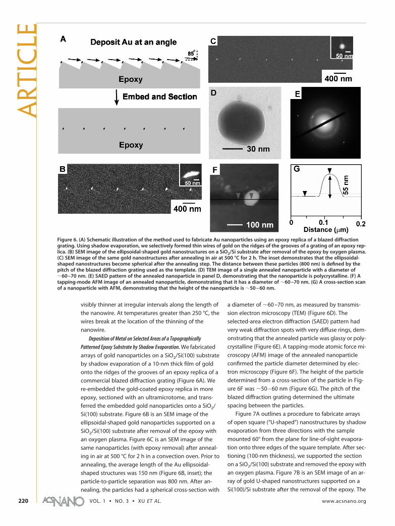
Deposition of Metal on Selected Areas of a Topographically
Patterned Epoxy Substrate by Shadow Evaporation. We fabricated
arrays of gold nanoparticles on a SiO2/Si(100) substrate
by shadow evaporation of a 10-nm thick film of gold
onto the ridges of the grooves of an epoxy replica of a
commercial blazed diffraction grating (Figure 6A). We
re-embedded the gold-coated epoxy replica in more
epoxy, sectioned with an ultramicrotome, and trans-
ferred the embedded gold nanoparticles onto a SiO2/
Si(100) substrate. Figure 6B is an SEM image of the
ellipsoidal-shaped gold nanoparticles supported on a
SiO2/Si(100) substrate after removal of the epoxy with
an oxygen plasma. Figure 6C is an SEM image of the
same nanoparticles (with epoxy removal) after anneal-
ing in air at 500 °C for 2 h in a convection oven. Prior to
annealing, the average length of the Au ellipsoidal-
shaped structures was 150 nm (Figure 6B, inset); the
particle-to-particle separation was 800 nm. After an-
nealing, the particles had a spherical cross-section with
a diameter of �60 –70 nm, as measured by transmis-
sion electron microscopy (TEM) (Figure 6D). The
selected-area electron diffraction (SAED) pattern had
very weak diffraction spots with very diffuse rings, dem-
onstrating that the annealed particle was glassy or poly-
crystalline (Figure 6E). A tapping-mode atomic force mi-
croscopy (AFM) image of the annealed nanoparticle
confirmed the particle diameter determined by elec-
tron microscopy (Figure 6F). The height of the particle
determined from a cross-section of the particle in Fig-
ure 6F was �50 – 60 nm (Figure 6G). The pitch of the
blazed diffraction grating determined the ultimate
spacing between the particles.
Figure 7A outlines a procedure to fabricate arrays
of open square (“U-shaped”) nanostructures by shadow
evaporation from three directions with the sample
mounted 60° from the plane for line-of-sight evapora-
tion onto three edges of the square template. After sec-
tioning (100-nm thickness), we supported the section
on a SiO2/Si(100) substrate and removed the epoxy with
an oxygen plasma. Figure 7B is an SEM image of an ar-
ray of gold U-shaped nanostructures supported on a
Si(100)/Si substrate after the removal of the epoxy. The
Figure 6. (A) Schematic illustration of the method used to fabricate Au nanoparticles using an epoxy replica of a blazed diffractiongrating. Using shadow evaporation, we selectively formed thin wires of gold on the ridges of the grooves of a grating of an epoxy rep-lica. (B) SEM image of the ellipsoidal-shaped gold nanostructures on a SiO2/Si substrate after removal of the epoxy by oxygen plasma.(C) SEM image of the same gold nanostructures after annealing in air at 500 °C for 2 h. The inset demonstrates that the ellipsoidal-shaped nanostructures become spherical after the annealing step. The distance between these particles (800 nm) is defined by thepitch of the blazed diffraction grating used as the template. (D) TEM image of a single annealed nanoparticle with a diameter of�60 –70 nm. (E) SAED pattern of the annealed nanoparticle in panel D, demonstrating that the nanoparticle is polycrystalline. (F) Atapping-mode AFM image of an annealed nanoparticle, demonstrating that it has a diameter of �60 –70 nm. (G) A cross-section scanof a nanoparticle with AFM, demonstrating that the height of the nanoparticle is �50 – 60 nm.
ART
ICLE
VOL. 1 ▪ NO. 3 ▪ XU ET AL. www.acsnano.org220
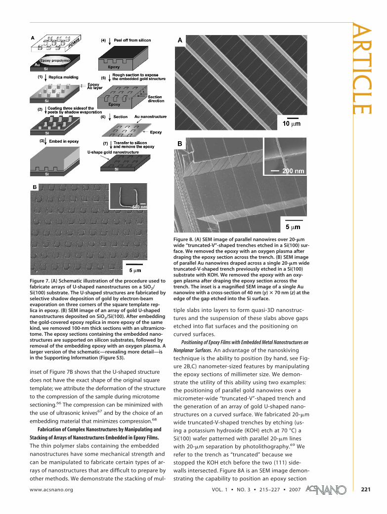
inset of Figure 7B shows that the U-shaped structure
does not have the exact shape of the original square
template; we attribute the deformation of the structure
to the compression of the sample during microtome
sectioning.66 The compression can be minimized with
the use of ultrasonic knives67 and by the choice of an
embedding material that minimizes compression.68
Fabrication of Complex Nanostructures by Manipulating and
Stacking of Arrays of Nanostructures Embedded in Epoxy Films.
The thin polymer slabs containing the embedded
nanostructures have some mechanical strength and
can be manipulated to fabricate certain types of ar-
rays of nanostructures that are difficult to prepare by
other methods. We demonstrate the stacking of mul-
tiple slabs into layers to form quasi-3D nanostruc-
tures and the suspension of these slabs above gaps
etched into flat surfaces and the positioning on
curved surfaces.
Positioning of Epoxy Films with Embedded Metal Nanostructures on
Nonplanar Surfaces. An advantage of the nanoskiving
technique is the ability to position (by hand, see Fig-
ure 2B,C) nanometer-sized features by manipulating
the epoxy sections of millimeter size. We demon-
strate the utility of this ability using two examples:
the positioning of parallel gold nanowires over a
micrometer-wide “truncated-V”-shaped trench and
the generation of an array of gold U-shaped nano-
structures on a curved surface. We fabricated 20-�m
wide truncated-V-shaped trenches by etching (us-
ing a potassium hydroxide (KOH) etch at 70 °C) a
Si(100) wafer patterned with parallel 20-�m lines
with 20-�m separation by photolithography.69 We
refer to the trench as “truncated” because we
stopped the KOH etch before the two (111) side-
walls intersected. Figure 8A is an SEM image demon-
strating the capability to position an epoxy section
Figure 7. (A) Schematic illustration of the procedure used tofabricate arrays of U-shaped nanostructures on a SiO2/Si(100) substrate. The U-shaped structures are fabricated byselective shadow deposition of gold by electron-beamevaporation on three corners of the square template rep-lica in epoxy. (B) SEM image of an array of gold U-shapednanostructures deposited on SiO2/Si(100). After embeddingthe gold-covered epoxy replica in more epoxy of the samekind, we removed 100-nm thick sections with an ultramicro-tome. The epoxy sections containing the embedded nano-structures are supported on silicon substrates, followed byremoval of the embedding epoxy with an oxygen plasma. Alarger version of the schematic—revealing more detail—isin the Supporting Information (Figure S3).
Figure 8. (A) SEM image of parallel nanowires over 20-�mwide “truncated-V”-shaped trenches etched in a Si(100) sur-face. We removed the epoxy with an oxygen plasma afterdraping the epoxy section across the trench. (B) SEM imageof parallel Au nanowires draped across a single 20-�m widetruncated-V-shaped trench previously etched in a Si(100)substrate with KOH. We removed the epoxy with an oxy-gen plasma after draping the epoxy section across thetrench. The inset is a magnified SEM image of a single Aunanowire with a cross-section of 40 nm (y) � 70 nm (z) at theedge of the gap etched into the Si surface.
ARTIC
LE
www.acsnano.org VOL. 1 ▪ NO. 3 ▪ 215–227 ▪ 2007 221
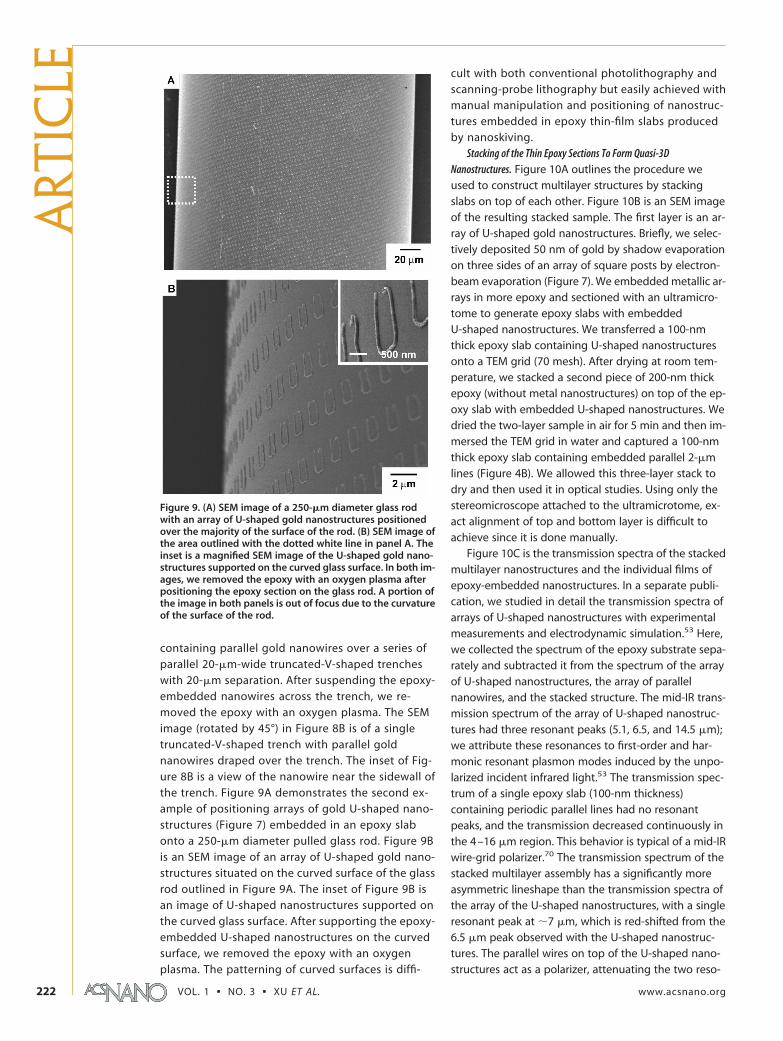
containing parallel gold nanowires over a series ofparallel 20-�m-wide truncated-V-shaped trencheswith 20-�m separation. After suspending the epoxy-embedded nanowires across the trench, we re-moved the epoxy with an oxygen plasma. The SEMimage (rotated by 45°) in Figure 8B is of a singletruncated-V-shaped trench with parallel goldnanowires draped over the trench. The inset of Fig-ure 8B is a view of the nanowire near the sidewall ofthe trench. Figure 9A demonstrates the second ex-ample of positioning arrays of gold U-shaped nano-structures (Figure 7) embedded in an epoxy slabonto a 250-�m diameter pulled glass rod. Figure 9Bis an SEM image of an array of U-shaped gold nano-structures situated on the curved surface of the glassrod outlined in Figure 9A. The inset of Figure 9B isan image of U-shaped nanostructures supported onthe curved glass surface. After supporting the epoxy-embedded U-shaped nanostructures on the curvedsurface, we removed the epoxy with an oxygenplasma. The patterning of curved surfaces is diffi-
cult with both conventional photolithography andscanning-probe lithography but easily achieved withmanual manipulation and positioning of nanostruc-tures embedded in epoxy thin-film slabs producedby nanoskiving.
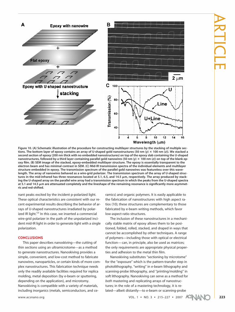
Stacking of the Thin Epoxy Sections To Form Quasi-3DNanostructures. Figure 10A outlines the procedure weused to construct multilayer structures by stackingslabs on top of each other. Figure 10B is an SEM imageof the resulting stacked sample. The first layer is an ar-ray of U-shaped gold nanostructures. Briefly, we selec-tively deposited 50 nm of gold by shadow evaporationon three sides of an array of square posts by electron-beam evaporation (Figure 7). We embedded metallic ar-rays in more epoxy and sectioned with an ultramicro-tome to generate epoxy slabs with embeddedU-shaped nanostructures. We transferred a 100-nmthick epoxy slab containing U-shaped nanostructuresonto a TEM grid (70 mesh). After drying at room tem-perature, we stacked a second piece of 200-nm thickepoxy (without metal nanostructures) on top of the ep-oxy slab with embedded U-shaped nanostructures. Wedried the two-layer sample in air for 5 min and then im-mersed the TEM grid in water and captured a 100-nmthick epoxy slab containing embedded parallel 2-�mlines (Figure 4B). We allowed this three-layer stack todry and then used it in optical studies. Using only thestereomicroscope attached to the ultramicrotome, ex-act alignment of top and bottom layer is difficult toachieve since it is done manually.
Figure 10C is the transmission spectra of the stackedmultilayer nanostructures and the individual films ofepoxy-embedded nanostructures. In a separate publi-cation, we studied in detail the transmission spectra ofarrays of U-shaped nanostructures with experimentalmeasurements and electrodynamic simulation.53 Here,we collected the spectrum of the epoxy substrate sepa-rately and subtracted it from the spectrum of the arrayof U-shaped nanostructures, the array of parallelnanowires, and the stacked structure. The mid-IR trans-mission spectrum of the array of U-shaped nanostruc-tures had three resonant peaks (5.1, 6.5, and 14.5 �m);we attribute these resonances to first-order and har-monic resonant plasmon modes induced by the unpo-larized incident infrared light.53 The transmission spec-trum of a single epoxy slab (100-nm thickness)containing periodic parallel lines had no resonantpeaks, and the transmission decreased continuously inthe 4 –16 �m region. This behavior is typical of a mid-IRwire-grid polarizer.70 The transmission spectrum of thestacked multilayer assembly has a significantly moreasymmetric lineshape than the transmission spectra ofthe array of the U-shaped nanostructures, with a singleresonant peak at �7 �m, which is red-shifted from the6.5 �m peak observed with the U-shaped nanostruc-tures. The parallel wires on top of the U-shaped nano-structures act as a polarizer, attenuating the two reso-
Figure 9. (A) SEM image of a 250-�m diameter glass rodwith an array of U-shaped gold nanostructures positionedover the majority of the surface of the rod. (B) SEM image ofthe area outlined with the dotted white line in panel A. Theinset is a magnified SEM image of the U-shaped gold nano-structures supported on the curved glass surface. In both im-ages, we removed the epoxy with an oxygen plasma afterpositioning the epoxy section on the glass rod. A portion ofthe image in both panels is out of focus due to the curvatureof the surface of the rod.
ART
ICLE
VOL. 1 ▪ NO. 3 ▪ XU ET AL. www.acsnano.org222
nant peaks excited by the incident p-polarized light.These optical characteristics are consistent with our re-cent experimental results describing the behavior of ar-rays of U-shaped nanostructures irradiated by polar-ized IR light.53 In this case, we inserted a commercialwire-grid polarizer in the path of the unpolarized inci-dent mid-IR light in order to generate light with a singlepolarization.
CONCLUSIONSThis paper describes nanoskiving—the cutting of
thin sections using an ultramicrotome—as a methodto generate nanostructures. Nanoskiving provides asimple, convenient, and low-cost method to fabricatenanowires, nanoparticles, or certain kinds of more com-plex nanostructures. This fabrication technique needsonly the readily available facilities required for replicamolding, metal deposition (by e-beam or sputtering,depending on the application), and microtomy.Nanoskiving is compatible with a variety of materials,including inorganics (metals, semiconductors, and ce-
ramics) and organic polymers. It is easily applicable tothe fabrication of nanostructures with high aspect ra-tios (10); these structures are complementary to thosefabricated by e-beam writing methods, which favorlow-aspect-ratio structures.
The inclusion of these nanostructures in a mechani-cally stable matrix of epoxy allows them to be posi-tioned, folded, rolled, stacked, and draped in ways thatcannot be accomplished by other techniques. A rangeof polymers—including those with optical or electricalfunction— can, in principle, also be used as matrices;the only requirements are appropriate physical proper-ties and adhesion to the metal thin film.
Nanoskiving substitutes “sectioning by microtome”for the “exposure” which is the pattern-transfer step inphotolithography, “writing” in e-beam lithography andscanning-probe lithography, and “printing/molding” insoft lithography. Nanoskiving can serve as a method forboth mastering and replicating arrays of nanostruc-tures; in the role of a mastering technology, it is re-lated—albeit distantly—to e-beam or scanning-probe
Figure 10. (A) Schematic illustration of the procedure for constructing multilayer structures by the stacking of multiple sec-tions. The bottom layer of epoxy contains an array of U-shaped gold nanostructures (50 nm (y) � 100 nm (z)). We stacked asecond section of epoxy (200 nm thick with no embedded nanostructures) on top of the epoxy slab containing the U-shapednanostructures, followed by a third layer containing parallel gold nanowires (50 nm (y) � 100 nm (z)) on top of the blank ep-oxy film. (B) SEM image of the stacked, epoxy-embedded multilayer structure. The epoxy is essentially transparent to theelectron beam and has minimal contrast in SEM. (C) Mid-IR transmission spectra of the individual elements and multilayerstructure embedded in epoxy. The transmission spectrum of the parallel gold nanowires was featureless over this wave-length. The array of nanowires behaved as a wire-grid polarizer. The transmission spectrum of the array of U-shaped struc-tures in the mid-infrared has three resonances located at 5.1, 6.5, and 14.5 �m, respectively. The array produced by stack-ing the U-shaped array on the parallel wire array had a transmission spectrum in which the peaks from the U-shaped spectraat 5.1 and 14.5 �m are attenuated completely and the lineshape of the remaining resonance is significantly more asymmet-ric and red-shifted.
ARTIC
LE
www.acsnano.org VOL. 1 ▪ NO. 3 ▪ 215–227 ▪ 2007 223
lithography; in the role of a replicating technology, ithas some analogy to photolithography or soft lithogra-phy. The versatility of nanoskiving—as a technique forboth mastering and replicating—is not found in any ofthe other methods used for nanofabrication.
We believe this technique will be of primary inter-est to researchers who wish to generate simple nano-structures, singly or in arrays, more simply and quicklythan can be accomplished by conventional means. It iseasily accessible to those not trained in top-down pro-cedures for fabrication and by those with limited or noaccess to the equipment and facilities needed for pho-tolithography or scanning-beam fabrication.71,72 In par-ticular, this technique might especially appeal to bio-physicists, because they are already familiar withmicrotomy (for the production of thin sections of bio-logical matter for analysis by electron microscopy), andto optical physicists, since the structures of interest inoptics often can tolerate a certain number of defects(electronic circuits typically cannot).
Nanoskiving has the potential to replace conven-tional microfabrication techniques for generatingsimple test structures in photonics. We demonstratedan example of a representative optical structure bystacking multiple epoxy sections containing metallicnanostructures; this structure is a mid-IR frequency-selective surface.
Nanoskiving has, of course, important limitations. Itis currently restricted to generating unconnected linestructures. The inability to fabricate connected struc-tures limits the application of these nanostructures inmaking integrated circuits. The sectioning procedure
leads to the introduction of artifacts and defects in the
nanostructures. The compression of the sample during
sectioning causes the true thickness of the individual
nanostructure or individual elements in the array of
nanostructures to be greater than the nominal thick-
ness. Nanoskiving also does not currently have the sta-
bility in the pattern necessary to generate sections that
can be registered precisely. We have—in the survey
work described here—manipulated the sections by
hand only with the aid of a stereomicroscope; the ex-
act registration between multiple slabs in a stack is con-
sequently poor. The distortion of the nanostructure lim-
its our ability to stack slabs precisely; the importance
of this distortion will depend on the particular
application.
We believe the formation of more complex nano-
structures will result from a combination of nanoskiv-
ing with other— conventional and unconventional—
nanofabrication techniques. The large areas of pattern
transfer achievable with photolithography (�square
inches) and NIL (�square inches) are challenging for
nanoskiving, because the knife can only cut square mil-
limeter areas in each section. Generation of larger ar-
eas by nanoskiving required tiling of multiple smaller
sections. The ability of capillary interaction to cause sec-
tions to self-assemble has the potential to assist in this
kind of tiling.
We believe that many of the limitations of nanoskiv-
ing reflect the early stages of its development and that,
as the technique develops, solutions to at least some
of the current limitations will emerge.
EXPERIMENTAL SECTIONFabrication of Flat and Patterned PDMS Molds. We obtained flat
poly(dimethylsiloxane) (PDMS) surfaces by curing PDMS againstan unsilanized polystyrene Petri dish. We obtained a topographi-cally patterned PDMS master by molding PDMS against a photo-resist patterned SiO2/Si(100) substrate fabricated by conven-tional photolithography and standard procedures of softlithography.14 Typically, we coated a 2-�m thick layer of SU-8 5photoresist (MicroChem Corp., Newton, MA) on silicon wafers(�100�, N/phosphorus or P/boron doped, 1–10 �-cm, SiliconSense, Nashua, NH) by spin-coating the prepolymer at 3000 rpmfor 30 s and processed according to manufacturer’s specifica-tions. We patterned the film of SU-8 with 2-�m lines with 2-�mseparation using the corresponding chrome mask by photoli-thography, coated the surface with a release layer (tridecafluo-rotetrahydrooctyltrichorosilane, United Chemical Technologies,Bristol, PA), and molded with PDMS (Dow Corning Sylgard 184kit, catalyst and prepolymer in 1:10 w/w ratio). The PDMS moldwas cured for 3 h at 70 °C in a convection oven.
Fabrication of Flat and Patterned Epoxy Substrates. We cured an ep-oxy prepolymer (Araldite 502, Electron Microscopy Sciences,Fort Washington, PA) against a flat or patterned PDMS sub-strate at 70 °C for 12 h. Preparation of the epoxy required mix-ing the different kit components in the following amounts: 5 mLof diglycidyl ether of bisphenol-A (isopropylidenediphenol,Araldite 502), 5.5 mL of dodecenylsuccinic anhydride (DDSA),and 0.3 mL of benzyldimethylamine (BDMA).
Deposition of Metal and Dielectric Layers on Epoxy Surfaces. We depos-ited thin films of gold on flat or patterned epoxy surfaces by
e-beam evaporation or sputtering. Gold was deposited at a rateof 1–3 Å/s by e-beam evaporation with the sample mounted ona rotating stage (30 rpm). We deposited the multilayer Au/SiO2
films by sputtering (Orion Sputtering System, AJA InternationalInc., Scituate, MA) and deposited gold at a rate of 3.3 Å/s using aDC gun, and SiO2 at a rate of 0.22 Å/s using an RF gun. We etchedthe SiO2 layer with CF4 (15 mTorr CF4, 15 sccm CF4, 200 W micro-wave, 200 W RF) for 30 s using a RIE system (Cirrus 150, Nexx Sys-tems, Inc., Billerica, MA).
Fabrication of Au Nanoparticles by Shadow Deposition and Annealing. Acommercial diffraction grating (1200 grooves/mm, Edmund In-dustrial Optics, Barrington, NJ) was silanized with 1H,1H,2H,2H-perfluorooctyltrichlorosilane (Fluka, 98%) overnight under housevacuum and replicated in PDMS according to standard soft li-thography procedures.14 We cured the PDMS mold at 70 °C for3 h and separated the PDMS replica from the diffraction grating.After replication of the diffraction grating in epoxy by casting ep-oxy prepolymer against the PDMS replica and curing, we evapo-rated 10 nm of gold directly onto the epoxy replica by shadowevaporation with the sample mounted 70° from the plane forline-of-sight evaporation. The Au-coated epoxy replica was re-embedded in epoxy and cured overnight.
Microtome Sectioning. We placed the Au-coated epoxy film (pla-nar or patterned) into a flat-embedding mold (Better Equip-ment For Electron Microscopy, Inc., West Chester, PA) (5.5 mmwidth � 12 mm length � 2.5 mm height) made of polyethyl-ene, re-embedded in the same epoxy prepolymer, and cured at70 °C overnight in a convection oven. We initially trimmed(“rough sectioning”) the metal-film embedded epoxy block with
ART
ICLE
VOL. 1 ▪ NO. 3 ▪ XU ET AL. www.acsnano.org224
a razor blade to an area of �0.5 mm � 0.5 mm with the aid ofthe stereomicroscope on the ultramicrotome (Leica Ultracut UCT,Leica, Inc., Germany) to expose a metal edge.40 The surface cre-ated with the razor blade was smoothed using a glass knife be-fore final sectioning with a diamond knife (Diatome Ultra 45°). Af-ter aligning the flat mold face with the diamond knife edge,53
we sliced (0.5 mm/s sectioning speed) epoxy thin-film sectionsand collected the epoxy sections on the surface of the water con-tained in the sample trough mounted to the backside of the dia-mond knife. We directly immersed the solid substrate (such asTEM grid or silicon wafer) into water below the epoxy slab andpulled it toward the surface in a way that allowed the floating ep-oxy film to settle on it. Alternately, we trapped the epoxy slabon a thin film of water with a 2-mm diameter loop (Diatome Per-fect Loop, Hatfield, PA) and deposited it on a chosen substrateby contacting the loop with the substrate and wicking away ex-cess water with a paper tissue. We removed the epoxy embed-ding the metallic nanostructures by oxygen plasma (250 –1000mTorr O2, 70 W barrel etcher, Anatech LTD, Alexandria, VA). Theamount of time required for complete removal of epoxy de-pended on the thickness of the section: for example, a 50-nm-thick slab required 300 s for complete removal of the epoxy.
Optical Measurement. We used a Nicolet Fourier-transform infra-red spectrometer in transmission mode to optically characterizethe sample. We placed a piece of aluminum foil (�20 �m thick)with a punched hole (�1.5-mm diameter) directly in front of thesample. For all transmittance measurements, 128 scans with aresolution of 4 cm�1 were averaged. A separate spectrum of theclean substrate was collected and used as a reference. The trans-mittance spectrum of the frequency-selective surface was ob-tained by normalizing it to this reference.
SEM and Light Microscopy Imaging. We observed the nanostruc-tures by SEM measurements using a LEO 982 SEM operating at2 kV and a working distance of 2– 6 mm, and by bright-field anddark-field optical microscopy using a Leica DMRX uprightmicroscope.
Atomic Force Microscopy. We collected images of the gold nano-particles supported on SiO2/Si(100) substrates in tapping modeon a Veeco (Digital Instruments) Dimension 3100 scanning probemicroscope.
Sample Preparation for TEM Imaging. We transferred epoxy sec-tions containing metal nanoparticles onto a DuraSiN film sup-port TEM grid (DTF-1523, Electron Microscopy Sciences, FortWashington, PA). After removing the epoxy with oxygen plasma,we heated the sample in a convection oven at 500 °C for 2 h inair. We measured the transmission spectrum and selected-areaelectron diffraction of the annealed gold nanoparticles using aJeol 2100 TEM at an operating voltage of 200 kV.
Acknowledgment. This research was supported by NIH(GM065364) and by DARPA (sub-award to G.M.W. from theCenter for Optofluidic Integration at the California Instituteof Technology). We acknowledge the use of MRSEC and NSECshared facilities supported by NSF under awards DMR-0213805 (MRSEC) and PHY-0117795 (NSEC). This work wasperformed in part at the Center for Nanoscale Systems (CNS),a member of the National Nanotechnology InfrastructureNetwork (NNIN), which is supported by the National ScienceFoundation under NSF award no. ECS-0335765. CNS is part ofthe Faculty of Arts and Sciences at Harvard University. R.M.R.acknowledges the support of the National Institute of Health(NIH) in the form of a postdoctoral fellowship (1 F32NS060356). We thank Dr. Richard Schalek of the CNS at Har-vard University for help with microtome sectioning andHongtao Wang of Harvard University for help with TEM. Wethank Dr. Jiming Bao of the School of Engineering and Ap-plied Science at Harvard University for helpful discussionabout the mid-IR transmission measurement. We acknowl-edge Dr. Helmut Gnägi of Diatome for private communica-tion concerning suitable materials for ultramicrotome sec-tioning at room temperature. We acknowledge Dr. ReinhardLihl of Leica Microsystems for private communication con-cerning the design of an ultramicrotome.
Supporting Information Available: Supporting Figures S1–S3.This material is available free of charge via the Internet at http://pubs.acs.org.
REFERENCES AND NOTES1. According to the Merriam-Webster dictionary, the verb “to
skive” is of Scandinavian origin and defined as “to cut offin thin layers or pieces”. It is often used in the context ofcutting rubber or leather.
2. Brainard, R. L.; Cobb, J.; Cutler, C. A. Current Status of EUVPhotoresists. J. Photopolym. Sci. Technol. 2003, 16,401–410.
3. Cerrina, F.; Bollepalli, S.; Khan, M.; Solak, H.; Li, W.; He, D.Image Formation in EUV Lithography: Multilayer andResist Properties. Microelectron. Eng. 2000, 53, 13–20.
4. Goethals, A. M.; Bisschop, P. D.; Hermans, J.; Jonckheere, R.;Van Roey, F.; Van den Heuvel, D.; Eliat, A.; Ronse, K.Introducing 157 nm Full Field Lithography. J. Photopolym.Sci. Technol. 2003, 16, 549–556.
5. Mulkens, J.; McClay, J.; Tirri, B.; Brunotte, M.; Mecking, B.;Jasper, H. Optical Lithography Solutions for Sub-65 nmSemiconductor Devices. Proc. SPIE–Int. Soc. Opt. Eng. 2003,5040, 753–762.
6. Gamo, K. Nanofabrication by FIB. Microelectron. Eng. 1996,32, 159–171.
7. Huang, W.-S.; He, W.; Li, W.; Moreau, W. M.; Lang, R.;Medeiros, D. R.; Petrillo, K. E.; Mahorowala, A. P.;Angelopoulos, M.; Deverich, C.; et al. CurrentDevelopments of a High-Performance CA Resist for Mask-Making Application. Proc. SPIE–Int. Soc. Opt. Eng. 2003,5130, 58–66.
8. Kubena, R. L. Resolution Limits of Focused-Ion-Beam ResistPatterning. Mater. Res. Soc. Symp. Proc. 1993, 279, 567–576.
9. Yasin, S.; Hasko, D. G.; Ahmed, H. Fabrication of �5 nmWidth Lines in Poly(methyl methacrylate) Resist using aWater:Isopropyl Alcohol Developer and Ultrasonically-Assisted Development. Appl. Phys. Lett. 2001, 78,2760–2762.
10. Li, L.; Fourkas, J. T. Multiphoton Polymerization. Mater.Today 2007, 10, 30–37.
11. Xia, Y.; Rogers, J. A.; Paul, K. E.; Whitesides, G. M.Unconventional Methods for Fabricating and PatterningNanostructures. Chem. Rev. 1999, 99, 1823–1848.
12. Gates, B. D.; Xu, Q.; Love, J. C.; Wolfe, D. B.; Whitesides,G. M. Unconventional Nanofabrication. Annu. Rev. Mater.Res. 2004, 34, 339–372.
13. Gates, B. D.; Xu, Q.; Stewart, M.; Ryan, D.; Willson, C. G.;Whitesides, G. M. New Approaches to Nanofabrication:Molding, Printing, and Other Techniques. Chem. Rev. 2005,105, 1171–1196.
14. Xia, Y.; Whitesides, G. M. Soft Lithography. Angew. Chem.,Int. Ed. 1998, 37, 550–575.
15. Kumar, A.; Whitesides, G. M. Features of Gold HavingMicrometer to Centimeter Dimensions Can be FormedThrough a Combination of Stamping with an ElastomericStamp and an Alkanethiol “Ink” Followed by ChemicalEtching. Appl. Phys. Lett. 1993, 63, 2002–2004.
16. Kim, E.; Xia, Y.; Whitesides, G. M. Polymer MicrostructuresFormed by Molding in Capillaries. Nature 1995, 376,581–584.
17. Xia, Y.; Whitesides, G. M. Use of Controlled ReactiveSpreading of Liquid Alkanethiol on the Surface of Gold ToModify the Size of Features Produced by MicrocontactPrinting. J. Am. Chem. Soc. 1995, 117, 3274–3275.
18. Xia, Y.; Kim, E.; Zhao, X.-M.; Rogers, J. A.; Prentiss, M.;Whitesides, G. M. Complex Optical Surfaces Formed byReplica Molding Against Elastomeric Masters. Science1996, 273, 347–349.
19. Biebuyck, H. A.; Larsen, N. B.; Delamarche, E.; Michel, B.Lithography Beyond Light: Microcontact Printing withMonolayer Resists. IBM J. Res. Dev. 1997, 41, 159–170.
20. Kim, E.; Xia, Y.; Zhao, X. M.; Whitesides, G. M. Solvent-Assisted Microcontact Molding: A Convenient Method forFabricating Three-Dimensional Structures on Surfaces ofPolymers. Adv. Mater. 1997, 9, 651–654.
ARTIC
LE
www.acsnano.org VOL. 1 ▪ NO. 3 ▪ 215–227 ▪ 2007 225
21. Xia, Y.; McClelland, J. J.; Gupta, R.; Qin, D.; Zhao, X. M.;Sohn, L. L.; Celotta, R. J.; Whitesides, G. M. Replica MoldingUsing Polymeric Materials: A Practical Step TowardNanomanufacturing. Adv. Mater. 1997, 9, 147–149.
22. Delamarche, E.; Geissler, M.; Wolf, H.; Michel, B. PositiveMicrocontact Printing. J. Am. Chem. Soc. 2002, 124, 3834–3835.
23. Geissler, M.; Schmid, H.; Bietsch, A.; Michel, B.; Delamarche,E. Defect-Tolerant and Directional Wet-Etch Systems forUsing Monolayers as Resists. Langmuir 2002, 18,2374–2377.
24. Loo, Y.-L.; Hsu, J. W. P.; Willett, R. L.; Baldwin, K. W.; West,K. W.; Rogers, J. A. High-Resolution Transfer Printing onGaAs Surfaces Using Alkane Dithiol Monolayers. J. Vac. Sci.Technol. B 2002, 20, 2853–2856.
25. Love, J. C.; Wolfe, D. B.; Chabinyc, M. L.; Paul, K. E.;Whitesides, G. M. Self-Assembled Monolayers ofAlkanethiolates on Palladium Are Good Etch Resists. J. Am.Chem. Soc. 2002, 124, 1576–1577.
26. Zaumseil, J.; Meitl, M. A.; Hsu, J. W. P.; Acharya, B. R.;Baldwin, K. W.; Loo, Y.-L.; Rogers, J. A. Three-Dimensionaland Multilayer Nanostructures Formed by NanotransferPrinting. Nano Lett. 2003, 3, 1223–1227.
27. Love, J. C.; Estroff, L. A.; Kriebel, J. K.; Nuzzo, R. G.;Whitesides, G. M. Self-Assembled Monolayers of Thiolateson Metals as a Form of Nanotechnology. Chem. Rev. 2005,105, 1103–1169.
28. Zhao, X. M.; Xia, Y.; Whitesides, G. M. Fabrication of Three-Dimensional Microstructure: Microtransfer Molding. Adv.Mater. 1996, 8, 837–840.
29. Martin, C. R. Nanomaterials: A Membrane-Based SyntheticApproach. Science 1994, 266, 1961–1966.
30. Smith, P. A.; Nordquist, C. D.; Jackson, T. N.; Mayer, T. S.;Martin, B. R.; Mbindyo, J.; Mallouk, T. E. Electric-FieldAssisted Assembly and Alignment of Metallic Nanowires.Appl. Phys. Lett. 2000, 77, 1399–1401.
31. Chou, S. Y.; Krauss, P. R.; Renstrom, P. J. NanoimprintLithography. J. Vac. Sci. Technol. B 1996, 14, 4129–4133.
32. Chou, S. Y.; Krauss, P. R.; Renstrom, P. J. ImprintLithography with 25-Nanometer Resolution. Science 1996,272, 85–87.
33. Chou, S. Y.; Krauss, P. R.; Zhang, W.; Guo, L.; Zhuang, L.Sub-10 nm Imprint Lithography and Applications. J. Vac.Sci. Technol. B 1997, 15, 2897–2904.
34. Wu, W.; Yu, Z. N.; Wang, S. Y.; Williams, R. S.; Liu, Y. M.; Sun,C.; Zhang, X.; Kim, E.; Shen, Y. R.; Fang, N. X. MidinfraredMetamaterials Fabricated by Nanoimprint Lithography.Appl. Phys. Lett. 2007, 90, 063107.
35. Resnick, D. J.; Dauksher, W. J.; Mancini, D. P.; Nordquist,K. J.; Ainley, E. S.; Gehoski, K. A.; Baker, J. H.; Bailey, T. C.;Choi, B. J.; Johnson, S.; et al. Proc. SPIE–Int. Soc. Opt. Eng.2002, 4688, 205–213.
36. Colburn, M.; Grot, A.; Amistoso, M. N.; Choi, B. J.; Bailey,T. C.; Ekerdt, J. G.; Sreenivasan, S. V.; Hollenhorst, J.;Willson, C. G. Step and Flash Imprint Lithography for Sub-100-nm Patterning. Proc. SPIE–Int. Soc. Opt. Eng. 2000,3997, 453–457.
37. Odom, T. W.; Thalladi, V. R.; Love, J. C.; Whitesides, G. M.Generation of 30 –50 nm Structures Using EasilyFabricated, Composite PDMS Masks. J. Am. Chem. Soc.2002, 124, 12112–12113.
38. Gates, B. D.; Xu, Q.; Thalladi, V. R.; Cao, T.; Knickerbocker, T.;Whitesides, G. M. Shear Patterning of Microdominos: ANew Class of Procedures for Making Micro- andNanostructures. Angew. Chem., Int. Ed. 2004, 43,2780–2783.
39. Melosh, N. A.; Boukai, A.; Diana, F.; Gerardot, B.; Badolato,A.; Petroff, P. M.; Heath, J. R. Ultrahigh-Density NanowireLattices and Circuits. Science 2003, 300, 112–115.
40. Xu, Q.; Gates, B. D.; Whitesides, G. M. Fabrication of MetalStructures with Nanometer-Scale Lateral Dimensions bySectioning Using a Microtome. J. Am. Chem. Soc. 2004,126, 1332–1333.
41. Aizenberg, J.; Black, A. J.; Whitesides, G. M. ControllingLocal Disorder in Self-Assembled Monolayers by
Patterning the Topography of their Metallic Supports.Nature 1998, 394, 868–871.
42. Cao, T. B.; Xu, Q. B.; Winkleman, A.; Whitesides, G. M.Fabrication of Thin, Metallic Films Along the Sidewalls of aTopographically Patterned Stamp and their Application inCharge Printing. Small 2005, 1, 1191–1195.
43. Crommie, M. F.; Lutz, C. P.; Eigler, D. M. Confinement ofElectrons to Quantum Corrals on a Metal Surface. Science1993, 262, 218–220.
44. Dagata, J. A.; Schneir, J.; Harary, H. H.; Evans, C. J.; Postek,M. T.; Bennett, J. Modification of Hydrogen PassivatedSilicon by a Scanning Tunneling Microscope Operating inAir. Appl. Phys. Lett. 1990, 56, 2001–2003.
45. Ginger, D. S.; Zhang, H.; Mirkin, C. A. The Evolution of Dip-Pen Nanolithography. Angew. Chem., Int. Ed. 2004, 43,30–35.
46. Liu, G.-Y.; Xu, S.; Qian, Y. Nanofabrication of Self-Assembled Monolayers Using Scanning ProbeLithography. Acc. Chem. Res. 2000, 33, 457–466.
47. Wouters, D.; Schubert, U. S. Nanolithography andNanochemistry: Probe-Related Patterning Techniques andChemical Modification for Nanometer-Sized Devices.Angew. Chem., Int. Ed. 2004, 43, 2480–2495.
48. Hong, S. H.; Mirkin, C. A. A Nanoplotter with Both Paralleland Serial Writing Capabilities. Science 2000, 288,1808–1811.
49. Piner, R. D.; Zhu, J.; Xu, F.; Hong, S.; Mirkin, C. A. “Dip-Pen”Nanolithography. Science 1999, 283, 661–663.
50. Zhang, H.; Mirkin, C. A. DPN-Generated NnanostructuresMade of Gold, Silver, and Palladium. Chem. Mater. 2004,16, 1480–1484.
51. Salaita, K.; Wang, Y. H.; Mirkin, C. A. Applications of Dip-Pen Nanolithography. Nature Nanotechnol. 2007, 2, 145–155.
52. Xu, Q.; Bao, J.; Capasso, F.; Whitesides, G. M. SurfacePlasmon Resonances of Free-Standing Gold NanowiresFabricated by Nanoskiving. Angew. Chem., Int. Ed. 2006, 45,3631–3635.
53. Xu, Q.; Bao, J.; Rioux, R. M.; Perez-Castillejos, R.; Capasso, F.;Whitesides, G. M. Fabrication of Large-Area PatternedNanostructures for Optical Applications by Nanoskiving.Nano Lett. 2007, 7, 2800–2805.
54. Xu, Q. B.; Perez-Castillejos, R.; Li, Z. F.; Whitesides, G. M.Fabrication of High-Aspect-Ratio Metallic NanostructuresUsing Nanoskiving. Nano Lett. 2006, 6, 2163–2165.
55. According to Random House Unabridged dictionary, thenoun “microtomy” is the process of cutting of very thinsections with a microtome.
56. Glauert, A. M. Practical Methods in Electron Microscopy;American Elsevier Publishing Co. Inc.: New York, 1974.
57. Plummer, H. K. Reflections on the Use of Microtomy forMaterials science Specimen Preparation. Microsc.Microanal. 1997, 3, 239–260.
58. The details of operation of a microtome are proprietary.This information was kindly provided by Dr. R. Lihl, R&Dmanager at Leica Microsystems.
59. Butler, J. K. Methods for Improved Light MicroscopeMicrotomy. Stain Technol. 1979, 54, 53–69.
60. http://www.emsdiasum.com/Diatome/diamond_knives/default.htm.
61. Glauert, A. M.; Rogers, G. E.; Glauert, R. H. New EmbeddingMedium for Electron Microscopy. Nature 1956, 178, 803–803.
62. Glauert, A. M.; Glauert, R. H. Araldite as an EmbeddingMedium for Electron Microscopy. J. Biophys. Biochem. Cytlo.1958, 4, 191–194.
63. A thin layer of Ti (2 nm) improved the adhesion betweenthe epoxy and gold.
64. Peachey, L. D. Thin Sections. 1. A Study of SectionThickness and Physical Distortion Produced DuringMicrotomy. J. Biophys. Biochem. Cytol. 1958, 4, 233–242.
65. Blumer, M. J. F.; Gahleitner, P.; Narzt, T.; Handl, C.;Ruthensteiner, B. Ribbons of Semithin Sections: AnAdvanced Method with a New Type of Diamond Knife.J. Neurosci. Methods 2002, 120, 11–16.
ART
ICLE
VOL. 1 ▪ NO. 3 ▪ XU ET AL. www.acsnano.org226
66. Richter, K. Cutting Artifacts on Ultrathin Cryosections ofBiological Bulk Specimens. Micron 1994, 25, 297–308.
67. Studer, D.; Gnaegi, H. Minimal Compression of UltrathinSections with Use of an Oscillating Diamond Knife. J.Microsc. 2000, 197, 94–100.
68. Private communication with Dr. Helmut Gnägi, DiatomeLtd., Biel, Switzerland.
69. Xu, Q. B.; Tonks, I.; Fuerstman, M. J.; Love, J. C.; Whitesides,G. M. Fabrication of Free-Standing Metallic PyramidalShells. Nano Lett. 2004, 4, 2509–2511.
70. Baba, K.; Shiraishi, K.; Obi, K.; Kataoka, T.; Kawakami, S.Optical Properties of Very Thin Metal-Films for LaminatedPolarizers. Appl. Opt. 1988, 27, 2554–2560.
71. Cavalcanti-Adam, E. A.; Volberg, T.; Micoulet, A.; Kessler, H.;Geiger, B.; Spatz, J. P. Cell Spreading and Focal AdhesionDynamics are Regulated by Spacing of Integrin Ligands.Biophys. J. 2007, 92, 2964–2974.
72. Mossman, K. D.; Campi, G.; Groves, J. T.; Dustin, M. L.Altered TCR Signaling from Geometrically RepatternedImmunological Synapses. Science 2005, 310, 1191–1193.
ARTIC
LE
www.acsnano.org VOL. 1 ▪ NO. 3 ▪ 215–227 ▪ 2007 227