fabrication of nonlinear optical devices in ionically self
TRANSCRIPT

Fi
ASSUD
NECE
CJVDB
VRL3B
1
ThaclnmceA�iIuasaht
�atsm
1
J. Micro/Nanolith. MEMS MOEMS 8�1�, 013011 �Jan–Mar 2009�
J
abrication of nonlinear optical devices inonically self-assembled monolayers
runa Kroetchtephen C. Buswelltephane Evoyniversity of Albertaepartment of Electrical and Computer Engineering
andational Institute for Nanotechnologydmonton, Alberta, T6G 2V4anada-mail: [email protected]
emil Durak. Randy Heflinirginia Polytechnic Institute & State Universityepartment of Physicslacksburg, Virginia 24061
ladimir Kocherginoger Duncanuna Innovations Inc.157 State Streetlacksburg, Virginia 24060
Abstract. The development of both “soft” and “hard” fabrication tech-niques for the patterning of nonlinear photonic devices in ionically self-assembled monolayer �ISAM� films is reported. A combination of electronbeam lithography and reactive ion etching was used to pattern two-dimensional holes with a lattice of 710 nm and diameters ranging from550 to 650 nm. A soft alternative to this fabrication was also demon-strated. Nanoimprint lithography was successfully employed to patternsimilar photonic structures with average hole diameters of 490 nm and alattice spacing of 750 nm, as well as Bragg gratings with a period of620 nm. Potential impact of this fabrication process on the chemicalcomposition and nonlinear properties of the ISAM films was assessedusing Fourier transform infrared spectroscopy, x-ray photoelectron spec-troscopy, and second harmonic generation. The spectroscopy tech-niques confirmed that the chemical composition and bonding of theISAM films was not adversely affected by the thermal cycles required fornanoimprinting. Second harmonic generation analysis also confirmedthat the nanoimprinting process did not affect the nonlinear properties ofthe material, PCBS/PAH ISAM films, further indicating the suitability ofsuch materials for the nanoimprinting of nonlinear optical photonicstructures. © 2009 Society of Photo-Optical Instrumentation Engineers.
�DOI: 10.1117/1.3066521�
Subject terms: ionically self-assembled monolayers; nanoimprint lithography;nonlinear optical materials; photonic crystals.
Paper 08069R received Jul. 16, 2008; revised manuscript received Nov. 5, 2008;accepted for publication Nov. 21, 2008; published online Mar. 4, 2009.
Introduction
here is a sustained interest toward the development ofigh-quality and robust optical components that would en-ble the further integration of photonic systems. Photonicrystals offer a promising platform for the manipulation ofight compared to traditional methods relying on total inter-al reflection.1 By circumventing index contrast confine-ent, active and passive devices based on photonic crystals
ould be more compactly designed. Most reports to thatffect have, however, been limited to “passive” structures.
photonic crystal technology leveraging nonlinear opticalNLO� materials would augment such platforms by includ-ng active devices such as switches and interferometers.norganic crystals, such as lithium niobate, are commonlysed for such purposes. The materials are, however, costlynd difficult to process and cannot easily be integrated withilicon technologies.2,3 Guest-host poled polymers are anlternative to inorganic crystals; however, their NLO be-avior is somewhat unstable,4,5 especially at high tempera-ures.
Alternatively, ionically self-assembled monolayersISAMs� are inexpensively fabricated and offer temporallynd thermally stable nonlinear optical properties withouthe need of poling.6 The synthesis of ISAMs is based on theuccessive electrostatic buildup of oppositely chargedonolayers. A negatively charged substrate is first dipped
932-5150/2009/$25.00 © 2009 SPIE
. Micro/Nanolith. MEMS MOEMS 013011-
into an aqueous polycation solution. The polycations elec-trostatically bind to the negatively charged substrate, result-ing in a charge reversal of the surface. The positivelycharged substrate is then dipped into a polyanion solutionthat will bind to the previously deposited polycation mono-layer, reverting back to a negatively charged surface �Fig.1�. This assembly process is easily scaled and automated.
The inherent low cost of “soft” patterning techniquessuch as nanoimprint lithography �NIL� offers a commer-cially viable pathway for the manufacturing of photonicand electronic devices requiring nanometer-scale featuresizes.7 Nanoimprint lithography consists of molding a ther-moplastic polymer with a master by applying a constantforce at a temperature exceeding its glass transition tem-perature. Under these conditions, the polymer flows andconformably contacts the master. Demolding is performedonce the system temperature is lowered, resulting in a to-pography of the imprinted polymer that is the negative im-age of the master. Nanometer-scale feature sizes are readilyachieved because this technique is not limited by diffrac-tion or scattering phenomena. In addition, NIL is not proneto overetching problems encountered with wet etching.8,9
The technique is therefore readily conducive to the pattern-ing of features of �10 nm.8 In addition, typical dry etchingmethods employed in microfabrication induce some levelof surface roughness that generates scattering losses.7
Nanoimprint lithography may reduce these losses by allow-ing the fabrication of vertical structures with smoother side-
Jan–Mar 2009/Vol. 8�1�1

wai
picpm
agtfiIbaa
2Mg
Fnac
Kroetch et al.: Fabrication of nonlinear optical devices in ionically self-assembled monolayers
J
alls. Photonic structures such as microring resonators7
nd photonic crystal structures9,10 have already been real-zed using NIL.
Poled polymers are not easily compatible with nanoim-rinting and require an additional poling step during heat-ng to ensure NLO behavior. In contrast, ISAM films areompatible to the thermal cycles associated with nanoim-rinting, enabling a platform for the cost-effective massanufacturing of nonlinear devices in organic materials.We report such development of both reactive ion etch
nd nanoimprint lithography-based fabrication methodolo-ies that uses ISAM films as a materials platform for pho-onic structures. A review of organic nonlinear materials isrst presented, followed by the experimental details ofSAM film synthesis and patterning. Results demonstratingoth ISAM films’ suitability to the nanoimprinting processnd the fabrication of photonic devices in such materialsre then discussed.
Overview of Organic Nonlinear Materialsultiple techniques have been reported to synthesize or-
anic films featuring a NLO effect. Such materials include
ig. 1 Ionically self-assembled monolayer deposition technique. Aegatively charged substrate is alternatively dipped in polycationnd polyanion solutions, electrostatically building up oppositelyharged monolayers.
. Micro/Nanolith. MEMS MOEMS 013011-
poled polymers, Langmuir–Blodgett �LB� films, covalentself-assembled monolayer �CSAM� films, and ISAM films.
Poled polymers are the most common because they arerapidly and easily deposited, with the poling process usu-ally being the most time-consuming step.4 These materialsconsist of a host polymer material that is doped with NLOchromophore guests.3 The doped polymers are not NLOactive as-deposited due to the random alignment of theirchromophores. Such poling will be induced by applicationof an electric field that will impart the noncentrosymmetricchromophore alignment necessary for NLO activity. Unfor-tunately, the chromophore alignment is somewhatunstable4,5 and will eventually relax even at roomtemperature.2 This polar stability decreases even more athigh temperatures, rendering them impractical for applica-tions and processes involving elevated temperatures.3,11,12
Introduction of chromophores into a polymer will also de-crease its glass transition temperature,4 which should be ashigh as possible for the reasons outlined above. In addition,because the polymers are not bound to any molecules, chro-mophores have been reported to diffuse to the surface andevaporate or sublimate at higher temperatures.4 The result-ing nonuniform distribution results in increased scatteringof guided light.4 Covalent bonding of the chromophores tothe polymer backbone2,4 and cross-linking the polymers af-ter poling.2,13,14 have been shown to reduce the decay ofchromophore alignment.
LB films are synthesized using a layer-by-layer filmdeposition technique that relies on hydrophilic and hydro-phobic interactions.3 This technique represents a promisingalternative to create NLO films because the chromophorealignment is now inherent to the assembly process.12 Al-though high electro-optic coefficients have been realized,LB films still display undesirable attributes. The depositionis time consuming,3,12 expensive,12 and requires specialequipment15,16 to control the surface pressure.14,17 If thecondensed material aggregates before deposition, then thisdefect will transfer to the substrate15 and persist throughoutthe deposition.16,18,19 These LB films also possess poortemporal and thermal stabilities.11,16,17,19,20 Increased stabil-ity has, however, been demonstrated with cadmium arachi-date by controlling the phase of the deposited monolayer.19
Another limiting factor is the narrow range of materials thatcan be deposited because the system must be able to form amonolayer on the surface.17,20
CSAM films are more stable21 due to the involvement ofcovalent bonds rather than hydrogen bonds. A monolayer isspontaneously formed on a substrate and then chemicallyactivated so another monolayer can covalently attach toit.3,22,23 The deposition process is also timeconsuming,11,18,24 because it requires activation steps forthe deposition.18 The films require 100% reaction yield toprevent nucleation and propagation of defects, renderingthe synthesis of thick films difficult.16,18 Finally, filmsformed at high temperatures11 may not be suitable for inte-gration with integrated circuit �IC� technology.
In comparison, ionically self-assembled monolayer filmsare created with uncomplicated equipment,25,26 with bilayerformation times on the order of minutes,3,27 and with aninherent NLO stability that does not involve poling.3,25,28,29
In addition, deposition is performed at room temperatureand is easily automated and scalable with no limit on sub-
Jan–Mar 2009/Vol. 8�1�2

sattcpmcbywtnvtma
hsfi2ctwtpsbdcafirbsmlttm
fictiaisihifinbiwoanam
Kroetch et al.: Fabrication of nonlinear optical devices in ionically self-assembled monolayers
J
trate size. Finally, unlike LB and CSAM films,18,19 nucle-tion of defects in the film will not propagate throughouthe deposition.30,31 The NLO-active polyelectrolyte con-ains chromophores on its side chains that result in a non-entrosymmetric material system that is necessary toresent second-order nonlinear behavior.27 This chro-ophore orientation is both thermally and thermodynami-
ally stable.32 Measurements of the second-order suscepti-ility have demonstrated stability over a period of threeears.32 At higher temperatures, chromophore alignmentas maintained in poly S-119/PAH ISAM films.12 Al-
hough the intensity of the second harmonic–generated sig-al decreased by �20% at 150 °C, this signal fully re-erted to its original value on cooling. This indicates thathermal cycles do not result in a permanent chromophore
isalignment demonstrating that ISAM films are fully suit-ble for nanoimprint lithography
Earlier efforts found poly�1-4-�3-carboxy-4-ydroxyphenylazo� benzenesulfonamido�-1,2-ethanediyl,odium salt� �PCBS�/poly�allylamine hydrochloride� �PAH�lms exhibited an r33 coefficient ranging between 1 andpm /V, which is less than lithium niobate with an r33
oefficient of 32 pm /V. When ISAM films are deposited,he chromophores near the interfaces are oriented both to-ard and away from the substrate due to their binding to
he PAH layers above and below them, resulting in a com-etitive chromophore alignment that reduces the overallecond-order susceptibility.12,27,33,34 Chromophores in theulk of the monolayers �not at the interfaces� possess ran-om orientations; thus again, there is a high degree ofancellation.33,34 More recent hybrid covalent/ionic self-ssembly methods using Procion Brown has resulted inlms showing r33 coefficients as high as 20 pm /V,27
oughly two-thirds that of lithium niobate.4 This method isased on the ionic bonding of the polyanion to the sub-trate, followed by the directional covalent bonding of aonomeric NLO chromophores to the polyanion
ayer.6,11,34 This structure results in higher NLO behavior ashe competitive dipole alignment and random orientation inhe bulk are eliminated, resulting in a high degree of chro-ophore order.6,11,34
Many methods have been developed to pattern ISAMlms. One general approach is to treat ISAM films likeonventional photoresists by leveraging polyelectrolyteshat chemically react under ultraviolet irradiation. This willnduce the formation of bonds between the monolayers thatre less soluble in certain solvents.35–37 Although promis-ng, this method is limited to materials that can react inuch a manner. Alternatively, creating surface relief grat-ngs in ISAM films on exposure to linearly polarized lightas also been reported.35,38 The approach is however lim-ted to the patterning of the film surface. Sculptured ISAMlms also present a novel patterning method.39 This tech-ique is, however, restricted to applications desiring mem-ranelike structures. ISAM structures have also been real-zed using liftoff techniques. A photoresist is first patternedith standard lithography, and ISAM films are then grownver the patterns. Biologically active ISAM testing array40
nd ISAM cantilevers41 were realized with this liftoff tech-ique. More recently, a soft microstamping technique waslso used to pattern ISAM films.42 In this approach, ISAMaterials were first adsorbed onto the patterned surface of a
. Micro/Nanolith. MEMS MOEMS 013011-
poly�dimethylsiloxane� stamp and then transferred onto asurface by stamping. Feature size was limited by the stampsize and the ability to grow and transfer films as the stampcritical dimensions decrease or as the film thickness in-creases. This work focuses on an alternate soft approach tothe patterning of ISAMs that rather reiles on imprinting ofthe films, rather than their stamping.
3 Experimental Details
3.1 ISAM Film Synthesis and CharacterizationTable 1 provides an overview of the materials used to fab-ricate photonic structures in ISAM films and their manufac-tures. The ISAM films were grown both on glass slides�Fisher Scientific� and prime silicon wafers �Silicon ValleyMicroelectronics, Inc�. A 590-nm-thick oxide layer was,however, thermally grown on the silicon wafers using aMinibrute Single Stack oven. This allows working with astarting surface similar to the glass slides typically em-ployed for ISAM synthesis. The substrates were chemicallytreated in a piranha solution consisting of a 2:1 solution ofH2SO4:H2O2 for 15 min. The piranha removed organiccontaminants while inducing a negative surface charge onthe substrate via a hydroxylation process.
The NLO-active polyanion, PCBS, was used in conjunc-tion with the NLO-inactive polycation, PAH, for the syn-thesis of the ISAM films. The average molecular weight ofPCBS is 369 g /mol while the one of PAH is 90 g /mol.Both polyelectrolytes were dissolved in deionized �DI� wa-ter to create 10-mM solutions. The pH of both solutions
Table 1 Chemicals used to synthesize and pattern PCBS/PAHISAM films with RIE and NIL.
Material Manufacturer
PCBS Aldrich
PAH Aldrich
PMMA 950k A2 MicroChem
HPR 504 Fujifilm
Microposit 354 Developer Shipley
MIBK:IPA 1:3 MicroChem
Chrome Etch; Semi Grade Fujifilm
EL MicroChem
Acetone J.T. Baker
Isopropyl Alcohol J.T. Baker
Sulfuric Acid J.T. Baker
Hydrogen Peroxide J.T. Baker
Trichloro �1H, 1H, 2H,2H-perfluorooctyl�-silane
Aldrich
Red Hi-Temp Silicone Permatex
Jan–Mar 2009/Vol. 8�1�3
wem
RTP21ooplen
aohcwFt
aQp�aravtttbstt6bot
Kroetch et al.: Fabrication of nonlinear optical devices in ionically self-assembled monolayers
J
as adjusted to 7 by adding NaOH and HCl, in order tonsure the consistency of the thickness of each depositedonolayer.Films were synthesized at room temperature using a
ichard-Allen Scientific DS/50 automated slide stainer.he anionic substrates were dipped in the 10-mM cationicAH solution for 3 min and then rinsed in DI water formin. The now cationic surface was then dipped in the
0-mM anionic PCBS solution for 3 min, followed by an-ther 2-min rinse in DI water. The DI water was continu-usly replenished and agitated in order to remove excessolyelectrolytes and prevent cross contamination. The so-utions were refreshed every 12 h. The deposition alwaysnded with a PCBS layer in order to ensure an optimalonlinear susceptibility.27
The morphology of the PCBS/PAH ISAM films weressessed using a DI-3100 atomic force microscope �AFM�perated in tapping mode, as well as with a Hitachi S4800igh-resolution scanning electron microscope �SEM�. Thehemical composition and bonding of the PCBS/PAH filmsas evaluated with a Nicolet 8700 FT-IR Spectrometer forourier transform infrared spectroscopy �FTIR� and a Kra-
os Axis 165 x-ray photoelectron spectrometer �XPS�.Second harmonic generation �SHG� was measured usingQ-switched Nd:YAG pulsed laser �Spectra Physics
uanta-Ray GCR 130� at �=1064 nm �Fig. 2�. Theulse frequency was f =10 kHz, and the pulse width was=15 ns at an energy of E=500 mJ. The beam encounteredfirst prism, in which over 95% of the pulse energy was
emoved. The remaining reflected beam was further attenu-ted using filters and then polarized. A high-pass filter pre-ented any light with a wavelength of �700 nm from beingransmitted, therefore eliminating any SHG produced fromhe optical elements themselves. The beam was then split inwo toward a photodetector that recorded the referenceeam and toward a lens that focused it onto the sample. Theample was mounted on a stage controlled by stepper mo-ors. After transmission, the beam was collimated and thenransmitted through a band-pass filter �between 380 and00 nm�, which filtered out the 1064-nm component of theeam. The final spike filter, at 532 nm, ensured that thenly light from SHG was collected by the photomultiplierube.
Prism Laser
DDump
ReductionFilter Photodetector Band-PassFilter
PolarizerBeamSplitter
SampleStage
PMT
Band-PassFilter
PrismHigh-PassFilter
CollimatingLensFilter
FocusingLens
SpikeFilter
Lens
Fig. 2 Schematic diagram of the SHG measurement apparatus.
. Micro/Nanolith. MEMS MOEMS 013011-
The light of a tunable laser �Santec TSL-210V� with awavelength ranging between �=1510 and 1630 nm wasguided through a polarization-controlled lensed fiber to per-form transmission measurements �Fig. 3� A piezoelectricstage was used to align the tip of the fibers with the fabri-cated waveguide. An InGaAs photodetector then collectedthe transmitted light.
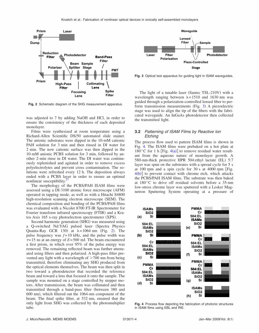
3.2 Patterning of ISAM Films by Reactive IonEtching
The process flow used to pattern ISAM films is shown inFig. 4. The ISAM films were prebaked on a hot plate at180°C for 1 h �Fig. 4�a�� to remove residual water result-ant from the aqueous nature of monolayer growth. A580-nm-thick protective HPR 504:ethyl lactate �EL� 5:7layer was spun on the substrates with a spread cycle for 5 sat 100 rpm and a spin cycle for 30 s at 4000 rpm �Fig.4�b�� to prevent contact with chrome etch, which attacksthe PCBS/PAH ISAM films. The substrate was then bakedat 180°C to drive off residual solvents before a 35-nmlow-stress chrome layer was sputtered with a Lesker Mag-netron Sputtering System operating at a pressure of
Lensed
Waveguide
Laser Fiber
Fiber Sample
PhotodetectorLaser FiberPolarization
Photodetector
Piezo-Controlled
Stageg
Fig. 3 Optical test apparatus for guiding light in ISAM waveguides.
SiO2Si
ISAMs
(a)
PMMA
504:ELISAMs
Cr
504:EL
SiO2Si
ISAMs
(b)
(e)SiO2Si
ISAMs
PMMASi
Cr504:EL
SiO2ISAMs
(b) PMMA
504:EL
SiO2ISAMs
Cr
PMMA
SiO2Si(c)
Cr
(f) Si
PMMA
504:ELCr
504:EL
SiO2Si
ISAMs
(d)
Cr
(g)
504:EL
SiO2Si
ISAMs
(h)SiO2Si
ISAMs
Fig. 4 Process flow depicting the fabrication of photonic structuresin ISAM films using EBL and RIE.
Jan–Mar 2009/Vol. 8�1�4

2lq
wesf11a1dafis5
Hpinauaspf5ml
3
Tisspuo5iti
iprs
Kroetch et al.: Fabrication of nonlinear optical devices in ionically self-assembled monolayers
J
.5 mTorr and a power of 300 W �Fig. 4�c��. This chromeayer masked areas of the ISAM films during the subse-uent oxygen plasma.
PMMA 950k electron beam lithography �EBL� resistas then spun �Fig. 4�d�� on the chrome masking layer and
xposed �Fig. 4�e��. Spin parameters for PMMA 950k con-isted of a spread cycle for 5 s at 100 rpm and a spin cycleor 30 s at 4000 rpm. The substrates were then baked at80°C. This process resulted in a PMMA thickness of20 nm. Typical Raith 150 EBL exposure parameters weren accelerating voltage of 2 keV, a 10-�m aperture, and a5-pA beam current. Following exposure, the PMMA waseveloped in an MIBK:IPA 1:3 solution for 30 s, placed inIPA stop bath for 15 s, rinsed in DI water for 15 s, and
nally dried with nitrogen. Before the chrome etch step, theides of the ISAM films were protected with HPR 504:EL:7.
The chrome masking layer was etched �f�, enabling thePR 504 and underlying PCBS/PAH ISAM layer to beatterned by the oxygen reactive ion-etching �RIE� plasman Fig. 4�g�. Manual agitation in a chrome etch solution wasot sufficient to “wet” some periodic structures because ofir-bubble formation. Therefore, chrome was etched usingltrasonic agitation until completion was visible, typicallyfter immersion for 15 s. The TRION Reactive Ion Etchystem was used to dry etch the ISAM films. The oxygenlasma was lit with an oxygen flow rate of 15 sccm, a radiorequency �RF� power of 60 W, and a chamber pressure of
mTorr. Finally, the protective, HPR 504 and chromeasking layers are removed in an ultrasonic acetone bath
eaving patterned ISAM films shown in Fig. 4�h�.
.3 Patterning ISAM Films by NanoimprintLithography
he process flow for creating silicon masters using in NILs shown in Fig. 5. EBL was used to create masters inilicon. PMMA 950k resist was spun on the silicon sub-trates �Fig. 5�a�� and exposed �Fig. 5�b�� with the samearameters presented in Section 3.2. Chrome was depositedsing an electron beam evaporation system to a thicknessf 30 nm as measured by a crystal thickness monitor �Fig.�c��. Sputtering was not used because of step coveragessues. Liftoff was performed in an ultrasonic acetone batho remove the resist and overlying chrome layer, resultingn negative-toned chrome patterned silicon �Fig. 5�d��.
The chrome pattern masked the underlying silicon dur-ng the silicon etch �Fig. 5�e��. Deep silicon etching waserformed using two different systems, depending on theirespective availability. An STS ICPRIE was used at a pres-ure of 20 mTorr, with a C F flow of 80 sccm and a SF
SiPMMA
(a) Si(d)Cr
SiPMMA
(b)Cr
Si(e)Cr
SiPMMA
(c) Si(f)
Fig. 5 Process flow illustrating the creation of silicon masters.
4 8 6
. Micro/Nanolith. MEMS MOEMS 013011-
flow of 100 sccm. The inductively coupled plasma �ICP�power was 2.5 kW, and the RF power was 20 W. A cryo-genic etch was also performed on the Oxford ICPRIE. Theexposed silicon was etched with a SF6 flow of 45 sccm, anO2 flow of 9 sccm, a pressure of 7.5 mTorr, an ICP powerof 400 W, and a RF power of 6 W. After pattern transferinto the silicon, the chrome was removed with the wetchrome etch �Fig. 5�f��. Finally, to prevent the ISAM filmsfrom adhering to the silicon masters, a monolayer oftrichloro�1H,1H,2H,2H-perfluorooctyl�-silane was appliedto the Si master as an antistiction layer. The silane andmaster were placed under vacuum for 1 h, resulting in amonolayer of silane forming on the master.
Jenoptik HEX 01 and HEX 02 hot embossing systemswere used to imprint the ISAM films. The system consistsof two horizontal metal plates whose temperature, position,and force exerted are controlled by manufacturer providedsoftware. All nanoimprinting was performed under vacuum.The glass transition temperature of similar ISAM films wasevaluated at 140°C by nanoindentation.43 These initialstudies also indicated that raising the film temperatureslightly above their glass transition did not significantly af-fect their molecular alignment. An imprinting temperatureof 145°C was therefore chosen in order to ensure cleanmolding of the material. The imprinting of the films willalso require some displacement of the material. This dis-
(a)(a)
(b)
Fig. 6 SEM images of 500 bilayer PCBS/PAH ISAM films areshown in �a� and �b�.
Jan–Mar 2009/Vol. 8�1�5

paNpddsh
4
4Ta
F1
Kroetch et al.: Fabrication of nonlinear optical devices in ionically self-assembled monolayers
J
laced material is likely to assume a different molecularlignment than the rest of the film, possibly inhibiting theLO properties in regions located near the edges of theatterns. As will be discussed below, the imprinted materialid retain strong NLO properties even after imprinting, in-icating that the thickness of this edge material was not thatignificant at least for the structure dimensions studiedere.
Results and Discussion
.1 ISAM Film Characterizationhe 500 bilayer PCBS/PAH ISAM films are continuousnd homogeneous as shown in Figs. 6�a� and 6�b�. AFM
(a)
(a)(b)( )( )
ig. 7 AFM images of 500 bilayer PCBS/PAH ISAM film with an �a�0-�m scan size and a �b� 1-�m scan size.
. Micro/Nanolith. MEMS MOEMS 013011-
images on the 500 bilayer PCBS/PAH films are shown inFigs. 7�a� and 7�b�. The average roughness of these filmswas 12.4 nm.
The thermal stability and polymeric nature of ISAMfilms suggest their amenability to NIL for their high-throughput patterning. To that end, the thermal stability ofPCBS/PAH films employed here had to be thoroughly ex-amined in order to assess whether the thermal cycling in-volved in NIL would degrade the chromophore alignmentand affect their nonlinear properties.
SHG measurements were taken on PCBS/PAH ISAMfilms to investigate how heating affected the nonlinear op-tical properties of the films. The SHG signal was measuredon both an unheated film and a film heated for 15 min atT=145°C in the hot embossing system that was subse-quently used for the imprinting work itself. The similitudebetween the SHG intensities coming from the two slides�Fig. 8� indicates that the chromophore alignment was notsignificantly affected by the thermal exposure and is there-fore compatible with NIL. A bare slide SHG signal wasalso measured �and amplified 50 times for visibility in Fig.8� demonstrating that the SHG signal was resultant fromthe NLO ISAM films and not substrate itself.
XPS was then employed to verify that the NIL thermalcycling did not affect the chemical composition of thefilms. To that end, another set of PCBS/PAH ISAM films
120001400016000
nsity
40006000800010000
SHGInten
020004000
30 35 40 45 50 55 60
S
30 35 40 45 50 55 60Angle (degrees)
Bare Slide (50 X) Unheated 300 Bilayer FilmH t d 300 Bil FilHeated 300 Bilayer Film
Fig. 8 Thermal investigation of the SHG of PCBS/PAH ISAM films.
0.80.91
rbance
0.50.60.7
Absor
0 20.30.40.5
00.10.2
400 600 800 1000 1200 1400 1600 1800 2000400 600 800 1000 1200 1400 1600 1800 2000Wavenumber [cm-1]
35°C 100°C 150°C 200°C
Fig. 9 FTIR spectra of PCBS/PAH films that have been heated andthen cooled back to room temperature.
Jan–Mar 2009/Vol. 8�1�6

wh=ttc
s1hMibSfies
4Fpccagcfirf�pmsosef
4
Apll
Tbt
Kroetch et al.: Fabrication of nonlinear optical devices in ionically self-assembled monolayers
J
ere subjected to a 10-min thermal cycle consisting ofeating them to temperatures ranging from T=35°C to T200°C for 10 min, and then cooling them back to room
emperature. As seen in Table 2, the atomic composition ofhe PCBS/PAH films was not affected by the heatingycles.
This assessment was further confirmed by FTIR. Theimilarities between the FTIR spectra after exposure to the0-min thermal cycles �Fig. 9� further demonstrate that theeating did not alter the chemical bonds within the films.ore specifically, the open-chain azo �–N=N– � feature44
ndicative of the PCBS is seen at 1600 cm−1 and the �C–H�ending indicative of PAH is seen at 1383 cm−1.45 Finally,HG experiments were also performed on fully imprintedlms in order to verify that the ISAMs retain their nonlin-ar properties following actual nanoimprinting. These re-ults are presented further below.
.2 Patterning ISAM Films by Reactive Ion Etchingor comparison to NIL, a RIE technique was first used toattern the PCBS/PAH ISAM films because a standard wethemical etch was not known for such materials and be-ause this dry etch technique could eventually be easilydapted to other types of ISAM films. A 3-�m-wide wave-uide with 4 �m of air cladding on either side was fabri-ated using this process in 400 bilayer PCBS/PAH ISAMlms �Fig. 10�a��. Figure 10�b� shows a side view of theesulting oxygen plasma etch profile. The plasma success-ully etched through both the HPR 504 protective layerlighter polymer above� as well as the ISAM films �darkerolymer below�. Although the etch is very anisotropic, theorphology of the resulting sidewalls is rougher than de-
irable. This roughness can be attributed to the raggednessf the etched chrome. Finally, hexagonal photonic crystaltructures with a lattice spacing of 710 nm and hole diam-ters ranging between 550 and 650 nm were also success-ully realized �Fig. 10�c��.
.3 Patterning ISAM Films Using NanoimprintLithography
suitable master had to be fabricated in order to similarlyattern the ISAM films by nanoimprinting. Silicon was se-ected due to its ease of processing and access to estab-ished processes for its machining. Although not as resistant
able 2 Percent mass composition of PCBS/PAH ISAM films aftereing heated to different temperatures and cooled back to roomemperature.
Temperature�°C�
Oxygen�%�
Nitrogen�%�
Carbon�%�
Sulfur�%�
35 20.6 12.8 60.0 6.5
100 19.9 13.1 60.5 6.5
150 22.0 10.2 62.2 5.5
200 21.3 11.3 61.7 5.7
. Micro/Nanolith. MEMS MOEMS 013011-
to wear as nickel, for instance, silicon is significantlycheaper and therefore enables more flexibility in terms ofdesign modification.
Figure 11�a� shows the silicon master used to create a3-�m-wide waveguide with a 590-nm period Bragg grat-ing. The etching process resulted in a very uniform aniso-tropic array with no apparent underetching. EBL was alsoused to fabricate 490-nm-diam pillars �Fig. 11�b��.
(a)
ProtectiveLayer
ISAMISAMFilm(b)
(b)
(c)
Fig. 10 PCBS/PAH ISAM films patterned with RIE �a� A waveguide,�b� the sideview of that waveguide, and �c� a photonic crystal struc-ture were fabricated in PCBS/PAH ISAM films using EBL.
Jan–Mar 2009/Vol. 8�1�7

swiaai
inTmvuwo2pn
tteta
Fp
Kroetch et al.: Fabrication of nonlinear optical devices in ionically self-assembled monolayers
J
Figure 12�a� shows a 3-�m-wide waveguide structureuccessfully imprinted into an ISAM films. A 3-�m-wideaveguide with an integrated 620-nm period Bragg grating
s also shown in Fig. 12�b�. Finally, in Fig. 12�c�, a hex-gonal photonic crystal structure with an average hole di-meter of 490 nm and a lattice spacing of 750 nm is shownmprinted in the ISAM films.
The SHG, XPS, and FTIR analysis presented previouslyndicated that the thermal cycles associated with NIL didot affect the composition of the PCBS/PAH ISAM films.his assessment was further confirmed by performing SHGeasurements on actual imprinted patterns in order to
erify that the nonlinear properties of the films were stillnaffected by overall process. To that end, ISAM filmsere imprinted for a period of 2 h at 150°C and a pressuref 10 kN with masters with fill factors ranging from 0 to5%. The films exhibit similar SHG results after nanoim-rinting �Fig. 13�, indicating again that the NIL process wasot affecting the nonlinear optical response of the material.
As discussed in Section 3, there is a strong possibilityhat some molecular misalignment of the material located athe very edge may inhibit the nonlinear activity near thosedges. The SHG results presented here would indicate thathis edge misalignment, although likely, is not significantlyffecting the NLO of the structure as whole, at least for the
(a)(a)
(b)
(b)
ig. 11 Silicon masters of an �a� 3-�m waveguide with a 590-nmeriod Bragg grating and �b� 490-nm-diam pillars are shown.
. Micro/Nanolith. MEMS MOEMS 013011-
dimensions studied here. We would also expect the issue tofully scale for photonic crystals eventually aiming to oper-ate in visible and near-visible range. Indeed, the proportionof the volume to be displaced, and thus, the relative thick-ness of this edge material would be expected to remainconstant as whole design is scaled down.
(a)
(a)(b)
(c)
Fig. 12 �a� 3-�m waveguide structures imprinted into the PCBS/PAH ISAM films is shown �a� and �b� with an integrated 620-nmperiod Bragg grating as shown. �c� A hexagonal photonic crystalstructure with an average hole diameter of 490 nm and a latticespacing of 750 nm is shown.
Jan–Mar 2009/Vol. 8�1�8

4Aw1opwpwtt
tetgrrtgbntiwtti
5TosPtfiNtctafo
Fd
Kroetch et al.: Fabrication of nonlinear optical devices in ionically self-assembled monolayers
J
.4 Guiding in ISAM Waveguideslaser tuned to �=1510 nm was coupled to an ISAM
aveguide fabricated by the RIE technique. From an initial0-mW laser power, quided transmission of 240 nW wasbserved. Coupling inefficiency does not completely ex-lain this loss. Transmission measurements of siliconaveguides measured on the same setup was found to haveowers two to three orders of magnitude higher. The side-all roughness and the inhomogeneous sites found within
he PCBS/PAH ISAM films contribute to this loss via scat-ering.
A similar assessment was also performed on waveguideshat have been fabricated by imprinting rather than by drytching. In this case, the transmitted power was, however,oo low to make a quantitative assessment of the relateduiding efficiency. The significant decrease in sidewalloughness that results from eliminating the RIE step shouldesult in a higher transmitted power because of the rela-ively smooth nanoimprinted walls. As before, the inhomo-eneous sites contribute to the loss of transmitted powerecause they act like scatter sites. As well, the inhomoge-eous sites result in incomplete imprinting because moreime is needed for sufficient polymer flow. This incompletemprint reduces the refractive index contrast, making theaveguides more susceptible to scattering losses. Addi-
ional work is underway to further refine the morphology ofhe films, making them fully suitable for optical waveguid-ng.
Conclusionshe development of a fabrication platform enabling the usef ISAM films in photonic devices has been reported. Morepecifically, we have demonstrated the use of NIL to patternCBS/PAH ISAM films. Photoelectron and infrared spec-
roscopy confirmed that the chemical composition of thelms was not affected by the heating cycle required byIL. In addition, measurement of the SHG also confirmed
hat the NIL process did not affect the alignment of thehromophores responsible for the nonlinear properties ofhe material. These observations confirm that these materi-ls are suitable to be patterned by nanoimprinting, a keyeature that would enable the cost-effective manufacturingf nanophotonic devices leveraging these materials.
y800
1000GIntensity
400
600
SHG
200
400
Angle (degrees)
030 35 40 45 50 55 60
4% 6% 9% 13% 17% 25%0% 0%
ig. 13 SHG of PCBS/PAH ISAM films after being imprinted withifferent area fill factors based on 5-�m circles.
. Micro/Nanolith. MEMS MOEMS 013011-
PCBS/PAH ISAM films were successfully patterned us-ing both plasma etching and NIL. In the first case, a com-bination of EBL and RIE was used to machine photoniccrystals structures with spacings of 710 nm and hole diam-eters ranging between 550 and 650 nm. In turn, similarstructures were also produced by the direct nanoimprintingof the films. Photonic crystals structures with an averagehole diameter of 490 nm and a lattice spacing of 750 nmwere successfully imprinted. Bragg gratings with a periodof 620 nm were also produced with this method. The inher-ent nonlinear optical stability of ISAM films, in addition totheir ease of processing, is anticipated to enable develop-ment of related commercial devices with substantially re-duced manufacturing costs.
AcknowledgmentsThis work was funded by the US Air Force Office of Sci-entific Research �AFOSR� through the SBIR/STTR pro-gram. A.K. and S.B. acknowledge financial assistance fromthe National Sciences and Engineering Scientific Councilof Canada through its Industrial Postgraduate Scholarshipsprogram. The University of Alberta’s NanoFab was utilizedto fabricate the photonic structures. SEM was performed atthe electron microscopy facilities of the National Institutefor Nanotechnology, a joint venture between the NationalResearch Council of Canada, the Province of Alberta, andthe University of Alberta. The authors acknowledge LucGervais for his assistance with AFM analysis and NealWilding for FTIR training.
References
1. W. Jiang, Y. Jiang, L. Gu, L. Wang, X. Chen, and R. T. Chen, “Sili-con and polymer nanophotonic devices based on photonic crystals,”Proc. SPIE 6124, 612410 �2006�.
2. M. Eich, G. C. Biorklund, and D. Y. Yoon, “Poled Amorphous Poly-mers for Second-Order Nonlinear Optics,” Polym. Adv. Technol. 1,189–198 �1990�.
3. X. Cheng and L. J. Guo, “Electrostatic self assembly of nanocompos-ite polymers in grating Structures,” J. Vac. Sci. Technol. B 19�6�,2736–2740 �2001�.
4. S. K. Yesodha, C. K. Sadashiva Pillai, and N. Tsutsumi, “Stable poly-meric materials for nonlinear optics: a review based on azobenzenesystems,” Prog. Colloid Polym. Sci. 29, 45–74 �2004�.
5. H. Kimura-Suda, Y. Zhang, T. Sassa, T. Wada, and H. Sasabe, “Polaralignment in spin-coated carbazole main- and side-chain polymerfilms,” Adv. Mater. Res. 12�16�, 1196–1199 �2000�.
6. J. R. Heflin, M. T. Guzy, P. J. Neyman, K. J. Gaskins, C. Brands, Z.Wang, H. W. Gibson, R. M. Davis, and K. E. Van Cott, “Efficient,thermally stable, second order nonlinear optical response in organichybrid covalent/ionic self-assembled films,” Langmuir 22, 5723–5727 �2006�.
7. H. Schift, S. Park, B. Jung, C. Choi, C. Kee, S. Han, K. Yoon, and J.Gobrecht, “Fabrication of polymer photonic crystals using nanoim-print lithography,” Nanotechnology 16, S261–S265 �2005�.
8. Y. Chou, P. R. Krauss, W. Zhang, L. J. Guo, and L. Zhuang,“Sub-10 nm imprint lithography and applications,” J. Vac. Sci. Tech-nol. B 15�6�, 2897–2904 �1997�.
9. L. J. Guo, “Recent progress in nanoimprint technology and its appli-cations,” J. Phys. D 37, R123–R141 �2004�.
10. C. Chao and L. J. Guo, “Polymer microring resonators fabricated bynanoimprint technique,” J. Vac. Sci. Technol. B 20�6�, 2862–2866�2002�.
11. K. E. Van Cott, M. Guzy, P. Neyman, C. Brands, J. R. Heflin, H. W.Gibson, and R. M. Davis, “Layer-by-layer deposition and ordering oflow-molecular-weight dye molecules for second-order nonlinear op-tics,” Angew. Chem., Int. Ed. 41�17�, 3235–3238 �2002�.
12. Z. Wang, J. R. Heflin, R. H. Stolen, and S. Ramachandran, “Highlysensitive optical response of optical fiber long period gratings tonanometer-thick ionic self-assembled multilayers,” Appl. Phys. Lett.86, 223104 �2005�.
Jan–Mar 2009/Vol. 8�1�9

1
1
1
1
1
1
1
2
2
2
2
2
2
2
2
2
2
3
3
3
3
3
3
3
Kroetch et al.: Fabrication of nonlinear optical devices in ionically self-assembled monolayers
J
3. R. P. Bertram, N. Benter, D. Apitz, E. Soergel, K. Buse, R. Hagen,and S. G. Kostromine, “Increased thermal stability of a poled electro-optic polymer using high-molar-mass fractions,” Phys. Rev. E 70,041802 �2004�.
4. C. Figura, P. Neyman, D. Marciu, C. Brands, M. A. Murray, S. Hair,R. M. Davis, M. B. Miller, and J. R. Heflin, “Thermal stability andimmersion solution dependence of second order nonlinear opticalionically self-assembled films,” Proc. SPIE 3939, 214–222 �2000�.
5. G. G. Roberts, “An applied science perspective of Langmuir-Blodgettfilms,” Adv. Phys. 34�4�, 475–512 �1985�.
6. G. Decher, “Fuzzy nanoassemblies: toward layered polymeric multi-composites,” Science 277, 1232–1237 �1997�.
7. J. A. Zasadzinski, R. Viswanthan, L. Madsen, J. Garnaes, and D. K.Schwartz, “Langmuir-Blodgett films,” Science 263�5154�, 1726–1733 �1994�.
8. Y. Liu, A. Rosidian, K. Lenahan, Y. Wang, T. Zeng, and R. O. Claus,“Characterization of electrostatically self-assembled nanocompositethin films,” Smart Mater. Struct. 8, 100–105 �1999�.
9. D. Y. Takamoto, E. Aydil, J. A. Zasadzinski, A. T. Ivanova, D. K.Schwartz, T. Yang, and P. S. Cremer, “Stable ordering in Langmuir-Blodgett films,” Science 293, 1292–1295 �2001�.
0. D. L. Allara, “Critical issues in applications of self-assembled mono-layers,” Biosens. Bioelectron. 10, 771–783 �1995�.
1. R. Paolesse, C. Di Natale, A. Macagnano, F. Davide, T. Boschi, andA. D’Amico, “Self-assembled monolayers of mercaptoporphyrins assensing material for quartz crystal microbalance chemical sensors,”Sens. Actuators B 47, 70–76 �1998�.
2. S. Stockhause, P. Neumann, S. Schrader, M. Kant, and L. Brehmer,“Structural and optical properties of self-assembled multilayers basedon organic zirconium bisphosphonates,” Synth. Met. 127�1–3�, 295–298 �2002�.
3. W. Lin, W. Lin, G. K. Wong, and T. J. Marks, “Supramolecular ap-proaches to second-order nonlinear optical materials. self-assemblyand microstructural characterization of intrinsically acentric ��ami-nophenyl�azoa�pyridinium superlattices,” J. Am. Chem. Soc. 118,8034–8042 �1996�.
4. T. Wink, S. J. van Zuilen, A. Bult, and W. P. van Bennekom, “Self-assembled monolayers for biosensors,” Analyst (Amsterdam) 122,43R–50R �1997�.
5. J. R. Heflin, Y. Liu, C. Figura, D. Marciu, and R. O. Claus, “Secondorder nonlinear optical thin films fabricated from ionically self-assembled monolayers,” Proc. SPIE 3147, 10–19 �1998�.
6. A. Rosidian, Y. Liu, and R. O. Claus, “Ionic self-assembly of ultra-hard ZrO2/polymer nanocomposite thin films,” Adv. Mater. Res.10�14�, 1087–1091 �1998�.
7. J. R. Heflin, C. Durak, P. J. Neyman, C. Brands, M. T. Guzy, K.Gaskins, A. Garg, R. M. Davis, K. E. Van Cott, H. Wang, and H. W.Gibson, “Organic electro-optic films fabricated by hybrid covalent/ionic self-assembly,” Conference on Lasers & Electro-Optics 3,1864–1866 �2005�.
8. G. Purvinis, P. S. Priambodo, M. Pomerantz, M. Zhou, T. A. Mal-donado, and R. Magnusson, “Second-harmonic generation in reso-nant waveguide gratings incorporating ionic self-assembled mono-layer polymer films,” Opt. Lett. 29�10�, 1108–1110 �2004�.
9. F. J. Arregui, B. Dickerson, R. O. Claus, I. R. Matias, and K. L.Cooper, “Polymeric thin films of controlled complex refractive indexformed by the electrostatic self-assembled monolayer process,” IEEEPhotonics Technol. Lett. 13�12�, 1319–1321 �2001�.
0. F. J. Arregui, I. R. Matias, K. L. Cooper, and R. O. Claus, “Fabrica-tion of microgratings on the ends of standard optical fibers by theelectrostatic self-assembly monolayer process,” Opt. Lett. 26�3�,131–133 �2001�.
1. K. Hyde, M. Rusa, and J. Hinestroza, “Layer-by-layer deposition ofpolyelectrolyte nanolayers on natural fibres: cotton,” Nanotechnology16, S422–S428 �2005�.
2. J. R. Heflin, C. Figura, D. Marciu, Y. Liu, and R. O. Claus, “Thick-ness dependence of second-harmonic generation in thin films fabri-cated from ionically self-assembled monolayers,” Appl. Phys. Lett.74�4�, 495–497 �1999�.
3. D. A. Chang-Yen and B. K. Gale, “An integrated optical biochemicalsensor fabricated using rapid-prototyping techniques,” Lab Chip 3,297–301 �2003�.
4. P. J. Neyman, M. Guzy, S. M. Shah, R. M. Davis, K. E. Van Cott, H.Wang, H. W. Gibson, C. Brands, and J. R. Heflin, “Novel hybridcovalent/ionic self-assembly technique for improved second-ordernonlinear optical films,” Mater. Res. Soc. Symp. Proc. 708, BB4.4.1–BB4.4.6 �2002�.
5. O. N. Oliveira, Jr., D. S. dos Santos, Jr., D. T. Balogh, V. Zucolotto,and C. R. Mendonca, “Optical storage and surface-relief gratings inazobenzene-containing nanostructured films,” Adv. Colloid InterfaceSci. 116, 179–192 �2005�.
6. P. Bertrand, A. Jonas, A. Laschewsky, and R. Legras, “Ultrathinpolymer coatings by complexation of polyelectrolytes at interfaces:suitable materials, structure and properties,” Macromol. Rapid Com-mun. 21, 319–348 �2000�.
. Micro/Nanolith. MEMS MOEMS 013011-1
37. T. Cao, F. Wei, X. Jiao, J. Chen, W. Liao, X. Zhao, and W. Cao,“Micropatterns of protein and conducting polymer molecules fabri-cated by layer-by-layer self-assembly and photolithography tech-niques,” Langmuir 19, 8127–8129 �2003�.
38. C. S. Camilo, D. S. dos Santos, Jr., J. J. Rodrigues, Jr., M. L. Vega, S.P. Campana Filho, O. N. Oliveira, Jr., and C. R. Mendoncüa,“Surface-relief gratings and photoinduced birefringence in layer-by-layer films of chitosan and an azopolymer,” Biomacromolecules 4,1583–1588 �2003�.
39. Y. Lin, C. Jiang, J. Xu, Z. Lin, and V. V. Tsukruk, “Sculptured layer-by-layer films,” Adv. Mater. Res. 19, 3827–3832 �2007�.
40. D. Wang, A. L. Rogach, and F. Caruso, “Composite photonic crystalsfrom semiconductor nanocrystal/polyelectrolyte-coated colloidalspheres,” Chem. Mater. 15, 2724–2729 �2003�.
41. D. Kommireddy, J. Shi, X. Yan, H. Ji, and Y. Lvov, “Electrostaticlayer-by-kayer nano-assembly: films, cantilevers, micropatterns andnanocapsules,” Proc. SPIE 4492, 120–131 �2005�.
42. J. Park and P. T. Hammond, “Multilayer transfer printing for poly-electrolyte multilayer patterning: direct Transfer of layer-by-layer as-sembled micropatterned thin films,” Adv. Mater. Res. 16�6�, 520–525�2004�.
43. C. C. Figura, “Second order nonlinear optics in ionically self-assembled films,” PhD Thesis, Virginia Tech �1999�.
44. J. Coates, “Interpretation of infrared spectra, a practical approach,”Encyclopedia of Analytical Chemistry, R. A. Meyers, Ed., pp. 10815–10837, Wiley, Chichester �2000�.
45. V. Zucolotto, M. Ferreira, M. R. Cordeiro, C. J. L. Constantino, D. T.Balogh, A. R. Zanatta, W. C. Moreira, and O. N. Oliveira, Jr., “Un-usual interactions binding iron tetrasulfonated phthalocyanine andpoly�allylamine hydrochloride� in layer-by-layer films,” J. Phys.Chem. B 107, 3733–3737 �2003�.
Aruna Kroetch received her BSc in engi-neering physics at the University of Albertain 2003 after which she went on to work atthe Univerity of Alberta’s Nanofab as a re-search professional. She completed herMSc in electrical and computer engineeringin 2008 at the Univeristy of Alberta wherethe focus of her thesis work was on the fab-rication, characterization, and patterning ofISAM films. She is currently working at Mi-cralyne Inc. in the R&D department as aproject engineer.
Steven C. Buswell received his BSc in en-gineering physics and MSc in electrical en-gineering from the University of Alberta in2005 and 2008, respectively. His thesis re-search was centered on the design, fabrica-tion, and sensing applications of photoniccrystals. He currently is an engineer withApplied Nanotools Inc.
Stephane Evoy received his PhD in appliedphysics from Cornell University in 1998. Heis associate professor of electrical and com-puter engineering at the University of Al-berta, with a cross appointment as researchofficer at the National Institute for Nanotech-nology in Edmonton, Alberta. His current re-search includes the development and inte-gration of nanomechanical devices forbiosensing applications and the integrationof nanostructures for the development of
chemical sensing arrays. Evoy has also recently coedited Introduc-tion to Nanoscale Science and Engineering, a textbook supportingthe teaching of nanoscale technologies at the undergraduate level.He is currently serving as secretary of the executive committee ofthe Nanoscale Science and Technology Division of the AmericanVacuum Society and since 2005 has been a member of the editorialboard of Review of Scientific Instruments.
Jan–Mar 2009/Vol. 8�1�0

I
mpbmm
Kroetch et al.: Fabrication of nonlinear optical devices in ionically self-assembled monolayers
J
Cemil Durak received his BS in physicsfrom Bilkent University, Ankara, Turkey, in2002, and his MS in physics in 2005 fromVirginia Tech, Blacksburg, Virginia. He hasbeen doing his graduate studies on second-order nonlinear properties of lonically self-assembled multilayers films under the su-pervision of Prof. James Heflin. He isplanning to finish his doctorate studies onDecember 2008.
J. Randy Heflin is professor of physics andassociate director of the Center for Self-Assembled Nanostructures and Devices atVirginia Tech, where he has been a memberof the faculty since 1992. He received hisPhD from the University of Pennsylvania in1990. His research focuses on organic op-toelectronic nanostructures and devices. Hecoedited the textbook Introduction to Nano-scale Science and Technology �Springer,2004� and is an associate editor of the
nternational Journal of Nanoscience.
Vladimir Kochergin joined the Optical Sys-tems Group at Luna Innovations in Septem-ber 2006. While at Luna, Vladimir’s respon-sibilities include project and programmanagement. He received his BS and MSin applied physics in 1996 and 1998, re-spectively, from Moscow Institute of Physicsand Technologies, and PhD in materials sci-ence in 2007 from Christian Albrecht Uni-versity of Kiel, Germany. Prior to Luna, heheld a similar position in the R&D Depart-
ent �from 2000 to 2004� and was managing the Optics R&D De-artment from 2005 to 2006 at Lake Shore Cryotronics, Inc., Colum-us, OH. Kochergin has over 50 publications �including aonograph and 11 assigned patents� in the field of photonics, plas-onics, and structural optical materials.
. Micro/Nanolith. MEMS MOEMS 013011-1
Roger Duncan joined the Optical SystemsGroup of Baker Hughes ProductionQuest inMay 2008 as the senior optical systems en-gineer. While at ProductionQuest, his re-sponsibilities centered on managing the de-velopment of the company’s OFDR-baseddistributed fiber-optic sensing platform.Prior to joining ProductionQuest, he servedas as a senior electro-optic engineer andprogram manager at Luna Innovations Inc.,where he led the distributed fiber-optic
sensing development team and was a primary inventor of the fi-beroptic shape-sensing technology. Duncan graduated from VirginiaTech in 2002 with his MS in electrical engineering with an emphasisin electromagnetics and optics. He has authored more than 24 pub-lications related to electro-optics, fiber-optic sensing, and photoniccrystals.
Jan–Mar 2009/Vol. 8�1�1