fabrication and characterization of memory devices based on … · the planar structures present...
TRANSCRIPT

Universidade do Algarve Faculdade de Ciências e Tecnologia
Fabrication and characterization of memory
devices based on nanoparticles
Asal Kiazadeh
Doctor of Philosophy in Electronics and optoelectronics
Supervisor
Prof. Doctor Henrique Gomes
September 2013

1
Fabrication and characterization of electronic devices based on
nanoparticles
Declaração de autoria de trabalho:
Declaro ser a autora deste trabalho, que é original e inédito. Autore e trabalhos consultados estão
devidamente citados no texto e constam na listagem de refrências incluída.
Copyright © 2013, por Asal Kiazadeh
A Universidade do Algarve tem o direito, perpétuo e sem limites geográficos, de arquivar e
publicar este trabalho através de exemplars impressos reproduzidos em papel ou de forma, ou
por qualquer outro meio conhecido ou que venha a ser inventado, de o divulger através de
repositóries científicos e de admitir a sua cópia e distribuição com objetivos educacionais ou de
investigação, não comerciais, desde que seja dado crédito ao autor e editor.

2
Acknowledgements
It is my great pleasure to thank Prof. Dr. Henrique Gomes for the supervision and advice
provided during my research, and for the training and access to required equipment in the
electronic Laboratories.
I also would like to thank to my co-supervisors Prof. Dr. Ana Rosa Da Costa and Prof. Dr. Jose
Morreira for all their help and support and for reviewing my dissertation.
My appreciation also goes to Prof. Dr. Dago de Leeuw, project leader at the Max Planck Institute
for Polymer Research, and Prof. Dr. Stephan Meskers, The varied discussions we have had
together were always enlightening.
I would like to thank the University of Algarve for facilitating the research environment and the
Tu/e and Philips research Labs, as our collaborators during this research project.
I am forever indebted to my mother, Parvin Ghamami, I have no suitable words that can describe
her everlasting love and support to me throughout my life.
I would like to express my utmost gratitude to my best friend, Daniel and my sister, Mahsa. This
work was not possible without their help, encouragement, and support during the tough stages of
my research and thanks in particular also go to Prof. Dr. Hamid Shahbazkia.
I am also grateful to my dear friend, Adrian, for his valuable comments on technical writing.
My sincere gratitude goes to all my laboratory colleagues, as well as my friends and family for
their support throughout this research.
Finally, I am thankful to the European commission Erasmus-Mundus Lot 7, for their financial
support of my scholarship, to the Fp7 project, FlexNet, Network of excellence for building up
Knowledge for better System Integration for Flexible Organic and Large Area Electronics
(FOLAE) and its exploitation, to the Portuguse Foundation for Science and Technology (FCT)
trough the project Intelligent Cell Surface (ICS) and the Instituto de Telecomunicações (IT-Lx).

3
Abstract
The objective of this study is to understand the electrical properties of non-volatile memories
based on metal oxide nanoparticles embedded into an insulating polymer matrix. These
memories are classified as resistive random access memories (RRAM), as they undergo resistive
switching between well-defined conductance states when submitted to a voltage pulse.
A number of memory devices were fabricated and studied using electrical techniques. Current-
voltage characteristics were studied as a function of the ambient atmosphere and temperature.
The dynamic electrical behaviour was probed using triangular voltage profiles with different
scan rates, transient techniques and electrical noise techniques. Electrical measurements were
complemented with morphological characterization. Important outcomes of this thesis are the
following:
It was shown that adsorbed moisture on the surface of the devices causes resistive switching.
This type of resistive switching can lead to very high on/off ratios, and therefore it is not reliable.
Silver oxide nanoparticles undergo an electroforming process similar to a soft-breakdown
mechanism as reported for binary oxides. A model that explains the basic features of the
electroforming mechanism was proposed. After the electroforming, the devices show resistance
switching properties with a high on/off ratio (> 104), good retention time, and programming
endurance.
A resistive switching mechanism was proposed. The model assumes that during
electroforming a percolation network of micro conducting paths (filaments) is established
between the electrodes. The creation and rupture of these micro-paths is responsible for the
changes in conductance.
Results from this study indicate that nanostructured thin films made of silver oxide
nanoparticles embedded in an insulating polymer show an electrical behaviour like the bulk
oxide based memory structures. The planar structures present the advantage of being
programmed in multi-resistance levels suggesting a very interesting finding that may pave the
way to achieve a multi-bit memory device.

4
Resumo
O objetivo desta tese foi estudar as propriedades elétricas de componentes electrónicos
fabricados com nanopartículas de metálicas. Este tipo de memoria é designado por memorias
resistivas porque mudam a sua resistência elétrica através da aplicação de um tensão elétrica.
Este componente é conhecido por “memristor”.
Um conjunto de memorias resistivas foi fabricado e caracterizado. Nomeadamente foram
realizadas um conjunto de medidas elétricas em diferentes ambientes (vácuo e atmosfera
ambiente) e em função da temperatura para obter informação sobre os mecanismos de transporte
electrónico e sobre a comutação elétrica da resistência.
As memorias fabricadas tem um elevado hiato entre os estados resistivos (> 104), são não-
voláteis e robustas, tendo sido testadas com mais de mil ciclos de programação entre os estados
resistivos.
Esta tese propõe um modelo para explicar as variações de resistência elétrica. O modelo assume
que as partículas de prata oxidam e formam um óxido de prata. Durante o processo de formação
da memoria, o elevado campo elétrico aplicado leva a ruptura dielétrica controlada do óxido e
forma defeitos eletricamente ativos. Esta rede de defeitos gera micro-caminhos para a condução
elétrica ou filamentos. As mudanças de resistência elétrica são causadas pela criação/ruptura
deste filamentos.
Os resultados desta tese indicam que as mudanças de resistência elétrica em filmes
nanoestruturados com nanopartículas metálicas são semelhantes as observadas em estruturas
resistivas com base em filmes finos óxidos como o dióxido de titânio (TiO2) e o óxido de
alumínio (Al2O3) entre outros.
Os “memristors” fabricadas neste tese são estruturas planares. O objectivo inicial foi ter um
instrumento de caracterização mais simples que a estrutura convencional em sanduiche. No
entanto a estrutura planar permite também obter vários níveis de resistência elétrica sugerindo
que pode funcionar como memorias “multi-bit”.

5
Table of Contents
CHAPTER 1- Motivations and Outline of the Thesis............................................................... 13
1.1 Motivations ............................................................................................................................. 14
1.2 Outline of the Thesis ............................................................................................................... 16
1.3 Peer Reviewed Published Work and Conference Presentations ............................................. 17
CHAPTER 2 - Overview of emerging memory technologies and review of the current status of
nanoparticle memory based devices .......................................................................................... 20
2.1 Introduction: Non-Volatile Memory ....................................................................................... 21
2.2 RRAM- Resistive Random Access Memory .......................................................................... 24
2.2.1 Memristor function to define RRAM .................................................................................. 27
2.3 Literature review of nanoparticles based RRAM devices ...................................................... 28
2.4 Requirements for the future storage class memory ................................................................. 31
2.5 Unsolved issues ....................................................................................................................... 32
2.4. Conclusions ............................................................................................................................ 33
CHAPTER 3-Synthesis of metal nanoparticles and thin film deposition ................................. 34
3.1 Introduction ............................................................................................................................. 35
3.1 Fabrication methods ................................................................................................................ 35
3.1.1 Terminology ......................................................................................................................... 35
3.1.2 Metal nanoparticles synthesis methods ................................................................................ 36
3.1.3 Nucleation and growth of metallic nanoparticles ................................................................ 37
3.1.4 Magic numbers..................................................................................................................... 38
3.1.5 Colloid stability .................................................................................................................... 40
3.1.6 Electrical and optical characteristics .................................................................................... 42
3.2 Experimental methods ............................................................................................................ 43
3.2.1 Silver nanoparticles .............................................................................................................. 43
3.2.2 Materials and instruments .................................................................................................... 43
Sample type A .............................................................................................................................. 45
Sample type B ............................................................................................................................... 46
Sample type C ............................................................................................................................... 48
Sample type D ............................................................................................................................... 48
Sample type E ............................................................................................................................... 49
Sample type F ............................................................................................................................... 50
3.3 Deposition techniques ........................................................................................................... 53

6
3.3.1 Drop casting ....................................................................................................................... 53
3.3.2 Boil deposition ................................................................................................................... 54
3.3.3 Dip coating ......................................................................................................................... 54
3.3.4 Spin coating ....................................................................................................................... 55
3.4. Advantages and disadvantages of planar diodes .................................................................... 55
CHAPTER 4 -The effect of ambient atmosphere on resistive switching ................................. 59
4.1 Introduction ............................................................................................................................. 60
Types of current-voltage characteristics ....................................................................................... 60
4.2 The effect of ambient atmosphere on electrical characteristics .............................................. 62
4.2.1 Electrical measurements. ..................................................................................................... 62
4.2.2 The electrical behaviour of planar diodes based on gold nanoparticles .............................. 63
4.2.3 The electrical behaviour of planar diodes based on silver nanoparticles-PVP .................... 63
4.3 The effect of channel length (L) ............................................................................................. 68
4.4 Discussion ............................................................................................................................... 70
4.5 Conclusion .............................................................................................................................. 71
CHAPTER 5 - Electroforming .................................................................................................. 72
5.1 Introduction ............................................................................................................................. 73
Dielectric soft-breakdown ............................................................................................................. 73
Percolation .................................................................................................................................... 74
5.2 Experimental: Electroforming in systems with silver nanoparticles ...................................... 76
5.3 Discussion ............................................................................................................................... 83
Percolation current paths............................................................................................................... 84
5.4 Conclusions ............................................................................................................................. 87
CHAPTER 6 - Resistive switching mechanism in silver oxide nanoparticles .......................... 88
6.1 Introduction ............................................................................................................................. 89
6.2 Post-breakdown current (on and off states) ............................................................................ 91
6.3 Temperature dependence of the current for both on and off states ......................................... 96
6.4 Current fluctuations ................................................................................................................ 97
6.5 Dependence of the on-state I-V characteristics on the voltage ramp speed ............................ 99
6.6 Delayed switch-on effect ...................................................................................................... 101
6.7 Light-induced effects ............................................................................................................ 103
6.8 Discussion ............................................................................................................................. 104
6.7 Conclusions ........................................................................................................................... 107
CHAPTER 7 - Diodes based on silver chloride nanocrystals ................................................. 109
7
7.1 Introduction ........................................................................................................................... 110
7.2 Electrical characteristics ....................................................................................................... 110
7.3 Temperature dependence of the current for a silver chloride polymer blend diode ............. 114
7.4 Discussion ............................................................................................................................. 115
7.5 Conclusion ............................................................................................................................ 116
CHAPTER 8 - Conclusions of the Research and Suggested Future Work ............................. 118
8.1 Conclusions ........................................................................................................................... 119
8.2 Future Works ........................................................................................................................ 121
Bibliography ............................................................................................................................... 124
8
List of Figures
1.1 Number of papers on resistive switching per year [13]……………………………………….……....15
2.1.1 Cost per GigaByte (GB) of Desktop and Enterprise hard disk drives (HDD) compared to the cost
reduction trend in DRAM and NAND flash memory [15]……………………………………….……….22
2.1.2 Observed trend in flash memory capacities in the past 12 years, presented at ISSCC (data from
ISSCC 2011 documentation)……………………………………………………………………………...22
2.1.3 Schematic view of a flash memory cell: the charge is stored in the floating gate (FG) by applying
the proper voltage to the control gate (CG); tunnel and control dielectric are also shown………………..23
2.2.1 Two terminal RRAM structure. The resistance of the switching medium determines the state of the
device……………………………………………………………………………………………………...25
2.2.2 Two types of resistance switching. (a) bipolar switching (b) unipolar switching…………………..26
3.1.1 (a) FCC unit cell, (b) 13-atom nanoparticle set in its FCC unit cell, showing the shape of polyhedron
associated with a nanocluster, (c) close-packed cuboctahedron cluster......................................................38
3.1.2 Percentage of atoms located on the surface of a spherical silver particle as a function of diameter of
the particle [54]…........................................................................................................................................39
3.1.3 Illustration of sterically and electrostatically stabilized nanoparticles [57]…………........................41
3.1.4 The effect of metal particle size on the electronic properties. Whereas bulk metals and metal
nanoparticles have a continuous band of energy levels, the limited number of atoms in metal nanoclusters
results in discrete energy levels, allowing interaction with light by electronic transitions between energy
levels. Metal nanoclusters bridge the gap between single atoms and nanoparticles [58]…........................42
3.2.1 Silver nanoparticle solutions of different sizes and number concentrations. 1: 10 nm (3.6x 10¹²
Nps
/ mL), 2: 40 nm (5.7x 10¹⁰
Nps / mL), 3: 60 nm (1.7x 10¹⁰
Nps / mL) and 4: 100 nm (3.6x 10⁹ Nps /
mL)………………………………………………............................……………….......................….….43
3.2.2 TEM images of (a) sample A, (b) sample B…………………………………....................………..45
3.2.3 Typical SAED pattern of nanoparticles in ethanol………………………………….....................…46
3.2.4 Surface plasmon resonance (SPR) from silver nanoparticle samples A (red) and B
(blue)......................................………………………………………………………..................................47
3.2.5 Typical XRD pattern recorded from a drop-coated film of Ag/polymer nanocomposite on a glass
substrate…………...............................…………………………………………………………………....47
3.2.6 SPR absorption of sample A (blue), sample D (green)…………………………...…........................48
3.2.7 TEM images of sample D…………………………………………………………….......................49
3.2.8 SPR absorption of silver/silver oxide nanoparticles (sample E) during 3 hours…..…......................50
3.2.9 TEM images of sample E…………………....….......................................................….....................50

9
3.2.10 XRD from Silver chloride/ polyaniline (PANI) core–shell (sample F)……………........................51
3.2.11 FTIR spectrum of AgCl/PANI core–shell composite……………………………….......................51
3.2.12 Final SPR peak absorption of gold nanoparticles………………………………….........................53
3.3.1 Silicon substrates, (a) Thermally oxidized silicon wafer, (b) HMDS treated transistors...................54
3.4.1 (a) Schematic diagram of PVP capped silver nanoparticles between interdigitated Au microelectrode
arrays, fabricated on thermally oxidized silicon wafers, (b) TEM image and X-ray differaction of PVP
capped silver nanoparticles..........................................................................................................................56
3.4.2 (a) Typical AFM image of PVP capped silver nanoparticles based diode type-B (b) Image of diode
type-C (silver nanoparticles were prepared by electron beam evaporation), interdigitated Au
microelectrode arrays, fabricated on thermally oxidized silicon wafers......................................................57
3.4.3 (a) Typical AFM image of PVP capped silver nanoparticles based diode type-E (b) Typical AFM
image of diode type-Au......................................................................................................................58
4.2.1 Schematic representation of N-shape I-V characteristics…………………………............................60
4.2.2 Schematic representation of (a) Symmetric, (b) Asymmetric S-shape I-V characteristics….…........61
4.2.1 I-V characteristics of a SiO2 substrate coated with a thin film of PVP. The resistance is
approximately 0.5 TΩ under an applied voltage of 50 V. The measurement is done in vacuum................62
4.2.2 The I-V characteristics of AuNps in air………………………………………………......................63
4.2.3 The I-V characteristics of AgNps-PVP based device in air…………………………........................64
4.2.4 Current-voltage characteristics, (a) symmetric S-shape and (b) asymmetric, of silver oxide Nps-PVP
(silver-PVP) planar diode (L: 10 µm)………………………………………....…......................................64
4.2.5 Retention time for both on and off states of a silver-PVP planar diode (L: 10 µm) in air….............65
4.2.6 Pristine-state and the final electroformed loop of silver-PVP planar diode (L: 10 µm) in vacuum...66
4.2.7 (a) I-V characteristics showing the on-state of silver-PVP planar diode (L: 10 µm) in vacuum........66
4.2.8 Endurance sweep cycles for a silver-PVP planar diode (L: 10 µm), in high vacuum (10-5
Torr):
Write: 30 V, Erase: 50 V, and Read: 3 V. The on/off ratio is 4 orders of magnitude.................................67
4.2.9 Retention time for both on and off states of a silver-PVP planar diode (L: 10 µm) in high vacuum.67
4.3.1 Channel length dependence of the threshold voltage for switching from the off-state to the on-state
for N- and S-shape switching.......................................................................................................................69
4.3.2 Current state at 3 V under N2/H2O gas exposure for a AgNps-PVP diode (L: 10 µm)......................69
5.1.1 One-dimensional poly-walk: (a) in diffusion, the walk is directed by random scattering, (b) in
percolation, the walk is controlled by the random medium.........................................................................75
5.1.2 (a) As-fabricated state of the region (pristine-state), with the defects randomly distributed in an
initial configuration (pink dots). (b) Percolation nanoscale filamentary path after the electroforming
[97]...............................................................................................................................................................76
10
5.2.1 Current-voltage characteristics of a diode prior to electroforming. The hysteresis loops are typical of
a capacitor like behaviour. The channel length L: 10 µm. The voltage ramp speed is 0.1Vs-1
...................77
5.2.2 Current-voltage characteristics of a diode during electroforming. The channel length (L) is 10 µm.
The inset shows the Vforming for different channel lengths (L: 5 µm, 7.5 µm, 10 µm, 20 µm, 40 µm. (5
devices were measured for each L)..............................................................................................................78
5.2.3 I-V characteristic of the on-state and off-state of a diode with silver nanoparticles, L: 10µm...........79
5.2.4 The evolution of the current under a constant applied voltage (V=15 V) for a diode with L: 5µm...80
5.2.5 XRD patterns for the empty silicon oxide substrate (black), pristine state (blue), electroformed state
(Red).............................................................................................................................................................81
5.2.6 I-V characteristics of a diode fabricated with only a PVP layer. (a) Blue curve is the first
measurement, the black curve is the second measurement. The dielectric breakdown occurs in the return
path. The measurements were carried out in vacuum for a diode with a channel length of 5 µm...............82
5.3.1 Schematic diagram of the three different types of filaments established upon electroforming.
Permanent paths (bold green), programmable paths (narrow green) and paths that turn on and off
intermittently or blink (in red). (a) During initial forming loops, (b) last forming loops (c) on-state, (d)
off-state, (e) the lowest off-state..................................................................................................................84
5.3.2 Schematic diagram showing the double barrier established between the silver oxide particle and the
nearby polymer region. Oxygen vacancies in the oxide can trap holes and the oxygen rich nearby polymer
regions trap electrons creating a local electric dipole..................................................................................86
5.3.3 Schematic diagram of the compensating electron filamentary paths. This path is determined by the
defect distribution and density.....................................................................................................................86
6.2.1 Symmetric current-voltage characteristics for different channel lengths (a) L: 5 µm, (b) L: 7.5 µm,
(c) L: 10 µm. The on-state exhibits a pronounced NDR becomes more defined for higher channel
lengths..........................................................................................................................................................92
6.2.2 I-V characteristics showing that as the applied voltage increases the NDR region is comprised of a
cascade of switching-off events. Different off-states can be obtained by selecting the applied voltage.....93
6.2.3 Different on- and off-states can be obtained by selective turning-off some of the current paths. This
is done by applying voltages slightly above the NDR region, 35 V (black), 40 V (red), and 45 V (blue) for
a time of 2 sec. (b) the programming of different conductance states can also be achieved by successively
increasing the voltage range above the NDR region, In (b) is shown three different current states obtained
by extending the scan voltage range, blue [0-60 V], red, black: [0-100 V] the ramp speed used is 500
mV/s.............................................................................................................................................................94
6.2.4 Time dependence of two on-states and 3 off-states. Different states can be programmed by
controlling the amplitude and the time of the voltage step..........................................................................94

11
6.2.5 Log (I)-Log (V) for both the on- and the off-state..............................................................................95
6.3.1 Arrhenius plot for the on-, off- and the lower off-state. All plots are perfect parallel showing the
same activation energy (72 meV). Channel length is L=10µm...................................................................96
6.4.1 Current fluctuations at the lower off-state..........................................................................................98
6.4.2 Typical time domain of the current fluctuation at NDR. The trace was recorded with an applied
voltage of 40 V.............................................................................................................................................98
6.4.3 Probability density function using the data in Fig. 6.4.2....................................................................99
6.5.1 Electrical characteristics of the on-state, voltage scan speed: 100 mV.s-1
, 300 mV.s-1
, 500 mV.s-1
,
1000 mV.s-1
(L: 5 µm)................................................................................................................................100
6.6.1 Temporal evolution of current from the off to the on-state after applying voltage steps of different
magnitudes. The experiment started from high to low bias (L=10 µm)....................................................101
6.6.2 Voltage dependence of the delay time for switching from off to on................................................102
6.7.1 Time response of the diode current to a few seconds light pulse. The diode is in the off-state with a
constant applied voltage of 5 V..................................................................................................................104
6.8.1 Hole flux, the same charge carriers at the on/off states, hole/electron recombination ruptures some
conductive paths at the off-state.................................................................................................................106
7.2.1 Schematic diagram of the device structure. The interdigitated gold microelectrode arrays were
10.000 m long (W), separated apart 10 m. The thin polymer film with the nanocrystals is
approximately 1m thick. The substrate is a thermally oxidized silicon wafer with a 200 nm thick SiO2
layer............................................................................................................................................................110
7.2.2 The pristine (blue) and the electroformed (black) states for AgCl nanocrystal polymer based diode,
L = 10µm....................................................................................................................................................111
7.2.3 The on/off I-V curves obtained after pulse at Von and Voff respectively for AgCl nanocrystal polymer
based diode, L = 10 µm................................................................................................................112
7.2.4 Initial current decay measured shortly after a programming pulse to the on-state. Inset shows the
discrete variations in the current with a typical signature of random telegraph noise of AgCl nanocrystal
polymer based diode..................................................................................................................................113
7.2.5 Endurance sweep of AgCl nanoclusters-PANI-PVP diode (L: 10µm), high vacuum: 10-5
Torr, Write:
18V, Erase: 30V and Read: 3V. The on/off ratio is 2 orders of magnitude..............................................113
7.3.1 (a) Temperature dependence of the current-voltage characteristics of the AgCl nanocrystal polymer
based device, below 245K the NDR disappears showing low conductance state, (b) Arrhenius plot of the
high conductance state measured at 6 V. The line fits the experimental points (∆)..................................114

12
List of Tables
2.4.1 Summary of reported device characteristics.......................................................................................31
3.1.1 Total and surface number of atoms for FCC-structured silver nanoparticles together with an estimate
of the particle size [54]………………………………………………………………………………….....40
3.2.2 Comparison of measured D-spacings for silver nanoclusters with D-spacings for FCC silver..........46
4.3.1 Programming voltage process of N-shape characteristics for different channel lengths (L)..............68
6.1.1 Charge transport mechanisms proposed in the literature for nanostructured resistive switching
devices..........................................................................................................................................................89

13
CHAPTER 1- Motivations and Outline of the Thesis
In this chapter, a brief review in non-volatile memory developments is presented. The
motivation of this research is also discussed. The thesis organization is presented at the end
together with a list of publications of this work.

14
1.1 Motivations
There is a large demand for a high-density, high-speed, and low-power nonvolatile memory
(NVM); the market of NVM has grown much faster than the entire semiconductor market in
recent years [1]. Flash memory has been one of the most important key drivers of memory
growth in terms of flexibility, cost and market size. However, as predicted by International
Technology Roadmap for Semiconductors (ITRS) [2-3], the flash cell reduction will face
physical limits in the near future due to the increasing difficulty of retaining electrons in
shrinking dimensions. Flash also suffers from general shortcomings like slow programming
(from microseconds up to milliseconds), limited endurance (typically 105-10
6 write/erase cycles)
as well as the need for high voltages (10-20 V) during programming and erase. Therefore, new
materials and novel device architectures are needed to overcome this technical and physical
scaling limit.
There are various candidates competing for the next-generation memory. For example,
magnetic random access memory (MRAM) and ferroelectric random access memory (FRAM),
which use magnetic tunnel junctions and reversible polarization of ferroelectric materials,
respectively, have attracted significant attention. However, both MRAM and FRAM face severe
problems in scaling. Under this circumstance, a new candidate emerged: resistance switching
random access memory (RRAM), in which the memory cells have the theoretically smallest area.
Resistive switching phenomenon was first reported in a series of binary oxides by Hickmott
in 1962 [4]. Since then, the resistive switching behaviour under an applied electric field has been
reported in many materials. Hence, the first period of research activity on resistive switching
phenomena arose in the 1970s and 1980s. Most of the early research focused on discussing and
revealing the physical mechanism of electrically stimulated resistive switching. Through the
development of microelectronics processing technology, researchers recognized that resistive
switching behaviour has the potential to be utilized as an ultimate NVM in the late 1990s,
bringing the second research surge in resistive switching [5-12].
As shown in Fig.1.1, the number of papers on RRAM increased rapidly year by year [13],
indicating that this area is attracting enormous scientific interest because of the excellent scaling
prospects and the outstanding operating and processing properties.

15
Fig. 1.1 Number of papers on resistive switching per year [13].
RRAM is still less mature than other emerging memory concepts, but it is appealing in its
vast potential for exploiting a memory combining high density, high speed and non-volatility.
In order to promote the commercial application of RRAM, further studies are required to
elucidate the microscopic mechanism of resistive switching. Studies on reliability become
important. What is the reason for cycling failure? How to improve retention time? How to
improve yield and parameter dispersion? These unsolved issues and the coexistence of the
scaling potential mean research in resistive switching can become a sustaining hotspot in fields
of physics and electronics as well as in materials research.
The need for a deeper understanding of the physics of the resistive switching mechanism has
been the major motivation for the work in this thesis. Towards this goal, we followed a twofold
strategy: Firstly we use planar device structures. Although these structures are not useful for
practical applications they offer an interesting research tool because they allow a decoupling of
the effects related to electrodes from the effect relating to the bulk layers making the data
analysis simpler. Secondly, in each sample we perform a systematic electrical characterization
including temperature dependent measurements and dynamic measurements to study the time
dependences of the physical process involved during switching. Our ultimate goal was to
understand the basic processes that can control the change in resistance upon a voltage step. To
gain further understanding we also compare the behaviour of our nanoparticle based device with
16
oxide-based memories and polymer or organic based memories. Apparently different devices
show a common behaviour. This strong resemblance has been overlooked due to a lack of
interaction between different scientific communities.
1.2 Outline of the Thesis
This thesis is organized into 8 chapters. Following this chapter, which gives an overview of
the thesis, motivation and organization, the remainder of the thesis is arranged as follows:
Chapter 2 provides an overview of emerging memory technologies, followed by a review of
the current status of nanoparticle memory based devices. The unsolved issues of RRAM in terms
of the requirements for the future storage class memory will be also presented. This chapter
concludes with the advantages and disadvantages of using planar devices when compared with
more conventional sandwich structures.
In chapter 3, the fabrication methods and synthesis of metal nanoparticles (silver, silver
oxide, gold, silver chloride) are explained. Different deposition methods are also presented. Thin
films of metal nanoparticles were deposited on the silicon substrates by drop casting and spin
coating. Structural and morphological characterization was done using TEM, UV-Vis
spectroscopy, AFM and XRD.
Chapter 4 is concerned with a systematic investigation on the electrical properties of metal
nanoparticles (silver and gold) in different ambient atmospheres. The same device structure can
show different types of current-voltage (I-V) characteristics (S- and N-shape) depending on the
surrounding atmosphere. The retention time and endurance cycles are also shown in this chapter.
Chapter 5 mainly focuses on the electroforming process. The electroforming is presented as a
dielectric soft-breakdown mechanism. In this chapter a model based on percolation networks is
proposed to explain how conducting filaments can be formed in a nanostructured memory
device.
In chapter 6, the study of the dynamic behaviour shows that repeated writing and erasing
cycles require a time scale of seconds. It is proposed that this slow switching dynamic is related
to the underlying physical process and if imposes a fundamental limitation on switching speed.

17
Electrical noise is also presented and discussed in terms of creation and annihilation of
filamentary current paths. The weak temperature dependence of the current in all the
conductance states is pointed to as evidence for a tunnelling charge transport mechanism. The
overall electrical behaviour is tentatively explained in the light of a proposed resistive switching
model.
In chapter 7, device characteristics of silver chloride embedded in a blend polymer (PANI
and PVP) are presented. The current-voltage (I-V) characteristics consist of electroforming and
on- and off-states will be shown. In this chapter, the temperature dependence of the on-state will
also be presented. The data is discussed in the light of the previously developed model for charge
transport mechanism in the silver nanoparticle based device.
Chapter 8 draws the major conclusions of this research and provides suggestions for future
research in the area.
1.3 Peer Reviewed Published Work and Conference Presentations
Journal Publications
1. A. Kiazadeh, H. L. Gomes, P. R. F. Rocha, Q. Chen, A. M. Rosa da Costa, J. A. Moreira, D. M.
de Leeuw and S. C. J. Meskers. “Intrinsic and extrinsic resistive switching in a planar diode based
on silver oxide nanoparticles”, Thin Solid Films, 522, 407-411 (2012).
2. A. Kiazadeh, H. L. Gomes, A. M. Rosa da Costa, J. A. Moreira, D. M. de Leeuw, S. C. J.
Meskers. “Non-volatile memory device using a polymer modified nanocrystal.”,Materials
Science and Engineering B. 176 (19), 1552-1555 (2011)
3. A. Kiazadeh, H. L. Gomes, A. M. Rosa da Costa, J. A. Moreira, D. M. de Leeuw, S. C. J.
Meskers. “Memristor based on silver oxide-polymer nanostructured thin film.” J. Appl. Phys.
(pending).
4. A. Kiazadeh , Henrique Gomes, book chapter: Organic memory (molecular, hybrid and polymer
memory), Woodhead publishing- Stanford University, Book: Advances in non-volatile memory
and storage technology (accepted and under process)
Other related Journal publications
5. Paulo R. F. Rocha, A. Kiazadeh, Dago M. de Leeuw and Stefan C. J. Meskers, H. L. Gomes,
“The role of internal structure in the anomalous switching dynamics of metal oxide/polymer
resistive random access memories” J. Appl. Phys. 113 (13), 134504-134504-6 (2013)

18
6. H. L. Gomes, P. R. F. Rocha, A. Kiazadeh, D. M. De Leeuw and S. C. J. Meskers “Anomalous
temperature dependence of the current in a metal-oxide-polymer resistive switching diode, J.
Phys. D: Apply Phys. 44 (2), 025103 (2010)
7. Paulo R. F. Rocha, H. L. Gomes, Q. Chen, A. Kiazadeh, Dago M. de Leeuw and Stefan C. J.
Meskers, Low-Frequency Diffusion Noise in Resistive-Switching Memories Based on Metal–
Oxide Polymer Structure”, IEEE TRANSACTIONS ON ELECTRON DEVICES 59 (9), 2483-
2487 (2012)
8. Q. Chen, H. L. Gomes, Paulo R. F. Rocha, A. Kiazadeh, Dago M. de Leeuw and Stefan C. J.
Meskers, “Opto-electronic characterization of electron traps upon forming polymer oxide
memory diodes”, Appl. Phys. Lett. 99, 083305 (2011)
Conference proceedings
9. A. Kiazadeh, P. Rocha, Q. Chen, H. L. Gomes, A. da Costa, J. A. Moreira: “New electronic
memory device concepts based on metal oxide-polymer nanostructures planar diodes”,
Technological Innovation for Value Creation: IFIP Advances in Information and Communication
Technology Vol. 372, 521-526 (2012)
10. A. Kiazadeh, H. L. Gomes, Paulo R. F. Rocha, Q. Chen, A. M. Rosa da Costa, José A. Moreira,
Dago M. de Leeuw and Stefan C. J. Meskers. “Planar non-volatile memory based on
nanoparticles”, MRS Online Proceedings Library, part of Cambridge Journals (2011)
11. A. Kiazadeh, P. Rocha, Q. Chen, H. L. Gomes, A. da Costa, J. A. Moreira: “Resistive Random
Access Memories (RRAMs) Based on Metal Nanoparticles”, TECHNOLOGICAL
INNOVATION FOR SUSTAINABILITY Book Series: IFIP Advances in Information and
Communication Technology Vol. 349, 591-595 (2011)
Oral and poster communications
1. A. Kiazadeh, H. L. Gomes, P. R. F. Rocha, Q. Chen, A. M. Rosa da Costa, J. A. Moreira, D. M.
de Leeuw and S. C. J. Meskers. “ Resistive switching in nanostructured thin films”, Workshop
NANO12, 21 October 2012, Lisbon, Portugal (oral communication)
2. A. Kiazadeh, H. L. Gomes, P. R. F. Rocha, Q. Chen, A. M. Rosa da Costa, J. A. Moreira, D. M.
de Leeuw and S. C. J. Meskers. “Electrical behaviour of metal nanoparticles capped in PVP as
insulating polymer” , 6th International Conference on Surfaces, Coatings and Nanostructured
Materials (NANOSMAT-6), 19-21 October 2011, Krakow, Poland (oral communication)
3. A. Kiazadeh, H. L. Gomes, P. R. F. Rocha, Q. Chen, A. M. Rosa da Costa, J. A. Moreira, D. M.
de Leeuw and S. C. J. Meskers. “Planar non-volatile memory based on nanoparticles”, 6th
International Conference on Surfaces, Coatings and Nanostructured Materials (MRS spring
meeting 2011), 25-29 April 2011, San Francisco , California, USA (oral communication)

19
4. A. Kiazadeh, Gomes H. L. and Tadjarodi A, ”Switching and Charge trapping phenomena in
silver nanoparticles capped in polymers”, 6th International Conference on Nanosciences &
Nanotechnologies (NN9) 11-14 July 2009, Thessaloniki, Greece (poster presentation).
5. A. Kiazadeh, H. L. Gomes, A. R. Da Costa, J. A. Moreira, D. M. De Leeuw and S. C.J. Meskers,
“non-volatile organic memory using a polymer modified nanoparticle device”, 7th International
Conference on Nanosciences & Nanotechnologies (NN10) 11-14 July 2010, Ouranopolise,
Greece (oral Communication)
6. A. Kiazadeh, H. L. Gomes, A. R. Da Costa, J. A. Moreira, D. M. De Leeuw and S. C. J.
Meskers, “Planar memory device based on silver nanoparticles”, 5th International Conference on
Surfaces, Coatings and Nanostructured Materials (NANOSMAT-5), 19-21 October 2010, Reims,
France (oral communication)
7. A. Kiazadeh, H. L. Gomes, A. R. Da Costa, J. A. Moreira, D. M. De Leeuw and S. C.J. Meskers,
“Electronic memory devices based on metal nanoparticles”, MPA-4, 28-30 July 2010, Braga ,
Portugal (poster presentation)
8. A. Kiazadeh, H. L. Gomes, P. R. F. Rocha, Q. Chen, A. M. Rosa da Costa, J. A. Moreira, D. M.
de Leeuw and S. C. J. Meskers. “New Electronic Memory Device Concepts Based on Metal
oxide-polymer nanostructured planar diode”, DOCEIS 2012, 27-29 Feb. Caparica, Lisbon,
Portugal. (oral communication)
9. A. Kiazadeh, H. L. Gomes, P. R. F. Rocha, Q. Chen, A. M. Rosa da Costa, J. A. Moreira, D. M.
de Leeuw and S. C. J. Meskers. “New Electronic Memory Device Concepts Based on Metal
oxide-polymer nanostructured planar diode”, DOCEIS 2011, Feb. Lisbon, Portugal. (oral
communication)

20
“The world little knows how many of the thoughts and theories which have passed through the
mind of a scientific investigator, have been crushed in silence and secrecy by his own severe
criticism and adverse examination.” Michael Faraday
CHAPTER 2 - Overview of emerging memory technologies and review of the
current status of nanoparticle memory based devices
This chapter presents a summary of current understanding of resistive switching materials and
devices. An introduction is given to the motivations behind the use of nanoparticle-polymer
based resistive memory. Some basic concepts about memories are introduced along with a
discussion of the current major memory technologies and their limitations.
Comparisons between the different classes of memory devices that have been investigated by
others will then be given, describing the general structure of the devices and the characteristics
they exhibit.

21
2.1 Introduction: Non-Volatile Memory
Generally, semiconductor memories can be divided into two categories, the volatile and the
nonvolatile memories. Volatile memories are fast in writing and reading and can be integrated in
very high density (dynamic random access memory (DRAM)) but once the power supply is
turned off the data stored will be lost. In contrast, nonvolatile memories can keep the data
without a power supply (hard disc drives (HDD) and flash memories). The name “flash” was
given to emphasize the phenomenon that the whole memory array can be erased “in a flash”,
meaning a very short time.
The increasing adoption of electronic low-volume portable devices with low power
consumption and high performance capacity is pushing up the demand for non-volatile memories
(NVMs). Smart phones, music players and tablets are only a few examples of the ever increasing
role played by NVM in changing our life style. From a simple concept in the early 80’s, Flash
memory, the actual market leader of NVMs, grew up and generated close to $23 billion in
worldwide revenue in 2007 [14], representing one of the many success stories in the
semiconductor industry.
This incredible growth was essentially driven by Moore’s Law, which led to dramatic
reductions in unit cost over the past few decades for the entire semiconductor industry. This
enables NVM to fulfill the requirement for products of ever higher density while continuously
pulling down market prices.
As can be seen in Fig. 2.1.1, the cost of flash memories has fallen from $10 000 per gigabyte
in the mid 90’s, to approaching $1 per gigabyte in 2010 [15]. This continuous reduction of the
memory price enabled the creation of new markets that in turn largely repaid the efforts devoted
to the manufacture of memory chips with increased performance and functionalities. All these
improvements were made possible by the innovation in the industry along different fronts,
firstly, in lithography which is fundamental for the area scaling. Great contribution were also
provided by innovative self-aligned technologies, the introduction of NAND1 memories to
reduce memory cell size, the introduction of multi-level cell technology and wafer size
increasing from 150 mm in 1987 to 300 mm in recent years [14].
1 NAND flash memory architectures: small blocks of cells are connected in series between a high input
signal and ground.

22
Fig. 2.1.1 Cost per GigaByte (GB) of Desktop and Enterprise hard disk drives (HDD) compared to the
cost reduction trend in DRAM and NAND flash memory [15].
Despite their high cost per bit with respect to magnetic hard disk drives, semiconductor
memories became the winning solution in all the consumer products requiring light weight, low
size, low power consumption and high reliability. Fig. 2.1.2 reports the significant developments
in NAND flash memory over the past few years, as extracted from the works presented at the
International Solid-State Circuits Conference (ISSCC 2011). Continuous scaling down of the
memory cell has resulted in an exponential increase of the memory density per chip.
Fig. 2.1.2 Observed trend in flash memory capacities in the past 12 years, presented at ISSCC (data from
ISSCC 2011 documentation).

23
Note that in 2010, the reduction in process feature sizes, coupled with advanced multi-level
cell (MLC) techniques have yielded a 32 Gb/chip capacity in a 32 nm technology with 2 bit/cell
operation.
However, in order to guarantee an ever increasing memory density and ever decreasing
memory costs, something more than the mere scaling down of feature size will be necessary, due
to the intrinsic physical limits that flash technology will face in the next years [3]. As an example
of some of these problems, we can cite the presence of oxide traps, contributing threshold-
voltage instability issues such as stress-induced leakage current (SILC) [16], and cell-cell
electrostatic coupling in the array [17]. A basic scheme of the flash memory is depicted in Fig.
2.1.3. Flash memories essentially consist of a metal oxide semiconductor field effect transistor
(MOSFET) which is a transistor with tunable threshold voltage. As in a conventional transistor,
the structure presents a floating gate (FG), in which it is possible to store charge, typically
electrons.
Fig. 2.1.3 Schematic view of a flash memory cell: the charge is stored in the floating gate (FG) by
applying the proper voltage to the control gate (CG); tunnel and control dielectric are also shown.
In terms of memory applications, it is generally believed that transistor based flash memories
will approach the end of scaling within about a decade. Hence, one of the most important
challenges in semiconductor industry is the need for a new memory technology which combines
the best features of current memories such as high density of DRAM, fast speed of SRAM and
the nonvolatile properties of flash with a CMOS compatible fabrication technology.
24
As a result, novel, non-FET based devices and architectures, which do not suffer from the
same problems associated with transistor scaling, will be needed to meet the demands for devices
of high density and high performance. Several nonvolatile memory device structures such as
Ferroelectric random access memory (FeRAM), Magneto-resistive RAM (MRAM), Resistive
RAM (RRAM) and Phase Change RAM (PCRAM) have been proposed. These emerging
memory devices can store information and switch into different states (e.g. ‘0’ and ‘1’) by
several mechanisms such as: ferroelectrification of a dielectric layer in a capacitor, which affects
stored charges in the capacitor [18]; switching of magnetization in ferro-magnetic layers [19];
conducting path formation in organic materials [4] and phase change of a material from an
amorphous state to a crystalline state [20]. The states of memory devices can then be
distinguished by sensing the current flow through the devices in specific conditions, which
reflects the state (stored information) of the memory. Unfortunately, none of the approaches
seem ideal. For example, even though FeRAM and MRAM possess fast switching (< 20ns) and
large programming endurance (> 1014
write/erase), these devices are not CMOS compatible. For
PCRAM, the resistance switching involves Joule heating, which inherently imposes power
consumption issues. Furthermore, the phase change is a volume effect which poses questions of
whether the phase change can be uniformly controlled in ultimately scaled-down devices in
which surface to volume ratio is very high.
The work reported in this thesis is focused on RRAMs based in a polymer matrix with
embedded nanoparticles. After this introduction, the chapter presents resistive switching
phenomenon and its possible use in resistive random access memories (RRAMs). The
mathematical model to explain the resistive switching known as the Memristor is also
introduced. Finally a review of nanostructured polymer based memory devices is presented.
2.2 RRAM- Resistive Random Access Memory
Resistive switching refers to the physical phenomenon of a dielectric suddenly changing its
(two terminal) resistance under the action of a strong electric field or current. The change of
resistance is non-volatile and reversible. Typical resistive switching systems are capacitor-like
devices, where the electrode is an ordinary metal and the dielectric a transition metal oxide

25
(TMO). The basic characteristic of RRAM is its two different resistance states, i.e. high
resistance state (HRS) and low resistance state (LRS), which can be switched from one to the
other by an appropriate electric stimulus.
RRAM architectures potentially offer the simplest cell structure of all the emerging memory
technologies, with a simple crossbar structure of electrodes on either side of a switching medium.
Fig. 2.2.1 shows a two-terminal RRAM device. The resistance of the switching medium can be
modulated by applying an electrical signal (current or voltage) to the electrodes. Even though
large electrical nonvolatile resistance changes are also observed in FeRAM, MRAM and PRAM,
the term RRAM typically refers to memory devices in which ferroelectricity, magnetization and
phase change of material states (i.e. amorphous to crystalline) are not involved, hence
distinguishing RRAM from FERAM, MRAM and PRAM.
Fig. 2.2.1 Two terminal RRAM structure. The resistance of the switching medium determines the state of
the device.
The resistance switching effect has been observed in a broad range of materials such as
organic materials [4-7], perovskite oxides [21] and transition metal oxides [22, 23] and currently,
an organic layer consists of deliberately introduced nanoparticles [11]. In many of these
materials, resistive switching was observed after an electroforming process. The electroforming
is performed by application of a high voltage. The voltage is terminated when the current reaches
the predetermined compliance level. The electroforming is often related to the soft breakdown of
these materials (see chapter 5).

26
In general, resistance switching can be classified into two types, bipolar (or S-shape) and
unipolar behaviour (or N-shaped).
In bipolar switching, the switching medium changes its resistance depending on the polarity
and magnitude of the applied signal. For example, the device can be changed into an on-state
(LRS) when a positive voltage larger than the threshold voltage (Vt) is applied to the top
electrode, while a negative voltage larger than the threshold voltage switches the device back to
the off-state (HRS). The operation which changes the resistance of the device from HRS to LRS
is called a ‘SET’ process, while the opposite process is defined as ‘RESET’. Once RRAM is set
to a specific state, the device can retain the information for a certain period without electrical
power, which is termed the retention time.
Fig. 2.2.2 Two types of resistance switching. (a) bipolar switching (b) unipolar switching.
Because the resistance switching is observed in a broad range of materials, the exact switching
mechanism is not a universal model yet. In the case of unipolar devices, switching only depends
on the magnitude of the applied bias, there is a local maximum in the current at a threshold
voltage (Vt) followed by a region of negative differential resistance (NDR). With voltage
application at the top and bottom of NDR, the low and high resistances are obtained.
In this thesis, both resistive switching behaviours (S- and N-shape electrical characteristics)
for the same device structure will be shown.

27
The resistance switching in RRAM can be nonvolatile (data storage > years) and fast
(switching speed of a few 100 ns). In addition, its simple two-terminal structure suggests scaling
of RRAM can reach beyond the transistor scaling limit, and allows for the fabrication of crossbar
memory structures which offer high density, random access, and 3D stacking capabilities. As a
result, RRAM is considered one of the most promising approaches for next generation memory
technologies.
2.2.1 Memristor function to define RRAM
RRAMs based on resistive switches can all be supported by the theoretical framework known
as the memristor. The existence of the memristor (contraction of the words “memory” and
“resistor”) was predicted by Leon Chua in 1971 in the paper “Memristor-The Missing Circuit
Element” [24].
According to the above cited paper, in circuit theory, there are four fundamental variables:
the current, the voltage, the charge, and the flux. Therefore, there are six possible combinations
to link each of the variables with another. The first relation (eq. 2.1) is derived from the physical
definition of charge and current: the charge is the time integral of the current. The second
relation (eq. 2.2) is given by Faraday's law of induction: the flux is the time integral of the
voltage.
( ) ∫ ( )
(2.1)
( ) ∫ ( )
(2.2)
Three other relationships are given by the behaviour of the so-called "basic circuit elements": the
resistor, the capacitor, and the inductor. The resistor puts in relation the voltage and the current:
(2.3)
The capacitor links the charge and the voltage by the following relation:
(2.4)
The inductor gives the relationship between the flux and the current:
(2.5)
Chua presented the memristor as the fourth basic two-terminal circuit element, which would
allow giving the missing relationship between the flux and the charge. This relationship could
28
not be realized with any passive RCL circuit. According to Chua's work, the fourth element
should be a nonlinear resistor with a memory effect: the memristor, which would be described as
follows:
(2.6)
The mathematical definition of a memristive device provides the framework for
understanding the physical process involved in resistive switching. Generally, changes in the
memristance depend upon the history of the device.
2.3 Literature review of nanoparticles based RRAM devices
The use of nanoparticles in RRAM devices originated in the work of Simmons and Verderber
in 1967 [25]. They were one of the first to use an “electronic” model to explain resistive
switching on gold/silicon-monoxide/aluminium (Au/SiO/Al) stacks. It was postulated that
injected gold ions introduce a broad band of localized impurity levels within the normally
forbidden band of the insulator. Charge carriers are assumed to transport by tunnelling through
the insulator between adjacent sites within the impurity band: the carriers also can be trapped
within the impurity band. The next progression in devices came from structures first proposed by
researchers at the University of California [7, 26-28]. The device was a tri-layer structure of
organic/metal-nanocluster/organic sandwiched between two aluminium electrodes (named as 3-
layer organic bistable devices, 3L-OBDs). An organic semiconducting polymer, 2-amino-4, 5-
imidazoledicarbonitrile (AIDCN), was used for the organic layers. The metal-nanocluster layer
was formed by evaporating a thin metal layer in the presence of oxygen or AIDCN, forming
discontinuous metal-nanoclusters. It was proposed that a charge could be stored at either side of
the nanocluster layer, thereby doping the AIDCN layers and significantly increasing the
conductivity of the device. Many permutations of metals [7] and various layer thicknesses [28]
were studied with on/off ratios in the devices ranging from 4 – 6 orders of magnitude, depending
upon the structure studied. He et al. [27] showed that switching mainly occurs in the bottom
organic layer, postulating that this was due to the organometallic complex formed by evaporating
the top contact, giving rise to an asymmetric device structure. The paper also shows devices can
be made asymmetric by deliberately introducing an Al2O3 layer under the top electrode.

29
However, this casts doubt over the mechanisms discussed, as Al2O3 was one of the first materials
reported to exhibit resistive switching. Subsequent reports by Tondelier et al. [29] studied the
same structure as well as devices without the middle metal-nanocluster layer and found that a
similar switching behaviour was present. They concluded that metal nanoparticles were included
in the polymer layer due to the thermal evaporation of the top electrode, with metallic filaments
of nanoparticles forming in the polymer under high electric fields, giving rise to a high
conductivity on-state. A subsequent evolution in device structure came by including ready-made
nanoparticles in the devices, rather than relying on nanoparticles forming during fabrication. Paul
et al. [30] demonstrated the first of these devices by incorporating a monolayer of gold
nanoparticles via the Langmuir-Blodgett technique into the insulating layer of metal-insulator-
semiconductor (MIS) capacitors. Capacitors including nanoparticles were found to show
hysteresis in their capacitance-voltage characteristics when compared to devices without
nanoparticles. This was attributed to electrons being injected into the nanoparticles from the
electrode, charging the nanoparticles and allowing data storage. Similar results were also
demonstrated in MIS structures more recently by Leong et al. [31], however, they attributed the
hysteresis as being due to holes injected into the nanoparticles. Although the devices described in
these papers were not used directly as memory devices, they demonstrated that the principle of
using nanoparticles as charge storage elements was feasible. The first paper to integrate discrete
nanoparticles into MIM memory structures was presented by Ouyang et al. [8], who
demonstrated resistive switching behaviour in devices comprised of an admixture of gold
nanoparticles capped with dodecanethiol (termed Au-DT in the report). These nanoparticles are
also the same as the Au nanoparticles/8-hydroxyquinoline (8HQ) molecules in a polystyrene
matrix. It has been shown that 8HQ and gold nanoparticles can act as electron donors and
acceptors respectively [32-34], with the change in conductivity in these devices attributed to the
transfer of electrons. Ouyang et al. [35] later studied MIM structures including nanoparticles
capped with 2-naphthalenethiol (Au-2NT) embedded in a polystyrene matrix. Here the proposed
mechanism was a transfer of electrons from the capping ligands of the nanoparticles and the
nanoparticle core itself, with tunnelling between the nanoparticles responsible for the conduction
in the on-state. These devices were found not to have a transition back to the off-state. Work on
investigating the effect of nanoparticles based on different metals, as well as their position in the
structure and electrode material has been carried out by Bozano et al. [11-12]. Electrical

30
bistability was shown to be a common phenomenon among the materials chosen and the
structures investigated. All devices used a semiconducting or insulating organic material as
organic layer, with compositions similar to those studied in [7] and [8]. However, once again,
Bozano et al. reported N-shaped I-V characteristics, in disagreement with those of Ma et al. [7]
and Ouyang et al. [8-9, 35]. Bozano et al. found that characteristics were broadly similar to those
reported by Simmons and Verderber (SV) [25] in their work on electroformed MIM structures
and concluded that similar conduction mechanisms are responsible. The main difference was
that, in the SV model, Au atoms introduced from the electrodes create charge transport and
trapping sites in the insulator, whereas in Bozano’s device structures that role is played by the
metal nanoparticles. Hence, conduction in the on-state is dominated by tunnelling between the
nanoparticles. Devices based on gold nanoparticles and 8HQ admixtures have also been
investigated by Prime et al. [36-37]. Interestingly, in these devices the electrical characteristics
were reported with no abrupt transition between on- and off-states. Other structures based on
gold nanoparticle charge transfer complexes have also been studied, with P3HT [38], and PVK
[39] being used as both electron donor and polymeric matrix. Similar S-shaped characteristics
were reported. Reddy et al. [40-41] found Poole-Frenkel emission to be dominant in the off-state
in devices based on aluminium nanoparticles, while on-state current fitted Fowler-Nordheim
tunnelling. In order to ensure nanoparticles were well dispersed in the devices, Tseng et al. [42]
incorporated platinum nanoparticles into the tobacco mosaic virus (TMV), finding that bistability
only occurred when the nanoparticles were present, with the mechanism again being attributed to
charge transfer, this time between the TMV and the nanoparticles. Another memory structure
demonstrated by Ma et al. included copper ions introduced into an AIDCN layer [43]. This
device switched to a high conductivity state at approximately 0.7 V, and switched off again at 2
V. Ma et al. proposed that the electric field induced migration of the Cu+
ions into the polymer
layer caused metallisation of the latter which resulted in a high conductivity state. At higher
voltages, the ions drift all the way across the polymer layer, returning back to an insulator.
In the majority of the work published to date, bistability, on/off ratio, and non-volatility are
reported, which constitute the absolute minimum requirements for a device to be called a
memory. Other important device characteristics such as retention time and memory cycles before
failure are either omitted completely or show large discrepancies. This lack of data regarding
longer term memory performance could be a symptom of the general trend in the field to overly

31
concentrate on the on/off ratio of the devices, which have now reached extraordinary levels. A
summary of reported data for the different characteristics is included in Table 2.3.1, with the data
being limited only to devices containing metal and metal oxide nanoclusters or nanoparticles.
Table 2.3.1 Summary of reported device characteristics.
Characteristic Minimum reported Maximum reported
on/off ratio 10 [12, 34-35] 109 [26]
Retention time > 3 hours [25] Several weeks
[23-24]
Memory cycles ~ 50 [34-35, 37] > 1 million [23-24]
Of these characteristics, the on/off ratio actually raises many questions regarding the working
mechanisms. For example, it is an incredibly high current density for organic based materials
with thicknesses of generally less than 100 nm and lateral dimensions of a few millimetres.
Especially when considering ratios are as high as 109 which have on-state current at milliamps.
2.4 Requirements for the future storage class memory
Based on current flash characteristics, the requirements for a memory to be competitive in
future are as follows: (Based on ITRS values):
The minimum feature that can be patterned with the lithography processes of the
technology used < 22 nm.
Minimum resistive ratio 10.
Write/read speed <100 ns. (Flash > 10 µs)
Write voltage 1 V to 5 V. (Flash > 5 V)
Retention time: 10 years.
Number of write cycles > 107. (Flash 10
3 to 10
7)

32
Therefore, future memories will have to be at least two orders of magnitude faster than flash
and able to achieve a number of write cycles of at least 107. Those values are the reference for
future comparison with our experiments, and to decide if a new technology can be competitive.
Of course, the industrial production feasibility and price will also play a major role.
2.5 Unsolved issues
Despite continued research there is still much speculation over the exact mechanisms that are
responsible for the large change in conductivity observed in resistive memories based on
nanoparticles. The main hypotheses which have so far been reported are as follows:
Charge transfer creating an internal electric field. This internal electric field then either
enhances or diminishes an external voltage applied to the device, thereby giving either
high or low conductance.
Nanoparticle/nanocluster presence leading to a change in material properties. Based on
charge trapping, various electrical conduction mechanisms have been proposed including
space charge limited current, Poole-Frenkel emission, and Fowler-Nordheim or direct
tunnelling.
Formation of current filamentary paths between electrodes. Conductive filaments are
formed under electrical stress, either from migration of electrode material, alignment of
nanoparticles or an oxygen vacancies chain. These filaments can then be ruptured,
returning the device to a low conduction state.
Modelling of the resistive switching in each aforementioned assumption results in a failure:
The trapping-detrapping of electronic charges faces an insolvable voltage-time dilemma.The
large retention time of 10 years for nonvolatile memories calls for sufficient barriers to suppress
the escape of the trapped electronic charge by thermally activated or tunnelling processes. At the
postulated low voltages, these necessary barriers prevent high enough current densities needed
for short read and write pulses (<100 ns) in the small areas (<10−10
cm−2
) of ultrahigh integrated
memories [44]. The stochastic nature of the thermal dissolution of the metallic filaments
produces off-state voltage variations leading to non-reliable physical explanations. Moreover, the

33
metallic filamentary (or REDOX based) mechanism is not processing at low temperatures.
Oxygen vacancy configuration is also generated by randomly placing a specified number of
oxygen vacancies during the electroforming process, representing the weak spot of fabricated as
such RRAM device.
Until the resistive switching mechanism is understood in greater detail, this is likely to prove
a large obstacle in the development and possible commercialization of RRAM. In summary,
there are several issues of missing or ambiguous data concerning RRAM that will each be
investigated throughout the course of this research:
A study of the switching mechanisms in nanoparticle based RRAMs.
A study of the individual roles of each device component, insulating matrix, nanoparticle
and electrodes in the resistive switching phenomena.
2.4. Conclusions
Actual memory technologies, such as flash type memories are approaching a scaling down
limit beyond which they cannot be improved. There is a strong need for a new type of memory to
meet the strong demand to store more information. A strong candidate is the resistive switching
type of memory. This memory can be fabricated using metal nanoparticles embedded into a
polymer insulating matrix. In spite of decades of research, the mechanism behind resistive
switching remains elusive. This lack of knowledge is limiting the optimization and eventually the
commercialization of these resistive RAMs.

34
“The universe is full of magical things patiently waiting for our wits to grow sharper.”
Eden Phillpott
CHAPTER 3-Synthesis of metal nanoparticles and thin film deposition
This chapter describes the experimental methods used in this thesis to fabricate planar
memory devices. These include, the synthesis of colloidal solutions of metal nanoparticles
(silver, gold and silver oxide/chloride) and the deposition of thin films with embedded metal
nanoparticles on the top of preformed microelectrode arrays on silicon substrates.

35
3.1 Introduction
The interesting properties of metal nanoparticles have been known for more than a century
now, but the recent development in nano-fabrication techniques and lithography has expanded
the interest to a wide range of applications over the last years. Among the different preparation
methods, chemical synthesis of metallic nanoparticles is a simple and economical solution,
which can be used on the large scale, necessary for industrial applications. In the present work, a
novel approach to fabricate silver (Ag) nanoparticles will be described. Silver nanoparticles were
synthesized by chemical reduction reactions. Silver nitrate was adopted as the main precursor,
and reduced by N,N dimethylformamide (DMF) or ethanol (both are weak reducing agent) to
produce particles of different size ranges. Particle size was measured by UV-Vis spectroscopy
and transmission electron microscopy (TEM). TEM was used to inspect nanoparticle structure
and morphology. The main purpose of the chemical syntheses is the deposition of the silver
nanoparticles onto silicon substrates to investigate resistive switching. Different techniques for
depositing the colloidal silver solutions were tested. This chapter aims to address the basic
terminology related to nanoparticles and fabrication methods. Then synthesis of nanoparticles
embedded in a polymer host matrix will be presented. Deposition methods will also be briefly
described.
3.1 Fabrication methods
3.1.1 Terminology
Following the increased focus on nanotechnology and materials in the nano-sized area, many
new terms have been brought into use. Below is a short list of the most frequently employed into
expressions in this work. A nanoparticle has all three external dimensions in the nanometer
range, e.g. between 1 and 100 nm. If not all dimensions are in the nanometer scale the material is
often referred to as nanostructured or nanoscaled; e.g. composition of interrelated constituent
parts in which one or more of those parts is a nanoscale region. A nanocrystal is a nanoscale
solid formed with a periodic lattice of atoms, ions or molecules. A metal nanocluster has at least
36
one dimension between 1 and 12 nanometers and a narrow size distribution. Colloids are not to
be mistaken for chemical solutions. While the latter contain completely dissolved particles with
sizes typically below the nanometer scale, colloidal particles are still small enough to be
dispersed uniformly and maintain a homogenous appearance but they are also large enough to
scatter light and not dissolve. These particles are in a state of constant random movement called
Brownian motion due to collisions with the surrounding medium. Repulsive electrostatic forces
or steric effects keep the particles in suspension (British standard institution: PAS 71:2011).
3.1.2 Metal nanoparticles synthesis methods
1. Wet chemical synthesis
The "bottom-up" method of wet chemical nanoparticle preparation is based on the reduction
of metal salts, electrochemical pathways or controlled decomposition of metastable
organometallic compounds [45]. Chemical reduction methods to produce silver nanoparticles
vary in the choice of the silver precursor, the reducing agent and their relative quantities and
concentrations, temperature, mixing rate, duration of reaction, etc. By the use of different
reagents and conditions for the synthesis, large variations in the particle shape, size and size
distributions may be expected. As for the source of silver, several salts have shown to be
applicable [46, 47] but silver nitrate is by far the most adopted. It has been shown that stronger
reducing agents produce smaller nuclei in the "seed" [45]. However, it is possible to obtain
comparable reaction rates and particle sizes by adjusting the reaction temperatures. This will
however, lead to differences in the internal crystal structure and thus the degree of crystalinity
[48]. The chemical synthesis method is utilized in this thesis.
2. Physical methods of nanoparticle deposition
Metal thermal deposition is a well-known technique to fabricate metal nanoparticles [49, 50].

37
In a thermal evaporation and annealing process, a thin metal layer is first deposited on top of
a substrate in a vacuum chamber. The samples are then annealed in an inert atmosphere,
inducing a rise in the surface tension that makes the metal coalesce together to form arrays of
nanostructures. By varying the mass thickness of the original metal layer and the parameters for
the annealing process, the size and shape of the metal islands can be altered [51]. The particles
resulting from this deposition method resemble oblate spheroids, having a major axis oriented
parallel to the substrate surface. A similar approach used also involves the deposition of the
initial metal layer through a shadow mask using electron beam evaporation [52]. As for the
thermal evaporation, this also requires an additional annealing step to form the particles.
Sputtering, where plasma is used to knock material from a target before it deposits on a substrate,
can also be used to fabricate thin films of metal. An important benefit for this method is the
possibility to work at low temperatures since no evaporation of the metal is needed [53].
3.1.3 Nucleation and growth of metallic nanoparticles
Metal atoms can be the product of reduction reactions in a homogeneous solution and once
generated, they are essentially insoluble in the liquid. As a consequence, slow aggregation leads
to clustering of atoms. Clusters containing a number of atoms corresponding to the "magic
numbers" (described in section 3.1.4) are more likely to become stable. As new atoms are
introduced into the system, it reaches a critical size and separates from the solution as solid
particles called nuclei. Through further addition of atoms these grow to primary (nanosize)
particles. Because these primary particles represent a system of large free energy, they are
unstable and may grow by further atom diffusion or by aggregation to form the final metal
particles. Both mechanisms may occur simultaneously in the same system but the structure,
shape and size of the final particles depends on which mechanism prevails. While the metal
crystals formed by the growth mechanism usually have facets and edges and a low number of
irregularities and defects, the aggregation mechanism favours the production of spherical
particles with lower density and a higher amount of internal grain boundaries [48].
To make stable dispersions of metal nanoparticles, the aggregation process must be
prevented at an early stage of the particle formation. This can be achieved by electrostatic or

38
steric stabilization (see section 3.1.4). The final size of the particles depends on the super-
saturation, i.e., the fraction of solute species involved in the nucleation step relative to the total
amount of metal in the system, and on the degree of aggregation. High super-saturation will
result in a large number of nuclei and a major consumption of the metal atoms in the system. If
aggregation is prevented in this situation, further increase in size will occur by incorporation of
the remaining metal species in the solution and results in particles in the nano size range. If only
a small number of nuclei are generated, on the other hand, the result is more likely to be larger
particles (approaching the micrometre range). These nuclei subsequently grow by integration of
the remaining metal species, which now exist in a high number in the solution. While the smaller
particles generally are the result of the reduction of uncomplexed metal compounds with strong
reducing agents, larger particles are often achieved by slow reactions, slow or gradual addition of
metal species in the system, or by adding of seeds [48].
3.1.4 Magic numbers
Usually, the crystal structure of a large nanocluster is the same as the bulk structure of the
material, with somewhat different lattice parameters. Most metals, including silver, have the
close-packed face-centred cubic (FCC) crystal structure, where each atom is surrounded by 12
other atoms. Theoretically, this 13-atom configuration represents the smallest possible nano-
particle construction with an FCC lattice [54]. The FCC lattice and its cuboctahedron
representation is shown in Fig. 3.1.1. Another layer of 42 atoms can be put around the 13-atom
Fig. 3.1.1 (a) FCC unit cell; (b) 13-atom nanoparticle set in its FCC unit cell, showing the shape of the
sided polyhedron associated with a nanocluster; (c) close-packed cuboctahedron cluster.

39
nanoparticle in Fig. 3.1.1. In this way, a 55-atom particle with the same polyhedron shape is
obtained. When adding more and more layers, the number of atoms in the resulting particles are
as follows: 1, 13, 55, 147, 309, 561, ... These are called the structural magic numbers. The total
number of atoms N in this FCC nanoparticle can be calculated by the following formula for a
given number of layers, n:
(3.1.1)
and the number of atoms on the surface Nsurf is given by
(3.1.2)
The diameter of each nanoparticle is given by the expression ( ) , where d is the
distance between the centres of the nearest-neighbour atoms, and √ , where α is the
lattice constant. Table 3.1.1 lists the structural magic numbers by the number of atomic layers in
metallic nanoparticles with an FCC structure. Also shown is the calculated number of surface
atoms and the diameter (D) of the respective particles made up from silver atoms (for which d =
0.376 nm). It is clear that very small particles have a large fraction of their atoms located on the
surface. This has a big influence on the properties of the particles. Fig. 3.1.2 shows the
percentage of surface atoms as a function of the diameter of spherical silver nanoparticles as
calculated by equations 3.1.1 and 3.1.2. From this simplified model, it can be seen that for silver
particles of 10 nm of diameter or less, there is a very high percentage of atoms situated on the
surface.
Fig. 3.1.2 Percentage of atoms located on the surface of a spherical silver particle as a function of the
diameter of the particle [54].

40
Table 3.1.1 Total and surface number of atoms for FCC-structured silver nanoparticles together with an
estimate of the particle size [54].
The nanoparticles will in this case have a large amount of unsaturated bonds and hence a
very high surface energy. This can be directly related to the chemical reactivity, which has been
shown to increase sharply for particles smaller than 10 nm [55]. Oxidation effects can thus be
great threats to the stability of nanoparticles in this size range.
3.1.5 Colloid stability
A crucial aspect of a colloidal solution of nanoparticles is the means by which the metal
particles are stabilized in the dispersing medium. Small metal particles tend to agglomerate. At
short interparticle distances, two particles would be attracted to each other by Van der Waals
forces. Without the aid of any counteracting repulsive forces, they would coagulate. There are in
Shell Diameter Ag particle D Total atoms Surface atoms %surf. atoms
1
2
3
4
5
6
7
8
9
10
25
50
100
1d
3d
5d
7d
9d
11d
13d
15d
17d
19d
49d
99d
199d
0.38
1.13
1.88
2.63
3.38
4.14
4.89
5.64
6.39
7.14
18.42
37.22
74.82
1
13
55
147
309
561
923
1415
2057
2869
4.9×10⁴
4.04×10⁵
3.28×10⁶
1
12
14
92
162
252
362
492
642
812
5.76×10³
2.40×10⁴
9.80×10⁴
100
92.3
76.4
62.6
52.4
44.9
39.2
34.8
31.2
28.3
11.7
5.9
3.0

41
general two methods for achieving counteraction: electrostatic and steric stabilization (Fig.
3.1.3). In the case of the reduction of silver nitrate by sodium borohydride, the formed colloidal
silver particles are surrounded by an electric double layer arising from the adsorbed borohydride
ions and the cations which are attracted to them (an excess of sodium borohydride is essential for
proper particle stabilization). This results in a Coulombic repulsion between the particles which
decays exponentially with increasing distance. Therefore, if the electric potential associated with
the electrostatic repulsion of the double layer is sufficiently high, agglomeration is prevented
[56]. However, if too much sodium borohydride is added, the overall ionic strength of the sol
will increase, leading to a narrow double layer and a shortened range of repulsion. Ultimately the
sol coagulates as the particles can no longer be kept apart. The addition of salts such as NaCl can
also induce aggregation as the salt will shield the charges that cause the repulsion between the
particles. The second way of preventing colloidal particles from aggregating is by the adsorption
of large molecules, also known as steric stabilization. These adsorbed particles, such as polymers
or surfactants, provide a protective layer, preventing the metal particles from approaching. There
are mainly two effects responsible for steric stabilization: the entropic effect, where the approach
of two particles is restricted because of the low configurational freedom of the polymer chains,
resulting in a lowering of the entropy; and the osmotic effect, where there is a rise in the local
concentration of polymer chains between two approaching particles [56]. In this work polymers
are used as stabilizers.
Fig. 3.1.3 Illustration of sterically and electrostatically stabilized nanoparticles [57].
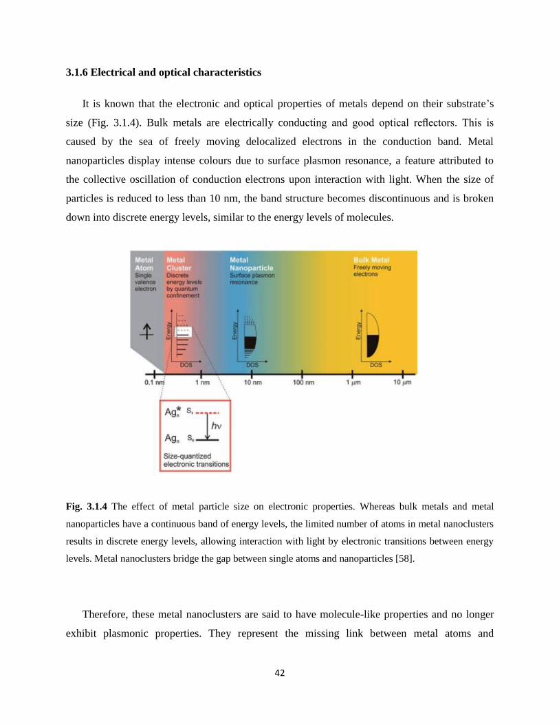
42
3.1.6 Electrical and optical characteristics
It is known that the electronic and optical properties of metals depend on their substrate’s
size (Fig. 3.1.4). Bulk metals are electrically conducting and good optical reflectors. This is
caused by the sea of freely moving delocalized electrons in the conduction band. Metal
nanoparticles display intense colours due to surface plasmon resonance, a feature attributed to
the collective oscillation of conduction electrons upon interaction with light. When the size of
particles is reduced to less than 10 nm, the band structure becomes discontinuous and is broken
down into discrete energy levels, similar to the energy levels of molecules.
Fig. 3.1.4 The effect of metal particle size on electronic properties. Whereas bulk metals and metal
nanoparticles have a continuous band of energy levels, the limited number of atoms in metal nanoclusters
results in discrete energy levels, allowing interaction with light by electronic transitions between energy
levels. Metal nanoclusters bridge the gap between single atoms and nanoparticles [58].
Therefore, these metal nanoclusters are said to have molecule-like properties and no longer
exhibit plasmonic properties. They represent the missing link between metal atoms and

43
nanoparticles. Nevertheless, metal nanoclusters can still interact with light via electronic
transitions between energy levels, resulting in intense light absorption and emission [58].
3.2 Experimental methods
3.2.1 Silver nanoparticles
In this thesis two main methods to synthesize silver nanoparticles were followed: (i) Physical
vapour deposition (top-down approach) and (ii) wet chemistry (bottom-up approach). Silver
nanoparticles are frequently described as being 'silver' although some are composed of a large
percentage of silver oxide due to their large ratio of surface to bulk silver atoms. The formation
of silver nanoparticles can be observed by a change in colour of the solution since the presence
of small silver nanoparticles makes it yellow. The silver colloidal agglomeration makes the
solution change colour to orange and grey, respectively. Fig. 3.2.1 shows the colour of solutions
depending on different nanoparticle (Nps) sizes.
Fig. 3.2.1 Silver nanoparticle solutions with different sizes and concentrations. 1: 10 nm (3.6× 10¹²
Nps /
mL), 2: 40 nm (5.7× 10¹⁰
Nps / mL), 3: 60 nm (1.7× 10¹⁰
Nps / mL) and 4: 100 nm (3.6× 10⁹ Nps / mL).
3.2.2 Materials and instruments
Silver nitrate (AgNO3, M= 169.87 g/mol), ammonium persulfate (APS) and all solvents were
purchased from Aldrich. Polyvinylpyrrolidone (PVP, M= 40.000 g/mol) was supplied by Fluka.
Aniline was distilled under reduced pressure and the other reagents were used without further

44
purification. UV–vis adsorption spectra were taken at room temperature on a Varian Carry 50
Bio, UV–vis spectrometer from 250 to 900 nm using 1 cm path length quartz cuvettes. The X-ray
diffraction patterns were taken on a Rigaku DMAX2200 using Ni-filtered Cu-Ka radiation over a
scanning range of 10–800 at an X-ray power of 40 kV and 40 mA. TEM images were obtained
with JEM-2100 electron microscope at a working voltage of 200 kV (JEOL). Samples for TEM
analysis were prepared by suspending an appropriate amount of product in acetone, casting onto
carbon-coated copper grids and drying in air at room temperature. Several samples, with
different sizes and morphologies were analysed.
In order to study the electrical behaviour, silver and gold nanoparticles were deposited on the
silicon substrates. Different methods were utilized to synthesize 6 samples of silver nano
structures (Table 3.2.1). The synthesis details will be described for each sample in the next
section. Gold nanoparticles were also obtained by chemical method.
Table 3.2.1 Summary of nanostructure samples.
Sample
Type Sample structure Synthesis method
Typical
particle size
(nm)
Electrical properties
A AgNps-PVP
partially oxidized Chemical method 10-20 nm
Reported in chapter 4
B AgNps-PVP Microwave 10 nm Reported in chapter 4
C AgNps Physical method 8-10 nm The samples were insulating
D Ag2O Nps-PVP O2 exposure of
sample A 20-35 nm
Reported in chapter 4-5
E Ag2O Nps-PVP Chemical method 10-45 nm Reported in chapter 4-5-6
F AgClNps-
PANI/PVP Chemical method 100 nm
Reported in chapter 7
Au AuNps-PVP Chemical method 25 nm Reported in chapter 4

45
(a)
Sample type A
In a typical experiment, PVP (0.2 g) was dissolved in 25 mL Dimethylformamide (DMF). An
aqueous solution of silver nitrate (0.01 M, 10 mL) was prepared and added to the PVP solution
dropwise under stirring (300 rpm) for almost 4 hours. The solution turned yellow and then to
light brown due to the presence of partially oxidized nanoparticles (<50 nm). This sample was
deposited on the silicon substrate to test the resistive switching (Fig. 3.2.2 (a)).
Fig. 3.2.2 TEM images of (a) sample A, (b) sample B.
(b)

46
Fig. 3.2.3 displays a typical diffraction pattern of nanoparticles. The discontinuous rings were
assigned to the aggregation of silver nanoparticles in clusters. The relation between this
diffraction pattern and D-spacing of silver nanoparticles is shown in table 3.2.2. All diffraction
rings are attributed to FCC.
Fig. 3.2.3 Typical SAED pattern of nanoparticles in ethanol.
Table 3.2.2 Comparison of measured D-spacings for silver nanoparticles with D-spacings for FCC silver.
Sample type B
In order to have nanoparticles with homogenous size, silver nanoparticles were obtained via
microwave assisted synthesis. 10 mL of 1% (w/v) ethanolic solution of PVP was added to 0.2
mL of AgNO3 (0.1M). After 20 s of microwave irradiation (800 watt, 2450 MHz) the solution
420 331 222 311 220 200 111 klH
0.914 0.938 1.180 1.231 1.445 2.044 2.359 Silver , Å
0.918 0.926 1.201 1.232 1.443 2.035 2.360 Silver Nano , Å

47
changed colour to yellow. PVP-stabilized Ag nanoparticles (~10 nm) are obtained. Fig. 3.2.2 (b)
shows the TEM image of the silver nanoparticles. The surface plasmon resonance (SPR) of the
solution is displayed in Fig. 3.2.4. X-ray diffraction (XRD) analysis was conducted on a glass
substrate drop coated with silver nanoparticles. A number of strong Bragg reflections were
observed which correspond to the 111 (~ 39º), 200 (~ 45º), 220 (~ 66º) and 311 (~79º) reflections
of face centered cubic silver [59] (Fig. 3.2.5), indicating that the silver nanoparticles within the
coating are crystalline.
Fig. 3.2.4 Surface plasmon resonance (SPR) from silver nanoparticle samples A (red) and B (blue).
Fig. 3.2.5 Typical XRD pattern recorded from a drop-coated film of Ag/polymer nanocomposite on a
glass substrate.

48
This sample was also deposited on a silicon substrate to investigate resistive switching
phenomena.
Sample type C
Silver nanoparticles were prepared in an ultra-high vacuum chamber (Pb <10-8
mbar) by
electron beam evaporation of Ag pellets. An effective thickness of 5.5 nm was initially deposited
with a deposition rate of 0.2 A/s on the silicon substrate. The substrate is a preformed
interdigitated Ti/Au microelectrode array, fabricated on 200 nm thermally oxidized silicon
wafers (Fig. 3.3.1). Then the samples were inserted in a glove box and were moderately annealed
at 200 oC for about 1 h to manipulate the size and the shape of the NPs. The mean size of silver
particles is 10 nm.
Sample type D
For the preparation of partially oxidized silver nanoparticles, a portion of sample A was
bubbled with oxygen for 30 min. The color of the solution turned to brown. The SPR peak
gradually shifted to a longer wavelength, with a slight broadening of the band width and a
lowering of maximum absorbance (Fig. 3.2.6).
Fig. 3.2.6 SPR of sample A (blue), sample D (green).

49
(a)
The red shift of the absorption after exposure to oxygen is attributed to the partial oxidation
of the silver nanoparticles [60]. This sample was deposited on a silicon substrate to study the
effect of silver oxide on resistive switching. Fig. 3.2.7 shows a typical TEM image of sample D.
Fig. 3.2.7 TEM images of sample D, X-ray diffraction.
Sample type E
An aqueous solution of silver nitrate (0.01 M, 10 mL) was prepared and added to the PVP
solution (0.2 g PVP dissolved in 25 mL DMF). The reaction was stirred (300 rpm) in an ambient
atmosphere for almost 3 hours. Meanwhile, 1 mL of NaOH (0.08M) was added gently (during
3h). The solution colour turned from orange to black showing particle growth. Silver particles
were also oxidized during the reaction. Fig. 3.2.8 shows SPR peaks during the reaction and the
final absorption peak at 398 nm. This sample was deposited on a silicon substrate to further
study the resistive switching. Fig. 3.2.9 shows the typical TEM image of this sample.

50
(b)
Fig. 3.2.8 SPR absorption of silver/silver oxide nanoparticles (sample E) in the course of the 3 hours
reaction.
Fig. 3.2.9 TEM images and X-ray diffraction of sample E.
Sample type F
AgNO3 (0.012 M) and aniline (0.012 M) were added to a 4% PVP aqueous solution. 5 ml of
1 M HCl aqueous solution of ammonium persulfate ((NH4)2S2O8, APS) as oxidant are dropped
into the above mixture under stirring at room temperature. The molar ratio of aniline to APS
([An]:[APS]) was 1:1. The reaction was allowed to proceed for 24 h. After that, the precipitate

51
was centrifuged and washed several times with distilled water and ethanol. The final product was
dried under vacuum at 40 ºC for 24 h. Fig. 3.2.10 shows the XRD of the silver
chloride/polyaniline (PANI) core-shell nanoparticles. This sample was deposited on a silicon
substrate. The molecular structure of AgCl/PANI was characterized by FTIR spectroscopy, as
shown in Fig. 3.2.11.
Fig. 3.2.10 XRD from Silver chloride/ polyaniline (PANI) core–shell (sample F).
Fig. 3.2.11 FTIR spectrum of AgCl/PANI core–shell composite.

52
The characteristic peaks at 1567 and 1483 cm−1
correspond to the C=C stretching of quinoid
and benzenoid rings. Absorption at 1301 and 1244 cm−1
are related to the C–N and C=N
stretching modes. Bonds at 1139 cm−1
and 805 cm−1
are attributed to the in-plane and out-of-
plane bending of C–H respectively. The absorption band assignable to C=O is observed at 1651
cm−1
, which indicates the presence of PVP.
Gold nanoparticles
Sample Au
Tetrachloroauric acid (HAuCl4·3H2O) and tri-sodium citrate, were purchased from Aldrich
and used as received. Milli-Q water was used to make up all solutions (R > 18.2 MΩ.cm). The
standard gold sol was prepared by boiling 95 mL of 2.62×10⁻⁴
M, HAuCl4 in a three neck round-
bottom vessel equipped with a cooler, and adding 5 mL of a warm sodium citrate solution (1 wt
%) to the stirred solution. The color of the final product is dependent upon the gold nanoparticles
size [61]. The reaction could be tracked via Uv-vis measurement. The final SPR curve is shown
in Fig. 3.2.12. The absorbance peak is located at 545 nm for Au nanoparticles. From this data we
can estimate that the gold nanoparticles produced in this experiment are approximately 25 nm in
diameter.
Nanoparticles were coated with PVP (10-360 kDa) by the following procedure: Gold
concentration is first obtained from the absorbance value at 400 nm in the SPR spectrum, and the
particle’s diameter estimated as stated above. From this data and using the density of gold (19.2
g.cm-3
), the number of particles and their surface area can be obtained. The quantity of PVP was
calculated assuming a ratio of 60 polymer molecules per nm2 of surface area, and the appropriate
amount was dissolved in water. The citrate solution containing the nanoparticles was centrifuged
at 3500 rpm for 90 min, the supernatant separated and the pellet re-suspended in water. The PVP
solution was added dropwise, under stirring, to this solution. The obtained PVP-coated
nanoparticle solution was again centrifuged at 3500 rpm for 90 min, the supernatant discarded,
and the pellet re-suspended in ethanol.
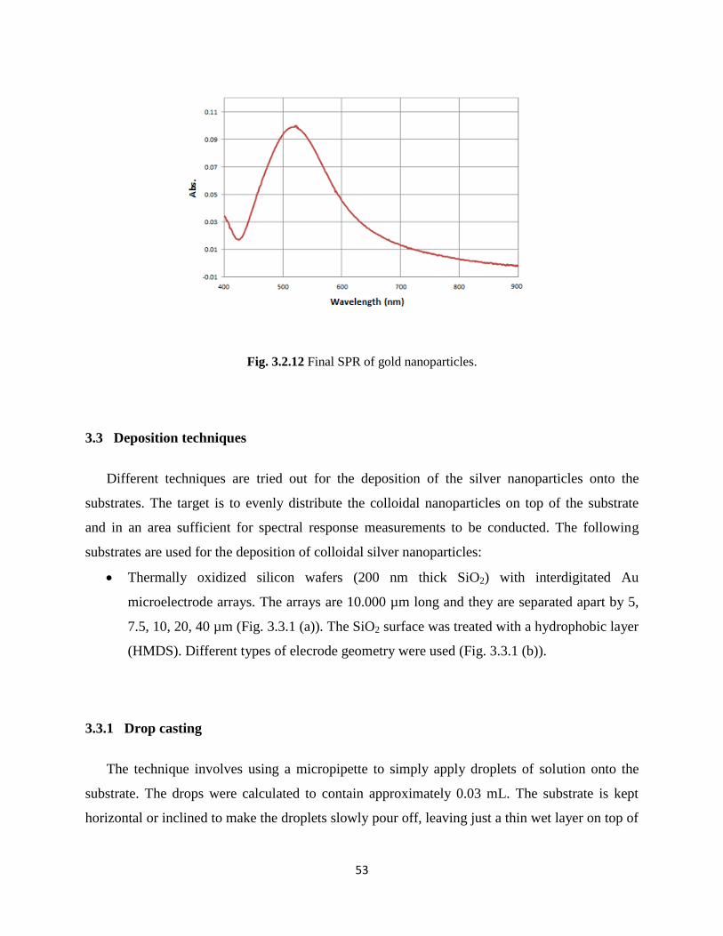
53
Fig. 3.2.12 Final SPR of gold nanoparticles.
3.3 Deposition techniques
Different techniques are tried out for the deposition of the silver nanoparticles onto the
substrates. The target is to evenly distribute the colloidal nanoparticles on top of the substrate
and in an area sufficient for spectral response measurements to be conducted. The following
substrates are used for the deposition of colloidal silver nanoparticles:
Thermally oxidized silicon wafers (200 nm thick SiO2) with interdigitated Au
microelectrode arrays. The arrays are 10.000 µm long and they are separated apart by 5,
7.5, 10, 20, 40 µm (Fig. 3.3.1 (a)). The SiO2 surface was treated with a hydrophobic layer
(HMDS). Different types of elecrode geometry were used (Fig. 3.3.1 (b)).
3.3.1 Drop casting
The technique involves using a micropipette to simply apply droplets of solution onto the
substrate. The drops were calculated to contain approximately 0.03 mL. The substrate is kept
horizontal or inclined to make the droplets slowly pour off, leaving just a thin wet layer on top of

54
the substrate. The substrates are subsequently left to dry. The deposition was most often
performed 3 times and with a quick N2 flush in between the steps in some of the cases.
Fig. 3.3.1 Different types of electrode arrays on top of thermally oxidized silicon wafer (200 nm thick
SiO2).
3.3.2 Boil deposition
When drops of colloidal silver dry on a surface, they tend to leave dense, ring-like deposits
covering only tiny fractions of the deposited area, even though the nanoparticles were initially
dispersed over the entire drop [62]. A solution to overcome this problem for larger area
depositions has been proposed to be by the use of a boiling process, previously demonstrated on
several substrates, including silicon [63]. In the present work, this is performed by depositing
colloidal silver on preheated silicon wafers and leaving it for the liquid to boil off. To get a stable
substrate temperature, the wafers were left on the heater (70 C) for several minutes before the
deposition was performed. A dropper was used to apply the drops. Each drop was calculated to
contain approximately 30 µL of silver sol. The substrates were removed rapidly from the heating
element as soon as all of the solvent had evaporated.
3.3.3 Dip coating
Dip coating is carried out by dipping the substrate into the sol followed by slowly pulling the
substrate back out. Both the pull rate, viscosity of the dispersing liquid, the size and adhesion

55
properties of the particles are expected to influence how the particles are deposited and
distributed on the substrate subsequently. Further experiments are performed after the substrate
is dry.
3.3.4 Spin coating
Spin coating can offer a rapid method of depositing thin films from solutions and is widely
employed in industry for the deposition of photoresists. Typically, a few drops of solution are
placed on to the surface of the substrate, the initial amount of solution having little effect on the
final film properties. The substrate is then rotated at several thousand rpm. The final film
properties are determined by the nature of the sol, e.g., the viscosity, drying rate, solides
percentage, surface tension, etc., but it also depends on the spin process parameters such as
rotation speed, acceleration, etc. For example, higher spin speeds, longer spin times and lower
solution viscosity are factors giving thinner films. In this thesis, the spin coating and drop casting
have been applied for all devices.
3.4. Advantages and disadvantages of planar diodes
All devices based on nanoparticles are capacitor like sandwich structures, which often use
reactive metal electrodes such as Al. This makes it extremely difficult to clarify where the
physical phenomenon of resistive switching is located. The strategy of this work is to fabricate
planar structures. The planar structures are symmetric and the electrodes used are gold electrodes
(Fig. 3.4.1). In this way, the role of the electrode is nullified. In particular, the possible migration
of atoms from the electrodes, and oxidation was prevented. This means that the resistive
switching must only be applied to bulk properties. Furthermore, the channel is exposed and
accessible to surface analytical techniques, as will be discussed later. On the other hand, a planar
devices must be kept in a high vacuum during measurement, and it can be contaminated easily
due to its exposed surface. In this thesis, drop on and spin coating processes were utilized to

56
make the devices ready. Typical AFM images of some samples are shown in Fig. 3.4.2 and Fig.
3.4.3.
Fig. 3.4.1 (a) Schematic diagram of PVP capped silver nanoparticles between interdigitated Au
microelectrode arrays, fabricated on thermally oxidized silicon wafers, (b) TEM image and X-ray
differaction of PVP capped silver nanoparticles.

57
Fig. 3.4.2 (a) Typical AFM image of PVP capped silver nanoparticles based diode type-B (b) Image of
diode type-C (silver nanoparticles were prepared by electron beam evaporation), interdigitated Au
microelectrode arrays, fabricated on thermally oxidized silicon wafers.
(a)
(b)

58
Fig. 3.4.3 (a) Typical AFM image of PVP capped silver nanoparticles based diode type-E (b) Typical
AFM image of diode type-Au.
(a)
(b)

59
“I have not failed. I've just found 10,000 ways that won't work!” Thomas A. Edison
CHAPTER 4 -The effect of ambient atmosphere on resistive switching
In this chapter, the effect of ambient atmosphere on the electrical properties of planar diodes
is studied. Diodes were fabricated using two types of metal nanoparticle, Ag and Au. For the
same diode structure two different resistive switching shapes are observed, which correspond to
the extrinsic and intrinsic switching phenomena. The extrinsic resistive switching usually
happens in air. The operating mechanism is redox mediated by moisture. An N2/H2O exposure
experiment proved this assumption. The intrinsic resistive switching occurs in a high vacuum. It
starts with the electroforming process. This type of switching is reliable and non-volatile.

60
4.1 Introduction
In this chapter we look at the effects of ambient atmosphere on resistive switching behaviour.
It is observed that electrical characteristics are strongly dependent on the presence of moisture.
In ambient air, the I-V curves have a shape which is known as an S-shape in the literature. In
contrast, under vacum conditions the I-V curve is N-shaped.
This chapter starts by introducing the types of I-V curves. Later, it provides clear evidence
showing that an S-shape I-V chracteritics is an artifact caused by the presence of moisture.
Types of current-voltage characteristics
I-V characteristics published can be grouped into one of two general shapes, namely, N-shape
and S-shape. N-shape characteristics (illustrated in Fig 4.1.1) are typified by a high current up to
a certain threshold voltage (VT) (region 1). If the voltage is then reduced, the device stays in this
high conductivity state. However, if voltages higher than VT are applied, a phenomenon known
as negative differential resistance (NDR) occurs, where an increase in voltage leads to a
reduction in current (region 2). Voltages higher than the NDR region return the device to its low
conductivity state. The I-V characteristics are symmetrical.
Fig. 4.2.1 Schematic representation of N-shape I-V characteristics.
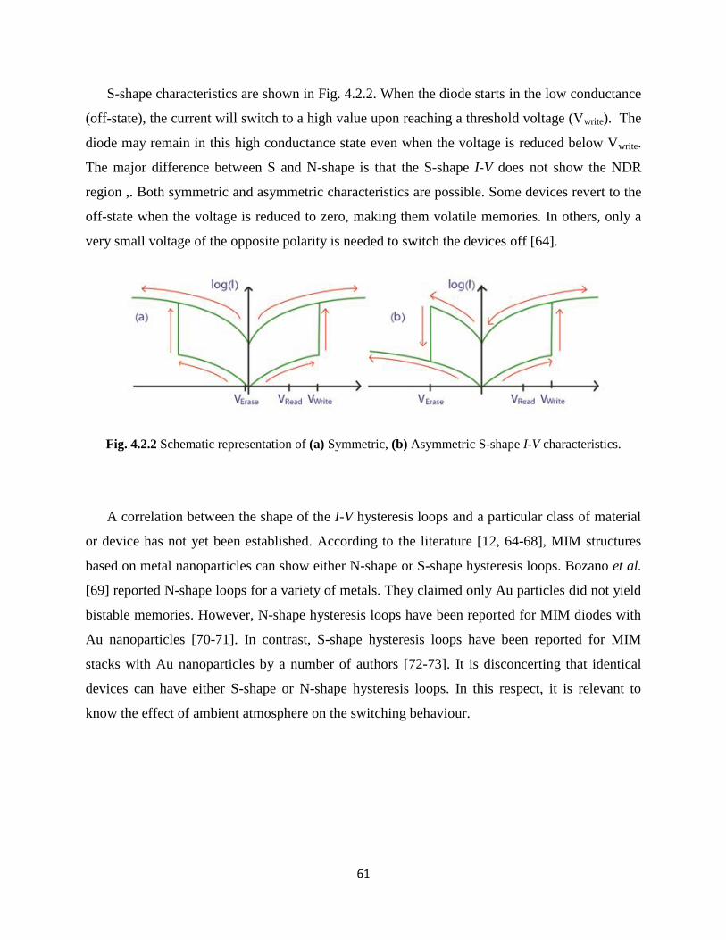
61
S-shape characteristics are shown in Fig. 4.2.2. When the diode starts in the low conductance
(off-state), the current will switch to a high value upon reaching a threshold voltage (Vwrite). The
diode may remain in this high conductance state even when the voltage is reduced below Vwrite.
The major difference between S and N-shape is that the S-shape I-V does not show the NDR
region ,. Both symmetric and asymmetric characteristics are possible. Some devices revert to the
off-state when the voltage is reduced to zero, making them volatile memories. In others, only a
very small voltage of the opposite polarity is needed to switch the devices off [64].
Fig. 4.2.2 Schematic representation of (a) Symmetric, (b) Asymmetric S-shape I-V characteristics.
A correlation between the shape of the I-V hysteresis loops and a particular class of material
or device has not yet been established. According to the literature [12, 64-68], MIM structures
based on metal nanoparticles can show either N-shape or S-shape hysteresis loops. Bozano et al.
[69] reported N-shape loops for a variety of metals. They claimed only Au particles did not yield
bistable memories. However, N-shape hysteresis loops have been reported for MIM diodes with
Au nanoparticles [70-71]. In contrast, S-shape hysteresis loops have been reported for MIM
stacks with Au nanoparticles by a number of authors [72-73]. It is disconcerting that identical
devices can have either S-shape or N-shape hysteresis loops. In this respect, it is relevant to
know the effect of ambient atmosphere on the switching behaviour.

62
4.2 The effect of ambient atmosphere on electrical characteristics
4.2.1 Electrical measurements.
Electrical measurements were carried out using a Keithley 487 picoammeter/voltage source.
During the measurements the silicon substrate is kept grounded to avoid a charging process from
the silicon. Then, the voltage was applied from two gold electrodes (two terminal measurement).
Under the same circuit, in each measurement, quality of the substrate with insulating polymer
(PVP) was tested before the deposition of the matrix with nanoparticles to make sure that the
silicon was not playing a role in any of the characteristics. In all cases, there was a high quality
insulating layer and it was ensured that there was no possibility of conduction through the silicon
from the planar diodes structure. Fig. 4.2.1 shows the current-voltage characteristics of a device
with a thin layer of PVP. The schematic of the electrical connections is depicted in the insert of
Fig. 4.2.1. The I-V characteristics show that the PVP layer behaves as an insulator in the voltage
range [-50, 50] V.
Fig. 4.2.1 I-V characteristics of a SiO2 substrate coated with a thin film of PVP. The resistance is
approximately 0.5 TΩ under an applied voltage of 50 V. The measurements were made under vacuum.
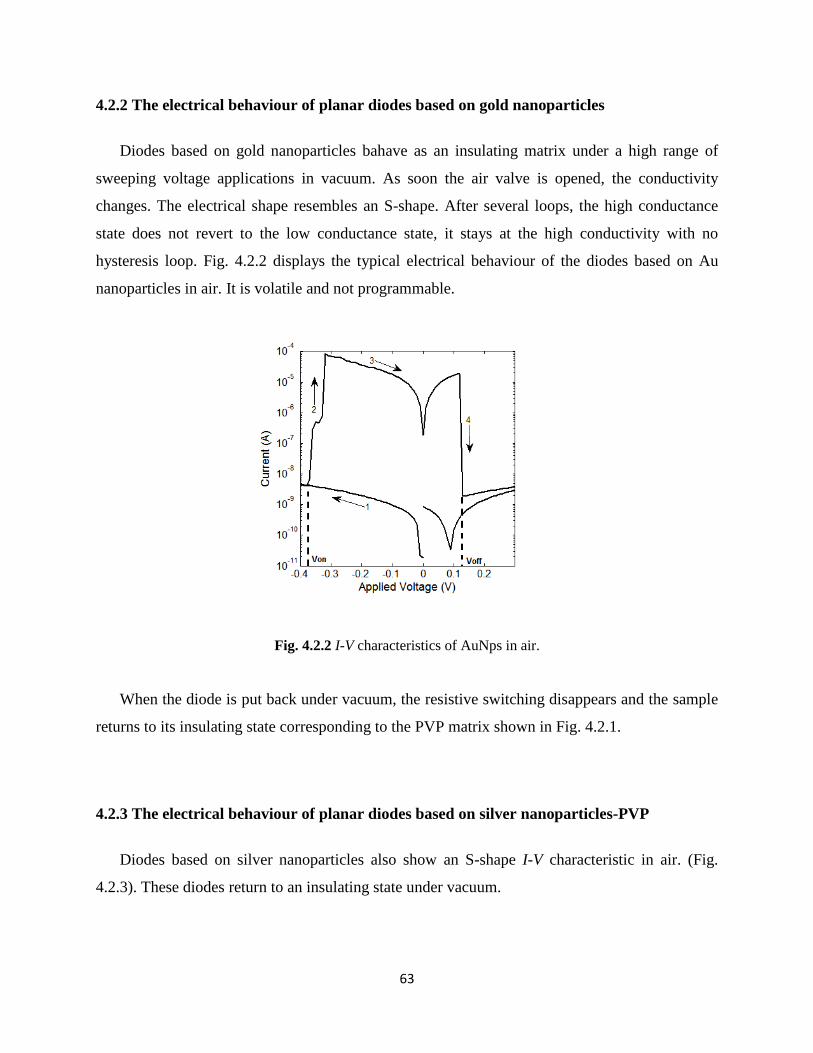
63
4.2.2 The electrical behaviour of planar diodes based on gold nanoparticles
Diodes based on gold nanoparticles bahave as an insulating matrix under a high range of
sweeping voltage applications in vacuum. As soon the air valve is opened, the conductivity
changes. The electrical shape resembles an S-shape. After several loops, the high conductance
state does not revert to the low conductance state, it stays at the high conductivity with no
hysteresis loop. Fig. 4.2.2 displays the typical electrical behaviour of the diodes based on Au
nanoparticles in air. It is volatile and not programmable.
Fig. 4.2.2 I-V characteristics of AuNps in air.
When the diode is put back under vacuum, the resistive switching disappears and the sample
returns to its insulating state corresponding to the PVP matrix shown in Fig. 4.2.1.
4.2.3 The electrical behaviour of planar diodes based on silver nanoparticles-PVP
Diodes based on silver nanoparticles also show an S-shape I-V characteristic in air. (Fig.
4.2.3). These diodes return to an insulating state under vacuum.

64
Fig. 4.2.3 I-V characteristics of AgNps-PVP based device in air.
The I-V characteristics of diodes based on silver oxide nanoparticles are shown in Fig. 4.2.4
(a). At a negative voltage, Vt, of -9 V, a sudden increase in current occurs to the high
conductance on-state. With the voltage scanning back towards zero, the diode remains in the on-
state down to near 0 V, where it suddenly switches back to the low conductance off-state. The
Fig. 4.2.4 Current-voltage characteristics (a) symmetric and (b) asymmetric S-shape, of silver oxide Nps-
PVP (silver-PVP) planar diode (L: 10 µm).
(a) (b)

65
I-V curves are symmetrical. This S-shape I-V curve is always observed when the diodes are
measured in air. Variations are possible: sometimes, the diode remains in the on-state even after
passing through 0 V and only returns back to the off-state after applying an opposite bias, which
is shown in Fig. 4.2.4 (b). Although this behaviour resembles a bipolar type of switching, the
voltage where it returns to the off-state fluctuates substantially between 0 and -7 V, suggesting
that the reverse voltage does not play a significant role to turn off the conductance. The retention
time of this on-state can reach two hours, as shown in Fig. 4.2.5.
Fig. 4.2.5 Retention time for both on and off states of a silver-PVP planar diode (L: 10 µm) in air.
When the same diodes are measured under vacuum, the switching behaviour is completely
different. Initially, the diodes are insulating. A voltage ramp up to 50 V has to be applied before
the diode becomes a bistable switch. When compared to the 9 V applied in S-shape switching, it
is clear that a substantially higher voltage is necessary to induce switching. This step corresponds
to an electroforming process. The electroforming will be explained in detail in chapter 5. The
electroforming cannot be observed in air because the diode resistance switches well below the
forming voltage. Fig. 4.2.6 displays the final electroformed loop. The insulating state before
electroforming is called pristine-state. After the electroforming the diode shows sharp transitions
of electrical resistance. The high conductance on-state exhibits a symmetrical NDR regions
located around |35| V, as shown in Fig. 4.2.7. The switching biases are indicated as Von and Voff.
A pulse near Voff, i.e. at the bottom of the NDR, will bring the diode to the lower current flow.
off-state
on-state

66
The high conductance I-V curve is restored by using a pulse near Von, i.e. at the top of the
NDR, typically at 32 V as shown. This switching behaviour is usually referred to as N-shape.
Fig. 4.2.6 Pristine-state and the final electroformed loop of a silver-PVP planar diode (L: 10 µm) under
vacuum.
Fig. 4.2.7 (a) I-V characteristics showing the on-state of a silver-PVP planar diode (L: 10 µm) under high
vacuum (10-5
Torr).

67
The on/off states retain their programmed conductance states without bias for at least a
month, as long as they are stored under vacuum. Fig. 4.2.8 shows that once the diode is
programmed into a certain state, it can reliably read-out many times without degradation. Data
retention is also excellent for both memory states, as shown in Fig. 4.2.9. The N-shape switching
is similar to the one reported for metal/oxide based memories [74], which require electroforming
and exhibit unipolar programming voltages.
Fig. 4.2.8 Endurance sweep cycles for a silver-PVP planar diode (L: 10 µm), in a high vacuum (10-5
Torr): Write: 30 V, Erase: 50 V, and Read: 3 V. The on/off ratio is 4 orders of magnitude.
Fig. 4.2.9 Retention time for both on and off states of a silver-PVP planar diode (L: 10 µm) in a high
vacuum (10-5
Torr).

68
4.3 The effect of channel length (L)
In addition to the I-V characteristics, S-shape and N-shape switching can also be compared in
terms of the voltage required to program the on and off-states. Table 4.3.1 shows that with
different channel lengths, various voltages are required to turn the device from the off to the on-
state, and the turning-off voltage is also channel length dependent. Fig. 4.3.1 displays the
switching voltage dependence on channel length (L). S-shape switching fluctuates for identical
samples in the voltage range of 5-8 V, and it is almost insensitive to change in channel length.
(Insert in Fig. 4.3.1).
Table 4.3.1 Programing voltage process of the N-shape characteristics for different channel lengths (L).
For N-shape switching, the programming voltage changes from 13 V up to 130 V, as the
channel length increases from 5 µm to 40 μm. This noticeable difference in the magnitude of the
switching voltage suggests that the associated mechanisms are different. Unipolar programming
voltages observed for N-type switching are in line with an oxide based resistive switching
mechanism, as mentioned earlier on. Switching in ambient air at low voltage (S-shape) could be
compatible with electrochemical reactions.
Furthermore, in order to clarify the role of atmosphere on diode function, a gas exposure
experiment was conducted as well. A diode based on AgNps-PVP (L: 10 µm) was mounted in a
chamber connected to N2 and O2 gas containers which was pumped for an hour to reach a high
L (µm) Von (V)
Voff (V)
5 13 17-20
10 35 47-50
20 70 82-85
40 127 135-138

69
Fig. 4.3.1 Channel length dependence of the threshold voltage for switching from the off-state to the on-
state for N- and S-shape switching.
Fig. 4.3.2 Current state at 3 V under N2/H2O gas exposure for a AgNps-PVP diode (L: 10 µm).

70
vacuum (10 -5
Torr). The electrical behaviour was tested on the same electrical set up (see
section 4.2) after individual exposure to N2 and O2 gases. The voltage application during the
whole measurement was 3 V. The diode responded as an insulating matrix in both ambients. In
another experiment, the nitrogen flux was passed through a water container prior to entering the
chamber. The electrical behaviour of the diode in each period of N2/H2O exposure time (~ 450
sec) is represented in Fig. 4.3.2. As can be seen, the diode reacts as a kind of humidity sensor. It
is concluded that water mediates redox reactions.
4.4 Discussion
The effect of ambient atmosphere to form S-shape switching is closely connected to the role
of water. Previous works have also shown that the presence of moisture is an important issue.
Tanaka [75] claimed that adsorbed water is essential to restore conducting filaments in silver thin
films. Kimura et al. [76] also reported that S-shape resistive switching needs moisture and was
observed in room air or wet nitrogen gas, but not under vacuum or dry gases such as nitrogen,
oxygen, and argon, even at reduced pressure. It is shown that, as the relative humidity is
decreased, the resistance of the on-state increases and the threshold voltage reduces, whereas the
off-state is changed very little. Diffusion of hydronium ions along with silver ions was necessary
to establish Ag filaments which has been explained as follows: in atmospheres containing more
moisture, the filamentary paths contain more hydronium ions and therefore, need more power to
vaporize these filaments by joule heating. In another contribution, for encapsulated Cu/P3HT/Au
junctions, Knorr et al. [77] reported that water is field-adsorbed and assists in the dissolution of
copper ions to form copper sulfide crystals, which may be an important precursor to filament
formation. Recently, Guo et al. [78] showed that water plays a crucial role in the growth and
electrochemical dissolution of Ag dendrites. Water mediates the following reaction:
Ag+
(aq) + e-→ Ag (s) (1)
Upon application of a voltage, Ag+ ions migrate and are reduced upon contact with the
electrode resulting in the growth of metallic Ag dendrites. The diode switches on when a
71
continuous path along the dendrites is established. Switching off is caused by a fast retreating of
the dendrite at the neck where the dendrite contacts the electrode surface. The curvature
difference between the dendrite and the planar metal electrode in their system constitutes the
reason for the bipolar switching observed [88]. Alternatively, water itself can also contribute to
electrical conduction. Surface-conductivity measurements on SiO2 suggested that protons (H+)
that are electrolytically produced from adsorbed water can act as charge carriers [75-76]. On
applying a bias, oxidation of water occurs, producing excess protons in the reaction:
(2)
In the absence of bias, H+ will recombine with negative species in the surrounding
environment and eventually will shut-down the conducting state.
4.5 Conclusion
In this chapter, it is explained that for the same diode structure two types of resistive
switching I-V shapes can occur, depending on the ambient atmosphere: S- and N-shape. The S-
shape electrical characteristics are only observed in air. The operating mechanism is redox
mediated by moisture. The N-shape I-V characteristic is the intrinsic resistive switching that
occurs in a high vacuum. It starts with the electroforming process. This type of switching is
reliable and non-volatile.
H2O (l) 2 H+ (aq) + 2 e- + 1/2 O2 (g)

72
“The important thing in science is not so much to obtain new facts as to discover new ways of
thinking about them.” William Lawrence Bragg
CHAPTER 5 - Electroforming
Electroforming is a process by which an insulating material is turned into a resistive
switching memory. The diode is submitted to an electric field that induces a dielectric soft-
breakdown during which electronic defects are created. These defects trap electronic charges and
create a percolation network of conducting filaments across the diode. In this chapter a model is
proposed to explain how conducting filaments can be formed in a nanostructured memory
device.

73
5.1 Introduction
The word forming or electroforming came into use to describe the process by which the
conductivity of the insulating state of the material (termed here as pristine state) is altered when a
sufficiently high electric field is applied. It can be done by applying a voltage or a current stress.
This process is required to obtain electrical bistable characteristics.
Electroforming in metal oxides and polymeric insulators were investigated by a number of
authors [79-80]. It is generally accepted that electroforming leads to the formation of a
percolation network of conducting filamentary paths across the material. How these filaments are
created is still under debate. Among the models proposed are (i) redox processes [81], (ii)
migration of metal from the electrodes [82-84], (iii) formation of carbonaceous material from the
insulator itself, or from sources of contamination introduced during the fabrication of the devices
[85-86], and (iv) dielectric soft-breakdown (SBD) [87-88]. Electroforming is usually irreversible.
Although it is often claimed that electroforming procedures play a crucial role in the final
memory properties, a clear correlation between electroforming and resistive switching behaviour
has not yet been thoroughly investigated. Electroforming is associated with two processes: (i)
dielectric breakdown and (ii) percolation-conduction. Therefore, we provide a brief introduction
to these concepts.
Dielectric soft-breakdown
The dielectric soft-breakdown is generally accepted to be due to material degradation and
accumulation of defects inside the insulating system [89]. Although several physical models
have been proposed to explain the origin of these defects, there is still no agreement on the real
cause of defects. Different authors have reported quantum tunnelling as a model to explain soft
breakdown I-V characteristics. Among all reports, the most accepted tunnelling models are direct
tunnelling [90] and trap-assisted tunnelling [91]. In direct tunnelling, breakdown can be the
result of a progressive degradation of a localized region close to the anode interface and a
decreasing of effective thickness at that region. Therefore, the insulation is thinning at the
physically damaged region, and direct tunnelling of carriers through the thin localized damage
region is the origin of soft-breakdown [90]. Trap-assisted tunnelling (TAT) is via the neutral trap

74
sites inside the insulating matrix. In this model it is believed that the neutral trap sites are
generated during high field stress, and capture and emission of charge carries in these trap sites
cause the leakage current.
Percolation
One of the best ways to understand “percolation” is to know its difference from the well-
known transport mechanism “diffusion”. An example of diffusion is the motion of one molecule
in a gas, as scattered by other molecules. The soaking of a fluid into a porous medium can be
considered a good example of the percolation process. Diffusion, such as the moving of
molecules through a gas, is a “memory-less” random process [92]. It means that, when the gas is
sufficiently dilute, the last collisions do not have an effect on the current scattering. Percolation,
however, has memory effects. Meaning that the random scattering of the particles in the fluid
must be treated as a property of the medium. Fig. 5.1.1 shows a one-dimensional random walk
(RW) which is a good illustration of the difference between percolation and diffusion [93]. When
the random mechanism is assigned to the fluid particles, a particle steps to the left or right with
equal probability but randomly. The result is that, as shown in Fig. 5.1.1 (a), the particle will
visit every lattice point if the process is allowed to continue indefinitely. This is a diffusion
process. On the other hand, Fig. 5.1.1 (b) illustrates the case when the random mechanism is
assigned to the medium of the lattice points. Suppose that the lattice points are initially assigned
with squares randomly but with different probability on the directions of the squares (black:
forward, white: backward). The direction of the steps of the particle at a certain lattice site is
agreed to be the direction of the square associated to the lattice point. It will be drastically
different from that of the previous process. The particle would get trapped somewhere and could
not visit every lattice point. This could be the case of percolation [92, 94]. Percolation was
originally studied as a mathematical subject but its broadest applications are found in the field of
materials research [5]. Percolation is one of the simplest models which explains phase
transitions. The most interesting topic in the area of phase-transition is the metal-insulator
transition. It strongly suggests that the metal-insulator transition is connected to microscopic
restructuring inside the system, and is a percolation transition between two phases [95-96].
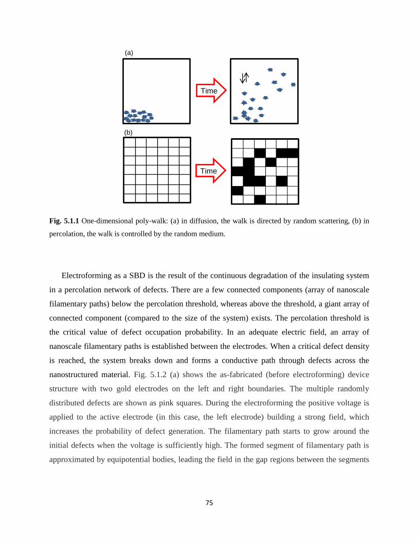
75
Fig. 5.1.1 One-dimensional poly-walk: (a) in diffusion, the walk is directed by random scattering, (b) in
percolation, the walk is controlled by the random medium.
Electroforming as a SBD is the result of the continuous degradation of the insulating system
in a percolation network of defects. There are a few connected components (array of nanoscale
filamentary paths) below the percolation threshold, whereas above the threshold, a giant array of
connected component (compared to the size of the system) exists. The percolation threshold is
the critical value of defect occupation probability. In an adequate electric field, an array of
nanoscale filamentary paths is established between the electrodes. When a critical defect density
is reached, the system breaks down and forms a conductive path through defects across the
nanostructured material. Fig. 5.1.2 (a) shows the as-fabricated (before electroforming) device
structure with two gold electrodes on the left and right boundaries. The multiple randomly
distributed defects are shown as pink squares. During the electroforming the positive voltage is
applied to the active electrode (in this case, the left electrode) building a strong field, which
increases the probability of defect generation. The filamentary path starts to grow around the
initial defects when the voltage is sufficiently high. The formed segment of filamentary path is
approximated by equipotential bodies, leading the field in the gap regions between the segments
Time
Time
(a)
(b)

76
stronger [97]. The Dijkstra shortest path algorithm [97] allows us to visually identify the most
conductive percolating filamentary paths in the system.
Fig. 5.1.2 (a) As-fabricated state of the region (pristine-state), with the defects randomly distributed in an
initial configuration (pink dots). (b) Percolation nanoscale filamentary paths after the electroforming [97].
This chapter is organized as follows: after this introduction, we start show the procedures
used to electroform the diodes. The principal differences observed between the electroforming
characteristics and the ones reported in the literature are highlighted. XRD data is also presented
to gain insight into chemical changes occurring during forming. Then the experimental results
are discussed in the context of the models available in the literature. Particular attention is
devoted to the percolation transport. The similarities between forming reported for oxide based
RRAMs and the one reported here is discussed in detail. Finally, the major findings are
summarized in the conclusions.
5.2 Experimental: Electroforming in systems with silver nanoparticles
As-fabricated diodes based on PVP embedded silver nanoparticles are insulating, showing
typical resistance of ~188 Gῼ in a high vacuum. In order to obtain memory characteristics, a
voltage ramp has to be applied. Fig. 5.2.1 shows several typical current-voltage characteristics of

77
the pristine state recorded for increasing voltage ranges. The hysteresis loops are typical of pure-
capacitor behaviour: the current is mostly displacement current. The successive application of
increasing voltage ramps causes a degradation of the electrical insulation properties. Then, after
a few cycles, a severe degradation of the insulating properties or a dielectric breakdown occurs.
Fig. 5.2.1 Current-voltage characteristics of a diode prior to electroforming. The hysteresis loops are
typical of a capacitor like behaviour. Channel length L: 10 µm. Voltage ramp speed is 0.1 V.s-1
.
Fig. 5.2.2 shows a typical example. For voltages above 20 V the current rises, first gently,
and then near 47 V an abrupt increase in current occurs, it rises by more than two orders of
magnitude. In the return path, the current is now extremely noisy, showing current fluctuations
that can reach to several µA. After this breakdown the I-V curve is rather peculiar. In the low
voltage range near the origin [-10, 10 V] it is noiseless and follows approximately an Ohmic
behaviour. For voltages above |10V| it becomes noisy and the higher the applied voltage the
lower is the overall current, showing clearly a voltage region with a negative differential
resistance (NDR). Although the diode no longer behaves as a capacitor, the resistance is still
relatively high (4 M), therefore this electroforming process does not cause a hard breakdown.
The required voltage to cause a permanent change in the electrical conduction and electrical
bistability is termed forming voltage (Vforming).

78
Fig. 5.2.2 Current-voltage characteristics of a diode during electroforming. Channel length (L) is 10 µm.
The inset shows the Vforming for different channel lengths (L: 5 µm, 7.5 µm, 10 µm, 20 µm, 40 µm. (5
devices were measured for each L).
As expected, the voltage increases with the channel length following approximately a linear
relationship. The inset of Fig. 5.2.2 shows Vforming for different channel lengths. The required
electric field to induce electroforming is typically 4×10⁶
V/m. For channel lengths of 40 µm
Vforming is somehow smaller than expected. The reason for this deviation is not clear. Reported
forming voltages in the literature are usually much higher and close to the dielectric breakdown
field of the materials used. For instance, for Al2O3, the forming voltage is close to 109 V/m. In
the discussion section a possible reason for this discrepancy will be presented.
After performing a few I-V loops the noise behaviour softens and gives rise to stable I-V
characteristics with symmetrical negative differential resistance regions. This state corresponds
to the red curve in Fig. 5.2.3. Then, the diode behaves as a memory and can be programmed
between a high conductive and a low conductive state using voltage pulses below and above the
NDR region respectively.

79
Fig. 5.2.3 I-V characteristics of the on and off states of a diode with silver nanoparticles, L: 10µm.
The low conductive state is the black I-V curve shown in Fig. 5.2.3. Although electroforming
is usually performed by voltage ramp sweeps with increasing voltage, as described earlier, it can
also be achieved by submitting the diode to an electric field for long periods of time. Fig. 5.2.4
shows a typical example. The diode is submitted to a constant applied voltage of 15 V. After 4
minutes, a discrete and sharp increase in current is observed. This is followed by other step
increments in the current. After 15 minutes the current increases by four orders of magnitude.
This process leads also to the noisy I-V curves with NDR and to bistable current-voltage
characteristics. It confirms that electroforming is not a spontaneous process at some critical field,
but an upsurge process resulting from stress-induced defects. This behaviour is typical of a
dielectric breakdown process commonly observed in oxides. Indeed, dielectric breakdown is not
only caused by the electric field, but is strongly dependent on the time the electric field is
applied. Low electric fields can also cause dielectric breakdown if applied for longer times. The
successive increments in current shown in Fig. 5.2.4 are recognized in the literature as dielectric
soft-breakdown (SBD) [98].
In this thesis, electroforming was carried out using voltage ramps. This method produced
more reliable memory characteristics. Electroforming under constant applied voltage did not
always lead to bistable electrical characteristics. The reason is still not clear.

80
Fig. 5.2.4 Evolution of the current under a constant applied voltage (V=15 V) for a diode with L= 5 µm.
In order to inspect for changes induced by the electroforming process in the chemistry and
microstructure of the PVP/silver oxide nanoparticle matrix, the samples were analyzed using X-
ray diffraction (XRD). Fig. 5.2.5 shows three different XRD diffractograms, corresponding to (a)
the silicon wafer substrate, (b) the diode in the pristine state (i.e. right after deposition), and (c)
after electroforming. The XRD spectrum recorded after electroforming shows clearly a
significant number of additional structures, most of them directly assigned to different phases of
silver oxide present, e.g., AgXO and Ag2O. Silver mix-valence (AgXO) becomes prevalent at the
electroformed state. This suggests that electroforming causes some structural changes in the
silver oxide nanoparticle/polymer matrix. XRD data show clear evidence of the presence of
deficient silver oxide species. According to literature, there is a variety of silver oxide species
and AgXO being(also written as AgIAg
IIIO2) of prime importance. There are indeed two types of
silver ions in AgXO. One, presumably Ag(III), being four-coordinated (square oxygen
coordination) and the other, two-coordinated (linear oxygen coordination), as shown by both X-
ray and neutron diffraction techniques [99]. The electrical conductivity of different oxide species
is also remarkably different. It has been reported that, whereas the resistivity of Ag2O is 108
Ω.cm, a sample of approximate composition AgXO has a resistivity of only 10 Ω.cm.

81
Fig. 5.2.5 XRD patterns for the empty silicon oxide substrate (black), pristine state (blue), and
electroformed state (red).
It is well-known that almost all the non-stoichiometric metal oxides are n-type transparent
conductors. However, the origin of p-type conductivity in non-stoichiometric silver sub oxide
thin films has been explained in the literature as well [100]. It is clear that holes are formed if
there is localization of covalent bonds in the material. The bonding between silver and oxygen is
partially ionic, and it is possible to calculate partial ionic charges on the various oxides of silver.
With the theory and empirical formulation proposed by Sanderson [100], calculations of the
partial ionic charge of silver in Ag2O, and AgXO yields 41 and 32%, respectively. Therefore,
there is a possibility of localization of the covalent bonds in these silver sub oxide thin films. The
localization of the oxide ions gives rise to the p-type nature of the conduction. If the density of
these localized states is considerably large in the film, the holes appear as majority carriers
showing only p-type conduction.
In order to clarify the role of silver oxide nanoparticles in the electroforming mechanism,
diodes with only a thin film of PVP (without nanoparticles) were prepared. These diodes were

82
submitted to the typical electroforming procedures described above. Fig. 5.2.6 shows a typical
behaviour observed for a PVP based diode. In the voltage range [-100, 100 V] the diode behaves
as a pure capacitor (see blue curve in Fig. 5.2.6). Since this device has a 5 µm channel length,
100 V corresponds to the application of an electric field of 20×106
V/m, 5 times higher than the
4×10⁶
V/m required to electroform the diodes with PVP/silver oxide nanoparticles. In the next I-
V curve the voltage was ramped up to [-120, 120 V]. In the negative region the diode stands the
maximum field of 24x106
V/m, however in the positive return path, the diode suffers a dielectric
breakdown near 60 V. The current has increased by almost three orders of magnitude. This
change is irreversible and does not lead to memory properties. Electrical bistability is only
observed when silver oxide nanoparticles are present in the system. This observation points
towards the general view that electroforming is a property of oxides. In this context, it is also
relevant to mention that we cannot observe electroforming if gold nanoparticles are used.
Fig. 5.2.6 I-V characteristics of a diode fabricated with only a PVP layer. (a) Blue curve is the first
measurement, and black curve is the second measurement. Dielectric breakdown occurs in the return path.
The measurements were carried out under vacuum for a diode with a channel length of 5 µm.

83
5.3 Discussion
The silver oxide-PVP matrix is insulating. Under the application of an electric field (~ 4
MV/m), it undergoes an electroforming process and turns into a resistive switching memory
(RRAM). Electroforming is commonly reported for memory devices based on binary transition
oxides or on polymer/oxide bilayers, but not for nanoparticle based RRAMs. We believe the
reason for that lies in the fact that these structures are usually too thin, typically 50 nm thick,
fabricated in a sandwich configuration. For example, when the thickness of the layer is 50 nm,
the required forming voltage should be around ~ 2 V (assuming they require a similar electric
field as in our planar diodes). Therefore, an I-V curve in the range [-8, 8 V] will immediately
electroform the sandwich MIM structure. It is possible that electroforming will not be noticed or
be misinterpreted as a resistive switching transition [11].
In agreement with recent views, electroforming is a soft breakdown mechanism, where Joule
heating is kept low to prevent local thermal damage. This process creates a percolation network
of defects and corresponding filamentary current paths. These current paths can be then turned
on and off under an electric field. This forms the basis of a resistive switching memory.
The interesting aspect of our findings is that the forming electric field is two orders of
magnitude lower than the values reported for oxide based memories. The reason must reside in
the nanoparticles. Next, we will discuss the physics behind this low forming field.
In a matrix containing a uniform distribution of oxide nanoparticle dielectric, the dielectric
breakdown shows some interesting features. In reality, the system is nanostructured: there are
oxide regions separated apart by thin polymer regions. Dielectric breakdown may occur first into
two adjacent oxide regions. When this occurs the two nearby regions become electrically
shorted. It causes an effective decrease of the total channel length and the effective applied
electric field increases. This rise in the electric field may force other nearby regions to undergo
dielectric breakdown. This process will continue in an avalanche-like or domino effect until a
continuous path is established across the electrodes. We may conclude that in a nanoparticle
system, dielectric breakdown is then comprised of a myriad small dielectric breakdown event.
These small breaks propagate until a conducting path is established across the entire device. The
required field to electroform is then the field to initiate the small breakdown event between two

84
adjacent regions. This process can be triggered with a lower electric field than the one estimated
based only on the physical distance between electrodes.
Electroforming gives rise to a network of conducting paths across the diode. This percolation
network must be comprised of (i) permanent or long lived paths, the ones responsible for the
background current after forming or the off-state, (ii) conducting paths that can be turned-on and
-off with the applied bias, which are responsible for the NDR region and for the memory
conducting states, and (iii) small paths that blink (turned on and off intermittently) generating
current fluctuations or noise. Fig. 5.3.1 shows a schematic of a view of the network of paths for
different conductivity states of the memory.
Fig. 5.3.1 Schematic diagram of the three different types of filaments established upon electroforming.
Permanent paths (bold green), programmable paths (narrow green) and paths that turn on and off
intermittently or blink (red), (a) during initial forming loops, (b) last forming loops (c) in the on-state,
(d) in the off-state, (e) in the lowest off-state.
Percolation current paths
It is important now to discuss the physical nature of these conductive paths. From the XRD
diffractogram presented earlier, it is clear that upon electroforming several species of deficient
silver oxide are present in the sample. Furthermore, the electroforming in our diode has a strong
resemblance to forming in oxides; therefore, we propose that individual conducting paths are
established in a way similar to oxide based memories. This view assumes that electroforming is
an oxide property. Based on this hypothesis, it is important to review the knowledge about

85
electroforming in oxide based RRAMs. In transition binary oxides, such as TiO2, NiO or Al2O3 it
is generally accepted that, during electroforming, a conducting path of oxygen vacancies is
established along the oxide. This implies that the oxygen migrates towards the electrode region.
A bilayer device comprised of an oxygen rich region in series with an oxygen deficient region is
then established. These bilayer structures can be fabricated using oxide/polymer interfaces in a
sandwich configuration or by deliberately contamining the oxide. In this latter case, the oxide
will be nanostructured. An example of this procedure is following in the work of Hickmott [101]
who found that in Al2O3 devices: electroforming and resistive switching can only be observed if,
during the evaporation of the Al2O3 layer, two rubber strips are placed inside the evaporator. He
assumed that the oxide would be contaminated with materials from the rubber.
Based on our knowledge about electroforming in oxide materials, we propose that the
physics must be similar in our nanoparticle-based diode. Here, our observed results suggest that
an electroforming mechanism is a coupled ionic and electronic transport model. It is associated
with the migration of oxygen towards the nearby adjacent regions located in the polymer where
it is deeply trapped, leaving behind the oxygen vacancies (oxygen-poor region, AgXO). The
double-barrier system is illustrated in Fig. 5.3.2. Holes will be trapped in the oxygen vacancies
and electrons will be trapped in the oxygen rich region. An array of dipoles is then established
along the diode. The trapped holes do not participate in the electrical conduction. The application
of an external bias will increase the electron carrier density and charge the dipoles. This carrier
density increases and eventually nearby compensating electronic clouds will merge into more
extended regions. Free electrons can flow along these regions. Once two electron clouds merge,
the effective electric field across the diode increases. This increase leads to a further injection of
electrons into the system. A conducting path will then be established between the electrodes,
growing along the silver oxide particles, which trap holes in the oxygen vacancies. Fig. 5.3.3
shows a schematic view. The applied external field also has the effect of lowering the barrier
and eventually at a high enough field, electrons will recombine with the holes in the vacancies,
causing the annulation of the dipole layer and shutting off the conducting path. This is the basic
mechanism for resistive switching and it will be discussed in detail in chapter 6.
In the view described above, electroforming corresponds to a process assisted by an electric
field where oxygen is removed from the silver oxide particle to the adjacent polymer region.
Therefore, electroforming in nanoparticles is identical to sandwich oxide based memories.

86
Fig. 5.3.2 Schematic diagram showing the double barrier established between the silver oxide particle and
the nearby polymer region. Oxygen vacancies in the oxide can trap holes and the oxygen rich nearby
polymer regions trap electrons creating a local electric dipole.
Fig. 5.3.3 Schematic diagram of the compensating electron filamentary paths. This path is determined by
the defect distribution and density.

87
Interestingly, due to the nanostructure nature of our diodes, electroforming requires a lower
electric field than conventional sandwich MIM junctions, as explained earlier. This model also
explains why the devices return to the pristine state when exposed to ambient atmosphere:
oxygen from the atmosphere will fill the oxygen vacancies. This observation is in line with
findings reported by other authors [102].
The electroforming procedure determines the defect density and the percolation network.
This will have strong impact in the final memory properties. Understanding how the forming
procedure affects the final memory properties, including the SET and RESET voltages, is of
paramount importance. We believe that the host polymer matrix also plays an important role.
How different host polymers affect the memory properties will be an interesting to study as a
continuation of this work.
5.4 Conclusions
A PVP matrix hosting a distribution of silver nanoparticles undergoes electroforming
when submitted to an electric field (0.04 MV.cm-1
). After electroforming the diode shows non-
volatile bistable current-voltage characteristics. Electroforming is achieved by sweeping the
voltage or by applying a constant voltage stress over prolonged periods of time. XRD data show
that new species of silver oxide are present after electroforming. Based on similarities to oxide-
based memories, we propose that electroforming corresponds to the creation of silver oxide
defects (oxygen vacancies). These defects can trap holes. This trapped positive charge is
compensated by electrons located in nearby oxygen rich regions. These electrons establish a
percolation current path across the diode.
88
“When I have fully decided that a result is worth getting I go ahead of it and make trial after
trial until it comes.”… Thomas A. Edison
CHAPTER 6 - Resistive switching mechanism in silver oxide nanoparticles
Electrical properties of memristors based on silver oxide nanoparticles are presented. It is
shown that these devices can operate as multi-bit memories. The dynamic behaviour upon
changing the voltage ramp speed together with the transient response to voltage steps shows that
repeated writing and erasing cycles require a time scale of seconds. It is proposed that this slow
switching dynamics is related to the underlying physical process and they impose a fundamental
limitation on switching speed.
Electrical noise is discussed in terms of creation and annihilation of filamentary current
paths. The weak temperature dependence of the current in all the conductance states is pointed
out as evidence for a tunnelling charge transport mechanism. The overall electrical behaviour is
tentatively explained in the light of a proposed resistive switching model. This model assumes
that current paths (filaments) are created by a trap filling mechanism. The annihilation of the
current paths is through a charge neutralization process occurring at high fields.
89
6.1 Introduction
Resistive switching has been reported in a variety of materials including oxides, polymers,
small molecules, and nanoparticle based systems. In chapter 4 we reported that resistive
switching can be extrinsic and caused by an interaction with atmospheric species, namely water.
In chapter 7 we will show that, by applying a high vacuum, the resistive switching can be also
related with the movement of ionic species. These kinds of systems cannot really be used for
memory applications, because of low memory retention time and non-reproducibility. In this
chapter, we focus on a resistive switching phenomenon, which is reproducible and reliable. This
type of resistive switching usually leads to regions in the I-V characteristics with negative
differential region. The curves are usually symmetric and the memory is reliably programmed in
non-volatile conduction states. The number of proposed models is also diverse and is often based
on some specific properties of the materials or devices used. Within the polymer community,
changes in the molecular structure are often invoked, while the oxide community adopted the
models based on oxygen vacancies, or metallic filaments. Table 6.1 provides an overview of the
models proposed to explain a resistive switching mechanism in nanostructured polymer based devices.
Table 6.1.1 Charge transport mechanisms proposed in the literature for nanostructured resistive switching
devices.
Device structure
Switching mechanism Memory performance
Ref.
Al/AIDCN/Al/AIDCN/Al Polarisation of middle Al
nanocluster layer On/off ratio: 10
6 [7]
Al/AIDCN/Al/AIDCN/Al
Trapped charges
polarisation in the middle
metal layer
On/off ratio: 104
Retention: several weeks
Cycles: > 1 million
Switching time: 10 ns
[10]
[26]
[27]

90
Al/AIDCN/Al/AIDCN/Al Polarisation of middle Al
nanocluster layer
On/off ratio: 103
Retention: > 3 hours
Cycles: > 10.000
[28]
Al/Alq3/Al/Alq3/Al SV mechanism /charge trapping
in nanoclusters Not discussed
[12]
Al/pentacene/Al Metallic pathways of
nanoparticles
On/off ratio: 109
Retention: > 1 week
Cycles: > 100
[29]
p-Si/Si02/Au-
NP/CdAA/Al
Charge trapping of electrons on
Au nanoparticles Not discussed [30]
n-Si/Si02/Au-
NP/pentacene/Al
Charge trapping of holes on Au
nanoparticles Not discussed [31]
Al/Au-DT+8HQ+PS/Al
Charge transfer between 8HQ
and Au-DT
On state: tunnelling between
8HQ molecules
On/off ratio: 104
Cycles: > 5
Switching time: < 25 ns
[8]
[9]
Al/Au-NT+PS/Al
On state: SCLC current
Off state: electrode limited
current injection
Charge transfer between ligand
and Au core
On/off ratio: 103
Retention: > 60 hours [35]
MIM structures with
various electrodes, metal
nanoparticles in polymer
matrices
SV mechanism /charge trapping
in metal nanoclusters
On state: tunnelling between
metal nanoparticles
On/off ratio: 10-106
Dependant as much on the
device, than the difference
between structures
[11]
Al/Au-NP+8HQ+PS/Al Charge transfer between 8HQ
and Au-NP
On/off ratio: 10
Cycles: ~ 50
Retention: > 3 hours
Working devices ~ 90%
[36]
[37]

91
This chapter is focused on providing experimental evidence to explain the resistive switching
mechanism in our nanoparticle based devices. Hence, charge transport models for the low and
high conductance states are reviewed. Then, the electrical characteristics of silver nanoparticle
based diodes at memory states are presented. Finally the existance of temperature dependence of
current-voltage characteristics is presented.
6.2 Post-breakdown current (on and off states)
After the electroforming process described in chapter 5, the diode behaves as a non-volatile
memory with two different and well-defined conductance states. Conductance states for different
channel lengths are presented in Fig. 6.2.1. The high conductance on-state exhibits symmetrical
NDR regions. The switching biases are indicated as Von and Voff. A pulse near Voff, i.e. at the
bottom of the NDR, will bring the diode to the lower I-V curve (off-state). The high conductance
I-V curve (on-state) is restored by using a pulse near Von, i.e. at the top of the NDR. The on/off
Al/Au-NP+P3HT/Al
Charge transfer between P3HT
and Au-NP
Off state: Contact limited
Schottky emission
On state: Bulk limited Poole-
Frenkel emission
On/off ratio: 103
Cycles: >3000 [38]
Al/TMV-Pt+PVA/Al
Charge transfer between TMV
and Pt particles
On state: tunnelling in Pt
nanoparticles
On/off ratio: > 103
Cycles: ~ 400
[42]
Al/PVK+Ag-Np/ITO
Al/PVK/Ag-ND+ITO
On state:tunnelling-Al2O3
particles
Off state: SCLC-charge trapping
in Ag-Np
On/off ratio: 104
Over 103 cycles without
any clear degradation
[103]

92
ratio is ~ 4 orders of magnitude at an operating voltage of 2 V. The cycle of endurance and
retention data has already been reported in section 4.2.
Fig. 6.2.1 shows off and on states for diodes with different channel length, ranging from 5
µm up to 10 µm. Interestingly, the higher the channel length, the higher the onset voltage of the
NDR region. The NDR region starts below 20 V for L=5 µm while for L=10 µm the NDR region
starts at nearly 30 V. Furthermore, with increasing channel length, the NDR region becomes
more defined. It tends to have a larger on/off ratio. In general terms, memristors with a channel
length of 10 µm are usually more reliable than ones with a 5 µm channel length. The underlying
physics still remains elusive.
Fig. 6.2.1 Symmetric current-voltage characteristics for different channel lengths (a) L: 5 µm, (b) L: 7.5
µm, (c) L: 10 µm. The on-state exhibits a pronounced NDR, which becoming more defined for higher
channel lengths.
The diode can be programmed into different off states, depending on the voltage step applied
above the onset of the NDR region. Fig. 6.2.2 exemplifies this behaviour. The application of a 35
V voltage step will bring the diode to a relatively high off-current (position (a) in Fig. 6.2.2).
As the magnitude of the voltage increases, more conducting paths can be switched off and,
finally, the application of a 45 V step brings the current to the lowest current level. The off-states
are relatively stable.
In order to observe that filamentary paths switch off in a sequence, different voltage pulses
(a) (b) (c)

93
Fig. 6.2.2 I-V characteristics showing that, as the applied voltage increases, the NDR region is comprised
of a cascade of switching-off events. Different off-states can be obtained by selecting the applied voltage
at a, b, or c.
located at the NDR region, lower than the off-state voltage, have been applied. The on-state is
obtained with the voltage pulse at 32 V and the off voltage pulse at 50 V. Fig. 6.2.3 (a) shows the
electrical characteristics of the diode which were obtained after voltage pulses at: 35 V (black),
40 V (red), and 45 V (blue). The NDR appears in all I-V plots. However, the diode is at the
intermediate states between on and off. The NDR shifts to a higher voltage range by increasing
the voltage pulse amplitude, moreover the current state decreases successively. Fig. 6.2.3 (b)
exhibits the I-V curves as the extended voltage sweep ramps to 60 V, and then 100 V.
Different off-states have corresponding multi on states. In reality, the memory can be
programmed in multi conductance states. An example of the retention of these multi-states is
shown in Fig. 6.2.4.
The voltage-current characteristics for both on and off states are shown in Fig. 6.2.5 in a log
(I)-log (V) plot. The on-state current increases linearly with the voltage, showing an Ohmic
behaviour. The off-state current also starts Ohmic at low voltages (V < 20 V), but then follows a
quadradic dependence, I=kV2, where k is a constant. It is noteworthy that, despite the current
density being lower in the off-state, a possible space charge limited region may be the origin of
V2 dependence.

94
Fig. 6.2.3 Different on- and off-states can be obtained by selectively turning-off some of the current
paths. This is done by applying voltages slightly above the NDR region: 35 V (black), 40 V (red), and 45
V (blue) for a time of 2 sec. (b) the programming of different conductance states can also be achieved by
successively increasing the voltage range above the NDR region. In (b) is shown three different current
states obtained by extending the scan voltage range: blue [0-60 V], red and black: [0-100 V]; the ramp
speed used was 500 mV/s.
Fig. 6.2.4 Time dependence of two on-states and 3 off-states. Different states can be programmed by
controlling the amplitude and the time of the voltage step.
(a) (b)

95
Fig. 6.2.5 Log (I)-Log (V) for both the on- and the off-state.
The increase in space charge with applied field is an obvious and inevitable result of the
interaction of field-dependent current density with spatially inhomogeneous resistivity. The usual
explanation for such behaviour is based on the hopping model for conduction. At low fields,
carriers are thermally activated out of traps, which are typically in the range of 1 eV deep [104],
and the electric field only makes motion in one direction a little more probable than motion in
the opposite direction. However, once the energy is gained by a carrier in propagating from one
trap to the next, it is comparable to kBT, and the electric field starts to have an appreciable effect
on the probability of detrapping. At room temperature, kBT is about 0.025 eV. Thus, at a field of
about 2×10⁶
V/m, the energy gained between traps is comparable to kBT, and this is the typical
transition region between ohmic and quadratic behaviour of the current density, as seen in Fig.
6.2.4 for the off-state. Based on the Mott-Gurney equation,
( )
where I is the current density, the material permittivity, L is length of the conductive
channel and is the charge carrier mobility; the mobility for the off-state is estimated to be ~
0.51×10⁻¹¹
cm2/V.s.

96
6.3 Temperature dependence of the current for both on and off states
The temperature dependence of the current was also measured for both on and off states in
the temperature range 180-300 K. The current was measured at the constantly read voltage (3 V)
for all states. Several off-states can be programmed by increasing the applied voltage above the
onset of the NDR region, as explained in section 6.2. The temperature dependence of two off-
states was measured. The states were named “off-state” and “lower off-state”. The Arrhenius
plot in Fig. 6.3.1 shows that all the conductivity states have identical activation energies (72
meV). This suggests that, under low voltages, the same charge transport mechanism
Fig. 6.3.1 Arrhenius plot for the on-, off- and lower off-state. All plots are perfectly parallel, showing the
same activation energy (72 meV). Channel length is L=10µm.
is operating for both on- and off-states. Since the activation energy is quite low a tunnelling
mechanism is proposed.

97
6.4 Current fluctuations
In general, all resistive switching devices show electrical noise. It appears as current
fluctuations, which can be quite large, depending on the memory conduction state and applied
voltage. For instance, the lower off-state in Fig. 6.3.1 shows clearly current fluctuations. Clearly
noise in electrical current comprises of information in the underlying transport processes not
accessible in the average current. In memristors, noise must be closely related to filamentary
conduction paths; therefore, the study of noise can reveal important information about the size
and the lifetime of conduction filaments. In this section, we look at two types of current
fluctuations: (i) the large and long-lived ones occurring at the NDR region, and (ii) the small and
fast (short-lived) fluctuations occurring at applied voltages below the NDR region. The first
ones correspond to turning on and off large filaments. They are responsible for the memory
properties of the diode. Small current fluctuations are caused by the blinking (fast turn on and
off) of tiny, small conduction paths. These paths must have the same physical origin of the large
ones. Although they are not responsible for memory properties, their temporal kinetics may shed
some light upon the mechanism responsible for the creation and annihilation of current paths in
the memristor. We will address first the small current fluctuations and later the large ones.
Fig. 6.4.1 shows an enlarged view of the lower off-state current fluctuations. The magnitude of
the change is surprisingly constant, roughly 2 nA, and relatively independent of the temperature.
However, their switching frequency increases with temperature (Fig. 6.4.1). Our proposed
interpretation is that the current fluctuation is caused by a filament carrying 2 nA. This filament
becomes active and annihilates at a fast rate. The higher the temperature, the faster the
annihilation/creation rate is. Next, we will discuss the switching of large filaments. The turning
off and on of these current paths can be observed at applied voltages under the NDR region.
Fig. 6.4.2 shows that, as the voltage is increased above the onset of the NDR region, a
cascade of discrete switching-off events occurs until a final off-state is reached.

98
Fig. 6.4.1 Current fluctuations at the lower off-state.
Fig. 6.4.2 Typical time domain of the current fluctuation at NDR. The trace was recorded with an
applied voltage of 40 V.

99
Fig. 6.4.3 Probability density function using the data in Fig. 6.4.2.
If the voltage is kept constant under the NDR region, the current exhibits very large
fluctuations with time. Fig. 6.4.2 displays a typical time domain trace of the current. The
corresponding probability density function (p.d.f) is displayed in Fig. 6.4.3. As expected multiple
current levels are observed. The responsible filaments for the on state carry an average current of
12 A.
6.5 Dependence of the on-state I-V characteristics on the voltage ramp speed
In this section we look at the dynamic behaviour of the on-state, particularly how the voltage
ramp speed affects the NDR region. Fig. 6.5.1 shows the current-voltage characteristics of the
on-state for increasing voltage ramp speeds ( )⁄ . The behaviour shows two interesting
features: first, the higher the voltage ramp speed, the higher the diode current. Moreover, the
magnitude of the NDR gradually decreases and disappears at a scan speed of 1 V/s. Secondly,
the NDR behaviour shifts to higher voltages upon increasing the scan speed. Next we will
analyze both effects separately.
The increase of diode current with voltage scan speed is expected if the current is dominated
12 A

100
by the displacement current ( )⁄ , which is not the case. In the on-state, the diode
does not behave as a capacitor and the current through the diode is essentially direct current
(DC). Furthermore, the increase in current is too high to be explained on the basis of
displacement current. Assuming a reasonable value for the diode capacitance (20 pF), an
increase of the displacement current by 1A requires a ⁄ 50 V/s, a value 50 times higher
than the maximum ⁄ used in the measurement. Careful inspection of the curves in Fig.
6.5.1 reveals that the black curve recorded at the lowest ⁄ , returns to the off-state and
remains there. However, in subsequent I-V curves, the NDR is smaller, therefore not all the
filaments are turned-off. We may conclude that in the sequences of I-V curves, the on-state is not
entirely switched-off. This causes the return path current slightly higher than the first I-V curve.
Therefore, the increase in current with voltage ramp speed is a cumulative effect. The NDR
disappears at high voltage scans because the diode cannot switch off. This observation suggests
that the switching-off mechanism is relatively slow and the turning-off voltage must be applied
for a relatively long time (several seconds). Interestingly, the disappearance of the NDR region at
high voltage scan rates is commonly observed in memory devices.
Fig. 6.5.1 Electrical characteristics of the on-state voltage scan speed: 100 mV.s-1
, 300 mV.s-1
, 500
mV.s-1
, 1000 mV.s-1
(L: 5 µm).

101
The phenomenon was first reported by Simmons and Verderber in 1967 [24]. They reported
that a single switch-on event can be very fast, but repeated switching is inhibited because some
time must elapse between two consecutive switching events. This time was called “dead time”
and it has been reported by a number of authors for nanoparticle based memristors [11], for
oxide based memories [97], and for polymer oxide based memories [105]. In our memristor, the
“dead time” is physically related to a slow switching-off process. In the discussion section, we
will propose a model for this slow mechanism.
The second observed effect is that, as the voltage scan rate increases, the NDR region moves
to higher voltages. From Fig. 6.5.1, it is clear that basically under high ⁄ , more filaments
are active. Therefore, in order to switch them off, it is necessary to go to higher voltages
(lowering the barrier further) leading to recombination in the same time domain.
6.6 Delayed switch-on effect
The magnitude of the applied bias also determines the time required for a device in the off-
state to be turned on, as shown in Fig. 6.6.1, where current is plotted as a function of time
following the application of a step voltage. In this experiment, a high voltage (40 V) above the
NDR region was first applied. The voltage was then reduced to zero for 3-5 minutes before
applying a step of lower amplitude. This procedure was repeated with gradually reducing voltage
steps, down to 15 V. As seen, switching does not occur immediately upon applying the voltage.
A so-called delay time, must elapse after voltage application, and before switching occurs.
Furthermore, the lower the applied voltage is, the longer the delay time before switching occurs.
This phenomenon is also reported by Wang et al [106].
In Fig. 6.6.2, the delay time, , follows an exponential dependence on applied voltage
according to the equation:
( ) (6.6.1)
where is a constant and is a voltage acceleration factor. A good fit to the data is obtained
for t0 = 3.89×10⁸ s and = 0.81. Interestingly, the functional dependence of on applied
voltage is similar to that observed for the time-to-dielectric-breakdown observed in thin films
such as SiO2 since the late 1970s [107] with ~7.5 for 5 nm thick films but asymptoting to lower

102
Fig. 6.6.1 Temporal evolution of current from the off- to the on-state after applying voltage steps of
different magnitudes. The experiment started from high to low bias (L=10 µm).
Fig. 6.6.2 Voltage dependence of the delay time for switching from off to on.

103
values for thicker films. This similarity suggests that the mechanism causing a change in the
resistive states in our nanoparticle based memristor is likely to arise from the breakdown
mechanism ameliorated by the limiting resistance of the polymer layer i.e. a form of soft
breakdown.
The delayed switch-on time has also been interpreted or re-invented by the memristor
community as a complex charge or atomic re-organization of the species in the conduction
filament. According to these recent views, the delayed switch-on time can be described by the
equation [108]:
=
where is delay time, is the applied voltage to switch on, are the resistance of
the on and off states, is the carrier mobility, and is the length of the device. The memristor
model behind this equation is based on a linear ion drift, where the ions have equal average ion
mobility. It is assumed two resistors are connected in series between the electrodes. One resistor
represents the high concentration of dopants region (deficient oxide), and the second resistor
represents the low concentration of dopants. This model exhibits the definition of the original
memristor [24], but it is inaccurate compared to physical memristive devices [109]. Our obtained
delay time data also does not fit linearly with inversed threshold voltage.
6.7 Light-induced effects
In order to gain further insight into the charge transport mechanism, the behaviour under
light exposure was also studied. A blue LED (350 nm 650 nm, max= 440 nm) was used as
an optical excitation source. The light intensity near the diode was quite high and kept constant
throughout the series of measurements, but was not calibrated. As expected, the diode on-state
does not respond to light, however, the off-state shows an interesting behaviour. Under light, the
current is dramatically reduced. Once the light is turned off the conduction restores its original
conductance level. This phenomenon is reproducible and it has been recorded for a number of
diodes.
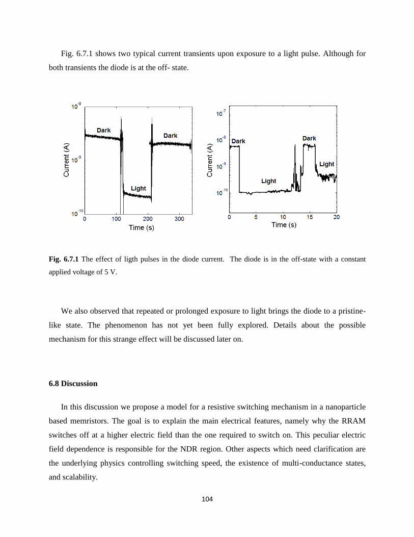
104
Fig. 6.7.1 shows two typical current transients upon exposure to a light pulse. Although for
both transients the diode is at the off- state.
Fig. 6.7.1 The effect of ligth pulses in the diode current. The diode is in the off-state with a constant
applied voltage of 5 V.
We also observed that repeated or prolonged exposure to light brings the diode to a pristine-
like state. The phenomenon has not yet been fully explored. Details about the possible
mechanism for this strange effect will be discussed later on.
6.8 Discussion
In this discussion we propose a model for a resistive switching mechanism in a nanoparticle
based memristors. The goal is to explain the main electrical features, namely why the RRAM
switches off at a higher electric field than the one required to switch on. This peculiar electric
field dependence is responsible for the NDR region. Other aspects which need clarification are
the underlying physics controlling switching speed, the existence of multi-conductance states,
and scalability.

105
Previously, in chapter 5, we proposed that, during electroforming, deep defects are created in
the silver oxide particles. These defects trap holes, which are compensated by a nearby cloud of
relatively free electrons. A conducting path will then be established between the electrodes when
the density of compensating electrons is high enough to form a continuous path for free carriers.
Although it has not been possible to visualize current filaments in our diodes, data suggests that
indeed the electrical conduction is filamentary. Even in the high conductance state, only a
relatively small fraction of the diode is actually conducting and the rest of the diode must remain
insulating. The observation of several discrete on and off states and electrical noise is supports
this view. This means there are discrete current paths that can be turned on and off. These paths
must be related to a particular arrangement (in wire-like nanostructured array) of the silver oxide
nanoparticles, either during forming or during diode fabrication. We believe this nanostructured
array of silver oxide particles determines the number of available current filaments (Fig. 6.8.1).
More precisely, in such material, electronic current is gated by ionic motions (oxygen vacancy).
The resulting behaviour is an electronic path across the dipole arrays between the electrodes. It is
important to understand how current paths are created and annihilated. In RRAMs based on
metallic filaments, filamentary paths are created by driving metallic species into the conduction
channel, forming a tiny metallic wire. Under high electric fields, metallic paths disrupt by Joule
heating. However, in our memristors there is no evidence of metallic paths. This is supported by
the temperature dependence of the current, shown in Fig. 6.3.1. Therefore, we propose that
switching-off is brought about by a recombination process that neutralizes the charged defects
and disrupts the conduction path. The combined effect of an excess of carriers and the external
field will force a neutralization of the trapped charge. When this occurs, free carrier density
collapses and the current paths will shut down.
The observation of current fluctuations shows that high current paths are carrying several
micro-amps. The filaments are long-lived and they are responsible for the memory properties.
High frequency current blinks in the range of nano-amps (RTS noise) must be caused by tiny
filaments. We have shown that the frequency of these events increases with temperature, in line
with our proposed recombination (neutralization) model. We assume that this recombination
takes place near the electrodes and probably only one defect is neutralized during the switching
off event. The current path is easily restored and disrupted again giving rise to RTS noise.

106
These paths are not contributing to the memory properties and therefore their presence
should be minimized. We have also shown that by controlling the applied voltage above the
onset of the NDR region, we can selectively turn off permanently some of the paths. In this way,
we can program the memory in several on and off states. This is a very interesting finding that
may pave the way to achieve a multi-bit memory device. In multi-level cells, the memory density
can be increased without a physical scaling. However, multi-bit memory has not been
successfully developed yet because many requirements such as a stable operation window
(retention and endurance with enough bit separation margin), easy integration, and scalability
have to be satisfied at the same time [110].
Fig. 6.8.1 Schematic diagram of AgXO-PVP interface: 1 shows just tunnelling charge carrier injection, 2
represents the mixed ionic electronic transport, 3 shows that by lowering the barrier at the high field
makes a hole/electron recombination.
Although we have shown that the retention time is appealing for memory applications
(chapter 4), the data presented in this chapter show that switching speed is relatively slow. The
observation of the switch-on delay basically tells us that switching is controlled by a physical
process that follows kinetics similar to the time of dielectric breakdown in oxides. The
switching-off mechanism is also slow. Fig. 6.5.1 shows that the voltage must be applied over a
certain length of time to assure that the filament is permanently disrupted. Short voltage steps
107
cause only a temporary disruption of the filament. As a summary, the switch-on time is
controlled by a trap filling mechanism and the switch-off time is controlled by a recombination
mechanism. Both processes will follow time kinetics strongly dependent on the applied bias.
Unfortunately, it was not possible to clarify which one is the slowest. However, it is clear that
repeated switching can only be performed in a time scale of seconds. This is not acceptable for
practical applications. Based on the proposed physical mechanism it is not likely that this speed
can be significantly improved by squeezing the device dimensions. Speed may turn out to be a
bottleneck for developing a commercial RRAM using these types of structures.
6.7 Conclusions
Non-volatile, bistable resistive memories have been fabricated in the form of planar
structures using nanoparticles embedded in an insulating PVP host matrix. In quasi-static
measurements the diodes display the well-reported negative differential resistance behaviour and
are readily switched reversibly between the off and on state. The responses of these diodes have
been probed using triangular voltage profiles with different scan rates. We have shown that the
on-state response is anomalous. The device current increases with increasing voltage scan rate
and the magnitude of the NDR gradually decreases and disappears at a scan speed of 1 V/s.
These effects are readily explained by assuming that the turn off voltage must be applied over a
certain length of time to effectively switch-off the conducting paths. Switching-on events are
also characterized by a delay time determined by the magnitude of the applied voltage. An
important outcome of the above findings is that the fundamental limitations on the speed of
operation of the RRAM are the time- and voltage-dependences of the switching-on and
switching-off mechanism.
Temperature dependence of the current is readily explained assuming that charge carrier
transport is through a percolating network of discrete paths (filaments). A change in the
conductance state corresponds to a change in the density of filaments. This thermally activated
behaviour confirms that filaments are not metallic.
It is proposed that RRAM switches to a high conductive state when the defects in the silver
oxide nanoparticles, probably oxygen vacancies, are filled with positive charges. When a

108
percolation path of such defects becomes established across the diode, a conductive filament is
created. Positive charge trapped in the nanoparticles is compensated by the free electrons trapped
at the polymer/nanoparticle interface, thus establishing a dipole layer. The resultant array of
dipoles and high electric field primes the conduction path so that when a critical voltage is
reached, electron tunnelling occurs through the array. Switching off occurrs when the free
electrons neutralize the trapped charges. This proposed model explains the basic electrical
characteristics observed.

109
“A scientific truth does not triumph by convincing its opponents and making them see the light,
but rather because its opponents eventually die and a new generation grows up that is familiar
with it.” Max Planck
CHAPTER 7 - Diodes based on silver chloride nanocrystals
Thin-film planar structures using AgCl nanocrystals embedded in a polymer blend exhibit
resistive switching between different non-volatile conductance states. Compared with the silver
oxide nanoparticle diode, the set and reset voltages occur at a lower electric field. The retention
time is shorter. Although, we expected the formation of silver filaments, temperature-dependent
measurements do not confirm this view.
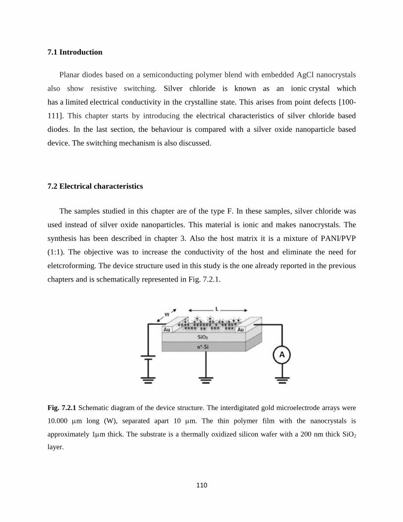
110
7.1 Introduction
Planar diodes based on a semiconducting polymer blend with embedded AgCl nanocrystals
also show resistive switching. Silver chloride is known as an ionic crystal which
has a limited electrical conductivity in the crystalline state. This arises from point defects [100-
111]. This chapter starts by introducing the electrical characteristics of silver chloride based
diodes. In the last section, the behaviour is compared with a silver oxide nanoparticle based
device. The switching mechanism is also discussed.
7.2 Electrical characteristics
The samples studied in this chapter are of the type F. In these samples, silver chloride was
used instead of silver oxide nanoparticles. This material is ionic and makes nanocrystals. The
synthesis has been described in chapter 3. Also the host matrix it is a mixture of PANI/PVP
(1:1). The objective was to increase the conductivity of the host and eliminate the need for
eletcroforming. The device structure used in this study is the one already reported in the previous
chapters and is schematically represented in Fig. 7.2.1.
Fig. 7.2.1 Schematic diagram of the device structure. The interdigitated gold microelectrode arrays were
10.000 m long (W), separated apart 10 m. The thin polymer film with the nanocrystals is
approximately 1m thick. The substrate is a thermally oxidized silicon wafer with a 200 nm thick SiO2
layer.
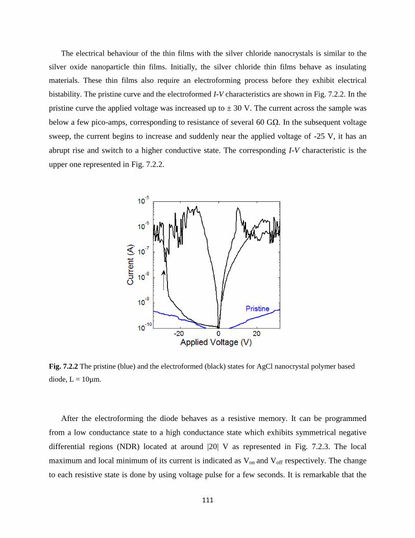
111
The electrical behaviour of the thin films with the silver chloride nanocrystals is similar to the
silver oxide nanoparticle thin films. Initially, the silver chloride thin films behave as insulating
materials. These thin films also require an electroforming process before they exhibit electrical
bistability. The pristine curve and the electroformed I-V characteristics are shown in Fig. 7.2.2. In the
pristine curve the applied voltage was increased up to ± 30 V. The current across the sample was
below a few pico-amps, corresponding to resistance of several 60 Gῼ. In the subsequent voltage
sweep, the current begins to increase and suddenly near the applied voltage of -25 V, it has an
abrupt rise and switch to a higher conductive state. The corresponding I-V characteristic is the
upper one represented in Fig. 7.2.2.
Fig. 7.2.2 The pristine (blue) and the electroformed (black) states for AgCl nanocrystal polymer based
diode, L = 10µm.
After the electroforming the diode behaves as a resistive memory. It can be programmed
from a low conductance state to a high conductance state which exhibits symmetrical negative
differential regions (NDR) located at around |20| V as represented in Fig. 7.2.3. The local
maximum and local minimum of its current is indicated as Von and Voff respectively. The change
to each resistive state is done by using voltage pulse for a few seconds. It is remarkable that the

112
on and off states can be set by pulses of either polarity. A pulse near Voff will bring the device to
the lower I-V curve (off-state). The high conductance I-V curve (on-state) is also restored by
using a pulse near Von which is typically 17 V. Once the device is biased into a particular on or
off-state, it can be read many times without degradation. To assess the retention time, the sample
was programmed in the on-state and the current at 1 V measured as a function of time.
Fig. 7.2.3 The on-state and off-state I-V curves obtained after pulse at Von and Voff respectively for AgCl
nanocrystal polymer based diode, L = 10µm.
Fig. 7.2.4 shows the initial behaviour of the current. In the first 16 minutes, a pronounced
decrease is observed which levels out after 33 minutes. The inset of Fig. 7.2.4 shows a
magnification in a narrow region of time of the initial decay. The current decreases in small
discrete events typical of a random telegraph signal (RTS) noise. Fig. 7.2.5 shows that once the
diode is programmed into a certain state, it reliably reads out many times without degradation.
The write voltage is 16 V and the erase voltage is 26 V. The read voltage for both states is 3 V.
The on/off ratio is two orders of magnitude.

113
Fig. 7.2.4 Time dependence of the current with 1 V applied and measured shortly after the device has
been programed to the on-state. The inset shows the discrete variations in the current with a typical
signature of random telegraph noise.
Fig. 7.2.5 The current response to the write-read-erase-read voltage cycles . The write voltage (W) is 16
V and the erase (E) is 26V. For both states the read voltage (R) is 3V.

114
7.3 Temperature dependence of the current for a silver chloride polymer blend diode
In order to get insight into the charge transport mechanism, temperature dependent
measurements were also carried-out. Fig. 7.3.1 (a) shows the one-state I-V curves recorded for
different temperatures. Temperature measurements were limited to the range 245-300 K. When
the diode is cooled down the ability to switch becomes increasingly difficult. The NDR region
tends to disappear and at 260 K is no longer observed. Below 250 K the low voltage region is no
longer Ohmic but becomes exponential.
Fig. 7.3.1 (b) represents the Arrhenius plot of the on-state current measured at the applied
bias of 6 V. It is shown that the current follows a single thermally activated process with
activation energy of 0.6 eV.
Fig. 7.3.1 (a) Temperature dependence of the current-voltage characteristics of the AgCl nanocrystal
polymer based device. Below 245 K the NDR disappears. (b) Arrhenius plot of the high conductance state
measured at 6 V. The line fits the experimental points (∆).
(a) (b)
Ea = 0.6 eV
115
7.4 Discussion
According to the literature, the AgCl capped with polymer blend form nanocrystals with a
typical size of 70-100 nm [112]. The AgCl/PANI core-shell thin films are comprised of AgCl
(core) surrounded by a semiconducting polymer (shell). From a structural point of view, this
nanocomposite thin film is similar to a silver oxide nanoparticle polymer based planar diode. In
both systems the oxide and chloride nano structure is uniformly distributed within an insulation
or semi-insulating polymer host matrix.
In respect to the electrical properties, the similarities between both memory systems are also
remarkable. Both systems need an electroforming process and have similar I-V characteristics
with NDR regions, and unipolar programming features. However, nanocrystal based diodes
require lower voltages to set and reset the memory states. The major difference between both
systems is in the temperature dependence of the current. While it is clearly shown in chapter 6
that the carrier transport in silver oxide nanoparticles is by tunnelling irrespective to the
conductance state, silver chloride based diodes show a strongly thermally activated low
resistance. This suggests that there are differences between the two types of devices.
Electroforming is needed to create the filament in the first place. It usually needs a higher
voltage than the SET operation. As explained in chapter 5, the electroforming of the filament is
achieved by applying a high electric field, produced by a reasonably low voltage bias to reach
the soft breakdown.
Since AgCl is an ionic crystal it may be reasonable to assume that the conduction through the
system is ionic or a mixture of ionic and electronic conduction. In order to move an ion through a
crystal, it must hop from an occupied site to a vacant site. Thus ionic conductivity can only
occur if defects are present. The two simplest types of point defects are Schottky and Frenkel
defects [113]. For ionic compounds like silver chloride, the anion is much larger than the other
ion, the cation; vacancies and interstitials (out of place ions or ionic defects) of the smaller ion
will allow an ionic conductivity.
Diffusion is the process of ion movement. It is driven by a concentration gradient (as already
explained in chapter 5). In structurally ordered, i.e. single crystalline systems, defects are
required for the movement of atoms or ions [111,113-115]. The components that influence the
ionic conductivity in the solid state are the concentration of charge carriers (ions), the

116
temperature of the crystal, the availability of vacant-accessible sites which is controlled by the
density of defects and the ease with which an ion can jump to another site. The last of the above
discussed factors, namely, the ease with which an ion can jump to a neighbouring site is
controlled by the activation energy. In fact, the activation energy indicates the free energy barrier
an ion has to overcome for a successful jump between the sites. In this system, it is assumed that
after the electroforming, conductive filaments of the ionic silver are established by a diffusion
process.
The RESET operation aims at destroying partially the ionic filament to make the device
switch again to the low conductance state. The goal is to avoid destroying the filament
completely, but only to damage it. It is believed that the vacancy diffusion effect at the higher
electric field leads to the breaking of filaments. The SET operation is used to repair the filament
partially destroyed by a RESET, and make it switch again to a high conductance state. This step
is similar to the forming, but requires a much smaller voltage, as the filament is already present
in the structure, and almost completely formed.
Assuming that the condution is through ionic silver, then the activation energy for charge
transport is expected to be low or even metallic. However, the measured activation energy is
relatively high (Ea=0.6 eV). The reason for this relatively high activation energy is not clear at
the moment. It was also noticed that when warming-up the device again to room temperature, the
device is in the off-state. We may speculate that as the device is cooled-down, some of the
conductive paths switch-off. If this is the case, then temperature depedent measurements do not
reflect activation energy for the charge transport. Temperature dependent hystherisis loops are
required to validate this assumption.
7.5 Conclusion
It has been demonstrated that a thin-film planar structure, using AgCl nanocrystals embedded
in a semiconducting polymer blend (PVP/PANI) can also switch between two different
conductance states. The retention time of the on-state is approximately one week. Although, we
expected the formation of silver filaments, temperature dependent measurements do not confirm
this view. However, it is not excluded that as temperature decreases some of the conducting
paths turn-off because there is a low thermal energy. This mechanism can prevent the

117
measurement of the real activation energy of the carrier transport mechanism. This type of
resistive switching mechanism is not reliable, thus it cannot be applied for RRAM devices.

118
CHAPTER 8 - Conclusions of the Research and Suggested Future Work
This chapter provides the conclusions to this dissertation and suggests directions that future
research can take.

119
8.1 Conclusions
The resistive switching behaviour of thin polymer films containing metal nanoparticles was
investigated within this dissertation. Thin planar symmetrical MIM structures were fabricated.
The switching behaviour was studied using electrical techniques. The major contribution of this
work to the knowledge in the field is the following:
Resistive switching in diodes that use metal nanoparticles is identical to bulk oxide MIM
structures. Resistive switching requires an oxide in a bilayer structure. The system must be
electroformed. Resistive switching in silver oxide nanoparticles is an electronic process.
An important consequence of this conclusion is that non-oxidized metal nanoparticles such as
gold nanoparticles cannot be used to make reliable RRAMs. They can only lead to resistive
switching devices through the migration of metal species and formation/rupture of metallic
filaments.
From this study we also draw a number of more detailed conclusions:
Electroforming
An electroforming process which induces a permanent change in the resistance state is a
prerequisite for the observation of unipolar or N-shaped switching behaviour. Electroforming is a
soft-breakdown mechanism. XRD data shows that new species of silver oxide are present after
electroforming. Based on the similarities with oxide-based memories we propose that
electroforming corresponds to the creation of silver oxide defects (possible oxygen vacancies).
Polymer thin films containing gold nanoparticles do not undergo electroforming.
To the best of our knowledge, electroforming has not been reported in the literature for
devices with incorporated nanoparticles. Our explanation for this is based on the fact that
incorporated nanoparticle devices require an electric field significantly lower than bulk oxide
memory devices. Since most devices reported in literature are a thin sandwich type, relatively
low voltage should be enough to electroform those structures. The electroforming may pass
unnoticed during the recording of the first I-V curve or be interpreted as a switching event.
120
Intrinsic and extrinsic switching
The same diode structure can exhibit two types of resistive switching, bipolar and unipolar.
The type of switching is dependent on the ambient atmosphere. The S-shape electrical
characteristics (bipolar type) are only observed in air. The N-shaped I-V characteristics (unipolar
switching) are observed only in high vacuum.
Our findings show clearly that S-shaped I-V characteristics can be induced by redox reactions
mediated by moisture. Although this type of switching can cause changes in resistance reaching
7 orders of magnitude, the on-state is unreliable.
There are a significant number of papers reporting resistive switching in devices with gold
nanoparticles. However, the evidence presented in this dissertation may raise doubts about the
interpretation of that data. We have reasons to suspect that when the measurements were carried
out in air, the resistive switching may be mediated by atmosphere and therefore not intrinsic to
the gold nanoparticles. This is in line with our observation that polymer/gold nanoparticles
cannot be electroformed.
Performance of RRAMS based on silver oxide nanoparticles
Non-volatile resistive switching memory properties with an on/off ratio of 4 orders of
magnitude and high cycle endurance were achieved.
The dynamic behaviour upon changing the voltage ramp speed, together with the transient
response to voltage steps shows that repeated writing and erasing cycles require a time scale of
mili-seconds. It is proposed that this slow switching dynamic is related to the time required to fill
the silver oxide trap states. This time imposes a fundamental limitation on switching speed.
A model for resistive switching mechanism in silver oxide nanoparticles
We propose that the electrical conduction in the polymer/silver oxide nanoparticle matrix is
through a discrete percolation network of conducting filaments. The changes in device resistance

121
are caused by changes in the density of filaments. A very high density of filaments characterizes
the low resistance state. This view is supported by temperature dependent measurements which
confirm independently of the device resistance, that the charge conduction mechanism remains
the same and is by tunnelling. The spontaneous rupture/creation of these filaments gives rise to
current fluctuations resembling a random telegraph type of noise, as observed.
A model is proposed for the creation/annihilation of the conducting filaments. During
electroforming silver oxide defects are created. These defects trap holes. Immobile holes are
compensated for by electrons. When the density of the compensating electrons is high enough, it
forms a continuous path for the flow of current. At the high field the conducting path is ruptured
because the electron recombines with the trapped hole. In fact, the application of a very high
voltage injects an excess of electrons and also may lower the barrier of the trapped holes causing
a massive electro/hole recombination. This turns-off all the conducting paths and brings the
device to its HRS. To turn the device to its LRS again, holes must be trapped again. This
requires the application of an electric field over a certain length of time. This proposed model
explains the basic electrical characteristics observed.
Resistive switching in ionic crystals
AgCl nanocrystals embedded in a semiconducting polymer blend can also switch between
two different conductance states. The retention time of the on- and off-states is approximately
one week. It is proposed that the charge transport mechanism is via ionic filamentary paths.
8.2 Future Works
As an extension of this thesis the following research issues are proposed:
Nanostructured versus bulk MIM structures
The model advanced in this dissertation to explain resistive switching in silver oxide
122
nanoparticles is similar to a model developed to explain resistive switching in bulk oxide MIM
structures. Basically, it requires a bilayer structure comprised of an oxide/polymer region. This
bilayer supports a dipole where the hole is immobile (trapped in the oxide) and the compensating
electron is the polymer (possible in an oxygen rich region). In a nanoparticle system these bilayer
units repeat themselves in a complex nanostructured network. Both systems lead to almost
identical resistive switching properties. An interesting question may now be raised: has the
nanostructured thin film an advantage over the bulk MIM structure?
One clear advantage already mentioned in chapter 5 is that the electric field needed to
electroform a nanostructured thin film, is lower than in a bulk MIM memory.
Other advantages may be related to the optimization of the electroforming procedures.
Electroforming is a soft-dielectric breakdown occurring at weak oxide points. This causes that in
bulk MIM structures, most of the device area remains insulating and not active. This problem
may be solved in a nanostructured thin film because the nanoparticles are uniformly distributed,
breakdown may be forced to occur over the entire device.
The observation of multi-resistance levels suggests that the density of active filaments in
nanostructured thin films can be easily controlled. This may open the road to the fabrication of
multi-bit memories.
Further studies are required to explore all the possible advantages of using a nanostructured
thin film to fabricate RRAMs.
The nature of defects created during electroforming
It is plausible that oxygen related defects play a key role in electroforming. Thus future work
may focus on the role of defects, such as oxygen vacancy distribution in thin films and their
movement in an electric field. It will be interesting to see if oxygen exposure can unform the
memory devices.
Reliability issues
The reliability of a device needs study including the variations of cell performance and the

123
yield of fabricated devices. What is the variation from sample to sample in SET and RESET
voltages? What controls the retention time? A study on a large number of samples and statistical
analysis is required to inspect for parameter variability.
Correlation effects in resistive switching
It is interesting to note that when the device is under the NDR region, a cascade of switching-
off events brings the device to its high resistance state. The idea is not excluded that once one
filament is turned off this may induce nearby filaments to also turned off in a domino-like effect.
Switching off may be a correlated effect. An important open question in resistive switching
phenomena in oxides is whether strong correlation effects play a role. In fact, strong correlation
effects, such as high temperature superconductivity, colossal magneto-resistance and metal-
insulator transitions have remained a central theme of research in condensed matter physics of
transition metal oxides, since the discovery of superconductivity in the cuprates in 1987. The
possibility of a solely electronically-driven resistive switching transition, such as the Mott metal-
insulator transition, may allow for fast devices with long endurances and low dissipation.
Nevertheless, a strongly correlated driven resistive switching system, a "Mott transistor", may
have already been realized, in the chalcogenide compound GaTa [116].
Although, all the evidence presented in this thesis indicates that resistive switching is related
to the creation of defects or trap states, it will be interesting for further work to monitor the
current fluctuations under the NDR region and look for correlated effects in current fluctuations.

124
Bibliography
[1] R. Waser, Nanoelectronics and Information Technology, Weinheim: Wiley-VCH, 2003.
[2] J. Scott, "Is there an immortal memory?," Science, vol. 304, no. 5667, pp. 62-63, 2004.
[3] "International Technology Roadmap for Semiconductors," 2010. [Online]. Available:
http://www.itrs.net/.
[4] T. W. Hickmott, "Low‐Frequency Negative Resistance in Thin Anodic Oxide Films,"
Journal of Applied Physics, vol. 33, no. 9, p. 2669, 1962.
[5] D. Ma, M. Aguiar, J. A. Freire and I. A. Hummelgen, "Organic reversible switching
devices for memory applications," Advanced Materials, vol. 12, no. 14, pp. 1063-1066,
2000.
[6] R. Sezi, A. Walter, R. Engl, A. Maltenberger and J. Schumann, "Organic Materials for
High-Density Non-Volatile Memory Applications," IEDM Tech. Dig., p. 259, 2003.
[7] L. P. Ma, J. Liu, S. Pyo, Q. F. Xu and Y. Yang, "Organic bistable devices," Molecular
Crystals and Liquid Crystals, vol. 378, pp. 185-192, 2002.
[8] J. Y. Ouyang, C. W. Chu, C. R. Szmanda, L. P. Ma and Y. Yang, "Programmable polymer
thin film and non-volatile memory device," Nature Materials, vol. 3, no. 12, pp. 918-922,
2004.
[9] J. Y. Ouyang, C. W. Chu, R. J. H. Tseng, A. Prakash and Y. Yang, "Organic memory
device fabricated through solution processing," Proceedings of the IEEE, vol. 93, no. 7, pp.
1287-1296, 2005.
[10] Y. Yang, J. Ouyang, L. P. Ma, R. J. H. Tseng and Chu C W, "Electrical switching and
bistability in organic/polymeric thin films and memory devices," Advanced Functional
Materials, vol. 16, no. 8, pp. 1001-1014, 2006.
[11] L. D. Bozano, B. W. Kean, M. Beinhoff, K. R. Carter, P. M. Rice and J. C. Scott, "Organic
materials and thin-film structures for cross-point memory cells based on trapping in
metallic nanoparticles," Advanced Functional Materials, vol. 15, no. 12, pp. 1933-1939,
2005.
[12] L. D. Bozano, B. W. Kean, V. R. Deline, J. R. Salem and J. C. Scott, "Mechanism for
bistability in organic memory elements," Applied Physics Letters, vol. 84, no. 4, pp. 607-
609, 2004.
[13] F. Pan, C. Chen, Z. S. Wang, Y. C. Yang, J. Yang and F. Zeng, "Nonvolatile resistive
switching memories-characteristics, mechanisms and challenges," Progress in Natural
science: materials Internationl, vol. 20, no. 8, pp. 1-15, 2010.

125
[14] S. K. Lai, "Flash memories: successes and challenges," IBM Journal of Research and
Development, vol. 52, pp. 529-535, 2008.
[15] G. W. Burr, B. N. Kurdi, J. C. Scott, C. H. Lam, K. Gopalakrishnan and R. S. Shenoy,
"Overview of candidate device technologies for storage-class memory," IBM Journal of
Research and Development, vol. 52, pp. 449-464, 2009.
[16] D. Ielmini, A. S. Spinelli, A. L. Lacaita and A. Modelli, "A new two-trap tunneling model
for the anomalous (SILC) in flash memories," Microelectronic Engineering, vol. 59, pp.
189-195, 2001.
[17] J. D. Lee, S. H. Hur and J. D. Choi, "Effects of floating-gate interference on NAND Flash
memory cell operation," IEEE Electron Device Letters, vol. 23, pp. 264-266, 2002.
[18] H. Kanaya, K. Tomioka, T. Matsushita, M. Omura and T. Ozaki, "A 0.602 μm2 nestled
'Chain' cell structure formed by one mask etching process for 64 Mbit FeRAM," VLSl
Tech. Dig, vol. 150, 2004.
[19] A. R. Sitaram, D. W. Abraham, C. Alof, D. Braun and S. Brown, "A 0.18 μm logic-based
MRAM technology for high performance nonvolatile memory applications," VLSl Tech.
Dig, vol. 15, 2003.
[20] S. Lai, "Current status of the phase change memory and its future," IEDM Tech. Dig, vol.
256, 2003.
[21] C. Y. Liu, P. H. Wu, A. Wang, W. Y. Jang and J. C. Young, "Bistable resistive switching
of a sputter-deposited Cr-doped SrZrO3 memory film," IEEE Electron Device Letters, vol.
26, p. 351, 2005.
[22] M. Cölle, M. Büchel and D. M. de Leeuw, "Switching and filamentary conduction in non-
volatile organic memories," Organic Electronics, vol. 7, pp. 305-312, 2006.
[23] T. Hada, K. Wasa and S. Hayakawa, "Bistable switching of ZnO thin film diodes,"
Japanese Journal of Applied Physics, vol. 10, pp. 521-522, 1971.
[24] L. Chua, "Memristor: The missing circuit element," IEEE Transactions on Circuit Theory,
vol. 18, no. 5, pp. 507-519, 1971.
[25] J. G. Simmons and R. R. Verderber, "New Conduction and Reversible Memory
Phenomena in Thin Insulating Films," Proceedings of the Royal Society of London. Series
A., vol. 301, pp. 77-102, 1967.
[26] L. P. Ma, S. Pyo, J. Ouyang, Q. F. Xu and Y. Yang, "Nonvolatile electrical bistability of
organic/metal-nanocluster/organic system," Applied Physics Letters, vol. 82, no. 9, pp.
1419-1421, 2003.

126
[27] J. He, L. P. Ma, J. H. Wu and Y. Yang , "Three-terminal organic memory devices,"
Journal of Applied Physics, vol. 97, no. 6, p. 064507, 2005.
[28] S. Pyo, L. P. Ma, J. He, Q. F. Xu, Y. Yang and Y. L. Gao, "Experimental study on
thickness-related electrical characteristics in organic/metal-nanocluster/organic systems,"
Journal of Applied Physics, vol. 98, no. 5, p. 054303, 2005.
[29] D. Tondelier, K. Lmimouni, D. Vuillaume, C. Fery and G. Haas, "Metal/organic/metal
bistable memory devices," Applied Physics Letters, vol. 85, no. 23, pp. 5763-5765, 2004.
[30] S. Paul, C. Pearson, A. Molloy, M. A. Cousins, M. Green, S. Kolliopoulou, P. Dimitrakis,
P. Normand, D. Tsoukalas and M. C. Petty, "Langmuir-Blodgett film deposition of
metallic nanoparticles and their application to electronic memory structures," Nano Letters,
vol. 3, no. 4, pp. 533-536, 2003.
[31] W. L. Leong, P. S. Lee, S. G. Mhaisalka, T. P. Chen and A. Dodabalapur, "Charging
phenomena in pentacene-gold nanoparticle memory device," Applied Physics Letters, vol.
90, no. 4, p. 042906, 2007.
[32] E. Castella and C. K. Prout, "Molecular Complexes .10. Crystal and Molecular Structure of
1-1 Complex of 8-Hydroxyquinoline and 1,3,5-Trinitrobenzene," Journal of the Chemical
Society A - Inorganic Physical Theoretical, no. 3, pp. 550-553, 1971.
[33] D. M. Adams, L. Brus, C. E. D. Chidsey, S. Creager, C. Creutz, C. R. Kagan, P. V. Kamat,
M. Lieberman, S. Lindsay, R. A. Marcus, R. M. Metzger, M. E. Michel-Beyerle, J. R.
Miller, M. D. Newton, D. R. Rolison, O. Sankey, K. S. Schanze, J. Yardley and X. Y. Zhu,
"Charge transfer on the nanoscale: Current status," Journal of Physical Chemistry B, vol.
107, no. 28, pp. 6668-6697, 2003.
[34] B. I. Ipe, K. G. Thomas, S. Barazzouk, S. Hotchandani and P. V. Kamat, "Photoinduced
charge separation in a fluorophore-gold nanoassembly," Journal of Physical Chemistry B,
vol. 106, no. 1, pp. 18-21, 2002.
[35] J. Y. Ouyang, C. W. Chu, D. Sieves and Y. Yang, "Electric-field-induced charge transfer
between gold nanoparticle and capping 2-naphthalenethiol and organic memory cells,"
Applied Physics Letters, vol. 86, no. 12, p. 123507, 2005.
[36] D. Prime and S. Paul, "Making Plastic Remember: Electrically Rewritable Polymer
Memory Devices," Materials Research Society Symposium Proceedings, vol. 997, pp. 21-
25, 2007.
[37] D. Prime and S. Paul, "Gold Nanoparticle Based Electrically Rewritable Polymer Memory
Devices," Advances In Science and Technology, vol. 54, pp. 480-485, 2008.
[38] A. Prakash, J. Ouyang, J. L. Lin and Y. Yang, "Polymer memory device based on
conjugated polymer and gold nanoparticles," Journal of Applied Physics, vol. 100, no. 5, p.

127
054309, 2006.
[39] Y. Song, Q. D. Ling, S. L. Lim, E. Y. H. Teo, Y. P. Tan, L. Li, E. T. Kang, D. S. H. Chan
and C. X. Zhu, "Electrically bistable thin-film device based on PVK and GNPs polymer
material," IEEE Electron Device Letters, vol. 28, no. 2, pp. 107-110, 2007.
[40] V. S. Reddy, S. Karak, S. K. Ray and A. Dhar, "Carrier transport mechanism in aluminum
nanoparticle embedded AlQ3 structures for organic bistable memory devices," Organic
Electronics, vol. 10, no. 1, pp. 138-44, 2009.
[41] V. S. Reddy, S. Karak and A. Dhar, "Multilevel conductance switching in organic memory
devices based on AlQ3 and Al/Al2O3 core-shell nanoparticles," Applied Physics Letters,
vol. 94, no. 17, p. 173304, 2009.
[42] R. J. Tseng, C. L. Tsai, L. P. Ma and J. Y. Ouyang, "Digital memory device based on
tobacco mosaic virus conjugated with nanoparticles," Nature Nanotechnology, vol. 1, no.
1, pp. 72-77, 2006.
[43] L. P. Ma, Q. F. Xu and Y. Yang, "Organic nonvolatile memory by controlling the dynamic
copper-ion concentration within organic layer," Applied Physics Letters, vol. 84, no. 24,
pp. 4908-4910, 2004.
[44] H. Schroeder, V. V. Zhirnov, R. K. Cavin and R. Waser, "Voltage-time dilemma of pure
electronic mechanisms in resistive switching memory cells," Appl. Phys, vol. 107, pp.
054517-8, 2010.
[45] H. Bönnemann and R. M. Richards, "Nanoscopic metal particles-synthetic methods and
potential applications," European Journal of Inorganic Chemistry, vol. 2001, no. 10, pp.
2455-2480, 2001.
[46] X. Z. Lin, X. Teng and H. Yang, "Direct synthesis of narrowly dispersed silver
nanoparticles using a single-source precursor," Langmuir, vol. 19, no. 24, pp. 10081-
10085, 2003.
[47] D. Andreescu, C. Eastman, K. Balantrapu and D. V. Goia, "A simple route for
manufacturing highly dispersed silver nanoparticles," Journal of materials research, vol.
22, no. 9, pp. 2488-2496, 2007.
[48] D. V. Goia and E. Matijevic, "Preparation of monodispersed metal particles," New Journal
of Chemistry, vol. 22, no. 11, pp. 1203-1215, 1998.
[49] S. Pillai, K. R. Catchpole, T. Trupke and M. A. Green, "Surface plasmon enhanced silicon
solar cells," Journal of Applied Physics, vol. 101, no. 9, p. 093105, 2007.
[50] F. J. Beck, S. Mokkapati, A. Polman and K. R. Catchpole, "Asymmetry in photocurrent
enhancement by plasmonic nanoparticle arrays located on the front or on the rear of solar

128
cells," Applied Physics Letters, vol. 96, no. 3, p. 033113, 2010.
[51] S. Pillai, Surface plasmons for enhanced thin-film silicon solar cells and light emitting
diodes, Australia: PhD thesis, School of photovoltaic and renewable energy engineering,
University of New South Wales, 2007.
[52] T. L. Temple, G. D. K. Mahanama, H. S. Reehal and D. M. Bagnall, "Influence of
localized surface plasmon excitation in silver nanoparticles on the performance of silicon
solar cells," Solar Energy Materials and Solar Cells, vol. 93, no. 11, pp. 1978-1985, 2009.
[53] S. A. Campbell, The science and engineering of microelectronic fabrication, Oxford
university press, NY, second edition, 2001.
[54] C. P. Poole, F. J. Jones and F. J. Owens, Introduction to Nanotechnology, New York,
USA: John Wiley & Sons, Inc, 2003.
[55] L. Liang and Z. Ying-Jie, "High chemical reactivity of silver nanoparticles toward
hydrochloric acid," Journal of Colloid and Interface Science, vol. 303, no. 2, pp. 415-418,
2006.
[56] G. Schmid, Clusters and Colloids - From Theory to Applications, Weinheim: Wiley-VCH,
1994.
[57] "Derjaguin, Landau, Verwey and Overbeek theory (DLVO theory)," Malvern Instruments
Corporate, [Online]. Available:
http://www.malvern.com/labeng/industry/colloids/dlvo_theory.htm.
[58] I. Diez and R. H. A. Ras, "Flourescent silver nanoclusters," Journal of Nanoscale, vol. 3,
no. 5, pp. 1963-1970, 2011.
[59] S. Mandal, S. K. Arumugam, R. Pasricha and M. Sastry, "Silver nanoparticles of variable
morphology synthesized in aqueous foams as novel templates," Bulletin of Material
Science, vol. 28, no. 5, pp. 503-510, 2005.
[60] G. V. Aguilar, J. A. García-Macedo and V. RenteríaTapia, "Silver Core - Silver Oxide
Shell Nanoparticles Embedded on Mesostructured Silica Films," Journal of Nano
Research, vol. 3, pp. 103-114, 2008.
[61] J. Turkevich, P. Cooper Stevenson and J. Hillier, "A study of the nucleation and growth
process in the synthesis of colloidal gold," Discussions of the Faraday Society, vol. 11, pp.
55-75, 1951.
[62] R. D. Deegan, O. Bakajin, T. F. Dupont, G. Huber, S. R. Nagel and T. A. Witten,
"Capillary flow as the cause of ring stains from dried liquid drops," Nature, vol. 389, no.
6653, pp. 827-829, 1997.

129
[63] K. Lee, M. Duchamp, G. Kulik, A. Magrez, J. W. Seo, S. Jeney, A. J. Kulik, L. Forro, R.
S. Sundaram and J. Brugger, "Uniformly dispersed deposition of colloidal nanoparticles
and nanowires by boiling," Applied Physics Letters, vol. 91, no. 17, p. 173112, 2007.
[64] D. Prime and S. Paul, "Overview of organic memory devices," Phil. Trans. R. Soc. A, vol.
367, pp. 4141-4157, 2009.
[65] A. Kiesow, J. E. Morris, C. Radehaus and A. Heilmann, "Switching behavior of plasma
polymer films containing silver nanoparticles," Journal of Applied Physics, vol. 94, p.
6988, 2003.
[66] H. X. Guo, B. Yang, L. Chen, Y. D. Xia, K. B. Yin and Z. G. Liu, "Resistive switching
devices based on nanocrystalline solid electrolyte (AgI)0.5(AgPO3)0.5," Applied Physics
Letters, vol. 91, p. 243513, 2007.
[67] R. Muller, J. Genoe and P. Heremans, "Bipolar resistive electrical switching of silver tetra
cyanoquinodimethane based memory cells with dedicated silicon dioxide “switching
layer”," Applied Physics Letters, vol. 95, p. 133509, 2009.
[68] T. Ouisse and O. Stephan, "Electrical bistability of polyfluorene devices," Organic
Electronics, vol. 5, pp. 251-256, 2004.
[69] J. C. Scott and L. D. Bozano, "Nonvolatile memory elements based on organic materials,"
Advanced Material, vol. 19, pp. 1452-1463, 2007.
[70] P. Dimitrakis, P. Normand, D. Tsoukalas, C. Pearson, J. H. Ah, M. F. Mabrook, M. C.
Petty, K. T. Kamtekar, C. Wang, M. R. Bryce and M. Green, "Electrical behavior of
memory devices based on polyfluorene- containing organic thin films," Journal of Applied
Physics, vol. 104, p. 044510, 2008.
[71] H. Houili, E. Tutis and R. Izquierdo, "Modeling nanoparticle embedded organic memory
devices," Organic Electronics, vol. 11, pp. 514-520, 2010.
[72] J. Ouyan and YangY, "Polymer: metal nanoparticle devices with electrode- sensitive
bipolar resistive switchings and their application as nonvolatile memory devices," Applied
Physics Letter, vol. 96, p. 063506, 2010.
[73] T. Tsukamoto, S. H. Liu and Z. A. Bao, "Resistance switching in a polystyrene film
containing Au nanoparticles," Japanese Journal of Applied Physics, vol. 46, pp. 3622-
3625, 2007.
[74] F. Verbakel, S. C. J. Meskers, R. A. J. Janssen, H. L. Gomes, M. Cölle, M. Büchel and L.
M. de Dago, "Reproducible resistive switching in nonvolatile organic memories," Applied
Physics Letters, vol. 91, p. 192103, 2007.
[75] K. Tanaka, "Modeling of hot-carrier effects in small-geometry MOSFETs," Electronics

130
and Communications in Japan, Vols. 67-C, p. 1, 1984.
[76] T. Kimura, K. Yamamoto and S. Yugo, "Humidity‐sensitive threshold switching in silver–
boron nitride–silicon–aluminum sandwiches," Applied Physics Letters, vol. 33, p. 15,
1978.
[77] N. Knorr, R. Wirtz, S. Rosselli and G. Nelles, "Field-Absorbed Water Induced
Electrochemical Processes in Organic Thin Film Junctions," The Journal of Physical
Chemistry C, vol. 114, p. 15791, 2010.
[78] X. Guo, C. Schindler, S. Menzel and R. Waser, "Understanding the switching-off
mechanism in Ag+ migration based resistively switching model systems," Applied Physics
Letters, vol. 91, p. 133513, 2007.
[79] C. A. Hogarth and M. Zor, "Some Observations of Voltage-Induced Conductance Changes
in Thin-Films of Evaporated Polyethylene," Thin Solid Films, vol. 27, no. 1, pp. L5-L7,
1975.
[80] T. W. Hickmott, "Potential Distribution and Negative Resistance in Thin Oxide Films,"
Journal of Applied Physics, vol. 35, p. 2678, 1964.
[81] A. A. Ansari and A. Qadeer, "Memory Switching in Thermally Grown Titanium-Oxide
Films," Journal of Physics D - Applied Physics, vol. 18, no. 5, pp. 911-917, 1985.
[82] R. R. Sutherland, "Theory for Negative Resistance and Memory Effects in Thin Insulating
Films and Its Application to Au-ZnS-Au Devices," Journal of Physics D - Applied Physics,
vol. 4, no. 3, pp. 468-479, 1971.
[83] G. Dearnaley, D. V. Morgan and A. M. Stoneham, "A model for filament growth and
switching in amorphoud oxide films," Journal of Non-Crystalline Solids, vol. 4, pp. 593-
612, 1970.
[84] C. A. Hogarth and T. Iqbal, "Electroforming of Thin-Films of Polypropylene,"
International Journal of Electronics, vol. 47, no. 4, pp. 349-353, 1979.
[85] H. Biederman, H. Lehmberg and H. Pagnia, "On the Source of Current-Carrying Filament
Material in Mim-Diodes," Vacuum, vol. 39, no. 1, pp. 27-28, 1989.
[86] R. Blessing, K. H. Gurtler and H. Pagnia, "Switching of Point-Contact Diodes Consisting
of Discontinuous Gold-Films," Physics Letters A, vol. 84, no. 6, pp. 341-344, 1981.
[87] A. Halimaoui, O. Briere and G. Ghibaudo, "Quasi-breakdown in ultrathin gate dielectrics,"
Microelectronic Engineering, vol. 36, no. 1, p. 157–160, 1997.
[88] K. Fu, "Partial breakdown of the tunnel oxide in floating gate devices," Solid-State
Electron, vol. 41, no. 5, pp. 774-777, 1997.

131
[89] J. H. Stathis, "Physical and predictive models of ultrathin oxide reliability in CMOS
devices and circuits," IEEE Trans. Device and Materials Reliability, vol. 1, no. 1, pp. 43-
59, 2001.
[90] S. Lee, B. Cho, J. Kim and S. Choi, "Quasi-breakdown of ultrathin gate oxide under high
field stress," Proc. IEEE IEDM Tech.Dig, pp. 605-608, 1994.
[91] M. Depas, T. Nigam and M. M. Heyns, "Soft breakdown of ultra-thin gate oxide Layers,"
IEEE Transaction on Electron Devices, vol. 43, no. 9, pp. 1499-1504, 1996.
[92] H. L. Frisch and J. M. Hammersley, "Percolation process and related topics," J. Soc.
Indust. Appl. Math, vol. 11, no. 4, pp. 894-918, 1963.
[93] V. K. S. Shante and S. Kirkpatrick, "An introduction to percolation theory," Advances in
Physics, vol. 20, no. 85, pp. 325-357, 1971.
[94] S. Y. Wang, N. T. Liang and Y. Shan, "Percolation and areal electrical conductance in an
ultra thin bismuth film," Chinese Journal of Physics, vol. 15, no. 4, p. 243, 1977.
[95] J. Shi, Two-dimensional metal-insulator transition, Oklahoma State University: Ph.D.
Thesis, 2002.
[96] N. J. Kim, 2D metal-insulator transition in si-based materials, University of North
Carolina: Ph.D. Thesis, Department of Physics and Astronomy, 2001.
[97] X. Guan, S. Yu and H. -S. Philip Wong, "On the Switching Parameter Variation of Metal-
Oxide RRAM-Part I: Physical Modeling and Simulation Methodology," IEEE Transaction
on Electron Devices, vol. 59, no. 4, pp. 1172-1182, 2012.
[98] E. Miranda, J. Su˜n´e, R. Rodr´ıguez, M. Nafr´ıa, X. Aymerich, L. Fonseca and F.
Campabadal, "Soft breakdown conduction in ultrathin (3-5 nm) gate dielectrics," IEEE
Transaction on Electron Devices, vol. 47, no. 1, pp. 82-89, 2000.
[99] T. H. Lee, J. I. Gonzalez, J. Zheng and R. M. Dickson, "Single-molecule optoelectronics,"
Acc. Chem. Res, vol. 38, no. 7, pp. 534-541, 2005.
[100] A. R. West, Solid State Chemistry and its Applications,p.290, New York: Revised Edition,
John Wiley, 1984.
[101] T. W. Hickmott, "Temperature dependence of voltage-controlled negative resistance and
electroluminescence in Al–Al2O3–Au diodes," Journal of Applied Physics, vol. 104, p.
103704, 2008.
[102] A. Younis, D. Chu and S. Li, "Oxygen level: the dominant of resistive switching
characteristics in cerium oxide thin films," Journal of Physics D: Applied Physics, vol. 45,
no. 35, p. 355101, 2012.
132
[103] T. Kondo, S. M. Lee, M. Malicki, B. Domercq, S. R. Marder and B. Kippelen, "A
nonvolatile organic memory device using ITO surface modified by Ag-nanodots,"
Advanced Functional Materials, vol. 18, pp. 1112-1118, 2008.
[104] G. Teyssedre, C. Laurent, A. Aslanides, N. Quirke, L. A. Dissado, G. C. Montanari, A.
Campus and L. Martinotto, "Deep Trapping Centers in Cross linked Polyethylene
Investigated by Molecular Modeling and Luminescence Techniques," IEEE Trans. DEI,
vol. 8, no. 5, pp. 744-752, 2001.
[105] F. Verbakel, S. C. J. Meskers, R. A. J. Janssena, H. L. Gomes, A. J. M. van den Biggelaar
and D. M. de Leeuw, "Switching dynamics in non-volatile polymer memories," Organic
Electronics, vol. 9, pp. 829-833, 2008.
[106] M. L. Wang, J. Zhou, X. D. Gao, B. F. Ding, Z. Shi, X. Y. Sun, X. M. Ding and X. Y.
Hou, "Delayed-switch-on effect in metal-insulator-metal organic memories," Applied
Physics Letters, vol. 91, no. 14, pp. 143511-3, 2007.
[107] D. L. Crook, "Method of Determining Reliability Screens for Time Dependent Dielectric
Breakdown," 17th annual Proc. Reliability Physics Symposium, pp. 1-7, 1979.
[108] D. B. Strukov, G. S. Sinder, D. R. Stewart and R. S. Williams, "The missing memristor
found," Nature, vol. 453, pp. 80-83, 2008.
[109] N. R. McDonald, R. E. Pino, P. J. Rozwood and B. T. Wysocki, "Analysis of dynamic
linear and non-linear memristor device models for emerging neuromorphic computing
hardware design," The 2010 International Joint Conference on Neural Networks (IJCNN),
pp. 1-5, 2010.
[110] S. J. Choi, K. H. Kim, G. S. Park, H. J. Bae, W. Y. Yang and S. Cho, "Multibit Operation
of Cu/Cu-GeTe/W Resistive Memory Device Controlled by Pulse Voltage Magnitude and
Width," IEEE Electron Device Letters, vol. 32, no. 3, pp. 375-377, 2011.
[111] H. Schmalzried, Chemical Kinetics of Solids, Weinheim: VCH, 1995.
[112] X. Feng, Y. Liu, C. Lu, W. Hou and J. Zhu, "One-step synthesis of AgCl/polyaniline core–
shell composites with enhanced electro-activity," Journal of Nanotechnology, vol. 17, pp.
3578-3583, 2006.
[113] E. M. Abdelrazeka, H. M. Ragabb and M. Abdelaziza, "Physical Characterization of Poly
(vinyl pyrrolidone) and Gelatin Blend Films Doped with Magnesium Chloride," Plastic
and Polymer Technology (PAPT), vol. 2, no. 1, pp. 1-8, 2013.
[114] A. Tawansi, A. H. Oraby, E. M. Abdelrazek and M. Abdelaziz, "Structural and electrical
properties of MgCl2 -filled PVDF films," Polymer Testing, vol. 18, pp. 569-579, 1999.
[115] H. Rickert, Electrochemistry of Solids : An Introduction., Berlin: Springer, 1982.
133
[116] C. Vaju, L. Cario, B. Corraze, E. Janod, V. Dubost, T. Cren, D. Roditchev, D. Braithwaite
and O. Chauvet, "Electric Field Assisted Nanostructuring of a Mott Insulator," Advanced
Functinal Materials, vol. 20, p. 2760, 2008.