f d a z f d l z - ab-electronic.com · post defect classification and reporting ... 8x angular side...
TRANSCRIPT

Optimized for Wave and Selective Soldering
AOI solution for Wave & Selective soldering of THT & SMT compo-nents
Bottom-up inspection
Inspects PCB's from below a conveyer belt or chain
Solder Frame compatible
Designed to inspect PCB's inside Solder Frames directly from the conveyer system
Ultra slim design inspects down to 280mm above factory floor
Save production space! Fits below existing Return and/or Feed conveyers
Modular inspection possibilities: Bottom, Top or Top + Bottom
Possibility to combine two SpectorBOX systems for simultaneous top+bottom AOI
Up to 18 cameras
Choose between 1 or 9 camera's per inspection side (up to 18 cameras in Top+Bottom configuration)
In Z-Axis moving optical head(s) Focus and position optimally for varying PCB distances or warp-age (FDAz head)
General purpose I/O
Configurable I/O to be controlled by existing conveyer systems
Post defect classification and reporting scenarios
Inspect your PCB’s automatically now, classify/report defects later whenever convenient
Cost effective solution Save costs by fitting practically at any conveyor spot
Mek SpectorBOX Bottom Up Modular AOI System
F D A z F D L z because inspection m
atters

Hardware and Software Features High grade Telecentric Lens Parallel image over the whole sensor/lens Field of View— No parallax effect
Telecentric Lens Conventional Lens
Large pixel image capturing sensor 18,8µ2 pixel size — less noise — smooth and detailed image— great dynamic range
High dynamics sensor Conventional sensor
90⁰ co-axial light through
Good solder Bad solder
65⁰ main light
Good solder Bad solder
45⁰ side light
Good solder Bad solder
Good solder
Bad solder
8x Angular Side Sensors (Only available for FDA and FDAz models) Simultaneously operating, multiplexed side view sensors with CameraLink interface — 45/45 arrangement — Triple use: Active automatic inspection, classification and repair — clear 9 angles defect review — high magnification 50x (10µm/pixel) — Full Color — Auto highlight — Large sensor pixels — 9 view images also in backup database
Omnidirectional multi angle, multi color LED lighting Optimal light no matter component direction — 3D color profile of solder meniscus — Reliable defect decision by the software — Decide Good Solder, No Solder, Lack of Solder and Too much solder for SMT and THT solder joints
90⁰ + 65⁰ + 45⁰ Meniscus Profiler
Mek Europe reserves the right to change the design and specifications without notice. © Mek Europe BV, November 2013
because inspection matters
F D A z F D L z

Clean User Interface Intuitive user interface — Control everything from one screen — Easy step-by-step teaching, pro-gramming and debugging environment
Short Programming Time Use of components database — Library management tools — Offline debugging — Inspection parameters of components unique selectable per program , per part name, per package or for all programs and all systems in the factory
Exra Part checking Inspect areas not covered by CAD data — Detect components and solder balls
2D SPI, and CIP (Component In Paste) inspections built-in Import of Gerber and CAD data — Check shape, offset, lack and smearing of solder paste
Automatic IC/QFP Parameter detection Auto detection of pitch size, pin length, pin width, number of pins — program 1 pin, others are automati-cally programmed
Combined Pattern Matching and Condition based algorithms Condition based to detect especially solder related errors — Pattern Matching for all kind of errors
Special THT inspection algorithms Detects all type of THT solder errors; pin availability, no solder, lack of solder, too much solder, bad shape solder, solder attached only to pin and circumferential wetting problems — Always inspect around pin also when pin is not in center of hole
In Height Adjustable Optical Head (Only available for FDLz and FDAz models) In Z-Axis moving Top Camera, Light and Side View cameras — Adaption to any PCB Thickness — PCB Warp Compensation — Inspection of PCB’s with very tall components — Reliable text and/or polarity inspection on tall components — Inspection of “Sandwich” assemblies without need of jigs and multiple inspections
Shift & Tilt Side View lenses (FDA and FDAz models only) Distortion free side images across whole FoV. Every point on the PCB within the FoV has same distance to the capturing sensor despite the angle of the optics
Without Shift&Tilt Shift&Tilt
Mek Europe reserves the right to change the design and specifications without notice. © Mek Europe BV, November 2013
because inspection matters
F D A z F D L z
Hardware and Software Features — Continued
Mek Europe BV Polluxstraat 2b
5047 RB Tilburg, Netherlands T +31 40 7114111
[email protected], www.mek-europe.com
Represented/Distributed by:
Mek Europe reserves the right to change the design and specifications without notice. © Mek Europe BV, November 2013
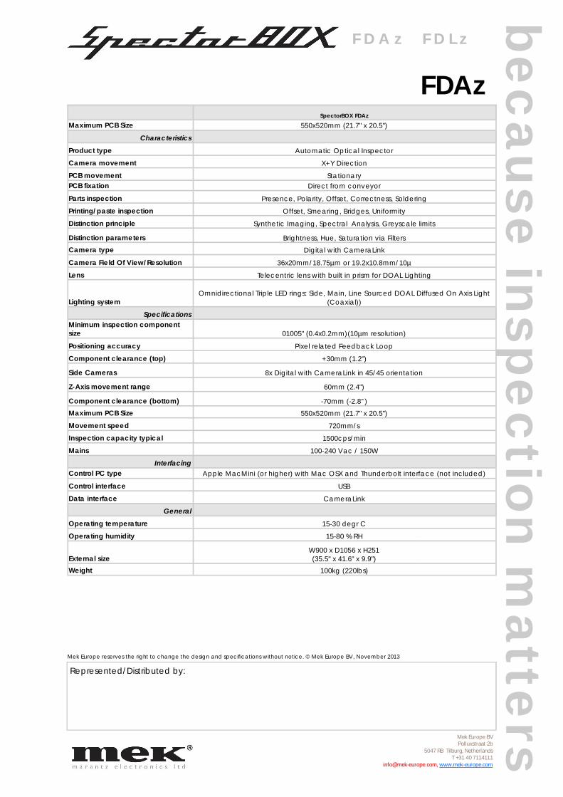
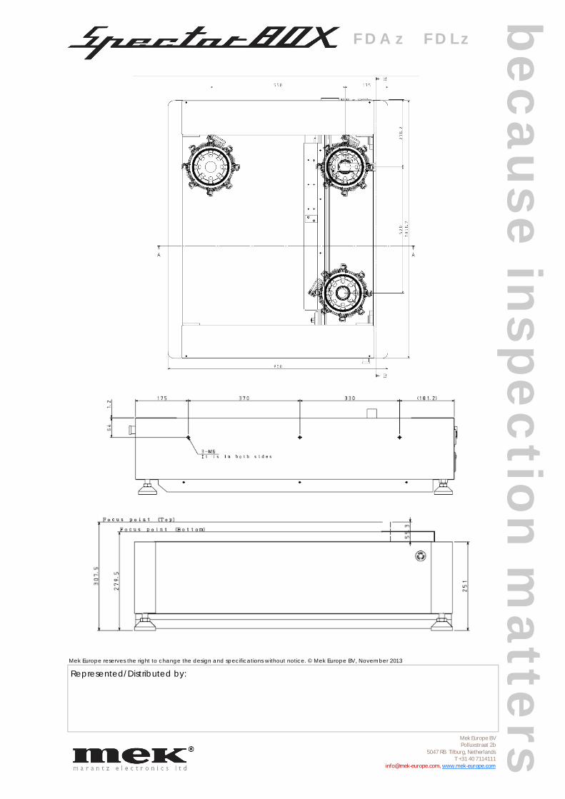
SpectorBOX FDAz Maximum PCB Size 550x520mm (21.7" x 20.5")
Characteristics
Product type Automatic Optical Inspector
Camera movement X+Y Direction
PCB movement Stationary PCB fixation Direct from conveyor
Parts inspection Presence, Polarity, Offset, Correctness, Soldering
Printing/paste inspection Offset, Smearing, Bridges, Uniformity
Distinction principle Synthetic Imaging, Spectral Analysis, Greyscale limits
Distinction parameters Brightness, Hue, Saturation via Filters Camera type Digital with CameraLink
Camera Field Of View/Resolution 36x20mm/18.75µm or 19.2x10.8mm/10µ
Lens Telecentric lens with built in prism for DOAL Lighting
Lighting system Omnidirectional Triple LED rings: Side, Main, Line Sourced DOAL Diffused On Axis Light
(Coaxial))
Specifications Minimum inspection component size 01005" (0.4x0.2mm)(10µm resolution)
Positioning accuracy Pixel related Feedback Loop
Component clearance (top) +30mm (1.2")
Side Cameras 8x Digital with CameraLink in 45/45 orientation
Z-Axis movement range 60mm (2.4")
Component clearance (bottom) -70mm (-2.8”) Maximum PCB Size 550x520mm (21.7" x 20.5")
Movement speed 720mm/s
Inspection capacity typical 1500cps/min
Mains 100-240 Vac / 150W
Interfacing Control PC type Apple MacMini (or higher) with Mac OSX and Thunderbolt interface (not included)
Control interface USB
Data interface CameraLink
General
Operating temperature 15-30 degr C
Operating humidity 15-80 % RH
External size W900 x D1056 x H251 (35.5" x 41.6" x 9.9")
Weight 100kg (220lbs)
FDAz because inspection m
atters F D A z F D L z

Mek Europe BV Polluxstraat 2b
5047 RB Tilburg, Netherlands T +31 40 7114111
[email protected], www.mek-europe.com
Represented/Distributed by: Mek Europe reserves the right to change the design and specifications without notice. © Mek Europe BV, November 2013
FDLz SpectorBOX FDLz Maximum PCB Size 550x520mm (21.7" x 20.5")
Characteristics
Product type Automatic Optical Inspector
Camera movement X+Y Direction
PCB movement Stationary PCB fixation Direct from conveyor
Parts inspection Presence, Polarity, Offset, Correctness, Soldering
Printing/paste inspection Offset, Smearing, Bridges, Uniformity
Distinction principle Synthetic Imaging, Spectral Analysis, Greyscale limits
Distinction parameters Brightness, Hue, Saturation via Filters Camera type Digital with CameraLink
Camera Field Of View/Resolution 36x20mm/18.75µm or 19.2x10.8mm/10µ
Lens Telecentric lens with built in prism for DOAL Lighting
Lighting system Omnidirectional Triple LED rings: Side, Main, Line Sourced DOAL Diffused On Axis Lighting
(Coaxial))
Specifications Minimum inspection component size 01005" (0.4x0.2mm)(10µm resolution)
Positioning accuracy Pixel related Feedback Loop
Component clearance (top) +40mm (1.57")
Side Cameras No side cameras
Z-Axis movement range 60mm (2.4")
Component clearance (bottom) -70mm (-2.8”) Maximum PCB Size 550x520mm (21.7" x 20.5")
Movement speed 720mm/s
Inspection capacity typical 1500cps/min
Mains 100-240 Vac / 150W
Interfacing Control PC type Apple MacMini (or higher) with Mac OSX and Thunderbolt interface (not included)
Control interface USB
Data interface CameraLink
General
Operating temperature 15-30 degr C
Operating humidity 15-80 % RH
External size W900 x D1056 x H251 (35.5" x 41.6" x 9.9")
Weight 100kg (220lbs)
because inspection matters
F D A z F D L z
Mek Europe BV Polluxstraat 2b
5047 RB Tilburg, Netherlands T +31 40 7114111
[email protected], www.mek-europe.com
Represented/Distributed by: Mek Europe reserves the right to change the design and specifications without notice. © Mek Europe BV, November 2013
F D A z F D L z because inspection m
atters