ezr32hg320 data sheet - silicon labs · ezr32hg wireless mcus ezr32hg320 data sheet ezr32hg320...
TRANSCRIPT
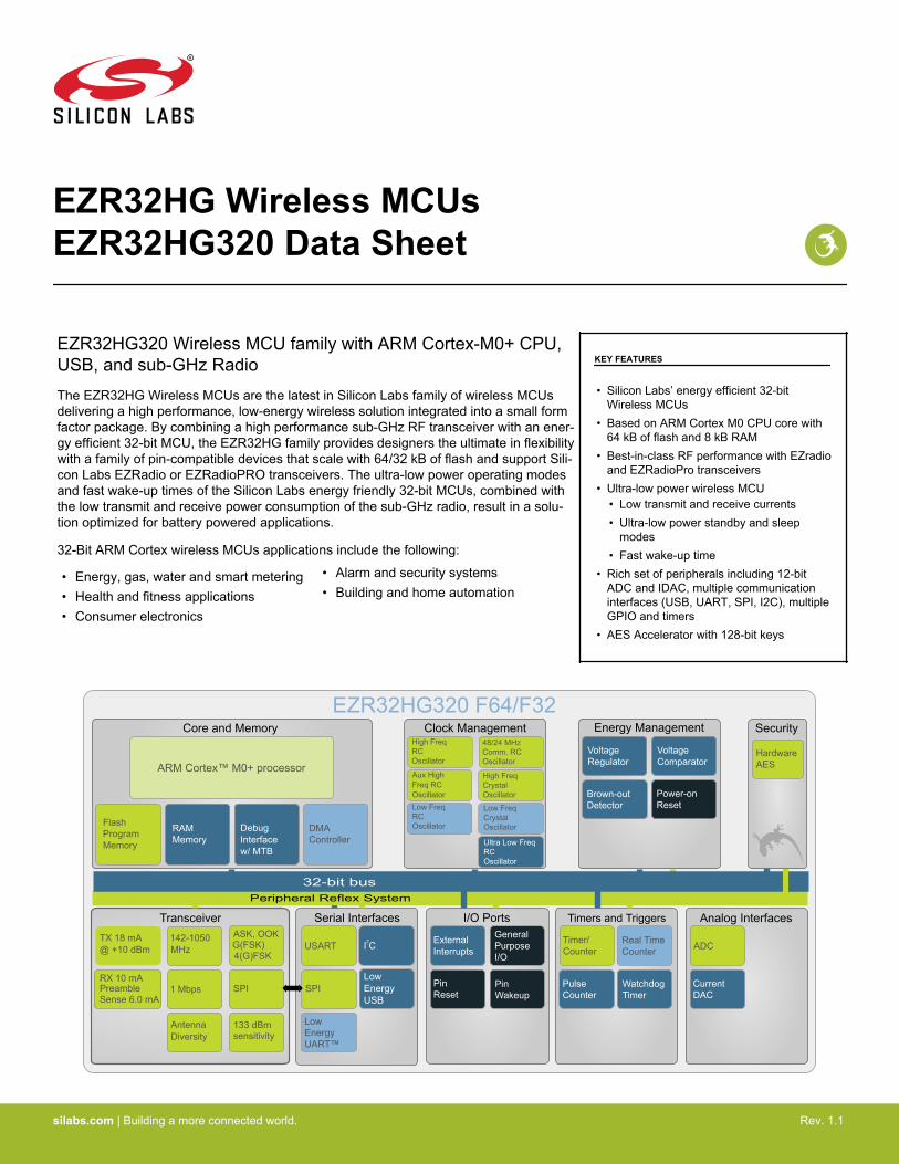
EZR32HG Wireless MCUsEZR32HG320 Data Sheet
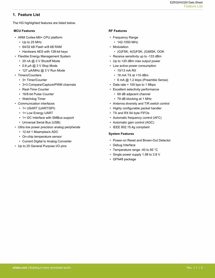
EZR32HG320 Wireless MCU family with ARM Cortex-M0+ CPU,USB, and sub-GHz RadioThe EZR32HG Wireless MCUs are the latest in Silicon Labs family of wireless MCUsdelivering a high performance, low-energy wireless solution integrated into a small formfactor package. By combining a high performance sub-GHz RF transceiver with an ener-gy efficient 32-bit MCU, the EZR32HG family provides designers the ultimate in flexibilitywith a family of pin-compatible devices that scale with 64/32 kB of flash and support Sili-con Labs EZRadio or EZRadioPRO transceivers. The ultra-low power operating modesand fast wake-up times of the Silicon Labs energy friendly 32-bit MCUs, combined withthe low transmit and receive power consumption of the sub-GHz radio, result in a solu-tion optimized for battery powered applications.
32-Bit ARM Cortex wireless MCUs applications include the following:
KEY FEATURES
• Silicon Labs’ energy efficient 32-bitWireless MCUs
• Based on ARM Cortex M0 CPU core with64 kB of flash and 8 kB RAM
• Best-in-class RF performance with EZradioand EZRadioPro transceivers
• Ultra-low power wireless MCU• Low transmit and receive currents• Ultra-low power standby and sleep
modes• Fast wake-up time
• Rich set of peripherals including 12-bitADC and IDAC, multiple communicationinterfaces (USB, UART, SPI, I2C), multipleGPIO and timers
• AES Accelerator with 128-bit keys
• Energy, gas, water and smart metering• Health and fitness applications• Consumer electronics
• Alarm and security systems• Building and home automation
Clock Management Energy Management
Serial Interfaces I/O Ports
Core and Memory
Timers and TriggersTransceiver
32-bit busPeripheral Reflex System
ARM Cortex™ M0+ processor
FlashProgramMemory
Pulse Counter
WatchdogTimer
RAMMemory
GeneralPurposeI/O
ExternalInterrupts
PinReset
EZR32HG320 F64/F32
USART I2C
Power-onReset
VoltageRegulator
VoltageComparator
Brown-outDetector
Timer/Counter
Real TimeCounter
Current DAC
LowEnergyUART™
SPI
142-1050MHz
ASK, OOKG(FSK)4(G)FSK
SPI
133 dBmsensitivity
1 Mbps
AntennaDiversity
TX 18 mA@ +10 dBm
RX 10 mAPreamble Sense 6.0 mA
PinWakeup
Analog Interfaces
ADC
Security
HardwareAES
DMAController
DebugInterfacew/ MTB
Low EnergyUSB
silabs.com | Building a more connected world. Rev. 1.1
1. Feature List
The HG highlighted features are listed below.
MCU Features
• ARM Cortex-M0+ CPU platform• Up to 25 MHz• 64/32 kB Flash w/8 kB RAM• Hardware AES with 128-bit keys
• Flexible Energy Management System• 20 nA @ 3 V Shutoff Mode• 0.6 µA @ 3 V Stop Mode• 127 µA/MHz @ 3 V Run Mode
• Timers/Counters• 3× Timer/Counter• 3×3 Compare/Capture/PWM channels• Real-Time Counter• 16/8-bit Pulse Counter• Watchdog Timer
• Communication interfaces• 1× USART (UART/SPI)• 1× Low Energy UART• 1× I2C Interface with SMBus support• Universal Serial Bus (USB)
• Ultra low power precision analog peripherals• 12-bit 1 Msamples/s ADC• On-chip temperature sensor• Current Digital to Analog Converter
• Up to 25 General Purpose I/O pins
RF Features
• Frequency Range• 142-1050 MHz
• Modulation• (G)FSK, 4(G)FSK, (G)MSK, OOK
• Receive sensitivity up to -133 dBm• Up to +20 dBm max output power• Low active power consumption
• 10/13 mA RX• 18 mA TX at +10 dBm• 6 mA @ 1.2 kbps (Preamble Sense)
• Data rate = 100 bps to 1 Mbps• Excellent selectivity performance
• 69 dB adjacent channel• 79 dB blocking at 1 MHz
• Antenna diversity and T/R switch control• Highly configurable packet handler• TX and RX 64 byte FIFOs• Automatic frequency control (AFC)• Automatic gain control (AGC)• IEEE 802.15.4g compliant
System Features
• Power-on Reset and Brown-Out Detector• Debug Interface• Temperature range -40 to 85 °C• Single power supply 1.98 to 3.8 V• QFN48 package
EZR32HG320 Data SheetFeature List
silabs.com | Building a more connected world. Rev. 1.1 | 2
2. Ordering Information
The table below shows the available EZR32HG320 devices.
Table 2.1. Ordering Information
Ordering Radio Flash (kB) RAM (kB) Power Am-plifier (dBm)
Max Sensi-tivity (dBm)
Supply Volt-age (V)
Package
EZR32HG320FxxR55G-C0 EZRadio 32-64 8 +13 -116 1.98 - 3.8 QFN48
EZR32HG320FxxR60G-C0 EZRadioPro 32-64 8 +13 -126 1.98 - 3.8 QFN48
EZR32HG320FxxR61G-C0 EZRadioPro 32-64 8 +16 -126 1.98 - 3.8 QFN48
EZR32HG320FxxR63G-C0 EZRadioPro 32-64 8 +20 -126 1.98 - 3.8 QFN48
EZR32HG320FxxR67G-C0 EZRadioPro 32-64 8 +13 -133 1.98 - 3.8 QFN48
EZR32HG320FxxR68G-C0 EZRadioPro 32-64 8 +20 -133 1.98 - 3.8 QFN48
EZR32HG320FxxR69G-C0 EZRadioPro 32-64 8 +13 & 20 -133 1.98 - 3.8 QFN48
Table 2.2. Flash Sizes
Example Part Number Flash Size
EZR32HG320F32R55G 32 kB
EZR32HG320F64R55G 64 kB
Note: Add an "(R)" at the end of the device part number to denote tape and reel option.
Visit www.silabs.com for information on global distributors and representatives.
EZR32HG320 Data SheetOrdering Information
silabs.com | Building a more connected world. Rev. 1.1 | 3
Table of Contents1. Feature List . . . . . . . . . . . . . . . . . . . . . . . . . . . . . . . . 2
2. Ordering Information . . . . . . . . . . . . . . . . . . . . . . . . . . . . 3
3. System Overview . . . . . . . . . . . . . . . . . . . . . . . . . . . . . . 73.1 Introduction . . . . . . . . . . . . . . . . . . . . . . . . . . . . . . . 7
3.1.1 ARM Cortex-M0+ Core . . . . . . . . . . . . . . . . . . . . . . . . . . 73.1.2 Debugging Interface (DBG) . . . . . . . . . . . . . . . . . . . . . . . . 73.1.3 Memory System Controller (MSC) . . . . . . . . . . . . . . . . . . . . . . 73.1.4 Direct Memory Access Controller (DMA) . . . . . . . . . . . . . . . . . . . . 83.1.5 Reset Management Unit (RMU) . . . . . . . . . . . . . . . . . . . . . . . 83.1.6 Energy Management Unit (EMU) . . . . . . . . . . . . . . . . . . . . . . 83.1.7 Clock Management Unit (CMU) . . . . . . . . . . . . . . . . . . . . . . . 83.1.8 Watchdog (WDOG) . . . . . . . . . . . . . . . . . . . . . . . . . . . 83.1.9 Peripheral Reflex System (PRS) . . . . . . . . . . . . . . . . . . . . . . 83.1.10 Universal Serial Bus Controller (USB) . . . . . . . . . . . . . . . . . . . . 83.1.11 Inter-Integrated Circuit Interface (I2C) . . . . . . . . . . . . . . . . . . . . 83.1.12 Universal Synchronous/Asynchronous Receiver/Transmitter (USART) . . . . . . . . . 83.1.13 Pre-Programmed USB/UART Bootloader . . . . . . . . . . . . . . . . . . . 83.1.14 Low Energy Universal Asynchronous Receiver/Transmitter (LEUART) . . . . . . . . . 93.1.15 Timer/Counter (TIMER) . . . . . . . . . . . . . . . . . . . . . . . . . 93.1.16 Real Time Counter (RTC) . . . . . . . . . . . . . . . . . . . . . . . . 93.1.17 Pulse Counter (PCNT) . . . . . . . . . . . . . . . . . . . . . . . . . 93.1.18 Voltage Comparator (VCMP) . . . . . . . . . . . . . . . . . . . . . . . 93.1.19 Analog to Digital Converter (ADC) . . . . . . . . . . . . . . . . . . . . . 93.1.20 Current Digital to Analog Converter (IDAC) . . . . . . . . . . . . . . . . . . 93.1.21 Advanced Encryption Standard Accelerator (AES) . . . . . . . . . . . . . . . . 93.1.22 General Purpose Input/Output (GPIO) . . . . . . . . . . . . . . . . . . . . 93.1.23 EZRadio® and EZRadioPro® Transceivers. . . . . . . . . . . . . . . . . . .10
3.2 Configuration Summary . . . . . . . . . . . . . . . . . . . . . . . . . . .11
3.3 Memory Map . . . . . . . . . . . . . . . . . . . . . . . . . . . . . .12
4. Electrical Specifications . . . . . . . . . . . . . . . . . . . . . . . . . . 134.1 Test Conditions . . . . . . . . . . . . . . . . . . . . . . . . . . . . . .13
4.1.1 Typical Values . . . . . . . . . . . . . . . . . . . . . . . . . . . .134.1.2 Minimum and Maximum Values . . . . . . . . . . . . . . . . . . . . . . .13
4.2 Absolute Maximum Ratings. . . . . . . . . . . . . . . . . . . . . . . . . .13
4.3 Thermal Characteristics . . . . . . . . . . . . . . . . . . . . . . . . . . .14
4.4 General Operating Conditions . . . . . . . . . . . . . . . . . . . . . . . . .14
4.5 Current Consumption . . . . . . . . . . . . . . . . . . . . . . . . . . . .154.5.1 EM0 Current Consumption . . . . . . . . . . . . . . . . . . . . . . . .174.5.2 EM1 Current Consumption . . . . . . . . . . . . . . . . . . . . . . . .204.5.3 EM2 Current Consumption . . . . . . . . . . . . . . . . . . . . . . . .224.5.4 EM3 Current Consumption . . . . . . . . . . . . . . . . . . . . . . . .234.5.5 EM4 Current Consumption . . . . . . . . . . . . . . . . . . . . . . . .23
silabs.com | Building a more connected world. Rev. 1.1 | 4
4.6 Transitions between Energy Modes . . . . . . . . . . . . . . . . . . . . . . .24
4.7 Power Management . . . . . . . . . . . . . . . . . . . . . . . . . . . .24
4.8 Flash . . . . . . . . . . . . . . . . . . . . . . . . . . . . . . . . .25
4.9 General Purpose Input Output . . . . . . . . . . . . . . . . . . . . . . . . .26
4.10 Oscillators . . . . . . . . . . . . . . . . . . . . . . . . . . . . . . .344.10.1 LFXO . . . . . . . . . . . . . . . . . . . . . . . . . . . . . . .344.10.2 HFXO . . . . . . . . . . . . . . . . . . . . . . . . . . . . . . .344.10.3 LFRCO . . . . . . . . . . . . . . . . . . . . . . . . . . . . . .354.10.4 HFRCO . . . . . . . . . . . . . . . . . . . . . . . . . . . . . .364.10.5 AUXHFRCO . . . . . . . . . . . . . . . . . . . . . . . . . . . . .394.10.6 USHFRCO . . . . . . . . . . . . . . . . . . . . . . . . . . . . .404.10.7 ULFRCO . . . . . . . . . . . . . . . . . . . . . . . . . . . . . .40
4.11 Analog Digital Converter (ADC) . . . . . . . . . . . . . . . . . . . . . . . .414.11.1 Typical Performance . . . . . . . . . . . . . . . . . . . . . . . . . .48
4.12 Current Digital Analog Converter (IDAC) . . . . . . . . . . . . . . . . . . . . .54
4.13 Voltage Comparator (VCMP) . . . . . . . . . . . . . . . . . . . . . . . . .59
4.14 I2C . . . . . . . . . . . . . . . . . . . . . . . . . . . . . . . . .60
4.15 USB . . . . . . . . . . . . . . . . . . . . . . . . . . . . . . . . .61
4.16 Radio. . . . . . . . . . . . . . . . . . . . . . . . . . . . . . . . .614.16.1 EZRadioPRO (R6x) DC Electrical Characteristics . . . . . . . . . . . . . . . .624.16.2 EZRadioPRO (R6x) Synthesizer AC Electrical Characteristics . . . . . . . . . . . .634.16.3 EZRadioPRO (R6x) Receiver AC Electrical Characteristics . . . . . . . . . . . . .644.16.4 EZRadioPRO (R6x) Transmitter AC Electrical Characteristics . . . . . . . . . . . .674.16.5 EZRadioPRO (R6x) Radio Auxillary Block Specifications . . . . . . . . . . . . . .684.16.6 EZRadio (R55) DC Electrical Characteristics . . . . . . . . . . . . . . . . . .694.16.7 EZRadio (R55) Synthesizer AC Electrical Characteristics . . . . . . . . . . . . . .694.16.8 EZRadio (R55) Receiver AC Electrical Characteristics . . . . . . . . . . . . . . .704.16.9 EZRadio (R55) Transmitter AC Electrical Characteristics . . . . . . . . . . . . . .714.16.10 EZRadio (R55) Radio Auxiliary Block Specifications . . . . . . . . . . . . . . .724.16.11 Radio Digital I/O Specification . . . . . . . . . . . . . . . . . . . . . .73
4.17 Digital Peripherals . . . . . . . . . . . . . . . . . . . . . . . . . . . .74
5. Pinout and Package . . . . . . . . . . . . . . . . . . . . . . . . . . . . 755.1 Pinout . . . . . . . . . . . . . . . . . . . . . . . . . . . . . . . . .75
5.2 Pin Descriptions . . . . . . . . . . . . . . . . . . . . . . . . . . . . .76
5.3 Alternate Functionality Pinout . . . . . . . . . . . . . . . . . . . . . . . . .78
5.4 GPIO Pinout Overview . . . . . . . . . . . . . . . . . . . . . . . . . . .80
5.5 QFN48 Package . . . . . . . . . . . . . . . . . . . . . . . . . . . . .81
6. PCB Layout and Soldering . . . . . . . . . . . . . . . . . . . . . . . . . 836.1 Recommended PCB Layout . . . . . . . . . . . . . . . . . . . . . . . . .83
6.2 Soldering Information . . . . . . . . . . . . . . . . . . . . . . . . . . . .84
7. Top Marking. . . . . . . . . . . . . . . . . . . . . . . . . . . . . . . 85
silabs.com | Building a more connected world. Rev. 1.1 | 5
8. Revision History . . . . . . . . . . . . . . . . . . . . . . . . . . . . . 86
silabs.com | Building a more connected world. Rev. 1.1 | 6
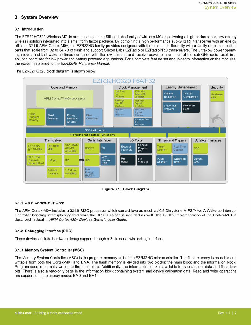
3. System Overview
3.1 Introduction
The EZR32HG320 Wireless MCUs are the latest in the Silicon Labs family of wireless MCUs delivering a high-performance, low-energywireless solution integrated into a small form factor package. By combining a high performance sub-GHz RF transceiver with an energyefficient 32-bit ARM Cortex-M0+, the EZR32HG family provides designers with the ultimate in flexibility with a family of pin-compatibleparts that scale from 32 to 64 kB of flash and support Silicon Labs EZRadio or EZRadioPRO transceivers. The ultra-low power operat-ing modes and fast wake-up times combined with the low transmit and receive power consumption of the sub-GHz radio result in asolution optimized for low power and battery powered applications. For a complete feature set and in-depth information on the modules,the reader is referred to the EZR32HG Reference Manual.
The EZR32HG320 block diagram is shown below.
Clock Management Energy Management
Serial Interfaces I/O Ports
Core and Memory
Timers and TriggersTransceiver
32-bit busPeripheral Reflex System
ARM Cortex™ M0+ processor
FlashProgramMemory
Pulse Counter
WatchdogTimer
RAMMemory
GeneralPurposeI/O
ExternalInterrupts
PinReset
EZR32HG320 F64/F32
USART I2C
Power-onReset
VoltageRegulator
VoltageComparator
Brown-outDetector
Timer/Counter
Real TimeCounter
Current DAC
LowEnergyUART™
SPI
142-1050MHz
ASK, OOKG(FSK)4(G)FSK
SPI
133 dBmsensitivity
1 Mbps
AntennaDiversity
TX 18 mA@ +10 dBm
RX 10 mAPreamble Sense 6.0 mA
PinWakeup
Analog Interfaces
ADC
Security
HardwareAES
DMAController
DebugInterfacew/ MTB
Low EnergyUSB
Figure 3.1. Block Diagram
3.1.1 ARM Cortex-M0+ Core
The ARM Cortex-M0+ includes a 32-bit RISC processor which can achieve as much as 0.9 Dhrystone MIPS/MHz. A Wake-up InterruptController handling interrupts triggered while the CPU is asleep is included as well. The EZR32 implementation of the Cortex-M0+ isdescribed in detail in ARM Cortex-M0+ Devices Generic User Guide.
3.1.2 Debugging Interface (DBG)
These devices include hardware debug support through a 2-pin serial-wire debug interface.
3.1.3 Memory System Controller (MSC)
The Memory System Controller (MSC) is the program memory unit of the EZR32HG microcontroller. The flash memory is readable andwritable from both the Cortex-M0+ and DMA. The flash memory is divided into two blocks: the main block and the information block.Program code is normally written to the main block. Additionally, the information block is available for special user data and flash lockbits. There is also a read-only page in the information block containing system and device calibration data. Read and write operationsare supported in the energy modes EM0 and EM1.
EZR32HG320 Data SheetSystem Overview
silabs.com | Building a more connected world. Rev. 1.1 | 7
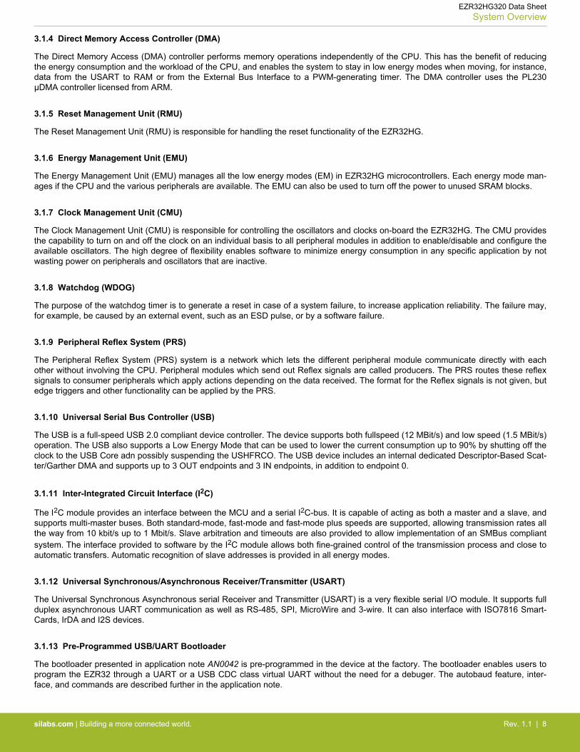
3.1.4 Direct Memory Access Controller (DMA)
The Direct Memory Access (DMA) controller performs memory operations independently of the CPU. This has the benefit of reducingthe energy consumption and the workload of the CPU, and enables the system to stay in low energy modes when moving, for instance,data from the USART to RAM or from the External Bus Interface to a PWM-generating timer. The DMA controller uses the PL230µDMA controller licensed from ARM.
3.1.5 Reset Management Unit (RMU)
The Reset Management Unit (RMU) is responsible for handling the reset functionality of the EZR32HG.
3.1.6 Energy Management Unit (EMU)
The Energy Management Unit (EMU) manages all the low energy modes (EM) in EZR32HG microcontrollers. Each energy mode man-ages if the CPU and the various peripherals are available. The EMU can also be used to turn off the power to unused SRAM blocks.
3.1.7 Clock Management Unit (CMU)
The Clock Management Unit (CMU) is responsible for controlling the oscillators and clocks on-board the EZR32HG. The CMU providesthe capability to turn on and off the clock on an individual basis to all peripheral modules in addition to enable/disable and configure theavailable oscillators. The high degree of flexibility enables software to minimize energy consumption in any specific application by notwasting power on peripherals and oscillators that are inactive.
3.1.8 Watchdog (WDOG)
The purpose of the watchdog timer is to generate a reset in case of a system failure, to increase application reliability. The failure may,for example, be caused by an external event, such as an ESD pulse, or by a software failure.
3.1.9 Peripheral Reflex System (PRS)
The Peripheral Reflex System (PRS) system is a network which lets the different peripheral module communicate directly with eachother without involving the CPU. Peripheral modules which send out Reflex signals are called producers. The PRS routes these reflexsignals to consumer peripherals which apply actions depending on the data received. The format for the Reflex signals is not given, butedge triggers and other functionality can be applied by the PRS.
3.1.10 Universal Serial Bus Controller (USB)
The USB is a full-speed USB 2.0 compliant device controller. The device supports both fullspeed (12 MBit/s) and low speed (1.5 MBit/s)operation. The USB also supports a Low Energy Mode that can be used to lower the current consumption up to 90% by shutting off theclock to the USB Core adn possibly suspending the USHFRCO. The USB device includes an internal dedicated Descriptor-Based Scat-ter/Garther DMA and supports up to 3 OUT endpoints and 3 IN endpoints, in addition to endpoint 0.
3.1.11 Inter-Integrated Circuit Interface (I2C)
The I2C module provides an interface between the MCU and a serial I2C-bus. It is capable of acting as both a master and a slave, andsupports multi-master buses. Both standard-mode, fast-mode and fast-mode plus speeds are supported, allowing transmission rates allthe way from 10 kbit/s up to 1 Mbit/s. Slave arbitration and timeouts are also provided to allow implementation of an SMBus compliantsystem. The interface provided to software by the I2C module allows both fine-grained control of the transmission process and close toautomatic transfers. Automatic recognition of slave addresses is provided in all energy modes.
3.1.12 Universal Synchronous/Asynchronous Receiver/Transmitter (USART)
The Universal Synchronous Asynchronous serial Receiver and Transmitter (USART) is a very flexible serial I/O module. It supports fullduplex asynchronous UART communication as well as RS-485, SPI, MicroWire and 3-wire. It can also interface with ISO7816 Smart-Cards, IrDA and I2S devices.
3.1.13 Pre-Programmed USB/UART Bootloader
The bootloader presented in application note AN0042 is pre-programmed in the device at the factory. The bootloader enables users toprogram the EZR32 through a UART or a USB CDC class virtual UART without the need for a debuger. The autobaud feature, inter-face, and commands are described further in the application note.
EZR32HG320 Data SheetSystem Overview
silabs.com | Building a more connected world. Rev. 1.1 | 8
3.1.14 Low Energy Universal Asynchronous Receiver/Transmitter (LEUART)
The unique Low Energy Universal Asynchronous Receiver/Transmitter (LEUART™), the Low Energy UART, is a UART that allows two-way UART communication on a strict power budget. Only a 32.768 kHz clock is needed to allow UART communication up to 9600baud/s. The LEUART includes all necessary hardware support to make asynchronous serial communication possible with minimum ofsoftware intervention and energy consumption.
3.1.15 Timer/Counter (TIMER)
The 16-bit general purpose Timer has 3 compare/capture channels for input capture and compare/Pulse-Width Modulation (PWM) out-put. TIMER0 also includes a Dead-Time Insertion module suitable for motor control applications.
3.1.16 Real Time Counter (RTC)
The Real Time Counter (RTC) contains a 24-bit counter and is clocked either by a 32.768 kHz crystal oscillator, or a 32.768 kHz RCoscillator. In addition to energy modes EM0 and EM1, the RTC is also available in EM2. This makes it ideal for keeping track of timesince the RTC is enabled in EM2 where most of the device is powered down.
3.1.17 Pulse Counter (PCNT)
The Pulse Counter (PCNT) can be used for counting pulses on a single input or to decode quadrature encoded inputs. It runs off eitherthe internal LFACLK or the PCNTn_S0IN pin as external clock source. The module may operate in energy mode EM0 - EM3.
3.1.18 Voltage Comparator (VCMP)
The Voltage Supply Comparator (VCMP) is used to monitor the supply voltage from software. An interrupt can be generated when thesupply falls below or rises above a programmable threshold. Response time and thereby also the current consumption can be config-ured by altering the current supply to the comparator.
3.1.19 Analog to Digital Converter (ADC)
The Analog to Digital Converter (ADC) is a Successive Approximation Register (SAR) architecture, with a resolution of up to 12 bits atup to one million samples per second. The integrated input mux can select inputs from 4 external pins and 6 internal signals.
3.1.20 Current Digital to Analog Converter (IDAC)
The current digital to analog converter (IDAC) can source or sink a configurable constant current, which can be output on, or sinkedfrom pin or ADC. The current is configurable with several ranges of various step sizes.
3.1.21 Advanced Encryption Standard Accelerator (AES)
The Advanced Encryption Standard Accelerator (AES) performs AES encryption and decryption with 128-bit keys. Encrypting or de-crypting one 128-bit data block takes 52 HFCORECLK cycles with 128-bit keys. The AES module is an AHB slave which enables effi-cient access to the data and key registers. All write accesses to the AES module must be 32-bit operations (i.e., 8- or 16-bit operationsare not supported).
3.1.22 General Purpose Input/Output (GPIO)
In the EZR32HG320, there are 25 General Purpose Input/Output (GPIO) pins, which are divided into ports with up to 16 pins each.These pins can individually be configured as either an output or input. More advanced configurations like open-drain, filtering and drivestrength can also be configured individually for the pins. The GPIO pins can also be overridden by peripheral pin connections, like Tim-er PWM outputs or USART communication, which can be routed to several locations on the device. The GPIO supports up to 16 asyn-chronous external pin interrupts, which enables interrupts from any pin on the device. Also, the input value of a pin can be routedthrough the Peripheral Reflex System to other peripherals.
EZR32HG320 Data SheetSystem Overview
silabs.com | Building a more connected world. Rev. 1.1 | 9
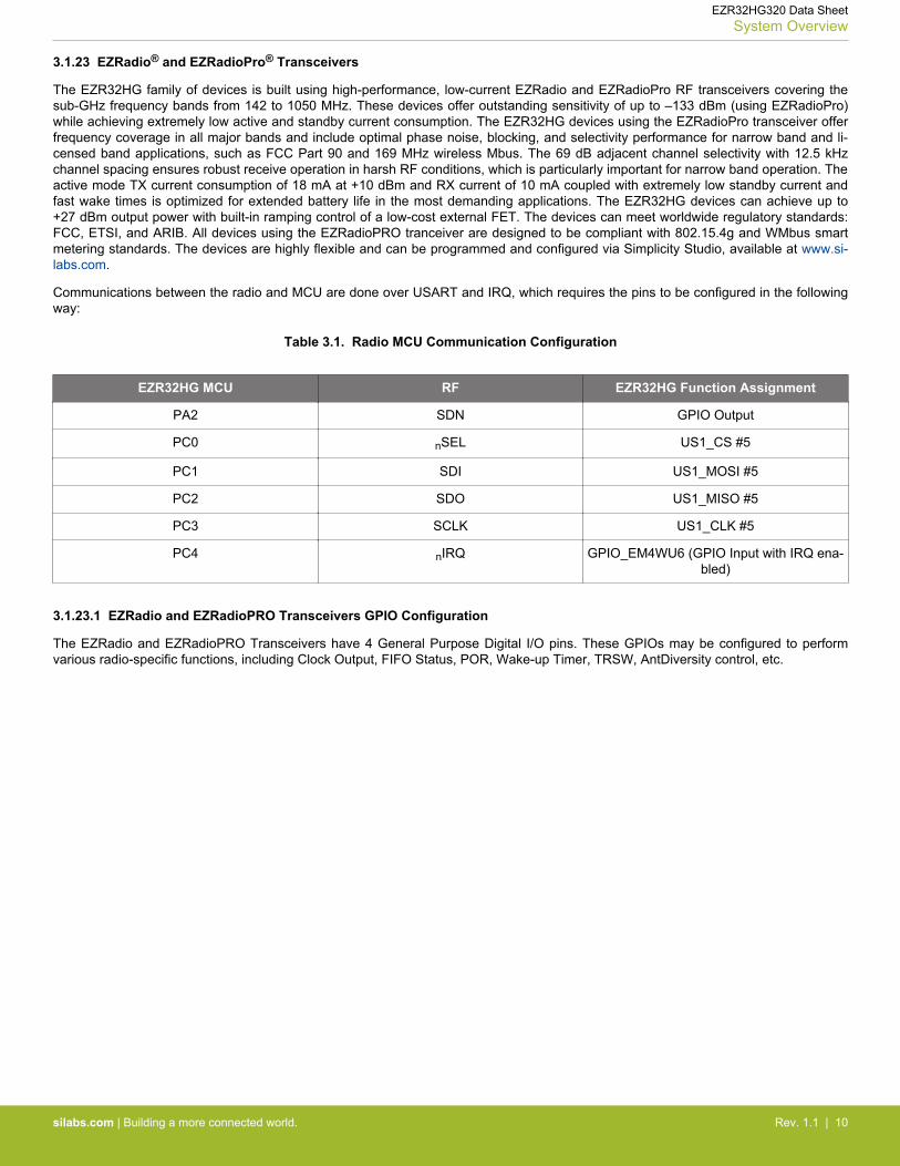
3.1.23 EZRadio® and EZRadioPro® Transceivers
The EZR32HG family of devices is built using high-performance, low-current EZRadio and EZRadioPro RF transceivers covering thesub-GHz frequency bands from 142 to 1050 MHz. These devices offer outstanding sensitivity of up to –133 dBm (using EZRadioPro)while achieving extremely low active and standby current consumption. The EZR32HG devices using the EZRadioPro transceiver offerfrequency coverage in all major bands and include optimal phase noise, blocking, and selectivity performance for narrow band and li-censed band applications, such as FCC Part 90 and 169 MHz wireless Mbus. The 69 dB adjacent channel selectivity with 12.5 kHzchannel spacing ensures robust receive operation in harsh RF conditions, which is particularly important for narrow band operation. Theactive mode TX current consumption of 18 mA at +10 dBm and RX current of 10 mA coupled with extremely low standby current andfast wake times is optimized for extended battery life in the most demanding applications. The EZR32HG devices can achieve up to+27 dBm output power with built-in ramping control of a low-cost external FET. The devices can meet worldwide regulatory standards:FCC, ETSI, and ARIB. All devices using the EZRadioPRO tranceiver are designed to be compliant with 802.15.4g and WMbus smartmetering standards. The devices are highly flexible and can be programmed and configured via Simplicity Studio, available at www.si-labs.com.
Communications between the radio and MCU are done over USART and IRQ, which requires the pins to be configured in the followingway:
Table 3.1. Radio MCU Communication Configuration
EZR32HG MCU RF EZR32HG Function Assignment
PA2 SDN GPIO Output
PC0 nSEL US1_CS #5
PC1 SDI US1_MOSI #5
PC2 SDO US1_MISO #5
PC3 SCLK US1_CLK #5
PC4 nIRQ GPIO_EM4WU6 (GPIO Input with IRQ ena-bled)
3.1.23.1 EZRadio and EZRadioPRO Transceivers GPIO Configuration
The EZRadio and EZRadioPRO Transceivers have 4 General Purpose Digital I/O pins. These GPIOs may be configured to performvarious radio-specific functions, including Clock Output, FIFO Status, POR, Wake-up Timer, TRSW, AntDiversity control, etc.
EZR32HG320 Data SheetSystem Overview
silabs.com | Building a more connected world. Rev. 1.1 | 10
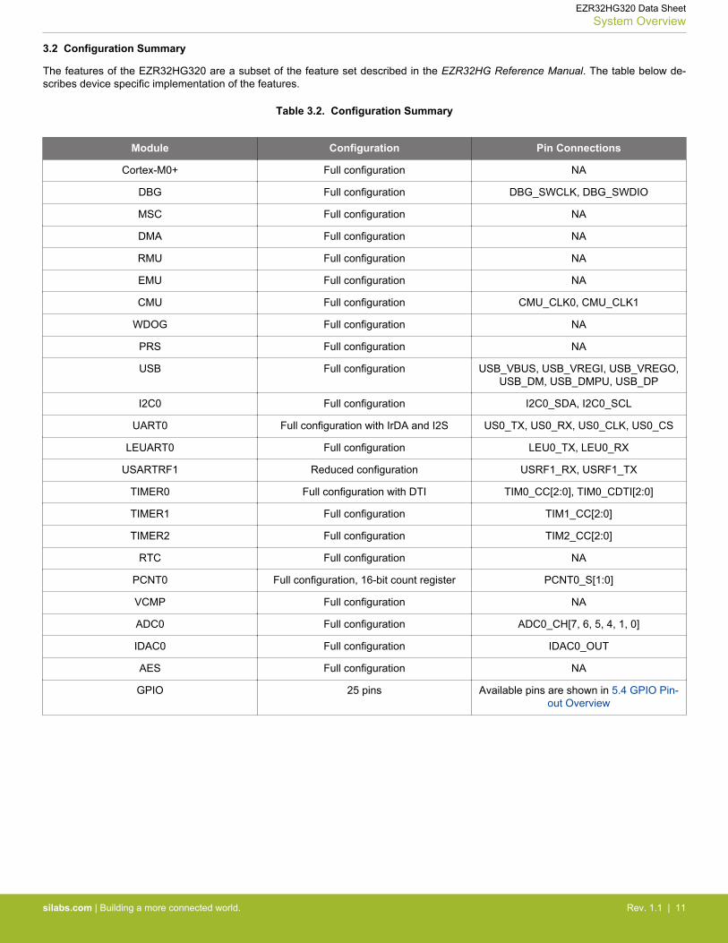
3.2 Configuration Summary
The features of the EZR32HG320 are a subset of the feature set described in the EZR32HG Reference Manual. The table below de-scribes device specific implementation of the features.
Table 3.2. Configuration Summary
Module Configuration Pin Connections
Cortex-M0+ Full configuration NA
DBG Full configuration DBG_SWCLK, DBG_SWDIO
MSC Full configuration NA
DMA Full configuration NA
RMU Full configuration NA
EMU Full configuration NA
CMU Full configuration CMU_CLK0, CMU_CLK1
WDOG Full configuration NA
PRS Full configuration NA
USB Full configuration USB_VBUS, USB_VREGI, USB_VREGO,USB_DM, USB_DMPU, USB_DP
I2C0 Full configuration I2C0_SDA, I2C0_SCL
UART0 Full configuration with IrDA and I2S US0_TX, US0_RX, US0_CLK, US0_CS
LEUART0 Full configuration LEU0_TX, LEU0_RX
USARTRF1 Reduced configuration USRF1_RX, USRF1_TX
TIMER0 Full configuration with DTI TIM0_CC[2:0], TIM0_CDTI[2:0]
TIMER1 Full configuration TIM1_CC[2:0]
TIMER2 Full configuration TIM2_CC[2:0]
RTC Full configuration NA
PCNT0 Full configuration, 16-bit count register PCNT0_S[1:0]
VCMP Full configuration NA
ADC0 Full configuration ADC0_CH[7, 6, 5, 4, 1, 0]
IDAC0 Full configuration IDAC0_OUT
AES Full configuration NA
GPIO 25 pins Available pins are shown in 5.4 GPIO Pin-out Overview
EZR32HG320 Data SheetSystem Overview
silabs.com | Building a more connected world. Rev. 1.1 | 11
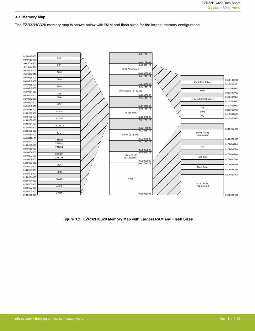
3.3 Memory Map
The EZR32HG320 memory map is shown below with RAM and flash sizes for the largest memory configuration.
Figure 3.2. EZR32HG320 Memory Map with Largest RAM and Flash Sizes
EZR32HG320 Data SheetSystem Overview
silabs.com | Building a more connected world. Rev. 1.1 | 12
4. Electrical Specifications
4.1 Test Conditions
4.1.1 Typical Values
The typical data are based on TAMB = 25°C and VDD = 3.0 V, as defined in Table 4.3 General Operating Conditions on page 14, bysimulation and/or technology characterisation unless otherwise specified.
4.1.2 Minimum and Maximum Values
The minimum and maximum values represent the worst conditions of ambient temperature, supply voltage and frequencies, as definedin Table 4.3 General Operating Conditions on page 14, by simulation and/or technology characterisation unless otherwise specified.
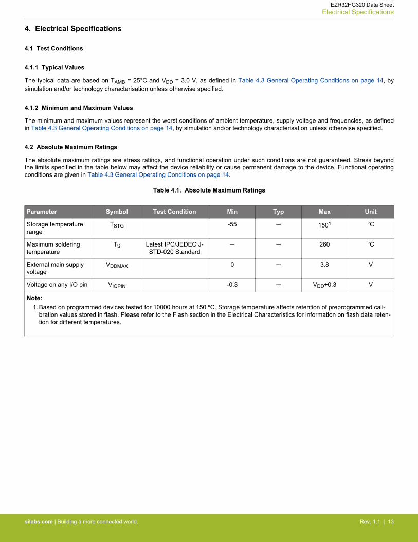
4.2 Absolute Maximum Ratings
The absolute maximum ratings are stress ratings, and functional operation under such conditions are not guaranteed. Stress beyondthe limits specified in the table below may affect the device reliability or cause permanent damage to the device. Functional operatingconditions are given in Table 4.3 General Operating Conditions on page 14.
Table 4.1. Absolute Maximum Ratings
Parameter Symbol Test Condition Min Typ Max Unit
Storage temperaturerange
TSTG -55 ─ 1501 °C
Maximum solderingtemperature
TS Latest IPC/JEDEC J-STD-020 Standard
─ ─ 260 °C
External main supplyvoltage
VDDMAX 0 ─ 3.8 V
Voltage on any I/O pin VIOPIN -0.3 ─ VDD+0.3 V
Note:1. Based on programmed devices tested for 10000 hours at 150 ºC. Storage temperature affects retention of preprogrammed cali-
bration values stored in flash. Please refer to the Flash section in the Electrical Characteristics for information on flash data reten-tion for different temperatures.
EZR32HG320 Data SheetElectrical Specifications
silabs.com | Building a more connected world. Rev. 1.1 | 13
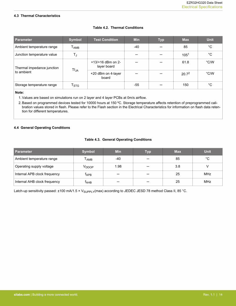
4.3 Thermal Characteristics
Table 4.2. Thermal Conditions
Parameter Symbol Test Condition Min Typ Max Unit
Ambient temperature range TAMB -40 ─ 85 °C
Junction temperature value TJ ─ ─ 1051 °C
Thermal impedance junctionto ambient
TIJA
+13/+16 dBm on 2-layer board
─ ─ 61.8 °C/W
+20 dBm on 4-layerboard
─ ─ 20.72 °C/W
Storage temperature range TSTG -55 ─ 150 °C
Note:1. Values are based on simulations run on 2 layer and 4 layer PCBs at 0m/s airflow.2. Based on programmed devices tested for 10000 hours at 150 ºC. Storage temperature affects retention of preprogrammed cali-
bration values stored in flash. Please refer to the Flash section in the Electrical Characteristics for information on flash data reten-tion for different temperatures.
4.4 General Operating Conditions
Table 4.3. General Operating Conditions
Parameter Symbol Min Typ Max Unit
Ambient temperature range TAMB -40 ─ 85 °C
Operating supply voltage VDDOP 1.98 ─ 3.8 V
Internal APB clock frequency fAPB ─ ─ 25 MHz
Internal AHB clock frequency fAHB ─ ─ 25 MHz
Latch-up sensitivity passed: ±100 mA/1.5 × VSUPPLY(max) according to JEDEC JESD 78 method Class II, 85 °C.
EZR32HG320 Data SheetElectrical Specifications
silabs.com | Building a more connected world. Rev. 1.1 | 14
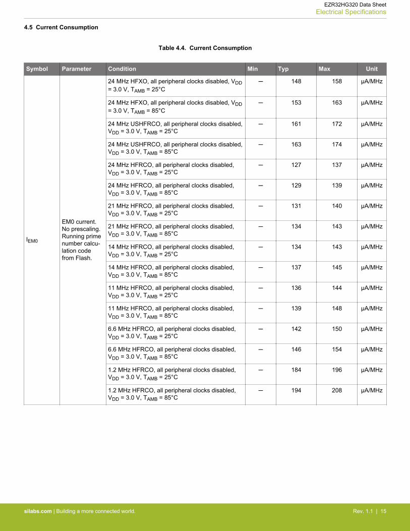
4.5 Current Consumption
Table 4.4. Current Consumption
Symbol Parameter Condition Min Typ Max Unit
IEM0
EM0 current.No prescaling.Running primenumber calcu-lation codefrom Flash.
24 MHz HFXO, all peripheral clocks disabled, VDD= 3.0 V, TAMB = 25°C
─ 148 158 µA/MHz
24 MHz HFXO, all peripheral clocks disabled, VDD= 3.0 V, TAMB = 85°C
─ 153 163 µA/MHz
24 MHz USHFRCO, all peripheral clocks disabled,VDD = 3.0 V, TAMB = 25°C
─ 161 172 µA/MHz
24 MHz USHFRCO, all peripheral clocks disabled,VDD = 3.0 V, TAMB = 85°C
─ 163 174 µA/MHz
24 MHz HFRCO, all peripheral clocks disabled,VDD = 3.0 V, TAMB = 25°C
─ 127 137 µA/MHz
24 MHz HFRCO, all peripheral clocks disabled,VDD = 3.0 V, TAMB = 85°C
─ 129 139 µA/MHz
21 MHz HFRCO, all peripheral clocks disabled,VDD = 3.0 V, TAMB = 25°C
─ 131 140 µA/MHz
21 MHz HFRCO, all peripheral clocks disabled,VDD = 3.0 V, TAMB = 85°C
─ 134 143 µA/MHz
14 MHz HFRCO, all peripheral clocks disabled,VDD = 3.0 V, TAMB = 25°C
─ 134 143 µA/MHz
14 MHz HFRCO, all peripheral clocks disabled,VDD = 3.0 V, TAMB = 85°C
─ 137 145 µA/MHz
11 MHz HFRCO, all peripheral clocks disabled,VDD = 3.0 V, TAMB = 25°C
─ 136 144 µA/MHz
11 MHz HFRCO, all peripheral clocks disabled,VDD = 3.0 V, TAMB = 85°C
─ 139 148 µA/MHz
6.6 MHz HFRCO, all peripheral clocks disabled,VDD = 3.0 V, TAMB = 25°C
─ 142 150 µA/MHz
6.6 MHz HFRCO, all peripheral clocks disabled,VDD = 3.0 V, TAMB = 85°C
─ 146 154 µA/MHz
1.2 MHz HFRCO, all peripheral clocks disabled,VDD = 3.0 V, TAMB = 25°C
─ 184 196 µA/MHz
1.2 MHz HFRCO, all peripheral clocks disabled,VDD = 3.0 V, TAMB = 85°C
─ 194 208 µA/MHz
EZR32HG320 Data SheetElectrical Specifications
silabs.com | Building a more connected world. Rev. 1.1 | 15
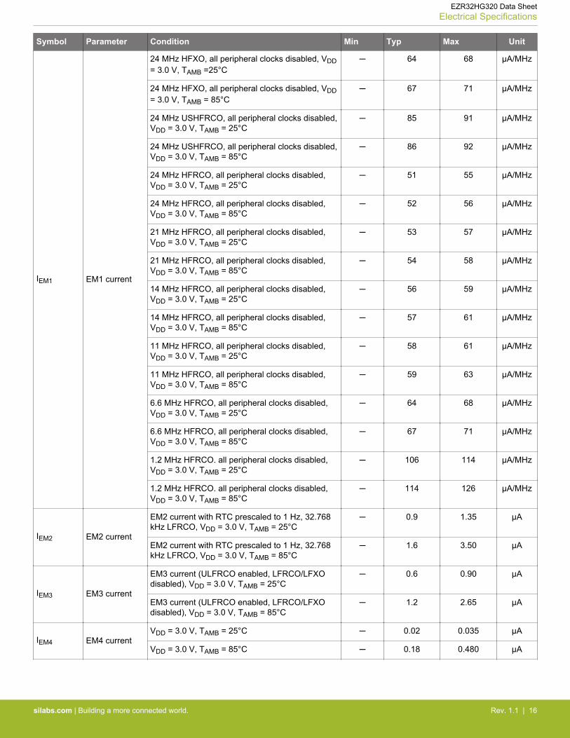
Symbol Parameter Condition Min Typ Max Unit
IEM1 EM1 current
24 MHz HFXO, all peripheral clocks disabled, VDD= 3.0 V, TAMB =25°C
─ 64 68 µA/MHz
24 MHz HFXO, all peripheral clocks disabled, VDD= 3.0 V, TAMB = 85°C
─ 67 71 µA/MHz
24 MHz USHFRCO, all peripheral clocks disabled,VDD = 3.0 V, TAMB = 25°C
─ 85 91 µA/MHz
24 MHz USHFRCO, all peripheral clocks disabled,VDD = 3.0 V, TAMB = 85°C
─ 86 92 µA/MHz
24 MHz HFRCO, all peripheral clocks disabled,VDD = 3.0 V, TAMB = 25°C
─ 51 55 µA/MHz
24 MHz HFRCO, all peripheral clocks disabled,VDD = 3.0 V, TAMB = 85°C
─ 52 56 µA/MHz
21 MHz HFRCO, all peripheral clocks disabled,VDD = 3.0 V, TAMB = 25°C
─ 53 57 µA/MHz
21 MHz HFRCO, all peripheral clocks disabled,VDD = 3.0 V, TAMB = 85°C
─ 54 58 µA/MHz
14 MHz HFRCO, all peripheral clocks disabled,VDD = 3.0 V, TAMB = 25°C
─ 56 59 µA/MHz
14 MHz HFRCO, all peripheral clocks disabled,VDD = 3.0 V, TAMB = 85°C
─ 57 61 µA/MHz
11 MHz HFRCO, all peripheral clocks disabled,VDD = 3.0 V, TAMB = 25°C
─ 58 61 µA/MHz
11 MHz HFRCO, all peripheral clocks disabled,VDD = 3.0 V, TAMB = 85°C
─ 59 63 µA/MHz
6.6 MHz HFRCO, all peripheral clocks disabled,VDD = 3.0 V, TAMB = 25°C
─ 64 68 µA/MHz
6.6 MHz HFRCO, all peripheral clocks disabled,VDD = 3.0 V, TAMB = 85°C
─ 67 71 µA/MHz
1.2 MHz HFRCO. all peripheral clocks disabled,VDD = 3.0 V, TAMB = 25°C
─ 106 114 µA/MHz
1.2 MHz HFRCO. all peripheral clocks disabled,VDD = 3.0 V, TAMB = 85°C
─ 114 126 µA/MHz
IEM2 EM2 current
EM2 current with RTC prescaled to 1 Hz, 32.768kHz LFRCO, VDD = 3.0 V, TAMB = 25°C
─ 0.9 1.35 µA
EM2 current with RTC prescaled to 1 Hz, 32.768kHz LFRCO, VDD = 3.0 V, TAMB = 85°C
─ 1.6 3.50 µA
IEM3 EM3 current
EM3 current (ULFRCO enabled, LFRCO/LFXOdisabled), VDD = 3.0 V, TAMB = 25°C
─ 0.6 0.90 µA
EM3 current (ULFRCO enabled, LFRCO/LFXOdisabled), VDD = 3.0 V, TAMB = 85°C
─ 1.2 2.65 µA
IEM4 EM4 currentVDD = 3.0 V, TAMB = 25°C ─ 0.02 0.035 µA
VDD = 3.0 V, TAMB = 85°C ─ 0.18 0.480 µA
EZR32HG320 Data SheetElectrical Specifications
silabs.com | Building a more connected world. Rev. 1.1 | 16
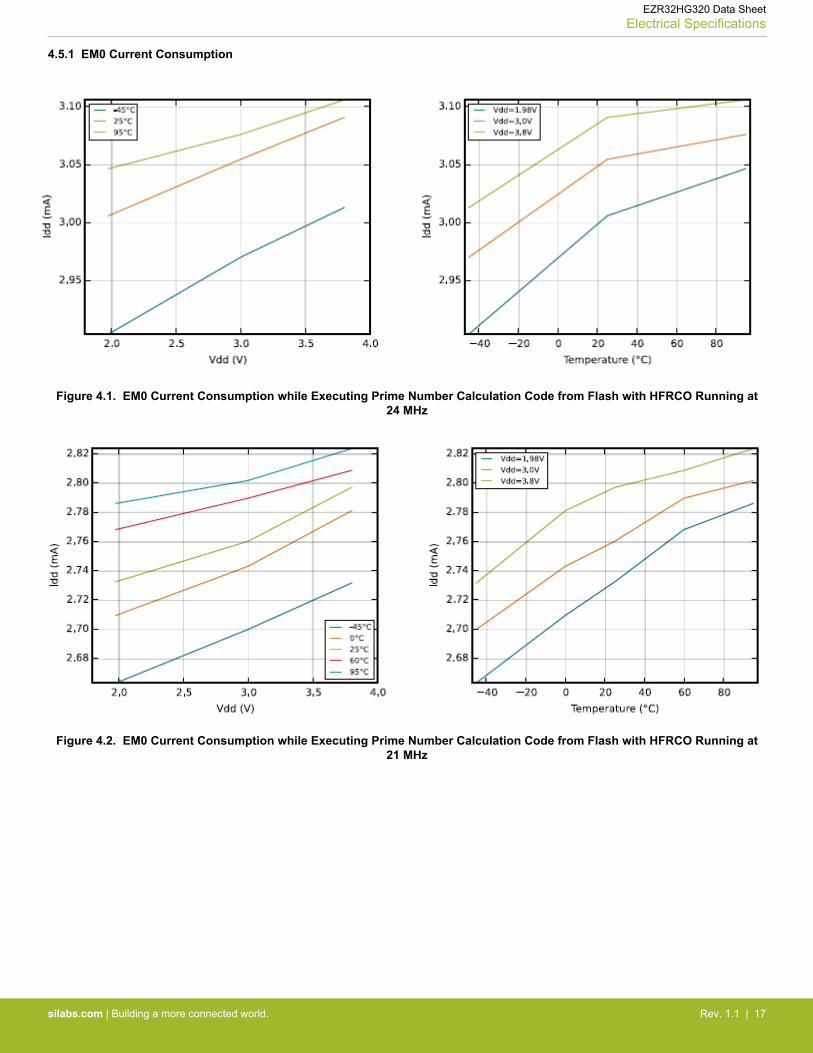
4.5.1 EM0 Current Consumption
Figure 4.1. EM0 Current Consumption while Executing Prime Number Calculation Code from Flash with HFRCO Running at24 MHz
Figure 4.2. EM0 Current Consumption while Executing Prime Number Calculation Code from Flash with HFRCO Running at21 MHz
EZR32HG320 Data SheetElectrical Specifications
silabs.com | Building a more connected world. Rev. 1.1 | 17
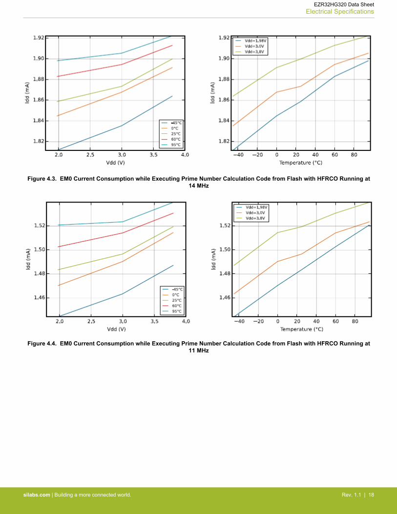
Figure 4.3. EM0 Current Consumption while Executing Prime Number Calculation Code from Flash with HFRCO Running at14 MHz
Figure 4.4. EM0 Current Consumption while Executing Prime Number Calculation Code from Flash with HFRCO Running at11 MHz
EZR32HG320 Data SheetElectrical Specifications
silabs.com | Building a more connected world. Rev. 1.1 | 18
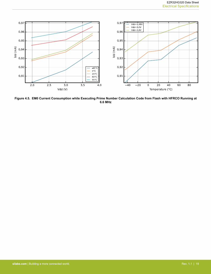
Figure 4.5. EM0 Current Consumption while Executing Prime Number Calculation Code from Flash with HFRCO Running at6.6 MHz
EZR32HG320 Data SheetElectrical Specifications
silabs.com | Building a more connected world. Rev. 1.1 | 19
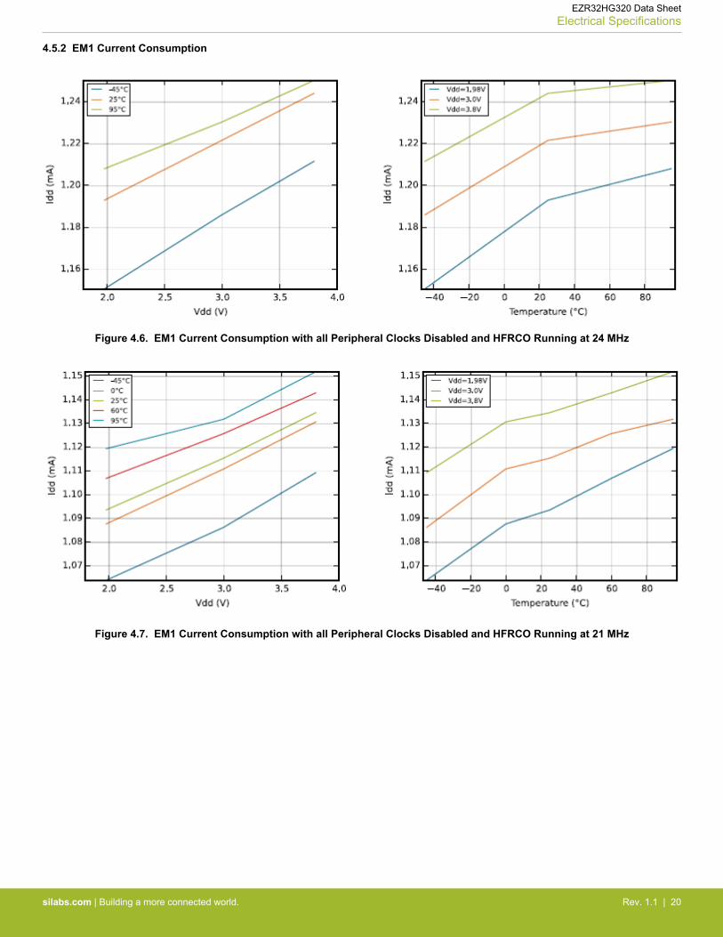
4.5.2 EM1 Current Consumption
Figure 4.6. EM1 Current Consumption with all Peripheral Clocks Disabled and HFRCO Running at 24 MHz
Figure 4.7. EM1 Current Consumption with all Peripheral Clocks Disabled and HFRCO Running at 21 MHz
EZR32HG320 Data SheetElectrical Specifications
silabs.com | Building a more connected world. Rev. 1.1 | 20
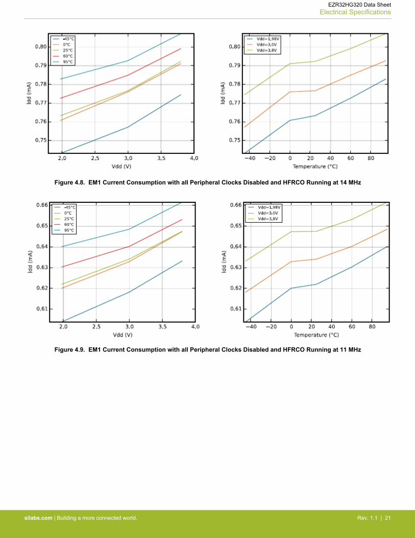
Figure 4.8. EM1 Current Consumption with all Peripheral Clocks Disabled and HFRCO Running at 14 MHz
Figure 4.9. EM1 Current Consumption with all Peripheral Clocks Disabled and HFRCO Running at 11 MHz
EZR32HG320 Data SheetElectrical Specifications
silabs.com | Building a more connected world. Rev. 1.1 | 21
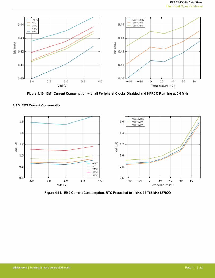
Figure 4.10. EM1 Current Consumption with all Peripheral Clocks Disabled and HFRCO Running at 6.6 MHz
4.5.3 EM2 Current Consumption
Figure 4.11. EM2 Current Consumption, RTC Prescaled to 1 kHz, 32.768 kHz LFRCO
EZR32HG320 Data SheetElectrical Specifications
silabs.com | Building a more connected world. Rev. 1.1 | 22
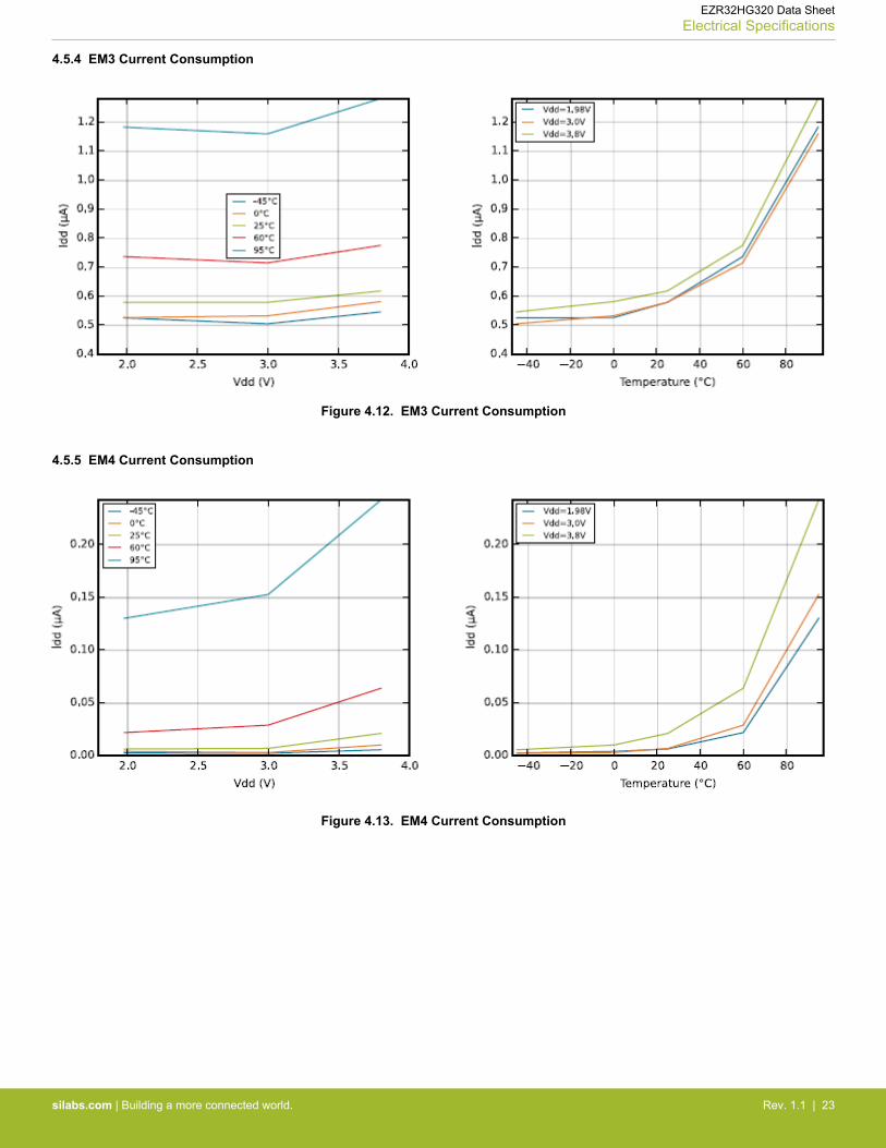
4.5.4 EM3 Current Consumption
Figure 4.12. EM3 Current Consumption
4.5.5 EM4 Current Consumption
Figure 4.13. EM4 Current Consumption
EZR32HG320 Data SheetElectrical Specifications
silabs.com | Building a more connected world. Rev. 1.1 | 23
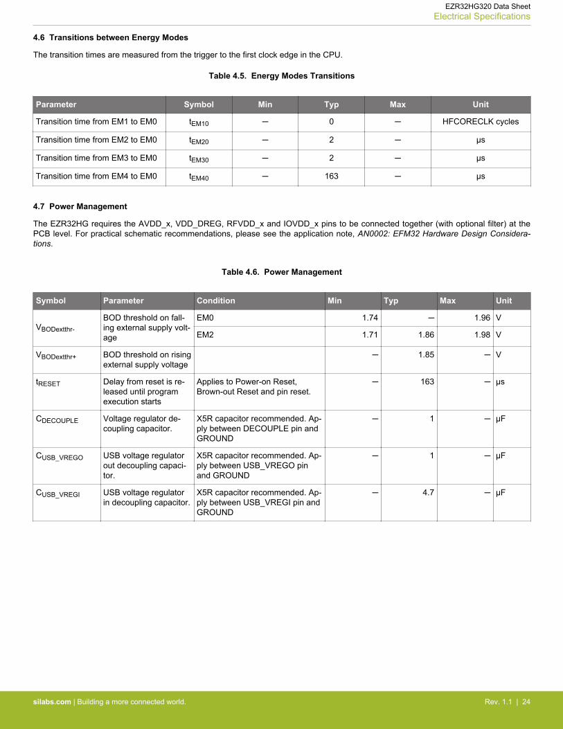
4.6 Transitions between Energy Modes
The transition times are measured from the trigger to the first clock edge in the CPU.
Table 4.5. Energy Modes Transitions
Parameter Symbol Min Typ Max Unit
Transition time from EM1 to EM0 tEM10 ─ 0 ─ HFCORECLK cycles
Transition time from EM2 to EM0 tEM20 ─ 2 ─ µs
Transition time from EM3 to EM0 tEM30 ─ 2 ─ µs
Transition time from EM4 to EM0 tEM40 ─ 163 ─ µs
4.7 Power Management
The EZR32HG requires the AVDD_x, VDD_DREG, RFVDD_x and IOVDD_x pins to be connected together (with optional filter) at thePCB level. For practical schematic recommendations, please see the application note, AN0002: EFM32 Hardware Design Considera-tions.
Table 4.6. Power Management
Symbol Parameter Condition Min Typ Max Unit
VBODextthr-
BOD threshold on fall-ing external supply volt-age
EM0 1.74 ─ 1.96 V
EM2 1.71 1.86 1.98 V
VBODextthr+ BOD threshold on risingexternal supply voltage
─ 1.85 ─ V
tRESET Delay from reset is re-leased until programexecution starts
Applies to Power-on Reset,Brown-out Reset and pin reset.
─ 163 ─ µs
CDECOUPLE Voltage regulator de-coupling capacitor.
X5R capacitor recommended. Ap-ply between DECOUPLE pin andGROUND
─ 1 ─ µF
CUSB_VREGO USB voltage regulatorout decoupling capaci-tor.
X5R capacitor recommended. Ap-ply between USB_VREGO pinand GROUND
─ 1 ─ µF
CUSB_VREGI USB voltage regulatorin decoupling capacitor.
X5R capacitor recommended. Ap-ply between USB_VREGI pin andGROUND
─ 4.7 ─ µF
EZR32HG320 Data SheetElectrical Specifications
silabs.com | Building a more connected world. Rev. 1.1 | 24
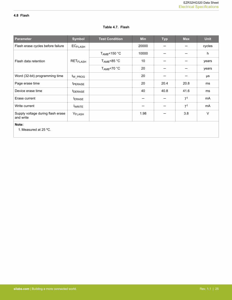
4.8 Flash
Table 4.7. Flash
Parameter Symbol Test Condition Min Typ Max Unit
Flash erase cycles before failure ECFLASH 20000 ─ ─ cycles
Flash data retention RETFLASH
TAMB<150 °C 10000 ─ ─ h
TAMB<85 °C 10 ─ ─ years
TAMB<70 °C 20 ─ ─ years
Word (32-bit) programming time tW_PROG 20 ─ ─ µs
Page erase time tPERASE 20 20.4 20.8 ms
Device erase time tDERASE 40 40.8 41.6 ms
Erase current IERASE ─ ─ 71 mA
Write current IWRITE ─ ─ 71 mA
Supply voltage during flash eraseand write
VFLASH 1.98 ─ 3.8 V
Note:1. Measured at 25 ºC.
EZR32HG320 Data SheetElectrical Specifications
silabs.com | Building a more connected world. Rev. 1.1 | 25
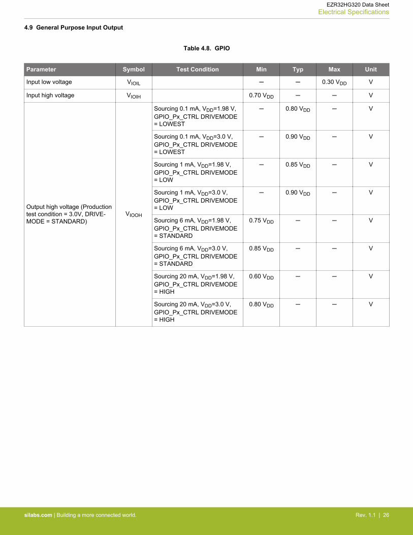
4.9 General Purpose Input Output
Table 4.8. GPIO
Parameter Symbol Test Condition Min Typ Max Unit
Input low voltage VIOIL ─ ─ 0.30 VDD V
Input high voltage VIOIH 0.70 VDD ─ ─ V
Output high voltage (Productiontest condition = 3.0V, DRIVE-MODE = STANDARD)
VIOOH
Sourcing 0.1 mA, VDD=1.98 V,GPIO_Px_CTRL DRIVEMODE= LOWEST
─ 0.80 VDD ─ V
Sourcing 0.1 mA, VDD=3.0 V,GPIO_Px_CTRL DRIVEMODE= LOWEST
─ 0.90 VDD ─ V
Sourcing 1 mA, VDD=1.98 V,GPIO_Px_CTRL DRIVEMODE= LOW
─ 0.85 VDD ─ V
Sourcing 1 mA, VDD=3.0 V,GPIO_Px_CTRL DRIVEMODE= LOW
─ 0.90 VDD ─ V
Sourcing 6 mA, VDD=1.98 V,GPIO_Px_CTRL DRIVEMODE= STANDARD
0.75 VDD ─ ─ V
Sourcing 6 mA, VDD=3.0 V,GPIO_Px_CTRL DRIVEMODE= STANDARD
0.85 VDD ─ ─ V
Sourcing 20 mA, VDD=1.98 V,GPIO_Px_CTRL DRIVEMODE= HIGH
0.60 VDD ─ ─ V
Sourcing 20 mA, VDD=3.0 V,GPIO_Px_CTRL DRIVEMODE= HIGH
0.80 VDD ─ ─ V
EZR32HG320 Data SheetElectrical Specifications
silabs.com | Building a more connected world. Rev. 1.1 | 26
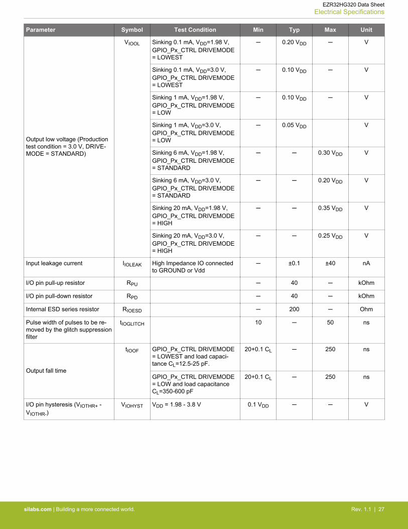
Parameter Symbol Test Condition Min Typ Max Unit
Output low voltage (Productiontest condition = 3.0 V, DRIVE-MODE = STANDARD)
VIOOL Sinking 0.1 mA, VDD=1.98 V,GPIO_Px_CTRL DRIVEMODE= LOWEST
─ 0.20 VDD ─ V
Sinking 0.1 mA, VDD=3.0 V,GPIO_Px_CTRL DRIVEMODE= LOWEST
─ 0.10 VDD ─ V
Sinking 1 mA, VDD=1.98 V,GPIO_Px_CTRL DRIVEMODE= LOW
─ 0.10 VDD ─ V
Sinking 1 mA, VDD=3.0 V,GPIO_Px_CTRL DRIVEMODE= LOW
─ 0.05 VDD V
Sinking 6 mA, VDD=1.98 V,GPIO_Px_CTRL DRIVEMODE= STANDARD
─ ─ 0.30 VDD V
Sinking 6 mA, VDD=3.0 V,GPIO_Px_CTRL DRIVEMODE= STANDARD
─ ─ 0.20 VDD V
Sinking 20 mA, VDD=1.98 V,GPIO_Px_CTRL DRIVEMODE= HIGH
─ ─ 0.35 VDD V
Sinking 20 mA, VDD=3.0 V,GPIO_Px_CTRL DRIVEMODE= HIGH
─ ─ 0.25 VDD V
Input leakage current IIOLEAK High Impedance IO connectedto GROUND or Vdd
─ ±0.1 ±40 nA
I/O pin pull-up resistor RPU ─ 40 ─ kOhm
I/O pin pull-down resistor RPD ─ 40 ─ kOhm
Internal ESD series resistor RIOESD ─ 200 ─ Ohm
Pulse width of pulses to be re-moved by the glitch suppressionfilter
tIOGLITCH 10 ─ 50 ns
Output fall time
tIOOF GPIO_Px_CTRL DRIVEMODE= LOWEST and load capaci-tance CL=12.5-25 pF.
20+0.1 CL ─ 250 ns
GPIO_Px_CTRL DRIVEMODE= LOW and load capacitanceCL=350-600 pF
20+0.1 CL ─ 250 ns
I/O pin hysteresis (VIOTHR+ -VIOTHR-)
VIOHYST VDD = 1.98 - 3.8 V 0.1 VDD ─ ─ V
EZR32HG320 Data SheetElectrical Specifications
silabs.com | Building a more connected world. Rev. 1.1 | 27
0.0 0.5 1.0 1.5 2.0Low-Level Output Voltage [V]
0.00
0.05
0.10
0.15
0.20
Low
-Lev
el O
utpu
t Cur
rent
[mA
]
-40°C
25°C
85°C
GPIO_Px_CTRL DRIVEMODE = LOWEST
0.0 0.5 1.0 1.5 2.0Low-Level Output Voltage [V]
0
1
2
3
4
5
Low
-Lev
el O
utpu
t Cur
rent
[mA
]
-40°C
25°C
85°C
GPIO_Px_CTRL DRIVEMODE = LOW
0.0 0.5 1.0 1.5 2.0Low-Level Output Voltage [V]
0
5
10
15
20
Low
-Lev
el O
utpu
t Cur
rent
[mA
]
-40°C
25°C
85°C
GPIO_Px_CTRL DRIVEMODE = STANDARD
0.0 0.5 1.0 1.5 2.0Low-Level Output Voltage [V]
0
5
10
15
20
25
30
35
40
45
Low
-Lev
el O
utpu
t Cur
rent
[mA
]
-40°C
25°C
85°C
GPIO_Px_CTRL DRIVEMODE = High
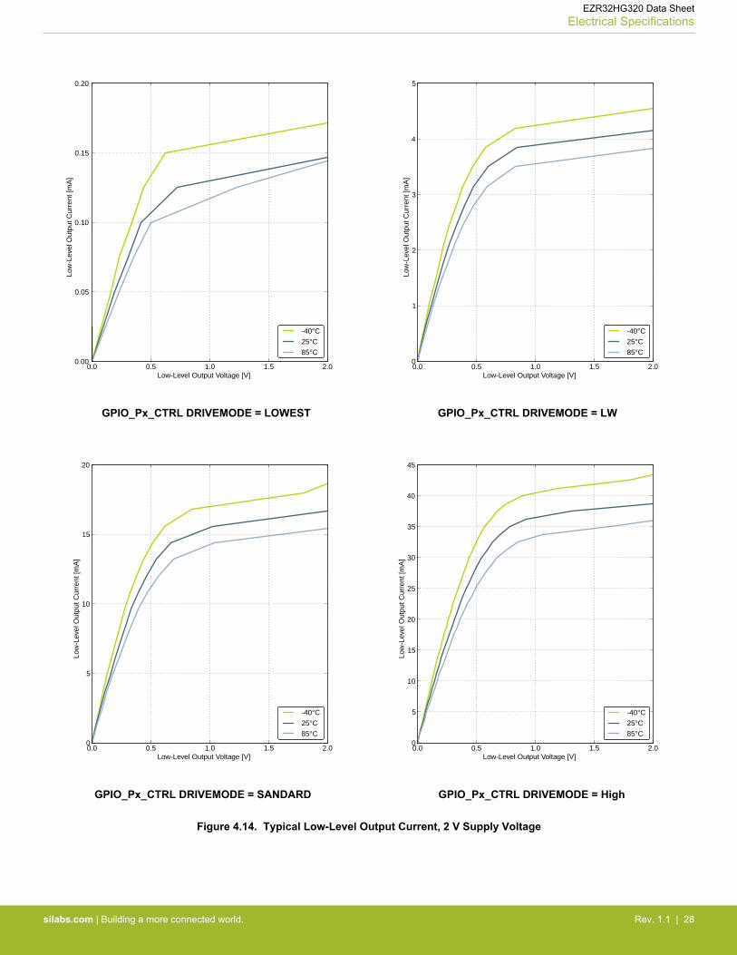
Figure 4.14. Typical Low-Level Output Current, 2 V Supply Voltage
EZR32HG320 Data SheetElectrical Specifications
silabs.com | Building a more connected world. Rev. 1.1 | 28
0.0 0.5 1.0 1.5 2.0High-Level Output Voltage [V]
–0.20
–0.15
–0.10
–0.05
0.00
Hig
h-Le
vel O
utpu
t Cur
rent
[mA
]
-40°C
25°C
85°C
GPIO_Px_CTRL DRIVEMODE = LOWEST
0.0 0.5 1.0 1.5 2.0High-Level Output Voltage [V]
–2.5
–2.0
–1.5
–1.0
–0.5
0.0
Hig
h-Le
vel O
utpu
t Cur
rent
[mA
]
-40°C
25°C
85°C
GPIO_Px_CTRL DRIVEMODE = LOW
0.0 0.5 1.0 1.5 2.0High-Level Output Voltage [V]
–20
–15
–10
–5
0
Hig
h-Le
vel O
utpu
t Cur
rent
[mA
]
-40°C
25°C
85°C
GPIO_Px_CTRL DRIVEMODE = STANDARD
0.0 0.5 1.0 1.5 2.0High-Level Output Voltage [V]
–50
–40
–30
–20
–10
0
Hig
h-Le
vel O
utpu
t Cur
rent
[mA
]
-40°C
25°C
85°C
GPIO_Px_CTRL DRIVEMODE = High
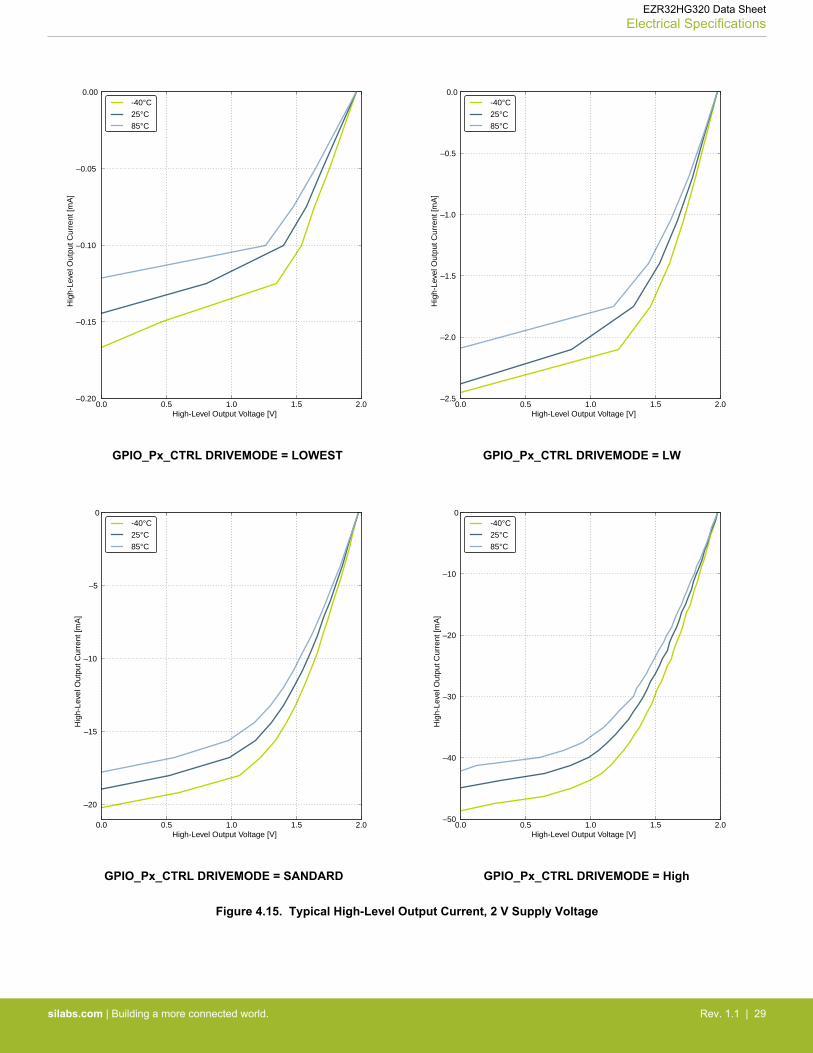
Figure 4.15. Typical High-Level Output Current, 2 V Supply Voltage
EZR32HG320 Data SheetElectrical Specifications
silabs.com | Building a more connected world. Rev. 1.1 | 29
0.0 0.5 1.0 1.5 2.0 2.5 3.0Low-Level Output Voltage [V]
0.0
0.1
0.2
0.3
0.4
0.5Lo
w-L
evel
Out
put C
urre
nt [m
A]
-40°C
25°C
85°C
GPIO_Px_CTRL DRIVEMODE = LOWEST
0.0 0.5 1.0 1.5 2.0 2.5 3.0Low-Level Output Voltage [V]
0
2
4
6
8
10
Low
-Lev
el O
utpu
t Cur
rent
[mA
]
-40°C
25°C
85°C
GPIO_Px_CTRL DRIVEMODE = LOW
0.0 0.5 1.0 1.5 2.0 2.5 3.0Low-Level Output Voltage [V]
0
5
10
15
20
25
30
35
40
Low
-Lev
el O
utpu
t Cur
rent
[mA
]
-40°C
25°C
85°C
GPIO_Px_CTRL DRIVEMODE = STANDARD
0.0 0.5 1.0 1.5 2.0 2.5 3.0Low-Level Output Voltage [V]
0
10
20
30
40
50
Low
-Lev
el O
utpu
t Cur
rent
[mA
]
-40°C
25°C
85°C
GPIO_Px_CTRL DRIVEMODE = High
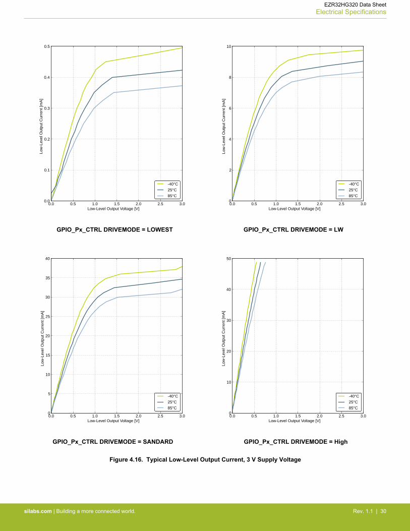
Figure 4.16. Typical Low-Level Output Current, 3 V Supply Voltage
EZR32HG320 Data SheetElectrical Specifications
silabs.com | Building a more connected world. Rev. 1.1 | 30
0.0 0.5 1.0 1.5 2.0 2.5 3.0High-Level Output Voltage [V]
–0.5
–0.4
–0.3
–0.2
–0.1
0.0
Hig
h-Le
vel O
utpu
t Cur
rent
[mA
]
-40°C
25°C
85°C
GPIO_Px_CTRL DRIVEMODE = LOWEST
0.0 0.5 1.0 1.5 2.0 2.5 3.0High-Level Output Voltage [V]
–6
–5
–4
–3
–2
–1
0
Hig
h-Le
vel O
utpu
t Cur
rent
[mA
]
-40°C
25°C
85°C
GPIO_Px_CTRL DRIVEMODE = LOW
0.0 0.5 1.0 1.5 2.0 2.5 3.0High-Level Output Voltage [V]
–50
–40
–30
–20
–10
0
Hig
h-Le
vel O
utpu
t Cur
rent
[mA
]
-40°C
25°C
85°C
GPIO_Px_CTRL DRIVEMODE = STANDARD
0.0 0.5 1.0 1.5 2.0 2.5 3.0High-Level Output Voltage [V]
–50
–40
–30
–20
–10
0
Hig
h-Le
vel O
utpu
t Cur
rent
[mA
]
-40°C
25°C
85°C
GPIO_Px_CTRL DRIVEMODE = High
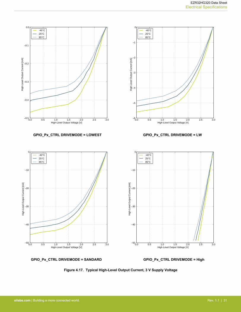
Figure 4.17. Typical High-Level Output Current, 3 V Supply Voltage
EZR32HG320 Data SheetElectrical Specifications
silabs.com | Building a more connected world. Rev. 1.1 | 31
0.0 0.5 1.0 1.5 2.0 2.5 3.0 3.5Low-Level Output Voltage [V]
0.0
0.1
0.2
0.3
0.4
0.5
0.6
0.7
0.8Lo
w-L
evel
Out
put C
urre
nt [m
A]
-40°C
25°C
85°C
GPIO_Px_CTRL DRIVEMODE = LOWEST
0.0 0.5 1.0 1.5 2.0 2.5 3.0 3.5Low-Level Output Voltage [V]
0
2
4
6
8
10
12
14
Low
-Lev
el O
utpu
t Cur
rent
[mA
]
-40°C
25°C
85°C
GPIO_Px_CTRL DRIVEMODE = LOW
0.0 0.5 1.0 1.5 2.0 2.5 3.0 3.5Low-Level Output Voltage [V]
0
10
20
30
40
50
Low
-Lev
el O
utpu
t Cur
rent
[mA
]
-40°C
25°C
85°C
GPIO_Px_CTRL DRIVEMODE = STANDARD
0.0 0.5 1.0 1.5 2.0 2.5 3.0 3.5Low-Level Output Voltage [V]
0
10
20
30
40
50
Low
-Lev
el O
utpu
t Cur
rent
[mA
]
-40°C
25°C
85°C
GPIO_Px_CTRL DRIVEMODE = High
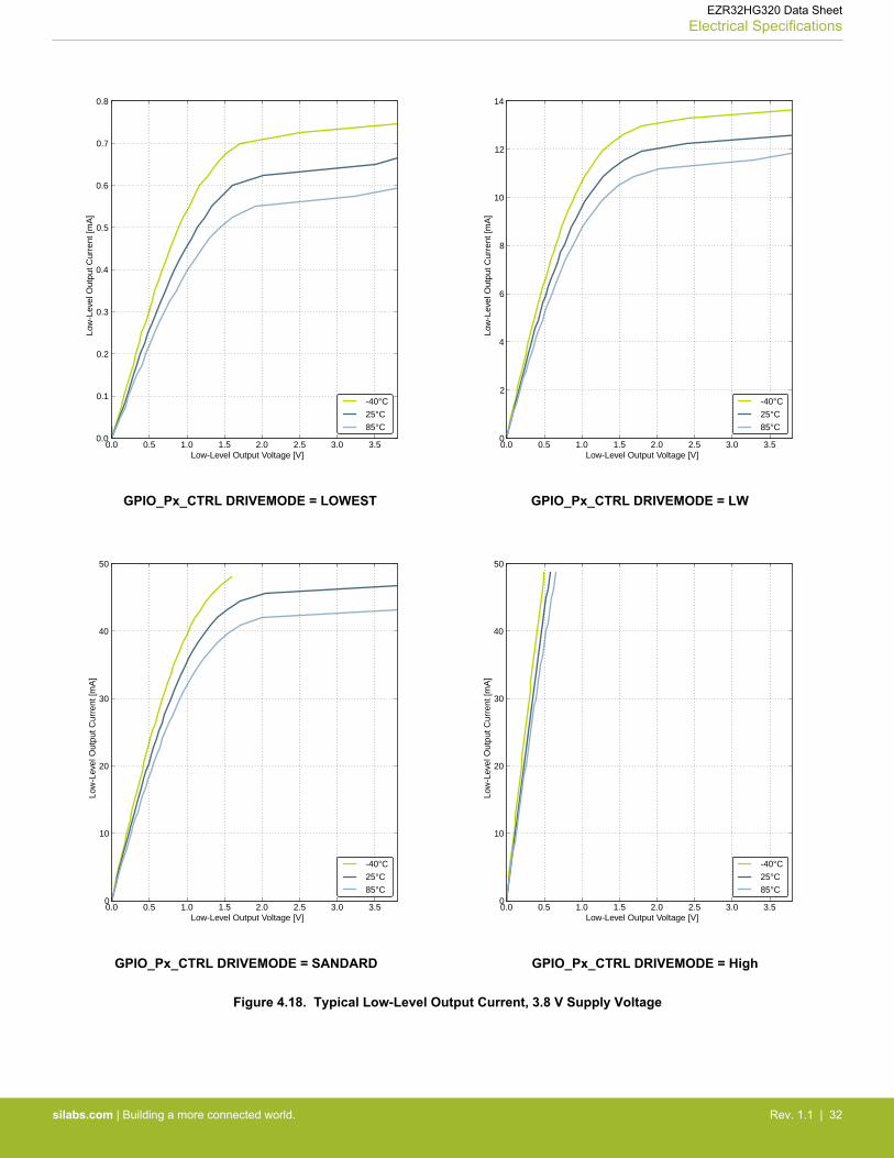
Figure 4.18. Typical Low-Level Output Current, 3.8 V Supply Voltage
EZR32HG320 Data SheetElectrical Specifications
silabs.com | Building a more connected world. Rev. 1.1 | 32
0.0 0.5 1.0 1.5 2.0 2.5 3.0 3.5High-Level Output Voltage [V]
–0.8
–0.7
–0.6
–0.5
–0.4
–0.3
–0.2
–0.1
0.0
Hig
h-Le
vel O
utpu
t Cur
rent
[mA
]
-40°C
25°C
85°C
GPIO_Px_CTRL DRIVEMODE = LOWEST
0.0 0.5 1.0 1.5 2.0 2.5 3.0 3.5High-Level Output Voltage [V]
–9
–8
–7
–6
–5
–4
–3
–2
–1
0
Hig
h-Le
vel O
utpu
t Cur
rent
[mA
]
-40°C
25°C
85°C
GPIO_Px_CTRL DRIVEMODE = LOW
0.0 0.5 1.0 1.5 2.0 2.5 3.0 3.5High-Level Output Voltage [V]
–50
–40
–30
–20
–10
0
Hig
h-Le
vel O
utpu
t Cur
rent
[mA
]
-40°C
25°C
85°C
GPIO_Px_CTRL DRIVEMODE = STANDARD
0.0 0.5 1.0 1.5 2.0 2.5 3.0 3.5High-Level Output Voltage [V]
–50
–40
–30
–20
–10
0
Hig
h-Le
vel O
utpu
t Cur
rent
[mA
]
-40°C
25°C
85°C
GPIO_Px_CTRL DRIVEMODE = High
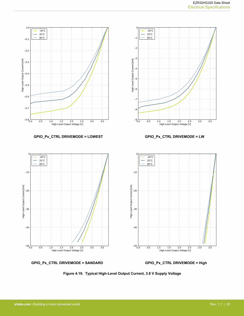
Figure 4.19. Typical High-Level Output Current, 3.8 V Supply Voltage
EZR32HG320 Data SheetElectrical Specifications
silabs.com | Building a more connected world. Rev. 1.1 | 33
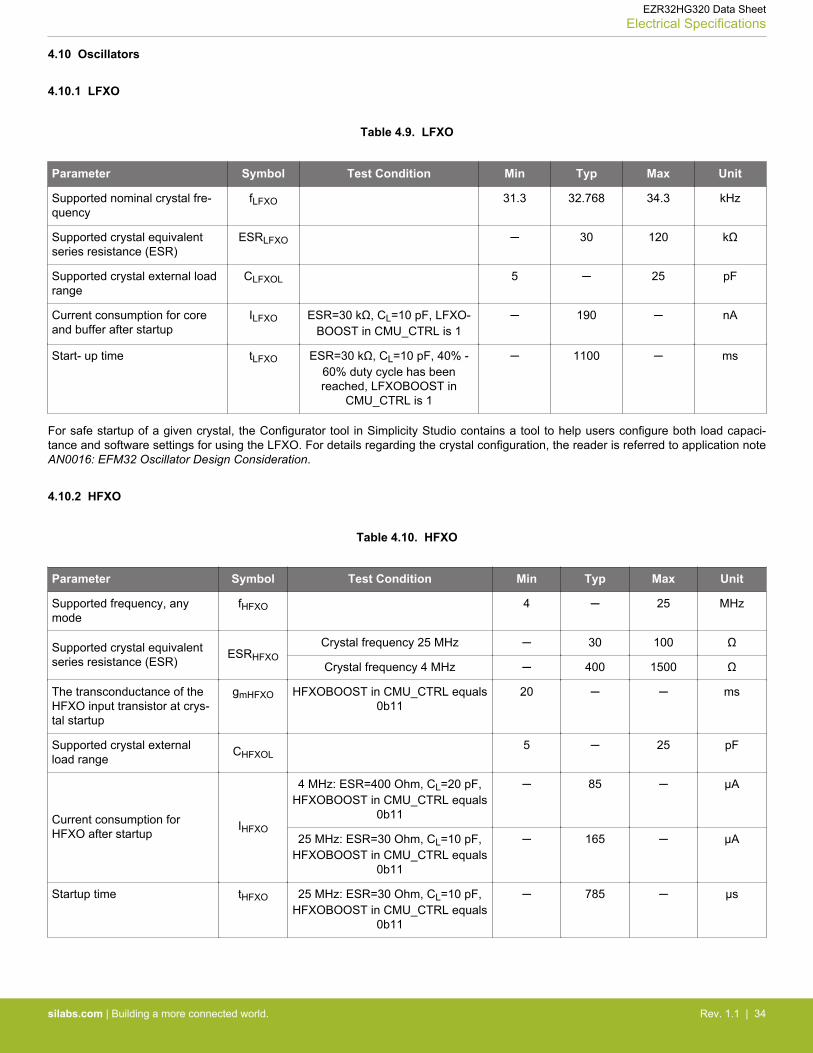
4.10 Oscillators
4.10.1 LFXO
Table 4.9. LFXO
Parameter Symbol Test Condition Min Typ Max Unit
Supported nominal crystal fre-quency
fLFXO 31.3 32.768 34.3 kHz
Supported crystal equivalentseries resistance (ESR)
ESRLFXO ─ 30 120 kΩ
Supported crystal external loadrange
CLFXOL 5 ─ 25 pF
Current consumption for coreand buffer after startup
ILFXO ESR=30 kΩ, CL=10 pF, LFXO-BOOST in CMU_CTRL is 1
─ 190 ─ nA
Start- up time tLFXO ESR=30 kΩ, CL=10 pF, 40% -60% duty cycle has beenreached, LFXOBOOST in
CMU_CTRL is 1
─ 1100 ─ ms
For safe startup of a given crystal, the Configurator tool in Simplicity Studio contains a tool to help users configure both load capaci-tance and software settings for using the LFXO. For details regarding the crystal configuration, the reader is referred to application noteAN0016: EFM32 Oscillator Design Consideration.
4.10.2 HFXO
Table 4.10. HFXO
Parameter Symbol Test Condition Min Typ Max Unit
Supported frequency, anymode
fHFXO 4 ─ 25 MHz
Supported crystal equivalentseries resistance (ESR)
ESRHFXOCrystal frequency 25 MHz ─ 30 100 Ω
Crystal frequency 4 MHz ─ 400 1500 Ω
The transconductance of theHFXO input transistor at crys-tal startup
gmHFXO HFXOBOOST in CMU_CTRL equals0b11
20 ─ ─ ms
Supported crystal externalload range
CHFXOL5 ─ 25 pF
Current consumption forHFXO after startup
IHFXO
4 MHz: ESR=400 Ohm, CL=20 pF,HFXOBOOST in CMU_CTRL equals
0b11
─ 85 ─ µA
25 MHz: ESR=30 Ohm, CL=10 pF,HFXOBOOST in CMU_CTRL equals
0b11
─ 165 ─ µA
Startup time tHFXO 25 MHz: ESR=30 Ohm, CL=10 pF,HFXOBOOST in CMU_CTRL equals
0b11
─ 785 ─ µs
EZR32HG320 Data SheetElectrical Specifications
silabs.com | Building a more connected world. Rev. 1.1 | 34
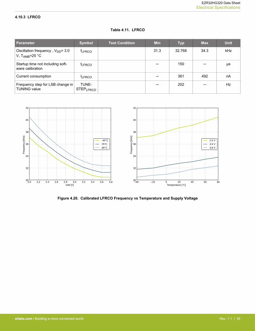
4.10.3 LFRCO
Table 4.11. LFRCO
Parameter Symbol Test Condition Min Typ Max Unit
Oscillation frequency , VDD= 3.0V, TAMB=25 °C
fLFRCO 31.3 32.768 34.3 kHz
Startup time not including soft-ware calibration
tLFRCO ─ 150 ─ µs
Current consumption ILFRCO ─ 361 492 nA
Frequency step for LSB change inTUNING value
TUNE-STEPLFRCO
─ 202 ─ Hz
2.0 2.2 2.4 2.6 2.8 3.0 3.2 3.4 3.6 3.8Vdd [V]
30
32
34
36
38
40
42
Freq
uenc
y [k
Hz]
-40°C
25°C
85°C
–40 –15 5 25 45 65 85Temperature [°C]
30
32
34
36
38
40
42
Freq
uenc
y [k
Hz]
2.0 V
3.0 V
3.8 V
Figure 4.20. Calibrated LFRCO Frequency vs Temperature and Supply Voltage
EZR32HG320 Data SheetElectrical Specifications
silabs.com | Building a more connected world. Rev. 1.1 | 35
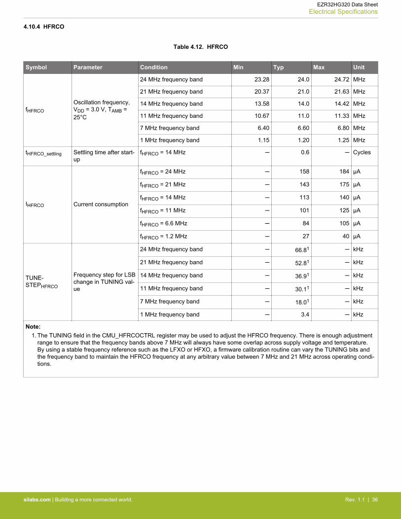
4.10.4 HFRCO
Table 4.12. HFRCO
Symbol Parameter Condition Min Typ Max Unit
fHFRCO
Oscillation frequency,VDD = 3.0 V, TAMB =25°C
24 MHz frequency band 23.28 24.0 24.72 MHz
21 MHz frequency band 20.37 21.0 21.63 MHz
14 MHz frequency band 13.58 14.0 14.42 MHz
11 MHz frequency band 10.67 11.0 11.33 MHz
7 MHz frequency band 6.40 6.60 6.80 MHz
1 MHz frequency band 1.15 1.20 1.25 MHz
tHFRCO_settling Settling time after start-up
fHFRCO = 14 MHz ─ 0.6 ─ Cycles
IHFRCO Current consumption
fHFRCO = 24 MHz ─ 158 184 µA
fHFRCO = 21 MHz ─ 143 175 µA
fHFRCO = 14 MHz ─ 113 140 µA
fHFRCO = 11 MHz ─ 101 125 µA
fHFRCO = 6.6 MHz ─ 84 105 µA
fHFRCO = 1.2 MHz ─ 27 40 µA
TUNE-STEPHFRCO
Frequency step for LSBchange in TUNING val-ue
24 MHz frequency band ─ 66.81 ─ kHz
21 MHz frequency band ─ 52.81 ─ kHz
14 MHz frequency band ─ 36.91 ─ kHz
11 MHz frequency band ─ 30.11 ─ kHz
7 MHz frequency band ─ 18.01 ─ kHz
1 MHz frequency band ─ 3.4 ─ kHz
Note:1. The TUNING field in the CMU_HFRCOCTRL register may be used to adjust the HFRCO frequency. There is enough adjustment
range to ensure that the frequency bands above 7 MHz will always have some overlap across supply voltage and temperature.By using a stable frequency reference such as the LFXO or HFXO, a firmware calibration routine can vary the TUNING bits andthe frequency band to maintain the HFRCO frequency at any arbitrary value between 7 MHz and 21 MHz across operating condi-tions.
EZR32HG320 Data SheetElectrical Specifications
silabs.com | Building a more connected world. Rev. 1.1 | 36
2.0 2.2 2.4 2.6 2.8 3.0 3.2 3.4 3.6 3.8Vdd [V]
1.05
1.10
1.15
1.20
1.25
1.30
1.35
1.40
1.45
Freq
uenc
y [M
Hz]
-40°C
25°C
85°C
–40 –15 5 25 45 65 85Temperature [°C]
1.05
1.10
1.15
1.20
1.25
1.30
1.35
1.40
1.45
Freq
uenc
y [M
Hz]
2.0 V
3.0 V
3.8 V
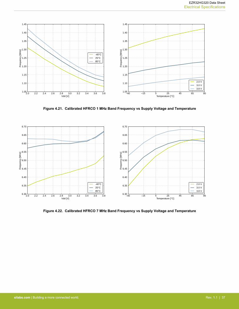
Figure 4.21. Calibrated HFRCO 1 MHz Band Frequency vs Supply Voltage and Temperature
2.0 2.2 2.4 2.6 2.8 3.0 3.2 3.4 3.6 3.8Vdd [V]
6.30
6.35
6.40
6.45
6.50
6.55
6.60
6.65
6.70
Freq
uenc
y [M
Hz]
-40°C
25°C
85°C
–40 –15 5 25 45 65 85Temperature [°C]
6.30
6.35
6.40
6.45
6.50
6.55
6.60
6.65
6.70
Freq
uenc
y [M
Hz]
2.0 V
3.0 V
3.8 V
Figure 4.22. Calibrated HFRCO 7 MHz Band Frequency vs Supply Voltage and Temperature
EZR32HG320 Data SheetElectrical Specifications
silabs.com | Building a more connected world. Rev. 1.1 | 37
1.8 2.2 2.6 3.0 3.4 3.8Vdd [V]
10.80
10.85
10.90
10.95
11.00
11.05
11.10
11.15
Freq
uenc
y [M
Hz]
-40°C
25°C
85°C
–40 –15 5 25 45 65 85Temperature [°C]
10.80
10.85
10.90
10.95
11.00
11.05
11.10
11.15
11.20
Freq
uenc
y [M
Hz]
1.8 V
3 V
3.8 V
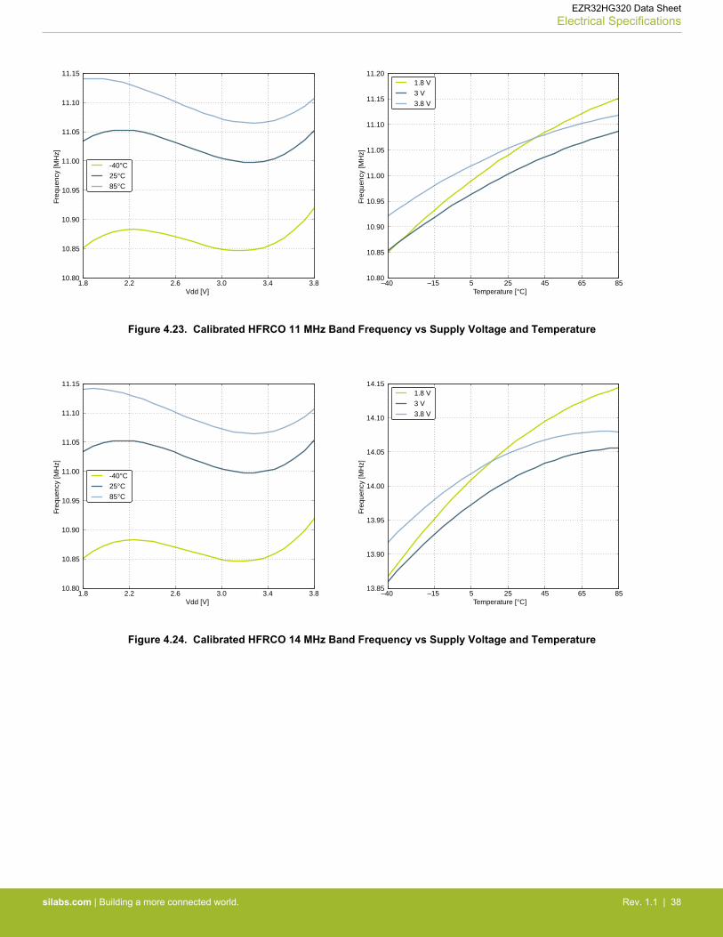
Figure 4.23. Calibrated HFRCO 11 MHz Band Frequency vs Supply Voltage and Temperature
1.8 2.2 2.6 3.0 3.4 3.8Vdd [V]
10.80
10.85
10.90
10.95
11.00
11.05
11.10
11.15
Freq
uenc
y [M
Hz]
-40°C
25°C
85°C
–40 –15 5 25 45 65 85Temperature [°C]
13.85
13.90
13.95
14.00
14.05
14.10
14.15
Freq
uenc
y [M
Hz]
1.8 V
3 V
3.8 V
Figure 4.24. Calibrated HFRCO 14 MHz Band Frequency vs Supply Voltage and Temperature
EZR32HG320 Data SheetElectrical Specifications
silabs.com | Building a more connected world. Rev. 1.1 | 38
1.8 2.2 2.6 3.0 3.4 3.8Vdd [V]
20.6
20.7
20.8
20.9
21.0
21.1
21.2
Freq
uenc
y [M
Hz]
-40°C
25°C
85°C
–40 –15 5 25 45 65 85Temperature [°C]
20.6
20.7
20.8
20.9
21.0
21.1
21.2
Freq
uenc
y [M
Hz]
1.8 V
3 V
3.8 V
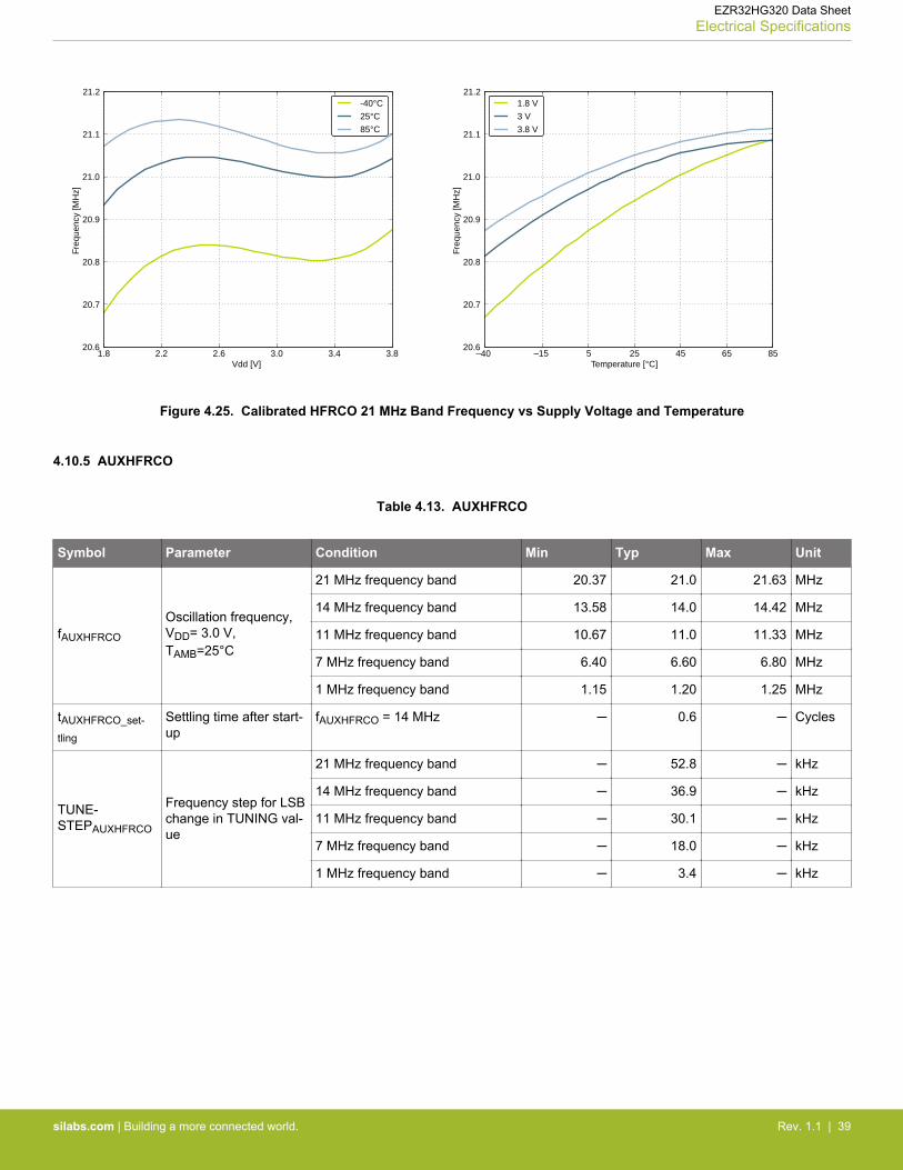
Figure 4.25. Calibrated HFRCO 21 MHz Band Frequency vs Supply Voltage and Temperature
4.10.5 AUXHFRCO
Table 4.13. AUXHFRCO
Symbol Parameter Condition Min Typ Max Unit
fAUXHFRCO
Oscillation frequency,VDD= 3.0 V,TAMB=25°C
21 MHz frequency band 20.37 21.0 21.63 MHz
14 MHz frequency band 13.58 14.0 14.42 MHz
11 MHz frequency band 10.67 11.0 11.33 MHz
7 MHz frequency band 6.40 6.60 6.80 MHz
1 MHz frequency band 1.15 1.20 1.25 MHz
tAUXHFRCO_set-
tling
Settling time after start-up
fAUXHFRCO = 14 MHz ─ 0.6 ─ Cycles
TUNE-STEPAUXHFRCO
Frequency step for LSBchange in TUNING val-ue
21 MHz frequency band ─ 52.8 ─ kHz
14 MHz frequency band ─ 36.9 ─ kHz
11 MHz frequency band ─ 30.1 ─ kHz
7 MHz frequency band ─ 18.0 ─ kHz
1 MHz frequency band ─ 3.4 ─ kHz
EZR32HG320 Data SheetElectrical Specifications
silabs.com | Building a more connected world. Rev. 1.1 | 39
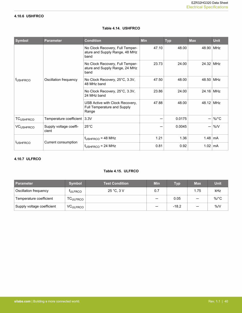
4.10.6 USHFRCO
Table 4.14. USHFRCO
Symbol Parameter Condition Min Typ Max Unit
fUSHFRCO Oscillation frequency
No Clock Recovery, Full Temper-ature and Supply Range, 48 MHzband
47.10 48.00 48.90 MHz
No Clock Recovery, Full Temper-ature and Supply Range, 24 MHzband
23.73 24.00 24.32 MHz
No Clock Recovery, 25°C, 3.3V,48 MHz band
47.50 48.00 48.50 MHz
No Clock Recovery, 25°C, 3.3V,24 MHz band
23.86 24.00 24.16 MHz
USB Active with Clock Recovery,Full Temperature and SupplyRange
47.88 48.00 48.12 MHz
TCUSHFRCO Temperature coefficient 3.3V ─ 0.0175 ─ %/°C
VCUSHFRCO Supply voltage coeffi-cient
25°C ─ 0.0045 ─ %/V
IUSHFRCO Current consumptionfUSHFRCO = 48 MHz 1.21 1.36 1.48 mA
fUSHFRCO = 24 MHz 0.81 0.92 1.02 mA
4.10.7 ULFRCO
Table 4.15. ULFRCO
Parameter Symbol Test Condition Min Typ Max Unit
Oscillation frequency fULFRCO 25 °C, 3 V 0.7 1.75 kHz
Temperature coefficient TCULFRCO ─ 0.05 ─ %/°C
Supply voltage coefficient VCULFRCO ─ -18.2 ─ %/V
EZR32HG320 Data SheetElectrical Specifications
silabs.com | Building a more connected world. Rev. 1.1 | 40
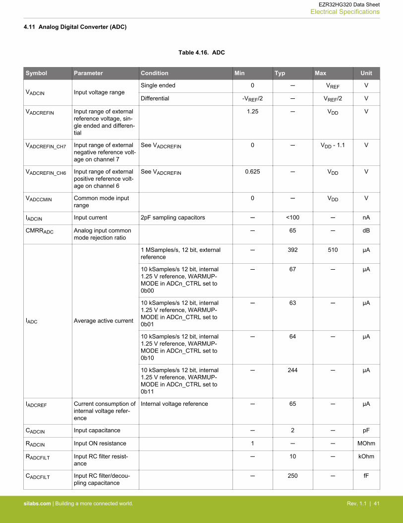
4.11 Analog Digital Converter (ADC)
Table 4.16. ADC
Symbol Parameter Condition Min Typ Max Unit
VADCIN Input voltage rangeSingle ended 0 ─ VREF V
Differential -VREF/2 ─ VREF/2 V
VADCREFIN Input range of externalreference voltage, sin-gle ended and differen-tial
1.25 ─ VDD V
VADCREFIN_CH7 Input range of externalnegative reference volt-age on channel 7
See VADCREFIN 0 ─ VDD - 1.1 V
VADCREFIN_CH6 Input range of externalpositive reference volt-age on channel 6
See VADCREFIN 0.625 ─ VDD V
VADCCMIN Common mode inputrange
0 ─ VDD V
IADCIN Input current 2pF sampling capacitors ─ <100 ─ nA
CMRRADC Analog input commonmode rejection ratio
─ 65 ─ dB
IADC Average active current
1 MSamples/s, 12 bit, externalreference
─ 392 510 µA
10 kSamples/s 12 bit, internal1.25 V reference, WARMUP-MODE in ADCn_CTRL set to0b00
─ 67 ─ µA
10 kSamples/s 12 bit, internal1.25 V reference, WARMUP-MODE in ADCn_CTRL set to0b01
─ 63 ─ µA
10 kSamples/s 12 bit, internal1.25 V reference, WARMUP-MODE in ADCn_CTRL set to0b10
─ 64 ─ µA
10 kSamples/s 12 bit, internal1.25 V reference, WARMUP-MODE in ADCn_CTRL set to0b11
─ 244 ─ µA
IADCREF Current consumption ofinternal voltage refer-ence
Internal voltage reference ─ 65 ─ µA
CADCIN Input capacitance ─ 2 ─ pF
RADCIN Input ON resistance 1 ─ ─ MOhm
RADCFILT Input RC filter resist-ance
─ 10 ─ kOhm
CADCFILT Input RC filter/decou-pling capacitance
─ 250 ─ fF
EZR32HG320 Data SheetElectrical Specifications
silabs.com | Building a more connected world. Rev. 1.1 | 41
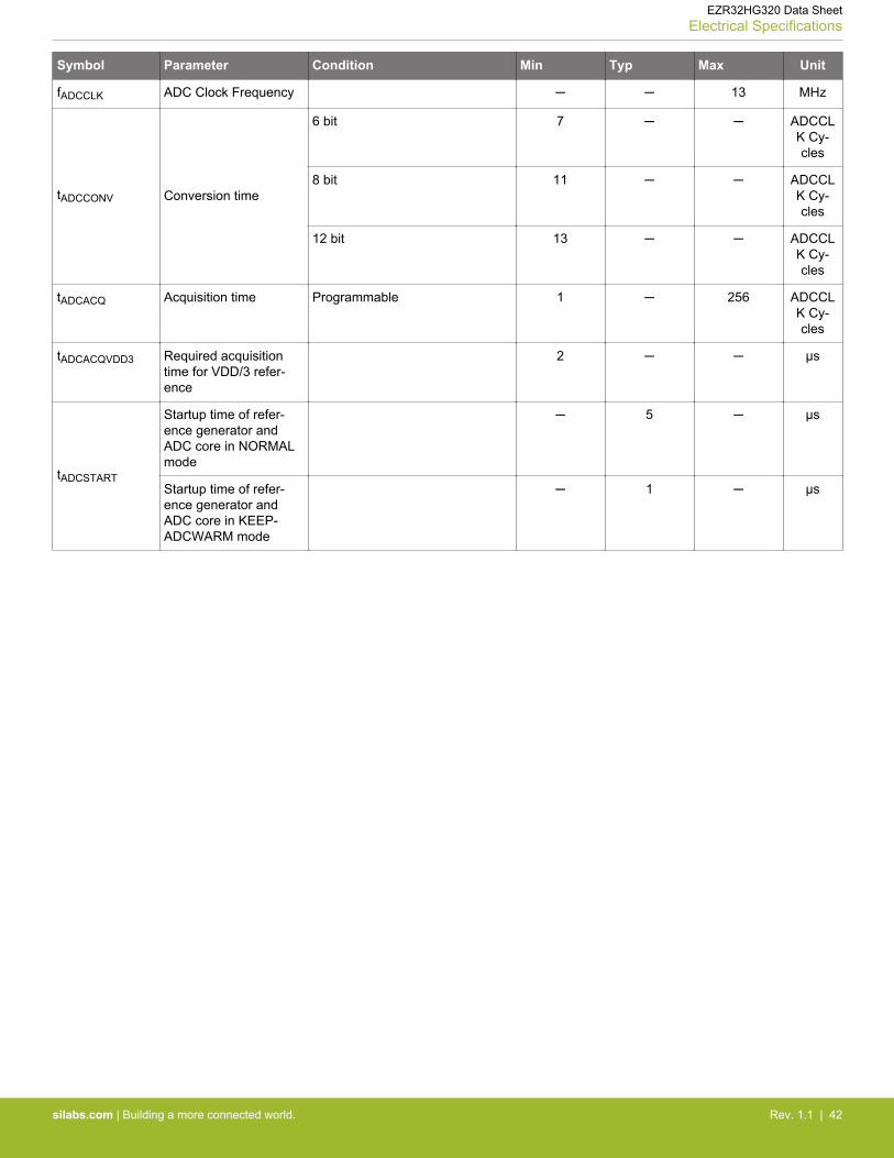
Symbol Parameter Condition Min Typ Max Unit
fADCCLK ADC Clock Frequency ─ ─ 13 MHz
tADCCONV Conversion time
6 bit 7 ─ ─ ADCCLK Cy-cles
8 bit 11 ─ ─ ADCCLK Cy-cles
12 bit 13 ─ ─ ADCCLK Cy-cles
tADCACQ Acquisition time Programmable 1 ─ 256 ADCCLK Cy-cles
tADCACQVDD3 Required acquisitiontime for VDD/3 refer-ence
2 ─ ─ µs
tADCSTART
Startup time of refer-ence generator andADC core in NORMALmode
─ 5 ─ µs
Startup time of refer-ence generator andADC core in KEEP-ADCWARM mode
─ 1 ─ µs
EZR32HG320 Data SheetElectrical Specifications
silabs.com | Building a more connected world. Rev. 1.1 | 42
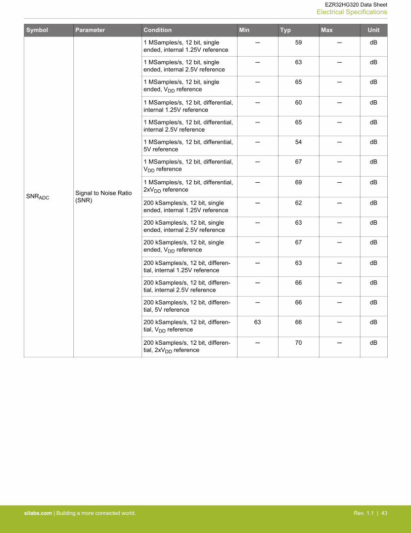
Symbol Parameter Condition Min Typ Max Unit
SNRADCSignal to Noise Ratio(SNR)
1 MSamples/s, 12 bit, singleended, internal 1.25V reference
─ 59 ─ dB
1 MSamples/s, 12 bit, singleended, internal 2.5V reference
─ 63 ─ dB
1 MSamples/s, 12 bit, singleended, VDD reference
─ 65 ─ dB
1 MSamples/s, 12 bit, differential,internal 1.25V reference
─ 60 ─ dB
1 MSamples/s, 12 bit, differential,internal 2.5V reference
─ 65 ─ dB
1 MSamples/s, 12 bit, differential,5V reference
─ 54 ─ dB
1 MSamples/s, 12 bit, differential,VDD reference
─ 67 ─ dB
1 MSamples/s, 12 bit, differential,2xVDD reference
─ 69 ─ dB
200 kSamples/s, 12 bit, singleended, internal 1.25V reference
─ 62 ─ dB
200 kSamples/s, 12 bit, singleended, internal 2.5V reference
─ 63 ─ dB
200 kSamples/s, 12 bit, singleended, VDD reference
─ 67 ─ dB
200 kSamples/s, 12 bit, differen-tial, internal 1.25V reference
─ 63 ─ dB
200 kSamples/s, 12 bit, differen-tial, internal 2.5V reference
─ 66 ─ dB
200 kSamples/s, 12 bit, differen-tial, 5V reference
─ 66 ─ dB
200 kSamples/s, 12 bit, differen-tial, VDD reference
63 66 ─ dB
200 kSamples/s, 12 bit, differen-tial, 2xVDD reference
─ 70 ─ dB
EZR32HG320 Data SheetElectrical Specifications
silabs.com | Building a more connected world. Rev. 1.1 | 43
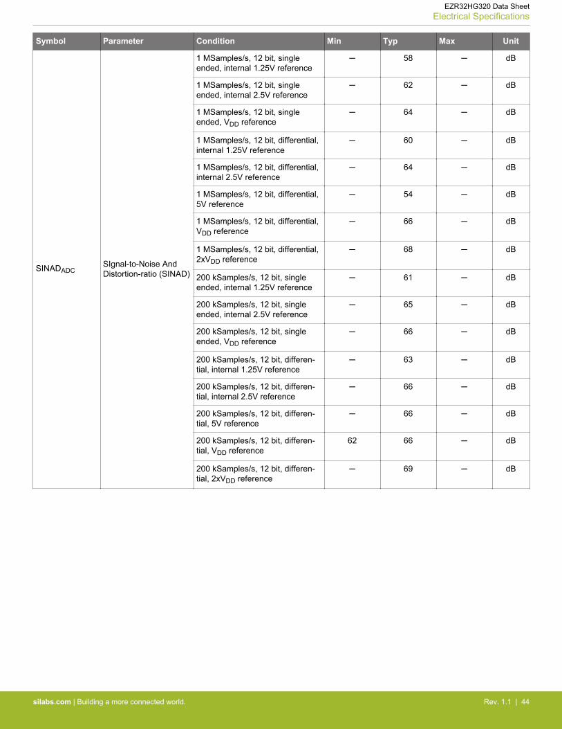
Symbol Parameter Condition Min Typ Max Unit
SINADADCSIgnal-to-Noise AndDistortion-ratio (SINAD)
1 MSamples/s, 12 bit, singleended, internal 1.25V reference
─ 58 ─ dB
1 MSamples/s, 12 bit, singleended, internal 2.5V reference
─ 62 ─ dB
1 MSamples/s, 12 bit, singleended, VDD reference
─ 64 ─ dB
1 MSamples/s, 12 bit, differential,internal 1.25V reference
─ 60 ─ dB
1 MSamples/s, 12 bit, differential,internal 2.5V reference
─ 64 ─ dB
1 MSamples/s, 12 bit, differential,5V reference
─ 54 ─ dB
1 MSamples/s, 12 bit, differential,VDD reference
─ 66 ─ dB
1 MSamples/s, 12 bit, differential,2xVDD reference
─ 68 ─ dB
200 kSamples/s, 12 bit, singleended, internal 1.25V reference
─ 61 ─ dB
200 kSamples/s, 12 bit, singleended, internal 2.5V reference
─ 65 ─ dB
200 kSamples/s, 12 bit, singleended, VDD reference
─ 66 ─ dB
200 kSamples/s, 12 bit, differen-tial, internal 1.25V reference
─ 63 ─ dB
200 kSamples/s, 12 bit, differen-tial, internal 2.5V reference
─ 66 ─ dB
200 kSamples/s, 12 bit, differen-tial, 5V reference
─ 66 ─ dB
200 kSamples/s, 12 bit, differen-tial, VDD reference
62 66 ─ dB
200 kSamples/s, 12 bit, differen-tial, 2xVDD reference
─ 69 ─ dB
EZR32HG320 Data SheetElectrical Specifications
silabs.com | Building a more connected world. Rev. 1.1 | 44
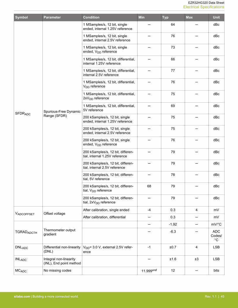
Symbol Parameter Condition Min Typ Max Unit
SFDRADCSpurious-Free DynamicRange (SFDR)
1 MSamples/s, 12 bit, singleended, internal 1.25V reference
─ 64 ─ dBc
1 MSamples/s, 12 bit, singleended, internal 2.5V reference
─ 76 ─ dBc
1 MSamples/s, 12 bit, singleended, VDD reference
─ 73 ─ dBc
1 MSamples/s, 12 bit, differential,internal 1.25V reference
─ 66 ─ dBc
1 MSamples/s, 12 bit, differential,internal 2.5V reference
─ 77 ─ dBc
1 MSamples/s, 12 bit, differential,VDD reference
─ 76 ─ dBc
1 MSamples/s, 12 bit, differential,2xVDD reference
─ 75 ─ dBc
1 MSamples/s, 12 bit, differential,5V reference
─ 69 ─ dBc
200 kSamples/s, 12 bit, singleended, internal 1.25V reference
─ 75 ─ dBc
200 kSamples/s, 12 bit, singleended, internal 2.5V reference
─ 75 ─ dBc
200 kSamples/s, 12 bit, singleended, VDD reference
─ 76 ─ dBc
200 kSamples/s, 12 bit, differen-tial, internal 1.25V reference
─ 79 ─ dBc
200 kSamples/s, 12 bit, differen-tial, internal 2.5V reference
─ 79 ─ dBc
200 kSamples/s, 12 bit, differen-tial, 5V reference
─ 78 ─ dBc
200 kSamples/s, 12 bit, differen-tial, VDD reference
68 79 ─ dBc
200 kSamples/s, 12 bit, differen-tial, 2xVDD reference
─ 79 ─ dBc
VADCOFFSET Offset voltageAfter calibration, single ended -4 0.3 4 mV
After calibration, differential ─ 0.3 ─ mV
TGRADADCTHThermometer outputgradient
─ -1.92 ─ mV/°C
─ -6.3 ─ ADCCodes/
°C
DNLADC Differential non-linearity(DNL)
VDD= 3.0 V, external 2.5V refer-ence
-1 ±0.7 4 LSB
INLADC Integral non-linearity(INL), End point method
─ ±1.6 ±3 LSB
MCADC No missing codes 11.999xref 12 ─ bits
EZR32HG320 Data SheetElectrical Specifications
silabs.com | Building a more connected world. Rev. 1.1 | 45
Symbol Parameter Condition Min Typ Max Unit
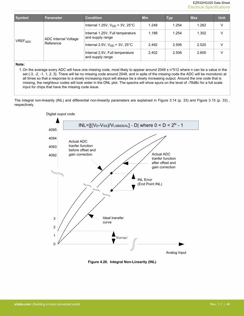
VREFADCADC Internal VoltageReference
Internal 1.25V, VDD = 3V, 25°C 1.248 1.254 1.262 V
Internal 1.25V, Full temperatureand supply range
1.188 1.254 1.302 V
Internal 2.5V, VDD = 3V, 25°C 2.492 2.506 2.520 V
Internal 2.5V, Full temperatureand supply range
2.402 2.506 2.600 V
Note:1. On the average every ADC will have one missing code, most likely to appear around 2048 ± n*512 where n can be a value in the
set {-3, -2, -1, 1, 2, 3}. There will be no missing code around 2048, and in spite of the missing code the ADC will be monotonic atall times so that a response to a slowly increasing input will always be a slowly increasing output. Around the one code that ismissing, the neighbour codes will look wider in the DNL plot. The spectra will show spurs on the level of -78dBc for a full scaleinput for chips that have the missing code issue.
The integral non-linearity (INL) and differential non-linearity parameters are explained in Figure 3.14 (p. 33) and Figure 3.15 (p. 33) ,respectively.
Ideal transfer curve
Digital ouput code
Analog Input
INL=|[(VD-VSS)/VLSBIDEAL] - D| where 0 < D < 2N - 1
0
1
2
3
4092
4093
4094
4095
VOFFSET
Actual ADC tranfer function before offset and gain correction Actual ADC
tranfer function after offset and gain correction
INL Error (End Point INL)
Figure 4.26. Integral Non-Linearity (INL)
EZR32HG320 Data SheetElectrical Specifications
silabs.com | Building a more connected world. Rev. 1.1 | 46
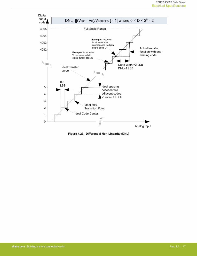
Ideal transfer curve
Digital ouputcode
Analog Input
DNL=|[(VD+1 - VD)/VLSBIDEAL] - 1| where 0 < D < 2N - 2
0
1
2
3
4092
4093
4094
4095
Actual transfer function with one missing code.
4
5
Full Scale Range
0.5 LSB
Ideal Code Center
Ideal 50% Transition Point
Ideal spacing between two adjacent codesVLSBIDEAL=1 LSB
Code width =2 LSBDNL=1 LSB
Example: Adjacent input value VD+1 corrresponds to digital output code D+1
Example: Input value VD corrresponds to digital output code D
Figure 4.27. Differential Non-Linearity (DNL)
EZR32HG320 Data SheetElectrical Specifications
silabs.com | Building a more connected world. Rev. 1.1 | 47
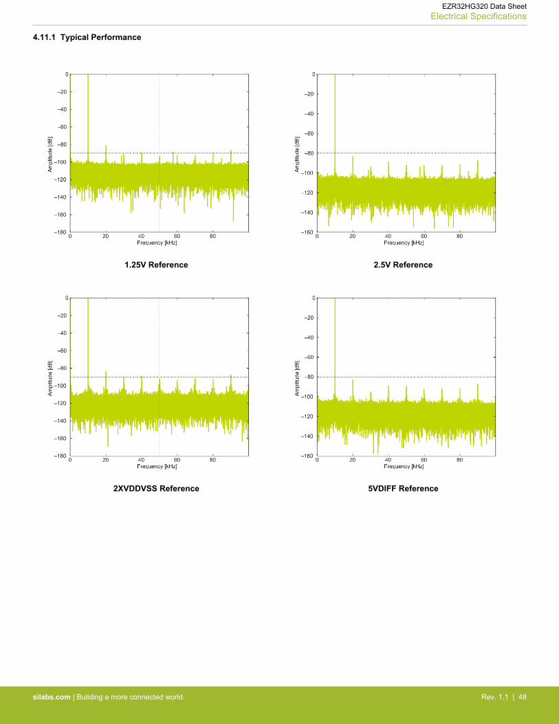
4.11.1 Typical Performance
1.25V Reference 2.5V Reference
2XVDDVSS Reference 5VDIFF Reference
EZR32HG320 Data SheetElectrical Specifications
silabs.com | Building a more connected world. Rev. 1.1 | 48
VDD Reference
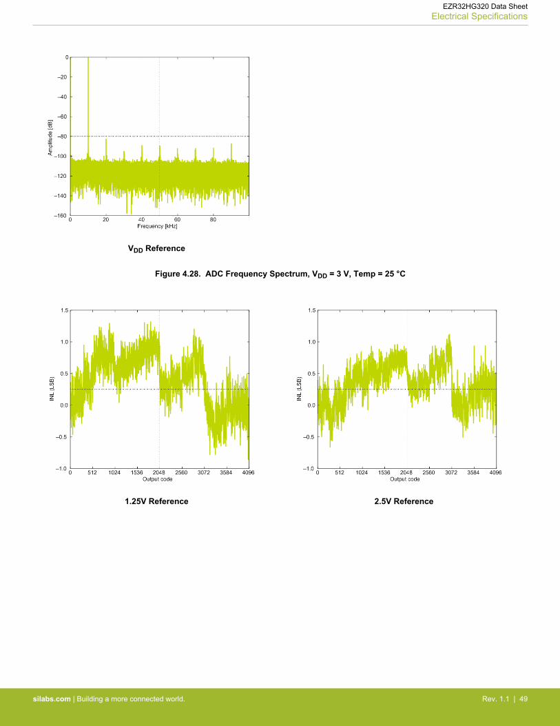
Figure 4.28. ADC Frequency Spectrum, VDD = 3 V, Temp = 25 °C
1.25V Reference 2.5V Reference
EZR32HG320 Data SheetElectrical Specifications
silabs.com | Building a more connected world. Rev. 1.1 | 49
2XVDDVSS Reference 5VDIFF Reference
VDD Reference
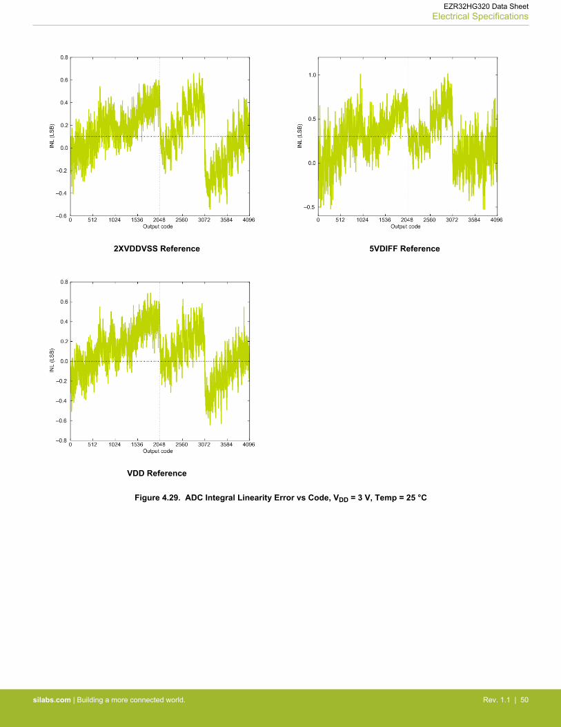
Figure 4.29. ADC Integral Linearity Error vs Code, VDD = 3 V, Temp = 25 °C
EZR32HG320 Data SheetElectrical Specifications
silabs.com | Building a more connected world. Rev. 1.1 | 50
1.25V Reference 2.5V Reference
2XVDDVSS Reference 5VDIFF Reference
EZR32HG320 Data SheetElectrical Specifications
silabs.com | Building a more connected world. Rev. 1.1 | 51
VDD Reference
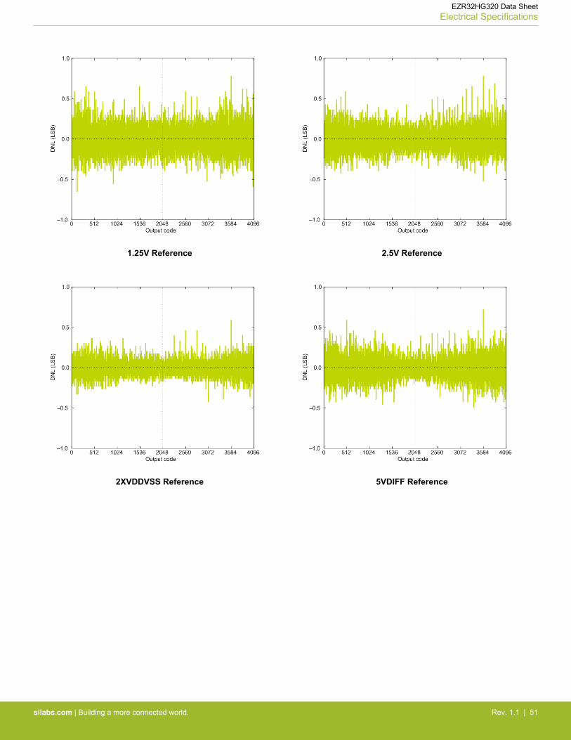
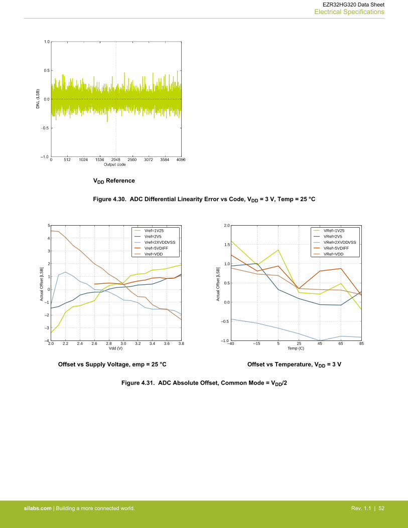
Figure 4.30. ADC Differential Linearity Error vs Code, VDD = 3 V, Temp = 25 °C
2.0 2.2 2.4 2.6 2.8 3.0 3.2 3.4 3.6 3.8Vdd (V)
–4
–3
–2
–1
0
1
2
3
4
5
Act
ual O
ffset
[LS
B]
Vref=1V25
Vref=2V5
Vref=2XVDDVSS
Vref=5VDIFF
Vref=VDD
Offset vs Supply Voltage, Temp = 25 °C
–40 –15 5 25 45 65 85Temp (C)
–1.0
–0.5
0.0
0.5
1.0
1.5
2.0
Act
ual O
ffset
[LS
B]
VRef=1V25
VRef=2V5
VRef=2XVDDVSS
VRef=5VDIFF
VRef=VDD
Offset vs Temperature, VDD = 3 V
Figure 4.31. ADC Absolute Offset, Common Mode = VDD/2
EZR32HG320 Data SheetElectrical Specifications
silabs.com | Building a more connected world. Rev. 1.1 | 52
–40 –15 5 25 45 65 85Temperature [°C]
63
64
65
66
67
68
69
70
71S
NR
[dB
]
1V25
2V5
Vdd
5VDIFF
2XVDDVSS
Signal to Noise Ratio (SNR)
–40 –15 5 25 45 65 85Temperature [°C]
78.0
78.2
78.4
78.6
78.8
79.0
79.2
79.4
SF
DR
[dB
]
1V25
2V5Vdd
5VDIFF
2XVDDVSS
Spurious-Free Dynamic Range (SFDR)
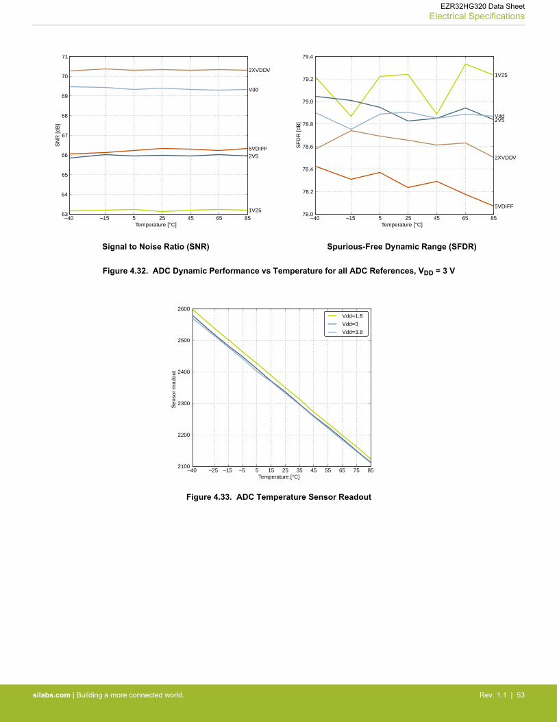
Figure 4.32. ADC Dynamic Performance vs Temperature for all ADC References, VDD = 3 V
–40 –25 –15 –5 5 15 25 35 45 55 65 75 85Temperature [°C]
2100
2200
2300
2400
2500
2600
Sen
sor
read
out
Vdd=1.8
Vdd=3
Vdd=3.8
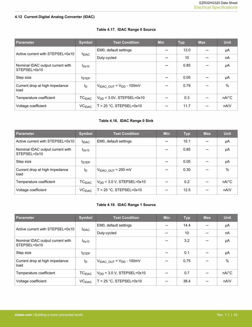
Figure 4.33. ADC Temperature Sensor Readout
EZR32HG320 Data SheetElectrical Specifications
silabs.com | Building a more connected world. Rev. 1.1 | 53
4.12 Current Digital Analog Converter (IDAC)
Table 4.17. IDAC Range 0 Source
Parameter Symbol Test Condition Min Typ Max Unit
Active current with STEPSEL=0x10 IIDACEM0, default settings ─ 13.0 ─ µA
Duty-cycled ─ 10 ─ nA
Nominal IDAC output current withSTEPSEL=0x10
I0x10 ─ 0.85 ─ µA
Step size ISTEP ─ 0.05 ─ µA
Current drop at high impedanceload
ID VIDAC_OUT = VDD - 100mV ─ 0.79 ─ %
Temperature coefficient TCIDAC VDD = 3.0V, STEPSEL=0x10 ─ 0.3 ─ nA/°C
Voltage coefficient VCIDAC T = 25 °C, STEPSEL=0x10 ─ 11.7 ─ nA/V
Table 4.18. IDAC Range 0 Sink
Parameter Symbol Test Condition Min Typ Max Unit
Active current with STEPSEL=0x10 IIDAC EM0, default settings ─ 15.1 ─ µA
Nominal IDAC output current withSTEPSEL=0x10
I0x10 ─ 0.85 ─ µA
Step size ISTEP ─ 0.05 ─ µA
Current drop at high impedanceload
ID VIDAC_OUT = 200 mV ─ 0.30 ─ %
Temperature coefficient TCIDAC VDD = 3.0 V, STEPSEL=0x10 ─ 0.2 ─ nA/°C
Voltage coefficient VCIDAC T = 25 °C, STEPSEL=0x10 ─ 12.5 ─ nA/V
Table 4.19. IDAC Range 1 Source
Parameter Symbol Test Condition Min Typ Max Unit
Active current with STEPSEL=0x10 IIDACEM0, default settings ─ 14.4 ─ µA
Duty-cycled ─ 10 ─ nA
Nominal IDAC output current withSTEPSEL=0x10
I0x10 ─ 3.2 ─ µA
Step size ISTEP ─ 0.1 ─ µA
Current drop at high impedanceload
ID VIDAC_OUT = VDD - 100mV ─ 0.75 ─ %
Temperature coefficient TCIDAC VDD = 3.0 V, STEPSEL=0x10 ─ 0.7 ─ nA/°C
Voltage coefficient VCIDAC T = 25 °C, STEPSEL=0x10 ─ 38.4 ─ nA/V
EZR32HG320 Data SheetElectrical Specifications
silabs.com | Building a more connected world. Rev. 1.1 | 54
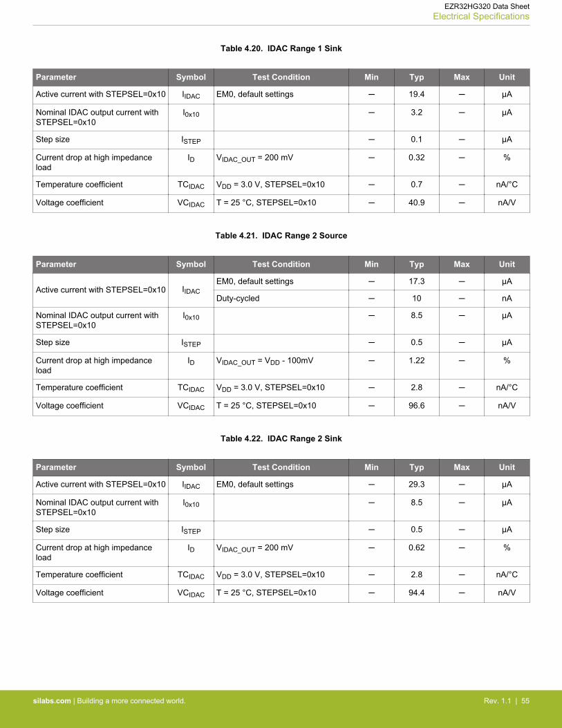
Table 4.20. IDAC Range 1 Sink
Parameter Symbol Test Condition Min Typ Max Unit
Active current with STEPSEL=0x10 IIDAC EM0, default settings ─ 19.4 ─ µA
Nominal IDAC output current withSTEPSEL=0x10
I0x10 ─ 3.2 ─ µA
Step size ISTEP ─ 0.1 ─ µA
Current drop at high impedanceload
ID VIDAC_OUT = 200 mV ─ 0.32 ─ %
Temperature coefficient TCIDAC VDD = 3.0 V, STEPSEL=0x10 ─ 0.7 ─ nA/°C
Voltage coefficient VCIDAC T = 25 °C, STEPSEL=0x10 ─ 40.9 ─ nA/V
Table 4.21. IDAC Range 2 Source
Parameter Symbol Test Condition Min Typ Max Unit
Active current with STEPSEL=0x10 IIDACEM0, default settings ─ 17.3 ─ µA
Duty-cycled ─ 10 ─ nA
Nominal IDAC output current withSTEPSEL=0x10
I0x10 ─ 8.5 ─ µA
Step size ISTEP ─ 0.5 ─ µA
Current drop at high impedanceload
ID VIDAC_OUT = VDD - 100mV ─ 1.22 ─ %
Temperature coefficient TCIDAC VDD = 3.0 V, STEPSEL=0x10 ─ 2.8 ─ nA/°C
Voltage coefficient VCIDAC T = 25 °C, STEPSEL=0x10 ─ 96.6 ─ nA/V
Table 4.22. IDAC Range 2 Sink
Parameter Symbol Test Condition Min Typ Max Unit
Active current with STEPSEL=0x10 IIDAC EM0, default settings ─ 29.3 ─ µA
Nominal IDAC output current withSTEPSEL=0x10
I0x10 ─ 8.5 ─ µA
Step size ISTEP ─ 0.5 ─ µA
Current drop at high impedanceload
ID VIDAC_OUT = 200 mV ─ 0.62 ─ %
Temperature coefficient TCIDAC VDD = 3.0 V, STEPSEL=0x10 ─ 2.8 ─ nA/°C
Voltage coefficient VCIDAC T = 25 °C, STEPSEL=0x10 ─ 94.4 ─ nA/V
EZR32HG320 Data SheetElectrical Specifications
silabs.com | Building a more connected world. Rev. 1.1 | 55
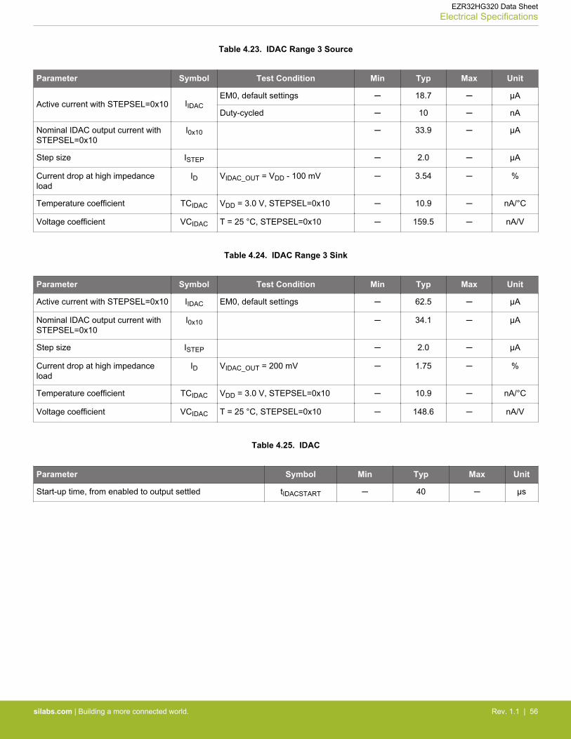
Table 4.23. IDAC Range 3 Source
Parameter Symbol Test Condition Min Typ Max Unit
Active current with STEPSEL=0x10 IIDACEM0, default settings ─ 18.7 ─ µA
Duty-cycled ─ 10 ─ nA
Nominal IDAC output current withSTEPSEL=0x10
I0x10 ─ 33.9 ─ µA
Step size ISTEP ─ 2.0 ─ µA
Current drop at high impedanceload
ID VIDAC_OUT = VDD - 100 mV ─ 3.54 ─ %
Temperature coefficient TCIDAC VDD = 3.0 V, STEPSEL=0x10 ─ 10.9 ─ nA/°C
Voltage coefficient VCIDAC T = 25 °C, STEPSEL=0x10 ─ 159.5 ─ nA/V
Table 4.24. IDAC Range 3 Sink
Parameter Symbol Test Condition Min Typ Max Unit
Active current with STEPSEL=0x10 IIDAC EM0, default settings ─ 62.5 ─ µA
Nominal IDAC output current withSTEPSEL=0x10
I0x10 ─ 34.1 ─ µA
Step size ISTEP ─ 2.0 ─ µA
Current drop at high impedanceload
ID VIDAC_OUT = 200 mV ─ 1.75 ─ %
Temperature coefficient TCIDAC VDD = 3.0 V, STEPSEL=0x10 ─ 10.9 ─ nA/°C
Voltage coefficient VCIDAC T = 25 °C, STEPSEL=0x10 ─ 148.6 ─ nA/V
Table 4.25. IDAC
Parameter Symbol Min Typ Max Unit
Start-up time, from enabled to output settled tIDACSTART ─ 40 ─ µs
EZR32HG320 Data SheetElectrical Specifications
silabs.com | Building a more connected world. Rev. 1.1 | 56
–2.0 –1.5 –1.0 –0.5 0.0V(IDAC_OUT) -Vdd [V]
90
91
92
93
94
95
96
97
98
99
100
101
Per
cent
age
of n
omin
al c
urre
nt [%
]
-40°C, 2.0V
25°C, 3.0V
85°C, 3.8V
–2.0 –1.5 –1.0 –0.5 0.0V(IDAC_OUT) -Vdd [V]
90
91
92
93
94
95
96
97
98
99
100
101
Per
cent
age
of n
omin
al c
urre
nt [%
]
-40°C, 2.0V
25°C, 3.0V
85°C, 3.8V
–2.0 –1.5 –1.0 –0.5 0.0V(IDAC_OUT) -Vdd [V]
90
91
92
93
94
95
96
97
98
99
100
101
Per
cent
age
of n
omin
al c
urre
nt [%
]
-40°C, 2.0V
25°C, 3.0V
85°C, 3.8V
–2.0 –1.5 –1.0 –0.5 0.0V(IDAC_OUT) -Vdd [V]
90
91
92
93
94
95
96
97
98
99
100
101
Per
cent
age
of n
omin
al c
urre
nt [%
]
-40°C, 2.0V
25°C, 3.0V
85°C, 3.8V
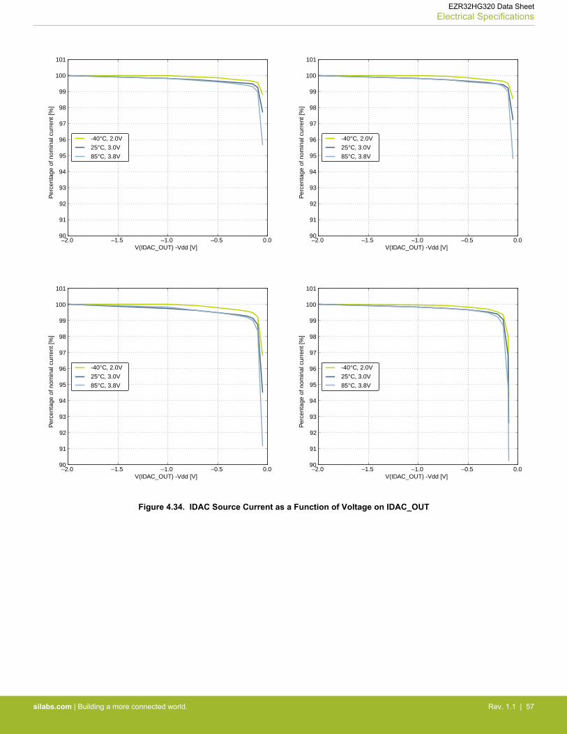
Figure 4.34. IDAC Source Current as a Function of Voltage on IDAC_OUT
EZR32HG320 Data SheetElectrical Specifications
silabs.com | Building a more connected world. Rev. 1.1 | 57
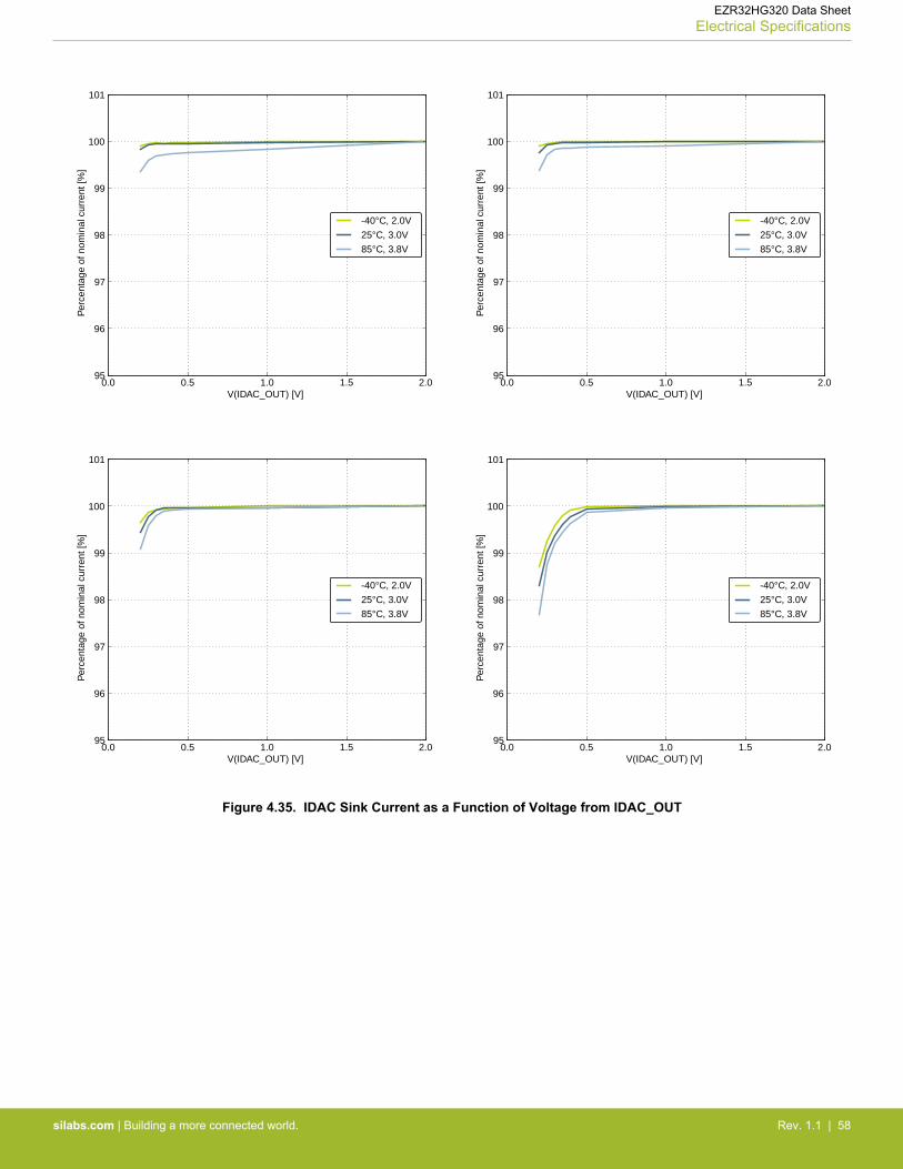
0.0 0.5 1.0 1.5 2.0V(IDAC_OUT) [V]
95
96
97
98
99
100
101
Per
cent
age
of n
omin
al c
urre
nt [%
]
-40°C, 2.0V
25°C, 3.0V
85°C, 3.8V
0.0 0.5 1.0 1.5 2.0V(IDAC_OUT) [V]
95
96
97
98
99
100
101
Per
cent
age
of n
omin
al c
urre
nt [%
]
-40°C, 2.0V
25°C, 3.0V
85°C, 3.8V
0.0 0.5 1.0 1.5 2.0V(IDAC_OUT) [V]
95
96
97
98
99
100
101
Per
cent
age
of n
omin
al c
urre
nt [%
]
-40°C, 2.0V
25°C, 3.0V
85°C, 3.8V
0.0 0.5 1.0 1.5 2.0V(IDAC_OUT) [V]
95
96
97
98
99
100
101
Per
cent
age
of n
omin
al c
urre
nt [%
]
-40°C, 2.0V
25°C, 3.0V
85°C, 3.8V
Figure 4.35. IDAC Sink Current as a Function of Voltage from IDAC_OUT
EZR32HG320 Data SheetElectrical Specifications
silabs.com | Building a more connected world. Rev. 1.1 | 58
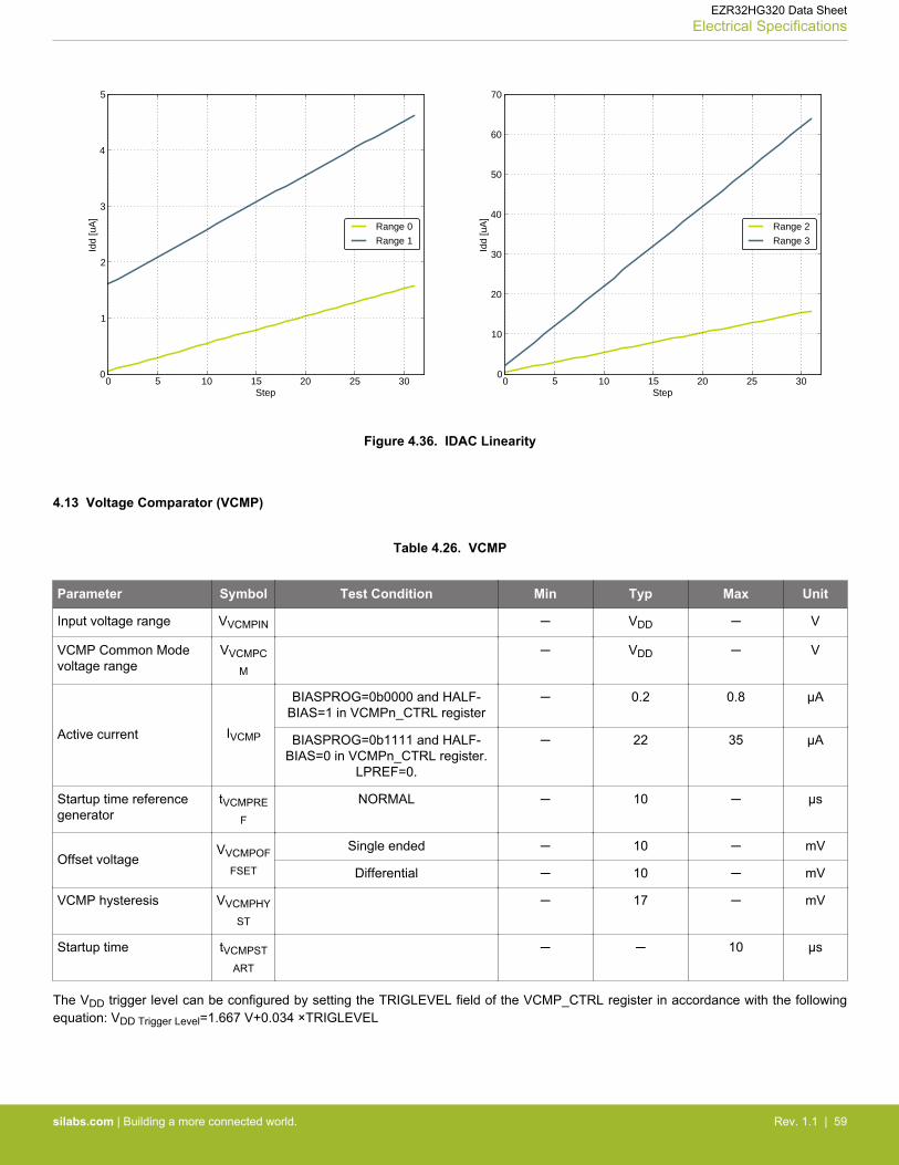
0 5 10 15 20 25 30Step
0
1
2
3
4
5Id
d [u
A]
Range 0
Range 1
0 5 10 15 20 25 30Step
0
10
20
30
40
50
60
70
Idd
[uA
]
Range 2
Range 3
Figure 4.36. IDAC Linearity
4.13 Voltage Comparator (VCMP)
Table 4.26. VCMP
Parameter Symbol Test Condition Min Typ Max Unit
Input voltage range VVCMPIN ─ VDD ─ V
VCMP Common Modevoltage range
VVCMPC
M
─ VDD ─ V
Active current IVCMP
BIASPROG=0b0000 and HALF-BIAS=1 in VCMPn_CTRL register
─ 0.2 0.8 µA
BIASPROG=0b1111 and HALF-BIAS=0 in VCMPn_CTRL register.
LPREF=0.
─ 22 35 µA
Startup time referencegenerator
tVCMPRE
F
NORMAL ─ 10 ─ µs
Offset voltageVVCMPOF
FSET
Single ended ─ 10 ─ mV
Differential ─ 10 ─ mV
VCMP hysteresis VVCMPHY
ST
─ 17 ─ mV
Startup time tVCMPST
ART
─ ─ 10 µs
The VDD trigger level can be configured by setting the TRIGLEVEL field of the VCMP_CTRL register in accordance with the followingequation: VDD Trigger Level=1.667 V+0.034 ×TRIGLEVEL
EZR32HG320 Data SheetElectrical Specifications
silabs.com | Building a more connected world. Rev. 1.1 | 59
4.14 I2C
Table 4.27. I2C Standard-Mode (Sm)
Parameter Symbol Min Typ Max Unit
SCL clock frequency fSCL 0 ─ 100 1 kHz
SCL clock low time tLOW 4.7 ─ ─ µs
SCL clock high time tHIGH 4.0 ─ ─ µs
SDA set-up time tSU,DAT 250 ─ ─ ns
SDA hold time tHD,DAT 8 ─ 34502, 3 ns
Repeated START condition set-up time tSU,STA 4.7 ─ ─ µs
(Repeated) START condition hold time tHD,STA 4.0 ─ ─ µs
STOP condition set-up time tSU,STO 4.0 ─ ─ µs
Bus free time between a STOP and a STARTcondition
tBUF 4.7 ─ ─ µs
Note:1. For the minimum HFPERCLK frequency required in Standard-mode, see the I2C chapter in the EZR32HG Reference Manual.2. The maximum SDA hold time (tHD,DAT) needs to be met only when the device does not stretch the low time of SCL (tLOW).
3. When transmitting data, this number is guaranteed only when I2Cn_CLKDIV < ((3450 * 10-9 [s] * fHFPERCLK [Hz]) - 4).
Table 4.28. I2C Fast-Mode (Fm)
Parameter Symbol Min Typ Max Unit
SCL clock frequency fSCL 0 ─ 4001 kHz
SCL clock low time tLOW 1.3 ─ ─ µs
SCL clock high time tHIGH 0.6 ─ ─ µs
SDA set-up time tSU,DAT 100 ─ ─ ns
SDA hold time tHD,DAT 8 ─ 9002 , 3 ns
Repeated START condition set-up time tSU,STA 0.6 ─ ─ µs
(Repeated) START condition hold time tHD,STA 0.6 ─ ─ µs
STOP condition set-up time tSU,STO 0.6 ─ ─ µs
Bus free time between a STOP and a START condi-tion
tBUF 1.3 ─ ─ µs
Note:1. For the minimum HFPERCLK frequency required in Fast-mode, see the I2C chapter in the EZR32HG Reference Manual.2. The maximum SDA hold time (tHD,DAT) needs to be met only when the device does not stretch the low time of SCL (tLOW).
3. When transmitting data, this number is guaranteed only when I2Cn_CLKDIV < ((900 * 10-9 [s] * fHFPERCLK [Hz]) - 4).
EZR32HG320 Data SheetElectrical Specifications
silabs.com | Building a more connected world. Rev. 1.1 | 60
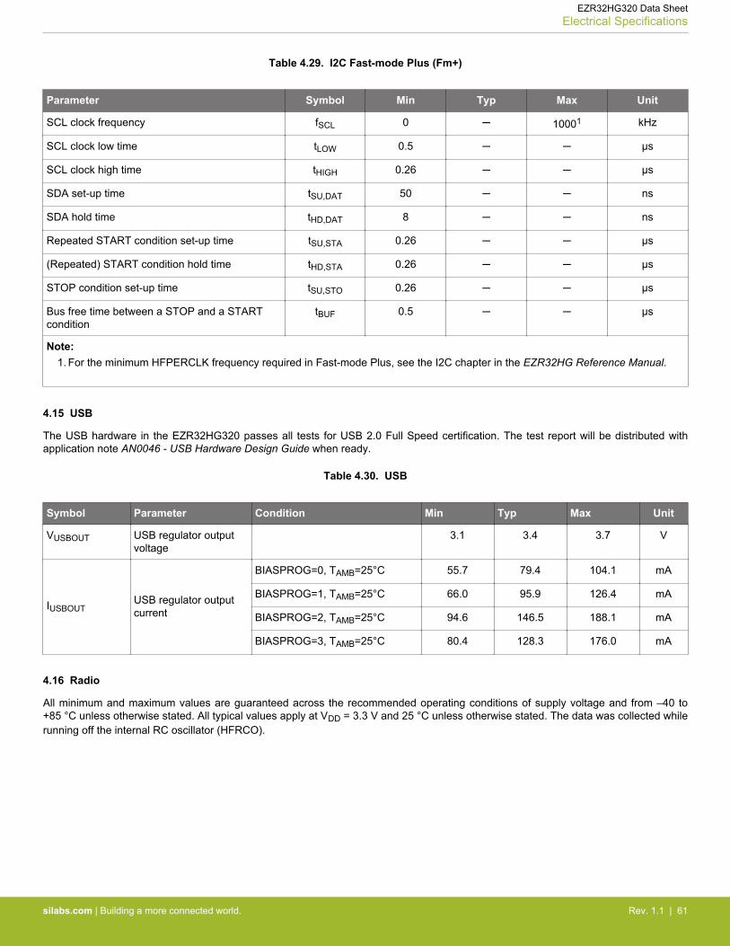
Table 4.29. I2C Fast-mode Plus (Fm+)
Parameter Symbol Min Typ Max Unit
SCL clock frequency fSCL 0 ─ 10001 kHz
SCL clock low time tLOW 0.5 ─ ─ µs
SCL clock high time tHIGH 0.26 ─ ─ µs
SDA set-up time tSU,DAT 50 ─ ─ ns
SDA hold time tHD,DAT 8 ─ ─ ns
Repeated START condition set-up time tSU,STA 0.26 ─ ─ µs
(Repeated) START condition hold time tHD,STA 0.26 ─ ─ µs
STOP condition set-up time tSU,STO 0.26 ─ ─ µs
Bus free time between a STOP and a STARTcondition
tBUF 0.5 ─ ─ µs
Note:1. For the minimum HFPERCLK frequency required in Fast-mode Plus, see the I2C chapter in the EZR32HG Reference Manual.
4.15 USB
The USB hardware in the EZR32HG320 passes all tests for USB 2.0 Full Speed certification. The test report will be distributed withapplication note AN0046 - USB Hardware Design Guide when ready.
Table 4.30. USB
Symbol Parameter Condition Min Typ Max Unit
VUSBOUT USB regulator outputvoltage
3.1 3.4 3.7 V
IUSBOUTUSB regulator outputcurrent
BIASPROG=0, TAMB=25°C 55.7 79.4 104.1 mA
BIASPROG=1, TAMB=25°C 66.0 95.9 126.4 mA
BIASPROG=2, TAMB=25°C 94.6 146.5 188.1 mA
BIASPROG=3, TAMB=25°C 80.4 128.3 176.0 mA
4.16 Radio
All minimum and maximum values are guaranteed across the recommended operating conditions of supply voltage and from –40 to+85 °C unless otherwise stated. All typical values apply at VDD = 3.3 V and 25 °C unless otherwise stated. The data was collected whilerunning off the internal RC oscillator (HFRCO).
EZR32HG320 Data SheetElectrical Specifications
silabs.com | Building a more connected world. Rev. 1.1 | 61
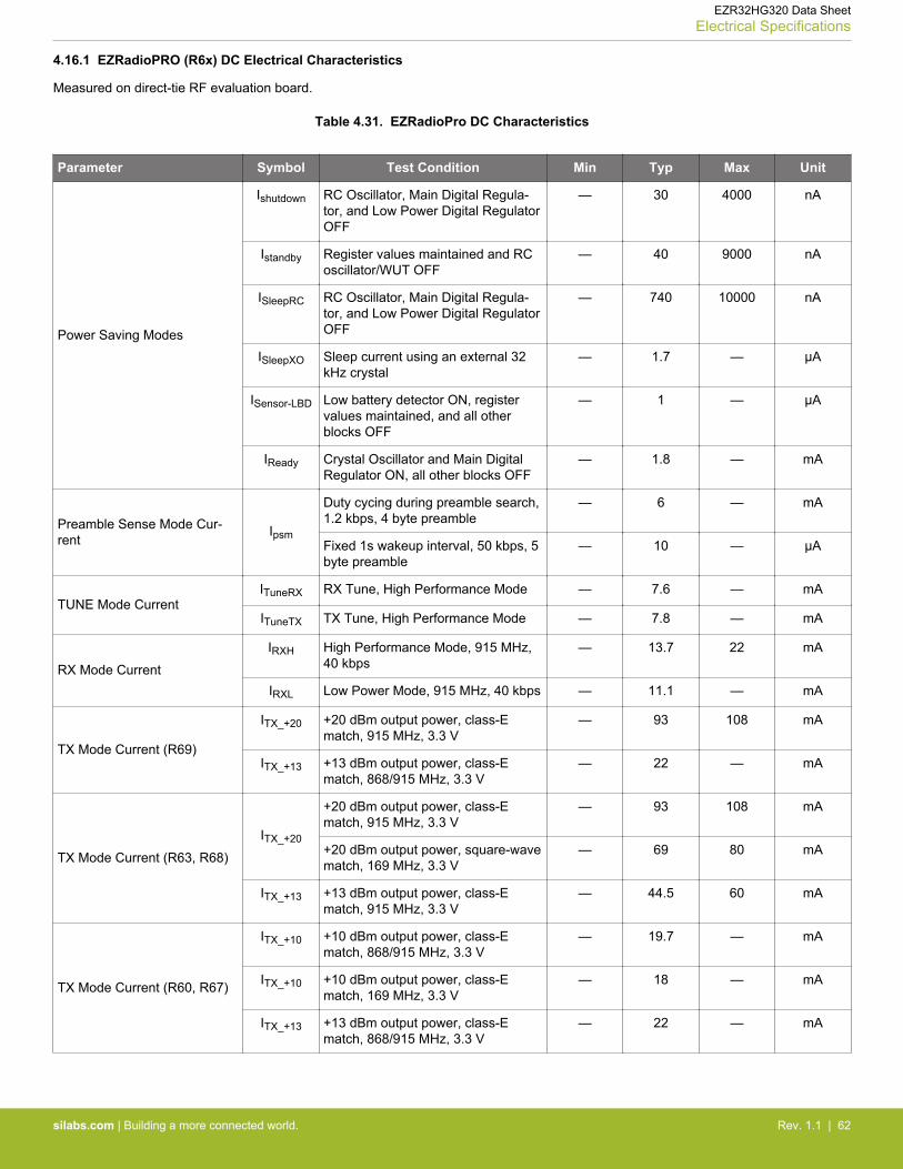
4.16.1 EZRadioPRO (R6x) DC Electrical Characteristics
Measured on direct-tie RF evaluation board.
Table 4.31. EZRadioPro DC Characteristics
Parameter Symbol Test Condition Min Typ Max Unit
Power Saving Modes
Ishutdown RC Oscillator, Main Digital Regula-tor, and Low Power Digital RegulatorOFF
— 30 4000 nA
Istandby Register values maintained and RCoscillator/WUT OFF
— 40 9000 nA
ISleepRC RC Oscillator, Main Digital Regula-tor, and Low Power Digital RegulatorOFF
— 740 10000 nA
ISleepXO Sleep current using an external 32kHz crystal
— 1.7 — μA
ISensor-LBD Low battery detector ON, registervalues maintained, and all otherblocks OFF
— 1 — μA
IReady Crystal Oscillator and Main DigitalRegulator ON, all other blocks OFF
— 1.8 — mA
Preamble Sense Mode Cur-rent
Ipsm
Duty cycing during preamble search,1.2 kbps, 4 byte preamble
— 6 — mA
Fixed 1s wakeup interval, 50 kbps, 5byte preamble
— 10 — μA
TUNE Mode CurrentITuneRX RX Tune, High Performance Mode — 7.6 — mA
ITuneTX TX Tune, High Performance Mode — 7.8 — mA
RX Mode Current
IRXH High Performance Mode, 915 MHz,40 kbps
— 13.7 22 mA
IRXL Low Power Mode, 915 MHz, 40 kbps — 11.1 — mA
TX Mode Current (R69)
ITX_+20 +20 dBm output power, class-Ematch, 915 MHz, 3.3 V
— 93 108 mA
ITX_+13 +13 dBm output power, class-Ematch, 868/915 MHz, 3.3 V
— 22 — mA
TX Mode Current (R63, R68)
ITX_+20
+20 dBm output power, class-Ematch, 915 MHz, 3.3 V
— 93 108 mA
+20 dBm output power, square-wavematch, 169 MHz, 3.3 V
— 69 80 mA
ITX_+13 +13 dBm output power, class-Ematch, 915 MHz, 3.3 V
— 44.5 60 mA
TX Mode Current (R60, R67)
ITX_+10 +10 dBm output power, class-Ematch, 868/915 MHz, 3.3 V
— 19.7 — mA
ITX_+10 +10 dBm output power, class-Ematch, 169 MHz, 3.3 V
— 18 — mA
ITX_+13 +13 dBm output power, class-Ematch, 868/915 MHz, 3.3 V
— 22 — mA
EZR32HG320 Data SheetElectrical Specifications
silabs.com | Building a more connected world. Rev. 1.1 | 62
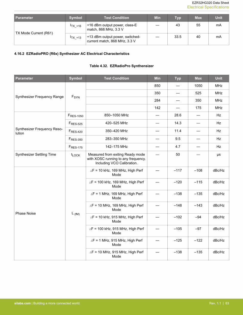
Parameter Symbol Test Condition Min Typ Max Unit
TX Mode Current (R61)
ITX_+16 +16 dBm output power, class-Ematch, 868 MHz, 3.3 V
— 43 55 mA
ITX_+13 +13 dBm output power, switched-current match, 868 MHz, 3.3 V
— 33.5 40 mA
4.16.2 EZRadioPRO (R6x) Synthesizer AC Electrical Characteristics
Table 4.32. EZRadioPro Synthensizer
Parameter Symbol Test Condition Min Typ Max Unit
Synthesizer Frequency Range FSYN
850 — 1050 MHz
350 — 525 MHz
284 — 350 MHz
142 — 175 MHz
Synthesizer Frequency Reso-lution
FRES-1050 850–1050 MHz — 28.6 — Hz
FRES-525 420–525 MHz — 14.3 — Hz
FRES-420 350–420 MHz — 11.4 — Hz
FRES-350 283–350 MHz — 9.5 — Hz
FRES-175 142–175 MHz — 4.7 — Hz
Synthesizer Settling Time tLOCK Measured from exiting Ready modewith XOSC running to any frequency.
Including VCO Calibration.
— 50 — μs
Phase Noise L Φ(fM)
ΔF = 10 kHz, 169 MHz, High PerfMode
— –117 –108 dBc/Hz
ΔF = 100 kHz, 169 MHz, High PerfMode
— –120 –115 dBc/Hz
ΔF = 1 MHz, 169 MHz, High PerfMode
— –138 –135 dBc/Hz
ΔF = 10 MHz, 169 MHz, High PerfMode
— –148 –143 dBc/Hz
ΔF = 10 kHz, 915 MHz, High PerfMode
— –102 –94 dBc/Hz
ΔF = 100 kHz, 915 MHz, High PerfMode
— –105 –97 dBc/Hz
ΔF = 1 MHz, 915 MHz, High PerfMode
— –125 –122 dBc/Hz
ΔF = 10 MHz, 915 MHz, High PerfMode
— –138 –135 dBc/Hz
EZR32HG320 Data SheetElectrical Specifications
silabs.com | Building a more connected world. Rev. 1.1 | 63
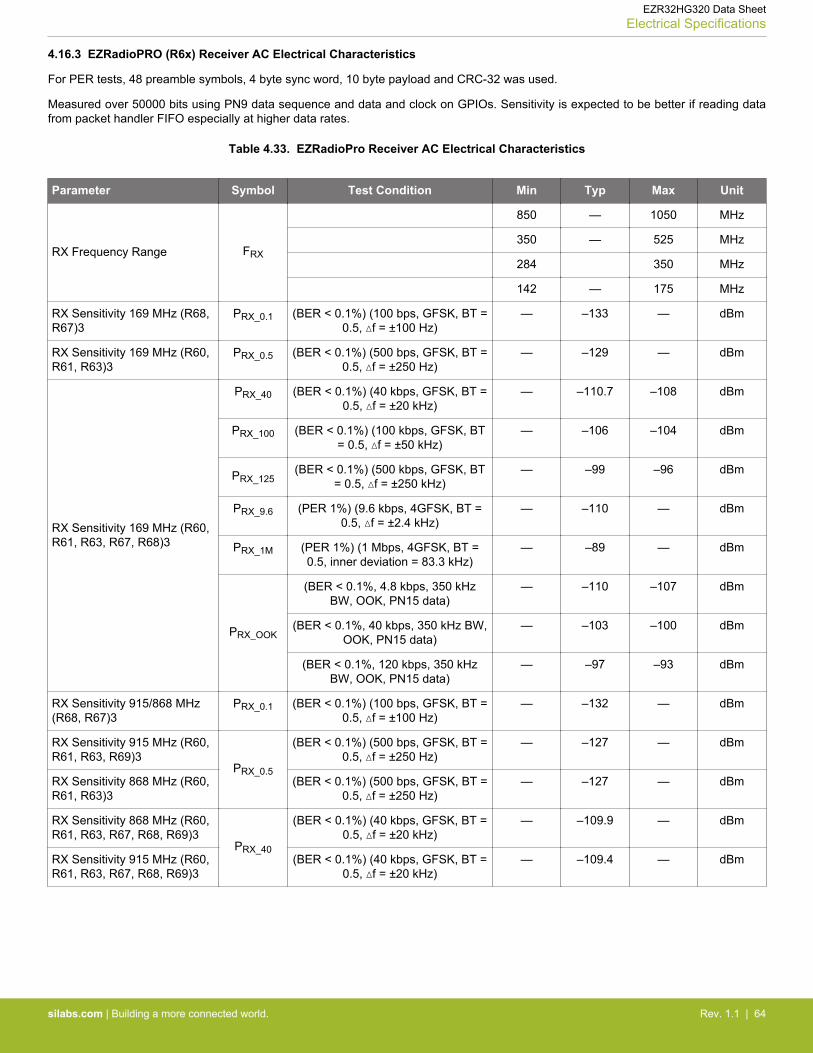
4.16.3 EZRadioPRO (R6x) Receiver AC Electrical Characteristics
For PER tests, 48 preamble symbols, 4 byte sync word, 10 byte payload and CRC-32 was used.
Measured over 50000 bits using PN9 data sequence and data and clock on GPIOs. Sensitivity is expected to be better if reading datafrom packet handler FIFO especially at higher data rates.
Table 4.33. EZRadioPro Receiver AC Electrical Characteristics
Parameter Symbol Test Condition Min Typ Max Unit
RX Frequency Range FRX
850 — 1050 MHz
350 — 525 MHz
284 350 MHz
142 — 175 MHz
RX Sensitivity 169 MHz (R68,R67)3
PRX_0.1 (BER < 0.1%) (100 bps, GFSK, BT =0.5, Δf = ±100 Hz)
— –133 — dBm
RX Sensitivity 169 MHz (R60,R61, R63)3
PRX_0.5 (BER < 0.1%) (500 bps, GFSK, BT =0.5, Δf = ±250 Hz)
— –129 — dBm
RX Sensitivity 169 MHz (R60,R61, R63, R67, R68)3
PRX_40 (BER < 0.1%) (40 kbps, GFSK, BT =0.5, Δf = ±20 kHz)
— –110.7 –108 dBm
PRX_100 (BER < 0.1%) (100 kbps, GFSK, BT= 0.5, Δf = ±50 kHz)
— –106 –104 dBm
PRX_125(BER < 0.1%) (500 kbps, GFSK, BT
= 0.5, Δf = ±250 kHz)— –99 –96 dBm
PRX_9.6 (PER 1%) (9.6 kbps, 4GFSK, BT =0.5, Δf = ±2.4 kHz)
— –110 — dBm
PRX_1M (PER 1%) (1 Mbps, 4GFSK, BT =0.5, inner deviation = 83.3 kHz)
— –89 — dBm
PRX_OOK
(BER < 0.1%, 4.8 kbps, 350 kHzBW, OOK, PN15 data)
— –110 –107 dBm
(BER < 0.1%, 40 kbps, 350 kHz BW,OOK, PN15 data)
— –103 –100 dBm
(BER < 0.1%, 120 kbps, 350 kHzBW, OOK, PN15 data)
— –97 –93 dBm
RX Sensitivity 915/868 MHz(R68, R67)3
PRX_0.1 (BER < 0.1%) (100 bps, GFSK, BT =0.5, Δf = ±100 Hz)
— –132 — dBm
RX Sensitivity 915 MHz (R60,R61, R63, R69)3
PRX_0.5
(BER < 0.1%) (500 bps, GFSK, BT =0.5, Δf = ±250 Hz)
— –127 — dBm
RX Sensitivity 868 MHz (R60,R61, R63)3
(BER < 0.1%) (500 bps, GFSK, BT =0.5, Δf = ±250 Hz)
— –127 — dBm
RX Sensitivity 868 MHz (R60,R61, R63, R67, R68, R69)3
PRX_40
(BER < 0.1%) (40 kbps, GFSK, BT =0.5, Δf = ±20 kHz)
— –109.9 — dBm
RX Sensitivity 915 MHz (R60,R61, R63, R67, R68, R69)3
(BER < 0.1%) (40 kbps, GFSK, BT =0.5, Δf = ±20 kHz)
— –109.4 — dBm
EZR32HG320 Data SheetElectrical Specifications
silabs.com | Building a more connected world. Rev. 1.1 | 64
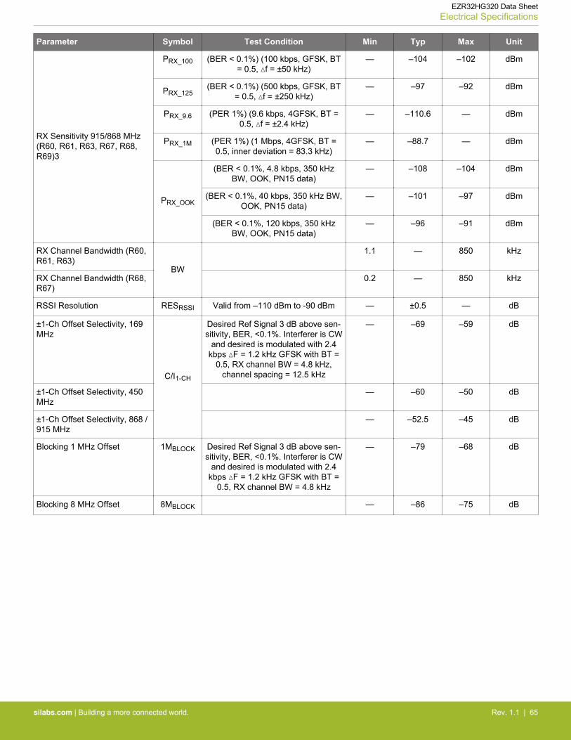
Parameter Symbol Test Condition Min Typ Max Unit
RX Sensitivity 915/868 MHz(R60, R61, R63, R67, R68,R69)3
PRX_100 (BER < 0.1%) (100 kbps, GFSK, BT= 0.5, Δf = ±50 kHz)
— –104 –102 dBm
PRX_125(BER < 0.1%) (500 kbps, GFSK, BT
= 0.5, Δf = ±250 kHz)— –97 –92 dBm
PRX_9.6 (PER 1%) (9.6 kbps, 4GFSK, BT =0.5, Δf = ±2.4 kHz)
— –110.6 — dBm
PRX_1M (PER 1%) (1 Mbps, 4GFSK, BT =0.5, inner deviation = 83.3 kHz)
— –88.7 — dBm
PRX_OOK
(BER < 0.1%, 4.8 kbps, 350 kHzBW, OOK, PN15 data)
— –108 –104 dBm
(BER < 0.1%, 40 kbps, 350 kHz BW,OOK, PN15 data)
— –101 –97 dBm
(BER < 0.1%, 120 kbps, 350 kHzBW, OOK, PN15 data)
— –96 –91 dBm
RX Channel Bandwidth (R60,R61, R63)
BW
1.1 — 850 kHz
RX Channel Bandwidth (R68,R67)
0.2 — 850 kHz
RSSI Resolution RESRSSI Valid from –110 dBm to -90 dBm — ±0.5 — dB
±1-Ch Offset Selectivity, 169MHz
C/I1-CH
Desired Ref Signal 3 dB above sen-sitivity, BER, <0.1%. Interferer is CW
and desired is modulated with 2.4kbps ΔF = 1.2 kHz GFSK with BT =
0.5, RX channel BW = 4.8 kHz,channel spacing = 12.5 kHz
— –69 –59 dB
±1-Ch Offset Selectivity, 450MHz
— –60 –50 dB
±1-Ch Offset Selectivity, 868 /915 MHz
— –52.5 –45 dB
Blocking 1 MHz Offset 1MBLOCK Desired Ref Signal 3 dB above sen-sitivity, BER, <0.1%. Interferer is CW
and desired is modulated with 2.4kbps ΔF = 1.2 kHz GFSK with BT =
0.5, RX channel BW = 4.8 kHz
— –79 –68 dB
Blocking 8 MHz Offset 8MBLOCK — –86 –75 dB
EZR32HG320 Data SheetElectrical Specifications
silabs.com | Building a more connected world. Rev. 1.1 | 65
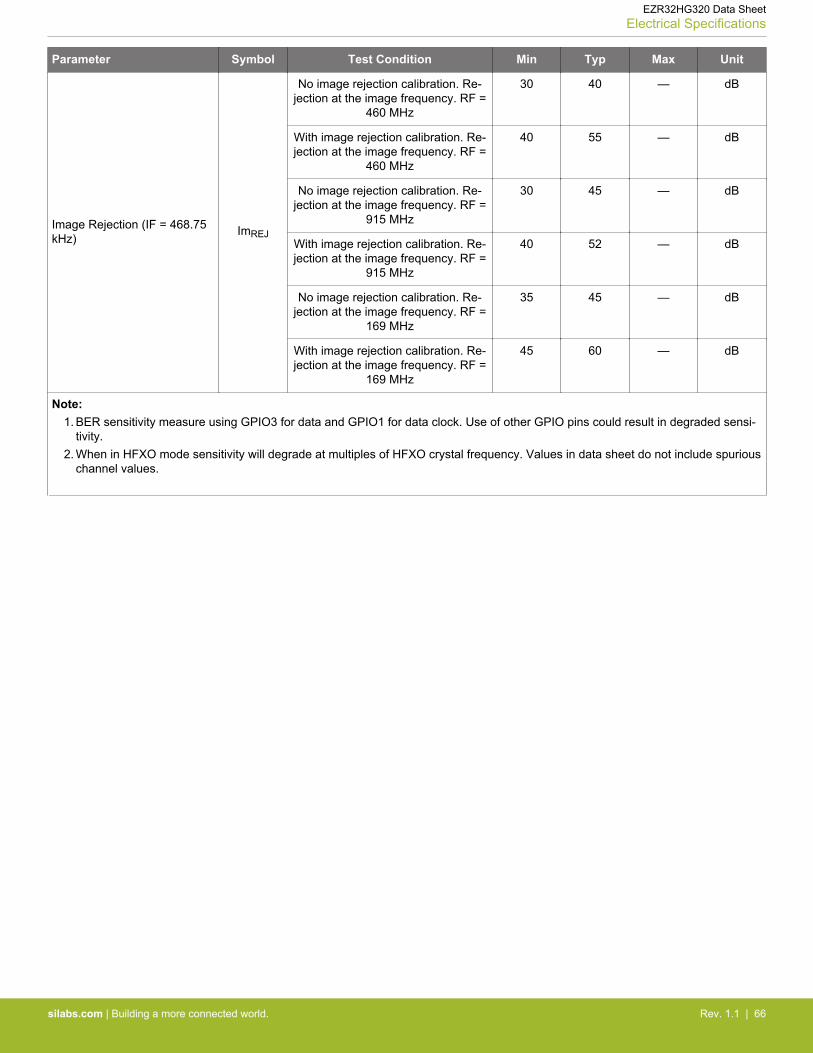
Parameter Symbol Test Condition Min Typ Max Unit
Image Rejection (IF = 468.75kHz)
ImREJ
No image rejection calibration. Re-jection at the image frequency. RF =
460 MHz
30 40 — dB
With image rejection calibration. Re-jection at the image frequency. RF =
460 MHz
40 55 — dB
No image rejection calibration. Re-jection at the image frequency. RF =
915 MHz
30 45 — dB
With image rejection calibration. Re-jection at the image frequency. RF =
915 MHz
40 52 — dB
No image rejection calibration. Re-jection at the image frequency. RF =
169 MHz
35 45 — dB
With image rejection calibration. Re-jection at the image frequency. RF =
169 MHz
45 60 — dB
Note:1. BER sensitivity measure using GPIO3 for data and GPIO1 for data clock. Use of other GPIO pins could result in degraded sensi-
tivity.2. When in HFXO mode sensitivity will degrade at multiples of HFXO crystal frequency. Values in data sheet do not include spurious
channel values.
EZR32HG320 Data SheetElectrical Specifications
silabs.com | Building a more connected world. Rev. 1.1 | 66
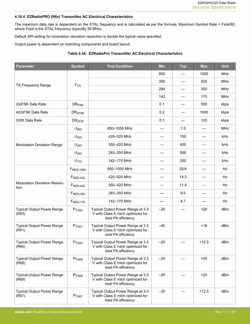
4.16.4 EZRadioPRO (R6x) Transmitter AC Electrical Characteristics
The maximum data rate is dependent on the XTAL frequency and is calculated as per the formula: Maximum Symbol Rate = Fxtal/60,where Fxtal is the XTAL frequency (typically 30 MHz).
Default API setting for modulation deviation resolution is double the typical value specified.
Output power is dependent on matching components and board layout.
Table 4.34. EZRadioPro Transmitter AC Electrical Characteristics
Parameter Symbol Test Condition Min Typ Max Unit
TX Frequency Range FTX
850 — 1050 MHz
350 — 525 MHz
284 — 350 MHz
142 — 175 MHz
(G)FSK Data Rate DRFSK 0.1 — 500 kbps
4(G)FSK Data Rate DR4FSK 0.2 — 1000 kbps
OOK Data Rate DROOK 0.1 — 120 kbps
Modulation Deviation Range
Δf960 850–1050 MHz — 1.5 — MHz
Δf525 420–525 MHz — 750 — kHz
Δf420 350–420 MHz — 600 — kHz
Δf350 283–350 MHz — 500 — kHz
Δf175 142–175 MHz — 250 — kHz
Modulation Deviation Resolu-tion
FRES-1050 850–1050 MHz — 28.6 — Hz
FRES-525 420–525 MHz — 14.3 — Hz
FRES-420 350–420 MHz — 11.4 — Hz
FRES-350 283–350 MHz — 9.5 — Hz
FRES-175 142–175 MHz — 4.7 — Hz
Typical Output Power Range(R63)
PTX63 Typical Output Power Range at 3.3V with Class E mtch optimized for
best PA efficiency
–20 — +20 dBm
Typical Output Power Range(R61)
PTX61 Typical Output Power Range at 3.3V with Class E mtch optimized for
best PA efficiency
–40 +16 dBm
Typical Output Power Range(R60)
PTX60 Typical Output Power Range at 3.3V with Class E mtch optimized for
best PA efficiency
–20 — +12.5 dBm
Typical Output Power Range(R68)
PTX68 Typical Output Power Range at 3.3V with Class E mtch optimized for
best PA efficiency
–20 — +20 dBm
Typical Output Power Range(R69)
PTX69 Typical Output Power Range at 3.3V with Class E mtch optimized for
best PA efficiency
–20 — +20 dBm
Typical Output Power Range(R67) PTX67
Typical Output Power Range at 3.3V with Class E mtch optimized for
best PA efficiency
–20 — +12.5 dBm
EZR32HG320 Data SheetElectrical Specifications
silabs.com | Building a more connected world. Rev. 1.1 | 67
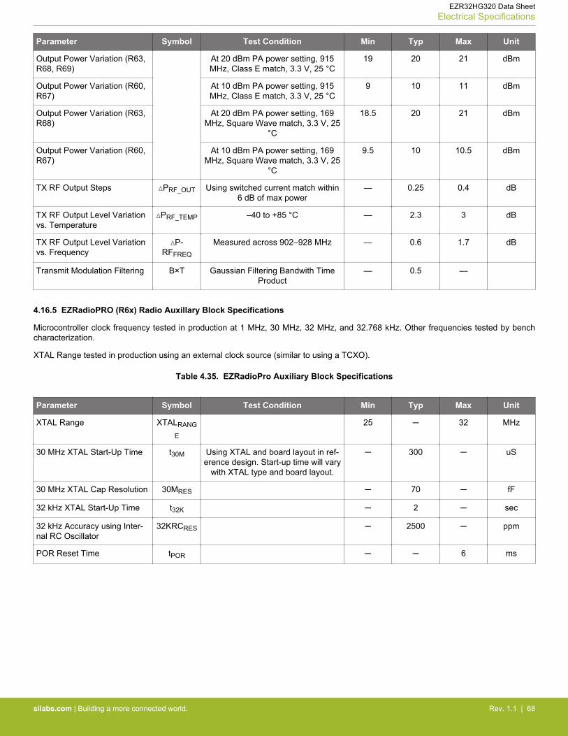
Parameter Symbol Test Condition Min Typ Max Unit
Output Power Variation (R63,R68, R69)
At 20 dBm PA power setting, 915MHz, Class E match, 3.3 V, 25 °C
19 20 21 dBm
Output Power Variation (R60,R67)
At 10 dBm PA power setting, 915MHz, Class E match, 3.3 V, 25 °C
9 10 11 dBm
Output Power Variation (R63,R68)
At 20 dBm PA power setting, 169MHz, Square Wave match, 3.3 V, 25
°C
18.5 20 21 dBm
Output Power Variation (R60,R67)
At 10 dBm PA power setting, 169MHz, Square Wave match, 3.3 V, 25
°C
9.5 10 10.5 dBm
TX RF Output Steps ΔPRF_OUT Using switched current match within6 dB of max power
— 0.25 0.4 dB
TX RF Output Level Variationvs. Temperature
ΔPRF_TEMP –40 to +85 °C — 2.3 3 dB
TX RF Output Level Variationvs. Frequency
ΔP-RFFREQ
Measured across 902–928 MHz — 0.6 1.7 dB
Transmit Modulation Filtering B×T Gaussian Filtering Bandwith TimeProduct
— 0.5 —
4.16.5 EZRadioPRO (R6x) Radio Auxillary Block Specifications
Microcontroller clock frequency tested in production at 1 MHz, 30 MHz, 32 MHz, and 32.768 kHz. Other frequencies tested by benchcharacterization.
XTAL Range tested in production using an external clock source (similar to using a TCXO).
Table 4.35. EZRadioPro Auxiliary Block Specifications
Parameter Symbol Test Condition Min Typ Max Unit
XTAL Range XTALRANG
E
25 ─ 32 MHz
30 MHz XTAL Start-Up Time t30M Using XTAL and board layout in ref-erence design. Start-up time will vary
with XTAL type and board layout.
─ 300 ─ uS
30 MHz XTAL Cap Resolution 30MRES ─ 70 ─ fF
32 kHz XTAL Start-Up Time t32K ─ 2 ─ sec
32 kHz Accuracy using Inter-nal RC Oscillator
32KRCRES ─ 2500 ─ ppm
POR Reset Time tPOR ─ ─ 6 ms
EZR32HG320 Data SheetElectrical Specifications
silabs.com | Building a more connected world. Rev. 1.1 | 68
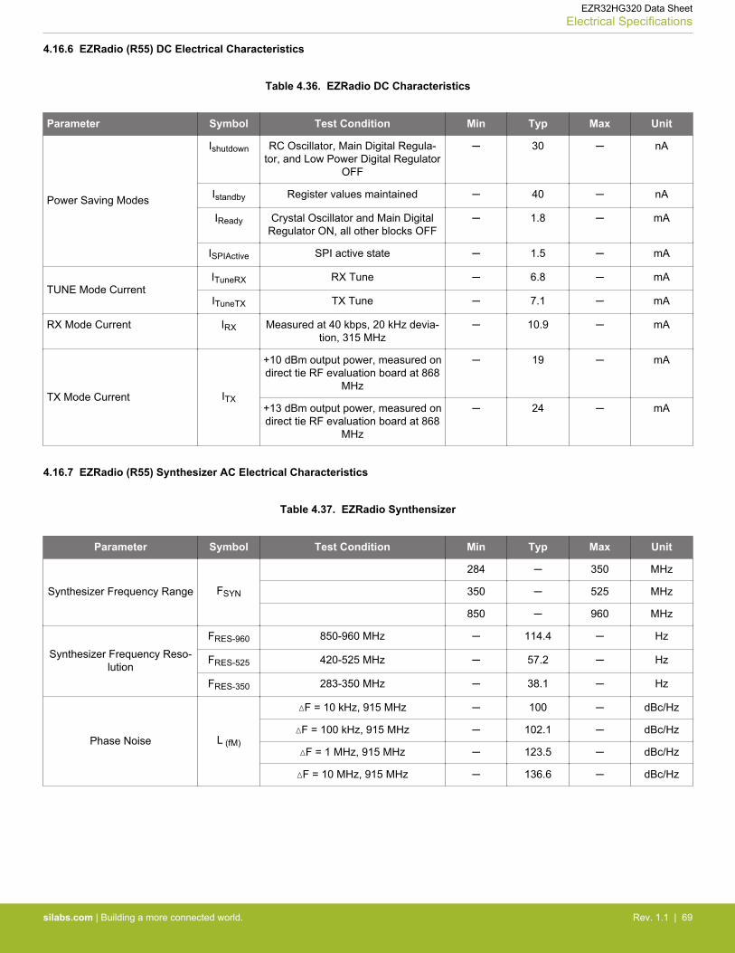
4.16.6 EZRadio (R55) DC Electrical Characteristics
Table 4.36. EZRadio DC Characteristics
Parameter Symbol Test Condition Min Typ Max Unit
Power Saving Modes
Ishutdown RC Oscillator, Main Digital Regula-tor, and Low Power Digital Regulator
OFF
─ 30 ─ nA
Istandby Register values maintained ─ 40 ─ nA
IReady Crystal Oscillator and Main DigitalRegulator ON, all other blocks OFF
─ 1.8 ─ mA
ISPIActive SPI active state ─ 1.5 ─ mA
TUNE Mode CurrentITuneRX RX Tune ─ 6.8 ─ mA
ITuneTX TX Tune ─ 7.1 ─ mA
RX Mode Current IRX Measured at 40 kbps, 20 kHz devia-tion, 315 MHz
─ 10.9 ─ mA
TX Mode Current ITX
+10 dBm output power, measured ondirect tie RF evaluation board at 868
MHz
─ 19 ─ mA
+13 dBm output power, measured ondirect tie RF evaluation board at 868
MHz
─ 24 ─ mA
4.16.7 EZRadio (R55) Synthesizer AC Electrical Characteristics
Table 4.37. EZRadio Synthensizer
Parameter Symbol Test Condition Min Typ Max Unit
Synthesizer Frequency Range FSYN
284 ─ 350 MHz
350 ─ 525 MHz
850 ─ 960 MHz
Synthesizer Frequency Reso-lution
FRES-960 850-960 MHz ─ 114.4 ─ Hz
FRES-525 420-525 MHz ─ 57.2 ─ Hz
FRES-350 283-350 MHz ─ 38.1 ─ Hz
Phase Noise L Φ(fM)
ΔF = 10 kHz, 915 MHz ─ 100 ─ dBc/Hz
ΔF = 100 kHz, 915 MHz ─ 102.1 ─ dBc/Hz
ΔF = 1 MHz, 915 MHz ─ 123.5 ─ dBc/Hz
ΔF = 10 MHz, 915 MHz ─ 136.6 ─ dBc/Hz
EZR32HG320 Data SheetElectrical Specifications
silabs.com | Building a more connected world. Rev. 1.1 | 69
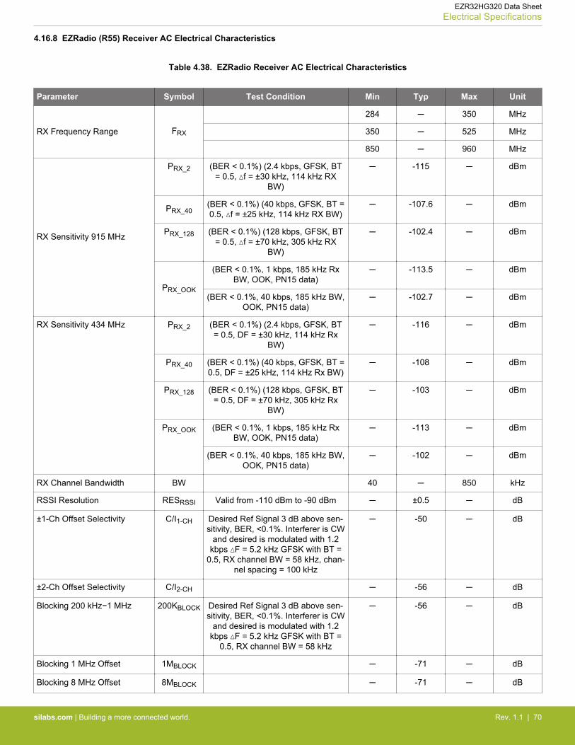
4.16.8 EZRadio (R55) Receiver AC Electrical Characteristics
Table 4.38. EZRadio Receiver AC Electrical Characteristics
Parameter Symbol Test Condition Min Typ Max Unit
RX Frequency Range FRX
284 ─ 350 MHz
350 ─ 525 MHz
850 ─ 960 MHz
RX Sensitivity 915 MHz
PRX_2 (BER < 0.1%) (2.4 kbps, GFSK, BT= 0.5, Δf = ±30 kHz, 114 kHz RX
BW)
─ -115 ─ dBm
PRX_40(BER < 0.1%) (40 kbps, GFSK, BT =0.5, Δf = ±25 kHz, 114 kHz RX BW)
─ -107.6 ─ dBm
PRX_128 (BER < 0.1%) (128 kbps, GFSK, BT= 0.5, Δf = ±70 kHz, 305 kHz RX
BW)
─ -102.4 ─ dBm
PRX_OOK
(BER < 0.1%, 1 kbps, 185 kHz RxBW, OOK, PN15 data)
─ -113.5 ─ dBm
(BER < 0.1%, 40 kbps, 185 kHz BW,OOK, PN15 data)
─ -102.7 ─ dBm
RX Sensitivity 434 MHz PRX_2 (BER < 0.1%) (2.4 kbps, GFSK, BT= 0.5, DF = ±30 kHz, 114 kHz Rx
BW)
─ -116 ─ dBm
PRX_40 (BER < 0.1%) (40 kbps, GFSK, BT =0.5, DF = ±25 kHz, 114 kHz Rx BW)
─ -108 ─ dBm
PRX_128 (BER < 0.1%) (128 kbps, GFSK, BT= 0.5, DF = ±70 kHz, 305 kHz Rx
BW)
─ -103 ─ dBm
PRX_OOK (BER < 0.1%, 1 kbps, 185 kHz RxBW, OOK, PN15 data)
─ -113 ─ dBm
(BER < 0.1%, 40 kbps, 185 kHz BW,OOK, PN15 data)
─ -102 ─ dBm
RX Channel Bandwidth BW 40 ─ 850 kHz
RSSI Resolution RESRSSI Valid from -110 dBm to -90 dBm ─ ±0.5 ─ dB
±1-Ch Offset Selectivity C/I1-CH Desired Ref Signal 3 dB above sen-sitivity, BER, <0.1%. Interferer is CW
and desired is modulated with 1.2kbps ΔF = 5.2 kHz GFSK with BT =
0.5, RX channel BW = 58 kHz, chan-nel spacing = 100 kHz
─ -50 ─ dB
±2-Ch Offset Selectivity C/I2-CH ─ -56 ─ dB
Blocking 200 kHz−1 MHz 200KBLOCK Desired Ref Signal 3 dB above sen-sitivity, BER, <0.1%. Interferer is CW
and desired is modulated with 1.2kbps ΔF = 5.2 kHz GFSK with BT =
0.5, RX channel BW = 58 kHz
─ -56 ─ dB
Blocking 1 MHz Offset 1MBLOCK ─ -71 ─ dB
Blocking 8 MHz Offset 8MBLOCK ─ -71 ─ dB
EZR32HG320 Data SheetElectrical Specifications
silabs.com | Building a more connected world. Rev. 1.1 | 70
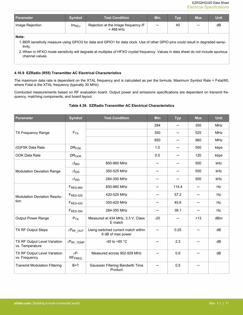
Parameter Symbol Test Condition Min Typ Max Unit
Image Rejection ImREJ Rejection at the image frequency IF= 468 kHz
─ 40 ─ dB
Note:1. BER sensitivity measure using GPIO3 for data and GPIO1 for data clock. Use of other GPIO pins could result in degraded sensi-
tivity.2. When in HFXO mode sensitivity will degrade at multiples of HFXO crystal frequency. Values in data sheet do not include spurious
channel values.
4.16.9 EZRadio (R55) Transmitter AC Electrical Characteristics
The maximum data rate is dependent on the XTAL frequency and is calculated as per the formula: Maximum Symbol Rate = Fxtal/60,where Fxtal is the XTAL frequency (typically 30 MHz).
Conducted measurements based on RF evaluation board. Output power and emissions specifications are dependent on transmit fre-quency, matching components, and board layout.
Table 4.39. EZRadio Transmitter AC Electrical Characteristics
Parameter Symbol Test Condition Min Typ Max Unit
TX Frequency Range FTX
284 ─ 350 MHz
350 ─ 525 MHz
850 ─ 960 MHz
(G)FSK Data Rate DRFSK 1.0 ─ 500 kbps
OOK Data Rate DROOK 0.5 ─ 120 kbps
Modulation Deviation Range
Δf960 850-960 MHz ─ ─ 500 kHz
Δf525 350-525 MHz ─ ─ 500 kHz
Δf350 284-350 MHz ─ ─ 500 kHz
Modulation Deviation Resolu-tion
FRES-960 850-960 MHz ─ 114.4 ─ Hz
FRES-525 420-525 MHz ─ 57.2 ─ Hz
FRES-420 350-420 MHz ─ 45.6 ─ Hz
FRES-350 284-350 MHz ─ 38.1 ─ Hz
Output Power Range PTX Measured at 434 MHz, 3.3 V, ClassE match
-20 ─ +13 dBm
TX RF Output Steps ΔPRF_OUT Using switched current match within6 dB of max power
─ 0.25 ─ dB
TX RF Output Level Variationvs. Temperature
ΔPRF_TEMP -40 to +85 °C ─ 2.3 ─ dB
TX RF Output Level Variationvs. Frequency
ΔP-RFFREQ
Measured across 902-928 MHz ─ 0.6 ─ dB
Transmit Modulation Filtering B×T Gaussian Filtering Bandwith TimeProduct
─ 0.5 ─
EZR32HG320 Data SheetElectrical Specifications
silabs.com | Building a more connected world. Rev. 1.1 | 71
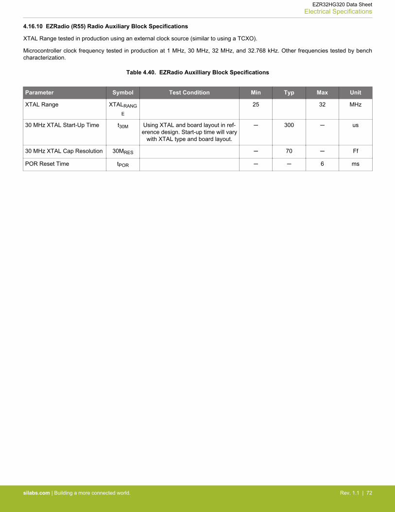
4.16.10 EZRadio (R55) Radio Auxiliary Block Specifications
XTAL Range tested in production using an external clock source (similar to using a TCXO).
Microcontroller clock frequency tested in production at 1 MHz, 30 MHz, 32 MHz, and 32.768 kHz. Other frequencies tested by benchcharacterization.
Table 4.40. EZRadio Auxilliary Block Specifications
Parameter Symbol Test Condition Min Typ Max Unit
XTAL Range XTALRANG
E
25 32 MHz
30 MHz XTAL Start-Up Time t30M Using XTAL and board layout in ref-erence design. Start-up time will vary
with XTAL type and board layout.
─ 300 ─ us
30 MHz XTAL Cap Resolution 30MRES ─ 70 ─ Ff
POR Reset Time tPOR ─ ─ 6 ms
EZR32HG320 Data SheetElectrical Specifications
silabs.com | Building a more connected world. Rev. 1.1 | 72
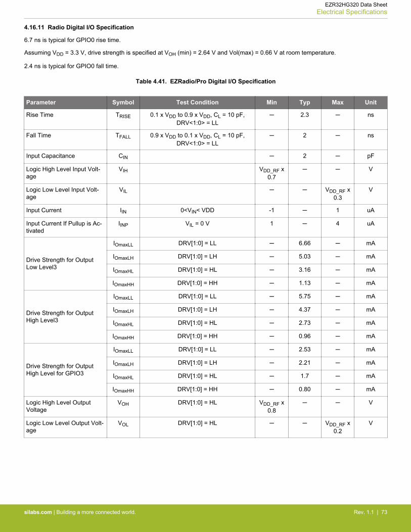
4.16.11 Radio Digital I/O Specification
6.7 ns is typical for GPIO0 rise time.
Assuming VDD = 3.3 V, drive strength is specified at VOH (min) = 2.64 V and Vol(max) = 0.66 V at room temperature.
2.4 ns is typical for GPIO0 fall time.
Table 4.41. EZRadio/Pro Digital I/O Specification
Parameter Symbol Test Condition Min Typ Max Unit
Rise Time TRISE 0.1 x VDD to 0.9 x VDD, CL = 10 pF,DRV<1:0> = LL
─ 2.3 ─ ns
Fall Time TFALL 0.9 x VDD to 0.1 x VDD, CL = 10 pF,DRV<1:0> = LL
─ 2 ─ ns
Input Capacitance CIN ─ 2 ─ pF
Logic High Level Input Volt-age
VIH VDD_RF x0.7
─ ─ V
Logic Low Level Input Volt-age
VIL ─ ─ VDD_RF x0.3
V
Input Current IIN 0<VIN< VDD -1 ─ 1 uA
Input Current If Pullup is Ac-tivated
IINP VIL = 0 V 1 ─ 4 uA
Drive Strength for OutputLow Level3
IOmaxLL DRV[1:0] = LL ─ 6.66 ─ mA
IOmaxLH DRV[1:0] = LH ─ 5.03 ─ mA
IOmaxHL DRV[1:0] = HL ─ 3.16 ─ mA
IOmaxHH DRV[1:0] = HH ─ 1.13 ─ mA
Drive Strength for OutputHigh Level3
IOmaxLL DRV[1:0] = LL ─ 5.75 ─ mA
IOmaxLH DRV[1:0] = LH ─ 4.37 ─ mA
IOmaxHL DRV[1:0] = HL ─ 2.73 ─ mA
IOmaxHH DRV[1:0] = HH ─ 0.96 ─ mA
Drive Strength for OutputHigh Level for GPIO3
IOmaxLL DRV[1:0] = LL ─ 2.53 ─ mA
IOmaxLH DRV[1:0] = LH ─ 2.21 ─ mA
IOmaxHL DRV[1:0] = HL ─ 1.7 ─ mA
IOmaxHH DRV[1:0] = HH ─ 0.80 ─ mA
Logic High Level OutputVoltage
VOH DRV[1:0] = HL VDD_RF x0.8
─ ─ V
Logic Low Level Output Volt-age
VOL DRV[1:0] = HL ─ ─ VDD_RF x0.2
V
EZR32HG320 Data SheetElectrical Specifications
silabs.com | Building a more connected world. Rev. 1.1 | 73
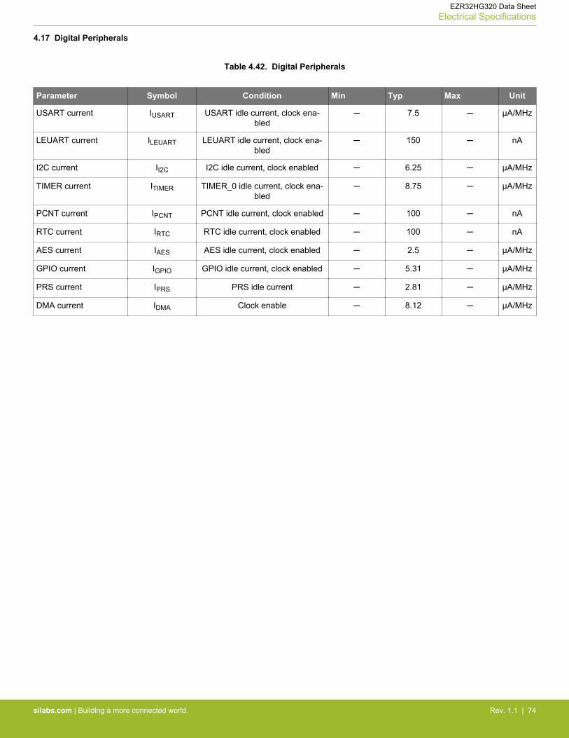
4.17 Digital Peripherals
Table 4.42. Digital Peripherals
Parameter Symbol Condition Min Typ Max Unit
USART current IUSART USART idle current, clock ena-bled
─ 7.5 ─ µA/MHz
LEUART current ILEUART LEUART idle current, clock ena-bled
─ 150 ─ nA
I2C current II2C I2C idle current, clock enabled ─ 6.25 ─ µA/MHz
TIMER current ITIMER TIMER_0 idle current, clock ena-bled
─ 8.75 ─ µA/MHz
PCNT current IPCNT PCNT idle current, clock enabled ─ 100 ─ nA
RTC current IRTC RTC idle current, clock enabled ─ 100 ─ nA
AES current IAES AES idle current, clock enabled ─ 2.5 ─ µA/MHz
GPIO current IGPIO GPIO idle current, clock enabled ─ 5.31 ─ µA/MHz
PRS current IPRS PRS idle current ─ 2.81 ─ µA/MHz
DMA current IDMA Clock enable ─ 8.12 ─ µA/MHz
EZR32HG320 Data SheetElectrical Specifications
silabs.com | Building a more connected world. Rev. 1.1 | 74
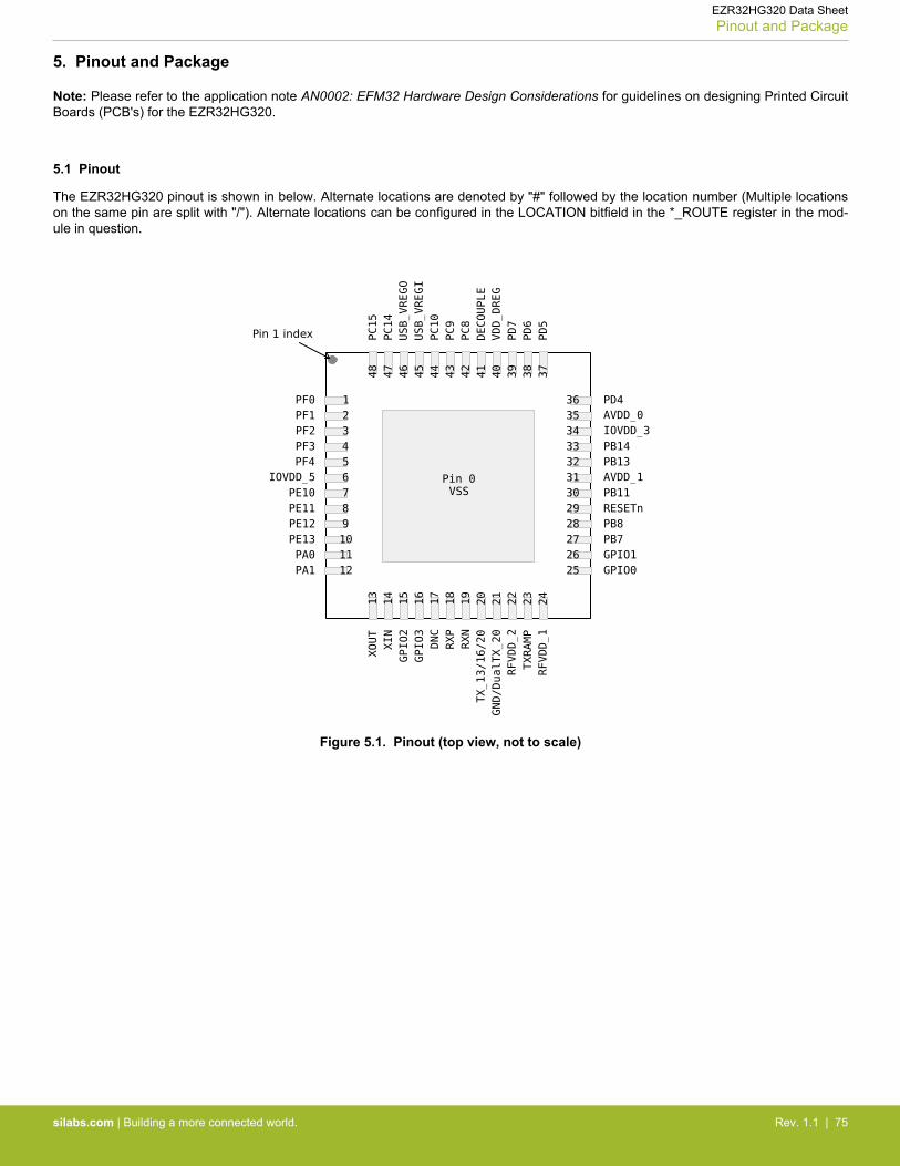
5. Pinout and Package
Note: Please refer to the application note AN0002: EFM32 Hardware Design Considerations for guidelines on designing Printed CircuitBoards (PCB's) for the EZR32HG320.
5.1 Pinout
The EZR32HG320 pinout is shown in below. Alternate locations are denoted by "#" followed by the location number (Multiple locationson the same pin are split with "/"). Alternate locations can be configured in the LOCATION bitfield in the *_ROUTE register in the mod-ule in question.
Figure 5.1. Pinout (top view, not to scale)
EZR32HG320 Data SheetPinout and Package
silabs.com | Building a more connected world. Rev. 1.1 | 75
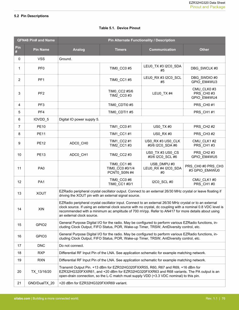
5.2 Pin Descriptions
Table 5.1. Device Pinout
QFN48 Pin# and Name Pin Alternate Functionality / Description
Pin# Pin Name Analog Timers Communication Other
0 VSS Ground.
1 PF0 TIM0_CC0 #5 LEU0_TX #3 I2C0_SDA#5 DBG_SWCLK #0
2 PF1 TIM0_CC1 #5 LEU0_RX #3 I2C0_SCL#5
DBG_SWDIO #0GPIO_EM4WU3
3 PF2 TIM0_CC2 #5/6TIM2_CC0 #3 LEU0_TX #4
CMU_CLK0 #3PRS_CH0 #3
GPIO_EM4WU4
4 PF3 TIM0_CDTI0 #5 PRS_CH0 #1
5 PF4 TIM0_CDTI1 #5 PRS_CH1 #1
6 IOVDD_5 Digital IO power supply 5.
7 PE10 TIM1_CC0 #1 US0_TX #0 PRS_CH2 #2
8 PE11 TIM1_CC1 #1 US0_RX #0 PRS_CH3 #2
9 PE12 ADC0_CH0 TIM1_CC2 #1TIM2_CC1 #3
US0_RX #3 US0_CLK#0/6 I2C0_SDA #6
CMU_CLK1 #2PRS_CH1 #3
10 PE13 ADC0_CH1 TIM2_CC2 #3 US0_TX #3 US0_CS#0/6 I2C0_SCL #6
PRS_CH2 #3GPIO_EM4WU5
11 PA0TIM0_CC1 #6
TIM0_CC0 #0/1/4PCNT0_S0IN #4
USB_DMPU #0LEU0_RX #4 I2C0_SDA
#0
PRS_CH0 #0 PRS_CH3#3 GPIO_EM4WU0
12 PA1 TIM0_CC0 #6TIM0_CC1 #0/1 I2C0_SCL #0 CMU_CLK1 #0
PRS_CH1 #0
13 XOUT EZRadio peripheral crystal oscillator output. Connect to an external 26/30 MHz crystal or leave floating ifdriving the XOUT pin with an external signal source.
14 XIN
EZRadio peripheral crystal oscillator input. Connect to an external 26/30 MHz crystal or to an externalclock source. If using an external clock source with no crystal, dc coupling with a nominal 0.8 VDC level isrecommended with a minimum ac amplitude of 700 mVpp. Refer to AN417 for more details about usingan external clock source.
15 GPIO2 General Purpose Digital I/O for the radio. May be configured to perform various EZRadio functions, in-cluding Clock Output, FIFO Status, POR, Wake-up Timer, TRSW, AntDiversity control, etc.
16 GPIO3 General Purpose Digital I/O for the radio. May be configured to perform various EZRadio functions, in-cluding Clock Output, FIFO Status, POR, Wake-up Timer, TRSW, AntDiversity control, etc.
17 DNC Do not connect.
18 RXP Differential RF Input Pin of the LNA. See application schematic for example matching network.
19 RXN Differential RF Input Pin of the LNA. See application schematic for example matching network.
20 TX_13/16/20Transmit Output Pin. +13 dBm for EZR32HG320FXXR55, R60, R67 and R69, +16 dBm forEZR32HG320FXXR61, and +20 dBm for EZR32HG320FXXR63 and R68 variants. The PA output is anopen-drain connection, so the L-C match must supply VDD (+3.3 VDC nominal) to this pin.
21 GND/DualTX_20 +20 dBm for EZR32HG320FXXR69 variant.
EZR32HG320 Data SheetPinout and Package
silabs.com | Building a more connected world. Rev. 1.1 | 76
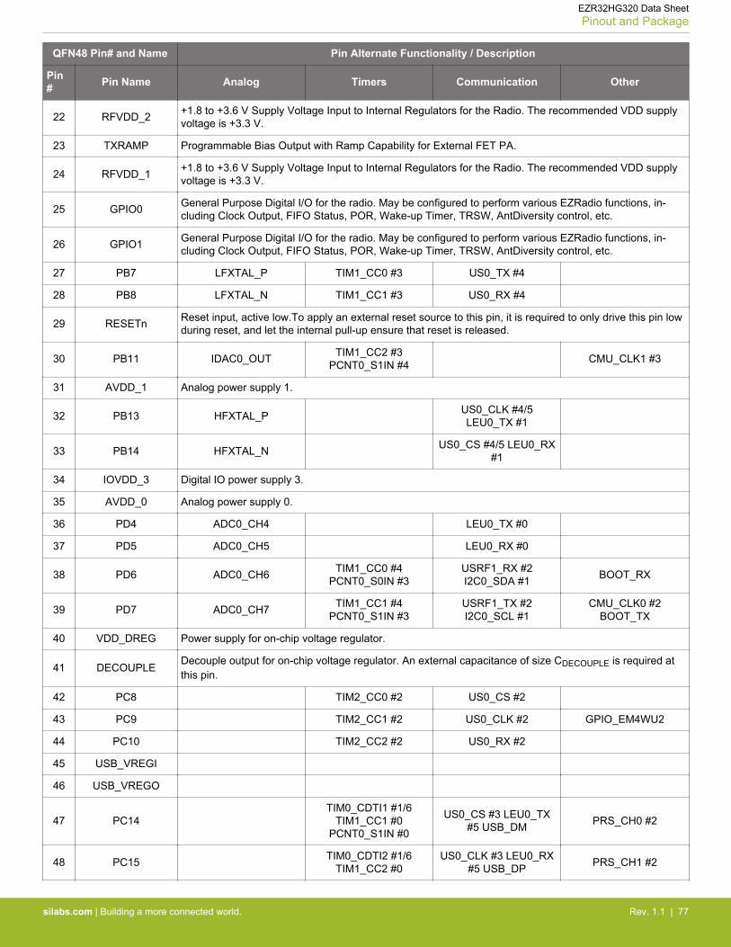
QFN48 Pin# and Name Pin Alternate Functionality / Description
Pin# Pin Name Analog Timers Communication Other
22 RFVDD_2 +1.8 to +3.6 V Supply Voltage Input to Internal Regulators for the Radio. The recommended VDD supplyvoltage is +3.3 V.
23 TXRAMP Programmable Bias Output with Ramp Capability for External FET PA.
24 RFVDD_1 +1.8 to +3.6 V Supply Voltage Input to Internal Regulators for the Radio. The recommended VDD supplyvoltage is +3.3 V.
25 GPIO0 General Purpose Digital I/O for the radio. May be configured to perform various EZRadio functions, in-cluding Clock Output, FIFO Status, POR, Wake-up Timer, TRSW, AntDiversity control, etc.
26 GPIO1 General Purpose Digital I/O for the radio. May be configured to perform various EZRadio functions, in-cluding Clock Output, FIFO Status, POR, Wake-up Timer, TRSW, AntDiversity control, etc.
27 PB7 LFXTAL_P TIM1_CC0 #3 US0_TX #4
28 PB8 LFXTAL_N TIM1_CC1 #3 US0_RX #4
29 RESETn Reset input, active low.To apply an external reset source to this pin, it is required to only drive this pin lowduring reset, and let the internal pull-up ensure that reset is released.
30 PB11 IDAC0_OUT TIM1_CC2 #3PCNT0_S1IN #4 CMU_CLK1 #3
31 AVDD_1 Analog power supply 1.
32 PB13 HFXTAL_P US0_CLK #4/5LEU0_TX #1
33 PB14 HFXTAL_N US0_CS #4/5 LEU0_RX#1
34 IOVDD_3 Digital IO power supply 3.
35 AVDD_0 Analog power supply 0.
36 PD4 ADC0_CH4 LEU0_TX #0
37 PD5 ADC0_CH5 LEU0_RX #0
38 PD6 ADC0_CH6 TIM1_CC0 #4PCNT0_S0IN #3
USRF1_RX #2I2C0_SDA #1 BOOT_RX
39 PD7 ADC0_CH7 TIM1_CC1 #4PCNT0_S1IN #3
USRF1_TX #2I2C0_SCL #1
CMU_CLK0 #2BOOT_TX
40 VDD_DREG Power supply for on-chip voltage regulator.
41 DECOUPLEDecouple output for on-chip voltage regulator. An external capacitance of size CDECOUPLE is required atthis pin.
42 PC8 TIM2_CC0 #2 US0_CS #2
43 PC9 TIM2_CC1 #2 US0_CLK #2 GPIO_EM4WU2
44 PC10 TIM2_CC2 #2 US0_RX #2
45 USB_VREGI
46 USB_VREGO
47 PC14TIM0_CDTI1 #1/6
TIM1_CC1 #0PCNT0_S1IN #0
US0_CS #3 LEU0_TX#5 USB_DM PRS_CH0 #2
48 PC15 TIM0_CDTI2 #1/6TIM1_CC2 #0
US0_CLK #3 LEU0_RX#5 USB_DP PRS_CH1 #2
EZR32HG320 Data SheetPinout and Package
silabs.com | Building a more connected world. Rev. 1.1 | 77
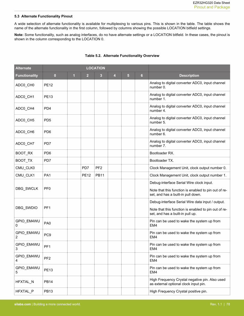
5.3 Alternate Functionality Pinout
A wide selection of alternate functionality is available for multiplexing to various pins. This is shown in the table. The table shows thename of the alternate functionality in the first column, followed by columns showing the possible LOCATION bitfield settings.
Note: Some functionality, such as analog interfaces, do no have alternate settings or a LOCATION bitfield. In these cases, the pinout isshown in the column corresponding to the LOCATION 0.
Table 5.2. Alternate Functionality Overview
Alternate LOCATION
Functionality 0 1 2 3 4 5 6 Description
ADC0_CH0 PE12 Analog to digital converter ADC0, input channelnumber 0.
ADC0_CH1 PE13 Analog to digital converter ADC0, input channelnumber 1.
ADC0_CH4 PD4 Analog to digital converter ADC0, input channelnumber 4.
ADC0_CH5 PD5 Analog to digital converter ADC0, input channelnumber 5.
ADC0_CH6 PD6 Analog to digital converter ADC0, input channelnumber 6.
ADC0_CH7 PD7 Analog to digital converter ADC0, input channelnumber 7.
BOOT_RX PD6 Bootloader RX.
BOOT_TX PD7 Bootloader TX.
CMU_CLK0 PD7 PF2 Clock Management Unit, clock output number 0.
CMU_CLK1 PA1 PE12 PB11 Clock Management Unit, clock output number 1.
DBG_SWCLK PF0Debug-interface Serial Wire clock input.
Note that this function is enabled to pin out of re-set, and has a built-in pull down.
DBG_SWDIO PF1Debug-interface Serial Wire data input / output.
Note that this function is enabled to pin out of re-set, and has a built-in pull up.
GPIO_EM4WU0 PA0 Pin can be used to wake the system up from
EM4
GPIO_EM4WU2 PC9 Pin can be used to wake the system up from
EM4
GPIO_EM4WU3 PF1 Pin can be used to wake the system up from
EM4
GPIO_EM4WU4 PF2 Pin can be used to wake the system up from
EM4
GPIO_EM4WU5 PE13 Pin can be used to wake the system up from
EM4
HFXTAL_N PB14 High Frequency Crystal negative pin. Also usedas external optional clock input pin.
HFXTAL_P PB13 High Frequency Crystal positive pin.
EZR32HG320 Data SheetPinout and Package
silabs.com | Building a more connected world. Rev. 1.1 | 78
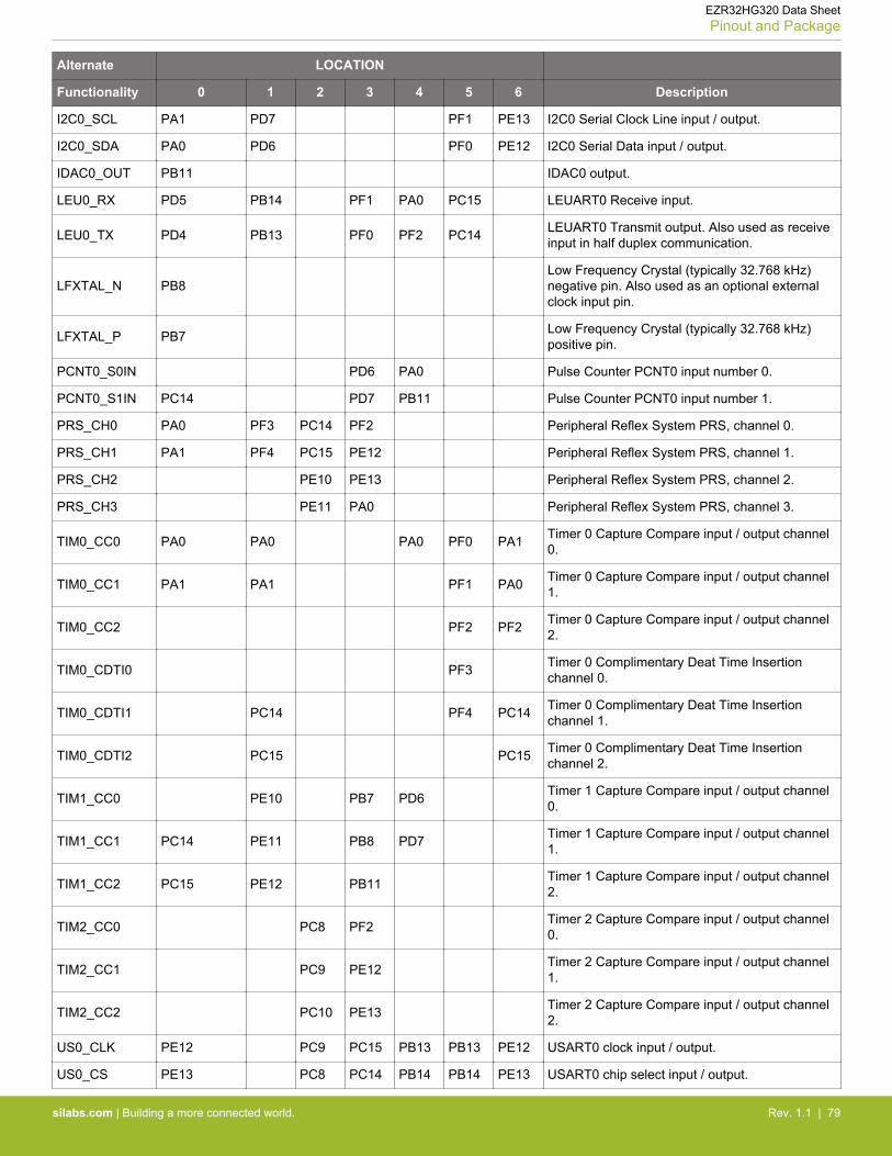
Alternate LOCATION
Functionality 0 1 2 3 4 5 6 Description
I2C0_SCL PA1 PD7 PF1 PE13 I2C0 Serial Clock Line input / output.
I2C0_SDA PA0 PD6 PF0 PE12 I2C0 Serial Data input / output.
IDAC0_OUT PB11 IDAC0 output.
LEU0_RX PD5 PB14 PF1 PA0 PC15 LEUART0 Receive input.
LEU0_TX PD4 PB13 PF0 PF2 PC14 LEUART0 Transmit output. Also used as receiveinput in half duplex communication.
LFXTAL_N PB8Low Frequency Crystal (typically 32.768 kHz)negative pin. Also used as an optional externalclock input pin.
LFXTAL_P PB7 Low Frequency Crystal (typically 32.768 kHz)positive pin.
PCNT0_S0IN PD6 PA0 Pulse Counter PCNT0 input number 0.
PCNT0_S1IN PC14 PD7 PB11 Pulse Counter PCNT0 input number 1.
PRS_CH0 PA0 PF3 PC14 PF2 Peripheral Reflex System PRS, channel 0.
PRS_CH1 PA1 PF4 PC15 PE12 Peripheral Reflex System PRS, channel 1.
PRS_CH2 PE10 PE13 Peripheral Reflex System PRS, channel 2.
PRS_CH3 PE11 PA0 Peripheral Reflex System PRS, channel 3.
TIM0_CC0 PA0 PA0 PA0 PF0 PA1 Timer 0 Capture Compare input / output channel0.
TIM0_CC1 PA1 PA1 PF1 PA0 Timer 0 Capture Compare input / output channel1.
TIM0_CC2 PF2 PF2 Timer 0 Capture Compare input / output channel2.
TIM0_CDTI0 PF3 Timer 0 Complimentary Deat Time Insertionchannel 0.
TIM0_CDTI1 PC14 PF4 PC14 Timer 0 Complimentary Deat Time Insertionchannel 1.
TIM0_CDTI2 PC15 PC15 Timer 0 Complimentary Deat Time Insertionchannel 2.
TIM1_CC0 PE10 PB7 PD6 Timer 1 Capture Compare input / output channel0.
TIM1_CC1 PC14 PE11 PB8 PD7 Timer 1 Capture Compare input / output channel1.
TIM1_CC2 PC15 PE12 PB11 Timer 1 Capture Compare input / output channel2.
TIM2_CC0 PC8 PF2 Timer 2 Capture Compare input / output channel0.
TIM2_CC1 PC9 PE12 Timer 2 Capture Compare input / output channel1.
TIM2_CC2 PC10 PE13 Timer 2 Capture Compare input / output channel2.
US0_CLK PE12 PC9 PC15 PB13 PB13 PE12 USART0 clock input / output.
US0_CS PE13 PC8 PC14 PB14 PB14 PE13 USART0 chip select input / output.
EZR32HG320 Data SheetPinout and Package
silabs.com | Building a more connected world. Rev. 1.1 | 79
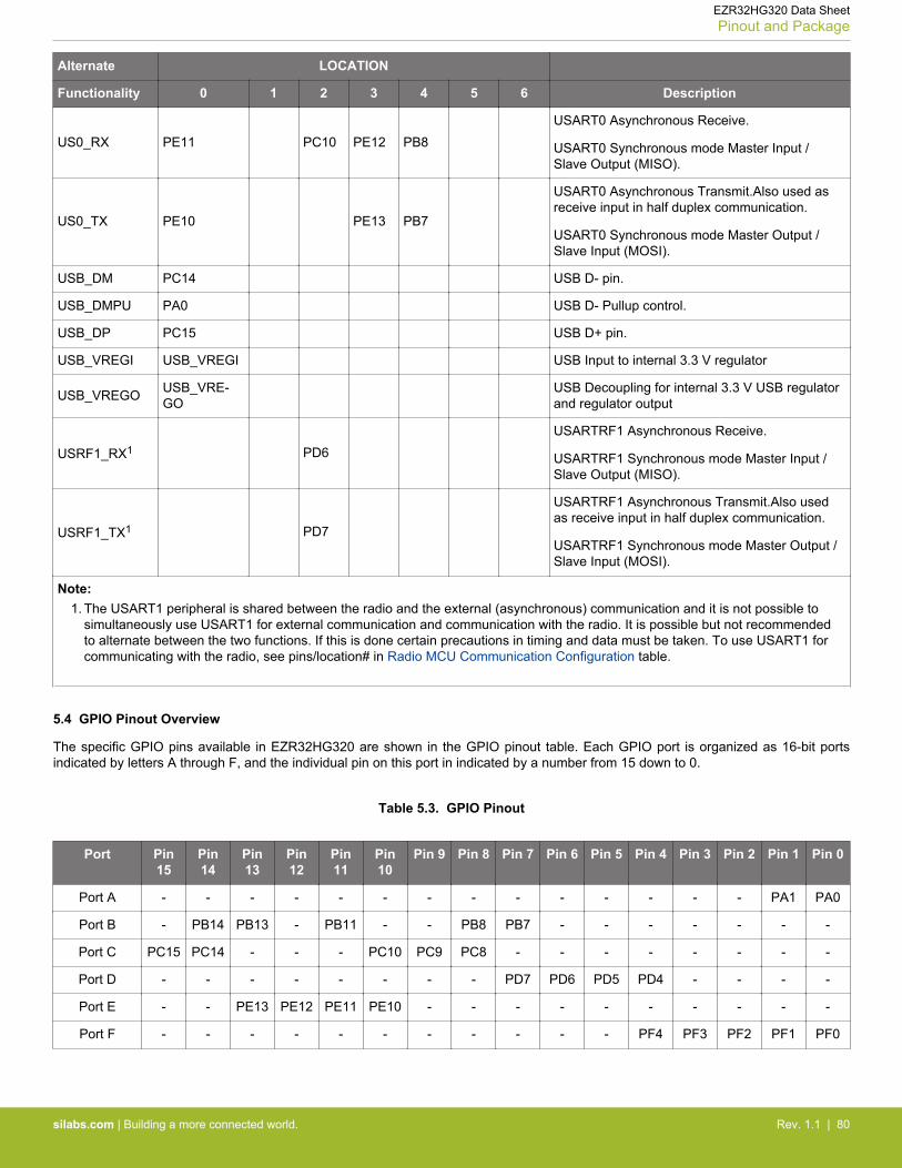
Alternate LOCATION
Functionality 0 1 2 3 4 5 6 Description
US0_RX PE11 PC10 PE12 PB8USART0 Asynchronous Receive.
USART0 Synchronous mode Master Input /Slave Output (MISO).
US0_TX PE10 PE13 PB7
USART0 Asynchronous Transmit.Also used asreceive input in half duplex communication.
USART0 Synchronous mode Master Output /Slave Input (MOSI).
USB_DM PC14 USB D- pin.
USB_DMPU PA0 USB D- Pullup control.
USB_DP PC15 USB D+ pin.
USB_VREGI USB_VREGI USB Input to internal 3.3 V regulator
USB_VREGO USB_VRE-GO
USB Decoupling for internal 3.3 V USB regulatorand regulator output
USRF1_RX1 PD6USARTRF1 Asynchronous Receive.
USARTRF1 Synchronous mode Master Input /Slave Output (MISO).
USRF1_TX1 PD7
USARTRF1 Asynchronous Transmit.Also usedas receive input in half duplex communication.
USARTRF1 Synchronous mode Master Output /Slave Input (MOSI).
Note:1. The USART1 peripheral is shared between the radio and the external (asynchronous) communication and it is not possible to
simultaneously use USART1 for external communication and communication with the radio. It is possible but not recommendedto alternate between the two functions. If this is done certain precautions in timing and data must be taken. To use USART1 forcommunicating with the radio, see pins/location# in Radio MCU Communication Configuration table.
5.4 GPIO Pinout Overview
The specific GPIO pins available in EZR32HG320 are shown in the GPIO pinout table. Each GPIO port is organized as 16-bit portsindicated by letters A through F, and the individual pin on this port in indicated by a number from 15 down to 0.
Table 5.3. GPIO Pinout
Port Pin15
Pin14
Pin13
Pin12
Pin11
Pin10
Pin 9 Pin 8 Pin 7 Pin 6 Pin 5 Pin 4 Pin 3 Pin 2 Pin 1 Pin 0
Port A - - - - - - - - - - - - - - PA1 PA0
Port B - PB14 PB13 - PB11 - - PB8 PB7 - - - - - - -
Port C PC15 PC14 - - - PC10 PC9 PC8 - - - - - - - -
Port D - - - - - - - - PD7 PD6 PD5 PD4 - - - -
Port E - - PE13 PE12 PE11 PE10 - - - - - - - - - -
Port F - - - - - - - - - - - PF4 PF3 PF2 PF1 PF0
EZR32HG320 Data SheetPinout and Package
silabs.com | Building a more connected world. Rev. 1.1 | 80
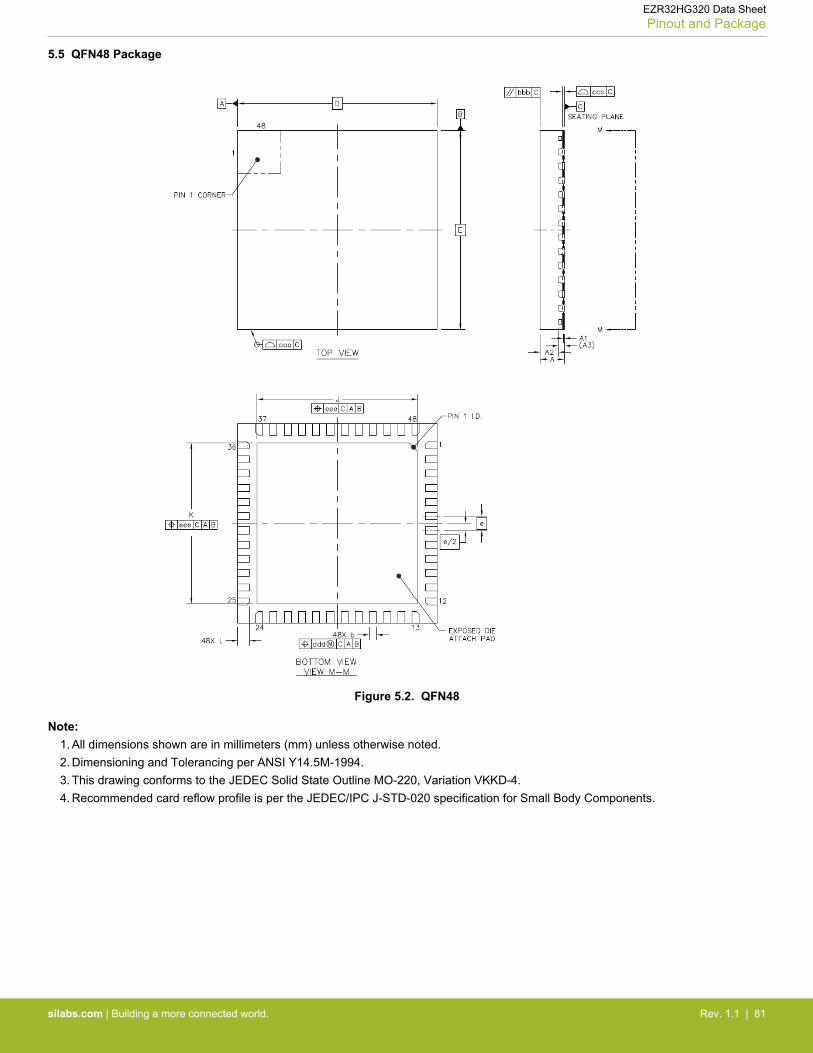
5.5 QFN48 Package
Figure 5.2. QFN48
Note:1. All dimensions shown are in millimeters (mm) unless otherwise noted.2. Dimensioning and Tolerancing per ANSI Y14.5M-1994.3. This drawing conforms to the JEDEC Solid State Outline MO-220, Variation VKKD-4.4. Recommended card reflow profile is per the JEDEC/IPC J-STD-020 specification for Small Body Components.
EZR32HG320 Data SheetPinout and Package
silabs.com | Building a more connected world. Rev. 1.1 | 81
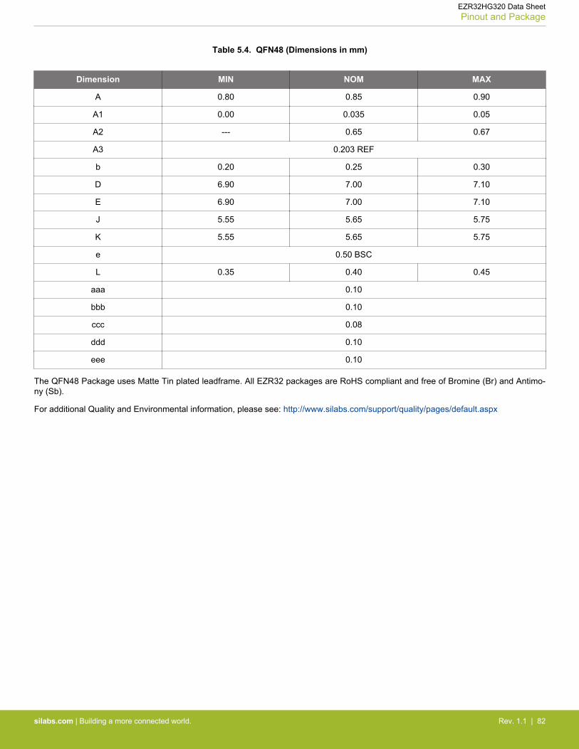
Table 5.4. QFN48 (Dimensions in mm)
Dimension MIN NOM MAX
A 0.80 0.85 0.90
A1 0.00 0.035 0.05
A2 --- 0.65 0.67
A3 0.203 REF
b 0.20 0.25 0.30
D 6.90 7.00 7.10
E 6.90 7.00 7.10
J 5.55 5.65 5.75
K 5.55 5.65 5.75
e 0.50 BSC
L 0.35 0.40 0.45
aaa 0.10
bbb 0.10
ccc 0.08
ddd 0.10
eee 0.10
The QFN48 Package uses Matte Tin plated leadframe. All EZR32 packages are RoHS compliant and free of Bromine (Br) and Antimo-ny (Sb).
For additional Quality and Environmental information, please see: http://www.silabs.com/support/quality/pages/default.aspx
EZR32HG320 Data SheetPinout and Package
silabs.com | Building a more connected world. Rev. 1.1 | 82
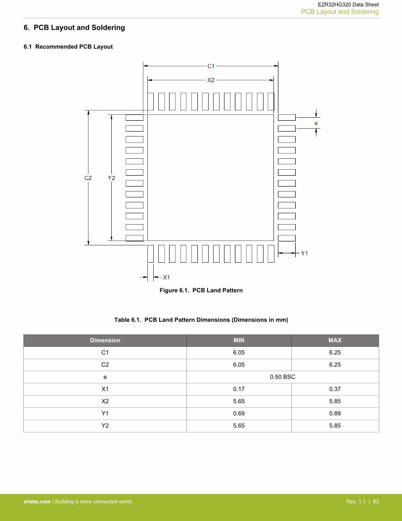
6. PCB Layout and Soldering
6.1 Recommended PCB Layout
Figure 6.1. PCB Land Pattern
Table 6.1. PCB Land Pattern Dimensions (Dimensions in mm)
Dimension MIN MAX
C1 6.05 6.25
C2 6.05 6.25
e 0.50 BSC
X1 0.17 0.37
X2 5.65 5.85
Y1 0.69 0.89
Y2 5.65 5.85
EZR32HG320 Data SheetPCB Layout and Soldering
silabs.com | Building a more connected world. Rev. 1.1 | 83
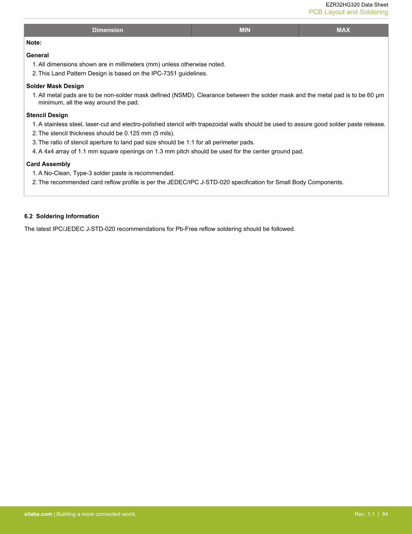
Dimension MIN MAX
Note:
General1. All dimensions shown are in millimeters (mm) unless otherwise noted.2. This Land Pattern Design is based on the IPC-7351 guidelines.
Solder Mask Design1. All metal pads are to be non-solder mask defined (NSMD). Clearance between the solder mask and the metal pad is to be 60 μm
minimum, all the way around the pad.
Stencil Design1. A stainless steel, laser-cut and electro-polished stencil with trapezoidal walls should be used to assure good solder paste release.2. The stencil thickness should be 0.125 mm (5 mils).3. The ratio of stencil aperture to land pad size should be 1:1 for all perimeter pads.4. A 4x4 array of 1.1 mm square openings on 1.3 mm pitch should be used for the center ground pad.
Card Assembly1. A No-Clean, Type-3 solder paste is recommended.2. The recommended card reflow profile is per the JEDEC/IPC J-STD-020 specification for Small Body Components.
6.2 Soldering Information
The latest IPC/JEDEC J-STD-020 recommendations for Pb-Free reflow soldering should be followed.
EZR32HG320 Data SheetPCB Layout and Soldering
silabs.com | Building a more connected world. Rev. 1.1 | 84
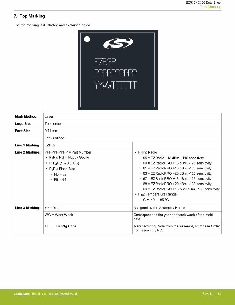
7. Top Marking
The top marking is illustrated and explained below.
Mark Method: Laser
Logo Size: Top center
Font Size: 0.71 mm
Left-Justified
Line 1 Marking: EZR32
Line 2 Marking: PPPPPPPPPP = Part Number• P1P2: HG = Happy Gecko• P3P4P5: 320 (USB)• P6P7: Flash Size
• FD = 32• FE = 64
• P8P9: Radio• 55 = EZRadio +13 dBm, -116 sensitivity• 60 = EZRadioPRO +13 dBm, -126 sensitivity• 61 = EZRadioPRO +16 dBm, -126 sensitivity• 63 = EZRadioPRO +20 dBm, -126 sensitivity• 67 = EZRadioPRO +13 dBm, -133 sensitivity• 68 = EZRadioPRO +20 dBm, -133 sensitivity• 69 = EZRadioPRO +13 & 20 dBm, -133 sensitivity
• P10: Temperature Range• G = -40 — 85 °C
Line 3 Marking: YY = Year Assigned by the Assembly House.
WW = Work Week Corresponds to the year and work week of the molddate.
TTTTTT = Mfg Code Manufacturing Code from the Assembly Purchase Orderfrom assembly PO.
EZR32HG320 Data SheetTop Marking
silabs.com | Building a more connected world. Rev. 1.1 | 85
8. Revision History
Revision1.1August, 2019• Updated Ordering Information table for the release of revision C devices• Added footnote to USRF1_TX and USRF1_RX in Alternate Functionality Overview table• Updated PCB Land Pattern Dimensions table to fix typographical error• New formatting throughout
Revision 1.0• Added R69 content
Revision 0.4• Removed content currently documented the RFI database:
• Environmental Table from the Electrical Specifications chapter• Moisture Sensitivity Level in the Soldering Information section
Revision 0.3• Updated Current Consumption table• Updated Power Management table• Revised text describing LFXO Oscillator: “energyAware Designer” to “Configurator tool”• Updated HFXO oscillator table, fHXFO parameter changed: “Supported nominal crystal Frequency” to “Supported frequency, any
mode”• Updated LFRCO table• Updated HFRCO table• Updated AUXHFRCO table• Updated USHFRCO table• Updated ADC table• Added USB electrical table
Revision 0.2• Initial Release
EZR32HG320 Data SheetRevision History
silabs.com | Building a more connected world. Rev. 1.1 | 86

Simplicity StudioOne-click access to MCU and wireless tools, documentation, software, source code libraries & more. Available for Windows, Mac and Linux!
IoT Portfoliowww.silabs.com/IoT
SW/HWwww.silabs.com/simplicity
Qualitywww.silabs.com/quality
Support and Communitycommunity.silabs.com
http://www.silabs.com
Silicon Laboratories Inc.400 West Cesar ChavezAustin, TX 78701USA
DisclaimerSilicon Labs intends to provide customers with the latest, accurate, and in-depth documentation of all peripherals and modules available for system and software implementers using or intending to use the Silicon Labs products. Characterization data, available modules and peripherals, memory sizes and memory addresses refer to each specific device, and "Typical" parameters provided can and do vary in different applications. Application examples described herein are for illustrative purposes only. Silicon Labs reserves the right to make changes without further notice to the product information, specifications, and descriptions herein, and does not give warranties as to the accuracy or completeness of the included information. Without prior notification, Silicon Labs may update product firmware during the manufacturing process for security or reliability reasons. Such changes will not alter the specifications or the performance of the product. Silicon Labs shall have no liability for the consequences of use of the information supplied in this document. This document does not imply or expressly grant any license to design or fabricate any integrated circuits. The products are not designed or authorized to be used within any FDA Class III devices, applications for which FDA premarket approval is required or Life Support Systems without the specific written consent of Silicon Labs. A "Life Support System" is any product or system intended to support or sustain life and/or health, which, if it fails, can be reasonably expected to result in significant personal injury or death. Silicon Labs products are not designed or authorized for military applications. Silicon Labs products shall under no circumstances be used in weapons of mass destruction including (but not limited to) nuclear, biological or chemical weapons, or missiles capable of delivering such weapons. Silicon Labs disclaims all express and implied warranties and shall not be responsible or liable for any injuries or damages related to use of a Silicon Labs product in such unauthorized applications.
Trademark InformationSilicon Laboratories Inc.® , Silicon Laboratories®, Silicon Labs®, SiLabs® and the Silicon Labs logo®, Bluegiga®, Bluegiga Logo®, ClockBuilder®, CMEMS®, DSPLL®, EFM®, EFM32®, EFR, Ember®, Energy Micro, Energy Micro logo and combinations thereof, "the world’s most energy friendly microcontrollers", Ember®, EZLink®, EZRadio®, EZRadioPRO®, Gecko®, Gecko OS, Gecko OS Studio, ISOmodem®, Precision32®, ProSLIC®, Simplicity Studio®, SiPHY®, Telegesis, the Telegesis Logo®, USBXpress® , Zentri, the Zentri logo and Zentri DMS, Z-Wave®, and others are trademarks or registered trademarks of Silicon Labs. ARM, CORTEX, Cortex-M3 and THUMB are trademarks or registered trademarks of ARM Holdings. Keil is a registered trademark of ARM Limited. Wi-Fi is a registered trademark of the Wi-Fi Alliance. All other products or brand names mentioned herein are trademarks of their respective holders.