extending hypertransport™ th l t80gb/itechnology to...
TRANSCRIPT

Extending HyperTransport™ T h l t 8 0 Gb/ iTechnology to 8.0 Gb/s in
32-nm SOI-CMOS ProcessorsBruce Doyle, Alvin Loke, Sanjeev Maheshwari,
Charles Wang Dennis Fischette Jeffrey CooperCharles Wang, Dennis Fischette, Jeffrey Cooper, Sanjeev Aggarwal, Tin Tin Wee, Chad Lackey,
Harishkumar Kedarnath, Michael Oshima, Gerry Talbot & Emerson Fang
Advanced Micro Devices, Inc.Advanced Micro Devices, Inc.

Motivation High demand for multi-socket processor systems
from explosive growth in server market Cores per die increasing faster than I/O capability Server performance increasingly limited by I/O
bandwidth between socketsbandwidth between sockets I/O technology shifts (e.g., PCIe-3) revolutionary
in architecture & design introduces product riskin architecture & design, introduces product risk Evolutionary enhancements to existing I/O
design can improve server system performancedesign can improve server system performance without revolutionary shifts
2

Evolution of AMD Server ProcessorsShanghai
45nm4 cores & 4 HT I/O
Magny Cours45nm
6 cores & 4 HT I/O
Orochi32nm
8 cores & 4 HT I/O
GOAL: 6.4Gb/s8.0Gb/s through modest improvements gwith jitter , return loss & constant power
+25% I/O aggregate BW up to +8% system performance !!
3

Outline Motivation HyperTransport™ Overview HyperTransport™ Overview Extending HT to 8Gb/s• Forwarded Clock Jitter Filtering• Wideband Digital Clean-Up PLL• Power & Performance Optimization
Silicon Results Conclusion
4

Outline Motivation HyperTransport™ Overview HyperTransport™ Overview Extending HT to 8Gb/s• Forwarded Clock Jitter Filtering• Wideband Digital Clean-Up PLL• Power & Performance Optimization
Silicon Results Conclusion
5
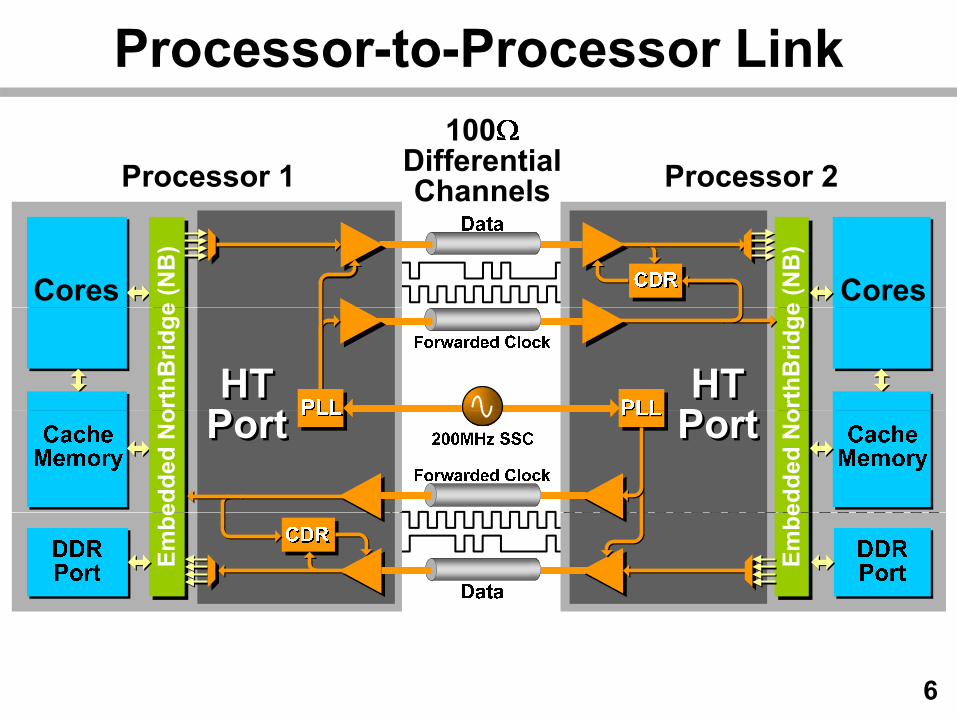
Processor-to-Processor Link
e (N
B)
e (N
B)
orth
Brid
ge
orth
Brid
ge
edde
d N
o
edde
d N
o
Embe
Embe
6

HT Link Characteristics Source synchronous Forward half-rate clock for RX data retimingg Common-mode jitter rejection, low latency
NRZ PAM-2 signalingNRZ PAM 2 signaling 2.4 to 6.4Gb/s per lane 2 sublinks of 1 CLK lane + 9 data lanes 2 sublinks of 1 CLK lane + 9 data lanes DLL-based CDR
7

Outline Motivation HyperTransport™ Overview HyperTransport™ Overview Extending HT to 8Gb/s• Forwarded Clock Jitter Filtering• Wideband Digital Clean-Up PLL• Power & Performance Optimization
Silicon Results Conclusion
8

Jitter in Forwarded Clock Links
TX RXTJtx
Data In Data OutData Lane
D Q
DATADATACLK
ForwardedClock LaneClock Lane
9

Jitter in Forwarded Clock Links
TX RXTJtx
Data In Data Outc
TJtx (c+ rx)
Data LaneD Qrx
DATA cdrDATACLK
ForwardedClock Lane
crx
disClock Lane dis
10
TJtx (c+ rx + dis + cdr)

Clock & Data Phase Relationship )2sin(2 tfAtft mmcdata
ha
se,
?tt clockdata
P
tt d tl k
Time, t
tt dataclock
11

Sampling Jitter vs. Delay Mismatch
10 = 0
)sin(2 msample fJ
0
= 0
r (dB
)
-10
Tran
sfer
-20
Jitte
r T
-301 10 100 1000Jitter Modulation Frequency, fm (MHz)
12

Sampling Jitter vs. Delay Mismatch
= 160ps10
)sin(2 msample fJ
= 160ps
0
r (dB
) jitteramplification
-10
Tran
sfer
-20
Jitte
r T
-301 10 100 1000Jitter Modulation Frequency, fm (MHz)
13

Sampling Jitter vs. Delay Mismatch
= 5 0ns10
)sin(2 msample fJ
= 5.0ns
0
r (dB
) jitteramplification
-10
Tran
sfer
-20
Jitte
r T
-301 10 100 1000Jitter Modulation Frequency, fm (MHz)
14

Desired Jitter Filtering Behavior
61
mf 61
mf
tdata
hase
,
cclock ft 2
Ph nosampling
jitterdoubling ofsampling
jitter
Time, t
j
Time, t
jitter
15

Desired Jitter Filtering Behavior
61
mf 61
mf
tdata
hase
,
cclock ft 2
Ph nosampling
jittersampling
jitter transferbounded to unity
Time, t
j
Time, t
bounded to unity
16

Jitter Filtering Example ( 2ns)
10) without jitter
6dB peaksat 250 &750MHz
0
fer (
dB)
with jitter
filtering750MHz
-10
r Tra
nsf with jitter
filtering
-20
Jitte
r
-301 10 100 1000
Jitter Modulation Frequency, fm (MHz)
17
Jitter Modulation Frequency, fm (MHz)

Outline Motivation HyperTransport™ Overview HyperTransport™ Overview Extending HT to 8Gb/s• Forwarded Clock Jitter Filtering• Wideband Digital Clean-Up PLL• Power & Performance Optimization
Silicon Results Conclusion
18
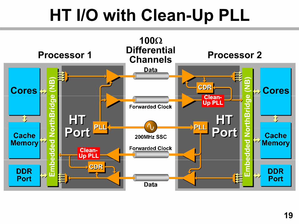
HT I/O with Clean-Up PLL
e (N
B)
e (N
B)
ClCl
orth
Brid
ge
orth
Brid
ge CleanClean--Up PLLUp PLL
edde
d N
o
edde
d N
o
CleanClean--Up PLLUp PLL
Embe
Embe
19

Wideband Digital Clean-Up PLL
N
ToDLLs
LocalREFCLK
IntegralCorrectionN
early2ReceivedF d d
14
Early/LatePhase
Comparator
early2early1late1late2
Forwarded Clock ±fbb1
±fbb2ProportionalCorrection
Adjustable bandwidth for jitter shaping (200MHz default)
Correction
j j g ( ) Variable bang-bang rate (fbb1 to fbb1+fbb2 ) Coarse frequency calibration to local REFCLK for PVT Low loop latency
20
Outline Motivation HyperTransport™ Overview HyperTransport™ Overview Extending HT to 8Gb/s• Forwarded Clock Jitter Filtering• Wideband Digital Clean-Up PLL• Power & Performance Optimization
Silicon Results Conclusion
21

TX Output Driver45nm Hybrid Mode 32nm Voltage Mode
Power 20% Return loss & DCD
22

RX 4:1 Deserializer45nm 32nm
23
Power 35%, latency

RX Front End
AC coupling to reduce CLK DCD
24 1-bit speculative (loop-unrolled) DFE

Outline Motivation HyperTransport™ Overview HyperTransport™ Overview Extending HT to 8Gb/s• Forwarded Clock Jitter Filtering• Wideband Digital Clean-Up PLL• Power & Performance Optimization
Silicon Results Conclusion
25
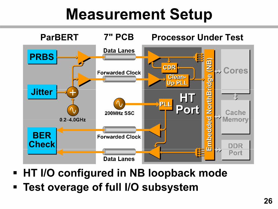
Measurement Setup
))rid
ge (N
B)
ridge
(NB
d N
orth
Br
d N
orth
Br
Embe
dded
Embe
dded
HT I/O configured in NB loopback mode
EE
Test overage of full I/O subsystem26

Measured TX Eye – 8Gb/s PRBS-15
27

RX Eye with Jitter Modulation
i j t 0 4UI i id l jittinject 0.4UIpp sinusoidal jitter
28

Impact of Clean-Up PLL
10-1
22500
3000
2500
3000
clean-up PLLdisabledB
ER ×
1500
2000
1500
2000
disabled
asur
ed
500
1000
1500
500
1000
1500
enabled
Mea
0
500
0 100 200 300 400 5000
500
0 100 200 300 400 500
0.4UIpp jitter amplitudeJitter Modulation Frequency (MHz)
pp Clean-up PLL removes >300MHz jitter
29
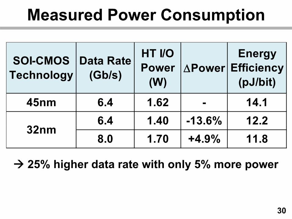
Measured Power Consumption
SOI-CMOS Data Rate HT I/O EnergySOI CMOSTechnology
Data Rate(Gb/s) Power
(W)Power Efficiency
(pJ/bit)
45nm 6.4 1.62 - 14.16.4 1.40 -13.6% 12.28.0 1.70 +4.9% 11.8
32nm
25% higher data rate with only 5% more power
30

Conclusion Achieved higher processor link bandwidth
through evolutionary enhancements in I/O design 25% boost in lane data rate Sampling jitter reduction with clean-up PLL Near constant power consumption for
socket compatibility
Sampling jitter reduction with clean up PLL
p y Improves server system performance with
minimal product riskp
31

감사합니다감사합니다감사합니다감사합니다
32