expresslane pex 8114ba - semiconductorstore.com€¦ · · 2008-10-22march, 2007 preface...
TRANSCRIPT

Copyright © 2007 by PLX Technology, Inc. All Rights Reserved – Version 1.2
March, 2007
ExpressLane PEX 8114BAPCI Express-to-PCI/PCI-X Bridge
Data Book
Version 1.2
March 2007
Website www.plxtech.com
Technical Support www.plxtech.com/support
Phone 800 759-3735
408 774-9060
FAX 408 774-2169
Copyright Information
Copyright © 2006 – 2007 PLX Technology, Inc. All rights reserved. The information in this document isproprietary to PLX Technology. No part of this document may be reproduced in any form or by anymeans or used to make any derivative work (such as translation, transformation, or adaptation) withoutwritten permission from PLX Technology.
PLX Technology provides this documentation without warranty, term or condition of any kind, eitherexpress or implied, including, but not limited to, express and implied warranties of merchantability,fitness for a particular purpose, and non-infringement. While the information contained herein isbelieved to be accurate, such information is preliminary, and no representations or warranties ofaccuracy or completeness are made. In no event will PLX Technology be liable for damages arisingdirectly or indirectly from any use of or reliance upon the information contained in this document. PLXTechnology may make improvements or changes in the product(s) and/or the program(s) described inthis documentation at any time.
PLX Technology retains the right to make changes to this product at any time, without notice. Productsmay have minor variations to this publication, known as errata. PLX Technology assumes no liabilitywhatsoever, including infringement of any patent or copyright, for sale and use of PLX Technologyproducts.
PLX Technology and the PLX logo are registered trademarks and ExpressLane is a trademark of PLXTechnology, Inc.
PCI Express is a trademark of the PCI Special Interest Group (PCI-SIG).
All product names are trademarks, registered trademarks, or servicemarks of their respective owners.
Order Number: 8114BA-SIL-DB-P1-1.2
Data Book PLX Technology, Inc.
ii ExpressLane PEX 8114BA PCI Express-to-PCI/PCI-X Bridge Data Book
Copyright © 2007 by PLX Technology, Inc. All Rights Reserved – Version 1.2
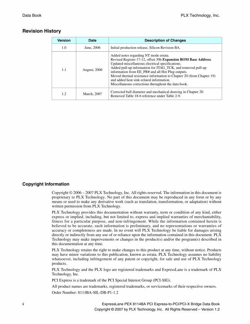
Revision History
Version Date Description of Changes
1.0 June, 2006 Initial production release, Silicon Revision BA.
1.1 August, 2006
Added notes regarding NT mode errata.Revised Register 17-12, offset 30h Expansion ROM Base Address.Updated miscellaneous electrical specifications.Added pull-up information for JTAG_TCK, and removed pull-up information from EE_PR# and all Hot Plug outputs.Moved thermal resistance information to Chapter 20 (from Chapter 19) and added heat sink-related information.Miscellaneous corrections throughout the data book.
1.2 March, 2007 Corrected ball diameter and mechanical drawing in Chapter 20.Removed Table 18-6 reference under Table 2-9.
March, 2007 Preface
ExpressLane PEX 8114BA PCI Express-to-PCI/PCI-X Bridge Data Book iii
Copyright © 2007 by PLX Technology, Inc. All Rights Reserved – Version 1.2
Preface
The information contained in this document is subject to change without notice. This document isperiodically updated as new information is made available.
Audience
This data book provides the functional details of the PLX ExpressLane PEX 8114BA PCI Express-to-PCI/PCI-X Bridge, for hardware designers and software/firmware engineers.
Supplemental Documentation
This data book assumes that the reader is familiar with the following documents:
• PCI Special Interest Group (PCI-SIG)
3855 SW 153rd Drive, Beaverton, OR 97006 USA
Tel: 503 619-0569, Fax: 503 644-6708, www.pcisig.com
– PCI Local Bus Specification, Revision 2.3
– PCI Local Bus Specification, Revision 3.0
– PCI 2.0 Card Electromechanical Specification, Revision 1.0a
– PCI to PCI Bridge Architecture Specification, Revision 1.1
– PCI Bus Power Management Interface Specification, Revision 1.2
– PCI Hot Plug Specification, Revision 1.1
– PCI Standard Hot Plug Controller and Subsystem Specification, Revision 1.0
– PCI-X Addendum to PCI Local Bus Specification, Revision 1.0b
– PCI-X Addendum to PCI Local Bus Specification, Revision 2.0a
– PCI Express Base Specification, Revision 1.0a
– PCI Express to PCI/PCI-X Bridge Specification, Revision 1.0
• The Institute of Electrical and Electronics Engineers, Inc. (IEEE)
445 Hoes Lane, PO Box 1331, Piscataway, NJ 08855-1331 USA
Tel: 800 678-4333 (domestic only) or 732 981-0060, Fax: 732 981-1721, www.ieee.org
– IEEE Standard 1149.1-1990, IEEE Standard Test Access Port and Boundary-Scan Architecture, 1990
– IEEE 1149.1a-1993, IEEE Standard Test Access Port and Boundary-Scan Architecture
– IEEE Standard 1149.1b-1994, Specifications for Vendor-Specific Extensions
– IEEE Standard 1149.6-2003, IEEE Standard Test Access Port and Boundary-Scan Architecture Extensions
Data Book PLX Technology, Inc.
iv ExpressLane PEX 8114BA PCI Express-to-PCI/PCI-X Bridge Data Book
Copyright © 2007 by PLX Technology, Inc. All Rights Reserved – Version 1.2
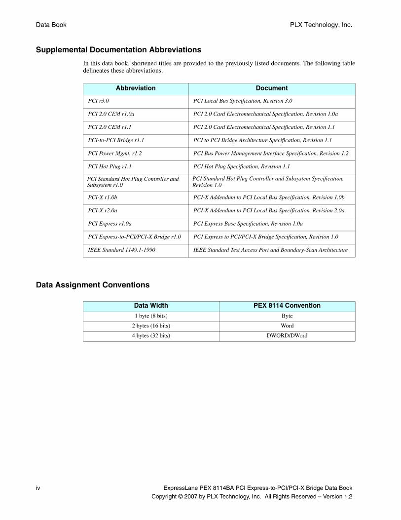
Supplemental Documentation Abbreviations
In this data book, shortened titles are provided to the previously listed documents. The following tabledelineates these abbreviations.
Data Assignment Conventions
Abbreviation Document
PCI r3.0 PCI Local Bus Specification, Revision 3.0
PCI 2.0 CEM r1.0a PCI 2.0 Card Electromechanical Specification, Revision 1.0a
PCI 2.0 CEM r1.1 PCI 2.0 Card Electromechanical Specification, Revision 1.1
PCI-to-PCI Bridge r1.1 PCI to PCI Bridge Architecture Specification, Revision 1.1
PCI Power Mgmt. r1.2 PCI Bus Power Management Interface Specification, Revision 1.2
PCI Hot Plug r1.1 PCI Hot Plug Specification, Revision 1.1
PCI Standard Hot Plug Controller and Subsystem r1.0
PCI Standard Hot Plug Controller and Subsystem Specification, Revision 1.0
PCI-X r1.0b PCI-X Addendum to PCI Local Bus Specification, Revision 1.0b
PCI-X r2.0a PCI-X Addendum to PCI Local Bus Specification, Revision 2.0a
PCI Express r1.0a PCI Express Base Specification, Revision 1.0a
PCI Express-to-PCI/PCI-X Bridge r1.0 PCI Express to PCI/PCI-X Bridge Specification, Revision 1.0
IEEE Standard 1149.1-1990 IEEE Standard Test Access Port and Boundary-Scan Architecture
Data Width PEX 8114 Convention
1 byte (8 bits) Byte
2 bytes (16 bits) Word
4 bytes (32 bits) DWORD/DWord

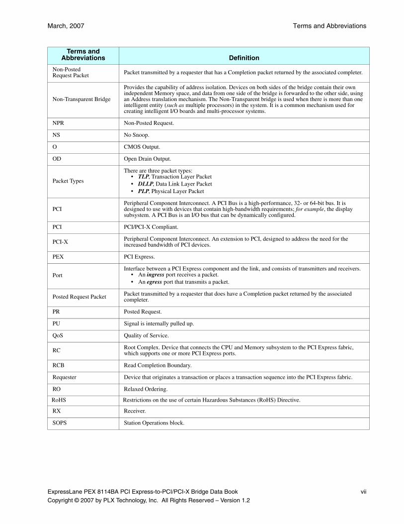
March, 2007 Terms and Abbreviations
ExpressLane PEX 8114BA PCI Express-to-PCI/PCI-X Bridge Data Book v
Copyright © 2007 by PLX Technology, Inc. All Rights Reserved – Version 1.2
Terms and Abbreviations
The following table delineates common terms and abbreviations used in this document. Terms andabbreviations defined in the PCI Express r1.0a are not included in this table.
Terms and Abbreviations Definition
# Active-Low signal.
ACK Acknowledge Control Packet. A control packet used by a destination to acknowledge data packet receipt. A signal that acknowledges signal receipt.
ADB Allowable Disconnect Boundary.
ADQ Allowable Disconnect Quantity. In the PCI Express interface, the ADQ is a buffer size, which is used to indicate memory requirements or reserves.
BAR Base Address Register.
BCR Bridge Control Register of the Type 1 CSR space.
Cold Reset A “Fundamental Reset” following the application of power.
Completer Device addressed by a requester.
CPL Completion Transaction.
CRC Cyclic Redundancy Check
CSR Configuration Status Register; Control and Status Register; Command and Status Register.
DL_Down Data Link Layer is down (a PCI Express link/port status).
DLLP Data Link Layer Packet (originate at the Data Link Layer); allow Flow Control (FCx DLLPs) to acknowledge packets (ACK and NAK DLLPs); and Power Management (PMx DLLPs).
DW DWord.
ECC Error Checking and Correction.
EEPROM Electrically Erasable Programmable Read-Only Memory.
Endpoint
Device, other than the Root Complex and switches that are requesters or completers of PCI Express transactions.
• Endpoints can be PCI Express endpoints or Conventional PCI endpoints.• Conventional PCI endpoints support I/O and Locked transaction semantics. PCI Express
endpoints do not.
FCPFlow Control Packet devices on each link exchange FCPs, which carry Header and Data Payload credit information for one of three packet types – Posted requests, Non-Posted requests, and Completions.
Fundamental ResetThe mechanism of setting or returning all registers and state machines to default/initial conditions, as defined in all PCI Express, PCI, PCI-X and Bridge specifications. This mechanism is implemented by way of the PEX_PERST# Input ball/signal.
Host A Host computer provides services to computers that connect to it on a network. It is considered in charge over the remainder of devices connected on the bus.
Hot Reset A reset propagated in-band across a Link using a Physical Layer mechanism (Training Sequence).
I CMOS Input.
I/O CMOS Bi-Directional Input Output.
INCH Ingress Credit Handler.
ITCH Internal Credit Handler.
Data Book PLX Technology, Inc.
vi ExpressLane PEX 8114BA PCI Express-to-PCI/PCI-X Bridge Data Book
Copyright © 2007 by PLX Technology, Inc. All Rights Reserved – Version 1.2
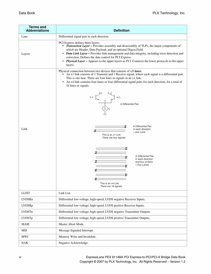
Lane Differential signal pair in each direction.
Layers
PCI Express defines three layers:• Transaction Layer – Provides assembly and disassembly of TLPs, the major components of
which are Header, Data Payload, and an optional Digest Field.• Data Link Layer – Provides link management and data integrity, including error detection and
correction. Defines the data control for PCI Express.• Physical Layer – Appears to the upper layers as PCI. Connects the lower protocols to the upper
layers.
Link
Physical connection between two devices that consists of xN lanes.• An x1 link consists of 1 Transmit and 1 Receive signal, where each signal is a differential pair.
This is one lane. There are four lines or signals in an x1 link.• An x4 link contains four lanes or four differential signal pairs for each direction, for a total of
16 lines or signals.
LLIST Link List.
LVDSRn Differential low-voltage, high-speed, LVDS negative Receiver Inputs.
LVDSRp Differential low-voltage, high-speed, LVDS positive Receiver Inputs.
LVDSTn Differential low-voltage, high-speed, LVDS negative Transmitter Outputs.
LVDSTp Differential low-voltage, high-speed, LVDS positive Transmitter Outputs.
MAM Master Abort Mode.
MSI Message Signaled Interrupt.
MWI Memory Write and Invalidate.
NAK Negative Acknowledge.
Terms and Abbreviations Definition
A Differential Pair
A Differential Pairin each direction= one Lane
This is an x1 LinkThere are four signals
This is an x4 LinkThere are 16 signals
A Differential Pairin each directionand four of them= four Lanes
March, 2007 Terms and Abbreviations
ExpressLane PEX 8114BA PCI Express-to-PCI/PCI-X Bridge Data Book vii
Copyright © 2007 by PLX Technology, Inc. All Rights Reserved – Version 1.2
Non-Posted Request Packet Packet transmitted by a requester that has a Completion packet returned by the associated completer.
Non-Transparent Bridge
Provides the capability of address isolation. Devices on both sides of the bridge contain their own independent Memory space, and data from one side of the bridge is forwarded to the other side, using an Address translation mechanism. The Non-Transparent bridge is used when there is more than one intelligent entity (such as multiple processors) in the system. It is a common mechanism used for creating intelligent I/O boards and multi-processor systems.
NPR Non-Posted Request.
NS No Snoop.
O CMOS Output.
OD Open Drain Output.
Packet Types
There are three packet types:• TLP, Transaction Layer Packet• DLLP, Data Link Layer Packet• PLP, Physical Layer Packet
PCIPeripheral Component Interconnect. A PCI Bus is a high-performance, 32- or 64-bit bus. It is designed to use with devices that contain high-bandwidth requirements; for example, the display subsystem. A PCI Bus is an I/O bus that can be dynamically configured.
PCI PCI/PCI-X Compliant.
PCI-X Peripheral Component Interconnect. An extension to PCI, designed to address the need for the increased bandwidth of PCI devices.
PEX PCI Express.
PortInterface between a PCI Express component and the link, and consists of transmitters and receivers.
• An ingress port receives a packet.• An egress port that transmits a packet.
Posted Request Packet Packet transmitted by a requester that does have a Completion packet returned by the associated completer.
PR Posted Request.
PU Signal is internally pulled up.
QoS Quality of Service.
RC Root Complex. Device that connects the CPU and Memory subsystem to the PCI Express fabric, which supports one or more PCI Express ports.
RCB Read Completion Boundary.
Requester Device that originates a transaction or places a transaction sequence into the PCI Express fabric.
RO Relaxed Ordering.
RoHS Restrictions on the use of certain Hazardous Substances (RoHS) Directive.
RX Receiver.
SOPS Station Operations block.
Terms and Abbreviations Definition
Data Book PLX Technology, Inc.
viii ExpressLane PEX 8114BA PCI Express-to-PCI/PCI-X Bridge Data Book
Copyright © 2007 by PLX Technology, Inc. All Rights Reserved – Version 1.2
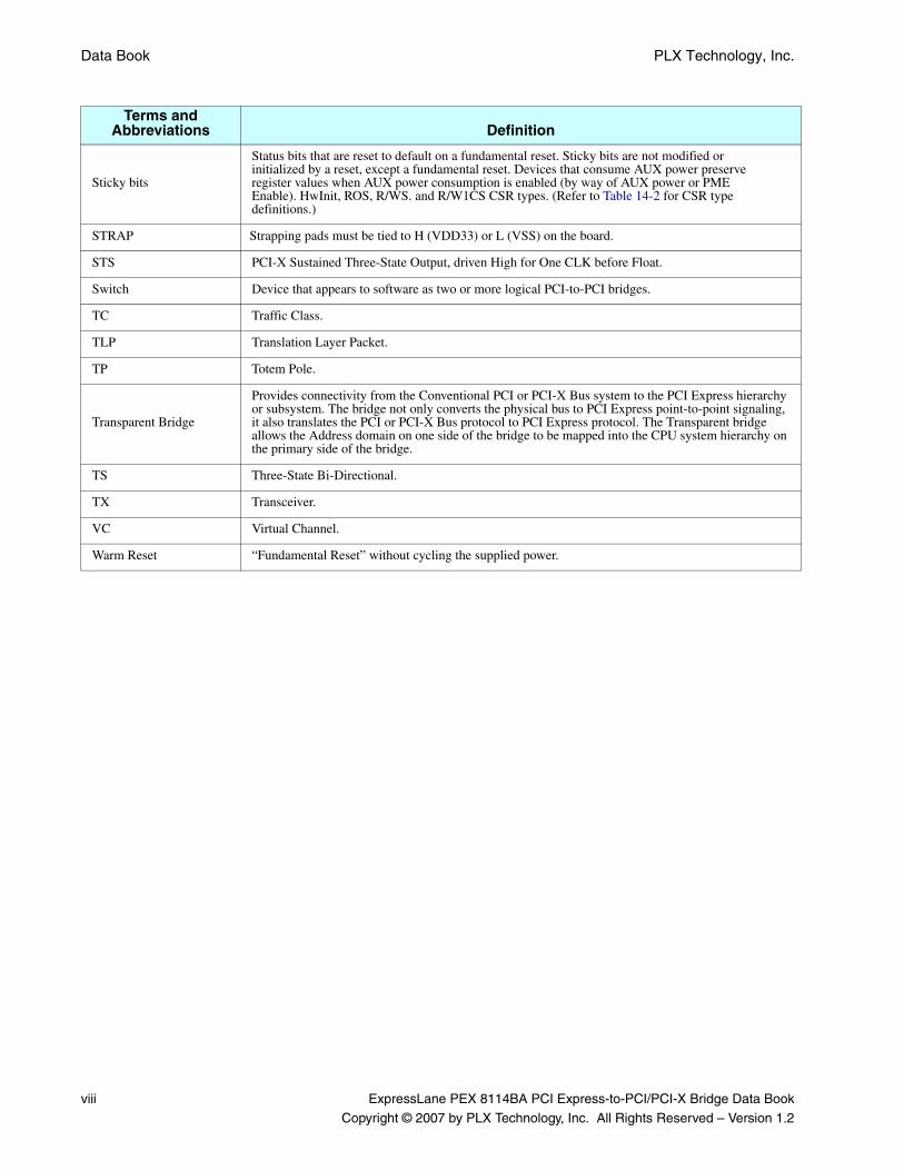
Sticky bits
Status bits that are reset to default on a fundamental reset. Sticky bits are not modified or initialized by a reset, except a fundamental reset. Devices that consume AUX power preserve register values when AUX power consumption is enabled (by way of AUX power or PME Enable). HwInit, ROS, R/WS. and R/W1CS CSR types. (Refer to Table 14-2 for CSR type definitions.)
STRAP Strapping pads must be tied to H (VDD33) or L (VSS) on the board.
STS PCI-X Sustained Three-State Output, driven High for One CLK before Float.
Switch Device that appears to software as two or more logical PCI-to-PCI bridges.
TC Traffic Class.
TLP Translation Layer Packet.
TP Totem Pole.
Transparent Bridge
Provides connectivity from the Conventional PCI or PCI-X Bus system to the PCI Express hierarchy or subsystem. The bridge not only converts the physical bus to PCI Express point-to-point signaling, it also translates the PCI or PCI-X Bus protocol to PCI Express protocol. The Transparent bridge allows the Address domain on one side of the bridge to be mapped into the CPU system hierarchy on the primary side of the bridge.
TS Three-State Bi-Directional.
TX Transceiver.
VC Virtual Channel.
Warm Reset “Fundamental Reset” without cycling the supplied power.
Terms and Abbreviations Definition

ExpressLane PEX 8114BA PCI Express-to-PCI/PCI-X Bridge Data Book ix
Copyright © 2007 by PLX Technology, Inc. All Rights Reserved – Version 1.2
Contents
Chapter 1 Introduction. . . . . . . . . . . . . . . . . . . . . . . . . . . . . . . . . . . . . . . . . . . . . . . . . . . . . . 11.1 Features . . . . . . . . . . . . . . . . . . . . . . . . . . . . . . . . . . . . . . . . . . . . . . . . . . . . . . . . . . . 11.2 PEX 8114 Serial PCI Express to PCI/PCI-X Bridge . . . . . . . . . . . . . . . . . . . . . . . . . . 3
1.2.1 Introduction to PEX 8114 Operation . . . . . . . . . . . . . . . . . . . . . . . . . . . . . . . . . . 41.3 Detailed Block Diagram . . . . . . . . . . . . . . . . . . . . . . . . . . . . . . . . . . . . . . . . . . . . . . . 5
1.3.1 Physical Layer – Layer 1 . . . . . . . . . . . . . . . . . . . . . . . . . . . . . . . . . . . . . . . . . . . 61.3.2 Data Link Layer – Layer 2 . . . . . . . . . . . . . . . . . . . . . . . . . . . . . . . . . . . . . . . . . . 61.3.3 Transaction Layer – Layer 3 . . . . . . . . . . . . . . . . . . . . . . . . . . . . . . . . . . . . . . . . 61.3.4 Sample Paths . . . . . . . . . . . . . . . . . . . . . . . . . . . . . . . . . . . . . . . . . . . . . . . . . . . 7
1.3.4.1 Forward Bridge Mode . . . . . . . . . . . . . . . . . . . . . . . . . . . . . . . . . . . . . . . . . . 71.3.4.2 Reverse Bridge Mode . . . . . . . . . . . . . . . . . . . . . . . . . . . . . . . . . . . . . . . . . . 81.3.4.3 Non-Transparent Mode . . . . . . . . . . . . . . . . . . . . . . . . . . . . . . . . . . . . . . . . 9
1.4 PEX 8114 Applications . . . . . . . . . . . . . . . . . . . . . . . . . . . . . . . . . . . . . . . . . . . . . . . 101.4.1 PCI Express Adapter Board . . . . . . . . . . . . . . . . . . . . . . . . . . . . . . . . . . . . . . . 101.4.2 Intelligent PCI Express Adapter Board . . . . . . . . . . . . . . . . . . . . . . . . . . . . . . . 111.4.3 PCI Express Motherboard to PCI-X Expansion Slot . . . . . . . . . . . . . . . . . . . . . 121.4.4 PCI-X Host Supporting a PCI Express Expansion Slot . . . . . . . . . . . . . . . . . . . 131.4.5 PCI-X Add-In Board Created from PCI Express Native Silicon . . . . . . . . . . . . . 141.4.6 PCI-X Extender Board . . . . . . . . . . . . . . . . . . . . . . . . . . . . . . . . . . . . . . . . . . . . 15
Chapter 2 Signal Ball Description. . . . . . . . . . . . . . . . . . . . . . . . . . . . . . . . . . . . . . . . . . . . 172.1 Introduction . . . . . . . . . . . . . . . . . . . . . . . . . . . . . . . . . . . . . . . . . . . . . . . . . . . . . . . 172.2 Abbreviations . . . . . . . . . . . . . . . . . . . . . . . . . . . . . . . . . . . . . . . . . . . . . . . . . . . . . . 18
2.2.1 Pull-Up Resistors . . . . . . . . . . . . . . . . . . . . . . . . . . . . . . . . . . . . . . . . . . . . . . . . 192.3 PCI/PCI-X Bus Interface Signals . . . . . . . . . . . . . . . . . . . . . . . . . . . . . . . . . . . . . . . 202.4 PCI Express Interface Signals . . . . . . . . . . . . . . . . . . . . . . . . . . . . . . . . . . . . . . . . . 252.5 Hot Plug Signals . . . . . . . . . . . . . . . . . . . . . . . . . . . . . . . . . . . . . . . . . . . . . . . . . . . . 262.6 Strapping Signals . . . . . . . . . . . . . . . . . . . . . . . . . . . . . . . . . . . . . . . . . . . . . . . . . . . 272.7 JTAG Interface Signals . . . . . . . . . . . . . . . . . . . . . . . . . . . . . . . . . . . . . . . . . . . . . . 282.8 Serial EEPROM Interface Signals . . . . . . . . . . . . . . . . . . . . . . . . . . . . . . . . . . . . . . 292.9 Power and Ground Signals . . . . . . . . . . . . . . . . . . . . . . . . . . . . . . . . . . . . . . . . . . . 302.10 Ball Assignments by Location . . . . . . . . . . . . . . . . . . . . . . . . . . . . . . . . . . . . . . . . 312.11 Ball Assignments by Signal Name . . . . . . . . . . . . . . . . . . . . . . . . . . . . . . . . . . . . . 382.12 Physical Ball Assignment . . . . . . . . . . . . . . . . . . . . . . . . . . . . . . . . . . . . . . . . . . . . 45
Chapter 3 Clock and Reset . . . . . . . . . . . . . . . . . . . . . . . . . . . . . . . . . . . . . . . . . . . . . . . . . 473.1 PEX 8114 Clocking Introduction . . . . . . . . . . . . . . . . . . . . . . . . . . . . . . . . . . . . . . . 47
3.1.1 PCI-X Clock Generator . . . . . . . . . . . . . . . . . . . . . . . . . . . . . . . . . . . . . . . . . . . 473.1.2 PCI-X Clocking of PCI-X Module . . . . . . . . . . . . . . . . . . . . . . . . . . . . . . . . . . . . 48
3.1.2.1 Clocking the PCI Module when PEX 8114 Clock Generator Is Not Used . 483.1.2.2 Clocking the PCI Module when PEX 8114 Clock Generator Is Used . . . . . 48
3.2 Determining PCI Bus and Internal Clock Initialization . . . . . . . . . . . . . . . . . . . . . . . 493.2.1 Determining Bus Mode Capability and Maximum Frequency . . . . . . . . . . . . . . 50
3.3 PCI Clock Master Mode . . . . . . . . . . . . . . . . . . . . . . . . . . . . . . . . . . . . . . . . . . . . . . 513.3.1 Clock Master Mode Signals . . . . . . . . . . . . . . . . . . . . . . . . . . . . . . . . . . . . . . . . 52
3.4 PCI Clock Slave Mode . . . . . . . . . . . . . . . . . . . . . . . . . . . . . . . . . . . . . . . . . . . . . . . 543.4.1 Clock Slave – Forward Bridge Mode . . . . . . . . . . . . . . . . . . . . . . . . . . . . . . . . . 543.4.2 Clock Slave – Reverse Bridge Mode . . . . . . . . . . . . . . . . . . . . . . . . . . . . . . . . . 563.4.3 Timing Diagrams – Forward or Reverse Bridge Mode . . . . . . . . . . . . . . . . . . . 57

PLX Technology, Inc.
x ExpressLane PEX 8114BA PCI Express-to-PCI/PCI-X Bridge Data Book
Copyright © 2007 by PLX Technology, Inc. All Rights Reserved – Version 1.2
3.5 Resets . . . . . . . . . . . . . . . . . . . . . . . . . . . . . . . . . . . . . . . . . . . . . . . . . . . . . . . . . . . 593.5.1 Level-0, Fundamental Reset (Power-On, Hard, Cold, Warm) . . . . . . . . . . . . . . 60
3.5.1.1 PEX_PERST# . . . . . . . . . . . . . . . . . . . . . . . . . . . . . . . . . . . . . . . . . . . . . . 603.5.1.2 Level-0 Reset – Forward Bridge Mode . . . . . . . . . . . . . . . . . . . . . . . . . . . . 613.5.1.3 Level-0 Reset – Reverse Bridge Mode . . . . . . . . . . . . . . . . . . . . . . . . . . . . 62
3.5.2 Level-1, Hot Reset . . . . . . . . . . . . . . . . . . . . . . . . . . . . . . . . . . . . . . . . . . . . . . . 633.5.2.1 Level-1 Reset – Forward Bridge Mode . . . . . . . . . . . . . . . . . . . . . . . . . . . . 633.5.2.2 Level-1 Reset – Reverse Bridge Mode . . . . . . . . . . . . . . . . . . . . . . . . . . . . 64
3.5.3 Secondary Bus Reset, Level-2 Reset . . . . . . . . . . . . . . . . . . . . . . . . . . . . . . . . 653.5.3.1 Level-2 Reset – Forward Bridge Mode . . . . . . . . . . . . . . . . . . . . . . . . . . . . 653.5.3.2 Level-2 Reset – Reverse Bridge Mode . . . . . . . . . . . . . . . . . . . . . . . . . . . . 65
3.6 Serial EEPROM Load Sequence . . . . . . . . . . . . . . . . . . . . . . . . . . . . . . . . . . . . . . . 66
Chapter 4 Data Path. . . . . . . . . . . . . . . . . . . . . . . . . . . . . . . . . . . . . . . . . . . . . . . . . . . . . . . .674.1 Internal Data Path Description . . . . . . . . . . . . . . . . . . . . . . . . . . . . . . . . . . . . . . . . . 674.2 PCI Express Credits . . . . . . . . . . . . . . . . . . . . . . . . . . . . . . . . . . . . . . . . . . . . . . . . . 674.3 Latency and Bandwidth . . . . . . . . . . . . . . . . . . . . . . . . . . . . . . . . . . . . . . . . . . . . . . 68
4.3.1 Data Flow-Through Latency . . . . . . . . . . . . . . . . . . . . . . . . . . . . . . . . . . . . . . . 684.3.2 PCI Transaction Initial Latency and Cycle Recovery Time . . . . . . . . . . . . . . . . 684.3.3 PCI-X Transaction Initial Latency and Cycle Recovery Time . . . . . . . . . . . . . . 694.3.4 Arbitration Latency . . . . . . . . . . . . . . . . . . . . . . . . . . . . . . . . . . . . . . . . . . . . . . . 69
Chapter 5 Address Spaces . . . . . . . . . . . . . . . . . . . . . . . . . . . . . . . . . . . . . . . . . . . . . . . . . .715.1 Introduction . . . . . . . . . . . . . . . . . . . . . . . . . . . . . . . . . . . . . . . . . . . . . . . . . . . . . . . . 715.2 Transparent Mode . . . . . . . . . . . . . . . . . . . . . . . . . . . . . . . . . . . . . . . . . . . . . . . . . . 71
5.2.1 Transparent Mode I/O Space . . . . . . . . . . . . . . . . . . . . . . . . . . . . . . . . . . . . . . 725.2.1.1 Enable Bits . . . . . . . . . . . . . . . . . . . . . . . . . . . . . . . . . . . . . . . . . . . . . . . . . 725.2.1.2 I/O Base and Limit Registers . . . . . . . . . . . . . . . . . . . . . . . . . . . . . . . . . . . 725.2.1.3 ISA Mode . . . . . . . . . . . . . . . . . . . . . . . . . . . . . . . . . . . . . . . . . . . . . . . . . . 745.2.1.4 VGA Mode . . . . . . . . . . . . . . . . . . . . . . . . . . . . . . . . . . . . . . . . . . . . . . . . . 75
5.2.2 Transparent Mode Memory-Mapped I/O Space . . . . . . . . . . . . . . . . . . . . . . . . 765.2.2.1 Enable Bits . . . . . . . . . . . . . . . . . . . . . . . . . . . . . . . . . . . . . . . . . . . . . . . . . 765.2.2.2 Memory-Mapped I/O Base and Limit Registers . . . . . . . . . . . . . . . . . . . . . 77
5.2.3 Transparent Mode Prefetchable Space . . . . . . . . . . . . . . . . . . . . . . . . . . . . . . . 785.2.3.1 Enable Bits . . . . . . . . . . . . . . . . . . . . . . . . . . . . . . . . . . . . . . . . . . . . . . . . . 785.2.3.2 Prefetchable Base and Limit Registers . . . . . . . . . . . . . . . . . . . . . . . . . . . 795.2.3.3 64-Bit Addressing . . . . . . . . . . . . . . . . . . . . . . . . . . . . . . . . . . . . . . . . . . . . 81
5.2.4 Transparent Mode Base Address Register Addressing . . . . . . . . . . . . . . . . . . 825.3 Non-Transparent Forward Bridge Mode . . . . . . . . . . . . . . . . . . . . . . . . . . . . . . . . . . 83
5.3.1 Non-Transparent Forward Bridge Mode Primary Interface BARs . . . . . . . . . . . 845.3.2 Non-Transparent Forward Bridge Mode Secondary Interface BARs . . . . . . . . 855.3.3 Non-Transparent Forward Bridge Mode Configuration BAR Usage . . . . . . . . . 86
5.3.3.1 Primary Interface . . . . . . . . . . . . . . . . . . . . . . . . . . . . . . . . . . . . . . . . . . . . 875.3.3.2 Secondary Interface . . . . . . . . . . . . . . . . . . . . . . . . . . . . . . . . . . . . . . . . . . 87
5.3.4 Non-Transparent Forward Bridge Mode Address Translation BAR Usage . . . . 885.3.4.1 Direct Address Translation . . . . . . . . . . . . . . . . . . . . . . . . . . . . . . . . . . . . . 885.3.4.2 Lookup Table Base Address Translation . . . . . . . . . . . . . . . . . . . . . . . . . . 895.3.4.3 Address Width Translation across Bridge . . . . . . . . . . . . . . . . . . . . . . . . . 90
5.3.5 Non-Transparent Forward Bridge Mode Register Type Descriptions . . . . . . . . 915.3.5.1 Base Address Registers (BARs) . . . . . . . . . . . . . . . . . . . . . . . . . . . . . . . . 915.3.5.2 BAR Setup Registers . . . . . . . . . . . . . . . . . . . . . . . . . . . . . . . . . . . . . . . . . 915.3.5.3 BAR Address Translation Registers . . . . . . . . . . . . . . . . . . . . . . . . . . . . . . 915.3.5.4 Downstream BAR Limit Registers . . . . . . . . . . . . . . . . . . . . . . . . . . . . . . . 92
March, 2007 PLX Technology, Inc.
ExpressLane PEX 8114BA PCI Express-to-PCI/PCI-X Bridge Data Book xi
Copyright © 2007 by PLX Technology, Inc. All Rights Reserved – Version 1.2
5.3.5.5 BAR Lookup Table Entry Registers . . . . . . . . . . . . . . . . . . . . . . . . . . . . . . 925.3.5.6 64-Bit PCI Express TLP Translation to and from
32-Bit PCI-X Address Transactions . . . . . . . . . . . . . . . . . . . . . . . . . . . . . . 92
Chapter 6 Configuration . . . . . . . . . . . . . . . . . . . . . . . . . . . . . . . . . . . . . . . . . . . . . . . . . . . 936.1 Introduction . . . . . . . . . . . . . . . . . . . . . . . . . . . . . . . . . . . . . . . . . . . . . . . . . . . . . . . 936.2 Type 0 Configuration Transactions . . . . . . . . . . . . . . . . . . . . . . . . . . . . . . . . . . . . . 956.3 Type 1 Configuration Transactions . . . . . . . . . . . . . . . . . . . . . . . . . . . . . . . . . . . . . 956.4 Type 1-to-Type 0 Conversion . . . . . . . . . . . . . . . . . . . . . . . . . . . . . . . . . . . . . . . . . . 96
6.4.1 Forward Transparent Bridge Mode . . . . . . . . . . . . . . . . . . . . . . . . . . . . . . . . . . 966.4.2 Reverse Transparent Bridge Mode . . . . . . . . . . . . . . . . . . . . . . . . . . . . . . . . . . 97
6.5 Type 1-to-Type 1 Forwarding in Transparent Mode . . . . . . . . . . . . . . . . . . . . . . . . . 986.5.1 Forward Transparent Bridge Mode . . . . . . . . . . . . . . . . . . . . . . . . . . . . . . . . . . 986.5.2 Reverse Transparent Bridge Mode . . . . . . . . . . . . . . . . . . . . . . . . . . . . . . . . . . 99
6.6 PCI Express Enhanced Configuration Mechanism . . . . . . . . . . . . . . . . . . . . . . . . . 996.7 Configuration Retry Mechanism . . . . . . . . . . . . . . . . . . . . . . . . . . . . . . . . . . . . . . . 100
6.7.1 Forward Bridge Mode . . . . . . . . . . . . . . . . . . . . . . . . . . . . . . . . . . . . . . . . . . . 1006.7.2 Reverse Bridge Mode . . . . . . . . . . . . . . . . . . . . . . . . . . . . . . . . . . . . . . . . . . . 100
6.8 Configuration Methods . . . . . . . . . . . . . . . . . . . . . . . . . . . . . . . . . . . . . . . . . . . . . . 1016.8.1 Configuration Methods Intent and Variations . . . . . . . . . . . . . . . . . . . . . . . . . 1016.8.2 PCI Express Extended Configuration Method . . . . . . . . . . . . . . . . . . . . . . . . . 1026.8.3 PCI Configuration Cycles . . . . . . . . . . . . . . . . . . . . . . . . . . . . . . . . . . . . . . . . 1026.8.4 BAR 0/1 Device-Specific Register Memory-Mapped Configuration . . . . . . . . 1026.8.5 Address and Data Pointer Configuration Method . . . . . . . . . . . . . . . . . . . . . . 1036.8.6 Configuration Specifics . . . . . . . . . . . . . . . . . . . . . . . . . . . . . . . . . . . . . . . . . . 103
6.8.6.1 Forward Transparent Bridge Mode . . . . . . . . . . . . . . . . . . . . . . . . . . . . . 1036.8.6.2 Reverse Transparent Bridge Mode . . . . . . . . . . . . . . . . . . . . . . . . . . . . . 1046.8.6.3 Forward Non-Transparent Bridge Mode . . . . . . . . . . . . . . . . . . . . . . . . . . 107
Chapter 7 Bridge Operations . . . . . . . . . . . . . . . . . . . . . . . . . . . . . . . . . . . . . . . . . . . . . . 1117.1 Introduction . . . . . . . . . . . . . . . . . . . . . . . . . . . . . . . . . . . . . . . . . . . . . . . . . . . . . . 1117.2 General Compliance . . . . . . . . . . . . . . . . . . . . . . . . . . . . . . . . . . . . . . . . . . . . . . . 1117.3 PCI-to-PCI Express Transactions . . . . . . . . . . . . . . . . . . . . . . . . . . . . . . . . . . . . . 112
7.3.1 PCI-to-PCI Express Flow Control . . . . . . . . . . . . . . . . . . . . . . . . . . . . . . . . . . 1127.3.2 PCI-to-PCI Express – PCI Posted Write Requests . . . . . . . . . . . . . . . . . . . . . 1127.3.3 PCI-to-PCI Express – PCI Non-Posted Requests . . . . . . . . . . . . . . . . . . . . . . 1137.3.4 PCI-to-PCI Express – PCI Non-Posted Transactions until
PCI Express Completion Returns . . . . . . . . . . . . . . . . . . . . . . . . . . . . . . . . 1137.3.5 PCI-to-PCI Express – PCI Requests Do Not Contain
Predetermined Lengths . . . . . . . . . . . . . . . . . . . . . . . . . . . . . . . . . . . . . . . . 1147.3.5.1 Memory Read Requests to Non-Prefetchable Space . . . . . . . . . . . . . . . 1147.3.5.2 Memory Read Requests to Prefetchable Space . . . . . . . . . . . . . . . . . . . 1147.3.5.3 Memory Read Line or Memory Read Line Multiple . . . . . . . . . . . . . . . . . 1157.3.5.4 Credits . . . . . . . . . . . . . . . . . . . . . . . . . . . . . . . . . . . . . . . . . . . . . . . . . . . 115
7.3.6 PCI-to-PCI Express Disposition of Unused Prefetched Data . . . . . . . . . . . . . 1167.3.7 PCI-to-PCI Express Pending Transaction Count Limits . . . . . . . . . . . . . . . . . 1167.3.8 PCI-to-PCI Express – PCI Write Transaction with
Discontiguous Byte Enables . . . . . . . . . . . . . . . . . . . . . . . . . . . . . . . . . . . . 1167.3.9 PCI-to-PCI Express – PCI Write Transactions Larger
than Maximum Packet Size . . . . . . . . . . . . . . . . . . . . . . . . . . . . . . . . . . . . . 1167.4 PCI-X-to-PCI Express Transactions . . . . . . . . . . . . . . . . . . . . . . . . . . . . . . . . . . . . 117
7.4.1 PCI-X-to-PCI Express Flow Control . . . . . . . . . . . . . . . . . . . . . . . . . . . . . . . . 1177.4.2 PCI-X-to-PCI Express – PCI-X Posted Requests . . . . . . . . . . . . . . . . . . . . . . 1177.4.3 PCI-X-to-PCI Express – PCI-X Non-Posted Requests . . . . . . . . . . . . . . . . . . 118
PLX Technology, Inc.
xii ExpressLane PEX 8114BA PCI Express-to-PCI/PCI-X Bridge Data Book
Copyright © 2007 by PLX Technology, Inc. All Rights Reserved – Version 1.2
7.4.4 PCI-X-to-PCI Express – PCI-X Read Requests Larger than Maximum Read Request Size . . . . . . . . . . . . . . . . . . . . . . . . . . . . . . . . . . . 118
7.4.5 PCI-X-to-PCI Express – PCI-X Transfer Special Case . . . . . . . . . . . . . . . . . . 1197.4.6 PCI-X-to-PCI Express – PCI-X Transactions that Require Bridge
to Take Ownership . . . . . . . . . . . . . . . . . . . . . . . . . . . . . . . . . . . . . . . . . . . 1197.4.7 PCI-X-to-PCI Express – PCI-X Writes with Discontiguous Byte Enables . . . . 1197.4.8 PCI-X-to-PCI Express – PCI-X Writes Longer than Maximum Packet Size . . 119
7.5 PCI Express-to-PCI Transactions . . . . . . . . . . . . . . . . . . . . . . . . . . . . . . . . . . . . . 1207.5.1 PCI Express-to-PCI Flow Control . . . . . . . . . . . . . . . . . . . . . . . . . . . . . . . . . . 1207.5.2 PCI Express-to-PCI – PCI Express Posted Transactions . . . . . . . . . . . . . . . . 1207.5.3 PCI Express-to-PCI – PCI Express Non-Posted Transactions . . . . . . . . . . . . 1217.5.4 PCI Express-to-PCI – PCI Bus Retry . . . . . . . . . . . . . . . . . . . . . . . . . . . . . . . 1217.5.5 PCI Express-to-PCI Transaction Request Size . . . . . . . . . . . . . . . . . . . . . . . . 1227.5.6 PCI Express-to-PCI Transaction Completion Size . . . . . . . . . . . . . . . . . . . . . 122
7.6 PCI Express-to-PCI-X Transactions . . . . . . . . . . . . . . . . . . . . . . . . . . . . . . . . . . . . 1237.6.1 PCI Express-to-PCI-X Posted Writes . . . . . . . . . . . . . . . . . . . . . . . . . . . . . . . 1237.6.2 PCI Express-to-PCI-X Non-Posted Transactions . . . . . . . . . . . . . . . . . . . . . . 124
7.6.2.1 Non-Posted Writes . . . . . . . . . . . . . . . . . . . . . . . . . . . . . . . . . . . . . . . . . . 1247.6.2.2 Non-Posted Writes and Reads . . . . . . . . . . . . . . . . . . . . . . . . . . . . . . . . . 1247.6.2.3 Transaction Concurrency . . . . . . . . . . . . . . . . . . . . . . . . . . . . . . . . . . . . . 125
7.7 Non-Transparent Transactions . . . . . . . . . . . . . . . . . . . . . . . . . . . . . . . . . . . . . . . . 1257.8 Transaction Transfer Failures . . . . . . . . . . . . . . . . . . . . . . . . . . . . . . . . . . . . . . . . 126
7.8.1 PCI Endpoint Fails to Retry Read Request . . . . . . . . . . . . . . . . . . . . . . . . . . . 1277.8.2 PCI-X Endpoint Fails to Transmit Split Completion . . . . . . . . . . . . . . . . . . . . . 1277.8.3 PCI-X Endpoint Allows Infinite Retries . . . . . . . . . . . . . . . . . . . . . . . . . . . . . . 1287.8.4 PCI Express Endpoint Fails to Return Completion Data . . . . . . . . . . . . . . . . . 129
Chapter 8 Error Handling . . . . . . . . . . . . . . . . . . . . . . . . . . . . . . . . . . . . . . . . . . . . . . . . . .1318.1 Forward Bridge Error Handling . . . . . . . . . . . . . . . . . . . . . . . . . . . . . . . . . . . . . . . . 131
8.1.1 Forward Bridge PCI Express Originating Interface (Primary to Secondary) . . 1318.1.1.1 Received Poisoned TLP . . . . . . . . . . . . . . . . . . . . . . . . . . . . . . . . . . . . . . 1328.1.1.2 Received ECRC Error . . . . . . . . . . . . . . . . . . . . . . . . . . . . . . . . . . . . . . . 1338.1.1.3 PCI/PCI-X Uncorrectable Data Errors . . . . . . . . . . . . . . . . . . . . . . . . . . . 1338.1.1.4 PCI/PCI-X Address/Attribute Errors . . . . . . . . . . . . . . . . . . . . . . . . . . . . . 1368.1.1.5 PCI/PCI-X Master Abort on Posted Transaction . . . . . . . . . . . . . . . . . . . 1378.1.1.6 PCI/PCI-X Master Abort on Non-Posted Transaction . . . . . . . . . . . . . . . . 1378.1.1.7 PCI-X Master Abort on Split Completion . . . . . . . . . . . . . . . . . . . . . . . . . 1388.1.1.8 PCI/PCI-X Target Abort on Posted Transaction . . . . . . . . . . . . . . . . . . . . 1388.1.1.9 PCI/PCI-X Target Abort on Non-Posted Transaction . . . . . . . . . . . . . . . . 1398.1.1.10 PCI-X Target Abort on Split Completion . . . . . . . . . . . . . . . . . . . . . . . . . 1398.1.1.11 Completer Abort . . . . . . . . . . . . . . . . . . . . . . . . . . . . . . . . . . . . . . . . . . . 1408.1.1.12 Unexpected Completion . . . . . . . . . . . . . . . . . . . . . . . . . . . . . . . . . . . . . 1408.1.1.13 Receive Non-Posted Request Unsupported . . . . . . . . . . . . . . . . . . . . . . 1418.1.1.14 Link Training Error . . . . . . . . . . . . . . . . . . . . . . . . . . . . . . . . . . . . . . . . . 1418.1.1.15 Data Link Protocol Error . . . . . . . . . . . . . . . . . . . . . . . . . . . . . . . . . . . . . 1428.1.1.16 Flow Control Protocol Error . . . . . . . . . . . . . . . . . . . . . . . . . . . . . . . . . . 1428.1.1.17 Receiver Overflow . . . . . . . . . . . . . . . . . . . . . . . . . . . . . . . . . . . . . . . . . 1438.1.1.18 Malformed TLP . . . . . . . . . . . . . . . . . . . . . . . . . . . . . . . . . . . . . . . . . . . . 143
8.1.2 Forward Bridge PCI/PCI-X Originating Interface (Secondary to Primary) . . . . 1448.1.2.1 Received PCI/PCI-X Errors . . . . . . . . . . . . . . . . . . . . . . . . . . . . . . . . . . . 1458.1.2.2 Unsupported Request (UR) Completion Status . . . . . . . . . . . . . . . . . . . . 1518.1.2.3 Completer Abort (CA) Completion Status . . . . . . . . . . . . . . . . . . . . . . . . . 1518.1.2.4 Split Completion Errors . . . . . . . . . . . . . . . . . . . . . . . . . . . . . . . . . . . . . . . 152
March, 2007 PLX Technology, Inc.
ExpressLane PEX 8114BA PCI Express-to-PCI/PCI-X Bridge Data Book xiii
Copyright © 2007 by PLX Technology, Inc. All Rights Reserved – Version 1.2
8.1.3 Forward Bridge Timeout Errors . . . . . . . . . . . . . . . . . . . . . . . . . . . . . . . . . . . . 1568.1.3.1 PCI Express Completion Timeout Errors . . . . . . . . . . . . . . . . . . . . . . . . . 1568.1.3.2 PCI Delayed Transaction Timeout Errors . . . . . . . . . . . . . . . . . . . . . . . . . 156
8.1.4 Forward Bridge SERR# Forwarding . . . . . . . . . . . . . . . . . . . . . . . . . . . . . . . . 1578.2 Reverse Bridge Error Handling . . . . . . . . . . . . . . . . . . . . . . . . . . . . . . . . . . . . . . . 158
8.2.1 Reverse Bridge Forwarding PEX 8114 System Errorsand System Error Messages . . . . . . . . . . . . . . . . . . . . . . . . . . . . . . . . . . . . 158
8.2.1.1 Root Port Error Forwarding Control . . . . . . . . . . . . . . . . . . . . . . . . . . . . . 1598.2.1.2 Conventional PCI Type 1 Error Forwarding Control . . . . . . . . . . . . . . . . . 1608.2.1.3 Bridge-Detected Error Reporting . . . . . . . . . . . . . . . . . . . . . . . . . . . . . . . 160
8.2.2 Reverse Bridge PCI Express Originating Interface (Secondary to Primary) . . 1618.2.2.1 Received Poisoned TLP . . . . . . . . . . . . . . . . . . . . . . . . . . . . . . . . . . . . . . 1628.2.2.2 Received ECRC Error . . . . . . . . . . . . . . . . . . . . . . . . . . . . . . . . . . . . . . . 1638.2.2.3 PCI/PCI-X Uncorrectable Data Errors . . . . . . . . . . . . . . . . . . . . . . . . . . . 1648.2.2.4 PCI/PCI-X Address/Attribute Errors . . . . . . . . . . . . . . . . . . . . . . . . . . . . . 1688.2.2.5 PCI/PCI-X Master Abort on Posted Transaction . . . . . . . . . . . . . . . . . . . 1688.2.2.6 PCI/PCI-X Master Abort on Non-Posted Transaction . . . . . . . . . . . . . . . 1698.2.2.7 PCI-X Master Abort on Split Completion . . . . . . . . . . . . . . . . . . . . . . . . . 1708.2.2.8 PCI/PCI-X Target Abort on Posted Transaction . . . . . . . . . . . . . . . . . . . . 1718.2.2.9 PCI/PCI-X Target Abort on Non-Posted Transaction . . . . . . . . . . . . . . . . 1728.2.2.10 PCI-X Target Abort on Split Completion . . . . . . . . . . . . . . . . . . . . . . . . . 1738.2.2.11 Unexpected Completion Received . . . . . . . . . . . . . . . . . . . . . . . . . . . . . 1748.2.2.12 Received Request Unsupported . . . . . . . . . . . . . . . . . . . . . . . . . . . . . . 1758.2.2.13 Link Training Error . . . . . . . . . . . . . . . . . . . . . . . . . . . . . . . . . . . . . . . . . 1768.2.2.14 Data Link Protocol Error . . . . . . . . . . . . . . . . . . . . . . . . . . . . . . . . . . . . . 1778.2.2.15 Flow Control Protocol Error . . . . . . . . . . . . . . . . . . . . . . . . . . . . . . . . . . 1788.2.2.16 Receiver Overflow . . . . . . . . . . . . . . . . . . . . . . . . . . . . . . . . . . . . . . . . . 1798.2.2.17 Malformed TLP . . . . . . . . . . . . . . . . . . . . . . . . . . . . . . . . . . . . . . . . . . . . 180
8.2.3 Reverse Bridge PCI/PCI-X Originating Interface (Primary to Secondary) . . . . 1818.2.3.1 Received PCI/PCI-X Errors . . . . . . . . . . . . . . . . . . . . . . . . . . . . . . . . . . . 1828.2.3.2 Unsupported Request (UR) Completion Status . . . . . . . . . . . . . . . . . . . . 1898.2.3.3 Completer Abort Completion Status . . . . . . . . . . . . . . . . . . . . . . . . . . . . . 1898.2.3.4 Split Completion Errors . . . . . . . . . . . . . . . . . . . . . . . . . . . . . . . . . . . . . . 190
8.2.4 Reverse Bridge Timeout Errors . . . . . . . . . . . . . . . . . . . . . . . . . . . . . . . . . . . . 1968.2.4.1 PCI Express Completion Timeout Errors . . . . . . . . . . . . . . . . . . . . . . . . . 1968.2.4.2 PCI Delayed Transaction Timeout Errors . . . . . . . . . . . . . . . . . . . . . . . . . 197
8.2.5 Reverse Bridge PCI Express Error Messages . . . . . . . . . . . . . . . . . . . . . . . . 198
Chapter 9 Serial EEPROM . . . . . . . . . . . . . . . . . . . . . . . . . . . . . . . . . . . . . . . . . . . . . . . . . 1999.1 Introduction . . . . . . . . . . . . . . . . . . . . . . . . . . . . . . . . . . . . . . . . . . . . . . . . . . . . . . 1999.2 Configuration Data Download . . . . . . . . . . . . . . . . . . . . . . . . . . . . . . . . . . . . . . . . 200
Chapter 10 Interrupt Handler. . . . . . . . . . . . . . . . . . . . . . . . . . . . . . . . . . . . . . . . . . . . . . . . 20310.1 Introduction . . . . . . . . . . . . . . . . . . . . . . . . . . . . . . . . . . . . . . . . . . . . . . . . . . . . . 20310.2 Interrupt Handler Features . . . . . . . . . . . . . . . . . . . . . . . . . . . . . . . . . . . . . . . . . . 20310.3 Events that Cause Interrupts . . . . . . . . . . . . . . . . . . . . . . . . . . . . . . . . . . . . . . . . 20310.4 INTA# Signaling . . . . . . . . . . . . . . . . . . . . . . . . . . . . . . . . . . . . . . . . . . . . . . . . . . 20510.5 Message Signaled Interrupts (MSI) . . . . . . . . . . . . . . . . . . . . . . . . . . . . . . . . . . . 206
10.5.1 MSI Capability Structure . . . . . . . . . . . . . . . . . . . . . . . . . . . . . . . . . . . . . . . . 20610.5.2 MSI Operation . . . . . . . . . . . . . . . . . . . . . . . . . . . . . . . . . . . . . . . . . . . . . . . . 207
10.6 Remapping INTA# Interrupts . . . . . . . . . . . . . . . . . . . . . . . . . . . . . . . . . . . . . . . . 20710.7 Interrupt Capability Specific to Non-Transparent Bridge Mode . . . . . . . . . . . . . . 208
PLX Technology, Inc.
xiv ExpressLane PEX 8114BA PCI Express-to-PCI/PCI-X Bridge Data Book
Copyright © 2007 by PLX Technology, Inc. All Rights Reserved – Version 1.2
Chapter 11 PCI/PCI-X Arbiter . . . . . . . . . . . . . . . . . . . . . . . . . . . . . . . . . . . . . . . . . . . . . . . .21111.1 Introduction . . . . . . . . . . . . . . . . . . . . . . . . . . . . . . . . . . . . . . . . . . . . . . . . . . . . . . 21111.2 Arbiter Key Features . . . . . . . . . . . . . . . . . . . . . . . . . . . . . . . . . . . . . . . . . . . . . . 21111.3 Functional Block Diagram . . . . . . . . . . . . . . . . . . . . . . . . . . . . . . . . . . . . . . . . . . 21211.4 PEX 8114 Arbiter Usage . . . . . . . . . . . . . . . . . . . . . . . . . . . . . . . . . . . . . . . . . . . 21311.5 External Bus Functional Description . . . . . . . . . . . . . . . . . . . . . . . . . . . . . . . . . . 21411.6 Detailed Functional Description . . . . . . . . . . . . . . . . . . . . . . . . . . . . . . . . . . . . . . 214
11.6.1 Bus Parking . . . . . . . . . . . . . . . . . . . . . . . . . . . . . . . . . . . . . . . . . . . . . . . . . . 21511.6.2 Hidden Bus Arbitration . . . . . . . . . . . . . . . . . . . . . . . . . . . . . . . . . . . . . . . . . . 21511.6.3 Address Stepping (PCI-X Mode Only) . . . . . . . . . . . . . . . . . . . . . . . . . . . . . . 215
Chapter 12 Hot Plug Support . . . . . . . . . . . . . . . . . . . . . . . . . . . . . . . . . . . . . . . . . . . . . . . .21712.1 Hot Plug Purpose and Capabilities . . . . . . . . . . . . . . . . . . . . . . . . . . . . . . . . . . . . 217
12.1.1 Hot Plug Controller Capabilities . . . . . . . . . . . . . . . . . . . . . . . . . . . . . . . . . . . 21712.1.2 Hot Plug Port External Signals . . . . . . . . . . . . . . . . . . . . . . . . . . . . . . . . . . . 21812.1.3 Hot Plug Typical Hardware Configuration . . . . . . . . . . . . . . . . . . . . . . . . . . . 21912.1.4 Hot Plug Sequence Illustration . . . . . . . . . . . . . . . . . . . . . . . . . . . . . . . . . . . 22012.1.5 PCI Express Capabilities Register . . . . . . . . . . . . . . . . . . . . . . . . . . . . . . . . . 22012.1.6 Hot Plug Interrupts . . . . . . . . . . . . . . . . . . . . . . . . . . . . . . . . . . . . . . . . . . . . . 22012.1.7 Hot Plug Insertion and Removal Process . . . . . . . . . . . . . . . . . . . . . . . . . . . 221
Chapter 13 Power Management . . . . . . . . . . . . . . . . . . . . . . . . . . . . . . . . . . . . . . . . . . . . . .22313.1 Power Management Capabilities . . . . . . . . . . . . . . . . . . . . . . . . . . . . . . . . . . . . . 22313.2 PEX 8114 Power Management Capabilities Summary . . . . . . . . . . . . . . . . . . . . 223
13.2.1 General Power Management Capabilities . . . . . . . . . . . . . . . . . . . . . . . . . . . 22313.2.2 Forward Bridge-Specific Power Management Capabilities . . . . . . . . . . . . . . 22313.2.3 Reverse Bridge-Specific Power Management Capabilities . . . . . . . . . . . . . . 22413.2.4 Device Power States . . . . . . . . . . . . . . . . . . . . . . . . . . . . . . . . . . . . . . . . . . . 224
13.2.4.1 D0 State . . . . . . . . . . . . . . . . . . . . . . . . . . . . . . . . . . . . . . . . . . . . . . . . . 22413.2.4.2 D3hot State . . . . . . . . . . . . . . . . . . . . . . . . . . . . . . . . . . . . . . . . . . . . . . . 22413.2.4.3 D3cold State . . . . . . . . . . . . . . . . . . . . . . . . . . . . . . . . . . . . . . . . . . . . . . 224
13.2.5 Link Power Management State . . . . . . . . . . . . . . . . . . . . . . . . . . . . . . . . . . . 22513.2.6 PEX 8114 PCI Express Power Management Support . . . . . . . . . . . . . . . . . . 226
Chapter 14 PEX 8114 Transparent Mode Registers . . . . . . . . . . . . . . . . . . . . . . . . . . . . . .23514.1 Introduction . . . . . . . . . . . . . . . . . . . . . . . . . . . . . . . . . . . . . . . . . . . . . . . . . . . . . . 23514.2 Type 1 PEX 8114 Register Map . . . . . . . . . . . . . . . . . . . . . . . . . . . . . . . . . . . . . . 23614.3 Register Descriptions . . . . . . . . . . . . . . . . . . . . . . . . . . . . . . . . . . . . . . . . . . . . . . 23814.4 Type 1 Configuration Space Header Registers . . . . . . . . . . . . . . . . . . . . . . . . . . 23914.5 Power Management Capability Registers . . . . . . . . . . . . . . . . . . . . . . . . . . . . . . 25714.6 Message Signaled Interrupt Capability Registers . . . . . . . . . . . . . . . . . . . . . . . . 25914.7 PCI-X Capability Registers . . . . . . . . . . . . . . . . . . . . . . . . . . . . . . . . . . . . . . . . . . 26114.8 PCI Express Capabilities Registers . . . . . . . . . . . . . . . . . . . . . . . . . . . . . . . . . . . 26714.9 PLX Indirect Configuration Access Mechanism Registers . . . . . . . . . . . . . . . . . . 27914.10 Device Serial Number Extended Capability Registers . . . . . . . . . . . . . . . . . . . . 28014.11 Device Power Budgeting Extended Capability Registers . . . . . . . . . . . . . . . . . . 28114.12 Virtual Channel Extended Capability Registers . . . . . . . . . . . . . . . . . . . . . . . . . 28314.13 PLX-Specific Registers . . . . . . . . . . . . . . . . . . . . . . . . . . . . . . . . . . . . . . . . . . . . 287
14.13.1 Error Checking and Debug Registers . . . . . . . . . . . . . . . . . . . . . . . . . . . . . 28814.13.2 Physical Layer Registers . . . . . . . . . . . . . . . . . . . . . . . . . . . . . . . . . . . . . . . 29514.13.3 CAM Routing Registers . . . . . . . . . . . . . . . . . . . . . . . . . . . . . . . . . . . . . . . . 305
14.13.3.1 Bus Number CAM Register . . . . . . . . . . . . . . . . . . . . . . . . . . . . . . . . . 30614.13.3.2 I/O CAM Register . . . . . . . . . . . . . . . . . . . . . . . . . . . . . . . . . . . . . . . . . 30614.13.3.3 AMCAM (Address-Mapping CAM) Registers . . . . . . . . . . . . . . . . . . . . 307
March, 2007 PLX Technology, Inc.
ExpressLane PEX 8114BA PCI Express-to-PCI/PCI-X Bridge Data Book xv
Copyright © 2007 by PLX Technology, Inc. All Rights Reserved – Version 1.2
14.13.3.4 TIC Control Registers . . . . . . . . . . . . . . . . . . . . . . . . . . . . . . . . . . . . . . 30814.13.3.5 I/O CAM Base and Limit Upper 16 Bits Registers . . . . . . . . . . . . . . . . 309
14.13.4 Base Address Registers (BARs) . . . . . . . . . . . . . . . . . . . . . . . . . . . . . . . . . 31014.13.5 Ingress Credit Handler (INCH) Registers . . . . . . . . . . . . . . . . . . . . . . . . . . 311
14.13.5.1 INCH Threshold Virtual Channel Registers . . . . . . . . . . . . . . . . . . . . . 31214.13.6 Internal Credit Handler (ITCH) VC&T Threshold Registers . . . . . . . . . . . . . 313
14.13.6.1 NT PCI Express Interface PLX-Specific Internal Credit Handler (ITCH) VC&T Threshold Registers . . . . . . . . . . . 313
14.13.6.2 NT PCI-X Interface PLX-Specific Internal Credit Handler (ITCH) VC&T Threshold Registers . . . . . . . . . . . 315
14.14 PCI-X PLX-Specific Registers . . . . . . . . . . . . . . . . . . . . . . . . . . . . . . . . . . . . . . 31714.15 Root Port Registers . . . . . . . . . . . . . . . . . . . . . . . . . . . . . . . . . . . . . . . . . . . . . . 31914.16 PCI-X-Specific Registers . . . . . . . . . . . . . . . . . . . . . . . . . . . . . . . . . . . . . . . . . . 32114.17 PCI Arbiter Registers . . . . . . . . . . . . . . . . . . . . . . . . . . . . . . . . . . . . . . . . . . . . . 32414.18 Advanced Error Reporting Capability Registers . . . . . . . . . . . . . . . . . . . . . . . . . 325
Chapter 15 Additional Non-Transparent Functionality. . . . . . . . . . . . . . . . . . . . . . . . . . . 33715.1 Additional Non-Transparent Features . . . . . . . . . . . . . . . . . . . . . . . . . . . . . . . . . 337
15.1.1 Non-Transparent Reset Options and Additional Steps . . . . . . . . . . . . . . . . . 33715.1.2 PCI-X and PCI Express Configuration/Memory[5:2] BAR Setup . . . . . . . . . . 33815.1.3 Scratchpad (Mailbox) Registers . . . . . . . . . . . . . . . . . . . . . . . . . . . . . . . . . . 33915.1.4 Expansion ROM . . . . . . . . . . . . . . . . . . . . . . . . . . . . . . . . . . . . . . . . . . . . . . 339
Chapter 16 PEX 8114 Non-Transparent Mode PCI-X Registers . . . . . . . . . . . . . . . . . . . . 34116.1 Introduction . . . . . . . . . . . . . . . . . . . . . . . . . . . . . . . . . . . . . . . . . . . . . . . . . . . . . 34116.2 Register Descriptions . . . . . . . . . . . . . . . . . . . . . . . . . . . . . . . . . . . . . . . . . . . . . . 34316.3 Type 0 Configuration Space Header Registers . . . . . . . . . . . . . . . . . . . . . . . . . . 34416.4 Message Signaled Interrupt Capability Registers . . . . . . . . . . . . . . . . . . . . . . . . 35216.5 PCI-X Capability Registers . . . . . . . . . . . . . . . . . . . . . . . . . . . . . . . . . . . . . . . . . . 35316.6 NT PCI-X Interface Registers . . . . . . . . . . . . . . . . . . . . . . . . . . . . . . . . . . . . . . . . 355
16.6.1 NT PCI-X Interface IRQ Doorbell Registers . . . . . . . . . . . . . . . . . . . . . . . . . 35616.6.2 NT Mode Scratchpad (Mailbox) Registers . . . . . . . . . . . . . . . . . . . . . . . . . . 35916.6.3 NT PCI-X BAR Setup Registers . . . . . . . . . . . . . . . . . . . . . . . . . . . . . . . . . . 36116.6.4 NT PCI Express BAR Setup Registers . . . . . . . . . . . . . . . . . . . . . . . . . . . . . 36516.6.5 NT PCI-X Cursor Mechanism Control Registers . . . . . . . . . . . . . . . . . . . . . . 368
16.7 Configuration Access Enable Register . . . . . . . . . . . . . . . . . . . . . . . . . . . . . . . . . 36916.8 Serial EEPROM Registers . . . . . . . . . . . . . . . . . . . . . . . . . . . . . . . . . . . . . . . . . . 37016.9 NT PCI Express Interface Ingress Credit Handler (INCH) Register . . . . . . . . . . . 37316.10 PEX 8114 Non-Transparent Bridging-Specific Registers . . . . . . . . . . . . . . . . . . 374
16.10.1 NT PCI-X Memory Address Translation and BAR Limit Registers . . . . . . . 37516.10.2 Lookup Table-Based Address Translation Registers . . . . . . . . . . . . . . . . . 37716.10.3 NT PCI Express Interface Captured Device and Bus Number Register . . . 37816.10.4 NT PCI Express Interface BAR 3 and BAR 5
Address Translation Registers . . . . . . . . . . . . . . . . . . . . . . . . . . . . . . . . . . 37916.10.5 NT PCI Express Interface Command Register . . . . . . . . . . . . . . . . . . . . . . 38016.10.6 Internal Credit Handler (ITCH) VC&T Threshold Registers . . . . . . . . . . . . . 38116.10.7 PLX-Specific Error Checking and Debug Registers (Factory Test Only) . . 38316.10.8 PCI-X Specific Registers . . . . . . . . . . . . . . . . . . . . . . . . . . . . . . . . . . . . . . . 384
PLX Technology, Inc.
xvi ExpressLane PEX 8114BA PCI Express-to-PCI/PCI-X Bridge Data Book
Copyright © 2007 by PLX Technology, Inc. All Rights Reserved – Version 1.2
Chapter 17 PEX 8114 Non-Transparent Mode PCI Express Registers . . . . . . . . . . . . . . .38917.1 Introduction . . . . . . . . . . . . . . . . . . . . . . . . . . . . . . . . . . . . . . . . . . . . . . . . . . . . . . 38917.2 Register Descriptions . . . . . . . . . . . . . . . . . . . . . . . . . . . . . . . . . . . . . . . . . . . . . . 39117.3 Type 0 Configuration Space Header Registers . . . . . . . . . . . . . . . . . . . . . . . . . . 39217.4 Power Management Capability Registers . . . . . . . . . . . . . . . . . . . . . . . . . . . . . . 40017.5 Message Signaled Interrupt Capability Registers . . . . . . . . . . . . . . . . . . . . . . . . 40217.6 PCI Express Capabilities Registers . . . . . . . . . . . . . . . . . . . . . . . . . . . . . . . . . . . 40317.7 NT PCI Express Interface Registers . . . . . . . . . . . . . . . . . . . . . . . . . . . . . . . . . . 408
17.7.1 NT PCI Express Interface Interrupt Request (IRQ) Doorbell Registers . . . . . 40817.7.2 NT Mode Scratchpad (Mailbox) Registers . . . . . . . . . . . . . . . . . . . . . . . . . . . 41117.7.3 NT PCI-X BAR Setup Registers . . . . . . . . . . . . . . . . . . . . . . . . . . . . . . . . . . 41317.7.4 NT PCI Express BAR Setup Registers . . . . . . . . . . . . . . . . . . . . . . . . . . . . . 41717.7.5 NT PCI Express Cursor Mechanism Control Registers . . . . . . . . . . . . . . . . . 420
17.8 Device Serial Number Extended Capability Registers . . . . . . . . . . . . . . . . . . . . . 42117.9 Device Power Budgeting Extended Capability Registers . . . . . . . . . . . . . . . . . . . 42117.10 Virtual Channel Extended Capability Registers . . . . . . . . . . . . . . . . . . . . . . . . . 42217.11 PLX-Specific Registers . . . . . . . . . . . . . . . . . . . . . . . . . . . . . . . . . . . . . . . . . . . . 423
17.11.1 Error Checking and Debug Registers . . . . . . . . . . . . . . . . . . . . . . . . . . . . . 42417.11.2 NT PCI Express Interface Physical Layer Registers . . . . . . . . . . . . . . . . . . 42717.11.3 NT PCI Express Interface TIC Control Registers . . . . . . . . . . . . . . . . . . . . 43517.11.4 Ingress Credit Handler (INCH) Registers . . . . . . . . . . . . . . . . . . . . . . . . . . 436
17.11.4.1 INCH Threshold Virtual Channel Registers . . . . . . . . . . . . . . . . . . . . . 43717.11.5 Internal Credit Handler (ITCH) VC&T Threshold Registers . . . . . . . . . . . . . 438
17.12 PEX 8114 Non-Transparent Bridging-Specific Registers . . . . . . . . . . . . . . . . . . 44017.12.1 NT PCI Express Interface Memory Address Translation
and BAR Limit Registers . . . . . . . . . . . . . . . . . . . . . . . . . . . . . . . . . . . . . . . 44117.13 Advanced Error Reporting Capability Registers . . . . . . . . . . . . . . . . . . . . . . . . . 443
Chapter 18 Test and Debug . . . . . . . . . . . . . . . . . . . . . . . . . . . . . . . . . . . . . . . . . . . . . . . . .44918.1 Physical Layer Loop-Back Operation . . . . . . . . . . . . . . . . . . . . . . . . . . . . . . . . . . 449
18.1.1 Overview . . . . . . . . . . . . . . . . . . . . . . . . . . . . . . . . . . . . . . . . . . . . . . . . . . . . 44918.1.2 Loop-Back Test Modes . . . . . . . . . . . . . . . . . . . . . . . . . . . . . . . . . . . . . . . . . 450
18.1.2.1 Internal Loop-Back . . . . . . . . . . . . . . . . . . . . . . . . . . . . . . . . . . . . . . . . . 45018.1.2.2 Analog Loop-Back Master . . . . . . . . . . . . . . . . . . . . . . . . . . . . . . . . . . . 45118.1.2.3 Digital Loop-Back Master . . . . . . . . . . . . . . . . . . . . . . . . . . . . . . . . . . . . 45218.1.2.4 Analog Loop-Back Slave . . . . . . . . . . . . . . . . . . . . . . . . . . . . . . . . . . . . 45318.1.2.5 Digital Loop-Back Slave . . . . . . . . . . . . . . . . . . . . . . . . . . . . . . . . . . . . . 453
18.2 Pseudo-Random and Bit-Pattern Generation . . . . . . . . . . . . . . . . . . . . . . . . . . . . 45418.3 JTAG Interface . . . . . . . . . . . . . . . . . . . . . . . . . . . . . . . . . . . . . . . . . . . . . . . . . . . 455
18.3.1 IEEE 1149.1 and 1149.6 Test Access Port . . . . . . . . . . . . . . . . . . . . . . . . . . 45518.3.2 JTAG Instructions . . . . . . . . . . . . . . . . . . . . . . . . . . . . . . . . . . . . . . . . . . . . . 45618.3.3 JTAG Boundary Scan . . . . . . . . . . . . . . . . . . . . . . . . . . . . . . . . . . . . . . . . . . 45718.3.4 JTAG Reset Input TRST# . . . . . . . . . . . . . . . . . . . . . . . . . . . . . . . . . . . . . . . 457
Chapter 19 Electrical Specifications . . . . . . . . . . . . . . . . . . . . . . . . . . . . . . . . . . . . . . . . . .45919.1 Introduction . . . . . . . . . . . . . . . . . . . . . . . . . . . . . . . . . . . . . . . . . . . . . . . . . . . . . . 45919.2 PEX 8114 Power-On Sequence . . . . . . . . . . . . . . . . . . . . . . . . . . . . . . . . . . . . . . 45919.3 Absolute Maximum Ratings . . . . . . . . . . . . . . . . . . . . . . . . . . . . . . . . . . . . . . . . . 45919.4 Digital Logic Interface Operating Characteristics . . . . . . . . . . . . . . . . . . . . . . . . . 461
19.4.1 SerDes/Lane Interface DC Characteristics . . . . . . . . . . . . . . . . . . . . . . . . . . 46219.5 SerDes Interface AC Specifications . . . . . . . . . . . . . . . . . . . . . . . . . . . . . . . . . . . 464

March, 2007 PLX Technology, Inc.
ExpressLane PEX 8114BA PCI Express-to-PCI/PCI-X Bridge Data Book xvii
Copyright © 2007 by PLX Technology, Inc. All Rights Reserved – Version 1.2
Chapter 20 Mechanical Specifications . . . . . . . . . . . . . . . . . . . . . . . . . . . . . . . . . . . . . . . . 46920.1 PEX 8114 Package Specifications . . . . . . . . . . . . . . . . . . . . . . . . . . . . . . . . . . . . 46920.2 Thermal Characteristics . . . . . . . . . . . . . . . . . . . . . . . . . . . . . . . . . . . . . . . . . . . . 46920.3 Mechanical Dimensions . . . . . . . . . . . . . . . . . . . . . . . . . . . . . . . . . . . . . . . . . . . . 470
Appendix A Serial EEPROM Maps . . . . . . . . . . . . . . . . . . . . . . . . . . . . . . . . . . . . . . . . . . . 471A.1 Serial EEPROM Map for Transparent Mode . . . . . . . . . . . . . . . . . . . . . . . . . . . . . 471A.2 Serial EEPROM Map for Non-Transparent Mode . . . . . . . . . . . . . . . . . . . . . . . . . 477
Appendix B Sample C Code Implementation of CRC Generator . . . . . . . . . . . . . . . . . . . 489
Appendix C General Information . . . . . . . . . . . . . . . . . . . . . . . . . . . . . . . . . . . . . . . . . . . . . 491C.1 Product Ordering Information . . . . . . . . . . . . . . . . . . . . . . . . . . . . . . . . . . . . . . . . 491C.2 United States and International Representatives and Distributors . . . . . . . . . . . . 492C.3 Technical Support . . . . . . . . . . . . . . . . . . . . . . . . . . . . . . . . . . . . . . . . . . . . . . . . . 492
PLX Technology, Inc.
xviii ExpressLane PEX 8114BA PCI Express-to-PCI/PCI-X Bridge Data Book
Copyright © 2007 by PLX Technology, Inc. All Rights Reserved – Version 1.2
THIS PAGE INTENTIONALLY LEFT BLANK.
ExpressLane PEX 8114BA PCI Express-to-PCI/PCI-X Bridge Data Book xix
Copyright © 2007 by PLX Technology, Inc. All Rights Reserved – Version 1.2
Registers
14-1. 00h Product Identification . . . . . . . . . . . . . . . . . . . . . . . . . . . . . . . . . . . . . . . . . . . . . . . . . . . . . . . . . . . . . .24014-2. 04h Command/Status . . . . . . . . . . . . . . . . . . . . . . . . . . . . . . . . . . . . . . . . . . . . . . . . . . . . . . . . . . . . . . . . .24014-3. 08h Class Code and Revision ID. . . . . . . . . . . . . . . . . . . . . . . . . . . . . . . . . . . . . . . . . . . . . . . . . . . . . . . . .24514-4. 0Ch Miscellaneous Control . . . . . . . . . . . . . . . . . . . . . . . . . . . . . . . . . . . . . . . . . . . . . . . . . . . . . . . . . . . . .24514-5. 10h Base Address 0 . . . . . . . . . . . . . . . . . . . . . . . . . . . . . . . . . . . . . . . . . . . . . . . . . . . . . . . . . . . . . . . . . .24614-6. 14h Base Address 1 . . . . . . . . . . . . . . . . . . . . . . . . . . . . . . . . . . . . . . . . . . . . . . . . . . . . . . . . . . . . . . . . . .24614-7. 18h Bus Number . . . . . . . . . . . . . . . . . . . . . . . . . . . . . . . . . . . . . . . . . . . . . . . . . . . . . . . . . . . . . . . . . . . . .24714-8. 1Ch Secondary Status, I/O Limit, and I/O Base . . . . . . . . . . . . . . . . . . . . . . . . . . . . . . . . . . . . . . . . . . . . .24814-9. 20h Memory Base and Limit Address . . . . . . . . . . . . . . . . . . . . . . . . . . . . . . . . . . . . . . . . . . . . . . . . . . . . .25114-10. 24h Prefetchable Memory Base and Limit Address . . . . . . . . . . . . . . . . . . . . . . . . . . . . . . . . . . . . . . . . .25114-11. 28h Prefetchable Memory Upper Base Address[63:32] . . . . . . . . . . . . . . . . . . . . . . . . . . . . . . . . . . . . . .25214-12. 2Ch Prefetchable Memory Upper Limit Address[63:32] . . . . . . . . . . . . . . . . . . . . . . . . . . . . . . . . . . . . . .25214-13. 30h I/O Base Address[31:16] and I/O Limit Address[31:16] . . . . . . . . . . . . . . . . . . . . . . . . . . . . . . . . . . .25214-14. 34h New Capability Pointer . . . . . . . . . . . . . . . . . . . . . . . . . . . . . . . . . . . . . . . . . . . . . . . . . . . . . . . . . . . .25314-15. 38h Expansion ROM Base Address . . . . . . . . . . . . . . . . . . . . . . . . . . . . . . . . . . . . . . . . . . . . . . . . . . . . .25314-16. 3Ch Bridge Control and Interrupt Signal . . . . . . . . . . . . . . . . . . . . . . . . . . . . . . . . . . . . . . . . . . . . . . . . . .25414-17. 40h Power Management Capability List, Capabilities . . . . . . . . . . . . . . . . . . . . . . . . . . . . . . . . . . . . . . . .25714-18. 44h Power Management Status and Control. . . . . . . . . . . . . . . . . . . . . . . . . . . . . . . . . . . . . . . . . . . . . . .25814-19. 48h Message Signaled Interrupt Capability List, Control . . . . . . . . . . . . . . . . . . . . . . . . . . . . . . . . . . . . .25914-20. 4Ch Lower Message Address[31:0] . . . . . . . . . . . . . . . . . . . . . . . . . . . . . . . . . . . . . . . . . . . . . . . . . . . . .26014-21. 50h Upper Message Address[63:32] . . . . . . . . . . . . . . . . . . . . . . . . . . . . . . . . . . . . . . . . . . . . . . . . . . . . .26014-22. 54h Message Data . . . . . . . . . . . . . . . . . . . . . . . . . . . . . . . . . . . . . . . . . . . . . . . . . . . . . . . . . . . . . . . . . .26014-23. 58h PCI-X Capability List, Secondary Status . . . . . . . . . . . . . . . . . . . . . . . . . . . . . . . . . . . . . . . . . . . . . .26114-24. 5Ch PCI-X Bridge Status. . . . . . . . . . . . . . . . . . . . . . . . . . . . . . . . . . . . . . . . . . . . . . . . . . . . . . . . . . . . . .26314-25. 60h Upstream Split Transaction Control . . . . . . . . . . . . . . . . . . . . . . . . . . . . . . . . . . . . . . . . . . . . . . . . . .26514-26. 64h Downstream Split Transaction Control . . . . . . . . . . . . . . . . . . . . . . . . . . . . . . . . . . . . . . . . . . . . . . . .26614-27. 68h PCI Express Capability List, Capabilities . . . . . . . . . . . . . . . . . . . . . . . . . . . . . . . . . . . . . . . . . . . . . .26714-28. 6Ch Device Capabilities . . . . . . . . . . . . . . . . . . . . . . . . . . . . . . . . . . . . . . . . . . . . . . . . . . . . . . . . . . . . . .26814-29. 70h Device Status and Control . . . . . . . . . . . . . . . . . . . . . . . . . . . . . . . . . . . . . . . . . . . . . . . . . . . . . . . . .27014-30. 74h Link Capabilities . . . . . . . . . . . . . . . . . . . . . . . . . . . . . . . . . . . . . . . . . . . . . . . . . . . . . . . . . . . . . . . . .27114-31. 78h Link Status and Control . . . . . . . . . . . . . . . . . . . . . . . . . . . . . . . . . . . . . . . . . . . . . . . . . . . . . . . . . . .27214-32. 7Ch Slot Capabilities (Reverse Bridge Mode Only). . . . . . . . . . . . . . . . . . . . . . . . . . . . . . . . . . . . . . . . . .27414-33. 80h Slot Status and Control (Reverse Bridge Mode Only) . . . . . . . . . . . . . . . . . . . . . . . . . . . . . . . . . . . .27614-34. F8h Configuration Address Window . . . . . . . . . . . . . . . . . . . . . . . . . . . . . . . . . . . . . . . . . . . . . . . . . . . . .27914-35. FCh Configuration Data Window. . . . . . . . . . . . . . . . . . . . . . . . . . . . . . . . . . . . . . . . . . . . . . . . . . . . . . . .27914-36. 100h Device Serial Number Extended Capability . . . . . . . . . . . . . . . . . . . . . . . . . . . . . . . . . . . . . . . . . . .28014-37. 104h Serial Number (Low) . . . . . . . . . . . . . . . . . . . . . . . . . . . . . . . . . . . . . . . . . . . . . . . . . . . . . . . . . . . .28014-38. 108h Serial Number (High) . . . . . . . . . . . . . . . . . . . . . . . . . . . . . . . . . . . . . . . . . . . . . . . . . . . . . . . . . . . .28014-39. 138h Device Power Budgeting Extended Capability . . . . . . . . . . . . . . . . . . . . . . . . . . . . . . . . . . . . . . . . .28114-40. 13Ch Data Select . . . . . . . . . . . . . . . . . . . . . . . . . . . . . . . . . . . . . . . . . . . . . . . . . . . . . . . . . . . . . . . . . . .28114-41. 140h Power Data . . . . . . . . . . . . . . . . . . . . . . . . . . . . . . . . . . . . . . . . . . . . . . . . . . . . . . . . . . . . . . . . . . . .28214-42. 144h Power Budget Capability . . . . . . . . . . . . . . . . . . . . . . . . . . . . . . . . . . . . . . . . . . . . . . . . . . . . . . . . .28214-43. 148h Virtual Channel Budgeting Extended Capability. . . . . . . . . . . . . . . . . . . . . . . . . . . . . . . . . . . . . . . .28314-44. 14Ch Port VC Capability 1. . . . . . . . . . . . . . . . . . . . . . . . . . . . . . . . . . . . . . . . . . . . . . . . . . . . . . . . . . . . .28414-45. 150h Port VC Capability 2 . . . . . . . . . . . . . . . . . . . . . . . . . . . . . . . . . . . . . . . . . . . . . . . . . . . . . . . . . . . . .28414-46. 154h Port VC Status and Control . . . . . . . . . . . . . . . . . . . . . . . . . . . . . . . . . . . . . . . . . . . . . . . . . . . . . . .28414-47. 158h VC0 Resource Capability . . . . . . . . . . . . . . . . . . . . . . . . . . . . . . . . . . . . . . . . . . . . . . . . . . . . . . . . .28514-48. 15Ch VC0 Resource Control . . . . . . . . . . . . . . . . . . . . . . . . . . . . . . . . . . . . . . . . . . . . . . . . . . . . . . . . . . .28514-49. 160h VC0 Resource Status. . . . . . . . . . . . . . . . . . . . . . . . . . . . . . . . . . . . . . . . . . . . . . . . . . . . . . . . . . . .28614-50. 1C8h ECC Check Disable . . . . . . . . . . . . . . . . . . . . . . . . . . . . . . . . . . . . . . . . . . . . . . . . . . . . . . . . . . . . .28814-51. 1CCh Device-Specific Error 32-Bit Error Status (Factory Test Only). . . . . . . . . . . . . . . . . . . . . . . . . . . . .28914-52. 1D0h Device-Specific Error 32-Bit Error Mask (Factory Test Only) . . . . . . . . . . . . . . . . . . . . . . . . . . . . . .291
PLX Technology, Inc.
xx ExpressLane PEX 8114BA PCI Express-to-PCI/PCI-X Bridge Data Book
Copyright © 2007 by PLX Technology, Inc. All Rights Reserved – Version 1.2
14-53. 1E0h Power Management Hot Plug User Configuration . . . . . . . . . . . . . . . . . . . . . . . . . . . . . . . . . . . . . 29214-54. 1E4h Egress Control and Status . . . . . . . . . . . . . . . . . . . . . . . . . . . . . . . . . . . . . . . . . . . . . . . . . . . . . . . 29314-55. 1E8h Bad TLP Count . . . . . . . . . . . . . . . . . . . . . . . . . . . . . . . . . . . . . . . . . . . . . . . . . . . . . . . . . . . . . . . . 29314-56. 1ECh Bad DLLP Count . . . . . . . . . . . . . . . . . . . . . . . . . . . . . . . . . . . . . . . . . . . . . . . . . . . . . . . . . . . . . . 29314-57. 1F0h TLP Payload Length Count . . . . . . . . . . . . . . . . . . . . . . . . . . . . . . . . . . . . . . . . . . . . . . . . . . . . . . . 29414-58. 1F8h ACK Transmission Latency Limit. . . . . . . . . . . . . . . . . . . . . . . . . . . . . . . . . . . . . . . . . . . . . . . . . . . 29414-59. 210h Test Pattern_0 . . . . . . . . . . . . . . . . . . . . . . . . . . . . . . . . . . . . . . . . . . . . . . . . . . . . . . . . . . . . . . . . . 29614-60. 214h Test Pattern_1 . . . . . . . . . . . . . . . . . . . . . . . . . . . . . . . . . . . . . . . . . . . . . . . . . . . . . . . . . . . . . . . . . 29614-61. 218h Test Pattern_2 . . . . . . . . . . . . . . . . . . . . . . . . . . . . . . . . . . . . . . . . . . . . . . . . . . . . . . . . . . . . . . . . . 29614-62. 21Ch Test Pattern_3. . . . . . . . . . . . . . . . . . . . . . . . . . . . . . . . . . . . . . . . . . . . . . . . . . . . . . . . . . . . . . . . . 29614-63. 220h Physical Layer Status and Control . . . . . . . . . . . . . . . . . . . . . . . . . . . . . . . . . . . . . . . . . . . . . . . . . 29714-64. 224h Port Configuration . . . . . . . . . . . . . . . . . . . . . . . . . . . . . . . . . . . . . . . . . . . . . . . . . . . . . . . . . . . . . . 29714-65. 228h Physical Layer Test . . . . . . . . . . . . . . . . . . . . . . . . . . . . . . . . . . . . . . . . . . . . . . . . . . . . . . . . . . . . . 29814-66. 22Ch Physical Layer (Factory Test Only) . . . . . . . . . . . . . . . . . . . . . . . . . . . . . . . . . . . . . . . . . . . . . . . . . 29914-67. 230h Physical Layer Port Command . . . . . . . . . . . . . . . . . . . . . . . . . . . . . . . . . . . . . . . . . . . . . . . . . . . . 30014-68. 234h Skip-Ordered Set Interval . . . . . . . . . . . . . . . . . . . . . . . . . . . . . . . . . . . . . . . . . . . . . . . . . . . . . . . . 30014-69. 238h Quad SerDes[0-3] Diagnostics Data . . . . . . . . . . . . . . . . . . . . . . . . . . . . . . . . . . . . . . . . . . . . . . . . 30114-70. 248h SerDes Nominal Drive Current Select. . . . . . . . . . . . . . . . . . . . . . . . . . . . . . . . . . . . . . . . . . . . . . . 30114-71. 24Ch SerDes Drive Current Level_1 . . . . . . . . . . . . . . . . . . . . . . . . . . . . . . . . . . . . . . . . . . . . . . . . . . . . 30114-72. 254h SerDes Drive Equalization Level Select_1 . . . . . . . . . . . . . . . . . . . . . . . . . . . . . . . . . . . . . . . . . . . 30214-73. 260h Serial EEPROM Status and Control . . . . . . . . . . . . . . . . . . . . . . . . . . . . . . . . . . . . . . . . . . . . . . . . 30314-74. 264h Serial EEPROM Buffer . . . . . . . . . . . . . . . . . . . . . . . . . . . . . . . . . . . . . . . . . . . . . . . . . . . . . . . . . . 30414-75. 2E8h Bus Number CAM 8 . . . . . . . . . . . . . . . . . . . . . . . . . . . . . . . . . . . . . . . . . . . . . . . . . . . . . . . . . . . . 30614-76. 318h I/O CAM_8. . . . . . . . . . . . . . . . . . . . . . . . . . . . . . . . . . . . . . . . . . . . . . . . . . . . . . . . . . . . . . . . . . . . 30614-77. 3C8h AMCAM_8 Memory Limit and Base . . . . . . . . . . . . . . . . . . . . . . . . . . . . . . . . . . . . . . . . . . . . . . . . 30714-78. 3CCh AMCAM_8 Prefetchable Memory Limit and Base[31:0] . . . . . . . . . . . . . . . . . . . . . . . . . . . . . . . . . 30714-79. 3D0h AMCAM_8 Prefetchable Memory Base[63:32] . . . . . . . . . . . . . . . . . . . . . . . . . . . . . . . . . . . . . . . . 30714-80. 3D4h AMCAM_8 Prefetchable Memory Limit[63:32] . . . . . . . . . . . . . . . . . . . . . . . . . . . . . . . . . . . . . . . . 30714-81. 660h TIC Control . . . . . . . . . . . . . . . . . . . . . . . . . . . . . . . . . . . . . . . . . . . . . . . . . . . . . . . . . . . . . . . . . . . 30814-82. 668h TIC Port Enable (Factory Test Only) . . . . . . . . . . . . . . . . . . . . . . . . . . . . . . . . . . . . . . . . . . . . . . . . 30814-83. 6A0h I/OCAM_8 Base and Limit Upper 16 Bits . . . . . . . . . . . . . . . . . . . . . . . . . . . . . . . . . . . . . . . . . . . . 30914-84. 700h BAR_0_8 . . . . . . . . . . . . . . . . . . . . . . . . . . . . . . . . . . . . . . . . . . . . . . . . . . . . . . . . . . . . . . . . . . . . . 31014-85. 704h BAR_1_8 . . . . . . . . . . . . . . . . . . . . . . . . . . . . . . . . . . . . . . . . . . . . . . . . . . . . . . . . . . . . . . . . . . . . . 31014-86. 9F4h INCH FC Update Pending Timer. . . . . . . . . . . . . . . . . . . . . . . . . . . . . . . . . . . . . . . . . . . . . . . . . . . 31114-87. 9FCh INCH Mode. . . . . . . . . . . . . . . . . . . . . . . . . . . . . . . . . . . . . . . . . . . . . . . . . . . . . . . . . . . . . . . . . . . 31114-88. A00h INCH Threshold VC0 Posted . . . . . . . . . . . . . . . . . . . . . . . . . . . . . . . . . . . . . . . . . . . . . . . . . . . . . 31214-89. A04h INCH Threshold VC0 Non-Posted . . . . . . . . . . . . . . . . . . . . . . . . . . . . . . . . . . . . . . . . . . . . . . . . . 31214-90. A08h INCH Threshold VC0 Completion . . . . . . . . . . . . . . . . . . . . . . . . . . . . . . . . . . . . . . . . . . . . . . . . . . 31214-91. C00h NT PCI Express Interface PCI Express ITCH VC&T Threshold_1 . . . . . . . . . . . . . . . . . . . . . . . . . 31414-92. C04h NT PCI Express Interface ITCH VC&T Threshold_2 . . . . . . . . . . . . . . . . . . . . . . . . . . . . . . . . . . . 31414-93. F70h NT PCI-X Interface ITCH VC&T Threshold_1. . . . . . . . . . . . . . . . . . . . . . . . . . . . . . . . . . . . . . . . . 31614-94. F74h NT PCI-X Interface ITCH VC&T Threshold_2. . . . . . . . . . . . . . . . . . . . . . . . . . . . . . . . . . . . . . . . . 31614-95. F80h PCI-X Interface Device-Specific Error 32-Bit Error Status (Factory Test Only) . . . . . . . . . . . . . . . . 31714-96. F84h PCI-X Interface Device-Specific Error 32-Bit Error Mask (Factory Test Only). . . . . . . . . . . . . . . . . 31814-97. F88h PCI-X Interface Completion Buffer Timeout . . . . . . . . . . . . . . . . . . . . . . . . . . . . . . . . . . . . . . . . . . 31814-98. F8Ch Root Control . . . . . . . . . . . . . . . . . . . . . . . . . . . . . . . . . . . . . . . . . . . . . . . . . . . . . . . . . . . . . . . . . . 31914-99. F90h Root Status . . . . . . . . . . . . . . . . . . . . . . . . . . . . . . . . . . . . . . . . . . . . . . . . . . . . . . . . . . . . . . . . . . . 31914-100. F94h Root Error Command . . . . . . . . . . . . . . . . . . . . . . . . . . . . . . . . . . . . . . . . . . . . . . . . . . . . . . . . . . 31914-101. F98h Root Error Status . . . . . . . . . . . . . . . . . . . . . . . . . . . . . . . . . . . . . . . . . . . . . . . . . . . . . . . . . . . . . 32014-102. F9Ch Error Identification . . . . . . . . . . . . . . . . . . . . . . . . . . . . . . . . . . . . . . . . . . . . . . . . . . . . . . . . . . . . 32014-103. FA0h PCI Clock Enable, Strong Ordering, Read Cycle Value . . . . . . . . . . . . . . . . . . . . . . . . . . . . . . . . 32214-104. FA4h Prefetch. . . . . . . . . . . . . . . . . . . . . . . . . . . . . . . . . . . . . . . . . . . . . . . . . . . . . . . . . . . . . . . . . . . . . 32314-105. FA8h Arbiter 0 . . . . . . . . . . . . . . . . . . . . . . . . . . . . . . . . . . . . . . . . . . . . . . . . . . . . . . . . . . . . . . . . . . . . 32414-106. FACh Arbiter 1 . . . . . . . . . . . . . . . . . . . . . . . . . . . . . . . . . . . . . . . . . . . . . . . . . . . . . . . . . . . . . . . . . . . . 32414-107. FB0h Arbiter 2 . . . . . . . . . . . . . . . . . . . . . . . . . . . . . . . . . . . . . . . . . . . . . . . . . . . . . . . . . . . . . . . . . . . . 32414-108. FB4h PCI Express Enhanced Capability Header . . . . . . . . . . . . . . . . . . . . . . . . . . . . . . . . . . . . . . . . . . 32614-109. FB8h Uncorrectable Error Status . . . . . . . . . . . . . . . . . . . . . . . . . . . . . . . . . . . . . . . . . . . . . . . . . . . . . . 32614-110. FBCh Uncorrectable Error Mask . . . . . . . . . . . . . . . . . . . . . . . . . . . . . . . . . . . . . . . . . . . . . . . . . . . . . . 327
March, 2007 PLX Technology, Inc.
ExpressLane PEX 8114BA PCI Express-to-PCI/PCI-X Bridge Data Book xxi
Copyright © 2007 by PLX Technology, Inc. All Rights Reserved – Version 1.2
14-111. FC0h Uncorrectable Error Severity . . . . . . . . . . . . . . . . . . . . . . . . . . . . . . . . . . . . . . . . . . . . . . . . . . . . .32814-112. FC4h Correctable Error Status . . . . . . . . . . . . . . . . . . . . . . . . . . . . . . . . . . . . . . . . . . . . . . . . . . . . . . . .32914-113. FC8h Correctable Error Mask . . . . . . . . . . . . . . . . . . . . . . . . . . . . . . . . . . . . . . . . . . . . . . . . . . . . . . . . .32914-114. FCCh Advanced Error Capabilities and Control . . . . . . . . . . . . . . . . . . . . . . . . . . . . . . . . . . . . . . . . . . .33014-115. FD0h Header Log_0 . . . . . . . . . . . . . . . . . . . . . . . . . . . . . . . . . . . . . . . . . . . . . . . . . . . . . . . . . . . . . . . .33014-116. FD4h Header Log_1 . . . . . . . . . . . . . . . . . . . . . . . . . . . . . . . . . . . . . . . . . . . . . . . . . . . . . . . . . . . . . . . .33014-117. FD8h Header Log_2 . . . . . . . . . . . . . . . . . . . . . . . . . . . . . . . . . . . . . . . . . . . . . . . . . . . . . . . . . . . . . . . .33014-118. FDCh Header Log_3 . . . . . . . . . . . . . . . . . . . . . . . . . . . . . . . . . . . . . . . . . . . . . . . . . . . . . . . . . . . . . . . .33014-119. FE0h Secondary Uncorrectable Error Status . . . . . . . . . . . . . . . . . . . . . . . . . . . . . . . . . . . . . . . . . . . . .33114-120. FE4h Secondary Uncorrectable Error Mask . . . . . . . . . . . . . . . . . . . . . . . . . . . . . . . . . . . . . . . . . . . . . .33214-121. FE8h Secondary Uncorrectable Error Severity . . . . . . . . . . . . . . . . . . . . . . . . . . . . . . . . . . . . . . . . . . . .33414-122. FECh Secondary Uncorrectable Error Pointer . . . . . . . . . . . . . . . . . . . . . . . . . . . . . . . . . . . . . . . . . . . .33514-123. FF0h – FFCh Secondary Header Log . . . . . . . . . . . . . . . . . . . . . . . . . . . . . . . . . . . . . . . . . . . . . . . . . . .33516-1. 00h Product Identification . . . . . . . . . . . . . . . . . . . . . . . . . . . . . . . . . . . . . . . . . . . . . . . . . . . . . . . . . . . . . .34416-2. 04h Status/Command . . . . . . . . . . . . . . . . . . . . . . . . . . . . . . . . . . . . . . . . . . . . . . . . . . . . . . . . . . . . . . . . .34516-3. 08h Class Code and Revision ID. . . . . . . . . . . . . . . . . . . . . . . . . . . . . . . . . . . . . . . . . . . . . . . . . . . . . . . . .34716-4. 0Ch Miscellaneous Control . . . . . . . . . . . . . . . . . . . . . . . . . . . . . . . . . . . . . . . . . . . . . . . . . . . . . . . . . . . . .34716-5. 10h Base Address 0 . . . . . . . . . . . . . . . . . . . . . . . . . . . . . . . . . . . . . . . . . . . . . . . . . . . . . . . . . . . . . . . . . .34816-6. 14h Base Address 1 . . . . . . . . . . . . . . . . . . . . . . . . . . . . . . . . . . . . . . . . . . . . . . . . . . . . . . . . . . . . . . . . . .34816-7. 18h Base Address 2 . . . . . . . . . . . . . . . . . . . . . . . . . . . . . . . . . . . . . . . . . . . . . . . . . . . . . . . . . . . . . . . . . .34916-8. 1Ch Base Address 3 . . . . . . . . . . . . . . . . . . . . . . . . . . . . . . . . . . . . . . . . . . . . . . . . . . . . . . . . . . . . . . . . . .34916-9. 20h Base Address 4 . . . . . . . . . . . . . . . . . . . . . . . . . . . . . . . . . . . . . . . . . . . . . . . . . . . . . . . . . . . . . . . . . .35016-10. 24h Base Address 5 . . . . . . . . . . . . . . . . . . . . . . . . . . . . . . . . . . . . . . . . . . . . . . . . . . . . . . . . . . . . . . . . .35016-11. 2Ch Subsystem ID and Subsystem Vendor ID . . . . . . . . . . . . . . . . . . . . . . . . . . . . . . . . . . . . . . . . . . . . .35016-12. 34h Capabilities Pointer. . . . . . . . . . . . . . . . . . . . . . . . . . . . . . . . . . . . . . . . . . . . . . . . . . . . . . . . . . . . . . .35116-13. 3Ch Interrupt . . . . . . . . . . . . . . . . . . . . . . . . . . . . . . . . . . . . . . . . . . . . . . . . . . . . . . . . . . . . . . . . . . . . . . .35116-14. 58h PCI-X Capability List, Command . . . . . . . . . . . . . . . . . . . . . . . . . . . . . . . . . . . . . . . . . . . . . . . . . . . .35316-15. 5Ch PCI-X Status . . . . . . . . . . . . . . . . . . . . . . . . . . . . . . . . . . . . . . . . . . . . . . . . . . . . . . . . . . . . . . . . . . .35416-16. 90h Set PCI-X Interface IRQ . . . . . . . . . . . . . . . . . . . . . . . . . . . . . . . . . . . . . . . . . . . . . . . . . . . . . . . . . . .35716-17. 94h Clear PCI-X Interface IRQ . . . . . . . . . . . . . . . . . . . . . . . . . . . . . . . . . . . . . . . . . . . . . . . . . . . . . . . . .35716-18. 98h Set PCI-X Interface IRQ Mask . . . . . . . . . . . . . . . . . . . . . . . . . . . . . . . . . . . . . . . . . . . . . . . . . . . . . .35716-19. 9Ch Clear PCI-X Interface IRQ Mask . . . . . . . . . . . . . . . . . . . . . . . . . . . . . . . . . . . . . . . . . . . . . . . . . . . .35716-20. A0h Set PCI Express Interface IRQ . . . . . . . . . . . . . . . . . . . . . . . . . . . . . . . . . . . . . . . . . . . . . . . . . . . . .35816-21. A4h Clear PCI Express Interface IRQ . . . . . . . . . . . . . . . . . . . . . . . . . . . . . . . . . . . . . . . . . . . . . . . . . . . .35816-22. A8h Set PCI Express Interface IRQ Mask. . . . . . . . . . . . . . . . . . . . . . . . . . . . . . . . . . . . . . . . . . . . . . . . .35816-23. ACh Clear PCI Express Interface IRQ Mask . . . . . . . . . . . . . . . . . . . . . . . . . . . . . . . . . . . . . . . . . . . . . . .35816-24. B0h NT Mode Scratchpad_0 . . . . . . . . . . . . . . . . . . . . . . . . . . . . . . . . . . . . . . . . . . . . . . . . . . . . . . . . . . .35916-25. B4h NT Mode Scratchpad_1 . . . . . . . . . . . . . . . . . . . . . . . . . . . . . . . . . . . . . . . . . . . . . . . . . . . . . . . . . . .35916-26. B8h NT Mode Scratchpad_2 . . . . . . . . . . . . . . . . . . . . . . . . . . . . . . . . . . . . . . . . . . . . . . . . . . . . . . . . . . .35916-27. BCh NT Mode Scratchpad_3. . . . . . . . . . . . . . . . . . . . . . . . . . . . . . . . . . . . . . . . . . . . . . . . . . . . . . . . . . .35916-28. C0h NT Mode Scratchpad_4. . . . . . . . . . . . . . . . . . . . . . . . . . . . . . . . . . . . . . . . . . . . . . . . . . . . . . . . . . .36016-29. C4h NT Mode Scratchpad_5. . . . . . . . . . . . . . . . . . . . . . . . . . . . . . . . . . . . . . . . . . . . . . . . . . . . . . . . . . .36016-30. C8h NT Mode Scratchpad_6. . . . . . . . . . . . . . . . . . . . . . . . . . . . . . . . . . . . . . . . . . . . . . . . . . . . . . . . . . .36016-31. CCh NT Mode Scratchpad_7 . . . . . . . . . . . . . . . . . . . . . . . . . . . . . . . . . . . . . . . . . . . . . . . . . . . . . . . . . .36016-32. D0h NT PCI-X Interface BAR 0/BAR 1 Setup . . . . . . . . . . . . . . . . . . . . . . . . . . . . . . . . . . . . . . . . . . . . . .36116-33. D4h NT PCI-X Interface BAR 2 Setup. . . . . . . . . . . . . . . . . . . . . . . . . . . . . . . . . . . . . . . . . . . . . . . . . . . .36216-34. D8h NT PCI-X Interface BAR 3 Setup. . . . . . . . . . . . . . . . . . . . . . . . . . . . . . . . . . . . . . . . . . . . . . . . . . . .36316-35. DCh NT PCI-X Interface BAR 4 Setup . . . . . . . . . . . . . . . . . . . . . . . . . . . . . . . . . . . . . . . . . . . . . . . . . . .36416-36. E0h NT PCI-X Interface BAR 5 Setup . . . . . . . . . . . . . . . . . . . . . . . . . . . . . . . . . . . . . . . . . . . . . . . . . . . .36416-37. E4h NT PCI Express Interface BAR 0/BAR 1 Setup . . . . . . . . . . . . . . . . . . . . . . . . . . . . . . . . . . . . . . . . .36516-38. E8h NT PCI Express Interface BAR 2 Setup. . . . . . . . . . . . . . . . . . . . . . . . . . . . . . . . . . . . . . . . . . . . . . .36516-39. ECh NT PCI Express Interface BAR 3 Setup . . . . . . . . . . . . . . . . . . . . . . . . . . . . . . . . . . . . . . . . . . . . . .36616-40. F0h NT PCI Express Interface BAR 4 Setup. . . . . . . . . . . . . . . . . . . . . . . . . . . . . . . . . . . . . . . . . . . . . . .36616-41. F4h NT PCI Express Interface BAR 5 Setup. . . . . . . . . . . . . . . . . . . . . . . . . . . . . . . . . . . . . . . . . . . . . . .36716-42. F8h Configuration Address Window . . . . . . . . . . . . . . . . . . . . . . . . . . . . . . . . . . . . . . . . . . . . . . . . . . . . .36816-43. FCh Configuration Data Window. . . . . . . . . . . . . . . . . . . . . . . . . . . . . . . . . . . . . . . . . . . . . . . . . . . . . . . .36816-44. 1DCh NT PCI-X Interface Configuration Access Enable . . . . . . . . . . . . . . . . . . . . . . . . . . . . . . . . . . . . .369

PLX Technology, Inc.
xxii ExpressLane PEX 8114BA PCI Express-to-PCI/PCI-X Bridge Data Book
Copyright © 2007 by PLX Technology, Inc. All Rights Reserved – Version 1.2
16-45. 260h NT PCI-X Interface Serial EEPROM Status and Control . . . . . . . . . . . . . . . . . . . . . . . . . . . . . . . . 37016-46. 264h NT PCI-X Interface Serial EEPROM Buffer . . . . . . . . . . . . . . . . . . . . . . . . . . . . . . . . . . . . . . . . . . 37216-47. A08h INCH Threshold VC0 Completion (Shadow Copy) . . . . . . . . . . . . . . . . . . . . . . . . . . . . . . . . . . . . 37316-48. C3Ch Memory BAR_2 Address Translation[31:0] . . . . . . . . . . . . . . . . . . . . . . . . . . . . . . . . . . . . . . . . . . 37516-49. C44h Memory BAR_4 Address Translation[31:0]. . . . . . . . . . . . . . . . . . . . . . . . . . . . . . . . . . . . . . . . . . . 37516-50. C48h Memory BAR_5 Address Translation[63:32]. . . . . . . . . . . . . . . . . . . . . . . . . . . . . . . . . . . . . . . . . . 37516-51. C4Ch Memory BAR_2 Limit[31:0] . . . . . . . . . . . . . . . . . . . . . . . . . . . . . . . . . . . . . . . . . . . . . . . . . . . . . . 37616-52. C54h Memory BAR_4 Limit[31:0]. . . . . . . . . . . . . . . . . . . . . . . . . . . . . . . . . . . . . . . . . . . . . . . . . . . . . . . 37616-53. C58h Memory BAR_5 Limit[63:32]. . . . . . . . . . . . . . . . . . . . . . . . . . . . . . . . . . . . . . . . . . . . . . . . . . . . . . 37616-54. C5Ch - D58h NT PCI-X Interface Lookup Table Base Address Translation Entry_n . . . . . . . . . . . . . . . . 37716-55. DF4h NT PCI Express Interface Captured Device and Bus Number (Shadow Copy) . . . . . . . . . . . . . . . 37816-56. F48h Memory BAR_3 Address Translation[63:32] (Shadow Copy). . . . . . . . . . . . . . . . . . . . . . . . . . . . . 37916-57. F4Ch Memory BAR_5 Address Translation[63:32] (Shadow Copy) . . . . . . . . . . . . . . . . . . . . . . . . . . . . 37916-58. F68h PCI Express Interface Command (Shadow Copy) . . . . . . . . . . . . . . . . . . . . . . . . . . . . . . . . . . . . . 38016-59. F70h NT PCI-X Interface ITCH VC&T Threshold_1 . . . . . . . . . . . . . . . . . . . . . . . . . . . . . . . . . . . . . . . . 38216-60. F74h NT PCI-X Interface ITCH VC&T Threshold_2 . . . . . . . . . . . . . . . . . . . . . . . . . . . . . . . . . . . . . . . . 38216-61. F80h Device-Specific Error 32-Bit Error Status (Factory Test Only). . . . . . . . . . . . . . . . . . . . . . . . . . . . . 38316-62. F84h Device-Specific Error 32-Bit Error Mask (Factory Test Only) . . . . . . . . . . . . . . . . . . . . . . . . . . . . . 38316-63. F88h Completion Buffer Timeout. . . . . . . . . . . . . . . . . . . . . . . . . . . . . . . . . . . . . . . . . . . . . . . . . . . . . . . 38416-64. FA0h PCI Clock Enable, Strong Ordering, Read Cycle Value. . . . . . . . . . . . . . . . . . . . . . . . . . . . . . . . . 38416-65. FA4h Prefetch. . . . . . . . . . . . . . . . . . . . . . . . . . . . . . . . . . . . . . . . . . . . . . . . . . . . . . . . . . . . . . . . . . . . . . 38616-66. FA8h PCI Arbiter 0 . . . . . . . . . . . . . . . . . . . . . . . . . . . . . . . . . . . . . . . . . . . . . . . . . . . . . . . . . . . . . . . . . . 38716-67. FACh PCI Arbiter 1 . . . . . . . . . . . . . . . . . . . . . . . . . . . . . . . . . . . . . . . . . . . . . . . . . . . . . . . . . . . . . . . . . . 38716-68. FB0h PCI Arbiter 2 . . . . . . . . . . . . . . . . . . . . . . . . . . . . . . . . . . . . . . . . . . . . . . . . . . . . . . . . . . . . . . . . . . 38717-1. 00h Product Identification. . . . . . . . . . . . . . . . . . . . . . . . . . . . . . . . . . . . . . . . . . . . . . . . . . . . . . . . . . . . . . 39217-2. 04h Status/Command. . . . . . . . . . . . . . . . . . . . . . . . . . . . . . . . . . . . . . . . . . . . . . . . . . . . . . . . . . . . . . . . . 39317-3. 08h Class Code and Revision ID . . . . . . . . . . . . . . . . . . . . . . . . . . . . . . . . . . . . . . . . . . . . . . . . . . . . . . . . 39517-4. 0Ch Miscellaneous Control . . . . . . . . . . . . . . . . . . . . . . . . . . . . . . . . . . . . . . . . . . . . . . . . . . . . . . . . . . . . 39517-5. 10h Base Address 0 . . . . . . . . . . . . . . . . . . . . . . . . . . . . . . . . . . . . . . . . . . . . . . . . . . . . . . . . . . . . . . . . . . 39617-6. 14h Base Address 1 . . . . . . . . . . . . . . . . . . . . . . . . . . . . . . . . . . . . . . . . . . . . . . . . . . . . . . . . . . . . . . . . . . 39617-7. 18h Base Address 2 . . . . . . . . . . . . . . . . . . . . . . . . . . . . . . . . . . . . . . . . . . . . . . . . . . . . . . . . . . . . . . . . . . 39717-8. 1Ch Base Address 3 . . . . . . . . . . . . . . . . . . . . . . . . . . . . . . . . . . . . . . . . . . . . . . . . . . . . . . . . . . . . . . . . . 39717-9. 20h Base Address 4 . . . . . . . . . . . . . . . . . . . . . . . . . . . . . . . . . . . . . . . . . . . . . . . . . . . . . . . . . . . . . . . . . . 39717-10. 24h Base Address 5 . . . . . . . . . . . . . . . . . . . . . . . . . . . . . . . . . . . . . . . . . . . . . . . . . . . . . . . . . . . . . . . . . 39817-11. 2Ch Subsystem ID and Subsystem Vendor ID. . . . . . . . . . . . . . . . . . . . . . . . . . . . . . . . . . . . . . . . . . . . . 39817-12. 30h Expansion ROM Base Address. . . . . . . . . . . . . . . . . . . . . . . . . . . . . . . . . . . . . . . . . . . . . . . . . . . . . 39817-13. 34h Capabilities Pointer . . . . . . . . . . . . . . . . . . . . . . . . . . . . . . . . . . . . . . . . . . . . . . . . . . . . . . . . . . . . . . 39917-14. 3Ch Interrupt . . . . . . . . . . . . . . . . . . . . . . . . . . . . . . . . . . . . . . . . . . . . . . . . . . . . . . . . . . . . . . . . . . . . . . 39917-15. 40h Power Management Capability List, Capabilities . . . . . . . . . . . . . . . . . . . . . . . . . . . . . . . . . . . . . . . 40017-16. 44h Power Management Status and Control . . . . . . . . . . . . . . . . . . . . . . . . . . . . . . . . . . . . . . . . . . . . . . 40117-17. 68h PCI Express Capability List, Capabilities . . . . . . . . . . . . . . . . . . . . . . . . . . . . . . . . . . . . . . . . . . . . . 40317-18. 6Ch Device Capabilities . . . . . . . . . . . . . . . . . . . . . . . . . . . . . . . . . . . . . . . . . . . . . . . . . . . . . . . . . . . . . . 40417-19. 70h Device Status and Control. . . . . . . . . . . . . . . . . . . . . . . . . . . . . . . . . . . . . . . . . . . . . . . . . . . . . . . . . 40517-20. 74h Link Capabilities . . . . . . . . . . . . . . . . . . . . . . . . . . . . . . . . . . . . . . . . . . . . . . . . . . . . . . . . . . . . . . . . 40617-21. 78h Link Status and Control . . . . . . . . . . . . . . . . . . . . . . . . . . . . . . . . . . . . . . . . . . . . . . . . . . . . . . . . . . . 40717-22. 90h Set PCI-X Interface IRQ . . . . . . . . . . . . . . . . . . . . . . . . . . . . . . . . . . . . . . . . . . . . . . . . . . . . . . . . . . 40917-23. 94h Clear PCI-X Interface IRQ. . . . . . . . . . . . . . . . . . . . . . . . . . . . . . . . . . . . . . . . . . . . . . . . . . . . . . . . . 40917-24. 98h Set PCI-X Interface IRQ Mask. . . . . . . . . . . . . . . . . . . . . . . . . . . . . . . . . . . . . . . . . . . . . . . . . . . . . . 40917-25. 9Ch Clear PCI-X Interface IRQ Mask. . . . . . . . . . . . . . . . . . . . . . . . . . . . . . . . . . . . . . . . . . . . . . . . . . . . 40917-26. A0h Set PCI Express Interface IRQ . . . . . . . . . . . . . . . . . . . . . . . . . . . . . . . . . . . . . . . . . . . . . . . . . . . . . 41017-27. A4h Clear PCI Express Interface IRQ . . . . . . . . . . . . . . . . . . . . . . . . . . . . . . . . . . . . . . . . . . . . . . . . . . . 41017-28. A8h Set PCI Express Interface IRQ Mask . . . . . . . . . . . . . . . . . . . . . . . . . . . . . . . . . . . . . . . . . . . . . . . . 41017-29. ACh Clear PCI Express Interface IRQ Mask . . . . . . . . . . . . . . . . . . . . . . . . . . . . . . . . . . . . . . . . . . . . . . 41017-30. B0h NT Mode Scratchpad_0 . . . . . . . . . . . . . . . . . . . . . . . . . . . . . . . . . . . . . . . . . . . . . . . . . . . . . . . . . . 41117-31. B4h NT Mode Scratchpad_1 . . . . . . . . . . . . . . . . . . . . . . . . . . . . . . . . . . . . . . . . . . . . . . . . . . . . . . . . . . 41117-32. B8h NT Mode Scratchpad_2 . . . . . . . . . . . . . . . . . . . . . . . . . . . . . . . . . . . . . . . . . . . . . . . . . . . . . . . . . . 41117-33. BCh NT Mode Scratchpad_3 . . . . . . . . . . . . . . . . . . . . . . . . . . . . . . . . . . . . . . . . . . . . . . . . . . . . . . . . . . 411
March, 2007 PLX Technology, Inc.
ExpressLane PEX 8114BA PCI Express-to-PCI/PCI-X Bridge Data Book xxiii
Copyright © 2007 by PLX Technology, Inc. All Rights Reserved – Version 1.2
17-34. C0h NT Mode Scratchpad_4. . . . . . . . . . . . . . . . . . . . . . . . . . . . . . . . . . . . . . . . . . . . . . . . . . . . . . . . . . .41217-35. C4h NT Mode Scratchpad_5. . . . . . . . . . . . . . . . . . . . . . . . . . . . . . . . . . . . . . . . . . . . . . . . . . . . . . . . . . .41217-36. C8h NT Mode Scratchpad_6. . . . . . . . . . . . . . . . . . . . . . . . . . . . . . . . . . . . . . . . . . . . . . . . . . . . . . . . . . .41217-37. CCh NT Mode Scratchpad_7 . . . . . . . . . . . . . . . . . . . . . . . . . . . . . . . . . . . . . . . . . . . . . . . . . . . . . . . . . .41217-38. D0h NT PCI-X Interface BAR 0/BAR 1 Setup . . . . . . . . . . . . . . . . . . . . . . . . . . . . . . . . . . . . . . . . . . . . . .41317-39. D4h NT PCI-X Interface BAR 2 Setup. . . . . . . . . . . . . . . . . . . . . . . . . . . . . . . . . . . . . . . . . . . . . . . . . . . .41417-40. D8h NT PCI-X Interface BAR 3 Setup. . . . . . . . . . . . . . . . . . . . . . . . . . . . . . . . . . . . . . . . . . . . . . . . . . . .41517-41. DCh NT PCI-X Interface BAR 4 Setup . . . . . . . . . . . . . . . . . . . . . . . . . . . . . . . . . . . . . . . . . . . . . . . . . . .41617-42. E0h NT PCI-X Interface BAR 5 Setup . . . . . . . . . . . . . . . . . . . . . . . . . . . . . . . . . . . . . . . . . . . . . . . . . . . .41617-43. E4h NT PCI Express Interface BAR 0/BAR 1 Setup . . . . . . . . . . . . . . . . . . . . . . . . . . . . . . . . . . . . . . . . .41717-44. E8h NT PCI Express Interface BAR 2 Setup. . . . . . . . . . . . . . . . . . . . . . . . . . . . . . . . . . . . . . . . . . . . . . .41717-45. ECh NT PCI Express Interface BAR 3 Setup . . . . . . . . . . . . . . . . . . . . . . . . . . . . . . . . . . . . . . . . . . . . . .41817-46. F0h NT PCI Express Interface BAR 4 Setup. . . . . . . . . . . . . . . . . . . . . . . . . . . . . . . . . . . . . . . . . . . . . . .41817-47. F4h NT PCI Express Interface BAR 5 Setup. . . . . . . . . . . . . . . . . . . . . . . . . . . . . . . . . . . . . . . . . . . . . . .41917-48. F8h Configuration Address Window . . . . . . . . . . . . . . . . . . . . . . . . . . . . . . . . . . . . . . . . . . . . . . . . . . . . .42017-49. FCh Configuration Data Window. . . . . . . . . . . . . . . . . . . . . . . . . . . . . . . . . . . . . . . . . . . . . . . . . . . . . . . .42017-50. 1CCh Error Status . . . . . . . . . . . . . . . . . . . . . . . . . . . . . . . . . . . . . . . . . . . . . . . . . . . . . . . . . . . . . . . . . . .42517-51. 1D0h Error Mask . . . . . . . . . . . . . . . . . . . . . . . . . . . . . . . . . . . . . . . . . . . . . . . . . . . . . . . . . . . . . . . . . . . .42517-52. 1E4h Egress NT PCI Express Interface Control and Status . . . . . . . . . . . . . . . . . . . . . . . . . . . . . . . . . . .42617-53. 1F0h TLP Payload Length Count . . . . . . . . . . . . . . . . . . . . . . . . . . . . . . . . . . . . . . . . . . . . . . . . . . . . . . .42617-54. 1F8h ACK Transmission Latency Limit . . . . . . . . . . . . . . . . . . . . . . . . . . . . . . . . . . . . . . . . . . . . . . . . . . .42617-55. 210h Test Pattern_0 . . . . . . . . . . . . . . . . . . . . . . . . . . . . . . . . . . . . . . . . . . . . . . . . . . . . . . . . . . . . . . . . .42817-56. 214h Test Pattern_1 . . . . . . . . . . . . . . . . . . . . . . . . . . . . . . . . . . . . . . . . . . . . . . . . . . . . . . . . . . . . . . . . .42817-57. 218h Test Pattern_2 . . . . . . . . . . . . . . . . . . . . . . . . . . . . . . . . . . . . . . . . . . . . . . . . . . . . . . . . . . . . . . . . .42817-58. 21Ch Test Pattern_3 . . . . . . . . . . . . . . . . . . . . . . . . . . . . . . . . . . . . . . . . . . . . . . . . . . . . . . . . . . . . . . . . .42817-59. 220h Physical Layer Status and Control . . . . . . . . . . . . . . . . . . . . . . . . . . . . . . . . . . . . . . . . . . . . . . . . . .42917-60. 224h Port Configuration. . . . . . . . . . . . . . . . . . . . . . . . . . . . . . . . . . . . . . . . . . . . . . . . . . . . . . . . . . . . . . .43017-61. 228h Physical Layer Test. . . . . . . . . . . . . . . . . . . . . . . . . . . . . . . . . . . . . . . . . . . . . . . . . . . . . . . . . . . . . .43017-62. 22Ch Physical Layer (Factory Test Only) . . . . . . . . . . . . . . . . . . . . . . . . . . . . . . . . . . . . . . . . . . . . . . . . .43117-63. 230h Physical Layer Port Command . . . . . . . . . . . . . . . . . . . . . . . . . . . . . . . . . . . . . . . . . . . . . . . . . . . . .43217-64. 234h Skip-Ordered Set Interval . . . . . . . . . . . . . . . . . . . . . . . . . . . . . . . . . . . . . . . . . . . . . . . . . . . . . . . . .43217-65. 238h Quad SerDes[0-3] Diagnostics Data . . . . . . . . . . . . . . . . . . . . . . . . . . . . . . . . . . . . . . . . . . . . . . . .43317-66. 248h SerDes Nominal Drive Current Select . . . . . . . . . . . . . . . . . . . . . . . . . . . . . . . . . . . . . . . . . . . . . . .43317-67. 24Ch SerDes Drive Current Level_1 . . . . . . . . . . . . . . . . . . . . . . . . . . . . . . . . . . . . . . . . . . . . . . . . . . . . .43317-68. 254h SerDes Drive Equalization Level Select_1 . . . . . . . . . . . . . . . . . . . . . . . . . . . . . . . . . . . . . . . . . . . .43417-69. 660h TIC Control . . . . . . . . . . . . . . . . . . . . . . . . . . . . . . . . . . . . . . . . . . . . . . . . . . . . . . . . . . . . . . . . . . . .43517-70. 668h TIC Port Enable (Factory Test Only). . . . . . . . . . . . . . . . . . . . . . . . . . . . . . . . . . . . . . . . . . . . . . . . .43517-71. 9F4h INCH FC Update Pending Timer . . . . . . . . . . . . . . . . . . . . . . . . . . . . . . . . . . . . . . . . . . . . . . . . . . .43617-72. 9FCh INCH Mode . . . . . . . . . . . . . . . . . . . . . . . . . . . . . . . . . . . . . . . . . . . . . . . . . . . . . . . . . . . . . . . . . . .43617-73. A00h INCH Threshold VC0 Posted . . . . . . . . . . . . . . . . . . . . . . . . . . . . . . . . . . . . . . . . . . . . . . . . . . . . . .43717-74. A04h INCH Threshold VC0 Non-Posted . . . . . . . . . . . . . . . . . . . . . . . . . . . . . . . . . . . . . . . . . . . . . . . . .43717-75. A08h INCH Threshold VC0 Completion . . . . . . . . . . . . . . . . . . . . . . . . . . . . . . . . . . . . . . . . . . . . . . . . . .43717-76. C00h NT PCI Express Interface ITCH VC&T Threshold_1 . . . . . . . . . . . . . . . . . . . . . . . . . . . . . . . . . . . .43917-77. C04h NT PCI Express Interface ITCH VC&T Threshold_2 . . . . . . . . . . . . . . . . . . . . . . . . . . . . . . . . . . . .43917-78. C3Ch Memory BAR_2 Address Translation[31:0] . . . . . . . . . . . . . . . . . . . . . . . . . . . . . . . . . . . . . . . . . . .44117-79. C40h Memory BAR_3 Address Translation[63:32] . . . . . . . . . . . . . . . . . . . . . . . . . . . . . . . . . . . . . . . . . .44117-80. C44h Memory BAR_4 Address Translation[31:0] . . . . . . . . . . . . . . . . . . . . . . . . . . . . . . . . . . . . . . . . . . .44117-81. C48h Memory BAR_5 Address Translation[63:32] . . . . . . . . . . . . . . . . . . . . . . . . . . . . . . . . . . . . . . . . . .44217-82. C4Ch Memory BAR_2 Limit[31:0] . . . . . . . . . . . . . . . . . . . . . . . . . . . . . . . . . . . . . . . . . . . . . . . . . . . . . . .44217-83. C50h Memory BAR_3 Limit[63:32] . . . . . . . . . . . . . . . . . . . . . . . . . . . . . . . . . . . . . . . . . . . . . . . . . . . . . .44217-84. C54h Memory BAR_4 Limit[31:0] . . . . . . . . . . . . . . . . . . . . . . . . . . . . . . . . . . . . . . . . . . . . . . . . . . . . . . .44217-85. C58h Memory BAR_5 Limit[63:32] . . . . . . . . . . . . . . . . . . . . . . . . . . . . . . . . . . . . . . . . . . . . . . . . . . . . . .44217-86. FB4h PCI Express Enhanced Capability Header . . . . . . . . . . . . . . . . . . . . . . . . . . . . . . . . . . . . . . . . . . .44417-87. FB8h Uncorrectable Error Status . . . . . . . . . . . . . . . . . . . . . . . . . . . . . . . . . . . . . . . . . . . . . . . . . . . . . . .44417-88. FBCh Uncorrectable Error Mask . . . . . . . . . . . . . . . . . . . . . . . . . . . . . . . . . . . . . . . . . . . . . . . . . . . . . . . .44517-89. FC0h Uncorrectable Error Severity . . . . . . . . . . . . . . . . . . . . . . . . . . . . . . . . . . . . . . . . . . . . . . . . . . . . . .44617-90. FC4h Correctable Error Status . . . . . . . . . . . . . . . . . . . . . . . . . . . . . . . . . . . . . . . . . . . . . . . . . . . . . . . . .44717-91. FC8h Correctable Error Mask . . . . . . . . . . . . . . . . . . . . . . . . . . . . . . . . . . . . . . . . . . . . . . . . . . . . . . . . . .44717-92. FCCh Advanced Error Capabilities and Control . . . . . . . . . . . . . . . . . . . . . . . . . . . . . . . . . . . . . . . . . . . .448
PLX Technology, Inc.
xxiv ExpressLane PEX 8114BA PCI Express-to-PCI/PCI-X Bridge Data Book
Copyright © 2007 by PLX Technology, Inc. All Rights Reserved – Version 1.2
17-93. FD0h Header Log_0. . . . . . . . . . . . . . . . . . . . . . . . . . . . . . . . . . . . . . . . . . . . . . . . . . . . . . . . . . . . . . . . . 44817-94. FD4h Header Log_1. . . . . . . . . . . . . . . . . . . . . . . . . . . . . . . . . . . . . . . . . . . . . . . . . . . . . . . . . . . . . . . . . 44817-95. FD8h Header Log_2. . . . . . . . . . . . . . . . . . . . . . . . . . . . . . . . . . . . . . . . . . . . . . . . . . . . . . . . . . . . . . . . . 44817-96. FDCh Header Log_3 . . . . . . . . . . . . . . . . . . . . . . . . . . . . . . . . . . . . . . . . . . . . . . . . . . . . . . . . . . . . . . . . 448
ExpressLane PEX 8114BA PCI Express-to-PCI/PCI-X Bridge Data Book 1
Copyright © 2007 by PLX Technology, Inc. All Rights Reserved – Version 1.2
Chapter 1 Introduction
1.1 FeaturesThe PLX ExpressLaneTM PEX 8114 PCI Express-to-PCI/PCI-X Bridge supports the following features:
• Four full-duplex PCI Express Lanes
• 8b/10b encoding, 2.5 Gbps bandwidth
• Four integrated SerDes on bridge
• x1, x2, or x4 port lane width, established during link auto-negotiation
• Lane reversal
• Lane polarity inversion
• Link Power Management states – L0, L0s, L1, L2/L3 Ready, and L3
• PCI Express 256-byte Maximum Payload Size
• Read Completion supported for all eight (8) traffic classes
• One Virtual Channel (VC0)
• TLP Digest
• End-to-end CRC checking
• Data poisoning
• Baseline and advanced error reporting capability
• SPI/serial EEPROM for initialization
• JTAG
• PCI Bus Clock Master and Slave
• Data rates
– Conventional PCI – 25, 33, 50, and 66 MHz
– PCI-X – 50, 66, 100, and 133 MHz
• Arbitration
– Internal arbitration (four REQ/GNT external pairs) that can be enabled or disabled
– External arbitration accepted
• Message Signaled Interrupts (MSI)
• 64-bit data width
• Dual Address Cycles (DAC)
• 64-bit addressing as Master and Slave
• Maximum 4-KB Master Writes and Reads on PCI-X Bus
• Eight outstanding Split transactions on primary side, and eight outstanding Split transactions on secondary side
• Address stepping and IDSEL stepping
• Transparent mode with one Type 1 Configuration Space Header
• Non-Transparent mode with two Type 0 Configuration Space Headers
Note: PLX does not recommend using the PEX 8114BA in NT mode due to the Non-Transparent mode errata detailed in the PEX 8114BA Errata document. There is no plan to fix the NT mode errata in future revisions of the PEX 8114.
Introduction PLX Technology, Inc.
2 ExpressLane PEX 8114BA PCI Express-to-PCI/PCI-X Bridge Data Book
Copyright © 2007 by PLX Technology, Inc. All Rights Reserved – Version 1.2
• Forward and Reverse Bridge modes (primary or secondary interface)
• All Completions to PCI Express transactions are assigned to the traffic class on which they originated
• Clocks up to four external PCI/PCI-X devices
• Prefetchable Memory Address range
• Expansion ROM
• Transaction Ordering and Deadlock Avoidance rules
• Oversubscribe and Flood modes provided for in Transparent mode
• ECC checking on destination packet RAM
• Scratchpad registers
• Doorbell registers
• Standards compliant
– PCI Local Bus Specification, Revision 2.3 (PCI r2.3)
– PCI Local Bus Specification, Revision 3.0 (PCI r3.0)
– PCI 2.0 Card Electromechanical Specification, Revision 1.0a (PCI 2.0 CEM r1.0a)
– PCI 2.0 Card Electromechanical Specification, Revision 1.1 (PCI 2.0 CEM r1.1)
– PCI to PCI Bridge Architecture Specification, Revision 1.1 (PCI-to-PCI Bridge r1.1)
– PCI Bus Power Management Interface Specification, Revision 1.2 (PCI Power Mgmt. r1.2)
– PCI Hot Plug Specification, Revision 1.1 (PCI HotPlug 1.1)
– PCI Standard Hot Plug Controller and Subsystem Specification, Revision 1.0 (Hot Plug r1.0)
– PCI-X Addendum to PCI Local Bus Specification, Revision 1.0b (PCI-X r1.0b)
– PCI-X Addendum to PCI Local Bus Specification, Revision 2.0a (PCI-X r2.0a)
– PCI Express Base Specification, Revision 1.0a (PCI Express Base 1.0a)
– PCI Express to PCI/PCI-X Bridge Specification, Revision 1.0(PCI Express-to-PCI/PCI-X Bridge r1.0)
– IEEE Standard 1149.1-1990, IEEE Standard Test Access Port and Boundary-Scan Architecture, 1990 (IEEE Standard 1149.1-1990)
– IEEE 1149.1a-1993, IEEE Standard Test Access Port and Boundary-Scan Architecture (IEEE Standard 1149.1-1993)
– IEEE Standard 1149.1b-1994, Specifications for Vendor-Specific Extensions(IEEE Standard 1149.1-1990)
– IEEE Standard Test Access Port and Boundary-Scan Architecture Extensions(IEEE Standard 1149.6-2003)
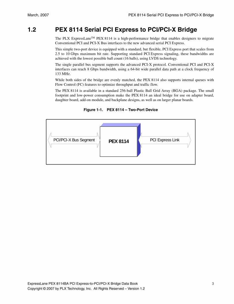
March, 2007 PEX 8114 Serial PCI Express to PCI/PCI-X Bridge
ExpressLane PEX 8114BA PCI Express-to-PCI/PCI-X Bridge Data Book 3
Copyright © 2007 by PLX Technology, Inc. All Rights Reserved – Version 1.2
1.2 PEX 8114 Serial PCI Express to PCI/PCI-X BridgeThe PLX ExpressLaneTM PEX 8114 is a high-performance bridge that enables designers to migrateConventional PCI and PCI-X Bus interfaces to the new advanced serial PCI Express.
This simple two-port device is equipped with a standard, but flexible, PCI Express port that scales from2.5 to 10 Gbps maximum bit rate. Supporting standard PCI Express signaling, these bandwidths areachieved with the lowest possible ball count (16 balls), using LVDS technology.
The single parallel bus segment supports the advanced PCI-X protocol. Conventional PCI and PCI-Xinterfaces can reach 8 Gbps bandwidth, using a 64-bit wide parallel data path at a clock frequency of133 MHz.
While both sides of the bridge are evenly matched, the PEX 8114 also supports internal queues withFlow Control (FC) features to optimize throughput and traffic flow.
The PEX 8114 is available in a standard 256-ball Plastic Ball Grid Array (BGA) package. The smallfootprint and low-power consumption make the PEX 8114 an ideal bridge for use on adapter board,daughter board, add-on module, and backplane designs, as well as on larger planar boards.
Figure 1-1. PEX 8114 – Two-Port Device
PEX 8104PEX 8114 PCI Express LinkPCI/PCI-X Bus Segment
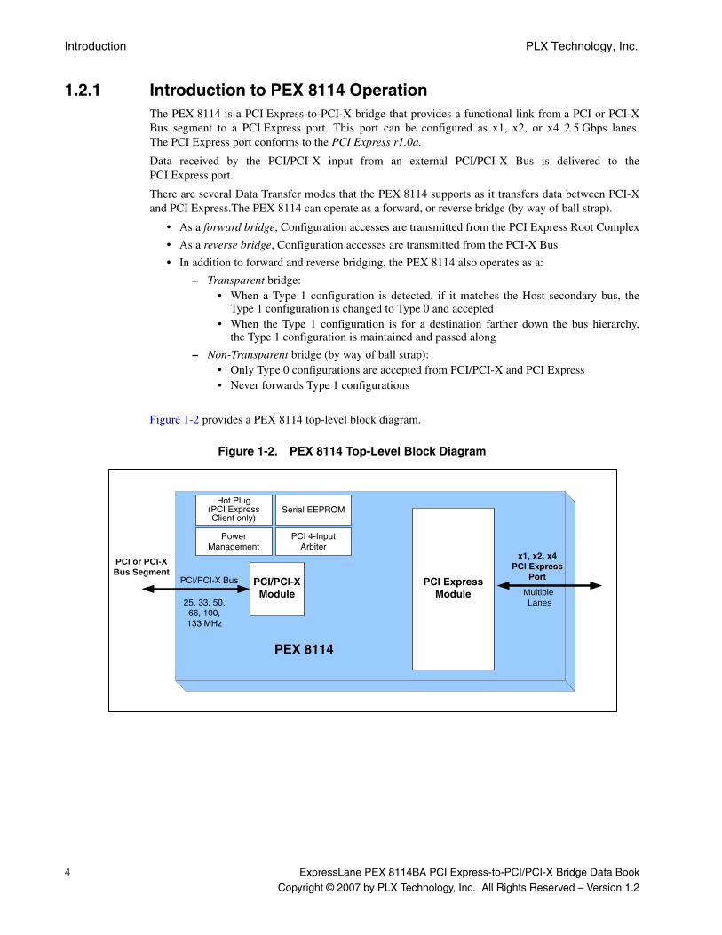
Introduction PLX Technology, Inc.
4 ExpressLane PEX 8114BA PCI Express-to-PCI/PCI-X Bridge Data Book
Copyright © 2007 by PLX Technology, Inc. All Rights Reserved – Version 1.2
1.2.1 Introduction to PEX 8114 OperationThe PEX 8114 is a PCI Express-to-PCI-X bridge that provides a functional link from a PCI or PCI-XBus segment to a PCI Express port. This port can be configured as x1, x2, or x4 2.5 Gbps lanes.The PCI Express port conforms to the PCI Express r1.0a.
Data received by the PCI/PCI-X input from an external PCI/PCI-X Bus is delivered to thePCI Express port.
There are several Data Transfer modes that the PEX 8114 supports as it transfers data between PCI-Xand PCI Express.The PEX 8114 can operate as a forward, or reverse bridge (by way of ball strap).
• As a forward bridge, Configuration accesses are transmitted from the PCI Express Root Complex
• As a reverse bridge, Configuration accesses are transmitted from the PCI-X Bus
• In addition to forward and reverse bridging, the PEX 8114 also operates as a:
– Transparent bridge:• When a Type 1 configuration is detected, if it matches the Host secondary bus, the
Type 1 configuration is changed to Type 0 and accepted • When the Type 1 configuration is for a destination farther down the bus hierarchy,
the Type 1 configuration is maintained and passed along
– Non-Transparent bridge (by way of ball strap):• Only Type 0 configurations are accepted from PCI/PCI-X and PCI Express• Never forwards Type 1 configurations
Figure 1-2 provides a PEX 8114 top-level block diagram.
Figure 1-2. PEX 8114 Top-Level Block Diagram
PCI or PCI-XBus Segment
PCI/PCI-XModule
PCI ExpressModule
PCI/PCI-X Bus
x1, x2, x4PCI Express
Port
PEX 8114
25, 33, 50, 66, 100, 133 MHz
Hot Plug(PCI Express Client only)
Power Management
Serial EEPROM
PCI 4-Input Arbiter
Multiple Lanes

March, 2007 Detailed Block Diagram
ExpressLane PEX 8114BA PCI Express-to-PCI/PCI-X Bridge Data Book 5
Copyright © 2007 by PLX Technology, Inc. All Rights Reserved – Version 1.2
1.3 Detailed Block DiagramFigure 1-3 illustrates PEX 8114 implementation, with the modules at the data transfer core. Othermodules, such as the PCI-X Arbiter and Power Management, are not included in Figure 1-3.
Figure 1-3. PEX 8114 Top-Level Detailed Block Diagram
PCI/P
CI-X
Bus
Seg
men
t
TLCeDE
CrossingDesti-nation
Source ISCrossingSource
DE Crossing
Desti-nation
TLCe
TLCi
DLL PHY
ISCrossing
Port
PCI/PCI-X PCI Express
CrossbarPCI/PCI-X
ModuleEither
Conventional PCI or a PCI-X Bus
Segment Interface Inte
rfac
e
Introduction PLX Technology, Inc.
6 ExpressLane PEX 8114BA PCI Express-to-PCI/PCI-X Bridge Data Book
Copyright © 2007 by PLX Technology, Inc. All Rights Reserved – Version 1.2
1.3.1 Physical Layer – Layer 1Layer 1 – Physical Layer (PHY) – defines the PCI Express electrical characteristics. The basictransmission unit consists of two pairs of wires, called a lane. Each pair is equipped with unidirectionaldata transmission at 2.5 Gbps, allowing the two wire pairs, when combined, to provide 2.5 Gbpsfull-duplex communication, without the risk of transmission collision.
1.3.2 Data Link Layer – Layer 2Layer 2 – Data Link Layer (DLL) – defines the PCI Express data control. The Data Link Layer provideslink management and data integrity, including error detection and correction. This layer calculates andappends a Cyclic Redundancy Check (CRC) and Sequence Number to the information transmitted from
the Data packet. The CRC verifies that data from link to link is correctly transmitted1. The SequenceNumber allows proper Data Packet ordering.
1.3.3 Transaction Layer – Layer 3Layer 3 – Transaction Layer (TL) – connects the lower protocols to the upper layers. This layer appearsto the upper layers as PCI.
The Transaction Layer packetizes and prepends a header to the Payload Data. Write and Readcommands, as well as prior sideband signals, such as Interrupts and Power Management requests, arealso included in this layer.
To achieve code compatibility with PCI, PCI Express does not modify the transaction layer. This issignificant because it allows vendors to leverage their existing PCI code to achieve not only a faster timeto market, using their proven design, it also provides a more stable and mature platform.
1. To ensure end-to-end data integrity, there is an optional feature in the PCI Express r1.0a. This feature is calledTLP Digest and is defined in Layer 3.
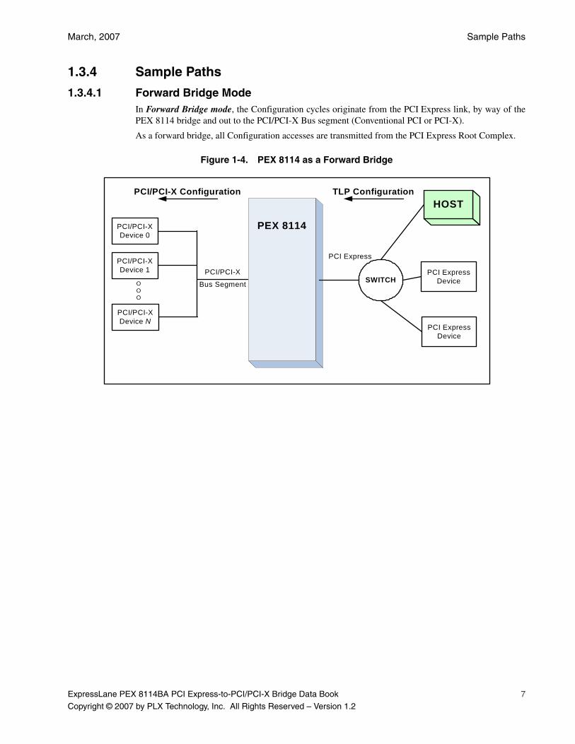
March, 2007 Sample Paths
ExpressLane PEX 8114BA PCI Express-to-PCI/PCI-X Bridge Data Book 7
Copyright © 2007 by PLX Technology, Inc. All Rights Reserved – Version 1.2
1.3.4 Sample Paths
1.3.4.1 Forward Bridge ModeIn Forward Bridge mode, the Configuration cycles originate from the PCI Express link, by way of thePEX 8114 bridge and out to the PCI/PCI-X Bus segment (Conventional PCI or PCI-X).
As a forward bridge, all Configuration accesses are transmitted from the PCI Express Root Complex.
Figure 1-4. PEX 8114 as a Forward Bridge
SWITCHPCI Express
Device
PCI ExpressDevice
PCI/PCI-XDevice 0
PCI/PCI-XDevice 1
PCI/PCI-XDevice N
PCI/PCI-X
PCI Express
Bus SegmentOOO
PEX 8114
HOSTTLP ConfigurationPCI/PCI-X Configuration
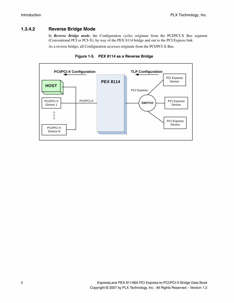
Introduction PLX Technology, Inc.
8 ExpressLane PEX 8114BA PCI Express-to-PCI/PCI-X Bridge Data Book
Copyright © 2007 by PLX Technology, Inc. All Rights Reserved – Version 1.2
1.3.4.2 Reverse Bridge ModeIn Reverse Bridge mode, the Configuration cycles originate from the PCI/PCI-X Bus segment(Conventional PCI or PCI-X), by way of the PEX 8114 bridge and out to the PCI Express link.
As a reverse bridge, all Configuration accesses originate from the PCI/PCI-X Bus.
Figure 1-5. PEX 8114 as a Reverse Bridge
PCI ExpressDevice
PCI ExpressDevice
PCI ExpressDevice
PCI/PCI-X
PCI Express
PCI/PCI-XDevice 1
PCI/PCI-XDevice N
PEX 8114HOST
TLP ConfigurationPCI/PCI-X Configuration
SWITCH
OOO
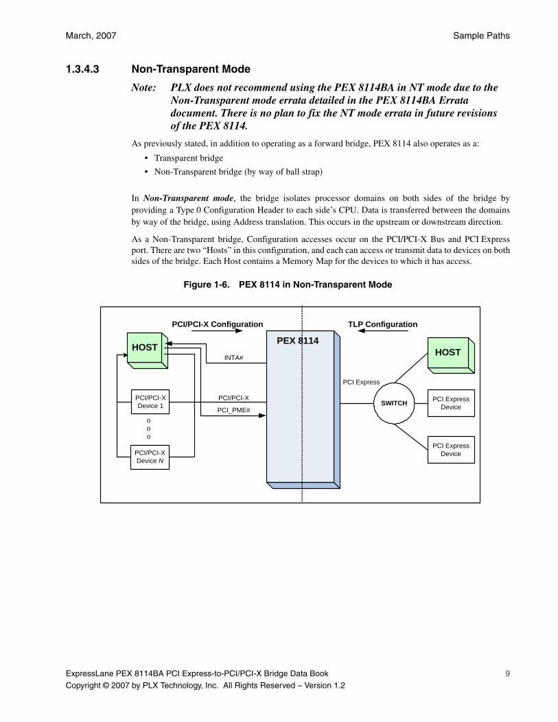
March, 2007 Sample Paths
ExpressLane PEX 8114BA PCI Express-to-PCI/PCI-X Bridge Data Book 9
Copyright © 2007 by PLX Technology, Inc. All Rights Reserved – Version 1.2
1.3.4.3 Non-Transparent Mode
Note: PLX does not recommend using the PEX 8114BA in NT mode due to the Non-Transparent mode errata detailed in the PEX 8114BA Errata document. There is no plan to fix the NT mode errata in future revisions of the PEX 8114.
As previously stated, in addition to operating as a forward bridge, PEX 8114 also operates as a:
• Transparent bridge
• Non-Transparent bridge (by way of ball strap)
In Non-Transparent mode, the bridge isolates processor domains on both sides of the bridge byproviding a Type 0 Configuration Header to each side’s CPU. Data is transferred between the domainsby way of the bridge, using Address translation. This occurs in the upstream or downstream direction.
As a Non-Transparent bridge, Configuration accesses occur on the PCI/PCI-X Bus and PCI Expressport. There are two “Hosts” in this configuration, and each can access or transmit data to devices on bothsides of the bridge. Each Host contains a Memory Map for the devices to which it has access.
Figure 1-6. PEX 8114 in Non-Transparent Mode
PCI ExpressDevice
HOST
SWITCH
PCI ExpressDevice
PCI/PCI-XDevice 1
PCI/PCI-X
PCI Express
INTA#
PCI_PME#ooo
PEX 8114HOST
PCI/PCI-XDevice N
TLP ConfigurationPCI/PCI-X Configuration

Introduction PLX Technology, Inc.
10 ExpressLane PEX 8114BA PCI Express-to-PCI/PCI-X Bridge Data Book
Copyright © 2007 by PLX Technology, Inc. All Rights Reserved – Version 1.2
1.4 PEX 8114 ApplicationsVarious PEX 8114 applications are as follows:
• PCI Express Adapter Board
• Intelligent PCI Express Adapter Board
• PCI Express Motherboard to PCI-X Expansion Slot
• PCI-X Host Supporting a PCI Express Expansion Slot
• PCI-X Add-In Board Created from PCI Express Native Silicon
• PCI-X Extender Board
1.4.1 PCI Express Adapter BoardIn a PCI Express Adapter Board application, the PEX 8114 is installed on a PCI Express adapter board,allowing a Conventional PCI or PCI-X device to create a PCI Express board. This configuration isillustrated in Figure 1-7, wherein the PEX 8114 is a Forward Transparent bridge.
Figure 1-7. PCI Express Board Created from PCI/PCI-X Native Silicon
PEX 8114 PCI or PCI-XNative Design
PCI-X BusPCI Express Port
Forward TransparentPCI Express Adapter Board
PCI Express Connector

March, 2007 Intelligent PCI Express Adapter Board
ExpressLane PEX 8114BA PCI Express-to-PCI/PCI-X Bridge Data Book 11
Copyright © 2007 by PLX Technology, Inc. All Rights Reserved – Version 1.2
1.4.2 Intelligent PCI Express Adapter BoardIn an Intelligent PCI Express Adapter Board application, the PEX 8114 is installed on a PCI Expressadapter board with a CPU and Memory subsystem, allowing an intelligent PCI or PCI-X subsystem tobe implemented on a PCI Express add-in board. This configuration is illustrated in Figure 1-8, whereinthe PEX 8114 is a Forward Non-Transparent bridge.
Figure 1-8. Intelligent PCI Express Board Created from PCI/PCI-X Native Silicon
PEX 8114PCI or PCI-XNative Design
PCI-X BusPCI Express Port
Forward Non-TransparentPCI Express Adapter Board
PCI Express Connector
CPU Memory
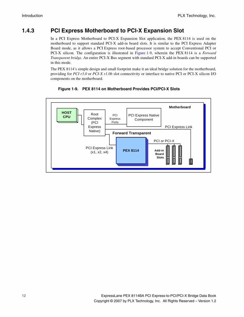
Introduction PLX Technology, Inc.
12 ExpressLane PEX 8114BA PCI Express-to-PCI/PCI-X Bridge Data Book
Copyright © 2007 by PLX Technology, Inc. All Rights Reserved – Version 1.2
1.4.3 PCI Express Motherboard to PCI-X Expansion SlotIn a PCI Express Motherboard to PCI-X Expansion Slot application, the PEX 8114 is used on themotherboard to support standard PCI-X add-in board slots. It is similar to the PCI Express AdapterBoard mode, as it allows a PCI Express root-based processor system to accept Conventional PCI orPCI-X silicon. The configuration is illustrated in Figure 1-9, wherein the PEX 8114 is a ForwardTransparent bridge. An entire PCI-X Bus segment with standard PCI-X add-in boards can be supportedin this mode.
The PEX 8114’s simple design and small footprint make it an ideal bridge solution for the motherboard,providing for PCI r3.0 or PCI-X r1.0b slot connectivity or interface to native PCI or PCI-X silicon I/Ocomponents on the motherboard.
Figure 1-9. PEX 8114 on Motherboard Provides PCI/PCI-X Slots
Root Complex
(PCI ExpressNative)
PCI Express
Ports
PCI Express Native Component
P-BridgePCI Express Link
(x1, x2, x4)
PCI or PCI-X
Add-in BoardSlots
Motherboard
PCI Express Link
P-BRIDGEPEX 8114
HOST CPU
Forward Transparent
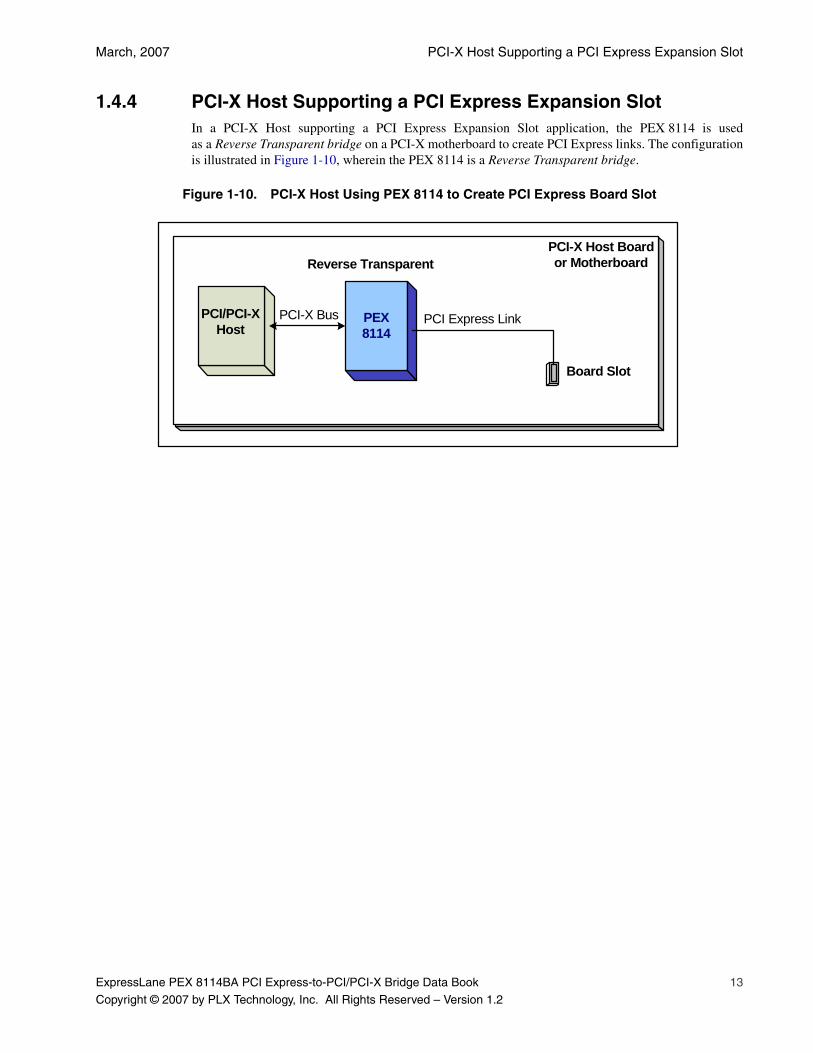
March, 2007 PCI-X Host Supporting a PCI Express Expansion Slot
ExpressLane PEX 8114BA PCI Express-to-PCI/PCI-X Bridge Data Book 13
Copyright © 2007 by PLX Technology, Inc. All Rights Reserved – Version 1.2
1.4.4 PCI-X Host Supporting a PCI Express Expansion SlotIn a PCI-X Host supporting a PCI Express Expansion Slot application, the PEX 8114 is usedas a Reverse Transparent bridge on a PCI-X motherboard to create PCI Express links. The configurationis illustrated in Figure 1-10, wherein the PEX 8114 is a Reverse Transparent bridge.
Figure 1-10. PCI-X Host Using PEX 8114 to Create PCI Express Board Slot
PCI Express LinkPCI-X Bus
Reverse Transparent PCI-X Host Boardor Motherboard
PEX8114
Board Slot
PCI/PCI-X Host

Introduction PLX Technology, Inc.
14 ExpressLane PEX 8114BA PCI Express-to-PCI/PCI-X Bridge Data Book
Copyright © 2007 by PLX Technology, Inc. All Rights Reserved – Version 1.2
1.4.5 PCI-X Add-In Board Created from PCI Express Native SiliconA PCI-X add-in board created from PCI Express native silicon application enables adapter boards basedon state-of-the-art PCI Express silicon to plug into PCI/PCI-X motherboard expansion slots.The configuration is illustrated in Figure 1-11, wherein the PEX 8114 is a Reverse Transparent bridge.
Figure 1-11. PCI-X Adapter Board Created Using PEX 8114 and PCI Express Native Silicon
PEX 8114
PCI Express
LinkPCI
ExpressNative Silicon
PCI-X Bus
Reverse Transparent

March, 2007 PCI-X Extender Board
ExpressLane PEX 8114BA PCI Express-to-PCI/PCI-X Bridge Data Book 15
Copyright © 2007 by PLX Technology, Inc. All Rights Reserved – Version 1.2
1.4.6 PCI-X Extender BoardA PCI-X Extender Board application uses the PEX 8114 to create a bridge board, enabling PCIor PCI-X Bus expansion over standardized PCI Express cabling. The configuration is illustratedin Figure 1-12, wherein the PEX 8114 is a Reverse Transparent bridge.
Figure 1-12. PCI-X Adapter Board Acting as Bridge Board for Bus Expansion
PEX 8114 PCI
Express Link
PCI-X Bus
Reverse Transparent
PCI Express Cable Connector

Introduction PLX Technology, Inc.
16 ExpressLane PEX 8114BA PCI Express-to-PCI/PCI-X Bridge Data Book
Copyright © 2007 by PLX Technology, Inc. All Rights Reserved – Version 1.2
THIS PAGE INTENTIONALLY LEFT BLANK.

ExpressLane PEX 8114BA PCI Express-to-PCI/PCI-X Bridge Data Book 17
Copyright © 2007 by PLX Technology, Inc. All Rights Reserved – Version 1.2
Chapter 2 Signal Ball Description
2.1 IntroductionThis chapter describes the PEX 8114 balls, grouped according to their operations, including signalname, type, location, and a brief description. Refer to Section 2.10 and Section 2.11 for further detailsregarding ball operation.
The following sections describe each PEX 8114 ball common to all operation modes:
• PCI/PCI-X Bus Interface Signals
• PCI Express Interface Signals
• Hot Plug Signals
• Strapping Signals
• JTAG Interface Signals
• Serial EEPROM Interface Signals
• Power and Ground Signals
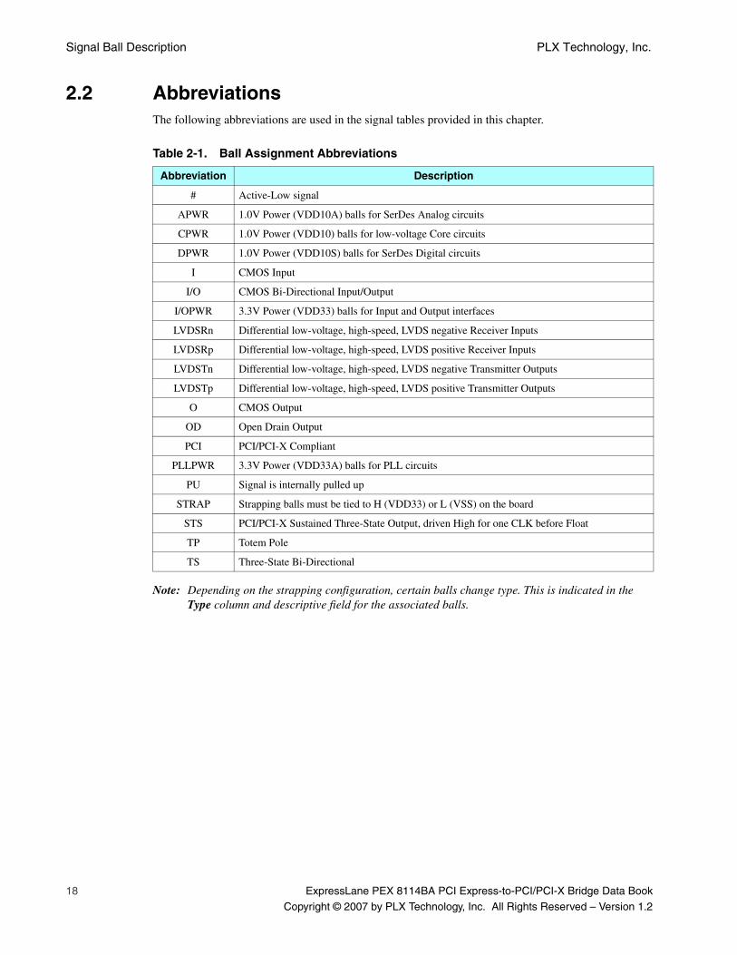
Signal Ball Description PLX Technology, Inc.
18 ExpressLane PEX 8114BA PCI Express-to-PCI/PCI-X Bridge Data Book
Copyright © 2007 by PLX Technology, Inc. All Rights Reserved – Version 1.2
2.2 AbbreviationsThe following abbreviations are used in the signal tables provided in this chapter.
Note: Depending on the strapping configuration, certain balls change type. This is indicated in the Type column and descriptive field for the associated balls.
Table 2-1. Ball Assignment Abbreviations
Abbreviation Description
# Active-Low signal
APWR 1.0V Power (VDD10A) balls for SerDes Analog circuits
CPWR 1.0V Power (VDD10) balls for low-voltage Core circuits
DPWR 1.0V Power (VDD10S) balls for SerDes Digital circuits
I CMOS Input
I/O CMOS Bi-Directional Input/Output
I/OPWR 3.3V Power (VDD33) balls for Input and Output interfaces
LVDSRn Differential low-voltage, high-speed, LVDS negative Receiver Inputs
LVDSRp Differential low-voltage, high-speed, LVDS positive Receiver Inputs
LVDSTn Differential low-voltage, high-speed, LVDS negative Transmitter Outputs
LVDSTp Differential low-voltage, high-speed, LVDS positive Transmitter Outputs
O CMOS Output
OD Open Drain Output
PCI PCI/PCI-X Compliant
PLLPWR 3.3V Power (VDD33A) balls for PLL circuits
PU Signal is internally pulled up
STRAP Strapping balls must be tied to H (VDD33) or L (VSS) on the board
STS PCI/PCI-X Sustained Three-State Output, driven High for one CLK before Float
TP Totem Pole
TS Three-State Bi-Directional
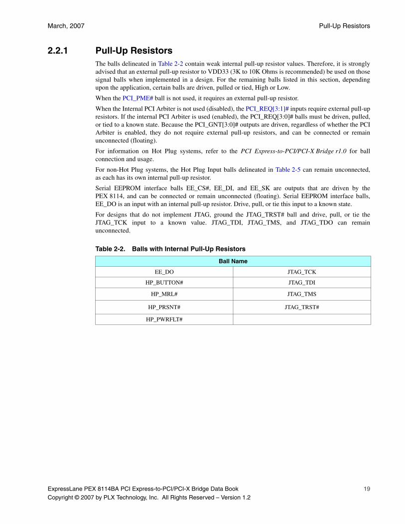
March, 2007 Pull-Up Resistors
ExpressLane PEX 8114BA PCI Express-to-PCI/PCI-X Bridge Data Book 19
Copyright © 2007 by PLX Technology, Inc. All Rights Reserved – Version 1.2
2.2.1 Pull-Up ResistorsThe balls delineated in Table 2-2 contain weak internal pull-up resistor values. Therefore, it is stronglyadvised that an external pull-up resistor to VDD33 (3K to 10K Ohms is recommended) be used on thosesignal balls when implemented in a design. For the remaining balls listed in this section, dependingupon the application, certain balls are driven, pulled or tied, High or Low.
When the PCI_PME# ball is not used, it requires an external pull-up resistor.
When the Internal PCI Arbiter is not used (disabled), the PCI_REQ[3:1]# inputs require external pull-upresistors. If the internal PCI Arbiter is used (enabled), the PCI_REQ[3:0]# balls must be driven, pulled,or tied to a known state. Because the PCI_GNT[3:0]# outputs are driven, regardless of whether the PCIArbiter is enabled, they do not require external pull-up resistors, and can be connected or remainunconnected (floating).
For information on Hot Plug systems, refer to the PCI Express-to-PCI/PCI-X Bridge r1.0 for ballconnection and usage.
For non-Hot Plug systems, the Hot Plug Input balls delineated in Table 2-5 can remain unconnected,as each has its own internal pull-up resistor.
Serial EEPROM interface balls EE_CS#, EE_DI, and EE_SK are outputs that are driven by thePEX 8114, and can be connected or remain unconnected (floating). Serial EEPROM interface balls,EE_DO is an input with an internal pull-up resistor. Drive, pull, or tie this input to a known state.
For designs that do not implement JTAG, ground the JTAG_TRST# ball and drive, pull, or tie theJTAG_TCK input to a known value. JTAG_TDI, JTAG_TMS, and JTAG_TDO can remainunconnected.
Table 2-2. Balls with Internal Pull-Up Resistors
Ball Name
EE_DO JTAG_TCK
HP_BUTTON# JTAG_TDI
HP_MRL# JTAG_TMS
HP_PRSNT# JTAG_TRST#
HP_PWRFLT#
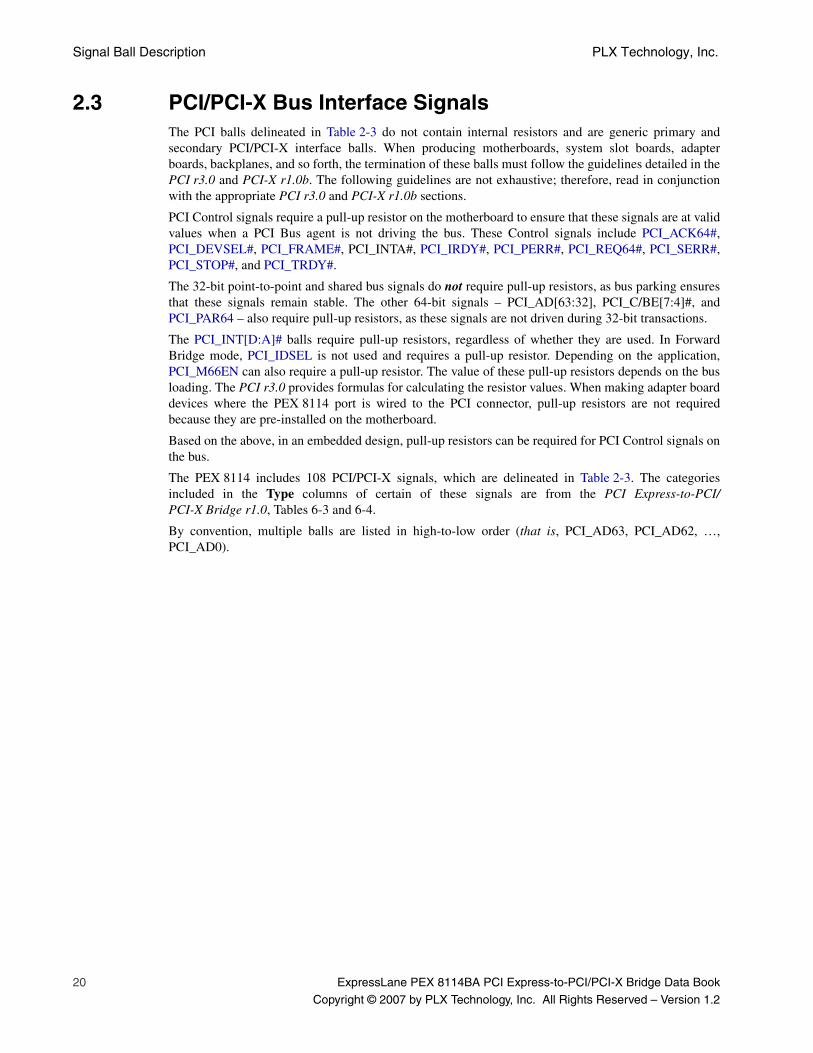
Signal Ball Description PLX Technology, Inc.
20 ExpressLane PEX 8114BA PCI Express-to-PCI/PCI-X Bridge Data Book
Copyright © 2007 by PLX Technology, Inc. All Rights Reserved – Version 1.2
2.3 PCI/PCI-X Bus Interface SignalsThe PCI balls delineated in Table 2-3 do not contain internal resistors and are generic primary andsecondary PCI/PCI-X interface balls. When producing motherboards, system slot boards, adapterboards, backplanes, and so forth, the termination of these balls must follow the guidelines detailed in thePCI r3.0 and PCI-X r1.0b. The following guidelines are not exhaustive; therefore, read in conjunctionwith the appropriate PCI r3.0 and PCI-X r1.0b sections.
PCI Control signals require a pull-up resistor on the motherboard to ensure that these signals are at validvalues when a PCI Bus agent is not driving the bus. These Control signals include PCI_ACK64#,PCI_DEVSEL#, PCI_FRAME#, PCI_INTA#, PCI_IRDY#, PCI_PERR#, PCI_REQ64#, PCI_SERR#,PCI_STOP#, and PCI_TRDY#.
The 32-bit point-to-point and shared bus signals do not require pull-up resistors, as bus parking ensuresthat these signals remain stable. The other 64-bit signals – PCI_AD[63:32], PCI_C/BE[7:4]#, andPCI_PAR64 – also require pull-up resistors, as these signals are not driven during 32-bit transactions.
The PCI_INT[D:A]# balls require pull-up resistors, regardless of whether they are used. In ForwardBridge mode, PCI_IDSEL is not used and requires a pull-up resistor. Depending on the application,PCI_M66EN can also require a pull-up resistor. The value of these pull-up resistors depends on the busloading. The PCI r3.0 provides formulas for calculating the resistor values. When making adapter boarddevices where the PEX 8114 port is wired to the PCI connector, pull-up resistors are not requiredbecause they are pre-installed on the motherboard.
Based on the above, in an embedded design, pull-up resistors can be required for PCI Control signals onthe bus.
The PEX 8114 includes 108 PCI/PCI-X signals, which are delineated in Table 2-3. The categoriesincluded in the Type columns of certain of these signals are from the PCI Express-to-PCI/PCI-X Bridge r1.0, Tables 6-3 and 6-4.
By convention, multiple balls are listed in high-to-low order (that is, PCI_AD63, PCI_AD62, …,PCI_AD0).

March, 2007 PCI/PCI-X Bus Interface Signals
ExpressLane PEX 8114BA PCI Express-to-PCI/PCI-X Bridge Data Book 21
Copyright © 2007 by PLX Technology, Inc. All Rights Reserved – Version 1.2
Table 2-3. PCI/PCI-X Bus Interface Signals (108 Balls)
Symbol Type Location Description
PCI_ACK64#I/OSTSPCI
A13
64-Bit Transfer AcknowledgeAsserted by the PCI Slave in response to PCI_REQ64#, to acknowledge a 64-bit Data transfer.0 = Acknowledges a 64-bit transfer1 = No acknowledge
PCI_AD[63:0]I/OTSPCI
A15, C15, A16, D14, B16, D15, C16, E13, D16, E14, E15, F13, E16, F14, F16, G13, G16, G14, H15, H13, H16, H14, J15, J13, J16, J14, K15, K13, K16, K14, L16, L14,
F1, F3, E1, F4, D1, E3, D2, D3, B1, C2, A1, C3, A2, D4, B3, C4, C7, A7, D8, A8, C8, A9, D9, B10, A10,
C10, B11, D11, A11, C11, A12, C12
Address and Data (64 Balls)PCI Multiplexed Address/Data Bus.
PCI_C/BE[7:0]#I/OTSPCI
C13, A14, D13, B14, C1, A3, B7, D10
Bus Command and Byte Enables (8 Balls)During the PCI and/or PCI-X Address phase, PCI_C/BE[7:0]# provide the transaction type.During the Data phase of PCI and/or PCI-X Memory Write transactions, PCI_C/BE[7:0]# provide Byte Enables.During the PCI-X Attribute phase, PCI_C/BE[7:0]# provide a portion of the attribute information.
PCI_CLKI
PCIJ1
PCI/PCI-X Bus Clock InputClock reference when STRAP_CLK_MST=0.Not the clock reference when STRAP_CLK_MST=1.(Refer to Chapter 3, “Clock and Reset,” for further details.)
PCI_CLKO[3:0]O
PCIL1, L2, K1, K3
Clock Outputs (4 Balls)PCI/PCI-X Bus clocks for up to four devices.Derived from PEX_REFCLKn/p.(Refer to Chapter 3, “Clock and Reset,” for further details.)
PCI_CLKO_DLY_FBKO
PCIN3
PCI Clock Delayed FeedbackPCI/PCI-X clock intended to be fed back to the PEX 8114 PCI_CLK input ball when STRAP_CLK_MST and STRAP_EXT_CLK_SEL are High. The trace length provides a time phase delay on the PCI clock that drives the internal PCI circuitry, thereby aligning the internal PCI_CLK rising edge with the clock edges of other PCI devices on the PCI Bus that can be sufficiently separated physically, such that Clock-phase alignment becomes necessary.
PCI_DEVSEL#I/OSTSPCI
A4Device SelectWhen actively driven, indicates the driving device decoded its address as the Target of the current access.
PCI_FRAME#I/OSTSPCI
D5
FrameDriven by the transaction Initiator to indicate an access start and duration.While PCI_FRAME# is asserted, Data transfers continue.
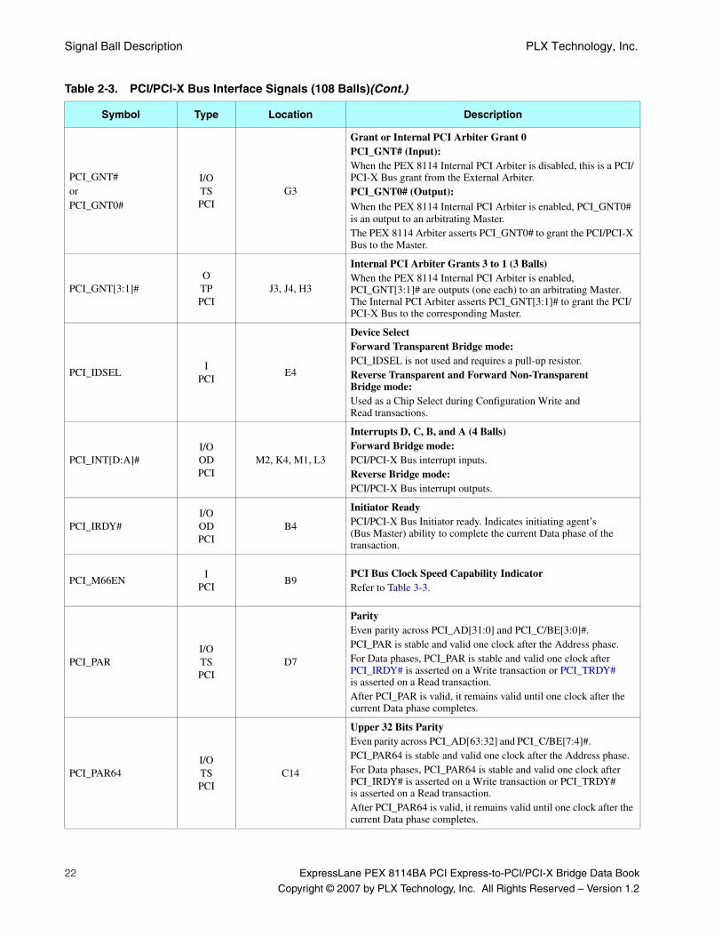
Signal Ball Description PLX Technology, Inc.
22 ExpressLane PEX 8114BA PCI Express-to-PCI/PCI-X Bridge Data Book
Copyright © 2007 by PLX Technology, Inc. All Rights Reserved – Version 1.2
PCI_GNT#orPCI_GNT0#
I/OTSPCI
G3
Grant or Internal PCI Arbiter Grant 0PCI_GNT# (Input):When the PEX 8114 Internal PCI Arbiter is disabled, this is a PCI/PCI-X Bus grant from the External Arbiter.PCI_GNT0# (Output):When the PEX 8114 Internal PCI Arbiter is enabled, PCI_GNT0# is an output to an arbitrating Master.The PEX 8114 Arbiter asserts PCI_GNT0# to grant the PCI/PCI-X Bus to the Master.
PCI_GNT[3:1]#OTPPCI
J3, J4, H3
Internal PCI Arbiter Grants 3 to 1 (3 Balls)When the PEX 8114 Internal PCI Arbiter is enabled, PCI_GNT[3:1]# are outputs (one each) to an arbitrating Master. The Internal PCI Arbiter asserts PCI_GNT[3:1]# to grant the PCI/PCI-X Bus to the corresponding Master.
PCI_IDSELI
PCIE4
Device SelectForward Transparent Bridge mode:PCI_IDSEL is not used and requires a pull-up resistor.Reverse Transparent and Forward Non-Transparent Bridge mode:Used as a Chip Select during Configuration Write and Read transactions.
PCI_INT[D:A]#I/OODPCI
M2, K4, M1, L3
Interrupts D, C, B, and A (4 Balls)Forward Bridge mode:PCI/PCI-X Bus interrupt inputs.Reverse Bridge mode:PCI/PCI-X Bus interrupt outputs.
PCI_IRDY#I/OODPCI
B4
Initiator ReadyPCI/PCI-X Bus Initiator ready. Indicates initiating agent’s (Bus Master) ability to complete the current Data phase of the transaction.
PCI_M66ENI
PCIB9
PCI Bus Clock Speed Capability IndicatorRefer to Table 3-3.
PCI_PARI/OTSPCI
D7
ParityEven parity across PCI_AD[31:0] and PCI_C/BE[3:0]#.PCI_PAR is stable and valid one clock after the Address phase.For Data phases, PCI_PAR is stable and valid one clock after PCI_IRDY# is asserted on a Write transaction or PCI_TRDY# is asserted on a Read transaction.After PCI_PAR is valid, it remains valid until one clock after the current Data phase completes.
PCI_PAR64I/OTSPCI
C14
Upper 32 Bits ParityEven parity across PCI_AD[63:32] and PCI_C/BE[7:4]#. PCI_PAR64 is stable and valid one clock after the Address phase.For Data phases, PCI_PAR64 is stable and valid one clock after PCI_IRDY# is asserted on a Write transaction or PCI_TRDY# is asserted on a Read transaction.After PCI_PAR64 is valid, it remains valid until one clock after the current Data phase completes.
Table 2-3. PCI/PCI-X Bus Interface Signals (108 Balls)(Cont.)
Symbol Type Location Description
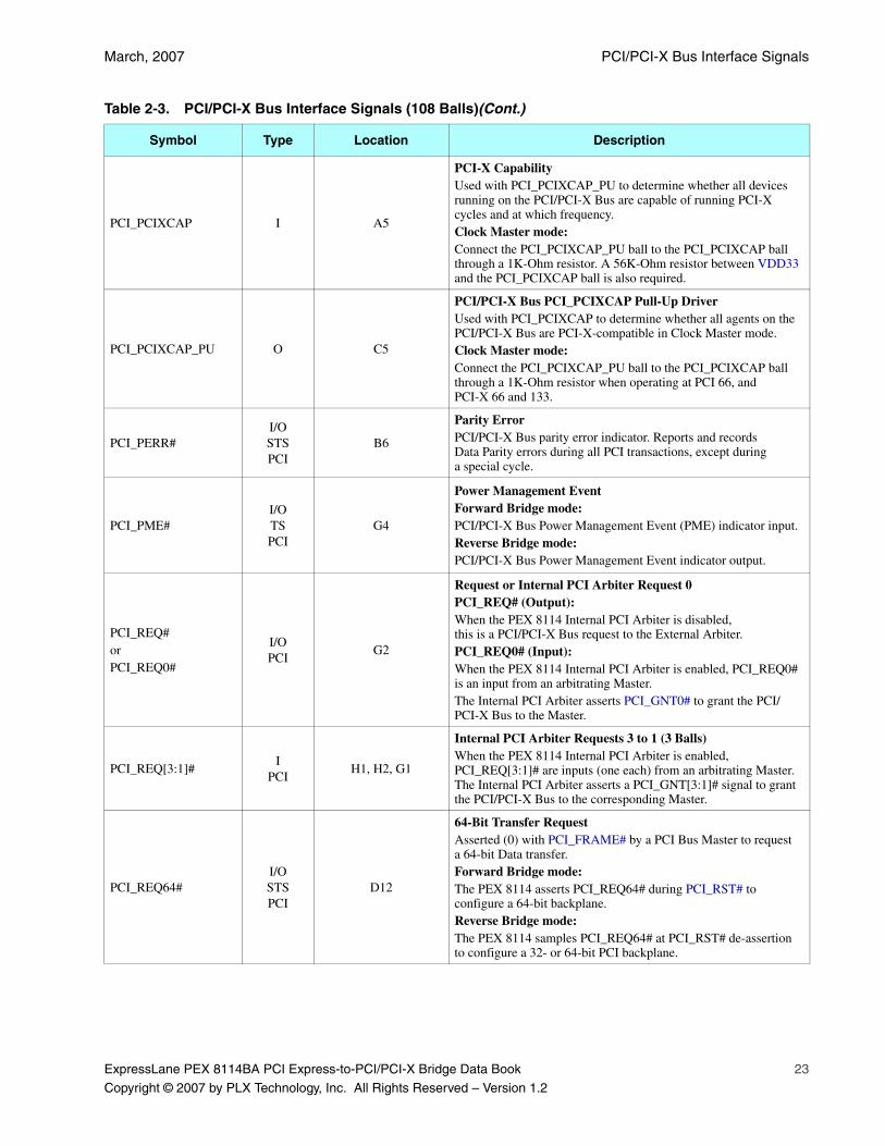
March, 2007 PCI/PCI-X Bus Interface Signals
ExpressLane PEX 8114BA PCI Express-to-PCI/PCI-X Bridge Data Book 23
Copyright © 2007 by PLX Technology, Inc. All Rights Reserved – Version 1.2
PCI_PCIXCAP I A5
PCI-X CapabilityUsed with PCI_PCIXCAP_PU to determine whether all devices running on the PCI/PCI-X Bus are capable of running PCI-X cycles and at which frequency.Clock Master mode:Connect the PCI_PCIXCAP_PU ball to the PCI_PCIXCAP ball through a 1K-Ohm resistor. A 56K-Ohm resistor between VDD33 and the PCI_PCIXCAP ball is also required.
PCI_PCIXCAP_PU O C5
PCI/PCI-X Bus PCI_PCIXCAP Pull-Up DriverUsed with PCI_PCIXCAP to determine whether all agents on the PCI/PCI-X Bus are PCI-X-compatible in Clock Master mode.Clock Master mode:Connect the PCI_PCIXCAP_PU ball to the PCI_PCIXCAP ball through a 1K-Ohm resistor when operating at PCI 66, and PCI-X 66 and 133.
PCI_PERR#I/OSTSPCI
B6
Parity ErrorPCI/PCI-X Bus parity error indicator. Reports and records Data Parity errors during all PCI transactions, except during a special cycle.
PCI_PME#I/OTSPCI
G4
Power Management EventForward Bridge mode:PCI/PCI-X Bus Power Management Event (PME) indicator input.Reverse Bridge mode:PCI/PCI-X Bus Power Management Event indicator output.
PCI_REQ#orPCI_REQ0#
I/OPCI
G2
Request or Internal PCI Arbiter Request 0PCI_REQ# (Output):When the PEX 8114 Internal PCI Arbiter is disabled, this is a PCI/PCI-X Bus request to the External Arbiter.PCI_REQ0# (Input):When the PEX 8114 Internal PCI Arbiter is enabled, PCI_REQ0# is an input from an arbitrating Master. The Internal PCI Arbiter asserts PCI_GNT0# to grant the PCI/PCI-X Bus to the Master.
PCI_REQ[3:1]#I
PCIH1, H2, G1
Internal PCI Arbiter Requests 3 to 1 (3 Balls)When the PEX 8114 Internal PCI Arbiter is enabled, PCI_REQ[3:1]# are inputs (one each) from an arbitrating Master. The Internal PCI Arbiter asserts a PCI_GNT[3:1]# signal to grant the PCI/PCI-X Bus to the corresponding Master.
PCI_REQ64#I/OSTSPCI
D12
64-Bit Transfer RequestAsserted (0) with PCI_FRAME# by a PCI Bus Master to request a 64-bit Data transfer. Forward Bridge mode:The PEX 8114 asserts PCI_REQ64# during PCI_RST# to configure a 64-bit backplane.Reverse Bridge mode:The PEX 8114 samples PCI_REQ64# at PCI_RST# de-assertion to configure a 32- or 64-bit PCI backplane.
Table 2-3. PCI/PCI-X Bus Interface Signals (108 Balls)(Cont.)
Symbol Type Location Description
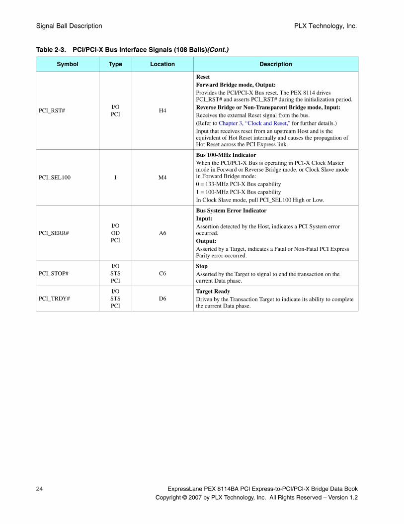
Signal Ball Description PLX Technology, Inc.
24 ExpressLane PEX 8114BA PCI Express-to-PCI/PCI-X Bridge Data Book
Copyright © 2007 by PLX Technology, Inc. All Rights Reserved – Version 1.2
PCI_RST#I/OPCI
H4
ResetForward Bridge mode, Output:Provides the PCI/PCI-X Bus reset. The PEX 8114 drives PCI_RST# and asserts PCI_RST# during the initialization period.Reverse Bridge or Non-Transparent Bridge mode, Input:Receives the external Reset signal from the bus.(Refer to Chapter 3, “Clock and Reset,” for further details.)Input that receives reset from an upstream Host and is the equivalent of Hot Reset internally and causes the propagation of Hot Reset across the PCI Express link.
PCI_SEL100 I M4
Bus 100-MHz IndicatorWhen the PCI/PCI-X Bus is operating in PCI-X Clock Master mode in Forward or Reverse Bridge mode, or Clock Slave mode in Forward Bridge mode:0 = 133-MHz PCI-X Bus capability1 = 100-MHz PCI-X Bus capabilityIn Clock Slave mode, pull PCI_SEL100 High or Low.
PCI_SERR#I/OODPCI
A6
Bus System Error IndicatorInput:Assertion detected by the Host, indicates a PCI System error occurred. Output:Asserted by a Target, indicates a Fatal or Non-Fatal PCI Express Parity error occurred.
PCI_STOP#I/OSTSPCI
C6StopAsserted by the Target to signal to end the transaction on the current Data phase.
PCI_TRDY#I/OSTSPCI
D6Target ReadyDriven by the Transaction Target to indicate its ability to complete the current Data phase.
Table 2-3. PCI/PCI-X Bus Interface Signals (108 Balls)(Cont.)
Symbol Type Location Description

March, 2007 PCI Express Interface Signals
ExpressLane PEX 8114BA PCI Express-to-PCI/PCI-X Bridge Data Book 25
Copyright © 2007 by PLX Technology, Inc. All Rights Reserved – Version 1.2
2.4 PCI Express Interface SignalsThe PEX 8114 includes 23 PCI Express port interface signals, which are delineated in Table 2-4.The port signals are Low-Voltage Differential Signal format that requires two balls for each lane, in eachdirection. The four PEX_LANE_GOODx# signals are used to drive LEDs to indicate the status ofeach lane.
Table 2-4. PCI Express Interface Signals (23 Balls)
Symbol Type Location Description
PEX_LANE_ GOOD[3:0]# O R16, T16, R15, T15PCI Express Lane Status Indicators (4 Balls)0 = Lane active (LED is On)1 = Lane inactive (LED is Off)
PEX_PERn[3:0]I(-)
LVDSRnM11, M9, M7, M5 Negative Half of PCI Express Receiver Differential
Signal Pairs (4 Balls)
PEX_PERp[3:0]I(+)
LVDSRpN11, N9, N7, N5 Positive Half of PCI Express Receiver Differential
Signal Pairs (4 Balls)
PEX_PETn[3:0]O(-)
LVDSTnT11, T9, T7, T5 Negative Half of PCI Express Transmitter Differential
Signal Pairs (4 Balls)
PEX_PETp[3:0]O(+)
LVDSTpR11, R9, R7, R5 Positive Half of PCI Express Transmitter Differential
Signal Pairs (4 Balls)
PEX_PERST# I T1PCI Express ResetUsed to cause a Fundamental Reset.(Refer to Chapter 3, “Clock and Reset,” for further details.)
PEX_REFCLKnI(-)
LVDSnR3
Negative Half of 100-MHz PCI Express Reference Clock Signal Pair(Refer to Chapter 3, “Clock and Reset,” for details.)
PEX_REFCLKpI(+)
LVDSpT3
Positive Half of 100-MHz PCI Express Reference Clock Signal Pair(Refer to Chapter 3, “Clock and Reset,” for details.)
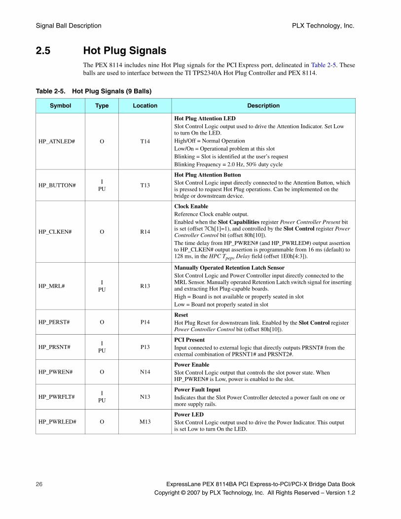
Signal Ball Description PLX Technology, Inc.
26 ExpressLane PEX 8114BA PCI Express-to-PCI/PCI-X Bridge Data Book
Copyright © 2007 by PLX Technology, Inc. All Rights Reserved – Version 1.2
2.5 Hot Plug SignalsThe PEX 8114 includes nine Hot Plug signals for the PCI Express port, delineated in Table 2-5. Theseballs are used to interface between the TI TPS2340A Hot Plug Controller and PEX 8114.
Table 2-5. Hot Plug Signals (9 Balls)
Symbol Type Location Description
HP_ATNLED# O T14
Hot Plug Attention LEDSlot Control Logic output used to drive the Attention Indicator. Set Low to turn On the LED.High/Off = Normal OperationLow/On = Operational problem at this slotBlinking = Slot is identified at the user’s requestBlinking Frequency = 2.0 Hz, 50% duty cycle
HP_BUTTON#I
PUT13
Hot Plug Attention ButtonSlot Control Logic input directly connected to the Attention Button, which is pressed to request Hot Plug operations. Can be implemented on the bridge or downstream device.
HP_CLKEN# O R14
Clock EnableReference Clock enable output.Enabled when the Slot Capabilities register Power Controller Present bit is set (offset 7Ch[1]=1), and controlled by the Slot Control register Power Controller Control bit (offset 80h[10]).The time delay from HP_PWREN# (and HP_PWRLED#) output assertion to HP_CLKEN# output assertion is programmable from 16 ms (default) to 128 ms, in the HPC Tpepv Delay field (offset 1E0h[4:3]).
HP_MRL#I
PUR13
Manually Operated Retention Latch SensorSlot Control Logic and Power Controller input directly connected to the MRL Sensor. Manually operated Retention Latch switch signal for inserting and extracting Hot Plug-capable boards.High = Board is not available or properly seated in slotLow = Board not properly seated in slot
HP_PERST# O P14ResetHot Plug Reset for downstream link. Enabled by the Slot Control register Power Controller Control bit (offset 80h[10]).
HP_PRSNT#I
PUP13
PCI PresentInput connected to external logic that directly outputs PRSNT# from the external combination of PRSNT1# and PRSNT2#.
HP_PWREN# O N14Power EnableSlot Control Logic output that controls the slot power state. When HP_PWREN# is Low, power is enabled to the slot.
HP_PWRFLT#I
PUN13
Power Fault InputIndicates that the Slot Power Controller detected a power fault on one or more supply rails.
HP_PWRLED# O M13Power LEDSlot Control Logic output used to drive the Power Indicator. This output is set Low to turn On the LED.
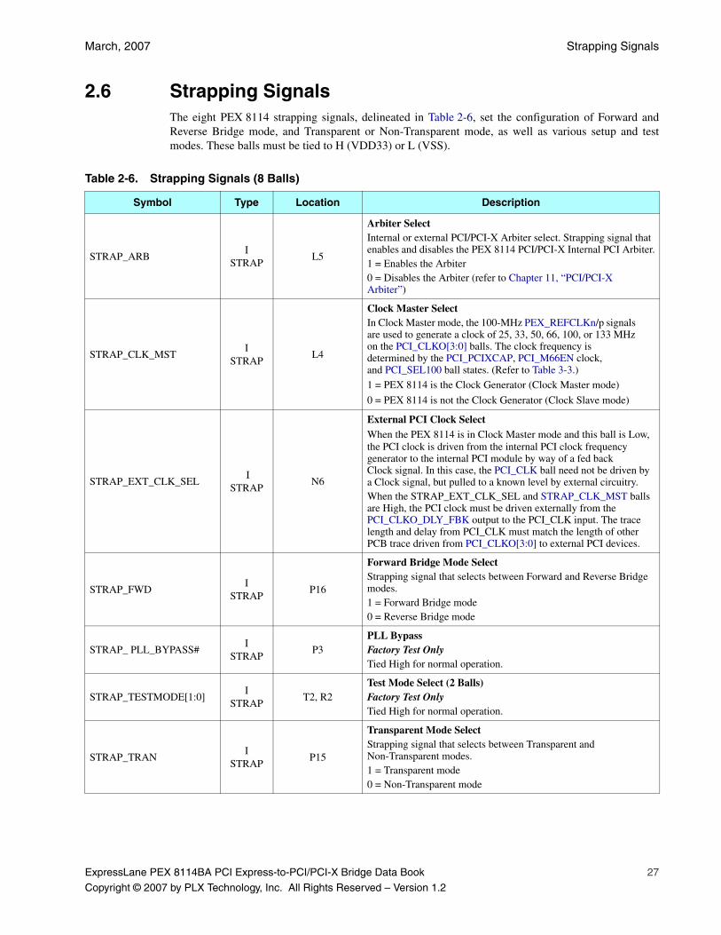
March, 2007 Strapping Signals
ExpressLane PEX 8114BA PCI Express-to-PCI/PCI-X Bridge Data Book 27
Copyright © 2007 by PLX Technology, Inc. All Rights Reserved – Version 1.2
2.6 Strapping SignalsThe eight PEX 8114 strapping signals, delineated in Table 2-6, set the configuration of Forward andReverse Bridge mode, and Transparent or Non-Transparent mode, as well as various setup and testmodes. These balls must be tied to H (VDD33) or L (VSS).
Table 2-6. Strapping Signals (8 Balls)
Symbol Type Location Description
STRAP_ARBI
STRAPL5
Arbiter SelectInternal or external PCI/PCI-X Arbiter select. Strapping signal that enables and disables the PEX 8114 PCI/PCI-X Internal PCI Arbiter.1 = Enables the Arbiter0 = Disables the Arbiter (refer to Chapter 11, “PCI/PCI-X Arbiter”)
STRAP_CLK_MSTI
STRAPL4
Clock Master SelectIn Clock Master mode, the 100-MHz PEX_REFCLKn/p signals are used to generate a clock of 25, 33, 50, 66, 100, or 133 MHz on the PCI_CLKO[3:0] balls. The clock frequency is determined by the PCI_PCIXCAP, PCI_M66EN clock, and PCI_SEL100 ball states. (Refer to Table 3-3.)
1 = PEX 8114 is the Clock Generator (Clock Master mode)
0 = PEX 8114 is not the Clock Generator (Clock Slave mode)
STRAP_EXT_CLK_SEL I
STRAPN6
External PCI Clock SelectWhen the PEX 8114 is in Clock Master mode and this ball is Low, the PCI clock is driven from the internal PCI clock frequency generator to the internal PCI module by way of a fed back Clock signal. In this case, the PCI_CLK ball need not be driven by a Clock signal, but pulled to a known level by external circuitry.When the STRAP_EXT_CLK_SEL and STRAP_CLK_MST balls are High, the PCI clock must be driven externally from the PCI_CLKO_DLY_FBK output to the PCI_CLK input. The trace length and delay from PCI_CLK must match the length of other PCB trace driven from PCI_CLKO[3:0] to external PCI devices.
STRAP_FWDI
STRAPP16
Forward Bridge Mode SelectStrapping signal that selects between Forward and Reverse Bridge modes.1 = Forward Bridge mode0 = Reverse Bridge mode
STRAP_ PLL_BYPASS#I
STRAPP3
PLL BypassFactory Test OnlyTied High for normal operation.
STRAP_TESTMODE[1:0]I
STRAPT2, R2
Test Mode Select (2 Balls)Factory Test OnlyTied High for normal operation.
STRAP_TRANI
STRAPP15
Transparent Mode SelectStrapping signal that selects between Transparent and Non-Transparent modes.1 = Transparent mode0 = Non-Transparent mode
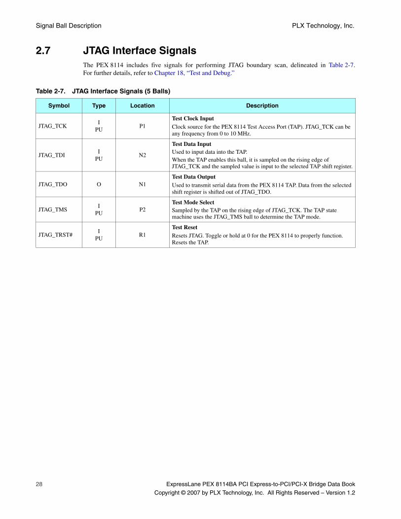
Signal Ball Description PLX Technology, Inc.
28 ExpressLane PEX 8114BA PCI Express-to-PCI/PCI-X Bridge Data Book
Copyright © 2007 by PLX Technology, Inc. All Rights Reserved – Version 1.2
2.7 JTAG Interface SignalsThe PEX 8114 includes five signals for performing JTAG boundary scan, delineated in Table 2-7.For further details, refer to Chapter 18, “Test and Debug.”
Table 2-7. JTAG Interface Signals (5 Balls)
Symbol Type Location Description
JTAG_TCKI
PUP1
Test Clock InputClock source for the PEX 8114 Test Access Port (TAP). JTAG_TCK can be any frequency from 0 to 10 MHz.
JTAG_TDII
PUN2
Test Data InputUsed to input data into the TAP.When the TAP enables this ball, it is sampled on the rising edge of JTAG_TCK and the sampled value is input to the selected TAP shift register.
JTAG_TDO O N1Test Data OutputUsed to transmit serial data from the PEX 8114 TAP. Data from the selected shift register is shifted out of JTAG_TDO.
JTAG_TMSI
PUP2
Test Mode SelectSampled by the TAP on the rising edge of JTAG_TCK. The TAP state machine uses the JTAG_TMS ball to determine the TAP mode.
JTAG_TRST#I
PUR1
Test ResetResets JTAG. Toggle or hold at 0 for the PEX 8114 to properly function. Resets the TAP.
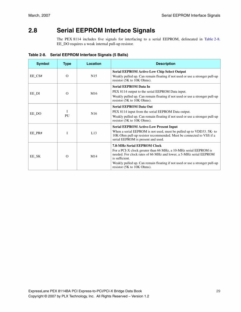
March, 2007 Serial EEPROM Interface Signals
ExpressLane PEX 8114BA PCI Express-to-PCI/PCI-X Bridge Data Book 29
Copyright © 2007 by PLX Technology, Inc. All Rights Reserved – Version 1.2
2.8 Serial EEPROM Interface SignalsThe PEX 8114 includes five signals for interfacing to a serial EEPROM, delineated in Table 2-8.EE_DO requires a weak internal pull-up resistor.
Table 2-8. Serial EEPROM Interface Signals (5 Balls)
Symbol Type Location Description
EE_CS# O N15Serial EEPROM Active-Low Chip Select OutputWeakly pulled up. Can remain floating if not used or use a stronger pull-up resistor (5K to 10K Ohms).
EE_DI O M16
Serial EEPROM Data InPEX 8114 output to the serial EEPROM Data input.Weakly pulled up. Can remain floating if not used or use a stronger pull-up resistor (5K to 10K Ohms).
EE_DOI
PUN16
Serial EEPROM Data OutPEX 8114 input from the serial EEPROM Data output.Weakly pulled up. Can remain floating if not used or use a stronger pull-up resistor (5K to 10K Ohms).
EE_PR# I L13
Serial EEPROM Active-Low Present InputWhen a serial EEPROM is not used, must be pulled up to VDD33. 5K- to 10K-Ohm pull-up resistor recommended. Must be connected to VSS if a serial EEPROM is present and used.
EE_SK O M14
7.8-MHz Serial EEPROM ClockFor a PCI-X clock greater than 66 MHz, a 10-MHz serial EEPROM is needed. For clock rates of 66 MHz and lower, a 5-MHz serial EEPROM is sufficient.Weakly pulled up. Can remain floating if not used or use a stronger pull-up resistor (5K to 10K Ohms).

Signal Ball Description PLX Technology, Inc.
30 ExpressLane PEX 8114BA PCI Express-to-PCI/PCI-X Bridge Data Book
Copyright © 2007 by PLX Technology, Inc. All Rights Reserved – Version 1.2
2.9 Power and Ground SignalsTable 2-9. Power and Ground Signals (98 Balls)
Symbol Type Location Description
VDD10 CPWRE6, E8, E9, E11, F5,
F12, G5, G12, J5, J12,K5, K12, M6, M10, M12
Core Supply Voltage (15 Balls)1.0V Power for Core Logic VCORE.
VDD10A APWR M8SerDes Analog Supply Voltage1.0V Power for SerDes Analog Circuits.
VDD10S DPWR P8, R4, R6, R8, R10, R12SerDes Digital Supply Voltage (6 Balls)1.0V Power for SerDes Digital Circuits.
VDD33 I/OPWR
B2, B8, B12, B15, E5,E7, E10, E12, F2, G15,H5, H12, J2, L12, M3,
M15, P12
I/O Supply Voltage (17 Balls)3.3V Power for I/O logic functions VRING.
VDD33A PLLPWR P4PLL Analog Supply Voltage3.3V Power for PLL Circuits.
VSS Ground
B5, B13, C9, E2, F6,F7, F8, F9, F10, F11,F15, G6, G7, G8, G9,
G10, G11, H6, H7, H8,H9, H10, H11, J6, J7,J8, J9, J10, J11, K2,
K6, K7, K8, K9, K10,K11, L6, L7, L8, L9,
L10, L11, L15, N8, N10, N12, P5, P6, P7, P9,
P10, P11, T4, T8, T12
Digital Ground Connections (55 Balls)
VSSA Ground N4 Analog Ground Connection
VTT_PEX[1:0] Supply T10, T6SerDes Termination Supply (2 Balls)
Tied to SerDes termination supply voltage (typically 1.5V).a
a. PEX_PETn/p[x] SerDes termination supply voltage controls the transmitter Common mode voltage (VTX–CM) value and output voltage swing (VTX–DIFFp), per the following formula:
VTX-CM = VTT – VTX–DIFFp
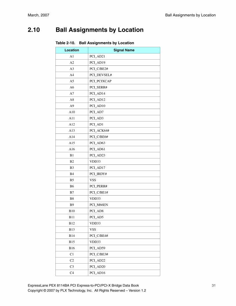
March, 2007 Ball Assignments by Location
ExpressLane PEX 8114BA PCI Express-to-PCI/PCI-X Bridge Data Book 31
Copyright © 2007 by PLX Technology, Inc. All Rights Reserved – Version 1.2
2.10 Ball Assignments by Location
Table 2-10. Ball Assignments by Location
Location Signal Name
A1 PCI_AD21
A2 PCI_AD19
A3 PCI_C/BE2#
A4 PCI_DEVSEL#
A5 PCI_PCIXCAP
A6 PCI_SERR#
A7 PCI_AD14
A8 PCI_AD12
A9 PCI_AD10
A10 PCI_AD7
A11 PCI_AD3
A12 PCI_AD1
A13 PCI_ACK64#
A14 PCI_C/BE6#
A15 PCI_AD63
A16 PCI_AD61
B1 PCI_AD23
B2 VDD33
B3 PCI_AD17
B4 PCI_IRDY#
B5 VSS
B6 PCI_PERR#
B7 PCI_C/BE1#
B8 VDD33
B9 PCI_M66EN
B10 PCI_AD8
B11 PCI_AD5
B12 VDD33
B13 VSS
B14 PCI_C/BE4#
B15 VDD33
B16 PCI_AD59
C1 PCI_C/BE3#
C2 PCI_AD22
C3 PCI_AD20
C4 PCI_AD16
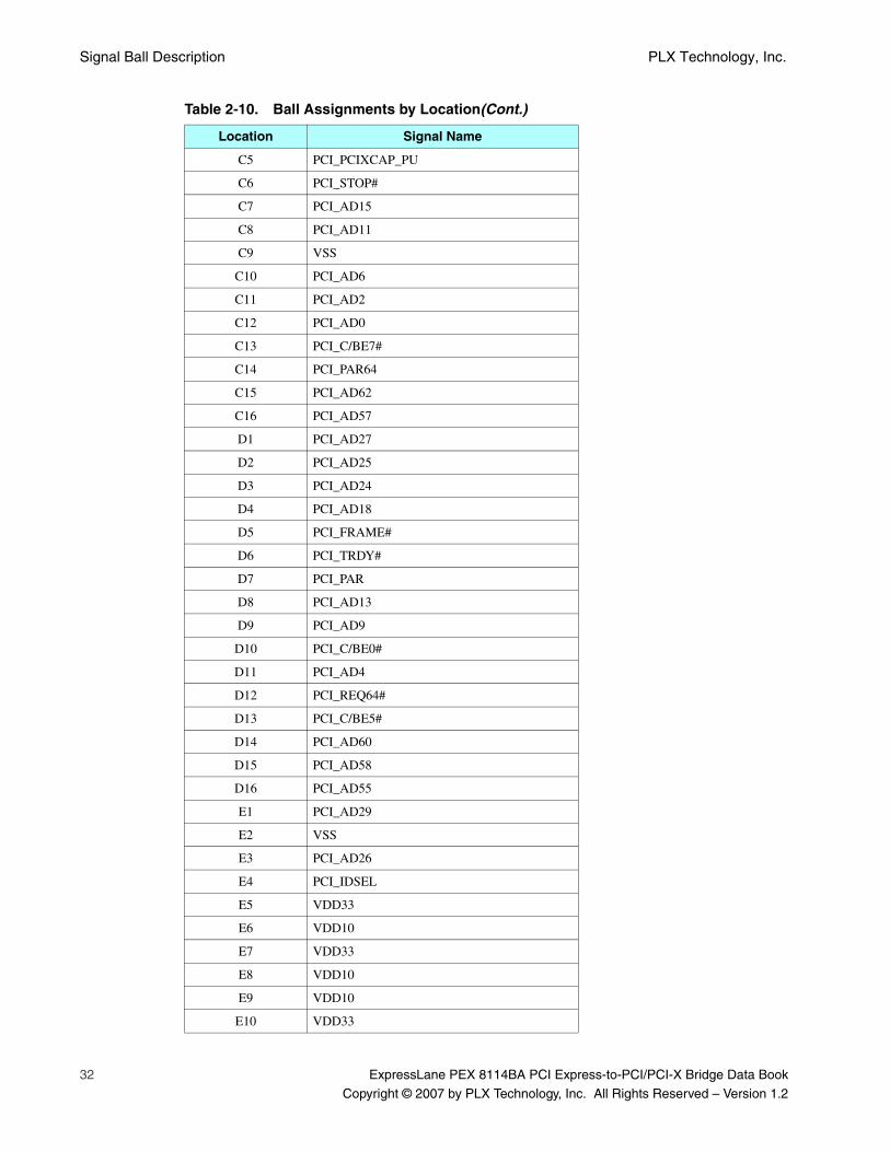
Signal Ball Description PLX Technology, Inc.
32 ExpressLane PEX 8114BA PCI Express-to-PCI/PCI-X Bridge Data Book
Copyright © 2007 by PLX Technology, Inc. All Rights Reserved – Version 1.2
C5 PCI_PCIXCAP_PU
C6 PCI_STOP#
C7 PCI_AD15
C8 PCI_AD11
C9 VSS
C10 PCI_AD6
C11 PCI_AD2
C12 PCI_AD0
C13 PCI_C/BE7#
C14 PCI_PAR64
C15 PCI_AD62
C16 PCI_AD57
D1 PCI_AD27
D2 PCI_AD25
D3 PCI_AD24
D4 PCI_AD18
D5 PCI_FRAME#
D6 PCI_TRDY#
D7 PCI_PAR
D8 PCI_AD13
D9 PCI_AD9
D10 PCI_C/BE0#
D11 PCI_AD4
D12 PCI_REQ64#
D13 PCI_C/BE5#
D14 PCI_AD60
D15 PCI_AD58
D16 PCI_AD55
E1 PCI_AD29
E2 VSS
E3 PCI_AD26
E4 PCI_IDSEL
E5 VDD33
E6 VDD10
E7 VDD33
E8 VDD10
E9 VDD10
E10 VDD33
Table 2-10. Ball Assignments by Location(Cont.)
Location Signal Name
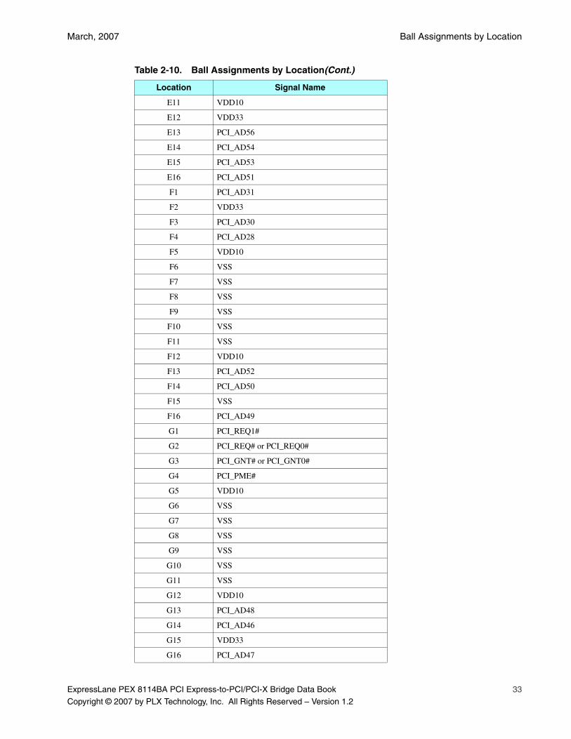
March, 2007 Ball Assignments by Location
ExpressLane PEX 8114BA PCI Express-to-PCI/PCI-X Bridge Data Book 33
Copyright © 2007 by PLX Technology, Inc. All Rights Reserved – Version 1.2
E11 VDD10
E12 VDD33
E13 PCI_AD56
E14 PCI_AD54
E15 PCI_AD53
E16 PCI_AD51
F1 PCI_AD31
F2 VDD33
F3 PCI_AD30
F4 PCI_AD28
F5 VDD10
F6 VSS
F7 VSS
F8 VSS
F9 VSS
F10 VSS
F11 VSS
F12 VDD10
F13 PCI_AD52
F14 PCI_AD50
F15 VSS
F16 PCI_AD49
G1 PCI_REQ1#
G2 PCI_REQ# or PCI_REQ0#
G3 PCI_GNT# or PCI_GNT0#
G4 PCI_PME#
G5 VDD10
G6 VSS
G7 VSS
G8 VSS
G9 VSS
G10 VSS
G11 VSS
G12 VDD10
G13 PCI_AD48
G14 PCI_AD46
G15 VDD33
G16 PCI_AD47
Table 2-10. Ball Assignments by Location(Cont.)
Location Signal Name

Signal Ball Description PLX Technology, Inc.
34 ExpressLane PEX 8114BA PCI Express-to-PCI/PCI-X Bridge Data Book
Copyright © 2007 by PLX Technology, Inc. All Rights Reserved – Version 1.2
H1 PCI_REQ3#
H2 PCI_REQ2#
H3 PCI_GNT1#
H4 PCI_RST#
H5 VDD33
H6 VSS
H7 VSS
H8 VSS
H9 VSS
H10 VSS
H11 VSS
H12 VDD33
H13 PCI_AD44
H14 PCI_AD42
H15 PCI_AD45
H16 PCI_AD43
J1 PCI_CLK
J2 VDD33
J3 PCI_GNT3#
J4 PCI_GNT2#
J5 VDD10
J6 VSS
J7 VSS
J8 VSS
J9 VSS
J10 VSS
J11 VSS
J12 VDD10
J13 PCI_AD40
J14 PCI_AD38
J15 PCI_AD41
J16 PCI_AD39
K1 PCI_CLKO1
K2 VSS
K3 PCI_CLKO0
K4 PCI_INTC#
K5 VDD10
K6 VSS
Table 2-10. Ball Assignments by Location(Cont.)
Location Signal Name
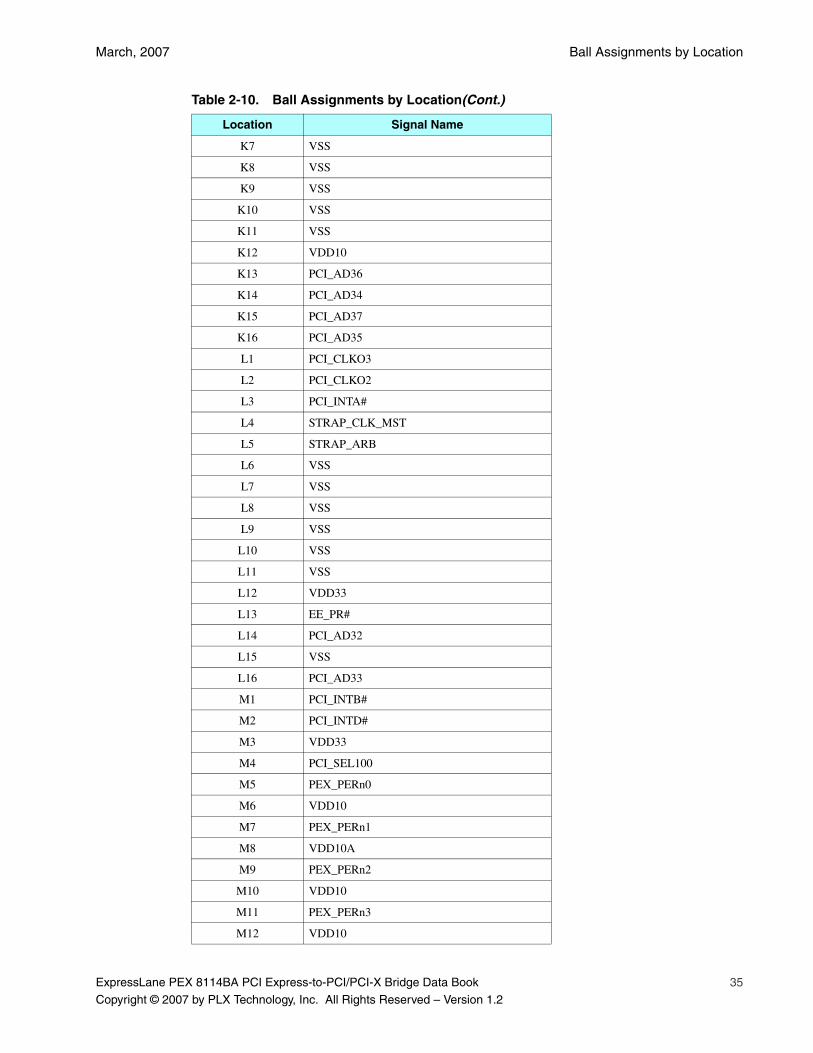
March, 2007 Ball Assignments by Location
ExpressLane PEX 8114BA PCI Express-to-PCI/PCI-X Bridge Data Book 35
Copyright © 2007 by PLX Technology, Inc. All Rights Reserved – Version 1.2
K7 VSS
K8 VSS
K9 VSS
K10 VSS
K11 VSS
K12 VDD10
K13 PCI_AD36
K14 PCI_AD34
K15 PCI_AD37
K16 PCI_AD35
L1 PCI_CLKO3
L2 PCI_CLKO2
L3 PCI_INTA#
L4 STRAP_CLK_MST
L5 STRAP_ARB
L6 VSS
L7 VSS
L8 VSS
L9 VSS
L10 VSS
L11 VSS
L12 VDD33
L13 EE_PR#
L14 PCI_AD32
L15 VSS
L16 PCI_AD33
M1 PCI_INTB#
M2 PCI_INTD#
M3 VDD33
M4 PCI_SEL100
M5 PEX_PERn0
M6 VDD10
M7 PEX_PERn1
M8 VDD10A
M9 PEX_PERn2
M10 VDD10
M11 PEX_PERn3
M12 VDD10
Table 2-10. Ball Assignments by Location(Cont.)
Location Signal Name
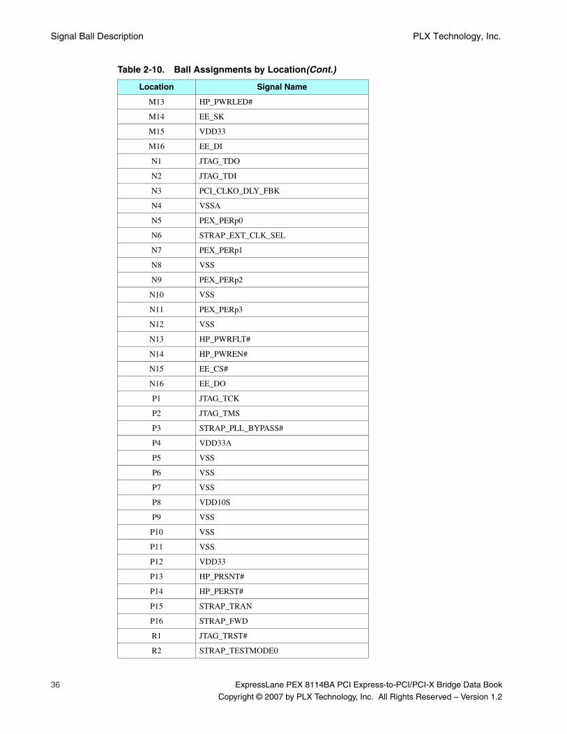
Signal Ball Description PLX Technology, Inc.
36 ExpressLane PEX 8114BA PCI Express-to-PCI/PCI-X Bridge Data Book
Copyright © 2007 by PLX Technology, Inc. All Rights Reserved – Version 1.2
M13 HP_PWRLED#
M14 EE_SK
M15 VDD33
M16 EE_DI
N1 JTAG_TDO
N2 JTAG_TDI
N3 PCI_CLKO_DLY_FBK
N4 VSSA
N5 PEX_PERp0
N6 STRAP_EXT_CLK_SEL
N7 PEX_PERp1
N8 VSS
N9 PEX_PERp2
N10 VSS
N11 PEX_PERp3
N12 VSS
N13 HP_PWRFLT#
N14 HP_PWREN#
N15 EE_CS#
N16 EE_DO
P1 JTAG_TCK
P2 JTAG_TMS
P3 STRAP_PLL_BYPASS#
P4 VDD33A
P5 VSS
P6 VSS
P7 VSS
P8 VDD10S
P9 VSS
P10 VSS
P11 VSS
P12 VDD33
P13 HP_PRSNT#
P14 HP_PERST#
P15 STRAP_TRAN
P16 STRAP_FWD
R1 JTAG_TRST#
R2 STRAP_TESTMODE0
Table 2-10. Ball Assignments by Location(Cont.)
Location Signal Name
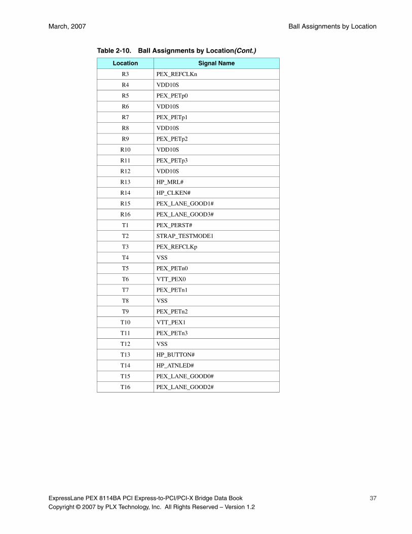
March, 2007 Ball Assignments by Location
ExpressLane PEX 8114BA PCI Express-to-PCI/PCI-X Bridge Data Book 37
Copyright © 2007 by PLX Technology, Inc. All Rights Reserved – Version 1.2
R3 PEX_REFCLKn
R4 VDD10S
R5 PEX_PETp0
R6 VDD10S
R7 PEX_PETp1
R8 VDD10S
R9 PEX_PETp2
R10 VDD10S
R11 PEX_PETp3
R12 VDD10S
R13 HP_MRL#
R14 HP_CLKEN#
R15 PEX_LANE_GOOD1#
R16 PEX_LANE_GOOD3#
T1 PEX_PERST#
T2 STRAP_TESTMODE1
T3 PEX_REFCLKp
T4 VSS
T5 PEX_PETn0
T6 VTT_PEX0
T7 PEX_PETn1
T8 VSS
T9 PEX_PETn2
T10 VTT_PEX1
T11 PEX_PETn3
T12 VSS
T13 HP_BUTTON#
T14 HP_ATNLED#
T15 PEX_LANE_GOOD0#
T16 PEX_LANE_GOOD2#
Table 2-10. Ball Assignments by Location(Cont.)
Location Signal Name
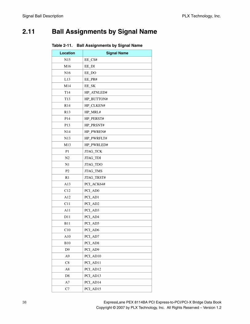
Signal Ball Description PLX Technology, Inc.
38 ExpressLane PEX 8114BA PCI Express-to-PCI/PCI-X Bridge Data Book
Copyright © 2007 by PLX Technology, Inc. All Rights Reserved – Version 1.2
2.11 Ball Assignments by Signal Name
Table 2-11. Ball Assignments by Signal Name
Location Signal Name
N15 EE_CS#
M16 EE_DI
N16 EE_DO
L13 EE_PR#
M14 EE_SK
T14 HP_ATNLED#
T13 HP_BUTTON#
R14 HP_CLKEN#
R13 HP_MRL#
P14 HP_PERST#
P13 HP_PRSNT#
N14 HP_PWREN#
N13 HP_PWRFLT#
M13 HP_PWRLED#
P1 JTAG_TCK
N2 JTAG_TDI
N1 JTAG_TDO
P2 JTAG_TMS
R1 JTAG_TRST#
A13 PCI_ACK64#
C12 PCI_AD0
A12 PCI_AD1
C11 PCI_AD2
A11 PCI_AD3
D11 PCI_AD4
B11 PCI_AD5
C10 PCI_AD6
A10 PCI_AD7
B10 PCI_AD8
D9 PCI_AD9
A9 PCI_AD10
C8 PCI_AD11
A8 PCI_AD12
D8 PCI_AD13
A7 PCI_AD14
C7 PCI_AD15

March, 2007 Ball Assignments by Signal Name
ExpressLane PEX 8114BA PCI Express-to-PCI/PCI-X Bridge Data Book 39
Copyright © 2007 by PLX Technology, Inc. All Rights Reserved – Version 1.2
C4 PCI_AD16
B3 PCI_AD17
D4 PCI_AD18
A2 PCI_AD19
C3 PCI_AD20
A1 PCI_AD21
C2 PCI_AD22
B1 PCI_AD23
D3 PCI_AD24
D2 PCI_AD25
E3 PCI_AD26
D1 PCI_AD27
F4 PCI_AD28
E1 PCI_AD29
F3 PCI_AD30
F1 PCI_AD31
L14 PCI_AD32
L16 PCI_AD33
K14 PCI_AD34
K16 PCI_AD35
K13 PCI_AD36
K15 PCI_AD37
J14 PCI_AD38
J16 PCI_AD39
J13 PCI_AD40
J15 PCI_AD41
H14 PCI_AD42
H16 PCI_AD43
H13 PCI_AD44
H15 PCI_AD45
G14 PCI_AD46
G16 PCI_AD47
G13 PCI_AD48
F16 PCI_AD49
F14 PCI_AD50
E16 PCI_AD51
F13 PCI_AD52
E15 PCI_AD53
Table 2-11. Ball Assignments by Signal Name(Cont.)
Location Signal Name

Signal Ball Description PLX Technology, Inc.
40 ExpressLane PEX 8114BA PCI Express-to-PCI/PCI-X Bridge Data Book
Copyright © 2007 by PLX Technology, Inc. All Rights Reserved – Version 1.2
E14 PCI_AD54
D16 PCI_AD55
E13 PCI_AD56
C16 PCI_AD57
D15 PCI_AD58
B16 PCI_AD59
D14 PCI_AD60
A16 PCI_AD61
C15 PCI_AD62
A15 PCI_AD63
D10 PCI_C/BE0#
B7 PCI_C/BE1#
A3 PCI_C/BE2#
C1 PCI_C/BE3#
B14 PCI_C/BE4#
D13 PCI_C/BE5#
A14 PCI_C/BE6#
C13 PCI_C/BE7#
J1 PCI_CLK
K3 PCI_CLKO0
K1 PCI_CLKO1
L2 PCI_CLKO2
L1 PCI_CLKO3
N3 PCI_CLKO_DLY_FBK
A4 PCI_DEVSEL#
D5 PCI_FRAME#
G3 PCI_GNT# or PCI_GNT0#
H3 PCI_GNT1#
J4 PCI_GNT2#
J3 PCI_GNT3#
E4 PCI_IDSEL
L3 PCI_INTA#
M1 PCI_INTB#
K4 PCI_INTC#
M2 PCI_INTD#
B4 PCI_IRDY#
B9 PCI_M66EN
D7 PCI_PAR
Table 2-11. Ball Assignments by Signal Name(Cont.)
Location Signal Name

March, 2007 Ball Assignments by Signal Name
ExpressLane PEX 8114BA PCI Express-to-PCI/PCI-X Bridge Data Book 41
Copyright © 2007 by PLX Technology, Inc. All Rights Reserved – Version 1.2
C14 PCI_PAR64
A5 PCI_PCIXCAP
C5 PCI_PCIXCAP_PU
B6 PCI_PERR#
G4 PCI_PME#
G2 PCI_REQ# or PCI_REQ0#
G1 PCI_REQ1#
H2 PCI_REQ2#
H1 PCI_REQ3#
D12 PCI_REQ64#
H4 PCI_RST#
M4 PCI_SEL100
A6 PCI_SERR#
C6 PCI_STOP#
D6 PCI_TRDY#
T15 PEX_LANE_GOOD0#
R15 PEX_LANE_GOOD1#
T16 PEX_LANE_GOOD2#
R16 PEX_LANE_GOOD3#
M5 PEX_PERn0
M7 PEX_PERn1
M9 PEX_PERn2
M11 PEX_PERn3
N5 PEX_PERp0
N7 PEX_PERp1
N9 PEX_PERp2
N11 PEX_PERp3
T1 PEX_PERST#
T5 PEX_PETn0
T7 PEX_PETn1
T9 PEX_PETn2
T11 PEX_PETn3
R5 PEX_PETp0
R7 PEX_PETp1
R9 PEX_PETp2
R11 PEX_PETp3
R3 PEX_REFCLKn
T3 PEX_REFCLKp
Table 2-11. Ball Assignments by Signal Name(Cont.)
Location Signal Name
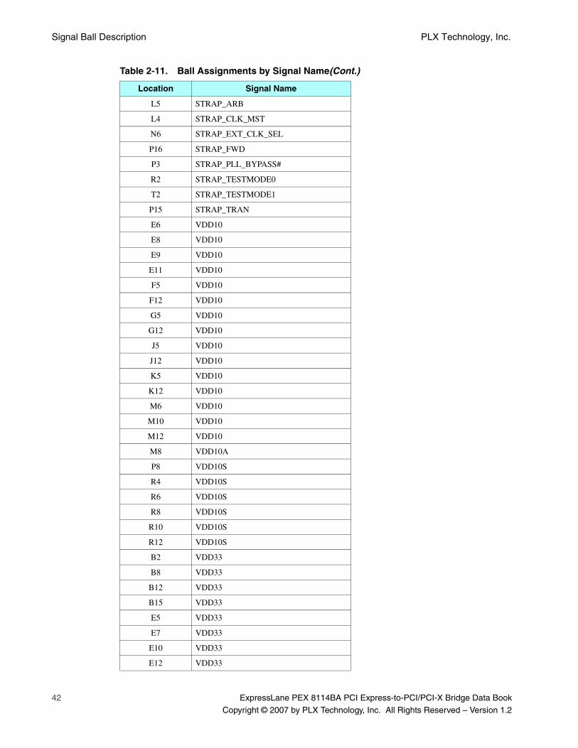
Signal Ball Description PLX Technology, Inc.
42 ExpressLane PEX 8114BA PCI Express-to-PCI/PCI-X Bridge Data Book
Copyright © 2007 by PLX Technology, Inc. All Rights Reserved – Version 1.2
L5 STRAP_ARB
L4 STRAP_CLK_MST
N6 STRAP_EXT_CLK_SEL
P16 STRAP_FWD
P3 STRAP_PLL_BYPASS#
R2 STRAP_TESTMODE0
T2 STRAP_TESTMODE1
P15 STRAP_TRAN
E6 VDD10
E8 VDD10
E9 VDD10
E11 VDD10
F5 VDD10
F12 VDD10
G5 VDD10
G12 VDD10
J5 VDD10
J12 VDD10
K5 VDD10
K12 VDD10
M6 VDD10
M10 VDD10
M12 VDD10
M8 VDD10A
P8 VDD10S
R4 VDD10S
R6 VDD10S
R8 VDD10S
R10 VDD10S
R12 VDD10S
B2 VDD33
B8 VDD33
B12 VDD33
B15 VDD33
E5 VDD33
E7 VDD33
E10 VDD33
E12 VDD33
Table 2-11. Ball Assignments by Signal Name(Cont.)
Location Signal Name
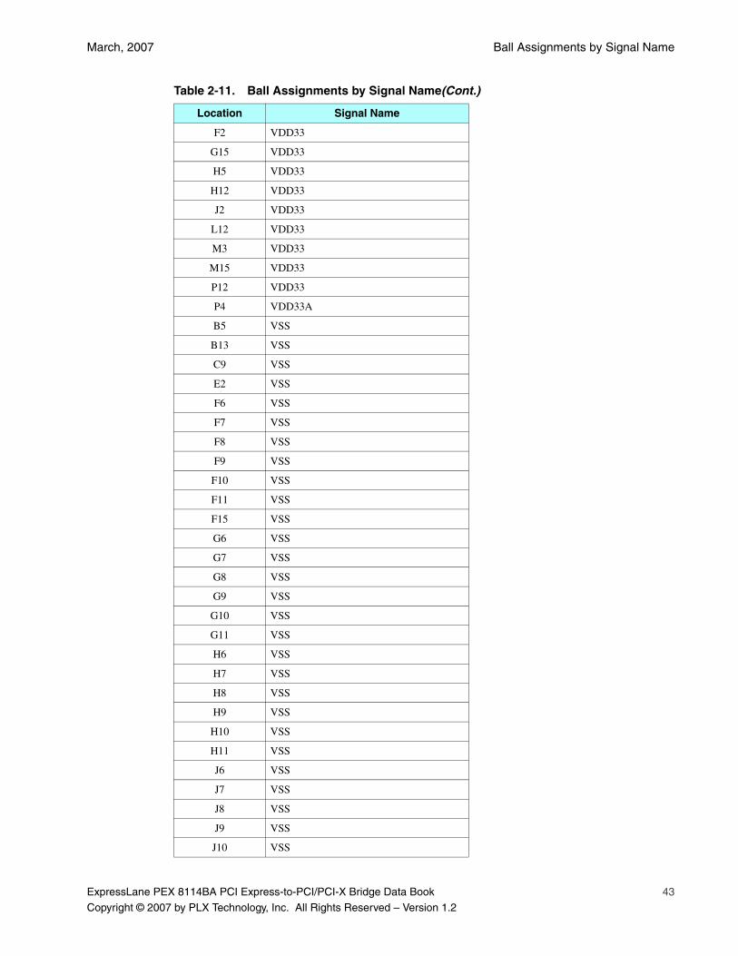
March, 2007 Ball Assignments by Signal Name
ExpressLane PEX 8114BA PCI Express-to-PCI/PCI-X Bridge Data Book 43
Copyright © 2007 by PLX Technology, Inc. All Rights Reserved – Version 1.2
F2 VDD33
G15 VDD33
H5 VDD33
H12 VDD33
J2 VDD33
L12 VDD33
M3 VDD33
M15 VDD33
P12 VDD33
P4 VDD33A
B5 VSS
B13 VSS
C9 VSS
E2 VSS
F6 VSS
F7 VSS
F8 VSS
F9 VSS
F10 VSS
F11 VSS
F15 VSS
G6 VSS
G7 VSS
G8 VSS
G9 VSS
G10 VSS
G11 VSS
H6 VSS
H7 VSS
H8 VSS
H9 VSS
H10 VSS
H11 VSS
J6 VSS
J7 VSS
J8 VSS
J9 VSS
J10 VSS
Table 2-11. Ball Assignments by Signal Name(Cont.)
Location Signal Name
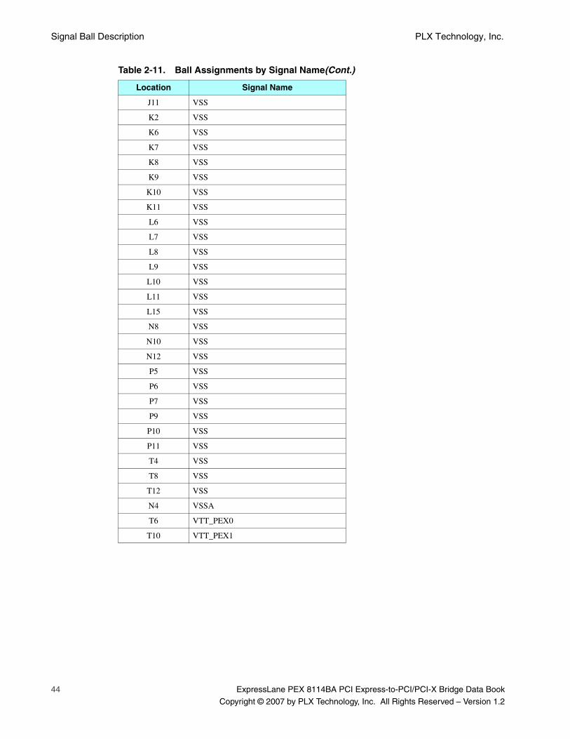
Signal Ball Description PLX Technology, Inc.
44 ExpressLane PEX 8114BA PCI Express-to-PCI/PCI-X Bridge Data Book
Copyright © 2007 by PLX Technology, Inc. All Rights Reserved – Version 1.2
J11 VSS
K2 VSS
K6 VSS
K7 VSS
K8 VSS
K9 VSS
K10 VSS
K11 VSS
L6 VSS
L7 VSS
L8 VSS
L9 VSS
L10 VSS
L11 VSS
L15 VSS
N8 VSS
N10 VSS
N12 VSS
P5 VSS
P6 VSS
P7 VSS
P9 VSS
P10 VSS
P11 VSS
T4 VSS
T8 VSS
T12 VSS
N4 VSSA
T6 VTT_PEX0
T10 VTT_PEX1
Table 2-11. Ball Assignments by Signal Name(Cont.)
Location Signal Name
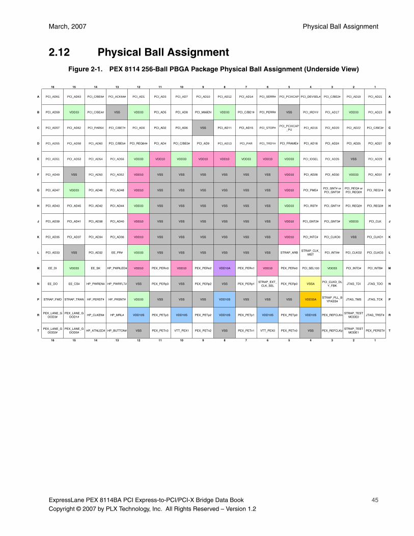
March, 2007 Physical Ball Assignment
ExpressLane PEX 8114BA PCI Express-to-PCI/PCI-X Bridge Data Book 45
Copyright © 2007 by PLX Technology, Inc. All Rights Reserved – Version 1.2
2.12 Physical Ball AssignmentFigure 2-1. PEX 8114 256-Ball PBGA Package Physical Ball Assignment (Underside View)
16 15 14 13 12 11 10 9 8 7 6 5 4 3 2 1
A PCI_AD61 PCI_AD63 PCI_C/BE6# PCI_ACK64# PCI_AD1 PCI_AD3 PCI_AD7 PCI_AD10 PCI_AD12 PCI_AD14 PCI_SERR# PCI_PCIXCAP PCI_DEVSEL# PCI_C/BE2# PCI_AD19 PCI_AD21 A
B PCI_AD59 VDD33 PCI_C/BE4# VSS VDD33 PCI_AD5 PCI_AD8 PCI_M66EN VDD33 PCI_C/BE1# PCI_PERR# VSS PCI_IRDY# PCI_AD17 VDD33 PCI_AD23 B
C PCI_AD57 PCI_AD62 PCI_PAR64 PCI_C/BE7# PCI_AD0 PCI_AD2 PCI_AD6 VSS PCI_AD11 PCI_AD15 PCI_STOP#PCI_PCIXCAP
_PUPCI_AD16 PCI_AD20 PCI_AD22 PCI_C/BE3# C
D PCI_AD55 PCI_AD58 PCI_AD60 PCI_C/BE5# PCI_REQ64# PCI_AD4 PCI_C/BE0# PCI_AD9 PCI_AD13 PCI_PAR PCI_TRDY# PCI_FRAME# PCI_AD18 PCI_AD24 PCI_AD25 PCI_AD27 D
E PCI_AD51 PCI_AD53 PCI_AD54 PCI_AD56 VDD33 VDD10 VDD33 VDD10 VDD10 VDD33 VDD10 VDD33 PCI_IDSEL PCI_AD26 VSS PCI_AD29 E
F PCI_AD49 VSS PCI_AD50 PCI_AD52 VDD10 VSS VSS VSS VSS VSS VSS VDD10 PCI_AD28 PCI_AD30 VDD33 PCI_AD31 F
G PCI_AD47 VDD33 PCI_AD46 PCI_AD48 VDD10 VSS VSS VSS VSS VSS VSS VDD10 PCI_PME#PCI_GNT# or PCI_GNT0#
PCI_REQ# or PCI_REQ0#
PCI_REQ1# G
H PCI_AD43 PCI_AD45 PCI_AD42 PCI_AD44 VDD33 VSS VSS VSS VSS VSS VSS VDD33 PCI_RST# PCI_GNT1# PCI_REQ2# PCI_REQ3# H
J PCI_AD39 PCI_AD41 PCI_AD38 PCI_AD40 VDD10 VSS VSS VSS VSS VSS VSS VDD10 PCI_GNT2# PCI_GNT3# VDD33 PCI_CLK J
K PCI_AD35 PCI_AD37 PCI_AD34 PCI_AD36 VDD10 VSS VSS VSS VSS VSS VSS VDD10 PCI_INTC# PCI_CLKO0 VSS PCI_CLKO1 K
L PCI_AD33 VSS PCI_AD32 EE_PR# VDD33 VSS VSS VSS VSS VSS VSS STRAP_ARBSTRAP_CLK_
MSTPCI_INTA# PCI_CLKO2 PCI_CLKO3 L
M EE_DI VDD33 EE_SK HP_PWRLED# VDD10 PEX_PERn3 VDD10 PEX_PERn2 VDD10A PEX_PERn1 VDD10 PEX_PERn0 PCI_SEL100 VDD33 PCI_INTD# PCI_INTB# M
N EE_DO EE_CS# HP_PWREN# HP_PWRFLT# VSS PEX_PERp3 VSS PEX_PERp2 VSS PEX_PERp1STRAP_EXT_
CLK_SELPEX_PERp0 VSSA
PCI_CLKO_DLY_FBK
JTAG_TDI JTAG_TDO N
P STRAP_FWD STRAP_TRAN HP_PERST# HP_PRSNT# VDD33 VSS VSS VSS VDD10S VSS VSS VSS VDD33ASTRAP_PLL_B
YPASS#JTAG_TMS JTAG_TCK P
RPEX_LANE_G
OOD3#PEX_LANE_G
OOD1#HP_CLKEN# HP_MRL# VDD10S PEX_PETp3 VDD10S PEX_PETp2 VDD10S PEX_PETp1 VDD10S PEX_PETp0 VDD10S PEX_REFCLKn
STRAP_TESTMODE0
JTAG_TRST# R
TPEX_LANE_G
OOD2#PEX_LANE_G
OOD0#HP_ATNLED# HP_BUTTON# VSS PEX_PETn3 VTT_PEX1 PEX_PETn2 VSS PEX_PETn1 VTT_PEX0 PEX_PETn0 VSS PEX_REFCLKp
STRAP_TESTMODE1
PEX_PERST# T
16 15 14 13 12 11 10 9 8 7 6 5 4 3 2 1
Signal Ball Description PLX Technology, Inc.
46 ExpressLane PEX 8114BA PCI Express-to-PCI/PCI-X Bridge Data Book
Copyright © 2007 by PLX Technology, Inc. All Rights Reserved – Version 1.2
THIS PAGE INTENTIONALLY LEFT BLANK.
ExpressLane PEX 8114BA PCI Express-to-PCI/PCI-X Bridge Data Book 47
Copyright © 2007 by PLX Technology, Inc. All Rights Reserved – Version 1.2
Chapter 3 Clock and Reset
3.1 PEX 8114 Clocking IntroductionNote: The PEX 8114 is compliant with the PCI-X Addendum to PCI Local Bus Specification,
Revisions 1.0b and 2.0a.
The PCI/PCI-X clock domain PLL is driven by the 100-MHz PEX_REFCLKn/p input, as well asPCI_CLK input. When the PCI/PCI-X clock domain PLL is driven by PEX_REFCLKn/p, the PLL isused to synthesize the PCI system clock and is referred to as operating in Clock Master mode. When thePCI/PCI-X clock domain PLL is driven by PCI_CLK, it is referred to as operating in Clock Slave mode.
The PEX 8114 includes a PCI-X Bus Clock Generator and two internal clock domains – one each forPCI-X and PCI Express. The Clock Generator is capable of synthesizing common PCI Clockfrequencies and driving four Clock Output balls, PCI_CLKO[3:0]. The PCI Express clock domain runsat a frequency that is compatible with 2.5 Gbps PCI Express data transmission rates, and is a Slave tothe PEX_REFCLKn/p inputs. The PCI-X clock domain is driven by the PCI_CLK input system clock,and runs at the PCI-X Bus clock frequency.
3.1.1 PCI-X Clock GeneratorThe PEX 8114 PCI/PCI-X (PCI-X) Clock Generator is used to synthesize PCI-X Bus clocks. ThePCI-X Clock Generator is driven by PEX_REFCLKn/p, and can generate four externally usable PCI-XBus system clocks. These clocks are driven out of the PEX 8114 onto the PCI_CLKO[3:0] balls.PCI_CLKO[3:0] are designed to drive four external PCI devices.
In addition to PCI_CLKO[3:0], the Clock Master circuitry also provides a PCI_CLKO_DLY_FBKClock Output ball. The PCI_CLKO_DLY_FBK output can optionally drive the PCI_CLK input to thePEX 8114, by way of a trace on the Printed Circuit Board (PCB). This ensures that the PCI-X SystemClock-phase alignment requirements are satisfied when other devices are located requiring long clocklines on the PCB.
The PCI/PCI-X Clock Generator is enabled when the STRAP_CLK_MST input ball is High.The synthesized PCI/PCI-X clock frequency is determined by the PCI_M66EN, PCI_PCIXCAP,PCI_PCIXCAP_PU, and PCI_SEL100 balls. (Refer to Section 3.3.) The Clock Generator is capableof synthesizing frequencies at 25. 33. 50, 66, 100, and 133 MHz. When the Clock Generator is disabled,the PCI_CLKO[3:0] and PCI_CLKO_DLY_FBK signals are driven Low. Additionally,the PCI_CLKO[3:0] signals can be individually disabled by writing 0 to the register bit associatedwith that specific output (offset FA0h, PCI_CLKO_EN[3:0] field). When the PEX 8114 exits reset withSTRAP_CLK_MST Low, the PCI_CLKO[3:0] and PCI_CLKO_DLY_FBK outputs are driven Low.When STRAP_CLK_MST is High at PEX 8114 reset, the PCI_CLKO[3:0] and PCI_CLKO_DLY_FBKoutputs drive active clocks.
When the PEX 8114 is the Clock Master, it sets the mode (PCI or PCI-X) and the clock frequency whenReset de-asserts.
Clock and Reset PLX Technology, Inc.
48 ExpressLane PEX 8114BA PCI Express-to-PCI/PCI-X Bridge Data Book
Copyright © 2007 by PLX Technology, Inc. All Rights Reserved – Version 1.2
3.1.2 PCI-X Clocking of PCI-X ModuleThe PEX 8114 PCI-X module must be supplied a clock from the PEX 8114’s internal Clock Generatoror a system-level Clock Generator. The PCI clocks, at the Input ball of each device on the PCI Bussegment, must be frequency- and phase-aligned.
3.1.2.1 Clocking the PCI Module when PEX 8114 Clock Generator Is Not UsedWhen the PEX 8114 is not used as the PCI System Clock Generator, the PEX 8114 receives the PCI BusSystem clock from its PCI_CLK input signal. The External Clock Generator is required to supply theclocks to the various PCI devices, allowing the devices to meet the phase-alignment requirements. ThePCI-X module can be driven at PCI-X clock frequencies up to 133 MHz, as well as PCI clockfrequencies down to DC. The PCI-X module determines to which mode (PCI or PCI-X) and frequency itis be driven at reset, by reading the initialization pattern on the PCI Bus, as described in the PCI-X r1.0band PCI-X r2.0a.
3.1.2.2 Clocking the PCI Module when PEX 8114 Clock Generator Is UsedWhen the PEX 8114’s clock generation circuitry is used (by setting STRAP_CLK_MST=1), thePCI clock can be driven to the PCI circuitry, internally or externally across the PCB:
• When the PCI clock must be internally driven from the PEX 8114’s Clock Generator to the PEX 8114 PCI device, drive the STRAP_EXT_CLK_SEL ball Low.
• When the PCI clock must be externally driven on the PCB, run a clock trace from the PEX 8114’s PCI_CLKO_DLY_FBK output to the PCI_CLK input, then drive the STRAP_EXT_CLK_SEL ball High. The ability to drive an external PCI_CLK PCB trace back to the PCI Express interface allows for delay, and the ability to align the PEX 8114’s PCI_CLK input with the other device’s PCI_CLK inputs, although the other device’s clocks are driven across a long PCB trace. Typically, the PCB trace length from the PCI_CLKO_DLY_FBK output to the PCI_CLK input is equal to the length of the clock traces from the PEX 8114’s PCI_CLKO[3:0] balls to the other external device’s clock inputs.
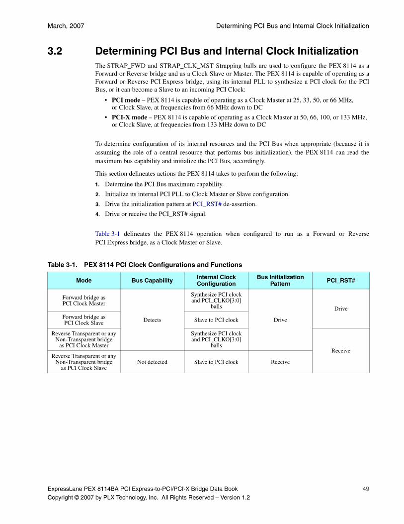
March, 2007 Determining PCI Bus and Internal Clock Initialization
ExpressLane PEX 8114BA PCI Express-to-PCI/PCI-X Bridge Data Book 49
Copyright © 2007 by PLX Technology, Inc. All Rights Reserved – Version 1.2
3.2 Determining PCI Bus and Internal Clock InitializationThe STRAP_FWD and STRAP_CLK_MST Strapping balls are used to configure the PEX 8114 as aForward or Reverse bridge and as a Clock Slave or Master. The PEX 8114 is capable of operating as aForward or Reverse PCI Express bridge, using its internal PLL to synthesize a PCI clock for the PCIBus, or it can become a Slave to an incoming PCI Clock:
• PCI mode – PEX 8114 is capable of operating as a Clock Master at 25, 33, 50, or 66 MHz, or Clock Slave, at frequencies from 66 MHz down to DC
• PCI-X mode – PEX 8114 is capable of operating as a Clock Master at 50, 66, 100, or 133 MHz, or Clock Slave, at frequencies from 133 MHz down to DC
To determine configuration of its internal resources and the PCI Bus when appropriate (because it isassuming the role of a central resource that performs bus initialization), the PEX 8114 can read themaximum bus capability and initialize the PCI Bus, accordingly.
This section delineates actions the PEX 8114 takes to perform the following:
1. Determine the PCI Bus maximum capability.
2. Initialize its internal PCI PLL to Clock Master or Slave configuration.
3. Drive the initialization pattern at PCI_RST# de-assertion.
4. Drive or receive the PCI_RST# signal.
Table 3-1 delineates the PEX 8114 operation when configured to run as a Forward or ReversePCI Express bridge, as a Clock Master or Slave.
Table 3-1. PEX 8114 PCI Clock Configurations and Functions
Mode Bus Capability Internal Clock Configuration
Bus Initialization Pattern PCI_RST#
Forward bridge as PCI Clock Master
Detects
Synthesize PCI clock and PCI_CLKO[3:0]
balls
Drive
DriveForward bridge as PCI Clock Slave Slave to PCI clock
Reverse Transparent or any Non-Transparent bridge
as PCI Clock Master
Synthesize PCI clock and PCI_CLKO[3:0]
ballsReceive
Reverse Transparent or any Non-Transparent bridge
as PCI Clock SlaveNot detected Slave to PCI clock Receive

Clock and Reset PLX Technology, Inc.
50 ExpressLane PEX 8114BA PCI Express-to-PCI/PCI-X Bridge Data Book
Copyright © 2007 by PLX Technology, Inc. All Rights Reserved – Version 1.2
3.2.1 Determining Bus Mode Capability and Maximum FrequencyThe PEX 8114, as a Clock Master or Forward PCI Express bridge in Clock Slave mode, must determinethe system’s bus mode capabilities and maximum frequency, using the PCI_PCIXCAP andPCI_PCIXCAP_PU balls.
Table 3-2 delineates the maximum clock frequency and PCI_PCIXCAP ball circuitry. For the threeclock frequencies listed in the table, connect the PCI_PCIXCAP_PU ball to the PCI_PCIXCAP ballthrough a 1K-Ohm resistor. A 56K-Ohm resistor between 3.3V and the PCI_PCIXCAP ball is alsorequired. The PEX 8114 detects this circuitry to determine the bus mode and maximum clock frequency,at power-up.
Table 3-2. Bus Mode, Maximum Clock Frequency, and PCI_PCIXCAP Ball Circuitry
Bus Mode Maximum Clock Frequency PCI_PCIXCAP Ball
PCI 66 MHz Grounded
PCI-X66 MHz Grounded through an RC network
133 MHz Connected to a capacitor
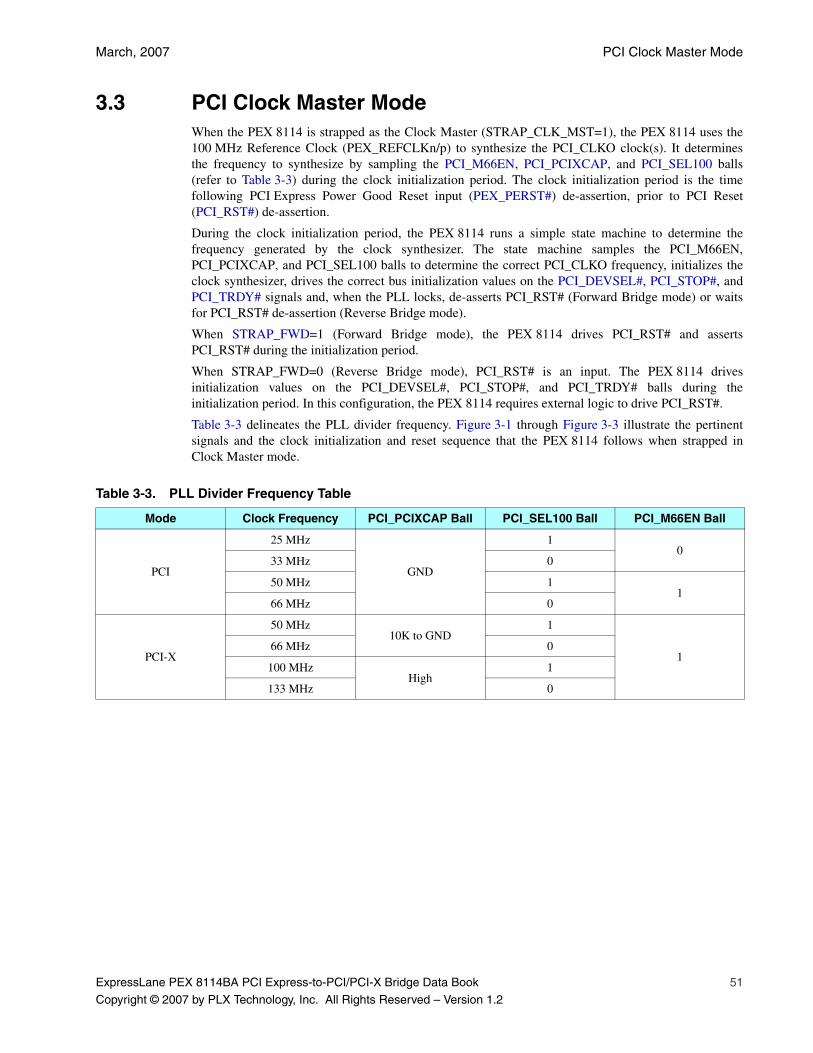
March, 2007 PCI Clock Master Mode
ExpressLane PEX 8114BA PCI Express-to-PCI/PCI-X Bridge Data Book 51
Copyright © 2007 by PLX Technology, Inc. All Rights Reserved – Version 1.2
3.3 PCI Clock Master ModeWhen the PEX 8114 is strapped as the Clock Master (STRAP_CLK_MST=1), the PEX 8114 uses the100 MHz Reference Clock (PEX_REFCLKn/p) to synthesize the PCI_CLKO clock(s). It determinesthe frequency to synthesize by sampling the PCI_M66EN, PCI_PCIXCAP, and PCI_SEL100 balls(refer to Table 3-3) during the clock initialization period. The clock initialization period is the timefollowing PCI Express Power Good Reset input (PEX_PERST#) de-assertion, prior to PCI Reset(PCI_RST#) de-assertion.
During the clock initialization period, the PEX 8114 runs a simple state machine to determine thefrequency generated by the clock synthesizer. The state machine samples the PCI_M66EN,PCI_PCIXCAP, and PCI_SEL100 balls to determine the correct PCI_CLKO frequency, initializes theclock synthesizer, drives the correct bus initialization values on the PCI_DEVSEL#, PCI_STOP#, andPCI_TRDY# signals and, when the PLL locks, de-asserts PCI_RST# (Forward Bridge mode) or waitsfor PCI_RST# de-assertion (Reverse Bridge mode).
When STRAP_FWD=1 (Forward Bridge mode), the PEX 8114 drives PCI_RST# and assertsPCI_RST# during the initialization period.
When STRAP_FWD=0 (Reverse Bridge mode), PCI_RST# is an input. The PEX 8114 drivesinitialization values on the PCI_DEVSEL#, PCI_STOP#, and PCI_TRDY# balls during theinitialization period. In this configuration, the PEX 8114 requires external logic to drive PCI_RST#.
Table 3-3 delineates the PLL divider frequency. Figure 3-1 through Figure 3-3 illustrate the pertinentsignals and the clock initialization and reset sequence that the PEX 8114 follows when strapped inClock Master mode.
Table 3-3. PLL Divider Frequency Table
Mode Clock Frequency PCI_PCIXCAP Ball PCI_SEL100 Ball PCI_M66EN Ball
PCI
25 MHz
GND
10
33 MHz 0
50 MHz 11
66 MHz 0
PCI-X
50 MHz10K to GND
1
166 MHz 0
100 MHzHigh
1
133 MHz 0
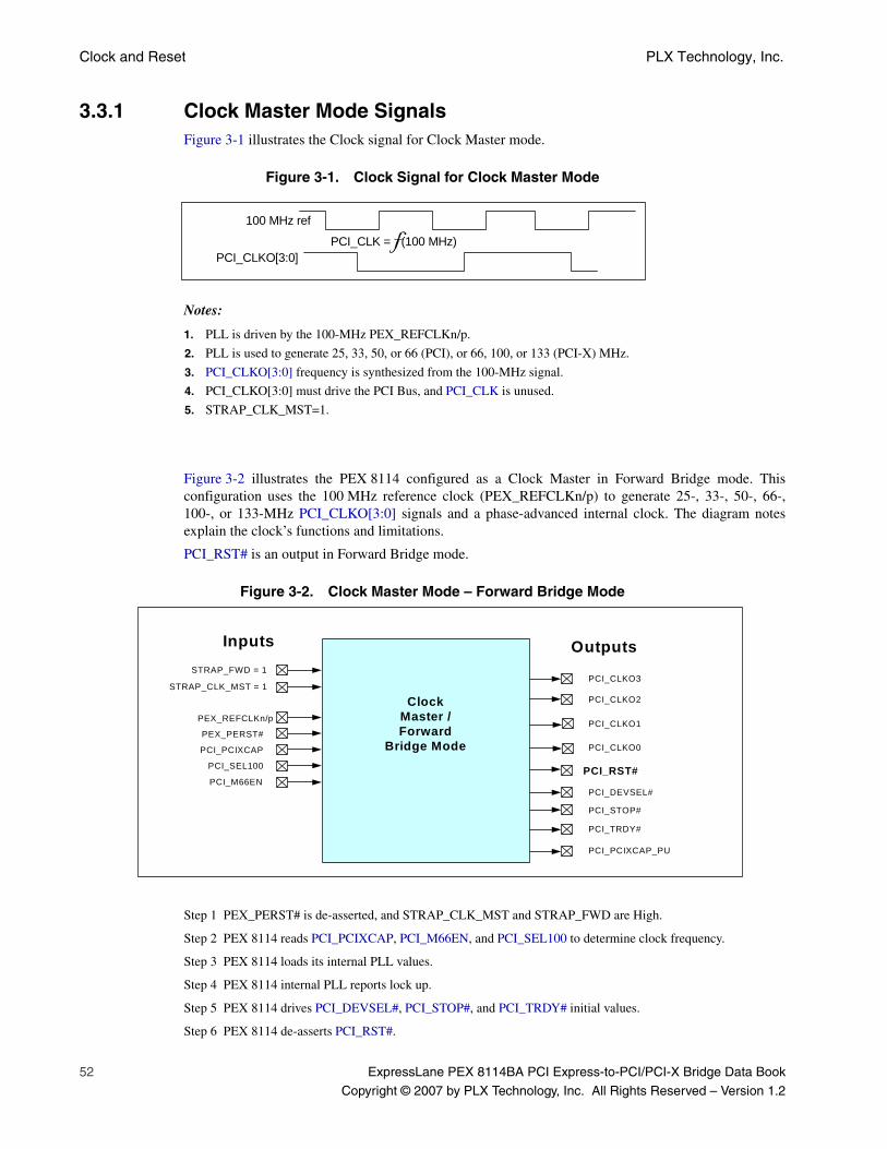
Clock and Reset PLX Technology, Inc.
52 ExpressLane PEX 8114BA PCI Express-to-PCI/PCI-X Bridge Data Book
Copyright © 2007 by PLX Technology, Inc. All Rights Reserved – Version 1.2
3.3.1 Clock Master Mode SignalsFigure 3-1 illustrates the Clock signal for Clock Master mode.
Figure 3-1. Clock Signal for Clock Master Mode
Notes:
1. PLL is driven by the 100-MHz PEX_REFCLKn/p.
2. PLL is used to generate 25, 33, 50, or 66 (PCI), or 66, 100, or 133 (PCI-X) MHz.
3. PCI_CLKO[3:0] frequency is synthesized from the 100-MHz signal.
4. PCI_CLKO[3:0] must drive the PCI Bus, and PCI_CLK is unused.
5. STRAP_CLK_MST=1.
Figure 3-2 illustrates the PEX 8114 configured as a Clock Master in Forward Bridge mode. Thisconfiguration uses the 100 MHz reference clock (PEX_REFCLKn/p) to generate 25-, 33-, 50-, 66-,100-, or 133-MHz PCI_CLKO[3:0] signals and a phase-advanced internal clock. The diagram notesexplain the clock’s functions and limitations.
PCI_RST# is an output in Forward Bridge mode.
Figure 3-2. Clock Master Mode – Forward Bridge Mode
Step 1 PEX_PERST# is de-asserted, and STRAP_CLK_MST and STRAP_FWD are High.
Step 2 PEX 8114 reads PCI_PCIXCAP, PCI_M66EN, and PCI_SEL100 to determine clock frequency.
Step 3 PEX 8114 loads its internal PLL values.
Step 4 PEX 8114 internal PLL reports lock up.
Step 5 PEX 8114 drives PCI_DEVSEL#, PCI_STOP#, and PCI_TRDY# initial values.
Step 6 PEX 8114 de-asserts PCI_RST#.
100 MHz ref
PCI_CLK = f(100 MHz)PCI_CLKO[3:0]
PCI_CLKO3
PCI_DEVSEL#
PCI_RST#
PCI_CLKO2
PCI_CLKO1
PCI_CLKO0
PCI_STOP#
PCI_TRDY#
PCI_PCIXCAP_PU
Clock Master /Forward
Bridge Mode
Inputs OutputsSTRAP_FWD = 1
STRAP_CLK_MST = 1
PEX_REFCLKn/p
PEX_PERST#
PCI_PCIXCAP
PCI_M66EN
PCI_SEL100
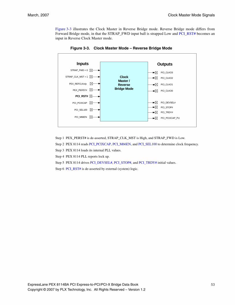
March, 2007 Clock Master Mode Signals
ExpressLane PEX 8114BA PCI Express-to-PCI/PCI-X Bridge Data Book 53
Copyright © 2007 by PLX Technology, Inc. All Rights Reserved – Version 1.2
Figure 3-3 illustrates the Clock Master in Reverse Bridge mode. Reverse Bridge mode differs fromForward Bridge mode, in that the STRAP_FWD input ball is strapped Low and PCI_RST# becomes aninput in Reverse Clock Master mode.
Figure 3-3. Clock Master Mode – Reverse Bridge Mode
Step 1 PEX_PERST# is de-asserted, STRAP_CLK_MST is High, and STRAP_FWD is Low.
Step 2 PEX 8114 reads PCI_PCIXCAP, PCI_M66EN, and PCI_SEL100 to determine clock frequency.
Step 3 PEX 8114 loads its internal PLL values.
Step 4 PEX 8114 PLL reports lock up.
Step 5 PEX 8114 drives PCI_DEVSEL#, PCI_STOP#, and PCI_TRDY# initial values.
Step 6 PCI_RST# is de-asserted by external (system) logic.
PEX_PERST#
PCI_PCIXCAP
PCI_M66EN
PCI_CLKO3
PCI_DEVSEL#
PCI_RST#
PCI_CLKO2
PCI_CLKO1
PCI_CLKO0
PCI_STOP#
PCI_TRDY#
PCI_PCIXCAP_PU
ClockMaster /Reverse
Bridge Mode
Inputs OutputsSTRAP_FWD = 0
PEX_REFCLKn/p
STRAP_CLK_MST = 1
PCI_SEL100
Clock and Reset PLX Technology, Inc.
54 ExpressLane PEX 8114BA PCI Express-to-PCI/PCI-X Bridge Data Book
Copyright © 2007 by PLX Technology, Inc. All Rights Reserved – Version 1.2
3.4 PCI Clock Slave ModeWhen the PEX 8114 is strapped as a Clock Slave (STRAP_CLK_MST=0), the PLL is used to cancelinternal clock delay for PCI clock frequencies above 33 MHz. When the PCI_CLK frequencyis 33 MHz or lower, the PLL is bypassed and PCI_CLK directly drives the PCI internal circuitry.A buffered and phase-delayed copy of PCI_CLK is driven out of the PCI_CLKO[3:0] balls.
3.4.1 Clock Slave – Forward Bridge ModeWhen the Clock Slave state machine is run in Forward Bridge mode, the PEX 8114 receives a clock, buttakes responsibility to drive the PCI-X initialization pattern at reset. Because the PEX 8114 drivesthe initialization pattern, it detects the circuit connected to the PCI_PCIXCAP, PCI_M66EN,and PCI_SEL100 ball states to determine the PCI Bus maximum clock frequency and whichPCI-X initialization pattern to drive.
External clock generation circuitry must:
• Determine and set the clock frequency, according to the values on PCI_PCIXCAP, PCI_M66EN, and PCI_SEL100, or
• Limit the system maximum clock frequency by driving values on PCI_PCIXCAP, PCI_M66EN, and PCI_SEL100
This requires coordination of the Clock Generator frequency and the values that the PEX 8114 readson the PCI_PCIXCAP, PCI_M66EN, and PCI_SEL100 balls.
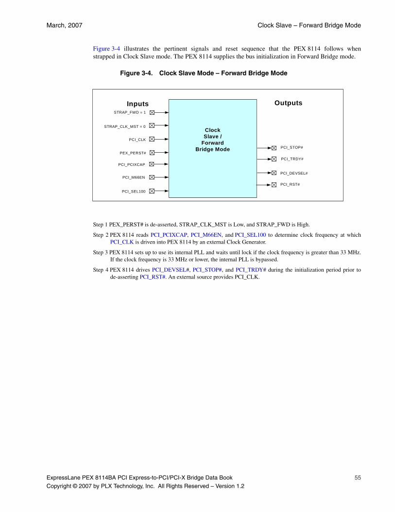
March, 2007 Clock Slave – Forward Bridge Mode
ExpressLane PEX 8114BA PCI Express-to-PCI/PCI-X Bridge Data Book 55
Copyright © 2007 by PLX Technology, Inc. All Rights Reserved – Version 1.2
Figure 3-4 illustrates the pertinent signals and reset sequence that the PEX 8114 follows whenstrapped in Clock Slave mode. The PEX 8114 supplies the bus initialization in Forward Bridge mode.
Figure 3-4. Clock Slave Mode – Forward Bridge Mode
Step 1 PEX_PERST# is de-asserted, STRAP_CLK_MST is Low, and STRAP_FWD is High.
Step 2 PEX 8114 reads PCI_PCIXCAP, PCI_M66EN, and PCI_SEL100 to determine clock frequency at whichPCI_CLK is driven into PEX 8114 by an external Clock Generator.
Step 3 PEX 8114 sets up to use its internal PLL and waits until lock if the clock frequency is greater than 33 MHz.If the clock frequency is 33 MHz or lower, the internal PLL is bypassed.
Step 4 PEX 8114 drives PCI_DEVSEL#, PCI_STOP#, and PCI_TRDY# during the initialization period prior tode-asserting PCI_RST#. An external source provides PCI_CLK.
ClockSlave /
Forward Bridge Mode
STRAP_CLK_MST = 0
PCI_CLK
PCI_RST#
PCI_M66EN
PCI_SEL100
PCI_STOP#
PCI_TRDY# PEX_PERST#
Inputs Outputs
PCI_DEVSEL#
PCI_PCIXCAP
STRAP_FWD = 1
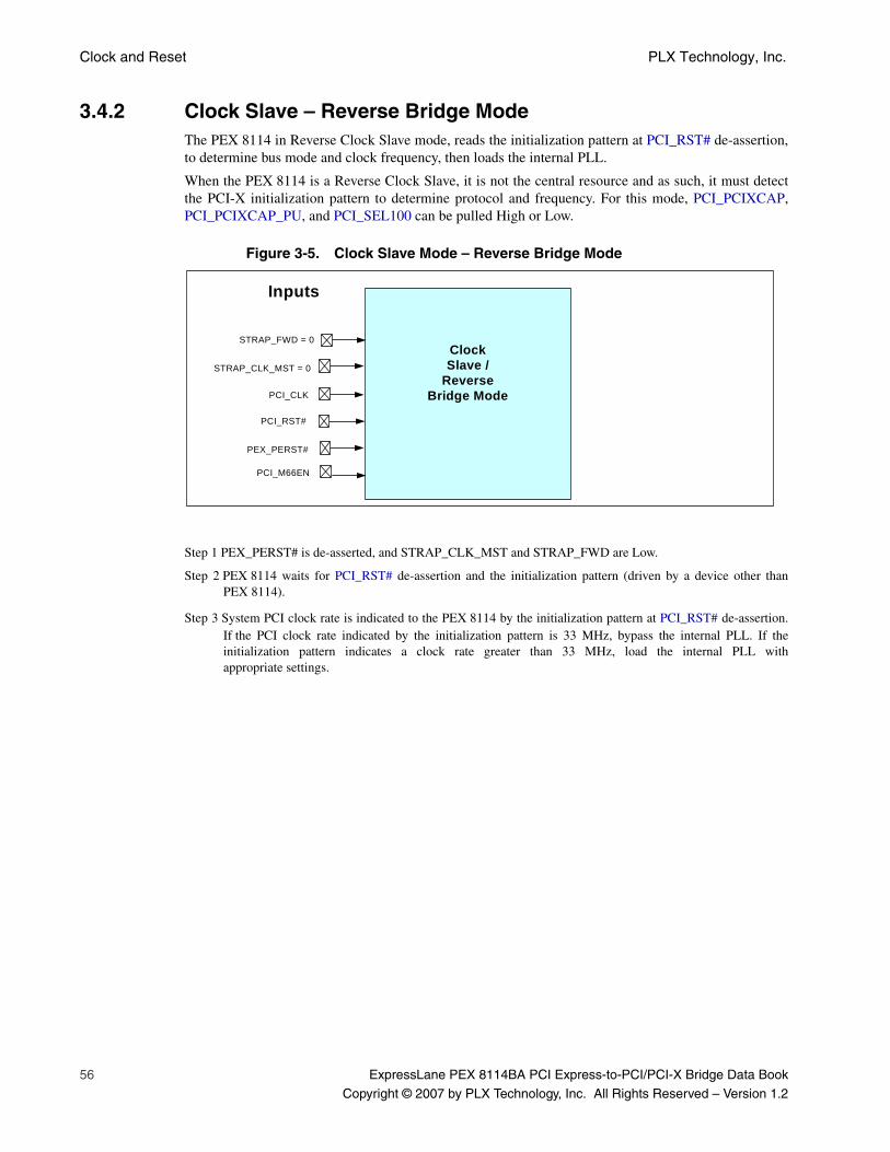
Clock and Reset PLX Technology, Inc.
56 ExpressLane PEX 8114BA PCI Express-to-PCI/PCI-X Bridge Data Book
Copyright © 2007 by PLX Technology, Inc. All Rights Reserved – Version 1.2
3.4.2 Clock Slave – Reverse Bridge ModeThe PEX 8114 in Reverse Clock Slave mode, reads the initialization pattern at PCI_RST# de-assertion,to determine bus mode and clock frequency, then loads the internal PLL.
When the PEX 8114 is a Reverse Clock Slave, it is not the central resource and as such, it must detectthe PCI-X initialization pattern to determine protocol and frequency. For this mode, PCI_PCIXCAP,PCI_PCIXCAP_PU, and PCI_SEL100 can be pulled High or Low.
Figure 3-5. Clock Slave Mode – Reverse Bridge Mode
Step 1 PEX_PERST# is de-asserted, and STRAP_CLK_MST and STRAP_FWD are Low.
Step 2 PEX 8114 waits for PCI_RST# de-assertion and the initialization pattern (driven by a device other thanPEX 8114).
Step 3 System PCI clock rate is indicated to the PEX 8114 by the initialization pattern at PCI_RST# de-assertion.If the PCI clock rate indicated by the initialization pattern is 33 MHz, bypass the internal PLL. If theinitialization pattern indicates a clock rate greater than 33 MHz, load the internal PLL withappropriate settings.
ClockSlave /
Reverse Bridge Mode
STRAP_FWD = 0
Inputs
PCI_CLK
PEX_PERST#
PCI_RST#
PCI_M66EN
STRAP_CLK_MST = 0
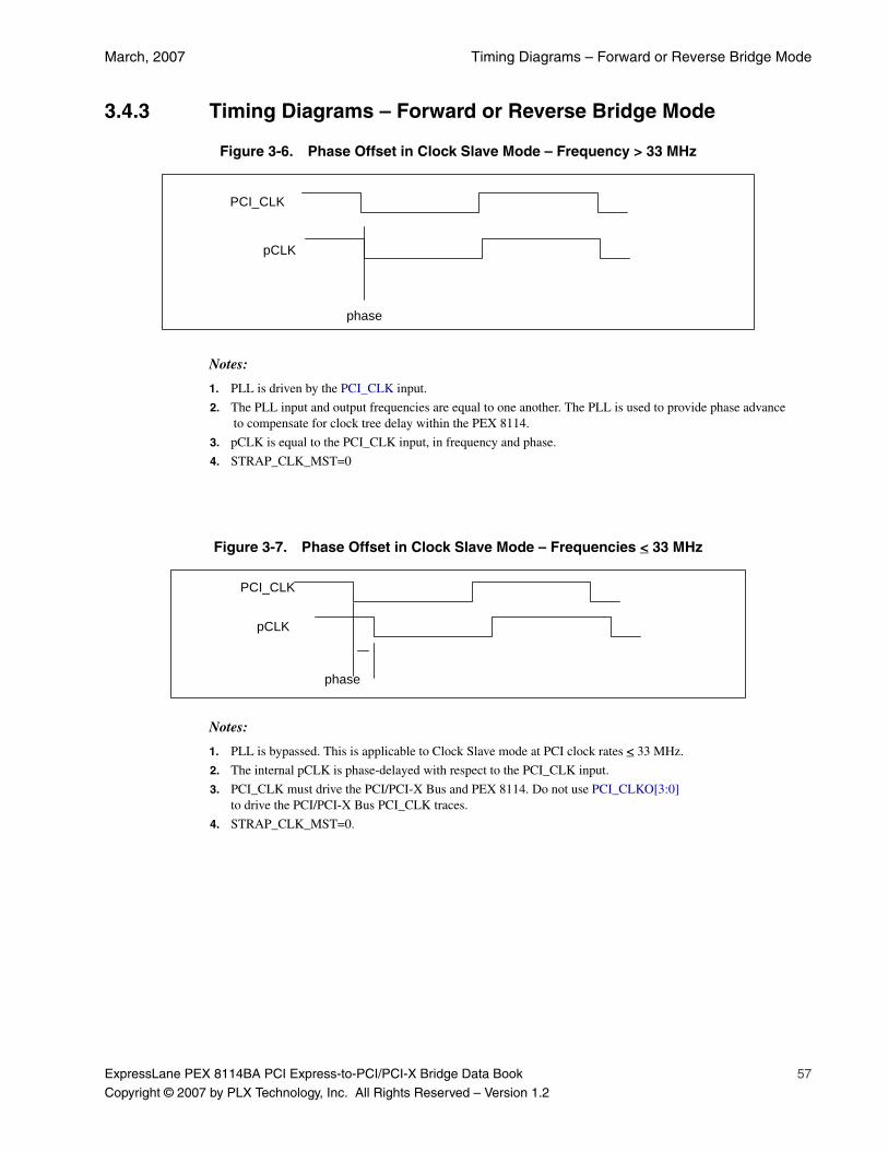
March, 2007 Timing Diagrams – Forward or Reverse Bridge Mode
ExpressLane PEX 8114BA PCI Express-to-PCI/PCI-X Bridge Data Book 57
Copyright © 2007 by PLX Technology, Inc. All Rights Reserved – Version 1.2
3.4.3 Timing Diagrams – Forward or Reverse Bridge Mode
Figure 3-6. Phase Offset in Clock Slave Mode – Frequency > 33 MHz
Notes:
1. PLL is driven by the PCI_CLK input.
2. The PLL input and output frequencies are equal to one another. The PLL is used to provide phase advance to compensate for clock tree delay within the PEX 8114.
3. pCLK is equal to the PCI_CLK input, in frequency and phase.
4. STRAP_CLK_MST=0
Figure 3-7. Phase Offset in Clock Slave Mode – Frequencies < 33 MHz
Notes:
1. PLL is bypassed. This is applicable to Clock Slave mode at PCI clock rates < 33 MHz.
2. The internal pCLK is phase-delayed with respect to the PCI_CLK input.
3. PCI_CLK must drive the PCI/PCI-X Bus and PEX 8114. Do not use PCI_CLKO[3:0] to drive the PCI/PCI-X Bus PCI_CLK traces.
4. STRAP_CLK_MST=0.
PCI_CLK
pCLK
phase
pCLK
PCI_CLK
phase

Clock and Reset PLX Technology, Inc.
58 ExpressLane PEX 8114BA PCI Express-to-PCI/PCI-X Bridge Data Book
Copyright © 2007 by PLX Technology, Inc. All Rights Reserved – Version 1.2
The PCI Express and PCI-X PLLs contain a signal that indicates to the PEX 8114 whether the PLL lostthe PLL lock. It is considered a serious error condition if the PCI Express or PCI-X PLL, when thePCI-X PLL is in Phase-Locked mode (that is, when not in PLL Bypass mode), indicates a loss of PLLlock and potential Data errors. Loss of PLL lock can be caused by one of the following:
• Serious out-of-specification noise
• Voltages on the PLL power inputs
• Out-of-specification jitter on the input reference clocks
Table 3-4 delineates the options for handling loss of PLL lock. The options are selected by the PLL LockControl 1 and PLL Lock Control 0 bits (offset FA0h[11:10]). By default, this field is cleared to 00b,which configures the PEX 8114 to ignore loss of PLL lock.
Sticky bits are set when the PCI Express or PCI-X PLL loses PLL lock:
• When the PCI Express PLL loses PLL lock, the Sticky PCI Express PLL Loss Lock bit is set (offset FA0h[15]=1)
• When the PCI-X PLL loses PLL lock, the Sticky PCI-X PLL Loss Lock bit is set (offset FA0h[14]=1)
Table 3-4. Methods for Handling Loss of PLL Lock
Offset FA0h[11:10] Description
00b Default. Ignores loss of PLL lock.
01b Loss of PLL lock immediately causes the PEX 8114 to reset.
10bThe PEX 8114 attempts to tolerate loss of PLL lock:• When lock is re-acquired in less than 200 µs, the PEX 8114 is not reset
• When lock is not re-acquired within 200 µs, the PEX 8114 is reset
11b The PEX 8114 is not reset if loss of PLL lock occurs.

March, 2007 Resets
ExpressLane PEX 8114BA PCI Express-to-PCI/PCI-X Bridge Data Book 59
Copyright © 2007 by PLX Technology, Inc. All Rights Reserved – Version 1.2
3.5 ResetsThis section explains the PEX 8114 Reset mechanism and how the differences between PCI Expressand PCI-X resets are incorporated in Forward and Reverse Bridge modes. The PCI Express r1.0a andPCI-X r1.0b define two common levels or reset types, Level-1 and Level-2. The PCI Express r1.0adefines an additional third level, Level-0. Table 3-5 delineates resets.
Table 3-5. Reset Table
Reset Type
PCI Express Definition Reset Source Impact to Various Internal
Components (Upon De-assertion)Impact to Internal Registers (No AUX and PME Enabled)
Level-0
Fundamental Reset• Cold Reset
• Warm Reset
PEX_PERST# reset input assertion
• Initialize entire bridge, including Sticky registers
• Serial EEPROM contents are loaded
• HwInit types evaluated
All registers initialized
Level-1
Forward Bridge mode:Hot Reset
• Reset bit of the TS ordered-set is set, at upstream port
• Upstream port entering DL_Down state
• Initialize ports
• Initialize entire bridge except the Sticky registers
• Serial EEPROM contents reloaded (selectively)
All registers initialized, with following exceptions:• Port Configuration registers
• All Sticky bits not affected by Hot Reset (HwInit, R/WS, R/W1CS, ROS)Reverse
Bridge mode:PCI_RST#
PCI_RST# asserted on PCI/PCI-X Bus
Level-2 Secondary Bus Reset
Forward Bridge mode
• Assert PCI_RST# on PCI-X Bus
• Drain traffic
• Drop request TLPs
• Redefine Bus mode and clock frequency in Clock Master mode
No effect to CSRs
Reverse Bridge mode
• PCI Express PL propagates Hot Reset
• PCI Express DLL down
• TLP layer initialized and exhibits DL_Down behavior
• Drops request TLPs
• Drain traffic corresponding to DL_Down behavior and initialize credits
• Redefine Bus mode and clock frequency in Clock Master mode
No effect to CSRs (other than to initialize credits)
Clock and Reset PLX Technology, Inc.
60 ExpressLane PEX 8114BA PCI Express-to-PCI/PCI-X Bridge Data Book
Copyright © 2007 by PLX Technology, Inc. All Rights Reserved – Version 1.2
3.5.1 Level-0, Fundamental Reset (Power-On, Hard, Cold, Warm)The PCI Express r1.0a defines the Fundamental Reset or Level-0 Reset. Level-0 Reset is a FundamentalReset. It is equivalent to Traditional Power-On Reset.
For this type of reset, PEX_PERST# is always an input to the PEX 8114, regardless of whether thebridge is operating in Forward or Reverse Bridge mode. Reset assertion by the system, external to thePEX 8114, causes a reset of all internal PEX 8114 registers, including Sticky bits, and drives all statemachines to known states.
3.5.1.1 PEX_PERST#In PCI Express, Fundamental Reset can be provided by the system Host or central resource.The sideband PCI Express Reset signal (PEX_PERST#) is routed in parallel to all system PCI Expressdevices in conjunction with a Power Good signal from the system power supply. For the PEX 8114, thePEX_PERST# signal is always an input in Forward and Reverse Bridge modes, which indicates that thepower is within specified tolerances and that the PEX 8114 performs internal Warm or Cold Reset.
In Forward Bridge mode, the PCI Express Root Complex feeds the PEX_PERST# signal to all devices.PEX_PERST# is driven in parallel to all PCI Express devices, following the PCI Express Power Goodreset standard practice.
In Reverse Bridge mode, the PCI central resource, including power supply monitors, feeds thePEX_PERST# signal to all PCI Express devices. The mechanism traditionally used to reset PCI Bussegments is preserved in Reverse Bridge mode, by transmitting protocol Hot Resets to reset bridges andbus segments.
When the PEX 8114 is operating in Reverse Bridge mode, the PEX_PERST# signal is expected tofunction similar to the pwr_good signal in the PCI r3.0, Figure 4.11, and to follow the timing andfunctionality defined in the PCI r3.0, Section 4.3.2.
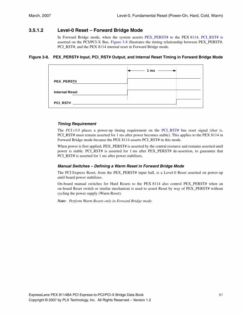
March, 2007 Level-0, Fundamental Reset (Power-On, Hard, Cold, Warm)
ExpressLane PEX 8114BA PCI Express-to-PCI/PCI-X Bridge Data Book 61
Copyright © 2007 by PLX Technology, Inc. All Rights Reserved – Version 1.2
3.5.1.2 Level-0 Reset – Forward Bridge ModeIn Forward Bridge mode, when the system asserts PEX_PERST# to the PEX 8114, PCI_RST# isasserted on the PCI/PCI-X Bus. Figure 3-8 illustrates the timing relationship between PEX_PERST#,PCI_RST#, and the PEX 8114 internal reset in Forward Bridge mode.
Figure 3-8. PEX_PERST# Input, PCI_RST# Output, and Internal Reset Timing in Forward Bridge Mode
Timing Requirement
The PCI r3.0 places a power-up timing requirement on the PCI_RST# bus reset signal (that is,PCI_RST# must remain asserted for 1 ms after power becomes stable). This applies to the PEX 8114 inForward Bridge mode because the PEX 8114 asserts PCI_RST# in this mode.
When power is first applied, PEX_PERST# is asserted by the central resource and remains asserted untilpower is stable. PCI_RST# is asserted for 1 ms after PEX_PERST# de-assertion, to guarantee thatPCI_RST# is asserted for 1 ms after power stabilizes.
Manual Switches – Defining a Warm Reset in Forward Bridge Mode
The PCI Express Reset, from the PEX_PERST# input ball, is a Level-0 Reset asserted on power-upuntil board power stabilizes.
On-board manual switches for Hard Resets to the PEX 8114 also control PEX_PERST# when anon-board Reset switch or similar mechanism is used to assert Reset by way of PEX_PERST# withoutcycling the power supply (Warm Reset).
Note: Perform Warm Resets only in Forward Bridge mode.
PEX_PERST#
Internal Reset
PCI_RST#
1 ms
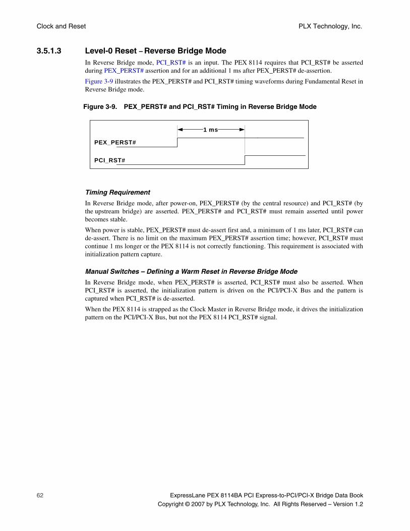
Clock and Reset PLX Technology, Inc.
62 ExpressLane PEX 8114BA PCI Express-to-PCI/PCI-X Bridge Data Book
Copyright © 2007 by PLX Technology, Inc. All Rights Reserved – Version 1.2
3.5.1.3 Level-0 Reset – Reverse Bridge ModeIn Reverse Bridge mode, PCI_RST# is an input. The PEX 8114 requires that PCI_RST# be assertedduring PEX_PERST# assertion and for an additional 1 ms after PEX_PERST# de-assertion.
Figure 3-9 illustrates the PEX_PERST# and PCI_RST# timing waveforms during Fundamental Reset inReverse Bridge mode.
Figure 3-9. PEX_PERST# and PCI_RST# Timing in Reverse Bridge Mode
Timing Requirement
In Reverse Bridge mode, after power-on, PEX_PERST# (by the central resource) and PCI_RST# (bythe upstream bridge) are asserted. PEX_PERST# and PCI_RST# must remain asserted until powerbecomes stable.
When power is stable, PEX_PERST# must de-assert first and, a minimum of 1 ms later, PCI_RST# cande-assert. There is no limit on the maximum PEX_PERST# assertion time; however, PCI_RST# mustcontinue 1 ms longer or the PEX 8114 is not correctly functioning. This requirement is associated withinitialization pattern capture.
Manual Switches – Defining a Warm Reset in Reverse Bridge Mode
In Reverse Bridge mode, when PEX_PERST# is asserted, PCI_RST# must also be asserted. WhenPCI_RST# is asserted, the initialization pattern is driven on the PCI/PCI-X Bus and the pattern iscaptured when PCI_RST# is de-asserted.
When the PEX 8114 is strapped as the Clock Master in Reverse Bridge mode, it drives the initializationpattern on the PCI/PCI-X Bus, but not the PEX 8114 PCI_RST# signal.
PEX_PERST#
PCI_RST#
1 ms
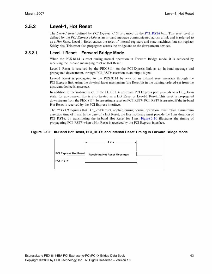
March, 2007 Level-1, Hot Reset
ExpressLane PEX 8114BA PCI Express-to-PCI/PCI-X Bridge Data Book 63
Copyright © 2007 by PLX Technology, Inc. All Rights Reserved – Version 1.2
3.5.2 Level-1, Hot ResetThe Level-1 Reset defined by PCI Express r1.0a is carried on the PCI_RST# ball. This reset level isdefined by the PCI Express r1.0a as an in-band message communicated across a link and is referred toas a Hot Reset. Level-1 Reset causes the reset of internal registers and state machines, but not registerSticky bits. This reset also propagates across the bridge and to the downstream devices.
3.5.2.1 Level-1 Reset – Forward Bridge ModeWhen the PEX 8114 is reset during normal operation in Forward Bridge mode, it is achieved byreceiving the in-band messaging reset or Hot Reset.
Level-1 Reset is received by the PEX 8114 on the PCI Express link as an in-band message andpropagated downstream, through PCI_RST# assertion as an output signal.
Level-1 Reset is propagated to the PEX 8114 by way of an in-band reset message through thePCI Express link, using the physical layer mechanism (the Reset bit in the training ordered-set from theupstream device is asserted).
In addition to the in-band reset, if the PEX 8114 upstream PCI Express port proceeds to a DL_Downstate, for any reason, this is also treated as a Hot Reset or Level-1 Reset. This reset is propagateddownstream from the PEX 8114, by asserting a reset on PCI_RST#. PCI_RST# is asserted if the in-bandHot Reset is received by the PCI Express interface.
The PCI r3.0 requires that PCI_RST# reset, applied during normal operation, must retain a minimumassertion time of 1 ms. In the case of a Hot Reset, the Host software must provide the 1 ms duration ofPCI_RST#, by transmitting the in-band Hot Reset for 1 ms. Figure 3-10 illustrates the timing ofpropagating PCI_RST# when a Hot Reset is received by the PCI Express interface.
Figure 3-10. In-Band Hot Reset, PCI_RST#, and Internal Reset Timing in Forward Bridge Mode
PCI Express Hot Reset
PCI_RST#
1 ms
Receiving Hot Reset Messages

Clock and Reset PLX Technology, Inc.
64 ExpressLane PEX 8114BA PCI Express-to-PCI/PCI-X Bridge Data Book
Copyright © 2007 by PLX Technology, Inc. All Rights Reserved – Version 1.2
3.5.2.2 Level-1 Reset – Reverse Bridge ModeIn Reverse Bridge mode, Level-1 Reset is received by the PEX 8114 on the PCI-X interface PCI_RST#ball as an input, and propagated downstream as an in-band message on the PCI Express link (using thePhysical Layer mechanism).
Level-1 Reset is the equivalent to Hot Reset in Forward Bridge mode received on the PCI Expressinterface. It causes the reset of internal registers and state machines, but not register Sticky bits.
The PCI r3.0 requires that PCI_RST# be asserted for a minimum of 1 ms.
Level-1 Reset also causes the serial EEPROM reload, bus mode recheck, and clock frequency recheck.
When PCI_RST# is asserted, it is propagated across the bridge and downstream on the PCI Express linkas a Hot Reset. During the time that PCI_RST# is asserted in-band, Hot Reset messages arecontinuously transmitted across the PCI Express link.
Figure 3-11 illustrates the timing relationship between PCI_RST# and transmitting in-band Hot Resetmessages.
Figure 3-11. PCI_RST# and Hot Reset Message Timing in Reverse Bridge Mode
1 ms
PCI_RST#
PCI Express Hot Reset Sending Hot Reset Messages

March, 2007 Secondary Bus Reset, Level-2 Reset
ExpressLane PEX 8114BA PCI Express-to-PCI/PCI-X Bridge Data Book 65
Copyright © 2007 by PLX Technology, Inc. All Rights Reserved – Version 1.2
3.5.3 Secondary Bus Reset, Level-2 ResetLevel-2 Reset is provided by the internal Bridge Control register Secondary Bus Reset bit (bit 6). Thisreset drives the bridge state machines to a known state, but not internal register resets. This reset alsopropagates a reset to downstream devices in the same manner as Level-1 Reset.
Level-2 Resets are sustained until the Secondary Bus Reset bit is cleared. This bit is set and cleared bysoftware, using Configuration Write accesses.
The Secondary Bus Reset is used to reset all downstream devices, without resetting the bridge.
3.5.3.1 Level-2 Reset – Forward Bridge ModeLevel-2 Reset, when the Secondary Bus Reset bit is set to 1, is propagated downstream in ForwardBridge mode, through PCI_RST# assertion.
In Forward Bridge mode, PCI_RST# is asserted on the PCI/PCI-X Bus when this bit is set.The minimum duration for PCI_RST# is 1 ms. The PEX 8114 internal state machines are forced toinitial states and internal transaction queues are flushed.
Figure 3-12 illustrates the timing relationship between Secondary Bus Reset and PCI_RST# in ForwardBridge mode.
Figure 3-12. Secondary Bus Reset and PCI_RST# Timing in Forward Bridge Mode
3.5.3.2 Level-2 Reset – Reverse Bridge ModeLevel-2 Reset, when the Secondary Bus Reset bit is set to 1, is propagated downstream through anin-band message on the PCI Express link.
When this bit is set in Reverse Bridge mode, in-band message reset is communicated through thePCI Express link from the PEX 8114 to the downstream devices. The PEX 8114 internal state machinesare forced to initial states and internal transaction queues are flushed.
Figure 3-13 illustrates the relationship between the Secondary Bus Reset bit and transmitting in-bandHot Reset messages.
Figure 3-13. Secondary Bus Reset and Hot Reset Message Timing in Reverse Bridge Mode
Secondary Bus Reset
PCI_RST#
1 ms
Secondary Bus Reset
Hot Reset Messages Sending Hot Reset Messages
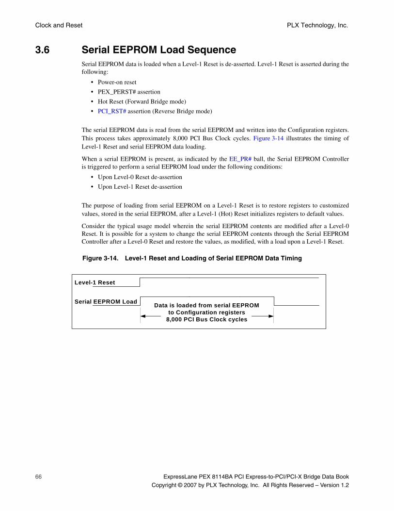
Clock and Reset PLX Technology, Inc.
66 ExpressLane PEX 8114BA PCI Express-to-PCI/PCI-X Bridge Data Book
Copyright © 2007 by PLX Technology, Inc. All Rights Reserved – Version 1.2
3.6 Serial EEPROM Load SequenceSerial EEPROM data is loaded when a Level-1 Reset is de-asserted. Level-1 Reset is asserted during thefollowing:
• Power-on reset
• PEX_PERST# assertion
• Hot Reset (Forward Bridge mode)
• PCI_RST# assertion (Reverse Bridge mode)
The serial EEPROM data is read from the serial EEPROM and written into the Configuration registers.This process takes approximately 8,000 PCI Bus Clock cycles. Figure 3-14 illustrates the timing ofLevel-1 Reset and serial EEPROM data loading.
When a serial EEPROM is present, as indicated by the EE_PR# ball, the Serial EEPROM Controlleris triggered to perform a serial EEPROM load under the following conditions:
• Upon Level-0 Reset de-assertion
• Upon Level-1 Reset de-assertion
The purpose of loading from serial EEPROM on a Level-1 Reset is to restore registers to customizedvalues, stored in the serial EEPROM, after a Level-1 (Hot) Reset initializes registers to default values.
Consider the typical usage model wherein the serial EEPROM contents are modified after a Level-0Reset. It is possible for a system to change the serial EEPROM contents through the Serial EEPROMController after a Level-0 Reset and restore the values, as modified, with a load upon a Level-1 Reset.
Figure 3-14. Level-1 Reset and Loading of Serial EEPROM Data Timing
Level-1 Reset
Serial EEPROM Load Data is loaded from serial EEPROMto Configuration registers
8,000 PCI Bus Clock cycles
ExpressLane PEX 8114BA PCI Express-to-PCI/PCI-X Bridge Data Book 67
Copyright © 2007 by PLX Technology, Inc. All Rights Reserved – Version 1.2
Chapter 4 Data Path
4.1 Internal Data Path DescriptionThe PEX 8114 bridge supports Data transfers from the PCI-X port to the PCI Express port. The PCI-Xport operates in PCI or PCI-X mode, at clock rates up to 133 MHz and 32- or 64-bit bus widths.The PCI Express port is four lanes wide and can be configured as a 4-, 2-, or 1-lane port.
The PEX 8114 internal data path is based on a central RAM. which holds and orders all data transferredthrough the bridge in three separate linked lists including Posted, Non-Posted and Completion data.There is a separate, central 8-KB RAM for data flowing in each direction. All transactions are heldwithin the RAM in a double store-and-forward method. Separate link lists for Posted and Non-Postedtransactions, as well as Completions, share space within the RAM and all link list accesses to theinternal RAM output are governed, according to PCI Express Ordering rules.
At least 2 KB of the 8-KB RAM are dedicated to Completions. Completions can optionally require asmuch as 6 KB of memory, according to demand. The remainder of the RAM is used for Posted andNon-Posted requests, or remains empty. In addition to the central RAM, there are eight, 256-byte buffersin the PCI modules that track and combine the data (for up to eight concurrent Non-Posted PCI requests)with their Completion data when the Completion returns from the PCI Express link. (Refer to Chapter 7,“Bridge Operations,” for further details.)
Additionally, the PCI interface modules include eight data-holding register sets that are dedicated totracking the Completion progress of eight PCI Express requests on the PCI Bus. These registers holdinformation that uniquely identifies the Target location and data quantity requested, for up to eightPCI Express requests. As the PCI module’s state machines supply the data requested by the PCI Expressdevice, these registers track progress toward Completion. After a transaction completes, the internalresources dedicated to that transaction are recovered and readied to service a new transaction.
4.2 PCI Express CreditsPCI Express credits are issued according to the PCI Express requirements to manage the internal 8-KBcentral RAM and ensure that no internal memory linked list is overrun.
Data Path PLX Technology, Inc.
68 ExpressLane PEX 8114BA PCI Express-to-PCI/PCI-X Bridge Data Book
Copyright © 2007 by PLX Technology, Inc. All Rights Reserved – Version 1.2
4.3 Latency and BandwidthThe PEX 8114 can be configured as a PCI or PCI-X device at up to 133 MHz and 64-bit data bus on thePCI-X side, transacting data with the PCI Express port configured as a 1-, 2-, or 4-lane port. It isanticipated that from a bandwidth-balancing perspective, the PCI Express port configured as a 4-lanedevice matches well with the PCI-X side operating at 133 MHz and 64 bits. In this matchedconfiguration, expect full bandwidth utilization on the PCI Express lanes and PCI-X Bus, withthroughput limitations being the external PCI Express and PCI-X ports’ bandwidth capability and notthe PEX 8114’s internal bandwidth. A 66-MHz, 64-bit PCI-X port should match an x2 PCI Expressport. It is anticipated that the PEX 8114 does not limit the bandwidth of those transactions. Bandwidth isaffected by many parameters, including but not limited to arbitration latency, cycle startup latency,Retries, packet sizes, and external endpoint latency. Adjust the parameters within the PEX 8114, basedon the PCI Express-to-PCI/PCI-X Bridge r1.0.
4.3.1 Data Flow-Through LatencyWhen the PEX 8114 is configured as a PCI-X device, operating at 133-MHz clock frequency with a64-bit wide data bus, and the PCI Express port is configured as a 4-lane link, expect approximately300 ns latency through the PEX 8114 for Header-only packets and approximately 850 ns for Headerswith 256-byte Data packets. This is the latency of data driven from PCI-X to PCI Express. This latencyis measured from the frame drop on the PCI-X Bus, when data is driven into the PEX 8114, until thestarting symbol of data TLP appears on the PCI Express lanes. Internal latency of data driven fromPCI Express to PCI-X is similar.
4.3.2 PCI Transaction Initial Latency and Cycle Recovery TimeIn PCI mode, when the PEX 8114 is a Read Cycle Target, the PEX 8114 supplies data or Retriesthe Master Read request. There are eight Clock cycles from when the Master asserts PCI_FRAME#until the PEX 8114 signals a Retry or is ready to supply data. This equates to an initial target latency ofeight clocks.
When the PEX 8114 is the Write Cycle Master, there is one Clock cycle from when the Master drivesPCI_FRAME# until the PEX 8114 drives PCI_IRDY# ready to supply data. This cycle is the Addressphase, required by the PCI r3.0. There are no initial wait states added by the PEX 8114. The PEX 8114 isa slow-decode device and supports fast back-to-back addressing.
The PEX 8114 requires certain Clock cycles after completion of a previous transaction, before it canparticipate in another transaction. This period is Clock cycles, from the last Data phase of the precedingtransaction and PCI_FRAME# assertion on a new transaction, and is referred to as transaction cyclerecovery time. The cycle recover time from mastering a PCI-X transaction is 10 Clock cycles.
March, 2007 PCI-X Transaction Initial Latency and Cycle Recovery Time
ExpressLane PEX 8114BA PCI Express-to-PCI/PCI-X Bridge Data Book 69
Copyright © 2007 by PLX Technology, Inc. All Rights Reserved – Version 1.2
4.3.3 PCI-X Transaction Initial Latency and Cycle Recovery TimeIn PCI-X mode, when the PEX 8114 is a Read Transaction Target, there are seven Clock cycles fromwhen the Master asserts PCI_FRAME# until the PEX 8114 drives a Split Response to the PCI-X Readrequest. When the PEX 8114 is a PCI-X Write Cycle Target, there are seven Clock cycles from when theMaster asserts PCI_FRAME# until the PEX 8114 drives PCI_IRDY# ready to accept data. This equatesto an initial Target latency of two clocks.
When the PEX 8114 is a Write or Read Completion Master, there are three Clock cycles from when thePEX 8114 asserts PCI_FRAME# until the PEX 8114 asserts PCI_IRDY# indicating that it is ready todrive data. These three Clocks cycles are the Address, Attribute, and Turnaround cycles required by thePCI-X r2.0a. There are no initial wait states added by the PEX 8114. The PEX 8114 is a slow-decodedevice and supports fast back-to-back addressing.
The PEX 8114 requires certain Clock cycles after the completion of a previous transaction, before it canparticipate in another transaction. This period is Clock cycles, from the last Data phase of the precedingtransaction and PCI_FRAME# assertion on a new transaction, and is referred to as transaction cyclerecovery time. The cycle recover time for mastering a PCI cycle is seven Clock cycles.
4.3.4 Arbitration LatencyArbitration latency is the number of PCI Clock cycles required for the bridge to be granted the bus whenit is waiting to make a transfer. This time can vary and is a function of the number of devices on thePCI Bus and each device’s demand for bus control. At a minimum, the bus can be parked on the bridgeand in that case, the arbitration latency is 0 clocks. If the bus is not parked on the bridge and not beingused by another device, the latency is 1 clock after the request. If the bus is being used by anotherMaster and hidden arbitration is enabled, the arbitration latency is 1 clock after the other users relinquishthe bus. If the bus is being used by another Master and hidden arbitration is not enabled, the arbitrationlatency is 2 clocks after the other users relinquish the bus.
Data Path PLX Technology, Inc.
70 ExpressLane PEX 8114BA PCI Express-to-PCI/PCI-X Bridge Data Book
Copyright © 2007 by PLX Technology, Inc. All Rights Reserved – Version 1.2
THIS PAGE INTENTIONALLY LEFT BLANK.
ExpressLane PEX 8114BA PCI Express-to-PCI/PCI-X Bridge Data Book 71
Copyright © 2007 by PLX Technology, Inc. All Rights Reserved – Version 1.2
Chapter 5 Address Spaces
5.1 IntroductionThe PEX 8114 can be configured at Power Good Reset, by way of a Strapping ball, to function as aTransparent or Non-Transparent PCI-X-to-PCI Express bridge. From an address perspective, theprimary difference between the Transparent and Non-Transparent bridge is that a Transparent bridgeprovides no address modification of the Data Target location as it passes through the bridge.In Non-Transparent mode, the data exiting the bridge can include a different address than it did when itentered the bridge. This chapter discusses the PEX 8114 Address space details for Transparent andNon-Transparent modes.
5.2 Transparent ModeIn Transparent mode, the PEX 8114 supports the following Address spaces:
• PCI-compatible Configuration (00h to FFh; 256 bytes)
• PCI Express Extended Configuration (100h to FFFh)
• I/O (32-bit; includes ISA and VGA modes)
• Memory-Mapped I/O (32-bit non-prefetchable)
• Prefetchable memory (64-bit)
• Base Address register (BAR) access to internal registers
The first two spaces, used for accessing Configuration registers, are described in Chapter 6,“Configuration.” The PCI Express Extended Configuration space (100h to FFFh) is supported only inForward Bridge mode, and BARs are used to access Extended Configuration space in ReverseBridge mode.
Configuration registers set up for I/O, Memory-Mapped and Prefetchable Memory Address spacesdetermine which transactions are forwarded from the primary bus to the secondary bus and from thesecondary bus to the primary bus. The I/O and Memory ranges are defined by a set of Base and Limitregisters in the Configuration Header. Transactions falling within the ranges defined by the Base andLimit registers are forwarded from the primary bus to the secondary bus. Transactions falling outsidethese ranges are forwarded from the secondary bus to the primary bus.
Table 5-1 delineates which interfaces are primary and secondary, for the two PEX 8114 bridge modes.
Table 5-1. Bridge Mode Primary and Secondary Interfaces
Bridge Mode Primary Interface/Bus Secondary Interface/Bus
Forward Bridge PCI Express PCI
Reverse Bridge PCI PCI Express
Address Spaces PLX Technology, Inc.
72 ExpressLane PEX 8114BA PCI Express-to-PCI/PCI-X Bridge Data Book
Copyright © 2007 by PLX Technology, Inc. All Rights Reserved – Version 1.2
5.2.1 Transparent Mode I/O SpaceThe I/O Address space determines whether to forward I/O Read or I/O Write transactions across thebridge. PCI Express uses the 32-bit Short Address Format (DWord-aligned) for I/O transactions.
5.2.1.1 Enable BitsThe following Configuration register bits control the bridge response to I/O transactions:
• Command register I/O Access Enable bit
• Command register Bus Master Enable bit
• Bridge Control register ISA Enable bit
• Bridge Control register VGA Enable bit
Set the I/O Access Enable bit to allow I/O transactions to forward downstream. When this bit is not set,all I/O transactions on the secondary bus are forwarded to the primary bus. If this bit is not set inForward Bridge mode, all primary interface I/O requests are completed with Unsupported Requeststatus. If this bit is not set in Reverse Bridge mode, all I/O transactions are ignored (no PCI_DEVSEL#assertion) on the primary (PCI) bus.
Set the Bus Master Enable bit to allow I/O transactions to forward upstream. If this bit is not set inForward Bridge mode, all I/O transactions on the secondary (PCI) bus are ignored. If this bit is not set inReverse Bridge mode, all I/O requests on the secondary (PCI Express) bus are completed withUnsupported Request status.
Setting the ISA Enable bit affects I/O transactions. (Refer to Section 5.2.1.3, “ISA Mode,” for details.)Setting the VGA Enable bit also affects I/O transactions. (Refer to Section 5.2.1.4, “VGA Mode,”for details.)
5.2.1.2 I/O Base and Limit RegistersThe PEX 8114 supports the optional 32-bit I/O Addressed access. The following I/O Base and LimitConfiguration registers are used to determine whether I/O transactions can be forwarded acrossthe bridge:
• I/O Base (upper four bits of the 8-bit register correspond to Address bits [15:12])
• I/O Base Upper 16 Bits (16-bit register corresponds to Address bits [31:16])
• I/O Limit (upper four bits of the 8-bit register correspond to Address bits [15:12])
• I/O Limit Upper 16 Bits (16-bit register corresponds to Address bits [31:16])
The I/O Base address consists of one 8-bit register and one 16-bit register. The upper four bits of the8-bit register define bits [15:12] of the I/O Base address. The lower four bits of the 8-bit registerdetermine the I/O address capability of this device. The I/O Base Upper 16 Bits register define bits[31:16] of the I/O Base address.
The I/O Limit address consists of one 8-bit register and one 16-bit register. The upper four bits ofthe 8-bit register define bits [15:12] of the I/O limit. The lower four bits of the 8-bit register determinethe I/O address capability of this device, and reflect the value of the same field in the I/O Base register.The I/O Limit Upper 16 Bits register defines bits [31:16] of the I/O Limit address.
Because Address bits [11:0] are not included in Address Space decoding, the I/O Address range has agranularity of 4 KB, and is always aligned to a 4-KB Address Boundary space. The maximum I/O rangeis 4 GB.
I/O transactions on the primary bus that fall within the range defined by the Base and Limit addressesare forwarded downstream to the secondary bus. I/O transactions on the secondary bus that are withinthe range are ignored.
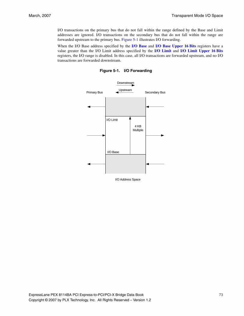
March, 2007 Transparent Mode I/O Space
ExpressLane PEX 8114BA PCI Express-to-PCI/PCI-X Bridge Data Book 73
Copyright © 2007 by PLX Technology, Inc. All Rights Reserved – Version 1.2
I/O transactions on the primary bus that do not fall within the range defined by the Base and Limitaddresses are ignored. I/O transactions on the secondary bus that do not fall within the range areforwarded upstream to the primary bus. Figure 5-1 illustrates I/O forwarding.
When the I/O Base address specified by the I/O Base and I/O Base Upper 16 Bits registers have avalue greater than the I/O Limit address specified by the I/O Limit and I/O Limit Upper 16 Bitsregisters, the I/O range is disabled. In this case, all I/O transactions are forwarded upstream, and no I/Otransactions are forwarded downstream.
Figure 5-1. I/O Forwarding
I/O Base
I/O Limit
4 KBMultiple
Primary Bus Secondary Bus
I/O Address Space
Downstream
Upstream
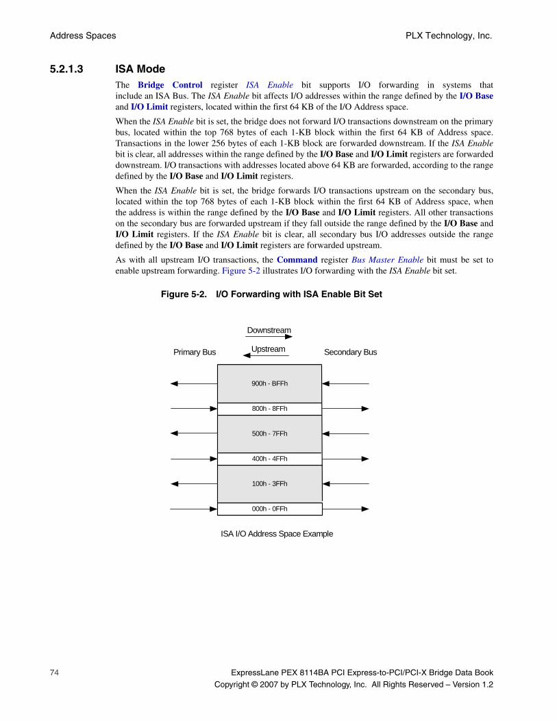
Address Spaces PLX Technology, Inc.
74 ExpressLane PEX 8114BA PCI Express-to-PCI/PCI-X Bridge Data Book
Copyright © 2007 by PLX Technology, Inc. All Rights Reserved – Version 1.2
5.2.1.3 ISA ModeThe Bridge Control register ISA Enable bit supports I/O forwarding in systems thatinclude an ISA Bus. The ISA Enable bit affects I/O addresses within the range defined by the I/O Baseand I/O Limit registers, located within the first 64 KB of the I/O Address space.
When the ISA Enable bit is set, the bridge does not forward I/O transactions downstream on the primarybus, located within the top 768 bytes of each 1-KB block within the first 64 KB of Address space.Transactions in the lower 256 bytes of each 1-KB block are forwarded downstream. If the ISA Enablebit is clear, all addresses within the range defined by the I/O Base and I/O Limit registers are forwardeddownstream. I/O transactions with addresses located above 64 KB are forwarded, according to the rangedefined by the I/O Base and I/O Limit registers.
When the ISA Enable bit is set, the bridge forwards I/O transactions upstream on the secondary bus,located within the top 768 bytes of each 1-KB block within the first 64 KB of Address space, whenthe address is within the range defined by the I/O Base and I/O Limit registers. All other transactionson the secondary bus are forwarded upstream if they fall outside the range defined by the I/O Base andI/O Limit registers. If the ISA Enable bit is clear, all secondary bus I/O addresses outside the rangedefined by the I/O Base and I/O Limit registers are forwarded upstream.
As with all upstream I/O transactions, the Command register Bus Master Enable bit must be set toenable upstream forwarding. Figure 5-2 illustrates I/O forwarding with the ISA Enable bit set.
Figure 5-2. I/O Forwarding with ISA Enable Bit Set
Secondary Bus
ISA I/O Address Space Example
000h - 0FFh
Primary Bus
400h - 4FFh
800h - 8FFh
900h - BFFh
500h - 7FFh
100h - 3FFh
Downstream
Upstream
March, 2007 Transparent Mode I/O Space
ExpressLane PEX 8114BA PCI Express-to-PCI/PCI-X Bridge Data Book 75
Copyright © 2007 by PLX Technology, Inc. All Rights Reserved – Version 1.2
5.2.1.4 VGA ModeThe Bridge Control register VGA Enable bit enables VGA Register accesses to forward downstreamfrom the primary to secondary bus, independent of the I/O Base and I/O Limit registers.
The Bridge Control register VGA 16-Bit Decode bit selects between 10- and 16-bit VGA I/O addressdecoding, and is applicable when the VGA Enable bit is set.
The VGA Enable and VGA 16-Bit Decode bits control the following VGA I/O addresses:
• 10-bit VGA I/O addressing – Address bits [9:0] = 3B0h through 3BBh, and 3C0h through 3DFh
• 16-bit VGA I/O addressing – Address bits [15:0] = 3B0h through 3BBh, and 3C0h through 3DFh
These ranges only apply to the first 64 KB of I/O Address space.
VGA Palette Snooping
VGA Palette snooping is not supported by PCI Express-to-PCI bridges; however, the PEX 8114supports Palette snooping in Reverse Bridge mode. In Forward Bridge mode, the Bridge Controlregister VGA Enable bit determines whether VGA Palette accesses are forwarded from PCI Express-to-PCI. The Command register VGA Palette Snoop bit is forced to 0 in Forward Bridge mode.
The Bridge Control register VGA 16-Bit Decode bit selects between 10- and 16-bit VGA I/O PaletteSnooping Address decoding, and is applicable when the VGA Palette Snoop bit is set.
The VGA Palette Snoop and VGA 16-Bit Decode bits control the following VGA I/O Palette Snoopaddresses:
• 10-bit VGA I/O addressing – Address bits [9:0] = 3C6h, 3C8h, and 3C9h
• 16-bit VGA I/O addressing – Address bits [15:0] = 3C6h, 3C8h, and 3C9h
The PEX 8114 supports the following three modes of Palette snooping:
• Ignore VGA Palette accesses when there are no graphic agents downstream that must snoop or respond to VGA Palette Access cycles (Writes or Reads)
• Positively decode and forward VGA Palette Writes when there are graphic agents downstream from the PEX 8114 that must snoop Palette Writes (Reads are ignored)
• Positively decode and forward VGA Palette Writes and Reads when there are graphic agents downstream that must snoop or respond to VGA Palette Access cycles (Writes or Reads)
The Bridge Control register VGA Enable bit and Command register VGA Palette Snoop bit select thebridge response to Palette accesses, as delineated in Table 5-2.
Note: X is “Don’t Care.”
Table 5-2. Bridge Response to Palette Accesses
VGA Enable Bit (Offset 3Ch[19])
VGA Palette Snoop Bit (Offset 04h[5]) Bridge Response to Palette Accesses
0 0 Ignore all Palette accesses
0 1 Positively decode Palette Writes (ignore Reads)
1 X Positively decode Palette Writes and Reads
Address Spaces PLX Technology, Inc.
76 ExpressLane PEX 8114BA PCI Express-to-PCI/PCI-X Bridge Data Book
Copyright © 2007 by PLX Technology, Inc. All Rights Reserved – Version 1.2
5.2.2 Transparent Mode Memory-Mapped I/O SpaceThe Memory-Mapped I/O Address space determines whether to forward Non-Prefetchable MemoryWrite or Read transactions across the bridge. Map devices with side effects during Reads, such asFIFOs, into this space. For PCI-to-PCI Express Reads, prefetching occurs in this space when MemoryRead Line or Memory Read Line Multiple commands are issued on the PCI Bus. When the MemoryRead Line command is used, the data quantity prefetched is determined by the Cache Line Size value.When a Memory Read Line Multiple is used, the data quantity prefetched is determined by the CacheLine Size (offset 0Ch[7:0]). For PCI-to-PCI Express transactions, the Prefetched data is flushed after thePCI device reading the data terminates its first successful Read transaction during which it receives data.For PCI-X-to-PCI Express Reads, the number of bytes to read is determined by the transaction sizerequested in the PCI-X attributes. For PCI Express-to-PCI or PCI-X Reads, the number of bytes to readis determined by the Memory Read Request TLP. Transactions that are forwarded using this Addressspace are limited to a 32-bit range.
5.2.2.1 Enable BitsThe following Configuration register bits control the bridge response to Memory-Mapped I/Otransactions:
• Command register Memory Access Enable bit
• Command register Bus Master Enable bit
Set the Memory Access Enable bit to allow Memory transactions to forward downstream. If this bit isnot set, all Memory transactions on the secondary bus are forwarded to the primary bus. If this bit is notset in Forward Bridge mode, all Non-Posted Memory requests are completed with an UnsupportedRequest status. Posted Write data is discarded. If this bit is not set in Reverse Bridge mode, all Memorytransactions are ignored on the primary (PCI) bus.
Set the Bus Master Enable bit to allow Memory transactions to forward upstream. If this bit is not set inForward Bridge mode, all Memory transactions on the secondary (PCI) bus are ignored. If this bit is notset in Reverse Bridge mode, all Non-Posted Memory requests on the secondary (PCI Express) bus arecompleted with an Unsupported Request status. Posted Write data is discarded.
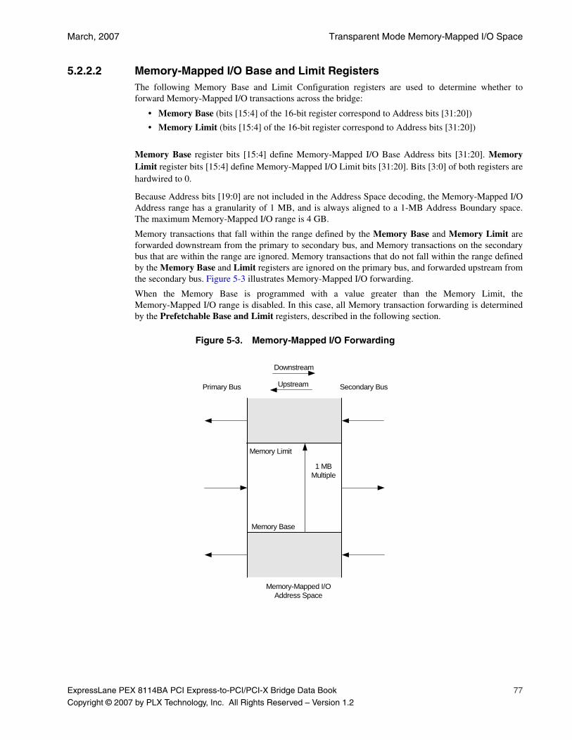
March, 2007 Transparent Mode Memory-Mapped I/O Space
ExpressLane PEX 8114BA PCI Express-to-PCI/PCI-X Bridge Data Book 77
Copyright © 2007 by PLX Technology, Inc. All Rights Reserved – Version 1.2
5.2.2.2 Memory-Mapped I/O Base and Limit RegistersThe following Memory Base and Limit Configuration registers are used to determine whether toforward Memory-Mapped I/O transactions across the bridge:
• Memory Base (bits [15:4] of the 16-bit register correspond to Address bits [31:20])
• Memory Limit (bits [15:4] of the 16-bit register correspond to Address bits [31:20])
Memory Base register bits [15:4] define Memory-Mapped I/O Base Address bits [31:20]. MemoryLimit register bits [15:4] define Memory-Mapped I/O Limit bits [31:20]. Bits [3:0] of both registers arehardwired to 0.
Because Address bits [19:0] are not included in the Address Space decoding, the Memory-Mapped I/OAddress range has a granularity of 1 MB, and is always aligned to a 1-MB Address Boundary space.The maximum Memory-Mapped I/O range is 4 GB.
Memory transactions that fall within the range defined by the Memory Base and Memory Limit areforwarded downstream from the primary to secondary bus, and Memory transactions on the secondarybus that are within the range are ignored. Memory transactions that do not fall within the range definedby the Memory Base and Limit registers are ignored on the primary bus, and forwarded upstream fromthe secondary bus. Figure 5-3 illustrates Memory-Mapped I/O forwarding.
When the Memory Base is programmed with a value greater than the Memory Limit, theMemory-Mapped I/O range is disabled. In this case, all Memory transaction forwarding is determinedby the Prefetchable Base and Limit registers, described in the following section.
Figure 5-3. Memory-Mapped I/O Forwarding
Memory Base
Memory Limit
1 MBMultiple
Primary Bus Secondary Bus
Memory-Mapped I/O Address Space
Downstream
Upstream
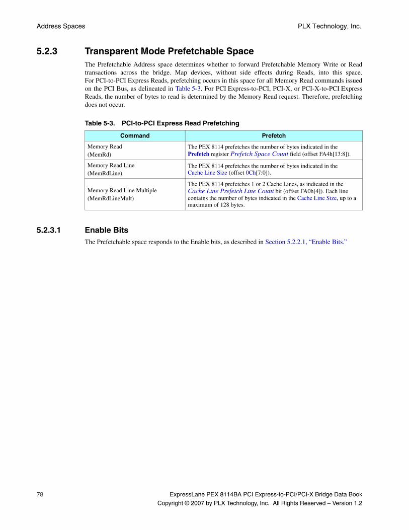
Address Spaces PLX Technology, Inc.
78 ExpressLane PEX 8114BA PCI Express-to-PCI/PCI-X Bridge Data Book
Copyright © 2007 by PLX Technology, Inc. All Rights Reserved – Version 1.2
5.2.3 Transparent Mode Prefetchable SpaceThe Prefetchable Address space determines whether to forward Prefetchable Memory Write or Readtransactions across the bridge. Map devices, without side effects during Reads, into this space.For PCI-to-PCI Express Reads, prefetching occurs in this space for all Memory Read commands issuedon the PCI Bus, as delineated in Table 5-3. For PCI Express-to-PCI, PCI-X, or PCI-X-to-PCI ExpressReads, the number of bytes to read is determined by the Memory Read request. Therefore, prefetchingdoes not occur.
5.2.3.1 Enable BitsThe Prefetchable space responds to the Enable bits, as described in Section 5.2.2.1, “Enable Bits.”
Table 5-3. PCI-to-PCI Express Read Prefetching
Command Prefetch
Memory Read(MemRd)
The PEX 8114 prefetches the number of bytes indicated in the Prefetch register Prefetch Space Count field (offset FA4h[13:8]).
Memory Read Line(MemRdLine)
The PEX 8114 prefetches the number of bytes indicated in the Cache Line Size (offset 0Ch[7:0]).
Memory Read Line Multiple(MemRdLineMult)
The PEX 8114 prefetches 1 or 2 Cache Lines, as indicated in the Cache Line Prefetch Line Count bit (offset FA0h[4]). Each line contains the number of bytes indicated in the Cache Line Size, up to a maximum of 128 bytes.
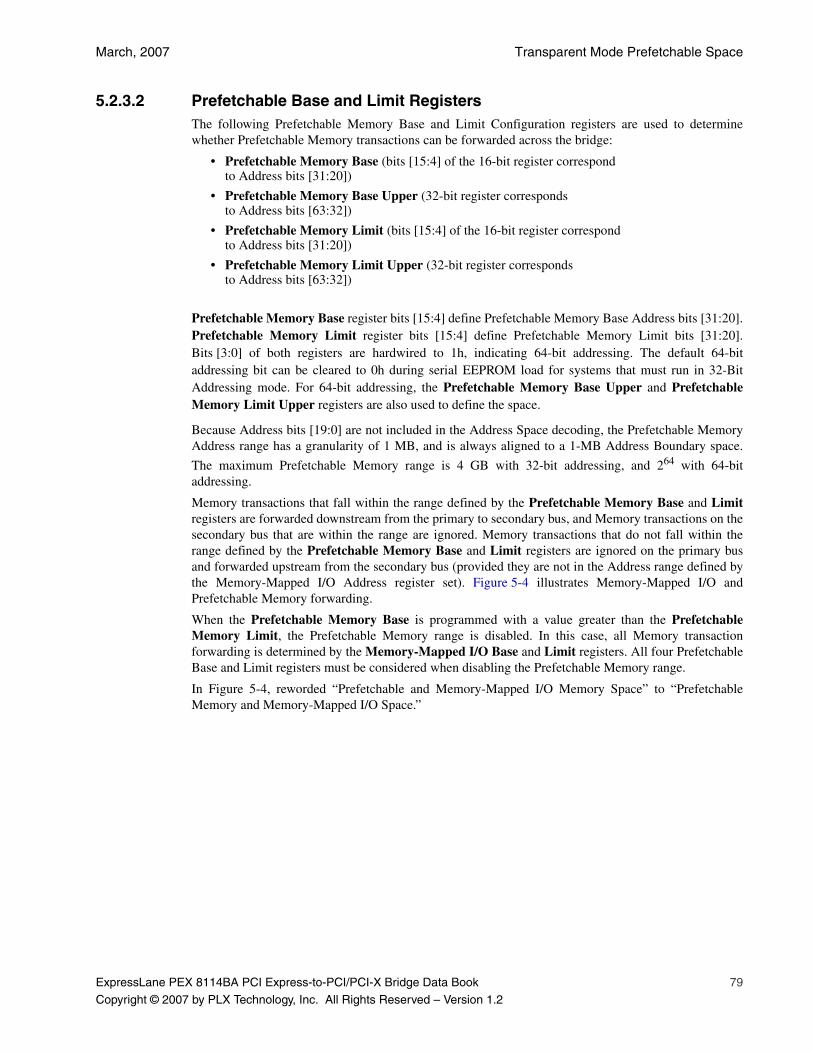
March, 2007 Transparent Mode Prefetchable Space
ExpressLane PEX 8114BA PCI Express-to-PCI/PCI-X Bridge Data Book 79
Copyright © 2007 by PLX Technology, Inc. All Rights Reserved – Version 1.2
5.2.3.2 Prefetchable Base and Limit RegistersThe following Prefetchable Memory Base and Limit Configuration registers are used to determinewhether Prefetchable Memory transactions can be forwarded across the bridge:
• Prefetchable Memory Base (bits [15:4] of the 16-bit register correspond to Address bits [31:20])
• Prefetchable Memory Base Upper (32-bit register corresponds to Address bits [63:32])
• Prefetchable Memory Limit (bits [15:4] of the 16-bit register correspond to Address bits [31:20])
• Prefetchable Memory Limit Upper (32-bit register corresponds to Address bits [63:32])
Prefetchable Memory Base register bits [15:4] define Prefetchable Memory Base Address bits [31:20].Prefetchable Memory Limit register bits [15:4] define Prefetchable Memory Limit bits [31:20].Bits [3:0] of both registers are hardwired to 1h, indicating 64-bit addressing. The default 64-bitaddressing bit can be cleared to 0h during serial EEPROM load for systems that must run in 32-BitAddressing mode. For 64-bit addressing, the Prefetchable Memory Base Upper and PrefetchableMemory Limit Upper registers are also used to define the space.
Because Address bits [19:0] are not included in the Address Space decoding, the Prefetchable MemoryAddress range has a granularity of 1 MB, and is always aligned to a 1-MB Address Boundary space.
The maximum Prefetchable Memory range is 4 GB with 32-bit addressing, and 264 with 64-bitaddressing.
Memory transactions that fall within the range defined by the Prefetchable Memory Base and Limitregisters are forwarded downstream from the primary to secondary bus, and Memory transactions on thesecondary bus that are within the range are ignored. Memory transactions that do not fall within therange defined by the Prefetchable Memory Base and Limit registers are ignored on the primary busand forwarded upstream from the secondary bus (provided they are not in the Address range defined bythe Memory-Mapped I/O Address register set). Figure 5-4 illustrates Memory-Mapped I/O andPrefetchable Memory forwarding.
When the Prefetchable Memory Base is programmed with a value greater than the PrefetchableMemory Limit, the Prefetchable Memory range is disabled. In this case, all Memory transactionforwarding is determined by the Memory-Mapped I/O Base and Limit registers. All four PrefetchableBase and Limit registers must be considered when disabling the Prefetchable Memory range.
In Figure 5-4, reworded “Prefetchable and Memory-Mapped I/O Memory Space” to “PrefetchableMemory and Memory-Mapped I/O Space.”
Address Spaces PLX Technology, Inc.
80 ExpressLane PEX 8114BA PCI Express-to-PCI/PCI-X Bridge Data Book
Copyright © 2007 by PLX Technology, Inc. All Rights Reserved – Version 1.2
Figure 5-4. Memory-Mapped I/O and Prefetchable Memory Forwarding
Prefetchable Memory Base
PrefetchableMemory Limit
Primary Bus Secondary Bus
Prefetchable Memory and Memory-Mapped
I/O Space
Memory-Mapped I/O Limit
Memory-Mapped I/O Base
4-GB Address Boundary Space
DAC
DAC DAC
DAC
SAC
SAC
SAC
SAC SAC
SAC
SAC
SAC
SAC = Single Address CycleDAC = Dual Address Cycle
1 MB Multiple
1 MB Multiple
Downstream
Upstream

March, 2007 Transparent Mode Prefetchable Space
ExpressLane PEX 8114BA PCI Express-to-PCI/PCI-X Bridge Data Book 81
Copyright © 2007 by PLX Technology, Inc. All Rights Reserved – Version 1.2
5.2.3.3 64-Bit AddressingUnlike Memory-Mapped I/O memory that must reside below the 4-GB Address Boundary space,Prefetchable memory can reside below, above, or span the 4-GB Address Boundary space. Memorylocations above the 4-GB Address Boundary space must be accessed using 64-bit addressing.PCI Express Memory transactions that use the Short Address (32-bit) format can target theNon-Prefetchable Memory space, or a Prefetchable Memory window located below the 4-GB AddressBoundary space. PCI Express Memory transactions that use the Long Address (64 bit) format can targetlocations anywhere in 64-bit Memory space.
PCI Memory transactions that use Single Address cycles can only target locations below the 4-GBAddress Boundary space. PCI Memory transactions that use Dual Address cycles can target locationsanywhere in 64-bit Memory space. The first Address phase of a Dual Address transaction contains thelower 32 bits of the address, and the second Address phase contains the upper 32 bits of the address.If the upper 32 bits of the address are 0, a Single Address transaction is performed.
Forward Bridge Mode
When the Prefetchable Memory Base Upper and Prefetchable Memory Limit Upper registers areboth cleared to 0, addresses located above the 4-GB Address Boundary space are not supported. InForward Bridge mode, if a PCI Express Memory transaction is detected with an address located above4 GB, the transaction is completed with Unsupported Request status. All Dual Address transactions onthe PCI Bus are forwarded upstream to the PCI Express interface.
When the Prefetchable memory is located entirely above the 4-GB Address Boundary space,the Prefetchable Memory Base Upper and Prefetchable Memory Limit Upper registers are both setto non-zero values. If a PCI Express Memory transaction is detected with an address located below the4-GB Address Boundary space, the transaction is completed with Unsupported Request status, and allSingle Address transactions on the PCI Bus are forwarded upstream to the PCI Express interface (unlessthey fall within the Memory-Mapped I/O range). A PCI Express Memory transaction located above4 GB, that falls within the range defined by the Prefetchable Base, Prefetchable Memory BaseUpper, Prefetchable Memory Limit, and Prefetchable Memory Limit Upper registers, is forwardeddownstream and becomes a Dual Address cycle on the PCI Bus. If a Dual Address cycle is detected onthe PCI Bus located outside the range defined by these registers, it is forwarded upstream to thePCI Express interface. If a PCI Express Memory transaction located above the 4-GB Address Boundaryspace does not fall within the range defined by these registers, it is completed with Unsupported Requeststatus. If a PCI Dual Address cycle falls within the range determined by these registers, it is ignored.
When the Prefetchable memory spans the 4-GB Address Boundary space, the Prefetchable MemoryBase Upper register is cleared to 0, and the Prefetchable Memory Limit Upper register is set to anon-zero value. If a PCI Express Memory transaction is detected with an address located below 4 GB,and is greater than or equal to the Prefetchable Memory Base Address, the transaction is forwardeddownstream. A Single Address transaction on the PCI Bus is forwarded upstream to the PCI Expressinterface if the address is less than the Prefetchable Memory Base Address. If a PCI Express Memorytransaction located above 4 GB is less than or equal to the Prefetchable Memory Limit register, it isforwarded downstream to the PCI Bus as a Dual Address cycle. If a Dual Address cycle on the PCI Busis less than or equal to the Prefetchable Memory Limit register, it is ignored. If a PCI Express Memorytransaction located above 4 GB is greater than the Prefetchable Memory Limit register, it is completedwith Unsupported Request status. If a Dual Address cycle on the PCI Bus is greater than thePrefetchable Memory Limit register, it is forwarded upstream to the PCI Express interface.
Address Spaces PLX Technology, Inc.
82 ExpressLane PEX 8114BA PCI Express-to-PCI/PCI-X Bridge Data Book
Copyright © 2007 by PLX Technology, Inc. All Rights Reserved – Version 1.2
Reverse Bridge Mode
When the Prefetchable Memory Base Upper and Prefetchable Memory Limit Upper registers areboth cleared to 0, addresses located above the 4-GB Address Boundary space are not supported. InReverse Bridge mode, if a Dual Address transaction on the PCI Bus is detected, the transaction isignored. If a PCI Express Memory transaction is detected with an address located above the 4-GBAddress Boundary space, it is forwarded upstream to the PCI Bus as a Dual Address cycle.
When the Prefetchable memory is located entirely above the 4-GB Address Boundary space,the Prefetchable Memory Base Upper and Prefetchable Memory Limit Upper registers are both setto non-zero values. The PEX 8114 ignores all single address Memory transactions on the PCI Bus, andforwards all PCI Express Memory transactions with addresses located below the 4-GB AddressBoundary space upstream to the PCI Bus (unless they fall within the Memory-Mapped I/O range).
A Dual Address transaction on the PCI Bus that falls within the range defined by the PrefetchableBase, Prefetchable Memory Base Upper, Prefetchable Memory Limit, and Prefetchable MemoryLimit Upper registers is forwarded downstream to the PCI Express interface. If a PCI Express Memorytransaction is located above the 4-GB Address Boundary space and falls outside the range defined bythese registers, it is forwarded upstream to the PCI Bus as a Dual Address cycle. If a Dual Addresstransaction on the PCI Bus does not fall within the range defined by these registers, it is ignored. If aPCI Express Memory transaction located above 4 GB falls within the range defined by these registers, itis completed with Unsupported Request status.
When the Prefetchable memory spans the 4-GB Address Boundary space, the Prefetchable MemoryBase Upper register is cleared to 0, and the Prefetchable Memory Limit Upper register is set to anon-zero value. If a PCI Single Address cycle is greater than or equal to the Prefetchable Memory BaseAddress, the transaction is forwarded downstream to the PCI Express interface. If a PCI ExpressMemory transaction is detected with an address located below the 4-GB Address Boundary space, and isless than the Prefetchable Memory Base Address, the transaction is forwarded upstream to the PCI Bus.If a Dual Address PCI transaction is less than or equal to the Prefetchable Memory Limit register, it isforwarded downstream to the PCI Express interface. If a PCI Express Memory transaction locatedabove the 4-GB Address Boundary space is less than or equal to the Prefetchable Memory Limitregister, it is completed with Unsupported Request status. If a Dual Address PCI transaction is greaterthan the Prefetchable Memory Limit register, it is ignored. If a PCI Express Memory transactionlocated above the 4-GB Address Boundary space is greater than the Prefetchable Memory Limitregister, it is forwarded upstream to the PCI Bus as a Dual Address cycle.
5.2.4 Transparent Mode Base Address Register AddressingThe Base Address Registers (BARs) provide Memory-Mapped access to internal Configurationregisters. This method of accessing internal registers is extensively used to access the PCI ExpressExtended register set when operating as a Reverse PCI bridge, without access to the higherConfiguration addresses. All accesses using the BARs return 1 DWord of data. The BARs do not affectdata forwarding through the bridge that uses Memory I/O, Memory-Mapped, or Prefetchable Memory.
The PEX 8114 defaults to a non-prefetchable 32-bit BAR access, using BAR 0 and leaving BAR 1unused. The PEX 8114 can be configured by serial EEPROM to support 64-bit non-prefetchable BARaccess, using both BAR 0 and BAR 1 to create a 64-bit BAR, by setting the Base Address 0 registerMemory Map Type field (offset 10h[2:1] to 10b.
Addresses transmitted to the BAR window are linearly translated into register address accesses. TheNth location of the BAR maps to the Nth Configuration register. Access to BAR locations that do notcontain registers corresponding to that address return UR in Forward Bridge mode and 0 in ReverseBridge mode.
For further details, refer to Chapter 6, “Configuration.”

March, 2007 Non-Transparent Forward Bridge Mode
ExpressLane PEX 8114BA PCI Express-to-PCI/PCI-X Bridge Data Book 83
Copyright © 2007 by PLX Technology, Inc. All Rights Reserved – Version 1.2
5.3 Non-Transparent Forward Bridge ModeThe PEX 8114 provides Non-Transparent Forward Bridge mode. Non-Transparent bridges are designedto allow data to transfer between two processor domains with conflicting address maps, by allowing theData address to be remapped as it crosses the bridge. In Non-Transparent mode, the PEX 8114 acts as agateway from PCI Express to an intelligent subsystem that controls a Local processor on the PCI-X sideof the PEX 8114. Base Address Registers (BARs) are provided to support Configuration-, Memory-,and I/O-mapped access across the PEX 8114. To support Data transfers between the two sides of thebridge in Non-Transparent mode, two types of Address translation are provided through the BARs tohandle resource conflicts that exist between the two separate PCI address domains. In addition tosupporting Address translation, the PEX 8114 also translates 64-bit address PCI Express TLPs into32-bit address PCI-X transactions. This allows the PCI Express side of the PEX 8114 to use 64-bitAddress space and exchange data across the bridge, to the PCI-X domain, in 32-bit Address space.
In Non-Transparent Forward Bridge mode, the primary (PCI Express) side is referred to as the HostDomain and the secondary (PCI-X) side is referred to as the Local Domain. The PEX 8114 appears as aPCI endpoint to the PCI Express Root Complex at the head of the Host Domain, as well as to the PCIHost in the Local Domain. When using the PEX 8114 in Non-Transparent mode, the PCI Express RootComplex and PCI-X Host detect an endpoint’s Type 0 register set in the PEX 8114. Configuration andData transfers can be performed through the BARs. Configuration can also be achieved throughstandard Configuration Access; however, configurations from the PCI Express Root Complex access thePCI Express side of the bridge, and PCI-X configurations access the 256-byte PCI-X registers. Whenconfiguring through the BARs, the first two BARs – BAR 0 and BAR 1 – are used for Configurationregister access. The remaining four BARs are used for Data transfers through the bridge.The PCI Express and PCI-X sides of the bridge implement and support the use of six BARs. (Refer toTable 5-4.)
The following sections delineate the BARs used for Configuration and Address translation, onboth sides of the PEX 8114, when configured in Non-Transparent mode. For further details onindividual bits, refer to the Non-Transparent register maps provided in Chapter 16, “PEX 8114 Non-Transparent Mode PCI-X Registers,” and Chapter 17, “PEX 8114 Non-Transparent Mode PCI ExpressRegisters.”
Table 5-4. PCI/PCI-X BAR Configuration
BAR PCI-X Side of the Bridge Supports PCI Express Side of the Bridge Supports
BAR 0A 32-bit Memory-Mapped Configuration register Access space, using BAR 0.
A 32-bit Memory-Mapped Configuration register Access space, using BAR 0.
BAR 1 An optional 32-bit I/O-mapped Configuration register Access space, using BAR 1.
An optional 32-bit I/O-mapped Configuration register Access space, using BAR 1.
BAR 2 and BAR 3
A 32-bit Direct Translation Memory space, using BAR 2.One 32-bit Lookup Translation Memory space, using BAR 3.
A 32- or 64-bit Direct Translation Memory space, using BAR 2 and BAR 3. If this Memory space is configured as 32 bits, BAR 2 is used to support 32-bit BAR values, and BAR 3 is unused.
BAR 4 and BAR 5
A 32- or 64-bit Direct Translation space, using BAR 4 and BAR 5. If this Memory space is configured as 32 bits, BAR 4 is used to support 32-bit BAR values, and BAR 5 is unused.
A 32- or 64-bit Direct Translation space, using BAR 4 and BAR 5. If this Memory space is configured as 32 bits, BAR 4 is used to support 32-bit BAR values, and BAR 5 is unused.

Address Spaces PLX Technology, Inc.
84 ExpressLane PEX 8114BA PCI Express-to-PCI/PCI-X Bridge Data Book
Copyright © 2007 by PLX Technology, Inc. All Rights Reserved – Version 1.2
5.3.1 Non-Transparent Forward Bridge Mode Primary Interface BARsTable 5-5 delineates the downstream BARs that decode transactions on the primary bus to forward ontothe secondary bus.
Table 5-5. Downstream BARs that Decode Transactions on Primary Bus Forwarded to Secondary Bus
Register Description
BAR 0Memory-mapped 8-KB register access 32-bit BAR capable of accessing both register sets.
BAR 1 I/O-mapped 256-byte register access 32-bit BAR capable of accessing 256-byte PCI Express registers.
BAR 2/332- or 64-bit Memory-Mapped direct translation BAR. To support 64-bit address size, both BAR 2 and BAR 3 are used. When configured as a 32-bit BAR, only BAR 2 is used, and BAR 3 is unusable.
BAR 4/532- or 64-bit Memory-Mapped direct translation BAR. To support 64-bit address size, both BAR 4 and BAR 5 are used. When configured as a 32-bit BAR, only BAR 4 is used, and BAR 5 is unusable.
EXPR Expansion ROM BAR.
BAR 1/0 Setup registers Directs the BIOS to use or forego BAR 1 use.
BAR 2 Setup register Configures BAR 2 as 32 or 64 bits and directs the maximum size.
BAR 3 Setup register Configures maximum size of BAR 3 if BAR 2 is a 64-bit register.
BAR 4 Setup register Configures BAR 4 as 32 or 64 bits and directs the maximum size.
BAR 5 Setup register Configures maximum size of BAR 5 if BAR 4 is a 64-bit register
BAR 2 Address Translation register
Sets the BASE of the to-be-translated-to address for BAR 2.
BAR 3 Address Translation register
Sets the upper BASE of the to-be-translated-to address for BAR 3 if BAR 2 is configured as a 64-bit BAR.
BAR 4 Address Translation register Sets the BASE of the to-be-translated-to address for BAR 4.
BAR 5 Address Translation register
Sets the upper BASE of the to-be-translated-to address for BAR 3 if BAR 4 is configured as a 64-bit BAR.
BAR 2/3 Limit registers Limits the top address of the range.
BAR 4/5 Limit registers Limits the top address of the range.

March, 2007 Non-Transparent Forward Bridge Mode Secondary Interface BARs
ExpressLane PEX 8114BA PCI Express-to-PCI/PCI-X Bridge Data Book 85
Copyright © 2007 by PLX Technology, Inc. All Rights Reserved – Version 1.2
5.3.2 Non-Transparent Forward Bridge Mode Secondary Interface BARsTable 5-6 delineates the upstream BARs that decode transactions on the secondary bus to forward ontothe primary bus.
Note: Lookup table entry [63:0] – 64 registers used support BAR 3 LUT translation.
Table 5-6. Upstream BARs that Decode Transactions on Secondary Bus Forwarded to Primary Bus
Register Description
BAR 0Memory-mapped 8-KB registers access 32-bit BAR capable of accessing both register sets.
BAR 1 I/O-mapped 256-byte register access 32-bit BAR capable of accessing 256-byte PCI-X registers.
BAR 2 Memory-mapped 32-bit Direct Address Translation BAR.
BAR 3 Memory-mapped Lookup Table Address Translation BAR.
BAR 4/5 Memory-mapped 64- or 32-bit (only using BAR 4) Direct Address Translation BAR.
BAR 0/1 Setup registers Directs the BIOS to use or forego BAR 1 use.
BAR 2 Setup register Configures BAR 2 as 32 bits and directs the maximum size.
BAR 3 Setup register Configures page size of BAR 3 register.
BAR 4 Setup register Configures BAR 4 as 32 or 64 bits and directs the maximum size.
BAR 5 Setup register Configures maximum size of BAR 5 if BAR 4 is a 64-bit register.
BAR 2 Address Translation register Sets the BASE of the to-be-translated-to address for BAR 2.
BAR 4 Address Translation register Sets the BASE of the to-be-translated-to address for BAR 4.
BAR 5 Address Translation register
Sets the upper BASE of the to-be-translated-to address for BAR 5 if BAR 4 is configured as a 64-bit BAR.
BAR 2 Limit register Limits the top address of the range.
BAR 4/5 Limit registers Limits the top address of the range.
Address Spaces PLX Technology, Inc.
86 ExpressLane PEX 8114BA PCI Express-to-PCI/PCI-X Bridge Data Book
Copyright © 2007 by PLX Technology, Inc. All Rights Reserved – Version 1.2
5.3.3 Non-Transparent Forward Bridge Mode Configuration BAR UsageIn Non-Transparent mode, the PEX 8114 appears as an endpoint to the PCI Express Root Complex andthe PCI-X Host. To run and be configured as two endpoints, the PEX 8114 must contain two distinctregister sets. One register set serves as an endpoint to the PCI-X Host with an “other Bridge” Class Codeof 068000h. It includes the Conventional PCI registers from Address 0h to 1Fh, an endpoint register setfrom 20h to 3Fh, and a PCI-X Extended Configuration register set and Device-Specific registers from40h to FFCh. All PCI registers up to FFh can be configured by Conventional PCI Configuration cycles.Registers from 100h to FFCh must be accessed through the Configuration BARs. The PCI Expressregisters cannot be accessed by the PCI Host through PCI Configuration cycles; however, they can beaccessed through BAR Memory-Mapped access.
The register set on the PCI Express side of the bridge serves as an endpoint to the PCI Express RootComplex and is a Type 0 register set with an “other Bridge” Class Code of 068000h. The PCI Expressregister set includes the Conventional PCI register set from Address 0h to 1Fh, an endpoint register setfrom 20h to 3Fh, and a PCI Express Extended Configuration register set and Device-Specific registersfrom 40h to FFCh. All PCI Express registers can be accessed by the PCI Express Root Complex usingstandard PCI Express configuration. PCI-X registers cannot be accessed by the PCI Express RootComplex through PCI Express Configuration cycles; however, they can be accessed through BARMemory-Mapped accesses.
Each register set requires 4 KB, for a total Configuration space of 8 KB. Both register sets can becompletely loaded by the PCI Express Root Complex or the PCI-X Host using BAR Memory-Mappedaccesses.
The lower two BARs (BAR 0 and BAR 1) are dedicated to providing Memory- and I/O-Mapped accessto the CSRs. BAR 0 provides a single 32-bit memory window into the two 4-KB Configuration spaces.BAR 1 is dedicated to providing I/O-Mapped access to the first 256 bytes of the register space on theside from which the I/O transaction originated (that is, I/O transactions from the PCI Express RootComplex access registers on the PCI Express side of the Non-Transparent bridge, and I/O transactionsfrom the PCI-X Host access registers on the PCI-X side of the Non-Transparent bridge).
The I/O window is provided for Conventional PCI software-compatibility purposes, and can access asubset of the CSRs due to limitations in I/O window size. BAR 0 and BAR 1 are a fixed size, due to thefixed size of the registers they access. When accessing the Configuration registers through a BAR,the offset into the BAR window is linearly mapped into the Configuration register locations, allowingthe CSR data at location N to be returned or written when the BAR Nth address is accessed.
The PCI-X registers are accessed using BAR 0 at locations indicated by the BAR’s base address plus (0hthrough FFCh). PCI Express registers 0h through FFCh are accessed at the BAR’s base address plus(1000h through 1FFCh). These register Address ranges, 0h through FFCh for PCI-X and 1000h through1FFCh for PCI Express, remain the same when accessing from the PCI-X or PCI Express side of thebridge using BAR 0. For details on the location of specific registers, refer to the Non-Transparentregister maps provided in Chapter 16, “PEX 8114 Non-Transparent Mode PCI-X Registers,” andChapter 17, “PEX 8114 Non-Transparent Mode PCI Express Registers.”
Accesses on the primary side of the bridge to locations not containing CSRs return a UR. Accesses onthe secondary side of the bridge to locations not containing CSRs receive a Completion with data = 0.
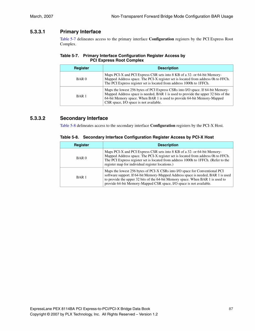
March, 2007 Non-Transparent Forward Bridge Mode Configuration BAR Usage
ExpressLane PEX 8114BA PCI Express-to-PCI/PCI-X Bridge Data Book 87
Copyright © 2007 by PLX Technology, Inc. All Rights Reserved – Version 1.2
5.3.3.1 Primary InterfaceTable 5-7 delineates access to the primary interface Configuration registers by the PCI Express RootComplex.
5.3.3.2 Secondary InterfaceTable 5-8 delineates access to the secondary interface Configuration registers by the PCI-X Host.
Table 5-7. Primary Interface Configuration Register Access by PCI Express Root Complex
Register Description
BAR 0Maps PCI-X and PCI Express CSR sets into 8 KB of a 32- or 64-bit Memory-Mapped Address space. The PCI-X register set is located from address 0h to FFCh. The PCI Express register set is located from address 1000h to 1FFCh.
BAR 1
Maps the lowest 256 bytes of PCI Express CSRs into I/O space. If 64-bit Memory-Mapped Address space is needed, BAR 1 is used to provide the upper 32 bits of the 64-bit Memory space. When BAR 1 is used to provide 64-bit Memory-Mapped CSR space, I/O space is not available.
Table 5-8. Secondary Interface Configuration Register Access by PCI-X Host
Register Description
BAR 0
Maps PCI-X and PCI Express CSR sets into 8 KB of a 32- or 64-bit Memory-Mapped Address space. The PCI-X register set is located from address 0h to FFCh. The PCI Express register set is located from address 1000h to 1FFCh. (Refer to the register map for individual register locations.)
BAR 1
Maps the lowest 256 bytes of PCI-X CSRs into I/O space for Conventional PCI software support. If 64-bit Memory-Mapped Address space is needed, BAR 1 is used to provide the upper 32 bits of the 64-bit Memory space. When BAR 1 is used to provide 64-bit Memory-Mapped CSR space, I/O space is not available.
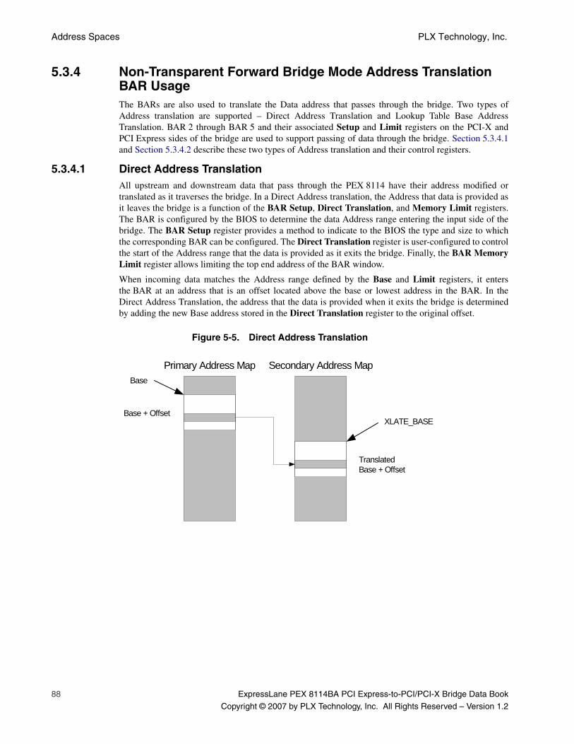
Address Spaces PLX Technology, Inc.
88 ExpressLane PEX 8114BA PCI Express-to-PCI/PCI-X Bridge Data Book
Copyright © 2007 by PLX Technology, Inc. All Rights Reserved – Version 1.2
5.3.4 Non-Transparent Forward Bridge Mode Address Translation BAR UsageThe BARs are also used to translate the Data address that passes through the bridge. Two types ofAddress translation are supported – Direct Address Translation and Lookup Table Base AddressTranslation. BAR 2 through BAR 5 and their associated Setup and Limit registers on the PCI-X andPCI Express sides of the bridge are used to support passing of data through the bridge. Section 5.3.4.1and Section 5.3.4.2 describe these two types of Address translation and their control registers.
5.3.4.1 Direct Address TranslationAll upstream and downstream data that pass through the PEX 8114 have their address modified ortranslated as it traverses the bridge. In a Direct Address translation, the Address that data is provided asit leaves the bridge is a function of the BAR Setup, Direct Translation, and Memory Limit registers.The BAR is configured by the BIOS to determine the data Address range entering the input side of thebridge. The BAR Setup register provides a method to indicate to the BIOS the type and size to whichthe corresponding BAR can be configured. The Direct Translation register is user-configured to controlthe start of the Address range that the data is provided as it exits the bridge. Finally, the BAR MemoryLimit register allows limiting the top end address of the BAR window.
When incoming data matches the Address range defined by the Base and Limit registers, it entersthe BAR at an address that is an offset located above the base or lowest address in the BAR. In theDirect Address Translation, the address that the data is provided when it exits the bridge is determinedby adding the new Base address stored in the Direct Translation register to the original offset.
Figure 5-5. Direct Address Translation
Primary Address Map Secondary Address Map
Base + Offset
TranslatedBase + Offset
Base
XLATE_BASE
March, 2007 Non-Transparent Forward Bridge Mode Address Translation BAR Usage
ExpressLane PEX 8114BA PCI Express-to-PCI/PCI-X Bridge Data Book 89
Copyright © 2007 by PLX Technology, Inc. All Rights Reserved – Version 1.2
5.3.4.2 Lookup Table Base Address TranslationOn the secondary side of the bridge, BAR 3 Lookup Table Base Address Translation uses the address ofthe incoming Data transactions as an index into a table. The table output becomes the translated addressof the data as it exits the bridge. Specifically, the PEX 8114 uses the least significant bits of theincoming data transaction’s address as an offset. The exact number of least significant bits isconfigurable from 8 to 25, by the Memory BAR 3 Setup register, bits [19:16, 0]. The size is the samefor all 64 Address spaces.
The next six bits located above those used as an offset in the incoming Transaction address are used asan index that selects one of 64 Lookup Table registers. The Lookup Table value becomes the Baseaddress of the exiting data. The offset portion of the original address, as selected by the Memory BAR 3Setup register LUT Page Size bits, is concatenated with the higher order bits from the selectedTranslated Base Address register to create the translated address. Each Lookup Table register, inaddition to the Translation Base Address bits, also contains an Entry Valid and Prefetchable bit. If theEntry Valid bit is cleared, the Address space represented by that Lookup Table entry is invalid. Whenset, the Prefetchable bit causes the Address space defined by that Lookup Table entry to be prefetchable.The Lookup Table provides further translation flexibility, as it assigns the secondary bus address fromits primary bus addresses and Lookup Table values.
BAR 3 on the PCI-X side of the bridge supports Lookup Table Base Address Translation. To implementa single Lookup Table Base Address Translation requires the following:
• BAR, which is configured by the BIOS to set the size and location of the base of the incoming address to translate
• BAR Setup register, to direct the BAR regarding the size and type of address block for which the BAR is configured
• 64 Lookup Table registers, that contain the Base addresses of the outgoing addresses
The Limit register indicates the top of the Memory space, when less than the full “power of two”Memory size (defined by the BAR) is needed. The Limit registers’ value is relative to the base of theBAR, and not an absolute value in memory. The value defaults to 0 at reset. If the Limit register is notchanged from zero by a Configuration Write, the register has no effect and all Memory spaces definedby the BAR are usable. If the Limit register is assigned a value lower the top of the Memory spacedefined by the BAR, the usable Address space extends from the base of the Address space, up to andincluding the address defined by the Limit register’s contents. If the Limit register’s value is greaterthan the top of the Memory space defined by the BAR, the Limit register has no effect and the entireMemory space defined by the BAR is used.
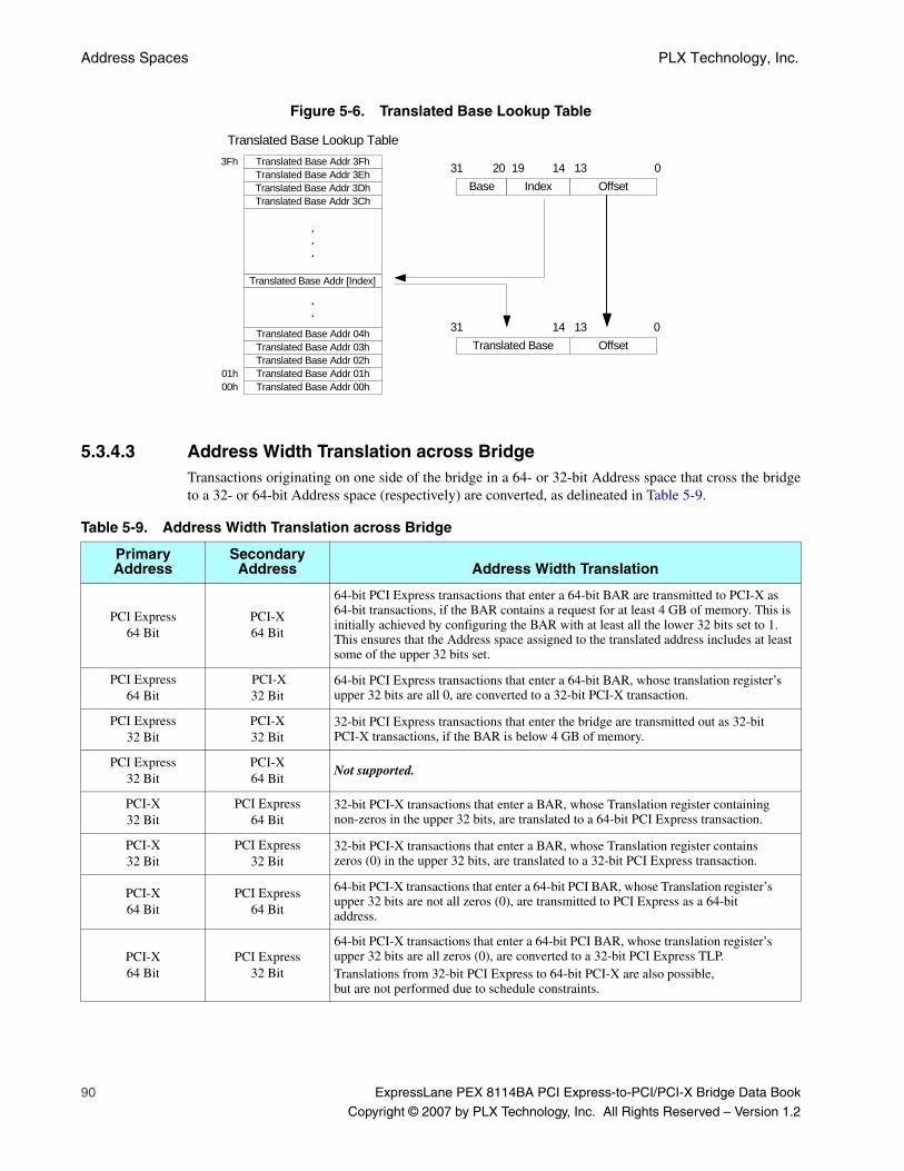
Address Spaces PLX Technology, Inc.
90 ExpressLane PEX 8114BA PCI Express-to-PCI/PCI-X Bridge Data Book
Copyright © 2007 by PLX Technology, Inc. All Rights Reserved – Version 1.2
Figure 5-6. Translated Base Lookup Table
5.3.4.3 Address Width Translation across BridgeTransactions originating on one side of the bridge in a 64- or 32-bit Address space that cross the bridgeto a 32- or 64-bit Address space (respectively) are converted, as delineated in Table 5-9.
Table 5-9. Address Width Translation across Bridge
Primary Address
Secondary Address Address Width Translation
PCI Express64 Bit
PCI-X64 Bit
64-bit PCI Express transactions that enter a 64-bit BAR are transmitted to PCI-X as 64-bit transactions, if the BAR contains a request for at least 4 GB of memory. This is initially achieved by configuring the BAR with at least all the lower 32 bits set to 1. This ensures that the Address space assigned to the translated address includes at least some of the upper 32 bits set.
PCI Express64 Bit
PCI-X32 Bit
64-bit PCI Express transactions that enter a 64-bit BAR, whose translation register’s upper 32 bits are all 0, are converted to a 32-bit PCI-X transaction.
PCI Express32 Bit
PCI-X32 Bit
32-bit PCI Express transactions that enter the bridge are transmitted out as 32-bit PCI-X transactions, if the BAR is below 4 GB of memory.
PCI Express32 Bit
PCI-X64 Bit
Not supported.
PCI-X32 Bit
PCI Express64 Bit
32-bit PCI-X transactions that enter a BAR, whose Translation register containing non-zeros in the upper 32 bits, are translated to a 64-bit PCI Express transaction.
PCI-X32 Bit
PCI Express32 Bit
32-bit PCI-X transactions that enter a BAR, whose Translation register contains zeros (0) in the upper 32 bits, are translated to a 32-bit PCI Express transaction.
PCI-X64 Bit
PCI Express64 Bit
64-bit PCI-X transactions that enter a 64-bit PCI BAR, whose Translation register’s upper 32 bits are not all zeros (0), are transmitted to PCI Express as a 64-bit address.
PCI-X64 Bit
PCI Express32 Bit
64-bit PCI-X transactions that enter a 64-bit PCI BAR, whose translation register’s upper 32 bits are all zeros (0), are converted to a 32-bit PCI Express TLP.Translations from 32-bit PCI Express to 64-bit PCI-X are also possible, but are not performed due to schedule constraints.
Translated Base Lookup TableTranslated Base Addr 3FhTranslated Base Addr 3EhTranslated Base Addr 3DhTranslated Base Addr 3Ch
.
.
.
Translated Base Addr [Index]
Translated Base Addr 04hTranslated Base Addr 03hTranslated Base Addr 02hTranslated Base Addr 01hTranslated Base Addr 00h
.
.
00h01h
3Fh
Translated Base Offset
Base OffsetIndex
31
31
0
0
14 13
20 19 14 13
March, 2007 Non-Transparent Forward Bridge Mode Register Type Descriptions
ExpressLane PEX 8114BA PCI Express-to-PCI/PCI-X Bridge Data Book 91
Copyright © 2007 by PLX Technology, Inc. All Rights Reserved – Version 1.2
5.3.5 Non-Transparent Forward Bridge Mode Register Type DescriptionsThis section describes the register types used to support Non-Transparent Configuration andData transfers.
5.3.5.1 Base Address Registers (BARs)The PEX 8114 Host and Local sides of the bridge each include six BAR registers. Their initializationprocedures and values conform to Conventional PCI BAR rules.
5.3.5.2 BAR Setup RegistersHost and Local BARs used to configure Address ranges for driving data through the bridge containprogrammable window sizes. These include BAR 2 through BAR 5. BAR 0 and BAR 1 are dedicatedto CSR access, and therefore contain dedicated window sizes that are fixed by the number of CSRs.The programmable-sized windows on BAR 2 through BAR 5 provide user-selectable Address rangememory sizes. The BAR Setup registers are used to configure BARs after reset with the correct patternof ones and zeros (1 and 0), allowing a requested memory window size to be indicated to the BIOS atthe start of enumeration.
The BAR Setup registers are located at Configuration Address offsets D0h through F4h:
• PCI-X Memory BAR Setup registers are located at offsets D0h through E0h
• PCI Express Memory BAR Setup registers are located at offsets E4h through F4h
These registers are loaded by serial EEPROM or Configuration Write, and are used to enable theAddress space and indicate the Address space size. Bit 31 of the Memory BAR Setup registers is usedto enable or disable Memory space. If bit 31 is cleared to 0 (default), the Address space is disabled.Writing Fh to the Setup register’s Most Significant Bits (MSBs) controls the Address Space size;therefore, all bits are not used when addressing the Memory space. Memory space is allocated in 1-MBincrements, allowing bits [30:12] to indicate memory size.
The BAR Setup registers are used as masks for the corresponding BARs. When the BIOS reads a BAR,it reads ones (1) in bits [30:12], if the corresponding Memory BAR Setup register contains ones (1) inthose bits. The BIOS uses this information to determine memory requirements.
5.3.5.3 BAR Address Translation RegistersThe BAR Address Translation registers provide a starting (base) address for the output memorywindow. These translation registers are used with the Direct Address translations.
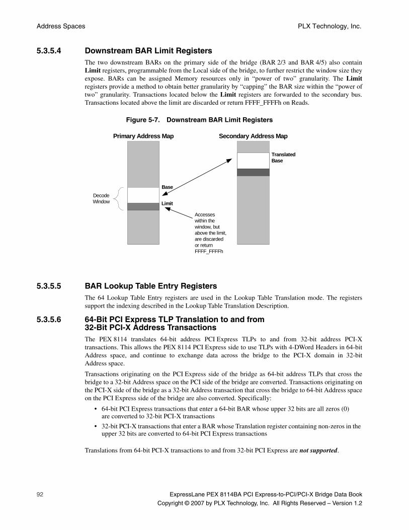
Address Spaces PLX Technology, Inc.
92 ExpressLane PEX 8114BA PCI Express-to-PCI/PCI-X Bridge Data Book
Copyright © 2007 by PLX Technology, Inc. All Rights Reserved – Version 1.2
5.3.5.4 Downstream BAR Limit RegistersThe two downstream BARs on the primary side of the bridge (BAR 2/3 and BAR 4/5) also containLimit registers, programmable from the Local side of the bridge, to further restrict the window size theyexpose. BARs can be assigned Memory resources only in “power of two” granularity. The Limitregisters provide a method to obtain better granularity by “capping” the BAR size within the “power oftwo” granularity. Transactions located below the Limit registers are forwarded to the secondary bus.Transactions located above the limit are discarded or return FFFF_FFFFh on Reads.
Figure 5-7. Downstream BAR Limit Registers
5.3.5.5 BAR Lookup Table Entry RegistersThe 64 Lookup Table Entry registers are used in the Lookup Table Translation mode. The registerssupport the indexing described in the Lookup Table Translation Description.
5.3.5.6 64-Bit PCI Express TLP Translation to and from32-Bit PCI-X Address TransactionsThe PEX 8114 translates 64-bit address PCI Express TLPs to and from 32-bit address PCI-Xtransactions. This allows the PEX 8114 PCI Express side to use TLPs with 4-DWord Headers in 64-bitAddress space, and continue to exchange data across the bridge to the PCI-X domain in 32-bitAddress space.
Transactions originating on the PCI Express side of the bridge as 64-bit address TLPs that cross thebridge to a 32-bit Address space on the PCI side of the bridge are converted. Transactions originating onthe PCI-X side of the bridge as a 32-bit Address transaction that cross the bridge to 64-bit Address spaceon the PCI Express side of the bridge are also converted. Specifically:
• 64-bit PCI Express transactions that enter a 64-bit BAR whose upper 32 bits are all zeros (0) are converted to 32-bit PCI-X transactions
• 32-bit PCI-X transactions that enter a BAR whose Translation register containing non-zeros in the upper 32 bits are converted to 64-bit PCI Express transactions
Translations from 64-bit PCI-X transactions to and from 32-bit PCI Express are not supported.
Secondary Address Map Primary Address Map
DecodeWindow
Translated Base
Accesses within the window, but above the limit, are discarded or return FFFF_FFFFh
Base
Limit
ExpressLane PEX 8114BA PCI Express-to-PCI/PCI-X Bridge Data Book 93
Copyright © 2007 by PLX Technology, Inc. All Rights Reserved – Version 1.2
Chapter 6 Configuration
6.1 IntroductionConfiguration requests are initiated by the Root Complex in a PCI Express system and by the PCI orPCI-X Host or Central Resource Function in a PCI system. All devices located within a PCI Express orPCI system include a Configuration space accessed using Configuration transactions to configureoperational characteristics of the device.
When the PEX 8114 operates as a Forward Transparent bridge, all configurations originate at thePCI Express Root Complex. The PEX 8114 is configured by the Root Complex. The PEX 8114 registerset appears as a Type 1 PCI Express Bridge register set with a Device ID of 8114h and additionalDevice-Specific registers. The PCI Express Bridge register set is enumerated and configured by theBIOS according to PCI Express conventions. Configuration or changes to the additionalDevice-Specific registers is optional, as changes to the Device-Specific registers are not required toallow the PEX 8114 to function. PCI devices located downstream from the PEX 8114 are configured bythe Root Complex through the PEX 8114.
When the PEX 8114 operates as a Reverse Transparent bridge, all configurations originate at the PCI-Xor PCI Host. The PCI-X Host configures the PEX 8114, using PCI transactions. The PCI-X Host alsoconfigures PCI Express devices, located downstream from the PEX 8114, by transmitting PCItransactions to the PEX 8114, which the bridge converts into PCI Express Configuration transactionsand then forwards to the PCI Express devices downstream. In Reverse Transparent Bridge mode, thePEX 8114 register set appears as a Type 1 PCI Bridge register set with a Device ID of 8114h andadditional Device-Specific registers. The PCI Bridge register set is enumerated and configured by theBIOS according to PCI Bridge conventions. Configuration or changes to the additional Device-Specificregisters is optional, as changes to the Device-Specific registers are not required to allow the PEX 8114to function.
When the PEX 8114 operates as a Non-Transparent bridge, the PEX 8114 appears as two endpoints, oneto the PCI Express Root Complex with a Device ID of 8104h, the other to the PCI-X Local Host with aDevice ID of 8114h. To appear as two endpoints, the PEX 8114 must contain two complete Type 0register sets – one for each side of the bridge, PCI Express and PCI-X. In Non-Transparent mode, theregister set on the PCI Express side is enumerated by the PCI Express Root Complex and the register seton the PCI-X side is enumerated by the Local PCI Host.
Type 0 Configuration transactions are used to access the internal PEX 8114 Configuration registerswhen the PEX 8114 operates in Transparent and Non-Transparent modes. When the PEX 8114 isconfigured as a Forward or Reverse Transparent bridge, Type 1 Configuration transactions aretransmitted into the PEX 8114 to access devices downstream from the PEX 8114. These Type 1configurations are converted to Type 0 transactions, if they are targeted to the device on the bus directlybelow the PEX 8114. If the transaction is a Target for a bus downstream from the bus located directlybelow the PEX 8114, the transaction is passed through the PEX 8114 as a Type 1 configuration. If thetransaction is not targeted for the PEX 8114, or devices located downstream from the PEX 8114, thetransaction is rejected.
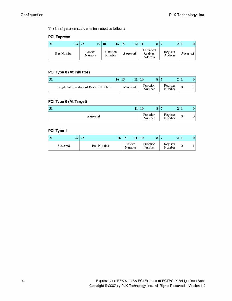
Configuration PLX Technology, Inc.
94 ExpressLane PEX 8114BA PCI Express-to-PCI/PCI-X Bridge Data Book
Copyright © 2007 by PLX Technology, Inc. All Rights Reserved – Version 1.2
The Configuration address is formatted as follows:
PCI Express
31 24 23 19 18 16 15 12 11 8 7 2 1 0
Bus Number Device Number
Function Number Reserved
Extended Register Address
Register Address Reserved
PCI Type 0 (At Initiator)
31 16 15 11 10 8 7 2 1 0
Single bit decoding of Device Number Reserved Function Number
Register Number 0 0
PCI Type 0 (At Target)
31 11 10 8 7 2 1 0
Reserved Function Number
Register Number 0 0
PCI Type 1
31 24 23 16 15 11 10 8 7 2 1 0
Reserved Bus Number Device Number
Function Number
Register Number 0 1
March, 2007 Type 0 Configuration Transactions
ExpressLane PEX 8114BA PCI Express-to-PCI/PCI-X Bridge Data Book 95
Copyright © 2007 by PLX Technology, Inc. All Rights Reserved – Version 1.2
6.2 Type 0 Configuration TransactionsThe PEX 8114 responds to Type 0 Configuration transactions on its primary bus that address thePEX 8114 Configuration space. A Type 0 Configuration transaction is used to configure the PEX 8114,and is not forwarded downstream to the secondary bus. In Transparent mode, the PEX 8114 ignoresType 0 Configuration transactions on its secondary bus. In Non-Transparent mode, Type 0configurations to the secondary bus access the PCI-Specific Configuration registers. Type 0Configuration transactions result in the transfer of 1 DWord. If Configuration Write data is poisoned, thedata is discarded and a Non-Fatal Error message is generated, if enabled.
6.3 Type 1 Configuration TransactionsType 1 Configuration transactions are used for device configuration in a hierarchical bus system.Transparent bridges and switches are the only devices that respond to Type 1 Configuration transactions.When the PEX 8114 operates in Non-Transparent mode, Type 1 Configuration transactions are rejectedby a UR.
Type 1 conversion to special cycles are not supported. When the PEX 8114 operates as a Type 1Transparent Bridge, Configuration transactions are used when the transaction is intended for a deviceresiding on a bus other than the one that issued the Type 1 request. The Bus Number field in aConfiguration transaction request specifies a unique bus in the hierarchy, on which the TransactionTarget resides. The bridge compares the specified bus number with two PEX 8114 Configurationregisters – Secondary Bus Number and Subordinate Bus Number – to determine whether to forwarda Type 1 Configuration transaction across the bridge.
When the primary interface receives a Type 1 Configuration transaction, the following tests are applied,in sequence, to the Bus Number field to determine how to handle the transaction:
1. When the Bus Number field is equal to the Secondary Bus Number register value, the PEX 8114 forwards the Configuration request to the secondary bus as a Type 0 Configuration transaction.
2. When the Bus Number field is not equal to the Secondary Bus Number register value, but is within the range of the Secondary Bus Number and Subordinate Bus Number (inclusive) registers, the Type 1 Configuration request is specifying a bus located behind the bridge. In this case, the PEX 8114 forwards the Configuration request to the secondary bus as a Type 1 Configuration transaction.
3. When the Bus Number field does not satisfy the above criteria, the Type 1 Configuration request is specifying a bus that is not located behind the bridge. In this case, the Configuration request is invalid. If the primary interface is PCI Express, a Completion with Unsupported Request status is returned. If the primary interface is PCI, the Configuration request is ignored, resulting in resulting in delivery of FFFF_FFFFh or a Target Abort. If the Bridge Control register Master Abort Mode bit (offset 3Ch[21]) is set, the PEX 8114 replies to the PCI requester’s follow-on Non-Posted requests with a Target Abort. If the Master Abort Mode bit is not set, the PEX 8114 replies to the PCI requester’s follow-on Non-Posted requests with FFFF_FFFFh.
Configuration PLX Technology, Inc.
96 ExpressLane PEX 8114BA PCI Express-to-PCI/PCI-X Bridge Data Book
Copyright © 2007 by PLX Technology, Inc. All Rights Reserved – Version 1.2
6.4 Type 1-to-Type 0 ConversionIn Transparent mode, the PEX 8114 performs a Type 1-to-Type 0 conversion when the Type 1transaction is generated on the primary bus and is intended for a device attached directly to thesecondary bus. In Non-Transparent mode, no Type 1-to-Type 0 conversion is performed and Type 1cycles are rejected. In Transparent mode, the PEX 8114 must convert the Type 1 Configurationtransaction to Type 0, to allow the downstream device to respond to it. Type 1-to-Type 0 conversions areperformed only in the downstream direction. The PEX 8114 generates Type 0 Configurationtransactions only on the secondary interface.
6.4.1 Forward Transparent Bridge ModeThe PEX 8114 forwards a Type 1 transaction on the PCI Express interface to a Type 0 transaction on thePCI Bus, if the Type 1 Configuration request Bus Number field is equal to the Secondary Bus Numberregister value.
The PEX 8114 then performs the following steps on the secondary interface:
1. Clears Address bits AD[1:0] to 00b.
2. Derives Address bits AD[7:2] directly from the Configuration request Register Address field.
3. Derives Address bits AD[10:8] directly from the Configuration request Function Number field.
4. Clears Address bits AD[15:11] to 0h.
5. Decodes the Device Number field and sets a single Address bit within the range AD[31:16] during the Address phase.
6. Verifies that the Extended Register Address field in the Configuration request is 0h. If the value is non-zero, the PEX 8114 does not forward the transaction, and treats it as an Unsupported Request on the PCI Express interface, and a Received Master Abort on the PCI Bus.
Type 1-to-Type 0 transactions are performed as Non-Posted transactions.
March, 2007 Reverse Transparent Bridge Mode
ExpressLane PEX 8114BA PCI Express-to-PCI/PCI-X Bridge Data Book 97
Copyright © 2007 by PLX Technology, Inc. All Rights Reserved – Version 1.2
6.4.2 Reverse Transparent Bridge ModeThe PEX 8114 forwards a Type 1 transaction on the PCI Bus to a Type 0 transaction on the PCI Expressinterface, if the following are true during the PCI Address phase:
• Address bits AD[1:0] are 01b.
• The Type 1 Configuration request Bus Number field (AD[23:16]) is equal to the Secondary Bus Number register value.
• The Bus command on PCI_C/BE[3:0]# (32-bit bus) or PCI_C/BE[7:0]# (64-bit bus) is a Configuration Write or Read.
• The Type 1 Configuration request Device Number field (AD[15:11]) is 0h. If it is non-zero, the PEX 8114 ignores the transaction, resulting in a Master Abort.
The PEX 8114 then creates a PCI Express Configuration request, according to the following:
1. Sets the request Type field to Configuration Type 0.
2. Derives the Register Address field [7:2] directly from the Configuration request Register Address field.
3. Clears the Extended Register Address field [11:8] to 0h.
4. Derives the Function Number field [18:16] directly from the Configuration request Function Number field.
5. Derives the Device Number field [23:19] directly from the Configuration request Device Number field (forced to 0h).
6. Derives the Bus Number field [31:24] directly from the Configuration request Bus Number field.
Type 1-to-Type 0 transactions are performed as Non-Posted transactions.
Configuration PLX Technology, Inc.
98 ExpressLane PEX 8114BA PCI Express-to-PCI/PCI-X Bridge Data Book
Copyright © 2007 by PLX Technology, Inc. All Rights Reserved – Version 1.2
6.5 Type 1-to-Type 1 Forwarding in Transparent ModeType 1-to-Type 1 transaction forwarding provides a hierarchical configuration mechanism when two ormore levels of bridges are used in Transparent mode. When the PEX 8114 detects a Type 1Configuration transaction intended for a PCI Bus downstream from the secondary bus, it forwards thetransaction, unchanged, to the secondary bus.
In this case, the Transaction Target does not reside on the PEX 8114’s secondary interface, but is locatedon a bus segment farther downstream. Ultimately, this transaction is converted to a Type 0 transaction bya downstream bridge.
6.5.1 Forward Transparent Bridge ModeThe PEX 8114 forwards a Type 1 transaction on the PCI Express interface to a Type 1 transaction on thePCI Bus, if the following are true:
• A Type 1 Configuration transaction is detected on the PCI Express interface
• The value specified by the Bus Number field is within the range of Bus Numbers between the Secondary Bus Number (exclusive) and Subordinate Bus Number (inclusive)
The PEX 8114 then performs the following steps on the secondary interface:
1. Generates Address bits AD[1:0] as 01b.
2. Generates PCI Register Number, Function Number, Device Number, and Bus Number directly from the PCI Express Configuration Request register Address, Function Number, Device Number, and Bus Number fields, respectively.
3. Generates Address bits AD[31:24] as 0h.
4. Verifies that the Extended Register Address field in the Configuration request is 0h. If the value is non-zero, the PEX 8114 does not forward the transaction, and returns a Completion with Unsupported Request status on the PCI Express interface, and a Received Master Abort on the PCI Bus.
Type 1-to-Type 1 forwarding transactions are performed as Non-Posted transactions.
March, 2007 Reverse Transparent Bridge Mode
ExpressLane PEX 8114BA PCI Express-to-PCI/PCI-X Bridge Data Book 99
Copyright © 2007 by PLX Technology, Inc. All Rights Reserved – Version 1.2
6.5.2 Reverse Transparent Bridge ModeThe PEX 8114 forwards a Type 1 transaction on the PCI Bus to a Type 1 transaction on the PCI Expressinterface, if the following are true during the PCI Address phase:
• Address bits AD[1:0] are 01b.
• The value specified by the Bus Number field is within the range of Bus Numbers between the Secondary Bus Number (exclusive) and Subordinate Bus Number (inclusive).
• The Bus command on PCI_C/BE[3:0]# (32-bit bus) or PCI_C/BE[7:0]# (64-bit bus) is a Configuration Write or Read.
The PEX 8114 then creates a PCI Express Configuration request, according to the following:
1. Sets the request Type field to Configuration Type 1.
2. Derives the Register Address field [7:2] directly from the Configuration request Register Address field.
3. Clears the Extended Register Address field [11:8] to 0h.
4. Derives the Function Number field [18:16] directly from the Configuration request Function Number field.
5. Derives the Device Number field [23:19] directly from the Configuration request Device Number field.
6. Derives the Bus Number field [31:24] directly from the Configuration request Bus Number field.
Type 1-to-Type 1 forwarding transactions are performed as Non-Posted transactions.
6.6 PCI Express Enhanced Configuration MechanismThe PCI Express Enhanced Configuration Mechanism adds four additional bits to the Register Addressfield, thereby expanding the space to 4,096 bytes. The PEX 8114 forwards Configuration transactionsonly when the Extended Register Address bits are all 0. This prevents address aliasing on the PCI Busthat does not support Extended Register Addressing.
When a Configuration transaction targets the PCI Bus and contains a non-zero value in the ExtendedRegister Address field, the PEX 8114 treats the transaction as if it received a Master Abort on the PCIBus. The PEX 8114 then performs the following steps:
1. Sets the appropriate status bits for the destination bus, as if the transaction executed and resulted in a Master Abort.
2. Generates a PCI Express Completion with Unsupported Request status.

Configuration PLX Technology, Inc.
100 ExpressLane PEX 8114BA PCI Express-to-PCI/PCI-X Bridge Data Book
Copyright © 2007 by PLX Technology, Inc. All Rights Reserved – Version 1.2
6.7 Configuration Retry Mechanism
6.7.1 Forward Bridge ModeBridges must return a Completion for all Configuration requests that traverse the bridge fromPCI Express-to-PCI prior to expiration of the Completion Timeout Timer in the Root Complex. Thisrequires that bridges take ownership of all Configuration requests forwarded across the bridge. If theConfiguration request to PCI successfully completes prior to the bridge Timer expiration, the bridgereturns a Completion with Successful Status to PCI Express. If the Configuration request to PCIencounters an error condition prior to the bridge Timer expiration, the bridge returns an appropriateerror Completion to PCI Express. If the Configuration request to PCI does not successfully complete orwith an error prior to Timer expiration, the bridge returns a Completion with Configuration Retry Status(CRS) to the PCI Express interface.
After the PEX 8114 returns a Completion with CRS to PCI Express, the PEX 8114 continues to allowthe Configuration transaction to remain alive on the PCI Bus. The PCI r3.0 states that once a PCIMaster detects a Target Retry, it must continue to Retry the transaction until at least 1 DWord istransferred. The PEX 8114 Retries the transaction until the transaction completes on the PCI Bus oruntil the PCI Express to PCI Retry Timer expires.
When the Configuration transaction completes on the PCI Bus after the return of a Completion withCRS on the PCI Express interface, the PEX 8114 discards the Completion information. Bridges thatimplement this option are also required to implement the Device Control register Bridge ConfigurationRetry Enable bit [15]. If this bit is cleared, the bridge does not return a Completion with CRS on behalfof Configuration requests forwarded across the bridge. The lack of a Completion results in eventualCompletion Timeout at the Root Complex.
Bridges, by default, do not return CRS for Configuration requests to a PCI device located behind thebridge. This can result in lengthy completion delays that must be comprehended by the CompletionTimeout value in the Root Complex.
6.7.2 Reverse Bridge ModeIn Reverse Bridge mode, when the PEX 8114 detects a CRS, it resends the Configuration request to thePCI Express device to allow the configuration request to remain alive, and reset its Internal Timer. If thePEX 8114 is in PCI mode and the Internal Timer times out before receiving a CRS or Error messagefrom the PCI Express device, the PEX 8114 replies with FFFF_FFFFh if the Bridge Control registerMaster Abort Mode bit (offset 3Ch[21]) is not set. Otherwise, it causes a Target Abort if the MasterAbort Mode bit is set. If the PEX 8114 is in PCI-X mode, it transmits a Split Completion with a TargetAbort Error message.
March, 2007 Configuration Methods
ExpressLane PEX 8114BA PCI Express-to-PCI/PCI-X Bridge Data Book 101
Copyright © 2007 by PLX Technology, Inc. All Rights Reserved – Version 1.2
6.8 Configuration MethodsThe PEX 8114 supports the Standard Configuration methods and maintains several Device-SpecificConfiguration methods. The PEX 8114 supports Forward and Reverse Transparent and ForwardNon-Transparent Bridge modes. Each mode is slightly different from a configuration perspective.
The basic configuration methods include:
• PCI Express Extended Configuration cycles
• PCI Configuration cycles
• BAR 0/1 Memory-Mapped configuration of Device-Specific registers
– Transparent mode
– Non-Transparent mode
• Address and Data Pointer method for
– Transparent mode register access
– Non-Transparent mode register access
The PCI Express Extended Configuration method provides a PCI Express r1.0a-compliant method forconfiguring PCI Express registers. The PCI Configuration method provides a PCI r3.0-compliantmethod for accessing PCI registers. The BAR 0 and BAR 1 configuration method provides 32- or 64-bitMemory-Mapped access to registers. This is typically used to access registers that cannot be accessedby PCI Express Extended or Conventional PCI configurations. In general, BAR 0 and BAR 1 point to8 KB of Memory Cycle-Accessible Address space. This 8 KB of space is used to Write and Readregisters within, or downstream from, the PEX 8114. The 8 KB of Memory-Mapped space accessesregisters in a slightly different manner in Forward and Reverse Transparent and Non-Transparentmodes. The differences are explained in the next section. The Address and Data Pointer methodprovides two registers within the Configuration space for Reverse Transparent or Non-TransparentBridge modes. One register represents an address in the PCI/PCI Express hierarchy, the other is a datavalue register. By loading the Address register with a Target address, then writing or reading the Dataregister, a location in the Address space can be written or read.
6.8.1 Configuration Methods Intent and VariationsConfiguration register accesses must be supported in all primary operation modes. These modes includeForward Transparent, Reverse Transparent, and Forward Non-Transparent. Each supportedconfiguration method provides access to at least some of the Configuration registers. Certainconfiguration methods provide access to Conventional PCI registers, while others provide easy access toDevice-Specific registers. By providing a combination of configuration methods, the PEX 8114 allowsConventional PCI access to many registers and logical simple access to Device-Specific registers, aswell as downstream device registers. Operation modes slightly vary; therefore, certain configurationmethods also vary. The following sections explain the basic capability differences.
Configuration PLX Technology, Inc.
102 ExpressLane PEX 8114BA PCI Express-to-PCI/PCI-X Bridge Data Book
Copyright © 2007 by PLX Technology, Inc. All Rights Reserved – Version 1.2
6.8.2 PCI Express Extended Configuration MethodThe PCI Express Extended Configuration method provides Forward Transparent and Non-Transparentbridges, with access to the standard set of PCI Express registers. This configuration method providesPCI-SIG-compliant access to the PEX 8114 PCI-SIG-defined registers. It also provides access toPCI-SIG-compliant access to registers in downstream devices when the PEX 8114 is used in ForwardTransparent Bridge mode. This method is, however, confined to accessing the PCI Express-definedregisters and is not used to access the PEX 8114 Device-Specific registers.
In Forward Transparent Bridge mode, Memory-Mapped access is supported to access Device-SpecificPEX 8114 registers. Address and Data Pointer register access is not supported in Forward TransparentBridge mode. Therefore, the PEX 8114 Device-Specific registers can only be accessed byMemory-Mapped access.
6.8.3 PCI Configuration CyclesPCI Configuration cycles are used in Reverse Transparent Bridge mode to access the standard 256-bytePCI-defined register space. Additionally, when the bridge is configured as a Forward Non-Transparentbridge, PCI Configuration cycles are used by the Local PCI Host to access the register set on thePCI side of the bridge. This method provides Conventional PCI register access that functions withConventional PCI BIOS; however, it does not provide access in the following:
• Reverse Transparent Bridge mode to downstream devices’ PCI Express Extended registers
• Reverse Transparent Bridge mode to downstream devices’ Device-Specific registers
• Forward Non-Transparent Bridge mode, to the PEX 8114 PCI Express register set
In Reverse Transparent Bridge mode, use the Memory-Mapped or Address and Data Pointer method toaccess the downstream devices’ PCI Express Extended registers or the Device-Specific registers. InForward Non-Transparent Bridge mode, use a variation of the Memory-Mapped and Address and DataPointer method to access the PEX 8114’s PCI Express register set, from the PCI Host side of the bridge.
6.8.4 BAR 0/1 Device-Specific Register Memory-Mapped ConfigurationBAR 0 and BAR 1 are used to provide 32- or 64-bit Memory-Mapped access to the Device-Specificregisters. The use of Memory-Mapped access is slightly different in Forward Transparent Bridge modethan it is in Reverse Transparent Bridge mode, and slightly different again in Non-Transparent mode.
• Forward Transparent Bridge mode – Memory-Mapped access provides access to PEX 8114 internal Device-Specific registers.
• Reverse Transparent Bridge mode – Memory-Mapped access provides access to all PEX 8114 internal registers, as well as to downstream PCI Express device registers. This Memory-Mapped method allows PCI Hosts (which support only Conventional PCI Configuration registers) to access devices on the downstream PCI Express side of the bridge, using PCI Express Extended Configuration space.
• Non-Transparent mode – Memory-Mapped access provides access to both PEX 8114 internal register sets – PCI Express and PCI 4-KB – from the PCI Express Root Complex and PCI Host.
BAR 0 and BAR 1 Device-Specific Register Memory-Mapped configuration can be disabled by settingthe Disable BAR 0 bit (offset FA0h[7]). By default, this bit is cleared; however, it can be set by way ofserial EEPROM load. When this bit is set, BAR 0 is loaded with all zeros (0) at reset, and appears to theoperating system as disabled.
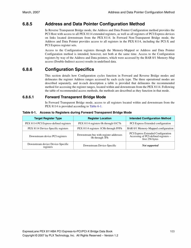
March, 2007 Address and Data Pointer Configuration Method
ExpressLane PEX 8114BA PCI Express-to-PCI/PCI-X Bridge Data Book 103
Copyright © 2007 by PLX Technology, Inc. All Rights Reserved – Version 1.2
6.8.5 Address and Data Pointer Configuration MethodIn Reverse Transparent Bridge mode, the Address and Data Pointer Configuration method provides thePCI Host with access to all PEX 8114 extended registers, as well as all registers of PCI Express deviceson links located downstream from the PEX 8114. In Forward Non-Transparent Bridge mode, theAddress and Data Pointer provides access to all registers in the PEX 8114, including the PCI-X andPCI Express register sets.
Access to the Configuration registers through the Memory-Mapped or Address and Data PointerConfiguration method is intended; however, not both at the same time. Access to the Configurationregisters by way of the Address and Data pointers, which were accessed by the BAR 0/1 Memory-Mapaccess (Double-Indirect access) results in undefined data.
6.8.6 Configuration SpecificsThis section details how Configuration cycles function in Forward and Reverse Bridge modes anddelineates the register Address ranges accessed by each cycle type. The three operational modes aredescribed separately, and in each description a table is provided that delineates the recommendedmethod for accessing the register ranges, located within and downstream from the PEX 8114. Followingthe table of recommended access methods, the methods are described as they function in that mode.
6.8.6.1 Forward Transparent Bridge ModeIn Forward Transparent Bridge mode, access to all registers located within and downstream from thePEX 8114 is provided according to Table 6-1.
Table 6-1. Access to Registers during Forward Transparent Bridge Mode
Target Register Type Register Location Intended Configuration Method
PEX 8114 PCI Express-defined registers PEX 8114 registers 0h through 01C7h PCI Express Extended configuration
PEX 8114 Device-Specific registers PEX 8114 registers 1C8h through FFFh BAR 0/1 Memory-Mapped configuration
Downstream device PCI registers Downstream bus with register addresses 0h through 3Fh
PCI Express Extended Configuration Accessing of PCI-defined registers –
first 256 bytes
Downstream device Device-Specific registers Downstream Device-Specific Not supported

Configuration PLX Technology, Inc.
104 ExpressLane PEX 8114BA PCI Express-to-PCI/PCI-X Bridge Data Book
Copyright © 2007 by PLX Technology, Inc. All Rights Reserved – Version 1.2
PCI Express Extended Configuration Access in Forward Transparent Bridge Mode
In Forward Transparent Bridge mode (as in all other modes), the PCI Express Extended Configurationmethod functions, as described in the PCI Express r1.0a, and as previously described. The PEX 8114makes no non-standard modifications to the standard PCI Express Extended Configuration method.
Forward Transparent Memory-Mapped BAR 0/1 Access to Internal Registers
In Forward Transparent Bridge mode, BAR 0 and BAR 1 are used to provide 32- or 64-bit Memory-Mapped access to internal Configuration registers. When BAR 0 and BAR 1 are enumerated accordingto PCI convention and the bridge operation description herein, access to a 4-KB Memory-Mappedwindow into the Configuration registers is provided. The 4-KB window provides access to allPCI Express Extended register addresses. The Memory-Mapped window locations are linearly mappedto Configuration register space, according to the following equation:
for N = 0 through 4 KB-1; Memory-Mapped address BASE+N access register N
All internal registers can be accessed through Memory-Mapped access in Forward TransparentBridge mode.
6.8.6.2 Reverse Transparent Bridge ModeIn Reverse Transparent Bridge mode, access to all registers located within and downstream from thePEX 8114 is provided according to Table 6-2.
Table 6-2. Access to Registers during Reverse Transparent Bridge Mode
Target Register Type Register Location Intended Configuration Method
PEX 8114 PCI-defined registers PEX 8114 registers 0h through FFh Conventional PCI configuration
PEX 8114 Device-Specific registers PEX 8114 registers 100h through FFFhBAR 0/1 Memory-Mapped configurationAddress and Data Pointer configuration
Downstream device PCI Type 0 Bridge register set from register 0h through 3Fh
for enumeration
Downstream bus with register addresses 0h through 3Fh Conventional PCI configuration
Downstream device PCI Express Extended registers
PCI Express Extended registers (includes registers 100h through FFFh)
BAR 0/1 Memory-Mapped configurationAddress and Data Pointer configuration
Downstream device Device-Specific registers Downstream Device-Specific
BAR 0/1 Memory-Mapped configurationAddress and Data Pointer configuration
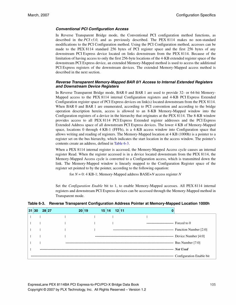
March, 2007 Configuration Specifics
ExpressLane PEX 8114BA PCI Express-to-PCI/PCI-X Bridge Data Book 105
Copyright © 2007 by PLX Technology, Inc. All Rights Reserved – Version 1.2
Conventional PCI Configuration Access
In Reverse Transparent Bridge mode, the Conventional PCI configuration method functions, asdescribed in the PCI r3.0, and as previously described. The PEX 8114 makes no non-standardmodifications to the PCI Configuration method. Using the PCI Configuration method, accesses can bemade to the PEX 8114 standard 256 bytes of PCI register space and the first 256 bytes of anydownstream PCI Express device located on links downstream from the PEX 8114. Because of thelimitation of having access to only the first 256-byte locations of the 4-KB extended register space of thedownstream PCI Express device, an extended Memory-Mapped method is used to access the additionalPCI Express registers of the downstream devices. The extended Memory-Mapped access method isdescribed in the next section.
Reverse Transparent Memory-Mapped BAR 0/1 Access to Internal Extended Registers and Downstream Device Registers
In Reverse Transparent Bridge mode, BAR 0 and BAR 1 are used to provide 32- or 64-bit Memory-Mapped access to the PEX 8114 internal Configuration registers and 4-KB PCI Express ExtendedConfiguration register space of PCI Express devices on link(s) located downstream from the PEX 8114.When BAR 0 and BAR 1 are enumerated, according to PCI convention and according to the bridgeoperation description herein, access is allowed to an 8-KB Memory-Mapped window into theConfiguration registers of a device in the hierarchy that originates at the PEX 8114. The 8-KB windowprovides access to all PEX 8114 PCI Express Extended register addresses and the PCI ExpressExtended Address space of all downstream PCI Express devices. The lower 4 KB of Memory-Mappedspace, locations 0 through 4 KB-1 (FFFh), is a 4-KB access window into Configuration space thatallows writing and reading of registers. The Memory-Mapped location at 4 KB (1000h) is a pointer to aregister set on the bus hierarchy, which indicates the start location in the access window. The pointer’scontents create an address, defined in Table 6-3.
When a PEX 8114 internal register is accessed, the Memory-Mapped Access cycle causes an internalregister Read. When the register accessed is in a device located downstream from the PEX 8114, theMemory-Mapped Access cycle is converted to a Configuration access, which is transmitted down thelink. The Memory-Mapped window is linearly mapped to the Configuration Register space of theregister set pointed to by the pointer, according to the following equation:
for N = 0: 4 KB-1; Memory-Mapped address BASE+N access register N
Set the Configuration Enable bit to 1, to enable Memory-Mapped accesses. All PEX 8114 internalregisters and downstream PCI Express devices can be accessed through the Memory-Mapped method inTransparent mode.
Table 6-3. Reverse Transparent Configuration Address Pointer at Memory-Mapped Location 1000h
31 30 28 27 20 19 15 14 12 11 0
| | | | | |
| | | | | --------------------- Forced to 0
| | | | ----------------------------------------------- Function Number [2:0]
| | | ------------------------------------------------------------- Device Number [4:0]
| | ------------------------------------------------------------------------------------ Bus Number [7:0]
| -------------------------------------------------------------------------------------------------------- Not Used
--------------------------------------------------------------------------------------------------------------- Configuration Enable bit
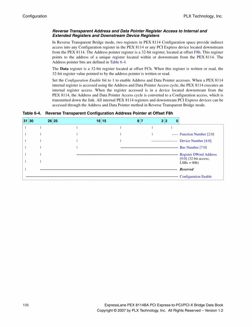
Configuration PLX Technology, Inc.
106 ExpressLane PEX 8114BA PCI Express-to-PCI/PCI-X Bridge Data Book
Copyright © 2007 by PLX Technology, Inc. All Rights Reserved – Version 1.2
Reverse Transparent Address and Data Pointer Register Access to Internal and Extended Registers and Downstream Device Registers
In Reverse Transparent Bridge mode, two registers in PEX 8114 Configuration space provide indirectaccess into any Configuration register in the PEX 8114 or any PCI Express device located downstreamfrom the PEX 8114. The Address pointer register is a 32-bit register, located at offset F8h. This registerpoints to the address of a unique register located within or downstream from the PEX 8114. TheAddress pointer bits are defined in Table 6-4.
The Data register is a 32-bit register located at offset FCh. When this register is written or read, the32-bit register value pointed to by the address pointer is written or read.
Set the Configuration Enable bit to 1 to enable Address and Data Pointer accesses. When a PEX 8114internal register is accessed using the Address and Data Pointer Access cycle, the PEX 8114 executes aninternal register access. When the register accessed is in a device located downstream from thePEX 8114, the Address and Data Pointer Access cycle is converted to a Configuration access, which istransmitted down the link. All internal PEX 8114 registers and downstream PCI Express devices can beaccessed through the Address and Data Pointer method in Reverse Transparent Bridge mode.
Table 6-4. Reverse Transparent Configuration Address Pointer at Offset F8h
31 30 26 25 16 15 8 7 3 2 0
| | | | | |
| | | | | ----- Function Number [2:0]
| | | | --------------------- Device Number [4:0]
| | | ------------------------------------------ Bus Number [7:0]
|
|
|
|
-------------------------------------------------------------------------- Register DWord Address [9:0] (32-bit access;LSBs = 00b)
| ---------------------------------------------------------------------------------------------------- Reserved
--------------------------------------------------------------------------------------------------------------- Configuration Enable
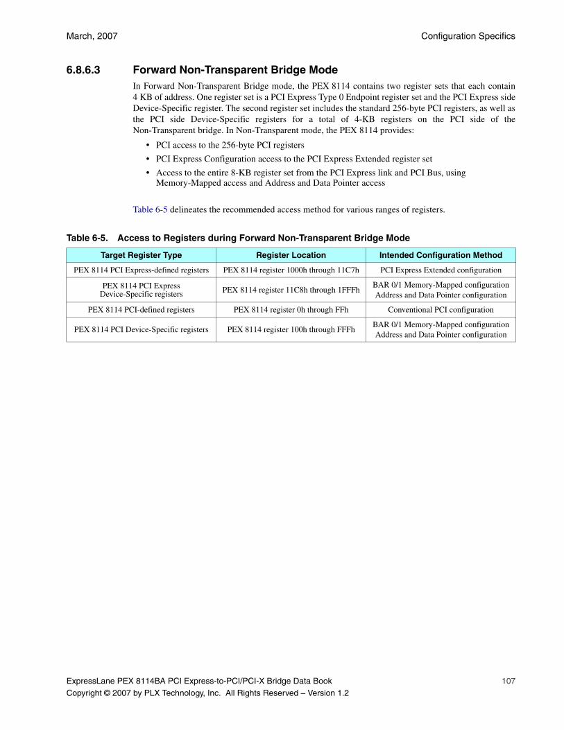
March, 2007 Configuration Specifics
ExpressLane PEX 8114BA PCI Express-to-PCI/PCI-X Bridge Data Book 107
Copyright © 2007 by PLX Technology, Inc. All Rights Reserved – Version 1.2
6.8.6.3 Forward Non-Transparent Bridge ModeIn Forward Non-Transparent Bridge mode, the PEX 8114 contains two register sets that each contain4 KB of address. One register set is a PCI Express Type 0 Endpoint register set and the PCI Express sideDevice-Specific register. The second register set includes the standard 256-byte PCI registers, as well asthe PCI side Device-Specific registers for a total of 4-KB registers on the PCI side of theNon-Transparent bridge. In Non-Transparent mode, the PEX 8114 provides:
• PCI access to the 256-byte PCI registers
• PCI Express Configuration access to the PCI Express Extended register set
• Access to the entire 8-KB register set from the PCI Express link and PCI Bus, using Memory-Mapped access and Address and Data Pointer access
Table 6-5 delineates the recommended access method for various ranges of registers.
Table 6-5. Access to Registers during Forward Non-Transparent Bridge Mode
Target Register Type Register Location Intended Configuration Method
PEX 8114 PCI Express-defined registers PEX 8114 register 1000h through 11C7h PCI Express Extended configuration
PEX 8114 PCI Express Device-Specific registers PEX 8114 register 11C8h through 1FFFh
BAR 0/1 Memory-Mapped configurationAddress and Data Pointer configuration
PEX 8114 PCI-defined registers PEX 8114 register 0h through FFh Conventional PCI configuration
PEX 8114 PCI Device-Specific registers PEX 8114 register 100h through FFFhBAR 0/1 Memory-Mapped configurationAddress and Data Pointer configuration
Configuration PLX Technology, Inc.
108 ExpressLane PEX 8114BA PCI Express-to-PCI/PCI-X Bridge Data Book
Copyright © 2007 by PLX Technology, Inc. All Rights Reserved – Version 1.2
Non-Transparent PCI Express Extended Configuration Access to PCI Express Endpoint Registers
In Forward Non-Transparent Bridge mode, the PCI Express Extended Configuration method functions,as described in the PCI Express r1.0a, and as previously described, to access PCI Express-definedregisters. The PEX 8114 makes no non-standard modifications to the standard PCI Express ExtendedConfiguration method.
Non-Transparent Conventional PCI Configuration Access to 256-Byte PCI-Specific Registers
In Forward Non-Transparent Bridge mode, the Conventional PCI Configuration method functions, asdescribed in the PCI r3.0, and as previously described, to access the 256-byte Conventional PCIregisters for PCI enumeration and configuration. The PEX 8114 makes no non-standard modificationsto the PCI Configuration method. Using the PCI Configuration method, access is achieved to thestandard 256 bytes of PCI register space located within the PEX 8114. Due to the limitation of havingaccess to only the first 256-byte locations of the 4-KB internal register space, a Memory-Mapped andAddress and Data Pointer Access method are supplied. The Extended Memory-Mapped Access methodand Address and Data Pointer Access method are described in the following sections.
Forward Non-Transparent BAR 0/1 Access to PEX 8114 Internal Type 0 Register Sets
In Non-Transparent mode, BAR 0 provides 32-bit Memory-Mapped access to both PEX 8114 registersets. BAR 1 is used as an I/O BAR to access the first 256 bytes of Configuration space in the registerset in which it resides. This is controlled by the Configuration BAR Setup registers at offsets D0h andE4h. When BAR 0 and BAR 1 are enumerated, according to PCI convention and bridge operationdescription herein, access is achieved to an 8-KB Memory-Mapped window into the PEX 8114Configuration registers. The 8-KB window provides access to PCI registers at offsets 0h through 0FFFh,and PCI Express Extended registers at offsets 1000h through 1FFFh.
When a PEX 8114 internal register is accessed, the Memory-Mapped Access cycle causes an internalregister Read. The Memory-Mapped window is linearly mapped to Configuration Register space of theregister set pointed to by the pointer, according to the following equation:
• For N = 0 through 4 KB-1; Memory-Mapped address BASE+N access register PCI side of bridge register N
• For N = 4 KB through 8 KB-1; Memory-Mapped address BASE+N access register PCI Express side of bridge register N
All PEX 8114 internal registers can be accessed through the Memory-Mapped method inNon-Transparent mode.
When non-existent registers are accessed from the PCI Express or PCI-X side of the bridge, thefollowing actions occur:
• Memory-Mapped Writes and Reads to undefined registers on the PCI-X side, from the PCI-X side, return 0 for Reads. Writes are silently dropped.
• Memory-Mapped Writes and Reads to undefined registers on the PCI Express side, from the PCI-X side, return 0 for Reads. Writes are silently dropped.
• Memory-Mapped Writes and Reads to undefined registers on the PCI-X side from the PCI Express side return 0 for Reads. Writes are silently dropped.
• Memory-Mapped Writes and Reads to undefined registers on the PCI Express side, from the PCI Express side, return Unsupported Requests (URs) and Write Completion errors and trigger Advanced Error Recovery (ERR_FATAL/ERROR_NONFATAL) messages.
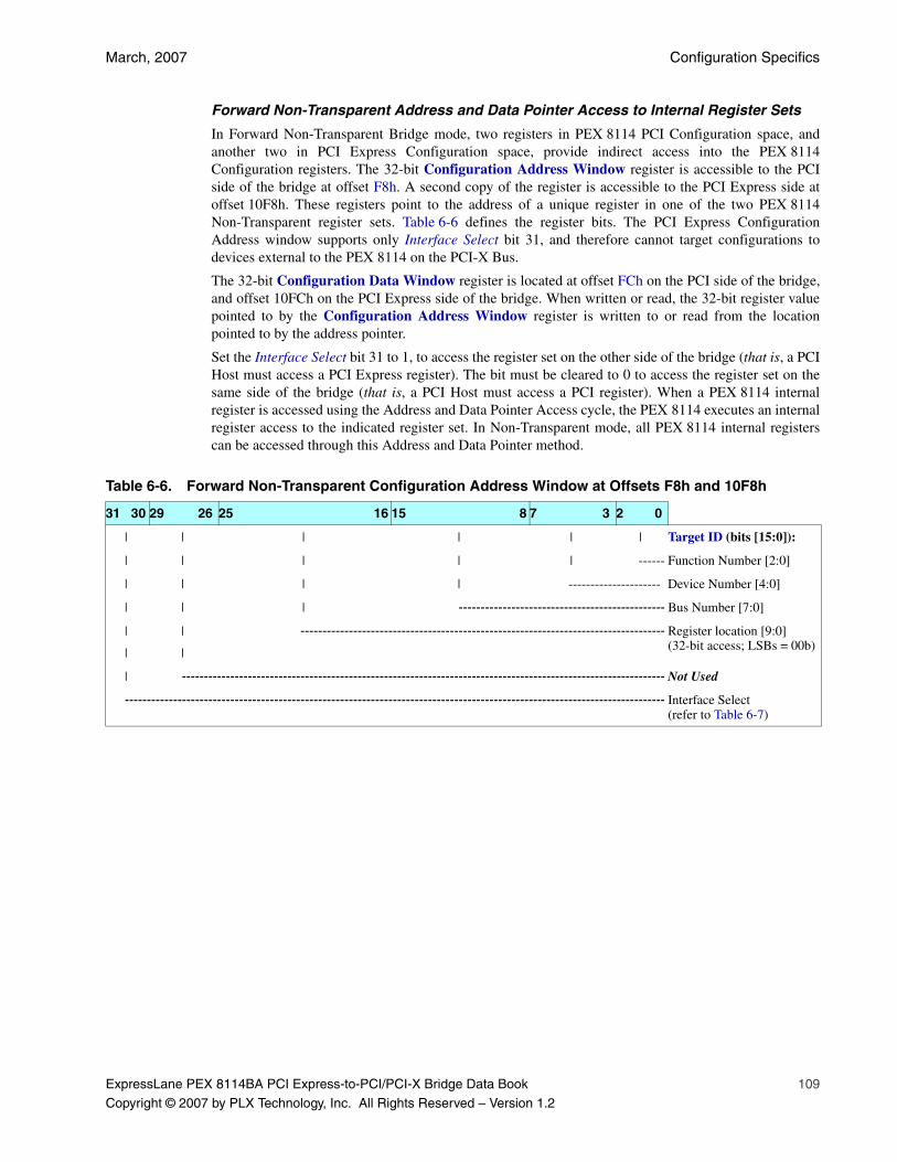
March, 2007 Configuration Specifics
ExpressLane PEX 8114BA PCI Express-to-PCI/PCI-X Bridge Data Book 109
Copyright © 2007 by PLX Technology, Inc. All Rights Reserved – Version 1.2
Forward Non-Transparent Address and Data Pointer Access to Internal Register Sets
In Forward Non-Transparent Bridge mode, two registers in PEX 8114 PCI Configuration space, andanother two in PCI Express Configuration space, provide indirect access into the PEX 8114Configuration registers. The 32-bit Configuration Address Window register is accessible to the PCIside of the bridge at offset F8h. A second copy of the register is accessible to the PCI Express side atoffset 10F8h. These registers point to the address of a unique register in one of the two PEX 8114Non-Transparent register sets. Table 6-6 defines the register bits. The PCI Express ConfigurationAddress window supports only Interface Select bit 31, and therefore cannot target configurations todevices external to the PEX 8114 on the PCI-X Bus.
The 32-bit Configuration Data Window register is located at offset FCh on the PCI side of the bridge,and offset 10FCh on the PCI Express side of the bridge. When written or read, the 32-bit register valuepointed to by the Configuration Address Window register is written to or read from the locationpointed to by the address pointer.
Set the Interface Select bit 31 to 1, to access the register set on the other side of the bridge (that is, a PCIHost must access a PCI Express register). The bit must be cleared to 0 to access the register set on thesame side of the bridge (that is, a PCI Host must access a PCI register). When a PEX 8114 internalregister is accessed using the Address and Data Pointer Access cycle, the PEX 8114 executes an internalregister access to the indicated register set. In Non-Transparent mode, all PEX 8114 internal registerscan be accessed through this Address and Data Pointer method.
Table 6-6. Forward Non-Transparent Configuration Address Window at Offsets F8h and 10F8h
31 30 29 26 25 16 15 8 7 3 2 0
| | | | | | Target ID (bits [15:0]):
| | | | | ------ Function Number [2:0]
| | | | --------------------- Device Number [4:0]
| | | ----------------------------------------------- Bus Number [7:0]
|
|
|
|
----------------------------------------------------------------------------------- Register location [9:0] (32-bit access; LSBs = 00b)
| -------------------------------------------------------------------------------------------------------------- Not Used
--------------------------------------------------------------------------------------------------------------------------- Interface Select (refer to Table 6-7)

Configuration PLX Technology, Inc.
110 ExpressLane PEX 8114BA PCI Express-to-PCI/PCI-X Bridge Data Book
Copyright © 2007 by PLX Technology, Inc. All Rights Reserved – Version 1.2
Forward Non-Transparent Address and Data Pointer Access to External Device Configuration Registers
To cause Type 0 and Type 1 Configuration cycles on the PCI Express port, access the Address and Datapointers with special values in the Configuration Address Window register Interface Select field. TheInterface Select field determines whether the Configuration cycle is targeted for internal or externalregisters, according to the decoding delineated in Table 6-7.
When the access is transmitted onto the PCI Express port as a Type 0 or Type 1 Configuration cycle, theremaining bits in the Configuration Address Window register determine which register to access.(Refer to Table 6-6.)
Table 6-7. Configuration Address Window Register Interface Select Field
Interface Select Field [31:30] Values Description
00b Access to NT PCI-X interface Type 0 Configuration Space register.
01b Access is transmitted as a Type 0 Configuration cycle across the PCI Express port.
10b Access to NT PCI Express interface Type 0 Configuration Space register.
11b Access is transmitted as a Type 1 Configuration cycle across the PCI Express port.
ExpressLane PEX 8114BA PCI Express-to-PCI/PCI-X Bridge Data Book 111
Copyright © 2007 by PLX Technology, Inc. All Rights Reserved – Version 1.2
Chapter 7 Bridge Operations
7.1 IntroductionThe PEX 8114 supports PCI Express transaction bridging to a PCI Bus operating in PCI or PCI-Xmode. To simplify the descriptions, the PEX 8114 operational description is divided into thefollowing types:
• PCI-to-PCI Express Transactions
• PCI-X-to-PCI Express Transactions
• PCI Express-to-PCI Transactions
• PCI Express-to-PCI-X Transactions
• Non-Transparent Transactions
The following sections discuss these transactions. Transaction transfer failures and general complianceare also discussed.
7.2 General ComplianceThe PEX 8114 complies with the following specifications for the listed processes and modes:
• PCI r3.0 – PCI mode
• PCI-X r1.0b or PCI-X r2.0a – PCI-X mode
• PCI Express r1.0a – PCI Express port
• PCI Express-to-PCI/PCI-X Bridge r1.0 – PCI and PCI Express Transaction Ordering rules
Bridge Operations PLX Technology, Inc.
112 ExpressLane PEX 8114BA PCI Express-to-PCI/PCI-X Bridge Data Book
Copyright © 2007 by PLX Technology, Inc. All Rights Reserved – Version 1.2
7.3 PCI-to-PCI Express TransactionsWhen a PCI device attempts a Write from the PCI Bus to the PCI Express interface, the PEX 8114translates PCI Burst Write transactions into PCI Express data TLPs. In the most basic transaction, thePEX 8114 receives a Data burst on the PCI Bus and transfers the data into a PCI Express TLP.
7.3.1 PCI-to-PCI Express Flow ControlThe PEX 8114 ensures that the internal resources for storing data are not overrun. If an internal datastorage resource is full, or approaching full in certain cases, the PEX 8114 issues Retries to all newRequest transactions and only accepts Completions or requests of types without depleted resources.
In general, the bridge tracks the number of outstanding data requested and does not transmit morerequests than it has space to receive Completions. There are two exceptions – Oversubscribe and Floodmodes. In Oversubscribe mode, the PEX 8114 tracks the number of outstanding bytes requested andensures that it limits the number to that allowed in the Oversubscribe register. In Flood mode, thePEX 8114 accepts and forwards all Read requests.
7.3.2 PCI-to-PCI Express – PCI Posted Write RequestsWhen servicing Posted Writes, no Completion information is returned to the PCI device that originatedthe transaction, and when the TLP is transmitted to the PCI Express link, the transaction is consideredcomplete. Table 7-1 delineates PCI Posted Write requests and the resultant PCI Express transactionscreated in response to the Posted Write.
Table 7-1. PCI Posted Write Requests
Initial Posted PCI Transactions Resultant PCI Express Transaction
Interrupt ACK Not supported
Special Cycle Not supported
Dual Address Cycle MWr TLP, up to Maximum Packet Size; type=00000b, fmt=11b
Memory Write MWr TLP, up to Maximum Packet Size; type=00000b, fmt=1Xb
Memory Write and Invalidate MWr TLP, up to Maximum Packet Size; type=00000b, fmt=1Xb
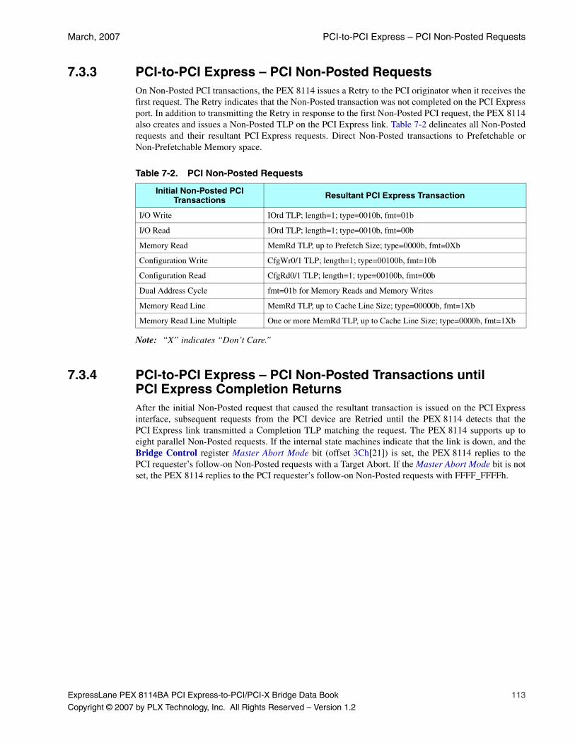
March, 2007 PCI-to-PCI Express – PCI Non-Posted Requests
ExpressLane PEX 8114BA PCI Express-to-PCI/PCI-X Bridge Data Book 113
Copyright © 2007 by PLX Technology, Inc. All Rights Reserved – Version 1.2
7.3.3 PCI-to-PCI Express – PCI Non-Posted RequestsOn Non-Posted PCI transactions, the PEX 8114 issues a Retry to the PCI originator when it receives thefirst request. The Retry indicates that the Non-Posted transaction was not completed on the PCI Expressport. In addition to transmitting the Retry in response to the first Non-Posted PCI request, the PEX 8114also creates and issues a Non-Posted TLP on the PCI Express link. Table 7-2 delineates all Non-Postedrequests and their resultant PCI Express requests. Direct Non-Posted transactions to Prefetchable orNon-Prefetchable Memory space.
Note: “X” indicates “Don’t Care.”
7.3.4 PCI-to-PCI Express – PCI Non-Posted Transactions until PCI Express Completion ReturnsAfter the initial Non-Posted request that caused the resultant transaction is issued on the PCI Expressinterface, subsequent requests from the PCI device are Retried until the PEX 8114 detects that thePCI Express link transmitted a Completion TLP matching the request. The PEX 8114 supports up toeight parallel Non-Posted requests. If the internal state machines indicate that the link is down, and theBridge Control register Master Abort Mode bit (offset 3Ch[21]) is set, the PEX 8114 replies to thePCI requester’s follow-on Non-Posted requests with a Target Abort. If the Master Abort Mode bit is notset, the PEX 8114 replies to the PCI requester’s follow-on Non-Posted requests with FFFF_FFFFh.
Table 7-2. PCI Non-Posted Requests
Initial Non-Posted PCI Transactions Resultant PCI Express Transaction
I/O Write IOrd TLP; length=1; type=0010b, fmt=01b
I/O Read IOrd TLP; length=1; type=0010b, fmt=00b
Memory Read MemRd TLP, up to Prefetch Size; type=0000b, fmt=0Xb
Configuration Write CfgWr0/1 TLP; length=1; type=00100b, fmt=10b
Configuration Read CfgRd0/1 TLP; length=1; type=00100b, fmt=00b
Dual Address Cycle fmt=01b for Memory Reads and Memory Writes
Memory Read Line MemRd TLP, up to Cache Line Size; type=00000b, fmt=1Xb
Memory Read Line Multiple One or more MemRd TLP, up to Cache Line Size; type=0000b, fmt=1Xb

Bridge Operations PLX Technology, Inc.
114 ExpressLane PEX 8114BA PCI Express-to-PCI/PCI-X Bridge Data Book
Copyright © 2007 by PLX Technology, Inc. All Rights Reserved – Version 1.2
7.3.5 PCI-to-PCI Express – PCI Requests Do Not ContainPredetermined LengthsPCI Read requests do not contain an indication of the quantity of data they require; however, the TLPsthat the PEX 8114 issues to the PCI Express device must indicate Data request quantities.The PEX 8114 treats Memory Reads to Prefetchable space differently than it treats Memory Readsto Non-Prefetchable space, and differently than it treats Memory Read Lines and Memory ReadLine Multiples. The PEX 8114 resolves the Data request quantity ambiguity, as discussed in thefollowing sections.
7.3.5.1 Memory Read Requests to Non-Prefetchable SpaceWhen the PEX 8114 receives a Memory Read request to Non-Prefetchable Memory space, it generatesa PCI Express Read request for 1 DWord (32-bit bus) and 2 DWords (64-bit bus).
7.3.5.2 Memory Read Requests to Prefetchable SpaceWhen the PEX 8114 receives a Memory Read Request to Prefetchable Memory space in PCI mode, itissues a Read request on the PCI Express interface for an amount of data that is determined by thePrefetch register Prefetch Space Count field (offset FA4h[13:8]) and the starting address of the request.The Prefetch Space Count field is not used in PCI-X mode because the request size is provided in thePCI-X Read request. Use of the Prefetch Space Count field to determine Prefetch Size pertains only toPCI Transparent and Non-Transparent modes.
The Prefetch Space Count field specifies the number of DWords to prefetch for Memory Readsoriginating on the PCI Bus that are forwarded to the PCI Express interface. Only even values between 0and 32 are allowed.
When the PEX 8114 is configured as a Forward bridge, prefetching occurs for all Memory Reads ofPrefetchable and Non-Prefetchable Memory space. This occurs because the BARs are not used forMemory Reads, making it impossible to determine whether the space is prefetchable. In Reverse Bridgemode, prefetching occurs only for Memory Reads that address Prefetchable Memory space. Prefetchingis Quad-word aligned, in that data is prefetched to the end of a Quad-word boundary. The number ofDWords prefetched is as follows:
• PEX 8114 prefetches 2 DWords when the following conditions are met:
– Prefetch Space Count field is cleared to 0, and
– PCI_AD0 or PCI_AD1 is High
– PCI_REQ64# is asserted (Low)
• PEX 8114 prefetches 1 DWord when the following conditions are met:
– Prefetch Space Count field is cleared to 0, and
– PCI_AD0 or PCI_AD1 is High
– PCI_REQ64# is de-asserted (High)
• When the Prefetch Space Count field contains an Even value greater than 0 and PCI_AD2 is High, the number of Prefetched DWords is 1 DWord less than the value in the Prefetch Space Count field; otherwise, the number of DWords prefetched is equal to the value in the Prefetch Space Count field.
Only Even values between 0 and 32 are allowed. Odd values provide unexpected results.
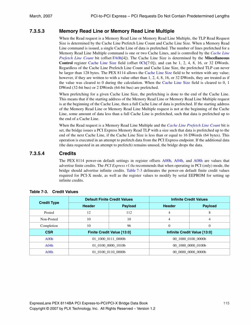
March, 2007 PCI-to-PCI Express – PCI Requests Do Not Contain Predetermined Lengths
ExpressLane PEX 8114BA PCI Express-to-PCI/PCI-X Bridge Data Book 115
Copyright © 2007 by PLX Technology, Inc. All Rights Reserved – Version 1.2
7.3.5.3 Memory Read Line or Memory Read Line MultipleWhen the Read request is a Memory Read Line or Memory Read Line Multiple, the TLP Read RequestSize is determined by the Cache Line Prefetch Line Count and Cache Line Size. When a Memory ReadLine command is issued, a single Cache Line of data is prefetched. The number of lines prefetched for aMemory Read Line Multiple command is one or two Cache Lines, and is controlled by the Cache LinePrefetch Line Count bit (offset FA0h[4]). The Cache Line Size is determined by the MiscellaneousControl register Cache Line Size field (offset 0Ch[7:0]), and can be 1, 2, 4, 8, 16, or 32 DWords.Regardless of the Cache Line Prefetch Line Count and Cache Line Size, the prefetched TLP can neverbe larger than 128 bytes. The PEX 8114 allows the Cache Line Size field to be written with any value;however, if they are written to with a value other than 1, 2, 4, 8, 16, or 32 DWords, they are treated as ifthe value was cleared to 0 during the calculation. When the Cache Line Size field is cleared to 0, 1DWord (32-bit bus) or 2 DWords (64-bit bus) are prefetched.
When prefetching for a given Cache Line Size, the prefetching is done to the end of the Cache Line.This means that if the starting address of the Memory Read Line or Memory Read Line Multiple requestis at the beginning of the Cache Line, then a full Cache Line of data is prefetched. If the starting addressof the Memory Read Line or Memory Read Line Multiple request is not at the beginning of the CacheLine, some amount of data less than a full Cache Line is prefetched, such that data is prefetched up tothe end of a Cache Line.
When the Read request is a Memory Read Line Multiple and the Cache Line Prefetch Line Count bit isset, the bridge issues a PCI Express Memory Read TLP with a size such that data is prefetched up to theend of the next Cache Line, if the Cache Line Size is less than or equal to 16 DWords (64 bytes). Thisoperation is executed in an attempt to prefetch data from the PCI Express endpoint. If the additional data(the data requested in an attempt to prefetch) remains unused, the bridge drops the data.
7.3.5.4 CreditsThe PEX 8114 power-on default settings in register offsets A00h, A04h, and A08h are values thatadvertise finite credits. The PCI Express r1.0a recommends that when operating in PCI (only) mode, thebridge should advertise infinite credits. Table 7-3 delineates the power-on default finite credit valuesrequired for PCI-X mode, as well as the register values to modify by serial EEPROM for setting upinfinite credits.
Table 7-3. Credit Values
Credit TypeDefault Finite Credit Values Infinite Credit Values
Header Payload Header Payload
Posted 12 112 4 8
Non-Posted 10 10 4 4
Completion 10 96 0 0
CSR Finite Credit Value [13:0] Infinite Credit Value [13:0]
A00h 01_1000_0111_0000b 00_1000_0100_0000b
A04h 01_0100_0000_1010b 00_1000_0000_0100b
A08h 01_0100_0110_0000b 00_0000_0000_0000b

Bridge Operations PLX Technology, Inc.
116 ExpressLane PEX 8114BA PCI Express-to-PCI/PCI-X Bridge Data Book
Copyright © 2007 by PLX Technology, Inc. All Rights Reserved – Version 1.2
7.3.6 PCI-to-PCI Express Disposition of Unused Prefetched DataAfter the PCI Express device completes the request to the PEX 8114, the PEX 8114 completes one ofthe PCI device’s subsequent attempts to Read by supplying data until the PCI device:
• Terminates the transaction normally, satisfying its need for data, OR
• Depletes the data that it transmitted from the PCI Express device.
If the PCI device terminates the Read, the PEX 8114 flushes the remaining data it prefetched from thePCI Express device. If the data is depleted by the PCI device’s Read, the PEX 8114 terminates the PCItransaction with a Disconnect-with-Data on the Data phase in which the last available data is read. ThePEX 8114 does not store and combine data from TLPs in an attempt to support lengthening thePCI burst.
7.3.7 PCI-to-PCI Express Pending Transaction Count LimitsThe PEX 8114 is capable of accepting multiple Posted PCI Writes. Each Write is stored in the centralRAM until it can be transmitted on the PCI Express link. Non-Posted transactions require Completionon the PCI Express side of the bridge, prior to completing the transaction on the PCI side of the bridge.When a Non-Posted transaction enters the PEX 8114, its context is saved until a PCI ExpressCompletion with a matching Requester ID is received. Upon receipt of the Completion from thePCI Express interface, the Completion is relayed to the PCI Initiator, which completes the transaction.The transaction is defined as outstanding from the time that the bridge receives the initial PCI requestuntil the bridge completes the transaction and returns it to the PCI requester. Up to eight Non-Postedtransactions can be outstanding at any given time.
7.3.8 PCI-to-PCI Express – PCI Write Transaction withDiscontiguous Byte EnablesPCI Express requires that all packet data beats, except the first and last, have all Byte Enables enabled.PCI has no such requirement. If the PCI data written to the PCI Express port disabled Byte Enables inthe middle of a burst, the PEX 8114 continues to accept the PCI data and creates two or more TLPs, asnecessary, to support long PCI bursts, while also honoring the PCI Express requirement forcontiguously asserted bytes.
7.3.9 PCI-to-PCI Express – PCI Write Transactions Largerthan Maximum Packet SizeWhen a PCI Burst Write transaction is longer than the PCI Express Maximum Packet Size, thePEX 8114 creates two or more PCI Express TLPs, as necessary, to support long bursts, while alsohonoring the PCI Express Maximum Packet Size requirements. When a PCI Data burst is completed,the TLP is transmitted and no attempt is made to combine multiple PCI Burst Writes into a single TLPtransaction. When the PEX 8114 PCI Express lanes cannot transmit PCI Express TLPs across the PCIExpress interface because of posted credit depletion, which would result in the filling of 6-KB centralmemory within the PEX 8114, the PEX 8114 starts issuing Retries on the PCI Bus to hold-off the PCIBus initiator from sending additional data to the PEX 8114.
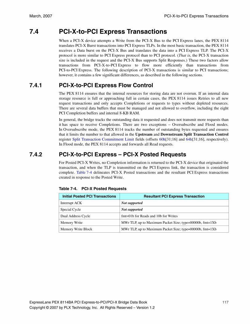
March, 2007 PCI-X-to-PCI Express Transactions
ExpressLane PEX 8114BA PCI Express-to-PCI/PCI-X Bridge Data Book 117
Copyright © 2007 by PLX Technology, Inc. All Rights Reserved – Version 1.2
7.4 PCI-X-to-PCI Express TransactionsWhen a PCI-X device attempts a Write from the PCI-X Bus to the PCI Express lanes, the PEX 8114translates PCI-X Burst transactions into PCI Express TLPs. In the most basic transaction, the PEX 8114receives a Data burst on the PCI-X Bus and translates the data into a PCI Express TLP. The PCI-Xprotocol is more similar to PCI Express protocol than to PCI protocol. (That is, the PCI-X transactionsize is included in the request and the PCI-X Bus supports Split Responses.) These two factors allowtransactions from PCI-X-to-PCI Express to flow more efficiently than transactions fromPCI-to-PCI Express. The following description of PCI-X transactions is similar to PCI transactions;however, it contains a few significant differences, as described in the following sections.
7.4.1 PCI-X-to-PCI Express Flow ControlThe PEX 8114 ensures that the internal resources for storing data are not overrun. If an internal datastorage resource is full or approaching full in certain cases, the PEX 8114 issues Retries to all newrequest transactions and only accepts Completions or requests to types without depleted resources.There are several data buffers that must be managed and not allowed to overflow, including the eightPCI Completion buffers and internal 8-KB RAM.
In general, the bridge tracks the outstanding data it requested and does not transmit more requests thanit has space to receive Completions. There are two exceptions – Oversubscribe and Flood modes.In Oversubscribe mode, the PEX 8114 tracks the number of outstanding bytes requested and ensuresthat it limits the number to that allowed in the Upstream and Downstream Split Transaction Controlregister Split Transaction Commitment Limit fields (offsets 60h[31;16] and 64h[31;16], respectively).In Flood mode, the PEX 8114 accepts and forwards all Read requests.
7.4.2 PCI-X-to-PCI Express – PCI-X Posted RequestsFor Posted PCI-X Writes, no Completion information is returned to the PCI-X device that originated thetransaction, and when the TLP is transmitted on the PCI Express link, the transaction is consideredcomplete. Table 7-4 delineates PCI-X Posted transactions and the resultant PCI Express transactionscreated in response to the Posted Write.
Table 7-4. PCI-X Posted Requests
Initial Posted PCI Transactions Resultant PCI Express Transaction
Interrupt ACK Not supported
Special Cycle Not supported
Dual Address Cycle fmt=01b for Reads and 10b for Writes
Memory Write MWr TLP, up to Maximum Packet Size; type=00000b, fmt=1Xb
Memory Write Block MWr TLP, up to Maximum Packet Size; type=00000b, fmt=1Xb
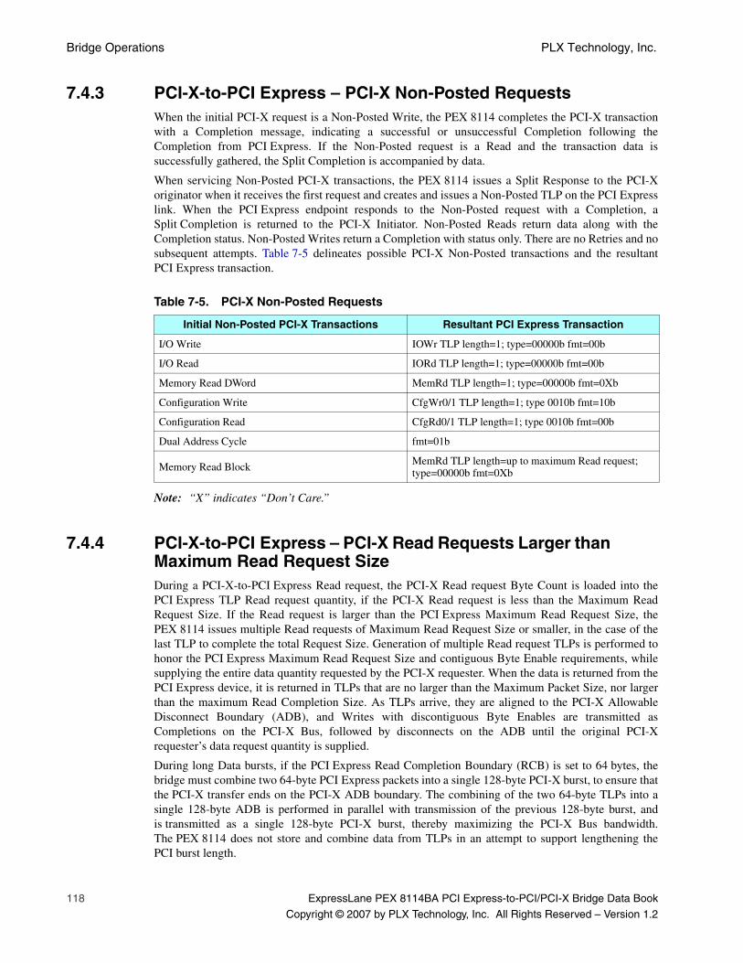
Bridge Operations PLX Technology, Inc.
118 ExpressLane PEX 8114BA PCI Express-to-PCI/PCI-X Bridge Data Book
Copyright © 2007 by PLX Technology, Inc. All Rights Reserved – Version 1.2
7.4.3 PCI-X-to-PCI Express – PCI-X Non-Posted RequestsWhen the initial PCI-X request is a Non-Posted Write, the PEX 8114 completes the PCI-X transactionwith a Completion message, indicating a successful or unsuccessful Completion following theCompletion from PCI Express. If the Non-Posted request is a Read and the transaction data issuccessfully gathered, the Split Completion is accompanied by data.
When servicing Non-Posted PCI-X transactions, the PEX 8114 issues a Split Response to the PCI-Xoriginator when it receives the first request and creates and issues a Non-Posted TLP on the PCI Expresslink. When the PCI Express endpoint responds to the Non-Posted request with a Completion, aSplit Completion is returned to the PCI-X Initiator. Non-Posted Reads return data along with theCompletion status. Non-Posted Writes return a Completion with status only. There are no Retries and nosubsequent attempts. Table 7-5 delineates possible PCI-X Non-Posted transactions and the resultantPCI Express transaction.
Note: “X” indicates “Don’t Care.”
7.4.4 PCI-X-to-PCI Express – PCI-X Read Requests Larger than Maximum Read Request SizeDuring a PCI-X-to-PCI Express Read request, the PCI-X Read request Byte Count is loaded into thePCI Express TLP Read request quantity, if the PCI-X Read request is less than the Maximum ReadRequest Size. If the Read request is larger than the PCI Express Maximum Read Request Size, thePEX 8114 issues multiple Read requests of Maximum Read Request Size or smaller, in the case of thelast TLP to complete the total Request Size. Generation of multiple Read request TLPs is performed tohonor the PCI Express Maximum Read Request Size and contiguous Byte Enable requirements, whilesupplying the entire data quantity requested by the PCI-X requester. When the data is returned from thePCI Express device, it is returned in TLPs that are no larger than the Maximum Packet Size, nor largerthan the maximum Read Completion Size. As TLPs arrive, they are aligned to the PCI-X AllowableDisconnect Boundary (ADB), and Writes with discontiguous Byte Enables are transmitted asCompletions on the PCI-X Bus, followed by disconnects on the ADB until the original PCI-Xrequester’s data request quantity is supplied.
During long Data bursts, if the PCI Express Read Completion Boundary (RCB) is set to 64 bytes, thebridge must combine two 64-byte PCI Express packets into a single 128-byte PCI-X burst, to ensure thatthe PCI-X transfer ends on the PCI-X ADB boundary. The combining of the two 64-byte TLPs into asingle 128-byte ADB is performed in parallel with transmission of the previous 128-byte burst, andis transmitted as a single 128-byte PCI-X burst, thereby maximizing the PCI-X Bus bandwidth.The PEX 8114 does not store and combine data from TLPs in an attempt to support lengthening thePCI burst length.
Table 7-5. PCI-X Non-Posted Requests
Initial Non-Posted PCI-X Transactions Resultant PCI Express Transaction
I/O Write IOWr TLP length=1; type=00000b fmt=00b
I/O Read IORd TLP length=1; type=00000b fmt=00b
Memory Read DWord MemRd TLP length=1; type=00000b fmt=0Xb
Configuration Write CfgWr0/1 TLP length=1; type 0010b fmt=10b
Configuration Read CfgRd0/1 TLP length=1; type 0010b fmt=00b
Dual Address Cycle fmt=01b
Memory Read Block MemRd TLP length=up to maximum Read request; type=00000b fmt=0Xb
March, 2007 PCI-X-to-PCI Express – PCI-X Transfer Special Case
ExpressLane PEX 8114BA PCI Express-to-PCI/PCI-X Bridge Data Book 119
Copyright © 2007 by PLX Technology, Inc. All Rights Reserved – Version 1.2
7.4.5 PCI-X-to-PCI Express – PCI-X Transfer Special CaseThis section documents the PCI-X transfer special case that exists when PCI-X Write requests are largerthan the Maximum Packet Size, cross 4-KB Address Boundary spaces, or have discontiguous ByteEnables. When a PCI-X device issues Write requests that are larger than the Maximum Packet Size,if the Write Request burst crosses a 4-KB Address Boundary space or the data has internaldiscontiguous Byte Enables, the PEX 8114 must break up the transaction into two or more transactions,assign unique Transaction IDs, and store details about each transaction generated, to facilitateaccounting for the transaction Completion.
7.4.6 PCI-X-to-PCI Express – PCI-X Transactions that Require Bridge to Take OwnershipWhen the PCI-X transaction is broken into multiple PCI Express transactions, the PEX 8114 mustensure that all requested data is read. To track data from large requests that require multiple TLPs togenerate, the PEX 8114 must track all transactions to completion. The PEX 8114 allows eight PCI-XRead Request transactions to be outstanding at any time. PCI-X Non-Posted Read transactions that aresmaller than the Maximum Read Request Size, as well as PCI-X Read requests that do not cross a 4-KBAddress Boundary space, without discontiguous Byte Enables, are not limited to eight outstandingtransactions. Limiting the Read Request Size, as less than or equal to the Maximum Read Request Size,allows for higher performance.
7.4.7 PCI-X-to-PCI Express – PCI-X Writes with Discontiguous Byte EnablesThe PEX 8114 is capable of accepting multiple Posted PCI-X Writes. Each Write is stored in the centralRAM until it can be transmitted on the PCI Express link. PCI Express requires that all packet data beats,except the first and last, have all Byte Enables enabled. PCI-X has no such requirement. If the PCI-Xdata has disabled Byte Enables in the middle of a burst, the PEX 8114 continues to accept the PCI-Xdata and creates two or more TLPs, as necessary, to support long PCI bursts, while also honoring thePCI Express requirement for contiguously asserted bytes.
7.4.8 PCI-X-to-PCI Express – PCI-X Writes Longer than Maximum Packet SizeWhen a PCI-X Burst transaction is longer than the PCI Express Maximum Packet Size, the PEX 8114creates two or more PCI Express TLPs, as necessary, to support long bursts, while also honoring thePCI Express Maximum Packet Size requirements. When a PCI-X Data burst is completed, the TLP istransmitted and no attempt is made to combine multiple small PCI-X Burst Writes into a single TLPtransaction. When the PEX 8114 PCI Express lanes cannot transmit PCI Express TLPs across the PCIExpress interface because of posted credit depletion, which would result in the filling of 6-KB centralmemory within the PEX 8114, the PEX 8114 starts issuing Retries on the PCI Bus to hold-off the PCIBus initiator from sending additional data to the PEX 8114.
Bridge Operations PLX Technology, Inc.
120 ExpressLane PEX 8114BA PCI Express-to-PCI/PCI-X Bridge Data Book
Copyright © 2007 by PLX Technology, Inc. All Rights Reserved – Version 1.2
7.5 PCI Express-to-PCI TransactionsIn PCI mode, when a PCI Express device transmits a transaction from the PCI Express interface to thePEX 8114 PCI-X bus, the transaction is translated from a PCI Express TLP into a PCI Burst transaction.In the most basic transaction, the PEX 8114 receives a TLP on the PCI Express lanes and translates thedata into one or more PCI bursts.
7.5.1 PCI Express-to-PCI Flow ControlCredits for up to 6 KB of PCI Express Posted and Non-Posted transactions are issued. Thesetransactions are queued, according to PCI Ordering Transaction rules in central memory, and aretransmitted to the PCI-X modules as bandwidth allows, limited by the eight outstandingPCI transactions. Transmitting packets into the PCI Express side of the bridge is throttled by spaceremaining in the central RAM. The process of transmitting transactions onto the PCI Bus is throttled bythe number of outstanding transactions transmitted to the PCI endpoints that did not complete.The PEX 8114 supports up to eight outstanding transactions on the PCI Bus. All transactions are driventhrough the bridge as quickly as possible, limited only by the PCI Express and PCI Bus bandwidths.
7.5.2 PCI Express-to-PCI – PCI Express Posted TransactionsWhen servicing Posted transactions, no Completion information is returned to the PCI Express devicethat originated the transaction, and when the transaction is transmitted on the PCI Bus, the transaction isconsidered complete. Table 7-6 delineates which PCI Express Posted transactions are supported and towhich PCI transaction they are translated.
Table 7-6. PCI Express Posted Transactions
Initial PCI Express Posted Transaction Type Resultant PCI Transaction
Memory Write PCI Memory Write.
Message Request
Messages that cause changes on the PCI side of the bridge are Interrupt messages, which are translated to INTA#. Internally, Power Management and error conditions can cause Error messages to generate to the PCI Express side of the bridge.
Message Request with Payload Not supported.
March, 2007 PCI Express-to-PCI – PCI Express Non-Posted Transactions
ExpressLane PEX 8114BA PCI Express-to-PCI/PCI-X Bridge Data Book 121
Copyright © 2007 by PLX Technology, Inc. All Rights Reserved – Version 1.2
7.5.3 PCI Express-to-PCI – PCI Express Non-Posted TransactionsWhen servicing Non-Posted PCI Express transactions, the PEX 8114 accepts the PCI Express TLP andcreates and issues a PCI request on the PCI Bus. The necessary data quantity is indicated in the TLP andthe PEX 8114 executes as many transactions as required on the PCI Bus to Write or Read the requesteddata. After the PEX 8114 successfully transmits or receives all data, it issues a Completion TLP to thePCI Express original requester. The PEX 8114 supports up to eight concurrent Non-Posted PCIrequests. Table 7-7 delineates the PCI Express Non-Posted requests and the resulting PCI transactionswhen the Non-Posted PCI Express request is received.
7.5.4 PCI Express-to-PCI – PCI Bus RetryWrites are serially processed on a first-come, first-served basis. Reads are attempted in parallel, that is,if one request receives a disconnect, the PEX 8114 attempts to gather data for another outstandingrequest, moving from request to request in an effort to complete as many transactions as possible, assoon as possible. If the Force Strong Ordering bit (offset FA0h[8]) is set, after data is returned inresponse to a Read request, the PEX 8114 concentrates all requests on gathering the remaining data forthat transaction until the transaction completes. By default, the bit is cleared at power-on reset. If the bitis set, only one outstanding Read is allowed at a time. All Posted and Non-Posted Write bursts on thePCI Bus cannot be longer than the PCI Express Maximum Packet Size. There is no internal combiningof Write TLPs in an effort to increase the PCI Burst Size.
Table 7-7. PCI Express Non-Posted Transactions
Initial PCI Express Non-Posted Transaction Type Resultant PCI Transaction
I/O Write Request I/O Write
I/O Read Request I/O Read
Configuration Write Type 0 Configuration Write Type 0
Configuration Read Type 0 Configuration Read Type 0
Configuration Write Type 1 Configuration Write Type 1
Configuration Read Type 1 Configuration Read Type 1
Memory Read – Locked Not supported – returns a UR
Memory Read RequestPCI Memory Read, PCI Memory Read Line, or PCI Memory Read Line Multiple
Bridge Operations PLX Technology, Inc.
122 ExpressLane PEX 8114BA PCI Express-to-PCI/PCI-X Bridge Data Book
Copyright © 2007 by PLX Technology, Inc. All Rights Reserved – Version 1.2
7.5.5 PCI Express-to-PCI Transaction Request SizeThe PEX 8114 determines which type of PCI Read request to issue on the PCI Bus, based on the sizeof the PCI Express Read request that the bridge receives. If a PCI Express Memory Read request entersthe PEX 8114 Prefetchable Memory space, with a TLP length and starting address such that allrequested data is within a single Cache Line and is less than an entire Cache Line, a Memory Readrequest is issued on the PCI Bus. If a PCI Express Memory Read request enters PEX 8114 PrefetchableMemory space, with a TLP length greater than or equal to the Cache Line Size, but less than two CacheLines in size, the PEX 8114 issues a Memory Read Line request on the PCI Bus.
When a PCI Express Memory Read request enters the PEX 8114’s Prefetchable Memory space, with aTLP length greater than or equal to two Cache Lines in size, the PEX 8114 issues a Memory Read LineMultiple request. Issuing of Memory Read Line Multiple requests can be disabled by clearing theMemory Read Line Multiple Enable bit. This method of determining whether to issue a Memory ReadLine or Memory Read Line Multiple request applies only to PCI mode. In PCI-X mode, the TransactionSize is stated in the transaction and it is unnecessary to indicate the Transaction Size.
7.5.6 PCI Express-to-PCI Transaction Completion SizeRead Completions are arranged according to the following description. If the data quantity requested inthe initial PCI Express Read request is less than or equal to the size of the maximum Read CompletionSize, the data is returned to the PCI Express requester in a single TLP. If the data quantity requested inthe initial PCI Express Read request is more than the maximum Read Completion Size, or if the Readcrosses a 4-KB Address Boundary space, the Completion is constructed into more than one TLP. TheTLPs are sized at the maximum Read Completion Size, except for the final TLP, which is sized tocomplete the remainder of the transaction.
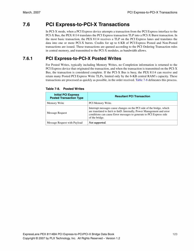
March, 2007 PCI Express-to-PCI-X Transactions
ExpressLane PEX 8114BA PCI Express-to-PCI/PCI-X Bridge Data Book 123
Copyright © 2007 by PLX Technology, Inc. All Rights Reserved – Version 1.2
7.6 PCI Express-to-PCI-X TransactionsIn PCI-X mode, when a PCI Express device attempts a transaction from the PCI Express interface to thePCI-X Bus, the PEX 8114 translates the PCI Express transaction TLP into a PCI-X Burst transaction. Inthe most basic transaction, the PEX 8114 receives a TLP on the PCI Express lanes and translates thedata into one or more PCI-X bursts. Credits for up to 6 KB of PCI Express Posted and Non-Postedtransactions are issued. These transactions are queued according to the PCI Ordering Transaction rulesin central memory, and transmitted to the PCI-X modules, as bandwidth allows.
7.6.1 PCI Express-to-PCI-X Posted WritesFor Posted Writes, typically including Memory Writes, no Completion information is returned to thePCI Express device that originated the transaction, and when the transaction is transmitted on the PCI-XBus, the transaction is considered complete. If the PCI-X Bus is busy, the PEX 8114 can receive andretain many Posted PCI Express Write TLPs, limited only by the 6-KB central RAM’s capacity. Thesetransactions are processed as quickly as possible, in the order received. Table 7-8 delineates this process.
Table 7-8. Posted Writes
Initial PCI ExpressPosted Transaction Type Resultant PCI Transaction
Memory Write PCI Memory Write.
Message Request
Interrupt messages cause changes on the PCI side of the bridge, which are translated to IntA to IntD. Internally, Power Management and error conditions can cause Error messages to generate to PCI Express side of the bridge.
Message Request with Payload Not supported.
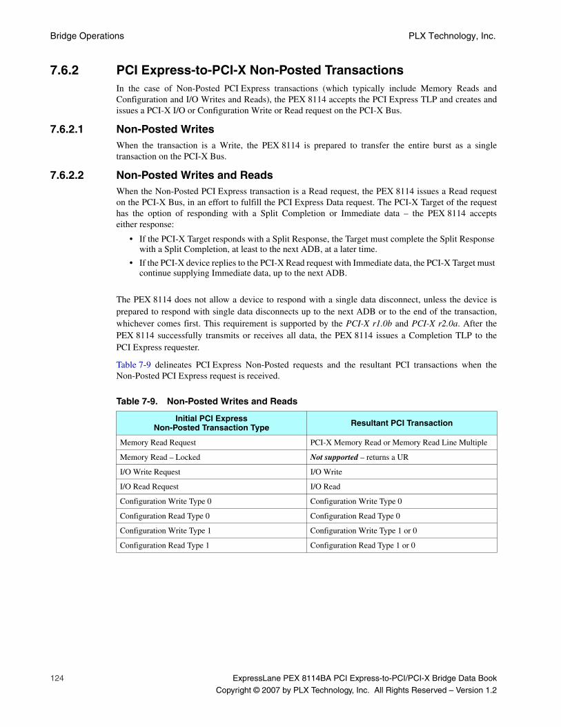
Bridge Operations PLX Technology, Inc.
124 ExpressLane PEX 8114BA PCI Express-to-PCI/PCI-X Bridge Data Book
Copyright © 2007 by PLX Technology, Inc. All Rights Reserved – Version 1.2
7.6.2 PCI Express-to-PCI-X Non-Posted TransactionsIn the case of Non-Posted PCI Express transactions (which typically include Memory Reads andConfiguration and I/O Writes and Reads), the PEX 8114 accepts the PCI Express TLP and creates andissues a PCI-X I/O or Configuration Write or Read request on the PCI-X Bus.
7.6.2.1 Non-Posted WritesWhen the transaction is a Write, the PEX 8114 is prepared to transfer the entire burst as a singletransaction on the PCI-X Bus.
7.6.2.2 Non-Posted Writes and ReadsWhen the Non-Posted PCI Express transaction is a Read request, the PEX 8114 issues a Read requeston the PCI-X Bus, in an effort to fulfill the PCI Express Data request. The PCI-X Target of the requesthas the option of responding with a Split Completion or Immediate data – the PEX 8114 acceptseither response:
• If the PCI-X Target responds with a Split Response, the Target must complete the Split Response with a Split Completion, at least to the next ADB, at a later time.
• If the PCI-X device replies to the PCI-X Read request with Immediate data, the PCI-X Target must continue supplying Immediate data, up to the next ADB.
The PEX 8114 does not allow a device to respond with a single data disconnect, unless the device isprepared to respond with single data disconnects up to the next ADB or to the end of the transaction,whichever comes first. This requirement is supported by the PCI-X r1.0b and PCI-X r2.0a. After thePEX 8114 successfully transmits or receives all data, the PEX 8114 issues a Completion TLP to thePCI Express requester.
Table 7-9 delineates PCI Express Non-Posted requests and the resultant PCI transactions when theNon-Posted PCI Express request is received.
Table 7-9. Non-Posted Writes and Reads
Initial PCI ExpressNon-Posted Transaction Type Resultant PCI Transaction
Memory Read Request PCI-X Memory Read or Memory Read Line Multiple
Memory Read – Locked Not supported – returns a UR
I/O Write Request I/O Write
I/O Read Request I/O Read
Configuration Write Type 0 Configuration Write Type 0
Configuration Read Type 0 Configuration Read Type 0
Configuration Write Type 1 Configuration Write Type 1 or 0
Configuration Read Type 1 Configuration Read Type 1 or 0
March, 2007 Non-Transparent Transactions
ExpressLane PEX 8114BA PCI Express-to-PCI/PCI-X Bridge Data Book 125
Copyright © 2007 by PLX Technology, Inc. All Rights Reserved – Version 1.2
7.6.2.3 Transaction ConcurrencyThe PEX 8114 supports up to eight Non-Posted PCI Express requests. Writes are serially processed on afirst-come, first-served basis. Reads are attempted in parallel, that is, if one request receives adisconnect, the PEX 8114 attempts to gather data for another of the outstanding requests, moving fromrequest to request in an effort to complete as many transactions as possible, as soon as possible. If theForce Strong Ordering bit (offset FA0h[8]) is set, after data is returned in response to a Read request, thePEX 8114 concentrates all requests on gathering data to complete that transaction until the transactioncompletes. This is performed only if the Force Strong Ordering bit is not set. If the bit is set, only oneoutstanding Read is allowed at a time.
All Posted and Non-Posted Write bursts on the PCI Bus can be no longer than the PCI ExpressMaximum Packet Size. There is no internal combining of Write TLPs in an effort to increase the PCIBurst Size. Read Completions are gathered from the PCI-X Bus as a single DWord Disconnect,Completions to the next ADB, or Completion of the entire requested data size. The Completion data iscollected within the PEX 8114, then delivered to the PCI Express requesters as TLP packets that are nolarger than the Maximum Packet Size, until all data requested by the PCI Express device is satisfied.
7.7 Non-Transparent TransactionsNon-Transparent transactions follow the same data path as Transparent transactions between thePCI Express link and the PCI or PCI-X Bus. The Non-Transparent transactions are also subject toAddress translation as they cross the Non-Transparent boundary. Address translation is described inChapter 5, “Address Spaces.”
When the PEX 8114 is a Master in Non-Transparent mode, Non-Posted transactions are handledsimilarly to Transparent mode, with the following exceptions:
• PEX 8114 takes ownership of all transactions
• PEX 8114 Requester ID replaces the originator’s Requester ID
This is achieved because devices on the PCI-X Bus are hidden from devices on the PCI Express side ofthe bridge, and cannot recognize the originator’s Requester ID, or, another device on the PCI Expressside might have the same Requester ID.
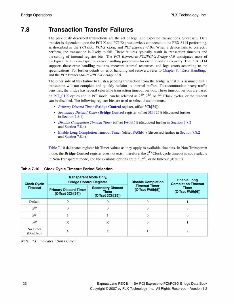
Bridge Operations PLX Technology, Inc.
126 ExpressLane PEX 8114BA PCI Express-to-PCI/PCI-X Bridge Data Book
Copyright © 2007 by PLX Technology, Inc. All Rights Reserved – Version 1.2
7.8 Transaction Transfer FailuresThe previously described transactions are the set of legal and expected transactions. Successful Datatransfer is dependent upon the PCI-X and PCI Express devices connected to the PEX 8114 performing,as described in the PCI r3.0, PCI-X r2.0a, and PCI Express r1.0a. When a device fails to correctlyperform, the transaction is likely to fail. These failures typically result in transaction timeouts andthe setting of internal register bits. The PCI Express-to-PCI/PCI-X Bridge r1.0 anticipates most ofthe typical failures and specifies error handling procedures for error condition recovery. The PEX 8114supports these error handling routines, recovers internal resources, and logs errors according to thespecifications. For further details on error handling and recovery, refer to Chapter 8, “Error Handling,”and the PCI Express-to-PCI/PCI-X Bridge r1.0.
The other side of this failure to flush a pending transaction from the bridge is that it is assumed that atransaction will not complete and quickly reclaim its internal buffers. To accommodate heavy trafficdensities, the bridge has several selectable transaction timeout periods. These timeout periods are based
on PCI_CLK cycles and in PCI mode, can be selected as 210, 215, or 220 Clock cycles, or the timeoutcan be disabled. The following register bits are used to select these timeouts:
• Primary Discard Timer (Bridge Control register, offset 3Ch[24])
• Secondary Discard Timer (Bridge Control register, offset 3Ch[25]) (discussed further in Section 7.8.1)
• Disable Completion Timeout Timer (offset FA0h[5]) (discussed further in Section 7.8.2 and Section 7.8.4)
• Enable Long Completion Timeout Timer (offset FA0h[6]) (discussed further in Section 7.8.2 and Section 7.8.4)
Table 7-10 delineates register bit Timer values as they apply to available timeouts. In Non-Transparent
mode, the Bridge Control register does not exist; therefore, the 215 Clock cycle timeout is not available
in Non-Transparent mode, and the available options are 210, 220, or no timeout (default).
Note: “X” indicates “Don’t Care.”
Table 7-10. Clock Cycle Timeout Period Selection
Clock Cycle Timeout
Transparent Mode Only,Bridge Control Register Disable Completion
Timeout Timer(Offset FA0h[5])
Enable Long Completion Timeout
Timer(Offset FA0h[6])Primary Discard Timer
(Offset 3Ch[24])
Secondary Discard Timer
(Offset 3Ch[25])
Default 0 0 0 1
210 0 0 0 0
215 1 1 0 0
220 X X 0 1
No Timer(Disabled)
X X 1 X
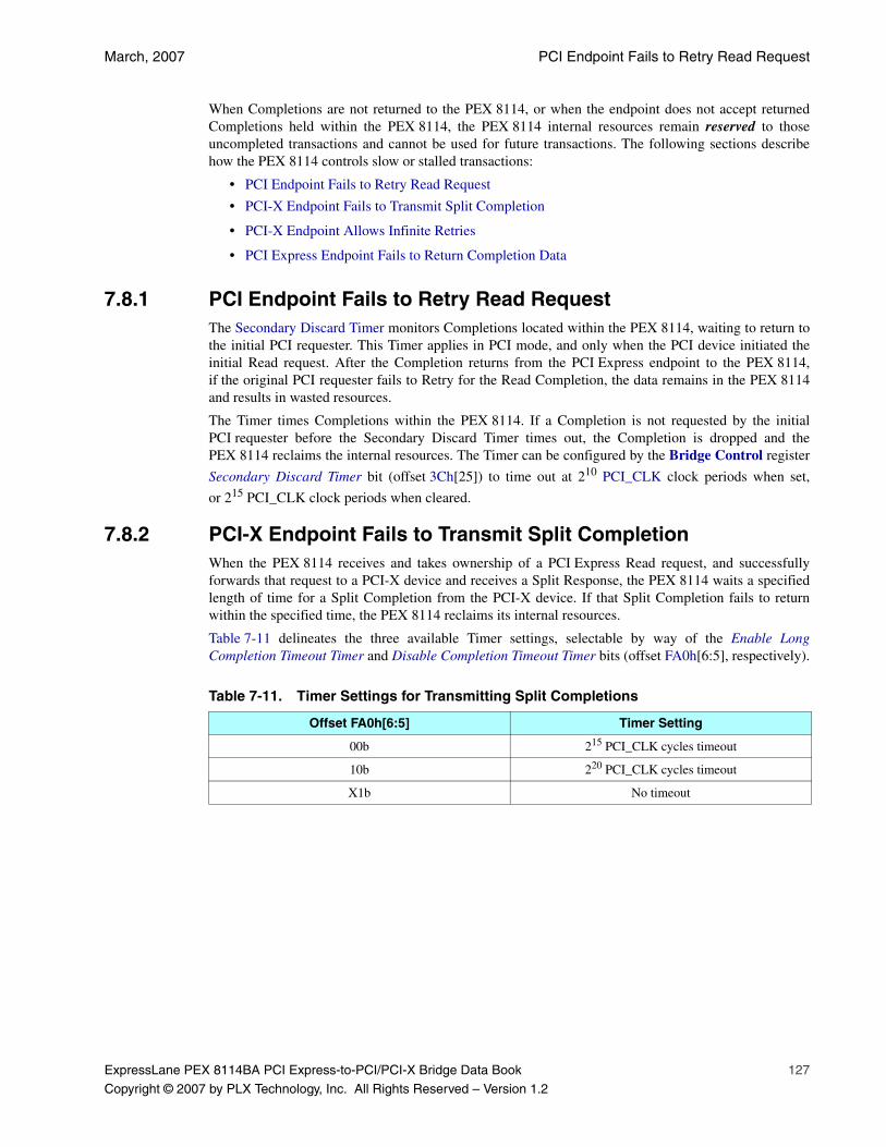
March, 2007 PCI Endpoint Fails to Retry Read Request
ExpressLane PEX 8114BA PCI Express-to-PCI/PCI-X Bridge Data Book 127
Copyright © 2007 by PLX Technology, Inc. All Rights Reserved – Version 1.2
When Completions are not returned to the PEX 8114, or when the endpoint does not accept returnedCompletions held within the PEX 8114, the PEX 8114 internal resources remain reserved to thoseuncompleted transactions and cannot be used for future transactions. The following sections describehow the PEX 8114 controls slow or stalled transactions:
• PCI Endpoint Fails to Retry Read Request
• PCI-X Endpoint Fails to Transmit Split Completion
• PCI-X Endpoint Allows Infinite Retries
• PCI Express Endpoint Fails to Return Completion Data
7.8.1 PCI Endpoint Fails to Retry Read RequestThe Secondary Discard Timer monitors Completions located within the PEX 8114, waiting to return tothe initial PCI requester. This Timer applies in PCI mode, and only when the PCI device initiated theinitial Read request. After the Completion returns from the PCI Express endpoint to the PEX 8114,if the original PCI requester fails to Retry for the Read Completion, the data remains in the PEX 8114and results in wasted resources.
The Timer times Completions within the PEX 8114. If a Completion is not requested by the initialPCI requester before the Secondary Discard Timer times out, the Completion is dropped and thePEX 8114 reclaims the internal resources. The Timer can be configured by the Bridge Control register
Secondary Discard Timer bit (offset 3Ch[25]) to time out at 210 PCI_CLK clock periods when set,
or 215 PCI_CLK clock periods when cleared.
7.8.2 PCI-X Endpoint Fails to Transmit Split CompletionWhen the PEX 8114 receives and takes ownership of a PCI Express Read request, and successfullyforwards that request to a PCI-X device and receives a Split Response, the PEX 8114 waits a specifiedlength of time for a Split Completion from the PCI-X device. If that Split Completion fails to returnwithin the specified time, the PEX 8114 reclaims its internal resources.
Table 7-11 delineates the three available Timer settings, selectable by way of the Enable LongCompletion Timeout Timer and Disable Completion Timeout Timer bits (offset FA0h[6:5], respectively).
Table 7-11. Timer Settings for Transmitting Split Completions
Offset FA0h[6:5] Timer Setting
00b 215 PCI_CLK cycles timeout
10b 220 PCI_CLK cycles timeout
X1b No timeout
Bridge Operations PLX Technology, Inc.
128 ExpressLane PEX 8114BA PCI Express-to-PCI/PCI-X Bridge Data Book
Copyright © 2007 by PLX Technology, Inc. All Rights Reserved – Version 1.2
7.8.3 PCI-X Endpoint Allows Infinite RetriesWhen the PEX 8114 attempts to master a PCI or PCI-X Read Request transaction onto the PCI-X Bus inresponse to a PCI Express endpoint Read request, it is expected that the PCI-X endpoint might notcontain data that is immediately ready and can respond to the PEX 8114’s Read request with a Retry.In response to the Retry, the PEX 8114 re-attempts the Read request, and it is expected that a futureRead attempt will be completed with data. If the endpoint infinitely replies to the PEX 8114 Readrequest with a Retry, the PEX 8114 terminates the transaction. To facilitate this, the number of Retriesreceived for each Read request are counted. At which time, the PEX 8114 compares the value stored inthe Maximum Read Cycle Value field (offset FA0h[26:16]). If the number of Retries received matchesthe number stored in the Maximum Read Cycle Value field, the Read request is dropped and the RetryFailure Status bit (offset FA0h[27]) is set. If the Force Strong Ordering bit (offset FA0h[8]) is not set,the PEX 8114 attempts up to eight Read requests in a Round-Robin scheme. A Retry Count for each ofthe eight Read requests is maintained, and compared, as it takes its turn at the PCI Bus.

March, 2007 PCI Express Endpoint Fails to Return Completion Data
ExpressLane PEX 8114BA PCI Express-to-PCI/PCI-X Bridge Data Book 129
Copyright © 2007 by PLX Technology, Inc. All Rights Reserved – Version 1.2
7.8.4 PCI Express Endpoint Fails to Return Completion DataThe PEX 8114 holds internal resources reserved to receive Completions. If the PCI Express endpointresponsible for a Completion fails to transmit a Completion, the PEX 8114’s internal resources are atrisk of remaining reserved, waiting for a Completion that might never occur. The PEX 8114 contains anInternal Timer used to trigger the bridge to reclaim internal resources reserved for Completions thatmight never occur. Table 7-12 delineates the three available Timer settings, selectable by way of theEnable Long Completion Timeout Timer and Disable Completion Timeout Timer bits (offset FA0h[6:5],respectively).
When PCI Non-Posted requests and Completions from PCI Express-to-PCI are executed and no timeoutis selected (offset FA0h[6:5]=X1b), the buffer holding Completions for the PCI requests are not
automatically reclaimed. However, after 220 clocks transpire without a Completion, the CompletionBuffer Timeout status bit for that buffer (offset F88h) is set to indicate that the buffer is reserved for an
extremely late Completion. When the timeout setting is set to 215 or 220 (offset FA0h[6:5]=00b or 10b,respectively) and the Completion fails to return before the timeout, the buffer is reclaimed after thetimeout and reused. If after a transaction times out, and the buffer is scheduled for reuse, and thePCI endpoint Retries the Read request for the transaction that timed out, the PEX 8114 returns a TargetAbort or FFFF_FFFFh, as selected by the Bridge Control register Master Abort Mode bit(offset 3Ch[21]) to indicate that a timeout occurred to the PCI endpoint. Each buffer can timeout and bereclaimed three times. After three reclaims and four timeouts, the Completion Buffer Timeout Status bitfor that buffer is set, to indicate that the buffer can no longer be reclaimed. When a buffer times out, if auser or operating system confirms that no stale Completions are pending, the buffer can be re-initializedby writing 1 to the offset F88h bit representing that buffer.
There is a degree of risk involved in re-initializing buffers. If a stale Completion is pending, and thesoftware is not aware of this, and the associated Completion Buffer Timeout Status bit is mistakenlycleared, the stale Completion can be mistaken for a Completion to a more-recent request, resulting inincorrect data being used for the Completion. If 32 PCI Read requests fail to complete by thePCI Express endpoint, all eight buffers timeout four times and all resources are consumed.
To prevent a lockup condition, the PEX 8114 automatically clears the Completion Buffer Timeout Statusbits for all eight registers, allowing it to continue to accept Non-Posted requests. If a lockup conditionoccurs, the PEX 8114 can no longer accept Non-Posted PCI-X requests, which precludes ConfigurationWrites. It therefore becomes impossible to clear the buffer timeouts after all buffers time out.
Note: “X” indicates “Don’t Care.”
Table 7-12. Timer Settings for Receiving Completions
Offset FA0h[6:5] Timer Setting
00b 215 PCI_CLK cycles timeout
10b 220 PCI_CLK cycles timeout
X1b No timeout

Bridge Operations PLX Technology, Inc.
130 ExpressLane PEX 8114BA PCI Express-to-PCI/PCI-X Bridge Data Book
Copyright © 2007 by PLX Technology, Inc. All Rights Reserved – Version 1.2
THIS PAGE INTENTIONALLY LEFT BLANK.

ExpressLane PEX 8114BA PCI Express-to-PCI/PCI-X Bridge Data Book 131
Copyright © 2007 by PLX Technology, Inc. All Rights Reserved – Version 1.2
Chapter 8 Error Handling
8.1 Forward Bridge Error HandlingFor all errors detected by the bridge, the bridge sets the appropriate error status bit [both ConventionalPCI/PCI-X Error bit(s) and PCI Express error status bit(s)], and generates an Error message on thePCI Express interface, if enabled. Each error condition has an error severity level programmable bysoftware, and a corresponding Error message generated on the PCI Express interface.
Four bits control PCI Express interface Error message generation:
• PCI/PCI-X Command register SERR# Enable bit
• PCI Express Device Control register Correctable Error Reporting Enable bit
• PCI Express Device Control register Non-Fatal Error Reporting Enable bit
• PCI Express Device Control register Fatal Error Reporting Enable bit
ERR_COR messages are enabled for transmission if the Correctable Error Reporting Enable bit is set.ERR_NONFATAL messages are enabled for transmission if the SERR# Enable or Non-Fatal ErrorReporting Enable bit is set. ERR_FATAL messages are enabled for transmission if the SERR# Enable orFatal Error Reporting Enable bit is set. The Device Status register Correctable Error Detected,Non-Fatal Error Detected, and Fatal Error Detected status bits are set for the corresponding errors onthe PCI Express interface, regardless of the Error Reporting Enable bit values.
8.1.1 Forward Bridge PCI Express Originating Interface (Primary to Secondary)This section describes error support for transactions that cross the bridge if the originating side isthe PCI Express interface, and the destination interface is operating in Conventional PCI/PCI-X modes.If a Write Request or Read Completion is received with a Poisoned TLP, consider the entire DataPayload of the PCI Express transaction as corrupt. Parity is inverted for all Data phases whencompleting the transaction on the PCI/PCI-X Bus. If a TLP is received and an ECRC error is detected,consider the entire TLP as corrupt and not forwarded, but dropped by the bridge.
Table 8-1 delineates the translation a bridge must perform when forwarding a Non-Posted PCI Expressrequest (Write or Read) to the PCI/PCI-X Bus, and the request is immediately completed on the PCI/PCI-X Bus, normally or with an error condition.
Table 8-1. Translation Bridge Action when Forwarding Non-Posted PCI Express Request to PCI/PCI-X Bus
Immediate PCI/PCI-X Termination PCI Express Completion Status
Data Transfer with Parity error (Non-Posted Writes) Unsupported Request
Data Transfer with Parity error (Reads) Successful (Poisoned TLP)
Master Abort Unsupported Request
Target Abort Completer Abort
Error Handling PLX Technology, Inc.
132 ExpressLane PEX 8114BA PCI Express-to-PCI/PCI-X Bridge Data Book
Copyright © 2007 by PLX Technology, Inc. All Rights Reserved – Version 1.2
8.1.1.1 Received Poisoned TLPWhen the PCI Express interface receives a Write Request or Read Completion with poisoned data, thefollowing occurs:
1. PCI Status register Detected Parity Error bit is set.
2. PCI Status register Master Data Parity Error bit is set if the Poisoned TLP is a Read Completion and the PCI Command register Parity Error Response Enable bit is set.
3. Uncorrectable Error Status register Poisoned TLP Status bit is set.
4. TLP Header is logged in the Header Log register and the Advanced Error Capabilities and Control register First Error Pointer is updated if the Uncorrectable Error Mask register Poisoned TLP Error Mask bit is cleared and the First Error Pointer is inactive.
5. ERR_FATAL/ERR_NONFATAL message is generated on the PCI Express interface, depending on the Uncorrectable Error Severity register Poisoned TLP Severity bit’s severity, if the following conditions are met:
– Uncorrectable Error Mask register Poisoned TLP Error Mask bit is cleared AND EITHER
– PCI Command register SERR# Enable bit is set OR
– PCI Express Device Control register Fatal Error Reporting Enable or Non-Fatal Error Reporting Enable bit is set
6. Device Status register Fatal Error Detected or Non-Fatal Error Detected bit is set.
7. PCI Status register Signaled System Error bit is set if the Uncorrectable Error Mask register Poisoned TLP Error Mask bit is cleared and the SERR# Enable bit is set.
8. Parity bit associated with each DWord of data on the PCI/PCI-X Bus is inverted.
9. When a Poisoned TLP Write Request is forwarded to the PCI/PCI-X Bus and the bridge detects PCI_PERR# asserted, the following occurs:
– Secondary Status register Secondary Master Data Parity Error bit is set if the Bridge Control register Secondary Parity Error Response Enable bit is set
– Secondary Uncorrectable Error Status register PERR# Assertion Detected bit is set
– Transaction command, attributes, and address are logged in the Secondary Header Log register and the FECh register Secondary Uncorrectable Error Pointer is updated if the Secondary Uncorrectable Error Mask register PERR# Assertion Detected Mask bit is clear and the First Error Pointer is inactive
10. No Error message is generated when a Poisoned TLP is forwarded to the PCI/PCI-X Bus with inverted parity and PCI_PERR# is detected asserted by the PCI/PCI-X Target device.

March, 2007 Forward Bridge PCI Express Originating Interface (Primary to Secondary)
ExpressLane PEX 8114BA PCI Express-to-PCI/PCI-X Bridge Data Book 133
Copyright © 2007 by PLX Technology, Inc. All Rights Reserved – Version 1.2
8.1.1.2 Received ECRC ErrorWhen a TLP is received and the bridge detects an ECRC error, the following occurs:
1. Transaction is dropped.
2. PCI Status register Detected Parity Error bit is set.
3. Uncorrectable Error Status register ECRC Error Status bit is set.
4. TLP Header is logged in the Header Log register and the Advanced Error Capabilities and Control register First Error Pointer is updated if the Uncorrectable Error Mask register ECRC Error Mask bit is cleared and the First Error Pointer is inactive.
5. ERR_FATAL/ERR_NONFATAL message is generated on the PCI Express interface, depending on the Uncorrectable Error Severity register ECRC Error Severity bit’s severity, if the following conditions are met:
– Uncorrectable Error Mask register ECRC Error Mask bit is cleared AND EITHER
– PCI Command register SERR# Enable bit is set OR
– PCI Express Device Control register Fatal Error Reporting Enable or Non-Fatal Error Reporting Enable bit is set
6. Device Status register Fatal Error Detected or Non-Fatal Error Detected bit is set.
7. PCI Status register Signaled System Error bit is set if the Uncorrectable Error Mask register ECRC Error Mask bit is cleared and the SERR# Enable bit is set.
8.1.1.3 PCI/PCI-X Uncorrectable Data ErrorsThe following sections describe error handling when forwarding Non-Poisoned PCI Expresstransactions to the PCI/PCI-X Bus, and an Uncorrectable PCI/PCI-X error is detected.
Posted Writes
When the PEX 8114 detects PCI_PERR# asserted on the PCI/PCI-X secondary interfacewhile forwarding a Non-Poisoned Posted Write transaction from the PCI Express interface, thefollowing occurs:
1. Secondary Status register Secondary Master Data Parity Error bit is set if the Bridge Control register Secondary Parity Error Response Enable bit is set.
2. Secondary Uncorrectable Error Status register PERR# Assertion Detected Status bit is set.
3. Transaction command, attributes, and address are logged in the Secondary Header Log register and the FECh register Secondary Uncorrectable First Error Pointer is updated if the Secondary Uncorrectable Error Mask register PERR# Assertion Detected Mask bit is cleared and the Secondary Uncorrectable First Error Pointer is inactive.
4. ERR_FATAL/ERR_NONFATAL message is generated on the PCI Express interface, depending on the Secondary Uncorrectable Error Severity register PERR# Assertion Detected Severity bit’s severity, if the following conditions are met:
– Secondary Uncorrectable Error Mask register PERR# Assertion Detected Mask bit is clear AND EITHER
– PCI Command register SERR# Enable bit is set OR
– PCI Express Device Control register Fatal Error Reporting Enable or Non-Fatal Error Reporting Enable bit is set
5. Device Status register Fatal Error Detected or Non-Fatal Error Detected bit is set.
6. PCI Status register Signaled System Error bit is set if the Secondary Uncorrectable Error Mask register PERR# Assertion Detected Mask bit is cleared and the SERR# Enable bit is set.
7. After the error is detected, the remainder of the data is forwarded.
Error Handling PLX Technology, Inc.
134 ExpressLane PEX 8114BA PCI Express-to-PCI/PCI-X Bridge Data Book
Copyright © 2007 by PLX Technology, Inc. All Rights Reserved – Version 1.2
Non-Posted Writes
When the PEX 8114 detects PCI_PERR# asserted on the PCI/PCI-X secondary interfacewhile forwarding a Non-Poisoned Non-Posted Write transaction from the PCI Express interface, thefollowing occurs:
1. Secondary Status register Secondary Master Data Parity Error bit is set if the Bridge Control register Secondary Parity Error Response Enable bit is set.
2. PCI Express Completion with Unsupported Request status is generated.
3. Secondary Uncorrectable Error Status register PERR# Assertion Detected Status bit is set.
4. Transaction command, attributes, and address are logged in the Secondary Header Log register and the FECh register Secondary Uncorrectable Error Pointer is updated if the Secondary Uncorrectable Error Mask register PERR# Assertion Detected Mask bit is cleared and the Secondary Uncorrectable First Error Pointer is inactive.
5. ERR_FATAL/ERR_NONFATAL message is generated on the PCI Express interface, depending on the Secondary Uncorrectable Error Severity register PERR# Assertion Detected Severity bit’s severity, if the following conditions are met:
– Secondary Uncorrectable Error Mask register PERR# Assertion Detected Mask bit is clear AND EITHER
– PCI Command register SERR# Enable bit is set OR
– PCI Express Device Control register Fatal Error Reporting Enable or Non-Fatal Error Reporting Enable bit is set
6. Device Status register Fatal Error Detected or Non-Fatal Error Detected bit is set.
7. PCI Status register Signaled System Error bit is set if the Secondary Uncorrectable Error Mask register PERR# Assertion Detected Mask bit is cleared and the SERR# Enable bit is set.
When the Target signals Split Response, the bridge terminates the transaction as it would for a SplitRequest that does not contain an error and takes no further action. If the returned Split Completion is aSplit Completion Error message, the bridge returns a PCI Express Completion with UnsupportedRequest status to the requester.
March, 2007 Forward Bridge PCI Express Originating Interface (Primary to Secondary)
ExpressLane PEX 8114BA PCI Express-to-PCI/PCI-X Bridge Data Book 135
Copyright © 2007 by PLX Technology, Inc. All Rights Reserved – Version 1.2
Immediate Reads
When the PEX 8114 forwards a Read request (I/O, Memory, or Configuration) from the PCI Expressinterface and detects an Uncorrectable Data error on the secondary bus while receiving an Immediate orSplit Response from the completer, the following occurs:
1. Secondary Status register Secondary Master Data Parity Error bit is set if the Bridge Control register Secondary Parity Error Response Enable bit is set.
2. Secondary Status register Secondary Detected Parity Error bit is set.
3. PCI_PERR# is asserted on the secondary interface if the Bridge Control register Secondary Parity Error Response Enable bit is set.
4. Secondary Uncorrectable Error Status register Uncorrectable Data Error Status bit is set.
5. Transaction command, attributes, and address are logged in the Secondary Header Log register and the FECh register Secondary Uncorrectable Error Pointer is updated if the Secondary Uncorrectable Error Mask register Uncorrectable Data Error Mask bit is cleared and the Secondary Uncorrectable First Error Pointer is inactive.
6. ERR_FATAL/ERR_NONFATAL message is generated on the PCI Express interface, depending on the Secondary Uncorrectable Error Severity register Uncorrectable Data Error Severity bit’s severity, if the following conditions are met:
– Secondary Uncorrectable Error Mask register Uncorrectable Data Error Mask bit is clear AND EITHER
– PCI Command register SERR# Enable bit is set OR
– PCI Express Device Control register Fatal Error Reporting Enable or Non-Fatal Error Reporting Enable bit is set
7. Device Status register Fatal Error Detected or Non-Fatal Error Detected bit is set.
8. PCI Status register Signaled System Error bit is set if the Secondary Uncorrectable Error Mask register Uncorrectable Data Error Mask bit is cleared and the SERR# Enable bit is set.
After detecting an Uncorrectable data error on the destination bus for an Immediate Read transaction,the PEX 8114 continues to fetch data until the Byte Count is satisfied or the Target ends the transaction.When the bridge creates the PCI Express Completion, it forwards the Completion with SuccessfulCompletion and poisons the TLP. For PCI-X, an Uncorrectable Data error on a Split Response does notaffect handling of subsequent Split Completions.
Error Handling PLX Technology, Inc.
136 ExpressLane PEX 8114BA PCI Express-to-PCI/PCI-X Bridge Data Book
Copyright © 2007 by PLX Technology, Inc. All Rights Reserved – Version 1.2
PCI-X Split Read Completions
When the bridge forwards a Non-Poisoned Read Completion from PCI Express to PCI-X and detectsPCI_PERR# asserted by the PCI-X Target, the following occurs:
1. Bridge continues to forward the remainder of the Split Completion.
2. Secondary Uncorrectable Error Status register PERR# Assertion Detected Status bit is set.
3. Transaction command, attributes, and address are logged in the Secondary Header Log register and the FECh register Secondary Uncorrectable Error Pointer is updated if the Secondary Uncorrectable Error Mask register PERR# Assertion Detected Mask bit is cleared and the Secondary Uncorrectable First Error Pointer is inactive.
4. ERR_FATAL/ERR_NONFATAL message is generated on the PCI Express interface, depending on the Secondary Uncorrectable Error Severity register PERR# Assertion Detected Severity bit’s severity, if the following conditions are met:
– Secondary Uncorrectable Error Mask register PERR# Assertion Detected Mask bit is clear AND EITHER
– PCI Command register SERR# Enable bit is set OR
– PCI Express Device Control register Fatal Error Reporting Enable or Non-Fatal Error Reporting Enable bit is set
5. Device Status register Fatal Error Detected or Non-Fatal Error Detected bit is set.
6. PCI Status register Signaled System Error bit is set if the Secondary Uncorrectable Error Mask register PERR# Assertion Detected Mask bit is cleared and the SERR# Enable bit is set.
8.1.1.4 PCI/PCI-X Address/Attribute ErrorsWhen the PEX 8114 forwards transactions from PCI Express to PCI/PCI-X, PCI Address errors arereported by SERR# Target assertion. When the PEX 8114 detects SERR# asserted, the followingoccurs:
1. Secondary Status register Secondary Received System Error bit is set.
2. Secondary Uncorrectable Error Status register SERR# Assertion Detected bit is set.
3. FECh register Secondary Uncorrectable Error Pointer is updated if the Secondary Uncorrectable First Error Pointer is inactive and the Secondary Uncorrectable Error Mask register SERR# Assertion Detected Mask bit is clear. No Header is logged.
4. ERR_FATAL/ERR_NONFATAL message is generated on the PCI Express interface, depending on the Secondary Uncorrectable Error Severity register SERR# Assertion Detected Severity bit’s severity, if the following conditions are met:
– Secondary Uncorrectable Error Mask register SERR# Assertion Detected Mask bit is clear OR the Bridge Control register SERR# Enable bit is set AND EITHER
– PCI Command register SERR# Enable bit is set OR
– PCI Express Device Control register Fatal Error Reporting Enable or Non-Fatal Error Reporting Enable bit is set
5. Device Status register Fatal Error Detected or Non-Fatal Error Detected bit is set.
6. PCI Status register Signaled System Error bit is set if the PCI Command and Bridge Control register SERR# Enable bits are set.
March, 2007 Forward Bridge PCI Express Originating Interface (Primary to Secondary)
ExpressLane PEX 8114BA PCI Express-to-PCI/PCI-X Bridge Data Book 137
Copyright © 2007 by PLX Technology, Inc. All Rights Reserved – Version 1.2
8.1.1.5 PCI/PCI-X Master Abort on Posted TransactionWhen a Posted Write transaction forwarded from PCI Express to PCI/PCI-X results in a Master Aborton the PCI/PCI-X Bus, the following occurs:
1. Entire transaction is discarded.
2. Secondary Status register Secondary Received Master Abort bit is set.
3. Secondary Uncorrectable Error Status register Received Master Abort Status bit is set.
4. Transaction command, attributes, and address are logged in the Secondary Header Log register and the FECh register Secondary Uncorrectable Error Pointer is updated if the Secondary Uncorrectable Error Mask register Received Master Abort Mask bit is cleared and the Secondary Uncorrectable First Error Pointer is inactive.
5. ERR_FATAL/ERR_NONFATAL message is generated on the PCI Express interface, depending on the Secondary Uncorrectable Error Severity register Received Master Abort Severity bit’s severity, if the following conditions are met:
– Secondary Uncorrectable Error Mask register Received Master Abort Mask bit is cleared OR the Bridge Control register Master Abort Mode bit is set AND EITHER
– PCI Command register SERR# Enable bit is set OR
– PCI Express Device Control register Fatal Error Reporting Enable or Non-Fatal Error Reporting Enable bit is set
6. Device Status register Fatal Error Detected or Non-Fatal Error Detected bit is set.
7. PCI Status register Signaled System Error bit is set if the Master Abort Mode bit is set or the Received Master Abort Mask bit is cleared and the SERR# Enable bit is set.
8.1.1.6 PCI/PCI-X Master Abort on Non-Posted TransactionWhen a Non-Posted transaction forwarded from PCI Express to PCI/PCI-X results in a Master Abort onthe PCI/PCI-X Bus, the following occurs:
1. Completion with Unsupported Request status is returned on the PCI Express interface.
2. Secondary Status register Secondary Received Master Abort bit is set.
3. Secondary Uncorrectable Error Status register Received Master Abort Status bit is set.
4. Transaction command, attributes, and address are logged in the Secondary Header Log register and the FECh register Secondary Uncorrectable Error Pointer is updated if the Secondary Uncorrectable Error Mask register Received Master Abort Mask bit is cleared and the Secondary Uncorrectable First Error Pointer is inactive.
5. ERR_FATAL/ERR_NONFATAL message is generated on the PCI express interface, depending on the Secondary Uncorrectable Error Severity register Received Master Abort Severity bit’s severity, if the following conditions are met:
– Secondary Uncorrectable Error Mask register Received Master Abort Mask bit is cleared AND EITHER
– PCI Command register SERR# Enable bit is set OR
– PCI Express Device Control register Fatal Error Reporting Enable or Non-Fatal Error Reporting Enable bit is set
6. Device Status register Fatal Error Detected or Non-Fatal Error Detected bit is set.
7. PCI Status register Signaled System Error bit is set if the Received Master Abort Mask bit is cleared and the SERR# Enable bit is set.
Error Handling PLX Technology, Inc.
138 ExpressLane PEX 8114BA PCI Express-to-PCI/PCI-X Bridge Data Book
Copyright © 2007 by PLX Technology, Inc. All Rights Reserved – Version 1.2
8.1.1.7 PCI-X Master Abort on Split CompletionWhen a Split Completion forwarded from PCI Express to PCI-X results in a Master Abort on the PCI-XBus, the following occurs:
1. Entire transaction is discarded.
2. Secondary Status register Secondary Received Master Abort bit is set.
3. PCI-X Secondary Status register Split Completion Discarded bit is set.
4. Secondary Uncorrectable Error Status register Master Abort on Split Completion Status bit is set.
5. Transaction command, attributes, and address are logged in the Secondary Header Log register and the FECh register Secondary Uncorrectable Error Pointer is updated if the Secondary Uncorrectable Error Mask register Master Abort on Split Completion Mask bit is cleared and the Secondary Uncorrectable First Error Pointer is inactive.
6. ERR_FATAL/ERR_NONFATAL message is generated on the PCI Express interface, depending on the Secondary Uncorrectable Error Severity register Master Abort on Split Completion Severity bit’s severity, if the following conditions are met:
– Secondary Uncorrectable Error Mask register Master Abort on Split Completion Mask bit is cleared AND EITHER
– PCI Command register SERR# Enable bit is set OR
– PCI Express Device Control register Fatal Error Reporting Enable or Non-Fatal Error Reporting Enable bit is set
7. Device Status register Fatal Error Detected or Non-Fatal Error Detected bit is set.
8. PCI Status register Signaled System Error bit is set if the Master Abort on Split Completion Mask bit is cleared and the SERR# Enable bit is set.
8.1.1.8 PCI/PCI-X Target Abort on Posted TransactionWhen a Posted Write transaction forwarded from PCI Express to PCI/PCI-X results in a Target Abort onthe PCI/PCI-X Bus, the following occurs:
1. Entire transaction is discarded.
2. Secondary Status register Secondary Received Target Abort bit is set.
3. Secondary Uncorrectable Error Status register Received Target Abort Status bit is set.
4. Transaction command, attributes, and address are logged in the Secondary Header Log register and the FECh register Secondary Uncorrectable Error Pointer is updated if the Secondary Uncorrectable Error Mask register Received Target Abort Mask bit is cleared and the Secondary Uncorrectable First Error Pointer is inactive.
5. ERR_FATAL/ERR_NONFATAL message is generated on the PCI Express interface, depending on the Secondary Uncorrectable Error Severity register Received Target Abort Severity bit’s severity, if the following conditions are met:
– Secondary Uncorrectable Error Mask register Received Target Abort Mask bit is cleared AND EITHER
– PCI Command register SERR# Enable bit is set OR
– PCI Express Device Control register Fatal Error Reporting Enable or Non-Fatal Error Reporting Enable bit is set
6. Device Status register Fatal Error Detected or Non-Fatal Error Detected bit is set.
7. PCI Status register Signaled System Error bit is set if the Received Target Abort Mask bit is cleared and the SERR# Enable bit is set.
March, 2007 Forward Bridge PCI Express Originating Interface (Primary to Secondary)
ExpressLane PEX 8114BA PCI Express-to-PCI/PCI-X Bridge Data Book 139
Copyright © 2007 by PLX Technology, Inc. All Rights Reserved – Version 1.2
8.1.1.9 PCI/PCI-X Target Abort on Non-Posted TransactionWhen a Non-Posted transaction forwarded from PCI Express to PCI/PCI-X results in a Target Abort onthe PCI/PCI-X Bus, the following occurs:
1. Completion with Completer Abort status is returned on the PCI Express interface.
2. Secondary Status register Secondary Received Target Abort bit is set.
3. Secondary Uncorrectable Error Status register Received Target Abort Status bit is set.
4. Transaction command, attributes, and address are logged in the Secondary Header Log register and the FECh register Secondary Uncorrectable Error Pointer is updated if the Secondary Uncorrectable Error Mask register Received Target Abort Mask bit is cleared and the Secondary Uncorrectable First Error Pointer is inactive.
5. ERR_FATAL/ERR_NONFATAL message is generated on the PCI Express interface, depending on the Secondary Uncorrectable Error Severity register Received Target Abort Severity bit’s severity, if the following conditions are met:
– Secondary Uncorrectable Error Mask register Received Target Abort Mask bit is cleared AND EITHER
– PCI Command register SERR# Enable bit is set OR
– PCI Express Device Control register Fatal Error Reporting Enable or Non-Fatal Error Reporting Enable bit is set
6. Device Status register Fatal Error Detected or Non-Fatal Error Detected bit is set.
7. PCI Status register Signaled System Error bit is set if the Received Target Abort Mask bit is cleared and the SERR# Enable bit is set.
8.1.1.10 PCI-X Target Abort on Split CompletionWhen a Split Completion forwarded from PCI Express to PCI-X results in a Target Abort on the PCI-XBus, the following occurs:
1. Entire transaction is discarded.
2. Secondary Status register Secondary Received Target Abort bit is set.
3. PCI-X Secondary Status register Split Completion Discarded bit is set.
4. Secondary Uncorrectable Error Status register Target Abort on Split Completion Status bit is set.
5. Transaction command, attributes, and address are logged in the Secondary Header Log register and the FECh register Secondary Uncorrectable Error Pointer is updated if the Secondary Uncorrectable Error Mask register Target Abort on Split Completion Mask bit is cleared and the Secondary Uncorrectable First Error Pointer is inactive.
6. ERR_FATAL/ERR_NONFATAL message is generated on the PCI Express interface, depending on the Secondary Uncorrectable Error Severity register Target Abort on Split Completion Severity bit’s severity, if the following conditions are met:
– Secondary Uncorrectable Error Mask register Target Abort on Split Completion Mask bit is clear AND EITHER
– PCI Command register SERR# Enable bit is set OR
– PCI Express Device Control register Fatal Error Reporting Enable or Non-Fatal Error Reporting Enable bit is set
7. Device Status register Fatal Error Detected or Non-Fatal Error Detected bit is set.
8. PCI Status register Signaled System Error bit is set if the Target Abort on Split Completion Mask bit is cleared and the SERR# Enable bit is set.
Error Handling PLX Technology, Inc.
140 ExpressLane PEX 8114BA PCI Express-to-PCI/PCI-X Bridge Data Book
Copyright © 2007 by PLX Technology, Inc. All Rights Reserved – Version 1.2
8.1.1.11 Completer AbortCSR registers internal to the PEX 8114 can be accessed through BAR 0 Memory-Mapped accesses.These Read/Write accesses are limited to single DWord transactions. If a Memory-Mapped CSR accessis received with a TLP length field greater than 1 DWord, the following occurs:
1. When the transaction is a Write Request, the transaction is dropped.
When the transaction is a Read request, a Completion with Completer Abort status is returned to the requester and the PCI Status register Signaled Target Abort bit is set.
2. Uncorrectable Error Status register Completer Abort Status bit is set.
3. TLP Header is logged in the Header Log register and the Advanced Error Capabilities and Control register First Error Pointer is updated if the Uncorrectable Error Mask register ECRC Error Mask bit is cleared and the First Error Pointer is inactive.
4. ERR_FATAL/ERR_NONFATAL message is generated on the PCI Express interface, depending on the Uncorrectable Error Severity register Completer Abort Severity bit’s severity, if the following conditions are met:
– Uncorrectable Error Mask register Completer Abort Mask bit is cleared AND EITHER
– PCI Command register SERR# Enable bit is set OR
– PCI Express Device Control register Fatal Error Reporting Enable or Non-Fatal Error Reporting Enable bit is set
5. Device Status register Fatal Error Detected or Non-Fatal Error Detected bit is set.
6. PCI Status register Signaled System Error bit is set if the Uncorrectable Error Mask register Completer Abort Mask bit is cleared and the SERR# Enable bit is set.
8.1.1.12 Unexpected CompletionWhen a Completion, targeted at the bridge, is received on the PCI Express interface that does notcontain a corresponding outstanding request, the following occurs:
1. Entire transaction is discarded.
2. PCI-X Bridge Status register Unexpected Split Completion bit is set.
3. Uncorrectable Error Status register Unexpected Completion Status bit is set.
4. TLP Header is logged in the Header Log register and the Advanced Error Capabilities and Control register First Error Pointer is updated if the Uncorrectable Error Mask register Unexpected Completion Mask bit is cleared and the First Error Pointer is inactive.
5. ERR_FATAL/ERR_NONFATAL message is generated on the PCI Express interface, depending on the Uncorrectable Error Severity register Unexpected Completion Severity bit’s severity, if the following conditions are met:
– Uncorrectable Error Mask register Unexpected Completion Mask bit is cleared AND EITHER
– PCI Command register SERR# Enable bit is set OR
– PCI Express Device Control register Fatal Error Reporting Enable or Non-Fatal Error Reporting Enable bit is set
6. Device Status register Fatal Error Detected or Non-Fatal Error Detected bit is set.
7. PCI Status register Signaled System Error bit is set if the Uncorrectable Error Mask register Unexpected Completion Mask bit is cleared and the SERR# Enable bit is set.
March, 2007 Forward Bridge PCI Express Originating Interface (Primary to Secondary)
ExpressLane PEX 8114BA PCI Express-to-PCI/PCI-X Bridge Data Book 141
Copyright © 2007 by PLX Technology, Inc. All Rights Reserved – Version 1.2
8.1.1.13 Receive Non-Posted Request UnsupportedWhen a Non-Posted request, targeted to the PEX 8114, is received on the PCI Express interface and thebridge cannot complete the request, the following occurs:
1. Completion with Unsupported Request Completion status is returned to the requester.
2. Uncorrectable Error Status register Unsupported Request Error Status bit is set.
3. TLP Header is logged in the Header Log register and the Advanced Error Capabilities and Control register Uncorrectable First Error Pointer is updated if the Uncorrectable Error Mask register Unsupported Request Error Mask bit is cleared and the Uncorrectable First Error Pointer is inactive.
4. ERR_FATAL/ERR_NONFATAL message is generated on the PCI Express interface, depending on the Uncorrectable Error Severity register Unsupported Request Error Severity bit’s severity, if the following conditions are met:
– Uncorrectable Error Mask register Unsupported Request Error Mask bit is cleared AND EITHER
– PCI Command register SERR# Enable bit is set OR
– PCI Express Device Control register Fatal Error Reporting Enable or Non-Fatal Error Reporting Enable bit is set
5. Device Status register Fatal Error Detected or Non-Fatal Error Detected bit is set.
6. PCI Status register Signaled System Error bit is set if the Unsupported Request Error Mask bit is clear and the SERR# Enable bit is set.
8.1.1.14 Link Training ErrorWhen a PCI Express Link Training error is detected, the following occurs:
1. Uncorrectable Error Status register Training Error Status bit is set.
2. ERR_FATAL/ERR_NONFATAL message is generated on the PCI Express interface, depending on the Uncorrectable Error Severity register Training Error Severity bit’s severity, if the following conditions are met:
– Uncorrectable Error Mask register Training Error Mask bit is cleared AND EITHER
– PCI Command register SERR# Enable bit is set OR
– PCI Express Device Control register Fatal Error Reporting Enable or Non-Fatal Error Reporting Enable bit is set
3. Device Status register Fatal Error Detected or Non-Fatal Error Detected bit is set.
4. PCI Status register Signaled System Error bit is set if the Training Error Mask bit is cleared and the SERR# Enable bit is set.
Error Handling PLX Technology, Inc.
142 ExpressLane PEX 8114BA PCI Express-to-PCI/PCI-X Bridge Data Book
Copyright © 2007 by PLX Technology, Inc. All Rights Reserved – Version 1.2
8.1.1.15 Data Link Protocol ErrorWhen a PCI Express Data Link Protocol error is detected, the following occurs:
1. Uncorrectable Error Status register Data Link Protocol Error Status bit is set.
2. ERR_FATAL/ERR_NONFATAL message is generated on the PCI Express interface, depending on the Uncorrectable Error Severity register Data Link Protocol Error Severity bit’s severity, if the following conditions are met:
– Uncorrectable Error Mask register Data Link Protocol Error Mask bit is cleared AND EITHER
– PCI Command register SERR# Enable bit is set OR
– PCI Express Device Control register Fatal Error Reporting Enable or Non-Fatal Error Reporting Enable bit is set
3. Device Status register Fatal Error Detected or Non-Fatal Error Detected bit is set.
4. PCI Status register Signaled System Error bit is set if the Data Link Protocol Error Mask bit is clear and the SERR# Enable bit is set.
8.1.1.16 Flow Control Protocol ErrorWhen a PCI Express Flow Control Protocol error is detected, the following occurs:
1. Uncorrectable Error Status register Flow Control Protocol Error Status bit is set.
2. ERR_FATAL/ERR_NONFATAL message is generated on the PCI Express interface, depending on the Uncorrectable Error Severity register Flow Control Protocol Error Severity bit’s severity, if the following conditions are met:
– Uncorrectable Error Mask register Flow Control Protocol Error Mask bit is cleared AND EITHER
– PCI Command register SERR# Enable bit is set OR
– PCI Express Device Control register Fatal Error Reporting Enable or Non-Fatal Error Reporting Enable bit is set
3. Device Status register Fatal Error Detected or Non-Fatal Error Detected bit is set.
4. PCI Status register Signaled System Error bit is set if the Flow Control Protocol Error Mask bit is clear and the SERR# Enable bit is set.
March, 2007 Forward Bridge PCI Express Originating Interface (Primary to Secondary)
ExpressLane PEX 8114BA PCI Express-to-PCI/PCI-X Bridge Data Book 143
Copyright © 2007 by PLX Technology, Inc. All Rights Reserved – Version 1.2
8.1.1.17 Receiver OverflowWhen a PCI Express Receiver Overflow is detected, the following occurs:
1. Uncorrectable Error Status register Receiver Overflow Status bit is set.
2. ERR_FATAL/ERR_NONFATAL message is generated on the PCI Express interface, depending on the Uncorrectable Error Severity register Receiver Overflow Severity bit’s severity, if the following conditions are met:
– Uncorrectable Error Mask register Receiver Overflow Mask bit is cleared AND EITHER
– PCI Command register SERR# Enable bit is set OR
– PCI Express Device Control register Fatal Error Reporting Enable or Non-Fatal Error Reporting Enable bit is set
3. Device Status register Fatal Error Detected or Non-Fatal Error Detected bit is set.
4. PCI Status register Signaled System Error bit is set if the Receiver Overflow Mask bit is cleared and the SERR# Enable bit is set.
8.1.1.18 Malformed TLPWhen a PCI Express Malformed TLP is received, the following occurs:
1. Uncorrectable Error Status register Malformed TLP Status bit is set.
2. ERR_FATAL/ERR_NONFATAL message is generated on the PCI Express interface, depending on the Uncorrectable Error Severity register Malformed TLP Severity bit’s severity, if the following conditions are met:
– Uncorrectable Error Mask register Malformed TLP Mask bit is cleared AND EITHER
– PCI Command register SERR# Enable bit is set OR
– PCI Express Device Control register Fatal Error Reporting Enable or Non-Fatal Error Reporting Enable bit is set
3. Device Status register Fatal Error Detected or Non-Fatal Error Detected bit is set.
4. PCI Status register Signaled System Error bit is set if the Malformed TLP Mask bit is cleared and the SERR# Enable bit is set.

Error Handling PLX Technology, Inc.
144 ExpressLane PEX 8114BA PCI Express-to-PCI/PCI-X Bridge Data Book
Copyright © 2007 by PLX Technology, Inc. All Rights Reserved – Version 1.2
8.1.2 Forward Bridge PCI/PCI-X Originating Interface (Secondary to Primary)This section describes error support for transactions that cross the bridge if the originating side is thePCI/PCI-X Bus, and the destination side is PCI Express. The PEX 8114 supports TLP poisoningas a transmitter to permit proper forwarding of Parity errors that occur on the PCI/PCI-X interface.Posted Write data received on the PCI/PCI-X interface with bad parity is forwarded to the PCI Expressinterface as Poisoned TLPs.
Table 8-2 delineates the error forwarding requirements for Uncorrectable Data errors that the PEX 8114detects when a transaction targets the PCI Express interface.
Table 8-3 delineates the bridge behavior on a PCI/PCI-X Delayed transaction forwarded by a bridge tothe PCI Express interface as a Memory Read or I/O Read/Write Request, and the PCI Express interfacereturns a Completion with UR or CA status for the request.
Table 8-2. Error Forwarding Requirements for Uncorrectable Data Errors
Received PCI/PCI-X Error Forwarded PCI Express Error
Write with Parity error Write Request with Poisoned TLP
Read Completion or Split Read Completion with Parity error in Data phase Read Completion with Poisoned TLP
Configuration or I/O Completion with Parity error in Data phase
Read/Write Completion with Completer Abort StatusSplit Completion message with Uncorrectable Data error in Data phase
Table 8-3. Bridge Behavior on PCI/PCI-X Delayed Transaction Forwarded by Bridge
PCI Express Completion Status
PCI/PCI-X Immediate Response
Master Abort Mode = 1 Master Abort Mode = 0
Unsupported Request(on Memory or I/O Read)
Target Abort
Normal Completion, returns FFFF_FFFFh
Unsupported Request(on I/O Write)
Normal Completion
Completer Abort Target Abort
March, 2007 Forward Bridge PCI/PCI-X Originating Interface (Secondary to Primary)
ExpressLane PEX 8114BA PCI Express-to-PCI/PCI-X Bridge Data Book 145
Copyright © 2007 by PLX Technology, Inc. All Rights Reserved – Version 1.2
8.1.2.1 Received PCI/PCI-X Errors
Uncorrectable Data Error on Posted Write
When the PEX 8114 detects an Uncorrectable Data error on the PCI/PCI-X secondary interface fora Posted Write transaction that crosses the bridge, the following occurs:
1. PCI_PERR# is asserted if the Bridge Control register Secondary Parity Error Response Enable bit is set.
2. Secondary Status register Secondary Detected Parity Error bit is set.
3. Posted Write transaction is forwarded to PCI Express as a Poisoned TLP.
4. PCI Status register Master Data Parity Error bit is set if the PCI Command register Parity Error Response Enable bit is set.
5. Secondary Uncorrectable Error Status register Uncorrectable Data Error Status bit is set.
6. Transaction command, attributes, and address are logged in the Secondary Header Log register and the FECh register Secondary Uncorrectable Error Pointer is updated if the Secondary Uncorrectable Error Mask register Uncorrectable Data Error Mask bit is cleared and the Secondary Uncorrectable First Error Pointer is inactive.
7. ERR_FATAL/ERR_NONFATAL message is generated on the PCI Express interface, depending on the Secondary Uncorrectable Error Severity register Uncorrectable Data Error Severity bit’s severity, if the following conditions are met:
– Secondary Uncorrectable Error Mask register Uncorrectable Data Error Mask bit is cleared AND EITHER
– PCI Command register SERR# Enable bit is set OR
– PCI Express Device Control register Fatal Error Reporting Enable or Non-Fatal Error Reporting Enable bit is set
8. Device Status register Fatal Error Detected or Non-Fatal Error Detected bit is set.
9. PCI Status register Signaled System Error bit is set if the Uncorrectable Data Error Mask bit is cleared and the SERR# Enable bit is set.
Error Handling PLX Technology, Inc.
146 ExpressLane PEX 8114BA PCI Express-to-PCI/PCI-X Bridge Data Book
Copyright © 2007 by PLX Technology, Inc. All Rights Reserved – Version 1.2
Uncorrectable Data Error on Non-Posted Write in Conventional PCI Mode
When a Non-Posted Write is addressed allowing it to cross the bridge, and the PEX 8114 detects anUncorrectable Data error on the PCI interface, the following occurs:
1. Secondary Status register Secondary Detected Parity Error bit is set.
2. When the Bridge Control register Secondary Parity Error Response Enable bit is set, the transaction is discarded and not forwarded to the PCI Express interface, and PCI_PERR# is asserted on the PCI Bus.
When the Secondary Parity Error Response Enable bit is not set, the data is forwarded to PCI Express as a Poisoned TLP. The PCI Status register Master Data Parity Error bit is set if the PCI Command register Parity Error Response Enable bit is set. PCI_PERR# is not asserted on the PCI Bus.
3. Secondary Uncorrectable Error Status register Uncorrectable Data Error Status bit is set.
4. Transaction command, attributes, and address are logged in the Secondary Header Log register and the FECh register Secondary Uncorrectable Error Pointer is updated if the Secondary Uncorrectable Error Mask register Uncorrectable Data Error Mask bit is cleared and the Secondary Uncorrectable First Error Pointer is inactive.
5. ERR_FATAL/ERR_NONFATAL message is generated on the PCI Express interface, depending on the Secondary Uncorrectable Error Severity register Uncorrectable Data Error Severity bit’s severity, if the following conditions are met:
– Secondary Uncorrectable Error Mask register Uncorrectable Data Error Mask bit is clear AND EITHER
– PCI Command register SERR# Enable bit is set OR
– PCI Express Device Control register Fatal Error Reporting Enable or Non-Fatal Error Reporting Enable bit is set
6. Device Status register Fatal Error Detected or Non-Fatal Error Detected bit is set.
7. PCI Status register Signaled System Error bit is set if the Uncorrectable Data Error Mask bit is clear and the SERR# Enable bit is set.

March, 2007 Forward Bridge PCI/PCI-X Originating Interface (Secondary to Primary)
ExpressLane PEX 8114BA PCI Express-to-PCI/PCI-X Bridge Data Book 147
Copyright © 2007 by PLX Technology, Inc. All Rights Reserved – Version 1.2
Uncorrectable Data Error on Non-Posted Write in PCI-X Mode
When a Non-Posted Write is addressed allowing it to cross the bridge, and the PEX 8114 detects anUncorrectable Data error on the PCI-X interface, the following occurs:
1. Secondary Status register Secondary Detected Parity Error bit is set.
2. PEX 8114 signals Data Transfer for Non-Posted Write transactions, and if there is an Uncorrectable Data error, the transaction is discarded.
3. When the Bridge Control register Secondary Parity Error Response Enable bit is set, PCI_PERR# is asserted on the PCI-X Bus.
4. Secondary Uncorrectable Error Status register Uncorrectable Data Error Status bit is set.
5. Transaction command, attributes, and address are logged in the Secondary Header Log register and the FECh register Secondary Uncorrectable Error Pointer is updated if the Secondary Uncorrectable Error Mask register Uncorrectable Data Error Mask bit is cleared and the Secondary Uncorrectable First Error Pointer is inactive.
6. ERR_FATAL/ERR_NONFATAL message is generated on the PCI Express interface, depending on the Secondary Uncorrectable Error Severity register Uncorrectable Data Error Severity bit’s severity, if the following conditions are met:
– Secondary Uncorrectable Error Mask register Uncorrectable Data Error Mask bit is cleared AND EITHER
– PCI Command register SERR# Enable bit is set OR
– PCI Express Device Control register Fatal Error Reporting Enable or Non-Fatal Error Reporting Enable bit is set
7. Device Status register Fatal Error Detected or Non-Fatal Error Detected bit is set.
8. PCI Status register Signaled System Error bit is set if the Uncorrectable Data Error Mask bit is cleared and the SERR# Enable bit is set.
Error Handling PLX Technology, Inc.
148 ExpressLane PEX 8114BA PCI Express-to-PCI/PCI-X Bridge Data Book
Copyright © 2007 by PLX Technology, Inc. All Rights Reserved – Version 1.2
Uncorrectable Data Error on PCI Delayed Read Completions
When the PEX 8114 forwards a Non-Poisoned Read Completion from PCI Express to PCI, and itdetects PCI_PERR# asserted by the PCI Master, the following occurs:
1. Remainder of the Completion is forwarded.
2. Secondary Uncorrectable Error Status register PERR# Assertion Detected bit is set.
3. Transaction command, attributes, and address are logged in the Secondary Header Log register and the FECh register Secondary Uncorrectable Error Pointer is updated if the Secondary Uncorrectable Error Mask register PERR# Assertion Detected Mask bit is cleared and the Secondary Uncorrectable First Error Pointer is inactive.
4. ERR_FATAL/ERR_NONFATAL message is generated on the PCI Express interface, depending on the Secondary Uncorrectable Error Severity register PERR# Assertion Detected Severity bit’s severity, if the following conditions are met:
– Secondary Uncorrectable Error Mask register PERR# Assertion Detected Mask bit is clear AND EITHER
– PCI Command register SERR# Enable bit is set OR
– PCI Express Device Control register Fatal Error Reporting Enable or Non-Fatal Error Reporting Enable bit is set
5. Device Status register Fatal Error Detected or Non-Fatal Error Detected bit is set.
6. PCI Status register Signaled System Error bit is set if the PERR# Assertion Detected Mask bit is clear and the SERR# Enable bit is set.
When the PEX 8114 forwards a Poisoned Read Completion from PCI Express to PCI, the PEX 8114proceeds with the listed actions when it detects PCI_PERR# asserted by the PCI Master; however, anError message is not generated on the PCI Express interface.
March, 2007 Forward Bridge PCI/PCI-X Originating Interface (Secondary to Primary)
ExpressLane PEX 8114BA PCI Express-to-PCI/PCI-X Bridge Data Book 149
Copyright © 2007 by PLX Technology, Inc. All Rights Reserved – Version 1.2
Uncorrectable Data Error on PCI-X Split Read Completions
When the PEX 8114 detects an Uncorrectable Data error on the PCI-X secondary interface whilereceiving a Split Read Completion that crosses the bridge, the following occurs:
1. PCI_PERR# is asserted if the Bridge Control register Secondary Parity Error Response Enable bit is set.
2. Secondary Status register Secondary Detected Parity Error bit is set.
3. Split Read Completion transaction is forwarded to PCI Express as a Poisoned TLP.
4. Secondary Status register Secondary Master Data Parity Error bit is set if the Bridge Control register Secondary Parity Error Response Enable bit is set.
5. Secondary Uncorrectable Error Status register Uncorrectable Data Error Status bit is set.
6. Transaction command, attributes, and address are logged in the Secondary Header Log register and the FECh register Secondary Uncorrectable Error Pointer is updated if the Secondary Uncorrectable Error Mask register Uncorrectable Data Error Mask bit is cleared and the Secondary Uncorrectable First Error Pointer is inactive.
7. ERR_FATAL/ERR_NONFATAL message is generated on the PCI Express interface, depending on the Secondary Uncorrectable Error Severity register Uncorrectable Data Error Severity bit’s severity, if the following conditions are met:
– Secondary Uncorrectable Error Mask register Uncorrectable Data Error Mask bit is cleared AND EITHER
– PCI Command register SERR# Enable bit is set OR
– PCI Express Device Control register Fatal Error Reporting Enable or Non-Fatal Error Reporting Enable bit is set
8. Device Status register Fatal Error Detected or Non-Fatal Error Detected bit is set.
9. PCI Status register Signaled System Error bit is set if the Uncorrectable Data Error Mask bit is cleared and the SERR# Enable bit is set.

Error Handling PLX Technology, Inc.
150 ExpressLane PEX 8114BA PCI Express-to-PCI/PCI-X Bridge Data Book
Copyright © 2007 by PLX Technology, Inc. All Rights Reserved – Version 1.2
Uncorrectable Address Error
When the PEX 8114 detects an Uncorrectable Address error, and Parity error detection is enabled byway of the Bridge Control register Secondary Parity Error Response Enable bit, the following occurs:
1. Transaction is terminated with a Target Abort and discarded.
2. Secondary Status register Secondary Detected Parity Error bit is set, independent of the Bridge Control register Secondary Parity Error Response Enable bit value.
3. Secondary Status register Secondary Signaled Target Abort bit is set.
4. Secondary Uncorrectable Error Status register Uncorrectable Address Error Status bit is set.
5. Transaction command, attributes, and address are logged in the Secondary Header Log register and the FECh register Secondary Uncorrectable Error Pointer is updated if the Secondary Uncorrectable Error Mask register Uncorrectable Address Error Mask bit is cleared and the Secondary Uncorrectable First Error Pointer is inactive.
6. ERR_FATAL/ERR_NONFATAL message is generated on the PCI Express interface, depending on the Secondary Uncorrectable Error Severity register Uncorrectable Address Error Severity bit’s severity, if the following conditions are met:
– Secondary Uncorrectable Error Mask register Uncorrectable Address Error Mask bit is clear AND EITHER
– PCI Command register SERR# Enable bit is set OR
– PCI Express Device Control register Fatal Error Reporting Enable or Non-Fatal Error Reporting Enable bit is set
7. Device Status register Fatal Error Detected or Non-Fatal Error Detected bit is set.
8. PCI Status register Signaled System Error bit is set if the Uncorrectable Address Error Mask bit is clear and the SERR# Enable bit is set.
Uncorrectable Attribute Error
When the PEX 8114 detects an Uncorrectable Attribute error, and Parity error detection is enabled byway of the Bridge Control register Secondary Parity Error Response Enable bit, the following occurs:
1. Transaction is terminated with a Target Abort and discarded.
2. Secondary Status register Secondary Detected Parity Error bit is set, independent of the Bridge Control register Secondary Parity Error Response Enable bit value.
3. Secondary Status register Secondary Signaled Target Abort bit is set.
4. Secondary Uncorrectable Error Status register Uncorrectable Attribute Error Status bit is set.
5. Transaction command, attributes, and address are logged in the Secondary Header Log register and the FECh register Secondary Uncorrectable Error Pointer is updated if the Secondary Uncorrectable Error Mask register Uncorrectable Attribute Error Mask bit is cleared and the Secondary Uncorrectable First Error Pointer is inactive.
6. ERR_FATAL/ERR_NONFATAL message is generated on the PCI Express interface, depending on the Secondary Uncorrectable Error Severity register Uncorrectable Attribute Error Severity bit’s severity, if the following conditions are met:
– Secondary Uncorrectable Error Mask register Uncorrectable Attribute Error Mask bit is clear AND EITHER
– PCI Command register SERR# Enable bit is set OR
– PCI Express Device Control register Fatal Error Reporting Enable or Non-Fatal Error Reporting Enable bit is set
7. Device Status register Fatal Error Detected or Non-Fatal Error Detected bit is set.
8. PCI Status register Signaled System Error bit is set if the Uncorrectable Attribute Error Mask bit is clear and the SERR# Enable bit is set.

March, 2007 Forward Bridge PCI/PCI-X Originating Interface (Secondary to Primary)
ExpressLane PEX 8114BA PCI Express-to-PCI/PCI-X Bridge Data Book 151
Copyright © 2007 by PLX Technology, Inc. All Rights Reserved – Version 1.2
8.1.2.2 Unsupported Request (UR) Completion StatusThe PEX 8114 provides two methods for handling a PCI Express Completion received withUnsupported Request (UR) status in response to requests originated by the PCI/PCI-X interface. TheBridge Control register Master Abort Mode bit controls the response. In either case, the PCI Statusregister Received Master Abort bit is set.
Master Abort Mode Bit Cleared
This is the default PCI compatibility mode, and an Unsupported Request is not considered an error.When a Read transaction initiated on the PCI/PCI-X Bus results in the return of a Completion withUnsupported Request status, the PEX 8114 returns FFFF_FFFFh to the originating Master and assertsPCI_TRDY# to terminate the Read transaction normally on the originating interface.
When a Non-Posted Write transaction results in a Completion with Unsupported Request status, thePEX 8114 asserts PCI_TRDY# to complete the Write transaction normally on the originating bus, anddiscards the Write data.
Master Abort Mode Bit Set
When the Master Abort Mode bit is set, the PEX 8114 signals a Target Abort to the originating Masterof an upstream Read or Non-Posted Write transaction when the corresponding request on the PCIExpress interface results in a Completion with UR Status. Additionally, the Secondary Status registerSecondary Signaled Target Abort bit is set.
8.1.2.3 Completer Abort (CA) Completion StatusWhen the PEX 8114 receives a Completion with Completer Abort status on the PCI Express primaryinterface in response to a forwarded Non-Posted PCI/PCI-X transaction, the PCI Status registerReceived Target Abort bit is set. A CA response results in a Delayed Transaction Target Abort or a SplitCompletion Target Abort Error message on the PCI/PCI-X Bus. The PEX 8114 provides data to therequesting PCI/PCI-X agent, up to the point where data was successfully returned from the PCI Expressinterface, then signals Target Abort. The Secondary Status register Secondary Signaled Target Abortbit is set when signaling Target Abort to a PCI/PCI-X agent.

Error Handling PLX Technology, Inc.
152 ExpressLane PEX 8114BA PCI Express-to-PCI/PCI-X Bridge Data Book
Copyright © 2007 by PLX Technology, Inc. All Rights Reserved – Version 1.2
8.1.2.4 Split Completion Errors
Split Completion Message with Completer Errors
A transaction originating from the PCI Express interface and requiring a Completion can be forwardedto the PCI-X interface, where the Target (completer) responds with Split Response. If the completerencounters a condition that prevents the successful execution of a Split transaction, the completer mustnotify the requester of the abnormal condition, by returning a Split Completion message with theCompleter Error class. If the bridge responds with Completer Abort status, it sets the PCI Statusregister Signaled Target Abort bit.
Table 8-4 delineates the abnormal conditions and the bridge’s response to the Split Completionmessage. Each is described in the sections that follow.
Table 8-4. Abnormal Conditions and Bridge Response to Split Completion Messages
PCI-X Split Completion Message
Completer Error Code Bit Set in Secondary
Status Register
Bit Set in Secondary Uncorrectable Error
Status Register
PCI Express Completion Status
Class Index
Master Abort 1h 00h Received Master Abort Received Master Abort Unsupported Request
Target Abort 1h 01h Received Target Abort Received Target Abort Completer Abort
Uncorrectable Write Data Error 1h 02h
Master Data Parity Error
PERR# Assertion Detected
Unsupported Request
Byte Count Out of Range 2h 00h None None Unsupported Request
Uncorrectable Split Write Data Error 2h 01h
Master Data Parity Error
PERR# Assertion Detected
Unsupported Request
Device-Specific Error 2h 8Xh None None Completer Abort
March, 2007 Forward Bridge PCI/PCI-X Originating Interface (Secondary to Primary)
ExpressLane PEX 8114BA PCI Express-to-PCI/PCI-X Bridge Data Book 153
Copyright © 2007 by PLX Technology, Inc. All Rights Reserved – Version 1.2
Split Completion Message with Master Abort
When a bridge receives a Split Completion message indicating Master Abort, the following occurs:
1. Completion with Unsupported Request status is returned to the requester.
2. Secondary Status register Received Master Abort bit is set.
3. Secondary Uncorrectable Error Status register Received Master Abort Status bit is set.
4. TLP Header of the original request is logged in the Secondary Header Log register and the FECh register Secondary Uncorrectable Error Pointer is updated if the Secondary Uncorrectable Error Mask register Received Master Abort Mask bit is clear and the Secondary Uncorrectable First Error Pointer is inactive.
5. ERR_FATAL/ERR_NONFATAL message is generated on the PCI Express interface, depending on the Secondary Uncorrectable Error Severity register Received Master Abort Severity bit’s severity, if the following conditions are met:
– Secondary Uncorrectable Error Mask register Received Master Abort Mask bit is cleared AND EITHER
– PCI Command register SERR# Enable bit is set OR
– PCI Express Device Control register Fatal Error Reporting Enable or Non-Fatal Error Reporting Enable bit is set
6. Device Status register Fatal Error Detected or Non-Fatal Error Detected bit is set.
7. PCI Status register Signaled System Error bit is set if the Received Master Abort Mask bit is cleared and the SERR# Enable bit is set.
Split Completion Message with Target Abort
When a bridge receives a Split Completion message indicating Target Abort, the following occurs:
1. Completion with Completer Abort status is returned to the requester.
2. Secondary Status register Received Target Abort bit is set.
3. Secondary Uncorrectable Error Status register Received Target Abort Status bit is set.
4. PCI Status register Signaled Target Abort bit is set.
5. TLP Header of the original request is logged in the Secondary Header Log register and the FECh register Secondary Uncorrectable Error Pointer is updated if the Secondary Uncorrectable Error Mask register Received Target Abort Mask bit is clear and the Secondary Uncorrectable First Error Pointer is inactive.
6. ERR_FATAL/ERR_NONFATAL message is generated on the PCI Express interface, depending on the Secondary Uncorrectable Error Severity register Received Target Abort Severity bit’s severity, if the following conditions are met:
– Secondary Uncorrectable Error Mask register Received Target Abort Mask bit is cleared AND EITHER
– PCI Command register SERR# Enable bit is set OR
– PCI Express Device Control register Fatal Error Reporting Enable or Non-Fatal Error Reporting Enable bit is set
7. Device Status register Fatal Error Detected or Non-Fatal Error Detected bit is set.
8. PCI Status register Signaled System Error bit is set if the Received Target Abort Mask bit is cleared and the SERR# Enable bit is set.
Error Handling PLX Technology, Inc.
154 ExpressLane PEX 8114BA PCI Express-to-PCI/PCI-X Bridge Data Book
Copyright © 2007 by PLX Technology, Inc. All Rights Reserved – Version 1.2
Split Completion Message with Uncorrectable Write Data Error or Uncorrectable Split Write Data Error
When a bridge receives a Split Completion message indicating an Uncorrectable Write Data erroror Uncorrectable Split Write Data error, the following occurs:
1. Completion with Unsupported Request status is returned to the requester.
2. Secondary Status register Secondary Master Data Parity Error bit is set if the Bridge Control register Secondary Parity Error Response Enable bit is set.
3. Secondary Uncorrectable Error Status register PERR# Assertion Detected bit is set.
4. TLP Header of the original request is logged in the Secondary Header Log register and the FECh register Secondary Uncorrectable Error Pointer is updated if the Secondary Uncorrectable Error Mask register PERR# Assertion Detected Mask bit is cleared and the Secondary Uncorrectable First Error Pointer is inactive.
5. ERR_FATAL/ERR_NONFATAL message is generated on the PCI Express interface, depending on the Secondary Uncorrectable Error Severity register PERR# Assertion Detected Severity bit’s severity, if the following conditions are met:
– Secondary Uncorrectable Error Mask register PERR# Assertion Detected Mask bit is clear AND EITHER
– PCI Command register SERR# Enable bit is set OR
– PCI Express Device Control register Fatal Error Reporting Enable or Non-Fatal Error Reporting Enable bit is set
6. Device Status register Fatal Error Detected or Non-Fatal Error Detected bit is set.
7. PCI Status register Signaled System Error bit is set if the PERR# Assertion Detected Mask bit is clear and the SERR# Enable bit is set.
Split Completion Message with Byte Count Out of Range
When a bridge receives a Split Completion message indicating a Byte Count Out of Range error,a Completion with Unsupported Request status is returned to the requester.
Split Completion Message with Device-Specific Error
When a bridge receives a Split Completion message indicating a Device-Specific error, a Completionwith Completer Abort status is returned to the requester.
March, 2007 Forward Bridge PCI/PCI-X Originating Interface (Secondary to Primary)
ExpressLane PEX 8114BA PCI Express-to-PCI/PCI-X Bridge Data Book 155
Copyright © 2007 by PLX Technology, Inc. All Rights Reserved – Version 1.2
Corrupted or Unexpected Split Completion
When a bridge receives a corrupted or unexpected Split Completion, the following occurs:
1. PCI-X Secondary Status register Unexpected Split Completion Status bit is set.
2. Secondary Uncorrectable Error Status register Unexpected Split Completion Error Status bit is set.
3. TLP Header of the corrupt or unexpected Split Completion is logged in the Secondary Header Log register and the FECh register Secondary Uncorrectable Error Pointer is updated if the Secondary Uncorrectable Error Mask register Unexpected Split Completion Mask bit is cleared and the Secondary Uncorrectable First Error Pointer is inactive.
4. ERR_FATAL/ERR_NONFATAL message is generated on the PCI Express interface, depending on the Secondary Uncorrectable Error Severity register Unexpected Split Completion Severity bit’s severity, if the following conditions are met:
– Secondary Uncorrectable Error Mask register Unexpected Split Completion Mask bit is clear AND EITHER
– PCI Command register SERR# Enable bit is set OR
– PCI Express Device Control register Fatal Error Reporting Enable or Non-Fatal Error Reporting Enable bit is set
5. Device Status register Fatal Error Detected or Non-Fatal Error Detected bit is set.
6. PCI Status register Signaled System Error bit is set if the Unexpected Split Completion Mask bit is clear and the SERR# Enable bit is set.
Data Parity Error on Split Completion Messages
When a bridge detects a Data error during the Data phase of a Split Completion message,the following occurs:
1. Secondary Uncorrectable Error Status register Uncorrectable Split Completion Message Data Error Status bit is set.
2. TLP Header of the Split Completion is logged in the Secondary Header Log register and the FECh register Secondary Uncorrectable Error Pointer is updated if the Secondary Uncorrectable Error Mask register Uncorrectable Split Completion Message Data Error Mask bit is cleared and the Secondary Uncorrectable First Error Pointer is inactive.
3. ERR_FATAL/ERR_NONFATAL message is generated on the PCI Express interface, depending on the Secondary Uncorrectable Error Severity register Uncorrectable Split Completion Message Data Error Severity bit’s severity, if the following conditions are met:
– Secondary Uncorrectable Error Mask register Uncorrectable Split Completion Message Data Error Mask bit is cleared AND EITHER
– PCI Command register SERR# Enable bit is set OR
– PCI Express Device Control register Fatal Error Reporting Enable or Non-Fatal Error Reporting Enable bit is set
4. Device Status register Fatal Error Detected or Non-Fatal Error Detected bit is set.
5. PCI Status register Signaled System Error bit is set if the Uncorrectable Split Completion Message Data Error Mask bit is cleared and the SERR# Enable bit is set.
Error Handling PLX Technology, Inc.
156 ExpressLane PEX 8114BA PCI Express-to-PCI/PCI-X Bridge Data Book
Copyright © 2007 by PLX Technology, Inc. All Rights Reserved – Version 1.2
8.1.3 Forward Bridge Timeout Errors
8.1.3.1 PCI Express Completion Timeout ErrorsThe PCI Express Completion Timeout mechanism allows requesters to abort a Non-Posted Request if aCompletion does not arrive within a reasonable time. Bridges, when acting as Initiators on the PCIExpress interface on behalf of internally generated requests, or when forwarding requests from asecondary interface, behave as endpoints for requests of which they assume ownership. If a Completiontimeout is detected and the link is up, the PEX 8114 responds as if a Completion with UnsupportedRequest status was received, and the following occurs:
1. Uncorrectable Error Status register Completion Timeout Status bit is set.
2. TLP Header of the original request is logged in the Header Log register and the Advanced Error Capabilities and Control register First Error Pointer is updated if the Uncorrectable Error Mask register Completion Timeout Mask bit is cleared and the First Error Pointer is inactive.
3. ERR_FATAL/ERR_NONFATAL message is generated on the PCI Express interface, depending on the Uncorrectable Error Severity register Completion Timeout Error Severity bit’s severity, if the following conditions are met:
– Uncorrectable Error Mask register Completion Timeout Mask bit is cleared AND EITHER
– PCI Command register SERR# Enable bit is set OR
– PCI Express Device Control register Fatal Error Reporting Enable or Non-Fatal Error Reporting Enable bit is set
4. Device Status register Fatal Error Detected or Non-Fatal Error Detected bit is set.
5. PCI Status register Signaled System Error bit is set if the SERR# Enable bit is set.
8.1.3.2 PCI Delayed Transaction Timeout ErrorsThe PEX 8114 contains Delayed Transaction Discard Timers for each queued Delayed transaction.If a Delayed Transaction timeout is detected, the following occurs:
1. Bridge Control register Discard Timer Status bit and Secondary Uncorrectable Error Status register Delayed Transaction Discard Timer Expired Status bit are set.
2. ERR_FATAL/ERR_NONFATAL message is generated on the PCI Express interface, depending on the Secondary Uncorrectable Error Severity register Delayed Transaction Discard Timer Expired Severity bit’s severity, if the following conditions are met:
– Secondary Uncorrectable Error Mask register Delayed Transaction Discard Timer Expired Mask bit is cleared OR Bridge Control register Discard Timer SERR# Enable bit is set AND EITHER
– PCI Command register SERR# Enable bit is set OR
– PCI Express Device Control register Fatal Error Reporting Enable or Non-Fatal Error Reporting Enable bit is set
3. Device Status register Fatal Error Detected or Non-Fatal Error Detected bit is set.
4. PCI Status register Signaled System Error bit is set if the SERR# Enable bit is set.
March, 2007 Forward Bridge SERR# Forwarding
ExpressLane PEX 8114BA PCI Express-to-PCI/PCI-X Bridge Data Book 157
Copyright © 2007 by PLX Technology, Inc. All Rights Reserved – Version 1.2
8.1.4 Forward Bridge SERR# ForwardingPCI devices can assert SERR# when detecting errors that compromise system integrity. When thePEX 8114 detects SERR# asserted on the secondary PCI/PCI-X Bus, the following occurs:
1. Secondary Status register Received System Error bit and Secondary Uncorrectable Error Status register SERR# Assertion Detected Status bit are set.
2. ERR_FATAL/ERR_NONFATAL message is generated on the PCI Express interface, depending on the severity of the Secondary Uncorrectable Error Severity register SERR# Assertion Detected Severity bit’s severity, if the following conditions are met:
– Secondary Uncorrectable Error Mask register SERR# Assertion Detected Mask bit is clear OR Bridge Control register SERR# Enable bit is set AND EITHER
– PCI Command register SERR# Enable bit is set OR
– PCI Express Device Control register Fatal Error Reporting Enable or Non-Fatal Error Reporting Enable bit is set
3. Device Status register Fatal Error Detected or Non-Fatal Error Detected bit is set.
4. PCI Status register Signaled System Error bit is set if the PCI Command and Bridge Control register SERR# Enable bits are set.
Error Handling PLX Technology, Inc.
158 ExpressLane PEX 8114BA PCI Express-to-PCI/PCI-X Bridge Data Book
Copyright © 2007 by PLX Technology, Inc. All Rights Reserved – Version 1.2
8.2 Reverse Bridge Error Handling
8.2.1 Reverse Bridge Forwarding PEX 8114 System Errorsand System Error MessagesPCI Express Error Reporting messages are not compatible with PCI/PCI-X interfaces. There are threetypes of error levels, each reported by a unique Error message:
• Correctable (ERR_COR)
• Non-Fatal (ERR_NONFATAL)
• Fatal (ERR_FATAL)
Error messages received from the PCI Express hierarchy are forwarded upstream, through thePCI_INTA# or PCI_SERR# balls or a Message Signaled interrupt (MSI). To control error reporting andforwarding by the PEX 8114, use one of the following:
• Root Port registers
• Conventional PCI Type 1 register set
For all errors detected by the bridge, the bridge sets the appropriate error status bit [both ConventionalPCI/PCI-X error bit(s) and PCI Express error status bit(s)]. If reporting for an error is not masked, thebridge also reports to the Root Port registers. The Root Port registers forward bridge-detected errors inthe same manner as Error messages received from the hierarchy, as if the bridge transmitted an Errormessage to itself.
March, 2007 Reverse Bridge Forwarding PEX 8114 System Errors and System Error Messages
ExpressLane PEX 8114BA PCI Express-to-PCI/PCI-X Bridge Data Book 159
Copyright © 2007 by PLX Technology, Inc. All Rights Reserved – Version 1.2
8.2.1.1 Root Port Error Forwarding ControlThe Root Port registers provide control, to enable forwarding of each error type, independently ofthe others.
The Root Control register enables reporting of error events through Conventional PCI system errors.PCI_SERR# is asserted when the PEX 8114 detects errors that are not masked, or an Error message isreceived and the corresponding Reporting Enable bit is set. Three bits control PCI_SERR# assertion forCorrectable, Non-Fatal, and Fatal errors:
• System Error on Correctable Error Enable
• System Error on Non-Fatal Error Enable
• System Error on Fatal Error Enable
The Root Error Command register enables forwarding of error events through Interrupt requests:
• PCI_INTA# is asserted when the PEX 8114 detects errors that are not masked, the corresponding Reporting Enable bit is set, and the Command register Interrupt Disable bit is cleared
• An MSI is transmitted, and PCI_INTA# is not asserted, when the PEX 8114 detects errors that are not masked, the corresponding Reporting Enable bit is set, the Command register Interrupt Disable bit is cleared, and the MSI Control register MSI Enable bit is set
• PCI_INTA# is asserted when the PEX 8114 receives an Error message on the PCI Express interface, and the corresponding Reporting Enable bit is set
• An MSI is transmitted, and PCI_INTA# is not asserted, when the PEX 8114 receives an Error message on the PCI Express interface, the corresponding Reporting Enable bit is set, and the MSI Control register MSI Enable bit is set
Three Root Error Command register bits control PCI_INTA# assertion or MSI signaling forCorrectable, Non-Fatal, and Fatal errors:
• Correctable Error Reporting Enable
• Non-Fatal Error Reporting Enable
• Fatal Error Reporting Enable
Error Handling PLX Technology, Inc.
160 ExpressLane PEX 8114BA PCI Express-to-PCI/PCI-X Bridge Data Book
Copyright © 2007 by PLX Technology, Inc. All Rights Reserved – Version 1.2
8.2.1.2 Conventional PCI Type 1 Error Forwarding ControlTwo Conventional PCI bits control reporting and forwarding of bridge-detected errors and Errormessages received from the PCI Express hierarchy:
• PCI Command register SERR# Enable bit
• Bridge Control register SERR# Enable bit
Fatal and Non-Fatal errors detected by the bridge are forwarded to the Host by PCI_SERR# assertion, ifthe PCI Command register SERR# Enable bit is set. Fatal and Non-Fatal Error messages received fromthe PCI Express hierarchy are forwarded to the Host by PCI_SERR# assertion if the PCI Commandand Bridge Control register SERR# Enable bits are set.
8.2.1.3 Bridge-Detected Error ReportingErrors detected by the PEX 8114 that are not masked must be enabled to report to the Root Portregisters. The following four bits control error reporting to the Root Port registers:
• PCI Command register SERR# Enable bit
• PCI Express Device Control register Correctable Error Reporting Enable bit
• PCI Express Device Control register Non-Fatal Error Reporting Enable bit
• PCI Express Device Control register Fatal Error Reporting Enable bit
Additionally, the SERR# Enable bit controls the forwarding of errors upstream to the Host.
Correctable errors (ERR_COR) are reported to the Root Port registers if the Correctable ErrorReporting Enable bit is set. Non-Fatal errors (ERR_NONFATAL) are reported to the Root Port registersif the SERR# Enable or Non-Fatal Error Reporting Enable bit is set. Fatal errors (ERR_FATAL) arereported to the Root Port registers if the SERR# Enable or Fatal Error Reporting Enable bit is set. TheDevice Status register Correctable, Non-Fatal, and Fatal Error Detected status bits are set for thecorresponding errors, regardless of the Error Reporting Enable settings.
March, 2007 Reverse Bridge PCI Express Originating Interface (Secondary to Primary)
ExpressLane PEX 8114BA PCI Express-to-PCI/PCI-X Bridge Data Book 161
Copyright © 2007 by PLX Technology, Inc. All Rights Reserved – Version 1.2
8.2.2 Reverse Bridge PCI Express Originating Interface (Secondary to Primary)This section describes error support for transactions that cross the bridge if the originating side is thePCI Express (secondary) interface, and the destination interface is operating in a Conventional PCI/PCI-X (primary) mode. If a Write Request or Read Completion is received with a Poisoned TLP, theentire PCI Express transaction Data Payload must be considered corrupt. Parity is inverted for all Dataphases when completing PCI/PCI-X Bus transactions. If a TLP is received and an ECRC error isdetected, the entire TLP must be considered corrupt and not forwarded, but dropped by the bridge.
Table 8-5 delineates the translation the PEX 8114 performs when it forwards a Non-Posted PCI ExpressRequest (Write or Read) to the PCI/PCI-X Bus, and the request is immediately completed normally onthe PCI/PCI-X Bus or with an error condition.
Table 8-5. Translation Bridge Action when Forwarding Non-Posted PCI Express Request to PCI/PCI-X Bus
Immediate PCI/PCI-X Termination PCI Express Completion Status
Data Transfer with Parity error (Reads) Successful (Poisoned TLP)
Completion with Parity error (Non-Posted Writes) Unsupported Request
Master Abort Unsupported Request
Target Abort Completer Abort
Error Handling PLX Technology, Inc.
162 ExpressLane PEX 8114BA PCI Express-to-PCI/PCI-X Bridge Data Book
Copyright © 2007 by PLX Technology, Inc. All Rights Reserved – Version 1.2
8.2.2.1 Received Poisoned TLPWhen a Write Request or Read Completion is received by the PCI Express interface, and the data ispoisoned, the following occurs:
1. Secondary Status register Secondary Detected Parity Error bit is set.
2. Secondary Status register Secondary Master Data Parity Error bit is set if the Poisoned TLP is a Read Completion and the Bridge Control register Secondary Parity Error Response Enable bit is set.
3. Uncorrectable Error Status register Poisoned TLP Status bit is set.
4. TLP Header is logged in the Header Log register and the Advanced Error Capabilities and Control register First Error Pointer is updated if the Uncorrectable Error Mask register Poisoned TLP Error Mask bit is cleared and the First Error Pointer is inactive.
5. PCI_SERR# is asserted on the PCI/PCI-X Bus, depending on the Uncorrectable Error Severity register Poisoned TLP Severity bit’s severity, if the following conditions are met:
– Uncorrectable Error Mask register Poisoned TLP Error Mask bit is cleared AND EITHER
– PCI Command register SERR# Enable bit is set OR
– PCI Express Device Control register Fatal Error Reporting Enable or Non-Fatal Error Reporting Enable bit is set, the Root Control register System Error on Fatal Error Enable or System Error on Non-Fatal Error Enable bit is set, and both bits match the Poisoned TLP Severity
6. PCI_INTA# is asserted on the PCI/PCI-X Bus –OR– an MSI is transmitted if the MSI Control register MSI Enable bit is set, depending on the Uncorrectable Error Severity register Poisoned TLP Severity bit’s severity, if the following conditions are met:
– Command register Interrupt Disable bit is cleared AND
– Uncorrectable Error Mask register Poisoned TLP Error Mask bit is cleared AND
– Root Error Command register Fatal Error Reporting Enable or Non-Fatal Error Reporting Enable bit is set and matches the Poisoned TLP Severity AND EITHER
– PCI Command register SERR# Enable bit is set OR
– PCI Express Device Control register Fatal Error Reporting Enable or Non-Fatal Error Reporting Enable bit is set and matches the Poisoned TLP Severity
7. Device Status register Fatal Error Detected or Non-Fatal Error Detected bit is set.
8. PCI Status register Signaled System Error bit is set if the Uncorrectable Error Mask register Poisoned TLP Error Mask bit is cleared and the SERR# Enable bit is set.
9. Parity bit associated with each DWord of data on the PCI/PCI-X Bus is inverted.
10. When a Poisoned TLP Write Request is forwarded to the PCI/PCI-X Bus and the bridge detects PCI_PERR# asserted, the following occurs:
– PCI Status register Master Data Parity Error bit is set if the PCI Command register Parity Error Response Enable bit is set
– Secondary Uncorrectable Error Status register PERR# Assertion Detected bit is set
– Transaction command, attributes, and address are logged in the Secondary Header Log register and the FECh register Secondary Uncorrectable Error Pointer is updated if the Secondary Uncorrectable Error Mask register PERR# Assertion Detected Mask bit is cleared and the First Error Pointer is inactive
March, 2007 Reverse Bridge PCI Express Originating Interface (Secondary to Primary)
ExpressLane PEX 8114BA PCI Express-to-PCI/PCI-X Bridge Data Book 163
Copyright © 2007 by PLX Technology, Inc. All Rights Reserved – Version 1.2
8.2.2.2 Received ECRC ErrorWhen a TLP is received and the bridge detects an ECRC error, the following occurs:
1. Transaction is dropped.
2. Secondary Status register Secondary Detected Parity Error bit is set.
3. Uncorrectable Error Status register ECRC Error Status bit is set.
4. TLP Header is logged in the Header Log register and the Advanced Error Capabilities and Control register First Error Pointer is updated if the Uncorrectable Error Mask register ECRC Error Mask bit is cleared and the First Error Pointer is inactive.
5. PCI_SERR# is asserted on the PCI/PCI-X Bus, depending on the Uncorrectable Error Severity register ECRC Error Severity bit’s severity, if the following conditions are met:
– Uncorrectable Error Mask register ECRC Error Mask bit is cleared AND EITHER
– PCI Command register SERR# Enable bit is set OR
– PCI Express Device Control register Fatal Error Reporting Enable or Non-Fatal Error Reporting Enable bit is set, the Root Control register System Error on Fatal Error Enable or System Error on Non-Fatal Error Enable bit is set, and both bits match the ECRC Error Severity
6. PCI_INTA# is asserted on the PCI/PCI-X Bus –OR– an MSI is transmitted if the MSI Control register MSI Enable bit is set, depending on the Uncorrectable Error Severity register ECRC Error Severity bit’s severity, if the following conditions are met:
– Command register Interrupt Disable bit is cleared AND
– Uncorrectable Error Mask register ECRC Error Mask bit is cleared AND
– Root Error Command register Fatal Error Reporting Enable or Non-Fatal Error Reporting Enable bit is set and matches the ECRC Error Severity AND EITHER
– PCI Command register SERR# Enable bit is set OR
– PCI Express Device Control register Fatal Error Reporting Enable or Non-Fatal Error Reporting Enable bit is set and matches the ECRC Error Severity
7. Device Status register Fatal Error Detected or Non-Fatal Error Detected bit is set.
8. PCI Status register Signaled System Error bit is set if the ECRC Error Mask bit is cleared and the SERR# Enable bit is set.
Error Handling PLX Technology, Inc.
164 ExpressLane PEX 8114BA PCI Express-to-PCI/PCI-X Bridge Data Book
Copyright © 2007 by PLX Technology, Inc. All Rights Reserved – Version 1.2
8.2.2.3 PCI/PCI-X Uncorrectable Data ErrorsThe following sections describe error handling when forwarding Non-Poisoned PCI Expresstransactions to the PCI/PCI-X Bus, and an Uncorrectable PCI/PCI-X error is detected.
Posted Writes
When the PEX 8114 detects PCI_PERR# asserted on the PCI/PCI-X primary interface while forwardinga Non-Poisoned Posted Write transaction from the PCI Express interface, the following occurs:
1. PCI Status register Master Data Parity Error bit is set if the PCI Command register Parity Error Response Enable bit is set.
2. Secondary Uncorrectable Error Status register PERR# Assertion Detected Status bit is set.
3. Transaction command, attributes, and address are logged in the Secondary Header Log register and the FECh register Secondary Uncorrectable Error Pointer is updated if the Secondary Uncorrectable Error Mask register PERR# Assertion Detected Mask bit is cleared and the Secondary Uncorrectable First Error Pointer is inactive.
4. PCI_SERR# is asserted on the PCI/PCI-X Bus, depending on the Secondary Uncorrectable Error Severity register PERR# Assertion Detected Severity bit’s severity, if the following conditions are met:
– Secondary Uncorrectable Error Mask register PERR# Assertion Detected Mask bit is clear AND EITHER
– PCI Command register SERR# Enable bit is set OR
– PCI Express Device Control register Fatal Error Reporting Enable or Non-Fatal Error Reporting Enable bit is set, the Root Control register System Error on Fatal Error Enable or System Error on Non-Fatal Error Enable bit is set, and both bits match the PERR# Assertion Detected Severity
5. PCI_INTA# is asserted on the PCI/PCI-X Bus –OR– an MSI is transmitted if the MSI Control register MSI Enable bit is set, depending on the Secondary Uncorrectable Error Severity register PERR# Assertion Detected Severity bit’s severity, if the following conditions are met:
– Command register Interrupt Disable bit is cleared AND
– Secondary Uncorrectable Error Mask register PERR# Assertion Detected Mask bit is clear AND
– Root Error Command register Fatal Error Reporting Enable or Non-Fatal Error Reporting Enable bit is set and matches the PERR# Assertion Detected Severity AND EITHER
– PCI Command register SERR# Enable bit is set OR
– PCI Express Device Control register Fatal Error Reporting Enable or Non-Fatal Error Reporting Enable bit is set and matches the PERR# Assertion Detected Severity
6. Device Status register Fatal Error Detected or Non-Fatal Error Detected bit is set.
7. PCI Status register Signaled System Error bit is set if the PERR# Assertion Detected Mask bit is clear and the SERR# Enable bit is set.
8. After the error is detected, the remainder of the data is forwarded.
March, 2007 Reverse Bridge PCI Express Originating Interface (Secondary to Primary)
ExpressLane PEX 8114BA PCI Express-to-PCI/PCI-X Bridge Data Book 165
Copyright © 2007 by PLX Technology, Inc. All Rights Reserved – Version 1.2
Non-Posted Writes
When the PEX 8114 detects PCI_PERR# asserted on the PCI/PCI-X primary interface while forwardinga Non-Poisoned Non-Posted Write transaction from the PCI Express interface, the following occurs:
1. PCI Status register Master Data Parity Error bit is set if the PCI Command register Parity Error Response Enable bit is set.
2. PCI Express Completion with Unsupported Request status is generated.
3. Secondary Uncorrectable Error Status register PERR# Assertion Detected Status bit is set.
4. Transaction command, attributes, and address are logged in the Secondary Header Log register and the FECh register Secondary Uncorrectable Error Pointer is updated if the Secondary Uncorrectable Error Mask register PERR# Assertion Detected Mask bit is cleared and the Secondary Uncorrectable First Error Pointer is inactive.
5. PCI_SERR# is asserted on the PCI/PCI-X Bus, depending on the Secondary Uncorrectable Error Severity register PERR# Assertion Detected Severity bit’s severity, if the following conditions are met:
– Secondary Uncorrectable Error Mask register PERR# Assertion Detected Mask bit is clear AND EITHER
– PCI Command register SERR# Enable bit is set OR
– PCI Express Device Control register Fatal Error Reporting Enable or Non-Fatal Error Reporting Enable bit is set, the Root Control register System Error on Fatal Error Enable or System Error on Non-Fatal Error Enable bit is set, and both bits match the PERR# Assertion Detected Severity
6. PCI_INTA# is asserted on the PCI/PCI-X Bus –OR– an MSI is transmitted if the MSI Control register MSI Enable bit is set, depending on the Secondary Uncorrectable Error Severity register PERR# Assertion Detected Severity bit’s severity, if the following conditions are met:
– Command register Interrupt Disable bit is cleared AND
– Secondary Uncorrectable Error Mask register PERR# Assertion Detected Mask bit is clear AND
– Root Error Command register Fatal Error Reporting Enable or Non-Fatal Error Reporting Enable bit is set and matches the PERR# Assertion Detected Severity AND EITHER
– PCI Command register SERR# Enable bit is set OR
– PCI Express Device Control register Fatal Error Reporting Enable or Non-Fatal Error Reporting Enable bit is set and matches the PERR# Assertion Detected Severity
7. Device Status register Fatal Error Detected or Non-Fatal Error Detected bit is set.
8. PCI Status register Signaled System Error bit is set if the PERR# Assertion Detected Mask bit is clear and the SERR# Enable bit is set.
When the Target signals Split Response, the bridge terminates the transaction as it would for a SplitRequest that does not contain an error and takes no further action. If the returned Split Completion is aSplit Completion Error message, the bridge returns a PCI Express Completion with UnsupportedRequest status to the requester.
Error Handling PLX Technology, Inc.
166 ExpressLane PEX 8114BA PCI Express-to-PCI/PCI-X Bridge Data Book
Copyright © 2007 by PLX Technology, Inc. All Rights Reserved – Version 1.2
Immediate Reads
When the PEX 8114 forwards a Read request (I/O, Memory, or Configuration) from the PCI Expressinterface and detects an Uncorrectable Data error on the primary bus while receiving an Immediate orSplit Response from the completer, the following occurs:
1. PCI Status register Master Data Parity Error bit is set if the PCI Command register Parity Error Response Enable bit is set.
2. PCI Status register Detected Parity Error bit is set.
3. PCI_PERR# is asserted on the secondary interface if the PCI Command register Parity Error Response Enable bit is set.
4. Secondary Uncorrectable Error Status register Uncorrectable Data Error Status bit is set.
5. Transaction command, attributes, and address are logged in the Secondary Header Log register and the FECh register Secondary Uncorrectable Error Pointer is updated if the Secondary Uncorrectable Error Mask register Uncorrectable Data Error Mask bit is cleared and the Secondary Uncorrectable First Error Pointer is inactive.
6. PCI_SERR# is asserted on the PCI/PCI-X Bus, depending on the Secondary Uncorrectable Error Severity register Uncorrectable Data Error Severity bit’s severity, if the following conditions are met:
– Secondary Uncorrectable Error Mask register Uncorrectable Data Error Mask bit is clear AND EITHER
– PCI Command register SERR# Enable bit is set OR
– PCI Express Device Control register Fatal Error Reporting Enable or Non-Fatal Error Reporting Enable bit is set, the Root Control register System Error on Fatal Error Enable or System Error on Non-Fatal Error Enable bit is set, and both bits match the Uncorrectable Data Error Severity
7. PCI_INTA# is asserted on the PCI/PCI-X Bus –OR– an MSI is transmitted if the MSI Control register MSI Enable bit is set, depending on the Secondary Uncorrectable Error Severity register Uncorrectable Data Error Severity bit’s severity, if the following conditions are met:
– Command register Interrupt Disable bit is cleared AND
– Secondary Uncorrectable Error Mask register Uncorrectable Data Error Mask bit is clear AND
– Root Error Command register Fatal Error Reporting Enable or Non-Fatal Error Reporting Enable bit is set and matches the Uncorrectable Data Error Severity AND EITHER
– PCI Command register SERR# Enable bit is set OR
– PCI Express Device Control register Fatal Error Reporting Enable or Non-Fatal Error Reporting Enable bit is set and matches the Uncorrectable Data Error Severity
8. Device Status register Fatal Error Detected or Non-Fatal Error Detected bit is set.
9. PCI Status register Signaled System Error bit is set if the Uncorrectable Data Error Mask bit is clear and the SERR# Enable bit is set.
After detecting an Uncorrectable Data error on the destination bus for an Immediate Read transaction,the PEX 8114 continues to fetch data until the Byte Count is satisfied or the Target ends the transaction.When the bridge creates the PCI Express Completion, it forwards the Completion with SuccessfulCompletion status and poisons the TLP. For PCI-X, an Uncorrectable Data error on a Split Responsedoes not affect handling of subsequent Split Completions.
March, 2007 Reverse Bridge PCI Express Originating Interface (Secondary to Primary)
ExpressLane PEX 8114BA PCI Express-to-PCI/PCI-X Bridge Data Book 167
Copyright © 2007 by PLX Technology, Inc. All Rights Reserved – Version 1.2
PCI-X Split Read Completions
When the bridge forwards a Non-Poisoned Read Completion from PCI Express to PCI-X and detectsPCI_PERR# asserted by the PCI-X Target, the following occurs:
1. Bridge continues to forward the remainder of the Split Completion.
2. Secondary Uncorrectable Error Status register PERR# Assertion Detected Status bit is set.
3. Transaction command, attributes, and address are logged in the Secondary Header Log register and the FECh register Secondary Uncorrectable Error Pointer is updated if the Secondary Uncorrectable Error Mask register PERR# Assertion Detected Mask bit is cleared and the Secondary Uncorrectable First Error Pointer is inactive.
4. PCI_SERR# is asserted on the PCI-X Bus, depending on the Secondary Uncorrectable Error Severity register PERR# Assertion Detected Severity bit’s severity, if the following conditions are met:
– Secondary Uncorrectable Error Mask register PERR# Assertion Detected Mask bit is clear AND EITHER
– PCI Command register SERR# Enable bit is set OR
– PCI Express Device Control register Fatal Error Reporting Enable or Non-Fatal Error Reporting Enable bit is set, the Root Control register System Error on Fatal Error Enable or System Error on Non-Fatal Error Enable bit is set, and both bits match the PERR# Assertion Detected Severity
5. PCI_INTA# is asserted on the PCI-X Bus –OR– an MSI is transmitted if the MSI Control register MSI Enable bit is set, depending on the Secondary Uncorrectable Error Severity register PERR# Assertion Detected Severity bit’s severity, if the following conditions are met:
– Command register Interrupt Disable bit is cleared AND
– Secondary Uncorrectable Error Mask register PERR# Assertion Detected Mask bit is clear AND
– Root Error Command register Fatal Error Reporting Enable or Non-Fatal Error Reporting Enable bit is set and matches the PERR# Assertion Detected Severity AND EITHER
– PCI Command register SERR# Enable bit is set OR
– PCI Express Device Control register Fatal Error Reporting Enable or Non-Fatal Error Reporting Enable bit is set and matches the PERR# Assertion Detected Severity
6. Device Status register Fatal Error Detected or Non-Fatal Error Detected bit is set.
7. PCI Status register Signaled System Error bit is set if the PERR# Assertion Detected Mask bit is clear and the SERR# Enable bit is set.

Error Handling PLX Technology, Inc.
168 ExpressLane PEX 8114BA PCI Express-to-PCI/PCI-X Bridge Data Book
Copyright © 2007 by PLX Technology, Inc. All Rights Reserved – Version 1.2
8.2.2.4 PCI/PCI-X Address/Attribute ErrorsWhen the PEX 8114 forwards transactions from PCI Express to PCI/PCI-X, the Target asserts SERR#to report PCI Address errors. The PEX 8114 ignores the SERR# assertion, and allows the PCI CentralResource to service the error.
8.2.2.5 PCI/PCI-X Master Abort on Posted TransactionWhen a Posted Write transaction forwarded from PCI Express to PCI/PCI-X results in a Master Aborton the PCI/PCI-X Bus, the following occurs:
1. Entire transaction is discarded.
2. PCI Status register Received Master Abort bit is set.
3. Secondary Uncorrectable Error Status register Received Master Abort Status bit is set.
4. Transaction command, attributes, and address are logged in the Secondary Header Log register and the FECh register Secondary Uncorrectable Error Pointer is updated if the Secondary Uncorrectable Error Mask register Received Master Abort Mask bit is cleared and the Secondary Uncorrectable First Error Pointer is inactive.
5. PCI_SERR# is asserted on the PCI/PCI-X Bus, depending on the Secondary Uncorrectable Error Severity register Received Master Abort Severity bit’s severity, if the following conditions are met:
– Secondary Uncorrectable Error Mask register Received Master Abort Mask bit is cleared AND EITHER
– PCI Command register SERR# Enable bit is set OR
– PCI Express Device Control register Fatal Error Reporting Enable or Non-Fatal Error Reporting Enable bit is set, the Root Control register System Error on Fatal Error Enable or System Error on Non-Fatal Error Enable bit is set, and both bits match the Received Master Abort Severity
6. PCI_INTA# is asserted on the PCI/PCI-X Bus –OR– an MSI is transmitted if the MSI Control register MSI Enable bit is set, depending on the Secondary Uncorrectable Error Severity register Received Master Abort Severity bit’s severity, if the following conditions are met:
– Command register Interrupt Disable bit is cleared AND
– Secondary Uncorrectable Error Mask register Received Master Abort Mask bit is clear AND
– Root Error Command register Fatal Error Reporting Enable or Non-Fatal Error Reporting Enable bit is set and matches the Received Master Abort Severity AND EITHER
– PCI Command register SERR# Enable bit is set OR
– PCI Express Device Control register Fatal Error Reporting Enable or Non-Fatal Error Reporting Enable bit is set and matches the Received Master Abort Severity
7. Device Status register Fatal Error Detected or Non-Fatal Error Detected bit is set.
8. PCI Status register Signaled System Error bit is set if the Received Master Abort Mask bit is cleared and the SERR# Enable bit is set.
March, 2007 Reverse Bridge PCI Express Originating Interface (Secondary to Primary)
ExpressLane PEX 8114BA PCI Express-to-PCI/PCI-X Bridge Data Book 169
Copyright © 2007 by PLX Technology, Inc. All Rights Reserved – Version 1.2
8.2.2.6 PCI/PCI-X Master Abort on Non-Posted TransactionWhen a Non-Posted transaction forwarded from PCI Express to PCI/PCI-X results in a Master Abort onthe PCI/PCI-X Bus, the following occurs:
1. Completion with Unsupported Request status is returned on the PCI Express interface.
2. PCI Status register Received Master Abort bit is set.
3. Secondary Uncorrectable Error Status register Received Master Abort Status bit is set.
4. Transaction command, attributes, and address are logged in the Secondary Header Log register and the FECh register Secondary Uncorrectable Error Pointer is updated if the Secondary Uncorrectable Error Mask register Received Master Abort Mask bit is cleared and the Secondary Uncorrectable First Error Pointer is inactive.
5. PCI_SERR# is asserted on the PCI/PCI-X Bus, depending on the Secondary Uncorrectable Error Severity register Received Master Abort Severity bit’s severity, if the following conditions are met:
– Secondary Uncorrectable Error Mask register Received Master Abort Mask bit is cleared AND EITHER
– PCI Command register SERR# Enable bit is set OR
– PCI Express Device Control register Fatal Error Reporting Enable or Non-Fatal Error Reporting Enable bit is set, the Root Control register System Error on Fatal Error Enable or System Error on Non-Fatal Error Enable bit is set, and both bits match the Received Master Abort Severity
6. PCI_INTA# is asserted on the PCI/PCI-X Bus –OR– an MSI is transmitted if the MSI Control register MSI Enable bit is set, depending on the Secondary Uncorrectable Error Severity register Received Master Abort Severity bit’s severity, if the following conditions are met:
– Command register Interrupt Disable bit is cleared AND
– Secondary Uncorrectable Error Mask register Received Master Abort Mask bit is clear AND
– Root Error Command register Fatal Error Reporting Enable or Non-Fatal Error Reporting Enable bit is set and matches the Received Master Abort Severity AND EITHER
– PCI Command register SERR# Enable bit is set OR
– PCI Express Device Control register Fatal Error Reporting Enable or Non-Fatal Error Reporting Enable bit is set and matches the Received Master Abort Severity
7. Device Status register Fatal Error Detected or Non-Fatal Error Detected bit is set.
8. PCI Status register Signaled System Error bit is set if the Received Master Abort Mask bit is cleared and the SERR# Enable bit is set.
Error Handling PLX Technology, Inc.
170 ExpressLane PEX 8114BA PCI Express-to-PCI/PCI-X Bridge Data Book
Copyright © 2007 by PLX Technology, Inc. All Rights Reserved – Version 1.2
8.2.2.7 PCI-X Master Abort on Split CompletionWhen a Split Completion forwarded from PCI Express to PCI-X results in a Master Abort on thePCI-X Bus, the following occurs:
1. Entire transaction is discarded.
2. PCI Status register Received Master Abort bit is set.
3. PCI-X Status register Split Completion Discarded bit is set.
4. Secondary Uncorrectable Error Status register Master Abort on Split Completion Status bit is set.
5. Transaction command, attributes, and address are logged in the Secondary Header Log register and the FECh register Secondary Uncorrectable Error Pointer is updated if the Secondary Uncorrectable Error Mask register Master Abort on Split Completion Mask bit is cleared and the Secondary Uncorrectable First Error Pointer is inactive.
6. PCI_SERR# is asserted on the PCI-X Bus, depending on the Secondary Uncorrectable Error Severity register Master Abort on Split Completion Severity bit’s severity, if the following conditions are met:
– Secondary Uncorrectable Error Mask register Master Abort on Split Completion Mask bit is cleared AND EITHER
– PCI Command register SERR# Enable bit is set OR
– PCI Express Device Control register Fatal Error Reporting Enable or Non-Fatal Error Reporting Enable bit is set, the Root Control register System Error on Fatal Error Enable or System Error on Non-Fatal Error Enable bit is set, and both bits match the Master Abort on Split Completion Severity
7. PCI_INTA# is asserted on the PCI-X Bus –OR– an MSI is transmitted if the MSI Control register MSI Enable bit is set, depending on the Secondary Uncorrectable Error Severity register Master Abort on Split Completion Severity bit’s severity, if the following conditions are met:
– Command register Interrupt Disable bit is cleared AND
– Secondary Uncorrectable Error Mask register Master Abort on Split Completion Mask bit is clear AND
– Root Error Command register Fatal Error Reporting Enable or Non-Fatal Error Reporting Enable bit is set and matches the Master Abort on Split Completion Severity AND EITHER
– PCI Command register SERR# Enable bit is set OR
– PCI Express Device Control register Fatal Error Reporting Enable or Non-Fatal Error Reporting Enable bit is set and matches the Master Abort on Split Completion Severity
8. Device Status register Fatal Error Detected or Non-Fatal Error Detected bit is set.
9. PCI Status register Signaled System Error bit is set if the Master Abort on Split Completion Mask bit is cleared and the SERR# Enable bit is set.
March, 2007 Reverse Bridge PCI Express Originating Interface (Secondary to Primary)
ExpressLane PEX 8114BA PCI Express-to-PCI/PCI-X Bridge Data Book 171
Copyright © 2007 by PLX Technology, Inc. All Rights Reserved – Version 1.2
8.2.2.8 PCI/PCI-X Target Abort on Posted TransactionWhen a Posted Write transaction forwarded from PCI Express to PCI/PCI-X results in a Target Abort onthe PCI/PCI-X Bus, the following occurs:
1. Entire transaction is discarded.
2. PCI Status register Received Target Abort bit is set.
3. Secondary Uncorrectable Error Status register Received Target Abort Status bit is set.
4. Transaction command, attributes, and address are logged in the Secondary Header Log register and the FECh register Secondary Uncorrectable Error Pointer is updated if the Secondary Uncorrectable Error Mask register Received Target Abort Mask bit is cleared and the Secondary Uncorrectable First Error Pointer is inactive.
5. PCI_SERR# is asserted on the PCI/PCI-X Bus, depending on the Secondary Uncorrectable Error Severity register Received Target Abort Severity bit’s severity, if the following conditions are met:
– Secondary Uncorrectable Error Mask register Received Target Abort Mask bit is cleared AND EITHER
– PCI Command register SERR# Enable bit is set OR
– PCI Express Device Control register Fatal Error Reporting Enable or Non-Fatal Error Reporting Enable bit is set, the Root Control register System Error on Fatal Error Enable or System Error on Non-Fatal Error Enable bit is set, and both bits match the Received Target Abort Severity
6. PCI_INTA# is asserted on the PCI/PCI-X Bus –OR– an MSI is transmitted if the MSI Control register MSI Enable bit is set, depending on the Secondary Uncorrectable Error Severity register Received Target Abort Severity bit’s severity, if the following conditions are met:
– Command register Interrupt Disable bit is cleared AND
– Secondary Uncorrectable Error Mask register Received Target Abort Mask bit is clear AND
– Root Error Command register Fatal Error Reporting Enable or Non-Fatal Error Reporting Enable bit is set and matches the Received Target Abort Severity AND EITHER
– PCI Command register SERR# Enable bit is set OR
– PCI Express Device Control register Fatal Error Reporting Enable or Non-Fatal Error Reporting Enable bit is set and matches the Received Target Abort Severity
7. Device Status register Fatal Error Detected or Non-Fatal Error Detected bit is set.
8. PCI Status register Signaled System Error bit is set if the Received Target Abort Mask bit is cleared and the SERR# Enable bit is set.
Error Handling PLX Technology, Inc.
172 ExpressLane PEX 8114BA PCI Express-to-PCI/PCI-X Bridge Data Book
Copyright © 2007 by PLX Technology, Inc. All Rights Reserved – Version 1.2
8.2.2.9 PCI/PCI-X Target Abort on Non-Posted TransactionWhen a Non-Posted transaction forwarded from PCI Express to PCI/PCI-X results in a Target Abort onthe PCI/PCI-X Bus, the following occurs:
1. Completion with Completer Abort status is returned on the PCI Express interface.
2. PCI Status register Received Target Abort bit is set.
3. Secondary Uncorrectable Error Status register Received Target Abort Status bit is set.
4. Transaction command, attributes, and address are logged in the Secondary Header Log register and the FECh register Secondary Uncorrectable Error Pointer is updated if the Secondary Uncorrectable Error Mask register Received Target Abort Mask bit is cleared and the Secondary Uncorrectable First Error Pointer is inactive.
5. PCI_SERR# is asserted on the PCI/PCI-X Bus, depending on the Secondary Uncorrectable Error Severity register Received Target Abort Severity bit’s severity, if the following conditions are met:
– Secondary Uncorrectable Error Mask register Received Target Abort Mask bit is cleared AND EITHER
– PCI Command register SERR# Enable bit is set OR
– PCI Express Device Control register Fatal Error Reporting Enable or Non-Fatal Error Reporting Enable bit is set, the Root Control register System Error on Fatal Error Enable or System Error on Non-Fatal Error Enable bit is set, and both bits match the Received Target Abort Severity
6. PCI_INTA# is asserted on the PCI/PCI-X Bus –OR– an MSI is transmitted if the MSI Control register MSI Enable bit is set, depending on the Secondary Uncorrectable Error Severity register Received Target Abort Severity bit’s severity, if the following conditions are met:
– Command register Interrupt Disable bit is cleared AND
– Secondary Uncorrectable Error Mask register Received Target Abort Mask bit is clear AND
– Root Error Command register Fatal Error Reporting Enable or Non-Fatal Error Reporting Enable bit is set and matches the Received Target Abort Severity AND EITHER
– PCI Command register SERR# Enable bit is set OR
– PCI Express Device Control register Fatal Error Reporting Enable or Non-Fatal Error Reporting Enable bit is set and matches the Received Target Abort Severity
7. Device Status register Fatal Error Detected or Non-Fatal Error Detected bit is set.
8. PCI Status register Signaled System Error bit is set if the Received Target Abort Mask bit is cleared and the SERR# Enable bit is set.
March, 2007 Reverse Bridge PCI Express Originating Interface (Secondary to Primary)
ExpressLane PEX 8114BA PCI Express-to-PCI/PCI-X Bridge Data Book 173
Copyright © 2007 by PLX Technology, Inc. All Rights Reserved – Version 1.2
8.2.2.10 PCI-X Target Abort on Split CompletionWhen a Split Completion forwarded from PCI Express to PCI-X results in a Target Abort on the PCI-XBus, the following occurs:
1. Entire transaction is discarded.
2. PCI Status register Received Target Abort bit is set.
3. PCI-X Bridge Status register Split Completion Discarded bit is set.
4. Secondary Uncorrectable Error Status register Target Abort on Split Completion Status bit is set.
5. Transaction command, attributes, and address are logged in the Secondary Header Log register and the FECh register Secondary Uncorrectable Error Pointer is updated if the Secondary Uncorrectable Error Mask register Target Abort on Split Completion Mask bit is cleared and the Secondary Uncorrectable First Error Pointer is inactive.
6. PCI_SERR# is asserted on the PCI/PCI-X Bus, depending on the Secondary Uncorrectable Error Severity register Target Abort on Split Completion Severity bit’s severity, if the following conditions are met:
– Secondary Uncorrectable Error Mask register Target Abort on Split Completion Mask bit is cleared AND EITHER
– PCI Command register SERR# Enable bit is set OR
– PCI Express Device Control register Fatal Error Reporting Enable or Non-Fatal Error Reporting Enable bit is set, the Root Control register System Error on Fatal Error Enable or System Error on Non-Fatal Error Enable bit is set, and both bits match the Target Abort on Split Completion Severity
7. PCI_INTA# is asserted on the PCI/PCI-X Bus –OR– an MSI is transmitted if the MSI Control register MSI Enable bit is set, depending on the Secondary Uncorrectable Error Severity register Target Abort on Split Completion Severity bit’s severity, if the following conditions are met:
– Command register Interrupt Disable bit is cleared AND
– Secondary Uncorrectable Error Mask register Target Abort on Split Completion Mask bit is clear AND
– Root Error Command register Fatal Error Reporting Enable or Non-Fatal Error Reporting Enable bit is set and matches the Target Abort on Split Completion Severity AND EITHER
– PCI Command register SERR# Enable bit is set OR
– PCI Express Device Control register Fatal Error Reporting Enable or Non-Fatal Error Reporting Enable bit is set and matches the Target Abort on Split Completion Severity
8. Device Status register Fatal Error Detected or Non-Fatal Error Detected bit is set.
9. PCI Status register Signaled System Error bit is set if the Target Abort on Split Completion Mask bit is cleared and the SERR# Enable bit is set.
Error Handling PLX Technology, Inc.
174 ExpressLane PEX 8114BA PCI Express-to-PCI/PCI-X Bridge Data Book
Copyright © 2007 by PLX Technology, Inc. All Rights Reserved – Version 1.2
8.2.2.11 Unexpected Completion ReceivedWhen a Completion targeted at the bridge is received on the PCI Express interface, without acorresponding outstanding request, the following occurs:
1. Entire transaction is discarded.
2. PCI-X Secondary Status register Unexpected Split Completion bit is set.
3. Uncorrectable Error Status register Unexpected Completion Status bit is set.
4. TLP Header is logged in the Header Log register and the Advanced Error Capabilities and Control register Uncorrectable First Error Pointer is updated if the Uncorrectable Error Mask register Unexpected Completion Mask bit is cleared and the Uncorrectable First Error Pointer is inactive.
5. PCI_SERR# is asserted on the PCI/PCI-X Bus, depending on the Secondary Uncorrectable Error Severity register Unexpected Completion Severity bit’s severity, if the following conditions are met:
– Uncorrectable Error Mask register Unexpected Completion Mask bit is cleared AND EITHER
– PCI Command register SERR# Enable bit is set OR
– PCI Express Device Control register Fatal Error Reporting Enable or Non-Fatal Error Reporting Enable bit is set, the Root Control register System Error on Fatal Error Enable or System Error on Non-Fatal Error Enable bit is set, and both bits match the Unexpected Completion Severity
6. PCI_INTA# is asserted on the PCI/PCI-X Bus –OR– an MSI is transmitted if the MSI Control register MSI Enable bit is set, depending on the Uncorrectable Error Severity register Unexpected Completion Severity bit’s severity, if the following conditions are met:
– Command register Interrupt Disable bit is cleared AND
– Uncorrectable Error Mask register Unexpected Completion Mask bit is cleared AND
– Root Error Command register Fatal Error Reporting Enable or Non-Fatal Error Reporting Enable bit is set and matches the Unexpected Completion Severity AND EITHER
– PCI Command register SERR# Enable bit is set OR
– PCI Express Device Control register Fatal Error Reporting Enable or Non-Fatal Error Reporting Enable bit is set and matches the Unexpected Completion Severity
7. Device Status register Fatal Error Detected or Non-Fatal Error Detected bit is set.
8. PCI Status register Signaled System Error bit is set if the Unexpected Completion Mask bit is cleared and the SERR# Enable bit is set.

March, 2007 Reverse Bridge PCI Express Originating Interface (Secondary to Primary)
ExpressLane PEX 8114BA PCI Express-to-PCI/PCI-X Bridge Data Book 175
Copyright © 2007 by PLX Technology, Inc. All Rights Reserved – Version 1.2
8.2.2.12 Received Request UnsupportedWhen a Non-Posted request, targeted to the PEX 8114, is received on the PCI Express interface and thebridge cannot complete the request, the following occurs:
1. Completion with Unsupported Request Completion status is returned to the requester.
2. Uncorrectable Error Status register Unsupported Request Error Status bit is set.
3. TLP Header is logged in the Header Log register and the Advanced Error Capabilities and Control register Uncorrectable First Error Pointer is updated if the Uncorrectable Error Mask register Unsupported Request Error Mask bit is cleared and the Uncorrectable First Error Pointer is inactive.
4. PCI_SERR# is asserted on the PCI/PCI-X Bus, depending on the Uncorrectable Error Severity register Unsupported Request Error Severity bit’s severity, if the following conditions are met:
– Uncorrectable Error Mask register Unsupported Request Error Mask bit is cleared AND EITHER
– PCI Command register SERR# Enable bit is set OR
– PCI Express Device Control register Fatal Error Reporting Enable or Non-Fatal Error Reporting Enable bit is set, the Root Control register System Error on Fatal Error Enable or System Error on Non-Fatal Error Enable bit is set, and both bits match the Unsupported Request Error Severity
5. PCI_INTA# is asserted on the PCI/PCI-X Bus –OR– an MSI is transmitted if the MSI Control register MSI Enable bit is set, depending on the Uncorrectable Error Severity register Unsupported Request Error Severity bit’s severity, if the following conditions are met:
– Command register Interrupt Disable bit is cleared AND
– Uncorrectable Error Mask register Unsupported Request Error Mask bit is cleared AND
– Root Error Command register Fatal Error Reporting Enable or Non-Fatal Error Reporting Enable bit is set and matches the Unsupported Request Error Severity AND EITHER
– PCI Command register SERR# Enable bit is set OR
– PCI Express Device Control register Fatal Error Reporting Enable or Non-Fatal Error Reporting Enable bit is set and matches the Unsupported Request Error Severity
6. Device Status register Fatal Error Detected or Non-Fatal Error Detected bit is set.
7. PCI Status register Signaled System Error bit is set if the Unsupported Request Error Mask bit is clear and the SERR# Enable bit is set.

Error Handling PLX Technology, Inc.
176 ExpressLane PEX 8114BA PCI Express-to-PCI/PCI-X Bridge Data Book
Copyright © 2007 by PLX Technology, Inc. All Rights Reserved – Version 1.2
8.2.2.13 Link Training ErrorWhen a PCI Express Link Training error is detected, the following occurs:
1. Uncorrectable Error Status register Training Error Status bit is set.
2. PCI_SERR# is asserted on the PCI/PCI-X Bus, depending on the Uncorrectable Error Severity register Training Error Severity bit’s severity, if the following conditions are met:
– Uncorrectable Error Mask register Training Error Mask bit is cleared AND EITHER
– PCI Command register SERR# Enable bit is set OR
– PCI Express Device Control register Fatal Error Reporting Enable or Non-Fatal Error Reporting Enable bit is set, the Root Control register System Error on Fatal Error Enable or System Error on Non-Fatal Error Enable bit is set, and both bits match the Training Error Severity
3. PCI_INTA# is asserted on the PCI/PCI-X Bus –OR– an MSI is transmitted if the MSI Control register MSI Enable bit is set, depending on the Uncorrectable Error Severity register Training Error Severity bit’s severity, if the following conditions are met:
– Command register Interrupt Disable bit is cleared AND
– Uncorrectable Error Mask register Training Error Mask bit is cleared AND
– Root Error Command register Fatal Error Reporting Enable or Non-Fatal Error Reporting Enable bit is set and matches the Training Error Severity AND EITHER
– PCI Command register SERR# Enable bit is set OR
– PCI Express Device Control register Fatal Error Reporting Enable or Non-Fatal Error Reporting Enable bit is set and matches the Training Error Severity
4. Device Status register Fatal Error Detected or Non-Fatal Error Detected bit is set.
5. PCI Status register Signaled System Error bit is set if the Training Error Mask bit is cleared and the SERR# Enable bit is set.

March, 2007 Reverse Bridge PCI Express Originating Interface (Secondary to Primary)
ExpressLane PEX 8114BA PCI Express-to-PCI/PCI-X Bridge Data Book 177
Copyright © 2007 by PLX Technology, Inc. All Rights Reserved – Version 1.2
8.2.2.14 Data Link Protocol ErrorWhen a PCI Express Data Link Protocol error is detected, the following occurs:
1. Uncorrectable Error Status register Data Link Protocol Error Status bit is set.
2. PCI_SERR# is asserted on the PCI/PCI-X Bus, depending on the Uncorrectable Error Severity register Data Link Protocol Error Severity bit’s severity, if the following conditions are met:
– Uncorrectable Error Mask register Data Link Protocol Error Mask bit is cleared AND EITHER
– PCI Command register SERR# Enable bit is set OR
– PCI Express Device Control register Fatal Error Reporting Enable or Non-Fatal Error Reporting Enable bit is set, the Root Control register System Error on Fatal Error Enable or System Error on Non-Fatal Error Enable bit is set, and both bits match the Data Link Protocol Error Severity
3. PCI_INTA# is asserted on the PCI/PCI-X Bus –OR– an MSI is transmitted if the MSI Control register MSI Enable bit is set, depending on the Uncorrectable Error Severity register Data Link Protocol Error Severity bit’s severity, if the following conditions are met:
– Command register Interrupt Disable bit is cleared AND
– Uncorrectable Error Mask register Data Link Protocol Error Mask bit is cleared AND
– Root Error Command register Fatal Error Reporting Enable or Non-Fatal Error Reporting Enable bit is set and matches the Data Link Protocol Error Severity AND EITHER
– PCI Command register SERR# Enable bit is set OR
– PCI Express Device Control register Fatal Error Reporting Enable or Non-Fatal Error Reporting Enable bit is set and matches the Data Link Protocol Error Severity
4. Device Status register Fatal Error Detected or Non-Fatal Error Detected bit is set.
5. PCI Status register Signaled System Error bit is set if the Data Link Protocol Error Mask bit is cleared and the SERR# Enable bit is set.
Error Handling PLX Technology, Inc.
178 ExpressLane PEX 8114BA PCI Express-to-PCI/PCI-X Bridge Data Book
Copyright © 2007 by PLX Technology, Inc. All Rights Reserved – Version 1.2
8.2.2.15 Flow Control Protocol ErrorWhen a PCI Express Flow Control Protocol error is detected, the following occurs:
1. Uncorrectable Error Status register Flow Control Protocol Error Status bit is set.
2. PCI_SERR# is asserted on the PCI/PCI-X Bus, depending on the Uncorrectable Error Severity register Flow Control Protocol Error Severity bit’s severity, if the following conditions are met:
– Uncorrectable Error Mask register Flow Control Protocol Error Mask bit is cleared AND EITHER
– PCI Command register SERR# Enable bit is set OR
– PCI Express Device Control register Fatal Error Reporting Enable or Non-Fatal Error Reporting Enable bit is set, the Root Control register System Error on Fatal Error Enable or System Error on Non-Fatal Error Enable bit is set, and both bits match the Flow Control Protocol Error Severity
3. PCI_INTA# is asserted on the PCI/PCI-X Bus –OR– an MSI is transmitted if the MSI Control register MSI Enable bit is set, depending on the Uncorrectable Error Severity register Flow Control Protocol Error Severity bit’s severity, if the following conditions are met:
– Command register Interrupt Disable bit is cleared AND
– Uncorrectable Error Mask register Flow Control Protocol Error Mask bit is cleared AND
– Root Error Command register Fatal Error Reporting Enable or Non-Fatal Error Reporting Enable bit is set and matches the Flow Control Protocol Error Severity AND EITHER
– PCI Command register SERR# Enable bit is set OR
– PCI Express Device Control register Fatal Error Reporting Enable or Non-Fatal Error Reporting Enable bit is set and matches the Flow Control Protocol Error Severity
4. Device Status register Fatal Error Detected or Non-Fatal Error Detected bit is set.
5. PCI Status register Signaled System Error bit is set if the Flow Control Protocol Error Mask bit is clear and the SERR# Enable bit is set.
March, 2007 Reverse Bridge PCI Express Originating Interface (Secondary to Primary)
ExpressLane PEX 8114BA PCI Express-to-PCI/PCI-X Bridge Data Book 179
Copyright © 2007 by PLX Technology, Inc. All Rights Reserved – Version 1.2
8.2.2.16 Receiver OverflowWhen a PCI Express Receiver Overflow is detected, the following occurs:
1. Uncorrectable Error Status register Receiver Overflow Status bit is set.
2. PCI_SERR# is asserted on the PCI/PCI-X Bus, depending on the Uncorrectable Error Severity register Receiver Overflow Severity bit’s severity, if the following conditions are met:
– Uncorrectable Error Mask register Receiver Overflow Mask bit is cleared AND EITHER
– PCI Command register SERR# Enable bit is set OR
– PCI Express Device Control register Fatal Error Reporting Enable or Non-Fatal Error Reporting Enable bit is set, the Root Control register System Error on Fatal Error Enable or System Error on Non-Fatal Error Enable bit is set, and both bits match the Receiver Overflow Severity
3. PCI_INTA# is asserted on the PCI/PCI-X Bus –OR– an MSI is transmitted if the MSI Control register MSI Enable bit is set, depending on the Uncorrectable Error Severity register Receiver Overflow Severity bit’s severity, if the following conditions are met:
– Command register Interrupt Disable bit is cleared AND
– Uncorrectable Error Mask register Receiver Overflow Mask bit is cleared AND
– Root Error Command register Fatal Error Reporting Enable or Non-Fatal Error Reporting Enable bit is set and matches the Receiver Overflow Severity AND EITHER
– PCI Command register SERR# Enable bit is set OR
– PCI Express Device Control register Fatal Error Reporting Enable or Non-Fatal Error Reporting Enable bit is set and matches the Receiver Overflow Severity
4. Device Status register Fatal Error Detected or Non-Fatal Error Detected bit is set.
5. PCI Status register Signaled System Error bit is set if the Receiver Overflow Mask bit is cleared and the SERR# Enable bit is set.
Error Handling PLX Technology, Inc.
180 ExpressLane PEX 8114BA PCI Express-to-PCI/PCI-X Bridge Data Book
Copyright © 2007 by PLX Technology, Inc. All Rights Reserved – Version 1.2
8.2.2.17 Malformed TLPWhen a PCI Express Malformed TLP is received, the following occurs:
1. Uncorrectable Error Status register Malformed TLP Status bit is set.
2. PCI_SERR# is asserted on the PCI/PCI-X Bus, depending on the Uncorrectable Error Severity register Malformed TLP Severity bit’s severity, if the following conditions are met:
– Uncorrectable Error Mask register Malformed TLP Mask bit is cleared AND EITHER
– PCI Command register SERR# Enable bit is set OR
– PCI Express Device Control register Fatal Error Reporting Enable or Non-Fatal Error Reporting Enable bit is set, the Root Control register System Error on Fatal Error Enable or System Error on Non-Fatal Error Enable bit is set, and both bits match the Malformed TLP Severity
3. PCI_INTA# is asserted on the PCI/PCI-X Bus –OR– an MSI is transmitted if the MSI Control register MSI Enable bit is set, depending on the Uncorrectable Error Severity register Malformed TLP Severity bit’s severity, if the following conditions are met:
– Command register Interrupt Disable bit is cleared AND
– Uncorrectable Error Mask register Malformed TLP Mask bit is cleared AND
– Root Error Command register Fatal Error Reporting Enable or Non-Fatal Error Reporting Enable bit is set and matches the Malformed TLP Severity AND EITHER
– PCI Command register SERR# Enable bit is set OR
– PCI Express Device Control register Fatal Error Reporting Enable or Non-Fatal Error Reporting Enable bit is set and matches the Malformed TLP Severity
4. Device Status register Fatal Error Detected or Non-Fatal Error Detected bit is set.
5. PCI Status register Signaled System Error bit is set if the Malformed TLP Mask bit is cleared and the SERR# Enable bit is set.
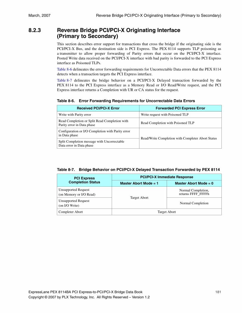
March, 2007 Reverse Bridge PCI/PCI-X Originating Interface (Primary to Secondary)
ExpressLane PEX 8114BA PCI Express-to-PCI/PCI-X Bridge Data Book 181
Copyright © 2007 by PLX Technology, Inc. All Rights Reserved – Version 1.2
8.2.3 Reverse Bridge PCI/PCI-X Originating Interface (Primary to Secondary)This section describes error support for transactions that cross the bridge if the originating side is thePCI/PCI-X Bus, and the destination side is PCI Express. The PEX 8114 supports TLP poisoning asa transmitter to allow proper forwarding of Parity errors that occur on the PCI/PCI-X interface.Posted Write data received on the PCI/PCI-X interface with bad parity is forwarded to the PCI Expressinterface as Poisoned TLPs.
Table 8-6 delineates the error forwarding requirements for Uncorrectable Data errors that the PEX 8114detects when a transaction targets the PCI Express interface.
Table 8-7 delineates the bridge behavior on a PCI/PCI-X Delayed transaction forwarded by thePEX 8114 to the PCI Express interface as a Memory Read or I/O Read/Write request, and the PCIExpress interface returns a Completion with UR or CA status for the request.
Table 8-6. Error Forwarding Requirements for Uncorrectable Data Errors
Received PCI/PCI-X Error Forwarded PCI Express Error
Write with Parity error Write request with Poisoned TLP
Read Completion or Split Read Completion with Parity error in Data phase
Read Completion with Poisoned TLP
Configuration or I/O Completion with Parity error in Data phase
Read/Write Completion with Completer Abort StatusSplit Completion message with Uncorrectable Data error in Data phase
Table 8-7. Bridge Behavior on PCI/PCI-X Delayed Transaction Forwarded by PEX 8114
PCI Express Completion Status
PCI/PCI-X Immediate Response
Master Abort Mode = 1 Master Abort Mode = 0
Unsupported Request (on Memory or I/O Read)
Target Abort
Normal Completion, returns FFFF_FFFFh
Unsupported Request(on I/O Write)
Normal Completion
Completer Abort Target Abort

Error Handling PLX Technology, Inc.
182 ExpressLane PEX 8114BA PCI Express-to-PCI/PCI-X Bridge Data Book
Copyright © 2007 by PLX Technology, Inc. All Rights Reserved – Version 1.2
8.2.3.1 Received PCI/PCI-X Errors
Uncorrectable Data Error on Posted Write
When the PEX 8114 detects an Uncorrectable Data error on the PCI/PCI-X primary interface fora Posted Write transaction that crosses the bridge, the following occurs:
1. PCI_PERR# is asserted if the PCI Command register Parity Error Response Enable bit is set.
2. PCI Status register Detected Parity Error bit is set.
3. Posted Write transaction is forwarded to the PCI Express interface as a Poisoned TLP.
4. Secondary Status register Secondary Master Data Parity Error bit is set if the Bridge Control register Secondary Parity Error Response Enable bit is set.
5. Secondary Uncorrectable Error Status register Uncorrectable Data Error Status bit is set.
6. Transaction command, attributes, and address are logged in the Secondary Header Log register and the FECh register Secondary Uncorrectable Error Pointer is updated if the Secondary Uncorrectable Error Mask register Uncorrectable Data Error Mask bit is cleared and the Secondary Uncorrectable First Error Pointer is inactive.
7. PCI_SERR# is asserted on the PCI/PCI-X Bus, depending on the Secondary Uncorrectable Error Severity register Uncorrectable Data Error Severity bit’s severity, if the following conditions are met:
– Secondary Uncorrectable Error Mask register Uncorrectable Data Error Mask bit is clear AND EITHER
– PCI Command register SERR# Enable bit is set OR
– PCI Express Device Control register Fatal Error Reporting Enable or Non-Fatal Error Reporting Enable bit is set, the Root Control register System Error on Fatal Error Enable or System Error on Non-Fatal Error Enable bit is set, and both bits match the Uncorrectable Data Error Severity
8. PCI_INTA# is asserted on the PCI/PCI-X Bus –OR– an MSI is transmitted if the MSI Control register MSI Enable bit is set, depending on the Secondary Uncorrectable Error Severity register Uncorrectable Data Error Severity bit’s severity, if the following conditions are met:
– Command register Interrupt Disable bit is cleared AND
– Secondary Uncorrectable Error Mask register Uncorrectable Data Error Mask bit is clear AND
– Root Error Command register Fatal Error Reporting Enable or Non-Fatal Error Reporting Enable bit is set and matches the Uncorrectable Data Error Severity AND EITHER
– PCI Command register SERR# Enable bit is set OR
– PCI Express Device Control register Fatal Error Reporting Enable or Non-Fatal Error Reporting Enable bit is set and matches the Uncorrectable Data Error Severity
9. Device Status register Fatal Error Detected or Non-Fatal Error Detected bit is set.
10. PCI Status register Signaled System Error bit is set if the Uncorrectable Data Error Mask bit is clear and the SERR# Enable bit is set.
March, 2007 Reverse Bridge PCI/PCI-X Originating Interface (Primary to Secondary)
ExpressLane PEX 8114BA PCI Express-to-PCI/PCI-X Bridge Data Book 183
Copyright © 2007 by PLX Technology, Inc. All Rights Reserved – Version 1.2
Uncorrectable Data Error on Non-Posted Write in Conventional PCI Mode
When a Non-Posted Write is addressed allowing it to cross the bridge, and the PEX 8114 detects anUncorrectable Data error on the PCI interface, the following occurs:
1. PCI Status register Detected Parity Error bit is set.
2. When the PCI Command register Parity Error Response Enable bit is set, the transaction is discarded and not forwarded to the PCI Express interface. PCI_PERR# is asserted on the PCI Bus.
When the Parity Error Response Enable bit is not set, the data is forwarded to the PCI Express interface as a Poisoned TLP. The Secondary Status register Secondary Master Data Parity Error bit is set if the Bridge Control register Secondary Parity Error Response Enable bit is set. PCI_PERR# is not asserted on the PCI Bus.
3. Secondary Uncorrectable Error Status register Uncorrectable Data Error Status bit is set.
4. Transaction command, attributes, and address are logged in the Secondary Header Log register and the FECh register Secondary Uncorrectable Error Pointer is updated if the Secondary Uncorrectable Error Mask register Uncorrectable Data Error Mask bit is cleared and the Secondary Uncorrectable First Error Pointer is inactive.
5. PCI_SERR# is asserted on the PCI/PCI-X Bus, depending on the Secondary Uncorrectable Error Severity register Uncorrectable Data Error Severity bit’s severity, if the following conditions are met:
– Secondary Uncorrectable Error Mask register Uncorrectable Data Error Mask bit is clear AND EITHER
– PCI Command register SERR# Enable bit is set OR
– PCI Express Device Control register Fatal Error Reporting Enable or Non-Fatal Error Reporting Enable bit is set, the Root Control register System Error on Fatal Error Enable or System Error on Non-Fatal Error Enable bit is set, and both bits match the Uncorrectable Data Error Severity
6. PCI_INTA# is asserted on the PCI/PCI-X Bus –OR– an MSI is transmitted if the MSI Control register MSI Enable bit is set, depending on the Secondary Uncorrectable Error Severity register Uncorrectable Data Error Severity bit’s severity, if the following conditions are met:
– Command register Interrupt Disable bit is cleared AND
– Secondary Uncorrectable Error Mask register Uncorrectable Data Error Mask bit is clear AND
– Root Error Command register Fatal Error Reporting Enable or Non-Fatal Error Reporting Enable bit is set and matches the Uncorrectable Data Error Severity AND EITHER
– PCI Command register SERR# Enable bit is set OR
– PCI Express Device Control register Fatal Error Reporting Enable or Non-Fatal Error Reporting Enable bit is set and matches the Uncorrectable Data Error Severity
7. Device Status register Fatal Error Detected or Non-Fatal Error Detected bit is set.
8. PCI Status register Signaled System Error bit is set if the Uncorrectable Data Error Mask bit is clear and the SERR# Enable bit is set.
Error Handling PLX Technology, Inc.
184 ExpressLane PEX 8114BA PCI Express-to-PCI/PCI-X Bridge Data Book
Copyright © 2007 by PLX Technology, Inc. All Rights Reserved – Version 1.2
Uncorrectable Data Error on Non-Posted Write in PCI-X Mode
When a Non-Posted Write is addressed allowing it to cross the bridge, and the PEX 8114 detects anUncorrectable Data error on the PCI-X interface, the following occurs:
1. PCI Status register Detected Parity Error bit is set.
2. PEX 8114 signals a Data transfer for Non-Posted Write transactions. If there is an Uncorrectable Data error, the transaction is discarded.
3. When the PCI Command register Parity Error Response Enable bit is set, PCI_PERR# is asserted on the PCI-X Bus.
4. Secondary Uncorrectable Error Status register Uncorrectable Data Error Status bit is set.
5. Transaction command, attributes, and address are logged in the Secondary Header Log register and the FECh register Secondary Uncorrectable Error Pointer is updated if the Secondary Uncorrectable Error Mask register Uncorrectable Data Error Mask bit is cleared and the Secondary Uncorrectable First Error Pointer is inactive.
6. PCI_SERR# is asserted on the PCI-X Bus, depending on the Secondary Uncorrectable Error Severity register Uncorrectable Data Error Severity bit’s severity, if the following conditions are met:
– Command register Interrupt Disable bit is cleared AND
– Secondary Uncorrectable Error Mask register Uncorrectable Data Error Mask bit is clear AND EITHER
– PCI Command register SERR# Enable bit is set OR
– PCI Express Device Control register Fatal Error Reporting Enable or Non-Fatal Error Reporting Enable bit is set, the Root Control register System Error on Fatal Error Enable or System Error on Non-Fatal Error Enable bit is set, and both bits match the Uncorrectable Data Error Severity
7. PCI_INTA# is asserted on the PCI-X Bus –OR– an MSI is transmitted if the MSI Control register MSI Enable bit is set, depending on the Secondary Uncorrectable Error Severity register Uncorrectable Data Error Severity bit’s severity, if the following conditions are met:
– Secondary Uncorrectable Error Mask register Uncorrectable Data Error Mask bit is clear AND
– Root Error Command register Fatal Error Reporting Enable or Non-Fatal Error Reporting Enable bit is set and matches the Uncorrectable Data Error Severity AND EITHER
– PCI Command register SERR# Enable bit is set OR
– PCI Express Device Control register Fatal Error Reporting Enable or Non-Fatal Error Reporting Enable bit is set and matches the Uncorrectable Data Error Severity
8. Device Status register Fatal Error Detected or Non-Fatal Error Detected bit is set.
9. PCI Status register Signaled System Error bit is set if the Uncorrectable Data Error Mask bit is clear and the SERR# Enable bit is set.
March, 2007 Reverse Bridge PCI/PCI-X Originating Interface (Primary to Secondary)
ExpressLane PEX 8114BA PCI Express-to-PCI/PCI-X Bridge Data Book 185
Copyright © 2007 by PLX Technology, Inc. All Rights Reserved – Version 1.2
Uncorrectable Data Error on PCI Delayed Read Completions
When the PEX 8114 forwards a Non-Poisoned or Poisoned Read Completion from PCI Express to PCI,and it detects PCI_PERR# asserted by the PCI Master, the following occurs:
1. Remainder of the Completion is forwarded.
2. Secondary Uncorrectable Error Status register PERR# Assertion Detected bit is set.
3. Transaction command, attributes, and address are logged in the Secondary Header Log register and the FECh register Secondary Uncorrectable Error Pointer is updated if the Secondary Uncorrectable Error Mask register PERR# Assertion Detected Mask bit is cleared and the Secondary Uncorrectable First Error Pointer is inactive.
4. PCI_SERR# is asserted on the PCI Bus, depending on the Secondary Uncorrectable Error Severity register PERR# Assertion Detected Severity bit’s severity, if the following conditions are met:
– Uncorrectable Error Mask register PERR# Assertion Detected Mask bit is cleared AND EITHER
– PCI Command register SERR# Enable bit is set OR
– PCI Express Device Control register Fatal Error Reporting Enable or Non-Fatal Error Reporting Enable bit is set, the Root Control register System Error on Fatal Error Enable or System Error on Non-Fatal Error Enable bit is set, and both bits match the PERR# Assertion Detected Severity
5. PCI_INTA# is asserted on the PCI Bus –OR– an MSI is transmitted if the MSI Control register MSI Enable bit is set, depending on the Uncorrectable Error Severity register PERR# Assertion Detected Severity bit’s severity, if the following conditions are met:
– Command register Interrupt Disable bit is cleared AND
– Uncorrectable Error Mask register PERR# Assertion Detected Mask bit is cleared AND
– Root Error Command register Fatal Error Reporting Enable or Non-Fatal Error Reporting Enable bit is set and matches the PERR# Assertion Detected Severity AND EITHER
– PCI Command register SERR# Enable bit is set OR
– PCI Express Device Control register Fatal Error Reporting Enable or Non-Fatal Error Reporting Enable bit is set and matches the PERR# Assertion Detected Severity
6. Device Status register Fatal Error Detected or Non-Fatal Error Detected bit is set.
7. PCI Status register Signaled System Error bit is set if the PERR# Assertion Detected Mask bit is clear and the SERR# Enable bit is set.
If the PEX 8114 forwards a Poisoned Read Completion from PCI Express to PCI, the PEX 8114proceeds with the above actions when it detects PCI_PERR# asserted by the PCI Master; however, anError message is not generated on the PCI Express interface.
Error Handling PLX Technology, Inc.
186 ExpressLane PEX 8114BA PCI Express-to-PCI/PCI-X Bridge Data Book
Copyright © 2007 by PLX Technology, Inc. All Rights Reserved – Version 1.2
Uncorrectable Data Error on PCI-X Split Read Completions
When the PEX 8114 detects an Uncorrectable Data error on the PCI-X interface while receiving a SplitRead Completion that crosses the bridge, the following occurs:
1. PCI_PERR# is asserted if the PCI Command register Parity Error Response Enable bit is set.
2. PCI Status register Detected Parity Error bit is set.
3. Split Read Completion transaction is forwarded to the PCI Express interface as a Poisoned TLP.
4. PCI Status register Master Data Parity Error bit is set if the PCI Command register Parity Error Response Enable bit is set.
5. Secondary Uncorrectable Error Status register Uncorrectable Data Error Status bit is set.
6. Transaction command, attributes, and address are logged in the Secondary Header Log register and the FECh register Secondary Uncorrectable Error Pointer is updated if the Secondary Uncorrectable Error Mask register Uncorrectable Data Error Mask bit is cleared and the Secondary Uncorrectable First Error Pointer is inactive.
7. PCI_SERR# is asserted on the PCI-X Bus, depending on the Secondary Uncorrectable Error Severity register Uncorrectable Data Error Severity bit’s severity, if the following conditions are met:
– Secondary Uncorrectable Error Mask register Uncorrectable Data Error Mask bit is clear AND EITHER
– PCI Command register SERR# Enable bit is set OR
– PCI Express Device Control register Fatal Error Reporting Enable or Non-Fatal Error Reporting Enable bit is set, the Root Control register System Error on Fatal Error Enable or System Error on Non-Fatal Error Enable bit is set, and both bits match the Uncorrectable Data Error Severity
8. PCI_INTA# is asserted on the PCI-X Bus –OR– an MSI is transmitted if the MSI Control register MSI Enable bit is set, depending on the Secondary Uncorrectable Error Severity register Uncorrectable Data Error Severity bit’s severity, if the following conditions are met:
– Command register Interrupt Disable bit is cleared AND
– Secondary Uncorrectable Error Mask register Uncorrectable Data Error Mask bit is clear AND
– Root Error Command register Fatal Error Reporting Enable or Non-Fatal Error Reporting Enable bit is set and matches the Uncorrectable Data Error Severity AND EITHER
– PCI Command register SERR# Enable bit is set OR
– PCI Express Device Control register Fatal Error Reporting Enable or Non-Fatal Error Reporting Enable bit is set and matches the Uncorrectable Data Error Severity
9. Device Status register Fatal Error Detected or Non-Fatal Error Detected bit is set.
10. PCI Status register Signaled System Error bit is set if the Uncorrectable Data Error Mask bit is clear and the SERR# Enable bit is set.
March, 2007 Reverse Bridge PCI/PCI-X Originating Interface (Primary to Secondary)
ExpressLane PEX 8114BA PCI Express-to-PCI/PCI-X Bridge Data Book 187
Copyright © 2007 by PLX Technology, Inc. All Rights Reserved – Version 1.2
Uncorrectable Address Error
When the PEX 8114 detects an Uncorrectable Address error and Parity error detection is enabled byway of the PCI Command register Parity Error Response Enable bit, the following occurs:
1. Transaction is terminated with a Target Abort and discarded.
2. PCI Status register Detected Parity Error bit is set, independent of the PCI Command register Parity Error Response Enable bit value.
3. PCI Status register Signaled Target Abort bit is set.
4. Secondary Uncorrectable Error Status register Uncorrectable Address Error Status bit is set.
5. Transaction command, attributes, and address are logged in the Secondary Header Log register and the FECh register Secondary Uncorrectable Error Pointer is updated if the Secondary Uncorrectable Error Mask register Uncorrectable Address Error Mask bit is cleared and the Secondary Uncorrectable First Error Pointer is inactive.
6. PCI_SERR# is asserted on the PCI/PCI-X Bus, depending on the Secondary Uncorrectable Error Severity register Uncorrectable Address Error Severity bit’s severity, if the following conditions are met:
– Secondary Uncorrectable Error Mask register Uncorrectable Address Error Mask bit is clear AND EITHER
– PCI Command register SERR# Enable bit is set OR
– PCI Express Device Control register Fatal Error Reporting Enable or Non-Fatal Error Reporting Enable bit is set, the Root Control register System Error on Fatal Error Enable or System Error on Non-Fatal Error Enable bit is set, and both bits match the Uncorrectable Address Error Severity
7. PCI_INTA# is asserted on the PCI/PCI-X Bus –OR– an MSI is transmitted if the MSI Control register MSI Enable bit is set, depending on the Secondary Uncorrectable Error Severity register Uncorrectable Address Error Severity bit’s severity, if the following conditions are met:
– Command register Interrupt Disable bit is cleared AND
– Secondary Uncorrectable Error Mask register Uncorrectable Address Error Mask bit is clear AND
– Root Error Command register Fatal Error Reporting Enable or Non-Fatal Error Reporting Enable bit is set and matches the Uncorrectable Address Error Severity AND EITHER
– PCI Command register SERR# Enable bit is set OR
– PCI Express Device Control register Fatal Error Reporting Enable or Non-Fatal Error Reporting Enable bit is set and matches the Uncorrectable Address Error Severity
8. Device Status register Fatal Error Detected or Non-Fatal Error Detected bit is set.
9. PCI Status register Signaled System Error bit is set if the Uncorrectable Address Error Mask bit is clear and the SERR# Enable bit is set.
Error Handling PLX Technology, Inc.
188 ExpressLane PEX 8114BA PCI Express-to-PCI/PCI-X Bridge Data Book
Copyright © 2007 by PLX Technology, Inc. All Rights Reserved – Version 1.2
Uncorrectable Attribute Error
When the PEX 8114 detects an Uncorrectable Attribute error and Parity error detection is enabled byway of the PCI Command register Parity Error Response Enable bit, the following occurs:
1. Transaction is terminated with a Target Abort and discarded.
2. PCI Status register Detected Parity Error bit is set, independent of the PCI Command register Parity Error Response Enable bit value.
3. PCI Status register Signaled Target Abort bit is set.
4. Secondary Uncorrectable Error Status register Uncorrectable Attribute Error Status bit is set.
5. Transaction command, attributes, and address are logged in the Secondary Header Log register and the FECh register Secondary Uncorrectable Error Pointer is updated if the Secondary Uncorrectable Error Mask register Uncorrectable Attribute Error Mask bit is cleared and the Secondary Uncorrectable First Error Pointer is inactive.
6. PCI_SERR# is asserted on the PCI/PCI-X Bus, depending on the Secondary Uncorrectable Error Severity register Uncorrectable Attribute Error Severity bit’s severity, if the following conditions are met:
– Secondary Uncorrectable Error Mask register Uncorrectable Attribute Error Mask bit is clear AND EITHER
– PCI Command register SERR# Enable bit is set OR
– PCI Express Device Control register Fatal Error Reporting Enable or Non-Fatal Error Reporting Enable bit is set, the Root Control register System Error on Fatal Error Enable or System Error on Non-Fatal Error Enable bit is set, and both bits match the Uncorrectable Attribute Error Severity
7. PCI_INTA# is asserted on the PCI/PCI-X Bus –OR– an MSI is transmitted if the MSI Control register MSI Enable bit is set, depending on the Secondary Uncorrectable Error Severity register Uncorrectable Attribute Error Severity bit’s severity, if the following conditions are met:
– Command register Interrupt Disable bit is cleared AND
– Secondary Uncorrectable Error Mask register Uncorrectable Attribute Error Mask bit is clear AND
– Root Error Command register Fatal Error Reporting Enable or Non-Fatal Error Reporting Enable bit is set and matches the Uncorrectable Attribute Error Severity AND EITHER
– PCI Command register SERR# Enable bit is set OR
– PCI Express Device Control register Fatal Error Reporting Enable or Non-Fatal Error Reporting Enable bit is set and matches the Uncorrectable Attribute Error Severity
8. Device Status register Fatal Error Detected or Non-Fatal Error Detected bit is set.
9. PCI Status register Signaled System Error bit is set if the Uncorrectable Attribute Error Mask bit is clear and the SERR# Enable bit is set.
March, 2007 Reverse Bridge PCI/PCI-X Originating Interface (Primary to Secondary)
ExpressLane PEX 8114BA PCI Express-to-PCI/PCI-X Bridge Data Book 189
Copyright © 2007 by PLX Technology, Inc. All Rights Reserved – Version 1.2
8.2.3.2 Unsupported Request (UR) Completion StatusThe PEX 8114 provides two methods for handling a PCI Express Completion received withUnsupported Request (UR) status in response to a request originated by the PCI/PCI-X interface. TheBridge Control register Master Abort Mode bit controls the response. In either case, the SecondaryStatus register Secondary Received Master Abort bit is set.
Master Abort Mode Bit Cleared
This is the default PCI/PCI-X compatibility mode, and a UR is not considered an error. When a Readtransaction initiated on the PCI/PCI-X Bus results in the return of a Completion with UR status, thePEX 8114 returns FFFF_FFFFh to the originating Master and asserts PCI_TRDY# to terminate theRead transaction normally on the originating interface. When a Non-Posted Write transaction results ina Completion with UR status, the PEX 8114 asserts PCI_TRDY# to complete the Write transactionnormally on the originating bus and discards the Write data.
Master Abort Mode Bit Set
When the Master Abort Mode bit is set, the PEX 8114 signals a Target Abort to the originating Masterof an upstream Read or Non-Posted Write transaction when the corresponding request on the PCIExpress interface results in a Completion with UR status. Additionally, the PCI Status register SignaledTarget Abort bit is set.
8.2.3.3 Completer Abort Completion StatusWhen the PEX 8114 receives a Completion with Completer Abort (CA) status on the PCI Expresssecondary interface, in response to a forwarded Non-Posted PCI/PCI-X transaction, the SecondaryStatus register Secondary Received Target Abort bit is set. A CA response results in a DelayedTransaction Target Abort or Split Completion Target Abort Error message on the PCI/PCI-X Bus. ThePEX 8114 provides data to the requesting PCI/PCI-X agent, up to the point where data was successfullyreturned from the PCI Express interface, then signals Target Abort. The PCI Status register SignaledTarget Abort bit is set when signaling Target Abort to a PCI/PCI-X agent.
Error Handling PLX Technology, Inc.
190 ExpressLane PEX 8114BA PCI Express-to-PCI/PCI-X Bridge Data Book
Copyright © 2007 by PLX Technology, Inc. All Rights Reserved – Version 1.2
8.2.3.4 Split Completion Errors
Split Completion Message with Completer Errors
A transaction originating from the PCI Express interface and requiring a Completion can be forwardedto the PCI-X interface where the Target (completer) responds with Split Response. If the completerencounters a condition that prevents the successful execution of a Split Transaction, the completer mustnotify the requester of the abnormal condition by returning a Split Completion message with theCompleter Error class. If the bridge responds with Completer Abort status, it sets the Secondary Statusregister Signaled Target Abort bit.
Table 8-8 delineates the abnormal conditions and the bridge’s response to the Split Completionmessage. Each is described in the sections that follow.
Table 8-8. Abnormal Conditions and Bridge Response to Split Completion Messages
PCI-X Split Completion Message
Completer Error Code Bit Set in
PCI Status Register
Bit Set in Secondary Uncorrectable Error
Status Register
PCI Express Completion Status
Class Index
Master Abort 1h 00h Received Master Abort Received Master Abort Unsupported Request
Target Abort 1h 01h Received Target Abort Received Target Abort Completer Abort
Uncorrectable Write Data Error 1h 02h
Master Data Parity Error
PERR# Assertion Detected
Unsupported Request
Byte Count Out of Range 2h 00h None None Unsupported Request
Uncorrectable Split Write Data Error 2h 01h
Master Data Parity Error
PERR# Assertion Detected
Unsupported Request
Device-Specific Error 2h 8Xh None None Completer Abort
March, 2007 Reverse Bridge PCI/PCI-X Originating Interface (Primary to Secondary)
ExpressLane PEX 8114BA PCI Express-to-PCI/PCI-X Bridge Data Book 191
Copyright © 2007 by PLX Technology, Inc. All Rights Reserved – Version 1.2
Split Completion Message with Master Abort
When a bridge receives a Split Completion message indicating Master Abort, the following occurs:
1. Completion with Unsupported Request status is returned to the requester.
2. PCI Status register Received Master Abort bit is set.
3. Secondary Uncorrectable Error Status register Received Master Abort Status bit is set.
4. TLP Header of the original request is logged in the Secondary Header Log register and the FECh register Secondary Uncorrectable Error Pointer is updated if the Secondary Uncorrectable Error Mask register Received Master Abort Status Mask bit is cleared and the Secondary Uncorrectable First Error Pointer is inactive.
5. PCI_SERR# is asserted on the PCI/PCI-X Bus, depending on the Secondary Uncorrectable Error Severity register Received Master Abort Severity bit’s severity, if the following conditions are met:
– Secondary Uncorrectable Error Mask register Received Master Abort Mask bit is cleared AND EITHER
– PCI Command register SERR# Enable bit is set OR
– PCI Express Device Control register Fatal Error Reporting Enable or Non-Fatal Error Reporting Enable bit is set, the Root Control register System Error on Fatal Error Enable or System Error on Non-Fatal Error Enable bit is set, and both bits match the Received Master Abort Severity
6. PCI_INTA# is asserted on the PCI/PCI-X Bus –OR– an MSI is transmitted if the MSI Control register MSI Enable bit is set, depending on the Secondary Uncorrectable Error Severity register Received Master Abort Severity bit’s severity, if the following conditions are met:
– Command register Interrupt Disable bit is cleared AND
– Secondary Uncorrectable Error Mask register Received Master Abort Mask bit is cleared AND
– Root Error Command register Fatal Error Reporting Enable or Non-Fatal Error Reporting Enable bit is set and matches the Received Master Abort Severity AND EITHER
– PCI Command register SERR# Enable bit is set OR
– PCI Express Device Control register Fatal Error Reporting Enable or Non-Fatal Error Reporting Enable bit is set and matches the Received Master Abort Severity
7. Device Status register Fatal Error Detected or Non-Fatal Error Detected bit is set.
8. PCI Status register Signaled System Error bit is set if the Received Master Abort Mask bit is cleared and the SERR# Enable bit is set.
Error Handling PLX Technology, Inc.
192 ExpressLane PEX 8114BA PCI Express-to-PCI/PCI-X Bridge Data Book
Copyright © 2007 by PLX Technology, Inc. All Rights Reserved – Version 1.2
Split Completion Message with Target Abort
When a bridge receives a Split Completion message indicating Target Abort, the following occurs:
1. Completion with Completer Abort status is returned to the requester.
2. PCI Status register Received Target Abort bit is set.
3. Secondary Uncorrectable Error Status register Received Target Abort bit is set.
4. Secondary Status register Signaled Target Abort bit is set.
5. TLP Header of the original request is logged in the Secondary Header Log register and the FECh register Secondary Uncorrectable Error Pointer is updated if the Secondary Uncorrectable Error Mask register Received Target Abort Mask bit is cleared and the Secondary Uncorrectable First Error Pointer is inactive.
6. PCI_SERR# is asserted on the PCI/PCI-X Bus, depending on the Secondary Uncorrectable Error Severity register Received Target Abort Severity bit’s severity, if the following conditions are met:
– Secondary Uncorrectable Error Mask register Received Target Abort Mask bit is cleared AND EITHER
– PCI Command register SERR# Enable bit is set OR
– PCI Express Device Control register Fatal Error Reporting Enable or Non-Fatal Error Reporting Enable bit is set, the Root Control register System Error on Fatal Error Enable or System Error on Non-Fatal Error Enable bit is set, and both bits match the Received Target Abort Severity
7. PCI_INTA# is asserted on the PCI/PCI-X Bus –OR– an MSI is transmitted if the MSI Control register MSI Enable bit is set, depending on the Secondary Uncorrectable Error Severity register Received Target Abort Severity bit’s severity, if the following conditions are met:
– Command register Interrupt Disable bit is cleared AND
– Secondary Uncorrectable Error Mask register Received Target Abort Mask bit is cleared AND
– Root Error Command register Fatal Error Reporting Enable or Non-Fatal Error Reporting Enable bit is set and matches the Received Target Abort Severity AND EITHER
– PCI Command register SERR# Enable bit is set OR
– PCI Express Device Control register Fatal Error Reporting Enable or Non-Fatal Error Reporting Enable bit is set and matches the Received Target Abort Severity
8. Device Status register Fatal Error Detected or Non-Fatal Error Detected bit is set.
9. PCI Status register Signaled System Error bit is set if the Received Target Abort Mask bit is cleared and the SERR# Enable bit is set.
March, 2007 Reverse Bridge PCI/PCI-X Originating Interface (Primary to Secondary)
ExpressLane PEX 8114BA PCI Express-to-PCI/PCI-X Bridge Data Book 193
Copyright © 2007 by PLX Technology, Inc. All Rights Reserved – Version 1.2
Split Completion Message with Uncorrectable Write Data Error or Uncorrectable Split Write Data Error
When a bridge receives a Split Completion message indicating an Uncorrectable Write Data error orUncorrectable Split Write Data error, the following occurs:
1. Completion with Unsupported Request status is returned to the requester.
2. PCI Status register Master Data Parity Error bit is set if the PCI Command register Parity Error Response Enable bit is set.
3. Secondary Uncorrectable Error Status register PERR# Assertion Detected bit is set.
4. TLP Header of the original request is logged in the Secondary Header Log register and the FECh register Secondary Uncorrectable Error Pointer is updated if the Secondary Uncorrectable Error Mask register PERR# Assertion Detected Mask bit is cleared and the Secondary Uncorrectable First Error Pointer is inactive.
5. PCI_SERR# is asserted on the PCI/PCI-X Bus, depending on the Secondary Uncorrectable Error Severity register PERR# Assertion Detected Severity bit’s severity, if the following conditions are met:
– Secondary Uncorrectable Error Mask register PERR# Assertion Detected Mask bit is clear AND EITHER
– PCI Command register SERR# Enable bit is set OR
– PCI Express Device Control register Fatal Error Reporting Enable or Non-Fatal Error Reporting Enable bit is set, the Root Control register System Error on Fatal Error Enable or System Error on Non-Fatal Error Enable bit is set, and both bits match the PERR# Assertion Detected Severity
6. PCI_INTA# is asserted on the PCI/PCI-X Bus –OR– an MSI is transmitted if the MSI Control register MSI Enable bit is set, depending on the Secondary Uncorrectable Error Severity register PERR# Assertion Detected Severity bit’s severity, if the following conditions are met:
– Command register Interrupt Disable bit is cleared AND
– Secondary Uncorrectable Error Mask register PERR# Assertion Detected Mask bit is clear AND
– Root Error Command register Fatal Error Reporting Enable or Non-Fatal Error Reporting Enable bit is set and matches the PERR# Assertion Detected Severity AND EITHER
– PCI Command register SERR# Enable bit is set OR
– PCI Express Device Control register Fatal Error Reporting Enable or Non-Fatal Error Reporting Enable bit is set and matches the PERR# Assertion Detected Severity
7. Device Status register Fatal Error Detected or Non-Fatal Error Detected bit is set.
8. PCI Status register Signaled System Error bit is set if the PERR# Assertion Detected Mask bit is clear and the SERR# Enable bit is set.
Split Completion Message with Byte Count Out of Range
When a bridge receives a Split Completion message indicating a Byte Count Out of Range error,a Completion with Unsupported Request status is returned to the requester.
Split Completion Message with Device-Specific Error
When a bridge receives a Split Completion message indicating a Device-Specific error, a Completionwith Completer Abort status is returned to the requester.
Error Handling PLX Technology, Inc.
194 ExpressLane PEX 8114BA PCI Express-to-PCI/PCI-X Bridge Data Book
Copyright © 2007 by PLX Technology, Inc. All Rights Reserved – Version 1.2
Corrupted or Unexpected Split Completion
When a bridge receives a corrupted or unexpected Split Completion, the following occurs:
1. PCI-X Bridge Status register Unexpected Split Completion Status bit is set.
2. Secondary Uncorrectable Error Status register Unexpected Split Completion Error Status bit is set.
3. TLP Header of the corrupt or unexpected Split Completion is logged in the Secondary Header Log register and the FECh register Secondary Uncorrectable Error Pointer is updated if the Secondary Uncorrectable Error Mask register Unexpected Split Completion Mask bit is cleared and the Secondary Uncorrectable First Error Pointer is inactive.
4. PCI_SERR# is asserted on the PCI/PCI-X Bus, depending on the Secondary Uncorrectable Error Severity register Unexpected Split Completion Severity bit’s severity, if the following conditions are met:
– Secondary Uncorrectable Error Mask register Unexpected Split Completion Mask bit is clear AND EITHER
– PCI Command register SERR# Enable bit is set OR
– PCI Express Device Control register Fatal Error Reporting Enable or Non-Fatal Error Reporting Enable bit is set, the Root Control register System Error on Fatal Error Enable or System Error on Non-Fatal Error Enable bit is set, and both bits match the Unexpected Split Completion Severity
5. PCI_INTA# is asserted on the PCI/PCI-X Bus –OR– an MSI is transmitted if the MSI Control register MSI Enable bit is set, depending on the Secondary Uncorrectable Error Severity register Unexpected Split Completion Severity bit’s severity, if the following conditions are met:
– Command register Interrupt Disable bit is cleared AND
– Secondary Uncorrectable Error Mask register Unexpected Split Completion Mask bit is clear AND
– Root Error Command register Fatal Error Reporting Enable or Non-Fatal Error Reporting Enable bit is set and matches the Unexpected Split Completion Severity AND EITHER
– PCI Command register SERR# Enable bit is set OR
– PCI Express Device Control register Fatal Error Reporting Enable or Non-Fatal Error Reporting Enable bit is set and matches the Unexpected Split Completion Severity
6. Device Status register Fatal Error Detected or Non-Fatal Error Detected bit is set.
7. PCI Status register Signaled System Error bit is set if the Unexpected Split Completion Mask bit is clear and the SERR# Enable bit is set.
March, 2007 Reverse Bridge PCI/PCI-X Originating Interface (Primary to Secondary)
ExpressLane PEX 8114BA PCI Express-to-PCI/PCI-X Bridge Data Book 195
Copyright © 2007 by PLX Technology, Inc. All Rights Reserved – Version 1.2
Data Parity Error on Split Completion Messages
When a bridge detects a Data error during the Data phase of a Split Completion message, thefollowing occurs:
1. Secondary Uncorrectable Error Status register Uncorrectable Split Completion Message Data Error Status bit is set.
2. TLP Header of the Split Completion is logged in the Secondary Header Log register and the FECh register Secondary Uncorrectable Error Pointer is updated if the Secondary Uncorrectable Error Mask register Uncorrectable Split Completion Message Data Error Mask bit is cleared and the Secondary Uncorrectable First Error Pointer is inactive.
3. PCI_SERR# is asserted on the PCI/PCI-X Bus, depending on the Secondary Uncorrectable Error Severity register Uncorrectable Split Completion Message Data Error Severity bit’s severity, if the following conditions are met:
– Secondary Uncorrectable Error Mask register Uncorrectable Split Completion Message Data Error Mask bit is cleared AND EITHER
– PCI Command register SERR# Enable bit is set OR
– PCI Express Device Control register Fatal Error Reporting Enable or Non-Fatal Error Reporting Enable bit is set, the Root Control register System Error on Fatal Error Enable or System Error on Non-Fatal Error Enable bit is set, and both bits match the Uncorrectable Split Completion Message Data Error Severity
4. PCI_INTA# is asserted on the PCI/PCI-X Bus –OR– an MSI is transmitted if the MSI Control register MSI Enable bit is set, depending on the Secondary Uncorrectable Error Severity register Uncorrectable Split Completion Message Data Error Severity bit’s severity, if the following conditions are met:
– Command register Interrupt Disable bit is cleared AND
– Secondary Uncorrectable Error Mask register Uncorrectable Split Completion Message Data Error Mask bit is cleared AND
– Root Error Command register Fatal Error Reporting Enable or Non-Fatal Error Reporting Enable bit is set and matches the Uncorrectable Split Completion Message Data Error Severity AND EITHER
– PCI Command register SERR# Enable bit is set OR
– PCI Express Device Control register Fatal Error Reporting Enable or Non-Fatal Error Reporting Enable bit is set and matches the Uncorrectable Split Completion Message Data Error Severity
5. Device Status register Fatal Error Detected or Non-Fatal Error Detected bit is set.
6. PCI Status register Signaled System Error bit is set if the Uncorrectable Split Completion Message Data Error Mask bit is cleared and the SERR# Enable bit is set.
Error Handling PLX Technology, Inc.
196 ExpressLane PEX 8114BA PCI Express-to-PCI/PCI-X Bridge Data Book
Copyright © 2007 by PLX Technology, Inc. All Rights Reserved – Version 1.2
8.2.4 Reverse Bridge Timeout Errors
8.2.4.1 PCI Express Completion Timeout ErrorsThe PCI Express Completion Timeout mechanism allows requesters to abort a Non-Posted request if aCompletion does not arrive within a reasonable time. Bridges, when acting as Initiators on the PCIExpress interface on behalf of internally generated requests or when forwarding requests from asecondary interface, behave as endpoints for requests of which they assume ownership. If a Completiontimeout is detected and the link is up, the PEX 8114 responds as if a Completion with UnsupportedRequest status was received, and the following occurs:
1. Uncorrectable Error Status register Completion Timeout Status bit is set.
2. TLP Header of the original request is logged in the Header Log register and the Advanced Error Capabilities and Control register First Error Pointer is updated if the Uncorrectable Error Mask register Completion Timeout Mask bit is cleared and the First Error Pointer is inactive.
3. PCI_SERR# is asserted on the PCI/PCI-X Bus, depending on the Secondary Uncorrectable Error Severity register Completion Timeout Severity bit’s severity, if the following conditions are met:
– Secondary Uncorrectable Error Mask register Completion Timeout Mask bit is cleared AND EITHER
– PCI Command register SERR# Enable bit is set OR
– PCI Express Device Control register Fatal Error Reporting Enable or Non-Fatal Error Reporting Enable bit is set, the Root Control register System Error on Fatal Error Enable or System Error on Non-Fatal Error Enable bit is set, and both bits match the Completion Timeout Severity
4. PCI_INTA# is asserted on the PCI/PCI-X Bus –OR– an MSI is transmitted if the MSI Control register MSI Enable bit is set, depending on the Uncorrectable Error Severity register Completion Timeout Severity bit’s severity, if the following conditions are met:
– Command register Interrupt Disable bit is cleared AND
– Uncorrectable Error Mask register Completion Timeout Mask bit is cleared AND
– Root Error Command register Fatal Error Reporting Enable or Non-Fatal Error Reporting Enable bit is set and matches the Completion Timeout Severity AND EITHER
– PCI Command register SERR# Enable bit is set OR
– PCI Express Device Control register Fatal Error Reporting Enable or Non-Fatal Error Reporting Enable bit is set and matches the Completion Timeout Severity
5. Device Status register Fatal Error Detected or Non-Fatal Error Detected bit is set.
6. PCI Status register Signaled System Error bit is set if the Completion Timeout Mask bit is cleared and the SERR# Enable bit is set.
March, 2007 Reverse Bridge Timeout Errors
ExpressLane PEX 8114BA PCI Express-to-PCI/PCI-X Bridge Data Book 197
Copyright © 2007 by PLX Technology, Inc. All Rights Reserved – Version 1.2
8.2.4.2 PCI Delayed Transaction Timeout ErrorsThe PEX 8114 has Delayed Transaction Discard Timers for each queued delayed transaction. If aDelayed Transaction timeout is detected, the following occurs:
1. Bridge Control register Discard Timer Status bit and Secondary Uncorrectable Error Status register Delayed Transaction Discard Timer Expired Status bit are set.
2. PCI_SERR# is asserted on the PCI/PCI-X Bus, depending on the Uncorrectable Error Severity register Delayed Transaction Discard Timer Expired Severity bit’s severity, if the following conditions are met:
– Uncorrectable Error Mask register Delayed Transaction Discard Timer Expired Mask bit is cleared AND EITHER
– PCI Command register SERR# Enable bit is set OR
– PCI Express Device Control register Fatal Error Reporting Enable or Non-Fatal Error Reporting Enable bit is set, the Root Control register System Error on Fatal Error Enable or System Error on Non-Fatal Error Enable bit is set, and both bits match the Delayed Transaction Discard Timer Expired Severity
3. PCI_INTA# is asserted on the PCI/PCI-X Bus –OR– an MSI is transmitted if the MSI Control register MSI Enable bit is set, depending on the Uncorrectable Error Severity register Delayed Transaction Discard Timer Expired Severity bit’s severity, if the following conditions are met:
– Command register Interrupt Disable bit is cleared AND
– Uncorrectable Error Mask register Delayed Transaction Discard Timer Expired Mask bit is cleared AND
– Root Error Command register Fatal Error Reporting Enable or Non-Fatal Error Reporting Enable bit is set and matches the Delayed Transaction Discard Timer Expired Severity AND EITHER
– PCI Command register SERR# Enable bit is set OR
– PCI Express Device Control register Fatal Error Reporting Enable or Non-Fatal Error Reporting Enable bit is set and matches the Delayed Transaction Discard Timer Expired Severity
4. Device Status register Fatal Error Detected or Non-Fatal Error Detected bit is set.
5. PCI Status register Signaled System Error bit is set if the Delayed Transaction Discard Timer Expired Mask bit is cleared and the SERR# Enable bit is set.
Error Handling PLX Technology, Inc.
198 ExpressLane PEX 8114BA PCI Express-to-PCI/PCI-X Bridge Data Book
Copyright © 2007 by PLX Technology, Inc. All Rights Reserved – Version 1.2
8.2.5 Reverse Bridge PCI Express Error MessagesPCI Express devices can transmit Error messages when detecting errors that compromise systemintegrity. When the PEX 8114 receives Error messages on the secondary PCI Express interface, thefollowing occurs:
1. Secondary Status register Received System Error bit is set if a Non-Fatal (ERR_NONFATAL) or Fatal (ERR_FATAL) Error message is received.
2. PCI_SERR# is asserted on the PCI/PCI-X Bus when one of the following conditions occur:
– Root Control register System Error on Correctable Error Enable bit is set and a Correctable Error message (ERR_COR) is received
– Root Control register System Error on Non-Fatal Error Enable bit is set and a Non-Fatal Error message (ERR_NONFATAL) is received
– Root Control register System Error on Fatal Error Enable bit is set and a Fatal Error message (ERR_FATAL) is received
– PCI Command and Bridge Control register SERR# Enable bits are set and a Non-Fatal Error message (ERR_NONFATAL) is received
– PCI Command and Bridge Control register SERR# Enable bits are set and a Fatal Error message (ERR_FATAL) is received
3. PCI_INTA# is asserted on the PCI/PCI-X Bus –OR– an MSI is transmitted if the MSI Control register MSI Enable bit is set, when one of the following conditions occur:
– Root Error Command register Correctable Error Reporting Enable bit is set and a Correctable Error message (ERR_COR) is received
– Root Error Command register Non-Fatal Error Reporting Enable bit is set and a Non-Fatal Error message (ERR_NONFATAL) is received
– Root Error Command register Fatal Error Reporting Enable bit is set and a Fatal Error message (ERR_FATAL) is received
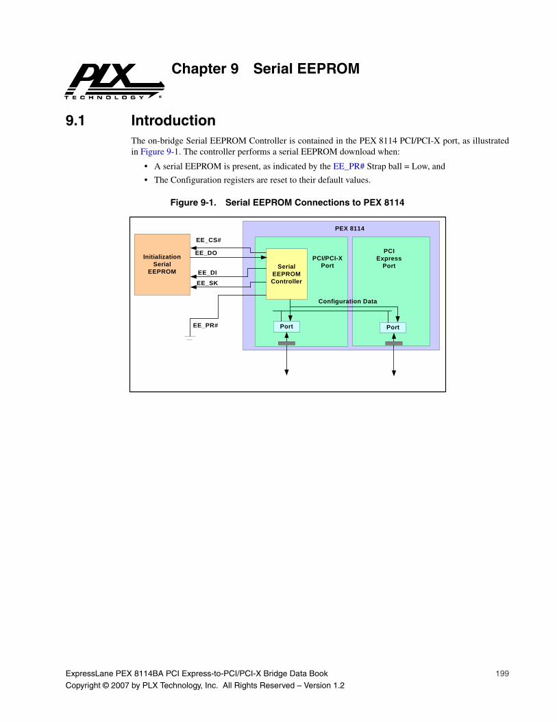
ExpressLane PEX 8114BA PCI Express-to-PCI/PCI-X Bridge Data Book 199
Copyright © 2007 by PLX Technology, Inc. All Rights Reserved – Version 1.2
Chapter 9 Serial EEPROM
9.1 IntroductionThe on-bridge Serial EEPROM Controller is contained in the PEX 8114 PCI/PCI-X port, as illustratedin Figure 9-1. The controller performs a serial EEPROM download when:
• A serial EEPROM is present, as indicated by the EE_PR# Strap ball = Low, and
• The Configuration registers are reset to their default values.
Figure 9-1. Serial EEPROM Connections to PEX 8114
InitializationSerial
EEPROM
Port
Serial EEPROMController
PCI/PCI-XPort
PortEE_PR#
EE_CS#
EE_DO
EE_DIEE_SK
PEX 8114
Configuration Data
PCI Express
Port
Serial EEPROM PLX Technology, Inc.
200 ExpressLane PEX 8114BA PCI Express-to-PCI/PCI-X Bridge Data Book
Copyright © 2007 by PLX Technology, Inc. All Rights Reserved – Version 1.2
9.2 Configuration Data DownloadThe Serial EEPROM Controller generates an EE_SK signal by dividing the PCI_CLK by 16, resultingin a shift clock frequency up to 8.3 MHz. The Serial EEPROM Controller reads a total of 1,004 bytes inTransparent mode, and 1,880 bytes in Non-Transparent mode, from the serial EEPROM, whichrepresents all data necessary to initialize the PEX 8114 registers. The serial EEPROM Memory Mapreflects the basic device register map. A detailed description of the Transparent and Non-Transparentmode serial EEPROM Memory maps is provided in Appendix A, “Serial EEPROM Maps.”
Note: For a PCI-X clock greater than 66 MHz, a 10-MHz serial EEPROM is needed. For clock rates of 66 MHz and lower, a 5-MHz serial EEPROM is sufficient.
When registers are modified through the serial EEPROM load, the serial EEPROM must retain data forall registers. Registers that must be modified away from their power-on default states can be changed byloading the necessary modified values in the serial EEPROM, at the location that corresponds to thatregister’s value in the serial EEPROM map. Registers that are not intended to be modified from theirdefault values by the serial EEPROM load must be located within the serial EEPROM loaded with thedefault value.
Serial Peripheral Interface EEPROMs, from 1 KB up to 64 KB sizes, are supported. A minimum ofa 1-KB serial EEPROM is required to support the PEX 8114 register load in Transparent mode.In Transparent mode, if a serial EEPROM larger than 1 KB is used, the additional space remains unusedby the PEX 8114 register load resources and is used as a general-purpose serial EEPROM. A minimumof a 2-KB serial EEPROM is required to support the PEX 8114’s register load in Non-Transparentmode. The register load data starts at location 0 in the serial EEPROM and the serial EEPROM data isloaded into the registers, in ascending sequence, and mapped according to the register assignment tablesin Appendix A, “Serial EEPROM Maps.” The table is arranged with the left column listing theCSR register addresses and the right column listing the serial EEPROM address to load to modify theCSR register.
In a few instances, the value of a single PCI-defined or PLX-specific CSR must be stored in twoseparate internal registers within the PEX 8114. When writing a CSR using PCI-type ConfigurationWrites – Memory-Mapped Writes or Pointer Indirect Writes – the internal state machines associatedwith the Write, place the data in both internal registers, without intervention. When loading a CSRlocation that contains two internal copies of the register using serial EEPROM loads, the value must bespecifically loaded into both internal registers (that is, two distinct Writes to two distinct locations arerequired). Therefore, in certain instances, when creating the serial EEPROM image, the value needed ina CSR must be placed in two address locations in the serial EEPROM, allowing two distinct Writes tooccur. The required registers for this procedure are indicated in the register assignment tables inAppendix A, “Serial EEPROM Maps,” by having two serial EEPROM addresses listed in a row that hasonly one corresponding CSR address. In cases where two serial EEPROM addresses must be loaded tomodify one CSR location, the Data loaded into both serial EEPROM addresses must be identical or thePEX 8114’s operation is undefined.
During the serial EEPROM download, the controller checks for a valid Class Code and terminates thedownload if a value other than 060400h (Transparent mode) or 068000h (Non-Transparent mode)is used.
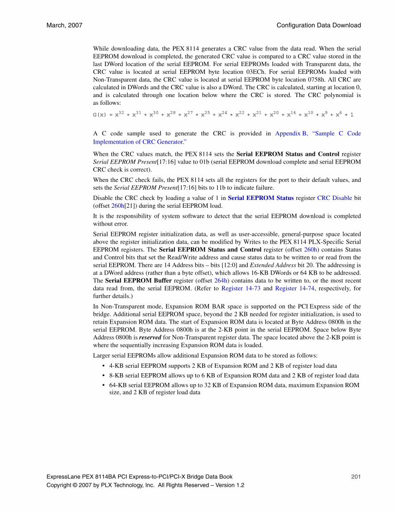
March, 2007 Configuration Data Download
ExpressLane PEX 8114BA PCI Express-to-PCI/PCI-X Bridge Data Book 201
Copyright © 2007 by PLX Technology, Inc. All Rights Reserved – Version 1.2
While downloading data, the PEX 8114 generates a CRC value from the data read. When the serialEEPROM download is completed, the generated CRC value is compared to a CRC value stored in thelast DWord location of the serial EEPROM. For serial EEPROMs loaded with Transparent data, theCRC value is located at serial EEPROM byte location 03ECh. For serial EEPROMs loaded withNon-Transparent data, the CRC value is located at serial EEPROM byte location 0758h. All CRC arecalculated in DWords and the CRC value is also a DWord. The CRC is calculated, starting at location 0,and is calculated through one location below where the CRC is stored. The CRC polynomial isas follows:
G(x) = x32 + x31 + x30 + x28 + x27 + x25 + x24 + x22 + x21 + x20 + x16 + x10 + x9 + x6 + 1
A C code sample used to generate the CRC is provided in Appendix B, “Sample C CodeImplementation of CRC Generator.”
When the CRC values match, the PEX 8114 sets the Serial EEPROM Status and Control registerSerial EEPROM Present[17:16] value to 01b (serial EEPROM download complete and serial EEPROMCRC check is correct).
When the CRC check fails, the PEX 8114 sets all the registers for the port to their default values, andsets the Serial EEPROM Present[17:16] bits to 11b to indicate failure.
Disable the CRC check by loading a value of 1 in Serial EEPROM Status register CRC Disable bit(offset 260h[21]) during the serial EEPROM load.
It is the responsibility of system software to detect that the serial EEPROM download is completedwithout error.
Serial EEPROM register initialization data, as well as user-accessible, general-purpose space locatedabove the register initialization data, can be modified by Writes to the PEX 8114 PLX-Specific SerialEEPROM registers. The Serial EEPROM Status and Control register (offset 260h) contains Statusand Control bits that set the Read/Write address and cause status data to be written to or read from theserial EEPROM. There are 14 Address bits – bits [12:0] and Extended Address bit 20. The addressing isat a DWord address (rather than a byte offset), which allows 16-KB DWords or 64 KB to be addressed.The Serial EEPROM Buffer register (offset 264h) contains data to be written to, or the most recentdata read from, the serial EEPROM. (Refer to Register 14-73 and Register 14-74, respectively, forfurther details.)
In Non-Transparent mode, Expansion ROM BAR space is supported on the PCI Express side of thebridge. Additional serial EEPROM space, beyond the 2 KB needed for register initialization, is used toretain Expansion ROM data. The start of Expansion ROM data is located at Byte Address 0800h in theserial EEPROM. Byte Address 0800h is at the 2-KB point in the serial EEPROM. Space below ByteAddress 0800h is reserved for Non-Transparent register data. The space located above the 2-KB point iswhere the sequentially increasing Expansion ROM data is loaded.
Larger serial EEPROMs allow additional Expansion ROM data to be stored as follows:
• 4-KB serial EEPROM supports 2 KB of Expansion ROM and 2 KB of register load data
• 8-KB serial EEPROM allows up to 6 KB of Expansion ROM data and 2 KB of register load data
• 64-KB serial EEPROM allows up to 32 KB of Expansion ROM data, maximum Expansion ROM size, and 2 KB of register load data
Serial EEPROM PLX Technology, Inc.
202 ExpressLane PEX 8114BA PCI Express-to-PCI/PCI-X Bridge Data Book
Copyright © 2007 by PLX Technology, Inc. All Rights Reserved – Version 1.2
Because the first 2 KB of the serial EEPROM space is used for register load data, and the remainingspace is available only for Expansion ROM data, the available Expansion ROM data is 2 KB less thanthe serial EEPROM size. Therefore, when attempting to use more than N KB of Expansion ROM data inan N-KB Expansion ROM BAR, the serial EEPROM provides 2 KB less data than the BAR size. Set theBAR size to one-half the serial EEPROM size used, or ensure that the Expansion ROM cannot beaccessed by the system within the upper 2 KB.
Note: Serial EEPROM Expansion ROM data can be changed by Writes to the PEX 8114 Serial EEPROM Status, Control, Status Data, and Buffer registers.
ExpressLane PEX 8114BA PCI Express-to-PCI/PCI-X Bridge Data Book 203
Copyright © 2007 by PLX Technology, Inc. All Rights Reserved – Version 1.2
Chapter 10 Interrupt Handler
10.1 IntroductionThe PEX 8114 includes two types of interrupts:
• Conventional PCI Interrupt, PCI/PCI-X PCI_INT[D:A]#, which are PEX 8114 I/O balls on the PCI/PCI-X Bus
• Message Signal Interrupt (MSI), which is conveyed with Memory Write transactions
In Forward Bridge mode, the Conventional PCI interrupts, when enabled, are converted by thePEX 8114 to Virtual Interrupt messages and transmitted upstream on the PCI Express interface. MSIinterrupts are passed through the PEX 8114 from PCI/PCI-X to PCI Express.
In Reverse Bridge mode, the Virtual Interrupt messages received on the PCI Express interfaceare converted to Conventional PCI interrupt signals and driven on the PCI_INT[D:A]# balls.MSI interrupts are passed through the PEX 8114, from PCI Express to PCI/PCI-X.
10.2 Interrupt Handler FeaturesInterrupt handler features are as follows:
• Senses internal interrupt events
• Generates Virtual Interrupt messages from Conventional PCI PCI_INT[D:A]# balls
• Drives Conventional PCI_INT[D:A]# balls from Virtual Interrupt messages
• Signals interrupts through Virtual INTA# signaling, PCI_INT[D:A]# signal Conventional PCI assertion, or MSI.
10.3 Events that Cause InterruptsEvents internal to the PEX 8114 that cause interrupts are as follows:
• Hot Plug events
– Attention Button pressed
– MRL sensor change event
– Presence detect change event
– Power fault detected
– Command complete event
• ECC Error detected in internal packet RAM
• Credit overflow or underflow
• Internal Error FIFO overflow
• Power Management Events
• Non-Transparent Interrupt set register bit
Interrupt requests proceed to the Interrupt Generator module, which sets the Status register InterruptStatus bit. Setting the status bit causes an INTA# interrupt or MSI to generate, depending on whichinterrupt is enabled.
INTA# and MSI interrupt generation are mutually exclusive.
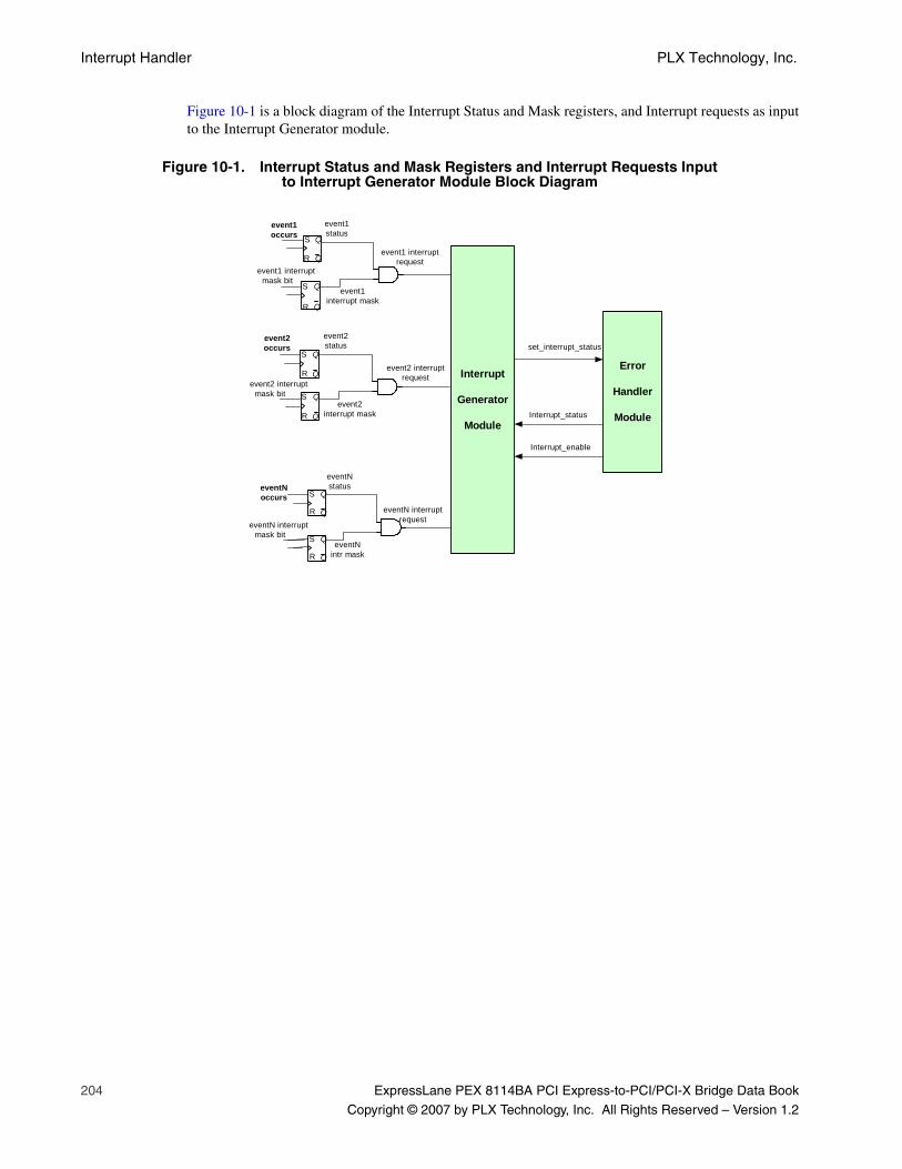
Interrupt Handler PLX Technology, Inc.
204 ExpressLane PEX 8114BA PCI Express-to-PCI/PCI-X Bridge Data Book
Copyright © 2007 by PLX Technology, Inc. All Rights Reserved – Version 1.2
Figure 10-1 is a block diagram of the Interrupt Status and Mask registers, and Interrupt requests as inputto the Interrupt Generator module.
Figure 10-1. Interrupt Status and Mask Registers and Interrupt Requests Input to Interrupt Generator Module Block Diagram
event1occurs
event1 interruptmask bit
event1 interruptrequest
Q
QS
R
event1status
event1interrupt mask
event2 interruptrequestQ
QS
R
Q
QS
R
event2status
event2interrupt mask
event2occurs
event2 interruptmask bit
eventN interruptrequest
eventN interruptmask bit
eventNoccurs
Interrupt
Generator
Module
Error
Handler
Module
set_interrupt_status
Interrupt_status
Interrupt_enable
eventNstatus
eventNintr mask
Q
QS
R
Q
QS
R
Q
QS
R
March, 2007 INTA# Signaling
ExpressLane PEX 8114BA PCI Express-to-PCI/PCI-X Bridge Data Book 205
Copyright © 2007 by PLX Technology, Inc. All Rights Reserved – Version 1.2
10.4 INTA# SignalingIn Forward Bridge mode, the PEX 8114 converts PCI_INTx# ball interrupts to virtual PCI ExpressINTA# signaled interrupts. PCI/PCI-X interrupts appearing on PCI_INTx# lines are converted toPCI Express-compatible packets (Assert_INTx# and Deassert_INTx# signaled interrupts) andtransmitted to the upstream port.
In Reverse Bridge mode, the PEX 8114 converts PCI Express virtual INTx# signaled interrupts toPCI_INTx# interrupts. Assert_INTx# and Deassert_INTx# signaled interrupts from the PCI Expressport are converted to the PCI_INTx# ball interrupts.
The PEX 8114 supports the PCI r3.0 Interrupt Pin and Interrupt Line registers, as well as thePCI r3.0 Command register PCI Interrupt Disable and Status register Interrupt Status bits.
Although the PCI Express r1.0a provides INT[D:A]# for INTA# signaling, the PEX 8114 uses onlyPCI_INTA# for internal Interrupt message generation.
When MSI is disabled (Message Signaled Interrupt Control register MSI Enable bit is cleared to 0)and INTA#-type interrupts are not disabled (Command register Interrupt Disable bit value is 0),interrupt requests from a defined event generate INTA#-type interrupts.
When MSI is enabled, the interrupt requests from a defined event generate MSI type interrupts,regardless of the Command register Interrupt Disable bit state.
When PCI_INTA# interrupts are enabled and there is an interrupt request from interrupt sources internalto the PEX 8114, the PCI Status register Interrupt Status bit is set.
• In Forward Bridge mode, when the Interrupt Status bit is set by an interrupt source internal to the PEX 8114, an Assert_INTA# message is transmitted on the PCI Express interface. When an external PCI-X device asserts the INTx# input to the PEX 8114, the Status register Interrupt Status bit is not set; however, the Assert_INTx# message is translated. When the external PCI-X device later de-asserts the PCI_INTx# input, the Deassert_INTx# message is transmitted without action from the host software.
• In Reverse Bridge mode, when the Interrupt Status bit is set, the PCI_INTA# signal is asserted on the PCI/PCI-X Bus.
When an interrupt source internal to the PEX 8114 causes an interrupt to be transmitted to the PCIExpress Root Complex, the host software reads and clears the event status after servicing the interrupt.
When an interrupt source internal to the PEX 8114 causes an interrupt, the PCI device hardware clearsthe Status register Interrupt Status bit when all event status bits are cleared, and transmits aDeassert_INTA# message on the PCI Express interface or de-asserts PCI_INTx# on the PCI/PCI-X Bus.
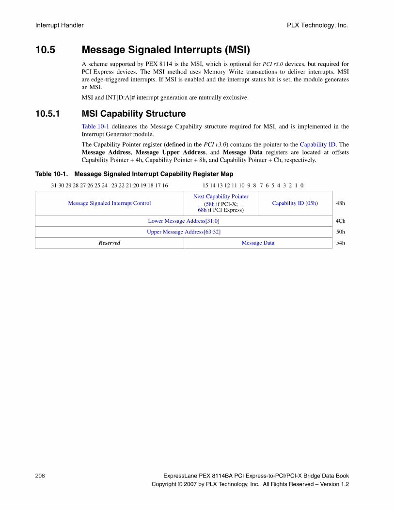
Interrupt Handler PLX Technology, Inc.
206 ExpressLane PEX 8114BA PCI Express-to-PCI/PCI-X Bridge Data Book
Copyright © 2007 by PLX Technology, Inc. All Rights Reserved – Version 1.2
10.5 Message Signaled Interrupts (MSI)A scheme supported by PEX 8114 is the MSI, which is optional for PCI r3.0 devices, but required forPCI Express devices. The MSI method uses Memory Write transactions to deliver interrupts. MSIare edge-triggered interrupts. If MSI is enabled and the interrupt status bit is set, the module generatesan MSI.
MSI and INT[D:A]# interrupt generation are mutually exclusive.
10.5.1 MSI Capability StructureTable 10-1 delineates the Message Capability structure required for MSI, and is implemented in theInterrupt Generator module.
The Capability Pointer register (defined in the PCI r3.0) contains the pointer to the Capability ID. TheMessage Address, Message Upper Address, and Message Data registers are located at offsetsCapability Pointer + 4h, Capability Pointer + 8h, and Capability Pointer + Ch, respectively.
Table 10-1. Message Signaled Interrupt Capability Register Map
31 30 29 28 27 26 25 24 23 22 21 20 19 18 17 16 15 14 13 12 11 10 9 8 7 6 5 4 3 2 1 0
Message Signaled Interrupt ControlNext Capability Pointer
(58h if PCI-X;68h if PCI Express)
Capability ID (05h) 48h
Lower Message Address[31:0] 4Ch
Upper Message Address[63:32] 50h
Reserved Message Data 54h
March, 2007 MSI Operation
ExpressLane PEX 8114BA PCI Express-to-PCI/PCI-X Bridge Data Book 207
Copyright © 2007 by PLX Technology, Inc. All Rights Reserved – Version 1.2
10.5.2 MSI OperationAt configuration, system software traverses the capability list of the function. If a Capability ID of 05his found, the function implements MSI. System software reads the Message Signaled InterruptCapability List register to determine whether the PEX 8114 is set up to support MSI.
Because the PEX 8114 supports only one message for MSI, the Multiple Message Enable and Capablefields are always 000b.
Initialize the 64-bit address capability field by system software:
• When set, the message address field is 64 bits
• When not set, the message address field is 32 bits
System software initializes the Message Data register (offset 54h) with a system-specified message.
The MSI Enable bit is cleared after reset and software must set the bit if the system supports the MSIscheme. After the bit is enabled, the module performs a DWord Memory Write to the address specifiedby the Message Address register contents. The two lower bytes of data written are taken from thecontents of the two lower bytes of the Message Data register. The upper two bytes of data are zero (0).
Because the Multiple Message Enable field is always 000b, the module is not permitted to change thelow order bits of message data to indicate a multiple message vector, and all Message Data register databits are directly copied to the data.
After the Interrupt Status bit is set and a message generated, the module does not generate anothermessage until the system services the interrupt and clears the Event Status bits.
The module hardware clears the Interrupt Status bit when all event status bits are cleared.
10.6 Remapping INTA# InterruptsThe PEX 8114 does not perform interrupt remapping, due to its single internal register-set topology.
When the PEX 8114 acts as a forward bridge, interrupt lines INTA_ INTB_, INTC_, and INTD_ arerouted straight through the PEX 8114 and converted into De-assert Interrupt and Assert Interrupt A, B,C, and D packets, respectively, on the PCI Express side of the bridge.
When PEX 8114 acts as a reverse bridge, each assert A, B, C, and D interrupt and de-assert interruptpacket causes the interrupt A, B, C, and D lines, respectively, to assert and de-assert.
Refer to the PCI Express-to-PCI/PCI-X Bridge r1.0, Section 8.2, for an explanation of routing forOption A bridges.
Interrupt Handler PLX Technology, Inc.
208 ExpressLane PEX 8114BA PCI Express-to-PCI/PCI-X Bridge Data Book
Copyright © 2007 by PLX Technology, Inc. All Rights Reserved – Version 1.2
10.7 Interrupt Capability Specific to Non-Transparent Bridge ModeWhen the PEX 8114 is in Non-Transparent mode, the capability to cause interrupts on the other side ofthe PEX 8114 Non-Transparent bridge by configuring, and then writing to, an interrupt request registeris enabled. This feature enables a PCI device on the PCI or PCI-X side of the Non-Transparent bridge tocause a PCI Express Assert_INTA# message or an MSI message on the PCI Express side of the bridge.Additionally, PCI Express devices can assert an INTA# interrupt on the PCI or PCI-X Bus, byconfiguring and writing to a set of Configuration registers from the PCI Express side of the bridge.
This capability is at times called Doorbell registers. However, herein, they are referred to as InterruptRequest registers. Two sets of four, 16-bit wide Interrupt Request registers associated with theconfiguration, setting, clearing, and masking of interrupts driven from one side of the bridge to the othercontrol this interrupt capability. These registers are further discussed in Chapter 16, “PEX 8114 Non-Transparent Mode PCI-X Registers,” and Chapter 17, “PEX 8114 Non-Transparent Mode PCI ExpressRegisters.” Table 10-2 delineates the register Configuration space address, and names, as well as a brieffunctional description.
Registers listed in Table 10-2 contain the least significant 16 bits that are not reserved, and can thereforecontribute to setting an interrupt request out of the IRQ module. From a functional perspective, eachN bit of each of the registers are related to one another. For example, if the IRQ Set register N bit valueis 1 and the IRQ Mask register N bit is not 1, an interrupt request is asserted out of the interrupt module.If the IRQ Set register N bit is set and the software has finished servicing the interrupt and now mustclear it, the software accomplishes this by writing 1 to the IRQ Clear register N bit. If the IRQ MaskSet register N bit is set, disabling interrupt requests from that bit, software can clear that bit by writing 1to the IRQ Mask Clear register.
When any of the IRQ Mask Set register’s 16 bits are set (causing interrupts from its associated bit todisable), the mask must be cleared. Clear the mask by writing 1 to the IRQ Mask Clear register.Reading the bits is a method for determining their current value. Writing 0 to the bits has no effect.
When the interrupt module is transmitting an Interrupt request, and the Command register InterruptDisable bit is cleared, the interrupt is driven out on the associated bus or link. Interrupts caused bywriting to an unmasked Interrupt Set register bit are transmitted to the PCI Express Root Complex asan interrupt or MSI. If interrupts are enabled and the MSI data structure does not exist, the interrupt isforwarded as an Assert_INTA# message. If MSIs are enabled, the interrupt is transmitted as an MSI.Interrupts are never transmitted as both Assert_INTA# and MSI.

March, 2007 Interrupt Capability Specific to Non-Transparent Bridge Mode
ExpressLane PEX 8114BA PCI Express-to-PCI/PCI-X Bridge Data Book 209
Copyright © 2007 by PLX Technology, Inc. All Rights Reserved – Version 1.2
Table 10-2. Interrupt Request Registers
Offset Register Name Register Function
90h Set PCI-X Interface IRQ
Controls the PCI-X interface Interrupt Request bits state. Reading returns the status of the bits. Writing 1 to a bit in the register sets the corresponding Interrupt request. When this register is non-zero, the corresponding bit is not masked and interrupts are enabled, the PCI-X interface interrupt is asserted. Writing 0 to any bit has no effect.
94h Clear PCI-X Interface IRQ
Controls the PCI-X interface Interrupt Request bits state. Reading returns the status of the bits. Writing 1 to a bit in the register clears the corresponding Interrupt request. When this register is non-zero, the corresponding bit is not masked and interrupts are enabled, the PCI-X interface interrupt is asserted. Writing 0 to any bit has no effect.
98h Set PCI-X Interface IRQ Mask
PCI-X interface interrupt IRQ Mask Set. Reading returns the state of the mask bits. 0 = Corresponding Interrupt Request bit is unmasked1 = Corresponding Interrupt Request bit is masked/disabledWriting 1 to a bit in the register sets the corresponding Interrupt Mask bit. Writing 0 to any bit has no effect.
9Ch Clear PCI-X Interface IRQ Mask
Controls the PCI-X interface Interrupt Request bits state. Reading returns the status of the bits. 0 = Corresponding Interrupt Request bit is unmasked1 = Corresponding Interrupt Request bit is masked/disabledWriting 1 to a bit in the register clears the corresponding Interrupt Mask bit. Writing 0 to any bit has no effect.
A0h Set PCI Express Interface IRQ
Controls the PCI Express interface Interrupt Request bits state. Reading returns the status of the bits. Writing 1 to a bit in the register sets the corresponding Interrupt request. When this register is non-zero, the corresponding bit is not masked and interrupts are enabled, the PCI Express interface interrupt is asserted.Writing 0 to any bit has no effect.
A4h Clear PCI Express Interface IRQ
Controls the PCI Express interface Interrupt Request bits state. Reading returns the status of the bits. Writing 1 to a bit in the register clears the corresponding Interrupt request. When this register is non-zero, the corresponding bit is not masked and interrupts are enabled, the PCI Express interface interrupt is asserted.Writing 0 to any bit has no effect.
A8h Set PCI Express Interface IRQ Mask
PCI Express interface Interrupt IRQ Mask Set. Reading returns the state of the IRQ mask. 0 = Corresponding Interrupt Request bit is unmasked1 = Corresponding Interrupt Request bit is masked/disabledWriting 1 to a bit in the register sets the corresponding Interrupt Mask bit. Writing 0 to any bit has no effect.
ACh Clear PCI Express Interface IRQ Mask
PCI Express interface Interrupt IRQ Mask Clear. Reading returns the state of the IRQ mask. 0 = Corresponding Interrupt Request bit is unmasked1 = Corresponding Interrupt Request bit is masked/disabledWriting 1 to a bit in the register clears the corresponding Interrupt Mask bit.Writing 0 to any bit has no effect.

Interrupt Handler PLX Technology, Inc.
210 ExpressLane PEX 8114BA PCI Express-to-PCI/PCI-X Bridge Data Book
Copyright © 2007 by PLX Technology, Inc. All Rights Reserved – Version 1.2
THIS PAGE INTENTIONALLY LEFT BLANK.
ExpressLane PEX 8114BA PCI Express-to-PCI/PCI-X Bridge Data Book 211
Copyright © 2007 by PLX Technology, Inc. All Rights Reserved – Version 1.2
Chapter 11 PCI/PCI-X Arbiter
11.1 IntroductionThe PCI/PCI-X Arbiter efficiently manages accesses to the PCI/PCI-X Bus shared by multiple Masters.It is not required that all systems provide equal bus access to all Masters. In reality, most systems requirecertain Masters be granted greater access to the bus than others. This is the case for systems with anembedded processor.
It is assumed that the bus access requirements for all Masters in a system are known. It is possible toprogram the bus access requirements to meet system needs.
11.2 Arbiter Key FeaturesThe key features of the PCI/PCI-X Arbiter are as follows:
• Arbiter supports up to five PCI-X or Conventional PCI devices (four external and one internal)
• Bus allocation is programmable in 10% increments
• Park bus on latest Master
• Enable/disable Arbiter (by way of STRAP_ARB ball)
• Address stepping on Configuration cycles (PCI-X mode only)
• Assert grants in two ways:
– Normal PCI/PCI-X-compliant grants during accesses
– Wait for idle bus to issue grant
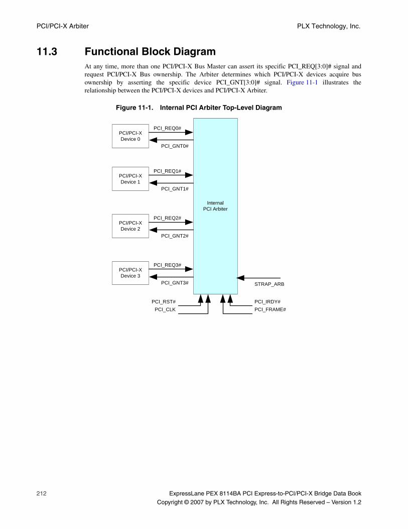
PCI/PCI-X Arbiter PLX Technology, Inc.
212 ExpressLane PEX 8114BA PCI Express-to-PCI/PCI-X Bridge Data Book
Copyright © 2007 by PLX Technology, Inc. All Rights Reserved – Version 1.2
11.3 Functional Block DiagramAt any time, more than one PCI/PCI-X Bus Master can assert its specific PCI_REQ[3:0]# signal andrequest PCI/PCI-X Bus ownership. The Arbiter determines which PCI/PCI-X devices acquire busownership by asserting the specific device PCI_GNT[3:0]# signal. Figure 11-1 illustrates therelationship between the PCI/PCI-X devices and PCI/PCI-X Arbiter.
Figure 11-1. Internal PCI Arbiter Top-Level Diagram
InternalPCI Arbiter
PCI_RST#PCI_CLK
PCI_IRDY#PCI_FRAME#
STRAP_ARB
PCI/PCI-XDevice 0
PCI_GNT0#
PCI_REQ0#
PCI/PCI-XDevice 1
PCI_GNT1#
PCI_REQ1#
PCI/PCI-XDevice 2
PCI_GNT2#
PCI_REQ2#
PCI/PCI-XDevice 3
PCI_GNT3#
PCI_REQ3#
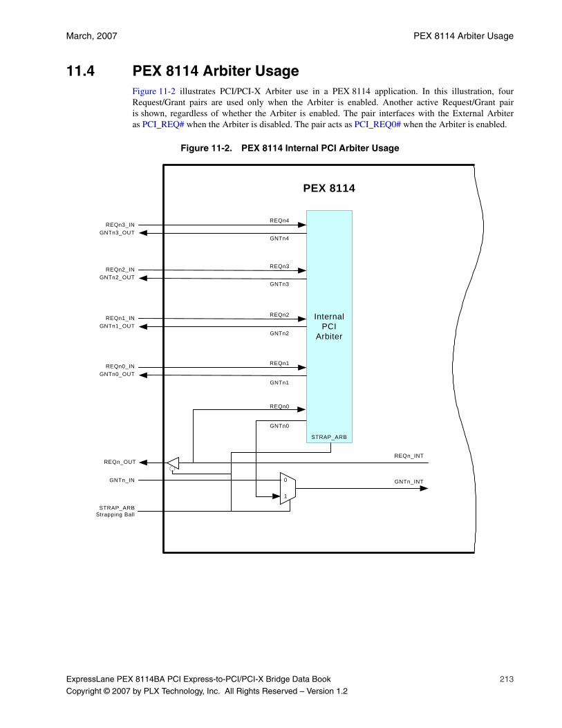
March, 2007 PEX 8114 Arbiter Usage
ExpressLane PEX 8114BA PCI Express-to-PCI/PCI-X Bridge Data Book 213
Copyright © 2007 by PLX Technology, Inc. All Rights Reserved – Version 1.2
11.4 PEX 8114 Arbiter UsageFigure 11-2 illustrates PCI/PCI-X Arbiter use in a PEX 8114 application. In this illustration, fourRequest/Grant pairs are used only when the Arbiter is enabled. Another active Request/Grant pairis shown, regardless of whether the Arbiter is enabled. The pair interfaces with the External Arbiteras PCI_REQ# when the Arbiter is disabled. The pair acts as PCI_REQ0# when the Arbiter is enabled.
Figure 11-2. PEX 8114 Internal PCI Arbiter Usage
InternalPCI
Arbiter
GNTn3
GNTn2
GNTn1
REQn1
REQn2
REQn3
GNTn4
REQn4
GNTn0
REQn0
0
1
REQn_INT
GNTn_INT
REQn0_INGNTn0_OUT
PEX 8114
STRAP_ARB
REQn_OUT
GNTn_IN
STRAP_ARBStrapping Ball
REQn1_INGNTn1_OUT
REQn2_INGNTn2_OUT
REQn3_INGNTn3_OUT
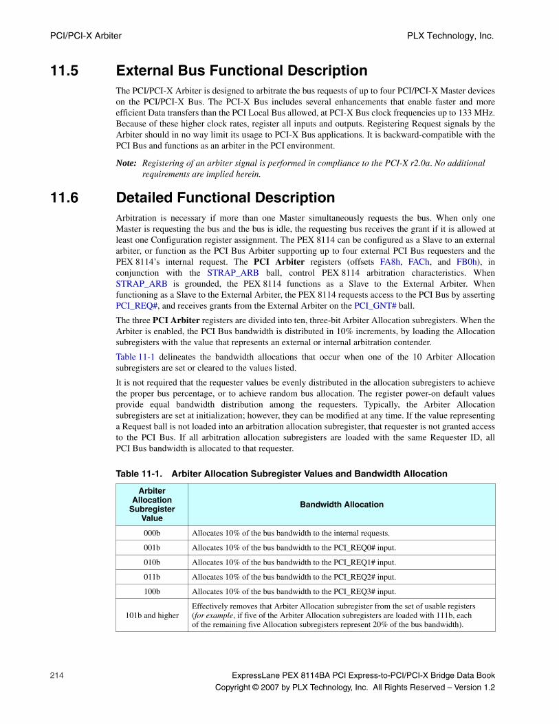
PCI/PCI-X Arbiter PLX Technology, Inc.
214 ExpressLane PEX 8114BA PCI Express-to-PCI/PCI-X Bridge Data Book
Copyright © 2007 by PLX Technology, Inc. All Rights Reserved – Version 1.2
11.5 External Bus Functional DescriptionThe PCI/PCI-X Arbiter is designed to arbitrate the bus requests of up to four PCI/PCI-X Master deviceson the PCI/PCI-X Bus. The PCI-X Bus includes several enhancements that enable faster and moreefficient Data transfers than the PCI Local Bus allowed, at PCI-X Bus clock frequencies up to 133 MHz.Because of these higher clock rates, register all inputs and outputs. Registering Request signals by theArbiter should in no way limit its usage to PCI-X Bus applications. It is backward-compatible with thePCI Bus and functions as an arbiter in the PCI environment.
Note: Registering of an arbiter signal is performed in compliance to the PCI-X r2.0a. No additional requirements are implied herein.
11.6 Detailed Functional DescriptionArbitration is necessary if more than one Master simultaneously requests the bus. When only oneMaster is requesting the bus and the bus is idle, the requesting bus receives the grant if it is allowed atleast one Configuration register assignment. The PEX 8114 can be configured as a Slave to an externalarbiter, or function as the PCI Bus Arbiter supporting up to four external PCI Bus requesters and thePEX 8114’s internal request. The PCI Arbiter registers (offsets FA8h, FACh, and FB0h), inconjunction with the STRAP_ARB ball, control PEX 8114 arbitration characteristics. WhenSTRAP_ARB is grounded, the PEX 8114 functions as a Slave to the External Arbiter. Whenfunctioning as a Slave to the External Arbiter, the PEX 8114 requests access to the PCI Bus by assertingPCI_REQ#, and receives grants from the External Arbiter on the PCI_GNT# ball.
The three PCI Arbiter registers are divided into ten, three-bit Arbiter Allocation subregisters. When theArbiter is enabled, the PCI Bus bandwidth is distributed in 10% increments, by loading the Allocationsubregisters with the value that represents an external or internal arbitration contender.
Table 11-1 delineates the bandwidth allocations that occur when one of the 10 Arbiter Allocationsubregisters are set or cleared to the values listed.
It is not required that the requester values be evenly distributed in the allocation subregisters to achievethe proper bus percentage, or to achieve random bus allocation. The register power-on default valuesprovide equal bandwidth distribution among the requesters. Typically, the Arbiter Allocationsubregisters are set at initialization; however, they can be modified at any time. If the value representinga Request ball is not loaded into an arbitration allocation subregister, that requester is not granted accessto the PCI Bus. If all arbitration allocation subregisters are loaded with the same Requester ID, allPCI Bus bandwidth is allocated to that requester.
Table 11-1. Arbiter Allocation Subregister Values and Bandwidth Allocation
Arbiter Allocation
Subregister Value
Bandwidth Allocation
000b Allocates 10% of the bus bandwidth to the internal requests.
001b Allocates 10% of the bus bandwidth to the PCI_REQ0# input.
010b Allocates 10% of the bus bandwidth to the PCI_REQ1# input.
011b Allocates 10% of the bus bandwidth to the PCI_REQ2# input.
100b Allocates 10% of the bus bandwidth to the PCI_REQ3# input.
101b and higherEffectively removes that Arbiter Allocation subregister from the set of usable registers (for example, if five of the Arbiter Allocation subregisters are loaded with 111b, each of the remaining five Allocation subregisters represent 20% of the bus bandwidth).

March, 2007 Bus Parking
ExpressLane PEX 8114BA PCI Express-to-PCI/PCI-X Bridge Data Book 215
Copyright © 2007 by PLX Technology, Inc. All Rights Reserved – Version 1.2
11.6.1 Bus ParkingThe Arbiter is designed to implement bus parking when there are no pending requests (bus idle). In thiscase, the Arbiter allows the Grant signal for the last Master to remain active. This ensures that if the lastMaster requested the bus again, it receives an immediate grant; however, if another Master requests thebus, the Arbiter causes all grants to go High before issuing a new grant.
11.6.2 Hidden Bus ArbitrationThe PCI r3.0 allows bus arbitration to occur while the currently granted device is performing a Datatransfer. This feature greatly reduces arbitration overhead and improves bus utilization. Hiddenarbitration occurs if the control register Grant_mode has a value of 1; otherwise, arbitration occurs whenthe bus is idle. Idle bus arbitration supports Conventional PCI devices.
11.6.3 Address Stepping (PCI-X Mode Only)The PEX 8114’s Internal PCI Arbiter supports address stepping when the Arbiter is used in PCI-Xmode. To acquire maximum PCI Bus utilization, the Arbiter removes a grant from a device that requeststhe bus; however, it fails to start a transaction on the bus within a specified minimum number ofPCI_CLK cycles.
In PCI-X mode high-frequency operation, when several devices are connected to the high-order Addresslines, the AD bus can be slow to settle when a device that is trying to drive a Configuration cycle on thebus, first starts to drive the AD lines. To accommodate these slow transitions during configurations, aConfiguring Master can delay PCI_FRAME# assertion one extra cycle, to allow the AD Bus linessufficient time to settle. The PCI_FRAME# delayed assertion is called address stepping. When aConfiguring Master delays PCI_FRAME# assertion, if the Master is used with a high-performanceArbiter, the Arbiter can remove the Grant signal when the Configuring Master starts to assertPCI_FRAME#. Address stepping forces the Arbiter to allow one extra Clock cycle for the device that isdriving the configuration to assert PCI_FRAME# before removing the grant.
The Address Stepping Enable bit (offset FA0h[13]) controls PEX 8114 Address stepping. At reset, thebit is cleared to 0 and address stepping is disabled. Setting the Address Stepping Enable bit causes theArbiter to delay grant removal during PCI-X Configuration cycles.

PCI/PCI-X Arbiter PLX Technology, Inc.
216 ExpressLane PEX 8114BA PCI Express-to-PCI/PCI-X Bridge Data Book
Copyright © 2007 by PLX Technology, Inc. All Rights Reserved – Version 1.2
THIS PAGE INTENTIONALLY LEFT BLANK.
ExpressLane PEX 8114BA PCI Express-to-PCI/PCI-X Bridge Data Book 217
Copyright © 2007 by PLX Technology, Inc. All Rights Reserved – Version 1.2
Chapter 12 Hot Plug Support
12.1 Hot Plug Purpose and CapabilitiesNote: The PEX 8114’s Hot Plug Controller is compliant with the Hot Plug r1.0
and PCI Standard Hot Plug Controller and Subsystem r1.0.
Hot Plug capabilities allow orderly insertion and extraction of boards from a running system, withoutadversely affecting the system. Board insertion or extraction, without system down time, is performedwhen repair of a faulty board or system reconfiguration becomes necessary. Hot Plug capabilities alsoallow systems to isolate faulty boards in the event of a failure. The PEX 8114 includes a Hot PlugController capable of supporting Hot Plugging of a downstream PCI Express link. Therefore, the HotPlug Controller is used when the PEX 8114 is in Reverse Transparent Bridge mode. PCI/PCI-X HotPlug is not supported. Do not use the PEX 8114 to support Hot Plug in Forward Transparent Bridgemode, nor in Forward Non-Transparent Bridge mode, where there is no downstream PCI Express link.
12.1.1 Hot Plug Controller Capabilities• Insertion and removal of PCI Express boards, without removing system power
• Hot Plug Controller function
• Board Present and MRL Sensor signal support
• Power Indicator and Attention Indicator output signal controlled
• Attention button monitored
• Power fault detection and Faulty board isolation
• Power switch for controlling downstream device power
• Generates PME for a Hot Plug event in a sleeping system (D3hot)
• Presence detect is achieved through an in-band SerDes receiver detect mechanism or by the HP_PRSNT# signal
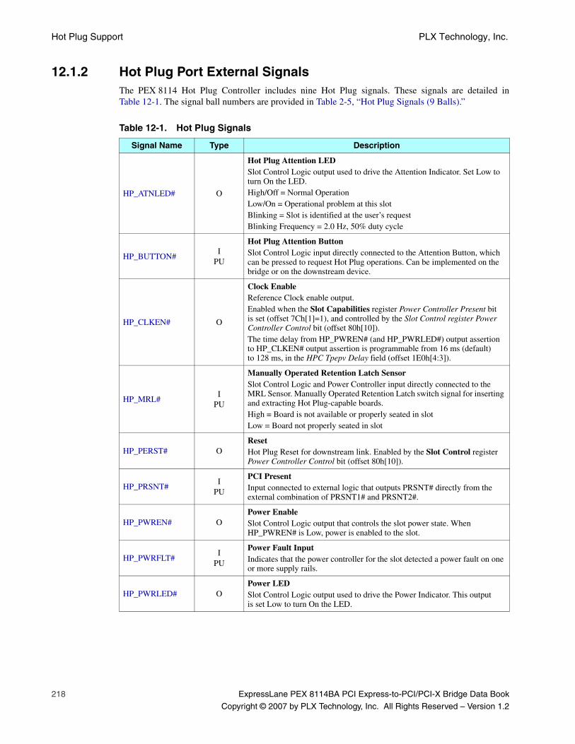
Hot Plug Support PLX Technology, Inc.
218 ExpressLane PEX 8114BA PCI Express-to-PCI/PCI-X Bridge Data Book
Copyright © 2007 by PLX Technology, Inc. All Rights Reserved – Version 1.2
12.1.2 Hot Plug Port External SignalsThe PEX 8114 Hot Plug Controller includes nine Hot Plug signals. These signals are detailed inTable 12-1. The signal ball numbers are provided in Table 2-5, “Hot Plug Signals (9 Balls).”
Table 12-1. Hot Plug Signals
Signal Name Type Description
HP_ATNLED# O
Hot Plug Attention LEDSlot Control Logic output used to drive the Attention Indicator. Set Low to turn On the LED.High/Off = Normal OperationLow/On = Operational problem at this slotBlinking = Slot is identified at the user’s requestBlinking Frequency = 2.0 Hz, 50% duty cycle
HP_BUTTON#I
PU
Hot Plug Attention ButtonSlot Control Logic input directly connected to the Attention Button, which can be pressed to request Hot Plug operations. Can be implemented on the bridge or on the downstream device.
HP_CLKEN# O
Clock EnableReference Clock enable output.Enabled when the Slot Capabilities register Power Controller Present bit is set (offset 7Ch[1]=1), and controlled by the Slot Control register Power Controller Control bit (offset 80h[10]).The time delay from HP_PWREN# (and HP_PWRLED#) output assertion to HP_CLKEN# output assertion is programmable from 16 ms (default) to 128 ms, in the HPC Tpepv Delay field (offset 1E0h[4:3]).
HP_MRL#I
PU
Manually Operated Retention Latch SensorSlot Control Logic and Power Controller input directly connected to the MRL Sensor. Manually Operated Retention Latch switch signal for inserting and extracting Hot Plug-capable boards.High = Board is not available or properly seated in slotLow = Board not properly seated in slot
HP_PERST# OResetHot Plug Reset for downstream link. Enabled by the Slot Control register Power Controller Control bit (offset 80h[10]).
HP_PRSNT#I
PU
PCI PresentInput connected to external logic that outputs PRSNT# directly from the external combination of PRSNT1# and PRSNT2#.
HP_PWREN# OPower EnableSlot Control Logic output that controls the slot power state. When HP_PWREN# is Low, power is enabled to the slot.
HP_PWRFLT#I
PU
Power Fault InputIndicates that the power controller for the slot detected a power fault on one or more supply rails.
HP_PWRLED# OPower LEDSlot Control Logic output used to drive the Power Indicator. This output is set Low to turn On the LED.
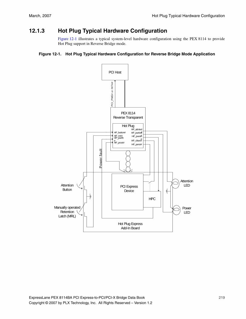
March, 2007 Hot Plug Typical Hardware Configuration
ExpressLane PEX 8114BA PCI Express-to-PCI/PCI-X Bridge Data Book 219
Copyright © 2007 by PLX Technology, Inc. All Rights Reserved – Version 1.2
12.1.3 Hot Plug Typical Hardware ConfigurationFigure 12-1 illustrates a typical system-level hardware configuration using the PEX 8114 to provideHot Plug support in Reverse Bridge mode.
Figure 12-1. Hot Plug Typical Hardware Configuration for Reverse Bridge Mode Application
PEX 8114Reverse Transparent
PCI Host
PC
I_P
ME
# or
IN
TA
#
Hot Plug
HP_button#HP_mrl#HP_pwrflt#HP_prsnt#
HP_attnled#HP_pwrled#HP_pwren#HP_clken#
HPC
Hot Plug Express Add-In Board
Attention Button
Manually operatedRetention
Latch (MRL)
AttentionLED
PowerLED
Pow
er fa
ult
PCI ExpressDevice
HP_perst#
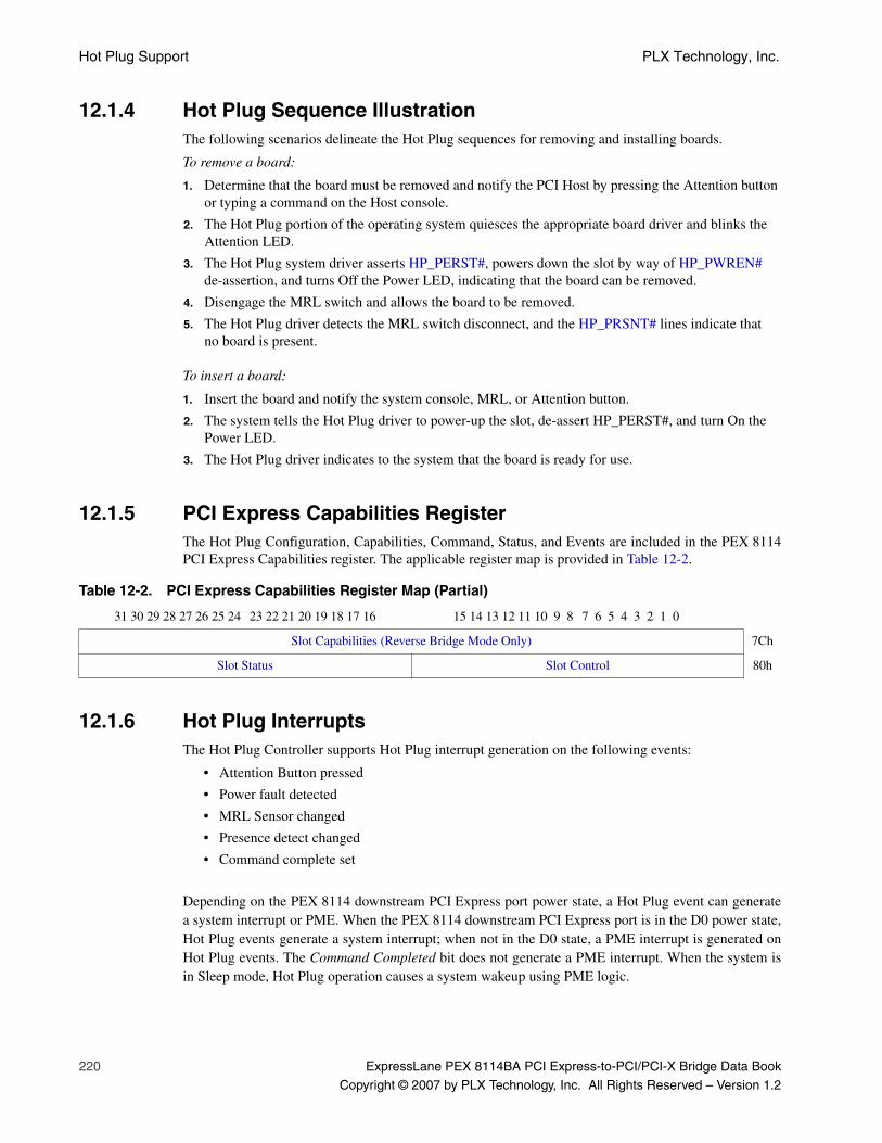
Hot Plug Support PLX Technology, Inc.
220 ExpressLane PEX 8114BA PCI Express-to-PCI/PCI-X Bridge Data Book
Copyright © 2007 by PLX Technology, Inc. All Rights Reserved – Version 1.2
12.1.4 Hot Plug Sequence IllustrationThe following scenarios delineate the Hot Plug sequences for removing and installing boards.
To remove a board:
1. Determine that the board must be removed and notify the PCI Host by pressing the Attention button or typing a command on the Host console.
2. The Hot Plug portion of the operating system quiesces the appropriate board driver and blinks the Attention LED.
3. The Hot Plug system driver asserts HP_PERST#, powers down the slot by way of HP_PWREN# de-assertion, and turns Off the Power LED, indicating that the board can be removed.
4. Disengage the MRL switch and allows the board to be removed.
5. The Hot Plug driver detects the MRL switch disconnect, and the HP_PRSNT# lines indicate that no board is present.
To insert a board:
1. Insert the board and notify the system console, MRL, or Attention button.
2. The system tells the Hot Plug driver to power-up the slot, de-assert HP_PERST#, and turn On the Power LED.
3. The Hot Plug driver indicates to the system that the board is ready for use.
12.1.5 PCI Express Capabilities RegisterThe Hot Plug Configuration, Capabilities, Command, Status, and Events are included in the PEX 8114PCI Express Capabilities register. The applicable register map is provided in Table 12-2.
12.1.6 Hot Plug InterruptsThe Hot Plug Controller supports Hot Plug interrupt generation on the following events:
• Attention Button pressed
• Power fault detected
• MRL Sensor changed
• Presence detect changed
• Command complete set
Depending on the PEX 8114 downstream PCI Express port power state, a Hot Plug event can generatea system interrupt or PME. When the PEX 8114 downstream PCI Express port is in the D0 power state,Hot Plug events generate a system interrupt; when not in the D0 state, a PME interrupt is generated onHot Plug events. The Command Completed bit does not generate a PME interrupt. When the system isin Sleep mode, Hot Plug operation causes a system wakeup using PME logic.
Table 12-2. PCI Express Capabilities Register Map (Partial)
31 30 29 28 27 26 25 24 23 22 21 20 19 18 17 16 15 14 13 12 11 10 9 8 7 6 5 4 3 2 1 0
Slot Capabilities (Reverse Bridge Mode Only) 7Ch
Slot Status Slot Control 80h

March, 2007 Hot Plug Insertion and Removal Process
ExpressLane PEX 8114BA PCI Express-to-PCI/PCI-X Bridge Data Book 221
Copyright © 2007 by PLX Technology, Inc. All Rights Reserved – Version 1.2
12.1.7 Hot Plug Insertion and Removal ProcessTable 12-3 delineates the board insertion procedure supported by the PEX 8114. Table 12-4 delineatesthe board removal procedure.
Table 12-3. Hot Plug Insertion Process
Operator Hot Plug Controller Software
A. Place board in slot.
1. Presence Detect State bit is set.
2. Presence Detect Change Enable bit is set.
3. Interrupt message is generated, if enabled.
4. Interrupt de-assertion message is transmitted, if enabled.
Presence Detect Change Enable bit is cleared.
B. Lock the MRL (Manually operated Retention Latch).
5. MRL Sensor Present bit = 0.
6. MRL Sensor Changed bit is set.
7. Interrupt message is generated, if enabled.
8. Interrupt de-assertion message is transmitted, if enabled
MRL Sensor Changed bit is cleared.
C. Press Attention Button.
9. Attention Button Present bit is set.
10. Interrupt message is generated, if enabled.
11. Interrupt de-assertion message is transmitted, if enabled.
Attention Button Present bit is cleared.
D. Power Indicator blinks.
12. Power Indicator Control field = 10b
13. Power indicator blink-message is transmitted downstream.
14. Command Complete bit is set.
15. Interrupt message is generated, if enabled.
16. Interrupt de-assertion message is transmitted, if enabled.
Write to Power Indicator Control field to blink the power LED, to indicate board is being powered up.
Command Complete bit is cleared.
E. Power Indicator On.
17. Power Indicator Control field = 01b.
18. After a Tpepv delay of 16 ms,
Command Complete bit is set.
19. Interrupt message is generated, if enabled.
20. Interrupt de-assertion message is transmitted, if enabled.
Write to the Control register Power Indicator Control field, to turn On power to the port.
Command Complete bit is cleared.
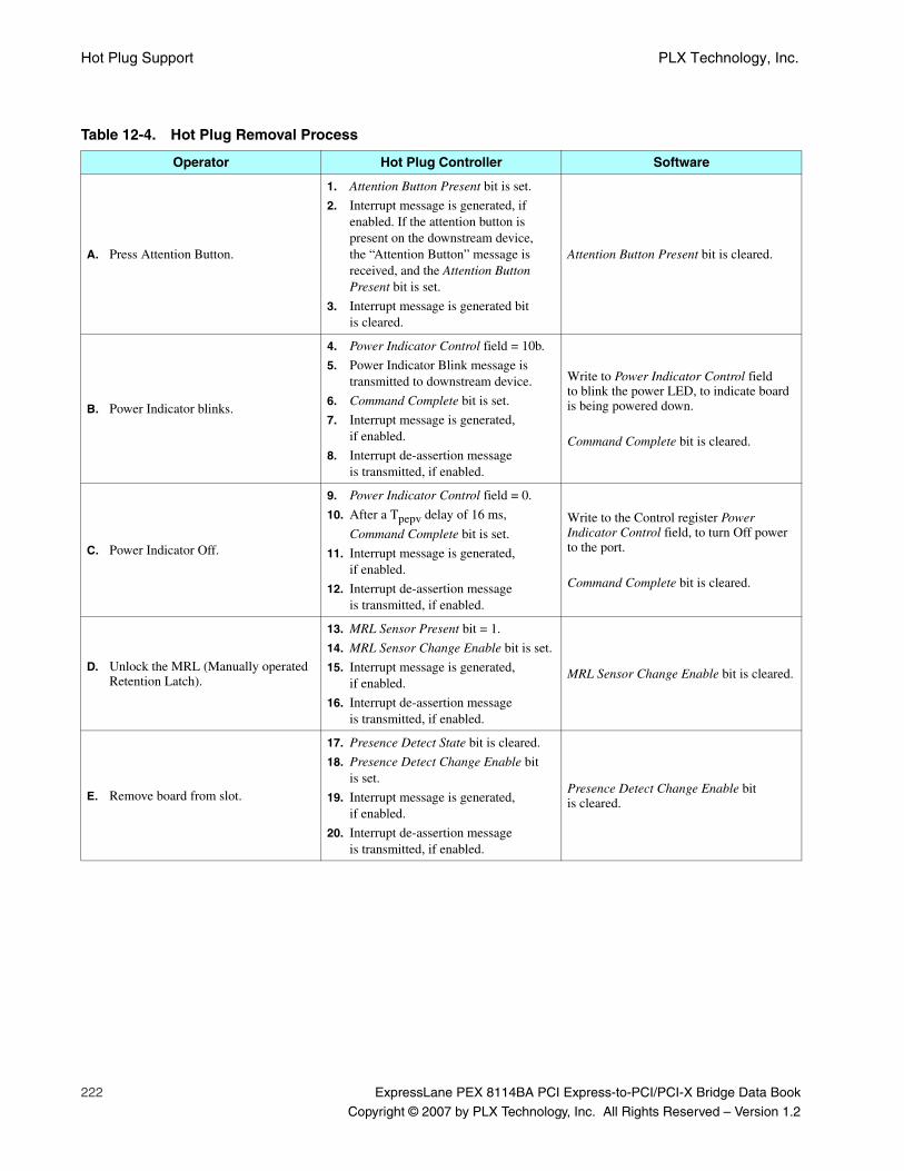
Hot Plug Support PLX Technology, Inc.
222 ExpressLane PEX 8114BA PCI Express-to-PCI/PCI-X Bridge Data Book
Copyright © 2007 by PLX Technology, Inc. All Rights Reserved – Version 1.2
Table 12-4. Hot Plug Removal Process
Operator Hot Plug Controller Software
A. Press Attention Button.
1. Attention Button Present bit is set.
2. Interrupt message is generated, if enabled. If the attention button is present on the downstream device, the “Attention Button” message is received, and the Attention Button Present bit is set.
3. Interrupt message is generated bit is cleared.
Attention Button Present bit is cleared.
B. Power Indicator blinks.
4. Power Indicator Control field = 10b.
5. Power Indicator Blink message is transmitted to downstream device.
6. Command Complete bit is set.
7. Interrupt message is generated, if enabled.
8. Interrupt de-assertion message is transmitted, if enabled.
Write to Power Indicator Control field to blink the power LED, to indicate board is being powered down.
Command Complete bit is cleared.
C. Power Indicator Off.
9. Power Indicator Control field = 0.
10. After a Tpepv delay of 16 ms,
Command Complete bit is set.
11. Interrupt message is generated, if enabled.
12. Interrupt de-assertion message is transmitted, if enabled.
Write to the Control register Power Indicator Control field, to turn Off power to the port.
Command Complete bit is cleared.
D. Unlock the MRL (Manually operated Retention Latch).
13. MRL Sensor Present bit = 1.
14. MRL Sensor Change Enable bit is set.
15. Interrupt message is generated, if enabled.
16. Interrupt de-assertion message is transmitted, if enabled.
MRL Sensor Change Enable bit is cleared.
E. Remove board from slot.
17. Presence Detect State bit is cleared.
18. Presence Detect Change Enable bit is set.
19. Interrupt message is generated, if enabled.
20. Interrupt de-assertion message is transmitted, if enabled.
Presence Detect Change Enable bit is cleared.
ExpressLane PEX 8114BA PCI Express-to-PCI/PCI-X Bridge Data Book 223
Copyright © 2007 by PLX Technology, Inc. All Rights Reserved – Version 1.2
Chapter 13 Power Management
13.1 Power Management CapabilitiesThe PEX 8114 Power Management (PM) module interfaces with different areas of the PEX 8114 toreduce power consumption during idle periods. The PEX 8114 supports hardware autonomous PowerManagement and software-driven D-State Power Management. It supports L0s and L1 link states inhardware autonomous active state link PM. It also supports L1, L2/L3 Ready, and L3 PCI Express linkstates in PCI-compatible Power Management states. D0, D3hot, and D3cold device states and B0PCI Bus states are supported in the PCI-compatible Power Management. Because the PEX 8114 doesnot support Aux-Power, PME generation in the D3cold state is not supported.
In Forward Bridge mode, the PM module interfaces with the Physical Layer electrical sub-block, totransition the Link State into low-power states when it receives a power state change request from anupstream PCI Express component, or when an internal event forces the link state entry into low-powerstates in hardware autonomous PM (Active Link State PM) mode. PCI Express link states are notdirectly visible to Conventional PCI Bus Driver software, but are derived from the Power Managementstate of the components residing on those links.
13.2 PEX 8114 Power Management Capabilities Summary
13.2.1 General Power Management Capabilities• Link Power Management State (L States)
– PCI Express Power Management – L1, L2/L3 Ready, and L3 (AUX power is not supported)
– Active State Power Management – L0s and L1
– PCI Bus B0 state
• Device Power Management State (D States)
– D0 (uninitialized and active) and D3 (hot and cold) support
• Power Management Event (PCI_PME#) support in D0 and D3hot
• Power Management Data register is supported through serial EEPROM load
13.2.2 Forward Bridge-Specific Power Management Capabilities• PME message generation on the PCI Express link caused by PCI_PME# assertion on the PCI Bus
in Forward Bridge mode.
• The PEX 8114 has no internal sources that generate PME messages in Forward Bridge mode. That is, there is no Forward Bridge mode PCI Bus Hot Plug support. Therefore, all PME messages result from downstream devices asserting PCI_PME# input to the PEX 8114.
• Only PCI D0 and D3 Device power states and B0 Bus power state are supported in Forward Bridge mode.

Power Management PLX Technology, Inc.
224 ExpressLane PEX 8114BA PCI Express-to-PCI/PCI-X Bridge Data Book
Copyright © 2007 by PLX Technology, Inc. All Rights Reserved – Version 1.2
13.2.3 Reverse Bridge-Specific Power Management Capabilities• Power Management events due to Hot Plug events in Reverse Bridge mode only (PCI Hot Plug
is not supported).
• Assert PCI_PME# on the upstream PCI Bus:
– Upon receiving a PME message from the PCI Express downstream device, if the PME signaling bit in the Power Management Status and Control register is enabled. The PCI_PME# signal is de-asserted when the PME Status or Enable bits are cleared, according to the PCI Power Mgmt. r1.2.
– Caused by a PEX 8114 internal Hot Plug event.
• Generate a PME_Turn_Off message to the PCI Express downstream devices when the bridge is requested to be placed into the D3 state. After generating the PME_Turn_Off message, the PEX 8114 waits for the PME_ACK message to return prior to entering the D3 state.
13.2.4 Device Power StatesThe PEX 8114 supports the PCI Express PCI-PM D0, D3hot, and D3cold (no VAUX) device PowerManagement states. The D1 and D2 states, which are optional in the PCI Express r1.0a, arenot supported.
13.2.4.1 D0 StateD0 is divided into two distinct substates, “uninitialized” and “active.” When power is initially applied tothe PCI Express bridge, it enters the D0_uninitialized state. The component remains in theD0_initialized state until the serial EEPROM loading and initial link training are complete.
A device enters the D0_active state when:
• Single Memory Access Enable occurs
• Combination of the following are set by system software:
– I/O Access Enable
– Memory Access Enable
– Bus Master Enable
13.2.4.2 D3hot StateA device in the D3hot state must be able to respond to Configuration accesses, allowing it to transitionby software to the D0_uninitialized state. Once in D3hot state, the device can be transitioned intoD3cold by removing power from the device. In the D3hot state, Hot Plug operations cause a PME.
13.2.4.3 D3cold StateThe PEX 8114 transitions to the D3cold state when its power is removed. Re-applying power causes thedevice to transition from the D3cold state into the D0_uninitialized state. D3cold state assumes that allprevious context is lost; therefore, software must save the necessary context while the device is in theD3hot state.
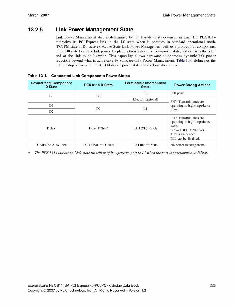
March, 2007 Link Power Management State
ExpressLane PEX 8114BA PCI Express-to-PCI/PCI-X Bridge Data Book 225
Copyright © 2007 by PLX Technology, Inc. All Rights Reserved – Version 1.2
13.2.5 Link Power Management StateLink Power Management state is determined by the D-state of its downstream link. The PEX 8114maintains its PCI Express link in the L0 state when it operates in standard operational mode(PCI PM state in D0_active). Active State Link Power Management defines a protocol for componentsin the D0 state to reduce link power, by placing their links into a low-power state, and instructs the otherend of the link to do likewise. This capability allows hardware autonomous dynamic-link powerreduction beyond what is achievable by software-only Power Management. Table 13-1 delineates therelationship between the PEX 8114 device power state and its downstream link.
Table 13-1. Connected Link Components Power States
Downstream Component D State PEX 8114 D State Permissible Interconnect
State Power Saving Actions
D0 D0L0 Full power.
L0s, L1 (optional)PHY Transmit lanes are operating in high-impedance state.
D1D0 L1
D2
D3hot D0 or D3hota
a. The PEX 8114 initiates a Link-state transition of its upstream port to L1 when the port is programmed to D3hot.
L1, L2/L3 Ready
PHY Transmit lanes are operating in high-impedance state.FC and DLL ACK/NAK Timers suspended.PLL can be disabled.
D3cold (no AUX-Pwr) D0, D3hot, or D3cold L3 Link-off State No power to component.

Power Management PLX Technology, Inc.
226 ExpressLane PEX 8114BA PCI Express-to-PCI/PCI-X Bridge Data Book
Copyright © 2007 by PLX Technology, Inc. All Rights Reserved – Version 1.2
13.2.6 PEX 8114 PCI Express Power Management SupportThe PEX 8114 supports PCI Express features that are required or important for PCI Express BridgePower Management. Table 13-2 delineates the supported and non-supported features, and the registerbits used for activating feature configuration. Reserved bits are not listed.
Note: Power Management is not supported in PCI-X mode.
Table 13-2. Supported PCI Express Power Management Capabilities
RegisterDescription
Supported
Offset Bit(s) Y N
40h
Power Management Capabilities
7:0Capabilities IDDefault 11h indicates compliance with the PCI Power Mgmt. r1.2.
✔
15:8Next PointerDefault 48h points to the Message Signaled Interrupt Capability List register
✔
18:16VersionDefault 011b indicates compliance with the PCI Power Mgmt. r1.2.
✔
19PME ClockSet to 1, as required by the PCI Express Base 1.0a.
✔
21Device-Specific InitializationDefault 0 indicates that Device-Specific Initialization is not required.
✔
24:22AUX CurrentNot supported. Default 000b indicates that the PEX 8114 does not support Auxiliary Current requirements.
✔
25D1 SupportNot supported. Default 0 indicates that the PEX 8114 does not support the D1 Power state.
✔
26D2 SupportNot supported. Default 0 indicates that the PEX 8114 does not support the D2 Power state.
✔
31:27PME SupportDefault 11001b indicates that the PEX 8114 forwards PME messages in the D0, D3hot, and D3cold power states.
✔
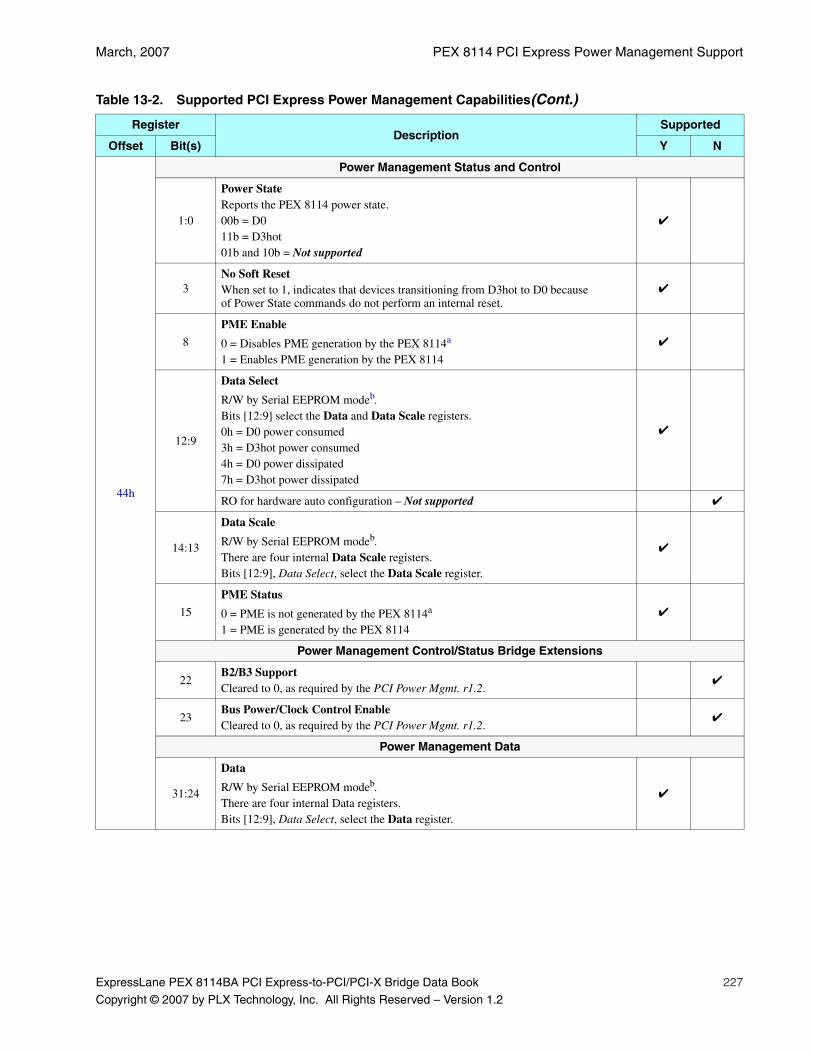
March, 2007 PEX 8114 PCI Express Power Management Support
ExpressLane PEX 8114BA PCI Express-to-PCI/PCI-X Bridge Data Book 227
Copyright © 2007 by PLX Technology, Inc. All Rights Reserved – Version 1.2
44h
Power Management Status and Control
1:0
Power StateReports the PEX 8114 power state.00b = D011b = D3hot01b and 10b = Not supported
✔
3No Soft ResetWhen set to 1, indicates that devices transitioning from D3hot to D0 because of Power State commands do not perform an internal reset.
✔
8
PME Enable
0 = Disables PME generation by the PEX 8114a
1 = Enables PME generation by the PEX 8114
✔
12:9
Data Select
R/W by Serial EEPROM modeb.Bits [12:9] select the Data and Data Scale registers.0h = D0 power consumed3h = D3hot power consumed4h = D0 power dissipated7h = D3hot power dissipated
✔
RO for hardware auto configuration – Not supported ✔
14:13
Data Scale
R/W by Serial EEPROM modeb.There are four internal Data Scale registers.Bits [12:9], Data Select, select the Data Scale register.
✔
15
PME Status
0 = PME is not generated by the PEX 8114a
1 = PME is generated by the PEX 8114
✔
Power Management Control/Status Bridge Extensions
22B2/B3 SupportCleared to 0, as required by the PCI Power Mgmt. r1.2.
✔
23Bus Power/Clock Control EnableCleared to 0, as required by the PCI Power Mgmt. r1.2.
✔
Power Management Data
31:24
Data
R/W by Serial EEPROM modeb.There are four internal Data registers.Bits [12:9], Data Select, select the Data register.
✔
Table 13-2. Supported PCI Express Power Management Capabilities(Cont.)
RegisterDescription
Supported
Offset Bit(s) Y N
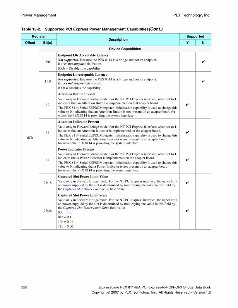
Power Management PLX Technology, Inc.
228 ExpressLane PEX 8114BA PCI Express-to-PCI/PCI-X Bridge Data Book
Copyright © 2007 by PLX Technology, Inc. All Rights Reserved – Version 1.2
6Ch
Device Capabilities
8:6
Endpoint L0s Acceptable LatencyNot supported. Because the PEX 8114 is a bridge and not an endpoint, it does not support this feature.000b = Disables the capability
✔
11:9
Endpoint L1 Acceptable LatencyNot supported. Because the PEX 8114 is a bridge and not an endpoint, it does not support this feature.000b = Disables the capability
✔
12
Attention Button Present
Valid only in Forward Bridge mode. For the NT PCI Express interface, when set to 1, indicates that an Attention Button is implemented on that adapter board.The PEX 8114 Serial EEPROM register initialization capability is used to change this value to 0, indicating that an Attention Button is not present on an adapter board for which the PEX 8114 is providing the system interface.
✔
13
Attention Indicator PresentValid only in Forward Bridge mode. For the NT PCI Express interface, when set to 1, indicates that an Attention Indicator is implemented on the adapter board.The PEX 8114 Serial EEPROM register initialization capability is used to change this value to 0, indicating an Attention Indicator is not present on an adapter board for which the PEX 8114 is providing the system interface.
✔
14
Power Indicator PresentValid only in Forward Bridge mode. For the NT PCI Express interface, when set to 1, indicates that a Power Indicator is implemented on the adapter board.The PEX 8114 Serial EEPROM register initialization capability is used to change this value to 0, indicating that a Power Indicator is not present on an adapter board for which the PEX 8114 is providing the system interface.
✔
25:18
Captured Slot Power Limit ValueValid only in Forward Bridge mode. For the NT PCI Express interface, the upper limit on power supplied by the slot is determined by multiplying the value in this field by the Captured Slot Power Limit Scale field value.
✔
27:26
Captured Slot Power Limit ScaleValid only in Forward Bridge mode. For the NT PCI Express interface, the upper limit on power supplied by the slot is determined by multiplying the value in this field by the Captured Slot Power Limit Value field value.00b = 1.001b = 0.110b = 0.0111b = 0.001
✔
Table 13-2. Supported PCI Express Power Management Capabilities(Cont.)
RegisterDescription
Supported
Offset Bit(s) Y N
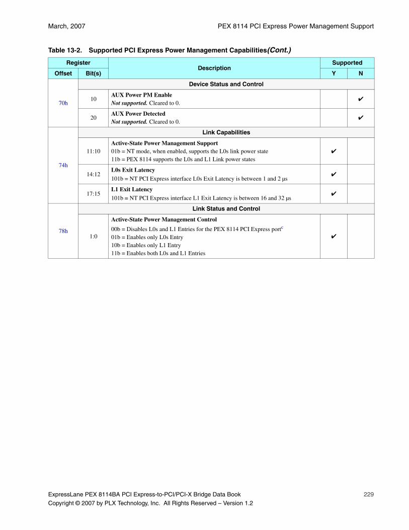
March, 2007 PEX 8114 PCI Express Power Management Support
ExpressLane PEX 8114BA PCI Express-to-PCI/PCI-X Bridge Data Book 229
Copyright © 2007 by PLX Technology, Inc. All Rights Reserved – Version 1.2
70h
Device Status and Control
10AUX Power PM EnableNot supported. Cleared to 0.
✔
20AUX Power DetectedNot supported. Cleared to 0.
✔
74h
Link Capabilities
11:10Active-State Power Management Support01b = NT mode, when enabled, supports the L0s link power state11b = PEX 8114 supports the L0s and L1 Link power states
✔
14:12L0s Exit Latency
101b = NT PCI Express interface L0s Exit Latency is between 1 and 2 µs✔
17:15L1 Exit Latency101b = NT PCI Express interface L1 Exit Latency is between 16 and 32 µs
✔
78h
Link Status and Control
1:0
Active-State Power Management Control
00b = Disables L0s and L1 Entries for the PEX 8114 PCI Express portc
01b = Enables only L0s Entry10b = Enables only L1 Entry11b = Enables both L0s and L1 Entries
✔
Table 13-2. Supported PCI Express Power Management Capabilities(Cont.)
RegisterDescription
Supported
Offset Bit(s) Y N
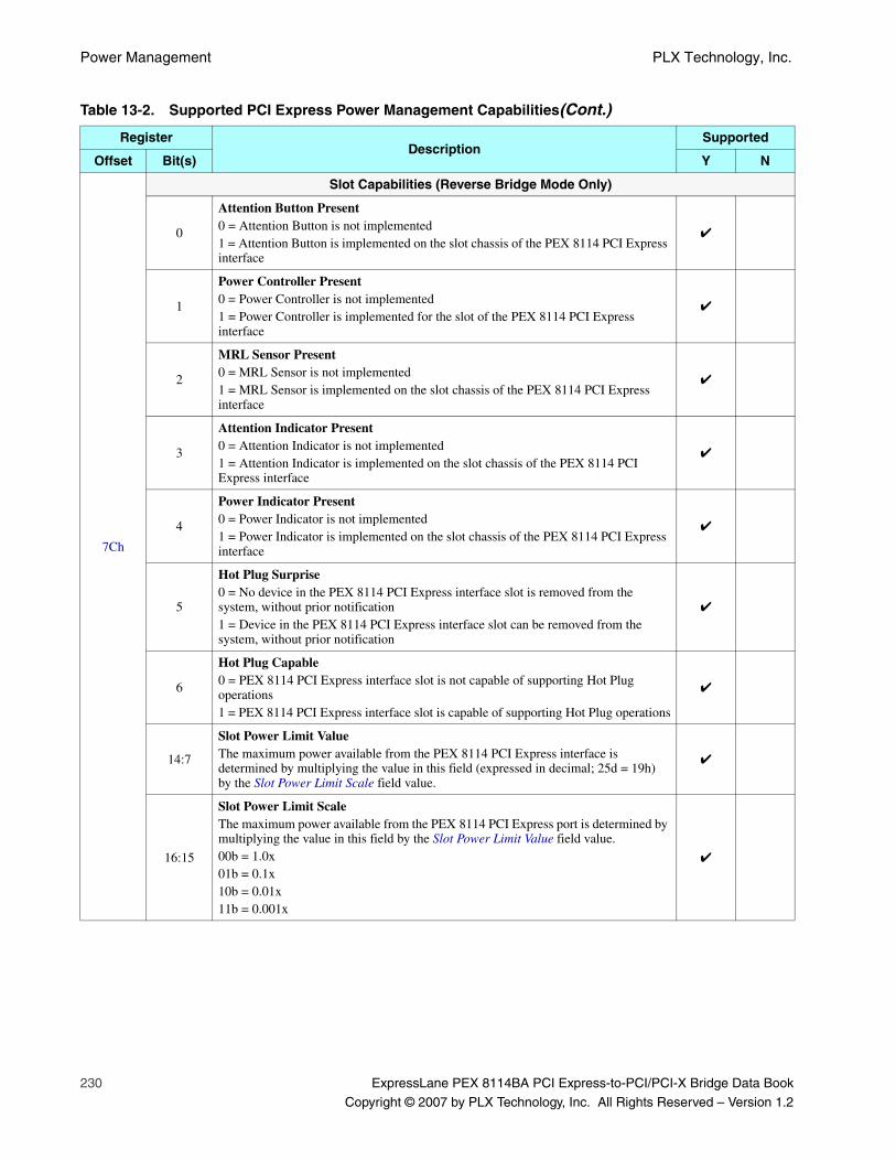
Power Management PLX Technology, Inc.
230 ExpressLane PEX 8114BA PCI Express-to-PCI/PCI-X Bridge Data Book
Copyright © 2007 by PLX Technology, Inc. All Rights Reserved – Version 1.2
7Ch
Slot Capabilities (Reverse Bridge Mode Only)
0
Attention Button Present0 = Attention Button is not implemented1 = Attention Button is implemented on the slot chassis of the PEX 8114 PCI Express interface
✔
1
Power Controller Present0 = Power Controller is not implemented1 = Power Controller is implemented for the slot of the PEX 8114 PCI Express interface
✔
2
MRL Sensor Present0 = MRL Sensor is not implemented1 = MRL Sensor is implemented on the slot chassis of the PEX 8114 PCI Express interface
✔
3
Attention Indicator Present0 = Attention Indicator is not implemented1 = Attention Indicator is implemented on the slot chassis of the PEX 8114 PCI Express interface
✔
4
Power Indicator Present0 = Power Indicator is not implemented1 = Power Indicator is implemented on the slot chassis of the PEX 8114 PCI Express interface
✔
5
Hot Plug Surprise0 = No device in the PEX 8114 PCI Express interface slot is removed from the system, without prior notification1 = Device in the PEX 8114 PCI Express interface slot can be removed from the system, without prior notification
✔
6
Hot Plug Capable0 = PEX 8114 PCI Express interface slot is not capable of supporting Hot Plug operations1 = PEX 8114 PCI Express interface slot is capable of supporting Hot Plug operations
✔
14:7
Slot Power Limit ValueThe maximum power available from the PEX 8114 PCI Express interface is determined by multiplying the value in this field (expressed in decimal; 25d = 19h) by the Slot Power Limit Scale field value.
✔
16:15
Slot Power Limit ScaleThe maximum power available from the PEX 8114 PCI Express port is determined by multiplying the value in this field by the Slot Power Limit Value field value.00b = 1.0x01b = 0.1x10b = 0.01x11b = 0.001x
✔
Table 13-2. Supported PCI Express Power Management Capabilities(Cont.)
RegisterDescription
Supported
Offset Bit(s) Y N
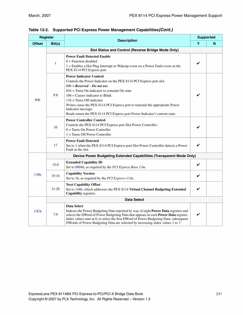
March, 2007 PEX 8114 PCI Express Power Management Support
ExpressLane PEX 8114BA PCI Express-to-PCI/PCI-X Bridge Data Book 231
Copyright © 2007 by PLX Technology, Inc. All Rights Reserved – Version 1.2
80h
Slot Status and Control (Reverse Bridge Mode Only)
1
Power Fault Detected Enable0 = Function disabled1 = Enables a Hot Plug Interrupt or Wakeup event on a Power Fault event on the PEX 8114 PCI Express port
✔
9:8
Power Indicator ControlControls the Power Indicator on the PEX 8114 PCI Express port slot.00b = Reserved – Do not use01b = Turns On indicator to constant On state10b = Causes indicator to Blink11b = Turns Off indicatorWrites cause the PEX 8114 PCI Express port to transmit the appropriate Power Indicator message.Reads return the PEX 8114 PCI Express port Power Indicator’s current state.
✔
10
Power Controller ControlControls the PEX 8114 PCI Express port Slot Power Controller:0 = Turns On Power Controller1 = Turns Off Power Controller
✔
17Power Fault DetectedSet to 1 when the PEX 8114 PCI Express port Slot Power Controller detects a Power Fault at the slot.
✔
138h
Device Power Budgeting Extended Capabilities (Transparent Mode Only)
15:0Extended Capability IDSet to 0004h, as required by the PCI Express Base 1.0a.
✔
19:16Capability VersionSet to 1h, as required by the PCI Express r1.0a.
✔
31:20Next Capability OffsetSet to 148h, which addresses the PEX 8114 Virtual Channel Budgeting Extended Capability registers.
✔
13Ch
Data Select
7:0
Data SelectIndexes the Power Budgeting Data reported by way of eight Power Data registers and selects the DWord of Power Budgeting Data that appears in each Power Data register. Index values start at 0, to select the first DWord of Power Budgeting Data; subsequent DWords of Power Budgeting Data are selected by increasing index values 1 to 7.
✔
Table 13-2. Supported PCI Express Power Management Capabilities(Cont.)
RegisterDescription
Supported
Offset Bit(s) Y N
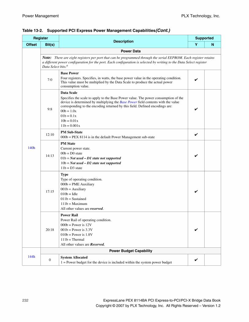
Power Management PLX Technology, Inc.
232 ExpressLane PEX 8114BA PCI Express-to-PCI/PCI-X Bridge Data Book
Copyright © 2007 by PLX Technology, Inc. All Rights Reserved – Version 1.2
140h
Power Data
Note: There are eight registers per port that can be programmed through the serial EEPROM. Each register retains a different power configuration for the port. Each configuration is selected by writing to the Data Select register Data Select bits.a
7:0
Base PowerFour registers. Specifies, in watts, the base power value in the operating condition. This value must be multiplied by the Data Scale to produce the actual power consumption value.
✔
9:8
Data Scale
Specifies the scale to apply to the Base Power value. The power consumption of the device is determined by multiplying the Base Power field contents with the value corresponding to the encoding returned by this field. Defined encodings are:00b = 1.0x01b = 0.1x10b = 0.01x11b = 0.001x
✔
12:10PM Sub-State000b = PEX 8114 is in the default Power Management sub-state
✔
14:13
PM StateCurrent power state.00b = D0 state01b = Not used – D1 state not supported10b = Not used – D2 state not supported11b = D3 state
✔
17:15
TypeType of operating condition.000b = PME Auxiliary001b = Auxiliary010b = Idle011b = Sustained111b = MaximumAll other values are reserved.
✔
20:18
Power RailPower Rail of operating condition.000b = Power is 12V001b = Power is 3.3V010b = Power is 1.8V111b = ThermalAll other values are Reserved.
✔
144h
Power Budget Capability
0System Allocated1 = Power budget for the device is included within the system power budget
✔
Table 13-2. Supported PCI Express Power Management Capabilities(Cont.)
RegisterDescription
Supported
Offset Bit(s) Y N
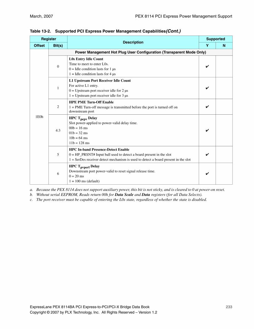
March, 2007 PEX 8114 PCI Express Power Management Support
ExpressLane PEX 8114BA PCI Express-to-PCI/PCI-X Bridge Data Book 233
Copyright © 2007 by PLX Technology, Inc. All Rights Reserved – Version 1.2
1E0h
Power Management Hot Plug User Configuration (Transparent Mode Only)
0
L0s Entry Idle CountTime to meet to enter L0s.0 = Idle condition lasts for 1 µs1 = Idle condition lasts for 4 µs
✔
1
L1 Upstream Port Receiver Idle CountFor active L1 entry.0 = Upstream port receiver idle for 2 µs1 = Upstream port receiver idle for 3 µs
✔
2HPE PME Turn-Off Enable1 = PME Turn-off message is transmitted before the port is turned off on downstream port
✔
4:3
HPC Tpepv DelaySlot power-applied to power-valid delay time.00b = 16 ms 01b = 32 ms 10b = 64 ms 11b = 128 ms
✔
5HPC In-band Presence-Detect Enable0 = HP_PRSNT# Input ball used to detect a board present in the slot1 = SerDes receiver detect mechanism is used to detect a board present in the slot
✔
6
HPC Tpvperl DelayDownstream port power-valid to reset signal release time.0 = 20 ms1 = 100 ms (default)
✔
a. Because the PEX 8114 does not support auxiliary power, this bit is not sticky, and is cleared to 0 at power-on reset.b. Without serial EEPROM, Reads return 00h for Data Scale and Data registers (for all Data Selects).c. The port receiver must be capable of entering the L0s state, regardless of whether the state is disabled.
Table 13-2. Supported PCI Express Power Management Capabilities(Cont.)
RegisterDescription
Supported
Offset Bit(s) Y N
Power Management PLX Technology, Inc.
234 ExpressLane PEX 8114BA PCI Express-to-PCI/PCI-X Bridge Data Book
Copyright © 2007 by PLX Technology, Inc. All Rights Reserved – Version 1.2
THIS PAGE INTENTIONALLY LEFT BLANK.
ExpressLane PEX 8114BA PCI Express-to-PCI/PCI-X Bridge Data Book 235
Copyright © 2007 by PLX Technology, Inc. All Rights Reserved – Version 1.2
Chapter 14 PEX 8114 Transparent Mode Registers
14.1 IntroductionThis chapter details the PEX 8114 Transparent mode registers, and presents the PEX 8114 user-programmable registers and the order in which they appear in the register map. Register descriptions,when applicable, include details regarding their use and meaning in Forward and Reverse Bridge modes.
NT mode registers are discussed in Chapter 16, “PEX 8114 Non-Transparent Mode PCI-X Registers,”and Chapter 17, “PEX 8114 Non-Transparent Mode PCI Express Registers.”
For further details regarding register names and descriptions, refer to the following specifications:
• PCI r2.3
• PCI r3.0
• PCI-to-PCI Bridge r1.1
• PCI Power Mgmt. r1.2
• PCI Express Base 1.0a
• PCI Express-to-PCI/PCI-X Bridge r1.0
• PCI-X r1.0b
• PCI-X r2.0a
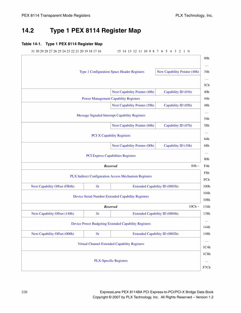
PEX 8114 Transparent Mode Registers PLX Technology, Inc.
236 ExpressLane PEX 8114BA PCI Express-to-PCI/PCI-X Bridge Data Book
Copyright © 2007 by PLX Technology, Inc. All Rights Reserved – Version 1.2
14.2 Type 1 PEX 8114 Register Map
Table 14-1. Type 1 PEX 8114 Register Map
31 30 29 28 27 26 25 24 23 22 21 20 19 18 17 16 15 14 13 12 11 10 9 8 7 6 5 4 3 2 1 0
00h
…
Type 1 Configuration Space Header Registers New Capability Pointer (40h) 34h
…
3Ch
Next Capability Pointer (48h) Capability ID (01h) 40h
Power Management Capability Registers 44h
Next Capability Pointer (58h) Capability ID (05h) 48h
Message Signaled Interrupt Capability Registers…
54h
Next Capability Pointer (68h) Capability ID (07h) 58h
PCI-X Capability Registers…
64h
Next Capability Pointer (00h) Capability ID (10h) 68h
PCI Express Capabilities Registers…
80h
Reserved 84h – F4h
PLX Indirect Configuration Access Mechanism RegistersF8h
FCh
Next Capability Offset (FB4h) 1h Extended Capability ID (0003h) 100h
Device Serial Number Extended Capability Registers104h
108h
Reserved 10Ch – 134h
Next Capability Offset (148h) 1h Extended Capability ID (0004h) 138h
Device Power Budgeting Extended Capability Registers…
144h
Next Capability Offset (000h) 1h Extended Capability ID (0002h) 148h
Virtual Channel Extended Capability Registers…
1C4h
PLX-Specific Registers
1C8h
…
F7Ch
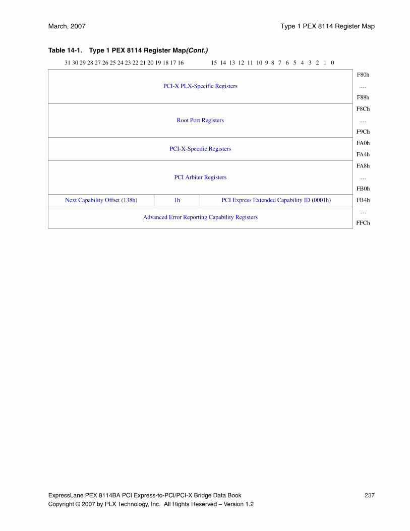
March, 2007 Type 1 PEX 8114 Register Map
ExpressLane PEX 8114BA PCI Express-to-PCI/PCI-X Bridge Data Book 237
Copyright © 2007 by PLX Technology, Inc. All Rights Reserved – Version 1.2
PCI-X PLX-Specific Registers
F80h
…
F88h
Root Port Registers
F8Ch
…
F9Ch
PCI-X-Specific RegistersFA0h
FA4h
PCI Arbiter Registers
FA8h
…
FB0h
Next Capability Offset (138h) 1h PCI Express Extended Capability ID (0001h) FB4h
Advanced Error Reporting Capability Registers…
FFCh
Table 14-1. Type 1 PEX 8114 Register Map(Cont.)
31 30 29 28 27 26 25 24 23 22 21 20 19 18 17 16 15 14 13 12 11 10 9 8 7 6 5 4 3 2 1 0
PEX 8114 Transparent Mode Registers PLX Technology, Inc.
238 ExpressLane PEX 8114BA PCI Express-to-PCI/PCI-X Bridge Data Book
Copyright © 2007 by PLX Technology, Inc. All Rights Reserved – Version 1.2
14.3 Register DescriptionsThe remainder of this chapter details the PEX 8114 registers, including:
• Bit/field names
• Register function in Forward and Reverse Bridge modes
• Type
• Whether the power-on/reset value can be modified by way of the PEX 8114 serial EEPROM initialization feature
• Initial power-on/reset (default) value
The register types are grouped by user accessibility. The types used in this device, and their descriptions,are delineated in Table 14-2.
Table 14-2. Register Types
Type Description
HwInit
Hardware Initialized Register or Register BitThe register bits are initialized by the PEX 8114 Hardware Initialization mechanism or PEX 8114 serial EEPROM register initialization feature. The register bits are Read-Only after initialization and can only be reset with “Power Good Reset” (PEX_PERST# assertion).
RCRead-Clear – Reading Register Clears Register ValueThe register bits generally indicate the tally of event occurrences. These registers are used for performance monitoring and, when read, are cleared to 0.
RO
Read-Only Register or Register BitThe register bits are Read-Only and cannot be altered by software. The register bits can be initialized by the PEX 8114 Hardware Initialization mechanism or PEX 8114 serial EEPROM register initialization feature.
R/WRead-Write Register or Register BitThe register bits are Read-Write and can be set or cleared by software to the needed state.
R/W1CRead-Only Status – Write 1 to Clear Status Register or Register BitThe register bits indicate status when read. A status bit set by the system to 1 to indicate status can be cleared by writing 1 to that bit.
R/W1CS
Read-Only Status – Write 1 to clear Status register or Register BitThe register bits indicate status when read. A status bit set by the system to 1 to indicate status can be cleared by writing 1 to that bit. Writing 0 has no effect.Bits are not initialized or modified by reset. Devices that consume AUX power preserve register values when AUX power consumption is enabled (by way of AUX power or PME Enable).
R/WS
Read-Write Register or BitThe register bits are Read-Write and can be set or cleared by software to the needed state. Bits are not initialized or modified by reset. Devices that consume AUX power preserve register values when AUX power consumption is enabled (by way of AUX power or PME Enable).
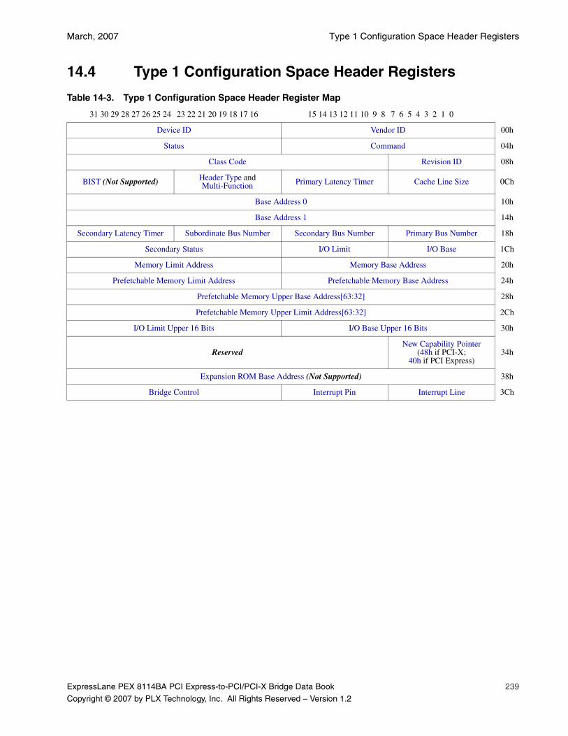
March, 2007 Type 1 Configuration Space Header Registers
ExpressLane PEX 8114BA PCI Express-to-PCI/PCI-X Bridge Data Book 239
Copyright © 2007 by PLX Technology, Inc. All Rights Reserved – Version 1.2
14.4 Type 1 Configuration Space Header Registers
Table 14-3. Type 1 Configuration Space Header Register Map
31 30 29 28 27 26 25 24 23 22 21 20 19 18 17 16 15 14 13 12 11 10 9 8 7 6 5 4 3 2 1 0
Device ID Vendor ID 00h
Status Command 04h
Class Code Revision ID 08h
BIST (Not Supported) Header Type and Multi-Function Primary Latency Timer Cache Line Size 0Ch
Base Address 0 10h
Base Address 1 14h
Secondary Latency Timer Subordinate Bus Number Secondary Bus Number Primary Bus Number 18h
Secondary Status I/O Limit I/O Base 1Ch
Memory Limit Address Memory Base Address 20h
Prefetchable Memory Limit Address Prefetchable Memory Base Address 24h
Prefetchable Memory Upper Base Address[63:32] 28h
Prefetchable Memory Upper Limit Address[63:32] 2Ch
I/O Limit Upper 16 Bits I/O Base Upper 16 Bits 30h
ReservedNew Capability Pointer
(48h if PCI-X; 40h if PCI Express)
34h
Expansion ROM Base Address (Not Supported) 38h
Bridge Control Interrupt Pin Interrupt Line 3Ch
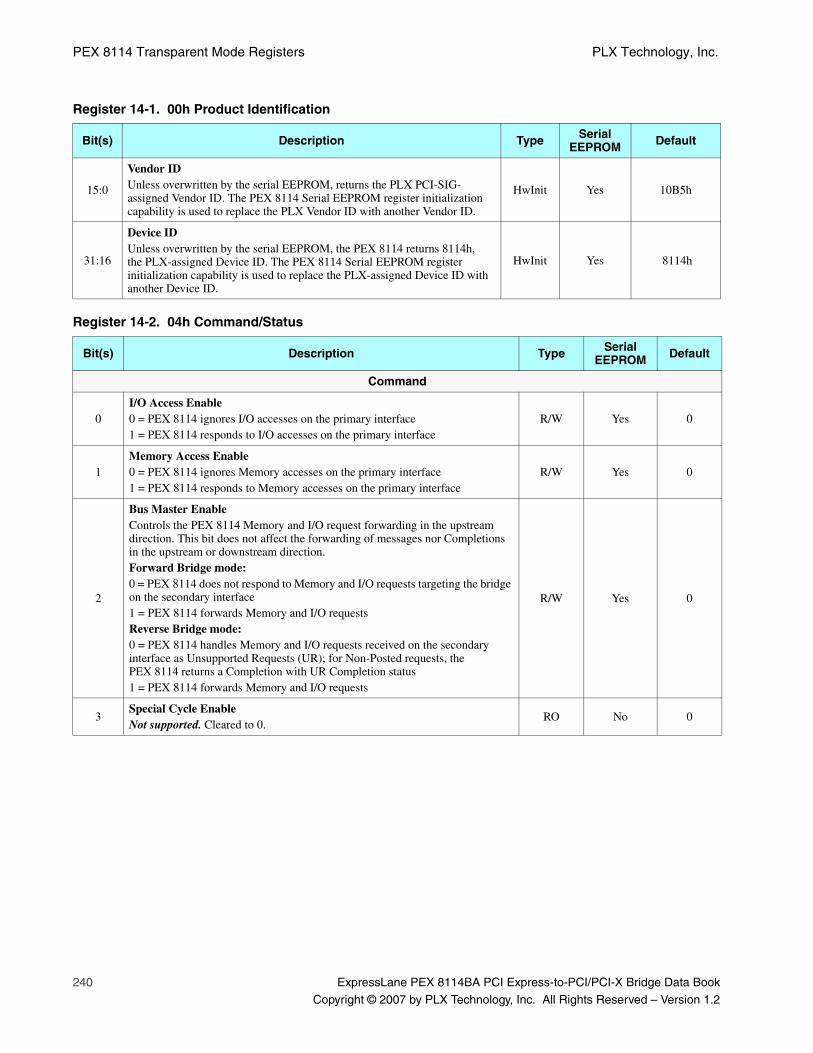
PEX 8114 Transparent Mode Registers PLX Technology, Inc.
240 ExpressLane PEX 8114BA PCI Express-to-PCI/PCI-X Bridge Data Book
Copyright © 2007 by PLX Technology, Inc. All Rights Reserved – Version 1.2
Register 14-1. 00h Product Identification
Bit(s) Description Type Serial EEPROM Default
15:0
Vendor IDUnless overwritten by the serial EEPROM, returns the PLX PCI-SIG- assigned Vendor ID. The PEX 8114 Serial EEPROM register initialization capability is used to replace the PLX Vendor ID with another Vendor ID.
HwInit Yes 10B5h
31:16
Device IDUnless overwritten by the serial EEPROM, the PEX 8114 returns 8114h, the PLX-assigned Device ID. The PEX 8114 Serial EEPROM register initialization capability is used to replace the PLX-assigned Device ID with another Device ID.
HwInit Yes 8114h
Register 14-2. 04h Command/Status
Bit(s) Description Type Serial EEPROM Default
Command
0I/O Access Enable0 = PEX 8114 ignores I/O accesses on the primary interface1 = PEX 8114 responds to I/O accesses on the primary interface
R/W Yes 0
1Memory Access Enable0 = PEX 8114 ignores Memory accesses on the primary interface1 = PEX 8114 responds to Memory accesses on the primary interface
R/W Yes 0
2
Bus Master EnableControls the PEX 8114 Memory and I/O request forwarding in the upstream direction. This bit does not affect the forwarding of messages nor Completions in the upstream or downstream direction.Forward Bridge mode:0 = PEX 8114 does not respond to Memory and I/O requests targeting the bridge on the secondary interface1 = PEX 8114 forwards Memory and I/O requestsReverse Bridge mode:0 = PEX 8114 handles Memory and I/O requests received on the secondary interface as Unsupported Requests (UR); for Non-Posted requests, the PEX 8114 returns a Completion with UR Completion status1 = PEX 8114 forwards Memory and I/O requests
R/W Yes 0
3Special Cycle EnableNot supported. Cleared to 0.
RO No 0
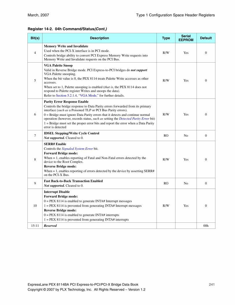
March, 2007 Type 1 Configuration Space Header Registers
ExpressLane PEX 8114BA PCI Express-to-PCI/PCI-X Bridge Data Book 241
Copyright © 2007 by PLX Technology, Inc. All Rights Reserved – Version 1.2
4
Memory Write and InvalidateUsed when the PCI-X interface is in PCI mode.Controls bridge ability to convert PCI Express Memory Write requests into Memory Write and Invalidate requests on the PCI Bus.
R/W Yes 0
5
VGA Palette SnoopValid in Reverse Bridge mode. PCI Express-to-PCI bridges do not support VGA Palette snooping.When the bit value is 0, the PEX 8114 treats Palette Write accesses as other accesses.When set to 1, Palette snooping is enabled (that is, the PEX 8114 does not respond to Palette register Writes and snoops the data).Refer to Section 5.2.1.4, “VGA Mode,” for further details.
R/W Yes 0
6
Parity Error Response EnableControls the bridge response to Data Parity errors forwarded from its primary interface (such as a Poisoned TLP or PCI Bus Parity errors). 0 = Bridge must ignore Data Parity errors that it detects and continue normal operation (however, records status, such as setting the Detected Parity Error bit)1 = Bridge must set the proper error bits and report the error when a Data Parity error is detected
R/W Yes 0
7IDSEL Stepping/Write Cycle ControlNot supported. Cleared to 0.
RO No 0
8
SERR# EnableControls the Signaled System Error bit.Forward Bridge mode:When = 1, enables reporting of Fatal and Non-Fatal errors detected by the device to the Root Complex. Reverse Bridge mode:When = 1, enables reporting of errors detected by the device by asserting SERR# on the PCI-X Bus.
R/W Yes 0
9Fast Back-to-Back Transaction EnabledNot supported. Cleared to 0.
RO No 0
10
Interrupt DisableForward Bridge mode:0 = PEX 8114 is enabled to generate INTA# Interrupt messages1 = PEX 8114 is prevented from generating INTA# Interrupt messagesReverse Bridge mode:0 = PEX 8114 is enabled to generate INTA# interrupts1 = PEX 8114 is prevented from generating INTA# interrupts
R/W Yes 0
15:11 Reserved 00h
Register 14-2. 04h Command/Status(Cont.)
Bit(s) Description Type Serial EEPROM Default

PEX 8114 Transparent Mode Registers PLX Technology, Inc.
242 ExpressLane PEX 8114BA PCI Express-to-PCI/PCI-X Bridge Data Book
Copyright © 2007 by PLX Technology, Inc. All Rights Reserved – Version 1.2
Status
18:16 Reserved 000b
19
Interrupt StatusIndicates that an INTx# interrupt message is pending on behalf of sources internal to the bridge. This bit does not reflect the PCI_INTx# input status associated with the secondary interface.0 = No INTA# Interrupt message is pending1 = INTA# Interrupt message is pending internally
RO No 0
20Capabilities ListRequired by the PCI Express Base 1.0a as 1 at all times.
RO No 1
21
66-MHz CapableForward Bridge mode:Cleared to 0, as required by the PCI Express Base 1.0a.Reverse Bridge mode:PCI-X interface is capable of 66-MHz operation; therefore, this bit is set to 1.
RO/FwdRO/Rev
No01
22 Reserved 0
23
Fast Back-to-Back Transaction CapableForward Bridge mode:Cleared to 0, as required by the PCI Express Base 1.0a.Reverse Bridge mode:Set to 1, indicating Fast Back-to-Back Transaction capability.
RO/FwdRO/Rev
No01
Register 14-2. 04h Command/Status(Cont.)
Bit(s) Description Type Serial EEPROM Default

March, 2007 Type 1 Configuration Space Header Registers
ExpressLane PEX 8114BA PCI Express-to-PCI/PCI-X Bridge Data Book 243
Copyright © 2007 by PLX Technology, Inc. All Rights Reserved – Version 1.2
24
Master Data Parity ErrorReports Data Parity error detection by the bridge on the primary interface. Set to 1 if the Command register Parity Error Response Enable bit is set and one of the following conditions occur.Forward Bridge mode:
• Bridge receives a Completion marked poisoned on the primary interface
• Bridge poisons a Write request on the primary interface
Reverse Bridge mode:• Bridge, as a bus Master on the primary interface, asserts PCI_PERR# on
a Read transaction or detects PCI_PERR# asserted on a Write transaction
• Bridge receives a Completion or Split Completion with a Parity error on the secondary interface
• Bridge receives a Split Completion message for a Non-Posted Write on the primary interface, indicating an Uncorrectable (Split) Write Data error
R/W1C Yes 0
26:25
DEVSEL TimingForward Bridge mode:Cleared to 00b, as required by the PCI Express Base 1.0a.Reverse Bridge mode:Pertain to PCI and PCI-X modes. Encode PCI_DEVSEL# timing. For the PEX 8114, the field is set to 10b, indicating slow speed.
RO/FwdRO/Rev
NoNo
00b10b
27
Signaled Target AbortForward Bridge mode:When a Memory-Mapped access Payload Length is greater than 1 DWord, the PEX 8114 sets this bit to 1. Also set to 1 when the bridge completes a request as a Transaction Target on its primary interface using Completer Abort Completion status.Reverse Bridge mode:When the PCI-X interface signals Target Abort, the PEX 8114 sets this bit to 1.
R/W1C Yes 0
Register 14-2. 04h Command/Status(Cont.)
Bit(s) Description Type Serial EEPROM Default

PEX 8114 Transparent Mode Registers PLX Technology, Inc.
244 ExpressLane PEX 8114BA PCI Express-to-PCI/PCI-X Bridge Data Book
Copyright © 2007 by PLX Technology, Inc. All Rights Reserved – Version 1.2
28
Received Target AbortForward Bridge mode:Set to 1 when the bridge receives a Completion with Completer Abort Completion status.Reverse Bridge mode:Set to 1 when the bridge is the transaction Master terminated with a Target Abort or PCI-X Split Completion message indicating that a Target Abort was received.
R/W1C Yes 0
29
Received Master AbortForward Bridge mode:Set to 1 when the bridge receives a Completion with Unsupported Request Completion status.Reverse Bridge mode:Set to 1 when the bridge is the transaction Master terminated by the bridge with Master Abort status.
R/W1C Yes 0
30
Signaled System ErrorForward Bridge mode:Set to 1 when the bridge transmits an ERR_FATAL or ERR_NONFATAL message to the Root Complex.Reverse Bridge mode:Set to 1 when the bridge asserts SERR# on the PCI-X Bus.
R/W1C Yes 0
31
Detected Parity ErrorForward Bridge mode:Set to 1 by the bridge when it receives a Poisoned TLP or TLP with bad ECRC (Read Completion or Write Request) on the primary interface, regardless of the Command register Parity Error Response Enable bit state. Reverse Bridge mode:Reports detection of an Address or Data Parity error by the bridge on its primary interface. Must be set to 1, regardless of the Command register Parity Error Response Enable bit state, when any of the following three conditions is true:
• Detects an Address or Attribute Parity error as a potential Target
• Detects a Data Parity error when the Target of a Write transaction or PCI-X Split Completion
• Detects a Data Parity error when the Master of a Read transaction (Immediate Read data or PCI-X Split Response)
R/W1C Yes 0
Register 14-2. 04h Command/Status(Cont.)
Bit(s) Description Type Serial EEPROM Default
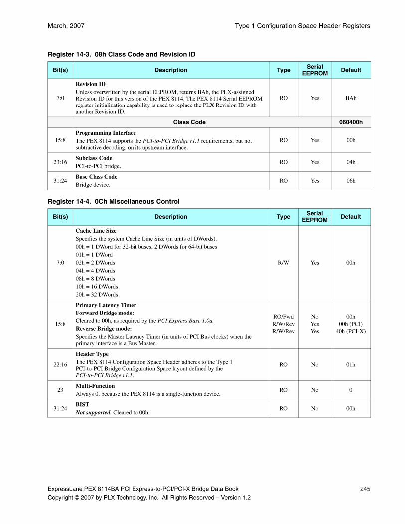
March, 2007 Type 1 Configuration Space Header Registers
ExpressLane PEX 8114BA PCI Express-to-PCI/PCI-X Bridge Data Book 245
Copyright © 2007 by PLX Technology, Inc. All Rights Reserved – Version 1.2
Register 14-3. 08h Class Code and Revision ID
Bit(s) Description Type Serial EEPROM Default
7:0
Revision IDUnless overwritten by the serial EEPROM, returns BAh, the PLX-assigned Revision ID for this version of the PEX 8114. The PEX 8114 Serial EEPROM register initialization capability is used to replace the PLX Revision ID with another Revision ID.
RO Yes BAh
Class Code 060400h
15:8Programming InterfaceThe PEX 8114 supports the PCI-to-PCI Bridge r1.1 requirements, but not subtractive decoding, on its upstream interface.
RO Yes 00h
23:16Subclass CodePCI-to-PCI bridge.
RO Yes 04h
31:24Base Class CodeBridge device.
RO Yes 06h
Register 14-4. 0Ch Miscellaneous Control
Bit(s) Description Type Serial EEPROM Default
7:0
Cache Line SizeSpecifies the system Cache Line Size (in units of DWords).00h = 1 DWord for 32-bit buses, 2 DWords for 64-bit buses01h = 1 DWord02h = 2 DWords04h = 4 DWords08h = 8 DWords10h = 16 DWords20h = 32 DWords
R/W Yes 00h
15:8
Primary Latency Timer Forward Bridge mode:Cleared to 00h, as required by the PCI Express Base 1.0a.Reverse Bridge mode:Specifies the Master Latency Timer (in units of PCI Bus clocks) when the primary interface is a Bus Master.
RO/FwdR/W/RevR/W/Rev
NoYesYes
00h00h (PCI)
40h (PCI-X)
22:16
Header TypeThe PEX 8114 Configuration Space Header adheres to the Type 1 PCI-to-PCI Bridge Configuration Space layout defined by the PCI-to-PCI Bridge r1.1.
RO No 01h
23Multi-FunctionAlways 0, because the PEX 8114 is a single-function device.
RO No 0
31:24BISTNot supported. Cleared to 00h.
RO No 00h
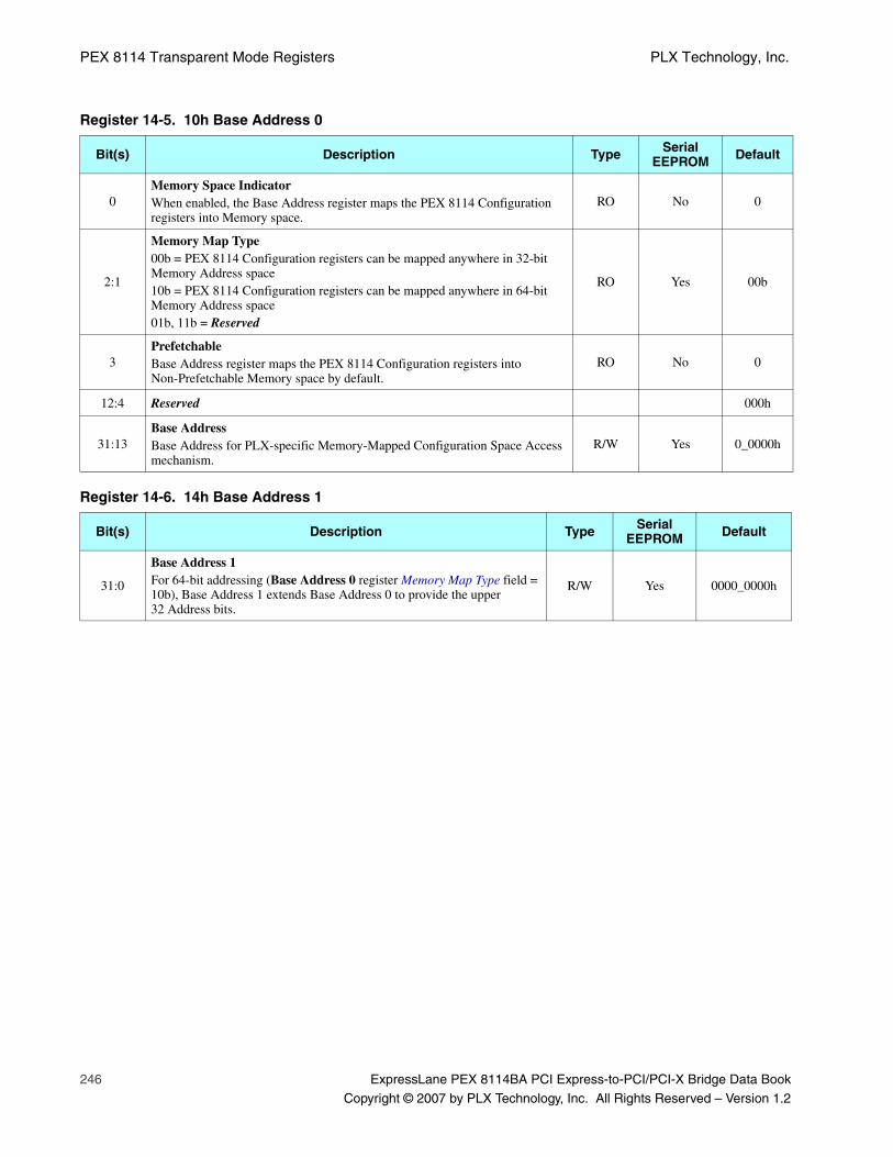
PEX 8114 Transparent Mode Registers PLX Technology, Inc.
246 ExpressLane PEX 8114BA PCI Express-to-PCI/PCI-X Bridge Data Book
Copyright © 2007 by PLX Technology, Inc. All Rights Reserved – Version 1.2
Register 14-5. 10h Base Address 0
Bit(s) Description Type Serial EEPROM Default
0Memory Space IndicatorWhen enabled, the Base Address register maps the PEX 8114 Configuration registers into Memory space.
RO No 0
2:1
Memory Map Type00b = PEX 8114 Configuration registers can be mapped anywhere in 32-bit Memory Address space10b = PEX 8114 Configuration registers can be mapped anywhere in 64-bit Memory Address space01b, 11b = Reserved
RO Yes 00b
3PrefetchableBase Address register maps the PEX 8114 Configuration registers into Non-Prefetchable Memory space by default.
RO No 0
12:4 Reserved 000h
31:13Base AddressBase Address for PLX-specific Memory-Mapped Configuration Space Access mechanism.
R/W Yes 0_0000h
Register 14-6. 14h Base Address 1
Bit(s) Description Type Serial EEPROM Default
31:0
Base Address 1For 64-bit addressing (Base Address 0 register Memory Map Type field = 10b), Base Address 1 extends Base Address 0 to provide the upper 32 Address bits.
R/W Yes 0000_0000h
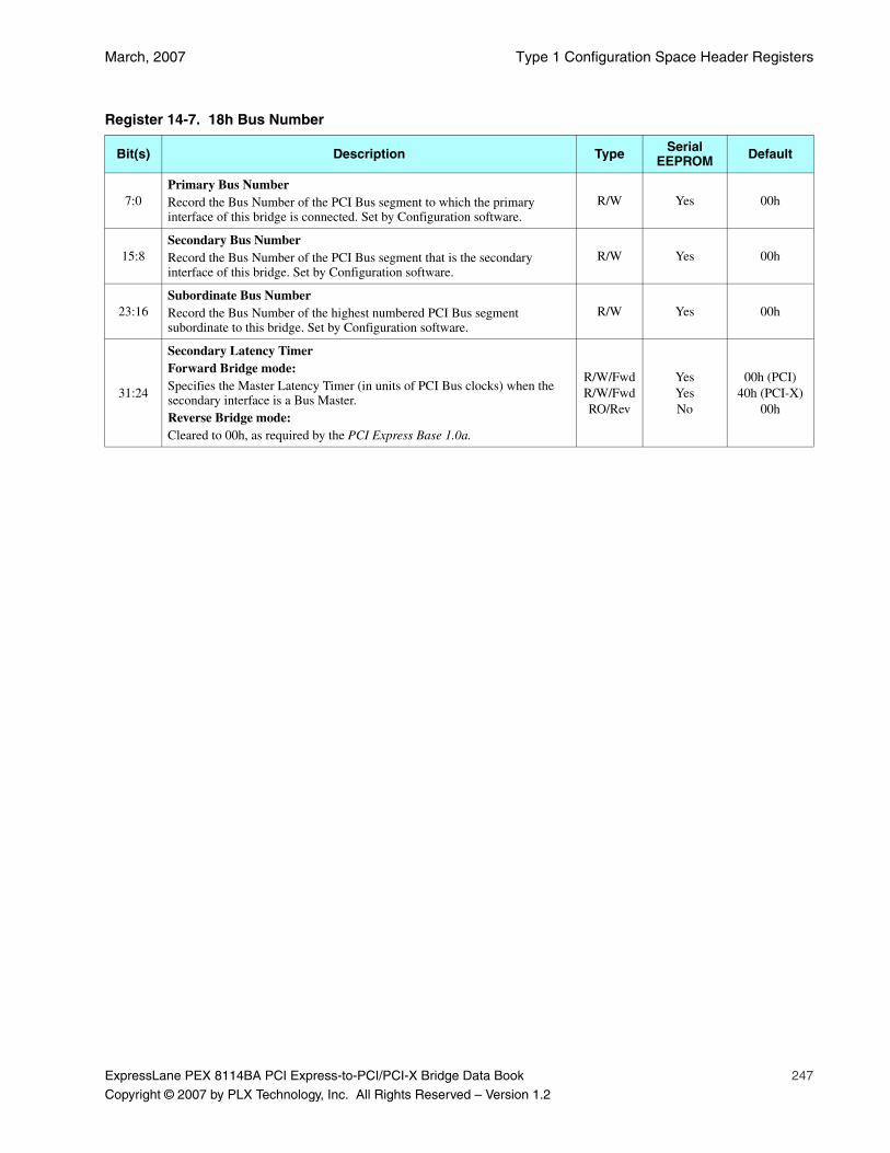
March, 2007 Type 1 Configuration Space Header Registers
ExpressLane PEX 8114BA PCI Express-to-PCI/PCI-X Bridge Data Book 247
Copyright © 2007 by PLX Technology, Inc. All Rights Reserved – Version 1.2
Register 14-7. 18h Bus Number
Bit(s) Description Type Serial EEPROM Default
7:0Primary Bus NumberRecord the Bus Number of the PCI Bus segment to which the primary interface of this bridge is connected. Set by Configuration software.
R/W Yes 00h
15:8Secondary Bus NumberRecord the Bus Number of the PCI Bus segment that is the secondary interface of this bridge. Set by Configuration software.
R/W Yes 00h
23:16Subordinate Bus NumberRecord the Bus Number of the highest numbered PCI Bus segment subordinate to this bridge. Set by Configuration software.
R/W Yes 00h
31:24
Secondary Latency TimerForward Bridge mode:Specifies the Master Latency Timer (in units of PCI Bus clocks) when the secondary interface is a Bus Master.Reverse Bridge mode:Cleared to 00h, as required by the PCI Express Base 1.0a.
R/W/FwdR/W/FwdRO/Rev
YesYesNo
00h (PCI)40h (PCI-X)
00h
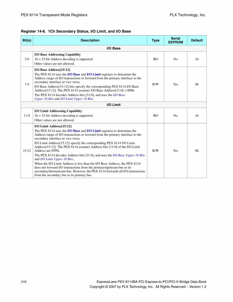
PEX 8114 Transparent Mode Registers PLX Technology, Inc.
248 ExpressLane PEX 8114BA PCI Express-to-PCI/PCI-X Bridge Data Book
Copyright © 2007 by PLX Technology, Inc. All Rights Reserved – Version 1.2
Register 14-8. 1Ch Secondary Status, I/O Limit, and I/O Base
Bit(s) Description Type Serial EEPROM Default
I/O Base
3:0I/O Base Addressing Capability1h = 32-bit Address decoding is supportedOther values are not allowed.
RO No 1h
7:4
I/O Base Address[15:12]The PEX 8114 uses the I/O Base and I/O Limit registers to determine the Address range of I/O transactions to forward from the primary interface to the secondary interface or vice versa.I/O Base Address[15:12] bits specify the corresponding PEX 8114 I/O Base Address[15:12]. The PEX 8114 assumes I/O Base Address[11:0] = 000h.The PEX 8114 decodes Address bits [31:0], and uses the I/O Base Upper 16 Bits and I/O Limit Upper 16 Bits.
R/W Yes 0h
I/O Limit
11:8I/O Limit Addressing Capability1h = 32-bit Address decoding is supportedOther values are not allowed.
RO No 1h
15:12
I/O Limit Address[15:12]The PEX 8114 uses the I/O Base and I/O Limit registers to determine the Address range of I/O transactions to forward from the primary interface to the secondary interface or vice versa.I/O Limit Address[15:12] specify the corresponding PEX 8114 I/O Limit Address[15:12]. The PEX 8114 assumes Address bits [11:0] of the I/O Limit Address are FFFh. The PEX 8114 decodes Address bits [31:0], and uses the I/O Base Upper 16 Bits and I/O Limit Upper 16 Bits.When the I/O Limit Address is less than the I/O Base Address, the PEX 8114 does not forward I/O transactions from the primary/upstream bus to its secondary/downstream bus. However, the PEX 8114 forwards all I/O transactions from the secondary bus to its primary bus.
R/W Yes 0h
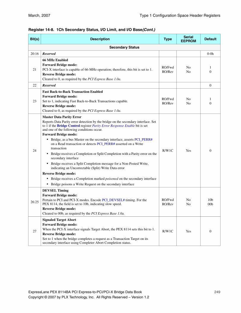
March, 2007 Type 1 Configuration Space Header Registers
ExpressLane PEX 8114BA PCI Express-to-PCI/PCI-X Bridge Data Book 249
Copyright © 2007 by PLX Technology, Inc. All Rights Reserved – Version 1.2
Secondary Status
20:16 Reserved 0-0h
21
66 MHz EnabledForward Bridge mode:PCI-X interface is capable of 66-MHz operation; therefore, this bit is set to 1.Reverse Bridge mode:Cleared to 0, as required by the PCI Express Base 1.0a.
RO/FwdRO/Rev
NoNo
10
22 Reserved 0
23
Fast Back-to-Back Transaction EnabledForward Bridge mode:Set to 1, indicating Fast Back-to-Back Transactions capable.Reverse Bridge mode:Cleared to 0, as required by the PCI Express Base 1.0a.
RO/FwdRO/Rev
NoNo
10
24
Master Data Parity ErrorReports Data Parity error detection by the bridge on the secondary interface. Set to 1 if the Bridge Control register Parity Error Response Enable bit is set and one of the following conditions occur.Forward Bridge mode:
• Bridge, as a bus Master on the secondary interface, asserts PCI_PERR# on a Read transaction or detects PCI_PERR# asserted on a Write transaction
• Bridge receives a Completion or Split Completion with a Parity error on the secondary interface
• Bridge receives a Split Completion message for a Non-Posted Write, indicating an Uncorrectable (Split) Write Data error
Reverse Bridge mode:• Bridge receives a Completion marked poisoned on the secondary interface
• Bridge poisons a Write Request on the secondary interface
R/W1C Yes 0
26:25
DEVSEL TimingForward Bridge mode:Pertain to PCI and PCI-X modes. Encode PCI_DEVSEL# timing. For the PEX 8114, the field is set to 10b, indicating slow speed.Reverse Bridge mode:Cleared to 00b, as required by the PCI Express Base 1.0a.
RO/FwdRO/Rev
NoNo
10b00b
27
Signaled Target AbortForward Bridge mode:When the PCI-X interface signals Target Abort, the PEX 8114 sets this bit to 1.Reverse Bridge mode:Set to 1 when the bridge completes a request as a Transaction Target on its secondary interface using Completer Abort Completion status.
R/W1C Yes 0
Register 14-8. 1Ch Secondary Status, I/O Limit, and I/O Base(Cont.)
Bit(s) Description Type Serial EEPROM Default
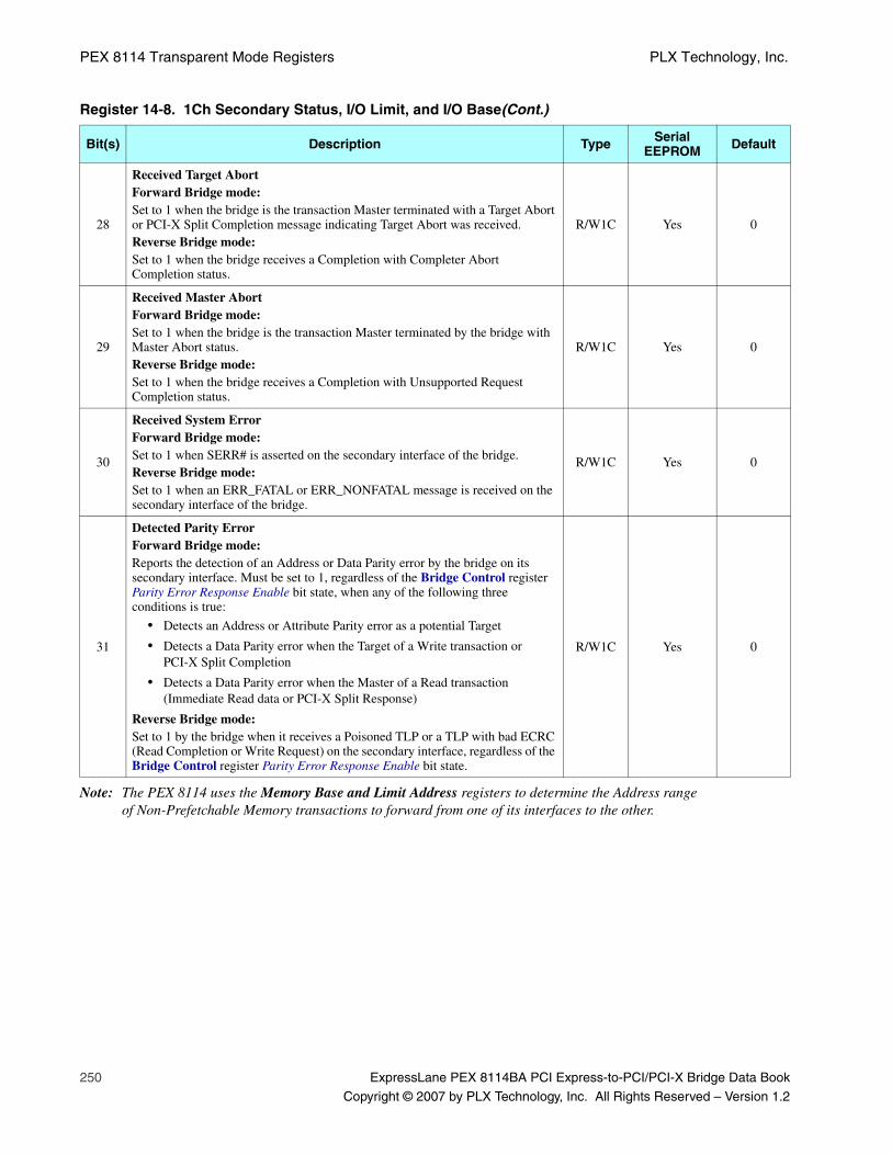
PEX 8114 Transparent Mode Registers PLX Technology, Inc.
250 ExpressLane PEX 8114BA PCI Express-to-PCI/PCI-X Bridge Data Book
Copyright © 2007 by PLX Technology, Inc. All Rights Reserved – Version 1.2
Note: The PEX 8114 uses the Memory Base and Limit Address registers to determine the Address range of Non-Prefetchable Memory transactions to forward from one of its interfaces to the other.
28
Received Target AbortForward Bridge mode: Set to 1 when the bridge is the transaction Master terminated with a Target Abort or PCI-X Split Completion message indicating Target Abort was received.Reverse Bridge mode:Set to 1 when the bridge receives a Completion with Completer Abort Completion status.
R/W1C Yes 0
29
Received Master AbortForward Bridge mode:Set to 1 when the bridge is the transaction Master terminated by the bridge with Master Abort status.Reverse Bridge mode:Set to 1 when the bridge receives a Completion with Unsupported Request Completion status.
R/W1C Yes 0
30
Received System Error Forward Bridge mode:Set to 1 when SERR# is asserted on the secondary interface of the bridge.Reverse Bridge mode:Set to 1 when an ERR_FATAL or ERR_NONFATAL message is received on the secondary interface of the bridge.
R/W1C Yes 0
31
Detected Parity ErrorForward Bridge mode:Reports the detection of an Address or Data Parity error by the bridge on its secondary interface. Must be set to 1, regardless of the Bridge Control register Parity Error Response Enable bit state, when any of the following three conditions is true:
• Detects an Address or Attribute Parity error as a potential Target
• Detects a Data Parity error when the Target of a Write transaction or PCI-X Split Completion
• Detects a Data Parity error when the Master of a Read transaction (Immediate Read data or PCI-X Split Response)
Reverse Bridge mode:Set to 1 by the bridge when it receives a Poisoned TLP or a TLP with bad ECRC (Read Completion or Write Request) on the secondary interface, regardless of the Bridge Control register Parity Error Response Enable bit state.
R/W1C Yes 0
Register 14-8. 1Ch Secondary Status, I/O Limit, and I/O Base(Cont.)
Bit(s) Description Type Serial EEPROM Default
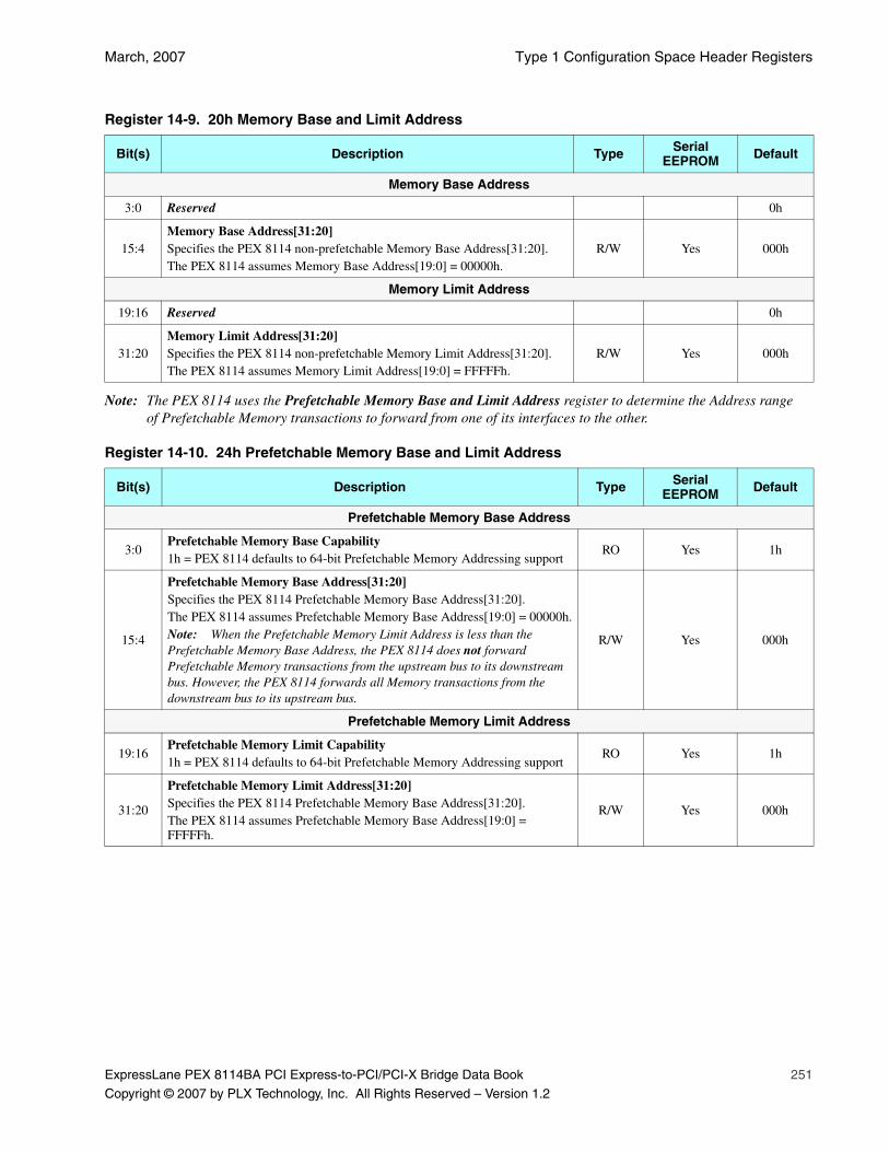
March, 2007 Type 1 Configuration Space Header Registers
ExpressLane PEX 8114BA PCI Express-to-PCI/PCI-X Bridge Data Book 251
Copyright © 2007 by PLX Technology, Inc. All Rights Reserved – Version 1.2
Note: The PEX 8114 uses the Prefetchable Memory Base and Limit Address register to determine the Address range of Prefetchable Memory transactions to forward from one of its interfaces to the other.
Register 14-9. 20h Memory Base and Limit Address
Bit(s) Description Type Serial EEPROM Default
Memory Base Address
3:0 Reserved 0h
15:4Memory Base Address[31:20]Specifies the PEX 8114 non-prefetchable Memory Base Address[31:20].The PEX 8114 assumes Memory Base Address[19:0] = 00000h.
R/W Yes 000h
Memory Limit Address
19:16 Reserved 0h
31:20Memory Limit Address[31:20]Specifies the PEX 8114 non-prefetchable Memory Limit Address[31:20].The PEX 8114 assumes Memory Limit Address[19:0] = FFFFFh.
R/W Yes 000h
Register 14-10. 24h Prefetchable Memory Base and Limit Address
Bit(s) Description Type Serial EEPROM Default
Prefetchable Memory Base Address
3:0Prefetchable Memory Base Capability1h = PEX 8114 defaults to 64-bit Prefetchable Memory Addressing support
RO Yes 1h
15:4
Prefetchable Memory Base Address[31:20]Specifies the PEX 8114 Prefetchable Memory Base Address[31:20].The PEX 8114 assumes Prefetchable Memory Base Address[19:0] = 00000h.Note: When the Prefetchable Memory Limit Address is less than the Prefetchable Memory Base Address, the PEX 8114 does not forward Prefetchable Memory transactions from the upstream bus to its downstream bus. However, the PEX 8114 forwards all Memory transactions from the downstream bus to its upstream bus.
R/W Yes 000h
Prefetchable Memory Limit Address
19:16Prefetchable Memory Limit Capability1h = PEX 8114 defaults to 64-bit Prefetchable Memory Addressing support
RO Yes 1h
31:20
Prefetchable Memory Limit Address[31:20]Specifies the PEX 8114 Prefetchable Memory Base Address[31:20].The PEX 8114 assumes Prefetchable Memory Base Address[19:0] = FFFFFh.
R/W Yes 000h
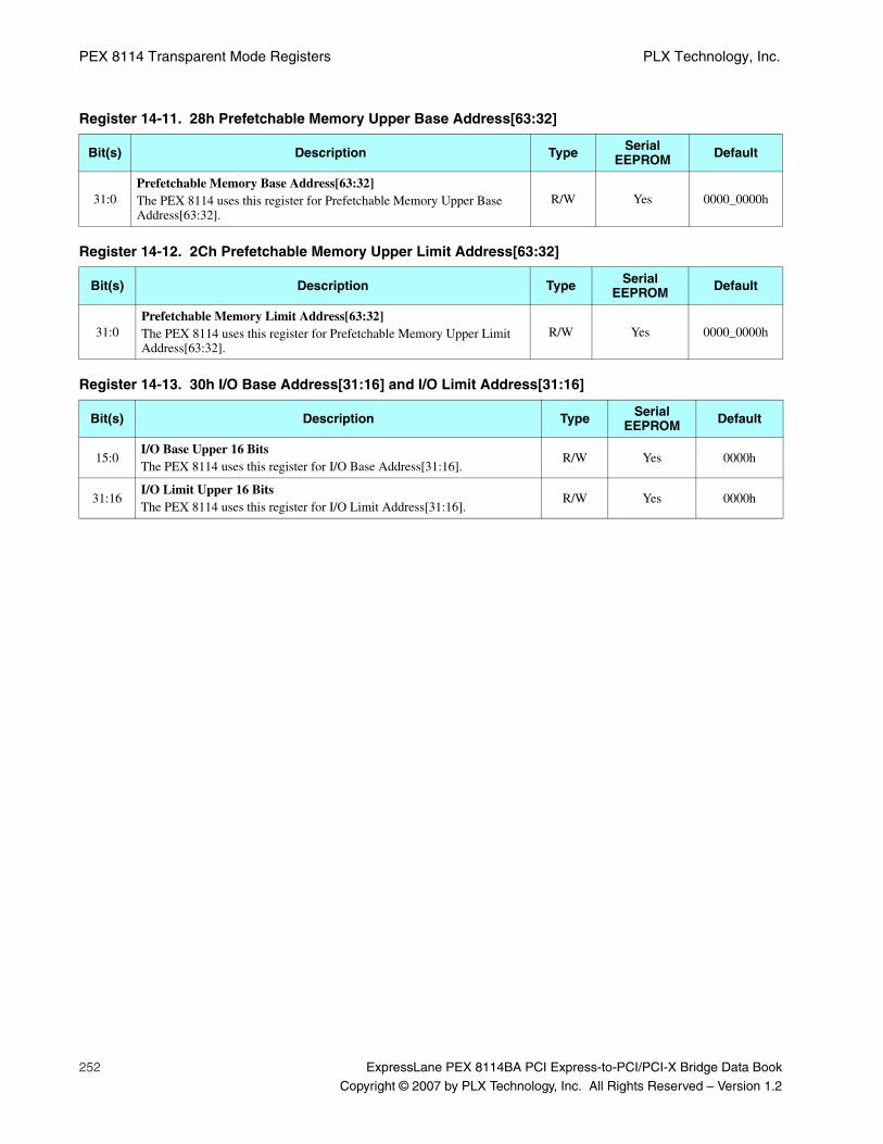
PEX 8114 Transparent Mode Registers PLX Technology, Inc.
252 ExpressLane PEX 8114BA PCI Express-to-PCI/PCI-X Bridge Data Book
Copyright © 2007 by PLX Technology, Inc. All Rights Reserved – Version 1.2
Register 14-11. 28h Prefetchable Memory Upper Base Address[63:32]
Bit(s) Description Type Serial EEPROM Default
31:0Prefetchable Memory Base Address[63:32]The PEX 8114 uses this register for Prefetchable Memory Upper Base Address[63:32].
R/W Yes 0000_0000h
Register 14-12. 2Ch Prefetchable Memory Upper Limit Address[63:32]
Bit(s) Description Type Serial EEPROM Default
31:0Prefetchable Memory Limit Address[63:32]The PEX 8114 uses this register for Prefetchable Memory Upper Limit Address[63:32].
R/W Yes 0000_0000h
Register 14-13. 30h I/O Base Address[31:16] and I/O Limit Address[31:16]
Bit(s) Description Type Serial EEPROM Default
15:0I/O Base Upper 16 BitsThe PEX 8114 uses this register for I/O Base Address[31:16].
R/W Yes 0000h
31:16I/O Limit Upper 16 BitsThe PEX 8114 uses this register for I/O Limit Address[31:16].
R/W Yes 0000h
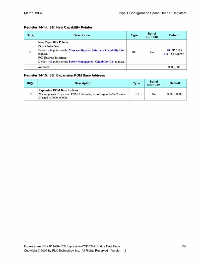
March, 2007 Type 1 Configuration Space Header Registers
ExpressLane PEX 8114BA PCI Express-to-PCI/PCI-X Bridge Data Book 253
Copyright © 2007 by PLX Technology, Inc. All Rights Reserved – Version 1.2
Register 14-14. 34h New Capability Pointer
Bit(s) Description Type Serial EEPROM Default
7:0
New Capability PointerPCI-X interface:Default 48h points to the Message Signaled Interrupt Capability List register.PCI Express interface:Default 40h points to the Power Management Capability List register.
RO No48h (PCI-X)
40h (PCI Express)
31:8 Reserved 0000_00h
Register 14-15. 38h Expansion ROM Base Address
Bit(s) Description Type Serial EEPROM Default
31:0Expansion ROM Base AddressNot supported. Expansion ROM Addressing is not supported in T mode. Cleared to 0000_0000h.
RO No 0000_0000h

PEX 8114 Transparent Mode Registers PLX Technology, Inc.
254 ExpressLane PEX 8114BA PCI Express-to-PCI/PCI-X Bridge Data Book
Copyright © 2007 by PLX Technology, Inc. All Rights Reserved – Version 1.2
Register 14-16. 3Ch Bridge Control and Interrupt Signal
Bit(s) Description Type Serial EEPROM Default
7:0Interrupt LineThe PEX 8114 does not use this register, but provides it for operating system and device driver use.
R/W Yes 00h
15:8Interrupt PinIdentifies the Conventional PCI Interrupt message that the PEX 8114 uses.01h maps to Conventional PCI INTA# Interrupt message.
RO No 01h
Bridge Control
16
Parity Error Response EnableControls bridge response to Address and Data Parity errors on the secondary interface. If this bit is set, the bridge must detect and report Parity errors on the secondary interface. If cleared, the bridge must ignore Parity errors that it detects on the secondary interface and continue normal operation. A bridge must generate parity, although Parity Error reporting is disabled.
R/W Yes 0
17
SERR# EnableForward Bridge mode:Controls forwarding of secondary interface SERR# assertions to the primary interface. The bridge transmits an ERR_FATAL or ERR_NONFATAL cycle on the primary interface when all of the following conditions are true:
• SERR# is asserted on the secondary interface
• This bit is set
• Command register SERR# Enable bit is set
Reverse Bridge mode:Controls forwarding of ERR_FATAL and ERR_NONFATAL from the secondary interface to the primary interface by asserting SERR# when all the following conditions are true.
• ERR_FATAL or ERR_NONFATAL is received on the secondary interface
• This bit is set
• Command register SERR# Enable bit is set
When set to 1, and the Command register SERR# Enable bit value is 1, enables the Signaled System Error bit.
R/W Yes 0
18ISA EnableRefer to Section 5.2.1.3, “ISA Mode,” for details.
R/W Yes 0
19VGA EnableRefer to Section 5.2.1.4, “VGA Mode,” and the PCI r3.0 for details.
R/W Yes 0
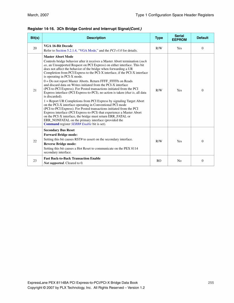
March, 2007 Type 1 Configuration Space Header Registers
ExpressLane PEX 8114BA PCI Express-to-PCI/PCI-X Bridge Data Book 255
Copyright © 2007 by PLX Technology, Inc. All Rights Reserved – Version 1.2
20VGA 16-Bit DecodeRefer to Section 5.2.1.4, “VGA Mode,” and the PCI r3.0 for details.
R/W Yes 0
21
Master Abort ModeControls bridge behavior after it receives a Master Abort termination (such as, an Unsupported Request on PCI Express) on either interface. This bit does not affect the behavior of the bridge when forwarding a UR Completion from PCI Express to the PCI-X interface, if the PCI-X interface is operating in PCI-X mode.0 = Do not report Master Aborts. Return FFFF_FFFFh on Reads and discard data on Writes initiated from the PCI-X interface (PCI-to-PCI Express). For Posted transactions initiated from the PCI Express interface (PCI Express-to-PCI), no action is taken (that is, all data is discarded).1 = Report UR Completions from PCI Express by signaling Target Abort on the PCI-X interface operating in Conventional PCI mode (PCI-to-PCI Express). For Posted transactions initiated from the PCI Express interface (PCI Express-to-PCI) that experience a Master Abort on the PCI-X interface, the bridge must return ERR_FATAL or ERR_NONFATAL on the primary interface (provided the Command register SERR# Enable bit is set).
R/W Yes 0
22
Secondary Bus ResetForward Bridge mode:Setting this bit causes RST# to assert on the secondary interface.Reverse Bridge mode:Setting this bit causes a Hot Reset to communicate on the PEX 8114 secondary interface.
R/W Yes 0
23Fast Back-to-Back Transaction EnableNot supported. Cleared to 0.
RO No 0
Register 14-16. 3Ch Bridge Control and Interrupt Signal(Cont.)
Bit(s) Description Type Serial EEPROM Default
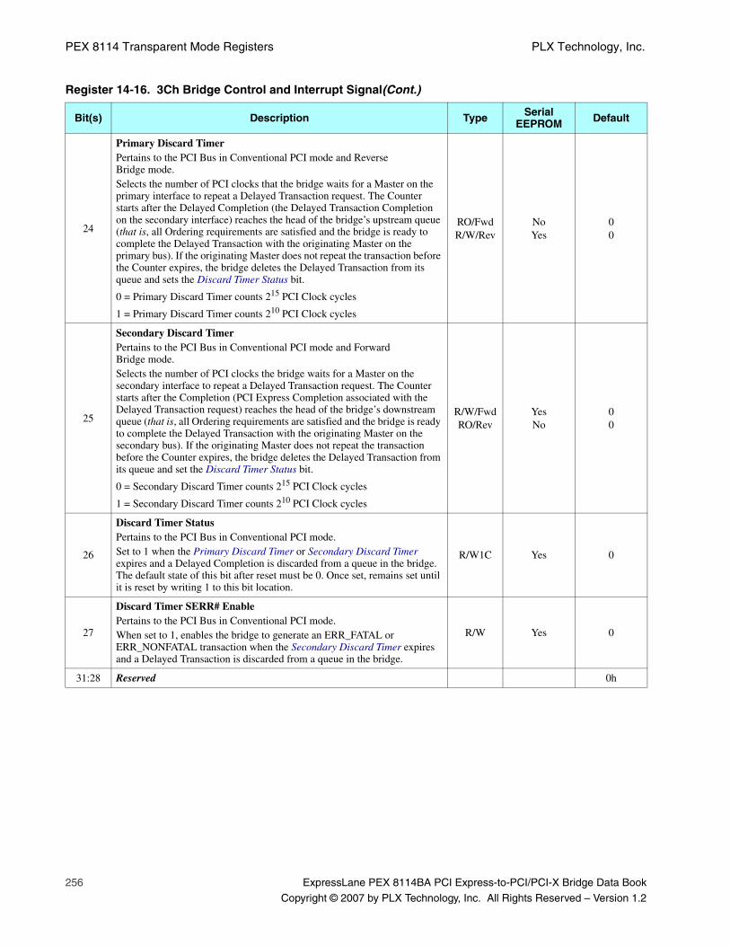
PEX 8114 Transparent Mode Registers PLX Technology, Inc.
256 ExpressLane PEX 8114BA PCI Express-to-PCI/PCI-X Bridge Data Book
Copyright © 2007 by PLX Technology, Inc. All Rights Reserved – Version 1.2
24
Primary Discard TimerPertains to the PCI Bus in Conventional PCI mode and Reverse Bridge mode.Selects the number of PCI clocks that the bridge waits for a Master on the primary interface to repeat a Delayed Transaction request. The Counter starts after the Delayed Completion (the Delayed Transaction Completion on the secondary interface) reaches the head of the bridge’s upstream queue (that is, all Ordering requirements are satisfied and the bridge is ready to complete the Delayed Transaction with the originating Master on the primary bus). If the originating Master does not repeat the transaction before the Counter expires, the bridge deletes the Delayed Transaction from its queue and sets the Discard Timer Status bit.
0 = Primary Discard Timer counts 215 PCI Clock cycles
1 = Primary Discard Timer counts 210 PCI Clock cycles
RO/FwdR/W/Rev
NoYes
00
25
Secondary Discard TimerPertains to the PCI Bus in Conventional PCI mode and Forward Bridge mode.Selects the number of PCI clocks the bridge waits for a Master on the secondary interface to repeat a Delayed Transaction request. The Counter starts after the Completion (PCI Express Completion associated with the Delayed Transaction request) reaches the head of the bridge’s downstream queue (that is, all Ordering requirements are satisfied and the bridge is ready to complete the Delayed Transaction with the originating Master on the secondary bus). If the originating Master does not repeat the transaction before the Counter expires, the bridge deletes the Delayed Transaction from its queue and set the Discard Timer Status bit.
0 = Secondary Discard Timer counts 215 PCI Clock cycles
1 = Secondary Discard Timer counts 210 PCI Clock cycles
R/W/FwdRO/Rev
YesNo
00
26
Discard Timer StatusPertains to the PCI Bus in Conventional PCI mode.Set to 1 when the Primary Discard Timer or Secondary Discard Timer expires and a Delayed Completion is discarded from a queue in the bridge. The default state of this bit after reset must be 0. Once set, remains set until it is reset by writing 1 to this bit location.
R/W1C Yes 0
27
Discard Timer SERR# EnablePertains to the PCI Bus in Conventional PCI mode.When set to 1, enables the bridge to generate an ERR_FATAL or ERR_NONFATAL transaction when the Secondary Discard Timer expires and a Delayed Transaction is discarded from a queue in the bridge.
R/W Yes 0
31:28 Reserved 0h
Register 14-16. 3Ch Bridge Control and Interrupt Signal(Cont.)
Bit(s) Description Type Serial EEPROM Default

March, 2007 Power Management Capability Registers
ExpressLane PEX 8114BA PCI Express-to-PCI/PCI-X Bridge Data Book 257
Copyright © 2007 by PLX Technology, Inc. All Rights Reserved – Version 1.2
14.5 Power Management Capability RegistersThis section details the PEX 8114 Power Management registers. Table 14-4 delineates theregister map.
Table 14-4. Power Management Capability Register Map
31 30 29 28 27 26 25 24 23 22 21 20 19 18 17 16 15 14 13 12 11 10 9 8 7 6 5 4 3 2 1 0
Power Management Capabilities Next Capability Pointer (48h) Capability ID (01h) 40h
Data Power Management Control/Status Bridge Extensions Power Management Status and Control 44h
Register 14-17. 40h Power Management Capability List, Capabilities
Bit(s) Description Type Serial EEPROM Default
Power Management Capability List
7:0Capability IDDefault 01h indicates that the data structure currently pointed to is the PCI Power Management data structure.
RO Yes 01h
15:8Next Capability PointerDefault 48h points to the Message Signaled Interrupt Capability List register.
RO Yes 48h
Power Management Capabilities
18:16VersionDefault 011b indicates compliance with the PCI Power Mgmt. r1.2.
RO Yes 011b
19PME ClockSet to 1, as required by the PCI Express Base 1.0a.
RO No 1
20 Reserved 0h
21Device-Specific InitializationDefault 0 indicates that Device-Specific Initialization is not required.
RO Yes 0
24:22AUX CurrentNot supported. Default 000b indicates that the PEX 8114 does not support Auxiliary Current requirements.
RO Yes 000b
25D1 SupportNot supported. Default 0 indicates that the PEX 8114 does not support the D1 Power state.
RO No 0
26D2 SupportNot supported. Default 0 indicates that the PEX 8114 does not support the D2 Power state.
RO No 0
31:27PME SupportDefault 11001b indicates that the PEX 8114 forwards PME messages in the D0, D3hot, and D3cold power states.
RO Yes 11001b

PEX 8114 Transparent Mode Registers PLX Technology, Inc.
258 ExpressLane PEX 8114BA PCI Express-to-PCI/PCI-X Bridge Data Book
Copyright © 2007 by PLX Technology, Inc. All Rights Reserved – Version 1.2
Register 14-18. 44h Power Management Status and Control
Bit(s) Description Type Serial EEPROM Default
Power Management Status and Control
1:0
Power StateReports the PEX 8114 power state.00b = D011b = D3hot01b and 10b = Not supported
R/W Yes 00b
2 Reserved 0
3No Soft ResetWhen set to 1, indicates that devices transitioning from D3hot to D0 because of Power State commands do not perform an internal reset.
RO Yes 1
7:4 Reserved 0h
8
PME Enable
0 = Disables PME generation by the PEX 8114a
1 = Enables PME generation by the PEX 8114
a. Because the PEX 8114 does not support auxiliary power, this bit is not sticky, and is cleared to 0 at power-on reset.
R/WS No 0
12:9
Data Select
R/W by Serial EEPROM modeb.Bits [12:9] select the Data and Data Scale registers.0h = D0 power consumed3h = D3hot power consumed4h = D0 power dissipated7h = D3hot power dissipated
b. Without serial EEPROM, Reads return 00h for Data Scale and Data registers (for all Data Selects).
RO Yes 0h
Not supported. RO for hardware auto-configuration. RO No 0h
14:13
Data Scale
R/W by Serial EEPROM modeb.There are four internal Data Scale registers.Bits [12:9], Data Select, select the Data Scale register.
RO Yes 00b
15
PME Status
0 = PME is not generated by the PEX 8114a
1 = PME is generated by the PEX 8114
R/W1C No 0
Power Management Control/Status Bridge Extensions
21:16 Reserved 0-0h
22B2/B3 SupportCleared to 0, as required by the PCI Power Mgmt. r1.2.
RO No 0
23Bus Power/Clock Control EnableCleared to 0, as required by the PCI Power Mgmt. r1.2.
RO No 0
Power Management Data
31:24
Data
R/W by Serial EEPROM modeb.There are four internal Data registers.Bits [12:9], Data Select, select the Data register.
RO Yes 00h
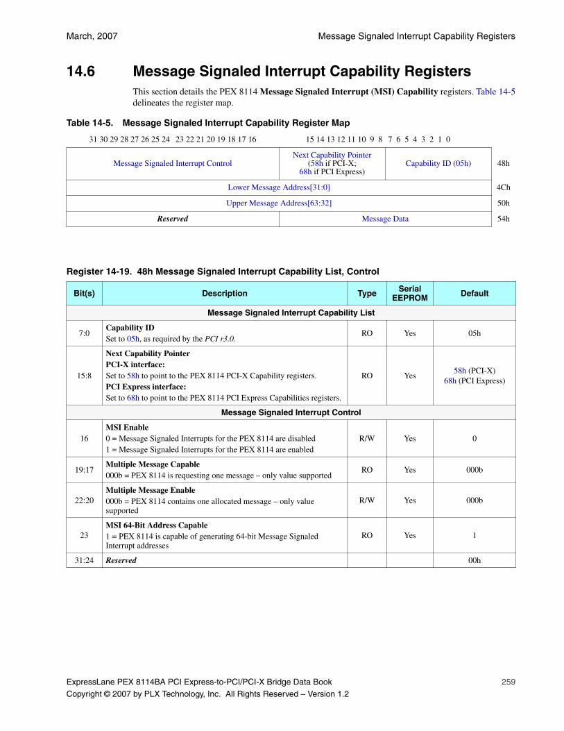
March, 2007 Message Signaled Interrupt Capability Registers
ExpressLane PEX 8114BA PCI Express-to-PCI/PCI-X Bridge Data Book 259
Copyright © 2007 by PLX Technology, Inc. All Rights Reserved – Version 1.2
14.6 Message Signaled Interrupt Capability RegistersThis section details the PEX 8114 Message Signaled Interrupt (MSI) Capability registers. Table 14-5delineates the register map.
Table 14-5. Message Signaled Interrupt Capability Register Map
31 30 29 28 27 26 25 24 23 22 21 20 19 18 17 16 15 14 13 12 11 10 9 8 7 6 5 4 3 2 1 0
Message Signaled Interrupt ControlNext Capability Pointer
(58h if PCI-X; 68h if PCI Express)
Capability ID (05h) 48h
Lower Message Address[31:0] 4Ch
Upper Message Address[63:32] 50h
Reserved Message Data 54h
Register 14-19. 48h Message Signaled Interrupt Capability List, Control
Bit(s) Description Type Serial EEPROM Default
Message Signaled Interrupt Capability List
7:0Capability IDSet to 05h, as required by the PCI r3.0.
RO Yes 05h
15:8
Next Capability PointerPCI-X interface:Set to 58h to point to the PEX 8114 PCI-X Capability registers.PCI Express interface:Set to 68h to point to the PEX 8114 PCI Express Capabilities registers.
RO Yes58h (PCI-X)
68h (PCI Express)
Message Signaled Interrupt Control
16MSI Enable0 = Message Signaled Interrupts for the PEX 8114 are disabled1 = Message Signaled Interrupts for the PEX 8114 are enabled
R/W Yes 0
19:17Multiple Message Capable000b = PEX 8114 is requesting one message – only value supported
RO Yes 000b
22:20Multiple Message Enable000b = PEX 8114 contains one allocated message – only value supported
R/W Yes 000b
23MSI 64-Bit Address Capable1 = PEX 8114 is capable of generating 64-bit Message Signaled Interrupt addresses
RO Yes 1
31:24 Reserved 00h
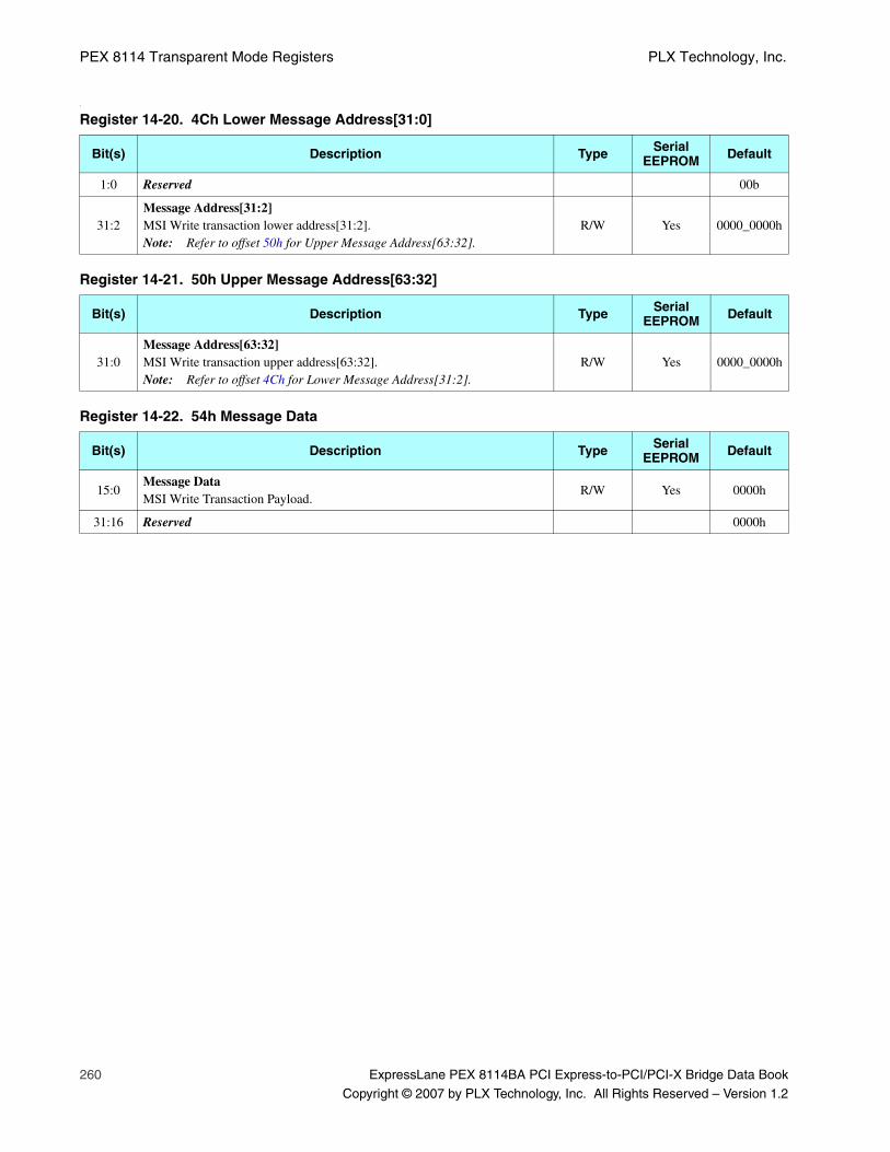
PEX 8114 Transparent Mode Registers PLX Technology, Inc.
260 ExpressLane PEX 8114BA PCI Express-to-PCI/PCI-X Bridge Data Book
Copyright © 2007 by PLX Technology, Inc. All Rights Reserved – Version 1.2
s
Register 14-20. 4Ch Lower Message Address[31:0]
Bit(s) Description Type Serial EEPROM Default
1:0 Reserved 00b
31:2Message Address[31:2]MSI Write transaction lower address[31:2].Note: Refer to offset 50h for Upper Message Address[63:32].
R/W Yes 0000_0000h
Register 14-21. 50h Upper Message Address[63:32]
Bit(s) Description Type Serial EEPROM Default
31:0Message Address[63:32]MSI Write transaction upper address[63:32].Note: Refer to offset 4Ch for Lower Message Address[31:2].
R/W Yes 0000_0000h
Register 14-22. 54h Message Data
Bit(s) Description Type Serial EEPROM Default
15:0Message DataMSI Write Transaction Payload.
R/W Yes 0000h
31:16 Reserved 0000h
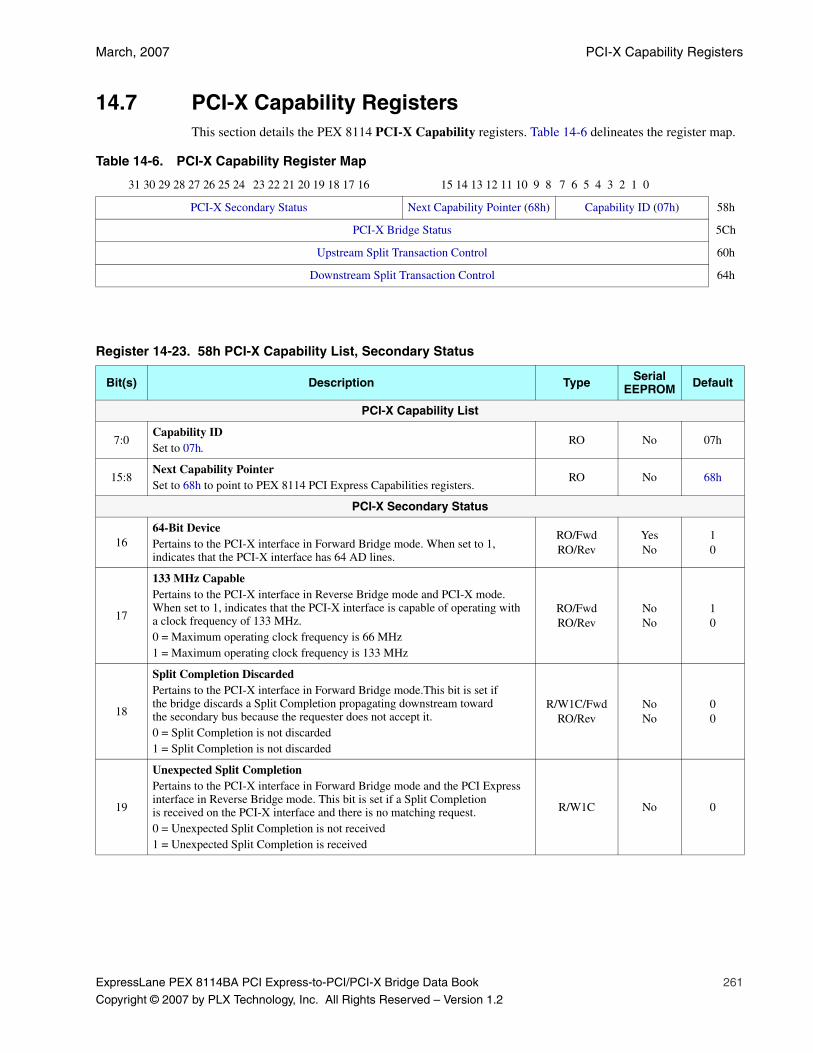
March, 2007 PCI-X Capability Registers
ExpressLane PEX 8114BA PCI Express-to-PCI/PCI-X Bridge Data Book 261
Copyright © 2007 by PLX Technology, Inc. All Rights Reserved – Version 1.2
14.7 PCI-X Capability RegistersThis section details the PEX 8114 PCI-X Capability registers. Table 14-6 delineates the register map.
Table 14-6. PCI-X Capability Register Map
31 30 29 28 27 26 25 24 23 22 21 20 19 18 17 16 15 14 13 12 11 10 9 8 7 6 5 4 3 2 1 0
PCI-X Secondary Status Next Capability Pointer (68h) Capability ID (07h) 58h
PCI-X Bridge Status 5Ch
Upstream Split Transaction Control 60h
Downstream Split Transaction Control 64h
Register 14-23. 58h PCI-X Capability List, Secondary Status
Bit(s) Description Type Serial EEPROM Default
PCI-X Capability List
7:0Capability IDSet to 07h.
RO No 07h
15:8Next Capability PointerSet to 68h to point to PEX 8114 PCI Express Capabilities registers.
RO No 68h
PCI-X Secondary Status
1664-Bit DevicePertains to the PCI-X interface in Forward Bridge mode. When set to 1, indicates that the PCI-X interface has 64 AD lines.
RO/FwdRO/Rev
YesNo
10
17
133 MHz CapablePertains to the PCI-X interface in Reverse Bridge mode and PCI-X mode. When set to 1, indicates that the PCI-X interface is capable of operating with a clock frequency of 133 MHz. 0 = Maximum operating clock frequency is 66 MHz1 = Maximum operating clock frequency is 133 MHz
RO/FwdRO/Rev
NoNo
10
18
Split Completion DiscardedPertains to the PCI-X interface in Forward Bridge mode.This bit is set if the bridge discards a Split Completion propagating downstream toward the secondary bus because the requester does not accept it. 0 = Split Completion is not discarded1 = Split Completion is not discarded
R/W1C/FwdRO/Rev
NoNo
00
19
Unexpected Split CompletionPertains to the PCI-X interface in Forward Bridge mode and the PCI Express interface in Reverse Bridge mode. This bit is set if a Split Completion is received on the PCI-X interface and there is no matching request. 0 = Unexpected Split Completion is not received1 = Unexpected Split Completion is received
R/W1C No 0
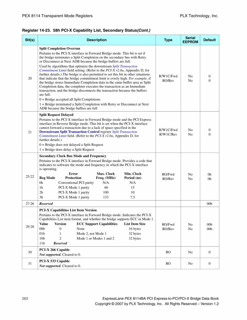
PEX 8114 Transparent Mode Registers PLX Technology, Inc.
262 ExpressLane PEX 8114BA PCI Express-to-PCI/PCI-X Bridge Data Book
Copyright © 2007 by PLX Technology, Inc. All Rights Reserved – Version 1.2
20
Split Completion OverrunPertains to the PCI-X interface in Forward Bridge mode. This bit is set if the bridge terminates a Split Completion on the secondary bus with Retry or Disconnect at Next ADB because the bridge buffers are full.Used by algorithms that optimize the downstream Split Transaction Commitment Limit field setting. (Refer to the PCI-X r2.0a, Appendix D, for further details.) The bridge is also permitted to set this bit in other situations that indicate that the bridge commitment limit is overly high. For example, if the bridge stores Immediate Completion data in the same buffer area as Split Completion data, the completer executes the transaction as an Immediate transaction, and the bridge disconnects the transaction because the buffers are full. 0 = Bridge accepted all Split Completions1 = Bridge terminated a Split Completion with Retry or Disconnect at Next ADB because the bridge buffers are full
R/W1C/FwdRO/Rev
NoNo
00
21
Split Request DelayedPertains to the PCI-X interface in Forward Bridge mode and the PCI Express interface in Reverse Bridge mode. This bit is set when the PCI-X interface cannot forward a transaction due to a lack of space specified in the Downstream Split Transaction Control register Split Transaction Commitment Limit field. (Refer to the PCI-X r2.0a, Appendix D, for further details.)0 = Bridge does not delayed a Split Request1 = Bridge does delay a Split Request
R/W1C/FwdR/W1C/Rev
NoNo
00
25:22
Secondary Clock Bus Mode and FrequencyPertains to the PCI-X interface in Forward Bridge mode. Provides a code that indicates to software the mode and frequency in which the PCI-X interface is operating.
Error Max. Clock Min. ClockReg Mode Protection Freq. (MHz) Period (ns)0h Conventional PCI parity N/A N/A1h PCI-X Mode 1 parity 66 152h PCI-X Mode 1 parity 100 103h PCI-X Mode 1 parity 133 7.5
RO/FwdRO/Rev
NoNo
0h0h
27:26 Reserved 00b
29:28
PCI-X Capabilities List Item VersionPertains to the PCI-X interface in Forward Bridge mode. Indicates the PCI-X Capabilities List item format, and whether the bridge supports ECC in Mode 1.Value Version ECC Support Capabilities List Item Size00b 0 None 16 bytes01b 1 Mode 2, not Mode 1 32 bytes10b 2 Mode 1 or Modes 1 and 2 32 bytes11b Reserved
RO/FwdRO/Rev
NoNo
00b00b
30PCI-X 266 CapableNot supported. Cleared to 0.
RO No 0
31PCI-X 533 CapableNot supported. Cleared to 0.
RO No 0
Register 14-23. 58h PCI-X Capability List, Secondary Status(Cont.)
Bit(s) Description Type Serial EEPROM Default
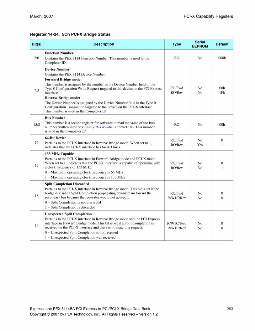
March, 2007 PCI-X Capability Registers
ExpressLane PEX 8114BA PCI Express-to-PCI/PCI-X Bridge Data Book 263
Copyright © 2007 by PLX Technology, Inc. All Rights Reserved – Version 1.2
Register 14-24. 5Ch PCI-X Bridge Status
Bit(s) Description Type Serial EEPROM Default
2:0Function NumberContains the PEX 8114 Function Number. This number is used in the Completer ID.
RO No 000b
7:3
Device NumberContains the PEX 8114 Device Number. Forward Bridge mode:This number is assigned by the number in the Device Number field of the Type 0 Configuration Write Request targeted to this device on the PCI Express interface.Reverse Bridge mode:The Device Number is assigned by the Device Number field in the Type 0 Configuration Transaction targeted to the device on the PCI-X interface. This number is used in the Completer ID.
RO/FwdRO/Rev
NoNo
00h1Fh
15:8
Bus NumberThis number is a second register for software to read the value of the Bus Number written into the Primary Bus Number at offset 18h. This number is used in the Completer ID.
RO No 00h
1664-Bit DevicePertains to the PCI-X interface in Reverse Bridge mode. When set to 1, indicates that the PCI-X interface has 64 AD lines.
RO/FwdRO/Rev
NoYes
01
17
133 MHz CapablePertains to the PCI-X interface in Forward Bridge mode and PCI-X mode. When set to 1, indicates that the PCI-X interface is capable of operating with a clock frequency of 133 MHz. 0 = Maximum operating clock frequency is 66 MHz1 = Maximum operating clock frequency is 133 MHz
RO/FwdRO/Rev
NoNo
01
18
Split Completion DiscardedPertains to the PCI-X interface in Reverse Bridge mode. This bit is set if the bridge discards a Split Completion propagating downstream toward the secondary bus because the requester would not accept it. 0 = Split Completion is not discarded1 = Split Completion is discarded
RO/FwdR/W1C/Rev
NoNo
00
19
Unexpected Split CompletionPertains to the PCI-X interface in Reverse Bridge mode and the PCI Express interface in Forward Bridge mode. This bit is set if a Split Completion is received on the PCI-X interface and there is no matching request.0 = Unexpected Split Completion is not received1 = Unexpected Split Completion was received
R/W1C/FwdR/W1C/Rev
NoNo
00
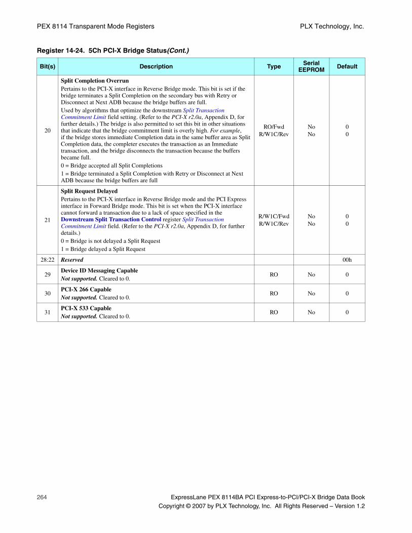
PEX 8114 Transparent Mode Registers PLX Technology, Inc.
264 ExpressLane PEX 8114BA PCI Express-to-PCI/PCI-X Bridge Data Book
Copyright © 2007 by PLX Technology, Inc. All Rights Reserved – Version 1.2
20
Split Completion OverrunPertains to the PCI-X interface in Reverse Bridge mode. This bit is set if the bridge terminates a Split Completion on the secondary bus with Retry or Disconnect at Next ADB because the bridge buffers are full.Used by algorithms that optimize the downstream Split Transaction Commitment Limit field setting. (Refer to the PCI-X r2.0a, Appendix D, for further details.) The bridge is also permitted to set this bit in other situations that indicate that the bridge commitment limit is overly high. For example, if the bridge stores immediate Completion data in the same buffer area as Split Completion data, the completer executes the transaction as an Immediate transaction, and the bridge disconnects the transaction because the buffers became full. 0 = Bridge accepted all Split Completions1 = Bridge terminated a Split Completion with Retry or Disconnect at Next ADB because the bridge buffers are full
RO/FwdR/W1C/Rev
NoNo
00
21
Split Request DelayedPertains to the PCI-X interface in Reverse Bridge mode and the PCI Express interface in Forward Bridge mode. This bit is set when the PCI-X interface cannot forward a transaction due to a lack of space specified in the Downstream Split Transaction Control register Split Transaction Commitment Limit field. (Refer to the PCI-X r2.0a, Appendix D, for further details.) 0 = Bridge is not delayed a Split Request1 = Bridge delayed a Split Request
R/W1C/FwdR/W1C/Rev
NoNo
00
28:22 Reserved 00h
29Device ID Messaging CapableNot supported. Cleared to 0.
RO No 0
30PCI-X 266 CapableNot supported. Cleared to 0.
RO No 0
31PCI-X 533 CapableNot supported. Cleared to 0.
RO No 0
Register 14-24. 5Ch PCI-X Bridge Status(Cont.)
Bit(s) Description Type Serial EEPROM Default
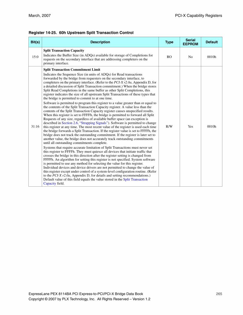
March, 2007 PCI-X Capability Registers
ExpressLane PEX 8114BA PCI Express-to-PCI/PCI-X Bridge Data Book 265
Copyright © 2007 by PLX Technology, Inc. All Rights Reserved – Version 1.2
Register 14-25. 60h Upstream Split Transaction Control
Bit(s) Description Type Serial EEPROM Default
15:0
Split Transaction CapacityIndicates the Buffer Size (in ADQs) available for storage of Completions for requests on the secondary interface that are addressing completers on the primary interface.
RO No 0010h
31:16
Split Transaction Commitment LimitIndicates the Sequence Size (in units of ADQs) for Read transactions forwarded by the bridge from requesters on the secondary interface, to completers on the primary interface. (Refer to the PCI-X r2.0a, Appendix D, for a detailed discussion of Split Transaction commitment.) When the bridge stores Split Read Completions in the same buffer as other Split Completions, this register indicates the size of all upstream Split Transactions of these types that the bridge is permitted to commit to at one time.Software is permitted to program this register to a value greater than or equal to the contents of the Split Transaction Capacity register. A value less than the contents of the Split Transaction Capacity register causes unspecified results. When this register is set to FFFFh, the bridge is permitted to forward all Split Requests of any size, regardless of available buffer space (an exception is described in Section 2.6, “Strapping Signals”). Software is permitted to change this register at any time. The most recent value of the register is used each time the bridge forwards a Split Transaction. If the register value is set to FFFFh, the bridge does not track the outstanding commitment. If the register is later set to another value, the bridge does not accurately track outstanding commitments until all outstanding commitments complete. Systems that require accurate limitation of Split Transactions must never set this register to FFFFh. They must quiesce all devices that initiate traffic that crosses the bridge in this direction after the register setting is changed from FFFFh. An algorithm for setting this register is not specified. System software is permitted to use any method for selecting the value for this register. Individual devices and device drivers are not permitted to change the value of this register except under control of a system-level configuration routine. (Refer to the PCI-X r2.0a, Appendix D, for details and setting recommendations.) Default value of this field equals the value stored in the Split Transaction Capacity field.
R/W Yes 0010h
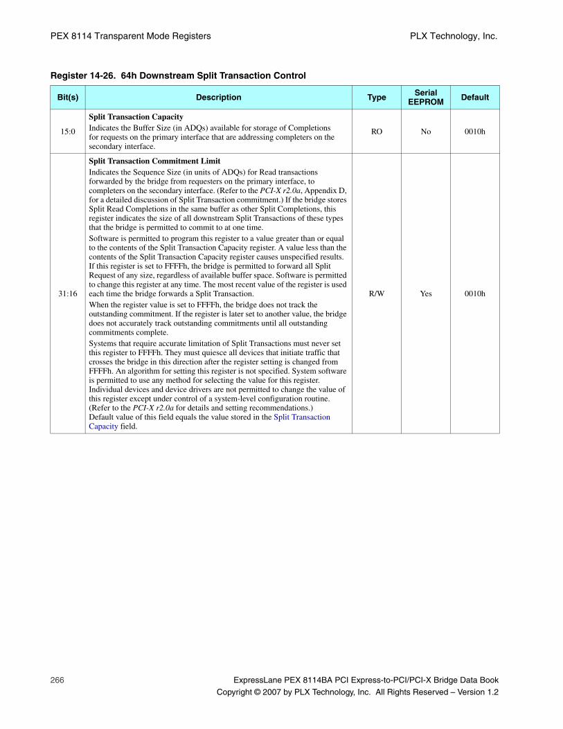
PEX 8114 Transparent Mode Registers PLX Technology, Inc.
266 ExpressLane PEX 8114BA PCI Express-to-PCI/PCI-X Bridge Data Book
Copyright © 2007 by PLX Technology, Inc. All Rights Reserved – Version 1.2
Register 14-26. 64h Downstream Split Transaction Control
Bit(s) Description Type Serial EEPROM Default
15:0
Split Transaction CapacityIndicates the Buffer Size (in ADQs) available for storage of Completions for requests on the primary interface that are addressing completers on the secondary interface.
RO No 0010h
31:16
Split Transaction Commitment LimitIndicates the Sequence Size (in units of ADQs) for Read transactions forwarded by the bridge from requesters on the primary interface, to completers on the secondary interface. (Refer to the PCI-X r2.0a, Appendix D, for a detailed discussion of Split Transaction commitment.) If the bridge stores Split Read Completions in the same buffer as other Split Completions, this register indicates the size of all downstream Split Transactions of these types that the bridge is permitted to commit to at one time.Software is permitted to program this register to a value greater than or equal to the contents of the Split Transaction Capacity register. A value less than the contents of the Split Transaction Capacity register causes unspecified results. If this register is set to FFFFh, the bridge is permitted to forward all Split Request of any size, regardless of available buffer space. Software is permitted to change this register at any time. The most recent value of the register is used each time the bridge forwards a Split Transaction.When the register value is set to FFFFh, the bridge does not track the outstanding commitment. If the register is later set to another value, the bridge does not accurately track outstanding commitments until all outstanding commitments complete. Systems that require accurate limitation of Split Transactions must never set this register to FFFFh. They must quiesce all devices that initiate traffic that crosses the bridge in this direction after the register setting is changed from FFFFh. An algorithm for setting this register is not specified. System software is permitted to use any method for selecting the value for this register. Individual devices and device drivers are not permitted to change the value of this register except under control of a system-level configuration routine. (Refer to the PCI-X r2.0a for details and setting recommendations.) Default value of this field equals the value stored in the Split Transaction Capacity field.
R/W Yes 0010h
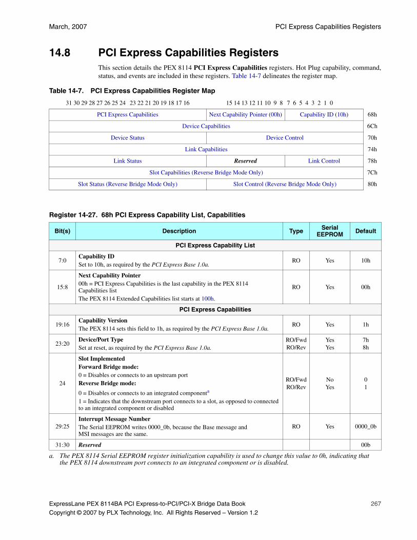
March, 2007 PCI Express Capabilities Registers
ExpressLane PEX 8114BA PCI Express-to-PCI/PCI-X Bridge Data Book 267
Copyright © 2007 by PLX Technology, Inc. All Rights Reserved – Version 1.2
14.8 PCI Express Capabilities RegistersThis section details the PEX 8114 PCI Express Capabilities registers. Hot Plug capability, command,status, and events are included in these registers. Table 14-7 delineates the register map.
Table 14-7. PCI Express Capabilities Register Map
31 30 29 28 27 26 25 24 23 22 21 20 19 18 17 16 15 14 13 12 11 10 9 8 7 6 5 4 3 2 1 0
PCI Express Capabilities Next Capability Pointer (00h) Capability ID (10h) 68h
Device Capabilities 6Ch
Device Status Device Control 70h
Link Capabilities 74h
Link Status Reserved Link Control 78h
Slot Capabilities (Reverse Bridge Mode Only) 7Ch
Slot Status (Reverse Bridge Mode Only) Slot Control (Reverse Bridge Mode Only) 80h
Register 14-27. 68h PCI Express Capability List, Capabilities
Bit(s) Description Type Serial EEPROM Default
PCI Express Capability List
7:0Capability IDSet to 10h, as required by the PCI Express Base 1.0a.
RO Yes 10h
15:8
Next Capability Pointer00h = PCI Express Capabilities is the last capability in the PEX 8114 Capabilities listThe PEX 8114 Extended Capabilities list starts at 100h.
RO Yes 00h
PCI Express Capabilities
19:16Capability VersionThe PEX 8114 sets this field to 1h, as required by the PCI Express Base 1.0a.
RO Yes 1h
23:20Device/Port TypeSet at reset, as required by the PCI Express Base 1.0a.
RO/FwdRO/Rev
YesYes
7h8h
24
Slot ImplementedForward Bridge mode:0 = Disables or connects to an upstream portReverse Bridge mode:
0 = Disables or connects to an integrated componenta
1 = Indicates that the downstream port connects to a slot, as opposed to connected to an integrated component or disabled
a. The PEX 8114 Serial EEPROM register initialization capability is used to change this value to 0h, indicating thatthe PEX 8114 downstream port connects to an integrated component or is disabled.
RO/FwdRO/Rev
NoYes
01
29:25Interrupt Message NumberThe Serial EEPROM writes 0000_0b, because the Base message and MSI messages are the same.
RO Yes 0000_0b
31:30 Reserved 00b
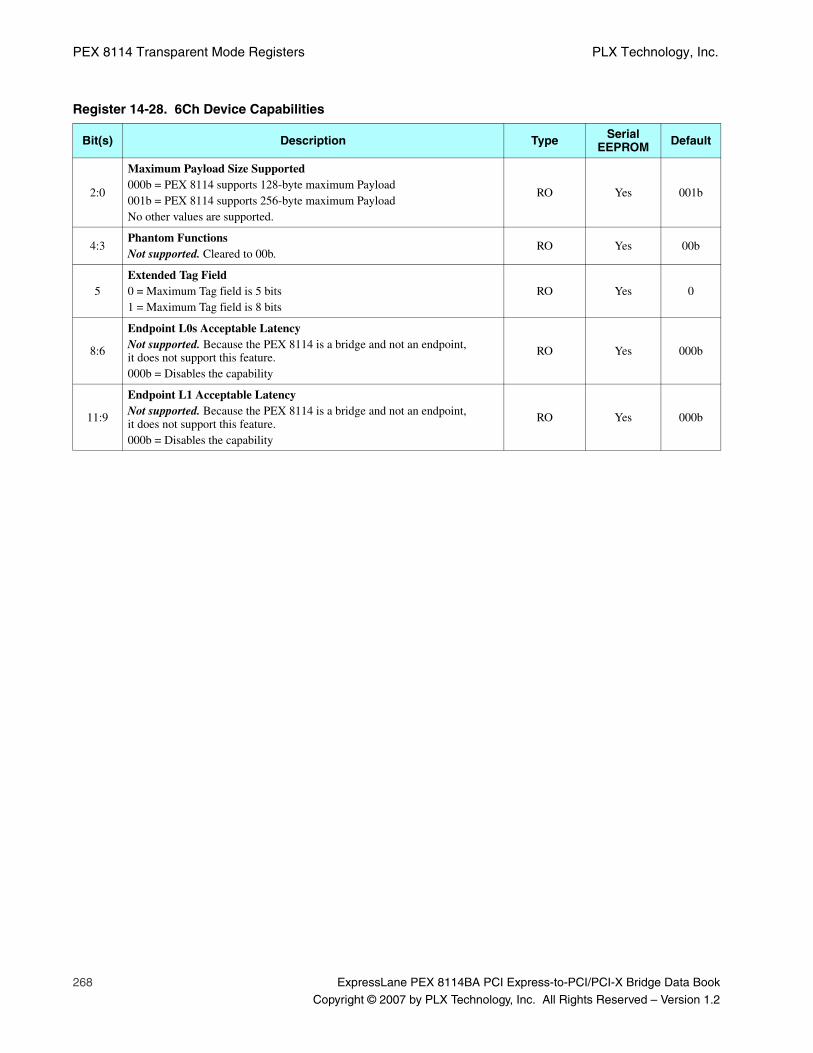
PEX 8114 Transparent Mode Registers PLX Technology, Inc.
268 ExpressLane PEX 8114BA PCI Express-to-PCI/PCI-X Bridge Data Book
Copyright © 2007 by PLX Technology, Inc. All Rights Reserved – Version 1.2
Register 14-28. 6Ch Device Capabilities
Bit(s) Description Type Serial EEPROM Default
2:0
Maximum Payload Size Supported000b = PEX 8114 supports 128-byte maximum Payload001b = PEX 8114 supports 256-byte maximum PayloadNo other values are supported.
RO Yes 001b
4:3Phantom FunctionsNot supported. Cleared to 00b.
RO Yes 00b
5Extended Tag Field0 = Maximum Tag field is 5 bits1 = Maximum Tag field is 8 bits
RO Yes 0
8:6
Endpoint L0s Acceptable LatencyNot supported. Because the PEX 8114 is a bridge and not an endpoint, it does not support this feature.000b = Disables the capability
RO Yes 000b
11:9
Endpoint L1 Acceptable LatencyNot supported. Because the PEX 8114 is a bridge and not an endpoint, it does not support this feature.000b = Disables the capability
RO Yes 000b
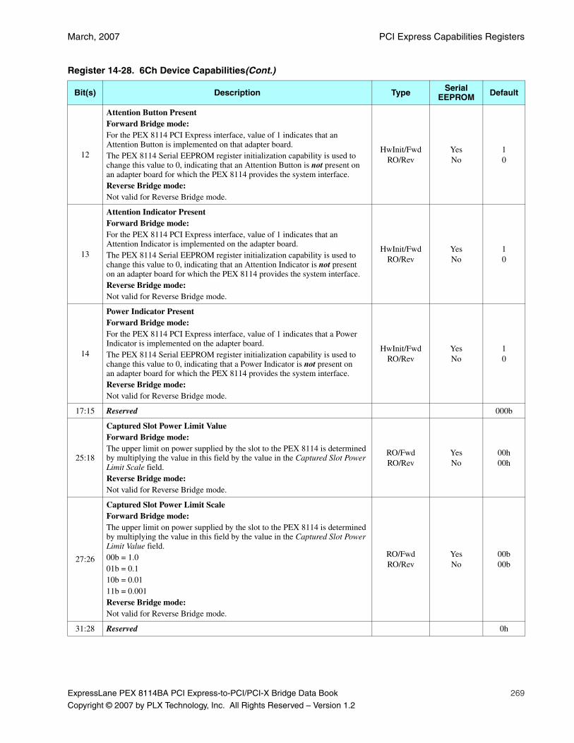
March, 2007 PCI Express Capabilities Registers
ExpressLane PEX 8114BA PCI Express-to-PCI/PCI-X Bridge Data Book 269
Copyright © 2007 by PLX Technology, Inc. All Rights Reserved – Version 1.2
12
Attention Button PresentForward Bridge mode:For the PEX 8114 PCI Express interface, value of 1 indicates that an Attention Button is implemented on that adapter board.The PEX 8114 Serial EEPROM register initialization capability is used to change this value to 0, indicating that an Attention Button is not present on an adapter board for which the PEX 8114 provides the system interface.Reverse Bridge mode:Not valid for Reverse Bridge mode.
HwInit/FwdRO/Rev
YesNo
10
13
Attention Indicator PresentForward Bridge mode:For the PEX 8114 PCI Express interface, value of 1 indicates that an Attention Indicator is implemented on the adapter board.The PEX 8114 Serial EEPROM register initialization capability is used to change this value to 0, indicating that an Attention Indicator is not present on an adapter board for which the PEX 8114 provides the system interface.Reverse Bridge mode:Not valid for Reverse Bridge mode.
HwInit/FwdRO/Rev
YesNo
10
14
Power Indicator PresentForward Bridge mode:For the PEX 8114 PCI Express interface, value of 1 indicates that a Power Indicator is implemented on the adapter board.The PEX 8114 Serial EEPROM register initialization capability is used to change this value to 0, indicating that a Power Indicator is not present on an adapter board for which the PEX 8114 provides the system interface.Reverse Bridge mode:Not valid for Reverse Bridge mode.
HwInit/FwdRO/Rev
YesNo
10
17:15 Reserved 000b
25:18
Captured Slot Power Limit ValueForward Bridge mode:The upper limit on power supplied by the slot to the PEX 8114 is determined by multiplying the value in this field by the value in the Captured Slot Power Limit Scale field.Reverse Bridge mode:Not valid for Reverse Bridge mode.
RO/FwdRO/Rev
YesNo
00h00h
27:26
Captured Slot Power Limit ScaleForward Bridge mode:The upper limit on power supplied by the slot to the PEX 8114 is determined by multiplying the value in this field by the value in the Captured Slot Power Limit Value field.00b = 1.001b = 0.110b = 0.0111b = 0.001Reverse Bridge mode:Not valid for Reverse Bridge mode.
RO/FwdRO/Rev
YesNo
00b00b
31:28 Reserved 0h
Register 14-28. 6Ch Device Capabilities(Cont.)
Bit(s) Description Type Serial EEPROM Default

PEX 8114 Transparent Mode Registers PLX Technology, Inc.
270 ExpressLane PEX 8114BA PCI Express-to-PCI/PCI-X Bridge Data Book
Copyright © 2007 by PLX Technology, Inc. All Rights Reserved – Version 1.2
Register 14-29. 70h Device Status and Control
Bit(s) Description Type Serial EEPROM Default
Device Control
0Correctable Error Reporting Enabled0 = Disables1 = Enables PEX 8114 to report Correctable errors
R/W Yes 0
1Non-Fatal Error Reporting Enabled 0 = Disables1 = Enables PEX 8114 to report Non-Fatal errors
R/W Yes 0
2Fatal Error Reporting Enabled0 = Disables1 = Enables PEX 8114 to report Fatal errors
R/W Yes 0
3Unsupported Request Reporting Enable0 = Disables1 = Enables PEX 8114 to report Unsupported Request errors
R/W Yes 0
4Relaxed Ordering EnabledNot supported. Cleared to 0.
RO No 0
7:5
Maximum Payload SizePower-on/reset value is 000b, indicating that initially the PEX 8114 is configured to support a Maximum Payload Size of 128 bytes. Software can change this field to configure the PEX 8114 to support Payload Sizes of 256 or 128. Software must not change this field to values other than those indicated by the Device Capabilities register Maximum Payload Size Supported field.
R/W Yes 000b
8Extended Tag Field EnabledNot supported. Cleared to 0.
RO No 0
9Phantom Functions EnableNot supported. Cleared to 0.
RO No 0
10AUX Power PM EnableNot supported. Cleared to 0.
RO No 0
11No Snoop EnableNot supported in Transparent mode. Cleared to 0.
RO No 0
14:12
Maximum Read Request SizeSpecifies the maximum size (in bytes) of a Read request generated by the PEX 8114.000b = 128 bytes001b = 256 bytes010b = 512 bytes (default)011b = 1,024 bytes100b = 2,048 bytes101b = 4,096 bytes110b, 111b = Reserved
R/W Yes 010b
15 Bridge Configuration Retry Enable R/W Yes 0
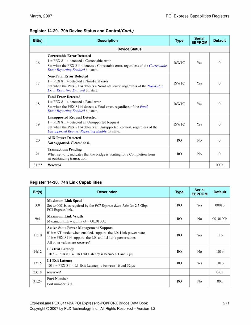
March, 2007 PCI Express Capabilities Registers
ExpressLane PEX 8114BA PCI Express-to-PCI/PCI-X Bridge Data Book 271
Copyright © 2007 by PLX Technology, Inc. All Rights Reserved – Version 1.2
Device Status
16
Correctable Error Detected1 = PEX 8114 detected a Correctable errorSet when the PEX 8114 detects a Correctable error, regardless of the Correctable Error Reporting Enabled bit state.
R/W1C Yes 0
17
Non-Fatal Error Detected1 = PEX 8114 detected a Non-Fatal errorSet when the PEX 8114 detects a Non-Fatal error, regardless of the Non-Fatal Error Reporting Enabled bit state.
R/W1C Yes 0
18
Fatal Error Detected1 = PEX 8114 detected a Fatal errorSet when the PEX 8114 detects a Fatal error, regardless of the Fatal Error Reporting Enabled bit state.
R/W1C Yes 0
19
Unsupported Request Detected1 = PEX 8114 detected an Unsupported RequestSet when the PEX 8114 detects an Unsupported Request, regardless of the Unsupported Request Reporting Enable bit state.
R/W1C Yes 0
20AUX Power Detected Not supported. Cleared to 0.
RO No 0
21Transactions PendingWhen set to 1, indicates that the bridge is waiting for a Completion from an outstanding transaction.
RO No 0
31:22 Reserved 000h
Register 14-30. 74h Link Capabilities
Bit(s) Description Type Serial EEPROM Default
3:0Maximum Link SpeedSet to 0001b, as required by the PCI Express Base 1.0a for 2.5 Gbps PCI Express link.
RO Yes 0001b
9:4Maximum Link WidthMaximum link width is x4 = 00_0100b.
RO No 00_0100b
11:10
Active-State Power Management Support01b = NT mode, when enabled, supports the L0s Link power state11b = PEX 8114 supports the L0s and L1 Link power statesAll other values are reserved.
RO Yes 11b
14:12L0s Exit Latency101b = PEX 8114 L0s Exit Latency is between 1 and 2 µs
RO No 101b
17:15L1 Exit Latency101b = PEX 8114 L1 Exit Latency is between 16 and 32 µs
RO Yes 101b
23:18 Reserved 0-0h
31:24Port Number
Port number is 0.RO No 00h
Register 14-29. 70h Device Status and Control(Cont.)
Bit(s) Description Type Serial EEPROM Default
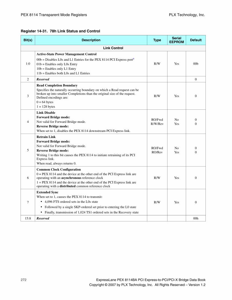
PEX 8114 Transparent Mode Registers PLX Technology, Inc.
272 ExpressLane PEX 8114BA PCI Express-to-PCI/PCI-X Bridge Data Book
Copyright © 2007 by PLX Technology, Inc. All Rights Reserved – Version 1.2
Register 14-31. 78h Link Status and Control
Bit(s) Description Type Serial EEPROM Default
Link Control
1:0
Active-State Power Management Control
00b = Disables L0s and L1 Entries for the PEX 8114 PCI Express porta
01b = Enables only L0s Entry10b = Enables only L1 Entry11b = Enables both L0s and L1 Entries
R/W Yes 00b
2 Reserved 0
3
Read Completion BoundarySpecifies the naturally occurring boundary on which a Read request can be broken up into smaller Completions than the original size of the request. Defined encodings are:0 = 64 bytes1 = 128 bytes
R/W Yes 0
4
Link DisableForward Bridge mode:Not valid for Forward Bridge mode.Reverse Bridge mode:When set to 1, disables the PEX 8114 downstream PCI Express link.
RO/FwdR/W/Rev
NoYes
00
5
Retrain LinkForward Bridge mode:Not valid for Forward Bridge mode.Reverse Bridge mode:Writing 1 to this bit causes the PEX 8114 to initiate retraining of its PCI Express link.When read, always returns 0.
RO/FwdRO/Rev
NoYes
00
6
Common Clock Configuration0 = PEX 8114 and the device at the other end of the PCI Express link are operating with an asynchronous reference clock1 = PEX 8114 and the device at the other end of the PCI Express link are operating with a distributed common reference clock
R/W Yes 0
7
Extended SyncWhen set to 1, causes the PEX 8114 to transmit:
• 4,096 FTS ordered sets in the L0s state
• Followed by a single SKP-ordered set prior to entering the L0 state
• Finally, transmission of 1,024 TS1 ordered sets in the Recovery state
R/W Yes 0
15:8 Reserved 00h
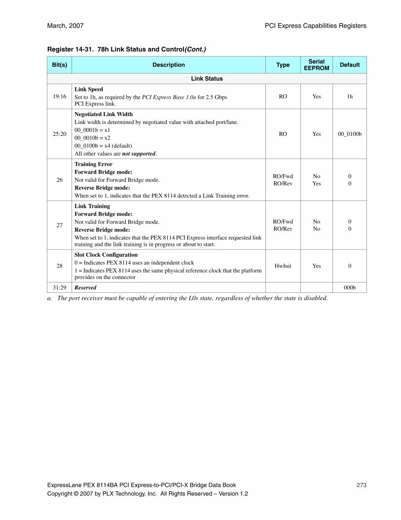
March, 2007 PCI Express Capabilities Registers
ExpressLane PEX 8114BA PCI Express-to-PCI/PCI-X Bridge Data Book 273
Copyright © 2007 by PLX Technology, Inc. All Rights Reserved – Version 1.2
Link Status
19:16Link SpeedSet to 1h, as required by the PCI Express Base 1.0a for 2.5 Gbps PCI Express link.
RO Yes 1h
25:20
Negotiated Link WidthLink width is determined by negotiated value with attached port/lane.00_0001b = x100_0010b = x200_0100b = x4 (default)All other values are not supported.
RO Yes 00_0100b
26
Training ErrorForward Bridge mode:Not valid for Forward Bridge mode.Reverse Bridge mode:When set to 1, indicates that the PEX 8114 detected a Link Training error.
RO/FwdRO/Rev
NoYes
00
27
Link TrainingForward Bridge mode:Not valid for Forward Bridge mode.Reverse Bridge mode:When set to 1, indicates that the PEX 8114 PCI Express interface requested link training and the link training is in progress or about to start.
RO/FwdRO/Rev
NoNo
00
28
Slot Clock Configuration0 = Indicates PEX 8114 uses an independent clock1 = Indicates PEX 8114 uses the same physical reference clock that the platform provides on the connector
HwInit Yes 0
31:29 Reserved 000b
a. The port receiver must be capable of entering the L0s state, regardless of whether the state is disabled.
Register 14-31. 78h Link Status and Control(Cont.)
Bit(s) Description Type Serial EEPROM Default
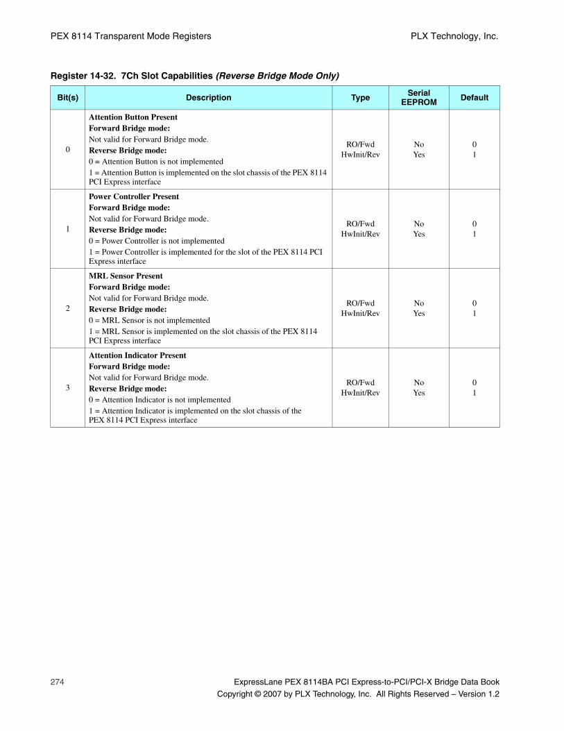
PEX 8114 Transparent Mode Registers PLX Technology, Inc.
274 ExpressLane PEX 8114BA PCI Express-to-PCI/PCI-X Bridge Data Book
Copyright © 2007 by PLX Technology, Inc. All Rights Reserved – Version 1.2
Register 14-32. 7Ch Slot Capabilities (Reverse Bridge Mode Only)
Bit(s) Description Type Serial EEPROM Default
0
Attention Button PresentForward Bridge mode:Not valid for Forward Bridge mode.Reverse Bridge mode:0 = Attention Button is not implemented1 = Attention Button is implemented on the slot chassis of the PEX 8114 PCI Express interface
RO/FwdHwInit/Rev
NoYes
01
1
Power Controller PresentForward Bridge mode:Not valid for Forward Bridge mode.Reverse Bridge mode:0 = Power Controller is not implemented1 = Power Controller is implemented for the slot of the PEX 8114 PCI Express interface
RO/FwdHwInit/Rev
NoYes
01
2
MRL Sensor PresentForward Bridge mode:Not valid for Forward Bridge mode.Reverse Bridge mode:0 = MRL Sensor is not implemented1 = MRL Sensor is implemented on the slot chassis of the PEX 8114 PCI Express interface
RO/FwdHwInit/Rev
NoYes
01
3
Attention Indicator PresentForward Bridge mode:Not valid for Forward Bridge mode.Reverse Bridge mode:0 = Attention Indicator is not implemented1 = Attention Indicator is implemented on the slot chassis of the PEX 8114 PCI Express interface
RO/FwdHwInit/Rev
NoYes
01
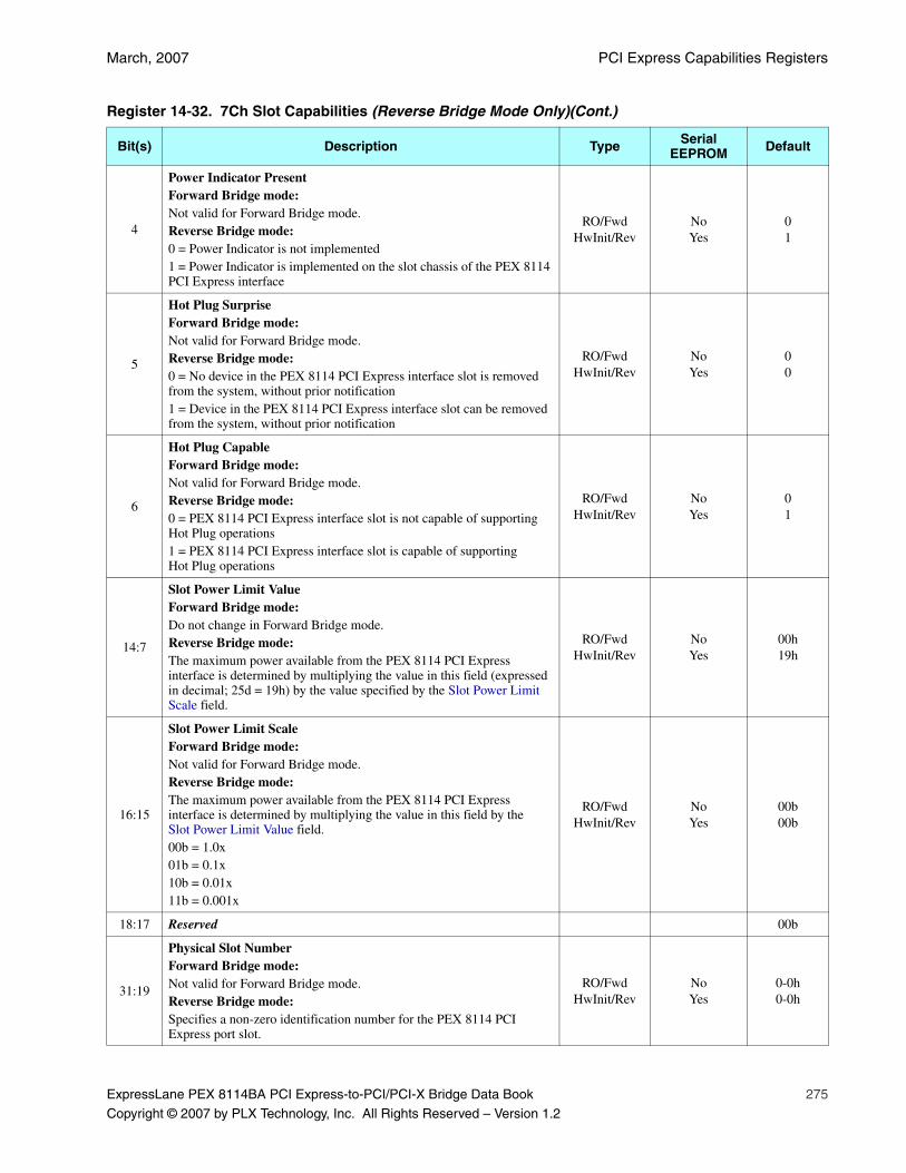
March, 2007 PCI Express Capabilities Registers
ExpressLane PEX 8114BA PCI Express-to-PCI/PCI-X Bridge Data Book 275
Copyright © 2007 by PLX Technology, Inc. All Rights Reserved – Version 1.2
4
Power Indicator PresentForward Bridge mode:Not valid for Forward Bridge mode.Reverse Bridge mode:0 = Power Indicator is not implemented1 = Power Indicator is implemented on the slot chassis of the PEX 8114 PCI Express interface
RO/FwdHwInit/Rev
NoYes
01
5
Hot Plug SurpriseForward Bridge mode:Not valid for Forward Bridge mode.Reverse Bridge mode:0 = No device in the PEX 8114 PCI Express interface slot is removed from the system, without prior notification1 = Device in the PEX 8114 PCI Express interface slot can be removed from the system, without prior notification
RO/FwdHwInit/Rev
NoYes
00
6
Hot Plug CapableForward Bridge mode:Not valid for Forward Bridge mode.Reverse Bridge mode:0 = PEX 8114 PCI Express interface slot is not capable of supporting Hot Plug operations1 = PEX 8114 PCI Express interface slot is capable of supporting Hot Plug operations
RO/FwdHwInit/Rev
NoYes
01
14:7
Slot Power Limit ValueForward Bridge mode:Do not change in Forward Bridge mode.Reverse Bridge mode:The maximum power available from the PEX 8114 PCI Express interface is determined by multiplying the value in this field (expressed in decimal; 25d = 19h) by the value specified by the Slot Power Limit Scale field.
RO/FwdHwInit/Rev
NoYes
00h19h
16:15
Slot Power Limit ScaleForward Bridge mode:Not valid for Forward Bridge mode.Reverse Bridge mode:The maximum power available from the PEX 8114 PCI Express interface is determined by multiplying the value in this field by the Slot Power Limit Value field. 00b = 1.0x01b = 0.1x10b = 0.01x11b = 0.001x
RO/FwdHwInit/Rev
NoYes
00b00b
18:17 Reserved 00b
31:19
Physical Slot NumberForward Bridge mode:Not valid for Forward Bridge mode.Reverse Bridge mode:Specifies a non-zero identification number for the PEX 8114 PCI Express port slot.
RO/FwdHwInit/Rev
NoYes
0-0h0-0h
Register 14-32. 7Ch Slot Capabilities (Reverse Bridge Mode Only)(Cont.)
Bit(s) Description Type Serial EEPROM Default

PEX 8114 Transparent Mode Registers PLX Technology, Inc.
276 ExpressLane PEX 8114BA PCI Express-to-PCI/PCI-X Bridge Data Book
Copyright © 2007 by PLX Technology, Inc. All Rights Reserved – Version 1.2
Register 14-33. 80h Slot Status and Control (Reverse Bridge Mode Only)
Bit(s) Description Type Serial EEPROM Default
Slot Control
0
Attention Button Pressed EnabledForward Bridge mode:Not valid for Forward Bridge mode.Reverse Bridge mode:0 = Function disabled1 = Enables a Hot Plug Interrupt or Wakeup event on an Attention Button Pressed event on the PEX 8114 PCI Express port
RO/FwdR/W/Rev
NoYes
00
1
Power Fault Detected EnableForward Bridge mode:Not valid for Forward Bridge mode.Reverse Bridge mode:0 = Function disabled1 = Enables a Hot Plug Interrupt or Wakeup event on a Power Fault event on the PEX 8114 PCI Express port
RO/FwdR/W/Rev
NoYes
00
2
MRL Sensor Change EnableForward Bridge mode:Not valid for Forward Bridge mode.Reverse Bridge mode:0 = Function disabled1 = Enables a Hot Plug Interrupt or Wakeup event on an MRL Sensor Change event on the PEX 8114 PCI Express port
RO/FwdR/W/Rev
NoYes
00
3
Presence Detect Change EnableForward Bridge mode:Not valid for Forward Bridge mode.Reverse Bridge mode:0 = Function disabled1 = Enables a Hot Plug Interrupt or Wakeup event on a Presence Detect Change event on the PEX 8114 PCI Express port
RO/FwdR/W/Rev
NoYes
00
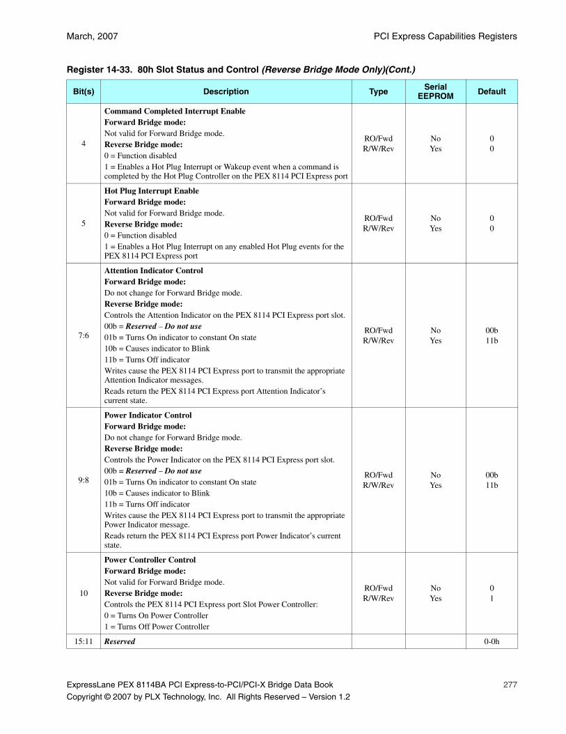
March, 2007 PCI Express Capabilities Registers
ExpressLane PEX 8114BA PCI Express-to-PCI/PCI-X Bridge Data Book 277
Copyright © 2007 by PLX Technology, Inc. All Rights Reserved – Version 1.2
4
Command Completed Interrupt EnableForward Bridge mode:Not valid for Forward Bridge mode.Reverse Bridge mode:0 = Function disabled1 = Enables a Hot Plug Interrupt or Wakeup event when a command is completed by the Hot Plug Controller on the PEX 8114 PCI Express port
RO/FwdR/W/Rev
NoYes
00
5
Hot Plug Interrupt EnableForward Bridge mode:Not valid for Forward Bridge mode.Reverse Bridge mode:0 = Function disabled1 = Enables a Hot Plug Interrupt on any enabled Hot Plug events for the PEX 8114 PCI Express port
RO/FwdR/W/Rev
NoYes
00
7:6
Attention Indicator ControlForward Bridge mode:Do not change for Forward Bridge mode.Reverse Bridge mode:Controls the Attention Indicator on the PEX 8114 PCI Express port slot.00b = Reserved – Do not use01b = Turns On indicator to constant On state10b = Causes indicator to Blink11b = Turns Off indicatorWrites cause the PEX 8114 PCI Express port to transmit the appropriate Attention Indicator messages.Reads return the PEX 8114 PCI Express port Attention Indicator’s current state.
RO/FwdR/W/Rev
NoYes
00b11b
9:8
Power Indicator ControlForward Bridge mode:Do not change for Forward Bridge mode.Reverse Bridge mode:Controls the Power Indicator on the PEX 8114 PCI Express port slot.00b = Reserved – Do not use01b = Turns On indicator to constant On state10b = Causes indicator to Blink11b = Turns Off indicatorWrites cause the PEX 8114 PCI Express port to transmit the appropriate Power Indicator message.Reads return the PEX 8114 PCI Express port Power Indicator’s current state.
RO/FwdR/W/Rev
NoYes
00b11b
10
Power Controller ControlForward Bridge mode:Not valid for Forward Bridge mode.Reverse Bridge mode:Controls the PEX 8114 PCI Express port Slot Power Controller:0 = Turns On Power Controller1 = Turns Off Power Controller
RO/FwdR/W/Rev
NoYes
01
15:11 Reserved 0-0h
Register 14-33. 80h Slot Status and Control (Reverse Bridge Mode Only)(Cont.)
Bit(s) Description Type Serial EEPROM Default

PEX 8114 Transparent Mode Registers PLX Technology, Inc.
278 ExpressLane PEX 8114BA PCI Express-to-PCI/PCI-X Bridge Data Book
Copyright © 2007 by PLX Technology, Inc. All Rights Reserved – Version 1.2
Slot Status
16
Attention Button PressedForward Bridge mode:Not valid for Forward Bridge mode.Reverse Bridge mode:Set to 1 when the PEX 8114 PCI Express port slot Attention Button is pressed.
RO/FwdR/W1C/Rev
NoYes
00
17
Power Fault DetectedForward Bridge mode:Not valid for Forward Bridge mode.Reverse Bridge mode:Set to 1 when the PEX 8114 PCI Express port Slot Power Controller detects a Power Fault at the slot.
RO/FwdR/W1C/Rev
NoYes
00
18
MRL Sensor ChangedForward Bridge mode:Not valid for Forward Bridge mode.Reverse Bridge mode:Set to 1 when an MRL state change is detected on the PEX 8114 PCI Express port slot.
RO/FwdR/W1C/Rev
NoYes
00
19
Presence Detect ChangedForward Bridge mode:Not valid for Forward Bridge mode.Reverse Bridge mode:Set to 1 when a Presence Detect Change is detected on the PEX 8114 PCI Express port slot.
RO/FwdR/W1C/Rev
NoYes
00
20
Command CompletedForward Bridge mode:Do not change for Forward Bridge mode.Reverse Bridge mode:Set to 1 when the PEX 8114 PCI Express port slot Hot Plug Controller completes an issued command.
RO/FwdR/W1C/Rev
NoYes
00
21
MRL Sensor StateForward Bridge mode:Do not change for Forward Bridge mode.Reverse Bridge mode:Reveals the PEX 8114 PCI Express port MRL sensor’s current state.0 = MRL sensor closed1 = MRL sensor open
RO/FwdRO/Rev
NoYes
00
22
Presence Detect StateForward Bridge mode:Do not use for Forward Bridge mode.Reverse Bridge mode:Reveals the PEX 8114 PCI Express port slot’s current state.0 = Slot empty1 = Slot occupied
RO/FwdRO/Rev
NoYes
00
31:23 Reserved 0-0h
Register 14-33. 80h Slot Status and Control (Reverse Bridge Mode Only)(Cont.)
Bit(s) Description Type Serial EEPROM Default
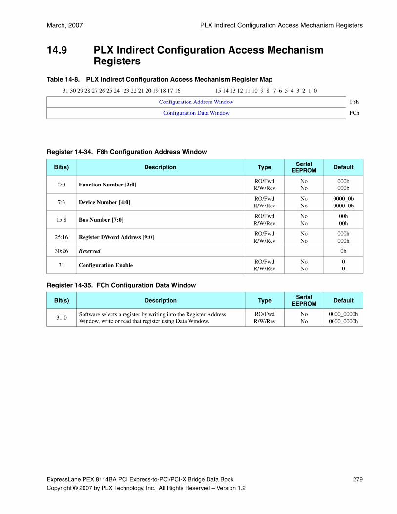
March, 2007 PLX Indirect Configuration Access Mechanism Registers
ExpressLane PEX 8114BA PCI Express-to-PCI/PCI-X Bridge Data Book 279
Copyright © 2007 by PLX Technology, Inc. All Rights Reserved – Version 1.2
14.9 PLX Indirect Configuration Access Mechanism Registers
Table 14-8. PLX Indirect Configuration Access Mechanism Register Map
31 30 29 28 27 26 25 24 23 22 21 20 19 18 17 16 15 14 13 12 11 10 9 8 7 6 5 4 3 2 1 0
Configuration Address Window F8h
Configuration Data Window FCh
Register 14-34. F8h Configuration Address Window
Bit(s) Description Type Serial EEPROM Default
2:0 Function Number [2:0]RO/FwdR/W/Rev
NoNo
000b000b
7:3 Device Number [4:0]RO/FwdR/W/Rev
NoNo
0000_0b0000_0b
15:8 Bus Number [7:0]RO/FwdR/W/Rev
NoNo
00h00h
25:16 Register DWord Address [9:0]RO/FwdR/W/Rev
NoNo
000h000h
30:26 Reserved 0h
31 Configuration EnableRO/FwdR/W/Rev
NoNo
00
Register 14-35. FCh Configuration Data Window
Bit(s) Description Type Serial EEPROM Default
31:0 Software selects a register by writing into the Register Address Window, write or read that register using Data Window.
RO/FwdR/W/Rev
NoNo
0000_0000h0000_0000h
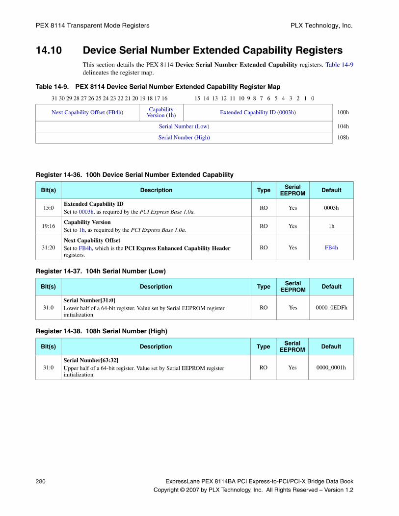
PEX 8114 Transparent Mode Registers PLX Technology, Inc.
280 ExpressLane PEX 8114BA PCI Express-to-PCI/PCI-X Bridge Data Book
Copyright © 2007 by PLX Technology, Inc. All Rights Reserved – Version 1.2
14.10 Device Serial Number Extended Capability RegistersThis section details the PEX 8114 Device Serial Number Extended Capability registers. Table 14-9delineates the register map.
Table 14-9. PEX 8114 Device Serial Number Extended Capability Register Map
31 30 29 28 27 26 25 24 23 22 21 20 19 18 17 16 15 14 13 12 11 10 9 8 7 6 5 4 3 2 1 0
Next Capability Offset (FB4h) Capability Version (1h) Extended Capability ID (0003h) 100h
Serial Number (Low) 104h
Serial Number (High) 108h
Register 14-36. 100h Device Serial Number Extended Capability
Bit(s) Description Type Serial EEPROM Default
15:0Extended Capability IDSet to 0003h, as required by the PCI Express Base 1.0a.
RO Yes 0003h
19:16Capability VersionSet to 1h, as required by the PCI Express Base 1.0a.
RO Yes 1h
31:20Next Capability OffsetSet to FB4h, which is the PCI Express Enhanced Capability Header registers.
RO Yes FB4h
Register 14-37. 104h Serial Number (Low)
Bit(s) Description Type Serial EEPROM Default
31:0Serial Number[31:0]Lower half of a 64-bit register. Value set by Serial EEPROM register initialization.
RO Yes 0000_0EDFh
Register 14-38. 108h Serial Number (High)
Bit(s) Description Type Serial EEPROM Default
31:0Serial Number[63:32]Upper half of a 64-bit register. Value set by Serial EEPROM register initialization.
RO Yes 0000_0001h
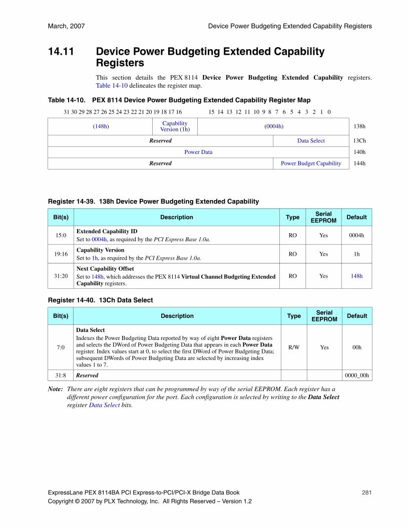
March, 2007 Device Power Budgeting Extended Capability Registers
ExpressLane PEX 8114BA PCI Express-to-PCI/PCI-X Bridge Data Book 281
Copyright © 2007 by PLX Technology, Inc. All Rights Reserved – Version 1.2
14.11 Device Power Budgeting Extended Capability RegistersThis section details the PEX 8114 Device Power Budgeting Extended Capability registers.Table 14-10 delineates the register map.
Note: There are eight registers that can be programmed by way of the serial EEPROM. Each register has a different power configuration for the port. Each configuration is selected by writing to the Data Select register Data Select bits.
Table 14-10. PEX 8114 Device Power Budgeting Extended Capability Register Map
31 30 29 28 27 26 25 24 23 22 21 20 19 18 17 16 15 14 13 12 11 10 9 8 7 6 5 4 3 2 1 0
(148h) Capability Version (1h) (0004h) 138h
Reserved Data Select 13Ch
Power Data 140h
Reserved Power Budget Capability 144h
Register 14-39. 138h Device Power Budgeting Extended Capability
Bit(s) Description Type Serial EEPROM Default
15:0Extended Capability IDSet to 0004h, as required by the PCI Express Base 1.0a.
RO Yes 0004h
19:16Capability VersionSet to 1h, as required by the PCI Express Base 1.0a.
RO Yes 1h
31:20Next Capability OffsetSet to 148h, which addresses the PEX 8114 Virtual Channel Budgeting Extended Capability registers.
RO Yes 148h
Register 14-40. 13Ch Data Select
Bit(s) Description Type Serial EEPROM Default
7:0
Data SelectIndexes the Power Budgeting Data reported by way of eight Power Data registers and selects the DWord of Power Budgeting Data that appears in each Power Data register. Index values start at 0, to select the first DWord of Power Budgeting Data; subsequent DWords of Power Budgeting Data are selected by increasing index values 1 to 7.
R/W Yes 00h
31:8 Reserved 0000_00h
PEX 8114 Transparent Mode Registers PLX Technology, Inc.
282 ExpressLane PEX 8114BA PCI Express-to-PCI/PCI-X Bridge Data Book
Copyright © 2007 by PLX Technology, Inc. All Rights Reserved – Version 1.2
Register 14-41. 140h Power Data
Bit(s) Description Type Serial EEPROM Default
7:0
Base PowerFour registers. Specifies, in watts, the base power value in the operating condition. This value must be multiplied by the Data Scale to produce the actual power consumption value.
RO Yes 00h
9:8
Data ScaleSpecifies the scale to apply to the Base Power value. The power consumption of the device is determined by multiplying the Base Power field contents with the value corresponding to the encoding returned by this field. Defined encodings are:00b = 1.0x01b = 0.1x10b = 0.01x11b = 0.001x
RO Yes 00b
12:10PM Sub-State000b = PEX 8114 is in the default Power Management sub-state
RO Yes 000b
14:13
PM StateCurrent power state.00b = D0 state01b = Not used – D1 state not supported10b = Not used – D2 state not supported11b = D3 state
RO Yes 00b
17:15
TypeType of operating condition.000b = PME Auxiliary001b = Auxiliary010b = Idle011b = Sustained111b = MaximumAll other values are reserved.
RO Yes 000b
20:18
Power RailPower Rail of operating condition.000b = Power 12V001b = Power 3.3V010b = Power 1.8V111b = ThermalAll other values are reserved.
RO Yes 000b
31:21 Reserved 0-0h
Register 14-42. 144h Power Budget Capability
Bit(s) Description Type Serial EEPROM Default
0System Allocated1 = Power budget for the device is included within the system power budget
HwInit Yes 1
31:1 Reserved 0-0h
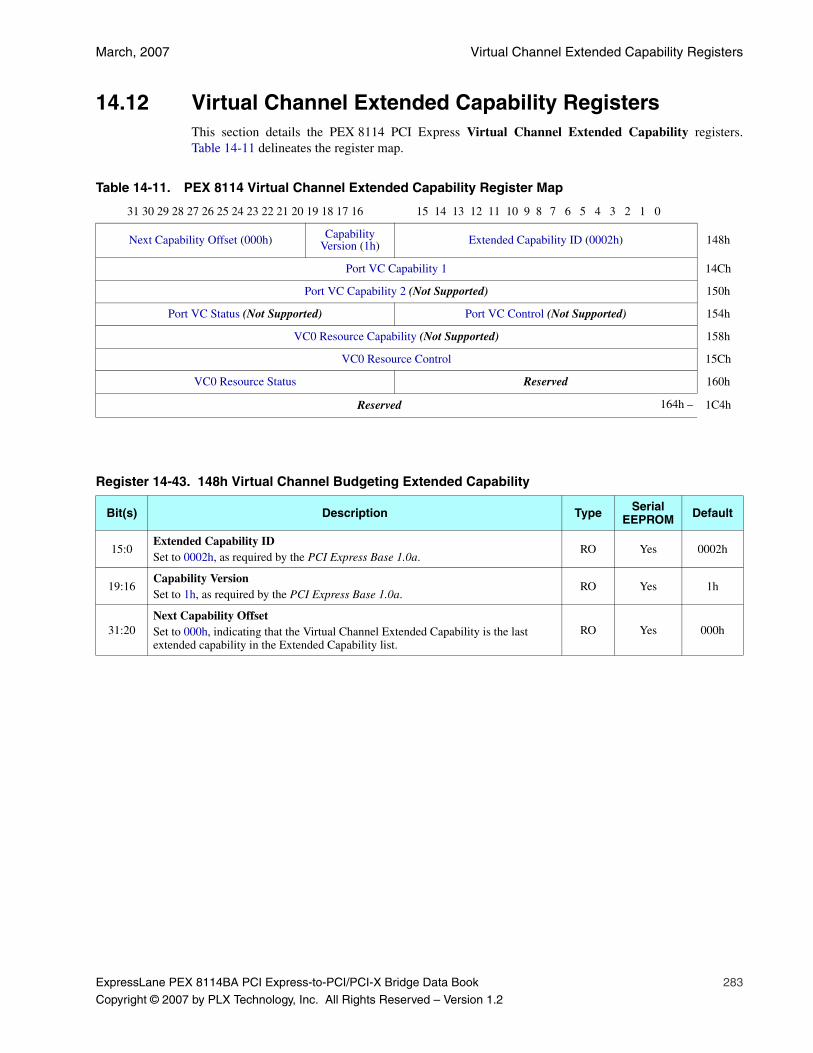
March, 2007 Virtual Channel Extended Capability Registers
ExpressLane PEX 8114BA PCI Express-to-PCI/PCI-X Bridge Data Book 283
Copyright © 2007 by PLX Technology, Inc. All Rights Reserved – Version 1.2
14.12 Virtual Channel Extended Capability RegistersThis section details the PEX 8114 PCI Express Virtual Channel Extended Capability registers.Table 14-11 delineates the register map.
Table 14-11. PEX 8114 Virtual Channel Extended Capability Register Map
31 30 29 28 27 26 25 24 23 22 21 20 19 18 17 16 15 14 13 12 11 10 9 8 7 6 5 4 3 2 1 0
Next Capability Offset (000h) Capability Version (1h) Extended Capability ID (0002h) 148h
Port VC Capability 1 14Ch
Port VC Capability 2 (Not Supported) 150h
Port VC Status (Not Supported) Port VC Control (Not Supported) 154h
VC0 Resource Capability (Not Supported) 158h
VC0 Resource Control 15Ch
VC0 Resource Status Reserved 160h
Reserved 164h – 1C4h
Register 14-43. 148h Virtual Channel Budgeting Extended Capability
Bit(s) Description Type Serial EEPROM Default
15:0Extended Capability IDSet to 0002h, as required by the PCI Express Base 1.0a.
RO Yes 0002h
19:16Capability VersionSet to 1h, as required by the PCI Express Base 1.0a.
RO Yes 1h
31:20Next Capability OffsetSet to 000h, indicating that the Virtual Channel Extended Capability is the last extended capability in the Extended Capability list.
RO Yes 000h
PEX 8114 Transparent Mode Registers PLX Technology, Inc.
284 ExpressLane PEX 8114BA PCI Express-to-PCI/PCI-X Bridge Data Book
Copyright © 2007 by PLX Technology, Inc. All Rights Reserved – Version 1.2
Register 14-44. 14Ch Port VC Capability 1
Bit(s) Description Type Serial EEPROM Default
0Extended VC Count0 = PEX 8114 supports only the default Virtual Channel 0
RO No 0
3:1 Reserved 000b
4
Low-Priority Extended VC CountFor strict priority arbitration, indicates the number of extended virtual channels (those in addition to the default Virtual Channel 0) that belong to the Low-Priority Virtual Channel group for the PEX 8114.0 = For the PEX 8114, only the default Virtual Channel 0 belongs to the Low-Priority Virtual Channel group
RO No 0
7:5 Reserved 000b
9:8Reference ClocksNot supported. Cleared to 00b.
RO No 00b
11:10Port Arbitration Table-Entry SizeNot supported. Cleared to 00b.
RO No 00b
31:12 Reserved 0-0h
Register 14-45. 150h Port VC Capability 2
Bit(s) Description Type Serial EEPROM Default
1:0VC Arbitration CapabilitiesNot supported. Cleared to 00b.
RO No 00b
23:2 Reserved 0-0h
31:24VC Arbitration Table OffsetNot supported. Cleared to 00h.
RO No 00h
Register 14-46. 154h Port VC Status and Control
Bit(s) Description Type Serial EEPROM Default
Port VC Control
0Load VC Arbitration TableNot supported. Cleared to 0.
RO No 0
1VC Arbitration SelectNot supported. Cleared to 0.
RO No 0
15:2 Reserved 0-0h
Port VC Status
16VC Arbitration Table StatusNot supported. Cleared to 0.
RO No 0
31:17 Reserved 0-0h
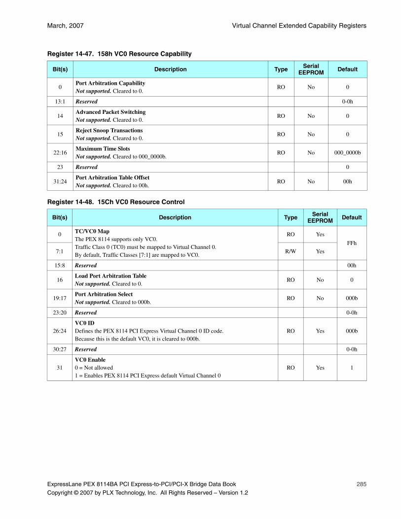
March, 2007 Virtual Channel Extended Capability Registers
ExpressLane PEX 8114BA PCI Express-to-PCI/PCI-X Bridge Data Book 285
Copyright © 2007 by PLX Technology, Inc. All Rights Reserved – Version 1.2
Register 14-47. 158h VC0 Resource Capability
Bit(s) Description Type Serial EEPROM Default
0Port Arbitration CapabilityNot supported. Cleared to 0.
RO No 0
13:1 Reserved 0-0h
14Advanced Packet SwitchingNot supported. Cleared to 0.
RO No 0
15Reject Snoop TransactionsNot supported. Cleared to 0.
RO No 0
22:16Maximum Time SlotsNot supported. Cleared to 000_0000b.
RO No 000_0000b
23 Reserved 0
31:24Port Arbitration Table OffsetNot supported. Cleared to 00h.
RO No 00h
Register 14-48. 15Ch VC0 Resource Control
Bit(s) Description Type Serial EEPROM Default
0 TC/VC0 MapThe PEX 8114 supports only VC0.Traffic Class 0 (TC0) must be mapped to Virtual Channel 0.By default, Traffic Classes [7:1] are mapped to VC0.
RO Yes
FFh
7:1 R/W Yes
15:8 Reserved 00h
16Load Port Arbitration TableNot supported. Cleared to 0.
RO No 0
19:17Port Arbitration SelectNot supported. Cleared to 000b.
RO No 000b
23:20 Reserved 0-0h
26:24VC0 IDDefines the PEX 8114 PCI Express Virtual Channel 0 ID code.Because this is the default VC0, it is cleared to 000b.
RO Yes 000b
30:27 Reserved 0-0h
31VC0 Enable0 = Not allowed1 = Enables PEX 8114 PCI Express default Virtual Channel 0
RO Yes 1

PEX 8114 Transparent Mode Registers PLX Technology, Inc.
286 ExpressLane PEX 8114BA PCI Express-to-PCI/PCI-X Bridge Data Book
Copyright © 2007 by PLX Technology, Inc. All Rights Reserved – Version 1.2
Register 14-49. 160h VC0 Resource Status
Bit(s) Description Type Serial EEPROM Default
15:0 Reserved 0000h
16Port Arbitration Table StatusNot supported. Cleared to 0.
RO No 0
17VC0 Negotiation Pending0 = VC0 negotiation completed1 = VC0 initialization is not complete for the PEX 8114 PCI Express link
RO Yes 1
31:18 Reserved 0-0h
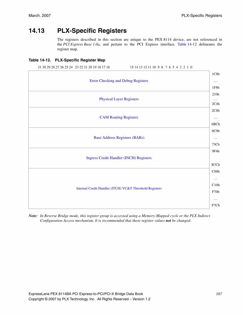
March, 2007 PLX-Specific Registers
ExpressLane PEX 8114BA PCI Express-to-PCI/PCI-X Bridge Data Book 287
Copyright © 2007 by PLX Technology, Inc. All Rights Reserved – Version 1.2
14.13 PLX-Specific RegistersThe registers described in this section are unique to the PEX 8114 device, are not referenced inthe PCI Express Base 1.0a, and pertain to the PCI Express interface. Table 14-12 delineates theregister map.
Note: In Reverse Bridge mode, this register group is accessed using a Memory-Mapped cycle or the PLX Indirect Configuration Access mechanism. It is recommended that these register values not be changed.
Table 14-12. PLX-Specific Register Map
31 30 29 28 27 26 25 24 23 22 21 20 19 18 17 16 15 14 13 12 11 10 9 8 7 6 5 4 3 2 1 0
Error Checking and Debug Registers
1C8h
…
1F8h
Physical Layer Registers210h…
2C4h
CAM Routing Registers
2C8h
…
6BCh
Base Address Registers (BARs)
6C0h
…
73Ch
Ingress Credit Handler (INCH) Registers
9F4h
B7Ch
Internal Credit Handler (ITCH) VC&T Threshold Registers
C00h
…
C10h
F70h
…
F7Ch
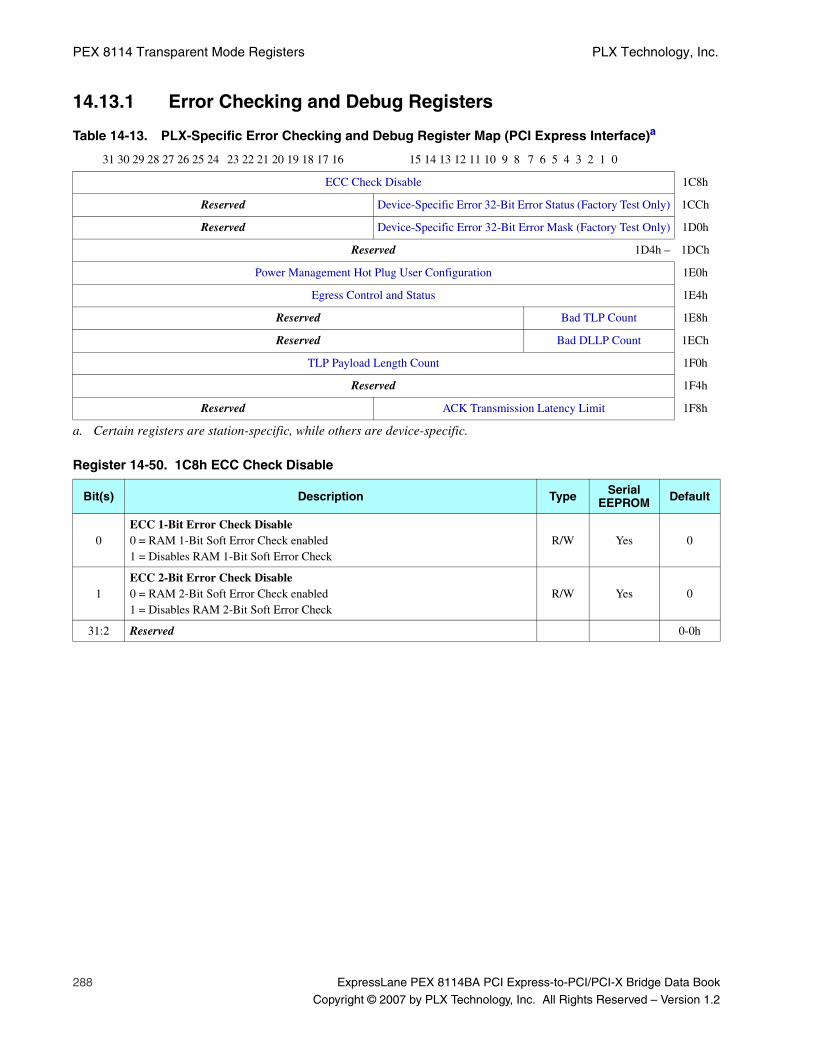
PEX 8114 Transparent Mode Registers PLX Technology, Inc.
288 ExpressLane PEX 8114BA PCI Express-to-PCI/PCI-X Bridge Data Book
Copyright © 2007 by PLX Technology, Inc. All Rights Reserved – Version 1.2
14.13.1 Error Checking and Debug Registers
Table 14-13. PLX-Specific Error Checking and Debug Register Map (PCI Express Interface)a
a. Certain registers are station-specific, while others are device-specific.
31 30 29 28 27 26 25 24 23 22 21 20 19 18 17 16 15 14 13 12 11 10 9 8 7 6 5 4 3 2 1 0
ECC Check Disable 1C8h
Reserved Device-Specific Error 32-Bit Error Status (Factory Test Only) 1CCh
Reserved Device-Specific Error 32-Bit Error Mask (Factory Test Only) 1D0h
Reserved 1D4h – 1DCh
Power Management Hot Plug User Configuration 1E0h
Egress Control and Status 1E4h
Reserved Bad TLP Count 1E8h
Reserved Bad DLLP Count 1ECh
TLP Payload Length Count 1F0h
Reserved 1F4h
Reserved ACK Transmission Latency Limit 1F8h
Register 14-50. 1C8h ECC Check Disable
Bit(s) Description Type Serial EEPROM Default
0ECC 1-Bit Error Check Disable0 = RAM 1-Bit Soft Error Check enabled1 = Disables RAM 1-Bit Soft Error Check
R/W Yes 0
1ECC 2-Bit Error Check Disable0 = RAM 2-Bit Soft Error Check enabled1 = Disables RAM 2-Bit Soft Error Check
R/W Yes 0
31:2 Reserved 0-0h

March, 2007 Error Checking and Debug Registers
ExpressLane PEX 8114BA PCI Express-to-PCI/PCI-X Bridge Data Book 289
Copyright © 2007 by PLX Technology, Inc. All Rights Reserved – Version 1.2
Note: All errors in this register generate MSI/INTA# interrupts, if enabled.
Register 14-51. 1CCh Device-Specific Error 32-Bit Error Status (Factory Test Only)
Bit(s) Description Type Serial EEPROM Default
0
Device-Specific Error Completion FIFO Overflow Status0 = No overflow detected1 = Completion FIFO Overflow detected when 4-deep Completion FIFO for ingress, or 2-deep Completion FIFO for egress, overflows
R/W1CS Yes 0
1
Egress PRAM Soft Error OverflowEgress Packet RAM 1-bit Soft Error Counter overflow.0 = No error detected1 = Egress PRAM 1-bit Soft Error (8-bit Counter) overflow when destination packet RAM 1-bit soft error count is greater than or equal to 256, it generates an MSI/INTA# interrupt, if enabled
R/W1CS Yes 0
2
Egress LLIST Soft Error OverflowEgress Link-List RAM 1-bit Soft Error Counter overflow.0 = No error detected1 = Egress Link-List 1-bit Soft Error (8-bit Counter) overflow when destination module link lists RAM 1-bit soft error count is greater than or equal to 256, it generates an MSI/INTA# interrupt, if enabled
R/W1CS Yes 0
3
Egress PRAM ECC ErrorEgress Packet RAM 2-bit error detection.0 = No error detected1 = Egress PRAM 2-bit ECC error detected
R/W1CS Yes 0
4
Egress LLIST ECC ErrorEgress Link-List RAM 2-bit error detection.0 = No error detected1 = Egress Link-List 2-bit ECC error detected
R/W1CS Yes 0
5
Ingress RAM 1-Bit ECC ErrorSource Packet RAM 1-bit soft error detection.0 = No error detected1 = Ingress RAM 1-BIT ECC error detected
R/W1CS Yes 0
6
Egress Memory Allocation Unit (MAU) 1-Bit Soft Error Counter OverflowEgress Memory Allocation/De-allocation RAM 1-bit soft error count is greater than or equal to 8.0 = No error detected1 = Egress MAU 1-bit Soft Error overflow
R/W1CS Yes 0
7
Egress Memory Allocation Unit (MAU) 2-Bit Soft ErrorEgress Packet Memory Allocation/De-allocation RAM 2-bit error detection.0 = No 2-bit error detected1 = Egress MAU 2-bit soft error detected
R/W1CS Yes 0

PEX 8114 Transparent Mode Registers PLX Technology, Inc.
290 ExpressLane PEX 8114BA PCI Express-to-PCI/PCI-X Bridge Data Book
Copyright © 2007 by PLX Technology, Inc. All Rights Reserved – Version 1.2
8
Ingress RAM Uncorrectable ECC ErrorIngress Packet RAM 2-bit Error detection.0 = No 2-bit error detected1 = Packet RAM Uncorrectable ECC error detected
R/W1CS Yes 0
9
Ingress LLIST 1-Bit ECC ErrorIngress Link-List RAM 1-bit soft error detection.0 = No error detected1 = 1-bit ECC error detected
R/W1CS Yes 0
10
Ingress LLIST Uncorrectable ECC ErrorIngress packet Link-List RAM 2-bit error detection.0 = No 2-bit error detected1 = Ingress Link-List Uncorrectable ECC Error detected
R/W1CS Yes 0
11
Credit Update Timeout StatusNo useful credit update to make forward progress for 512 ms or 1s (disabled by default).0 = No Credit Update Timeout detected1 = Credit Update Timeout completed
R/W1CS Yes 0
12
INCH Underrun ErrorIngress Credit Underrun.0 = No error detected1 = Credit underrun error detected
R/W1CS Yes 0
13
Ingress Memory Allocation Unit 1-Bit Soft Error Counter OverflowIngress Memory Allocation/De-allocation RAM 1-bit Soft Error count greater than or equal to 8.0 = No error detected1 = 1-bit Soft Error Counter is > 8
R/W1CS Yes 0
14
Ingress Memory Allocation Unit 2-Bit Soft ErrorIngress Memory Allocation/De-allocation RAM 2-bit error detection for Transaction Layer Ingress Memory Allocation/De-allocation unit.0 = No error detected1 = 2-bit soft error detected
R/W1CS Yes 0
31:15 Reserved 0-0h
Register 14-51. 1CCh Device-Specific Error 32-Bit Error Status (Factory Test Only)(Cont.)
Bit(s) Description Type Serial EEPROM Default
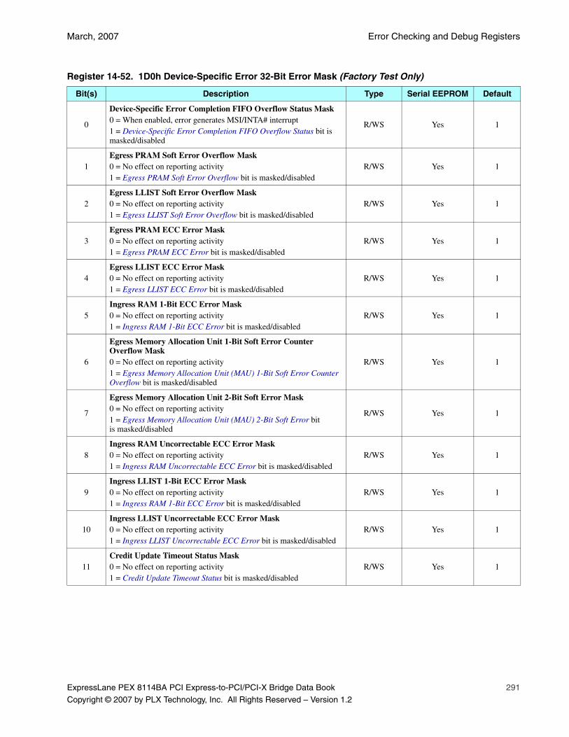
March, 2007 Error Checking and Debug Registers
ExpressLane PEX 8114BA PCI Express-to-PCI/PCI-X Bridge Data Book 291
Copyright © 2007 by PLX Technology, Inc. All Rights Reserved – Version 1.2
Register 14-52. 1D0h Device-Specific Error 32-Bit Error Mask (Factory Test Only)
Bit(s) Description Type Serial EEPROM Default
0
Device-Specific Error Completion FIFO Overflow Status Mask0 = When enabled, error generates MSI/INTA# interrupt1 = Device-Specific Error Completion FIFO Overflow Status bit is masked/disabled
R/WS Yes 1
1Egress PRAM Soft Error Overflow Mask0 = No effect on reporting activity1 = Egress PRAM Soft Error Overflow bit is masked/disabled
R/WS Yes 1
2Egress LLIST Soft Error Overflow Mask0 = No effect on reporting activity1 = Egress LLIST Soft Error Overflow bit is masked/disabled
R/WS Yes 1
3Egress PRAM ECC Error Mask0 = No effect on reporting activity1 = Egress PRAM ECC Error bit is masked/disabled
R/WS Yes 1
4Egress LLIST ECC Error Mask0 = No effect on reporting activity1 = Egress LLIST ECC Error bit is masked/disabled
R/WS Yes 1
5Ingress RAM 1-Bit ECC Error Mask0 = No effect on reporting activity1 = Ingress RAM 1-Bit ECC Error bit is masked/disabled
R/WS Yes 1
6
Egress Memory Allocation Unit 1-Bit Soft Error Counter Overflow Mask0 = No effect on reporting activity1 = Egress Memory Allocation Unit (MAU) 1-Bit Soft Error Counter Overflow bit is masked/disabled
R/WS Yes 1
7
Egress Memory Allocation Unit 2-Bit Soft Error Mask0 = No effect on reporting activity1 = Egress Memory Allocation Unit (MAU) 2-Bit Soft Error bit is masked/disabled
R/WS Yes 1
8Ingress RAM Uncorrectable ECC Error Mask0 = No effect on reporting activity1 = Ingress RAM Uncorrectable ECC Error bit is masked/disabled
R/WS Yes 1
9Ingress LLIST 1-Bit ECC Error Mask0 = No effect on reporting activity 1 = Ingress RAM 1-Bit ECC Error bit is masked/disabled
R/WS Yes 1
10Ingress LLIST Uncorrectable ECC Error Mask0 = No effect on reporting activity1 = Ingress LLIST Uncorrectable ECC Error bit is masked/disabled
R/WS Yes 1
11Credit Update Timeout Status Mask0 = No effect on reporting activity1 = Credit Update Timeout Status bit is masked/disabled
R/WS Yes 1

PEX 8114 Transparent Mode Registers PLX Technology, Inc.
292 ExpressLane PEX 8114BA PCI Express-to-PCI/PCI-X Bridge Data Book
Copyright © 2007 by PLX Technology, Inc. All Rights Reserved – Version 1.2
12INCH Underrun Error Mask0 = No effect on reporting activity1 = INCH Underrun Error bit is masked/disabled
R/WS Yes 1
13
Ingress Memory Allocation Unit 1-Bit Soft Error Counter Overflow Mask0 = No effect on reporting activity1 = TIC_MAU 1-bit Soft Error Counter-overflow is masked/disabled
R/WS Yes 1
14Ingress Memory Allocation Unit 2-Bit Soft Error Mask0 = Error reporting enabled using interrupts1 = 2-Bit soft error reporting is masked/disabled
R/WS Yes 1
31:15 Reserved 0-0h
Register 14-53. 1E0h Power Management Hot Plug User Configuration
Bit(s) Description Type Serial EEPROM Default
0
L0s Entry Idle CountTime to meet to enter L0s.0 = Idle condition lasts for 1 µs1 = Idle condition lasts for 4 µs
R/W Yes 0
1
L1 Upstream Port Receiver Idle CountFor active L1 entry.0 = Upstream port receiver idle for 2 µs1 = Upstream port receiver idle for 3 µs
R/W Yes 0
2HPC PME Turn-Off Enable1 = PME Turn-off message is transmitted before the port is turned off on downstream port
R/W Yes 0
4:3
HPC Tpepv DelaySlot power-applied to power-valid delay time.00b = 16 ms 01b = 32 ms 10b = 64 ms 11b = 128 ms
RO Yes 00b
5
HPC Inband Presence Detect Enable0 = HP_PRSNT# Input ball used to detect a board present in the slot1 = SerDes receiver detect mechanism is used to detect a board present in the slot
RO Yes 0
6
HPC Tpvperl DelayDownstream port power-valid to reset signal release time.0 = 20 ms1 = 100 ms
RO Yes 1
12:7HPC Test BitsFactory Test Only. Testing bits – must be 0_0000_0b.
R/W Yes 0_0000_0b
31:13 Reserved 0-0h
Register 14-52. 1D0h Device-Specific Error 32-Bit Error Mask (Factory Test Only)(Cont.)
Bit(s) Description Type Serial EEPROM Default
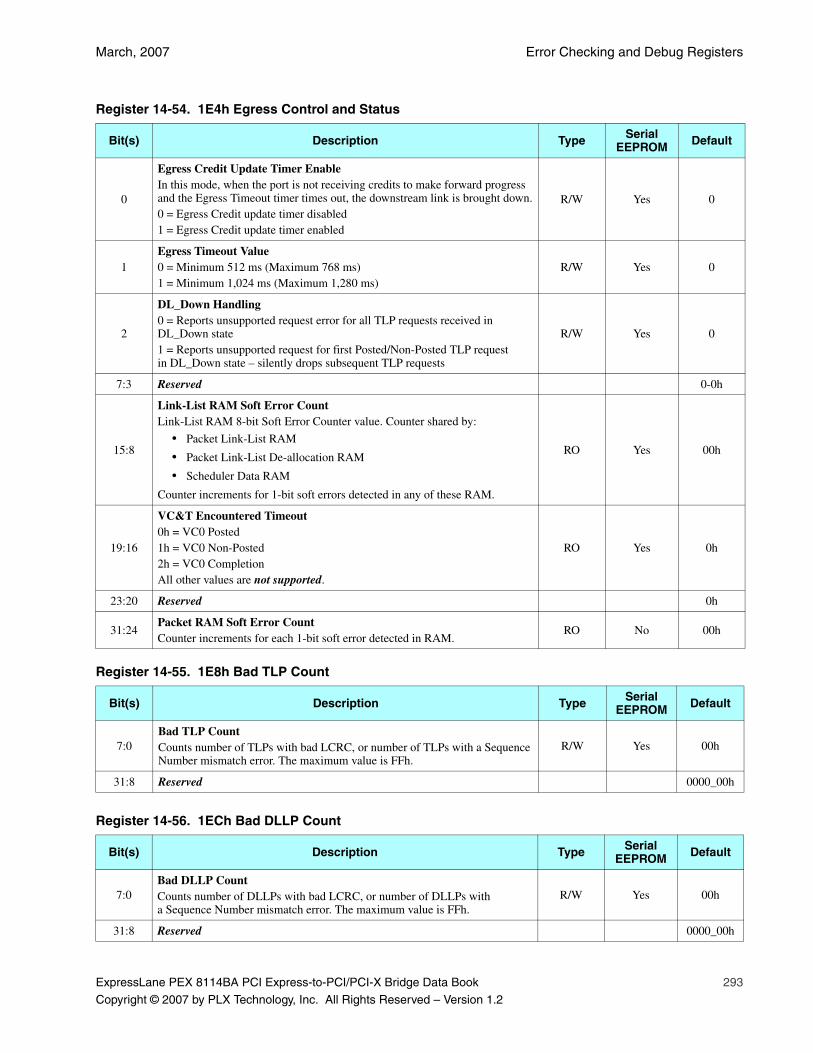
March, 2007 Error Checking and Debug Registers
ExpressLane PEX 8114BA PCI Express-to-PCI/PCI-X Bridge Data Book 293
Copyright © 2007 by PLX Technology, Inc. All Rights Reserved – Version 1.2
Register 14-54. 1E4h Egress Control and Status
Bit(s) Description Type Serial EEPROM Default
0
Egress Credit Update Timer EnableIn this mode, when the port is not receiving credits to make forward progress and the Egress Timeout timer times out, the downstream link is brought down.0 = Egress Credit update timer disabled1 = Egress Credit update timer enabled
R/W Yes 0
1Egress Timeout Value0 = Minimum 512 ms (Maximum 768 ms)1 = Minimum 1,024 ms (Maximum 1,280 ms)
R/W Yes 0
2
DL_Down Handling0 = Reports unsupported request error for all TLP requests received in DL_Down state1 = Reports unsupported request for first Posted/Non-Posted TLP request in DL_Down state – silently drops subsequent TLP requests
R/W Yes 0
7:3 Reserved 0-0h
15:8
Link-List RAM Soft Error CountLink-List RAM 8-bit Soft Error Counter value. Counter shared by:
• Packet Link-List RAM
• Packet Link-List De-allocation RAM
• Scheduler Data RAM
Counter increments for 1-bit soft errors detected in any of these RAM.
RO Yes 00h
19:16
VC&T Encountered Timeout0h = VC0 Posted1h = VC0 Non-Posted2h = VC0 CompletionAll other values are not supported.
RO Yes 0h
23:20 Reserved 0h
31:24Packet RAM Soft Error CountCounter increments for each 1-bit soft error detected in RAM.
RO No 00h
Register 14-55. 1E8h Bad TLP Count
Bit(s) Description Type Serial EEPROM Default
7:0Bad TLP CountCounts number of TLPs with bad LCRC, or number of TLPs with a Sequence Number mismatch error. The maximum value is FFh.
R/W Yes 00h
31:8 Reserved 0000_00h
Register 14-56. 1ECh Bad DLLP Count
Bit(s) Description Type Serial EEPROM Default
7:0Bad DLLP CountCounts number of DLLPs with bad LCRC, or number of DLLPs with a Sequence Number mismatch error. The maximum value is FFh.
R/W Yes 00h
31:8 Reserved 0000_00h
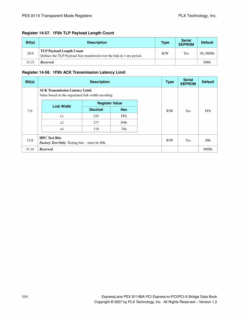
PEX 8114 Transparent Mode Registers PLX Technology, Inc.
294 ExpressLane PEX 8114BA PCI Express-to-PCI/PCI-X Bridge Data Book
Copyright © 2007 by PLX Technology, Inc. All Rights Reserved – Version 1.2
Register 14-57. 1F0h TLP Payload Length Count
Bit(s) Description Type Serial EEPROM Default
20:0TLP Payload Length CountDefines the TLP Payload Size transferred over the link in 1-ms period.
R/W Yes 00_0000h
31:21 Reserved 000h
Register 14-58. 1F8h ACK Transmission Latency Limit
Bit(s) Description Type Serial EEPROM Default
7:0
ACK Transmission Latency LimitValue based on the negotiated link width encoding:
R/W Yes FFh
15:8HPC Test BitsFactory Test Only. Testing bits – must be 00h.
R/W Yes 00h
31:16 Reserved 0000h
Link WidthRegister Value
Decimal Hex
x1 255 FFh
x2 217 D9h
x4 118 76h

March, 2007 Physical Layer Registers
ExpressLane PEX 8114BA PCI Express-to-PCI/PCI-X Bridge Data Book 295
Copyright © 2007 by PLX Technology, Inc. All Rights Reserved – Version 1.2
14.13.2 Physical Layer Registers
Note: In this section, the term “SerDes quad” or “quad” refers to assembling SerDes lanes into a group of four contiguous lanes for testing purposes. The quad is defined as SerDes[0-3].
Table 14-14. PLX-Specific Physical Layer Register Map
31 30 29 28 27 26 25 24 23 22 21 20 19 18 17 16 15 14 13 12 11 10 9 8 7 6 5 4 3 2 1 0
Test Pattern_0 210h
Test Pattern_1 214h
Test Pattern_2 218h
Test Pattern_3 21Ch
Physical Layer Status Physical Layer Control 220h
Port Configuration 224h
Physical Layer Test 228h
Physical Layer (Factory Test Only) 22Ch
Physical Layer Port Command 230h
Skip-Ordered Set Interval 234h
Quad SerDes[0-3] Diagnostics Data 238h
Reserved 23Ch – 244h
Reserved SerDes Nominal Drive Cur-rent Select 248h
Reserved SerDes Drive Current Level_1 24Ch
Reserved 250h
Reserved SerDes Drive Equalization Level Select_1 254h
Reserved 258h – 25Ch
Status Data from Serial EEPROM Serial EEPROM Status Serial EEPROM Control 260h
Serial EEPROM Buffer 264h
Reserved 268h – 2C4h
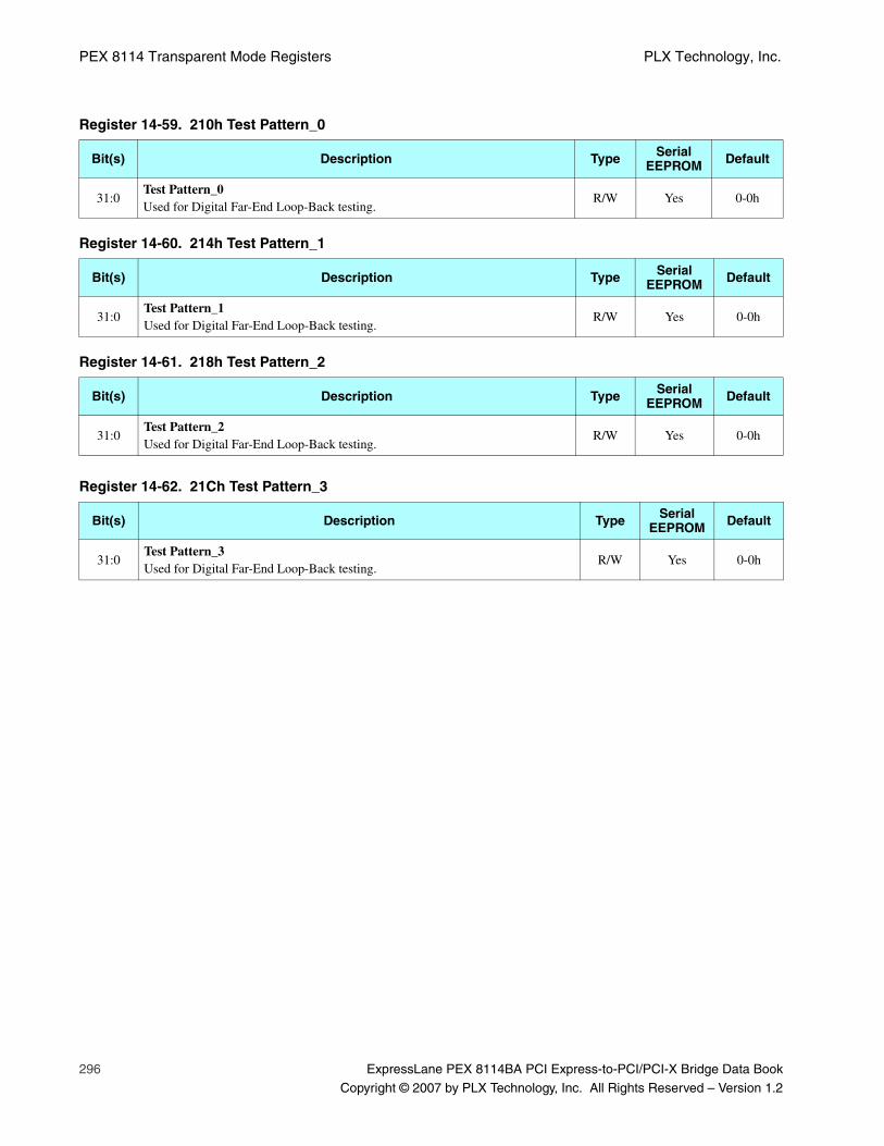
PEX 8114 Transparent Mode Registers PLX Technology, Inc.
296 ExpressLane PEX 8114BA PCI Express-to-PCI/PCI-X Bridge Data Book
Copyright © 2007 by PLX Technology, Inc. All Rights Reserved – Version 1.2
Register 14-59. 210h Test Pattern_0
Bit(s) Description Type Serial EEPROM Default
31:0Test Pattern_0Used for Digital Far-End Loop-Back testing.
R/W Yes 0-0h
Register 14-60. 214h Test Pattern_1
Bit(s) Description Type Serial EEPROM Default
31:0Test Pattern_1Used for Digital Far-End Loop-Back testing.
R/W Yes 0-0h
Register 14-61. 218h Test Pattern_2
Bit(s) Description Type Serial EEPROM Default
31:0Test Pattern_2Used for Digital Far-End Loop-Back testing.
R/W Yes 0-0h
Register 14-62. 21Ch Test Pattern_3
Bit(s) Description Type Serial EEPROM Default
31:0Test Pattern_3Used for Digital Far-End Loop-Back testing.
R/W Yes 0-0h
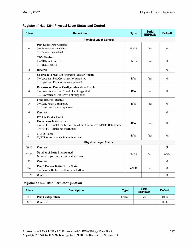
March, 2007 Physical Layer Registers
ExpressLane PEX 8114BA PCI Express-to-PCI/PCI-X Bridge Data Book 297
Copyright © 2007 by PLX Technology, Inc. All Rights Reserved – Version 1.2
Register 14-63. 220h Physical Layer Status and Control
Bit(s) Description Type Serial EEPROM Default
Physical Layer Control
0Port Enumerator Enable0 = Enumerate not enabled1 = Enumerate enabled
HwInit Yes 0
1TDM Enable0 = TDM not enabled1 = TDM enabled
HwInit Yes 0
2 Reserved 0
3Upstream Port as Configuration Master Enable0 = Upstream Port Cross-link not supported1 = Upstream Port Cross-link supported
R/W Yes 0
4Downstream Port as Configuration Slave Enable0 = Downstream Port Cross-link not supported1 = Downstream Port Cross-link supported
R/W Yes 0
5Lane Reversal Disable0 = Lane reversal supported1 = Lane reversal not supported
R/W Yes 0
6 Reserved 0
7
FC-Init Triplet EnableFlow control Initialization.0 = Init FL1 Triplet can be interrupted by skip-ordered set/Idle Data symbol1 = Init FL1 Triplet not interrupted
R/W Yes 0
15:8N_FTS ValueN_FTS value to transmit in training sets.
R/W Yes 40h
Physical Layer Status
19:16 Reserved 0h
22:20Number of Ports EnumeratedNumber of ports in current configuration.
HwInit Yes 000b
23 Reserved 0
24Port 0 Deskew Buffer Error Status1 = Deskew Buffer overflow or underflow
R/W1C Yes 0
31:25 Reserved 00h
Register 14-64. 224h Port Configuration
Bit(s) Description Type Serial EEPROM Default
2:0 Port Configuration HwInit Yes 000b
31:3 Reserved 0-0h
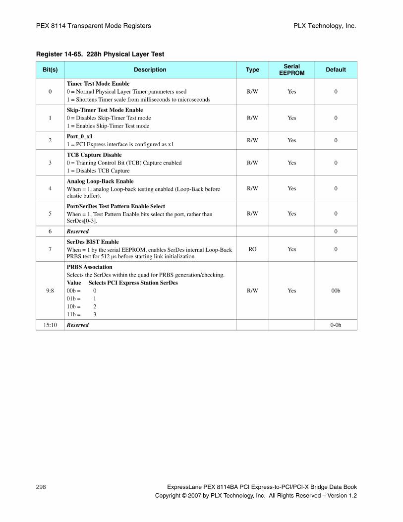
PEX 8114 Transparent Mode Registers PLX Technology, Inc.
298 ExpressLane PEX 8114BA PCI Express-to-PCI/PCI-X Bridge Data Book
Copyright © 2007 by PLX Technology, Inc. All Rights Reserved – Version 1.2
Register 14-65. 228h Physical Layer Test
Bit(s) Description Type Serial EEPROM Default
0Timer Test Mode Enable0 = Normal Physical Layer Timer parameters used1 = Shortens Timer scale from milliseconds to microseconds
R/W Yes 0
1Skip-Timer Test Mode Enable0 = Disables Skip-Timer Test mode1 = Enables Skip-Timer Test mode
R/W Yes 0
2Port_0_x11 = PCI Express interface is configured as x1
R/W Yes 0
3TCB Capture Disable0 = Training Control Bit (TCB) Capture enabled1 = Disables TCB Capture
R/W Yes 0
4Analog Loop-Back EnableWhen = 1, analog Loop-back testing enabled (Loop-Back before elastic buffer).
R/W Yes 0
5Port/SerDes Test Pattern Enable SelectWhen = 1, Test Pattern Enable bits select the port, rather than SerDes[0-3].
R/W Yes 0
6 Reserved 0
7SerDes BIST EnableWhen = 1 by the serial EEPROM, enables SerDes internal Loop-Back PRBS test for 512 µs before starting link initialization.
RO Yes 0
9:8
PRBS AssociationSelects the SerDes within the quad for PRBS generation/checking.Value Selects PCI Express Station SerDes00b = 001b = 110b = 211b = 3
R/W Yes 00b
15:10 Reserved 0-0h
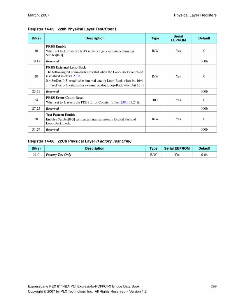
March, 2007 Physical Layer Registers
ExpressLane PEX 8114BA PCI Express-to-PCI/PCI-X Bridge Data Book 299
Copyright © 2007 by PLX Technology, Inc. All Rights Reserved – Version 1.2
16PRBS EnableWhen set to 1, enables PRBS sequence generation/checking on SerDes[0-3].
R/W Yes 0
19:17 Reserved 000b
20
PRBS External Loop-BackThe following bit commands are valid when the Loop-Back command is enabled in offset 230h.0 = SerDes[0-3] establishes internal analog Loop-Back when bit 16=11 = SerDes[0-3] establishes external analog Loop-Back when bit 16=1
R/W Yes 0
23:21 Reserved 000b
24PRBS Error Count ResetWhen set to 1, resets the PRBS Error Counter (offset 238h[31:24]).
RO Yes 0
27:25 Reserved 000b
28Test Pattern EnableEnables SerDes[0-3] test pattern transmission in Digital Far-End Loop-Back mode.
R/W Yes 0
31:29 Reserved 000b
Register 14-66. 22Ch Physical Layer (Factory Test Only)
Bit(s) Description Type Serial EEPROM Default
31:0 Factory Test Only R/W Yes 0-0h
Register 14-65. 228h Physical Layer Test(Cont.)
Bit(s) Description Type Serial EEPROM Default
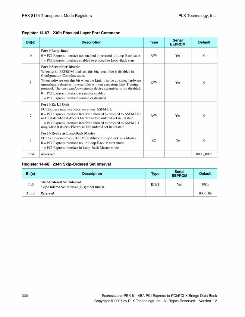
PEX 8114 Transparent Mode Registers PLX Technology, Inc.
300 ExpressLane PEX 8114BA PCI Express-to-PCI/PCI-X Bridge Data Book
Copyright © 2007 by PLX Technology, Inc. All Rights Reserved – Version 1.2
Register 14-67. 230h Physical Layer Port Command
Bit(s) Description Type Serial EEPROM Default
0Port 0 Loop-Back0 = PCI Express interface not enabled to proceed to Loop-Back state1 = PCI Express interface enabled to proceed to Loop-Back state
R/W Yes 0
1
Port 0 Scrambler DisableWhen serial EEPROM load sets this bit, scrambler is disabled in Configuration-Complete state.When software sets this bit when the Link is in the up state, hardware immediately disables its scrambler without executing Link Training protocol. The upstream/downstream device scrambler is not disabled.0 = PCI Express interface scrambler enabled1 = PCI Express interface scrambler disabled
R/W Yes 0
2
Port 0 Rx L1 OnlyPCI Express interface Receiver enters ASPM L1.0 = PCI Express interface Receiver allowed to proceed to ASPM L0s or L1 state when it detects Electrical Idle ordered set in L0 state1 = PCI Express interface Receiver allowed to proceed to ASPM L1 only when it detects Electrical Idle ordered set in L0 state
R/W Yes 0
3
Port 0 Ready as Loop-Back MasterPCI Express interface LTSSM established Loop-Back as a Master.0 = PCI Express interface not in Loop-Back Master mode1 = PCI Express interface in Loop-Back Master mode
RO No 0
31:4 Reserved 0000_000h
Register 14-68. 234h Skip-Ordered Set Interval
Bit(s) Description Type Serial EEPROM Default
11:0SKP-Ordered Set IntervalSkip-Ordered Set Interval (in symbol times).
R/WS Yes 49Ch
31:12 Reserved 0000_0h
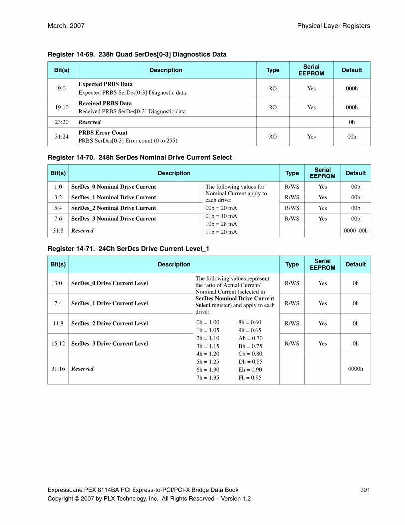
March, 2007 Physical Layer Registers
ExpressLane PEX 8114BA PCI Express-to-PCI/PCI-X Bridge Data Book 301
Copyright © 2007 by PLX Technology, Inc. All Rights Reserved – Version 1.2
Register 14-69. 238h Quad SerDes[0-3] Diagnostics Data
Bit(s) Description Type Serial EEPROM Default
9:0Expected PRBS DataExpected PRBS SerDes[0-3] Diagnostic data.
RO Yes 000h
19:10Received PRBS DataReceived PRBS SerDes[0-3] Diagnostic data.
RO Yes 000h
23:20 Reserved 0h
31:24PRBS Error CountPRBS SerDes[0-3] Error count (0 to 255).
RO Yes 00h
Register 14-70. 248h SerDes Nominal Drive Current Select
Bit(s) Description Type Serial EEPROM Default
1:0 SerDes_0 Nominal Drive Current The following values for Nominal Current apply to each drive:00b = 20 mA01b = 10 mA10b = 28 mA11b = 20 mA
R/WS Yes 00b
3:2 SerDes_1 Nominal Drive Current R/WS Yes 00b
5:4 SerDes_2 Nominal Drive Current R/WS Yes 00b
7:6 SerDes_3 Nominal Drive Current R/WS Yes 00b
31:8 Reserved 0000_00h
Register 14-71. 24Ch SerDes Drive Current Level_1
Bit(s) Description Type Serial EEPROM Default
3:0 SerDes_0 Drive Current LevelThe following values represent the ratio of Actual Current/Nominal Current (selected in SerDes Nominal Drive Current Select register) and apply to each drive:
R/WS Yes 0h
7:4 SerDes_1 Drive Current Level R/WS Yes 0h
11:8 SerDes_2 Drive Current Level R/WS Yes 0h
15:12 SerDes_3 Drive Current Level R/WS Yes 0h
31:16 Reserved 0000h
0h = 1.001h = 1.052h = 1.103h = 1.154h = 1.205h = 1.256h = 1.307h = 1.35
8h = 0.609h = 0.65Ah = 0.70Bh = 0.75Ch = 0.80Dh = 0.85Eh = 0.90Fh = 0.95
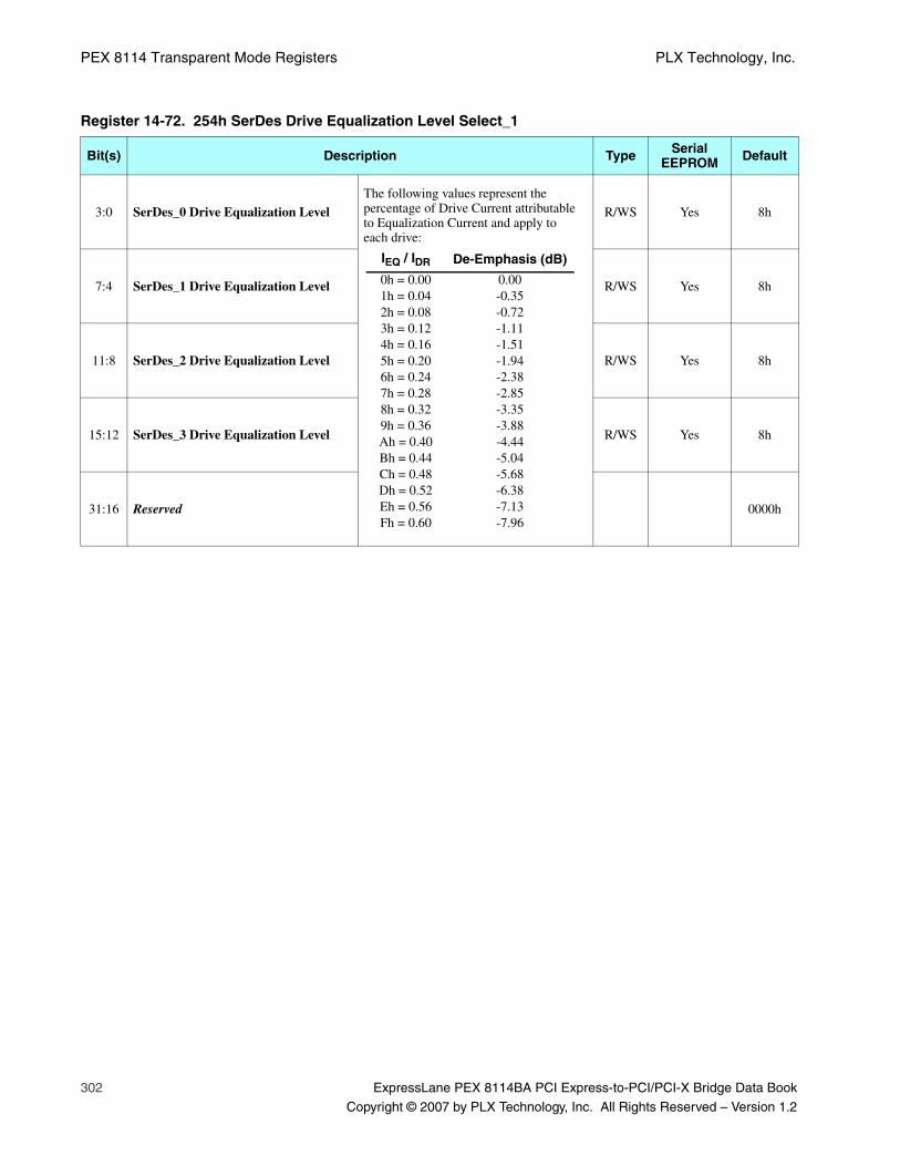
PEX 8114 Transparent Mode Registers PLX Technology, Inc.
302 ExpressLane PEX 8114BA PCI Express-to-PCI/PCI-X Bridge Data Book
Copyright © 2007 by PLX Technology, Inc. All Rights Reserved – Version 1.2
Register 14-72. 254h SerDes Drive Equalization Level Select_1
Bit(s) Description Type Serial EEPROM Default
3:0 SerDes_0 Drive Equalization LevelThe following values represent the percentage of Drive Current attributable to Equalization Current and apply to each drive:
R/WS Yes 8h
7:4 SerDes_1 Drive Equalization Level R/WS Yes 8h
11:8 SerDes_2 Drive Equalization Level R/WS Yes 8h
15:12 SerDes_3 Drive Equalization Level R/WS Yes 8h
31:16 Reserved 0000h
IEQ / IDR De-Emphasis (dB)
0h = 0.001h = 0.042h = 0.083h = 0.124h = 0.165h = 0.206h = 0.247h = 0.288h = 0.329h = 0.36Ah = 0.40Bh = 0.44Ch = 0.48Dh = 0.52Eh = 0.56Fh = 0.60
0.00-0.35-0.72-1.11-1.51-1.94-2.38-2.85-3.35-3.88-4.44-5.04-5.68-6.38-7.13-7.96
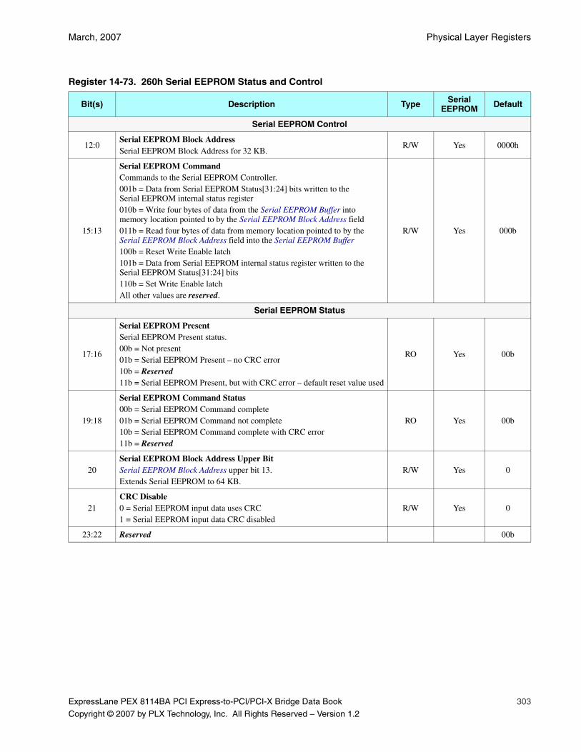
March, 2007 Physical Layer Registers
ExpressLane PEX 8114BA PCI Express-to-PCI/PCI-X Bridge Data Book 303
Copyright © 2007 by PLX Technology, Inc. All Rights Reserved – Version 1.2
Register 14-73. 260h Serial EEPROM Status and Control
Bit(s) Description Type Serial EEPROM Default
Serial EEPROM Control
12:0Serial EEPROM Block AddressSerial EEPROM Block Address for 32 KB.
R/W Yes 0000h
15:13
Serial EEPROM CommandCommands to the Serial EEPROM Controller.001b = Data from Serial EEPROM Status[31:24] bits written to the Serial EEPROM internal status register010b = Write four bytes of data from the Serial EEPROM Buffer into memory location pointed to by the Serial EEPROM Block Address field011b = Read four bytes of data from memory location pointed to by the Serial EEPROM Block Address field into the Serial EEPROM Buffer100b = Reset Write Enable latch101b = Data from Serial EEPROM internal status register written to the Serial EEPROM Status[31:24] bits110b = Set Write Enable latchAll other values are reserved.
R/W Yes 000b
Serial EEPROM Status
17:16
Serial EEPROM PresentSerial EEPROM Present status.00b = Not present01b = Serial EEPROM Present – no CRC error10b = Reserved11b = Serial EEPROM Present, but with CRC error – default reset value used
RO Yes 00b
19:18
Serial EEPROM Command Status00b = Serial EEPROM Command complete01b = Serial EEPROM Command not complete10b = Serial EEPROM Command complete with CRC error11b = Reserved
RO Yes 00b
20Serial EEPROM Block Address Upper BitSerial EEPROM Block Address upper bit 13.Extends Serial EEPROM to 64 KB.
R/W Yes 0
21CRC Disable0 = Serial EEPROM input data uses CRC1 = Serial EEPROM input data CRC disabled
R/W Yes 0
23:22 Reserved 00b
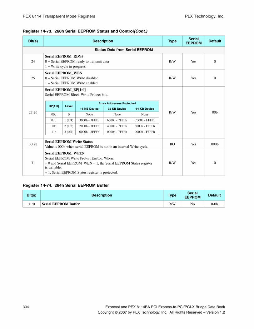
PEX 8114 Transparent Mode Registers PLX Technology, Inc.
304 ExpressLane PEX 8114BA PCI Express-to-PCI/PCI-X Bridge Data Book
Copyright © 2007 by PLX Technology, Inc. All Rights Reserved – Version 1.2
Status Data from Serial EEPROM
24Serial EEPROM_RDY#0 = Serial EEPROM ready to transmit data1 = Write cycle in progress
R/W Yes 0
25Serial EEPROM_WEN0 = Serial EEPROM Write disabled1 = Serial EEPROM Write enabled
R/W Yes 0
27:26
Serial EEPROM_BP[1:0]Serial EEPROM Block-Write Protect bits.
R/W Yes 00b
30:28Serial EEPROM Write StatusValue is 000b when serial EEPROM is not in an internal Write cycle.
RO Yes 000b
31
Serial EEPROM_WPENSerial EEPROM Write Protect Enable. When:= 0 and Serial EEPROM_WEN = 1, the Serial EEPROM Status register is writable.= 1, Serial EEPROM Status register is protected.
R/W Yes 0
Register 14-74. 264h Serial EEPROM Buffer
Bit(s) Description Type Serial EEPROM Default
31:0 Serial EEPROM Buffer R/W No 0-0h
Register 14-73. 260h Serial EEPROM Status and Control(Cont.)
Bit(s) Description Type Serial EEPROM Default
BP[1:0] LevelArray Addresses Protected
16-KB Device 32-KB Device 64-KB Device
00b 0 None None None
01b 1 (1/4) 3000h - 3FFFh 6000h - 7FFFh C000h - FFFFh
10b 2 (1/2) 2000h - 3FFFh 4000h - 7FFFh 8000h - FFFFh
11b 3 (All) 0000h - 3FFFh 0000h - 7FFFh 0000h - FFFFh
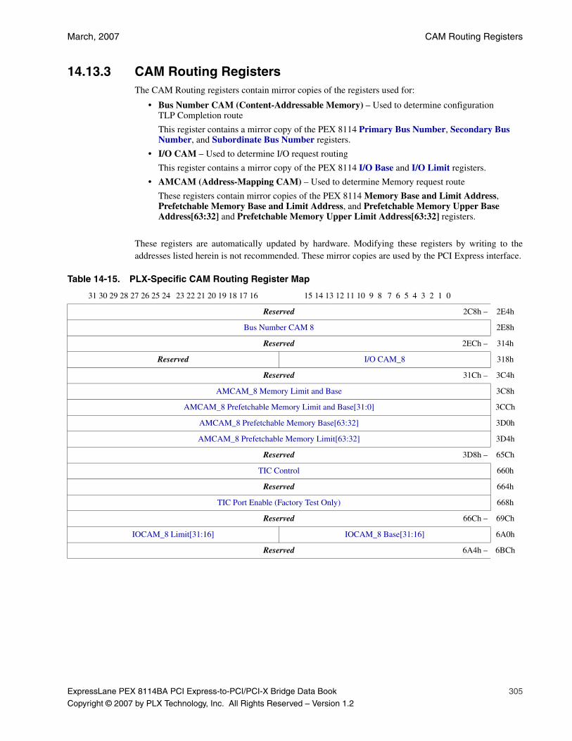
March, 2007 CAM Routing Registers
ExpressLane PEX 8114BA PCI Express-to-PCI/PCI-X Bridge Data Book 305
Copyright © 2007 by PLX Technology, Inc. All Rights Reserved – Version 1.2
14.13.3 CAM Routing RegistersThe CAM Routing registers contain mirror copies of the registers used for:
• Bus Number CAM (Content-Addressable Memory) – Used to determine configuration TLP Completion route
This register contains a mirror copy of the PEX 8114 Primary Bus Number, Secondary Bus Number, and Subordinate Bus Number registers.
• I/O CAM – Used to determine I/O request routing
This register contains a mirror copy of the PEX 8114 I/O Base and I/O Limit registers.
• AMCAM (Address-Mapping CAM) – Used to determine Memory request route
These registers contain mirror copies of the PEX 8114 Memory Base and Limit Address, Prefetchable Memory Base and Limit Address, and Prefetchable Memory Upper Base Address[63:32] and Prefetchable Memory Upper Limit Address[63:32] registers.
These registers are automatically updated by hardware. Modifying these registers by writing to theaddresses listed herein is not recommended. These mirror copies are used by the PCI Express interface.
Table 14-15. PLX-Specific CAM Routing Register Map
31 30 29 28 27 26 25 24 23 22 21 20 19 18 17 16 15 14 13 12 11 10 9 8 7 6 5 4 3 2 1 0
Reserved 2C8h – 2E4h
Bus Number CAM 8 2E8h
Reserved 2ECh – 314h
Reserved I/O CAM_8 318h
Reserved 31Ch – 3C4h
AMCAM_8 Memory Limit and Base 3C8h
AMCAM_8 Prefetchable Memory Limit and Base[31:0] 3CCh
AMCAM_8 Prefetchable Memory Base[63:32] 3D0h
AMCAM_8 Prefetchable Memory Limit[63:32] 3D4h
Reserved 3D8h – 65Ch
TIC Control 660h
Reserved 664h
TIC Port Enable (Factory Test Only) 668h
Reserved 66Ch – 69Ch
IOCAM_8 Limit[31:16] IOCAM_8 Base[31:16] 6A0h
Reserved 6A4h – 6BCh
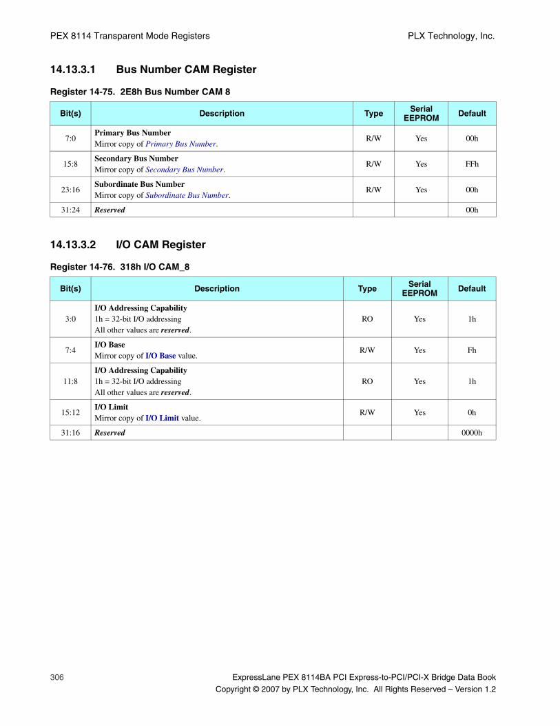
PEX 8114 Transparent Mode Registers PLX Technology, Inc.
306 ExpressLane PEX 8114BA PCI Express-to-PCI/PCI-X Bridge Data Book
Copyright © 2007 by PLX Technology, Inc. All Rights Reserved – Version 1.2
14.13.3.1 Bus Number CAM Register
14.13.3.2 I/O CAM Register
Register 14-75. 2E8h Bus Number CAM 8
Bit(s) Description Type Serial EEPROM Default
7:0Primary Bus NumberMirror copy of Primary Bus Number.
R/W Yes 00h
15:8Secondary Bus NumberMirror copy of Secondary Bus Number.
R/W Yes FFh
23:16Subordinate Bus NumberMirror copy of Subordinate Bus Number.
R/W Yes 00h
31:24 Reserved 00h
Register 14-76. 318h I/O CAM_8
Bit(s) Description Type Serial EEPROM Default
3:0I/O Addressing Capability1h = 32-bit I/O addressingAll other values are reserved.
RO Yes 1h
7:4I/O BaseMirror copy of I/O Base value.
R/W Yes Fh
11:8I/O Addressing Capability1h = 32-bit I/O addressingAll other values are reserved.
RO Yes 1h
15:12I/O LimitMirror copy of I/O Limit value.
R/W Yes 0h
31:16 Reserved 0000h
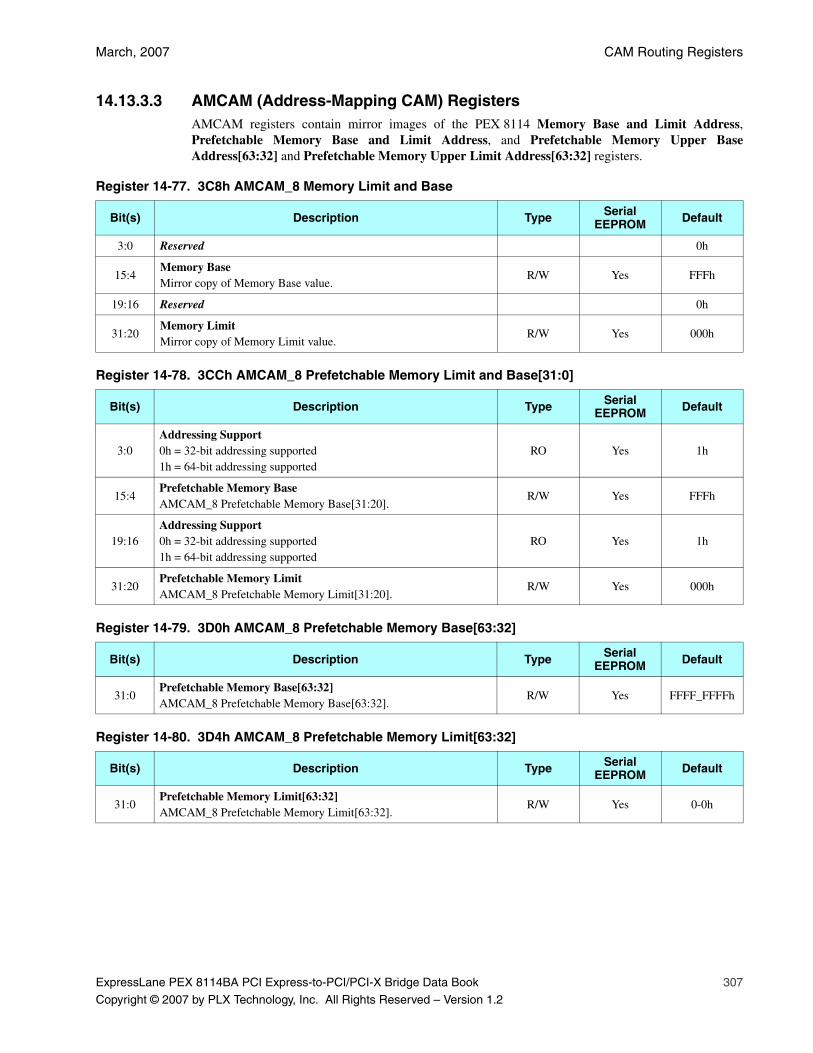
March, 2007 CAM Routing Registers
ExpressLane PEX 8114BA PCI Express-to-PCI/PCI-X Bridge Data Book 307
Copyright © 2007 by PLX Technology, Inc. All Rights Reserved – Version 1.2
14.13.3.3 AMCAM (Address-Mapping CAM) RegistersAMCAM registers contain mirror images of the PEX 8114 Memory Base and Limit Address,Prefetchable Memory Base and Limit Address, and Prefetchable Memory Upper BaseAddress[63:32] and Prefetchable Memory Upper Limit Address[63:32] registers.
Register 14-77. 3C8h AMCAM_8 Memory Limit and Base
Bit(s) Description Type Serial EEPROM Default
3:0 Reserved 0h
15:4Memory BaseMirror copy of Memory Base value.
R/W Yes FFFh
19:16 Reserved 0h
31:20Memory LimitMirror copy of Memory Limit value.
R/W Yes 000h
Register 14-78. 3CCh AMCAM_8 Prefetchable Memory Limit and Base[31:0]
Bit(s) Description Type Serial EEPROM Default
3:0Addressing Support0h = 32-bit addressing supported1h = 64-bit addressing supported
RO Yes 1h
15:4Prefetchable Memory BaseAMCAM_8 Prefetchable Memory Base[31:20].
R/W Yes FFFh
19:16Addressing Support0h = 32-bit addressing supported1h = 64-bit addressing supported
RO Yes 1h
31:20Prefetchable Memory LimitAMCAM_8 Prefetchable Memory Limit[31:20].
R/W Yes 000h
Register 14-79. 3D0h AMCAM_8 Prefetchable Memory Base[63:32]
Bit(s) Description Type Serial EEPROM Default
31:0Prefetchable Memory Base[63:32]AMCAM_8 Prefetchable Memory Base[63:32].
R/W Yes FFFF_FFFFh
Register 14-80. 3D4h AMCAM_8 Prefetchable Memory Limit[63:32]
Bit(s) Description Type Serial EEPROM Default
31:0Prefetchable Memory Limit[63:32]AMCAM_8 Prefetchable Memory Limit[63:32].
R/W Yes 0-0h
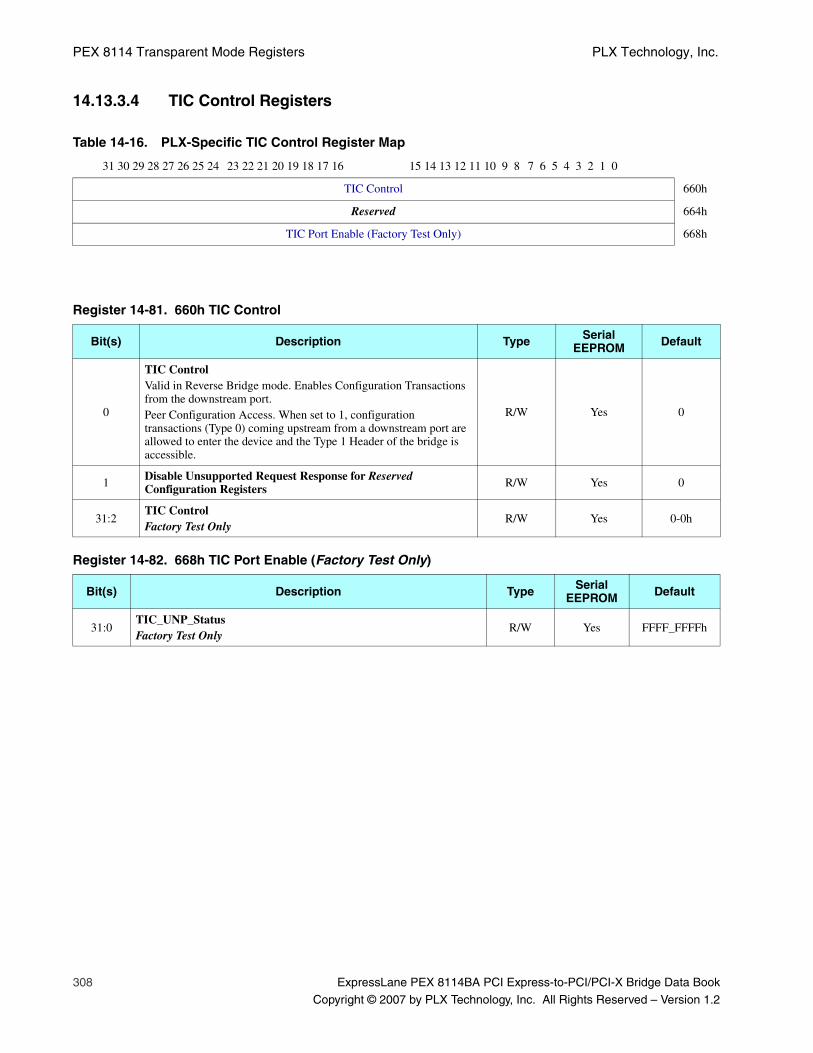
PEX 8114 Transparent Mode Registers PLX Technology, Inc.
308 ExpressLane PEX 8114BA PCI Express-to-PCI/PCI-X Bridge Data Book
Copyright © 2007 by PLX Technology, Inc. All Rights Reserved – Version 1.2
14.13.3.4 TIC Control Registers
Table 14-16. PLX-Specific TIC Control Register Map
31 30 29 28 27 26 25 24 23 22 21 20 19 18 17 16 15 14 13 12 11 10 9 8 7 6 5 4 3 2 1 0
TIC Control 660h
Reserved 664h
TIC Port Enable (Factory Test Only) 668h
Register 14-81. 660h TIC Control
Bit(s) Description Type Serial EEPROM Default
0
TIC ControlValid in Reverse Bridge mode. Enables Configuration Transactions from the downstream port.Peer Configuration Access. When set to 1, configuration transactions (Type 0) coming upstream from a downstream port are allowed to enter the device and the Type 1 Header of the bridge is accessible.
R/W Yes 0
1 Disable Unsupported Request Response for Reserved Configuration Registers R/W Yes 0
31:2TIC ControlFactory Test Only
R/W Yes 0-0h
Register 14-82. 668h TIC Port Enable (Factory Test Only)
Bit(s) Description Type Serial EEPROM Default
31:0TIC_UNP_StatusFactory Test Only
R/W Yes FFFF_FFFFh
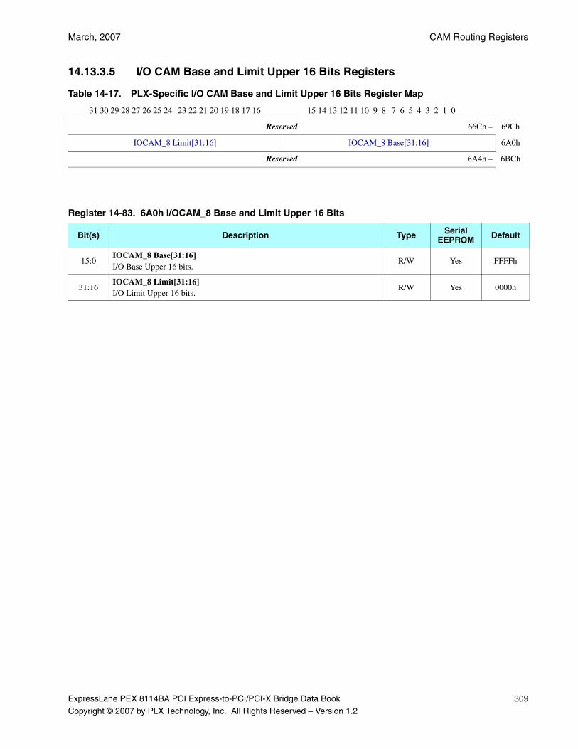
March, 2007 CAM Routing Registers
ExpressLane PEX 8114BA PCI Express-to-PCI/PCI-X Bridge Data Book 309
Copyright © 2007 by PLX Technology, Inc. All Rights Reserved – Version 1.2
14.13.3.5 I/O CAM Base and Limit Upper 16 Bits Registers
Table 14-17. PLX-Specific I/O CAM Base and Limit Upper 16 Bits Register Map
31 30 29 28 27 26 25 24 23 22 21 20 19 18 17 16 15 14 13 12 11 10 9 8 7 6 5 4 3 2 1 0
Reserved 66Ch – 69Ch
IOCAM_8 Limit[31:16] IOCAM_8 Base[31:16] 6A0h
Reserved 6A4h – 6BCh
Register 14-83. 6A0h I/OCAM_8 Base and Limit Upper 16 Bits
Bit(s) Description Type Serial EEPROM Default
15:0IOCAM_8 Base[31:16]I/O Base Upper 16 bits.
R/W Yes FFFFh
31:16IOCAM_8 Limit[31:16]I/O Limit Upper 16 bits.
R/W Yes 0000h
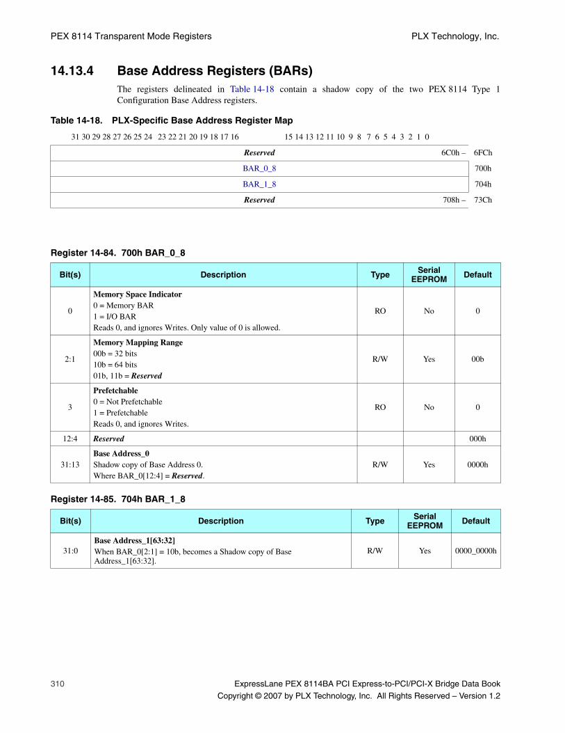
PEX 8114 Transparent Mode Registers PLX Technology, Inc.
310 ExpressLane PEX 8114BA PCI Express-to-PCI/PCI-X Bridge Data Book
Copyright © 2007 by PLX Technology, Inc. All Rights Reserved – Version 1.2
14.13.4 Base Address Registers (BARs)The registers delineated in Table 14-18 contain a shadow copy of the two PEX 8114 Type 1Configuration Base Address registers.
Table 14-18. PLX-Specific Base Address Register Map
31 30 29 28 27 26 25 24 23 22 21 20 19 18 17 16 15 14 13 12 11 10 9 8 7 6 5 4 3 2 1 0
Reserved 6C0h – 6FCh
BAR_0_8 700h
BAR_1_8 704h
Reserved 708h – 73Ch
Register 14-84. 700h BAR_0_8
Bit(s) Description Type Serial EEPROM Default
0
Memory Space Indicator0 = Memory BAR1 = I/O BARReads 0, and ignores Writes. Only value of 0 is allowed.
RO No 0
2:1
Memory Mapping Range00b = 32 bits10b = 64 bits01b, 11b = Reserved
R/W Yes 00b
3
Prefetchable0 = Not Prefetchable1 = PrefetchableReads 0, and ignores Writes.
RO No 0
12:4 Reserved 000h
31:13Base Address_0Shadow copy of Base Address 0.Where BAR_0[12:4] = Reserved.
R/W Yes 0000h
Register 14-85. 704h BAR_1_8
Bit(s) Description Type Serial EEPROM Default
31:0Base Address_1[63:32]When BAR_0[2:1] = 10b, becomes a Shadow copy of Base Address_1[63:32].
R/W Yes 0000_0000h
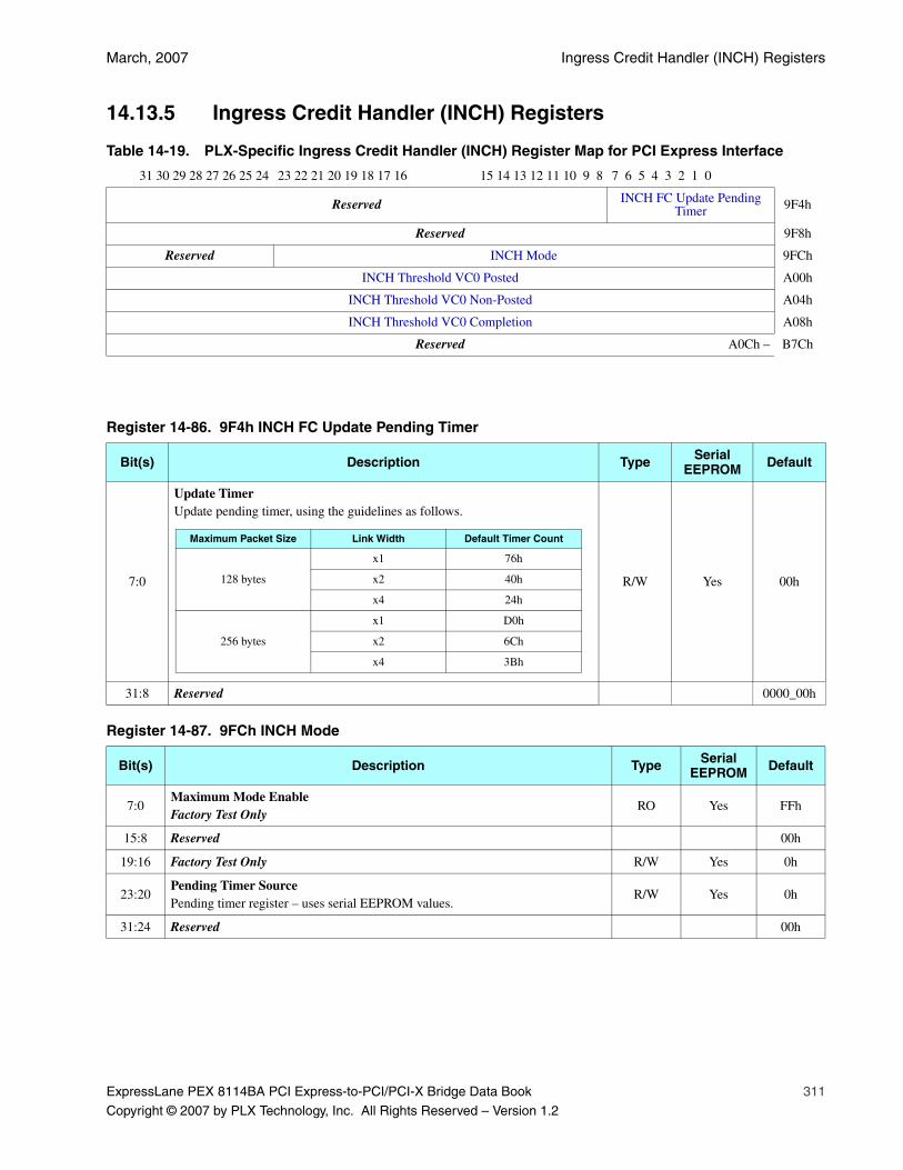
March, 2007 Ingress Credit Handler (INCH) Registers
ExpressLane PEX 8114BA PCI Express-to-PCI/PCI-X Bridge Data Book 311
Copyright © 2007 by PLX Technology, Inc. All Rights Reserved – Version 1.2
14.13.5 Ingress Credit Handler (INCH) Registers
Table 14-19. PLX-Specific Ingress Credit Handler (INCH) Register Map for PCI Express Interface
31 30 29 28 27 26 25 24 23 22 21 20 19 18 17 16 15 14 13 12 11 10 9 8 7 6 5 4 3 2 1 0
Reserved INCH FC Update Pending Timer 9F4h
Reserved 9F8h
Reserved INCH Mode 9FCh
INCH Threshold VC0 Posted A00h
INCH Threshold VC0 Non-Posted A04h
INCH Threshold VC0 Completion A08h
Reserved A0Ch – B7Ch
Register 14-86. 9F4h INCH FC Update Pending Timer
Bit(s) Description Type Serial EEPROM Default
7:0
Update TimerUpdate pending timer, using the guidelines as follows.
R/W Yes 00h
31:8 Reserved 0000_00h
Register 14-87. 9FCh INCH Mode
Bit(s) Description Type Serial EEPROM Default
7:0Maximum Mode EnableFactory Test Only
RO Yes FFh
15:8 Reserved 00h
19:16 Factory Test Only R/W Yes 0h
23:20Pending Timer SourcePending timer register – uses serial EEPROM values.
R/W Yes 0h
31:24 Reserved 00h
Maximum Packet Size Link Width Default Timer Count
128 bytes
x1 76h
x2 40h
x4 24h
256 bytes
x1 D0h
x2 6Ch
x4 3Bh
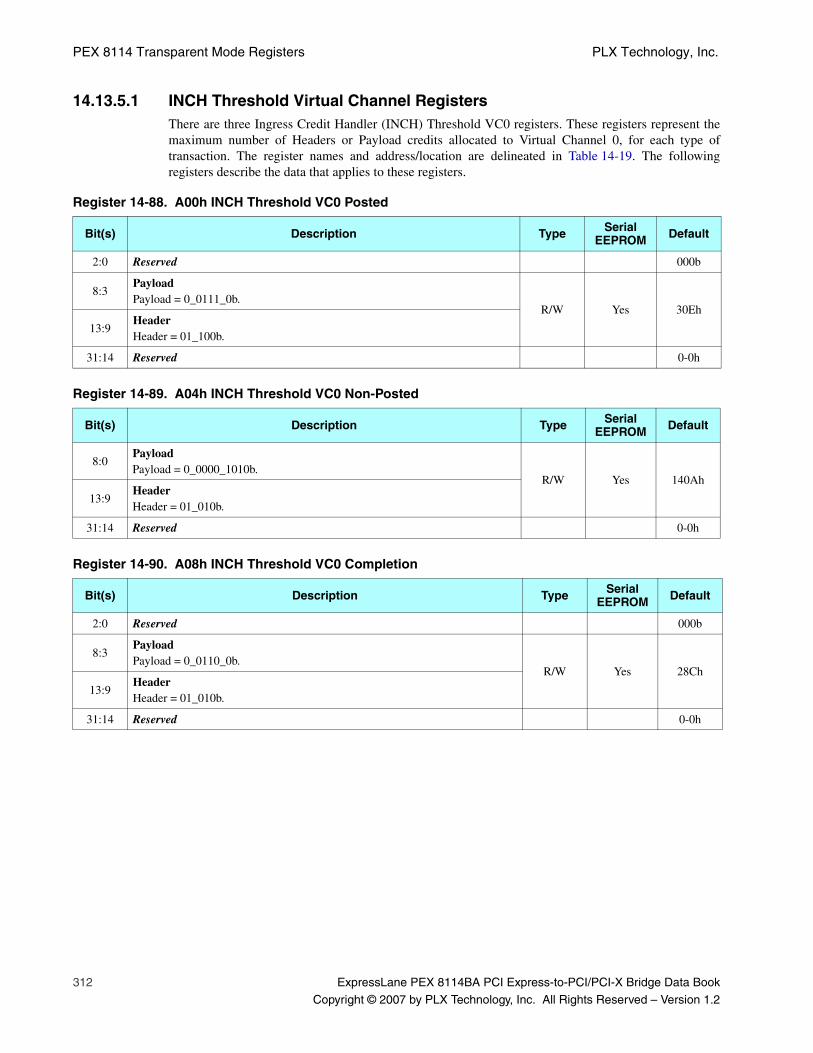
PEX 8114 Transparent Mode Registers PLX Technology, Inc.
312 ExpressLane PEX 8114BA PCI Express-to-PCI/PCI-X Bridge Data Book
Copyright © 2007 by PLX Technology, Inc. All Rights Reserved – Version 1.2
14.13.5.1 INCH Threshold Virtual Channel RegistersThere are three Ingress Credit Handler (INCH) Threshold VC0 registers. These registers represent themaximum number of Headers or Payload credits allocated to Virtual Channel 0, for each type oftransaction. The register names and address/location are delineated in Table 14-19. The followingregisters describe the data that applies to these registers.
Register 14-88. A00h INCH Threshold VC0 Posted
Bit(s) Description Type Serial EEPROM Default
2:0 Reserved 000b
8:3PayloadPayload = 0_0111_0b.
R/W Yes 30Eh
13:9HeaderHeader = 01_100b.
31:14 Reserved 0-0h
Register 14-89. A04h INCH Threshold VC0 Non-Posted
Bit(s) Description Type Serial EEPROM Default
8:0PayloadPayload = 0_0000_1010b.
R/W Yes 140Ah
13:9HeaderHeader = 01_010b.
31:14 Reserved 0-0h
Register 14-90. A08h INCH Threshold VC0 Completion
Bit(s) Description Type Serial EEPROM Default
2:0 Reserved 000b
8:3PayloadPayload = 0_0110_0b.
R/W Yes 28Ch
13:9HeaderHeader = 01_010b.
31:14 Reserved 0-0h
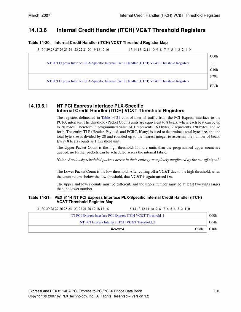
March, 2007 Internal Credit Handler (ITCH) VC&T Threshold Registers
ExpressLane PEX 8114BA PCI Express-to-PCI/PCI-X Bridge Data Book 313
Copyright © 2007 by PLX Technology, Inc. All Rights Reserved – Version 1.2
14.13.6 Internal Credit Handler (ITCH) VC&T Threshold Registers
14.13.6.1 NT PCI Express Interface PLX-Specific Internal Credit Handler (ITCH) VC&T Threshold RegistersThe registers delineated in Table 14-21 control internal traffic from the PCI Express interface to thePCI-X interface. The threshold (Packet Count) units are equivalent to 8 beats, where each beat can be upto 20 bytes. Therefore, a programmed value of 1 represents 160 bytes, 2 represents 320 bytes, and soforth. The entire TLP (Header, Payload, and ECRC, if any) is used to determine a total byte size, and thetotal byte size is divided by 20 and rounded up to the nearest integer to ascertain the number of beats.Every 8 beats counts as 1 threshold unit.
The Upper Packet Count is the high threshold. If more units than the programmed upper count arequeued, no further packets can be scheduled across the internal fabric.
Note: Previously scheduled packets arrive in their entirety, completely unaffected by the cut-off signal.
The Lower Packet Count is the low threshold. After cutting off a VC&T due to the high threshold, whenthe count returns below the low threshold, that VC&T is again turned On.
The upper and lower counts must be different, and the upper number must be at least two units largerthan the lower number.
Table 14-20. Internal Credit Handler (ITCH) VC&T Threshold Register Map
31 30 29 28 27 26 25 24 23 22 21 20 19 18 17 16 15 14 13 12 11 10 9 8 7 6 5 4 3 2 1 0
NT PCI Express Interface PLX-Specific Internal Credit Handler (ITCH) VC&T Threshold Registers
C00h
…
C10h
NT PCI Express Interface PLX-Specific Internal Credit Handler (ITCH) VC&T Threshold RegistersF70h
…F7Ch
Table 14-21. PEX 8114 NT PCI Express Interface PLX-Specific Internal Credit Handler (ITCH) VC&T Threshold Register Map
31 30 29 28 27 26 25 24 23 22 21 20 19 18 17 16 15 14 13 12 11 10 9 8 7 6 5 4 3 2 1 0
NT PCI Express Interface PCI Express ITCH VC&T Threshold_1 C00h
NT PCI Express Interface ITCH VC&T Threshold_2 C04h
Reserved C08h – C10h

PEX 8114 Transparent Mode Registers PLX Technology, Inc.
314 ExpressLane PEX 8114BA PCI Express-to-PCI/PCI-X Bridge Data Book
Copyright © 2007 by PLX Technology, Inc. All Rights Reserved – Version 1.2
Note: Although the PEX 8114 supports only VC0, the VC1 Posted credit fields are used for internal transactions, such as shadow Writes.
Register 14-91. C00h NT PCI Express Interface PCI Express ITCH VC&T Threshold_1
Bit(s) Description Type Serial EEPROM Default
4:0VC0 Posted Upper Packet CountVC0 Posted upper packet beat limit.
R/W Yes 10h
7:5 Not used R/W Yes 000b
12:8VC0 Posted Lower Packet CountVC0 Posted lower packet beat limit.
R/W Yes 08h
15:13 Not used R/W Yes 000b
20:16VC0 Non-Posted Upper Packet CountVC0 Non-Posted upper packet beat limit.
R/W Yes 04h
23:21 Not used R/W Yes 000b
28:24VC0 Non-Posted Lower Packet CountVC0 Non-Posted lower packet beat limit.
R/W Yes 01h
31:29 Not used R/W Yes 000b
Register 14-92. C04h NT PCI Express Interface ITCH VC&T Threshold_2
Bit(s) Description Type Serial EEPROM Default
4:0VC0 Completion Upper Packet CountVC0 Completion upper packet beat limit.
R/W Yes 10h
7:5 Not used R/W Yes 000b
12:8VC0 Completion Lower Packet CountVC0 Completion lower packet beat limit.
R/W Yes 08h
15:13 Not used R/W Yes 000b
20:16
VC1 Posted Upper Packet CountVC1 Posted upper packet beat limit. This information is listed for internal and serial EEPROM configuration only – not to be changed by users.
R/W Yes 04h
23:21 Not used R/W Yes 000b
28:24
VC1 Posted Lower Packet CountVC1 Posted lower packet beat limit. This information is listed for internal and serial EEPROM configuration only – not to be changed by users.
R/W Yes 01h
31:29 Not used R/W Yes 000b
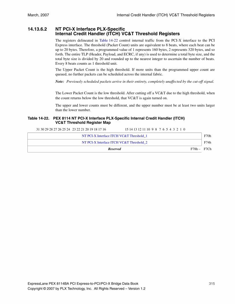
March, 2007 Internal Credit Handler (ITCH) VC&T Threshold Registers
ExpressLane PEX 8114BA PCI Express-to-PCI/PCI-X Bridge Data Book 315
Copyright © 2007 by PLX Technology, Inc. All Rights Reserved – Version 1.2
14.13.6.2 NT PCI-X Interface PLX-Specific Internal Credit Handler (ITCH) VC&T Threshold RegistersThe registers delineated in Table 14-22 control internal traffic from the PCI-X interface to the PCIExpress interface. The threshold (Packet Count) units are equivalent to 8 beats, where each beat can beup to 20 bytes. Therefore, a programmed value of 1 represents 160 bytes, 2 represents 320 bytes, and soforth. The entire TLP (Header, Payload, and ECRC, if any) is used to determine a total byte size, and thetotal byte size is divided by 20 and rounded up to the nearest integer to ascertain the number of beats.Every 8 beats counts as 1 threshold unit.
The Upper Packet Count is the high threshold. If more units than the programmed upper count arequeued, no further packets can be scheduled across the internal fabric.
Note: Previously scheduled packets arrive in their entirety, completely unaffected by the cut-off signal.
The Lower Packet Count is the low threshold. After cutting off a VC&T due to the high threshold, whenthe count returns below the low threshold, that VC&T is again turned on.
The upper and lower counts must be different, and the upper number must be at least two units largerthan the lower number.
Table 14-22. PEX 8114 NT PCI-X Interface PLX-Specific Internal Credit Handler (ITCH) VC&T Threshold Register Map
31 30 29 28 27 26 25 24 23 22 21 20 19 18 17 16 15 14 13 12 11 10 9 8 7 6 5 4 3 2 1 0
NT PCI-X Interface ITCH VC&T Threshold_1 F70h
NT PCI-X Interface ITCH VC&T Threshold_2 F74h
Reserved F78h – F7Ch
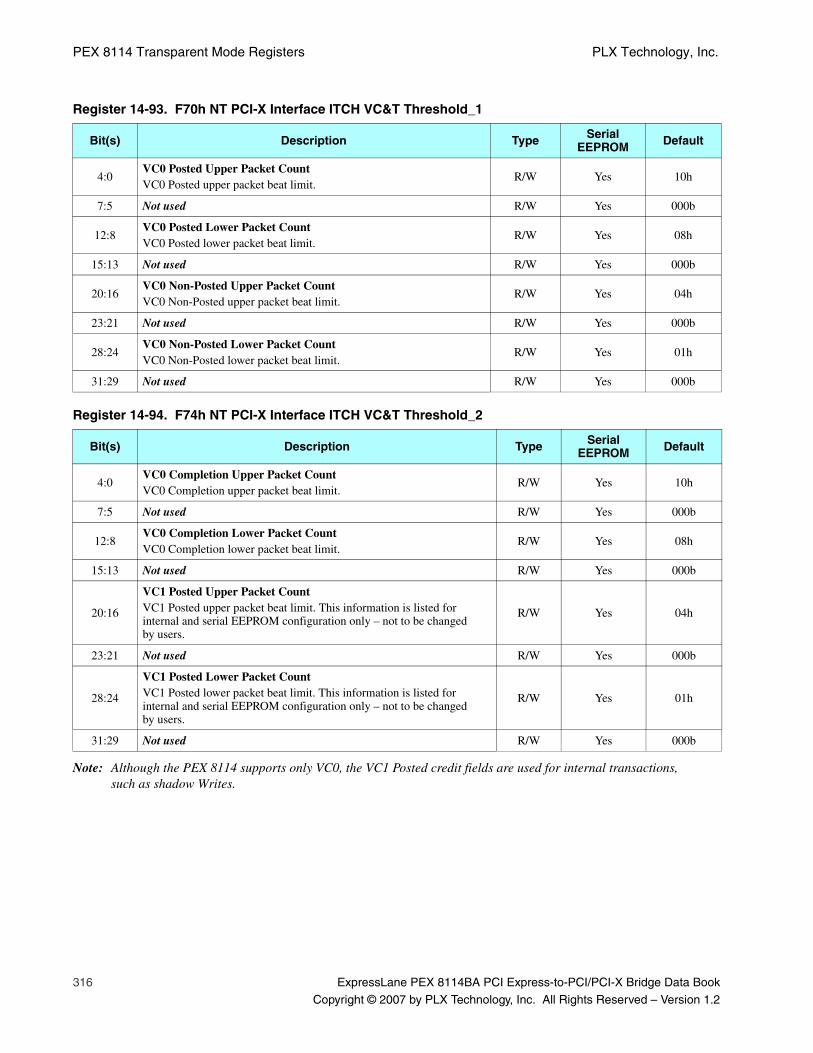
PEX 8114 Transparent Mode Registers PLX Technology, Inc.
316 ExpressLane PEX 8114BA PCI Express-to-PCI/PCI-X Bridge Data Book
Copyright © 2007 by PLX Technology, Inc. All Rights Reserved – Version 1.2
Note: Although the PEX 8114 supports only VC0, the VC1 Posted credit fields are used for internal transactions, such as shadow Writes.
Register 14-93. F70h NT PCI-X Interface ITCH VC&T Threshold_1
Bit(s) Description Type Serial EEPROM Default
4:0VC0 Posted Upper Packet CountVC0 Posted upper packet beat limit.
R/W Yes 10h
7:5 Not used R/W Yes 000b
12:8VC0 Posted Lower Packet CountVC0 Posted lower packet beat limit.
R/W Yes 08h
15:13 Not used R/W Yes 000b
20:16VC0 Non-Posted Upper Packet CountVC0 Non-Posted upper packet beat limit.
R/W Yes 04h
23:21 Not used R/W Yes 000b
28:24VC0 Non-Posted Lower Packet CountVC0 Non-Posted lower packet beat limit.
R/W Yes 01h
31:29 Not used R/W Yes 000b
Register 14-94. F74h NT PCI-X Interface ITCH VC&T Threshold_2
Bit(s) Description Type Serial EEPROM Default
4:0VC0 Completion Upper Packet CountVC0 Completion upper packet beat limit.
R/W Yes 10h
7:5 Not used R/W Yes 000b
12:8VC0 Completion Lower Packet CountVC0 Completion lower packet beat limit.
R/W Yes 08h
15:13 Not used R/W Yes 000b
20:16
VC1 Posted Upper Packet CountVC1 Posted upper packet beat limit. This information is listed for internal and serial EEPROM configuration only – not to be changed by users.
R/W Yes 04h
23:21 Not used R/W Yes 000b
28:24
VC1 Posted Lower Packet CountVC1 Posted lower packet beat limit. This information is listed for internal and serial EEPROM configuration only – not to be changed by users.
R/W Yes 01h
31:29 Not used R/W Yes 000b
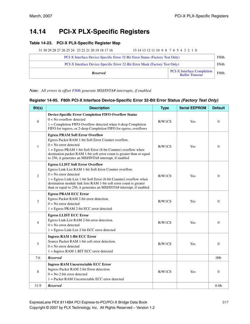
March, 2007 PCI-X PLX-Specific Registers
ExpressLane PEX 8114BA PCI Express-to-PCI/PCI-X Bridge Data Book 317
Copyright © 2007 by PLX Technology, Inc. All Rights Reserved – Version 1.2
14.14 PCI-X PLX-Specific Registers
Note: All errors in offset F80h generate MSI/INTA# interrupts, if enabled.
Table 14-23. PCI-X PLX-Specific Register Map
31 30 29 28 27 26 25 24 23 22 21 20 19 18 17 16 15 14 13 12 11 10 9 8 7 6 5 4 3 2 1 0
PCI-X Interface Device-Specific Error 32-Bit Error Status (Factory Test Only) F80h
PCI-X Interface Device-Specific Error 32-Bit Error Mask (Factory Test Only) F84h
Reserved PCI-X Interface Completion Buffer Timeout F88h
Register 14-95. F80h PCI-X Interface Device-Specific Error 32-Bit Error Status (Factory Test Only)
Bit(s) Description Type Serial EEPROM Default
0
Device-Specific Error Completion FIFO Overflow Status0 = No overflow detected1 = Completion FIFO Overflow detected when 4-deep Completion FIFO for ingress, or 2-deep Completion FIFO for egress, overflows
R/W1CS Yes 0
1
Egress PRAM Soft Error OverflowEgress Packet RAM 1-bit Soft Error Counter overflow.0 = No error detected1 = Egress PRAM 1-bit Soft Error (8-bit Counter) overflow when destination packet RAM 1-bit soft error count is greater than or equal to 256, it generates an MSI/INTA# interrupt, if enabled
R/W1CS Yes 0
2
Egress LLIST Soft Error OverflowEgress Link-List RAM 1-bit Soft Error Counter overflow.0 = No error detected1 = Egress Link-List 1-bit Soft Error (8-bit Counter) overflow when destination module link lists RAM 1-bit soft error count is greater than or equal to 256, it generates an MSI/INTA# interrupt, if enabled
R/W1CS Yes 0
3
Egress PRAM ECC ErrorEgress Packet RAM 2-bit error detection.0 = No error detected1 = Egress PRAM 2-bit ECC error detected
R/W1CS Yes 0
4
Egress LLIST ECC ErrorEgress Link-List RAM 2-bit error detection.0 = No error detected1 = Egress Link-List 2-bit ECC error detected
R/W1CS Yes 0
5
Ingress RAM 1-Bit ECC ErrorSource Packet RAM 1-bit soft error detection.0 = No error detected1 = Ingress RAM 1-BIT ECC error detected
R/W1CS Yes 0
7:6 Reserved 00b
8
Ingress RAM Uncorrectable ECC ErrorIngress Packet RAM 2-bit Error detection.0 = No 2-bit error detected1 = Packet RAM Uncorrectable ECC error detected
R/W1CS Yes 0
31:9 Reserved 0-0h
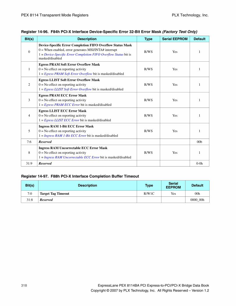
PEX 8114 Transparent Mode Registers PLX Technology, Inc.
318 ExpressLane PEX 8114BA PCI Express-to-PCI/PCI-X Bridge Data Book
Copyright © 2007 by PLX Technology, Inc. All Rights Reserved – Version 1.2
Register 14-96. F84h PCI-X Interface Device-Specific Error 32-Bit Error Mask (Factory Test Only)
Bit(s) Description Type Serial EEPROM Default
0
Device-Specific Error Completion FIFO Overflow Status Mask0 = When enabled, error generates MSI/INTA# interrupt1 = Device-Specific Error Completion FIFO Overflow Status bit is masked/disabled
R/WS Yes 1
1Egress PRAM Soft Error Overflow Mask0 = No effect on reporting activity1 = Egress PRAM Soft Error Overflow bit is masked/disabled
R/WS Yes 1
2Egress LLIST Soft Error Overflow Mask0 = No effect on reporting activity1 = Egress LLIST Soft Error Overflow bit is masked/disabled
R/WS Yes 1
3Egress PRAM ECC Error Mask0 = No effect on reporting activity1 = Egress PRAM ECC Error bit is masked/disabled
R/WS Yes 1
4Egress LLIST ECC Error Mask0 = No effect on reporting activity1 = Egress LLIST ECC Error bit is masked/disabled
R/WS Yes 1
5Ingress RAM 1-Bit ECC Error Mask0 = No effect on reporting activity1 = Ingress RAM 1-Bit ECC Error bit is masked/disabled
R/WS Yes 1
7:6 Reserved 00b
8Ingress RAM Uncorrectable ECC Error Mask0 = No effect on reporting activity1 = Ingress RAM Uncorrectable ECC Error bit is masked/disabled
R/WS Yes 1
31:9 Reserved 0-0h
Register 14-97. F88h PCI-X Interface Completion Buffer Timeout
Bit(s) Description Type Serial EEPROM Default
7:0 Target Tag Timeout R/W1C Yes 00h
31:8 Reserved 0000_00h
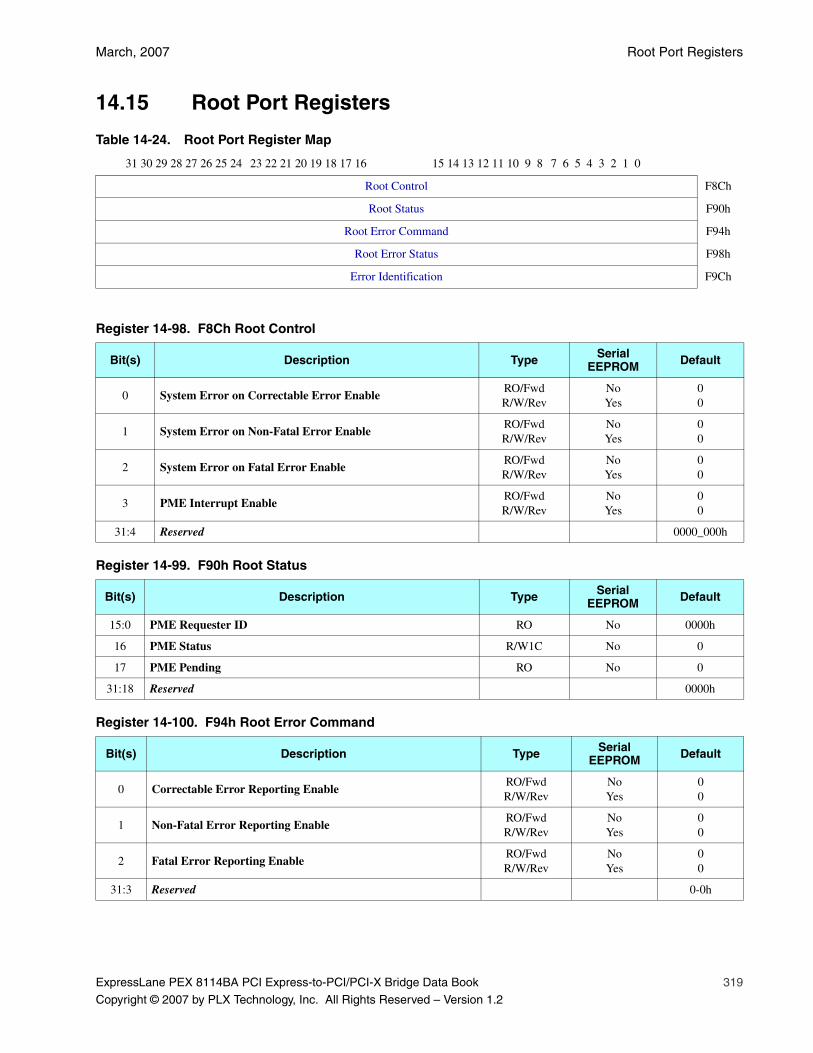
March, 2007 Root Port Registers
ExpressLane PEX 8114BA PCI Express-to-PCI/PCI-X Bridge Data Book 319
Copyright © 2007 by PLX Technology, Inc. All Rights Reserved – Version 1.2
14.15 Root Port Registers
Table 14-24. Root Port Register Map
31 30 29 28 27 26 25 24 23 22 21 20 19 18 17 16 15 14 13 12 11 10 9 8 7 6 5 4 3 2 1 0
Root Control F8Ch
Root Status F90h
Root Error Command F94h
Root Error Status F98h
Error Identification F9Ch
Register 14-98. F8Ch Root Control
Bit(s) Description Type Serial EEPROM Default
0 System Error on Correctable Error EnableRO/FwdR/W/Rev
NoYes
00
1 System Error on Non-Fatal Error EnableRO/FwdR/W/Rev
NoYes
00
2 System Error on Fatal Error EnableRO/FwdR/W/Rev
NoYes
00
3 PME Interrupt EnableRO/FwdR/W/Rev
NoYes
00
31:4 Reserved 0000_000h
Register 14-99. F90h Root Status
Bit(s) Description Type Serial EEPROM Default
15:0 PME Requester ID RO No 0000h
16 PME Status R/W1C No 0
17 PME Pending RO No 0
31:18 Reserved 0000h
Register 14-100. F94h Root Error Command
Bit(s) Description Type Serial EEPROM Default
0 Correctable Error Reporting EnableRO/FwdR/W/Rev
NoYes
00
1 Non-Fatal Error Reporting EnableRO/FwdR/W/Rev
NoYes
00
2 Fatal Error Reporting EnableRO/FwdR/W/Rev
NoYes
00
31:3 Reserved 0-0h
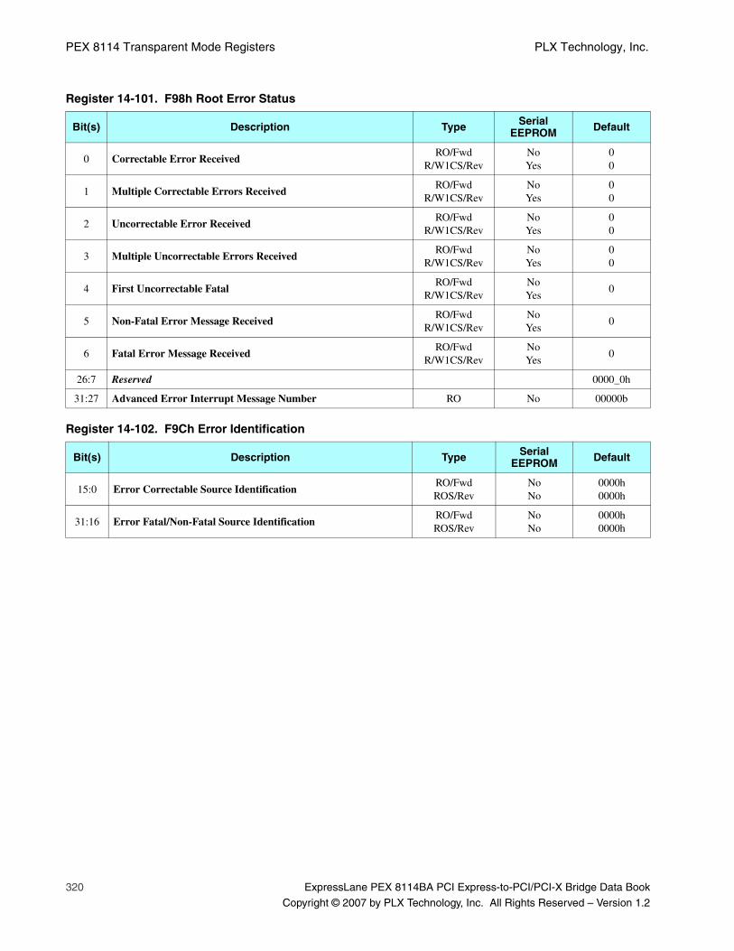
PEX 8114 Transparent Mode Registers PLX Technology, Inc.
320 ExpressLane PEX 8114BA PCI Express-to-PCI/PCI-X Bridge Data Book
Copyright © 2007 by PLX Technology, Inc. All Rights Reserved – Version 1.2
Register 14-101. F98h Root Error Status
Bit(s) Description Type Serial EEPROM Default
0 Correctable Error ReceivedRO/Fwd
R/W1CS/RevNoYes
00
1 Multiple Correctable Errors ReceivedRO/Fwd
R/W1CS/RevNoYes
00
2 Uncorrectable Error ReceivedRO/Fwd
R/W1CS/RevNoYes
00
3 Multiple Uncorrectable Errors ReceivedRO/Fwd
R/W1CS/RevNoYes
00
4 First Uncorrectable FatalRO/Fwd
R/W1CS/RevNoYes
0
5 Non-Fatal Error Message ReceivedRO/Fwd
R/W1CS/RevNoYes
0
6 Fatal Error Message ReceivedRO/Fwd
R/W1CS/RevNoYes
0
26:7 Reserved 0000_0h
31:27 Advanced Error Interrupt Message Number RO No 00000b
Register 14-102. F9Ch Error Identification
Bit(s) Description Type Serial EEPROM Default
15:0 Error Correctable Source IdentificationRO/FwdROS/Rev
NoNo
0000h0000h
31:16 Error Fatal/Non-Fatal Source IdentificationRO/FwdROS/Rev
NoNo
0000h0000h
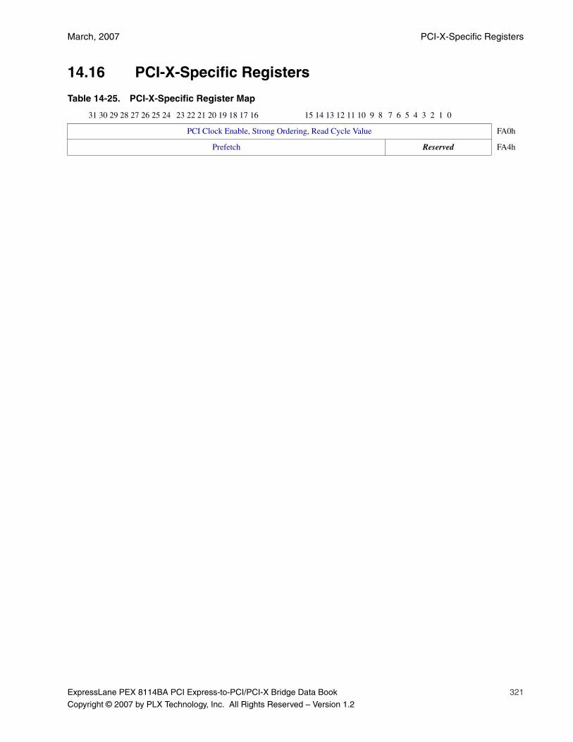
March, 2007 PCI-X-Specific Registers
ExpressLane PEX 8114BA PCI Express-to-PCI/PCI-X Bridge Data Book 321
Copyright © 2007 by PLX Technology, Inc. All Rights Reserved – Version 1.2
14.16 PCI-X-Specific Registers
Table 14-25. PCI-X-Specific Register Map
31 30 29 28 27 26 25 24 23 22 21 20 19 18 17 16 15 14 13 12 11 10 9 8 7 6 5 4 3 2 1 0
PCI Clock Enable, Strong Ordering, Read Cycle Value FA0h
Prefetch Reserved FA4h

PEX 8114 Transparent Mode Registers PLX Technology, Inc.
322 ExpressLane PEX 8114BA PCI Express-to-PCI/PCI-X Bridge Data Book
Copyright © 2007 by PLX Technology, Inc. All Rights Reserved – Version 1.2
Register 14-103. FA0h PCI Clock Enable, Strong Ordering, Read Cycle Value
Bit(s) Description Type Serial EEPROM Default
3:0
PCI_CLKO_EN[3:0]PCI_CLKO_EN[0]=1 enables PCI_CLKO0PCI_CLKO_EN[1]=1 enables PCI_CLKO1PCI_CLKO_EN[2]=1 enables PCI_CLKO2PCI_CLKO_EN[3]=1 enables PCI_CLKO3
R/W Yes0h if STRAP_CLK_MST=0Fh if STRAP_CLK_MST=1
4
Cache Line Prefetch Line CountControls the number of lines prefetched during Memory Reads.0 = 1 Cache Line1 = 2 Cache Lines; used only if the Cache Line Size field (offset 0Ch[7:0]) is less than or equal to 16 DWords (64 bytes)
R/W Yes 0
5Disable Completion Timeout TimerRefer to Section 7.8, “Transaction Transfer Failures.”
R/W Yes 0
6Enable Long Completion Timeout TimerRefer to Section 7.8, “Transaction Transfer Failures.”
R/W Yes 1
7 Disable BAR 0 R/W Yes 0
8
Force Strong OrderingAfter data is returned to the PEX 8114 in response to a Read request, the PEX 8114 Retries the same transaction until complete and does not attempt to gather data from other outstanding transactions.
R/W Yes 0
9 Reserved 0
10PLL Lock Control 0Resets on loss of PLL lock, unless bits [11:10]=00b. (Refer to Table 14-26 for methods of handling loss of PLL lock.)
R/W Yes 0
11PLL Lock Control 1Reset after timer timeout on loss of PLL lock. (Refer to Table 14-26 for methods of handling loss of PLL lock.)
R/W Yes 0
12 Memory Read Line Multiple Enable R/W Yes 0
13 Address Stepping Enable R/W Yes 0
14Sticky PCI-X PLL Loss LockSet when the PCI-X PLL loses PLL lock.
R/W1CS Yes 0
15Sticky PCI Express PLL Loss LockSet when the PCI Express PLL loses PLL lock.
R/W1CS Yes 0
26:16 Maximum Read Cycle Value R/W Yes 7FFh
27 Retry Failure Status R/W1C Yes 0
31:28 Reserved 0h
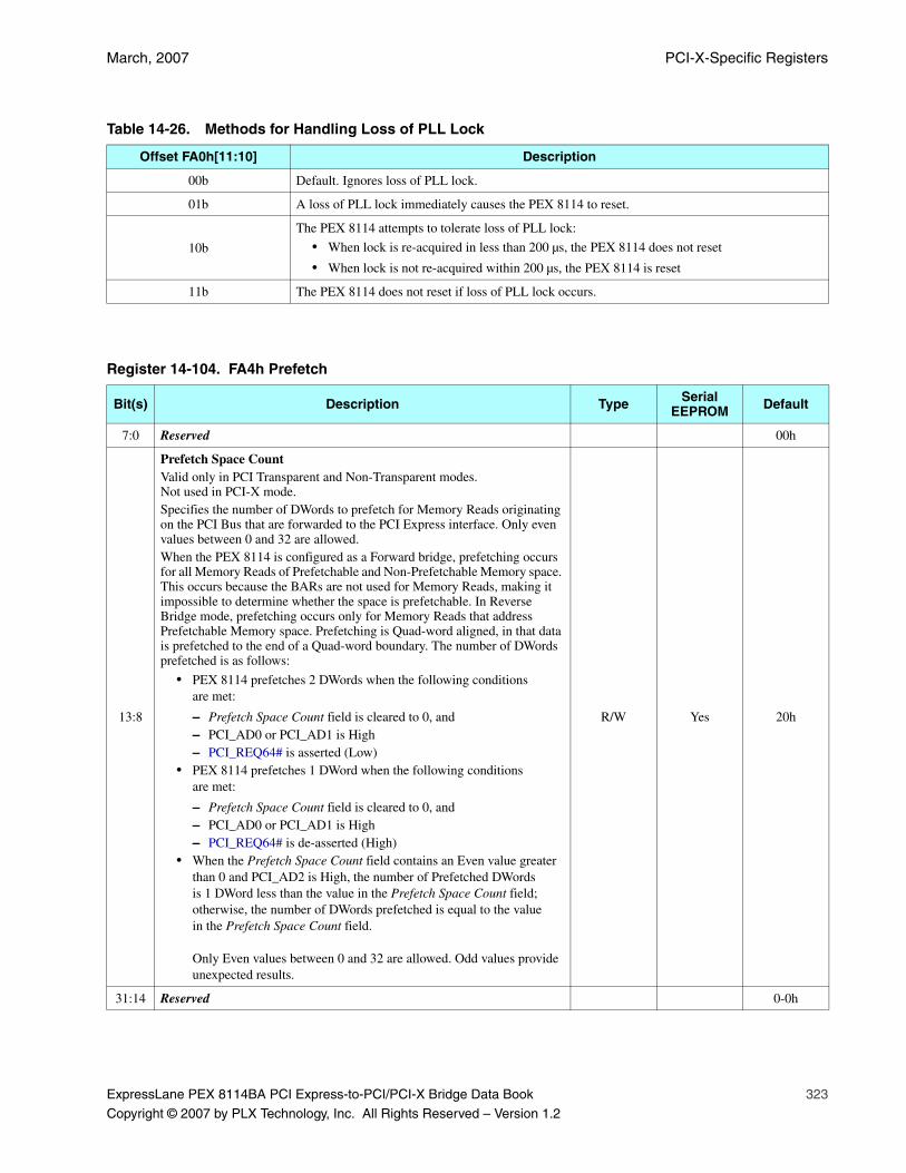
March, 2007 PCI-X-Specific Registers
ExpressLane PEX 8114BA PCI Express-to-PCI/PCI-X Bridge Data Book 323
Copyright © 2007 by PLX Technology, Inc. All Rights Reserved – Version 1.2
Table 14-26. Methods for Handling Loss of PLL Lock
Offset FA0h[11:10] Description
00b Default. Ignores loss of PLL lock.
01b A loss of PLL lock immediately causes the PEX 8114 to reset.
10b
The PEX 8114 attempts to tolerate loss of PLL lock:
• When lock is re-acquired in less than 200 µs, the PEX 8114 does not reset
• When lock is not re-acquired within 200 µs, the PEX 8114 is reset
11b The PEX 8114 does not reset if loss of PLL lock occurs.
Register 14-104. FA4h Prefetch
Bit(s) Description Type Serial EEPROM Default
7:0 Reserved 00h
13:8
Prefetch Space CountValid only in PCI Transparent and Non-Transparent modes. Not used in PCI-X mode.Specifies the number of DWords to prefetch for Memory Reads originating on the PCI Bus that are forwarded to the PCI Express interface. Only even values between 0 and 32 are allowed.When the PEX 8114 is configured as a Forward bridge, prefetching occurs for all Memory Reads of Prefetchable and Non-Prefetchable Memory space. This occurs because the BARs are not used for Memory Reads, making it impossible to determine whether the space is prefetchable. In Reverse Bridge mode, prefetching occurs only for Memory Reads that address Prefetchable Memory space. Prefetching is Quad-word aligned, in that data is prefetched to the end of a Quad-word boundary. The number of DWords prefetched is as follows:
• PEX 8114 prefetches 2 DWords when the following conditions are met:
– Prefetch Space Count field is cleared to 0, and– PCI_AD0 or PCI_AD1 is High– PCI_REQ64# is asserted (Low)
• PEX 8114 prefetches 1 DWord when the following conditions are met:
– Prefetch Space Count field is cleared to 0, and– PCI_AD0 or PCI_AD1 is High– PCI_REQ64# is de-asserted (High)
• When the Prefetch Space Count field contains an Even value greater than 0 and PCI_AD2 is High, the number of Prefetched DWords is 1 DWord less than the value in the Prefetch Space Count field; otherwise, the number of DWords prefetched is equal to the value in the Prefetch Space Count field.
Only Even values between 0 and 32 are allowed. Odd values provide unexpected results.
R/W Yes 20h
31:14 Reserved 0-0h
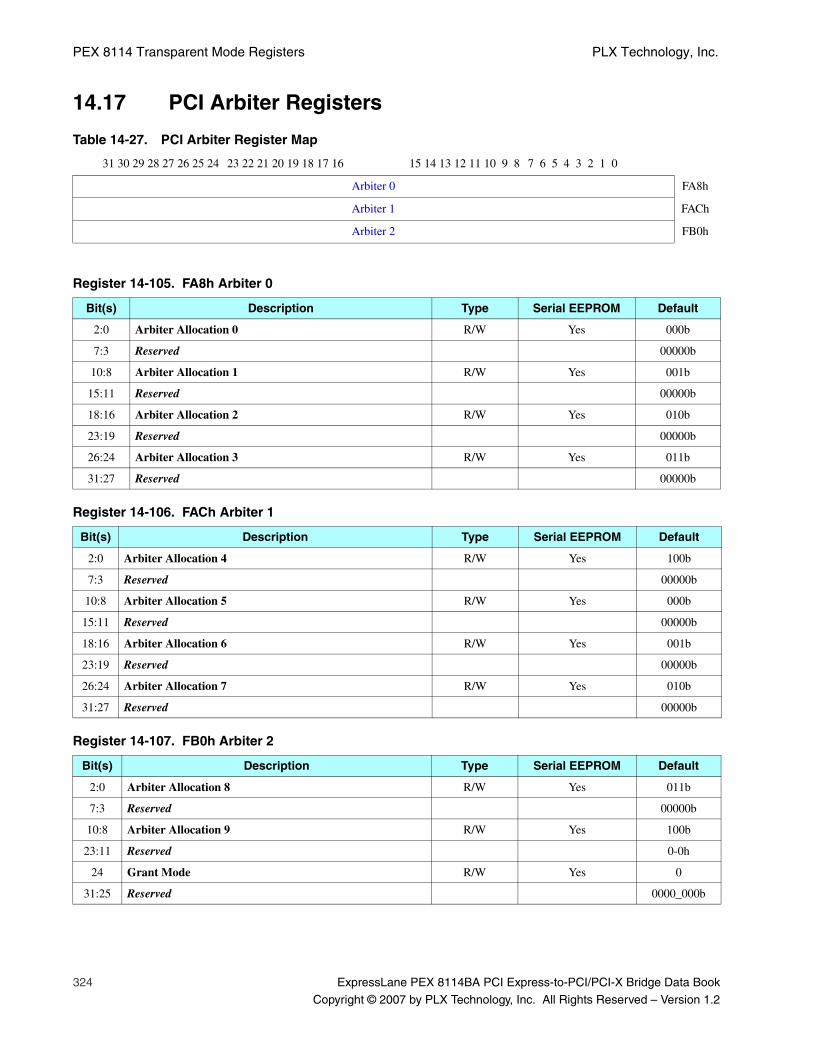
PEX 8114 Transparent Mode Registers PLX Technology, Inc.
324 ExpressLane PEX 8114BA PCI Express-to-PCI/PCI-X Bridge Data Book
Copyright © 2007 by PLX Technology, Inc. All Rights Reserved – Version 1.2
14.17 PCI Arbiter Registers
Table 14-27. PCI Arbiter Register Map
31 30 29 28 27 26 25 24 23 22 21 20 19 18 17 16 15 14 13 12 11 10 9 8 7 6 5 4 3 2 1 0
Arbiter 0 FA8h
Arbiter 1 FACh
Arbiter 2 FB0h
Register 14-105. FA8h Arbiter 0
Bit(s) Description Type Serial EEPROM Default
2:0 Arbiter Allocation 0 R/W Yes 000b
7:3 Reserved 00000b
10:8 Arbiter Allocation 1 R/W Yes 001b
15:11 Reserved 00000b
18:16 Arbiter Allocation 2 R/W Yes 010b
23:19 Reserved 00000b
26:24 Arbiter Allocation 3 R/W Yes 011b
31:27 Reserved 00000b
Register 14-106. FACh Arbiter 1
Bit(s) Description Type Serial EEPROM Default
2:0 Arbiter Allocation 4 R/W Yes 100b
7:3 Reserved 00000b
10:8 Arbiter Allocation 5 R/W Yes 000b
15:11 Reserved 00000b
18:16 Arbiter Allocation 6 R/W Yes 001b
23:19 Reserved 00000b
26:24 Arbiter Allocation 7 R/W Yes 010b
31:27 Reserved 00000b
Register 14-107. FB0h Arbiter 2
Bit(s) Description Type Serial EEPROM Default
2:0 Arbiter Allocation 8 R/W Yes 011b
7:3 Reserved 00000b
10:8 Arbiter Allocation 9 R/W Yes 100b
23:11 Reserved 0-0h
24 Grant Mode R/W Yes 0
31:25 Reserved 0000_000b
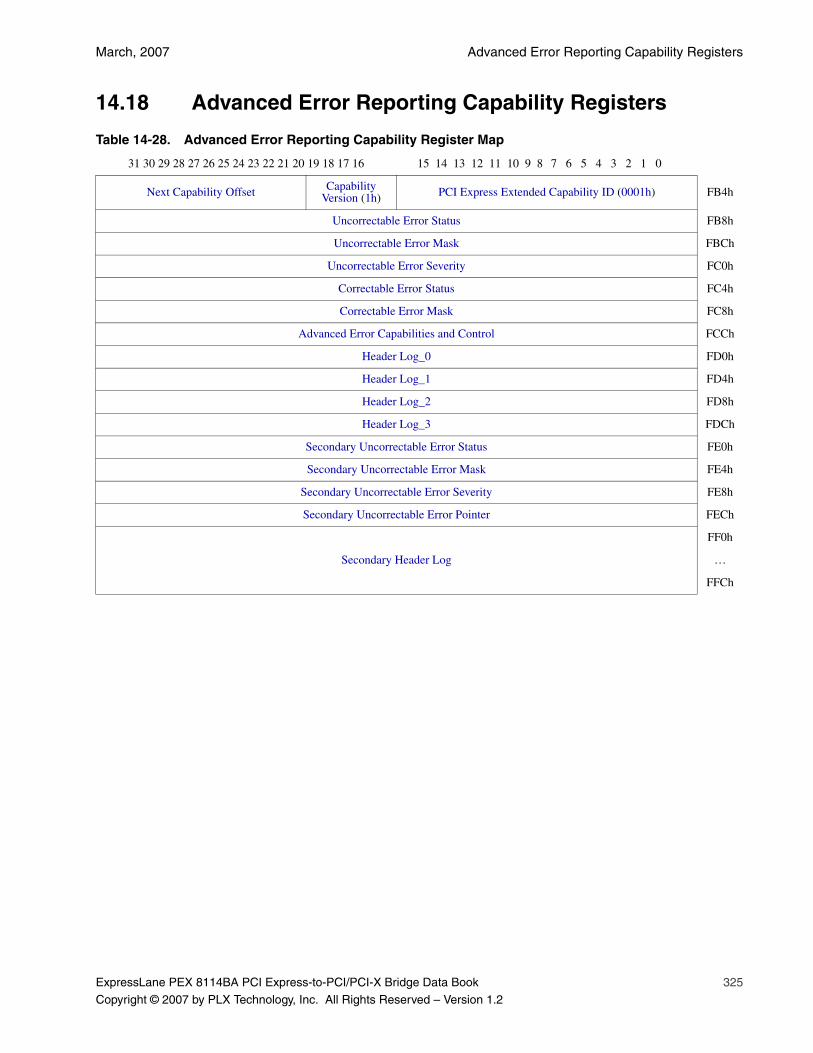
March, 2007 Advanced Error Reporting Capability Registers
ExpressLane PEX 8114BA PCI Express-to-PCI/PCI-X Bridge Data Book 325
Copyright © 2007 by PLX Technology, Inc. All Rights Reserved – Version 1.2
14.18 Advanced Error Reporting Capability Registers
Table 14-28. Advanced Error Reporting Capability Register Map
31 30 29 28 27 26 25 24 23 22 21 20 19 18 17 16 15 14 13 12 11 10 9 8 7 6 5 4 3 2 1 0
Next Capability Offset Capability Version (1h) PCI Express Extended Capability ID (0001h) FB4h
Uncorrectable Error Status FB8h
Uncorrectable Error Mask FBCh
Uncorrectable Error Severity FC0h
Correctable Error Status FC4h
Correctable Error Mask FC8h
Advanced Error Capabilities and Control FCCh
Header Log_0 FD0h
Header Log_1 FD4h
Header Log_2 FD8h
Header Log_3 FDCh
Secondary Uncorrectable Error Status FE0h
Secondary Uncorrectable Error Mask FE4h
Secondary Uncorrectable Error Severity FE8h
Secondary Uncorrectable Error Pointer FECh
Secondary Header Log
FF0h
…
FFCh
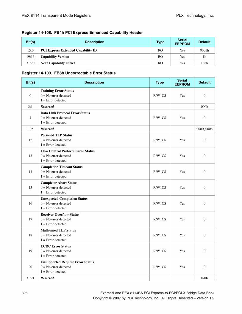
PEX 8114 Transparent Mode Registers PLX Technology, Inc.
326 ExpressLane PEX 8114BA PCI Express-to-PCI/PCI-X Bridge Data Book
Copyright © 2007 by PLX Technology, Inc. All Rights Reserved – Version 1.2
Register 14-108. FB4h PCI Express Enhanced Capability Header
Bit(s) Description Type Serial EEPROM Default
15:0 PCI Express Extended Capability ID RO Yes 0001h
19:16 Capability Version RO Yes 1h
31:20 Next Capability Offset RO Yes 138h
Register 14-109. FB8h Uncorrectable Error Status
Bit(s) Description Type Serial EEPROM Default
0Training Error Status0 = No error detected1 = Error detected
R/W1CS Yes 0
3:1 Reserved 000b
4Data Link Protocol Error Status0 = No error detected1 = Error detected
R/W1CS Yes 0
11:5 Reserved 0000_000b
12Poisoned TLP Status0 = No error detected1 = Error detected
R/W1CS Yes 0
13Flow Control Protocol Error Status0 = No error detected1 = Error detected
R/W1CS Yes 0
14Completion Timeout Status0 = No error detected1 = Error detected
R/W1CS Yes 0
15Completer Abort Status0 = No error detected1 = Error detected
R/W1CS Yes 0
16Unexpected Completion Status0 = No error detected1 = Error detected
R/W1CS Yes 0
17Receiver Overflow Status0 = No error detected1 = Error detected
R/W1CS Yes 0
18Malformed TLP Status0 = No error detected1 = Error detected
R/W1CS Yes 0
19ECRC Error Status0 = No error detected1 = Error detected
R/W1CS Yes 0
20Unsupported Request Error Status0 = No error detected1 = Error detected
R/W1CS Yes 0
31:21 Reserved 0-0h

March, 2007 Advanced Error Reporting Capability Registers
ExpressLane PEX 8114BA PCI Express-to-PCI/PCI-X Bridge Data Book 327
Copyright © 2007 by PLX Technology, Inc. All Rights Reserved – Version 1.2
Register 14-110. FBCh Uncorrectable Error Mask
Bit(s) Description Type Serial EEPROM Default
0
Training Error Mask0 = No mask is set1 = Error reporting, first error update, and Header logging are masked for this error
R/WS Yes 0
3:1 Reserved 000b
4
Data Link Protocol Error Mask0 = No mask is set1 = Error reporting, first error update, and Header logging are masked for this error
R/WS Yes 0
11:5 Reserved 0000_000b
12
Poisoned TLP Mask0 = No mask is set1 = Error reporting, first error update, and Header logging are masked for this error
R/WS Yes 0
13
Flow Control Protocol Mask0 = No mask is set1 = Error reporting, first error update, and Header logging are masked for this error
R/WS Yes 0
14
Completion Timeout Mask0 = No mask is set1 = Error reporting, first error update, and Header logging are masked for this error
R/WS Yes 0
15
Completer Abort Mask0 = No mask is set1 = Error reporting, first error update, and Header logging are masked for this error
R/WS Yes 0
16
Unexpected Completion Mask0 = No mask is set1 = Error reporting, first error update, and Header logging are masked for this error
R/WS Yes 0
17
Receiver Overflow Mask0 = No mask is set1 = Error reporting, first error update, and Header logging are masked for this error
R/WS Yes 0
18
Malformed TLP Mask0 = No mask is set1 = Error reporting, first error update, and Header logging are masked for this error
R/WS Yes 0
19
ECRC Error Mask0 = No mask is set1 = Error reporting, first error update, and Header logging are masked for this error
R/WS Yes 0
20
Unsupported Request Error Mask0 = No mask is set1 = Error reporting, first error update, and Header logging are masked for this error
R/WS Yes 0
31:21 Reserved 0-0h

PEX 8114 Transparent Mode Registers PLX Technology, Inc.
328 ExpressLane PEX 8114BA PCI Express-to-PCI/PCI-X Bridge Data Book
Copyright © 2007 by PLX Technology, Inc. All Rights Reserved – Version 1.2
Register 14-111. FC0h Uncorrectable Error Severity
Bit(s) Description Type Serial EEPROM Default
0Training Error Severity0 = Error reported as non-fatal1 = Error reported as fatal
R/WS Yes 1
3:1 Reserved 000b
4Data Link Protocol Error Severity0 = Error reported as non-fatal1 = Error reported as fatal
R/WS Yes 1
11:5 Reserved 0000_000b
12Poisoned TLP Severity0 = Error reported as non-fatal1 = Error reported as fatal
R/WS Yes 0
13Flow Control Protocol Error Severity0 = Error reported as non-fatal1 = Error reported as fatal
R/WS Yes 1
14Completion Timeout Severity0 = Error reported as non-fatal1 = Error reported as fatal
R/WS Yes 0
15Completer Abort Severity0 = Error reported as non-fatal1 = Error reported as fatal
R/WS Yes 0
16Unexpected Completion Severity0 = Error reported as non-fatal1 = Error reported as fatal
R/WS Yes 0
17Receiver Overflow Severity0 = Error reported as non-fatal1 = Error reported as fatal
R/WS Yes 1
18Malformed TLP Severity0 = Error reported as non-fatal1 = Error reported as fatal
R/WS Yes 1
19ECRC Error Severity0 = Error reported as non-fatal1 = Error reported as fatal
R/WS Yes 0
20Unsupported Request Error Severity0 = Error reported as non-fatal1 = Error reported as fatal
R/WS Yes 0
31:21 Reserved 0-0h
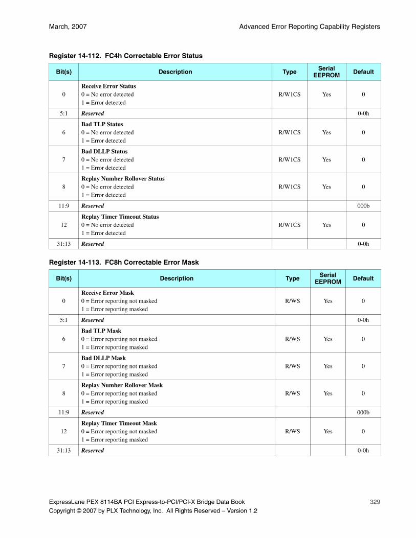
March, 2007 Advanced Error Reporting Capability Registers
ExpressLane PEX 8114BA PCI Express-to-PCI/PCI-X Bridge Data Book 329
Copyright © 2007 by PLX Technology, Inc. All Rights Reserved – Version 1.2
Register 14-112. FC4h Correctable Error Status
Bit(s) Description Type Serial EEPROM Default
0Receive Error Status0 = No error detected1 = Error detected
R/W1CS Yes 0
5:1 Reserved 0-0h
6Bad TLP Status0 = No error detected1 = Error detected
R/W1CS Yes 0
7Bad DLLP Status0 = No error detected1 = Error detected
R/W1CS Yes 0
8Replay Number Rollover Status0 = No error detected1 = Error detected
R/W1CS Yes 0
11:9 Reserved 000b
12Replay Timer Timeout Status0 = No error detected1 = Error detected
R/W1CS Yes 0
31:13 Reserved 0-0h
Register 14-113. FC8h Correctable Error Mask
Bit(s) Description Type Serial EEPROM Default
0Receive Error Mask0 = Error reporting not masked1 = Error reporting masked
R/WS Yes 0
5:1 Reserved 0-0h
6Bad TLP Mask0 = Error reporting not masked1 = Error reporting masked
R/WS Yes 0
7Bad DLLP Mask0 = Error reporting not masked1 = Error reporting masked
R/WS Yes 0
8Replay Number Rollover Mask0 = Error reporting not masked1 = Error reporting masked
R/WS Yes 0
11:9 Reserved 000b
12Replay Timer Timeout Mask0 = Error reporting not masked1 = Error reporting masked
R/WS Yes 0
31:13 Reserved 0-0h

PEX 8114 Transparent Mode Registers PLX Technology, Inc.
330 ExpressLane PEX 8114BA PCI Express-to-PCI/PCI-X Bridge Data Book
Copyright © 2007 by PLX Technology, Inc. All Rights Reserved – Version 1.2
Register 14-114. FCCh Advanced Error Capabilities and Control
Bit(s) Description Type Serial EEPROM Default
4:0First Error PointerIdentifies the bit position of the first error reported in the Uncorrectable Error Status register.
ROS Yes 1_1111b
5ECRC Generation Capable0 = ECRC generation not supported1 = ECRC generation supported, but must be enabled
RO Yes 1
6ECRC Generation Enable0 = ECRC generation disabled1 = ECRC generation enabled
R/WS Yes 0
7ECRC Checking Capable0 = ECRC checking not supported1 = ECRC checking supported, but must be enabled
RO Yes 1
8ECRC Checking Enable0 = ECRC checking disabled1 = ECRC checking enabled
R/WS Yes 0
31:9 Reserved 0-0h
Register 14-115. FD0h Header Log_0
Bit(s) Description Type Serial EEPROM Default
31:0TLP Header_0First DWord Header. TLP Header associated with error.
ROS Yes 0-0h
Register 14-116. FD4h Header Log_1
Bit(s) Description Type Serial EEPROM Default
31:0TLP Header_1Second DWord Header. TLP Header associated with error.
ROS Yes 0-0h
Register 14-117. FD8h Header Log_2
Bit(s) Description Type Serial EEPROM Default
31:0TLP Header_2Third DWord Header. TLP Header associated with error.
ROS Yes 0-0h
Register 14-118. FDCh Header Log_3
Bit(s) Description Type Serial EEPROM Default
31:0TLP Header_3Fourth DWord Header. TLP Header associated with error.
ROS Yes 0-0h
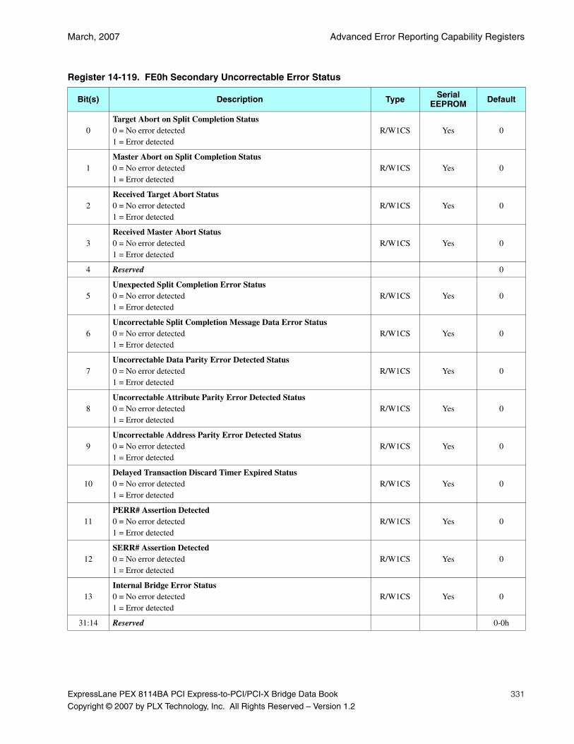
March, 2007 Advanced Error Reporting Capability Registers
ExpressLane PEX 8114BA PCI Express-to-PCI/PCI-X Bridge Data Book 331
Copyright © 2007 by PLX Technology, Inc. All Rights Reserved – Version 1.2
Register 14-119. FE0h Secondary Uncorrectable Error Status
Bit(s) Description Type Serial EEPROM Default
0Target Abort on Split Completion Status0 = No error detected1 = Error detected
R/W1CS Yes 0
1Master Abort on Split Completion Status0 = No error detected1 = Error detected
R/W1CS Yes 0
2Received Target Abort Status0 = No error detected1 = Error detected
R/W1CS Yes 0
3Received Master Abort Status0 = No error detected1 = Error detected
R/W1CS Yes 0
4 Reserved 0
5Unexpected Split Completion Error Status0 = No error detected1 = Error detected
R/W1CS Yes 0
6Uncorrectable Split Completion Message Data Error Status0 = No error detected1 = Error detected
R/W1CS Yes 0
7Uncorrectable Data Parity Error Detected Status0 = No error detected1 = Error detected
R/W1CS Yes 0
8Uncorrectable Attribute Parity Error Detected Status0 = No error detected1 = Error detected
R/W1CS Yes 0
9Uncorrectable Address Parity Error Detected Status0 = No error detected1 = Error detected
R/W1CS Yes 0
10Delayed Transaction Discard Timer Expired Status0 = No error detected1 = Error detected
R/W1CS Yes 0
11PERR# Assertion Detected0 = No error detected1 = Error detected
R/W1CS Yes 0
12SERR# Assertion Detected0 = No error detected1 = Error detected
R/W1CS Yes 0
13Internal Bridge Error Status0 = No error detected1 = Error detected
R/W1CS Yes 0
31:14 Reserved 0-0h

PEX 8114 Transparent Mode Registers PLX Technology, Inc.
332 ExpressLane PEX 8114BA PCI Express-to-PCI/PCI-X Bridge Data Book
Copyright © 2007 by PLX Technology, Inc. All Rights Reserved – Version 1.2
Register 14-120. FE4h Secondary Uncorrectable Error Mask
Bit(s) Description Type Serial EEPROM Default
0
Target Abort on Split Completion Mask0 = No mask is set1 = Error reporting, first error update, and Header logging are masked for this error
R/WS Yes 0
1
Master Abort on Split Completion Mask0 = No mask is set1 = Error reporting, first error update, and Header logging are masked for this error
R/WS Yes 0
2
Received Target Abort Mask0 = No mask is set1 = Error reporting, first error update, and Header logging are masked for this error
R/WS Yes 0
3
Received Master Abort Mask0 = No mask is set1 = Error reporting, first error update, and Header logging are masked for this error
R/WS Yes 1
4 Reserved 0
5
Unexpected Split Completion Error Mask0 = No mask is set1 = Error reporting, first error update, and Header logging are masked for this error
R/WS Yes 1
6
Uncorrectable Split Completion Message Data Error Mask0 = No mask is set1 = Error reporting, first error update, and Header logging are masked for this error
R/WS Yes 0
7
Uncorrectable Data Parity Error Detected Mask0 = No mask is set1 = Error reporting, first error update, and Header logging are masked for this error
R/WS Yes 1
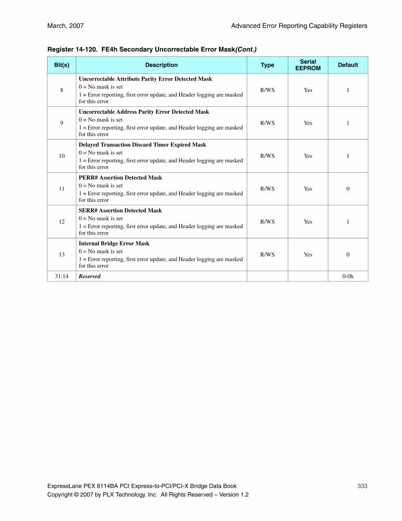
March, 2007 Advanced Error Reporting Capability Registers
ExpressLane PEX 8114BA PCI Express-to-PCI/PCI-X Bridge Data Book 333
Copyright © 2007 by PLX Technology, Inc. All Rights Reserved – Version 1.2
8
Uncorrectable Attribute Parity Error Detected Mask0 = No mask is set1 = Error reporting, first error update, and Header logging are masked for this error
R/WS Yes 1
9
Uncorrectable Address Parity Error Detected Mask0 = No mask is set1 = Error reporting, first error update, and Header logging are masked for this error
R/WS Yes 1
10
Delayed Transaction Discard Timer Expired Mask0 = No mask is set1 = Error reporting, first error update, and Header logging are masked for this error
R/WS Yes 1
11
PERR# Assertion Detected Mask0 = No mask is set1 = Error reporting, first error update, and Header logging are masked for this error
R/WS Yes 0
12
SERR# Assertion Detected Mask0 = No mask is set1 = Error reporting, first error update, and Header logging are masked for this error
R/WS Yes 1
13
Internal Bridge Error Mask0 = No mask is set1 = Error reporting, first error update, and Header logging are masked for this error
R/WS Yes 0
31:14 Reserved 0-0h
Register 14-120. FE4h Secondary Uncorrectable Error Mask(Cont.)
Bit(s) Description Type Serial EEPROM Default
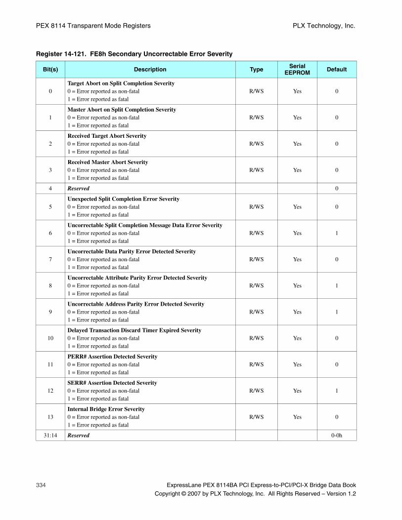
PEX 8114 Transparent Mode Registers PLX Technology, Inc.
334 ExpressLane PEX 8114BA PCI Express-to-PCI/PCI-X Bridge Data Book
Copyright © 2007 by PLX Technology, Inc. All Rights Reserved – Version 1.2
Register 14-121. FE8h Secondary Uncorrectable Error Severity
Bit(s) Description Type Serial EEPROM Default
0Target Abort on Split Completion Severity0 = Error reported as non-fatal1 = Error reported as fatal
R/WS Yes 0
1Master Abort on Split Completion Severity0 = Error reported as non-fatal1 = Error reported as fatal
R/WS Yes 0
2Received Target Abort Severity0 = Error reported as non-fatal1 = Error reported as fatal
R/WS Yes 0
3Received Master Abort Severity0 = Error reported as non-fatal1 = Error reported as fatal
R/WS Yes 0
4 Reserved 0
5Unexpected Split Completion Error Severity0 = Error reported as non-fatal1 = Error reported as fatal
R/WS Yes 0
6Uncorrectable Split Completion Message Data Error Severity0 = Error reported as non-fatal1 = Error reported as fatal
R/WS Yes 1
7Uncorrectable Data Parity Error Detected Severity0 = Error reported as non-fatal1 = Error reported as fatal
R/WS Yes 0
8Uncorrectable Attribute Parity Error Detected Severity0 = Error reported as non-fatal1 = Error reported as fatal
R/WS Yes 1
9Uncorrectable Address Parity Error Detected Severity0 = Error reported as non-fatal1 = Error reported as fatal
R/WS Yes 1
10Delayed Transaction Discard Timer Expired Severity0 = Error reported as non-fatal1 = Error reported as fatal
R/WS Yes 0
11PERR# Assertion Detected Severity0 = Error reported as non-fatal1 = Error reported as fatal
R/WS Yes 0
12SERR# Assertion Detected Severity0 = Error reported as non-fatal1 = Error reported as fatal
R/WS Yes 1
13Internal Bridge Error Severity0 = Error reported as non-fatal1 = Error reported as fatal
R/WS Yes 0
31:14 Reserved 0-0h
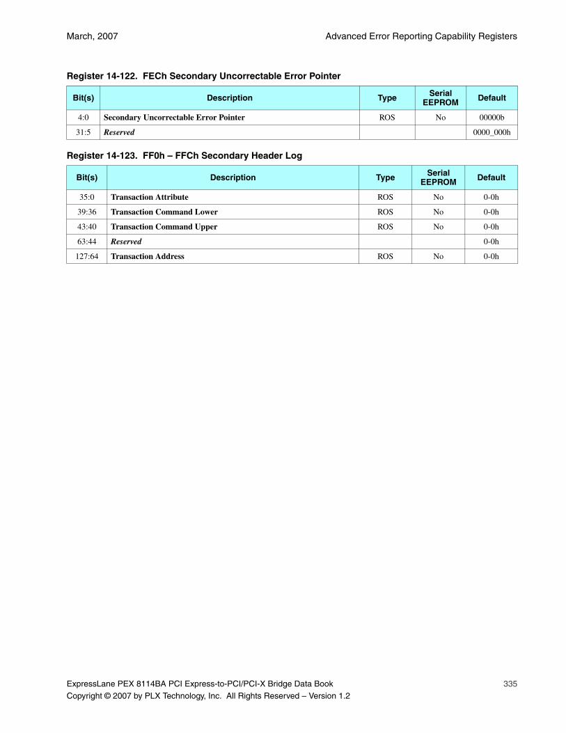
March, 2007 Advanced Error Reporting Capability Registers
ExpressLane PEX 8114BA PCI Express-to-PCI/PCI-X Bridge Data Book 335
Copyright © 2007 by PLX Technology, Inc. All Rights Reserved – Version 1.2
Register 14-122. FECh Secondary Uncorrectable Error Pointer
Bit(s) Description Type Serial EEPROM Default
4:0 Secondary Uncorrectable Error Pointer ROS No 00000b
31:5 Reserved 0000_000h
Register 14-123. FF0h – FFCh Secondary Header Log
Bit(s) Description Type Serial EEPROM Default
35:0 Transaction Attribute ROS No 0-0h
39:36 Transaction Command Lower ROS No 0-0h
43:40 Transaction Command Upper ROS No 0-0h
63:44 Reserved 0-0h
127:64 Transaction Address ROS No 0-0h
PEX 8114 Transparent Mode Registers PLX Technology, Inc.
336 ExpressLane PEX 8114BA PCI Express-to-PCI/PCI-X Bridge Data Book
Copyright © 2007 by PLX Technology, Inc. All Rights Reserved – Version 1.2
THIS PAGE INTENTIONALLY LEFT BLANK.
ExpressLane PEX 8114BA PCI Express-to-PCI/PCI-X Bridge Data Book 337
Copyright © 2007 by PLX Technology, Inc. All Rights Reserved – Version 1.2
Chapter 15 Additional Non-Transparent Functionality
15.1 Additional Non-Transparent FeaturesIn Non-Transparent mode, several additional features are included to support Non-Transparentoperations and add flexibility to the PEX 8114. This chapter describes those features.
Note: PLX does not recommend using the PEX 8114BA in NT mode due to the Non-Transparent mode errata detailed in the PEX 8114BA Errata document. There is no plan to fix the NT mode errata in future revisions of the PEX 8114.
15.1.1 Non-Transparent Reset Options and Additional StepsA Transparent bridge is a simpler device than a Non-Transparent bridge, in which default registersettings are likely to be acceptable, also in which all configuration can be achieved throughConfiguration cycles from the upstream port. Non-Transparent bridges are more complicated and lesslikely to contain acceptable default values. The most prominent example of additional complications inNon-Transparent bridge use is that the Base Address sizes must be established prior to PCI Expressenumeration, allowing the Enumerating software to provide an indication of the required memory size.In Non-Transparent mode, the reset sequence can be altered for flexibility, enabling the configurationof the PCI Express registers prior to PCI Express enumeration. The following is a step-by-step sequenceof the PEX 8114 Non-Transparent mode Reset process.
1. The Power Good Reset (PEX_PERST#) de-asserts, initializing registers to default values.
2. The PCI Reset (PCI_RST#) de-asserts, initializing the PCI Bus.
3. Optional. The serial EEPROM, if installed, loads and modifies registers to user-specific values. When the serial EEPROM completes its load sequence, or if the serial EEPROM is not installed or is strapped disabled, the NT PCI-X Interface Configuration Access Enable register PCI-X Access Enable bit (1DCh[28]) is set, allowing the PCI side of the bridge to accept Enumeration cycles.
4. Optional. The PEX 8114 PCI Bus starts to accept configurations; however, the PEX 8114 PCI Express interface does not accept configurations, allowing the PCI Host another attempt at configuration modifications in the PCI Express register set.
5. The PCI Host or serial EEPROM load, if PCI modification is not used, causes the NT PCI-X Interface Configuration Access Enable register PCI Express Access Enable bit (1DCh[29]) to be set, allowing the PEX 8114 to accept PCI Express configuration.
This sequence is designed as PCI-compliant and provides flexibility in configuring the Non-Transparentbridge. Steps 1 and 2 initialize the bridge with default Configuration register values. When the bridge isin Non-Transparent mode and the STRAP_CLK_MST ball is strapped High, the PEX 8114 synthesizesand drives PCI_CLK. When the STRAP_CLK_MST ball is strapped Low, the PCI side of the bridgeSlaves to PCI_CLK. In both cases, PCI_RST# is an input and HP_PERST# is an output. A Hot Reset onthe PCI Express side of the bridge causes HP_PERST# to assert, indicating a Hot Reset was received onthe PCI Express link. The duration of HP_PERST# assertion is selectable through the HP_PERST#Timer Select bit (offset FA0h[29]). The default value of this bit is 0, which causes HP_PERST# to assertfor 1 ms. If software sets the bit to 1, HP_PERST# asserts for 128 ns.
Additional Non-Transparent Functionality PLX Technology, Inc.
338 ExpressLane PEX 8114BA PCI Express-to-PCI/PCI-X Bridge Data Book
Copyright © 2007 by PLX Technology, Inc. All Rights Reserved – Version 1.2
By default, the PEX 8114 resets when HP_PERST# or PCI_RST# is asserted. Resetting of thePEX 8114 HP_PERST# signal can be disabled by setting the NT Reset Select bit (offset FA0h[30]).When this bit is set, the PEX 8114 can only be reset by asserting PCI_RST#. However, a Hot Resetreceived on the PCI Express link continues to cause HP_PERST# to assert. If the PEX 8114 is assertingHP_PERST#, software can prematurely terminate the assertion by writing 1 to the Clear HP_PERST#bit (offset FA0h[31]). HP_PERST# assertion indicates to the PCI Host that the PCI Express side of thebridge has reset, and that the bridge requires reconfiguration. The default values leave the BAR sizesand BAR translation address at 0; however, these values are often unusable.
Step 3 is optional. By installing a serial EEPROM and setting the EE_PR# ball Low, the defaultConfiguration register values can be replaced with user-specific register values through serial EEPROMWrites prior to allowing the PCI Express Root Complex to enumerate. When the serial EEPROM isused to load the CSR, the bridge’s normal boot sequence can be overridden. That is, steps 4 and 5 canbe reversed, allowing the PEX 8114 to boot the PCI Express side first. This is achieved by setting theNT PCI-X Interface Configuration Access Enable register PCI Express Access Enable bit(1DCh[29]) and clearing the PCI-X Access Enable bit (1DCh[28]) by way of a serial EEPROM load.This allows a limited Reverse Non-Transparent Bridge mode of operation.
The NT PCI-X Interface Configuration Access Enable register default values allows only thePCI side of the bridge to accept accesses. The PCI Express link is refused access until the serialEEPROM or PCI Host sets the PCI Express Access Enable bit. This configuration delay allows thePCI Host to also modify Configuration registers prior to allowing the PCI Express Root Complex toenumerate. Step 4 is also optional; however, the serial EEPROM or PCI Host must modify configurationprior to PCI Express enumeration. If all necessary configuration modifications are performed by theserial EEPROM load in step 3, the serial EEPROM can also override the initial values of the NT PCI-XInterface Configuration Access Enable register, allowing the PCI and PCI Express sides of the bridgeto simultaneously start the configuration, following serial EEPROM loading of the Configurationregisters. If the serial EEPROM load is omitted, the PCI Host can make the necessary configurationmodifications, then enable the PCI Express enumerations. Therefore, configuration modificationsexecuted by the serial EEPROM or PCI Host are allowed.
Step 5, the final step after the PEX 8114 is correctly configured for PCI Express enumeration, is toallow the PCI Express Configuration cycles to be accepted. This is achieved by setting the PCI ExpressAccess Enable bit, which is performed by the serial EEPROM or PCI Host.
15.1.2 PCI-X and PCI Express Configuration/Memory[5:2] BAR SetupThe BAR Setup registers are located at Configuration Address offsets D0h through F4h:
• PCI-X Memory BAR Setup registers are located at offsets D0h through E0h
• PCI Express Memory BAR Setup registers are located at offsets E4h through F4h
These registers are loaded by serial EEPROM or Configuration Writes, and are used to enable theAddress space and indicate the Address Space size. Bit 31 of the Memory BAR Setup registers is usedto enable or disable Memory space. If bit 31 is cleared to 0 (default), the Address space is disabled.Writing Fh in the Setup register’s MSBs controls the Address space size; therefore, all bits are not usedwhen addressing the Memory space. Memory space is allocated in 1-MB increments; therefore, onlybits [30:12] are used to indicate memory size.
The BAR Setup registers are used as masks for the corresponding BARs. When the BIOS reads a BAR,it reads ones (1) in bits [30:12], if the corresponding Memory BAR Setup register contains ones (1) inthose bits. The BIOS uses this information to determine memory requirements.
March, 2007 Scratchpad (Mailbox) Registers
ExpressLane PEX 8114BA PCI Express-to-PCI/PCI-X Bridge Data Book 339
Copyright © 2007 by PLX Technology, Inc. All Rights Reserved – Version 1.2
15.1.3 Scratchpad (Mailbox) RegistersWhen the PEX 8114 is in Non-Transparent mode, eight 32-bit Scratchpad registers (sometimesreferred to as Mailbox registers) are available. These registers are intended as general-purpose datarepositories that retain data or messages that must be transferred across the Non-Transparent boundary.Like the Doorbell/Interrupt Request registers, these registers can be accessed from either side of thebridge, and provide synchronizing information.
Scratchpad registers differ from Doorbell/Interrupt Request registers, that is, they retain data;however, they do not cause interrupts or other indications when loaded. These registers can be writtenand read from both sides of the bridge. Software must regulate access to these registers, not allowing thePCI Host and PCI Express Root Complex to execute conflicting access to these registers. If it isnecessary to transfer data and transmit indications that the transfer is in need of service, use theScratchpad registers to retain the message, and the Interrupt register to signal that a message iswaiting. These eight registers can be accessed by PCI and PCI Express, through Configuration CycleWrites and Reads to locations B0h through CCh.
15.1.4 Expansion ROMIn Non-Transparent mode, Expansion ROM BAR space is supported on the PCI Express side of thebridge. Additional serial EEPROM space, beyond the 2 KB needed for register initialization, is used toretain Expansion ROM data. The start of Expansion ROM data is located at Byte Address 800h in theserial EEPROM. Byte Address 800h is at the 2-KB point in the serial EEPROM. The space locatedbelow Byte Address 800h is reserved for Non-Transparent register data. The space located above the2-KB point is where the sequentially increasing Expansion ROM data is loaded.
Larger serial EEPROMs allow additional Expansion ROM data to be stored:
• 4-KB serial EEPROM supports 2 KB of Expansion ROM and 2 KB of register load data
• 8-KB serial EEPROM allows up to 6 KB of Expansion ROM data and 2 KB of register load data
• 64-KB serial EEPROM allows up to 32 KB of Expansion ROM data, maximum Expansion ROM size, and 2 KB of register load data
Because the first 2 KB of the serial EEPROM space is used for register load data, and the remainingspace is available only for Expansion ROM data, the available Expansion ROM data is 2 KB less thanthe serial EEPROM size. Therefore, when attempting to use more than N KB of Expansion ROM data inan N-KB Expansion ROM BAR, the serial EEPROM provides 2 KB less data than the BAR size. Eitherset the BAR size to one-half the serial EEPROM size used, or ensure that the Expansion ROM cannot beaccessed by the system within the upper 2 KB.
Note: Serial EEPROM Expansion ROM data can be changed by Writes to the PEX 8114 Serial EEPROM Control, Status, Status Data, and Buffer registers.
Additional Non-Transparent Functionality PLX Technology, Inc.
340 ExpressLane PEX 8114BA PCI Express-to-PCI/PCI-X Bridge Data Book
Copyright © 2007 by PLX Technology, Inc. All Rights Reserved – Version 1.2
THIS PAGE INTENTIONALLY LEFT BLANK.
ExpressLane PEX 8114BA PCI Express-to-PCI/PCI-X Bridge Data Book 341
Copyright © 2007 by PLX Technology, Inc. All Rights Reserved – Version 1.2
Chapter 16 PEX 8114 Non-Transparent Mode PCI-X Registers
16.1 IntroductionNote: PLX does not recommend using the PEX 8114BA in NT mode due to the
Non-Transparent mode errata detailed in the PEX 8114BA Errata document. There is no plan to fix the NT mode errata in future revisions of the PEX 8114.
This chapter defines the PEX 8114 Non-Transparent (NT) PCI-X interface registers. The NT modebridge includes two sets of configuration-capability, control, and status registers to support PCI-X andPCI Express interfaces. Table 16-1 delineates NT mode PCI-X interface register mapping.
NT mode PCI Express interface registers are defined in Chapter 17, “PEX 8114 Non-Transparent ModePCI Express Registers.” Transparent mode registers are defined in Chapter 14, “PEX 8114 TransparentMode Registers.”
For further details regarding register names and descriptions, refer to the following specifications:
• PCI r2.3
• PCI r3.0
• PCI-to-PCI Bridge r1.1
• PCI Express Base 1.0a
• PCI Express-to-PCI/PCI-X Bridge r1.0
• PCI-X r1.0b
• PCI-X r2.0a
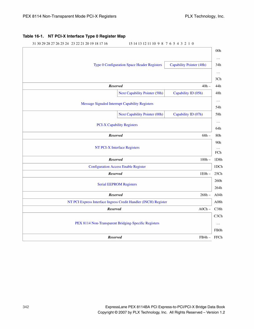
PEX 8114 Non-Transparent Mode PCI-X Registers PLX Technology, Inc.
342 ExpressLane PEX 8114BA PCI Express-to-PCI/PCI-X Bridge Data Book
Copyright © 2007 by PLX Technology, Inc. All Rights Reserved – Version 1.2
Table 16-1. NT PCI-X Interface Type 0 Register Map
31 30 29 28 27 26 25 24 23 22 21 20 19 18 17 16 15 14 13 12 11 10 9 8 7 6 5 4 3 2 1 0
00h
…
Type 0 Configuration Space Header Registers Capability Pointer (48h) 34h
…
3Ch
Reserved 40h – 44h
Next Capability Pointer (58h) Capability ID (05h) 48h
Message Signaled Interrupt Capability Registers…
54h
Next Capability Pointer (00h) Capability ID (07h) 58h
PCI-X Capability Registers…
64h
Reserved 68h – 80h
NT PCI-X Interface Registers90h…
FCh
Reserved 100h – 1D8h
Configuration Access Enable Register 1DCh
Reserved 1E0h – 25Ch
Serial EEPROM Registers260h
264h
Reserved 268h – A04h
NT PCI Express Interface Ingress Credit Handler (INCH) Register A08h
Reserved A0Ch – C38h
PEX 8114 Non-Transparent Bridging-Specific Registers
C3Ch
…
FB0h
Reserved FB4h – FFCh
March, 2007 Register Descriptions
ExpressLane PEX 8114BA PCI Express-to-PCI/PCI-X Bridge Data Book 343
Copyright © 2007 by PLX Technology, Inc. All Rights Reserved – Version 1.2
16.2 Register DescriptionsThe remainder of this chapter details the PEX 8114 NT mode PCI-X interface registers, including:
• Bit/field names
• Description of the register’s function in the PEX 8114 NT mode PCI-X and PCI Express interfaces
• Type
• Whether the power-on/reset value can be modified by way of the PEX 8114 serial EEPROM initialization feature
• Initial power-on/reset (default) value
The register types are grouped by user accessibility. The types used in this device, and their descriptions,are delineated in Table 14-2, “Register Types.”
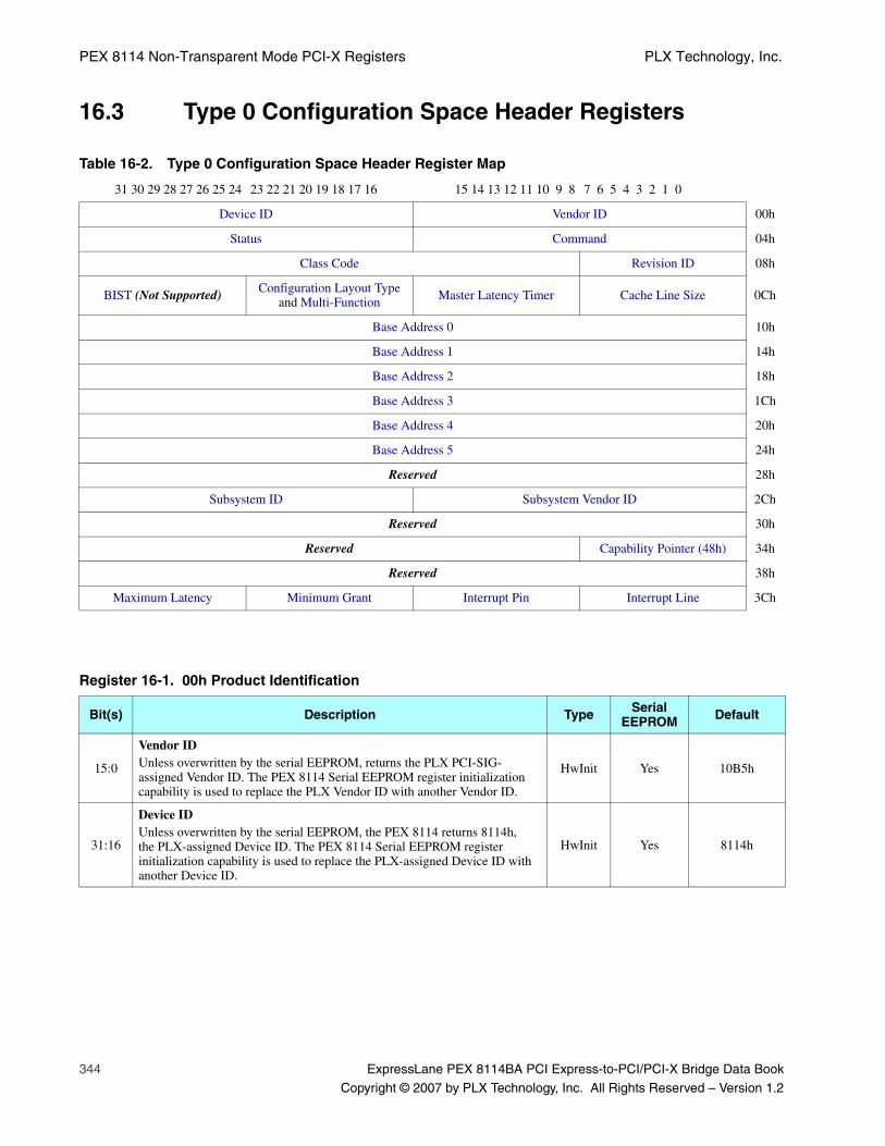
PEX 8114 Non-Transparent Mode PCI-X Registers PLX Technology, Inc.
344 ExpressLane PEX 8114BA PCI Express-to-PCI/PCI-X Bridge Data Book
Copyright © 2007 by PLX Technology, Inc. All Rights Reserved – Version 1.2
16.3 Type 0 Configuration Space Header Registers
Table 16-2. Type 0 Configuration Space Header Register Map
31 30 29 28 27 26 25 24 23 22 21 20 19 18 17 16 15 14 13 12 11 10 9 8 7 6 5 4 3 2 1 0
Device ID Vendor ID 00h
Status Command 04h
Class Code Revision ID 08h
BIST (Not Supported) Configuration Layout Type and Multi-Function Master Latency Timer Cache Line Size 0Ch
Base Address 0 10h
Base Address 1 14h
Base Address 2 18h
Base Address 3 1Ch
Base Address 4 20h
Base Address 5 24h
Reserved 28h
Subsystem ID Subsystem Vendor ID 2Ch
Reserved 30h
Reserved Capability Pointer (48h) 34h
Reserved 38h
Maximum Latency Minimum Grant Interrupt Pin Interrupt Line 3Ch
Register 16-1. 00h Product Identification
Bit(s) Description Type Serial EEPROM Default
15:0
Vendor IDUnless overwritten by the serial EEPROM, returns the PLX PCI-SIG- assigned Vendor ID. The PEX 8114 Serial EEPROM register initialization capability is used to replace the PLX Vendor ID with another Vendor ID.
HwInit Yes 10B5h
31:16
Device IDUnless overwritten by the serial EEPROM, the PEX 8114 returns 8114h, the PLX-assigned Device ID. The PEX 8114 Serial EEPROM register initialization capability is used to replace the PLX-assigned Device ID with another Device ID.
HwInit Yes 8114h
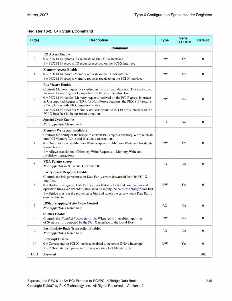
March, 2007 Type 0 Configuration Space Header Registers
ExpressLane PEX 8114BA PCI Express-to-PCI/PCI-X Bridge Data Book 345
Copyright © 2007 by PLX Technology, Inc. All Rights Reserved – Version 1.2
Register 16-2. 04h Status/Command
Bit(s) Description Type Serial EEPROM Default
Command
0I/O Access Enable0 = PEX 8114 ignores I/O requests on the PCI-X interface1 = PEX 8114 accepts I/O requests received on the PCI-X interface
R/W Yes 0
1Memory Access Enable0 = PEX 8114 ignores Memory requests on the PCI-X interface1 = PEX 8114 accepts Memory requests received on the PCI-X interface
R/W Yes 0
2
Bus Master EnableControls Memory request forwarding in the upstream direction. Does not affect message forwarding nor Completions in the upstream direction.0 = PEX 8114 handles Memory requests received on the PCI Express interface as Unsupported Requests (UR); for Non-Posted requests, the PEX 8114 returns a Completion with UR Completion status1 = PEX 8114 forwards Memory requests from the PCI Express interface to the PCI-X interface in the upstream direction
R/W Yes 0
3Special Cycle EnableNot supported. Cleared to 0.
RO No 0
4
Memory Write and InvalidateControls the ability of the bridge to convert PCI Express Memory Write requests into PCI Memory Write and Invalidate transactions.0 = Does not translate Memory Write Requests to Memory Write and Invalidate transactions1 = Allows translation of Memory Write Requests to Memory Write and Invalidate transactions
R/W Yes 0
5VGA Palette SnoopNot supported in NT mode. Cleared to 0.
RO No 0
6
Parity Error Response EnableControls the bridge response to Data Parity errors forwarded from its PCI-X interface. 0 = Bridge must ignore Data Parity errors that it detects and continue normal operation (however, records status, such as setting the Detected Parity Error bit)1 = Bridge must set the proper error bits and report the error when a Data Parity error is detected
R/W Yes 0
7IDSEL Stepping/Write Cycle ControlNot supported. Cleared to 0.
RO No 0
8SERR# EnableControls the Signaled System Error bit. When set to 1, enables reporting of System errors detected by the PCI-X interface to the Local Host.
R/W Yes 0
9Fast Back-to-Back Transaction EnabledNot supported. Cleared to 0.
RO No 0
10Interrupt Disable0 = Corresponding PCI-X interface enabled to generate INTA# interrupts1 = PCI-X interface prevented from generating INTA# interrupts
R/W Yes 0
15:11 Reserved 00h

PEX 8114 Non-Transparent Mode PCI-X Registers PLX Technology, Inc.
346 ExpressLane PEX 8114BA PCI Express-to-PCI/PCI-X Bridge Data Book
Copyright © 2007 by PLX Technology, Inc. All Rights Reserved – Version 1.2
Status
18:16 Reserved 000b
19Interrupt Status 0 = No INTA# interrupt pending1 = INTA# interrupt pending internally to the PCI-X interface
RO No 0
20Capabilities ListSet to 1.
RO No 1
2166-MHz CapableSet to 1.
RO No 1
22 Reserved 0
23Fast Back-to-Back Transaction EnabledSet to 1.
RO No 1
24
Master Data Parity ErrorReports detection of Uncorrectable Data errors.Set in the PCI-X interface if the Command register Parity Error Response Enable bit is set and any of the following three conditions occur:
• Interface receives a Completion or Split Completion with a Parity error• Bridge receives a Split Completion message for a Non-Posted Write on the
PCI-X interface, indicating an Uncorrectable (Split) Write Data error• Interface, as a bus Master, asserts PCI_PERR# on a Read transaction or
detects PCI_PERR# asserted on a Write transaction that it initiates
R/W1C Yes 0
26:25DEVSEL TimingSet to 10b, which indicates the PEX 8114 is a slow-speed device.
RO No 10b
27
Signaled Target AbortSet in the PCI-X interface when the interface, as a Target, terminates a transaction with Target Abort. Also set when the interface signals a Split Completion with Target Abort.
R/W1C Yes 0
28
Received Target AbortSet in the PCI-X interface when a Target Abort is detected and the interface is the Master of the transaction. Also set if a PCI-X Split Completion message is received indicating Target Abort.
R/W1C Yes 0
29Received Master AbortSet in the PCI-X interface when it is the transaction Master and receives a Master Abort.
R/W1C Yes 0
30Signaled System ErrorSet to 1 in the PCI-X interface when the interface asserts SERR#.
R/W1C Yes 0
31
Detected Parity ErrorSet to 1 in the PCI-X interface, regardless of the Command register Parity Error Response Enable bit state, when any of the following conditions are true:
• Detects an Address or Attribute Parity error as a potential Target• Detects a Data Parity error when the Target of a Write transaction
or PCI-X Split Completion• Detects a Data Parity error when a Read transaction Master
(Immediate Read data or PCI-X Split Response)
R/W1C Yes 0
Register 16-2. 04h Status/Command(Cont.)
Bit(s) Description Type Serial EEPROM Default
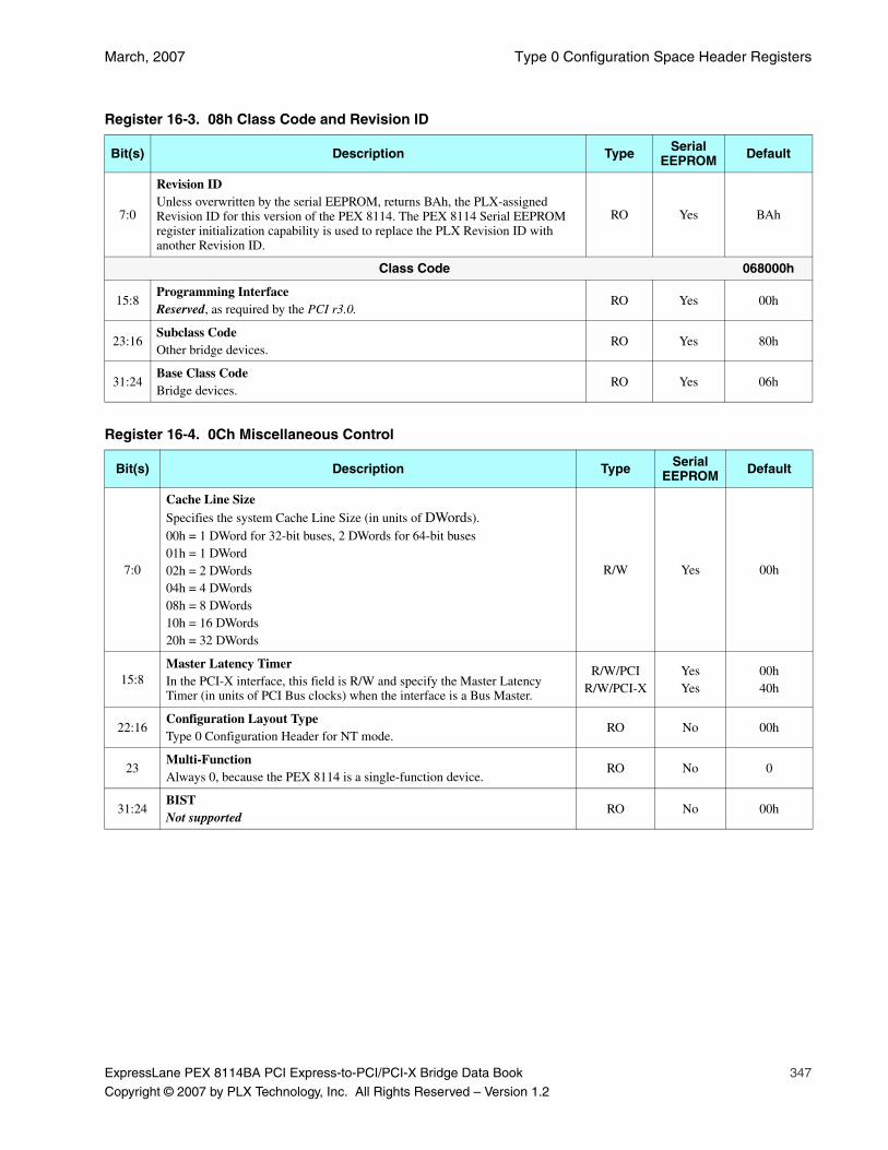
March, 2007 Type 0 Configuration Space Header Registers
ExpressLane PEX 8114BA PCI Express-to-PCI/PCI-X Bridge Data Book 347
Copyright © 2007 by PLX Technology, Inc. All Rights Reserved – Version 1.2
Register 16-3. 08h Class Code and Revision ID
Bit(s) Description Type Serial EEPROM Default
7:0
Revision IDUnless overwritten by the serial EEPROM, returns BAh, the PLX-assigned Revision ID for this version of the PEX 8114. The PEX 8114 Serial EEPROM register initialization capability is used to replace the PLX Revision ID with another Revision ID.
RO Yes BAh
Class Code 068000h
15:8Programming InterfaceReserved, as required by the PCI r3.0.
RO Yes 00h
23:16Subclass CodeOther bridge devices.
RO Yes 80h
31:24Base Class CodeBridge devices.
RO Yes 06h
Register 16-4. 0Ch Miscellaneous Control
Bit(s) Description Type Serial EEPROM Default
7:0
Cache Line SizeSpecifies the system Cache Line Size (in units of DWords).00h = 1 DWord for 32-bit buses, 2 DWords for 64-bit buses01h = 1 DWord02h = 2 DWords04h = 4 DWords08h = 8 DWords10h = 16 DWords20h = 32 DWords
R/W Yes 00h
15:8Master Latency TimerIn the PCI-X interface, this field is R/W and specify the Master Latency Timer (in units of PCI Bus clocks) when the interface is a Bus Master.
R/W/PCIR/W/PCI-X
YesYes
00h40h
22:16Configuration Layout TypeType 0 Configuration Header for NT mode.
RO No 00h
23Multi-FunctionAlways 0, because the PEX 8114 is a single-function device.
RO No 0
31:24BISTNot supported
RO No 00h
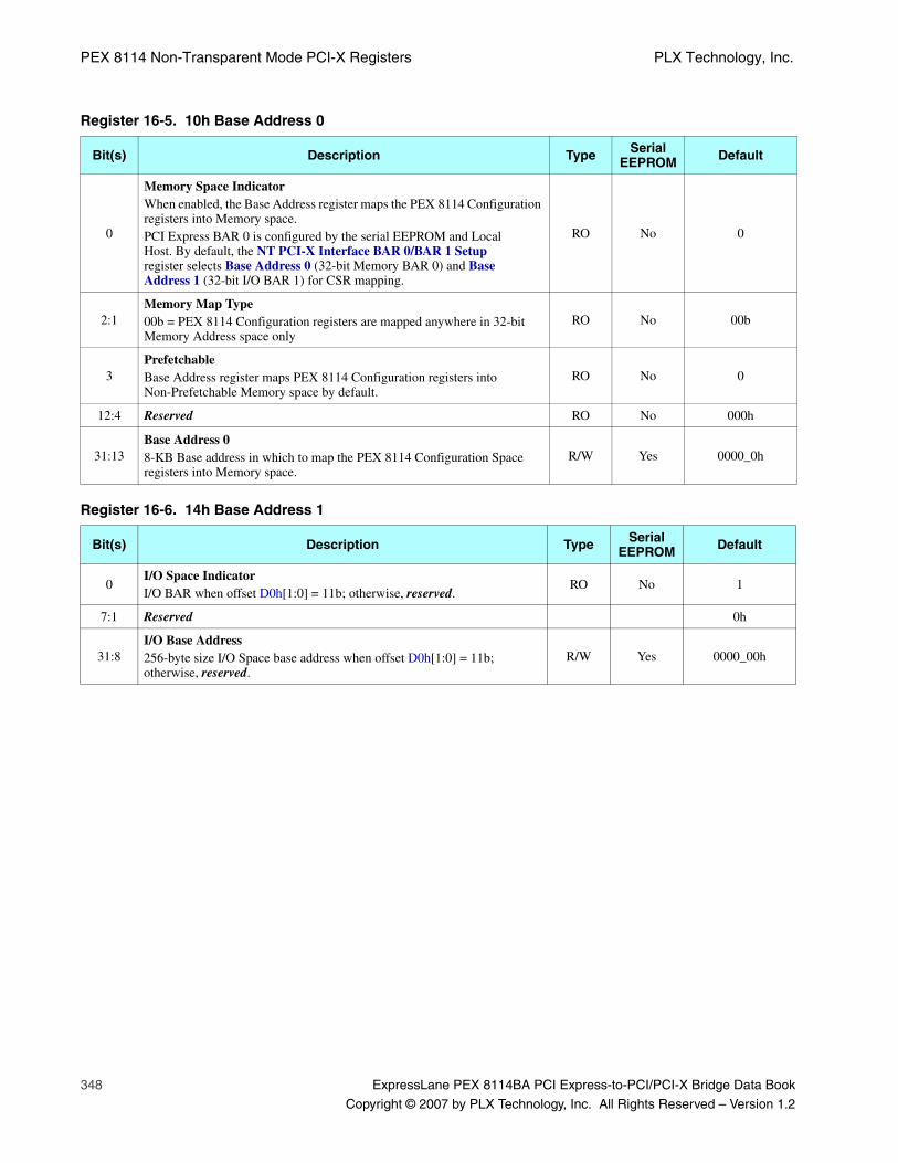
PEX 8114 Non-Transparent Mode PCI-X Registers PLX Technology, Inc.
348 ExpressLane PEX 8114BA PCI Express-to-PCI/PCI-X Bridge Data Book
Copyright © 2007 by PLX Technology, Inc. All Rights Reserved – Version 1.2
Register 16-5. 10h Base Address 0
Bit(s) Description Type Serial EEPROM Default
0
Memory Space IndicatorWhen enabled, the Base Address register maps the PEX 8114 Configuration registers into Memory space.PCI Express BAR 0 is configured by the serial EEPROM and Local Host. By default, the NT PCI-X Interface BAR 0/BAR 1 Setup register selects Base Address 0 (32-bit Memory BAR 0) and Base Address 1 (32-bit I/O BAR 1) for CSR mapping.
RO No 0
2:1Memory Map Type00b = PEX 8114 Configuration registers are mapped anywhere in 32-bit Memory Address space only
RO No 00b
3PrefetchableBase Address register maps PEX 8114 Configuration registers into Non-Prefetchable Memory space by default.
RO No 0
12:4 Reserved RO No 000h
31:13Base Address 08-KB Base address in which to map the PEX 8114 Configuration Space registers into Memory space.
R/W Yes 0000_0h
Register 16-6. 14h Base Address 1
Bit(s) Description Type Serial EEPROM Default
0I/O Space IndicatorI/O BAR when offset D0h[1:0] = 11b; otherwise, reserved.
RO No 1
7:1 Reserved 0h
31:8I/O Base Address256-byte size I/O Space base address when offset D0h[1:0] = 11b; otherwise, reserved.
R/W Yes 0000_00h
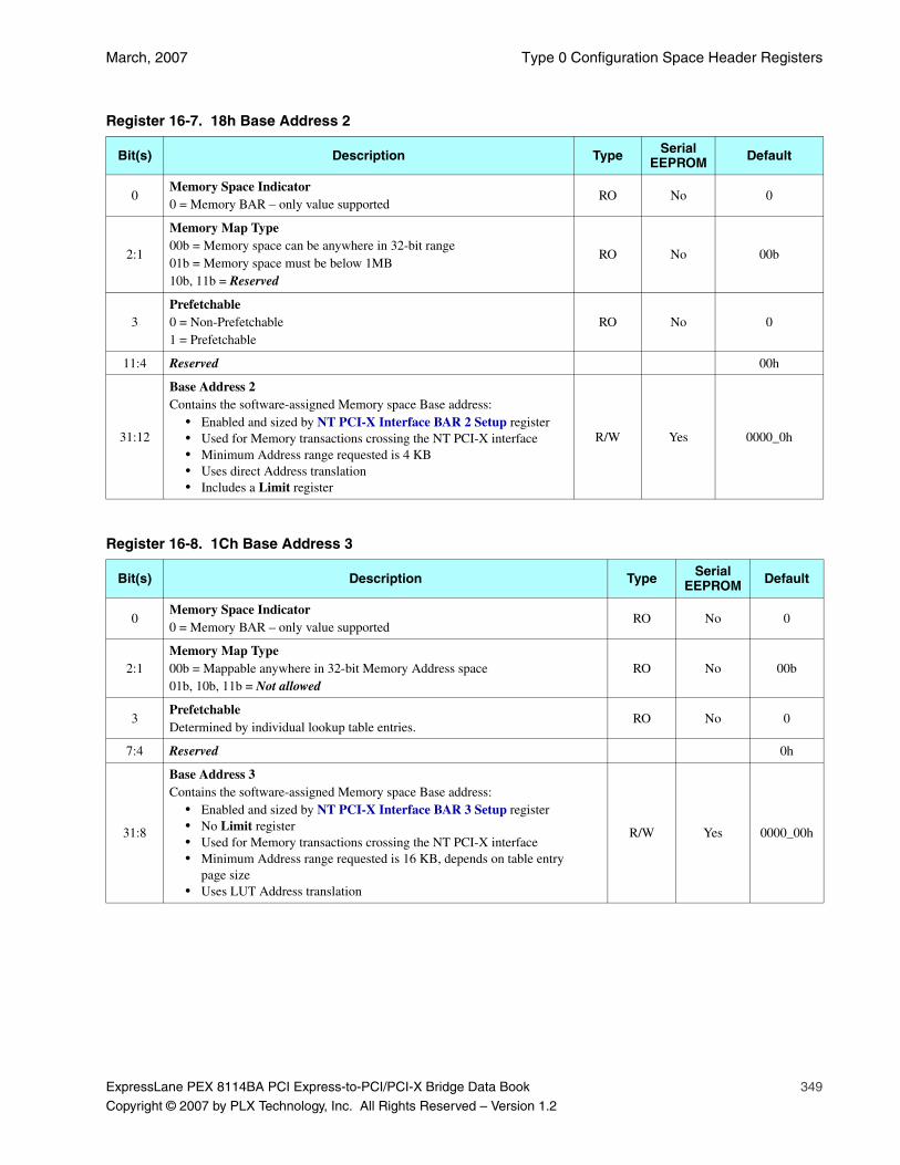
March, 2007 Type 0 Configuration Space Header Registers
ExpressLane PEX 8114BA PCI Express-to-PCI/PCI-X Bridge Data Book 349
Copyright © 2007 by PLX Technology, Inc. All Rights Reserved – Version 1.2
Register 16-7. 18h Base Address 2
Bit(s) Description Type Serial EEPROM Default
0Memory Space Indicator0 = Memory BAR – only value supported
RO No 0
2:1
Memory Map Type00b = Memory space can be anywhere in 32-bit range01b = Memory space must be below 1MB10b, 11b = Reserved
RO No 00b
3Prefetchable0 = Non-Prefetchable1 = Prefetchable
RO No 0
11:4 Reserved 00h
31:12
Base Address 2Contains the software-assigned Memory space Base address:
• Enabled and sized by NT PCI-X Interface BAR 2 Setup register• Used for Memory transactions crossing the NT PCI-X interface• Minimum Address range requested is 4 KB• Uses direct Address translation• Includes a Limit register
R/W Yes 0000_0h
Register 16-8. 1Ch Base Address 3
Bit(s) Description Type Serial EEPROM Default
0Memory Space Indicator0 = Memory BAR – only value supported
RO No 0
2:1Memory Map Type00b = Mappable anywhere in 32-bit Memory Address space01b, 10b, 11b = Not allowed
RO No 00b
3PrefetchableDetermined by individual lookup table entries.
RO No 0
7:4 Reserved 0h
31:8
Base Address 3Contains the software-assigned Memory space Base address:
• Enabled and sized by NT PCI-X Interface BAR 3 Setup register• No Limit register• Used for Memory transactions crossing the NT PCI-X interface• Minimum Address range requested is 16 KB, depends on table entry
page size• Uses LUT Address translation
R/W Yes 0000_00h

PEX 8114 Non-Transparent Mode PCI-X Registers PLX Technology, Inc.
350 ExpressLane PEX 8114BA PCI Express-to-PCI/PCI-X Bridge Data Book
Copyright © 2007 by PLX Technology, Inc. All Rights Reserved – Version 1.2
Register 16-9. 20h Base Address 4
Bit(s) Description Type Serial EEPROM Default
0Memory Space Indicator0 = Memory BAR – only value supported
RO No 0
2:1
Memory Map Type00b = BAR is mapped anywhere in 32-bit Memory space10b = BAR is mapped anywhere in 64-bit Memory space01b, 11b = Reserved
RO No 00b
3Prefetchable0 = Non-Prefetchable1 = Prefetchable
RO No 0
11:4 Reserved 00h
31:12
Base Address 4Contains the software-assigned Memory space Base address:
• Enabled and sized by NT PCI-X Interface BAR 4 Setup register• Used for Memory transactions crossing the NT PCI-X interface• Minimum Address range requested is 4 KB• Uses direct Address translation• Includes a Limit register
R/W Yes 0000_0h
Register 16-10. 24h Base Address 5
Bit(s) Description Type Serial EEPROM Default
31:0
Base Address 5NT PCI-X interface upper 32-bit address if BAR 4/5 is implemented as a 64-bit BAR; otherwise, reserved.R/W, based on NT PCI-X Interface BAR 5 Setup register.The BAR 4/5 group uses direct Address translation. Includes a Limit register.
R/W Yes 0-0h
Register 16-11. 2Ch Subsystem ID and Subsystem Vendor ID
Bit(s) Description Type Serial EEPROM Default
15:0
Subsystem Vendor IDUnless overwritten by the serial EEPROM, returns 0000h. The PEX 8114 Serial EEPROM register initialization capability is used to assign a Subsystem Vendor ID.
HwInit Yes 0000h
31:16
Subsystem IDUnless overwritten by the serial EEPROM, returns 0000h. The PEX 8114 Serial EEPROM register initialization capability is used to assign a Subsystem Device ID.
HwInit Yes 0000h
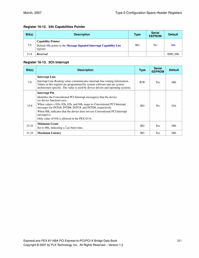
March, 2007 Type 0 Configuration Space Header Registers
ExpressLane PEX 8114BA PCI Express-to-PCI/PCI-X Bridge Data Book 351
Copyright © 2007 by PLX Technology, Inc. All Rights Reserved – Version 1.2
Register 16-12. 34h Capabilities Pointer
Bit(s) Description Type Serial EEPROM Default
7:0Capability Pointer
Default 48h points to the Message Signaled Interrupt Capability List register.
RO No 48h
31:8 Reserved 0000_00h
Register 16-13. 3Ch Interrupt
Bit(s) Description Type Serial EEPROM Default
7:0
Interrupt Line
Interrupt Line Routing value communicates interrupt line routing information. Values in this register are programmed by system software and are system architecture-specific. The value is used by device drivers and operating systems.
R/W Yes 00h
15:8
Interrupt Pin
Identifies the Conventional PCI Interrupt message(s) that the device (or device function) uses. When values = 01h, 02h, 03h, and 04h, maps to Conventional PCI Interrupt messages for INTA#, INTB#, INTC#, and INTD#, respectively.When 00h, indicates that the device does not use Conventional PCI Interrupt message(s).Only value of 01h is allowed in the PEX 8114.
RO No 01h
23:16Minimum GrantSet to 08h, indicating a 2 µs burst time.
RO Yes 08h
31:24 Maximum Latency RO Yes 00h
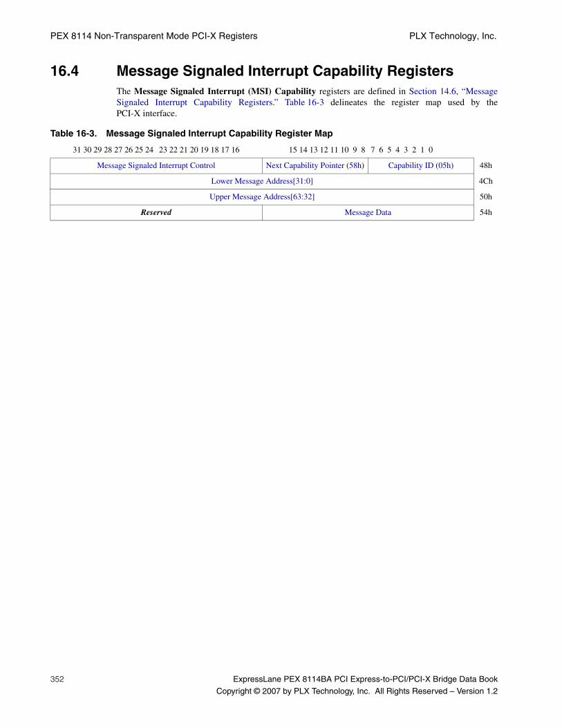
PEX 8114 Non-Transparent Mode PCI-X Registers PLX Technology, Inc.
352 ExpressLane PEX 8114BA PCI Express-to-PCI/PCI-X Bridge Data Book
Copyright © 2007 by PLX Technology, Inc. All Rights Reserved – Version 1.2
16.4 Message Signaled Interrupt Capability RegistersThe Message Signaled Interrupt (MSI) Capability registers are defined in Section 14.6, “MessageSignaled Interrupt Capability Registers.” Table 16-3 delineates the register map used by thePCI-X interface.
Table 16-3. Message Signaled Interrupt Capability Register Map
31 30 29 28 27 26 25 24 23 22 21 20 19 18 17 16 15 14 13 12 11 10 9 8 7 6 5 4 3 2 1 0
Message Signaled Interrupt Control Next Capability Pointer (58h) Capability ID (05h) 48h
Lower Message Address[31:0] 4Ch
Upper Message Address[63:32] 50h
Reserved Message Data 54h

March, 2007 PCI-X Capability Registers
ExpressLane PEX 8114BA PCI Express-to-PCI/PCI-X Bridge Data Book 353
Copyright © 2007 by PLX Technology, Inc. All Rights Reserved – Version 1.2
16.5 PCI-X Capability RegistersThis section details the PEX 8114 PCI-X Capability registers. Table 16-4 delineates the register map.
Table 16-4. PCI-X Capability Register Map
31 30 29 28 27 26 25 24 23 22 21 20 19 18 17 16 15 14 13 12 11 10 9 8 7 6 5 4 3 2 1 0
PCI-X Command Next Capability Pointer (00h) Capability ID (07h) 58h
PCI-X Status 5Ch
Reserved 60h – 64h
Register 16-14. 58h PCI-X Capability List, Command
Bit(s) Description Type Serial EEPROM Default
PCI-X Capability List
7:0Capability IDSet to 07h.
RO No 07h
15:8Next Capability PointerThe value in this register is 00h, indicating the end of the Capabilities List for the PCI-X interface.
RO No 00h
PCI-X Command
16 Uncorrectable Data Error Recovery Enable R/W Yes 0
17 Enable Relaxed Ordering R/W Yes 1
19:18Maximum Memory Read Byte CountSets the maximum Byte Count the device uses when initiating a sequence with a Burst Memory Read command.
R/W Yes 00b
22:20Maximum Outstanding Split TransactionsMaximum number of Split Transactions that can be initiated on the PCI-X Bus that have not received Completions.
R/W Yes 100b
27:23 Reserved 00000b
29:28PCI-X Capabilities List Item VersionIndicates the format of this PCI-X Capabilities List and whether ECC is supported. ECC is not supported.
RO No 00b
31:30 Reserved 00b
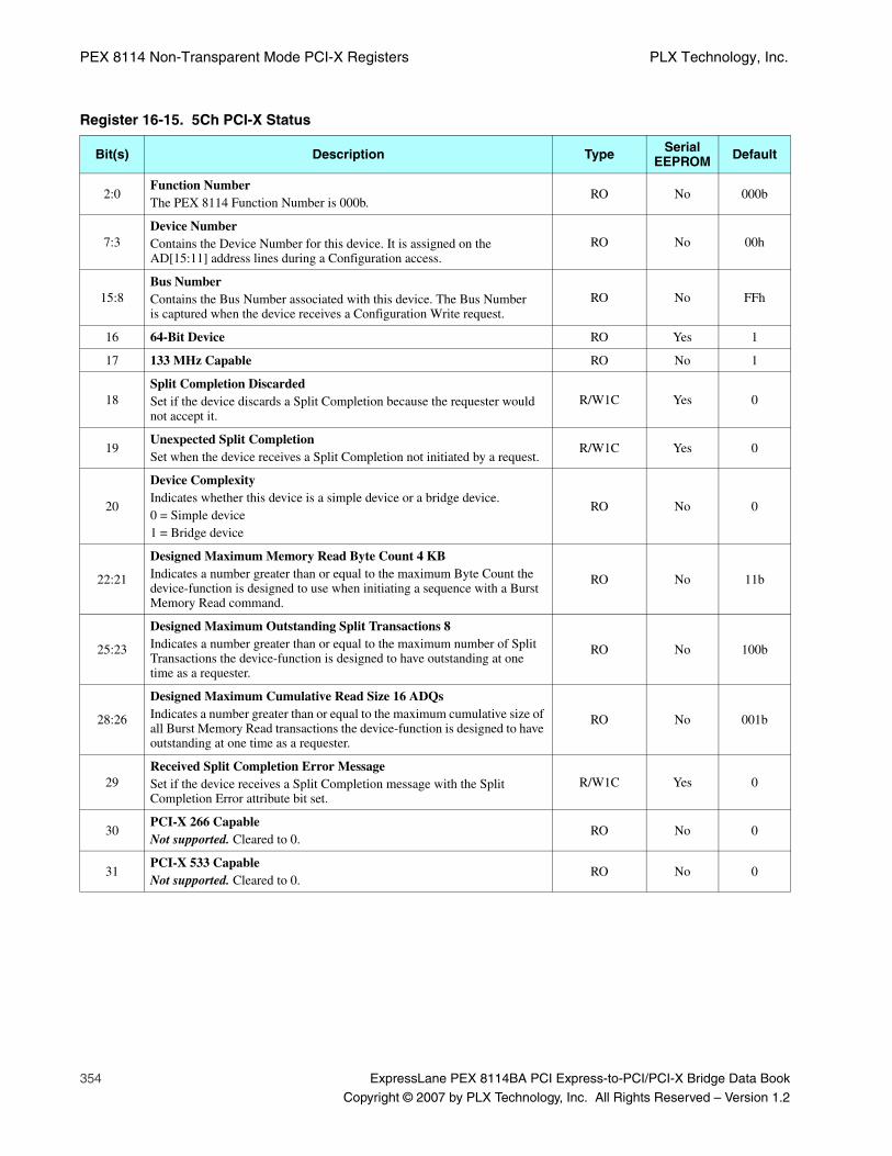
PEX 8114 Non-Transparent Mode PCI-X Registers PLX Technology, Inc.
354 ExpressLane PEX 8114BA PCI Express-to-PCI/PCI-X Bridge Data Book
Copyright © 2007 by PLX Technology, Inc. All Rights Reserved – Version 1.2
Register 16-15. 5Ch PCI-X Status
Bit(s) Description Type Serial EEPROM Default
2:0Function NumberThe PEX 8114 Function Number is 000b.
RO No 000b
7:3Device NumberContains the Device Number for this device. It is assigned on the AD[15:11] address lines during a Configuration access.
RO No 00h
15:8Bus NumberContains the Bus Number associated with this device. The Bus Number is captured when the device receives a Configuration Write request.
RO No FFh
16 64-Bit Device RO Yes 1
17 133 MHz Capable RO No 1
18Split Completion DiscardedSet if the device discards a Split Completion because the requester would not accept it.
R/W1C Yes 0
19Unexpected Split CompletionSet when the device receives a Split Completion not initiated by a request.
R/W1C Yes 0
20
Device ComplexityIndicates whether this device is a simple device or a bridge device.0 = Simple device1 = Bridge device
RO No 0
22:21
Designed Maximum Memory Read Byte Count 4 KBIndicates a number greater than or equal to the maximum Byte Count the device-function is designed to use when initiating a sequence with a Burst Memory Read command.
RO No 11b
25:23
Designed Maximum Outstanding Split Transactions 8Indicates a number greater than or equal to the maximum number of Split Transactions the device-function is designed to have outstanding at one time as a requester.
RO No 100b
28:26
Designed Maximum Cumulative Read Size 16 ADQsIndicates a number greater than or equal to the maximum cumulative size of all Burst Memory Read transactions the device-function is designed to have outstanding at one time as a requester.
RO No 001b
29Received Split Completion Error MessageSet if the device receives a Split Completion message with the Split Completion Error attribute bit set.
R/W1C Yes 0
30PCI-X 266 CapableNot supported. Cleared to 0.
RO No 0
31PCI-X 533 CapableNot supported. Cleared to 0.
RO No 0
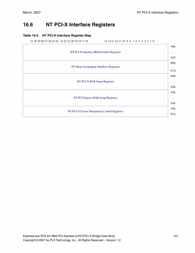
March, 2007 NT PCI-X Interface Registers
ExpressLane PEX 8114BA PCI Express-to-PCI/PCI-X Bridge Data Book 355
Copyright © 2007 by PLX Technology, Inc. All Rights Reserved – Version 1.2
16.6 NT PCI-X Interface Registers
Table 16-5. NT PCI-X Interface Register Map
31 30 29 28 27 26 25 24 23 22 21 20 19 18 17 16 15 14 13 12 11 10 9 8 7 6 5 4 3 2 1 0
NT PCI-X Interface IRQ Doorbell Registers
90h
…
ACh
NT Mode Scratchpad (Mailbox) RegistersB0h…
CCh
NT PCI-X BAR Setup Registers
D0h
…
E0h
NT PCI Express BAR Setup Registers
E4h
…
F4h
NT PCI-X Cursor Mechanism Control RegistersF8h
FCh

PEX 8114 Non-Transparent Mode PCI-X Registers PLX Technology, Inc.
356 ExpressLane PEX 8114BA PCI Express-to-PCI/PCI-X Bridge Data Book
Copyright © 2007 by PLX Technology, Inc. All Rights Reserved – Version 1.2
16.6.1 NT PCI-X Interface IRQ Doorbell RegistersThis section details the PEX 8114 NT PCI-X interface Interrupt Request (IRQ) Doorbell registers.The PEX 8114 NT Interrupt Request registers are defined in Section 10.7, “Interrupt CapabilitySpecific to Non-Transparent Bridge Mode.” Table 16-6 delineates the register map.
Table 16-6. PCI-X Interface Interrupt Request (IRQ) Doorbell Register Map
31 30 29 28 27 26 25 24 23 22 21 20 19 18 17 16 15 14 13 12 11 10 9 8 7 6 5 4 3 2 1 0
Reserved Set PCI-X Interface IRQ 90h
Reserved Clear PCI-X Interface IRQ 94h
Reserved Set PCI-X Interface IRQ Mask 98h
Reserved Clear PCI-X Interface IRQ Mask 9Ch
Reserved Set PCI Express Interface IRQ A0h
Reserved Clear PCI Express Interface IRQ A4h
Reserved Set PCI Express Interface IRQ Mask A8h
Reserved Clear PCI Express Interface IRQ Mask ACh
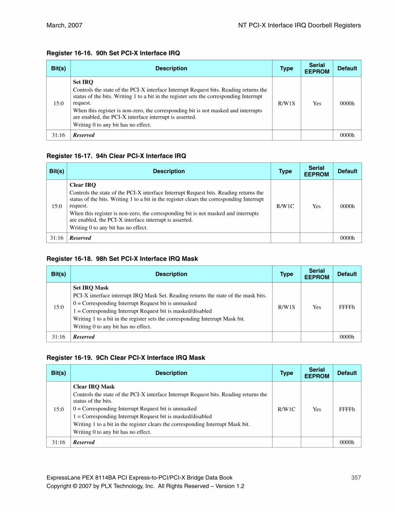
March, 2007 NT PCI-X Interface IRQ Doorbell Registers
ExpressLane PEX 8114BA PCI Express-to-PCI/PCI-X Bridge Data Book 357
Copyright © 2007 by PLX Technology, Inc. All Rights Reserved – Version 1.2
Register 16-16. 90h Set PCI-X Interface IRQ
Bit(s) Description Type Serial EEPROM Default
15:0
Set IRQControls the state of the PCI-X interface Interrupt Request bits. Reading returns the status of the bits. Writing 1 to a bit in the register sets the corresponding Interrupt request. When this register is non-zero, the corresponding bit is not masked and interrupts are enabled, the PCI-X interface interrupt is asserted. Writing 0 to any bit has no effect.
R/W1S Yes 0000h
31:16 Reserved 0000h
Register 16-17. 94h Clear PCI-X Interface IRQ
Bit(s) Description Type Serial EEPROM Default
15:0
Clear IRQControls the state of the PCI-X interface Interrupt Request bits. Reading returns the status of the bits. Writing 1 to a bit in the register clears the corresponding Interrupt request. When this register is non-zero, the corresponding bit is not masked and interrupts are enabled, the PCI-X interface interrupt is asserted. Writing 0 to any bit has no effect.
R/W1C Yes 0000h
31:16 Reserved 0000h
Register 16-18. 98h Set PCI-X Interface IRQ Mask
Bit(s) Description Type Serial EEPROM Default
15:0
Set IRQ MaskPCI-X interface interrupt IRQ Mask Set. Reading returns the state of the mask bits. 0 = Corresponding Interrupt Request bit is unmasked1 = Corresponding Interrupt Request bit is masked/disabledWriting 1 to a bit in the register sets the corresponding Interrupt Mask bit. Writing 0 to any bit has no effect.
R/W1S Yes FFFFh
31:16 Reserved 0000h
Register 16-19. 9Ch Clear PCI-X Interface IRQ Mask
Bit(s) Description Type Serial EEPROM Default
15:0
Clear IRQ MaskControls the state of the PCI-X interface Interrupt Request bits. Reading returns the status of the bits. 0 = Corresponding Interrupt Request bit is unmasked1 = Corresponding Interrupt Request bit is masked/disabledWriting 1 to a bit in the register clears the corresponding Interrupt Mask bit. Writing 0 to any bit has no effect.
R/W1C Yes FFFFh
31:16 Reserved 0000h
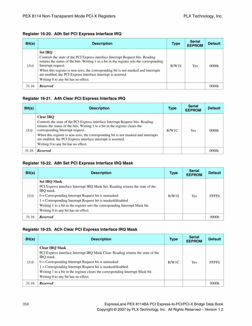
PEX 8114 Non-Transparent Mode PCI-X Registers PLX Technology, Inc.
358 ExpressLane PEX 8114BA PCI Express-to-PCI/PCI-X Bridge Data Book
Copyright © 2007 by PLX Technology, Inc. All Rights Reserved – Version 1.2
Register 16-20. A0h Set PCI Express Interface IRQ
Bit(s) Description Type Serial EEPROM Default
15:0
Set IRQControls the state of the PCI Express interface Interrupt Request bits. Reading returns the status of the bits. Writing 1 to a bit in the register sets the corresponding Interrupt request. When this register is non-zero, the corresponding bit is not masked and interrupts are enabled, the PCI Express interface interrupt is asserted. Writing 0 to any bit has no effect.
R/W1S Yes 0000h
31:16 Reserved 0000h
Register 16-21. A4h Clear PCI Express Interface IRQ
Bit(s) Description Type Serial EEPROM Default
15:0
Clear IRQControls the state of the PCI Express interface Interrupt Request bits. Reading returns the status of the bits. Writing 1 to a bit in the register clears the corresponding Interrupt request. When this register is non-zero, the corresponding bit is not masked and interrupts are enabled, the PCI Express interface interrupt is asserted. Writing 0 to any bit has no effect.
R/W1C Yes 0000h
31:16 Reserved 0000h
Register 16-22. A8h Set PCI Express Interface IRQ Mask
Bit(s) Description Type Serial EEPROM Default
15:0
Set IRQ MaskPCI Express interface Interrupt IRQ Mask Set. Reading returns the state of the IRQ mask. 0 = Corresponding Interrupt Request bit is unmasked1 = Corresponding Interrupt Request bit is masked/disabledWriting 1 to a bit in the register sets the corresponding Interrupt Mask bit. Writing 0 to any bit has no effect.
R/W1S Yes FFFFh
31:16 Reserved 0000h
Register 16-23. ACh Clear PCI Express Interface IRQ Mask
Bit(s) Description Type Serial EEPROM Default
15:0
Clear IRQ MaskPCI Express interface Interrupt IRQ Mask Clear. Reading returns the state of the IRQ mask. 0 = Corresponding Interrupt Request bit is unmasked1 = Corresponding Interrupt Request bit is masked/disabledWriting 1 to a bit in the register clears the corresponding Interrupt Mask bit.Writing 0 to any bit has no effect.
R/W1C Yes FFFFh
31:16 Reserved 0000h
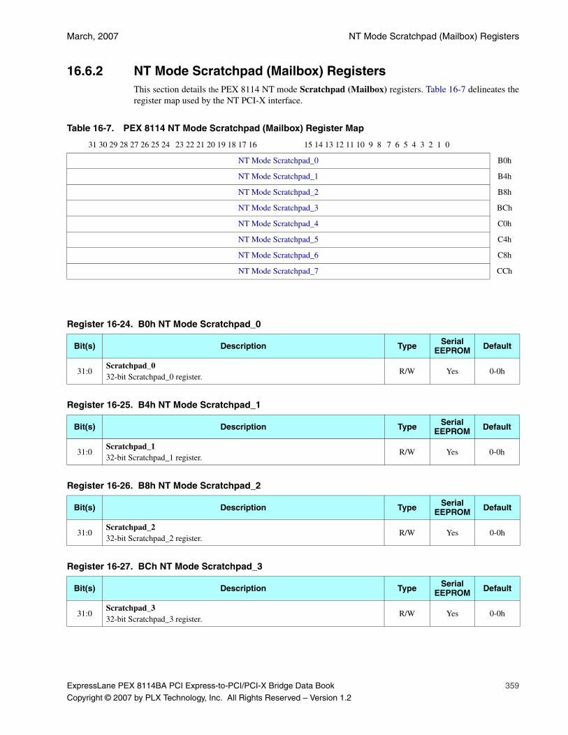
March, 2007 NT Mode Scratchpad (Mailbox) Registers
ExpressLane PEX 8114BA PCI Express-to-PCI/PCI-X Bridge Data Book 359
Copyright © 2007 by PLX Technology, Inc. All Rights Reserved – Version 1.2
16.6.2 NT Mode Scratchpad (Mailbox) RegistersThis section details the PEX 8114 NT mode Scratchpad (Mailbox) registers. Table 16-7 delineates theregister map used by the NT PCI-X interface.
Table 16-7. PEX 8114 NT Mode Scratchpad (Mailbox) Register Map
31 30 29 28 27 26 25 24 23 22 21 20 19 18 17 16 15 14 13 12 11 10 9 8 7 6 5 4 3 2 1 0
NT Mode Scratchpad_0 B0h
NT Mode Scratchpad_1 B4h
NT Mode Scratchpad_2 B8h
NT Mode Scratchpad_3 BCh
NT Mode Scratchpad_4 C0h
NT Mode Scratchpad_5 C4h
NT Mode Scratchpad_6 C8h
NT Mode Scratchpad_7 CCh
Register 16-24. B0h NT Mode Scratchpad_0
Bit(s) Description Type Serial EEPROM Default
31:0Scratchpad_032-bit Scratchpad_0 register.
R/W Yes 0-0h
Register 16-25. B4h NT Mode Scratchpad_1
Bit(s) Description Type Serial EEPROM Default
31:0Scratchpad_132-bit Scratchpad_1 register.
R/W Yes 0-0h
Register 16-26. B8h NT Mode Scratchpad_2
Bit(s) Description Type Serial EEPROM Default
31:0Scratchpad_232-bit Scratchpad_2 register.
R/W Yes 0-0h
Register 16-27. BCh NT Mode Scratchpad_3
Bit(s) Description Type Serial EEPROM Default
31:0Scratchpad_332-bit Scratchpad_3 register.
R/W Yes 0-0h

PEX 8114 Non-Transparent Mode PCI-X Registers PLX Technology, Inc.
360 ExpressLane PEX 8114BA PCI Express-to-PCI/PCI-X Bridge Data Book
Copyright © 2007 by PLX Technology, Inc. All Rights Reserved – Version 1.2
Register 16-28. C0h NT Mode Scratchpad_4
Bit(s) Description Type Serial EEPROM Default
31:0Scratchpad_432-bit Scratchpad_4 register.
R/W Yes 0-0h
Register 16-29. C4h NT Mode Scratchpad_5
Bit(s) Description Type Serial EEPROM Default
31:0Scratchpad_532-bit Scratchpad_5 register.
R/W Yes 0-0h
Register 16-30. C8h NT Mode Scratchpad_6
Bit(s) Description Type Serial EEPROM Default
31:0Scratchpad_632-bit Scratchpad_6 register.
R/W Yes 0-0h
Register 16-31. CCh NT Mode Scratchpad_7
Bit(s) Description Type Serial EEPROM Default
31:0Scratchpad_732-bit Scratchpad_7 register.
R/W Yes 0-0h
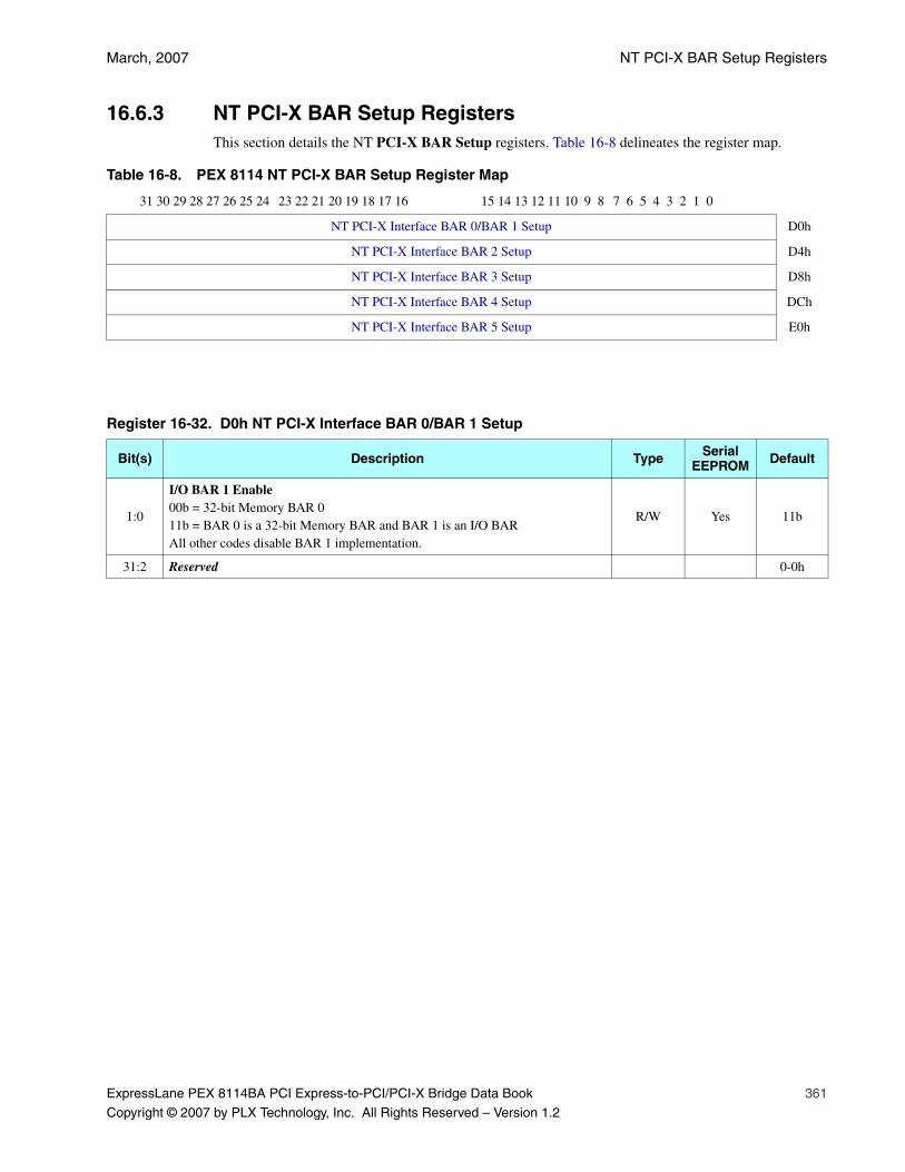
March, 2007 NT PCI-X BAR Setup Registers
ExpressLane PEX 8114BA PCI Express-to-PCI/PCI-X Bridge Data Book 361
Copyright © 2007 by PLX Technology, Inc. All Rights Reserved – Version 1.2
16.6.3 NT PCI-X BAR Setup RegistersThis section details the NT PCI-X BAR Setup registers. Table 16-8 delineates the register map.
Table 16-8. PEX 8114 NT PCI-X BAR Setup Register Map
31 30 29 28 27 26 25 24 23 22 21 20 19 18 17 16 15 14 13 12 11 10 9 8 7 6 5 4 3 2 1 0
NT PCI-X Interface BAR 0/BAR 1 Setup D0h
NT PCI-X Interface BAR 2 Setup D4h
NT PCI-X Interface BAR 3 Setup D8h
NT PCI-X Interface BAR 4 Setup DCh
NT PCI-X Interface BAR 5 Setup E0h
Register 16-32. D0h NT PCI-X Interface BAR 0/BAR 1 Setup
Bit(s) Description Type Serial EEPROM Default
1:0
I/O BAR 1 Enable00b = 32-bit Memory BAR 011b = BAR 0 is a 32-bit Memory BAR and BAR 1 is an I/O BARAll other codes disable BAR 1 implementation.
R/W Yes 11b
31:2 Reserved 0-0h
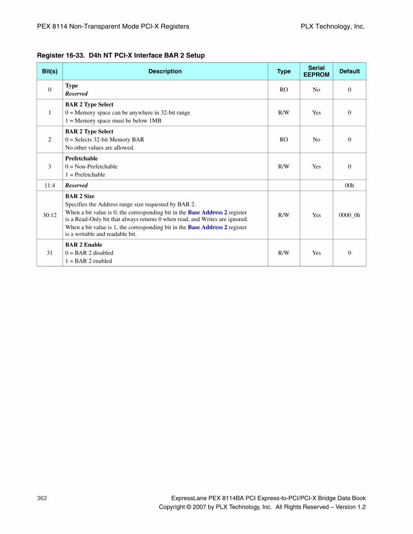
PEX 8114 Non-Transparent Mode PCI-X Registers PLX Technology, Inc.
362 ExpressLane PEX 8114BA PCI Express-to-PCI/PCI-X Bridge Data Book
Copyright © 2007 by PLX Technology, Inc. All Rights Reserved – Version 1.2
Register 16-33. D4h NT PCI-X Interface BAR 2 Setup
Bit(s) Description Type Serial EEPROM Default
0Type Reserved
RO No 0
1BAR 2 Type Select0 = Memory space can be anywhere in 32-bit range1 = Memory space must be below 1MB
R/W Yes 0
2BAR 2 Type Select0 = Selects 32-bit Memory BARNo other values are allowed.
RO No 0
3Prefetchable0 = Non-Prefetchable1 = Prefetchable
R/W Yes 0
11:4 Reserved 00h
30:12
BAR 2 SizeSpecifies the Address range size requested by BAR 2. When a bit value is 0, the corresponding bit in the Base Address 2 register is a Read-Only bit that always returns 0 when read, and Writes are ignored.When a bit value is 1, the corresponding bit in the Base Address 2 register is a writable and readable bit.
R/W Yes 0000_0h
31BAR 2 Enable0 = BAR 2 disabled1 = BAR 2 enabled
R/W Yes 0
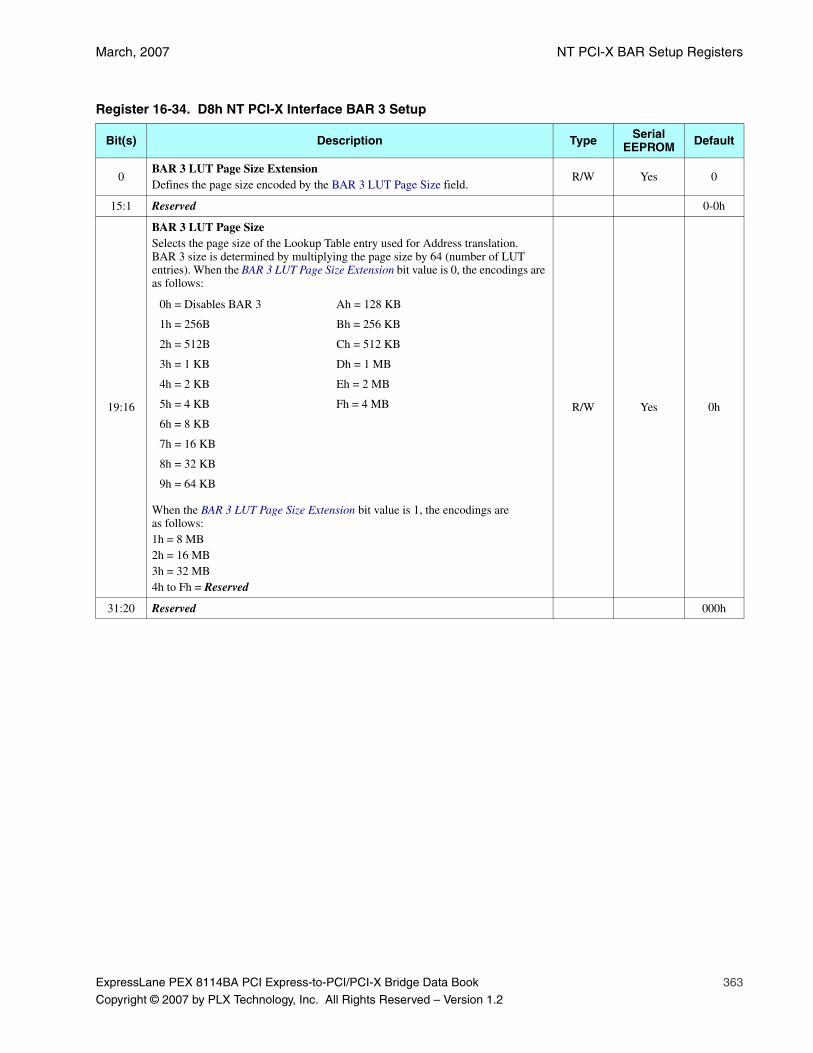
March, 2007 NT PCI-X BAR Setup Registers
ExpressLane PEX 8114BA PCI Express-to-PCI/PCI-X Bridge Data Book 363
Copyright © 2007 by PLX Technology, Inc. All Rights Reserved – Version 1.2
Register 16-34. D8h NT PCI-X Interface BAR 3 Setup
Bit(s) Description Type Serial EEPROM Default
0BAR 3 LUT Page Size ExtensionDefines the page size encoded by the BAR 3 LUT Page Size field.
R/W Yes 0
15:1 Reserved 0-0h
19:16
BAR 3 LUT Page SizeSelects the page size of the Lookup Table entry used for Address translation. BAR 3 size is determined by multiplying the page size by 64 (number of LUT entries). When the BAR 3 LUT Page Size Extension bit value is 0, the encodings are as follows:
When the BAR 3 LUT Page Size Extension bit value is 1, the encodings are as follows: 1h = 8 MB2h = 16 MB3h = 32 MB4h to Fh = Reserved
R/W Yes 0h
31:20 Reserved 000h
0h = Disables BAR 3 Ah = 128 KB
1h = 256B Bh = 256 KB
2h = 512B Ch = 512 KB
3h = 1 KB Dh = 1 MB
4h = 2 KB Eh = 2 MB
5h = 4 KB Fh = 4 MB
6h = 8 KB
7h = 16 KB
8h = 32 KB
9h = 64 KB

PEX 8114 Non-Transparent Mode PCI-X Registers PLX Technology, Inc.
364 ExpressLane PEX 8114BA PCI Express-to-PCI/PCI-X Bridge Data Book
Copyright © 2007 by PLX Technology, Inc. All Rights Reserved – Version 1.2
Register 16-35. DCh NT PCI-X Interface BAR 4 Setup
Bit(s) Description Type Serial EEPROM Default
0Type Reserved
RO No 0
2:1
BAR 4 Type Select00b = BAR 4 implemented as 32-bit Memory BAR10b = BAR 4/5 implemented as 64-bit Memory BAR; it is illegal to program 10b and clear the BAR 5 Enable bit (offset E0h[31])
R/W Yes 00b
3Prefetchable0 = Non-Prefetchable1 = Prefetchable
R/W Yes 0
11:4 Reserved 00h
30:12
BAR 4 SizeSpecifies the Address range size requested by BAR 4.When a bit value is 0, the corresponding bit in the Base Address 4 register is a Read-Only bit that always returns 0 when read, and Writes are ignored.When a bit value is 1, the corresponding bit in the Base Address 4 register is a writable and readable bit.
R/W Yes 0000_0h
31BAR 4 Enable in 32-Bit Mode0 = BAR 4 and BAR 5 disabled1 = BAR 4 enabled
R/W Yes 0
Register 16-36. E0h NT PCI-X Interface BAR 5 Setup
Bit(s) Description Type Serial EEPROM Default
30:0
BAR 5 SizeSpecifies the Address range size requested by BAR 4/5 in 64-bit mode. When a bit value is 0, the corresponding bit in the Base Address 5 register is a Read-Only bit that always returns 0 when read, and Writes are ignored.When a bit value is 1, the corresponding bit in the Base Address 5 register is a writable and readable bit.Reserved if BAR 4/5 is configured as a 32-bit BAR.
R/W Yes 0-0h
31
BAR 5 Enable0 = BAR 5 disabled1 = BAR 4/5 enabled as 64-bit memory; it is illegal to program BAR 4 Type Select = 10b (offset DCh[2:1]) and clear this bit
R/W Yes 0
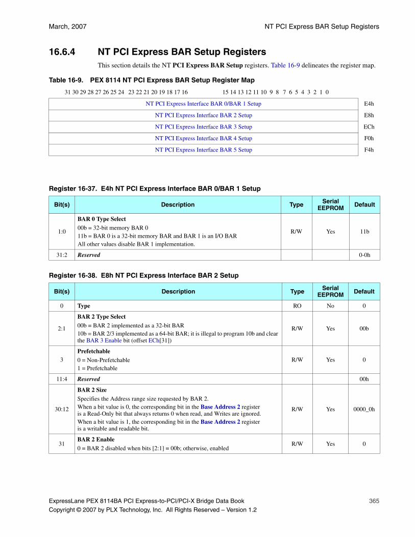
March, 2007 NT PCI Express BAR Setup Registers
ExpressLane PEX 8114BA PCI Express-to-PCI/PCI-X Bridge Data Book 365
Copyright © 2007 by PLX Technology, Inc. All Rights Reserved – Version 1.2
16.6.4 NT PCI Express BAR Setup RegistersThis section details the NT PCI Express BAR Setup registers. Table 16-9 delineates the register map.
Table 16-9. PEX 8114 NT PCI Express BAR Setup Register Map
31 30 29 28 27 26 25 24 23 22 21 20 19 18 17 16 15 14 13 12 11 10 9 8 7 6 5 4 3 2 1 0
NT PCI Express Interface BAR 0/BAR 1 Setup E4h
NT PCI Express Interface BAR 2 Setup E8h
NT PCI Express Interface BAR 3 Setup ECh
NT PCI Express Interface BAR 4 Setup F0h
NT PCI Express Interface BAR 5 Setup F4h
Register 16-37. E4h NT PCI Express Interface BAR 0/BAR 1 Setup
Bit(s) Description Type Serial EEPROM Default
1:0
BAR 0 Type Select
00b = 32-bit memory BAR 011b = BAR 0 is a 32-bit memory BAR and BAR 1 is an I/O BARAll other values disable BAR 1 implementation.
R/W Yes 11b
31:2 Reserved 0-0h
Register 16-38. E8h NT PCI Express Interface BAR 2 Setup
Bit(s) Description Type Serial EEPROM Default
0 Type RO No 0
2:1
BAR 2 Type Select
00b = BAR 2 implemented as a 32-bit BAR10b = BAR 2/3 implemented as a 64-bit BAR; it is illegal to program 10b and clear the BAR 3 Enable bit (offset ECh[31])
R/W Yes 00b
3Prefetchable
0 = Non-Prefetchable1 = Prefetchable
R/W Yes 0
11:4 Reserved 00h
30:12
BAR 2 Size
Specifies the Address range size requested by BAR 2.When a bit value is 0, the corresponding bit in the Base Address 2 register is a Read-Only bit that always returns 0 when read, and Writes are ignored.When a bit value is 1, the corresponding bit in the Base Address 2 register is a writable and readable bit.
R/W Yes 0000_0h
31BAR 2 Enable
0 = BAR 2 disabled when bits [2:1] = 00b; otherwise, enabledR/W Yes 0

PEX 8114 Non-Transparent Mode PCI-X Registers PLX Technology, Inc.
366 ExpressLane PEX 8114BA PCI Express-to-PCI/PCI-X Bridge Data Book
Copyright © 2007 by PLX Technology, Inc. All Rights Reserved – Version 1.2
Register 16-39. ECh NT PCI Express Interface BAR 3 Setup
Bit(s) Description Type Serial EEPROM Default
30:0
BAR 3 Size
Specifies the Address range size requested by BAR 2/3 in 64-bit mode. When a bit value is 0, the corresponding bit in the Base Address 3 register is a Read-Only bit that always returns 0 when read, and Writes are ignored.When a bit value is 1, the corresponding bit in the Base Address 3 register is a writable and readable bit.Reserved if BAR 2/3 is configured as a 32-bit BAR.
R/W Yes 0-0h
31
BAR 3 Enable
0 = BAR 3 disabled 1 = BAR 2/3 implemented as a 64-bit BAR; it is illegal to program BAR 2 Type Select =10b (offset E4h[2:1]) and clear this bit
R/W Yes 0
Register 16-40. F0h NT PCI Express Interface BAR 4 Setup
Bit(s) Description Type Serial EEPROM Default
0 Type RO No 0
2:1
BAR 4 Type Select
00b = BAR 4 implemented as a 32-bit BAR10b = BAR 4/5 implemented as a 64-bit BAR; it is illegal to program 10b and clear the BAR 5 Enable bit (offset F4h[31])
R/W Yes 00b
3Prefetchable
0 = Non-Prefetchable1 = Prefetchable
R/W Yes 0
11:4 Reserved 00h
30:12
BAR 4 Size
Specifies the Address range size requested by BAR 4.When a bit value is 0, the corresponding bit in the Base Address 4 register is a Read-Only bit that always returns 0 when read, and Writes are ignored.When a bit value is 1, the corresponding bit in the Base Address 4 register is a writable and readable bit.
R/W Yes 0000_0h
31BAR 4 Enable
0 = BAR 4 disabled when bits [2:1] = 00b; otherwise, enabledR/W Yes 0
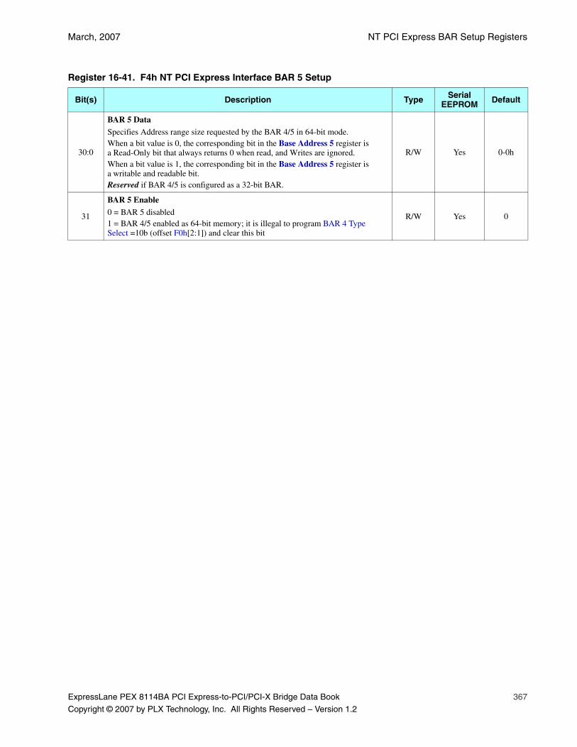
March, 2007 NT PCI Express BAR Setup Registers
ExpressLane PEX 8114BA PCI Express-to-PCI/PCI-X Bridge Data Book 367
Copyright © 2007 by PLX Technology, Inc. All Rights Reserved – Version 1.2
Register 16-41. F4h NT PCI Express Interface BAR 5 Setup
Bit(s) Description Type Serial EEPROM Default
30:0
BAR 5 Data
Specifies Address range size requested by the BAR 4/5 in 64-bit mode. When a bit value is 0, the corresponding bit in the Base Address 5 register is a Read-Only bit that always returns 0 when read, and Writes are ignored. When a bit value is 1, the corresponding bit in the Base Address 5 register is a writable and readable bit. Reserved if BAR 4/5 is configured as a 32-bit BAR.
R/W Yes 0-0h
31
BAR 5 Enable
0 = BAR 5 disabled 1 = BAR 4/5 enabled as 64-bit memory; it is illegal to program BAR 4 Type Select =10b (offset F0h[2:1]) and clear this bit
R/W Yes 0
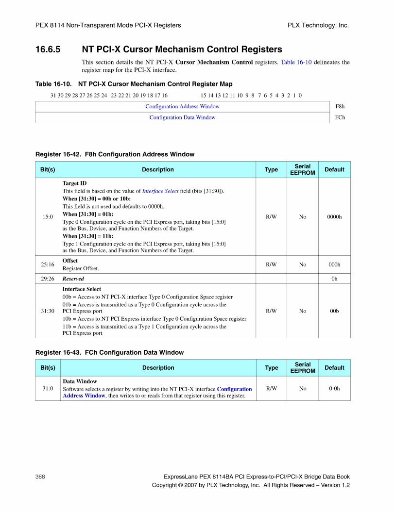
PEX 8114 Non-Transparent Mode PCI-X Registers PLX Technology, Inc.
368 ExpressLane PEX 8114BA PCI Express-to-PCI/PCI-X Bridge Data Book
Copyright © 2007 by PLX Technology, Inc. All Rights Reserved – Version 1.2
16.6.5 NT PCI-X Cursor Mechanism Control RegistersThis section details the NT PCI-X Cursor Mechanism Control registers. Table 16-10 delineates theregister map for the PCI-X interface.
Table 16-10. NT PCI-X Cursor Mechanism Control Register Map
31 30 29 28 27 26 25 24 23 22 21 20 19 18 17 16 15 14 13 12 11 10 9 8 7 6 5 4 3 2 1 0
Configuration Address Window F8h
Configuration Data Window FCh
Register 16-42. F8h Configuration Address Window
Bit(s) Description Type Serial EEPROM Default
15:0
Target IDThis field is based on the value of Interface Select field (bits [31:30]). When [31:30] = 00b or 10b:This field is not used and defaults to 0000h.When [31:30] = 01b:Type 0 Configuration cycle on the PCI Express port, taking bits [15:0] as the Bus, Device, and Function Numbers of the Target.When [31:30] = 11b:Type 1 Configuration cycle on the PCI Express port, taking bits [15:0] as the Bus, Device, and Function Numbers of the Target.
R/W No 0000h
25:16OffsetRegister Offset.
R/W No 000h
29:26 Reserved 0h
31:30
Interface Select00b = Access to NT PCI-X interface Type 0 Configuration Space register01b = Access is transmitted as a Type 0 Configuration cycle across the PCI Express port10b = Access to NT PCI Express interface Type 0 Configuration Space register11b = Access is transmitted as a Type 1 Configuration cycle across the PCI Express port
R/W No 00b
Register 16-43. FCh Configuration Data Window
Bit(s) Description Type Serial EEPROM Default
31:0Data WindowSoftware selects a register by writing into the NT PCI-X interface Configuration Address Window, then writes to or reads from that register using this register.
R/W No 0-0h
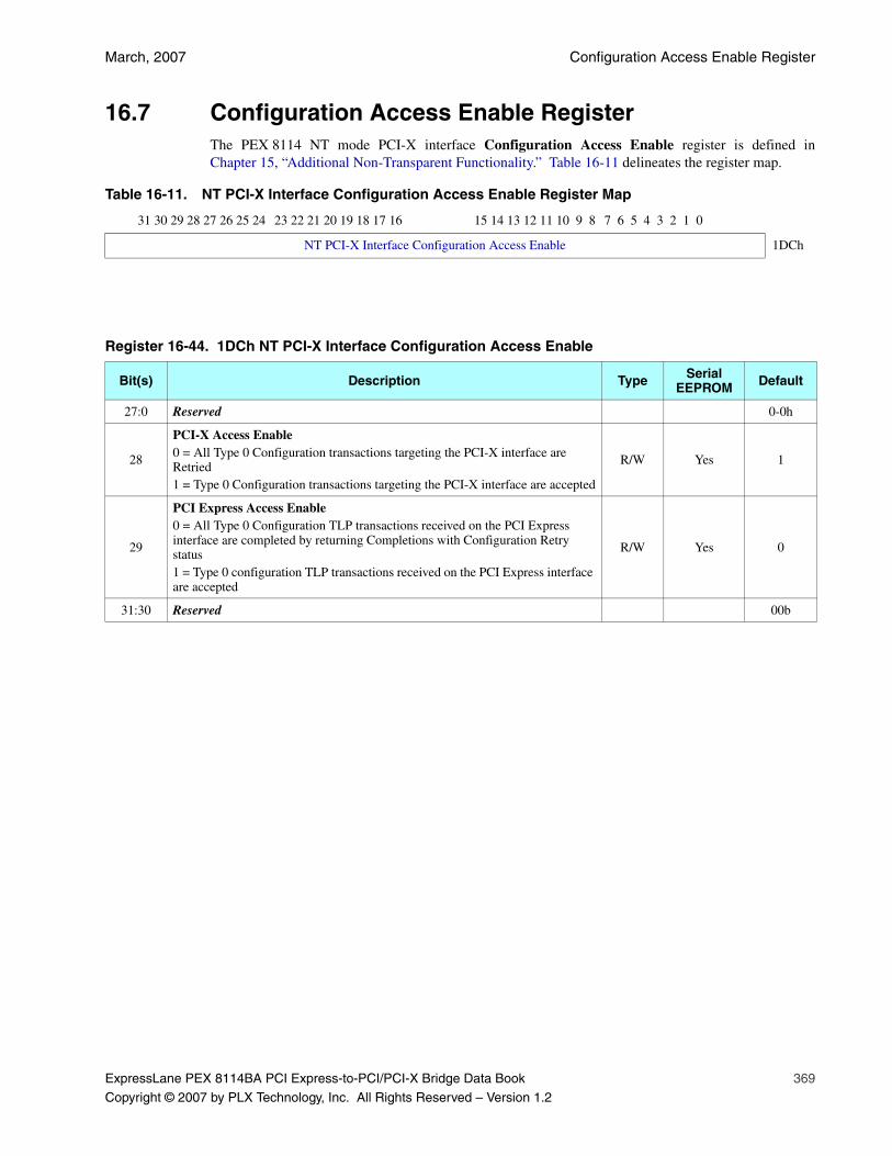
March, 2007 Configuration Access Enable Register
ExpressLane PEX 8114BA PCI Express-to-PCI/PCI-X Bridge Data Book 369
Copyright © 2007 by PLX Technology, Inc. All Rights Reserved – Version 1.2
16.7 Configuration Access Enable RegisterThe PEX 8114 NT mode PCI-X interface Configuration Access Enable register is defined inChapter 15, “Additional Non-Transparent Functionality.” Table 16-11 delineates the register map.
Table 16-11. NT PCI-X Interface Configuration Access Enable Register Map
31 30 29 28 27 26 25 24 23 22 21 20 19 18 17 16 15 14 13 12 11 10 9 8 7 6 5 4 3 2 1 0
NT PCI-X Interface Configuration Access Enable 1DCh
Register 16-44. 1DCh NT PCI-X Interface Configuration Access Enable
Bit(s) Description Type Serial EEPROM Default
27:0 Reserved 0-0h
28
PCI-X Access Enable0 = All Type 0 Configuration transactions targeting the PCI-X interface are Retried1 = Type 0 Configuration transactions targeting the PCI-X interface are accepted
R/W Yes 1
29
PCI Express Access Enable0 = All Type 0 Configuration TLP transactions received on the PCI Express interface are completed by returning Completions with Configuration Retry status1 = Type 0 configuration TLP transactions received on the PCI Express interface are accepted
R/W Yes 0
31:30 Reserved 00b
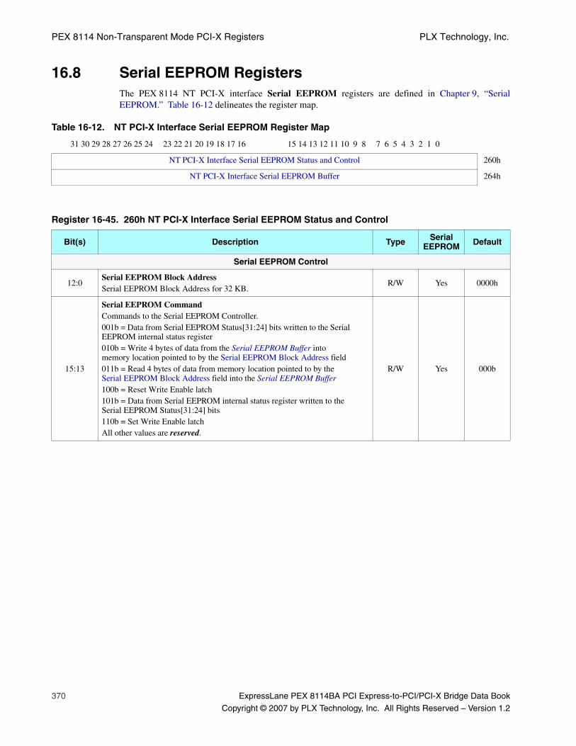
PEX 8114 Non-Transparent Mode PCI-X Registers PLX Technology, Inc.
370 ExpressLane PEX 8114BA PCI Express-to-PCI/PCI-X Bridge Data Book
Copyright © 2007 by PLX Technology, Inc. All Rights Reserved – Version 1.2
16.8 Serial EEPROM RegistersThe PEX 8114 NT PCI-X interface Serial EEPROM registers are defined in Chapter 9, “SerialEEPROM.” Table 16-12 delineates the register map.
Table 16-12. NT PCI-X Interface Serial EEPROM Register Map
31 30 29 28 27 26 25 24 23 22 21 20 19 18 17 16 15 14 13 12 11 10 9 8 7 6 5 4 3 2 1 0
NT PCI-X Interface Serial EEPROM Status and Control 260h
NT PCI-X Interface Serial EEPROM Buffer 264h
Register 16-45. 260h NT PCI-X Interface Serial EEPROM Status and Control
Bit(s) Description Type Serial EEPROM Default
Serial EEPROM Control
12:0Serial EEPROM Block AddressSerial EEPROM Block Address for 32 KB.
R/W Yes 0000h
15:13
Serial EEPROM CommandCommands to the Serial EEPROM Controller.001b = Data from Serial EEPROM Status[31:24] bits written to the Serial EEPROM internal status register010b = Write 4 bytes of data from the Serial EEPROM Buffer into memory location pointed to by the Serial EEPROM Block Address field011b = Read 4 bytes of data from memory location pointed to by the Serial EEPROM Block Address field into the Serial EEPROM Buffer100b = Reset Write Enable latch101b = Data from Serial EEPROM internal status register written to the Serial EEPROM Status[31:24] bits110b = Set Write Enable latchAll other values are reserved.
R/W Yes 000b
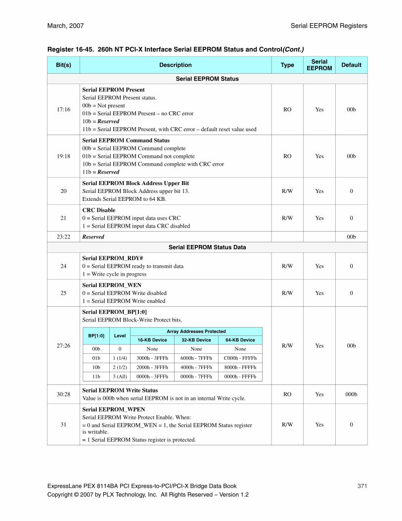
March, 2007 Serial EEPROM Registers
ExpressLane PEX 8114BA PCI Express-to-PCI/PCI-X Bridge Data Book 371
Copyright © 2007 by PLX Technology, Inc. All Rights Reserved – Version 1.2
Serial EEPROM Status
17:16
Serial EEPROM PresentSerial EEPROM Present status.00b = Not present01b = Serial EEPROM Present – no CRC error10b = Reserved11b = Serial EEPROM Present, with CRC error – default reset value used
RO Yes 00b
19:18
Serial EEPROM Command Status00b = Serial EEPROM Command complete01b = Serial EEPROM Command not complete10b = Serial EEPROM Command complete with CRC error11b = Reserved
RO Yes 00b
20Serial EEPROM Block Address Upper BitSerial EEPROM Block Address upper bit 13.Extends Serial EEPROM to 64 KB.
R/W Yes 0
21CRC Disable0 = Serial EEPROM input data uses CRC1 = Serial EEPROM input data CRC disabled
R/W Yes 0
23:22 Reserved 00b
Serial EEPROM Status Data
24Serial EEPROM_RDY#0 = Serial EEPROM ready to transmit data1 = Write cycle in progress
R/W Yes 0
25Serial EEPROM_WEN0 = Serial EEPROM Write disabled1 = Serial EEPROM Write enabled
R/W Yes 0
27:26
Serial EEPROM_BP[1:0]Serial EEPROM Block-Write Protect bits.
R/W Yes 00b
30:28Serial EEPROM Write StatusValue is 000b when serial EEPROM is not in an internal Write cycle.
RO Yes 000b
31
Serial EEPROM_WPENSerial EEPROM Write Protect Enable. When:= 0 and Serial EEPROM_WEN = 1, the Serial EEPROM Status register is writable.= 1 Serial EEPROM Status register is protected.
R/W Yes 0
Register 16-45. 260h NT PCI-X Interface Serial EEPROM Status and Control(Cont.)
Bit(s) Description Type Serial EEPROM Default
BP[1:0] LevelArray Addresses Protected
16-KB Device 32-KB Device 64-KB Device
00b 0 None None None
01b 1 (1/4) 3000h - 3FFFh 6000h - 7FFFh C000h - FFFFh
10b 2 (1/2) 2000h - 3FFFh 4000h - 7FFFh 8000h - FFFFh
11b 3 (All) 0000h - 3FFFh 0000h - 7FFFh 0000h - FFFFh
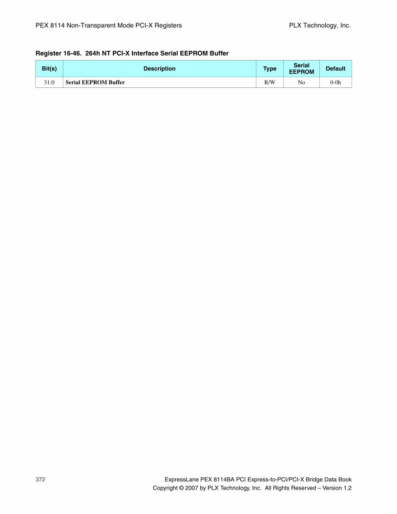
PEX 8114 Non-Transparent Mode PCI-X Registers PLX Technology, Inc.
372 ExpressLane PEX 8114BA PCI Express-to-PCI/PCI-X Bridge Data Book
Copyright © 2007 by PLX Technology, Inc. All Rights Reserved – Version 1.2
Register 16-46. 264h NT PCI-X Interface Serial EEPROM Buffer
Bit(s) Description Type Serial EEPROM Default
31:0 Serial EEPROM Buffer R/W No 0-0h
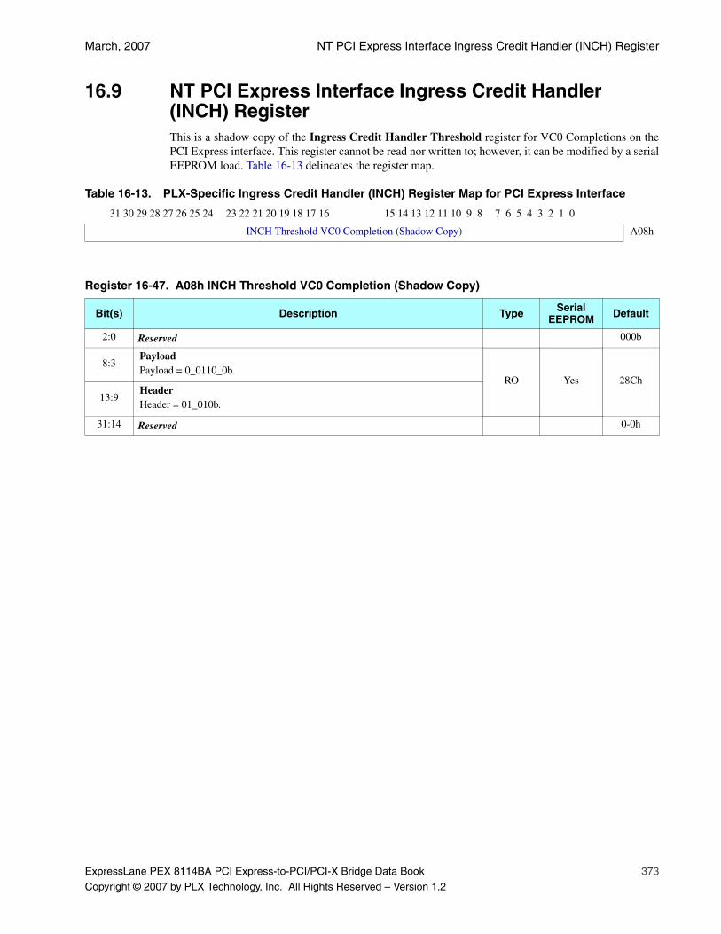
March, 2007 NT PCI Express Interface Ingress Credit Handler (INCH) Register
ExpressLane PEX 8114BA PCI Express-to-PCI/PCI-X Bridge Data Book 373
Copyright © 2007 by PLX Technology, Inc. All Rights Reserved – Version 1.2
16.9 NT PCI Express Interface Ingress Credit Handler (INCH) RegisterThis is a shadow copy of the Ingress Credit Handler Threshold register for VC0 Completions on thePCI Express interface. This register cannot be read nor written to; however, it can be modified by a serialEEPROM load. Table 16-13 delineates the register map.
Table 16-13. PLX-Specific Ingress Credit Handler (INCH) Register Map for PCI Express Interface
31 30 29 28 27 26 25 24 23 22 21 20 19 18 17 16 15 14 13 12 11 10 9 8 7 6 5 4 3 2 1 0
INCH Threshold VC0 Completion (Shadow Copy) A08h
Register 16-47. A08h INCH Threshold VC0 Completion (Shadow Copy)
Bit(s) Description Type Serial EEPROM Default
2:0 Reserved 000b
8:3PayloadPayload = 0_0110_0b.
RO Yes 28Ch
13:9HeaderHeader = 01_010b.
31:14 Reserved 0-0h
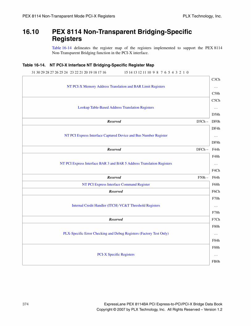
PEX 8114 Non-Transparent Mode PCI-X Registers PLX Technology, Inc.
374 ExpressLane PEX 8114BA PCI Express-to-PCI/PCI-X Bridge Data Book
Copyright © 2007 by PLX Technology, Inc. All Rights Reserved – Version 1.2
16.10 PEX 8114 Non-Transparent Bridging-Specific RegistersTable 16-14 delineates the register map of the registers implemented to support the PEX 8114Non-Transparent Bridging function in the PCI-X interface.
Table 16-14. NT PCI-X Interface NT Bridging-Specific Register Map
31 30 29 28 27 26 25 24 23 22 21 20 19 18 17 16 15 14 13 12 11 10 9 8 7 6 5 4 3 2 1 0
NT PCI-X Memory Address Translation and BAR Limit Registers
C3Ch
…
C58h
Lookup Table-Based Address Translation Registers
C5Ch
…
D58h
Reserved D5Ch – DF0h
NT PCI Express Interface Captured Device and Bus Number Register
DF4h
…
DF8h
Reserved DFCh – F44h
NT PCI Express Interface BAR 3 and BAR 5 Address Translation Registers
F48h
…
F4Ch
Reserved F50h – F64h
NT PCI Express Interface Command Register F68h
Reserved F6Ch
Internal Credit Handler (ITCH) VC&T Threshold Registers
F70h
…
F78h
Reserved F7Ch
PLX-Specific Error Checking and Debug Registers (Factory Test Only)
F80h
…
F84h
PCI-X Specific Registers
F88h
…
FB0h

March, 2007 NT PCI-X Memory Address Translation and BAR Limit Registers
ExpressLane PEX 8114BA PCI Express-to-PCI/PCI-X Bridge Data Book 375
Copyright © 2007 by PLX Technology, Inc. All Rights Reserved – Version 1.2
16.10.1 NT PCI-X Memory Address Translation and BAR Limit RegistersThe NT PCI-X interface Memory Address Translation and BAR Limit registers are described inSection 5.3.4.1, “Direct Address Translation.” Table 16-15 delineates the register map.
Table 16-15. NT PCI-X Memory Address Translation and BAR Limit Register Map
31 30 29 28 27 26 25 24 23 22 21 20 19 18 17 16 15 14 13 12 11 10 9 8 7 6 5 4 3 2 1 0
Memory BAR_2 Address Translation[31:0] C3Ch
Reserved C40h
Memory BAR_4 Address Translation[31:0] C44h
Memory BAR_5 Address Translation[63:32] C48h
Memory BAR_2 Limit[31:0] C4Ch
Reserved C50h
Memory BAR_4 Limit[31:0] C54h
Memory BAR_5 Limit[63:32] C58h
Register 16-48. C3Ch Memory BAR_2 Address Translation[31:0]
Bit(s) Description Type Serial EEPROM Default
11:0 Reserved 0-0h
31:12BAR_2 Base Translation[31:12]Translation base address if BAR_2 is enabled.
R/W Yes 0-0h
Register 16-49. C44h Memory BAR_4 Address Translation[31:0]
Bit(s) Description Type Serial EEPROM Default
11:0 Reserved 0-0h
31:12BAR_4 Base Translation[31:12]Translation base address if BAR_4 is enabled.
R/W Yes 0-0h
Register 16-50. C48h Memory BAR_5 Address Translation[63:32]
Bit(s) Description Type Serial EEPROM Default
31:0BAR_5 Base Translation[63:32]Translation base address if BAR_5 is enabled.
R/W Yes 0-0h
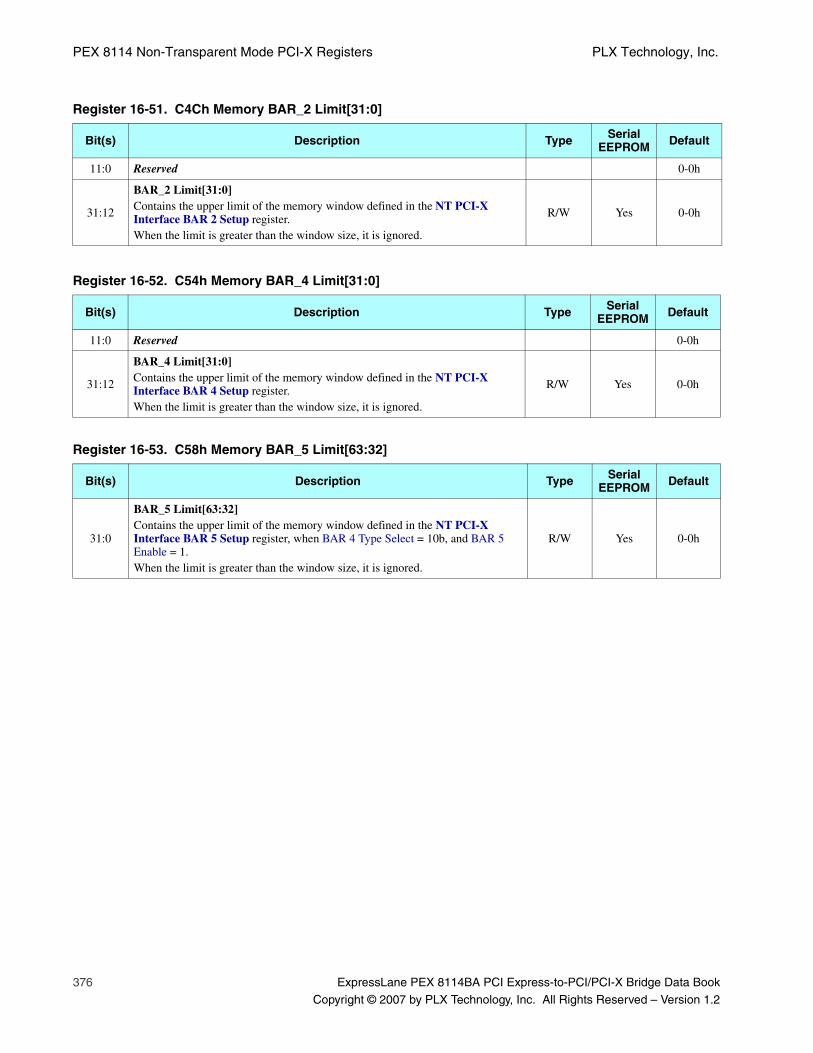
PEX 8114 Non-Transparent Mode PCI-X Registers PLX Technology, Inc.
376 ExpressLane PEX 8114BA PCI Express-to-PCI/PCI-X Bridge Data Book
Copyright © 2007 by PLX Technology, Inc. All Rights Reserved – Version 1.2
Register 16-51. C4Ch Memory BAR_2 Limit[31:0]
Bit(s) Description Type Serial EEPROM Default
11:0 Reserved 0-0h
31:12
BAR_2 Limit[31:0]Contains the upper limit of the memory window defined in the NT PCI-X Interface BAR 2 Setup register.When the limit is greater than the window size, it is ignored.
R/W Yes 0-0h
Register 16-52. C54h Memory BAR_4 Limit[31:0]
Bit(s) Description Type Serial EEPROM Default
11:0 Reserved 0-0h
31:12
BAR_4 Limit[31:0]Contains the upper limit of the memory window defined in the NT PCI-X Interface BAR 4 Setup register.When the limit is greater than the window size, it is ignored.
R/W Yes 0-0h
Register 16-53. C58h Memory BAR_5 Limit[63:32]
Bit(s) Description Type Serial EEPROM Default
31:0
BAR_5 Limit[63:32]Contains the upper limit of the memory window defined in the NT PCI-X Interface BAR 5 Setup register, when BAR 4 Type Select = 10b, and BAR 5 Enable = 1.When the limit is greater than the window size, it is ignored.
R/W Yes 0-0h

March, 2007 Lookup Table-Based Address Translation Registers
ExpressLane PEX 8114BA PCI Express-to-PCI/PCI-X Bridge Data Book 377
Copyright © 2007 by PLX Technology, Inc. All Rights Reserved – Version 1.2
16.10.2 Lookup Table-Based Address Translation RegistersThere are 64 Base-Translation Lookup Table (LUT) Entry registers that support LUT-based Addresstranslation. These registers are defined in Section 5.3.4.2, “Lookup Table Base Address Translation,”and are accessed using the NT PCI-X interface Memory-Mapped or Cursor mechanism. Table 16-16delineates the register and address locations. The register description that follows defines the bitdefinitions that apply to all 64 registers.
Table 16-16. Base-Translation Lookup Table Entry_n Register Locations
ADDR Location
Lookup Table
Entry_n
ADDR Location
Lookup Table
Entry_n
ADDR Location
Lookup Table
Entry_n
ADDR Location
Lookup Table
Entry_n
C5Ch 0 C60h 1 C64h 2 C68h 3
C6Ch 4 C70h 5 C74h 6 C78h 7
C7Ch 8 C80h 9 C84h 10 C88h 11
C8Ch 12 C90h 13 C94h 14 C98h 15
C9Ch 17 CA0h 17 CA4h 18 CA8h 19
CACh 20 CB0h 21 CB4h 22 CB8h 23
CBCh 24 CC0h 25 CC4h 26 CC8h 27
CCCh 28 CD0h 29 CD4h 30 CD8h 31
CDCh 32 CE0h 33 CE4h 34 CE8h 35
CECh 36 CF0h 37 CF4h 38 CF8h 39
CFCh 40 D00h 41 D04h 42 D08h 43
D0Ch 44 D10h 45 D14h 46 D18h 47
D1Ch 48 D20h 49 D24h 50 D28h 51
D2Ch 52 D30h 53 D34h 54 D38h 55
D3Ch 56 D40h 57 D44h 58 D48h 59
D4Ch 60 D50h 61 D54h 62 D58h 63
Register 16-54. C5Ch - D58h NT PCI-X Interface Lookup Table Base Address Translation Entry_n (where n = 0 through 63)
Bit(s) Description Type Serial EEPROM Default
0Entry Status0 = Invalid1 = Valid
R/W Yes 0
2:1 Reserved 00b
3Prefetchable0 = Non-Prefetchable1 = Prefetchable
R/W Yes 0
7:4 Reserved 0h
31:8Base TranslationBase Translation address value.
R/W Yes 0000_00h
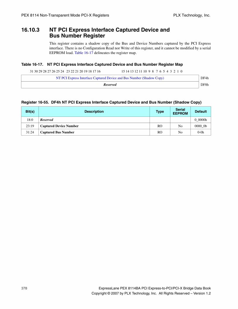
PEX 8114 Non-Transparent Mode PCI-X Registers PLX Technology, Inc.
378 ExpressLane PEX 8114BA PCI Express-to-PCI/PCI-X Bridge Data Book
Copyright © 2007 by PLX Technology, Inc. All Rights Reserved – Version 1.2
16.10.3 NT PCI Express Interface Captured Device and Bus Number RegisterThis register contains a shadow copy of the Bus and Device Numbers captured by the PCI Expressinterface. There is no Configuration Read nor Write of this register, and it cannot be modified by a serialEEPROM load. Table 16-17 delineates the register map.
Table 16-17. NT PCI Express Interface Captured Device and Bus Number Register Map
31 30 29 28 27 26 25 24 23 22 21 20 19 18 17 16 15 14 13 12 11 10 9 8 7 6 5 4 3 2 1 0
NT PCI Express Interface Captured Device and Bus Number (Shadow Copy) DF4h
Reserved DF8h
Register 16-55. DF4h NT PCI Express Interface Captured Device and Bus Number (Shadow Copy)
Bit(s) Description Type Serial EEPROM Default
18:0 Reserved 0_0000h
23:19 Captured Device Number RO No 0000_0b
31:24 Captured Bus Number RO No 0-0h
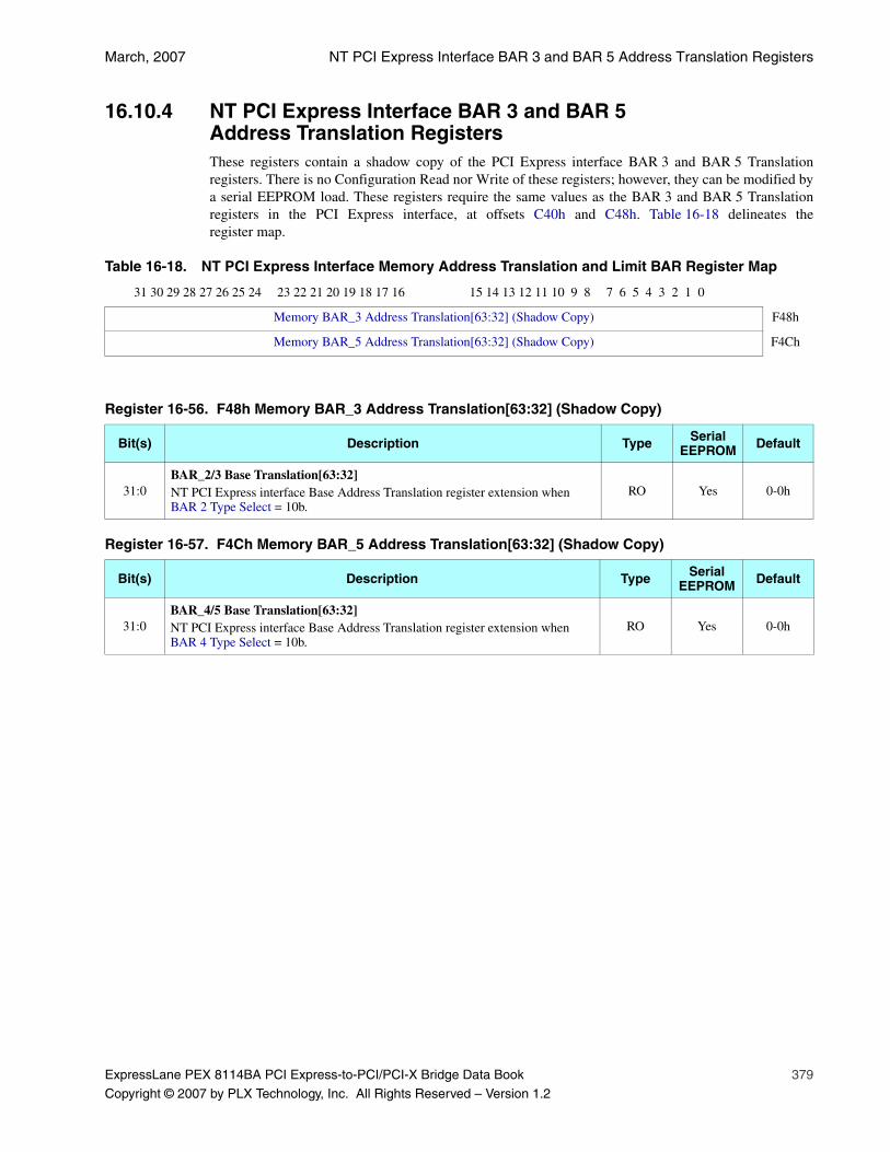
March, 2007 NT PCI Express Interface BAR 3 and BAR 5 Address Translation Registers
ExpressLane PEX 8114BA PCI Express-to-PCI/PCI-X Bridge Data Book 379
Copyright © 2007 by PLX Technology, Inc. All Rights Reserved – Version 1.2
16.10.4 NT PCI Express Interface BAR 3 and BAR 5Address Translation RegistersThese registers contain a shadow copy of the PCI Express interface BAR 3 and BAR 5 Translationregisters. There is no Configuration Read nor Write of these registers; however, they can be modified bya serial EEPROM load. These registers require the same values as the BAR 3 and BAR 5 Translationregisters in the PCI Express interface, at offsets C40h and C48h. Table 16-18 delineates theregister map.
Table 16-18. NT PCI Express Interface Memory Address Translation and Limit BAR Register Map
31 30 29 28 27 26 25 24 23 22 21 20 19 18 17 16 15 14 13 12 11 10 9 8 7 6 5 4 3 2 1 0
Memory BAR_3 Address Translation[63:32] (Shadow Copy) F48h
Memory BAR_5 Address Translation[63:32] (Shadow Copy) F4Ch
Register 16-56. F48h Memory BAR_3 Address Translation[63:32] (Shadow Copy)
Bit(s) Description Type Serial EEPROM Default
31:0BAR_2/3 Base Translation[63:32]NT PCI Express interface Base Address Translation register extension when BAR 2 Type Select = 10b.
RO Yes 0-0h
Register 16-57. F4Ch Memory BAR_5 Address Translation[63:32] (Shadow Copy)
Bit(s) Description Type Serial EEPROM Default
31:0BAR_4/5 Base Translation[63:32]NT PCI Express interface Base Address Translation register extension when BAR 4 Type Select = 10b.
RO Yes 0-0h
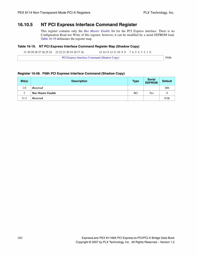
PEX 8114 Non-Transparent Mode PCI-X Registers PLX Technology, Inc.
380 ExpressLane PEX 8114BA PCI Express-to-PCI/PCI-X Bridge Data Book
Copyright © 2007 by PLX Technology, Inc. All Rights Reserved – Version 1.2
16.10.5 NT PCI Express Interface Command RegisterThis register contains only the Bus Master Enable bit for the PCI Express interface. There is noConfiguration Read nor Write of this register; however, it can be modified by a serial EEPROM load.Table 16-19 delineates the register map.
Table 16-19. NT PCI Express Interface Command Register Map (Shadow Copy)
31 30 29 28 27 26 25 24 23 22 21 20 19 18 17 16 15 14 13 12 11 10 9 8 7 6 5 4 3 2 1 0
PCI Express Interface Command (Shadow Copy) F68h
Register 16-58. F68h PCI Express Interface Command (Shadow Copy)
Bit(s) Description Type Serial EEPROM Default
1:0 Reserved 00b
2 Bus Master Enable RO Yes 0
31:3 Reserved 0-0h

March, 2007 Internal Credit Handler (ITCH) VC&T Threshold Registers
ExpressLane PEX 8114BA PCI Express-to-PCI/PCI-X Bridge Data Book 381
Copyright © 2007 by PLX Technology, Inc. All Rights Reserved – Version 1.2
16.10.6 Internal Credit Handler (ITCH) VC&T Threshold RegistersThe registers delineated in Table 16-20 control internal traffic from the PCI-X interface to the PCIExpress interface. The threshold (Packet Count) units are equivalent to 8 beats, where each beat can beup to 20 bytes. Therefore, a programmed value of 1 represents 160 bytes, 2 represents 320 bytes, and soforth. The entire TLP (Header, Payload, and ECRC, if any) is used to determine a total byte size, and thetotal byte size is divided by 20 and rounded up to the nearest integer to ascertain the number of beats.Every 8 beats counts as 1 threshold unit.
The Upper Packet Count is the high threshold. If more units than the programmed upper count arequeued, no further packets can be scheduled across the internal fabric.
Note: Previously scheduled packets arrive in their entirety, completely unaffected by the cut-off signal.
The Lower Packet Count is the low threshold. After cutting off a VC&T due to the high threshold, whenthe count returns below the low threshold, that VC&T is again turned on.
The upper and lower counts must be different, and the upper number must be at least two units largerthan the lower number.
Table 16-20. PEX 8114 NT PCI-X Interface PLX-Specific Internal Credit Handler (ITCH) VC&T Threshold Register Map
31 30 29 28 27 26 25 24 23 22 21 20 19 18 17 16 15 14 13 12 11 10 9 8 7 6 5 4 3 2 1 0
NT PCI-X Interface ITCH VC&T Threshold_1 F70h
NT PCI-X Interface ITCH VC&T Threshold_2 F74h
Reserved F78h
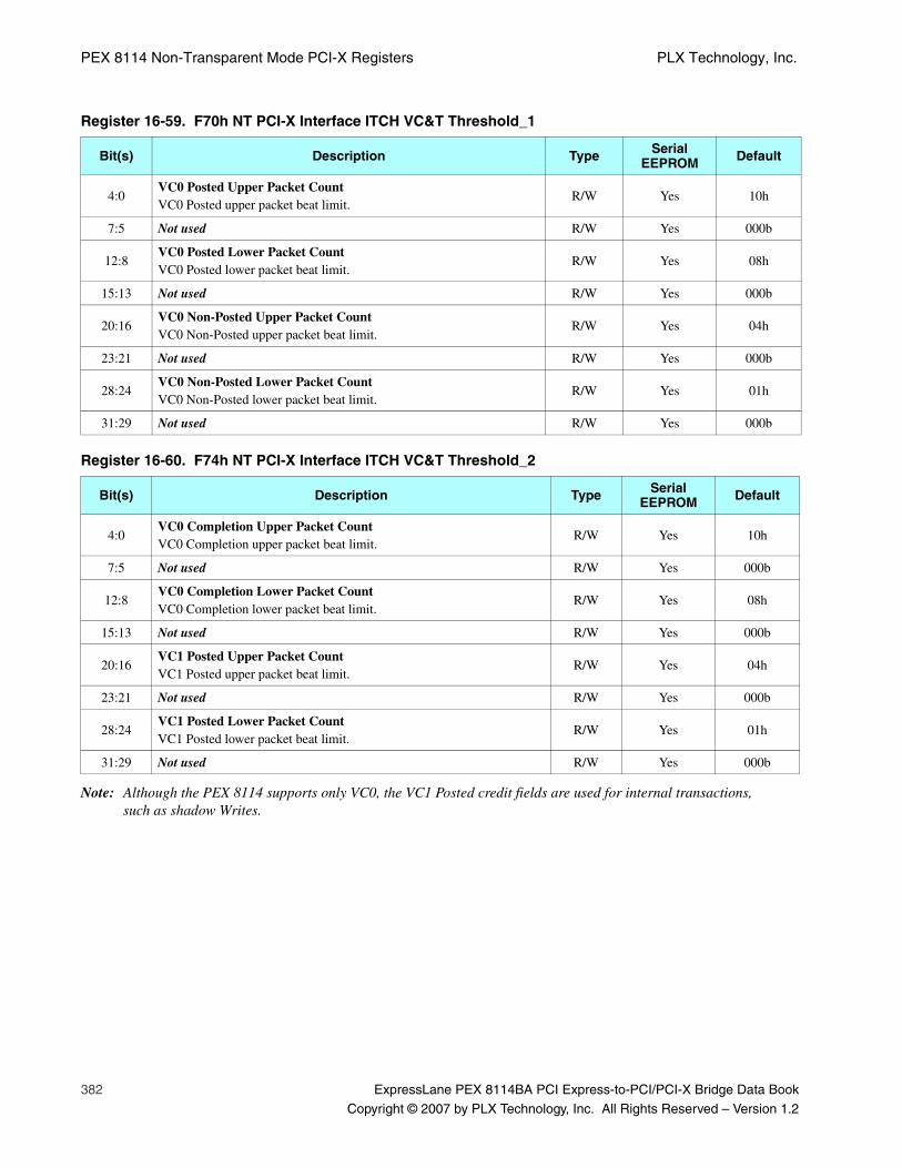
PEX 8114 Non-Transparent Mode PCI-X Registers PLX Technology, Inc.
382 ExpressLane PEX 8114BA PCI Express-to-PCI/PCI-X Bridge Data Book
Copyright © 2007 by PLX Technology, Inc. All Rights Reserved – Version 1.2
Note: Although the PEX 8114 supports only VC0, the VC1 Posted credit fields are used for internal transactions, such as shadow Writes.
Register 16-59. F70h NT PCI-X Interface ITCH VC&T Threshold_1
Bit(s) Description Type Serial EEPROM Default
4:0VC0 Posted Upper Packet CountVC0 Posted upper packet beat limit.
R/W Yes 10h
7:5 Not used R/W Yes 000b
12:8VC0 Posted Lower Packet CountVC0 Posted lower packet beat limit.
R/W Yes 08h
15:13 Not used R/W Yes 000b
20:16VC0 Non-Posted Upper Packet CountVC0 Non-Posted upper packet beat limit.
R/W Yes 04h
23:21 Not used R/W Yes 000b
28:24VC0 Non-Posted Lower Packet CountVC0 Non-Posted lower packet beat limit.
R/W Yes 01h
31:29 Not used R/W Yes 000b
Register 16-60. F74h NT PCI-X Interface ITCH VC&T Threshold_2
Bit(s) Description Type Serial EEPROM Default
4:0VC0 Completion Upper Packet CountVC0 Completion upper packet beat limit.
R/W Yes 10h
7:5 Not used R/W Yes 000b
12:8VC0 Completion Lower Packet CountVC0 Completion lower packet beat limit.
R/W Yes 08h
15:13 Not used R/W Yes 000b
20:16VC1 Posted Upper Packet CountVC1 Posted upper packet beat limit.
R/W Yes 04h
23:21 Not used R/W Yes 000b
28:24VC1 Posted Lower Packet CountVC1 Posted lower packet beat limit.
R/W Yes 01h
31:29 Not used R/W Yes 000b
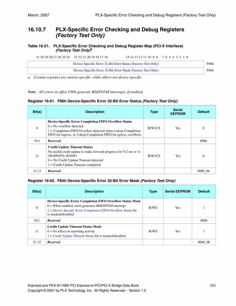
March, 2007 PLX-Specific Error Checking and Debug Registers (Factory Test Only)
ExpressLane PEX 8114BA PCI Express-to-PCI/PCI-X Bridge Data Book 383
Copyright © 2007 by PLX Technology, Inc. All Rights Reserved – Version 1.2
16.10.7 PLX-Specific Error Checking and Debug Registers (Factory Test Only)
Note: All errors in offset F80h generate MSI/INTA# interrupts, if enabled.
Table 16-21. PLX-Specific Error Checking and Debug Register Map (PCI-X Interface) (Factory Test Only)a
a. Certain registers are station-specific, while others are device-specific.
31 30 29 28 27 26 25 24 23 22 21 20 19 18 17 16 15 14 13 12 11 10 9 8 7 6 5 4 3 2 1 0
Device-Specific Error 32-Bit Error Status (Factory Test Only) F80h
Device-Specific Error 32-Bit Error Mask (Factory Test Only) F84h
Register 16-61. F80h Device-Specific Error 32-Bit Error Status (Factory Test Only)
Bit(s) Description Type Serial EEPROM Default
0
Device-Specific Error Completion FIFO Overflow Status0 = No overflow detected1 = Completion FIFO Overflow detected when 4-deep Completion FIFO for ingress, or 2-deep Completion FIFO for egress, overflows
R/W1CS Yes 0
10:1 Reserved 000h
11
Credit Update Timeout StatusNo useful credit update to make forward progress for 512 ms or 1s (disabled by default)0 = No Credit Update Timeout detected1 = Credit Update Timeout completed
R/W1CS Yes 0
31:12 Reserved 0000_0h
Register 16-62. F84h Device-Specific Error 32-Bit Error Mask (Factory Test Only)
Bit(s) Description Type Serial EEPROM Default
0
Device-Specific Error Completion FIFO Overflow Status Mask0 = When enabled, error generates MSI/INTA# interrupt1 = Device-Specific Error Completion FIFO Overflow Status bit is masked/disabled
R/WS Yes 1
10:1 Reserved 000h
11Credit Update Timeout Status Mask0 = No effect on reporting activity1 = Credit Update Timeout Status bit is masked/disabled
R/WS Yes 1
31:12 Reserved 0000_0h

PEX 8114 Non-Transparent Mode PCI-X Registers PLX Technology, Inc.
384 ExpressLane PEX 8114BA PCI Express-to-PCI/PCI-X Bridge Data Book
Copyright © 2007 by PLX Technology, Inc. All Rights Reserved – Version 1.2
16.10.8 PCI-X Specific Registers
Table 16-22. PCI-X Specific Register Map (PCI-X Interface)a
a. Certain registers are station-specific, while others are device-specific.
31 30 29 28 27 26 25 24 23 22 21 20 19 18 17 16 15 14 13 12 11 10 9 8 7 6 5 4 3 2 1 0
Completion Buffer Timeout F88h
Reserved F8Ch – F9Ch
PCI Clock Enable, Strong Ordering, Read Cycle Value FA0h
Prefetch FA4h
PCI Arbiter 0 FA8h
PCI Arbiter 1 FACh
PCI Arbiter 2 FB0h
Register 16-63. F88h Completion Buffer Timeout
Bit(s) Description Type Serial EEPROM Default
7:0 Target Tag Timeout R/W1C Yes 00h
31:8 Reserved 0000_00h
Register 16-64. FA0h PCI Clock Enable, Strong Ordering, Read Cycle Value
Bit(s) Description Type Serial EEPROM Default
3:0
PCI_CLKO_EN[3:0]PCI_CLKO_EN[0]=1 enables PCI_CLKO0PCI_CLKO_EN[1]=1 enables PCI_CLKO1PCI_CLKO_EN[2]=1 enables PCI_CLKO2PCI_CLKO_EN[3]=1 enables PCI_CLKO3
R/W Yes0h if STRAP_CLK_MST=0Fh if STRAP_CLK_MST=1
4Prefetch on Read Line MultipleEnables reading multiple Cache Lines upon receiving a Memory Read Line Multiple transaction on the PCI Bus.
R/W Yes 0
5Disable Completion Timeout TimerRefer to Section 7.8, “Transaction Transfer Failures.”
R/W Yes 0
6Enable Long Completion Timeout TimerRefer to Section 7.8, “Transaction Transfer Failures.”
R/W Yes 1
7 Disable BAR 0 R/W Yes 0

March, 2007 PCI-X Specific Registers
ExpressLane PEX 8114BA PCI Express-to-PCI/PCI-X Bridge Data Book 385
Copyright © 2007 by PLX Technology, Inc. All Rights Reserved – Version 1.2
8
Force Strong OrderingAfter data is returned to the PEX 8114 in response to a Read request, the PEX 8114 Retries the same transaction until complete and does not attempt to gather data from other outstanding transactions.
R/W Yes 0
9 Reserved 0
10PLL Lock Control 0Resets on loss of PLL lock, unless bits [11:10]=00b. (Refer to Table 16-23 for methods of handling loss of PLL lock.)
R/W Yes 0
11PLL Lock Control 1Reset after timer timeout on loss of PLL lock. (Refer to Table 16-23 for methods of handling loss of PLL lock.)
R/W Yes 0
12 Memory Read Line Multiple Enable R/W Yes 0
13 Address Stepping Enable R/W Yes 0
14Sticky PCI-X PLL Loss LockSet when the PCI-X PLL loses PLL lock.
R/W1C Yes 0
15Sticky PCI Express PLL Loss LockSet when the PCI Express PLL loses PLL lock.
R/W1C Yes 0
26:16 Maximum Read Cycle Value R/W Yes 7FFh
27 Retry Failure Status R/W1C Yes 0
28 No Snoop Enable R/W Yes 0
29
HP_PERST# Timer Select0 = Hot reset signaled on the PCI Express link causes HP_PERST# output to assert Low for 1 ms.1 = Hot reset signaled on the PCI Express interface causes HP_PERST# to assert Low for 128 ns. When the reset is complete, all PCI Express and PCI-X registers are operating in their default states
R/W Yes 0
30
NT Reset Select0 = PEX 8114 resets when PCI_RST# input is asserted or when HP_PERST# output is asserted1 = PEX 8114 resets only when PCI_RST# input is asserted
R/W Yes 0
31 Clear HP_PERST# R/W Yes 0
Table 16-23. Methods for Handling Loss of PLL Lock
Offset FA0h[11:10] Description
00b Default. Ignores loss of PLL lock.
01b A loss of PLL lock immediately causes the PEX 8114 to reset.
10bThe PEX 8114 attempts to tolerate loss of PLL lock:
• When lock is re-acquired in less than 200 µs, the PEX 8114 does not reset• When lock is not re-acquired within 200 µs, the PEX 8114 is reset
11b The PEX 8114 does not reset if loss of PLL lock occurs.
Register 16-64. FA0h PCI Clock Enable, Strong Ordering, Read Cycle Value(Cont.)
Bit(s) Description Type Serial EEPROM Default
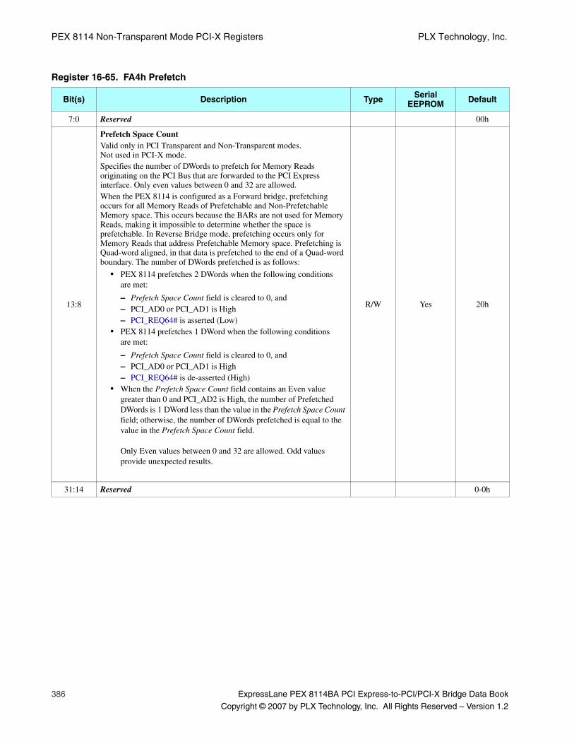
PEX 8114 Non-Transparent Mode PCI-X Registers PLX Technology, Inc.
386 ExpressLane PEX 8114BA PCI Express-to-PCI/PCI-X Bridge Data Book
Copyright © 2007 by PLX Technology, Inc. All Rights Reserved – Version 1.2
Register 16-65. FA4h Prefetch
Bit(s) Description Type Serial EEPROM Default
7:0 Reserved 00h
13:8
Prefetch Space CountValid only in PCI Transparent and Non-Transparent modes. Not used in PCI-X mode.Specifies the number of DWords to prefetch for Memory Reads originating on the PCI Bus that are forwarded to the PCI Express interface. Only even values between 0 and 32 are allowed.When the PEX 8114 is configured as a Forward bridge, prefetching occurs for all Memory Reads of Prefetchable and Non-Prefetchable Memory space. This occurs because the BARs are not used for Memory Reads, making it impossible to determine whether the space is prefetchable. In Reverse Bridge mode, prefetching occurs only for Memory Reads that address Prefetchable Memory space. Prefetching is Quad-word aligned, in that data is prefetched to the end of a Quad-word boundary. The number of DWords prefetched is as follows:
• PEX 8114 prefetches 2 DWords when the following conditions are met:
– Prefetch Space Count field is cleared to 0, and– PCI_AD0 or PCI_AD1 is High– PCI_REQ64# is asserted (Low)
• PEX 8114 prefetches 1 DWord when the following conditions are met:
– Prefetch Space Count field is cleared to 0, and– PCI_AD0 or PCI_AD1 is High– PCI_REQ64# is de-asserted (High)
• When the Prefetch Space Count field contains an Even value greater than 0 and PCI_AD2 is High, the number of Prefetched DWords is 1 DWord less than the value in the Prefetch Space Count field; otherwise, the number of DWords prefetched is equal to the value in the Prefetch Space Count field.
Only Even values between 0 and 32 are allowed. Odd values provide unexpected results.
R/W Yes 20h
31:14 Reserved 0-0h
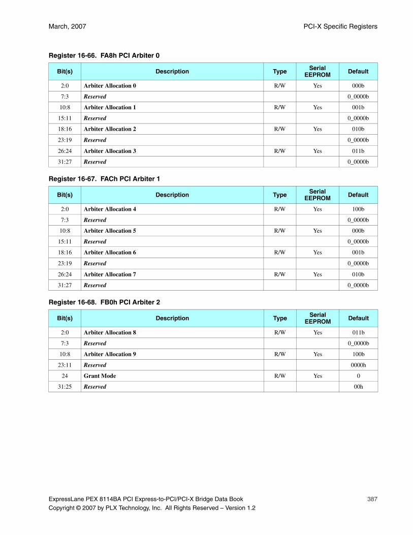
March, 2007 PCI-X Specific Registers
ExpressLane PEX 8114BA PCI Express-to-PCI/PCI-X Bridge Data Book 387
Copyright © 2007 by PLX Technology, Inc. All Rights Reserved – Version 1.2
Register 16-66. FA8h PCI Arbiter 0
Bit(s) Description Type Serial EEPROM Default
2:0 Arbiter Allocation 0 R/W Yes 000b
7:3 Reserved 0_0000b
10:8 Arbiter Allocation 1 R/W Yes 001b
15:11 Reserved 0_0000b
18:16 Arbiter Allocation 2 R/W Yes 010b
23:19 Reserved 0_0000b
26:24 Arbiter Allocation 3 R/W Yes 011b
31:27 Reserved 0_0000b
Register 16-67. FACh PCI Arbiter 1
Bit(s) Description Type Serial EEPROM Default
2:0 Arbiter Allocation 4 R/W Yes 100b
7:3 Reserved 0_0000b
10:8 Arbiter Allocation 5 R/W Yes 000b
15:11 Reserved 0_0000b
18:16 Arbiter Allocation 6 R/W Yes 001b
23:19 Reserved 0_0000b
26:24 Arbiter Allocation 7 R/W Yes 010b
31:27 Reserved 0_0000b
Register 16-68. FB0h PCI Arbiter 2
Bit(s) Description Type Serial EEPROM Default
2:0 Arbiter Allocation 8 R/W Yes 011b
7:3 Reserved 0_0000b
10:8 Arbiter Allocation 9 R/W Yes 100b
23:11 Reserved 0000h
24 Grant Mode R/W Yes 0
31:25 Reserved 00h
PEX 8114 Non-Transparent Mode PCI-X Registers PLX Technology, Inc.
388 ExpressLane PEX 8114BA PCI Express-to-PCI/PCI-X Bridge Data Book
Copyright © 2007 by PLX Technology, Inc. All Rights Reserved – Version 1.2
THIS PAGE INTENTIONALLY LEFT BLANK.
ExpressLane PEX 8114BA PCI Express-to-PCI/PCI-X Bridge Data Book 389
Copyright © 2007 by PLX Technology, Inc. All Rights Reserved – Version 1.2
Chapter 17 PEX 8114 Non-Transparent Mode PCI Express Registers
17.1 IntroductionNote: PLX does not recommend using the PEX 8114BA in NT mode due to the
Non-Transparent mode errata detailed in the PEX 8114BA Errata document. There is no plan to fix the NT mode errata in future revisions of the PEX 8114.
This chapter defines the PEX 8114 Non-Transparent (NT) PCI Express interface registers. The NTmode bridge includes two sets of configuration-capability, control, and status registers to support PCI-Xand PCI Express interfaces. Table 17-1 delineates NT PCI Express interface register mapping.
NT mode PCI-X interface registers are defined in Chapter 16, “PEX 8114 Non-Transparent ModePCI-X Registers.” Transparent mode registers are defined in Chapter 14, “PEX 8114 Transparent ModeRegisters.”
For further details regarding register names and descriptions, refer to the following specifications:
• PCI r2.3
• PCI r3.0
• PCI-to-PCI Bridge r1.1
• PCI Power Mgmt. r1.2
• PCI Express Base 1.0a
• PCI Express-to-PCI/PCI-X Bridge r1.0
• PCI-X r1.0b
• PCI-X r2.0a
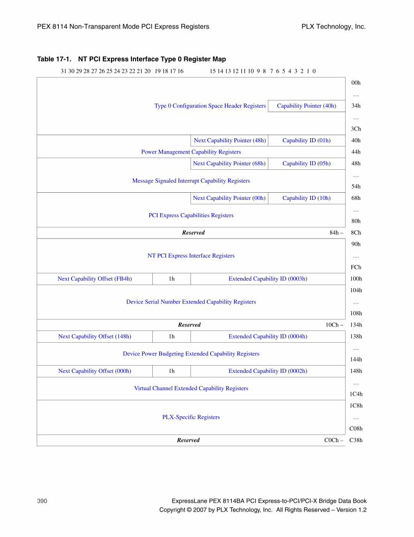
PEX 8114 Non-Transparent Mode PCI Express Registers PLX Technology, Inc.
390 ExpressLane PEX 8114BA PCI Express-to-PCI/PCI-X Bridge Data Book
Copyright © 2007 by PLX Technology, Inc. All Rights Reserved – Version 1.2
Table 17-1. NT PCI Express Interface Type 0 Register Map
31 30 29 28 27 26 25 24 23 22 21 20 19 18 17 16 15 14 13 12 11 10 9 8 7 6 5 4 3 2 1 0
00h
…
Type 0 Configuration Space Header Registers Capability Pointer (40h) 34h
…
3Ch
Next Capability Pointer (48h) Capability ID (01h) 40h
Power Management Capability Registers 44h
Next Capability Pointer (68h) Capability ID (05h) 48h
Message Signaled Interrupt Capability Registers…
54h
Next Capability Pointer (00h) Capability ID (10h) 68h
PCI Express Capabilities Registers…
80h
Reserved 84h – 8Ch
NT PCI Express Interface Registers
90h
…
FCh
Next Capability Offset (FB4h) 1h Extended Capability ID (0003h) 100h
Device Serial Number Extended Capability Registers
104h
…
108h
Reserved 10Ch – 134h
Next Capability Offset (148h) 1h Extended Capability ID (0004h) 138h
Device Power Budgeting Extended Capability Registers…
144h
Next Capability Offset (000h) 1h Extended Capability ID (0002h) 148h
Virtual Channel Extended Capability Registers…
1C4h
PLX-Specific Registers
1C8h
…
C08h
Reserved C0Ch – C38h
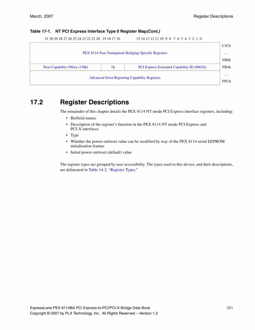
March, 2007 Register Descriptions
ExpressLane PEX 8114BA PCI Express-to-PCI/PCI-X Bridge Data Book 391
Copyright © 2007 by PLX Technology, Inc. All Rights Reserved – Version 1.2
17.2 Register DescriptionsThe remainder of this chapter details the PEX 8114 NT mode PCI Express interface registers, including:
• Bit/field names
• Description of the register’s function in the PEX 8114 NT mode PCI Express and PCI-X interfaces
• Type
• Whether the power-on/reset value can be modified by way of the PEX 8114 serial EEPROM initialization feature
• Initial power-on/reset (default) value
The register types are grouped by user accessibility. The types used in this device, and their descriptions,are delineated in Table 14-2, “Register Types.”
PEX 8114 Non-Transparent Bridging-Specific Registers
C3Ch
…
FB0h
Next Capability Offset (138h) 1h PCI Express Extended Capability ID (0001h) FB4h
Advanced Error Reporting Capability Registers…
FFCh
Table 17-1. NT PCI Express Interface Type 0 Register Map(Cont.)
31 30 29 28 27 26 25 24 23 22 21 20 19 18 17 16 15 14 13 12 11 10 9 8 7 6 5 4 3 2 1 0

PEX 8114 Non-Transparent Mode PCI Express Registers PLX Technology, Inc.
392 ExpressLane PEX 8114BA PCI Express-to-PCI/PCI-X Bridge Data Book
Copyright © 2007 by PLX Technology, Inc. All Rights Reserved – Version 1.2
17.3 Type 0 Configuration Space Header Registers
Table 17-2. Type 0 Configuration Space Header Register Map
31 30 29 28 27 26 25 24 23 22 21 20 19 18 17 16 15 14 13 12 11 10 9 8 7 6 5 4 3 2 1 0
Device ID Vendor ID 00h
Status Command 04h
Class Code Revision ID 08h
BIST (Not Supported) Configuration Layout Type and Multi-Function Master Latency Timer Cache Line Size 0Ch
Base Address 0 10h
Base Address 1 14h
Base Address 2 18h
Base Address 3 1Ch
Base Address 4 20h
Base Address 5 24h
Reserved 28h
Subsystem ID Subsystem Vendor ID 2Ch
Expansion ROM Base Address 30h
Reserved Capability Pointer (40h) 34h
Reserved 38h
Reserved Interrupt Pin Interrupt Line 3Ch
Register 17-1. 00h Product Identification
Bit(s) Description Type Serial EEPROM Default
15:0
Vendor IDUnless overwritten by the serial EEPROM, returns the PLX PCI-SIG-assigned Vendor ID. The PEX 8114 Serial EEPROM register initialization capability is used to replace the PLX Vendor ID with another Vendor ID.
HwInit Yes 10B5h
31:16
Device ID
Unless overwritten by the serial EEPROM, the PEX 8114 returns 8104h, the PLX-assigned Device ID. The PEX 8114 Serial EEPROM register initialization capability is used to replace the PLX-assigned Device ID with another Device ID.
HwInit Yes 8104h
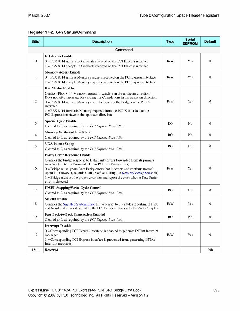
March, 2007 Type 0 Configuration Space Header Registers
ExpressLane PEX 8114BA PCI Express-to-PCI/PCI-X Bridge Data Book 393
Copyright © 2007 by PLX Technology, Inc. All Rights Reserved – Version 1.2
Register 17-2. 04h Status/Command
Bit(s) Description Type Serial EEPROM Default
Command
0I/O Access Enable
0 = PEX 8114 ignores I/O requests received on the PCI Express interface1 = PEX 8114 accepts I/O requests received on the PCI Express interface
R/W Yes 0
1Memory Access Enable0 = PEX 8114 ignores Memory requests received on the PCI Express interface1 = PEX 8114 accepts Memory requests received on the PCI Express interface
R/W Yes 0
2
Bus Master Enable
Controls PEX 8114 Memory request forwarding in the upstream direction. Does not affect message forwarding nor Completions in the upstream direction.0 = PEX 8114 ignores Memory requests targeting the bridge on the PCI-X interface 1 = PEX 8114 forwards Memory requests from the PCI-X interface to the PCI Express interface in the upstream direction
R/W Yes 0
3Special Cycle Enable
Cleared to 0, as required by the PCI Express Base 1.0a.RO No 0
4Memory Write and InvalidateCleared to 0, as required by the PCI Express Base 1.0a.
RO No 0
5VGA Palette Snoop
Cleared to 0, as required by the PCI Express Base 1.0a.RO No 0
6
Parity Error Response Enable
Controls the bridge response to Data Parity errors forwarded from its primary interface (such as a Poisoned TLP or PCI Bus Parity errors). 0 = Bridge must ignore Data Parity errors that it detects and continue normal operation (however, records status, such as setting the Detected Parity Error bit)1 = Bridge must set the proper error bits and report the error when a Data Parity error is detected
R/W Yes 0
7IDSEL Stepping/Write Cycle ControlCleared to 0, as required by the PCI Express Base 1.0a.
RO No 0
8SERR# Enable
Controls the Signaled System Error bit. When set to 1, enables reporting of Fatal and Non-Fatal errors detected by the PCI Express interface to the Root Complex.
R/W Yes 0
9Fast Back-to-Back Transaction Enabled
Cleared to 0, as required by the PCI Express Base 1.0a.RO No 0
10
Interrupt Disable
0 = Corresponding PCI Express interface is enabled to generate INTA# Interrupt messages1 = Corresponding PCI Express interface is prevented from generating INTA# Interrupt messages
R/W Yes 0
15:11 Reserved 00h

PEX 8114 Non-Transparent Mode PCI Express Registers PLX Technology, Inc.
394 ExpressLane PEX 8114BA PCI Express-to-PCI/PCI-X Bridge Data Book
Copyright © 2007 by PLX Technology, Inc. All Rights Reserved – Version 1.2
Status
18:16 Reserved 000b
19Interrupt Status
0 = No INTA# Interrupt pending1 = INTA# Interrupt pending internally to the PCI Express interface
RO Yes 0
20Capabilities ListSet to 1.
RO Yes 1
2166-MHz Capable
Cleared to 0, as required by the PCI Express Base 1.0a.RO No 0
22 Reserved 0
23Fast Back-to-Back Transaction Enabled
Cleared to 0, as required by the PCI Express Base 1.0a.RO No 0
24
Master Data Parity Error
When the Parity Error Response Enable bit = 1, the PEX 8114 sets this bit to 1 when the following occurs:
• PEX 8114 forwards a Poisoned TLP Write request from the PCI-X interface to the PCI Express interface, or
• PCI Express interface receives a Completion marked poisoned
When the Parity Error Response Enable bit = 0, the PEX 8114 never sets this bit.
R/W1C Yes 0
26:25DEVSEL TimingNot supported. Always cleared to 00b.
RO No 00b
27
Signaled Target Abort
When a Memory-Mapped access Payload length is greater than 1 DWord, the PCI Express interface sets this bit to 1. This bit is also set to 1 when the PEX 8114 forwards a Completion with Completer Abort (CA) status from the PCI-X interface to the PCI Express interface.Note: When set during a forwarded Completion, the Uncorrectable Error Status register Completer Abort Status bit is not set.
R/W1C Yes 0
28Received Target AbortSet to 1 when the bridge receives a Completion with Completer Abort Completion status.
R/W1C Yes 0
29Received Master AbortSet to 1 when the bridge receives a Completion with Unsupported Request Completion status.
R/W1C Yes 0
30
Signaled System ErrorWhen the SERR# Enable bit = 1, the PCI Express interface sets this bit to 1 when it transmits an ERR_FATAL or ERR_NONFATAL message to its upstream device.
R/W1C Yes 0
31Detected Parity Error
The PCI Express interface sets this bit to 1 when it receives a Poisoned TLP, regardless of the Parity Error Response Enable bit state.
R/W1C Yes 0
Register 17-2. 04h Status/Command(Cont.)
Bit(s) Description Type Serial EEPROM Default
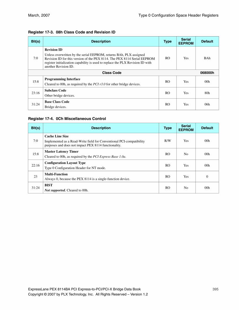
March, 2007 Type 0 Configuration Space Header Registers
ExpressLane PEX 8114BA PCI Express-to-PCI/PCI-X Bridge Data Book 395
Copyright © 2007 by PLX Technology, Inc. All Rights Reserved – Version 1.2
Register 17-3. 08h Class Code and Revision ID
Bit(s) Description Type Serial EEPROM Default
7:0
Revision ID
Unless overwritten by the serial EEPROM, returns BAh, PLX-assigned Revision ID for this version of the PEX 8114. The PEX 8114 Serial EEPROM register initialization capability is used to replace the PLX Revision ID with another Revision ID.
RO Yes BAh
Class Code 068000h
15:8Programming InterfaceCleared to 00h, as required by the PCI r3.0 for other bridge devices.
RO Yes 00h
23:16Subclass Code
Other bridge devices.RO Yes 80h
31:24Base Class Code
Bridge devices.RO Yes 06h
Register 17-4. 0Ch Miscellaneous Control
Bit(s) Description Type Serial EEPROM Default
7:0Cache Line Size
Implemented as a Read-Write field for Conventional PCI-compatibility purposes and does not impact PEX 8114 functionality.
R/W Yes 00h
15:8Master Latency Timer
Cleared to 00h, as required by the PCI Express Base 1.0a.RO No 00h
22:16Configuration Layout Type
Type 0 Configuration Header for NT mode.RO Yes 00h
23Multi-FunctionAlways 0, because the PEX 8114 is a single-function device.
RO Yes 0
31:24BIST
Not supported. Cleared to 00h.RO No 00h

PEX 8114 Non-Transparent Mode PCI Express Registers PLX Technology, Inc.
396 ExpressLane PEX 8114BA PCI Express-to-PCI/PCI-X Bridge Data Book
Copyright © 2007 by PLX Technology, Inc. All Rights Reserved – Version 1.2
1
Register 17-5. 10h Base Address 0
Bit(s) Description Type Serial EEPROM Default
0
Memory Space Indicator
When enabled, the Base Address register maps PEX 8114 Configuration registers into Memory space. PCI Express BAR 0 is configured by serial EEPROM and Local Host. By default, the NT PCI Express Interface BAR 0/BAR 1 Setup register selects Base Address 0 (32-bit Memory BAR 0) and Base Address 1 (32-bit I/O BAR 1) for CSR mapping.
RO No 0
2:1Memory Map Type00b = PEX 8114 Configuration registers are mapped anywhere in 32-bit Memory Address space
RO No 00b
3PrefetchableBase Address register maps PEX 8114 Configuration registers into Non-Prefetchable Memory space by default.
RO No 0
12:4 Reserved 00-0h
31:13Base Address 0
8-KB Base address in which to map the PEX 8114 Configuration Space registers into Memory space.
R/W Yes 0000_0h
Register 17-6. 14h Base Address 1
Bit(s) Description Type Serial EEPROM Default
0I/O Space Indicator0 = Reserved1 = Implemented as an I/O BAR
RO No 1
7:1 Reserved 0000_000b
31:8I/O Base AddressI/O space Base address of 256-byte size.For the PCI Express interface, when offset E4h[1:0]=11b, this BAR is enabled.
R/W Yes 0000_00h

March, 2007 Type 0 Configuration Space Header Registers
ExpressLane PEX 8114BA PCI Express-to-PCI/PCI-X Bridge Data Book 397
Copyright © 2007 by PLX Technology, Inc. All Rights Reserved – Version 1.2
Register 17-7. 18h Base Address 2
Bit(s) Description Type Serial EEPROM Default
0Memory Space Indicator
0 = Implemented as a Memory BAR; otherwise, reservedRO No 0
2:1
Memory Map Type
00b = Mappable anywhere in 32-bit Memory space10b = Mappable anywhere in 64-bit Memory space01b, 11b = Reserved
RO No 00b
3Prefetchable
0 = Non-Prefetchable1 = Prefetchable
RO No 0
11:4 Reserved 00h
31:12
Base Address 2
Base Address is enabled and sized by the NT PCI Express Interface BAR 2 Setup register. The BAR 2/BAR 3 group uses direct Address translation. The minimum BAR size is programmed to 4 KB. Includes a Limit register.
R/W Yes 0000_0h
Register 17-8. 1Ch Base Address 3
Bit(s) Description Type Serial EEPROM Default
31:0
Upper Base Address
PCI Express interface upper 32-bit address if BAR 2/3 is implemented as a 64-bit BAR; otherwise, reserved. These fields are R/W, based on the NT PCI Express Interface BAR 2 Setup and NT PCI Express Interface BAR 3 Setup registers.The BAR 2/3 group uses direct Address translation. Includes a Limit register.
R/W Yes 0-0h
Register 17-9. 20h Base Address 4
Bit(s) Description Type Serial EEPROM Default
0Memory Space Indicator
0 = Implemented as a Memory BAR; otherwise, reservedRO No 0
2:1
Memory Map Type00b = Mappable anywhere in 32-bit Memory space10b = Mappable anywhere in 64-bit Memory space01b, 11b = Reserved
RO No 00b
3Prefetchable
0 = Non-Prefetchable1 = Prefetchable
RO No 0
11:4 Reserved 00h
31:12
Base Address 4
Base Address size is set, and enabled by the NT PCI Express Interface BAR 4 Setup register.The BAR 4/5 group uses direct Address translation. The minimum BAR size is programmed to 4 KB. Includes a Limit register.
R/W Yes 0000_0h
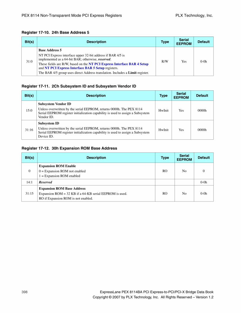
PEX 8114 Non-Transparent Mode PCI Express Registers PLX Technology, Inc.
398 ExpressLane PEX 8114BA PCI Express-to-PCI/PCI-X Bridge Data Book
Copyright © 2007 by PLX Technology, Inc. All Rights Reserved – Version 1.2
Register 17-10. 24h Base Address 5
Bit(s) Description Type Serial EEPROM Default
31:0
Base Address 5
NT PCI Express interface upper 32-bit address if BAR 4/5 is implemented as a 64-bit BAR; otherwise, reserved. These fields are R/W, based on the NT PCI Express Interface BAR 4 Setup and NT PCI Express Interface BAR 5 Setup registers.The BAR 4/5 group uses direct Address translation. Includes a Limit register.
R/W Yes 0-0h
Register 17-11. 2Ch Subsystem ID and Subsystem Vendor ID
Bit(s) Description Type Serial EEPROM Default
15:0
Subsystem Vendor ID
Unless overwritten by the serial EEPROM, returns 0000h. The PEX 8114 Serial EEPROM register initialization capability is used to assign a Subsystem Vendor ID.
HwInit Yes 0000h
31:16
Subsystem ID
Unless overwritten by the serial EEPROM, returns 0000h. The PEX 8114 Serial EEPROM register initialization capability is used to assign a Subsystem Device ID.
HwInit Yes 0000h
Register 17-12. 30h Expansion ROM Base Address
Bit(s) Description Type Serial EEPROM Default
0Expansion ROM Enable
0 = Expansion ROM not enabled1 = Expansion ROM enabled
RO No 0
14:1 Reserved 0-0h
31:15Expansion ROM Base Address
Expansion ROM = 32 KB if a 64-KB serial EEPROM is used.RO if Expansion ROM is not enabled.
RO No 0-0h
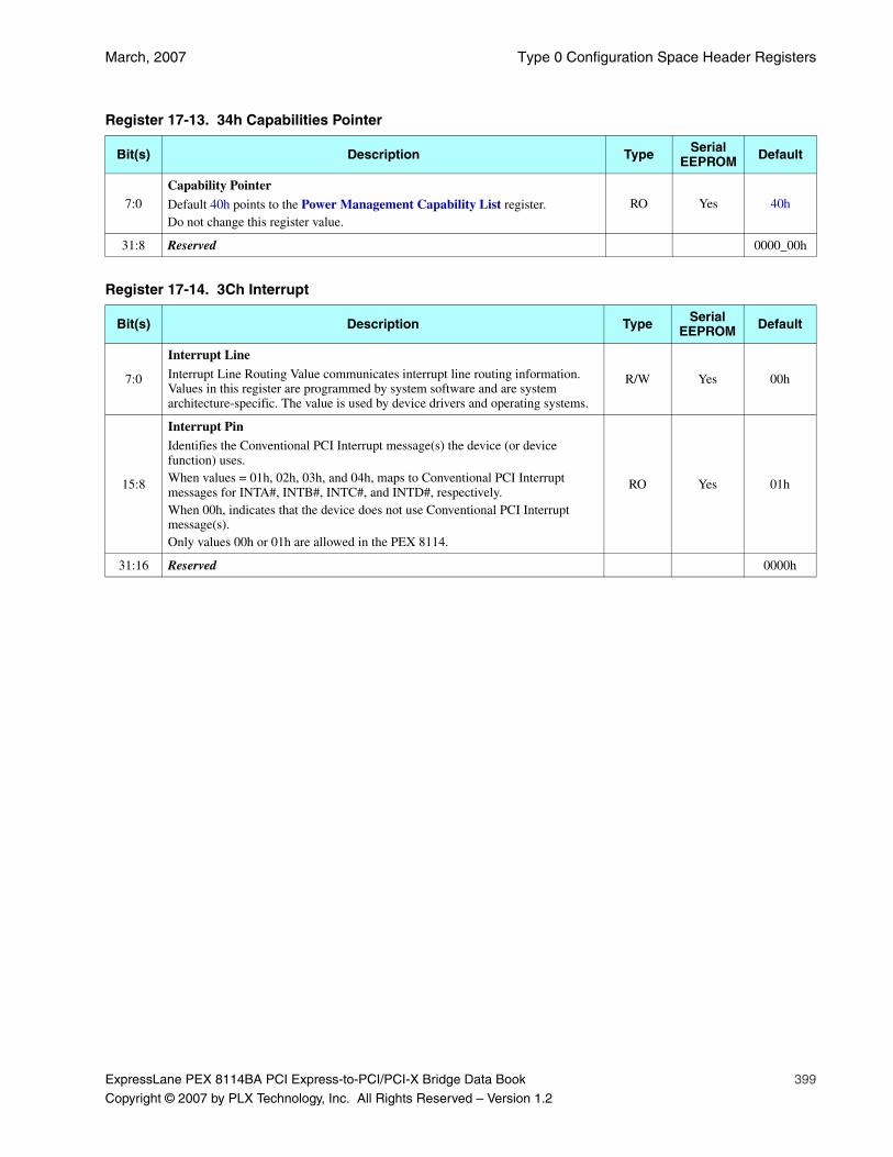
March, 2007 Type 0 Configuration Space Header Registers
ExpressLane PEX 8114BA PCI Express-to-PCI/PCI-X Bridge Data Book 399
Copyright © 2007 by PLX Technology, Inc. All Rights Reserved – Version 1.2
Register 17-13. 34h Capabilities Pointer
Bit(s) Description Type Serial EEPROM Default
7:0Capability Pointer
Default 40h points to the Power Management Capability List register.Do not change this register value.
RO Yes 40h
31:8 Reserved 0000_00h
Register 17-14. 3Ch Interrupt
Bit(s) Description Type Serial EEPROM Default
7:0
Interrupt Line
Interrupt Line Routing Value communicates interrupt line routing information. Values in this register are programmed by system software and are system architecture-specific. The value is used by device drivers and operating systems.
R/W Yes 00h
15:8
Interrupt PinIdentifies the Conventional PCI Interrupt message(s) the device (or device function) uses. When values = 01h, 02h, 03h, and 04h, maps to Conventional PCI Interrupt messages for INTA#, INTB#, INTC#, and INTD#, respectively.When 00h, indicates that the device does not use Conventional PCI Interrupt message(s).Only values 00h or 01h are allowed in the PEX 8114.
RO Yes 01h
31:16 Reserved 0000h
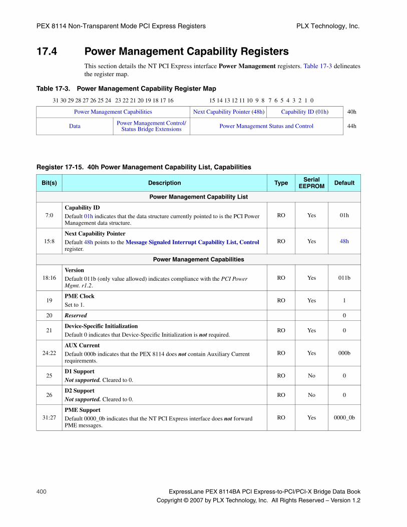
PEX 8114 Non-Transparent Mode PCI Express Registers PLX Technology, Inc.
400 ExpressLane PEX 8114BA PCI Express-to-PCI/PCI-X Bridge Data Book
Copyright © 2007 by PLX Technology, Inc. All Rights Reserved – Version 1.2
17.4 Power Management Capability RegistersThis section details the NT PCI Express interface Power Management registers. Table 17-3 delineatesthe register map.
Table 17-3. Power Management Capability Register Map
31 30 29 28 27 26 25 24 23 22 21 20 19 18 17 16 15 14 13 12 11 10 9 8 7 6 5 4 3 2 1 0
Power Management Capabilities Next Capability Pointer (48h) Capability ID (01h) 40h
Data Power Management Control/Status Bridge Extensions Power Management Status and Control 44h
Register 17-15. 40h Power Management Capability List, Capabilities
Bit(s) Description Type Serial EEPROM Default
Power Management Capability List
7:0Capability ID
Default 01h indicates that the data structure currently pointed to is the PCI Power Management data structure.
RO Yes 01h
15:8Next Capability Pointer
Default 48h points to the Message Signaled Interrupt Capability List, Control register.
RO Yes 48h
Power Management Capabilities
18:16VersionDefault 011b (only value allowed) indicates compliance with the PCI Power Mgmt. r1.2.
RO Yes 011b
19PME ClockSet to 1.
RO Yes 1
20 Reserved 0
21Device-Specific Initialization Default 0 indicates that Device-Specific Initialization is not required.
RO Yes 0
24:22AUX Current
Default 000b indicates that the PEX 8114 does not contain Auxiliary Current requirements.
RO Yes 000b
25D1 Support
Not supported. Cleared to 0.RO No 0
26D2 Support
Not supported. Cleared to 0.RO No 0
31:27PME SupportDefault 0000_0b indicates that the NT PCI Express interface does not forward PME messages.
RO Yes 0000_0b

March, 2007 Power Management Capability Registers
ExpressLane PEX 8114BA PCI Express-to-PCI/PCI-X Bridge Data Book 401
Copyright © 2007 by PLX Technology, Inc. All Rights Reserved – Version 1.2
Register 17-16. 44h Power Management Status and Control
Bit(s) Description Type Serial EEPROM Default
Power Management Status and Control
1:0
Power State
00b = D011b = D3hot01b and 10b = Not supported
R/W Yes 00b
2 Reserved 0
3No Soft Reset
When set to 1, indicates that devices transitioning from D3hot to D0 because of Power State commands do not perform an internal reset.
RO Yes 1
7:4 Reserved 0h
8PME Enable
0 = Disables PME generationa
a. Because the PEX 8114 does not support auxiliary power, this bit is not sticky, and is cleared to 0 at power-on reset.
RO No 0
12:9
Data Select
Writable by Serial EEPROM modeb.Bits [12:9] select the Data and Data Scale registers.0h = D0 power consumed3h = D3hot power consumed4h = D0 power dissipated7h = D3hot power dissipated
RO Yes 0h
14:13
Data Scale
Writable by Serial EEPROM modeb.There are four internal Data Scale registers per port.Bits [12:9], Data Select, select the Data Scale register.
RO Yes 00b
15PME Status
0 = PME is not generated by the PEX 8114aRO No 0
Power Management Control/Status Bridge Extensions
21:16 Reserved 0-0h
22B2/B3 SupportCleared to 0, as required by the PCI Express Base 1.0a.
RO No 0
23Bus Power/Clock Control Enable
Cleared to 0, as required by the PCI Express Base 1.0a.RO No 0
Power Management Data
31:24
Data
Writable by Serial EEPROM modeb.There are four internal Data registers per port.Bits [12:9], Data Select, select the Data register.
b. Without serial EEPROM, Reads return 0h for Data Scale and Data registers (for all Data Selects).
RO Yes 00h
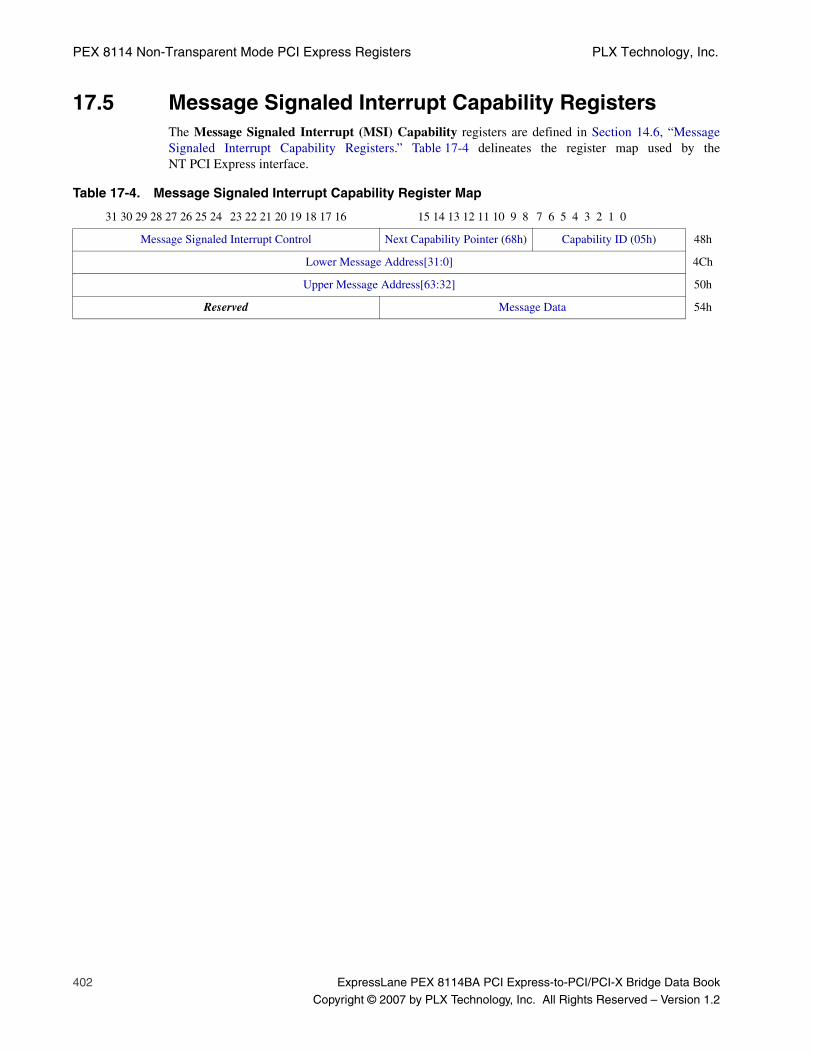
PEX 8114 Non-Transparent Mode PCI Express Registers PLX Technology, Inc.
402 ExpressLane PEX 8114BA PCI Express-to-PCI/PCI-X Bridge Data Book
Copyright © 2007 by PLX Technology, Inc. All Rights Reserved – Version 1.2
17.5 Message Signaled Interrupt Capability RegistersThe Message Signaled Interrupt (MSI) Capability registers are defined in Section 14.6, “MessageSignaled Interrupt Capability Registers.” Table 17-4 delineates the register map used by theNT PCI Express interface.
Table 17-4. Message Signaled Interrupt Capability Register Map
31 30 29 28 27 26 25 24 23 22 21 20 19 18 17 16 15 14 13 12 11 10 9 8 7 6 5 4 3 2 1 0
Message Signaled Interrupt Control Next Capability Pointer (68h) Capability ID (05h) 48h
Lower Message Address[31:0] 4Ch
Upper Message Address[63:32] 50h
Reserved Message Data 54h

March, 2007 PCI Express Capabilities Registers
ExpressLane PEX 8114BA PCI Express-to-PCI/PCI-X Bridge Data Book 403
Copyright © 2007 by PLX Technology, Inc. All Rights Reserved – Version 1.2
17.6 PCI Express Capabilities RegistersThis section details the PEX 8114 PCI Express Capabilities registers. Table 17-5 delineates theregister map.
Table 17-5. PCI Express Capabilities Register Map
31 30 29 28 27 26 25 24 23 22 21 20 19 18 17 16 15 14 13 12 11 10 9 8 7 6 5 4 3 2 1 0
PCI Express Capabilities Next Capability Pointer (00h) Capability ID (10h) 68h
Device Capabilities 6Ch
Device Status Device Control 70h
Link Capabilities 74h
Link Status Link Control 78h
Reserved 7Ch – 80h
Register 17-17. 68h PCI Express Capability List, Capabilities
Bit(s) Description Type Serial EEPROM Default
PCI Express Capability List
7:0Capability ID
Set to 10h by default.RO Yes 10h
15:8
Next Capability Pointer00h = PEX 8114 PCI Express Capability is the last capability in the first 256-byte Configuration space of the NT PCI Express interface capability listThe Extended Capabilities list starts at 100h.
RO Yes 00h
PCI Express Capabilities
19:16Capability Version
The PEX 8114 NT PCI Express interface sets this field to 1h, as required by the PCI Express Base 1.0a.
RO Yes 1h
23:20Device/Port Type
Default = PCI Express Endpoint device.RO Yes 0h
24Slot ImplementedNot implemented in the NT PCI Express interface.
RO No 0
29:25Interrupt Message Number
The serial EEPROM writes 0000_0b, because the Base message and MSI messages are the same.
RO Yes 0000_0b
31:30 Reserved 00b
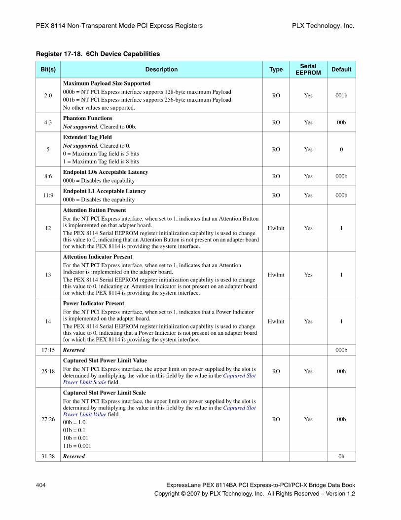
PEX 8114 Non-Transparent Mode PCI Express Registers PLX Technology, Inc.
404 ExpressLane PEX 8114BA PCI Express-to-PCI/PCI-X Bridge Data Book
Copyright © 2007 by PLX Technology, Inc. All Rights Reserved – Version 1.2
Register 17-18. 6Ch Device Capabilities
Bit(s) Description Type Serial EEPROM Default
2:0
Maximum Payload Size Supported
000b = NT PCI Express interface supports 128-byte maximum Payload001b = NT PCI Express interface supports 256-byte maximum PayloadNo other values are supported.
RO Yes 001b
4:3Phantom Functions
Not supported. Cleared to 00b.RO Yes 00b
5
Extended Tag Field
Not supported. Cleared to 0.0 = Maximum Tag field is 5 bits1 = Maximum Tag field is 8 bits
RO Yes 0
8:6Endpoint L0s Acceptable Latency000b = Disables the capability
RO Yes 000b
11:9Endpoint L1 Acceptable Latency
000b = Disables the capabilityRO Yes 000b
12
Attention Button Present
For the NT PCI Express interface, when set to 1, indicates that an Attention Button is implemented on that adapter board.The PEX 8114 Serial EEPROM register initialization capability is used to change this value to 0, indicating that an Attention Button is not present on an adapter board for which the PEX 8114 is providing the system interface.
HwInit Yes 1
13
Attention Indicator PresentFor the NT PCI Express interface, when set to 1, indicates that an Attention Indicator is implemented on the adapter board.The PEX 8114 Serial EEPROM register initialization capability is used to change this value to 0, indicating an Attention Indicator is not present on an adapter board for which the PEX 8114 is providing the system interface.
HwInit Yes 1
14
Power Indicator Present
For the NT PCI Express interface, when set to 1, indicates that a Power Indicator is implemented on the adapter board.The PEX 8114 Serial EEPROM register initialization capability is used to change this value to 0, indicating that a Power Indicator is not present on an adapter board for which the PEX 8114 is providing the system interface.
HwInit Yes 1
17:15 Reserved 000b
25:18
Captured Slot Power Limit Value
For the NT PCI Express interface, the upper limit on power supplied by the slot is determined by multiplying the value in this field by the value in the Captured Slot Power Limit Scale field.
RO Yes 00h
27:26
Captured Slot Power Limit ScaleFor the NT PCI Express interface, the upper limit on power supplied by the slot is determined by multiplying the value in this field by the value in the Captured Slot Power Limit Value field.00b = 1.001b = 0.110b = 0.0111b = 0.001
RO Yes 00b
31:28 Reserved 0h
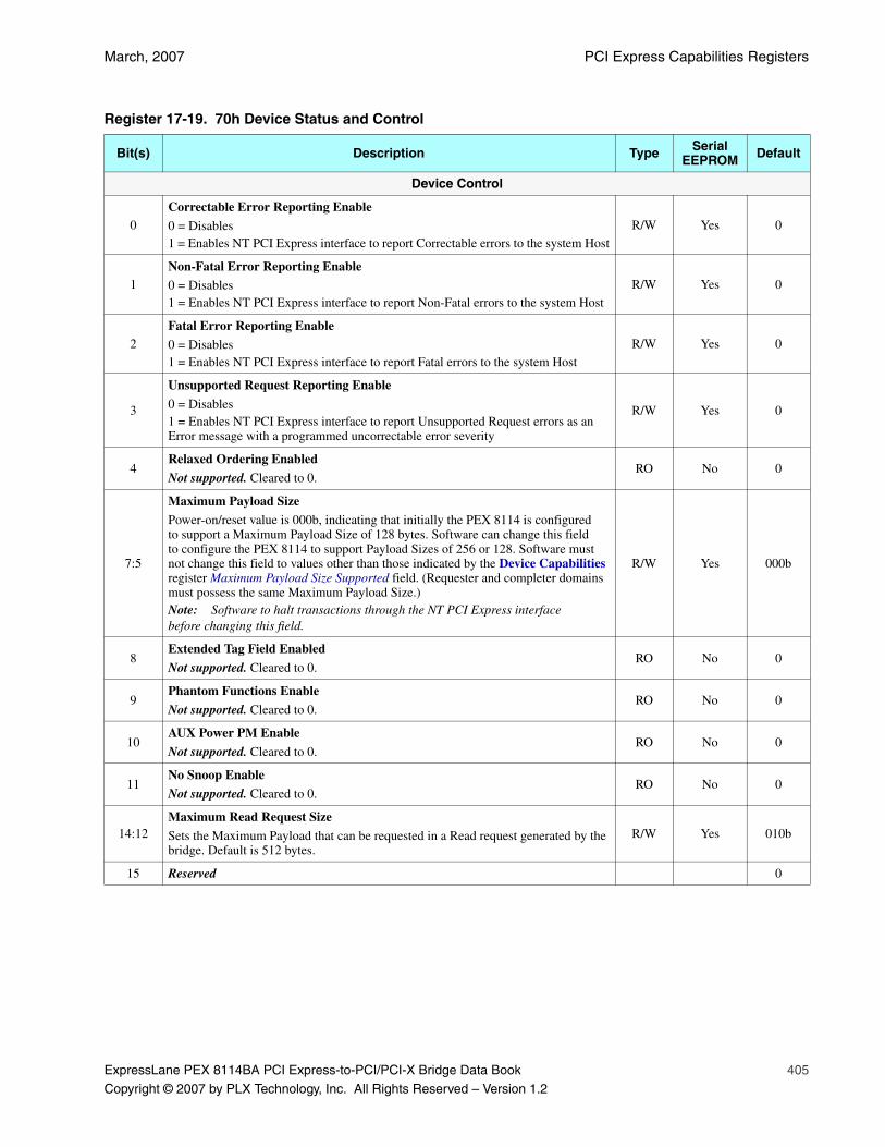
March, 2007 PCI Express Capabilities Registers
ExpressLane PEX 8114BA PCI Express-to-PCI/PCI-X Bridge Data Book 405
Copyright © 2007 by PLX Technology, Inc. All Rights Reserved – Version 1.2
Register 17-19. 70h Device Status and Control
Bit(s) Description Type Serial EEPROM Default
Device Control
0Correctable Error Reporting Enable
0 = Disables1 = Enables NT PCI Express interface to report Correctable errors to the system Host
R/W Yes 0
1Non-Fatal Error Reporting Enable0 = Disables1 = Enables NT PCI Express interface to report Non-Fatal errors to the system Host
R/W Yes 0
2Fatal Error Reporting Enable
0 = Disables1 = Enables NT PCI Express interface to report Fatal errors to the system Host
R/W Yes 0
3
Unsupported Request Reporting Enable
0 = Disables1 = Enables NT PCI Express interface to report Unsupported Request errors as an Error message with a programmed uncorrectable error severity
R/W Yes 0
4Relaxed Ordering Enabled
Not supported. Cleared to 0. RO No 0
7:5
Maximum Payload SizePower-on/reset value is 000b, indicating that initially the PEX 8114 is configured to support a Maximum Payload Size of 128 bytes. Software can change this field to configure the PEX 8114 to support Payload Sizes of 256 or 128. Software must not change this field to values other than those indicated by the Device Capabilities register Maximum Payload Size Supported field. (Requester and completer domains must possess the same Maximum Payload Size.)Note: Software to halt transactions through the NT PCI Express interface before changing this field.
R/W Yes 000b
8Extended Tag Field EnabledNot supported. Cleared to 0.
RO No 0
9Phantom Functions Enable
Not supported. Cleared to 0.RO No 0
10AUX Power PM Enable
Not supported. Cleared to 0.RO No 0
11No Snoop EnableNot supported. Cleared to 0.
RO No 0
14:12Maximum Read Request Size
Sets the Maximum Payload that can be requested in a Read request generated by the bridge. Default is 512 bytes.
R/W Yes 010b
15 Reserved 0
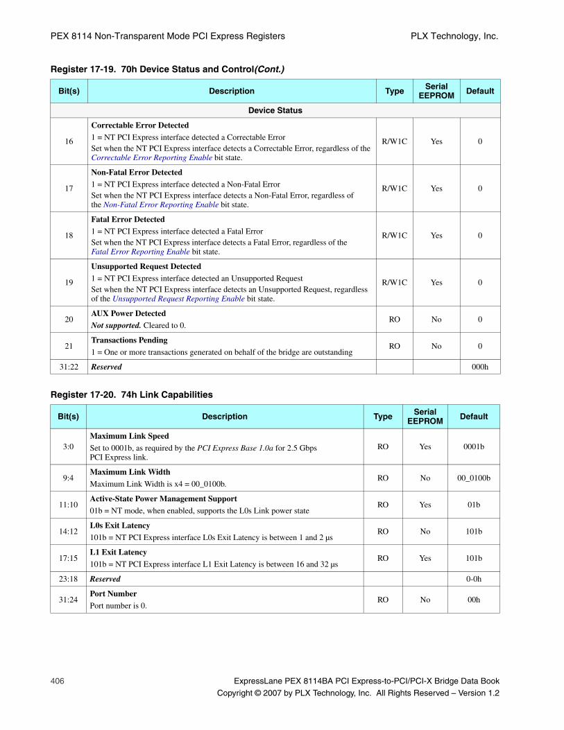
PEX 8114 Non-Transparent Mode PCI Express Registers PLX Technology, Inc.
406 ExpressLane PEX 8114BA PCI Express-to-PCI/PCI-X Bridge Data Book
Copyright © 2007 by PLX Technology, Inc. All Rights Reserved – Version 1.2
Device Status
16
Correctable Error Detected
1 = NT PCI Express interface detected a Correctable ErrorSet when the NT PCI Express interface detects a Correctable Error, regardless of the Correctable Error Reporting Enable bit state.
R/W1C Yes 0
17
Non-Fatal Error Detected1 = NT PCI Express interface detected a Non-Fatal ErrorSet when the NT PCI Express interface detects a Non-Fatal Error, regardless of the Non-Fatal Error Reporting Enable bit state.
R/W1C Yes 0
18
Fatal Error Detected1 = NT PCI Express interface detected a Fatal ErrorSet when the NT PCI Express interface detects a Fatal Error, regardless of the Fatal Error Reporting Enable bit state.
R/W1C Yes 0
19
Unsupported Request Detected1 = NT PCI Express interface detected an Unsupported RequestSet when the NT PCI Express interface detects an Unsupported Request, regardless of the Unsupported Request Reporting Enable bit state.
R/W1C Yes 0
20AUX Power DetectedNot supported. Cleared to 0.
RO No 0
21Transactions Pending
1 = One or more transactions generated on behalf of the bridge are outstandingRO No 0
31:22 Reserved 000h
Register 17-20. 74h Link Capabilities
Bit(s) Description Type Serial EEPROM Default
3:0Maximum Link Speed
Set to 0001b, as required by the PCI Express Base 1.0a for 2.5 Gbps PCI Express link.
RO Yes 0001b
9:4Maximum Link Width
Maximum Link Width is x4 = 00_0100b.RO No 00_0100b
11:10Active-State Power Management Support01b = NT mode, when enabled, supports the L0s Link power state
RO Yes 01b
14:12L0s Exit Latency
101b = NT PCI Express interface L0s Exit Latency is between 1 and 2 µsRO No 101b
17:15L1 Exit Latency
101b = NT PCI Express interface L1 Exit Latency is between 16 and 32 µsRO Yes 101b
23:18 Reserved 0-0h
31:24Port NumberPort number is 0.
RO No 00h
Register 17-19. 70h Device Status and Control(Cont.)
Bit(s) Description Type Serial EEPROM Default
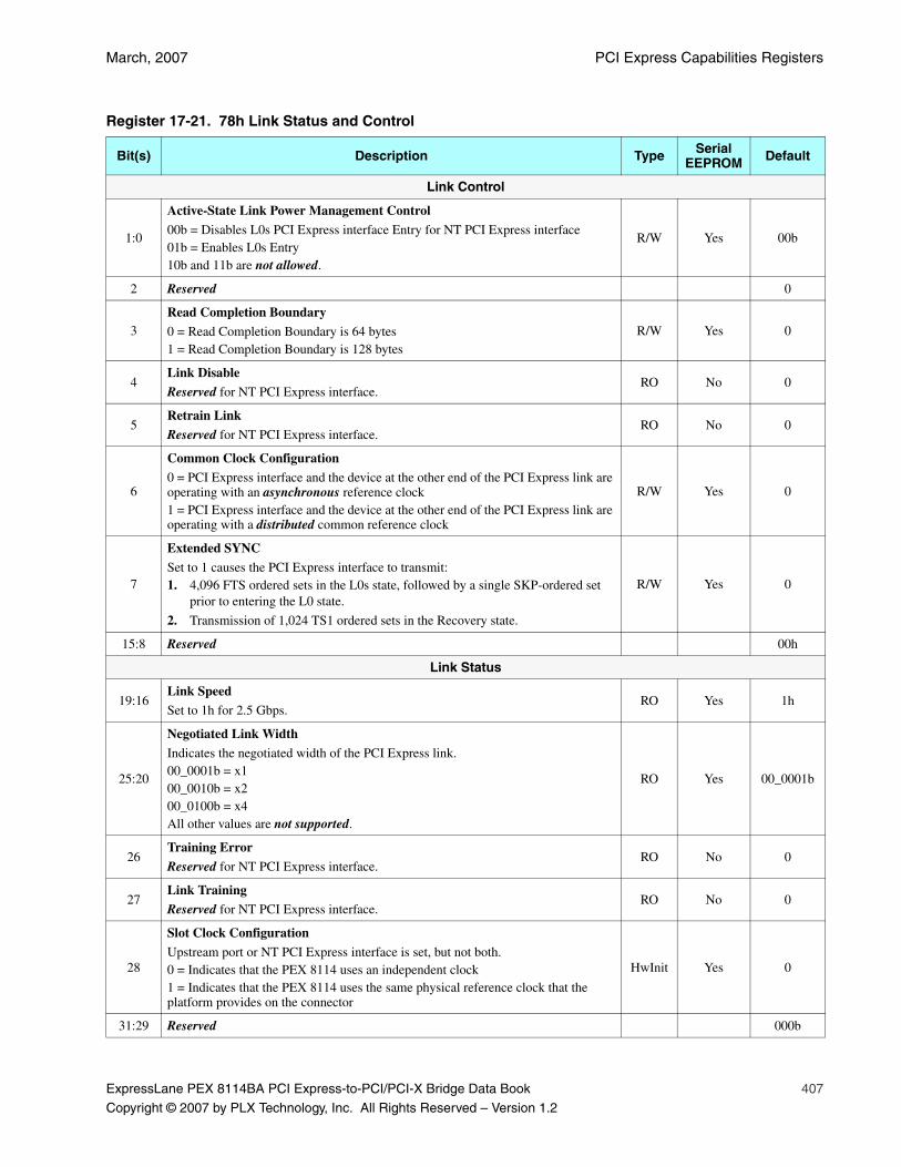
March, 2007 PCI Express Capabilities Registers
ExpressLane PEX 8114BA PCI Express-to-PCI/PCI-X Bridge Data Book 407
Copyright © 2007 by PLX Technology, Inc. All Rights Reserved – Version 1.2
Register 17-21. 78h Link Status and Control
Bit(s) Description Type Serial EEPROM Default
Link Control
1:0
Active-State Link Power Management Control
00b = Disables L0s PCI Express interface Entry for NT PCI Express interface01b = Enables L0s Entry10b and 11b are not allowed.
R/W Yes 00b
2 Reserved 0
3Read Completion Boundary
0 = Read Completion Boundary is 64 bytes1 = Read Completion Boundary is 128 bytes
R/W Yes 0
4Link DisableReserved for NT PCI Express interface.
RO No 0
5Retrain Link
Reserved for NT PCI Express interface.RO No 0
6
Common Clock Configuration
0 = PCI Express interface and the device at the other end of the PCI Express link are operating with an asynchronous reference clock1 = PCI Express interface and the device at the other end of the PCI Express link are operating with a distributed common reference clock
R/W Yes 0
7
Extended SYNC
Set to 1 causes the PCI Express interface to transmit:1. 4,096 FTS ordered sets in the L0s state, followed by a single SKP-ordered set
prior to entering the L0 state.
2. Transmission of 1,024 TS1 ordered sets in the Recovery state.
R/W Yes 0
15:8 Reserved 00h
Link Status
19:16Link SpeedSet to 1h for 2.5 Gbps.
RO Yes 1h
25:20
Negotiated Link Width
Indicates the negotiated width of the PCI Express link.00_0001b = x100_0010b = x200_0100b = x4All other values are not supported.
RO Yes 00_0001b
26Training Error
Reserved for NT PCI Express interface.RO No 0
27Link TrainingReserved for NT PCI Express interface.
RO No 0
28
Slot Clock Configuration
Upstream port or NT PCI Express interface is set, but not both.0 = Indicates that the PEX 8114 uses an independent clock1 = Indicates that the PEX 8114 uses the same physical reference clock that the platform provides on the connector
HwInit Yes 0
31:29 Reserved 000b
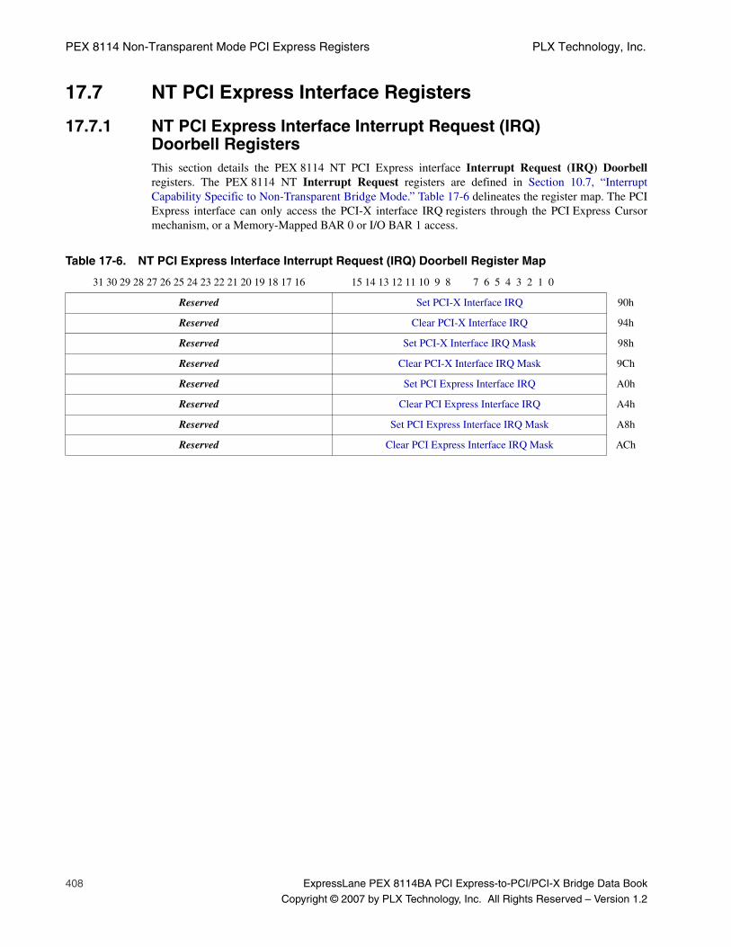
PEX 8114 Non-Transparent Mode PCI Express Registers PLX Technology, Inc.
408 ExpressLane PEX 8114BA PCI Express-to-PCI/PCI-X Bridge Data Book
Copyright © 2007 by PLX Technology, Inc. All Rights Reserved – Version 1.2
17.7 NT PCI Express Interface Registers
17.7.1 NT PCI Express Interface Interrupt Request (IRQ) Doorbell RegistersThis section details the PEX 8114 NT PCI Express interface Interrupt Request (IRQ) Doorbellregisters. The PEX 8114 NT Interrupt Request registers are defined in Section 10.7, “InterruptCapability Specific to Non-Transparent Bridge Mode.” Table 17-6 delineates the register map. The PCIExpress interface can only access the PCI-X interface IRQ registers through the PCI Express Cursormechanism, or a Memory-Mapped BAR 0 or I/O BAR 1 access.
Table 17-6. NT PCI Express Interface Interrupt Request (IRQ) Doorbell Register Map
31 30 29 28 27 26 25 24 23 22 21 20 19 18 17 16 15 14 13 12 11 10 9 8 7 6 5 4 3 2 1 0
Reserved Set PCI-X Interface IRQ 90h
Reserved Clear PCI-X Interface IRQ 94h
Reserved Set PCI-X Interface IRQ Mask 98h
Reserved Clear PCI-X Interface IRQ Mask 9Ch
Reserved Set PCI Express Interface IRQ A0h
Reserved Clear PCI Express Interface IRQ A4h
Reserved Set PCI Express Interface IRQ Mask A8h
Reserved Clear PCI Express Interface IRQ Mask ACh

March, 2007 NT PCI Express Interface Interrupt Request (IRQ) Doorbell Registers
ExpressLane PEX 8114BA PCI Express-to-PCI/PCI-X Bridge Data Book 409
Copyright © 2007 by PLX Technology, Inc. All Rights Reserved – Version 1.2
Register 17-22. 90h Set PCI-X Interface IRQ
Bit(s) Description Type Serial EEPROM Default
15:0
Set IRQControls the state of the PCI-X interface Interrupt Request bits. Reading returns the status of the bits. Writing 1 to a bit in the register sets the corresponding Interrupt request. When this register is non-zero, the corresponding bit is not masked and interrupts are enabled, the PCI-X interface interrupt is asserted. Writing 0 to any bit has no effect.
R/W1S Yes 0000h
31:16 Reserved 0000h
Register 17-23. 94h Clear PCI-X Interface IRQ
Bit(s) Description Type Serial EEPROM Default
15:0
Clear IRQControls the state of the PCI-X interface Interrupt Request bits. Reading returns the status of the bits. Writing 1 to a bit in the register clears the corresponding Interrupt request. When this register is non-zero, the corresponding bit is not masked and interrupts are enabled, the PCI-X interface interrupt is asserted. Writing 0 to any bit has no effect.
R/W1C Yes 0000h
31:16 Reserved 0000h
Register 17-24. 98h Set PCI-X Interface IRQ Mask
Bit(s) Description Type Serial EEPROM Default
15:0
Set IRQ MaskPCI-X interface interrupt IRQ Mask Set. Reading returns the state of the mask bits. 0 = Corresponding Interrupt Request bit is unmasked1 = Corresponding Interrupt Request bit is masked/disabledWriting 1 to a bit in the register sets the corresponding Interrupt Mask bit. Writing 0 to any bit has no effect.
R/W1S Yes FFFFh
31:16 Reserved 0000h
Register 17-25. 9Ch Clear PCI-X Interface IRQ Mask
Bit(s) Description Type Serial EEPROM Default
15:0
Clear IRQ MaskControls the state of the PCI-X interface Interrupt Request bits. Reading returns the status of the bits. 0 = Corresponding Interrupt Request bit is unmasked1 = Corresponding Interrupt Request bit is masked/disabledWriting 1 to a bit in the register clears the corresponding Interrupt Mask bit. Writing 0 to any bit has no effect.
R/W1C Yes FFFFh
31:16 Reserved 0000h
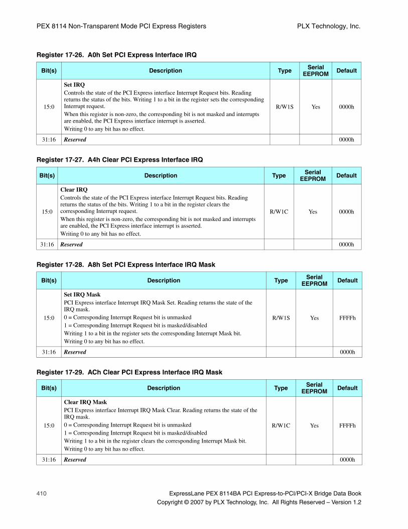
PEX 8114 Non-Transparent Mode PCI Express Registers PLX Technology, Inc.
410 ExpressLane PEX 8114BA PCI Express-to-PCI/PCI-X Bridge Data Book
Copyright © 2007 by PLX Technology, Inc. All Rights Reserved – Version 1.2
Register 17-26. A0h Set PCI Express Interface IRQ
Bit(s) Description Type Serial EEPROM Default
15:0
Set IRQControls the state of the PCI Express interface Interrupt Request bits. Reading returns the status of the bits. Writing 1 to a bit in the register sets the corresponding Interrupt request. When this register is non-zero, the corresponding bit is not masked and interrupts are enabled, the PCI Express interface interrupt is asserted. Writing 0 to any bit has no effect.
R/W1S Yes 0000h
31:16 Reserved 0000h
Register 17-27. A4h Clear PCI Express Interface IRQ
Bit(s) Description Type Serial EEPROM Default
15:0
Clear IRQControls the state of the PCI Express interface Interrupt Request bits. Reading returns the status of the bits. Writing 1 to a bit in the register clears the corresponding Interrupt request. When this register is non-zero, the corresponding bit is not masked and interrupts are enabled, the PCI Express interface interrupt is asserted. Writing 0 to any bit has no effect.
R/W1C Yes 0000h
31:16 Reserved 0000h
Register 17-28. A8h Set PCI Express Interface IRQ Mask
Bit(s) Description Type Serial EEPROM Default
15:0
Set IRQ MaskPCI Express interface Interrupt IRQ Mask Set. Reading returns the state of the IRQ mask. 0 = Corresponding Interrupt Request bit is unmasked1 = Corresponding Interrupt Request bit is masked/disabledWriting 1 to a bit in the register sets the corresponding Interrupt Mask bit. Writing 0 to any bit has no effect.
R/W1S Yes FFFFh
31:16 Reserved 0000h
Register 17-29. ACh Clear PCI Express Interface IRQ Mask
Bit(s) Description Type Serial EEPROM Default
15:0
Clear IRQ MaskPCI Express interface Interrupt IRQ Mask Clear. Reading returns the state of the IRQ mask. 0 = Corresponding Interrupt Request bit is unmasked1 = Corresponding Interrupt Request bit is masked/disabledWriting 1 to a bit in the register clears the corresponding Interrupt Mask bit.Writing 0 to any bit has no effect.
R/W1C Yes FFFFh
31:16 Reserved 0000h

March, 2007 NT Mode Scratchpad (Mailbox) Registers
ExpressLane PEX 8114BA PCI Express-to-PCI/PCI-X Bridge Data Book 411
Copyright © 2007 by PLX Technology, Inc. All Rights Reserved – Version 1.2
17.7.2 NT Mode Scratchpad (Mailbox) RegistersThe PEX 8114 NT mode Scratchpad (Mailbox) registers are defined in Section 15.1.3, “Scratchpad(Mailbox) Registers.” Table 17-7 delineates the register map used by the NT PCI Express interface.
Table 17-7. PEX 8114 NT Mode Scratchpad (Mailbox) Register Map
31 30 29 28 27 26 25 24 23 22 21 20 19 18 17 16 15 14 13 12 11 10 9 8 7 6 5 4 3 2 1 0
NT Mode Scratchpad_0 B0h
NT Mode Scratchpad_1 B4h
NT Mode Scratchpad_2 B8h
NT Mode Scratchpad_3 BCh
NT Mode Scratchpad_4 C0h
NT Mode Scratchpad_5 C4h
NT Mode Scratchpad_6 C8h
NT Mode Scratchpad_7 CCh
Register 17-30. B0h NT Mode Scratchpad_0
Bit(s) Description Type Serial EEPROM Default
31:0Scratchpad_032-bit Scratchpad_0 register.
R/W Yes 0-0h
Register 17-31. B4h NT Mode Scratchpad_1
Bit(s) Description Type Serial EEPROM Default
31:0Scratchpad_132-bit Scratchpad_1 register.
R/W Yes 0-0h
Register 17-32. B8h NT Mode Scratchpad_2
Bit(s) Description Type Serial EEPROM Default
31:0Scratchpad_232-bit Scratchpad_2 register.
R/W Yes 0-0h
Register 17-33. BCh NT Mode Scratchpad_3
Bit(s) Description Type Serial EEPROM Default
31:0Scratchpad_332-bit Scratchpad_3 register.
R/W Yes 0-0h
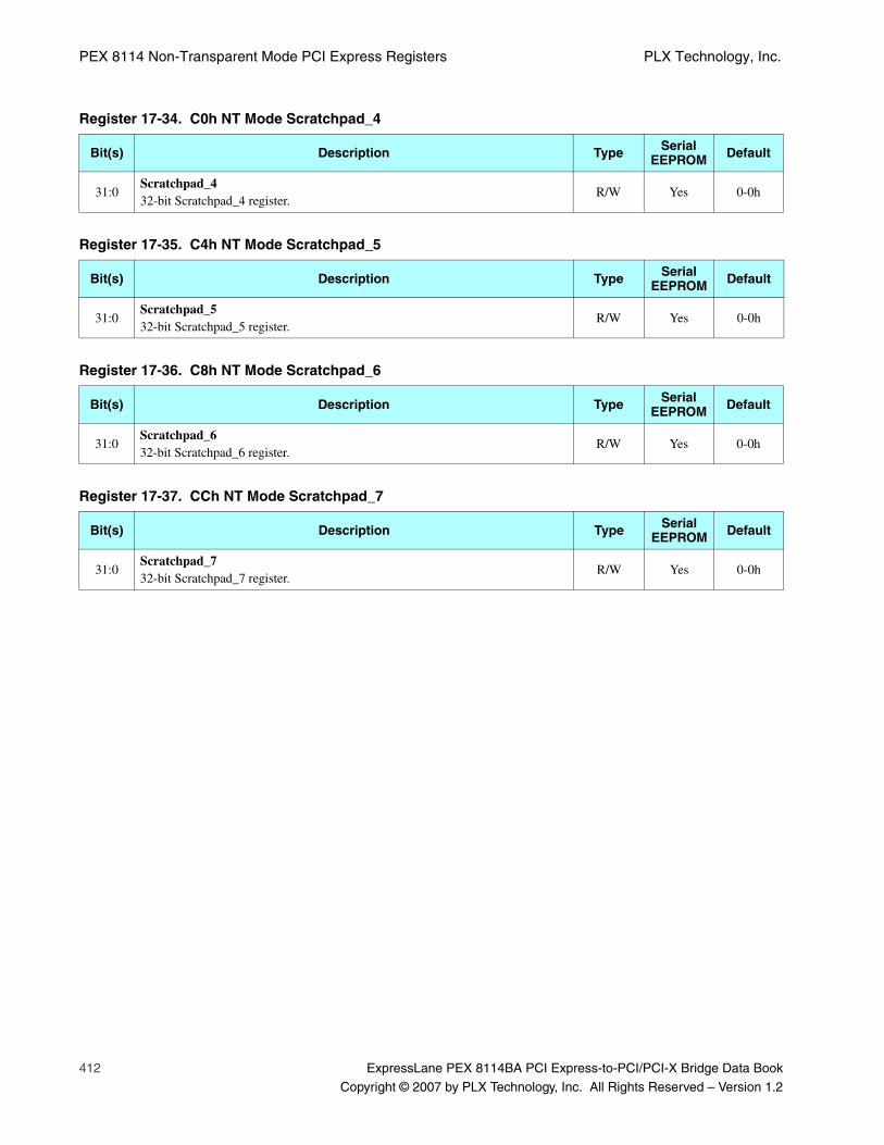
PEX 8114 Non-Transparent Mode PCI Express Registers PLX Technology, Inc.
412 ExpressLane PEX 8114BA PCI Express-to-PCI/PCI-X Bridge Data Book
Copyright © 2007 by PLX Technology, Inc. All Rights Reserved – Version 1.2
Register 17-34. C0h NT Mode Scratchpad_4
Bit(s) Description Type Serial EEPROM Default
31:0Scratchpad_432-bit Scratchpad_4 register.
R/W Yes 0-0h
Register 17-35. C4h NT Mode Scratchpad_5
Bit(s) Description Type Serial EEPROM Default
31:0Scratchpad_532-bit Scratchpad_5 register.
R/W Yes 0-0h
Register 17-36. C8h NT Mode Scratchpad_6
Bit(s) Description Type Serial EEPROM Default
31:0Scratchpad_632-bit Scratchpad_6 register.
R/W Yes 0-0h
Register 17-37. CCh NT Mode Scratchpad_7
Bit(s) Description Type Serial EEPROM Default
31:0Scratchpad_732-bit Scratchpad_7 register.
R/W Yes 0-0h
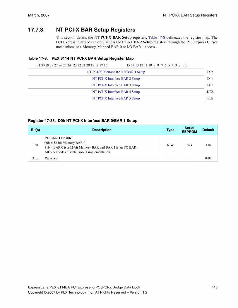
March, 2007 NT PCI-X BAR Setup Registers
ExpressLane PEX 8114BA PCI Express-to-PCI/PCI-X Bridge Data Book 413
Copyright © 2007 by PLX Technology, Inc. All Rights Reserved – Version 1.2
17.7.3 NT PCI-X BAR Setup RegistersThis section details the NT PCI-X BAR Setup registers. Table 17-8 delineates the register map. ThePCI Express interface can only access the PCI-X BAR Setup registers through the PCI Express Cursormechanism, or a Memory-Mapped BAR 0 or I/O BAR 1 access.
Table 17-8. PEX 8114 NT PCI-X BAR Setup Register Map
31 30 29 28 27 26 25 24 23 22 21 20 19 18 17 16 15 14 13 12 11 10 9 8 7 6 5 4 3 2 1 0
NT PCI-X Interface BAR 0/BAR 1 Setup D0h
NT PCI-X Interface BAR 2 Setup D4h
NT PCI-X Interface BAR 3 Setup D8h
NT PCI-X Interface BAR 4 Setup DCh
NT PCI-X Interface BAR 5 Setup E0h
Register 17-38. D0h NT PCI-X Interface BAR 0/BAR 1 Setup
Bit(s) Description Type Serial EEPROM Default
1:0
I/O BAR 1 Enable00b = 32-bit Memory BAR 011b = BAR 0 is a 32-bit Memory BAR and BAR 1 is an I/O BARAll other codes disable BAR 1 implementation.
R/W Yes 11b
31:2 Reserved 0-0h

PEX 8114 Non-Transparent Mode PCI Express Registers PLX Technology, Inc.
414 ExpressLane PEX 8114BA PCI Express-to-PCI/PCI-X Bridge Data Book
Copyright © 2007 by PLX Technology, Inc. All Rights Reserved – Version 1.2
Register 17-39. D4h NT PCI-X Interface BAR 2 Setup
Bit(s) Description Type Serial EEPROM Default
0Type Reserved
RO No 0
1BAR 2 Type Select0 = Memory space can be anywhere in 32-bit range1 = Memory space must be below 1MB
R/W Yes 0
2BAR 2 Type Select0 = Selects 32-bit Memory BARNo other values are allowed.
RO No 0
3Prefetchable0 = Non-Prefetchable1 = Prefetchable
R/W Yes 0
11:4 Reserved 00h
30:12
BAR 2 SizeSpecifies the Address range size requested by BAR 2.When a bit value is 0, the corresponding bit in the Base Address 2 register is a Read-Only bit that always returns 0 when read, and Writes are ignored.When a bit value is 1, the corresponding bit in the Base Address 2 register is a writable and readable bit.
R/W Yes 0000_0h
31BAR 2 Enable0 = BAR 2 disabled1 = BAR 2 enabled
R/W Yes 0
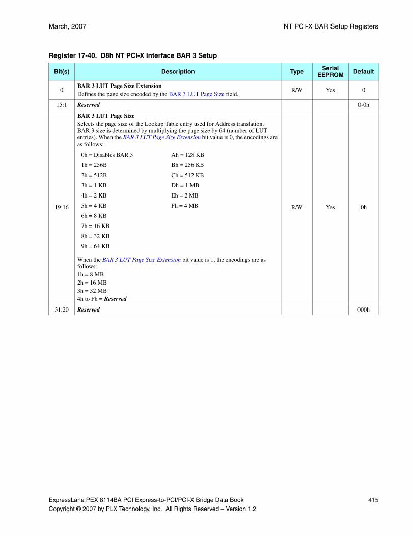
March, 2007 NT PCI-X BAR Setup Registers
ExpressLane PEX 8114BA PCI Express-to-PCI/PCI-X Bridge Data Book 415
Copyright © 2007 by PLX Technology, Inc. All Rights Reserved – Version 1.2
Register 17-40. D8h NT PCI-X Interface BAR 3 Setup
Bit(s) Description Type Serial EEPROM Default
0BAR 3 LUT Page Size ExtensionDefines the page size encoded by the BAR 3 LUT Page Size field.
R/W Yes 0
15:1 Reserved 0-0h
19:16
BAR 3 LUT Page SizeSelects the page size of the Lookup Table entry used for Address translation. BAR 3 size is determined by multiplying the page size by 64 (number of LUT entries). When the BAR 3 LUT Page Size Extension bit value is 0, the encodings are as follows:
When the BAR 3 LUT Page Size Extension bit value is 1, the encodings are as follows: 1h = 8 MB2h = 16 MB3h = 32 MB4h to Fh = Reserved
R/W Yes 0h
31:20 Reserved 000h
0h = Disables BAR 3 Ah = 128 KB
1h = 256B Bh = 256 KB
2h = 512B Ch = 512 KB
3h = 1 KB Dh = 1 MB
4h = 2 KB Eh = 2 MB
5h = 4 KB Fh = 4 MB
6h = 8 KB
7h = 16 KB
8h = 32 KB
9h = 64 KB
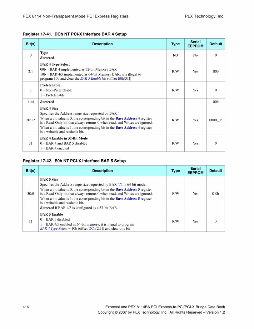
PEX 8114 Non-Transparent Mode PCI Express Registers PLX Technology, Inc.
416 ExpressLane PEX 8114BA PCI Express-to-PCI/PCI-X Bridge Data Book
Copyright © 2007 by PLX Technology, Inc. All Rights Reserved – Version 1.2
Register 17-41. DCh NT PCI-X Interface BAR 4 Setup
Bit(s) Description Type Serial EEPROM Default
0Type Reserved
RO No 0
2:1
BAR 4 Type Select00b = BAR 4 implemented as 32-bit Memory BAR10b = BAR 4/5 implemented as 64-bit Memory BAR; it is illegal to program 10b and clear the BAR 5 Enable bit (offset E0h[31])
R/W Yes 00b
3Prefetchable0 = Non-Prefetchable1 = Prefetchable
R/W Yes 0
11:4 Reserved 00h
30:12
BAR 4 SizeSpecifies the Address range size requested by BAR 4.When a bit value is 0, the corresponding bit in the Base Address 4 register is a Read-Only bit that always returns 0 when read, and Writes are ignored.When a bit value is 1, the corresponding bit in the Base Address 4 register is a writable and readable bit.
R/W Yes 0000_0h
31BAR 4 Enable in 32-Bit Mode0 = BAR 4 and BAR 5 disabled1 = BAR 4 enabled
R/W Yes 0
Register 17-42. E0h NT PCI-X Interface BAR 5 Setup
Bit(s) Description Type Serial EEPROM Default
30:0
BAR 5 SizeSpecifies the Address range size requested by BAR 4/5 in 64-bit mode. When a bit value is 0, the corresponding bit in the Base Address 5 register is a Read-Only bit that always returns 0 when read, and Writes are ignored.When a bit value is 1, the corresponding bit in the Base Address 5 register is a writable and readable bit.Reserved if BAR 4/5 is configured as a 32-bit BAR.
R/W Yes 0-0h
31
BAR 5 Enable0 = BAR 5 disabled1 = BAR 4/5 enabled as 64-bit memory; it is illegal to program BAR 4 Type Select = 10b (offset DCh[2:1]) and clear this bit
R/W Yes 0
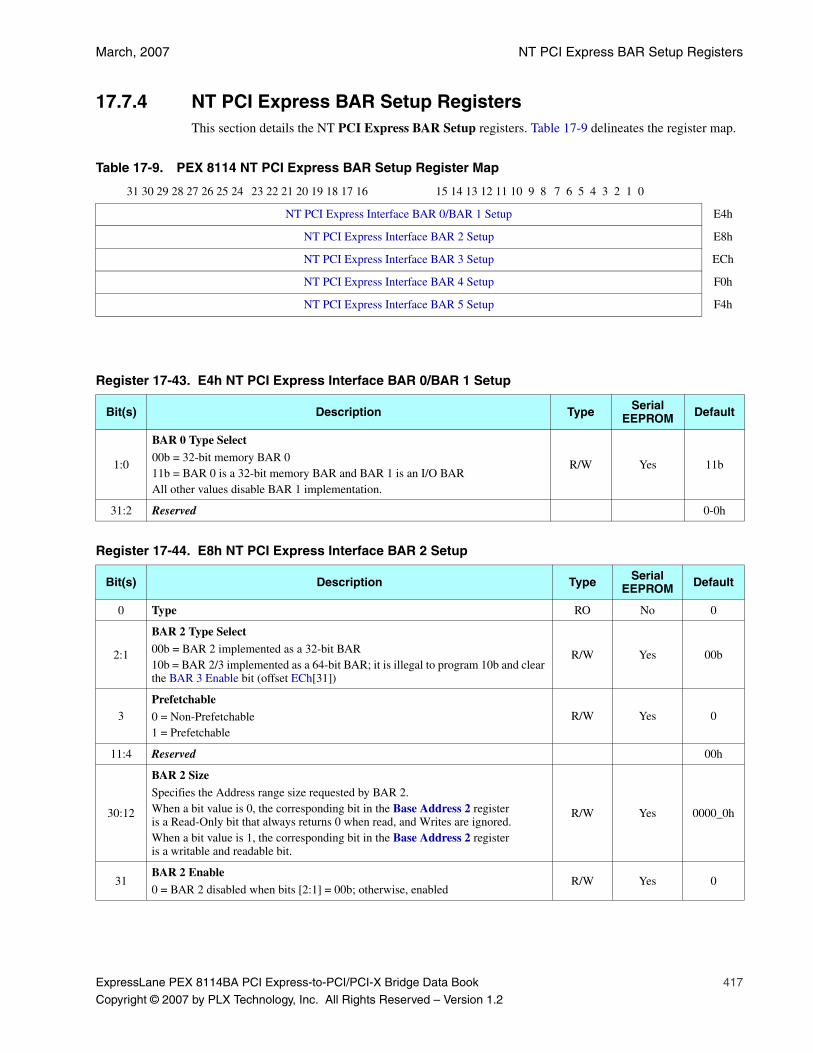
March, 2007 NT PCI Express BAR Setup Registers
ExpressLane PEX 8114BA PCI Express-to-PCI/PCI-X Bridge Data Book 417
Copyright © 2007 by PLX Technology, Inc. All Rights Reserved – Version 1.2
17.7.4 NT PCI Express BAR Setup RegistersThis section details the NT PCI Express BAR Setup registers. Table 17-9 delineates the register map.
Table 17-9. PEX 8114 NT PCI Express BAR Setup Register Map
31 30 29 28 27 26 25 24 23 22 21 20 19 18 17 16 15 14 13 12 11 10 9 8 7 6 5 4 3 2 1 0
NT PCI Express Interface BAR 0/BAR 1 Setup E4h
NT PCI Express Interface BAR 2 Setup E8h
NT PCI Express Interface BAR 3 Setup ECh
NT PCI Express Interface BAR 4 Setup F0h
NT PCI Express Interface BAR 5 Setup F4h
Register 17-43. E4h NT PCI Express Interface BAR 0/BAR 1 Setup
Bit(s) Description Type Serial EEPROM Default
1:0
BAR 0 Type Select00b = 32-bit memory BAR 011b = BAR 0 is a 32-bit memory BAR and BAR 1 is an I/O BARAll other values disable BAR 1 implementation.
R/W Yes 11b
31:2 Reserved 0-0h
Register 17-44. E8h NT PCI Express Interface BAR 2 Setup
Bit(s) Description Type Serial EEPROM Default
0 Type RO No 0
2:1
BAR 2 Type Select00b = BAR 2 implemented as a 32-bit BAR10b = BAR 2/3 implemented as a 64-bit BAR; it is illegal to program 10b and clear the BAR 3 Enable bit (offset ECh[31])
R/W Yes 00b
3Prefetchable0 = Non-Prefetchable1 = Prefetchable
R/W Yes 0
11:4 Reserved 00h
30:12
BAR 2 SizeSpecifies the Address range size requested by BAR 2.When a bit value is 0, the corresponding bit in the Base Address 2 register is a Read-Only bit that always returns 0 when read, and Writes are ignored.When a bit value is 1, the corresponding bit in the Base Address 2 register is a writable and readable bit.
R/W Yes 0000_0h
31BAR 2 Enable0 = BAR 2 disabled when bits [2:1] = 00b; otherwise, enabled
R/W Yes 0
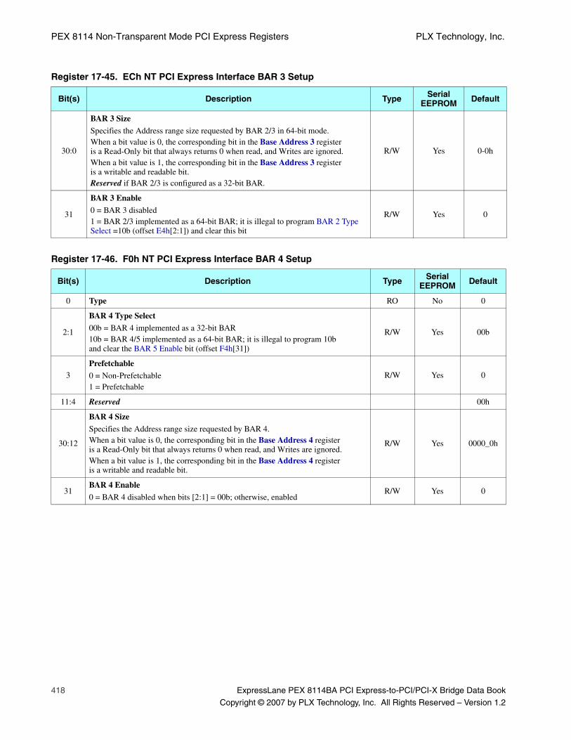
PEX 8114 Non-Transparent Mode PCI Express Registers PLX Technology, Inc.
418 ExpressLane PEX 8114BA PCI Express-to-PCI/PCI-X Bridge Data Book
Copyright © 2007 by PLX Technology, Inc. All Rights Reserved – Version 1.2
Register 17-45. ECh NT PCI Express Interface BAR 3 Setup
Bit(s) Description Type Serial EEPROM Default
30:0
BAR 3 Size
Specifies the Address range size requested by BAR 2/3 in 64-bit mode. When a bit value is 0, the corresponding bit in the Base Address 3 register is a Read-Only bit that always returns 0 when read, and Writes are ignored.When a bit value is 1, the corresponding bit in the Base Address 3 register is a writable and readable bit. Reserved if BAR 2/3 is configured as a 32-bit BAR.
R/W Yes 0-0h
31
BAR 3 Enable
0 = BAR 3 disabled 1 = BAR 2/3 implemented as a 64-bit BAR; it is illegal to program BAR 2 Type Select =10b (offset E4h[2:1]) and clear this bit
R/W Yes 0
Register 17-46. F0h NT PCI Express Interface BAR 4 Setup
Bit(s) Description Type Serial EEPROM Default
0 Type RO No 0
2:1
BAR 4 Type Select
00b = BAR 4 implemented as a 32-bit BAR10b = BAR 4/5 implemented as a 64-bit BAR; it is illegal to program 10b and clear the BAR 5 Enable bit (offset F4h[31])
R/W Yes 00b
3Prefetchable
0 = Non-Prefetchable1 = Prefetchable
R/W Yes 0
11:4 Reserved 00h
30:12
BAR 4 Size
Specifies the Address range size requested by BAR 4.When a bit value is 0, the corresponding bit in the Base Address 4 register is a Read-Only bit that always returns 0 when read, and Writes are ignored.When a bit value is 1, the corresponding bit in the Base Address 4 register is a writable and readable bit.
R/W Yes 0000_0h
31BAR 4 Enable
0 = BAR 4 disabled when bits [2:1] = 00b; otherwise, enabledR/W Yes 0

March, 2007 NT PCI Express BAR Setup Registers
ExpressLane PEX 8114BA PCI Express-to-PCI/PCI-X Bridge Data Book 419
Copyright © 2007 by PLX Technology, Inc. All Rights Reserved – Version 1.2
Register 17-47. F4h NT PCI Express Interface BAR 5 Setup
Bit(s) Description Type Serial EEPROM Default
30:0
BAR 5 Data
Specifies Address range size requested by the BAR 4/5 in 64-bit mode.When a bit value is 0, the corresponding bit in the Base Address 5 register is a Read-Only bit that always returns 0 when read, and Writes are ignored.When a bit value is 1, the corresponding bit in the Base Address 5 register is a writable and readable bit.Reserved if BAR 4/5 is configured as a 32-bit BAR.
R/W Yes 0-0h
31
BAR 5 Enable
0 = BAR 5 disabled 1 = BAR 4/5 enabled as 64-bit memory; it is illegal to program BAR 4 Type Select =10b (offset F0h[2:1]) and clear this bit
R/W Yes 0
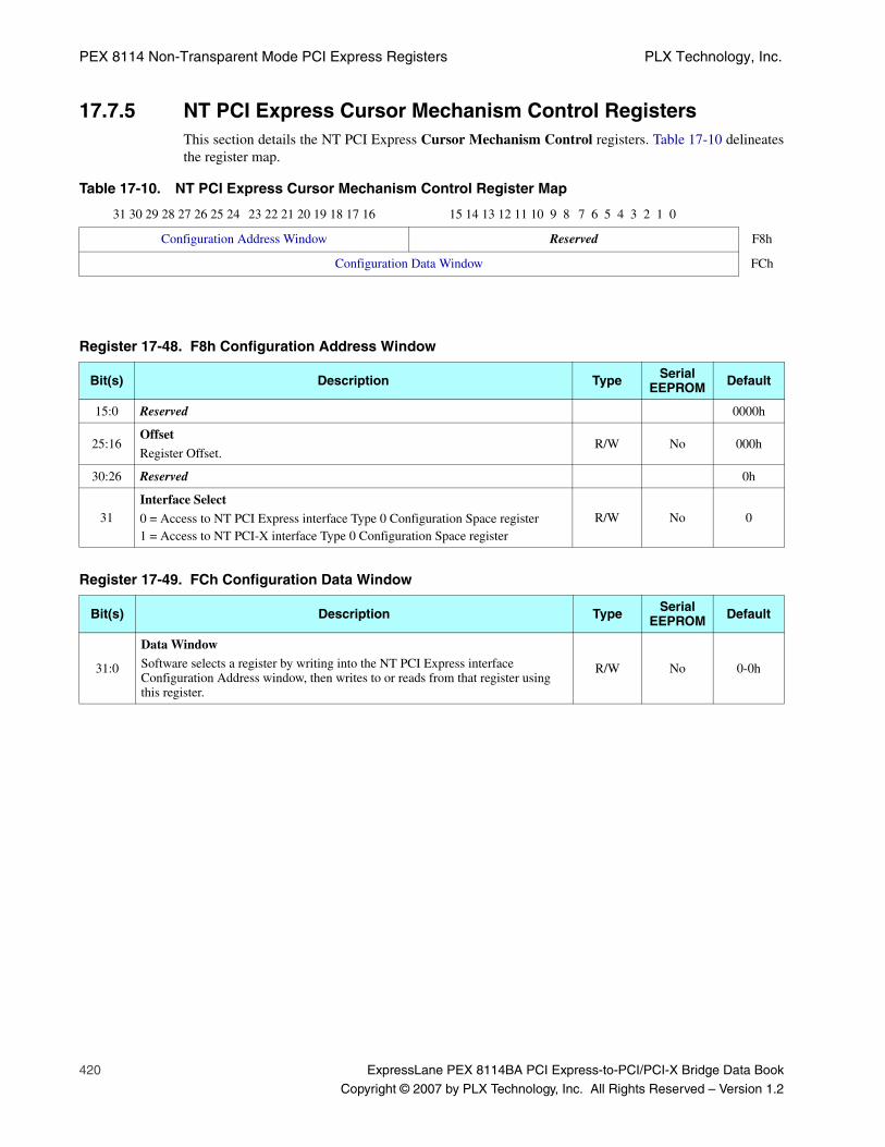
PEX 8114 Non-Transparent Mode PCI Express Registers PLX Technology, Inc.
420 ExpressLane PEX 8114BA PCI Express-to-PCI/PCI-X Bridge Data Book
Copyright © 2007 by PLX Technology, Inc. All Rights Reserved – Version 1.2
17.7.5 NT PCI Express Cursor Mechanism Control RegistersThis section details the NT PCI Express Cursor Mechanism Control registers. Table 17-10 delineatesthe register map.
Table 17-10. NT PCI Express Cursor Mechanism Control Register Map
31 30 29 28 27 26 25 24 23 22 21 20 19 18 17 16 15 14 13 12 11 10 9 8 7 6 5 4 3 2 1 0
Configuration Address Window Reserved F8h
Configuration Data Window FCh
Register 17-48. F8h Configuration Address Window
Bit(s) Description Type Serial EEPROM Default
15:0 Reserved 0000h
25:16Offset
Register Offset.R/W No 000h
30:26 Reserved 0h
31Interface Select
0 = Access to NT PCI Express interface Type 0 Configuration Space register1 = Access to NT PCI-X interface Type 0 Configuration Space register
R/W No 0
Register 17-49. FCh Configuration Data Window
Bit(s) Description Type Serial EEPROM Default
31:0
Data WindowSoftware selects a register by writing into the NT PCI Express interface Configuration Address window, then writes to or reads from that register using this register.
R/W No 0-0h
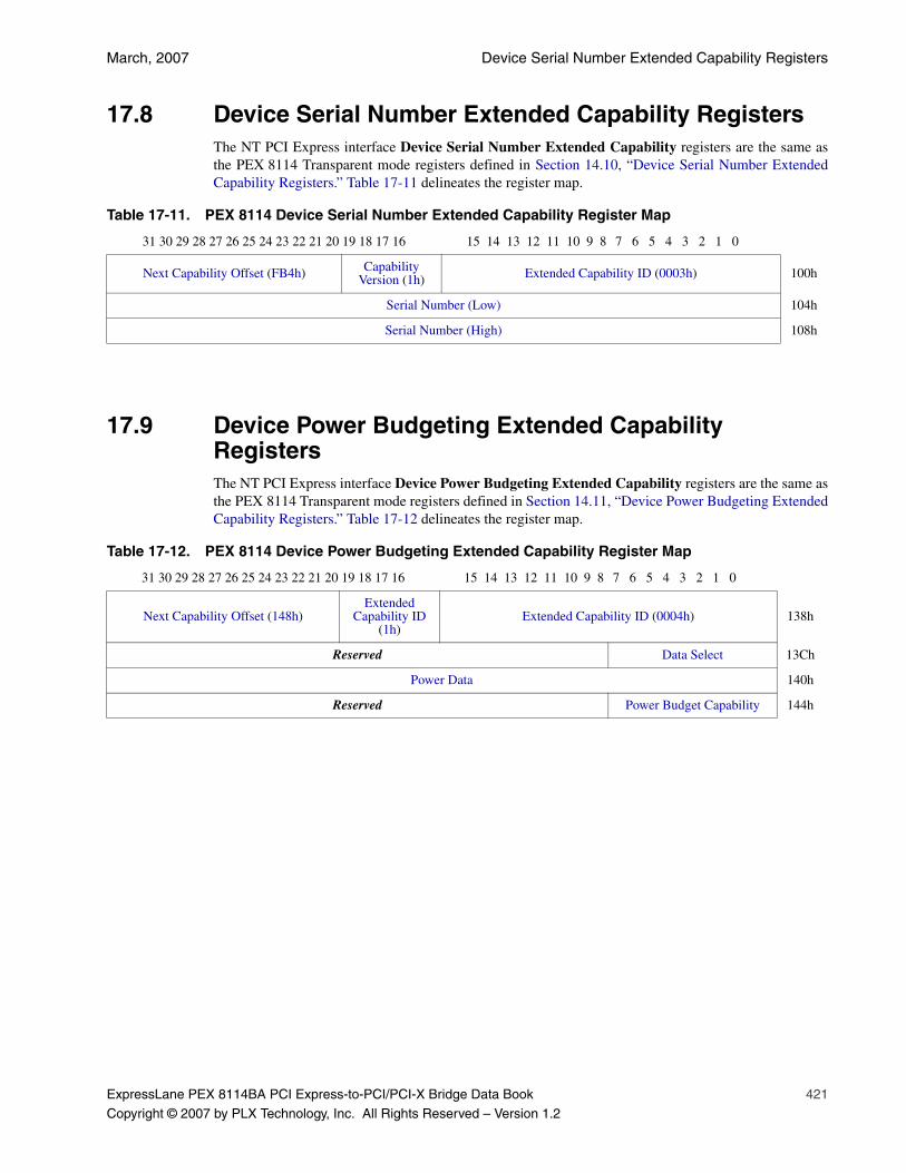
March, 2007 Device Serial Number Extended Capability Registers
ExpressLane PEX 8114BA PCI Express-to-PCI/PCI-X Bridge Data Book 421
Copyright © 2007 by PLX Technology, Inc. All Rights Reserved – Version 1.2
17.8 Device Serial Number Extended Capability RegistersThe NT PCI Express interface Device Serial Number Extended Capability registers are the same asthe PEX 8114 Transparent mode registers defined in Section 14.10, “Device Serial Number ExtendedCapability Registers.” Table 17-11 delineates the register map.
17.9 Device Power Budgeting Extended Capability RegistersThe NT PCI Express interface Device Power Budgeting Extended Capability registers are the same asthe PEX 8114 Transparent mode registers defined in Section 14.11, “Device Power Budgeting ExtendedCapability Registers.” Table 17-12 delineates the register map.
Table 17-11. PEX 8114 Device Serial Number Extended Capability Register Map
31 30 29 28 27 26 25 24 23 22 21 20 19 18 17 16 15 14 13 12 11 10 9 8 7 6 5 4 3 2 1 0
Next Capability Offset (FB4h) Capability Version (1h) Extended Capability ID (0003h) 100h
Serial Number (Low) 104h
Serial Number (High) 108h
Table 17-12. PEX 8114 Device Power Budgeting Extended Capability Register Map
31 30 29 28 27 26 25 24 23 22 21 20 19 18 17 16 15 14 13 12 11 10 9 8 7 6 5 4 3 2 1 0
Next Capability Offset (148h)Extended
Capability ID (1h)
Extended Capability ID (0004h) 138h
Reserved Data Select 13Ch
Power Data 140h
Reserved Power Budget Capability 144h
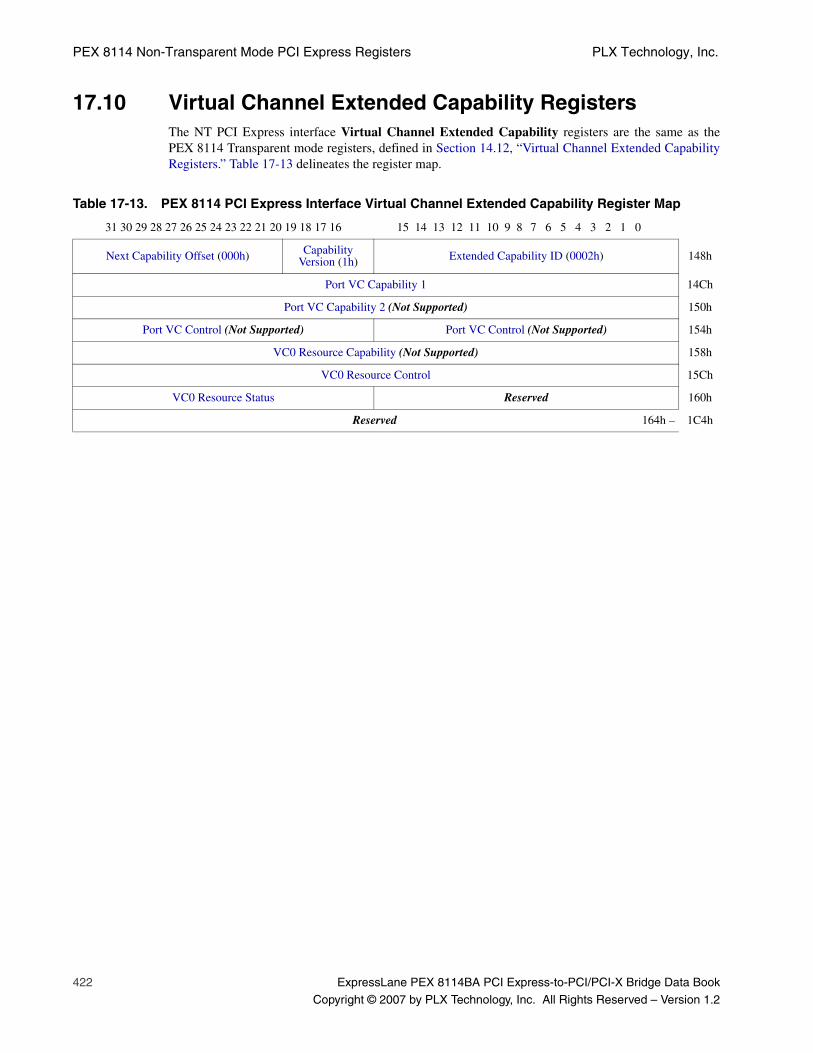
PEX 8114 Non-Transparent Mode PCI Express Registers PLX Technology, Inc.
422 ExpressLane PEX 8114BA PCI Express-to-PCI/PCI-X Bridge Data Book
Copyright © 2007 by PLX Technology, Inc. All Rights Reserved – Version 1.2
17.10 Virtual Channel Extended Capability RegistersThe NT PCI Express interface Virtual Channel Extended Capability registers are the same as thePEX 8114 Transparent mode registers, defined in Section 14.12, “Virtual Channel Extended CapabilityRegisters.” Table 17-13 delineates the register map.
Table 17-13. PEX 8114 PCI Express Interface Virtual Channel Extended Capability Register Map
31 30 29 28 27 26 25 24 23 22 21 20 19 18 17 16 15 14 13 12 11 10 9 8 7 6 5 4 3 2 1 0
Next Capability Offset (000h) Capability Version (1h) Extended Capability ID (0002h) 148h
Port VC Capability 1 14Ch
Port VC Capability 2 (Not Supported) 150h
Port VC Control (Not Supported) Port VC Control (Not Supported) 154h
VC0 Resource Capability (Not Supported) 158h
VC0 Resource Control 15Ch
VC0 Resource Status Reserved 160h
Reserved 164h – 1C4h

March, 2007 PLX-Specific Registers
ExpressLane PEX 8114BA PCI Express-to-PCI/PCI-X Bridge Data Book 423
Copyright © 2007 by PLX Technology, Inc. All Rights Reserved – Version 1.2
17.11 PLX-Specific RegistersTable 17-15 through Table 17-17 delineate the PEX 8114 NT PCI Express interface PLX-Specificregisters and/or their respective register tables. Table 17-14 delineates the entire register map.
Table 17-14. NT PCI Express Interface PLX-Specific Register Map
31 30 29 28 27 26 25 24 23 22 21 20 19 18 17 16 15 14 13 12 11 10 9 8 7 6 5 4 3 2 1 0
Error Checking and Debug Registers
1C8h
…
1F8h
Reserved 1FCh – 20Ch
NT PCI Express Interface Physical Layer Registers
210h
…
2C4h
Reserved 2C8h – 65Ch
NT PCI Express Interface TIC Control Registers
660h
…
668h
Reserved 66Ch – 9F0h
Ingress Credit Handler (INCH) Registers
9F4h
…
B7Ch
Reserved B80h – BFCh
Internal Credit Handler (ITCH) VC&T Threshold Registers
C00h
…
C08h
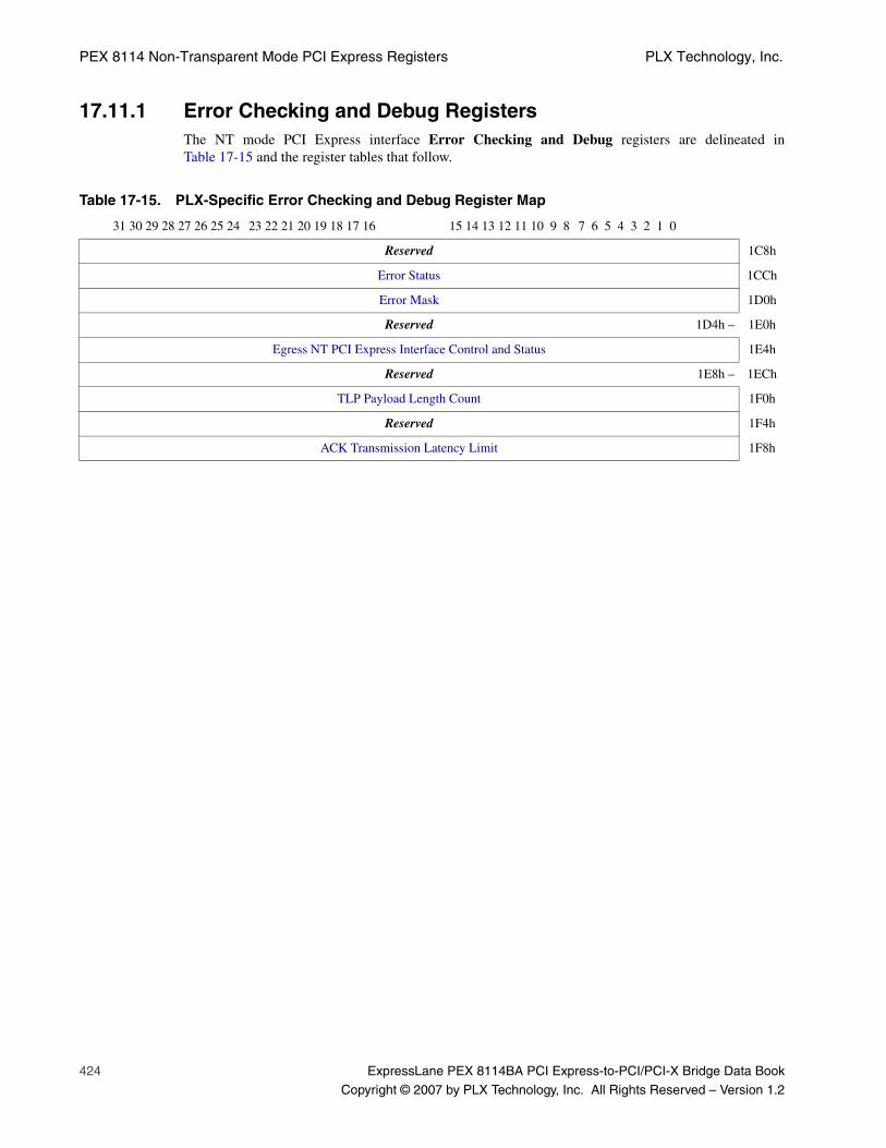
PEX 8114 Non-Transparent Mode PCI Express Registers PLX Technology, Inc.
424 ExpressLane PEX 8114BA PCI Express-to-PCI/PCI-X Bridge Data Book
Copyright © 2007 by PLX Technology, Inc. All Rights Reserved – Version 1.2
17.11.1 Error Checking and Debug RegistersThe NT mode PCI Express interface Error Checking and Debug registers are delineated inTable 17-15 and the register tables that follow.
Table 17-15. PLX-Specific Error Checking and Debug Register Map
31 30 29 28 27 26 25 24 23 22 21 20 19 18 17 16 15 14 13 12 11 10 9 8 7 6 5 4 3 2 1 0
Reserved 1C8h
Error Status 1CCh
Error Mask 1D0h
Reserved 1D4h – 1E0h
Egress NT PCI Express Interface Control and Status 1E4h
Reserved 1E8h – 1ECh
TLP Payload Length Count 1F0h
Reserved 1F4h
ACK Transmission Latency Limit 1F8h
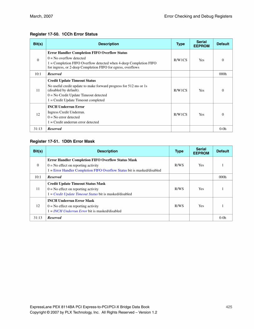
March, 2007 Error Checking and Debug Registers
ExpressLane PEX 8114BA PCI Express-to-PCI/PCI-X Bridge Data Book 425
Copyright © 2007 by PLX Technology, Inc. All Rights Reserved – Version 1.2
Register 17-50. 1CCh Error Status
Bit(s) Description Type Serial EEPROM Default
0
Error Handler Completion FIFO Overflow Status
0 = No overflow detected1 = Completion FIFO Overflow detected when 4-deep Completion FIFO for ingress, or 2-deep Completion FIFO for egress, overflows
R/W1CS Yes 0
10:1 Reserved 000h
11
Credit Update Timeout Status
No useful credit update to make forward progress for 512 ms or 1s (disabled by default).0 = No Credit Update Timeout detected1 = Credit Update Timeout completed
R/W1CS Yes 0
12
INCH Underrun Error
Ingress Credit Underrun. 0 = No error detected1 = Credit underrun error detected
R/W1CS Yes 0
31:13 Reserved 0-0h
Register 17-51. 1D0h Error Mask
Bit(s) Description Type Serial EEPROM Default
0Error Handler Completion FIFO Overflow Status Mask0 = No effect on reporting activity1 = Error Handler Completion FIFO Overflow Status bit is masked/disabled
R/WS Yes 1
10:1 Reserved 000h
11Credit Update Timeout Status Mask0 = No effect on reporting activity1 = Credit Update Timeout Status bit is masked/disabled
R/WS Yes 1
12INCH Underrun Error Mask
0 = No effect on reporting activity1 = INCH Underrun Error bit is masked/disabled
R/WS Yes 1
31:13 Reserved 0-0h
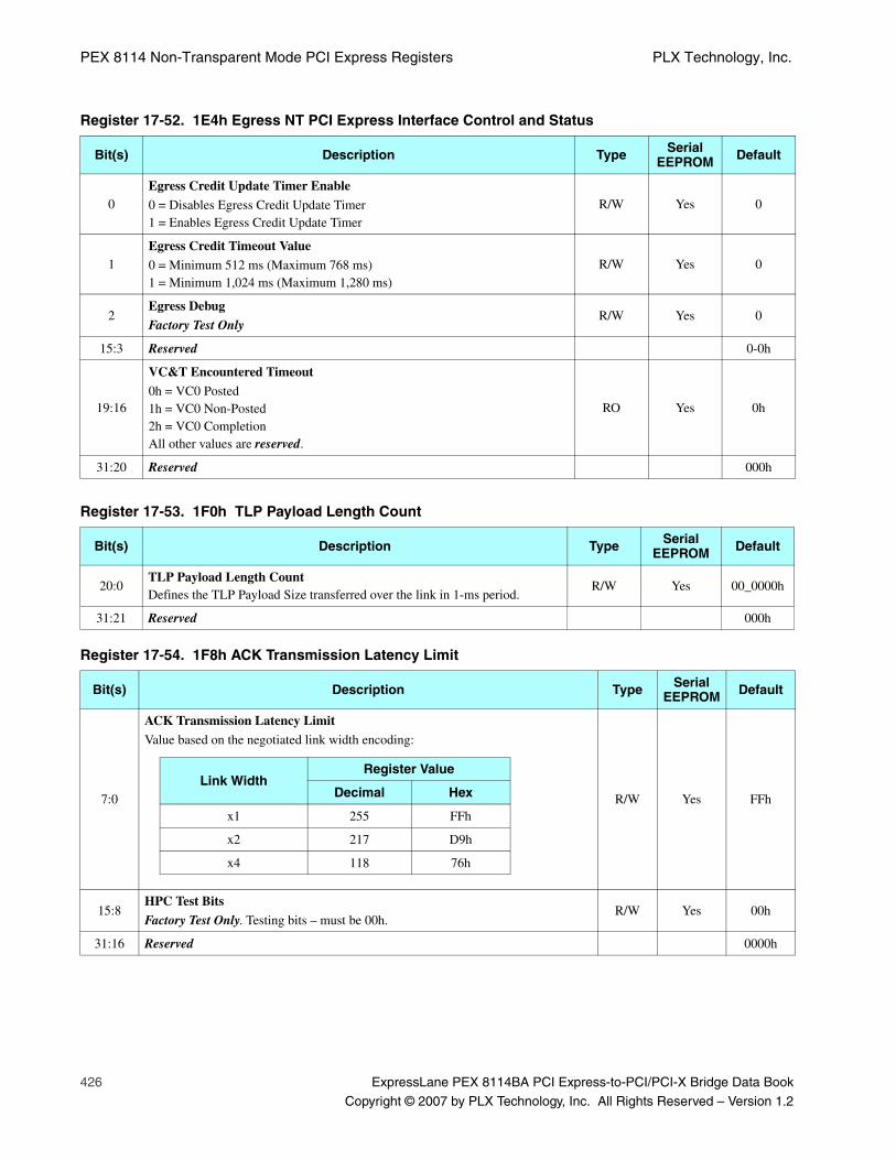
PEX 8114 Non-Transparent Mode PCI Express Registers PLX Technology, Inc.
426 ExpressLane PEX 8114BA PCI Express-to-PCI/PCI-X Bridge Data Book
Copyright © 2007 by PLX Technology, Inc. All Rights Reserved – Version 1.2
Register 17-52. 1E4h Egress NT PCI Express Interface Control and Status
Bit(s) Description Type Serial EEPROM Default
0Egress Credit Update Timer Enable
0 = Disables Egress Credit Update Timer1 = Enables Egress Credit Update Timer
R/W Yes 0
1Egress Credit Timeout Value
0 = Minimum 512 ms (Maximum 768 ms)1 = Minimum 1,024 ms (Maximum 1,280 ms)
R/W Yes 0
2Egress Debug
Factory Test OnlyR/W Yes 0
15:3 Reserved 0-0h
19:16
VC&T Encountered Timeout
0h = VC0 Posted1h = VC0 Non-Posted2h = VC0 CompletionAll other values are reserved.
RO Yes 0h
31:20 Reserved 000h
Register 17-53. 1F0h TLP Payload Length Count
Bit(s) Description Type Serial EEPROM Default
20:0TLP Payload Length CountDefines the TLP Payload Size transferred over the link in 1-ms period.
R/W Yes 00_0000h
31:21 Reserved 000h
Register 17-54. 1F8h ACK Transmission Latency Limit
Bit(s) Description Type Serial EEPROM Default
7:0
ACK Transmission Latency Limit
Value based on the negotiated link width encoding:
R/W Yes FFh
15:8HPC Test Bits
Factory Test Only. Testing bits – must be 00h.R/W Yes 00h
31:16 Reserved 0000h
Link WidthRegister Value
Decimal Hex
x1 255 FFh
x2 217 D9h
x4 118 76h

March, 2007 NT PCI Express Interface Physical Layer Registers
ExpressLane PEX 8114BA PCI Express-to-PCI/PCI-X Bridge Data Book 427
Copyright © 2007 by PLX Technology, Inc. All Rights Reserved – Version 1.2
17.11.2 NT PCI Express Interface Physical Layer RegistersThe NT PCI Express interface Physical Layer registers are delineated in Table 17-16.
Table 17-16. PLX-Specific NT PCI Express Interface Physical Layer Register Map
31 30 29 28 27 26 25 24 23 22 21 20 19 18 17 16 15 14 13 12 11 10 9 8 7 6 5 4 3 2 1 0
Test Pattern_0 210h
Test Pattern_1 214h
Test Pattern_2 218h
Test Pattern_3 21Ch
Physical Layer Status Physical Layer Control 220h
Port Configuration 224h
Physical Layer Test 228h
Physical Layer (Factory Test Only) 22Ch
Physical Layer Port Command 230h
Skip-Ordered Set Interval 234h
Quad SerDes[0-3] Diagnostics Data 238h
Reserved 23Ch – 244h
Reserved SerDes Nominal Drive Cur-rent Select 248h
Reserved SerDes Drive Current Level_1 24Ch
Reserved 250h
Reserved SerDes Drive Equalization Level Select_1 254h
Reserved 258h – 2C4h
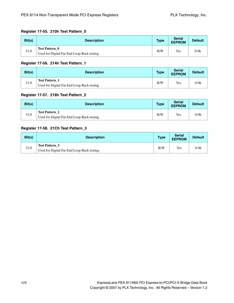
PEX 8114 Non-Transparent Mode PCI Express Registers PLX Technology, Inc.
428 ExpressLane PEX 8114BA PCI Express-to-PCI/PCI-X Bridge Data Book
Copyright © 2007 by PLX Technology, Inc. All Rights Reserved – Version 1.2
Register 17-55. 210h Test Pattern_0
Bit(s) Description Type Serial EEPROM Default
31:0Test Pattern_0
Used for Digital Far-End Loop-Back testing.R/W Yes 0-0h
Register 17-56. 214h Test Pattern_1
Bit(s) Description Type Serial EEPROM Default
31:0Test Pattern_1
Used for Digital Far-End Loop-Back testing.R/W Yes 0-0h
Register 17-57. 218h Test Pattern_2
Bit(s) Description Type Serial EEPROM Default
31:0Test Pattern_2
Used for Digital Far-End Loop-Back testing.R/W Yes 0-0h
Register 17-58. 21Ch Test Pattern_3
Bit(s) Description Type Serial EEPROM Default
31:0Test Pattern_3
Used for Digital Far-End Loop-Back testing.R/W Yes 0-0h
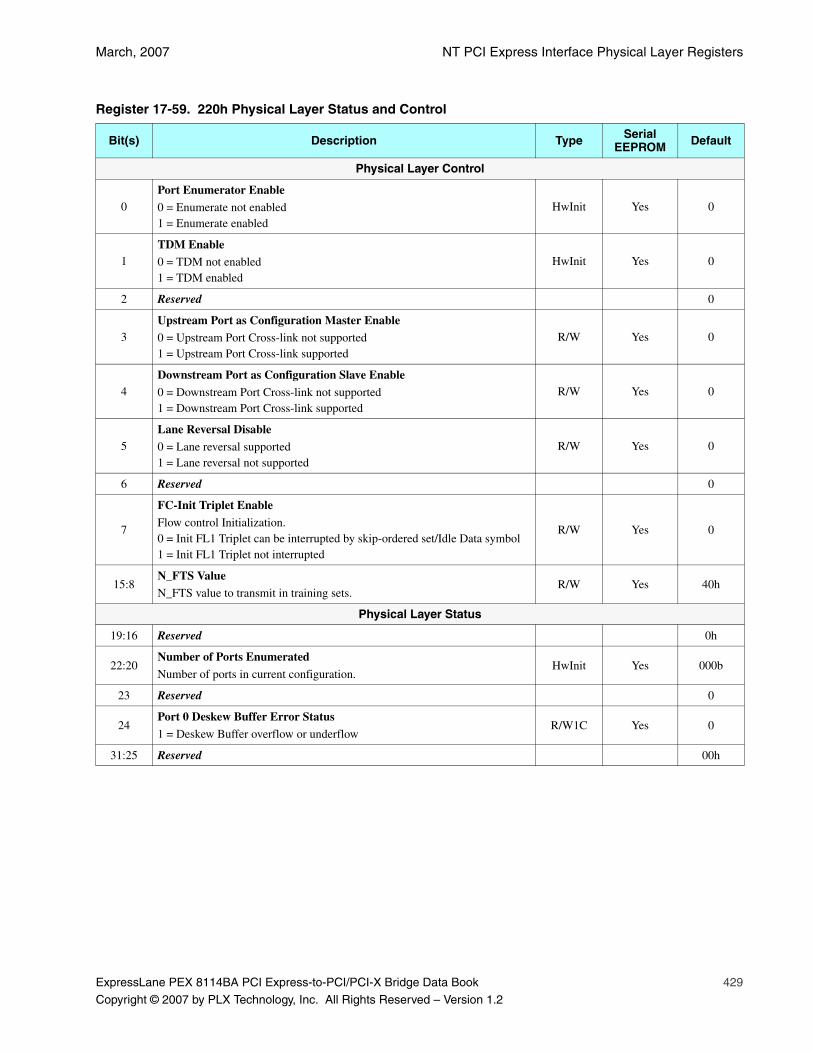
March, 2007 NT PCI Express Interface Physical Layer Registers
ExpressLane PEX 8114BA PCI Express-to-PCI/PCI-X Bridge Data Book 429
Copyright © 2007 by PLX Technology, Inc. All Rights Reserved – Version 1.2
Register 17-59. 220h Physical Layer Status and Control
Bit(s) Description Type Serial EEPROM Default
Physical Layer Control
0Port Enumerator Enable
0 = Enumerate not enabled1 = Enumerate enabled
HwInit Yes 0
1TDM Enable0 = TDM not enabled1 = TDM enabled
HwInit Yes 0
2 Reserved 0
3Upstream Port as Configuration Master Enable0 = Upstream Port Cross-link not supported1 = Upstream Port Cross-link supported
R/W Yes 0
4Downstream Port as Configuration Slave Enable
0 = Downstream Port Cross-link not supported1 = Downstream Port Cross-link supported
R/W Yes 0
5Lane Reversal Disable
0 = Lane reversal supported1 = Lane reversal not supported
R/W Yes 0
6 Reserved 0
7
FC-Init Triplet Enable
Flow control Initialization.0 = Init FL1 Triplet can be interrupted by skip-ordered set/Idle Data symbol1 = Init FL1 Triplet not interrupted
R/W Yes 0
15:8N_FTS ValueN_FTS value to transmit in training sets.
R/W Yes 40h
Physical Layer Status
19:16 Reserved 0h
22:20Number of Ports Enumerated
Number of ports in current configuration.HwInit Yes 000b
23 Reserved 0
24Port 0 Deskew Buffer Error Status
1 = Deskew Buffer overflow or underflowR/W1C Yes 0
31:25 Reserved 00h
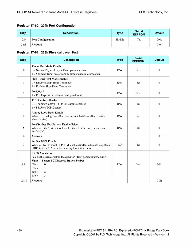
PEX 8114 Non-Transparent Mode PCI Express Registers PLX Technology, Inc.
430 ExpressLane PEX 8114BA PCI Express-to-PCI/PCI-X Bridge Data Book
Copyright © 2007 by PLX Technology, Inc. All Rights Reserved – Version 1.2
Register 17-60. 224h Port Configuration
Bit(s) Description Type Serial EEPROM Default
2:0 Port Configuration HwInit Yes 000b
31:3 Reserved 0-0h
Register 17-61. 228h Physical Layer Test
Bit(s) Description Type Serial EEPROM Default
0Timer Test Mode Enable0 = Normal Physical Layer Timer parameters used1 = Shortens Timer scale from milliseconds to microseconds
R/W Yes 0
1Skip-Timer Test Mode Enable0 = Disables Skip-Timer Test mode1 = Enables Skip-Timer Test mode
R/W Yes 0
2Port_0_x11 = PCI Express interface is configured as x1
R/W Yes 0
3TCB Capture Disable0 = Training Control Bit (TCB) Capture enabled1 = Disables TCB Capture
R/W Yes 0
4Analog Loop-Back EnableWhen = 1, analog Loop-Back testing enabled (Loop-Back before elastic buffer).
R/W Yes 0
5Port/SerDes Test Pattern Enable SelectWhen = 1, the Test Pattern Enable bits select the port, rather than SerDes[0-3].
R/W Yes 0
6 Reserved 0
7SerDes BIST EnableWhen = 1 by the serial EEPROM, enables SerDes internal Loop-Back PRBS test for 512 µs before starting link initialization.
RO Yes 0
9:8
PRBS AssociationSelects the SerDes within the quad for PRBS generation/checking:Value Selects PCI Express Station SerDes00b = 001b = 110b = 211b = 3
R/W Yes 00b
15:10 Reserved 0-0h
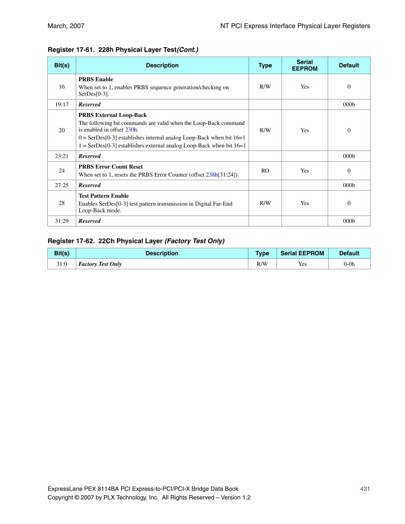
March, 2007 NT PCI Express Interface Physical Layer Registers
ExpressLane PEX 8114BA PCI Express-to-PCI/PCI-X Bridge Data Book 431
Copyright © 2007 by PLX Technology, Inc. All Rights Reserved – Version 1.2
16PRBS EnableWhen set to 1, enables PRBS sequence generation/checking on SerDes[0-3].
R/W Yes 0
19:17 Reserved 000b
20
PRBS External Loop-BackThe following bit commands are valid when the Loop-Back command is enabled in offset 230h.0 = SerDes[0-3] establishes internal analog Loop-Back when bit 16=11 = SerDes[0-3] establishes external analog Loop-Back when bit 16=1
R/W Yes 0
23:21 Reserved 000b
24PRBS Error Count ResetWhen set to 1, resets the PRBS Error Counter (offset 238h[31:24]).
RO Yes 0
27:25 Reserved 000b
28Test Pattern EnableEnables SerDes[0-3] test pattern transmission in Digital Far-End Loop-Back mode.
R/W Yes 0
31:29 Reserved 000b
Register 17-62. 22Ch Physical Layer (Factory Test Only)
Bit(s) Description Type Serial EEPROM Default
31:0 Factory Test Only R/W Yes 0-0h
Register 17-61. 228h Physical Layer Test(Cont.)
Bit(s) Description Type Serial EEPROM Default
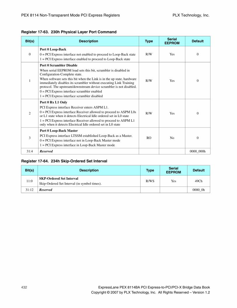
PEX 8114 Non-Transparent Mode PCI Express Registers PLX Technology, Inc.
432 ExpressLane PEX 8114BA PCI Express-to-PCI/PCI-X Bridge Data Book
Copyright © 2007 by PLX Technology, Inc. All Rights Reserved – Version 1.2
Register 17-63. 230h Physical Layer Port Command
Bit(s) Description Type Serial EEPROM Default
0Port 0 Loop-Back
0 = PCI Express interface not enabled to proceed to Loop-Back state1 = PCI Express interface enabled to proceed to Loop-Back state
R/W Yes 0
1
Port 0 Scrambler Disable
When serial EEPROM load sets this bit, scrambler is disabled in Configuration-Complete state.When software sets this bit when the Link is in the up state, hardware immediately disables its scrambler without executing Link Training protocol. The upstream/downstream device scrambler is not disabled.0 = PCI Express interface scrambler enabled1 = PCI Express interface scrambler disabled
R/W Yes 0
2
Port 0 Rx L1 Only
PCI Express interface Receiver enters ASPM L1.0 = PCI Express interface Receiver allowed to proceed to ASPM L0s or L1 state when it detects Electrical Idle ordered set in L0 state1 = PCI Express interface Receiver allowed to proceed to ASPM L1 only when it detects Electrical Idle ordered set in L0 state
R/W Yes 0
3
Port 0 Loop-Back Master
PCI Express interface LTSSM established Loop-Back as a Master.0 = PCI Express interface not in Loop-Back Master mode1 = PCI Express interface in Loop-Back Master mode
RO No 0
31:4 Reserved 0000_000h
Register 17-64. 234h Skip-Ordered Set Interval
Bit(s) Description Type Serial EEPROM Default
11:0SKP-Ordered Set Interval
Skip-Ordered Set Interval (in symbol times).R/WS Yes 49Ch
31:12 Reserved 0000_0h

March, 2007 NT PCI Express Interface Physical Layer Registers
ExpressLane PEX 8114BA PCI Express-to-PCI/PCI-X Bridge Data Book 433
Copyright © 2007 by PLX Technology, Inc. All Rights Reserved – Version 1.2
Register 17-65. 238h Quad SerDes[0-3] Diagnostics Data
Bit(s) Description Type Serial EEPROM Default
9:0Expected PRBS Data
Expected PRBS SerDes[0-3] Diagnostic data.RO Yes 000h
19:10Received PRBS Data
Received PRBS SerDes[0-3] Diagnostic data.RO Yes 000h
23:20 Reserved 0h
31:24PRBS Error Count
PRBS SerDes[0-3] Error count (0 to 255).RO Yes 00h
Register 17-66. 248h SerDes Nominal Drive Current Select
Bit(s) Description Type Serial EEPROM Default
1:0 SerDes_0 Nominal Drive Current The following values for Nominal Current apply to each drive:00b = 20 mA01b = 10 mA10b = 28 mA11b = 20 mA
R/WS Yes 00b
3:2 SerDes_1 Nominal Drive Current R/WS Yes 00b
5:4 SerDes_2 Nominal Drive Current R/WS Yes 00b
7:6 SerDes_3 Nominal Drive Current R/WS Yes 00b
31:8 Reserved 0000_00h
Register 17-67. 24Ch SerDes Drive Current Level_1
Bit(s) Description Type Serial EEPROM Default
3:0 SerDes_0 Drive Current LevelThe following values represent the ratio of Actual Current/Nominal Current (selected in SerDes Nominal Drive Current Select register) and apply to each drive:
R/WS Yes 0h
7:4 SerDes_1 Drive Current Level R/WS Yes 0h
11:8 SerDes_2 Drive Current Level R/WS Yes 0h
15:12 SerDes_3 Drive Current Level R/WS Yes 0h
31:16 Reserved 0000h
0h = 1.001h = 1.052h = 1.103h = 1.154h = 1.205h = 1.256h = 1.307h = 1.35
8h = 0.609h = 0.65Ah = 0.70Bh = 0.75Ch = 0.80Dh = 0.85Eh = 0.90Fh = 0.95
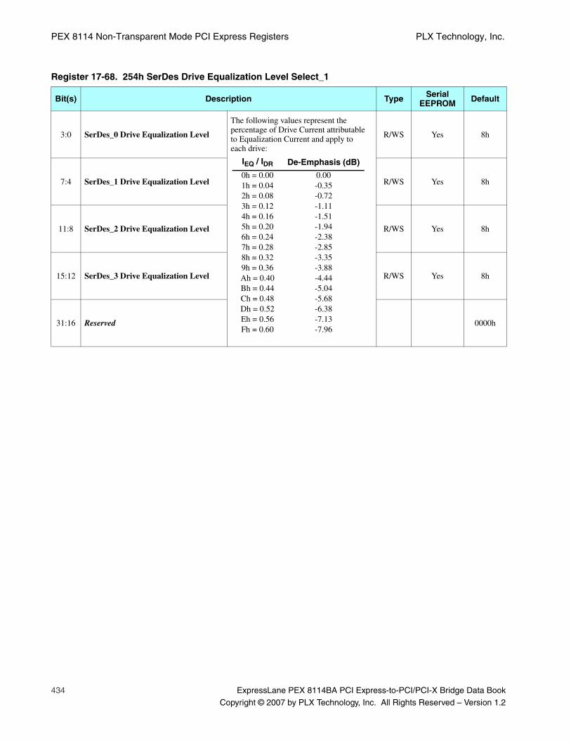
PEX 8114 Non-Transparent Mode PCI Express Registers PLX Technology, Inc.
434 ExpressLane PEX 8114BA PCI Express-to-PCI/PCI-X Bridge Data Book
Copyright © 2007 by PLX Technology, Inc. All Rights Reserved – Version 1.2
Register 17-68. 254h SerDes Drive Equalization Level Select_1
Bit(s) Description Type Serial EEPROM Default
3:0 SerDes_0 Drive Equalization Level
The following values represent the percentage of Drive Current attributable to Equalization Current and apply to each drive:
R/WS Yes 8h
7:4 SerDes_1 Drive Equalization Level R/WS Yes 8h
11:8 SerDes_2 Drive Equalization Level R/WS Yes 8h
15:12 SerDes_3 Drive Equalization Level R/WS Yes 8h
31:16 Reserved 0000h
IEQ / IDR De-Emphasis (dB)
0h = 0.001h = 0.042h = 0.083h = 0.124h = 0.165h = 0.206h = 0.247h = 0.288h = 0.329h = 0.36Ah = 0.40Bh = 0.44Ch = 0.48Dh = 0.52Eh = 0.56Fh = 0.60
0.00-0.35-0.72-1.11-1.51-1.94-2.38-2.85-3.35-3.88-4.44-5.04-5.68-6.38-7.13-7.96
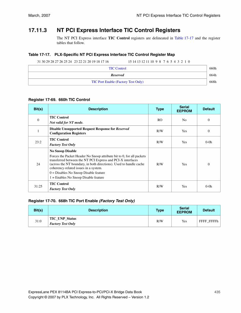
March, 2007 NT PCI Express Interface TIC Control Registers
ExpressLane PEX 8114BA PCI Express-to-PCI/PCI-X Bridge Data Book 435
Copyright © 2007 by PLX Technology, Inc. All Rights Reserved – Version 1.2
17.11.3 NT PCI Express Interface TIC Control RegistersThe NT PCI Express interface TIC Control registers are delineated in Table 17-17 and the registertables that follow.
Table 17-17. PLX-Specific NT PCI Express Interface TIC Control Register Map
31 30 29 28 27 26 25 24 23 22 21 20 19 18 17 16 15 14 13 12 11 10 9 8 7 6 5 4 3 2 1 0
TIC Control 660h
Reserved 664h
TIC Port Enable (Factory Test Only) 668h
Register 17-69. 660h TIC Control
Bit(s) Description Type Serial EEPROM Default
0TIC Control
Not valid for NT mode.RO No 0
1Disable Unsupported Request Response for Reserved Configuration Registers
R/W Yes 0
23:2TIC Control
Factory Test OnlyR/W Yes 0-0h
24
No Snoop DisableForces the Packet Header No Snoop attribute bit to 0, for all packets transferred between the NT PCI Express and PCI-X interfaces (across the NT boundary, in both directions). Used to handle cache coherency-related issues in a system.0 = Disables No Snoop Disable feature1 = Enables No Snoop Disable feature
R/W Yes 0
31:25TIC Control
Factory Test OnlyR/W Yes 0-0h
Register 17-70. 668h TIC Port Enable (Factory Test Only)
Bit(s) Description Type Serial EEPROM Default
31:0TIC_UNP_StatusFactory Test Only
R/W Yes FFFF_FFFFh
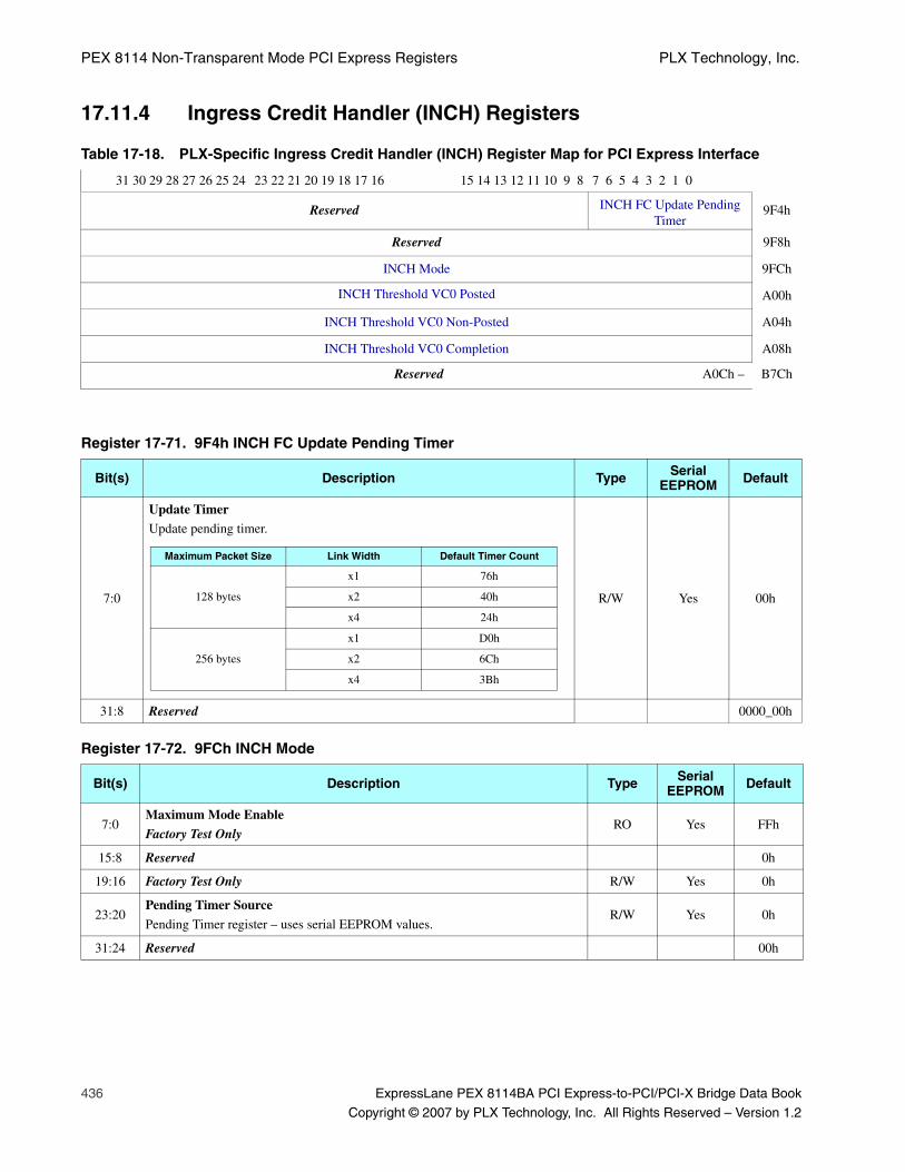
PEX 8114 Non-Transparent Mode PCI Express Registers PLX Technology, Inc.
436 ExpressLane PEX 8114BA PCI Express-to-PCI/PCI-X Bridge Data Book
Copyright © 2007 by PLX Technology, Inc. All Rights Reserved – Version 1.2
17.11.4 Ingress Credit Handler (INCH) Registers
Table 17-18. PLX-Specific Ingress Credit Handler (INCH) Register Map for PCI Express Interface
31 30 29 28 27 26 25 24 23 22 21 20 19 18 17 16 15 14 13 12 11 10 9 8 7 6 5 4 3 2 1 0
Reserved INCH FC Update Pending Timer
9F4h
Reserved 9F8h
INCH Mode 9FCh
INCH Threshold VC0 Posted A00h
INCH Threshold VC0 Non-Posted A04h
INCH Threshold VC0 Completion A08h
Reserved A0Ch – B7Ch
Register 17-71. 9F4h INCH FC Update Pending Timer
Bit(s) Description Type Serial EEPROM Default
7:0
Update TimerUpdate pending timer.
R/W Yes 00h
31:8 Reserved 0000_00h
Register 17-72. 9FCh INCH Mode
Bit(s) Description Type Serial EEPROM Default
7:0Maximum Mode Enable
Factory Test OnlyRO Yes FFh
15:8 Reserved 0h
19:16 Factory Test Only R/W Yes 0h
23:20Pending Timer Source
Pending Timer register – uses serial EEPROM values.R/W Yes 0h
31:24 Reserved 00h
Maximum Packet Size Link Width Default Timer Count
128 bytes
x1 76h
x2 40h
x4 24h
256 bytes
x1 D0h
x2 6Ch
x4 3Bh

March, 2007 Ingress Credit Handler (INCH) Registers
ExpressLane PEX 8114BA PCI Express-to-PCI/PCI-X Bridge Data Book 437
Copyright © 2007 by PLX Technology, Inc. All Rights Reserved – Version 1.2
17.11.4.1 INCH Threshold Virtual Channel RegistersThere are three Ingress Credit Handler (INCH) Threshold VC0 registers. These registers represent themaximum number of Headers or Payload credits allocated to Virtual Channel 0, for each type oftransaction. The register names and address/location are delineated in Table 17-18. The followingregisters describe the data that applies to these registers.
Register 17-73. A00h INCH Threshold VC0 Posted
Bit(s) Description Type Serial EEPROM Default
2:0 Reserved 000b
8:3Payload
Payload = 0_0111_0b.R/W Yes 30Eh
13:9Header
Header = 01_100b.
31:14 Reserved 0-0h
Register 17-74. A04h INCH Threshold VC0 Non-Posted
Bit(s) Description Type Serial EEPROM Default
8:0PayloadPayload = 0_0000_1010b.
R/W Yes 140Ah
13:9Header
Header = 01_010b.
31:14 Reserved 0-0h
Register 17-75. A08h INCH Threshold VC0 Completion
Bit(s) Description Type Serial EEPROM Default
2:0 Reserved 000b
8:3Payload
Payload = 0_0110_0b.R/W Yes 28Ch
13:9Header
Header = 01_010b.
31:14 Reserved 0-0h

PEX 8114 Non-Transparent Mode PCI Express Registers PLX Technology, Inc.
438 ExpressLane PEX 8114BA PCI Express-to-PCI/PCI-X Bridge Data Book
Copyright © 2007 by PLX Technology, Inc. All Rights Reserved – Version 1.2
17.11.5 Internal Credit Handler (ITCH) VC&T Threshold Registers
Table 17-19. PEX 8114 NT PCI Express Interface PLX-Specific Internal Credit Handler (ITCH) VC&T Threshold Register Map
31 30 29 28 27 26 25 24 23 22 21 20 19 18 17 16 15 14 13 12 11 10 9 8 7 6 5 4 3 2 1 0
NT PCI Express Interface ITCH VC&T Threshold_1 C00h
NT PCI Express Interface ITCH VC&T Threshold_2 C04h
Reserved C08h – C10h

March, 2007 Internal Credit Handler (ITCH) VC&T Threshold Registers
ExpressLane PEX 8114BA PCI Express-to-PCI/PCI-X Bridge Data Book 439
Copyright © 2007 by PLX Technology, Inc. All Rights Reserved – Version 1.2
Note: Although the PEX 8114 supports only VC0, the VC1 Posted credit fields are used for internal transactions, such as shadow Writes.
Register 17-76. C00h NT PCI Express Interface ITCH VC&T Threshold_1
Bit(s) Description Type Serial EEPROM Default
4:0VC0 Posted Upper Packet CountVC0 Posted upper packet beat limit.
R/W Yes 10h
7:5 Not used R/W Yes 000b
12:8VC0 Posted Lower Packet CountVC0 Posted lower packet beat limit.
R/W Yes 08h
15:13 Not used R/W Yes 000b
20:16VC0 Non-Posted Upper Packet CountVC0 Non-Posted upper packet beat limit.
R/W Yes 04h
23:21 Not used R/W Yes 000b
28:24VC0 Non-Posted Lower Packet CountVC0 Non-Posted lower packet beat limit.
R/W Yes 01h
31:29 Not used R/W Yes 000b
Register 17-77. C04h NT PCI Express Interface ITCH VC&T Threshold_2
Bit(s) Description Type Serial EEPROM Default
4:0VC0 Completion Upper Packet CountVC0 Completion upper packet beat limit.
R/W Yes 10h
7:5 Not used R/W Yes 000b
12:8VC0 Completion Lower Packet CountVC0 Completion lower packet beat limit.
R/W Yes 08h
15:13 Not used R/W Yes 000b
20:16
VC1 Posted Upper Packet CountVC1 Posted upper packet beat limit. This information is listed for internal and serial EEPROM configuration only – not to be changed by users.
R/W Yes 04h
23:21 Not used R/W Yes 000b
28:24
VC1 Posted Lower Packet CountVC1 Posted lower packet beat limit. This information is listed for internal and serial EEPROM configuration only – not to be changed by users.
R/W Yes 01h
31:29 Not used R/W Yes 000b
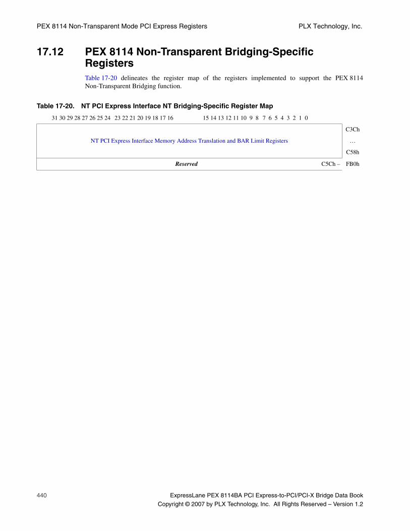
PEX 8114 Non-Transparent Mode PCI Express Registers PLX Technology, Inc.
440 ExpressLane PEX 8114BA PCI Express-to-PCI/PCI-X Bridge Data Book
Copyright © 2007 by PLX Technology, Inc. All Rights Reserved – Version 1.2
17.12 PEX 8114 Non-Transparent Bridging-Specific RegistersTable 17-20 delineates the register map of the registers implemented to support the PEX 8114Non-Transparent Bridging function.
Table 17-20. NT PCI Express Interface NT Bridging-Specific Register Map
31 30 29 28 27 26 25 24 23 22 21 20 19 18 17 16 15 14 13 12 11 10 9 8 7 6 5 4 3 2 1 0
NT PCI Express Interface Memory Address Translation and BAR Limit Registers
C3Ch
…
C58h
Reserved C5Ch – FB0h

March, 2007 NT PCI Express Interface Memory Address Translation and BAR Limit Registers
ExpressLane PEX 8114BA PCI Express-to-PCI/PCI-X Bridge Data Book 441
Copyright © 2007 by PLX Technology, Inc. All Rights Reserved – Version 1.2
17.12.1 NT PCI Express Interface Memory Address Translation and BAR Limit RegistersThe NT PCI Express interface Memory Address Translation and BAR Limit registers are delineatedin Table 17-21 and the register tables that follow.
Table 17-21. NT PCI Express Interface Memory Address Translation and BAR Limit Register Map
31 30 29 28 27 26 25 24 23 22 21 20 19 18 17 16 15 14 13 12 11 10 9 8 7 6 5 4 3 2 1 0
Memory BAR_2 Address Translation[31:0] C3Ch
Memory BAR_3 Address Translation[63:32] C40h
Memory BAR_4 Address Translation[31:0] C44h
Memory BAR_5 Address Translation[63:32] C48h
Memory BAR_2 Limit[31:0] C4Ch
Memory BAR_3 Limit[63:32] C50h
Memory BAR_4 Limit[31:0] C54h
Memory BAR_5 Limit[63:32] C58h
Register 17-78. C3Ch Memory BAR_2 Address Translation[31:0]
Bit(s) Description Type Serial EEPROM Default
11:0 Reserved 0-0h
31:12BAR_2 Base Translation[31:12]
NT PCI Express interface Base Address Translation register if BAR_2 is enabled.
R/W Yes 0-0h
Register 17-79. C40h Memory BAR_3 Address Translation[63:32]
Bit(s) Description Type Serial EEPROM Default
31:0BAR_2/3 Base Translation[63:32]NT PCI Express interface Base Address Translation register extension when BAR 2 Type Select = 10b.
R/W Yes 0-0h
Register 17-80. C44h Memory BAR_4 Address Translation[31:0]
Bit(s) Description Type Serial EEPROM Default
11:0 Reserved 0-0h
31:12BAR_4 Base Translation[31:12]
NT PCI Express interface Base Address Translation register if BAR_4 is enabled.
R/W Yes 0-0h
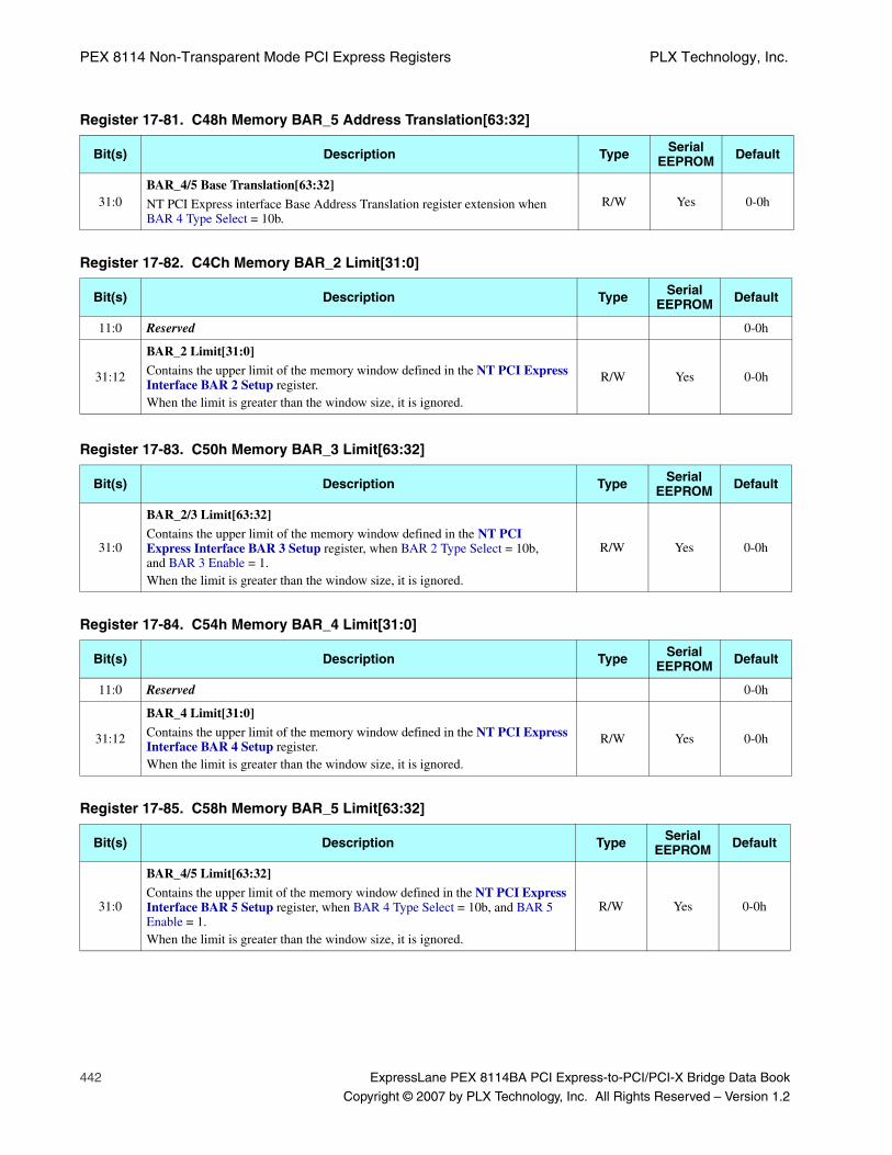
PEX 8114 Non-Transparent Mode PCI Express Registers PLX Technology, Inc.
442 ExpressLane PEX 8114BA PCI Express-to-PCI/PCI-X Bridge Data Book
Copyright © 2007 by PLX Technology, Inc. All Rights Reserved – Version 1.2
Register 17-81. C48h Memory BAR_5 Address Translation[63:32]
Bit(s) Description Type Serial EEPROM Default
31:0BAR_4/5 Base Translation[63:32]
NT PCI Express interface Base Address Translation register extension when BAR 4 Type Select = 10b.
R/W Yes 0-0h
Register 17-82. C4Ch Memory BAR_2 Limit[31:0]
Bit(s) Description Type Serial EEPROM Default
11:0 Reserved 0-0h
31:12
BAR_2 Limit[31:0]Contains the upper limit of the memory window defined in the NT PCI Express Interface BAR 2 Setup register.When the limit is greater than the window size, it is ignored.
R/W Yes 0-0h
Register 17-83. C50h Memory BAR_3 Limit[63:32]
Bit(s) Description Type Serial EEPROM Default
31:0
BAR_2/3 Limit[63:32]
Contains the upper limit of the memory window defined in the NT PCI Express Interface BAR 3 Setup register, when BAR 2 Type Select = 10b, and BAR 3 Enable = 1.When the limit is greater than the window size, it is ignored.
R/W Yes 0-0h
Register 17-84. C54h Memory BAR_4 Limit[31:0]
Bit(s) Description Type Serial EEPROM Default
11:0 Reserved 0-0h
31:12
BAR_4 Limit[31:0]
Contains the upper limit of the memory window defined in the NT PCI Express Interface BAR 4 Setup register.When the limit is greater than the window size, it is ignored.
R/W Yes 0-0h
Register 17-85. C58h Memory BAR_5 Limit[63:32]
Bit(s) Description Type Serial EEPROM Default
31:0
BAR_4/5 Limit[63:32]
Contains the upper limit of the memory window defined in the NT PCI Express Interface BAR 5 Setup register, when BAR 4 Type Select = 10b, and BAR 5 Enable = 1.When the limit is greater than the window size, it is ignored.
R/W Yes 0-0h
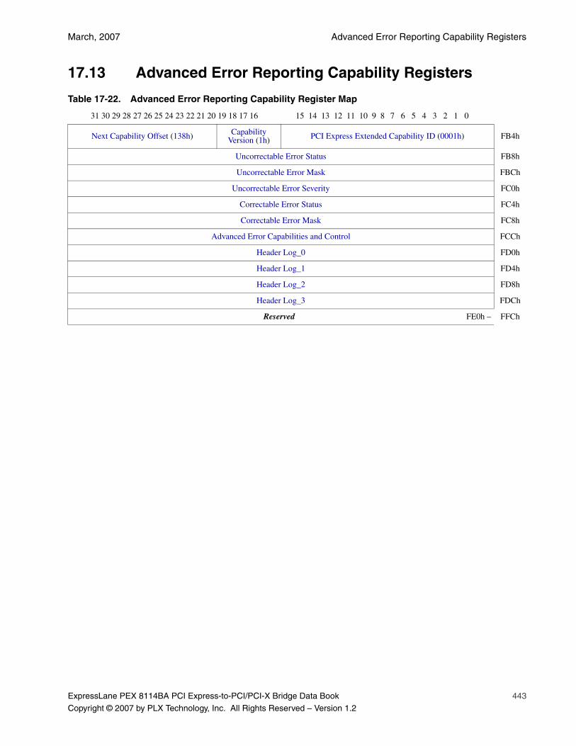
March, 2007 Advanced Error Reporting Capability Registers
ExpressLane PEX 8114BA PCI Express-to-PCI/PCI-X Bridge Data Book 443
Copyright © 2007 by PLX Technology, Inc. All Rights Reserved – Version 1.2
17.13 Advanced Error Reporting Capability Registers
Table 17-22. Advanced Error Reporting Capability Register Map
31 30 29 28 27 26 25 24 23 22 21 20 19 18 17 16 15 14 13 12 11 10 9 8 7 6 5 4 3 2 1 0
Next Capability Offset (138h) Capability Version (1h) PCI Express Extended Capability ID (0001h) FB4h
Uncorrectable Error Status FB8h
Uncorrectable Error Mask FBCh
Uncorrectable Error Severity FC0h
Correctable Error Status FC4h
Correctable Error Mask FC8h
Advanced Error Capabilities and Control FCCh
Header Log_0 FD0h
Header Log_1 FD4h
Header Log_2 FD8h
Header Log_3 FDCh
Reserved FE0h – FFCh
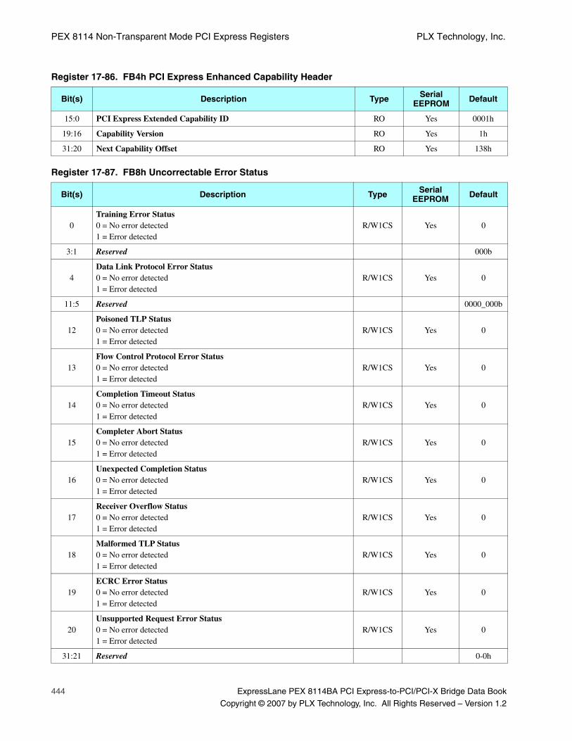
PEX 8114 Non-Transparent Mode PCI Express Registers PLX Technology, Inc.
444 ExpressLane PEX 8114BA PCI Express-to-PCI/PCI-X Bridge Data Book
Copyright © 2007 by PLX Technology, Inc. All Rights Reserved – Version 1.2
Register 17-86. FB4h PCI Express Enhanced Capability Header
Bit(s) Description Type Serial EEPROM Default
15:0 PCI Express Extended Capability ID RO Yes 0001h
19:16 Capability Version RO Yes 1h
31:20 Next Capability Offset RO Yes 138h
Register 17-87. FB8h Uncorrectable Error Status
Bit(s) Description Type Serial EEPROM Default
0Training Error Status0 = No error detected1 = Error detected
R/W1CS Yes 0
3:1 Reserved 000b
4Data Link Protocol Error Status0 = No error detected1 = Error detected
R/W1CS Yes 0
11:5 Reserved 0000_000b
12Poisoned TLP Status0 = No error detected1 = Error detected
R/W1CS Yes 0
13Flow Control Protocol Error Status0 = No error detected1 = Error detected
R/W1CS Yes 0
14Completion Timeout Status0 = No error detected1 = Error detected
R/W1CS Yes 0
15Completer Abort Status0 = No error detected1 = Error detected
R/W1CS Yes 0
16Unexpected Completion Status0 = No error detected1 = Error detected
R/W1CS Yes 0
17Receiver Overflow Status0 = No error detected1 = Error detected
R/W1CS Yes 0
18Malformed TLP Status0 = No error detected1 = Error detected
R/W1CS Yes 0
19ECRC Error Status0 = No error detected1 = Error detected
R/W1CS Yes 0
20Unsupported Request Error Status0 = No error detected1 = Error detected
R/W1CS Yes 0
31:21 Reserved 0-0h

March, 2007 Advanced Error Reporting Capability Registers
ExpressLane PEX 8114BA PCI Express-to-PCI/PCI-X Bridge Data Book 445
Copyright © 2007 by PLX Technology, Inc. All Rights Reserved – Version 1.2
Register 17-88. FBCh Uncorrectable Error Mask
Bit(s) Description Type Serial EEPROM Default
0
Training Error Mask0 = No mask is set1 = Error reporting, first error update, and Header logging are masked for this error
R/WS Yes 0
3:1 Reserved 000b
4
Data Link Protocol Error Mask0 = No mask is set1 = Error reporting, first error update, and Header logging are masked for this error
R/WS Yes 0
11:5 Reserved 0000_000b
12
Poisoned TLP Mask0 = No mask is set1 = Error reporting, first error update, and Header logging are masked for this error
R/WS Yes 0
13
Flow Control Protocol Mask0 = No mask is set1 = Error reporting, first error update, and Header logging are masked for this error
R/WS Yes 0
14
Completion Timeout Mask0 = No mask is set1 = Error reporting, first error update, and Header logging are masked for this error
R/WS Yes 0
15
Completer Abort Mask0 = No mask is set1 = Error reporting, first error update, and Header logging are masked for this error
R/WS Yes 0
16
Unexpected Completion Mask0 = No mask is set1 = Error reporting, first error update, and Header logging are masked for this error
R/WS Yes 0
17
Receiver Overflow Mask0 = No mask is set1 = Error reporting, first error update, and Header logging are masked for this error
R/WS Yes 0
18
Malformed TLP Mask0 = No mask is set1 = Error reporting, first error update, and Header logging are masked for this error
R/WS Yes 0
19
ECRC Error Mask0 = No mask is set1 = Error reporting, first error update, and Header logging are masked for this error
R/WS Yes 0
20
Unsupported Request Error Mask0 = No mask is set1 = Error reporting, first error update, and Header logging are masked for this error
R/WS Yes 0
31:21 Reserved 0-0h
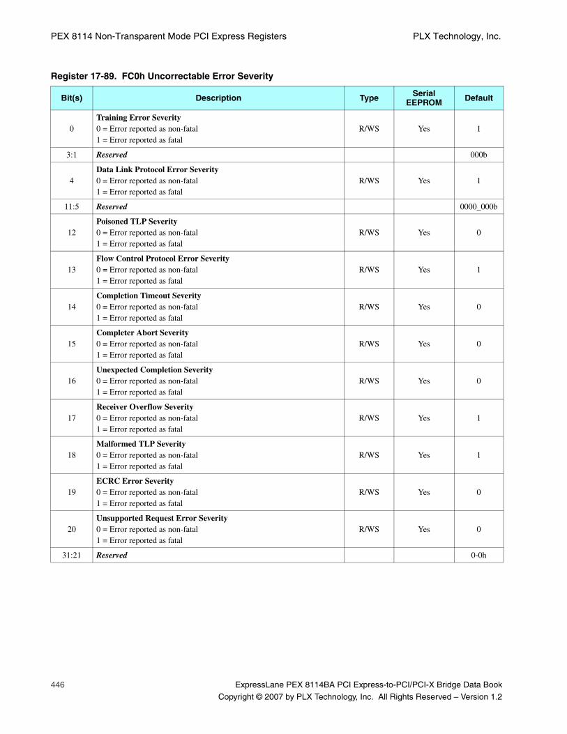
PEX 8114 Non-Transparent Mode PCI Express Registers PLX Technology, Inc.
446 ExpressLane PEX 8114BA PCI Express-to-PCI/PCI-X Bridge Data Book
Copyright © 2007 by PLX Technology, Inc. All Rights Reserved – Version 1.2
Register 17-89. FC0h Uncorrectable Error Severity
Bit(s) Description Type Serial EEPROM Default
0Training Error Severity0 = Error reported as non-fatal1 = Error reported as fatal
R/WS Yes 1
3:1 Reserved 000b
4Data Link Protocol Error Severity0 = Error reported as non-fatal1 = Error reported as fatal
R/WS Yes 1
11:5 Reserved 0000_000b
12Poisoned TLP Severity0 = Error reported as non-fatal1 = Error reported as fatal
R/WS Yes 0
13Flow Control Protocol Error Severity0 = Error reported as non-fatal1 = Error reported as fatal
R/WS Yes 1
14Completion Timeout Severity0 = Error reported as non-fatal1 = Error reported as fatal
R/WS Yes 0
15Completer Abort Severity0 = Error reported as non-fatal1 = Error reported as fatal
R/WS Yes 0
16Unexpected Completion Severity0 = Error reported as non-fatal1 = Error reported as fatal
R/WS Yes 0
17Receiver Overflow Severity0 = Error reported as non-fatal1 = Error reported as fatal
R/WS Yes 1
18Malformed TLP Severity0 = Error reported as non-fatal1 = Error reported as fatal
R/WS Yes 1
19ECRC Error Severity0 = Error reported as non-fatal1 = Error reported as fatal
R/WS Yes 0
20Unsupported Request Error Severity0 = Error reported as non-fatal1 = Error reported as fatal
R/WS Yes 0
31:21 Reserved 0-0h
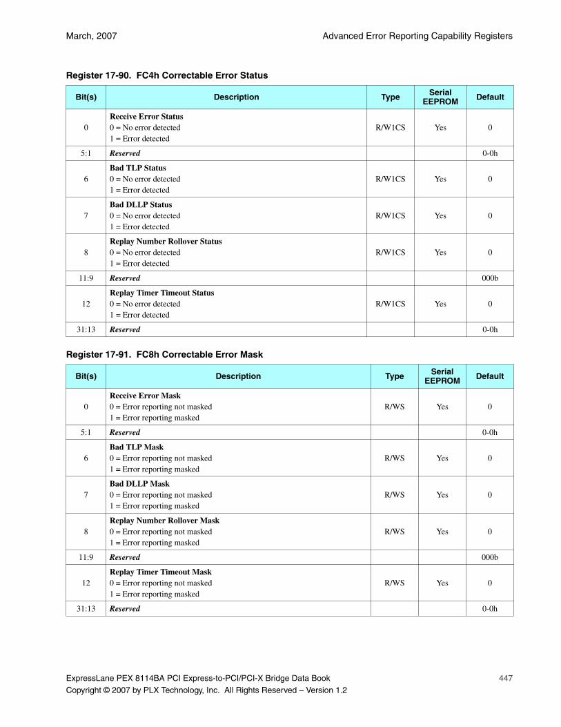
March, 2007 Advanced Error Reporting Capability Registers
ExpressLane PEX 8114BA PCI Express-to-PCI/PCI-X Bridge Data Book 447
Copyright © 2007 by PLX Technology, Inc. All Rights Reserved – Version 1.2
Register 17-90. FC4h Correctable Error Status
Bit(s) Description Type Serial EEPROM Default
0Receive Error Status0 = No error detected1 = Error detected
R/W1CS Yes 0
5:1 Reserved 0-0h
6Bad TLP Status0 = No error detected1 = Error detected
R/W1CS Yes 0
7Bad DLLP Status0 = No error detected1 = Error detected
R/W1CS Yes 0
8Replay Number Rollover Status0 = No error detected1 = Error detected
R/W1CS Yes 0
11:9 Reserved 000b
12Replay Timer Timeout Status0 = No error detected1 = Error detected
R/W1CS Yes 0
31:13 Reserved 0-0h
Register 17-91. FC8h Correctable Error Mask
Bit(s) Description Type Serial EEPROM Default
0Receive Error Mask0 = Error reporting not masked1 = Error reporting masked
R/WS Yes 0
5:1 Reserved 0-0h
6Bad TLP Mask0 = Error reporting not masked1 = Error reporting masked
R/WS Yes 0
7Bad DLLP Mask0 = Error reporting not masked1 = Error reporting masked
R/WS Yes 0
8Replay Number Rollover Mask0 = Error reporting not masked1 = Error reporting masked
R/WS Yes 0
11:9 Reserved 000b
12Replay Timer Timeout Mask0 = Error reporting not masked1 = Error reporting masked
R/WS Yes 0
31:13 Reserved 0-0h
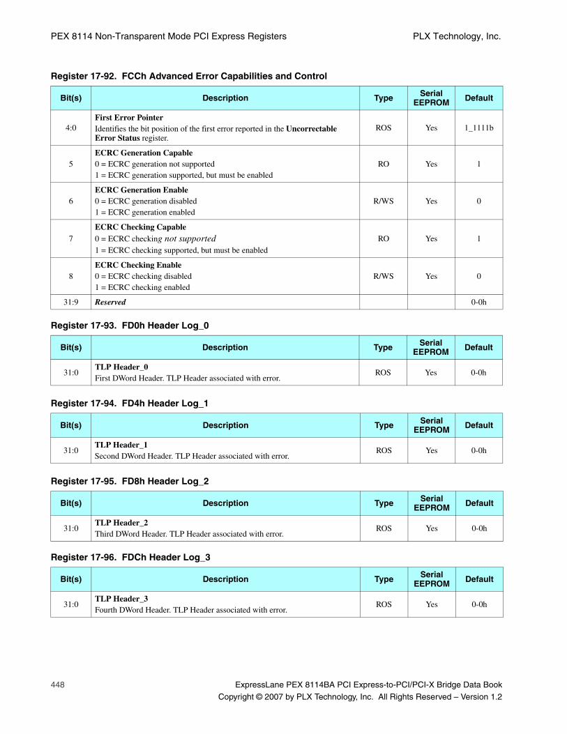
PEX 8114 Non-Transparent Mode PCI Express Registers PLX Technology, Inc.
448 ExpressLane PEX 8114BA PCI Express-to-PCI/PCI-X Bridge Data Book
Copyright © 2007 by PLX Technology, Inc. All Rights Reserved – Version 1.2
Register 17-92. FCCh Advanced Error Capabilities and Control
Bit(s) Description Type Serial EEPROM Default
4:0First Error PointerIdentifies the bit position of the first error reported in the Uncorrectable Error Status register.
ROS Yes 1_1111b
5ECRC Generation Capable0 = ECRC generation not supported1 = ECRC generation supported, but must be enabled
RO Yes 1
6ECRC Generation Enable0 = ECRC generation disabled1 = ECRC generation enabled
R/WS Yes 0
7ECRC Checking Capable0 = ECRC checking not supported1 = ECRC checking supported, but must be enabled
RO Yes 1
8ECRC Checking Enable0 = ECRC checking disabled1 = ECRC checking enabled
R/WS Yes 0
31:9 Reserved 0-0h
Register 17-93. FD0h Header Log_0
Bit(s) Description Type Serial EEPROM Default
31:0TLP Header_0First DWord Header. TLP Header associated with error.
ROS Yes 0-0h
Register 17-94. FD4h Header Log_1
Bit(s) Description Type Serial EEPROM Default
31:0TLP Header_1Second DWord Header. TLP Header associated with error.
ROS Yes 0-0h
Register 17-95. FD8h Header Log_2
Bit(s) Description Type Serial EEPROM Default
31:0TLP Header_2Third DWord Header. TLP Header associated with error.
ROS Yes 0-0h
Register 17-96. FDCh Header Log_3
Bit(s) Description Type Serial EEPROM Default
31:0TLP Header_3Fourth DWord Header. TLP Header associated with error.
ROS Yes 0-0h
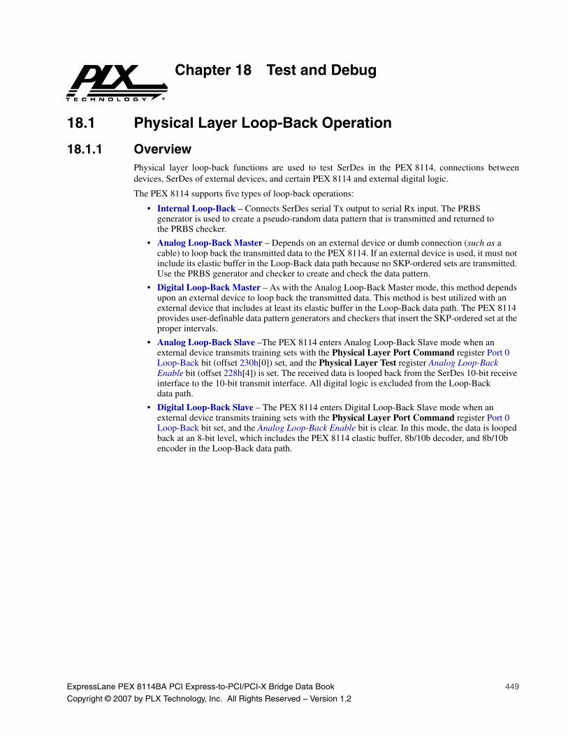
ExpressLane PEX 8114BA PCI Express-to-PCI/PCI-X Bridge Data Book 449
Copyright © 2007 by PLX Technology, Inc. All Rights Reserved – Version 1.2
Chapter 18 Test and Debug
18.1 Physical Layer Loop-Back Operation
18.1.1 OverviewPhysical layer loop-back functions are used to test SerDes in the PEX 8114, connections betweendevices, SerDes of external devices, and certain PEX 8114 and external digital logic.
The PEX 8114 supports five types of loop-back operations:
• Internal Loop-Back – Connects SerDes serial Tx output to serial Rx input. The PRBS generator is used to create a pseudo-random data pattern that is transmitted and returned to the PRBS checker.
• Analog Loop-Back Master – Depends on an external device or dumb connection (such as a cable) to loop back the transmitted data to the PEX 8114. If an external device is used, it must not include its elastic buffer in the Loop-Back data path because no SKP-ordered sets are transmitted. Use the PRBS generator and checker to create and check the data pattern.
• Digital Loop-Back Master – As with the Analog Loop-Back Master mode, this method depends upon an external device to loop back the transmitted data. This method is best utilized with an external device that includes at least its elastic buffer in the Loop-Back data path. The PEX 8114 provides user-definable data pattern generators and checkers that insert the SKP-ordered set at the proper intervals.
• Analog Loop-Back Slave –The PEX 8114 enters Analog Loop-Back Slave mode when an external device transmits training sets with the Physical Layer Port Command register Port 0 Loop-Back bit (offset 230h[0]) set, and the Physical Layer Test register Analog Loop-Back Enable bit (offset 228h[4]) is set. The received data is looped back from the SerDes 10-bit receive interface to the 10-bit transmit interface. All digital logic is excluded from the Loop-Back data path.
• Digital Loop-Back Slave – The PEX 8114 enters Digital Loop-Back Slave mode when an external device transmits training sets with the Physical Layer Port Command register Port 0 Loop-Back bit set, and the Analog Loop-Back Enable bit is clear. In this mode, the data is looped back at an 8-bit level, which includes the PEX 8114 elastic buffer, 8b/10b decoder, and 8b/10b encoder in the Loop-Back data path.

Test and Debug PLX Technology, Inc.
450 ExpressLane PEX 8114BA PCI Express-to-PCI/PCI-X Bridge Data Book
Copyright © 2007 by PLX Technology, Inc. All Rights Reserved – Version 1.2
18.1.2 Loop-Back Test ModesThe PEX 8114 supports all Loop-Back modes described in the PCI Express Base r1.1. To establish thePEX 8114 as a Loop-Back Master, the serial EEPROM is used to Write 1 to the Physical Layer PortCommand register Port 0 Ready as Loop-Back Master bit (offset 230h[3]). This enables the PEX 8114to set its Port 0 Loop-Back bit (offset 230h[0]) in the training sets during theConfiguration.Linkwidth.Start state.
After the PEX 8114 is established as a Loop-Back Master, the Physical Layer Port Command registerPort 0 Ready as Loop-Back Master bit is set. Depending on the capability of the Loop-Back Slave, thePRBS generator or Bit-Pattern generator is used to create a bit stream that is checked by checking logic.
When the PEX 8114 is established as a Loop-Back Slave, it can operate as an Analog or Digital(default) Far-End device.
• Analog Loop-Back mode is selected by setting the Physical Layer Test register Analog Loop-Back Enable bit (offset 228h[4]) to 1. In Analog Loop-Back mode, the received data is looped back from the 10-bit received data, to the 10-bit transmit data.
• When Digital Loop-Back mode is selected (power-on default), the data is looped back from the 8-bit decoded received data to the 8-bit transmit data path. This loop-back point allows the elastic buffer 8b/10b decoder, and 8b/10b encoder to be included in the test data path. Digital Loop-Back mode requires that SKP-ordered sets are included in the data stream.
18.1.2.1 Internal Loop-BackFigure 18-1 illustrates the Loop-Back data path when Internal Loop-Back mode is enabled. The onlyitems in the data path are the serializer and de-serializer. Loop-Back mode is used when the SerDesBuilt-In Self-Test (BIST) is enabled.
SerDes BIST is intended to overlap with the serial EEPROM load operation. To achieve this overlap, thePhysical Layer Test register SerDes BIST Enable bit (offset 228h[7]) is written early in the serialEEPROM load operation. After the SerDes BIST Enable bit is set, SerDes is placed in Loop-Back modeand the PRBS generator is started. The BIST is run for 512 µs; if an error is detected on a SerDes, thenthe Quad SerDes[0-3] Diagnostics Data register (offset 238h) logs the number of PRBS errorsgenerated for the group of SerDes lanes. While the SerDes BIST is in progress, the PRBS test data ispresent on the external TxP and TxN balls. The Tx Pad TxN signals must have an AC-coupled, 50-Ohmtermination to ground. The reloading of the Serial EEPROM register load has no effect on theSerDes BIST.
Figure 18-1. Internal Loop-Back (Analog near End) Data Path
PRBS Gen
PRBS Chk
Tx Pad
Rx Pad
PEX 8114
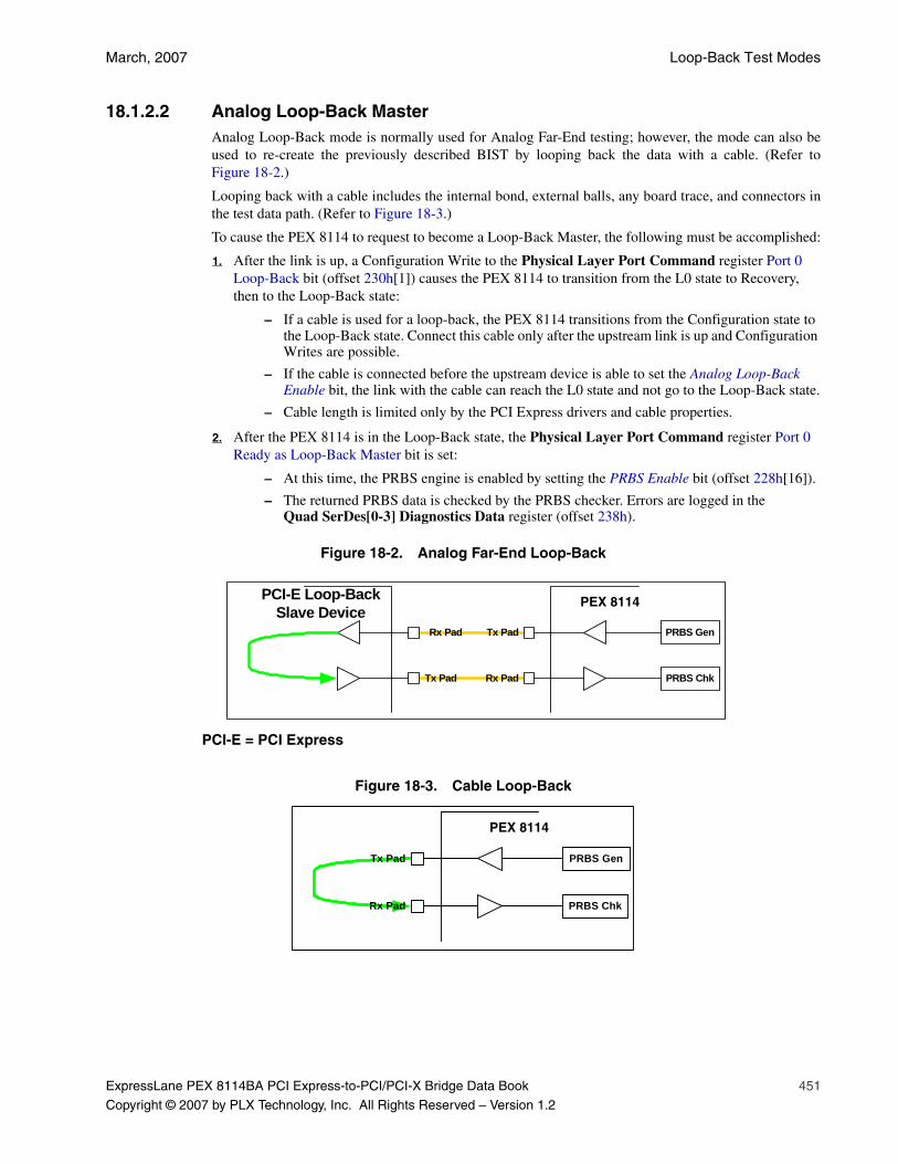
March, 2007 Loop-Back Test Modes
ExpressLane PEX 8114BA PCI Express-to-PCI/PCI-X Bridge Data Book 451
Copyright © 2007 by PLX Technology, Inc. All Rights Reserved – Version 1.2
18.1.2.2 Analog Loop-Back MasterAnalog Loop-Back mode is normally used for Analog Far-End testing; however, the mode can also beused to re-create the previously described BIST by looping back the data with a cable. (Refer toFigure 18-2.)
Looping back with a cable includes the internal bond, external balls, any board trace, and connectors inthe test data path. (Refer to Figure 18-3.)
To cause the PEX 8114 to request to become a Loop-Back Master, the following must be accomplished:
1. After the link is up, a Configuration Write to the Physical Layer Port Command register Port 0 Loop-Back bit (offset 230h[1]) causes the PEX 8114 to transition from the L0 state to Recovery, then to the Loop-Back state:
– If a cable is used for a loop-back, the PEX 8114 transitions from the Configuration state to the Loop-Back state. Connect this cable only after the upstream link is up and Configuration Writes are possible.
– If the cable is connected before the upstream device is able to set the Analog Loop-Back Enable bit, the link with the cable can reach the L0 state and not go to the Loop-Back state.
– Cable length is limited only by the PCI Express drivers and cable properties.
2. After the PEX 8114 is in the Loop-Back state, the Physical Layer Port Command register Port 0 Ready as Loop-Back Master bit is set:
– At this time, the PRBS engine is enabled by setting the PRBS Enable bit (offset 228h[16]).
– The returned PRBS data is checked by the PRBS checker. Errors are logged in the Quad SerDes[0-3] Diagnostics Data register (offset 238h).
Figure 18-2. Analog Far-End Loop-Back
Figure 18-3. Cable Loop-Back
PRBS Gen
PRBS Chk
Tx Pad
Rx Pad
PCI-E Loop-Back Slave Device
Tx Pad
Rx Pad
PCI-E = PCI Express
PEX 8114
PRBS Gen
PRBS Chk
Tx Pad
Rx Pad
PEX 8114
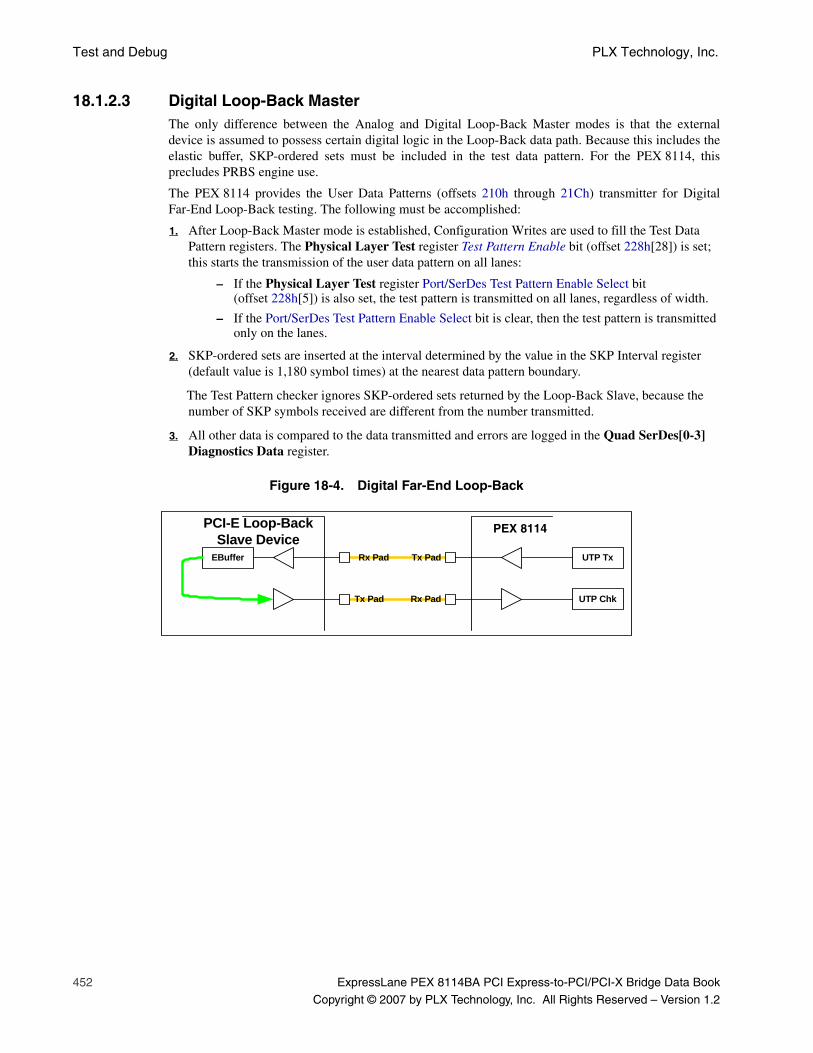
Test and Debug PLX Technology, Inc.
452 ExpressLane PEX 8114BA PCI Express-to-PCI/PCI-X Bridge Data Book
Copyright © 2007 by PLX Technology, Inc. All Rights Reserved – Version 1.2
18.1.2.3 Digital Loop-Back MasterThe only difference between the Analog and Digital Loop-Back Master modes is that the externaldevice is assumed to possess certain digital logic in the Loop-Back data path. Because this includes theelastic buffer, SKP-ordered sets must be included in the test data pattern. For the PEX 8114, thisprecludes PRBS engine use.
The PEX 8114 provides the User Data Patterns (offsets 210h through 21Ch) transmitter for DigitalFar-End Loop-Back testing. The following must be accomplished:
1. After Loop-Back Master mode is established, Configuration Writes are used to fill the Test Data Pattern registers. The Physical Layer Test register Test Pattern Enable bit (offset 228h[28]) is set; this starts the transmission of the user data pattern on all lanes:
– If the Physical Layer Test register Port/SerDes Test Pattern Enable Select bit (offset 228h[5]) is also set, the test pattern is transmitted on all lanes, regardless of width.
– If the Port/SerDes Test Pattern Enable Select bit is clear, then the test pattern is transmitted only on the lanes.
2. SKP-ordered sets are inserted at the interval determined by the value in the SKP Interval register (default value is 1,180 symbol times) at the nearest data pattern boundary.
The Test Pattern checker ignores SKP-ordered sets returned by the Loop-Back Slave, because the number of SKP symbols received are different from the number transmitted.
3. All other data is compared to the data transmitted and errors are logged in the Quad SerDes[0-3] Diagnostics Data register.
Figure 18-4. Digital Far-End Loop-Back
UTP Tx
UTP Chk
Tx Pad
Rx Pad
PCI-E Loop-Back Slave Device
Tx Pad
Rx PadEBuffer
PEX 8114
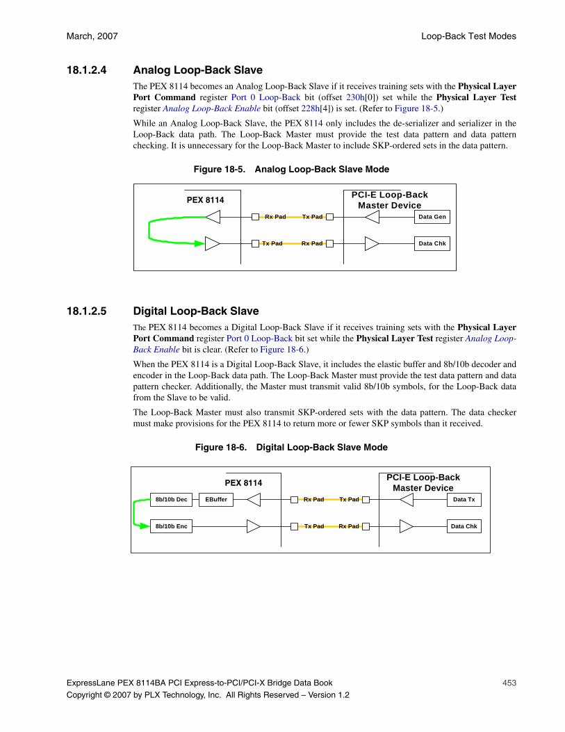
March, 2007 Loop-Back Test Modes
ExpressLane PEX 8114BA PCI Express-to-PCI/PCI-X Bridge Data Book 453
Copyright © 2007 by PLX Technology, Inc. All Rights Reserved – Version 1.2
18.1.2.4 Analog Loop-Back SlaveThe PEX 8114 becomes an Analog Loop-Back Slave if it receives training sets with the Physical LayerPort Command register Port 0 Loop-Back bit (offset 230h[0]) set while the Physical Layer Testregister Analog Loop-Back Enable bit (offset 228h[4]) is set. (Refer to Figure 18-5.)
While an Analog Loop-Back Slave, the PEX 8114 only includes the de-serializer and serializer in theLoop-Back data path. The Loop-Back Master must provide the test data pattern and data patternchecking. It is unnecessary for the Loop-Back Master to include SKP-ordered sets in the data pattern.
Figure 18-5. Analog Loop-Back Slave Mode
18.1.2.5 Digital Loop-Back SlaveThe PEX 8114 becomes a Digital Loop-Back Slave if it receives training sets with the Physical LayerPort Command register Port 0 Loop-Back bit set while the Physical Layer Test register Analog Loop-Back Enable bit is clear. (Refer to Figure 18-6.)
When the PEX 8114 is a Digital Loop-Back Slave, it includes the elastic buffer and 8b/10b decoder andencoder in the Loop-Back data path. The Loop-Back Master must provide the test data pattern and datapattern checker. Additionally, the Master must transmit valid 8b/10b symbols, for the Loop-Back datafrom the Slave to be valid.
The Loop-Back Master must also transmit SKP-ordered sets with the data pattern. The data checkermust make provisions for the PEX 8114 to return more or fewer SKP symbols than it received.
Figure 18-6. Digital Loop-Back Slave Mode
Data Gen
Data Chk
Tx Pad
Rx Pad
PCI-E Loop-Back Master Device
Tx Pad
Rx Pad
PEX 8114
Data Tx
Data Chk
Tx Pad
Rx Pad
PCI-E Loop-Back Master Device
Tx Pad
Rx PadEBuffer8b/10b Dec
8b/10b Enc
PEX 8114
Test and Debug PLX Technology, Inc.
454 ExpressLane PEX 8114BA PCI Express-to-PCI/PCI-X Bridge Data Book
Copyright © 2007 by PLX Technology, Inc. All Rights Reserved – Version 1.2
18.2 Pseudo-Random and Bit-Pattern GenerationThe SerDes quad contains a PRBS generator and checker. The PRBS generator is based on a 7-bit
Linear Feedback Shift register (LFSR), which can generate up to (27 – 1) unique patterns. ThePRBS logic is assigned to a SerDes within the quad by manipulating the Physical Layer Test registerPRBS Association field (offset 228h[9:8]). The PRBS bit stream is used for internal SerDes or analogfar-end loop-back testing.
The PEX 8114 also provides a method of creating a repeating user-defined bit pattern. Each of the four32-bit Test Pattern registers are loaded with a 32-bit data pattern. After the PEX 8114 is established as aLoop-Back Master, the Physical Layer Test register Test Pattern Enable bit (offset 228h[28]) is set to 1.The PEX 8114 proceeds to transmit the data pattern on all lanes, starting with byte 0 of the TestPattern_0 register, and continuing in sequence through the byte 3 of the Test Pattern_3 register.SKP-ordered sets are inserted at the proper intervals, which makes this method appropriate for DigitalFar-End Loop-Back testing. The received pattern is checked/compared for errors. The errors are loggedand retrieved by reading the Quad SerDes[0-3] Diagnostics Data register.
March, 2007 JTAG Interface
ExpressLane PEX 8114BA PCI Express-to-PCI/PCI-X Bridge Data Book 455
Copyright © 2007 by PLX Technology, Inc. All Rights Reserved – Version 1.2
18.3 JTAG InterfaceThe PEX 8114 provides a JTAG Boundary Scan interface, which is utilized to debug board connectivityfor each ball.
18.3.1 IEEE 1149.1 and 1149.6 Test Access PortThe IEEE 1149.1 Test Access Port (TAP), commonly referred to as the JTAG (Joint Test Action Group)debug port, is an architectural standard described in the IEEE Standard 1149.1-1990. The IEEEStandard 1149.6-2003 defines extensions to 1149.1 to support PCI Express SerDes testing. Thesestandards describe methods for accessing internal bridge facilities, using a four- or five-signal interface.
The JTAG debug port, originally designed to support scan-based board testing, is enhanced to supportthe attachment of debug tools. These enhancements, which comply with IEEE Standard 1149.1b-1994Specifications for Vendor-Specific Extensions, are compatible with standard JTAG hardware forboundary-scan system testing.
• JTAG Signals – JTAG debug port implements the four required JTAG signals – JTAG_TCK, JTAG_TDI, JTAG_TDO, JTAG_TMS – and optional JTAG_TRST# signal
• Clock Requirements – The JTAG_TCK signal frequency ranges from DC to 10 MHz
• JTAG Reset Requirements – Refer to Section 18.3.4, “JTAG Reset Input TRST#”
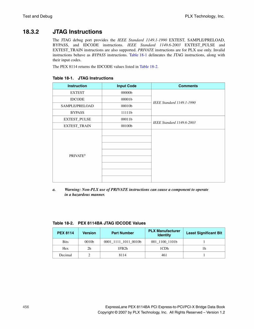
Test and Debug PLX Technology, Inc.
456 ExpressLane PEX 8114BA PCI Express-to-PCI/PCI-X Bridge Data Book
Copyright © 2007 by PLX Technology, Inc. All Rights Reserved – Version 1.2
18.3.2 JTAG InstructionsThe JTAG debug port provides the IEEE Standard 1149.1-1990 EXTEST, SAMPLE/PRELOAD,BYPASS, and IDCODE instructions. IEEE Standard 1149.6-2003 EXTEST_PULSE andEXTEST_TRAIN instructions are also supported. PRIVATE instructions are for PLX use only. Invalidinstructions behave as BYPASS instructions. Table 18-1 delineates the JTAG instructions, along withtheir input codes.
The PEX 8114 returns the IDCODE values listed in Table 18-2.
Table 18-1. JTAG Instructions
Instruction Input Code Comments
EXTEST 00000b
IEEE Standard 1149.1-1990IDCODE 00001b
SAMPLE/PRELOAD 00010b
BYPASS 11111b
EXTEST_PULSE 00011bIEEE Standard 1149.6-2003
EXTEST_TRAIN 00100b
PRIVATEa
a. Warning: Non-PLX use of PRIVATE instructions can cause a component to operate in a hazardous manner.
Table 18-2. PEX 8114BA JTAG IDCODE Values
PEX 8114 Version Part Number PLX Manufacturer Identity Least Significant Bit
Bits 0010b 0001_1111_1011_0010b 001_1100_1101b 1
Hex 2h 1FB2h 1CDh 1h
Decimal 2 8114 461 1
March, 2007 JTAG Boundary Scan
ExpressLane PEX 8114BA PCI Express-to-PCI/PCI-X Bridge Data Book 457
Copyright © 2007 by PLX Technology, Inc. All Rights Reserved – Version 1.2
18.3.3 JTAG Boundary ScanScan Description Language (BSDL), IEEE 1149.1b-1994, is a supplement to IEEE Standard 1149.1-1990 and IEEE 1149.1a-1993, IEEE Standard Test Access Port and Boundary-Scan Architecture.BSDL, a subset of the IEEE 1076-1993 Standard VHSIC Hardware Description Language (VHDL),delineates a rigorous description of testability features in components which comply with the Standard.It is used by automated test pattern generation tools for package interconnect tests and ElectronicDesign Automation (EDA) tools for synthesized test logic and verification. BSDL supports robustextensions used for internal test generation and to write software for hardware debug and diagnostics.
The primary components of BSDL include the logical port description, physical ball map, instructionset, and boundary register description.
The logical port description assigns symbolic names to the PEX 8114 balls. Each ball includes a logicaltype of in, out, in out, buffer, or linkage that defines the logical direction of signal flow.
The physical ball map correlates the PEX 8114 logical ports to the physical balls of a specific package.A BSDL description can have several physical ball maps; each map is given a unique name.
Instruction set statements describe the bit patterns that must be shifted into the Instruction Register toplace the PEX 8114 in the various test modes defined by the Standard. Instruction set statements alsosupport descriptions of instructions that are unique to the PEX 8114.
The Boundary register description lists each cell or shift stage of the Boundary register. Each cell has aunique number; the cell numbered 0 is the closest to the Test Data Out (TDO) ball and the cell with thehighest number is closest to the Test Data In (TDI) ball. Each cell contains further details, including:
• Cell type
• Logical port associated with the cell
• Logical function of the cell
• Safe value
• Control cell number
• Disable value
• Result value
18.3.4 JTAG Reset Input TRST#The JTAG_TRST# input ball is the asynchronous JTAG logic reset. When JTAG_TRST# is asserted,it causes the PEX 8114 TAP Controller to initialize. In addition, when the TAP Controller is initialized,it selects the PEX 8114 normal logic path (core-to-I/O). It is recommended that the following be takeninto consideration when implementing the asynchronous JTAG logic reset on a board:
• When JTAG functionality is required, consider one of the following:
– JTAG_TRST# input signal to use a Low-to-High transition once during the PEX 8114 boot-up, along with the system PEX_PERST# signal
– Hold the PEX 8114 TMS ball High while transitioning the PEX 8114 JTAG_TCK ball five times
• When JTAG functionality is not required, directly connect the JTAG_TRST# signal to Ground

Test and Debug PLX Technology, Inc.
458 ExpressLane PEX 8114BA PCI Express-to-PCI/PCI-X Bridge Data Book
Copyright © 2007 by PLX Technology, Inc. All Rights Reserved – Version 1.2
THIS PAGE INTENTIONALLY LEFT BLANK.
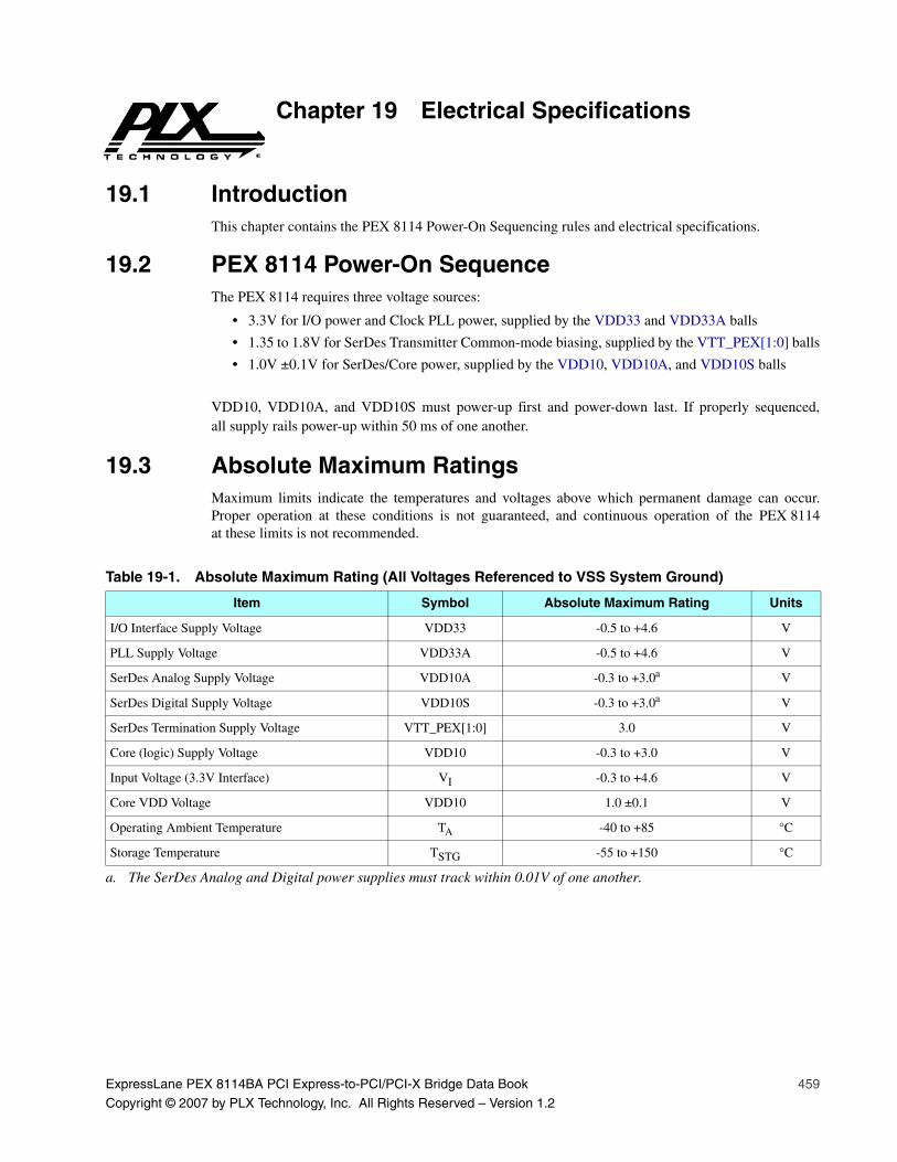
ExpressLane PEX 8114BA PCI Express-to-PCI/PCI-X Bridge Data Book 459
Copyright © 2007 by PLX Technology, Inc. All Rights Reserved – Version 1.2
Chapter 19 Electrical Specifications
19.1 IntroductionThis chapter contains the PEX 8114 Power-On Sequencing rules and electrical specifications.
19.2 PEX 8114 Power-On SequenceThe PEX 8114 requires three voltage sources:
• 3.3V for I/O power and Clock PLL power, supplied by the VDD33 and VDD33A balls
• 1.35 to 1.8V for SerDes Transmitter Common-mode biasing, supplied by the VTT_PEX[1:0] balls
• 1.0V ±0.1V for SerDes/Core power, supplied by the VDD10, VDD10A, and VDD10S balls
VDD10, VDD10A, and VDD10S must power-up first and power-down last. If properly sequenced,all supply rails power-up within 50 ms of one another.
19.3 Absolute Maximum RatingsMaximum limits indicate the temperatures and voltages above which permanent damage can occur.Proper operation at these conditions is not guaranteed, and continuous operation of the PEX 8114at these limits is not recommended.
Table 19-1. Absolute Maximum Rating (All Voltages Referenced to VSS System Ground)
Item Symbol Absolute Maximum Rating Units
I/O Interface Supply Voltage VDD33 -0.5 to +4.6 V
PLL Supply Voltage VDD33A -0.5 to +4.6 V
SerDes Analog Supply Voltage VDD10A -0.3 to +3.0a
a. The SerDes Analog and Digital power supplies must track within 0.01V of one another.
V
SerDes Digital Supply Voltage VDD10S -0.3 to +3.0a V
SerDes Termination Supply Voltage VTT_PEX[1:0] 3.0 V
Core (logic) Supply Voltage VDD10 -0.3 to +3.0 V
Input Voltage (3.3V Interface) VI -0.3 to +4.6 V
Core VDD Voltage VDD10 1.0 ±0.1 V
Operating Ambient Temperature TA -40 to +85 °C
Storage Temperature TSTG -55 to +150 °C

Electrical Specifications PLX Technology, Inc.
460 ExpressLane PEX 8114BA PCI Express-to-PCI/PCI-X Bridge Data Book
Copyright © 2007 by PLX Technology, Inc. All Rights Reserved – Version 1.2
Table 19-2. Capacitance for Logic/Control I/O
Item Symbol Conditions Min Typ Max Unit
Input Ball CINVDD33/A = 0.0V,
VDD10/A/S = 0.0V
4 6 pF
Output Ball COUT 6 10 pF
Input/Output and Three-State Ball CI/O 6 10 pF
Table 19-3. Power Dissipation
Parameter Symbol Conditionsa
a. PEX_REFCLKn/p = 100 MHz. A 250-MHz clock is synthesized from PEX_REFCLKn/p andused internally to clock the SerDes and core logic.
Min. Typ Max Unit
Power Dissipation PDVDD33/A = 3.3V, ±10%
VDD10/A/S = 1.0V, ±10%VTT_PEX[1:0] = 1.5V, ±10%
3001.475115
3751.93150
mWW
mW
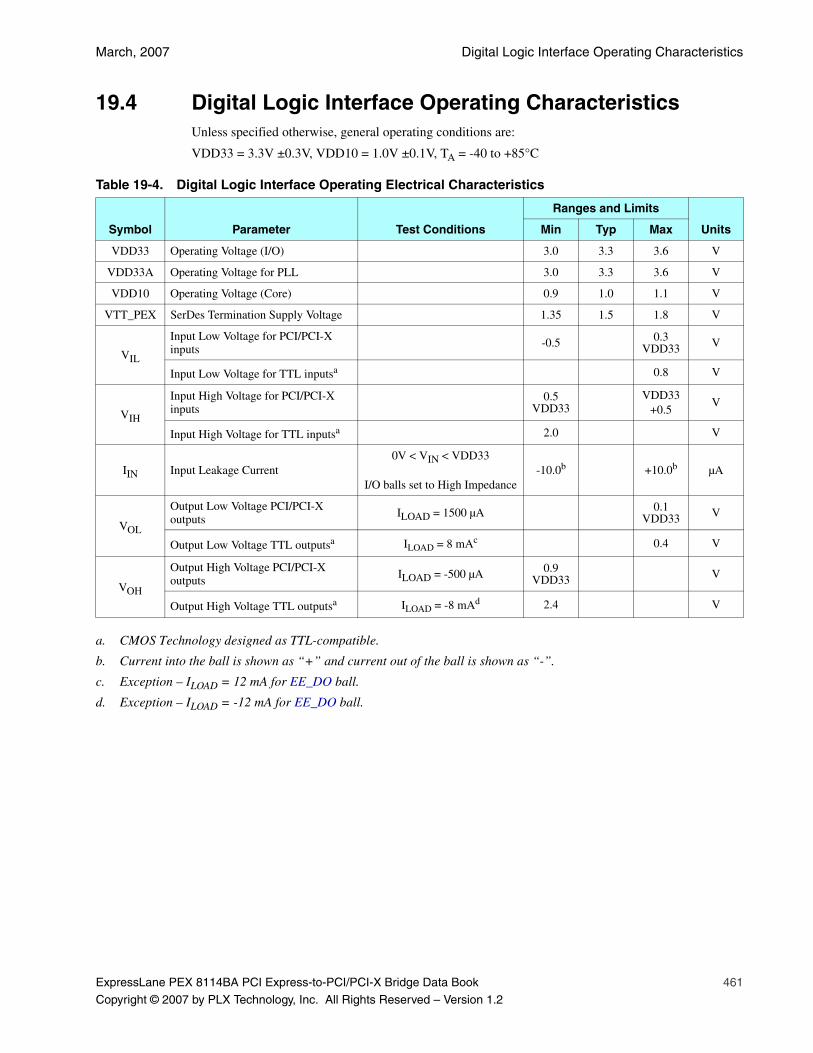
March, 2007 Digital Logic Interface Operating Characteristics
ExpressLane PEX 8114BA PCI Express-to-PCI/PCI-X Bridge Data Book 461
Copyright © 2007 by PLX Technology, Inc. All Rights Reserved – Version 1.2
19.4 Digital Logic Interface Operating CharacteristicsUnless specified otherwise, general operating conditions are:
VDD33 = 3.3V ±0.3V, VDD10 = 1.0V ±0.1V, TA = -40 to +85°C
Table 19-4. Digital Logic Interface Operating Electrical Characteristics
Symbol Parameter Test Conditions
Ranges and Limits
UnitsMin Typ Max
VDD33 Operating Voltage (I/O) 3.0 3.3 3.6 V
VDD33A Operating Voltage for PLL 3.0 3.3 3.6 V
VDD10 Operating Voltage (Core) 0.9 1.0 1.1 V
VTT_PEX SerDes Termination Supply Voltage 1.35 1.5 1.8 V
VIL
Input Low Voltage for PCI/PCI-X inputs -0.5 0.3
VDD33 V
Input Low Voltage for TTL inputsa
a. CMOS Technology designed as TTL-compatible.
0.8 V
VIH
Input High Voltage for PCI/PCI-X inputs
0.5 VDD33
VDD33+0.5
V
Input High Voltage for TTL inputsa 2.0 V
IIN Input Leakage Current0V < VIN < VDD33
I/O balls set to High Impedance-10.0b +10.0b
b. Current into the ball is shown as “+” and current out of the ball is shown as “-”.
µA
VOL
Output Low Voltage PCI/PCI-X outputs
ILOAD = 1500 µA 0.1 VDD33 V
Output Low Voltage TTL outputsa ILOAD = 8 mAc
c. Exception – ILOAD = 12 mA for EE_DO ball.
0.4 V
VOH
Output High Voltage PCI/PCI-X outputs ILOAD = -500 µA 0.9
VDD33 V
Output High Voltage TTL outputsa ILOAD = -8 mAd
d. Exception – ILOAD = -12 mA for EE_DO ball.
2.4 V
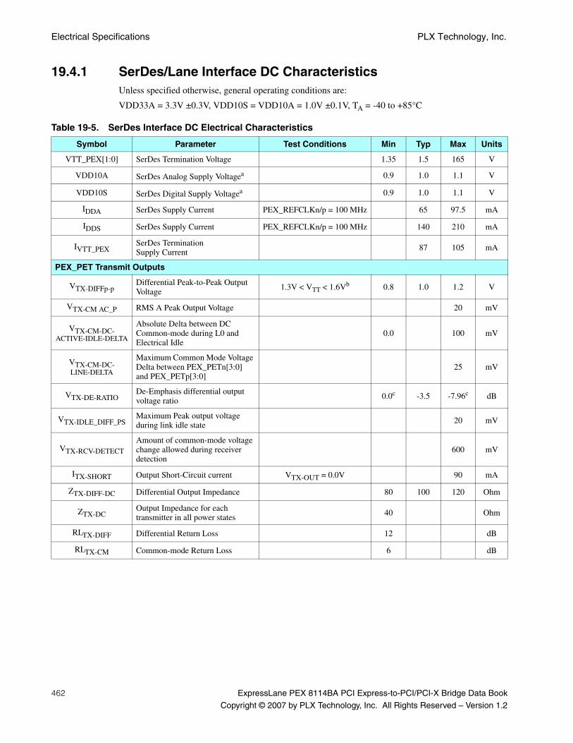
Electrical Specifications PLX Technology, Inc.
462 ExpressLane PEX 8114BA PCI Express-to-PCI/PCI-X Bridge Data Book
Copyright © 2007 by PLX Technology, Inc. All Rights Reserved – Version 1.2
19.4.1 SerDes/Lane Interface DC CharacteristicsUnless specified otherwise, general operating conditions are:
VDD33A = 3.3V ±0.3V, VDD10S = VDD10A = 1.0V ±0.1V, TA = -40 to +85°C
Table 19-5. SerDes Interface DC Electrical Characteristics
Symbol Parameter Test Conditions Min Typ Max Units
VTT_PEX[1:0] SerDes Termination Voltage 1.35 1.5 165 V
VDD10A SerDes Analog Supply Voltagea 0.9 1.0 1.1 V
VDD10S SerDes Digital Supply Voltagea 0.9 1.0 1.1 V
IDDA SerDes Supply Current PEX_REFCLKn/p = 100 MHz 65 97.5 mA
IDDS SerDes Supply Current PEX_REFCLKn/p = 100 MHz 140 210 mA
IVTT_PEXSerDes Termination Supply Current
87 105 mA
PEX_PET Transmit Outputs
VTX-DIFFp-pDifferential Peak-to-Peak Output Voltage
1.3V < VTT < 1.6Vb 0.8 1.0 1.2 V
VTX-CM AC_P RMS A Peak Output Voltage 20 mV
VTX-CM-DC-ACTIVE-IDLE-DELTA
Absolute Delta between DC Common-mode during L0 and Electrical Idle
0.0 100 mV
VTX-CM-DC-LINE-DELTA
Maximum Common Mode Voltage Delta between PEX_PETn[3:0] and PEX_PETp[3:0]
25 mV
VTX-DE-RATIODe-Emphasis differential output voltage ratio 0.0c -3.5 -7.96c dB
VTX-IDLE_DIFF_PSMaximum Peak output voltage during link idle state 20 mV
VTX-RCV-DETECT
Amount of common-mode voltage change allowed during receiver detection
600 mV
ITX-SHORT Output Short-Circuit current VTX-OUT = 0.0V 90 mA
ZTX-DIFF-DC Differential Output Impedance 80 100 120 Ohm
ZTX-DCOutput Impedance for each transmitter in all power states 40 Ohm
RLTX-DIFF Differential Return Loss 12 dB
RLTX-CM Common-mode Return Loss 6 dB
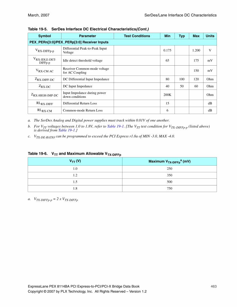
March, 2007 SerDes/Lane Interface DC Characteristics
ExpressLane PEX 8114BA PCI Express-to-PCI/PCI-X Bridge Data Book 463
Copyright © 2007 by PLX Technology, Inc. All Rights Reserved – Version 1.2
PEX_PERn[3:0]/PEX_PERp[3:0] Receiver Inputs
VRX-DIFFp-pDifferential Peak-to-Peak Input Voltage
0.175 1.200 V
VRX-IDLE-DET-DIFFp-p
Idle detect threshold voltage 65 175 mV
VRX-CM ACReceiver Common-mode voltage for AC Coupling 150 mV
ZRX-DIFF-DC DC Differential Input Impedance 80 100 120 Ohm
ZRX-DC DC Input Impedance 40 50 60 Ohm
ZRX-HIGH-IMP-DCInput Impedance during power down conditions 200K Ohm
RLRX-DIFF Differential Return Loss 15 dB
RLRX-CM Common-mode Return Loss 6 dB
a. The SerDes Analog and Digital power supplies must track within 0.01V of one another.
b. For VTT voltages between 1.0 to 1.8V, refer to Table 19-1. [The VTT test condition for VTX–DIFFp-p (listed above)is derived from Table 19-1.]
c. VTX-DE-RATIO can be programmed to exceed the PCI Express r1.0a of MIN -3.0, MAX -4.0.
Table 19-6. VTT and Maximum Allowable VTX-DIFFp
VTT (V) Maximum VTX-DIFFpa (mV)
a. VTX-DIFFp-p = 2 x VTX-DIFFp
1.0 250
1.2 350
1.5 500
1.8 750
Table 19-5. SerDes Interface DC Electrical Characteristics(Cont.)
Symbol Parameter Test Conditions Min Typ Max Units
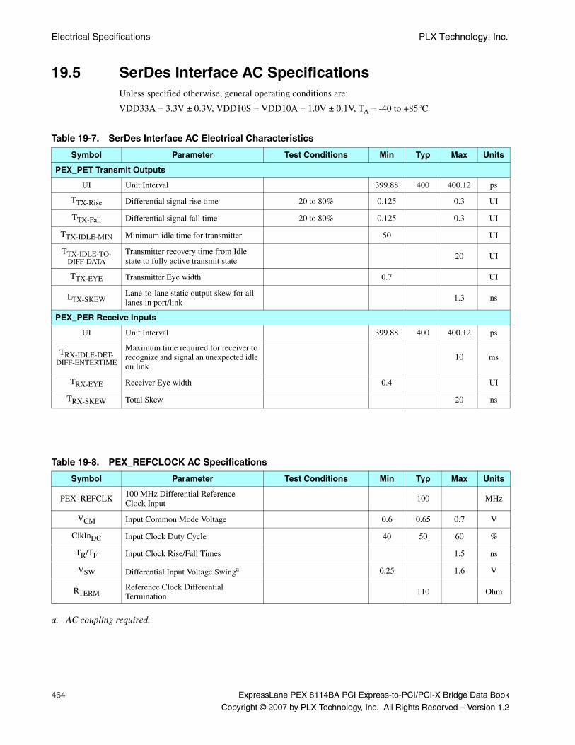
Electrical Specifications PLX Technology, Inc.
464 ExpressLane PEX 8114BA PCI Express-to-PCI/PCI-X Bridge Data Book
Copyright © 2007 by PLX Technology, Inc. All Rights Reserved – Version 1.2
19.5 SerDes Interface AC SpecificationsUnless specified otherwise, general operating conditions are:
VDD33A = 3.3V ± 0.3V, VDD10S = VDD10A = 1.0V ± 0.1V, TA = -40 to +85°C
Table 19-7. SerDes Interface AC Electrical Characteristics
Symbol Parameter Test Conditions Min Typ Max Units
PEX_PET Transmit Outputs
UI Unit Interval 399.88 400 400.12 ps
TTX-Rise Differential signal rise time 20 to 80% 0.125 0.3 UI
TTX-Fall Differential signal fall time 20 to 80% 0.125 0.3 UI
TTX-IDLE-MIN Minimum idle time for transmitter 50 UI
TTX-IDLE-TO-DIFF-DATA
Transmitter recovery time from Idle state to fully active transmit state
20 UI
TTX-EYE Transmitter Eye width 0.7 UI
LTX-SKEWLane-to-lane static output skew for all lanes in port/link 1.3 ns
PEX_PER Receive Inputs
UI Unit Interval 399.88 400 400.12 ps
TRX-IDLE-DET-DIFF-ENTERTIME
Maximum time required for receiver to recognize and signal an unexpected idle on link
10 ms
TRX-EYE Receiver Eye width 0.4 UI
TRX-SKEW Total Skew 20 ns
Table 19-8. PEX_REFCLOCK AC Specifications
Symbol Parameter Test Conditions Min Typ Max Units
PEX_REFCLK 100 MHz Differential Reference Clock Input
100 MHz
VCM Input Common Mode Voltage 0.6 0.65 0.7 V
ClkInDC Input Clock Duty Cycle 40 50 60 %
TR/TF Input Clock Rise/Fall Times 1.5 ns
VSW Differential Input Voltage Swinga
a. AC coupling required.
0.25 1.6 V
RTERMReference Clock Differential Termination 110 Ohm
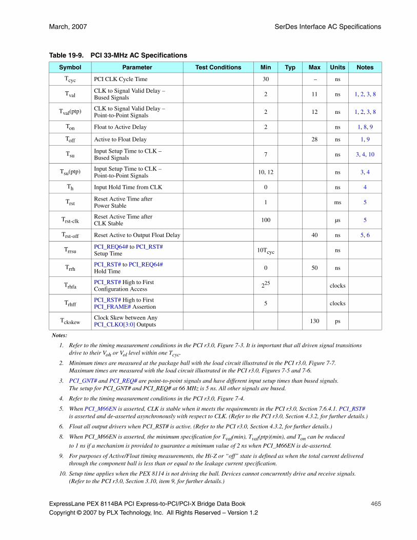
March, 2007 SerDes Interface AC Specifications
ExpressLane PEX 8114BA PCI Express-to-PCI/PCI-X Bridge Data Book 465
Copyright © 2007 by PLX Technology, Inc. All Rights Reserved – Version 1.2
Table 19-9. PCI 33-MHz AC Specifications
Symbol Parameter Test Conditions Min Typ Max Units Notes
Tcyc PCI CLK Cycle Time 30 – ns
TvalCLK to Signal Valid Delay – Bused Signals 2 11 ns 1, 2, 3, 8
Tval(ptp) CLK to Signal Valid Delay – Point-to-Point Signals 2 12 ns 1, 2, 3, 8
Ton Float to Active Delay 2 ns 1, 8, 9
Toff Active to Float Delay 28 ns 1, 9
TsuInput Setup Time to CLK – Bused Signals 7 ns 3, 4, 10
Tsu(ptp) Input Setup Time to CLK – Point-to-Point Signals
10, 12 ns 3, 4
Th Input Hold Time from CLK 0 ns 4
TrstReset Active Time after Power Stable
1 ms 5
Trst-clkReset Active Time after CLK Stable 100 µs 5
Trst-off Reset Active to Output Float Delay 40 ns 5, 6
TrrsuPCI_REQ64# to PCI_RST# Setup Time 10Tcyc ns
TrrhPCI_RST# to PCI_REQ64# Hold Time
0 50 ns
TrhfaPCI_RST# High to First Configuration Access 225 clocks
TrhffPCI_RST# High to First PCI_FRAME# Assertion 5 clocks
TckskewClock Skew between Any PCI_CLKO[3:0] Outputs
130 ps
Notes:
1. Refer to the timing measurement conditions in the PCI r3.0, Figure 7-3. It is important that all driven signal transitions drive to their Voh or Vol level within one Tcyc.
2. Minimum times are measured at the package ball with the load circuit illustrated in the PCI r3.0, Figure 7-7. Maximum times are measured with the load circuit illustrated in the PCI r3.0, Figures 7-5 and 7-6.
3. PCI_GNT# and PCI_REQ# are point-to-point signals and have different input setup times than bused signals. The setup for PCI_GNT# and PCI_REQ# at 66 MHz is 5 ns. All other signals are bused.
4. Refer to the timing measurement conditions in the PCI r3.0, Figure 7-4.
5. When PCI_M66EN is asserted, CLK is stable when it meets the requirements in the PCI r3.0, Section 7.6.4.1. PCI_RST# is asserted and de-asserted asynchronously with respect to CLK. (Refer to the PCI r3.0, Section 4.3.2, for further details.)
6. Float all output drivers when PCI_RST# is active. (Refer to the PCI r3.0, Section 4.3.2, for further details.)
8. When PCI_M66EN is asserted, the minimum specification for Tval(min), Tval(ptp)(min), and Ton can be reduced
to 1 ns if a mechanism is provided to guarantee a minimum value of 2 ns when PCI_M66EN is de-asserted.
9. For purposes of Active/Float timing measurements, the Hi-Z or “off” state is defined as when the total current delivered through the component ball is less than or equal to the leakage current specification.
10. Setup time applies when the PEX 8114 is not driving the ball. Devices cannot concurrently drive and receive signals. (Refer to the PCI r3.0, Section 3.10, item 9, for further details.)
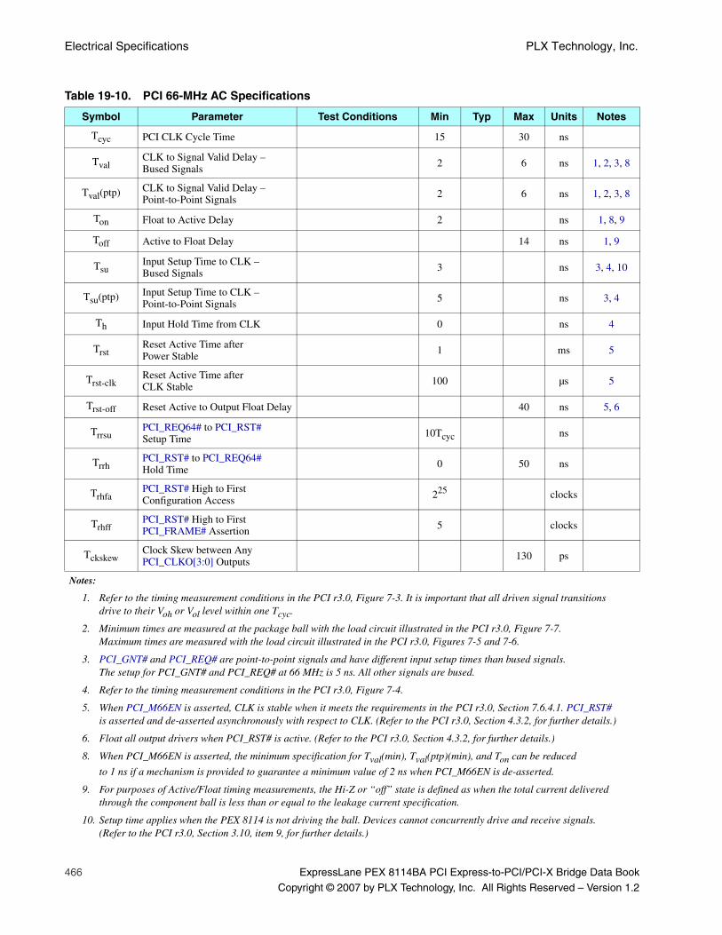
Electrical Specifications PLX Technology, Inc.
466 ExpressLane PEX 8114BA PCI Express-to-PCI/PCI-X Bridge Data Book
Copyright © 2007 by PLX Technology, Inc. All Rights Reserved – Version 1.2
Table 19-10. PCI 66-MHz AC Specifications
Symbol Parameter Test Conditions Min Typ Max Units Notes
Tcyc PCI CLK Cycle Time 15 30 ns
TvalCLK to Signal Valid Delay – Bused Signals 2 6 ns 1, 2, 3, 8
Tval(ptp) CLK to Signal Valid Delay – Point-to-Point Signals 2 6 ns 1, 2, 3, 8
Ton Float to Active Delay 2 ns 1, 8, 9
Toff Active to Float Delay 14 ns 1, 9
TsuInput Setup Time to CLK – Bused Signals 3 ns 3, 4, 10
Tsu(ptp) Input Setup Time to CLK – Point-to-Point Signals
5 ns 3, 4
Th Input Hold Time from CLK 0 ns 4
TrstReset Active Time after Power Stable
1 ms 5
Trst-clkReset Active Time after CLK Stable 100 µs 5
Trst-off Reset Active to Output Float Delay 40 ns 5, 6
TrrsuPCI_REQ64# to PCI_RST# Setup Time 10Tcyc ns
TrrhPCI_RST# to PCI_REQ64# Hold Time
0 50 ns
TrhfaPCI_RST# High to First Configuration Access 225 clocks
TrhffPCI_RST# High to First PCI_FRAME# Assertion 5 clocks
TckskewClock Skew between Any PCI_CLKO[3:0] Outputs
130 ps
Notes:
1. Refer to the timing measurement conditions in the PCI r3.0, Figure 7-3. It is important that all driven signal transitions drive to their Voh or Vol level within one Tcyc.
2. Minimum times are measured at the package ball with the load circuit illustrated in the PCI r3.0, Figure 7-7. Maximum times are measured with the load circuit illustrated in the PCI r3.0, Figures 7-5 and 7-6.
3. PCI_GNT# and PCI_REQ# are point-to-point signals and have different input setup times than bused signals. The setup for PCI_GNT# and PCI_REQ# at 66 MHz is 5 ns. All other signals are bused.
4. Refer to the timing measurement conditions in the PCI r3.0, Figure 7-4.
5. When PCI_M66EN is asserted, CLK is stable when it meets the requirements in the PCI r3.0, Section 7.6.4.1. PCI_RST# is asserted and de-asserted asynchronously with respect to CLK. (Refer to the PCI r3.0, Section 4.3.2, for further details.)
6. Float all output drivers when PCI_RST# is active. (Refer to the PCI r3.0, Section 4.3.2, for further details.)
8. When PCI_M66EN is asserted, the minimum specification for Tval(min), Tval(ptp)(min), and Ton can be reduced
to 1 ns if a mechanism is provided to guarantee a minimum value of 2 ns when PCI_M66EN is de-asserted.
9. For purposes of Active/Float timing measurements, the Hi-Z or “off” state is defined as when the total current delivered through the component ball is less than or equal to the leakage current specification.
10. Setup time applies when the PEX 8114 is not driving the ball. Devices cannot concurrently drive and receive signals. (Refer to the PCI r3.0, Section 3.10, item 9, for further details.)
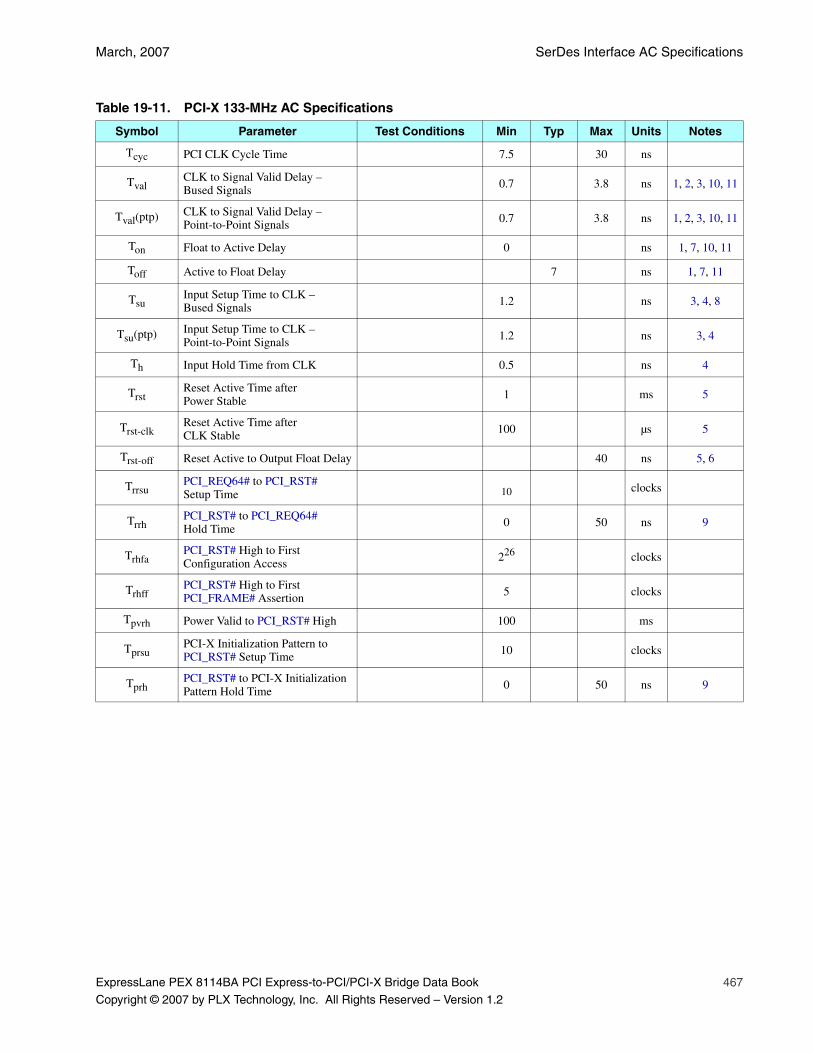
March, 2007 SerDes Interface AC Specifications
ExpressLane PEX 8114BA PCI Express-to-PCI/PCI-X Bridge Data Book 467
Copyright © 2007 by PLX Technology, Inc. All Rights Reserved – Version 1.2
Table 19-11. PCI-X 133-MHz AC Specifications
Symbol Parameter Test Conditions Min Typ Max Units Notes
Tcyc PCI CLK Cycle Time 7.5 30 ns
TvalCLK to Signal Valid Delay – Bused Signals 0.7 3.8 ns 1, 2, 3, 10, 11
Tval(ptp) CLK to Signal Valid Delay – Point-to-Point Signals 0.7 3.8 ns 1, 2, 3, 10, 11
Ton Float to Active Delay 0 ns 1, 7, 10, 11
Toff Active to Float Delay 7 ns 1, 7, 11
TsuInput Setup Time to CLK – Bused Signals 1.2 ns 3, 4, 8
Tsu(ptp) Input Setup Time to CLK – Point-to-Point Signals
1.2 ns 3, 4
Th Input Hold Time from CLK 0.5 ns 4
TrstReset Active Time after Power Stable
1 ms 5
Trst-clkReset Active Time after CLK Stable 100 µs 5
Trst-off Reset Active to Output Float Delay 40 ns 5, 6
TrrsuPCI_REQ64# to PCI_RST# Setup Time 10 clocks
TrrhPCI_RST# to PCI_REQ64# Hold Time
0 50 ns 9
TrhfaPCI_RST# High to First Configuration Access 226 clocks
TrhffPCI_RST# High to First PCI_FRAME# Assertion 5 clocks
Tpvrh Power Valid to PCI_RST# High 100 ms
TprsuPCI-X Initialization Pattern to PCI_RST# Setup Time 10 clocks
TprhPCI_RST# to PCI-X Initialization Pattern Hold Time
0 50 ns 9
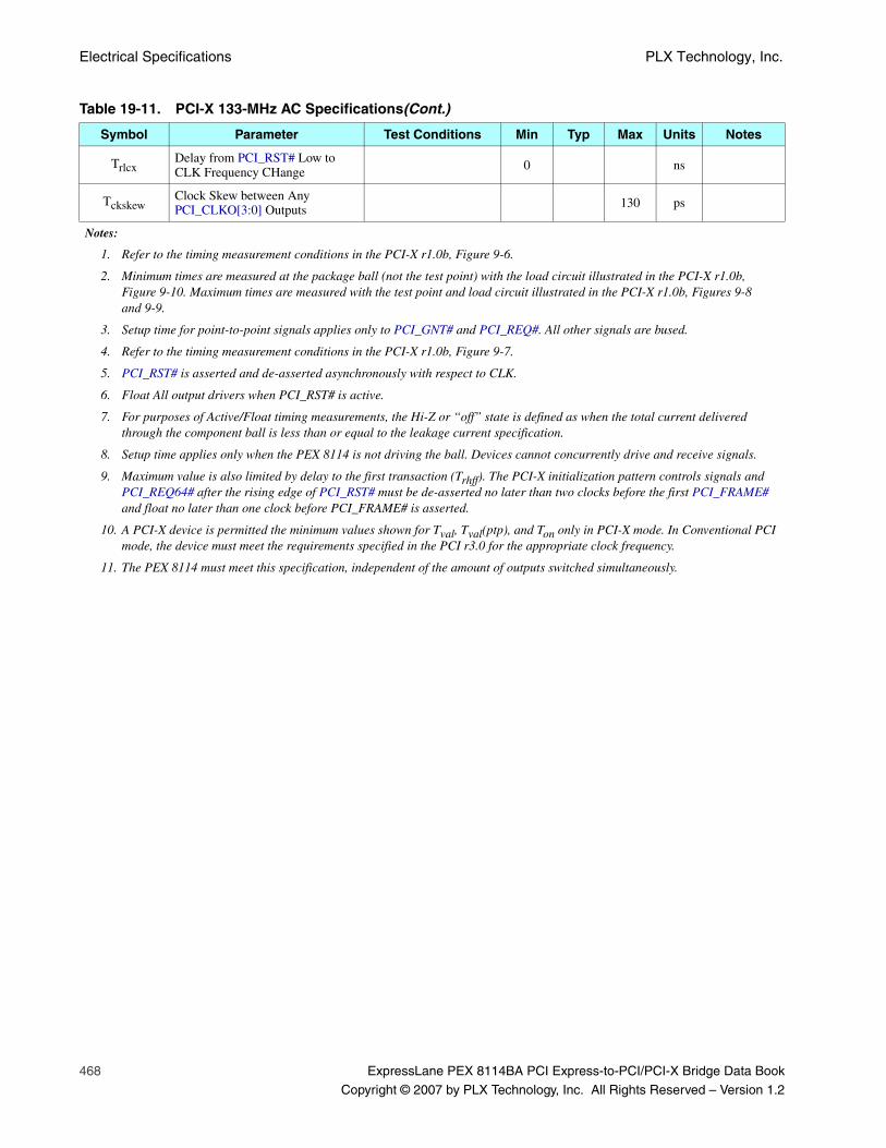
Electrical Specifications PLX Technology, Inc.
468 ExpressLane PEX 8114BA PCI Express-to-PCI/PCI-X Bridge Data Book
Copyright © 2007 by PLX Technology, Inc. All Rights Reserved – Version 1.2
TrlcxDelay from PCI_RST# Low to CLK Frequency CHange 0 ns
TckskewClock Skew between Any PCI_CLKO[3:0] Outputs 130 ps
Notes:
1. Refer to the timing measurement conditions in the PCI-X r1.0b, Figure 9-6.
2. Minimum times are measured at the package ball (not the test point) with the load circuit illustrated in the PCI-X r1.0b, Figure 9-10. Maximum times are measured with the test point and load circuit illustrated in the PCI-X r1.0b, Figures 9-8 and 9-9.
3. Setup time for point-to-point signals applies only to PCI_GNT# and PCI_REQ#. All other signals are bused.
4. Refer to the timing measurement conditions in the PCI-X r1.0b, Figure 9-7.
5. PCI_RST# is asserted and de-asserted asynchronously with respect to CLK.
6. Float All output drivers when PCI_RST# is active.
7. For purposes of Active/Float timing measurements, the Hi-Z or “off” state is defined as when the total current delivered through the component ball is less than or equal to the leakage current specification.
8. Setup time applies only when the PEX 8114 is not driving the ball. Devices cannot concurrently drive and receive signals.
9. Maximum value is also limited by delay to the first transaction (Trhff). The PCI-X initialization pattern controls signals and PCI_REQ64# after the rising edge of PCI_RST# must be de-asserted no later than two clocks before the first PCI_FRAME# and float no later than one clock before PCI_FRAME# is asserted.
10. A PCI-X device is permitted the minimum values shown for Tval, Tval(ptp), and Ton only in PCI-X mode. In Conventional PCI mode, the device must meet the requirements specified in the PCI r3.0 for the appropriate clock frequency.
11. The PEX 8114 must meet this specification, independent of the amount of outputs switched simultaneously.
Table 19-11. PCI-X 133-MHz AC Specifications(Cont.)
Symbol Parameter Test Conditions Min Typ Max Units Notes

ExpressLane PEX 8114BA PCI Express-to-PCI/PCI-X Bridge Data Book 469
Copyright © 2007 by PLX Technology, Inc. All Rights Reserved – Version 1.2
Chapter 20 Mechanical Specifications
20.1 PEX 8114 Package SpecificationsThe PEX 8114 is offered in a 256-Ball, 17-mm square Plastic Ball Grid Array (BGA) package. Table 20-1delineates the package specifications.
20.2 Thermal Characteristics
Table 20-1. PEX 8114 256-Ball PBGA Package Specifications
Parameter Specification
Package Type Plastic Ball Grid Array
Package Dimensions 17 x 17 mm (approximately 1.86 mm high)
Ball matrix pattern 16 x 16 mm
Ball pitch 1.00 mm
Ball diameter 0.50 ±0.10 mm
Ball spacing 0.40 mm
Table 20-2. PEX 8114 Package Thermal Resistance Airflow, Θj-c = 4.6 °C/Wa
a. Relevant for packages used with external heat sinks.
Theta 0 m/s 1 m/s 2 m/s
°C/W (Θj-a)b
b. Relevant for packages used without external heat sinks.c. The PEX 8114 does not require a heat sink during standard operating conditions.
17.8 15.9 14.8
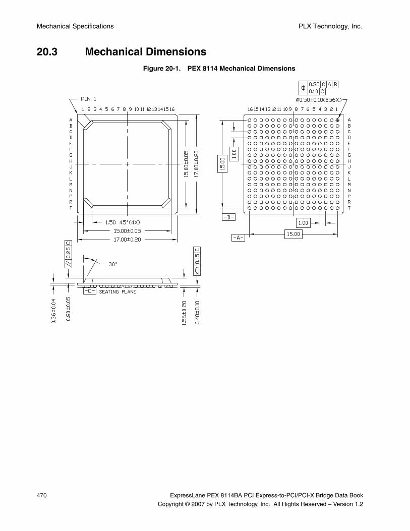
Mechanical Specifications PLX Technology, Inc.
470 ExpressLane PEX 8114BA PCI Express-to-PCI/PCI-X Bridge Data Book
Copyright © 2007 by PLX Technology, Inc. All Rights Reserved – Version 1.2
20.3 Mechanical DimensionsFigure 20-1. PEX 8114 Mechanical Dimensions
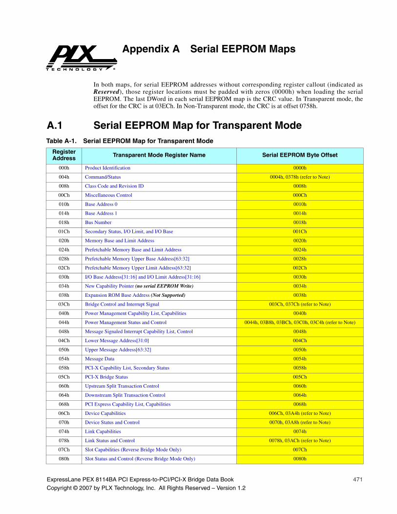
ExpressLane PEX 8114BA PCI Express-to-PCI/PCI-X Bridge Data Book 471
Copyright © 2007 by PLX Technology, Inc. All Rights Reserved – Version 1.2
Appendix A Serial EEPROM Maps
In both maps, for serial EEPROM addresses without corresponding register callout (indicated asReserved), those register locations must be padded with zeros (0000h) when loading the serialEEPROM. The last DWord in each serial EEPROM map is the CRC value. In Transparent mode, theoffset for the CRC is at 03ECh. In Non-Transparent mode, the CRC is at offset 0758h.
A.1 Serial EEPROM Map for Transparent ModeTable A-1. Serial EEPROM Map for Transparent Mode
Register Address Transparent Mode Register Name Serial EEPROM Byte Offset
000h Product Identification 0000h
004h Command/Status 0004h, 0378h (refer to Note)
008h Class Code and Revision ID 0008h
00Ch Miscellaneous Control 000Ch
010h Base Address 0 0010h
014h Base Address 1 0014h
018h Bus Number 0018h
01Ch Secondary Status, I/O Limit, and I/O Base 001Ch
020h Memory Base and Limit Address 0020h
024h Prefetchable Memory Base and Limit Address 0024h
028h Prefetchable Memory Upper Base Address[63:32] 0028h
02Ch Prefetchable Memory Upper Limit Address[63:32] 002Ch
030h I/O Base Address[31:16] and I/O Limit Address[31:16] 0030h
034h New Capability Pointer (no serial EEPROM Write) 0034h
038h Expansion ROM Base Address (Not Supported) 0038h
03Ch Bridge Control and Interrupt Signal 003Ch, 037Ch (refer to Note)
040h Power Management Capability List, Capabilities 0040h
044h Power Management Status and Control 0044h, 03B8h, 03BCh, 03C0h, 03C4h (refer to Note)
048h Message Signaled Interrupt Capability List, Control 0048h
04Ch Lower Message Address[31:0] 004Ch
050h Upper Message Address[63:32] 0050h
054h Message Data 0054h
058h PCI-X Capability List, Secondary Status 0058h
05Ch PCI-X Bridge Status 005Ch
060h Upstream Split Transaction Control 0060h
064h Downstream Split Transaction Control 0064h
068h PCI Express Capability List, Capabilities 0068h
06Ch Device Capabilities 006Ch, 03A4h (refer to Note)
070h Device Status and Control 0070h, 03A8h (refer to Note)
074h Link Capabilities 0074h
078h Link Status and Control 0078h, 03ACh (refer to Note)
07Ch Slot Capabilities (Reverse Bridge Mode Only) 007Ch
080h Slot Status and Control (Reverse Bridge Mode Only) 0080h
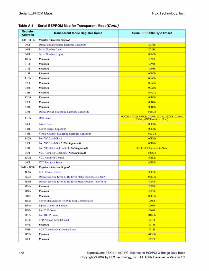
Serial EEPROM Maps PLX Technology, Inc.
472 ExpressLane PEX 8114BA PCI Express-to-PCI/PCI-X Bridge Data Book
Copyright © 2007 by PLX Technology, Inc. All Rights Reserved – Version 1.2
084h - 0FCh Register Addresses Skipped
100h Device Serial Number Extended Capability 0084h
104h Serial Number (Low) 0088h
108h Serial Number (High) 008Ch
10Ch Reserved 0090h
110h Reserved 0094h
114h Reserved 0098h
118h Reserved 009Ch
11Ch Reserved 00A0h
120h Reserved 00A4h
124h Reserved 00A8h
128h Reserved 00ACh
12Ch Reserved 00B0h
130h Reserved 00B4h
134h Reserved 00B8h
138h Device Power Budgeting Extended Capability 00BCh
13Ch Data Select 00C0h, 03CCh, 03D0h, 03D4h, 03D8h, 03DCh, 03E0h, 03E4h, 03E8h (refer to Note)
140h Power Data 00C4h
144h Power Budget Capability 00C8h
148h Virtual Channel Budgeting Extended Capability 00CCh
14Ch Port VC Capability 1 00D0h
150h Port VC Capability 2 (Not Supported) 00D4h
154h Port VC Status and Control (Not Supported) 00D8h, 03C8h (refer to Note)
158h VC0 Resource Capability (Not Supported) 00DCh
15Ch VC0 Resource Control 00E0h
160h VC0 Resource Status 00E4h
164h - 1C4h Register Addresses Skipped
1C8h ECC Check Disable 00E8h
1CCh Device-Specific Error 32-Bit Error Status (Factory Test Only) 00ECh
1D0h Device-Specific Error 32-Bit Error Mask (Factory Test Only) 00F0h
1D4h Reserved 00F4h
1D8h Reserved 00F8h
1DCh Reserved 00FCh
1E0h Power Management Hot Plug User Configuration 0100h
1E4h Egress Control and Status 0104h
1E8h Bad TLP Count 0108h
1ECh Bad DLLP Count 010Ch
1F0h TLP Payload Length Count 0110h
1F4h Reserved 0114h
1F8h ACK Transmission Latency Limit 0118h
1FCh Reserved 011Ch
200h Reserved 0120h
Table A-1. Serial EEPROM Map for Transparent Mode(Cont.)Register Address Transparent Mode Register Name Serial EEPROM Byte Offset
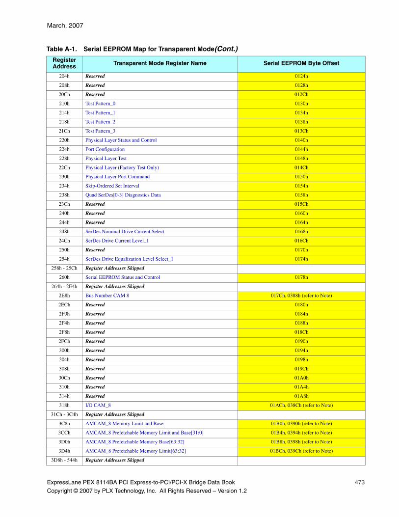
March, 2007
ExpressLane PEX 8114BA PCI Express-to-PCI/PCI-X Bridge Data Book 473
Copyright © 2007 by PLX Technology, Inc. All Rights Reserved – Version 1.2
204h Reserved 0124h
208h Reserved 0128h
20Ch Reserved 012Ch
210h Test Pattern_0 0130h
214h Test Pattern_1 0134h
218h Test Pattern_2 0138h
21Ch Test Pattern_3 013Ch
220h Physical Layer Status and Control 0140h
224h Port Configuration 0144h
228h Physical Layer Test 0148h
22Ch Physical Layer (Factory Test Only) 014Ch
230h Physical Layer Port Command 0150h
234h Skip-Ordered Set Interval 0154h
238h Quad SerDes[0-3] Diagnostics Data 0158h
23Ch Reserved 015Ch
240h Reserved 0160h
244h Reserved 0164h
248h SerDes Nominal Drive Current Select 0168h
24Ch SerDes Drive Current Level_1 016Ch
250h Reserved 0170h
254h SerDes Drive Equalization Level Select_1 0174h
258h - 25Ch Register Addresses Skipped
260h Serial EEPROM Status and Control 0178h
264h - 2E4h Register Addresses Skipped
2E8h Bus Number CAM 8 017Ch, 0388h (refer to Note)
2ECh Reserved 0180h
2F0h Reserved 0184h
2F4h Reserved 0188h
2F8h Reserved 018Ch
2FCh Reserved 0190h
300h Reserved 0194h
304h Reserved 0198h
308h Reserved 019Ch
30Ch Reserved 01A0h
310h Reserved 01A4h
314h Reserved 01A8h
318h I/O CAM_8 01ACh, 038Ch (refer to Note)
31Ch - 3C4h Register Addresses Skipped
3C8h AMCAM_8 Memory Limit and Base 01B0h, 0390h (refer to Note)
3CCh AMCAM_8 Prefetchable Memory Limit and Base[31:0] 01B4h, 0394h (refer to Note)
3D0h AMCAM_8 Prefetchable Memory Base[63:32] 01B8h, 0398h (refer to Note)
3D4h AMCAM_8 Prefetchable Memory Limit[63:32] 01BCh, 039Ch (refer to Note)
3D8h - 544h Register Addresses Skipped
Table A-1. Serial EEPROM Map for Transparent Mode(Cont.)Register Address Transparent Mode Register Name Serial EEPROM Byte Offset
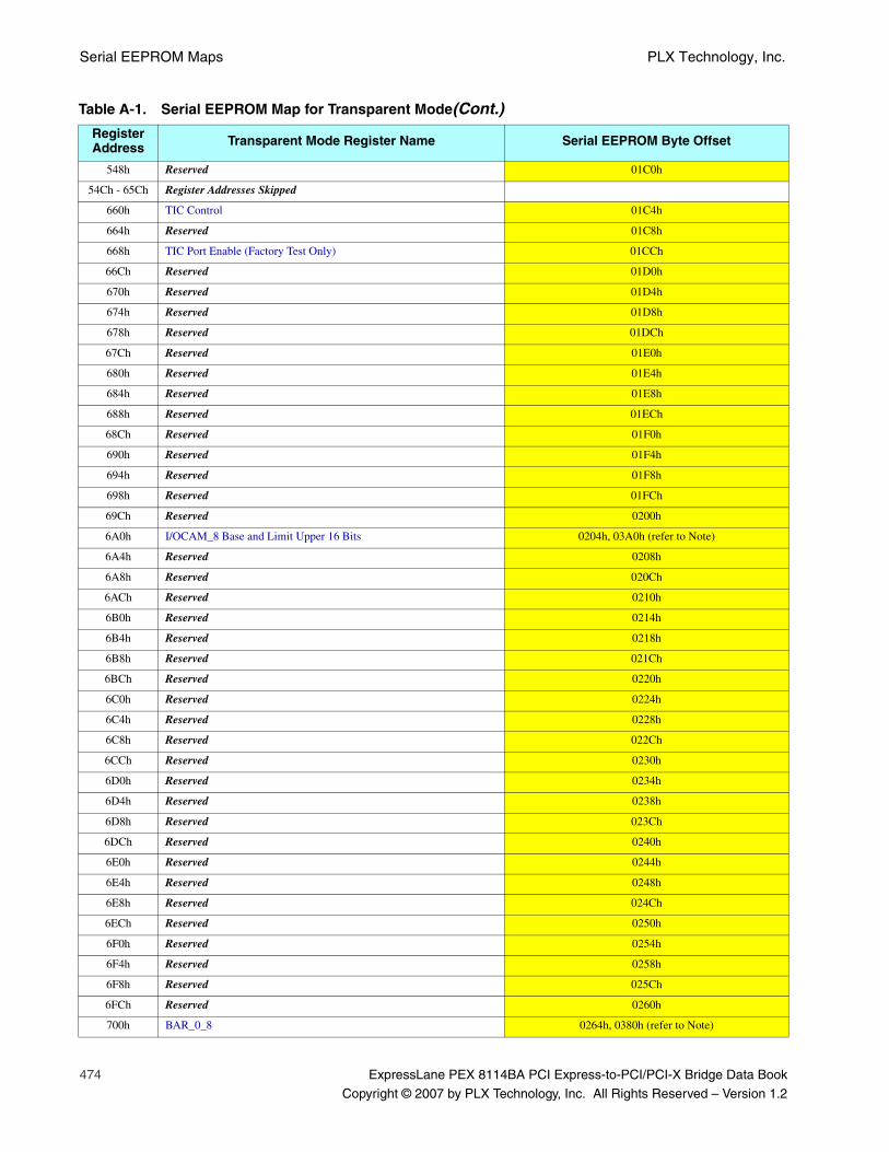
Serial EEPROM Maps PLX Technology, Inc.
474 ExpressLane PEX 8114BA PCI Express-to-PCI/PCI-X Bridge Data Book
Copyright © 2007 by PLX Technology, Inc. All Rights Reserved – Version 1.2
548h Reserved 01C0h
54Ch - 65Ch Register Addresses Skipped
660h TIC Control 01C4h
664h Reserved 01C8h
668h TIC Port Enable (Factory Test Only) 01CCh
66Ch Reserved 01D0h
670h Reserved 01D4h
674h Reserved 01D8h
678h Reserved 01DCh
67Ch Reserved 01E0h
680h Reserved 01E4h
684h Reserved 01E8h
688h Reserved 01ECh
68Ch Reserved 01F0h
690h Reserved 01F4h
694h Reserved 01F8h
698h Reserved 01FCh
69Ch Reserved 0200h
6A0h I/OCAM_8 Base and Limit Upper 16 Bits 0204h, 03A0h (refer to Note)
6A4h Reserved 0208h
6A8h Reserved 020Ch
6ACh Reserved 0210h
6B0h Reserved 0214h
6B4h Reserved 0218h
6B8h Reserved 021Ch
6BCh Reserved 0220h
6C0h Reserved 0224h
6C4h Reserved 0228h
6C8h Reserved 022Ch
6CCh Reserved 0230h
6D0h Reserved 0234h
6D4h Reserved 0238h
6D8h Reserved 023Ch
6DCh Reserved 0240h
6E0h Reserved 0244h
6E4h Reserved 0248h
6E8h Reserved 024Ch
6ECh Reserved 0250h
6F0h Reserved 0254h
6F4h Reserved 0258h
6F8h Reserved 025Ch
6FCh Reserved 0260h
700h BAR_0_8 0264h, 0380h (refer to Note)
Table A-1. Serial EEPROM Map for Transparent Mode(Cont.)Register Address Transparent Mode Register Name Serial EEPROM Byte Offset
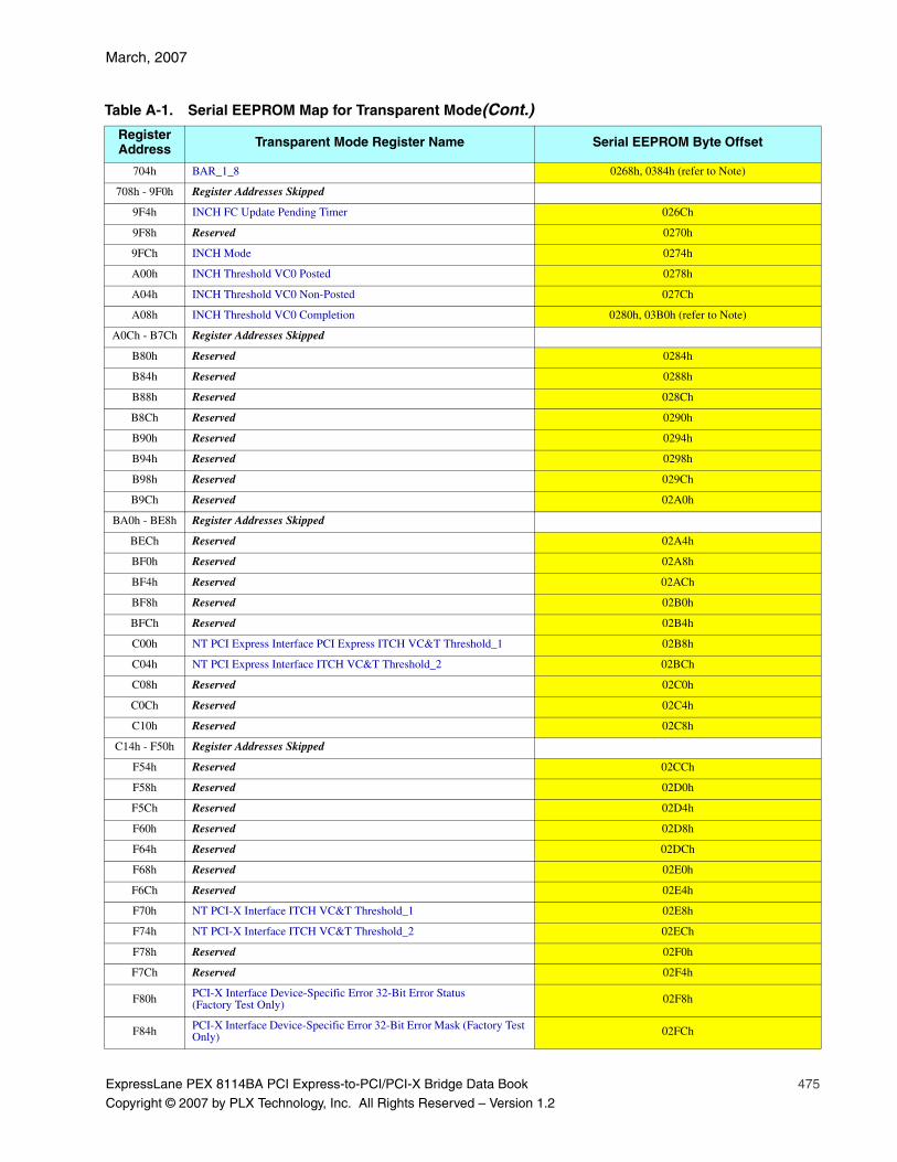
March, 2007
ExpressLane PEX 8114BA PCI Express-to-PCI/PCI-X Bridge Data Book 475
Copyright © 2007 by PLX Technology, Inc. All Rights Reserved – Version 1.2
704h BAR_1_8 0268h, 0384h (refer to Note)
708h - 9F0h Register Addresses Skipped
9F4h INCH FC Update Pending Timer 026Ch
9F8h Reserved 0270h
9FCh INCH Mode 0274h
A00h INCH Threshold VC0 Posted 0278h
A04h INCH Threshold VC0 Non-Posted 027Ch
A08h INCH Threshold VC0 Completion 0280h, 03B0h (refer to Note)
A0Ch - B7Ch Register Addresses Skipped
B80h Reserved 0284h
B84h Reserved 0288h
B88h Reserved 028Ch
B8Ch Reserved 0290h
B90h Reserved 0294h
B94h Reserved 0298h
B98h Reserved 029Ch
B9Ch Reserved 02A0h
BA0h - BE8h Register Addresses Skipped
BECh Reserved 02A4h
BF0h Reserved 02A8h
BF4h Reserved 02ACh
BF8h Reserved 02B0h
BFCh Reserved 02B4h
C00h NT PCI Express Interface PCI Express ITCH VC&T Threshold_1 02B8h
C04h NT PCI Express Interface ITCH VC&T Threshold_2 02BCh
C08h Reserved 02C0h
C0Ch Reserved 02C4h
C10h Reserved 02C8h
C14h - F50h Register Addresses Skipped
F54h Reserved 02CCh
F58h Reserved 02D0h
F5Ch Reserved 02D4h
F60h Reserved 02D8h
F64h Reserved 02DCh
F68h Reserved 02E0h
F6Ch Reserved 02E4h
F70h NT PCI-X Interface ITCH VC&T Threshold_1 02E8h
F74h NT PCI-X Interface ITCH VC&T Threshold_2 02ECh
F78h Reserved 02F0h
F7Ch Reserved 02F4h
F80h PCI-X Interface Device-Specific Error 32-Bit Error Status (Factory Test Only) 02F8h
F84h PCI-X Interface Device-Specific Error 32-Bit Error Mask (Factory Test Only) 02FCh
Table A-1. Serial EEPROM Map for Transparent Mode(Cont.)Register Address Transparent Mode Register Name Serial EEPROM Byte Offset
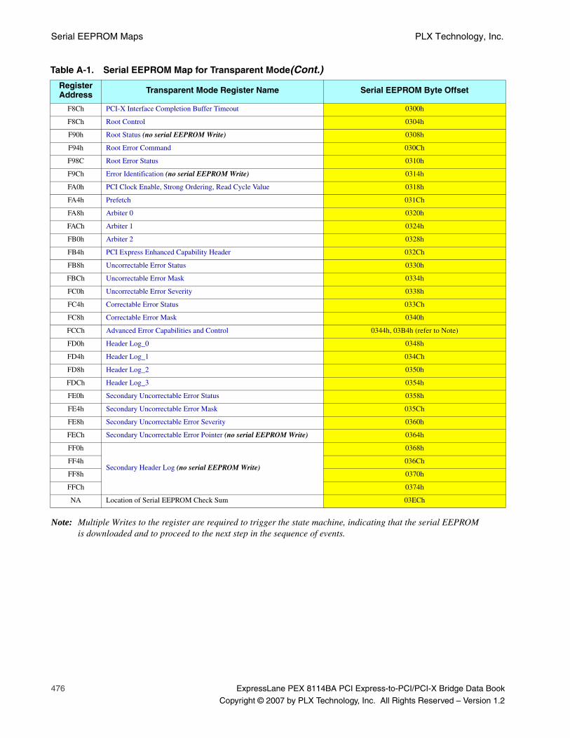
Serial EEPROM Maps PLX Technology, Inc.
476 ExpressLane PEX 8114BA PCI Express-to-PCI/PCI-X Bridge Data Book
Copyright © 2007 by PLX Technology, Inc. All Rights Reserved – Version 1.2
Note: Multiple Writes to the register are required to trigger the state machine, indicating that the serial EEPROM is downloaded and to proceed to the next step in the sequence of events.
F8Ch PCI-X Interface Completion Buffer Timeout 0300h
F8Ch Root Control 0304h
F90h Root Status (no serial EEPROM Write) 0308h
F94h Root Error Command 030Ch
F98C Root Error Status 0310h
F9Ch Error Identification (no serial EEPROM Write) 0314h
FA0h PCI Clock Enable, Strong Ordering, Read Cycle Value 0318h
FA4h Prefetch 031Ch
FA8h Arbiter 0 0320h
FACh Arbiter 1 0324h
FB0h Arbiter 2 0328h
FB4h PCI Express Enhanced Capability Header 032Ch
FB8h Uncorrectable Error Status 0330h
FBCh Uncorrectable Error Mask 0334h
FC0h Uncorrectable Error Severity 0338h
FC4h Correctable Error Status 033Ch
FC8h Correctable Error Mask 0340h
FCCh Advanced Error Capabilities and Control 0344h, 03B4h (refer to Note)
FD0h Header Log_0 0348h
FD4h Header Log_1 034Ch
FD8h Header Log_2 0350h
FDCh Header Log_3 0354h
FE0h Secondary Uncorrectable Error Status 0358h
FE4h Secondary Uncorrectable Error Mask 035Ch
FE8h Secondary Uncorrectable Error Severity 0360h
FECh Secondary Uncorrectable Error Pointer (no serial EEPROM Write) 0364h
FF0h
Secondary Header Log (no serial EEPROM Write)
0368h
FF4h 036Ch
FF8h 0370h
FFCh 0374h
NA Location of Serial EEPROM Check Sum 03ECh
Table A-1. Serial EEPROM Map for Transparent Mode(Cont.)Register Address Transparent Mode Register Name Serial EEPROM Byte Offset
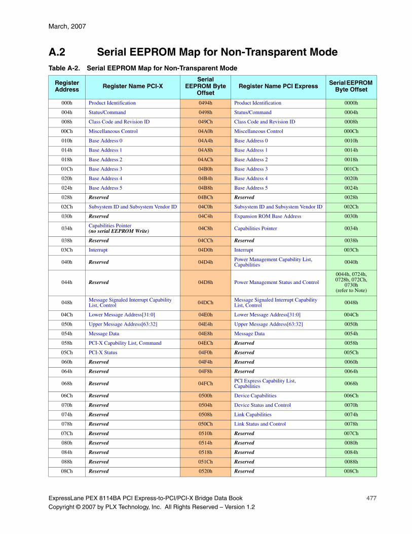
March, 2007
ExpressLane PEX 8114BA PCI Express-to-PCI/PCI-X Bridge Data Book 477
Copyright © 2007 by PLX Technology, Inc. All Rights Reserved – Version 1.2
A.2 Serial EEPROM Map for Non-Transparent ModeTable A-2. Serial EEPROM Map for Non-Transparent Mode
Register Address Register Name PCI-X
Serial EEPROM Byte
OffsetRegister Name PCI Express Serial EEPROM
Byte Offset
000h Product Identification 0494h Product Identification 0000h
004h Status/Command 0498h Status/Command 0004h
008h Class Code and Revision ID 049Ch Class Code and Revision ID 0008h
00Ch Miscellaneous Control 04A0h Miscellaneous Control 000Ch
010h Base Address 0 04A4h Base Address 0 0010h
014h Base Address 1 04A8h Base Address 1 0014h
018h Base Address 2 04ACh Base Address 2 0018h
01Ch Base Address 3 04B0h Base Address 3 001Ch
020h Base Address 4 04B4h Base Address 4 0020h
024h Base Address 5 04B8h Base Address 5 0024h
028h Reserved 04BCh Reserved 0028h
02Ch Subsystem ID and Subsystem Vendor ID 04C0h Subsystem ID and Subsystem Vendor ID 002Ch
030h Reserved 04C4h Expansion ROM Base Address 0030h
034h Capabilities Pointer (no serial EEPROM Write) 04C8h Capabilities Pointer 0034h
038h Reserved 04CCh Reserved 0038h
03Ch Interrupt 04D0h Interrupt 003Ch
040h Reserved 04D4h Power Management Capability List, Capabilities 0040h
044h Reserved 04D8h Power Management Status and Control
0044h, 0724h, 0728h, 072Ch,
0730h (refer to Note)
048h Message Signaled Interrupt Capability List, Control 04DCh Message Signaled Interrupt Capability
List, Control 0048h
04Ch Lower Message Address[31:0] 04E0h Lower Message Address[31:0] 004Ch
050h Upper Message Address[63:32] 04E4h Upper Message Address[63:32] 0050h
054h Message Data 04E8h Message Data 0054h
058h PCI-X Capability List, Command 04ECh Reserved 0058h
05Ch PCI-X Status 04F0h Reserved 005Ch
060h Reserved 04F4h Reserved 0060h
064h Reserved 04F8h Reserved 0064h
068h Reserved 04FCh PCI Express Capability List, Capabilities 0068h
06Ch Reserved 0500h Device Capabilities 006Ch
070h Reserved 0504h Device Status and Control 0070h
074h Reserved 0508h Link Capabilities 0074h
078h Reserved 050Ch Link Status and Control 0078h
07Ch Reserved 0510h Reserved 007Ch
080h Reserved 0514h Reserved 0080h
084h Reserved 0518h Reserved 0084h
088h Reserved 051Ch Reserved 0088h
08Ch Reserved 0520h Reserved 008Ch

Serial EEPROM Maps PLX Technology, Inc.
478 ExpressLane PEX 8114BA PCI Express-to-PCI/PCI-X Bridge Data Book
Copyright © 2007 by PLX Technology, Inc. All Rights Reserved – Version 1.2
090h Set PCI-X Interface IRQ 0524h Reserved 0090h
094h Clear PCI-X Interface IRQ 0528h Reserved 0094h
098h Set PCI-X Interface IRQ Mask 052Ch Reserved 0098h
09Ch Clear PCI-X Interface IRQ Mask 0530h Reserved 009Ch
0A0h Reserved 0534h Set PCI Express Interface IRQ 00A0h
0A4h Reserved 0538h Clear PCI Express Interface IRQ 00A4h
0A8h Reserved 053Ch Set PCI Express Interface IRQ Mask 00A8h
0ACh Reserved 0540h Clear PCI Express Interface IRQ Mask 00ACh
0B0h Reserved 0544h NT Mode Scratchpad_0 00B0h
0B4h Reserved 0548h NT Mode Scratchpad_1 00B4h
0B8h Reserved 054Ch NT Mode Scratchpad_2 00B8h
0BCh Reserved 0550h NT Mode Scratchpad_3 00BCh
0C0h Reserved 0554h NT Mode Scratchpad_4 00C0h
0C4h Reserved 0558h NT Mode Scratchpad_5 00C4h
0C8h Reserved 055Ch NT Mode Scratchpad_6 00C8h
0CCh Reserved 0560h NT Mode Scratchpad_7 00CCh
0D0h NT PCI-X Interface BAR 0/BAR 1 Setup 0564h Reserved 00D0h
0D4h NT PCI-X Interface BAR 2 Setup 0568h Reserved 00D4h
0D8h NT PCI-X Interface BAR 3 Setup 056Ch Reserved 00D8h
0DCh NT PCI-X Interface BAR 4 Setup 0570h Reserved 00DCh
0E0h NT PCI-X Interface BAR 5 Setup 0574h Reserved 00E0h
0E4h Reserved 0578h NT PCI Express Interface BAR 0/BAR 1 Setup 00E4h
0E8h Reserved 057Ch NT PCI Express Interface BAR 2 Setup 00E8h
0ECh Reserved 0580h NT PCI Express Interface BAR 3 Setup 00ECh
0F0h Reserved 0584h NT PCI Express Interface BAR 4 Setup 00F0h
0F4h Reserved 0588h NT PCI Express Interface BAR 5 Setup 00F4h
0F8h - 0FCh Register Addresses Skipped Register Addresses Skipped
100h Register Addresses Skipped Device Serial Number Extended Capability 00F8h
104h Register Addresses Skipped Serial Number (Low) 00FCh
108h Register Addresses Skipped Serial Number (High) 0100h
10Ch Register Addresses Skipped Reserved 0104h
110h Register Addresses Skipped Reserved 0108h
114h Register Addresses Skipped Reserved 010Ch
118h Register Addresses Skipped Reserved 0110h
11Ch Register Addresses Skipped Reserved 0114h
120h Register Addresses Skipped Reserved 0118h
124h Register Addresses Skipped Reserved 011Ch
128h Register Addresses Skipped Reserved 0120h
12Ch Register Addresses Skipped Reserved 0124h
130h Register Addresses Skipped Reserved 0128h
134h Register Addresses Skipped Reserved 012Ch
Table A-2. Serial EEPROM Map for Non-Transparent Mode(Cont.)
Register Address Register Name PCI-X
Serial EEPROM Byte
OffsetRegister Name PCI Express Serial EEPROM
Byte Offset
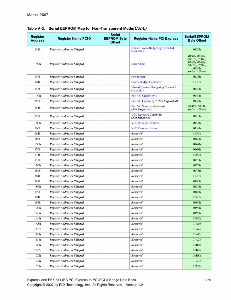
March, 2007
ExpressLane PEX 8114BA PCI Express-to-PCI/PCI-X Bridge Data Book 479
Copyright © 2007 by PLX Technology, Inc. All Rights Reserved – Version 1.2
138h Register Addresses Skipped Device Power Budgeting Extended Capability 0130h
13Ch Register Addresses Skipped Data Select
0134h, 0738h, 073Ch, 0740h, 0744h, 0748h, 074Ch, 0750h,
0754h(refer to Note)
140h Register Addresses Skipped Power Data 0138h
144h Register Addresses Skipped Power Budget Capability 013Ch
148h Register Addresses Skipped Virtual Channel Budgeting Extended Capability 0140h
14Ch Register Addresses Skipped Port VC Capability 1 0144h
150h Register Addresses Skipped Port VC Capability 2 (Not Supported) 0148h
154h Register Addresses Skipped Port VC Status and Control (Not Supported)
014Ch, 0734h (refer to Note)
158h Register Addresses Skipped VC0 Resource Capability (Not Supported) 0150h
15Ch Register Addresses Skipped VC0 Resource Control 0154h
160h Register Addresses Skipped VC0 Resource Status 0158h
164h Register Addresses Skipped Reserved 015Ch
168h Register Addresses Skipped Reserved 0160h
16Ch Register Addresses Skipped Reserved 0164h
170h Register Addresses Skipped Reserved 0168h
174h Register Addresses Skipped Reserved 016Ch
178h Register Addresses Skipped Reserved 0170h
17Ch Register Addresses Skipped Reserved 0174h
180h Register Addresses Skipped Reserved 0178h
184h Register Addresses Skipped Reserved 017Ch
188h Register Addresses Skipped Reserved 0180h
18Ch Register Addresses Skipped Reserved 0184h
190h Register Addresses Skipped Reserved 0188h
194h Register Addresses Skipped Reserved 018Ch
198h Register Addresses Skipped Reserved 0190h
19Ch Register Addresses Skipped Reserved 0194h
1A0h Register Addresses Skipped Reserved 0198h
1A4h Register Addresses Skipped Reserved 019Ch
1A8h Register Addresses Skipped Reserved 01A0h
1ACh Register Addresses Skipped Reserved 01A4h
1B0h Register Addresses Skipped Reserved 01A8h
1B4h Register Addresses Skipped Reserved 01ACh
1B8h Register Addresses Skipped Reserved 01B0h
1BCh Register Addresses Skipped Reserved 01B4h
1C0h Register Addresses Skipped Reserved 01B8h
1C4h Register Addresses Skipped Reserved 01BCh
1C8h Register Addresses Skipped Reserved 01C0h
Table A-2. Serial EEPROM Map for Non-Transparent Mode(Cont.)
Register Address Register Name PCI-X
Serial EEPROM Byte
OffsetRegister Name PCI Express Serial EEPROM
Byte Offset
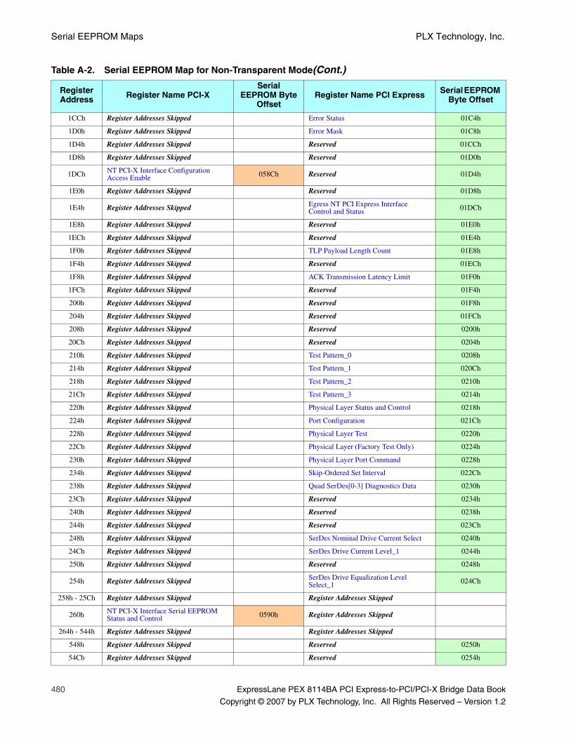
Serial EEPROM Maps PLX Technology, Inc.
480 ExpressLane PEX 8114BA PCI Express-to-PCI/PCI-X Bridge Data Book
Copyright © 2007 by PLX Technology, Inc. All Rights Reserved – Version 1.2
1CCh Register Addresses Skipped Error Status 01C4h
1D0h Register Addresses Skipped Error Mask 01C8h
1D4h Register Addresses Skipped Reserved 01CCh
1D8h Register Addresses Skipped Reserved 01D0h
1DCh NT PCI-X Interface Configuration Access Enable 058Ch Reserved 01D4h
1E0h Register Addresses Skipped Reserved 01D8h
1E4h Register Addresses Skipped Egress NT PCI Express Interface Control and Status 01DCh
1E8h Register Addresses Skipped Reserved 01E0h
1ECh Register Addresses Skipped Reserved 01E4h
1F0h Register Addresses Skipped TLP Payload Length Count 01E8h
1F4h Register Addresses Skipped Reserved 01ECh
1F8h Register Addresses Skipped ACK Transmission Latency Limit 01F0h
1FCh Register Addresses Skipped Reserved 01F4h
200h Register Addresses Skipped Reserved 01F8h
204h Register Addresses Skipped Reserved 01FCh
208h Register Addresses Skipped Reserved 0200h
20Ch Register Addresses Skipped Reserved 0204h
210h Register Addresses Skipped Test Pattern_0 0208h
214h Register Addresses Skipped Test Pattern_1 020Ch
218h Register Addresses Skipped Test Pattern_2 0210h
21Ch Register Addresses Skipped Test Pattern_3 0214h
220h Register Addresses Skipped Physical Layer Status and Control 0218h
224h Register Addresses Skipped Port Configuration 021Ch
228h Register Addresses Skipped Physical Layer Test 0220h
22Ch Register Addresses Skipped Physical Layer (Factory Test Only) 0224h
230h Register Addresses Skipped Physical Layer Port Command 0228h
234h Register Addresses Skipped Skip-Ordered Set Interval 022Ch
238h Register Addresses Skipped Quad SerDes[0-3] Diagnostics Data 0230h
23Ch Register Addresses Skipped Reserved 0234h
240h Register Addresses Skipped Reserved 0238h
244h Register Addresses Skipped Reserved 023Ch
248h Register Addresses Skipped SerDes Nominal Drive Current Select 0240h
24Ch Register Addresses Skipped SerDes Drive Current Level_1 0244h
250h Register Addresses Skipped Reserved 0248h
254h Register Addresses Skipped SerDes Drive Equalization Level Select_1 024Ch
258h - 25Ch Register Addresses Skipped Register Addresses Skipped
260h NT PCI-X Interface Serial EEPROM Status and Control 0590h Register Addresses Skipped
264h - 544h Register Addresses Skipped Register Addresses Skipped
548h Register Addresses Skipped Reserved 0250h
54Ch Register Addresses Skipped Reserved 0254h
Table A-2. Serial EEPROM Map for Non-Transparent Mode(Cont.)
Register Address Register Name PCI-X
Serial EEPROM Byte
OffsetRegister Name PCI Express Serial EEPROM
Byte Offset
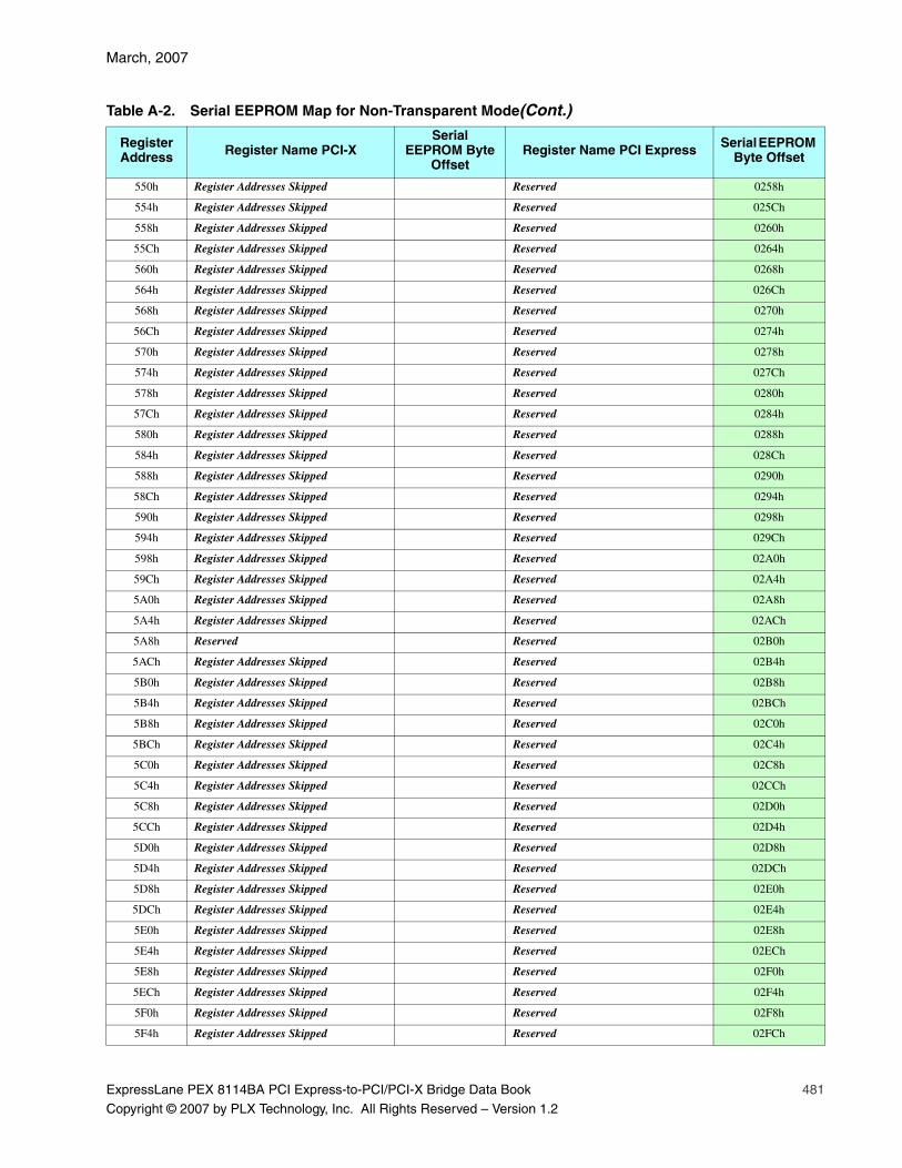
March, 2007
ExpressLane PEX 8114BA PCI Express-to-PCI/PCI-X Bridge Data Book 481
Copyright © 2007 by PLX Technology, Inc. All Rights Reserved – Version 1.2
550h Register Addresses Skipped Reserved 0258h
554h Register Addresses Skipped Reserved 025Ch
558h Register Addresses Skipped Reserved 0260h
55Ch Register Addresses Skipped Reserved 0264h
560h Register Addresses Skipped Reserved 0268h
564h Register Addresses Skipped Reserved 026Ch
568h Register Addresses Skipped Reserved 0270h
56Ch Register Addresses Skipped Reserved 0274h
570h Register Addresses Skipped Reserved 0278h
574h Register Addresses Skipped Reserved 027Ch
578h Register Addresses Skipped Reserved 0280h
57Ch Register Addresses Skipped Reserved 0284h
580h Register Addresses Skipped Reserved 0288h
584h Register Addresses Skipped Reserved 028Ch
588h Register Addresses Skipped Reserved 0290h
58Ch Register Addresses Skipped Reserved 0294h
590h Register Addresses Skipped Reserved 0298h
594h Register Addresses Skipped Reserved 029Ch
598h Register Addresses Skipped Reserved 02A0h
59Ch Register Addresses Skipped Reserved 02A4h
5A0h Register Addresses Skipped Reserved 02A8h
5A4h Register Addresses Skipped Reserved 02ACh
5A8h Reserved Reserved 02B0h
5ACh Register Addresses Skipped Reserved 02B4h
5B0h Register Addresses Skipped Reserved 02B8h
5B4h Register Addresses Skipped Reserved 02BCh
5B8h Register Addresses Skipped Reserved 02C0h
5BCh Register Addresses Skipped Reserved 02C4h
5C0h Register Addresses Skipped Reserved 02C8h
5C4h Register Addresses Skipped Reserved 02CCh
5C8h Register Addresses Skipped Reserved 02D0h
5CCh Register Addresses Skipped Reserved 02D4h
5D0h Register Addresses Skipped Reserved 02D8h
5D4h Register Addresses Skipped Reserved 02DCh
5D8h Register Addresses Skipped Reserved 02E0h
5DCh Register Addresses Skipped Reserved 02E4h
5E0h Register Addresses Skipped Reserved 02E8h
5E4h Register Addresses Skipped Reserved 02ECh
5E8h Register Addresses Skipped Reserved 02F0h
5ECh Register Addresses Skipped Reserved 02F4h
5F0h Register Addresses Skipped Reserved 02F8h
5F4h Register Addresses Skipped Reserved 02FCh
Table A-2. Serial EEPROM Map for Non-Transparent Mode(Cont.)
Register Address Register Name PCI-X
Serial EEPROM Byte
OffsetRegister Name PCI Express Serial EEPROM
Byte Offset
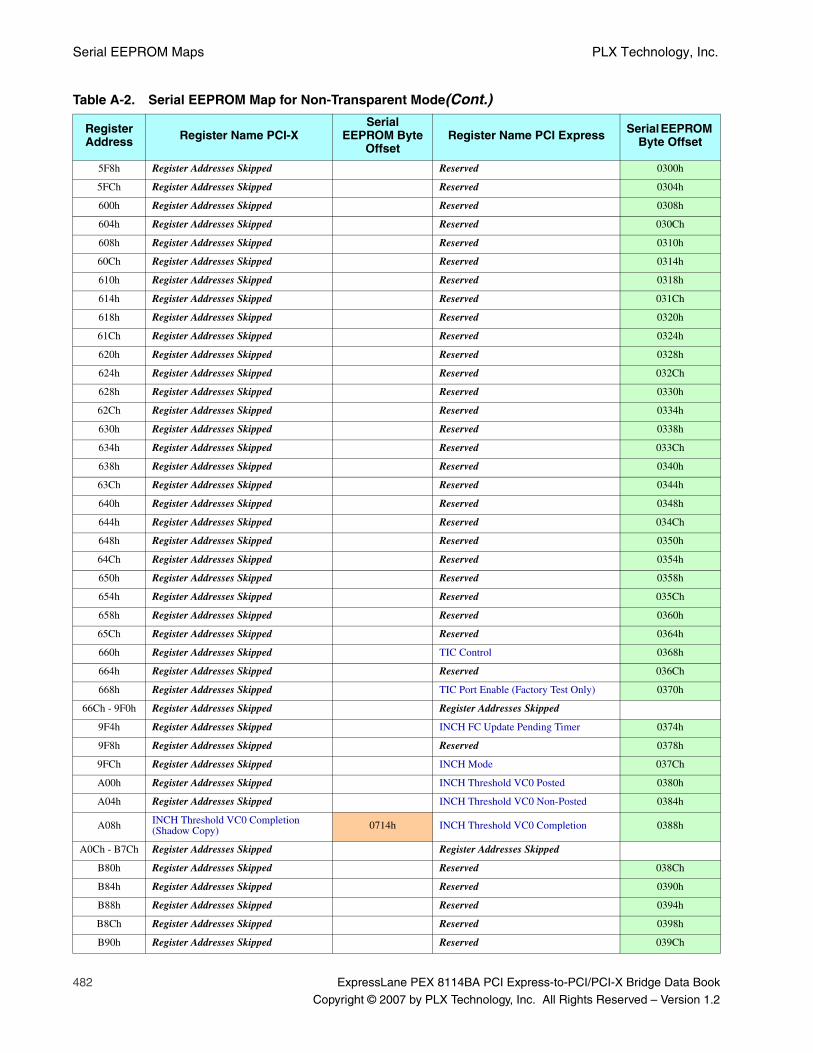
Serial EEPROM Maps PLX Technology, Inc.
482 ExpressLane PEX 8114BA PCI Express-to-PCI/PCI-X Bridge Data Book
Copyright © 2007 by PLX Technology, Inc. All Rights Reserved – Version 1.2
5F8h Register Addresses Skipped Reserved 0300h
5FCh Register Addresses Skipped Reserved 0304h
600h Register Addresses Skipped Reserved 0308h
604h Register Addresses Skipped Reserved 030Ch
608h Register Addresses Skipped Reserved 0310h
60Ch Register Addresses Skipped Reserved 0314h
610h Register Addresses Skipped Reserved 0318h
614h Register Addresses Skipped Reserved 031Ch
618h Register Addresses Skipped Reserved 0320h
61Ch Register Addresses Skipped Reserved 0324h
620h Register Addresses Skipped Reserved 0328h
624h Register Addresses Skipped Reserved 032Ch
628h Register Addresses Skipped Reserved 0330h
62Ch Register Addresses Skipped Reserved 0334h
630h Register Addresses Skipped Reserved 0338h
634h Register Addresses Skipped Reserved 033Ch
638h Register Addresses Skipped Reserved 0340h
63Ch Register Addresses Skipped Reserved 0344h
640h Register Addresses Skipped Reserved 0348h
644h Register Addresses Skipped Reserved 034Ch
648h Register Addresses Skipped Reserved 0350h
64Ch Register Addresses Skipped Reserved 0354h
650h Register Addresses Skipped Reserved 0358h
654h Register Addresses Skipped Reserved 035Ch
658h Register Addresses Skipped Reserved 0360h
65Ch Register Addresses Skipped Reserved 0364h
660h Register Addresses Skipped TIC Control 0368h
664h Register Addresses Skipped Reserved 036Ch
668h Register Addresses Skipped TIC Port Enable (Factory Test Only) 0370h
66Ch - 9F0h Register Addresses Skipped Register Addresses Skipped
9F4h Register Addresses Skipped INCH FC Update Pending Timer 0374h
9F8h Register Addresses Skipped Reserved 0378h
9FCh Register Addresses Skipped INCH Mode 037Ch
A00h Register Addresses Skipped INCH Threshold VC0 Posted 0380h
A04h Register Addresses Skipped INCH Threshold VC0 Non-Posted 0384h
A08h INCH Threshold VC0 Completion (Shadow Copy) 0714h INCH Threshold VC0 Completion 0388h
A0Ch - B7Ch Register Addresses Skipped Register Addresses Skipped
B80h Register Addresses Skipped Reserved 038Ch
B84h Register Addresses Skipped Reserved 0390h
B88h Register Addresses Skipped Reserved 0394h
B8Ch Register Addresses Skipped Reserved 0398h
B90h Register Addresses Skipped Reserved 039Ch
Table A-2. Serial EEPROM Map for Non-Transparent Mode(Cont.)
Register Address Register Name PCI-X
Serial EEPROM Byte
OffsetRegister Name PCI Express Serial EEPROM
Byte Offset
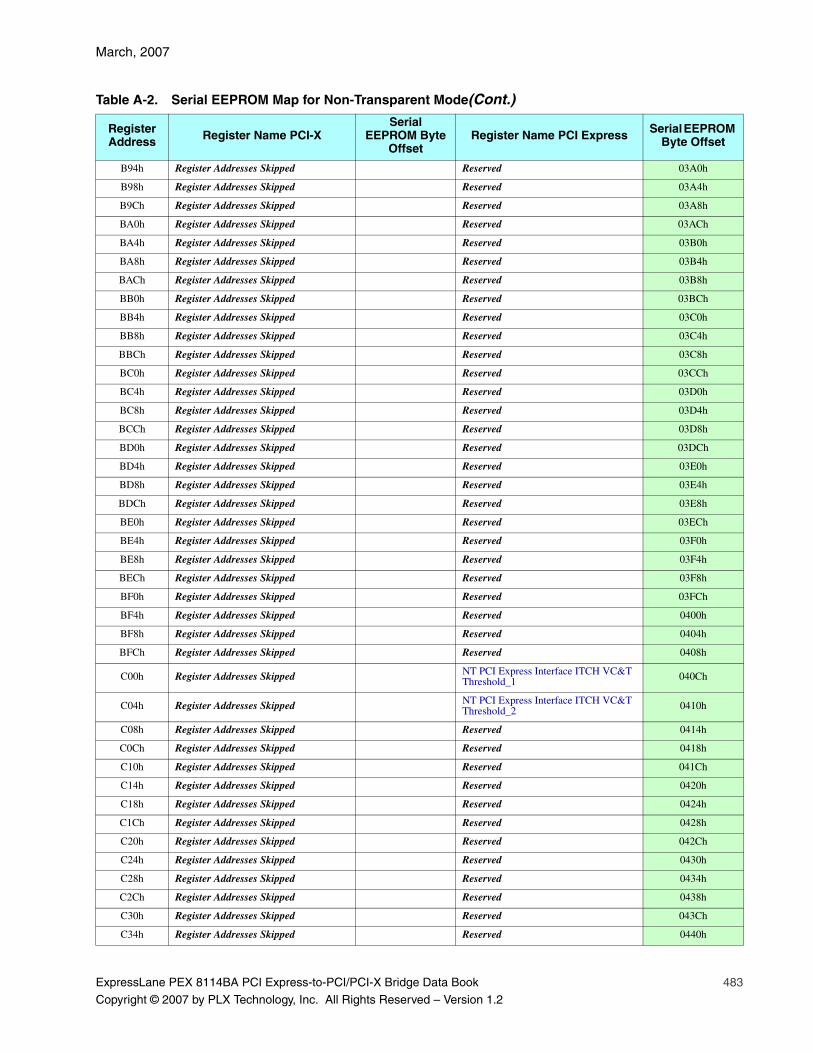
March, 2007
ExpressLane PEX 8114BA PCI Express-to-PCI/PCI-X Bridge Data Book 483
Copyright © 2007 by PLX Technology, Inc. All Rights Reserved – Version 1.2
B94h Register Addresses Skipped Reserved 03A0h
B98h Register Addresses Skipped Reserved 03A4h
B9Ch Register Addresses Skipped Reserved 03A8h
BA0h Register Addresses Skipped Reserved 03ACh
BA4h Register Addresses Skipped Reserved 03B0h
BA8h Register Addresses Skipped Reserved 03B4h
BACh Register Addresses Skipped Reserved 03B8h
BB0h Register Addresses Skipped Reserved 03BCh
BB4h Register Addresses Skipped Reserved 03C0h
BB8h Register Addresses Skipped Reserved 03C4h
BBCh Register Addresses Skipped Reserved 03C8h
BC0h Register Addresses Skipped Reserved 03CCh
BC4h Register Addresses Skipped Reserved 03D0h
BC8h Register Addresses Skipped Reserved 03D4h
BCCh Register Addresses Skipped Reserved 03D8h
BD0h Register Addresses Skipped Reserved 03DCh
BD4h Register Addresses Skipped Reserved 03E0h
BD8h Register Addresses Skipped Reserved 03E4h
BDCh Register Addresses Skipped Reserved 03E8h
BE0h Register Addresses Skipped Reserved 03ECh
BE4h Register Addresses Skipped Reserved 03F0h
BE8h Register Addresses Skipped Reserved 03F4h
BECh Register Addresses Skipped Reserved 03F8h
BF0h Register Addresses Skipped Reserved 03FCh
BF4h Register Addresses Skipped Reserved 0400h
BF8h Register Addresses Skipped Reserved 0404h
BFCh Register Addresses Skipped Reserved 0408h
C00h Register Addresses Skipped NT PCI Express Interface ITCH VC&T Threshold_1 040Ch
C04h Register Addresses Skipped NT PCI Express Interface ITCH VC&T Threshold_2 0410h
C08h Register Addresses Skipped Reserved 0414h
C0Ch Register Addresses Skipped Reserved 0418h
C10h Register Addresses Skipped Reserved 041Ch
C14h Register Addresses Skipped Reserved 0420h
C18h Register Addresses Skipped Reserved 0424h
C1Ch Register Addresses Skipped Reserved 0428h
C20h Register Addresses Skipped Reserved 042Ch
C24h Register Addresses Skipped Reserved 0430h
C28h Register Addresses Skipped Reserved 0434h
C2Ch Register Addresses Skipped Reserved 0438h
C30h Register Addresses Skipped Reserved 043Ch
C34h Register Addresses Skipped Reserved 0440h
Table A-2. Serial EEPROM Map for Non-Transparent Mode(Cont.)
Register Address Register Name PCI-X
Serial EEPROM Byte
OffsetRegister Name PCI Express Serial EEPROM
Byte Offset
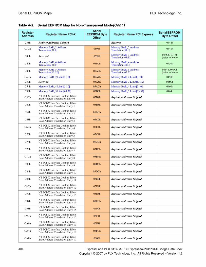
Serial EEPROM Maps PLX Technology, Inc.
484 ExpressLane PEX 8114BA PCI Express-to-PCI/PCI-X Bridge Data Book
Copyright © 2007 by PLX Technology, Inc. All Rights Reserved – Version 1.2
C38h Register Addresses Skipped Reserved 0444h
C3Ch Memory BAR_2 Address Translation[31:0] 0594h Memory BAR_2 Address
Translation[31:0] 0448h
C40h Reserved 0598h Memory BAR_3 Address Translation[63:32]
044Ch, 0718h (refer to Note)
C44h Memory BAR_4 Address Translation[31:0] 059Ch Memory BAR_4 Address
Translation[31:0] 0450h
C48h Memory BAR_5 Address Translation[63:32] 05A0h Memory BAR_5 Address
Translation[63:32]0454h, 071Ch (refer to Note)
C4Ch Memory BAR_2 Limit[31:0] 05A4h Memory BAR_2 Limit[31:0] 0458h
C50h Reserved 05A8h Memory BAR_3 Limit[63:32] 045Ch
C54h Memory BAR_4 Limit[31:0] 05ACh Memory BAR_4 Limit[31:0] 0460h
C58h Memory BAR_5 Limit[63:32] 05B0h Memory BAR_5 Limit[63:32] 0464h
C5Ch NT PCI-X Interface Lookup Table Base Address Translation Entry 0 05B4h Register Addresses Skipped
C60h NT PCI-X Interface Lookup Table Base Address Translation Entry 1 05B8h Register Addresses Skipped
C64h NT PCI-X Interface Lookup Table Base Address Translation Entry 2 05BCh Register Addresses Skipped
C68h NT PCI-X Interface Lookup Table Base Address Translation Entry 3 05C0h Register Addresses Skipped
C6Ch NT PCI-X Interface Lookup Table Base Address Translation Entry 4 05C4h Register Addresses Skipped
C70h NT PCI-X Interface Lookup Table Base Address Translation Entry 5 05C8h Register Addresses Skipped
C74h NT PCI-X Interface Lookup Table Base Address Translation Entry 6 05CCh Register Addresses Skipped
C78h NT PCI-X Interface Lookup Table Base Address Translation Entry 7 05D0h Register Addresses Skipped
C7Ch NT PCI-X Interface Lookup Table Base Address Translation Entry 8 05D4h Register Addresses Skipped
C80h NT PCI-X Interface Lookup Table Base Address Translation Entry 9 05D8h Register Addresses Skipped
C84h NT PCI-X Interface Lookup Table Base Address Translation Entry 10 05DCh Register Addresses Skipped
C88h NT PCI-X Interface Lookup Table Base Address Translation Entry 11 05E0h Register Addresses Skipped
C8Ch NT PCI-X Interface Lookup Table Base Address Translation Entry 12 05E4h Register Addresses Skipped
C90h NT PCI-X Interface Lookup Table Base Address Translation Entry 13 05E8h Register Addresses Skipped
C94h NT PCI-X Interface Lookup Table Base Address Translation Entry 14 05ECh Register Addresses Skipped
C98h NT PCI-X Interface Lookup Table Base Address Translation Entry 15 05F0h Register Addresses Skipped
C9Ch NT PCI-X Interface Lookup Table Base Address Translation Entry 16 05F4h Register Addresses Skipped
CA0h NT PCI-X Interface Lookup Table Base Address Translation Entry 17 05F8h Register Addresses Skipped
CA4h NT PCI-X Interface Lookup Table Base Address Translation Entry 18 05FCh Register Addresses Skipped
CA8h NT PCI-X Interface Lookup Table Base Address Translation Entry 19 0600h Register Addresses Skipped
Table A-2. Serial EEPROM Map for Non-Transparent Mode(Cont.)
Register Address Register Name PCI-X
Serial EEPROM Byte
OffsetRegister Name PCI Express Serial EEPROM
Byte Offset
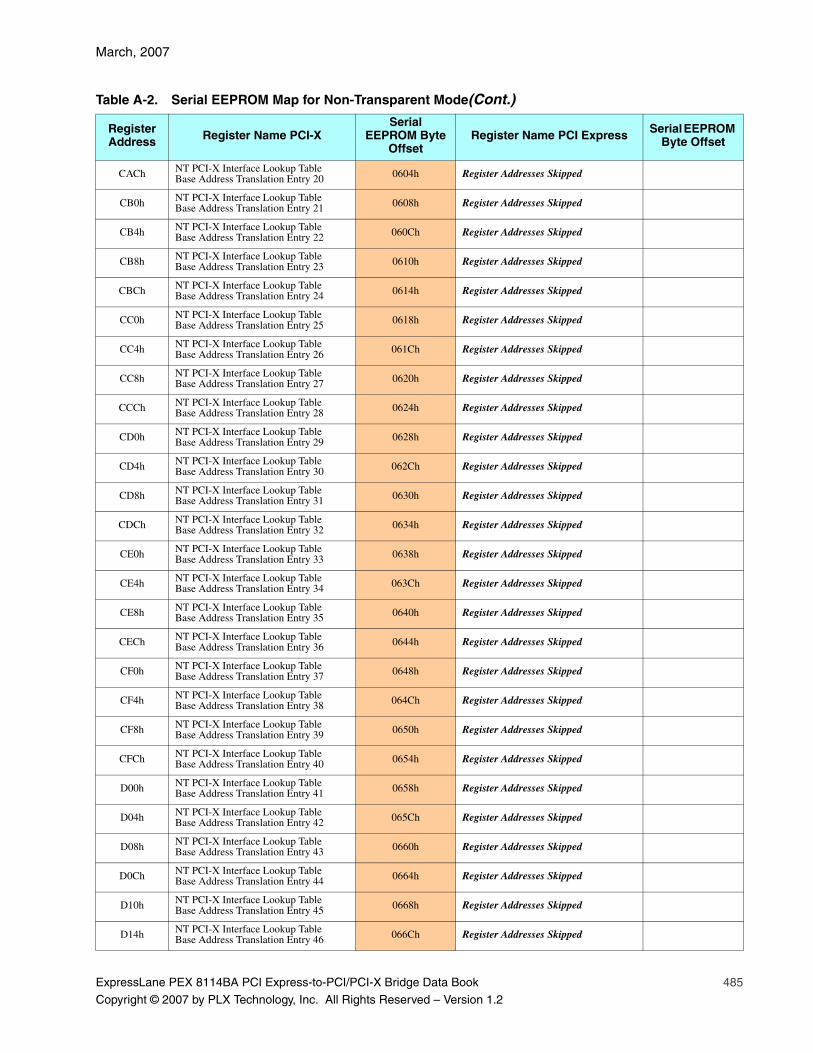
March, 2007
ExpressLane PEX 8114BA PCI Express-to-PCI/PCI-X Bridge Data Book 485
Copyright © 2007 by PLX Technology, Inc. All Rights Reserved – Version 1.2
CACh NT PCI-X Interface Lookup Table Base Address Translation Entry 20 0604h Register Addresses Skipped
CB0h NT PCI-X Interface Lookup Table Base Address Translation Entry 21 0608h Register Addresses Skipped
CB4h NT PCI-X Interface Lookup Table Base Address Translation Entry 22 060Ch Register Addresses Skipped
CB8h NT PCI-X Interface Lookup Table Base Address Translation Entry 23 0610h Register Addresses Skipped
CBCh NT PCI-X Interface Lookup Table Base Address Translation Entry 24 0614h Register Addresses Skipped
CC0h NT PCI-X Interface Lookup Table Base Address Translation Entry 25 0618h Register Addresses Skipped
CC4h NT PCI-X Interface Lookup Table Base Address Translation Entry 26 061Ch Register Addresses Skipped
CC8h NT PCI-X Interface Lookup Table Base Address Translation Entry 27 0620h Register Addresses Skipped
CCCh NT PCI-X Interface Lookup Table Base Address Translation Entry 28 0624h Register Addresses Skipped
CD0h NT PCI-X Interface Lookup Table Base Address Translation Entry 29 0628h Register Addresses Skipped
CD4h NT PCI-X Interface Lookup Table Base Address Translation Entry 30 062Ch Register Addresses Skipped
CD8h NT PCI-X Interface Lookup Table Base Address Translation Entry 31 0630h Register Addresses Skipped
CDCh NT PCI-X Interface Lookup Table Base Address Translation Entry 32 0634h Register Addresses Skipped
CE0h NT PCI-X Interface Lookup Table Base Address Translation Entry 33 0638h Register Addresses Skipped
CE4h NT PCI-X Interface Lookup Table Base Address Translation Entry 34 063Ch Register Addresses Skipped
CE8h NT PCI-X Interface Lookup Table Base Address Translation Entry 35 0640h Register Addresses Skipped
CECh NT PCI-X Interface Lookup Table Base Address Translation Entry 36 0644h Register Addresses Skipped
CF0h NT PCI-X Interface Lookup Table Base Address Translation Entry 37 0648h Register Addresses Skipped
CF4h NT PCI-X Interface Lookup Table Base Address Translation Entry 38 064Ch Register Addresses Skipped
CF8h NT PCI-X Interface Lookup Table Base Address Translation Entry 39 0650h Register Addresses Skipped
CFCh NT PCI-X Interface Lookup Table Base Address Translation Entry 40 0654h Register Addresses Skipped
D00h NT PCI-X Interface Lookup Table Base Address Translation Entry 41 0658h Register Addresses Skipped
D04h NT PCI-X Interface Lookup Table Base Address Translation Entry 42 065Ch Register Addresses Skipped
D08h NT PCI-X Interface Lookup Table Base Address Translation Entry 43 0660h Register Addresses Skipped
D0Ch NT PCI-X Interface Lookup Table Base Address Translation Entry 44 0664h Register Addresses Skipped
D10h NT PCI-X Interface Lookup Table Base Address Translation Entry 45 0668h Register Addresses Skipped
D14h NT PCI-X Interface Lookup Table Base Address Translation Entry 46 066Ch Register Addresses Skipped
Table A-2. Serial EEPROM Map for Non-Transparent Mode(Cont.)
Register Address Register Name PCI-X
Serial EEPROM Byte
OffsetRegister Name PCI Express Serial EEPROM
Byte Offset
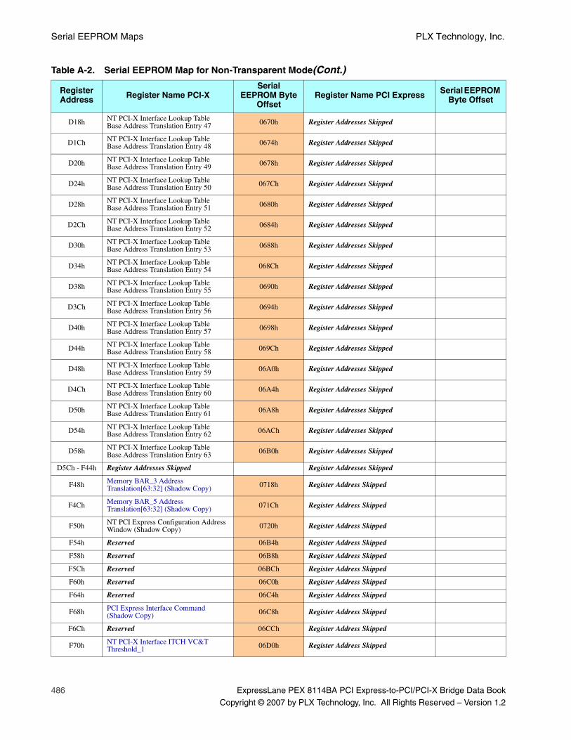
Serial EEPROM Maps PLX Technology, Inc.
486 ExpressLane PEX 8114BA PCI Express-to-PCI/PCI-X Bridge Data Book
Copyright © 2007 by PLX Technology, Inc. All Rights Reserved – Version 1.2
D18h NT PCI-X Interface Lookup Table Base Address Translation Entry 47 0670h Register Addresses Skipped
D1Ch NT PCI-X Interface Lookup Table Base Address Translation Entry 48 0674h Register Addresses Skipped
D20h NT PCI-X Interface Lookup Table Base Address Translation Entry 49 0678h Register Addresses Skipped
D24h NT PCI-X Interface Lookup Table Base Address Translation Entry 50 067Ch Register Addresses Skipped
D28h NT PCI-X Interface Lookup Table Base Address Translation Entry 51 0680h Register Addresses Skipped
D2Ch NT PCI-X Interface Lookup Table Base Address Translation Entry 52 0684h Register Addresses Skipped
D30h NT PCI-X Interface Lookup Table Base Address Translation Entry 53 0688h Register Addresses Skipped
D34h NT PCI-X Interface Lookup Table Base Address Translation Entry 54 068Ch Register Addresses Skipped
D38h NT PCI-X Interface Lookup Table Base Address Translation Entry 55 0690h Register Addresses Skipped
D3Ch NT PCI-X Interface Lookup Table Base Address Translation Entry 56 0694h Register Addresses Skipped
D40h NT PCI-X Interface Lookup Table Base Address Translation Entry 57 0698h Register Addresses Skipped
D44h NT PCI-X Interface Lookup Table Base Address Translation Entry 58 069Ch Register Addresses Skipped
D48h NT PCI-X Interface Lookup Table Base Address Translation Entry 59 06A0h Register Addresses Skipped
D4Ch NT PCI-X Interface Lookup Table Base Address Translation Entry 60 06A4h Register Addresses Skipped
D50h NT PCI-X Interface Lookup Table Base Address Translation Entry 61 06A8h Register Addresses Skipped
D54h NT PCI-X Interface Lookup Table Base Address Translation Entry 62 06ACh Register Addresses Skipped
D58h NT PCI-X Interface Lookup Table Base Address Translation Entry 63 06B0h Register Addresses Skipped
D5Ch - F44h Register Addresses Skipped Register Addresses Skipped
F48h Memory BAR_3 Address Translation[63:32] (Shadow Copy) 0718h Register Address Skipped
F4Ch Memory BAR_5 Address Translation[63:32] (Shadow Copy) 071Ch Register Address Skipped
F50h NT PCI Express Configuration Address Window (Shadow Copy) 0720h Register Address Skipped
F54h Reserved 06B4h Register Address Skipped
F58h Reserved 06B8h Register Address Skipped
F5Ch Reserved 06BCh Register Address Skipped
F60h Reserved 06C0h Register Address Skipped
F64h Reserved 06C4h Register Address Skipped
F68h PCI Express Interface Command (Shadow Copy) 06C8h Register Address Skipped
F6Ch Reserved 06CCh Register Address Skipped
F70h NT PCI-X Interface ITCH VC&T Threshold_1 06D0h Register Address Skipped
Table A-2. Serial EEPROM Map for Non-Transparent Mode(Cont.)
Register Address Register Name PCI-X
Serial EEPROM Byte
OffsetRegister Name PCI Express Serial EEPROM
Byte Offset
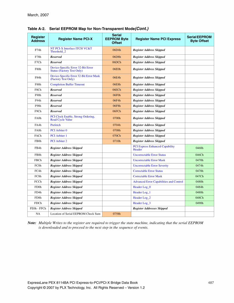
March, 2007
ExpressLane PEX 8114BA PCI Express-to-PCI/PCI-X Bridge Data Book 487
Copyright © 2007 by PLX Technology, Inc. All Rights Reserved – Version 1.2
Note: Multiple Writes to the register are required to trigger the state machine, indicating that the serial EEPROM is downloaded and to proceed to the next step in the sequence of events.
F74h NT PCI-X Interface ITCH VC&T Threshold_2 06D4h Register Address Skipped
F78h Reserved 06D8h Register Address Skipped
F7Ch Reserved 06DCh Register Address Skipped
F80h Device-Specific Error 32-Bit Error Status (Factory Test Only) 06E0h Register Address Skipped
F84h Device-Specific Error 32-Bit Error Mask (Factory Test Only) 06E4h Register Address Skipped
F88h Completion Buffer Timeout 06E8h Register Address Skipped
F8Ch Reserved 06ECh Register Address Skipped
F90h Reserved 06F0h Register Address Skipped
F94h Reserved 06F4h Register Address Skipped
F98h Reserved 06F8h Register Address Skipped
F9Ch Reserved 06FCh Register Address Skipped
FA0h PCI Clock Enable, Strong Ordering, Read Cycle Value 0700h Register Address Skipped
FA4h Prefetch 0704h Register Address Skipped
FA8h PCI Arbiter 0 0708h Register Address Skipped
FACh PCI Arbiter 1 070Ch Register Address Skipped
FB0h PCI Arbiter 2 0710h Register Address Skipped
FB4h Register Address Skipped PCI Express Enhanced Capability Header 0468h
FB8h Register Address Skipped Uncorrectable Error Status 046Ch
FBCh Register Address Skipped Uncorrectable Error Mask 0470h
FC0h Register Address Skipped Uncorrectable Error Severity 0474h
FC4h Register Address Skipped Correctable Error Status 0478h
FC8h Register Address Skipped Correctable Error Mask 047Ch
FCCh Register Address Skipped Advanced Error Capabilities and Control 0480h
FD0h Register Address Skipped Header Log_0 0484h
FD4h Register Address Skipped Header Log_1 0488h
FD8h Register Address Skipped Header Log_2 048Ch
FDCh Register Address Skipped Header Log_3 0490h
FE0h - FFCh Register Address Skipped Register Addresses Skipped
NA Location of Serial EEPROM Check Sum 0758h
Table A-2. Serial EEPROM Map for Non-Transparent Mode(Cont.)
Register Address Register Name PCI-X
Serial EEPROM Byte
OffsetRegister Name PCI Express Serial EEPROM
Byte Offset

Serial EEPROM Maps PLX Technology, Inc.
488 ExpressLane PEX 8114BA PCI Express-to-PCI/PCI-X Bridge Data Book
Copyright © 2007 by PLX Technology, Inc. All Rights Reserved – Version 1.2
THIS PAGE INTENTIONALLY LEFT BLANK.
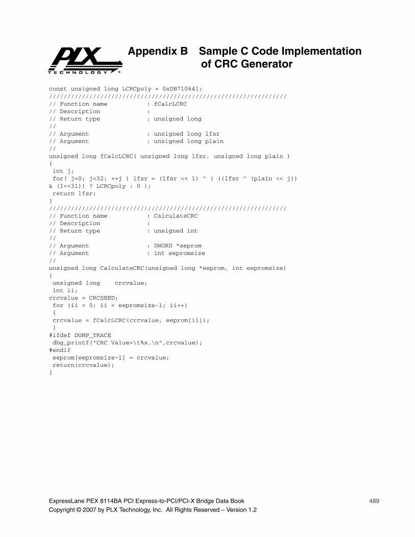
ExpressLane PEX 8114BA PCI Express-to-PCI/PCI-X Bridge Data Book 489
Copyright © 2007 by PLX Technology, Inc. All Rights Reserved – Version 1.2
Appendix B Sample C Code Implementation of CRC Generator
const unsigned long LCRCpoly = 0xDB710641;/////////////////////////////////////////////////////////////////// Function name : fCalcLCRC// Description :// Return type : unsigned long//// Argument : unsigned long lfsr// Argument : unsigned long plain//unsigned long fCalcLCRC( unsigned long lfsr, unsigned long plain ){ int j; for( j=0; j<32; ++j ) lfsr = (lfsr << 1) ^ ( ((lfsr ^ (plain << j)) & (1<<31)) ? LCRCpoly : 0 ); return lfsr;}/////////////////////////////////////////////////////////////////// Function name : CalculateCRC// Description :// Return type : unsigned int//// Argument : DWORD *eeprom// Argument : int eepromsize//unsigned long CalculateCRC(unsigned long *eeprom, int eepromsize){ unsigned long crcvalue; int ii;crcvalue = CRCSEED; for (ii = 0; ii < eepromsize-1; ii++) { crcvalue = fCalcLCRC(crcvalue, eeprom[ii]); }#ifdef DUMP_TRACE dbg_printf("CRC Value>\t%x.\n",crcvalue);#endif eeprom[eepromsize-1] = crcvalue; return(crcvalue);}
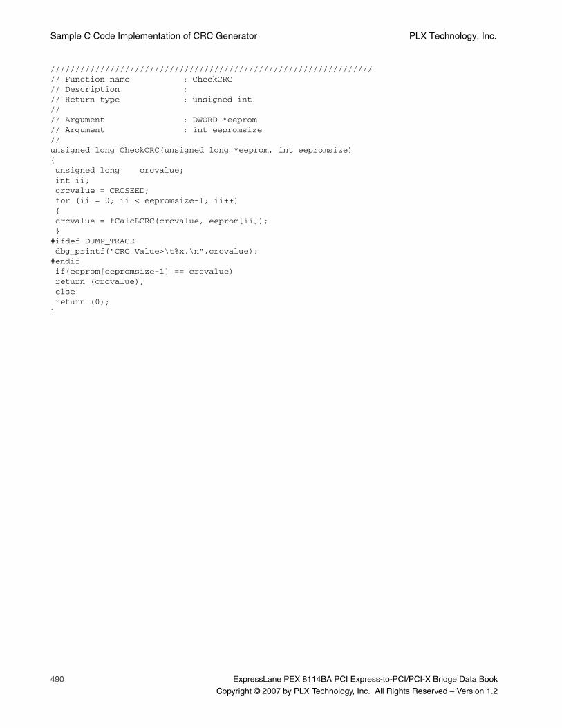
Sample C Code Implementation of CRC Generator PLX Technology, Inc.
490 ExpressLane PEX 8114BA PCI Express-to-PCI/PCI-X Bridge Data Book
Copyright © 2007 by PLX Technology, Inc. All Rights Reserved – Version 1.2
/////////////////////////////////////////////////////////////////// Function name : CheckCRC// Description :// Return type : unsigned int//// Argument : DWORD *eeprom// Argument : int eepromsize//unsigned long CheckCRC(unsigned long *eeprom, int eepromsize){ unsigned long crcvalue; int ii; crcvalue = CRCSEED; for (ii = 0; ii < eepromsize-1; ii++) { crcvalue = fCalcLCRC(crcvalue, eeprom[ii]); }#ifdef DUMP_TRACE dbg_printf("CRC Value>\t%x.\n",crcvalue);#endif if(eeprom[eepromsize-1] == crcvalue) return (crcvalue); else return (0);}

ExpressLane PEX 8114BA PCI Express-to-PCI/PCI-X Bridge Data Book 491
Copyright © 2007 by PLX Technology, Inc. All Rights Reserved – Version 1.2
Appendix C General Information
C.1 Product Ordering InformationContact your local PLX Sales Representative for ordering information.
Table C-1. Product Ordering Information
Part Number Description
PEX8114-BA13BI PCI Express-to-PCI/PCI-X Bridge Plastic BGA Package (17-mm square, 256-ball)
PEX8114-BA13BI G PCI Express-to-PCI/PCI-X Bridge Plastic BGA Package (17-mm square, 256-ball),Lead-Free RoHS Green package
PEX8114-BA13 B I G
G – Lead-free, RoHS-Compliant, Fully Green
I – Industrial Temperature
B – Plastic Ball Grid Array package
BA – Part Revision Code13 – Clock Frequency (133 MHz)
8114 – Part NumberPEX – PCI Express product family
PEX8114RDK-F PEX 8114 Forward Bridge Reference Design Kit
PEX8114RDK-R PEX 8114 Reverse Bridge Reference Design Kit

General Information PLX Technology, Inc.
492 ExpressLane PEX 8114BA PCI Express-to-PCI/PCI-X Bridge Data Book
Copyright © 2007 by PLX Technology, Inc. All Rights Reserved – Version 1.2
C.2 United States and International Representatives and DistributorsPLX Technology, Inc., representatives and distributors are listed at www.plxtech.com.
C.3 Technical SupportPLX Technology, Inc., technical support information is listed at www.plxtech.com/support/, or call800 759-3735 or 408 774-9060.