experimental validation of full-field compensation for …€¦ · experimental validation of...
TRANSCRIPT

G-Number
1
Experimental validation of full-field compensation for
EUV flare and mask shadowing
Manish Chandhok, Sang H. Lee, Todd R. Younkin, Michael Leeson
Intel Corporation
10/18/11

G-Number
2
Motivation EUV lithography has specific issues
that induce CD variation such as –Mask shadowing due to off-normal angle of
incidence
–Flare created by scattering due to mirror roughness
–Mask reflectivity variation
These effects need to be properly
characterized to enable methods
such as OPC to compensate for them

G-Number
3
Flare compensation

G-Number
4
Flare REflectivity Shadowing COmpensation (FRESCO) mask
Having both compensated and uncompensated on the same mask reduces mask-to-mask & wafer-to-wafer variation
26 mm
22 mm
No
compensation
With
compensation
Separator
distance
(6 mm)
8 rows x 26
columns of
1 mm x 1 mm
Micro-cell
with H& V
OCD
structures
8 mm

G-Number
5
Micro-cell layout (FRESCO)
OCD area
Alternate
rows of H
(red) & V
(orange)
Window to measure
reflectivity (0.5 mm x 0.15
mm)
Row
column
label
Features:
L40P80,
L40P120,
L40P160
L50P100,
L50P150,
L50P200
L60P120,
L60P180,
L60P240
15 combinations of
pitch and CD in
column
1 2 3 4 5 6 7 8 9 10 11 12 13 14 15
L40 P80 only for uniformity
L60 P120 only for uniformity
L50 P100 only for uniformity
L40 P80, L40 P120, L40 P160
repeated 5X
L50 P100, L50 P150, L50
P200 repeated 5X
L60 P120, L60 P180, L60 P240 repeated 5X
Feature sizes were selected to be much larger than resolution limit to minimize CD variation

G-Number
6
OCD pattern layout details
OCD structures were used to minimize local CD variation
60 x 60 micron OCD pads
Label is on top of the H-V pair
0.5 m
line to
measure
flare
H
V

G-Number
7
FRESCO after dummification
Pattern density as drawn is too uniform
Clear and dark dummies added to induce density variation and hence flare variation
As drawn
Additional
Dummies: Green = Clear
Blue = Dark
Final Density map
No dummies

G-Number
8
Principle of rule based FVC (Flare Variation Compensation)
All regions within the orange boundary get a bias depending on flare as per the equation below (rule based)
FVC Rules
0.0
0.2
0.4
0.6
0.8
1.0
1.2
1.4
1.6
1.8
2.0
2.2
2.4
2.6
2.8
3.0
3.2
3.4
3.6
3.8
L4
0P
80
L4
0P
12
0
L4
0P
16
0
L4
0P
20
0
L5
0P
10
0
L5
0P
15
0
L5
0P
20
0
L5
0P
25
0
L6
0P
12
0
L6
0P
18
0
L6
0P
24
0
L6
0P
30
0
Slo
pe
of
CD
Vs
. F
lare
Fit
(b
lue
), R
2 f
or
Lin
ea
r F
it (
red
)
Slope
R2
Sample CD sensitivity to
flare “rules”

G-Number
9
CD sensitivity to flare and MEEF for SEVR-59
SEVR-59 sensitivity to flare and MEEF all appear to be close to 1 for FRESCO structures
Calibrated values from IMEC as seen in SEVR-59 simulations were ultimately used for the rule based FVC
Flare rules for FRESCO SEVR-59 simulations SEVR59 measured
VARIABLE meef_l40_p80 0.93 1.15
VARIABLE meef_l40_p120 0.9
VARIABLE meef_l40_p160 0.93 0.85
VARIABLE meef_l50_p100 0.92 0.9
VARIABLE meef_l50_p150 1
VARIABLE meef_l50_p200 0.97 0.9
VARIABLE meef_l60_p120 0.91
VARIABLE meef_l60_p180 1
VARIABLE meef_l60_p240 0.99
VARIABLE slope_flare_l40_p80 0.97 1.3nm/%Flare change
VARIABLE slope_flare_l40_p120 0.97 1.3nm/%Flare change
VARIABLE slope_flare_l40_p160 0.97 1.3nm/%Flare change
VARIABLE slope_flare_l50_p100 0.94
VARIABLE slope_flare_l50_p150 0.94
VARIABLE slope_flare_l50_p200 0.94
VARIABLE slope_flare_l60_p120 0.95
VARIABLE slope_flare_l60_p180 0.95
VARIABLE slope_flare_l60_p240 0.95

G-Number
10
FRESCO mask flare variation
0
1
2
3
4
5
6
7
8
0 2000 4000 6000 8000 10000 12000 14000 16000 18000 20000 22000
Flar
e (%
,)
Location in Y (um)
X=13 mm, Top, Compensated H
X=13 mm, Bottom, Uncompensated H
X=3 mm, Top, Compensated H
X=3 mm, Bottom, Uncompensated H
X = 3 mm X = 13 mm
With CD sensitivity to flare ~1 nm/% flare and expected flare range of ~3%, ~3 nm CD change is expected

G-Number
11
Mask Shadowing Compensation

G-Number
12
EUV mask shadowing
Effective CD from
geometric optics
Reflective
Multi-layers
Absorber
Shadowing effect for EUV masks
Absorber height
of ~ 51-87 nm
Incident angle = 0
Parallel
No shadowing
Incident angle = 6
Perpendicular
Shadowing
Produces H-V bias (varies across the slit), distorts 2D features
Center shift
Tilted Bossungs
Difference in best focus for H & V
E-field at mask

G-Number
13
Shadowing variation across the slit
The angle of incidence at the same radius along the curved slit is the same
However, the structures on the mask may be rotated with respect to plane of incidence of the light1
1U. Mickan and M. Lowisch, “Discussion of a simple EUV reticle model,” Proc. EMLC, pp. 243 (2005)
CRAO = 6, varies by slit location, & = 0 for
vertical structures & 90 for horizontal structures

G-Number
14
Rule based shadowing compensation
Use rigorous mask simulations to estimate the
Horizontal and Vertical CD variation with respect to
effective shadowing angle across the slit
Obtain compensated CDs by scaling the predicted CD
difference with respect to center vertical CD, with
appropriate MEEF
Location
at 1X (x)
Compensation
H (nm)
Compensation
V (nm)HV bias (nm)
-13 to -11 1.94 0.26 1.68
-11 to -9 2.05 0.20 1.85
-9 to -7 2.14 0.15 1.99
-7 to -5 2.21 0.08 2.13
-5 to -3 2.25 0.05 2.21
-3 to -1 2.30 0.02 2.28
-1 to +1 2.33 0.00 2.33 Center
+1 to +3 2.30 0.02 2.28
+3 to +5 2.25 0.05 2.21
+5 to +7 2.21 0.08 2.13
+7 to +9 2.14 0.15 1.99
+9 to +11 2.05 0.20 1.85
+1 to +13 1.94 0.26 1.68
-4
-3
-2
-1
0
1
2
3
4
5
6
7
-30 -25 -20 -15 -10 -5 0 5 10 15 20 25 30 35 40
Effe
ctiv
e S
ha
do
win
g A
ng
le (
°)
Slit position given by azimuth angle (°)
ESA Horizontal Structures
ESA Vertical Structures

G-Number
15
Mask Reflectivity Variation Compensation

G-Number
16
Reflectivity measurements on FRESCO
Reflectivity variation < 0.1% (absolute); so no compensation for reflectivity variation (sensitivity in model is ~1 nm per 1% reflectivity change)
Reflectivity optimized for 6 angle of incidence which has the right d-spacing for uniform reflectivity through incidence angle
No reflectivity variation worth correcting for
-15 -10 -5 0 5 10 1564.08
64.10
64.12
64.14
64.16
64.18AGC 071214-1
Re
fle
ctivity (
%)
Measurement
A
12.5 13.0 13.5 14.0 14.50.0
0.1
0.2
0.3
0.4
0.5
0.6
0.7
AGC 071214-1
Re
fle
cta
nce
Wavelength (nm)
4 deg
6 deg
8 deg

G-Number
17
Experiments on the ADT

G-Number
18
FRESCO compensation experiments on Alpha Demo Tool(ADT)
ADT#2 (IMEC): 0.25 NA, =0.5
80 nm FT SEVR-59 resist on 20 nm underlayer
7 x 7 shot map, 26 mm x 22 mm with 4 mm spacing (non–touching die)
38.00
40.00
42.00
44.00
46.00
48.00
50.00
10 11 12 13 14 15 16 17 18 19
DC
CD
(n
m)
Dose (mJ/cm2)
V L40P80 at X=13 mm, Y= 8mm
L40P80
18 mJ/cm2, 3.3 nm LWR
31.00
33.00
35.00
37.00
39.00
41.00
43.00
45.00
-0.15 -0.1 -0.05 0 0.05 0.1 0.15
DC
CD
(n
m)
Focus(um)
L40P80 FE V uncompensated, X=13 mm, Y = 0.01 mm
12
13
14
15
16
17
18
Wafers were targeted to print 40 nm HP features at 18 mJ/cm2; LWR was low (~3.3 nm)

G-Number
19
CD-SEM measurements
Automated CD-SEM jobs were created to measure the CD at 9 points separated by 2 m centered at the center of the OCD pads (spread over a 4 m x 4 m region in the center of the OCD pad)
The average standard deviation of the 9 measurements was < 0.2 nm (see sample below)
The measurements were done at 26 x 16 locations or 3744 measurements/die

G-Number
20
L40P80 CDU across the slit
CDU shows that there is a strange slit signature on the ADT which could be from illumination non-uniformity, lens aberrations (astigmatism, & coma/trifoil), apodization, and source shape
Mask CD variation appears to be negligible
Comparing HV-bias across the slit eliminates the illumination non-uniformity but not lens aberrations etc
33.00
34.00
35.00
36.00
37.00
38.00
39.00
40.00
41.00
42.00
43.00
44.00
0 2500 5000 7500 10000 12500 15000 17500 20000 22500 25000
DC
CD
(n
m)
Location in X (um)
V L40P80 CDU at Y = 5 mm
Vertical
Horizontal
Mask CD V
Mask CD H

G-Number
21
L40P80 HV-bias across the slit
Predicted HV-bias was ~ 1 nm less than experiment (bottom, uncompensated) – Predicted HV-bias (using 87 nm mask absorber thickness) was 2.3
nm at the center (X=13 mm), and 1.68 nm at the edges (X= 1 mm) whereas the experimental data shows center HV-bias is 3.5 nm & 2.5 nm at the edges
The measured HV bias across the slit for the compensated region varies from 0 to 1 nm – There is a strange effect at the edges of the slit (at X values of 0, 1,
24, and 25 mm)
The residual trend in the compensated HV-bias could be due to aberrations, apodization, &/or source shape
0.000.501.001.502.002.503.003.504.00
0 2000 4000 6000 8000 10000 12000 14000 16000 18000 20000 22000 24000 26000
HV
-bia
s (n
m)
Location in X (um)
L40P80 HV bias averaged in Y (across all density/flare levels)
HV bias, Top (compensated)HV bias, Bottom (uncompensated)Predicted optical HV bias

G-Number
22
Reminder: flare variation
0
1
2
3
4
5
6
7
8
0 2000 4000 6000 8000 10000 12000 14000 16000 18000 20000 22000
Flar
e (%
,)
Location in Y (um)
X=13 mm, Top, Compensated H
X=13 mm, Bottom, Uncompensated H
X=3 mm, Top, Compensated H
X=3 mm, Bottom, Uncompensated H
X = 3 mm X = 13 mm
With CD sensitivity to flare ~1 nm/% flare and expected flare range of ~3%, ~3 nm CD change is expected

G-Number
23
Mask CD variation
Mask CD deviation from design increases with increased “chrome” loading during the mask making process
0
0.5
1
1.5
2
0 2000 4000 6000 8000
∆FC
CD
mas
k (n
m,
1X
)
Location in Y (um, 1X)
∆ Mask CD Vs design CD at the bottom (uncompensated) Vs location in Y at X = 13,100 (1X)
Delta V mask CD bottom center
Delta H mask CD bottom center
0
0.5
1
1.5
2
13000 15000 17000 19000 21000
∆FC
CD
mas
k (n
m,
1X
)
Location in Y (um, 1X)
∆ Mask CD Vs design CD at the top (compensated for flare and shadowing) Vs location in Y at X = 13,100
(1X)
Delta H mask CD
Delta V mask CD
0
1
2
3
4
5
6
7
8
0 2000 4000 6000 8000 10000 12000 14000 16000 18000 20000 22000
Flar
e (%
,)
Location in Y (um)
X=13 mm, Top, Compensated H
X=13 mm, Bottom, Uncompensated H
X=3 mm, Top, Compensated H
X=3 mm, Bottom, Uncompensated H
G-Number
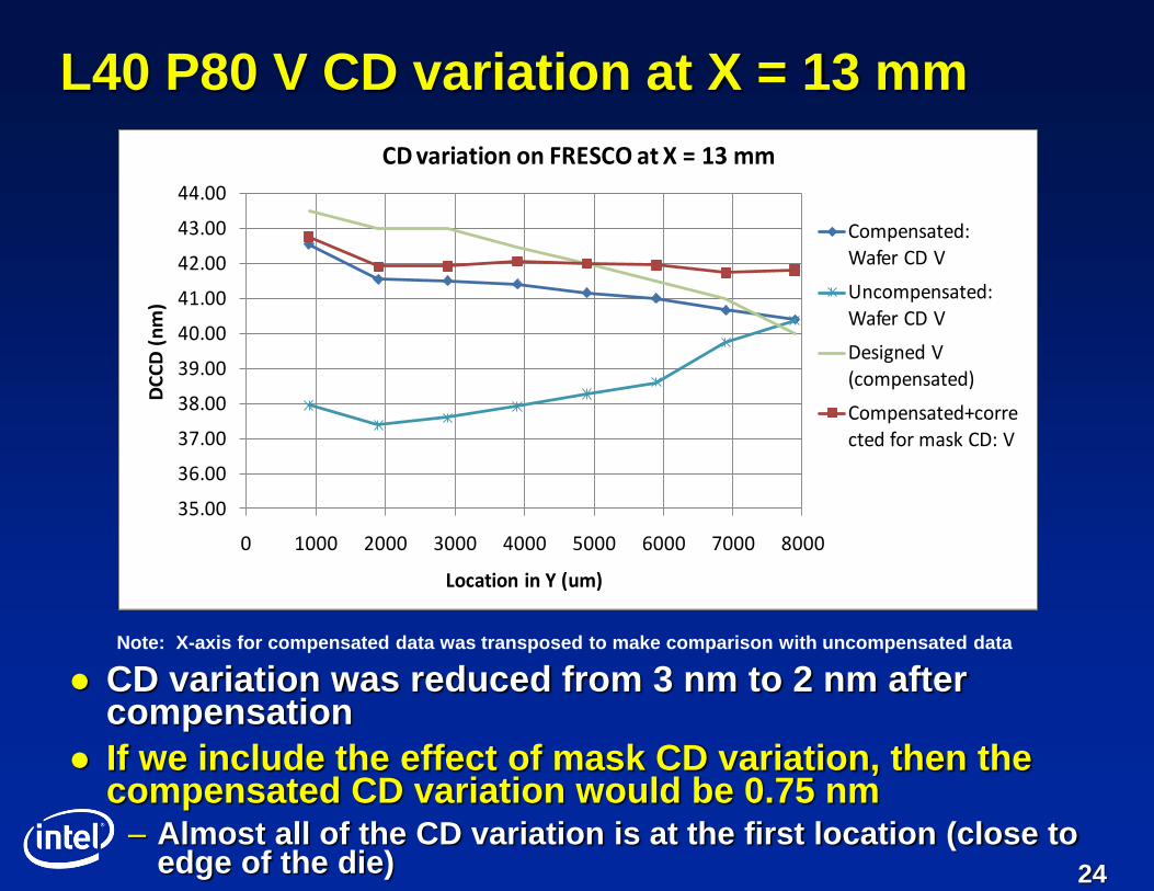
24
L40 P80 V CD variation at X = 13 mm
CD variation was reduced from 3 nm to 2 nm after compensation
If we include the effect of mask CD variation, then the compensated CD variation would be 0.75 nm – Almost all of the CD variation is at the first location (close to
edge of the die)
35.00
36.00
37.00
38.00
39.00
40.00
41.00
42.00
43.00
44.00
0 1000 2000 3000 4000 5000 6000 7000 8000
DC
CD
(n
m)
Location in Y (um)
CD variation on FRESCO at X = 13 mm
Compensated: Wafer CD V
Uncompensated: Wafer CD V
Designed V (compensated)
Compensated+corrected for mask CD: V
Note: X-axis for compensated data was transposed to make comparison with uncompensated data

G-Number
25
L40 P80 V CD variation at X = 3 mm
CD variation was reduced from 3.75 nm to 2 nm after compensation
If we include the effect of mask CD variation, then the compensated CD variation would be 1 nm
– Almost all of the CD variation is at the first 2 locations (close to edge of the die)
Note: X-axis for compensated data was transposed to make comparison with uncompensated data
35.00
36.00
37.00
38.00
39.00
40.00
41.00
42.00
43.00
44.00
0 1000 2000 3000 4000 5000 6000 7000 8000
DC
CD
(n
m)
Location in Y (um)
CD variation on FRESCO at X = 3 mm
Compensated: Wafer CD V
Uncompensated: Wafer CD V
Designed V (compensated)
Compensated+corrected for mask CD: V

G-Number
26
L40 P80 H CD variation at X = 13 mm
CD variation was reduced from 3.5 nm to 2 nm after compensation
If we include the effect of mask CD variation, then the compensated CD variation would be 1 nm – Part of the CD variation is due to the 1st point at the edge of the die
– However, the compensated CD variation observed at Y = 4 mm and 5 mm is due the designed CD variation based on the rule based compensation
– Due to relatively large discretization of flare levels in the rule based FVC, the flare values at those locations (6.6% and 6.1%) were barely above the previous lower flare bin
Note: X-axis for compensated data was transposed to make comparison with uncompensated data
35.00
36.00
37.00
38.00
39.00
40.00
41.00
42.00
43.00
44.00
45.00
0 1000 2000 3000 4000 5000 6000 7000 8000
DC
CD
(n
m)
Location in Y (um)
CD variation on FRESCO at X = 13 mm
Compensated: Wafer CD H
Uncompensated: Wafer CD H
Designed H (compensated)
Compensated+corrected for mask CD: H

G-Number
27
L40 P80 H CD variation at X = 3 mm
CD variation was reduced from 3.5 nm to 2 nm after compensation
If we include the effect of mask CD variation, then the compensated CD variation would be 1.5 nm – Most of the CD variation is due to the 1st point at the edge of
the die
Note: X-axis for compensated data was transposed to make comparison with uncompensated data
35.00
36.00
37.00
38.00
39.00
40.00
41.00
42.00
43.00
44.00
0 1000 2000 3000 4000 5000 6000 7000 8000
DC
CD
(n
m)
Location in Y (um)
CD variation on FRESCO at X = 3 mm
Compensated: Wafer CD H
Uncompensated: Wafer CD H
Designed H (compensated)
Compensated+corrected for mask CD: H

G-Number
28
L40 P160
Even without accounting for mask CD variation, the CD variation reduced from 3 nm to 1 nm after FVC for L40 P160
35.00
36.00
37.00
38.00
39.00
40.00
41.00
42.00
43.00
44.00
45.00
0 1000 2000 3000 4000 5000 6000 7000 8000
DC
CD
(n
m)
Location in Y (um)
CD variation on FRESCO at X = 3 mm
Compensated: Wafer CD V
Uncompensated: Wafer CD V
35.00
36.00
37.00
38.00
39.00
40.00
41.00
42.00
43.00
44.00
45.00
0 1000 2000 3000 4000 5000 6000 7000 8000
DC
CD
(n
m)
Location in Y (um)
L40 P160 CD variation on FRESCO at X = 3 mm
Compensated: Wafer CD H
Uncompensated: Wafer CD H
35.00
36.00
37.00
38.00
39.00
40.00
41.00
42.00
43.00
44.00
45.00
0 1000 2000 3000 4000 5000 6000 7000 8000
DC
CD
(n
m)
Location in Y (um)
L40 P160 CD variation on FRESCO at X = 13 mm
Compensated: Wafer CD V
Uncompensated: Wafer CD V
35.00
36.00
37.00
38.00
39.00
40.00
41.00
42.00
43.00
44.00
45.00
0 1000 2000 3000 4000 5000 6000 7000 8000
DC
CD
(n
m)
Location in Y (um)
L40 P160 CD variation on FRESCO at X = 13 mm
Compensated: Wafer CD H
Uncompensated: Wafer CD H

G-Number
29
Summary & conclusions Observed significant CD variation due to mask
shadowing on the ADT exposure tool
– H-V bias decreases from the center to the edge of the slit
– Shadowing compensation reduced H-V bias from 3.5 nm to <1 nm across the slit
Demonstrated up to 67% reduction in CD variation by Flare Variation Compensation (FVC)
– Nearly half of the residual after FVC was due to mask CD variation; the remaining half was due to flare modeling errors at the edge of the die
Reflectivity variation across the field is < 0.1% (absolute); no variation worth correcting for
OPC for EUV must include effects such as flare and
mask shadowing
G-Number
30
Acknowledgements
Intel EUV lithography team & IMO
IMEC