experiment 2: pulse width modulation and power … experiment 2: pulse width modulation and power...
TRANSCRIPT
11
Experiment 2: Pulse Width Modulation and Power Control Power delivered to a load, such as a lamp, heater, or dc motor, can be most efficiently controlled using pulse width modulation (PWM). A power transistor connected in series with the load is repetitively turned on and off. When the transistor is on, almost all of the power supply voltage is supplied to the load. When the transistor is off, no power is supplied to the load. Enhancement mode power mosfets are often used to supply power to a load using PWM. The average power delivered to the load is controlled by the “duty cycle” of the transistor, which is the ratio of its “on” time to the time of one cycle. IDS(ON) is the transistor’s drain to source current when it is on, and VDS(ON) is the transistor’s drain to source voltage when it is on. Given that DC is the duty cycle, the average power, PL, supplied to a load, and percent efficiency, %Eff, are given by:
( ) ( )
( ) ( ) ( )
LL ON
L Q
QON ON ONL
DS(ON)DD DS(ON)DS
DD
DD DS(ON)DS DS DS
PP I DC %Eff 100% 100%
P P
(V Vwhere : I P I V DC
R
V(V V ) 1
V
)
= ⋅ = =+
−= = ⋅ ⋅
⎡ ⎤− −⎢ ⎥
⎣ ⎦
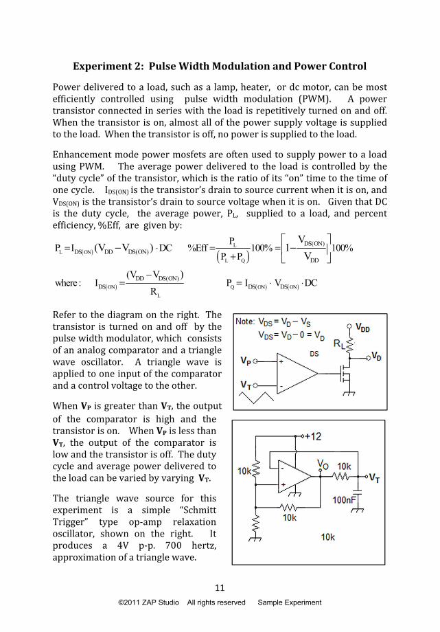
Refer to the diagram on the right. The transistor is turned on and off by the pulse width modulator, which consists of an analog comparator and a triangle wave oscillator. A triangle wave is applied to one input of the comparator and a control voltage to the other. When VP is greater than VT, the output of the comparator is high and the transistor is on. When VP is less than VT, the output of the comparator is low and the transistor is off. The duty cycle and average power delivered to the load can be varied by varying VT. The triangle wave source for this experiment is a simple “Schmitt Trigger” type op-amp relaxation oscillator, shown on the right. It produces a 4V p-p. 700 hertz, approximation of a triangle wave.
©2011 ZAP Studio All rights reserved Sample Experiment
12
When VO is high, about 10.5 volts, the capacitor charges. When VO is low, near zero volts, the capacitor discharges. The resistor values shown produce a trigger voltage at the non-inverting input of 8 volts when VO is high and 4 volts when VO is low. The result is that the capacitor charges exponentially to 8 volts and discharges exponentially to 4 volts. The resulting waveform approximates a triangle wave because the charge and discharge times are less than one RC time constant. This exercise will demonstrate the ability of the mosfet to vary the amount of power supplied to the load using PWM (Pulse Width Modulation). The circuit is basically a “light dimmer”, but the same principle can be used to control power supplied to motors and to other devices
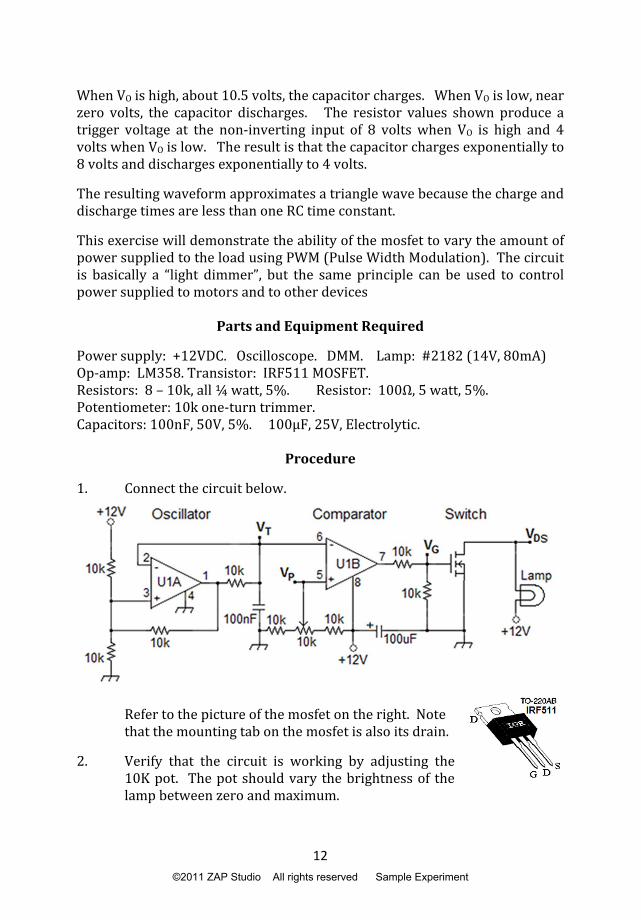
Parts and Equipment Required Power supply: +12VDC. Oscilloscope. DMM. Lamp: #2182 (14V, 80mA) Op-amp: LM358. Transistor: IRF511 MOSFET. Resistors: 8 – 10k, all ¼ watt, 5%. Resistor: 100Ω, 5 watt, 5%. Potentiometer: 10k one-turn trimmer. Capacitors: 100nF, 50V, 5%. 100µF, 25V, Electrolytic. Procedure 1. Connect the circuit below.
Refer to the picture of the mosfet on the right. Note that the mounting tab on the mosfet is also its drain. 2. Verify that the circuit is working by adjusting the 10K pot. The pot should vary the brightness of the lamp between zero and maximum.
©2011 ZAP Studio All rights reserved Sample Experiment
13
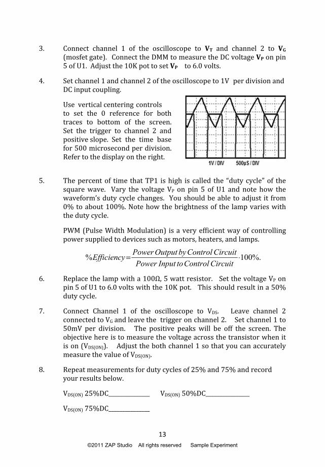
3. Connect channel 1 of the oscilloscope to VT and channel 2 to VG (mosfet gate). Connect the DMM to measure the DC voltage VP on pin 5 of U1. Adjust the 10K pot to set VP to 6.0 volts. 4. Set channel 1 and channel 2 of the oscilloscope to 1V per division and DC input coupling. Use vertical centering controls to set the 0 reference for both traces to bottom of the screen. Set the trigger to channel 2 and positive slope. Set the time base for 500 microsecond per division. Refer to the display on the right. 5. The percent of time that TP1 is high is called the “duty cycle” of the square wave. Vary the voltage VP on pin 5 of U1 and note how the waveform’s duty cycle changes. You should be able to adjust it from 0% to about 100%. Note how the brightness of the lamp varies with the duty cycle. PWM (Pulse Width Modulation) is a very efficient way of controlling power supplied to devices such as motors, heaters, and lamps. 6. Replace the lamp with a 100Ω, 5 watt resistor. Set the voltage VP on pin 5 of U1 to 6.0 volts with the 10K pot. This should result in a 50% duty cycle. 7. Connect Channel 1 of the oscilloscope to VDS. Leave channel 2 connected to VG and leave the trigger on channel 2. Set channel 1 to 50mV per division. The positive peaks will be off the screen. The objective here is to measure the voltage across the transistor when it is on (VDS(ON)). Adjust the both channel 1 so that you can accurately measure the value of VDS(ON). 8. Repeat measurements for duty cycles of 25% and 75% and record your results below. VDS(ON) 25%DC_______________ VDS(ON) 50%DC________________ VDS(ON) 75%DC_______________
%.100% ⋅=CircuitControltoInputPowerCircuitControlbyOutputPowerEfficiency
©2011 ZAP Studio All rights reserved Sample Experiment

14
Analysis: 1. Transfer the results of step 8 into a spreadsheet. Use the table layout shown below. IDS(ON) is the transistor current when the transistor is on. PQ is the average power dissipation of the transistor. PL is the average power dissipation of the 100 ohm resistor. DC is the duty cycle expressed as a fraction. 2. An easier way to vary the power delivered to a load would be to connect a variable resistor (rheostat) between the battery and the load. Compare the efficiency of the PWM circuit in delivering power to a 100 ohm resistor operating at 25% and 75% duty cycle to the rheostat circuit shown on the right. (a) Calculate the current, I, required to deliver the same power to the 100 ohm resistor in the DC circuit as was delivered to the lamp in the PWM circuit for a 25% and 75% duty cycle. (b) Calculate the value of the resistance RR required to obtain the currents calculated above for each duty cycle.. Hint: Use PL = I2RL to calculate I in the DC circuit. Power input to the circuit is 12V times the circuit current, I. (I = 12/(RR + RL) 3. Use the results above to compare the efficiency of the rheostat circuit above to the 25% duty cycle and 75% duty cycle PWM circuit.
DC VDS(ON) Volts
IDS(ON)
Amps PQ
Watts PL
Watts RL
Ohms Efficiency Percent
.25
.50
.75
©2011 ZAP Studio All rights reserved Sample Experiment

15
Pulse Width Modulation and Power Control Simulation The LTspice diagram is shown on the right. The LT1006 op-amp is equivalent to the LM358.
The IRF510 was obtained by first selecting “mosfet” and placing it into the schematic. Right click on the mosfet, select “Pick New MOSFET” and scroll down until you find the IRF510. A 150 ohm resistor, R8, represents a 2182 lamp. Simulation was set to “Transient” with a stop time of 10 milliseconds. The graph below on the left shows the triangle wave output of the oscillator and the waveform at the gate of the transistor with VP set to 6.0 volts. The graph below on the right shows the waveform on the drain of the transistor. When the transistor is on, about 53mV appears on the transistor’s drain. This is the transistor’s saturation voltage. VDS. When the transistor is off, the drain voltage is 12 volts and is off the graph.
©2011 ZAP Studio All rights reserved Sample Experiment