evil - patentimages.storage.googleapis.com · ericson; william b. dress, all of evil 1clge, all oi...
TRANSCRIPT

USOO5965873A
United States Patent (19) 11 Patent Number: 5,965,873 Simpson et al. (45) Date of Patent: Oct. 12, 1999
54 INTEGRATED CMOS SPECTROMETERS 4,191,452 3/1980 Grinberg et al. ....................... 257/222 4.820,915 4/1989 Hamakawa et al. .................... 250/226
(75) Inventors: Michael L. Simpson; M. Nance 5,726,440 3/1998 Kalkhoran et al. .................. 250/214.1 Ericson; William B. Dress, all of
Evil said oSS's E. Primary Examiner-Que T. Le 1Clge, all OI lenn., 9 Jr., Tucson, Ariz., Alan L. Attorney, Agent, or Firm-Quarles & Brady LLP Wintenberg, Knoxville, Tenn. 57 ABSTRACT
73 Assignee: Lockheed Martin Energy Research A spectrometer, comprises: a Semiconductor having a Silicon Corporation, Oak Ridge, Tenn. Substrate, the Substrate having integrally formed thereon a
plurality of layers forming photo diodes, each of the photo 21 Appl. No.: 09/082,082 diodes having an independent spectral response to an input
Spectra within a spectral range of the Semiconductor and 22 Filed: May 20, 1998 each of the photo diodes formed only from at least one of the
plurality of layers of the Semiconductor above the Substrate; Related U.S. Application Data and, a Signal processing circuit for modifying Signals from
the photo diodes with respective weights, the weighted 63 Continuation of application No. 08/932,225, Sep. 17, 1997, Signals being representative of a specific Spectral response.
abandoned. The photo diodes have different junction depths and differ (51) Int. Cl. ................................................ H01J 40/14 ent polycrystalline Silicon and oxide coverings. The Signal 52 U.S. Cl. .................. 250/214.1; 250/226; 257/461 processing circuit applies the respective weights and Sums 58 Field of Search ............................. 250/2141, 214 R, the weighted signals. In a corresponding method, a spec
250/226; 356/346,349; 257/461, 464, 458 trometer is manufactured by manipulating only the Standard masks, materials and fabrication Steps of Standard Semicon
56) References Cited ductor processing, and integrating the spectrometer with a Signal processing circuit.
U.S. PATENT DOCUMENTS
4,079,405 3/1978 Ohuchi et al. .......................... 257/464 14 Claims, 14 Drawing Sheets
PROCESSING
PHOTO LIGHT SENSOR
DETECTORS DIGITAL
CONVERTER
Output 1 Output 2 Output 3
SIGNAL
26 28
ANALOG
TO- SOFTWARE
SPECTRAL INFORMATION

U.S. Patent Oct. 12, 1999 Sheet 1 of 14 5,965,873
Output 1 Output 2 Output 3
SIGNAL PROCESSING O
24 26 28
PHOTO- Alps. LIGHT-> SENSOR DIGITAL SOFTWARE
SPECTRAL INFORMATION
FIG 1)

U.S. Patent Oct. 12, 1999 Sheet 2 of 14 5,965,873
INCIDENT
THIN FILM STACK
PHOTO-DETECTOR TRANSMITTED
S-POLARZATION
FIG.3a
P-POLARIZATION
FIG. 3b

U.S. Patent Oct. 12, 1999 Sheet 3 of 14
CEL C CPG
CAA
nWel P-TYPE SUBSTRATE
FIG. 4a
P-TYPE SUBSTRATE
FIG. 40
COX COX
P-TYPE SUBSTRATE
FIG. 4C
5,965,873

U.S. Patent Oct. 12, 1999 Sheet 4 of 14 5,965,873
CVA
P-TYPE SUBSTRATE
FIG. 5a
rCVA
P-TYPE SUBSTRATE
F.G. 5)
P-TYPE SUBSTRATE
FIG.50

U.S. Patent Oct. 12, 1999 Sheet S of 14 5,965,873
sS 3
S. a.
SNOdS OZTWWON
U.S. Patent Oct. 12, 1999 Sheet 6 of 14 5,965,873
C Co - y
c
v O O
O 2, S 3. -
c s C
O O C
as
o S S 9
N d
- 92 > O
is s
O O CO
O C
Co O r
o o o N co L N. co C\ o -- C Co Cd C C C O C O O
SNOdS OZTWWON

U.S. Patent Oct. 12, 1999 Sheet 7 of 14 5,965,873
\ pdiffusion // P-TYPE SUBSTRATE
16+6
Et 1e-5-
CD 2 C
s 1e4 S3 ge
1e-1-3 300 400 500 600 700 800
WAVELENGTH(nm)
FIG. 9a


U.S. Patent Oct. 12, 1999 Sheet 9 of 14 5,965,873
3
5
SNOdS OZTWWON

5,965,873 Sheet 10 of 14 Oct. 12, 1999 U.S. Patent
00||
000||006 UJU
|| '0|| H10NETHAWM ||
SNOdS OZIWWHON
U.S. Patent Oct. 12, 1999 Sheet 11 of 14 5,965,873
- INPUT SPECTRUM A MEASURED RESPONSE
FIG.12a O
O.O -0.2
400 500 600 700 800 900 1000 1100
WAVELENGTH(nm)
14 12- - INPUT SPECTRUM
its '' A MEASURED RESPONSE 1.0-
C/O
0.8– 0.6- is 04 FIG.12b
- 0.2- O.O z
400 500 600 700 800 900 1000 1100 WAVELENGTH(nm)
14 1.2 - INPUT SPECTRUM
2 10 A MEASURED RESPONSE C - '' CAD
?h
S FIG. 12C c d ? O 2
0.4 400 500 600 700 800 900 1000 1100
WAVELENGTH(nm)

U.S. Patent Oct. 12, 1999 Sheet 12 of 14 5,965,873
El --INPUT SPECTRUM A MEASURED RESPONSE
1.O
O.6 0.4- 0.2 O.O -0.2 -0.4
400 500 600 700 800 900 1000 1100
WAVELENGTH(nm)
FIG. 13

U.S. Patent Oct. 12, 1999 Sheet 13 of 14 5,965,873
14 12 - INPUT SPECTRUM
2 - A MEASURED RESPONSE 10 0.8-
is 06- FIG. 14a S 0.4- S 0.2- t O.O a. A AA
-0.2 400 450 500 550 600
WAVELENGTH(nm)
14 12 - INPUT SPECTRUM
2 - A MEASURED RESPONSE a 10–
0.8– Ch
is 06- FIG. 14b S 0.4- s 0.2 t AA AAA
0.0-law 's -0.2
500 550 600 650 700 750 800
WAVELENGTH(nm)
14 12 - INPUT SPECTRUM
2 A MEASURED RESPONSE 5 ? F.G. 14C s s O al
900 950 1000 1050 1100
WAVELENGTH (nm)

U.S. Patent Oct. 12, 1999 Sheet 14 of 14 5,965,873
NPUISPECTRUM 2 a MEASURED RESPONSE a 10- A C/D
9. ?h
is 0.6 FIG. 15 S 0.4- S 0.2– f 00
-0.2 650 700 750 800 850 900 950
WAVELENGTH(nm)
14 --INPUISPECTRUM 2 : A MEASURED RESPONSE a 10
CMO
0.8– ?h
is 0.6 FIG 16 S 0.4- 25 0.2- f 00
-0.2 590 610 63O 650 67O 690
WAVELENGTH(nm)
14 - NESPECIBM 2 : A MEASURED RESPONSE
O CfO
?h
s FIG. 17 s
O 2
580 600 620 640 660 680 WAVELENGTH (nm)

5,965,873 1
INTEGRATED CMOS SPECTROMETERS
CROSS REFERENCE TO RELATED APPLICATIONS
This application is a continuation of U.S. patent applica tion Ser. No. 08/932,225 (abandoned).
BACKGROUND OF THE INVENTION
1. Field of the Invention
This invention relates to the field of photo-Spectrometers, and in particular, to photo-spectrometers realized in a stan dard Semiconductor process, to an IC compatible photo diode spectral Selectivity/enhancement method using mul tiple pn junctions and to a method for determining light Spectra using optical detectors with controllable spectral response.
2. Description of Related Art Photo-spectrometers are used in a variety of Scientific and
industrial applications including atmospheric measurements, medical instruments, flame monitoring in commercial hydrocarbon-fueled furnaces and aircraft engines, and a number of colorimetry applications ranging from color Scanners to industrial process control. Even red-green-blue color imaging is a limited application of photo-spectroScopy. Many photo-spectrometers consist of an array of
photodiodes, an optical filtering or dispersive element, col limating and focusing optics, and data collection electronics. Each technique allocates a wavelength band to one photo diode in the array. Although these Systems are capable of resolution better than 1 nm, they require precise alignment, are relatively expensive, and are too large for micro instrumentation applications.
Micro-fabrication techniques are used to produce photo Spectrometers that overcome the disadvantages of the SyS tems described above. There is on-going research to produce spectrometers based on Silicon-on-insulator (SOI) photo diode arrays. Fabry-Perot micro-spectrometers have been produced using bulk and Surface micro-machining techniques, and a spectrometer composed of a micro fabricated diffraction grating attached to a CCD array has been realized. In addition, a calorimeter realized using an amorphous silicon (Si) Schottky photodiode has also been reported.
These micro-fabricated Spectrometers or calorimeters are capable of good spectral resolution and are appropriate for micro-instrumentation. However, these devices require fab rication Steps or materials that are not part of a low-cost, Standard IC proceSS and do not take full advantage of mass production in this mature technology. None of these spec trometers can be realized in a Standard Semiconductor pro ceSS using only the Standard masks, materials, and fabrica tion StepS. Such prior art devices cannot be integrated with additional analog, digital, and wireless circuits constructed in the same Semiconductor process to produce a true instrument-on-a-chip.
SUMMARY OF THE INVENTION
The problems of the prior art spectrometers have been overcome in accordance with the inventive arrangements, which utilize a Standard, Semiconductor process using only the Standard masks, materials, and fabrication Steps. Devices in accordance with the inventive arrangements can be inte grated with additional analog, digital, and wireless circuits constructed in the Same Semiconductor process to produce a
15
25
35
40
45
50
55
60
65
2 true instrument-on-a-chip. Suitable Semiconductor pro cesses include, for example, n-well CMOS, p-well CMOS, silicon-on-insulator (SOI) CMOS, Sibipolar and most other Semiconductor processes as well.
Only the masks, materials and fabrication Steps inherent to these IC processes need be used. No post processing is necessary to add mechanical or optical devices for filtering. Such a spectrometer can comprise, for example, a set of 18 detectors with independent Spectral responses. The responses of these devices can be weighted and Summed to form outputs proportional to the power in discrete wave length bands in a region, for example, from ~350 nm to ~1100 nm for Si. With the solution space restricted to a 60 nm band, this instrument can resolve gaussian input Spectra (O=5 nm) with a peak-to-peak spacing of less than 15 nm. This device can easily be integrated with additional analog, digital, or wireless circuits to realize a true instrument on-a-chip. A spectrometer in accordance with an inventive arrange
ment comprises: a Semiconductor having a Silicon Substrate, the Silicon Substrate having integrally formed thereon a plurality of layers forming photo diodes, each of the photo diodes having an independent spectral response to an input Spectra and each of the photo diodes formed only from at least one of the plurality of layers of the Semiconductor above the Silicon Substrate; and, a signal processing circuit for modifying Signals from the photo diodes with respective weights, the weighted Signals being representative of a Specific spectral response. The Signal processing circuit Sums the weighted Signals to define a composite spectral response function, which can be plotted. The photo diodes are advantageously manufactured in
accordance with Standard Semiconductor processes, includ ing for example, the n-well CMOS process, the p-well CMOS process, the silicon-on-insulator (SOI) CMOS process, the Sibipolar process and most other Semiconduc tor processes as well. The photo diodes can have different junction depths and
different polycrystalline Silicon and oxide coverings. The respective weights are Set in accordance with prede
termined information regarding an expected limited range of wavelengths to be detected within the broader spectral range of the Semiconductor. The limited range of wavelengths to be detected is preferably approximately 100-200 nanom eterS.
The range of the input light can be anything within the Spectral range of the particular Semiconductor, for example -350 nm-1100 nm for Si. However, the spectrometer gives better performance if the Spectral range to be detected is known beforehand to be limited within a range of approxi mately 100-200 nm, within the larger spectral range of the Semiconductor. A spectrometer in accordance with a another inventive
arrangement comprises: a Semiconductor having a Silicon Substrate and a light transmissive Surface, the Semiconductor having a plurality of pnjunctions located above the Substrate at different fixed depths from the Surface, the pn junctions generating respective and independent output Signals repre Sentative of unique depth-related Spectral Sensitivity func tions, and, a Signal processing circuit for modifying Signals from the photo diodes with respective weights, the weighted Signals being representative of a specific Spectral response. The Signal processing circuit Sums the weighted Signals to define a composite Spectral response function, which can be plotted. The pn junctions are advantageously manufactured in
accordance with Standard Semiconductor processes, includ
5,965,873 3
ing for example, the n-well CMOS process, the p-well CMOS process, the silicon-on-insulator (SOI) CMOS process, the Sibipolar process and most other Semiconduc tor processes as well.
The output Signals generated by the pn junctions differ from one another by reason of interactions occurring in different regions of the Semiconductor above the Substrate. The different regions include a p-diffusion region, a deple tion region, and a region beyond the depletion region. A method for manufacturing a spectrometer, in accor
dance with yet another inventive arrangement, comprises the Steps of: providing a plurality of Sites on a Silicon Substrate which have different junction depths and different polycrys talline Silicon and oxide coverings, by manipulating only the Standard masks, materials and fabrication Steps of Standard Semiconductor processing, each of the Sites having an inde pendent Spectral response to an input spectra, and, integrat ing the Sites with a circuit for respectively weighting and Summing the Spectral responses from the Sites, by using the Standard Semiconductor processing, the weighted Signals representing a specific spectral response of the input spectra. The weighted Signals are preferably Summed to define a composite spectral response function, which can be plotted.
The method can further comprise the Step of integrating the Sites with an analog signal processing circuit, a digital Signal processing circuit or a WireleSS Signal processing circuit.
The method advantageously utilizes numerous Semicon ductor processing, including for example, n-well CMOS processing, p-well CMOS processing, Silicon-on-insulator (SOI) CMOS processing, Si bipolar processing and most other Semiconductor processing as well.
BRIEF DESCRIPTION OF THE DRAWINGS
FIGS. 1a and 1b are block diagrams of a photo Spectrometer in accordance with the inventive arrangements, realized in a standard CMOS IC process.
FIG. 2 is a diagram illustrating geometry of a thin-film Stack.
FIGS. 3(a) and 3(b) are diagrams illustrating perpendicu lar (S) and parallel (P) polarization States, respectively, of incident light.
FIGS. 4(a), 4(b) and 4(c) are diagrams illustrating n-well/ p-Substrate photo detectors with double polycrystalline Sili con covering and all oxides present, passivation removed, and minimum oxide, respectively.
FIGS. 5(a), 5(b) and 5(c) are diagrams illustrating n-diffusion/p-Substrate photo detectors with no polycrystal line Silicon covering and all oxides present, passivation removed, and minimum oxide, respectively.
FIG. 6 is a plot useful for explaining n-diffusion device response with two different oxide thicknesses.
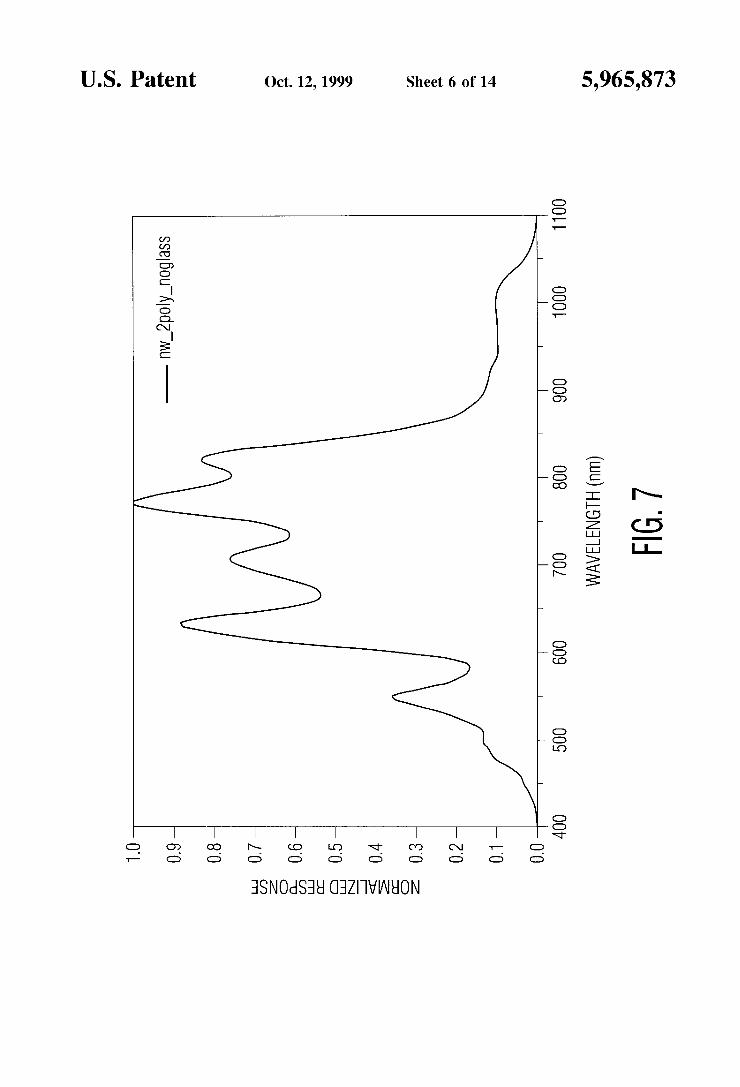
FIG. 7 is a plot useful for explaining n-well/p-substrate device response with a polycrystalline Silicon/oxide/ polycrystalline Silicon covering.
FIG. 8 is a diagram of a multi-junction device (stack diode).
FIG. 9(a) is a plot useful for explaining silicon absorption coefficient (a) VS. wavelength.
FIG. 9(b) is a plot useful for explaining the extinction coefficient and refractive indeX for crystalline and polycrys talline Si.
FIG. 10 is a plot useful for explaining the photon response of p-diffusion/n-well and n-well/p-substrate photodiodes.
15
25
35
40
45
50
55
60
65
4 FIG. 11 is plot useful for explaining the photon response
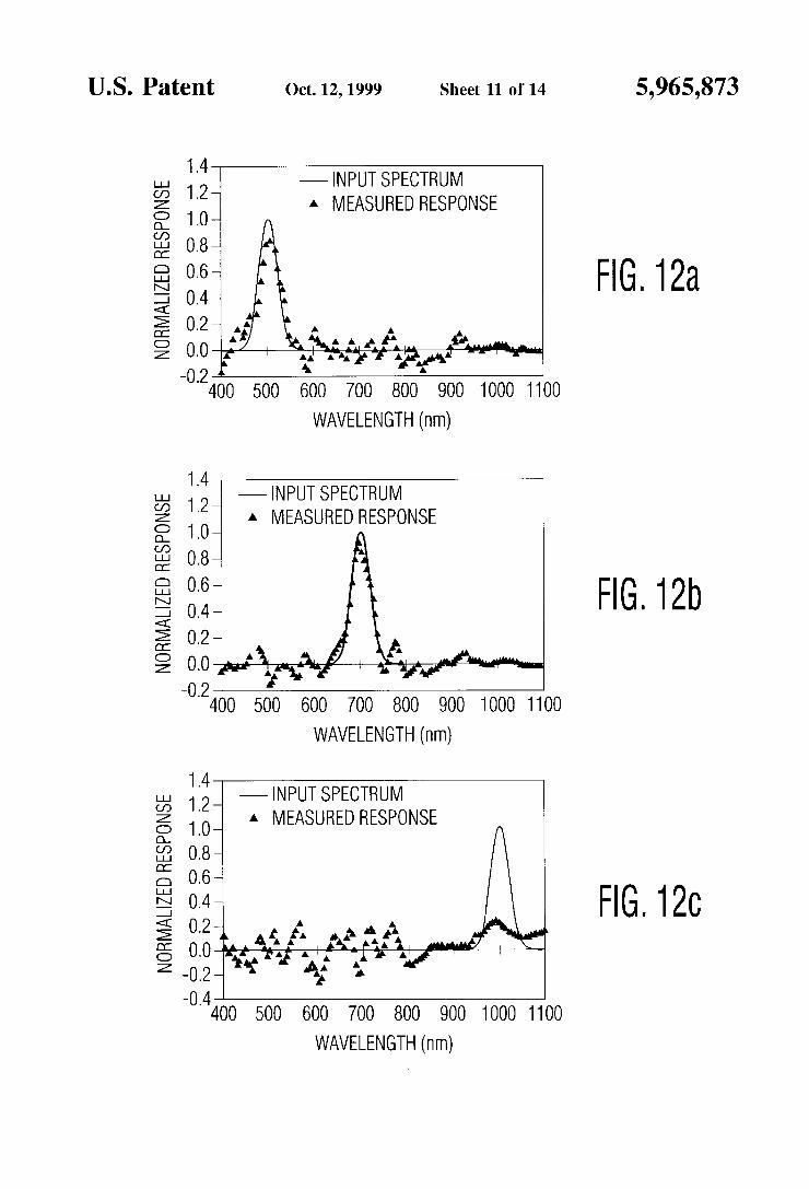
of a photo-spectrometer in accordance with the inventive arrangements, utilizing 18 detectors. FIGS. 12(a), 12(b) and 12(c) are plots useful for explain
ing the response of the Spectrometer to gaussian input spectra (O=20 nm) centered at 500 nm, 700 nm, and 1000 nm, respectively, the Solution Space being constrained to the 400-1100-nm band.
FIG. 13 is a plot useful for explaining the response of the spectrometer to a doublet (one gaussian centered at 800 nm, another at 875 nm, and O=20 nm for each), the solution space being constrained to the 400-1100-nm band.
FIGS. 14(a), 14(b) and 14(c) are plots useful for explain ing the response of the Spectrometer to the same gaussian spectra used to generate FIGS. 12(a), 12(b) and 12(c), the solution space being constrained to the 400-600-nm band, the 500-800-nm band, and the 900-1100-nm band, respec tively.
FIG. 15 is a plot useful for explaining the response of the Spectrometer to the same doublet used to generate FIG. 13, the solution space being constrained to the 740–910-nm band.
FIG. 16 is a plot useful for explaining the response of the spectrometer to a doublet centered at 640 nm and 655 nm with O=5 nm, the Solution Space being constrained to the 620-680-nm band.
FIG. 17 is a plot useful for explaining the response of the spectrometer to a doublet centered at 640 nm and 650 nm with O=5 nm, the Solution Space being constrained to the 620-680-nm band.
DETAILED DESCRIPTION OF THE PREFERRED EMBODIMENTS
FIG. 1(a) shows a block diagram of a spectrometer 10 in accordance with the inventive arrangements. The Spectrom eter 10 uses m photodiode detectors designated DET1 through DETm, each with an independent spectral response. A Signal processing circuit 12 weights and Sums the respec tive responses of each detector to form in outputs designated OUTPUT1 through OUTPUTn. Each of the n outputs cor responds to the input signal power in a discrete wavelength band.
The weights can be changed electronically in-situ to allow a range of programmable Spectral functions. The processing of the Signals can range from Straight-forward Sign-weighted Summing to digital Signal processing or neural net proceSS ing. A block diagram of the Spectrometer 10 in conjunction with a computer processor is shown in FIG. 1(b). Incident light to be analyzed falls onto an array 20 of m photo detectors. The outputs of the m photo detectors are amplified by an array of amplifiers 22, the outputs of which are digitized by digital to analog converter 24, which may form part of a digital processor in a computer 26. A Software program 28 can process the digitized data and provide Spectral information as an output, in digital or analog form, in numerous formats. The computer also provides control signals for the array 20 of photo detectors.
Data processing options are numerous and range from Straight-forward analog processing including but not limited to weighted Summing and Subtraction, to more complex methods including artificial neural net processing and digital Signal processing methods, or any combination thereof.
Generally Speaking, two or more pn junctions located at different fixed depths from the surface of the semiconductor can provide different output signals, each with a unique

5,965,873 S
depth-related Spectral Sensitivity function. Monochromatic light is normally incident on the Surface of the pdiff region of the detector. Depending on the wavelength of the light, interactions can occur in three regions: the p-diffusion region, the depletion region, and the region beyond. The various layers above the Silicon Substrate can be manipu lated to control these interactions and provide the indepen dent Spectral Sensitivities.
In accordance with the inventive arrangements, photo diode detectors with respective and independent spectral responses are created and the appropriate weights for each independent spectral response are determined. The indepen dent Spectral responses and the appropriate weights can be determined in accordance with the following analysis and methodology.
Suppose there are m basis functions that can represent any possible detector-array spectrum. That is, let S(0) be the power Spectral density of any Source illuminating the detec tor array, then
i (1)
S() = Xa B.A),
where the C, are the set of numerical coefficients, the B.0) are the basis functions that characterize the detector array, and m is the number of individual photo detectors in the array. Physically, the coefficients are the responses of the devices, while the basis functions are yet to be determined.
The responses of the detectors are given by
(2) a = I, R(A)s(a)da,
where C, and S(0) have the same meaning as above and R(0) is the spectral response of the j" detector. A means or methodology is needed to compute the basis functions given a Sampled representation of the Spectral-response functions. That is, a numerical Solution is needed to the result of Substituting equation (1) into equation (2),
(3)
This set of equations is to be solved for the B(0) in terms of R(0) on discrete set of Samples {2} for q=1,..., n. If a Stable Set of approximate Solutions to this set of integral equations can be found, a Spectrum can be obtained of many possible photon distributions falling within the range of posius), by multiplying the vector of measured device responses by the numerical matrix representing the basis Set, O
i (4) S X6jaj,
i=l
where now ) is an integer that indexes the Set of wave lengths used in characterizing the response functions (i.e., in calibrating the device array) and f, is the numerical matrix obtained from an approximate Solution to (3).
If the detector array is calibrated using a Standard mono chromator with slits set for a spectral width of 5 nm and measurements are made every 5 nm between 2–400 nm and
15
25
35
40
45
50
55
60
65
6 2=1100 nm, the integral equations in (3) can be approxi mated by the matrix equation
CXCRAW, (5)
O
(6)
where the measured coefficient vector is o, the response matrix, R, is now the Spectral response integrated over the Slit function represented by A2=5 nm, and Bis the unknown set of discrete basis functions on the interval from 400 to 1100 nm. Equation (6) has the formal solution, B=R', but the actual numerical Solution involves a bit of manipulation.
Typically there are far more wavelength Samples than photo detectors. The standard way to invert the matrix R, which in the example presented herein is a set of m=20 by n=141 numbers, is to use the Moore-Penrose pseudo inverse, giving
provided that the inverse of the Square, m-by-m matrix exists. By the construction of R times its transpose, this form is equivalent to a least-Squares Solution of the matrix equa tion (6). If the pseudo inverse is computed using the method of Singular-value decomposition, however, control is retained over which calibration Sets are important and which may be ignored. Thus, a decomposition of the matrix R into three matrices is Sought in the form
where U is an m-by-m column-Orthogonal matrix, W is an m-by-m diagonal matrix whose non-Zero elements are the m Singular values, and V is an n-by-m column-Orthogonal matrix. The pseudo inverse is then given by
and the measured spectrum is given by equation (4). The key to establishing that certain calibration Sets are not
important is contained in the ratio of the m Singular values to the largest Singular value. Such ratioS approaching machine precision are Suspect. The Standard way to treat Such contributions is to Set the reciprocal of those terms to Zero in equation (9). In this example, calibration Sets that contribute the Small Singular values are Simply removed, and Subsequently, readings from the corresponding photo detectors are blocked out. Alternatively, other approaches Such as consolidating Similar detectors can be implemented.
In accordance with the inventive arrangements, photo detectors are created with independent spectral responses in the wavelength regions of interest using only the processing steps inherent to standard CMOS IC fabrication. It is an important advantage of the inventive arrangements that no post processing of the Si wafer is required. Thus, only the Silicon dioxide, aluminum, and polycrystalline Silicon layers above the Si Substrate, and the placement and geometry of wells and diffusions in the substrate, can be specified. The Spectral responses of the detectors can be differentiated by using thin-film interference effects and by taking advantage of the wavelength dependence of the photon absorption depth in crystalline and polycrystalline Si. The layers of polycrystalline silicon and SiO over the
photo detectors behave as a stack of thin-film filters. The optical transmission of the assembly can be determined if the polarization and angle of incidence of the light are

5,965,873 7
known and if the thickness and the index of refraction of each layer is known.
FIG. 2 illustrates the geometry of a thin-film stack com prised of L layers. Incident light enters the top layer at an angle of incidence Om. The Subsequent angles of incidence change at each layer, until light transmitted through each of the layerS enter the photo-detector layer.
The polarization effects of the thin-film stack may be determined by decomposing the incident light into two orthogonal States: S-polarization, wherein the electric field is perpendicular to the plane of incidence; and, p-polarization, wherein the electric field is parallel to the plane of incidence. FIG. 3 illustrates the two polarization states. The intensity transmittance for a given polarization, (S- or -p) is given by
in (10)
where t is the amplitude transmittance of the thin-film Stack for the polarized light, n is the effective refractive index of the photo detector Semiconductor material, and n is the effective refractive index of the incident medium. In general, the effective refractive index for any of the material layers is defined by
i. f p-polarization (11)
n = cosé nicos(); S - polarization
where n is the refractive index (which is complex-valued for absorbing materials) of layer j, and 0, is the angle of the light ray with respect to the Surface normal in the material layer.
The relationship between the angle of the light ray in any two adjacent layerS is given by Snell's Law
nisin 6 =n-1 sin 0,1 (12)
For a given polarization, the amplitude transmittance is given by
2nn (13) no B+ C
where B and C are calculated by
(C)= M ). and where the matrix M is given by
(14)
M=MM . . . M.M. (15)
Thus, the thin-film effects for each layer are described by a matrix M, (where j=1,2,..., L). The matrix for each layer is given by
(16)
15
25
35
40
45
50
55
60
65
8 -continued
(17) of = (nd cost),
where d, is the thickness of the thin-film layer and is the wavelength of the light in a vacuum.
For unpolarized or randomly polarized light, the intensity transmittance for the thin-film Stack is given by
1 (18) Tunpolarized = 5 (T. +T),
where T is the intensity transmittance of S-polarized light and T is the intensity transmittance of p-polarized light. The IC process used for this example included two metal,
two polycrystalline Silicon, and Six oxide layers. A designer has full control over placement of the polycrystalline Silicon and metal Structures, and Some control over the placement of SiO layers. Table 1 identifies the filter element layers available in standard CMOS processes. FIGS. 4 and 5 show examples of devices that can be fabricated in the CMOS process used in accordance with the inventive arrangements.
TABLE 1.
Layer Name Description
COG top level passivation oxide CVA metal 1 f metal 2 via oxide CCE metal 1 to polycrystalline silicon or diffusion oxide CEL polycrystalline silicon 2 COX polycrystalline silicon 1 to 2 oxide CPG polycrystalline silicon 1 CAA field oxide gOX MOSFET gate oxide
In FIGS. 4(a), 4(b) and 4(c), an n-well/p-substrate diode is shown with a double polycrystalline Silicon covering and three SiO covering options. FIG. 4(a) shows all oxides present. FIGS. 4(b) shows passivation removed. FIG. 4(c) shows minimum oxide.
FIGS. 5(a), 5(b) and 5(c) illustrate an n-diffusion/ Substrate diode with no polycrystalline Silicon coverings, and the same three SiO2 covering options shown in FIGS. 4(a), 4(b) and 4(c). Unfortunately, the prohibited use of polycrystalline Silicon Structures over n-diffusion and p-diffusion devices in self-aligning CMOS processes limits the detector covering options.
FIG. 6 shows the response of two photodiodes with different Sio coating thicknesses. Two distinct interference patterns are seen.
FIG. 7 shows the response of an n-well/p-substrate pho todiode with a covering of two polycrystalline Silicon layers separated by a thin-film of SiO. This response function is rich with interference Structure. An n-well CMOS process allows the realization of n-well/
p-Substrate, n-diffusion/p-Substrate, and p-diffusion/n-well junctions. A double-junction or Stack-diode Structure is shown in FIG.8. The depth dependent absorption of light as it passes through this detector is given by
F=Foe"), (19)
where F is the number of incident photons, F is the number of photons absorbed, a is the absorption coefficient for Si, and d is the distance into the detector. AS shown in FIG. 9(a), a is a strong function of wavelength, varying from -10 cm at 300 nm to essentially 0 at 1100 nm. FIG. 9(b)

5,965,873
shows extinction coefficient and refractive index values for crystalline and polycrystalline Si. Thus, longer wavelength light produces charge deep in the device that is preferentially collected at the n-well/p-Substrate junction, while shorter wavelength light produces shallow charge that is collected by the p-diffusion/n-well junction. This behavior produces the spectral responses shown in FIG. 10. The p-diffusion/ n-well diode has a response that peaks at 500 nm, while the n-well/p-substrate diode response peaks at 750 nm. The stack-diode provides two devices with well differentiated Spectral responses.
Using photodiodes with different oxide and polycrystal line Silicon coverings as well as the two devices inherent to the Stack-diode, 18 devices with independent Spectral responses were fabricated. Table 2 gives a brief device description for a photo-spectrometer IC. The devices were commonly made up of 4 Smaller devices connected in parallel, that is, a 4-cell Structure.
TABLE 2
Device Device Name Description
n-well 4-cell structure with 0% poly-Si coverage n-well 4-cell structure with 20% poly-Si coverage n-well 4-cell structure with 60% poly-Si coverage n-well 4-cell structure with 80% poly-Si coverage n-well 4-cell structure with 100% poly-Si coverage n-diffusion 4-cell structure - COG removed n-diffusion 4-cell structure n-well 4-cell structure n-well 4-cell structure - COG, CVA, CCE, CAA oxides removed n-well 4-cell structure with 2 poly-Si coverings n-well 4-cell structure with 2 poly-Si coverings- COG oxide removed
1. nw bot Op
2 nw bot 20p
3 nw bot 60p
4 nw bot 80p
5 nw bot 100p
6 n-diff noglass
7 n-diff nw poly
9 nw poly noox 8
10 nw 2poly
11 nw 2poly noglass
12 nw 2poly noox n-well 4-cell structure with 2 poly-Si coverings- COG, CVA, CCE, CAA Oxides removed
13 n-well bot array n-well 25-cell structure 14 n-well bot big large n-well single structure 15 n-well bot big noox large n-well single structure - COG,
CVA, CCE, CAA oxides removed 16 n-diff noox big large n-diffusion single structure 17 p diff p-diffusion device 18 m well n-well device
FIG. 11 shows the spectral response of all the photo diodes. The photo-spectrometer was calibrated by measur ing the response of each detector in 5-nm Steps from 400 nm to 1100 nm. Thus, the R matrix was 18x141 (rowsx columns). The b matrix was calculated using equation (9), and the input spectra is given by equation (4). The photo-spectrometer was evaluated in two ways. In the
first Set of tests it was only assumed that the input spectrum resided within the 400-1100-nm band where Si detectors have an appreciable response. The response of the devices to test functions were calculated, and the outputs of the Spec trometer were found using equation 3. FIGS. 12(a), 12(b) and 12(c) show the response of the spectrometer, with the above constraint, to gaussian input spectra (O=20 nm) cen tered at 500, 700, and 1000 nm. These plots show that reasonable spectra can be obtained for the 500 and 700 nm inputs (albeit with up to 20% of the measured peak out-of band noise), while the measurement is quite poor at 1000 nm. FIG. 13 shows the response of the spectrometer to a doublet. One gaussian peak is centered at 800 nm and
15
25
35
40
45
50
55
60
65
10 another is centered at 860 nm, with O=20 nm for both. Although this doublet is resolvable, the out-of-band noise exceeds 25% of the peak Signal. The Second Set of tests assumed a priori knowledge of the
input spectrum was available. In a significant number of measurements the general region of the expected input Spectrum is known and only the details of the lines in this region need to be resolved. FIGS. 14(a), 14(b) and 14(c) show the response of the Spectrometer to the same gaussian input spectra used to generate FIG. 12. However, the R matrix was defined only over local regions around the input Spectra. This results in a new b matrix and, as the parts of FIG. 14 show, considerable improvement in the measured spectra. With the wavelength band limited to 900-1100 nm the input spectrum centered at 1000 nm, which was essen tially unmeasureable in FIG. 12(c) was resolved quite well as shown in FIG. 14(c), with out-of-band noise less than 10% of the peak. FIG. 15 shows the response of the Spectrometer to the same doublet used to generate FIG. 13, with a local region defined from 740-910 nm. The measured peaks were essentially as well resolved as the input peaks with no appreciable increase in the full width at half maxi mum (FWHM).
FIGS. 16 and 17 show the response of the spectrometer to a doublet (O=5 nm) in the region 620-680 nm. As FIG. 16 shows, at a spacing of 15 nm the doublet is resolved. When the spacing is reduced to 10 nm, as illustrated by in FIG. 17, the doublet is unresolveable. A photo-spectrometer which can be realized in a Standard
Semiconductor proceSS has been taught and described. Only the mask, materials, and fabrication Steps inherent to a Standard Semiconductor process need be used to realize Such a device. Such a spectrometer produces a composite response function constructed from the response functions of a plurality of individually characterized photodiodes. A Specific embodiment utilizing 18 Such photodiodes has been described in particular detail. The Spectral responses of the photodiodes can be decoupled by using different junction depths and polycrystalline Silicon and oxide coverings. A spectrometer according to the inventive arrangements
offerS modest performance as a wide-band Spectrometer, but offers excellent performance when a priori knowledge of the input Spectra can be used to constrain the Solution Space to a narrow band, for example ~100-200 nm, within the broader Spectral response of the particular Semiconductor.
While the spectrometer taught herein does not provide the resolution of diffraction or reflective gratings or photodiode array instruments, it can be maSS produced in a Standard IC process, requires no post-processing of the wafer, and can be integrated with a variety of other analog, digital, and wire less circuits to produce a true instrument-on-a-chip that can be applied in a variety of low-cost, low-power, rugged micro-instruments. Suitable Semiconductor processes can include, for example, n-well CMOS, p-well CMOS, silicon on-insulator (SOI) CMOS, Sibipolar and most other semi conductor processes as well. What is claimed is: 1. A Spectrometer, comprising: a Semiconductor having a Silicon Substrate, Said Silicon
Substrate having integrally formed thereon a plurality of layerS and junctions forming photo diodes, each of Said photo diodes having an output signal representa tive of an independent spectral response to an input Spectra within a spectral range of Said Semiconductor and each of Said photo diodes formed only from at least one of Said plurality of layers of Said Semiconductor above Said Silicon Substrate;

5,965,873 11
a Signal processing circuit for modifying Said output Signals from Said photo diodes with respective weights, Said respectively weighted output Signals together being representative of a specific Spectral response to Said input spectra; and,
Said Semiconductor and Said Signal processing circuit being formed by only standard CMOS semiconductor materials, masks and fabrication Steps.
2. The Spectrometer of claim 1, wherein Said photodiodes differ from one another with respect to junction depths and with respect to polycrystalline Silicon and oxide coverings.
3. The Spectrometer of claim 1, wherein Said Signal processing circuit Sums said weighted Signals to define a composite spectral response function.
4. The Spectrometer of claim 1, wherein Said respective weights are Set in accordance with predetermined informa tion regarding an expected limited range of wavelengths to be detected within Said spectral range of Said Semiconductor.
5. The Spectrometer of claim 4, wherein Said limited range of wavelengths to be detected is approximately 100-200 nanometerS.
6. A spectrometer, comprising: a Semiconductor having a Silicon Substrate and a light
transmissive Surface, Said Semiconductor having a plu rality of pn junctions located above Said Substrate at different fixed depths from Said Surface, Said pn junc tions generating respective and independent output Signals representative of unique depth-related Spectral Sensitivity functions,
a Signal processing circuit for modifying Said output Signals from Said pnjunctions with respective weights, Said weighted output Signals together being represen tative of a Specific spectral response to an input spectra radiating Said pn junctions, and,
Said Semiconductor and Said Signal processing circuit being formed by only standard CMOS semiconductor materials, masks and fabrication Steps.
7. The Spectrometer of claim 6, wherein Said Signal processing circuit Sums said weighted Signals to define a composite spectral response function.
1O
15
25
35
12 8. The Spectrometer of claim 6, wherein Said unique
depth-related Spectral Sensitivity functions of Said pn junc tions interact with Said input spectra at different regions of Said Semiconductor above Said Substrate, whereby Said out put Signals generated by Said pn junctions differ from one another.
9. The spectrometer of claim 8, wherein said different regions include a p-diffusion region, a depletion region, and a region beyond the depletion region.
10. A method for manufacturing a spectrometer, compris ing the Steps of:
providing a plurality of Sites on a Silicon Substrate which have different junction depths and different polycrys talline Silicon and oxide coverings, each of Said Sites having an independent spectral response to an input Spectra,
integrating Said Sites with a circuit for respectively weighting and Summing Said spectral responses from Said Sites, by using Said Standard Semiconductor processing, Said Weighted Signals representing a Spe cific Spectral response of Said input spectra; and,
implementing Said providing and integrating StepS using only standard CMOS semiconductor materials, masks and fabrication Steps.
11. The method of claim 10, comprising the step of integrating Said Sites with a wireleSS Signal processing circuit.
12. The method of claim 10, further comprising the step of Summing Said weighted Signals co define a composite spectral response function.
13. The method of claim 10, comprising the step of integrating Said Sites with an analog signal processing cir cuit.
14. The method of claim 10, comprising the step of integrating Said Sites with a digital Signal processing circuit.