evaluation of null method for operational amplifier short ... · • investigation with spice...
TRANSCRIPT

Kobayashi Lab.
Gunma University
Evaluation of Null Method
for Operational Amplifier Short-Time Testing
Riho Aoki, S. Katayama, Y. Sasaki, K. Machida, T. Nakatani,
J. Wang, A. Kuwana, K. Hatayama, H. Kobayashi
K. Sato, T. Ishida, T. Okamoto, T. Ichikawa
Division of Electronics and Informatics
Gunma University
ROHM Semiconductor
B8-4 Chip Test & Reliability
16:45-17:00
Nov. 1, 2019(Fri)

2/42
Outline
• Research Background
• Basic Operational Amplifier Measurement Circuit
• Null Method Prototype Circuit
• Investigation with SPICE Simulation and Experiment
Frequency Characteristics
Offset Voltage
Open Loop Gain (AOL)
Common-Mode Rejection Ratio (CMRR)
Power Supply Rejection Ratio (PSRR)
• Conclusion

3/42
Outline
• Research Background
• Basic Operational Amplifier Measurement Circuit
• Null Method Prototype Circuit
• Investigation with SPICE Simulation and Experiment
Frequency Characteristics
Offset Voltage
Open Loop Gain (AOL)
Common-Mode Rejection Ratio (CMRR)
Power Supply Rejection Ratio (PSRR)
• Conclusion

4/42
Operational Amplifier is Everywhere !
Present
Sensor・Interface analog circuit
Spread of IoT (Internet of Things) technology
Past
Analog computers
Differential inputs Single-ended output -
+
Operational Amplifier
Extremely high gain

5/42
Faraday’s Experiment
Michael Faraday(1791 ~ 1867)
British Chemist / Physicist
Flow velocity measurement
on the principle of electromagnetic flowmeter
River Thames

6/42
Faraday’s Experiment
Importance of
operational amplifier,
analog signal conditioning circuits
Michael Faraday(1791 ~ 1867)
British Chemist / Physicist
Flow velocity measurement
on the principle of electromagnetic flowmeter
No electronic amplifier
of the detected weak electrical signal
Reason
River Thames
Impossible

7/42
Research Goal
Low-cost , high-quality testing of operation amplifier
Null Method → Apply for mass production testing
Measurement time : Long
Mass production testing : Difficult
1 second test time for
1 US dollar chip
Good capacitor value selection Fast, stable operation
Goal
Null Method

8/42
Problem and Approach
Open loop gain : High
Small voltage error generation
Minus input voltage of amplifier
→Zero potential with servo loop
Operational Amplifier : Accurate measurement
Problem
Verification of Null method circuit

9/42
Outline
• Research Background
• Basic Operational Amplifier Measurement Circuit
• Null Method Prototype Circuit
• Investigation with SPICE Simulation and Experiment
Frequency Characteristics
Offset Voltage
Open Loop Gain (AOL)
Common-Mode Rejection Ratio (CMRR)
Power Supply Rejection Ratio (PSRR)
• Conclusion

10/42
Basic Measurement Circuit
Operational Amplifier Measurement Circuit
using the Null Method
Switches (S1,.., S6)
• Offset
• Bias Current
• DC gain
• AC gain
• DC CMRR
• DC PSRR
• AC CMRR
• AC PSRR etc.
can be measured
accurately
Source : Analog Dialogue Vol 45 Apr.2011 Analog Devices

11/42
Operational Amplifier Measurement Items
Switch States and Operational Amplifier Measurement Items
Parameter S1 S2 S3 S4 S5 S6
Offset short short open A a open
Offset and
bias currentshort/open short/open open A a open
DC gain short short open A a open/short
AC gain short short open A a open
DC CMRR short short open A/B a/b open
DC PSRR short short open A/B a/b open
AC CMRR short short short C c open
AC PSRR short short short D d open

12/42
Source : Analog Dialogue Vol 45 Apr.2011 Analog Devices
Measured
Operational Amplifier
Several tens of mV
Measurement : Easy
Offset voltage (Minute)
Measurement : Difficult
×1,000
Operational Amplifier Measurement Circuit using Null Method

13/42
Outline
• Research Background
• Basic Operational Amplifier Measurement Circuit
• Null Method Prototype Circuit
• Investigation with SPICE Simulation and Experiment
Frequency Characteristics
Offset Voltage
Open Loop Gain (AOL)
Common-Mode Rejection Ratio (CMRR)
Power Supply Rejection Ratio (PSRR)
• Conclusion
14/42
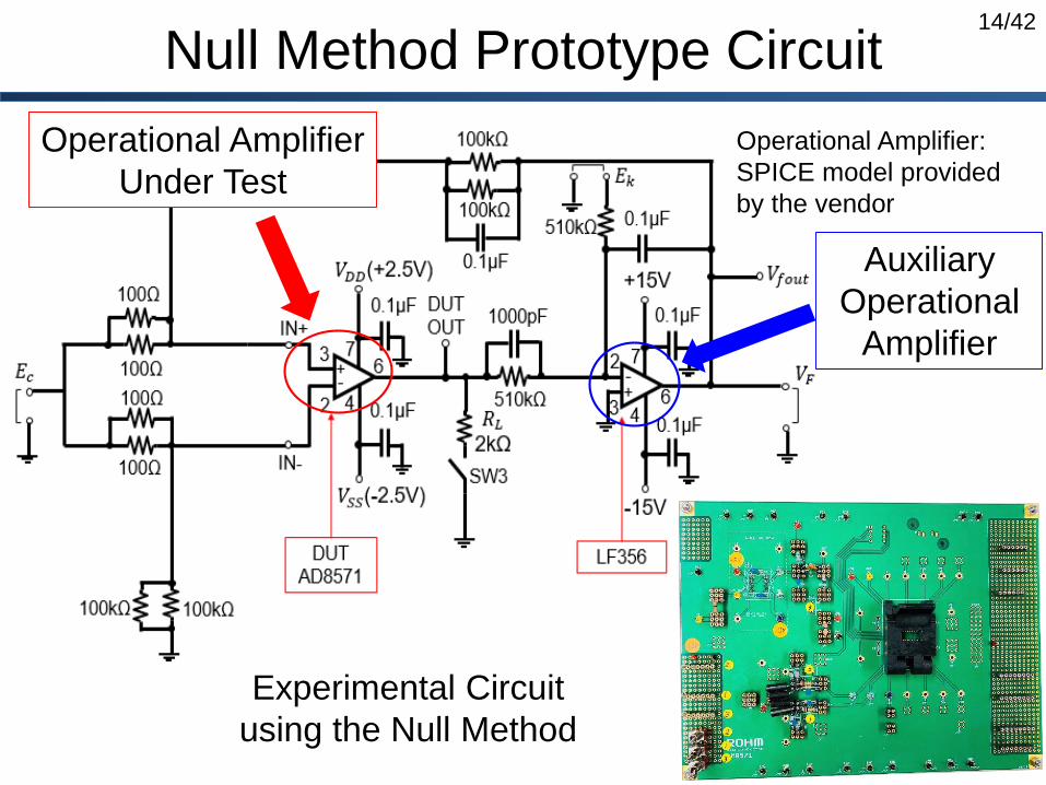
Null Method Prototype Circuit
Experimental Circuit
using the Null Method
Operational Amplifier
Under Test
Auxiliary
Operational
Amplifier
Operational Amplifier:
SPICE model provided
by the vendor

15/42
Outline
• Research Background
• Basic Operational Amplifier Measurement Circuit
• Null Method Prototype Circuit
• Investigation with SPICE Simulation and Experiment
Frequency Characteristics
Offset Voltage
Open Loop Gain (AOL)
Common-Mode Rejection Ratio (CMRR)
Power Supply Rejection Ratio (PSRR)
• Conclusion

16/42
Frequency Characteristics
Simulation Circuit
Input sine wave
(1mVP-P , 1kHz)
Change
C1 and C2
x 1,000 gain
amplifier circuit
Frequency Characteristics

17/42
60dB
Amplifier
Gain=20log1000=60dB
No peak ⇒ Stable
Cutoff frequency fc≅30Hz Slow response
Frequency characteristics
of the Null circuit (SPICE simulation)
Input frequency (1kHz)
-30dB down
Frequency Characteristics when C1=0.1μF, C2=0.1μF
Simulation Result (C1=0.1μF, C2=0.1μF)

18/42
C1 → 0.1μF (fixed)
C2 → Small
Slightly faster response
Input frequency (1kHz)
-40dB down
60dB Slightly faster
Simulation Result (C1=0.1μF, C2=1nF)
Frequency Characteristics when C1=0.1μF, C2=1nF
Frequency characteristics
of the Null circuit (SPICE simulation)

19/42
Optimal value :
C1=1nF, C2=0.1μF
Input frequency (1kHz)
Almost never down
60dB Cutoff frequency fc≅1kHz Fast response
30 times faster than when C1, C2=0.1μF (fc≅30Hz)
Simulation Result (C1=1nF, C2=0.1μF)
C1 → Small
C2 → 0.1μF (fixed)
Frequency Characteristics when C1=1nF, C2=0.1μF
Frequency characteristics
of the Null circuit (SPICE simulation)

20/42
Sine wave input
(1mVP-P , 1kHz)
Input frequency (1kHz)
-30dB down (P.17)
30mVP-P (About 1/30)
C1=0.1μF, C2=0.1μF
Observe
output waveform Vout
Transient Characteristics (Sine wave input) (1)
Transient response
of the Null circuit (SPICE simulation)

21/42
10mVP-P
≠ ×1,000
C1=1nF, C2=0.1μF (Optimal value)700mVP-P
approaches to ×1,000
Transient Characteristics (Sine wave input) (2)
SPICE simulationC1=0.1μF, C2=1nF

22/42
Transient Characteristics (Square wave input)(1)
Square wave input
(1mVP-P , 1kHz)
50mVP-P
≠ ×1,000
C1=0.1μF, C2=0.1μF
Observe
output waveform Vout
Transient response
of the Null circuit (SPICE simulation)

23/42
17mVP-P
≠ ×1,000
950mVP-P
approaches to ×1,000
C1=0.1μF, C2=1nF
C1=1nF, C2=0.1μF (Optimal value)
Transient Characteristics (Square wave input) (2)
SPICE simulation

24/42
Outline
• Research Background
• Basic Operational Amplifier Measurement Circuit
• Null Method Prototype Circuit
• Investigation with SPICE Simulation and Experiment
Frequency Characteristics
Offset Voltage
Open Loop Gain (AOL)
Common-Mode Rejection Ratio (CMRR)
Power Supply Rejection Ratio (PSRR)
• Conclusion
25/42
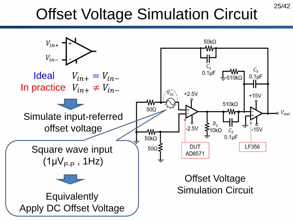
Ideal 𝑉𝑖𝑛+ = 𝑉𝑖𝑛−In practice 𝑉𝑖𝑛+ ≠ 𝑉𝑖𝑛−
Offset Voltage Simulation Circuit
Offset Voltage
Simulation Circuit
Square wave input
(1μVP-P , 1Hz)
Equivalently
Apply DC Offset Voltage
-
+𝑉𝑖𝑛+
𝑉𝑖𝑛−
Simulate input-referred
offset voltage

26/42
Transfer Function
I1
I2
R1
R2
C
𝐼1 =𝑉𝑖𝑛𝑅1
𝐼2 =1
𝑅2+
1
1/𝑗𝜔𝐶𝑉𝑖𝑛 − 𝑉𝑜𝑢𝑡
=1 + 𝑗𝜔𝐶𝑅2
𝑅2𝑉𝑖𝑛 − 𝑉𝑜𝑢𝑡
𝐼1 = −𝐼2
∴𝑉𝑜𝑢𝑡𝑉𝑖𝑛
=𝑅2
𝑅12 + (𝜔𝐶𝑅1𝑅2)
2
+ 1
At 𝑅1 = 50Ω, 𝑅2 = 50𝑘Ω, 𝐶 = 0.1μ𝐹, 𝑓 = 1𝐻𝑧
𝑉𝑜𝑢𝑡𝑉𝑖𝑛
= 1,000.5068⋯ ≅ 1,000

27/42
Offset Voltage Simulation Result
Vout=
1mVp-p
Offset Voltage Simulation Result
1μVP-P 1mVP−P
x 1,000
Easy Measurement
Minute error
28/42
Outline
• Research Background
• Basic Operational Amplifier Measurement Circuit
• Null Method Prototype Circuit
• Investigation with SPICE Simulation and Experiment
Frequency Characteristics
Offset Voltage
Open Loop Gain (AOL)
Common-Mode Rejection Ratio (CMRR)
Power Supply Rejection Ratio (PSRR)
• Conclusion
29/42
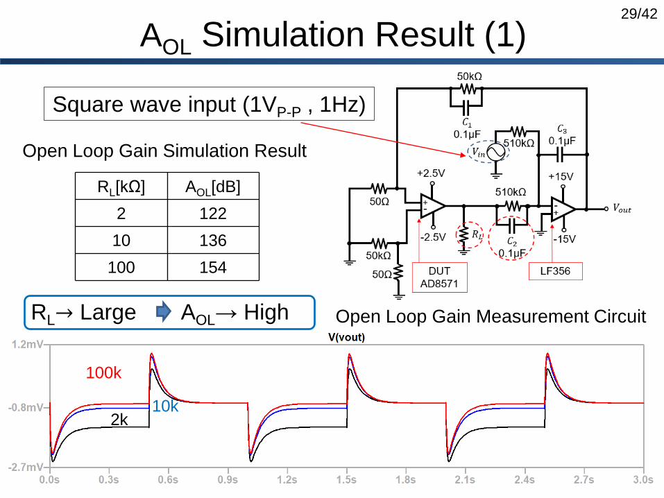
AOL Simulation Result (1)
RL[kΩ] AOL[dB]
2 122
10 136
100 154
2k10k
100k
Square wave input (1VP-P , 1Hz)
RL→ Large AOL→ High Open Loop Gain Measurement Circuit
Open Loop Gain Simulation Result

30/42
C2=0.1uF
C2=1nF
C2=0.01uF
C2=0.1uF0.01uF1nF
Vout
160uVp-p
RL=10kΩ, C1=1nF, C2 is varied
Unstable
Stable
Settling time
→ 30ms
Settling time
→ 200ms
AOL Simulation Result (2)
RL=10kΩ, C1=0.1μF, C2 is varied
Settling time
1/10
31/42
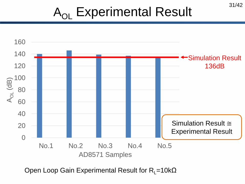
AOL Experimental Result
0
20
40
60
80
100
120
140
160
No.1 No.2 No.3 No.4 No.5
AO
L(d
B)
AD8571 Samples
Simulation Result
136dB
Open Loop Gain Experimental Result for RL=10kΩ
Simulation Result ≅Experimental Result
32/42
Outline
• Research Background
• Basic Operational Amplifier Measurement Circuit
• Null Method Prototype Circuit
• Investigation with SPICE Simulation and Experiment
Frequency Characteristics
Offset Voltage
Open Loop Gain (AOL)
Common-Mode Rejection Ratio (CMRR)
Power Supply Rejection Ratio (PSRR)
• Conclusion

33/42
RL[kΩ] CMRR[dB]
2 126
10 126
100 126
Shift power supply voltages
Find CMRR equivalently
VP … +2.5V → +3.0V
VN … -2.5V → -2.0V
VP=+2.5V
VN=-2.5V
VP=+3.0V
VN=-2.0V
Not affected by RL
CMRR Measurement Circuit
CMRR Simulation Result
CMRR Simulation Result (1)
34/42
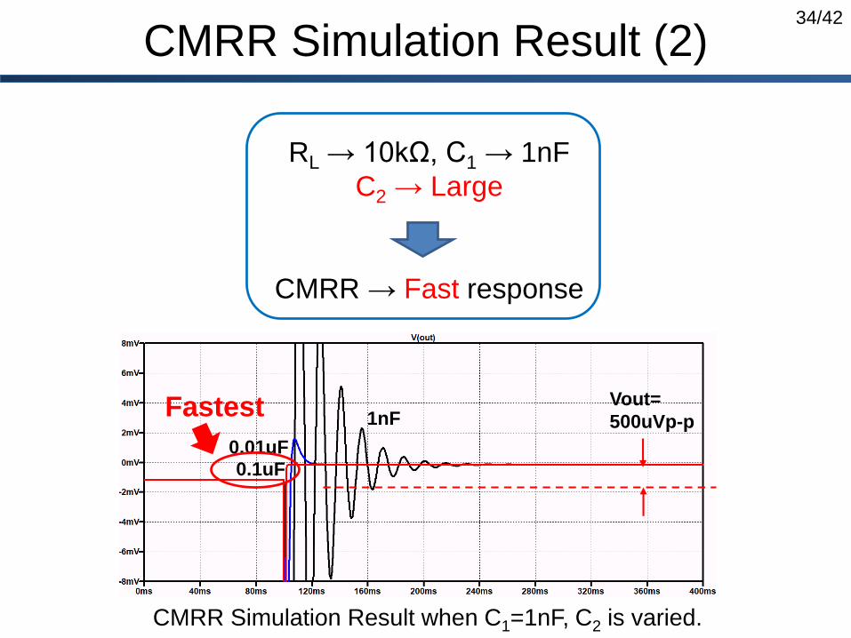
RL → 10kΩ, C1 → 1nF
C2 → Large
CMRR → Fast response
Vout=
500uVp-p1nF
0.01uF0.1uF
CMRR Simulation Result when C1=1nF, C2 is varied.
CMRR Simulation Result (2)
Fastest

35/42
CMRR Experimental Result
0
20
40
60
80
100
120
140
No.1 No.2 No.3 No.4 No.5
CM
RR
(d
B)
AD8571 Samples
Simulation Result
126dB
CMRR Experimental Result for RL=10kΩ
Simulation Result ≅Experimental Result
36/42
Outline
• Research Background
• Basic Operational Amplifier Measurement Circuit
• Null Method Prototype Circuit
• Investigation with SPICE Simulation and Experiment
Frequency Characteristics
Offset Voltage
Open Loop Gain (AOL)
Common-Mode Rejection Ratio (CMRR)
Power Supply Rejection Ratio (PSRR)
• Conclusion

37/42
RL[kΩ] PSRR[dB]
2 120
10 120
100 120
Same configuration as CMRR
VP … +2.0V → +2.5V
VN … -2.0V → -2.5V
Power supply voltage 4V
Between VP and VN
Power supply voltage 5V
Between VP and VN
Not affected by RL
Same as CMRR Measurement Circuit
PSRR Simulation Result
PSRR Simulation Result (1)

38/42
RL → 10kΩ, C1 → 1nF
C2 → Large
PSRR → Fast response
(Same as CMRR)
1nFC2=
0.1uF
0.01uF Vout
964uVp-p
PSRR Simulation Result (2)
PSRR Simulation Result when C1=1nF, C2 is varied.
Fastest

39/42
PSRR Experimental Result
0
20
40
60
80
100
120
No.1 No.2 No.3 No.4 No.5
PS
RR
(d
B)
AD8571 Samples
Simulation Result
120dB
PSRR Experimental Result for RL=10kΩ
Simulation Result ≅Experimental Result

40/42
Outline
• Research Background
• Basic Operational Amplifier Measurement Circuit
• Null Method Prototype Circuit
• Investigation with SPICE Simulation and Experiment
Frequency Characteristics
Offset Voltage
Open Loop Gain (AOL)
Common-Mode Rejection Ratio (CMRR)
Power Supply Rejection Ratio (PSRR)
• Conclusion

41/42
• Optimization of phase compensation constants
C1=1nF, C2=0.1μF
Null Circuit → Fast and Stable
• Null Circuit : Change of signal application point
depending on the measurement item
• Switching C1 and C2 depending on the measurement item
Settling time reduction → ≒ 1/10
Signal input change (C1, C2 : Fixed)
Different response characteristics of each input / output
Conclusion

42/42
Thank you for attention
43/42
Q&A
Q. オープンループゲインはどのようにして求めるのか?
A. (P.29のスライドを表示して)図のこの部分に 1Vp-p、1Hzの矩形波を入力した時のVoutから求めています。