evaluation of chip breaker using flank...
TRANSCRIPT

1
EVALUATION OF CHIP BREAKER USING FLANK
WEAR
A THESIS SUBMITTED IN PARTIAL FULFILLMENT
OF THE REQUIREMENTS FOR DEGREE OF
Bachelor of Technology
in
Mechanical Engineering
By
SUMIT GOYAL
Roll No: 10603044
Department of Mechanical Engineering
National Institute of Technology
Rourkela
2010
1
EVALUATION OF CHIP BREAKERS WITH FLANK
WEAR
A THESIS SUBMITTED IN PARTIAL FULFILLMENT
OF THE REQUIREMENTS FOR DEGREE OF
Bachelor of Technology
in
Mechanical Engineering
By
SUMIT GOYAL
Roll No: 10603044
Under the Guidance of
Prof. C.K. Biswas
Department of Mechanical Engineering
National Institute of Technology
Rourkela
2010
I

1
National Institute of Technology
ROURKELA
CERTIFICATE
This is to certify that the thesis entitled, “EVALUATION OF CHIP BREAKER WITH
FLANK WEAR” submitted by Sri Sumit Goyal in partial fulfillment of the requirements
for the award of Bachelor of Technology in Mechanical Engineering at the National
Institute of Technology, Rourkela is an authentic work carried out by him under my
supervision and guidance.
To the best of my knowledge, the matter embodied in the thesis has not been submitted to any
other University/ Institute for the award of any Degree or Diploma.
Date: Prof. C.K. BISWAS
Dept. of Mechanical Engg.
National Institute of Technology
Rourkela - 769008
II

1
ACKNOWLEDGEMENT
I avail this opportunity to extend my hearty indebtedness to my guide Prof C.K. Biswas,
Mechanical Engineering Department, for his valuable guidance, constant encouragement and
kind help at different stages for the execution of this dissertation work.
I also express my sincere gratitude to Mr. Kunal Nayak and Mr. G.S. Reddy for extending
their help in completing this project.
I take this opportunity to express my sincere thanks to my project guide for co-operation and
to reach a satisfactory conclusion.
SUMIT GOYAL
Roll No: 10603044
Mechanical Engineering
National Institute of Technology
Rourkela
III

1
ABSTRACT
Machining is a common and essential part of manufacturing of almost all metal
products, and also or other materials like wood and plastic. In the today’s era of automatic
machines optimization of machining operations is one of the key requirements. During
turning operation, unbroken chips pose a major hindrance during machining and hence
appropriate control of the chip shape becomes a very important task for maintaining reliable
machining process. The continuous chip generated during turning operation deteriorates the
workpiece precision and causes safety hazards for the operator. In particular, effective chip
control is necessary for a CNC machine or automatic production system because any failure
in chip control can cause the lowering in productivity and the worsening in operation due to
frequent stop. Chip control in turning is difficult in the case of mild steel because chips are
continuous. Thus the development of a chip breaker for mild steel is an important subject for
the automation of turning operations. In this study, the role of different parameters like speed,
feed and depth of cut, tool flank wear and chip breaker height and width are studied. In this
study chip characteristics were tested for changing tool flank wear values. Response surface
methodology was used to analyze the relationship between several explanatory variables and
two predecided response variables. The chips obtained were found to have greater thickness
at low feed and depth of cut, and gradually decreased as feed and depth of cut increases. The
analysis lead to the conclusion that cutting speed and depth of cut are the most significant
factors along with their higher order terms and interactions between variables.
IV

1
CONTENTS
Page No.
List of figures ii
List of Tables iii
Chapter 1 Introduction 1
Introduction 2
1.1 Chip Breaker 3
1.2 Chip breaking in single point cutting tool 4
1.3 Classification of chip pattern 5
1.4 Tool Wear 6
Chapter 2 Brief Introduction of the project 7
2.1 Need and purpose of chip-breaking 8
Chapter 3 Literature Review 9
3.1 Experimental studies on chip breaker 10
3.2 Principles of chip breaking 12
Chapter 4 Experimental work 16
Introduction 17
4.1 Procedure 17
Chapter 5 Results and discussion 20
5.1 Response surface methodology for L(avg) 23
5.2 Response surface methodology for chip thickness 29
5.3 Conclusion 36
References 37

1
(i)
List of Figures
Page No.
Fig.1.1 Classification of chip pattern (INFOS) 5
Fig. 3.1 Principles of self breaking of chips 13
Fig. 3.2 Principle of forced chip breaking 11
Fig. 3.3 Clamped type chip breakers 14
Fig .4.1 Heavy duty HMT lathe machine 18
Fig 4.2 Experimental set up (cutting tool with workpiece) 18
Fig 5.1 Photographs of chip samples obtained from different run orders 22
Fig 5.2 Normal probability curve of the residuals for chip length 25
Fig.5.3 Residual Versus the fitted values 26
Fig 5.4 Histogram of the residuals 26
Fig. 5.5 Residuals vs order of the data 27
Fig 5.6 Main effect plot for chip length 28
Fig 5.7 Interaction plot for L(avg) 29
Fig 5.8 Residuals vs the order of the data for chip thickness 32
Fig 5.9 Residual histogram for chip thickness 33
Fig.5.10 Residuals vs the fitted values for chip thickness 33
Fig 5.11 Normal probability curve of the residuals for chip thickness 34
Fig 5.12 Interaction plot for chip thickness 35
Fig 5.13 Main effect plot for chip thickness 35

1
(ii)
List of Tables
Page no.
Table 1 Measured parameters for different tools 17
Table 2 Experimental conditions 18
Table 3 Experimental input chart 19
Table 4 Observation table 21
Table 5 Estimated Regression Coefficients for L(avg) 23
Table 6 Analysis of Variance for chip length 24
Table 7 Estimated Regression Coefficients for L(avg) after modification 24
(The analysis was done using coded units.)
Table 8 Variance analysis of chip thickness after modification 25
Table 9 regression analysis for chip thickness after modification 29
Table 10 Variance analysis of chip thickness before modification 30
Table 11 Estimated regression analysis for chip thickness after modification 31
Table 12 Variance analysis of chip thickness after modification 31

1
CHAPTER 1
INTRODUCTION

2
INTRODUCTION
Conventional machining, one of the most important material removal methods, is a
collection of material-working processes in which power-driven machine tools, such as
lathes, milling machines, and drill presses, are used with a sharp cutting tool to mechanically
cut the material to achieve the desired geometry. Machining process produces chips due to
removal of excess material from the metal surface. The geometrical and metallurgical
characteristics of these chips are very representative of the performances of the process.
Indeed, they bear witness to most of the physical and thermal phenomena occurring during
the machining.
Maximization in productivity is required in present day manufacturing methods.
Introduction of Computer Integrated Manufacturing (CIM) system and Flexible
Manufacturing System (FMS) have led to maximization in productivity. Keeping in eye the
present demanding situation, the quality of cutting tools has been improved continuously for
better and more efficient cutting techniques.
Numerous chips are being generated in short time during machining operarions
which requires effective control of lenth and thickness of chips which is one of the most
important factors for work performance. When the chips are out of control, it may lead to
system failure which directly affects productivity and is also very dangerous for the person
working on machine.
The chip shape generated in cutting processing is closely related to product
productivity. If an incorrect chip shape is generated, the production is highly inefficient in
terms of time and money because of safety hazards to the operator, damage of production
tools and work piece surface, not to mention the loss in productivity due to the frequent
stopping of the production machine.
Failure in chip control has a significant effect on surface roughness of the
workpiece, precision of product, and wear of tool, etc. However, chip breaker performance
testing requires significant time and efforts as eveloping new cutting inserts necessitates

3
forming, sintering, grinding, and coating processes, extends developing time and involves
expensive research.
Tool wear describes the gradual failure of tool because of regular operation. It is a term often
associated with tipped tools, tool bits, or drill bits that are used with machine tools. Flank
wear is a type of wear in which the portion of the tool in contact with the finished part erodes.
This type of wear can be described using tool life expectancy equation. In this study we have
varied tool flank wear with other parameters like feed, depth of cut and speed to observe its
effects on chip shapes.
Chip control is highly essential to ensure reliable operation in automated as well as
traditional or manual control machining systems. Effective chip control includes
predictability of chip form/chip breakability for a given set of input machining conditions.
However because of complexity of chip formation mechanism under different combinations
of machining conditions studying the effect of individual parameter and their mutual
interactions, it is difficult to predict the chip formation process and chip geometries in
advance.
1.1 CHIP BREAKER
Chip breaker is defined as the modifications of the face to control or break the chip,
consisting of either an integral groove or integral or attached obstruction. The controlling and
breaking of chip can be accomplished by chip breakers by improving chip breakability which
results in efficient chip control and improved productivity. It also decreases cutting resistance
which also leads to a greater tool life, and gives a better surface finish to the work-piece. A
chip breaker is usually used for improving chip breakability by decreasing the chip radius.
The chip breaker pattern affects chip breakability.
The principle of chip breaker is that fracture is generated by the force and moment
acting on chip surface. A chip breaker acts by controlling the radius of the chip and directing
the chip in such a way that it breaks into a shorter length, in addition to an appropriate chip
breaker design, it is necessary to have the correct tool geometry so that the chip will follow
the proper path across the tool face.
4
1.2 CHIP BREAKING IN SINGLE POINT CUTTING TOOL
In the machining process the tool is oriented in such a manner that the excess material
is removed from the parent work-piece in the form of chips. When a cutting tool removes a
layer from the work piece, the uncut layer is first elastically deformed followed by plastic
deformations separation taking place near the cutting edge of the tool, however it is difficult
to postulate that deformation is concentrated at one point or one line. Chip is formed by a
process of deformation when subjected by a force impressed by the cutting tool on the work
material.
Generation of narrow and long chips during the machining by a single point cutting
tool lead to problems such as difficulty in chip handling, surface damage of products,
tangling together and safety hazards for the operator. Therefore, it is necessary to cut chips to
the appropriate size.
Chip breaking is done in two ways
self breaking :- This is accomplished by without using a separate chip breaker
either as an attachment or an additional geometric modification of the tool.
Forced chip breaking :- If the hot continuous chip does not become enough
curl or work hardened it may not break, in this case the running chip is forced
to bend or closely curl so that it breaks into pieces.
Various factors that affect the chip formation analysis for continuous chips can be
depth of cut to feed ratio, number of active or passive cutting edges, length of cutting edge to
width of cut ratio, cutting speed, inclination angle (ʎ), rake angle, depth of cut to diameter
ratio (for turning and similar cases), action of cutting fluids etc. Analysis of these factors lead
to better designs of chip breaker.

5
Chip breaking is usually caused by curling of the removed metal and than striking
against work-piece or tool. Different Patterns and sizes of broken chips are obtained
depending on deformation mechanism and collision location. The generated chip makes
continuous curling and it is known that chip breakability enlarges when we reduce the up
curling radius and down curling radius of a chip clearance that is formed at this time.
Externally applied forces increases the fracture strain of the chip and decreases the
radius of the chip, so for determination of chip pattern these forces should be kept at optimum
levels. Even though much research has been done and still being done on to predict the chip
behavior and to achieve maximum chip control but it is still difficult to break chips in the
finishing of mild steel. Ch
On chip breakers has been accomplished, but

6
1.3 CLASSIFICATION OF CHIP PATTERN
Chips are classified either on the basis of mechanism of chip formation or the inal shape of
the chip. Chip pattern has been classified by CIRP and INFOS, but each classification is very
similar. Chip pattern classified by INFOS is illustrated in fig. 1
Fig.1 Classification of chip pattern (INFOS)
1.4 TOOL WEAR
Tool wear describes the gradual failure of cutting tools due to regular operation. It is a
term often associated with tipped tools, tool bits, or drill bits that are used with machine tools.
Types of wear include:

7
flank wear in which the portion of the tool in contact with the finished part erodes.
Can be described using the Tool Life Expectancy equation.
crater wear in which contact with chips erodes the rake face. This is somewhat
normal for tool wear, and does not seriously degrade the use of a tool until it becomes
serious enough to cause a cutting edge failure.
built-up edge in which material being machined builds up on the cutting edge. Some
materials (notably aluminum and copper) have a tendency to anneal themselves to the
cutting edge of a tool. It occurs most frequently on softer metals, with a lower melting
point. It can be prevented by increasing cutting speeds and using lubricant. When
drilling it can be noticed as alternating dark and shiny rings.
glazing occurs on grinding wheels, and occurs when the exposed abrasive becomes
dulled. It is noticeable as a sheen while the wheel is in motion.
edge wear, in drills, refers to wear to the outer edge of a drill bit around the cutting
face caused by excessive cutting speed. It extends down the drill flutes, and requires a
large volume of material to be removed from the drill bit before it can be corrected.
The useful life of tool is limited by tool wear. Wear can be described as the total loss of
weight or mass of the sliding pairs accompanying friction.

8
CHAPTER 2
BRIEF INTRODUCTION OF THE PROJECT

9
2.1 NEED AND PURPOSE OF CHIP BREAKING
Continuous machining operations like turning of ductile metals, produce continuous
chips of different shapes which leads to their handling and disposal problems and are not safe
for working. The problems become acute when ductile but strong metals like steels are
machined at high cutting velocity for high MRR by flat rake face type carbide or ceramic
inserts.
The sharp edged hot continuous chip that comes out at very high speeds becomes
dangerous to the operator and the other people working In the vicinity. Very small sized chips
pose serious problems for the safety of the workman working on the machine. These chips
comes out of the machine in uncontrolled directions that makes it difficult to handle and
dispose. When chips breaking is not proper long continuous chips may cause entangling with
the rotating job. That may impair the surface finish of the product.
Therefore to get the proper surface finish and highly efficient machining operation it is
essentially needed to break continuous chips into small regular pieces for
Safety of the working people
Prevention of damage of the product
Easy collection and disposal of chips.
Improving machinability by reducing the chip-tool contact area cutting forces and
crater wear of the cutting tool.
Therefore this study tends to solve the problems of uncontrolled chip formation and
construct the basis of improved factory automation by using chip breakers of the attached
obstruction type, which represents a relatively new concept in chip breaking.
In this projest work, parameters like cutting speed, feed, depth of cut, height and width of
chip breaker and along with that one other parameter tool flank wear will be taken as input
parameter and their effect on the chip breakability will be studied, so that better control of
chip can be done.

10
CHAPTER 3
LITERATURE REVIEW

11
3. LITERATURE REVIEW
3.1 EXPERIMENTAL STUDIES ON CHIP BREAKER
J.D.Kim et.al. [1], has presented experimental research dealing with the modeling of chip
formation process using different insert geometries and leas to important characteristic
parameters in chip control. The study is focused on chip breaker design by analyzing
characteristics like cutting speed, feed and depth of cut for experimental cutting of mild steel
with chip breaker. It emphasizes on that attached type chip breaker is better than a grooved
one. In this work a designed chip breaker with three chip breakers attached –two side curl
chip breakers and one up curl chip breaker is used for fine and rough breaking. The chip
breaker is similar to conventional attached to the chip breaker except its shape is an arc.
The experiment chip breaking conditions in to three regions – uncontrolled, transient and
control. The experimental research establishes that for finish turning operation with that of
curl less than 1 mm designed chip breaker is much more effective than conventional chip
breaker. At cutting speeds less than 150 m/min the chip breaking conditions are better than at
high cutting speeds. Major factor of chip breaking is the chip flow direction in the designed
chip breaker. Increasing the cutting speed changes the chip type from side curl to up curl.
R.M.D. Mesquita et.al [2], devised a method for the prediction of cutting forces to predict the
cutting forces for a wide range of cutting conditions. considering the indentation and
ploughing effect and pressure of a parallel groove type chip breaker. The technique is based
on the measurement of chip breaker geometry and the effective side rake angle. Tests are
done on martensitic stainless steel using coated carbide tools. Two types of tests are
discussed in the paper, one to access the indentation or ploughing effect and other to establish
the mean dynamic stress, mean friction angle and machinability constant and to check the
fisibility of the model.
Hong-Gyoo Kim et.al [3], used the neural network analysis to analyze the performance of a
commercial chip breaker. Form parameters such as depth of cut, land breadth depth of cut
and radius are provided as input to the neural network. The experimental work established the

12
fact that as the chip breaker depth increases, and the width decreases, performance of chip
breaking was excellent at the finishing area. However, the chip breakability was excellent at
the roughing area as the depth decreased and the width increased.
N.S.Das et.al [4] developed a field model for orthogonal cutting with step type chip breaker
with adhesion friction at chip tool interface using kudo’s basic slip line field. An alternate
method is suggested for estimation of breaking strain in the chip. The analysis showed that
the breaking strain in the chip is the most important factor on which chip breaking depends
and a method was suggested for determining chip breaker distance for any given feed and
chip breaker height for effective chip breaking. It also showcased that the chip breaking
criterion is based neither on specific cutting energy nor on material damage which can be
taken as adequate criterion for chip breaking.
K.P.Maity et.al. [5] presented a theoretical analysis of metal machining with an orthogonal
cutting tool using the slip line field analysis given by Dewhurst assuming constant friction.
The height of chip breaker is kept at four times the that of uncut chip thickness while its
position with respect to principal cutting edge is varied. The paper shows that the position of
chip breakers vary within a range for under breaking and over breaking conditions for a
particular feed. The optimum position for the chip breaker is around 13-14 times the uncut
chip thickness. With the step heights used in the experiment it was seen that there is no chip
breaking effect when the chip breaker position is more than 28.5 times the uncut chip
thickness.
J.P. Choi et al [6] proposed a systematic chip breaking prediction method using a 3d cutting
model with the equivalent parameter concept. A new type insert with medium type insert for
medium finish operations with variable parameters was designed by modifying the
commercial one. The chip strain ratio is used as a chip breaking criteria. In this paper the
effect of each parameter on chip breakage are examined to simulation, a new insert with
variable parameters along the main cutting edge is designed and simulated.
Shi, T. et al [7] developed a slip line field model for orthogonal cutting with chip breake and
flank wear. The model predicts a linear relationship between flank wear and cutting force
components. The results also show that non-zero strains occur at and below the machined
surface when machining with a worn tool. Severity and depth of deformation below the

13
machined surface increases with increasing flank wear. Forces acting on the chip breaker
surface are found to be small and suggest that chip control for automated machining may be
feasible with other means.
3.2 Principles of chip-breaking
The principles and methods of chip breaking are generally classified as follows:
Self breaking: This is accomplished without using a separate chip-breaker either as
an attachment or an additional geometrical modification of the tool.
Forced chip breaking by additional tool geometrical features or devices
(a) Self breaking of chips
Ductile chips usually become curled or tend to curl (like clock spring) even in machining
by tools with flat rake surface due to unequal speed of flow of the chip at its free and
generated (rubbed) surfaces and unequal temperature and cooling rate at those two surfaces.
With the increase in cutting velocity and rake angle (positive) the radius of curvature
increases, which is more dangerous. In case of oblique cutting due to presence of inclination
angle, restricted cutting effect etc. the curled chips deviate laterally resulting helical coiling
of the chips.
The curled chips may self break:
By natural fracturing of the strain hardened outgoing chip after sufficient cooling and
spring back as indicated in Fig.3.1 (a). This kind of chip breaking is generally
observed under the condition close to that which favors formation of jointed or
segmented chips.
By striking against the cutting surface of the job, as shown in Fig. 3.1 (b), mostly
under pure orthogonal cutting.
By striking against the tool flank after each half to full turn as indicated in Fig 3.1(c).

14
(a) Natural (b) striking on job (c) striking at tool flank
Fig. 3.1 Principles of self breaking of chips.
(b) Forced chip-breaking
The hot continuous chip becomes hard and brittle at a distance from its origin due to work
hardening and cooling. If the running chip does not become enough curled and work
hardened, it may not break. In that case the running chip is forced to bend or closely curl so
that it breaks into pieces at regular intervals. Such broken chips are of regular size and shape
depending upon the configuration of the chip breaker.
Chip breakers are basically of two types:
• In-built type
• Clamped or attachment type
In-built breakers are in the form of step or groove at the rake surface near the cutting edges of
the tools. Such chip breakers are provided either
After their manufacture – in case of HSS tools like drills, milling cutters, broaches etc
and brazed type carbide inserts.
During their manufacture by powder metallurgical process – e.g., throw away type
inserts of carbides, ceramics and cermets.

15
W = width, H = height, β = shear angle
Fig. 3.2 Principle of forced chip breaking.
The unique characteristics of in-built chip breakers are:
• The outer end of the step or groove acts as the heel that forcibly bends and fractures
the running chip
• Simple in configuration, easy manufacture and inexpensive
• The geometry of the chip-breaking features are fixed once made (i.e., cannot be
controlled)
• Effective only for fixed range of speed and feed for any given tool-work
combination.
Some commonly used step type chip breakers:
a. Parallel step
b. Angular step; positive and negative type
c. Parallel step with nose radius – for heavy cuts
Groove type in-built chip breaker may be of
• Circular groove
• Tilted V groove

16
(c) Clamped type chip-breaker
Clamped type chip breakers work basically in the principle of stepped type chip-breaker but
have the provision of varying the width of the step and / or the angle of the heel.
Fig. 3.3 schematically shows three such chip breakers of common use:
a. With fixed distance and angle of the additional strip – effective only for a limited
domain of parametric combination
b. With variable width (W) only – little versatile
c. With variable width (W), height (H) and angle (β) – quite versatile but less rugged
and more expensive.
(a) Fixed geometry (b) variable width
(c) Variable width and angle
Fig. 3.3 Clamped type chip breakers

17
CHAPTER 4
EXPERIMENTAL WORK
18
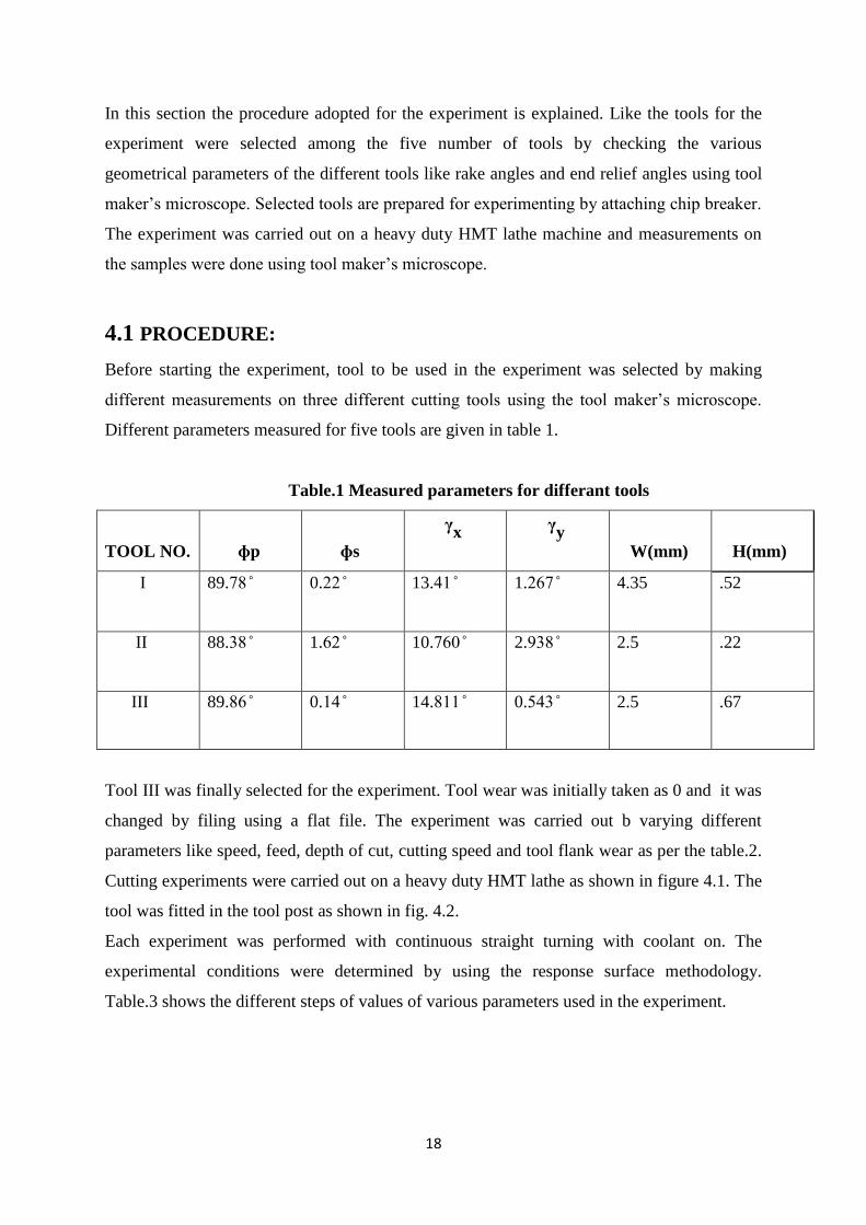
In this section the procedure adopted for the experiment is explained. Like the tools for the
experiment were selected among the five number of tools by checking the various
geometrical parameters of the different tools like rake angles and end relief angles using tool
maker’s microscope. Selected tools are prepared for experimenting by attaching chip breaker.
The experiment was carried out on a heavy duty HMT lathe machine and measurements on
the samples were done using tool maker’s microscope.
4.1 PROCEDURE:
Before starting the experiment, tool to be used in the experiment was selected by making
different measurements on three different cutting tools using the tool maker’s microscope.
Different parameters measured for five tools are given in table 1.
Table.1 Measured parameters for differant tools
TOOL NO.
ɸp
ɸs ᵞx ᵞy
W(mm)
H(mm)
I 89.78 ̊ 0.22 ̊ 13.41 ̊ 1.267 ̊ 4.35 .52
II 88.38 ̊ 1.62 ̊ 10.760 ̊ 2.938 ̊ 2.5 .22
III 89.86 ̊ 0.14 ̊ 14.811 ̊ 0.543 ̊ 2.5 .67
Tool III was finally selected for the experiment. Tool wear was initially taken as 0 and it was
changed by filing using a flat file. The experiment was carried out b varying different
parameters like speed, feed, depth of cut, cutting speed and tool flank wear as per the table.2.
Cutting experiments were carried out on a heavy duty HMT lathe as shown in figure 4.1. The
tool was fitted in the tool post as shown in fig. 4.2.
Each experiment was performed with continuous straight turning with coolant on. The
experimental conditions were determined by using the response surface methodology.
Table.3 shows the different steps of values of various parameters used in the experiment.
19
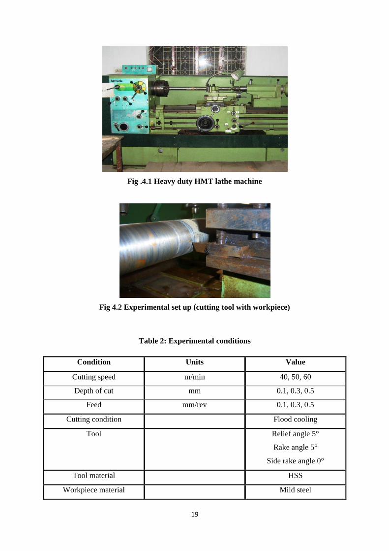
Fig .4.1 Heavy duty HMT lathe machine
Fig 4.2 Experimental set up (cutting tool with workpiece)
Table 2: Experimental conditions
Condition Units Value
Cutting speed m/min 40, 50, 60
Depth of cut mm 0.1, 0.3, 0.5
Feed mm/rev 0.1, 0.3, 0.5
Cutting condition Flood cooling
Tool Relief angle 5°
Rake angle 5°
Side rake angle 0°
Tool material HSS
Workpiece material Mild steel

20
Table.3: Experiment Input Chart
S.No. Std
Order
RunOrder PtType Blocks F
(mm/rev)
V
(m/min)
D
(mm)
Wear
(mm)
1 1 19 1 1 0.1 27 0.1 0
2 2 6 1 1 0.3 27 0.1 0
3 3 24 1 1 0.1 45 0.1 0
4 4 23 1 1 0.3 45 0.1 0
5 23 9 -1 1 0.2 35 0.2 0
6 5 15 1 1 0.1 27 0.3 0
7 6 5 1 1 0.3 27 0.3 0
8 7 26 1 1 0.1 45 0.3 0
9 8 31 1 1 0.3 45 0.3 0
10 21 17 -1 1 0.2 35 0.1 0.5
11 19 22 -1 1 0.2 27 0.2 0.5
12 17 7 -1 1 0.1 35 0.2 0.5
13 29 1 0 1 0.2 35 0.2 0.5
14 31 8 0 1 0.2 35 0.2 0.5
15 25 11 0 1 0.2 35 0.2 0.5
16 27 12 0 1 0.2 35 0.2 0.5
17 30 14 0 1 0.2 35 0.2 0.5
18 26 21 0 1 0.2 35 0.2 0.5
19 28 29 0 1 0.2 35 0.2 0.5
20 18 28 -1 1 0.3 35 0.2 0.5
21 20 16 -1 1 0.2 45 0.2 0.5
22 22 30 -1 1 0.2 35 0.3 0.5
23 9 27 1 1 0.1 27 0.1 1
24 10 13 1 1 0.3 27 0.1 1
25 11 3 1 1 0.1 45 0.1 1
26 12 18 1 1 0.3 45 0.1 1
27 24 10 -1 1 0.2 35 0.2 1
28 13 25 1 1 0.1 27 0.3 1
29 14 20 1 1 0.3 27 0.3 1
30 15 2 1 1 0.1 45 0.3 1
31 16 4 1 1 0.3 45 0.3 1

21
CHAPTER 5
RESULTS AND DISCUSSIONS

22
Table 4 shows the observation table for the experimental work on the lathe machine.
In the table first column contains the run order value. Onsecutive column show value of feed,
cutting speed, depth of cut, flank wear, measured L values and measured chip thickness.
Table 4 : Observation table
Run
Order
f
(mm)
V
(m/min)
d
(mm)
Wear
(mm)
L1
(mm)
L2
(mm)
L3
(mm)
L(avg)
(mm)
ChipThickness
(mm)
19 0.1 27 0.1 0 4.98 4.09 4.94 4.67 0.308
6 0.3 27 0.1 0 18 12.05 11.4 13.81 0.305
24 0.1 45 0.1 0 17.73 37.47 38.93 31.37 0.124
23 0.3 45 0.1 0 23.91 23.68 24.33 23.97 0.201
9 0.2 35 0.2 0 6.99 6.09 7.73 6.93 0.241
15 0.1 27 0.3 0 6.55 7.27 10 7.904 0.287
5 0.3 27 0.3 0 11.97 6.89 8.22 9.02 0.455
26 0.1 45 0.3 0 9.2 12.07 9.49 10.253 0.182
31 0.3 45 0.3 0 19.2 15.83 14.19 16.4 0.304
17 0.2 35 0.1 0.5 42.19 13.6 13.26 23.01 0.262
22 0.2 27 0.2 0.5 16.47 28.09 18.27 20.94 0.164
7 0.1 35 0.2 0.5 13.8 16.74 19.63 16.72 0.23
1 0.2 35 0.2 0.5 9.15 10.6 7.04 8.93 0.287
8 0.2 35 0.2 0.5 12.21 33.58 20.1 21.96 0.222
11 0.2 35 0.2 0.5 10.89 10.8 12.8 11.49 0.221
12 0.2 35 0.2 0.5 10.27 14.07 11.05 11.79 0.288
14 0.2 35 0.2 0.5 20.37 19.36 18.36 19.36 0.255
21 0.2 35 0.2 0.5 20.37 19.36 18.36 19.36 0.255
29 0.2 35 0.2 0.5 20.37 19.36 18.36 19.36 0.255
28 0.3 35 0.2 0.5 32.4 19.65 25.55 25.86 0.398
16 0.2 45 0.2 0.5 45.45 33.28 39.24 39.32 0.207
30 0.2 35 0.3 0.5 45.39 50.24 26.64 40.75 0.268
27 0.1 27 0.1 1 12.66 7.12 6.94 8.9 0.313
13 0.3 27 0.1 1 25.65 21.62 18.02 21.76 0.367
3 0.1 45 0.1 1 25.65 21.62 18.02 21.76 0.367
18 0.3 45 0.1 1 16.47 15.65 20.86 17.66 0.276
10 0.2 35 0.2 1 17.15 15.97 8.89 13.73 0.313
25 0.1 27 0.3 1 16.87 15.09 17.29 16.41 0.298
20 0.3 27 0.3 1 28.41 21.09 11.58 20.36 0.299
2 0.1 45 0.3 1 24.1 27.8 30.04 27.31 0.198
4 0.3 45 0.3 1 30.85 28.73 28.62 29.4 0.385

23
Figure 5.1(a) to 5.1 (e) show photographs of some chip samples obtained for
different input parameters from run orders 4, 2, 6, 8, 10 and 3 respectively. Measurements of
chip length are done by using these photographs with the help of pdf-xchangeviewer
software. Chip thickness is measured with the help of tool maker’s microscope.
(a)R.O.4 (b)R.O.2 (c)R.O.6
(d)R.O.8 (e)R.O.10 (f)R.O.3
Figure 5.1 : Photographs of chip samples obtained from different run orders

24
5.1 RESPONSE SURFACE METHODOLOGY FOR L(avg)
RESPONSE SURFACE REGRESSION : L(avg) versus f, V, d, Wear
The experimental results were analyzed by RSM using Minitab software. RSM
explores the relationship between several explanatory variables and one or more response
variables. The main idea of RSM is to use a set of designed experiments to obtain an optimal
response. Using this method, various tables were analyzed to see the relationship of different
variables and their significance.
From table.5 regression coefficient of L(avg) vs f, d , v and wear are analysed. This
table shows that V, wear*wear, V*V and d*wear have a significant effect on the value of
average chip length whereas wear also have a little effect on L(avg). In this regression R-
square value is 72.4% which shows fairly feasible experimental results. The analysis was
done using uncoded units.
Table.5 Estimated Regression Coefficients for L(avg)
Term Coef SE Coef T P
Constant 116.189 52.760 2.202 0.043
F 40.079 155.731 0.257 0.800
V -7.245 3.219 -2.251 0.039
D 46.625 155.731 0.299 0.768
Wear 39.388 19.955 1.974 0.066
f*f 119.461 352.382 0.339 0.739
V*V 0.118 0.044 2.685 0.016
d*d -121.539 352.382 -0.345 0.735
Wear*Wear -39.062 14.095 -2.771 0.014
f*V -1.998 1.576 -1.268 0.223
f*d -20.606 141.917 -0.145 0.886
f*Wear 14.871 28.383 0.524 0.608
V*d -0.723 1.576 -0.459 0.652
V*Wear -0.335 0.315 -1.064 0.303
d*Wear 69.679 28.383 2.455 0.026
S = 5.677 R-Sq = 72.4% R-Sq(adj) = 48.3%
Table.6 shows variance analysis for L(avg). From this chart we can infer that
L(avg) depends mainly upon square terms in the equation. Effect of linear and interaction

25
terms are negligible for determination of L(avg). Lack-of-fit value is low that indicates the
validity of the experimental setup.
Table.6 variance analysis for L(avg) before modification
RESPONSE SURFACE REGRESSION: L(avg) versus V, d, Wear
Analysis is again done by using response surface method by removing terms with
negligible effect on the value of average chip length. Table.7 shows the regression coefficient
values for L(avg). This shows that length of chip depends upon speed of cutting V, depth of
cut d, wear, V*V, Wear*Wear and d*Wear. There respective coefficients are given in the the
table.
Table.7 Estimated Regression Coefficients for L(avg) after modification
S = 5.378 R-Sq = 62.9% R-Sq(adj) = 53.6%
R-square value is 62.9% which indicate fairly feasible analysis. Table.8 shows the variance
analysis of average chip length after . Lack-of-fit value is in the acceptable range.
Source DF Seq SS Adj SS Adj MS F P
Regression 14 1354.5 1354.5 96.75 3.00 0.019
Linear 4 679.5 246.3 61.58 1.91 0.158
Square 4 376.2 376.2 94.06 2.92 0.055
Interaction 6 298.8 298.8 49.80 1.55 0.227
Residual Error 16 515.6 515.6 32.22
Lack-of-Fit 10 328.5 328.5 32.85 1.05 0.497
Pure Error 6 187.1 187.1 31.19
Total 30 1870.1
Term Coef SE Coef T P
Constant 144.897 44.9419 3.224 0.004
V -7.949 2.6122 -3.043 0.006
d -32.063 18.4791 -1.735 0.096
Wear 30.368 12.9893 2.338 0.028
V*V 0.118 0.0361 3.273 0.003
Wear*Wear -39.097 11.5486 -3.385 0.002
d*Wear 69.679 26.8910 2.591 0.016

26
Table.8 Analysis of Variance for L(avg) after modification
Source DF Seq SS Adj SS Adj MS F P
Regression 6 1175.9 1175.9 195.98 6.78 0.000
Linear 3 611.3 401.2 133.74 4.62 0.011
Square 2 370.4 370.4 185.21 6.40 0.006
Interaction 1 194.2 194.2 194.21 6.71 0.016
Residual Error 24 694.2 694.2 28.93
Lack-of-Fit 8 238.1 238.1 29.77 1.04 0.445
Pure Error 16 456.1 456.1 28.50
Total 30 1870.1
Figure 5.2 shows normal probability plot of the residuals for the average chip length.
The graph shows that almost all the experimental values follow a normal distribution pattern
i.e. all the point lie on the diagonal line. Only a few points in the end on the curve are slightly
distracted from the pattern. The curve shows that experimental values follow a normal
probability distribution which indicates the validity of the setup.
Figure 5.2 normal probability curve of the residuals for chip length
Standardized Residual
Pe
rce
nt
3210-1-2-3
99
95
90
80
70
60
50
40
30
20
10
5
1
Normal Probability Plot of the Residuals(response is L(avg))

27
Figure 5.3 shows the graphical representation of the normal versus the fitted values.
This plot shows that all the point are almost uniformly distributed above and below the
median line which validates the experiment.
Figure.5.3 Residual Versus the fitted values
Figure 5.4 shows the histogram of the residuals. The residual versus frequency
curve is almost according to the Gaussian distribution.
Figure.5.4 Histogram of the residuals
Fitted Value
Sta
nd
ard
ize
d R
esid
ua
l
3530252015105
2
1
0
-1
-2
Residuals Versus the Fitted Values(response is L(avg))
Standardized Residual
Fre
qu
en
cy
210-1-2
7
6
5
4
3
2
1
0
Histogram of the Residuals(response is L(avg))

28
Figure 5.5 is the residual versus the order of the data plot. The curve does not
follow any symmetric pattern with the run order value. It shows almost randon beahaviour of
residuals with the increasing run order which indicates that the model is a good fit one.
Figure 5.5 Residual versus the order of the data
Main effect of L(avg) plot is shown in figure 5.6. The plot of L(avg) with feed and
depth of cut shows little variation of L(avg) with the changing values of these parameters.
This pattern explains the negligible effect of f and d in the determination of L(avg) and hence
these parameters are neglected for truncated results. There is a significant change in the
average value of chip length with the change in values of cutting speed V, as the value of L
changes by approximately 11 mm (13-24 mm) with the change in value of speed from 27 to
45 m/min.
L(avg) is also influenced by change in wear value. It’s value changes from 13mm to
20 mm by changing flank wear value from 0 to 1mm. Change in the L(avg) value is large for
wear values from 0 to .5 mm, from .5 to 1 mm change in flank wear value it’s value changes
slightly.
Observation Order
Sta
nd
ard
ize
d R
esid
ua
l
30282624222018161412108642
2
1
0
-1
-2
Residuals Versus the Order of the Data(response is L(avg))

29
Figure.5.6 Main effects of L(avg)
Figure 5.7 shows interaction plot for L(avg). From this plot it can be inferred that there is
significant interaction between the parameters depth of cut and flank wear. It is also evident
from the regression analysis. There are also some other interactions shown in the figure
between V & d and f & d curves.
Developed equation for the Average chip length is:-
L(avg) = 144.897 – 7.949*V – 32.063*d + 30.368*Wear + .118*V*V – 39.097*wear*wear
+ 69.679*d*wear
Me
an
of
L(a
vg
)
0.30.20.1
25.0
22.5
20.0
17.5
15.0
453527
0.30.20.1
25.0
22.5
20.0
17.5
15.0
1.00.50.0
f V
d Wear
Main effects of L(avg)

30
Figure.5.7 Interaction plot of L(avg)
5.2 Response Surface Methodology for chip thickness
Response Surface Regression: Chip Thickness versus f, V, d, Wear
Similar to that for average chip length, response surface analysis was performed on
the other output parameter chip thickness. Table.9 shows regression plot for the coefficients
to the different terms in the equation for determination of chip thickness before the
modifications. In this table coefficients for differant parameters, square of parameters and
interaction of parameters are given. Feed has a very significant effect on the response value.
Term for which P value is more than 0.05 are considered to have negligible effect on the
f
d
Wear
V
453527 1.00.50.0
39
27
15
39
27
15
39
27
15
0.30.20.1
39
27
15
0.30.20.1
f
0.3
0.1
0.2
V
45
27
35
d
0.3
0.1
0.2
Wear
1.0
0.0
0.5
Interaction plot of L(avg)

31
value of the response. Here we neglect such terms to get the truncated solution. R-square
value is 80.5%. and all the analysis were done using non coded units.
Table.9 Regression coefficients for the chip thickness before modification
Term Coef SE Coef. T P
Constant -0.11752 0.39695 -0.296 0.771
f -2.85474 1.17166 -2.436 0.027
V 0.04412 0.02422 1.822 0.087
d -1.03042 1.17166 -0.879 0.392
Wear -0.15205 0.15014 -1.013 0.326
f*f 6.33253 2.65119 2.389 0.030
V*V -0.00077 0.00033 -2.307 0.035
d*d 1.43253 2.65119 0.540 0.596
Wear*Wear 0.10530 0.10605 0.993 0.336
f*V 0.01088 0.01186 0.918 0.372
f*d 2.18750 1.06773 2.049 0.057
f*Wear -0.15250 0.21355 -0.714 0.485
V*d 0.01029 0.01186 0.868 0.398
V*Wear 0.00552 0.00237 2.328 0.033
d*Wear -0.42750 0.21355 -2.002 0.063
S = 0.04271 R-Sq = 80.5% R-Sq(adj) = 63.4%.
Analysis of variance for chip thickness is shown in table.10. It shows that square terms
has the maximum effect on the chip thickness value. Linear and interaction terms also have
slight effect on the response value. Lack-of-fit value is low at .153 which infers that the
model is fit.
Table.10 Variance analysis of chip thickness before modification.
Source DF Seq SS Adj SS Adj MS F P
Regression 14 0.120532 0.120532 0.008609 4.72 0.002
Linear 4 0.064393 0.020499 0.005125 2.81 0.061
Square 4 0.027450 0.027450 0.006862 3.76 0.024
Interaction 6 0.028690 0.028690 0.004782 2.62 0.058
Residual Error 16 0.029185 0.029185 0.001824
Lack-of-Fit 10 0.023263 0.023263 0.002326 2.36 0.153
Pure Error 6 0.005923 0.005923 0.000987
Total 30 0.149717

32
RESPONSE SURFACE REGRESSION: Chip thickness versus f, V, Wear
After removing the terms that have negligible effect on the response value, truncated
model solution is obtained. Regression coefficient table.11 is as shown below. This indicate
that feed and speed of cutting have affects the valur of chip thickness mostly.
Flank wear have negligible effect on chip thickness as a linear term but it’s interaction with
speed of cutting has minor contribution to the chip thickness value. Variance analysis of chip
thickness is given in table.12. It shows that linear and square terms have major contribution
in the value of chip thickness but interaction terms also effect it slightly. Lack-of-fit value is
low at .354.
Table.11 Estimated regression coefficients for chip thickness
Term Coef SE Coef T P
Constant 0.57567 0.09701 5.934 0.000
f -1.50174 0.73067 -2.055 0.050
V -0.00683 0.00189 -3.621 0.001
Wear -0.2774 0.10130 -1.607 0.121
f*f 4.82934 1.80327 2.678 0.013
V*Wear 0.00552 0.00275 2.009 0.055
Table.12 Variance analysis for chip thickness after modification
Source DF Seq SS Adj SS Adj MS F P
Regression 5 0.088524 0.088524 0.017705 7.23 0.000
Linear 3 0.061085 0.045251 0.015084 6.16 0.003
Square 1 0.017556 0.017556 0.017556 7.17 0.013
Interaction 1 0.009883 0.009883 0.009883 4.04 0.055
Residual Error 25 0.061193 0.061193 0.002448
Lack-of-Fit 9 0.024775 0.024775 0.002753 1.21 0.354
Pure Error 16 0.036418 0.036418 0.002276
Total 30 0.149717
33
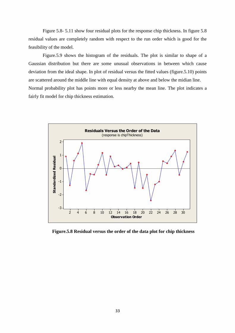
Figure 5.8- 5.11 show four residual plots for the response chip thickness. In figure 5.8
residual values are completely random with respect to the run order which is good for the
feasibility of the model.
Figure.5.9 shows the histogram of the residuals. The plot is similar to shape of a
Gaussian distribution but there are some unusual observations in between which cause
deviation from the ideal shape. In plot of residual versus the fitted values (figure.5.10) points
are scattered around the middle line with equal density at above and below the midian line.
Normal probability plot has points more or less nearby the mean line. The plot indicates a
fairly fit model for chip thickness estimation.
Figure.5.8 Residual versus the order of the data plot for chip thickness
Observation Order
Sta
nd
ard
ize
d R
esid
ua
l
30282624222018161412108642
2
1
0
-1
-2
-3
Residuals Versus the Order of the Data(response is chipThickness)

34
Figure.5.9 Residual histogram for chip thickness
Figure.5.10 Residual versus fitted value plot for chip thickness
Standardized Residual
Fre
qu
en
cy
210-1-2
7
6
5
4
3
2
1
0
Histogram of the Residuals(response is chipThickness)
Fitted Value
Sta
nd
ard
ize
d R
esid
ua
l
0.400.350.300.250.20
2
1
0
-1
-2
-3
Residuals Versus the Fitted Values(response is chipThickness)

35
Figure.5.11 Normal probability curve of the residuals for chip thickness
Interaction curves of chip thickness analysis are given in figure.5.12. V and wear has
good interaction so their interaction term is there in the equation of the response. Other
interactions are there for f &V or V & d. V has the maximum effect on the chip thickness
values so it is also having interation with other parameters.
Figure 5.13 is the main effects plot for chip thickness. It is clear by observing the
four effect plots that V and f are responsible for change in the value of chip thickness. In both
the plots chip thickness value is varying by almost .1 mm because of change in values of V
and f from 27 to 45 and .1 to .3 respectively
Tool flank wear does not have any significant effect on the thickness of the chip.
Even though its interaction with V changes the value of chip thickness. Response value
changes from .27 to approx. 3 because change in flank wear from 0 to 0.1.
Developed equation for chip thickness = .57567 – 1.50174*f - 00683*V + 4.82934*V*V +
0.00552*V*wear
Standardized Residual
Pe
rce
nt
3210-1-2-3
99
95
90
80
70
60
50
40
30
20
10
5
1
Normal Probability Plot of the Residuals(response is chipThickness)

36
Figure.5.12 Interaction plot of chip thickness
Figure.5.13 Main effacts plot of chip thickness
f
453527 1.00.50.0
0.4
0.3
0.2
0.4
0.3
0.2
V
d
0.4
0.3
0.2
0.30.20.1
0.4
0.3
0.2
0.30.20.1
Wear
f
0.3
0.1
0.2
V
45
27
35
d
0.3
0.1
0.2
Wear
1.0
0.0
0.5
Interaction plot of chip thicknessM
ea
n o
f ch
ipTh
ickn
ess
0.30.20.1
0.32
0.30
0.28
0.26
0.24
453527
0.30.20.1
0.32
0.30
0.28
0.26
0.24
1.00.50.0
f V
d Wear
Main effacts plot of chip thickness

37
CONCLUSION
In the experimental study the effect of parameters like feed, depth of cut, cutting
speed and tool flank wear on the length of chip and the chip thickness is studies. Main aim of
the study was to analyze the effect of tool flank wear on the response parameters.
By analyzing the result it was found that chip thickness increases with increasing feed
and decreasing cutting velocity. Thickness of chip first decreases and than increases with the
increase in both tool flank wear and depth of cut.
For average chip length speed of cutting is the most important factor which effects its
value. But at the same time tool wear also contributes significantly to its value. Length of
chip value is observed to increase first with increase in flank wear and than becomes almost
constant.
Thus we can conclude that tool flank wear along with other parameters is an
important parameters to control chip length.

38
REFERENCES

39
REFERENCES
[1] Kim J.D., Kweun O.B., A chip-breaking system for mild steel in turning, International
Journal of machine tools manufacture, vol.37, no.5, (1997), 607-617.
[2] Mesquita R.M.D, Soares F.A.M., Barata Marques M.J.M., An experimental study of the
effect of cutting speed on chip breaking, Journal of Materials Processing Technology, 56
(1996) 313-320.
[3] Hong-Gyoo Kim, Jae-Hyung Sim, Hyeog-Jun Kweon, Performance evaluation of chip
breaker utilizing neural network, Journal of materials processing technology 2 0 9 ( 2 0 0 9 )
647–656
[4] Das N.S., Chawla B.S., Biswas C.K., An analysis of strain in chip breaking using slip-line
field theory with adhesion friction at chip/tool interface, Journal of Materials Processing
Technology 170 (2005), 509–515
[5] Maity K.P., Das N.S., A slip-line solution to metal machining using a cutting tool with a
step-type chip-breaker, Journal of Materials Processing Technology, 79, ( 1998), 217-223
[6] J. P. Choi and S. J. Lee, Efficient Chip Breaker Design by Predicting the Chip Breaking
Performance. Department of Mechanical Engineering, Yonsei University, Seoul, Korea.
International Journal of Advance Manufacturing Technology (2001) 17:489–497
[7] Shi, T., Ramalingam, S., Slip-line solution for orthogonal cutting with a chip breaker and
flank wear, International Journal of Mechanical Sciences Volume 33, Issue 9, 1991, Pages
689-704
[8] Komanduri R., Schroeder T., Hazra J., Turkovich B.F. von, Flom D.G., On the
catastrophic shear instability in high-speed machining of an AISI 4340 steel, Journal of
Engineering for Industry,104, (1982) 121–131